KR102735067B1 - Display device and manufacturing method for the same - Google Patents
Display device and manufacturing method for the sameDownload PDFInfo
- Publication number
- KR102735067B1 KR102735067B1KR1020240118026AKR20240118026AKR102735067B1KR 102735067 B1KR102735067 B1KR 102735067B1KR 1020240118026 AKR1020240118026 AKR 1020240118026AKR 20240118026 AKR20240118026 AKR 20240118026AKR 102735067 B1KR102735067 B1KR 102735067B1
- Authority
- KR
- South Korea
- Prior art keywords
- panel
- pads
- dpd
- bonding layer
- display device
- Prior art date
- Legal status (The legal status is an assumption and is not a legal conclusion. Google has not performed a legal analysis and makes no representation as to the accuracy of the status listed.)
- Active
Links
Images


Classifications
- G—PHYSICS
- G02—OPTICS
- G02F—OPTICAL DEVICES OR ARRANGEMENTS FOR THE CONTROL OF LIGHT BY MODIFICATION OF THE OPTICAL PROPERTIES OF THE MEDIA OF THE ELEMENTS INVOLVED THEREIN; NON-LINEAR OPTICS; FREQUENCY-CHANGING OF LIGHT; OPTICAL LOGIC ELEMENTS; OPTICAL ANALOGUE/DIGITAL CONVERTERS
- G02F1/00—Devices or arrangements for the control of the intensity, colour, phase, polarisation or direction of light arriving from an independent light source, e.g. switching, gating or modulating; Non-linear optics
- G02F1/01—Devices or arrangements for the control of the intensity, colour, phase, polarisation or direction of light arriving from an independent light source, e.g. switching, gating or modulating; Non-linear optics for the control of the intensity, phase, polarisation or colour
- G02F1/13—Devices or arrangements for the control of the intensity, colour, phase, polarisation or direction of light arriving from an independent light source, e.g. switching, gating or modulating; Non-linear optics for the control of the intensity, phase, polarisation or colour based on liquid crystals, e.g. single liquid crystal display cells
- G02F1/133—Constructional arrangements; Operation of liquid crystal cells; Circuit arrangements
- G02F1/1333—Constructional arrangements; Manufacturing methods
- G02F1/1345—Conductors connecting electrodes to cell terminals
- G02F1/13452—Conductors connecting driver circuitry and terminals of panels
- G—PHYSICS
- G09—EDUCATION; CRYPTOGRAPHY; DISPLAY; ADVERTISING; SEALS
- G09F—DISPLAYING; ADVERTISING; SIGNS; LABELS OR NAME-PLATES; SEALS
- G09F9/00—Indicating arrangements for variable information in which the information is built-up on a support by selection or combination of individual elements
- G09F9/30—Indicating arrangements for variable information in which the information is built-up on a support by selection or combination of individual elements in which the desired character or characters are formed by combining individual elements
- G09F9/301—Indicating arrangements for variable information in which the information is built-up on a support by selection or combination of individual elements in which the desired character or characters are formed by combining individual elements flexible foldable or roll-able electronic displays, e.g. thin LCD, OLED
- G—PHYSICS
- G02—OPTICS
- G02F—OPTICAL DEVICES OR ARRANGEMENTS FOR THE CONTROL OF LIGHT BY MODIFICATION OF THE OPTICAL PROPERTIES OF THE MEDIA OF THE ELEMENTS INVOLVED THEREIN; NON-LINEAR OPTICS; FREQUENCY-CHANGING OF LIGHT; OPTICAL LOGIC ELEMENTS; OPTICAL ANALOGUE/DIGITAL CONVERTERS
- G02F1/00—Devices or arrangements for the control of the intensity, colour, phase, polarisation or direction of light arriving from an independent light source, e.g. switching, gating or modulating; Non-linear optics
- G02F1/01—Devices or arrangements for the control of the intensity, colour, phase, polarisation or direction of light arriving from an independent light source, e.g. switching, gating or modulating; Non-linear optics for the control of the intensity, phase, polarisation or colour
- G02F1/13—Devices or arrangements for the control of the intensity, colour, phase, polarisation or direction of light arriving from an independent light source, e.g. switching, gating or modulating; Non-linear optics for the control of the intensity, phase, polarisation or colour based on liquid crystals, e.g. single liquid crystal display cells
- G02F1/133—Constructional arrangements; Operation of liquid crystal cells; Circuit arrangements
- G02F1/1333—Constructional arrangements; Manufacturing methods
- G02F1/1343—Electrodes
- G02F1/13439—Electrodes characterised by their electrical, optical, physical properties; materials therefor; method of making
- G—PHYSICS
- G02—OPTICS
- G02F—OPTICAL DEVICES OR ARRANGEMENTS FOR THE CONTROL OF LIGHT BY MODIFICATION OF THE OPTICAL PROPERTIES OF THE MEDIA OF THE ELEMENTS INVOLVED THEREIN; NON-LINEAR OPTICS; FREQUENCY-CHANGING OF LIGHT; OPTICAL LOGIC ELEMENTS; OPTICAL ANALOGUE/DIGITAL CONVERTERS
- G02F1/00—Devices or arrangements for the control of the intensity, colour, phase, polarisation or direction of light arriving from an independent light source, e.g. switching, gating or modulating; Non-linear optics
- G02F1/01—Devices or arrangements for the control of the intensity, colour, phase, polarisation or direction of light arriving from an independent light source, e.g. switching, gating or modulating; Non-linear optics for the control of the intensity, phase, polarisation or colour
- G02F1/13—Devices or arrangements for the control of the intensity, colour, phase, polarisation or direction of light arriving from an independent light source, e.g. switching, gating or modulating; Non-linear optics for the control of the intensity, phase, polarisation or colour based on liquid crystals, e.g. single liquid crystal display cells
- G02F1/133—Constructional arrangements; Operation of liquid crystal cells; Circuit arrangements
- G02F1/1333—Constructional arrangements; Manufacturing methods
- G02F1/1345—Conductors connecting electrodes to cell terminals
- G02F1/13458—Terminal pads
- H—ELECTRICITY
- H05—ELECTRIC TECHNIQUES NOT OTHERWISE PROVIDED FOR
- H05K—PRINTED CIRCUITS; CASINGS OR CONSTRUCTIONAL DETAILS OF ELECTRIC APPARATUS; MANUFACTURE OF ASSEMBLAGES OF ELECTRICAL COMPONENTS
- H05K1/00—Printed circuits
- H05K1/02—Details
- H05K1/0277—Bendability or stretchability details
- H05K1/028—Bending or folding regions of flexible printed circuits
- H—ELECTRICITY
- H05—ELECTRIC TECHNIQUES NOT OTHERWISE PROVIDED FOR
- H05K—PRINTED CIRCUITS; CASINGS OR CONSTRUCTIONAL DETAILS OF ELECTRIC APPARATUS; MANUFACTURE OF ASSEMBLAGES OF ELECTRICAL COMPONENTS
- H05K1/00—Printed circuits
- H05K1/02—Details
- H05K1/11—Printed elements for providing electric connections to or between printed circuits
- H05K1/111—Pads for surface mounting, e.g. lay-out
- H—ELECTRICITY
- H05—ELECTRIC TECHNIQUES NOT OTHERWISE PROVIDED FOR
- H05K—PRINTED CIRCUITS; CASINGS OR CONSTRUCTIONAL DETAILS OF ELECTRIC APPARATUS; MANUFACTURE OF ASSEMBLAGES OF ELECTRICAL COMPONENTS
- H05K1/00—Printed circuits
- H05K1/02—Details
- H05K1/11—Printed elements for providing electric connections to or between printed circuits
- H05K1/115—Via connections; Lands around holes or via connections
- H05K1/116—Lands, clearance holes or other lay-out details concerning the surrounding of a via
- H—ELECTRICITY
- H05—ELECTRIC TECHNIQUES NOT OTHERWISE PROVIDED FOR
- H05K—PRINTED CIRCUITS; CASINGS OR CONSTRUCTIONAL DETAILS OF ELECTRIC APPARATUS; MANUFACTURE OF ASSEMBLAGES OF ELECTRICAL COMPONENTS
- H05K1/00—Printed circuits
- H05K1/02—Details
- H05K1/14—Structural association of two or more printed circuits
- H05K1/147—Structural association of two or more printed circuits at least one of the printed circuits being bent or folded, e.g. by using a flexible printed circuit
- H—ELECTRICITY
- H05—ELECTRIC TECHNIQUES NOT OTHERWISE PROVIDED FOR
- H05K—PRINTED CIRCUITS; CASINGS OR CONSTRUCTIONAL DETAILS OF ELECTRIC APPARATUS; MANUFACTURE OF ASSEMBLAGES OF ELECTRICAL COMPONENTS
- H05K3/00—Apparatus or processes for manufacturing printed circuits
- H05K3/30—Assembling printed circuits with electric components, e.g. with resistor
- H05K3/32—Assembling printed circuits with electric components, e.g. with resistor electrically connecting electric components or wires to printed circuits
- H05K3/321—Assembling printed circuits with electric components, e.g. with resistor electrically connecting electric components or wires to printed circuits by conductive adhesives
- H05K3/323—Assembling printed circuits with electric components, e.g. with resistor electrically connecting electric components or wires to printed circuits by conductive adhesives by applying an anisotropic conductive adhesive layer over an array of pads
- H—ELECTRICITY
- H05—ELECTRIC TECHNIQUES NOT OTHERWISE PROVIDED FOR
- H05K—PRINTED CIRCUITS; CASINGS OR CONSTRUCTIONAL DETAILS OF ELECTRIC APPARATUS; MANUFACTURE OF ASSEMBLAGES OF ELECTRICAL COMPONENTS
- H05K1/00—Printed circuits
- H05K1/18—Printed circuits structurally associated with non-printed electric components
- H05K1/189—Printed circuits structurally associated with non-printed electric components characterised by the use of a flexible or folded printed circuit
- H—ELECTRICITY
- H05—ELECTRIC TECHNIQUES NOT OTHERWISE PROVIDED FOR
- H05K—PRINTED CIRCUITS; CASINGS OR CONSTRUCTIONAL DETAILS OF ELECTRIC APPARATUS; MANUFACTURE OF ASSEMBLAGES OF ELECTRICAL COMPONENTS
- H05K2201/00—Indexing scheme relating to printed circuits covered by H05K1/00
- H05K2201/05—Flexible printed circuits [FPCs]
- H—ELECTRICITY
- H05—ELECTRIC TECHNIQUES NOT OTHERWISE PROVIDED FOR
- H05K—PRINTED CIRCUITS; CASINGS OR CONSTRUCTIONAL DETAILS OF ELECTRIC APPARATUS; MANUFACTURE OF ASSEMBLAGES OF ELECTRICAL COMPONENTS
- H05K2201/00—Indexing scheme relating to printed circuits covered by H05K1/00
- H05K2201/10—Details of components or other objects attached to or integrated in a printed circuit board
- H05K2201/10007—Types of components
- H05K2201/10128—Display
- H—ELECTRICITY
- H05—ELECTRIC TECHNIQUES NOT OTHERWISE PROVIDED FOR
- H05K—PRINTED CIRCUITS; CASINGS OR CONSTRUCTIONAL DETAILS OF ELECTRIC APPARATUS; MANUFACTURE OF ASSEMBLAGES OF ELECTRICAL COMPONENTS
- H05K2201/00—Indexing scheme relating to printed circuits covered by H05K1/00
- H05K2201/10—Details of components or other objects attached to or integrated in a printed circuit board
- H05K2201/10007—Types of components
- H05K2201/10151—Sensor
Landscapes
- Physics & Mathematics (AREA)
- Engineering & Computer Science (AREA)
- Nonlinear Science (AREA)
- Microelectronics & Electronic Packaging (AREA)
- General Physics & Mathematics (AREA)
- Mathematical Physics (AREA)
- Chemical & Material Sciences (AREA)
- Crystallography & Structural Chemistry (AREA)
- Optics & Photonics (AREA)
- Manufacturing & Machinery (AREA)
- Theoretical Computer Science (AREA)
- Devices For Indicating Variable Information By Combining Individual Elements (AREA)
Abstract
Translated fromKorean
Description
Translated fromKorean본 발명은 표시 장치 및 표시 장치의 제조 방법에 대한 것으로, 보다 상세하게는 표시 패널과 회로 기판을 결합시키고 도전입자를 갖는 접합층을 포함한 표시 장치 및 그 제조 방법에 관한 것이다.The present invention relates to a display device and a method for manufacturing the display device, and more particularly, to a display device including a bonding layer that combines a display panel and a circuit board and has conductive particles, and a method for manufacturing the same.
표시 장치 등의 전자 장치는 복수의 회로 배선들 및 이들에 연결된 복수의 전자 소자들을 포함하고, 전기적 신호를 인가 받아 동작한다. 이러한 복수의 회로 배선들과 전자 소자들을 전기적으로 연결시키기 위하여 도전성 접합 부재가 사용되고 있다. 예를 들어, 이방성 도전 필름(ACF, Anisotropic Conductive Film) 등이 표시 장치의 표시 패널과 회로 기판 등을 전기적으로 접속하기 위하여 사용되고 있다.Electronic devices such as display devices include a plurality of circuit wires and a plurality of electronic elements connected to them, and operate by receiving electrical signals. Conductive bonding materials are used to electrically connect these plurality of circuit wires and electronic elements. For example, anisotropic conductive films (ACFs) are used to electrically connect display panels and circuit boards of display devices.
한편, 표시 장치에서 고해상도가 요구되면서 고정세의 회로 배선들과 접합시키기 위한 접합 부재를 필요로 하고 있다.Meanwhile, as high resolution is required in display devices, bonding materials are needed to bond high-definition circuit wires.
본 발명의 목적은 접합층에 포함된 도전입자의 배열을 제어하여 개선된 신뢰성을 갖는 표시 장치를 제공하는 것이다.An object of the present invention is to provide a display device having improved reliability by controlling the arrangement of conductive particles included in a bonding layer.
또한, 본 발명의 목적은 패드들과 중첩되는 부분과 중첩되지 않는 부분에서 다른 배열 특성을 갖는 도전입자를 갖는 접합층을 형성하는 단계를 포함하여 개선된 신뢰성을 갖는 표시 장치의 제조 방법을 제공하는 것이다.Furthermore, it is an object of the present invention to provide a method for manufacturing a display device having improved reliability, including a step of forming a bonding layer having conductive particles having different arrangement characteristics in a portion overlapping with pads and a portion not overlapping with pads.
일 실시예는 복수 개의 패널패드들을 포함하는 표시 패널; 상기 패널패드들에 대응하는 복수 개의 접속패드들을 포함하는 연성회로기판; 및 상기 표시 패널과 상기 연성회로기판 사이에 배치되고, 복수 개의 도전입자들을 포함한 접합층; 을 포함하고, 상기 접합층은 서로 대응하는 상기 패널패드들 및 상기 접속패드들과 중첩하는 중첩부; 및 상기 패널패드들 및 상기 접속패드들과 비중첩하는 비중첩부; 를 포함하며, 상기 비중첩부에서, 상기 도전입자들은 서로 이웃하는 패널패드들 중 하나의 패널패드의 일 측에 인접하여 배치된 표시 장치를 제공한다.One embodiment provides a display device including a display panel including a plurality of panel pads; a flexible circuit board including a plurality of connection pads corresponding to the panel pads; and a bonding layer disposed between the display panel and the flexible circuit board and including a plurality of conductive particles, wherein the bonding layer includes an overlapping portion overlapping the panel pads and the connection pads corresponding to each other; and a non-overlapping portion non-overlapping the panel pads and the connection pads; wherein in the non-overlapping portion, the conductive particles are disposed adjacent to one side of one of the panel pads adjacent to each other.
상기 비중첩부에서, 상기 도전입자들은 상기 하나의 패널패드의 일 측에 전기적으로 접촉할 수 있다.In the above non-overlapping portion, the challenge particles can make electrical contact with one side of the one panel pad.
상기 비중첩부에서, 상기 도전입자들은 상기 이웃하는 패널패드들 중 다른 하나의 패널패드와 절연된 것일 수 있다.In the above non-overlapping portion, the challenge particles may be insulated from another panel pad among the neighboring panel pads.
상기 복수 개의 패널패드들은 서로 이웃하여 정렬된 제1 패널패드 및 제2 패널패드를 포함하고, 상기 비중첩부는 상기 제1 패널패드 및 상기 제2 패널패드와 비중첩하며, 상기 비중첩부에 포함된 상기 복수 개의 도전입자들은 상기 제1 패널패드의 제1 측면에서 이격되고, 상기 제1 측면과 인접한 상기 제2 패널패드의 제2 측면에 인접하여 배치될 수 있다.The plurality of panel pads may include a first panel pad and a second panel pad that are aligned adjacent to each other, the non-overlapping portion may non-overlap with the first panel pad and the second panel pad, and the plurality of conductive particles included in the non-overlapping portion may be spaced apart from a first side of the first panel pad and arranged adjacent to a second side of the second panel pad that is adjacent to the first side.
상기 비중첩부에서, 상기 도전입자들은 상기 제1 측면 및 상기 제2 측면으로부터 동일한 거리에 있는 가상의 중심선을 기준으로 상기 제2 측면에 보다 인접하여 배치될 수 있다.In the above non-overlapping portion, the challenge particles can be arranged closer to the second side with respect to a virtual center line that is the same distance from the first side and the second side.
상기 중첩부에서, 상기 도전입자들은 랜덤하게 배열될 수 있다.In the above overlapping portion, the challenge particles can be arranged randomly.
상기 표시 패널과 나란한 평면 상에서, 상기 중첩부에 배치된 상기 도전입자들은 서로 비접촉할 수 있다.On a plane parallel to the above display panel, the conductive particles arranged in the overlapping portion can be in non-contact with each other.
상기 표시 패널과 나란한 평면 상에서, 상기 하나의 패널패드의 일 측에 인접하여 배치된 상기 도전입자들은 하나의 열로 정렬되어 배치될 수 있다.On a plane parallel to the display panel, the conductive particles arranged adjacent to one side of the one panel pad can be arranged in a row.
상기 접합층은 수지부를 더 포함하고, 상기 수지부는 상기 패널패드들과 상기 접속패드들 사이를 충전할 수 있다.The above bonding layer further includes a resin portion, and the resin portion can fill a space between the panel pads and the connection pads.
상기 중첩부는 상기 패널패드와 상기 접속패드 사이에서 하나의 층으로 배치된 상기 도전입자들을 포함할 수 있다.The above-mentioned overlapping portion may include the above-mentioned conductive particles arranged in a single layer between the above-mentioned panel pad and the above-mentioned connection pad.
상기 중첩부에 포함된 상기 도전입자들은 두께 방향으로 비중첩할 수 있다.The above challenging particles included in the above overlapping portion may be non-overlapping in the thickness direction.
상기 표시 패널 상에 배치되고, 복수 개의 감지패드들을 포함하는 입력감지부; 상기 감지패드들과 대응하는 감지 접속패드들을 포함하는 감지 연성회로기판; 및 상기 입력감지부 및 상기 감지 연성회로기판 사이에 배치되고 복수 개의 도전입자들을 포함하는 감지 접합층; 을 더 포함하고, 상기 감지 접합층은 서로 대응하는 상기 감지패드들 및 상기 감지 접속패드들과 중첩하는 감지 중첩부; 및 상기 감지패드들 및 상기 감지 접속패드들과 비중첩하는 감지 비중첩부; 를 포함하며, 상기 감지 비중첩부에서, 상기 도전입자들은 서로 이웃하는 감지패드들 중 하나의 감지패드의 일 측에 인접하여 배치될 수 있다.The present invention further comprises: an input sensing unit disposed on the display panel and including a plurality of sensing pads; a sensing flexible circuit board including sensing connection pads corresponding to the sensing pads; and a sensing bonding layer disposed between the input sensing unit and the sensing flexible circuit board and including a plurality of conductive particles; wherein the sensing bonding layer includes a sensing overlapping portion overlapping the sensing pads and the sensing connection pads corresponding to each other; and a sensing non-overlapping portion non-overlapping with the sensing pads and the sensing connection pads; wherein, in the sensing non-overlapping portion, the conductive particles can be disposed adjacent to one side of one of the sensing pads adjacent to each other.
일 실시예는 n 개의 패널패드들을 포함하는 표시 패널; 상기 n 개의 패널패드들에 대응하는 n 개의 접속패드들을 포함하는 연성회로기판; 및 상기 표시 패널과 상기 연성회로기판 사이에 배치되고, 복수 개의 도전입자들을 포함한 접합층; 을 포함하고, 상기 접합층은 서로 대응하는 상기 패널패드들 및 상기 접속패드들과 중첩하는 복수 개의 중첩부들; 및 상기 패널패드들 및 상기 접속패드들과 비중첩하고, 상기 중첩부들 사이에 배치된 비중첩부들; 을 포함하고, 상기 비중첩부들에서 상기 도전입자들은 상기 패널패드들 중 m번 째 패널패드의 일 측면에 인접하여 배치되고 상기 m번 째 패널패드의 타 측면으로부터 이격되어 배치된 표시 장치를 제공할 수 있다. 일 실시예에서, 상기 n은 2 이상의 정수이고, 상기 m은 1 이상 n 이하의 정수이다.One embodiment may provide a display device including a display panel including n panel pads; a flexible circuit board including n connection pads corresponding to the n panel pads; and a bonding layer disposed between the display panel and the flexible circuit board and including a plurality of conductive particles; wherein the bonding layer includes a plurality of overlapping portions overlapping the panel pads and the connection pads corresponding to each other; and non-overlapping portions disposed between the overlapping portions and non-overlapping with the panel pads and the connection pads; wherein in the non-overlapping portions, the conductive particles are disposed adjacent to one side of an m-th panel pad among the panel pads and spaced apart from the other side of the m-th panel pad. In one embodiment, n is an integer greater than or equal to 2, and m is an integer greater than or equal to 1 and less than or equal to n.
상기 패널패드들 중 (m-1)번 째 패널패드 및 상기 m번 째 패널패드와 각각 중첩하는 상기 중첩부들 사이에 배치된 상기 비중첩부에 포함된 상기 도전입자들은 상기 (m-1)번 째 패널패드에서 이격되고, 상기 m 번 째 패널패드에 인접하여 배치될 수 있다.The conductive particles included in the non-overlapping portions arranged between the overlapping portions that overlap the (m-1)th panel pad and the mth panel pad among the above panel pads may be arranged spaced apart from the (m-1)th panel pad and adjacent to the mth panel pad.
상기 m번 째 패널패드의 상기 일 측면에 인접한 상기 도전입자들은 상기 일 측면에서 상기 m번 째 패널패드와 전기적으로 접촉할 수 있다.The conductive particles adjacent to the one side of the mth panel pad can make electrical contact with the mth panel pad at the one side.
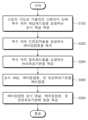
다른 실시예는 소정의 각도로 기울어진 스테이지 상에 복수 개의 패널패드들을 포함하는 표시 패널을 제공하는 단계; 상기 패널패드들 상에 복수 개의 도전입자들을 포함하는 예비접합층을 배치하는 단계; 상기 에비접합층 상에 복수 개의 접속패드들을 포함하는 연성회로기판을 제공하는 단계; 가압하여, 순차적으로 제공된 상기 표시 패널, 상기 예비접합층, 및 상기 연성회로기판을 예비접합하는 단계; 및 예비접합된 상기 표시 패널, 상기 예비접합층, 및 상기 연성회로기판에 열을 제공하는 단계; 를 포함하는 표시 장치 제조 방법을 제공한다.Another embodiment provides a method for manufacturing a display device, comprising: providing a display panel including a plurality of panel pads on a stage inclined at a predetermined angle; arranging a pre-bonding layer including a plurality of conductive particles on the panel pads; providing a flexible circuit board including a plurality of connection pads on the pre-bonding layer; applying pressure to sequentially pre-bond the provided display panel, the pre-bonding layer, and the flexible circuit board; and providing heat to the pre-bonded display panel, the pre-bonding layer, and the flexible circuit board.
상기 예비접합층은 상기 패널패드들 및 상기 접속패드들과 중첩하는 중첩부 및 상기 패널패드들 및 상기 접속패드들과 비중첩하는 비중첩부를 포함하고, 상기 예비접합하는 단계에서, 상기 중첩부에 배치된 복수 개의 도전입자들은 마주하는 상기 패널패드들 및 상기 접속패드들에 전기적으로 접촉할 수 있다.The above-described pre-bonding layer includes an overlapping portion that overlaps the panel pads and the connection pads and a non-overlapping portion that does not overlap the panel pads and the connection pads, and in the step of pre-bonding, a plurality of conductive particles arranged in the overlapping portion can make electrical contact with the facing panel pads and the connection pads.
상기 열을 제공하는 단계는 상기 비중첩부에 포함된 상기 도전입자들이 이웃하는 패널패드들 중 상대적으로 하측에 배치된 패널패드 측으로 이동하는 단계를 포함할 수 있다.The step of providing the above heat may include a step of moving the challenging particles included in the non-overlapping portion toward a panel pad positioned relatively lower among the neighboring panel pads.
상기 소정의 각도는 0도 초과 90도 이하일 수 있다.The above-mentioned predetermined angle may be greater than 0 degrees and less than or equal to 90 degrees.
상기 예비접합층은 상기 도전입자들 사이를 충전하는 수지부를 포함하고, 상기 열을 제공하는 단계는 상기 수지부의 점도를 감소시키는 유동 단계; 및 상기 유동 단계 이후에 상기 수지부 및 상기 도전입자를 고정시켜 상기 예비접합층을 접합층으로 변환시키는 경화 단계; 를 포함할 수 있다.The above pre-bonding layer may include a resin portion that fills between the conductive particles, and the step of providing heat may include a fluidizing step that reduces the viscosity of the resin portion; and a curing step that fixes the resin portion and the conductive particles after the fluidizing step to convert the pre-bonding layer into a bonding layer.
일 실시예의 표시 장치는 패드와 비중첩하는 영역에 배치된 도전입자들이 패드의 일 측에 정렬되어 배열된 접합층을 포함하여 개선된 신뢰성 특성을 나타낼 수 있다.A display device of one embodiment may exhibit improved reliability characteristics by including a bonding layer in which conductive particles are arranged in a non-overlapping region with the pad and aligned on one side of the pad.
일 실시예의 표시 장치 제조 방법은 표시 패널과 회로 기판 사이에 제공되는 접합층에서 도전입자의 이동을 제어하는 공정을 포함하여 고해상도에서도 우수한 신뢰성을 갖는 표시 장치를 제공할 수 있다.A method for manufacturing a display device of one embodiment can provide a display device having excellent reliability even at a high resolution, including a process for controlling movement of conductive particles in a bonding layer provided between a display panel and a circuit board.
도 1은 일 실시예의 표시 장치의 사시도이다.
도 2는 일 실시예의 표시 장치의 분해 사시도이다.
도 3은 일 실시예에 따른 표시 장치 일부의 평면도이다.
도 4는 일 실시예의 표시 장치의 일 부분을 나타낸 분해 사시도이다.
도 5는 일 실시예의 표시 장치의 일 부분을 나타낸 단면도이다.
도 6은 일 실시예의 표시 장치의 일 부분을 나타낸 단면도이다.
도 7a는 일 실시예에 따른 표시 장치의 일부를 나타낸 평면도이다.
도 7b는 일 실시예에 따른 표시 장치의 일부를 나타낸 평면도이다.
도 7c는 일 실시예에 따른 도전입자의 배열을 예시적으로 나타낸 평면도이다.
도 8은 일 실시예에 따른 표시 장치의 일부를 나타낸 평면도이다
도 9는 일 실시예에 따른 표시 장치의 일 부분을 나타낸 단면도이다.
도 10은 일 실시예의 표시 장치의 제조 방법을 나타낸 순서도이다.
도 11은 일 실시예의 표시 장치의 제조 방법의 일부를 나타낸 순서도이다.
도 12는 일 실시예의 표시 장치 제조 방법의 일 단계를 개략적으로 나타낸 도면이다.
도 13은 일 실시예의 표시 장치 제조 방법의 일 단계를 개략적으로 나타낸 도면이다.
도 14는 일 실시예의 표시 장치 제조 방법의 일 단계를 개략적으로 나타낸 도면이다.Figure 1 is a perspective view of a display device of one embodiment.
Figure 2 is an exploded perspective view of a display device of one embodiment.
FIG. 3 is a plan view of a portion of a display device according to one embodiment.
Figure 4 is an exploded perspective view showing a part of a display device of one embodiment.
Figure 5 is a cross-sectional view showing a portion of a display device of one embodiment.
Fig. 6 is a cross-sectional view showing a portion of a display device of one embodiment.
FIG. 7a is a plan view illustrating a portion of a display device according to one embodiment.
FIG. 7b is a plan view illustrating a portion of a display device according to one embodiment.
FIG. 7c is a plan view exemplarily showing an arrangement of challenge particles according to one embodiment.
FIG. 8 is a plan view showing a portion of a display device according to one embodiment.
FIG. 9 is a cross-sectional view showing a portion of a display device according to one embodiment.
Figure 10 is a flowchart showing a method for manufacturing a display device according to one embodiment.
Fig. 11 is a flowchart showing part of a method for manufacturing a display device according to one embodiment.
Figure 12 is a drawing schematically illustrating one step of a method for manufacturing a display device according to one embodiment.
Figure 13 is a drawing schematically illustrating one step of a method for manufacturing a display device according to one embodiment.
Figure 14 is a drawing schematically illustrating one step of a method for manufacturing a display device according to one embodiment.
본 발명은 다양한 변경을 가할 수 있고 여러 가지 형태를 가질 수 있는 바, 특정 실시예들을 도면에 예시하고 본문에 상세하게 설명하고자 한다. 그러나, 이는 본 발명을 특정한 개시 형태에 대해 한정하려는 것이 아니며, 본 발명의 사상 및 기술 범위에 포함되는 모든 변경, 균등물 내지 대체물을 포함하는 것으로 이해되어야 한다.The present invention can be modified in various ways and can take various forms, and specific embodiments are illustrated in the drawings and described in detail in the text. However, this is not intended to limit the present invention to specific disclosed forms, but should be understood to include all modifications, equivalents, or substitutes included in the spirit and technical scope of the present invention.
본 명세서에서, 어떤 구성요소(또는 영역, 층, 부분 등)가 다른 구성요소 "상에 있다", "연결 된다", 또는 "결합된다"고 언급되는 경우에 그것은 다른 구성요소 상에 직접 배치/연결/결합될 수 있거나 또는 그들 사이에 제3의 구성요소가 배치될 수도 있다는 것을 의미한다.In this specification, when a component (or region, layer, portion, etc.) is referred to as being “on,” “connected to,” or “coupled to” another component, it means that it can be directly disposed/connected/coupled to the other component, or that a third component may be disposed between them.
한편, 본 출원에서 "직접 배치"된다는 것은 층, 막, 영역, 판 등의 부분과 다른 부분 사이에 추가되는 층, 막, 영역, 판 등이 없는 것을 의미하는 것일 수 있다. 예를 들어, "직접 배치"된다는 것은 두 개의 층 또는 두 개의 부재들 사이에 접착 부재 등의 추가 부재를 사용하지 않고 배치하는 것을 의미하는 것일 수 있다.Meanwhile, in the present application, "directly disposed" may mean that there is no additional layer, film, region, plate, etc. between a part such as a layer, film, region, plate, etc. and another part. For example, "directly disposed" may mean disposed without using an additional member such as an adhesive member between two layers or two members.
동일한 도면부호는 동일한 구성요소를 지칭한다. 또한, 도면들에 있어서, 구성요소들의 두께, 비율, 및 치수는 기술적 내용의 효과적인 설명을 위해 과장된 것이다.Identical drawing symbols refer to identical components. Also, in the drawings, the thicknesses, proportions, and dimensions of components are exaggerated for the purpose of effectively explaining the technical contents.
"및/또는"은 연관된 구성들이 정의할 수 있는 하나 이상의 조합을 모두 포함한다.“And/or” includes any combination of one or more of the associated constructs that can be defined.
제1, 제2 등의 용어는 다양한 구성요소들을 설명하는데 사용될 수 있지만, 상기 구성요소들은 상기 용어들에 의해 한정되어서는 안 된다. 상기 용어들은 하나의 구성요소를 다른 구성요소로부터 구별하는 목적으로만 사용된다. 예를 들어, 본 발명의 권리 범위를 벗어나지 않으면서 제1 구성요소는 제2 구성요소로 명명될 수 있고, 유사하게 제2 구성요소도 제1 구성요소로 명명될 수 있다. 단수의 표현은 문맥상 명백하게 다르게 뜻하지 않는 한, 복수의 표현을 포함한다.The terms first, second, etc. may be used to describe various components, but the components should not be limited by the terms. The terms are only used to distinguish one component from another. For example, without departing from the scope of the present invention, the first component may be referred to as the second component, and similarly, the second component may also be referred to as the first component. The singular expression includes the plural expression unless the context clearly indicates otherwise.
또한, "아래에", "하측에", "위에", "상측에" 등의 용어는 도면에 도시된 구성들의 연관관계를 설명하기 위해 사용된다. 상기 용어들은 상대적인 개념으로, 도면에 표시된 방향을 기준으로 설명된다. 본 명세서에서 "상에 배치되는" 것은 어느 하나의 부재의 상부뿐 아니라 하부에 배치되는 경우도 나타내는 것일 수 있다.In addition, terms such as "below," "underneath," "above," and "upper," are used to describe the relationships between components depicted in the drawings. The above terms are relative concepts and are described based on the directions indicated in the drawings. In this specification, "placed on" may refer to being placed below as well as above a certain member.
다르게 정의되지 않는 한, 본 명세서에서 사용된 모든 용어 (기술 용어 및 과학 용어 포함)는 본 발명이 속하는 기술 분야의 당업자에 의해 일반적으로 이해되는 것과 동일한 의미를 갖는다. 또한, 일반적으로 사용되는 사전에서 정의된 용어와 같은 용어는 관련 기술의 맥락에서 의미와 일치하는 의미를 갖는 것으로 해석되어야 하고, 이상적인 또는 지나치게 형식적인 의미로 해석되지 않는 한, 명시적으로 여기에서 정의된 것으로 해석된다.Unless otherwise defined, all terms (including technical and scientific terms) used herein have the same meaning as commonly understood by one of ordinary skill in the art to which this invention belongs. In addition, terms that are defined in commonly used dictionaries, such as terms, should be interpreted as having a meaning consistent with the meaning in the context of the relevant art, and unless interpreted in an idealized or overly formal sense, they are interpreted as being explicitly defined herein.
"포함하다" 또는 "가지다" 등의 용어는 명세서 상에 기재된 특징, 숫자, 단계, 동작, 구성요소, 부품 또는 이들을 조합한 것이 존재함을 지정하려는 것이지, 하나 또는 그 이상의 다른 특징들이나 숫자, 단계, 동작, 구성요소, 부분품 또는 이들을 조합한 것들의 존재 또는 부가 가능성을 미리 배제하지 않는 것으로 이해되어야 한다.It should be understood that the terms "include" or "have" are intended to specify the presence of a feature, number, step, operation, component, part, or combination thereof described in the specification, but do not exclude in advance the possibility of the presence or addition of one or more other features, numbers, steps, operations, components, parts, or combinations thereof.
이하, 도면들을 참조하여 본 발명의 일 실시예에 따른 표시 장치 및 일 실시예의 표시 장치 제조 방법에 대하여 설명한다.Hereinafter, a display device according to one embodiment of the present invention and a method for manufacturing the display device according to one embodiment will be described with reference to the drawings.
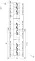
도 1은 일 실시예에 따른 표시 장치의 사시도이다. 도 2는 일 실시예의 표시 장치의 분해 사시도이다. 도 3은 일 실시예에 따른 표시 장치의 일부에 대한 평면도이다. 도 4는 일 실시예의 표시 장치의 일 부분에 대한 분해 사시도이다.FIG. 1 is a perspective view of a display device according to one embodiment. FIG. 2 is an exploded perspective view of a display device according to one embodiment. FIG. 3 is a plan view of a portion of a display device according to one embodiment. FIG. 4 is an exploded perspective view of a portion of a display device according to one embodiment.
표시 장치(DD)는 전기적 신호에 따라 활성화되는 장치일 수 있다. 표시 장치(DD)는 다양한 실시예들을 포함할 수 있다. 예를 들어, 표시 장치(DD)는 퍼스널 컴퓨터, 노트북 컴퓨터, 개인 디지털 단말기, 자동차 내비게이션 유닛, 게임기, 스마트폰, 태블릿, 또는 카메라 등일 수 있다. 또한, 이것들은 단지 실시예로서 제시된 것들로서, 본 발명의 개념에서 벗어나지 않은 이상 다른 표시 장치로도 채용될 수 있다. 본 실시예에서, 표시 장치(DD)는 스마트 폰으로 예시적으로 도시되었다.The display device (DD) may be a device activated by an electrical signal. The display device (DD) may include various embodiments. For example, the display device (DD) may be a personal computer, a notebook computer, a personal digital terminal, a car navigation unit, a game machine, a smart phone, a tablet, or a camera. In addition, these are presented only as examples, and other display devices may be employed without departing from the concept of the present invention. In the present embodiment, the display device (DD) is illustrated as a smart phone as an example.
한편, 도 1 및 이하 도면들에서는 제1 방향축(DR1) 내지 제3 방향축(DR3)을 도시하였으며, 본 명세서에서 설명되는 제1 내지 제3 방향축들(DR1, DR2, DR3)이 지시하는 방향은 상대적인 개념으로서 다른 방향으로 변환될 수 있다.Meanwhile, in FIG. 1 and the drawings below, the first direction axis (DR1) to the third direction axis (DR3) are illustrated, and the directions indicated by the first to third direction axes (DR1, DR2, DR3) described in this specification are relative concepts and can be converted into other directions.
본 명세서에서는 설명의 편의를 위하여 제3 방향축(DR3) 방향은 사용자에게 이미지가 제공되는 방향으로 정의된다. 또한, 제1 방향축(DR1)과 제2 방향축(DR2)은 서로 직교하고, 제3 방향축(DR3)은 제1 방향축(DR1)과 제2 방향축(DR2)이 정의하는 평면에 대한 법선 방향일 수 있다.In this specification, for convenience of explanation, the third direction axis (DR3) is defined as the direction in which an image is provided to a user. In addition, the first direction axis (DR1) and the second direction axis (DR2) are orthogonal to each other, and the third direction axis (DR3) may be a normal direction to a plane defined by the first direction axis (DR1) and the second direction axis (DR2).
일 실시예의 표시 장치(DD)는 표시 패널(DP), 연성회로기판(FB-DP)을 포함하는 패널 구동부(DP-M), 및 접합층(AP)을 포함할 수 있다. 일 실시예의 표시 장치(DD)는 복수 개의 패널패드들(DPD)을 포함하는 표시 패널(DP), 패널패드들(DPD)에 대응하는 복수 개의 접속패드들(CPD)을 포함하는 연성회로기판(FB-DP), 표시 패널(DP)과 연성회로기판(FB-DP) 사이에 배치된 접합층(AP)을 포함할 수 있다. 또한, 일 실시예의 표시 장치(DD)는 입력감지부(ISU) 및 감지 구동부(TP-M)를 더 포함할 수 있다. 일 실시예의 표시 장치(DD)는 윈도우(WP) 및 하우징(HAU)을 포함하고, 윈도우(WP)와 하우징(HAU)은 결합되어 표시 장치(DD)의 외관을 구성할 수 있다.A display device (DD) of one embodiment may include a display panel (DP), a panel driver (DP-M) including a flexible printed circuit board (FB-DP), and a bonding layer (AP). The display device (DD) of one embodiment may include a display panel (DP) including a plurality of panel pads (DPD), a flexible printed circuit board (FB-DP) including a plurality of connection pads (CPD) corresponding to the panel pads (DPD), and a bonding layer (AP) disposed between the display panel (DP) and the flexible printed circuit board (FB-DP). In addition, the display device (DD) of one embodiment may further include an input detection unit (ISU) and a detection driver unit (TP-M). The display device (DD) of one embodiment may include a window (WP) and a housing (HAU), and the window (WP) and the housing (HAU) may be combined to form an appearance of the display device (DD).
도면에 도시된 바와 달리 일 실시예의 표시 장치(DD)에서 입력감지부(ISU) 및 감지 구동부(TP-M)는 생략될 수 있다. 또한, 도시된 바와 달리 입력감지부(ISU)는 표시 패널(DP) 상에 직접 배치되어 표시 패널(DP)과 일체로 제공될 수 있다.Unlike as shown in the drawing, the input detection unit (ISU) and the detection driving unit (TP-M) may be omitted in the display device (DD) of one embodiment. In addition, unlike as shown, the input detection unit (ISU) may be directly disposed on the display panel (DP) and provided as an integral part with the display panel (DP).
일 실시예에서 표시 장치(DD)는 제1 방향축(DR1) 및 제2 방향축(DR2)으로 정의되는 평면과 평행한 표시면(FS)에 제3 방향축(DR3) 방향을 향해 이미지(IM)를 표시할 수 있다. 이미지(IM)가 표시되는 표시면(FS)은 표시 장치(DD)의 전면(front surface)과 대응될 수 있으며, 윈도우(WP)의 전면(FS)과 대응될 수 있다. 이하, 표시 장치(DD)의 표시면, 전면, 및 윈도우(WP)의 전면은 동일한 참조부호를 사용하기로 한다. 이미지(IM)는 동적인 이미지는 물론 정지 이미지를 포함할 수 있다. 도 1에서 이미지(IM)의 일 예로 시계창 및 애플리케이션 아이콘들이 도시되었다.In one embodiment, the display device (DD) can display an image (IM) toward a third direction axis (DR3) on a display surface (FS) parallel to a plane defined by a first direction axis (DR1) and a second direction axis (DR2). The display surface (FS) on which the image (IM) is displayed may correspond to a front surface of the display device (DD) and may correspond to a front surface (FS) of a window (WP). Hereinafter, the display surface, the front surface, and the front surface of the window (WP) of the display device (DD) will use the same reference numerals. The image (IM) may include a still image as well as a dynamic image. In FIG. 1, a clock window and application icons are illustrated as examples of the image (IM).
일 실시예의 표시 장치(DD)에서 윈도우(WP)는 광학적으로 투명한 절연 물질을 포함할 수 있다. 윈도우(WP)는 투과 영역(TA) 및 베젤 영역(BZA)을 포함할 수 있다. 투과 영역(TA) 및 베젤 영역(BZA)을 포함한 윈도우(WP)의 전면(FS)은 표시 장치(DD)의 전면(FS)에 해당한다. 사용자는 표시 장치(DD)의 전면(FS)에 해당하는 투과 영역(TA)을 통해 제공되는 이미지를 시인할 수 있다.In a display device (DD) of one embodiment, a window (WP) may include an optically transparent insulating material. The window (WP) may include a transparent area (TA) and a bezel area (BZA). A front surface (FS) of the window (WP) including the transparent area (TA) and the bezel area (BZA) corresponds to the front surface (FS) of the display device (DD). A user can recognize an image provided through the transparent area (TA) corresponding to the front surface (FS) of the display device (DD).
투과 영역(TA)은 광학적으로 투명한 영역일 수 있다. 베젤 영역(BZA)은 투과 영역(TA)에 비해 상대적으로 광 투과율이 낮은 영역일 수 있다. 베젤 영역(BZA)은 소정의 컬러를 가질 수 있다. 베젤 영역(BZA)은 투과 영역(TA)에 인접하며, 투과 영역(TA)을 에워쌀 수 있다. 베젤 영역(BZA)은 투과 영역(TA)의 형상을 정의할 수 있다. 다만, 실시예가 도시된 것에 한정되는 것은 아니며 베젤 영역(BZA)은 투과 영역(TA)의 일 측에만 인접하여 배치될 수도 있고, 일 부분이 생략될 수도 있다.The transparent area (TA) may be an optically transparent area. The bezel area (BZA) may be an area having relatively low light transmittance compared to the transparent area (TA). The bezel area (BZA) may have a predetermined color. The bezel area (BZA) is adjacent to the transparent area (TA) and may surround the transparent area (TA). The bezel area (BZA) may define a shape of the transparent area (TA). However, the embodiment is not limited to what is illustrated, and the bezel area (BZA) may be arranged adjacent to only one side of the transparent area (TA), or a portion thereof may be omitted.
표시 패널(DP)은 윈도우(WP) 아래에 배치될 수 있다. 본 명세서에서 "아래"는 표시 패널(DP)이 이미지를 제공하는 방향의 반대 방향을 의미할 수 있다.The display panel (DP) may be positioned below the window (WP). In this specification, “below” may mean a direction opposite to the direction in which the display panel (DP) provides an image.
일 실시예에서, 표시 패널(DP)은 실질적으로 이미지(IM)를 생성하는 구성일 수 있다. 표시 패널(DP)이 생성하는 이미지(IM)는 표시면(IS)에 표시되고, 투과 영역(TA)을 통해 외부에서 사용자에게 시인된다.In one embodiment, the display panel (DP) may be configured to substantially generate an image (IM). The image (IM) generated by the display panel (DP) is displayed on the display surface (IS) and viewed by a user from the outside through the transparent area (TA).
일 실시예의 표시 장치(DD)에서 표시 패널(DP)은 액정 표시 패널 또는 발광형 표시 패널일 수 있다. 예를 들어, 표시 패널(DP)은 액정소자를 포함하는 액정 표시 패널, 유기 전계 발광 소자를 포함하는 유기 전계 발광 표시 패널, 또는 양자점 발광 소자를 포함하는 양자점 발광 표시 패널일 수 있다. 하지만, 실시예가 이에 제한되는 것은 아니다.In the display device (DD) of one embodiment, the display panel (DP) may be a liquid crystal display panel or a light-emitting display panel. For example, the display panel (DP) may be a liquid crystal display panel including a liquid crystal element, an organic electroluminescent display panel including an organic electroluminescent element, or a quantum dot light-emitting display panel including a quantum dot light-emitting element. However, the embodiment is not limited thereto.
표시 패널(DP)은 표시 영역(DA) 및 비표시 영역(NDA)을 포함할 수 있다. 일 실시예에서 표시 패널(DP)의 표시 영역(DA)에 액정소자, 유기 전계 발광 소자, 또는 양자점 발광 소자 등이 배치될 수 있다.A display panel (DP) may include a display area (DA) and a non-display area (NDA). In one embodiment, a liquid crystal element, an organic electroluminescent element, or a quantum dot light emitting element may be placed in the display area (DA) of the display panel (DP).
표시 패널(DP)은 표시 영역(DA) 및 비표시 영역(NDA)을 포함하는 표시면(IS)을 포함한다. 표시 영역(DA)은 전기적 신호에 따라 활성화되는 영역일 수 있다. 비표시 영역(NDA)은 베젤 영역(BZA)에 의해 커버되는 영역일 수 있다. 비표시 영역(NDA)은 표시 영역(DA)에 인접한다. 비표시 영역(NDA)은 표시 영역(DA)을 에워쌀 수 있다. 비표시 영역(NDA)에는 표시 영역(DA)을 구동하기 위한 구동 회로나 구동 배선 등이 배치될 수 있다. 비표시 영역(NDA)에는 패널패드 영역(DPA)이 배치될 수 있다.The display panel (DP) includes a display surface (IS) including a display area (DA) and a non-display area (NDA). The display area (DA) may be an area activated according to an electrical signal. The non-display area (NDA) may be an area covered by a bezel area (BZA). The non-display area (NDA) is adjacent to the display area (DA). The non-display area (NDA) may surround the display area (DA). A driving circuit or driving wiring for driving the display area (DA) may be arranged in the non-display area (NDA). A panel pad area (DPA) may be arranged in the non-display area (NDA).
표시 패널(DP)은 베이스 기판(BS) 및 베이스 기판(BS) 상에 배치된 표시층(DP-EL)을 포함하는 것일 수 있다. 예를 들어, 표시 패널(DP)이 발광형 표시 패널인 경우 표시층(DP-EL)은 발광 소자층(미도시) 및 봉지층(미도시)을 포함할 수 있다.The display panel (DP) may include a base substrate (BS) and a display layer (DP-EL) disposed on the base substrate (BS). For example, if the display panel (DP) is an emissive display panel, the display layer (DP-EL) may include a light-emitting element layer (not shown) and an encapsulation layer (not shown).
베이스 기판(BS)은 표시층(DP-EL)이 배치되는 베이스 면을 제공하는 부재일 수 있다. 베이스 기판(BS)은 유리기판, 금속기판, 플라스틱기판 등일 수 있다. 하지만, 실시예가 이에 한정되는 것은 아니며 베이스 기판(BS)은 무기층, 유기층 또는 복합재료층일 수 있다. 베이스 기판(BS)은 용이하게 벤딩되거나 폴딩될 수 있는 플렉서블(flexible) 기판일 수 있다.The base substrate (BS) may be a member that provides a base surface on which the display layer (DP-EL) is arranged. The base substrate (BS) may be a glass substrate, a metal substrate, a plastic substrate, etc. However, the embodiment is not limited thereto, and the base substrate (BS) may be an inorganic layer, an organic layer, or a composite material layer. The base substrate (BS) may be a flexible substrate that can be easily bent or folded.
예를 들어, 베이스 기판(BS)은 투명 유리 기판 또는 투명 폴리이미드 기판일 수 있다. 또한, 이와 달리 베이스 기판(BS)은 불투명한 폴리이미드 기판일 수 있다.For example, the base substrate (BS) may be a transparent glass substrate or a transparent polyimide substrate. Alternatively, the base substrate (BS) may be an opaque polyimide substrate.
표시 패널(DP)의 비표시 영역(NDA)에는 복수 개의 패널패드들(DPD)이 배치될 수 있다. 복수 개의 패널패드들(DPD)은 패널패드 영역(DPA)에서 서로 이격되어 배열될 수 있다. 도 3 및 도 4 등에서는 복수 개의 패널패드들(DPD)이 제1 방향축(DR1)을 따라 하나의 열을 이루며 일정한 간격으로 이격되어 정렬된 것으로 도시되었으나, 실시예가 이에 한정되는 것은 아니다. 예를 들어, 복수 개의 패널패드들(DPD)은 2열 이상으로 복수 개의 열을 이루며 정렬된 것일 수 있다. 또한, 복수 개의 패널패드들(DPD) 사이의 이격 간격은 서로 상이할 수 있으며, 또는 복수 개의 패널패드들(DPD)은 제2 방향축(DR2)에 대하여 서로 다른 기울기를 갖도록 사선 방향으로 정렬되어 배치될 수도 있다.A plurality of panel pads (DPD) may be arranged in a non-display area (NDA) of a display panel (DP). The plurality of panel pads (DPD) may be arranged to be spaced apart from each other in the panel pad area (DPA). In FIGS. 3 and 4, the plurality of panel pads (DPD) are illustrated as being aligned to be spaced apart at regular intervals in a single row along the first direction axis (DR1), but the embodiment is not limited thereto. For example, the plurality of panel pads (DPD) may be aligned to form multiple rows of two or more rows. In addition, the spacing between the plurality of panel pads (DPD) may be different from each other, or the plurality of panel pads (DPD) may be arranged to be aligned in a diagonal direction to have different inclinations with respect to the second direction axis (DR2).
패널패드들(DPD)은 표시 연결배선(DCL)에 연결되어 표시 패널(DP)의 회로층(미도시)과 전기적으로 연결될 수 있다. 회로층(미도시)은 베이스 기판(BS) 상에 배치되며, 표시층(DP-EL)에 포함된 복수 개의 발광 소자들을 구동하기 위한 스위칭 트랜지스터 및 구동 트랜지스터 등을 포함하는 것일 수 있다.Panel pads (DPD) can be electrically connected to a circuit layer (not shown) of a display panel (DP) by being connected to a display connection wiring (DCL). The circuit layer (not shown) is arranged on a base substrate (BS) and may include a switching transistor and a driving transistor for driving a plurality of light-emitting elements included in the display layer (DP-EL).
표시 장치(DD)는 패널 구동부(DP-M)를 포함할 수 있다. 패널 구동부(DP-M)는 연성회로기판(FB-DP)을 포함할 수 있다. 연성회로기판(FB-DP)은 표시 패널(DP)의 일 측에 배치될 수 있다. 하지만, 실시예가 이에 한정되는 것은 아니다.The display device (DD) may include a panel driver (DP-M). The panel driver (DP-M) may include a flexible circuit board (FB-DP). The flexible circuit board (FB-DP) may be arranged on one side of the display panel (DP). However, the embodiment is not limited thereto.
연성회로기판(FB-DP)은 복수 개의 접속패드들(CPD)을 포함할 수 있다. 연성회로기판(FB-DP)은 베이스 필름(BF) 및 베이스 필름(BF) 상에 배치된 복수 개의 접속패드들(CPD)을 포함할 수 있다. 베이스 필름(BF)은 플렉서블(Flexible)한 물질, 예를 들어 폴리이미드(Polyimide)로 형성될 수 있다.A flexible printed circuit board (FB-DP) may include a plurality of connection pads (CPD). The flexible printed circuit board (FB-DP) may include a base film (BF) and a plurality of connection pads (CPD) arranged on the base film (BF). The base film (BF) may be formed of a flexible material, for example, polyimide.
연성회로기판(FB-DP)은 접속패드 영역(CPA)를 포함할 수 있다. 복수 개의 접속패드들(CPD)은 접속패드 영역(CPA)에서 복수 개의 패널패드들(DPD)에 각각 대응하도록 배치될 수 있다.A flexible printed circuit board (FB-DP) may include a connection pad area (CPA). A plurality of connection pads (CPD) may be arranged to correspond to a plurality of panel pads (DPD) in the connection pad area (CPA).
도 3 및 도 4 등을 참조하면, 일 실시예의 표시 장치(DD)는 연성회로기판(FB-DP) 및 패널구동기판(MB-DP)을 포함하는 것일 수 있다. 연성회로기판(FB-DP)은 표시 패널(DP)과 패널구동기판(MB-DP) 사이에 배치되어 표시 패널(DP) 및 패널구동기판(MB-DP)과 전기적으로 접속된 것일 수 있다.Referring to FIGS. 3 and 4, etc., a display device (DD) of one embodiment may include a flexible circuit board (FB-DP) and a panel driver board (MB-DP). The flexible circuit board (FB-DP) may be disposed between the display panel (DP) and the panel driver board (MB-DP) and may be electrically connected to the display panel (DP) and the panel driver board (MB-DP).
패널 구동부(DP-M)는 구동칩(IC)을 포함할 수 있다. 구동칩(IC)은 연성회로기판(FB-DP) 상에 실장될 수 있다. 구동칩(IC)은 연성회로기판(FB-DP)의 신호 라인들(CL)에 접속되어 표시 패널(DP)과 전기적으로 연결될 수 있다. 구동칩(IC)은 각종 전기적 신호를 생성하거나 처리할 수 있다. 연성회로기판(FB-DP)은 칩온필름(Chip on Film, CoF)으로도 지칭될 수 있다.The panel driver (DP-M) may include a driver chip (IC). The driver chip (IC) may be mounted on a flexible printed circuit board (FB-DP). The driver chip (IC) may be electrically connected to the display panel (DP) by being connected to signal lines (CL) of the flexible printed circuit board (FB-DP). The driver chip (IC) may generate or process various electrical signals. The flexible printed circuit board (FB-DP) may also be referred to as a chip on film (CoF).
연성회로기판(FB-DP)은 접합층(AP)을 통해 표시 패널(DP)에 전기적 및 물리적으로 결합될 수 있다. 접합층(AP)은 표시 패널(DP)과 연성회로기판(FB-DP) 사이에 배치될 수 있다. 또한, 일 실시예의 표시 장치(DD)는 연성회로기판(FB-DP) 및 패널구동기판(MB-DP)을 전기적 및 물리적으로 결합시키는 구동접합층(M-AP)을 포함할 수 있다. 패널구동기판(MB-DP)은 구동패드 영역(MPA)을 포함할 수 있다. 패널구동기판(MB-DP)의 구동패드 영역(MPA)에는 복수 개의 구동패드들(MPD)이 배치될 수 있다. 구동접합층(M-AP)은 구동패드들(MPD) 및 구동패드들(MPD)에 각각 대응하여 배치된 접속패드들(CPD)을 서로 접합시키는 것일 수 있다.A flexible printed circuit board (FB-DP) can be electrically and physically coupled to a display panel (DP) through a bonding layer (AP). The bonding layer (AP) can be disposed between the display panel (DP) and the flexible printed circuit board (FB-DP). In addition, a display device (DD) of one embodiment can include a driving bonding layer (M-AP) that electrically and physically couples the flexible printed circuit board (FB-DP) and a panel driver board (MB-DP). The panel driver board (MB-DP) can include a driving pad area (MPA). A plurality of driving pads (MPD) can be disposed in the driving pad area (MPA) of the panel driver board (MB-DP). The driving bonding layer (M-AP) can be configured to bond the driving pads (MPD) and the connection pads (CPD) disposed corresponding to the driving pads (MPD) to each other.
접합층(AP)은 패널패드 영역(DPA)과 접속패드 영역(CPA) 사이에 배치될 수 있다. 즉, 접합층(AP)은 서로 마주하여 대응하도록 배치된 패널패드들(DPD) 및 접속패드들(CPD) 사이에 배치되는 것일 수 있다.The bonding layer (AP) may be disposed between the panel pad area (DPA) and the connection pad area (CPA). That is, the bonding layer (AP) may be disposed between the panel pads (DPD) and the connection pads (CPD) that are disposed to face each other.
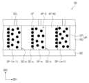
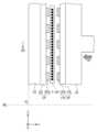
도 5 및 도 6은 각각 일 실시예의 표시 장치의 일 부분에 대한 단면도이다. 도 5는 도 3의 I-I'선에 대응하는 부분의 단면도이고, 도 6은 도 3의 II-II'선에 대응하는 부분의 단면도이다. 도 7a 및 도 7b는 각각 일 실시예에 따른 표시 장치의 일부를 나타낸 평면도이다. 도 7a 및 도 7b는 각각 접합층이 부착된 표시 패널의 일부를 예시적으로 나타낸 평면도이다.FIGS. 5 and 6 are cross-sectional views of a portion of a display device according to one embodiment, respectively. FIG. 5 is a cross-sectional view of a portion corresponding to line I-I' of FIG. 3, and FIG. 6 is a cross-sectional view of a portion corresponding to line II-II' of FIG. 3. FIGS. 7A and 7B are plan views each showing a portion of a display device according to one embodiment. FIGS. 7A and 7B are plan views each showing a portion of a display panel to which an adhesive layer is attached, as an example.
도 5 및 도 6을 참조하면, 접합층(AP)은 복수 개의 도전입자들(CP)을 포함하는 것일 수 있다. 접합층(AP)은 이방성 도전 필름(Anisotropic Conductive Film: ACF)일 수 있다. 접합층(AP)은 복수 개의 도전입자들(CP) 및 복수 개의 도전입자들(CP) 사이를 충전하는 수지부(RS)를 포함하는 것일 수 있다.Referring to FIGS. 5 and 6, the bonding layer (AP) may include a plurality of conductive particles (CP). The bonding layer (AP) may be an anisotropic conductive film (ACF). The bonding layer (AP) may include a plurality of conductive particles (CP) and a resin portion (RS) filling between the plurality of conductive particles (CP).
도전입자(CP)는 금속 입자, 또는 다수의 금속들인 혼합된 합금 입자 등일 수 있다. 예를 들어, 도전입자(CP)는 은, 구리, 비스무스, 아연, 인듐, 주석, 니켈, 코발트, 크롬, 및 철 중 적어도 하나를 포함하는 금속 또는 금속 합금 입자일 수 있다. 또한, 도전입자(CP)는 고분자수지 등으로 형성된 코어부 및 코어부를 감싸는 도전성 물질의 코팅층을 갖는 것일 수도 있다.The conductive particle (CP) may be a metal particle, a mixed alloy particle of a plurality of metals, etc. For example, the conductive particle (CP) may be a metal or metal alloy particle including at least one of silver, copper, bismuth, zinc, indium, tin, nickel, cobalt, chromium, and iron. In addition, the conductive particle (CP) may have a core formed of a polymer resin, etc., and a coating layer of a conductive material surrounding the core.
접합층(AP)은 중첩부(AP-O) 및 비중첩부(AP-NO)를 포함할 수 있다. 중첩부(AP-O)는 패널패드(DPD) 및 접속패드(CPD)와 중첩하는 부분이고, 비중첩부(AP-NO)는 패널패드(DPD) 및 접속패드(CPD) 모두와 비중첩하는 부분이다. 접합층(AP)에서 중첩부(AP-O)는 마주하는 패널패드(DPD) 및 접속패드(CPD)와 중첩하는 영역에 해당한다. 비중첩부(AP-NO)는 중첩부들(AP-O) 사이에 배치된 부분일 수 있다. 접합층(AP)은 교대로 배치된 중첩부(AP-O) 및 비중첩부(AP-NO)를 포함하는 것일 수 있다.The bonding layer (AP) may include an overlapping portion (AP-O) and a non-overlapping portion (AP-NO). The overlapping portion (AP-O) is a portion that overlaps the panel pad (DPD) and the contact pad (CPD), and the non-overlapping portion (AP-NO) is a portion that does not overlap both the panel pad (DPD) and the contact pad (CPD). In the bonding layer (AP), the overlapping portion (AP-O) corresponds to a region that overlaps the facing panel pad (DPD) and the contact pad (CPD). The non-overlapping portion (AP-NO) may be a portion positioned between the overlapping portions (AP-O). The bonding layer (AP) may include alternately positioned overlapping portions (AP-O) and non-overlapping portions (AP-NO).
일 실시예의 표시 장치(DD)에서 비중첩부(AP-NO)의 도전입자들(CP)은 서로 이웃하는 패널패드들 중 하나의 패널패드(DPD)의 일 측에 인접하여 배치되는 것일 수 있다. 또한, 중첩부(AP-O)에서 도전입자들(CP)은 패널패드(DPD) 및 대응하여 배치된 접속패드(CPD) 사이에 배치되는 것을 수 있다. 중첩부(AP-O)에서는 도전입자들(CP)이 분산되어 배치될 수 있다. 예를 들어, 중첩부(AP-O)에서 도전입자들(CP)은 패널패드(DPD) 상에서 분산되어 배치된 것일 수 있다. 또한, 비중첩부(AP-NO)에서는 도전입자들(CP)이 일 측으로 집중되어 배치될 수 있다.In a display device (DD) of one embodiment, conductive particles (CP) of a non-overlapping portion (AP-NO) may be arranged adjacent to one side of a panel pad (DPD) of one of the neighboring panel pads. In addition, in the overlapping portion (AP-O), the conductive particles (CP) may be arranged between the panel pad (DPD) and a correspondingly arranged connection pad (CPD). In the overlapping portion (AP-O), the conductive particles (CP) may be arranged in a distributed manner. For example, in the overlapping portion (AP-O), the conductive particles (CP) may be arranged in a distributed manner on the panel pad (DPD). In addition, in the non-overlapping portion (AP-NO), the conductive particles (CP) may be arranged in a concentrated manner on one side.
예를 들어, 접합층(AP)에 포함된 도전입자들(CP) 중 이웃하는 두 개의 패널패드들(DPD-1, DPD-2) 사이에 배치된 도전입자들(CP)은 이웃하는 두 개의 패널패드들 (DPD-1, DPD-2)중 하나의 패널패드(DPD-2)의 일 측(SS-a)에 인접하여 배치되는 것일 수 있다. 한편, 본 명세서에서 일 측(SS-a)과 일 측면(SS-a)은 동일한 도면 부호를 이용하여 설명되었다. 일 측은 일 측면을 포함하는 의미일 수 있다.For example, among the conductive particles (CP) included in the bonding layer (AP), the conductive particles (CP) arranged between two neighboring panel pads (DPD-1, DPD-2) may be arranged adjacent to one side (SS-a) of one panel pad (DPD-2) of the two neighboring panel pads (DPD-1, DPD-2). Meanwhile, in the present specification, one side (SS-a) and one side (SS-a) are described using the same drawing reference numerals. One side may mean including one side.
이웃하는 두 개의 패널패드들(DPD-1, DPD-2) 사이에 배치된 비중첩부(AP-NO)에 포함된 도전입자들(CP)은 이웃하는 두 개의 패널패드들(DPD-1, DPD-2) 중 하나의 패널패드(DPD-2)의 일 측에 접촉하는 것일 수 있다. 즉 비중첩부(AP-NO)에서의 도전입자들(CP)은 이웃하는 두 개의 패널패드들(DPD-1, DPD-2) 중 하나의 패널패드(DPD-2)와 전기적으로 접촉(electrically contact)하고, 나머지 하나의 패널패드(DPD-1)와는 절연된 것일 수 있다.The conductive particles (CP) included in the non-overlapping portion (AP-NO) positioned between the two neighboring panel pads (DPD-1, DPD-2) may contact one side of the panel pad (DPD-2) of one of the two neighboring panel pads (DPD-1, DPD-2). That is, the conductive particles (CP) in the non-overlapping portion (AP-NO) may electrically contact one panel pad (DPD-2) of the two neighboring panel pads (DPD-1, DPD-2) and be insulated from the remaining panel pad (DPD-1).
접합층(AP)은 수지부(RS)는 포함하는 것일 수 있다. 접합층(AP)의 수지부(RS)는 도전입자들(CP) 사이를 충전하는 것일 수 있다. 수지부(RS)는 고분자 물질을 포함하는 것일 수 있다. 수지부(RS)는 아크릴계 고분자, 실리콘계 고분자, 우레탄계 고분자, 및 이미드계 고분자 중 적어도 하나를 포함하는 것일 수 있다. 예를 들어, 수지부(RS)는 아크릴계 고분자, 실리콘계 고분자, 우레탄계 고분자, 및 이미드계 고분자 중 선택되는 어느 하나의 고분자 물질 또는 선택되는 복수의 고분자 물질들의 조합을 포함하는 것일 수 있다. 수지부(RS)는 아크릴계 수지, 실리콘계 수지, 우레탄계 수지, 또는 이미드계 수지로부터 형성된 것일 수 있다. 예를 들어, 수지부(RS)는 아크릴계 수지, 실리콘계 수지, 우레탄계 수지, 또는 이미드계 수지 등의 베이스 수지가 열경화되거나 또는 광경화되어 형성된 부분일 수 있다.The bonding layer (AP) may include a resin portion (RS). The resin portion (RS) of the bonding layer (AP) may fill between the conductive particles (CP). The resin portion (RS) may include a polymer material. The resin portion (RS) may include at least one of an acrylic polymer, a silicone polymer, a urethane polymer, and an imide polymer. For example, the resin portion (RS) may include any one polymer material selected from an acrylic polymer, a silicone polymer, a urethane polymer, and an imide polymer, or a combination of a plurality of selected polymer materials. The resin portion (RS) may be formed from an acrylic resin, a silicone resin, a urethane resin, or an imide resin. For example, the resin portion (RS) may be a portion formed by heat-curing or photo-curing a base resin such as an acrylic resin, a silicone resin, a urethane resin, or an imide resin.
도 5 내지 도 7b 등을 참조하면, 일 실시예에서 표시 패널(DP)은 제1 방향축(DR1) 방향으로 배열된 n 개의 패널패드들(DPD-1, DPD-2,…,DPD-(n-1), DPD-n)을 포함한다. 또한, 연성회로기판(FB-DP)은 제1 방향축(DR1) 방향으로 배열된 n 개의 접속패드들(CPD-1, CPD-2,…,CPD-(n-1), CPD-n)을 포함하며, n 개의 접속패드들(CPD-1, CPD-2,…,CPD-(n-1), CPD-n)은 각각 n 개의 패널패드들(DPD-1, DPD-2,…,DPD-(n-1), DPD-n)에 대응하도록 배치된 것일 수 있다. 한편, n은 2 이상의 정수일 수 있다.Referring to FIGS. 5 to 7b, etc., in one embodiment, the display panel (DP) includes n panel pads (DPD-1, DPD-2, …, DPD-(n-1), DPD-n) arranged in the direction of the first direction axis (DR1). In addition, the flexible circuit board (FB-DP) includes n connection pads (CPD-1, CPD-2, …, CPD-(n-1), CPD-n) arranged in the direction of the first direction axis (DR1), and the n connection pads (CPD-1, CPD-2, …, CPD-(n-1), CPD-n) may be arranged to correspond to the n panel pads (DPD-1, DPD-2, …, DPD-(n-1), DPD-n), respectively. Meanwhile, n may be an integer greater than or equal to 2.
일 실시예에서 패널패드들(DPD-1, DPD-2,…,DPD-(n-1), DPD-n)은 이웃하는 제1 패널패드(DPD-1) 및 제2 패널패드(DPD-2)를 포함하고, 접합층(AP)의 비중첩부(AP-NO)는 제1 패널패드(DPD-1) 및 제2 패널패드(DPD-2)와 비중첩하는 것일 수 있다. 비중첩부(AP-NO)에 포함된 도전입자들(CP)은 제1 패널패드(DPD-1)의 제1 측면(SS-b)에서 이격되고 제2 패널패드(DPD-2)의 제2 측면(SS-a)에 인접하여 배치되는 것일 수 있다. 제1 패널패드(DPD-1)의 제1 측면(SS-b) 및 제2 패널패드(DPD-2)의 제2 측면(SS-b)은 서로 인접한 측면들일 수 있다. 한편, 이는 예시적으로 설명한 것이고 제1 및 제2 패널패드들(DPD-1, DPD-2) 이외에 이웃하는 패널패드들(DPD)에 대하여도 동일하게 적용될 수 있다. 즉, 비중첩부(AP-NO)에 포함된 도전입자들(CP)은 m번 째 패널패드(DPD-m)의 일 측면(SS-a)에 인접하여 배치되고, m번 째 패널패드(DPD-m)의 타 측면(SS-b)으로부터 이격되어 배치된 것일 수 있다. 한편, 본 명세서에서 m은 1 이상 n 이하의 정수일 수 있다.In one embodiment, the panel pads (DPD-1, DPD-2, …, DPD-(n-1), DPD-n) include neighboring first panel pads (DPD-1) and second panel pads (DPD-2), and a non-overlapping portion (AP-NO) of a bonding layer (AP) may non-overlap with the first panel pad (DPD-1) and the second panel pad (DPD-2). The conductive particles (CP) included in the non-overlapping portion (AP-NO) may be spaced apart from the first side (SS-b) of the first panel pad (DPD-1) and arranged adjacent to the second side (SS-a) of the second panel pad (DPD-2). The first side (SS-b) of the first panel pad (DPD-1) and the second side (SS-b) of the second panel pad (DPD-2) may be adjacent to each other. Meanwhile, this is described by way of example and can be equally applied to neighboring panel pads (DPD) other than the first and second panel pads (DPD-1, DPD-2). That is, the conductive particles (CP) included in the non-overlapping portion (AP-NO) may be arranged adjacent to one side (SS-a) of the m-th panel pad (DPD-m) and spaced apart from the other side (SS-b) of the m-th panel pad (DPD-m). Meanwhile, in the present specification, m may be an integer greater than or equal to 1 and less than or equal to n.
일 실시예에서, 접합층(AP)에 포함된 도전입자들(CP) 중 비중첩부(AP-NO)에 포함되는 도전입자들(CP)은 패널패드(DPD)의 일 측에만 인접하여 배치된 것일 수 있다. 도 5 및 도 6 등의 도시를 참조하면, 제1 방향축(DR1) 및 제3 방향축(DR3)이 정의하는 단면 상에서, 비중첩부들(AP-NO)에 포함된 도전입자들(CP)은 모두 패널패드(DPD)의 좌측 측면에 인접하여 배치되는 것일 수 있다. 한편, 도 5 및 도 6은 접합층(AP)의 실시예를 예시적으로 도시한 것이며, 도시된 바와 달리 비중첩부들(AP-NO)에 포함된 도전입자들(CP)은 모두 패널패드(DPD)의 우측 측면에 인접하여 배치되는 것일 수 있다.In one embodiment, among the conductive particles (CP) included in the bonding layer (AP), the conductive particles (CP) included in the non-overlapping portion (AP-NO) may be arranged adjacent to only one side of the panel pad (DPD). Referring to the illustrations of FIGS. 5 and 6, all of the conductive particles (CP) included in the non-overlapping portions (AP-NO) may be arranged adjacent to the left side of the panel pad (DPD) on the cross-section defined by the first direction axis (DR1) and the third direction axis (DR3). Meanwhile, FIGS. 5 and 6 exemplarily illustrate embodiments of the bonding layer (AP), and unlike the illustrations, all of the conductive particles (CP) included in the non-overlapping portions (AP-NO) may be arranged adjacent to the right side of the panel pad (DPD).
m번 째 패널패드(DPD-m)와 중첩하지 않으며, m번 째 패널패드(DPD-m)의 양 측에 각각 배치된 도전입자들(CP) 중 m번 째 패널패드(DPD-m)의 일 측면(SS-a) 방향에 배치된 도전입자들(CP)은 m번 째 패널패드(DPD-m)와 전기적으로 접속하여 배치되는 것일 수 있다. 또한, 이와 달리 m번 째 패널패드(DPD-m)의 타 측면(SS-b) 방향에 배치된 도전입자들(CP)은 m번 째 패널패드(DPD-m)와 이격되어 배치되는 것일 수 있다.The conductive particles (CP) arranged on each side of the m-th panel pad (DPD-m) do not overlap with the m-th panel pad (DPD-m), and the conductive particles (CP) arranged in the direction of one side (SS-a) of the m-th panel pad (DPD-m) may be arranged so as to be electrically connected to the m-th panel pad (DPD-m). In addition, on the contrary, the conductive particles (CP) arranged in the direction of the other side (SS-b) of the m-th panel pad (DPD-m) may be arranged so as to be spaced apart from the m-th panel pad (DPD-m).
제1 방향축(DR1) 방향으로 이웃하여 배치된 두 개의 패널패드들(DPD-(m-1), DPD-m)과 비중첩하고, 두 개의 패널패드들(DPD-(m-1), DPD-m) 사이에 배치된 비중첩부(AP-NO)에 포함된 도전입자들(CP)은 (m-1)번 째 패널패드(DPD-(m-1))와는 이격되고 m번 째 패널패드(DPD-m)에 인접하여 배치되는 것일 수 있다. 또한, 제1 방향축(DR1) 방향으로 이웃하여 배치된 두 개의 패널패드들(DPD-m, DPD-(m+1))과 비중첩하고, 두 개의 패널패드들(DPD-m, DPD-(m+1)) 사이에 배치된 비중첩부(AP-NO)에 포함된 도전입자들(CP)은 m번 째 패널패드(DPD-m)와는 이격되고 (m+1)번 째 패널패드(DPD-(m+1))에 인접하여 배치되는 것일 수 있다. 즉, 일 실시예에서 패널패드와 비중첩하는 비중첩부에 배치된 도전입자들은 이웃하는 두 개의 패널패드들 중 하나의 패널패드에 인접하고 나머지 하나의 패널패드로부터 이격되어 배치되는 것일 수 있다.The conductive particles (CP) included in the non-overlapping portion (AP-NO) between the two panel pads (DPD-(m-1), DPD-m) that are arranged adjacent to each other in the first direction axis (DR1) and that do not overlap with each other may be arranged spaced apart from the (m-1)-th panel pad (DPD-(m-1)) and adjacent to the m-th panel pad (DPD-m). In addition, the conductive particles (CP) included in the non-overlapping portion (AP-NO) disposed between the two panel pads (DPD-m, DPD-(m+1)) that are adjacently arranged in the first direction axis (DR1) and do not overlap with each other may be arranged spaced apart from the m-th panel pad (DPD-m) and adjacent to the (m+1)-th panel pad (DPD-(m+1)). That is, in one embodiment, the conductive particles arranged in the non-overlapping portion that does not overlap with the panel pads may be arranged adjacent to one of the two adjacent panel pads and spaced apart from the other panel pad.
접합층(AP)에 포함된 도전입자들(CP)은 패널패드(DPD)와 접속패드(CPD) 사이에서 하나의 층으로 배치된 것일 수 있다. 즉, 접합층(AP)의 중첩부(AP-O)에서 도전입자들(CP)은 두께 방향으로 비중첩하는 것일 수 있다. 중첩부(AP-O)에서 도전입자들(CP)은 제1 방향축(DR1) 및 제2 방향축(DR2)으로 정의되는 평면과 평행한 평면 상에서 분산되어 배치되고 제3 방향축(DR3) 방향으로 적층되지 않는다. 예를 들어, 패널패드(DPD)와 접속패드(CPD) 사이의 간격으로 정의되는 중첩부(AP-O)의 두께는 패널패드(DPD)와 접속패드(CPD) 사이에 배치된 도전입자(CP)의 직경과 실질적으로 동일할 수 있다.The conductive particles (CP) included in the bonding layer (AP) may be arranged as a single layer between the panel pad (DPD) and the connection pad (CPD). That is, the conductive particles (CP) in the overlapping portion (AP-O) of the bonding layer (AP) may not overlap in the thickness direction. In the overlapping portion (AP-O), the conductive particles (CP) are arranged to be dispersed on a plane parallel to the plane defined by the first direction axis (DR1) and the second direction axis (DR2), and are not stacked in the direction of the third direction axis (DR3). For example, the thickness of the overlapping portion (AP-O) defined as the gap between the panel pad (DPD) and the connection pad (CPD) may be substantially the same as the diameter of the conductive particles (CP) arranged between the panel pad (DPD) and the connection pad (CPD).
일 실시예의 표시 장치는 패널패드들 사이에 배치되는 도전입자들을 이웃하는 패널패드들 중 하나의 패널패드 측에 인접하도록 배치한 접합층을 포함하여 개선된 전기적 신뢰성을 나타낼 수 있다. 즉, 일 실시예는 두 개의 패널패드들 사이에 배치된 도전입자들을 하나의 패널패드 측에 인접하도록 배치한 접합층을 포함하여 이웃하는 패널패드들 사이에 배치된 도전 입자에 의해 발생하는 쇼트 문제가 개선된 표시 장치를 제공할 수 있다.A display device of one embodiment may exhibit improved electrical reliability by including a bonding layer in which conductive particles arranged between panel pads are arranged adjacent to a side of one of the panel pads adjacent to each other. That is, one embodiment may provide a display device in which a short circuit problem caused by conductive particles arranged between neighboring panel pads is improved by including a bonding layer in which conductive particles arranged between two panel pads are arranged adjacent to a side of one of the panel pads.
한편, 도 5 내지 도 7a 등에서는 비중첩부(AP-NO)에 배치된 도전입자들(CP)이 제2 방향축(DR2)을 따라 하나의 열을 이루어 정렬된 것으로 도시되었으나 실시예가 이에 한정되는 것은 아니다. 도 7b를 참조하면, 일 실시예에 따른 표시 장치(DD-1)에서 접합층(AP-1)의 비중첩부(AP-NO)에 포함된 도전입자들(CP)은 하나의 열을 이루지 않을 수 있다. 비중첩부(AP-NO)에 포함된 도전입자들(CP)은, 비중첩부(AP-NO)를 사이에 두고 서로 이웃하는 두 개의 패널패드들(DPD-(m-1), DPD-m) 중 하나의 패널패드(DPD-m)의 일 측면(SS-a)에 인접하면서 랜덤하게 배치될 수 있다. 또한, 도면에 도시되지는 않았으나 비중첩부(AP-NO)에서 도전입자들(CP)은 하나의 패널패드(DPD-m)의 일 측면(SS-a)에 인접하면서 복수의 열을 이루어 배치될 수도 있다.Meanwhile, although the conductive particles (CP) arranged in the non-overlapping portion (AP-NO) are illustrated as being aligned in one column along the second direction axis (DR2) in FIGS. 5 to 7a, the embodiment is not limited thereto. Referring to FIG. 7b, in the display device (DD-1) according to one embodiment, the conductive particles (CP) included in the non-overlapping portion (AP-NO) of the bonding layer (AP-1) may not form one column. The conductive particles (CP) included in the non-overlapping portion (AP-NO) may be randomly arranged adjacent to one side (SS-a) of one panel pad (DPD-m) among the two panel pads (DPD-(m-1), DPD-m) that are adjacent to each other with the non-overlapping portion (AP-NO) interposed therebetween. Additionally, although not shown in the drawing, in the non-overlapping portion (AP-NO), the challenge particles (CP) may be arranged in multiple rows adjacent to one side (SS-a) of one panel pad (DPD-m).
다만, 복수의 열을 이루어 배치되는 경우에 있어서도, 이웃하는 두 개의 패널패드들(DPD-(m-1), DPD-m) 사이에 배치된 비중첩부(AP-NO)에 포함된 도전입자들(CP)은 이웃하는 두 개의 측면들(SS-a, SS-b)로부터 동일한 거리에 있는 가상의 중심선(CTL)을 기준으로 하나의 측면(SS-b)에 보다 인접하여 배치된 것일 수 있다. 예를 들어, 도 7b를 참조하면 이웃하는 두 개의 패널패드들(DPD-(m-1), DPD-m) 사이에 배치된 비중첩부(AP-NO)에 포함된 도전입자들(CP)은 (m-1)번 째 패널패드(DPD-(m-1))의 측면(SS-b)과 m번 째 패널패드(DPD-m)의 측면(SS-a)으로부터 동일(D1 및 D2가 동일)한 거리에 있는 가상의 중심선(CTL)을 기준으로 m번 째 패널패드(DPD-m)의 측면(SS-a)에 보다 인접하여 배치된 것일 수 있다. 즉, 비중첩부(AP-NO)의 도전입자들(CP)은 가상의 중심선(CTL)과 m번 째 패널패드(DPD-m)의 측면(SS-a) 사이에 배치된 것일 수 있다. 두 개의 패널패드들(DPD-(m-1), DPD-m) 사이에 배치된 비중첩부(AP-NO)에 포함된 도전입자들(CP)의 중심점(CTP, 도 7c)은 가상의 중심선(CTL)을 기준으로 (m-1)번 째 패널패드(DPD-(m-1))의 측면(SS-b) 보다 m번 째 패널패드(DPD-m)의 측면(SS-a)에 보다 인접하여 배치되는 것일 수 있다.However, even in the case where multiple rows are formed, the conductive particles (CP) included in the non-overlapping portion (AP-NO) arranged between two neighboring panel pads (DPD-(m-1), DPD-m) may be arranged closer to one side (SS-b) based on a virtual center line (CTL) that is at the same distance from the two neighboring sides (SS-a, SS-b). For example, referring to FIG. 7b, conductive particles (CP) included in a non-overlapping portion (AP-NO) disposed between two neighboring panel pads (DPD-(m-1), DPD-m) may be disposed closer to the side surface (SS-a) of the m-th panel pad (DPD-m) with respect to a virtual center line (CTL) that is at the same distance (D1 and D2 are the same) from the side surface (SS-b) of the (m-1)-th panel pad (DPD-(m-1)) and the side surface (SS-a) of the m-th panel pad (DPD-m). That is, the conductive particles (CP) of the non-overlapping portion (AP-NO) may be disposed between the virtual center line (CTL) and the side surface (SS-a) of the m-th panel pad (DPD-m). The center point (CTP, Fig. 7c) of the conductive particles (CP) included in the non-overlapping portion (AP-NO) arranged between two panel pads (DPD-(m-1), DPD-m) may be arranged closer to the side (SS-a) of the m-th panel pad (DPD-m) than to the side (SS-b) of the (m-1)-th panel pad (DPD-(m-1)) with respect to the virtual center line (CTL).
도 7c는 패널패드들 사이에서 도전입자의 배치를 개략적으로 나타낸 평면도이다. 이웃하는 두 개의 패널패드들(DPD-(m-1), DPD-m) 사이의 최소 이격 간격을 P라고 할 때, 가상의 중심선(CTL)은 (m-1)번 째 패널패드(DPD-(m-1))의 일 측면(SS-b)으로부터 P/2의 위치로 정의될 수 있다.Fig. 7c is a plan view schematically showing the arrangement of the challenger between the panel pads. When the minimum separation distance between two neighboring panel pads (DPD-(m-1), DPD-m) is P, the virtual center line (CTL) can be defined as a position P/2 from one side (SS-b) of the (m-1)th panel pad (DPD-(m-1)).
도 7c를 참조하면, 두 개의 패널패드들(DPD-(m-1), DPD-m) 사이에 배치된 도전입자(CP)와 (m-1)번 째 패널패드(DPD-(m-1))의 측면(SS-b) 사이의 이격 간격(S1)은 P/2의 간격보다 큰 것일 수 있다. 또한, 도전입자(CP)와 m번 째 패널패드(DPD-m)의 측면(SS-a) 사이의 이격 간격(S2)은 P/2의 간격보다 작은 것일 수 있다. 한편, 도전입자(CP)와 패널패드들(DPD-(m-1), DPD-m)과의 이격 간격(S1, S2)은 도전입자(CP)의 중심점(CTP)을 기준으로 한 이격거리에 해당한다.Referring to FIG. 7c, a spacing (S1) between a conductive particle (CP) disposed between two panel pads (DPD-(m-1), DPD-m) and a side surface (SS-b) of the (m-1)th panel pad (DPD-(m-1)) may be greater than the spacing of P/2. In addition, a spacing (S2) between the conductive particle (CP) and the side surface (SS-a) of the mth panel pad (DPD-m) may be smaller than the spacing of P/2. Meanwhile, the spacings (S1, S2) between the conductive particle (CP) and the panel pads (DPD-(m-1), DPD-m) correspond to a spacing distance based on the center point (CTP) of the conductive particle (CP).
도전입자(CP)와 (m-1)번 째 패널패드(DPD-(m-1))의 측면(SS-b) 사이의 이격 간격(S1)은 도전입자(CP)와 (m-1)번 째 패널패드(DPD-(m-1)) 사이에서 쇼트가 발생할 수 있는 최대 거리보다 큰 것일 수 있다. 또한, 도전입자(CP)와 m번 째 패널패드(DPD-m)의 측면(SS-a) 사이의 이격 간격(S2)은 도전입자(CP)와 m번 째 패널패드(DPD-m)사이에서 쇼트가 발생할 수 있는 최소 거리 이하일 수 있다. 한편, 도전입자(CP)와 패널패드(DPD) 사이에서 쇼트가 발생할 수 있는 최소 거리는 사용된 도전입자(CP) 및 접합층(AP)에 포함된 수지부(RS)의 유전율과 같은 전기적인 특징에 의해 변화될 수 있다.A separation distance (S1) between a conductive particle (CP) and a side surface (SS-b) of an (m-1)th panel pad (DPD-(m-1)) may be greater than a maximum distance at which a short may occur between the conductive particle (CP) and the (m-1)th panel pad (DPD-(m-1)). In addition, a separation distance (S2) between the conductive particle (CP) and the side surface (SS-a) of the mth panel pad (DPD-m) may be smaller than a minimum distance at which a short may occur between the conductive particle (CP) and the mth panel pad (DPD-m). Meanwhile, the minimum distance at which a short may occur between the conductive particle (CP) and the panel pad (DPD) may vary depending on electrical characteristics such as a permittivity of a resin portion (RS) included in the conductive particle (CP) and the bonding layer (AP).
즉, 도전입자들(CP)은 이웃하는 두 개의 패널패드들(DPD-(m-1), DPD-m) 중 하나의 패널패드(DPD-(m-1))와는 쇼트가 발생하지 않을 정도의 거리로 충분히 이격되어 있으며, 나머지 하나의 패널패드(DPD-m)와는 전기적으로 접촉하거나 인접하여 배치되어 있는 것일 수 있다. 이에 따라, 접합층(AP)의 비중첩부(AP-NO)에 포함된 도전입자(CP)는 이웃하는 두 개의 패널패드들 중 하나의 패널패드와 충분히 이격되어 있으므로 두 개의 패널패드들 간의 쇼트 현상이 발생하지 않는다.That is, the conductive particles (CP) may be sufficiently spaced apart from one of the two neighboring panel pads (DPD-(m-1), DPD-m) by a distance such that a short circuit does not occur, and may be arranged in electrical contact with or adjacent to the remaining panel pad (DPD-m). Accordingly, the conductive particles (CP) included in the non-overlapping portion (AP-NO) of the bonding layer (AP) are sufficiently spaced apart from one of the two neighboring panel pads, so that a short circuit phenomenon does not occur between the two panel pads.
한편, 도 5 내지 도 7c를 참고하여 설명한 접합층(AP)에 대한 설명은 구동접합층(M-AP)에도 동일하게 적용될 수 있다. 즉, 구동접합층(M-AP)에 포함된 도전입자들 중 구동패드들(MPD)과 비중첩하는 부분에서의 도전입자는 이웃하는 구동패드들(MPD) 중 하나의 구동패드(MPD)의 일 측에 인접하여 배치되는 것일 수 있다.Meanwhile, the description of the bonding layer (AP) described with reference to FIGS. 5 to 7c can be equally applied to the driving bonding layer (M-AP). That is, among the conductive particles included in the driving bonding layer (M-AP), the conductive particles in the non-overlapping portion with the driving pads (MPD) can be arranged adjacent to one side of one of the neighboring driving pads (MPD).
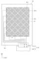
도 8은 일 실시예의 표시 장치의 일 부분을 나타낸 평면도이다. 도 8에서는 일 실시예의 표시 장치(DD, 도 2)에 포함된 입력감지부(ISU) 및 감지 구동부(TP-M)를 도시하였다. 도 9는 도 8의 III-III'선에 대응하는 부분의 단면도이다.Fig. 8 is a plan view showing a part of a display device according to one embodiment. Fig. 8 illustrates an input detection unit (ISU) and a detection driving unit (TP-M) included in a display device (DD, Fig. 2) according to one embodiment. Fig. 9 is a cross-sectional view of a part corresponding to line III-III' of Fig. 8.
도 2, 도 8 및 도 9를 참조하면, 일 실시예의 표시 장치(DD)에서 입력감지부(ISU)는 표시 패널(DP) 상에 별개의 부재로 제공되는 것일 수 있다. 하지만, 도시된 바와 달리 입력감지부(ISU)는 표시 패널(DP) 상에 직접 배치될 수 있다. 예를 들어, 입력감지부(ISU)는 표시 패널(DP) 상에 직접 배치될 수 있다.Referring to FIGS. 2, 8, and 9, in the display device (DD) of one embodiment, the input detection unit (ISU) may be provided as a separate member on the display panel (DP). However, unlike as illustrated, the input detection unit (ISU) may be directly disposed on the display panel (DP). For example, the input detection unit (ISU) may be directly disposed on the display panel (DP).
입력감지부(ISU)는 외부 입력(TC, 도1)을 감지하여 외부 입력의 위치나 세기 정보를 얻을 수 있다. 예를 들어, 외부 입력은 사용자 신체의 일부, 광, 열, 또는 압력 등 다양한 형태의 외부 입력들을 포함한다. 또한, 입력감지부(ISU)는 입력감지부(ISU)에 접촉하는 입력은 물론, 근접하거나 인접하는 입력을 감지할 수도 있다.The input sensing unit (ISU) can detect external input (TC, Fig. 1) and obtain information on the location or intensity of the external input. For example, the external input includes various forms of external input such as a part of the user's body, light, heat, or pressure. In addition, the input sensing unit (ISU) can detect input that comes into contact with the input sensing unit (ISU), as well as input that is close to or adjacent to it.
입력감지부(ISU)는 감지 영역(SA) 및 비감지 영역(NSA)을 포함할 수 있다. 감지 영역(SA)은 표시 영역(DA)과 중첩될 수 있다. 비감지 영역(NSA)은 감지 영역(SA)에 인접한다. 비감지 영역(NSA)은 감지 영역(SA)의 가장 자리를 에워쌀 수 있다. 다만, 이는 예시적으로 도시한 것이고, 비감지 영역(NSA)은 감지 영역(SA)의 가장 자리 일부에만 인접할 수도 있고, 생략될 수도 있으며, 어느 하나의 실시예로 한정되지 않는다.The input sensing unit (ISU) may include a sensing area (SA) and a non-sensing area (NSA). The sensing area (SA) may overlap with the display area (DA). The non-sensing area (NSA) is adjacent to the sensing area (SA). The non-sensing area (NSA) may surround an edge of the sensing area (SA). However, this is merely an example, and the non-sensing area (NSA) may be adjacent to only a part of an edge of the sensing area (SA), may be omitted, and is not limited to any one embodiment.
입력감지부(ISU)는 복수 개의 감지 전극들(SEL1, SEL2), 복수 개의 감지 라인들(SL1, SL2), 및 복수 개의 감지패드들(TPD)을 포함할 수 있다. 감지 전극들(SEL1, SEL2)은 감지 영역(SA)에 배치되고, 감지 패드들(TPD)은 비감지 영역(NSA)에 배치될 수 있다. 감지패드들(TPD)은 입력감지부(ISU)의 일측 단부에 인접하여 배치되는 것일 수 있다.The input sensing unit (ISU) may include a plurality of sensing electrodes (SEL1, SEL2), a plurality of sensing lines (SL1, SL2), and a plurality of sensing pads (TPD). The sensing electrodes (SEL1, SEL2) may be arranged in a sensing area (SA), and the sensing pads (TPD) may be arranged in a non-sensing area (NSA). The sensing pads (TPD) may be arranged adjacent to one end of the input sensing unit (ISU).
감지 라인들(SL1, SL2)은 감지 전극들(SEL1, SEL2)에 연결되고, 비감지 영역(NSA)으로 연장하여 감지패드들(TPD)에 연결될 수 있다. 감지패드들(TPD)은 감지 연성회로기판(FB-TP)을 통해 입력감지부(ISU)를 구동하기 위한 감지 구동기판(MB-TP)에 연결될 수 있다.The sensing lines (SL1, SL2) are connected to the sensing electrodes (SEL1, SEL2) and can be extended to the non-sensing area (NSA) and connected to the sensing pads (TPD). The sensing pads (TPD) can be connected to the sensing driving board (MB-TP) for driving the input sensing unit (ISU) through the sensing flexible circuit board (FB-TP).
감지 전극들(SEL1, SEL2) 및 감지 라인들(SL1, SL2)은 단층 구조 또는 상부 방향으로 적층된 다층 구조를 가질 수 있다. 감지 전극들(SEL1, SEL2) 및 감지 라인들(SL1, SL2)은 감지 베이스기판(BS-T) 상에 제공될 수 있다. 감지 베이스기판(BS-T)은 유리기판, 금속기판, 플라스틱기판 등일 수 있다. 하지만, 실시예가 이에 한정되는 것은 아니며 감지 베이스기판(BS-T)은 무기층, 유기층 또는 복합재료층일 수 있다.The sensing electrodes (SEL1, SEL2) and the sensing lines (SL1, SL2) may have a single-layer structure or a multi-layer structure stacked in an upward direction. The sensing electrodes (SEL1, SEL2) and the sensing lines (SL1, SL2) may be provided on a sensing base substrate (BS-T). The sensing base substrate (BS-T) may be a glass substrate, a metal substrate, a plastic substrate, or the like. However, the embodiment is not limited thereto, and the sensing base substrate (BS-T) may be an inorganic layer, an organic layer, or a composite material layer.
한편, 입력감지부(ISU)가 표시 패널(DP) 상에 직접 배치될 경우 감지 베이스기판(BS-T)은 생략될 수 있다. 이 경우 감지 전극들(SEL1, SEL2) 및 감지 라인들(SL1, SL2)은 표시 패널(DP) 상에 직접 제공될 수 있다.Meanwhile, if the input sensing unit (ISU) is placed directly on the display panel (DP), the sensing base substrate (BS-T) may be omitted. In this case, the sensing electrodes (SEL1, SEL2) and the sensing lines (SL1, SL2) may be provided directly on the display panel (DP).
감지 전극들(SEL1, SEL2)은 복수 개의 제1 감지 전극들(SEL1) 및 복수 개의 제2 감지 전극들(SEL2)을 포함할 수 있다. 감지 라인들(SL1, SL2)은 제1 감지 전극들(SEL1)에 연결된 복수 개의 제1 감지 라인들(SL1) 및 제2 감지 전극들(SEL2)에 연결된 복수 개의 제2 감지 라인들(SL2)을 포함할 수 있다.The sensing electrodes (SEL1, SEL2) may include a plurality of first sensing electrodes (SEL1) and a plurality of second sensing electrodes (SEL2). The sensing lines (SL1, SL2) may include a plurality of first sensing lines (SL1) connected to the first sensing electrodes (SEL1) and a plurality of second sensing lines (SL2) connected to the second sensing electrodes (SEL2).
제1 감지 전극들(SEL1)은 제2 감지 전극들(SEL2)과 절연되어 교차하도록 연장할 수 있다. 제1 감지 전극들(SEL1) 및 제2 감지 전극들(SEL2)은 메쉬 형상을 가질 수 있다. 제1 감지 전극들(SEL1)과 제2 감지 전극들(SEL2)에 의해 정전 용량들이 형성될 수 있다.The first sensing electrodes (SEL1) can be extended to intersect with the second sensing electrodes (SEL2) while being insulated from each other. The first sensing electrodes (SEL1) and the second sensing electrodes (SEL2) can have a mesh shape. Capacitances can be formed by the first sensing electrodes (SEL1) and the second sensing electrodes (SEL2).
감지 구동부(TP-M)는 감지 연성회로기판(FB-TP) 및 감지 구동기판(MB-TP)을 포함할 수 있다. 또한, 입력감지부(ISU)와 감지 연성회로기판(FB-TP) 사이에 감지 접합층(T-AP)이 배치될 수 있다. 감지 연성회로기판(FB-TP)은 입력감지부(ISU)의 일측에 배치되고 복수 개의 감지패드들(TPD)과 대응하는 감지 접속패드들(CPD-T)을 포함하는 것일 수 있다. 감지 연성회로기판(FB-TP)은 베이스 필름(BF-T) 및 베이스 필름(BF-T)의 일면 상에 제공된 복수 개의 감지 접속패드들(CPD-T)을 포함하는 것일 수 있다.The sensing driving unit (TP-M) may include a sensing flexible circuit board (FB-TP) and a sensing driving board (MB-TP). In addition, a sensing bonding layer (T-AP) may be disposed between the input sensing unit (ISU) and the sensing flexible circuit board (FB-TP). The sensing flexible circuit board (FB-TP) may be disposed on one side of the input sensing unit (ISU) and may include a plurality of sensing pads (TPD) and corresponding sensing connection pads (CPD-T). The sensing flexible circuit board (FB-TP) may include a base film (BF-T) and a plurality of sensing connection pads (CPD-T) provided on one surface of the base film (BF-T).
감지 접합층(T-AP)은 입력감지부(ISU) 및 감지 연성회로기판(FB-TP) 사이에 배치되며, 복수 개의 도전입자들(CP)을 포함하는 것일 수 있다. 감지 접합층(T-AP)은 서로 대응하는 감지패드들(TPD) 및 감지 접속패드들(CPD-T)과 중첩하는 감지 중첩부(T-APO)를 포함한다. 또한, 감지 접합층(T-AP)은 감지패드들(TPD) 및 감지 접속패드들(CPD-T)과 비중첩하는 감지 비중첩부(T-APN)을 포함한다. 감지 접합층(T-AP)에 대하여는 상술한 접합층(AP)에 대한 설명과 동일한 내용이 적용될 수 있다. 즉, 감지 비중첩부(T-APN)에서 도전입자들(CP)은 이웃하는 감지패드들 중 하나의 감지패드(TPD)의 일 측에 인접하여 배치되는 것일 수 있다.The sensing bonding layer (T-AP) is arranged between the input sensing unit (ISU) and the sensing flexible circuit board (FB-TP), and may include a plurality of conductive particles (CP). The sensing bonding layer (T-AP) includes a sensing overlapping portion (T-APO) that overlaps the corresponding sensing pads (TPD) and the sensing connection pads (CPD-T). In addition, the sensing bonding layer (T-AP) includes a sensing non-overlapping portion (T-APN) that does not overlap the sensing pads (TPD) and the sensing connection pads (CPD-T). The same description as for the above-described bonding layer (AP) may be applied to the sensing bonding layer (T-AP). That is, in the sensing non-overlapping portion (T-APN), the conductive particles (CP) may be arranged adjacent to one side of the sensing pad (TPD) of one of the neighboring sensing pads.
일 실시예의 표시 장치는 패드들 사이에 배치된 도전입자들이 이웃하는 패드들 중 하나의 패드의 일 측에만 인접하도록 도전입자들의 배치를 제어한 접합층을 포함하여, 도전입자들과 패드들 사이의 쇼트 불량이 개선된 특성을 나타낼 수 있다. 또한, 이웃하는 패드들 사이의 이격 거리인 피치(Pitch)가 작아진 고해상도 표시 장치에서도 도전입자들의 배치를 제어한 접합층을 포함하여 우수한 신뢰성을 나타낼 수 있다.A display device of one embodiment may exhibit improved characteristics in terms of short-circuit defects between the conductive particles and the pads, including a bonding layer in which the arrangement of the conductive particles is controlled so that the conductive particles arranged between the pads are adjacent to only one side of one of the neighboring pads. In addition, even in a high-resolution display device in which the pitch, which is the separation distance between the neighboring pads, is reduced, the display device may exhibit excellent reliability, including the bonding layer in which the arrangement of the conductive particles is controlled.
이하 도 10 내지 도 14 등을 참조하여 일 실시예의 표시 장치의 제조 방법에 대하여 설명한다. 이하 설명하는 일 실시예의 표시 장치의 제조 방법에 있어서, 상술한 일 실시예의 표시 장치에 대한 설명과 중복되는 내용은 다시 설명하지 않으며 차이점을 위주로 설명한다.Hereinafter, a method for manufacturing a display device according to an embodiment will be described with reference to FIGS. 10 to 14, etc. In the method for manufacturing a display device according to an embodiment described below, any content that overlaps with the description of the display device according to the above-described embodiment will not be described again, and differences will be mainly described.
도 10 및 도 11은 각각 일 실시예의 표시 장치의 제조 방법을 나타낸 순서도이다. 도 12 내지 도 14는 도 10 및 도 11에 도시된 일 실시예의 표시 장치의 제조 방법의 단계에 대응하는 단계 중 일부를 개략적으로 나타낸 도면이다.FIGS. 10 and 11 are flowcharts each showing a method for manufacturing a display device according to one embodiment. FIGS. 12 to 14 are schematic diagrams showing some of the steps corresponding to the steps of the method for manufacturing a display device according to one embodiment shown in FIGS. 10 and 11.
일 실시예의 표시 장치 제조 방법은 소정의 각도로 기울어진 스테이지 상에 복수 개의 패널패드들을 포함하는 표시 패널을 제공하는 단계(S100), 복수 개의 도전입자들을 포함하는 예비접합층을 배치하는 단계(S200), 복수 개의 접속패드들을 포함하는 연성회로기판을 제공하는 단계(S300), 표시 패널, 예비접합층, 및 연성회로기판을 예비접합하는 단계(S400), 및 예비접합된 표시 패널, 예비접합층, 및 연성회로기판에 열을 제공하는 단계(S500)를 포함하는 것일 수 있다.A method for manufacturing a display device of one embodiment may include the steps of: providing a display panel including a plurality of panel pads on a stage inclined at a predetermined angle (S100); arranging a pre-bonding layer including a plurality of conductive particles (S200); providing a flexible circuit board including a plurality of connection pads (S300); pre-bonding the display panel, the pre-bonding layer, and the flexible circuit board (S400); and providing heat to the pre-bonded display panel, the pre-bonding layer, and the flexible circuit board (S500).
도 12 및 도 13은 표시 패널, 예비접합층, 및 연성회로기판이 순차적으로 제공된 것을 나타낸 것이다. 복수 개의 패널패드들(DPD)을 포함하는 표시 패널(DP)은 스테이지(ST) 상에 제공된다. 스테이지(ST)는 소정의 각도(θ)를 갖도록 기울어진 것일 수 있다. 소정의 각도(θ)는 0도 초가 90도 이하일 수 있다. 스테이지(ST)의 기울어진 각도(θ)는 가상의 면(IML)을 기준으로 한 것일 수 있다. 도 12에서 도시된 가상의 면(IML)은 중력 방향(GD)에 수직하는 면일 수 있다. 즉, 가상의 면(IML)은 X축 및 Y축으로 정의되는 평면과 나란한 면일 수 있다. 한편, 도 12 내지 도 14에서 표시된 X축, Y축, 및 Z축은 표시 장치를 제조하는 장치를 사용하는 사용자를 기준으로 하여 예시적으로 나타낸 것이다. 사용자가 바라보는 방향에서 보이는 평면을 X축 및 Z축이 정의하는 평면으로 정의하였다.FIGS. 12 and 13 illustrate that a display panel, a pre-bonding layer, and a flexible circuit board are sequentially provided. A display panel (DP) including a plurality of panel pads (DPD) is provided on a stage (ST). The stage (ST) may be inclined to have a predetermined angle (θ). The predetermined angle (θ) may be 0 degrees or less and 90 degrees or less. The inclined angle (θ) of the stage (ST) may be based on a virtual plane (IML). The virtual plane (IML) illustrated in FIG. 12 may be a plane perpendicular to the gravity direction (GD). That is, the virtual plane (IML) may be a plane parallel to a plane defined by the X-axis and the Y-axis. Meanwhile, the X-axis, the Y-axis, and the Z-axis illustrated in FIGS. 12 to 14 are exemplary examples based on a user using a device for manufacturing a display device. A plane visible from a direction viewed by a user is defined as a plane defined by the X-axis and the Z-axis.
표시 패널(DP)은 기울어진 스테이지(ST) 상에 제공될 수 있다. 도시되지는 않았으나, 스테이지(ST)는 표시 패널(DP)이 안착되는 면에 표시 패널(DP)을 고정시키기 위한 진공흡입부(미도시) 등을 포함하는 것일 수 있다. 표시 패널(DP) 상에 복수 개의 도전입자들(CP)을 포함한 예비접합층(P-AP)이 제공되고, 예비접합층(P-AP) 상에 연성회로기판(FB-DP)이 순차적으로 배치될 수 있다. 연성회로기판(FB-DP)은 복수 개의 접속패드들(CPD)이 복수 개의 패널패드들(DPD)에 각각 대응하도록 배치될 수 있다.The display panel (DP) may be provided on a tilted stage (ST). Although not shown, the stage (ST) may include a vacuum suction unit (not shown) for fixing the display panel (DP) to a surface on which the display panel (DP) is mounted. A pre-bonding layer (P-AP) including a plurality of conductive particles (CP) is provided on the display panel (DP), and a flexible printed circuit board (FB-DP) may be sequentially arranged on the pre-bonding layer (P-AP). The flexible printed circuit board (FB-DP) may be arranged such that a plurality of connection pads (CPD) respectively correspond to a plurality of panel pads (DPD).
접속패드들(CPD)이 배치된 일면과 마주하는 연성회로기판(FB-DP)의 타면에 가압지그(JG)가 배치될 수 있다. 가압지그(JG)를 이용하여 표시 패널(DP), 예비접합층(P-AP), 및 연성회로기판(FB-DP)을 가압할 수 있다. 가압하는 방향(PR)은 스테이지(ST)에 수직하는 방향이다.A pressing jig (JG) may be placed on the other side of the flexible printed circuit board (FB-DP) facing the one side on which the connection pads (CPD) are placed. The display panel (DP), the pre-bonding layer (P-AP), and the flexible printed circuit board (FB-DP) may be pressed using the pressing jig (JG). The pressing direction (PR) is perpendicular to the stage (ST).
순차적으로 제공된 표시 패널(DP), 예비접합층(P-AP), 및 연성회로기판(FB-DP)은 가압지그(JG)로 가압되어 예비접합 될 수 있다. 예비접합층(P-AP)은 패널패드들(DPD) 및 접속패드들(CPD)과 중첩하는 중첩부(AP-O) 및 패널패드들(DPD) 및 접속패드들(CPD)과 비중첩하는 비중첩부(AP-NO)를 포함할 수 있다.The sequentially provided display panel (DP), pre-bonding layer (P-AP), and flexible circuit board (FB-DP) can be pre-bonded by being pressed by a pressing jig (JG). The pre-bonding layer (P-AP) can include an overlapping portion (AP-O) overlapping the panel pads (DPD) and the connection pads (CPD) and a non-overlapping portion (AP-NO) non-overlapping the panel pads (DPD) and the connection pads (CPD).
예비접합된 상태는 대응하여 배치된 패널패드(DPD)와 접속패드(CPD) 사이에 배치된 도전입자(CP)가 패널패드(DPD) 및 접속패드(CPD)와 전기적으로 접촉된 상태를 나타낸다. 즉, 예비접합하는 단계(S400)에서 중첩부(AP-O)에 배치된 도전입자들(CP)은 가압지그(JG)로 압착되어 패널패드(DPD)와 접속패드(CPD) 사이에서 고정될 수 있다.The pre-bonded state refers to a state in which the conductive particles (CP) arranged between the correspondingly arranged panel pads (DPD) and connection pads (CPD) are in electrical contact with the panel pads (DPD) and connection pads (CPD). That is, in the pre-bonding step (S400), the conductive particles (CP) arranged in the overlapping portion (AP-O) can be fixed between the panel pads (DPD) and the connection pads (CPD) by being pressed by a pressurizing jig (JG).
도 14는 예비접합된 표시 패널, 예비접합층, 및 연성회로기판에 열을 제공하는 단계(S500)의 일부를 나타낸 도면이다. 가압지그(JG)를 이용하여 예비접합층(P-AP) 및 연성회로기판(FB-DP) 등에 열이 제공될 수 있다. 예를 들어, 예비접합층(P-AP)이 170℃±10℃의 온도에 도달할 때까지 가압지그(JG)를 이용하여 열이 제공될 수 있다. 즉, 가압지그(JG)는 가압 및 가열할 수 있는 부분으로 가압지그(JG)를 이용하여 표시 패널(DP), 예비접합층(P-AP), 및 연성회로기판(FB-DP)을 열압착할 수 있다.FIG. 14 is a drawing showing a part of a step (S500) of providing heat to a pre-bonded display panel, a pre-bonded layer, and a flexible circuit board. Heat can be provided to the pre-bonded layer (P-AP) and the flexible circuit board (FB-DP) using a pressurizing jig (JG). For example, heat can be provided using the pressurizing jig (JG) until the pre-bonded layer (P-AP) reaches a temperature of 170°C±10°C. That is, the pressurizing jig (JG) is a part that can be pressurized and heated, and the display panel (DP), the pre-bonded layer (P-AP), and the flexible circuit board (FB-DP) can be thermally compressed using the pressurizing jig (JG).
도 12를 참고하면, 일 실시예의 표시 장치 제조 방법에서 열을 제공하는 단계(S500)는 유동 단계(S510) 및 경화 단계(S520)를 포함할 수 있다.Referring to FIG. 12, in a method for manufacturing a display device according to one embodiment, a step of providing heat (S500) may include a flow step (S510) and a curing step (S520).
일 실시예의 표시 장치 제조 방법에서 유동 단계(S510)는 예비접합층(P-AP)에 포함된 수지부(RS)의 점도를 감소시키는 단계일 수 있다. 열을 제공하는 단계(S500)에서 예비접합층(P-AP)에 열을 제공하여 수지부(RS)의 점도를 감소시키고, 수지부(RS)가 유동성을 갖도록 할 수 있다. 수지부(RS)가 유동성을 갖는 상태에서 비중첩부(AP-NO)에 배치된 도전입자들(CP)은 중력(GF)에 의해 기울어진 상태에서 상대적으로 하측에 있는 패널패드(DPD) 측으로 이동될 수 있다. 즉, 일 실시예의 표시 장치 제조 방법에 있어서, 중력(GF) 및 수지부(RS)의 유동성을 이용하여 도전입자들(CP)의 배치를 제어할 수 있다.In the method for manufacturing a display device according to one embodiment, the fluidization step (S510) may be a step for reducing the viscosity of the resin portion (RS) included in the pre-bonding layer (P-AP). In the step of providing heat (S500), heat may be provided to the pre-bonding layer (P-AP) to reduce the viscosity of the resin portion (RS) and allow the resin portion (RS) to have fluidity. In a state where the resin portion (RS) has fluidity, the conductive particles (CP) arranged in the non-overlapping portion (AP-NO) may move toward the panel pad (DPD) located relatively lower in a tilted state due to gravity (GF). That is, in the method for manufacturing a display device according to one embodiment, the arrangement of the conductive particles (CP) may be controlled by utilizing gravity (GF) and the fluidity of the resin portion (RS).
열을 제공하는 단계(S500)에서 패널패드(DPD)와 접속패드(CPD) 사이의 도전입자(CP)가 고정된 중첩부분(OP)에서는 도전입자(CP)의 이동이 없으며, 패널패드(DPD)와 접속패드(CPD)가 배치되지 않은 비중첩부분(NOP)에서 도전입자(CP)가 상대적으로 하측에 배치된 패널패드(DPD) 측으로 이동하게 된다.In the step of providing heat (S500), in the overlapping portion (OP) where the conductive particle (CP) is fixed between the panel pad (DPD) and the connection pad (CPD), there is no movement of the conductive particle (CP), and in the non-overlapping portion (NOP) where the panel pad (DPD) and the connection pad (CPD) are not arranged, the conductive particle (CP) moves toward the panel pad (DPD) that is arranged relatively lower.
일 실시예의 표시 장치 제조 방법에서 열을 제공하는 단계(S500)는 유동 단계(S510) 및 경화 단계(S520)를 포함하며, 유동 단계(S510)와 경화 단계(S520)는 시간의 흐름으로 구분될 수 있다. 본 명세서에서, 경화 단계(S520)는 수지부(RS)의 유동성이 감소되어 도전입자들(CP)의 이동이 없는 상태를 나타낸다. 수지부(RS)는 제공된 열에 의하여 열 경화가 진행될 수 있다. 열 경화는 유동 단계(S510)에서도 일부 진행될 수 있다.In a method for manufacturing a display device according to one embodiment, a step (S500) of providing heat includes a fluidization step (S510) and a curing step (S520), and the fluidization step (S510) and the curing step (S520) can be distinguished by the passage of time. In the present specification, the curing step (S520) indicates a state in which the fluidity of the resin portion (RS) is reduced and there is no movement of the conductive particles (CP). The resin portion (RS) can undergo thermal curing by the provided heat. The thermal curing can also partially proceed in the fluidization step (S510).
본 명세서에서는 일부 경화가 진행된 상태인 경우에도 도전입자(CP)가 이동될 수 있는 유동성을 갖는 상태를 유동 단계(S510)라고 하고, 이후 도전입자(CP)의 이동이 제한될 정도로 수지부(RS)의 점도가 높아진 상태부터 최종적으로 수지부(RS)가 경화되어 고상화될 때까지를 경화 단계(S520)로 설명하였다. 하지만, 이는 예시적으로 설명한 것으로 경화 단계(S520)는 유동 단계(S510)와 하나의 단계로 진행될 수 있다. 경화 단계(S520)는 수지부(RS) 및 도전입자(CP)를 고정시켜 예비접합층(P-AP)을 접합층(AP)으로 변환시키는 단계를 포함하는 것일 수 있다.In this specification, a state in which a conductive particle (CP) has fluidity that can move even when some curing has progressed is referred to as a fluid stage (S510), and the period from when the viscosity of the resin portion (RS) increases to the extent that the movement of the conductive particle (CP) is restricted until the resin portion (RS) is finally cured and solidified is described as a curing stage (S520). However, this is described as an example, and the curing stage (S520) may be performed as one stage with the fluid stage (S510). The curing stage (S520) may include a step of fixing the resin portion (RS) and the conductive particle (CP) to convert the pre-bonding layer (P-AP) into a bonding layer (AP).
일 실시예의 표시 장치 제조 방법에서 도전입자들(CP)은 패널패드(DPD)와 수지부(RS)의 표면에너지 차이에 의해서도 이동될 수 있다. 금속을 포함하는 입자인 도전입자들(CP)은 수지부(RS)에 비하여 상대적으로 친수성을 갖는 패널패드(DPD) 측으로 보다 용이하게 이동될 수 있다. 따라서, 중력 및 패널패드(DPD)의 친수성 특성에 의해 비중첩부(AP-NO)에 있는 도전입자들(CP)은 패널패드(DPD)의 일 측에만 인접하도록 배치될 수 있다.In one embodiment of the method for manufacturing a display device, the conductive particles (CP) can also be moved by the difference in surface energy between the panel pad (DPD) and the resin portion (RS). The conductive particles (CP), which are particles including metal, can be moved more easily toward the panel pad (DPD) side, which is relatively hydrophilic compared to the resin portion (RS). Therefore, due to gravity and the hydrophilic characteristics of the panel pad (DPD), the conductive particles (CP) in the non-overlapping portion (AP-NO) can be arranged adjacent to only one side of the panel pad (DPD).
일 실시예의 표시 장치 제조 방법은 기울어진 스테이지 상에 표시 패널, 예비접합층, 연성회로기판을 배치하는 단계, 및 예비접합된 표시 패널, 예비접합층, 연성회로기판에 열을 제공하는 단계를 포함하여, 예비접합층에 포함된 도전입자들을 이동시킴으로써 양호한 신뢰성을 갖는 표시 장치의 제조에 사용될 수 있다.A method for manufacturing a display device of one embodiment includes the steps of arranging a display panel, a pre-bonding layer, and a flexible circuit board on an inclined stage, and the step of providing heat to the pre-bonded display panel, the pre-bonding layer, and the flexible circuit board, thereby moving conductive particles included in the pre-bonding layer, thereby enabling the manufacturing of a display device having good reliability.
또한, 일 실시예의 표시 장치는 패드들과 비중첩하며, 이웃하는 패드들 사이에 배치된 도전입자들을 하나의 패드의 일 측으로 배열한 접합층을 포함하여 우수한 신뢰성 특성을 나타낼 수 있다. 한편, 일 실시예의 표시 장치는 이웃하는 패드들 사이에 배치된 도전입자들을 하나의 패드의 일 측으로만 인접하도록 배열한 접합층을 포함하여, 고해상도를 구현하기 위하여 고정세로 배열된 패드들을 포함하는 경우에도 우수한 신뢰성을 나타낼 수 있다.In addition, the display device of one embodiment may exhibit excellent reliability characteristics even when it includes pads arranged in a high definition manner to implement a high resolution, including a bonding layer in which conductive particles arranged between neighboring pads are arranged to be adjacent to only one side of one pad, while the pads do not overlap. Meanwhile, the display device of one embodiment may exhibit excellent reliability even when it includes pads arranged in a high definition manner to implement a high resolution, including a bonding layer in which conductive particles arranged between neighboring pads are arranged to be adjacent to only one side of one pad.
이상에서는 본 발명의 바람직한 실시예를 참조하여 설명하였지만, 해당 기술 분야의 숙련된 당업자 또는 해당 기술 분야에 통상의 지식을 갖는 자라면, 후술될 특허청구범위에 기재된 본 발명의 사상 및 기술 영역으로부터 벗어나지 않는 범위 내에서 본 발명을 다양하게 수정 및 변경시킬 수 있음을 이해할 수 있을 것이다.Although the present invention has been described above with reference to preferred embodiments thereof, it will be understood by those skilled in the art or having ordinary knowledge in the art that various modifications and changes may be made to the present invention without departing from the spirit and technical scope of the present invention as set forth in the claims below.
따라서, 본 발명의 기술적 범위는 명세서의 상세한 설명에 기재된 내용으로 한정되는 것이 아니라 특허청구범위에 의해 정하여져야만 할 것이다.Therefore, the technical scope of the present invention should not be limited to the contents described in the detailed description of the specification, but should be defined by the scope of the patent claims.
DD : 표시 장치 DP : 표시 패널
AP : 접합층 FB-DP : 연성회로기판
DPD : 패널패드 CPD : 접속패드
CP : 도전입자DD: Display Device DP: Display Panel
AP: Bonding layer FB-DP: Flexible circuit board
DPD: Panel Pad CPD: Connection Pad
CP: Challenger
Claims (5)
Translated fromKorean상기 패널패드들 상에 복수 개의 도전입자들을 포함하는 예비접합층을 배치하는 단계;
상기 예비접합층 상에 복수 개의 접속패드들을 포함하는 연성회로기판을 제공하는 단계;
가압하여, 순차적으로 제공된 상기 표시 패널, 상기 예비접합층, 및 상기 연성회로기판을 예비접합하는 단계; 및
예비접합된 상기 표시 패널, 상기 예비접합층, 및 상기 연성회로기판에 열을 제공하는 단계; 를 포함하는 표시 장치 제조 방법.A step of providing a display panel including a plurality of panel pads on a stage inclined at a predetermined angle;
A step of arranging a pre-bonding layer including a plurality of challenging particles on the above panel pads;
A step of providing a flexible circuit board including a plurality of connection pads on the above-mentioned pre-bonding layer;
A step of sequentially bonding the display panel, the pre-bonding layer, and the flexible circuit board by applying pressure; and
A method for manufacturing a display device, comprising: a step of providing heat to the pre-bonded display panel, the pre-bonded layer, and the flexible circuit board;
상기 예비접합층은 상기 패널패드들 및 상기 접속패드들과 중첩하는 중첩부 및 상기 패널패드들 및 상기 접속패드들과 비중첩하는 비중첩부를 포함하고,
상기 예비접합하는 단계에서, 상기 중첩부에 배치된 복수 개의 도전입자들은 마주하는 상기 패널패드들 및 상기 접속패드들에 전기적으로 접촉하는 표시 장치 제조 방법.In paragraph 1,
The above pre-bonding layer includes an overlapping portion that overlaps the panel pads and the connection pads and a non-overlapping portion that does not overlap the panel pads and the connection pads.
A method for manufacturing a display device, wherein, in the above-mentioned preliminary bonding step, a plurality of conductive particles arranged in the above-mentioned overlapping portion electrically contact the facing panel pads and the connection pads.
상기 열을 제공하는 단계는
상기 비중첩부에 포함된 상기 도전입자들이 이웃하는 패널패드들 중 상대적으로 하측에 배치된 패널패드 측으로 이동하는 단계를 포함하는 표시 장치 제조 방법.In the second paragraph,
The step of providing the above heat is
A method for manufacturing a display device, comprising a step of moving the challenging particles included in the non-overlapping portion toward a panel pad positioned relatively lower among neighboring panel pads.
상기 소정의 각도는 0도 초과 90도 이하인 표시 장치 제조 방법.In paragraph 1,
A method for manufacturing a display device wherein the above-mentioned predetermined angle is greater than 0 degrees and less than or equal to 90 degrees.
상기 예비접합층은 상기 도전입자들 사이를 충전하는 수지부를 포함하고,
상기 열을 제공하는 단계는
상기 수지부의 점도를 감소시키는 유동 단계; 및
상기 유동 단계 이후에 상기 수지부 및 상기 도전입자를 고정시켜 상기 예비접합층을 접합층으로 변환시키는 경화 단계; 를 포함하는 표시 장치 제조 방법.In paragraph 1,
The above pre-bonding layer includes a resin portion that fills between the above challenging particles,
The step of providing the above heat is
A fluidizing step for reducing the viscosity of the resin portion; and
A method for manufacturing a display device, comprising: a curing step for fixing the resin portion and the conductive particles after the fluidizing step to convert the pre-bonding layer into a bonding layer;
Priority Applications (1)
| Application Number | Priority Date | Filing Date | Title |
|---|---|---|---|
| KR1020240118026AKR102735067B1 (en) | 2020-03-30 | 2024-08-30 | Display device and manufacturing method for the same |
Applications Claiming Priority (2)
| Application Number | Priority Date | Filing Date | Title |
|---|---|---|---|
| KR1020200038482AKR20210122359A (en) | 2020-03-30 | 2020-03-30 | Display device and manufacturing method for the same |
| KR1020240118026AKR102735067B1 (en) | 2020-03-30 | 2024-08-30 | Display device and manufacturing method for the same |
Related Parent Applications (1)
| Application Number | Title | Priority Date | Filing Date |
|---|---|---|---|
| KR1020200038482ADivisionKR20210122359A (en) | 2020-03-30 | 2020-03-30 | Display device and manufacturing method for the same |
Publications (2)
| Publication Number | Publication Date |
|---|---|
| KR20240134821A KR20240134821A (en) | 2024-09-10 |
| KR102735067B1true KR102735067B1 (en) | 2024-11-29 |
Family
ID=77856740
Family Applications (2)
| Application Number | Title | Priority Date | Filing Date |
|---|---|---|---|
| KR1020200038482APendingKR20210122359A (en) | 2020-03-30 | 2020-03-30 | Display device and manufacturing method for the same |
| KR1020240118026AActiveKR102735067B1 (en) | 2020-03-30 | 2024-08-30 | Display device and manufacturing method for the same |
Family Applications Before (1)
| Application Number | Title | Priority Date | Filing Date |
|---|---|---|---|
| KR1020200038482APendingKR20210122359A (en) | 2020-03-30 | 2020-03-30 | Display device and manufacturing method for the same |
Country Status (3)
| Country | Link |
|---|---|
| US (1) | US11419216B2 (en) |
| KR (2) | KR20210122359A (en) |
| CN (1) | CN113470516A (en) |
Families Citing this family (2)
| Publication number | Priority date | Publication date | Assignee | Title |
|---|---|---|---|---|
| CN112909062B (en)* | 2021-02-03 | 2024-03-15 | 京东方科技集团股份有限公司 | A kind of preparation method of display module |
| KR20240154142A (en)* | 2023-04-17 | 2024-10-25 | 삼성디스플레이 주식회사 | Electronic apparatus |
Citations (1)
| Publication number | Priority date | Publication date | Assignee | Title |
|---|---|---|---|---|
| US20110079895A1 (en) | 2009-10-02 | 2011-04-07 | Industrial Technology Research Institute | Bump structure, chip package structure including the same and method of manufacturing the same |
Family Cites Families (29)
| Publication number | Priority date | Publication date | Assignee | Title |
|---|---|---|---|---|
| JPS5555608A (en) | 1978-10-19 | 1980-04-23 | Nec Corp | Automatic gain control circuit |
| JPH06180459A (en) | 1992-12-15 | 1994-06-28 | Ricoh Co Ltd | Packaging structure of liquid crystal display device and its production |
| KR0149721B1 (en) | 1994-06-29 | 1998-10-15 | 김정덕 | A method of setting printed circuit by using anisotropic conductive adhesive |
| JP2000183470A (en) | 1998-12-16 | 2000-06-30 | Sony Corp | Wiring where migration is prevented and its prevention method |
| JP2001271053A (en)* | 2000-03-24 | 2001-10-02 | Toshiba Chem Corp | Anisotropic electroconductive adhesive |
| KR20040052126A (en)* | 2002-12-13 | 2004-06-19 | 엘지전선 주식회사 | Anisotropic-electroconductive adhesive, circuit connection using the same, and circuit connection structure |
| JP2005129757A (en) | 2003-10-24 | 2005-05-19 | Matsushita Electric Ind Co Ltd | Semiconductor device connection method |
| EP2348087A1 (en)* | 2005-12-26 | 2011-07-27 | Hitachi Chemical Company, Ltd. | Adhesive composition, circuit connecting material and connecting structure of circuit member |
| KR101309319B1 (en)* | 2006-11-22 | 2013-09-13 | 삼성디스플레이 주식회사 | Driving circuit, method of manufacturing thereof and liquid crystal display apparatus having the same |
| KR101115686B1 (en) | 2009-09-29 | 2012-03-05 | 한국과학기술원 | Anisotropic Conductive Film |
| US9148957B2 (en)* | 2011-03-04 | 2015-09-29 | Sharp Kabushiki Kaisha | Electronic circuit substrate, display device, and wiring substrate |
| JP2013207115A (en)* | 2012-03-28 | 2013-10-07 | Dexerials Corp | Connection structure and manufacturing method of the same, electronic component and manufacturing method of the same, connection method of electronic component |
| CN107722853B (en)* | 2012-08-01 | 2021-12-17 | 迪睿合电子材料有限公司 | Method for manufacturing anisotropic conductive film, and connection structure |
| JP6221285B2 (en) | 2013-03-21 | 2017-11-01 | 日立化成株式会社 | Circuit member connection method |
| JP7052254B2 (en) | 2016-11-04 | 2022-04-12 | デクセリアルズ株式会社 | Filler-containing film |
| JP6759578B2 (en) | 2014-12-22 | 2020-09-23 | デクセリアルズ株式会社 | Heteroconductive film and connecting structures |
| KR101969248B1 (en) | 2015-01-20 | 2019-04-15 | 데쿠세리아루즈 가부시키가이샤 | Method for producing connected body, method for connecting electronic component, and connected body |
| CN105493204A (en) | 2015-10-29 | 2016-04-13 | 京东方科技集团股份有限公司 | Anisotropic conductive film, bonding structure, and display panel and preparation method thereof |
| KR102513996B1 (en)* | 2016-03-15 | 2023-03-24 | 삼성디스플레이 주식회사 | Display device |
| US10756119B2 (en)* | 2016-04-20 | 2020-08-25 | Samsung Display Co., Ltd. | Display device and method for manufacturing same |
| KR20170130003A (en) | 2016-05-17 | 2017-11-28 | 삼성디스플레이 주식회사 | Display device including an anisotropic conductive film and manufactring method of the anisotropic conductive film |
| KR102569713B1 (en) | 2016-05-18 | 2023-08-25 | 삼성디스플레이 주식회사 | Display device, method of manufacturing the display device and method of attaching electoronic device |
| KR102637015B1 (en)* | 2016-06-08 | 2024-02-16 | 삼성디스플레이 주식회사 | Display apparatus and manufacturing method thereof |
| KR102626385B1 (en)* | 2016-06-08 | 2024-01-19 | 삼성디스플레이 주식회사 | Display device and method for manufacturing the same |
| KR102487061B1 (en) | 2016-06-30 | 2023-01-12 | 삼성디스플레이 주식회사 | Display device |
| KR101776584B1 (en) | 2017-06-28 | 2017-09-12 | 한국과학기술원 | Anisotropic Conductive Film including Anchoring Polymer Layer with Conductive Particles and Manufacturing Method thereof |
| KR20190023028A (en)* | 2017-08-25 | 2019-03-07 | 삼성디스플레이 주식회사 | Connecting member and display device having the same and manufacturing of display device |
| KR20200145985A (en) | 2019-06-21 | 2020-12-31 | 삼성디스플레이 주식회사 | Display device and method of manufacturing display device |
| CN110930879B (en)* | 2019-11-25 | 2020-11-10 | 武汉华星光电半导体显示技术有限公司 | Display device |
- 2020
- 2020-03-30KRKR1020200038482Apatent/KR20210122359A/enactivePending
- 2020-11-12USUS17/095,887patent/US11419216B2/enactiveActive
- 2021
- 2021-02-23CNCN202110200524.5Apatent/CN113470516A/enactivePending
- 2024
- 2024-08-30KRKR1020240118026Apatent/KR102735067B1/enactiveActive
Patent Citations (1)
| Publication number | Priority date | Publication date | Assignee | Title |
|---|---|---|---|---|
| US20110079895A1 (en) | 2009-10-02 | 2011-04-07 | Industrial Technology Research Institute | Bump structure, chip package structure including the same and method of manufacturing the same |
Also Published As
| Publication number | Publication date |
|---|---|
| US11419216B2 (en) | 2022-08-16 |
| US20210307174A1 (en) | 2021-09-30 |
| KR20240134821A (en) | 2024-09-10 |
| KR20210122359A (en) | 2021-10-12 |
| CN113470516A (en) | 2021-10-01 |
Similar Documents
| Publication | Publication Date | Title |
|---|---|---|
| KR102735067B1 (en) | Display device and manufacturing method for the same | |
| CN101610633B (en) | Flexible printed circuit board, touch panel, display panel and display | |
| KR102823479B1 (en) | Display device and method for manufacturing thereof | |
| KR102024860B1 (en) | Display device having touchscreen panel | |
| CN109144320A (en) | Display panel and display device | |
| US11894627B2 (en) | Display device and method for manufacturing the same | |
| KR102446203B1 (en) | Driving chip and display device including same | |
| CN103676249A (en) | Methods and apparatus for attaching multi-layer flex circuits to substrates | |
| WO2021103352A1 (en) | Display apparatus | |
| KR102767329B1 (en) | Display device and fabrication method for the same | |
| KR20150059375A (en) | Touch sensor module and manufacturing method thereof | |
| KR20110012212A (en) | Touch screen with a structure where the upper and lower panels of the touch panel are bonded without bending by separating the upper and lower terminals of the double-sided FPC and the manufacturing method thereof | |
| US11877483B2 (en) | Display device with circuit film coupled to lateral surface of base substrate | |
| KR20160080249A (en) | Touch screen-integrated display device and mathod for manufacturing the same | |
| KR20090029084A (en) | Anisotropic conductive film and display device including same | |
| KR20220069160A (en) | Display device and method for manufacturing display device | |
| JP2006018179A (en) | Liquid crystal display module and liquid crystal display device | |
| US10602615B2 (en) | Display device | |
| US20210151543A1 (en) | Method for manufacturing display device | |
| CN114660858A (en) | Display device and manufacturing method of display device | |
| KR20220014455A (en) | Display device and manufacturing method for the same | |
| CN114327156B (en) | Touch element and device comprising same | |
| EP3786698B1 (en) | Auxiliary coupling layer and display device having the same | |
| TWI776273B (en) | Touch module and electronic device having the same | |
| CN114447043A (en) | Display device and method for manufacturing the same |
Legal Events
| Date | Code | Title | Description |
|---|---|---|---|
| PA0107 | Divisional application | St.27 status event code:A-0-1-A10-A16-div-PA0107 St.27 status event code:A-0-1-A10-A18-div-PA0107 | |
| PA0201 | Request for examination | St.27 status event code:A-1-2-D10-D11-exm-PA0201 | |
| PG1501 | Laying open of application | St.27 status event code:A-1-1-Q10-Q12-nap-PG1501 | |
| PE0701 | Decision of registration | St.27 status event code:A-1-2-D10-D22-exm-PE0701 | |
| PR0701 | Registration of establishment | St.27 status event code:A-2-4-F10-F11-exm-PR0701 | |
| PR1002 | Payment of registration fee | Fee payment year number:1 St.27 status event code:A-2-2-U10-U11-oth-PR1002 | |
| PG1601 | Publication of registration | St.27 status event code:A-4-4-Q10-Q13-nap-PG1601 |