KR102734508B1 - Gate driving circuit and display panel using the same - Google Patents
Gate driving circuit and display panel using the sameDownload PDFInfo
- Publication number
- KR102734508B1 KR102734508B1KR1020160155311AKR20160155311AKR102734508B1KR 102734508 B1KR102734508 B1KR 102734508B1KR 1020160155311 AKR1020160155311 AKR 1020160155311AKR 20160155311 AKR20160155311 AKR 20160155311AKR 102734508 B1KR102734508 B1KR 102734508B1
- Authority
- KR
- South Korea
- Prior art keywords
- transistor
- stage
- gate
- signal
- block
- Prior art date
- Legal status (The legal status is an assumption and is not a legal conclusion. Google has not performed a legal analysis and makes no representation as to the accuracy of the status listed.)
- Active
Links
Images


Classifications
- G—PHYSICS
- G09—EDUCATION; CRYPTOGRAPHY; DISPLAY; ADVERTISING; SEALS
- G09G—ARRANGEMENTS OR CIRCUITS FOR CONTROL OF INDICATING DEVICES USING STATIC MEANS TO PRESENT VARIABLE INFORMATION
- G09G3/00—Control arrangements or circuits, of interest only in connection with visual indicators other than cathode-ray tubes
- G09G3/20—Control arrangements or circuits, of interest only in connection with visual indicators other than cathode-ray tubes for presentation of an assembly of a number of characters, e.g. a page, by composing the assembly by combination of individual elements arranged in a matrix no fixed position being assigned to or needed to be assigned to the individual characters or partial characters
- G09G3/22—Control arrangements or circuits, of interest only in connection with visual indicators other than cathode-ray tubes for presentation of an assembly of a number of characters, e.g. a page, by composing the assembly by combination of individual elements arranged in a matrix no fixed position being assigned to or needed to be assigned to the individual characters or partial characters using controlled light sources
- G09G3/30—Control arrangements or circuits, of interest only in connection with visual indicators other than cathode-ray tubes for presentation of an assembly of a number of characters, e.g. a page, by composing the assembly by combination of individual elements arranged in a matrix no fixed position being assigned to or needed to be assigned to the individual characters or partial characters using controlled light sources using electroluminescent panels
- G09G3/32—Control arrangements or circuits, of interest only in connection with visual indicators other than cathode-ray tubes for presentation of an assembly of a number of characters, e.g. a page, by composing the assembly by combination of individual elements arranged in a matrix no fixed position being assigned to or needed to be assigned to the individual characters or partial characters using controlled light sources using electroluminescent panels semiconductive, e.g. using light-emitting diodes [LED]
- G09G3/3208—Control arrangements or circuits, of interest only in connection with visual indicators other than cathode-ray tubes for presentation of an assembly of a number of characters, e.g. a page, by composing the assembly by combination of individual elements arranged in a matrix no fixed position being assigned to or needed to be assigned to the individual characters or partial characters using controlled light sources using electroluminescent panels semiconductive, e.g. using light-emitting diodes [LED] organic, e.g. using organic light-emitting diodes [OLED]
- G09G3/3266—Details of drivers for scan electrodes
- G—PHYSICS
- G09—EDUCATION; CRYPTOGRAPHY; DISPLAY; ADVERTISING; SEALS
- G09G—ARRANGEMENTS OR CIRCUITS FOR CONTROL OF INDICATING DEVICES USING STATIC MEANS TO PRESENT VARIABLE INFORMATION
- G09G3/00—Control arrangements or circuits, of interest only in connection with visual indicators other than cathode-ray tubes
- G09G3/20—Control arrangements or circuits, of interest only in connection with visual indicators other than cathode-ray tubes for presentation of an assembly of a number of characters, e.g. a page, by composing the assembly by combination of individual elements arranged in a matrix no fixed position being assigned to or needed to be assigned to the individual characters or partial characters
- G09G3/22—Control arrangements or circuits, of interest only in connection with visual indicators other than cathode-ray tubes for presentation of an assembly of a number of characters, e.g. a page, by composing the assembly by combination of individual elements arranged in a matrix no fixed position being assigned to or needed to be assigned to the individual characters or partial characters using controlled light sources
- G09G3/30—Control arrangements or circuits, of interest only in connection with visual indicators other than cathode-ray tubes for presentation of an assembly of a number of characters, e.g. a page, by composing the assembly by combination of individual elements arranged in a matrix no fixed position being assigned to or needed to be assigned to the individual characters or partial characters using controlled light sources using electroluminescent panels
- G09G3/32—Control arrangements or circuits, of interest only in connection with visual indicators other than cathode-ray tubes for presentation of an assembly of a number of characters, e.g. a page, by composing the assembly by combination of individual elements arranged in a matrix no fixed position being assigned to or needed to be assigned to the individual characters or partial characters using controlled light sources using electroluminescent panels semiconductive, e.g. using light-emitting diodes [LED]
- G09G3/3208—Control arrangements or circuits, of interest only in connection with visual indicators other than cathode-ray tubes for presentation of an assembly of a number of characters, e.g. a page, by composing the assembly by combination of individual elements arranged in a matrix no fixed position being assigned to or needed to be assigned to the individual characters or partial characters using controlled light sources using electroluminescent panels semiconductive, e.g. using light-emitting diodes [LED] organic, e.g. using organic light-emitting diodes [OLED]
- G09G3/3225—Control arrangements or circuits, of interest only in connection with visual indicators other than cathode-ray tubes for presentation of an assembly of a number of characters, e.g. a page, by composing the assembly by combination of individual elements arranged in a matrix no fixed position being assigned to or needed to be assigned to the individual characters or partial characters using controlled light sources using electroluminescent panels semiconductive, e.g. using light-emitting diodes [LED] organic, e.g. using organic light-emitting diodes [OLED] using an active matrix
- G09G3/3258—Control arrangements or circuits, of interest only in connection with visual indicators other than cathode-ray tubes for presentation of an assembly of a number of characters, e.g. a page, by composing the assembly by combination of individual elements arranged in a matrix no fixed position being assigned to or needed to be assigned to the individual characters or partial characters using controlled light sources using electroluminescent panels semiconductive, e.g. using light-emitting diodes [LED] organic, e.g. using organic light-emitting diodes [OLED] using an active matrix with pixel circuitry controlling the voltage across the light-emitting element
- G—PHYSICS
- G09—EDUCATION; CRYPTOGRAPHY; DISPLAY; ADVERTISING; SEALS
- G09G—ARRANGEMENTS OR CIRCUITS FOR CONTROL OF INDICATING DEVICES USING STATIC MEANS TO PRESENT VARIABLE INFORMATION
- G09G3/00—Control arrangements or circuits, of interest only in connection with visual indicators other than cathode-ray tubes
- G09G3/20—Control arrangements or circuits, of interest only in connection with visual indicators other than cathode-ray tubes for presentation of an assembly of a number of characters, e.g. a page, by composing the assembly by combination of individual elements arranged in a matrix no fixed position being assigned to or needed to be assigned to the individual characters or partial characters
- G09G3/22—Control arrangements or circuits, of interest only in connection with visual indicators other than cathode-ray tubes for presentation of an assembly of a number of characters, e.g. a page, by composing the assembly by combination of individual elements arranged in a matrix no fixed position being assigned to or needed to be assigned to the individual characters or partial characters using controlled light sources
- G09G3/30—Control arrangements or circuits, of interest only in connection with visual indicators other than cathode-ray tubes for presentation of an assembly of a number of characters, e.g. a page, by composing the assembly by combination of individual elements arranged in a matrix no fixed position being assigned to or needed to be assigned to the individual characters or partial characters using controlled light sources using electroluminescent panels
- G09G3/32—Control arrangements or circuits, of interest only in connection with visual indicators other than cathode-ray tubes for presentation of an assembly of a number of characters, e.g. a page, by composing the assembly by combination of individual elements arranged in a matrix no fixed position being assigned to or needed to be assigned to the individual characters or partial characters using controlled light sources using electroluminescent panels semiconductive, e.g. using light-emitting diodes [LED]
- G09G3/3208—Control arrangements or circuits, of interest only in connection with visual indicators other than cathode-ray tubes for presentation of an assembly of a number of characters, e.g. a page, by composing the assembly by combination of individual elements arranged in a matrix no fixed position being assigned to or needed to be assigned to the individual characters or partial characters using controlled light sources using electroluminescent panels semiconductive, e.g. using light-emitting diodes [LED] organic, e.g. using organic light-emitting diodes [OLED]
- G09G3/3225—Control arrangements or circuits, of interest only in connection with visual indicators other than cathode-ray tubes for presentation of an assembly of a number of characters, e.g. a page, by composing the assembly by combination of individual elements arranged in a matrix no fixed position being assigned to or needed to be assigned to the individual characters or partial characters using controlled light sources using electroluminescent panels semiconductive, e.g. using light-emitting diodes [LED] organic, e.g. using organic light-emitting diodes [OLED] using an active matrix
- G—PHYSICS
- G11—INFORMATION STORAGE
- G11C—STATIC STORES
- G11C19/00—Digital stores in which the information is moved stepwise, e.g. shift registers
- G11C19/18—Digital stores in which the information is moved stepwise, e.g. shift registers using capacitors as main elements of the stages
- G11C19/182—Digital stores in which the information is moved stepwise, e.g. shift registers using capacitors as main elements of the stages in combination with semiconductor elements, e.g. bipolar transistors, diodes
- G11C19/184—Digital stores in which the information is moved stepwise, e.g. shift registers using capacitors as main elements of the stages in combination with semiconductor elements, e.g. bipolar transistors, diodes with field-effect transistors, e.g. MOS-FET
- G—PHYSICS
- G11—INFORMATION STORAGE
- G11C—STATIC STORES
- G11C19/00—Digital stores in which the information is moved stepwise, e.g. shift registers
- G11C19/28—Digital stores in which the information is moved stepwise, e.g. shift registers using semiconductor elements
- G—PHYSICS
- G09—EDUCATION; CRYPTOGRAPHY; DISPLAY; ADVERTISING; SEALS
- G09G—ARRANGEMENTS OR CIRCUITS FOR CONTROL OF INDICATING DEVICES USING STATIC MEANS TO PRESENT VARIABLE INFORMATION
- G09G2300/00—Aspects of the constitution of display devices
- G09G2300/04—Structural and physical details of display devices
- G09G2300/0421—Structural details of the set of electrodes
- G09G2300/0426—Layout of electrodes and connections
- G—PHYSICS
- G09—EDUCATION; CRYPTOGRAPHY; DISPLAY; ADVERTISING; SEALS
- G09G—ARRANGEMENTS OR CIRCUITS FOR CONTROL OF INDICATING DEVICES USING STATIC MEANS TO PRESENT VARIABLE INFORMATION
- G09G2310/00—Command of the display device
- G09G2310/02—Addressing, scanning or driving the display screen or processing steps related thereto
- G09G2310/0202—Addressing of scan or signal lines
- G09G2310/0213—Addressing of scan or signal lines controlling the sequence of the scanning lines with respect to the patterns to be displayed, e.g. to save power
- G—PHYSICS
- G09—EDUCATION; CRYPTOGRAPHY; DISPLAY; ADVERTISING; SEALS
- G09G—ARRANGEMENTS OR CIRCUITS FOR CONTROL OF INDICATING DEVICES USING STATIC MEANS TO PRESENT VARIABLE INFORMATION
- G09G2310/00—Command of the display device
- G09G2310/02—Addressing, scanning or driving the display screen or processing steps related thereto
- G09G2310/0202—Addressing of scan or signal lines
- G09G2310/0218—Addressing of scan or signal lines with collection of electrodes in groups for n-dimensional addressing
- G—PHYSICS
- G09—EDUCATION; CRYPTOGRAPHY; DISPLAY; ADVERTISING; SEALS
- G09G—ARRANGEMENTS OR CIRCUITS FOR CONTROL OF INDICATING DEVICES USING STATIC MEANS TO PRESENT VARIABLE INFORMATION
- G09G2310/00—Command of the display device
- G09G2310/02—Addressing, scanning or driving the display screen or processing steps related thereto
- G09G2310/0202—Addressing of scan or signal lines
- G09G2310/0221—Addressing of scan or signal lines with use of split matrices
- G—PHYSICS
- G09—EDUCATION; CRYPTOGRAPHY; DISPLAY; ADVERTISING; SEALS
- G09G—ARRANGEMENTS OR CIRCUITS FOR CONTROL OF INDICATING DEVICES USING STATIC MEANS TO PRESENT VARIABLE INFORMATION
- G09G2310/00—Command of the display device
- G09G2310/02—Addressing, scanning or driving the display screen or processing steps related thereto
- G09G2310/0232—Special driving of display border areas
- G—PHYSICS
- G09—EDUCATION; CRYPTOGRAPHY; DISPLAY; ADVERTISING; SEALS
- G09G—ARRANGEMENTS OR CIRCUITS FOR CONTROL OF INDICATING DEVICES USING STATIC MEANS TO PRESENT VARIABLE INFORMATION
- G09G2310/00—Command of the display device
- G09G2310/02—Addressing, scanning or driving the display screen or processing steps related thereto
- G09G2310/0264—Details of driving circuits
- G09G2310/0286—Details of a shift registers arranged for use in a driving circuit
- G—PHYSICS
- G09—EDUCATION; CRYPTOGRAPHY; DISPLAY; ADVERTISING; SEALS
- G09G—ARRANGEMENTS OR CIRCUITS FOR CONTROL OF INDICATING DEVICES USING STATIC MEANS TO PRESENT VARIABLE INFORMATION
- G09G2310/00—Command of the display device
- G09G2310/04—Partial updating of the display screen
- G—PHYSICS
- G09—EDUCATION; CRYPTOGRAPHY; DISPLAY; ADVERTISING; SEALS
- G09G—ARRANGEMENTS OR CIRCUITS FOR CONTROL OF INDICATING DEVICES USING STATIC MEANS TO PRESENT VARIABLE INFORMATION
- G09G2310/00—Command of the display device
- G09G2310/06—Details of flat display driving waveforms
- G09G2310/061—Details of flat display driving waveforms for resetting or blanking
- G09G2310/062—Waveforms for resetting a plurality of scan lines at a time
- G—PHYSICS
- G09—EDUCATION; CRYPTOGRAPHY; DISPLAY; ADVERTISING; SEALS
- G09G—ARRANGEMENTS OR CIRCUITS FOR CONTROL OF INDICATING DEVICES USING STATIC MEANS TO PRESENT VARIABLE INFORMATION
- G09G2310/00—Command of the display device
- G09G2310/08—Details of timing specific for flat panels, other than clock recovery
- G—PHYSICS
- G09—EDUCATION; CRYPTOGRAPHY; DISPLAY; ADVERTISING; SEALS
- G09G—ARRANGEMENTS OR CIRCUITS FOR CONTROL OF INDICATING DEVICES USING STATIC MEANS TO PRESENT VARIABLE INFORMATION
- G09G2320/00—Control of display operating conditions
- G09G2320/04—Maintaining the quality of display appearance
- G09G2320/043—Preventing or counteracting the effects of ageing
- G—PHYSICS
- G09—EDUCATION; CRYPTOGRAPHY; DISPLAY; ADVERTISING; SEALS
- G09G—ARRANGEMENTS OR CIRCUITS FOR CONTROL OF INDICATING DEVICES USING STATIC MEANS TO PRESENT VARIABLE INFORMATION
- G09G2330/00—Aspects of power supply; Aspects of display protection and defect management
- G09G2330/02—Details of power systems and of start or stop of display operation
- G09G2330/021—Power management, e.g. power saving
- G09G2330/023—Power management, e.g. power saving using energy recovery or conservation
- G—PHYSICS
- G09—EDUCATION; CRYPTOGRAPHY; DISPLAY; ADVERTISING; SEALS
- G09G—ARRANGEMENTS OR CIRCUITS FOR CONTROL OF INDICATING DEVICES USING STATIC MEANS TO PRESENT VARIABLE INFORMATION
- G09G2354/00—Aspects of interface with display user
- G—PHYSICS
- G09—EDUCATION; CRYPTOGRAPHY; DISPLAY; ADVERTISING; SEALS
- G09G—ARRANGEMENTS OR CIRCUITS FOR CONTROL OF INDICATING DEVICES USING STATIC MEANS TO PRESENT VARIABLE INFORMATION
- G09G3/00—Control arrangements or circuits, of interest only in connection with visual indicators other than cathode-ray tubes
- G09G3/001—Control arrangements or circuits, of interest only in connection with visual indicators other than cathode-ray tubes using specific devices not provided for in groups G09G3/02 - G09G3/36, e.g. using an intermediate record carrier such as a film slide; Projection systems; Display of non-alphanumerical information, solely or in combination with alphanumerical information, e.g. digital display on projected diapositive as background
- G09G3/003—Control arrangements or circuits, of interest only in connection with visual indicators other than cathode-ray tubes using specific devices not provided for in groups G09G3/02 - G09G3/36, e.g. using an intermediate record carrier such as a film slide; Projection systems; Display of non-alphanumerical information, solely or in combination with alphanumerical information, e.g. digital display on projected diapositive as background to produce spatial visual effects
Landscapes
- Engineering & Computer Science (AREA)
- Physics & Mathematics (AREA)
- Computer Hardware Design (AREA)
- General Physics & Mathematics (AREA)
- Theoretical Computer Science (AREA)
- Microelectronics & Electronic Packaging (AREA)
- Power Engineering (AREA)
- Control Of Indicators Other Than Cathode Ray Tubes (AREA)
Abstract
Translated fromKoreanDescription
Translated fromKorean본 명세서는 게이트 구동회로 및 이를 이용한 표시패널로서, 보다 구체적으로는 고속구동을 하기 위해 불필요한 부분의 화소를 오프(off)시키기 위한 트랜지스터를 배치시킨 게이트 구동회로 및 이를 이용한 표시패널에 관한 것이다.The present specification relates to a gate driving circuit and a display panel using the same, and more specifically, to a gate driving circuit having a transistor arranged to turn off unnecessary pixels for high-speed driving, and a display panel using the same.
본격적인 정보화 시대로 접어듦에 따라, 전기적 정보신호를 시각적으로 표시할 수 있는 표시장치 분야가 급속도로 발전하고 있다. 표시장치는 단순한 이미지뿐만 아니라 문서, 사진, 및 동영상 등 다양한 콘텐츠를 감상하고 즐기고, 공유하는데 사용된다. 더 나아가서 사용자는 현실인 것처럼 느끼거나 현실로서 지각될 수 있도록 디지털 방식으로 재생되는 이미지나 동영상들이 사용자에게 제시되는 가상현실 또는 증강현실 경험을 제공할 수 있는 표시장치를 개발하고 있다. 가상현실(Virtual Reality; VR)은 현실 세계의 시각적 입력 없이 디지털 또는 가상 이미지 정보를 나타내고, 증강현실(Augmented Reality; AR)은 가상현실의 한 종류로 현실 세계의 기반위에 가상 이미지 정보를 합성하여 원래의 환경속에 존재하는 사물처럼 보이도록 하는 기술이다.As we enter the full-fledged information age, the field of display devices that can visually display electrical information signals is developing rapidly. Display devices are used to view, enjoy, and share not only simple images but also various contents such as documents, photos, and videos. Furthermore, display devices that can provide virtual reality or augmented reality experiences are being developed, in which images or videos that are reproduced digitally are presented to the user so that the user feels or can perceive them as reality. Virtual Reality (VR) displays digital or virtual image information without visual input from the real world, and Augmented Reality (AR) is a type of virtual reality that synthesizes virtual image information on the basis of the real world to make it appear as objects existing in the original environment.
이에, 액정 표시장치(Liquid Crystal Display device; LCD), 플라즈마 표시장치(Plasma Display Panel device; PDP), 전계방출 표시장치(Field Emission Display device; FED), 전기영동 표시장치(Electro Phoretic Display device; EPD), 전기습윤 표시장치(Electro-Wetting Display device; EWD) 및 유기발광 표시장치(Organic Light Emitting Display device; OLED) 등의 다양한 표시장치를 가상현실 구현에 이용할 수 있다.Accordingly, various display devices such as a liquid crystal display device (LCD), a plasma display panel device (PDP), a field emission display device (FED), an electrophoretic display device (EPD), an electro-wetting display device (EWD), and an organic light emitting display device (OLED) can be used to implement virtual reality.
언급된 표시장치들은 표시패널의 종류에 따라 분류된 것으로써, 다양한 표시패널은 영상을 표시하는 화소 어레이, 화소 어레이에 연결된 데이터 라인들에 데이터 신호를 공급하는 데이터 구동회로, 게이트 신호에 동기되어 게이트 신호를 화소 어레이의 게이트 배선들에 순차적으로 공급하는 게이트 구동회로 등을 포함한다.The display devices mentioned are classified according to the type of display panel, and various display panels include a pixel array that displays an image, a data driving circuit that supplies data signals to data lines connected to the pixel array, and a gate driving circuit that sequentially supplies gate signals to gate wires of the pixel array in synchronization with the gate signal.
각 화소들은 게이트 배선을 통해 공급되는 게이트 신호에 응답하여 데이터 라인의 전압을 화소 전극에 공급하는 박막트랜지스터(Thin Film Transistor; TFT)를 포함할 수 있다. 게이트 신호는 게이트 하이 전압(Gate High Voltage; VGH)과 게이트 로우 전압(Gate Low Voltage; VGL) 사이에서 스윙(swing)한다. P형 박막트랜지스터의 경우 게이트 로우 전압에 응답하여 턴온(turn-on) 되고, N형 박막트랜지스터의 경우 게이트 하이 전압에 응답하여 턴오프(turn-off) 된다.Each pixel may include a thin film transistor (TFT) that supplies a voltage of a data line to a pixel electrode in response to a gate signal supplied through a gate wiring. The gate signal swings between a gate high voltage (VGH) and a gate low voltage (VGL). A P-type thin film transistor is turned on in response to a gate low voltage, and an N-type thin film transistor is turned off in response to a gate high voltage.
게이트 구동회로는 화소 어레이와 함께 표시패널에 내장하는 기술이 적용될 수 있는데, 표시패널에 내장된 게이트 구동회로는 GIP(Gate In Panel) 회로로 알려져 있다. GIP 회로는 시프트 레지스터(shift register)를 포함하고, 시프트 레지스터를 구성하는 스테이지(stage)들은 스타트 펄스(start pulse)에 응답하여 출력을 발생하고 그 출력을 클럭(clock)에 따라 시프트시킬 수 있다.The gate driving circuit can be applied with a technology of being built into the display panel together with the pixel array, and the gate driving circuit built into the display panel is known as a GIP (Gate In Panel) circuit. The GIP circuit includes a shift register, and the stages constituting the shift register can generate output in response to a start pulse and shift the output according to a clock.
시프트 레이지터의 스테이지들은 게이트 전극을 충전시키는 Q 노드와, 게이트 전극을 방전시키는 QB(Q Bar) 노드, Q 노드와 QB 노드에 연결된 스위치 회로를 포함한다. 스위치 회로는 스타트 펄스 또는 이전 스테이지의 출력에 응답하여 Q 노드를 충전시켜 게이트 전극의 전압을 상승시키고, 다음 스테이지의 출력 또는 리셋 펄스(reset pulse)에 응답하여 QB 노드를 방전시킬 수 있다. 스위치 회로는 P형 또는 N형 구조의 트랜지스터를 포함할 수 있다.The stages of the shift laser diode include a Q node for charging a gate electrode, a QB (Q Bar) node for discharging the gate electrode, and a switch circuit connected to the Q node and the QB node. The switch circuit can charge the Q node to increase the voltage of the gate electrode in response to a start pulse or an output of a previous stage, and discharge the QB node in response to an output of a next stage or a reset pulse. The switch circuit can include a transistor of a P-type or N-type structure.
언급한 바와 같이 다양한 표시장치를 이용하여 가상현실을 구현하기 위해서는 화면에 배치된 복수의 화소들의 고속구동이 가능해야 하므로 이를 위한 GIP 회로의 설계가 연구되고 있다.As mentioned, in order to implement virtual reality using various display devices, high-speed operation of multiple pixels arranged on the screen must be possible, and therefore, the design of a GIP circuit for this purpose is being studied.
가상현실 구현을 위한 표시장치는 일반적인 구동속도인 60Hz보다 높은 구동속도로 화면을 고속구동할 수 있어야 한다. 고속구동을 위해서는 75Hz 이상의 구동속도가 요구되는데, 유기발광 표시장치의 경우, 화소에 계조에 따른 구동 전류를 정확히 인가하기 위한 구동 트랜지스터의 특성 또는 유기발광소자가 열화되는 것을 최소화하기 위해서 화소를 보상하는 과정을 수행한다. 화소들은 발광하기 전, 샘플링 기간을 통해 실시간으로 보상하는 과정을 수행하기 때문에 고속구동을 할수록 샘플링 기간이 축소될 수 밖에 없다. 따라서, 보상시간을 확보하기 위하여 표시장치의 일부 영역 중 사용자의 시야에서 벗어나는 영역의 화소를 오프(off)시키는 방법이 제안되었다. 즉, 일반적인 표시장치의 용도로 사용하는 경우에는 표시장치의 모든 화소를 온(on)시킬 수 있고, 가상현실을 구현하기 위한 경우에는 불필요한 영역의 화소를 오프(off)시킬 수 있어야 한다.A display device for implementing virtual reality must be able to drive the screen at a high speed higher than the general driving speed of 60 Hz. For high-speed driving, a driving speed of 75 Hz or higher is required. In the case of an organic light-emitting display device, a process of compensating pixels is performed to minimize the characteristics of the driving transistor to accurately apply driving current according to the gradation to the pixels or deterioration of the organic light-emitting element. Since the pixels perform a compensation process in real time through a sampling period before emitting light, the sampling period cannot help but be shortened as high-speed driving is performed. Therefore, a method of turning off pixels in an area of the display device that is out of the user's field of vision in some area has been proposed to secure compensation time. In other words, when used as a general display device, all pixels of the display device can be turned on, and when implementing virtual reality, pixels in unnecessary areas must be turned off.
이에 본 발명의 발명자들은 위에서 언급한 문제점들을 인식하고, 사용자의 시야에서 벗어나는 일부 영역의 화소를 오프(off)시키기 위한 구동회로를 고안하고, 이를 적용한 표시패널을 발명하였다.Accordingly, the inventors of the present invention recognized the problems mentioned above, designed a driving circuit for turning off pixels in some areas outside the user's field of view, and invented a display panel applying the same.
본 명세서의 실시예에 따른 해결 과제는 표시패널의 상단부에 배치된 화소를 오프(off)시키기 위한 구동회로를 포함하는 표시패널을 제공하는 것이다.The problem solved by the embodiment of the present specification is to provide a display panel including a driving circuit for turning off a pixel arranged at an upper portion of the display panel.
또한, 본 명세서의 실시예에 따른 해결 과제는 표시패널의 하단부에 배치된 화소를 오프(off)시키기 위한 구동회로를 포함하는 표시패널을 제공하는 것이다.In addition, the problem solved according to the embodiment of the present specification is to provide a display panel including a driving circuit for turning off a pixel arranged at a lower portion of the display panel.
또한, 본 명세서의 실시예에 따른 해결 과제는 표시패널의 임의의 행에 배치된 화소를 오프(off)시키기 위한 구동회로를 제공하는 것이다.Additionally, a problem solved according to an embodiment of the present specification is to provide a driving circuit for turning off pixels arranged in any row of a display panel.
본 명세서의 과제들은 이상에서 언급한 과제들로 제한되지 않으며, 언급되지 않은 또 다른 과제들은 아래의 기재로부터 당업자에게 명확하게 이해될 수 있을 것이다.The tasks of this specification are not limited to those mentioned above, and other tasks not mentioned will be clearly understood by those skilled in the art from the description below.
본 명세서의 일 실시예에 따른 표시패널에 있어서, 표시패널은 제1 영역 및 제2 영역을 포함하는 기판, 기판 상에 배치된 복수행의 화소들, 복수행의 화소들에 게이트 신호를 제공하기 위한 복수의 게이트 배선들, 및 복수의 게이트 배선들과 연결된 게이트 구동회로를 포함하고, 게이트 구동회로는 복수행의 화소들 중 제2 영역에 배치된 행의 화소들을 오프시키기 위한 트랜지스터들을 포함함으로써, 어두운 영역에 배치된 복수행의 화소를 오프(off)시켜서 구동해야 하는 화소의 개수를 축소하고 화소 보상시간을 확보하여 표시패널을 고속구동할 수 있다.In a display panel according to one embodiment of the present specification, the display panel includes a substrate including a first region and a second region, a plurality of rows of pixels arranged on the substrate, a plurality of gate wires for providing gate signals to the plurality of rows of pixels, and a gate driving circuit connected to the plurality of gate wires, wherein the gate driving circuit includes transistors for turning off pixels in a row arranged in a second region among the plurality of rows of pixels, thereby reducing the number of pixels that need to be driven by turning off the plurality of rows of pixels arranged in a dark region, and securing a pixel compensation time, thereby enabling the display panel to be driven at high speed.
본 명세서의 일 실시예에 따른 표시패널에 있어서, 표시패널은 복수행의 화소들에 게이트 신호를 제공하기 위한 복수의 게이트 배선들이 포함된 기판, 및 복수의 게이트 배선들과 연결된 게이트 구동회로를 포함하고, 게이트 구동회로는 k(k는 2이상의 자연수)번째 행의 게이트 배선에 입력되는 신호를 제공하는 k번째 스테이지, 및 k번째 스테이지에 입력되는 (k-1)번째 스테이지의 출력신호를 차단하는 차단 트랜지스터를 포함함으로써, k번째 행 이후의 화소들를 오프(off)시켜서 구동해야 하는 화소의 개수를 축소하고 화소 보상시간을 확보하여 표시패널을 고속구동할 수 있다.In a display panel according to one embodiment of the present specification, the display panel includes a substrate including a plurality of gate wires for providing gate signals to pixels in a plurality of rows, and a gate driving circuit connected to the plurality of gate wires, wherein the gate driving circuit includes a k-th stage providing a signal input to the gate wire of a k-th row (k is a natural number greater than or equal to 2), and a blocking transistor for blocking an output signal of a (k-1)-th stage input to the k-th stage, thereby reducing the number of pixels that must be driven by turning off pixels after the k-th row and securing a pixel compensation time, thereby enabling the display panel to be driven at high speed.
본 명세서의 일 실시예에 따른 스캔 구동회로 및 에미션 구동회로를 포함하는 게이트 구동회로에 있어서, 스캔 구동회로 및 에미션 구동회로는 각각 n(n은 자연수)개의 스캔 스테이지 및 n개의 에미션 스테이지, (j-1)(1≤j<n)번째 스캔 스테이지 및 (j-1)번째 에미션 스테이지의 출력신호를 차단하는 제1 차단 트랜지스터, k(1≤j<k≤n)번째 스캔 스테이지 및 k번째 에미션 스테이지의 출력신호를 차단하는 제2 차단 트랜지스터, 및 (k+1)번째 스캔 스테이지 및 (k+1)번째 에미션 스테이지의 스타트 펄스 전압을 제어하기 위한 컨트롤 트랜지스터를 포함함으로써, j번째 행부터 k번째 행의 화소들를 오프(off)시켜서 구동해야하는 화소의 개수를 축소하고 화소 보상시간을 확보하여 표시패널을 고속구동할 수 있다.In a gate driving circuit including a scan driving circuit and an emission driving circuit according to one embodiment of the present specification, the scan driving circuit and the emission driving circuit each include n (n is a natural number) scan stages and n emission stages, a first blocking transistor for blocking an output signal of a (j-1)(1 ≤ j < n)-th scan stage and a (j-1)-th emission stage, a second blocking transistor for blocking an output signal of a k(1 ≤ j < k ≤ n)-th scan stage and a k-th emission stage, and a control transistor for controlling a start pulse voltage of the (k+1)-th scan stage and the (k+1)-th emission stage, thereby reducing the number of pixels that need to be driven by turning off pixels from the j-th row to the k-th row and securing a pixel compensation time, thereby enabling high-speed driving of the display panel.
기타 실시예의 구체적인 사항들은 상세한 설명 및 도면들에 포함되어 있다.Specific details of other embodiments are included in the detailed description and drawings.
본 명세서의 실시예들에 따르면, k번째 스테이지에 입력되는 스타트 펄스 전압을 조절하기 위한 컨트롤 트랜지스터 및/또는 (k-1)번째 스테이지로부터 출력되어 k번째 스테이지에 입력되는 신호를 차단하기 위한 차단 트랜지스터를 배치함으로써, k번째 행 이후의 화소들을 온(on) 또는 오프(off)시켜서 구동해야 하는 화소의 개수를 축소하고 화소 보상시간을 확보하여 표시패널을 고속구동할 수 있으며, 고속구동이 가능하면서 화소 보상시간을 일반적인 구동과 동일하게 유지할 수 있는 효과가 있다.According to embodiments of the present specification, by arranging a control transistor for controlling a start pulse voltage input to a k-th stage and/or a blocking transistor for blocking a signal output from a (k-1)-th stage and input to the k-th stage, the number of pixels that must be driven by turning on or off pixels after the k-th row is reduced, and pixel compensation time is secured, so that the display panel can be driven at high speed, and there is an effect of being able to maintain the pixel compensation time the same as in general driving while enabling high-speed driving.
또한, 본 명세서의 실시예들에 따르면, 스테이지에 게이트 하이 전압에 연결된 출력 트랜지스터를 턴온(turn-on)시키기 위한 블록 트랜지스터를 배치함으로써, 인에이블 신호가 인가되었을 때 블록 트랜지스터가 배치된 스테이지에 연결된 행의 화소들을 오프(off)시켜서 구동해야하는 화소의 개수를 축소하고 화소 보상시간을 확보하여 표시패널을 고속구동할 수 있다.In addition, according to the embodiments of the present specification, by arranging a block transistor for turning on an output transistor connected to a gate high voltage in a stage, when an enable signal is applied, the pixels of a row connected to the stage on which the block transistor is arranged are turned off, thereby reducing the number of pixels that need to be driven and securing pixel compensation time, thereby enabling high-speed driving of the display panel.
또한, 본 명세서의 실시예들에 따르면, 화소들을 오프(off)시키기 위한 행에 배치된 스테이지에 제1 블록 트랜지스터 및 제2 블록 트랜지스터를 배치하고 제1 블록 트랜지스터의 게이트 전극과 제2 블록 트랜지스터의 게이트 전극이 서로 인에이블 배선에 연결되어 동일한 신호를 인가받을 수 있도록 배치함으로써, 인에이블 신호가 인가되었을 때 블록 트랜지스터가 배치된 스테이지에 연결된 행의 화소들을 오프(off)시켜서 구동해야하는 화소의 개수를 축소하고 화소 보상시간을 확보하여 표시패널을 고속구동할 수 있다.In addition, according to embodiments of the present specification, by arranging a first block transistor and a second block transistor on a stage arranged in a row for turning off pixels and arranging the gate electrodes of the first block transistor and the second block transistor so as to be connected to an enable wiring so as to receive the same signal, when an enable signal is applied, the pixels of the row connected to the stage on which the block transistors are arranged are turned off, thereby reducing the number of pixels that need to be driven and securing pixel compensation time, thereby enabling high-speed driving of the display panel.
또한, 본 명세서의 실시예들에 따르면, 화소들을 오프(off)시키기 위한 행에 배치된 스테이지에 입력되는 신호를 제어하기 위해 제1 블록 트랜지스터 및 제2 블록 트랜지스터를 스테이지의 스타트 펄스 전압의 입력단에 배치함으로써, 인에이블 신호가 인가되었을 때 에미션 스테이지에 연결된 행의 화소들을 오프(off)시켜서 구동해야하는 화소의 개수를 축소하고 화소 보상시간을 확보하여 표시패널을 고속구동할 수 있다.In addition, according to the embodiments of the present specification, by arranging the first block transistor and the second block transistor at the input terminal of the start pulse voltage of the stage to control the signal input to the stage arranged in the row for turning off the pixels, when the enable signal is applied, the number of pixels that need to be driven by turning off the pixels of the row connected to the emission stage is reduced and the pixel compensation time is secured, so that the display panel can be driven at high speed.
이상에서 해결하고자 하는 과제, 과제 해결 수단, 효과에 기재한 명세서의 내용이 청구항의 필수적인 특징을 특정하는 것은 아니므로, 청구항의 권리범위는 명세서의 내용에 기재된 사항에 의하여 제한되지 않는다.Since the contents of the specification described above in terms of the problem to be solved, the means for solving the problem, and the effect do not specify the essential features of the claim, the scope of the claim is not limited by the matters described in the contents of the specification.
도 1은 가상현실을 구현한 표시장치를 착용한 모습을 나타낸 도면이다.
도 2는 일 실시예에 따른 표시장치를 나타낸 도면이다.
도 3은 일 실시예에 따른 표시패널을 나타낸 도면이다.
도 4a는 도 3의 A영역을 확대하여 나타낸 블록도이다.
도 4b는 도 3의 B영역을 확대하여 나타낸 블록도이다.
도 5a는 도 4a 및 도 4b의 어두운 영역(DA)에 포함된 스테이지를 구성하는 제1 실시예에 따른 회로도이다.
도 5b는 도 4a 및 도 4b의 어두운 영역(DA)에 포함된 스테이지를 구성하는 제2 실시예에 따른 회로도이다.
도 5c는 도 4a 및 도 4b의 어두운 영역(DA)에 포함된 스테이지를 구성하는 제3 실시예에 따른 회로도이다.
도 6a는 도 4a 및 도 4b의 주변영역(PA)에 포함된 스캔 스테이지를 구성하는 일 실시예에 따른 회로도이다.
도 6b는 도 4a 및 도 4b의 주변영역(PA)에 포함된 에미션 스테이지를 구성하는 일 실시예에 따른 회로도이다.
도 7a는 도 6a의 회로를 어두운 영역(DA)에 배치시키기 위한 스캔 스테이지를 구성하는 제1 실시예에 따른 회로도이다.
도 7b는 도 6a의 회로를 어두운 영역(DA)에 배치시키기 위한 스캔 스테이지를 구성하는 제2 실시예에 따른 회로도이다.
도 8a는 도 6b의 회로를 어두운 영역(DA)에 배치시키기 위한 에미션 스테이지를 구성하는 제1 실시예에 따른 회로도이다.
도 8b는 도 6b의 회로를 어두운 영역(DA)에 배치시키기 위한 에미션 스테이지를 구성하는 제2 실시예에 따른 회로도이다.Figure 1 is a drawing showing a person wearing a display device that implements virtual reality.
FIG. 2 is a drawing showing a display device according to one embodiment.
FIG. 3 is a drawing showing a display panel according to one embodiment.
Figure 4a is a block diagram showing an enlarged view of area A of Figure 3.
Figure 4b is a block diagram showing an enlarged view of area B in Figure 3.
FIG. 5a is a circuit diagram according to a first embodiment constituting a stage included in the dark area (DA) of FIGS. 4a and 4b.
FIG. 5b is a circuit diagram according to a second embodiment constituting a stage included in the dark area (DA) of FIGS. 4a and 4b.
FIG. 5c is a circuit diagram according to a third embodiment constituting a stage included in the dark area (DA) of FIGS. 4a and 4b.
FIG. 6a is a circuit diagram according to one embodiment of a scan stage included in the peripheral area (PA) of FIGS. 4a and 4b.
FIG. 6b is a circuit diagram according to one embodiment of the present invention configuring an emission stage included in the peripheral area (PA) of FIGS. 4a and 4b.
FIG. 7a is a circuit diagram according to a first embodiment of a scan stage for placing the circuit of FIG. 6a in a dark area (DA).
FIG. 7b is a circuit diagram according to a second embodiment of a scan stage for placing the circuit of FIG. 6a in a dark area (DA).
FIG. 8a is a circuit diagram according to a first embodiment of the present invention for configuring an emission stage for placing the circuit of FIG. 6b in a dark area (DA).
FIG. 8b is a circuit diagram according to a second embodiment of the present invention for configuring an emission stage for placing the circuit of FIG. 6b in a dark area (DA).
본 발명의 이점 및 특징, 그리고 그것들을 달성하는 방법은 첨부되는 도면과 함께 상세하게 후술되어 있는 실시예들을 참조하면 명확해질 것이다. 그러나 본 발명은 이하에서 개시되는 실시예들에 한정되는 것이 아니라 서로 다른 다양한 형태로 구현될 것이며, 단지 본 실시예들은 본 발명의 개시가 완전하도록 하며, 본 발명이 속하는 기술분야에서 통상의 지식을 가진 자에게 발명의 범주를 완전하게 알려주기 위해 제공되는 것이며, 본 발명은 청구항의 범주에 의해 정의될 뿐이다.The advantages and features of the present invention, and the method for achieving them, will become clear with reference to the embodiments described in detail below together with the accompanying drawings. However, the present invention is not limited to the embodiments disclosed below, but may be implemented in various different forms, and these embodiments are provided only to make the disclosure of the present invention complete and to fully inform a person having ordinary skill in the art to which the present invention belongs of the scope of the invention, and the present invention is defined only by the scope of the claims.
본 발명의 실시예를 설명하기 위한 도면에 개시된 형상, 크기, 비율, 각도, 개수 등은 예시적인 것이므로 본 발명이 도시된 사항에 한정되는 것은 아니다. 명세서 전체에 걸쳐 동일 참조 부호는 동일 구성 요소를 지칭한다. 또한, 본 발명을 설명함에 있어서, 관련된 공지 기술에 대한 구체적인 설명이 본 발명의 요지를 불필요하게 흐릴 수 있다고 판단되는 경우 그 상세한 설명은 생략한다. 본 명세서 상에서 언급된 '포함한다', '갖는다', '이루어진다' 등이 사용되는 경우 '~만'이 사용되지 않는 이상 다른 부분이 추가될 수 있다. 구성 요소를 단수로 표현한 경우에 특별히 명시적인 기재 사항이 없는 한 복수를 포함하는 경우를 포함한다.The shapes, sizes, ratios, angles, numbers, etc. disclosed in the drawings for explaining embodiments of the present invention are exemplary, and therefore the present invention is not limited to the matters illustrated. Like reference numerals refer to like elements throughout the specification. In addition, in describing the present invention, if it is determined that a detailed description of a related known technology may unnecessarily obscure the gist of the present invention, the detailed description will be omitted. When the terms “includes,” “has,” “consists of,” etc. are used in this specification, other parts may be added unless “only” is used. When a component is expressed in the singular, it includes a case where the plural is included unless there is a specifically explicit description.
구성 요소를 해석함에 있어서, 별도의 명시적 기재가 없더라도 오차 범위를 포함하는 것으로 해석한다.When interpreting a component, it is interpreted as including the error range even if there is no separate explicit description.
위치 관계에 대한 설명일 경우, 예를 들어, '~상에', '~상부에', '~하부에', '~옆에' 등으로 두 부분의 위치 관계가 설명되는 경우, '바로' 또는 '직접'이 사용되지 않는 이상 두 부분 사이에 하나 이상의 다른 부분이 위치할 수도 있다.When describing a positional relationship, for example, when the positional relationship between two parts is described as 'on ~', 'upper ~', 'lower ~', 'next to ~', etc., one or more other parts may be located between the two parts, unless 'right' or 'directly' is used.
시간 관계에 대한 설명일 경우, 예를 들어, '~후에', '~에 이어서', '~다음에', '~전에' 등으로 시간 적 선후 관계가 설명되는 경우, '바로' 또는 '직접'이 사용되지 않는 이상 연속적이지 않은 경우도 포함할 수 있다.When describing a temporal relationship, for example, when describing a temporal continuity such as 'after', 'following', 'next to', 'before', etc., it can also include cases where it is not continuous, as long as 'right away' or 'directly' is not used.
제1, 제2 등이 다양한 구성요소들을 서술하기 위해서 사용되나, 이들 구성요소들은 이들 용어에 의해 제한되지 않는다. 이들 용어들은 단지 하나의 구성요소를 다른 구성요소와 구별하기 위하여 사용하는 것이다. 따라서, 이하에서 언급되는 제1 구성요소는 본 발명의 기술적 사상 내에서 제2 구성요소일 수도 있다.Although the terms first, second, etc. are used to describe various components, these components are not limited by these terms. These terms are only used to distinguish one component from another. Accordingly, a first component referred to below may also be a second component within the technical concept of the present invention.
본 명세서의 여러 실시예들의 각각 특징들이 부분적으로 또는 전체적으로 서로 결합 또는 조합 가능하고, 기술적으로 다양한 연동 및 구동이 가능하며, 각 실시예들이 서로에 대하여 독립적으로 실시 가능할 수도 있고 연관 관계로 함께 실시할 수도 있다.The individual features of the various embodiments of the present specification may be partially or wholly combined or combined with each other, and may be technically interconnected and operated in various ways, and the individual embodiments may be implemented independently of each other or implemented together in a related relationship.
이하, 첨부된 도면을 참조하여 본 명세서의 실시예에 따른 유기발광 표시장치에 대하여 설명하기로 한다.Hereinafter, an organic light-emitting display device according to an embodiment of the present specification will be described with reference to the attached drawings.
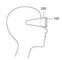
도 1은 가상현실을 구현한 표시장치를 착용한 모습을 나타낸 도면이다.Figure 1 is a drawing showing a person wearing a display device that implements virtual reality.
앞에 언급한 다양한 표시장치(100)는 가상현실 구현장치로도 사용할 수 있다. 가상현실을 구현하기 위해서는 사용자가 바라보는 방향 및 위치에 따른 공간적인 이미지를 보여주어야 하므로, 사용자의 머리 또는 눈의 이동에 따라 함께 움직일 수 있는 가볍고 작은 표시장치(100)를 활용하는 것이 용이하다. 따라서, 표시장치(100) 중에서는 모바일(Mobile) 또는 작은 사이즈의 테블릿 PC(Tablet PC) 등을 활용할 수 있다.The various display devices (100) mentioned above can also be used as virtual reality implementation devices. In order to implement virtual reality, it is necessary to show spatial images according to the direction and position that the user is looking at, so it is easy to utilize a light and small display device (100) that can move along with the movement of the user's head or eyes. Accordingly, among the display devices (100), a mobile or a small-sized tablet PC can be utilized.
문서나, 동영상을 보기 위한 표시장치(100)를 이용하여 가상현실 구현장치로 활용하기 위해서는 사용자의 눈 앞에 표시장치(100)를 고정시킬 수 있어야 한다. 따라서, 표시장치(100)를 고정시키기 위한 기구물(200)이 필요하다. 기구물은 다양한 재료와 형태로 제작될 수 있으며, 가상현실을 적절히 구현할 수 있도록 표시장치(100)와 사용자의 눈 사이의 거리를 조절할 수도 있다.In order to utilize a display device (100) for viewing documents or videos as a virtual reality implementation device, the display device (100) must be fixed in front of the user's eyes. Therefore, a device (200) for fixing the display device (100) is required. The device can be manufactured from various materials and shapes, and the distance between the display device (100) and the user's eyes can be adjusted so that virtual reality can be properly implemented.
즉, 사용자는 기존에 사용하고 있던 표시장치(100)를 활용함으로써, 가상현실 장비를 추가로 구입해야 하는 비용이 발생하지 않고 쉽게 가상현실 컨텐츠를 즐길 수 있다.That is, users can easily enjoy virtual reality content by utilizing the display device (100) they are currently using, without incurring the cost of purchasing additional virtual reality equipment.
도 2는 일 실시예에 따른 표시장치(100)를 나타낸 도면이다.FIG. 2 is a drawing showing a display device (100) according to one embodiment.
인간의 시야각은 약 200°이지만 실제 보이는 시야범위는 120°~140°이기 때문에 표시장치(100)를 사용자의 눈 앞에 고정시키면 실질적으로 눈이 위치하게 되는 중심영역(CA)과 주변영역(PA)만 일부 보일뿐 사용자가 인지하지 못하는 어두운 영역(DA)이 표시장치(100)의 좌우에 발생하게 된다. 또한, 일반적인 용도로 표시장치(100)를 사용할 때보다 표시장치(100)와 사용자의 눈 사이의 거리가 가까워지게 되므로 사용자는 표시장치(100)의 해상도를 보다 잘 인지할 수 있게 된다.The human field of vision is approximately 200°, but the actual field of vision is 120° to 140°. Therefore, when the display device (100) is fixed in front of the user's eyes, only the central area (CA) and the peripheral area (PA) where the eyes are actually located are partially visible, and a dark area (DA) that the user cannot perceive occurs on the left and right of the display device (100). In addition, since the distance between the display device (100) and the user's eyes becomes closer than when the display device (100) is used for general purposes, the user can better perceive the resolution of the display device (100).
즉, 표시장치(100)에 가상현실 구현을 위한 화면이 표시될 때 중심영역(CA)에 위치한 화소들에는 암점이나 휘점이 발생하지 않아야 하고, 주변영역(PA)에 위치한 화소들은 일반적인 용도로 표시장치(100)를 사용할 때 표시되는 화면 상태와 유사한 화질을 갖도록 표시장치(100)의 표시영역을 분리하여 관리할 필요가 있다. 그리고, 사용자가 인지하지 못하는 어두운 영역(DA)은 화면이 표시되지 않도록 어두운 영역(DA)에 위치하는 화소들을 오프(off)시킴으로써 블랙화면을 구현할 수 있다. 실질적으로 표시장치(100)의 일부 영역을 구동하지 않게 함으로써 소비전력을 감소시킬 수 있지만, 보다 실질적인 효과로는 화면의 고속구동이 가능하게 된다.That is, when a screen for implementing virtual reality is displayed on the display device (100), the pixels located in the central area (CA) should not have dark spots or bright spots, and the pixels located in the peripheral area (PA) should have similar picture quality to the screen state displayed when the display device (100) is used for general purposes. It is necessary to manage the display area of the display device (100) separately. In addition, a black screen can be implemented by turning off the pixels located in the dark area (DA) that the user does not recognize so that the screen is not displayed. In fact, power consumption can be reduced by not driving a part of the display device (100), but a more practical effect is that high-speed driving of the screen becomes possible.
일반적인 용도로 사용되는 표시장치(100)의 구동속도는 약 60Hz이지만, 가상현실을 구현하기 위해서는 약 75Hz 이상의 구동속도가 필요하다. 구동속도가 빨라질수록 움직이는 영상이 눈의 잔상효과로 인해 중첩되어 영상이 번져보이는 현상이 심하게 발생하므로 영상이 화면에 유지되는 시간을 줄여서 영상의 중첩을 최소화하고 응답속도가 빠른것처럼 인식할 수 있게 할 수 있다. 60Hz 구동시 16ms의 유지시간을 갖지만, 75Hz 이상 구동시 2ms의 낮은 유지시간을 갖게 함으로써 영상의 번짐(motion blur)을 방지할 수 있다. 이를 Low Persistency(LP)라고 지칭하기도 하며, 이하의 설명에서 이를 이용하는 방법을 LP 모드(LP mode) 또는 가상현실 모드라고 지칭하도록 한다.The driving speed of a display device (100) used for general purposes is approximately 60 Hz, but a driving speed of approximately 75 Hz or higher is required to implement virtual reality. As the driving speed increases, the phenomenon in which moving images overlap due to the afterimage effect of the eyes and the image appears blurred occurs more severely, so the time that the image is maintained on the screen can be reduced to minimize the overlapping of images and make it seem as if the response speed is fast. When driven at 60 Hz, the retention time is 16 ms, but when driven at 75 Hz or higher, the retention time is reduced to 2 ms, thereby preventing image blur. This is also referred to as Low Persistency (LP), and the method of utilizing this in the following description will be referred to as LP mode or virtual reality mode.
또한, LP 모드를 구현하기 위한 표시장치(100)에 유기발광패널을 사용함으로써, 화소를 구동시키는 구동회로 및 유기발광소자를 실시간으로 보상하는 시간이 충분히 확보되어야 한다. 구동속도가 빨라짐에 따라 한 프레임이 화면에 표시될 수 있는 시간이 줄어들게 되고 개별 화소가 구동되는 시간도 줄어들게 되므로 화소 보상시간을 충분히 갖지 못할 수 있다. 따라서, 필요한 화면의 일부분만 구동시키고 필요하지 않은 부분은 구동시키지 않음으로써 화소 보상시간을 확보할 수 있다. 또한, 고속구동을 하면서 일반적인 구동속도인 60Hz와 동일한 화소 보상시간을 유지할 수 있는 효과가 있다.In addition, by using an organic light-emitting panel in the display device (100) for implementing the LP mode, sufficient time must be secured to compensate the driving circuit and the organic light-emitting element that drive the pixels in real time. As the driving speed increases, the time for one frame to be displayed on the screen decreases and the time for individual pixels to be driven also decreases, so that sufficient pixel compensation time may not be available. Accordingly, pixel compensation time can be secured by driving only a necessary part of the screen and not driving an unnecessary part. In addition, there is an effect of being able to maintain the same pixel compensation time as the general driving speed of 60 Hz while performing high-speed driving.
이미지를 보거나 동영상을 시청하는 등 일반적인 용도로 표시장치(100)를 사용할 때에는 일반 모드(normal mode)로 동작하게 하고, 가상현실을 구현하기 위한 장치로 사용할 때에는 LP 모드(LP mode)로 동작하게 할 수 있는데, LP 모드 구현시 구동속도는 높이고 유지시간은 줄이며 어두운 영역(DA)에 배치된 화소를 오프(off)시킴으로써 화면의 고속구동을 원활히 할 수 있다.When the display device (100) is used for general purposes such as viewing images or watching videos, it can be operated in normal mode, and when used as a device for implementing virtual reality, it can be operated in LP mode. When implementing LP mode, the operating speed is increased, the maintenance time is reduced, and pixels placed in a dark area (DA) are turned off, thereby enabling smooth high-speed operation of the screen.
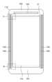
도 3은 일 실시예에 따른 표시패널을 나타낸 도면이다.FIG. 3 is a drawing showing a display panel according to one embodiment.
도 2에서 언급된 표시장치(100)를 구현하기 위해 도 3에 도시된 표시패널을 이용할 수 있다. 표시패널은 복수의 화소들이 배치되어 화면을 표시하는 표시영역(D)과 화면이 표시되지 않는 비표시영역(ND)으로 구분되는 기판(110)을 포함한다. 표시영역(D)을 둘러싸고 있는 비표시영역(ND)에는 발광하지 않는 더미화소(dummy pixel)가 배치될 수 있다.In order to implement the display device (100) mentioned in Fig. 2, the display panel illustrated in Fig. 3 can be used. The display panel includes a substrate (110) divided into a display area (D) in which a plurality of pixels are arranged to display a screen and a non-display area (ND) in which a screen is not displayed. A dummy pixel that does not emit light can be arranged in the non-display area (ND) surrounding the display area (D).
표시영역(D)에 배치된 복수의 화소들은 데이터 배선 및 게이트 배선을 통해 각각 데이터 신호 및 게이트 신호를 전달받아 동작한다. 데이터 배선은 기판(110)의 상단부에 배치된 데이터 구동회로(data driver, 120)에 연결되어 신호를 인가받을 수 있다. 데이터 구동회로(120)는 구동칩(driver-ic)의 형태로 제작되어 기판(110) 상에 부착될 수 있으나, 데이터 구동회로(120)의 위치나 형태가 이에 한정되지는 않는다.A plurality of pixels arranged in the display area (D) receive data signals and gate signals through data lines and gate lines, respectively, and operate. The data lines can be connected to a data driver circuit (data driver, 120) arranged on the upper part of the substrate (110) to receive signals. The data driver circuit (120) can be manufactured in the form of a driver chip (driver-ic) and attached to the substrate (110), but the position or shape of the data driver circuit (120) is not limited thereto.
게이트 배선은 화소의 발광을 제어하는 트랜지스터의 게이트 전극을 제어하는 에미션 배선(emission line)을 포함할 수 있으며 에미션 배선은 에미션 구동회로(emission driver, 140)에 연결되어 에미션 신호를 인가받는다. 게이트 배선은 화소의 발광을 제어하는 트랜지스터 이외에 신호를 스위칭하는 스위칭 트랜지스터의 게이트 전극을 제어하는 스캔 배선(scan line)을 포함하고, 스캔 배선을 일반적으로 게이트 배선(gate line)이라고 지칭할 수도 있다. 스캔 배선은 스캔 구동회로(scan driver, 130)에 연결되어 스캔 신호를 인가받는다.The gate wiring may include an emission wiring that controls a gate electrode of a transistor that controls light emission of a pixel, and the emission wiring is connected to an emission driver circuit (140) to receive an emission signal. The gate wiring includes a scan wiring that controls a gate electrode of a switching transistor that switches a signal in addition to the transistor that controls light emission of the pixel, and the scan wiring may be generally referred to as a gate wiring. The scan wiring is connected to a scan driver circuit (130) to receive a scan signal.
스캔 구동회로(130)와 에미션 구동회로(140)를 통칭하여 게이트 구동회로(gate driver)라고 부르기도 하며, 게이트 구동회로는 기판(110) 상에 직접 증착되어 형성된 GIP 회로일 수 있다. 게이트 구동회로는 좌우에 대칭으로 설계될 수 있지만, 이에 한정되지는 않는다.The scan driving circuit (130) and the emission driving circuit (140) are collectively called gate driving circuits, and the gate driving circuit may be a GIP circuit formed by direct deposition on the substrate (110). The gate driving circuit may be designed symmetrically on the left and right, but is not limited thereto.
가상현실 구현을 하기 위한 LP 모드에서 표시패널은 표시영역(D)의 일부영역에 배치된 화소를 오프(off)시킬 수 있어야 한다. 가상현실 구현시에는 도 3에 도시된 표시패널을 시계방향 또는 반시계방향으로 90°회전한 상태에서 화면이 표시되므로, 도 3에 도시된 상태에서는 표시패널의 상단부와 하단부의 일부영역에 배치된 화소를 오프(off)시킬 수 있어야 한다. 즉, 중심영역(CA)을 포함하는 주변영역(PA)의 위/아래로 어두운 영역(DA)을 설정할 수 있다. 이때, 어두운 영역(DA)은 표시영역(D)의 일부를 포함하는 영역이고 제2 영역이라고 지칭할 수 있으며, 중심영역(CA)을 포함하는 주변영역(PA)은 제1 영역이라고 지칭할 수 있다.In the LP mode for implementing virtual reality, the display panel must be able to turn off pixels arranged in a part of the display area (D). When implementing virtual reality, the screen is displayed in a state where the display panel illustrated in Fig. 3 is rotated 90° clockwise or counterclockwise, so in the state illustrated in Fig. 3, pixels arranged in a part of the upper and lower parts of the display panel must be able to be turned off. That is, a dark area (DA) can be set above/below a peripheral area (PA) including a central area (CA). At this time, the dark area (DA) is an area including a part of the display area (D) and can be referred to as a second area, and the peripheral area (PA) including the central area (CA) can be referred to as a first area.
어두운 영역(DA)의 화소들은 LP 모드로 동작하고, 주변영역(PA)의 화소들은 일반 모드로 동작한다. 화소들을 LP 모드와 일반 모드로 동작시키기 위한 게이트 구동회로를 알아보기 위해 주변영역(PA)과 어두운 영역(DA)의 경계부분이면서 좌측 상단부에 위치한 A영역과 좌측 하단부에 위치한 B영역을 나타낸 블록도를 이어서 설명하고자 한다.Pixels in the dark area (DA) operate in LP mode, and pixels in the peripheral area (PA) operate in normal mode. In order to understand the gate driving circuit for operating pixels in LP mode and normal mode, a block diagram showing area A located in the upper left corner and area B located in the lower left corner, which are the boundaries between the peripheral area (PA) and the dark area (DA), will be explained next.
도 4a는 도 3의 A영역을 확대하여 나타낸 블록도이다.Figure 4a is a block diagram showing an enlarged view of area A of Figure 3.
n(n은 2이상의 자연수)행의 화소들이 배치된 표시패널에는 각 행에 순차적으로 신호를 전달하기 위한 n개의 스테이지(stage)로 이루어진 게이트 구동회로가 있다. 구체적으로 설명하면, 게이트 구동회로는 스캔 구동회로(130)와 에미션 구동회로(140)를 포함하고, 스캔 구동회로(130)와 에미션 구동회로(140) 각각은 n개의 스캔 스테이지(S Stage(n))와 n개의 에미션 스테이지(EM Stage(n))를 포함한다. 첫번째 스테이지 이전과 n번째 스테이지 이후에는 각각 더미 스테이지를 포함할 수 있다.A display panel on which pixels are arranged in n rows (where n is a natural number greater than or equal to 2) has a gate driving circuit composed of n stages for sequentially transmitting signals to each row. Specifically, the gate driving circuit includes a scan driving circuit (130) and an emission driving circuit (140), and each of the scan driving circuit (130) and the emission driving circuit (140) includes n scan stages (S Stage(n)) and n emission stages (EM Stage(n)). A dummy stage may be included before the first stage and after the nth stage, respectively.
스캔 스테이지와 에미션 스테이지의 구성 및 역할은 유사하다. 단지, 스캔 스테이지는 두 개의 클럭 신호를 받아서 출력신호를 발생시키고, 에미션 스테이지는 한 개의 클럭 신호를 받아서 출력신호를 발생시킨다는 점에 차이가 있다. 이때, 스캔 스테이지는 두 개의 클럭 신호를 이용하여 펄스를 발생시킬 수 있는 2상 회로를 도시하였지만, 이에 한정되지는 않는다.The configuration and role of the scan stage and the emission stage are similar. The only difference is that the scan stage receives two clock signals and generates an output signal, while the emission stage receives one clock signal and generates an output signal. In this case, the scan stage is illustrated as a two-phase circuit that can generate a pulse using two clock signals, but is not limited thereto.
스캔 구동회로를 동작시키는데 기본적으로 필요한 신호는 두 개의 게이트 클럭 신호인 게이트 클럭 신호1(Gate CLocK1; GCLK1)과 게이트 클럭 신호2(Gate CLocK2; GCLK2), 그리고 게이트 스타트 펄스 전압(Gate STart pulse Voltage; GVST), 게이트 하이 전압(Gate High Voltage; VGH), 및 게이트 로우 전압(Gate Low Voltage; VGL)을 포함한다.The signals basically required to operate the scan driver circuit include two gate clock signals, Gate Clock Signal 1 (Gate CLocK1; GCLK1) and Gate Clock Signal 2 (Gate CLocK2; GCLK2), and Gate Start Pulse Voltage (GVST), Gate High Voltage (VGH), and Gate Low Voltage (VGL).
스캔 구동회로에 입력되는 신호와 유사하게 에미션 구동회로를 동작시키는데 기본적으로 필요한 신호는 두 개의 에미션 클럭 신호인 에미션 클럭 신호1(Emission CLocK1; ECLK1)과 에미션 클럭 신호2(Emission CLocK2; ECLK2), 그리고 에미션 스타트 펄스 전압(Emission STart pulse Voltage; EVST), 에미션 하이 전압(Emission High Voltage; VEH), 및 에미션 로우 전압(Emission Low Voltage; VEL)을 포함한다.Similar to the signals input to the scan driver circuit, signals basically required to operate the emission driver circuit include two emission clock signals, emission clock signal 1 (Emission CLocK1; ECLK1) and emission clock signal 2 (Emission CLocK2; ECLK2), and an emission start pulse voltage (Emission STart pulse Voltage; EVST), an emission high voltage (Emission High Voltage; VEH), and an emission low voltage (Emission Low Voltage; VEL).
이러한 신호들이 스테이지 각각에 입력신호로 인가되면 각 스테이지가 출력신호를 발생시켜서 각 행에 배열된 화소들의 구동을 제어할 수 있다.When these signals are applied as input signals to each stage, each stage generates an output signal to control the operation of the pixels arranged in each row.
스테이지들은 각각 이전 스테이지에서 발생시키는 출력신호를 받아서 동작하는 캐스캐이드(cascade) 방식으로 동작한다. 따라서, 일부 행 이후에 배치된 화소들을 오프(off)시키기 위해서는 처음으로 오프(off)시키고자 하는 행의 스테이지에 입력되는 신호를 제어함으로써 구현할 수 있다. 마찬가지로 일부 행 이후에 배치된 화소들을 온(on)시키기 위해서는 처음으로 온(on)시키고자 하는 행의 스테이지에 입력되는 신호를 제어함으로써 구현할 수 있다. 따라서, 일부 행 이후에 배치된 화소의 온(on)/오프(off)를 제어할 수 있도록 게이트 구동회로에는 인에이블 신호(Enable) 및 디스에이블 신호(Disable)를 인가할 수 있는 배선이 배치되고, 이를 각각 인에이블 배선 및 디스에이블 배선이라고 할 수 있다.The stages operate in a cascade manner, each receiving an output signal generated from the previous stage. Therefore, in order to turn off pixels positioned after some rows, this can be implemented by controlling the signal input to the stage of the row to be turned off first. Similarly, in order to turn on pixels positioned after some rows, this can be implemented by controlling the signal input to the stage of the row to be turned on first. Therefore, in order to control the on/off of pixels positioned after some rows, wiring capable of applying an enable signal and a disable signal is arranged in the gate driving circuit, and these can be referred to as enable wiring and disable wiring, respectively.
이하에서 언급되는 회로에 사용되는 트랜지스터는 P형 트랜지스터를 예로써 들고자한다. 따라서, 인에이블 배선은 LP 모드가 동작시 활성화되는 배선으로서 로우 전압이 인가되고, 디스에이블 배선은 LP 모드가 동작시 비활성화되는 배선으로서 하이 전압이 인가된다. 다만, 이하에서 언급되는 회로에 사용되는 트랜지스터로 N형 트랜지스터도 사용될 수 있다.The transistor used in the circuit mentioned below will be a P-type transistor as an example. Accordingly, the enable wiring is a wiring that is activated when the LP mode operates and a low voltage is applied, and the disable wiring is a wiring that is deactivated when the LP mode operates and a high voltage is applied. However, an N-type transistor may also be used as the transistor used in the circuit mentioned below.
오프(off)시키고자 하는 행의 화소가 첫번째 행의 화소((1)st Pixel)부터 j번째 행의 화소((j)th Pixel, 1<j<n, j는 자연수)라고 할 때, 게이트 구동회로는 첫번째 스테이지에 입력되는 스타트 펄스 전압을 제어하기 위한 제1 컨트롤 트랜지스터(T11, T12)를 포함한다.When the pixels of a row to be turned off are pixels of the first row ((1)st Pixel) to pixels of the jth row ((j)th Pixel, 1<j<n, j is a natural number), the gate driving circuit includes a first control transistor (T11, T12) for controlling the start pulse voltage input to the first stage.
스캔 스테이지의 경우, 제1 컨트롤 트랜지스터(T11)의 일전극은 게이트 스타트 펄스 전압(GVST)이 인가되는 배선에 연결되고, 다른 일전극은 첫번째 스캔 스테이지(S Stage(1)) 또는 더미 스캔 스테이지(S Dummy)에 입력신호로서 인가될 수 있도록 입력단에 연결되며, 제1 컨트롤 트랜지스터(T11)의 게이트 전극은 디스에이블 신호가 인가되는 배선에 연결된다. LP 모드 동안에는 디스에이블 배선에 하이 전압이 인가되므로, 제1 컨트롤 트랜지스터(T11)는 턴오프(turn-off)되어 게이트 스타트 펄스 전압(GVST)이 첫번째 스캔 스테이지(S Stage(1))에 인가되지 않으므로 첫번째 스캔 스테이지(S Stage(1)) 및 이어지는 스캔 스테이지에서도 정상적인 출력신호가 발생하지 않게 된다. 따라서, 첫번째 행의 화소((1)st Pixel) 및 이어지는 행의 화소에도 정상적인 구동신호가 입력되지 않으므로 화소에 인가되는 신호를 차단할 수 있다.In the case of the scan stage, one electrode of the first control transistor (T11) is connected to a wiring to which a gate start pulse voltage (GVST) is applied, the other electrode is connected to an input terminal so as to be applied as an input signal to the first scan stage (S Stage (1)) or a dummy scan stage (S Dummy), and the gate electrode of the first control transistor (T11) is connected to a wiring to which a disable signal is applied. Since a high voltage is applied to the disable wiring during the LP mode, the first control transistor (T11) is turned off and the gate start pulse voltage (GVST) is not applied to the first scan stage (S Stage (1)), so that a normal output signal is not generated in the first scan stage (S Stage (1)) and the subsequent scan stages. Accordingly, a normal driving signal is not input to the pixels of the first row ((1)st Pixel) and the pixels of the subsequent rows, so that the signal applied to the pixels can be blocked.
또한, 에미션 스테이지의 경우에도 마찬가지로 제1 컨트롤 트랜지스터(T12)가 에미션 구동회로에 배치될 수 있다. 제1 컨트롤 트랜지스터(T12)의 일전극은 에미션 스타트 펄스 전압(EVST)이 인가되는 배선에 연결되고, 제1 컨트롤 트랜지스터(T12)의 다른 일전극은 첫번째 에미션 스테이지(EM Stage(1)) 또는 더미 에미션 스테이지(EM Dummy)에 입력신호로서 인가될 수 있도록 입력단에 연결되며, 제1 컨트롤 트랜지스터(T12)의 게이트 전극은 디스에이블 신호가 인가되는 배선에 연결된다. 따라서, 상술한 바와 같이 제1 컨트롤 트랜지스터(T12)를 배치함으로써, 첫번째 행의 화소((1)st Pixel) 및 이어지는 행의 화소에 연결된 에미션 배선에 인가되는 정상적인 구동신호를 차단할 수 있다.In addition, in the case of the emission stage, the first control transistor (T12) may also be arranged in the emission driving circuit. One electrode of the first control transistor (T12) is connected to a wiring to which an emission start pulse voltage (EVST) is applied, the other electrode of the first control transistor (T12) is connected to an input terminal so as to be applied as an input signal to the first emission stage (EM Stage (1)) or a dummy emission stage (EM Dummy), and the gate electrode of the first control transistor (T12) is connected to a wiring to which a disable signal is applied. Therefore, by arranging the first control transistor (T12) as described above, it is possible to block a normal driving signal applied to the emission wiring connected to the pixels of the first row ((1)st Pixel) and the pixels of the subsequent rows.
따라서, 첫번째 스캔 스테이지(S Stage(1)) 및 첫번째 에미션 스테이지(EM Stage(1))의 입력단에 인가되는 스타트 펄스 전압을 제어하기 위한 제1 컨트롤 트랜지스터를 배치함으로써, 첫번째 행의 화소((1)st Pixel)를 포함하여 그 이후에 배치된 화소들에 인가되는 정상적인 구동신호를 차단하여 화소들을 오프(off)시킬 수 있다.Therefore, by arranging the first control transistor for controlling the start pulse voltage applied to the input terminal of the first scan stage (S Stage (1)) and the first emission stage (EM Stage (1)), the normal driving signal applied to the pixels arranged thereafter, including the pixels of the first row ((1)st Pixel), can be blocked to turn the pixels off.
이어서, 첫번째 행의 화소((1)st Pixel)부터 차단된 신호가 j번째 행의 화소((j)th Pixel)까지 이어지다가, (j+1)번째 행의 화소((j+1)th Pixel)부터 화소들이 온(on)되기 위해서는 (j+1)번째 스테이지에 다시 스타트 펄스 전압을 인가해야 하므로 (j+1)번째 스테이지의 입력신호 입력단에 제2 컨트롤 트랜지스터(T13, T14)를 배치시킬 수 있다.Next, since the signal blocked from the pixel of the first row ((1)st Pixel) continues to the pixel of the jth row ((j)th Pixel), and in order for the pixels from the pixel of the (j+1)th row ((j+1)th Pixel) to turn on, a start pulse voltage must be applied again to the (j+1)th stage, so a second control transistor (T13, T14) can be placed at the input signal input terminal of the (j+1)th stage.
스캔 스테이지의 경우, 제2 컨트롤 트랜지스터(T13)의 일전극은 게이트 스타트 펄스 전압(GVST)이 인가되는 배선에 연결되고, 다른 일전극은 (j+1)번째 스캔 스테이지(S Stage(j+1))의 입력신호 입력단에 연결되며, 제2 컨트롤 트랜지스터(T13)의 게이트 전극은 인에이블 배선에 연결된다. LP 모드 동안에는 인에이블 배선에 로우 전압이 인가되므로, 제2 컨트롤 트랜지스터(T13)가 턴온(turn-on)되어 게이트 스타트 펄스 전압(GVST)이 (j+1)번째 스캔 스테이지(S Stage(j+1))에 인가되므로 (j+1)번째 스캔 스테이지로부터 정상 구동신호를 출력할 수 있다.In the case of the scan stage, one electrode of the second control transistor (T13) is connected to a wiring to which a gate start pulse voltage (GVST) is applied, the other electrode is connected to an input signal input terminal of the (j+1)th scan stage (S Stage(j+1)), and the gate electrode of the second control transistor (T13) is connected to an enable wiring. Since a low voltage is applied to the enable wiring during the LP mode, the second control transistor (T13) is turned on and the gate start pulse voltage (GVST) is applied to the (j+1)th scan stage (S Stage(j+1)), so that a normal driving signal can be output from the (j+1)th scan stage.
또한, 에미션 스테이지의 경우에도 마찬가지로 제2 컨트롤 트랜지스터(T13)가 에미션 구동회로에 배치될 수 있다. 제2 컨트롤 트랜지스터(T13)의 일전극은 에미션 스타트 펄스 전압(EVST)이 인가되는 배선에 연결되고, 제2 컨트롤 트랜지스터(T13)의 다른 일전극은 첫번째 에미션 스테이지(EM Stage(1))의 입력신호 입력단에 연결되며, 제2 컨트롤 트랜지스터(T13)의 게이트 전극은 인에이블 배선에 연결된다. 따라서, 인에이블 신호에 의해 제2 컨트롤 트랜지스터(T14)가 턴온(turn-on)되어 에미션 스타트 펄스 전압(EVST)이 (j+1)번째 에미션 스테이지(EM Stage(j+1))에 인가되므로 (j+1)번째 에미션 스테이지로부터 정상 구동신호를 출력할 수 있다.In addition, in the case of the emission stage, a second control transistor (T13) may also be arranged in the emission driving circuit. One electrode of the second control transistor (T13) is connected to a wiring to which an emission start pulse voltage (EVST) is applied, the other electrode of the second control transistor (T13) is connected to an input signal input terminal of the first emission stage (EM Stage (1)), and a gate electrode of the second control transistor (T13) is connected to an enable wiring. Therefore, the second control transistor (T14) is turned on by the enable signal, and the emission start pulse voltage (EVST) is applied to the (j+1)th emission stage (EM Stage (j+1)), so that a normal driving signal can be output from the (j+1)th emission stage.
따라서, (j+1)번째 스캔 스테이지(S Stage(j+1)) 및 (j+1)번째 에미션 스테이지(EM Stage(j+1))의 입력신호 입력단에 스타트 펄스 전압을 제어하기 위한 제2 컨트롤 트랜지스터를 배치함으로써, (j+1)번째 행의 화소((j+1)th Pixel)를 포함하여 그 이후에 배치된 화소들에 정상적인 구동신호를 인가하여 화소들을 온(on)시킬 수 있다.Therefore, by arranging a second control transistor for controlling the start pulse voltage at the input signal input terminal of the (j+1)th scan stage (S Stage(j+1)) and the (j+1)th emission stage (EM Stage(j+1)), a normal driving signal can be applied to the pixels arranged thereafter, including the pixels in the (j+1)th row ((j+1)th Pixel), to turn on the pixels.
또한, (j+1)번째 행의 화소((j+1)th Pixel)부터 정상동작시키기 위해서는 (j+1)번째 스테이지가 j번째 스테이지로부터 입력받는 입력신호를 차단해야 하므로 (j+1)번째 스테이지의 입력신호 입력단에 차단 트랜지스터(cut-off transistor, T21, T22)를 배치할 수 있다. 이때, j번째 스테이지에서 출력되는 출력신호를 차단시키는 이유는 j번째 스테이지에서 출력되는 출력신호가 정상적인 신호가 아니기 때문이다.In addition, in order to operate normally from the pixel of the (j+1)th row ((j+1)th Pixel), the (j+1)th stage must block the input signal received from the jth stage, so a cut-off transistor (T21, T22) can be placed at the input signal input terminal of the (j+1)th stage. At this time, the reason for blocking the output signal output from the jth stage is because the output signal output from the jth stage is not a normal signal.
스캔 스테이지의 경우, 제1 차단 트랜지스터(T21)의 일전극은 j번째 스캔 스테이지(S Stage(j))의 출력신호 출력단에 연결되고, 제1 차단 트랜지스터(T21)의 다른 일전극은 (j+1)번째 스캔 스테이지(S Stage(j+1))의 입력신호 입력단에 연결되며, 제1 차단 트랜지스터(T21)의 게이트 전극은 디스에이블 배선에 연결된다. LP 모드 동안에는 디스에이블 배선에 하이 전압이 인가되므로, 제1 차단 트랜지스터(T21)가 턴오프(turn-off)되어 j번째 스캔 스테이지(S Stage(j))의 출력신호가 차단될 수 있다.In the case of the scan stage, one electrode of the first blocking transistor (T21) is connected to the output signal output terminal of the jth scan stage (S Stage(j)), the other electrode of the first blocking transistor (T21) is connected to the input signal input terminal of the (j+1)th scan stage (S Stage(j+1)), and the gate electrode of the first blocking transistor (T21) is connected to the disable wiring. Since a high voltage is applied to the disable wiring during the LP mode, the first blocking transistor (T21) is turned off so that the output signal of the jth scan stage (S Stage(j)) can be blocked.
또한, 에미션 스테이지의 경우에도 마찬가지로 제1 차단 트랜지스터(T22)가 에미션 구동회로에 배치될 수 있다. 제1 차단 트랜지스터(T22)의 일전극은 j번째 에미션 스테이지(EM Stage(j))의 출력신호 출력단에 연결되고, 제1 차단 트랜지스터(T22)의 다른 일전극은 (j+1)번째 에미션 스테이지(EM Stage(j+1))의 입력신호 입력단에 연결되며, 제1 차단 트랜지스터(T22)의 게이트 전극은 디스에이블 배선에 연결된다. 따라서, 디스에이블 신호에 의해 제1 차단 트랜지스터(T22)가 턴오프(turn-off)되어 j번째 에미션 스테이지(EM Stage(j))의 출력신호가 차단될 수 있다.In addition, in the case of the emission stage, the first blocking transistor (T22) may also be arranged in the emission driving circuit. One electrode of the first blocking transistor (T22) is connected to an output signal output terminal of the j-th emission stage (EM Stage(j)), the other electrode of the first blocking transistor (T22) is connected to an input signal input terminal of the (j+1)-th emission stage (EM Stage(j+1)), and the gate electrode of the first blocking transistor (T22) is connected to a disable wiring. Therefore, the first blocking transistor (T22) may be turned off by the disable signal, so that the output signal of the j-th emission stage (EM Stage(j)) may be blocked.
따라서, (j+1)번째 스캔 스테이지(S Stage(j+1)) 및 (j+1)번째 에미션 스테이지(EM Stage(j+1))의 입력신호 입력단에 j번째 스캔 스테이지(S Stage(j)) 및 j번째 에미션 스테이지(EM Stage(j))의 출력신호를 제어할 수 있는 차단 트랜지스터를 배치함으로써, (j+1)번째 행의 화소((j+1)th Pixel)를 포함하여 그 이후에 배치된 화소들에 정상적인 구동신호를 인가하여 화소들을 온(on)시킬 수 있다.Therefore, by arranging a blocking transistor capable of controlling the output signal of the jth scan stage (S Stage(j)) and the jth emission stage (EM Stage(j)) at the input signal input terminals of the (j+1)th scan stage (S Stage(j+1)) and the (j+1)th emission stage (EM Stage(j+1)), a normal driving signal can be applied to the pixels arranged thereafter, including the pixels in the (j+1)th row ((j+1)th Pixel), to turn on the pixels.
도 4b는 도 3의 B영역을 확대하여 나타낸 블록도이다.Figure 4b is a block diagram showing an enlarged view of area B in Figure 3.
(j+1)번째 행의 화소((j+1)th Pixel)부터 k(j<k<n, k는 자연수)번째 행의 화소((k)th Pixel)까지는 주변영역(PA)에 배치된 화소들이 온(on) 상태에서 정상동작을 하지만, (k+1)번째 행의 화소((k+1)th Pixel)부터 오프(off) 상태로 전환하기 위해서는 k번째 스테이지에서 출력되는 출력신호를 (k+1)번째 스테이지에 인가되지 못하도록 차단할 수 있는 차단 트랜지스터(T23, T24)를 배치할 수 있다.The pixels arranged in the peripheral area (PA) from the pixel of the (j+1)th row ((j+1)th Pixel) to the pixel of the kth row ((k)th Pixel) (j<k<n, k is a natural number) (j+1)th Pixel) operate normally in the on state, but in order to switch from the pixel of the (k+1)th row ((k+1)th Pixel) to the off state, a blocking transistor (T23, T24) that can block the output signal output from the kth stage from being applied to the (k+1)th stage can be arranged.
스캔 스테이지의 경우, 제2 차단 트랜지스터(T23)가 스캔 구동회로에 배치될 수 있다. 제2 차단 트랜지스터(T23)의 일전극은 k번째 스캔 스테이지(S Stage(k))의 출력신호 출력단에 연결되고, 제2 차단 트랜지스터(T23)의 다른 일전극은 (k+1)번째 스캔 스테이지(S Stage(k+1))의 입력신호 입력단에 연결되며, 제2 차단 트랜지스터(T23)의 게이트 전극은 디스에이블 배선에 연결된다. LP 모드 동안에는 디스에이블 배선에 하이 전압이 인가되므로, 제2 차단 트랜지스터(T23)가 턴오프(turn-off)되어 k번째 스캔 스테이지(S Stage(k))의 출력신호가 차단될 수 있다.In the case of the scan stage, a second blocking transistor (T23) may be arranged in the scan driving circuit. One electrode of the second blocking transistor (T23) is connected to an output signal output terminal of the kth scan stage (S Stage(k)), the other electrode of the second blocking transistor (T23) is connected to an input signal input terminal of the (k+1)th scan stage (S Stage(k+1)), and a gate electrode of the second blocking transistor (T23) is connected to a disable wiring. Since a high voltage is applied to the disable wiring during the LP mode, the second blocking transistor (T23) may be turned off to block the output signal of the kth scan stage (S Stage(k)).
또한, 에미션 스테이지의 경우에도 마찬가지로 제2 차단 트랜지스터(T24)가 에미션 구동회로에 배치될 수 있다. 제2 차단 트랜지스터(T24)의 일전극은 k번째 에미션 스테이지(EM Stage(k))의 출력신호 출력단에 연결되고, 제2 차단 트랜지스터(T24)의 다른 일전극은 (k+1)번째 에미션 스테이지(EM Stage(k+1))의 입력신호 입력단에 연결되며, 제2 차단 트랜지스터(T24)의 게이트 전극은 디스에이블 배선에 연결된다. 따라서, 디스에이블 신호에 의해 제2 차단 트랜지스터(T24)가 턴오프(turn-off)되므로 k번째 에미션 스테이지(EM Stage(k))의 출력신호가 차단될 수 있다.In addition, in the case of the emission stage, a second blocking transistor (T24) may also be arranged in the emission driving circuit. One electrode of the second blocking transistor (T24) is connected to an output signal output terminal of the kth emission stage (EM Stage(k)), the other electrode of the second blocking transistor (T24) is connected to an input signal input terminal of the (k+1)th emission stage (EM Stage(k+1)), and a gate electrode of the second blocking transistor (T24) is connected to a disable wiring. Therefore, since the second blocking transistor (T24) is turned off by the disable signal, the output signal of the kth emission stage (EM Stage(k)) can be blocked.
따라서, (k+1)번째 스캔 스테이지(S Stage(k+1)) 및 (k+1)번째 에미션 스테이지(EM Stage(k+1))의 입력신호 입력단에 k번째 스캔 스테이지(S Stage(k)) 및 k번째 에미션 스테이지(EM Stage(k))의 출력신호를 제어할 수 있는 차단 트랜지스터를 배치함으로써, (k+1)번째 행의 화소((k+1)th Pixel)를 포함하여 그 이후에 배치된 화소들을 오프(off)시킬 수 있다.Therefore, by arranging a blocking transistor capable of controlling the output signal of the kth scan stage (S Stage(k)) and the kth emission stage (EM Stage(k)) at the input signal input terminals of the (k+1)th scan stage (S Stage(k+1)) and the (k+1)th emission stage (EM Stage(k+1)), the pixels arranged thereafter, including the pixels in the (k+1)th row ((k+1)th Pixel), can be turned off.
도 4a 및 도 4b의 게이트 구동회로에 배치된 트랜지스터들의 위치 및 그에 따른 동작에 따른 본 명세서의 실시예에서는, k번째 스테이지에 입력되는 스타트 펄스 전압을 조절하기 위한 컨트롤 트랜지스터 및/또는 (k-1)번째 스테이지로부터 출력되어 k번째 스테이지에 입력되는 신호를 차단하기 위한 차단 트랜지스터를 배치함으로써, k번째 행 이후의 화소들을 온(on) 또는 오프(off)시켜서 구동해야 하는 화소의 개수를 축소하고 화소 보상시간을 확보하여 표시패널을 고속구동할 수 있다. 또한, 고속구동을 하면서 60Hz와 동일한 화소 보상 시간을 유지할 수 있는 효과가 있다.In the embodiment of the present specification according to the positions of the transistors arranged in the gate driving circuits of FIGS. 4A and 4B and the operations thereof, a control transistor for controlling a start pulse voltage input to the kth stage and/or a blocking transistor for blocking a signal output from the (k-1)th stage and input to the kth stage are arranged, thereby reducing the number of pixels that must be driven by turning on or off the pixels after the kth row, securing pixel compensation time, and enabling high-speed driving of the display panel. In addition, there is an effect of being able to maintain the same pixel compensation time as 60 Hz while performing high-speed driving.
오프(off)시키고자 하는 화소가 배치된 행에 연결된 스테이지의 이전 또는 이후에 컨트롤 트랜지스터 및 차단 트랜지스터를 배치함으로써 화소를 오프(off)시킬 수도 있지만, 앞서 설명한 바와 같이 이때 화소에 입력되는 신호가 완전히 차단되지 않고 왜곡된 임의의 신호가 인가될 수도 있다. 따라서, 이하에서는 화소를 확실히 오프(off)시키기 위해서 각 스테이지에서 하이 전압을 출력할 수 있도록 트랜지스터를 추가 배치하는 방법을 설명하고자 한다.It is also possible to turn off a pixel by placing a control transistor and a blocking transistor before or after the stage connected to the row in which the pixel to be turned off is placed. However, as described above, in this case, the signal input to the pixel is not completely blocked and a distorted arbitrary signal may be applied. Therefore, in the following, a method of additionally placing transistors so that each stage can output a high voltage in order to reliably turn the pixel off will be described.
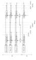
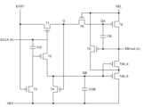
도 5a는 도 4a 및 도 4b의 어두운 영역(DA)에 포함된 스테이지를 구성하는 제1 실시예에 따른 회로도이다.FIG. 5a is a circuit diagram according to a first embodiment constituting a stage included in the dark area (DA) of FIGS. 4a and 4b.
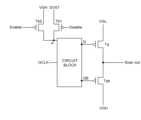
앞서 설명한 바와 같이, 각 스테이지들은 클럭 신호에 따라 로우 전압 또는 하이 전압을 출력시키는 역할을 한다. 따라서, 기본적으로 게이트 전극을 충전시키는 Q 노드를 가지는 제1 출력 트랜지스터(Tq)와 게이트 전극을 방전시키는 QB(Q Bar) 노드를 가지는 제2 출력 트랜지스터(Tqb)를 포함한다. 즉, Q 노드에 하이 전압이 입력되면 QB 노드에는 로우 전압이 입력되어야 하며 그 반대일 수도 있지만, 서로 다른 전압이 입력되도록 회로가 구성된다.As explained above, each stage has the function of outputting a low voltage or a high voltage according to a clock signal. Therefore, it basically includes a first output transistor (Tq) having a Q node that charges a gate electrode and a second output transistor (Tqb) having a QB (Q Bar) node that discharges the gate electrode. That is, when a high voltage is input to the Q node, a low voltage must be input to the QB node, and vice versa, but the circuit is configured so that different voltages are input.
구체적으로 설명하면, 제1 출력 트랜지스터(Tq) 및 제2 출력 트랜지스터(Tqb)는 서로 직렬연결되고, 제1 출력 트랜지스터(Tq) 및 제2 출력 트랜지스터(Tqb)가 서로 연결되지 않은 다른 일전극은 각각 게이트 로우 전압(VGL) 및 게이트 하이 전압(VGH)에 연결될 수 있다. 따라서, 클럭 신호에 따라 제1 출력 트랜지스터(Tq) 또는 제2 출력 트랜지스터(Tqb)가 선택되어 로우 전압 또는 하이 전압이 출력될 수 있다. 직렬연결된 제1 출력 트랜지스터(Tq)와 제2 출력 트랜지스터(Tqb), 그리고 Q 노드 및 QB 노드는 스테이지를 구성하는 모든 회로에 적용되는 구성이므로 이하에서는 설명을 생략하고자 한다.Specifically, the first output transistor (Tq) and the second output transistor (Tqb) are connected in series with each other, and the other electrode of the first output transistor (Tq) and the second output transistor (Tqb) which is not connected to each other can be connected to a gate low voltage (VGL) and a gate high voltage (VGH), respectively. Therefore, the first output transistor (Tq) or the second output transistor (Tqb) can be selected according to a clock signal to output a low voltage or a high voltage. The series-connected first output transistor (Tq) and second output transistor (Tqb), and the Q node and the QB node are configurations that are applied to all circuits constituting the stage, and therefore, their description will be omitted below.
LP 모드 동작 시에는 스테이지에서 하이 전압이 출력되어 화소에 전달되어야 블랙화면을 구현할 수 있기 때문에 LP 모드가 동작했을 때 하이 전압이 출력되기 위해서는 게이트 하이 전압(VGH)에 연결된 제2 출력 트랜지스터(Tqb)를 턴온(turn-on)시킬 수 있도록 회로를 구성해야 한다. 즉, 블록 트랜지스터(block transistor, Tb)가 스테이지에 구성될 수 있다. 블록 트랜지스터(block transistor, Tb)의 게이트 전극은 인에이블 배선에 연결되고, 블록 트랜지스터(block transistor, Tb)의 일전극은 QB 노드에 연결되며 블록 트랜지스터(block transistor, Tb)의 다른 일전극은 게이트 로우 전압(VGL) 또는 게이트 클럭 신호(GCLK)에 연결된다.When the LP mode is operated, a high voltage must be output from the stage and transmitted to the pixel to implement a black screen. Therefore, in order to output a high voltage when the LP mode is operated, a circuit must be configured to turn on the second output transistor (Tqb) connected to the gate high voltage (VGH). That is, a block transistor (Tb) can be configured in the stage. The gate electrode of the block transistor (Tb) is connected to the enable wiring, one electrode of the block transistor (Tb) is connected to the QB node, and the other electrode of the block transistor (Tb) is connected to a gate low voltage (VGL) or a gate clock signal (GCLK).
따라서, LP 모드가 동작되면 인에이블 신호에 로우 전압이 인가되어 블록 트랜지스터(Tb)를 턴온(turn-on)시킨다. 그리고, QB 노드에 로우 전압이 인가되어 제2 출력 트랜지스터(Tqb)를 턴온(turn-on)시키므로 하이 전압이 스테이지로부터 출력될 수 있다.Therefore, when the LP mode is activated, a low voltage is applied to the enable signal to turn on the block transistor (Tb). Then, a low voltage is applied to the QB node to turn on the second output transistor (Tqb), so that a high voltage can be output from the stage.
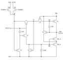
즉, 스테이지에 게이트 하이 전압에 연결된 출력 트랜지스터를 턴온(turn-on)시키기 위한 블록 트랜지스터를 배치함으로써, 인에이블 신호가 인가되었을 때 블록 트랜지스터가 배치된 스테이지에 연결된 행의 화소들을 오프(off)시킬 수 있다.That is, by arranging a block transistor for turning on an output transistor connected to a gate high voltage in a stage, the pixels in the row connected to the stage where the block transistor is arranged can be turned off when an enable signal is applied.
도 5b는 도 4a 및 도 4b의 어두운 영역(DA)에 포함된 스테이지를 구성하는 제2 실시예에 따른 회로도이다. 도 5b는 도 5a의 변형으로 도 5a와 마찬가지로 LP 모드가 동작하여 인에이블 신호(Enable)가 인가되었을 때 스테이지에서 하이 전압을 출력시킴으로써 화소를 오프(off)시킬 수 있다.Fig. 5b is a circuit diagram according to a second embodiment of the present invention that constitutes a stage included in the dark area (DA) of Figs. 4a and 4b. Fig. 5b is a modification of Fig. 5a, and like Fig. 5a, the LP mode operates so that when an enable signal (Enable) is applied, the stage outputs a high voltage to turn off the pixel.
스테이지를 구성하는 회로는 각각의 게이트 전극이 서로 단락(short)되어 인에이블 배선에 연결된 제1 블록 트랜지스터(Tb1) 및 제2 블록 트랜지스터(Tb2)를 포함할 수 있다. 제1 블록 트랜지스터(Tb1)의 일전극은 QB 노드에 연결되고 다른 일전극은 게이트 로우 전압(VGL) 또는 게이트 클럭 신호(GCLK)에 연결될 수 있다. 그리고, 제2 블록 트랜지스터(Tb2)의 일전극은 Q 노드에 연결되고 다른 일전극은 QB 노드에 연결될 수 있다.The circuit constituting the stage may include a first block transistor (Tb1) and a second block transistor (Tb2), each of whose gate electrodes are shorted to each other and connected to an enable wiring. One electrode of the first block transistor (Tb1) may be connected to the QB node and the other electrode may be connected to a gate low voltage (VGL) or a gate clock signal (GCLK). In addition, one electrode of the second block transistor (Tb2) may be connected to the Q node and the other electrode may be connected to the QB node.
LP 모드가 동작되어 인에이블 신호(Enable)가 인가되었을 때 제1 블록 트랜지스터(Tb1)가 턴온(turn-on)되어 QB 노드에 로우 전압이 인가되므로 제2 출력 트랜지스터(Tqb)가 턴온(turn-on)되고, 제2 블록 트랜지스터(Tb2)가 턴온(turn-on)되어 게이트 하이 전압(VGH)이 Q 노드에 인가되므로 제1 출력 트랜지스터(Tq)는 턴오프(turn-off)된다. 따라서, 턴온(turn-on)된 제2 출력 트랜지스터(Tqb)에 의해 게이트 하이 전압(VGH)이 스테이지로부터 출력되어 화소를 오프(off)시킬 수 있다.When the LP mode is activated and the enable signal (Enable) is applied, the first block transistor (Tb1) is turned on and a low voltage is applied to the QB node, so that the second output transistor (Tqb) is turned on, and the second block transistor (Tb2) is turned on and a gate high voltage (VGH) is applied to the Q node, so that the first output transistor (Tq) is turned off. Accordingly, the gate high voltage (VGH) can be output from the stage by the turned-on second output transistor (Tqb) to turn off the pixel.
도 5c는 도 4a 및 도 4b의 어두운 영역(DA)에 포함된 스테이지를 구성하는 제3 실시예에 따른 회로도이다.FIG. 5c is a circuit diagram according to a third embodiment constituting a stage included in the dark area (DA) of FIGS. 4a and 4b.
스테이지를 구성하는 회로는 제1 출력 트랜지스터(Tq), 제2 출력 트랜지스터(Tqb), 및 Q 노드와 QB 노드에 신호를 전달하는 서킷 블록(CIRCUIT BLOCK)을 포함한다. 이때 서킷 블록은 서킷 블록에 입력되는 신호와 동일한 신호를 스테이지의 출력신호로 내보낼 수 있는 회로로 구성될 수 있다.The circuit constituting the stage includes a first output transistor (Tq), a second output transistor (Tqb), and a circuit block (CIRCUIT BLOCK) that transmits a signal to the Q node and the QB node. At this time, the circuit block can be configured as a circuit that can output a signal identical to a signal input to the circuit block as an output signal of the stage.
스테이지를 통해 하이 전압이 출력되게 하기 위해서 서킷 블록에 입력신호가 인가되는 입력단인 A 노드에 제1 블록 트랜지스터(Tb1) 및 제2 블록 트랜지스터(Tb2)로 구성된 회로를 배치할 수 있다. 제1 블록 트랜지스터(Tb1)의 일전극은 게이트 하이 전압(VGH)에 연결되고, 게이트 전극은 인에이블 배선에 연결된다. 제2 블록 트랜지스터(Tb2)의 일전극은 게이트 스타트 펄스 전압(GVST)에 연결되고, 게이트 전극은 디스에이블 배선에 연결된다. 그리고 제1 블록 트랜지스터(Tb1)의 다른 일전극과 제2 블록 트랜지스터(Tb2)의 다른 일전극은 서로 연결되어 서킷 블록의 입력단에 연결된다.In order to output a high voltage through the stage, a circuit composed of a first block transistor (Tb1) and a second block transistor (Tb2) can be placed at a node A, which is an input terminal to which an input signal is applied to the circuit block. One electrode of the first block transistor (Tb1) is connected to a gate high voltage (VGH), and the gate electrode is connected to an enable wiring. One electrode of the second block transistor (Tb2) is connected to a gate start pulse voltage (GVST), and the gate electrode is connected to a disable wiring. In addition, the other electrode of the first block transistor (Tb1) and the other electrode of the second block transistor (Tb2) are connected to each other and connected to an input terminal of the circuit block.
LP 모드가 동작되어 인에이블 신호가 인가되었을 때 제2 블록 트랜지스터(Tb2)가 턴온(turn-on)되어 게이트 하이 전압(VGH)이 서킷 블록의 A 노드에 입력되기 때문에 스테이지를 통해 출력되는 신호는 하이 전압이 되므로 화소를 오프(off)시킬 수 있다.When the LP mode is activated and the enable signal is applied, the second block transistor (Tb2) is turned on and the gate high voltage (VGH) is input to the A node of the circuit block, so the signal output through the stage becomes a high voltage, thereby turning the pixel off.
도 5a, 도 5b, 및 도 5c의 회로들은 화소들을 오프(off)시키기 위한 행에 배치된 스테이지에 입력되는 신호를 제어하기 위해서 스테이지를 구성하는 회로에 블록 트랜지스터를 배치함으로써, 구동해야 하는 화소의 개수를 축소하고 화소 보상시간을 확보하여 표시패널을 고속구동할 수 있다.The circuits of FIGS. 5A, 5B, and 5C can reduce the number of pixels to be driven and secure pixel compensation time by arranging block transistors in circuits constituting stages to control signals input to stages arranged in rows for turning off pixels, thereby enabling high-speed driving of the display panel.
도 5a, 도 5b, 및 도 5c에서 언급된 게이트 로우 전압(VGL), 게이트 하이 전압(VGH), 및 게이트 클럭 신호(GCLK)는 각각 에미션 로우 전압(VEL), 에미션 하이 전압(VEH), 및 에미션 클럭 신호(ECLK)로 대체될 수도 있다. 즉, 도 5a, 도 5b, 및 도 5c의 회로도는 스캔 스테이지뿐만 아니라 에미션 스테이지에 모두 적용될 수 있다.The gate low voltage (VGL), the gate high voltage (VGH), and the gate clock signal (GCLK) mentioned in FIGS. 5a, 5b, and 5c may be replaced with an emission low voltage (VEL), an emission high voltage (VEH), and an emission clock signal (ECLK), respectively. That is, the circuit diagrams of FIGS. 5a, 5b, and 5c can be applied to both the scan stage and the emission stage.
도 6a는 도 4a 및 도 4b의 주변영역(PA)에 포함된 스캔 스테이지를 구성하는 일 실시예에 따른 회로도이다.FIG. 6a is a circuit diagram according to one embodiment of a scan stage included in the peripheral area (PA) of FIGS. 4a and 4b.
n번째 행의 화소에 신호를 인가시켜주는 n번째 스캔 스테이지는 제1 출력 트랜지스터(Tq), 제2 출력 트랜지스터(Tqb), 여섯개의 트랜지스터, 및 두 개의 캐패시터를 포함할 수 있다. 스캔 스테이지는 두 개의 게이트 클럭 신호(GCLK1, GCLK2) 및 게이트 스타트 펄스 전압(GVST)에 의해 구동되고, 제1 트랜지스터(T1) 내지 제6 트랜지스터(T6)는 제1 출력 트랜지스터(Tq)의 게이트 전극인 QA 노드와 제2 출력 트랜지스터(Tqb)의 게이트 전극인 QB노드의 전압을 각각 하이 전압 또는 로우 전압으로 다르게 인가시켜 줌으로써 스캔 스테이지를 통해 출력되는 출력신호(Scan-out(n))를 제어할 수 있다. 이때, 스캔 스테이지가 첫번째 행에 위치하지 않은 경우, 게이트 스타트 펄스 전압(GVST)의 입력단에는 이전 스캔 스테이지에서 출력되는 출력신호를 인가받는 입력단일 수 있다. 또한, 스캔 스테이지가 출력신호를 제공하는 순간에 부트스트랩(bootstrap) 현상에 의해 Q 노드가 게이트 로우 전압(VGL)보다 낮은 전압으로 감소하게 된다. 이때 Q 노드와 연결된 제1 트랜지스터(T1), 제2 트랜지스터(T2), 및 제5 트랜지스터(T5)가 영향을 받아 임계 특성이 크게 바이어스(bias)될 수 있기 때문에, 제6 트랜지스터(T6)를 배치하여 바이어스 스트레스(bias stress)에 의한 제1 트랜지스터(T1), 제2 트랜지스터(T2), 및 제5 트랜지스터(T5)의 신뢰성을 향상시킬 수 있다. 제6 트랜지스터(T6)는 바이어스 스트레스(bias stress)에 대한 완충 역할을 할 뿐 게이트 전극은 게이트 로우 전압(VGL)에 연결되어 있기 때문에 항상 턴온(turn-on) 상태를 유지하므로 QA 노드의 전압은 Q 노드의 전압과 동일하게 유지시킬 수 있다.An nth scan stage that applies a signal to a pixel in the nth row may include a first output transistor (Tq), a second output transistor (Tqb), six transistors, and two capacitors. The scan stage is driven by two gate clock signals (GCLK1, GCLK2) and a gate start pulse voltage (GVST), and the first transistor (T1) to the sixth transistor (T6) apply different voltages, such as a high voltage or a low voltage, to the QA node, which is a gate electrode of the first output transistor (Tq), and the QB node, which is a gate electrode of the second output transistor (Tqb), thereby controlling an output signal (Scan-out(n)) output through the scan stage. At this time, when the scan stage is not located in the first row, an input terminal of the gate start pulse voltage (GVST) may be an input terminal that receives an output signal output from a previous scan stage. In addition, at the moment when the scan stage provides an output signal, the Q node is reduced to a voltage lower than the gate low voltage (VGL) due to the bootstrap phenomenon. At this time, the first transistor (T1), the second transistor (T2), and the fifth transistor (T5) connected to the Q node are affected, so that the critical characteristics may be significantly biased. Therefore, by arranging the sixth transistor (T6), the reliability of the first transistor (T1), the second transistor (T2), and the fifth transistor (T5) due to bias stress can be improved. The sixth transistor (T6) only acts as a buffer for the bias stress, and since its gate electrode is connected to the gate low voltage (VGL), it always maintains a turn-on state, so that the voltage of the QA node can be maintained the same as the voltage of the Q node.
따라서, 스캔 스테이지에 연결된 행의 화소들은 정상적인 스캔 신호(게이트 신호)를 인가받아서 화면을 표시할 수 있다.Therefore, the pixels in the row connected to the scan stage can display the screen by receiving a normal scan signal (gate signal).
도 6b는 도 4a 및 도 4b의 주변영역(PA)에 포함된 에미션 스테이지를 구성하는 일 실시예에 따른 회로도이다.FIG. 6b is a circuit diagram according to one embodiment of the present invention configuring an emission stage included in the peripheral area (PA) of FIGS. 4a and 4b.
n번?? 행의 화소에 신호를 인가시켜주는 n번째 에미션 스테이지는 제1 출력 트랜지스터(Tq), 제2 출력 트랜지스터(Tqb), 여섯개의 트랜지스터, 및 세 개의 캐패시터를 포함할 수 있다. 에미션 스테이지는 에미션 클럭 신호(ECLK(n)) 및 에미션 스타트 펄스 전압(EVST)에 의해 구동되고, 제1 트랜지스터(T1) 내지 제6 트랜지스터(T6)는 제1 출력 트랜지스터(Tq)의 게이트 전극인 QA 노드와 제2 출력 트랜지스터(Tqb)의 게이트 전극인 QB노드의 전압을 각각 하이 전압 또는 로우 전압으로 다르게 인가시켜 줌으로써 에미션 스테이지를 통해 출력되는 출력신호(EM-out(n))를 제어할 수 있다. 이때, 제2 출력 트랜지스터(Tqb)는 직렬연결된 두 개의 제2 출력 트랜지스터(Tqb_a, Tqb_b)를 포함할 수 있다. 1프레임 동안 제2 출력 트랜지스터(Tqb)의 드레인소스전압(Vds)은 에미션 하이 전압(VEH)과 에미션 로우 전압(VEL)의 차이가 인가되므로 높은 정션 스트레스(high junction stress)를 받기 때문에, 제2 출력 트랜지스터(Tqb)의 신뢰성 향상을 위해 두 개의 제2 출력 트랜지스터(Tqb_a, Tqb_b)로 분리하고, 두 개의 제2 출력 트랜지스터(Tqb_a, Tqb_b)가 연결된 중간 노드에 제5 트랜지스터(T5)를 이용하여 에미션 로우 전압(VEL)을 인가하여 제2 출력 트랜지스터(Tqb)의 드레인소스전압(Vds)을 감소시킬 수 있다.The nth emission stage for applying a signal to a pixel in the nth row may include a first output transistor (Tq), a second output transistor (Tqb), six transistors, and three capacitors. The emission stage is driven by an emission clock signal (ECLK(n)) and an emission start pulse voltage (EVST), and the first transistor (T1) to the sixth transistor (T6) may control an output signal (EM-out(n)) output through the emission stage by applying different voltages between a QA node, which is a gate electrode of the first output transistor (Tq), and a QB node, which is a gate electrode of the second output transistor (Tqb), as a high voltage or a low voltage, respectively. At this time, the second output transistor (Tqb) may include two second output transistors (Tqb_a, Tqb_b) that are connected in series. During one frame, the drain-source voltage (Vds) of the second output transistor (Tqb) is subject to high junction stress because the difference between the emission high voltage (VEH) and the emission low voltage (VEL) is applied. Therefore, in order to improve the reliability of the second output transistor (Tqb), the second output transistor (Tqb) is separated into two second output transistors (Tqb_a, Tqb_b), and an emission low voltage (VEL) is applied to the middle node to which the two second output transistors (Tqb_a, Tqb_b) are connected using a fifth transistor (T5), thereby reducing the drain-source voltage (Vds) of the second output transistor (Tqb).
따라서, 에미션 스테이지에 연결된 행의 화소들은 정상적인 에미션 신호를 인가받아서 화면을 표시할 수 있다.Therefore, the pixels in the row connected to the emission stage can display the screen by receiving a normal emission signal.
도 7a는 도 6a의 회로를 어두운 영역(DA)에 배치시키기 위한 스캔 스테이지를 구성하는 제1 실시예에 따른 회로도이다.FIG. 7a is a circuit diagram according to a first embodiment of a scan stage for placing the circuit of FIG. 6a in a dark area (DA).
도 6a에 도시된 회로에 블록 트랜지스터(Tb)를 추가배치함으로써, LP 모드 동작시 인에이블 신호(Enable)가 인가되면 스캔 스테이지에서 화소를 오프(off)시킬 수 있는 출력신호(Scan-out(n))를 제공할 수 있다.By additionally arranging a block transistor (Tb) in the circuit illustrated in Fig. 6a, an output signal (Scan-out(n)) that can turn off a pixel in the scan stage when an enable signal (Enable) is applied during LP mode operation can be provided.
블록 트랜지스터(Tb)의 게이트 전극은 인에이블 배선에 연결되고, 일전극은 게이트 로우 전압(VGL)에 연결되며, 다른 일전극은 QB 노드에 연결된다. 인에이블 배선에 로우 전압이 인가되면 블록 트랜지스터(Tb)는 턴온(turn-on)되어 QB 노드에 게이트 로우 전압(VGL)을 인가시킨다. QB 노드에 인가된 게이트 로우 전압(VGL)에 의해 제3 트랜지스터(T3) 및 제2 출력 트랜지스터(Tqb)가 턴온(turn-on)되어 게이트 하이 전압(VGH)을 스캔 스테이지의 출력신호(Scan-out(n))로 출력시킨다. 이때, 제6 트랜지스터(T6)는 게이트 로우 전압(VGL)에 의해서 항상 턴온(turn-on)상태이므로 Q 노드 및 QA 노드의 전압은 동일한 상태를 유지시킨다. 그리고, 턴온(turn-on)된 제3 트랜지스터(T3) 및 제2 트랜지스터(T2)에 의해 게이트 하이 전압(VGH)이 Q 노드 및 QA 노드에 입력되므로 제5 트랜지스터(T5) 및 제1 출력 트랜지스터(Tq)는 턴오프(turn-off) 상태가 된다.The gate electrode of the block transistor (Tb) is connected to the enable wiring, one electrode is connected to the gate low voltage (VGL), and the other electrode is connected to the QB node. When a low voltage is applied to the enable wiring, the block transistor (Tb) is turned on and applies the gate low voltage (VGL) to the QB node. The third transistor (T3) and the second output transistor (Tqb) are turned on by the gate low voltage (VGL) applied to the QB node and output the gate high voltage (VGH) as the output signal (Scan-out(n)) of the scan stage. At this time, since the sixth transistor (T6) is always turned on by the gate low voltage (VGL), the voltages of the Q node and the QA node are maintained in the same state. And, since the gate high voltage (VGH) is input to the Q node and the QA node by the turned-on third transistor (T3) and the second transistor (T2), the fifth transistor (T5) and the first output transistor (Tq) are turned off.
도 7b는 도 6a의 회로를 어두운 영역(DA)에 배치시키기 위한 스캔 스테이지를 구성하는 제2 실시예에 따른 회로도이다.FIG. 7b is a circuit diagram according to a second embodiment of a scan stage for placing the circuit of FIG. 6a in a dark area (DA).
도 7b는 도 7a의 변형된 회로도로써, 블록 트랜지스터(Tb)의 일전극이 게이트 로우 전압(VGL)이 아닌 게이트 클럭 신호2(GCLK2)에 연결된다. 게이트 클럭 신호2(GCLK2)도 게이트 로우 전압(VGL)과 마찬가지로 로우 전압을 포함하고 있기 때문에 로우 전압을 사용함으로써 동일한 기능을 수행할 수 있다.Fig. 7b is a modified circuit diagram of Fig. 7a, in which one electrode of the block transistor (Tb) is connected to the gate clock signal 2 (GCLK2) instead of the gate low voltage (VGL). Since the gate clock signal 2 (GCLK2) also includes a low voltage like the gate low voltage (VGL), the same function can be performed by using the low voltage.
블록 트랜지스터(Tb)를 제외한 나머지 구성요소들의 연결관계는 도 7a와 동일하므로 설명은 생략하도록 한다.The connection relationship of the remaining components except for the block transistor (Tb) is the same as in Fig. 7a, so its description is omitted.
따라서, 도 7a 및 도 7b에 도시된 회로는 스캔 스테이지에 게이트 하이 전압에 연결된 출력 트랜지스터를 턴온(turn-on)시키기 위한 블록 트랜지스터를 배치함으로써, 인에이블 신호가 인가되었을 때 스캔 스테이지에 연결된 행의 화소들을 오프(off)시켜서 구동해야 하는 화소의 개수를 축소하고 화소 보상시간을 확보하여 표시패널을 고속구동할 수 있다.Accordingly, the circuits illustrated in FIGS. 7a and 7b can reduce the number of pixels that need to be driven and secure pixel compensation time by arranging block transistors for turning on output transistors connected to a gate high voltage in the scan stage, thereby turning off pixels in a row connected to the scan stage when an enable signal is applied, thereby enabling high-speed driving of the display panel.
도 8a는 도 6b의 회로를 어두운 영역(DA)에 배치시키기 위한 에미션 스테이지를 구성하는 제1 실시예에 따른 회로도이다.FIG. 8a is a circuit diagram according to a first embodiment of the present invention for configuring an emission stage for placing the circuit of FIG. 6b in a dark area (DA).
도 6b에 도시된 회로에 제1 블록 트랜지스터(Tb1) 및 제2 블록 트랜지스터(Tb2)를 추가배치함으로써, LP 모드 동작시 인에이블 신호(Enable)가 인가되면 에미션 스테이지에서 화소를 오프(off)시킬 수 있는 출력신호(EM-out(n))를 제공할 수 있다.By additionally arranging a first block transistor (Tb1) and a second block transistor (Tb2) in the circuit illustrated in Fig. 6b, an output signal (EM-out(n)) capable of turning off a pixel in the emission stage can be provided when an enable signal (Enable) is applied during LP mode operation.
제1 블록 트랜지스터(Tb1) 및 제2 블록 트랜지스터(Tb2)의 게이트 전극은 서로 연결되어 인에이블 배선에 연결된다. 제1 블록 트랜지스터(Tb1)의 일전극은 에미션 로우 전압(VEL)에 연결되고, 다른 일전극은 QB 노드에 연결된다. 그리고, 제2 블록 트랜지스터(Tb2)의 일전극은 Q 노드에 연결되고, 다른 일전극은 에미션 하이 전압(VEH)에 연결된다.The gate electrodes of the first block transistor (Tb1) and the second block transistor (Tb2) are connected to each other and connected to an enable wiring. One electrode of the first block transistor (Tb1) is connected to an emission low voltage (VEL), and the other electrode is connected to a QB node. In addition, one electrode of the second block transistor (Tb2) is connected to a Q node, and the other electrode is connected to an emission high voltage (VEH).
인에이블 배선에 로우 전압이 인가되면 제1 블록 트랜지스터(Tb1) 및 제2 블록 트랜지스터(Tb2)는 턴온(turn-on)되어 제1 블록 트랜지스터(Tb1)를 통해 에미션 로우 전압(VEL)이 QB 노드에 인가되고, 제2 블록 트랜지스터(Tb2)를 통해 에미션 하이 전압(VEH)이 Q 노드에 인가된다. 이때, 제6 트랜지스터(T6)는 에미션 로우 전압(VEL)에 의해 항상 턴온(turn-on)되어 Q 노드와 QA 노드의 전압을 동일한 상태로 만들어주므로, QA 노드에 에미션 하이 전압(VEH)이 인가되어 제1 출력 트랜지스터(Tq)는 턴오프(turn-off)된다. 그리고, QB 노드 전압에 의해 제2 출력 트랜지스터(Tqb_a, Tqb_b)는 턴온(turn-on)되어 에미션 하이 전압(VEH)을 에미션 스테이지의 출력신호(EM-out(n))로 출력시킨다. 추가로, Q 노드에 의해 제4 트랜지스터(T4)는 턴오프(turn-off)되고, 제1 트랜지스터(T1) 및 제3 트랜지스터(T3)는 도 4a에 도시된 제1 컨트롤 트랜지스터(T12)에 의해서 에미션 스타트 펄스 전압(EVST)을 인가받지 못하므로 턴온(turn-on)되지 않는다. 제3 트랜지스터(T3)가 턴오프(turn-off)상태이기 때문에 제2 트랜지스터(T2)의 게이트 전극이 플로팅(floating)되므로 에미션 클럭 신호(ECLK(n))에 따라 제2 트랜지스터(T2)의 턴온(turn-on)/턴오프(turn-off)가 바뀌게 되지만, QB 노드가 에미션 하이 전압(VEH)을 유지하는 데에는 영향을 미치지 못한다.When a low voltage is applied to the enable wiring, the first block transistor (Tb1) and the second block transistor (Tb2) are turned on, so that an emission low voltage (VEL) is applied to the QB node through the first block transistor (Tb1), and an emission high voltage (VEH) is applied to the Q node through the second block transistor (Tb2). At this time, the sixth transistor (T6) is always turned on by the emission low voltage (VEL) to make the voltages of the Q node and the QA node the same, so that an emission high voltage (VEH) is applied to the QA node, so that the first output transistor (Tq) is turned off. And, the second output transistors (Tqb_a, Tqb_b) are turned on by the QB node voltage to output the emission high voltage (VEH) as the output signal (EM-out(n)) of the emission stage. In addition, the fourth transistor (T4) is turned off by the Q node, and the first transistor (T1) and the third transistor (T3) are not turned on because they are not applied with the emission start pulse voltage (EVST) by the first control transistor (T12) illustrated in FIG. 4A. Since the third transistor (T3) is in a turn-off state, the gate electrode of the second transistor (T2) is floating, so the turn-on/turn-off of the second transistor (T2) changes according to the emission clock signal (ECLK(n)), but it does not affect the QB node maintaining the emission high voltage (VEH).
따라서, 화소들을 오프(off)시키기 위한 행에 배치된 에미션 스테이지에 제1 블록 트랜지스터(Tb1) 및 제2 블록 트랜지스터(Tb2)를 배치하고 제1 블록 트랜지스터(Tb1)의 게이트 전극과와 제2 블록 트랜지스터(Tb2)의 게이트 전극이 서로 연결되어 인에이블 신호(Enable)를 인가받을 수 있도록 배치함으로써, 인에이블 신호(Enalble)가 인가되었을 때 에미션 스테이지에 연결된 행의 화소들을 오프(off)시켜서 구동해야하는 화소의 개수를 축소하고 화소 보상시간을 확보하여 표시패널을 고속구동할 수 있다.Accordingly, by arranging the first block transistor (Tb1) and the second block transistor (Tb2) in the emission stage arranged in the row for turning off the pixels and arranging the gate electrode of the first block transistor (Tb1) and the gate electrode of the second block transistor (Tb2) so as to be connected to each other and receive an enable signal (Enable), when the enable signal (Enable) is applied, the number of pixels that must be driven by turning off the pixels of the row connected to the emission stage is reduced and the pixel compensation time is secured, so that the display panel can be driven at high speed.
도 8b는 도 6b의 회로를 어두운 영역(DA)에 배치시키기 위한 에미션 스테이지를 구성하는 제2 실시예에 따른 회로도이다.FIG. 8b is a circuit diagram according to a second embodiment of the present invention for configuring an emission stage for placing the circuit of FIG. 6b in a dark area (DA).
도 6b에 도시된 회로에 제1 블록 트랜지스터(Tb1) 및 제2 블록 트랜지스터(Tb2)를 도 6b의 에미션 스타트 펄스 전압(EVST)의 입력단에 추가배치함으로써, LP 모드 동작시 인에이블 신호(Enable)가 인가되면 에미션 스테이지에서 화소를 오프(off)시킬 수 있는 출력신호(EM-out(n))를 제공할 수 있다.By additionally arranging the first block transistor (Tb1) and the second block transistor (Tb2) in the circuit illustrated in Fig. 6b at the input terminal of the emission start pulse voltage (EVST) of Fig. 6b, when the enable signal (Enable) is applied during LP mode operation, an output signal (EM-out(n)) capable of turning off the pixel in the emission stage can be provided.
도 6b는 입력신호에 따라 출력신호(EM-out(n))가 결정되므로 입력신호에 하이 전압을 인가함으로써 출력신호(EM-out(n))에 하이 전압을 출력시켜 화소를 오프(off)시킬 수 있다. 구체적으로 설명하면, 입력신호가 인가되는 입력단에 제1 블록 트랜지스터(Tb1)의 일전극 및 제2 블록 트랜지스터(Tb2)의 일전극을 연결시키고, 제1 블록 트랜지스터(Tb1)의 게이트 전극은 디스에이블 배선에, 다른 일전극은 에미션 스타트 펄스 전압(EVST)에 연결시킨다. 그리고, 제2 블록 트랜지스터(Tb2)의 게이트 전극은 인에이블 배선에, 다른 일전극은 에미션 하이 전압(VEH)에 연결시킨다. 따라서, LP 모드가 동작하면 인에이블 배선에 로우 전압이 인가되고 디스에이블 배선에 하이 전압이 인가되기 ??문에, 제1 블록 트랜지스터(Tb1)는 턴오프(turn-off)되고 제2 블록 트랜지스터(Tb2)가 턴온(turn-on)되어 에미션 하이 전압(VEH)이 B 노드에 인가되므로 에미션 스테이지를 통해 출력되는 전압은 하이 전압이 된다.Fig. 6b shows that the output signal (EM-out(n)) is determined according to the input signal, so that a high voltage is applied to the input signal to output a high voltage to the output signal (EM-out(n)), thereby turning off the pixel. Specifically, one electrode of the first block transistor (Tb1) and one electrode of the second block transistor (Tb2) are connected to an input terminal to which an input signal is applied, and the gate electrode of the first block transistor (Tb1) is connected to a disable wiring, and the other electrode is connected to an emission start pulse voltage (EVST). In addition, the gate electrode of the second block transistor (Tb2) is connected to an enable wiring, and the other electrode is connected to an emission high voltage (VEH). Therefore, when the LP mode is operating, a low voltage is applied to the enable wiring and a high voltage is applied to the disable wiring, so the first block transistor (Tb1) is turned off and the second block transistor (Tb2) is turned on, so that an emission high voltage (VEH) is applied to the B node, and thus the voltage output through the emission stage becomes a high voltage.
따라서, 화소들을 오프(off)시키기 위한 행에 배치된 에미션 스테이지에 입력되는 신호를 제어하기 위해 제1 블록 트랜지스터(Tb1) 및 제2 블록 트랜지스터(Tb2)를 도 6의 에미션 스테이지의 에미션 스타트 펄스 전압(EVST)의 입력단에 배치함으로써, 인에이블 신호(Enalble)가 인가되었을 때 에미션 스테이지에 연결된 행의 화소들을 오프(off)시켜서 구동해야 하는 화소의 개수를 축소시키고 보상시간을 확보하여 고속구동을 할 수 있다.Accordingly, by arranging the first block transistor (Tb1) and the second block transistor (Tb2) at the input terminal of the emission start pulse voltage (EVST) of the emission stage of Fig. 6 to control the signal input to the emission stage arranged in the row for turning off the pixels, the number of pixels that must be driven by turning off the pixels of the row connected to the emission stage when the enable signal (Enable) is applied is reduced and the compensation time is secured, thereby enabling high-speed driving.
이상에 설명된 회로도에서 도시된 트랜지스터들은 P형 트랜지스터를 나타내었으나, 이에 한정되지 않고 N형 트랜지스터로 배치할 수 있다.The transistors depicted in the circuit diagram described above represent P-type transistors, but are not limited thereto and may be arranged as N-type transistors.
또한, 도 6a, 도 6b, 도 7a, 도 7b, 도 8a, 및 도 8b에 도시된 스캔 스테이지 또는 에미션 스테이지가 첫번째 행에 위치하지 않은 경우, 게이트 스타트 펄스 전압(GVST) 또는 에미션 스타트 펄스 전압(EVST)의 입력단에는 이전 스캔 스테이지 또는 에미션 스테이지에서 출력되는 출력신호를 인가받는 입력단일 수 있다.In addition, when the scan stage or emission stage illustrated in FIGS. 6a, 6b, 7a, 7b, 8a, and 8b is not located in the first row, the input terminal of the gate start pulse voltage (GVST) or the emission start pulse voltage (EVST) may be an input terminal that receives an output signal output from a previous scan stage or emission stage.
본 명세서의 실시예에 따른 게이트 구동회로 및 이를 이용한 표시패널은 다음과 같이 설명될 수 있다.A gate driving circuit and a display panel using the same according to an embodiment of the present specification can be described as follows.
본 명세서의 일 실시예에 따른 표시패널에 있어서, 표시패널은 제1 영역 및 제2 영역을 포함하는 기판, 기판 상에 배치된 복수행의 화소들, 복수행의 화소들에 게이트 신호를 제공하기 위한 복수의 게이트 배선들, 및 복수의 게이트 배선들과 연결된 게이트 구동회로를 포함하고, 게이트 구동회로는 복수행의 화소들 중 제2 영역에 배치된 행의 화소들을 오프시키기 위한 트랜지스터들을 포함함으로써, 어두운 영역에 배치된 복수행의 화소를 오프(off)시켜서 구동해야 하는 화소의 개수를 축소하고 화소 보상시간을 확보하여 표시패널을 고속구동할 수 있다.In a display panel according to one embodiment of the present specification, the display panel includes a substrate including a first region and a second region, a plurality of rows of pixels arranged on the substrate, a plurality of gate wires for providing gate signals to the plurality of rows of pixels, and a gate driving circuit connected to the plurality of gate wires, wherein the gate driving circuit includes transistors for turning off pixels in a row arranged in a second region among the plurality of rows of pixels, thereby reducing the number of pixels that need to be driven by turning off the plurality of rows of pixels arranged in a dark region, and securing a pixel compensation time, thereby enabling the display panel to be driven at high speed.
표시패널은 트랜지스터들을 제어하기 위한 인에이블 배선 및 디스에이블 배선을 더 포함할 수 있다.The display panel may further include enable wiring and disable wiring for controlling the transistors.
게이트 구동회로는 복수의 게이트 배선들 중 k(k는 자연수)번째 행의 게이트 배선에 입력되는 신호를 제공하는 k번째 스테이지를 포함하고, 트랜지스터들은, 첫번째 스테이지에 입력되는 스타트 펄스 전압을 제어하기 위한 제1 컨트롤 트랜지스터, 및 (k+1)번째 스테이지에 입력되는 k번째 스테이지의 출력신호를 차단하는 차단(cut-off) 트랜지스터를 포함할 수 있다.The gate driving circuit may include a k-th stage that provides a signal input to a gate wiring of a k-th row (k is a natural number) among a plurality of gate wirings, and the transistors may include a first control transistor for controlling a start pulse voltage input to the first stage, and a cut-off transistor for blocking an output signal of the k-th stage input to the (k+1)-th stage.
트랜지스터들이 (k+1)번째 스테이지의 입력단에 (k+1)번째 스테이지에 입력되는 스타트 펄스 전압을 제어하기 위한 제2 컨트롤 트랜지스터를 더 포함할 수 있다.The transistors may further include a second control transistor for controlling a start pulse voltage input to the (k+1)th stage at the input terminal of the (k+1)th stage.
k번째 스테이지는 스캔 스테이지 및 에미션 스테이지 중 적어도 하나를 포함할 수 있다.The kth stage may include at least one of a scan stage and an emission stage.
k번째 스테이지는, 선택적으로 턴온(turn-on)되는 제1 출력 트랜지스터 및 제2 출력 트랜지스터, 및 k번째 스테이지에 연결된 화소들을 오프시키기 위한 출력신호를 제공하는 블록 트랜지스터를 포함하고, 제1 출력 트랜지스터 및 제2 출력 트랜지스터는 각각 게이트 하이 전압 또는 게이트 로우 전압을 제공하는 배선에 연결될 수 있다.The k-th stage includes a first output transistor and a second output transistor that are selectively turned on, and a block transistor that provides an output signal for turning off pixels connected to the k-th stage, and the first output transistor and the second output transistor can be connected to wiring that provides a gate high voltage or a gate low voltage, respectively.
블록 트랜지스터의 일전극은 제1 출력 트랜지스터 또는 제2 출력 트랜지스터의 게이트 전극에 연결되고, 블록 트랜지스터의 다른 일전극은 블록 트랜지스터의 일전극에 연결된 제1 출력 트랜지스터 또는 제2 출력 트랜지스터의 게이트 전압과 다른 전압을 제공하는 배선에 연결될 수 있다.One electrode of the block transistor may be connected to a gate electrode of the first output transistor or the second output transistor, and the other electrode of the block transistor may be connected to a wiring that provides a voltage different from a gate voltage of the first output transistor or the second output transistor connected to the one electrode of the block transistor.
블록 트랜지스터는 제1 블록 트랜지스터 및 제2 블록 트랜지스터를 포함하고, 제1 블록 트랜지스터의 게이트 전극과 제2 블록 트랜지스터의 게이트 전극은 서로 연결되어 인에이블 배선으로부터 동일한 신호를 인가받을 수 있다.The block transistor includes a first block transistor and a second block transistor, and a gate electrode of the first block transistor and a gate electrode of the second block transistor are connected to each other so that the same signal can be applied from an enable wiring.
k번째 스테이지는 k번째 스테이지에 입력되는 입력신호와 동일한 신호를 출력하는 회로로 구성되고, 블록 트랜지스터는 k번째 스테이지의 입력신호를 제어하며, 블록 트랜지스터는 인에이블 배선 또는 디스에이블 배선의 신호에 의해 선택된 신호를 회로에 인가할 수 있다.The kth stage is composed of a circuit that outputs a signal identical to an input signal input to the kth stage, and the block transistor controls the input signal of the kth stage, and the block transistor can apply a signal selected by a signal of an enable wiring or a disable wiring to the circuit.
본 명세서의 일 실시예에 따른 표시패널에 있어서, 표시패널은 복수행의 화소들에 게이트 신호를 제공하기 위한 복수의 게이트 배선들이 포함된 기판, 복수의 게이트 배선들과 연결된 게이트 구동회로를 포함하고, 게이트 구동회로는 k(k는 2이상의 자연수)번째 행의 게이트 배선에 입력되는 신호를 제공하는 k번째 스테이지 및, k번째 스테이지에 입력되는 (k-1)번째 스테이지의 출력신호를 차단하는 차단 트랜지스터를 포함함으로써, k번째 행 이후의 화소들를 오프(off)시켜서 구동해야하는 화소의 개수를 축소하고 화소 보상시간을 확보하여 표시패널을 고속구동할 수 있다.In a display panel according to one embodiment of the present specification, the display panel includes a substrate including a plurality of gate wires for providing gate signals to pixels in a plurality of rows, a gate driving circuit connected to the plurality of gate wires, and the gate driving circuit includes a k-th stage providing a signal input to the gate wire of a k-th row (k is a natural number greater than or equal to 2), and a blocking transistor for blocking an output signal of a (k-1)-th stage input to the k-th stage, thereby reducing the number of pixels that must be driven by turning off pixels after the k-th row and securing a pixel compensation time, thereby enabling the display panel to be driven at high speed.
표시패널은 차단 트랜지스터에 입력되는 디스에이블 신호를 제공하는 디스에이블 배선을 더 포함할 수 있다.The display panel may further include a disable wire providing a disable signal input to the blocking transistor.
스테이지는 스캔 스테이지 및 에미션 스테이지 중 적어도 하나를 포함할 수 있다.The stage may include at least one of a scan stage and an emission stage.
k번째 스테이지는, 선택적으로 턴온되는 제1 출력 트랜지스터 및 제2 출력트랜지스터, 및 k번째 스테이지에 연결된 화소들을 오프시키기 위한 출력신호를 제공하는 블록 트랜지스터를 포함하고, 제1 출력 트랜지스터 및 제2 출력 트랜지스터는 각각 게이트 하이 전압 또는 게이트 로우 전압을 제공하는 배선에 연결될 수 있다.The k-th stage includes a first output transistor and a second output transistor that are selectively turned on, and a block transistor that provides an output signal for turning off pixels connected to the k-th stage, and the first output transistor and the second output transistor can be connected to wiring that provides a gate high voltage or a gate low voltage, respectively.
블록 트랜지스터의 일전극은 제1 출력 트랜지스터 또는 제2 출력 트랜지스터의 게이트 전극에 연결되고, 블록 트랜지스터의 다른 일전극은 블록 트랜지스터의 일전극에 연결된 제1 출력 트랜지스터 또는 제2 출력 트랜지스터의 게이트 전압과 다른 전압을 제공하는 배선에 연결될 수 있다.One electrode of the block transistor may be connected to a gate electrode of the first output transistor or the second output transistor, and the other electrode of the block transistor may be connected to a wiring that provides a voltage different from a gate voltage of the first output transistor or the second output transistor connected to the one electrode of the block transistor.
블록 트랜지스터는 제1 블록 트랜지스터 및 제2 블록 트랜지스터를 포함하고, 제1 블록 트랜지스터의 게이트 전극과 제2 블록 트랜지스터의 게이트 전극은 서로 연결되어 인에이블 배선으로부터 동일한 신호를 인가받을 수 있다.The block transistor includes a first block transistor and a second block transistor, and a gate electrode of the first block transistor and a gate electrode of the second block transistor are connected to each other so that the same signal can be applied from an enable wiring.
k번째 스테이지는 k번째 스테이지에 입력되는 입력신호와 동일한 신호를 출력하는 회로로 구성되고, 블록 트랜지스터는 k번째 스테이지의 입력신호를 제어하며, 블록 트랜지스터는 인에이블 배선 또는 디스에이블 배선의 신호에 의해 선택된 신호를 회로에 인가할 수 있다.The kth stage is composed of a circuit that outputs a signal identical to an input signal input to the kth stage, and the block transistor controls the input signal of the kth stage, and the block transistor can apply a signal selected by a signal of an enable wiring or a disable wiring to the circuit.
본 명세서의 일 실시예에 따른 스캔 구동회로 및 에미션 구동회로를 포함하는 게이트 구동회로에 있어서, 스캔 구동회로 및 에미션 구동회로는 각각 n(n은 자연수)개의 스캔 스테이지 및 n개의 에미션 스테이지, (j-1)(1≤j<n)번째 스캔 스테이지 및 (j-1)번째 에미션 스테이지의 출력신호를 차단하는 제1 차단 트랜지스터, k(1≤j<k≤n)번째 스캔 스테이지 및 k번째 에미션 스테이지의 출력신호를 차단하는 제2 차단 트랜지스터, 및 (k+1)번째 스캔 스테이지 및 (k+1)번째 에미션 스테이지의 스타트 펄스 전압을 제어하기 위한 컨트롤 트랜지스터를 포함함으로써, j번째 행부터 k번째 행의 화소들를 오프(off)시켜서 구동해야하는 화소의 개수를 축소하고 화소 보상시간을 확보하여 표시패널을 고속구동할 수 있다.In a gate driving circuit including a scan driving circuit and an emission driving circuit according to one embodiment of the present specification, the scan driving circuit and the emission driving circuit each include n (n is a natural number) scan stages and n emission stages, a first blocking transistor for blocking an output signal of a (j-1)(1 ≤ j < n)-th scan stage and a (j-1)-th emission stage, a second blocking transistor for blocking an output signal of a k(1 ≤ j < k ≤ n)-th scan stage and a k-th emission stage, and a control transistor for controlling a start pulse voltage of the (k+1)-th scan stage and the (k+1)-th emission stage, thereby reducing the number of pixels that need to be driven by turning off pixels from the j-th row to the k-th row and securing a pixel compensation time, thereby enabling high-speed driving of the display panel.
j번째 내지 k번째 스캔 스테이지들은 선택적으로 턴온되는 제1 출력 트랜지스터 및 제2 출력 트랜지스터를 포함하고, 제1 출력 트랜지스터는 게이트 클럭 신호를 제공하는 배선에 연결되고, 제2 출력 트랜지스터는 게이트 하이 전압을 제공하는 배선에 연결되며, j번째 내지 k번째 스캔 스테이지들은 블록 트랜지스터를 포함하며, 제2 출력 트랜지스터의 게이트 전극에 블록 트랜지스터의 일전극이 연결되고 블록 트랜지스터의 다른 일전극에 게이트 로우 전압 또는 게이트 클럭 신호를 제공하는 배선에 연결될 수 있다.The j-th to k-th scan stages include a first output transistor and a second output transistor that are selectively turned on, the first output transistor is connected to a wiring providing a gate clock signal, the second output transistor is connected to a wiring providing a gate high voltage, and the j-th to k-th scan stages include a block transistor, one electrode of the block transistor is connected to a gate electrode of the second output transistor, and the other electrode of the block transistor can be connected to a wiring providing a gate low voltage or a gate clock signal.
j번째 내지 k번째 에미션 스테이지들은 선택적으로 턴온되는 제1 출력 트랜지스터 및 제2 출력 트랜지스터를 포함하고, j번째 내지 k번째 에미션 스테이지들은 제1 출력 트랜지스터의 일전극 및 제2 출력 트랜지스터의 게이트 전극에 연결된 제1 블록 트랜지스터, 및 제1 출력 트랜지스터의 게이트 전극 및 제2 출력 트랜지스터의 일전극에 연결된 제2 블록 트랜지스터를 포함하며, 제1 블록 트랜지스터 및 제2 블록 트랜지스터의 게이트 전극은 서로 연결되어 인에이블 신호를 인가받을 수 있다.The j-th to k-th emission stages include a first output transistor and a second output transistor that are selectively turned on, the j-th to k-th emission stages include a first block transistor connected to a first electrode of the first output transistor and a gate electrode of the second output transistor, and a second block transistor connected to a gate electrode of the first output transistor and a first electrode of the second output transistor, wherein the gate electrodes of the first block transistor and the second block transistor are connected to each other and can receive an enable signal.
j번째 내지 k번째 에미션 스테이지들은 j번째 내지 k번째 에미션 스테이지들에 입력되는 입력신호와 동일한 신호를 출력하는 회로로 구성되고, 에미션 스테이지들은 입력신호를 제어하는 블록 트랜지스터를 포함하며, 블록 트랜지스터는 인에이블 배선 또는 디스에이블 배선의 신호에 의해 선택된 신호를 j번째 내지 k번째 에미션 스테이지에 인가할 수 있다.The j-th to k-th emission stages are configured as circuits that output signals identical to input signals input to the j-th to k-th emission stages, and the emission stages include block transistors that control the input signals, and the block transistors can apply signals selected by signals of enable wiring or disable wiring to the j-th to k-th emission stages.
이상 첨부된 도면을 참조하여 본 발명의 실시예들을 더욱 상세하게 설명하였으나, 본 발명은 반드시 이러한 실시예로 국한되는 것은 아니고, 본 발명의 기술사상을 벗어나지 않는 범위 내에서 다양하게 변형 실시될 수 있다. 따라서, 본 발명에 개시된 실시예들은 본 발명의 기술 사상을 한정하기 위한 것이 아니라 설명하기 위한 것이고, 이러한 실시예에 의하여 본 발명의 기술 사상의 범위가 한정되는 것은 아니다. 그러므로, 이상에서 기술한 실시예들은 모든 면에서 예시적인 것이며 한정적이 아닌 것으로 이해해야만 한다. 본 발명의 보호 범위는 청구범위에 의하여 해석되어야 하며, 그와 동등한 범위 내에 있는 모든 기술 사상은 본 발명의 권리범위에 포함되는 것으로 해석되어야 할 것이다.Although the embodiments of the present invention have been described in more detail with reference to the attached drawings, the present invention is not necessarily limited to these embodiments, and various modifications may be made without departing from the technical idea of the present invention. Accordingly, the embodiments disclosed in the present invention are not intended to limit the technical idea of the present invention, but to explain it, and the scope of the technical idea of the present invention is not limited by these embodiments. Therefore, it should be understood that the embodiments described above are exemplary in all aspects and not restrictive. The protection scope of the present invention should be interpreted by the claims, and all technical ideas within a scope equivalent thereto should be interpreted as being included in the scope of the rights of the present invention.
100 : 표시장치
110 : 기판
120 : 데이터 구동회로
130 : 스캔 구동회로
140 : 에미션 구동회로
200 : 기구물
CA : 중심영역
PA : 주변영역
DA : 어두운 영역
D : 표시영역
ND : 비표시영역
T11, T12 : 제1 컨트롤 트랜지스터
T13, T14 : 제2 컨트롤 트랜지스터
T21, T22 : 제1 차단 트랜지스터
T23, T24 : 제2 차단 트랜지스터100 : Display device
110 : Substrate
120: Data drive circuit
130 : Scan driving circuit
140: Emission driving circuit
200 : apparatus
CA: Central Area
PA: Peripheral Area
DA: Dark Area
D: Display area
ND: Non-display area
T11, T12: 1st control transistor
T13, T14: Second control transistor
T21, T22: 1st blocking transistor
T23, T24: Second blocking transistor
Claims (20)
Translated fromKorean상기 기판 상에 배치된 복수행의 화소들;
상기 복수행의 화소들에 게이트 신호를 제공하기 위한 복수의 게이트 배선들; 및
상기 복수의 게이트 배선들과 연결되며, 상기 복수행의 화소들 중 상기 제2 영역에 배치된 행의 화소들을 오프시키기 위한 트랜지스터들을 포함하는 게이트 구동회로를 포함하고,
상기 게이트 구동회로는,
상기 복수의 게이트 배선들 중 k(k는 자연수)번째 행의 게이트 배선에 입력되는 신호를 제공하는 k번째 스테이지를 포함하고,
상기 트랜지스터들은,
첫번째 스테이지에 입력되는 스타트 펄스 전압을 제어하기 위한 제1 컨트롤 트랜지스터; 및
(k+1)번째 스테이지에 입력되는 상기 k번째 스테이지의 출력신호를 차단하는 차단(cut-off) 트랜지스터를 포함하는, 표시패널.A substrate comprising a first region and a second region;
A plurality of rows of pixels arranged on the above substrate;
a plurality of gate wires for providing gate signals to the pixels of the plurality of rows; and
A gate driving circuit is connected to the plurality of gate wirings and includes transistors for turning off pixels in a row arranged in the second region among the plurality of rows of pixels,
The above gate driving circuit,
It includes a kth stage that provides a signal input to the gate wiring of the kth row (k is a natural number) among the plurality of gate wirings,
The above transistors are,
A first control transistor for controlling the start pulse voltage input to the first stage; and
A display panel including a cut-off transistor that blocks the output signal of the kth stage input to the (k+1)th stage.
상기 트랜지스터들을 제어하기 위한 인에이블 배선 및 디스에이블 배선을 더 포함하는 표시패널.In the first paragraph,
A display panel further comprising enable wiring and disable wiring for controlling the above transistors.
상기 트랜지스터들은 상기 (k+1)번째 스테이지의 입력단에 상기 (k+1)번째 스테이지에 입력되는 스타트 펄스 전압을 제어하기 위한 제2 컨트롤 트랜지스터를 더 포함하는 표시패널.In the first paragraph,
A display panel further comprising a second control transistor for controlling a start pulse voltage input to the (k+1)th stage at an input terminal of the (k+1)th stage.
상기 k번째 스테이지는 스캔 스테이지 및/ 에미션 스테이지 중 적어도 하나를 포함하는 표시패널.In the first paragraph,
A display panel wherein the kth stage includes at least one of a scan stage and/or an emission stage.
상기 k번째 스테이지는,
선택적으로 턴온(turn-on)되는 제1 출력 트랜지스터 및 제2 출력 트랜지스터; 및
상기 k번째 스테이지에 연결된 화소들을 오프시키기 위한 출력신호를 제공하는 블록 트랜지스터를 포함하고,
상기 제1 출력 트랜지스터 및 상기 제2 출력 트랜지스터는 각각 게이트 하이 전압 또는 게이트 로우 전압을 제공하는 배선에 연결된 표시패널.In the first paragraph,
The above kth stage is,
a first output transistor and a second output transistor which are selectively turned on; and
A block transistor is included that provides an output signal for turning off the pixels connected to the kth stage.
A display panel in which the first output transistor and the second output transistor are each connected to a wiring that provides a gate high voltage or a gate low voltage.
상기 블록 트랜지스터의 일전극은 상기 제1 출력 트랜지스터 또는 상기 제2 출력 트랜지스터의 게이트 전극에 연결되고,
상기 블록 트랜지스터의 다른 일전극은 상기 블록 트랜지스터의 일전극에 연결된 상기 제1 출력 트랜지스터 또는 상기 제2 출력 트랜지스터의 게이트 전압과 다른 전압을 제공하는 배선에 연결된 표시패널.In Article 6,
One electrode of the above block transistor is connected to the gate electrode of the first output transistor or the second output transistor,
A display panel in which the other electrode of the block transistor is connected to a wiring that provides a voltage different from the gate voltage of the first output transistor or the second output transistor connected to the other electrode of the block transistor.
상기 블록 트랜지스터는 제1 블록 트랜지스터 및 제2 블록 트랜지스터를 포함하고,
상기 제1 블록 트랜지스터의 게이트 전극과 상기 제2 블록 트랜지스터의 게이트 전극은 서로 연결되어 인에이블 배선으로부터 동일한 신호를 인가받는 표시패널.In Article 6,
The above block transistor includes a first block transistor and a second block transistor,
A display panel in which the gate electrode of the first block transistor and the gate electrode of the second block transistor are connected to each other and receive the same signal from the enable wiring.
상기 k번째 스테이지는 상기 k번째 스테이지에 입력되는 입력신호와 동일한 신호를 출력하는 회로로 구성되고,
상기 블록 트랜지스터는 상기 k번째 스테이지의 상기 입력신호를 제어하며,
상기 블록 트랜지스터는 인에이블 배선 또는 디스에이블 배선의 신호에 의해 선택된 신호를 상기 회로에 인가하는 표시패널.In Article 6,
The above kth stage is composed of a circuit that outputs a signal identical to the input signal input to the kth stage,
The above block transistor controls the input signal of the kth stage,
The above block transistor is a display panel that applies a signal selected by a signal of an enable wiring or a disable wiring to the circuit.
상기 복수의 게이트 배선들과 연결된 게이트 구동회로를 포함하고,
상기 게이트 구동회로는,
k(k는 2이상의 자연수)번째 행의 상기 게이트 배선에 입력되는 신호를 제공하는 k번째 스테이지; 및
상기 k번째 스테이지에 입력되는 (k-1)번째 스테이지의 출력신호를 차단하는 차단 트랜지스터를 포함하고,
상기 k번째 스테이지는,
선택적으로 턴온되는 제1 출력 트랜지스터 및 제2 출력 트랜지스터; 및
상기 k번째 스테이지에 연결된 화소들을 오프시키기 위한 출력신호를 제공하는 블록 트랜지스터를 포함하고,
상기 제1 출력 트랜지스터 및 상기 제2 출력 트랜지스터는 각각 게이트 하이 전압 또는 게이트 로우 전압을 제공하는 배선에 연결된, 표시패널.A substrate including a plurality of gate wires for providing gate signals to multiple rows of pixels; and
A gate driving circuit is included that is connected to the plurality of gate wirings.
The above gate driving circuit,
The kth stage providing a signal input to the gate wiring of the kth row (where k is a natural number greater than or equal to 2); and
It includes a blocking transistor that blocks the output signal of the (k-1)th stage input to the kth stage,
The above kth stage is,
A first output transistor and a second output transistor which are selectively turned on; and
A block transistor is included that provides an output signal for turning off the pixels connected to the kth stage.
A display panel, wherein the first output transistor and the second output transistor are each connected to a wiring that provides a gate high voltage or a gate low voltage.
상기 차단 트랜지스터에 입력되는 디스에이블 신호를 제공하는 디스에이블 배선을 더 포함하는 표시패널.In Article 10,
A display panel further comprising a disable wiring providing a disable signal input to the above-described blocking transistor.
상기 스테이지는 스캔 스테이지 및 에미션 스테이지 중 적어도 하나를 포함하는 표시패널.In Article 10,
The above stage is a display panel including at least one of a scan stage and an emission stage.
상기 블록 트랜지스터의 일전극은 상기 제1 출력 트랜지스터 또는 상기 제2 출력 트랜지스터의 게이트 전극에 연결되고,
상기 블록 트랜지스터의 다른 일전극은 상기 블록 트랜지스터의 일전극에 연결된 상기 제1 출력 트랜지스터 또는 상기 제2 출력 트랜지스터의 게이트 전압과 다른 전압을 제공하는 배선에 연결된 표시패널.In Article 10,
One electrode of the above block transistor is connected to the gate electrode of the first output transistor or the second output transistor,
A display panel in which the other electrode of the block transistor is connected to a wiring that provides a voltage different from the gate voltage of the first output transistor or the second output transistor connected to the other electrode of the block transistor.
상기 블록 트랜지스터는 제1 블록 트랜지스터 및 제2 블록 트랜지스터를 포함하고,
상기 제1 블록 트랜지스터의 게이트 전극과 상기 제2 블록 트랜지스터의 게이트 전극은 서로 연결되어 인에이블 배선으로부터 동일한 신호를 인가받는 표시패널.In Article 10,
The above block transistor includes a first block transistor and a second block transistor,
A display panel in which the gate electrode of the first block transistor and the gate electrode of the second block transistor are connected to each other and receive the same signal from the enable wiring.
상기 k번째 스테이지는 상기 k번째 스테이지에 입력되는 입력신호와 동일한 신호를 출력하는 회로로 구성되고,
상기 블록 트랜지스터는 상기 k번째 스테이지의 상기 입력신호를 제어하며,
상기 블록 트랜지스터는 인에이블 배선 또는 디스에이블 배선의 신호에 의해 선택된 신호를 상기 회로에 인가하는 표시패널.In Article 10,
The above kth stage is composed of a circuit that outputs a signal identical to the input signal input to the kth stage,
The above block transistor controls the input signal of the kth stage,
The above block transistor is a display panel that applies a signal selected by a signal of an enable wiring or a disable wiring to the circuit.
상기 스캔 구동회로 및 상기 에미션 구동회로는 각각 n(n은 자연수)개의 스캔 스테이지 및 n개의 에미션 스테이지;
(j-1)(1≤j<n)번째 스캔 스테이지 및 (j-1)번째 에미션 스테이지의 출력신호를 차단하는 제1 차단 트랜지스터;
k(1≤j<k≤n)번째 스캔 스테이지 및 k번째 에미션 스테이지의 출력신호를 차단하는 제2 차단 트랜지스터; 및
(k+1)번째 스캔 스테이지 및 (k+1)번째 에미션 스테이지의 스타트 펄스 전압을 제어하기 위한 컨트롤 트랜지스터를 포함하는 게이트 구동회로.In a gate driving circuit including a scan driving circuit and an emission driving circuit,
The above scan driving circuit and the above emission driving circuit each have n (n is a natural number) scan stages and n emission stages;
A first blocking transistor for blocking the output signal of the (j-1)(1≤j<n)th scan stage and the (j-1)th emission stage;
A second blocking transistor for blocking the output signal of the k(1≤j<k≤n)th scan stage and the kth emission stage; and
A gate driving circuit including a control transistor for controlling a start pulse voltage of a (k+1)th scan stage and a (k+1)th emission stage.
상기 j번째 내지 상기 k번째 스캔 스테이지들은 선택적으로 턴온되는 제1 출력 트랜지스터 및 제2 출력 트랜지스터를 포함하고,
상기 제1 출력 트랜지스터는 게이트 클럭 신호를 제공하는 배선에 연결되고,
상기 제2 출력 트랜지스터는 게이트 하이 전압을 제공하는 배선에 연결되며,
상기 j번째 내지 상기 k번째 스캔 스테이지들은 블록 트랜지스터를 포함하며, 상기 제2 출력 트랜지스터의 게이트 전극에 상기 블록 트랜지스터의 일전극이 연결되고 상기 블록 트랜지스터의 다른 일전극에 게이트 로우 전압 또는 게이트 클럭 신호를 제공하는 배선에 연결된 게이트 구동회로.In Article 17,
The above jth to kth scan stages include a first output transistor and a second output transistor that are selectively turned on,
The above first output transistor is connected to a wiring that provides a gate clock signal,
The second output transistor is connected to a wiring that provides a gate high voltage,
The above jth to kth scan stages include a block transistor, a gate driving circuit having one electrode of the block transistor connected to a gate electrode of the second output transistor and connected to wiring that provides a gate low voltage or a gate clock signal to the other electrode of the block transistor.
상기 j번째 내지 상기 k번째 에미션 스테이지들은 선택적으로 턴온되는 제1 출력 트랜지스터 및 제2 출력 트랜지스터를 포함하고,
상기 j번째 내지 상기 k번째 에미션 스테이지들은,
상기 제1 출력 트랜지스터의 일전극 및 상기 제2 출력 트랜지스터의 게이트 전극에 연결된 제1 블록 트랜지스터; 및
상기 제1 출력 트랜지스터의 게이트 전극 및 상기 제2 출력 트랜지스터의 일전극에 연결된 제2 블록 트랜지스터를 포함하며,
상기 제1 블록 트랜지스터 및 상기 제2 블록 트랜지스터의 게이트 전극은 서로 연결되어 인에이블 신호를 인가받는 게이트 구동회로.In Article 17,
The jth to kth emission stages include a first output transistor and a second output transistor that are selectively turned on,
The jth to kth emission stages are,
A first block transistor connected to the first electrode of the first output transistor and the gate electrode of the second output transistor; and
A second block transistor is included, connected to the gate electrode of the first output transistor and the first electrode of the second output transistor,
A gate driving circuit in which the gate electrodes of the first block transistor and the second block transistor are connected to each other and receive an enable signal.
상기 j번째 내지 상기 k번째 에미션 스테이지들은 상기 j번째 내지 상기 k번째 에미션 스테이지들에 입력되는 입력신호와 동일한 신호를 출력하는 회로로 구성되고,
상기 에미션 스테이지들은 상기 입력신호를 제어하는 블록 트랜지스터를 포함하며,
상기 블록 트랜지스터는 인에이블 배선 또는 디스에이블 배선의 신호에 의해 선택된 신호를 상기 j번째 내지 상기 k번째 에미션 스테이지에 인가하는 게이트 구동회로.In Article 17,
The above jth to kth emission stages are configured as circuits that output the same signal as the input signal input to the jth to kth emission stages,
The above emission stages include block transistors that control the input signal,
The above block transistor is a gate driving circuit that applies a signal selected by a signal of an enable wiring or a disable wiring to the jth to kth emission stages.
Priority Applications (4)
| Application Number | Priority Date | Filing Date | Title |
|---|---|---|---|
| KR1020160155311AKR102734508B1 (en) | 2016-11-21 | 2016-11-21 | Gate driving circuit and display panel using the same |
| US15/618,387US10665172B2 (en) | 2016-11-21 | 2017-06-09 | Gate driver and display panel using the same |
| EP17178316.0AEP3324396B1 (en) | 2016-11-21 | 2017-06-28 | Gate driver and display panel using the same |
| CN201710507399.6ACN108091304B (en) | 2016-11-21 | 2017-06-28 | Gate driver and display panel using the same |
Applications Claiming Priority (1)
| Application Number | Priority Date | Filing Date | Title |
|---|---|---|---|
| KR1020160155311AKR102734508B1 (en) | 2016-11-21 | 2016-11-21 | Gate driving circuit and display panel using the same |
Publications (2)
| Publication Number | Publication Date |
|---|---|
| KR20180057101A KR20180057101A (en) | 2018-05-30 |
| KR102734508B1true KR102734508B1 (en) | 2024-11-25 |
Family
ID=59253357
Family Applications (1)
| Application Number | Title | Priority Date | Filing Date |
|---|---|---|---|
| KR1020160155311AActiveKR102734508B1 (en) | 2016-11-21 | 2016-11-21 | Gate driving circuit and display panel using the same |
Country Status (4)
| Country | Link |
|---|---|
| US (1) | US10665172B2 (en) |
| EP (1) | EP3324396B1 (en) |
| KR (1) | KR102734508B1 (en) |
| CN (1) | CN108091304B (en) |
Families Citing this family (14)
| Publication number | Priority date | Publication date | Assignee | Title |
|---|---|---|---|---|
| KR102339821B1 (en) | 2017-03-13 | 2021-12-16 | 삼성디스플레이 주식회사 | Organic Light Emitting Display Device and Driving Method Thereof |
| KR102567324B1 (en)* | 2017-08-30 | 2023-08-16 | 엘지디스플레이 주식회사 | Gate driver and display device including the same |
| CN114944129B (en)* | 2017-08-31 | 2025-05-13 | 乐金显示有限公司 | Electroluminescent Display |
| KR102458254B1 (en)* | 2018-04-17 | 2022-10-26 | 삼성디스플레이 주식회사 | Display device |
| CN110534048B (en)* | 2018-05-25 | 2022-02-22 | 京东方科技集团股份有限公司 | Shifting register unit, driving method, grid driving circuit and display device |
| CN109166553B (en)* | 2018-10-18 | 2021-01-29 | 业成科技(成都)有限公司 | Liquid crystal display device and driving method thereof |
| CN111429843B (en)* | 2020-04-30 | 2021-09-24 | 京东方科技集团股份有限公司 | Display substrate, display device |
| KR102747233B1 (en)* | 2020-06-26 | 2025-01-02 | 삼성디스플레이 주식회사 | Display device |
| KR102775873B1 (en)* | 2020-06-30 | 2025-03-07 | 삼성디스플레이 주식회사 | Display device |
| KR102778466B1 (en) | 2020-07-14 | 2025-03-12 | 삼성디스플레이 주식회사 | Light emission driving circuit, scan driving circuit and display device including same |
| KR102741785B1 (en) | 2020-08-05 | 2024-12-13 | 삼성디스플레이 주식회사 | Display device |
| KR102841366B1 (en)* | 2020-11-03 | 2025-08-04 | 삼성디스플레이 주식회사 | Driving circuit and display device having thereof |
| CN113917748B (en)* | 2021-10-15 | 2023-10-13 | 京东方科技集团股份有限公司 | Array substrate, display panel and display device |
| KR20250121865A (en)* | 2024-02-05 | 2025-08-12 | 엘지디스플레이 주식회사 | Display device |
Citations (2)
| Publication number | Priority date | Publication date | Assignee | Title |
|---|---|---|---|---|
| CN101122720A (en) | 2006-08-08 | 2008-02-13 | 三星电子株式会社 | Gate driver and display device having same |
| CN105374318A (en) | 2014-08-14 | 2016-03-02 | 伊格尼斯创新公司 | System and method for usage dynamic power control of display system |
Family Cites Families (46)
| Publication number | Priority date | Publication date | Assignee | Title |
|---|---|---|---|---|
| US6590573B1 (en)* | 1983-05-09 | 2003-07-08 | David Michael Geshwind | Interactive computer system for creating three-dimensional image information and for converting two-dimensional image information for three-dimensional display systems |
| JPH088674B2 (en)* | 1989-07-11 | 1996-01-29 | シャープ株式会社 | Display device |
| US5801672A (en)* | 1993-09-09 | 1998-09-01 | Kabushiki Kaisha Toshiba | Display device and its driving method |
| JP3108616B2 (en)* | 1995-11-01 | 2000-11-13 | シャープ株式会社 | Liquid crystal display device and wireless receiving device provided with liquid crystal display device |
| TW334554B (en)* | 1995-12-30 | 1998-06-21 | Samsung Electronics Co Ltd | Display, a driving circuit and a driving method thereof |
| US5867140A (en)* | 1996-11-27 | 1999-02-02 | Motorola, Inc. | Display system and circuit therefor |
| JP3572473B2 (en)* | 1997-01-30 | 2004-10-06 | 株式会社ルネサステクノロジ | Liquid crystal display control device |
| JP2001343946A (en)* | 2000-05-31 | 2001-12-14 | Alps Electric Co Ltd | Liquid crystal display device and its driving method |
| US7034816B2 (en)* | 2000-08-11 | 2006-04-25 | Seiko Epson Corporation | System and method for driving a display device |
| KR100367015B1 (en)* | 2000-12-29 | 2003-01-09 | 엘지.필립스 엘시디 주식회사 | Driving Method of Liquid Crystal Display |
| JP3743503B2 (en) | 2001-05-24 | 2006-02-08 | セイコーエプソン株式会社 | Scan driving circuit, display device, electro-optical device, and scan driving method |
| EP3716257B1 (en)* | 2001-09-07 | 2021-01-20 | Joled Inc. | El display panel, method of driving the same, and el display device |
| AU2003211470A1 (en)* | 2002-03-04 | 2003-09-16 | Sanyo Electric Co., Ltd. | Organic electroluminescence display and its application |
| US20030222866A1 (en)* | 2002-05-30 | 2003-12-04 | Eastman Kodak Company | Display driver and method for driving an emissive video display in an image displaying device |
| US7126588B2 (en)* | 2002-06-27 | 2006-10-24 | Intel Corporation | Multiple mode display apparatus |
| JP4470507B2 (en) | 2004-02-05 | 2010-06-02 | ソニー株式会社 | Display device |
| JP2005227390A (en)* | 2004-02-10 | 2005-08-25 | Sharp Corp | Display device driver circuit and display device |
| JP4846217B2 (en)* | 2004-09-17 | 2011-12-28 | 東芝モバイルディスプレイ株式会社 | Liquid crystal display |
| KR101243807B1 (en)* | 2006-06-30 | 2013-03-18 | 엘지디스플레이 주식회사 | Shift register |
| JP5117762B2 (en)* | 2007-05-18 | 2013-01-16 | 株式会社半導体エネルギー研究所 | Liquid crystal display |
| KR101048994B1 (en) | 2009-01-29 | 2011-07-12 | 삼성모바일디스플레이주식회사 | Organic electroluminescence display device and driving method thereof |
| US8867115B2 (en)* | 2009-07-22 | 2014-10-21 | Dolby Laboratories Licensing Corporation | Control of array of two-dimensional imaging elements in light modulating displays |
| US9606607B2 (en)* | 2011-05-17 | 2017-03-28 | Ignis Innovation Inc. | Systems and methods for display systems with dynamic power control |
| CN109272933A (en)* | 2011-05-17 | 2019-01-25 | 伊格尼斯创新公司 | The method for operating display |
| KR101473843B1 (en)* | 2012-04-25 | 2014-12-17 | 엘지디스플레이 주식회사 | Liquid crystal display |
| KR102001890B1 (en)* | 2012-09-28 | 2019-07-22 | 엘지디스플레이 주식회사 | Liquid crystal display device |
| CN103839523A (en)* | 2012-11-20 | 2014-06-04 | 北京京东方光电科技有限公司 | Apparatus and method for reducing power consumption of liquid crystal display panel |
| JP6232763B2 (en) | 2013-06-12 | 2017-11-22 | セイコーエプソン株式会社 | Head-mounted display device and method for controlling head-mounted display device |
| KR102139693B1 (en)* | 2013-11-18 | 2020-07-31 | 삼성디스플레이 주식회사 | Method of controlling luminance, luminance control unit, and organic light emitting display device having the same |
| US10332467B2 (en)* | 2014-03-10 | 2019-06-25 | Lg Display Co., Ltd. | Display device and a method for driving same |
| KR102276726B1 (en)* | 2014-03-10 | 2021-07-13 | 엘지디스플레이 주식회사 | Display device |
| US9766459B2 (en)* | 2014-04-25 | 2017-09-19 | Microsoft Technology Licensing, Llc | Display devices with dimming panels |
| US9325311B1 (en)* | 2014-11-20 | 2016-04-26 | Innolux Corporation | Gate driver and display device using the same |
| KR101693088B1 (en)* | 2014-12-31 | 2017-01-04 | 엘지디스플레이 주식회사 | Display panel having a scan driver and method of operating the same |
| US10290156B2 (en)* | 2015-03-11 | 2019-05-14 | Facebook Technologies, Llc | Display device with dual data drivers |
| TWI554932B (en)* | 2015-05-15 | 2016-10-21 | 晨星半導體股份有限公司 | Touch sensing and display circuit and touch sensing and display control module of touch screen, and method of controlling touch screen |
| US9607428B2 (en)* | 2015-06-30 | 2017-03-28 | Ariadne's Thread (Usa), Inc. | Variable resolution virtual reality display system |
| CN104992686A (en)* | 2015-07-21 | 2015-10-21 | 京东方科技集团股份有限公司 | Display panel and driving method and driving device thereof |
| US9606362B2 (en)* | 2015-08-07 | 2017-03-28 | Ariadne's Thread (Usa), Inc. | Peripheral field-of-view illumination system for a head mounted display |
| KR102494031B1 (en)* | 2015-08-20 | 2023-02-01 | 삼성디스플레이 주식회사 | Liquid crystal display device and driving method of the same |
| KR20170033462A (en)* | 2015-09-16 | 2017-03-27 | 삼성디스플레이 주식회사 | Electronic device and method for displaying image of a head mounted display device |
| US10504417B2 (en)* | 2015-12-31 | 2019-12-10 | Omnivision Technologies, Inc. | Low latency display system and method |
| US10475370B2 (en)* | 2016-02-17 | 2019-11-12 | Google Llc | Foveally-rendered display |
| WO2018026809A2 (en)* | 2016-08-01 | 2018-02-08 | Emagin Corporation | Reconfigurable display and method therefor |
| US10482822B2 (en)* | 2016-09-09 | 2019-11-19 | Apple Inc. | Displays with multiple scanning modes |
| KR102740962B1 (en)* | 2017-01-10 | 2024-12-12 | 삼성디스플레이 주식회사 | Display device and driving method thereof |
- 2016
- 2016-11-21KRKR1020160155311Apatent/KR102734508B1/enactiveActive
- 2017
- 2017-06-09USUS15/618,387patent/US10665172B2/enactiveActive
- 2017-06-28CNCN201710507399.6Apatent/CN108091304B/enactiveActive
- 2017-06-28EPEP17178316.0Apatent/EP3324396B1/enactiveActive
Patent Citations (2)
| Publication number | Priority date | Publication date | Assignee | Title |
|---|---|---|---|---|
| CN101122720A (en) | 2006-08-08 | 2008-02-13 | 三星电子株式会社 | Gate driver and display device having same |
| CN105374318A (en) | 2014-08-14 | 2016-03-02 | 伊格尼斯创新公司 | System and method for usage dynamic power control of display system |
Also Published As
| Publication number | Publication date |
|---|---|
| KR20180057101A (en) | 2018-05-30 |
| CN108091304A (en) | 2018-05-29 |
| US20180144688A1 (en) | 2018-05-24 |
| EP3324396A1 (en) | 2018-05-23 |
| EP3324396B1 (en) | 2023-06-07 |
| US10665172B2 (en) | 2020-05-26 |
| CN108091304B (en) | 2021-01-12 |
Similar Documents
| Publication | Publication Date | Title |
|---|---|---|
| KR102734508B1 (en) | Gate driving circuit and display panel using the same | |
| US10424252B2 (en) | Display panel having gate driver | |
| US20220208062A1 (en) | Gate driver and display panel having the same | |
| US11594168B2 (en) | Display device having a plurality of pixel areas | |
| US10796642B2 (en) | Display device | |
| KR102578838B1 (en) | Gate Driving Unit and Display Device Having the same | |
| KR102607402B1 (en) | Gate driving circuit and display device using the same | |
| KR20180082692A (en) | Display device and driving method thereof | |
| KR20180122525A (en) | Display device and method of driving the display device | |
| KR102865946B1 (en) | Organic light emitting display apparatus | |
| US10037738B2 (en) | Display gate driver circuits with dual pulldown transistors | |
| KR102455584B1 (en) | Organic Light Emitting Diode display panel and Organic Light Emitting Diode display device using the same | |
| EP4579644A1 (en) | Display panel and display device including the same | |
| KR102750057B1 (en) | Gate driving circuit, and image display device including the same | |
| KR20200089328A (en) | Liquid crystal display panel and its EOA module | |
| EP3188179B1 (en) | Gate driving module and gate-in-panel | |
| KR101918151B1 (en) | Shift register and display device including the same | |
| JP2012053257A (en) | Electro-optic device and electronic equipment | |
| KR102581724B1 (en) | Display Device | |
| KR20190024367A (en) | Gate Driving Circuit and Display Device having the Same | |
| KR20190066956A (en) | Flat panel display device | |
| KR20180013467A (en) | Timing controller and organic light emitting display apparatus using the same | |
| JP2015055812A (en) | Scan line drive circuit, driving method of electro-optic device, electro-optic device, and electronic apparatus | |
| JP2020190604A (en) | Data line drive circuits, electro-optics and electronics |
Legal Events
| Date | Code | Title | Description |
|---|---|---|---|
| PA0109 | Patent application | Patent event code:PA01091R01D Comment text:Patent Application Patent event date:20161121 | |
| PG1501 | Laying open of application | ||
| A201 | Request for examination | ||
| PA0201 | Request for examination | Patent event code:PA02012R01D Patent event date:20211001 Comment text:Request for Examination of Application Patent event code:PA02011R01I Patent event date:20161121 Comment text:Patent Application | |
| E902 | Notification of reason for refusal | ||
| PE0902 | Notice of grounds for rejection | Comment text:Notification of reason for refusal Patent event date:20230830 Patent event code:PE09021S01D | |
| E701 | Decision to grant or registration of patent right | ||
| PE0701 | Decision of registration | Patent event code:PE07011S01D Comment text:Decision to Grant Registration Patent event date:20240822 | |
| GRNT | Written decision to grant | ||
| PR0701 | Registration of establishment | Comment text:Registration of Establishment Patent event date:20241121 Patent event code:PR07011E01D | |
| PR1002 | Payment of registration fee | Payment date:20241121 End annual number:3 Start annual number:1 | |
| PG1601 | Publication of registration |