KR102730503B1 - Semiconductor device - Google Patents
Semiconductor deviceDownload PDFInfo
- Publication number
- KR102730503B1 KR102730503B1KR1020170018269AKR20170018269AKR102730503B1KR 102730503 B1KR102730503 B1KR 102730503B1KR 1020170018269 AKR1020170018269 AKR 1020170018269AKR 20170018269 AKR20170018269 AKR 20170018269AKR 102730503 B1KR102730503 B1KR 102730503B1
- Authority
- KR
- South Korea
- Prior art keywords
- signal
- address
- pulse
- refresh
- generation circuit
- Prior art date
- Legal status (The legal status is an assumption and is not a legal conclusion. Google has not performed a legal analysis and makes no representation as to the accuracy of the status listed.)
- Active
Links
Images


Classifications
- G—PHYSICS
- G11—INFORMATION STORAGE
- G11C—STATIC STORES
- G11C11/00—Digital stores characterised by the use of particular electric or magnetic storage elements; Storage elements therefor
- G11C11/21—Digital stores characterised by the use of particular electric or magnetic storage elements; Storage elements therefor using electric elements
- G11C11/34—Digital stores characterised by the use of particular electric or magnetic storage elements; Storage elements therefor using electric elements using semiconductor devices
- G11C11/40—Digital stores characterised by the use of particular electric or magnetic storage elements; Storage elements therefor using electric elements using semiconductor devices using transistors
- G11C11/401—Digital stores characterised by the use of particular electric or magnetic storage elements; Storage elements therefor using electric elements using semiconductor devices using transistors forming cells needing refreshing or charge regeneration, i.e. dynamic cells
- G11C11/406—Management or control of the refreshing or charge-regeneration cycles
- G11C11/40615—Internal triggering or timing of refresh, e.g. hidden refresh, self refresh, pseudo-SRAMs
- G—PHYSICS
- G11—INFORMATION STORAGE
- G11C—STATIC STORES
- G11C11/00—Digital stores characterised by the use of particular electric or magnetic storage elements; Storage elements therefor
- G11C11/21—Digital stores characterised by the use of particular electric or magnetic storage elements; Storage elements therefor using electric elements
- G11C11/34—Digital stores characterised by the use of particular electric or magnetic storage elements; Storage elements therefor using electric elements using semiconductor devices
- G11C11/40—Digital stores characterised by the use of particular electric or magnetic storage elements; Storage elements therefor using electric elements using semiconductor devices using transistors
- G11C11/401—Digital stores characterised by the use of particular electric or magnetic storage elements; Storage elements therefor using electric elements using semiconductor devices using transistors forming cells needing refreshing or charge regeneration, i.e. dynamic cells
- G11C11/406—Management or control of the refreshing or charge-regeneration cycles
- G11C11/40611—External triggering or timing of internal or partially internal refresh operations, e.g. auto-refresh or CAS-before-RAS triggered refresh
- G—PHYSICS
- G06—COMPUTING OR CALCULATING; COUNTING
- G06F—ELECTRIC DIGITAL DATA PROCESSING
- G06F1/00—Details not covered by groups G06F3/00 - G06F13/00 and G06F21/00
- G06F1/04—Generating or distributing clock signals or signals derived directly therefrom
- G—PHYSICS
- G06—COMPUTING OR CALCULATING; COUNTING
- G06F—ELECTRIC DIGITAL DATA PROCESSING
- G06F1/00—Details not covered by groups G06F3/00 - G06F13/00 and G06F21/00
- G06F1/26—Power supply means, e.g. regulation thereof
- G06F1/32—Means for saving power
- G06F1/3203—Power management, i.e. event-based initiation of a power-saving mode
- G06F1/3206—Monitoring of events, devices or parameters that trigger a change in power modality
- G06F1/3215—Monitoring of peripheral devices
- G06F1/3225—Monitoring of peripheral devices of memory devices
- G—PHYSICS
- G06—COMPUTING OR CALCULATING; COUNTING
- G06F—ELECTRIC DIGITAL DATA PROCESSING
- G06F1/00—Details not covered by groups G06F3/00 - G06F13/00 and G06F21/00
- G06F1/26—Power supply means, e.g. regulation thereof
- G06F1/32—Means for saving power
- G06F1/3203—Power management, i.e. event-based initiation of a power-saving mode
- G06F1/3234—Power saving characterised by the action undertaken
- G06F1/3237—Power saving characterised by the action undertaken by disabling clock generation or distribution
- G—PHYSICS
- G06—COMPUTING OR CALCULATING; COUNTING
- G06F—ELECTRIC DIGITAL DATA PROCESSING
- G06F1/00—Details not covered by groups G06F3/00 - G06F13/00 and G06F21/00
- G06F1/26—Power supply means, e.g. regulation thereof
- G06F1/32—Means for saving power
- G06F1/3203—Power management, i.e. event-based initiation of a power-saving mode
- G06F1/3234—Power saving characterised by the action undertaken
- G06F1/325—Power saving in peripheral device
- G06F1/3275—Power saving in memory, e.g. RAM, cache
- G—PHYSICS
- G11—INFORMATION STORAGE
- G11C—STATIC STORES
- G11C11/00—Digital stores characterised by the use of particular electric or magnetic storage elements; Storage elements therefor
- G11C11/21—Digital stores characterised by the use of particular electric or magnetic storage elements; Storage elements therefor using electric elements
- G11C11/34—Digital stores characterised by the use of particular electric or magnetic storage elements; Storage elements therefor using electric elements using semiconductor devices
- G11C11/40—Digital stores characterised by the use of particular electric or magnetic storage elements; Storage elements therefor using electric elements using semiconductor devices using transistors
- G11C11/401—Digital stores characterised by the use of particular electric or magnetic storage elements; Storage elements therefor using electric elements using semiconductor devices using transistors forming cells needing refreshing or charge regeneration, i.e. dynamic cells
- G11C11/402—Digital stores characterised by the use of particular electric or magnetic storage elements; Storage elements therefor using electric elements using semiconductor devices using transistors forming cells needing refreshing or charge regeneration, i.e. dynamic cells with charge regeneration individual to each memory cell, i.e. internal refresh
- G—PHYSICS
- G11—INFORMATION STORAGE
- G11C—STATIC STORES
- G11C11/00—Digital stores characterised by the use of particular electric or magnetic storage elements; Storage elements therefor
- G11C11/21—Digital stores characterised by the use of particular electric or magnetic storage elements; Storage elements therefor using electric elements
- G11C11/34—Digital stores characterised by the use of particular electric or magnetic storage elements; Storage elements therefor using electric elements using semiconductor devices
- G11C11/40—Digital stores characterised by the use of particular electric or magnetic storage elements; Storage elements therefor using electric elements using semiconductor devices using transistors
- G11C11/401—Digital stores characterised by the use of particular electric or magnetic storage elements; Storage elements therefor using electric elements using semiconductor devices using transistors forming cells needing refreshing or charge regeneration, i.e. dynamic cells
- G11C11/406—Management or control of the refreshing or charge-regeneration cycles
- G11C11/40626—Temperature related aspects of refresh operations
- G—PHYSICS
- G11—INFORMATION STORAGE
- G11C—STATIC STORES
- G11C11/00—Digital stores characterised by the use of particular electric or magnetic storage elements; Storage elements therefor
- G11C11/21—Digital stores characterised by the use of particular electric or magnetic storage elements; Storage elements therefor using electric elements
- G11C11/34—Digital stores characterised by the use of particular electric or magnetic storage elements; Storage elements therefor using electric elements using semiconductor devices
- G11C11/40—Digital stores characterised by the use of particular electric or magnetic storage elements; Storage elements therefor using electric elements using semiconductor devices using transistors
- G11C11/401—Digital stores characterised by the use of particular electric or magnetic storage elements; Storage elements therefor using electric elements using semiconductor devices using transistors forming cells needing refreshing or charge regeneration, i.e. dynamic cells
- G11C11/4063—Auxiliary circuits, e.g. for addressing, decoding, driving, writing, sensing or timing
- G11C11/407—Auxiliary circuits, e.g. for addressing, decoding, driving, writing, sensing or timing for memory cells of the field-effect type
- G11C11/408—Address circuits
- G—PHYSICS
- G11—INFORMATION STORAGE
- G11C—STATIC STORES
- G11C5/00—Details of stores covered by group G11C11/00
- G11C5/14—Power supply arrangements, e.g. power down, chip selection or deselection, layout of wirings or power grids, or multiple supply levels
- G11C5/147—Voltage reference generators, voltage or current regulators; Internally lowered supply levels; Compensation for voltage drops
- G—PHYSICS
- G11—INFORMATION STORAGE
- G11C—STATIC STORES
- G11C11/00—Digital stores characterised by the use of particular electric or magnetic storage elements; Storage elements therefor
- G11C11/21—Digital stores characterised by the use of particular electric or magnetic storage elements; Storage elements therefor using electric elements
- G11C11/34—Digital stores characterised by the use of particular electric or magnetic storage elements; Storage elements therefor using electric elements using semiconductor devices
- G11C11/40—Digital stores characterised by the use of particular electric or magnetic storage elements; Storage elements therefor using electric elements using semiconductor devices using transistors
- G11C11/401—Digital stores characterised by the use of particular electric or magnetic storage elements; Storage elements therefor using electric elements using semiconductor devices using transistors forming cells needing refreshing or charge regeneration, i.e. dynamic cells
- G11C11/403—Digital stores characterised by the use of particular electric or magnetic storage elements; Storage elements therefor using electric elements using semiconductor devices using transistors forming cells needing refreshing or charge regeneration, i.e. dynamic cells with charge regeneration common to a multiplicity of memory cells, i.e. external refresh
- G—PHYSICS
- G11—INFORMATION STORAGE
- G11C—STATIC STORES
- G11C2211/00—Indexing scheme relating to digital stores characterized by the use of particular electric or magnetic storage elements; Storage elements therefor
- G11C2211/401—Indexing scheme relating to cells needing refreshing or charge regeneration, i.e. dynamic cells
- G11C2211/406—Refreshing of dynamic cells
- G11C2211/4065—Low level details of refresh operations
- G—PHYSICS
- G11—INFORMATION STORAGE
- G11C—STATIC STORES
- G11C2211/00—Indexing scheme relating to digital stores characterized by the use of particular electric or magnetic storage elements; Storage elements therefor
- G11C2211/401—Indexing scheme relating to cells needing refreshing or charge regeneration, i.e. dynamic cells
- G11C2211/406—Refreshing of dynamic cells
- G11C2211/4067—Refresh in standby or low power modes
- Y—GENERAL TAGGING OF NEW TECHNOLOGICAL DEVELOPMENTS; GENERAL TAGGING OF CROSS-SECTIONAL TECHNOLOGIES SPANNING OVER SEVERAL SECTIONS OF THE IPC; TECHNICAL SUBJECTS COVERED BY FORMER USPC CROSS-REFERENCE ART COLLECTIONS [XRACs] AND DIGESTS
- Y02—TECHNOLOGIES OR APPLICATIONS FOR MITIGATION OR ADAPTATION AGAINST CLIMATE CHANGE
- Y02D—CLIMATE CHANGE MITIGATION TECHNOLOGIES IN INFORMATION AND COMMUNICATION TECHNOLOGIES [ICT], I.E. INFORMATION AND COMMUNICATION TECHNOLOGIES AIMING AT THE REDUCTION OF THEIR OWN ENERGY USE
- Y02D10/00—Energy efficient computing, e.g. low power processors, power management or thermal management
Landscapes
- Engineering & Computer Science (AREA)
- Theoretical Computer Science (AREA)
- Microelectronics & Electronic Packaging (AREA)
- Computer Hardware Design (AREA)
- Physics & Mathematics (AREA)
- General Engineering & Computer Science (AREA)
- General Physics & Mathematics (AREA)
- Power Engineering (AREA)
- Dram (AREA)
Abstract
Translated fromKorean
Description
Translated fromKorean본 발명은 리프레쉬 동작을 수행하는 반도체장치에 관한 것이다.The present invention relates to a semiconductor device that performs a refresh operation.
반도체장치는 데이터를 저장하기 위한 다수의 메모리셀을 구비하고 있다. 메모리셀 각각은 셀 커패시터(capacitor)와 셀 트랜지스터(transistor)로 구성된다. 반도체장치는 셀 커패시터에 전하를 충전하거나 방전하는 동작을 통해 데이터를 저장하며, 셀 커패시터에 저장된 전하량은 이상적으로 항상 일정해야 한다. 그러나 주변 회로와의 전압 차이 또는 셀 커패시터의 누설전류로 인하여 셀 커패시터에 저장된 전하량이 변하게 된다. 이와 같이 셀 커패시터의 전하량이 변화된다는 것은 셀 커패시터에 저장된 데이터가 변화됨을 의미하며, 이는 저장된 데이터의 유실을 의미한다. 반도체장치는 이와 같이 데이터가 유실되는 현상을 방지하기 위하여 리프레시(refresh) 동작을 수행한다.Semiconductor devices have a number of memory cells for storing data. Each memory cell is composed of a cell capacitor and a cell transistor. Semiconductor devices store data by charging or discharging charges in the cell capacitor, and the amount of charge stored in the cell capacitor should ideally always be constant. However, the amount of charge stored in the cell capacitor changes due to a voltage difference with the surrounding circuit or leakage current of the cell capacitor. This change in the amount of charge in the cell capacitor means that the data stored in the cell capacitor changes, which means that the stored data is lost. Semiconductor devices perform a refresh operation to prevent this phenomenon of data loss.
한편, 공정 기술이 발달함에 따라 반도체장치의 집적도가 점점 증가하므로 메모리셀 간의 간격이 줄어들고, 메모리셀들 각각에 연결되어 있는 워드라인(word line) 사이의 간격이 줄어들고 있다. 워드라인 간의 간격이 좁아지면 인접한 워드라인 사이에 간섭 효과가 발생하게 되어 해당 워드라인에 연결되어 있는 메모리셀에 저장된 데이터가 유지되기 어려운 상태가 될 수 있다. 즉, 데이터가 유실될 수 있는 확률이 증가한다.Meanwhile, as process technology develops, the integration of semiconductor devices increases, so the gap between memory cells decreases, and the gap between word lines connected to each memory cell decreases. When the gap between word lines decreases, interference occurs between adjacent word lines, making it difficult to maintain data stored in memory cells connected to the word lines. In other words, the probability of data loss increases.
본 발명은 타겟어드레스에 의해 엑세스되는 메모리셀에 대해 리프레쉬 동작을 수행하는 반도체장치를 제공한다.The present invention provides a semiconductor device that performs a refresh operation on a memory cell accessed by a target address.
이를 위해 본 발명은 리프레쉬펄스를 토대로 구간신호를 생성하는 구간신호생성회로; 및 상기 구간신호가 인에이블되는 구간동안 타겟어드레스와 동일한 조합의 어드레스가 입력되는 경우 상기 어드레스가 상기 타겟어드레스로 설정되는 동작을 제어하기 위한 차단신호를 생성하는 차단신호생성회로를 포함하는 반도체장치를 제공한다.To this end, the present invention provides a semiconductor device including: an interval signal generation circuit that generates an interval signal based on a refresh pulse; and a blocking signal generation circuit that generates a blocking signal for controlling an operation in which an address of the same combination as a target address is input during a interval in which the interval signal is enabled, and in which the address is set to the target address.
또한, 본 발명은 구간신호가 인에이블되는 구간동안 리프레쉬펄스에 동기하여 카운팅되는 제어코드를 생성하는 종료펄스생성회로; 및 상기 구간신호가 인에이블되는 구간동안 타겟어드레스와 동일한 조합의 어드레스가 입력되는 경우 상기 어드레스가 상기 타겟어드레스로 설정되는 동작을 제어하기 위한 차단신호를 생성하는 차단신호생성회로를 포함하는 반도체장치를 제공한다.In addition, the present invention provides a semiconductor device including a termination pulse generation circuit that generates a control code counted in synchronization with a refresh pulse during a section in which an interval signal is enabled; and a blocking signal generation circuit that generates a blocking signal for controlling an operation in which an address of the same combination as a target address is set to the target address when the address is input during the section in which the interval signal is enabled.
또한, 본 발명은 구간신호가 인에이블되는 구간동안 타겟어드레스와 동일한 조합의 어드레스가 입력되는 경우 상기 어드레스가 상기 타겟어드레스로 설정되는 동작을 제어하기 위한 차단신호를 생성하는 차단신호생성회로; 상기 차단신호 및 액티브신호를 토대로 상기 어드레스로부터 상기 타겟어드레스를 설정하는 타겟어드레스생성회로; 및 상기 차단신호를 토대로 리프레쉬제어신호로부터 상기 타겟어드레스에 의해 엑세스되는 셀에 대해 수행되는 리프레쉬 동작을 제어하기 위한 내부리프레쉬신호를 생성하는 제어신호입력회로를 포함하는 반도체장치를 제공한다.
또한, 본 발명은 액티브동작을 위한 어드레스가 타겟어드레스와 동일할 때 상기 어드레스가 상기 타겟어드레스로 설정되는 동작을 차단하기 위한 차단신호를 생성하는 차단신호생성회로를 포함하되, 상기 어드레스는 리프레쉬동작을 수행하기 위해 상기 타겟어드레스로 설정되는 반도체장치를 제공한다.In addition, the present invention provides a semiconductor device including a blocking signal generation circuit which generates a blocking signal for controlling an operation in which an address is set to the target address when an address of the same combination as the target address is input during a section in which an interval signal is enabled; a target address generation circuit which sets the target address from the address based on the blocking signal and the active signal; and a control signal input circuit which generates an internal refresh signal for controlling a refresh operation performed for a cell accessed by the target address from a refresh control signal based on the blocking signal.
In addition, the present invention provides a semiconductor device including a blocking signal generation circuit that generates a blocking signal for blocking an operation in which an address for an active operation is set to the target address when the address is the same as the target address, wherein the address is set to the target address to perform a refresh operation.
본 발명에 의하면 타겟어드레스와 동일한 어드레스에 대한 액티브동작이 수행되는 경우 입력된 어드레스가 타겟어드레스로 중복되어 생성되지 않도록 하여 전류 소모를 감소시킬 수 있는 효과가 있다.According to the present invention, when an active operation is performed for an address identical to a target address, the input address is prevented from being generated as a duplicate target address, thereby reducing current consumption.
또한, 본 발명에 의하면 타겟어드레스와 동일한 어드레스에 대한 액티브동작이 수행되어 입력된 어드레스가 타겟어드레스로 중복되어 생성되지 않도록 설정된 구간동안 타겟어드레스와 동일한 어드레스에 대한 리프레쉬 동작이 수행되지 않도록 하여 리프레쉬 동작이 효율성을 증가시키고 전류 소모를 절감할 수 있는 효과도 있다.In addition, according to the present invention, there is also an effect of increasing the efficiency of the refresh operation and reducing current consumption by preventing the refresh operation for the same address as the target address from being performed during a set period in which an active operation for the same address as the target address is performed so that the input address is not duplicated and generated as the target address.
도 1은 본 발명의 일 실시예에 따른 반도체장치의 구성을 도시한 블럭도이다.
도 2는 도 1에 도시된 반도체장치에 포함된 구간신호생성회로의 일 실시예에 따른 회로도이다.
도 3은 도 1에 도시된 반도체장치에 포함된 종료펄스생성회로의 일 실시예에 따른 구성을 도시한 블럭도이다.
도 4는 도 3에 도시된 종료펄스생성회로에 포함된 카운터의 일 실시예에 따른 블럭도이다.
도 5는 도 3에 도시된 종료펄스생성회로에 포함된 비교기의 일 실시예에 따른 회로도이다.
도 6은 도 3에 도시된 종료펄스생성회로에 포함된 리셋펄스합성부의 일 실시예에 따른 회로도이다.
도 7은 도 1에 도시된 반도체장치에 포함된 차단신호생성회로의 일 실시예에 따른 도면이다.
도 8은 도 7에 도시된 차단신호생성회로에 포함된 어드레스비교기의 일 실시예에 따른 회로도이다.
도 9는 도 1에 도시된 반도체장치에 포함된 타겟어드레스생성회로의 일 실시예에 따른 블럭도이다.
도 10은 도 9에 도시된 타겟어드레스생성회로에 포함된 입력차단기의 일 실시예에 따른 회로도이다.
도 11은 도 9에 도시된 타겟어드레스생성회로에 포함된 제1 래치의 일 실시예에 따른 블럭도이다.
도 12는 도 9에 도시된 타겟어드레스생성회로에 포함된 제2 래치의 일 실시예에 따른 회로도이다.
도 13은 도 9에 도시된 타겟어드레스생성회로에 포함된 제3 래치의 일 실시예에 따른 회로도이다.
도 14는 도 1에 도시된 반도체장치에 포함된 제어신호입력회로의 일 실시예에 따른 회로도이다.
도 15는 도 1 내지 도 14에 도시된 반도체장치의 동작을 설명하기 위한 타이밍도이다.
도 16은 도 1 내지 도 14에 도시된 반도체장치가 적용된 전자시스템의 일 실시예에 따른 구성을 도시한 블럭도이다.FIG. 1 is a block diagram illustrating the configuration of a semiconductor device according to one embodiment of the present invention.
FIG. 2 is a circuit diagram according to one embodiment of a section signal generation circuit included in the semiconductor device illustrated in FIG. 1.
FIG. 3 is a block diagram illustrating a configuration according to one embodiment of a termination pulse generation circuit included in the semiconductor device illustrated in FIG. 1.
FIG. 4 is a block diagram according to one embodiment of a counter included in the termination pulse generation circuit illustrated in FIG. 3.
FIG. 5 is a circuit diagram according to one embodiment of a comparator included in the termination pulse generation circuit illustrated in FIG. 3.
FIG. 6 is a circuit diagram according to one embodiment of a reset pulse synthesis unit included in the termination pulse generation circuit illustrated in FIG. 3.
FIG. 7 is a diagram according to one embodiment of a blocking signal generation circuit included in the semiconductor device illustrated in FIG. 1.
FIG. 8 is a circuit diagram according to one embodiment of an address comparator included in the blocking signal generation circuit illustrated in FIG. 7.
FIG. 9 is a block diagram according to one embodiment of a target address generation circuit included in the semiconductor device illustrated in FIG. 1.
FIG. 10 is a circuit diagram according to one embodiment of an input circuit breaker included in the target address generation circuit illustrated in FIG. 9.
FIG. 11 is a block diagram according to one embodiment of the first latch included in the target address generation circuit illustrated in FIG. 9.
FIG. 12 is a circuit diagram according to one embodiment of a second latch included in the target address generation circuit illustrated in FIG. 9.
FIG. 13 is a circuit diagram according to one embodiment of the third latch included in the target address generation circuit illustrated in FIG. 9.
FIG. 14 is a circuit diagram according to one embodiment of a control signal input circuit included in the semiconductor device illustrated in FIG. 1.
FIG. 15 is a timing diagram for explaining the operation of the semiconductor device illustrated in FIGS. 1 to 14.
FIG. 16 is a block diagram illustrating a configuration according to one embodiment of an electronic system to which the semiconductor devices illustrated in FIGS. 1 to 14 are applied.
이하, 실시예를 통하여 본 발명을 더욱 상세히 설명하기로 한다. 이들 실시예는 단지 본 발명을 예시하기 위한 것이며, 본 발명의 권리 보호 범위가 이들 실시예에 의해 제한되는 것은 아니다.Hereinafter, the present invention will be described in more detail through examples. These examples are only intended to illustrate the present invention, and the scope of protection of the rights of the present invention is not limited by these examples.
도 1에 도시된 바와 같이, 본 발명의 일 실시예에 따른 반도체장치는 구간신호생성회로(1), 종료펄스생성회로(2), 차단신호생성회로(3), 타겟어드레스생성회로(4), 제어신호입력회로(5) 및 리프레쉬제어회로(6)를 포함할 수 있다.As illustrated in FIG. 1, a semiconductor device according to one embodiment of the present invention may include a section signal generation circuit (1), a termination pulse generation circuit (2), a blocking signal generation circuit (3), a target address generation circuit (4), a control signal input circuit (5), and a refresh control circuit (6).
구간신호생성회로(1)는 리프레쉬펄스(REFP) 및 종료펄스(ENDP)에 응답하여 구간신호(PDS)를 생성할 수 있다. 구간신호생성회로(1)는 리프레쉬펄스(REFP)가 발생하는 시점에 동기하여 인에이블되는 구간신호(PDS)를 생성할 수 있다. 구간신호생성회로(1)는 종료펄스(ENDP)가 발생하는 시점에 동기하여 디스에이블되는 구간신호(PDS)를 생성할 수 있다. 구간신호(PDS)는 리프레쉬펄스(REFP)가 발생하여 인에이블된 후 종료펄스(ENDP)가 발생하는 시점까지 인에이블된 상태를 유지할 수 있다. 리프레쉬펄스(REFP)는 리프레쉬 동작을 위한 리프레쉬커맨드(미도시)가 반도체장치에 입력되는 경우 발생될 수 있다. 리프레쉬 동작에는 오토리프레쉬 동작과 셀프리프레쉬 동작이 포함될 수 있다. 종료펄스(ENDP)는 기설정된 횟수만큼 리프레쉬펄스(REFP)가 발생된 경우 발생되도록 설정될 수 있다.The interval signal generation circuit (1) can generate an interval signal (PDS) in response to a refresh pulse (REFP) and an end pulse (ENDP). The interval signal generation circuit (1) can generate an interval signal (PDS) that is enabled in synchronization with the time point at which the refresh pulse (REFP) occurs. The interval signal generation circuit (1) can generate an interval signal (PDS) that is disabled in synchronization with the time point at which the end pulse (ENDP) occurs. The interval signal (PDS) can be enabled when the refresh pulse (REFP) occurs and can remain enabled until the time point at which the end pulse (ENDP) occurs. The refresh pulse (REFP) can be generated when a refresh command (not shown) for a refresh operation is input to a semiconductor device. The refresh operation can include an auto-refresh operation and a self-refresh operation. The end pulse (ENDP) can be set to occur when the refresh pulse (REFP) has occurred a preset number of times.
종료펄스생성회로(2)는 구간신호(PDS), 설정코드(SET<L:1>), 리프레쉬펄스(REFP) 및 리셋펄스(RSTP)에 응답하여 종료펄스(ENDP)를 생성할 수 있다. 종료펄스생성회로(2)는 구간신호(PDS)가 인에이블된 구간동안 리프레쉬펄스(REFP)가 발생된 횟수가 설정코드(SET<L:1>)에 의해 설정된 설정값과 동일한 경우 발생되는 종료펄스(ENDP)를 생성할 수 있다. 설정코드(SET<L:1>)에 의해 설정된 설정값과 비트 수(L)은 실시예에 따라서 다양하게 설정될 수 있다. 종료펄스생성회로(2)는 리셋펄스(RSTP)에 응답하여 리프레쉬펄스(REFP)가 발생된 횟수를 초기화할 수 있다. 리셋펄스(RSTP)는 반도체장치의 초기화동작을 위해 발생되고, 반도체장치 외부에서 입력되거나 내부에서 생성되는 신호일 수 있다.The end pulse generation circuit (2) can generate the end pulse (ENDP) in response to the interval signal (PDS), the setting code (SET<L:1>), the refresh pulse (REFP), and the reset pulse (RSTP). The end pulse generation circuit (2) can generate the end pulse (ENDP) that is generated when the number of times the refresh pulse (REFP) is generated during the interval in which the interval signal (PDS) is enabled is equal to the setting value set by the setting code (SET<L:1>). The setting value and the number of bits (L) set by the setting code (SET<L:1>) can be set in various ways depending on the embodiment. The end pulse generation circuit (2) can initialize the number of times the refresh pulse (REFP) is generated in response to the reset pulse (RSTP). The reset pulse (RSTP) is generated for the initialization operation of the semiconductor device, and can be a signal input from outside the semiconductor device or generated internally.
차단신호생성회로(3)는 구간신호(PDS), 액티브신호(ACT), 타겟어드레스(TADD) 및 어드레스(ADD)에 응답하여 차단신호(CUT)를 생성할 수 있다. 차단신호생성회로(3)는 구간신호(PDS)가 인에이블된 구간동안 액티브신호(ACT)에 동기하여 입력된 어드레스(ADD)가 타겟어드레스(TADD)와 동일한 경우 인에이블되는 차단신호(CUT)를 생성할 수 있다. 차단신호생성회로(3)는 액티브동작이 수행되는 어드레스(ADD)가 타겟어드레스(TADD)와 동일한 경우 어드레스(ADD)가 타겟어드레스(TADD)로 설정되는 동작을 중단하기 위해 인에이블되는 차단신호(CUT)를 생성할 수 있다. 어드레스(ADD)는 반도체장치 내의 원하는 메모리셀(미도시)에 선택적으로 엑세스하기 위해 반도체장치 외부에서 입력될 수 있다. 타겟어드레스(TADD)는 리프레쉬 동작을 수행하기 위해 어드레스(ADD)로부터 설정될 수 있다.The blocking signal generation circuit (3) can generate a blocking signal (CUT) in response to a segment signal (PDS), an active signal (ACT), a target address (TADD), and an address (ADD). The blocking signal generation circuit (3) can generate a blocking signal (CUT) that is enabled when an address (ADD) input in synchronization with the active signal (ACT) is identical to the target address (TADD) during a segment in which the segment signal (PDS) is enabled. The blocking signal generation circuit (3) can generate a blocking signal (CUT) that is enabled to stop an operation in which the address (ADD) is set to the target address (TADD) when the address (ADD) at which an active operation is performed is identical to the target address (TADD). The address (ADD) can be input from outside the semiconductor device to selectively access a desired memory cell (not shown) within the semiconductor device. The target address (TADD) can be set from the address (ADD) to perform a refresh operation.
타겟어드레스생성회로(4)는 차단신호(CUT), 액티브신호(ACT), 랜덤펄스(RP) 및 리프레쉬펄스(REFP)에 응답하여 어드레스(ADD)로부터 타겟어드레스(TADD)를 생성할 수 있다. 타겟어드레스생성회로(4)는 차단신호(CUT)가 인에이블되는 경우 액티브신호(ACT)의 입력을 차단하여 어드레스(ADD)로부터 타겟어드레스(TADD)를 생성하는 동작을 중단할 수 있다. 타겟어드레스생성회로(4)는 차단신호(CUT)가 디스에이블된 상태에서 액티브신호(ACT), 랜덤펄스(RP) 및 리프레쉬펄스(REFP)에 동기하여 어드레스(ADD)를 순차적으로 래치하여 타겟어드레스(TADD)를 생성할 수 있다. 랜덤펄스(RP)는 임의의 시점에서 발생될 수 있다. 랜덤펄스(RP)가 발생하는 시점은 실시예에 따라서 다양하게 설정될 수 있다.The target address generation circuit (4) can generate a target address (TADD) from an address (ADD) in response to a cutoff signal (CUT), an active signal (ACT), a random pulse (RP), and a refresh pulse (REFP). When the cutoff signal (CUT) is enabled, the target address generation circuit (4) can stop the operation of generating the target address (TADD) from the address (ADD) by cutting off the input of the active signal (ACT). The target address generation circuit (4) can generate the target address (TADD) by sequentially latching the address (ADD) in synchronization with the active signal (ACT), the random pulse (RP), and the refresh pulse (REFP) while the cutoff signal (CUT) is disabled. The random pulse (RP) can be generated at any point in time. The point in time at which the random pulse (RP) is generated can be set in various ways depending on the embodiment.
제어신호입력회로(5)는 차단신호(CUT)에 응답하여 리프레쉬제어신호(REFCNT)로부터 내부리프레쉬신호(IREFC)를 생성할 수 있다. 제어신호입력회로(5)는 차단신호(CUT)가 인에이블되는 경우 리프레쉬제어신호(REFCNT)로부터 내부리프레쉬신호(IREFC)를 생성하는 동작을 중단할 수 있다. 제어신호입력회로(5)는 차단신호(CUT)가 디스에이블되는 경우 리프레쉬제어신호(REFCNT)를 버퍼링하여 내부리프레쉬신호(IREFC)를 생성할 수 있다. 리프레쉬제어신호(REFCNT)는 타겟어드레스(TADD)에 대한 리프레쉬 동작을 수행하기 위해 인에이블되는 신호일 수 있다. 리프레쉬제어신호(REFCNT)는 반도체장치 외부에서 입력되거나 내부에서 생성되는 신호일 수 있다. 리프레쉬제어신호(REFCNT)가 인에이블되는 논리레벨은 실시예에 따라서 다양하게 설정될 수 있다. 타겟어드레스(TADD)에 대한 리프레쉬 동작은 타겟어드레스(TADD)에 의해 엑세스되는 셀에 대한 리프레쉬 동작 및 타겟어드레스(TADD)에 의해 엑세스되는 셀과 인접한 셀에 대한 리프레쉬 동작을 포함할 수 있다.The control signal input circuit (5) can generate an internal refresh signal (IREFC) from a refresh control signal (REFCNT) in response to a cutoff signal (CUT). The control signal input circuit (5) can stop the operation of generating the internal refresh signal (IREFC) from the refresh control signal (REFCNT) when the cutoff signal (CUT) is enabled. The control signal input circuit (5) can buffer the refresh control signal (REFCNT) to generate the internal refresh signal (IREFC) when the cutoff signal (CUT) is disabled. The refresh control signal (REFCNT) can be a signal that is enabled to perform a refresh operation for a target address (TADD). The refresh control signal (REFCNT) can be a signal that is input from outside the semiconductor device or generated internally. The logic level at which the refresh control signal (REFCNT) is enabled can be set variously depending on the embodiment. A refresh operation for a target address (TADD) may include a refresh operation for a cell accessed by the target address (TADD) and a refresh operation for a cell adjacent to the cell accessed by the target address (TADD).
리프레쉬제어회로(6)는 타겟어드레스(TADD) 및 내부리프레쉬신호(IREFC)에 응답하여 리프레쉬 동작을 제어할 수 있다. 리프레쉬제어회로(6)는 내부리프레쉬신호(IREFC)가 인에이블되는 경우 타겟어드레스(TADD)에 의해 엑세스되는 셀에 대한 리프레쉬 동작을 제어할 수 있다. 리프레쉬제어회로(6)는 내부리프레쉬신호(IREFC)가 인에이블되는 경우 타겟어드레스(TADD)에 의해 엑세스되는 셀과 인접한 셀에 대한 리프레쉬 동작을 제어할 수 있다.The refresh control circuit (6) can control a refresh operation in response to a target address (TADD) and an internal refresh signal (IREFC). The refresh control circuit (6) can control a refresh operation for a cell accessed by the target address (TADD) when the internal refresh signal (IREFC) is enabled. The refresh control circuit (6) can control a refresh operation for a cell adjacent to a cell accessed by the target address (TADD) when the internal refresh signal (IREFC) is enabled.
도 2를 참고하면 구간신호생성회로(1)는 구동기(11) 및 래치출력기(12)를 포함할 수 있다. 구동기(11)는 리프레쉬펄스(REFP) 및 종료펄스(ENDP)에 응답하여 노드(nd11)의 전압레벨을 구동할 수 있다. 구동기(11)는 리프레쉬펄스(REFP)가 발생하는 경우 노드(nd11)의 전압레벨을 로직하이레벨로 구동할 수 있다. 구동기(11)는 종료펄스(ENDP)가 발생하는 경우 노드(nd11)의 전압레벨을 로직로우레벨로 구동할 수 있다. 래치출력기(12)는 노드(nd11)의 전압레벨에 응답하여 구간신호(PDS)를 생성할 수 있다. 래치출력기(12)는 노드(nd11)의 신호를 래치하고, 버퍼링하여 구간신호(PDS)를 출력할 수 있다. 이와 같이 구성된 구간신호생성회로(1)는 리프레쉬펄스(REFP)가 발생하는 시점에 동기하여 인에이블되고, 종료펄스(ENDP)가 발생하는 시점에 동기하여 디스에이블되는 구간신호(PDS)를 생성할 수 있다.Referring to FIG. 2, the interval signal generation circuit (1) may include a driver (11) and a latch output unit (12). The driver (11) may drive the voltage level of the node (nd11) in response to a refresh pulse (REFP) and an end pulse (ENDP). When the refresh pulse (REFP) occurs, the driver (11) may drive the voltage level of the node (nd11) to a logic high level. When the end pulse (ENDP) occurs, the driver (11) may drive the voltage level of the node (nd11) to a logic low level. The latch output unit (12) may generate a interval signal (PDS) in response to the voltage level of the node (nd11). The latch output unit (12) may latch and buffer a signal of the node (nd11) to output the interval signal (PDS). The interval signal generation circuit (1) configured in this manner can generate an interval signal (PDS) that is enabled synchronously when a refresh pulse (REFP) occurs and disabled synchronously when an end pulse (ENDP) occurs.
도 3을 참고하면 종료펄스생성회로(2)는 구간리프레쉬펄스생성기(21), 카운터(22), 비교기(23) 및 리셋펄스합성기(24)를 포함할 수 있다. 리셋펄스합성기(24)는 종료펄스(ENDP) 및 리셋펄스(RSTP)에 응답하여 합성리셋펄스(RSTP_SUM)를 생성할 수 있다. 리셋펄스합성기(24)는 종료펄스(ENDP) 및 리셋펄스(RSTP) 중 적어도 하나가 발생하는 경우 합성리셋펄스(RSTP_SUM)를 발생시킬 수 있다.Referring to FIG. 3, the end pulse generation circuit (2) may include an interval refresh pulse generator (21), a counter (22), a comparator (23), and a reset pulse synthesizer (24). The reset pulse synthesizer (24) may generate a synthesized reset pulse (RSTP_SUM) in response to the end pulse (ENDP) and the reset pulse (RSTP). The reset pulse synthesizer (24) may generate a synthesized reset pulse (RSTP_SUM) when at least one of the end pulse (ENDP) and the reset pulse (RSTP) occurs.
구간리프레쉬펄스생성기(21)는 구간신호(PDS) 및 리프레쉬펄스(REFP)에 응답하여 구간리프레쉬펄스(PREFP)를 생성할 수 있다. 구간리프레쉬펄스생성기(21)는 구간신호(PDS)가 인에이블되는 구간동안 리프레쉬펄스(REFP)를 버퍼링하여 구간리프레쉬펄스(PREFP)로 출력할 수 있다.The interval refresh pulse generator (21) can generate an interval refresh pulse (PREFP) in response to an interval signal (PDS) and a refresh pulse (REFP). The interval refresh pulse generator (21) can buffer the refresh pulse (REFP) during the interval in which the interval signal (PDS) is enabled and output it as an interval refresh pulse (PREFP).
카운터(22)는 구간리프레쉬펄스(PREFP) 및 합성리셋펄스(RSTP_SUM)에 응답하여 제어코드(CNT<L:1>)를 생성할 수 있다. 카운터(22)는 구간리프레쉬펄스(PREFP)가 발생할 때마다 제어코드(CNT<L:1>)를 카운팅할 수 있다. 예를 들어, 제어코드(CNT<L:1>)의 비트 수(L)가 2인 경우 구간리프레쉬펄스(PREFP)가 발생할 때마다 제어코드(CNT<2:1>)는 '00', '01', '10', '11'의 순서로 순차적으로 업(up) 카운팅될 수 있다. 제어코드(CNT<2:1>)가 '01'이라 함은 제어코드의 제1 비트(CNT<1>)가 로직하이레벨이고, 제어코드의 제2 비트(CNT<2>)가 로직로우레벨임을 의미한다. 카운터(22)는 합성리셋펄스(RSTP_SUM)가 발생하는 경우 제어코드(CNT<2:1>)를 초기논리레벨조합으로 초기화할 수 있다. 예를 들어, 카운터(22)는 합성리셋펄스(RSTP_SUM)가 발생하는 경우 제어코드(CNT<2:1>)를 '00'으로 설정할 수 있다.The counter (22) can generate a control code (CNT<L:1>) in response to the interval refresh pulse (PREFP) and the composite reset pulse (RSTP_SUM). The counter (22) can count the control code (CNT<L:1>) whenever the interval refresh pulse (PREFP) occurs. For example, when the number of bits (L) of the control code (CNT<L:1>) is 2, the control code (CNT<2:1>) can be sequentially counted up in the order of '00', '01', '10', and '11' whenever the interval refresh pulse (PREFP) occurs. The control code (CNT<2:1>) being '01' means that the first bit (CNT<1>) of the control code is at a logic high level and the second bit (CNT<2>) of the control code is at a logic low level. The counter (22) can initialize the control code (CNT<2:1>) to the initial logic level combination when a synthetic reset pulse (RSTP_SUM) occurs. For example, the counter (22) can set the control code (CNT<2:1>) to '00' when a synthetic reset pulse (RSTP_SUM) occurs.
비교기(23)는 제어코드(CNT<L:1>) 및 설정코드(SET<L:1>)에 응답하여 종료펄스(ENDP)를 생성할 수 있다. 비교기(23)는 제어코드(CNT<L:1>) 및 설정코드(SET<L:1>)가 동일한 논리레벨조합을 갖는 경우 종료펄스(ENDP)를 발생시킬 수 있다. 설정코드(SET<L:1>)는 기설정된 설정값을 갖도록 설정될 수 있다. 예를 들어, 설정코드(SET<L:1>)의 비트 수(L)가 2인 경우 설정코드(SET<2:1>)가 2의 10진수에 대응하는 '10'의 논리레벨조합으로 설정될 수 있다. 비교기(23)는 제어코드(CNT<L:1>)가 순차적으로 카운팅되어 설정코드(SET<L:1>)와 동일한 논리레벨조합을 갖는 경우 종료펄스(ENDP)를 발생시킬 수 있다.The comparator (23) can generate an end pulse (ENDP) in response to the control code (CNT<L:1>) and the setting code (SET<L:1>). The comparator (23) can generate the end pulse (ENDP) when the control code (CNT<L:1>) and the setting code (SET<L:1>) have the same logical level combination. The setting code (SET<L:1>) can be set to have a preset setting value. For example, when the number of bits (L) of the setting code (SET<L:1>) is 2, the setting code (SET<2:1>) can be set to a logical level combination of '10' corresponding to the decimal number of 2. The comparator (23) can generate the end pulse (ENDP) when the control code (CNT<L:1>) is sequentially counted and has the same logical level combination as the setting code (SET<L:1>).
도 4를 참고하면 카운터(22)는 인버터(IV221) 및 제1 내지 제L 플립플롭(22(1)~22(L))을 포함할 수 있다. 인버터(IV221)는 구간리프레쉬펄스(PREFP)를 반전 버퍼링하여 출력할 수 있다. 제1 플립플롭(22(1))은 인버터(IV221)의 출력신호에 동기하여 제어코드의 제1 비트(CNT<1>)를 생성할 수 있다. 제1 플립플롭(22(1))은 합성리셋펄스(RSTP_SUM)가 발생하는 경우 제어코드의 제1 비트(CNT<1>)를 초기화할 수 있다. 제2 플립플롭(22(2))은 제1 플립플롭(22(1))의 출력신호에 응답하여 제어코드의 제2 비트(CNT<2>)를 생성할 수 있다. 제2 플립플롭(22(2))은 합성리셋펄스(RSTP_SUM)가 발생하는 경우 제어코드의 제2 비트(CNT<2>)를 초기화할 수 있다. 제L 플립플롭(22(L))은 제L-1 플립플롭(미도시)의 출력신호에 응답하여 제어코드의 제L 비트(CNT<L>)를 생성할 수 있다. 제L 플립플롭(22(L))은 합성리셋펄스(RSTP_SUM)가 발생하는 경우 제어코드의 제L 비트(CNT<L>)를 초기화할 수 있다. 이와 같이 구성된 카운터(22)는 구간리프레쉬펄스(PREFP)가 발생할 때마다 제어코드(CNT<L:1>)를 1 비트씩 업(up) 카운팅할 수 있다. 예를 들어, 제어코드(CNT<L:1>)의 비트 수(L)가 2인 경우 구간리프레쉬펄스(PREFP)가 발생할 때마다 제어코드(CNT<2:1>)는 '00', '01', '10', '11'의 순서로 순차적으로 업(up) 카운팅될 수 있다.Referring to FIG. 4, the counter (22) may include an inverter (IV221) and first to Lth flip-flops (22(1) to 22(L)). The inverter (IV221) may invert and buffer a section refresh pulse (PREFP) and output it. The first flip-flop (22(1)) may generate a first bit (CNT<1>) of a control code in synchronization with an output signal of the inverter (IV221). The first flip-flop (22(1)) may initialize the first bit (CNT<1>) of the control code when a synthetic reset pulse (RSTP_SUM) is generated. The second flip-flop (22(2)) may generate a second bit (CNT<2>) of the control code in response to an output signal of the first flip-flop (22(1)). The second flip-flop (22(2)) can initialize the second bit (CNT<2>) of the control code when a synthetic reset pulse (RSTP_SUM) occurs. The L-th flip-flop (22(L)) can generate the L-th bit (CNT<L>) of the control code in response to an output signal of the L-1-th flip-flop (not shown). The L-th flip-flop (22(L)) can initialize the L-th bit (CNT<L>) of the control code when a synthetic reset pulse (RSTP_SUM) occurs. The counter (22) configured in this way can count up the control code (CNT<L:1>) by 1 bit whenever an interval refresh pulse (PREFP) occurs. For example, if the number of bits (L) of the control code (CNT<L:1>) is 2, the control code (CNT<2:1>) can be sequentially counted up in the order of '00', '01', '10', and '11' whenever the interval refresh pulse (PREFP) occurs.
도 5를 참고하면 비교기(23)는 감지신호생성기(231) 및 종료펄스출력기(232)를 포함할 수 있다. 감지신호생성기(231)는 제어코드(CNT<L:1>) 및 설정코드(SET<L:1>)에 응답하여 감지신호(DET)를 생성할 수 있다. 감지신호생성기(231)는 제어코드(CNT<L:1>) 및 설정코드(SET<L:1>)가 동일한 논리레벨조합을 갖는 경우 인에이블되는 감지신호(DET)를 생성할 수 있다. 감지신호(DET)가 인에이블되는 논리레벨은 실시예에 따라서 다양하게 설정될 수 있다. 종료펄스출력기(232)는 감지신호(DET)에 응답하여 종료펄스(ENDP)를 생성할 수 있다. 종료펄스출력기(232)는 감지신호(DET)가 인에이블되는 시점에 동기하여 종료펄스(ENDP)를 발생시킬 수 있다.Referring to FIG. 5, the comparator (23) may include a detection signal generator (231) and an end pulse output unit (232). The detection signal generator (231) may generate a detection signal (DET) in response to a control code (CNT<L:1>) and a setting code (SET<L:1>). The detection signal generator (231) may generate a detection signal (DET) that is enabled when the control code (CNT<L:1>) and the setting code (SET<L:1>) have the same logical level combination. The logical level at which the detection signal (DET) is enabled may be set in various ways depending on the embodiment. The end pulse output unit (232) may generate an end pulse (ENDP) in response to the detection signal (DET). The end pulse output unit (232) may generate the end pulse (ENDP) in synchronization with the time at which the detection signal (DET) is enabled.
도 6을 참고하면 리셋펄스합성기(24)는 노어게이트(NOR21) 및 인버터(IV21)를 포함할 수 있다. 리셋펄스합성기(24)는 종료펄스(ENDP) 및 리셋펄스(RSTP)의 오어(OR) 연산을 수행하여 종료펄스(ENDP) 및 리셋펄스(RSTP) 중 적어도 하나가 발생하는 경우 합성리셋펄스(RSTP_SUM)를 발생시킬 수 있다.Referring to Fig. 6, the reset pulse synthesizer (24) may include a NOR gate (NOR21) and an inverter (IV21). The reset pulse synthesizer (24) may perform an OR operation of the end pulse (ENDP) and the reset pulse (RSTP) to generate a synthesized reset pulse (RSTP_SUM) when at least one of the end pulse (ENDP) and the reset pulse (RSTP) occurs.
도 7을 참고하면 차단신호생성회로(3)는 어드레스비교기(31), 전송제어신호생성기(32) 및 선택출력기(33)를 포함할 수 있다. 차단신호생성회로(3)는 액티브동작이 수행되는 어드레스(ADD)가 타겟어드레스(TADD)와 동일한 경우 어드레스(ADD)가 타겟어드레스(TADD)로 설정되는 동작을 중단하기 위해 인에이블되는 차단신호(CUT)를 생성할 수 있다.Referring to Fig. 7, the blocking signal generation circuit (3) may include an address comparator (31), a transmission control signal generator (32), and a selection output device (33). The blocking signal generation circuit (3) may generate a blocking signal (CUT) that is enabled to stop an operation in which the address (ADD) is set to the target address (TADD) when the address (ADD) at which an active operation is performed is the same as the target address (TADD).
어드레스비교기(31)는 타겟어드레스(TADD) 및 어드레스(ADD)에 응답하여 어드레스비교신호(COM_A)를 생성할 수 있다. 어드레스비교기(31)는 타겟어드레스(TADD) 및 어드레스(ADD)가 동일한 경우 인에이블되는 어드레스비교신호(COM_A)를 생성할 수 있다. 타겟어드레스(TADD) 및 어드레스(ADD)는 실시예에 따라서 다수의 비트들을 포함할 수 있고, 타겟어드레스(TADD) 및 어드레스(ADD)가 동일한 경우라 함은 타겟어드레스(TADD) 및 어드레스(ADD)에 포함된 비트들의 논리레벨조합이 동일한 경우를 의미할 수 있다.The address comparator (31) can generate an address comparison signal (COM_A) in response to the target address (TADD) and the address (ADD). The address comparator (31) can generate an address comparison signal (COM_A) that is enabled when the target address (TADD) and the address (ADD) are the same. The target address (TADD) and the address (ADD) may include a plurality of bits according to an embodiment, and the case where the target address (TADD) and the address (ADD) are the same may mean a case where the logical level combinations of the bits included in the target address (TADD) and the address (ADD) are the same.
전송제어신호생성기(32)는 낸드게이트(NAND31) 및 인버터(IV31)를 포함하고, 액티브신호(ACT) 및 구간신호(PDS)에 응답하여 전송제어신호(TCNT)를 생성할 수 있다. 전송제어신호생성기(32)는 구간신호(PDS)가 인에이블된 구간동안 액티브신호(ACT)가 액티브 동작 수행을 위해 인에이블되는 경우 인에이블되는 전송제어신호(TCNT) 및 전송제어신호(TCNT)의 상보신호에 해당하는 반전전송제어신호(TCNTB)를 생성할 수 있다. 전송제어신호(TCNT)는 로직하이레벨로 인에이블되고, 반전전송제어신호(TCNTB)는 로직로우레벨로 인에이블될 수 있다.The transmission control signal generator (32) includes a NAND gate (NAND31) and an inverter (IV31), and can generate a transmission control signal (TCNT) in response to an active signal (ACT) and a segment signal (PDS). The transmission control signal generator (32) can generate a transmission control signal (TCNT) that is enabled when the active signal (ACT) is enabled for performing an active operation during a segment in which the segment signal (PDS) is enabled, and an inverted transmission control signal (TCNTB) corresponding to a complementary signal of the transmission control signal (TCNT). The transmission control signal (TCNT) can be enabled with a logic high level, and the inverted transmission control signal (TCNTB) can be enabled with a logic low level.
선택출력기(33)는 전달게이트(T31) 및 인버터들(IV32, IV33)을 포함하고, 전송제어신호(TCNT)에 응답하여 어드레스비교신호(COM_A)로부터 차단신호(CUT)를 생성할 수 있다. 선택출력기(33)는 전송제어신호(TCNT)가 로직하이레벨로 인에이블되고, 반전전송제어신호(TCNTB)가 로직로우레벨로 인에이블되는 경우 턴온되는 전달게이트(T31)를 통해 어드레스비교신호(COM_A)를 버퍼링하여 차단신호(CUT)를 생성할 수 있다.The selection output device (33) includes a transmission gate (T31) and inverters (IV32, IV33), and can generate a blocking signal (CUT) from an address comparison signal (COM_A) in response to a transmission control signal (TCNT). The selection output device (33) can generate a blocking signal (CUT) by buffering the address comparison signal (COM_A) through the transmission gate (T31) that is turned on when the transmission control signal (TCNT) is enabled to a logic high level and the inverted transmission control signal (TCNTB) is enabled to a logic low level.
도 8을 참고하면 어드레스비교기(31)는 배타적부정논리합연산소자(XNOR)를 포함할 수 있다. 어드레스비교기(31)는 타겟어드레스(TADD) 및 어드레스(ADD)가 동일한 경우 로직하이레벨로 인에이블되는 어드레스비교신호(COM_A)를 생성할 수 있다.Referring to Fig. 8, the address comparator (31) may include an exclusive negation logical unit (XNOR). The address comparator (31) may generate an address comparison signal (COM_A) that is enabled to a logic high level when the target address (TADD) and the address (ADD) are the same.
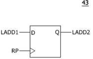
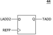
도 9를 참고하면 타겟어드레스생성회로(4)는 입력차단기(41), 제1 래치(42), 제2 래치(43) 및 제3 래치(44)를 포함할 수 있다. 입력차단기(41)는 액티브신호(ACT) 및 차단신호(CUT)에 응답하여 내부액티브신호(IACT)를 생성할 수 있다. 입력차단기(41)는 차단신호(CUT)가 디스에이블된 상태에서 액티브신호(ACT)를 버퍼링하여 내부액티브신호(IACT)를 생성할 수 있다. 입력차단기(41)는 차단신호(CUT)가 인에이블된 상태에서 액티브신호(ACT)로부터 내부액티브신호(IACT)가 생성되는 동작을 차단할 수 있다. 제1 래치(42)는 내부액티브신호(IACT)에 응답하여 어드레스(ADD)로부터 제1 래치어드레스(LADD1)를 생성할 수 있다. 제1 래치(42)는 내부액티브신호(IACT)가 인에이블되는 경우 어드레스(ADD)를 래치하여 제1 래치어드레스(LADD1)를 생성할 수 있다. 제2 래치(43)는 랜덤펄스(RP)에 응답하여 제1 래치어드레스(LADD1)로부터 제2 래치어드레스(LADD2)를 생성할 수 있다. 제2 래치(43)는 랜덤펄스(RP)가 발생하는 경우 제1 래치어드레스(LADD1)를 래치하여 제2 래치어드레스(LADD2)를 생성할 수 있다. 제3 래치(44)는 리프레쉬펄스(REFP)에 응답하여 제2 래치어드레스(LADD2)로부터 타겟어드레스(TADD)를 생성할 수 있다. 제3 래치(44)는 리프레쉬펄스(REFP)가 발생하는 경우 제2 래치어드레스(LADD2)를 래치하여 타겟어드레스(TADD)를 생성할 수 있다. 타겟어드레스생성회로(4)는 차단신호(CUT)가 인에이블되는 경우 액티브신호(ACT)의 입력을 차단하여 어드레스(ADD)로부터 타겟어드레스(TADD)를 생성하는 동작을 중단할 수 있다. 타겟어드레스생성회로(4)는 차단신호(CUT)가 디스에이블된 상태에서 액티브신호(ACT), 랜덤펄스(RP) 및 리프레쉬펄스(REFP)에 동기하여 어드레스(ADD)를 순차적으로 래치하여 타겟어드레스(TADD)를 생성할 수 있다.Referring to FIG. 9, the target address generation circuit (4) may include an input breaker (41), a first latch (42), a second latch (43), and a third latch (44). The input breaker (41) may generate an internal active signal (IACT) in response to an active signal (ACT) and a blocking signal (CUT). The input breaker (41) may buffer the active signal (ACT) in a state where the blocking signal (CUT) is disabled to generate the internal active signal (IACT). The input breaker (41) may block an operation in which the internal active signal (IACT) is generated from the active signal (ACT) in a state where the blocking signal (CUT) is enabled. The first latch (42) may generate a first latch address (LADD1) from an address (ADD) in response to the internal active signal (IACT). The first latch (42) can latch the address (ADD) to generate the first latch address (LADD1) when the internal active signal (IACT) is enabled. The second latch (43) can generate the second latch address (LADD2) from the first latch address (LADD1) in response to the random pulse (RP). The second latch (43) can latch the first latch address (LADD1) to generate the second latch address (LADD2) when the random pulse (RP) occurs. The third latch (44) can generate the target address (TADD) from the second latch address (LADD2) in response to the refresh pulse (REFP). The third latch (44) can latch the second latch address (LADD2) to generate the target address (TADD) when the refresh pulse (REFP) occurs. The target address generation circuit (4) can stop the operation of generating the target address (TADD) from the address (ADD) by blocking the input of the active signal (ACT) when the blocking signal (CUT) is enabled. The target address generation circuit (4) can generate the target address (TADD) by sequentially latching the address (ADD) in synchronization with the active signal (ACT), the random pulse (RP), and the refresh pulse (REFP) while the blocking signal (CUT) is disabled.
도 10을 참고하면 입력차단기(41)는 인버터(IV41) 및 노어게이트(NOR41)를 포함할 수 있다. 입력차단기(41)는 차단신호(CUT)가 로직로우레벨로 디스에이블된 상태에서 인버터(IV41) 및 노어게이트(NOR41)를 통해 액티브신호(ACT)를 버퍼링하여 내부액티브신호(IACT)를 생성할 수 있다. 입력차단기(41)는 차단신호(CUT)가 로직하이레벨로 인에이블된 상태에서 액티브신호(ACT)에 상관없이 로직로우레벨로 디스에이블되는 내부액티브신호(IACT)를 생성할 수 있다.Referring to Fig. 10, the input breaker (41) may include an inverter (IV41) and a NOR gate (NOR41). The input breaker (41) may generate an internal active signal (IACT) by buffering an active signal (ACT) through the inverter (IV41) and the NOR gate (NOR41) in a state where the blocking signal (CUT) is disabled to a logic low level. The input breaker (41) may generate an internal active signal (IACT) that is disabled to a logic low level regardless of the active signal (ACT) in a state where the blocking signal (CUT) is enabled to a logic high level.
도 11을 참고하면 제1 래치(42)는 플립플롭으로 구현될 수 있다. 제1 래치(42)는 내부액티브신호(IACT)가 인에이블되는 경우 어드레스(ADD)를 래치하여 제1 래치어드레스(LADD1)를 생성할 수 있다.Referring to Fig. 11, the first latch (42) can be implemented as a flip-flop. The first latch (42) can latch an address (ADD) when the internal active signal (IACT) is enabled to generate a first latch address (LADD1).
도 12를 참고하면 제2 래치(43)는 플립플롭으로 구현될 수 있다. 제2 래치(43)는 랜덤펄스(RP)가 발생하는 경우 제1 래치어드레스(LADD1)를 래치하여 제2 래치어드레스(LADD2)를 생성할 수 있다.Referring to Fig. 12, the second latch (43) can be implemented as a flip-flop. When a random pulse (RP) occurs, the second latch (43) can latch the first latch address (LADD1) to generate the second latch address (LADD2).
도 13을 참고하면 제3 래치(44)는 플립플롭으로 구현될 수 있다. 제3 래치(44)는 리프레쉬펄스(REFP)가 발생하는 경우 제2 래치어드레스(LADD2)를 래치하여 타겟어드레스(TADD)를 생성할 수 있다.Referring to Fig. 13, the third latch (44) can be implemented as a flip-flop. When a refresh pulse (REFP) occurs, the third latch (44) can latch the second latch address (LADD2) to generate a target address (TADD).
도 14를 참고하면 제어신호입력회로(5)는 인버터(IV51) 및 노어게이트(NOR51)를 포함할 수 있다. 제어신호입력회로(5)는 차단신호(CUT)가 로직하이레벨로 인에이블되는 경우 리프레쉬제어신호(REFCNT)에 관계없이 로직로우레벨로 디스에이블된 내부리프레쉬신호(IREFC)를 생성할 수 있다. 제어신호입력회로(5)는 차단신호(CUT)가 로직로우레벨로 디스에이블되는 경우 인버터(IV51) 및 노어게이트(NOR51)를 통해 리프레쉬제어신호(REFCNT)를 버퍼링하여 내부리프레쉬신호(IREFC)를 생성할 수 있다.Referring to FIG. 14, the control signal input circuit (5) may include an inverter (IV51) and a NOR gate (NOR51). The control signal input circuit (5) may generate an internal refresh signal (IREFC) that is disabled to a logic low level regardless of the refresh control signal (REFCNT) when the blocking signal (CUT) is enabled to a logic high level. The control signal input circuit (5) may generate an internal refresh signal (IREFC) by buffering the refresh control signal (REFCNT) through the inverter (IV51) and the NOR gate (NOR51) when the blocking signal (CUT) is disabled to a logic low level.
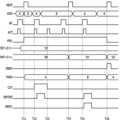
이상 살펴본 바와 같이 구성된 반도체장치의 동작을 도 15를 참고하여 살펴보면 다음과 같다.The operation of the semiconductor device configured as described above is as follows with reference to Fig. 15.
T11 시점 이전에 발생된 랜덤펄스(RP) 및 액티브신호(ACT)의 펄스에 동기하여 반도체장치에 입력되는 제1 조합(A)을 갖는 어드레스(ADD)가 래치된다. T11 시점에서, 제1 조합(A)을 갖는 어드레스(ADD)은 타겟어드레스(TADD)로 설정된다. T11 시점에서 발생되는 리프레쉬펄스(REFP)에 동기하여 구간신호(PDS)는 로직하이레벨로 인에이블된다.An address (ADD) having a first combination (A) input to a semiconductor device is latched in synchronization with a pulse of a random pulse (RP) and an active signal (ACT) generated before time T11. At time T11, the address (ADD) having the first combination (A) is set to a target address (TADD). In synchronization with a refresh pulse (REFP) generated at time T11, a segment signal (PDS) is enabled to a logic high level.
T12 시점에서 발생된 랜덤펄스(RP) 및 액티브신호(ACT)의 펄스에 동기하여 입력되는 어드레스(ADD)의 제1 조합(A)은 타겟어드레스(TADD)로 설정된 조합과 동일하므로 차단신호(CUT)가 로직하이레벨로 인에이블된다. T13 시점에서 발생된 액티브신호(ACT)의 펄스에 동기하여 차단신호(CUT)가 로직로우레벨로 디스에이블된다. T12 시점부터 T13 시점까지의 구간동안 로직하이레벨의 차단신호(CUT)에 의해 어드레스(ADD)의 제1 조합(A)이 타겟어드레스(TADD)로 설정되는 동작이 차단된다. 또한, T12 시점부터 T13 시점까지의 구간동안 로직하이레벨의 차단신호(CUT)에 의해 리프레쉬제어신호(REFCNT)에 의해 내부리프레쉬신호(IREFC)가 생성되는 동작도 차단된다.The first combination (A) of the address (ADD) input in synchronization with the pulse of the random pulse (RP) and the active signal (ACT) generated at time T12 is the same as the combination set as the target address (TADD), so the blocking signal (CUT) is enabled to a logic high level. The blocking signal (CUT) is disabled to a logic low level in synchronization with the pulse of the active signal (ACT) generated at time T13. During the section from time T12 to time T13, the operation in which the first combination (A) of the address (ADD) is set to the target address (TADD) is blocked by the blocking signal (CUT) at a logic high level. In addition, the operation in which the internal refresh signal (IREFC) is generated by the refresh control signal (REFCNT) by the blocking signal (CUT) at a logic high level is also blocked during the section from time T12 to time T13.
T14 시점에서 발생되는 리프레쉬펄스(REFP)에 동기하여 래치된 어드레스(ADD)의 제2 조합(B)이 타겟어드레스(TADD)로 설정된다. T14 시점에서 제어코드(CNT<2:1>)는 리프레쉬펄스(REFP)에 동기하여 '00'에서 '01'로 카운팅된다.At the T14 point in time, the second combination (B) of the latched address (ADD) is set to the target address (TADD) in synchronization with the refresh pulse (REFP). At the T14 point in time, the control code (CNT<2:1>) is counted from '00' to '01' in synchronization with the refresh pulse (REFP).
T15 시점 이후 순차적으로 발생되는 랜덤펄스(RP) 및 액티브신호(ACT)의 펄스에 동기하여 입력되는 어드레스(ADD)의 제2 조합(B)이 래치된다. 어드레스(ADD)의 제1 조합(A)은 타겟어드레스(TADD)로 설정된 조합과 상이하므로 차단신호(CUT)는 로직로우레벨로 디스에이블 상태를 유지한다. 따라서, 인에이블된 리프레쉬제어신호(REFCNT)에 의해 인에이블된 내부리프레쉬신호(IREFC)가 생성되고, 제2 조합(B)으로 설정된 타겟어드레스(TADD)에 의해 엑세스되는 셀에 대한 리프레쉬 동작이 수행된다.A second combination (B) of addresses (ADD) input in synchronization with the pulses of random pulses (RP) and active signals (ACT) that are sequentially generated after time point T15 is latched. Since the first combination (A) of addresses (ADD) is different from the combination set as the target address (TADD), the blocking signal (CUT) is maintained in a disabled state at a logic low level. Accordingly, an internal refresh signal (IREFC) enabled by the enabled refresh control signal (REFCNT) is generated, and a refresh operation is performed for a cell accessed by the target address (TADD) set as the second combination (B).
T16 시점에서 발생되는 리프레쉬펄스(REFP)에 동기하여 래치된 어드레스(ADD)의 제1 조합(A)이 타겟어드레스(TADD)로 설정된다. T16 시점에서 제어코드(CNT<2:1>)는 리프레쉬펄스(REFP)에 동기하여 '01'에서 '10'으로 카운팅된다. T16 시점에서 제어코드(CNT<2:1>) 및 설정코드(SET<2:1>)가 동일한 논리레벨조합을 갖으므로 종료펄스(ENDP)가 발생된다. T16 시점에서 발생된 종료펄스(ENDP)에 의해 구간신호(PDS)는 로직로우레벨로 디스에이블된다.At time T16, the first combination (A) of the latched address (ADD) is set to the target address (TADD) in synchronization with the refresh pulse (REFP). At time T16, the control code (CNT<2:1>) is counted from '01' to '10' in synchronization with the refresh pulse (REFP). Since the control code (CNT<2:1>) and the setting code (SET<2:1>) have the same logical level combination at time T16, the end pulse (ENDP) is generated. The section signal (PDS) is disabled to a logic low level by the end pulse (ENDP) generated at time T16.
이상 살펴본 바와 같이 구성된 반도체장치는 타겟어드레스(TADD)와 동일한 조합의 어드레스(ADD)가 입력되는 경우 타겟어드레스(TADD)로 중복 설정되는 동작을 차단하고, 타겟어드레스(TADD)에 대한 중복된 리프레쉬 동작을 차단하여 리프레쉬 동작의 효율성을 증가시키고 전류 소모를 감소시킬 수 있다.As described above, the semiconductor device configured can block an operation in which an address (ADD) of the same combination as the target address (TADD) is input, which is duplicated and set to the target address (TADD), and can block duplicate refresh operations for the target address (TADD), thereby increasing the efficiency of the refresh operation and reducing current consumption.
앞서, 도 1 내지 도 15에서 살펴본 반도체장치는 메모리시스템, 그래픽시스템, 컴퓨팅시스템 및 모바일시스템 등을 포함하는 전자시스템에 적용될 수 있다. 예를 들어, 도 16을 참고하면 본 발명의 일 실시예에 따른 전자시스템(1000)은 데이터저장부(1001), 메모리컨트롤러(1002), 버퍼메모리(1003) 및 입출력인터페이스(1004)를 포함할 수 있다.The semiconductor devices discussed above in FIGS. 1 to 15 can be applied to electronic systems including memory systems, graphic systems, computing systems, and mobile systems. For example, referring to FIG. 16, an electronic system (1000) according to an embodiment of the present invention can include a data storage unit (1001), a memory controller (1002), a buffer memory (1003), and an input/output interface (1004).
데이터저장부(1001)는 메모리컨트롤러(1002)로부터의 제어신호에 따라 메모리컨트롤러(1002)로부터 인가되는 데이터를 저장하고 저장된 데이터를 판독하여 메모리컨트롤러(1002)에 출력한다. 한편, 데이터저장부(1001)는 전원이 차단되어도 데이터를 잃지 않고 계속 저장할 수 있는 비휘발성 메모리를 포함할 수 있다. 비휘발성 메모리는 플래쉬 메모리(Nor Flash Memory, NAND Flash Memory), 상변환 메모리(Phase Change Random Access Memory; PRAM), 저항 메모리(ReSVstive Random Access Memory;RRAM), 스핀 주입자화반전 메모리(Spin Transfer Torque Random Access Memory; STTRAM), 자기메모리(Magnetic Random Access Memory; MRAM)로 구현될 수 있다.The data storage unit (1001) stores data input from the memory controller (1002) according to a control signal from the memory controller (1002), reads out the stored data, and outputs the data to the memory controller (1002). Meanwhile, the data storage unit (1001) may include a nonvolatile memory that can continuously store data without losing it even when power is cut off. The nonvolatile memory may be implemented as a flash memory (NOR Flash Memory, NAND Flash Memory), a phase change random access memory (PRAM), a resistive memory (ReSVstive Random Access Memory; RRAM), a spin transfer torque random access memory (STTRAM), or a magnetic random access memory (MRAM).
메모리컨트롤러(1002)는 입출력인터페이스(1004)를 통해 외부기기(호스트 장치)로부터 인가되는 명령어를 디코딩하고 디코딩된 결과에 따라 데이터저장부(1001) 및 버퍼메모리(1003)에 대한 데이터 입출력을 제어한다. 도 16에서는 메모리컨트롤러(1002)가 하나의 블록으로 표시되었으나, 메모리컨트롤러(1002)는 데이터저장부(1001)를 제어하기 위한 컨트롤러와 휘발성 메모리인 버퍼메모리(1003)를 제어하기 위한 컨트롤러가 독립적으로 구성될 수 있다.The memory controller (1002) decodes a command input from an external device (host device) through an input/output interface (1004) and controls data input/output for the data storage unit (1001) and buffer memory (1003) according to the decoded result. In Fig. 16, the memory controller (1002) is shown as one block, but the memory controller (1002) may be configured independently as a controller for controlling the data storage unit (1001) and a controller for controlling the buffer memory (1003), which is a volatile memory.
버퍼메모리(1003)는 메모리컨트롤러(1002)에서 처리할 데이터 즉 데이터저장부(1001)에 입출력되는 데이터를 임시적으로 저장할 수 있다. 버퍼메모리(1003)는 제어신호에 따라 메모리컨트롤러(1002)에서 인가되는 데이터(DATA)를 저장할 수 있다. 버퍼메모리(1003)는 저장된 데이터를 판독하여 메모리컨트롤러(1002)에 출력한다. 버퍼메모리(1003)는 DRAM(Dynamic Random Access Memory), Moblie DRAM, SRAM(Static Random Access Memory) 등의 휘발성 메모리를 포함할 수 있다.The buffer memory (1003) can temporarily store data to be processed by the memory controller (1002), that is, data input/output to the data storage unit (1001). The buffer memory (1003) can store data (DATA) applied from the memory controller (1002) according to a control signal. The buffer memory (1003) reads the stored data and outputs it to the memory controller (1002). The buffer memory (1003) can include volatile memory such as DRAM (Dynamic Random Access Memory), Mobile DRAM, and SRAM (Static Random Access Memory).
입출력인터페이스(1004)는 메모리컨트롤러(1002)와 외부기기(호스트) 사이의 물리적 연결을 제공하여 메모리컨트롤러(1002)가 외부기기로부터 데이터 입출력을 위한 제어신호를 수신하고 외부기기와 데이터를 교환할 수 있도록 해준다. 입출력인터페이스(1004)는 USB, MMC, PCI-E, SAS, SATA, PATA, SCSV, ESDI, 및 IDE 등과 같은 다양한 인터페이스 프로토콜들 중 하나를 포함할 수 있다.The input/output interface (1004) provides a physical connection between the memory controller (1002) and an external device (host) to enable the memory controller (1002) to receive a control signal for data input/output from the external device and exchange data with the external device. The input/output interface (1004) may include one of various interface protocols, such as USB, MMC, PCI-E, SAS, SATA, PATA, SCSV, ESDI, and IDE.
전자시스템(1000)은 호스트 장치의 보조 기억장치 또는 외부 저장장치로 사용될 수 있다. 전자시스템(1000)은 고상 디스크(Solid State Disk; SSD), USB 메모리(Universal Serial Bus Memory), 씨큐어 디지털 카드(Secure Digital; SD), 미니 씨큐어 디지털 카드(mini Secure Digital card; mSD), 마이크로 씨큐어 디지털 카드(micro SD), 고용량 씨큐어 디지털 카드(Secure Digital High Capacity; SDHC), 메모리 스틱 카드(Memory Stick Card), 스마트 미디어 카드(Smart Media Card; SM), 멀티 미디어 카드(Multi Media Card; MMC), 내장 멀티 미디어 카드(Embedded MMC; eMMC), 컴팩트 플래시 카드(Compact Flash; CF) 등을 포함할 수 있다.The electronic system (1000) can be used as an auxiliary memory device or an external storage device of a host device. The electronic system (1000) can include a solid state disk (SSD), a universal serial bus memory (USB memory), a Secure Digital (SD) card, a mini Secure Digital card (mSD), a micro Secure Digital card (micro SD), a Secure Digital High Capacity (SDHC), a Memory Stick Card, a Smart Media Card (SM), a Multi Media Card (MMC), an embedded MMC (eMMC), a compact flash card (CF), and the like.
1: 구간신호생성회로2: 종료펄스생성회로
3: 차단신호생성회로4: 타겟어드레스생성회로
5: 제어신호입력회로6: 리프레쉬제어회로
11: 구동기12: 래치출력기
21: 구간리프레쉬펄스생성기22: 카운터
23: 비교기24: 리셋펄스합성기
22(1)~22(L): 제1 내지 제L 플립플롭
231: 감지신호생성기232: 종료펄스출력기
31: 어드레스비교기32: 전송제어신호생성기
33: 선택출력기41: 입력차단기
42: 제1 래치43: 제2 래치
44: 제3 래치1: Interval signal generation circuit 2: End pulse generation circuit
3: Blocking signal generation circuit 4: Target address generation circuit
5: Control signal input circuit 6: Refresh control circuit
11: Driver 12: Latch Output
21: Interval refresh pulse generator 22: Counter
23: Comparator 24: Reset pulse synthesizer
22(1)~22(L): 1st to Lth flip-flops
231: Detection signal generator 232: End pulse output device
31: Address comparator 32: Transmission control signal generator
33: Selector output 41: Input breaker
42: 1st latch 43: 2nd latch
44: 3rd latch
Claims (24)
Translated fromKorean리프레쉬펄스를 토대로 구간신호를 생성하는 구간신호생성회로; 및
상기 구간신호가 인에이블되는 구간동안 상기 타겟어드레스와 동일한 조합의 상기 어드레스가 입력되는 경우 상기 어드레스로부터 상기 타겟어드레스를 설정하는 동작을 제어하기 위한 상기 차단신호를 생성하는 차단신호생성회로를 포함하는 반도체장치.
A target address generation circuit that sets a target address from an address based on a blocking signal and an active signal;
An interval signal generation circuit that generates an interval signal based on a refresh pulse; and
A semiconductor device including a blocking signal generation circuit that generates the blocking signal for controlling an operation of setting the target address from the address when the address of the same combination as the target address is input during the section in which the section signal is enabled.
상기 리프레쉬펄스는 리프레쉬 동작을 위해 발생하는 반도체장치.
In paragraph 1,
The above refresh pulse is a semiconductor device that generates a refresh operation.
상기 구간신호생성회로는 상기 리프레쉬펄스 및 종료펄스를 토대로 상기 구간신호를 생성하고,
상기 종료펄스는 상기 리프레쉬펄스가 설정코드에 의해 설정된 횟수만큼 발생하는 경우 발생되는 반도체장치.
In paragraph 1,
The above-mentioned section signal generation circuit generates the above-mentioned section signal based on the above-mentioned refresh pulse and end pulse,
A semiconductor device in which the above termination pulse is generated when the above refresh pulse occurs the number of times set by the setting code.
상기 구간신호생성회로는 상기 리프레쉬펄스 및 종료펄스를 토대로 상기 구간신호를 생성하고,
상기 구간신호는 상기 리프레쉬펄스가 발생하는 시점에 동기하여 인에이블되며,
상기 구간신호는 상기 종료펄스가 인에이블되는 시점에 동기하여 디스에이블되는 반도체장치.In paragraph 1,
The above-mentioned section signal generation circuit generates the above-mentioned section signal based on the above-mentioned refresh pulse and end pulse,
The above section signal is enabled synchronously with the time at which the above refresh pulse occurs.
A semiconductor device in which the above-mentioned section signal is disabled synchronously with the point in time when the above-mentioned termination pulse is enabled.
상기 구간신호가 인에이블되는 구간동안 상기 리프레쉬펄스에 동기하여 카운팅되는 제어코드를 생성하고, 상기 제어코드와 설정코드를 비교하여 종료펄스를 생성하는 종료펄스생성회로를 더 포함하되,
상기 구간신호생성회로는 상기 리프레쉬펄스 및 상기 종료펄스를 토대로 상기 구간신호를 생성하는 반도체장치.
In paragraph 1,
Further comprising a termination pulse generation circuit that generates a control code that is counted in synchronization with the refresh pulse during the section in which the above section signal is enabled, and generates a termination pulse by comparing the control code with the setting code,
The above-mentioned section signal generation circuit is a semiconductor device that generates the above-mentioned section signal based on the above-mentioned refresh pulse and the above-mentioned termination pulse.
상기 구간신호 및 상기 리프레쉬펄스를 토대로 구간리프레쉬펄스를 생성하는 구간리프레쉬펄스생성기;
상기 구간리프레쉬펄스에 동기하여 상기 제어코드를 카운팅하는 카운터;
상기 제어코드와 상기 설정코드를 비교하여 상기 종료펄스를 생성하는 비교기; 및
상기 종료펄스와 리셋펄스를 토대로 상기 제어코드를 초기화하기 위한 합성리셋펄스를 생성하는 리셋펄스합성기를 포함하는 반도체장치.
In the fifth paragraph, the termination pulse generation circuit
An interval refresh pulse generator that generates an interval refresh pulse based on the interval signal and the refresh pulse;
A counter that counts the control code in synchronization with the above section refresh pulse;
A comparator that compares the above control code and the above setting code to generate the termination pulse; and
A semiconductor device including a reset pulse synthesizer that generates a synthetic reset pulse for initializing the control code based on the termination pulse and reset pulse.
상기 타겟어드레스와 상기 어드레스를 비교하여 어드레스비교신호를 생성하는 어드레스비교기;
상기 액티브신호 및 상기 구간신호를 토대로 전송제어신호를 생성하는 전송제어신호생성기; 및
상기 전송제어신호를 토대로 상기 어드레스비교신호로부터 상기 차단신호를 생성하는 선택출력기를 포함하는 반도체장치.
In the first paragraph, the blocking signal generation circuit
An address comparator that compares the target address with the address to generate an address comparison signal;
A transmission control signal generator that generates a transmission control signal based on the above active signal and the above section signal; and
A semiconductor device including a selection output device that generates the blocking signal from the address comparison signal based on the transmission control signal.
상기 차단신호를 토대로 상기 액티브신호를 버퍼링하여 내부액티브신호를 생성하는 입력차단기;
상기 내부액티브신호를 토대로 상기 어드레스를 래치하여 제1 래치어드레스를 생성하는 제1 래치;
랜덤펄스에 동기하여 상기 제1 래치어드레스를 래치하여 제2 래치어드레스를 생성하는 제2 래치; 및
상기 리프레쉬펄스에 동기하여 상기 제2 래치어드레스를 래치하여 상기 타겟어드레스를 생성하는 제3 래치를 포함하는 반도체장치.
In the first paragraph, the target address generation circuit
An input circuit breaker that buffers the active signal based on the above blocking signal and generates an internal active signal;
A first latch that latches the address based on the internal active signal to generate a first latch address;
A second latch that latches the first latch address in synchronization with a random pulse to generate a second latch address; and
A semiconductor device including a third latch that latches the second latch address in synchronization with the refresh pulse to generate the target address.
상기 차단신호를 토대로 리프레쉬제어신호로부터 상기 타겟어드레스에 의해 엑세스되는 셀에 대해 수행되는 리프레쉬 동작을 제어하기 위한 내부리프레쉬신호를 생성하는 제어신호입력회로를 더 포함하는 반도체장치.
In paragraph 1,
A semiconductor device further comprising a control signal input circuit that generates an internal refresh signal for controlling a refresh operation performed on a cell accessed by the target address from a refresh control signal based on the above blocking signal.
구간신호가 인에이블되는 구간동안 리프레쉬펄스에 동기하여 카운팅되는 제어코드를 생성하는 종료펄스생성회로; 및
상기 구간신호가 인에이블되는 구간동안 상기 타겟어드레스와 동일한 조합의 상기 어드레스가 입력되는 경우 상기 어드레스로부터 상기 타겟어드레스를 설정하는 동작을 제어하기 위한 상기 차단신호를 생성하는 차단신호생성회로를 포함하는 반도체장치.
A target address generation circuit that sets a target address from an address based on a blocking signal and an active signal;
A termination pulse generation circuit that generates a control code that is counted in synchronization with a refresh pulse during a section in which an interval signal is enabled; and
A semiconductor device including a blocking signal generation circuit that generates the blocking signal for controlling an operation of setting the target address from the address when the address of the same combination as the target address is input during the section in which the section signal is enabled.
상기 종료펄스생성회로는 상기 제어코드와 설정코드를 비교하여 종료펄스를 생성하고,
상기 종료펄스생성회로는
상기 구간신호 및 상기 리프레쉬펄스를 토대로 구간리프레쉬펄스를 생성하는 구간리프레쉬펄스생성기;
상기 구간리프레쉬펄스에 동기하여 상기 제어코드를 카운팅하는 카운터;
상기 제어코드와 상기 설정코드를 비교하여 상기 종료펄스를 생성하는 비교기; 및
상기 종료펄스와 리셋펄스를 토대로 상기 제어코드를 초기화하기 위한 합성리셋펄스를 생성하는 리셋펄스합성기를 포함하는 반도체장치.
In Article 11,
The above termination pulse generation circuit compares the above control code and setting code to generate a termination pulse,
The above termination pulse generation circuit
An interval refresh pulse generator that generates an interval refresh pulse based on the interval signal and the refresh pulse;
A counter that counts the control code in synchronization with the above section refresh pulse;
A comparator that compares the above control code and the above setting code to generate the termination pulse; and
A semiconductor device including a reset pulse synthesizer that generates a synthetic reset pulse for initializing the control code based on the termination pulse and reset pulse.
상기 타겟어드레스와 상기 어드레스를 비교하여 어드레스비교신호를 생성하는 어드레스비교기;
상기 액티브신호 및 상기 구간신호를 토대로 전송제어신호를 생성하는 전송제어신호생성기; 및
상기 전송제어신호를 토대로 상기 어드레스비교신호로부터 상기 차단신호를 생성하는 선택출력기를 포함하는 반도체장치.
In the 11th paragraph, the blocking signal generation circuit
An address comparator that compares the target address with the address to generate an address comparison signal;
A transmission control signal generator that generates a transmission control signal based on the above active signal and the above section signal; and
A semiconductor device including a selection output device that generates the blocking signal from the address comparison signal based on the transmission control signal.
상기 리프레쉬펄스 및 종료펄스를 토대로 상기 구간신호를 생성하는 구간신호생성회로를 더 포함하되,
상기 종료펄스생성회로는 상기 제어코드와 설정코드를 비교하여 상기 종료펄스를 생성하는 반도체장치.
In Article 11,
Further comprising an interval signal generation circuit that generates the interval signal based on the refresh pulse and the end pulse,
The above-mentioned termination pulse generation circuit is a semiconductor device that generates the above-mentioned termination pulse by comparing the above-mentioned control code and the setting code.
A semiconductor device in accordance with claim 14, wherein the interval signal is enabled synchronously with the time at which the refresh pulse occurs and is disabled synchronously with the time at which the end pulse is enabled.
상기 차단신호를 토대로 상기 액티브신호를 버퍼링하여 내부액티브신호를 생성하는 입력차단기;
상기 내부액티브신호를 토대로 상기 어드레스를 래치하여 제1 래치어드레스를 생성하는 제1 래치;
랜덤펄스에 동기하여 상기 제1 래치어드레스를 래치하여 제2 래치어드레스를 생성하는 제2 래치; 및
상기 리프레쉬펄스에 동기하여 상기 제2 래치어드레스를 래치하여 상기 타겟어드레스를 생성하는 제3 래치를 포함하는 반도체장치.
In the 11th paragraph, the target address generation circuit
An input circuit breaker that buffers the active signal based on the above blocking signal and generates an internal active signal;
A first latch that latches the address based on the internal active signal to generate a first latch address;
A second latch that latches the first latch address in synchronization with a random pulse to generate a second latch address; and
A semiconductor device including a third latch that latches the second latch address in synchronization with the refresh pulse to generate the target address.
상기 차단신호를 토대로 리프레쉬제어신호로부터 상기 타겟어드레스에 의해 엑세스되는 셀에 대해 수행되는 리프레쉬 동작을 제어하기 위한 내부리프레쉬신호를 생성하는 제어신호입력회로를 더 포함하는 반도체장치.
In Article 11,
A semiconductor device further comprising a control signal input circuit that generates an internal refresh signal for controlling a refresh operation performed on a cell accessed by the target address from a refresh control signal based on the above blocking signal.
구간신호가 인에이블되는 구간동안 상기 타겟어드레스와 동일한 조합의 상기 어드레스가 입력되는 경우 상기 어드레스로부터 상기 타겟어드레스를 설정하는 동작을 제어하기 위한 상기 차단신호를 생성하는 차단신호생성회로; 및
상기 차단신호를 토대로 리프레쉬제어신호로부터 상기 타겟어드레스에 의해 엑세스되는 셀에 대해 수행되는 리프레쉬 동작을 제어하기 위한 내부리프레쉬신호를 생성하는 제어신호입력회로를 포함하는 반도체장치.
A target address generation circuit that sets a target address from an address based on a blocking signal and an active signal;
A blocking signal generation circuit that generates the blocking signal for controlling an operation of setting the target address from the address when the address of the same combination as the target address is input during the section in which the section signal is enabled; and
A semiconductor device including a control signal input circuit that generates an internal refresh signal for controlling a refresh operation performed on a cell accessed by the target address from a refresh control signal based on the above blocking signal.
리프레쉬펄스 및 종료펄스를 토대로 상기 구간신호를 생성하는 구간신호생성회로; 및
상기 구간신호 및 상기 리프레쉬펄스를 토대로 카운팅되는 제어코드를 생성하고, 상기 제어코드와 설정코드를 비교하여 상기 종료펄스를 생성하는 종료펄스생성회로 더 포함하는 반도체장치.
In Article 19,
An interval signal generation circuit that generates the interval signal based on a refresh pulse and an end pulse; and
A semiconductor device further comprising a termination pulse generation circuit that generates a control code counted based on the above-mentioned interval signal and the above-mentioned refresh pulse, and generates the termination pulse by comparing the control code with the setting code.
액티브동작을 위한 상기 어드레스가 상기 타겟어드레스와 동일할 때 상기 어드레스로부터 상기 타겟어드레스를 설정하는 동작을 차단하기 위한 차단신호를 생성하는 차단신호생성회로를 포함하되,
상기 어드레스는 리프레쉬동작을 수행하기 위해 상기 타겟어드레스로 설정되는 반도체장치.
A target address generation circuit that sets a target address from an address based on a blocking signal and an active signal; and
Including a blocking signal generation circuit that generates a blocking signal to block an operation of setting the target address from the address when the address for active operation is identical to the target address,
A semiconductor device in which the above address is set as the target address to perform a refresh operation.
상기 차단신호에 의해 상기 어드레스가 상기 타겟어드레스로 설정되는 동작이 차단되지 않을 때 리프레쉬펄스를 토대로 상기 어드레스로부터 상기 타겟어드레스를 생성하는 반도체장치.
In the 21st paragraph, the target address generation circuit
A semiconductor device that generates the target address from the address based on a refresh pulse when an operation of setting the address to the target address is not blocked by the blocking signal.
리프레쉬펄스를 토대로 구간신호를 생성하는 구간신호생성회로를 더 포함하되,
상기 차단신호생성회로는 상기 구간신호가 인에이블되는 구간동안 상기 어드레스가 상기 타겟어드레스와 동일한 조합의 어드레스가 입력되는 경우 상기 어드레스가 상기 타겟어드레스로 설정되는 동작을 차단하는 반도체장치.
In Article 21,
Further comprising an interval signal generation circuit that generates an interval signal based on a refresh pulse,
The above-mentioned blocking signal generation circuit is a semiconductor device that blocks an operation in which the address is set to the target address when an address of the same combination as the target address is input during a section in which the above-mentioned section signal is enabled.
구간신호가 인에이블되는 구간동안 리프레쉬펄스에 동기하여 카운팅되는 제어코드를 생성하는 종료펄스생성회로를 더 포함하되,
상기 차단신호생성회로는 상기 구간신호가 인에이블되는 구간동안 상기 어드레스가 상기 타겟어드레스와 동일한 조합의 어드레스가 입력되는 경우 상기 어드레스가 상기 타겟어드레스로 설정되는 동작을 차단하는 반도체장치.
In Article 21,
Further comprising a termination pulse generation circuit that generates a control code that is counted in synchronization with the refresh pulse during the section in which the section signal is enabled,
The above-mentioned blocking signal generation circuit is a semiconductor device that blocks an operation in which the address is set to the target address when an address of the same combination as the target address is input during a section in which the above-mentioned section signal is enabled.
Priority Applications (2)
| Application Number | Priority Date | Filing Date | Title |
|---|---|---|---|
| KR1020170018269AKR102730503B1 (en) | 2017-02-09 | 2017-02-09 | Semiconductor device |
| US15/654,999US11074957B2 (en) | 2017-02-09 | 2017-07-20 | Semiconductor device |
Applications Claiming Priority (1)
| Application Number | Priority Date | Filing Date | Title |
|---|---|---|---|
| KR1020170018269AKR102730503B1 (en) | 2017-02-09 | 2017-02-09 | Semiconductor device |
Publications (2)
| Publication Number | Publication Date |
|---|---|
| KR20180092513A KR20180092513A (en) | 2018-08-20 |
| KR102730503B1true KR102730503B1 (en) | 2024-11-14 |
Family
ID=63037897
Family Applications (1)
| Application Number | Title | Priority Date | Filing Date |
|---|---|---|---|
| KR1020170018269AActiveKR102730503B1 (en) | 2017-02-09 | 2017-02-09 | Semiconductor device |
Country Status (2)
| Country | Link |
|---|---|
| US (1) | US11074957B2 (en) |
| KR (1) | KR102730503B1 (en) |
Families Citing this family (22)
| Publication number | Priority date | Publication date | Assignee | Title |
|---|---|---|---|---|
| US10490251B2 (en) | 2017-01-30 | 2019-11-26 | Micron Technology, Inc. | Apparatuses and methods for distributing row hammer refresh events across a memory device |
| CN112106138B (en) | 2018-05-24 | 2024-02-27 | 美光科技公司 | Apparatus and method for pure time adaptive sampling for row hammer refresh sampling |
| US10573370B2 (en) | 2018-07-02 | 2020-02-25 | Micron Technology, Inc. | Apparatus and methods for triggering row hammer address sampling |
| US10685696B2 (en) | 2018-10-31 | 2020-06-16 | Micron Technology, Inc. | Apparatuses and methods for access based refresh timing |
| CN113168861B (en) | 2018-12-03 | 2024-05-14 | 美光科技公司 | Semiconductor device performing row hammer refresh operation |
| CN117198356A (en) | 2018-12-21 | 2023-12-08 | 美光科技公司 | Apparatus and method for timing interleaving for targeted refresh operations |
| US10957377B2 (en) | 2018-12-26 | 2021-03-23 | Micron Technology, Inc. | Apparatuses and methods for distributed targeted refresh operations |
| US11615831B2 (en) | 2019-02-26 | 2023-03-28 | Micron Technology, Inc. | Apparatuses and methods for memory mat refresh sequencing |
| US11227649B2 (en) | 2019-04-04 | 2022-01-18 | Micron Technology, Inc. | Apparatuses and methods for staggered timing of targeted refresh operations |
| US11069393B2 (en) | 2019-06-04 | 2021-07-20 | Micron Technology, Inc. | Apparatuses and methods for controlling steal rates |
| US10978132B2 (en) | 2019-06-05 | 2021-04-13 | Micron Technology, Inc. | Apparatuses and methods for staggered timing of skipped refresh operations |
| US11302374B2 (en) | 2019-08-23 | 2022-04-12 | Micron Technology, Inc. | Apparatuses and methods for dynamic refresh allocation |
| US11302377B2 (en)* | 2019-10-16 | 2022-04-12 | Micron Technology, Inc. | Apparatuses and methods for dynamic targeted refresh steals |
| KR102851146B1 (en) | 2020-06-02 | 2025-08-28 | 에스케이하이닉스 주식회사 | Semiconductor memory device including address generation circuit and operating method thereof |
| US11309010B2 (en) | 2020-08-14 | 2022-04-19 | Micron Technology, Inc. | Apparatuses, systems, and methods for memory directed access pause |
| US11348631B2 (en) | 2020-08-19 | 2022-05-31 | Micron Technology, Inc. | Apparatuses, systems, and methods for identifying victim rows in a memory device which cannot be simultaneously refreshed |
| US11380382B2 (en) | 2020-08-19 | 2022-07-05 | Micron Technology, Inc. | Refresh logic circuit layout having aggressor detector circuit sampling circuit and row hammer refresh control circuit |
| US11557331B2 (en) | 2020-09-23 | 2023-01-17 | Micron Technology, Inc. | Apparatuses and methods for controlling refresh operations |
| US11222686B1 (en) | 2020-11-12 | 2022-01-11 | Micron Technology, Inc. | Apparatuses and methods for controlling refresh timing |
| US11264079B1 (en) | 2020-12-18 | 2022-03-01 | Micron Technology, Inc. | Apparatuses and methods for row hammer based cache lockdown |
| US12125514B2 (en) | 2022-04-28 | 2024-10-22 | Micron Technology, Inc. | Apparatuses and methods for access based refresh operations |
| US12112787B2 (en) | 2022-04-28 | 2024-10-08 | Micron Technology, Inc. | Apparatuses and methods for access based targeted refresh operations |
Family Cites Families (7)
| Publication number | Priority date | Publication date | Assignee | Title |
|---|---|---|---|---|
| US5315130A (en)* | 1990-03-30 | 1994-05-24 | Tactical Fabs, Inc. | Very high density wafer scale device architecture |
| KR100929155B1 (en)* | 2007-01-25 | 2009-12-01 | 삼성전자주식회사 | Semiconductor memory device and memory cell access method thereof |
| KR102182368B1 (en) | 2013-12-19 | 2020-11-24 | 에스케이하이닉스 주식회사 | Circuit for detecting address and memory including the same |
| KR20160035897A (en) | 2014-09-24 | 2016-04-01 | 에스케이하이닉스 주식회사 | Semiconductor memory device and system including thereof |
| JP2017182854A (en)* | 2016-03-31 | 2017-10-05 | マイクロン テクノロジー, インク. | Semiconductor device |
| CN108885892B (en)* | 2016-04-08 | 2022-05-10 | 超极存储器股份有限公司 | Semiconductor memory device with a plurality of memory cells |
| KR102468251B1 (en)* | 2016-06-27 | 2022-11-18 | 에스케이하이닉스 주식회사 | Semiconductor memory device and operating method thereof |
- 2017
- 2017-02-09KRKR1020170018269Apatent/KR102730503B1/enactiveActive
- 2017-07-20USUS15/654,999patent/US11074957B2/enactiveActive
Also Published As
| Publication number | Publication date |
|---|---|
| US20180226119A1 (en) | 2018-08-09 |
| US11074957B2 (en) | 2021-07-27 |
| KR20180092513A (en) | 2018-08-20 |
Similar Documents
| Publication | Publication Date | Title |
|---|---|---|
| KR102730503B1 (en) | Semiconductor device | |
| US10446199B2 (en) | Semiconductor device and semiconductor system | |
| US10580474B2 (en) | Semiconductor devices | |
| US10157646B2 (en) | Latch control signal generation circuit to reduce row hammering | |
| US10068632B2 (en) | Semiconductor device and semiconductor system | |
| US9613666B1 (en) | Semiconductor devices and semiconductor systems including the same | |
| CN111105823B (en) | Semiconductor device | |
| KR102730500B1 (en) | Semiconductor device | |
| KR102420640B1 (en) | Semiconductor device | |
| US10055152B2 (en) | Semiconductor devices | |
| US10796740B2 (en) | Method for generating command pulses and semiconductor device configured to perform the method | |
| CN110364200B (en) | Semiconductor device | |
| KR102298776B1 (en) | Semiconductor device | |
| US10699762B2 (en) | Cycle control circuits | |
| US10991419B2 (en) | Semiconductor devices and methods of handling data lifetime codes used therein | |
| US11915783B2 (en) | Semiconductor device related to operation of internal circuits | |
| US10720190B2 (en) | Semiconductor devices and semiconductor systems including the same | |
| KR20170082199A (en) | Semiconductor device and semiconductor system |
Legal Events
| Date | Code | Title | Description |
|---|---|---|---|
| PA0109 | Patent application | Patent event code:PA01091R01D Comment text:Patent Application Patent event date:20170209 | |
| PG1501 | Laying open of application | ||
| PA0201 | Request for examination | Patent event code:PA02012R01D Patent event date:20220127 Comment text:Request for Examination of Application Patent event code:PA02011R01I Patent event date:20170209 Comment text:Patent Application | |
| E902 | Notification of reason for refusal | ||
| PE0902 | Notice of grounds for rejection | Comment text:Notification of reason for refusal Patent event date:20240422 Patent event code:PE09021S01D | |
| E701 | Decision to grant or registration of patent right | ||
| PE0701 | Decision of registration | Patent event code:PE07011S01D Comment text:Decision to Grant Registration Patent event date:20241031 | |
| GRNT | Written decision to grant | ||
| PR0701 | Registration of establishment | Comment text:Registration of Establishment Patent event date:20241111 Patent event code:PR07011E01D | |
| PR1002 | Payment of registration fee | Payment date:20241112 End annual number:3 Start annual number:1 | |
| PG1601 | Publication of registration |