KR102728796B1 - Heat treatment apparatus for semiconductor substrate - Google Patents
Heat treatment apparatus for semiconductor substrateDownload PDFInfo
- Publication number
- KR102728796B1 KR102728796B1KR1020190075226AKR20190075226AKR102728796B1KR 102728796 B1KR102728796 B1KR 102728796B1KR 1020190075226 AKR1020190075226 AKR 1020190075226AKR 20190075226 AKR20190075226 AKR 20190075226AKR 102728796 B1KR102728796 B1KR 102728796B1
- Authority
- KR
- South Korea
- Prior art keywords
- heat treatment
- gas
- semiconductor substrate
- efem
- semiconductor
- Prior art date
- Legal status (The legal status is an assumption and is not a legal conclusion. Google has not performed a legal analysis and makes no representation as to the accuracy of the status listed.)
- Active
Links
- 238000010438heat treatmentMethods0.000titleclaimsabstractdescription102
- 239000000758substrateSubstances0.000titleclaimsabstractdescription87
- 239000004065semiconductorSubstances0.000titleclaimsdescription140
- 239000007789gasSubstances0.000claimsabstractdescription61
- QVGXLLKOCUKJST-UHFFFAOYSA-Natomic oxygenChemical compound[O]QVGXLLKOCUKJST-UHFFFAOYSA-N0.000claimsabstractdescription18
- 239000001301oxygenSubstances0.000claimsabstractdescription18
- 229910052760oxygenInorganic materials0.000claimsabstractdescription18
- 230000003064anti-oxidating effectEffects0.000claimsdescription19
- 238000001816coolingMethods0.000claimsdescription10
- IJGRMHOSHXDMSA-UHFFFAOYSA-NAtomic nitrogenChemical compoundN#NIJGRMHOSHXDMSA-UHFFFAOYSA-N0.000claimsdescription9
- 238000002347injectionMethods0.000claimsdescription3
- 239000007924injectionSubstances0.000claimsdescription3
- 239000007788liquidSubstances0.000claimsdescription2
- 229910052757nitrogenInorganic materials0.000claimsdescription2
- 238000007254oxidation reactionMethods0.000abstractdescription15
- 230000003647oxidationEffects0.000abstractdescription10
- 230000002265preventionEffects0.000abstractdescription6
- 238000000034methodMethods0.000description57
- 239000000956alloySubstances0.000description10
- 239000000463materialSubstances0.000description10
- 238000004519manufacturing processMethods0.000description9
- 229910052751metalInorganic materials0.000description9
- 239000002184metalSubstances0.000description9
- 239000007769metal materialSubstances0.000description5
- 239000011229interlayerSubstances0.000description4
- 239000010410layerSubstances0.000description4
- 229910052710siliconInorganic materials0.000description4
- 230000004888barrier functionEffects0.000description3
- 230000006870functionEffects0.000description3
- XUIMIQQOPSSXEZ-UHFFFAOYSA-NSiliconChemical compound[Si]XUIMIQQOPSSXEZ-UHFFFAOYSA-N0.000description2
- 238000005530etchingMethods0.000description2
- 229910052732germaniumInorganic materials0.000description2
- 238000002955isolationMethods0.000description2
- 229910021332silicideInorganic materials0.000description2
- 239000010703siliconSubstances0.000description2
- JBRZTFJDHDCESZ-UHFFFAOYSA-NAsGaChemical compound[As]#[Ga]JBRZTFJDHDCESZ-UHFFFAOYSA-N0.000description1
- GPXJNWSHGFTCBW-UHFFFAOYSA-NIndium phosphideChemical compound[In]#PGPXJNWSHGFTCBW-UHFFFAOYSA-N0.000description1
- 238000000137annealingMethods0.000description1
- 230000005540biological transmissionEffects0.000description1
- 230000015572biosynthetic processEffects0.000description1
- 150000001875compoundsChemical class0.000description1
- 230000003111delayed effectEffects0.000description1
- 238000007599dischargingMethods0.000description1
- 230000005611electricityEffects0.000description1
- GNPVGFCGXDBREM-UHFFFAOYSA-Ngermanium atomChemical compound[Ge]GNPVGFCGXDBREM-UHFFFAOYSA-N0.000description1
- RPQDHPTXJYYUPQ-UHFFFAOYSA-Nindium arsenideChemical compound[In]#[As]RPQDHPTXJYYUPQ-UHFFFAOYSA-N0.000description1
- 239000012212insulatorSubstances0.000description1
- 238000000206photolithographyMethods0.000description1
- 238000005498polishingMethods0.000description1
- HBMJWWWQQXIZIP-UHFFFAOYSA-Nsilicon carbideChemical compound[Si+]#[C-]HBMJWWWQQXIZIP-UHFFFAOYSA-N0.000description1
- 125000006850spacer groupChemical group0.000description1
- 230000003068static effectEffects0.000description1
Images


Classifications
- H—ELECTRICITY
- H01—ELECTRIC ELEMENTS
- H01L—SEMICONDUCTOR DEVICES NOT COVERED BY CLASS H10
- H01L21/00—Processes or apparatus adapted for the manufacture or treatment of semiconductor or solid state devices or of parts thereof
- H01L21/67—Apparatus specially adapted for handling semiconductor or electric solid state devices during manufacture or treatment thereof; Apparatus specially adapted for handling wafers during manufacture or treatment of semiconductor or electric solid state devices or components ; Apparatus not specifically provided for elsewhere
- H01L21/67005—Apparatus not specifically provided for elsewhere
- H01L21/67011—Apparatus for manufacture or treatment
- H01L21/67098—Apparatus for thermal treatment
- H—ELECTRICITY
- H01—ELECTRIC ELEMENTS
- H01L—SEMICONDUCTOR DEVICES NOT COVERED BY CLASS H10
- H01L21/00—Processes or apparatus adapted for the manufacture or treatment of semiconductor or solid state devices or of parts thereof
- H01L21/02—Manufacture or treatment of semiconductor devices or of parts thereof
- H01L21/04—Manufacture or treatment of semiconductor devices or of parts thereof the devices having potential barriers, e.g. a PN junction, depletion layer or carrier concentration layer
- H01L21/18—Manufacture or treatment of semiconductor devices or of parts thereof the devices having potential barriers, e.g. a PN junction, depletion layer or carrier concentration layer the devices having semiconductor bodies comprising elements of Group IV of the Periodic Table or AIIIBV compounds with or without impurities, e.g. doping materials
- H01L21/30—Treatment of semiconductor bodies using processes or apparatus not provided for in groups H01L21/20 - H01L21/26
- H01L21/324—Thermal treatment for modifying the properties of semiconductor bodies, e.g. annealing, sintering
- H01L29/66045—
- H—ELECTRICITY
- H10—SEMICONDUCTOR DEVICES; ELECTRIC SOLID-STATE DEVICES NOT OTHERWISE PROVIDED FOR
- H10D—INORGANIC ELECTRIC SEMICONDUCTOR DEVICES
- H10D30/00—Field-effect transistors [FET]
- H10D30/01—Manufacture or treatment
Landscapes
- Engineering & Computer Science (AREA)
- Physics & Mathematics (AREA)
- Condensed Matter Physics & Semiconductors (AREA)
- General Physics & Mathematics (AREA)
- Manufacturing & Machinery (AREA)
- Computer Hardware Design (AREA)
- Microelectronics & Electronic Packaging (AREA)
- Power Engineering (AREA)
- Internal Circuitry In Semiconductor Integrated Circuit Devices (AREA)
Abstract
Translated fromKoreanDescription
Translated fromKorean본 발명의 기술적 사상은 반도체 기판의 열처리 장치에 관한 것으로서, 더욱 상세하게는, 반도체 소자의 콘택트 영역에서 접촉 저항을 감소시킬 수 있는 반도체 기판의 열처리 장치에 관한 것이다.The technical idea of the present invention relates to a heat treatment device for a semiconductor substrate, and more specifically, to a heat treatment device for a semiconductor substrate capable of reducing contact resistance in a contact area of a semiconductor element.
반도체 소자가 구동하기 위해서는 금속 전극에 전기 신호를 주어야 한다. 예를 들어, 소스/드레인 영역에서 금속 전극은 반도체 물질과 전기적으로 연결되어 있다. 금속 전극과 반도체 물질 사이의 저항을 접촉 저항이라고 하며, 이러한 접촉 저항이 낮을수록 반도체 소자의 성능이 향상될 수 있다. 반도체 소자의 콘택트 영역에서 접촉 저항을 감소시키기 위하여, 반도체 기판의 열처리 장치에서 저(低) 산화 분위기가 요구되는 실정이다.In order for a semiconductor device to operate, an electrical signal must be applied to the metal electrode. For example, in the source/drain region, the metal electrode is electrically connected to the semiconductor material. The resistance between the metal electrode and the semiconductor material is called contact resistance, and the lower this contact resistance is, the better the performance of the semiconductor device can be. In order to reduce the contact resistance in the contact region of the semiconductor device, a low-oxidation atmosphere is required in the heat treatment device of the semiconductor substrate.
본 발명의 기술적 사상이 해결하고자 하는 과제는, 반도체 소자의 콘택트 영역에서 접촉 저항을 감소시킬 수 있도록 저(低) 산화 분위기가 가능한 반도체 기판의 열처리 장치를 제공하는 것이다.The problem that the technical idea of the present invention seeks to solve is to provide a heat treatment device for a semiconductor substrate capable of a low oxidation atmosphere so as to reduce contact resistance in a contact area of a semiconductor element.
본 발명의 기술적 사상이 해결하고자 하는 과제는, 이상에서 언급한 과제에 제한되지 않으며, 언급되지 않은 또 다른 과제들은 아래의 기재로부터 당업자에게 명확하게 이해될 수 있을 것이다.The problems to be solved by the technical idea of the present invention are not limited to the problems mentioned above, and other problems not mentioned will be clearly understood by those skilled in the art from the description below.
본 발명의 기술적 사상의 실시예에 따른 반도체 기판의 열처리 장치는, 가스 주입부(inlet) 및 가스 배출부(outlet)를 구비하는 기판 이송 모듈(Equipment Front End Module, EFEM); 상기 EFEM으로부터 기판을 공급받아, 열처리를 수행하는 하나 이상의 열처리 챔버; 및 상기 가스 주입부를 통하여 산화 방지 가스를 공급하고, 상기 가스 배출부를 통하여 배출되는 상기 산화 방지 가스를, 다시 상기 가스 주입부로 순환 공급하는 가스 순환기;를 포함하고, 상기 산화 방지 가스를 통하여, 상기 EFEM의 산소 농도를 1ppm 이하로 조절한다.According to an embodiment of the technical idea of the present invention, a heat treatment device for a semiconductor substrate includes: a substrate transfer module (Equipment Front End Module, EFEM) having a gas inlet and a gas outlet; one or more heat treatment chambers which receive a substrate from the EFEM and perform heat treatment; and a gas circulator which supplies an oxidation prevention gas through the gas inlet and circulates the oxidation prevention gas discharged through the gas outlet back to the gas inlet; and controls an oxygen concentration of the EFEM to 1 ppm or less through the oxidation prevention gas.
본 발명의 기술적 사상에 따른 반도체 기판의 열처리 장치는, 열처리 공정의 전체 과정이 저(低) 산화 분위기에서 수행되도록 하여, 반도체 소자의 콘택트 영역에서 접촉 저항을 감소시킬 수 있다.A heat treatment device for a semiconductor substrate according to the technical idea of the present invention can reduce contact resistance in a contact area of a semiconductor element by performing the entire heat treatment process in a low oxidation atmosphere.
도 1은 본 발명의 기술적 사상의 일 실시예에 따른 반도체 기판의 열처리 장치를 나타내는 평면도이다.
도 2는 도 1의 열처리 장치의 구성 요소인 기판 이송 모듈을 나타내는 측면도이다.
도 3은 도 1의 열처리 장치의 구성 요소인 기판 이송 모듈을 나타내는 측면도이다.
도 4는 도 1의 열처리 장치의 구성 요소인 열처리 챔버를 나타내는 측면도이다.
도 5는 도 1의 열처리 장치의 구성 요소인 열처리 챔버를 나타내는 측면도이다.
도 6은 본 발명의 기술적 사상의 다른 실시예에 따른 반도체 기판의 열처리 장치를 나타내는 평면도이다.
도 7은 본 발명의 기술적 사상의 실시예에 따른 반도체 기판의 열처리 장치를 이용하여 반도체 소자를 제조하는 방법을 나타내는 순서도이다.
도 8은 도 7의 방법에서 사용되는 반도체 기판을 나타내는 평면도이다.
도 9는 도 7의 방법으로 제조된 반도체 소자를 나타내는 측면도이다.FIG. 1 is a plan view showing a heat treatment device for a semiconductor substrate according to one embodiment of the technical idea of the present invention.
Fig. 2 is a side view showing a substrate transfer module, which is a component of the heat treatment device of Fig. 1.
Fig. 3 is a side view showing a substrate transfer module, which is a component of the heat treatment device of Fig. 1.
Fig. 4 is a side view showing a heat treatment chamber, which is a component of the heat treatment device of Fig. 1.
Fig. 5 is a side view showing a heat treatment chamber, which is a component of the heat treatment device of Fig. 1.
FIG. 6 is a plan view showing a heat treatment device for a semiconductor substrate according to another embodiment of the technical idea of the present invention.
FIG. 7 is a flowchart showing a method for manufacturing a semiconductor device using a heat treatment device for a semiconductor substrate according to an embodiment of the technical idea of the present invention.
Fig. 8 is a plan view showing a semiconductor substrate used in the method of Fig. 7.
FIG. 9 is a side view showing a semiconductor device manufactured by the method of FIG. 7.
이하, 첨부한 도면들을 참조하여 본 발명의 기술적 사상의 실시예에 대해 상세히 설명하기로 한다.Hereinafter, embodiments of the technical idea of the present invention will be described in detail with reference to the attached drawings.
본 명세서에서 제시되는 각종 수치 및 물질은 예시적인 것이며, 이에 한정되는 것은 아니다.The various numbers and materials presented in this specification are exemplary and are not limited thereto.
도 1은 본 발명의 기술적 사상의 일 실시예에 따른 반도체 기판의 열처리 장치를 나타내는 평면도이다.FIG. 1 is a plan view showing a heat treatment device for a semiconductor substrate according to one embodiment of the technical idea of the present invention.
도 1을 참조하면, 반도체 기판의 열처리 장치(10)는, 풉(foup)(100), 기판 이송 모듈(Equipment Front End Module, EFEM)(200), 및 열처리 챔버(300)를 포함할 수 있다.Referring to FIG. 1, a heat treatment device (10) for a semiconductor substrate may include a foup (100), a substrate transfer module (Equipment Front End Module, EFEM) (200), and a heat treatment chamber (300).
풉(100)은 반도체 기판(1000)을 열처리 장치(10)의 내부로 반입하거나 반출하기 위한 기능을 수행할 수 있다. 상기 풉(100)은 열처리 장치(10)에서 처리할 수 있는 반도체 기판(1000)의 크기와 매수에 따라 형태를 달리할 수 있다. 도면에는 상기 풉(100)이 2개로 도시되어 있으나, 이에 한정되는 것은 아니다.The hopper (100) can perform a function of bringing a semiconductor substrate (1000) into or out of the heat treatment device (10). The hopper (100) can have different shapes depending on the size and number of semiconductor substrates (1000) that can be processed in the heat treatment device (10). In the drawing, the hopper (100) is illustrated as two, but is not limited thereto.
EFEM(200)은 기판을 공정 챔버로 이송하기 위한 기능을 수행할 수 있다. 즉, 상기 EFEM(200)은 상기 풉(100)으로부터 전달받은 상기 반도체 기판(1000)을 열처리 챔버(300)로 이송할 수 있다. 일부 실시예들에서, 상기 EFEM(200)의 기판 이송 과정은 자동화 모듈에 의하여 수행될 수 있다. 일부 실시예들에서, 저(低) 산화 공정을 구현하기 위해, 열처리 장치(10)의 상기 EFEM(200)은 질소(N2) 분위기로 준(準) 밀폐되어 산소 농도가 약 1ppm 이하로 유지될 수 있다. 이에 대한 상세한 내용은 후술하도록 한다.The EFEM (200) can perform a function for transferring a substrate to a process chamber. That is, the EFEM (200) can transfer the semiconductor substrate (1000) received from the FOUP (100) to the heat treatment chamber (300). In some embodiments, the substrate transfer process of the EFEM (200) can be performed by an automation module. In some embodiments, in order to implement a low oxidation process, the EFEM (200) of the heat treatment device (10) can be semi-sealed in a nitrogen (N2 ) atmosphere so that the oxygen concentration can be maintained at about 1 ppm or less. Details thereof will be described later.
열처리 챔버(300)는 반도체 기판(1000)에 어닐링(annealing) 또는 급속 열처리(rapid thermal anneal, RTA)와 같은 열처리 공정을 수행할 수 있다. 일부 실시예들에서, 상기 열처리 공정의 공정 시간은 약 50㎲ 내지 약 600㎲로 수행될 수 있다. 또한, 상기 열처리 공정의 열원은 레이저의 파장을 통해서 인가될 수 있다. 일부 실시예들에서, 상기 열처리 공정에서, 상기 레이저의 파장은 약 200㎚ 내지 약 20㎛로 수행될 수 있다. 바람직하게, 상기 열처리 공정에서, 상기 레이저의 파장은 약 810㎚로 수행될 수 있다.The heat treatment chamber (300) can perform a heat treatment process, such as annealing or rapid thermal anneal (RTA), on the semiconductor substrate (1000). In some embodiments, the process time of the heat treatment process can be performed at about 50 μs to about 600 μs. In addition, the heat source of the heat treatment process can be applied via a wavelength of a laser. In some embodiments, in the heat treatment process, the wavelength of the laser can be performed at about 200 nm to about 20 μm. Preferably, in the heat treatment process, the wavelength of the laser can be performed at about 810 nm.
반도체 소자가 구동하기 위해서는 금속 전극에 전기 신호를 주어야 한다. 예를 들어, 소스/드레인 영역에서 금속 전극은 반도체 물질과 전기적으로 연결되어 있다. 금속 전극과 반도체 물질 사이의 저항을 접촉 저항(Rcnt)이라고 하며, 이러한 접촉 저항이 낮을수록 반도체 소자의 성능이 향상될 수 있다.In order for a semiconductor device to operate, an electrical signal must be applied to the metal electrode. For example, in the source/drain region, the metal electrode is electrically connected to the semiconductor material. The resistance between the metal electrode and the semiconductor material is called the contact resistance (Rcnt ), and the lower the contact resistance, the better the performance of the semiconductor device.
구체적으로 설명하면, 금속 물질과 반도체 물질을 접촉시킨 후, 낮은 접촉 저항을 형성하기 위해 반도체 기판(1000)에 열처리 공정을 진행하게 된다. 본 발명의 기술적 사상에 따르면, 상기 열처리 공정에 사용되는 열처리 장치(10)의 내부 산소 농도를 낮게 유지할 수 있다.Specifically, after bringing a metal material and a semiconductor material into contact, a heat treatment process is performed on the semiconductor substrate (1000) to form a low contact resistance. According to the technical idea of the present invention, the internal oxygen concentration of the heat treatment device (10) used in the heat treatment process can be maintained low.
따라서, 열처리 공정 후 형성되는 금속-반도체 합금 물질에서 산소 함유량이 적어지게 되어, 산소 농도를 조절하지 못하는 열처리 장치를 이용한 열처리 공정에 비해, 반도체 소자의 콘택트 영역에서 접촉 저항이 낮아지게 된다.Accordingly, the oxygen content in the metal-semiconductor alloy material formed after the heat treatment process is reduced, and the contact resistance in the contact area of the semiconductor element is lowered compared to the heat treatment process using a heat treatment device that cannot control the oxygen concentration.
결과적으로, 본 발명의 기술적 사상에 따른 반도체 기판의 열처리 장치(10)는, 반도체 소자의 콘택트 영역에서 접촉 저항을 낮출 수 있도록, 반도체 소자의 콘택트 영역에서 금속-반도체 합금 물질의 형성 공정 시 산소 농도를 조절하여, 열처리 공정의 전체 과정을 저(低) 산화 분위기에서 구현할 수 있다.As a result, the heat treatment device (10) of a semiconductor substrate according to the technical idea of the present invention can implement the entire heat treatment process in a low-oxidation atmosphere by controlling the oxygen concentration during the formation process of a metal-semiconductor alloy material in the contact region of a semiconductor element so as to lower the contact resistance in the contact region of the semiconductor element.
도 2는 도 1의 열처리 장치의 구성 요소인 기판 이송 모듈을 나타내는 측면도이다.Fig. 2 is a side view showing a substrate transfer module, which is a component of the heat treatment device of Fig. 1.
도 2를 참조하면, EFEM(200)은 준(準) 밀폐되어 가스 순환기(220)로부터 산화 방지 가스(220G)를 공급받을 수 있다.Referring to FIG. 2, the EFEM (200) is semi-sealed and can receive an anti-oxidation gas (220G) from a gas circulator (220).
스테이지(210)는 진공 또는 정전기를 이용하여 반도체 기판(1000)을 고정하여 지지하는 척(chuck)일 수 있다. 상기 스테이지(210)는 회전하지 않고 고정된 상태에서 반도체 기판(1000)을 지지하도록 구성될 수 있고, 이와 달리, 상기 스테이지(210)는 회전하면서 반도체 기판(1000)을 지지하도록 구성될 수도 있다. 상기 스테이지(210)를 회전시키기 위하여, 회전 축을 중심으로 회전하도록 구성되는 스핀 척(spin chuck)일 수 있다.The stage (210) may be a chuck that fixes and supports a semiconductor substrate (1000) using vacuum or static electricity. The stage (210) may be configured to support the semiconductor substrate (1000) in a fixed state without rotating, or alternatively, the stage (210) may be configured to support the semiconductor substrate (1000) while rotating. In order to rotate the stage (210), it may be a spin chuck configured to rotate around a rotation axis.
가스 순환기(220)는 가스 주입부(inlet)(201)를 통하여 산화 방지 가스(220G)를 EFEM(200)에 공급하고, 가스 배출부(outlet)(203)를 통하여 배출되는 상기 산화 방지 가스(220G)를, 다시 상기 가스 주입부(201)로 순환 공급하는 기능을 수행할 수 있다.The gas circulator (220) can perform the function of supplying an anti-oxidation gas (220G) to the EFEM (200) through a gas inlet (201) and circulating the anti-oxidation gas (220G) discharged through a gas discharge outlet (203) back to the gas inlet (201).
상기 산화 방지 가스(220G)를 이용하여, 상기 EFEM(200)을 산화 방지 가스(220G)로 준 밀폐된 상태로 만들 수 있고, 이에 따라, 상기 EFEM(200) 내부의 산소 농도를 1ppm 이하로 유지할 수 있다. 상기 산화 방지 가스(220G)는 예를 들어, 질소(N2) 가스일 수 있으나, 이에 한정되는 것은 아니다.By using the above-mentioned anti-oxidation gas (220G), the EFEM (200) can be made into a semi-sealed state with the anti-oxidation gas (220G), and thus, the oxygen concentration inside the EFEM (200) can be maintained at 1 ppm or less. The anti-oxidation gas (220G) can be, for example, nitrogen (N2 ) gas, but is not limited thereto.
본 발명의 기술적 사상과 다른 일반적인 EFEM은 필터를 지나는 외부의 공기(air)가 내부로 유입되는 개방형 구조이나, 본 발명의 기술적 사상에 따른 반도체 기판의 열처리 장치(10, 도 1 참조)를 구성하는 EFEM(200)은 내부에 산화 방지 가스(220G)가 주입되어 산화 방지 분위기를 구현할 수 있다.A typical EFEM, which is different from the technical idea of the present invention, has an open structure in which external air passing through a filter flows into the interior, but an EFEM (200) constituting a heat treatment device (10, see FIG. 1) for a semiconductor substrate according to the technical idea of the present invention can implement an anti-oxidation atmosphere by injecting an anti-oxidation gas (220G) into the interior.
또한, 산화 방지 가스(220G)의 사용을 절감하기 위하여, 상기 EFEM(200)을 폐쇄형 구조(200G)로 설계할 수 있다. 즉, 산화 방지 가스(220G)를 주입하는 가스 주입부(201) 및 산화 방지 가스(220G)를 배출하는 가스 배출부(203)를 포함하도록 상기 EFEM(200)을 구성하고, 상기 가스 순환기(220)를 이용하여 산화 방지 가스(220G)를 순환 공급할 수 있다. 상기 가스 순환기(220)를 이용하면, 상대적으로 적은 양의 산화 방지 가스(220G)를 소모하면서도 충분한 유량을 상기 EFEM(200)으로 공급할 수 있다.In addition, in order to reduce the use of the anti-oxidation gas (220G), the EFEM (200) can be designed as a closed structure (200G). That is, the EFEM (200) is configured to include a gas injection unit (201) for injecting the anti-oxidation gas (220G) and a gas discharge unit (203) for discharging the anti-oxidation gas (220G), and the anti-oxidation gas (220G) can be circulated and supplied using the gas circulator (220). By using the gas circulator (220), a sufficient flow rate can be supplied to the EFEM (200) while consuming a relatively small amount of the anti-oxidation gas (220G).
도 3은 도 1의 열처리 장치의 구성 요소인 기판 이송 모듈을 나타내는 측면도이다.Fig. 3 is a side view showing a substrate transfer module, which is a component of the heat treatment device of Fig. 1.
도 3을 참조하면, EFEM(200)은 냉각 장치(230) 및 온도 측정 장치(240)를 포함할 수 있다.Referring to FIG. 3, the EFEM (200) may include a cooling device (230) and a temperature measuring device (240).
반도체 기판(1000)이 안착되는 스테이지(210)의 온도는 약 50℃ 내지 약 500℃로 변동될 수 있다. 구체적으로, 상기 반도체 기판(1000)은 열처리 공정 후, 열처리 챔버(300)에서 반출된 후, 약 1ppm 이하의 산소 분위기에서 약 50℃ 내지 약 100℃로 온도가 내려갈 때까지 스테이지(210)에서 대기 후, 풉(100) 내부로 반입될 수 있다.The temperature of the stage (210) on which the semiconductor substrate (1000) is placed can vary from about 50° C. to about 500° C. Specifically, the semiconductor substrate (1000) is taken out of the heat treatment chamber (300) after the heat treatment process, and then waits on the stage (210) until the temperature drops to about 50° C. to about 100° C. in an oxygen atmosphere of about 1 ppm or less, and then can be brought into the chamber (100).
이를 위하여, 본 발명의 기술적 사상에 따른 반도체 기판의 열처리 장치(10)의 EFEM(200)은, 상기 반도체 기판(1000)의 온도를 순간적으로 낮출 수 있도록 냉각 장치(230)를 포함할 수 있다. 상기 냉각 장치(230)는 상기 반도체 기판(1000)과 스테이지(210)의 사이에 배치될 수 있으나, 이에 한정되는 것은 아니다.To this end, the EFEM (200) of the heat treatment device (10) of a semiconductor substrate according to the technical idea of the present invention may include a cooling device (230) to instantly lower the temperature of the semiconductor substrate (1000). The cooling device (230) may be placed between the semiconductor substrate (1000) and the stage (210), but is not limited thereto.
상기 냉각 장치(230)는 액체 질소를 이용하는 장치로 구성되거나, 또는 수랭식 장치로 구성될 수 있다. 또한, 상기 냉각 장치(230)는 제1 컨트롤러(231)에 의하여 반도체 기판(1000)의 온도를 적정 온도로 셋팅하도록 제어될 수 있다.The cooling device (230) may be configured as a device using liquid nitrogen or as a water-cooling device. In addition, the cooling device (230) may be controlled by the first controller (231) to set the temperature of the semiconductor substrate (1000) to an appropriate temperature.
또한, 본 발명의 기술적 사상에 따른 반도체 기판의 열처리 장치(10)의 EFEM(200)은, 반도체 기판(1000)의 온도를 정확하게 제어하기 위하여, 반도체 기판(1000)의 온도를 측정할 수 있는 온도 측정 장치(240)를 포함할 수 있다. 상기 온도 측정 장치(240)는 상기 반도체 기판(1000)의 상부에 배치될 수 있으나, 이에 한정되는 것은 아니다.In addition, the EFEM (200) of the heat treatment device (10) of a semiconductor substrate according to the technical idea of the present invention may include a temperature measuring device (240) capable of measuring the temperature of the semiconductor substrate (1000) in order to accurately control the temperature of the semiconductor substrate (1000). The temperature measuring device (240) may be placed on top of the semiconductor substrate (1000), but is not limited thereto.
상기 온도 측정 장치(240)에서 측정된 실시간 온도 데이터를 기초로 피드백 데이터를 형성하는 제2 컨트롤러(241)를 포함할 수 있다. 상기 제2 컨트롤러(241)는 상기 제1 컨트롤러(231)와 연동될 수 있다. 즉, 상기 제2 컨트롤러(241)로부터 전달되는 상기 피드백 데이터에 기초하여, 상기 제1 컨트롤러(231)는 상기 냉각 장치(230)를 제어할 수 있다.It may include a second controller (241) that forms feedback data based on real-time temperature data measured by the temperature measuring device (240). The second controller (241) may be linked with the first controller (231). That is, the first controller (231) may control the cooling device (230) based on the feedback data transmitted from the second controller (241).
도 4는 도 1의 열처리 장치의 구성 요소인 열처리 챔버를 나타내는 측면도이다.Fig. 4 is a side view showing a heat treatment chamber, which is a component of the heat treatment device of Fig. 1.
도 4를 참조하면, 열처리 챔버(300A)는 리액터(317), 상기 리액터(317)를 감싸는 히터(315), 상기 히터(315)를 감싸는 하우징(310), 가스 주입구(311), 및 가스 배출구(313)를 포함할 수 있다.Referring to FIG. 4, the heat treatment chamber (300A) may include a reactor (317), a heater (315) surrounding the reactor (317), a housing (310) surrounding the heater (315), a gas inlet (311), and a gas outlet (313).
열처리 챔버(300A)는 배치 타입의 장치일 수 있다. 즉, 상기 열처리 챔버(300A)는, 한 번의 열처리 공정을 복수의 반도체 기판(1000)에 대하여 동시에 수행할 수 있다.The heat treatment chamber (300A) may be a batch type device. That is, the heat treatment chamber (300A) can perform one heat treatment process on multiple semiconductor substrates (1000) simultaneously.
리액터(317) 내에 복수의 반도체 기판(1000)이 동시에 제공될 수 있다. 상기 복수의 반도체 기판(1000)은 상기 리액터(317) 내에 서로 평행하게 배치될 수 있다. 일부 실시예들에서, 상기 복수의 반도체 기판(1000)은 지지대(319)에 의해 고정되어, 상기 복수의 반도체 기판(1000)의 상면들이 지면과 수직하도록 배치될 수 있다. 다른 실시예들에서, 상기 복수의 반도체 기판(1000)은 지지대(319)에 의해 고정되어, 상기 복수의 반도체 기판(1000)의 상면들이 지면과 수평으로 배치될 수 있다.A plurality of semiconductor substrates (1000) may be provided simultaneously within the reactor (317). The plurality of semiconductor substrates (1000) may be arranged in parallel with each other within the reactor (317). In some embodiments, the plurality of semiconductor substrates (1000) may be fixed by a support (319) so that the upper surfaces of the plurality of semiconductor substrates (1000) may be arranged perpendicular to the ground. In other embodiments, the plurality of semiconductor substrates (1000) may be fixed by a support (319) so that the upper surfaces of the plurality of semiconductor substrates (1000) may be arranged horizontally to the ground.
히터(315)는 상기 복수의 반도체 기판(1000) 상에 형성된 반도체 소자에 열을 공급할 수 있다. 상기 히터(315)는 예를 들어, 히터 코일 또는 레이저일 수 있으나, 이에 한정되는 것은 아니다.The heater (315) can supply heat to semiconductor elements formed on the plurality of semiconductor substrates (1000). The heater (315) can be, for example, a heater coil or a laser, but is not limited thereto.
가스 주입구(311)를 통해, 공정 가스 및/또는 산화 방지 가스가 상기 리액터(317) 내에 공급될 수 있다. 가스 배출구(313)를 통해, 상기 공정 가스 및/또는 산화 방지 가스가 상기 리액터(317) 외부로 배출될 수 있다.Through the gas inlet (311), the process gas and/or the anti-oxidation gas can be supplied into the reactor (317). Through the gas outlet (313), the process gas and/or the anti-oxidation gas can be discharged outside the reactor (317).
도 5는 도 1의 열처리 장치의 구성 요소인 열처리 챔버를 나타내는 측면도이다.Fig. 5 is a side view showing a heat treatment chamber, which is a component of the heat treatment device of Fig. 1.
도 5를 참조하면, 열처리 챔버(300B)는 하우징(320), 하우징(320)에 연결되는 가스 라인(321), 하우징(320)의 내부에 마련되는 히터(323), 반도체 기판(1000)을 하우징(320) 내부로 반입/반출시키는 이송부(327)를 포함한다.Referring to FIG. 5, the heat treatment chamber (300B) includes a housing (320), a gas line (321) connected to the housing (320), a heater (323) provided inside the housing (320), and a transport unit (327) for bringing a semiconductor substrate (1000) into/out of the housing (320).
열처리 챔버(300B)는 싱글 타입의 장치일 수 있다. 즉, 상기 열처리 챔버(300B)는 한 번의 열처리 공정을 하나의 반도체 기판(1000)에 대하여 수행할 수 있다.The heat treatment chamber (300B) may be a single-type device. That is, the heat treatment chamber (300B) may perform one heat treatment process on one semiconductor substrate (1000).
하우징(320)은 상기 반도체 기판(1000)에 대한 공정을 수행하는 공간을 형성한다. 상기 하우징(320)에는 가스 라인(321)이 연결될 수 있다.The housing (320) forms a space for performing a process on the semiconductor substrate (1000). A gas line (321) can be connected to the housing (320).
또한, 상기 하우징(320)에는 반도체 기판(1000)을 반입/반출하는 통로 역할을 하는 도어(325)가 설치될 수 있다. 상기 도어(325)는 열처리 공정 진행 시, 상기 하우징(320)의 내부로 외기의 진입을 차단하고, 이송부(327)가 상기 하우징(320)으로부터 이탈되는 것을 방지하는 역할을 한다.In addition, a door (325) that serves as a passage for loading/unloading a semiconductor substrate (1000) may be installed in the housing (320). The door (325) blocks the entry of outside air into the interior of the housing (320) during a heat treatment process and prevents the transfer unit (327) from being separated from the housing (320).
히터(323)는 상기 반도체 기판(1000) 상에 형성된 반도체 소자에 열을 공급할 수 있다. 상기 히터(323)는 예를 들어, 히터 코일 또는 레이저일 수 있으나, 이에 한정되는 것은 아니다.The heater (323) can supply heat to a semiconductor element formed on the semiconductor substrate (1000). The heater (323) can be, for example, a heater coil or a laser, but is not limited thereto.
도 6은 본 발명의 기술적 사상의 다른 실시예에 따른 반도체 기판의 열처리 장치를 나타내는 평면도이다.FIG. 6 is a plan view showing a heat treatment device for a semiconductor substrate according to another embodiment of the technical idea of the present invention.
이하에서 설명하는 반도체 기판의 열처리 장치(20)를 구성하는 대부분의 구성 요소 및 상기 구성 요소의 특징은 앞서 도 1 내지 도 5에서 설명한 바와 실질적으로 동일하거나 유사하다. 따라서, 설명의 편의를 위하여, 앞서 설명한 반도체 기판의 열처리 장치(10, 도 1 참조)와 차이점을 중심으로 설명하도록 한다.Most of the components and features of the components that constitute the semiconductor substrate heat treatment device (20) described below are substantially the same as or similar to those described above in FIGS. 1 to 5. Therefore, for convenience of explanation, the differences from the semiconductor substrate heat treatment device (10, see FIG. 1) described above will be explained.
도 6을 참조하면, 반도체 기판의 열처리 장치(20)는, EFEM(200)과 열처리 챔버(300M)의 사이에, 로드락(Load-Lock, L/L)(400) 및 전송 모듈(Transfer Module, TM)(500)을 포함할 수 있다.Referring to FIG. 6, a heat treatment device (20) for a semiconductor substrate may include a load lock (L/L) (400) and a transfer module (TM) (500) between an EFEM (200) and a heat treatment chamber (300M).
열처리 챔버(300M)는 하나 이상의 공정 챔버를 포함할 수 있다. 특히, 반도체 기판의 열처리 장치(20)는 셋 이상의 공정 챔버를 포함할 수 있다. 이 경우, EFEM(200)만으로는 반도체 기판(1000)의 이송 처리가 지연될 수 있으므로, EFEM(200)과 열처리 챔버(300M)의 사이에 L/L(400) 및 TM(500)을 배치할 수 있다.The heat treatment chamber (300M) may include one or more process chambers. In particular, the heat treatment device (20) for a semiconductor substrate may include three or more process chambers. In this case, since the transfer processing of the semiconductor substrate (1000) may be delayed with only the EFEM (200), an L/L (400) and a TM (500) may be placed between the EFEM (200) and the heat treatment chamber (300M).
상기 L/L(400) 및 상기 TM(500) 각각의 내부의 분위기를 산소 농도가 약 1ppm 이하가 되도록, 질소(N2) 분위기로 유지할 수 있다. 이를 위해, 상기 L/L(400) 및 상기 TM(500) 각각에 진공 펌프가 구비될 수 있고, 상기 진공 펌프는 내부의 공기를 펌핑한 후 질소(N2)로 채워 넣을 수 있다. 다시 말해, 상기 L/L(400) 및 상기 TM(500) 각각의 산소 농도는, 상기 EFEM(200)의 산소 농도와 실질적으로 동일하게 유지될 수 있다.The atmosphere inside each of the L/L (400) and the TM (500) can be maintained as a nitrogen (N2 ) atmosphere so that the oxygen concentration is about 1 ppm or less. To this end, a vacuum pump can be provided in each of the L/L (400) and the TM (500), and the vacuum pump can pump the air inside and then fill it with nitrogen (N2 ). In other words, the oxygen concentration in each of the L/L (400) and the TM (500) can be maintained substantially the same as the oxygen concentration in the EFEM (200).
따라서, 본 발명의 기술적 사상에 따른 반도체 기판의 열처리 장치(20)는, 반도체 소자의 콘택트 영역에서 금속-반도체 합금 물질의 열처리 공정 시, 반도체 기판(1000)의 이송을 포함하는 전체 과정에서, 산소 농도를 조절하여 저 산화 분위기를 구현할 수 있다.Therefore, the heat treatment device (20) of a semiconductor substrate according to the technical idea of the present invention can implement a low-oxidation atmosphere by controlling the oxygen concentration during the entire process including the transfer of the semiconductor substrate (1000) during the heat treatment process of a metal-semiconductor alloy material in the contact area of a semiconductor element.
도 7은 본 발명의 기술적 사상의 실시예에 따른 반도체 기판의 열처리 장치를 이용하여 반도체 소자를 제조하는 방법을 나타내는 순서도이다.FIG. 7 is a flowchart showing a method for manufacturing a semiconductor device using a heat treatment device for a semiconductor substrate according to an embodiment of the technical idea of the present invention.
이하에서 반도체 소자의 제조 방법(S10)은, 어떤 실시예가 달리 구현 가능한 경우에 특정한 공정 단계는 설명되는 순서와 다르게 수행될 수도 있다. 예를 들어, 연속하여 설명되는 두 공정이 실질적으로 동시에 수행될 수도 있고, 설명되는 순서와 반대의 순서로 수행될 수도 있다.In the method for manufacturing a semiconductor device (S10) described below, if an embodiment can be implemented differently, specific process steps may be performed in a different order from the described order. For example, two processes described in succession may be performed substantially simultaneously, or may be performed in an order opposite to the described order.
도 7을 참조하면, 여러 가지 반도체 소자의 제조 공정 중, 특히 트랜지스터의 접촉 저항을 낮추어, 반도체 소자의 성능을 개선하고자 하는 공정을 중심으로 나타낸다.Referring to Figure 7, among the manufacturing processes of various semiconductor devices, a process is shown that aims to improve the performance of semiconductor devices by lowering the contact resistance of transistors in particular.
본 발명의 기술적 사상에 따른 반도체 소자의 제조 방법(S10)은, 콘택트 홀 형성을 위한 사진 및 식각 공정을 수행하는 제1 단계(S110), 콘택트 홀 내부에 라이너를 형성하는 제2 단계(S120), 라이너를 오픈하도록 식각 공정을 수행하는 제3 단계(S130), 콘택트 홀의 내벽을 따라 배리어 금속을 형성하는 제4 단계(S140), 배리어 금속-실리사이드 형성을 위한 열처리 공정을 수행하는 제5 단계(S150), 콘택트 홀을 채우는 콘택트 금속을 형성하는 제6 단계(S160), 콘택트 금속의 상부를 연마하는 제7 단계(S170), 및 콘택트를 형성하는 제8 단계(S180)를 포함할 수 있다.A method for manufacturing a semiconductor device (S10) according to the technical idea of the present invention may include a first step (S110) of performing a photolithography and etching process for forming a contact hole, a second step (S120) of forming a liner inside the contact hole, a third step (S130) of performing an etching process to open the liner, a fourth step (S140) of forming a barrier metal along an inner wall of the contact hole, a fifth step (S150) of performing a heat treatment process for forming a barrier metal-silicide, a sixth step (S160) of forming a contact metal to fill the contact hole, a seventh step (S170) of polishing an upper portion of the contact metal, and an eighth step (S180) of forming a contact.
이 중, 상기 열처리 공정을 수행하는 제5 단계(S150)에서, 앞서 설명한 반도체 기판의 열처리 장치(10, 20)가 이용될 수 있다.Among these, in the fifth step (S150) of performing the heat treatment process, the heat treatment device (10, 20) for the semiconductor substrate described above can be used.
구체적으로, 접촉 저항은 트랜지스터의 소스/드레인 영역에서 금속 물질과 반도체 물질이 접촉하는 부분의 저항을 의미한다. 금속-반도체 계면의 접촉 저항을 낮추기 위해, 열처리 공정을 이용하여 금속-반도체 합금 물질을 형성하여 접촉을 형성하게 된다.Specifically, contact resistance refers to the resistance of the part where the metal material and the semiconductor material come into contact in the source/drain region of the transistor. In order to lower the contact resistance of the metal-semiconductor interface, a heat treatment process is used to form a metal-semiconductor alloy material to form the contact.
금속-반도체 합금 물질의 접촉 저항이 높으면, 전류의 양과 속도가 줄어들어 반도체 소자의 성능 하락을 초래할 수 있다. 따라서, 금속-반도체 합금 물질의 접촉 저항을 낮추기 위해서 열처리 공정 시, 산소 농도를 낮게 하여 금속-반도체 합금 물질의 산화 정도를 상당히 작게 조절하는 것이 필요하다.If the contact resistance of the metal-semiconductor alloy material is high, the amount and speed of the current may decrease, which may lead to a decrease in the performance of the semiconductor device. Therefore, in order to lower the contact resistance of the metal-semiconductor alloy material, it is necessary to lower the oxygen concentration during the heat treatment process to significantly reduce the oxidation level of the metal-semiconductor alloy material.
이를 위해, 본 발명의 기술적 사상에 따른 반도체 기판의 열처리 장치(10, 20)를 이용하여, 배리어 금속-실리사이드(barrier metal-silicide)를 형성하는 열처리 공정을 저 산화 분위기에서 진행할 수 있다.To this end, a heat treatment process for forming a barrier metal-silicide can be performed in a low-oxidation atmosphere using a heat treatment device (10, 20) for a semiconductor substrate according to the technical idea of the present invention.
본 발명의 발명자들은 실제 반도체 소자에 본 발명을 적용할 시, 금속-반도체 합금 물질에서 약 5% 정도의 접촉 저항 감소를 확인할 수 있었다.The inventors of the present invention were able to confirm a reduction in contact resistance of about 5% in a metal-semiconductor alloy material when applying the present invention to an actual semiconductor device.
상기 반도체 소자에서, 상기 반도체 물질은 Si, Ge, SixGey 등으로 구성될 수 있고, 상기 금속 물질은 Ti 등으로 구성될 수 있다. 일부 실시예들에서, 상기 열처리 공정의 온도는 약 800℃ 내지 1200℃로 수행될 수 있으나, 이에 한정되는 것은 아니다.In the semiconductor device, the semiconductor material may be composed of Si, Ge, Six Gey, etc., and the metal material may be composed of Ti, etc. In some embodiments, the temperature of the heat treatment process may be performed at about 800° C. to 1200° C., but is not limited thereto.
트랜지스터는 소스/드레인 영역에 금속 물질과 반도체 물질 간의 접촉을 가질 수 있다. 따라서, 본 발명의 기술적 사상은, 트랜지스터를 포함하는 반도체 소자의 제조 방법(S10)에 일반적으로 적용될 수 있다.The transistor can have contact between a metal material and a semiconductor material in the source/drain region. Therefore, the technical idea of the present invention can be generally applied to a method (S10) for manufacturing a semiconductor device including a transistor.
또한, 일부 실시예들에서, 반도체 소자의 제조 방법(S10)은 약 10㎚ 이하의 로직 소자를 포함하는 공정에 적용될 수 있다. 구체적으로, 반도체 소자의 제조 방법(S10)은 미들 오브 라인(middle of the line) 공정의 콘택트 형성 공정에 적용될 수 있다.In addition, in some embodiments, the method for manufacturing a semiconductor device (S10) can be applied to a process including a logic device of about 10 nm or less. Specifically, the method for manufacturing a semiconductor device (S10) can be applied to a contact forming process of a middle of the line process.
도 8은 도 7의 방법에서 사용되는 반도체 기판을 나타내는 평면도이다.Fig. 8 is a plan view showing a semiconductor substrate used in the method of Fig. 7.
도 8을 참조하면, 반도체 웨이퍼(1100) 상에 형성되는 복수의 반도체 소자(1101)를 포함하는 반도체 기판(1000)의 모습을 나타낸다.Referring to FIG. 8, the appearance of a semiconductor substrate (1000) including a plurality of semiconductor elements (1101) formed on a semiconductor wafer (1100) is shown.
반도체 웨이퍼(1100)는 실리콘 웨이퍼(Si wafer)일 수 있다. 상기 반도체 웨이퍼(1100)는 저머늄(Ge)과 같은 반도체 원소, 또는 SiC(silicon carbide), GaAs(gallium arsenide), InAs(indium arsenide), InP(indium phosphide)와 같은 반도체 화합물을 포함할 수 있다.The semiconductor wafer (1100) may be a silicon wafer (Si wafer). The semiconductor wafer (1100) may include a semiconductor element such as germanium (Ge), or a semiconductor compound such as silicon carbide (SiC), gallium arsenide (GaAs), indium arsenide (InAs), or indium phosphide (InP).
한편, 상기 반도체 웨이퍼(1100)는 SOI(silicon on insulator) 구조를 가질 수 있다. 예를 들어, 상기 반도체 웨이퍼(1100)는 BOX 층(buried oxide layer)을 포함할 수 있다.Meanwhile, the semiconductor wafer (1100) may have a silicon on insulator (SOI) structure. For example, the semiconductor wafer (1100) may include a BOX layer (buried oxide layer).
상기 반도체 웨이퍼(1100)는 도전 영역, 예를 들어, 불순물이 도핑된 웰(well) 및/또는 불순물이 도핑된 구조물을 포함할 수 있다. 또한, 상기 반도체 웨이퍼(1100)는 STI(shallow trench isolation) 구조와 같은 다양한 소자 분리 구조를 가질 수 있다.The semiconductor wafer (1100) may include a challenging region, for example, a doped well and/or a doped structure. In addition, the semiconductor wafer (1100) may have various device isolation structures, such as a shallow trench isolation (STI) structure.
복수의 반도체 소자(1101)는 휘발성 메모리 반도체 및/또는 비휘발성 메모리 반도체로 구현될 수 있다. 상기 휘발성 메모리 반도체는 예를 들어, DRAM, SRAM, DDR DRAM(Double Data Rate DRAM) 등과 같이 다양하게 구현될 수 있다. 또한, 상기 비휘발성 메모리 반도체는 예를 들어, 플래시 메모리, PRAM(Phase-change RAM), RRAM(Resistive RAM), FRAM(Ferroelectric RAM), MRAM(Magnetic RAM) 등과 같이 다양하게 구현될 수 있다.The plurality of semiconductor devices (1101) may be implemented as volatile memory semiconductors and/or nonvolatile memory semiconductors. The volatile memory semiconductors may be implemented in various ways, such as, for example, DRAM, SRAM, DDR DRAM (Double Data Rate DRAM), etc. In addition, the nonvolatile memory semiconductors may be implemented in various ways, such as, for example, flash memory, PRAM (Phase-change RAM), RRAM (Resistive RAM), FRAM (Ferroelectric RAM), MRAM (Magnetic RAM), etc.
본 발명의 기술적 사상에 따른 반도체 기판의 열처리 장치(10, 20)는, 반도체 기판(1000)에 열처리 공정을 진행함으로써, 복수의 반도체 소자(1101) 각각의 콘택트 영역에서 금속-반도체 합금 물질의 형성 공정 시, 산소 농도를 조절하여 저 산화 분위기를 구현할 수 있다.A heat treatment device (10, 20) for a semiconductor substrate according to the technical idea of the present invention can implement a low-oxidation atmosphere by controlling the oxygen concentration during the process of forming a metal-semiconductor alloy material in the contact area of each of a plurality of semiconductor elements (1101) by performing a heat treatment process on a semiconductor substrate (1000).
도 9는 도 7의 방법으로 제조된 반도체 소자를 나타내는 측면도이다.FIG. 9 is a side view showing a semiconductor device manufactured by the method of FIG. 7.
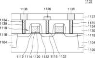
도 9를 참조하면, 복수의 반도체 소자(1101, 도 8 참조)를 구성하는 각각의 구성 요소를 보다 자세히 살펴보기로 한다. 특히, 복수의 반도체 소자(1101, 도 8 참조)에 포함되는 트랜지스터(1102)에 대하여 자세히 살펴보도록 한다.Referring to FIG. 9, each component constituting a plurality of semiconductor elements (1101, see FIG. 8) will be examined in more detail. In particular, a transistor (1102) included in a plurality of semiconductor elements (1101, see FIG. 8) will be examined in more detail.
트랜지스터(1102)는 게이트 절연막(1112), 게이트 전극(1114), 소스 영역(1116), 및 드레인 영역(1118)을 포함할 수 있다. 상기 게이트 전극(1114)은 절연 캡핑 패턴(1120) 및 절연 스페이서(1122)에 의해 그 상면 및 양 측벽이 각각 절연되도록 배치될 수 있다.The transistor (1102) may include a gate insulating film (1112), a gate electrode (1114), a source region (1116), and a drain region (1118). The gate electrode (1114) may be arranged so that its upper surface and both side walls are each insulated by an insulating capping pattern (1120) and an insulating spacer (1122).
반도체 웨이퍼(1100) 상에 상기 트랜지스터(1102)를 덮는 제1 층간 절연막(1130)이 배치되고, 상기 제1 층간 절연막(1130)을 관통하여 상기 소스 영역(1116)에 전기적으로 연결되는 제1 콘택트(1132)와, 상기 드레인 영역(1118)에 전기적으로 연결되는 제2 콘택트(1134)가 배치될 수 있다.A first interlayer insulating film (1130) covering the transistor (1102) may be disposed on a semiconductor wafer (1100), and a first contact (1132) electrically connected to the source region (1116) and a second contact (1134) electrically connected to the drain region (1118) may be disposed through the first interlayer insulating film (1130).
상기 제1 콘택트(1132) 및 상기 제2 콘택트(1134)를 둘러싸는 라이너(1135)가 배치될 수 있다. 앞서 설명한 바와 같이, 접촉 저항은 트랜지스터(1102)의 소스 영역(1116) 및 드레인 영역(1118)에서 금속 물질과 반도체 물질이 접촉하는 부분의 저항을 의미한다.A liner (1135) surrounding the first contact (1132) and the second contact (1134) may be arranged. As described above, the contact resistance refers to the resistance of the portion where the metal material and the semiconductor material come into contact in the source region (1116) and the drain region (1118) of the transistor (1102).
금속-반도체 계면의 접촉 저항을 낮추기 위해 열처리 공정을 통해 금속-반도체 합금 물질의 접촉을 형성하게 된다. 즉, 라이너(1135)와 소스 영역(1116)의 접촉 저항, 그리고 라이너(1135)와 드레인 영역(1118)의 접촉 저항을 낮추기 위한 열처리 공정을 본 발명의 기술적 사상에 따른 반도체 기판의 열처리 장치(10, 20)에서 수행할 수 있다.In order to lower the contact resistance of the metal-semiconductor interface, a contact of the metal-semiconductor alloy material is formed through a heat treatment process. That is, a heat treatment process for lowering the contact resistance of the liner (1135) and the source region (1116) and the contact resistance of the liner (1135) and the drain region (1118) can be performed in a heat treatment device (10, 20) for a semiconductor substrate according to the technical idea of the present invention.
따라서, 상기 트랜지스터(1102)는 소스 영역(1116)에 전기적으로 연결되는 제1 콘택트(1132)의 접촉 저항 및 드레인 영역(1118)에 전기적으로 연결되는 제2 콘택트(1134)의 접촉 저항이 상대적으로 낮을 수 있다.Accordingly, the transistor (1102) may have relatively low contact resistance of the first contact (1132) electrically connected to the source region (1116) and relatively low contact resistance of the second contact (1134) electrically connected to the drain region (1118).
상기 제1 층간 절연막(1130) 위에 도전층(미도시)을 형성한 후, 상기 도전층을 패터닝하여, 복수의 제1 콘택트(1132)를 통해 상기 소스 영역(1116)에 전기적으로 연결되는 소스 라인(1136)과, 상기 소스 라인(1136)의 양측에서 상기 제2 콘택트(1134)를 통해 드레인 영역(1118)에 각각 전기적으로 연결되는 하부 전극(1138)이 배치될 수 있다.After forming a conductive layer (not shown) on the first interlayer insulating film (1130), the conductive layer can be patterned so that a source line (1136) electrically connected to the source region (1116) through a plurality of first contacts (1132) and a lower electrode (1138) electrically connected to the drain region (1118) through the second contacts (1134) on both sides of the source line (1136) can be arranged.
상기 제1 층간 절연막(1130) 상에, 상기 소스 라인(1136) 및 상기 하부 전극(1138)을 덮도록 하부 절연막(1137)이 배치될 수 있다. 상기 하부 전극(1138)의 상면을 노출시키도록 상기 하부 절연막(1137)의 일부가 제거될 수 있다.A lower insulating film (1137) may be placed on the first interlayer insulating film (1130) to cover the source line (1136) and the lower electrode (1138). A portion of the lower insulating film (1137) may be removed to expose the upper surface of the lower electrode (1138).
이상, 첨부된 도면들을 참조하여 본 발명의 기술적 사상의 실시예를 설명하였지만, 본 발명이 속하는 기술분야에서 통상의 지식을 가진 자는 본 발명이 그 기술적 사상이나 필수적인 특징을 변경하지 않고서 다른 구체적인 형태로 실시될 수 있다는 것을 이해할 수 있을 것이다. 그러므로 이상에서 기술한 실시예는 모든 면에서 예시적인 것이며 한정적이 아닌 것으로 이해해야만 한다.Above, the technical idea of the present invention has been described with reference to the attached drawings, but those skilled in the art will understand that the present invention can be implemented in other specific forms without changing the technical idea or essential features thereof. Therefore, it should be understood that the above-described embodiments are exemplary in all respects and not restrictive.
10, 20: 반도체 기판의 열처리 장치
S10: 반도체 소자의 제조 방법
100: 풉
200: 기판 이송 모듈
300: 열처리 챔버
400: 로드락
500: 전송 모듈10, 20: Heat treatment device for semiconductor substrate
S10: Method for manufacturing semiconductor devices
100: Phew
200: Substrate transfer module
300: Heat treatment chamber
400: Roadlock
500: Transmission Module
Claims (10)
Translated fromKorean상기 EFEM으로부터 기판을 공급받아, 열처리를 수행하는 하나 이상의 열처리 챔버; 및
상기 가스 주입부를 통하여 산화 방지 가스를 공급하고, 상기 가스 배출부를 통하여 배출되는 상기 산화 방지 가스를, 다시 상기 가스 주입부로 순환 공급하는 가스 순환기;를 포함하고,
상기 산화 방지 가스를 통하여, 상기 EFEM의 산소 농도를 1ppm 이하로 조절하고,
상기 EFEM과 상기 열처리 챔버의 사이에,
로드락(Load-Lock, L/L); 및
전송 모듈(Transfer Module, TM);을 포함하고,
상기 L/L 및 상기 TM 각각에 진공 펌프가 구비되어, 상기 L/L 및 상기 TM 각각의 산소 농도는 상기 EFEM의 산소 농도와 실질적으로 동일한,
반도체 기판의 열처리 장치.A substrate transfer module (Equipment Front End Module, EFEM) having a gas inlet and a gas outlet;
One or more heat treatment chambers for receiving a substrate from the EFEM and performing heat treatment; and
A gas circulator is included that supplies an anti-oxidation gas through the gas injection unit and circulates the anti-oxidation gas discharged through the gas discharge unit back to the gas injection unit;
Through the above-mentioned anti-oxidation gas, the oxygen concentration of the EFEM is controlled to 1 ppm or less,
Between the above EFEM and the above heat treatment chamber,
Load-Lock (L/L); and
Contains a Transfer Module (TM);
A vacuum pump is provided in each of the L/L and the TM, so that the oxygen concentration of each of the L/L and the TM is substantially the same as the oxygen concentration of the EFEM.
Heat treatment device for semiconductor substrates.
상기 산화 방지 가스는 질소(N2) 가스인 것을 특징으로 하는 반도체 기판의 열처리 장치.In the first paragraph,
A heat treatment device for a semiconductor substrate, characterized in that the above-mentioned anti-oxidation gas is nitrogen (N2 ) gas.
상기 EFEM은 폐쇄형 구조로 이루어지는 것을 특징으로 하는 반도체 기판의 열처리 장치.In the second paragraph,
A heat treatment device for a semiconductor substrate, characterized in that the above EFEM has a closed structure.
상기 EFEM의 내부에,
상기 기판의 온도를 낮추는 냉각 장치를 포함하는 것을 특징으로 하는 반도체 기판의 열처리 장치.In the first paragraph,
Inside the above EFEM,
A heat treatment device for a semiconductor substrate, characterized by including a cooling device for lowering the temperature of the substrate.
상기 냉각 장치는,
액체 질소를 이용한 장치; 또는
수랭식 장치;인 것을 특징으로 하는 반도체 기판의 열처리 장치.In paragraph 4,
The above cooling device,
A device using liquid nitrogen; or
A heat treatment device for a semiconductor substrate, characterized by being a water-cooling device.
상기 EFEM의 내부에,
상기 기판의 온도를 측정할 수 있는 온도 측정 장치를 포함하는 것을 특징으로 하는 반도체 기판의 열처리 장치.In the first paragraph,
Inside the above EFEM,
A heat treatment device for a semiconductor substrate, characterized by including a temperature measuring device capable of measuring the temperature of the substrate.
상기 온도 측정 장치에서 측정된 온도 데이터를 기초로 피드백 데이터를 형성하는 것을 특징으로 하는 반도체 기판의 열처리 장치.In Article 6,
A heat treatment device for a semiconductor substrate, characterized in that feedback data is formed based on temperature data measured by the above temperature measuring device.
상기 열처리 챔버는 셋 이상으로 구성되는 것을 특징으로 하는 반도체 기판의 열처리 장치.In the first paragraph,
A heat treatment device for a semiconductor substrate, characterized in that the heat treatment chamber is composed of three or more heat treatment chambers.
Applications Claiming Priority (2)
| Application Number | Priority Date | Filing Date | Title |
|---|---|---|---|
| KR20190031908 | 2019-03-20 | ||
| KR1020190031908 | 2019-03-20 |
Publications (2)
| Publication Number | Publication Date |
|---|---|
| KR20200112585A KR20200112585A (en) | 2020-10-05 |
| KR102728796B1true KR102728796B1 (en) | 2024-11-12 |
Family
ID=72809308
Family Applications (1)
| Application Number | Title | Priority Date | Filing Date |
|---|---|---|---|
| KR1020190075226AActiveKR102728796B1 (en) | 2019-03-20 | 2019-06-24 | Heat treatment apparatus for semiconductor substrate |
Country Status (1)
| Country | Link |
|---|---|
| KR (1) | KR102728796B1 (en) |
Citations (1)
| Publication number | Priority date | Publication date | Assignee | Title |
|---|---|---|---|---|
| WO2018167846A1 (en)* | 2017-03-14 | 2018-09-20 | 株式会社Kokusai Electric | Substrate processing device, method for manufacturing semiconductor device, and program |
Family Cites Families (3)
| Publication number | Priority date | Publication date | Assignee | Title |
|---|---|---|---|---|
| KR20040064326A (en)* | 2003-01-10 | 2004-07-19 | 삼성전자주식회사 | Substrate processing apparatus for controlling contamination in substrate transfer module |
| CN109671643B (en)* | 2013-08-12 | 2023-11-28 | 应用材料公司 | Substrate processing systems, devices and methods with factory interface environmental control |
| KR20170118397A (en)* | 2016-04-15 | 2017-10-25 | 피에스케이 주식회사 | Substrate treating apparatus |
- 2019
- 2019-06-24KRKR1020190075226Apatent/KR102728796B1/enactiveActive
Patent Citations (1)
| Publication number | Priority date | Publication date | Assignee | Title |
|---|---|---|---|---|
| WO2018167846A1 (en)* | 2017-03-14 | 2018-09-20 | 株式会社Kokusai Electric | Substrate processing device, method for manufacturing semiconductor device, and program |
Also Published As
| Publication number | Publication date |
|---|---|
| KR20200112585A (en) | 2020-10-05 |
Similar Documents
| Publication | Publication Date | Title |
|---|---|---|
| TWI495014B (en) | Semiconductor device manufacturing method | |
| TWI405251B (en) | Semiconductor device manufacturing method | |
| US6063300A (en) | Method of manufacturing semiconductor device including light etching | |
| JPWO2015115002A1 (en) | Method for forming fine pattern, method for manufacturing semiconductor device, substrate processing apparatus, and recording medium | |
| KR20070111979A (en) | Manufacturing Method of Semiconductor Device | |
| US20190123262A1 (en) | Semiconductor manufacturing apparatus, memory device, and method of manufacturing the memory device | |
| CN110875225B (en) | Wet etching equipment | |
| JPWO2002073697A1 (en) | Semiconductor integrated circuit device and method of manufacturing the same | |
| KR20180031787A (en) | Method for manufacturing semiconductor device, substrate processing apparatus and program | |
| US6403475B1 (en) | Fabrication method for semiconductor integrated device | |
| KR20110106233A (en) | Spacer Protection and Electrical Wiring in Array Devices | |
| KR102728796B1 (en) | Heat treatment apparatus for semiconductor substrate | |
| KR19990030191A (en) | Gap Filling of Semiconductor Structures Using Doped Silicate Glass | |
| KR20170102816A (en) | Rare earth metal surface-activated plasma doping on semiconductor substrates | |
| JPH11354751A (en) | Semiconductor device, method of manufacturing semiconductor device, and semiconductor manufacturing apparatus | |
| US20160211151A1 (en) | Substrate processing apparatus and method of manufacturing semiconductor device | |
| CN106486353B (en) | Method of forming semiconductor device | |
| TW201916130A (en) | Method for processing semiconductor wafer in furnace | |
| TWI871852B (en) | Semiconductor device having semiconductor channel layer | |
| CN110277492A (en) | Method for manufacturing semiconductor device | |
| KR100516134B1 (en) | Apparatus for manufacturing SIMOX SOI wafer | |
| US20240105509A1 (en) | Middle of line dielectric layer engineering for via void prevention | |
| CN110911265A (en) | Method for removing silicon oxide in titanium nitride generation process | |
| US20150311090A1 (en) | Method of manufacturing a semiconductor device | |
| KR20060133606A (en) | Contact hole cleaning method and manufacturing method of semiconductor device using same |
Legal Events
| Date | Code | Title | Description |
|---|---|---|---|
| PA0109 | Patent application | Patent event code:PA01091R01D Comment text:Patent Application Patent event date:20190624 | |
| PG1501 | Laying open of application | ||
| A201 | Request for examination | ||
| PA0201 | Request for examination | Patent event code:PA02012R01D Patent event date:20220525 Comment text:Request for Examination of Application Patent event code:PA02011R01I Patent event date:20190624 Comment text:Patent Application | |
| E902 | Notification of reason for refusal | ||
| PE0902 | Notice of grounds for rejection | Comment text:Notification of reason for refusal Patent event date:20240323 Patent event code:PE09021S01D | |
| E701 | Decision to grant or registration of patent right | ||
| PE0701 | Decision of registration | Patent event code:PE07011S01D Comment text:Decision to Grant Registration Patent event date:20241004 | |
| GRNT | Written decision to grant | ||
| PR0701 | Registration of establishment | Comment text:Registration of Establishment Patent event date:20241106 Patent event code:PR07011E01D | |
| PR1002 | Payment of registration fee | Payment date:20241107 End annual number:3 Start annual number:1 | |
| PG1601 | Publication of registration |