KR102724660B1 - Light emitting device - Google Patents
Light emitting deviceDownload PDFInfo
- Publication number
- KR102724660B1 KR102724660B1KR1020160166885AKR20160166885AKR102724660B1KR 102724660 B1KR102724660 B1KR 102724660B1KR 1020160166885 AKR1020160166885 AKR 1020160166885AKR 20160166885 AKR20160166885 AKR 20160166885AKR 102724660 B1KR102724660 B1KR 102724660B1
- Authority
- KR
- South Korea
- Prior art keywords
- light
- conductive semiconductor
- semiconductor layer
- emitting
- emitting structure
- Prior art date
- Legal status (The legal status is an assumption and is not a legal conclusion. Google has not performed a legal analysis and makes no representation as to the accuracy of the status listed.)
- Active
Links
- 239000004065semiconductorSubstances0.000claimsabstractdescription129
- 239000000758substrateSubstances0.000claimsabstractdescription41
- 238000005530etchingMethods0.000claimsdescription19
- 238000009826distributionMethods0.000abstractdescription2
- 239000000463materialSubstances0.000description28
- 238000000034methodMethods0.000description23
- 238000010586diagramMethods0.000description14
- 238000000926separation methodMethods0.000description12
- 229910002601GaNInorganic materials0.000description11
- 230000017525heat dissipationEffects0.000description8
- 239000000203mixtureSubstances0.000description8
- 150000004767nitridesChemical class0.000description6
- 239000011149active materialSubstances0.000description4
- 239000010408filmSubstances0.000description4
- 239000012535impuritySubstances0.000description4
- 239000004973liquid crystal related substanceSubstances0.000description4
- 239000002243precursorSubstances0.000description4
- 229910052594sapphireInorganic materials0.000description4
- 239000010980sapphireSubstances0.000description4
- PXHVJJICTQNCMI-UHFFFAOYSA-NNickelChemical compound[Ni]PXHVJJICTQNCMI-UHFFFAOYSA-N0.000description3
- KDLHZDBZIXYQEI-UHFFFAOYSA-NPalladiumChemical compound[Pd]KDLHZDBZIXYQEI-UHFFFAOYSA-N0.000description3
- 229910052581Si3N4Inorganic materials0.000description3
- BQCADISMDOOEFD-UHFFFAOYSA-NSilverChemical compound[Ag]BQCADISMDOOEFD-UHFFFAOYSA-N0.000description3
- ATJFFYVFTNAWJD-UHFFFAOYSA-NTinChemical compound[Sn]ATJFFYVFTNAWJD-UHFFFAOYSA-N0.000description3
- 229910052782aluminiumInorganic materials0.000description3
- XAGFODPZIPBFFR-UHFFFAOYSA-NaluminiumChemical compound[Al]XAGFODPZIPBFFR-UHFFFAOYSA-N0.000description3
- 238000006243chemical reactionMethods0.000description3
- 238000004891communicationMethods0.000description3
- 238000005520cutting processMethods0.000description3
- 238000004519manufacturing processMethods0.000description3
- 229910052751metalInorganic materials0.000description3
- 239000002184metalSubstances0.000description3
- BASFCYQUMIYNBI-UHFFFAOYSA-NplatinumChemical compound[Pt]BASFCYQUMIYNBI-UHFFFAOYSA-N0.000description3
- 229910052709silverInorganic materials0.000description3
- 239000004332silverSubstances0.000description3
- 239000010409thin filmSubstances0.000description3
- 229910052718tinInorganic materials0.000description3
- 238000001039wet etchingMethods0.000description3
- 229910010093LiAlOInorganic materials0.000description2
- 229910020068MgAlInorganic materials0.000description2
- -1Si 3 N 4Inorganic materials0.000description2
- 229910004298SiO 2Inorganic materials0.000description2
- VYPSYNLAJGMNEJ-UHFFFAOYSA-NSilicium dioxideChemical compoundO=[Si]=OVYPSYNLAJGMNEJ-UHFFFAOYSA-N0.000description2
- 229910010037TiAlNInorganic materials0.000description2
- 229910010413TiO 2Inorganic materials0.000description2
- 229910008482TiSiNInorganic materials0.000description2
- MCMNRKCIXSYSNV-UHFFFAOYSA-NZirconium dioxideChemical compoundO=[Zr]=OMCMNRKCIXSYSNV-UHFFFAOYSA-N0.000description2
- 238000003491arrayMethods0.000description2
- 238000005229chemical vapour depositionMethods0.000description2
- 239000011651chromiumSubstances0.000description2
- 150000001875compoundsChemical class0.000description2
- 239000010949copperSubstances0.000description2
- 239000010931goldSubstances0.000description2
- 238000002955isolationMethods0.000description2
- QRXWMOHMRWLFEY-UHFFFAOYSA-NisoniazideChemical compoundNNC(=O)C1=CC=NC=C1QRXWMOHMRWLFEY-UHFFFAOYSA-N0.000description2
- 238000005272metallurgyMethods0.000description2
- 230000003287optical effectEffects0.000description2
- LIVNPJMFVYWSIS-UHFFFAOYSA-Nsilicon monoxideChemical compound[Si-]#[O+]LIVNPJMFVYWSIS-UHFFFAOYSA-N0.000description2
- HQVNEWCFYHHQES-UHFFFAOYSA-Nsilicon nitrideChemical compoundN12[Si]34N5[Si]62N3[Si]51N64HQVNEWCFYHHQES-UHFFFAOYSA-N0.000description2
- 229910052814silicon oxideInorganic materials0.000description2
- 229910000679solderInorganic materials0.000description2
- 239000010936titaniumSubstances0.000description2
- 238000002834transmittanceMethods0.000description2
- 229910018072Al 2 O 3Inorganic materials0.000description1
- 229910002704AlGaNInorganic materials0.000description1
- 229910017083AlNInorganic materials0.000description1
- PIGFYZPCRLYGLF-UHFFFAOYSA-NAluminum nitrideChemical compound[Al]#NPIGFYZPCRLYGLF-UHFFFAOYSA-N0.000description1
- OKTJSMMVPCPJKN-UHFFFAOYSA-NCarbonChemical compound[C]OKTJSMMVPCPJKN-UHFFFAOYSA-N0.000description1
- VYZAMTAEIAYCRO-UHFFFAOYSA-NChromiumChemical compound[Cr]VYZAMTAEIAYCRO-UHFFFAOYSA-N0.000description1
- RYGMFSIKBFXOCR-UHFFFAOYSA-NCopperChemical compound[Cu]RYGMFSIKBFXOCR-UHFFFAOYSA-N0.000description1
- JMASRVWKEDWRBT-UHFFFAOYSA-NGallium nitrideChemical compound[Ga]#NJMASRVWKEDWRBT-UHFFFAOYSA-N0.000description1
- UFHFLCQGNIYNRP-UHFFFAOYSA-NHydrogenChemical compound[H][H]UFHFLCQGNIYNRP-UHFFFAOYSA-N0.000description1
- RTAQQCXQSZGOHL-UHFFFAOYSA-NTitaniumChemical compound[Ti]RTAQQCXQSZGOHL-UHFFFAOYSA-N0.000description1
- 239000000853adhesiveSubstances0.000description1
- 230000001070adhesive effectEffects0.000description1
- PNEYBMLMFCGWSK-UHFFFAOYSA-Naluminium oxideInorganic materials[O-2].[O-2].[O-2].[Al+3].[Al+3]PNEYBMLMFCGWSK-UHFFFAOYSA-N0.000description1
- 238000004380ashingMethods0.000description1
- 230000004888barrier functionEffects0.000description1
- 230000015572biosynthetic processEffects0.000description1
- 229910052799carbonInorganic materials0.000description1
- 229910052804chromiumInorganic materials0.000description1
- 239000004020conductorSubstances0.000description1
- 229910052802copperInorganic materials0.000description1
- 229910052593corundumInorganic materials0.000description1
- 239000013078crystalSubstances0.000description1
- 230000007547defectEffects0.000description1
- 239000006185dispersionSubstances0.000description1
- 239000002019doping agentSubstances0.000description1
- 230000005684electric fieldEffects0.000description1
- 238000010292electrical insulationMethods0.000description1
- PCHJSUWPFVWCPO-UHFFFAOYSA-NgoldChemical compound[Au]PCHJSUWPFVWCPO-UHFFFAOYSA-N0.000description1
- 229910052737goldInorganic materials0.000description1
- 229910052739hydrogenInorganic materials0.000description1
- 239000001257hydrogenSubstances0.000description1
- 229910052738indiumInorganic materials0.000description1
- APFVFJFRJDLVQX-UHFFFAOYSA-Nindium atomChemical compound[In]APFVFJFRJDLVQX-UHFFFAOYSA-N0.000description1
- 238000002347injectionMethods0.000description1
- 239000007924injectionSubstances0.000description1
- 239000011147inorganic materialSubstances0.000description1
- 239000011810insulating materialSubstances0.000description1
- 238000005304joiningMethods0.000description1
- 239000011159matrix materialSubstances0.000description1
- 229910001092metal group alloyInorganic materials0.000description1
- 238000001451molecular beam epitaxyMethods0.000description1
- 229910052759nickelInorganic materials0.000description1
- 239000011368organic materialSubstances0.000description1
- 238000012858packaging processMethods0.000description1
- 229910052763palladiumInorganic materials0.000description1
- 238000000059patterningMethods0.000description1
- 229910052697platinumInorganic materials0.000description1
- 230000001681protective effectEffects0.000description1
- 230000006798recombinationEffects0.000description1
- 238000005215recombinationMethods0.000description1
- 238000002310reflectometryMethods0.000description1
- 239000000523sampleSubstances0.000description1
- 239000000126substanceSubstances0.000description1
- JBQYATWDVHIOAR-UHFFFAOYSA-NtellanylidenegermaniumChemical compound[Te]=[Ge]JBQYATWDVHIOAR-UHFFFAOYSA-N0.000description1
- 229910052719titaniumInorganic materials0.000description1
- 238000000927vapour-phase epitaxyMethods0.000description1
- 229910001845yogo sapphireInorganic materials0.000description1
Images


Classifications
- H—ELECTRICITY
- H10—SEMICONDUCTOR DEVICES; ELECTRIC SOLID-STATE DEVICES NOT OTHERWISE PROVIDED FOR
- H10H—INORGANIC LIGHT-EMITTING SEMICONDUCTOR DEVICES HAVING POTENTIAL BARRIERS
- H10H29/00—Integrated devices, or assemblies of multiple devices, comprising at least one light-emitting semiconductor element covered by group H10H20/00
- H10H29/10—Integrated devices comprising at least one light-emitting semiconductor component covered by group H10H20/00
- H10H29/14—Integrated devices comprising at least one light-emitting semiconductor component covered by group H10H20/00 comprising multiple light-emitting semiconductor components
- H10H29/142—Two-dimensional arrangements, e.g. asymmetric LED layout
- H01L33/62—
- H—ELECTRICITY
- H10—SEMICONDUCTOR DEVICES; ELECTRIC SOLID-STATE DEVICES NOT OTHERWISE PROVIDED FOR
- H10H—INORGANIC LIGHT-EMITTING SEMICONDUCTOR DEVICES HAVING POTENTIAL BARRIERS
- H10H20/00—Individual inorganic light-emitting semiconductor devices having potential barriers, e.g. light-emitting diodes [LED]
- H10H20/80—Constructional details
- H10H20/85—Packages
- H10H20/857—Interconnections, e.g. lead-frames, bond wires or solder balls
- H01L27/153—
- H01L33/02—
- H01L33/504—
- H—ELECTRICITY
- H10—SEMICONDUCTOR DEVICES; ELECTRIC SOLID-STATE DEVICES NOT OTHERWISE PROVIDED FOR
- H10H—INORGANIC LIGHT-EMITTING SEMICONDUCTOR DEVICES HAVING POTENTIAL BARRIERS
- H10H20/00—Individual inorganic light-emitting semiconductor devices having potential barriers, e.g. light-emitting diodes [LED]
- H10H20/01—Manufacture or treatment
- H10H20/036—Manufacture or treatment of packages
- H10H20/0364—Manufacture or treatment of packages of interconnections
- H—ELECTRICITY
- H10—SEMICONDUCTOR DEVICES; ELECTRIC SOLID-STATE DEVICES NOT OTHERWISE PROVIDED FOR
- H10H—INORGANIC LIGHT-EMITTING SEMICONDUCTOR DEVICES HAVING POTENTIAL BARRIERS
- H10H20/00—Individual inorganic light-emitting semiconductor devices having potential barriers, e.g. light-emitting diodes [LED]
- H10H20/80—Constructional details
- H10H20/81—Bodies
- H—ELECTRICITY
- H10—SEMICONDUCTOR DEVICES; ELECTRIC SOLID-STATE DEVICES NOT OTHERWISE PROVIDED FOR
- H10H—INORGANIC LIGHT-EMITTING SEMICONDUCTOR DEVICES HAVING POTENTIAL BARRIERS
- H10H20/00—Individual inorganic light-emitting semiconductor devices having potential barriers, e.g. light-emitting diodes [LED]
- H10H20/80—Constructional details
- H10H20/85—Packages
- H10H20/851—Wavelength conversion means
- H10H20/8511—Wavelength conversion means characterised by their material, e.g. binder
- H10H20/8512—Wavelength conversion materials
- H10H20/8513—Wavelength conversion materials having two or more wavelength conversion materials
- H—ELECTRICITY
- H10—SEMICONDUCTOR DEVICES; ELECTRIC SOLID-STATE DEVICES NOT OTHERWISE PROVIDED FOR
- H10H—INORGANIC LIGHT-EMITTING SEMICONDUCTOR DEVICES HAVING POTENTIAL BARRIERS
- H10H29/00—Integrated devices, or assemblies of multiple devices, comprising at least one light-emitting semiconductor element covered by group H10H20/00
- H10H29/10—Integrated devices comprising at least one light-emitting semiconductor component covered by group H10H20/00
- H10H29/14—Integrated devices comprising at least one light-emitting semiconductor component covered by group H10H20/00 comprising multiple light-emitting semiconductor components
- H—ELECTRICITY
- H01—ELECTRIC ELEMENTS
- H01L—SEMICONDUCTOR DEVICES NOT COVERED BY CLASS H10
- H01L2924/00—Indexing scheme for arrangements or methods for connecting or disconnecting semiconductor or solid-state bodies as covered by H01L24/00
- H01L2924/10—Details of semiconductor or other solid state devices to be connected
- H01L2924/11—Device type
- H01L2924/12—Passive devices, e.g. 2 terminal devices
- H01L2924/1204—Optical Diode
- H01L2924/12041—LED
- H01L2933/0066—
- H—ELECTRICITY
- H10—SEMICONDUCTOR DEVICES; ELECTRIC SOLID-STATE DEVICES NOT OTHERWISE PROVIDED FOR
- H10H—INORGANIC LIGHT-EMITTING SEMICONDUCTOR DEVICES HAVING POTENTIAL BARRIERS
- H10H20/00—Individual inorganic light-emitting semiconductor devices having potential barriers, e.g. light-emitting diodes [LED]
- H10H20/80—Constructional details
- H10H20/81—Bodies
- H10H20/819—Bodies characterised by their shape, e.g. curved or truncated substrates
- H—ELECTRICITY
- H10—SEMICONDUCTOR DEVICES; ELECTRIC SOLID-STATE DEVICES NOT OTHERWISE PROVIDED FOR
- H10H—INORGANIC LIGHT-EMITTING SEMICONDUCTOR DEVICES HAVING POTENTIAL BARRIERS
- H10H20/00—Individual inorganic light-emitting semiconductor devices having potential barriers, e.g. light-emitting diodes [LED]
- H10H20/80—Constructional details
- H10H20/83—Electrodes
- H10H20/831—Electrodes characterised by their shape
- H10H20/8312—Electrodes characterised by their shape extending at least partially through the bodies
Landscapes
- Led Devices (AREA)
Abstract
Translated fromKoreanDescription
Translated fromKorean본 발명의 기술적 사상은 발광 소자에 관한 것이다. 보다 상세하게는 직렬 연결된 복수의 발광 다이오드(Light emitting diode, LED)를 포함하는 발광 소자에 관한 것이다.The technical idea of the present invention relates to a light emitting device. More specifically, it relates to a light emitting device including a plurality of light emitting diodes (LEDs) connected in series.
일반적으로, LED는 낮은 소비전력, 고휘도 등의 여러 장점 때문에 광원으로서 널리 사용된다. 특히, 최근 반도체 발광소자는 조명장치 및 대형 액정 디스플레이(Liquid Crystal Display, LCD) 용 백라이트(Backlight) 장치로 채용되고 있다.In general, LEDs are widely used as light sources because of their many advantages, such as low power consumption and high brightness. In particular, semiconductor light-emitting devices have recently been adopted as backlight devices for lighting devices and large-scale liquid crystal displays (LCDs).
발광소자의 효율을 높이기 위해서 복수개의 LED 칩들을 서로 직렬로 연결하는 방법이 채용될 수 있다. 이때 개별 칩을 직렬 연결하는 경우 기판 분리 공정, 분리된 LED 칩에 대한 패키징 공정 등이 요구되며, 각각의 패키지들을 기판 상에 배치하는 실장공정 및 패키지가 가지는 전극들 사이의 배선 공정이 별도로 요구된다. 따라서, 공정 소요 시간이 증가하고, 제조단가가 상승하는 문제가 있다. 이에 따라 복수개의 발광 다이오드를 포함하는 칩을 포함하는 발광 소자가 제안된다.In order to increase the efficiency of a light-emitting element, a method of connecting multiple LED chips in series with each other can be adopted. At this time, when connecting individual chips in series, a substrate separation process, a packaging process for the separated LED chips, etc. are required, and a mounting process for arranging each package on a substrate and a wiring process between electrodes of the package are required separately. Therefore, there is a problem that the process time increases and the manufacturing cost rises. Accordingly, a light-emitting element including a chip including multiple light-emitting diodes is proposed.
본 발명의 기술적 사상이 해결하고자 하는 기술적 과제는 신뢰성이 제고된 발광 소자를 제공하는 것이다.The technical problem that the technical idea of the present invention seeks to solve is to provide a light-emitting element with improved reliability.
본 발명의 기술적 사상이 해결하고자 하는 기술적 과제는 발광 효율이 제고된 발광 소자를 제공하는 것이다.The technical problem that the technical idea of the present invention seeks to solve is to provide a light-emitting element with improved light-emitting efficiency.
본 발명의 기술적 사상이 해결하고자 하는 과제는 이상에서 언급한 과제에 제한되지 않으며, 언급되지 않은 또 다른 과제들은 아래의 기재로부터 당업자에게 명확하게 이해될 수 있을 것이다.The problems to be solved by the technical idea of the present invention are not limited to the problems mentioned above, and other problems not mentioned will be clearly understood by those skilled in the art from the description below.
상술한 과제를 해결하기 위한, 예시적 실시예들에 따른 발광 소자는 투광 기판 상에 수평 방향으로 이격되어 배치되며, 순차적으로 적층된 제1 도전형 반도체층, 활성층 및 제2 도전형 반도체층을 포함하는 제1 발광 구조물 및 제2 발광 구조물 및 상기 제1 발광 구조물의 상기 제1 도전형 반도체층과 상기 제2 발광 구조물의 상기 제2 도전형 반도체층 사이를 전기적으로 연결될 수 있도록 구성된 구조물간 도전층을 포함하되, 상기 제2 발광 구조물은 상면도적 관점에서 외주로부터 내부로 길게 식각되어 형성된 핑거부를 포함 할 수 있다.In order to solve the above-described problem, according to exemplary embodiments, a light-emitting element is disposed horizontally spaced apart from each other on a light-transmitting substrate, and includes a first light-emitting structure and a second light-emitting structure including a first conductive semiconductor layer, an active layer, and a second conductive semiconductor layer that are sequentially laminated, and an inter-structure conductive layer configured to electrically connect between the first conductive semiconductor layer of the first light-emitting structure and the second conductive semiconductor layer of the second light-emitting structure, wherein the second light-emitting structure may include a finger portion formed by being etched long from the outer periphery to the inner periphery when viewed from a top view.
다른 예시적인 실시예들에 발광 소자는 투광기판 및 상기 투광기판의 일면에 평행한 제1 방향으로 이격되어 배치되되, 순차적으로 적층된 제1 도전형 반도체층, 활성층 및 제2 도전형 반도체층을 각각 포함하는 제1 발광 구조물 및 제2 발광 구조물을 포함하되, 상기 제1 발광 구조물의 상기 제1 도전형 반도체층과 상기 제2 발광 구조물의 상기 제2 도전형 반도체층은 전기적으로 연결되도록 구성되고, 상기 제2 발광 구조물은 상기 일면에 평행하며 상기 제1 방향과 교차하는 제2 방향으로 이격된 복수개의 섬 영역들 및 상기 복수개의 섬 영역들 중 이웃한 어느 두 섬 영역들 사이에 배치된 브릿지 영역을 포함할 수 있다.In other exemplary embodiments, the light emitting element may include a first light emitting structure and a second light emitting structure, each of which includes a first conductive semiconductor layer, an active layer, and a second conductive semiconductor layer, which are sequentially stacked and arranged in a first direction parallel to a surface of the light emitting substrate, wherein the first conductive semiconductor layer of the first light emitting structure and the second conductive semiconductor layer of the second light emitting structure are configured to be electrically connected, and the second light emitting structure may include a plurality of island regions spaced in a second direction parallel to the surface and intersecting the first direction, and a bridge region disposed between any two adjacent island regions among the plurality of island regions.
본 발명의 기술적 사상에 따르면, 전류 분배 특성이 향상된 발광 소자를 제공할 수 있다. 또한 본 발명의 기술적 사상에 따르면, 내부 빛 샘이 감소된 발광 소자를 제공할 수 있다. 이에 따라 신뢰성이 제고된 발광 소자를 제공할 수 있다.According to the technical idea of the present invention, a light-emitting element with improved current distribution characteristics can be provided. In addition, according to the technical idea of the present invention, a light-emitting element with reduced internal light sources can be provided. Accordingly, a light-emitting element with improved reliability can be provided.
도 1은 예시적인 실시예들에 따른 발광 소자를 설명하기 위한 회로도이다.
도 2는 예시적인 실시예들에 따른 발광 소자를 설명하기 위한 레이아웃도이다.
도 3은 예시적인 실시예들에 따른 발광 소자를 설명하기 위하여 도 2의 절단선 I-I`를 따라 취한 단면도이다
도 4 내지 도 11은 예시적인 실시예들에 따른 발광 소자의 제조방법을 설명하기 위한 단면도들이다.
도 12는 예시적인 실시예들에 따른 발광 소자를 설명하기 위한 레이아웃도이다
도 13a는 예시적인 실시예들에 따른 발광 소자를 설명하기 위한 회로도이다.
도 13b는 예시적인 실시예들에 따른 발광 소자를 설명하기 위한 레이아웃도이다.
도 14a은 예시적인 실시예들에 따른 발광 소자를 설명하기 위한 회로도이다.
도 14b는 예시적인 실시예들에 따른 발광 소자를 설명하기 위한 레이아웃도이다.
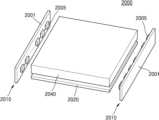
도 15은 예시적인 실시예에 따른 발광 소자를 포함하는 백라이트 유닛의 개략적인 사시도이다.
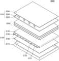
도 16은 예시적인 실시예에 따른 발광 소자를 포함하는 디스플레이 장치의 개략적인 분해 사시도이다.
도 17는 예시적인 실시예에 따른 발광 소자를 포함하는 바(bar) 타입의 조명 장치를 개략적으로 나타내는 분해 사시도이다.FIG. 1 is a circuit diagram for explaining a light-emitting element according to exemplary embodiments.
FIG. 2 is a layout diagram illustrating a light-emitting element according to exemplary embodiments.
FIG. 3 is a cross-sectional view taken along the cutting line II` of FIG. 2 to explain a light-emitting element according to exemplary embodiments.
FIGS. 4 to 11 are cross-sectional views illustrating a method for manufacturing a light-emitting element according to exemplary embodiments.
FIG. 12 is a layout diagram for explaining a light-emitting element according to exemplary embodiments.
FIG. 13a is a circuit diagram for explaining a light-emitting element according to exemplary embodiments.
FIG. 13b is a layout diagram for explaining a light-emitting element according to exemplary embodiments.
FIG. 14a is a circuit diagram for explaining a light-emitting element according to exemplary embodiments.
FIG. 14b is a layout diagram for explaining a light-emitting element according to exemplary embodiments.
FIG. 15 is a schematic perspective view of a backlight unit including a light-emitting element according to an exemplary embodiment.
FIG. 16 is a schematic exploded perspective view of a display device including a light-emitting element according to an exemplary embodiment.
FIG. 17 is an exploded perspective view schematically illustrating a bar-type lighting device including a light-emitting element according to an exemplary embodiment.
이하, 첨부 도면을 참조하여 본 발명의 실시예들을 상세히 설명한다. 도면상의 동일한 구성요소에 대해서는 동일한 참조부호를 사용하고, 이들에 대한 중복된 설명은 생략한다.Hereinafter, embodiments of the present invention will be described in detail with reference to the attached drawings. The same reference numerals are used for the same components in the drawings, and redundant descriptions thereof are omitted.
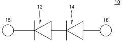
도 1은 예시적인 실시예들에 따른 발광 소자(10)를 개략적으로 도시한 회로도이다.FIG. 1 is a circuit diagram schematically illustrating a light-emitting element (10) according to exemplary embodiments.
도 1을 참조하면 발광 소자는 제1 및 제2 LED(13, 14)를 포함할 수 있다. 제1 및 제2 LED(13, 14)는 제1 및 제2 외부 단자(15, 16) 사이에 직렬 연결될 수 있다. 제1 LED(13)의 P절점이 제1 외부 단자(15)와 전기적으로 연결될 수 있다. 제2 LED(14)의 N 절점은 제2 외부 단자(16)와 전기적으로 연결될 수 있다. 제1 LED(13)의 N 절점은 제2 LED(14)의 P절점과 연결될 수 있다. 이에 따라 각 외부 단자 사이에는 두 개의 활성층이 존재하게 된다.Referring to FIG. 1, the light emitting element may include first and second LEDs (13, 14). The first and second LEDs (13, 14) may be connected in series between first and second external terminals (15, 16). The P node of the first LED (13) may be electrically connected to the first external terminal (15). The N node of the second LED (14) may be electrically connected to the second external terminal (16). The N node of the first LED (13) may be connected to the P node of the second LED (14). Accordingly, two active layers exist between each external terminal.
하나의 LED에 따른 전압강하를 Vd라고 할 때 도 1에 도시된 발광 소자는 두 개의 직렬 연결된 LED를 포함하는바, 제1 및 제2 외부단자(15,16) 사이에 2Vd의 전압 강하가 나타나게 된다. 예컨대 하나의 LED에 대응되는 전압강하가 3V라고 한다면 두 개의 LED가 직렬 연결된 것으로 제1 및 제2 외부 단자 사이에서 6V의 전압 강하가 발생할 수 있다. 이에 따라 교류-직류 변환 과정에서 높은 직류 전압으로 변환이 가능한 바, 상용 교류전원을 사용하는 경우 직류로 변환 효율이 제고될 수 있다.When the voltage drop according to one LED is Vd, the light-emitting element illustrated in Fig. 1 includes two LEDs connected in series, so a voltage drop of 2 Vd appears between the first and second external terminals (15, 16). For example, if the voltage drop corresponding to one LED is 3 V, a voltage drop of 6 V may occur between the first and second external terminals when two LEDs are connected in series. Accordingly, since conversion into a high DC voltage is possible during the AC-DC conversion process, the conversion efficiency into DC can be improved when using a commercial AC power source.
도 2는 예시적인 실시예들에 따른 발광 소자(10)를 개략적으로 도시한 레이아웃도이다. 도 3은 도 2의 절단선 I-I`를 따라 취한 단면도이다.Fig. 2 is a layout diagram schematically illustrating a light emitting element (10) according to exemplary embodiments. Fig. 3 is a cross-sectional view taken along the cutting line I-I` of Fig. 2.
도 2 및 도 3을 참조하면, 예시적인 실시예들에 따른 반도체 발광 소자(10)는 기판(101), 제1 및 제2 발광 구조물(100a, 100b), 제1 절연 패턴들(200a, 200b), 제1 및 제2 도전층(300a, 300b) 구조물간 도전층(300i), 제2 절연 패턴(400) 및 제1 및 제2 전극들(500a, 500b)을 포함할 수 있다.Referring to FIGS. 2 and 3, a semiconductor light-emitting device (10) according to exemplary embodiments may include a substrate (101), first and second light-emitting structures (100a, 100b), first insulating patterns (200a, 200b), first and second conductive layers (300a, 300b), an inter-structure conductive layer (300i), a second insulating pattern (400), and first and second electrodes (500a, 500b).
기판(101)은 발광 구조물의 성장용 기판으로 제공될 수 있으며, 사파이어, Si, SiC, MgAl2O4, MgO, LiAlO2, LiGaO2, GaN 등과 같이 절연성 또는 반도체 물질을 이용할 수 있다. 하지만 이에 제한 되는 것은 아니고, 경우에 따라 기판(101)은 도전성일 수 있다. 질화물 반도체 성장용 기판으로 널리 이용되는 사파이어는, 전기 절연성을 가지며 육각-롬보형(Hexa-Rhombo R3c) 대칭성을 갖는 결정체로서 c축 및 a측 방향의 격자상수가 각각 13.001Å과 4.758Å이며, C(0001)면, A(1120)면, R(1102)면 등을 갖는다. 이 경우, C면은 비교적 질화물 박막의 성장이 용이하며, 고온에서 안정하기 때문에 질화물 성장용 기판으로 주로 사용된다.The substrate (101) can be provided as a substrate for growth of a light-emitting structure, and an insulating or semiconductor material such as sapphire, Si, SiC, MgAl2 O4 , MgO, LiAlO2 , LiGaO2 , GaN, etc. can be used. However, it is not limited thereto, and in some cases, the substrate (101) can be conductive. Sapphire, which is widely used as a substrate for growth of nitride semiconductors, is a crystal having electrical insulation and hexagonal-Rhombo R3c symmetry, and the lattice constants in the c-axis and a-axis directions are 13.001 Å and 4.758 Å, respectively, and has a C (0001) plane, an A (1120) plane, an R (1102) plane, etc. In this case, the C plane is mainly used as a substrate for nitride growth because it is relatively easy to grow a nitride thin film on it and it is stable at high temperatures.
그리고, 도면에서 도시하는 것과 같이, 기판(101)의 상면, 즉, 제1 및 제2 발광 구조물(100a, 100b)이 배치되는 면에는 다수의 요철 구조(102)가 형성될 수 있으며, 이러한 요철 구조(102)에 의하여 반도체층들의 결정성과 광 방출 효율 등이 향상될 수 있다. 도 3을 참조하면 요철 구조(102)가 돔 형상의 볼록한 형태를 가지는 것으로 예시하고 있으나, 이에 한정하는 것은 아니다. 예를 들어, 요철 구조(102)는 사각형, 삼각형 등의 다양한 형태로 형성될 수 있다. 요철 구조(102)는 선택적으로 형성될 수 있는 것으로서 생략될 수도 있다.And, as illustrated in the drawing, a plurality of uneven structures (102) may be formed on the upper surface of the substrate (101), that is, the surface on which the first and second light-emitting structures (100a, 100b) are arranged, and the crystallinity and light emission efficiency of the semiconductor layers may be improved by the uneven structures (102). Referring to FIG. 3, the uneven structures (102) are exemplified as having a dome-shaped convex shape, but are not limited thereto. For example, the uneven structures (102) may be formed in various shapes, such as a square or a triangle. The uneven structures (102) may be formed selectively and may be omitted.
기판(101)의 상면에 평행하면서 서로 교차하는 두 방향을 각각 제1 방향(x방향) 및 제2 방향(y방향)으로, 상면에 실질적으로 수직인 방향을 제1 방향(z방향)으로 정의한다. 예를 들면, 제1 방향(x방향) 및 제2 방향(y방향)은 실질적으로 서로 수직으로 교차할 수 있다. 제1 방향(x방향) 및 제2 방향(y방향)은 실질적으로 제3 방향(z방향)에 대하여 수직인 방향들이다. 도면상에 화살표로 표시된 방향과 이의 반대 방향은 동일 방향으로 설명한다. 전술한 방향에 대한 정의는 이후 모든 도면들에서 동일하다.The two directions that are parallel to the upper surface of the substrate (101) and intersect each other are defined as the first direction (x direction) and the second direction (y direction), respectively, and the direction that is substantially perpendicular to the upper surface is defined as the first direction (z direction). For example, the first direction (x direction) and the second direction (y direction) can intersect each other substantially perpendicularly. The first direction (x direction) and the second direction (y direction) are directions that are substantially perpendicular to the third direction (z direction). The direction indicated by an arrow in the drawing and the opposite direction thereof are described as the same direction. The definition of the above-mentioned directions is the same in all drawings thereafter.
기판은 제1 셀 영역(CELL1), 제1 셀 영역와 제1 방향(x방향)으로 이격된 제2 셀 영역(CELL2) 및 제1 셀 영역(CELL1)과 제2 셀 영역(CELL2)사이에 개재된 분리 영역(ISO)이 정의될 수 있다. 제1 셀 영역(CELL1) 상에는 제1 발광 구조물(100a)이 배치될 수 있고, 제2 셀 영역(CELL2) 상에는 제2 발광 구조물(100b)이 배치될 수 있다. 일부 실시예들에 있어서, 제1 셀 영역(CELL1)은 도 1을 참조하여 설명한 제1 LED(13)에 대응될 수 있고, 제2 셀 영역(CELL2)은 도 1을 참조하여 설명한 제2 LED(14)에 대응될 수 있다. 다른 일부 실시예들에 있어서, 제1 셀 영역(CELL1)은 도 1을 참조하여 설명한 제2 LED(14)에 대응될 수 있고, 제2 셀 영역(CELL2)은 도 1을 참조하여 설명한 제1 LED(13)에 대응될 수 있다.The substrate may be defined with a first cell region (CELL1), a second cell region (CELL2) spaced apart from the first cell region in a first direction (x direction), and a separation region (ISO) interposed between the first cell region (CELL1) and the second cell region (CELL2). A first light-emitting structure (100a) may be arranged on the first cell region (CELL1), and a second light-emitting structure (100b) may be arranged on the second cell region (CELL2). In some embodiments, the first cell region (CELL1) may correspond to the first LED (13) described with reference to FIG. 1, and the second cell region (CELL2) may correspond to the second LED (14) described with reference to FIG. 1. In some other embodiments, the first cell region (CELL1) may correspond to the second LED (14) described with reference to FIG. 1, and the second cell region (CELL2) may correspond to the first LED (13) described with reference to FIG. 1.
기판(101)은 경우에 따라서 이후의 공정에서 제거될 수 있다. 즉, 제1 도전형 반도체층들(110a, 110b), 활성층들(120a, 120b) 및 제2 도전형 반도체층들(130a, 130b)을 성장시키기 위한 성장용 기판으로 제공된 후 분리 공정을 거쳐 제거될 수 있다. 특히 기판(101)이 도전성인 경우, 제1 및 제2 발광 구조물(100a, 100b)간의 단락을 방지하기 위하여 제거될 수 있다. 기판(101)의 분리는 레이저 리프트 오프(Laser Lift Off), 화학적 리프트 오프(Chemical Lift Off) 등의 방식을 통해 제1 및 제2 발광 구조물(100a, 100b)과 분리될 수 있다.The substrate (101) may be removed in a subsequent process, depending on the case. That is, it may be removed through a separation process after being provided as a growth substrate for growing the first conductive semiconductor layers (110a, 110b), the active layers (120a, 120b), and the second conductive semiconductor layers (130a, 130b). In particular, when the substrate (101) is conductive, it may be removed to prevent a short circuit between the first and second light-emitting structures (100a, 100b). The substrate (101) may be separated from the first and second light-emitting structures (100a, 100b) by a method such as a laser lift off or a chemical lift off.
도면에는 도시되지 않았으나, 기판(101)의 상면에는 버퍼층이 더 구비될 수 있다. 버퍼층은 기판(101) 상에 성장되는 반도체층의 격자 결함 완화를 위한 것으로, 질화물 등으로 이루어진 도핑되지 않은(undoped) 반도체층으로 이루어질 수 있다. 버퍼층은, 예를 들어, 사파이어로 이루어진 기판(101)과 기판(101) 상면에 적층되는 GaN으로 이루어진 제1 도전형 반도체층들(110a, 110b) 사이의 격자상수 차이를 완화하여, GaN층의 결정성을 증대시킬 수 있다. 버퍼층은 도핑되지 않은 GaN, AlN, InGaN 등이 적용될 수 있으며, 500℃ 내지 600℃의 저온에서 수십 내지 수백 Å의 두께로 성장시켜 형성할 수 있다. 도핑되지 않았음은 반도체층에 불순물 도핑 공정을 따로 거치지 않은 것을 의미하며, 반도체층에 본래 존재하던 수준의 불순물 농도, 예컨대, 질화갈륨 반도체를 유기 금속 화학 증착(Metal Organic Chemical Vapor Deposition, MOCVD)을 이용하여 성장시킬 경우, 도펀트로서 사용되는 Si 등이 의도하지 않더라도 약 1014~ 1018/㎤의 수준으로 포함될 수 있다. 다만, 이러한 버퍼층은 본 실시예에서 필수적인 요소는 아니며 경우에 따라 생략될 수도 있다.Although not shown in the drawing, a buffer layer may be further provided on the upper surface of the substrate (101). The buffer layer is for alleviating lattice defects of a semiconductor layer grown on the substrate (101) and may be formed of an undoped semiconductor layer made of nitride, etc. The buffer layer may alleviate the lattice constant difference between the substrate (101) made of, for example, sapphire and the first conductive semiconductor layers (110a, 110b) made of GaN stacked on the upper surface of the substrate (101), thereby increasing the crystallinity of the GaN layer. Undoped GaN, AlN, InGaN, etc. may be applied to the buffer layer, and may be formed by growing it to a thickness of several tens to several hundred Å at a low temperature of 500° C. to 600° C. Undoped means that the semiconductor layer has not undergone a separate impurity doping process, and the impurity concentration at the original level of the semiconductor layer, for example, when a gallium nitride semiconductor is grown using Metal Organic Chemical Vapor Deposition (MOCVD), Si used as a dopant may be included at a level of about 1014 to 1018 /cm3 even if unintentional. However, such a buffer layer is not an essential element in the present embodiment and may be omitted in some cases.
제1 및 제2 발광 구조물(100a, 100b)은 복수의 반도체층이 적층된 구조로서, 기판의 상면 상에 순차적으로 적층된 제1 도전형 반도체층들(110a, 110b), 활성층들(120a, 120b) 및 제2 도전형 반도체층들(130a, 130b)을 포함할 수 있다. 예컨대, 기판(101)상에 적층되는 제1 도전형 반도체층들(110a, 110b)은 n형 불순물이 도핑된 반도체로 이루어질 수 있으며, n형 질화물 반도체층일 수 있다. 그리고, 제2 도전형 반도체층들(130a, 130b)은 p형 불순물이 도핑된 반도체로 이루어질 수 있으며, p형 질화물 반도체층일 수 있다. 경우에 따라서 제1 및 제2 도전형 반도체층들(110a, 110b, 130a, 130b)은 위치가 바뀌어 적층될 수도 있다. 이러한 제1 및 제2 도전형 반도체층들(110a, 110b, 130a, 130b)은 AlxInyGa(1-x-y)N 조성식(단, 0≤x≤1, 0≤y≤1, 0≤x+y≤1)을 가지며, 예컨대, GaN, AlGaN, InGaN, AlInGaN 등의 물질이 이에 해당될 수 있다.The first and second light-emitting structures (100a, 100b) are structures in which a plurality of semiconductor layers are laminated, and may include first conductive semiconductor layers (110a, 110b), active layers (120a, 120b), and second conductive semiconductor layers (130a, 130b) that are sequentially laminated on the upper surface of the substrate. For example, the first conductive semiconductor layers (110a, 110b) laminated on the substrate (101) may be formed of a semiconductor doped with an n-type impurity and may be n-type nitride semiconductor layers. In addition, the second conductive semiconductor layers (130a, 130b) may be formed of a semiconductor doped with a p-type impurity and may be p-type nitride semiconductor layers. In some cases, the first and second conductive semiconductor layers (110a, 110b, 130a, 130b) may be laminated with their positions switched. These first and second challenge type semiconductor layers (110a, 110b, 130a, 130b) have a composition formula of Alx Iny Ga(1-xy) N (where 0≤x≤1, 0≤y≤1, 0≤x+y≤1), and may be materials such as GaN, AlGaN, InGaN, and AlInGaN.
제1 및 제2 도전형 반도체층들(110a, 110b, 130a, 130b) 사이에 배치되는 활성층들(120a, 120b)은 전자와 정공의 재결합에 의해 소정의 에너지를 갖는 광을 방출한다. 활성층들(120a, 120b)은 제1 및 제2 도전형 반도체층들(110a, 110b, 130a, 130b)의 에너지 밴드 갭보다 작은 에너지 밴드 갭을 갖는 물질을 포함할 수 있다. 예를 들어, 제1 및 제2 도전형 반도체층들(110a, 110b, 130a, 130b)이 GaN계 화합물 반도체인 경우, 활성층들(120a, 120b)은 GaN의 에너지 밴드 갭보다 작은 에너지 밴드 갭을 갖는 InGaN계 화합물 반도체를 포함할 수 있다. 또한, 활성층들(120a, 120b)은 양자우물층과 양자장벽층이 서로 교대로 적층된 다중 양자우물(Multiple Quantum Wells, MQW) 구조, 예컨대, InGaN/GaN 구조가 사용될 수 있다. 다만, 이에 제한되는 것은 아니므로 활성층들(120a, 120b)은 단일 양자우물 구조(Single Quantum Well, SQW)가 사용될 수도 있다.The active layers (120a, 120b) disposed between the first and second conductive semiconductor layers (110a, 110b, 130a, 130b) emit light having a predetermined energy by recombination of electrons and holes. The active layers (120a, 120b) may include a material having an energy band gap smaller than the energy band gaps of the first and second conductive semiconductor layers (110a, 110b, 130a, 130b). For example, when the first and second conductive semiconductor layers (110a, 110b, 130a, 130b) are GaN-based compound semiconductors, the active layers (120a, 120b) may include an InGaN-based compound semiconductor having an energy band gap smaller than the energy band gap of GaN. In addition, the active layers (120a, 120b) may use a multiple quantum well (MQW) structure in which quantum well layers and quantum barrier layers are alternately stacked, for example, an InGaN/GaN structure. However, the present invention is not limited thereto, and a single quantum well (SQW) structure may be used as the active layers (120a, 120b).
제1 및 제2 발광 구조물(100a, 100b)은, 제2 도전형 반도체층들(130a, 130b), 활성층들(120a, 120b) 및 제1 도전형 반도체층들(110a, 110b)의 일부가 식각된 식각 영역(E)과, 식각 영역(E)에 의해 정의된 복수의 메사 영역(M)을 포함할 수 있다.The first and second light-emitting structures (100a, 100b) may include an etched region (E) in which parts of the second conductive semiconductor layers (130a, 130b), the active layers (120a, 120b) and the first conductive semiconductor layers (110a, 110b) are etched, and a plurality of mesa regions (M) defined by the etched regions (E).
제1 발광 구조물(100a)은 상면도적 관점에서(Top View) 하나의 섬 형상을 포함할 수 있다. 또는 제1 발광 구조물(100a)은 하나의 섬 형상으로 구성된다. 제1 발광 구조물(100a)에 포함되거나 제1 발광 구조물(100a)을 구성하는 섬형상은 사각형 또는 모서리(C)가 둥근 사각형구조를 포함할 수 있다. 제1 발광 구조물(100a)의 식각 영역(E)은 상면도적 관점(Top view)에 따른 가장자리들로부터 내부로 연장되지 않는다. 한편 메사 영역(M)의 모서리(C)에 전류 쏠림 현상을 방지하기 위해, 모서리 부분에서 외측으로 돌출된 형상을 취할 수 있다. 즉 모서리(C)로부터 이격된 부분이 모서리(C)에 인접한 부분에 비해 더 리세스될 수 있다.The first light-emitting structure (100a) may include one island shape in a top view. Alternatively, the first light-emitting structure (100a) is configured as one island shape. The island shape included in or constituting the first light-emitting structure (100a) may include a square or a square structure with rounded corners (C). The etched area (E) of the first light-emitting structure (100a) does not extend inward from the edges according to the top view. Meanwhile, in order to prevent a current concentration phenomenon at the corner (C) of the mesa region (M), a shape protruding outwardly from the corner portion may be taken. That is, a portion spaced apart from the corner (C) may be more recessed than a portion adjacent to the corner (C).
제2 발광 구조물(100b)의 식각 영역(E)은 사각형 또는 모서리(C)가 둥근 사각형구조를 포함하는 제2 발광 구조물(100b)의 일측면에서 이와 대향하는 타측면을 향해 소정의 폭 및 길이로 식각되어 생긴 틈새 구조인 핑거부(F)를 포함할 수 있다. 핑거부(F)는 제1 방향(x 방향)으로 연장될 수 있다. 예시적인 실시예들에 있어서, 핑거부(F)는 복수개 형성되되 서로 평행하게 형성될 수 있다. 예컨대 제2 발광 구조물(100b)에 형성되는 식각 영역은(E) 4개의 측면들 중 제1 발광 구조물(100a)로부터 가장 멀리 이격된 측면에서 제1 발광 구조물(100a)에 가장 인접한 측면을 향해서 연장될 수 있다.The etching region (E) of the second light-emitting structure (100b) may include a finger portion (F), which is a gap structure formed by etching from one side of the second light-emitting structure (100b) including a square or a square structure with rounded corners (C) toward the opposite side with a predetermined width and length. The finger portion (F) may extend in the first direction (x direction). In exemplary embodiments, the finger portions (F) may be formed in multiple numbers and may be formed parallel to each other. For example, the etching region (E) formed in the second light-emitting structure (100b) may extend from the side farthest from the first light-emitting structure (100a) among the four side surfaces toward the side closest to the first light-emitting structure (100a).
이때 제2 발광 구조물(100b)의 복수의 메사 영역(M)은 핑거부(F)에 의해 완전히 분리되는 것은 아니며, 타측면 부분에서 서로 연결되어 하나의 구조를 이룰 수 있다. 즉 핑거부(F)의 제1 방향(x방향)에 따른 길이는 제2 발광 구조물(100b)의 제1 방향(x방향)에 따른 길이보다 작을 수 있다. 단, 제1 및 제2 발광 구조물(100a, 100b)은 분리 영역(ISO)에 의해서 분리되어 별개의 LED를 구성한다.At this time, the plurality of mesa regions (M) of the second light-emitting structure (100b) are not completely separated by the finger portion (F), and may be connected to each other at the other side portion to form one structure. That is, the length of the finger portion (F) along the first direction (x direction) may be smaller than the length of the second light-emitting structure (100b) along the first direction (x direction). However, the first and second light-emitting structures (100a, 100b) are separated by the separation region (ISO) to form separate LEDs.
이러한 식각 영역(E)의 형성에 의해 제2 발광 구조물(100b)은 제2 방향을 따라 이격된 복수개의 섬 영역들(IR) 및 복수개의 섬 영역들(IR)중 어느 두 섬 영역들(IR)사이에 개재된 브릿지 영역(BR)을 포함하는 구조를 가질 수 있다. 브릿지 영역(BR)은 이웃한 두 섬 영역들(IR)을 연결할 수 있다. 이에 따라 제2 발광 구조물(100b)은 분리되지 않고 하나의 LED로 형성될 수 있다. 경우에 따라 브릿지 영역(BR) 및 복수개의 섬 영역(IR)의 제2 방향에 따른 길이의 합은 제1 발광 구조물(100a)의 제2 방향에 따른 길이와 실질적으로 동일할 수 있다. 하지만 이에 제한되는 것은 아니고, 브릿지 영역(BR) 및 복수개의 섬 영역(IR)의 제2 방향에 따른 길이의 합은 제1 발광 구조물(100a)의 제2 방향에 따른 길이와 서로 다를 수 있다. 이 경우 제1 발광 구조물(100a)과 제2 발광 구조물(100b)의 제2 방향에 따른 길이가 서로 다를 수 있다. 상술한 바를 종합하면 제1 및 제2 발광 구조물(100a, 100b)는 비대칭적인 구조 또는 서로 다른 구조를 포함할 수 있다.By forming such an etching region (E), the second light-emitting structure (100b) can have a structure including a plurality of island regions (IR) spaced apart along the second direction and a bridge region (BR) interposed between any two island regions (IR) of the plurality of island regions (IR). The bridge region (BR) can connect two adjacent island regions (IR). Accordingly, the second light-emitting structure (100b) can be formed as a single LED without being separated. In some cases, the sum of the lengths of the bridge region (BR) and the plurality of island regions (IR) along the second direction can be substantially the same as the length of the first light-emitting structure (100a) along the second direction. However, the present invention is not limited thereto, and the sum of the lengths of the bridge region (BR) and the plurality of island regions (IR) along the second direction can be different from the length of the first light-emitting structure (100a) along the second direction. In this case, the lengths of the first light-emitting structure (100a) and the second light-emitting structure (100b) in the second direction may be different from each other. In summary of the above, the first and second light-emitting structures (100a, 100b) may include an asymmetrical structure or different structures.
식각 영역(E)으로 노출되는 활성층들(120a, 120b)을 덮도록 메사 영역(M)의 측면, 즉 메사 영역(M)의 측면 경사면 및 하부 절연 패턴들(210a, 210b)이 배치될 수 있다. 하부 절연 패턴들(210a, 210b)은 제1 및 제2 발광 구조물(100a, 100b)을 전체적으로 덮는 구조로 제1 및 제2 발광 구조물(100a, 100b) 상에 배치될 수 있다.The side surface of the mesa region (M), i.e., the side slope of the mesa region (M), and the lower insulating patterns (210a, 210b) may be arranged to cover the active layers (120a, 120b) exposed to the etching region (E). The lower insulating patterns (210a, 210b) may be arranged on the first and second light-emitting structures (100a, 100b) in a structure that entirely covers the first and second light-emitting structures (100a, 100b).
하부 절연 패턴들(210a, 210b)은 절연 특성을 지닌 재료로 이루어질 수 있으며, 무기질 또는 유기질 물질을 사용하여 형성될 수 있다. 또한, 하부 절연 패턴들(210a, 210b)은 실리콘 산화물 또는 실리콘 질화물을 포함하여 이루어질 수 있으며, 예를 들어, SiO2, SiN, SiOxNy, TiO2, Si3N4, Al2O3, TiN, AlN, ZrO2, TiAlN, TiSiN 등으로 이루어질 수 있다.The lower insulating patterns (210a, 210b) may be made of a material having insulating properties and may be formed using an inorganic or organic material. In addition, the lower insulating patterns (210a, 210b) may be made of silicon oxide or silicon nitride, and may be made of, for example, SiO2 , SiN, SiOx Ny , TiO 2 , Si3 N4 , Al2 O3 , TiN, AlN, ZrO2 , TiAlN, TiSiN, etc.
하부 절연 패턴들(210a, 210b)은 식각 영역(E)으로 노출된 제1 도전형 반도체층들(110a, 110b) 및 제2 도전형 반도체층들(130a, 130b)의 상면의 일부를 노출 시키는 제1 개구부들(215)을 복수 개 구비할 수 있다. 구체적으로, 제1 개구부들(215)은 제2 도전형 반도체층들(130a, 130b)이 후술하는 제2 콘택 전극들(150a, 150b)과 전기적으로 연결될 수 있도록 제2 도전형 반도체층들(130a, 130b)의 상면의 일부를 부분적으로 노출시키도록 구성된다. 후술하듯 제1 개구부들(215)을 형성할 때 습식 식각 공정에 의하는바 하부 절연 패턴들(210a, 210b)은 리세스되어 제2 콘택 전극들(150a, 150b)로부터 수평방향으로 이격될 수 있다. 하지만 이에 제한되는 것은 아니고, 공정상 오차 또는 산포 등에 의해 하부 절연 패턴들(210a, 210b)은 제2 콘택 전극들(150a, 150b)과 접할 수 있다.The lower insulating patterns (210a, 210b) may have a plurality of first openings (215) that expose a portion of the upper surface of the first conductive semiconductor layers (110a, 110b) and the second conductive semiconductor layers (130a, 130b) exposed to the etching region (E). Specifically, the first openings (215) are configured to partially expose a portion of the upper surface of the second conductive semiconductor layers (130a, 130b) so that the second conductive semiconductor layers (130a, 130b) can be electrically connected to the second contact electrodes (150a, 150b) described below. As described later, when forming the first openings (215), the lower insulating patterns (210a, 210b) may be recessed and horizontally spaced from the second contact electrodes (150a, 150b) by a wet etching process. However, this is not limited thereto, and the lower insulating patterns (210a, 210b) may come into contact with the second contact electrodes (150a, 150b) due to process errors or dispersions.
이때 제1 개구부들(215)에 의해 노출되는 제2 도전형 반도체층들(130a, 130b) 상에는 제2 콘택 전극들(150a, 150b)이 배치될 수 있다. 제2 콘택 전극들(150a, 150b)은 제2 도전형 반도체층들(130a, 130b)과 전기적으로 연결될 수 있도록 구성된다At this time, second contact electrodes (150a, 150b) may be arranged on the second conductive semiconductor layers (130a, 130b) exposed by the first openings (215). The second contact electrodes (150a, 150b) are configured to be electrically connected to the second conductive semiconductor layers (130a, 130b).
제2 콘택 전극들(150a, 150b)은 반사 전극층들(151a, 151b)을 포함할 수 있다. 반사 전극층들(151a, 151b)은 메사 영역(M)의 상면에 대응되는 제2 도전형 반도체층들(130a, 130b)의 상면의 일부를 덮는 형태로 형성될 수 있다. 반사 전극층들(151a, 151b)은 구리(Cu), 알루미늄(Al), 니켈(Ni), 은(Ag), 금(Au), 백금(Pt), 주석(Sn), 납(Pb), 티타늄(Ti), 크롬(Cr), 팔라듐(Pd), 인듐(In) 및 아연(Zn)로 구성된 그룹으로부터 선택된 적어도 하나의 금속 또는 금속 합금 또는 탄소(C)를 포함할 수 있다. 후술하는 제1 및 제2 도전층(300a, 300b), 구조물간 도전층(300i), 제1 및 제2 전극들(500a, 500b) 또한 제1 콘택 전극들(140a, 140b)도 동일한 물질들을 포함할 수 있다. 특히 반사 전극층들(151a, 151b)은 알루미늄, 은 등의 반사도가 높은 물질을 포함하는 경우 반사층의 역할을 수행하므로 발광효율이 제고될 수 있다. 반사 전극층들(151a, 151b) 서로 다른 조성의 층이 반복적으로 적층된 다층 구조를 포함할 수 있다.The second contact electrodes (150a, 150b) may include reflective electrode layers (151a, 151b). The reflective electrode layers (151a, 151b) may be formed to cover a portion of the upper surface of the second conductive semiconductor layers (130a, 130b) corresponding to the upper surface of the mesa region (M). The reflective electrode layers (151a, 151b) may include at least one metal or metal alloy selected from the group consisting of copper (Cu), aluminum (Al), nickel (Ni), silver (Ag), gold (Au), platinum (Pt), tin (Sn), lead (Pb), titanium (Ti), chromium (Cr), palladium (Pd), indium (In), and zinc (Zn), or carbon (C). The first and second conductive layers (300a, 300b), the inter-structure conductive layer (300i), the first and second electrodes (500a, 500b), and the first contact electrodes (140a, 140b) described below may also include the same materials. In particular, when the reflective electrode layers (151a, 151b) include a highly reflective material such as aluminum or silver, they function as a reflective layer, so that the luminous efficiency can be improved. The reflective electrode layers (151a, 151b) may include a multilayer structure in which layers of different compositions are repeatedly laminated.
제2 콘택 전극들(150a, 150b)은 반사 전극층들(151a, 151b)을 덮는 피복층들(152a, 152b)을 더 포함할 수 있다. 도 3을 참조하면 피복층들(152a, 152b)은 반사 전극층들(151a, 151b)의 상면 및 측면을 덮는 것으로 도시되었으나 이에 제한 되는 것은 아니다. 예컨대 피복층들(152a, 152b)은 반사 전극층들(151a, 151b)의 상면만을 덮을 수 있다. 또한, 피복층들(152a, 152b)은 선택적으로 배치될 수 있으며, 경우에 따라서 생략될 수도 있다. 피복층들(152a, 152b)은 경우에 따라 절연 물질일 수 있다. 피복층들(152a, 152b)은 경우에 따라 도전성 물질이거나 반도체 물질일 수 있다.The second contact electrodes (150a, 150b) may further include covering layers (152a, 152b) covering the reflective electrode layers (151a, 151b). Referring to FIG. 3, the covering layers (152a, 152b) are illustrated as covering the upper and side surfaces of the reflective electrode layers (151a, 151b), but are not limited thereto. For example, the covering layers (152a, 152b) may cover only the upper surfaces of the reflective electrode layers (151a, 151b). In addition, the covering layers (152a, 152b) may be selectively arranged and may be omitted in some cases. The covering layers (152a, 152b) may be an insulating material in some cases. The covering layers (152a, 152b) may be a conductive material or a semiconductor material, depending on the case.
상부 절연 패턴들(220a, 220b)은 제1 콘택 전극들(140a, 140b), 제2 콘택 전극들(150a, 150b), 하부 절연 패턴들(210a, 210b), 노출된 제1 도전형 반도체층들(110a, 110b) 및 노출된 제2 도전형 반도체층들(130a, 130b)상에 배치된다. 나아가 상부 절연 패턴은 분리 영역(ISO) 상에 식각되어 노출된 제1 도전형 반도체층들(110a, 110b)을 덮을 수 있다. 하부 절연 패턴들(210a, 210b)은 제2 콘택 전극들(150a, 150b)로부터 이격되어 형성되는 경우, 상부 절연 패턴들(220a, 220b)은 하부 절연 패턴과 제2 콘택 전극들(150a, 150b) 사이에 그루브(221)를 포함할 수 있다. 상부 절연 패턴들(220a, 220b)은 하부 절연 패턴들(210a, 210b)을 실질적으로 동일한 조성을 포함할 수 있다.Upper insulating patterns (220a, 220b) are arranged on the first contact electrodes (140a, 140b), the second contact electrodes (150a, 150b), the lower insulating patterns (210a, 210b), the exposed first conductive semiconductor layers (110a, 110b), and the exposed second conductive semiconductor layers (130a, 130b). Furthermore, the upper insulating pattern can be etched on the isolation region (ISO) to cover the exposed first conductive semiconductor layers (110a, 110b). When the lower insulating patterns (210a, 210b) are formed spaced apart from the second contact electrodes (150a, 150b), the upper insulating patterns (220a, 220b) may include a groove (221) between the lower insulating pattern and the second contact electrodes (150a, 150b). The upper insulating patterns (220a, 220b) may include substantially the same composition as the lower insulating patterns (210a, 210b).
하부 절연 패턴들(210a, 210b)과 상부 절연 패턴들(220a, 220b)이 조성이 같은 경우 하나의 통합된(integrated) 제1 절연 패턴들(200a, 200b)을 제공할 수 있다. 하지만 이에 제한되는 것은 아니고, 하부 절연 패턴들(210a, 210b)과 상부 절연 패턴들(220a, 220b)이 조성이 서로 다른 경우 구별되는 두 개의 층을 구성할 수 있다.When the lower insulating patterns (210a, 210b) and the upper insulating patterns (220a, 220b) have the same composition, they can provide one integrated first insulating pattern (200a, 200b). However, the present invention is not limited thereto, and when the lower insulating patterns (210a, 210b) and the upper insulating patterns (220a, 220b) have different compositions, they can form two distinct layers.
제1 절연 패턴들(200a, 200b)의 수직 두께는 가변적일 수 있다. 제2 콘택 전극들(150a, 150b)으로부터 이격되어 배치된 제1 절연 패턴들(200a, 200b)은 제2 콘택 전극들(150a, 150b) 상에 배치된 제1 절연 패턴들(200a, 200b)보다 더 큰 수직 두께를 갖는 부분을 포함할 수 있다. 제2 콘택 전극들(150a, 150b)으로부터 이격되어 배치된 제1 절연 패턴들(200a, 200b)의 수직 두께의 평균은 제2 콘택 전극들(150a, 150b) 상에 배치된 제1 절연 패턴들(200a, 200b)의 수직 두께의 평균보다 더 클 수 있다. 하부 절연 패턴들(210a, 210b)에 대응되는 제1 절연 패턴들(200a, 200b)의 수직 두께는 제2 콘택 전극들(150a, 150b)에 대응되는 제1 절연 패턴들(200a, 200b)보다 더 클 수 있다. 또 식각 영역(E) 상의 제1 도전형 반도체층들(110a, 110b) 상에 배치된 제1 절연 패턴들(200a, 200b)의 수직 두께는 제2 콘택 전극들(150a, 150b) 상에 배치된 제1 절연 패턴들(200a, 200b)의 수직두께 보다 클 수 있다. 이때 수직 두께는 제3 방향(z방향)에 따른 길이를 말한다.The vertical thickness of the first insulating patterns (200a, 200b) may be variable. The first insulating patterns (200a, 200b) arranged spaced apart from the second contact electrodes (150a, 150b) may include a portion having a greater vertical thickness than the first insulating patterns (200a, 200b) arranged on the second contact electrodes (150a, 150b). The average of the vertical thicknesses of the first insulating patterns (200a, 200b) arranged spaced apart from the second contact electrodes (150a, 150b) may be greater than the average of the vertical thicknesses of the first insulating patterns (200a, 200b) arranged on the second contact electrodes (150a, 150b). The vertical thickness of the first insulating patterns (200a, 200b) corresponding to the lower insulating patterns (210a, 210b) may be greater than the vertical thickness of the first insulating patterns (200a, 200b) corresponding to the second contact electrodes (150a, 150b). In addition, the vertical thickness of the first insulating patterns (200a, 200b) arranged on the first conductive semiconductor layers (110a, 110b) on the etching region (E) may be greater than the vertical thickness of the first insulating patterns (200a, 200b) arranged on the second contact electrodes (150a, 150b). In this case, the vertical thickness refers to the length along the third direction (z direction).
상부 절연 패턴들(220a, 220b)은 제2 콘택 전극들(150a, 150b)의 상면의 일부 및 제1 도전형 반도체들(110a, 110b)의 상면의 일부를 노출 시키는 제2 개구부들(225)을 복수 개 구비할 수 있다. 제2 개구부들(225)을 통해 노출된 제1 도전형 반도체들(110a, 110b)의 상면 상에 제1 콘택 전극들(140a, 140b)이 배치될 수 있다. 제1 콘택 전극들(140a, 140b)은 전극의 균일한 주입을 위하여 핑거부(F)를 따라 연장될 수 있다. 하지만 이에 제한되는 것은 아니고, 제1 콘택 전극들(140a, 140b)은 경우에 따라 생략될 수 있다. 이 경우 후술하는 제2 도전층(300b) 또는 구조물간 도전층(300i)이 직접 제1 도전형 반도체층들(110a, 110b)에 전기적으로 연결될 수 있도록 구성된다.The upper insulating patterns (220a, 220b) may have a plurality of second openings (225) that expose a portion of the upper surface of the second contact electrodes (150a, 150b) and a portion of the upper surface of the first conductive semiconductors (110a, 110b). The first contact electrodes (140a, 140b) may be arranged on the upper surfaces of the first conductive semiconductors (110a, 110b) exposed through the second openings (225). The first contact electrodes (140a, 140b) may extend along the finger portions (F) for uniform injection of the electrode. However, the present invention is not limited thereto, and the first contact electrodes (140a, 140b) may be omitted in some cases. In this case, the second conductive layer (300b) or inter-structure conductive layer (300i) described later is configured to be electrically connected directly to the first conductive semiconductor layers (110a, 110b).
제1 및 제2 발광 구조물(100a, 100b)에서의 발광 효율을 증가시키기 위해 제1 콘택 전극들(140a, 140b)과 제2 콘택 전극들(150a, 150b)은 전체적으로 서로 엇갈리는 구조를 가지도록 배치될 수 있다. 다만, 제1 콘택 전극들(140a, 150b) 및 제2 콘택 전극들(150a, 150b)의 형상 및 구조는 예시적인 것으로 도면에 도시된 것에 한정되지 않는다.In order to increase the light emitting efficiency in the first and second light emitting structures (100a, 100b), the first contact electrodes (140a, 140b) and the second contact electrodes (150a, 150b) may be arranged to have an overall structure that is staggered from each other. However, the shapes and structures of the first contact electrodes (140a, 150b) and the second contact electrodes (150a, 150b) are exemplary and are not limited to those illustrated in the drawings.
제1 및 제2 도전층(300a, 300b) 및 구조물간 도전층(300i)은 상부 절연 패턴들(220a, 220b), 제1 콘택 전극들(140a, 140b) 및 노출된 제2 콘택 전극들(150a, 150b) 상에 배치될 수 있다.The first and second conductive layers (300a, 300b) and the inter-structure conductive layer (300i) can be arranged on the upper insulating patterns (220a, 220b), the first contact electrodes (140a, 140b), and the exposed second contact electrodes (150a, 150b).
제1 및 제2 도전층(300a, 300b) 및 구조물간 도전층(300i)은 서로 이격되어 배치될 수 있다. 구체적으로 제1 도전층(300a) 및 구조물간 도전층(300i)은 후술하는 제2 절연 패턴(400)을 사이에 두고 이격되어 배치될 수 있다. 제2 도전층(300b) 및 구조물간 도전층(300i)은 제2 절연 패턴(400)을 사이에 두고 이격되어 배치될 수 있다. 즉 제1, 제2 도전층(300a, 300b) 및 구조물간 도전층(300i)은 서로 직접적으로 전기적으로 연결되지 않도록 구성된다.The first and second conductive layers (300a, 300b) and the inter-structure conductive layer (300i) may be arranged to be spaced apart from each other. Specifically, the first conductive layer (300a) and the inter-structure conductive layer (300i) may be arranged to be spaced apart from each other with the second insulating pattern (400) interposed therebetween, which will be described later. The second conductive layer (300b) and the inter-structure conductive layer (300i) may be arranged to be spaced apart from each other with the second insulating pattern (400) interposed therebetween. That is, the first and second conductive layers (300a, 300b) and the inter-structure conductive layer (300i) are configured not to be directly electrically connected to each other.
제1 도전층(300a)은 제1 발광 구조물(100a) 상에 배치된 제2 콘택 전극(150a)과 전기적으로 연결될 수 있도록 구성된다. 제2 도전층(300b)은 제2 발광 구조물(100b) 상에 배치된 제1 콘택 전극들(140b)과 전기적으로 연결될 수 있도록 구성된다. 구조물간 도전층(300i)은 제1 발광 구조물(100a) 상에 배치된 제1 콘택 전극들(140a)과 제2 발광 구조물(100b) 상에 배치된 제2 콘택 전극(150b)을 전기적으로 연결될 수 있도록 구성된다. 제1 콘택 전극들(140a, 140b)이 생략된 경우, 제2 도전층(300b)은 제2 발광 구조물(100b)의 제1 도전형 반도체층(110b)과 전기적으로 연결될 수 있도록 구성되고, 구조물간 도전층은 제1 발광 구조물(100a) 상의 제1 도전형 반도체층(110a)과 제2 발광 구조물(100b) 상에 배치된 제2 콘택 전극(150b)을 전기적으로 연결될 수 있도록 구성된다.The first conductive layer (300a) is configured to be electrically connected to the second contact electrode (150a) disposed on the first light-emitting structure (100a). The second conductive layer (300b) is configured to be electrically connected to the first contact electrodes (140b) disposed on the second light-emitting structure (100b). The inter-structure conductive layer (300i) is configured to be electrically connected to the first contact electrodes (140a) disposed on the first light-emitting structure (100a) and the second contact electrode (150b) disposed on the second light-emitting structure (100b). When the first contact electrodes (140a, 140b) are omitted, the second conductive layer (300b) is configured to be electrically connected to the first conductive semiconductor layer (110b) of the second light-emitting structure (100b), and the inter-structure conductive layer is configured to be electrically connected to the first conductive semiconductor layer (110a) on the first light-emitting structure (100a) and the second contact electrode (150b) disposed on the second light-emitting structure (100b).
결과적으로 제1 발광 구조물(100a)의 제1 도전형 반도체층(110a)과 제2 발광 구조물(100b)의 제2 도전형 반도체층(130b)이 전기적으로 연결되도록 구성된다. 이에 따라 제1 LED(13, 도 1 참조)에 대응되는 제1 셀 영역(CELL1)상의 제1 발광 구조물(100a)과 제2 LED(14, 도 1 참조)에 대응되는 제2 셀 영역(CELL2) 상의 제2 발광 구조물(100b)은 직렬 연결될 수 있다.As a result, the first conductive semiconductor layer (110a) of the first light-emitting structure (100a) and the second conductive semiconductor layer (130b) of the second light-emitting structure (100b) are configured to be electrically connected. Accordingly, the first light-emitting structure (100a) on the first cell region (CELL1) corresponding to the first LED (13, see FIG. 1) and the second light-emitting structure (100b) on the second cell region (CELL2) corresponding to the second LED (14, see FIG. 1) can be connected in series.
예시적인 실시예들에 따르면 구조물간 도전층(300i)은 제1 셀 영역(CELL1) 및 제2 셀 영역(CELL2) 사이의 식각 영역(E), 분리영역(ISO) 및 발광 구조물의 측면을 덮어서 셀간 빛 샘을 방지할 수 있다. 셀간 빛 샘이라 함은 제1 셀 영역(CELL1) 및 제2 셀 영역(CELL2) 사이, 즉 분리영역의(ISO)에 인접한 제1 및 제2 발광 구조물(100a, 100b)의 측면을 통해서 빛이 새어나가 발광 효율이 떨어지는 현상을 말한다.According to exemplary embodiments, the inter-structure conductive layer (300i) can cover the etching region (E), the separation region (ISO) and the side surface of the light-emitting structure between the first cell region (CELL1) and the second cell region (CELL2) to prevent inter-cell light leakage. Inter-cell light leakage refers to a phenomenon in which light leaks through the side surface of the first and second light-emitting structures (100a, 100b) between the first cell region (CELL1) and the second cell region (CELL2), i.e., adjacent to the separation region (ISO), thereby reducing light emission efficiency.
경우에 따라 구조물간 도전층(300i)은 분리영역(ISO) 상에서 노출되는 제1 및 제2 발광 구조물(100a, 100b)의 식각 영역(E), 분리영역(ISO)에서 노출된 측면에 형성되는 경사면 및 평면들을 모두 덮어서 내부 빛 샘을 방지할 수 있다. 특히 구조물간 도전층(300i)이 알루미늄, 은 등의 반사율이 높은 물질을 포함하는 경우 내부 빛 샘에 더욱 효과적일 수 있다. 경우에 따라 구조물간 도전층(300i)은 분리영역(ISO) 상에서 노출되는 제1 및 제2 발광 구조물(100a, 100b)의 전부를 덮어서 내부 빛 샘을 방지할 수 있다.In some cases, the inter-structure conductive layer (300i) can cover all of the etched areas (E) of the first and second light-emitting structures (100a, 100b) exposed on the separation area (ISO), the inclined surfaces and planes formed on the side surfaces exposed on the separation area (ISO), to prevent internal light leakage. In particular, when the inter-structure conductive layer (300i) includes a material with high reflectivity, such as aluminum or silver, it can be more effective against internal light leakage. In some cases, the inter-structure conductive layer (300i) can cover all of the first and second light-emitting structures (100a, 100b) exposed on the separation area (ISO), to prevent internal light leakage.
구조물간 도전층(300i)의 제2 방향(y방향)에 따른 길이와 제1 및 제2 발광 구조물(100a, 100b)의 제2 방향(y방향)에 따른 길이가 실질적으로 동일할 수 있다. 이에 따라 구조물간 도전층(300i)을 통해 전류가 흐를 수 있는 단면적 또한 넓어지는 바 전류 쏠림 현상을 방지하고 제1 발광 구조물(100a) 및 제2 발광 구조물(100b)간의 저항을 낮출 수 있어 발광 효율을 제고할 수 있다.The length of the inter-structure conductive layer (300i) along the second direction (y direction) and the length of the first and second light-emitting structures (100a, 100b) along the second direction (y direction) may be substantially the same. Accordingly, the cross-sectional area through which current can flow through the inter-structure conductive layer (300i) also increases, thereby preventing the current concentration phenomenon and lowering the resistance between the first light-emitting structure (100a) and the second light-emitting structure (100b), thereby improving light-emitting efficiency.
제2 절연 패턴(400)은 제1 및 제2 도전층(300a, 300b) 및 구조물간 도전층(300i) 상에 배치되며, 제1 및 제2 도전층(300a, 300b) 및 구조물간 도전층(300i)을 전체적으로 덮어 보호한다. 제2 절연 패턴(400)은 전술한 하부 절연 패턴(210b)과 실질적으로 동일한 조성을 포함할 수 있다. 제2 절연 패턴(400)은, 제1 및 제2 도전층(300a, 300b) 및 구조물간 도전층(300i)의 적어도 일부를 노출시키는 제3 개구부들(405)을 구비할 수 있다.The second insulating pattern (400) is disposed on the first and second conductive layers (300a, 300b) and the inter-structure conductive layer (300i), and entirely covers and protects the first and second conductive layers (300a, 300b) and the inter-structure conductive layer (300i). The second insulating pattern (400) may include substantially the same composition as the lower insulating pattern (210b) described above. The second insulating pattern (400) may have third openings (405) that expose at least a portion of the first and second conductive layers (300a, 300b) and the inter-structure conductive layer (300i).
제3 개구부들(405)은 제1 셀 영역(CELL1) 상의 제1 도전층(300a) 및 제2 셀 영역(CELL2) 상의 제2 도전층(300b)의 상면을 적어도 부분적으로 노출시킬 수 있도록 복수개로 형성될 수 있다. 도 3을 참조하면 제1 셀 영역(CELL1)에 한 개 제2 셀 영역(CELL2)에 두 개로 총 세 개의 제3 개구부들(405)이 형성되어 비대칭 구조를 이루는 것으로 예시하고 있으나, 이에 한정하는 것은 아니다. 제3 개구부들(405)의 개수 및 배치 형태는 다양하게 변형될 수 있다.The third openings (405) may be formed in multiple numbers so as to at least partially expose the upper surfaces of the first conductive layer (300a) on the first cell region (CELL1) and the second conductive layer (300b) on the second cell region (CELL2). Referring to FIG. 3, a total of three third openings (405) are formed, one in the first cell region (CELL1) and two in the second cell region (CELL2), to form an asymmetrical structure, but the present invention is not limited thereto. The number and arrangement of the third openings (405) may be modified in various ways.
제3 개구부들(405)을 통해 부분적으로 노출되는 제1 및 제2 도전층(300a, 300b) 상에 각각 순서대로 제1 및 제2 전극들(500a, 500b)이 구비될 수 있다. 제1 전극(500a)은 및 제1 도전층(300a) 및 제2 콘택 전극(150a)을 경유해 제1 셀 영역(CELL1) 상의 제2 도전형 반도체층(130a)에 전기적으로 연결될 수 있도록 구성된다. 제2 전극들(500b)은 제2 도전층(300b) 및 제1 콘택 전극들(140b)을 경유해 제2 셀 영역(CELL2) 상의 제1 도전형 반도체층(110b)에 전기적으로 연결될 수 있도록 구성된다. 제1 콘택 전극들(140b)이 생략되는 경우 제2 전극들(500b)은 제2 도전층(300b) 을 경유해 제2 셀 영역(CELL2) 상의 제1 도전형 반도체층(110b)에 전기적으로 연결될 수 있도록 구성된다.First and second electrodes (500a, 500b) may be sequentially provided on the first and second conductive layers (300a, 300b) partially exposed through the third openings (405), respectively. The first electrode (500a) is configured to be electrically connected to the second conductive semiconductor layer (130a) on the first cell region (CELL1) via the first conductive layer (300a) and the second contact electrode (150a). The second electrodes (500b) are configured to be electrically connected to the first conductive semiconductor layer (110b) on the second cell region (CELL2) via the second conductive layer (300b) and the first contact electrodes (140b). When the first contact electrodes (140b) are omitted, the second electrodes (500b) are configured to be electrically connected to the first conductive semiconductor layer (110b) on the second cell region (CELL2) via the second conductive layer (300b).
제1 전극(500a) 및 제2 전극들(500b)은, 예를 들어, UBM(Under Bump Metallurgy) 층일 수 있다. 그리고, 각각 한 개 또는 복수개로 구비될 수 있다. 도2 및 도 3을 참조하면, 제1 전극(500a)이 1개, 제2 전극들(500b)은 2개가 제공되는 것으로 예시하고 있으나 이에 한정하는 것은 아니다. 제1 전극(500a)과 제2 전극들(500b)의 개수와 배치 구조는 제3 개구부들(405)에 따라 조절될 수 있다. 제1 및 제2 전극들(500a, 500b)에는 도전성 접착물, 예를 들어, Sn 솔더가 놓이는 홈이 형성될 수 있다. Sn 솔더는 외부 단자로서 도 1의 제1 외부 단자(15) 및 제2 외부 단자(16)에 대응될 수 있다.The first electrode (500a) and the second electrodes (500b) may be, for example, UBM (Under Bump Metallurgy) layers. And, each may be provided as one or more. Referring to FIGS. 2 and 3, it is exemplified that one first electrode (500a) and two second electrodes (500b) are provided, but the present invention is not limited thereto. The number and arrangement structure of the first electrode (500a) and the second electrodes (500b) may be adjusted according to the third openings (405). A groove may be formed in the first and second electrodes (500a, 500b) in which a conductive adhesive, for example, Sn solder, is placed. The Sn solder may correspond to the first external terminal (15) and the second external terminal (16) of FIG. 1 as an external terminal.
도 4 내지 도 11은 예시적인 실시예에 따른 발광 소자의 제조 방법을 설명하기 위하여 도 2의 절단선 Ⅰ-Ⅰ'을 따라 취한 단면도들이다.FIGS. 4 to 11 are cross-sectional views taken along the cutting line Ⅰ-Ⅰ' of FIG. 2 to explain a method for manufacturing a light-emitting element according to an exemplary embodiment.
도 4 내지 도 11에서, 도 2 및 도 3과 동일한 참조 부호는 동일한 부재를 나타내며, 따라서 중복되는 설명은 생략한다.In FIGS. 4 to 11, the same reference numerals as in FIGS. 2 and 3 represent the same elements, and therefore, redundant descriptions are omitted.
도 4를 참조하면, 먼저 기판(101) 상에 요철 구조(102)를 형성할 수 있다. 다만, 경우에 따라 요철 구조(102)는 생략될 수있다. 기판(101)은, 앞서 설명한 바와 같이, 사파이어, Si, SiC, MgAl2O4, MgO, LiAlO2, LiGaO2, GaN 등의 물질로 이루어진 기판을 사용할 수 있다. 그리고, 도면에서는 도시하지 않았으나, 기판 상에는 버퍼층이 선택적으로 구비될 수 있다. 버퍼층은 도핑되지 않은 GaN, AlN, InGaN 등의 물질로 이루어질 수 있다.Referring to FIG. 4, first, a rough structure (102) can be formed on a substrate (101). However, in some cases, the rough structure (102) may be omitted. As described above, the substrate (101) may be a substrate made of a material such as sapphire, Si, SiC, MgAl2 O4 , MgO, LiAlO2 , LiGaO2 , GaN, etc. In addition, although not shown in the drawing, a buffer layer may be optionally provided on the substrate. The buffer layer may be made of a material such as undoped GaN, AlN, InGaN, etc.
다음으로, 유기 금속 화학 증착(Metal Organic Chemical Vapor Deposition, MOCVD), 수소화 기상 에피택시(Hydride Vapor Phase Epitaxy, HVPE), 분자선 에피택시(Molecular Beam Epitaxy, MBE)의 방법을 이용하여, 기판(101) 상에 순차적으로 제1 도전형 반도체 물질층(110), 활성 물질층(120) 및 제2 도전형 반도체 물질층(130)을 성장시켜 복수개의 반도체층들이 적층된 구조의 발광 구조물 전구체(100)를 형성한다. 여기서, 제1 도전형 반도체 물질층(110)과 제2 도전형 반도체 물질층(130)은 각각 n형 반도체층 및 p형 반도체층일 수 있다. 제1 및 제2 발광 구조물(100b)에서 제1 도전형 반도체 물질층(110)과 제2 도전형 반도체 물질층(130)의 위치는 서로 바뀔 수 있으며, 제2 도전형 반도체 물질층(130)이 기판(101) 상에 먼저 형성될 수 있다.Next, using a method of Metal Organic Chemical Vapor Deposition (MOCVD), Hydrogen Vapor Phase Epitaxy (HVPE), or Molecular Beam Epitaxy (MBE), a first conductive semiconductor material layer (110), an active material layer (120), and a second conductive semiconductor material layer (130) are sequentially grown on a substrate (101) to form a light emitting structure precursor (100) having a structure in which a plurality of semiconductor layers are stacked. Here, the first conductive semiconductor material layer (110) and the second conductive semiconductor material layer (130) may be an n-type semiconductor layer and a p-type semiconductor layer, respectively. The positions of the first conductive semiconductor material layer (110) and the second conductive semiconductor material layer (130) in the first and second light-emitting structures (100b) may be swapped, and the second conductive semiconductor material layer (130) may be formed first on the substrate (101).
도 5를 참조하면 제1 도전형 반도체 물질층(110)의 적어도 일부가 노출되도록 제2 도전형 반도체 물질층(130, 도4 참조), 활성 물질층(120, 도4 참조) 및 제1 도전형 반도체 물질층(110)의 일부를 식각할 수 있다.Referring to FIG. 5, the second conductive semiconductor material layer (130, see FIG. 4), the active material layer (120, see FIG. 4), and a portion of the first conductive semiconductor material layer (110) can be etched so that at least a portion of the first conductive semiconductor material layer (110) is exposed.
포토 마스크 패턴을 발광 구조물 전구체(100)상에 제공한 후, 포토 마스크 패턴을 식각 마스크로 하여 제2 도전형 반도체 물질층(130, 도4 참조), 활성 물질층(120, 도4 참조) 및 제1 도전형 반도체 물질층(110)의 일부를 습식 또는 건식 식각할 수 있다. 이에 의해 식각 영역(E)과 식각 영역(E)에 의해 정의되는 복수의 메사 영역(M)을 형성할 수 있다. 이에 따라 제2 도전형 반도체 물질층(130)과 활성 물질층(120)이 둘로 분리되어 각각 순서대로 제2 도전형 반도체층들(130a, 130b)과 활성층들(120a, 120b)이 형성될 수 있다. 경우에 따라, 제1 도전형 반도체 물질층(110)은 식각되지 않고 상면만 일부 노출되도록 식각 공정이 수행될 수도 있다. 경우에 따라 과도식각에 의해 제1 도전형 반도체 물질층(110)이 소정의 깊이까지 식각될 수도 있다.After a photomask pattern is provided on a light-emitting structure precursor (100), a second conductive semiconductor material layer (130, see FIG. 4), an active material layer (120, see FIG. 4), and a part of the first conductive semiconductor material layer (110) can be wet or dry etched using the photomask pattern as an etching mask. As a result, an etching region (E) and a plurality of mesa regions (M) defined by the etching region (E) can be formed. Accordingly, the second conductive semiconductor material layer (130) and the active material layer (120) can be separated into two, and second conductive semiconductor layers (130a, 130b) and active layers (120a, 120b) can be sequentially formed, respectively. In some cases, the etching process may be performed so that the first conductive semiconductor material layer (110) is not etched and only a part of the upper surface is exposed. In some cases, the first challenge type semiconductor material layer (110) may be etched to a predetermined depth by overetching.
도 6을 참조하면, 메사 영역(M) 및 식각 영역(E) 상에 하부 절연층(210)이 콘포말하게 형성될 수 있다. 하부 절연층(210)은 메사 영역(M)의 상면 가장자리와 식각 영역(E)의 바닥면의 적어도 일부를 포함하여 메사 영역(M)의 측면을 덮는 구조로 형성될 수 있다. 따라서, 메사 영역(M)을 형성할 때 노출된 활성층들(120a, 120b)이 하부 절연층(210)에 의해 외부로 노출되지 않도록 커버될 수 있다. 또한, 상기 제1 절연층(200)은 실리콘 산화물 또는 실리콘 질화물을 포함하여 이루어질 수 있으며, 예를 들어, SiO2, SiN, SiOxNy, TiO2, Si3N4, Al2O3, TiN, AlN, ZrO2, TiAlN, TiSiN 등으로 이루어질 수 있다.Referring to FIG. 6, a lower insulating layer (210) can be conformally formed on the mesa region (M) and the etching region (E). The lower insulating layer (210) can be formed to have a structure that covers the side surface of the mesa region (M) including at least a portion of the upper edge of the mesa region (M) and the bottom surface of the etching region (E). Accordingly, when forming the mesa region (M), the exposed active layers (120a, 120b) can be covered so as not to be exposed to the outside by the lower insulating layer (210). In addition, the first insulating layer (200) can be formed including silicon oxide or silicon nitride, and can be formed of, for example, SiO2 , SiN, SiOx Ny , TiO2 , Si3N4, Al2O3, TiN, AlN, ZrO2, TiAlN, TiSiN, etc.
도 7을 참조하면, 발광 구조물 전구체(100)를 분리하여 제1 셀 영역(CELL1), 제2 셀 영역(CELL2) 및 분리 영역(ISO)을 형성한다.Referring to FIG. 7, a light emitting structure precursor (100) is separated to form a first cell region (CELL1), a second cell region (CELL2), and a separation region (ISO).
포토 마스크 패턴을 발광 구조물 전구체(100)상에 제공한 후 기판(101)의 상면이 노출될 때까지 제1 도전형 반도체 물질층(110)을 식각할 수 있다. 이에 따라 제1 도전형 반도체 물질층(110, 도 6 참조)은 분리되어 제1 셀 영역(CELL1) 및 제2 셀 영역(CELL2) 및 분리 영역(ISO)이 정의된다.After the photomask pattern is provided on the light-emitting structure precursor (100), the first conductive semiconductor material layer (110) can be etched until the upper surface of the substrate (101) is exposed. Accordingly, the first conductive semiconductor material layer (110, see FIG. 6) is separated, and a first cell region (CELL1), a second cell region (CELL2), and an isolation region (ISO) are defined.
이때 하부 절연층(210)은 분리 공정에서 발생되는 제1 도전형 반도체 물질층(110)의 비산물 등이 메사 영역(M)의 측면 및 제2 도전형 반도체층들(130a, 130b)의 상면을 오염시키는 것을 방지할 수 있다. 이에 따라 신뢰성이 제고된 발광 소자를 제공할 수 있다.At this time, the lower insulating layer (210) can prevent the first conductive semiconductor material layer (110) generated in the separation process from being contaminated with the side surface of the mesa region (M) and the upper surface of the second conductive semiconductor layers (130a, 130b). Accordingly, a light-emitting element with improved reliability can be provided.
도 8을 참조하면, 메사 영역(M) 상의 제2 도전형 반도체층들(130a, 130b) 상에 제1 개구부들(215) 및 제2 콘택 전극들(150)이 형성될 수 있다.Referring to FIG. 8, first openings (215) and second contact electrodes (150) can be formed on second conductive semiconductor layers (130a, 130b) on the mesa region (M).
제2 콘택 전극들(150a, 150b)을 제공하기 위한 제1 개구부들(215)을 정의하기 위하여 제1 및 제2 발광 구조물(100a, 100b) 및 기판(101)상에 포토 마스크 패턴을 제공한다. 그 후 식각 공정을 통해 하부 절연층(210)의 일부를 제거하여 제1 개구부들(215)을 포함하는 하부 절연 패턴들(210a, 210b)을 형성한다. 하부 절연층(210) 중 노출되는 부분들이 습식 식각 공정에 의해 제거되는 경우, 포토 마스크 패턴에 의해 노출된 영역보다 수평방향으로 더 리세스 될 수 있다. 제1 개구부들(215)에 의하여 제2 도전형 반도체층들(130a, 130b)의 상면의 일부가 노출된다.A photomask pattern is provided on the first and second light-emitting structures (100a, 100b) and the substrate (101) to define first openings (215) for providing second contact electrodes (150a, 150b). Thereafter, a portion of the lower insulating layer (210) is removed through an etching process to form lower insulating patterns (210a, 210b) including the first openings (215). When exposed portions of the lower insulating layer (210) are removed by a wet etching process, the lower insulating layer may be recessed further in the horizontal direction than the region exposed by the photomask pattern. A portion of the upper surface of the second conductive semiconductor layers (130a, 130b) is exposed by the first openings (215).
제1 개구부들(215) 및 포토 마스크 패턴 상에 순서대로 반사 전극 제공층 및 피복 제공층을 제공할 수 있다. 이어서 애슁 또는 리프트 오프 공정을 통해 포토 마스크 패턴을 제거한다. 이에 따라 포토 마스크 패턴 상에 배치된 반사 전극 제공층 및 반사 전극 제공층을 덮는 피복 제공층이 제거 되고, 반사 전극층들(151a, 151b) 및 피복층들(152a, 152b)을 포함하는 제2 콘택 전극들(150a, 150b)이 형성된다. 전술했듯 제1 개구부들(215)이 리세스되는바 제2 콘택 전극들(150a, 150b)은 하부 절연 패턴들(210a, 210b)과 수평방향으로 이격될 수 있다. 하지만 이에 제한되는 것은 아니고, 공정상 오차에 의해 하부 절연 패턴과 제2 콘택 전극들(150a, 150b)은 접할 수 있다.A reflective electrode providing layer and a covering layer can be sequentially provided on the first openings (215) and the photomask pattern. Subsequently, the photomask pattern is removed through an ashing or lift-off process. Accordingly, the reflective electrode providing layer and the covering layer covering the reflective electrode providing layer arranged on the photomask pattern are removed, and second contact electrodes (150a, 150b) including reflective electrode layers (151a, 151b) and covering layers (152a, 152b) are formed. As described above, since the first openings (215) are recessed, the second contact electrodes (150a, 150b) may be horizontally spaced from the lower insulating patterns (210a, 210b). However, the present invention is not limited thereto, and the lower insulating pattern and the second contact electrodes (150a, 150b) may come into contact due to a process error.
도 8을 참조하면, 피복층들(152a, 152b)이 반사 전극층들(151a, 151b)의 상면 및 측면을 덮는 것으로 도시되었으나, 이에 제한되는 것은 아니다. 예컨대 피복층들(152a, 152b)이 반사 전극층들(151a, 151b)의 상면만을 덮을 수 있다. 또한 제2 콘택 전극들(150a, 150b)은 둘 이상의 반사 전극층들 및/또는 둘이상의 피복층들을 포함하는 다중층 구조로 구성될 수 있다.Referring to FIG. 8, the covering layers (152a, 152b) are illustrated as covering the upper and side surfaces of the reflective electrode layers (151a, 151b), but are not limited thereto. For example, the covering layers (152a, 152b) may cover only the upper surfaces of the reflective electrode layers (151a, 151b). In addition, the second contact electrodes (150a, 150b) may be configured as a multilayer structure including two or more reflective electrode layers and/or two or more covering layers.
도 9를 참조하면 제2 개구부들(225)을 포함하는 상부 절연 패턴들(220a, 220b) 형성될 수 있다. 상부 절연층을 콘포말하게 제공한 이후 상부 절연층을 패터닝함으로써 상부 절연 패턴들(220a, 220b)을 형성할 수 있다. 상부 절연층은 하부 절연층(210, 도6 참조)과 동일한 조성을 포함할 수 있다. 제2 개구부들(225)에 의해 제2 콘택 전극들(150a, 150b)의 상면의 일부가 노출될 수 있다.Referring to FIG. 9, upper insulating patterns (220a, 220b) including second openings (225) can be formed. The upper insulating patterns (220a, 220b) can be formed by patterning the upper insulating layer after conformally providing the upper insulating layer. The upper insulating layer can include the same composition as the lower insulating layer (210, see FIG. 6). Part of the upper surface of the second contact electrodes (150a, 150b) can be exposed by the second openings (225).
상부 절연 패턴들(220a, 220b)과 하부 절연 패턴들(210a, 210b)은 통합된 구조로서 제1 절연 패턴(200a)을 구성할 수 있다. 또는 상부 절연 패턴들(220a, 220b)과 하부 절연 패턴(210a) 서로 구별되는 별개의 층을 형성할 수 있다. 전술했듯 제2 콘택 전극들(150a, 150b)은 하부 절연 패턴들(210a, 210b)과 수평방향으로 이격된바, 제2 콘택 전극들(150a, 150b)과 하부 절연 패턴들(210a, 210b)의 사이에 배치된 상부 절연 패턴들(220a, 220b)은 그루브(211)를 포함할 수 있다.The upper insulating patterns (220a, 220b) and the lower insulating patterns (210a, 210b) may form a first insulating pattern (200a) as an integrated structure. Alternatively, the upper insulating patterns (220a, 220b) and the lower insulating pattern (210a) may form separate layers that are distinct from each other. As described above, the second contact electrodes (150a, 150b) are horizontally spaced from the lower insulating patterns (210a, 210b), and the upper insulating patterns (220a, 220b) arranged between the second contact electrodes (150a, 150b) and the lower insulating patterns (210a, 210b) may include a groove (211).
도 10을 참조하면 제1 콘택 전극들(140a, 140b) 및 도전층(300)이 제공될 수 있다.Referring to FIG. 10, first contact electrodes (140a, 140b) and a conductive layer (300) can be provided.
제2 개구부들(225)에 의해 노출된 식각 영역(E), 즉 노출된 제1 도전형 반도체층들(110a, 110b)의 상면에 제1 콘택 전극들(140a, 140b)이 제공될 수 있다. 즉 제1 콘택 전극들(140a, 140b)은 식각 영역(E)을 따라서 식각 영역(E)의 바닥면을 정의하는 제1 도전형 반도체층들(110a, 110b)과 전기적으로 연결될 수 있도록 구성된다. 경우에 따라 제1 콘택 전극들(140a, 140b)은 생략될 수 있다.First contact electrodes (140a, 140b) may be provided on the upper surface of the exposed first conductive semiconductor layers (110a, 110b) in the etched region (E) exposed by the second openings (225). That is, the first contact electrodes (140a, 140b) are configured to be electrically connected to the first conductive semiconductor layers (110a, 110b) defining the bottom surface of the etched region (E) along the etched region (E). In some cases, the first contact electrodes (140a, 140b) may be omitted.
이어서 상부 절연 패턴들(220a, 220b), 제1 콘택 전극들(140a, 140b) 및 노출된 제2 콘택 전극들(150a, 150b) 상에 도전층(300)을 콘포말하게 제공할 수 있다. 제1 콘택 전극들(140a, 140b)이 생략되는 경우 도전층(300)이 직접 제1 도전형 반도체층들(110a, 110b)에 전기적으로 연결될 수 있도록 구성된다.Next, a conductive layer (300) can be conformally provided on the upper insulating patterns (220a, 220b), the first contact electrodes (140a, 140b), and the exposed second contact electrodes (150a, 150b). When the first contact electrodes (140a, 140b) are omitted, the conductive layer (300) is configured to be directly electrically connected to the first conductive semiconductor layers (110a, 110b).
도 11을 참조하면, 도전층(300, 도 10참조)이 식각되어 제1 도전층(300a), 제2 도전층(300b) 및 구조물간 도전층(300i)이 형성될 수 있다. 도전층(300, 도 10참조)상에 마스크 패턴을 형성한 후 도전층을 식각공정으로 분리하여 제1 및 제2 도전층(300a, 300b) 및 구조물간 도전층(300i)을 형성한다.Referring to FIG. 11, a conductive layer (300, see FIG. 10) may be etched to form a first conductive layer (300a), a second conductive layer (300b), and an inter-structure conductive layer (300i). After a mask pattern is formed on the conductive layer (300, see FIG. 10), the conductive layer is separated by an etching process to form the first and second conductive layers (300a, 300b) and the inter-structure conductive layer (300i).
제2 도전층(300b)은 제2 셀 영역(CELL2)의 제2 도전형 반도체층(130b) 상에 형성된 제2 개구부들(225)로부터 수평방향으로 이격될 수 있다. 제2 도전층(300b) 은 제2 셀 영역(CELL2)의 제1 도전형 반도체층(110b)상에 형성된 제2 개구부들(225)과 상면도적 관점에서 중첩될 수 있다.The second conductive layer (300b) can be horizontally spaced from the second openings (225) formed on the second conductive semiconductor layer (130b) of the second cell region (CELL2). The second conductive layer (300b) can overlap the second openings (225) formed on the first conductive semiconductor layer (110b) of the second cell region (CELL2) from a top view perspective.
구조체간 도전층(300i)은 제2 셀 영역(CELL2)의 제2 도전형 반도체층(130b) 상에 형성된 제2 개구부들(225)과 상면도적 관점에서 중첩될 수 있다. 구조체간 도전층(300i)은 제1 셀 영역(CELL1)의 제1 도전형 반도체층(110a) 상에 형성된 제2 개구부들(225)과 상면도적 관점에서 중첩될 수 있다.The inter-structure conductive layer (300i) may overlap with the second openings (225) formed on the second conductive semiconductor layer (130b) of the second cell region (CELL2) from a top view perspective. The inter-structure conductive layer (300i) may overlap with the second openings (225) formed on the first conductive semiconductor layer (110a) of the first cell region (CELL1) from a top view perspective.
다시 도 2를 참조하면, 제1 도전층(300a)은 구조체간 도전층(300i)에 의해 둘러싸인 섬 형상일 수 있다. 제1 도전층(300a)은 제1 셀 영역(CELL1)의 제1 도전형 반도체층(110a) 상에 형성된 제2 개구부들(225)로부터 수평방향으로 이격될 수 있다. 제1 도전층(300a)은 제1 셀 영역(CELL1)의 제2 도전형 반도체층(130b)상에 형성된 제2 개구부들(225)과 상면도적 관점에서 중첩될 수 있다.Referring again to FIG. 2, the first conductive layer (300a) may be an island shape surrounded by the inter-structure conductive layer (300i). The first conductive layer (300a) may be spaced apart in the horizontal direction from the second openings (225) formed on the first conductive semiconductor layer (110a) of the first cell region (CELL1). The first conductive layer (300a) may overlap the second openings (225) formed on the second conductive semiconductor layer (130b) of the first cell region (CELL1) from a top view perspective.
이는 노드 분리 공정에 해당하는 것으로서 제1 도전층(300a)은 제1 셀 영역(CELL1)의 제2 도전형 반도체층(130a)과 직접 전기적으로 연결될 수 있도록 구성되되, 제1 셀 영역(CELL1)의 제1 도전형 반도체층(110a) 및 제2 셀 영역(CELL2)의 제1, 제2 도전형 반도체층(110b, 130b)과는 직접 전기적으로 연결되지 않도록 구성된다. 제2 도전층(300b)은 제2 셀 영역(CELL2)의 제1 도전형 반도체층(110b)과 직접 전기적으로 연결될 수 있도록 구성되되, 제1 셀 영역(CELL1)의 제1, 제2 도전형 반도체층(110a, 130a) 및 제2 셀 영역(CELL2)의 제2 도전형 반도체층(130b)과는 직접 전기적으로 연결되지 않도록 구성된다. 또한 구조물간 도전층(300i)은 제1 셀 영역(CELL1)의 제1 도전형 반도체층(110a) 및 제2 셀 영역(CELL2)의 제2 도전형 반도체층(130b)과 직접 전기적으로 연결될 수 있도록 구성되되, 제1 셀 영역(CELL1)의 제2 도전형 반도체층(130a) 및 제2 셀 영역(CELL2)의 제1 도전형 반도체층(110b)과는 직접 전기적으로 연결되지 않도록 구성된다.This corresponds to a node separation process, and the first conductive layer (300a) is configured so as to be directly electrically connected to the second conductive semiconductor layer (130a) of the first cell region (CELL1), but is configured so as not to be directly electrically connected to the first conductive semiconductor layer (110a) of the first cell region (CELL1) and the first and second conductive semiconductor layers (110b, 130b) of the second cell region (CELL2). The second conductive layer (300b) is configured so as to be directly electrically connected to the first conductive semiconductor layer (110b) of the second cell region (CELL2), but is configured so as not to be directly electrically connected to the first and second conductive semiconductor layers (110a, 130a) of the first cell region (CELL1) and the second conductive semiconductor layer (130b) of the second cell region (CELL2). In addition, the inter-structure conductive layer (300i) is configured so as to be directly electrically connected to the first conductive semiconductor layer (110a) of the first cell region (CELL1) and the second conductive semiconductor layer (130b) of the second cell region (CELL2), but is configured so as not to be directly electrically connected to the second conductive semiconductor layer (130a) of the first cell region (CELL1) and the first conductive semiconductor layer (110b) of the second cell region (CELL2).
다시 도 3을 참조하면 제2 절연 패턴, 제1 전극(500a) 및 제2 전극들(500b)이 형성될 수 있다.Referring again to FIG. 3, a second insulating pattern, a first electrode (500a) and second electrodes (500b) can be formed.
제1, 제2 도전층(300a, 300b) 및 구조체간 도전층(300i), 그리고 그 사이에 노출된 제1 절연 패턴들(200a, 200b)상에 제2 절연막(미도시)을 콘포말하게 제공한다. 제2 절연막은 하부 절연층(200, 도6 참조)과 동일한 조성을 포함할 수 있다. 이에 따라 제1 도전층(300a)과 구조체간 도전층(300i)의 사이 및 제2 도전층(300b)과 구조체간 도전층(300i)의 사이에 제2 절연막이 개재될 수 있다.A second insulating film (not shown) is conformally provided on the first and second conductive layers (300a, 300b) and the inter-structure conductive layer (300i), and the first insulating patterns (200a, 200b) exposed therebetween. The second insulating film may include the same composition as the lower insulating layer (200, see FIG. 6). Accordingly, the second insulating film may be interposed between the first conductive layer (300a) and the inter-structure conductive layer (300i) and between the second conductive layer (300b) and the inter-structure conductive layer (300i).
이어서 제1 및 제2 도전층(300a, 300b) 상에 형성된 제2 절연막의 적어도 일부를 노출시키는 마스크 패턴을 형성한다. 이어서 도 8을 이용하여 제2 콘택 전극들(150a, 150b)을 형성한 것과 실질적으로 동일한 방법으로 제2 절연 패턴(400), 제1 및 제2 전극들(500a, 500b)을 형성할 수 있다.Next, a mask pattern is formed that exposes at least a portion of the second insulating film formed on the first and second conductive layers (300a, 300b). Then, the second insulating pattern (400) and the first and second electrodes (500a, 500b) can be formed using substantially the same method as the method of forming the second contact electrodes (150a, 150b) using FIG. 8.
이에 따라 복수개의 제3 개구부들(405)을 포함하는 제2 절연 패턴(400)이 제공될 수 있다. 제1 도전층(300a)과 구조체간 도전층(300i)은 제2 절연 패턴(400)을 사이에 두고 서로 이격된다. 제2 도전층(300b)과 구조체간 도전층(300i)은 제2 절연 패턴(400)을 사이에 두고 서로 이격된다. 제3 개구부들(405)은 제1 및 제2 도전층(300a, 300b)의 적어도 일부를 노출시킨다.Accordingly, a second insulating pattern (400) including a plurality of third openings (405) can be provided. The first conductive layer (300a) and the inter-structure conductive layer (300i) are spaced apart from each other with the second insulating pattern (400) therebetween. The second conductive layer (300b) and the inter-structure conductive layer (300i) are spaced apart from each other with the second insulating pattern (400) therebetween. The third openings (405) expose at least a portion of the first and second conductive layers (300a, 300b).
제3 개구부들(405)을 통해 부분적으로 노출되는 제1 및 제2 도전층(300a, 300b) 상에 각각 제1 전극(500a) 및 제2 전극들(500b)이 형성될 수 있다. 상기 제1 및 제2 전극들(500a, 500b)은, 예를 들어, UBM(Under Bump Metallurgy) 층일 수 있다. 이에 따라 제1 전극(500a)은 제1 셀 영역(CELL1)의 메사 영역(M)상에 배치될 수 있고, 제2 전극들(500b)은 제2 셀 영역(CELL2)의 메사 영역(M) 상에 배치 수 있다.A first electrode (500a) and second electrodes (500b) may be formed on the first and second conductive layers (300a, 300b) partially exposed through the third openings (405), respectively. The first and second electrodes (500a, 500b) may be, for example, UBM (Under Bump Metallurgy) layers. Accordingly, the first electrode (500a) may be disposed on the mesa region (M) of the first cell region (CELL1), and the second electrodes (500b) may be disposed on the mesa region (M) of the second cell region (CELL2).
도 8에서 하부 절연 패턴의 형성에 대하여 설명한 것과 마찬가지로 제2 절연 패턴(400) 또한 습식 식각에 의해 리세스 될 수 있다. 따라서 제1 및 제2 전극들(500a, 500b)은 제2 절연 패턴(400)과 수평방향으로 이격될 수 있다. 하지만 이에 제한되는 것은 아니고, 공정상 오차에 의해 제1 및 제2 전극들(500a, 500b)은 각각 제2 절연 패턴(400)과 접할 수 있다.As described with respect to the formation of the lower insulating pattern in Fig. 8, the second insulating pattern (400) may also be recessed by wet etching. Accordingly, the first and second electrodes (500a, 500b) may be horizontally spaced from the second insulating pattern (400). However, this is not limited thereto, and the first and second electrodes (500a, 500b) may each come into contact with the second insulating pattern (400) due to a process error.
도 12는 예시적인 실시예들에 따른 발광 소자(20)를 개략적으로 도시한 레이아웃도이다. 이하에서는 설명의 편의상, 중복되는 설명을 생략하고 도 2 및 도 3을 참조하여 설명한 것과 다른 점을 위주로 설명한다.Fig. 12 is a layout diagram schematically illustrating a light-emitting element (20) according to exemplary embodiments. In the following, for convenience of explanation, redundant explanations are omitted and differences from those described with reference to Figs. 2 and 3 are mainly described.
도 12를 참조하면 제1 셀 영역(CELL1) 상에는 제1 발광 구조물(100a)이 배치될 수 있다. 제1 발광 구조물은 상면도적 관점에서 사각형 또는 모서리가 둥근 사각형구조의 하나의 섬 형상으로 이루어 질 수 있다. 제1 발광 구조물(100a)의 식각 영역(E)은 가장자리들로부터 내부로 연장되지 않는다.Referring to Fig. 12, a first light-emitting structure (100a) may be arranged on a first cell region (CELL1). The first light-emitting structure may be formed in the shape of an island having a square or a square structure with rounded corners from a top view. The etched area (E) of the first light-emitting structure (100a) does not extend inward from the edges.
제2 셀 영역(CELL2) 상에는 제2 발광 구조물(100b)이 배치될 수 있다. 제2 발광 구조물(100b)은 외주로부터 내부를 향해 소정의 두께 및 길이로 식각되어 생긴 틈새 구조인 제1 및 제2 핑거부들(F1, F2)을 포함할 수 있다. 제1 핑거부(F1) 는 일측면에서 이와 대향하는 타측면을 향해 연장될 수 있다. 구체적으로 제1 핑거부(F1)는 제1 발광 구조물(100a)과 가장 멀리 이격된 가장자리로부터 제1 방향(x 방향)을 따라 연장될 수 있다. 제2 핑거부(F2)는 타측면에서 이와 대향하는 일측면을 향해 연장될 수 있다. 구체적으로 제2 핑거부(F2)는 제1 발광 구조물(100a)과 가장 멀리 인접한 가장자리로부터 제1 방향(x 방향)을 따라 연장될 수 있다. 도 12응 참조하면 제1 핑거부(F1)와 제2 핑거부(F2)는 교대로, 엇갈려서 배치된 것으로 도시되었으나 이에 제한되는 것은 아니다. 단 제2 핑거부(F2)에 대응되는 제2 개구부들(225)은 구조물간 도전층(300i)과의 단락을 방지하기 위해 제1 핑거부(F1)에 대응되는 제2 개구부들(225)에 비해 짧게 형성될 수 있다.A second light-emitting structure (100b) may be arranged on the second cell region (CELL2). The second light-emitting structure (100b) may include first and second finger portions (F1, F2) which are gap structures formed by etching from the outer periphery toward the inner periphery with a predetermined thickness and length. The first finger portion (F1) may extend from one side toward the opposite side. Specifically, the first finger portion (F1) may extend in a first direction (x direction) from an edge that is furthest away from the first light-emitting structure (100a). The second finger portion (F2) may extend from the other side toward the opposite side. Specifically, the second finger portion (F2) may extend in a first direction (x direction) from an edge that is furthest adjacent to the first light-emitting structure (100a). Referring to FIG. 12, the first finger portion (F1) and the second finger portion (F2) are shown as being arranged alternately and staggered, but are not limited thereto. However, the second openings (225) corresponding to the second finger portion (F2) may be formed shorter than the second openings (225) corresponding to the first finger portion (F1) in order to prevent short circuiting with the inter-structure conductive layer (300i).
도 13a는 예시적인 실시예들에 따른 발광 소자(30)를 개략적으로 도시한 회로도이다. 도 13b는 도 13a에 대응되는 발광 소자(30)의 레이아웃도이다. 이하에서는 설명의 편의상, 도 2 및 도 3을 참조하여 설명한 것과 다른 점을 위주로 설명한다.Fig. 13a is a circuit diagram schematically illustrating a light-emitting element (30) according to exemplary embodiments. Fig. 13b is a layout diagram of a light-emitting element (30) corresponding to Fig. 13a. For convenience of explanation, the following description will focus on differences from those described with reference to Figs. 2 and 3.
도 13a를 참조하면 발광 소자(30)는 제1 내지 제4 LED(31, 32, 33, 34)를 포함할 수 있다. 제1 내지 제4 LED(31, 32, 33, 34)는 각각 순서대로 제1 셀 영역 내지 제4 셀 영역(CELL1, CELL2, CELL3, CELL4)에 대응된다. 제1 내지 제4 LED(31, 32, 33, 34)는 제1 및 제2 외부 단자(35, 36) 사이에 직렬 연결될 수 있다. 제1 LED(31)의 P절점이 제1 외부 단자(35)와 전기적으로 연결될 수 있다. 제4 LED(34)의 N 절점이 제2 외부 단자(36)와 전기적으로 연결될 수 있다. 제1 LED(31)의 N 절점이 제2 LED(32)의 P절점과 연결될 수 있다. 제2 LED(32)의 N 절점이 제3 LED(33)의 P절점과 연결될 수 있다. 제3 LED(33)의 N 절점이 제4 LED(34)의 P절점과 연결될 수 있다. 이에 따라 각 외부 단자 사이에는 네 개의 활성층이 존재하게 된다. 일반적으로 하나의 LED에 따른 전압강하를 Vd라고 할 때 도 13a에 대응되는 발광 소자(30)에서는 4 개의 LED이 직렬 연결되는바 4Vd의 전압 강하가 나타나게 된다.Referring to FIG. 13a, the light emitting element (30) may include first to fourth LEDs (31, 32, 33, 34). The first to fourth LEDs (31, 32, 33, 34) correspond to the first to fourth cell regions (CELL1, CELL2, CELL3, CELL4) in order, respectively. The first to fourth LEDs (31, 32, 33, 34) may be connected in series between the first and second external terminals (35, 36). The P node of the first LED (31) may be electrically connected to the first external terminal (35). The N node of the fourth LED (34) may be electrically connected to the second external terminal (36). The N node of the first LED (31) may be connected to the P node of the second LED (32). The N node of the second LED (32) can be connected to the P node of the third LED (33). The N node of the third LED (33) can be connected to the P node of the fourth LED (34). Accordingly, four active layers exist between each external terminal. Generally, when the voltage drop according to one LED is Vd, in the light-emitting element (30) corresponding to Fig. 13a, four LEDs are connected in series, resulting in a voltage drop of 4 Vd.
나아가 상술된 방식에 의해 n개의 LED가 직렬 연결된 발광 소자에서는 1번째 LED의 P 절점 및 n번째 LED의 N절점이 각각 외부 단자에 연결되고, (k-1)번째 LED의 N절점이 k번째 LED의 P절점에 연결되는 방식으로 직렬 연결될 수 있다.Furthermore, in a light-emitting element in which n LEDs are connected in series by the above-described method, the P node of the 1st LED and the N node of the nth LED can be connected in series in such a way that they are each connected to external terminals, and the N node of the (k-1)th LED is connected to the P node of the kth LED.
도 13b를 참조하면 제1 내지 제4 셀 영역(CELL1, CELL2, CELL3, CELL4)에 각각 순서대로 제1 내지 제4 발광 구조물들(100a, 100b, 100c, 100d)이 제공될 수 있다. 제 2 및 제3 발광 구조물들(100b, 100c)에는 제1 전극(500a)이 형성되지 않는바, 하나 이상의 핑거부(F)가 형성될 수 있다. 이때 도면상 제2 및 제3 발광 구조물들(100b, 100c)에 각각 2개의 핑거부(F)가 형성되는 것으로 도시되었으나 이에 제한되는 것은 아니다. 예컨대 제2 및 제3 발광 구조물들(100b, 100c)에는 핑거부(F)가 형성되지 않을 수 있다. 또는 제2 및 제3 발광 구조물들(100b, 100c)에 서로 다른 개수의 핑거부(F)가 형성될 수 있다. 즉, 제1 내지 제 4 발광 구조물들(100a, 100b, 100c, 100d)의 형상은 서로 다를 수 있다. 즉 직렬 연결되는 발광 구조물들 형상은 실시예들에 따라서 적합한 구조를 갖도록 다양하게 변형시킬 수 있다.Referring to FIG. 13b, first to fourth light-emitting structures (100a, 100b, 100c, 100d) may be sequentially provided in the first to fourth cell regions (CELL1, CELL2, CELL3, CELL4), respectively. Since the first electrode (500a) is not formed in the second and third light-emitting structures (100b, 100c), one or more finger portions (F) may be formed. At this time, although two finger portions (F) are illustrated as being formed in each of the second and third light-emitting structures (100b, 100c) in the drawing, the present invention is not limited thereto. For example, the finger portions (F) may not be formed in the second and third light-emitting structures (100b, 100c). Alternatively, different numbers of finger portions (F) may be formed on the second and third light-emitting structures (100b, 100c). That is, the shapes of the first to fourth light-emitting structures (100a, 100b, 100c, 100d) may be different from each other. That is, the shapes of the light-emitting structures connected in series may be variously modified to have a suitable structure according to embodiments.
경우에 따라, 제1 내지 제4 셀 영역(CELL1, CELL2, CELL3, CELL4)에는 제1 도전층(300a), 제2 도전층(300b) 및 구조물간 도전층(300i)의 적어도 일부를 노출시키는 오픈 영역을 더 구비할 수 있다. 이러한 오픈 영역은 발광 소자를 장착하기 전에 작동 여부를 확인할 수 있도록 외부의 프로브와 전기적으로 연결될 수 있도록 구성된다.In some cases, the first to fourth cell regions (CELL1, CELL2, CELL3, CELL4) may further include open regions that expose at least a portion of the first conductive layer (300a), the second conductive layer (300b), and the inter-structure conductive layer (300i). These open regions are configured to be electrically connected to an external probe so that operation can be confirmed before mounting the light-emitting element.
도 14a는 예시적인 실시예들에 따른 발광 소자(40)를 개략적으로 도시한 회로도이다. 도 14b는 도 14a에 대응되는 발광 소자(40)의 레이아웃도이다. 이하에서는 설명의 편의상, 도 2 및 도 3을 참조하여 설명한 것 또는 도 13a 및 도 13b를 참조하여 설명한 것과 다른 점을 위주로 설명한다.Fig. 14a is a circuit diagram schematically illustrating a light emitting element (40) according to exemplary embodiments. Fig. 14b is a layout diagram of a light emitting element (40) corresponding to Fig. 14a. For convenience of explanation, the following description will focus on differences from what has been described with reference to Figs. 2 and 3 or with reference to Figs. 13a and 13b.
도 14a 및 도 14b를 참조하면 발광 소자(40)는 제1 내지 제8 LED(41, 42, 43, 44, 47, 48, 49, 50)를 포함할 수 있다. 제1 내지 제8 LED(41, 42, 43, 44, 47, 48, 49, 50)는 각각 순서대로 제1 셀 영역 내지 제8 셀 영역(CELL1, CELL2, CELL3, CELL4, CELL5, CELL6, CELL7, CELL8)에 대응된다.Referring to FIGS. 14a and 14b, the light emitting element (40) may include first to eighth LEDs (41, 42, 43, 44, 47, 48, 49, 50). The first to eighth LEDs (41, 42, 43, 44, 47, 48, 49, 50) correspond to the first to eighth cell regions (CELL1, CELL2, CELL3, CELL4, CELL5, CELL6, CELL7, CELL8) in that order, respectively.
제1 내지 제4 LED는 제1 LED 어레이(LA1)를 이루면서 직렬로 연결되고 제 5 내지 제8 LED는 제2 LED 어레이(LA2)를 이루면서 직렬로 연결된다. 제 1 LED 어레이(LA1)와 제2 LED 어레이(LA2)는 병렬로 연결될 수 있다. 제1 LED(41) 및 제5 LED(47)의 P절점은 제1 단자(45)에 연결될 수 있고, 제4 LED(44) 및 제8 LED(50)의 N절점은 제2 단자(46)에 연결될 수 있다. 발광 소자(40)는 병렬 연결된 두 개의 LED 어레이를 포함하는 것으로 도시되었으나, 이를 세 개 이상의 LED 어레이의 병렬 연결로 확장할 수 있다.The first to fourth LEDs are connected in series to form a first LED array (LA1), and the fifth to eighth LEDs are connected in series to form a second LED array (LA2). The first LED array (LA1) and the second LED array (LA2) can be connected in parallel. The P nodes of the first LED (41) and the fifth LED (47) can be connected to the first terminal (45), and the N nodes of the fourth LED (44) and the eighth LED (50) can be connected to the second terminal (46). The light-emitting element (40) is illustrated as including two LED arrays connected in parallel, but this can be expanded to a parallel connection of three or more LED arrays.
도 14b를 참조하면 경우에 따라 제1 전극(500a)과 제5 전극(500e)이 서로 분리되어 형성되고, 제 4 전극(500d)과 제8 전극(500h)이 분리되어 형성되었으나 이에 제한되는 것은 아니다. 예컨대, 제1 전극(500a)과 제5 전극(500e) 분리되지 않고 일체형으로 형성될 수 있고, 제 4 전극(500d)과 제8 전극(500h)이 분리되지 않고 일체형으로 형성될 수 있다.Referring to FIG. 14b, in some cases, the first electrode (500a) and the fifth electrode (500e) are formed separately from each other, and the fourth electrode (500d) and the eighth electrode (500h) are formed separately, but this is not limited thereto. For example, the first electrode (500a) and the fifth electrode (500e) may be formed integrally without being separated, and the fourth electrode (500d) and the eighth electrode (500h) may be formed integrally without being separated.
도 14b를 참조하면 제2 셀 영역(CELL2), 제3 셀 영역(CELL3), 제6 셀 영역(CELL6) 및 제7 셀 영역(CELL7)은 각각 2개 핑거부(F)를 포함하는 것으로 도시되었으나 이에 제한되는 것은 아니다. 제1 LED 어레이(LA1)와 제2 LED 어레이 제1 LED 어레이(LA2)는 비대칭적인 구조를 포함할 수 있다. 제1 LED 어레이(LA1)와 제2 LED 어레이 제1 LED 어레이(LA2)는 서로 다른 구조를 포함할 수 있다.Referring to FIG. 14b, the second cell region (CELL2), the third cell region (CELL3), the sixth cell region (CELL6), and the seventh cell region (CELL7) are illustrated as each including two fingers (F), but are not limited thereto. The first LED array (LA1) and the second LED array first LED array (LA2) may include an asymmetrical structure. The first LED array (LA1) and the second LED array first LED array (LA2) may include different structures.
도 15는 예시적인 실시예들에 따른 발광 소자를 포함하는 백라이트 유닛의 개략적인 사시도이다.FIG. 15 is a schematic perspective view of a backlight unit including a light-emitting element according to exemplary embodiments.
구체적으로, 백라이트 유닛(2000)은 도광판(2040) 및 도광판(2040) 양측면에 제공되는 광원 모듈(2010)을 포함할 수 있다. 또한, 백라이트 유닛(2000)은 도광판(2040)의 하부에 배치되는 반사판(2020)을 더 포함할 수 있다. 본 실시예의 백라이트 유닛(2000)은 에지형 백라이트 유닛일 수 있다. 실시예에 따라, 광원 모듈(2010)은 도광판(2040)의 일 측면에만 제공되거나, 다른 측면에 추가적으로 제공될 수도 있다. 광원 모듈(2010)은 인쇄회로기판(2001) 및 인쇄회로기판(2001) 상면에 실장된 복수의 광원(2005)을 포함할 수 있다. 광원(2005)은 앞서 설명한 예시적인 실시예들에 따른 발광 소자(10, 20, 30, 40 도 2, 도 13, 도 14a, 도 15a 참조)일 수 있다.Specifically, the backlight unit (2000) may include a light guide plate (2040) and a light source module (2010) provided on both sides of the light guide plate (2040). In addition, the backlight unit (2000) may further include a reflector (2020) disposed below the light guide plate (2040). The backlight unit (2000) of the present embodiment may be an edge-type backlight unit. According to the embodiment, the light source module (2010) may be provided only on one side of the light guide plate (2040) or may be additionally provided on another side. The light source module (2010) may include a printed circuit board (2001) and a plurality of light sources (2005) mounted on an upper surface of the printed circuit board (2001). The light source (2005) may be a light emitting element (see FIGS. 10, 20, 30, 40 , FIGS. 2, 13, 14a, and 15a ) according to the exemplary embodiments described above.
도 16은 예시적인 실시예들에 따른 발광 소자를 포함하는 디스플레이 장치의 개략적인 분해 사시도이다.FIG. 16 is a schematic exploded perspective view of a display device including a light-emitting element according to exemplary embodiments.
구체적으로, 디스플레이 장치(3000)는, 백라이트 유닛(3100), 광학시트(3200) 및 액정 패널과 같은 화상 표시 패널(3300)을 포함할 수 있다. 백라이트 유닛(3100)은 바텀 케이스(3110), 반사판(3120), 도광판(3140) 및 도광판(3140)의 적어도 일 측면에 제공되는 광원 모듈(3130)을 포함할 수 있다. 광원 모듈(3130)은 인쇄회로기판(3131) 및 광원(3132)을 포함할 수 있다.Specifically, the display device (3000) may include a backlight unit (3100), an optical sheet (3200), and an image display panel (3300) such as a liquid crystal panel. The backlight unit (3100) may include a bottom case (3110), a reflector (3120), a light guide plate (3140), and a light source module (3130) provided on at least one side of the light guide plate (3140). The light source module (3130) may include a printed circuit board (3131) and a light source (3132).
특히, 광원(3132)은 광방출면에 인접한 측면으로 실장된 사이드뷰 타입 발광 소자일 수 있다. 광원(3132)은 앞서 설명한 예시적인 실시예들에 따른 발광 소자(10, 20, 30, 40 도 2, 도 13, 도 14a, 도 15a 참조)일 수 있다. 시트, 프리즘시트 또는 보호시트와 같은 여러 종류의 시트를 포함할 수 있다.In particular, the light source (3132) may be a side-view type light emitting element mounted on the side adjacent to the light emitting surface. The light source (3132) may be a light emitting element (see FIGS. 10, 20, 30, 40 , FIGS. 2 , 13 , 14A, and 15A ) according to the exemplary embodiments described above. It may include various types of sheets, such as a sheet, a prism sheet, or a protective sheet.
화상 표시 패널(3300)은 광학시트(3200)를 출사한 광을 이용하여 영상을 표시할 수 있다. 화상 표시 패널(3300)은 어레이 기판(3320), 액정층(3330) 및 컬러 필터 기판(3340)을 포함할 수 있다. 어레이 기판(3320)은 매트릭스 형태로 배치된 화소 전극들, 상기 화소 전극에 구동 전압을 인가하는 박막 트랜지스터들 및 상기 박막 트랜지스터들을 작동시키기 위한 신호 라인들을 포함할 수 있다.The image display panel (3300) can display an image using light emitted from an optical sheet (3200). The image display panel (3300) can include an array substrate (3320), a liquid crystal layer (3330), and a color filter substrate (3340). The array substrate (3320) can include pixel electrodes arranged in a matrix form, thin film transistors for applying a driving voltage to the pixel electrodes, and signal lines for operating the thin film transistors.
컬러 필터 기판(3340)은 투명기판, 컬러 필터 및 공통 전극을 포함할 수 있다. 상기 컬러 필터는 백라이트 유닛(3100)으로부터 방출되는 백색광 중 특정 파장의 광을 선택적으로 통과시키기 위한 필터들을 포함할 수 있다. 액정층(3330)은 상기 화소 전극 및 상기 공통 전극 사이에 형성된 전기장에 의해 재배열되어 광투과율을 조절할 수 있다. 광투과율이 조절된 광은 컬러 필터 기판(3340)의 상기 컬러 필터를 통과함으로써 영상을 표시할 수 있다. 화상 표시 패널(3300)은 영상 신호를 처리하는 구동회로 유닛 등을 더 포함할 수 있다.The color filter substrate (3340) may include a transparent substrate, a color filter, and a common electrode. The color filter may include filters for selectively passing light of a specific wavelength among white light emitted from the backlight unit (3100). The liquid crystal layer (3330) may be rearranged by an electric field formed between the pixel electrode and the common electrode to adjust light transmittance. Light with adjusted light transmittance may display an image by passing through the color filter of the color filter substrate (3340). The image display panel (3300) may further include a driving circuit unit for processing an image signal, etc.
도 17은 예시적인 실시예들에 따른 발광 소자를 포함하는 바(bar) 타입의 조명 장치를 개략적으로 나타내는 분해 사시도이다.FIG. 17 is an exploded perspective view schematically illustrating a bar-type lighting device including a light-emitting element according to exemplary embodiments.
구체적으로, 조명 장치(4400)는 방열 부재(4401), 커버(4427), 광원 모듈(4421), 제1 소켓(4405) 및 제2 소켓(4423)을 포함한다. 방열 부재(4401)의 내부 및/또는 외부 표면에 다수개의 방열 핀(4500, 4409)이 요철 형태로 형성될 수 있으며, 방열 핀(4500, 4409)은 다양한 형상 및 간격을 갖도록 설계될 수 있다. 방열 부재(4401)의 내측에는 돌출 형태의 지지대(4413)가 형성되어 있다. 지지대(4413)에는 광원 모듈(4421)이 고정될 수 있다. 방열 부재(4401)의 양 끝단에는 걸림 턱(4411)이 형성될 수 있다.Specifically, the lighting device (4400) includes a heat dissipation member (4401), a cover (4427), a light source module (4421), a first socket (4405), and a second socket (4423). A plurality of heat dissipation fins (4500, 4409) may be formed in a protruding shape on an inner and/or outer surface of the heat dissipation member (4401), and the heat dissipation fins (4500, 4409) may be designed to have various shapes and intervals. A protruding support member (4413) is formed on the inner side of the heat dissipation member (4401). A light source module (4421) may be fixed to the support member (4413). A catch protrusion (4411) may be formed at both ends of the heat dissipation member (4401).
커버(4427)에는 걸림 홈(4429)이 형성되어 있으며, 걸림 홈(4429)에는 방열 부재(4401)의 걸림 턱(4411)이 후크 결합 구조로 결합될 수 있다. 걸림 홈(4429)과 걸림 턱(4411)이 형성되는 위치는 서로 바뀔 수도 있다.A catch groove (4429) is formed in the cover (4427), and a catch protrusion (4411) of a heat dissipation member (4401) can be joined to the catch groove (4429) in a hook-joining structure. The positions where the catch groove (4429) and the catch protrusion (4411) are formed may be swapped.
광원 모듈(4421)은 발광 소자 어레이를 포함할 수 있다. 광원 모듈(4421)은 인쇄회로기판(4419), 광원(4417) 및 컨트롤러(4415)를 포함할 수 있다. 컨트롤러(4415)는 광원(4417)의 구동 정보를 저장할 수 있다. 인쇄회로기판(4419)에는 광원(4417)을 동작시키기 위한 회로 배선들이 형성되어 있다. 또한, 광원(4417)을 동작시키기 위한 구성 요소들이 포함될 수도 있다. 광원(4417)은 앞서 설명한 예시적인 실시예들에 따른 발광 소자(10, 20, 30, 40 도 2, 도 13, 도 14a, 도 15a 참조)일 수 있다.The light source module (4421) may include an array of light emitting elements. The light source module (4421) may include a printed circuit board (4419), a light source (4417), and a controller (4415). The controller (4415) may store driving information of the light source (4417). Circuit wirings for operating the light source (4417) are formed on the printed circuit board (4419). In addition, components for operating the light source (4417) may be included. The light source (4417) may be a light emitting element (see FIGS. 10, 20, 30, 40 , 2 , 13 , 14A, and 15A ) according to the exemplary embodiments described above.
제1 및 제 2 소켓(4405, 4423)은 한 쌍의 소켓으로서 방열 부재(4401) 및 커버(4427)로 구성된 원통형 커버 유닛의 양단에 결합되는 구조를 갖는다. 예를 들어, 제1 소켓(4405)은 전극 단자(4403) 및 전원 장치(4407)를 포함할 수 있고, 제2 소켓(4423)에는 더미 단자(4425)가 배치될 수 있다. 또한, 제1 소켓(4405) 또는 제2 소켓(4423) 중의 어느 하나의 소켓에 광센서 및/또는 통신 모듈이 내장될 수 있다. 예를 들어, 더미 단자(4425)가 배치된 제2 소켓(4423)에 광센서 및/또는 통신 모듈이 내장될 수 있다. 다른 예로서, 전극 단자(4403)가 배치된 제1 소켓(4405)에 광센서 및/또는 통신 모듈이 내장될 수도 있다.The first and second sockets (4405, 4423) have a structure that is coupled to both ends of a cylindrical cover unit composed of a heat dissipation member (4401) and a cover (4427) as a pair of sockets. For example, the first socket (4405) may include an electrode terminal (4403) and a power supply (4407), and a dummy terminal (4425) may be arranged in the second socket (4423). In addition, a light sensor and/or a communication module may be built into either the first socket (4405) or the second socket (4423). For example, a light sensor and/or a communication module may be built into the second socket (4423) in which a dummy terminal (4425) is arranged. As another example, a light sensor and/or a communication module may be built into the first socket (4405) in which an electrode terminal (4403) is arranged.
이상, 첨부된 도면을 참조하여 본 발명의 실시 예를 설명하였지만, 본 발명이 속하는 기술분야에서 통상의 지식을 가진 자는 본 발명이 그 기술적 사상이나 필수적인 특징을 변경하지 않고서 다른 구체적인 형태로 실시될 수 있다는 것을 이해할 수 있을 것이다. 그러므로 이상에서 기술한 실시 예에는 모든 면에서 예시적인 것이며 한정적이 아닌 것으로 이해해야만 한다.Above, while the embodiments of the present invention have been described with reference to the attached drawings, those skilled in the art to which the present invention pertains will understand that the present invention can be implemented in other specific forms without changing the technical idea or essential features thereof. Therefore, it should be understood that the embodiments described above are exemplary in all respects and not restrictive.
10, 20, 30, 40: 발광 소자
13, 14, 31, 32, 33, 34, 41, 42, 43, 44, 47, 48, 49, 50: LED
15, 16, 35, 36, 45, 46: 외부 단자
100a, 100b, 100c, 100d, 100e, 100f, 100g, 100h: 발광 구조물
CELL1, CELL2, CELL3, CELL4, CELL5, CELL6, CELL7, CELL8: 셀 영역
215: 제1 개구부 225: 제2 개구부 405: 제3 개구부
300a: 제1 도전층, 300b:제2 도전층, 300i: 구조물간 도전층
110a, 110b: 제1 도전형 반도체층, 120a, 120b: 활성층
130a, 130b: 제2 도전형 반도체층, 500a, 500b: 제1 및 제2 전극10, 20, 30, 40: Light-emitting elements
13, 14, 31, 32, 33, 34, 41, 42, 43, 44, 47, 48, 49, 50: LED
15, 16, 35, 36, 45, 46: External terminals
100a, 100b, 100c, 100d, 100e, 100f, 100g, 100h: luminescent structures
CELL1, CELL2, CELL3, CELL4, CELL5, CELL6, CELL7, CELL8: cell area
215: 1st opening 225: 2nd opening 405: 3rd opening
300a: 1st challenge layer, 300b: 2nd challenge layer, 300i: Inter-structure challenge layer
110a, 110b: first challenge type semiconductor layer, 120a, 120b: active layer
130a, 130b: second conductive semiconductor layer, 500a, 500b: first and second electrodes
Claims (10)
Translated fromKorean상기 제1 발광 구조물의 상기 제1 도전형 반도체층과 상기 제2 발광 구조물의 상기 제2 도전형 반도체층 사이를 전기적으로 연결될 수 있도록 구성된 구조물간 도전층을 포함하되,
상기 제2 발광 구조물은 상면도적 관점에 따른 외주로부터 내부로 식각되어 형성되며, 제1 방향으로 연장되는 핑거부를 포함하고,
상기 핑거부의 제1 방향 길이는 상기 제2 발광 구조물의 제1 방향 길이보다 작고,
상기 제2 도전형 반도체층 상에 배치되어 상기 제2 도전형 반도체층과 전기적으로 연결될 수 있도록 구성된 제1 전극; 및
상기 제1 전극, 상기 제1 및 제2 발광 구조물을 각각 부분적으로 덮는 제1 절연 패턴을 더 포함하되, 상기 제1 절연 패턴의 상기 제1 전극 상에 배치된 부분의 두께는 상기 제1 절연 패턴의 상기 제2 도전형 반도체층 상에서 상기 제1 전극과 수평방향으로 이격되어 배치된 부분의 두께보다 더 작은 것을 특징으로 하는 발광 소자.A first light-emitting structure and a second light-emitting structure each including a first conductive semiconductor layer, an active layer, and a second conductive semiconductor layer, which are arranged horizontally spaced apart from each other on a light-transmitting substrate and are sequentially laminated; and
Including an inter-structure conductive layer configured to be electrically connected between the first conductive semiconductor layer of the first light-emitting structure and the second conductive semiconductor layer of the second light-emitting structure,
The above second light-emitting structure is formed by etching from the outer periphery to the inner periphery according to a top view perspective, and includes a finger portion extending in the first direction,
The first direction length of the above finger portion is smaller than the first direction length of the second light-emitting structure,
A first electrode arranged on the second conductive semiconductor layer and configured to be electrically connected to the second conductive semiconductor layer; and
A light-emitting device further comprising a first insulating pattern partially covering the first electrode and the first and second light-emitting structures, respectively, wherein a thickness of a portion of the first insulating pattern disposed on the first electrode is smaller than a thickness of a portion of the first insulating pattern disposed horizontally spaced apart from the first electrode on the second conductive semiconductor layer.
상기 핑거부는 상기 제2 발광 구조물에만 형성되는 것을 특징으로 하는 발광 소자.In the first paragraph,
A light-emitting element characterized in that the finger portion is formed only on the second light-emitting structure.
상기 제1 절연 패턴은 하부 절연 패턴과 상부 절연 패턴을 포함하되, 상기 하부 절연 패턴은 상기 제2 도전형 반도체층의 일부를 덮고, 상기 상부 절연 패턴은 상기 제2 도전형 반도체층, 상기 하부 절연 패턴 및 상기 제1 전극의 일부를 덮는 것을 특징으로 하는 발광 소자.In the third paragraph,
A light-emitting device, characterized in that the first insulating pattern includes a lower insulating pattern and an upper insulating pattern, wherein the lower insulating pattern covers a portion of the second conductive semiconductor layer, and the upper insulating pattern covers a portion of the second conductive semiconductor layer, the lower insulating pattern, and the first electrode.
상기 하부 절연 패턴은 상기 제1 전극으로부터 수평 방향으로 이격된 것을 특징으로 하는 발광 소자.In paragraph 4,
A light emitting element, characterized in that the lower insulating pattern is spaced horizontally from the first electrode.
상기 제1 및 제2 발광 구조물은, 상기 제2 도전형 반도체층, 상기 활성층 및 상기 제1 도전형 반도체층의 일부가 식각된 식각 영역과, 상기 식각 영역에 의해 부분적으로 구획된 복수의 메사 영역을 포함하는 것을 특징으로 하는 발광 소자.In the first paragraph,
A light-emitting device characterized in that the first and second light-emitting structures include an etched region in which the second conductive semiconductor layer, the active layer and a portion of the first conductive semiconductor layer are etched, and a plurality of mesa regions partially partitioned by the etched region.
상기 핑거부는 상기 식각 영역에 대응되는 것을 특징으로 하는 발광 소자.In Article 6,
A light emitting element characterized in that the finger portion corresponds to the etching area.
상기 투광기판의 일면에 평행한 제1 방향으로 이격되어 배치되되, 순차적으로 적층된 제1 도전형 반도체층, 활성층 및 제2 도전형 반도체층을 각각 포함하는 제1 발광 구조물 및 제2 발광 구조물을 포함하되,
상기 제1 발광 구조물의 상기 제1 도전형 반도체층과 상기 제2 발광 구조물의 상기 제2 도전형 반도체층은 전기적으로 연결되도록 구성되고, 상기 제2 발광 구조물은 상기 일면에 평행하며 상기 제1 방향과 교차하는 제2 방향으로 이격된 복수개의 섬 영역들 및 상기 복수개의 섬 영역들 중 이웃한 어느 두 섬 영역들 사이에 배치된 브릿지 영역을 포함하고,
상기 제2 도전형 반도체층 상에 배치되어 상기 제2 도전형 반도체층과 전기적으로 연결될 수 있도록 구성된 제1 전극; 및
상기 제1 전극, 상기 제1 및 제2 발광 구조물을 각각 부분적으로 덮는 제1 절연 패턴을 더 포함하되, 상기 제1 절연 패턴의 상기 제1 전극 상에 배치된 부분의 두께는 상기 제1 절연 패턴의 상기 제2 도전형 반도체층 상에서 상기 제1 전극과 수평방향으로 이격되어 배치된 부분의 두께보다 더 작은 것을 특징으로 하는 발광 소자.a light-emitting substrate; and
A first light-emitting structure and a second light-emitting structure each including a first conductive semiconductor layer, an active layer, and a second conductive semiconductor layer, which are sequentially stacked and spaced apart in a first direction parallel to one surface of the light-emitting substrate,
The first conductive semiconductor layer of the first light-emitting structure and the second conductive semiconductor layer of the second light-emitting structure are configured to be electrically connected, and the second light-emitting structure includes a plurality of island regions spaced apart in a second direction parallel to the one surface and intersecting the first direction, and a bridge region arranged between any two adjacent island regions among the plurality of island regions.
A first electrode arranged on the second conductive semiconductor layer and configured to be electrically connected to the second conductive semiconductor layer; and
A light-emitting device further comprising a first insulating pattern partially covering the first electrode and the first and second light-emitting structures, respectively, wherein a thickness of a portion of the first insulating pattern disposed on the first electrode is smaller than a thickness of a portion of the first insulating pattern disposed horizontally spaced apart from the first electrode on the second conductive semiconductor layer.
상기 어느 두 섬 영역들은 상기 브릿지 영역에 의해 연결되는 것을 특징으로 하는 발광 소자.In Article 8,
A light emitting device characterized in that the two island regions are connected by the bridge region.
상기 브릿지 영역 및 상기 복수개의 섬 영역의 상기 제2 방향에 따른 길이들의 합은 상기 제1 발광 구조물의 상기 제2 방향에 따른 길이와 실질적으로 동일한 것을 특징으로 하는 발광 소자.In Article 8,
A light emitting element, characterized in that the sum of the lengths of the bridge region and the plurality of island regions along the second direction is substantially equal to the length of the first light emitting structure along the second direction.
Priority Applications (2)
| Application Number | Priority Date | Filing Date | Title |
|---|---|---|---|
| KR1020160166885AKR102724660B1 (en) | 2016-12-08 | 2016-12-08 | Light emitting device |
| US15/607,930US10147760B2 (en) | 2016-12-08 | 2017-05-30 | Light-emitting devices |
Applications Claiming Priority (1)
| Application Number | Priority Date | Filing Date | Title |
|---|---|---|---|
| KR1020160166885AKR102724660B1 (en) | 2016-12-08 | 2016-12-08 | Light emitting device |
Publications (2)
| Publication Number | Publication Date |
|---|---|
| KR20180065700A KR20180065700A (en) | 2018-06-18 |
| KR102724660B1true KR102724660B1 (en) | 2024-10-31 |
Family
ID=62489634
Family Applications (1)
| Application Number | Title | Priority Date | Filing Date |
|---|---|---|---|
| KR1020160166885AActiveKR102724660B1 (en) | 2016-12-08 | 2016-12-08 | Light emitting device |
Country Status (2)
| Country | Link |
|---|---|
| US (1) | US10147760B2 (en) |
| KR (1) | KR102724660B1 (en) |
Families Citing this family (6)
| Publication number | Priority date | Publication date | Assignee | Title |
|---|---|---|---|---|
| US10134950B2 (en) | 2016-08-18 | 2018-11-20 | Genesis Photonics Inc. | Micro light emitting diode and manufacturing method thereof |
| JP7094694B2 (en)* | 2017-12-01 | 2022-07-04 | キヤノン株式会社 | Light emitting element array and exposure head and image forming device using this |
| TWD191816S (en)* | 2017-12-12 | 2018-07-21 | 新世紀光電股份有限公司 | Led chip |
| KR102619665B1 (en)* | 2018-06-29 | 2023-12-29 | 삼성전자주식회사 | Light emitting device |
| CN112740419A (en)* | 2020-12-02 | 2021-04-30 | 英诺赛科(苏州)半导体有限公司 | Semiconductor device structure and method of making the same |
| US12310152B2 (en) | 2021-05-20 | 2025-05-20 | Nichia Corporation | Light emitting element including substrate, emission parts, insulation layer, and electrodes |
Citations (2)
| Publication number | Priority date | Publication date | Assignee | Title |
|---|---|---|---|---|
| KR101040140B1 (en)* | 2010-11-03 | 2011-06-09 | (주)더리즈 | Semiconductor light emitting device array and manufacturing method thereof |
| US20120228580A1 (en) | 2011-03-11 | 2012-09-13 | Chi Mei Lighting Technology Corp. | Light-emitting diode device and method for manufacturing the same |
Family Cites Families (37)
| Publication number | Priority date | Publication date | Assignee | Title |
|---|---|---|---|---|
| CN1143394C (en) | 1996-08-27 | 2004-03-24 | 精工爱普生株式会社 | Peeling method, thin film device transfer method and thin film device |
| USRE38466E1 (en) | 1996-11-12 | 2004-03-16 | Seiko Epson Corporation | Manufacturing method of active matrix substrate, active matrix substrate and liquid crystal display device |
| US7208725B2 (en) | 1998-11-25 | 2007-04-24 | Rohm And Haas Electronic Materials Llc | Optoelectronic component with encapsulant |
| JP3906654B2 (en) | 2000-07-18 | 2007-04-18 | ソニー株式会社 | Semiconductor light emitting device and semiconductor light emitting device |
| US6818465B2 (en) | 2001-08-22 | 2004-11-16 | Sony Corporation | Nitride semiconductor element and production method for nitride semiconductor element |
| JP2003218034A (en) | 2002-01-17 | 2003-07-31 | Sony Corp | Selective growth method, semiconductor light emitting device and method of manufacturing the same |
| JP3815335B2 (en) | 2002-01-18 | 2006-08-30 | ソニー株式会社 | Semiconductor light emitting device and manufacturing method thereof |
| KR100499129B1 (en) | 2002-09-02 | 2005-07-04 | 삼성전기주식회사 | Light emitting laser diode and fabricatin method thereof |
| US7002182B2 (en) | 2002-09-06 | 2006-02-21 | Sony Corporation | Semiconductor light emitting device integral type semiconductor light emitting unit image display unit and illuminating unit |
| US7009199B2 (en) | 2002-10-22 | 2006-03-07 | Cree, Inc. | Electronic devices having a header and antiparallel connected light emitting diodes for producing light from AC current |
| KR100714639B1 (en) | 2003-10-21 | 2007-05-07 | 삼성전기주식회사 | Light emitting element |
| KR100506740B1 (en) | 2003-12-23 | 2005-08-08 | 삼성전기주식회사 | Nitride semiconductor light emitting device and method of manufacturing the same |
| US7285801B2 (en) | 2004-04-02 | 2007-10-23 | Lumination, Llc | LED with series-connected monolithically integrated mesas |
| KR100664985B1 (en) | 2004-10-26 | 2007-01-09 | 삼성전기주식회사 | Nitride-based semiconductor device |
| KR100665222B1 (en) | 2005-07-26 | 2007-01-09 | 삼성전기주식회사 | LED package using diffusion material and manufacturing method thereof |
| US8901575B2 (en) | 2005-08-09 | 2014-12-02 | Seoul Viosys Co., Ltd. | AC light emitting diode and method for fabricating the same |
| KR100661614B1 (en) | 2005-10-07 | 2006-12-26 | 삼성전기주식회사 | Nitride-based semiconductor light emitting device and its manufacturing method |
| KR100723247B1 (en) | 2006-01-10 | 2007-05-29 | 삼성전기주식회사 | Chip coated LED package and manufacturing method thereof |
| KR100735325B1 (en) | 2006-04-17 | 2007-07-04 | 삼성전기주식회사 | Light emitting diode package and its manufacturing method |
| US9443903B2 (en)* | 2006-06-30 | 2016-09-13 | Cree, Inc. | Low temperature high strength metal stack for die attachment |
| KR100930171B1 (en) | 2006-12-05 | 2009-12-07 | 삼성전기주식회사 | White light emitting device and white light source module using same |
| KR100855065B1 (en) | 2007-04-24 | 2008-08-29 | 삼성전기주식회사 | Light emitting diode package |
| KR100982980B1 (en) | 2007-05-15 | 2010-09-17 | 삼성엘이디 주식회사 | Surface light source device and LCD backlight unit having same |
| KR101164026B1 (en) | 2007-07-12 | 2012-07-18 | 삼성전자주식회사 | Nitride semiconductor light emitting device and fabrication method thereof |
| KR100891761B1 (en) | 2007-10-19 | 2009-04-07 | 삼성전기주식회사 | Semiconductor light emitting device, manufacturing method thereof and semiconductor light emitting device package using same |
| KR101332794B1 (en) | 2008-08-05 | 2013-11-25 | 삼성전자주식회사 | Light emitting device, light emitting system comprising the same, and fabricating method of the light emitting device and the light emitting system |
| KR20100030470A (en) | 2008-09-10 | 2010-03-18 | 삼성전자주식회사 | Light emitting device and system providing white light with various color temperatures |
| KR101530876B1 (en) | 2008-09-16 | 2015-06-23 | 삼성전자 주식회사 | Light emitting device with increased light emitting amount, light emitting device including same, method of manufacturing light emitting device and light emitting device |
| US8008683B2 (en) | 2008-10-22 | 2011-08-30 | Samsung Led Co., Ltd. | Semiconductor light emitting device |
| US9093293B2 (en) | 2009-04-06 | 2015-07-28 | Cree, Inc. | High voltage low current surface emitting light emitting diode |
| US8354680B2 (en) | 2009-09-15 | 2013-01-15 | Seoul Opto Device Co., Ltd. | AC light emitting diode having full-wave light emitting cell and half-wave light emitting cell |
| WO2011115361A2 (en) | 2010-03-15 | 2011-09-22 | 서울옵토디바이스주식회사 | Light-emitting device having a plurality of light-emitting cells |
| KR20110121857A (en)* | 2010-05-03 | 2011-11-09 | 서울옵토디바이스주식회사 | Light emitting diodes having a plurality of light emitting cells |
| WO2014038794A1 (en) | 2012-09-07 | 2014-03-13 | 서울바이오시스 주식회사 | Wafer level light-emitting diode array |
| KR20140140803A (en) | 2013-05-30 | 2014-12-10 | 서울바이오시스 주식회사 | Light emitting device and method for fabricating the same |
| TW201526282A (en)* | 2013-12-30 | 2015-07-01 | Lextar Electronics Corp | Light-emitting diode chip |
| KR102197082B1 (en)* | 2014-06-16 | 2020-12-31 | 엘지이노텍 주식회사 | Light emitting device and light emitting device package including the same |
- 2016
- 2016-12-08KRKR1020160166885Apatent/KR102724660B1/enactiveActive
- 2017
- 2017-05-30USUS15/607,930patent/US10147760B2/enactiveActive
Patent Citations (2)
| Publication number | Priority date | Publication date | Assignee | Title |
|---|---|---|---|---|
| KR101040140B1 (en)* | 2010-11-03 | 2011-06-09 | (주)더리즈 | Semiconductor light emitting device array and manufacturing method thereof |
| US20120228580A1 (en) | 2011-03-11 | 2012-09-13 | Chi Mei Lighting Technology Corp. | Light-emitting diode device and method for manufacturing the same |
Also Published As
| Publication number | Publication date |
|---|---|
| US10147760B2 (en) | 2018-12-04 |
| US20180166498A1 (en) | 2018-06-14 |
| KR20180065700A (en) | 2018-06-18 |
Similar Documents
| Publication | Publication Date | Title |
|---|---|---|
| KR102724660B1 (en) | Light emitting device | |
| KR101926361B1 (en) | Semiconductor Light Emitting Device, Light Emitting Apparatus and Manufacturing Method of the Semconductor Light Emitting Device | |
| KR101978968B1 (en) | Semiconductor light emitting device and light emitting apparatus | |
| KR102323250B1 (en) | Fabrication method of semiconductor light emitting device | |
| KR102223038B1 (en) | Semiconductor light emitting device and semiconductor light emitting apparatus having the same | |
| US20130020554A1 (en) | Semiconductor light emitting device and light emitting apparatus | |
| KR20160025456A (en) | Light emitting diode and method of fabricating the same | |
| US11784210B2 (en) | Light-emitting device and manufacturing method thereof | |
| US20240297207A1 (en) | Light emitting device | |
| KR102212559B1 (en) | Semiconductor light emitting diode and semiconductor light emitting diode package using the same | |
| US11450788B2 (en) | Semiconductor device | |
| US8735923B2 (en) | Semiconductor light emitting device and manufacturing method thereof | |
| KR20140117791A (en) | Light emitting diode and method of fabricating the same | |
| KR20120051970A (en) | Light emitting device | |
| KR102385209B1 (en) | Semiconductor device | |
| KR20170124898A (en) | Light emitting diode having plurality of light emitting cells and light emitting device having the same | |
| US10014259B2 (en) | Light emitting device, light emitting device package comprising light emitting device, and light emitting apparatus comprising light emitting device package | |
| KR100587018B1 (en) | Nitride semiconductor light emitting device for flip chip | |
| KR100631970B1 (en) | Nitride semiconductor light emitting device for flip chip | |
| KR102619665B1 (en) | Light emitting device | |
| KR101710889B1 (en) | Light Emitting Device | |
| KR102462718B1 (en) | Semiconductor device | |
| KR20230024121A (en) | Semiconductor light emitting device | |
| TW202341523A (en) | Light-emitting device | |
| TW202316681A (en) | Light emitting device |
Legal Events
| Date | Code | Title | Description |
|---|---|---|---|
| PA0109 | Patent application | Patent event code:PA01091R01D Comment text:Patent Application Patent event date:20161208 | |
| PG1501 | Laying open of application | ||
| A201 | Request for examination | ||
| PA0201 | Request for examination | Patent event code:PA02012R01D Patent event date:20211104 Comment text:Request for Examination of Application Patent event code:PA02011R01I Patent event date:20161208 Comment text:Patent Application | |
| E902 | Notification of reason for refusal | ||
| PE0902 | Notice of grounds for rejection | Comment text:Notification of reason for refusal Patent event date:20230814 Patent event code:PE09021S01D | |
| E902 | Notification of reason for refusal | ||
| PE0902 | Notice of grounds for rejection | Comment text:Notification of reason for refusal Patent event date:20240220 Patent event code:PE09021S01D | |
| E701 | Decision to grant or registration of patent right | ||
| PE0701 | Decision of registration | Patent event code:PE07011S01D Comment text:Decision to Grant Registration Patent event date:20240919 | |
| GRNT | Written decision to grant | ||
| PR0701 | Registration of establishment | Comment text:Registration of Establishment Patent event date:20241028 Patent event code:PR07011E01D | |
| PR1002 | Payment of registration fee | Payment date:20241029 End annual number:3 Start annual number:1 | |
| PG1601 | Publication of registration |