KR102724536B1 - Memory system, memory controller, and operating method - Google Patents
Memory system, memory controller, and operating methodDownload PDFInfo
- Publication number
- KR102724536B1 KR102724536B1KR1020190109243AKR20190109243AKR102724536B1KR 102724536 B1KR102724536 B1KR 102724536B1KR 1020190109243 AKR1020190109243 AKR 1020190109243AKR 20190109243 AKR20190109243 AKR 20190109243AKR 102724536 B1KR102724536 B1KR 102724536B1
- Authority
- KR
- South Korea
- Prior art keywords
- namespace
- memory
- sharing level
- namespaces
- super
- Prior art date
- Legal status (The legal status is an assumption and is not a legal conclusion. Google has not performed a legal analysis and makes no representation as to the accuracy of the status listed.)
- Active
Links
Images


Classifications
- G—PHYSICS
- G06—COMPUTING OR CALCULATING; COUNTING
- G06F—ELECTRIC DIGITAL DATA PROCESSING
- G06F3/00—Input arrangements for transferring data to be processed into a form capable of being handled by the computer; Output arrangements for transferring data from processing unit to output unit, e.g. interface arrangements
- G06F3/06—Digital input from, or digital output to, record carriers, e.g. RAID, emulated record carriers or networked record carriers
- G06F3/0601—Interfaces specially adapted for storage systems
- G06F3/0668—Interfaces specially adapted for storage systems adopting a particular infrastructure
- G06F3/0671—In-line storage system
- G06F3/0673—Single storage device
- G06F3/0679—Non-volatile semiconductor memory device, e.g. flash memory, one time programmable memory [OTP]
- G—PHYSICS
- G06—COMPUTING OR CALCULATING; COUNTING
- G06F—ELECTRIC DIGITAL DATA PROCESSING
- G06F3/00—Input arrangements for transferring data to be processed into a form capable of being handled by the computer; Output arrangements for transferring data from processing unit to output unit, e.g. interface arrangements
- G06F3/06—Digital input from, or digital output to, record carriers, e.g. RAID, emulated record carriers or networked record carriers
- G06F3/0601—Interfaces specially adapted for storage systems
- G06F3/0628—Interfaces specially adapted for storage systems making use of a particular technique
- G06F3/0638—Organizing or formatting or addressing of data
- G06F3/0644—Management of space entities, e.g. partitions, extents, pools
- G—PHYSICS
- G06—COMPUTING OR CALCULATING; COUNTING
- G06F—ELECTRIC DIGITAL DATA PROCESSING
- G06F12/00—Accessing, addressing or allocating within memory systems or architectures
- G06F12/02—Addressing or allocation; Relocation
- G06F12/0223—User address space allocation, e.g. contiguous or non contiguous base addressing
- G06F12/023—Free address space management
- G06F12/0238—Memory management in non-volatile memory, e.g. resistive RAM or ferroelectric memory
- G06F12/0246—Memory management in non-volatile memory, e.g. resistive RAM or ferroelectric memory in block erasable memory, e.g. flash memory
- G—PHYSICS
- G06—COMPUTING OR CALCULATING; COUNTING
- G06F—ELECTRIC DIGITAL DATA PROCESSING
- G06F3/00—Input arrangements for transferring data to be processed into a form capable of being handled by the computer; Output arrangements for transferring data from processing unit to output unit, e.g. interface arrangements
- G06F3/06—Digital input from, or digital output to, record carriers, e.g. RAID, emulated record carriers or networked record carriers
- G06F3/0601—Interfaces specially adapted for storage systems
- G06F3/0602—Interfaces specially adapted for storage systems specifically adapted to achieve a particular effect
- G06F3/0604—Improving or facilitating administration, e.g. storage management
- G—PHYSICS
- G06—COMPUTING OR CALCULATING; COUNTING
- G06F—ELECTRIC DIGITAL DATA PROCESSING
- G06F3/00—Input arrangements for transferring data to be processed into a form capable of being handled by the computer; Output arrangements for transferring data from processing unit to output unit, e.g. interface arrangements
- G06F3/06—Digital input from, or digital output to, record carriers, e.g. RAID, emulated record carriers or networked record carriers
- G06F3/0601—Interfaces specially adapted for storage systems
- G06F3/0602—Interfaces specially adapted for storage systems specifically adapted to achieve a particular effect
- G06F3/061—Improving I/O performance
- G06F3/0611—Improving I/O performance in relation to response time
- G—PHYSICS
- G06—COMPUTING OR CALCULATING; COUNTING
- G06F—ELECTRIC DIGITAL DATA PROCESSING
- G06F3/00—Input arrangements for transferring data to be processed into a form capable of being handled by the computer; Output arrangements for transferring data from processing unit to output unit, e.g. interface arrangements
- G06F3/06—Digital input from, or digital output to, record carriers, e.g. RAID, emulated record carriers or networked record carriers
- G06F3/0601—Interfaces specially adapted for storage systems
- G06F3/0628—Interfaces specially adapted for storage systems making use of a particular technique
- G06F3/0638—Organizing or formatting or addressing of data
- G06F3/064—Management of blocks
- G—PHYSICS
- G06—COMPUTING OR CALCULATING; COUNTING
- G06F—ELECTRIC DIGITAL DATA PROCESSING
- G06F3/00—Input arrangements for transferring data to be processed into a form capable of being handled by the computer; Output arrangements for transferring data from processing unit to output unit, e.g. interface arrangements
- G06F3/06—Digital input from, or digital output to, record carriers, e.g. RAID, emulated record carriers or networked record carriers
- G06F3/0601—Interfaces specially adapted for storage systems
- G06F3/0628—Interfaces specially adapted for storage systems making use of a particular technique
- G06F3/0655—Vertical data movement, i.e. input-output transfer; data movement between one or more hosts and one or more storage devices
- G06F3/0658—Controller construction arrangements
- G—PHYSICS
- G06—COMPUTING OR CALCULATING; COUNTING
- G06F—ELECTRIC DIGITAL DATA PROCESSING
- G06F3/00—Input arrangements for transferring data to be processed into a form capable of being handled by the computer; Output arrangements for transferring data from processing unit to output unit, e.g. interface arrangements
- G06F3/06—Digital input from, or digital output to, record carriers, e.g. RAID, emulated record carriers or networked record carriers
- G06F3/0601—Interfaces specially adapted for storage systems
- G06F3/0628—Interfaces specially adapted for storage systems making use of a particular technique
- G06F3/0655—Vertical data movement, i.e. input-output transfer; data movement between one or more hosts and one or more storage devices
- G06F3/0661—Format or protocol conversion arrangements
- G—PHYSICS
- G06—COMPUTING OR CALCULATING; COUNTING
- G06F—ELECTRIC DIGITAL DATA PROCESSING
- G06F3/00—Input arrangements for transferring data to be processed into a form capable of being handled by the computer; Output arrangements for transferring data from processing unit to output unit, e.g. interface arrangements
- G06F3/06—Digital input from, or digital output to, record carriers, e.g. RAID, emulated record carriers or networked record carriers
- G06F3/0601—Interfaces specially adapted for storage systems
- G06F3/0668—Interfaces specially adapted for storage systems adopting a particular infrastructure
- G06F3/0671—In-line storage system
- G06F3/0673—Single storage device
- G—PHYSICS
- G06—COMPUTING OR CALCULATING; COUNTING
- G06F—ELECTRIC DIGITAL DATA PROCESSING
- G06F2212/00—Indexing scheme relating to accessing, addressing or allocation within memory systems or architectures
- G06F2212/72—Details relating to flash memory management
- G06F2212/7202—Allocation control and policies
- G—PHYSICS
- G06—COMPUTING OR CALCULATING; COUNTING
- G06F—ELECTRIC DIGITAL DATA PROCESSING
- G06F2212/00—Indexing scheme relating to accessing, addressing or allocation within memory systems or architectures
- G06F2212/72—Details relating to flash memory management
- G06F2212/7207—Details relating to flash memory management management of metadata or control data
Landscapes
- Engineering & Computer Science (AREA)
- Theoretical Computer Science (AREA)
- Physics & Mathematics (AREA)
- General Engineering & Computer Science (AREA)
- General Physics & Mathematics (AREA)
- Human Computer Interaction (AREA)
- Read Only Memory (AREA)
Abstract
Translated fromKorean
Description
Translated fromKorean본 발명의 실시예들은 메모리 시스템, 메모리 컨트롤러 및 동작 방법에 관한 것이다.Embodiments of the present invention relate to a memory system, a memory controller, and an operating method.
저장 장치에 해당하는 메모리 시스템은 컴퓨터와, 스마트 폰, 태블릿 등의 모바일 단말, 또는 각종 전자 기기와 같은 호스트(host)의 요청을 기초로 데이터를 저장하는 장치이다. 메모리 시스템은 하드 디스크 드라이브(HDD: Hard Disk Drive)와 같이 자기 디스크에 데이터를 저장하는 장치뿐 아니라, 솔리드 스테이트 드라이브(SSD: Solid State Drive), UFS(Universal Flash Storage) 장치, eMMC(embedded MMC) 장치 등과 같이 비휘발성 메모리에 데이터를 저장하는 장치 등을 포함할 수 있다.A memory system corresponding to a storage device is a device that stores data based on a request from a host such as a computer, a mobile terminal such as a smart phone or tablet, or various electronic devices. The memory system may include not only a device that stores data on a magnetic disk such as a hard disk drive (HDD), but also a device that stores data in non-volatile memory such as a solid state drive (SSD), a universal flash storage (UFS) device, and an embedded MMC (eMMC) device.
메모리 시스템은 메모리 장치를 제어하기 위한 메모리 컨트롤러를 더 포함할 수 있으며, 이러한 메모리 컨트롤러는 호스트로부터 커맨드(Command)를 입력 받아, 입력 받은 커맨드에 기초하여 메모리 시스템에 포함된 휘발성 메모리 또는 비휘발성 메모리에 데이터를 리드(Read), 라이트(Write), 또는 소거(Erase) 하기 위한 동작들을 실행하거나 제어할 수 있다. 그리고 메모리 컨트롤러는 이러한 동작들을 실행하거나 제어하기 위한 논리 연산을 수행하기 위한 펌웨어를 구동할 수 있다.The memory system may further include a memory controller for controlling a memory device, and the memory controller may receive a command from a host and execute or control operations for reading, writing, or erasing data in a volatile memory or a non-volatile memory included in the memory system based on the received command. In addition, the memory controller may drive firmware for performing logical operations for executing or controlling these operations.
한편, 메모리 시스템의 저장 용량이 계속 증가하면서, 호스트가 메모리 시스템을 효율적으로 사용하기 위해서, 메모리 시스템이 복수의 논리적 영역을 제공할 수 있는 네임스페이스(namespace) 기능을 지원할 필요성이 증가하고 있다.Meanwhile, as the storage capacity of memory systems continues to increase, the need for memory systems to support a namespace function that can provide multiple logical areas is increasing in order for the host to efficiently use the memory system.
본 발명의 실시예들은, 복수의 네임스페이스에 데이터를 효율적으로 저장할 수 있는 메모리 시스템, 메모리 컨트롤러 및 동작 방법을 제공할 수 있다.Embodiments of the present invention can provide a memory system, a memory controller, and an operating method capable of efficiently storing data in a plurality of namespaces.
또한, 본 발명의 실시예들은, 복수의 네임스페이스 각각의 포맷 시간의 증가를 최소화할 수 있는 메모리 시스템, 메모리 컨트롤러 및 동작 방법을 제공할 수 있다.In addition, embodiments of the present invention can provide a memory system, a memory controller, and an operating method capable of minimizing an increase in format time for each of a plurality of namespaces.
일 측면에서, 본 발명의 실시예들은, 다수의 메모리 블록을 포함하는 메모리 장치 및 메모리 장치를 제어하는 메모리 컨트롤러를 포함하는 메모리 시스템을 제공할 수 있다.In one aspect, embodiments of the present invention can provide a memory system including a memory device including a plurality of memory blocks and a memory controller that controls the memory device.
메모리 컨트롤러는 메모리 장치의 데이터 저장 공간을 N개(N은 2 이상의 자연수)의 네임스페이스로 분할할 수 있다.A memory controller can divide the data storage space of a memory device into N namespaces (where N is a natural number greater than or equal to 2).
메모리 컨트롤러는 N개의 네임스페이스 중 제1 네임스페이스가 다수의 메모리 블록 중 일부를 포함하는 슈퍼 메모리 블록을 i) N개의 네임스페이스 중 제1 네임스페이스와 다른 제2 네임스페이스와 공유하거나 또는 ii) 독립적으로 점유하도록 제어할 수 있다.The memory controller can control a first namespace among the N namespaces to i) share a super memory block including some of the plurality of memory blocks with a second namespace that is different from the first namespace among the N namespaces, or ii) occupy it independently.
이때, 메모리 컨트롤러는 제1 네임스페이스에 대한 공유 레벨에 기초하여, 제1 네임스페이스가 다수의 메모리 블록 중 일부를 포함하는 슈퍼 메모리 블록을 i) N개의 네임스페이스 중 제1 네임스페이스와 다른 제2 네임스페이스와 공유하거나 또는 ii) 독립적으로 점유하도록 제어할 수 있다.At this time, the memory controller can control the first namespace to i) share a super memory block including some of the plurality of memory blocks with a second namespace different from the first namespace among the N namespaces, or ii) independently occupy the super memory block based on the sharing level for the first namespace.
제1 네임스페이스에 대한 공유 레벨은 메모리 장치의 데이터 저장 공간 전체의 사이즈 대비 제1 네임스페이스의 사이즈의 비율에 따라 설정될 수 있다.The sharing level for the first namespace can be set according to the ratio of the size of the first namespace to the size of the entire data storage space of the memory device.
제1 네임스페이스에 대한 공유 레벨은 제1 네임스페이스의 사이즈와 하나 이상의 임계 사이즈 정보에 따라 설정될 수 있다.The sharing level for the first namespace can be set based on the size of the first namespace and one or more threshold size information.
메모리 컨트롤러는 제1 네임스페이스에 대한 공유 레벨이 제1 공유 레벨이면 제1 네임스페이스가 슈퍼 메모리 블록을 독립적으로 점유하도록 제어할 수 있다.The memory controller can control the first namespace to independently occupy the super memory block if the sharing level for the first namespace is the first sharing level.
메모리 컨트롤러는 제1 네임스페이스에 대한 공유 레벨이 제1 공유 레벨과 다른 제2 공유 레벨이면 제1 네임스페이스가 슈퍼 메모리 블록을 제2 네임스페이스와 공유하도록 제어할 수 있다. 이때, 제2 네임스페이스에 대한 공유 레벨은 제2 공유 레벨일 수 있다.The memory controller can control the first namespace to share the super memory block with the second namespace if the sharing level for the first namespace is a second sharing level that is different from the first sharing level. In this case, the sharing level for the second namespace can be the second sharing level.
메모리 컨트롤러는 제2 공유 레벨의 값에 따라 슈퍼 메모리 블록을 공유할 수 있는 네임스페이스의 최대 개수를 설정할 수 있다.The memory controller can set the maximum number of namespaces that can share a super memory block, depending on the value of the second sharing level.
메모리 컨트롤러는 제1 네임스페이스에 대한 공유 레벨이 제1 공유 레벨과 다른 제2 공유 레벨이고 공유 레벨이 제2 공유 레벨인 다른 네임스페이스가 존재하지 않는 경우, 제1 네임스페이스가 슈퍼 메모리 블록을 독립적으로 점유하도록 제어할 수 있다.The memory controller can control the first namespace to independently occupy the super memory block if the sharing level for the first namespace is a second sharing level different from the first sharing level and there is no other namespace whose sharing level is the second sharing level.
다른 측면에서, 본 발명의 실시예들은, 다수의 메모리 블록을 포함하는 메모리 장치와 통신하기 위한 메모리 인터페이스 및 메모리 장치를 제어하기 위한 제어 회로를 포함하는 메모리 컨트롤러를 제공할 수 있다.In another aspect, embodiments of the present invention can provide a memory controller including a memory interface for communicating with a memory device including a plurality of memory blocks and a control circuit for controlling the memory device.
제어 회로는 메모리 장치의 데이터 저장 공간을 N개(N은 2 이상의 자연수)의 네임스페이스로 분할할 수 있다.The control circuit can divide the data storage space of the memory device into N namespaces (where N is a natural number greater than or equal to 2).
제어 회로는 N개의 네임스페이스 중 제1 네임스페이스가 다수의 메모리 블록 중 일부를 포함하는 슈퍼 메모리 블록을 i) N개의 네임스페이스 중 제1 네임스페이스와 다른 제2 네임스페이스와 공유하거나 또는 ii) 독립적으로 점유하도록 제어할 수 있다.The control circuit can control a first namespace among the N namespaces to i) share a super memory block including some of the plurality of memory blocks with a second namespace that is different from the first namespace among the N namespaces, or ii) occupy it independently.
이때, 제어 회로는 제1 네임스페이스에 대한 공유 레벨에 기초하여, 제1 네임스페이스가 다수의 메모리 블록 중 일부를 포함하는 슈퍼 메모리 블록을 i) N개의 네임스페이스 중 제1 네임스페이스와 다른 제2 네임스페이스와 공유하거나 또는 ii) 독립적으로 점유하도록 제어할 수 있다.At this time, the control circuit can control the first namespace to i) share a super memory block including some of the plurality of memory blocks with a second namespace different from the first namespace among the N namespaces, or ii) independently occupy the super memory block, based on the sharing level for the first namespace.
제어 회로는 제1 네임스페이스에 대한 공유 레벨이 제1 공유 레벨이면 제1 네임스페이스가 슈퍼 메모리 블록을 독립적으로 점유하도록 제어할 수 있다.The control circuit can control the first namespace to independently occupy the super memory block if the sharing level for the first namespace is the first sharing level.
제어 회로는 제1 네임스페이스에 대한 공유 레벨이 제1 공유 레벨과 다른 제2 공유 레벨이면, 제1 네임스페이스가 슈퍼 메모리 블록을 제2 네임스페이스와 공유하도록 제어할 수 있다. 이때, 제2 네임스페이스에 대한 공유 레벨은 제2 공유 레벨일 수 있다.The control circuit can control the first namespace to share the super memory block with the second namespace if the sharing level for the first namespace is a second sharing level different from the first sharing level. In this case, the sharing level for the second namespace can be the second sharing level.
제어 회로는 제2 공유 레벨의 값에 따라 슈퍼 메모리 블록을 공유할 수 있는 네임스페이스의 최대 개수를 설정할 수 있다.The control circuit can set the maximum number of namespaces that can share a super memory block depending on the value of the second shared level.
제어 회로는 제1 네임스페이스에 대한 공유 레벨이 제1 공유 레벨과 다른 제2 공유 레벨이고 공유 레벨이 제2 공유 레벨인 다른 네임스페이스가 존재하지 않는 경우, 제1 네임스페이스가 슈퍼 메모리 블록을 독립적으로 점유하도록 제어할 수 있다.The control circuit can control the first namespace to independently occupy the super memory block if the sharing level for the first namespace is a second sharing level different from the first sharing level and there is no other namespace whose sharing level is the second sharing level.
또 다른 측면에서, 본 발명의 실시예들은, 다수의 메모리 블록을 포함하는 메모리 장치를 제어하는 메모리 컨트롤러의 동작 방법을 제공할 수 있다.In another aspect, embodiments of the present invention can provide a method of operating a memory controller that controls a memory device including a plurality of memory blocks.
메모리 컨트롤러의 동작 방법은 메모리 장치의 데이터 저장 공간을 N개(N은 2 이상의 자연수)의 네임스페이스로 분할하는 단계를 포함할 수 있다.A method of operating a memory controller may include a step of dividing a data storage space of a memory device into N namespaces (N is a natural number greater than or equal to 2).
메모리 컨트롤러의 동작 방법은 N개의 네임스페이스 중 제1 네임스페이스가, 다수의 메모리 블록 중 일부를 포함하는 슈퍼 메모리 블록을 i) N개의 네임스페이스 중 제1 네임스페이스와 다른 제2 네임스페이스와 공유하거나 또는 ii) 독립적으로 점유하도록 제어하는 단계를 포함할 수 있다.The method of operating the memory controller may include a step of controlling a first namespace among N namespaces to i) share a super memory block including some of the plurality of memory blocks with a second namespace that is different from the first namespace among the N namespaces, or ii) independently occupy the super memory block.
본 발명의 실시예들에 의하면, 복수의 네임스페이스에 데이터를 효율적으로 저장할 수 있다.According to embodiments of the present invention, data can be efficiently stored in multiple namespaces.
또한, 본 발명의 실시예들에 의하면, 복수의 네임스페이스 각각의 포맷 시간의 증가를 최소화할 수 있다.Additionally, according to embodiments of the present invention, an increase in the format time of each of a plurality of namespaces can be minimized.
도 1은 본 발명의 실시예들에 따른 메모리 시스템의 개략적인 구성도이다.
도 2는 본 발명의 실시예들에 따른 메모리 장치를 개략적으로 나타낸 블록도다.
도 3은 본 발명의 실시예들에 따른 메모리 장치의 각 메모리 블록을 개략적으로 나타낸 도면이다.
도 4는 본 발명의 실시예들에 따른 메모리 장치의 워드 라인 및 비트 라인의 구조를 나타낸 도면이다.
도 5는 본 발명의 실시예들에 따른 메모리 시스템에서 네임스페이스와 슈퍼 메모리 블록의 관계의 일 예를 나타낸 도면이다.
도 6은 본 발명의 실시예들에 따른 메모리 시스템에서 공유 레벨에 따른 네임스페이스와 슈퍼 메모리 블록의 관계의 일 예를 나타낸 도면이다.
도 7은 본 발명의 실시예들에 따른 메모리 시스템에서 네임스페이스의 공유 레벨을 결정하는 일 예를 나타낸 도면이다.
도 8은 본 발명의 실시예들에 따른 메모리 시스템에서 네임스페이스의 공유 레벨을 결정하는 다른 예를 나타낸 도면이다.
도 9는 본 발명의 실시예들에 따른 메모리 시스템에서 네임스페이스가 슈퍼 메모리 블록을 독립적으로 점유하는 경우의 일 예를 나타낸 도면이다.
도 10은 본 발명의 실시예들에 따른 메모리 시스템에서 네임스페이스가 슈퍼 메모리 블록을 다른 네임스페이스와 공유하는 경우의 일 예를 나타낸 도면이다.
도 11은 본 발명의 실시예들에 따른 메모리 시스템에서 네임스페이스가 슈퍼 메모리 블록을 다른 네임스페이스와 공유하는 경우의 다른 예를 나타낸 도면이다.
도 12는 본 발명의 실시예들에 따른 메모리 시스템에서 동일한 공유 레벨을 가지는 네임스페이스가 슈퍼 메모리 블록을 점유하는 경우의 일 예를 나타낸 도면이다.
도 13은 본 발명의 실시예들에 따른 메모리 시스템에서 서로 다른 공유 레벨을 가지는 네임스페이스가 슈퍼 메모리 블록을 점유하는 경우의 일 예를 나타낸 도면이다.
도 14는 본 발명의 실시예들에 따른 메모리 컨트롤러의 동작 방법을 나타낸 흐름도이다.
도 15는 본 발명의 실시예들에 따른 컴퓨팅 시스템의 구성도이다.FIG. 1 is a schematic configuration diagram of a memory system according to embodiments of the present invention.
FIG. 2 is a block diagram schematically illustrating a memory device according to embodiments of the present invention.
FIG. 3 is a diagram schematically illustrating each memory block of a memory device according to embodiments of the present invention.
FIG. 4 is a diagram showing the structure of word lines and bit lines of a memory device according to embodiments of the present invention.
FIG. 5 is a diagram illustrating an example of the relationship between a namespace and a super memory block in a memory system according to embodiments of the present invention.
FIG. 6 is a diagram illustrating an example of a relationship between a namespace and a super memory block according to a sharing level in a memory system according to embodiments of the present invention.
FIG. 7 is a diagram illustrating an example of determining a sharing level of a namespace in a memory system according to embodiments of the present invention.
FIG. 8 is a diagram illustrating another example of determining the sharing level of a namespace in a memory system according to embodiments of the present invention.
FIG. 9 is a diagram illustrating an example of a case where a namespace independently occupies a super memory block in a memory system according to embodiments of the present invention.
FIG. 10 is a diagram illustrating an example of a case in which a namespace shares a super memory block with another namespace in a memory system according to embodiments of the present invention.
FIG. 11 is a diagram illustrating another example of a case in which a namespace shares a super memory block with another namespace in a memory system according to embodiments of the present invention.
FIG. 12 is a diagram illustrating an example of a case where namespaces having the same sharing level occupy a super memory block in a memory system according to embodiments of the present invention.
FIG. 13 is a diagram illustrating an example of a case where namespaces having different sharing levels occupy a super memory block in a memory system according to embodiments of the present invention.
Figure 14 is a flowchart illustrating an operation method of a memory controller according to embodiments of the present invention.
Figure 15 is a configuration diagram of a computing system according to embodiments of the present invention.
이하, 본 발명의 일부 실시예들을 예시적인 도면을 참조하여 상세하게 설명한다. 각 도면의 구성 요소들에 참조부호를 부가함에 있어서, 동일한 구성 요소들에 대해서는 비록 다른 도면상에 표시되더라도 가능한 한 동일한 부호를 가질 수 있다. 또한, 본 발명을 설명함에 있어, 관련된 공지 구성 또는 기능에 대한 구체적인 설명이 본 발명의 요지를 흐릴 수 있다고 판단되는 경우에는 그 상세한 설명은 생략할 수 있다. 본 명세서 상에서 언급된 "포함한다", "갖는다", "이루어진다" 등이 사용되는 경우 "~만"이 사용되지 않는 이상 다른 부분이 추가될 수 있다. 구성 요소를 단수로 표현한 경우에 특별한 명시적인 기재 사항이 없는 한 복수를 포함하는 경우를 포함할 수 있다.Hereinafter, some embodiments of the present invention will be described in detail with reference to exemplary drawings. When adding reference numerals to components of each drawing, the same components may have the same numerals as much as possible even if they are shown in different drawings. In addition, when describing the present invention, if it is determined that a specific description of a related known configuration or function may obscure the gist of the present invention, the detailed description may be omitted. When "includes," "has," "consists of," etc. are used in this specification, other parts may be added unless "only" is used. When a component is expressed in the singular, it may include a case where it includes plural unless there is a special explicit description.
또한, 본 발명의 구성 요소를 설명하는 데 있어서, 제1, 제2, A, B, (a), (b) 등의 용어를 사용할 수 있다. 이러한 용어는 그 구성 요소를 다른 구성 요소와 구별하기 위한 것일 뿐, 그 용어에 의해 해당 구성 요소의 본질, 차례, 순서 또는 개수 등이 한정되지 않는다.In addition, when describing components of the present invention, terms such as first, second, A, B, (a), (b), etc. may be used. These terms are only intended to distinguish the components from other components, and the nature, order, sequence, or number of the components are not limited by these terms.
구성 요소들의 위치 관계에 대한 설명에 있어서, 둘 이상의 구성 요소가 "연결", "결합" 또는 "접속" 등이 된다고 기재된 경우, 둘 이상의 구성 요소가 직접적으로 "연결", "결합" 또는 "접속" 될 수 있지만, 둘 이상의 구성 요소와 다른 구성 요소가 더 "개재"되어 "연결", "결합" 또는 "접속"될 수도 있다고 이해되어야 할 것이다. 여기서, 다른 구성 요소는 서로 "연결", "결합" 또는 "접속" 되는 둘 이상의 구성 요소 중 하나 이상에 포함될 수도 있다.In a description of the positional relationship of components, when it is described that two or more components are "connected", "coupled" or "connected", it should be understood that the two or more components may be directly "connected", "coupled" or "connected", but the two or more components and another component may be further "interposed" to be "connected", "coupled" or "connected". Here, the other component may be included in one or more of the two or more components that are "connected", "coupled" or "connected" to each other.
구성 요소들이나, 동작 방법이나 제작 방법 등과 관련한 시간적 흐름 관계에 대한 설명에 있어서, 예를 들어, "~후에", "~에 이어서", "~다음에", "~전에" 등으로 시간적 선후 관계 또는 흐름적 선후 관계가 설명되는 경우, "바로" 또는 "직접"이 사용되지 않는 이상 연속적이지 않은 경우도 포함할 수 있다.In the description of the temporal flow relationship related to components, operation methods, or manufacturing methods, for example, when the temporal chronological relationship or the chronological flow relationship is described as “after”, “following”, “next to”, or “before”, it can also include cases where it is not continuous, as long as “immediately” or “directly” is not used.
한편, 구성 요소에 대한 수치 또는 그 대응 정보(예: 레벨 등)가 언급된 경우, 별도의 명시적 기재가 없더라도, 수치 또는 그 대응 정보는 각종 요인(예: 공정상의 요인, 내부 또는 외부 충격, 노이즈 등)에 의해 발생할 수 있는 오차 범위를 포함하는 것으로 해석될 수 있다.Meanwhile, when a numerical value or its corresponding information (e.g., level, etc.) for a component is mentioned, even if there is no separate explicit description, the numerical value or its corresponding information may be interpreted as including an error range that may occur due to various factors (e.g., process factors, internal or external impact, noise, etc.).
이하에서는, 본 발명의 실시예들을 첨부된 도면을 참조하여 상세히 설명한다.Hereinafter, embodiments of the present invention will be described in detail with reference to the attached drawings.
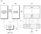
도 1은 본 발명의 실시예들에 따른 메모리 시스템(100)의 개략적인 구성도이다.FIG. 1 is a schematic configuration diagram of a memory system (100) according to embodiments of the present invention.
도 1을 참조하면, 본 발명의 실시예들에 따른 메모리 시스템(100)은 데이터를 저장하는 메모리 장치(110)와, 메모리 장치(110)를 제어하는 메모리 컨트롤러(120) 등을 포함할 수 있다.Referring to FIG. 1, a memory system (100) according to embodiments of the present invention may include a memory device (110) that stores data, a memory controller (120) that controls the memory device (110), etc.
메모리 장치(110)는 다수의 메모리 블록(Memory Block)을 포함하며, 메모리 컨트롤러(120)의 제어에 응답하여 동작한다. 여기서, 메모리 장치(110)의 동작은 일 예로, 읽기 동작(Read Operation), 프로그램 동작(Program Operation; "Write Operation" 이라고도 함) 및 소거 동작(Erasure Operation) 등을 포함할 수 있다.The memory device (110) includes a plurality of memory blocks and operates in response to the control of the memory controller (120). Here, the operation of the memory device (110) may include, for example, a read operation, a program operation (also called a “write operation”), and an erase operation.
메모리 장치(110)는 데이터를 저장하는 복수의 메모리 셀(Memory Cell; 간단히 줄여서 "셀" 이라고도 함)을 포함하는 메모리 셀 어레이(Memory Cell Array)를 포함할 수 있다. 이러한 메모리 셀 어레이는 메모리 블록 내에 존재할 수 있다.The memory device (110) may include a memory cell array including a plurality of memory cells (also simply referred to as “cells”) that store data. This memory cell array may exist within a memory block.
예를 들어, 메모리 장치(110)는 DDR SDRAM(Double Data Rate Synchronous Dynamic Random Access Memory), LPDDR4(Low Power Double Data Rate4) SDRAM, GDDR(Graphics Double Data Rate) SDRAM, LPDDR(Low Power DDR), RDRAM(Rambus Dynamic Random Access Memory), 낸드 플래시 메모리(NAND Flash Memory), 3차원 낸드 플래시 메모리(3D NAND Flash Memory), 노아 플래시 메모리(NOR Flash memory), 저항성 램(Resistive Random Access Memory: RRAM), 상변화 메모리(Phase-Change Memory: PRAM), 자기저항 메모리(Magnetoresistive Random Access Memory: MRAM), 강유전체 메모리(Ferroelectric Random Access Memory: FRAM), 또는 스핀주입 자화반전 메모리(Spin Transfer Torque Random Access Memory: STT-RAM) 등으로 다양한 타입으로 구현될 수 있다.For example, the memory device (110) may be implemented in various types, such as DDR SDRAM (Double Data Rate Synchronous Dynamic Random Access Memory), LPDDR4 (Low Power Double Data Rate4) SDRAM, GDDR (Graphics Double Data Rate) SDRAM, LPDDR (Low Power DDR), RDRAM (Rambus Dynamic Random Access Memory), NAND Flash Memory, 3D NAND Flash Memory, NOR Flash Memory, Resistive Random Access Memory (RRAM), Phase-Change Memory (PRAM), Magnetoresistive Random Access Memory (MRAM), Ferroelectric Random Access Memory (FRAM), or Spin Transfer Torque Random Access Memory (STT-RAM).
한편, 메모리 장치(110)는 3차원 어레이 구조(three-Dimensional Array structure)로 구현될 수 있다. 본 발명의 실시예들은 전하 저장층이 전도성 부유 게이트(Floating Gate)로 구성된 플래시 메모리 장치는 물론, 전하 저장층이 절연막으로 구성된 차지 트랩형 플래시(Charge Trap Flash; CTF)에도 적용될 수 있다.Meanwhile, the memory device (110) may be implemented as a three-dimensional array structure. Embodiments of the present invention may be applied to a flash memory device in which a charge storage layer is composed of a conductive floating gate, as well as a charge trap flash (CTF) in which a charge storage layer is composed of an insulating film.
메모리 장치(110)는 메모리 컨트롤러(120)로부터 커맨드 및 어드레스 등을 수신하고, 메모리 셀 어레이 중 어드레스에 의해 선택된 영역을 액세스하도록 구성된다. 즉, 메모리 장치(110)는 어드레스에 의해 선택된 영역에 대해 커맨드에 해당하는 동작을 수행할 수 있다.The memory device (110) receives commands and addresses, etc. from the memory controller (120), and is configured to access an area selected by the address among the memory cell arrays. That is, the memory device (110) can perform an operation corresponding to the command for an area selected by the address.
예를 들면, 메모리 장치(110)는 프로그램 동작, 읽기 동작 및 소거 동작 등을 수행할 수 있다. 이와 관련하여, 프로그램 동작 시, 메모리 장치(110)는 어드레스에 의해 선택된 영역에 데이터를 프로그램 할 것이다. 읽기 동작 시, 메모리 장치(110)는 어드레스에 의해 선택된 영역으로부터 데이터를 읽을 것이다. 소거 동작 시, 메모리 장치(110)는 어드레스에 의해 선택된 영역에 저장된 데이터를 소거할 것이다.For example, the memory device (110) can perform a program operation, a read operation, an erase operation, etc. In this regard, during a program operation, the memory device (110) will program data in an area selected by an address. During a read operation, the memory device (110) will read data from an area selected by an address. During an erase operation, the memory device (110) will erase data stored in an area selected by an address.
메모리 컨트롤러(120)는 메모리 장치(110)에 대한 쓰기(프로그램), 읽기, 소거 및 백그라운드(background) 동작을 제어할 수 있다. 여기서, 백그라운드 동작은 일 예로 가비지 컬렉션(GC, Garbage Collection), 웨어 레벨링(WL, Wear Leveling), 또는 배드 블록 관리(BBM, Bad Block Management) 동작 등 중 하나 이상을 포함할 수 있다.The memory controller (120) can control write (program), read, erase, and background operations for the memory device (110). Here, the background operations can include, for example, one or more of garbage collection (GC), wear leveling (WL), or bad block management (BBM) operations.
메모리 컨트롤러(120)는 호스트(HOST)의 요청에 따라 메모리 장치(110)의 동작을 제어할 수 있다. 이와 다르게, 메모리 컨트롤러(120)는 호스트(HOST)의 요청과 무관하게 메모리 장치(110)의 동작을 제어할 수도 있다.The memory controller (120) can control the operation of the memory device (110) according to the request of the host (HOST). Alternatively, the memory controller (120) can control the operation of the memory device (110) regardless of the request of the host (HOST).
한편, 메모리 컨트롤러(120)와 호스트(HOST)는 서로 분리된 장치일 수도 있다. 경우에 따라서, 메모리 컨트롤러(120)와 호스트(HOST)는 하나의 장치로 통합되어 구현될 수도 있다. 아래에서는, 설명의 편의를 위하여, 메모리 컨트롤러(120)와 호스트(HOST)가 서로 분리된 장치인 것을 예로 들어 설명한다.Meanwhile, the memory controller (120) and the host (HOST) may be separate devices. In some cases, the memory controller (120) and the host (HOST) may be implemented as a single device. Below, for convenience of explanation, an example in which the memory controller (120) and the host (HOST) are separate devices will be described.
도 1을 참조하면, 메모리 컨트롤러(120)는 메모리 인터페이스(122) 및 제어 회로(123) 등을 포함할 수 있으며, 호스트 인터페이스(121) 등을 더 포함할 수 있다.Referring to FIG. 1, the memory controller (120) may include a memory interface (122) and a control circuit (123), and may further include a host interface (121).
호스트 인터페이스(121)는 호스트(HOST)와의 통신을 위한 인터페이스를 제공한다.The host interface (121) provides an interface for communication with the host (HOST).
제어 회로(123)는 호스트(HOST)로부터 커맨드를 수신할 때, 호스트 인터페이스(121)를 통해서 커맨드를 수신하여, 수신된 커맨드를 처리하는 동작을 수행할 수 있다.When the control circuit (123) receives a command from the host (HOST), it can receive the command through the host interface (121) and perform an operation to process the received command.
메모리 인터페이스(122)는, 메모리 장치(110)와 연결되어 메모리 장치(110)와의 통신을 위한 인터페이스를 제공한다. 즉, 메모리 인터페이스(122)는 제어 회로(123)의 제어에 응답하여 메모리 장치(110)와 메모리 컨트롤러(120)를 인터페이스를 제공하도록 구성될 수 있다.The memory interface (122) is connected to the memory device (110) and provides an interface for communication with the memory device (110). That is, the memory interface (122) may be configured to provide an interface between the memory device (110) and the memory controller (120) in response to the control of the control circuit (123).
제어 회로(123)는 메모리 컨트롤러(120)의 전반적인 제어 동작을 수행하여 메모리 장치(110)의 동작을 제어한다. 이를 위해, 일 예로, 제어 회로(123)는 프로세서(124), 워킹 메모리(125) 등 중 하나 이상을 포함할 수 있으며, 경우에 따라서, 에러 검출 및 정정 회로(ECC Circuit, 126) 등을 더 포함할 수 있다.The control circuit (123) performs overall control operations of the memory controller (120) to control the operation of the memory device (110). For this purpose, as an example, the control circuit (123) may include one or more of a processor (124), a working memory (125), etc., and in some cases, may further include an error detection and correction circuit (ECC Circuit, 126), etc.
프로세서(124)는 메모리 컨트롤러(120)의 제반 동작을 제어하고, 논리 연산을 수행할 수 있다. 프로세서(124)는 호스트 인터페이스(121)를 통해 호스트(HOST)와 통신하고, 메모리 인터페이스(122)를 통해 메모리 장치(110)와 통신할 수 있다.The processor (124) can control all operations of the memory controller (120) and perform logical operations. The processor (124) can communicate with the host (HOST) through the host interface (121) and communicate with the memory device (110) through the memory interface (122).
프로세서(124)는 플래시 변환 레이어(FTL: Flash Translation Layer)의 기능을 수행할 수 있다. 프로세서(124)는 플래시 변환 계층(FTL)을 통해 호스트가 제공한 논리 블록 어드레스(LBA, logical block address)를 물리 블록 어드레스(PBA, physical block address)로 변환할 수 있다. 플래시 변환 계층(FTL)은 맵핑 테이블을 이용하여 논리 블록 어드레스(LBA)를 입력 받아, 물리 블록 어드레스(PBA)로 변환시킬 수 있다.The processor (124) can perform the function of a flash translation layer (FTL). The processor (124) can convert a logical block address (LBA) provided by a host into a physical block address (PBA) through the flash translation layer (FTL). The flash translation layer (FTL) can receive a logical block address (LBA) using a mapping table and convert it into a physical block address (PBA).
플래시 변환 계층의 주소 맵핑 방법에는 맵핑 단위에 따라 여러 가지가 있다. 대표적인 어드레스 맵핑 방법에는 페이지 맵핑 방법(Page mapping method), 블록 맵핑 방법(Block mapping method), 그리고 혼합 맵핑 방법(Hybrid mapping method)이 있다.There are several address mapping methods in the flash translation layer depending on the mapping unit. Representative address mapping methods include the page mapping method, the block mapping method, and the hybrid mapping method.
프로세서(124)는 호스트(HOST)로부터 수신된 데이터를 랜더마이즈하도록 구성된다. 예를 들면, 프로세서(124)는 랜더마이징 시드(seed)를 이용하여 호스트(HOST)로부터 수신된 데이터를 랜더마이즈할 것이다. 랜더마이즈된 데이터는 저장될 데이터로서 메모리 장치(110)에 제공되어 메모리 셀 어레이에 프로그램 된다.The processor (124) is configured to randomize data received from the host (HOST). For example, the processor (124) will randomize data received from the host (HOST) using a randomizing seed. The randomized data is provided to the memory device (110) as data to be stored and programmed into the memory cell array.
프로세서(124)는 읽기 동작 시 메모리 장치(110)로부터 수신된 데이터를 디랜더마이즈하도록 구성된다. 예를 들면, 프로세서(124)는 디랜더마이징 시드를 이용하여 메모리 장치(110)로부터 수신된 데이터를 디랜더마이즈할 것이다. 디랜더마이즈된 데이터는 호스트(HOST)로 출력될 것이다.The processor (124) is configured to derandomize data received from the memory device (110) during a read operation. For example, the processor (124) will derandomize data received from the memory device (110) using a derandomizing seed. The derandomized data will be output to the host (HOST).
프로세서(124)는 펌웨어(FirmWare)를 실행하여 메모리 컨트롤러(120)의 동작을 제어할 수 있다. 다시 말해, 프로세서(124)는, 메모리 컨트롤러(120)의 제반 동작을 제어하고, 논리 연산을 수행하기 위하여, 부팅 시 워킹 메모리(125)에 로딩 된 펌웨어를 실행(구동)할 수 있다.The processor (124) can control the operation of the memory controller (120) by executing firmware. In other words, the processor (124) can execute (drive) firmware loaded into the working memory (125) at boot time in order to control the overall operation of the memory controller (120) and perform logical operations.
펌웨어(FirmWare)는 메모리 시스템(100) 내에서 실행되는 프로그램으로서, 다양한 기능적 레이어들을 포함할 수 있다.Firmware is a program that runs within the memory system (100) and may include various functional layers.
예를 들어, 펌웨어는, 호스트(HOST)에서 메모리 시스템(100)에 요구하는 논리 주소(Logical Address)와 메모리 장치(110)의 물리주소(Physical Address) 간의 변환 기능을 하는 플래시 변환 레이어(FTL: Flash Translation Layer)와, 호스트(HOST)에서 저장 장치인 메모리 시스템(100)에 요구하는 커맨드를 해석하여 플래시 변환 레이어(FTL)에 전달하는 역할을 하는 호스트 인터페이스 레이어(HIL: Host Interface Layer)와, 플래시 변환 레이어(FTL)에서 지시하는 커맨드를 메모리 장치(110)로 전달하는 플래시 인터페이스 레이어(FIL: Flash Interface Layer) 등 중 하나 이상을 포함할 수 있다.For example, the firmware may include at least one of a Flash Translation Layer (FTL) that performs a conversion function between a logical address requested from a host (HOST) to a memory system (100) and a physical address of a memory device (110), a Host Interface Layer (HIL) that interprets a command requested from a host (HOST) to a memory system (100), which is a storage device, and transmits it to the Flash Translation Layer (FTL), and a Flash Interface Layer (FIL) that transmits a command instructed by the Flash Translation Layer (FTL) to the memory device (110).
이러한 펌웨어는, 일 예로, 메모리 장치(110)에 저장되어 있다가 워킹 메모리(125)에 로딩 될 수 있다.Such firmware may, for example, be stored in a memory device (110) and then loaded into the working memory (125).
워킹 메모리(125)는 메모리 컨트롤러(120)를 구동하기 위해 필요한 펌웨어, 프로그램 코드, 커맨드 또는 데이터들을 저장할 수 있다. 이러한 워킹 메모리(125)는, 일 예로, 휘발성 메모리로서, SRAM (Static RAM), DRAM (Dynamic RAM) 및 SDRAM(Synchronous DRAM) 등 중 하나 이상을 포함할 수 있다.The working memory (125) can store firmware, program code, commands, or data required to drive the memory controller (120). The working memory (125) may include, for example, one or more of SRAM (Static RAM), DRAM (Dynamic RAM), and SDRAM (Synchronous DRAM) as volatile memory.
에러 검출 및 정정 회로(126)는 에러 정정 코드(Error Correction Code)를 이용하여 확인 대상 데이터의 에러 비트를 검출하고, 검출된 에러 비트를 정정하도록 구성될 수 있다. 여기서, 확인 대상 데이터는, 일 예로, 워킹 메모리(125)에 저장된 데이터이거나, 메모리 장치(110)로부터 읽어온 데이터 등일 수 있다.The error detection and correction circuit (126) may be configured to detect error bits of the data to be verified using an error correction code and to correct the detected error bits. Here, the data to be verified may be, for example, data stored in the working memory (125) or data read from the memory device (110).
에러 검출 및 정정 회로(126)는 에러 정정 코드로 데이터를 디코딩하도록 구현될 수 있다. 에러 검출 및 정정 회로(126)는 다양한 코드 디코더로 구현될 수 있다. 예를 들어, 비체계적 코드 디코딩을 수행하는 디코더 또는 체계적 코드 디코딩을 수행하는 디코더가 이용될 수 있다.The error detection and correction circuit (126) may be implemented to decode data with an error correction code. The error detection and correction circuit (126) may be implemented with various code decoders. For example, a decoder that performs non-systematic code decoding or a decoder that performs systematic code decoding may be used.
예를 들면, 에러 검출 및 정정 회로(126)는 읽기 데이터들 각각에 대해 섹터(Sector) 단위로 에러 비트를 검출할 수 있다. 즉, 각각의 읽기 데이터는 복수의 섹터(Sector)로 구성될 수 있다. 섹터(Sector)는 플래시 메모리의 읽기 단위인 페이지(Page)보다 더 작은 데이터 단위를 의미할 수 있다. 각각의 읽기 데이터를 구성하는 섹터들은 어드레스를 매개로 서로 대응될 수 있다.For example, the error detection and correction circuit (126) can detect error bits for each read data in sector units. That is, each read data can be composed of multiple sectors. A sector can mean a smaller data unit than a page, which is a read unit of a flash memory. The sectors constituting each read data can correspond to each other through an address.
에러 검출 및 정정 회로(126)는 비트 에러율(Bit Error Rate, BER)을 산출하고, 섹터 단위로 정정 가능 여부를 판단할 수 있다. 에러 검출 및 정정 회로(126)는 예를 들어, 비트 에러율(BER)이 기준값(reference value)보다 높은 경우 해당 섹터를 정정 불가능(Uncorrectable or Fail)으로 판단할 것이다. 반면에, 비트 에러율(BER)이 기준값보다 낮은 경우 해당 섹터를 정정 가능(Correctable or Pass)으로 판단할 것이다.The error detection and correction circuit (126) can calculate the bit error rate (BER) and determine whether or not correction is possible on a sector-by-sector basis. For example, if the bit error rate (BER) is higher than a reference value, the error detection and correction circuit (126) will determine the sector as uncorrectable (or Fail). On the other hand, if the bit error rate (BER) is lower than the reference value, the sector will be determined as correctable (or Pass).
에러 검출 및 정정 회로(126)는 모든 읽기 데이터들에 대해 순차적으로 에러 검출 및 정정 동작을 수행할 수 있다. 에러 검출 및 정정 회로(126)는 읽기 데이터에 포함된 섹터가 정정 가능한 경우 다음 읽기 데이터에 대해서는 해당 섹터에 대한 에러 검출 및 정정 동작을 생략할 수 있다. 이렇게 모든 읽기 데이터들에 대한 에러 검출 및 정정 동작이 종료되면, 에러 검출 및 정정 회로(126)는 마지막까지 정정 불가능으로 판단된 섹터를 검출할 수 있다. 정정 불가능한 것으로 판단된 섹터는 하나 또는 그 이상일 수 있다. 에러 검출 및 정정 회로(126)는 정정 불가능으로 판단된 섹터에 대한 정보(ex. 어드레스 정보)를 프로세서(124)로 전달할 수 있다.The error detection and correction circuit (126) can sequentially perform error detection and correction operations on all read data. If a sector included in the read data is correctable, the error detection and correction circuit (126) can omit the error detection and correction operation on the corresponding sector for the next read data. When the error detection and correction operations on all read data are completed in this way, the error detection and correction circuit (126) can detect the sectors determined to be uncorrectable until the end. The number of sectors determined to be uncorrectable may be one or more. The error detection and correction circuit (126) can transmit information (ex. address information) on the sectors determined to be uncorrectable to the processor (124).
버스(127)는 메모리 컨트롤러(120)의 구성 요소들(121, 122, 124, 125, 126) 사이의 채널(Channel)을 제공하도록 구성될 수 있다. 이러한 버스(127)는, 일 예로, 각종 제어 신호, 커맨드 등을 전달하기 위한 제어 버스와, 각종 데이터를 전달하기 위한 데이터 버스 등을 포함할 수 있다.The bus (127) may be configured to provide a channel between components (121, 122, 124, 125, 126) of the memory controller (120). This bus (127) may include, for example, a control bus for transmitting various control signals, commands, etc., and a data bus for transmitting various data.
메모리 컨트롤러(120)의 전술한 구성 요소들(121, 122, 124, 125, 126)은 예시일 뿐이다. 메모리 컨트롤러(120)의 전술한 구성 요소들(121, 122, 124, 125, 126) 중 일부의 구성 요소는 삭제되거나, 메모리 컨트롤러(120)의 전술한 구성 요소들 (121, 122, 124, 125, 126) 중 몇몇 구성 요소들이 하나로 통합될 수 있다. 경우에 따라, 메모리 컨트롤러(120)의 전술한 구성 요소들 이외에 하나 이상의 다른 구성 요소가 추가될 수도 있다.The above-described components (121, 122, 124, 125, 126) of the memory controller (120) are only examples. Some of the above-described components (121, 122, 124, 125, 126) of the memory controller (120) may be deleted, or some of the above-described components (121, 122, 124, 125, 126) of the memory controller (120) may be integrated into one. In some cases, one or more other components may be added in addition to the above-described components of the memory controller (120).
아래에서는, 도 2를 참조하여 메모리 장치(110)에 대하여 더욱 상세하게 설명한다.Below, the memory device (110) is described in more detail with reference to FIG. 2.
도 2는 본 발명의 실시예들에 따른 메모리 장치(110)를 개략적으로 나타낸 블록도다.FIG. 2 is a block diagram schematically illustrating a memory device (110) according to embodiments of the present invention.
도 2를 참조하면, 본 발명의 실시예들에 따른 메모리 장치(110)는, 메모리 셀 어레이(Memory Cell Array, 210), 어드레스 디코더(Address Decoder, 220), 읽기 및 쓰기 회로(Read and Write Circuit, 230), 제어 로직(Control Logic, 240) 및 전압 생성 회로(Voltage Generation Circuit, 250) 등을 포함할 수 있다.Referring to FIG. 2, a memory device (110) according to embodiments of the present invention may include a memory cell array (210), an address decoder (220), a read and write circuit (230), a control logic (240), and a voltage generation circuit (250).
메모리 셀 어레이(210)는 다수의 메모리 블록(BLK1~BLKz, z는 2 이상의 자연수)을 포함할 수 있다.The memory cell array (210) may include a plurality of memory blocks (BLK1 to BLKz, z is a natural number greater than or equal to 2).
다수의 메모리 블록(BLK1~BLKz)에는, 다수의 워드 라인(WL)과 다수의 비트 라인(BL)이 배치되며, 다수의 메모리 셀(MC)이 배열될 수 있다.In a plurality of memory blocks (BLK1 to BLKz), a plurality of word lines (WL) and a plurality of bit lines (BL) are arranged, and a plurality of memory cells (MC) can be arranged.
다수의 메모리 블록(BLK1~BLKz)은 다수의 워드 라인(WL)을 통해 어드레스 디코더(220)와 연결될 수 있다. 다수의 메모리 블록(BLK1~BLKz)은 다수의 비트 라인(BL)을 통해 읽기 및 쓰기 회로(230)와 연결될 수 있다.A plurality of memory blocks (BLK1 to BLKz) can be connected to an address decoder (220) through a plurality of word lines (WL). A plurality of memory blocks (BLK1 to BLKz) can be connected to a read and write circuit (230) through a plurality of bit lines (BL).
다수의 메모리 블록(BLK1~BLKz) 각각은 다수의 메모리 셀을 포함할 수 있다. 예를 들어, 다수의 메모리 셀은 불휘발성 메모리 셀들이며, 수직 채널 구조를 갖는 불휘발성 메모리 셀들로 구성될 수 있다.Each of the plurality of memory blocks (BLK1 to BLKz) may include a plurality of memory cells. For example, the plurality of memory cells may be nonvolatile memory cells and may be configured as nonvolatile memory cells having a vertical channel structure.
메모리 셀 어레이(210)는 2차원 구조의 메모리 셀 어레이로 구성될 수 있으며, 경우에 따라서는, 3차원 구조의 메모리 셀 어레이로 구성될 수도 있다.The memory cell array (210) may be configured as a two-dimensional memory cell array, and in some cases, may be configured as a three-dimensional memory cell array.
한편, 메모리 셀 어레이(210)에 포함되는 복수의 메모리 셀 각각은 적어도 1비트의 데이터를 저장할 수 있다. 일 예로, 메모리 셀 어레이(210)에 포함되는 복수의 메모리 셀 각각은 1비트의 데이터를 저장하는 싱글-레벨 셀(SLC: Single-Level Cell)일 수 있다. 다른 예로, 메모리 셀 어레이(210)에 포함되는 복수의 메모리 셀 각각은 2비트의 데이터를 저장하는 멀티-레벨 셀(MLC: Multi-Level Cell)일 수 있다. 또 다른 예로, 메모리 셀 어레이(210)에 포함되는 복수의 메모리 셀 각각은 3비트의 데이터를 저장하는 트리플-레벨 셀(TLC: Triple-Level Cell)일 수 있다. 또 다른 예로, 메모리 셀 어레이(210)에 포함되는 복수의 메모리 셀 각각은 4비트의 데이터를 저장하는 쿼드-레벨 셀(QLC: Quad-Level Cell)일 수 있다. 또 다른 예로, 메모리 셀 어레이(210)는 5비트 이상의 데이터를 각각 저장하는 복수의 메모리 셀을 포함할 수도 있다.Meanwhile, each of the plurality of memory cells included in the memory cell array (210) can store at least 1 bit of data. For example, each of the plurality of memory cells included in the memory cell array (210) may be a single-level cell (SLC: Single-Level Cell) that stores 1 bit of data. As another example, each of the plurality of memory cells included in the memory cell array (210) may be a multi-level cell (MLC: Multi-Level Cell) that stores 2 bits of data. As another example, each of the plurality of memory cells included in the memory cell array (210) may be a triple-level cell (TLC: Triple-Level Cell) that stores 3 bits of data. As another example, each of the plurality of memory cells included in the memory cell array (210) may be a quad-level cell (QLC: Quad-Level Cell) that stores 4 bits of data. As another example, the memory cell array (210) may include a plurality of memory cells that each store 5 or more bits of data.
도 2를 참조하면, 어드레스 디코더(220), 읽기 및 쓰기 회로(230), 제어 로직(240) 및 전압 생성 회로(250) 등은 메모리 셀 어레이(210)를 구동하는 주변 회로로서 동작할 수 있다.Referring to FIG. 2, an address decoder (220), a read and write circuit (230), a control logic (240), and a voltage generation circuit (250) may operate as peripheral circuits that drive a memory cell array (210).
어드레스 디코더(220)는 다수의 워드 라인(WL)을 통해 메모리 셀 어레이(210)에 연결될 수 있다.An address decoder (220) can be connected to a memory cell array (210) through a plurality of word lines (WL).
어드레스 디코더(220)는 제어 로직(240)의 제어에 응답하여 동작하도록 구성될 수 있다.The address decoder (220) may be configured to operate in response to control of the control logic (240).
어드레스 디코더(220)는 메모리 장치(110) 내부의 입출력 버퍼를 통해 어드레스(Address)를 수신할 수 있다. 어드레스 디코더(220)는 수신된 어드레스 중 블록 어드레스(Block Address)를 디코딩 하도록 구성될 수 있다. 어드레스 디코더(220)는 디코딩된 블록 어드레스에 따라 적어도 하나의 메모리 블록을 선택할 수 있다.The address decoder (220) can receive an address through an input/output buffer inside the memory device (110). The address decoder (220) can be configured to decode a block address among the received addresses. The address decoder (220) can select at least one memory block according to the decoded block address.
어드레스 디코더(220)는 전압 생성 회로(250)로부터 읽기 전압(Vread) 및 패스 전압(Vpass)을 입력 받을 수 있다.The address decoder (220) can receive a read voltage (Vread) and a pass voltage (Vpass) from a voltage generation circuit (250).
어드레스 디코더(220)는 읽기 동작 중 읽기 전압 인가 동작 시, 선택된 메모리 블록 내 선택된 워드 라인(WL)으로 읽기 전압(Vread)를 인가하고, 나머지 비 선택된 워드 라인들(WL)에는 패스 전압(Vpass)을 인가할 수 있다.The address decoder (220) can apply a read voltage (Vread) to a selected word line (WL) within a selected memory block during a read voltage application operation during a read operation, and apply a pass voltage (Vpass) to the remaining non-selected word lines (WL).
어드레스 디코더(220)는 프로그램 검증 동작 시, 선택된 메모리 블록 내 선택된 워드 라인(WL)에 전압 생성 회로(250)에서 발생된 검증 전압을 인가하고, 나머지 비 선택된 워드 라인들(WL)에 패스 전압(Vpass)을 인가할 수 있다.The address decoder (220) can apply a verification voltage generated by a voltage generation circuit (250) to a selected word line (WL) within a selected memory block during a program verification operation, and can apply a pass voltage (Vpass) to the remaining non-selected word lines (WL).
어드레스 디코더(220)는 수신된 어드레스 중 열 어드레스를 디코딩 하도록 구성될 수 있다. 어드레스 디코더(220)는 디코딩 된 열 어드레스를 읽기 및 쓰기 회로(230)에 전송할 수 있다.The address decoder (220) may be configured to decode a column address among the received addresses. The address decoder (220) may transmit the decoded column address to the read and write circuit (230).
메모리 장치(110)의 읽기 동작 및 프로그램 동작은 페이지 단위로 수행될 수 있다. 읽기 동작 및 프로그램 동작 요청 시에 수신되는 어드레스는 블록 어드레스, 행 어드레스 및 열 어드레스 중 하나 이상을 포함할 수 있다.The read operation and program operation of the memory device (110) can be performed in units of pages. An address received when requesting a read operation and a program operation may include one or more of a block address, a row address, and a column address.
어드레스 디코더(220)는 블록 어드레스 및 행 어드레스에 따라 하나의 메모리 블록 및 하나의 워드 라인을 선택할 수 있다. 열 어드레스는 어드레스 디코더(220)에 의해 디코딩 되어 읽기 및 쓰기 회로(230)에 제공될 수 있다.The address decoder (220) can select one memory block and one word line according to the block address and row address. The column address can be decoded by the address decoder (220) and provided to the read and write circuit (230).
어드레스 디코더(220)는 블록 디코더, 행 디코더, 열 디코더 및 어드레스 버퍼 등 중 하나 이상을 포함할 수 있다.The address decoder (220) may include one or more of a block decoder, a row decoder, a column decoder, and an address buffer.
읽기 및 쓰기 회로(230)는 다수의 페이지 버퍼(PB)를 포함할 수 있다. 읽기 및 쓰기 회로(230)는 메모리 셀 어레이(210)의 읽기 동작(Read Operation) 시에는 "읽기 회로(Read Circuit)"로 동작하고, 쓰기 동작(Write Operation) 시에는 "쓰기 회로(Write Circuit)"로 동작할 수 있다.The read and write circuit (230) may include a plurality of page buffers (PBs). The read and write circuit (230) may operate as a “read circuit” during a read operation of the memory cell array (210), and may operate as a “write circuit” during a write operation.
전술한 읽기 및 쓰기 회로(230)는 다수의 페이지 버퍼(PB)를 포함하는 페이지 버퍼 회로(Page Buffer Circuit) 또는 데이터 레지스터 회로(Data Register Circuit)라고도 한다. 여기서, 읽기 및 쓰기 회로(230)는 데이터 처리 기능을 담당하는 데이터 버퍼(Data Buffer)를 포함할 수 있고, 경우에 따라서, 캐싱 기능을 담당하는 캐쉬 버퍼(Cache Buffer)를 추가로 더 포함할 수 있다.The read and write circuit (230) described above is also called a page buffer circuit or a data register circuit including a plurality of page buffers (PBs). Here, the read and write circuit (230) may include a data buffer responsible for a data processing function, and in some cases, may additionally include a cache buffer responsible for a caching function.
다수의 페이지 버퍼(PB)는 다수의 비트 라인(BL)을 통해 메모리 셀 어레이(210)에 연결될 수 있다. 다수의 페이지 버퍼(PB)는 읽기 동작 및 프로그램 검증 동작 시, 메모리 셀들의 문턱전압(Vth)을 센싱하기 위하여, 메모리 셀들과 연결된 비트 라인들(BL)에 센싱 전류를 계속적으로 공급하면서, 대응하는 메모리 셀의 프로그램 상태에 따라 흐르는 전류량이 변화되는 것을 센싱 노드를 통해 감지하여 센싱 데이터로 래치할 수 있다.A plurality of page buffers (PBs) may be connected to a memory cell array (210) via a plurality of bit lines (BLs). The plurality of page buffers (PBs) may continuously supply sensing current to bit lines (BLs) connected to memory cells in order to sense threshold voltages (Vth) of memory cells during a read operation and a program verification operation, and may detect a change in the amount of current flowing according to a program state of a corresponding memory cell via a sensing node and latch it as sensing data.
읽기 및 쓰기 회로(230)는 제어 로직(240)에서 출력되는 페이지 버퍼 제어 신호들에 응답하여 동작할 수 있다.The read and write circuit (230) can operate in response to page buffer control signals output from the control logic (240).
읽기 및 쓰기 회로(230)는 읽기 동작 시, 메모리 셀의 데이터를 센싱하여 독출 데이터를 임시 저장한 후, 메모리 장치(110)의 입출력 버퍼로 데이터(DATA)를 출력한다. 예시적인 실시 예로서, 읽기 및 쓰기 회로(230)는 페이지 버퍼들(PB) 또는 페이지 레지스터들 이외에도, 열 선택 회로 등을 포함할 수 있다.The read and write circuit (230) senses data of a memory cell during a read operation, temporarily stores the read data, and then outputs data (DATA) to the input/output buffer of the memory device (110). As an exemplary embodiment, the read and write circuit (230) may include a column selection circuit, etc., in addition to page buffers (PB) or page registers.
제어 로직(240)은 어드레스 디코더(220), 읽기 및 쓰기 회로(230), 및 전압 생성 회로(250) 등과 연결될 수 있다. 제어 로직(240)은 메모리 장치(110)의 입출력 버퍼를 통해 커맨드(CMD) 및 제어 신호(CTRL)를 수신할 수 있다.The control logic (240) may be connected to an address decoder (220), a read and write circuit (230), and a voltage generation circuit (250). The control logic (240) may receive a command (CMD) and a control signal (CTRL) through an input/output buffer of the memory device (110).
제어 로직(240)은 제어 신호(CTRL)에 응답하여 메모리 장치(110)의 제반 동작을 제어하도록 구성될 수 있다. 제어 로직(240)은 다수의 페이지 버퍼(PB)의 센싱 노드의 프리 차지 전위 레벨을 조절하기 위한 제어 신호를 출력할 수 있다.The control logic (240) may be configured to control the overall operation of the memory device (110) in response to a control signal (CTRL). The control logic (240) may output a control signal for adjusting the precharge potential level of the sensing nodes of a plurality of page buffers (PBs).
제어 로직(240)은 메모리 셀 어레이(210)의 읽기 동작을 수행하도록 읽기 및 쓰기 회로(230)를 제어할 수 있다. 전압 생성 회로(250)는, 제어 로직(240)에서 출력되는 전압 생성 회로 제어 신호에 응답하여, 읽기 동작 시, 이용되는 읽기 전압(Vread) 및 패스 전압(Vpass)을 생성할 수 있다.The control logic (240) can control the read and write circuit (230) to perform a read operation of the memory cell array (210). The voltage generation circuit (250) can generate a read voltage (Vread) and a pass voltage (Vpass) used during a read operation in response to a voltage generation circuit control signal output from the control logic (240).
도 3은 본 발명의 실시예들에 따른 메모리 장치(110)의 각 메모리 블록(BLK) 를 개략적으로 나타낸 도면이다.FIG. 3 is a diagram schematically illustrating each memory block (BLK) of a memory device (110) according to embodiments of the present invention.
도 3을 참조하면, 메모리 장치(110)에 포함된 메모리 블록(BLK)은, 일 예로, 다수의 페이지(PG)와 다수의 스트링(STR)이 교차하는 방향으로 배치되어 구성될 수 있다.Referring to FIG. 3, a memory block (BLK) included in a memory device (110) may be configured, for example, with a plurality of pages (PG) and a plurality of strings (STR) arranged in an intersecting direction.
다수의 페이지(PG)는 다수의 워드 라인(WL)과 대응되고, 다수의 스트링(STR)은 다수의 비트 라인(BL)과 대응된다.A number of pages (PG) correspond to a number of word lines (WL), and a number of strings (STR) correspond to a number of bit lines (BL).
메모리 블록(BLK)에는 다수의 워드 라인(WL)과 다수의 비트 라인(BL)이 교차하면서 배치될 수 있다. 예를 들어, 다수의 워드 라인(WL) 각각은 행 방향으로 배치되고, 다수의 비트 라인(BL) 각각은 열 방향으로 배치될 수 있다. 다른 예를 들어, 다수의 워드 라인(WL) 각각은 열 방향으로 배치되고, 다수의 비트 라인(BL) 각각은 행 방향으로 배치될 수 있다.A memory block (BLK) may have a plurality of word lines (WL) and a plurality of bit lines (BL) arranged in an intersecting manner. For example, each of the plurality of word lines (WL) may be arranged in a row direction, and each of the plurality of bit lines (BL) may be arranged in a column direction. For another example, each of the plurality of word lines (WL) may be arranged in a column direction, and each of the plurality of bit lines (BL) may be arranged in a row direction.
다수의 워드 라인(WL)과 다수의 비트 라인(BL)이 서로 교차하여, 다수의 메모리 셀(MC)이 정의될 수 있다. 각 메모리 셀(MC)에는 트랜지스터(TR)가 배치될 수 있다.A plurality of word lines (WL) and a plurality of bit lines (BL) may intersect each other to define a plurality of memory cells (MC). A transistor (TR) may be placed in each memory cell (MC).
예를 들어, 각 메모리 셀(MC)에 배치된 트랜지스터(TR)는 드레인, 소스 및 게이트 등을 포함할 수 있다. 트랜지스터(TR)의 드레인(또는 소스)은 해당 비트 라인(BL)과 직접 또는 다른 트랜지스터(TR)를 경유하여 연결될 수 있다. 트랜지스터(TR)의 소스(또는 드레인)는 소스 라인(그라운드일 수 있음)과 직접 또는 다른 트랜지스터(TR)를 경유하여 연결될 수 있다. 트랜지스터(TR)의 게이트는 절연체에 둘러싸인 플로팅 게이트(FG: Floating Gate)와 워드 라인(WL)으로부터 게이트 전압이 인가되는 컨트롤 게이트(CG: Control Gate)를 포함할 수 있다.For example, a transistor (TR) arranged in each memory cell (MC) may include a drain, a source, and a gate, etc. The drain (or source) of the transistor (TR) may be connected to a corresponding bit line (BL) directly or via another transistor (TR). The source (or drain) of the transistor (TR) may be connected to a source line (which may be ground) directly or via another transistor (TR). The gate of the transistor (TR) may include a floating gate (FG: Floating Gate) surrounded by an insulator and a control gate (CG: Control Gate) to which a gate voltage is applied from a word line (WL).
다수의 메모리 블록(BLK1~BLKz) 각각에는, 2개의 최외곽 워드 라인 중 읽기 및 쓰기 회로(230)와 더 인접한 제1 최외곽 워드 라인의 바깥쪽에는 제1 선택 라인(소스 선택 라인 또는 드레인 선택 라인이라고도 함)이 더 배치될 수 있으며, 다른 제2 최외곽 워드 라인의 바깥쪽에는 제2 선택 라인(드레인 선택 라인 또는 소스 선택 라인이라고도 함)이 더 배치될 수 있다.In each of the plurality of memory blocks (BLK1 to BLKz), a first selection line (also called a source selection line or a drain selection line) may be further arranged outside of a first outermost word line that is closer to the read and write circuit (230) among the two outermost word lines, and a second selection line (also called a drain selection line or a source selection line) may be further arranged outside of another second outermost word line.
경우에 따라서, 제1 최외곽 워드 라인과 제1 선택 라인 사이에는 하나 이상의 더미 워드 라인이 더 배치될 수 있다. 또한, 제2 최외곽 워드 라인과 제2 선택 라인 사이에도 하나 이상의 더미 워드 라인이 더 배치될 수 있다.In some cases, one or more dummy word lines may be further arranged between the first outermost word line and the first selection line. In addition, one or more dummy word lines may also be further arranged between the second outermost word line and the second selection line.
도 3과 같은 메모리 블록 구조를 가질 때, 읽기 동작 및 프로그램 동작(쓰기 동작)은 페이지 단위로 수행될 수 있으며, 소거(Erasure) 동작은 메모리 블록 단위로 수행될 수 있다.When having a memory block structure such as Fig. 3, read operations and program operations (write operations) can be performed in page units, and erase operations can be performed in memory block units.
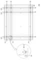
도 4는 본 발명의 실시예들에 따른 메모리 장치(110)의 워드 라인(WL) 및 비트 라인(BL)의 구조를 나타낸 도면이다.FIG. 4 is a diagram showing the structure of a word line (WL) and a bit line (BL) of a memory device (110) according to embodiments of the present invention.
도 4를 참조하면, 메모리 장치(110)에는, 메모리 셀들(MC)이 모여 있는 핵심 영역과 이 핵심 영역의 나머지 영역에 해당하며 메모리 셀 어레이(210)의 동작을 위해 서포트(Support) 해주는 보조 영역이 존재한다.Referring to FIG. 4, the memory device (110) has a core region where memory cells (MC) are gathered and an auxiliary region corresponding to the remaining region of the core region and supporting the operation of the memory cell array (210).
핵심 영역은 페이지들(PG)과 스트링들(STR)으로 구성될 수 있다. 이러한 핵심 영역에는, 다수의 워드 라인(WL1 ~ WL9)과 다수의 비트 라인(BL)이 교차하면서 배치된다.A core area can be composed of pages (PG) and strings (STR). In this core area, a number of word lines (WL1 to WL9) and a number of bit lines (BL) are arranged intersecting each other.
다수의 워드 라인(WL1 ~ WL9)은 행 디코더(410)와 연결되고, 다수의 비트 라인(BL)은 열 디코더(420)와 연결될 수 있다. 다수의 비트 라인(BL)와 열 디코더(420) 사이에는 읽기 및 쓰기 회로(230)에 해당하는 데이터 레지스터(430)가 존재할 수 있다.A plurality of word lines (WL1 to WL9) may be connected to a row decoder (410), and a plurality of bit lines (BL) may be connected to a column decoder (420). A data register (430) corresponding to a read and write circuit (230) may be present between the plurality of bit lines (BL) and the column decoder (420).
다수의 워드 라인(WL1 ~ WL9)은 다수의 페이지(PG)와 대응된다.A number of word lines (WL1 to WL9) correspond to a number of pages (PG).
예를 들어, 도 4와 같이 다수의 워드 라인(WL1 ~ WL9) 각각은 하나의 페이지(PG)와 대응될 수 있다. 이와 다르게, 다수의 워드 라인(WL1 ~ WL9) 각각이 사이즈가 큰 경우, 다수의 워드 라인(WL1 ~ WL9) 각각은 둘 이상(예: 2개 또는 4개)의 페이지(PG)와 대응될 수도 있다. 페이지(PG)는 프로그램 동작과 읽기 동작을 진행하는데 있어서 최소 단위가 되며, 프로그램 동작 및 읽기 동작 시, 동일 페이지(PG) 내에서의 모든 메모리 셀(MC)은 동시 동작을 수행할 수 있다.For example, as shown in FIG. 4, each of the plurality of word lines (WL1 to WL9) may correspond to one page (PG). Alternatively, if each of the plurality of word lines (WL1 to WL9) is large in size, each of the plurality of word lines (WL1 to WL9) may correspond to two or more (e.g., two or four) pages (PG). A page (PG) is the minimum unit for performing program and read operations, and during program and read operations, all memory cells (MC) within the same page (PG) can perform simultaneous operations.
다수의 비트 라인(BL)은 홀수 번째 비트 라인(BL)과 짝수 번째 비트 라인(BL)을 구분되면서 열 디코더(420)와 연결될 수 있다.A plurality of bit lines (BL) can be connected to a column decoder (420) while distinguishing between odd bit lines (BL) and even bit lines (BL).
메모리 셀(MC)에 액세스 하기 위해서는, 주소가 먼저 입출력 단을 거쳐 행 디코더(410)와 열 디코더(420)를 통하여 핵심 영역으로 들어와서, 타깃 메모리 셀을 지정할 수 있다. 타깃 메모리 셀을 지정한다는 것은 행 디코더(410)와 연결된 워드 라인들(WL1 ~ WL9)과 열 디코더(420)와 연결된 비트 라인들(BL)의 교차되는 사이트에 있는 메모리 셀(MC)에 데이터를 프로그램 하거나 프로그램 된 데이터를 읽어 내기 위하여 액세스 한다는 것을 의미한다.In order to access a memory cell (MC), an address must first pass through an input/output terminal and enter a core area through a row decoder (410) and a column decoder (420), so that a target memory cell can be designated. Designating a target memory cell means accessing a memory cell (MC) located at an intersection site of word lines (WL1 to WL9) connected to the row decoder (410) and bit lines (BL) connected to the column decoder (420) to program data or read programmed data.
제1 방향(예: X축 방향)의 페이지(PG)는 워드 라인(WL)이란 공통으로 사용하는 라인으로 묶여 있으며, 제2 방향(예: Y축 방향)의 스트링(STR)도 비트 라인(BL)이란 공통 라인으로 묶여(연결되어) 있다. 공통으로 묶여 있다는 것은 구조적으로 동일한 물질로 연결되어 있고, 전압 인가 시에도 모두 동일한 전압이 동시에 인가된다는 것을 의미한다. 물론, 직렬로 연결된 중간 위치나 마지막 위치의 메모리 셀(MC)은 앞의 메모리 셀(MC)의 전압 강하에 의하여, 처음에 위치하는 메모리 셀(MC)과 맨 마지막에 위치하는 메모리 셀(MC)에 인가되는 전압은 약간 다를 수 있다.Pages (PG) in the first direction (e.g. X-axis direction) are grouped together by a commonly used line called a word line (WL), and strings (STR) in the second direction (e.g. Y-axis direction) are also grouped (connected) by a common line called a bit line (BL). Being grouped together means that they are structurally connected by the same material, and the same voltage is applied to all at the same time when voltage is applied. Of course, the voltages applied to the memory cells (MC) located first and last in the middle or the last position connected in series may be slightly different due to the voltage drop of the memory cell (MC) in front.
메모리 장치(110)의 데이터 처리 모두는, 데이터 레지스터(430)를 경유하여 프로그램 및 읽기가 되므로, 데이터 레지스터(430)는 중추적 역할을 한다. 데이터 레지스터(430)의 데이터 처리가 늦어지면 다른 모든 영역에서는 데이터 레지스터(430)가 데이터 처리를 완료할 때까지 기다려야 한다. 또한, 데이터 레지스터(430)의 성능이 저하되면, 메모리 장치(110)의 전체 성능을 저하시킬 수 있다.Since all data processing of the memory device (110) is programmed and read via the data register (430), the data register (430) plays a pivotal role. If the data processing of the data register (430) is delayed, all other areas must wait until the data register (430) completes data processing. In addition, if the performance of the data register (430) deteriorates, the overall performance of the memory device (110) may deteriorate.
도 4의 예시를 참조하면, 1개의 스트링(STR)에는, 다수의 워드 라인(WL1 ~ WL9)과 연결되는 다수의 트랜지스터(TR1 ~ TR9)가 존재할 수 있다. 다수의 트랜지스터(TR1 ~ TR9)가 존재하는 영역들이 메모리 셀들(MC)에 해당한다. 여기서, 다수의 트랜지스터(TR1 ~ TR9)는 전술한 바와 같이, 제어 게이트 (CG)와 플로팅 게이트(FG)를 포함하는 트랜지스터들이다.Referring to the example of Fig. 4, in one string (STR), there may be a plurality of transistors (TR1 to TR9) connected to a plurality of word lines (WL1 to WL9). The regions where the plurality of transistors (TR1 to TR9) exist correspond to memory cells (MC). Here, the plurality of transistors (TR1 to TR9) are transistors including a control gate (CG) and a floating gate (FG), as described above.
다수의 워드 라인(WL1 ~ WL9)은 2개의 최외곽 워드 라인(WL1, WL9)을 포함한다. 2개의 최외곽 워드 라인(WL1, WL9) 중 신호 경로적 측면에서 데이터 레지스터(430)와 더 인접한 제1 최외곽 워드 라인(WL1)의 바깥쪽에는 제1 선택 라인(DSL)이 더 배치되고, 다른 제2 최외곽 워드 라인(WL9)의 바깥쪽에는 제2 선택 라인(SSL)이 더 배치될 수 있다.The plurality of word lines (WL1 to WL9) include two outermost word lines (WL1, WL9). A first selection line (DSL) may be further arranged outside the first outermost word line (WL1) which is closer to the data register (430) in terms of signal path among the two outermost word lines (WL1, WL9), and a second selection line (SSL) may be further arranged outside the other second outermost word line (WL9).
제1 선택 라인(DSL)에 의해 온-오프가 제어되는 제1 선택 트랜지스터(D-TR)는 제1 선택 라인(DSL)과 연결된 게이트 전극을 가지고 있을 뿐, 플로팅 게이트(FG)를 포함하지 않는 트랜지스터이다. 제2 선택 라인(SSL)에 의해 온-오프가 제어되는 제2 선택 트랜지스터(S-TR)는 제2 선택 라인(SSL)과 연결된 게이트 전극을 가지고 있을 뿐, 플로팅 게이트(FG)를 포함하지 않는 트랜지스터이다.A first selection transistor (D-TR), whose on-off is controlled by a first selection line (DSL), is a transistor that has only a gate electrode connected to the first selection line (DSL) and does not include a floating gate (FG). A second selection transistor (S-TR), whose on-off is controlled by a second selection line (SSL), is a transistor that has only a gate electrode connected to the second selection line (SSL) and does not include a floating gate (FG).
제1 선택 트랜지스터(D-TR)는 해당 스트링(STR)과 데이터 레지스터(430) 간의 연결을 온 또는 오프 시키는 스위치 역할을 한다. 제2 선택 트랜지스터(S-TR)는 해당 스트링(STR)과 소스 라인(SL) 간의 연결을 온 또는 오프 시켜주는 스위치 역할을 한다. 즉, 제1 선택 트랜지스터(D-TR) 및 제2 선택 트랜지스터(S-TR)는 해당 스트링(STR)의 양쪽 끝에 있으면서, 신호를 이어주고 끊어내는 문지기 역할을 한다.The first selection transistor (D-TR) acts as a switch that turns on or off the connection between the string (STR) and the data register (430). The second selection transistor (S-TR) acts as a switch that turns on or off the connection between the string (STR) and the source line (SL). That is, the first selection transistor (D-TR) and the second selection transistor (S-TR) are located at both ends of the string (STR) and act as gatekeepers that connect and disconnect signals.
메모리 시스템(100)은, 프로그램 동작 시, 프로그램 할 비트 라인(BL)의 타깃 메모리 셀(MC)에 전자를 채워야 하기 때문에, 제1 선택 트랜지스터(D-TR)의 게이트 전극에 소정의 턴-온 전압(Vcc)를 인가하여 제1 선택 트랜지스터(D-TR)를 턴-온 시키고, 제2 선택 트랜지스터(S-TR)의 게이트 전극에는 소정의 턴-오프 전압(예: 0V)을 인가하여 제2 선택 트랜지스터(S-TR)를 턴-오프 시킨다.Since the memory system (100) must fill the target memory cell (MC) of the bit line (BL) to be programmed with electrons during a program operation, a predetermined turn-on voltage (Vcc) is applied to the gate electrode of the first selection transistor (D-TR) to turn on the first selection transistor (D-TR), and a predetermined turn-off voltage (e.g., 0 V) is applied to the gate electrode of the second selection transistor (S-TR) to turn off the second selection transistor (S-TR).
메모리 시스템(100)은, 읽기 동작 또는 검증(Verification) 동작 시, 제1 선택 트랜지스터(D-TR) 및 제2 선택 트랜지스터(S-TR)를 모두 턴-온 시켜준다. 이에 따라, 전류가 해당 스트링(STR)을 관통하여 그라운드에 해당하는 소스 라인(SL)으로 빠질 수 있어서, 비트 라인(BL)의 전압 레벨이 측정될 수 있다. 다만, 읽기 동작 시, 제1 선택 트랜지스터(D-TR) 및 제2 선택 트랜지스터(S-TR)의 온-오프 타이밍의 시간 차이가 있을 수 있다.The memory system (100) turns on both the first selection transistor (D-TR) and the second selection transistor (S-TR) during a read operation or a verification operation. Accordingly, current can pass through the corresponding string (STR) and flow to the source line (SL) corresponding to the ground, so that the voltage level of the bit line (BL) can be measured. However, during a read operation, there may be a time difference between the on-off timing of the first selection transistor (D-TR) and the second selection transistor (S-TR).
메모리 시스템(100)은, 소거(Erasure) 동작 시, 소스 라인(SL)을 통하여 기판(Substrate)에 소정 전압(예: +20V)를 공급하기도 한다. 메모리 시스템(100)은, 소거(Erasure) 동작 시, 제1 선택 트랜지스터(D-TR) 및 제2 선택 트랜지스터(S-TR)를 모두 플로팅(Floating) 시켜서 무한대의 저항을 만들어 준다. 이에 따라, 제1 선택 트랜지스터(D-TR) 및 제2 선택 트랜지스터(S-TR)의 역할이 없도록 해주고, 플로팅 게이트(FG)와 기판(Substrate) 사이에서만 전위 차이에 의한 전자(electron)가 동작할 수 있도록 구조화 되어 있다.The memory system (100) also supplies a predetermined voltage (e.g., +20 V) to the substrate through the source line (SL) during an erase operation. The memory system (100) creates infinite resistance by floating both the first selection transistor (D-TR) and the second selection transistor (S-TR) during an erase operation. Accordingly, the role of the first selection transistor (D-TR) and the second selection transistor (S-TR) is eliminated, and the structure is such that electrons can operate only between the floating gate (FG) and the substrate due to the potential difference.
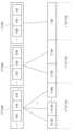
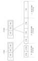
도 5는 본 발명의 실시예들에 따른 메모리 시스템(100)에서 네임스페이스와 슈퍼 메모리 블록의 관계의 일 예를 나타낸 도면이다.FIG. 5 is a diagram showing an example of the relationship between a namespace and a super memory block in a memory system (100) according to embodiments of the present invention.
도 5를 참조하면, 메모리 시스템(100)의 메모리 컨트롤러(120)는 메모리 장치(110)의 데이터 저장 공간을 N개(N은 2 이상의 자연수)의 네임스페이스(namespace)로 분할할 수 있다.Referring to FIG. 5, the memory controller (120) of the memory system (100) can divide the data storage space of the memory device (110) into N namespaces (N is a natural number greater than or equal to 2).
네임스페이스는 데이터 저장 공간을 복수의 논리적 공간으로 분할하였을 때, 각각의 논리적 공간을 의미한다.A namespace refers to each logical space when data storage space is divided into multiple logical spaces.
전술한 N개의 네임스페이스 각각은 서로 동일하거나 상이한 사이즈(용량)을 가질 수 있으며, 서로 동일하거나 상이한 프로텍션 타입 등을 가질 수 있다. 이때, N개의 네임스페이스 각각의 사이즈, 프로텍션 타입 등의 정보는 호스트(HOST)가 지시할 수 있다.Each of the N namespaces described above may have the same or different size (capacity) and may have the same or different protection types, etc. At this time, information such as the size and protection type of each of the N namespaces can be indicated by the host (HOST).
호스트(HOST)는 N개의 네임스페이스를 N개의 서로 다른 논리적 영역(또는 파티션)으로 인식할 수 있다. 그리고 호스트(HOST)는 각 네임스페이스를 별도로 포맷하는 동작을 메모리 컨트롤러(120)에 지시할 수 있다.The host (HOST) can recognize N namespaces as N different logical areas (or partitions). And the host (HOST) can instruct the memory controller (120) to format each namespace separately.
이때, 메모리 컨트롤러(120)는 N개의 네임스페이스 중 어느 하나인 제1 네임스페이스가, 메모리 장치(110)에 포함된 다수의 메모리 블록 중 일부를 포함하는 슈퍼 메모리 블록을 i) N개의 네임스페이스 중 제1 네임스페이스와 다른 제2 네임스페이스와 공유하거나 또는 ii) 독립적으로 점유하도록 제어할 수 있다.At this time, the memory controller (120) can control the first namespace, which is one of the N namespaces, to i) share a super memory block including some of the plurality of memory blocks included in the memory device (110) with a second namespace that is different from the first namespace among the N namespaces, or ii) to independently occupy the super memory block.
슈퍼 메모리 블록은 메모리 컨트롤러(120)가 메모리 장치(110)에 포함된 다수의 메모리 블록을 관리하는 논리적인 단위일 수 있다. 일 예로 메모리 컨트롤러(120)는 데이터를 메모리 장치(110)에 라이트할 때 슈퍼 메모리 블록 단위로 오픈 블록을 설정할 수 있다.A super memory block may be a logical unit in which a memory controller (120) manages a plurality of memory blocks included in a memory device (110). For example, the memory controller (120) may set an open block in units of super memory blocks when writing data to the memory device (110).
네임스페이스가 슈퍼 메모리 블록을 독립적으로 점유한다는 것은, 해당 슈퍼 메모리 블록에는 해당 네임스페이스에 대응하는 데이터만이 저장(프로그램)될 수 있다는 것을 의미한다.The fact that a namespace independently occupies a super memory block means that only data corresponding to that namespace can be stored (programmed) in that super memory block.
반면, 서로 다른 네임스페이스가 슈퍼 메모리 블록을 공유한다는 것은 해당 슈퍼 메모리 블록에 서로 다른 네임스페이스에 대응하는 데이터가 같이 저장될 수 있다는 것을 의미한다.On the other hand, the fact that different namespaces share a super memory block means that data corresponding to different namespaces can be stored together in that super memory block.
도 5를 참조하면, 메모리 컨트롤러(120)는 네임스페이스(NS_1)가 슈퍼 메모리 블록(SBLK_1)을 독립적으로 점유하도록 제어할 수 있다.Referring to FIG. 5, the memory controller (120) can control the namespace (NS_1) to independently occupy the super memory block (SBLK_1).
그리고 메모리 컨트롤러(120)는 네임스페이스(NS_2)와 네임스페이스(NS_3)가 슈퍼 메모리 블록(SBLK_2)을 공유하도록 제어할 수 있다.And the memory controller (120) can control the namespace (NS_2) and the namespace (NS_3) to share the super memory block (SBLK_2).
그리고 메모리 컨트롤러(120)는 네임스페이스(NS_4, ... , NS_N-1, NS_N)이 슈퍼 메모리 블록(SBLK_3)을 공유하도록 제어할 수 있다.And the memory controller (120) can control the namespaces (NS_4, ..., NS_N-1, NS_N) to share the super memory block (SBLK_3).
이때, 슈퍼 메모리 블록(SBLK_1, SBLK_2, SBLK_3) 각각은 다수의 메모리 블록(BLK)을 포함할 수 있다.At this time, each of the super memory blocks (SBLK_1, SBLK_2, SBLK_3) can include multiple memory blocks (BLK).
전술한 바와 같이, 메모리 컨트롤러(120)가 어떤 네임스페이스는 하나의 슈퍼 메모리 블록을 독립적으로 점유하고, 다른 네임스페이스는 하나의 슈퍼 메모리 블록을 공유하도록 제어하는 이유는 다음과 같다.As described above, the reason why the memory controller (120) controls some namespaces to independently occupy one super memory block and other namespaces to share one super memory block is as follows.
만약, N개의 네임스페이스 각각이 모두 하나의 슈퍼 메모리 블록을 독립적으로 점유하는 경우에는 각 네임스페이스를 포맷하는데 소요되는 시간이 짧아진다는 장점이 있다. 하나의 슈퍼 메모리 블록에는 하나의 네임스페이스에 대응하는 데이터만 저장되어 있으므로, 메모리 컨트롤러(120)가 슈퍼 메모리 블록에 포함된 메모리 블록 각각을 소거(erase)하면 포맷을 완료할 수 있기 때문이다.If each of the N namespaces independently occupies one super memory block, there is an advantage in that the time required to format each namespace is shortened. Since only data corresponding to one namespace is stored in one super memory block, the format can be completed by the memory controller (120) erasing each memory block included in the super memory block.
반면, 네임스페이스 각각이 모두 하나의 슈퍼 메모리 블록을 독립적으로 점유하면, 각 네임스페이스에 저장되는 데이터가 서로 다른 슈퍼 메모리 블록에 분산되기 때문에 메모리 장치(110)에 데이터를 라이트하는 동작이 비효율적으로 수행되는 단점이 있다.On the other hand, if each namespace independently occupies one super memory block, there is a disadvantage in that the operation of writing data to the memory device (110) is performed inefficiently because the data stored in each namespace is distributed to different super memory blocks.
일 예로 2개의 네임스페이스가 서로 다른 슈퍼 메모리 블록을 독립적으로 점유한다고 가정한다. 이 경우 호스트(HOST)가 2개의 네임스페이스에 동시에 데이터를 라이트하는 요청을 메모리 컨트롤러(120)로 전송하면, 메모리 컨트롤러(120)는 두 개의 서로 다른 슈퍼 메모리 블록을 오픈하여 데이터를 라이트해야 한다.For example, assume that two namespaces independently occupy different super memory blocks. In this case, if the host (HOST) sends a request to write data to two namespaces simultaneously to the memory controller (120), the memory controller (120) must open two different super memory blocks to write the data.
반면 2개의 네임스페이스가 하나의 슈퍼 메모리 블록을 공유하면 호스트(HOST)가 2개의 네임스페이스에 동시에 데이터를 라이트하는 요청을 메모리 컨트롤러(120)로 전송해도, 메모리 컨트롤러(120)는 하나의 슈퍼 메모리 블록만 오픈하여 데이터를 라이트하면 되기 때문에 보다 효율적으로 데이터를 라이트하는 동작을 수행할 수 있다.On the other hand, if two namespaces share one super memory block, even if the host sends a request to write data to two namespaces simultaneously to the memory controller (120), the memory controller (120) can perform the data writing operation more efficiently because it only has to open one super memory block and write the data.
또한, 메모리 컨트롤러(120)가 2개의 네임스페이스에 동시에 데이터를 라이트하는 도중 SPO(sudden power off)가 발생하는 경우, SPO에 대한 리커버리 동작의 소요 시간이 증가하는 단점이 있다.In addition, if a sudden power off (SPO) occurs while the memory controller (120) is simultaneously writing data to two namespaces, there is a disadvantage in that the time required for the recovery operation for the SPO increases.
만약 2개의 네임스페이스가 서로 다른 슈퍼 메모리 블록을 독립적으로 점유하면, 메모리 컨트롤러(120)는 두 개의 서로 다른 슈퍼 메모리 블록에 대한 리커버리 동작을 수행해야 한다. 반면 2개의 네임스페이스가 하나의 슈퍼 메모리 블록을 공유하면 메모리 컨트롤러(120)는 하나의 슈퍼 메모리 블록에 대한 리커버리 동작을 수행하면 되기 때문에 SPO에 대한 리커버리 동작을 보다 빠르게 수행할 수 있다.If two namespaces independently occupy different super memory blocks, the memory controller (120) must perform recovery operations for two different super memory blocks. On the other hand, if two namespaces share one super memory block, the memory controller (120) only needs to perform the recovery operation for one super memory block, so the recovery operation for SPO can be performed more quickly.
이와 반대로, N개의 네임스페이스가 모두 하나의 슈퍼 메모리 블록을 공유하는 경우에는 메모리 장치(110)의 데이터 저장 공간을 효율적으로 사용할 수 있다는 장점이 있다. 하나의 슈퍼 메모리 블록에는 N개의 네임스페이스 중 하나에 대응하는 모든 데이터가 라이트될 수 있기 때문이다.Conversely, when all N namespaces share one super memory block, there is an advantage in that the data storage space of the memory device (110) can be used efficiently. This is because all data corresponding to one of the N namespaces can be written to one super memory block.
그러나 N개의 네임스페이스가 모두 하나의 슈퍼 메모리 블록을 공유하는 경우에는 각 네임스페이스를 포맷하는데 소요되는 시간이 증가한다는 단점이 있다.However, if all N namespaces share one super memory block, there is a disadvantage in that the time required to format each namespace increases.
하나의 슈퍼 메모리 블록에 서로 다른 네임스페이스에 대응하는 데이터가 함께 저장되어 있으므로, 메모리 컨트롤러(120)가 포맷 대상이 아닌 네임스페이스에 대응하는 데이터를 다른 슈퍼 메모리 블록으로 이동시킨 다음에 슈퍼 메모리 블록에 포함된 메모리 블록을 소거할 수 있기 때문이다.Since data corresponding to different namespaces are stored together in one super memory block, the memory controller (120) can move data corresponding to a namespace that is not a format target to another super memory block and then erase the memory block included in the super memory block.
따라서, 전술한 두 가지 경우 중 어느 하나만을 사용할 경우에 발생할 수 있는 문제점을 최소화하기 위해서, 메모리 시스템(100)의 메모리 컨트롤러(120)는 어떤 네임스페이스는 하나의 슈퍼 메모리 블록을 독립적으로 점유하고, 다른 네임스페이스는 하나의 슈퍼 메모리 블록을 공유하도록 제어할 수 있다.Therefore, in order to minimize problems that may occur when using only one of the two cases described above, the memory controller (120) of the memory system (100) can control certain namespaces to independently occupy one super memory block and other namespaces to share one super memory block.
이를 통해 메모리 시스템(100)이 복수의 네임스페이스에 효율적으로 데이터를 저장하면서도 복수의 네임스페이스 각각의 포맷 시간의 증가는 최소화할 수 있다.This allows the memory system (100) to efficiently store data in multiple namespaces while minimizing the increase in format time for each of the multiple namespaces.
이하, 메모리 컨트롤러(120)가 N개의 네임스페이스 중에서 하나의 슈퍼 메모리 블록을 독립적으로 점유하는 네임스페이스와 하나의 슈퍼 메모리 블록을 다른 네임스페이스와 공유하는 네임스페이스를 설정하는 구체적인 방법에 대해서 설명한다.Below, a specific method for setting up a namespace in which a memory controller (120) independently occupies one super memory block among N namespaces and a namespace in which one super memory block is shared with another namespace is described.
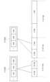
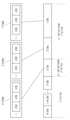
도 6은 본 발명의 실시예들에 따른 메모리 시스템(100)에서 공유 레벨에 따른 네임스페이스와 슈퍼 메모리 블록의 관계의 일 예를 나타낸 도면이다.FIG. 6 is a diagram showing an example of the relationship between a namespace and a super memory block according to a sharing level in a memory system (100) according to embodiments of the present invention.
도 6을 참조하면 메모리 시스템(100)의 메모리 컨트롤러는(120)는 N개의 네임스페이스 중 하나인 제1 네임스페이스에 대해서, 제1 네임스페이스에 대한 공유 레벨에 기초하여 슈퍼 메모리 블록을 i) N개의 네임스페이스 중 제1 네임스페이스와 다른 제2 네임스페이스와 공유하거나 또는 ii) 독립적으로 점유하도록 제어할 수 있다.Referring to FIG. 6, a memory controller (120) of a memory system (100) can control a super memory block to be i) shared with a second namespace that is different from the first namespace among N namespaces or ii) occupied independently, based on a sharing level for the first namespace, which is one of N namespaces.
네임스페이스의 공유 레벨은 해당 네임스페이스가 어느 하나의 슈퍼 메모리 블록을 독립적으로 점유할 수 있는지 아니면 몇 개의 서로 다른 네임스페이스와 공유할 수 있는지를 지시하는 값이다.The sharing level of a namespace is a value that indicates whether the namespace can occupy a single super memory block independently or share it with several other namespaces.
도 6에서, 메모리 컨트롤러(120)는 공유 레벨(SH_LVL_1)인 네임스페이스(NS_1)가 슈퍼 메모리 블록(SBLK_1)을 독립적으로 점유하도록 제어할 수 있다.In FIG. 6, the memory controller (120) can control the namespace (NS_1) of the shared level (SH_LVL_1) to independently occupy the super memory block (SBLK_1).
그리고 메모리 컨트롤러(120)는 공유 레벨(SH_LVL_2)인 두 개의 네임스페이스(NS_2, NS_3)가 슈퍼 메모리 블록(SBLK_2)을 공유하도록 제어할 수 있다.And the memory controller (120) can control two namespaces (NS_2, NS_3) with shared level (SH_LVL_2) to share the super memory block (SBLK_2).
그리고 메모리 컨트롤러(120)는 공유 레벨(SH_LVL_3)인 네임스페이스(NS_4, ..., NS_N-1, NS_N)가 슈퍼 메모리 블록(SBLK_3)을 공유하도록 제어할 수 있다.And the memory controller (120) can control the namespaces (NS_4, ..., NS_N-1, NS_N) of shared level (SH_LVL_3) to share the super memory block (SBLK_3).
이하, 메모리 시스템(100)의 메모리 컨트롤러(120)가 N개의 네임스페이스 각각의 공유 레벨을 결정하는 구체적인 방법에 대해 설명한다.Below, a specific method by which the memory controller (120) of the memory system (100) determines the sharing level of each of the N namespaces is described.
도 7은 본 발명의 실시예들에 따른 메모리 시스템(100)에서 네임스페이스의 공유 레벨을 결정하는 일 예를 나타낸 도면이다.FIG. 7 is a diagram illustrating an example of determining a sharing level of a namespace in a memory system (100) according to embodiments of the present invention.
도 7을 참조하면 네임스페이스의 공유 레벨은 메모리 장치(110)의 데이터 저장 공간 전체의 사이즈 대비 네임스페이스의 사이즈의 비율(%)에 따라 결정될 수 있다.Referring to FIG. 7, the sharing level of the namespace can be determined according to the ratio (%) of the size of the namespace to the size of the entire data storage space of the memory device (110).
도 7에서, 네임스페이스(NS_1)의 사이즈는 데이터 저장 공간 전체의 사이즈의 50%이고, 네임스페이스(NS_2)의 사이즈는 데이터 저장 공간 전체의 사이즈의 25%이고, 네임스페이스(NS_3)의 사이즈는 데이터 저장 공간 전체의 사이즈의 10%이고, 네임스페이스(NS_4, ... , NS_N-1, NS_N)의 사이즈는 각각 데이터 저장 공간 전체의 사이즈의 1%이다.In Fig. 7, the size of namespace (NS_1) is 50% of the size of the entire data storage space, the size of namespace (NS_2) is 25% of the size of the entire data storage space, the size of namespace (NS_3) is 10% of the size of the entire data storage space, and the sizes of namespaces (NS_4, ..., NS_N-1, NS_N) are each 1% of the size of the entire data storage space.
이때, 메모리 시스템(100)의 메모리 컨트롤러(120)는 데이터 저장 공간 전체의 사이즈 대비 네임스페이스의 사이즈의 비율에 따라 공유 레벨을 다음과 같이 결정할 수 있다.At this time, the memory controller (120) of the memory system (100) can determine the sharing level as follows based on the ratio of the size of the namespace to the size of the entire data storage space.
메모리 컨트롤러(120)는 네임스페이스의 사이즈가 데이터 저장 공간 전체의 사이즈의 50% 이상인 네임스페이스의 공유 레벨을 공유 레벨(SH_LVL_1)로 설정할 수 있다.The memory controller (120) can set the sharing level of a namespace whose size is 50% or more of the size of the entire data storage space to the sharing level (SH_LVL_1).
메모리 컨트롤러(120)는 네임스페이스의 사이즈가 데이터 저장 공간 전체의 사이즈의 50% 미만이고 25% 이상인 네임스페이스의 공유 레벨을 공유 레벨(SH_LVL_2)로 설정할 수 있다.The memory controller (120) can set the sharing level of a namespace whose size is less than 50% and more than 25% of the size of the entire data storage space to the sharing level (SH_LVL_2).
도 7에서 메모리 컨트롤러(120)는 네임스페이스의 사이즈가 데이터 저장 공간 전체의 사이즈의 25% 미만이고 10% 이상인 네임스페이스의 공유 레벨을 공유 레벨(SH_LVL_3)로 설정할 수 있다.In Fig. 7, the memory controller (120) can set the sharing level of a namespace whose size is less than 25% and more than 10% of the size of the entire data storage space to the sharing level (SH_LVL_3).
마지막으로 메모리 컨트롤러(120)는 네임스페이스의 사이즈가 데이터 저장 공간 전체의 사이즈의 10% 미만인 네임스페이스의 공유 레벨을 공유 레벨(SH_LVL_4)로 설정할 수 있다.Finally, the memory controller (120) can set the sharing level of a namespace whose size is less than 10% of the size of the entire data storage space to the sharing level (SH_LVL_4).
이때, 도 7에서 네임스페이스(NS_1)의 공유 레벨이 공유 레벨(SH_LVL_1)으로 설정된다. 그리고 네임스페이스(NS_2)의 공유 레벨이 공유 레벨(SH_LVL_2)으로 설정된다. 그리고 네임스페이스(NS_3)의 공유 레벨이 공유 레벨(SH_LVL_3)으로 설정된다. 그리고 네임스페이스(NS_4, ... , NS_N-1, NS_N)의 공유 레벨이 공유 레벨(SH_LVL_4)으로 설정된다.At this time, the sharing level of namespace (NS_1) in Fig. 7 is set to the sharing level (SH_LVL_1). And the sharing level of namespace (NS_2) is set to the sharing level (SH_LVL_2). And the sharing level of namespace (NS_3) is set to the sharing level (SH_LVL_3). And the sharing level of namespaces (NS_4, ..., NS_N-1, NS_N) is set to the sharing level (SH_LVL_4).
도 8은 본 발명의 실시예들에 따른 메모리 시스템(100)에서 네임스페이스의 공유 레벨을 결정하는 다른 예를 나타낸 도면이다.FIG. 8 is a diagram illustrating another example of determining the sharing level of a namespace in a memory system (100) according to embodiments of the present invention.
도 8을 참조하면 네임스페이스의 공유 레벨은 네임스페이스의 사이즈와 하나 이상의 임계 사이즈 정보에 따라 결정될 수 있다.Referring to FIG. 8, the sharing level of a namespace can be determined based on the size of the namespace and one or more threshold size information.
메모리 컨트롤러(120)는 네임스페이스의 사이즈가 임계 사이즈 512GB 이상인 네임스페이스의 공유 레벨을 공유 레벨(SH_LVL_1)로 설정할 수 있다.The memory controller (120) can set the sharing level of a namespace whose size is greater than the critical size of 512 GB to the sharing level (SH_LVL_1).
메모리 컨트롤러(120)는 네임스페이스의 사이즈가 임계 사이즈 512GB 미만이고 임계 사이즈 256GB 이상인 네임스페이스의 공유 레벨을 공유 레벨(SH_LVL_2)로 설정할 수 있다.The memory controller (120) can set the sharing level of a namespace whose size is less than the critical size of 512 GB and greater than the critical size of 256 GB to the sharing level (SH_LVL_2).
메모리 컨트롤러(120)는 네임스페이스의 사이즈가 임계 사이즈 256GB 미만이고 임계 사이즈 100GB 이상인 네임스페이스의 공유 레벨을 공유 레벨(SH_LVL_3)로 설정할 수 있다.The memory controller (120) can set the sharing level of a namespace whose size is less than the critical size of 256 GB and greater than the critical size of 100 GB to the sharing level (SH_LVL_3).
메모리 컨트롤러(120)는 네임스페이스의 사이즈가 임계 사이즈 100GB 미만인 네임스페이스의 공유 레벨을 공유 레벨(SH_LVL_4)로 설정할 수 있다.The memory controller (120) can set the sharing level of a namespace whose size is less than the critical size of 100 GB to the sharing level (SH_LVL_4).
이때, 도 8에서 네임스페이스(NS_1)의 공유 레벨이 공유 레벨(SH_LVL_1)으로 설정된다. 그리고, 네임스페이스(NS_2, NS_3)의 공유 레벨이 공유 레벨(SH_LVL_2)으로 설정된다. 그리고, 도 8에서 네임스페이스(NS_4)의 공유 레벨이 공유 레벨(SH_LVL_3)으로 설정된다. 그리고, 도 8에서 나머지 네임스페이스(... NS_N-1, NS_N)의 공유 레벨이 공유 레벨(SH_LVL_4)으로 설정된다.At this time, the sharing level of the namespace (NS_1) in Fig. 8 is set to the sharing level (SH_LVL_1). Then, the sharing level of the namespaces (NS_2, NS_3) is set to the sharing level (SH_LVL_2). Then, the sharing level of the namespace (NS_4) in Fig. 8 is set to the sharing level (SH_LVL_3). Then, the sharing level of the remaining namespaces (... NS_N-1, NS_N) in Fig. 8 is set to the sharing level (SH_LVL_4).
도 7 내지 도 8에서, 네임스페이스의 사이즈(용량)이 클수록 하나의 슈퍼 메모리 블록을 공유하는 네임스페이스의 개수가 작아진다. 이는 네임스페이스의 사이즈가 클수록 해당 네임스페이스가 슈퍼 메모리 블록의 대부분을 점유할 가능성이 높아서, 다른 네임스페이스와 해당 슈퍼 메모리 블록을 공유함으로서 생기는 효율이 줄어들기 때문이다.In FIGS. 7 and 8, as the size (capacity) of a namespace increases, the number of namespaces sharing one super memory block decreases. This is because as the size of a namespace increases, the namespace is more likely to occupy most of the super memory block, thereby reducing the efficiency gained by sharing the super memory block with other namespaces.
이상에서 각 네임스페이스에 대한 공유 레벨을 결정하는 실시예들을 설명하였다.The embodiments for determining the sharing level for each namespace are described above.
이하, 공유 레벨에 따라 각 네임스페이스가 슈퍼 메모리 블록을 독립적으로 점유하거나 또는 다른 네임스페이스와 공유하는 실시예들을 설명한다.Below, embodiments are described in which each namespace independently occupies a super memory block or shares it with other namespaces, depending on the sharing level.
도 9는 본 발명의 실시예들에 따른 메모리 시스템(100)에서 네임스페이스가 슈퍼 메모리 블록을 독립적으로 점유하는 경우의 일 예를 나타낸 도면이다.FIG. 9 is a diagram showing an example of a case where a namespace independently occupies a super memory block in a memory system (100) according to embodiments of the present invention.
도 9를 참조하면 메모리 컨트롤러(120)는 특정한 제1 공유 레벨을 가지는 네임스페이스가 슈퍼 메모리 블록을 독립적으로 점유하도록 제어할 수 있다.Referring to FIG. 9, the memory controller (120) can control a namespace having a specific first shared level to independently occupy a super memory block.
도 9에서, 공유 레벨(SH_LVL_1)인 네임스페이스(NS_1, NS_2)는 각각 슈퍼 메모리 블록(SBLK_1), 슈퍼 메모리 블록(SBLK_2)을 독립적으로 점유한다.In Fig. 9, namespaces (NS_1, NS_2) at the shared level (SH_LVL_1) independently occupy super memory block (SBLK_1) and super memory block (SBLK_2), respectively.
도 10은 본 발명의 실시예들에 따른 메모리 시스템(100)에서 네임스페이스가 슈퍼 메모리 블록을 다른 네임스페이스와 공유하는 경우의 일 예를 나타낸 도면이다.FIG. 10 is a diagram showing an example of a case in which a namespace shares a super memory block with another namespace in a memory system (100) according to embodiments of the present invention.
도 10을 참조하면 메모리 컨트롤러(120)는 도 9에서 설명한 제1 공유 레벨과 다른 제2 공유 레벨을 가지는 네임스페이스가 슈퍼 메모리 블록을 다른 네임스페이스와 공유하도록 제어할 수 있다.Referring to FIG. 10, the memory controller (120) can control a namespace having a second sharing level different from the first sharing level described in FIG. 9 to share a super memory block with another namespace.
도 10에서, 공유 레벨(SH_LVL_2)인 네임스페이스(NS_3, NS_4)와 공유 레벨(SH_LVL_3)인 네임스페이스(... , NS_N-1, NS_N)는 슈퍼 메모리 블록(SBLK_3)을 공유한다.In Fig. 10, namespaces (NS_3, NS_4) at a shared level (SH_LVL_2) and namespaces (..., NS_N-1, NS_N) at a shared level (SH_LVL_3) share a super memory block (SBLK_3).
도 11은 본 발명의 실시예들에 따른 메모리 시스템(100)에서 네임스페이스가 슈퍼 메모리 블록을 다른 네임스페이스와 공유하는 경우의 다른 예를 나타낸 도면이다.FIG. 11 is a diagram showing another example of a case where a namespace shares a super memory block with another namespace in a memory system (100) according to embodiments of the present invention.
도 11을 참조하면 메모리 시스템(100)의 메모리 컨트롤러(120)는 하나의 슈퍼 메모리 블록을 공유하는 네임스페이스는 공유 레벨이 서로 동일하도록 제어할 수 있다. 즉, 제1 네임스페이스와 제2 네임스페이스가 하나의 슈퍼 메모리 블록을 공유하는 경우에, 제1 네임스페이스의 공유 레벨이 제2 공유 레벨이면, 제2 네임스페이스의 공유 레벨 역시 제2 공유 레벨일 수 있다.Referring to FIG. 11, the memory controller (120) of the memory system (100) can control namespaces that share one super memory block so that their sharing levels are the same. That is, when a first namespace and a second namespace share one super memory block, if the sharing level of the first namespace is the second sharing level, the sharing level of the second namespace can also be the second sharing level.
도 11에서 동일한 공유 레벨(SH_LVL_2)을 가지는 네임스페이스(NS_3, NS_4)는 슈퍼 메모리 블록(SBLK_4)을 공유할 수 있다.In Fig. 11, namespaces (NS_3, NS_4) with the same sharing level (SH_LVL_2) can share the super memory block (SBLK_4).
그러나 공유 레벨(SH_LVL_2)과 다른 공유 레벨(SH_LVL_3)을 가지는 네임스페이스(... , NS_N-1, NS_N)는 네임스페이스(NS_3, NS_4)와 동일한 슈퍼 메모리 블록(SBLK_4)을 공유할 수 없다.However, namespaces (..., NS_N-1, NS_N) that have different sharing levels (SH_LVL_2) and different sharing levels (SH_LVL_3) cannot share the same super memory block (SBLK_4) with namespaces (NS_3, NS_4).
대신, 공유 레벨(SH_LVL_3)을 가지는 네임스페이스(... , NS_N-1, NS_N)는 다른 슈퍼 메모리 블록(SBLK_5)을 공유할 수 있다.Instead, namespaces (..., NS_N-1, NS_N) with shared level (SH_LVL_3) can share different super memory blocks (SBLK_5).
도 12는 본 발명의 실시예들에 따른 메모리 시스템(100)에서 동일한 공유 레벨을 가지는 네임스페이스가 슈퍼 메모리 블록을 점유하는 경우의 일 예를 나타낸 도면이다.FIG. 12 is a diagram showing an example of a case where namespaces having the same sharing level occupy a super memory block in a memory system (100) according to embodiments of the present invention.
도 12를 참조하면 메모리 컨트롤러(120)는 하나의 슈퍼 메모리 블록을 공유할 수 있는 네임스페이스의 최대 개수(MAX_SH_NS)를 공유 레벨에 따라 다르게 설정할 수 있다.Referring to FIG. 12, the memory controller (120) can set the maximum number (MAX_SH_NS) of namespaces that can share one super memory block differently depending on the sharing level.
메모리 컨트롤러(120)는 공유 레벨(SH_LVL_1)을 가지는 네임스페이스에 대해서, 하나의 슈퍼 메모리 블록을 공유할 수 있는 네임스페이스의 최대 개수(MAX_SH_NS)를 1로 설정할 수 있다.The memory controller (120) can set the maximum number (MAX_SH_NS) of namespaces that can share one super memory block to 1 for a namespace having a shared level (SH_LVL_1).
메모리 컨트롤러(120)는 공유 레벨(SH_LVL_2)을 가지는 네임스페이스에 대해서, 하나의 슈퍼 메모리 블록을 공유할 수 있는 네임스페이스의 최대 개수(MAX_SH_NS)를 2로 설정할 수 있다.The memory controller (120) can set the maximum number (MAX_SH_NS) of namespaces that can share one super memory block to 2 for a namespace having a shared level (SH_LVL_2).
메모리 컨트롤러(120)는 공유 레벨(SH_LVL_3)을 가지는 네임스페이스에 대해서, 하나의 슈퍼 메모리 블록을 공유할 수 있는 네임스페이스의 최대 개수(MAX_SH_NS)를 4로 설정할 수 있다.The memory controller (120) can set the maximum number (MAX_SH_NS) of namespaces that can share one super memory block to 4 for a namespace having a shared level (SH_LVL_3).
이 경우 공유 레벨(SH_LVL_1)을 가지는 네임스페이스는 하나의 슈퍼 메모리 블록을 독립적으로 점유하게 된다. 그리고 공유 레벨(SH_LVL_2)을 가지는 네임스페이스 중 최대 2개가 하나의 슈퍼 메모리 블록을 공유할 수 있다. 그리고 공유 레벨(SH_LVL_3)을 가지는 네임스페이스 중 최대 4개가 하나의 슈퍼 메모리 블록을 공유할 수 있다.In this case, a namespace with a shared level (SH_LVL_1) independently occupies one super memory block. And up to two namespaces with a shared level (SH_LVL_2) can share one super memory block. And up to four namespaces with a shared level (SH_LVL_3) can share one super memory block.
도 12에서, 공유 레벨(SH_LVL_2)을 가지는 네임스페이스(NS_2, NS_3, NS_4) 중에서 네임스페이스(NS_2, NS_3)이 슈퍼 메모리 블록(SBLK_6)을 공유한다.In Fig. 12, among namespaces (NS_2, NS_3, NS_4) having a shared level (SH_LVL_2), namespace (NS_2, NS_3) shares a super memory block (SBLK_6).
그러나, 네임스페이스(NS_4)는 네임스페이스(NS_2, NS_3)과 동일한 공유 레벨(SH_LVL_2)을 가지지만 네임스페이스(NS_2, NS_3)과 슈퍼 메모리 블록(SBLK_6)을 공유할 수 없다. 공유 레벨(SH_LVL_2)을 가지는 네임스페이스에 대해서, 하나의 슈퍼 메모리 블록을 공유할 수 있는 네임스페이스의 최대 개수(MAX_SH_NS)는 2이기 때문이다.However, namespace (NS_4) cannot share a super memory block (SBLK_6) with namespaces (NS_2, NS_3) even though it has the same sharing level (SH_LVL_2). This is because, for namespaces with a sharing level (SH_LVL_2), the maximum number of namespaces (MAX_SH_NS) that can share one super memory block is 2.
따라서, 네임스페이스(NS_4)는 네임스페이스(NS_2, NS_3)와 슈퍼 메모리 블록(SBLK_6)을 공유하는 대신에, 다른 슈퍼 메모리 블록(SBLK_7)을 점유한다.Therefore, instead of sharing the super memory block (SBLK_6) with namespaces (NS_2, NS_3), namespace (NS_4) occupies a different super memory block (SBLK_7).
이때, 특정 공유 레벨을 가지는 네임스페이스에 대해서, 하나의 슈퍼 메모리 블록을 공유할 수 있는 네임스페이스의 최대 개수(MAX_SH_NS)의 값은 다양한 방법으로 설정될 수 있다.At this time, for namespaces having a specific sharing level, the value of the maximum number of namespaces (MAX_SH_NS) that can share one super memory block can be set in various ways.
예를 들어, 하나의 슈퍼 메모리 블록을 공유할 수 있는 네임스페이스의 최대 개수(MAX_SH_NS)의 값은 2^k(k는 임의의 정수)로 설정될 수 있다.For example, the value of the maximum number of namespaces that can share one super memory block (MAX_SH_NS) can be set to 2^k (where k is any integer).
도 13은 본 발명의 실시예들에 따른 메모리 시스템(100)에서 서로 다른 공유 레벨을 가지는 네임스페이스가 슈퍼 메모리 블록을 점유하는 경우의 일 예를 나타낸 도면이다.FIG. 13 is a diagram showing an example of a case where namespaces having different sharing levels occupy a super memory block in a memory system (100) according to embodiments of the present invention.
도 13을 참조하면 메모리 시스템(100)의 메모리 컨트롤러(120)는 특정한 공유 레벨을 가지는 네임스페이스가 하나만 존재하면, 해당 네임스페이스는 하나의 슈퍼 메모리 블록을 독립적으로 점유하도록 제어할 수 있다.Referring to FIG. 13, the memory controller (120) of the memory system (100) can control, if there is only one namespace having a specific sharing level, the namespace to independently occupy one super memory block.
도 13에서 공유 레벨(SH_LVL_2)를 가지는 네임스페이스는 네임스페이스(NS_3) 하나만 존재한다. 이 경우, 공유 레벨(SH_LVL_2)를 가지는 네임스페이스에 대해서 하나의 슈퍼 메모리 블록을 공유할 수 있는 네임스페이스의 최대 개수(MAX_SH_NS)가 2로 설정된 경우에도, 네임스페이스(NS_3)은 슈퍼 메모리 블록(SBLK_3)을 다른 네임스페이스와 공유하지 않고 독립적으로 점유할 수 있다.In Fig. 13, there is only one namespace (NS_3) with a shared level (SH_LVL_2). In this case, even if the maximum number (MAX_SH_NS) of namespaces that can share one super memory block for the namespace with a shared level (SH_LVL_2) is set to 2, the namespace (NS_3) can independently occupy the super memory block (SBLK_3) without sharing it with other namespaces.
이상의 도 6 내지 도 13에서는 공유 레벨에 따라 네임스페이스가 슈퍼 메모리 블록을 독립적으로 점유하거나 또는 다른 슈퍼 메모리 블록과 공유하는 동작을 설명하였다.The above Figures 6 to 13 describe the operation of a namespace independently occupying a super memory block or sharing it with another super memory block depending on the sharing level.
이하, 공유 레벨에 따라 네임스페이스가 슈퍼 메모리 블록을 독립적으로 점유하거나 또는 다른 슈퍼 메모리 블록과 공유하는 다양한 시나리오를 설명한다.Below, we describe various scenarios in which a namespace occupies a super memory block independently or shares it with other super memory blocks, depending on the sharing level.
먼저 4개의 공유 레벨(L1, L2, L3, L4)은 메모리 장치(110)의 데이터 저장 공간 전체의 사이즈 대비 네임스페이스의 사이즈의 비율(%)에 따라 다음과 같이 결정된다고 가정한다.First, it is assumed that the four shared levels (L1, L2, L3, L4) are determined as follows based on the ratio (%) of the size of the namespace to the size of the entire data storage space of the memory device (110).
L1 : SIZE >= 50%L1 : SIZE >= 50%
L2 : 50% > SIZE >= 25%L2 : 50% > SIZE >= 25%
L3 : 25% > SIZE >= 10%L3 : 25% > SIZE >= 10%
L4 : 10% > SIZE > 0%L4 : 10% > SIZE > 0%
그리고 공유 레벨(L1)인 네임스페이스는 하나의 슈퍼 메모리 블록을 독립적으로 점유할 수 있다고 가정한다. 그리고 공유 레벨(L2)인 네임스페이스는 최대 2개가 하나의 슈퍼 메모리 블록을 공유할 수 있다고 가정한다. 그리고 공유 레벨(L3)인 네임스페이스는 최대 4개가 하나의 슈퍼 메모리 블록을 공유할 수 있다고 가정한다. 그리고 공유 레벨(L4)인 네임스페이스는 최대 8개가 하나의 슈퍼 메모리 블록을 공유할 수 있다고 가정한다.And it is assumed that a namespace with a shared level (L1) can independently occupy one super memory block. And it is assumed that a namespace with a shared level (L2) can share one super memory block with a maximum of two. And it is assumed that a namespace with a shared level (L3) can share one super memory block with a maximum of four. And it is assumed that a namespace with a shared level (L4) can share one super memory block with a maximum of eight.
[시나리오 1][Scenario 1]
메모리 장치(110)의 데이터 저장 공간은 다음과 같이 6개의 네임스페이스(NS_1, NS_2, NS_3, NS_4, NS_5, NS_6)로 분할되며, 메모리 장치(110)의 데이터 저장 공간 전체의 사이즈 대비 각 네임스페이스의 사이즈의 비율은 다음과 같다고 가정한다.The data storage space of the memory device (110) is divided into six namespaces (NS_1, NS_2, NS_3, NS_4, NS_5, NS_6) as follows, and it is assumed that the ratio of the size of each namespace to the size of the entire data storage space of the memory device (110) is as follows.
NS_1 : 50%NS_1 : 50%
NS_2 : 25%NS_2 : 25%
NS_3 : 10%NS_3 : 10%
NS_4 : 5%NS_4 : 5%
NS_5 : 5%NS_5 : 5%
NS_6 : 5%NS_6 : 5%
이때, 네임스페이스(NS_1)의 공유 레벨은 L1이고, 네임스페이스(NS_1)는 하나의 슈퍼 메모리 블록을 독립적으로 점유한다.At this time, the shared level of namespace (NS_1) is L1, and namespace (NS_1) independently occupies one super memory block.
그리고 네임스페이스(NS_2)의 공유 레벨은 L2이고, 공유 레벨이 L2인 다른 네임스페이스가 존재하지 않으므로 네임스페이스(NS_2)는 역시 하나의 슈퍼 메모리 블록을 독립적으로 점유한다.And since the shared level of namespace (NS_2) is L2 and there is no other namespace with a shared level of L2, namespace (NS_2) also occupies one super memory block independently.
그리고 네임스페이스(NS_3)의 공유 레벨은 L3이고, 공유 레벨이 L3인 다른 네임스페이스가 존재하지 않으므로 네임스페이스(NS_3)는 역시 하나의 슈퍼 메모리 블록을 독립적으로 점유한다.And since the shared level of namespace (NS_3) is L3 and there is no other namespace with a shared level of L3, namespace (NS_3) also occupies one super memory block independently.
그리고 나머지 네임스페이스(NS_4, NS_5, NS_6)의 공유 레벨은 L4이고, 네임스페이스(NS_4, NS_5, NS_6)는 하나의 슈퍼 메모리 블록을 서로 공유한다.And the sharing level of the remaining namespaces (NS_4, NS_5, NS_6) is L4, and the namespaces (NS_4, NS_5, NS_6) share one super memory block with each other.
[시나리오 2][Scenario 2]
메모리 장치(110)의 데이터 저장 공간은 다음과 같이 3개의 네임스페이스(NS_1, NS_2, NS_3)로 분할되며, 메모리 장치(110)의 데이터 저장 공간 전체의 사이즈 대비 각 네임스페이스의 사이즈의 비율은 다음과 같다고 가정한다.The data storage space of the memory device (110) is divided into three namespaces (NS_1, NS_2, NS_3) as follows, and it is assumed that the ratio of the size of each namespace to the size of the entire data storage space of the memory device (110) is as follows.
NS_1 : 40%NS_1 : 40%
NS_2 : 40%NS_2 : 40%
NS_3 : 20%NS_3 : 20%
이때, 네임스페이스(NS_1, NS_2)의 공유 레벨은 L2이고, 네임스페이스(NS_1, NS_2)는 하나의 슈퍼 메모리 블록을 공유한다.At this time, the sharing level of namespaces (NS_1, NS_2) is L2, and namespaces (NS_1, NS_2) share one super memory block.
그리고 네임스페이스(NS_3)의 공유 레벨은 L3이고, 공유 레벨이 L3인 다른 네임스페이스가 존재하지 않으므로 네임스페이스(NS_3)은 하나의 슈퍼 메모리 블록을 독립적으로 점유한다.And since the shared level of namespace (NS_3) is L3 and there is no other namespace with a shared level of L3, namespace (NS_3) occupies one super memory block independently.
[시나리오 3][Scenario 3]
메모리 장치(110)의 데이터 저장 공간은 다음과 같이 3개의 네임스페이스(NS_1, NS_2, NS_3)로 분할되며, 메모리 장치(110)의 데이터 저장 공간 전체의 사이즈 대비 각 네임스페이스의 사이즈의 비율은 다음과 같다고 가정한다.The data storage space of the memory device (110) is divided into three namespaces (NS_1, NS_2, NS_3) as follows, and it is assumed that the ratio of the size of each namespace to the size of the entire data storage space of the memory device (110) is as follows.
NS_1 : 33%NS_1 : 33%
NS_2 : 33%NS_2 : 33%
NS_3 : 33%NS_3 : 33%
이때, 네임스페이스(NS_1, NS_2, NS_3)의 공유 레벨은 L2인데, 공유 레벨(L2)인 네임스페이스는 최대 2개가 하나의 슈퍼 메모리 블록을 공유할 수 있다. 따라서 3개의 네임스페이스(NS_1, NS_2, NS_3) 중 2개의 네임스페이스(NS_1, NS_2)는 하나의 슈퍼 메모리 블록을 공유하고, 나머지 네임스페이스(NS_3)은 하나의 슈퍼 메모리 블록을 독립적으로 점유할 수 있다.At this time, the sharing level of namespaces (NS_1, NS_2, NS_3) is L2, and a maximum of two namespaces with a sharing level (L2) can share one super memory block. Therefore, among the three namespaces (NS_1, NS_2, NS_3), two namespaces (NS_1, NS_2) share one super memory block, and the remaining namespace (NS_3) can independently occupy one super memory block.
도 14는 본 발명의 실시예들에 따른 메모리 컨트롤러(120)의 동작 방법을 나타낸 흐름도이다.Figure 14 is a flowchart illustrating an operation method of a memory controller (120) according to embodiments of the present invention.
도 14를 참조하면, 메모리 컨트롤러(120)의 동작 방법은 메모리 장치(110)의 데이터 저장 공간을 N개(N은 2 이상의 자연수)의 네임스페이스로 분할하는 단계를 포함할 수 있다(S1410).Referring to FIG. 14, the operation method of the memory controller (120) may include a step of dividing the data storage space of the memory device (110) into N namespaces (N is a natural number greater than or equal to 2) (S1410).
이때, N개의 네임스페이스 각각에 대한 정보(e.g. 사이즈(용량), 프로텍션 타입 등)는 호스트(HOST)에 의해 지시될 수 있다.At this time, information for each of the N namespaces (e.g. size (capacity), protection type, etc.) can be indicated by the host (HOST).
그리고 메모리 컨트롤러(120)의 동작 방법은 S1410 단계에서 분할된 N개의 네임스페이스 중 하나인 제1 네임스페이스가, 메모리 장치(110)에 포함된 다수의 메모리 블록 중 일부를 포함하는 슈퍼 메모리 블록을 i) N개의 네임스페이스 중 제1 네임스페이스와 다른 제2 네임스페이스와 공유하거나 또는 ii) 독립적으로 점유하도록 제어하는 단계를 포함할 수 있다(S1420).And the operation method of the memory controller (120) may include a step of controlling the first namespace, which is one of the N namespaces divided in step S1410, to i) share a super memory block including some of the plurality of memory blocks included in the memory device (110) with a second namespace that is different from the first namespace among the N namespaces, or ii) independently occupy it (S1420).
한편, 이상에서 설명한 메모리 컨트롤러(120)의 동작은 제어 회로(123)에 의해 제어될 수 있으며, 프로세서(124)가 메모리 컨트롤러(120)의 제반 동작이 프로그램된 펌웨어를 실행(구동)하는 방식으로 수행될 수 있다.Meanwhile, the operation of the memory controller (120) described above can be controlled by the control circuit (123), and the processor (124) can be performed in a manner in which the overall operation of the memory controller (120) is executed (driven) by programmed firmware.
도 15는 본 발명의 실시예들에 따른 컴퓨팅 시스템(1500)의 구성도이다.FIG. 15 is a configuration diagram of a computing system (1500) according to embodiments of the present invention.
도 15을 참조하면, 본 발명의 실시예들에 따른 컴퓨팅 시스템(1500)은 시스템 버스(1560)에 전기적으로 연결되는 메모리 시스템(100), 컴퓨팅 시스템(1500)의 전반적인 동작을 제어하는 중앙처리장치(CPU, 1510), 컴퓨팅 시스템(1500)의 동작과 관련한 데이터 및 정보를 저장하는 램(RAM, 1520), 사용자에게 사용 환경을 제공하기 위한 UI/UX (User Interface/User Experience) 모듈(1530), 외부 장치와 유선 및/또는 무선 방식으로 통신하기 위한 통신 모듈(1540), 컴퓨팅 시스템(1500)이 사용하는 파워를 관리하는 파워 관리 모듈(1550) 등을 포함할 수 있다.Referring to FIG. 15, a computing system (1500) according to embodiments of the present invention may include a memory system (100) electrically connected to a system bus (1560), a central processing unit (CPU, 1510) that controls the overall operation of the computing system (1500), a random access memory (RAM, 1520) that stores data and information related to the operation of the computing system (1500), a UI/UX (User Interface/User Experience) module (1530) for providing a user environment, a communication module (1540) for communicating with an external device in a wired and/or wireless manner, a power management module (1550) for managing power used by the computing system (1500), etc.
컴퓨팅 시스템(1500)은 PC(Personal Computer)이거나, 스마트 폰, 태블릿 등의 모바일 단말, 또는 각종 전자 기기 등을 포함할 수 있다.The computing system (1500) may include a personal computer (PC), a mobile terminal such as a smart phone or tablet, or various electronic devices.
컴퓨팅 시스템(1500)은, 동작 전압을 공급하기 위한 배터리를 더 포함할 수 있으며, 응용 칩셋(Application Chipset), 그래픽 관련 모듈, 카메라 이미지 프로세서(Camera Image Processor: CIS), 디램 등을 더 포함할 수도 있다. 이외에도, 이 분야의 통상적인 지식을 습득한 자들에게 자명하다.The computing system (1500) may further include a battery for supplying an operating voltage, and may further include an application chipset, a graphic-related module, a camera image processor (CIS), DRAM, etc. In addition, this is obvious to those who have acquired general knowledge in this field.
한편, 메모리 시스템(100)은, 하드 디스크 드라이브(HDD: Hard Disk Drive)와 같이 자기 디스크에 데이터를 저장하는 장치뿐 아니라, 솔리드 스테이트 드라이브(SSD: Solid State Drive), UFS(Universal Flash Storage) 장치, eMMC(embedded MMC) 장치 등과 같이 비휘발성 메모리에 데이터를 저장하는 장치 등을 포함할 수 있다. 비휘발성 메모리는 ROM(Read Only Memory), PROM(Programmable ROM), EPROM (Electrically Programmable ROM), EEPROM(Electrically Erasable and Programmable ROM), 플래시 메모리, PRAM(Phase-change RAM), MRAM(Magnetic RAM), RRAM(Resistive RAM), FRAM(Ferroelectric RAM) 등을 포함할 수 있다. 이뿐만 아니라, 메모리 시스템(100)은 다양한 형태의 저장 장치로 구현되어, 다양한 전자 기기 내에 탑재될 수 있다.Meanwhile, the memory system (100) may include not only a device that stores data in a magnetic disk, such as a hard disk drive (HDD), but also a device that stores data in non-volatile memory, such as a solid state drive (SSD), a universal flash storage (UFS) device, and an embedded MMC (eMMC) device. The non-volatile memory may include a read only memory (ROM), a programmable ROM (PROM), an electrically programmable ROM (EPROM), an electrically erasable and programmable ROM (EEPROM), a flash memory, a phase-change RAM (PRAM), a magnetic RAM (MRAM), a resistive RAM (RRAM), a ferroelectric RAM (FRAM), and the like. In addition, the memory system (100) may be implemented as various types of storage devices and may be mounted in various electronic devices.
이상의 설명은 본 발명의 기술 사상을 예시적으로 설명한 것에 불과한 것으로서, 본 발명이 속하는 기술 분야에서 통상의 지식을 가진 자라면 본 발명의 본질적인 특성에서 벗어나지 않는 범위에서 다양한 수정 및 변형이 가능할 것이다. 또한, 본 발명에 개시된 실시예들은 본 발명의 기술 사상을 한정하기 위한 것이 아니라 설명하기 위한 것이므로 이러한 실시예에 의하여 본 발명의 기술 사상의 범위가 한정되는 것은 아니다. 본 발명의 보호 범위는 아래의 청구범위에 의하여 해석되어야 하며, 그와 동등한 범위 내에 있는 모든 기술 사상은 본 발명의 권리 범위에 포함되는 것으로 해석되어야 할 것이다.The above description is merely an illustrative description of the technical idea of the present invention, and those skilled in the art will appreciate that various modifications and variations may be made without departing from the essential characteristics of the present invention. In addition, the embodiments disclosed in the present invention are not intended to limit the technical idea of the present invention but to explain it, and therefore the scope of the technical idea of the present invention is not limited by these embodiments. The protection scope of the present invention should be interpreted by the following claims, and all technical ideas within a scope equivalent thereto should be interpreted as being included in the scope of the rights of the present invention.
100: 메모리 시스템110: 메모리 장치
120: 메모리 컨트롤러121: 호스트 인터페이스
122: 메모리 인터페이스123: 제어 회로
124: 프로세서125: 워킹 메모리
126: 에러 검출 및 정정 회로210: 메모리 셀 어레이
220: 어드레스 디코더230: 리드 앤 라이트 회로
240: 제어 로직250: 전압 생성 회로100: Memory system 110: Memory device
120: Memory Controller 121: Host Interface
122: Memory interface 123: Control circuit
124: Processor 125: Working Memory
126: Error detection and correction circuit 210: Memory cell array
220: Address decoder 230: Read and write circuit
240: Control logic 250: Voltage generation circuit
Claims (15)
Translated fromKorean상기 메모리 장치를 제어하는 메모리 컨트롤러를 포함하고,
상기 메모리 컨트롤러는,
상기 메모리 장치의 데이터 저장 공간을 N개(N은 2 이상의 자연수)의 네임스페이스로 분할하고,
상기 N개의 네임스페이스 중 제1 네임스페이스가, 상기 제1 네임스페이스에 대한 공유 레벨에 기초하여 상기 다수의 메모리 블록 중 일부를 포함하는 슈퍼 메모리 블록을 i) 상기 N개의 네임스페이스 중 상기 제1 네임스페이스와 다른 제2 네임스페이스와 공유하거나 또는 ii) 독립적으로 점유하도록 제어하고,
상기 제1 네임스페이스에 대한 공유 레벨은,
상기 메모리 장치의 데이터 저장 공간 전체의 사이즈 대비 상기 제1 네임스페이스의 사이즈의 비율에 따라 설정되는 메모리 시스템.
A memory device comprising a plurality of memory blocks; and
comprising a memory controller that controls the above memory device;
The above memory controller,
The data storage space of the above memory device is divided into N namespaces (N is a natural number greater than or equal to 2),
A first namespace among the N namespaces controls a super memory block including some of the plurality of memory blocks to i) share with a second namespace other than the first namespace among the N namespaces or ii) independently occupy, based on a sharing level for the first namespace,
The sharing level for the above first namespace is:
A memory system set according to the ratio of the size of the first namespace to the size of the entire data storage space of the memory device.
상기 제1 네임스페이스에 대한 공유 레벨은,
상기 제1 네임스페이스의 사이즈와 하나 이상의 임계 사이즈 정보에 따라 설정되는 메모리 시스템.
In the first paragraph,
The sharing level for the above first namespace is:
A memory system set according to the size of the first namespace and one or more threshold size information.
상기 메모리 컨트롤러는,
상기 제1 네임스페이스에 대한 공유 레벨이 제1 공유 레벨이면, 상기 제1 네임스페이스가 상기 슈퍼 메모리 블록을 독립적으로 점유하도록 제어하는 메모리 시스템.
In the first paragraph,
The above memory controller,
A memory system that controls the first namespace to independently occupy the super memory block when the sharing level for the first namespace is the first sharing level.
상기 메모리 컨트롤러는,
상기 제1 네임스페이스에 대한 공유 레벨이 상기 제1 공유 레벨과 다른 제2 공유 레벨이면,
상기 제1 네임스페이스가 상기 슈퍼 메모리 블록을 상기 제2 네임스페이스와 공유하도록 제어하는 메모리 시스템.
In paragraph 4,
The above memory controller,
If the sharing level for the first namespace is a second sharing level that is different from the first sharing level,
A memory system that controls the first namespace to share the super memory block with the second namespace.
상기 제2 네임스페이스에 대한 공유 레벨은 상기 제2 공유 레벨인 메모리 시스템.
In paragraph 5,
A memory system in which the sharing level for the second namespace is the second sharing level.
상기 메모리 컨트롤러는,
상기 제2 공유 레벨의 값에 따라 상기 슈퍼 메모리 블록을 공유할 수 있는 네임스페이스의 최대 개수를 설정하는 메모리 시스템.
In paragraph 5,
The above memory controller,
A memory system that sets the maximum number of namespaces that can share the super memory block based on the value of the second sharing level.
상기 메모리 컨트롤러는,
상기 제1 네임스페이스에 대한 공유 레벨이 상기 제1 공유 레벨과 다른 제2 공유 레벨이고 상기 N개의 네임스페이스 중 공유 레벨이 상기 제2 공유 레벨인 다른 네임스페이스가 존재하지 않는 경우,
상기 제1 네임스페이스가 상기 슈퍼 메모리 블록을 독립적으로 점유하도록 제어하는 메모리 시스템.
In paragraph 4,
The above memory controller,
If the sharing level for the first namespace is a second sharing level different from the first sharing level and there is no other namespace among the N namespaces whose sharing level is the second sharing level,
A memory system that controls the above first namespace to independently occupy the above super memory block.
상기 메모리 장치를 제어하기 위한 제어 회로를 포함하고,
상기 제어 회로는,
상기 메모리 장치의 데이터 저장 공간을 N개(N은 2 이상의 자연수)의 네임스페이스로 분할하고,
상기 N개의 네임스페이스 중 제1 네임스페이스가, 상기 제1 네임스페이스에 대한 공유 레벨에 기초하여 상기 다수의 메모리 블록 중 일부를 포함하는 슈퍼 메모리 블록을 i) 상기 N개의 네임스페이스 중 상기 제1 네임스페이스와 다른 제2 네임스페이스와 공유하거나 또는 ii) 독립적으로 점유하도록 제어하고,
상기 제1 네임스페이스에 대한 공유 레벨은,
상기 메모리 장치의 데이터 저장 공간 전체의 사이즈 대비 상기 제1 네임스페이스의 사이즈의 비율에 따라 설정되는 메모리 컨트롤러.
A memory interface for communicating with a memory device including a plurality of memory blocks; and
A control circuit for controlling the above memory device is included,
The above control circuit,
The data storage space of the above memory device is divided into N namespaces (N is a natural number greater than or equal to 2),
A first namespace among the N namespaces controls a super memory block including some of the plurality of memory blocks to i) share with a second namespace other than the first namespace among the N namespaces or ii) independently occupy, based on a sharing level for the first namespace,
The sharing level for the above first namespace is:
A memory controller set according to the ratio of the size of the first namespace to the size of the entire data storage space of the memory device.
상기 제어 회로는,
상기 제1 네임스페이스에 대한 공유 레벨이 제1 공유 레벨이면 상기 제1 네임스페이스가 상기 슈퍼 메모리 블록을 독립적으로 점유하도록 제어하는 메모리 컨트롤러.
In Article 9,
The above control circuit,
A memory controller that controls the first namespace to independently occupy the super memory block when the sharing level for the first namespace is the first sharing level.
상기 제어 회로는,
상기 제1 네임스페이스에 대한 공유 레벨이 제1 공유 레벨과 다른 제2 공유 레벨이면,
상기 제1 네임스페이스가 상기 슈퍼 메모리 블록을 상기 제2 네임스페이스와 공유하도록 제어하는 메모리 컨트롤러.
In Article 9,
The above control circuit,
If the sharing level for the first namespace is a second sharing level that is different from the first sharing level,
A memory controller that controls the first namespace to share the super memory block with the second namespace.
상기 제2 네임스페이스에 대한 공유 레벨은 상기 제2 공유 레벨인 메모리 컨트롤러.
In Article 11,
The sharing level for the above second namespace is the memory controller which is the second sharing level.
상기 제어 회로는,
상기 제2 공유 레벨의 값에 따라 상기 슈퍼 메모리 블록을 공유할 수 있는 네임스페이스의 최대 개수를 설정하는 메모리 컨트롤러.
In Article 12,
The above control circuit,
A memory controller that sets the maximum number of namespaces that can share the super memory block based on the value of the second sharing level.
상기 제어 회로는,
상기 제1 네임스페이스에 대한 공유 레벨이 상기 제1 공유 레벨과 다른 제2 공유 레벨이고 상기 N개의 네임스페이스 중 공유 레벨이 상기 제2 공유 레벨인 다른 네임스페이스가 존재하지 않는 경우,
상기 제1 네임스페이스가 상기 슈퍼 메모리 블록을 독립적으로 점유하도록 제어하는 메모리 컨트롤러.
In Article 10,
The above control circuit,
If the sharing level for the first namespace is a second sharing level different from the first sharing level and there is no other namespace among the N namespaces whose sharing level is the second sharing level,
A memory controller that controls the first namespace to independently occupy the super memory block.
상기 메모리 장치의 데이터 저장 공간을 N개(N은 2 이상의 자연수)의 네임스페이스로 분할하는 단계; 및
상기 N개의 네임스페이스 중 제1 네임스페이스가, 상기 제1 네임스페이스에 대한 공유 레벨에 기초하여 상기 다수의 메모리 블록 중 일부를 포함하는 슈퍼 메모리 블록을 i) 상기 N개의 네임스페이스 중 상기 제1 네임스페이스와 다른 제2 네임스페이스와 공유하거나 또는 ii) 독립적으로 점유하도록 제어하는 단계를 포함하고,
상기 제1 네임스페이스에 대한 공유 레벨은,
상기 메모리 장치의 데이터 저장 공간 전체의 사이즈 대비 상기 제1 네임스페이스의 사이즈의 비율에 따라 설정되는 메모리 컨트롤러의 동작 방법.A method of operating a memory controller that controls a memory device including a plurality of memory blocks,
A step of dividing the data storage space of the above memory device into N namespaces (N is a natural number greater than or equal to 2); and
A step of controlling a first namespace among the N namespaces to i) share a super memory block including some of the plurality of memory blocks with a second namespace different from the first namespace among the N namespaces or ii) independently occupy the super memory block based on a sharing level for the first namespace,
The sharing level for the above first namespace is:
An operating method of a memory controller set according to a ratio of the size of the first namespace to the size of the entire data storage space of the memory device.
Priority Applications (2)
| Application Number | Priority Date | Filing Date | Title |
|---|---|---|---|
| KR1020190109243AKR102724536B1 (en) | 2019-09-04 | 2019-09-04 | Memory system, memory controller, and operating method |
| US16/988,111US11474726B2 (en) | 2019-09-04 | 2020-08-07 | Memory system, memory controller, and operation method thereof |
Applications Claiming Priority (1)
| Application Number | Priority Date | Filing Date | Title |
|---|---|---|---|
| KR1020190109243AKR102724536B1 (en) | 2019-09-04 | 2019-09-04 | Memory system, memory controller, and operating method |
Publications (2)
| Publication Number | Publication Date |
|---|---|
| KR20210028335A KR20210028335A (en) | 2021-03-12 |
| KR102724536B1true KR102724536B1 (en) | 2024-10-31 |
Family
ID=74682269
Family Applications (1)
| Application Number | Title | Priority Date | Filing Date |
|---|---|---|---|
| KR1020190109243AActiveKR102724536B1 (en) | 2019-09-04 | 2019-09-04 | Memory system, memory controller, and operating method |
Country Status (2)
| Country | Link |
|---|---|
| US (1) | US11474726B2 (en) |
| KR (1) | KR102724536B1 (en) |
Families Citing this family (1)
| Publication number | Priority date | Publication date | Assignee | Title |
|---|---|---|---|---|
| US11640254B2 (en)* | 2021-08-25 | 2023-05-02 | Western Digital Technologies, Inc. | Controlled imbalance in super block allocation in ZNS SSD |
Family Cites Families (11)
| Publication number | Priority date | Publication date | Assignee | Title |
|---|---|---|---|---|
| US20150121003A1 (en)* | 2010-09-07 | 2015-04-30 | Daniel L. Rosenband | Storage controllers |
| US10235097B2 (en)* | 2015-07-21 | 2019-03-19 | Samsung Electronics Co., Ltd. | Area and performance optimized namespace sharing method in virtualized PCIE based SSD controller |
| KR102372825B1 (en)* | 2015-07-31 | 2022-03-14 | 에스케이하이닉스 주식회사 | Data storage device and operating method thereof |
| US10733137B2 (en)* | 2017-04-25 | 2020-08-04 | Samsung Electronics Co., Ltd. | Low latency direct access block storage in NVME-of ethernet SSD |
| US10452536B2 (en)* | 2017-06-12 | 2019-10-22 | Western Digital Technologies, Inc. | Dynamic management of garbage collection and overprovisioning for host stream storage |
| US11294594B2 (en)* | 2017-08-07 | 2022-04-05 | Kioxia Corporation | SSD architecture supporting low latency operation |
| KR102503177B1 (en) | 2018-03-05 | 2023-02-24 | 에스케이하이닉스 주식회사 | Memory system and operating method thereof |
| JP7109992B2 (en)* | 2018-05-22 | 2022-08-01 | キオクシア株式会社 | Memory system and control method |
| KR20200032404A (en) | 2018-09-18 | 2020-03-26 | 에스케이하이닉스 주식회사 | Data Storage Device and Operation Method Thereof, Storage System Having the Same |
| CN111651371B (en)* | 2019-03-04 | 2023-06-16 | 慧荣科技股份有限公司 | Asymmetric plane management method, data storage device and controller thereof |
| US10922235B2 (en)* | 2019-06-26 | 2021-02-16 | Western Digital Technologies, Inc. | Method and system for address table eviction management |
- 2019
- 2019-09-04KRKR1020190109243Apatent/KR102724536B1/enactiveActive
- 2020
- 2020-08-07USUS16/988,111patent/US11474726B2/enactiveActive
Also Published As
| Publication number | Publication date |
|---|---|
| US20210064260A1 (en) | 2021-03-04 |
| KR20210028335A (en) | 2021-03-12 |
| US11474726B2 (en) | 2022-10-18 |
Similar Documents
| Publication | Publication Date | Title |
|---|---|---|
| KR102769751B1 (en) | Memory system, memory device, and operating method of memory device | |
| US11262939B2 (en) | Memory system, memory controller, and operation method | |
| KR102695175B1 (en) | Memory system, memory controller, and operating method | |
| KR102831409B1 (en) | Memory system, memory controller, and operating method of memory system | |
| KR102835718B1 (en) | Memory system and operating method of memory system | |
| US11301174B2 (en) | Memory system, memory controller and method for operating memory system | |
| US12072809B2 (en) | Memory system, memory controller, and operation method of memory system for loading and updating mapping information to host memory area | |
| KR102838945B1 (en) | Memory system, memory controller, and operating method thereof | |
| KR102849583B1 (en) | Memory system, memory controller, and operating method | |
| KR102699949B1 (en) | Memory system, memory controller, and operating method | |
| US20250117327A1 (en) | Memory system, memory controller and operating method of the memory system for controlling garbage collection | |
| KR102789969B1 (en) | Memory system, memory device, and operating method of memory device | |
| US11709610B2 (en) | Memory system, memory controller and operating method | |
| KR102816391B1 (en) | Memory system and memory controller | |
| KR102831413B1 (en) | Memory system, memory controller, and operating method of memory system | |
| KR102789979B1 (en) | Memory system, memory controller, and operating method | |
| US11893255B2 (en) | Memory system for managing data corresponding to a plurality of zones and operating method thereof | |
| KR102724536B1 (en) | Memory system, memory controller, and operating method | |
| US11507509B2 (en) | Memory system, memory controller and method for operating memory system for determining whether to perform direct write based on reference write size | |
| KR20240058593A (en) | Memory system and operating method of memory system | |
| KR102724235B1 (en) | Memory system, memory device, and operating method of memory system | |
| KR102789981B1 (en) | Memory system, memory controller, and operating method | |
| KR102708947B1 (en) | Memory system, memory controller, and memory device | |
| KR102716788B1 (en) | Memory system, memory device, memory controller and operating method of thereof | |
| KR20210132806A (en) | Memory system, memory controller, and operating method of memory system |
Legal Events
| Date | Code | Title | Description |
|---|---|---|---|
| PA0109 | Patent application | Patent event code:PA01091R01D Comment text:Patent Application Patent event date:20190904 | |
| PG1501 | Laying open of application | ||
| A201 | Request for examination | ||
| PA0201 | Request for examination | Patent event code:PA02012R01D Patent event date:20220905 Comment text:Request for Examination of Application Patent event code:PA02011R01I Patent event date:20190904 Comment text:Patent Application | |
| E902 | Notification of reason for refusal | ||
| PE0902 | Notice of grounds for rejection | Comment text:Notification of reason for refusal Patent event date:20240321 Patent event code:PE09021S01D | |
| E701 | Decision to grant or registration of patent right | ||
| PE0701 | Decision of registration | Patent event code:PE07011S01D Comment text:Decision to Grant Registration Patent event date:20240801 | |
| GRNT | Written decision to grant | ||
| PR0701 | Registration of establishment | Comment text:Registration of Establishment Patent event date:20241028 Patent event code:PR07011E01D | |
| PR1002 | Payment of registration fee | Payment date:20241029 End annual number:3 Start annual number:1 | |
| PG1601 | Publication of registration |