KR102723329B1 - Transistor, semiconductor device, display device including the semiconductor device, display module including the display device, and electronic device including the semiconductor device, the display device, and the display module - Google Patents
Transistor, semiconductor device, display device including the semiconductor device, display module including the display device, and electronic device including the semiconductor device, the display device, and the display moduleDownload PDFInfo
- Publication number
- KR102723329B1 KR102723329B1KR1020230067552AKR20230067552AKR102723329B1KR 102723329 B1KR102723329 B1KR 102723329B1KR 1020230067552 AKR1020230067552 AKR 1020230067552AKR 20230067552 AKR20230067552 AKR 20230067552AKR 102723329 B1KR102723329 B1KR 102723329B1
- Authority
- KR
- South Korea
- Prior art keywords
- insulating film
- conductive layer
- transistor
- oxide semiconductor
- film
- Prior art date
- Legal status (The legal status is an assumption and is not a legal conclusion. Google has not performed a legal analysis and makes no representation as to the accuracy of the status listed.)
- Active
Links
Images


Classifications
- H—ELECTRICITY
- H10—SEMICONDUCTOR DEVICES; ELECTRIC SOLID-STATE DEVICES NOT OTHERWISE PROVIDED FOR
- H10K—ORGANIC ELECTRIC SOLID-STATE DEVICES
- H10K59/00—Integrated devices, or assemblies of multiple devices, comprising at least one organic light-emitting element covered by group H10K50/00
- H10K59/10—OLED displays
- H10K59/12—Active-matrix OLED [AMOLED] displays
- H10K59/121—Active-matrix OLED [AMOLED] displays characterised by the geometry or disposition of pixel elements
- H10K59/1213—Active-matrix OLED [AMOLED] displays characterised by the geometry or disposition of pixel elements the pixel elements being TFTs
- H01L29/78606—
- H01L29/7869—
- H—ELECTRICITY
- H10—SEMICONDUCTOR DEVICES; ELECTRIC SOLID-STATE DEVICES NOT OTHERWISE PROVIDED FOR
- H10D—INORGANIC ELECTRIC SEMICONDUCTOR DEVICES
- H10D30/00—Field-effect transistors [FET]
- H10D30/60—Insulated-gate field-effect transistors [IGFET]
- H10D30/67—Thin-film transistors [TFT]
- H10D30/6704—Thin-film transistors [TFT] having supplementary regions or layers in the thin films or in the insulated bulk substrates for controlling properties of the device
- H—ELECTRICITY
- H10—SEMICONDUCTOR DEVICES; ELECTRIC SOLID-STATE DEVICES NOT OTHERWISE PROVIDED FOR
- H10D—INORGANIC ELECTRIC SEMICONDUCTOR DEVICES
- H10D30/00—Field-effect transistors [FET]
- H10D30/60—Insulated-gate field-effect transistors [IGFET]
- H10D30/67—Thin-film transistors [TFT]
- H10D30/6729—Thin-film transistors [TFT] characterised by the electrodes
- H10D30/673—Thin-film transistors [TFT] characterised by the electrodes characterised by the shapes, relative sizes or dispositions of the gate electrodes
- H10D30/6733—Multi-gate TFTs
- H10D30/6734—Multi-gate TFTs having gate electrodes arranged on both top and bottom sides of the channel, e.g. dual-gate TFTs
- H—ELECTRICITY
- H10—SEMICONDUCTOR DEVICES; ELECTRIC SOLID-STATE DEVICES NOT OTHERWISE PROVIDED FOR
- H10D—INORGANIC ELECTRIC SEMICONDUCTOR DEVICES
- H10D30/00—Field-effect transistors [FET]
- H10D30/60—Insulated-gate field-effect transistors [IGFET]
- H10D30/67—Thin-film transistors [TFT]
- H10D30/6729—Thin-film transistors [TFT] characterised by the electrodes
- H10D30/6737—Thin-film transistors [TFT] characterised by the electrodes characterised by the electrode materials
- H10D30/6739—Conductor-insulator-semiconductor electrodes
- H—ELECTRICITY
- H10—SEMICONDUCTOR DEVICES; ELECTRIC SOLID-STATE DEVICES NOT OTHERWISE PROVIDED FOR
- H10D—INORGANIC ELECTRIC SEMICONDUCTOR DEVICES
- H10D30/00—Field-effect transistors [FET]
- H10D30/60—Insulated-gate field-effect transistors [IGFET]
- H10D30/67—Thin-film transistors [TFT]
- H10D30/674—Thin-film transistors [TFT] characterised by the active materials
- H10D30/6755—Oxide semiconductors, e.g. zinc oxide, copper aluminium oxide or cadmium stannate
- H—ELECTRICITY
- H10—SEMICONDUCTOR DEVICES; ELECTRIC SOLID-STATE DEVICES NOT OTHERWISE PROVIDED FOR
- H10D—INORGANIC ELECTRIC SEMICONDUCTOR DEVICES
- H10D30/00—Field-effect transistors [FET]
- H10D30/60—Insulated-gate field-effect transistors [IGFET]
- H10D30/67—Thin-film transistors [TFT]
- H10D30/6757—Thin-film transistors [TFT] characterised by the structure of the channel, e.g. transverse or longitudinal shape or doping profile
- H—ELECTRICITY
- H10—SEMICONDUCTOR DEVICES; ELECTRIC SOLID-STATE DEVICES NOT OTHERWISE PROVIDED FOR
- H10D—INORGANIC ELECTRIC SEMICONDUCTOR DEVICES
- H10D30/00—Field-effect transistors [FET]
- H10D30/60—Insulated-gate field-effect transistors [IGFET]
- H10D30/67—Thin-film transistors [TFT]
- H10D30/6758—Thin-film transistors [TFT] characterised by the insulating substrates
- H—ELECTRICITY
- H10—SEMICONDUCTOR DEVICES; ELECTRIC SOLID-STATE DEVICES NOT OTHERWISE PROVIDED FOR
- H10D—INORGANIC ELECTRIC SEMICONDUCTOR DEVICES
- H10D86/00—Integrated devices formed in or on insulating or conducting substrates, e.g. formed in silicon-on-insulator [SOI] substrates or on stainless steel or glass substrates
- H10D86/40—Integrated devices formed in or on insulating or conducting substrates, e.g. formed in silicon-on-insulator [SOI] substrates or on stainless steel or glass substrates characterised by multiple TFTs
- H10D86/421—Integrated devices formed in or on insulating or conducting substrates, e.g. formed in silicon-on-insulator [SOI] substrates or on stainless steel or glass substrates characterised by multiple TFTs having a particular composition, shape or crystalline structure of the active layer
- H10D86/423—Integrated devices formed in or on insulating or conducting substrates, e.g. formed in silicon-on-insulator [SOI] substrates or on stainless steel or glass substrates characterised by multiple TFTs having a particular composition, shape or crystalline structure of the active layer comprising semiconductor materials not belonging to the Group IV, e.g. InGaZnO
- H—ELECTRICITY
- H10—SEMICONDUCTOR DEVICES; ELECTRIC SOLID-STATE DEVICES NOT OTHERWISE PROVIDED FOR
- H10D—INORGANIC ELECTRIC SEMICONDUCTOR DEVICES
- H10D86/00—Integrated devices formed in or on insulating or conducting substrates, e.g. formed in silicon-on-insulator [SOI] substrates or on stainless steel or glass substrates
- H10D86/40—Integrated devices formed in or on insulating or conducting substrates, e.g. formed in silicon-on-insulator [SOI] substrates or on stainless steel or glass substrates characterised by multiple TFTs
- H10D86/481—Integrated devices formed in or on insulating or conducting substrates, e.g. formed in silicon-on-insulator [SOI] substrates or on stainless steel or glass substrates characterised by multiple TFTs integrated with passive devices, e.g. auxiliary capacitors
- H—ELECTRICITY
- H10—SEMICONDUCTOR DEVICES; ELECTRIC SOLID-STATE DEVICES NOT OTHERWISE PROVIDED FOR
- H10D—INORGANIC ELECTRIC SEMICONDUCTOR DEVICES
- H10D86/00—Integrated devices formed in or on insulating or conducting substrates, e.g. formed in silicon-on-insulator [SOI] substrates or on stainless steel or glass substrates
- H10D86/40—Integrated devices formed in or on insulating or conducting substrates, e.g. formed in silicon-on-insulator [SOI] substrates or on stainless steel or glass substrates characterised by multiple TFTs
- H10D86/60—Integrated devices formed in or on insulating or conducting substrates, e.g. formed in silicon-on-insulator [SOI] substrates or on stainless steel or glass substrates characterised by multiple TFTs wherein the TFTs are in active matrices
- H—ELECTRICITY
- H10—SEMICONDUCTOR DEVICES; ELECTRIC SOLID-STATE DEVICES NOT OTHERWISE PROVIDED FOR
- H10F—INORGANIC SEMICONDUCTOR DEVICES SENSITIVE TO INFRARED RADIATION, LIGHT, ELECTROMAGNETIC RADIATION OF SHORTER WAVELENGTH OR CORPUSCULAR RADIATION
- H10F39/00—Integrated devices, or assemblies of multiple devices, comprising at least one element covered by group H10F30/00, e.g. radiation detectors comprising photodiode arrays
- H10F39/80—Constructional details of image sensors
- H10F39/803—Pixels having integrated switching, control, storage or amplification elements
- H10F39/8037—Pixels having integrated switching, control, storage or amplification elements the integrated elements comprising a transistor
- H—ELECTRICITY
- H10—SEMICONDUCTOR DEVICES; ELECTRIC SOLID-STATE DEVICES NOT OTHERWISE PROVIDED FOR
- H10F—INORGANIC SEMICONDUCTOR DEVICES SENSITIVE TO INFRARED RADIATION, LIGHT, ELECTROMAGNETIC RADIATION OF SHORTER WAVELENGTH OR CORPUSCULAR RADIATION
- H10F39/00—Integrated devices, or assemblies of multiple devices, comprising at least one element covered by group H10F30/00, e.g. radiation detectors comprising photodiode arrays
- H10F39/80—Constructional details of image sensors
- H10F39/809—Constructional details of image sensors of hybrid image sensors
- H—ELECTRICITY
- H10—SEMICONDUCTOR DEVICES; ELECTRIC SOLID-STATE DEVICES NOT OTHERWISE PROVIDED FOR
- H10K—ORGANIC ELECTRIC SOLID-STATE DEVICES
- H10K59/00—Integrated devices, or assemblies of multiple devices, comprising at least one organic light-emitting element covered by group H10K50/00
- H10K59/10—OLED displays
- H10K59/12—Active-matrix OLED [AMOLED] displays
- H10K59/121—Active-matrix OLED [AMOLED] displays characterised by the geometry or disposition of pixel elements
- H10K59/1216—Active-matrix OLED [AMOLED] displays characterised by the geometry or disposition of pixel elements the pixel elements being capacitors
- H—ELECTRICITY
- H10—SEMICONDUCTOR DEVICES; ELECTRIC SOLID-STATE DEVICES NOT OTHERWISE PROVIDED FOR
- H10K—ORGANIC ELECTRIC SOLID-STATE DEVICES
- H10K59/00—Integrated devices, or assemblies of multiple devices, comprising at least one organic light-emitting element covered by group H10K50/00
- H10K59/10—OLED displays
- H10K59/12—Active-matrix OLED [AMOLED] displays
- H10K59/131—Interconnections, e.g. wiring lines or terminals
- H—ELECTRICITY
- H10—SEMICONDUCTOR DEVICES; ELECTRIC SOLID-STATE DEVICES NOT OTHERWISE PROVIDED FOR
- H10K—ORGANIC ELECTRIC SOLID-STATE DEVICES
- H10K59/00—Integrated devices, or assemblies of multiple devices, comprising at least one organic light-emitting element covered by group H10K50/00
- H10K59/80—Constructional details
- H10K59/805—Electrodes
Landscapes
- Engineering & Computer Science (AREA)
- Microelectronics & Electronic Packaging (AREA)
- Physics & Mathematics (AREA)
- Geometry (AREA)
- Thin Film Transistor (AREA)
- Electroluminescent Light Sources (AREA)
- Devices For Indicating Variable Information By Combining Individual Elements (AREA)
- Liquid Crystal (AREA)
- Semiconductor Integrated Circuits (AREA)
- Metal-Oxide And Bipolar Metal-Oxide Semiconductor Integrated Circuits (AREA)
- Electrodes Of Semiconductors (AREA)
Abstract
Translated fromKoreanDescription
Translated fromKorean본 발명의 일 형태는 산화물 반도체막을 사용한 반도체 장치 및 상기 반도체 장치를 사용한 표시 장치에 관한 것이다.One aspect of the present invention relates to a semiconductor device using an oxide semiconductor film and a display device using the semiconductor device.
다만, 본 발명의 일 형태는 상술한 기술 분야에 한정되지 않는다. 본 명세서 등에 개시(開示)되는 발명의 일 형태에 따른 기술 분야는 물건, 방법, 또는 제조 방법에 관한 것이다. 또는, 본 발명은 프로세스, 기계(machine), 제품(manufacture), 또는 조성물(composition of matter)에 관한 것이다. 특히, 본 발명의 일 형태는 반도체 장치, 표시 장치, 발광 장치, 축전 장치, 기억 장치, 이들의 구동 방법, 또는 이들의 제조 방법에 관한 것이다.However, one embodiment of the present invention is not limited to the technical fields described above. The technical fields according to one embodiment of the invention disclosed in this specification and the like relate to objects, methods, or manufacturing methods. Alternatively, the present invention relates to processes, machines, manufactures, or compositions of matter. In particular, one embodiment of the present invention relates to semiconductor devices, display devices, light-emitting devices, power storage devices, memory devices, driving methods thereof, or manufacturing methods thereof.
또한, 본 명세서 등에서, 반도체 장치란, 반도체 특성을 이용함으로써 기능할 수 있는 장치 전반을 가리킨다. 트랜지스터 등의 반도체 소자를 비롯하여, 반도체 회로, 연산 장치, 기억 장치는 반도체 장치의 일 형태다. 촬상 장치, 표시 장치, 액정 표시 장치, 발광 장치, 전기 광학 장치, 발전 장치(박막 태양 전지, 유기 박막 태양 전지 등을 포함함) 및 전자 기기는 반도체 장치를 갖는 경우가 있다.In addition, in this specification and the like, a semiconductor device refers to all devices that can function by utilizing semiconductor characteristics. Semiconductor elements such as transistors, as well as semiconductor circuits, calculation devices, and memory devices are types of semiconductor devices. Imaging devices, display devices, liquid crystal display devices, light-emitting devices, electro-optical devices, power generation devices (including thin-film solar cells, organic thin-film solar cells, etc.), and electronic devices may have semiconductor devices.
절연 표면을 갖는 기판 위에 형성된 반도체 박막을 사용하여 트랜지스터(전계 효과 트랜지스터(FET) 또는 박막 트랜지스터(TFT)라고도 함)를 구성하는 기술이 주목받고 있다. 상기 트랜지스터는 집적 회로(IC)나 화상 표시 장치(표시 장치)와 같은 전자 기기에 널리 응용되고 있다. 트랜지스터에 적용 가능한 반도체 박막으로서 실리콘으로 대표되는 반도체 재료가 널리 알려져 있지만, 기타 재료로서 산화물 반도체가 주목받고 있다.A technology for constructing a transistor (also called a field-effect transistor (FET) or thin-film transistor (TFT)) using a semiconductor thin film formed on a substrate having an insulating surface is attracting attention. The transistor is widely used in electronic devices such as integrated circuits (ICs) and image display devices (display devices). Semiconductor materials represented by silicon are widely known as semiconductor thin films applicable to transistors, but oxide semiconductors are attracting attention as other materials.
예를 들어, 산화물 반도체로서, In, Zn, Ga, Sn 등을 포함하는 비정질 산화물을 사용하여 트랜지스터를 제작하는 기술이 개시되어 있다(특허문헌 1 참조). 또한, 자기 정렬된 톱 게이트 구조를 갖는 산화물 박막의 트랜지스터를 제작하는 기술이 개시되어 있다(특허문헌 2 참조).For example, a technology for manufacturing a transistor using an amorphous oxide including In, Zn, Ga, Sn, etc. as an oxide semiconductor is disclosed (see Patent Document 1). In addition, a technology for manufacturing a transistor using an oxide thin film having a self-aligned top gate structure is disclosed (see Patent Document 2).
산화물 반도체막을 사용한 트랜지스터로서는 예컨대 역 스태거형(보텀 게이트 구조라고도 함) 또는 플레너형(톱 게이트 구조라고도 함) 등을 들 수 있다. 산화물 반도체막을 사용한 트랜지스터를 표시 장치에 적용하는 경우, 제작 공정이 비교적 간편하고 제조 비용을 절감할 수 있기 때문에 플레너형 트랜지스터보다 역 스태거형 트랜지스터가 이용되는 경우가 많다. 하지만, 표시 장치 화면의 대형화나, 또는 표시 장치의 화질의 고정세(高精細)화(예컨대 4k×2k(수평 방향의 화소수=3840화소, 수직 방향의 화소수=2160화소) 또는 8k×4k(수평 방향의 화소수=7680화소, 수직 방향의 화소수=4320화소)로 대표되는 고정세한 표시 장치)가 진행되면 역 스태거형 트랜지스터에서는 게이트 전극과, 소스 전극 및 드레인 전극 사이의 기생 용량이 있기 때문에 상기 기생 용량에 따라 신호 지연 등이 커져 표시 장치의 화질이 열화된다는 문제가 있었다. 또한, 플레너형 트랜지스터보다 역 스태거형 트랜지스터에서는 트랜지스터의 점유 면적이 크다는 문제가 있다. 그래서 산화물 반도체막을 사용한 플레너형 트랜지스터에 대하여, 안정된 반도체 특성 및 높은 신뢰성을 갖는 구조이며 제작 공정이 간편한 트랜지스터의 개발이 요구되고 있다.Examples of transistors using an oxide semiconductor film include an inverted stagger type (also called a bottom-gate structure) and a planar type (also called a top-gate structure). When applying a transistor using an oxide semiconductor film to a display device, an inverted stagger type transistor is often used rather than a planar type transistor because the manufacturing process is relatively simple and manufacturing costs can be reduced. However, as the screen of the display device becomes larger or the image quality of the display device becomes higher definition (for example, a high-definition display device represented by 4k x 2k (horizontal pixel count = 3840 pixels, vertical pixel count = 2160 pixels) or 8k x 4k (horizontal pixel count = 7680 pixels, vertical pixel count = 4320 pixels)), there is a problem that in the case of an inverted stagger type transistor, because there is a parasitic capacitance between the gate electrode and the source electrode and the drain electrode, signal delay, etc. increase depending on the parasitic capacitance, and the image quality of the display device deteriorates. In addition, there is a problem that the transistor occupied area is larger in the reverse staggered transistor than in the planar transistor. Therefore, for the planar transistor using the oxide semiconductor film, there is a demand for the development of a transistor having a structure with stable semiconductor characteristics and high reliability and a simple manufacturing process.
또한, 표시 장치의 화면의 대형화, 또는 표시 장치의 화질의 고정세화가 진행되면 표시 장치의 화소에 형성되는 트랜지스터와, 상기 트랜지스터에 접속되는 용량 소자의 구성이 중요하게 된다. 용량 소자는 화소에 기록된 데이터를 유지하는 유지 용량으로서 기능한다. 용량 소자의 구성에 따라서는 화소에 기록된 데이터를 유지할 수 없어, 표시 장치의 화질이 열화된다는 문제가 있었다.In addition, as the screen of the display device becomes larger or the image quality of the display device becomes more precise, the configuration of the transistor formed in the pixel of the display device and the capacitor connected to the transistor becomes important. The capacitor functions as a storage capacitor that maintains the data recorded in the pixel. Depending on the configuration of the capacitor, there was a problem that the image quality of the display device deteriorated because the data recorded in the pixel could not be maintained.
상술한 문제를 감안하여 본 발명의 일 형태는 산화물 반도체를 사용한 트랜지스터를 갖는 신규 반도체 장치를 제공하는 것을 과제 중 하나로 한다. 특히, 산화물 반도체를 사용한 플레너형 트랜지스터를 갖는 반도체 장치를 제공하는 것을 과제 중 하나로 한다. 또는 산화물 반도체를 사용한 플레너형 트랜지스터와, 상기 트랜지스터에 접속되는 용량 소자를 갖는 반도체 장치를 제공하는 것을 과제 중 하나로 한다. 또는 산화물 반도체를 사용한, 온 전류가 높은 트랜지스터를 갖는 반도체 장치를 제공하는 것을 과제 중 하나로 한다. 또는 산화물 반도체를 사용한, 오프 전류가 낮은 트랜지스터를 갖는 반도체 장치를 제공하는 것을 과제 중 하나로 한다. 또는 산화물 반도체를 사용한 점유 면적이 작은 트랜지스터를 갖는 반도체 장치를 제공하는 것을 과제 중 하나로 한다. 또는 산화물 반도체를 사용한, 안정된 전기 특성을 갖는 트랜지스터를 갖는 반도체 장치를 제공하는 것을 과제 중 하나로 한다. 또는 산화물 반도체를 사용한 신뢰성이 높은 트랜지스터를 갖는 반도체 장치를 제공하는 것을 과제 중 하나로 한다. 또는 신규 반도체 장치를 제공하는 것을 과제 중 하나로 한다. 또는 신규 표시 장치를 제공하는 것을 과제 중 하나로 한다.In view of the above-described problems, one embodiment of the present invention has as one of its objects the provision of a novel semiconductor device having a transistor using an oxide semiconductor. In particular, one of its objects is the provision of a semiconductor device having a planar-type transistor using an oxide semiconductor. Or one of its objects is the provision of a semiconductor device having a planar-type transistor using an oxide semiconductor and a capacitance element connected to the transistor. Or one of its objects is the provision of a semiconductor device having a high on-current transistor using an oxide semiconductor. Or one of its objects is the provision of a semiconductor device having a low off-current transistor using an oxide semiconductor. Or one of its objects is the provision of a semiconductor device having a small-area transistor using an oxide semiconductor. Or one of its objects is the provision of a semiconductor device having a transistor having stable electrical characteristics using an oxide semiconductor. Or one of its objects is the provision of a semiconductor device having a highly reliable transistor using an oxide semiconductor. Or one of its objects is the provision of a novel semiconductor device. Or one of its objects is the provision of a novel display device.
또한, 상술한 과제의 기재는, 다른 과제의 존재를 방해하는 것이 아니다. 또한, 본 발명의 일 형태는 반드시 이들 과제 모두를 해결할 필요는 없다. 상술한 과제 외의 과제는 명세서 등의 기재로부터 저절로 명확해지는 것이고 명세서 등의 기재로부터 상술한 과제 외의 과제를 추출할 수 있다.In addition, the description of the above-described tasks does not prevent the existence of other tasks. In addition, one embodiment of the present invention does not necessarily have to solve all of these tasks. Tasks other than the above-described tasks are automatically clear from the description of the specification, etc., and tasks other than the above-described tasks can be extracted from the description of the specification, etc.
본 발명의 일 형태는 트랜지스터와 용량 소자를 포함하는 반도체 장치이고, 트랜지스터는 산화물 반도체막과, 산화물 반도체막 위의 게이트 절연막과, 게이트 절연막 위의 게이트 전극과, 게이트 전극 위의 제 2 절연막과, 제 2 절연막 위의 제 3 절연막과, 제 3 절연막 위의 소스 전극과, 제 3 절연막 위의 드레인 전극을 포함하고, 소스 전극은 산화물 반도체막과 전기적으로 접속되고, 드레인 전극은 산화물 반도체막과 전기적으로 접속되고, 용량 소자는 제 1 도전막과, 제 2 도전막과, 제 2 절연막을 포함하고, 제 1 도전막은 게이트 전극과 동일 표면 위에 제공되고, 제 2 도전막은 소스 전극 및 드레인 전극과 동일 표면 위에 제공되고, 제 2 절연막은 제 1 도전막과 제 2 도전막 사이에 제공된다. 이하에서 더 자세하게 기재한다.One embodiment of the present invention is a semiconductor device including a transistor and a capacitor, wherein the transistor includes an oxide semiconductor film, a gate insulating film over the oxide semiconductor film, a gate electrode over the gate insulating film, a second insulating film over the gate electrode, a third insulating film over the second insulating film, a source electrode over the third insulating film, and a drain electrode over the third insulating film, wherein the source electrode is electrically connected to the oxide semiconductor film, and the drain electrode is electrically connected to the oxide semiconductor film, and the capacitor includes a first conductive film, a second conductive film, and a second insulating film, wherein the first conductive film is provided over the same surface as the gate electrode, the second conductive film is provided over the same surface as the source electrode and the drain electrode, and the second insulating film is provided between the first conductive film and the second conductive film. This will be described in more detail below.
본 발명의 일 형태는 트랜지스터와 용량 소자를 포함하는 반도체 장치이고, 트랜지스터는 제 1 절연막 위의 산화물 반도체막과, 산화물 반도체막 위의 게이트 절연막과, 게이트 절연막 위의 게이트 전극과, 게이트 전극 위의 제 2 절연막과, 제 2 절연막 위의 제 3 절연막과, 제 3 절연막 위의 소스 전극과, 제 3 절연막 위의 드레인 전극을 포함하고, 제 1 절연막은 산소를 함유하고, 제 2 절연막은 질소를 함유하고, 소스 전극은 산화물 반도체막과 전기적으로 접속되고, 드레인 전극은 산화물 반도체막과 전기적으로 접속되고, 용량 소자는 제 1 도전막과, 제 2 도전막과, 제 2 절연막을 포함하고, 제 1 도전막은 게이트 전극과 동일 표면 위에 제공되고, 제 2 도전막은 소스 전극 및 드레인 전극과 동일 표면 위에 제공되고, 제 2 절연막은 제 1 도전막과 제 2 도전막 사이에 제공된다.One embodiment of the present invention is a semiconductor device including a transistor and a capacitor, wherein the transistor includes an oxide semiconductor film over a first insulating film, a gate insulating film over the oxide semiconductor film, a gate electrode over the gate insulating film, a second insulating film over the gate electrode, a third insulating film over the second insulating film, a source electrode over the third insulating film, and a drain electrode over the third insulating film, wherein the first insulating film contains oxygen, the second insulating film contains nitrogen, the source electrode is electrically connected to the oxide semiconductor film, and the drain electrode is electrically connected to the oxide semiconductor film, and the capacitor includes a first conductive film, a second conductive film, and a second insulating film, wherein the first conductive film is provided over the same surface as the gate electrode, the second conductive film is provided over the same surface as the source electrode and the drain electrode, and the second insulating film is provided between the first conductive film and the second conductive film.
또한, 본 발명의 다른 일 형태는 트랜지스터와 용량 소자를 포함하는 반도체 장치이고, 트랜지스터는 제 1 절연막 위의 제 1 게이트 전극과, 제 1 게이트 전극 위의 제 1 게이트 절연막과, 제 1 게이트 절연막 위의 산화물 반도체막과, 산화물 반도체막 위의 제 2 게이트 절연막과, 제 2 게이트 절연막 위의 제 2 게이트 전극과, 제 2 게이트 전극 위의 제 2 절연막과, 제 2 절연막 위의 제 3 절연막과, 제 3 절연막 위의 소스 전극과, 제 3 절연막 위의 드레인 전극을 포함하고, 제 1 게이트 절연막은 산소를 함유하고, 제 2 절연막은 질소를 함유하고, 소스 전극은 산화물 반도체막과 전기적으로 접속되고, 드레인 전극은 산화물 반도체막과 전기적으로 접속되고, 용량 소자는 제 1 도전막과, 제 2 도전막과, 제 2 절연막을 포함하고, 제 1 도전막은 제 2 게이트 전극과 동일 표면 위에 제공되고, 제 2 도전막은 소스 전극 및 드레인 전극과 동일 표면 위에 제공되고, 제 2 절연막은 제 1 도전막과 제 2 도전막 사이에 제공된다.In addition, another aspect of the present invention is a semiconductor device including a transistor and a capacitor, wherein the transistor includes a first gate electrode over a first insulating film, a first gate insulating film over the first gate electrode, an oxide semiconductor film over the first gate insulating film, a second gate insulating film over the oxide semiconductor film, a second gate electrode over the second gate insulating film, a second insulating film over the second gate electrode, a third insulating film over the second insulating film, a source electrode over the third insulating film, and a drain electrode over the third insulating film, wherein the first gate insulating film contains oxygen, the second insulating film contains nitrogen, the source electrode is electrically connected to the oxide semiconductor film, and the drain electrode is electrically connected to the oxide semiconductor film, and the capacitor includes a first conductive film, a second conductive film, and a second insulating film, wherein the first conductive film is provided over the same surface as the second gate electrode, and the second conductive film is provided over the same surface as the source electrode and the drain electrode, A second insulating film is provided between the first conductive film and the second conductive film.
또한, 상술한 일 형태에서 산화물 반도체막은 제 1 영역과 제 2 영역을 갖고, 제 1 영역은 게이트 전극과 중첩되는 영역을 갖고 제 2 영역은 게이트 전극과 중첩되지 않는 영역을 갖고, 제 1 영역은 불순물 원소의 농도가 제 1 농도인 부분을 갖고, 제 2 영역은 불순물 원소의 농도가 제 2 농도인 부분을 갖고, 제 1 농도는 제 2 농도와 다른 농도인 것이 바람직하다. 또한, 상술한 일 형태에서 산화물 반도체막은 제 1 영역과, 제 2 영역을 갖고, 제 1 영역은 제 2 게이트 전극과 중첩되는 영역을 갖고 제 2 영역은 제 2 게이트 전극과 중첩되지 않는 영역을 갖고, 제 1 영역은 불순물 원소의 농도가 제 1 농도인 부분을 갖고, 제 2 영역은 불순물 원소의 농도가 제 2 농도인 부분을 갖고, 제 1 농도는 제 2 농도와 다른 농도인 것이 바람직하다.In addition, in the above-described one embodiment, the oxide semiconductor film has a first region and a second region, the first region has a region overlapping the gate electrode and the second region has a region not overlapping the gate electrode, the first region has a portion where the concentration of the impurity element is the first concentration, the second region has a portion where the concentration of the impurity element is the second concentration, and it is preferable that the first concentration is a different concentration from the second concentration. In addition, in the above-described one embodiment, the oxide semiconductor film has a first region and a second region, the first region has a region overlapping the second gate electrode and the second region has a region not overlapping the second gate electrode, the first region has a portion where the concentration of the impurity element is the first concentration, the second region has a portion where the concentration of the impurity element is the second concentration, and it is preferable that the first concentration is a different concentration from the second concentration.
또한, 상술한 일 형태에서 불순물 원소는 수소, 붕소, 탄소, 질소, 불소, 알루미늄, 실리콘, 인, 염소, 및 희가스 원소 중 하나 이상을 갖는 것이 바람직하다. 또한, 상술한 일 형태에서 불순물 원소는 아르곤과 수소를 갖는 것이 바람직하다.In addition, in the above-described one embodiment, it is preferable that the impurity elements have at least one of hydrogen, boron, carbon, nitrogen, fluorine, aluminum, silicon, phosphorus, chlorine, and a noble gas element. In addition, in the above-described one embodiment, it is preferable that the impurity elements have argon and hydrogen.
또한, 상술한 일 형태에서 제 2 영역은 제 2 절연막과 접촉되는 영역을 갖는 것이 바람직하다. 또한, 상술한 일 형태에서 제 2 영역은 제 1 영역보다 불순물 원소의 농도가 높은 영역을 가지면 바람직하다. 또한, 상술한 일 형태에서 제 1 영역은 제 2 영역보다 결정성이 높은 영역을 가지면 바람직하다.In addition, in the above-described embodiment, it is preferable that the second region has a region in contact with the second insulating film. In addition, in the above-described embodiment, it is preferable that the second region has a region having a higher concentration of impurity elements than the first region. In addition, in the above-described embodiment, it is preferable that the first region has a region having a higher crystallinity than the second region.
또한, 상술한 일 형태에서 산화물 반도체막은 산소와, In과, Zn과, M(M은 Ti, Ga, Y, Zr, La, Ce, Nd, 또는 Hf)을 함유하면 바람직하다. 또한, 상술한 일 형태에서 산화물 반도체막은 결정부를 포함하고, 결정부는 c축 배향성을 갖고 c축이 산화물 반도체막의 피형성면의 법선 벡터에 평행한 부분을 가지면 바람직하다.In addition, in the above-described one embodiment, it is preferable that the oxide semiconductor film contains oxygen, In, Zn, and M (M is Ti, Ga, Y, Zr, La, Ce, Nd, or Hf). In addition, in the above-described one embodiment, it is preferable that the oxide semiconductor film includes a crystal portion, and the crystal portion has a c-axis orientation and has a portion in which the c-axis is parallel to a normal vector of a formation surface of the oxide semiconductor film.
또한, 본 발명의 다른 일 형태는 상술한 일 형태 중 어느 하나에 기재된 반도체 장치와 표시 소자를 갖는 표시 장치다. 또한, 본 발명의 다른 일 형태는 상기 표시 장치와, 터치 센서를 갖는 표시 모듈이다. 또한, 본 발명의 다른 일 형태는 상술한 일 형태 중 어느 하나에 기재된 반도체 장치, 상기 표시 장치, 또는 상기 표시 모듈과, 조작 키 또는 배터리를 갖는 전자 기기다.In addition, another embodiment of the present invention is a display device having a semiconductor device and a display element described in any one of the above-described embodiments. In addition, another embodiment of the present invention is a display module having the display device and a touch sensor. In addition, another embodiment of the present invention is an electronic device having the semiconductor device described in any one of the above-described embodiments, the display device, or the display module, and an operation key or a battery.
본 발명의 일 형태에 의하여, 산화물 반도체를 사용한 트랜지스터를 갖는 신규 반도체 장치를 제공할 수 있다. 특히, 산화물 반도체를 사용한 플레너형 트랜지스터를 갖는 반도체 장치를 제공할 수 있다. 또는 산화물 반도체를 사용한 플레너형 트랜지스터와, 상기 트랜지스터에 접속되는 용량 소자를 갖는 반도체 장치를 제공할 수 있다. 또는 산화물 반도체를 사용한, 온 전류가 높은 트랜지스터를 갖는 반도체 장치를 제공할 수 있다. 또는 산화물 반도체를 사용한, 오프 전류가 낮은 트랜지스터를 갖는 반도체 장치를 제공할 수 있다. 또는 산화물 반도체를 사용한, 점유 면적이 작은 트랜지스터를 갖는 반도체 장치를 제공할 수 있다. 또는 산화물 반도체를 사용한, 안정된 전기 특성을 갖는 트랜지스터를 갖는 반도체 장치를 제공할 수 있다. 또는 산화물 반도체를 사용한, 신뢰성이 높은 트랜지스터를 갖는 반도체 장치를 제공할 수 있다. 또는 신규 반도체 장치를 제공할 수 있다. 또는 신규 표시 장치를 제공할 수 있다.According to one embodiment of the present invention, a novel semiconductor device having a transistor using an oxide semiconductor can be provided. In particular, a semiconductor device having a planar-type transistor using an oxide semiconductor can be provided. Or a semiconductor device having a planar-type transistor using an oxide semiconductor and a capacitance element connected to the transistor can be provided. Or a semiconductor device having a high on-current transistor using an oxide semiconductor can be provided. Or a semiconductor device having a low off-current transistor using an oxide semiconductor can be provided. Or a semiconductor device having a small occupied area transistor using an oxide semiconductor can be provided. Or a semiconductor device having a stable electrical characteristic transistor using an oxide semiconductor can be provided. Or a semiconductor device having a highly reliable transistor using an oxide semiconductor can be provided. Or a novel semiconductor device can be provided. Or a novel display device can be provided.
또한, 상술한 효과의 기재는, 다른 효과의 존재를 방해하는 것이 아니다. 또한, 본 발명의 일 형태는 반드시 이들 효과 모두를 가질 필요는 없다. 상술한 효과 외의 효과는 명세서, 도면, 청구항 등의 기재로부터 저절로 명확해지는 것이고 명세서, 도면, 청구항 등의 기재로부터 상술한 효과 외의 효과를 추출할 수 있다.In addition, the description of the above-described effects does not prevent the existence of other effects. In addition, one embodiment of the present invention does not necessarily have to have all of these effects. Effects other than the above-described effects are naturally apparent from the description of the specification, drawings, claims, etc., and effects other than the above-described effects can be extracted from the description of the specification, drawings, claims, etc.
도 1은 반도체 장치의 일 형태를 도시한 상면도 및 단면도.
도 2는 반도체 장치의 일 형태를 도시한 단면도.
도 3은 반도체 장치의 일 형태를 도시한 단면도.
도 4는 반도체 장치의 일 형태를 도시한 단면도.
도 5는 반도체 장치의 일 형태를 도시한 상면도 및 단면도.
도 6은 반도체 장치의 일 형태를 도시한 단면도.
도 7은 반도체 장치의 일 형태를 도시한 단면도.
도 8은 반도체 장치의 일 형태를 도시한 단면도.
도 9는 반도체 장치의 일 형태를 도시한 단면도.
도 10은 반도체 장치의 일 형태를 도시한 단면도.
도 11은 반도체 장치의 일 형태를 도시한 단면도, 및 밴드 구조의 일 형태를 도시한 도면.
도 12는 반도체 장치의 제작 공정의 일례를 도시한 단면도.
도 13은 반도체 장치의 제작 공정의 일례를 도시한 단면도.
도 14는 반도체 장치의 제작 공정의 일례를 도시한 단면도.
도 15는 반도체 장치의 제작 공정의 일례를 도시한 단면도.
도 16은 반도체 장치의 제작 공정의 일례를 도시한 단면도.
도 17은 산화물 반도체의 단면 TEM 이미지 및 국소적인 푸리에 변환 이미지.
도 18은 산화물 반도체막의 나노빔 전자 회절 패턴을 나타낸 도면, 및 투과 전자 회절 측정 장치의 일례를 도시한 도면.
도 19는 투과 전자 회절 측정에 의한 구조 해석의 일례를 나타낸 그래프, 및 평면 TEM 이미지.
도 20은 계산 모델을 설명하기 위한 도면.
도 21은 초기 상태와 최종 상태를 설명하기 위한 도면.
도 22는 활성화 장벽을 설명하기 위한 그래프.
도 23은 초기 상태와 최종 상태를 설명하기 위한 도면.
도 24는 활성화 장벽을 설명하기 위한 그래프.
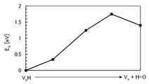
도 25는 VoH의 천이 레벨을 설명하기 위한 도면.
도 26은 표시 장치의 일 형태를 도시한 상면도.
도 27은 표시 장치의 일 형태를 도시한 단면도.
도 28은 표시 장치의 일 형태를 도시한 단면도.
도 29는 발광 장치의 화소부의 구성에 대하여 설명하기 위한 도면.
도 30은 반도체 장치의 단면도.
도 31은 표시 장치의 상면도 및 회로도.
도 32는 표시 장치의 회로도 및 타이밍 차트.
도 33은 표시 장치의 회로도 및 타이밍 차트.
도 34는 표시 장치의 회로도 및 타이밍 차트.
도 35는 표시 장치의 회로도 및 타이밍 차트.
도 36은 표시 모듈을 설명하기 위한 도면.
도 37은 전자 기기를 설명하기 위한 도면.
도 38은 실시예에서의 단면 TEM 이미지.
도 39는 저항률의 온도 의존성을 설명하기 위한 그래프.
도 40은 CAAC-OS의 성막 모델을 설명하기 위한 모식도, 펠릿 및 CAAC-OS의 단면도.
도 41은 nc-OS의 성막 모델 및 펠릿을 설명하기 위한 모식도.
도 42는 펠릿을 설명하기 위한 도면.
도 43은 피형성면에서 펠릿에 가해지는 힘을 설명하기 위한 도면.
도 44는 피형성면에서의 펠릿의 움직임을 설명하기 위한 도면.
도 45는 InGaZnO4의 결정을 설명하기 위한 도면.
도 46은 원자가 충돌되기 전의 InGaZnO4의 구조 등을 설명하기 위한 도면.
도 47은 원자가 충돌된 후의 InGaZnO4의 구조 등을 설명하기 위한 도면.
도 48은 원자가 충돌된 후의 원자의 궤적을 설명하기 위한 도면.
도 49는 CAAC-OS 및 타깃의 단면 HAADF-STEM 이미지.Figure 1 is a top view and a cross-sectional view showing one form of a semiconductor device.
Fig. 2 is a cross-sectional view showing one form of a semiconductor device.
Figure 3 is a cross-sectional view illustrating one form of a semiconductor device.
Fig. 4 is a cross-sectional view showing one form of a semiconductor device.
Figure 5 is a top view and a cross-sectional view showing one form of a semiconductor device.
Fig. 6 is a cross-sectional view showing one form of a semiconductor device.
Fig. 7 is a cross-sectional view illustrating one form of a semiconductor device.
Fig. 8 is a cross-sectional view showing one form of a semiconductor device.
Fig. 9 is a cross-sectional view showing one form of a semiconductor device.
Fig. 10 is a cross-sectional view showing one form of a semiconductor device.
Fig. 11 is a cross-sectional view showing one form of a semiconductor device, and a drawing showing one form of a band structure.
Fig. 12 is a cross-sectional view illustrating an example of a semiconductor device manufacturing process.
Fig. 13 is a cross-sectional view illustrating an example of a semiconductor device manufacturing process.
Fig. 14 is a cross-sectional view illustrating an example of a semiconductor device manufacturing process.
Fig. 15 is a cross-sectional view illustrating an example of a semiconductor device manufacturing process.
Fig. 16 is a cross-sectional view illustrating an example of a semiconductor device manufacturing process.
Figure 17 shows a cross-sectional TEM image and a local Fourier transform image of an oxide semiconductor.
FIG. 18 is a drawing showing a nanobeam electron diffraction pattern of an oxide semiconductor film, and a drawing showing an example of a transmission electron diffraction measuring device.
Figure 19 is a graph showing an example of structural analysis by transmission electron diffraction measurement and a planar TEM image.
Figure 20 is a drawing for explaining the computational model.
Figure 21 is a drawing for explaining the initial state and the final state.
Figure 22 is a graph explaining the activation barrier.
Figure 23 is a drawing for explaining the initial state and the final state.
Figure 24 is a graph explaining the activation barrier.
Figure 25 is a drawing for explaining the transition level of Vo H.
Fig. 26 is a top view showing one form of the display device.
Fig. 27 is a cross-sectional view showing one form of a display device.
Fig. 28 is a cross-sectional view showing one form of a display device.
Fig. 29 is a drawing for explaining the configuration of a pixel portion of a light-emitting device.
Fig. 30 is a cross-sectional view of a semiconductor device.
Figure 31 is a top view and circuit diagram of the display device.
Figure 32 is a circuit diagram and timing chart of the display device.
Figure 33 is a circuit diagram and timing chart of the display device.
Figure 34 is a circuit diagram and timing chart of the display device.
Figure 35 is a circuit diagram and timing chart of the display device.
Figure 36 is a drawing for explaining the display module.
Figure 37 is a drawing for explaining an electronic device.
Figure 38 is a cross-sectional TEM image in an embodiment.
Figure 39 is a graph explaining the temperature dependence of resistivity.
Figure 40 is a schematic diagram illustrating the deposition model of CAAC-OS, a cross-sectional view of a pellet and CAAC-OS.
Figure 41 is a schematic diagram explaining the deposition model and pellet of nc-OS.
Figure 42 is a drawing for explaining a pellet.
Figure 43 is a drawing for explaining the force applied to the pellet in the forming surface.
Figure 44 is a drawing for explaining the movement of pellets on the forming surface.
Figure 45 is a drawing for explaining the crystal of InGaZnO4 .
Figure 46 is a drawing for explaining the structure of InGaZnO4 before the atoms collide.
Figure 47 is a drawing for explaining the structure of InGaZnO4 after atomic collision.
Figure 48 is a drawing to explain the trajectory of atoms after the atoms collide.
Figure 49 is a cross-sectional HAADF-STEM image of CAAC-OS and target.
이하에서는 실시형태에 대하여 도면을 참조하여 자세히 설명한다. 다만, 실시형태는 많은 상이한 형태로 실시할 수 있고, 취지 및 그 범위에서 벗어남이 없이 그 형태 및 자세한 사항을 다양하게 변경할 수 있다는 것은 당업자라면 쉽게 이해할 수 있다. 따라서, 본 발명은 이하에 기재되는 실시형태의 내용에 한정하여 해석되는 것이 아니다.Hereinafter, embodiments will be described in detail with reference to the drawings. However, it will be readily understood by those skilled in the art that the embodiments can be implemented in many different forms, and that the forms and details can be variously changed without departing from the spirit and scope thereof. Accordingly, the present invention should not be interpreted as being limited to the contents of the embodiments described below.
또한, 도면에서, 크기, 막 두께, 또는 영역은 명료화를 위하여 과장되어 있는 경우가 있다. 따라서, 반드시 그 스케일에 한정되지 않는다. 또한, 도면은 이상적인 예를 모식적으로 도시한 것이고 도면에 도시된 형상 또는 값 등에 한정되지 않는다.In addition, in the drawings, the size, film thickness, or area may be exaggerated for clarity. Therefore, it is not necessarily limited to that scale. In addition, the drawings schematically depict ideal examples and are not limited to the shapes or values depicted in the drawings.
또한, 본 명세서에서 "제 1", "제 2", "제 3" 등의 서수사는 구성 요소의 혼동을 피하기 위하여 붙이는 것이며, 수적으로 한정되는 것이 아니라고 부기한다.In addition, it is noted that ordinal numbers such as “first,” “second,” and “third” in this specification are added to avoid confusion among components and are not numerically limited.
또한, 본 명세서에서, "위에", "아래에" 등의 배치를 나타내는 어구는, 구성끼리의 위치 관계를, 도면을 참조하여 설명하기 위하여 편의상 사용한다. 또한, 구성끼리의 위치 관계는, 각 구성을 묘사하는 방향에 따라서 적절히 변화하는 것이다. 그러므로, 명세서에서 설명한 어구에 한정되지 않고, 상황에 따라서 적절히 바꿔 말할 수 있다.In addition, in this specification, phrases indicating arrangement such as "above" and "below" are used for convenience in explaining the positional relationship between components with reference to drawings. In addition, the positional relationship between components changes appropriately depending on the direction in which each component is described. Therefore, it is not limited to the phrases explained in the specification, and can be appropriately changed depending on the situation.
또한, 본 명세서 등에서, 트랜지스터란, 게이트와, 드레인과, 소스를 포함하는 적어도 3개의 단자를 갖는 소자를 가리킨다. 그리고, 드레인(드레인 단자, 드레인 영역, 또는 드레인 전극)과 소스(소스 단자, 소스 영역, 또는 소스 전극) 사이에 채널 영역을 가지고, 드레인과 채널 영역과 소스를 통하여 전류를 흘릴 수 있는 것이다. 또한, 본 명세서 등에서, 채널 영역이란 전류가 주로 흐르는 영역을 가리킨다.In addition, in this specification and the like, a transistor refers to a device having at least three terminals including a gate, a drain, and a source. And, it has a channel region between the drain (drain terminal, drain region, or drain electrode) and the source (source terminal, source region, or source electrode), and can flow current through the drain, the channel region, and the source. In addition, in this specification and the like, a channel region refers to a region through which current mainly flows.
또한, 소스나 드레인의 기능은 상이한 극성을 갖는 트랜지스터가 채용되거나 회로 동작에서 전류의 방향이 바뀌는 경우 등에는 서로 바뀌는 경우가 있다. 따라서, 본 명세서 등에서는, 소스나 드레인이라는 용어는, 서로 바꿔서 사용할 수 있다.In addition, the functions of the source and drain may be interchanged when transistors with different polarities are used or the direction of current is changed in circuit operation. Therefore, in this specification and elsewhere, the terms source and drain may be used interchangeably.
또한, 본 명세서 등에서, "전기적으로 접속"에는, "어떠한 전기적 작용을 갖는 것"을 통하여 접속되어 있는 경우가 포함된다. 여기서, "어떠한 전기적 작용을 갖는 것"은 접속 대상간에서 전기 신호의 수수(授受)를 가능하게 하는 것이면 특별한 제한을 받지 않는다. 예를 들어, "어떠한 전기적 작용을 갖는 것"에는 전극이나 배선을 비롯하여 트랜지스터 등의 스위칭 소자, 저항 소자, 인덕터, 커패시터, 기타 각종 기능을 갖는 소자 등이 포함된다.In addition, in this specification and the like, "electrically connected" includes a case where it is connected through "something having some electrical action." Here, "something having some electrical action" is not particularly limited as long as it enables transmission and reception of an electric signal between connection objects. For example, "something having some electrical action" includes electrodes or wiring, as well as switching elements such as transistors, resistor elements, inductors, capacitors, and other elements having various functions.
(실시형태 1)(Embodiment 1)
본 실시형태에서는 트랜지스터와 용량 소자를 동일 기판 위에 구비하는 반도체 장치, 및 상기 반도체 장치의 제작 방법의 일례에 대하여 도 1~도 16을 사용하여 설명한다.In this embodiment, an example of a semiconductor device having a transistor and a capacitor on the same substrate and a method for manufacturing the semiconductor device are described using FIGS. 1 to 16.
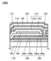
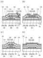
<반도체 장치의 구성 1><
도 1에 트랜지스터와 용량 소자를 동일 기판 위에 구비하는 반도체 장치의 일례를 도시하였다. 또한, 트랜지스터는 톱 게이트 구조다.Fig. 1 illustrates an example of a semiconductor device having a transistor and a capacitor on the same substrate. In addition, the transistor has a top gate structure.
도 1의 (A)는 반도체 장치가 갖는 트랜지스터(100)의 상면도이고, 도 1의 (B)는 반도체 장치가 갖는 용량 소자(150)의 상면도이고, 도 1의 (C)는 도 1의 (A)를 일점 쇄선 X1-X2를 따라 자른 단면도이고, 도 1의 (D)는 도 1의 (B)를 일점 쇄선 X3-X4를 따라 자른 단면도다. 또한, 도 1의 (A) 및 (B)에서는 명료화를 위하여 기판(102), 절연막(104), 절연막(108), 절연막(118), 절연막(120) 등을 생략하였다. 또한, 트랜지스터 및 용량 소자의 상면도에서는 이후의 도면에서도 도 1의 (A) 및 (B)와 마찬가지로 구성 요소의 일부를 생략하는 경우가 있다. 또한, 일점 쇄선 X1-X2 방향을 채널 길이 방향, 일점 쇄선 Y1-Y2 방향을 채널 폭 방향으로 부르는 경우가 있다.Fig. 1(A) is a top view of a transistor (100) included in a semiconductor device, Fig. 1(B) is a top view of a capacitor (150) included in a semiconductor device, Fig. 1(C) is a cross-sectional view taken along dashed-dotted line X1-X2 in Fig. 1(A), and Fig. 1(D) is a cross-sectional view taken along dashed-dotted line X3-X4 in Fig. 1(B). In addition, in Figs. 1(A) and (B), the substrate (102), the insulating film (104), the insulating film (108), the insulating film (118), the insulating film (120), etc. are omitted for clarity. In addition, in the top views of the transistor and the capacitor, some of the components may be omitted in subsequent drawings as in Figs. 1(A) and (B). In addition, the dashed-dotted line X1-X2 direction may be called the channel length direction, and the dashed-dotted line Y1-Y2 direction may be called the channel width direction.
도 1의 (A) 및 (C)에 도시된 트랜지스터(100)는 기판(102) 위에 형성된 절연막(108)과, 절연막(108) 위의 산화물 반도체막(110)과, 산화물 반도체막(110) 위의 절연막(112)과, 절연막(112)을 개재(介在)하여 산화물 반도체막(110)과 중첩되는 도전막(114)과, 산화물 반도체막(110), 절연막(112), 및 도전막(114)을 덮는 절연막(118)과, 절연막(118) 위의 절연막(120)과, 절연막(118) 및 절연막(120)에 제공되는 개구부(140a)를 통하여 산화물 반도체막(110)에 접속되는 도전막(122)과, 절연막(118) 및 절연막(120)에 제공되는 개구부(140b)를 통하여 산화물 반도체막(110)에 접속되는 도전막(124)을 포함한다. 또한, 트랜지스터(100) 위에는 절연막(120), 도전막(122), 및 도전막(124)을 덮는 절연막(128)을 제공하여도 좋다.The transistor (100) illustrated in (A) and (C) of FIG. 1 comprises an insulating film (108) formed on a substrate (102), an oxide semiconductor film (110) over the insulating film (108), an insulating film (112) over the oxide semiconductor film (110), a conductive film (114) overlapping the oxide semiconductor film (110) with the insulating film (112) interposed therebetween, an insulating film (118) covering the oxide semiconductor film (110), the insulating film (112), and the conductive film (114), an insulating film (120) over the insulating film (118), a conductive film (122) connected to the oxide semiconductor film (110) through an opening (140a) provided in the insulating film (118) and the insulating film (120), and an oxide semiconductor film (118) formed over an opening (140b) provided in the insulating film (120). It includes a conductive film (124) connected to a semiconductor film (110). In addition, an insulating film (120), a conductive film (122), and an insulating film (128) covering the conductive film (124) may be provided on the transistor (100).
또한, 도 1의 (C)에서, 절연막(108)은 절연막(108a)과, 절연막(108a) 위의 절연막(108b)으로 이루어지는 적층 구조를 갖는다. 또한, 도전막(114)은 도전막(114a)과, 도전막(114a) 위의 도전막(114b)으로 이루어지는 적층 구조를 갖는다. 또한, 도전막(122)은 도전막(122a)과, 도전막(122a) 위의 도전막(122b)으로 이루어지는 적층 구조를 갖는다. 또한, 도전막(124)은 도전막(124a)과, 도전막(124a) 위의 도전막(124b)으로 이루어지는 적층 구조를 갖는다.In addition, in (C) of Fig. 1, the insulating film (108) has a laminated structure composed of an insulating film (108a) and an insulating film (108b) over the insulating film (108a). In addition, the conductive film (114) has a laminated structure composed of a conductive film (114a) and a conductive film (114b) over the conductive film (114a). In addition, the conductive film (122) has a laminated structure composed of a conductive film (122a) and a conductive film (122b) over the conductive film (122a). In addition, the conductive film (124) has a laminated structure composed of a conductive film (124a) and a conductive film (124b) over the conductive film (124a).
트랜지스터(100)에서, 도전막(114)은 게이트 전극(톱 게이트 전극이라고도 함)으로서 기능하고, 도전막(122)은 소스 전극 및 드레인 전극 중 한쪽 전극으로서 기능하고, 도전막(124)은 소스 전극 및 드레인 전극 중 다른 쪽 전극으로서 기능한다. 또한, 트랜지스터(100)에서, 절연막(108)은 산화물 반도체막(110)의 하지막으로서 기능하고, 절연막(112)은 게이트 절연막으로서 기능한다.In the transistor (100), the conductive film (114) functions as a gate electrode (also called a top gate electrode), the conductive film (122) functions as one of the source electrode and the drain electrode, and the conductive film (124) functions as the other of the source electrode and the drain electrode. In addition, in the transistor (100), the insulating film (108) functions as a bottom film of the oxide semiconductor film (110), and the insulating film (112) functions as a gate insulating film.
또한, 도 1의 (B) 및 (D)에 도시된 용량 소자(150)는 기판(102) 위에 형성된 절연막(108)과, 절연막(108) 위의 절연막(112)과, 절연막(112) 위의 도전막(116)과, 절연막(108), 절연막(112), 및 도전막(116)을 덮는 절연막(118)과, 절연막(118) 위의 절연막(120)과, 절연막(120)에 제공되는 개구부(140c)에서 절연막(118)을 개재하여 도전막(116)과 중첩되는 도전막(126)을 포함한다. 또한, 용량 소자(150) 위에는 절연막(120) 및 도전막(126)을 덮는 절연막(128)을 제공하여도 좋다.In addition, the capacitor element (150) illustrated in (B) and (D) of FIG. 1 includes an insulating film (108) formed on a substrate (102), an insulating film (112) over the insulating film (108), a conductive film (116) over the insulating film (112), an insulating film (118) covering the insulating film (108), the insulating film (112), and the conductive film (116), an insulating film (120) over the insulating film (118), and a conductive film (126) overlapping the conductive film (116) with the insulating film (118) interposed in an opening (140c) provided in the insulating film (120). In addition, an insulating film (128) covering the insulating film (120) and the conductive film (126) may be provided over the capacitor element (150).
또한, 도 1의 (D)에서, 절연막(108)은 절연막(108a)과, 절연막(108a) 위의 절연막(108b)으로 이루어지는 적층 구조를 갖는다. 또한, 도전막(116)은 도전막(116a)과, 도전막(116a) 위의 도전막(116b)으로 이루어지는 적층 구조를 갖는다. 또한, 도전막(126)은 도전막(126a)과, 도전막(126a) 위의 도전막(126b)으로 이루어지는 적층 구조를 갖는다.In addition, in (D) of Fig. 1, the insulating film (108) has a laminated structure composed of an insulating film (108a) and an insulating film (108b) over the insulating film (108a). In addition, the conductive film (116) has a laminated structure composed of a conductive film (116a) and a conductive film (116b) over the conductive film (116a). In addition, the conductive film (126) has a laminated structure composed of a conductive film (126a) and a conductive film (126b) over the conductive film (126a).
또한, 용량 소자(150)는 한 쌍의 전극 사이에 유전체를 협지하는 구조를 갖는다. 더 자세하게 말하면 한 쌍의 전극 중 한쪽이 도전막(116)이고, 한 쌍의 전극 중 다른 쪽이 도전막(126)이고, 도전막(116)과 도전막(126) 사이의 절연막(118)이 유전체로서 기능한다.In addition, the capacitor element (150) has a structure that sandwiches a dielectric between a pair of electrodes. More specifically, one of the pair of electrodes is a conductive film (116), the other of the pair of electrodes is a conductive film (126), and an insulating film (118) between the conductive films (116) and the conductive films (126) functions as a dielectric.
또한, 트랜지스터(100)의 게이트 전극으로서 기능하는 도전막(114)과, 용량 소자(150)의 한 쌍의 전극 중 한쪽으로서 기능하는 도전막(116)은 동일 공정에서 형성되고 적어도 일부가 동일 표면 위에 형성된다. 또한, 트랜지스터(100)의 소스 전극 및 드레인 전극으로서 기능하는 도전막(122) 및 도전막(124)과, 용량 소자(150)의 한 쌍의 전극 중 다른 쪽으로서 기능하는 도전막(126)은 동일 공정에서 형성되고 적어도 일부가 동일 표면 위에 형성된다.In addition, the conductive film (114) functioning as the gate electrode of the transistor (100) and the conductive film (116) functioning as one of the pair of electrodes of the capacitor element (150) are formed in the same process and at least part of them are formed on the same surface. In addition, the conductive film (122) and the conductive film (124) functioning as the source electrode and drain electrode of the transistor (100) and the conductive film (126) functioning as the other of the pair of electrodes of the capacitor element (150) are formed in the same process and at least part of them are formed on the same surface.
이와 같이, 트랜지스터(100) 및 용량 소자(150)의 각 전극으로서 기능하는 도전막을 동일 공정에서 형성함으로써 제조 비용을 절감할 수 있다.In this way, the manufacturing cost can be reduced by forming the conductive film that functions as each electrode of the transistor (100) and the capacitor element (150) in the same process.
또한, 용량 소자(150)에서, 절연막(120)은 개구부(140c)를 갖는다. 따라서 절연막(118)과 절연막(120)이 적층되어 이루어지는 절연막에서 절연막(118)만을 유전체로서 기능시킨다. 이와 같은 구성으로 함으로써 용량 소자(150)의 용량 값을 크게 할 수 있다. 따라서 표시 장치의 용량 값을 크게 할 수 있다.In addition, in the capacitor element (150), the insulating film (120) has an opening (140c). Therefore, in the insulating film formed by laminating the insulating film (118) and the insulating film (120), only the insulating film (118) functions as a dielectric. By forming the film with this configuration, the capacitance value of the capacitor element (150) can be increased. Therefore, the capacitance value of the display device can be increased.
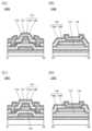
다음에 도 1의 (A)에 도시된 트랜지스터(100)를 일점 쇄선 Y1-Y2 방향(채널 폭 방향)을 따라 자른 단면도를 도 2에 도시하였다.Next, a cross-sectional view of the transistor (100) shown in (A) of Fig. 1 cut along the dashed-dotted line Y1-Y2 direction (channel width direction) is shown in Fig. 2.
도 2에 도시된 바와 같이, 채널 폭 방향에서, 도전막(114a)의 단부는 도전막(114b)의 단부보다 외측에 위치한다. 또한, 절연막(112)의 단부는 도전막(114a)의 단부보다 외측에 위치한다. 또한, 절연막(108b)은 절연막(112)이 중첩되지 않는 영역에 오목부를 갖는다. 이와 같은 구조로 함으로써 절연막(118), 절연막(120), 및 절연막(128)의 피복성을 향상시킬 수 있다.As shown in Fig. 2, in the channel width direction, the end of the conductive film (114a) is located outside the end of the conductive film (114b). In addition, the end of the insulating film (112) is located outside the end of the conductive film (114a). In addition, the insulating film (108b) has a concave portion in a region where the insulating films (112) do not overlap. By forming a structure like this, the covering properties of the insulating films (118), the insulating films (120), and the insulating films (128) can be improved.
다음에 트랜지스터(100)가 갖는 산화물 반도체막(110)의 자세한 사항에 대하여 이하에서 설명한다.Next, the details of the oxide semiconductor film (110) of the transistor (100) are described below.
트랜지스터(100)의 산화물 반도체막(110)에서, 도전막(114)과 중첩되지 않는 영역에는 산소 빈자리(Oxygen Vacancy)를 형성하는 원소를 갖는다. 이하, 산소 빈자리를 형성하는 원소를 불순물 원소로 하여 설명한다. 불순물 원소의 대표적인 예로서는 수소, 붕소, 탄소, 질소, 불소, 알루미늄, 실리콘, 인, 염소, 희가스 원소 등이 있다. 희가스 원소의 대표적인 예로서는, 헬륨, 네온, 아르곤, 크립톤, 및 제논이 있다.In the oxide semiconductor film (110) of the transistor (100), an element forming an oxygen vacancy is included in a region that does not overlap with the conductive film (114). Hereinafter, the element forming the oxygen vacancy will be described as an impurity element. Representative examples of the impurity element include hydrogen, boron, carbon, nitrogen, fluorine, aluminum, silicon, phosphorus, chlorine, and noble gas elements. Representative examples of the noble gas element include helium, neon, argon, krypton, and xenon.
불순물 원소가 산화물 반도체막에 첨가되면 산화물 반도체막 중의 금속 원소 및 산소의 결합이 절단되어 산소 빈자리가 형성된다. 또는, 불순물 원소가 산화물 반도체막에 첨가되면 산화물 반도체막 중의 금속 원소와 결합된 산소가 불순물 원소와 결합되어 금속 원소로부터 산소가 이탈되어 산소 빈자리가 형성된다. 이로써, 산화물 반도체막에서 캐리어 밀도가 증가되어 도전성이 높게 된다.When an impurity element is added to an oxide semiconductor film, the bond between the metal element and oxygen in the oxide semiconductor film is broken, forming an oxygen vacancy. Alternatively, when an impurity element is added to an oxide semiconductor film, the oxygen bonded to the metal element in the oxide semiconductor film is bonded to the impurity element, and oxygen is released from the metal element, forming an oxygen vacancy. As a result, the carrier density in the oxide semiconductor film increases, thereby enhancing conductivity.
불순물 원소를 첨가함으로써 산소 빈자리가 형성된 산화물 반도체에 수소를 첨가하면, 산소 빈자리가 형성된 곳에 수소가 들어가 전도대 근방에 도너 준위가 형성된다. 결과적으로, 산화물 반도체는 도전성이 높게 되어 도전체화된다. 도전체화된 산화물 반도체를 산화물 도전체라고 할 수 있다. 일반적으로, 산화물 반도체는 에너지 갭이 크기 때문에 가시광에 대한 투광성을 갖는다. 한편, 산화물 도전체는 전도대 근방에 도너 준위를 갖는 산화물 반도체다. 따라서, 이 도너 준위로 인한 흡수의 영향은 작고, 가시광에 대한 투광성이 산화물 반도체와 같은 정도다.When hydrogen is added to an oxide semiconductor in which oxygen vacancies are formed by adding impurity elements, hydrogen enters the oxygen vacancies formed, and a donor level is formed near the conduction band. As a result, the oxide semiconductor becomes highly conductive and becomes a conductor. An oxide semiconductor that becomes conductive can be called an oxide conductor. In general, an oxide semiconductor has a large energy gap, so it has transparency to visible light. On the other hand, an oxide conductor is an oxide semiconductor that has a donor level near the conduction band. Therefore, the effect of absorption due to this donor level is small, and the transparency to visible light is similar to that of an oxide semiconductor.
여기서 산화물 도전체로 형성되는 막(이하, 산화물 도전체막이라고 함)에서의 저항률의 온도 의존성에 대하여 도 39를 사용하여 설명한다.The temperature dependence of the resistivity in a film formed of an oxide conductor (hereinafter referred to as an oxide conductor film) is explained using Figure 39.
여기서는 산화물 도전체막을 갖는 시료를 제작하였다. 산화물 도전체막으로서는 산화물 반도체막이 질화 실리콘막에 접촉됨으로써 형성된 산화물 도전체막(OC_SiNx), 도핑 장치에서 산화물 반도체막에 아르곤이 첨가되고 질화 실리콘막과 접촉됨으로써 형성된 산화물 도전체막(OC_Ar dope+SiNx), 또는 플라즈마 처리 장치에서 산화물 반도체막이 아르곤 플라즈마에 노출되며 질화 실리콘막과 접촉함으로써 형성된 산화물 도전체막(OC_Ar plasma+SiNx)을 제작하였다. 또한, 질화 실리콘막은 수소를 함유한다.Here, a sample having an oxide conductor film was fabricated. As the oxide conductor film, an oxide conductor film (OC_SiNx ) formed by bringing an oxide semiconductor film into contact with a silicon nitride film, an oxide conductor film formed by adding argon to an oxide semiconductor film in a doping device and bringing it into contact with a silicon nitride film (OC_Ar dope+SiNx ), or an oxide conductor film formed by exposing an oxide semiconductor film to argon plasma in a plasma treatment device and bringing it into contact with a silicon nitride film (OC_Ar plasma+SiNx ) were fabricated. In addition, the silicon nitride film contains hydrogen.
산화물 도전체막(OC_SiNx)을 포함하는 시료의 제작 방법을 이하에 기재한다. 유리 기판 위에 두께 400nm의 산화질화 실리콘막을 플라즈마 CVD법에 의하여 형성한 후, 산소 플라즈마에 노출하여 산소 이온을 산화질화 실리콘막에 첨가함으로써, 가열에 의하여 산소를 방출하는 산화질화 실리콘막을 형성하였다. 다음에 가열에 의하여 산소를 방출하는 산화질화 실리콘막 위에 원자수비가 In:Ga:Zn=1:1:1.2인 스퍼터링 타깃을 사용한 스퍼터링법에 의하여 두께 100nm의 In-Ga-Zn산화물막을 형성하고 450℃의 질소 분위기하에서 가열 처리를 수행한 후, 450℃의 질소 및 산소의 혼합 가스 분위기하에서 가열 처리를 수행하였다. 다음에 플라즈마 CVD법에 의하여 두께 100nm의 질화 실리콘막을 형성하였다. 다음에 350℃의 질소 및 산소의 혼합 가스 분위기하에서 가열 처리를 수행하였다.Hereinafter, a method for fabricating a sample including an oxide conductive film (OC_SiNx ) is described. A silicon oxynitride film having a thickness of 400 nm was formed on a glass substrate by a plasma CVD method, and then exposed to oxygen plasma to add oxygen ions to the silicon oxynitride film, thereby forming a silicon oxynitride film that releases oxygen when heated. Next, an In-Ga-Zn oxide film having a thickness of 100 nm was formed on the silicon oxynitride film that releases oxygen when heated by a sputtering method using a sputtering target having an atomic ratio of In:Ga:Zn = 1:1:1.2, and heat treatment was performed in a nitrogen atmosphere at 450°C, and then heat treatment was performed in a mixed gas atmosphere of nitrogen and oxygen at 450°C. Next, a silicon nitride film having a thickness of 100 nm was formed by a plasma CVD method. Next, heat treatment was performed in a mixed gas atmosphere of nitrogen and oxygen at 350°C.
산화물 도전체막(OC_Ar dope+SiNx)을 포함하는 시료의 제작 방법을 이하에 기재한다. 유리 기판 위에 두께 400nm의 산화질화 실리콘막을 플라즈마 CVD법에 의하여 형성한 후, 산소 플라즈마에 노출하여 산소 이온을 산화질화 실리콘막에 첨가함으로써, 가열에 의하여 산소를 방출하는 산화질화 실리콘막을 형성하였다. 다음에 가열에 의하여 산소를 방출하는 산화질화 실리콘막 위에 원자수비가 In:Ga:Zn=1:1:1.2인 스퍼터링 타깃을 사용한 스퍼터링법에 의하여 두께 100nm의 In-Ga-Zn산화물막을 형성하고 450℃의 질소 분위기하에서 가열 처리를 수행한 후, 450℃의 질소 및 산소의 혼합 가스 분위기하에서 가열 처리를 수행하였다. 다음에 도핑 장치를 사용하여 In-Ga-Zn산화물막에 가속 전압을 10kV로 하여 도즈량이 5×10¹⁴ions/cm2의 아르곤을 첨가하여 In-Ga-Zn산화물막에 산소 빈자리를 형성하였다. 다음에 플라즈마 CVD법에 의하여 두께 100nm의 질화 실리콘막을 형성하였다. 다음에 350℃의 질소 및 산소의 혼합 가스 분위기하에서 가열 처리를 수행하였다.A method for fabricating a sample including an oxide conductive film (OC_Ar dope+SiNx ) is described below. A silicon oxynitride film having a thickness of 400 nm was formed on a glass substrate by a plasma CVD method, and then exposed to oxygen plasma to add oxygen ions to the silicon oxynitride film, thereby forming a silicon oxynitride film that releases oxygen when heated. Next, an In-Ga-Zn oxide film having a thickness of 100 nm was formed on the silicon oxynitride film that releases oxygen when heated by a sputtering method using a sputtering target having an atomic ratio of In:Ga:Zn = 1:1:1.2, and heat treatment was performed in a nitrogen atmosphere at 450°C, and then heat treatment was performed in a mixed gas atmosphere of nitrogen and oxygen at 450°C. Next, using a doping device, argon was added at a dose of 5×10¹⁴ ions/cm2 at an acceleration voltage of 10 kV to form oxygen vacancies in the In-Ga-Zn oxide film. Then, a silicon nitride film with a thickness of 100 nm was formed by the plasma CVD method. Then, heat treatment was performed in a mixed gas atmosphere of nitrogen and oxygen at 350°C.
산화물 도전체막(OC_Ar plasma+SiNx)을 포함하는 시료의 제작 방법을 이하에 기재한다. 유리 기판 위에 두께 400nm의 산화질화 실리콘막을 플라즈마 CVD법에 의하여 형성한 후, 산소 플라즈마에 노출함으로써, 가열에 의하여 산소를 방출하는 산화질화 실리콘막을 형성하였다. 다음에 가열에 의하여 산소를 방출하는 산화질화 실리콘막 위에 원자수비가 In:Ga:Zn=1:1:1.2인 스퍼터링 타깃을 사용한 스퍼터링법에 의하여 두께 100nm의 In-Ga-Zn산화물막을 형성하고 450℃의 질소 분위기하에서 가열 처리를 수행한 후, 450℃의 질소 및 산소의 혼합 가스 분위기하에서 가열 처리를 수행하였다. 다음에 플라즈마 처리 장치에서 아르곤 플라즈마를 발생시키고 가속시킨 아르곤 이온을 In-Ga-Zn산화물막에 충돌시킴으로써 산소 빈자리를 형성하였다. 다음에 플라즈마 CVD법에 의하여 두께 100nm의 질화 실리콘막을 형성하였다. 다음에 350℃의 질소 및 산소의 혼합 가스 분위기하에서 가열 처리를 수행하였다.Hereinafter, a method for fabricating a sample including an oxide conductive film (OC_Ar plasma+SiNx ) is described. A silicon oxynitride film having a thickness of 400 nm was formed on a glass substrate by a plasma CVD method, and then exposed to oxygen plasma to form a silicon oxynitride film that releases oxygen when heated. Next, an In-Ga-Zn oxide film having a thickness of 100 nm was formed on the silicon oxynitride film that releases oxygen when heated by a sputtering method using a sputtering target having an atomic ratio of In:Ga:Zn = 1:1:1.2, and heat treatment was performed in a nitrogen atmosphere at 450°C, and then heat treatment was performed in a mixed gas atmosphere of nitrogen and oxygen at 450°C. Next, argon plasma was generated in a plasma processing device, and accelerated argon ions were collided with the In-Ga-Zn oxide film to form oxygen vacancies. Next, a silicon nitride film having a thickness of 100 nm was formed by a plasma CVD method. Next, heat treatment was performed in a mixed gas atmosphere of nitrogen and oxygen at 350°C.
다음에 각 시료의 저항률을 측정한 결과를 도 39에 나타냈다. 여기서 저항률의 측정은 4단자의 van-der-Pauw법으로 수행하였다. 도 39에서 가로 축은 측정 온도를 나타내고, 세로 축은 저항률을 나타낸다. 또한, 산화물 도전체막(OC_SiNx)의 측정 결과를 사각표로 나타내고, 산화물 도전체막(OC_Ar dope+SiNx)의 측정 결과를 동그라미표로 나타내고, 산화물 도전체막(OC_Ar plasma+SiNx)의 측정 결과를 삼각표로 나타낸다.Next, the results of measuring the resistivity of each sample are shown in Fig. 39. Here, the resistivity was measured by the four-terminal van-der-Pauw method. In Fig. 39, the horizontal axis represents the measurement temperature, and the vertical axis represents the resistivity. In addition, the measurement results of the oxide conductive film (OC_SiNx ) are represented by square tables, the measurement results of the oxide conductive film (OC_Ar dope+SiNx ) are represented by circle tables, and the measurement results of the oxide conductive film (OC_Ar plasma+SiNx ) are represented by triangular tables.
또한, 도시되지 않았지만 질화 실리콘막과 접촉되지 않는 산화물 반도체막은 저항률이 높기 때문에, 저항률을 측정하기 어려웠다. 따라서 산화물 도전체막은 산화물 반도체막보다 저항률이 낮은 것을 알 수 있다.In addition, it was difficult to measure the resistivity of the oxide semiconductor film that is not in contact with the silicon nitride film, which is not shown in the diagram, because it has a high resistivity. Therefore, it can be seen that the oxide conductor film has a lower resistivity than the oxide semiconductor film.
도 39를 보면 알다시피 산화물 도전체막(OC_Ar dope+SiNx) 및 산화물 도전체막(OC_Ar plasma+SiNx)이 산소 빈자리 및 수소를 함유하는 경우, 저항률의 변동이 작다. 대표적으로는 80K 이상 290K 이하에서, 저항률의 변동률은 ±20% 미만이다. 또는 150K 이상 250K 이하에서, 저항률의 변동률은 ±10% 미만이다. 즉, 산화물 도전체는 축퇴형 반도체(degenerate semiconductor)이고, 전도대단과 페르미 준위가 일치 또는 대략 일치한다고 추정된다. 그러므로 산화물 도전체막을 트랜지스터의 소스 영역 및 드레인 영역으로서 사용함으로써 산화물 도전체막과, 소스 전극 및 드레인 전극으로서 기능하는 도전막과의 접촉이 오믹 접촉이 되어 산화물 도전체막과, 소스 전극 및 드레인 전극으로서 기능하는 도전막 사이의 접촉 저항을 저감할 수 있다. 또한, 산화물 도전체의 저항률은 온도 의존성이 낮기 때문에 산화물 도전체막과, 소스 전극 및 드레인 전극으로서 기능하는 도전막과의 접촉 저항의 변동량이 적고, 신뢰성이 높은 트랜지스터를 제작할 수 있다.As can be seen from Fig. 39, when the oxide conductor film (OC_Ar dope+SiNx ) and the oxide conductor film (OC_Ar plasma+SiNx ) contain oxygen vacancies and hydrogen, the variation of resistivity is small. Typically, at 80 K or more and 290 K or less, the variation of resistivity is less than ±20%. Or, at 150 K or more and 250 K or less, the variation of resistivity is less than ±10%. That is, the oxide conductor is a degenerate semiconductor, and it is estimated that the conduction band and the Fermi level coincide or approximately coincide. Therefore, by using the oxide conductor film as the source region and the drain region of the transistor, the contact between the oxide conductor film and the conductive film functioning as the source electrode and the drain electrode becomes an ohmic contact, so that the contact resistance between the oxide conductor film and the conductive film functioning as the source electrode and the drain electrode can be reduced. In addition, since the resistivity of the oxide conductor has a low temperature dependence, the amount of variation in the contact resistance between the oxide conductor film and the conductive film functioning as the source electrode and drain electrode is small, and a highly reliable transistor can be manufactured.
여기서, 산화물 반도체막(110) 근방의 확대도를 도 3 및 도 4에 도시하였다. 또한, 도 3 및 도 4에서는 복잡하게 되는 것을 피하기 위하여 구성 요소의 일부를 생략하였다.Here, an enlarged view of the vicinity of the oxide semiconductor film (110) is shown in FIGS. 3 and 4. In addition, some of the components are omitted in FIGS. 3 and 4 to avoid complexity.
산화물 반도체막(110)의 채널 길이 방향의 단면 형상에서, 산화물 반도체막(110)의 캐리어 밀도가 증가되어 도전성이 높게 되는 영역(이하, 저저항 영역이라고 함)이 형성된다. 또한, 산화물 반도체막(110) 중에 형성되는 저저항 영역은 도 3 및 도 4에 도시된 바와 같이, 복수의 구성 요소로 이루어지고 있다. 또한, 도 3 및 도 4에서 채널 길이(L)는, 한 쌍의 저저항 영역에 끼워진 영역의 길이를 가리킨다.In the cross-sectional shape of the channel length direction of the oxide semiconductor film (110), a region (hereinafter referred to as a low-resistance region) is formed in which the carrier density of the oxide semiconductor film (110) increases and the conductivity becomes high. In addition, the low-resistance region formed in the oxide semiconductor film (110) is composed of a plurality of components, as shown in FIGS. 3 and 4. In addition, the channel length (L) in FIGS. 3 and 4 refers to the length of a region sandwiched between a pair of low-resistance regions.
도 3의 (A)에 도시된 바와 같이, 산화물 반도체막(110)은, 도전막(114)과 중첩되는 영역에 형성되는 채널 영역(110a)과, 채널 영역(110a)을 끼우며 불순물 원소를 함유하는 영역 즉, 저저항 영역(110b) 및 저저항 영역(110c)을 갖는다. 또한, 도 3의 (A)에 도시된 바와 같이, 채널 길이 방향의 단면 형상에서 채널 영역(110a)과 저저항 영역(110b)의 경계, 및 채널 영역(110a)과 저저항 영역(110c)의 경계가 절연막(112)을 개재하여 도전막(114a)의 하단부와 일치 또는 대략 일치한다. 즉, 상면 형상에서 채널 영역(110a)과 저저항 영역(110b)의 경계, 및 채널 영역(110a)과 저저항 영역(110c)의 경계가 도전막(114a)의 하단부와 일치 또는 대략 일치한다.As illustrated in (A) of FIG. 3, the oxide semiconductor film (110) has a channel region (110a) formed in a region overlapping with the conductive film (114), and a region containing an impurity element, i.e., a low-resistance region (110b) and a low-resistance region (110c), sandwiching the channel region (110a). In addition, as illustrated in (A) of FIG. 3, in the cross-sectional shape in the channel length direction, the boundary between the channel region (110a) and the low-resistance region (110b), and the boundary between the channel region (110a) and the low-resistance region (110c) coincide with or approximately coincide with the lower end of the conductive film (114a) via the insulating film (112). That is, in the top surface shape, the boundary between the channel region (110a) and the low-resistance region (110b), and the boundary between the channel region (110a) and the low-resistance region (110c) coincide with or approximately coincide with the lower portion of the conductive film (114a).
또한 도 3의 (A)에 도시된 바와 같이, 채널 길이 방향의 단면 형상에서, 도전막(114a)의 단부는 도전막(114b)의 단부보다 외측에 위치하고 도전막(114b)이 테이퍼 형상이라도 좋다. 즉, 도전막(114a) 및 도전막(114b)이 접촉되는 면과 도전막(114b)의 측면이 이루는 각도 θ1이 90° 미만, 10° 이상 85° 이하, 또는 15° 이상 85° 이하, 또는 30° 이상 85° 이하, 또는 45° 이상 85° 이하, 또는 60° 이상 85° 이하라도 좋다. 각도 θ1을 90° 미만, 10° 이상 85° 이하, 또는 15° 이상 85° 이하, 또는 30° 이상 85° 이하, 또는 45° 이상 85° 이하, 또는 60° 이상 85° 이하로 함으로써 도전막(114b)의 측면에서의 절연막(118)의 피복성을 높일 수 있다.In addition, as illustrated in (A) of FIG. 3, in the cross-sectional shape in the channel length direction, the end of the conductive film (114a) may be positioned outside the end of the conductive film (114b), and the conductive film (114b) may have a tapered shape. That is, the angle θ1 formed between the surfaces where the conductive films (114a) and (114b) come into contact and the side surface of the conductive film (114b) may be less than 90°, 10° or more and 85° or less, or 15° or more and 85° or less, or 30° or more and 85° or less, or 45° or more and 85° or less, or 60° or more and 85° or less. By setting the angle θ1 to less than 90°, 10° or more and 85° or less, or 15° or more and 85° or less, or 30° or more and 85° or less, or 45° or more and 85° or less, or 60° or more and 85° or less, the covering property of the insulating film (118) on the side surface of the conductive film (114b) can be increased.
또한, 도 3의 (A)에 도시된 바와 같이, 채널 길이 방향의 단면 형상에서, 절연막(112)의 단부가 도전막(114a) 및 도전막(114b)의 단부보다 외측에 위치하여도 좋다. 또한, 절연막(112)의 단부의 일부가 원호를 가져도 좋다. 또한, 절연막(112)이 테이퍼 형상이라도 좋다. 즉, 산화물 반도체막(110) 및 절연막(112)이 접촉되는 면과 절연막(112)의 측면이 이루는 각도 θ2가 90° 미만, 바람직하게는 30° 이상 90° 미만이라도 좋다.In addition, as shown in (A) of Fig. 3, in the cross-sectional shape in the channel length direction, the end portion of the insulating film (112) may be located outside the ends of the conductive film (114a) and the conductive film (114b). In addition, a part of the end portion of the insulating film (112) may have an arc. In addition, the insulating film (112) may have a tapered shape. That is, the angle θ2 formed by the surface where the oxide semiconductor film (110) and the insulating film (112) are in contact and the side surface of the insulating film (112) may be less than 90°, preferably 30° or more and less than 90°.
또는 도 3의 (B)에 도시된 바와 같이, 채널 길이 방향의 단면 형상에서, 저저항 영역(110b) 및 저저항 영역(110c)은 절연막(112)을 개재하여 도전막(114)과 중첩되는 영역을 갖는다. 상기 영역은 오버 랩 영역으로서 기능한다. 채널 길이 방향에서의 오버 랩 영역의 길이를 Lov로 나타낸다. Lov는 채널 길이(L)의 20% 미만, 또는 10% 미만, 또는 5% 미만, 또는 2% 미만이다.Or, as illustrated in (B) of FIG. 3, in the cross-sectional shape in the channel length direction, the low-resistance region (110b) and the low-resistance region (110c) have a region that overlaps with the conductive film (114) via the insulating film (112). The region functions as an overlap region. The length of the overlap region in the channel length direction is represented by Lov . Lov is less than 20%, or less than 10%, or less than 5%, or less than 2% of the channel length (L).
또는 도 3의 (C)에 도시된 바와 같이, 채널 길이 방향의 단면 형상에서, 채널 영역(110a)은 도전막(114a)의 하단부와 중첩되지 않는 영역을 갖는다. 상기 영역은 오프 셋 영역으로서 기능한다. 채널 길이 방향에서의 오프 셋 영역의 길이를 Loff로 나타낸다. 또한, 오프 셋 영역이 복수로 있는 경우에는 하나의 오프 셋 영역의 길이를 Loff로 한다. Loff는 채널 길이(L)에 포함된다. 또한, Loff는 채널 길이(L)의 20% 미만, 또는 10% 미만, 또는 5% 미만, 또는 2% 미만이다.Or, as illustrated in (C) of FIG. 3, in the cross-sectional shape in the channel length direction, the channel region (110a) has a region that does not overlap with the lower end of the conductive film (114a). The region functions as an offset region. The length of the offset region in the channel length direction is represented as Loff . In addition, when there are multiple offset regions, the length of one offset region is set as Loff . Loff is included in the channel length (L). In addition, Loff is less than 20% of the channel length (L), or less than 10%, or less than 5%, or less than 2%.
또는, 도 3의 (D)에 도시된 바와 같이, 채널 길이 방향의 단면 형상에서, 산화물 반도체막(110)은 채널 영역(110a)과 저저항 영역(110b) 사이에 저저항 영역(110d)을 갖고, 채널 영역(110a)과 저저항 영역(110c) 사이에 저저항 영역(110e)을 갖는다. 저저항 영역(110d) 및 저저항 영역(110e)은 저저항 영역(110b) 및 저저항 영역(110c)보다 불순물 원소의 농도가 낮고, 저항률이 높다. 여기서는 저저항 영역(110d) 및 저저항 영역(110e)은 절연막(112)과 중첩되지만 절연막(112)에 더하여 도전막(114)과 중첩되어도 좋다.Alternatively, as illustrated in (D) of FIG. 3, in the cross-sectional shape in the channel length direction, the oxide semiconductor film (110) has a low-resistance region (110d) between the channel region (110a) and the low-resistance region (110b), and has a low-resistance region (110e) between the channel region (110a) and the low-resistance region (110c). The low-resistance region (110d) and the low-resistance region (110e) have lower concentrations of impurity elements and higher resistivities than the low-resistance region (110b) and the low-resistance region (110c). Here, the low-resistance region (110d) and the low-resistance region (110e) overlap with the insulating film (112), but may overlap with the conductive film (114) in addition to the insulating film (112).
또는, 도 4의 (A)에 도시된 바와 같이, 채널 길이 방향의 단면 형상에서, 산화물 반도체막(110)은 도전막(122)과 중첩되는 영역에 영역(110f), 및 도전막(124)과 중첩되는 영역에 영역(110g)을 갖는다. 영역(110f) 및 영역(110g)에는 불순물 원소가 첨가되지 않아도 된다. 이 경우, 산화물 반도체막(110)은 도전막(122) 및 도전막(124)과 각각 접촉되는 영역(110f) 및 영역(110g)과 채널 영역(110a) 사이에 불순물 원소를 갖는 영역, 즉 저저항 영역(110b) 및 저저항 영역(110c)을 갖는다. 또한, 영역(110f) 및 영역(110g)은 각각 도전막(122) 및 도전막(124)에 전압이 인가되면 도전성을 갖기 때문에 소스 영역 및 드레인 영역으로서 기능한다.Alternatively, as illustrated in (A) of FIG. 4, in the cross-sectional shape in the channel length direction, the oxide semiconductor film (110) has a region (110f) in a region overlapping with the conductive film (122), and a region (110g) in a region overlapping with the conductive film (124). The regions (110f) and (110g) do not need to have an impurity element added. In this case, the oxide semiconductor film (110) has regions having an impurity element between the regions (110f) and (110g) in contact with the conductive film (122) and the conductive film (124), respectively, and the channel region (110a), i.e., a low-resistance region (110b) and a low-resistance region (110c). In addition, the regions (110f) and (110g) function as a source region and a drain region because they have conductivity when a voltage is applied to the conductive film (122) and the conductive film (124), respectively.
또한, 도 4의 (A)에 도시된 구조는, 도전막(122) 및 도전막(124)을 형성한 후, 도전막(114), 도전막(122), 및 도전막(124)을 마스크로 하여 절연막(120) 및 절연막(118)을 개재하여 불순물 원소를 산화물 반도체막(110)에 첨가함으로써 형성된다.In addition, the structure illustrated in (A) of FIG. 4 is formed by forming a conductive film (122) and a conductive film (124), and then adding an impurity element to the oxide semiconductor film (110) by interposing an insulating film (120) and an insulating film (118) using the conductive film (114), the conductive film (122), and the conductive film (124) as masks.
또는, 도 4의 (B)에 도시된 바와 같이, 채널 길이 방향의 단면 형상에서, 채널 영역(110a)을 끼우는 저저항 영역(110b), 저저항 영역(110c), 저저항 영역(110d), 저저항 영역(110e), 저저항 영역(110h), 및 저저항 영역(110i)을 제공하여도 좋다.Alternatively, as illustrated in (B) of FIG. 4, in the cross-sectional shape in the channel length direction, a low resistance region (110b), a low resistance region (110c), a low resistance region (110d), a low resistance region (110e), a low resistance region (110h), and a low resistance region (110i) may be provided, sandwiching the channel region (110a).
구체적으로는 도 4의 (B)에 도시된 산화물 반도체막(110)은, 채널 영역(110a)과, 채널 영역(110a)을 끼우는 저저항 영역(110h) 및 저저항 영역(110i)과, 저저항 영역(110h) 및 저저항 영역(110i)을 끼우는 저저항 영역(110d) 및 저저항 영역(110e)과, 저저항 영역(110d) 및 저저항 영역(110e)을 끼우는 저저항 영역(110b) 및 저저항 영역(110c)을 갖는다. 저저항 영역(110h) 및 저저항 영역(110i)은 도전막(114b)과 중첩되지 않는 영역의 도전막(114a)과, 절연막(112)을 개재하여 불순물 원소를 첨가함으로써 형성된다. 또한, 저저항 영역(110d) 및 저저항 영역(110e)은 도전막(114a) 및 도전막(114b)과 중첩되지 않는 영역의 절연막(112)을 개재하여 불순물 원소를 첨가함으로써 형성된다. 또한 저저항 영역(110b) 및 저저항 영역(110c)은 불순물 원소를 직접 첨가함으로써 형성된다. 따라서 저저항 영역(110h) 및 저저항 영역(110i)은 저저항 영역(110d), 저저항 영역(110e), 저저항 영역(110b), 및 저저항 영역(110c)보다 불순물 원소의 농도가 낮고, 저항률이 높다. 또한, 저저항 영역(110d) 및 저저항 영역(110e)은 저저항 영역(110b) 및 저저항 영역(110c)보다 불순물 원소의 농도가 낮고, 저항률이 높다.Specifically, the oxide semiconductor film (110) illustrated in (B) of FIG. 4 has a channel region (110a), a low-resistance region (110h) and a low-resistance region (110i) sandwiching the channel region (110a), a low-resistance region (110d) and a low-resistance region (110e) sandwiching the low-resistance region (110h) and the low-resistance region (110i), and a low-resistance region (110b) and a low-resistance region (110c) sandwiching the low-resistance region (110d) and the low-resistance region (110e). The low-resistance region (110h) and the low-resistance region (110i) are formed by adding an impurity element to the conductive film (114a) in a region that does not overlap with the conductive film (114b) and interposing an insulating film (112). In addition, the low-resistance region (110d) and the low-resistance region (110e) are formed by adding an impurity element through an insulating film (112) in a region that does not overlap with the conductive film (114a) and the conductive film (114b). In addition, the low-resistance region (110b) and the low-resistance region (110c) are formed by directly adding the impurity element. Therefore, the low-resistance region (110h) and the low-resistance region (110i) have lower concentrations of impurity elements and higher resistivities than the low-resistance region (110d), the low-resistance region (110e), the low-resistance region (110b), and the low-resistance region (110c). In addition, the low-resistance region (110d) and the low-resistance region (110e) have lower concentrations of impurity elements and higher resistivities than the low-resistance region (110b) and the low-resistance region (110c).
또한, 도 4의 (B)에서, 채널 영역(110a)은 도전막(114b)과 중첩된다. 또한, 저저항 영역(110h) 및 저저항 영역(110i)은 도전막(114b) 외측에 돌출된 도전막(114a)과 중첩된다. 또한, 저저항 영역(110d) 및 저저항 영역(110e)은 도전막(114a) 외측에 돌출된 절연막(112)과 중첩된다. 또한, 저저항 영역(110b) 및 저저항 영역(110c)은 절연막(112) 외측에 있고 절연막(118)과 중첩된다.In addition, in (B) of FIG. 4, the channel region (110a) overlaps with the conductive film (114b). In addition, the low-resistance region (110h) and the low-resistance region (110i) overlap with the conductive film (114a) protruding outside the conductive film (114b). In addition, the low-resistance region (110d) and the low-resistance region (110e) overlap with the insulating film (112) protruding outside the conductive film (114a). In addition, the low-resistance region (110b) and the low-resistance region (110c) are outside the insulating film (112) and overlap with the insulating film (118).
도 3의 (D) 및 도 4의 (B)에 도시된 바와 같이, 산화물 반도체막(110)이, 저저항 영역(110b) 및 저저항 영역(110c)보다 불순물 원소의 농도가 낮고, 저항률이 높은 저저항 영역(110d), 저저항 영역(110e), 저저항 영역(110h), 및 저저항 영역(110i)을 가짐으로써 드레인 영역의 전계 완화가 가능하다. 그러므로 드레인 영역의 전계에 기인한 트랜지스터의 문턱 전압의 변동을 저감할 수 있다.As illustrated in (D) of FIG. 3 and (B) of FIG. 4, the oxide semiconductor film (110) has a low-resistance region (110d), a low-resistance region (110e), a low-resistance region (110h), and a low-resistance region (110i) having lower concentrations of impurity elements and higher resistivity than the low-resistance region (110b) and the low-resistance region (110c), thereby enabling relaxation of the electric field in the drain region. Therefore, fluctuations in the threshold voltage of the transistor caused by the electric field in the drain region can be reduced.
또한, 도 3 및 도 4에 도시된 산화물 반도체막(110)은 절연막(112) 및 도전막(114)과 중첩되지 않는 영역의 막 두께가 절연막(112) 및 도전막(114)과 중첩되는 영역의 막 두께보다 얇은 영역을 갖는다. 상기 얇은 영역은 절연막(112) 및 도전막(114)과 중첩되는 영역의 산화물 반도체막의 막 두께보다 얇고, 상기 얇은 영역의 두께는 0.1nm 이상 5nm 이하다.In addition, the oxide semiconductor film (110) illustrated in FIGS. 3 and 4 has a region in which the film thickness of a region that does not overlap with the insulating film (112) and the conductive film (114) is thinner than the film thickness of a region that overlaps with the insulating film (112) and the conductive film (114). The thin region is thinner than the film thickness of the oxide semiconductor film in the region that overlaps with the insulating film (112) and the conductive film (114), and the thickness of the thin region is 0.1 nm or more and 5 nm or less.
또한, 산화물 반도체막(110) 중의 저저항 영역(110b) 및 저저항 영역(110c)은 소스 영역 및 드레인 영역으로서 기능한다. 또한, 저저항 영역(110b), 저저항 영역(110c), 저저항 영역(110d), 저저항 영역(110e), 저저항 영역(110h), 및 저저항 영역(110i)에는 불순물 원소가 포함된다.In addition, the low resistance region (110b) and the low resistance region (110c) in the oxide semiconductor film (110) function as a source region and a drain region. In addition, the low resistance region (110b), the low resistance region (110c), the low resistance region (110d), the low resistance region (110e), the low resistance region (110h), and the low resistance region (110i) contain impurity elements.
불순물 원소가 희가스 원소이고 산화물 반도체막(110)이 스퍼터링법으로 형성되는 경우, 채널 영역(110a), 저저항 영역(110b), 저저항 영역(110c), 저저항 영역(110d), 저저항 영역(110e), 저저항 영역(110h), 및 저저항 영역(110i)은 각각 희가스 원소를 함유한다. 또한, 채널 영역(110a)에 비하여 저저항 영역(110b) 및 저저항 영역(110c)이 희가스 원소의 농도가 높다. 또한 저저항 영역(110d) 및 저저항 영역(110e)에 비하여 저저항 영역(110b) 및 저저항 영역(110c)이 희가스 원소의 농도가 높다. 또한, 저저항 영역(110h) 및 저저항 영역(110i)에 비하여 저저항 영역(110d) 및 저저항 영역(110e)이 희가스 원소의 농도가 높다.When the impurity element is a noble gas element and the oxide semiconductor film (110) is formed by a sputtering method, the channel region (110a), the low-resistance region (110b), the low-resistance region (110c), the low-resistance region (110d), the low-resistance region (110e), the low-resistance region (110h), and the low-resistance region (110i) each contain a noble gas element. In addition, the low-resistance region (110b) and the low-resistance region (110c) have a higher concentration of the noble gas element than the channel region (110a). In addition, the low-resistance region (110b) and the low-resistance region (110c) have a higher concentration of the noble gas element than the low-resistance region (110d) and the low-resistance region (110e). Additionally, the low resistance region (110d) and low resistance region (110e) have higher concentrations of noble gas elements than the low resistance region (110h) and low resistance region (110i).
이것은 산화물 반도체막(110)이 스퍼터링법으로 형성되는 경우, 스퍼터링 가스로서 희가스를 사용하므로 산화물 반도체막(110)에 희가스가 포함되는 것, 및 저저항 영역(110b) 및 저저항 영역(110c)에서 산소 빈자리를 형성하기 위하여 의도적으로 희가스가 첨가되는 것이 원인이다. 또한, 저저항 영역(110d), 저저항 영역(110e), 저저항 영역(110h), 및 저저항 영역(110i)은, 저저항 영역(110d), 저저항 영역(110e), 저저항 영역(110h), 및 저저항 영역(110i) 위에 형성되는 막 구성 및 막 두께의 차이에 의하여, 산소 빈자리를 형성하기 위하여 첨가되는 희가스의 농도가 저저항 영역(110d), 저저항 영역(110e), 저저항 영역(110h), 및 저저항 영역(110i)에서 상이하다. 또한, 저저항 영역(110b), 저저항 영역(110c), 저저항 영역(110d), 저저항 영역(110e), 저저항 영역(110h), 및 저저항 영역(110i)에서, 채널 영역(110a)과 상이한 희가스 원소가 첨가되어도 좋다.This is because, when the oxide semiconductor film (110) is formed by a sputtering method, a noble gas is used as a sputtering gas, so the oxide semiconductor film (110) contains a noble gas, and the noble gas is intentionally added to form oxygen vacancies in the low-resistance region (110b) and the low-resistance region (110c). In addition, the low resistance region (110d), the low resistance region (110e), the low resistance region (110h), and the low resistance region (110i) have different concentrations of the noble gas added to form oxygen vacancies in the low resistance region (110d), the low resistance region (110e), the low resistance region (110h), and the low resistance region (110i) due to differences in the film configuration and film thickness formed on the low resistance region (110d), the low resistance region (110e), the low resistance region (110h), and the low resistance region (110i). In addition, a noble gas element different from that in the channel region (110a) may be added in the low resistance region (110b), the low resistance region (110c), the low resistance region (110d), the low resistance region (110e), the low resistance region (110h), and the low resistance region (110i).
또한, 불순물 원소가 붕소, 탄소, 질소, 불소, 알루미늄, 실리콘, 인, 또는 염소인 경우, 저저항 영역(110b), 저저항 영역(110c), 저저항 영역(110d), 저저항 영역(110e), 저저항 영역(110h), 및 저저항 영역(110i)은 상기 불순물 원소를 함유한다. 이로써 채널 영역(110a)에 비하여 저저항 영역(110b), 저저항 영역(110c), 저저항 영역(110d), 저저항 영역(110e), 저저항 영역(110h), 및 저저항 영역(110i)은 상술한 불순물 원소의 농도가 높다. 또한, 저저항 영역(110b), 저저항 영역(110c), 저저항 영역(110d), 저저항 영역(110e), 저저항 영역(110h), 및 저저항 영역(110i)에서, 2차 이온 질량 분석법(SIMS: Secondary Ion Mass Spectrometry)에 의하여 얻어지는 불순물 원소의 농도는 5×10¹⁸atoms/cm3 이상 1×10²²atoms/cm3 이하, 또는 1×10¹⁹atoms/cm3 이상 1×10²¹atoms/cm3 이하, 또는 5×10¹⁹atoms/cm3 이상 5×10²⁰atoms/cm3 이하로 할 수 있다.In addition, when the impurity element is boron, carbon, nitrogen, fluorine, aluminum, silicon, phosphorus, or chlorine, the low resistance region (110b), the low resistance region (110c), the low resistance region (110d), the low resistance region (110e), the low resistance region (110h), and the low resistance region (110i) contain the impurity element. Accordingly, the low resistance region (110b), the low resistance region (110c), the low resistance region (110d), the low resistance region (110e), the low resistance region (110h), and the low resistance region (110i) have a higher concentration of the impurity element than the channel region (110a). In addition, in the low resistance region (110b), the low resistance region (110c), the low resistance region (110d), the low resistance region (110e), the low resistance region (110h), and the low resistance region (110i), the concentration of impurity elements obtained by secondary ion mass spectrometry (SIMS) can be 5×10¹⁸ atoms/cm3 or more and 1×10²² atoms/cm3 or less, or 1×10¹⁹ atoms/cm3 or more and 1×10²¹ atoms/cm3 or less, or 5×10¹⁹ atoms/cm3 or more and 5×10²⁰ atoms/cm3 or less.
또한, 불순물 원소가 수소인 경우, 채널 영역(110a)에 비하여 저저항 영역(110b), 저저항 영역(110c), 저저항 영역(110d), 저저항 영역(110e), 저저항 영역(110h), 및 저저항 영역(110i)은 수소 농도가 높다. 또한, 저저항 영역(110b), 저저항 영역(110c), 저저항 영역(110d), 저저항 영역(110e), 저저항 영역(110h), 및 저저항 영역(110i)에서, 2차 이온 질량 분석법으로 얻어지는 수소 농도는 8×10¹⁹atoms/cm3 이상, 또는 1×10²⁰atoms/cm3 이상, 또는 5×10²⁰atoms/cm3 이상으로 할 수 있다.In addition, when the impurity element is hydrogen, the low resistance region (110b), the low resistance region (110c), the low resistance region (110d), the low resistance region (110e), the low resistance region (110h), and the low resistance region (110i) have a higher hydrogen concentration than the channel region (110a). In addition, in the low resistance region (110b), the low resistance region (110c), the low resistance region (110d), the low resistance region (110e), the low resistance region (110h), and the low resistance region (110i), the hydrogen concentration obtained by secondary ion mass spectrometry can be 8×10¹⁹ atoms/cm3 or more, or 1×10²⁰ atoms/cm3 or more, or 5×10²⁰ atoms/cm3 or more.
저저항 영역(110b), 저저항 영역(110c), 저저항 영역(110d), 저저항 영역(110e), 저저항 영역(110h), 및 저저항 영역(110i)은 불순물 원소를 갖기 때문에 산소 빈자리가 증가되어 캐리어 밀도가 증가된다. 이 결과, 저저항 영역(110b), 저저항 영역(110c), 저저항 영역(110d), 저저항 영역(110e), 저저항 영역(110h), 및 저저항 영역(110i)의 도전성이 높게 된다.Since the low resistance region (110b), the low resistance region (110c), the low resistance region (110d), the low resistance region (110e), the low resistance region (110h), and the low resistance region (110i) have impurity elements, oxygen vacancies increase, thereby increasing carrier density. As a result, the conductivity of the low resistance region (110b), the low resistance region (110c), the low resistance region (110d), the low resistance region (110e), the low resistance region (110h), and the low resistance region (110i) increases.
또한, 불순물 원소로서는, 수소, 붕소, 탄소, 질소, 불소, 알루미늄, 실리콘, 인, 및 염소 중 하나 이상과 희가스를 조합하여도 좋다. 이 경우, 저저항 영역(110b), 저저항 영역(110c), 저저항 영역(110d), 저저항 영역(110e), 저저항 영역(110h), 및 저저항 영역(110i)에서 희가스에 의하여 형성된 산소 빈자리와, 첨가된 수소, 붕소, 탄소, 질소, 불소, 알루미늄, 실리콘, 인, 및 염소 중 하나 이상이 상호적으로 작용되어 저저항 영역(110b), 저저항 영역(110c), 저저항 영역(110d), 저저항 영역(110e), 저저항 영역(110h), 및 저저항 영역(110i)의 도전성이 더 높게 되는 경우가 있다.In addition, as an impurity element, one or more of hydrogen, boron, carbon, nitrogen, fluorine, aluminum, silicon, phosphorus, and chlorine may be combined with a noble gas. In this case, the oxygen vacancy formed by the noble gas in the low resistance region (110b), the low resistance region (110c), the low resistance region (110d), the low resistance region (110e), the low resistance region (110h), and the low resistance region (110i) and one or more of the added hydrogen, boron, carbon, nitrogen, fluorine, aluminum, silicon, phosphorus, and chlorine may interact with each other, thereby further increasing the conductivity of the low resistance region (110b), the low resistance region (110c), the low resistance region (110d), the low resistance region (110e), the low resistance region (110h), and the low resistance region (110i).
또한, 불순물 원소가 첨가됨으로써 산소 빈자리가 형성된 산화물 반도체에 수소를 첨가하면, 산소 빈자리가 형성된 곳에 수소가 들어가 전도대 근방에 도너 준위가 형성된다. 이 결과, 산화물 도전체를 형성할 수 있다. 이로써 산화물 도전체는 투광성을 갖는다. 또한, 여기서는 도전체화된 산화물 반도체를 산화물 도전체라고 한다.In addition, when hydrogen is added to an oxide semiconductor in which oxygen vacancies are formed by adding impurity elements, hydrogen enters the oxygen vacancies formed, and a donor level is formed near the conduction band. As a result, an oxide conductor can be formed. As a result, the oxide conductor has light transmitting properties. In addition, an oxide semiconductor that has become conductive is called an oxide conductor here.
산화물 도전체는 축퇴형 반도체이고, 전도대단과 페르미 준위가 일치 또는 대략 일치한다고 추정된다. 그러므로 산화물 도전체막과, 소스 전극 및 드레인 전극으로서 기능하는 도전막과의 접촉은 오믹 접촉이 되어 산화물 도전체막과, 소스 전극 및 드레인 전극으로서 기능하는 도전막 사이의 접촉 저항을 저감할 수 있다.The oxide conductor is a degenerate semiconductor, and it is assumed that the conduction band and the Fermi level coincide or approximately coincide. Therefore, the contact between the oxide conductor film and the conductive film functioning as the source electrode and the drain electrode becomes an ohmic contact, which can reduce the contact resistance between the oxide conductor film and the conductive film functioning as the source electrode and the drain electrode.
본 실시형태에 기재된 트랜지스터(100)는 채널 영역(110a)이, 소스 영역 및 드레인 영역으로서 기능하는 저저항 영역(110b) 및 저저항 영역(110c)에 의하여 끼워진 구조를 갖는다. 따라서 트랜지스터(100)는 온 전류가 높고, 전계 효과 이동도가 높다. 또한, 트랜지스터(100)에서, 도전막(114)을 마스크로 하여 불순물 원소가 산화물 반도체막(110)에 첨가된다. 즉 자기 정합적으로 저저항 영역을 형성할 수 있다.The transistor (100) described in this embodiment has a structure in which a channel region (110a) is sandwiched by a low-resistance region (110b) and a low-resistance region (110c) that function as a source region and a drain region. Therefore, the transistor (100) has a high on-state current and a high field-effect mobility. In addition, in the transistor (100), an impurity element is added to the oxide semiconductor film (110) using a conductive film (114) as a mask. That is, a low-resistance region can be formed in a self-aligning manner.
또한, 트랜지스터(100)는, 게이트 전극으로서 기능하는 도전막(114)과, 소스 전극 및 드레인 전극으로서 각각 기능하는 도전막(122) 및 도전막(124)이 중첩되지 않는 구성을 갖는다. 따라서 도전막(114)과 도전막(122) 사이, 및 도전막(114)과 도전막(124) 사이의 기생 용량을 저감할 수 있다. 이 결과, 기판(102)으로서 대면적 기판을 사용한 경우, 도전막(114)과 도전막(122) 사이, 및 도전막(114)과 도전막(124) 사이에서의 신호 지연을 저감할 수 있다.In addition, the transistor (100) has a configuration in which the conductive film (114) functioning as a gate electrode and the conductive films (122) and (124) functioning as source electrodes and drain electrodes, respectively, do not overlap. Therefore, the parasitic capacitance between the conductive film (114) and the conductive film (122), and between the conductive film (114) and the conductive film (124), can be reduced. As a result, when a large-area substrate is used as the substrate (102), the signal delay between the conductive film (114) and the conductive film (122), and between the conductive film (114) and the conductive film (124) can be reduced.
다음에, 도 1에 도시된 반도체 장치의 기타 구성의 자세한 사항에 대하여 설명한다.Next, details of other configurations of the semiconductor device illustrated in Fig. 1 will be described.
기판(102)으로서는 다양한 기판을 사용할 수 있고, 특정한 것에 한정되지 않는다. 기판의 일례로서는 반도체 기판(예컨대 단결정 기판 또는 실리콘 기판), SOI 기판, 유리 기판, 석영 기판, 플라스틱 기판, 금속 기판, 스테인리스강 기판, 스테인리스강박이 사용된 기판, 텅스텐 기판, 텅스텐박이 사용된 기판, 가요성 기판, 접합 필름, 섬유상 재료를 포함하는 종이, 또는 기재(基材) 필름 등을 들 수 있다. 유리 기판의 일례로서는, 바륨보로실리케이트 유리, 알루미노보로실리케이트 유리, 또는 소다석회 유리 등이 있다. 가요성 기판, 접합 필름, 기재 필름 등의 일례로서는 예컨대 폴리에틸렌테레프탈레이트(PET), 폴리에틸렌나프탈레이트(PEN), 폴리에터설폰(PES)으로 대표되는 플라스틱을 들 수 있다. 또는, 일례로서 아크릴 등의 합성 수지 등을 들 수 있다. 또는 일례로서 폴리에스터, 폴리프로필렌, 폴리 불화 바이닐, 또는 폴리 염화 바이닐 등을 들 수 있다. 또는 일례로서 폴리아마이드, 폴리이미드, 아라미드, 에폭시, 무기 증착 필름, 또는 종이류 등을 들 수 있다. 특히, 반도체 기판, 단결정 기판, 또는 SOI 기판 등을 사용하여 트랜지스터 및 용량 소자를 제작함으로써, 특성, 사이즈, 또는 형상 등의 편차가 적고 전류 능력이 높으며 사이즈가 작은 트랜지스터 및 용량 소자를 제작할 수 있다. 이와 같은 트랜지스터 및 용량 소자를 사용하여 회로를 구성하면, 회로의 저소비 전력화, 또는 회로의 고집적화를 도모할 수 있다.As the substrate (102), various substrates can be used and are not limited to specific ones. Examples of the substrate include a semiconductor substrate (e.g., a single crystal substrate or a silicon substrate), an SOI substrate, a glass substrate, a quartz substrate, a plastic substrate, a metal substrate, a stainless steel substrate, a substrate using stainless steel foil, a tungsten substrate, a substrate using tungsten foil, a flexible substrate, a bonding film, paper including a fibrous material, or a substrate film. Examples of the glass substrate include barium borosilicate glass, aluminoborosilicate glass, or soda lime glass. Examples of the flexible substrate, the bonding film, the substrate film, and the like include plastics represented by polyethylene terephthalate (PET), polyethylene naphthalate (PEN), and polyether sulfone (PES). Alternatively, examples include synthetic resins such as acrylic. Or examples include polyester, polypropylene, polyvinyl fluoride, or polyvinyl chloride. Or examples include polyamide, polyimide, aramid, epoxy, inorganic deposition film, or paper. In particular, by manufacturing transistors and capacitors using a semiconductor substrate, a single crystal substrate, or an SOI substrate, it is possible to manufacture transistors and capacitors with little deviation in characteristics, size, or shape, etc., high current capability, and small size. By configuring a circuit using such transistors and capacitors, it is possible to achieve low power consumption or high integration of the circuit.
또한, 기판(102)으로서 가요성 기판을 사용하고 가요성 기판 위에 직접 트랜지스터 및 용량 소자를 형성하여도 좋다. 또는, 기판(102)과 트랜지스터 및 용량 소자 사이에 박리층을 제공하여도 좋다. 박리층은 그 위에 반도체 장치를 부분적으로 또는 완전히 완성시킨 후, 기판(102)으로부터 분리하여, 다른 기판에 전재(轉載)하는데 사용할 수 있다. 이 때, 트랜지스터 및 용량 소자는 내열성이 떨어지는 기판이나 가요성 기판에도 전재될 수 있다. 또한, 상기 박리층은, 예컨대 텅스텐막과 산화 실리콘막 등의 무기막을 적층한 구성이나, 기판 위에 폴리이미드 등의 유기 수지막이 형성된 구성 등을 가질 수 있다.In addition, a flexible substrate may be used as the substrate (102) and the transistor and the capacitor may be formed directly on the flexible substrate. Alternatively, a peeling layer may be provided between the substrate (102) and the transistor and the capacitor. The peeling layer can be used to partially or completely complete a semiconductor device thereon, and then separate it from the substrate (102) and transfer it to another substrate. At this time, the transistor and the capacitor can be transferred to a substrate with poor heat resistance or a flexible substrate. In addition, the peeling layer may have a configuration in which an inorganic film such as a tungsten film and a silicon oxide film are laminated, or a configuration in which an organic resin film such as polyimide is formed on the substrate.
트랜지스터 및 용량 소자가 전재되는 기판의 일례로서는, 상술한 트랜지스터 및 용량 소자를 형성하는 것이 가능한 기판에 더하여, 종이 기판, 셀로판 기판, 아라미드 필름 기판, 폴리이미드 필름 기판, 석재 기판, 목재 기판, 천 기판(천연 섬유(비단, 면, 삼), 합성 섬유(나일론, 폴리우레탄, 폴리에스터) 또는 재생 섬유(아세테이트, 큐프라, 레이온, 재생 폴리에스터) 등을 포함함), 피혁 기판, 또는 고무 기판 등을 들 수 있다. 이들 기판을 사용함으로써, 특성이 양호한 트랜지스터의 형성, 소비 전력이 작은 트랜지스터의 형성, 깨지기 어려운 장치의 제조, 내열성의 부여, 경량화, 또는 박형화를 도모할 수 있다.Examples of substrates on which transistors and capacitors are formed include, in addition to the substrates capable of forming the above-described transistors and capacitors, a paper substrate, a cellophane substrate, an aramid film substrate, a polyimide film substrate, a stone substrate, a wood substrate, a cloth substrate (including natural fibers (silk, cotton, hemp), synthetic fibers (nylon, polyurethane, polyester) or regenerated fibers (acetate, cupro, rayon, regenerated polyester)), a leather substrate, or a rubber substrate. By using these substrates, it is possible to form transistors having good characteristics, form transistors with low power consumption, manufacture unbreakable devices, provide heat resistance, reduce weight, or reduce thickness.
절연막(108)은 스퍼터링법, CVD법, 증착법, 펄스레이저퇴적(PLD)법, 인쇄법, 도포법 등을 적절히 사용하여 형성할 수 있다. 또한, 절연막(108)은 예컨대 산화물 절연막 또는 질화물 절연막을 단층 또는 적층으로 형성할 수 있다. 또한, 절연막(108)과 산화물 반도체막(110)의 계면 특성을 향상시키기 위하여, 절연막(108) 중의, 적어도 산화물 반도체막(110)과 접촉되는 영역은 산화물 절연막으로 형성되는 것이 바람직하다. 또한, 가열에 의하여 산소를 방출하는 산화물 절연막을 절연막(108)으로서 사용함으로써 가열 처리에 의하여, 절연막(108)에 포함되는 산소를 산화물 반도체막(110)으로 이동시킬 수 있다.The insulating film (108) can be formed appropriately by using a sputtering method, a CVD method, a deposition method, a pulsed laser deposition (PLD) method, a printing method, a coating method, or the like. In addition, the insulating film (108) can be formed as a single layer or a laminated layer of, for example, an oxide insulating film or a nitride insulating film. In addition, in order to improve the interface characteristics between the insulating film (108) and the oxide semiconductor film (110), it is preferable that at least a region of the insulating film (108) that comes into contact with the oxide semiconductor film (110) is formed as an oxide insulating film. In addition, by using an oxide insulating film that releases oxygen by heating as the insulating film (108), oxygen contained in the insulating film (108) can be moved to the oxide semiconductor film (110) by heat treatment.
절연막(108)의 두께는 50nm 이상 또는 100nm 이상 3000nm 이하, 또는 200nm 이상 1000nm 이하로 할 수 있다. 절연막(108)을 두껍게 함으로써 절연막(108)의 산소 방출량을 증가시킬 수 있음과 함께, 절연막(108)과 산화물 반도체막(110)의 계면에서의 계면 준위 및 산화물 반도체막(110)의 채널 영역(110a)에 포함되는 산소 빈자리를 저감할 수 있다.The thickness of the insulating film (108) can be 50 nm or more, or 100 nm or more and 3000 nm or less, or 200 nm or more and 1000 nm or less. By thickening the insulating film (108), the amount of oxygen released from the insulating film (108) can be increased, and the interface state at the interface between the insulating film (108) and the oxide semiconductor film (110) and the oxygen vacancies included in the channel region (110a) of the oxide semiconductor film (110) can be reduced.
절연막(108)으로서 예컨대 산화 실리콘, 산화질화 실리콘, 질화산화 실리콘, 질화 실리콘, 산화 알루미늄, 산화 하프늄, 산화 갈륨, 또는 Ga-Zn산화물 등을 사용하여 단층 또는 적층으로 형성하면 좋다. 본 실시형태에서는 절연막(108a)으로서 질화 실리콘막을 사용하고 절연막(108b)으로서 산화질화 실리콘막을 사용한다.As the insulating film (108), it is preferable to form a single layer or a laminate using, for example, silicon oxide, silicon oxynitride, silicon nitride oxide, silicon nitride, aluminum oxide, hafnium oxide, gallium oxide, or Ga-Zn oxide. In the present embodiment, a silicon nitride film is used as the insulating film (108a), and a silicon oxynitride film is used as the insulating film (108b).
산화물 반도체막(110)은 대표적으로는, In-Ga산화물, In-Zn산화물, In-M-Zn산화물(M은, Ti, Ga, Y, Zr, La, Ce, Nd, 또는 Hf) 등의 금속 산화물로 형성된다. 또한, 산화물 반도체막(110)은 투광성을 갖는다.The oxide semiconductor film (110) is typically formed of a metal oxide such as In-Ga oxide, In-Zn oxide, or In-M-Zn oxide (M is Ti, Ga, Y, Zr, La, Ce, Nd, or Hf). In addition, the oxide semiconductor film (110) has light transmitting properties.
또한, 산화물 반도체막(110)이 In-M-Zn산화물인 경우, In 및 M의 원자수비율은, In 및 M의 합을 100atomic%로 하였을 때, In을 25atomic% 이상 M을 75atomic% 미만, 또는 In을 34atomic% 이상 M을 66atomic% 미만으로 한다.In addition, when the oxide semiconductor film (110) is an In-M-Zn oxide, the atomic ratio of In and M is 25 atomic% or more and M is less than 75 atomic%, or In is 34 atomic% or more and M is less than 66 atomic%, when the sum of In and M is 100 atomic%.
산화물 반도체막(110)의 에너지 갭은 2eV 이상, 또는 2.5eV 이상, 또는 3eV 이상이다.The energy gap of the oxide semiconductor film (110) is 2 eV or more, or 2.5 eV or more, or 3 eV or more.
산화물 반도체막(110)의 두께는 3nm 이상 200nm 이하, 3nm 이상 100nm 이하, 또는 3nm 이상 60nm 이하로 할 수 있다.The thickness of the oxide semiconductor film (110) can be 3 nm or more and 200 nm or less, 3 nm or more and 100 nm or less, or 3 nm or more and 60 nm or less.
산화물 반도체막(110)이 In-M-Zn산화물인 경우, In-M-Zn산화물을 성막하기 위하여 사용하는 스퍼터링 타깃의 금속 원소의 원자수비는, In≥M, Zn≥M을 만족시키는 것이 바람직하다. 이와 같은 스퍼터링 타깃의 금속 원소의 원자수비로서 In:M:Zn=1:1:1, In:M:Zn=1:1:1.2, In:M:Zn=2:1:1.5, In:M:Zn=2:1:2.3, In:M:Zn=2:1:3, In:M:Zn=3:1:2 등이 바람직하다. 또한, 성막되는 산화물 반도체막(110)의 원자수비는 각각, 상술한 스퍼터링 타깃에 포함되는 금속 원소의 원자수비의 ±40%의 오차 변동을 포함한다.When the oxide semiconductor film (110) is an In-M-Zn oxide, it is preferable that the atomic ratio of the metal elements of the sputtering target used to form the In-M-Zn oxide film satisfies In≥M, Zn≥M. As the atomic ratio of the metal elements of such a sputtering target, In:M:Zn=1:1:1, In:M:Zn=1:1:1.2, In:M:Zn=2:1:1.5, In:M:Zn=2:1:2.3, In:M:Zn=2:1:3, In:M:Zn=3:1:2, etc. are preferable. In addition, the atomic ratio of the oxide semiconductor film (110) to be formed includes an error variation of ±40% of the atomic ratio of the metal elements included in the above-described sputtering target.
또한, 산화물 반도체막(110)에서, 제 14족 원소의 하나인 실리콘이나 탄소가 포함되면, 산화물 반도체막(110)에서 산소 빈자리가 증가되어 n형화된다. 그러므로, 산화물 반도체막(110)에서의(특히 채널 영역(110a)에서의) 실리콘이나 탄소의 농도(2차 이온 질량 분석법에 의하여 얻어지는 농도)를 2×10¹⁸atoms/cm3 이하, 또는 2×10¹⁷atoms/cm3 이하로 할 수 있다. 이 결과, 트랜지스터는 문턱 전압이 플러스가 되는 전기 특성(노멀리 오프(normally-off) 특성이라고도 함)을 갖는다.In addition, when silicon or carbon, which is one of the group 14 elements, is included in the oxide semiconductor film (110), oxygen vacancies in the oxide semiconductor film (110) increase and the film becomes n-type. Therefore, the concentration of silicon or carbon (concentration obtained by secondary ion mass spectrometry) in the oxide semiconductor film (110) (particularly in the channel region (110a)) can be 2×10¹⁸ atoms/cm3 or less, or 2×10¹⁷ atoms/cm3 or less. As a result, the transistor has electrical characteristics in which the threshold voltage is positive (also called normally-off characteristics).
또한, 산화물 반도체막(110)에서의(특히 채널 영역(110a)에서의), 2차 이온 질량 분석법에 의하여 얻어지는 알칼리 금속 또는 알칼리 토금속의 농도를 1×10¹⁸atoms/cm3 이하, 또는 2×10¹⁶atoms/cm3 이하로 할 수 있다. 알칼리 금속 및 알칼리 토금속은 산화물 반도체와 결합되면 캐리어를 생성할 경우가 있어 트랜지스터의 오프 전류가 증대되는 경우가 있다. 이로써 채널 영역(110a)의 알칼리 금속 또는 알칼리 토금속의 농도를 저감하는 것이 바람직하다. 이 결과, 트랜지스터는 문턱 전압이 플러스가 되는 전기 특성(노멀리 오프 특성이라고도 함)을 갖는다.In addition, the concentration of the alkali metal or alkaline earth metal obtained by secondary ion mass spectrometry in the oxide semiconductor film (110) (particularly in the channel region (110a)) can be 1×10¹⁸ atoms/cm3 or less, or 2×10¹⁶ atoms/cm3 or less. When the alkali metal and alkaline earth metal are combined with the oxide semiconductor, there are cases where carriers are generated, and thus the off-state current of the transistor may increase. Therefore, it is desirable to reduce the concentration of the alkali metal or alkaline earth metal in the channel region (110a). As a result, the transistor has electrical characteristics in which the threshold voltage is positive (also called normally off characteristics).
또한, 산화물 반도체막(110)에(특히 채널 영역(110a)에) 질소가 포함되면 캐리어인 전자가 생겨 캐리어 밀도가 증가되어 n형화되는 경우가 있다. 이 결과, 질소가 포함되는 산화물 반도체막을 사용한 트랜지스터는 노멀리 온 특성이 되기 쉽다. 따라서, 상기 산화물 반도체막(110)에서의(특히 채널 영역(110a)에서의) 질소는 가능한 한 저감되는 것이 바람직하다. 예를 들어, 2차 이온 질량 분석법에 의하여 얻어지는 질소 농도는 5×10¹⁸atoms/cm3 이하로 할 수 있다.In addition, if nitrogen is included in the oxide semiconductor film (110) (particularly in the channel region (110a)), electrons as carriers are generated, and the carrier density increases, resulting in an n-type transistor. As a result, a transistor using an oxide semiconductor film containing nitrogen tends to have normally-on characteristics. Therefore, it is desirable that nitrogen in the oxide semiconductor film (110) (particularly in the channel region (110a)) be reduced as much as possible. For example, the nitrogen concentration obtained by secondary ion mass spectrometry can be 5×10¹⁸ atoms/cm3 or less.
산화물 반도체막(110)에서의(특히 채널 영역(110a)에서의) 불순물 원소를 저감함으로써 산화물 반도체막의 캐리어 밀도를 저감할 수 있다. 따라서 산화물 반도체막(110)에서의(특히 채널 영역(110a)에서의) 캐리어 밀도를 1×10¹⁷개/cm3 이하, 또는 1×10¹⁵개/cm3 이하, 또는 1×10¹³개/cm3 이하, 또는 1×10¹¹개/cm3 이하, 또는 1×10⁻⁹개/cm3 이상 1×10¹⁰개/cm3 이하로 할 수 있다.By reducing the impurity elements in the oxide semiconductor film (110) (particularly in the channel region (110a)), the carrier density of the oxide semiconductor film can be reduced. Accordingly, the carrier density in the oxide semiconductor film (110) (particularly in the channel region (110a)) can be 1×10¹⁷ carriers/cm3 or less, or 1×10¹⁵ carriers/cm3 or less, or 1×10¹³ carriers/cm3 or less, or 1×10¹¹ carriers/cm3 or less, or 1×10⁻⁹ carriers/cm3 or more and 1×10¹⁰ carriers/cm3 or less.
산화물 반도체막(110)으로서 불순물 농도가 낮고, 결함 준위 밀도가 낮은 산화물 반도체막을 이용함으로써, 더 뛰어난 전기 특성을 갖는 트랜지스터를 제작할 수 있다. 여기서는 불순물 농도가 낮고 결함 준위 밀도가 낮은(산소 빈자리가 적은) 것을 '고순도 진성', 또는 '실질적으로 고순도 진성'이라고 부른다. 고순도 진성인 산화물 반도체 또는 실질적으로 고순도 진성인 산화물 반도체는 캐리어 발생원이 적기 때문에 캐리어 밀도를 저감할 수 있는 경우가 있다. 따라서, 상기 산화물 반도체막에 채널 영역이 형성되는 트랜지스터는 문턱 전압이 플러스가 되는 전기 특성(노멀리 오프 특성이라고도 함)이 되기 쉽다. 또한, 고순도 진성인 산화물 반도체막 또는 실질적으로 고순도 진성인 산화물 반도체막은 결함 준위 밀도가 낮기 때문에, 트랩 준위 밀도도 낮게 되는 경우가 있다. 또한, 고순도 진성인 산화물 반도체막 또는 실질적으로 고순도 진성인 산화물 반도체막은 오프 전류가 현저하게 낮고, 소스 전극과 드레인 전극 사이의 전압(드레인 전압)이 1V~10V의 범위에서, 오프 전류가 반도체 파라미터 분석기의 측정 한계 이하, 즉 1×10-13A 이하라는 특성을 얻을 수 있다. 따라서, 상기 산화물 반도체막에 채널 영역이 형성되는 트랜지스터는 전기 특성의 변동이 작고, 신뢰성이 높은 트랜지스터가 되는 경우가 있다.By using an oxide semiconductor film (110) having a low impurity concentration and a low defect state density, a transistor having better electrical characteristics can be manufactured. Here, a film having a low impurity concentration and a low defect state density (fewer oxygen vacancies) is called a "high-purity intrinsic" or a "substantially high-purity intrinsic". A high-purity intrinsic oxide semiconductor or a substantially high-purity intrinsic oxide semiconductor may have a reduced carrier density because there are few carrier generation sources. Therefore, a transistor in which a channel region is formed in the oxide semiconductor film tends to have electrical characteristics in which the threshold voltage becomes positive (also called a normally-off characteristic). In addition, a high-purity intrinsic oxide semiconductor film or a substantially high-purity intrinsic oxide semiconductor film may have a low trap state density because the defect state density is low. In addition, a high-purity intrinsic oxide semiconductor film or a substantially high-purity intrinsic oxide semiconductor film can obtain a characteristic that the off-state current is remarkably low and that the off-state current is below the measurement limit of a semiconductor parameter analyzer, that is, 1×10-13 A or less, when the voltage between the source electrode and the drain electrode (drain voltage) is in the range of 1 V to 10 V. Accordingly, a transistor in which a channel region is formed in the oxide semiconductor film may become a transistor with small fluctuations in electrical characteristics and high reliability.
또한, 산화물 반도체막(110)은 예컨대 비단결정 구조를 가져도 좋다. 비단결정 구조는, 예컨대, 후술하는 CAAC-OS(C-Axis Aligned Crystalline Oxide Semiconductor), 다결정 구조, 후술하는 미결정 구조, 또는 비정질 구조를 포함한다. 비단결정 구조에서, 비정질 구조는 결함 준위 밀도가 가장 높고, CAAC-OS는 결함 준위 밀도가 가장 낮다.In addition, the oxide semiconductor film (110) may have, for example, a non-single-crystal structure. The non-single-crystal structure includes, for example, a CAAC-OS (C-Axis Aligned Crystalline Oxide Semiconductor) described below, a polycrystalline structure, a microcrystalline structure described below, or an amorphous structure. In the non-single-crystal structure, the amorphous structure has the highest density of defect states, and the CAAC-OS has the lowest density of defect states.
또한, 산화물 반도체막(110)이 비정질 구조의 영역, 미결정 구조의 영역, 다결정 구조의 영역, CAAC-OS의 영역, 단결정 구조의 영역 중 어느 2종 이상을 갖는 혼합막이라도 좋다. 혼합막은, 예컨대 비정질 구조의 영역, 미결정 구조의 영역, 다결정 구조의 영역, CAAC-OS의 영역, 단결정 구조의 영역 중 어느 2종 이상의 영역을 갖는 단층 구조의 경우가 있다. 또한, 혼합막은, 예컨대 비정질 구조의 영역, 미결정 구조의 영역, 다결정 구조의 영역, CAAC-OS의 영역, 단결정 구조의 영역 중 어느 2종 이상이 적층된 구조를 갖는 경우가 있다.In addition, the oxide semiconductor film (110) may be a mixed film having two or more of an amorphous structure region, a microcrystalline structure region, a polycrystalline structure region, a CAAC-OS region, and a single-crystal structure region. The mixed film may have a single-layer structure having two or more of the amorphous structure region, the microcrystalline structure region, the polycrystalline structure region, the CAAC-OS region, and the single-crystal structure region, for example. In addition, the mixed film may have a structure in which two or more of the amorphous structure region, the microcrystalline structure region, the polycrystalline structure region, the CAAC-OS region, and the single-crystal structure region are stacked.
또한, 산화물 반도체막(110)에서, 채널 영역(110a)과, 저저항 영역(110b), 저저항 영역(110c), 저저항 영역(110d), 저저항 영역(110e), 저저항 영역(110h), 및 저저항 영역(110i)의 결정성이 상이한 경우가 있다. 구체적으로는 산화물 반도체막(110)에서, 저저항 영역(110b), 저저항 영역(110c), 저저항 영역(110d), 저저항 영역(110e), 저저항 영역(110h), 및 저저항 영역(110i)의 결정성보다 채널 영역(110a)의 결정성이 높다. 이것은 저저항 영역(110b), 저저항 영역(110c), 저저항 영역(110d), 저저항 영역(110e), 저저항 영역(110h), 및 저저항 영역(110i)에 불순물 원소가 첨가되는 경우에 저저항 영역(110b), 저저항 영역(110c), 저저항 영역(110d), 저저항 영역(110e), 저저항 영역(110h), 및 저저항 영역(110i)에 대미지가 가해져 결정성이 저하되기 때문이다.In addition, in the oxide semiconductor film (110), there are cases where the crystallinity of the channel region (110a), the low-resistance region (110b), the low-resistance region (110c), the low-resistance region (110d), the low-resistance region (110e), the low-resistance region (110h), and the low-resistance region (110i) are different. Specifically, in the oxide semiconductor film (110), the crystallinity of the channel region (110a) is higher than the crystallinity of the low-resistance region (110b), the low-resistance region (110c), the low-resistance region (110d), the low-resistance region (110e), the low-resistance region (110h), and the low-resistance region (110i). This is because when an impurity element is added to the low resistance region (110b), the low resistance region (110c), the low resistance region (110d), the low resistance region (110e), the low resistance region (110h), and the low resistance region (110i), damage is applied to the low resistance region (110b), the low resistance region (110c), the low resistance region (110d), the low resistance region (110e), the low resistance region (110h), and the low resistance region (110i), thereby lowering the crystallinity.
절연막(112)은 산화물 절연막 또는 질화물 절연막을 단층 또는 적층으로 형성할 수 있다. 또한, 절연막(112)과 산화물 반도체막(110)의 계면 특성을 향상시키기 위하여, 절연막(112) 중의, 적어도 산화물 반도체막(110)과 접촉되는 영역은 산화물 절연막을 사용하여 형성되는 것이 바람직하다. 절연막(112)으로서 예컨대 산화 실리콘, 산화질화 실리콘, 질화산화 실리콘, 질화 실리콘, 산화 알루미늄, 산화 하프늄, 산화 갈륨, 또는 Ga-Zn산화물 등을 사용하여 단층 또는 적층으로 형성하면 좋다.The insulating film (112) can be formed as a single layer or laminated oxide insulating film or nitride insulating film. In addition, in order to improve the interface characteristics between the insulating film (112) and the oxide semiconductor film (110), it is preferable that at least a region of the insulating film (112) that comes into contact with the oxide semiconductor film (110) be formed using an oxide insulating film. For example, the insulating film (112) may be formed as a single layer or laminated silicon oxide, silicon oxynitride, silicon nitride oxide, silicon nitride, aluminum oxide, hafnium oxide, gallium oxide, or Ga—Zn oxide.
또한, 절연막(112)으로서 산소, 수소, 물 등에 대한 블로킹 효과를 갖는 절연막을 제공함으로써 산소가 산화물 반도체막(110)으로부터 외부로 확산되거나, 수소, 물 등이 외부로부터 산화물 반도체막(110)으로 침입되는 것을 방지할 수 있다. 산소, 수소, 물 등에 대한 블로킹 효과를 갖는 절연막으로서는 산화 알루미늄, 산화질화 알루미늄, 산화 갈륨, 산화질화 갈륨, 산화 이트륨, 산화질화 이트륨, 산화 하프늄, 산화질화 하프늄 등이 있다.In addition, by providing an insulating film having a blocking effect against oxygen, hydrogen, water, etc. as an insulating film (112), it is possible to prevent oxygen from diffusing to the outside from the oxide semiconductor film (110) or hydrogen, water, etc. from penetrating to the oxide semiconductor film (110) from the outside. Examples of the insulating film having a blocking effect against oxygen, hydrogen, water, etc. include aluminum oxide, aluminum oxynitride, gallium oxide, gallium oxynitride, yttrium oxide, yttrium oxynitride, hafnium oxide, and hafnium oxynitride.
또한, 절연막(112)으로서 하프늄 실리케이트(HfSiOx), 질소가 첨가된 하프늄 실리케이트(HfSixOyNz), 질소가 첨가된 하프늄 알루미네이트(HfAlxOyNz), 산화 하프늄, 산화 이트륨 등의 high-k 재료를 사용함으로써 트랜지스터의 게이트 누설 전류를 저감시킬 수 있다.In addition, by using a high-k material such as hafnium silicate (HfSiOx ), nitrogen-doped hafnium silicate (HfSix Oy Nz ), nitrogen-doped hafnium aluminate (HfAlx Oy Nz ), hafnium oxide, or yttrium oxide as an insulating film (112), the gate leakage current of the transistor can be reduced.
또한, 가열에 의하여 산소를 방출하는 산화물 절연막을 절연막(112)으로서 사용함으로써 가열 처리에 의하여 절연막(112)에 포함되는 산소를 산화물 반도체막(110)으로 이동시킬 수 있다.In addition, by using an oxide insulating film that releases oxygen by heating as the insulating film (112), oxygen contained in the insulating film (112) can be moved to the oxide semiconductor film (110) by heat treatment.
절연막(112)의 두께는 5nm 이상 400nm 이하, 5nm 이상 300nm 이하, 또는 10nm 이상 250nm 이하로 할 수 있다.The thickness of the insulating film (112) can be 5 nm or more and 400 nm or less, 5 nm or more and 300 nm or less, or 10 nm or more and 250 nm or less.
도전막(114), 도전막(116), 도전막(122), 도전막(124), 및 도전막(126)은 스퍼터링법, 진공 증착법, 펄스레이저퇴적(PLD)법, 열CVD법 등을 사용하여 형성할 수 있다. 또한, 도전막(114), 도전막(116), 도전막(122), 도전막(124), 및 도전막(126)으로서는 예컨대 알루미늄, 크로뮴, 구리, 탄탈럼, 타이타늄, 몰리브데넘, 니켈, 철, 코발트, 텅스텐 중으로부터 선택된 금속 원소, 또는 상술한 금속 원소를 성분으로 하는 합금이나 상술한 금속 원소를 조합한 합금 등을 사용하여 형성할 수 있다. 또한, 망가니즈 및 지르코늄으로부터 선택된 어느 하나 또는 복수의 금속 원소를 사용하여도 좋다. 또한, 도전막(114), 도전막(116), 도전막(122), 도전막(124), 및 도전막(126)은 단층 구조라도 좋고 2층 이상의 적층 구조로 하여도 좋다. 예를 들어, 실리콘을 포함하는 알루미늄막의 단층 구조, 망가니즈를 포함하는 구리막의 단층 구조, 알루미늄막 위에 타이타늄막을 적층하는 2층 구조, 질화 타이타늄막 위에 타이타늄막을 적층하는 2층 구조, 질화 타이타늄막 위에 텅스텐막을 적층하는 2층 구조, 질화 탄탈럼막 또는 질화 텅스텐막 위에 텅스텐막을 적층하는 2층 구조, 망가니즈를 포함하는 구리막 위에 구리막을 적층하는 2층 구조, 타이타늄막 위에 알루미늄막을 적층하여 이들 위에 타이타늄막을 더 적층하는 3층 구조, 망가니즈를 포함하는 구리막 위에 구리막을 적층하여 이들 위에 망가니즈를 포함하는 구리막을 더 형성하는 3층 구조 등이 있다. 또한, 알루미늄에, 타이타늄, 탄탈럼, 텅스텐, 몰리브데넘, 크로뮴, 네오디뮴, 스칸듐 중에서 선택된 하나 또는 복수의 원소를 조합한 합금막, 또는 이들의 질화막을 사용하여도 좋다.The conductive film (114), the conductive film (116), the conductive film (122), the conductive film (124), and the conductive film (126) can be formed using a sputtering method, a vacuum deposition method, a pulsed laser deposition (PLD) method, a thermal CVD method, or the like. In addition, the conductive film (114), the conductive film (116), the conductive film (122), the conductive film (124), and the conductive film (126) can be formed using, for example, a metal element selected from among aluminum, chromium, copper, tantalum, titanium, molybdenum, nickel, iron, cobalt, and tungsten, or an alloy containing the above-described metal elements as a component, or an alloy combining the above-described metal elements. In addition, one or more metal elements selected from manganese and zirconium may be used. In addition, the conductive film (114), the conductive film (116), the conductive film (122), the conductive film (124), and the conductive film (126) may have a single-layer structure or a laminated structure of two or more layers. For example, there may be a single-layer structure of an aluminum film including silicon, a single-layer structure of a copper film including manganese, a two-layer structure in which a titanium film is laminated on an aluminum film, a two-layer structure in which a titanium film is laminated on a titanium nitride film, a two-layer structure in which a tungsten film is laminated on a titanium nitride film, a two-layer structure in which a tungsten film is laminated on a tantalum nitride film or a tungsten nitride film, a two-layer structure in which a copper film is laminated on a copper film including manganese, a three-layer structure in which an aluminum film is laminated on a titanium film and a titanium film is further laminated thereon, and a three-layer structure in which a copper film is laminated on a copper film including manganese and a copper film including manganese is further formed thereon, etc. In addition, an alloy film combining one or more elements selected from titanium, tantalum, tungsten, molybdenum, chromium, neodymium, and scandium, or a nitride film thereof may be used on aluminum.
또한, 도전막(114) 및 도전막(116)은 동시에 형성되기 때문에 같은 재료 및 같은 적층 구조를 갖는다. 또한, 도전막(122), 도전막(124), 및 도전막(126)은 동시에 형성되기 때문에 같은 재료 및 같은 적층 구조를 갖는다.In addition, since the conductive film (114) and the conductive film (116) are formed simultaneously, they have the same material and the same laminated structure. In addition, since the conductive film (122), the conductive film (124), and the conductive film (126) are formed simultaneously, they have the same material and the same laminated structure.
또한, 도전막(114), 도전막(116), 도전막(122), 도전막(124), 및 도전막(126)은 인듐 주석 산화물(Indium Tin Oxide, ITO라고도 함), 산화 텅스텐을 포함하는 인듐 산화물, 산화 텅스텐을 포함하는 인듐 아연 산화물, 산화 타이타늄을 포함하는 인듐 산화물, 산화 타이타늄을 포함하는 인듐 주석 산화물, 인듐 아연 산화물, 산화 실리콘을 포함하는 인듐 주석 산화물 등의 투광성을 갖는 도전성 재료를 적용할 수도 있다. 또한, 상기 투광성을 갖는 도전성 재료와 상기 금속 원소의 적층 구조로 할 수도 있다.In addition, the conductive film (114), the conductive film (116), the conductive film (122), the conductive film (124), and the conductive film (126) may use a conductive material having light transmittance, such as indium tin oxide (also called ITO), indium oxide containing tungsten oxide, indium zinc oxide containing tungsten oxide, indium oxide containing titanium oxide, indium tin oxide containing titanium oxide, indium zinc oxide, and indium tin oxide containing silicon oxide. In addition, a laminated structure of the conductive material having light transmittance and the metal element may be used.
도전막(114), 도전막(116), 도전막(122), 도전막(124), 및 도전막(126)의 두께는 30nm 이상 500nm 이하, 또는 100nm 이상 400nm 이하로 할 수 있다.The thickness of the conductive film (114), the conductive film (116), the conductive film (122), the conductive film (124), and the conductive film (126) can be 30 nm or more and 500 nm or less, or 100 nm or more and 400 nm or less.
절연막(118)은 질화물 절연막을 사용한다. 상기 질화물 절연막은 질화 실리콘, 질화산화 실리콘, 질화 알루미늄, 질화산화 알루미늄 등을 사용하여 형성할 수 있다. 절연막(118)에 포함되는 수소 농도는 1×10²²atoms/cm3 이상이면 바람직하다. 또한, 절연막(118)은 산화물 반도체막(110)의 저저항 영역과 접촉된다. 따라서 산화물 반도체막(110)에서, 절연막(118)에 포함되는 수소가 산화물 반도체막(110)의 저저항 영역에 확산됨으로써 채널 영역의 수소 농도보다 저저항 영역의 수소 농도가 높게 된다.The insulating film (118) uses a nitride insulating film. The nitride insulating film can be formed using silicon nitride, silicon nitride oxide, aluminum nitride, aluminum nitride oxide, etc. The hydrogen concentration included in the insulating film (118) is preferably 1×10²² atoms/cm3 or higher. In addition, the insulating film (118) is in contact with the low-resistance region of the oxide semiconductor film (110). Therefore, in the oxide semiconductor film (110), hydrogen included in the insulating film (118) diffuses into the low-resistance region of the oxide semiconductor film (110), so that the hydrogen concentration in the low-resistance region becomes higher than the hydrogen concentration in the channel region.
절연막(120)은 산화물 절연막 또는 질화물 절연막을 단층 또는 적층으로 형성할 수 있다. 절연막(120)은, 예컨대 산화 실리콘, 산화질화 실리콘, 질화산화 실리콘, 질화 실리콘, 산화 알루미늄, 산화 하프늄, 산화 갈륨, 또는 Ga-Zn산화물 등을 사용하여 단층 또는 적층으로 형성하면 좋다.The insulating film (120) can be formed as a single layer or laminated oxide insulating film or nitride insulating film. The insulating film (120) may be formed as a single layer or laminated film using, for example, silicon oxide, silicon oxynitride, silicon nitride oxide, silicon nitride, aluminum oxide, hafnium oxide, gallium oxide, or Ga-Zn oxide.
절연막(128)은 외부로부터 침입되는 수소, 물 등에 대한 배리어막으로서 기능하는 막인 것이 바람직하다. 절연막(128)은 예컨대, 질화 실리콘, 질화산화 실리콘, 산화 알루미늄 등을 사용하여 단층 또는 적층으로 형성하면 좋다.It is preferable that the insulating film (128) be a film that functions as a barrier film against hydrogen, water, etc. that invade from the outside. The insulating film (128) may be formed in a single layer or a laminate using, for example, silicon nitride, silicon nitride oxide, aluminum oxide, etc.
절연막(118), 절연막(120), 및 절연막(128)의 두께는 각각 30nm 이상 500nm 이하, 또는 100nm 이상 400nm 이하로 할 수 있다.The thickness of the insulating film (118), the insulating film (120), and the insulating film (128) can be 30 nm or more and 500 nm or less, or 100 nm or more and 400 nm or less, respectively.
<반도체 장치의 구성 2><
다음에, 도 1에 도시된 반도체 장치의 다른 구성에 대하여 도 5 및 도 6을 참조하여 설명한다.Next, another configuration of the semiconductor device illustrated in Fig. 1 will be described with reference to Figs. 5 and 6.
도 5의 (A)는 반도체 장치가 갖는 트랜지스터(100A)의 상면도이고, 도 5의 (B)는 반도체 장치가 갖는 용량 소자(150A)의 상면도이고, 도 5의 (C)는 도 5의 (A)를 일점 쇄선 X1-X2를 따라 자른 단면도이고, 도 5의 (D)는 도 5의 (B)를 일점 쇄선 X3-X4를 따라 자른 단면도다.Fig. 5 (A) is a top view of a transistor (100A) included in a semiconductor device, Fig. 5 (B) is a top view of a capacitor (150A) included in a semiconductor device, Fig. 5 (C) is a cross-sectional view taken along dashed-dotted line X1-X2 in Fig. 5 (A), and Fig. 5 (D) is a cross-sectional view taken along dashed-dotted line X3-X4 in Fig. 5 (B).
도 5의 (A) 및 (C)에 도시된 트랜지스터(100A)는 기판(102) 위에 형성된 절연막(104)과, 절연막(104) 위의 도전막(106)과, 절연막(104) 및 도전막(106) 위의 절연막(108)과, 절연막(108)을 개재하여 도전막(106)과 중첩되는 산화물 반도체막(110)과, 산화물 반도체막(110) 위의 절연막(112)과, 절연막(112)을 개재하여 산화물 반도체막(110)과 중첩되는 도전막(114)과, 산화물 반도체막(110), 절연막(112), 및 도전막(114)을 덮는 절연막(118)과, 절연막(118) 위의 절연막(120)과, 절연막(118) 및 절연막(120)에 제공되는 개구부(140a)를 통하여 산화물 반도체막(110)에 접속되는 도전막(122)과, 절연막(118) 및 절연막(120)에 제공되는 개구부(140b)를 통하여 산화물 반도체막(110)에 접속되는 도전막(124)을 포함한다. 또한, 트랜지스터(100A) 위에는 절연막(120), 도전막(122), 및 도전막(124)을 덮는 절연막(128)을 제공하여도 좋다.The transistor (100A) illustrated in (A) and (C) of FIG. 5 comprises an insulating film (104) formed on a substrate (102), a conductive film (106) over the insulating film (104), an insulating film (108) over the insulating film (104) and the conductive film (106), an oxide semiconductor film (110) overlapping the conductive film (106) with the insulating film (108) interposed therebetween, an insulating film (112) over the oxide semiconductor film (110), a conductive film (114) overlapping the oxide semiconductor film (110) with the insulating film (112) interposed therebetween, an insulating film (118) covering the oxide semiconductor film (110), the insulating film (112), and the conductive film (114), an insulating film (120) over the insulating film (118), and an oxide semiconductor film (118) formed through an opening (140a) provided in the insulating film (118) and the insulating film (120). It includes a conductive film (122) connected to a semiconductor film (110), and a conductive film (124) connected to the oxide semiconductor film (110) through an opening (140b) provided in the insulating film (118) and the insulating film (120). In addition, an insulating film (128) covering the insulating film (120), the conductive film (122), and the conductive film (124) may be provided on the transistor (100A).
또한, 도 5의 (C)에서, 도전막(106)은 도전막(106a)과, 도전막(106a) 위의 도전막(106b)으로 이루어지는 적층 구조를 갖는다. 또한, 절연막(108)은 절연막(108a)과, 절연막(108a) 위의 절연막(108b)으로 이루어지는 적층 구조를 갖는다. 또한, 도전막(114)은 도전막(114a)과, 도전막(114a) 위의 도전막(114b)으로 이루어지는 적층 구조를 갖는다. 또한, 도전막(122)은 도전막(122a)과, 도전막(122a) 위의 도전막(122b)으로 이루어지는 적층 구조를 갖는다. 또한, 도전막(124)은 도전막(124a)과, 도전막(124a) 위의 도전막(124b)으로 이루어지는 적층 구조를 갖는다.In addition, in (C) of FIG. 5, the conductive film (106) has a laminated structure composed of a conductive film (106a) and a conductive film (106b) over the conductive film (106a). In addition, the insulating film (108) has a laminated structure composed of an insulating film (108a) and an insulating film (108b) over the insulating film (108a). In addition, the conductive film (114) has a laminated structure composed of a conductive film (114a) and a conductive film (114b) over the conductive film (114a). In addition, the conductive film (122) has a laminated structure composed of a conductive film (122a) and a conductive film (122b) over the conductive film (122a). In addition, the conductive film (124) has a laminated structure composed of a conductive film (124a) and a conductive film (124b) over the conductive film (124a).
트랜지스터(100A)에서, 도전막(106)은 제 1 게이트 전극(보텀 게이트 전극이라고도 함)으로서 기능하고, 도전막(114)은 제 2 게이트 전극(톱 게이트 전극이라고도 함)으로서 기능하고, 도전막(122)은 소스 전극 및 드레인 전극 중 한쪽 전극으로서 기능하고, 도전막(124)은 소스 전극 및 드레인 전극 중 다른 쪽 전극으로서 기능한다. 또한, 트랜지스터(100A)에서, 절연막(108)은 제 1 게이트 절연막으로서 기능하고, 절연막(112)은 제 2 게이트 절연막으로서 기능한다.In the transistor (100A), the conductive film (106) functions as a first gate electrode (also called a bottom gate electrode), the conductive film (114) functions as a second gate electrode (also called a top gate electrode), the conductive film (122) functions as one of the source electrode and the drain electrode, and the conductive film (124) functions as the other of the source electrode and the drain electrode. In addition, in the transistor (100A), the insulating film (108) functions as a first gate insulating film, and the insulating film (112) functions as a second gate insulating film.
또한, 도 5의 (A) 및 (C)에 도시된 트랜지스터(100A)는, 앞에서 설명한 트랜지스터(100)와는 달리 산화물 반도체막(110)의 위 및 아래에 게이트 전극으로서 기능하는 도전막을 갖는 구조를 갖는다. 트랜지스터(100A)와 같이, 본 발명의 일 형태에 따른 반도체 장치에는 게이트 전극을 2개 이상 제공하여도 좋다.In addition, the transistor (100A) illustrated in (A) and (C) of Fig. 5, unlike the transistor (100) described above, has a structure having a conductive film functioning as a gate electrode above and below the oxide semiconductor film (110). Like the transistor (100A), a semiconductor device according to one embodiment of the present invention may be provided with two or more gate electrodes.
또한, 도 5의 (B) 및 (D)에 도시된 용량 소자(150A)는 기판(102) 위에 형성된 절연막(104)과, 절연막(104) 위의 절연막(108)과, 절연막(108) 위의 절연막(112)과, 절연막(112) 위의 도전막(116)과, 절연막(108), 절연막(112), 및 도전막(116)을 덮는 절연막(118)과, 절연막(118) 위의 절연막(120)과, 절연막(120)에 제공되는 개구부(140c)에서, 절연막(118)을 개재하여 도전막(116)과 중첩되는 도전막(126)을 포함한다. 또한, 용량 소자(150A) 위에는 절연막(120) 및 도전막(126)을 덮는 절연막(128)을 제공하여도 좋다.In addition, the capacitor element (150A) illustrated in (B) and (D) of FIG. 5 includes an insulating film (104) formed on a substrate (102), an insulating film (108) over the insulating film (104), an insulating film (112) over the insulating film (108), a conductive film (116) over the insulating film (112), an insulating film (118) covering the insulating film (108), the insulating film (112), and the conductive film (116), an insulating film (120) over the insulating film (118), and a conductive film (126) overlapping the conductive film (116) with the insulating film (118) interposed in an opening (140c) provided in the insulating film (120). In addition, an insulating film (128) covering the insulating film (120) and the conductive film (126) may be provided over the capacitor element (150A).
또한, 도 5의 (D)에서, 절연막(108)은 절연막(108a)과, 절연막(108a) 위의 절연막(108b)으로 이루어지는 적층 구조를 갖는다. 또한, 도전막(116)은 도전막(116a)과, 도전막(116a) 위의 도전막(116b)으로 이루어지는 적층 구조를 갖는다. 또한, 도전막(126)은 도전막(126a)과, 도전막(126a) 위의 도전막(126b)으로 이루어지는 적층 구조를 갖는다.In addition, in (D) of Fig. 5, the insulating film (108) has a laminated structure composed of an insulating film (108a) and an insulating film (108b) over the insulating film (108a). In addition, the conductive film (116) has a laminated structure composed of a conductive film (116a) and a conductive film (116b) over the conductive film (116a). In addition, the conductive film (126) has a laminated structure composed of a conductive film (126a) and a conductive film (126b) over the conductive film (126a).
또한, 용량 소자(150A)는 한 쌍의 전극 사이에 유전체를 협지하는 구조를 갖는다. 더 자세하게 말하면 한 쌍의 전극 중 한쪽이 도전막(116)이고 한 쌍의 전극 중 다른 쪽이 도전막(126)이고, 도전막(116)과 도전막(126) 사이의 절연막(118)이 유전체로서 기능한다.In addition, the capacitor element (150A) has a structure that sandwiches a dielectric between a pair of electrodes. More specifically, one of the pair of electrodes is a conductive film (116), the other of the pair of electrodes is a conductive film (126), and an insulating film (118) between the conductive films (116) and the conductive films (126) functions as a dielectric.
또한, 트랜지스터(100A)의 제 2 게이트 전극으로서 기능하는 도전막(114)과, 용량 소자(150A)의 한 쌍의 전극 중 한쪽으로서 기능하는 도전막(116)은 동일 공정에서 형성되고 적어도 일부가 동일 표면 위에 형성된다. 또한, 트랜지스터(100A)의 소스 전극 및 드레인 전극으로서 기능하는 도전막(122) 및 도전막(124)과, 용량 소자(150A)의 한 쌍의 전극 중 다른 쪽으로서 기능하는 도전막(126)은 동일 공정에서 형성되고 적어도 일부가 동일 표면 위에 형성된다.In addition, the conductive film (114) functioning as the second gate electrode of the transistor (100A) and the conductive film (116) functioning as one of the pair of electrodes of the capacitor element (150A) are formed in the same process and at least part of them are formed on the same surface. In addition, the conductive film (122) and the conductive film (124) functioning as the source electrode and drain electrode of the transistor (100A) and the conductive film (126) functioning as the other of the pair of electrodes of the capacitor element (150A) are formed in the same process and at least part of them are formed on the same surface.
이와 같이, 트랜지스터(100A) 및 용량 소자(150A)의 각 전극으로서 기능하는 도전막을 동일 공정에서 형성함으로써 제조 비용을 절감할 수 있다.In this way, the manufacturing cost can be reduced by forming the conductive film that functions as each electrode of the transistor (100A) and the capacitor element (150A) in the same process.
또한, 용량 소자(150A)에서, 절연막(120)은 개구부(140c)를 갖는다. 따라서 절연막(118) 및 절연막(120)이 적층되어 이루어지는 절연막에서 절연막(118)만을 유전체로서 기능시킨다. 이와 같은 구성으로 함으로써 용량 소자(150A)의 용량 값을 크게 할 수 있다. 따라서 표시 장치의 용량 값을 크게 할 수 있다.In addition, in the capacitance element (150A), the insulating film (120) has an opening (140c). Therefore, in the insulating film formed by laminating the insulating film (118) and the insulating film (120), only the insulating film (118) functions as a dielectric. By forming the film with this configuration, the capacitance value of the capacitance element (150A) can be increased. Therefore, the capacitance value of the display device can be increased.
다음에 도 5의 (A)에 도시된 트랜지스터(100A)를 일점 쇄선 Y3-Y4 방향(채널 폭 방향)을 따라 자른 단면도를 도 6에 도시하였다.Next, a cross-sectional view of the transistor (100A) shown in Fig. 5 (A) taken along the dashed-dotted line Y3-Y4 direction (channel width direction) is shown in Fig. 6.
도 6에 도시된 바와 같이, 제 2 게이트 전극으로서 기능하는 도전막(114)은 절연막(108) 및 절연막(112)에 제공되는 개구부(139)에서, 제 1 게이트 전극으로서 기능하는 도전막(106)에 접속된다. 따라서 도전막(114) 및 도전막(106)에는 같은 전위가 인가된다. 또한, 개구부(139)를 제공하지 않고 도전막(114)과 도전막(106)을 접속시키지 않는 구성으로 하여도 좋다. 도전막(114)과 도전막(106)을 접속시키지 않는 구성으로 하는 경우, 도전막(114) 및 도전막(106)에는 상이한 전위가 인가되어도 좋다.As illustrated in FIG. 6, the conductive film (114) functioning as the second gate electrode is connected to the conductive film (106) functioning as the first gate electrode through an opening (139) provided in the insulating film (108) and the insulating film (112). Therefore, the same potential is applied to the conductive film (114) and the conductive film (106). In addition, a configuration in which the opening (139) is not provided and the conductive film (114) and the conductive film (106) are not connected may be adopted. In the case of a configuration in which the conductive film (114) and the conductive film (106) are not connected, different potentials may be applied to the conductive film (114) and the conductive film (106).
또한, 도 6에 도시된 바와 같이, 산화물 반도체막(110)은, 제 1 게이트 전극으로서 기능하는 도전막(106)과, 제 2 게이트 전극으로서 기능하는 도전막(114) 각각과 대향하도록 위치하고, 게이트 전극으로서 기능하는 2개의 도전막에 끼워져 있다. 제 2 게이트 전극으로서 기능하는 도전막(114)의 채널 폭 방향의 길이는 산화물 반도체막(110)의 채널 폭 방향의 길이보다 길고, 산화물 반도체막(110)의 채널 폭 방향 전체는 절연막(112)을 개재하여 도전막(114)으로 덮인다. 또한, 제 2 게이트 전극으로서 기능하는 도전막(114)과 제 1 게이트 전극으로서 기능하는 도전막(106)은 절연막(108) 및 절연막(112)에 제공되는 개구부(139)에서 접속되기 때문에 산화물 반도체막(110)의 채널 폭 방향의 측면의 한쪽은 절연막(112)을 개재하여 제 2 게이트 전극으로서 기능하는 도전막(114)과 대향한다.In addition, as illustrated in FIG. 6, the oxide semiconductor film (110) is positioned to face the conductive film (106) functioning as the first gate electrode and the conductive film (114) functioning as the second gate electrode, respectively, and is sandwiched between the two conductive films functioning as gate electrodes. The length of the conductive film (114) functioning as the second gate electrode in the channel width direction is longer than the length of the oxide semiconductor film (110) in the channel width direction, and the entirety of the oxide semiconductor film (110) in the channel width direction is covered with the conductive film (114) with the insulating film (112) interposed therebetween. In addition, since the conductive film (114) functioning as the second gate electrode and the conductive film (106) functioning as the first gate electrode are connected at the opening (139) provided in the insulating film (108) and the insulating film (112), one side of the side in the channel width direction of the oxide semiconductor film (110) faces the conductive film (114) functioning as the second gate electrode with the insulating film (112) interposed therebetween.
바꿔 말하면, 트랜지스터(100A)의 채널 폭 방향에서, 제 1 게이트 전극으로서 기능하는 도전막(106) 및 제 2 게이트 전극으로서 기능하는 도전막(114)은, 제 1 게이트 절연막으로서 기능하는 절연막(108) 및 제 2 게이트 절연막으로서 기능하는 절연막(112)에 제공되는 개구부에서 접속됨과 함께 제 1 게이트 절연막으로서 기능하는 절연막(108) 및 제 2 게이트 절연막으로서 기능하는 절연막(112)을 개재하여 산화물 반도체막(110)을 둘러싸는 구성을 갖는다고도 말할 수 있다.In other words, in the channel width direction of the transistor (100A), the conductive film (106) functioning as the first gate electrode and the conductive film (114) functioning as the second gate electrode are connected to the insulating film (108) functioning as the first gate insulating film and the insulating film (112) functioning as the second gate insulating film at an opening provided therein, and it can also be said that the transistor has a configuration in which the oxide semiconductor film (110) is surrounded by the insulating film (108) functioning as the first gate insulating film and the insulating film (112) functioning as the second gate insulating film.
이와 같은 구성을 가짐으로써, 제 1 게이트 전극으로서 기능하는 도전막(106) 및 제 2 게이트 전극으로서 기능하는 도전막(114)의 전계에 의하여, 트랜지스터(100A)에 포함되는 산화물 반도체막(110)을 전기적으로 둘러쌀 수 있다. 트랜지스터(100A)와 같이, 제 1 게이트 전극 및 제 2 게이트 전극의 전계에 의하여, 채널 영역이 형성되는 산화물 반도체막을 전기적으로 둘러싸는 트랜지스터의 디바이스 구조를 surrounded channel(s-channel) 구조라고 부를 수 있다.By having such a configuration, the oxide semiconductor film (110) included in the transistor (100A) can be electrically surrounded by the electric fields of the conductive film (106) functioning as the first gate electrode and the conductive film (114) functioning as the second gate electrode. Like the transistor (100A), the device structure of the transistor in which the oxide semiconductor film in which the channel region is formed is electrically surrounded by the electric fields of the first gate electrode and the second gate electrode can be called a surrounded channel (s-channel) structure.
트랜지스터(100A)는 s-channel 구조를 갖기 때문에, 제 1 게이트 전극으로서 기능하는 도전막(106) 또는 제 2 게이트 전극으로서 기능하는 도전막(114)에 의하여 채널을 유기시키기 위한 전계를 효과적으로 산화물 반도체막(110)에 인가할 수 있으므로, 트랜지스터(100A)의 전류 구동 능력이 향상되어, 높은 온 전류 특성을 얻을 수 있게 된다. 또한, 온 전류를 높게 할 수 있기 때문에, 트랜지스터(100A)를 미세화할 수 있게 된다. 또한, 트랜지스터(100A)는 제 1 게이트 전극으로서 기능하는 도전막(106) 및 제 2 게이트 전극으로서 기능하는 도전막(114)에 의하여 산화물 반도체막(110)이 둘러싸이는 구조를 갖기 때문에 트랜지스터(100A)의 기계적 강도를 높일 수 있다.Since the transistor (100A) has an s-channel structure, an electric field for inducing a channel can be effectively applied to the oxide semiconductor film (110) by the conductive film (106) functioning as the first gate electrode or the conductive film (114) functioning as the second gate electrode, so that the current driving capability of the transistor (100A) is improved, and high on-state current characteristics can be obtained. In addition, since the on-state current can be increased, the transistor (100A) can be made miniaturized. In addition, since the transistor (100A) has a structure in which the oxide semiconductor film (110) is surrounded by the conductive film (106) functioning as the first gate electrode and the conductive film (114) functioning as the second gate electrode, the mechanical strength of the transistor (100A) can be increased.
또한, 트랜지스터(100A)의 채널 폭 방향에서 개구부(139)가 형성되지 않는 산화물 반도체막(110)의 측면에 개구부(139)와 상이한 개구부를 형성하여도 좋다.Additionally, an opening different from the opening (139) may be formed on the side of the oxide semiconductor film (110) in which the opening (139) is not formed in the channel width direction of the transistor (100A).
트랜지스터(100A) 및 용량 소자(150A)가 갖는 절연막(104)으로서는 절연막(108)에 사용되는 재료와 같은 재료를 사용할 수 있다. 여기서는 절연막(104)으로서 PECVD 장치를 사용하여 막 두께 100nm의 질화 실리콘막을 형성한다.As the insulating film (104) of the transistor (100A) and the capacitor element (150A), the same material as that used for the insulating film (108) can be used. Here, a silicon nitride film having a film thickness of 100 nm is formed using a PECVD device as the insulating film (104).
또한, 트랜지스터(100A)가 갖는 도전막(106)에는 도전막(114), 도전막(122), 및 도전막(124)에 사용되는 재료와 같은 재료를 사용할 수 있다. 여기서는 스퍼터링 장치를 사용하여 막 두께 10nm의 질화 탄탈럼막을 도전막(106a)으로서 형성하고, 스퍼터링 장치를 사용하여 막 두께 300nm의 구리막을 도전막(106b)으로서 형성한다.In addition, the conductive film (106) of the transistor (100A) may use the same material as the material used for the conductive film (114), the conductive film (122), and the conductive film (124). Here, a tantalum nitride film having a film thickness of 10 nm is formed as the conductive film (106a) using a sputtering device, and a copper film having a film thickness of 300 nm is formed as the conductive film (106b) using a sputtering device.
다음에 도 1 및 도 5에 도시된 반도체 장치의 다른 구성에 대하여 도 7~도 11의 (A)를 사용하여 설명한다. 또한, 도 7~도 11의 (A)에 도시된 반도체 장치는 도 5에 도시된 반도체 장치의 변형예다.Next, another configuration of the semiconductor device illustrated in FIGS. 1 and 5 will be described using (A) of FIGS. 7 to 11. In addition, the semiconductor device illustrated in (A) of FIGS. 7 to 11 is a modified example of the semiconductor device illustrated in FIG. 5.
도 7의 (A)는 반도체 장치가 갖는 트랜지스터(100B)의 단면도이고, 도 7의 (B)는 반도체 장치가 갖는 용량 소자(150B)의 단면도다. 또한, 트랜지스터(100B) 및 용량 소자(150B)의 상면도에 대해서는 각각 도 5의 (A) 및 (B)에 도시된 상면도와 같기 때문에 여기서는 기재를 생략한다. 또한, 도 7의 (C)에 도시된 트랜지스터(100C), 도 7의 (D)에 도시된 용량 소자(150C), 도 8의 (A)에 도시된 트랜지스터(100D), 도 8의 (B)에 도시된 용량 소자(150D), 도 8의 (C)에 도시된 트랜지스터(100E), 도 8의 (D)에 도시된 용량 소자(150E), 도 9의 (A)에 도시된 트랜지스터(100F), 도 9의 (B)에 도시된 용량 소자(150F), 도 9의 (C)에 도시된 트랜지스터(100G), 도 9의 (D)에 도시된 용량 소자(150G)에 도시된 상면도에 대해서도 각각 도 5의 (A) 및 (B)에 도시된 상면도와 같기 때문에 여기서는 기재를 생략한다.Fig. 7 (A) is a cross-sectional view of a transistor (100B) included in a semiconductor device, and Fig. 7 (B) is a cross-sectional view of a capacitor (150B) included in a semiconductor device. In addition, since the top views of the transistor (100B) and the capacitor (150B) are the same as the top views shown in Fig. 5 (A) and (B), respectively, description thereof is omitted here. In addition, the top views of the transistor (100C) illustrated in (C) of FIG. 7, the capacitor (150C) illustrated in (D) of FIG. 7, the transistor (100D) illustrated in (A) of FIG. 8, the capacitor (150D) illustrated in (B) of FIG. 8, the transistor (100E) illustrated in (C) of FIG. 8, the capacitor (150E) illustrated in (D) of FIG. 8, the transistor (100F) illustrated in (A) of FIG. 9, the capacitor (150F) illustrated in (B) of FIG. 9, the transistor (100G) illustrated in (C) of FIG. 9, and the capacitor (150G) illustrated in (D) of FIG. 9 are the same as the top views illustrated in (A) and (B) of FIG. 5, and therefore description thereof is omitted herein.
또한, 도 7~도 11의 (A)에 도시된 구성에서 앞에서 설명한 기능과 같은 기능을 갖는 경우에는 해치 패턴을 같게 하여 특별히 부호를 붙이지 않는 경우가 있다.In addition, in the case where the configuration shown in (A) of FIGS. 7 to 11 has the same function as the function described above, there are cases where the hatch pattern is the same and no special sign is attached.
<반도체 장치의 구성 3><Semiconductor device configuration 3>
도 7의 (A)에 도시된 트랜지스터(100B)는 도 5의 (C)에 도시된 트랜지스터(100A)와 도전막(114)의 형상이 상이하다. 구체적으로 말하면, 트랜지스터(100B)가 갖는 도전막(114)은, 도전막(114a)과, 도전막(114a) 위의 도전막(114b)으로 이루어지는 적층 구조를 갖고, 도전막(114a)의 하단부와 절연막(112)의 상단부가 일치 또는 대략 일치하고 도전막(114b)의 하단부가 도전막(114a)의 상단부보다 내측에 위치한다. 또한, 도전막(114b)의 단부의 일부가 원호를 갖는다.The transistor (100B) illustrated in (A) of Fig. 7 has a different shape of the conductive film (114) from that of the transistor (100A) illustrated in (C) of Fig. 5. Specifically, the conductive film (114) of the transistor (100B) has a laminated structure composed of a conductive film (114a) and a conductive film (114b) over the conductive film (114a), and the lower portion of the conductive film (114a) and the upper portion of the insulating film (112) are aligned or approximately aligned, and the lower portion of the conductive film (114b) is positioned more inward than the upper portion of the conductive film (114a). In addition, a part of the end portion of the conductive film (114b) has an arc.
또한, 도 7의 (B)에 도시된 용량 소자(150B)는 도 5의 (D)에 도시된 용량 소자(150A)와 도전막(116)의 형상이 상이하다. 구체적으로 말하면, 용량 소자(150B)가 갖는 도전막(116)은 도전막(116a)과, 도전막(116a) 위의 도전막(116b)으로 이루어지는 적층 구조를 갖고, 도전막(116a)의 하단부와 절연막(112)의 상단부가 일치 또는 대략 일치하고 도전막(116b)의 하단부가 도전막(116a)의 상단부보다 내측에 위치한다.In addition, the capacitor element (150B) illustrated in (B) of Fig. 7 has a different shape of the conductive film (116) from that of the capacitor element (150A) illustrated in (D) of Fig. 5. Specifically, the conductive film (116) of the capacitor element (150B) has a laminated structure composed of a conductive film (116a) and a conductive film (116b) over the conductive film (116a), and the lower portion of the conductive film (116a) and the upper portion of the insulating film (112) are aligned or approximately aligned, and the lower portion of the conductive film (116b) is positioned further inward than the upper portion of the conductive film (116a).
도 7의 (A) 및 (B)에 도시된 절연막(112) 및/또는, 도전막(114) 및 도전막(116)이 갖는 형상으로 함으로써 절연막(118)의 피복성을 높일 수 있다.By forming the insulating film (112) and/or the conductive film (114) and the conductive film (116) into the shapes shown in (A) and (B) of Fig. 7, the covering property of the insulating film (118) can be increased.
<반도체 장치의 구성 4><Semiconductor device configuration 4>
도 7의 (C)에 도시된 트랜지스터(100C)는 도 5의 (C)에 도시된 트랜지스터(100A)와 절연막(112)의 형상이 상이하다. 구체적으로 말하면, 트랜지스터(100C)가 갖는 절연막(112)은 절연막(112)의 하단부 및 상단부가 도전막(114)의 하단부보다 외측에 위치한다. 즉 절연막(112)이 도전막(114)으로부터 돌출된 형상을 갖는다. 도 7의 (C)에 도시된 절연막(112)이 갖는 형상으로 함으로써 산화물 반도체막(110)의 채널 영역으로부터 절연막(118)을 멀어지게 할 수 있기 때문에 절연막(118)에 포함되는 질소나 수소 등이 산화물 반도체막(110)의 채널 영역으로 침입하는 것을 억제할 수 있다.The transistor (100C) illustrated in (C) of Fig. 7 has a different shape of the insulating film (112) from that of the transistor (100A) illustrated in (C) of Fig. 5. Specifically, the insulating film (112) of the transistor (100C) has lower and upper portions of the insulating film (112) positioned outside the lower portion of the conductive film (114). In other words, the insulating film (112) has a shape that protrudes from the conductive film (114). By having the shape of the insulating film (112) illustrated in (C) of Fig. 7, the insulating film (118) can be moved away from the channel region of the oxide semiconductor film (110), so that nitrogen or hydrogen included in the insulating film (118) can be suppressed from penetrating into the channel region of the oxide semiconductor film (110).
도 7의 (D)에 도시된 용량 소자(150C)는 도 5의 (D)에 도시된 용량 소자(150A)와 절연막(112)의 형상이 상이하다. 구체적으로 말하면, 용량 소자(150C)가 갖는 절연막(112)은 절연막(112)의 하단부 및 상단부가 도전막(116)의 하단부보다 외측에 위치한다.The capacitor element (150C) illustrated in (D) of Fig. 7 has a different shape of the insulating film (112) from that of the capacitor element (150A) illustrated in (D) of Fig. 5. Specifically, the insulating film (112) of the capacitor element (150C) has the lower and upper portions of the insulating film (112) positioned further outside the lower portion of the conductive film (116).
도 7의 (C) 및 (D)에 도시된 절연막(112)이 갖는 형상으로 함으로써 절연막(118)의 피복성을 높일 수 있다.By forming the insulating film (112) into the shape shown in (C) and (D) of Fig. 7, the covering property of the insulating film (118) can be increased.
<반도체 장치의 구성 5><Semiconductor device configuration 5>
도 8의 (A)에 도시된 트랜지스터(100D)는 도 5의 (C)에 도시된 트랜지스터(100A)와 절연막(108) 및 절연막(112)의 구조가 상이하다. 구체적으로 말하면, 도 8의 (A)에 도시된 트랜지스터(100D)가 갖는 절연막(108)은 절연막(108a), 절연막(108b), 및 절연막(108c)으로 이루어지는 적층 구조를 갖는다. 또한, 도 8의 (A)에 도시된 트랜지스터(100D)가 갖는 절연막(112)은 절연막(112a) 및 절연막(112b)으로 이루어지는 적층 구조를 갖는다.The transistor (100D) illustrated in (A) of Fig. 8 has a different structure of an insulating film (108) and an insulating film (112) from the transistor (100A) illustrated in (C) of Fig. 5. Specifically, the insulating film (108) of the transistor (100D) illustrated in (A) of Fig. 8 has a laminated structure composed of an insulating film (108a), an insulating film (108b), and an insulating film (108c). In addition, the insulating film (112) of the transistor (100D) illustrated in (A) of Fig. 8 has a laminated structure composed of an insulating film (112a) and an insulating film (112b).
도 8의 (B)에 도시된 용량 소자(150D)는 도 5의 (D)에 도시된 용량 소자(150A)와 절연막(108) 및 절연막(112)의 구조가 상이하다. 구체적으로 말하면, 도 8의 (B)에 도시된 용량 소자(150D)가 갖는 절연막(108)은 절연막(108a), 절연막(108b), 및 절연막(108c)으로 이루어지는 적층 구조를 갖는다. 또한, 도 8의 (B)에 도시된 용량 소자(150D)가 갖는 절연막(112)은 절연막(112a) 및 절연막(112b)으로 이루어지는 적층 구조를 갖는다.The capacitor element (150D) illustrated in (B) of Fig. 8 has a different structure of the insulating film (108) and the insulating film (112) from the capacitor element (150A) illustrated in (D) of Fig. 5. Specifically, the insulating film (108) of the capacitor element (150D) illustrated in (B) of Fig. 8 has a laminated structure composed of an insulating film (108a), an insulating film (108b), and an insulating film (108c). In addition, the insulating film (112) of the capacitor element (150D) illustrated in (B) of Fig. 8 has a laminated structure composed of an insulating film (112a) and an insulating film (112b).
도 8의 (A) 및 (B)에 도시된 절연막(108c) 및 절연막(112a)은 질소 산화물의 준위 밀도가 낮은 산화물 절연막을 사용하여 형성할 수 있다. 또한, 상기 질소 산화물의 준위 밀도는 산화물 반도체막의 가전자대 상단의 에너지(Ev_os)와 산화물 반도체막의 전도대 하단의 에너지(Ec_os) 사이에 형성될 수 있다. Ev_os와 Ec_os 사이에 질소 산화물의 준위 밀도가 낮은 산화물 절연막으로서 질소 산화물의 방출량이 적은 산화질화 실리콘막, 또는 질소 산화물의 방출량이 적은 산화질화 알루미늄막 등을 사용할 수 있다. 또한, 절연막(108c) 및 절연막(112a)의 평균 막 두께는 0.1nm 이상 50nm 이하, 또는 0.5nm 이상 10nm 이하다.The insulating film (108c) and the insulating film (112a) illustrated in (A) and (B) of FIG. 8 can be formed using an oxide insulating film having a low nitrogen oxide state density. In addition, the nitrogen oxide state density can be formed between the energy of the upper valence band (Ev_os ) of the oxide semiconductor film and the energy of the lower conduction band (Ec_os ) of the oxide semiconductor film. As the oxide insulating film having a low nitrogen oxide state density between Ev_os and Ec_os , a silicon oxynitride film having a low nitrogen oxide emission amount, or an aluminum oxynitride film having a low nitrogen oxide emission amount, can be used. In addition, the average film thickness of the insulating film (108c) and the insulating film (112a) is 0.1 nm or more and 50 nm or less, or 0.5 nm or more and 10 nm or less.
또한, 질소 산화물의 방출량이 적은 산화질화 실리콘막은 승온 이탈 가스 분광법(TDS(Thermal Desorption Spectroscopy))에서 질소 산화물의 방출량보다 암모니아의 방출량이 많은 막이고 대표적으로는 암모니아의 방출량이 1×10¹⁸개/cm3 이상 5×10¹⁹개/cm3 이하다. 또한, 암모니아의 방출량은 막의 표면 온도가 50℃ 이상 650℃ 이하, 바람직하게는 50℃ 이상 550℃ 이하인 가열 처리에 의한 방출량으로 한다.In addition, a silicon oxynitride film with a low nitrogen oxide emission amount is a film that emits more ammonia than nitrogen oxide in thermal desorption spectroscopy (TDS), and typically has an ammonia emission amount of 1×10¹⁸ units/cm3 or more and 5×10¹⁹ units/cm3 or less. In addition, the ammonia emission amount is the emission amount due to heat treatment at a surface temperature of the film of 50℃ or more and 650℃ or less, preferably 50℃ or more and 550℃ or less.
절연막(108b) 및 절연막(112b)은 가열에 의하여 산소를 방출하는 산화물 절연막을 사용하여 형성할 수 있다. 또한, 절연막(108b) 및 절연막(112b)의 평균 막 두께는 5nm 이상 1000nm 이하, 또는 10nm 이상 500nm 이하다.The insulating film (108b) and the insulating film (112b) can be formed using an oxide insulating film that releases oxygen by heating. In addition, the average film thickness of the insulating film (108b) and the insulating film (112b) is 5 nm or more and 1000 nm or less, or 10 nm or more and 500 nm or less.
가열에 의하여 산소를 방출하는 산화물 절연막의 대표적인 예로서는 산화질화 실리콘막, 산화질화 알루미늄막 등이 있다.Representative examples of oxide insulating films that release oxygen when heated include silicon oxynitride films and aluminum oxynitride films.
질소 산화물(NOx(x는 0 이상 2 이하, 바람직하게는 1 이상 2 이하), 대표적으로는 NO2 또는 NO)은 절연막(108) 및 절연막(112) 등에 준위를 형성한다. 상기 준위는 산화물 반도체막(110)의 에너지 갭 내에 위치한다. 그러므로 질소 산화물이 산화물 반도체막(110)과 절연막(108) 사이의 계면, 산화물 반도체막(110)과 절연막(112) 사이의 계면, 및 절연막(108)과 절연막(112) 사이의 계면에 확산되면 상기 준위가 절연막(108) 측 및 절연막(112) 측에서 전자를 포획하는 경우가 있다. 이 결과, 포획된 전자가 산화물 반도체막(110)과 절연막(108) 사이의 계면 근방, 산화물 반도체막(110)과 절연막(112) 사이의 계면 근방, 및 절연막(108)과 절연막(112) 사이의 계면 근방에 모이기 때문에 트랜지스터의 문턱 전압을 플러스 방향으로 시프트시킨다.Nitrogen oxide (NOx (x is 0 or more and 2 or less, preferably 1 or more and 2 or less), typically NO2 or NO) forms a level in the insulating film (108) and the insulating film (112). The level is located within the energy gap of the oxide semiconductor film (110). Therefore, when nitrogen oxide diffuses into the interface between the oxide semiconductor film (110) and the insulating film (108), the interface between the oxide semiconductor film (110) and the insulating film (112), and the interface between the insulating film (108) and the insulating film (112), there are cases where the level captures electrons on the insulating film (108) side and the insulating film (112) side. As a result, the threshold voltage of the transistor shifts in the positive direction because the captured electrons gather near the interface between the oxide semiconductor film (110) and the insulating film (108), near the interface between the oxide semiconductor film (110) and the insulating film (112), and near the interface between the insulating film (108) and the insulating film (112).
또한, 질소 산화물은 가열 처리함으로써 암모니아 및 산소와 반응한다. 절연막(108b) 및 절연막(112b)에 포함되는 질소 산화물은 가열 처리에서 절연막(108c) 및 절연막(112a)에 포함되는 암모니아와 반응하기 때문에 절연막(108b) 및 절연막(112b)에 포함되는 질소 산화물이 저감된다. 그러므로 산화물 반도체막(110)과 절연막(108) 사이의 계면, 산화물 반도체막(110)과 절연막(112) 사이의 계면, 및 절연막(108)과 절연막(112) 사이의 계면에서 전자가 포획되기 어렵다.In addition, nitrogen oxide reacts with ammonia and oxygen by heat treatment. Since nitrogen oxide included in the insulating film (108b) and the insulating film (112b) reacts with ammonia included in the insulating film (108c) and the insulating film (112a) by heat treatment, nitrogen oxide included in the insulating film (108b) and the insulating film (112b) is reduced. Therefore, it is difficult for electrons to be captured at the interface between the oxide semiconductor film (110) and the insulating film (108), the interface between the oxide semiconductor film (110) and the insulating film (112), and the interface between the insulating film (108) and the insulating film (112).
절연막(108c) 및 절연막(112a)으로서, Ev_os와 Ec_os 사이에 질소 산화물의 준위 밀도가 낮은 산화물 절연막을 사용함으로써 트랜지스터의 문턱 전압이 시프트되는 일을 저감할 수 있고 트랜지스터의 전기 특성의 변동을 저감할 수 있다.By using an oxide insulating film having a low nitrogen oxide level density between Ev_os and Ec_os as the insulating film (108c) and the insulating film (112a), the shift of the threshold voltage of the transistor can be reduced and the fluctuation of the electrical characteristics of the transistor can be reduced.
또한, 트랜지스터의 제작 공정에서 가열 처리(대표적으로는 300℃ 이상 기판의 변형점 미만의 가열 처리)를 수행함으로써 절연막(108) 및 절연막(112)에서는, 100K 이하의 ESR로 측정하여 얻어진 스펙트럼에서의 g값이 2.037 이상 2.039 이하인 제 1 시그널, g값이 2.001 이상 2.003 이하인 제 2 시그널, 및 g값이 1.964 이상 1.966 이하인 제 3 시그널이 관측된다. 또한, 제 1 시그널과 제 2 시그널의 스플릿 폭, 및 제 2 시그널과 제 3 시그널의 스플릿 폭은 X밴드의 ESR 측정에서 5mT 정도다. 또한, g값이 2.037 이상 2.039 이하인 제 1 시그널, g값이 2.001 이상 2.003 이하인 제 2 시그널, 및 g값이 1.964 이상 1.966 이하인 제 3 시그널의 총 스핀 밀도가 1×10¹⁸spins/cm3 미만, 대표적으로는 1×10¹⁷spins/cm3 이상 1×10¹⁸spins/cm3 미만이다.In addition, by performing a heat treatment (typically a heat treatment at 300° C. or higher and lower than the deformation point of the substrate) in the manufacturing process of the transistor, a first signal having a g value of 2.037 or more and 2.039 or less in a spectrum obtained by measuring with an ESR of 100 K or less, a second signal having a g value of 2.001 or more and 2.003 or less, and a third signal having a g value of 1.964 or more and 1.966 or less are observed in the insulating film (108) and the insulating film (112). In addition, the split width of the first signal and the second signal, and the split width of the second signal and the third signal are approximately 5 mT in the ESR measurement of the X band. In addition, the total spin density of the first signal having a g value of 2.037 or more and 2.039 or less, the second signal having a g value of 2.001 or more and 2.003 or less, and the third signal having a g value of 1.964 or more and 1.966 or less is less than 1×10¹⁸ spins/cm3 , and typically is 1×10¹⁷ spins/cm3 or more and less than 1×10¹⁸ spins/cm3 .
또한, 100K 이하의 ESR 스펙트럼에서의 g값이 2.037 이상 2.039 이하인 제 1 시그널, g값이 2.001 이상 2.003 이하인 제 2 시그널, 및 g값이 1.964 이상 1.966 이하인 제 3 시그널은 질소 산화물(NOx(x는 0 이상 2 이하, 바람직하게는 1 이상 2 이하))에 기인한 시그널에 상당한다. 질소 산화물의 대표적인 예로서는, 일산화 질소, 이산화 질소 등이 있다. 즉, g값이 2.037 이상 2.039 이하인 제 1 시그널, g값이 2.001 이상 2.003 이하인 제 2 시그널, 및 g값이 1.964 이상 1.966 이하인 제 3 시그널의 총 스핀 밀도가 낮을수록, 산화물 절연막 중의 질소 산화물의 함유량이 적다고 할 수 있다.In addition, in the ESR spectrum below 100 K, the first signal having a g value of 2.037 or more and 2.039 or less, the second signal having a g value of 2.001 or more and 2.003 or less, and the third signal having a g value of 1.964 or more and 1.966 or less correspond to signals caused by nitrogen oxides (NOx (x is 0 or more and 2 or less, preferably 1 or more and 2 or less)). Representative examples of nitrogen oxides include nitrogen monoxide and nitrogen dioxide. That is, the lower the total spin density of the first signal having a g value of 2.037 or more and 2.039 or less, the second signal having a g value of 2.001 or more and 2.003 or less, and the third signal having a g value of 1.964 or more and 1.966 or less, the lower the content of nitrogen oxide in the oxide insulating film.
또한, 질소를 함유하고 결함량이 적은 산화물 절연막은 SIMS로 측정되는 질소 농도가 6×10²⁰atoms/cm3 이하다.Additionally, the oxide insulating film containing nitrogen and having a low defect content has a nitrogen concentration of less than 6×10²⁰ atoms/cm3 as measured by SIMS.
기판 온도가 220℃ 이상 또는 280℃ 이상, 또는 350℃ 이상이고, 실레인 및 일산화 이질소를 사용한 PECVD법을 사용하여 질소를 함유하며 결함량이 적은 산화물 절연막을 형성함으로써 치밀하고 경도가 높은 막을 형성할 수 있다.By forming an oxide insulating film containing nitrogen and having a small amount of defects using a PECVD method using silane and dinitrogen monoxide at a substrate temperature of 220°C or higher, or 280°C or higher, or 350°C or higher, a dense and hard film can be formed.
<반도체 장치의 구성 6><Semiconductor device configuration 6>
도 8의 (C)에 도시된 트랜지스터(100E)는 도 5의 (C)에 도시된 트랜지스터(100A)와 절연막(112) 및 도전막(114)의 형상이 상이하다. 구체적으로 말하면, 트랜지스터(100E)가 갖는 절연막(112)의 단부의 일부가 원호를 갖는다. 또한, 도전막(114a)의 하단부 및 상단부가 절연막(112)의 상단부보다 내측에 위치한다. 또한, 도전막(114b)의 하단부가 도전막(114a)의 상단부보다 내측에 위치한다. 또한, 도전막(114a) 및 도전막(114b)의 단부의 일부가 원호를 갖는다.The transistor (100E) illustrated in (C) of Fig. 8 is different from the transistor (100A) illustrated in (C) of Fig. 5 in the shape of the insulating film (112) and the conductive film (114). Specifically, a part of the end of the insulating film (112) of the transistor (100E) has an arc. In addition, the lower end and the upper end of the conductive film (114a) are located inward from the upper end of the insulating film (112). In addition, the lower end of the conductive film (114b) is located inward from the upper end of the conductive film (114a). In addition, a part of the end of the conductive film (114a) and the conductive film (114b) have an arc.
도 8의 (D)에 도시된 용량 소자(150E)는 도 5의 (D)에 도시된 용량 소자(150A)와 절연막(112) 및 도전막(116)의 형상이 상이하다. 구체적으로 말하면, 용량 소자(150E)가 갖는 절연막(112)의 단부의 일부가 원호를 갖는다. 또한, 도전막(116a)의 하단부 및 상단부가 절연막(112)의 상단부보다 내측에 위치한다. 또한, 도전막(116b)의 하단부가 도전막(116a)의 상단부보다 내측에 위치한다. 또한, 도전막(116a) 및 도전막(116b)의 단부의 일부가 원호를 갖는다.The capacitor element (150E) illustrated in (D) of Fig. 8 is different from the capacitor element (150A) illustrated in (D) of Fig. 5 in the shape of the insulating film (112) and the conductive film (116). Specifically, a part of the end of the insulating film (112) of the capacitor element (150E) has an arc. In addition, the lower end and the upper end of the conductive film (116a) are located inward from the upper end of the insulating film (112). In addition, the lower end of the conductive film (116b) is located inward from the upper end of the conductive film (116a). In addition, a part of the end of the conductive film (116a) and the conductive film (116b) have an arc.
<반도체 장치의 구성 7><
도 9의 (A)에 도시된 트랜지스터(100F)는 도 5의 (C)에 도시된 트랜지스터(100A)와 절연막(112) 및 도전막(114)의 형상 등이 상이하다. 구체적으로 말하면, 트랜지스터(100F)가 갖는 절연막(112) 및 도전막(114)은 단면 형상이 직사각형이다. 또한, 트랜지스터(100F)는 산화물 반도체막(110)과 절연막(118) 사이에 절연막(117)을 포함한다.The transistor (100F) illustrated in (A) of Fig. 9 is different from the transistor (100A) illustrated in (C) of Fig. 5 in the shapes of the insulating film (112) and the conductive film (114), etc. Specifically, the insulating film (112) and the conductive film (114) of the transistor (100F) have a rectangular cross-sectional shape. In addition, the transistor (100F) includes an insulating film (117) between the oxide semiconductor film (110) and the insulating film (118).
도 9의 (B)에 도시된 용량 소자(150F)는 도 5의 (D)에 도시된 용량 소자(150A)와 절연막(112) 및 도전막(116)의 형상 등이 상이하다. 구체적으로 말하면, 용량 소자(150F)가 갖는 절연막(112) 및 도전막(116)은 단면 형상이 직사각형이다. 또한, 용량 소자(150F)는 도전막(116)과 절연막(118) 사이에 절연막(117)을 포함한다.The capacitor element (150F) illustrated in (B) of Fig. 9 is different from the capacitor element (150A) illustrated in (D) of Fig. 5 in the shape of the insulating film (112) and the conductive film (116), etc. Specifically, the insulating film (112) and the conductive film (116) of the capacitor element (150F) have a rectangular cross-sectional shape. In addition, the capacitor element (150F) includes an insulating film (117) between the conductive film (116) and the insulating film (118).
도 9의 (A) 및 (B)에 도시된 절연막(117)은, 도 8의 (A) 및 (B)에 도시된 트랜지스터(100D) 및 용량 소자(150D)에서 설명한, 절연막(108c) 및 절연막(112a)에 사용할 수 있는, 질소를 함유하며 결함량이 적은 산화물 절연막을 사용하여 형성할 수 있다.The insulating film (117) illustrated in (A) and (B) of FIG. 9 can be formed using an oxide insulating film containing nitrogen and having a low amount of defects, which can be used for the insulating film (108c) and the insulating film (112a) described in the transistor (100D) and the capacitor element (150D) illustrated in (A) and (B) of FIG. 8.
트랜지스터(100F)의 구조를 도 9의 (A)에 도시된 형상으로 함으로써 산화물 반도체막(110) 중에 형성되는 저저항 영역의 형상이 도 10에 도시된 구조가 될 경우가 있다.By making the structure of the transistor (100F) into the shape shown in (A) of Fig. 9, the shape of the low-resistance region formed in the oxide semiconductor film (110) may become the structure shown in Fig. 10.
도 10은 도 9의 (A)에 도시된 트랜지스터(100F)의 산화물 반도체막(110) 근방의 확대도다. 도 10에 도시된 바와 같이, 산화물 반도체막(110)의 채널 길이 방향의 단면 형상에서 산화물 반도체막의 캐리어 밀도가 증가되어 도전성이 높은 영역(저저항 영역)이 형성된다. 또한, 도 10에서 채널 길이(L)는 한 쌍의 저저항 영역에 끼워진 영역의 길이를 가리킨다.Fig. 10 is an enlarged view of the vicinity of the oxide semiconductor film (110) of the transistor (100F) illustrated in Fig. 9 (A). As illustrated in Fig. 10, in the cross-sectional shape of the oxide semiconductor film (110) in the channel length direction, the carrier density of the oxide semiconductor film increases, thereby forming a highly conductive region (low-resistance region). In addition, the channel length (L) in Fig. 10 refers to the length of a region sandwiched between a pair of low-resistance regions.
도 10에 도시된 바와 같이, 채널 길이 방향의 단면 형상에서, 산화물 반도체막(110)은, 채널 영역(110a)과 저저항 영역(110b) 사이에 저저항 영역(110d)을 갖고, 채널 영역(110a)과 저저항 영역(110c) 사이에 저저항 영역(110e)을 갖는다. 저저항 영역(110d) 및 저저항 영역(110e)은 저저항 영역(110b) 및 저저항 영역(110c)보다 불순물 원소의 농도가 낮고, 저항률이 높다. 또한 여기서는 저저항 영역(110d) 및 저저항 영역(110e)은 절연막(112) 및 도전막(114)의 측면에 접촉되는 절연막(117)과 중첩되는 영역이다. 또한, 저저항 영역(110d) 및 저저항 영역(110e)은 절연막(112) 및 도전막(114)과 중첩되어도 좋다.As illustrated in FIG. 10, in the cross-sectional shape in the channel length direction, the oxide semiconductor film (110) has a low-resistance region (110d) between the channel region (110a) and the low-resistance region (110b), and has a low-resistance region (110e) between the channel region (110a) and the low-resistance region (110c). The low-resistance region (110d) and the low-resistance region (110e) have lower concentrations of impurity elements and higher resistivities than the low-resistance region (110b) and the low-resistance region (110c). In addition, the low-resistance region (110d) and the low-resistance region (110e) are regions that overlap with the insulating film (117) that contacts the side surfaces of the insulating film (112) and the conductive film (114). Additionally, the low resistance region (110d) and the low resistance region (110e) may overlap with the insulating film (112) and the conductive film (114).
산화물 반도체막(110)이, 저저항 영역(110b) 및 저저항 영역(110c)보다 불순물 원소의 농도가 낮고, 저항률이 높은 저저항 영역(110d) 및 저저항 영역(110e)을 가짐으로써 드레인 영역의 전계 완화가 가능하다. 그러므로 드레인 영역의 전계에 기인한 트랜지스터의 문턱 전압의 변동을 저감하는 것이 가능하다.Since the oxide semiconductor film (110) has a low-resistance region (110d) and a low-resistance region (110e) having lower concentrations of impurity elements and higher resistivity than the low-resistance region (110b) and the low-resistance region (110c), it is possible to alleviate the electric field in the drain region. Therefore, it is possible to reduce fluctuations in the threshold voltage of the transistor caused by the electric field in the drain region.
<반도체 장치의 구성 8><Semiconductor device configuration 8>
도 9의 (C)에 도시된 트랜지스터(100G)는 도 5의 (C)에 도시된 트랜지스터(100A)와 절연막(112) 및 산화물 반도체막(110)의 형상이 상이하다. 구체적으로 말하면, 트랜지스터(100G)가 갖는 절연막(112)은 막 두께를 2개 갖고 도전막(114)과 중첩되는 영역의 막 두께와, 도전막(114)과 중첩되지 않는 영역의 막 두께가 상이하다. 도전막(114)과 중첩되는 영역의 막 두께보다 도전막(114)과 중첩되지 않는 영역의 막 두께가 얇다. 또한, 절연막(112)이 산화물 반도체막(110)을 덮는 구성을 갖기 때문에 산화물 반도체막(110) 전체에서 막 두께가 대략 동일하다.The transistor (100G) illustrated in (C) of Fig. 9 is different from the transistor (100A) illustrated in (C) of Fig. 5 in the shape of the insulating film (112) and the oxide semiconductor film (110). Specifically, the insulating film (112) of the transistor (100G) has two film thicknesses, and the film thickness of the region overlapping with the conductive film (114) and the film thickness of the region not overlapping with the conductive film (114) are different. The film thickness of the region not overlapping with the conductive film (114) is thinner than the film thickness of the region overlapping with the conductive film (114). In addition, since the insulating film (112) has a configuration that covers the oxide semiconductor film (110), the film thickness is approximately the same throughout the oxide semiconductor film (110).
도 9의 (D)에 도시된 용량 소자(150G)는 도 5의 (D)에 도시된 용량 소자(150A)와 절연막(112)의 형상이 상이하다. 구체적으로 말하면, 용량 소자(150G)가 갖는 절연막(112)은 막 두께를 2개 갖고 도전막(116)과 중첩되는 영역의 막 두께와, 도전막(116)과 중첩되지 않는 영역의 막 두께가 상이하다. 도전막(116)과 중첩되는 영역의 막 두께보다 도전막(116)과 중첩되지 않는 영역의 막 두께가 얇다.The capacitor element (150G) illustrated in (D) of Fig. 9 has a different shape of the insulating film (112) from that of the capacitor element (150A) illustrated in (D) of Fig. 5. Specifically, the insulating film (112) of the capacitor element (150G) has two film thicknesses, and the film thickness of the region overlapping with the conductive film (116) and the film thickness of the region not overlapping with the conductive film (116) are different. The film thickness of the region not overlapping with the conductive film (116) is thinner than the film thickness of the region overlapping with the conductive film (116).
도 9의 (C) 및 (D)에 도시된 절연막(112)의 형성 방법으로서는 예컨대 도전막(114)을 가공한 후 절연막(112)을 제거할 때에 도전막(114)과 중첩되지 않는 영역의 절연막(112)을 남김으로써 형성할 수 있다.As a method for forming the insulating film (112) shown in (C) and (D) of Fig. 9, for example, when removing the insulating film (112) after processing the conductive film (114), the insulating film (112) can be formed by leaving an area that does not overlap with the conductive film (114).
또한, 도 9의 (C)에 도시된 트랜지스터(100G)는 절연막(112)이 산화물 반도체막(110)의 채널 영역(110a)과 접촉됨과 함께 저저항 영역(110b) 및 저저항 영역(110c)에 접촉된다. 또한, 절연막(112)은 채널 영역(110a)과 접촉되는 영역의 막 두께보다 저저항 영역(110b) 및 저저항 영역(110c)과 접촉되는 영역의 막 두께가 얇고 대표적으로는 평균 막 두께가 0.1nm 이상 50nm 이하, 또는 0.5nm 이상 10nm 이하다. 이 결과, 절연막(112)을 개재하여 산화물 반도체막(110)에 불순물 원소를 첨가할 수 있음과 함께 절연막(118)에 포함되는 수소를 절연막(112)을 개재하여 산화물 반도체막(110)으로 이동시킬 수 있다. 이 결과, 저저항 영역(110b) 및 저저항 영역(110c)을 형성할 수 있다.In addition, the transistor (100G) illustrated in (C) of FIG. 9 has an insulating film (112) that is in contact with the channel region (110a) of the oxide semiconductor film (110) and also in contact with the low-resistance region (110b) and the low-resistance region (110c). In addition, the insulating film (112) has a film thickness in a region in contact with the low-resistance region (110b) and the low-resistance region (110c) that is thinner than the film thickness in a region in contact with the channel region (110a), and typically has an average film thickness of 0.1 nm or more and 50 nm or less, or 0.5 nm or more and 10 nm or less. As a result, an impurity element can be added to the oxide semiconductor film (110) through the insulating film (112), and hydrogen included in the insulating film (118) can be moved to the oxide semiconductor film (110) through the insulating film (112). As a result, a low resistance region (110b) and a low resistance region (110c) can be formed.
절연막(112)으로서 질소를 함유하고 결함량이 적은 산화물 절연막을 사용하여 형성함으로써 절연막(112)에서 질소 산화물이 생기기 어렵게 되어 절연막(112)과 산화물 반도체막(110) 사이의 계면에서 캐리어가 포획되는 일을 저감시킬 수 있다. 이 결과, 트랜지스터의 문턱 전압이 시프트되는 일을 저감할 수 있고, 트랜지스터의 전기 특성의 변동을 저감할 수 있다.By forming the insulating film (112) using an oxide insulating film containing nitrogen and having a small amount of defects, it is difficult for nitrogen oxides to be generated in the insulating film (112), and thus carriers can be reduced from being captured at the interface between the insulating film (112) and the oxide semiconductor film (110). As a result, shifts in the threshold voltage of the transistor can be reduced, and fluctuations in the electrical characteristics of the transistor can be reduced.
또한, 절연막(108)을 절연막(108a), 절연막(108b), 및 절연막(108c)으로 이루어지는 다층 구조로 하고, 예컨대 질화물 절연막을 사용하여 절연막(108a)을 형성하고 가열에 의하여 산소를 방출하는 산화물 절연막을 사용하여 절연막(108b)을 형성하고, 질소를 함유하며 결함량이 적은 산화물 절연막을 사용하여 절연막(108c)을 형성한다. 또한, 질소를 함유하며 결함량이 적은 산화물 절연막을 사용하여 절연막(112)을 형성한다. 즉, 질소를 함유하며 결함량이 적은 산화물 절연막으로 산화물 반도체막(110)을 덮을 수 있다. 이 결과, 절연막(108b)에 포함되는 산소를 가열 처리에 의하여 산화물 반도체막(110)으로 이동시켜 산화물 반도체막(110)의 채널 영역(110a)에 포함되는 산소 빈자리를 저감하면서 산화물 반도체막(110)과 절연막(108c)의 계면, 및 산화물 반도체막(110)과 절연막(112)의 계면에서 캐리어가 포획되는 일을 저감할 수 있다. 이 결과, 트랜지스터의 문턱 전압이 시프트되는 일을 저감할 수 있고 트랜지스터의 전기 특성의 변동을 저감할 수 있다.In addition, the insulating film (108) is formed as a multilayer structure composed of an insulating film (108a), an insulating film (108b), and an insulating film (108c). For example, the insulating film (108a) is formed using a nitride insulating film, the insulating film (108b) is formed using an oxide insulating film that releases oxygen by heating, and the insulating film (108c) is formed using an oxide insulating film that contains nitrogen and has a small amount of defects. In addition, the insulating film (112) is formed using an oxide insulating film that contains nitrogen and has a small amount of defects. That is, the oxide semiconductor film (110) can be covered with an oxide insulating film that contains nitrogen and has a small amount of defects. As a result, by moving oxygen included in the insulating film (108b) to the oxide semiconductor film (110) through heat treatment, oxygen vacancies included in the channel region (110a) of the oxide semiconductor film (110) can be reduced, while carriers being captured at the interface between the oxide semiconductor film (110) and the insulating film (108c), and at the interface between the oxide semiconductor film (110) and the insulating film (112) can be reduced. As a result, shifts in the threshold voltage of the transistor can be reduced, and fluctuations in the electrical characteristics of the transistor can be reduced.
<반도체 장치의 구성 9><Semiconductor Device Configuration 9>
도 11의 (A)에 도시된 트랜지스터(100H)는 도 5의 (C)에 도시된 트랜지스터(100A)와 산화물 반도체막(110)의 구조가 상이하다. 구체적으로 말하면, 트랜지스터(100H)가 갖는 산화물 반도체막(110)은 산화물 반도체막(110_1)과, 산화물 반도체막(110_1)과 접촉되도록 제공되는 산화물 반도체막(110_2)을 포함한다. 즉 산화물 반도체막(110)은 다층 구조를 갖는다.The transistor (100H) illustrated in (A) of Fig. 11 has a different structure of an oxide semiconductor film (110) from that of the transistor (100A) illustrated in (C) of Fig. 5. Specifically, the oxide semiconductor film (110) of the transistor (100H) includes an oxide semiconductor film (110_1) and an oxide semiconductor film (110_2) provided to be in contact with the oxide semiconductor film (110_1). In other words, the oxide semiconductor film (110) has a multilayer structure.
또한, 도 11의 (A)에 도시된 트랜지스터(100H)의 산화물 반도체막(110)은 앞에서 설명한 저저항 영역을 갖는다. 구체적으로는 트랜지스터(100H)의 산화물 반도체막(110)은 채널 영역(110a_1)과, 채널 영역(110a_2)과, 저저항 영역(110b_1)과, 저저항 영역(110b_2)과, 저저항 영역(110c_1)과, 저저항 영역(110c_2)을 갖는다.In addition, the oxide semiconductor film (110) of the transistor (100H) illustrated in (A) of Fig. 11 has the low-resistance region described above. Specifically, the oxide semiconductor film (110) of the transistor (100H) has a channel region (110a_1), a channel region (110a_2), a low-resistance region (110b_1), a low-resistance region (110b_2), a low-resistance region (110c_1), and a low-resistance region (110c_2).
<밴드 구조><Band Structure>
여기서 도 11의 (B)에 트랜지스터(100H)의 채널 영역을 포함하는 A-B단면에서의 밴드 구조를 도시하였다. 또한, 산화물 반도체막(110_2)은 산화물 반도체막(110_1)보다 에너지 갭이 크다. 또한, 절연막(108a), 절연막(108b), 및 절연막(112)은 산화물 반도체막(110_1) 및 산화물 반도체막(110_2)보다 에너지 갭이 크다. 또한, 산화물 반도체막(110_1), 산화물 반도체막(110_2), 절연막(108a), 절연막(108b), 및 절연막(112)의 페르미 준위(Ef라고 표기함)는 각각 진성 페르미 준위(Ei라고 표기함)의 위치로 한다. 또한, 도전막(106) 및 도전막(114)의 일 함수는 상기 페르미 준위와 같은 위치로 한다.Here, the band structure in the A-B cross section including the channel region of the transistor (100H) in Fig. 11 (B) is illustrated. In addition, the oxide semiconductor film (110_2) has a larger energy gap than the oxide semiconductor film (110_1). In addition, the insulating film (108a), the insulating film (108b), and the insulating film (112) have larger energy gaps than the oxide semiconductor film (110_1) and the oxide semiconductor film (110_2). In addition, the Fermi levels (denoted as Ef) of the oxide semiconductor film (110_1), the oxide semiconductor film (110_2), the insulating film (108a), the insulating film (108b), and the insulating film (112) are each set to the position of the intrinsic Fermi level (denoted as Ei). In addition, the work functions of the conductive film (106) and the conductive film (114) are set to the same position as the Fermi level.
게이트 전압을 트랜지스터의 문턱 전압 이상으로 하였을 때, 산화물 반도체막(110_1)과 산화물 반도체막(110_2) 사이의 전도대 하단의 에너지 차이에 의하여 전자는 산화물 반도체막(110_1)을 우선적으로 흐른다. 즉, 산화물 반도체막(110_1)에 전자가 매립된다고 추정할 수 있다. 또한, 전도대 하단의 에너지를 Ec로 포기하고 가전자대 상단의 에너지를 Ev로 표기한다.When the gate voltage is higher than the threshold voltage of the transistor, electrons preferentially flow through the oxide semiconductor film (110_1) due to the energy difference at the bottom of the conduction band between the oxide semiconductor film (110_1) and the oxide semiconductor film (110_2). In other words, it can be assumed that electrons are buried in the oxide semiconductor film (110_1). In addition, the energy at the bottom of the conduction band is given up as Ec, and the energy at the top of the valence band is expressed as Ev.
따라서 본 발명의 일 형태에 따른 트랜지스터는 전자가 매립됨으로써 계면 산란의 영향이 저감된다. 그러므로 본 발명의 일 형태에 따른 트랜지스터는 채널 저항이 작다.Therefore, in a transistor according to one embodiment of the present invention, the influence of interface scattering is reduced by burying electrons. Therefore, a transistor according to one embodiment of the present invention has a small channel resistance.
다음에 도 11의 (C)에 트랜지스터의 소스 영역 또는 드레인 영역을 포함하는 C-D단면에서의 밴드 구조를 도시하였다. 또한, 저저항 영역(110c_1) 및 저저항 영역(110c_2)은 축퇴 상태로 한다. 또한, 저저항 영역(110c_1)에서 산화물 반도체막(110_1)의 페르미 준위는 전도대 하단의 에너지와 같은 정도로 한다. 또한, 저저항 영역(110c_2)에서 산화물 반도체막(110_2)의 페르미 준위는 전도대 하단의 에너지와 같은 정도로 한다.Next, the band structure in the C-D cross section including the source region or the drain region of the transistor is illustrated in (C) of Fig. 11. In addition, the low-resistance region (110c_1) and the low-resistance region (110c_2) are made in a degenerate state. In addition, the Fermi level of the oxide semiconductor film (110_1) in the low-resistance region (110c_1) is made to be approximately the same as the energy of the bottom of the conduction band. In addition, the Fermi level of the oxide semiconductor film (110_2) in the low-resistance region (110c_2) is made to be approximately the same as the energy of the bottom of the conduction band.
이 때 소스 전극 또는 드레인 전극으로서의 기능을 갖는 도전막(124)과, 저저항 영역(110c_2)은 에너지 장벽이 충분히 작기 때문에 오믹 접촉이 된다. 또한, 저저항 영역(110c_2)과 저저항 영역(110c_1)은 오믹 접촉이 된다. 따라서 산화물 반도체막(110_1) 및 산화물 반도체막(110_2)과, 도전막(124)과의 사이에서 전자가 원활하게 수수되는 것을 알 수 있다.At this time, the conductive film (124) functioning as a source electrode or drain electrode and the low-resistance region (110c_2) form an ohmic contact because the energy barrier is sufficiently small. In addition, the low-resistance region (110c_2) and the low-resistance region (110c_1) form an ohmic contact. Therefore, it can be seen that electrons are smoothly transferred between the oxide semiconductor film (110_1) and the oxide semiconductor film (110_2) and the conductive film (124).
또한, 트랜지스터의 소스 전극 및 드레인 전극 중 한쪽 전극으로서 기능하는 도전막(122)과, 산화물 반도체막(110)의 저저항 영역(110b_1) 및 저저항 영역(110b_2)이 접촉되는 영역에 대해서도 도 11의 (C)와 같은 설명을 참조할 수 있다.In addition, the same description as in (C) of Fig. 11 may be referred to for the region where the conductive film (122) functioning as one of the source electrode and the drain electrode of the transistor and the low-resistance region (110b_1) and the low-resistance region (110b_2) of the oxide semiconductor film (110) come into contact.
상술한 바와 같이, 본 발명의 일 형태에 따른 트랜지스터는 소스 전극 및 드레인 전극과, 채널 영역 사이에서 전자가 원활하게 수수되고 채널 저항이 작은 트랜지스터다. 즉 뛰어난 스위칭 특성을 갖는 트랜지스터인 것을 알 수 있다.As described above, it can be seen that the transistor according to one embodiment of the present invention is a transistor in which electrons are smoothly transferred between the source electrode and the drain electrode and the channel region and the channel resistance is small. In other words, it is a transistor having excellent switching characteristics.
<반도체 장치의 도전막의 접속부 및 교차부><Connection and intersection of conductive films of semiconductor devices>
다음에 도 5에 도시된, 본 발명의 일 형태에 따른 반도체 장치의 각 도전막의 접속부 및 교차부의 구성에 대하여 도 30을 사용하여 설명한다. 또한, 도 30의 (A)~(C)는 각 도전막의 접속부의 구성을 도시한 단면도이고, 도 30의 (D)는 상이한 2개의 도전막의 교차부의 구성을 도시한 단면도다.Next, the configuration of the connection portion and the intersection portion of each conductive film of the semiconductor device according to one embodiment of the present invention, as illustrated in FIG. 5, will be described using FIG. 30. In addition, (A) to (C) of FIG. 30 are cross-sectional views illustrating the configuration of the connection portion of each conductive film, and (D) of FIG. 30 is a cross-sectional view illustrating the configuration of the intersection portion of two different conductive films.
도 30의 (A)에 도시된 접속부는 기판(102) 위의 절연막(104)과, 절연막(104) 위의 도전막(306)과, 도전막(306)을 덮는 절연막(108)과, 절연막(108) 위의 절연막(112)과, 절연막(112) 위에 제공되고, 절연막(112) 및 절연막(108)에 제공된 개구부(352)를 통하여 도전막(306)과 접속되는 도전막(314)과, 절연막(108), 절연막(112), 및 도전막(314)을 덮는 절연막(118)과, 절연막(118) 위의 절연막(120)과, 절연막(120) 위에 제공되고, 절연막(118) 및 절연막(120)에 제공된 개구부(353)를 통하여 도전막(314)과 접속되는 도전막(318)과, 절연막(120) 및 도전막(318)을 덮는 절연막(128)을 포함한다.The connection portion illustrated in (A) of FIG. 30 comprises an insulating film (104) on a substrate (102), a conductive film (306) on the insulating film (104), an insulating film (108) covering the conductive film (306), an insulating film (112) on the insulating film (108), a conductive film (314) provided on the insulating film (112) and connected to the conductive film (306) through an opening (352) provided in the insulating film (112) and the insulating film (108), an insulating film (118) covering the insulating film (108), the insulating film (112), and the conductive film (314), an insulating film (120) on the insulating film (118), and a conductive film (314) provided on the insulating film (120) and connected to the conductive film (314) through an opening (353) provided in the insulating film (118) and the insulating film (120). It includes a conductive film (318), an insulating film (120), and an insulating film (128) covering the conductive film (318).
도 30의 (B)에 도시된 접속부는 기판(102) 위의 절연막(104)과, 절연막(104) 위의 절연막(108)과, 절연막(108) 위의 절연막(112)과, 절연막(112) 위의 도전막(324)과, 절연막(108), 절연막(112), 및 도전막(324)을 덮는 절연막(118)과, 절연막(118) 위의 절연막(120)과, 절연막(120) 위에 제공되고, 절연막(118) 및 절연막(120)에 제공된 개구부(354)를 통하여 도전막(324)과 접속되는 도전막(328)과, 절연막(120) 및 도전막(328)을 덮는 절연막(128)을 포함한다.The connection portion illustrated in (B) of FIG. 30 includes an insulating film (104) on a substrate (102), an insulating film (108) on the insulating film (104), an insulating film (112) on the insulating film (108), a conductive film (324) on the insulating film (112), an insulating film (118) covering the insulating film (108), the insulating film (112), and the conductive film (324), an insulating film (120) on the insulating film (118), a conductive film (328) provided on the insulating film (120) and connected to the conductive film (324) through an opening (354) provided in the insulating film (118) and the insulating film (120), and an insulating film (128) covering the insulating film (120) and the conductive film (328).
도 30의 (C)에 도시된 접속부는 기판(102) 위의 절연막(104)과, 절연막(104) 위의 도전막(316)과, 도전막(316)을 덮는 절연막(108)과, 절연막(108) 위의 절연막(112)과, 절연막(112) 위에 제공되고, 절연막(112) 및 절연막(108)에 제공된 개구부(355)를 통하여 도전막(316)과 접속되는 도전막(334)과, 절연막(108) 및 도전막(334)을 덮는 절연막(118)과, 절연막(118) 위의 절연막(120)과, 절연막(120) 위의 절연막(128)을 포함한다.The connection portion illustrated in (C) of FIG. 30 includes an insulating film (104) on a substrate (102), a conductive film (316) on the insulating film (104), an insulating film (108) covering the conductive film (316), an insulating film (112) on the insulating film (108), a conductive film (334) provided on the insulating film (112) and connected to the conductive film (316) through an opening (355) provided in the insulating film (112) and the insulating film (108), an insulating film (118) covering the insulating film (108) and the conductive film (334), an insulating film (120) on the insulating film (118), and an insulating film (128) on the insulating film (120).
도 30의 (D)에 도시된 교차부는 기판(102) 위의 절연막(104)과, 절연막(104) 위의 도전막(326)과, 도전막(326)을 덮는 절연막(108)과, 절연막(108) 위의 절연막(118)과, 절연막(118) 위의 절연막(120)과, 절연막(120) 위의 도전막(338)과, 도전막(338) 위의 절연막(128)을 포함한다.The intersection illustrated in (D) of FIG. 30 includes an insulating film (104) on a substrate (102), a conductive film (326) on the insulating film (104), an insulating film (108) covering the conductive film (326), an insulating film (118) on the insulating film (108), an insulating film (120) on the insulating film (118), a conductive film (338) on the insulating film (120), and an insulating film (128) on the conductive film (338).
또한, 도 30에서, 절연막(108)은 절연막(108a)과, 절연막(108a) 위의 절연막(108b)으로 이루어지는 적층 구조를 갖는다. 또한, 도 30의 (A)에서, 도전막(306)은 도전막(306a)과, 도전막(306a) 위의 도전막(306b)으로 이루어지는 적층 구조를 갖고, 도전막(314)은 도전막(314a)과, 도전막(314a) 위의 도전막(314b)으로 이루어지는 적층 구조를 갖고, 도전막(318)은 도전막(318a)과, 도전막(318a) 위의 도전막(318b)으로 이루어지는 적층 구조를 갖는다. 또한, 도 30의 (B)에서, 도전막(324)은 도전막(324a)과, 도전막(324a) 위의 도전막(324b)으로 이루어지는 적층 구조를 갖고, 도전막(328)은 도전막(328a)과, 도전막(328a) 위의 도전막(328b)으로 이루어지는 적층 구조를 갖는다. 또한, 도 30의 (C)에서, 도전막(316)은 도전막(316a)과, 도전막(316a) 위의 도전막(316b)으로 이루어지는 적층 구조를 갖고, 도전막(334)은 도전막(334a)과, 도전막(334a) 위의 도전막(334b)으로 이루어지는 적층 구조를 갖는다. 또한, 도 30의 (D)에서, 도전막(326)은 도전막(326a)과, 도전막(326a) 위의 도전막(326b)으로 이루어지는 적층 구조를 갖고, 도전막(338)은 도전막(338a)과, 도전막(338a) 위의 도전막(338b)으로 이루어지는 적층 구조를 갖는다.In addition, in Fig. 30, the insulating film (108) has a laminated structure composed of an insulating film (108a) and an insulating film (108b) over the insulating film (108a). In addition, in Fig. 30 (A), the conductive film (306) has a laminated structure composed of a conductive film (306a) and a conductive film (306b) over the conductive film (306a), the conductive film (314) has a laminated structure composed of a conductive film (314a) and a conductive film (314b) over the conductive film (314a), and the conductive film (318) has a laminated structure composed of a conductive film (318a) and a conductive film (318b) over the conductive film (318a). In addition, in (B) of FIG. 30, the conductive film (324) has a laminated structure composed of a conductive film (324a) and a conductive film (324b) over the conductive film (324a), and the conductive film (328) has a laminated structure composed of a conductive film (328a) and a conductive film (328b) over the conductive film (328a). In addition, in (C) of FIG. 30, the conductive film (316) has a laminated structure composed of a conductive film (316a) and a conductive film (316b) over the conductive film (316a), and the conductive film (334) has a laminated structure composed of a conductive film (334a) and a conductive film (334b) over the conductive film (334a). In addition, in (D) of FIG. 30, the conductive film (326) has a laminated structure composed of a conductive film (326a) and a conductive film (326b) over the conductive film (326a), and the conductive film (338) has a laminated structure composed of a conductive film (338a) and a conductive film (338b) over the conductive film (338a).
도전막(306), 도전막(316), 및 도전막(326)은 트랜지스터(100A)가 갖는 도전막(106)과 동일 공정에서 형성된다. 즉, 도전막(106), 도전막(306), 도전막(316), 및 도전막(326)은 적어도 일부가 동일 표면 위에 형성된다. 또한, 도전막(314), 도전막(324), 및 도전막(334)은 트랜지스터(100A)가 갖는 도전막(114) 및 용량 소자(150A)가 갖는 도전막(116)과 동일 공정에서 형성된다. 즉 도전막(114), 도전막(116), 도전막(314), 도전막(324), 및 도전막(334)은 적어도 일부가 동일 표면 위에 형성된다. 또한, 도전막(318), 도전막(328), 및 도전막(338)은 트랜지스터(100A)가 갖는 도전막(122) 및 도전막(124), 및 용량 소자(150A)가 갖는 도전막(126)과 동일 공정에서 형성된다. 즉, 도전막(124), 도전막(126), 도전막(318), 도전막(328), 및 도전막(338)은 적어도 일부가 동일 표면 위에 형성된다.The conductive film (306), the conductive film (316), and the conductive film (326) are formed in the same process as the conductive film (106) of the transistor (100A). That is, at least a portion of the conductive film (106), the conductive film (306), the conductive film (316), and the conductive film (326) are formed on the same surface. In addition, the conductive film (314), the conductive film (324), and the conductive film (334) are formed in the same process as the conductive film (114) of the transistor (100A) and the conductive film (116) of the capacitor element (150A). That is, at least a portion of the conductive film (114), the conductive film (116), the conductive film (314), the conductive film (324), and the conductive film (334) are formed on the same surface. In addition, the conductive film (318), the conductive film (328), and the conductive film (338) are formed in the same process as the conductive film (122) and the conductive film (124) of the transistor (100A), and the conductive film (126) of the capacitor element (150A). That is, the conductive film (124), the conductive film (126), the conductive film (318), the conductive film (328), and the conductive film (338) are formed at least partially on the same surface.
또한, 도 30의 (D)에 도시된 바와 같이, 도전막(326)과 도전막(338) 사이에는 절연막(108), 절연막(118), 및 절연막(120)이 제공된다. 즉, 도전막(326)과 도전막(338)의 교차부는 복수의 절연막이 적층된 구조를 갖는다. 도전막의 교차부가 도 30의 (D)에 도시된 바와 같은 구조를 가짐으로써 도전막이 교차되는 부분에서의 기생 용량을 저감할 수 있다. 이 결과, 상기 기생 용량에 의한 신호 지연을 저감할 수 있다.In addition, as illustrated in (D) of Fig. 30, an insulating film (108), an insulating film (118), and an insulating film (120) are provided between the conductive film (326) and the conductive film (338). That is, the intersection of the conductive film (326) and the conductive film (338) has a structure in which a plurality of insulating films are laminated. Since the intersection of the conductive films has a structure as illustrated in (D) of Fig. 30, the parasitic capacitance at the portion where the conductive films intersect can be reduced. As a result, the signal delay due to the parasitic capacitance can be reduced.
<반도체 장치의 제작 방법 1><Method for
다음에, 도 1에 도시된 트랜지스터(100) 및 용량 소자(150)의 제작 방법의 일례에 대하여, 도 12~도 16을 사용하여 설명한다.Next, an example of a method for manufacturing a transistor (100) and a capacitor (150) illustrated in Fig. 1 will be described using Figs. 12 to 16.
또한, 트랜지스터(100) 및 용량 소자(150)를 구성하는 막(절연막, 산화물 반도체막, 도전막 등)은 스퍼터링법, 화학 기상 퇴적(CVD)법, 진공 증착법, 펄스 레이저 퇴적(PLD)법을 사용하여 형성할 수 있다. 또는, 도포법이나 인쇄법으로 형성할 수 있다. 성막 방법으로서는 스퍼터링법, 플라즈마 화학 기상 퇴적(PECVD)법이 대표적이지만, 열CVD법이라도 좋다. 열CVD법의 예로서, MOCVD(유기 금속 화학 퇴적)법이나 ALD(원자층 성막)법을 사용하여도 좋다.In addition, the film (insulating film, oxide semiconductor film, conductive film, etc.) constituting the transistor (100) and the capacitor element (150) can be formed using a sputtering method, a chemical vapor deposition (CVD) method, a vacuum deposition method, or a pulsed laser deposition (PLD) method. Alternatively, it can be formed using a coating method or a printing method. As a film formation method, a sputtering method and a plasma enhanced chemical vapor deposition (PECVD) method are representative, but a thermal CVD method may also be used. As an example of the thermal CVD method, a MOCVD (metal organic chemical vapor deposition) method or an ALD (atomic layer deposition) method may be used.
열CVD법은 체임버 내를 대기압 또는 감압하로 하고, 원료 가스와 산화제를 동시에 체임버 내로 보내고, 기판 근방 또는 기판 위에서 반응시켜 기판 위에 퇴적시킴으로써 성막을 수행한다. 이와 같이, 열CVD법은 플라즈마를 발생시키지 않는 성막 방법이기 때문에, 플라즈마 손상에 의하여 결함이 생성되는 일이 없다는 이점을 갖는다.The thermal CVD method performs film formation by simultaneously sending raw material gas and oxidizer into the chamber at atmospheric pressure or reduced pressure, reacting near or on the substrate, and depositing on the substrate. As such, the thermal CVD method is a film formation method that does not generate plasma, and thus has the advantage of not generating defects due to plasma damage.
또한, ALD법은 체임버 내를 대기압 또는 감압하로 하고, 반응을 위한 원료 가스가 순차적으로 체임버에 도입되고, 그 가스 도입의 순서를 반복함으로써 성막을 수행한다. 예를 들어, 각각 스위칭 밸브(고속 밸브라고도 함)를 전환하여 2종류 이상의 원료 가스를 순차적으로 체임버에 공급하고, 복수 종류의 원료 가스가 섞이지 않도록 제 1 원료 가스와 동시에 또는 제 1 원료 가스를 도입한 후에 불활성 가스(아르곤 또는 질소 등) 등을 도입하고 나서 제 2 원료 가스를 도입한다. 또한, 불활성 가스를 동시에 도입하는 경우 불활성 가스는 캐리어 가스가 되고, 또한, 제 2 원료 가스를 도입할 때에도 불활성 가스를 동시에 도입하여도 좋다. 또한, 불활성 가스의 도입 대신에 진공 배기에 의하여 제 1 원료 가스를 배출한 후, 제 2 원료 가스를 도입하여도 좋다. 제 1 원료 가스가 기판 표면에 흡착됨으로써 제 1 단원자층이 성막되고, 나중에 도입되는 제 2 원료 가스와 제 1 단원자층이 반응함으로써 제 1 단원자층 위에 제 2 단원자층이 적층되어, 박막이 형성된다.In addition, the ALD method performs film formation by setting the inside of the chamber to atmospheric pressure or reduced pressure, sequentially introducing raw material gases for the reaction into the chamber, and repeating the order of the gas introduction. For example, two or more types of raw material gases are sequentially supplied to the chamber by switching switching valves (also called high-speed valves), and in order to prevent the plural types of raw material gases from being mixed, an inert gas (such as argon or nitrogen) is introduced simultaneously with the first raw material gas or after the first raw material gas is introduced, and then the second raw material gas is introduced. In addition, when the inert gas is introduced simultaneously, the inert gas becomes a carrier gas, and also, when introducing the second raw material gas, the inert gas may be introduced simultaneously. In addition, instead of introducing the inert gas, the first raw material gas may be discharged by vacuum exhaust, and then the second raw material gas may be introduced. A first monoatomic layer is formed when the first raw material gas is adsorbed onto the substrate surface, and a second monoatomic layer is deposited on the first monoatomic layer when the second raw material gas introduced later reacts with the first monoatomic layer, thereby forming a thin film.
상술한 가스 도입 절차를 제어하면서 원하는 두께가 될 때까지 여러 번 반복함으로써 뛰어난 스텝 커버리지를 갖는 박막을 형성할 수 있다. 박막의 두께는, 가스 도입 절차를 반복하는 횟수에 따라 조절할 수 있기 때문에, 정밀한 막 두께 조절이 가능하고, 미세한 트랜지스터를 제작하는 경우에 적합하다.By controlling the above-described gas introduction procedure and repeating it several times until the desired thickness is achieved, a thin film having excellent step coverage can be formed. Since the thickness of the thin film can be adjusted by the number of times the gas introduction procedure is repeated, precise film thickness control is possible and it is suitable for manufacturing fine transistors.
또한, 도 12의 (A), (C), (E), 및 (G), 도 13의 (A), (C), 및 (E), 도 14의 (A), (C), 및 (E), 도 15의 (A), (C), 및 (E), 및 도 16의 (A), (C), 및 (E)는 트랜지스터(100)의 제작 방법을 설명하기 위한 단면도이고, 도 12의 (B), (D), (F), 및 (H), 도 13의 (B), (D), 및 (F), 도 14의 (B), (D), 및 (F), 도 15의 (B), (D), 및 (F), 및 도 16의 (B), (D), 및 (F)는 용량 소자(150)의 제작 방법을 설명하기 위한 단면도다.In addition, (A), (C), (E), and (G) of FIG. 12, (A), (C), and (E) of FIG. 13, (A), (C), and (E) of FIG. 14, (A), (C), and (E) of FIG. 15, and (A), (C), and (E) of FIG. 16 are cross-sectional views for explaining a method of manufacturing a transistor (100), and (B), (D), (F), and (H) of FIG. 12, (B), (D), and (F) of FIG. 13, (B), (D), and (F) of FIG. 14, (B), (D), and (F) of FIG. 15, and (B), (D), and (F) of FIG. 16 are cross-sectional views for explaining a method of manufacturing a capacitor element (150).
먼저, 기판(102) 위에 절연막(108)(절연막(108a) 및 절연막(108b))을 형성한다(도 12의 (A) 및 (B) 참조).First, an insulating film (108) (insulating film (108a) and insulating film (108b)) is formed on a substrate (102) (see (A) and (B) of FIG. 12).
절연막(108)은 스퍼터링법, CVD법, 증착법, 펄스레이저퇴적(PLD)법, 인쇄법, 도포법 등을 적절히 사용하여 형성할 수 있다. 본 실시형태에서는 절연막(108a)으로서 PECVD 장치를 사용하여 질화 실리콘막을 100nm 형성한다. 또한, 절연막(108b)으로서 PECVD 장치를 사용하여 산화질화 실리콘막을 400nm 형성한다.The insulating film (108) can be formed by appropriately using a sputtering method, a CVD method, a deposition method, a pulsed laser deposition (PLD) method, a printing method, a coating method, etc. In the present embodiment, a 100 nm silicon nitride film is formed as the insulating film (108a) using a PECVD device. In addition, a 400 nm silicon oxynitride film is formed as the insulating film (108b) using a PECVD device.
또한, 절연막(108b)을 형성한 후, 절연막(108b)에 산소를 첨가하여도 좋다. 절연막(108b)에 첨가하는 산소로서는 산소 라디칼, 산소 원자, 산소 원자 이온, 산소 분자 이온 등이 있다. 또한, 첨가하는 방법으로서는 이온 도핑법, 이온 주입법, 플라즈마 처리법 등이 있다. 또한, 절연막 위에 산소의 이탈을 억제하는 막을 형성한 후, 상기 막을 개재하여 절연막(108b)에 산소를 첨가하여도 좋다.In addition, after forming the insulating film (108b), oxygen may be added to the insulating film (108b). As the oxygen to be added to the insulating film (108b), there are oxygen radicals, oxygen atoms, oxygen atomic ions, oxygen molecular ions, etc. In addition, as the method of addition, there are ion doping, ion implantation, plasma treatment, etc. In addition, after forming a film that suppresses the release of oxygen on the insulating film, oxygen may be added to the insulating film (108b) through the film.
또한, PECVD 장치의 진공 배기된 처리실 내에 재치(載置)된 기판을 180℃ 이상 280℃ 이하 또는 200℃ 이상 240℃ 이하로 유지하고, 처리실에 원료 가스를 도입하여 처리실 내에서의 압력을 100Pa 이상 250Pa 이하, 또는 100Pa 이상 200Pa 이하로 하고, 처리실 내에 설치되는 전극에 0.17W/cm2 이상 0.5W/cm2 이하, 또는 0.25W/cm2 이상 0.35W/cm2 이하의 고주파 전력을 공급하는 조건에 의하여, 가열 처리에 의하여 산소를 방출할 수 있는 산화 실리콘막 또는 산화질화 실리콘막을 절연막(108b)으로서 형성할 수 있다.In addition, under the conditions of maintaining a substrate placed in a vacuum-exhausted processing chamber of a PECVD device at 180°C or more and 280°C or less, or 200°C or more and 240°C or less, introducing a raw material gas into the processing chamber to make the pressure in the
여기서는 절연막(108b) 위에 산소의 이탈을 억제하는 막을 형성한 후, 상기 막을 개재하여 절연막(108b)에 산소를 첨가하는 방법을 설명한다.Here, a method of forming a film that suppresses the escape of oxygen on an insulating film (108b) and then adding oxygen to the insulating film (108b) through the film is described.
절연막(108b) 위에 산소의 이탈을 억제하는 막(141)을 형성한다(도 12의 (C) 및 (D) 참조).A film (141) that suppresses the escape of oxygen is formed on the insulating film (108b) (see (C) and (D) of Fig. 12).
다음에, 막(141)을 개재하여 절연막(108b)에 산소(142)를 첨가한다(도 12의 (E) 및 (F) 참조).Next, oxygen (142) is added to the insulating film (108b) through a membrane (141) (see (E) and (F) of FIG. 12).
산소의 이탈을 억제하는 막(141)으로서 알루미늄, 크로뮴, 탄탈럼, 타이타늄, 몰리브데넘, 니켈, 철, 코발트, 텅스텐으로부터 선택된 금속 원소, 상술한 금속 원소를 성분으로 하는 합금, 상술한 금속 원소를 조합한 합금, 상술한 금속 원소를 갖는 금속 질화물, 상술한 금속 원소를 갖는 금속 산화물, 상술한 금속 원소를 갖는 금속 질화 산화물 등 도전성을 갖는 재료를 사용하여 형성한다.A film (141) that suppresses the escape of oxygen is formed using a conductive material, such as a metal element selected from aluminum, chromium, tantalum, titanium, molybdenum, nickel, iron, cobalt, and tungsten, an alloy containing the above-described metal elements as components, an alloy combining the above-described metal elements, a metal nitride having the above-described metal element, a metal oxide having the above-described metal element, or a metal nitride oxide having the above-described metal element.
산소의 이탈을 억제하는 막(141)의 두께는 1nm 이상 20nm 이하, 또는 2nm 이상 10nm 이하로 할 수 있다.The thickness of the film (141) that suppresses oxygen escape can be 1 nm or more and 20 nm or less, or 2 nm or more and 10 nm or less.
막(141)을 개재하여 절연막(108b)에 산소(142)를 첨가하는 방법으로서는 이온 도핑법, 이온 주입법, 플라즈마 처리법 등이 있다. 절연막(108b) 위에 막(141)을 제공하여 산소를 첨가함으로써 절연막(108b)으로부터 산소가 이탈되는 것을 억제하기 위한 보호막으로서 막(141)이 기능한다. 따라서 절연막(108b)에 더 많은 산소를 첨가할 수 있다.Methods for adding oxygen (142) to the insulating film (108b) through the film (141) include ion doping, ion injection, and plasma treatment. By providing the film (141) on the insulating film (108b) and adding oxygen, the film (141) functions as a protective film to suppress oxygen from escaping from the insulating film (108b). Therefore, more oxygen can be added to the insulating film (108b).
또한, 플라즈마 처리에 의하여 산소를 첨가하는 경우, 마이크로파로 산소를 여기하여 고밀도 산소 플라즈마를 발생시킴으로써 절연막(108b)으로의 산소 첨가량을 증가시킬 수 있다.In addition, when adding oxygen by plasma treatment, the amount of oxygen added to the insulating film (108b) can be increased by exciting oxygen with microwaves to generate high-density oxygen plasma.
이 후, 막(141)을 제거한다(도 12의 (G) 및 (H) 참조).After this, the membrane (141) is removed (see (G) and (H) of Fig. 12).
또한, 성막한 후에 산소가 충분히 첨가된 절연막(108b)을 형성할 수 있는 경우에는 도 12의 (C) 및 (D), 및 도 12의 (E) 및 (F)에 도시된 산소를 첨가하는 처리를 수행하지 않아도 된다.In addition, if an insulating film (108b) to which oxygen is sufficiently added can be formed after deposition, the treatment for adding oxygen as shown in (C) and (D) of Fig. 12 and (E) and (F) of Fig. 12 does not need to be performed.
다음에, 절연막(108b) 위에 산화물 반도체막을 형성하고, 상기 산화물 반도체막을 원하는 형상으로 가공함으로써 산화물 반도체막(110)을 형성한다. 이 후, 절연막(108b) 및 산화물 반도체막(110) 위에 절연막(112)을 형성한다(도 13의 (A) 및 (B) 참조).Next, an oxide semiconductor film is formed on an insulating film (108b), and the oxide semiconductor film is processed into a desired shape to form an oxide semiconductor film (110). Thereafter, an insulating film (112) is formed on the insulating film (108b) and the oxide semiconductor film (110) (see (A) and (B) of FIG. 13).
산화물 반도체막(110)의 형성 방법에 대하여 이하에 설명한다. 절연막(108b) 위에 스퍼터링법, 도포법, 펄스 레이저 증착법, 레이저 어블레이션(laser ablation)법, 열CVD법 등에 의하여 산화물 반도체막을 형성한다. 다음에 산화물 반도체막 위에 리소그래피 공정에 의하여 마스크를 형성한 후, 이 마스크를 사용하여 산화물 반도체막의 일부를 에칭함으로써, 도 13의 (A)에 도시된 바와 같이 산화물 반도체막(110)을 형성할 수 있다. 이 후, 마스크를 제거한다. 또한, 산화물 반도체막(110)을 형성한 후 가열 처리를 수행하여도 좋다.The method for forming the oxide semiconductor film (110) is described below. An oxide semiconductor film is formed on an insulating film (108b) by a sputtering method, a coating method, a pulsed laser deposition method, a laser ablation method, a thermal CVD method, or the like. Next, a mask is formed on the oxide semiconductor film by a lithography process, and then a part of the oxide semiconductor film is etched using this mask, thereby forming the oxide semiconductor film (110) as shown in (A) of Fig. 13. Thereafter, the mask is removed. In addition, heat treatment may be performed after forming the oxide semiconductor film (110).
또한, 산화물 반도체막(110)으로서 인쇄법을 이용하여, 소자 분리된 산화물 반도체막(110)을 직접 형성할 수 있다.In addition, a device-separated oxide semiconductor film (110) can be directly formed using a printing method as an oxide semiconductor film (110).
스퍼터링법으로 산화물 반도체막을 형성하는 경우, 플라즈마를 발생시키기 위한 전원 장치는 RF 전원 장치, AC 전원 장치, DC 전원 장치 등을 적절히 이용할 수 있다. 또한, AC 전원 장치 또는 DC 전원 장치를 사용함으로써 CAAC-OS막을 형성할 수 있다. 또한, RF 전원 장치를 사용한 스퍼터링법으로 산화물 반도체막을 형성하기보다 AC 전원 장치 또는 DC 전원 장치를 사용한 스퍼터링법으로 산화물 반도체막을 형성하면 막 두께의 분포, 막 조성의 분포, 또는 결정성의 분포가 균일하게 되기 때문에 바람직하다.When forming an oxide semiconductor film by a sputtering method, a power supply for generating plasma can be appropriately used, such as an RF power supply, an AC power supply, or a DC power supply. In addition, a CAAC-OS film can be formed by using an AC power supply or a DC power supply. In addition, it is preferable to form an oxide semiconductor film by a sputtering method using an AC power supply or a DC power supply rather than by a sputtering method using an RF power supply because the film thickness distribution, the film composition distribution, or the crystallinity distribution becomes uniform.
산화물 반도체막을 형성하는 경우의 스퍼터링 가스는 희가스(대표적으로는 아르곤), 산소 가스, 희가스 및 산소 가스의 혼합 가스를 적절히 사용한다. 또한 희가스 및 산소 가스의 혼합 가스인 경우 희가스에 대한 산소의 가스비를 높게 하는 것이 바람직하다.When forming an oxide semiconductor film, the sputtering gas appropriately uses a noble gas (typically argon), oxygen gas, or a mixture of noble gas and oxygen gas. In addition, when using a mixture of noble gas and oxygen gas, it is desirable to increase the gas ratio of oxygen to noble gas.
또한, 산화물 반도체막을 형성하는 경우의 스퍼터링 타깃은, 형성하는 산화물 반도체막의 조성에 맞추어 적절히 선택하면 좋다.In addition, when forming an oxide semiconductor film, it is best to select a sputtering target appropriately according to the composition of the oxide semiconductor film to be formed.
또한, 산화물 반도체막을 형성할 때에, 예컨대 스퍼터링법을 사용하는 경우, 기판 온도를 150℃ 이상 750℃ 이하, 또는 150℃ 이상 450℃ 이하, 또는 200℃ 이상 350℃ 이하로 하여, 산화물 반도체막을 성막함으로써, CAAC-OS막을 형성할 수 있다. 또한, 기판 온도를 25℃ 이상 150℃ 미만으로 함으로써 미결정 산화물 반도체막을 형성할 수 있다.In addition, when forming an oxide semiconductor film, for example, when using a sputtering method, a CAAC-OS film can be formed by forming the oxide semiconductor film at a substrate temperature of 150°C or more and 750°C or less, or 150°C or more and 450°C or less, or 200°C or more and 350°C or less. In addition, a microcrystalline oxide semiconductor film can be formed by setting the substrate temperature to 25°C or more and less than 150°C.
또한, 나중에 기재하는 CAAC-OS막을 형성하기 위하여 이하의 조건을 적용하는 것이 바람직하다.In addition, it is desirable to apply the following conditions to form a CAAC-OS film described later.
성막 시의 불순물 혼입을 억제함으로써, 불순물에 의하여 결정 상태가 무너지는 것을 억제할 수 있다. 예를 들어, 성막실 내에 존재하는 불순물(수소, 물, 이산화탄소, 및 질소 등) 농도를 저감하면 좋다. 또한, 성막 가스 내의 불순물 농도를 저감하면 좋다. 구체적으로는, 이슬점이 -80℃ 이하, 바람직하게는 -100℃ 이하인 성막 가스를 사용한다.By suppressing the mixing of impurities during the deposition, the collapse of the crystal state due to impurities can be suppressed. For example, it is good to reduce the concentration of impurities (such as hydrogen, water, carbon dioxide, and nitrogen) present in the deposition chamber. In addition, it is good to reduce the concentration of impurities in the deposition gas. Specifically, a deposition gas having a dew point of -80°C or lower, preferably -100°C or lower, is used.
또한, 성막 가스 내의 산소 비율을 높이고 전력을 최적화시킴으로써 성막 시의 플라즈마 손상을 경감시키면 바람직하다. 성막 가스 중의 산소 비율은 30체적% 이상 또는 100체적%로 한다.In addition, it is desirable to reduce plasma damage during deposition by increasing the oxygen ratio in the deposition gas and optimizing power. The oxygen ratio in the deposition gas is set to 30% by volume or more or 100% by volume.
또한, 산화물 반도체막을 형성한 후, 가열 처리를 수행하여 산화물 반도체막의 탈수소화 또는 탈수화를 수행하여도 좋다. 가열 처리의 온도는 대표적으로는 150℃ 이상 기판의 변형점 미만, 또는 250℃ 이상 450℃ 이하, 또는 300℃ 이상 450℃ 이하로 한다.In addition, after forming the oxide semiconductor film, heat treatment may be performed to perform dehydrogenation or dehydration of the oxide semiconductor film. The temperature of the heat treatment is typically 150°C or higher and lower than the deformation point of the substrate, or 250°C or higher and 450°C or lower, or 300°C or higher and 450°C or lower.
가열 처리는 헬륨, 네온, 아르곤, 제논, 크립톤 등의 희가스, 또는 질소를 함유하는 불활성 가스 분위기하에서 수행된다. 또는, 불활성 가스 분위기하에서 가열한 후, 산소 분위기하에서 가열하여도 좋다. 또한, 상기 불활성 분위기 및 산소 분위기에 수소, 물 등이 포함되지 않는 것이 바람직하다. 처리 시간은 3분 이상 24시간 이하로 한다.The heat treatment is performed under an inert gas atmosphere containing a noble gas such as helium, neon, argon, xenon, or krypton, or nitrogen. Alternatively, heating may be performed under an inert gas atmosphere, followed by heating under an oxygen atmosphere. In addition, it is preferable that the inert atmosphere and the oxygen atmosphere do not contain hydrogen, water, or the like. The treatment time is 3 minutes or more and 24 hours or less.
상기 가열 처리는 전기로, RTA 장치 등을 사용할 수 있다. RTA 장치를 이용함으로써, 단시간에 한하여 기판의 변형점 이상의 온도로 가열 처리를 수행할 수 있다. 따라서 가열 처리 시간을 단축할 수 있다.The above heat treatment can be performed using an electric furnace, an RTA device, etc. By using an RTA device, heat treatment can be performed at a temperature higher than the deformation point of the substrate for a short period of time. Therefore, the heat treatment time can be shortened.
산화물 반도체막을 가열하면서 성막함으로써, 또는 산화물 반도체막을 형성한 후, 가열 처리를 수행함으로써, 산화물 반도체막에서, 2차 이온 질량 분석법에 의하여 얻어지는 수소 농도를 5×10¹⁹atoms/cm3 이하, 또는 1×10¹⁹atoms/cm3 이하, 또는 5×10¹⁸atoms/cm3 이하, 또는 1×10¹⁸atoms/cm3 이하, 또는 5×10¹⁷atoms/cm3 이하, 또는 1×10¹⁶atoms/cm3 이하로 할 수 있다.By forming an oxide semiconductor film while heating, or by performing a heat treatment after forming an oxide semiconductor film, the hydrogen concentration in the oxide semiconductor film obtained by secondary ion mass spectrometry can be set to 5×10¹⁹ atoms/cm3 or less, or 1×10¹⁹ atoms/cm3 or less, or 5×10¹⁸ atoms/cm3 or less, or 1×10¹⁸ atoms/cm3 or less, or 5×10¹⁷ atoms/cm3 or less, or 1×10¹⁶ atoms/cm3 or less.
ALD를 이용하는 성막 장치에 의하여 산화물 반도체막, 예컨대 InGaZnOx(X>0)막을 형성하는 경우에는 In(CH3)3 가스와 O3 가스를 순차적으로 반복하여 도입함으로써 InO2층을 형성하고, 이 후, Ga(CH3)3 가스와 O3 가스를 동시에 도입함으로써 GaO층을 형성하고 나서, Zn(CH3)2와 O3 가스를 동시에 도입함으로써 ZnO층을 형성한다. 또한, 이들 층의 순서는 상술한 예에 한정되지 않는다. 또한, 이들 가스를 섞어서 InGaO2층이나 InZnO2층, GaInO층, ZnInO층, GaZnO층 등의 혼합 화합물층을 형성하여도 좋다. 또한, O3 가스 대신에 Ar 등의 불활성 가스로 버블링하여 얻어진 H2O 가스를 사용하여도 좋지만, H를 포함하지 않은 O3 가스를 사용하는 것이 바람직하다. 또한, In(CH3)3 가스 대신에 In(C2H5)3 가스를 사용하여도 좋다. 또한, Ga(CH3)3 가스 대신에 Ga(C2H5)3 가스를 사용하여도 좋다. 또한, Zn(CH3)2 가스를 사용하여도 좋다.When forming an oxide semiconductor film, for example, an InGaZnOx (X>0) film, by a film deposition apparatus using ALD, In(CH3 )3 gas andO3 gas are sequentially and repeatedly introduced to form anInO2 layer, then Ga(CH3 )3 gas andO3 gas are simultaneously introduced to form a GaO layer, and then Zn(CH3 )2 andO3 gases are simultaneously introduced to form a ZnO layer. Furthermore, the order of these layers is not limited to the examples described above. Furthermore, these gases may be mixed to form mixed compound layers, such as anInGaO2 layer, an InZnO2layer , a GaInO layer, a ZnInO layer, or a GaZnO layer. Furthermore, instead of theO3 gas,H2O gas obtained by bubbling with an inert gas such as Ar may be used, but it is preferable to useO3 gas that does not contain H. Also, In(C2 H5 )3 gas may be used instead of In(CH3 )3 gas. Also, Ga(C2 H5 )3 gas may be used instead of Ga(CH3 )3 gas. Also, Zn(CH3 )2 gas may be used.
또한, 본 실시형태에서, 산화물 반도체막(110)으로서 스퍼터링 장치를 사용하고, 스퍼터링 타깃으로서 In-Ga-Zn금속 산화물(In:Ga:Zn=1:1:1.2[원자수비])을 사용하여 막 두께 50nm의 산화물 반도체막을 형성한 후, 가열 처리를 수행하여 절연막(108b)에 포함되는 산소를 산화물 반도체막으로 이동시킨다. 다음에 상기 산화물 반도체막 위에 마스크를 형성하고 산화물 반도체막의 일부를 선택적으로 에칭함으로써 산화물 반도체막(110)을 형성한다.In addition, in the present embodiment, a sputtering device is used as the oxide semiconductor film (110), and an In-Ga-Zn metal oxide (In:Ga:Zn = 1:1:1.2 [atomic ratio]) is used as the sputtering target to form an oxide semiconductor film having a film thickness of 50 nm, and then heat treatment is performed to move oxygen included in the insulating film (108b) to the oxide semiconductor film. Next, a mask is formed over the oxide semiconductor film, and a part of the oxide semiconductor film is selectively etched, thereby forming the oxide semiconductor film (110).
또한, 가열 처리는 350℃보다 높고 650℃ 이하, 또는 450℃ 이상 600℃ 이하로 수행함으로써 나중에 기재하는 CAAC화율이 60% 이상 100% 미만, 또는 80% 이상 100% 미만, 또는 90% 이상 100% 미만, 또는 95% 이상 98% 이하인 산화물 반도체막을 얻을 수 있다. 또한, 수소, 물 등의 함유량이 저감된 산화물 반도체막을 얻을 수 있다. 즉 불순물 농도가 낮고 결함 준위 밀도가 낮은 산화물 반도체막을 형성할 수 있다.In addition, by performing the heat treatment at a temperature higher than 350°C and lower than or equal to 650°C, or higher than or equal to 450°C and lower than or equal to 600°C, it is possible to obtain an oxide semiconductor film having a CAAC conversion rate of 60% or more and less than 100%, or 80% or more and less than 100%, or 90% or more and less than 100%, or 95% or more and 98% or less. In addition, it is possible to obtain an oxide semiconductor film with a reduced content of hydrogen, water, etc. That is, it is possible to form an oxide semiconductor film having a low impurity concentration and a low density of defect states.
절연막(112)은 절연막(108b)의 형성 방법을 적절히 사용할 수 있다. 절연막(112)으로서는 산화 실리콘막 또는 산화질화 실리콘막을 PECVD법을 사용하여 형성할 수 있다. 이 경우, 원료 가스로서는, 실리콘을 포함한 퇴적성 가스 및 산화성 가스를 이용하는 것이 바람직하다. 실리콘을 포함하는 퇴적성 가스의 대표적인 예로서는, 실레인, 다이실레인, 트라이실레인, 불화 실레인 등이 있다. 산화성 가스로서는, 산소, 오존, 일산화 이질소, 이산화 질소 등이 있다.The insulating film (112) can appropriately use the formation method of the insulating film (108b). As the insulating film (112), a silicon oxide film or a silicon oxynitride film can be formed using the PECVD method. In this case, as the raw material gas, it is preferable to use a deposition gas and an oxidizing gas containing silicon. Representative examples of the deposition gas containing silicon include silane, disilane, trisilane, and silane fluoride. Examples of the oxidizing gas include oxygen, ozone, nitrogen monoxide, and nitrogen dioxide.
또한, 절연막(112)으로서는 퇴적성 가스에 대한 산화성 가스를 20배보다 크고 100배 미만, 또는 40배 이상 80배 이하로 하고, 처리실 내의 압력을 100Pa 미만, 또는 50Pa 이하로 하는 PECVD법을 이용함으로써, 결함량이 적은 산화질화 실리콘막을 형성할 수 있다.In addition, by using a PECVD method in which the amount of oxidizing gas relative to the deposition gas is 20 times greater and less than 100 times greater, or 40 times greater and less than 80 times greater, and the pressure within the processing chamber is less than 100 Pa or less than 50 Pa, as an insulating film (112), a silicon oxynitride film with a small amount of defects can be formed.
또한, PECVD 장치의 진공 배기된 처리실 내에 재치된 기판을 280℃ 이상 400℃ 이하로 유지하고, 처리실에 원료 가스를 도입하여 처리실 내의 압력을 20Pa 이상 250Pa 이하, 바람직하게는 100Pa 이상 250Pa 이하로 하고, 처리실 내에 설치되는 전극에 고주파 전력을 공급하는 조건에 의하여, 치밀한 산화 실리콘막 또는 산화질화 실리콘막을 절연막(112)으로서 형성할 수 있다.In addition, under the conditions of maintaining a substrate placed in a vacuum-exhausted processing chamber of a PECVD device at 280° C. or higher and 400° C. or lower, introducing a raw material gas into the processing chamber to make the pressure in the processing chamber 20 Pa or higher and 250 Pa or lower, preferably 100 Pa or higher and 250 Pa or lower, and supplying high-frequency power to an electrode installed in the processing chamber, a dense silicon oxide film or silicon oxynitride film can be formed as an insulating film (112).
또한, 절연막(112)을 마이크로파를 사용한 플라즈마 CVD법을 사용하여 형성할 수 있다. 마이크로파란 300MHz~300GHz의 주파수역을 가리킨다. 마이크로파는 전자 온도가 낮고 전자 에너지가 작다. 또한, 공급된 전력에서 전자의 가속에 사용되는 비율이 적고 더 많은 분자의 해리 및 전리에 사용될 수 있고 밀도가 높은 플라즈마(고밀도 플라즈마)를 여기할 수 있다. 따라서 피성막면 및 퇴적물에 대한 플라즈마 손상이 적고 결함이 적은 절연막(112)을 형성할 수 있다.In addition, the insulating film (112) can be formed using a plasma CVD method using microwaves. Microwaves refer to a frequency range of 300 MHz to 300 GHz. Microwaves have low electron temperature and small electron energy. In addition, the proportion of the supplied power used for electron acceleration is small, and can be used for dissociation and ionization of more molecules, and can excite high-density plasma (high-density plasma). Therefore, an insulating film (112) with less plasma damage to the film surface and deposits and fewer defects can be formed.
또한, 절연막(112)을 유기 실레인 가스를 사용한 CVD법을 사용하여 형성할 수 있다. 유기 실레인 가스로서는 규산 에틸(TEOS: 화학식 Si(OC2H5)4), 테트라메틸실레인(TMS: 화학식 Si(CH3)4), 테트라메틸사이클로테트라실록산(TMCTS), 옥타메틸사이클로테트라실록산(OMCTS), 헥사메틸다이실라잔(HMDS), 트라이에톡시실레인(SiH(OC2H5)3), 트리스다이메틸아마이노실레인(SiH(N(CH3)2)3) 등의 실리콘 함유 화합물을 이용할 수 있다. 유기 실레인 가스를 사용한 CVD법을 사용함으로써 피복성이 높은 절연막(112)을 형성할 수 있다.In addition, the insulating film (112) can be formed using a CVD method using an organic silane gas. As the organic silane gas, silicon-containing compounds such as ethyl silicate (TEOS: chemical formula Si(OC2 H5 )4 ), tetramethylsilane (TMS: chemical formula Si(CH3 )4 ), tetramethylcyclotetrasiloxane (TMCTS), octamethylcyclotetrasiloxane (OMCTS), hexamethyldisilazane (HMDS), triethoxysilane (SiH(OC2 H5 )3 ), and trisdimethylaminosilane (SiH(N(CH3 )2 )3 ) can be used. By using a CVD method using an organic silane gas, an insulating film (112) with high covering properties can be formed.
또한, 절연막(112)으로서 산화 갈륨막을 형성하는 경우, MOCVD(Metal Organic Chemical Vapor Deposition)법을 이용하여 형성할 수 있다.In addition, when forming a gallium oxide film as an insulating film (112), it can be formed using the MOCVD (Metal Organic Chemical Vapor Deposition) method.
또한, 절연막(112)으로서 MOCVD법이나 ALD법 등의 열CVD법을 사용하여 산화 하프늄막을 형성하는 경우에는 용매와 하프늄 전구체 화합물을 함유하는 액체(하프늄알콕사이드 용액, 대표적으로는 테트라키스다이메틸아마이드하프늄(TDMAH))를 기화시킨 원료 가스와, 산화제로서 오존(O3)의 2종류의 가스를 사용한다. 또한, 테트라키스다이메틸아마이드하프늄의 화학식은 Hf[N(CH3)2]4다. 또한, 다른 재료액으로서 테트라키스(에틸메틸아마이드)하프늄 등이 있다.In addition, when forming a hafnium oxide film using a thermal CVD method such as the MOCVD method or the ALD method as an insulating film (112), two types of gases are used: a raw material gas obtained by vaporizing a liquid containing a solvent and a hafnium precursor compound (a hafnium alkoxide solution, typically tetrakisdimethylamide hafnium (TDMAH)), and ozone (O3 ) as an oxidizing agent. In addition, the chemical formula of tetrakisdimethylamide hafnium is Hf[N(CH3 )2 ]4 . In addition, there is tetrakis(ethylmethylamide)hafnium, etc. as another material liquid.
또한, 절연막(112)으로서 MOCVD법이나 ALD법 등의 열CVD법을 사용하여 산화 알루미늄막을 형성하는 경우에는 용매와 알루미늄 전구체 화합물을 함유하는 액체(트라이메틸알루미늄(TMA) 등)를 기화시킨 원료 가스와, 산화제로서 H2O의 2종류의 가스를 사용한다. 또한, 트라이메틸알루미늄의 화학식은 Al(CH3)3이다. 또한, 다른 재료액으로서는 트리스(다이메틸아마이드)알루미늄, 트라이아이소뷰틸알루미늄, 알루미늄트리스(2,2,6,6-테트라메틸-3,5-헵탄다이오네이트) 등이 있다. 또한, ALD법으로 형성함으로써 피복률이 높고 막 두께가 얇은 절연막(112)을 형성할 수 있다.In addition, when forming an aluminum oxide film using a thermal CVD method such as the MOCVD method or the ALD method as an insulating film (112), two types of gases are used: a raw material gas obtained by vaporizing a liquid (such as trimethylaluminum (TMA)) containing a solvent and an aluminum precursor compound, and H2 O as an oxidizing agent. In addition, the chemical formula of trimethylaluminum is Al(CH3 )3 . In addition, other material liquids include tris(dimethylamide)aluminum, triisobutylaluminum, aluminum tris(2,2,6,6-tetramethyl-3,5-heptanedionate), etc. In addition, by forming using the ALD method, an insulating film (112) having a high coverage and a thin film thickness can be formed.
또한, 절연막(112)으로서 MOCVD법이나 ALD법 등의 열CVD법을 사용하여 산화 실리콘막을 형성하는 경우에는 헥사클로로다이실레인을 피성막면에 흡착시키고, 흡착물에 함유되는 염소를 제거하고, 산화성 가스(O2, 일산화 이질소)의 라디칼을 공급하여 흡착물과 반응시킨다.In addition, when forming a silicon oxide film using a thermal CVD method such as the MOCVD method or the ALD method as an insulating film (112), hexachlorodisilane is adsorbed onto the film-forming surface, chlorine contained in the adsorbate is removed, and radicals of an oxidizing gas (O2 , nitrogen monoxide) are supplied to react with the adsorbate.
여기서는 절연막(112)으로서 PECVD 장치를 사용하여 막 두께 100nm의 산화질화 실리콘막을 형성한다.Here, a silicon oxide nitride film with a thickness of 100 nm is formed using a PECVD device as an insulating film (112).
다음에 절연막(112) 위에 도전막(113)(도전막(113a) 및 도전막(113b))을 형성한다(도 13의 (C) 및 (D) 참조).Next, a conductive film (113) (conductive film (113a) and conductive film (113b)) is formed on the insulating film (112) (see (C) and (D) of FIG. 13).
도전막(113)은 스퍼터링법, 진공 증착법, 펄스레이저퇴적(PLD)법, 열CVD법 등을 사용하여 형성할 수 있다. 본 실시형태에서 도전막(113a)으로서 스퍼터링 장치를 사용하여 질화 탄탈럼막을 10nm 형성한다. 또한, 도전막(113b)으로서 스퍼터링 장치를 사용하여 구리막을 300nm 형성한다. 또한, 도전막(113a) 및 도전막(113b)을 진공 중에서 연속하여 형성하면 도전막(113a)과 도전막(113b) 사이의 계면에 불순물이 혼입되는 것을 억제할 수 있어 바람직하다.The conductive film (113) can be formed using a sputtering method, a vacuum deposition method, a pulsed laser deposition (PLD) method, a thermal CVD method, or the like. In the present embodiment, a 10 nm tantalum nitride film is formed as the conductive film (113a) using a sputtering device. In addition, a 300 nm copper film is formed as the conductive film (113b) using a sputtering device. In addition, it is preferable that the conductive films (113a) and (113b) are formed continuously in a vacuum, since this can suppress impurities from being mixed into the interface between the conductive films (113a) and (113b).
또한, ALD법을 이용하는 성막 장치에 의하여 텅스텐막을 도전막(113b)으로서 형성할 수 있다. 이 경우에는, WF6 가스와 B2H6 가스를 순차적으로 반복 도입하여 초기 텅스텐막을 형성하고, 그 후에 WF6 가스와 H2 가스를 동시에 도입하여 텅스텐막을 형성한다. 또한, B2H6가스 대신에 SiH4가스를 사용하여도 좋다.In addition, a tungsten film can be formed as a conductive film (113b) by a film forming apparatus using the ALD method. In this case, WF6 gas and B2 H6 gas are sequentially and repeatedly introduced to form an initial tungsten film, and then WF6 gas and H2 gas are simultaneously introduced to form a tungsten film. In addition, SiH4 gas may be used instead of B2 H6 gas.
다음에 도전막(113b) 위에 리소그래피 공정에 의하여 마스크(145)를 형성한 후 도전막(113b), 도전막(113a), 및 절연막(112)의 일부를 에칭한다(도 13의 (E) 및 (F) 참조).Next, a mask (145) is formed on the conductive film (113b) by a lithography process, and then a portion of the conductive film (113b), the conductive film (113a), and the insulating film (112) are etched (see (E) and (F) of FIG. 13).
도전막(113) 및 절연막(112)을 에칭하는 방법은 웨트 에칭법 또는/및 드라이 에칭법을 적절히 사용할 수 있다.The method for etching the conductive film (113) and the insulating film (112) may appropriately use a wet etching method or/and a dry etching method.
다음에 마스크(145)를 축소시키면서 도전막(113) 및 절연막(112)을 가공함으로써 도전막(114a), 도전막(114b), 도전막(116a), 및 도전막(116b)을 형성한다(도 14의 (A) 및 (B) 참조).Next, by processing the conductive film (113) and the insulating film (112) while reducing the mask (145), a conductive film (114a), a conductive film (114b), a conductive film (116a), and a conductive film (116b) are formed (see (A) and (B) of FIG. 14).
또한, 트랜지스터(100)에서는 도전막(113) 및 절연막(112)을 에칭하는 공정에서, 산화물 반도체막(110)의 일부를 노출시킨다. 또한, 산화물 반도체막(110)의 일부가 노출된 영역은 도전막(114) 및 절연막(112)을 에칭하는 공정에 의하여, 도전막(114)과 중첩되는 산화물 반도체막(110)보다 막 두께가 얇게 되는 경우가 있다. 또한, 트랜지스터(100)에서는, 도전막(113) 및 절연막(112)을 에칭하는 공정에서, 하지막으로서 기능하는 절연막(108b)에서의, 산화물 반도체막(110)으로 덮이지 않은 영역의 일부가 제거되어 산화물 반도체막(110)과 중첩되는 영역의 막 두께보다 얇게 되는 경우가 있다. 또한, 용량 소자(150)에서는, 도전막(113) 및 절연막(112)을 에칭하는 공정에서, 하지막으로서 기능하는 절연막(108b)에서의, 절연막(112)으로 덮이지 않은 영역의 일부가 제거되어 절연막(112)과 중첩되는 영역의 막 두께보다 얇게 되는 경우가 있다.In addition, in the transistor (100), in the process of etching the conductive film (113) and the insulating film (112), a part of the oxide semiconductor film (110) is exposed. In addition, the region where a part of the oxide semiconductor film (110) is exposed may have a film thickness thinner than the oxide semiconductor film (110) overlapping the conductive film (114) by the process of etching the conductive film (114) and the insulating film (112). In addition, in the transistor (100), in the process of etching the conductive film (113) and the insulating film (112), a part of the region of the insulating film (108b) that functions as a base film and is not covered by the oxide semiconductor film (110) may be removed, thereby making the region thinner than the film thickness of the region overlapping the oxide semiconductor film (110). In addition, in the capacitor element (150), in the process of etching the conductive film (113) and the insulating film (112), there are cases where a part of the area of the insulating film (108b) that functions as a base film and is not covered by the insulating film (112) is removed, thereby making the film thickness thinner than that of the area overlapping the insulating film (112).
다음에 절연막(108b), 절연막(112), 산화물 반도체막(110), 도전막(114), 및 마스크(145) 위로부터 불순물 원소(143)를 첨가한다(도 14의 (C) 및 (D) 참조).Next, an impurity element (143) is added from above the insulating film (108b), the insulating film (112), the oxide semiconductor film (110), the conductive film (114), and the mask (145) (see (C) and (D) of FIG. 14).
불순물 원소(143)를 첨가하는 공정에서 도전막(114), 절연막(112), 및 마스크(145)로 덮이지 않는 산화물 반도체막(110)에 불순물 원소가 첨가된다. 또한, 불순물 원소(143)를 첨가함으로써 산화물 반도체막(110)에 산소 빈자리가 형성된다.In the process of adding an impurity element (143), the impurity element is added to the oxide semiconductor film (110) that is not covered by the conductive film (114), the insulating film (112), and the mask (145). In addition, by adding the impurity element (143), an oxygen vacancy is formed in the oxide semiconductor film (110).
불순물 원소(143)를 첨가하는 방법으로서는 이온 도핑법, 이온 주입법, 플라즈마 처리법 등이 있다. 플라즈마 처리법을 사용하는 경우, 첨가하는 불순물 원소를 함유하는 가스 분위기하에서 플라즈마를 발생시켜 플라즈마 처리를 수행함으로써 불순물 원소를 첨가할 수 있다. 상기 플라즈마를 발생시키는 장치로서는, 드라이 에칭 장치, 애싱 장치, 플라즈마 CVD 장치, 고밀도 플라즈마 CVD 장치 등을 사용할 수 있다.Methods for adding impurity elements (143) include ion doping, ion implantation, and plasma treatment. When using the plasma treatment, the impurity elements can be added by performing plasma treatment by generating plasma in a gas atmosphere containing the impurity elements to be added. As a device for generating the plasma, a dry etching device, an ashing device, a plasma CVD device, a high-density plasma CVD device, or the like can be used.
또한, 불순물 원소(143)의 원료 가스로서 B2H6, PH3, CH4, N2, NH3, AlH3, AlCl3, SiH4, Si2H6, F2, HF, H2, 및 희가스 중 하나 이상을 사용할 수 있다. 또는, 희가스로 희석된 B2H6, PH3, N2, NH3, AlH3, AlCl3, F2, HF, 및 H2 중 하나 이상을 사용할 수 있다. 희가스로 희석된 B2H6, PH3, N2, NH3, AlH3, AlCl3, F2, HF, 및 H2 중 하나 이상을 사용하여 불순물 원소(143)를 산화물 반도체막(110)에 첨가함으로써 희가스와, 수소, 붕소, 탄소, 질소, 불소, 알루미늄, 실리콘, 인, 및 염소 중 하나 이상을 동시에 산화물 반도체막(110)에 첨가할 수 있다.In addition, one or more of B2 H6 , PH3 , CH4 , N2, NH3 , AlH 3 , AlCl3 , SiH4 , Si2 H6 , F2 , HF, H2 , and a noble gas may be used as the raw material gas of the impurity element (143). Alternatively, one or more of B2 H6 , PH3 , N2 , NH3 , AlH3 , AlCl3 , F2 , HF, and H2 diluted with a noble gas may be used. By adding an impurity element (143) to the oxide semiconductor film (110) using one or more of B2 H6 , PH3 , N2 , NH3 , AlH3 , AlCl3 , F2 , HF, and H2 diluted with a noble gas, the noble gas and one or more of hydrogen, boron, carbon, nitrogen, fluorine, aluminum, silicon, phosphorus, and chlorine can be simultaneously added to the oxide semiconductor film (110).
또는, 희가스를 산화물 반도체막(110)에 첨가한 후, B2H6, PH3, CH4, N2, NH3, AlH3, AlCl3, SiH4, Si2H6, F2, HF, 및 H2 중 하나 이상을 산화물 반도체막(110)에 첨가하여도 좋다.Alternatively, after adding a noble gas to the oxide semiconductor film (110), one or more of B2 H6 , PH3 , CH4 , N2 , NH3 , AlH3 , AlCl3 , SiH4 , Si2 H6 , F2 , HF, and H2 may be added to the oxide semiconductor film (110).
또는, B2H6, PH3, CH4, N2, NH3, AlH3, AlCl3, SiH4, Si2H6, F2, HF, 및 H2 중 하나 이상을 산화물 반도체막(110)에 첨가한 후, 희가스를 산화물 반도체막(110)에 첨가하여도 좋다.Alternatively, after adding one or more of B2 H6 , PH3 , CH4 , N2 , NH3 , AlH3 , AlCl3 , SiH4 , Si2 H6 , F2 , HF, and H2 to the oxide semiconductor film (110), a noble gas may be added to the oxide semiconductor film (110).
불순물 원소(143)의 첨가는 가속 전압, 도즈량 등의 주입 조건을 적절히 설정하여 제어하면 좋다. 예를 들어, 이온 주입법으로 아르곤을 첨가하는 경우, 가속 전압은 10kV, 도즈량은 1×10¹³ions/cm2 이상 1×10¹⁶ions/cm2 이하로 하면 좋고, 예컨대 1×10¹⁴ions/cm2로 하면 좋다. 또한, 이온 주입법으로 인 이온을 첨가하는 경우, 가속 전압은 30kV, 도즈량은 1×10¹³ions/cm2 이상 5×10¹⁶ions/cm2 이하로 하면 좋고, 예컨대 1×10¹⁵ions/cm2로 하면 좋다.The addition of impurity elements (143) can be controlled by appropriately setting injection conditions such as acceleration voltage and dose. For example, when adding argon by ion implantation, the acceleration voltage should be 10 kV and the dose should be 1×10¹³ ions/cm2 or more and 1×10¹⁶ ions/cm2 or less, for example, 1×10¹⁴ ions/cm2 . In addition, when adding phosphorus ions by ion implantation, the acceleration voltage should be 30 kV and the dose should be 1×10¹³ ions/cm2 or more and 5×10¹⁶ ions/cm2 or less, for example, 1×10¹⁵ ions/cm2 .
또한, 드라이 에칭 장치를 사용하여 불순물 원소(143)로서 아르곤을 첨가하는 경우, 평행 평판의 캐소드(cathode) 측에 기판을 설치하고 기판 측에 바이어스가 인가되도록 RF 전력을 공급하면 좋다. 상기 RF 전력으로서는 예컨대 전력 밀도를 0.1W/cm2 이상 2W/cm2 이하로 하면 좋다.In addition, when adding argon as an impurity element (143) using a dry etching device, it is preferable to install the substrate on the cathode side of the parallel plate and supply RF power so that a bias is applied to the substrate side. As the RF power, it is preferable to set the power density to, for example, 0.1 W/cm2 or more and 2 W/cm2 or less.
또한, 본 실시형태에 기재된 바와 같이, 마스크(145)를 남긴 채, 불순물 원소(143)를 첨가하면 바람직하다. 마스크(145)를 남긴 채, 불순물 원소(143)를 첨가함으로써 도전막(114)의 구성 원소가 절연막(112)의 측벽에 부착되는 것을 억제할 수 있다. 다만, 불순물 원소(143)를 첨가하는 방법은 이에 한정되지 않고 예컨대 마스크(145)를 제거한 후에 도전막(114) 및 절연막(112)을 마스크로 하여 불순물 원소(143)를 첨가하여도 좋다.In addition, as described in the present embodiment, it is preferable to add the impurity element (143) while leaving the mask (145). By adding the impurity element (143) while leaving the mask (145), it is possible to suppress the constituent elements of the conductive film (114) from being attached to the side wall of the insulating film (112). However, the method of adding the impurity element (143) is not limited to this, and for example, the impurity element (143) may be added after removing the mask (145) and using the conductive film (114) and the insulating film (112) as masks.
이 후, 가열 처리를 수행하여, 불순물 원소(143)가 첨가된 영역의 도전성을 더 높여도 좋다. 상기 가열 처리의 온도는 대표적으로는 150℃ 이상 기판의 변형점 미만, 또는 250℃ 이상 450℃ 이하, 또는 300℃ 이상 450℃ 이하로 한다.After this, heat treatment may be performed to further increase the conductivity of the region to which the impurity element (143) is added. The temperature of the heat treatment is typically 150°C or higher and lower than the deformation point of the substrate, or 250°C or higher and 450°C or lower, or 300°C or higher and 450°C or lower.
다음에 마스크(145)를 제거한다(도 14의 (E) 및 (F) 참조).Next, the mask (145) is removed (see (E) and (F) of Fig. 14).
다음에 절연막(108b), 산화물 반도체막(110), 도전막(114), 및 도전막(116) 위에 절연막(118)을 형성하고, 절연막(118) 위에 절연막(120)을 형성한다(도 15의 (A) 및 (B) 참조).Next, an insulating film (118) is formed on the insulating film (108b), the oxide semiconductor film (110), the conductive film (114), and the conductive film (116), and an insulating film (120) is formed on the insulating film (118) (see (A) and (B) of FIG. 15).
절연막(118) 및 절연막(120)은 절연막(108a) 및 절연막(108b)의 형성 방법을 적절히 사용할 수 있다.The insulating film (118) and the insulating film (120) can appropriately use the forming method of the insulating film (108a) and the insulating film (108b).
본 실시형태에서는 절연막(118)으로서 PECVD 장치를 사용하여 질화 실리콘막을 100nm 형성한다. 또한, 절연막(120)으로서 PECVD 장치를 사용하여 산화질화 실리콘막을 300nm 형성한다.In this embodiment, a 100 nm silicon nitride film is formed as an insulating film (118) using a PECVD device. In addition, a 300 nm silicon oxynitride film is formed as an insulating film (120) using a PECVD device.
절연막(118)으로서 질화 실리콘막을 사용함으로써 상기 질화 실리콘막 중의 수소가 산화물 반도체막(110) 중에 침입되어 절연막(118)에 접촉되는 산화물 반도체막(110)의 캐리어 농도를 더 향상시킬 수 있다.By using a silicon nitride film as an insulating film (118), hydrogen in the silicon nitride film can penetrate into the oxide semiconductor film (110), thereby further improving the carrier concentration of the oxide semiconductor film (110) in contact with the insulating film (118).
다음에 절연막(120) 위에 리소그래피 공정에 의하여 마스크를 형성한 후, 절연막(120)의 일부를 에칭하여 절연막(118)에 도달되는 개구부(140c)를 형성한다(도 15의 (C) 및 (D) 참조).Next, a mask is formed on the insulating film (120) by a lithography process, and then a part of the insulating film (120) is etched to form an opening (140c) that reaches the insulating film (118) (see (C) and (D) of FIG. 15).
절연막(120)을 에칭하는 방법은 웨트 에칭법 또는/및 드라이 에칭법을 적절히 사용할 수 있다.The method for etching the insulating film (120) may appropriately use a wet etching method or/and a dry etching method.
다음에 절연막(120) 위에 리소그래피 공정에 의하여 마스크를 형성한 후, 절연막(118) 및 절연막(120)의 일부를 에칭하여 산화물 반도체막(110)에 도달되는 개구부(140a) 및 개구부(140b)를 형성한다(도 15의 (E) 및 (F) 참조).Next, a mask is formed on the insulating film (120) by a lithography process, and then a portion of the insulating film (118) and the insulating film (120) are etched to form an opening (140a) and an opening (140b) that reach the oxide semiconductor film (110) (see (E) and (F) of FIG. 15).
또한, 본 실시형태에서는 개구부(140c)와, 개구부(140a) 및 개구부(140b)는 따로 형성하는 방법을 예시하였지만 이에 한정되지 않는다. 예를 들어, 하프톤 마스크, 또는 그레이톤 마스크를 사용하여 개구부(140c), 개구부(140a), 및 개구부(140b)를 일제로 형성하여도 좋다. 하프톤 마스크 또는 그레이톤 마스크를 사용함으로써 리소그래피 공정을 한 공정 줄일 수 있어 제조 비용을 절감할 수 있다.In addition, in this embodiment, the method of forming the opening (140c), the opening (140a), and the opening (140b) separately is exemplified, but the present invention is not limited thereto. For example, the opening (140c), the opening (140a), and the opening (140b) may be formed simultaneously using a halftone mask or a gray tone mask. By using a halftone mask or a gray tone mask, the lithography process can be reduced by one process, thereby reducing the manufacturing cost.
다음에 개구부(140c), 개구부(140a), 및 개구부(140b)를 덮도록 절연막(120) 위에 도전막(121)(도전막(121a) 및 도전막(121b))을 형성한다(도 16의 (A) 및 (B) 참조).Next, a conductive film (121) (conductive film (121a) and conductive film (121b)) is formed on the insulating film (120) to cover the opening (140c), the opening (140a), and the opening (140b) (see (A) and (B) of FIG. 16).
도전막(121)으로서는 도전막(113)의 형성 방법을 적절히 사용할 수 있다. 여기서는 도전막(121a)으로서는 스퍼터링 장치를 사용하여 두께 50nm의 텅스텐막을 형성한다. 또한, 도전막(121b)으로서는 스퍼터링 장치를 사용하여 두께 200nm의 구리막을 형성한다.As the conductive film (121), the method of forming the conductive film (113) can be appropriately used. Here, as the conductive film (121a), a tungsten film having a thickness of 50 nm is formed using a sputtering device. In addition, as the conductive film (121b), a copper film having a thickness of 200 nm is formed using a sputtering device.
다음에 도전막(121b) 위에 리소그래피 공정에 의하여 마스크를 형성하고 나서, 도전막(121a) 및 도전막(121b)의 일부를 에칭하여 도전막(122), 도전막(124), 및 도전막(126)을 형성한다(도 16의 (C) 및 (D) 참조).Next, a mask is formed on the conductive film (121b) by a lithography process, and then a portion of the conductive film (121a) and the conductive film (121b) is etched to form the conductive film (122), the conductive film (124), and the conductive film (126) (see (C) and (D) of FIG. 16).
또한, 도전막(122)은 도전막(122a)과, 도전막(122a) 위의 도전막(122b)으로 이루어지는 적층 구조를 갖는다. 또한, 도전막(124)은 도전막(124a)과, 도전막(124a) 위의 도전막(124b)으로 이루어지는 적층 구조를 갖는다. 또한, 도전막(126)은 도전막(126a)과, 도전막(126a) 위의 도전막(126b)으로 이루어지는 적층 구조를 갖는다.In addition, the conductive film (122) has a laminated structure composed of a conductive film (122a) and a conductive film (122b) over the conductive film (122a). In addition, the conductive film (124) has a laminated structure composed of a conductive film (124a) and a conductive film (124b) over the conductive film (124a). In addition, the conductive film (126) has a laminated structure composed of a conductive film (126a) and a conductive film (126b) over the conductive film (126a).
다음에 절연막(120), 도전막(122), 도전막(124), 및 도전막(126) 위에 절연막(128)을 형성한다(도 16의 (E) 및 (F) 참조).Next, an insulating film (128) is formed on the insulating film (120), the conductive film (122), the conductive film (124), and the conductive film (126) (see (E) and (F) of FIG. 16).
절연막(128)은 절연막(108a)의 형성 방법을 적절히 사용할 수 있다. 여기서는 절연막(128)으로서 PECVD 장치를 사용하여 막 두께 200nm의 질화 실리콘막을 형성한다.The insulating film (128) can appropriately use the method for forming the insulating film (108a). Here, a silicon nitride film having a film thickness of 200 nm is formed using a PECVD device as the insulating film (128).
상술한 공정을 거쳐 트랜지스터(100) 및 용량 소자(150)를 동일 기판 위에 제작할 수 있다.Through the above-described process, a transistor (100) and a capacitor (150) can be manufactured on the same substrate.
<반도체 장치의 제작 방법 2><Method for
다음에, 도 5에 도시된 트랜지스터(100A) 및 용량 소자(150A)의 제작 방법의 일례에 대하여 이하에서 설명한다.Next, an example of a method for manufacturing a transistor (100A) and a capacitor (150A) illustrated in Fig. 5 will be described below.
기판(102) 위에 절연막(104)을 형성한다. 다음에 절연막(104) 위에 도전막을 형성하고 상기 도전막을 원하는 형상으로 가공함으로써 도전막(106)을 형성한다. 다음에 도 12, 및 도 13의 (A) 및 (B)에 도시된 공정과 같은 공정을 수행한다. 이 후, 절연막(112) 위에 리소그래피 공정에 의하여 마스크를 형성한 후, 절연막(112)의 일부를 에칭하여 도전막(106)에 도달되는 개구부(139)를 형성한다. 이 후의 공정에 대해서는 도 13의 (C) 이후에 도시된 공정과 같은 공정을 수행하면 도 5에 도시된 트랜지스터(100A) 및 용량 소자(150A)를 동일 기판 위에 제작할 수 있다.An insulating film (104) is formed on a substrate (102). Next, a conductive film is formed on the insulating film (104), and the conductive film is processed into a desired shape to form a conductive film (106). Next, processes similar to those illustrated in (A) and (B) of FIG. 12 and FIG. 13 are performed. After this, a mask is formed on the insulating film (112) by a lithography process, and then a portion of the insulating film (112) is etched to form an opening (139) that reaches the conductive film (106). For the subsequent processes, if processes similar to those illustrated after (C) of FIG. 13 are performed, the transistor (100A) and the capacitor (150A) illustrated in FIG. 5 can be manufactured on the same substrate.
이상, 본 실시형태에 기재된 구성이나 방법은 다른 실시형태에 기재된 구성이나 방법과 적절히 조합하여 사용할 수 있다.Above, the configuration or method described in this embodiment can be used in appropriate combination with the configuration or method described in other embodiments.
(실시형태 2)(Embodiment 2)
본 실시형태에서는 본 발명의 일 형태에 따른 반도체 장치에 포함되는 산화물 반도체막의 구성에 대하여 이하에서 자세히 설명한다.In this embodiment, the configuration of an oxide semiconductor film included in a semiconductor device according to one embodiment of the present invention is described in detail below.
먼저, 이하에서 산화물 반도체막이 가질 수 있는 구조에 대하여 설명한다.First, the structures that oxide semiconductor films can have are described below.
산화물 반도체막은 비단결정 산화물 반도체막과 단결정 산화물 반도체막으로 대별된다. 비단결정 산화물 반도체막이란, CAAC-OS(C-Axis Aligned Crystalline Oxide Semiconductor)막, 다결정 산화물 반도체막, 미결정 산화물 반도체막, 비정질 산화물 반도체막 등이 있다.Oxide semiconductor films are broadly classified into non-single-crystal oxide semiconductor films and single-crystal oxide semiconductor films. Non-single-crystal oxide semiconductor films include CAAC-OS (C-Axis Aligned Crystalline Oxide Semiconductor) films, polycrystalline oxide semiconductor films, microcrystalline oxide semiconductor films, and amorphous oxide semiconductor films.
먼저, CAAC-OS막에 대하여 설명한다.First, the CAAC-OS membrane is explained.
CAAC-OS막은 c축 배향된 복수의 결정부를 갖는 산화물 반도체막 중 하나다.A CAAC-OS film is one of the oxide semiconductor films having multiple crystal parts oriented along the c-axis.
CAAC-OS막을 투과형 전자 현미경(TEM: Transmission Electron Microscope)에 의하여 관찰하면, 결정부와 결정부의 명확한 경계, 즉 결정 입계(그레인 바운더리라고도 함)는 확인되지 않는다. 따라서, CAAC-OS막은 결정 입계에 기인하는 전자 이동도의 저하가 일어나기 어렵다고 할 수 있다.When a CAAC-OS film is observed using a transmission electron microscope (TEM), no clear boundary between crystal parts, i.e., grain boundaries (also called grain boundaries), is observed. Therefore, it can be said that a CAAC-OS film is unlikely to experience a decrease in electron mobility due to grain boundaries.
CAAC-OS막을 시료면에 대략 평행한 방향으로부터 TEM에 의하여 관찰(단면 TEM 관찰)하면, 결정부에서 금속 원자가 층상으로 배열되어 있는 것을 확인할 수 있다. 금속 원자의 각 층은 CAAC-OS막이 형성되는 면(피형성면이라고도 함) 또는 CAAC-OS막의 상면의 요철을 반영한 형상이며 CAAC-OS막의 피형성면 또는 상면에 평행하게 배열된다.When a CAAC-OS film is observed by TEM from a direction roughly parallel to the sample plane (cross-sectional TEM observation), it can be confirmed that metal atoms are arranged in layers in the crystal part. Each layer of metal atoms has a shape that reflects the unevenness of the plane on which the CAAC-OS film is formed (also called the formation plane) or the upper surface of the CAAC-OS film, and is arranged parallel to the formation plane or upper surface of the CAAC-OS film.
한편, CAAC-OS막을 시료면에 대략 수직인 방향으로부터 TEM에 의하여 관찰(평면 TEM 관찰)하면, 결정부에서 금속 원자가 삼각형 또는 육각형으로 배열되어 있는 것을 확인할 수 있다. 그러나, 상이한 결정부들간에서 금속 원자의 배열에는 규칙성이 보이지 않는다.Meanwhile, when the CAAC-OS film is observed by TEM from a direction approximately perpendicular to the sample surface (planar TEM observation), it can be confirmed that the metal atoms in the crystal parts are arranged in a triangle or hexagon. However, there is no regularity in the arrangement of the metal atoms between different crystal parts.
도 17의 (A)는 CAAC-OS막의 단면 TEM 이미지다. 또한, 도 17의 (B)는 도 17의 (A)를 더 확대한 단면 TEM 이미지이고, 이해되기 쉽게 하기 위하여 원자 배열을 강조 표시하였다.Fig. 17(A) is a cross-sectional TEM image of a CAAC-OS film. In addition, Fig. 17(B) is a cross-sectional TEM image that is a further enlargement of Fig. 17(A), and the atomic arrangement is highlighted for ease of understanding.
도 17의 (C)는 도 17의 (A)의 A-O-A' 사이의, 동그라미로 둘러싸인 영역(직경 4nm 정도)의 국소적인 푸리에 변환 이미지다. 도 17의 (C)로부터, 각 영역에서 c축 배향성이 있는 것이 확인된다. 또한, A-O 사이와 O-A' 사이에서는, c축의 방향이 다르기 때문에, 다른 그레인인 것이 시사된다. 또한, A-O 사이에서는 c축의 각도가 14.3°, 16.6°, 30.9°로 조금씩 연속적으로 변화하고 있음을 알 수 있다. 마찬가지로, O-A' 사이에서는 c축의 각도가 -18.3°, -17.6°, -11.3°로 조금씩 연속적으로 변화하고 있음을 알 수 있다.Fig. 17(C) is a local Fourier transform image of the area surrounded by a circle (about 4 nm in diameter) between A-O-A' in Fig. 17(A). From Fig. 17(C), it is confirmed that there is a c-axis orientation in each area. In addition, since the directions of the c-axis are different between A-O and O-A', it is suggested that they are different grains. In addition, it can be seen that the c-axis angle between A-O gradually and continuously changes to 14.3°, 16.6°, and 30.9°. Similarly, it can be seen that the c-axis angle gradually and continuously changes to -18.3°, -17.6°, and -11.3° between O-A'.
또한, CAAC-OS막에 대하여 전자 회절을 수행하면, 배향성을 나타내는 스폿(휘점)이 관측된다. 예를 들어, CAAC-OS막의 상면에 대하여, 예컨대 1nm 이상 30nm 이하의 전자빔을 사용하는 전자 회절(나노빔 전자 회절이라고도 함)을 수행하면 스폿이 관측된다(도 18의 (A) 참조).In addition, when electron diffraction is performed on the CAAC-OS film, spots (bright spots) indicating orientation are observed. For example, when electron diffraction (also called nanobeam electron diffraction) is performed on the upper surface of the CAAC-OS film using an electron beam of, for example, 1 nm to 30 nm, spots are observed (see (A) of FIG. 18).
단면 TEM 관찰 및 평면 TEM 관찰로부터 CAAC-OS막의 결정부가 배향성을 가짐을 알 수 있다.From cross-sectional TEM observation and planar TEM observation, it can be seen that the crystal part of the CAAC-OS film has orientation.
또한 CAAC-OS막에 포함되는 결정부의 대부분은 하나의 변이 100nm 미만인 입방체 내에 들어가는 사이즈다. 따라서, CAAC-OS막에 포함되는 결정부는 하나의 변이 10nm 미만, 5nm 미만, 또는 3nm 미만인 입방체 내에 들어가는 사이즈인 경우도 포함된다. 다만 CAAC-OS막에 포함되는 복수의 결정부가 연결됨으로써 하나의 큰 결정 영역을 형성하는 경우가 있다. 예를 들어, 평면 TEM 이미지로부터 2500nm2 이상, 5μm2 이상, 또는 1000μm2 이상이 되는 결정 영역이 관찰되는 경우가 있다.In addition, most of the crystal parts included in the CAAC-OS film are sized to fit within a cube with one side of less than 100 nm. Therefore, the crystal parts included in the CAAC-OS film also include cases where they fit within a cube with one side of less than 10 nm, less than 5 nm, or less than 3 nm. However, there are cases where multiple crystal parts included in the CAAC-OS film are connected to form one large crystal region. For example, there are cases where crystal regions with a size of 2500 nm2 or more, 5 μm2 or more, or 1000 μm2 or more are observed from a planar TEM image.
X선 회절(XRD: X-Ray Diffraction) 장치를 사용하여 CAAC-OS막의 구조를 해석하면, 예컨대 InGaZnO4의 결정을 갖는 CAAC-OS막의 out-of-plane법에 의한 해석에서는, 회절각(2θ)이 31° 근방일 때 피크가 나타나는 경우가 있다. 이 피크는, InGaZnO4의 결정의 (009)면에 귀속되기 때문에, CAAC-OS막의 결정이 c축 배향성을 갖고, c축이 피형성면 또는 상면에 대략 수직인 방향으로 배향되는 것을 확인할 수 있다.When analyzing the structure of a CAAC-OS film using an X-ray diffraction (XRD) device, for example, in the analysis of a CAAC-OS film having an InGaZnO4 crystal by the out-of-plane method, a peak may appear when the diffraction angle (2θ) is around 31°. Since this peak is assigned to the (009) plane of the InGaZnO4 crystal, it can be confirmed that the crystal of the CAAC-OS film has a c-axis orientation, and that the c-axis is oriented in a direction approximately perpendicular to the formation plane or the upper surface.
한편, CAAC-OS막에 대하여 c축에 대략 수직인 방향으로부터 X선을 입사시키는 in-plane법에 의한 해석에서는, 2θ가 56° 근방일 때 피크가 나타나는 경우가 있다. 이 피크는 InGaZnO4의 결정의 (110)면에 귀속된다. InGaZnO4의 단결정 산화물 반도체막의 경우에는, 2θ를 56° 근방에 고정하고, 시료면의 법선 벡터를 축(φ축)으로 하여 시료를 회전시키면서 분석(φ 스캔)을 수행하면, (110)면과 등가인 결정면에 귀속되는 6개의 피크가 관찰된다. 한편, CAAC-OS막의 경우에는, 2θ를 56° 근방에 고정하고 φ 스캔을 수행하여도 명료한 피크가 나타나지 않는다.Meanwhile, in the analysis by the in-plane method in which X-rays are incident from a direction approximately perpendicular to the c-axis for the CAAC-OS film, a peak sometimes appears when 2θ is around 56°. This peak is assigned to the (110) plane of the InGaZnO4 crystal. In the case of a single crystal oxide semiconductor film of InGaZnO4 , when 2θ is fixed around 56° and analysis (φ scan) is performed while rotating the sample around the normal vector of the sample plane as the axis (φ axis), six peaks assigned to a crystal plane equivalent to the (110) plane are observed. On the other hand, in the case of the CAAC-OS film, no clear peak appears even when 2θ is fixed around 56° and a φ scan is performed.
상술한 것으로부터, CAAC-OS막에서는, 상이한 결정부들 사이에서 a축 및 b축의 배향이 불규칙하지만, c축 배향성을 가지며 c축이 피형성면 또는 상면의 법선 벡터에 평행한 방향으로 배향되는 것을 알 수 있다. 따라서, 상술한 단면 TEM 관찰로 확인된 층상으로 배열된 금속 원자의 각 층은, 결정의 ab면에 평행한 면이다.From the above, it can be seen that in the CAAC-OS film, although the orientations of the a-axis and b-axis are irregular between different crystal parts, it has a c-axis orientation and the c-axis is oriented in a direction parallel to the normal vector of the formation plane or the upper surface. Therefore, each layer of the metal atoms arranged in a layered manner confirmed by the cross-sectional TEM observation described above is a plane parallel to the ab-plane of the crystal.
또한, 결정부는 CAAC-OS막을 형성하였을 때 또는 가열 처리 등의 결정화 처리를 수행하였을 때에 형성된다. 상술한 바와 같이, 결정의 c축은 CAAC-OS막의 피형성면 또는 상면의 법선 벡터에 평행한 방향으로 배향된다. 따라서, 예컨대 CAAC-OS막의 형상을 에칭 등에 의하여 변화시킨 경우, 결정의 c축이 CAAC-OS막의 피형성면 또는 상면의 법선 벡터에 평행하게 배향되지 않는 경우도 있다.In addition, the crystal portion is formed when the CAAC-OS film is formed or when a crystallization treatment such as a heat treatment is performed. As described above, the c-axis of the crystal is oriented in a direction parallel to the normal vector of the formation plane or the upper surface of the CAAC-OS film. Therefore, for example, when the shape of the CAAC-OS film is changed by etching or the like, the c-axis of the crystal may not be oriented parallel to the normal vector of the formation plane or the upper surface of the CAAC-OS film.
또한, CAAC-OS막 중의 c축 배향된 결정부의 분포가 균일하지 않아도 좋다. 예를 들어, CAAC-OS막의 결정부가 CAAC-OS막의 상면 근방으로부터의 결정 성장에 의하여 형성되는 경우에는, 상면 근방의 영역은 피형성면 근방의 영역보다 c축 배향된 결정부의 비율이 높게 되는 경우가 있다. 또한, CAAC-OS막에 불순물을 첨가하는 경우에는, 불순물이 첨가된 영역이 변질되어, c축 배향된 결정부의 비율이 상이한 영역이 부분적으로 형성될 수도 있다.In addition, the distribution of the c-axis-oriented crystal portions in the CAAC-OS film need not be uniform. For example, when the crystal portions of the CAAC-OS film are formed by crystal growth from near the top surface of the CAAC-OS film, the region near the top surface may have a higher ratio of c-axis-oriented crystal portions than the region near the formation surface. In addition, when an impurity is added to the CAAC-OS film, the region to which the impurity is added may be deformed, and a region having a different ratio of c-axis-oriented crystal portions may be partially formed.
또한, InGaZnO4의 결정을 갖는 CAAC-OS막의 out-of-plane법에 의한 해석에서는, 2θ가 31° 근방인 피크에 더하여, 2θ가 36° 근방인 피크도 나타나는 경우가 있다. 2θ가 36° 근방인 피크는 CAAC-OS막 중의 일부에, c축 배향성을 갖지 않는 결정이 포함되는 것을 가리킨다. CAAC-OS막은 2θ가 31° 근방에 피크가 나타나고, 2θ가 36° 근방에 피크가 나타나지 않는 것이 바람직하다.In addition, in the analysis of a CAAC-OS film having a crystal of InGaZnO4 by the out-of-plane method, in addition to the peak at 2θ of around 31°, a peak at 2θ of around 36° may also appear. The peak at 2θ of around 36° indicates that some of the CAAC-OS films contain crystals that do not have c-axis alignment. It is preferable that the CAAC-OS film has a peak at 2θ of around 31° and no peak at 2θ of around 36°.
CAAC-OS막은 불순물 농도가 낮은 산화물 반도체막이다. 불순물은 수소, 탄소, 실리콘, 천이 금속 원소 등 산화물 반도체막의 주성분 외의 원소다. 특히 실리콘 등의, 산화물 반도체막을 구성하는 금속 원소보다 산소와의 결합력이 강한 원소는 산화물 반도체막에서 산소를 빼앗음으로써 산화물 반도체막의 원자 배열을 흐트러지게 하고 결정성을 저하시키는 요인이 된다. 또한 철이나 니켈 등의 중금속, 아르곤, 이산화탄소 등은 원자 반경(또는 분자 반경)이 크기 때문에 산화물 반도체막 내부에 포함되면 산화물 반도체막의 원자 배열을 흐트러지게 하고 결정성을 저하시키는 요인이 된다. 또한 산화물 반도체막에 포함되는 불순물은 캐리어 트랩이나 캐리어 발생원이 되는 경우가 있다.The CAAC-OS film is an oxide semiconductor film with a low impurity concentration. Impurities are elements other than the main components of the oxide semiconductor film, such as hydrogen, carbon, silicon, and transition metal elements. In particular, elements that have a stronger bonding force with oxygen than the metal elements that make up the oxide semiconductor film, such as silicon, steal oxygen from the oxide semiconductor film, thereby disrupting the atomic arrangement of the oxide semiconductor film and reducing its crystallinity. In addition, heavy metals such as iron or nickel, argon, and carbon dioxide have large atomic radii (or molecular radii), so if they are included in the oxide semiconductor film, they disrupt the atomic arrangement of the oxide semiconductor film and reduce its crystallinity. In addition, impurities included in the oxide semiconductor film may act as carrier traps or carrier generation sources.
또한 CAAC-OS막은 결함 준위 밀도가 낮은 산화물 반도체막이다. 예를 들어, 산화물 반도체막 중의 산소 빈자리는 캐리어 트랩이 되거나 또는 수소를 포획함으로써 캐리어 발생원이 되는 경우가 있다.In addition, the CAAC-OS film is an oxide semiconductor film with a low density of defect states. For example, oxygen vacancies in the oxide semiconductor film may serve as carrier traps or as carrier generation sources by capturing hydrogen.
다음에, 미결정 산화물 반도체막에 대하여 설명한다.Next, the microcrystalline oxide semiconductor film is described.
미결정 산화물 반도체막을 TEM에 의하여 관찰하면 결정부를 명확히 확인할 수 없는 경우가 있다. 미결정 산화물 반도체막에 포함되는 결정부는 1nm 이상 100nm 이하, 또는 1nm 이상 10nm 이하의 크기인 경우가 많다. 특히, 1nm 이상 10nm 이하, 또는 1nm 이상 3nm 이하의 미결정인 나노 결정(nc: nanocrystal)을 갖는 산화물 반도체막을 nc-OS(nanocrystalline Oxide Semiconductor)막이라고 부른다. 또한, nc-OS막을 예컨대 TEM에 의하여 관찰하면 결정 입계를 명확히 확인할 수 없는 경우가 있다.When observing a microcrystalline oxide semiconductor film using TEM, there are cases where the crystal portion cannot be clearly identified. The crystal portion included in a microcrystalline oxide semiconductor film is often sized from 1 nm to 100 nm, or from 1 nm to 10 nm. In particular, an oxide semiconductor film having microcrystalline nanocrystals (nc: nanocrystals) sized from 1 nm to 10 nm, or from 1 nm to 3 nm, is called a nanocrystalline oxide semiconductor (nc-OS) film. In addition, when observing an nc-OS film using, for example, TEM, there are cases where the crystal grain boundaries cannot be clearly identified.
nc-OS막은 미소한 영역(예컨대 1nm 이상 10nm 이하의 영역, 특히 1nm 이상 3nm 이하의 영역)에서 원자 배열에 주기성을 갖는다. 또한, nc-OS막은 상이한 결정부들 사이에서 결정 방위에 규칙성이 보이지 않는다. 그러므로, 막 전체에서 배향성을 찾을 수 없다. 따라서, nc-OS막은 분석 방법에 따라서는 비정질 산화물 반도체막과 구별할 수 없는 경우가 있다. 예를 들어, nc-OS막에 대하여 결정부보다 직경이 큰 X선을 사용하는 XRD 장치를 사용하여 구조를 해석하면, out-of-plane법에 의한 해석에서는 결정면을 나타내는 피크가 검출되지 않는다. 또한, nc-OS막에 대하여, 결정부보다 큰 프로브 직경(예컨대 50nm 이상)의 전자빔을 사용하는 전자 회절(제한 시야 전자 회절이라고도 함)을 수행하면, 헤일로 패턴(halo pattern)과 같은 회절 패턴이 관측된다. 한편, nc-OS막에 대하여, 결정부의 크기와 가깝거나 결정부보다 작은 프로브 직경의 전자빔을 사용하는 나노 전자빔 회절 패턴에서는, 스폿이 관측된다. 또한, nc-OS막의 나노 전자빔 회절 패턴에서는, 휘도가 높은 원(환) 형상의 영역이 관측되는 경우가 있다. 또한, nc-OS막의 나노 전자빔 회절 패턴에서는, 환상 영역에 복수의 스폿이 관측되는 경우가 있다(도 18의 (B) 참조).The nc-OS film has periodicity in the atomic arrangement in a microscopic region (for example, a region of 1 nm to 10 nm, particularly a region of 1 nm to 3 nm). In addition, the nc-OS film does not show regularity in the crystal orientation between different crystal parts. Therefore, no orientation can be found throughout the film. Accordingly, the nc-OS film may not be distinguished from an amorphous oxide semiconductor film depending on the analysis method. For example, when the structure of the nc-OS film is analyzed using an XRD device that uses X-rays with a diameter larger than that of the crystal parts, a peak indicating a crystal plane is not detected in the analysis using the out-of-plane method. In addition, when electron diffraction (also called limited-field electron diffraction) using an electron beam with a probe diameter larger than that of the crystal parts (for example, 50 nm or more) is performed on the nc-OS film, a diffraction pattern such as a halo pattern is observed. Meanwhile, for the nc-OS film, in the nano-electron beam diffraction pattern using an electron beam with a probe diameter close to or smaller than the size of the crystal part, spots are observed. In addition, in the nano-electron beam diffraction pattern of the nc-OS film, a high-luminosity circular (ring)-shaped region is sometimes observed. In addition, in the nano-electron beam diffraction pattern of the nc-OS film, multiple spots are sometimes observed in the ring region (see Fig. 18 (B)).
nc-OS막은 비정질 산화물 반도체막보다 규칙성이 높은 산화물 반도체막이다. 따라서, nc-OS막은 비정질 산화물 반도체막보다 결함 준위 밀도가 낮다. 다만, nc-OS막은 상이한 결정부들 사이에서 결정 방위에 규칙성이 보이지 않는다. 따라서, nc-OS막은 CAAC-OS막보다 결함 준위 밀도가 높다.The nc-OS film is an oxide semiconductor film with higher order of regularity than the amorphous oxide semiconductor film. Therefore, the nc-OS film has a lower density of defect states than the amorphous oxide semiconductor film. However, the nc-OS film does not show order in crystal orientation between different crystal parts. Therefore, the nc-OS film has a higher density of defect states than the CAAC-OS film.
또한, 산화물 반도체막의 구조는 예컨대 비정질 산화물 반도체막, 미결정 산화물 반도체막, CAAC-OS막 중 2종류 이상의 구조를 갖는 막이라도 좋다.In addition, the structure of the oxide semiconductor film may be a film having two or more types of structures, for example, an amorphous oxide semiconductor film, a microcrystalline oxide semiconductor film, and a CAAC-OS film.
산화물 반도체막이 복수의 구조를 갖는 경우, 나노 전자빔 회절을 사용함으로써 구조를 해석할 수 있게 되는 경우가 있다.When an oxide semiconductor film has multiple structures, it is sometimes possible to analyze the structure by using nano electron beam diffraction.
도 18의 (C)에, 전자총실(210)과, 전자총실(210) 아래의 광학계(212)와, 광학계(212) 아래의 시료실(214)과, 시료실(214) 아래의 광학계(216)와, 광학계(216) 아래의 관찰실(220)과, 관찰실(220)에 설치된 카메라(218)와, 관찰실(220) 아래의 필름실(222)을 갖는 투과 전자 회절 측정 장치를 도시하였다. 카메라(218)는 관찰실(220) 내부를 향하여 설치된다. 또한, 필름실(222)을 갖지 않아도 된다.In Fig. 18 (C), a transmission electron diffraction measuring device having an electron gun chamber (210), an optical system (212) under the electron gun chamber (210), a sample chamber (214) under the optical system (212), an optical system (216) under the sample chamber (214), an observation chamber (220) under the optical system (216), a camera (218) installed in the observation chamber (220), and a film chamber (222) under the observation chamber (220) is illustrated. The camera (218) is installed facing the inside of the observation chamber (220). In addition, the film chamber (222) may not be provided.
또한, 도 18의 (D)에는 도 18의 (C)에 도시된 투과 전자 회절 측정 장치 내부의 구조를 도시하였다. 투과 전자 회절 측정 장치 내부에서는, 전자총실(210)에 설치된 전자총으로부터 방출된 전자가, 광학계(212)를 통하여 시료실(214)에 배치된 물질(228)에 조사된다. 물질(228)을 통과한 전자는, 광학계(216)를 통하여 관찰실(220) 내부에 설치된 형광판(232)에 입사한다. 형광판(232)에서는, 입사한 전자의 강도에 따른 패턴이 나타남으로써 투과 전자 회절 패턴을 측정할 수 있다.In addition, Fig. 18 (D) illustrates the structure inside the transmission electron diffraction measurement device illustrated in Fig. 18 (C). Inside the transmission electron diffraction measurement device, electrons emitted from an electron gun installed in an electron gun chamber (210) are irradiated onto a material (228) placed in a sample chamber (214) through an optical system (212). The electrons passing through the material (228) are incident on a fluorescent plate (232) installed inside an observation chamber (220) through an optical system (216). On the fluorescent plate (232), a pattern appears according to the intensity of the incident electrons, thereby enabling the measurement of a transmission electron diffraction pattern.
카메라(218)는 형광판(232)을 향하여 설치되고, 형광판(232)에 나타난 패턴을 촬영할 수 있다. 카메라(218)의 렌즈의 중앙, 및 형광판(232)의 중앙을 통과하는 직선과 형광판(232)이 이루는 각도는 예컨대 15° 이상 80° 이하, 30° 이상 75° 이하, 또는 45° 이상 70° 이하로 한다. 이 각도가 작을수록, 카메라(218)로 촬영되는 투과 전자 회절 패턴의 변형이 커진다. 다만, 이 각도를 미리 알고 있으면, 얻어진 투과 전자 회절 패턴의 변형을 보정할 수도 있다. 또한, 카메라(218)를 필름실(222)에 설치하여도 좋은 경우가 있다. 예를 들어, 카메라(218)를 필름실(222)에, 전자(224)의 입사 방향과 대향하도록 설치하여도 좋다. 이 경우, 형광판(232)의 이면으로부터, 변형이 적은 투과 전자 회절 패턴을 촬영할 수 있다.The camera (218) is installed facing the fluorescent plate (232) and can capture a pattern displayed on the fluorescent plate (232). The angle formed between the center of the lens of the camera (218) and the straight line passing through the center of the fluorescent plate (232) and the fluorescent plate (232) is, for example, 15° to 80°, 30° to 75°, or 45° to 70°. The smaller this angle is, the greater the distortion of the transmission electron diffraction pattern captured by the camera (218). However, if this angle is known in advance, the distortion of the obtained transmission electron diffraction pattern can be corrected. In addition, there are cases where the camera (218) may be installed in the film room (222). For example, the camera (218) may be installed in the film room (222) so as to face the incident direction of electrons (224). In this case, a transmission electron diffraction pattern with little distortion can be photographed from the back of the fluorescent plate (232).
시료실(214)에는, 시료인 물질(228)을 고정시키기 위한 홀더가 설치된다. 홀더는 물질(228)을 통과하는 전자를 투과시키는 구조를 갖는다. 홀더는 예컨대 물질(228)을 X축, Y축, Z축 등으로 이동시키는 기능을 가져도 좋다. 홀더의 이동 기능은 예컨대 1nm 이상 10nm 이하, 5nm 이상 50nm 이하, 10nm 이상 100nm 이하, 50nm 이상 500nm 이하, 100nm 이상 1μm 이하 등의 범위에서 이동시키는 정밀도를 가지면 좋다. 이들 범위는 물질(228)의 구조에 따라 최적의 범위를 설정하면 좋다.In the sample room (214), a holder for fixing a material (228) as a sample is installed. The holder has a structure that allows electrons passing through the material (228) to pass through. The holder may have a function of moving the material (228) along, for example, the X-axis, the Y-axis, the Z-axis, etc. It is preferable that the movement function of the holder has a precision of moving in a range of, for example, 1 nm to 10 nm, 5 nm to 50 nm, 10 nm to 100 nm, 50 nm to 500 nm, or 100 nm to 1 μm. It is preferable that these ranges be set to an optimal range depending on the structure of the material (228).
다음에, 상술한 투과 전자 회절 측정 장치를 사용하여, 물질의 투과 전자 회절 패턴을 측정하는 방법에 대하여 설명한다.Next, a method for measuring a transmission electron diffraction pattern of a material using the above-described transmission electron diffraction measuring device is described.
예를 들어, 도 18의 (D)에 도시된 바와 같이 물질에서의 나노빔인 전자(224)의 조사 위치를 변화시킴으로써(스캔함으로써), 물질의 구조가 변화해 가는 상황을 확인할 수 있다. 이 때, 물질(228)이 CAAC-OS막이라면, 도 18의 (A)에 도시된 바와 같은 회절 패턴이 관측된다. 또는, 물질(228)이 nc-OS막이라면, 도 18의 (B)에 도시된 바와 같은 회절 패턴이 관측된다.For example, as illustrated in (D) of Fig. 18, by changing (scanning) the irradiation position of electrons (224), which are nanobeams, on the material, it is possible to confirm the situation in which the structure of the material changes. At this time, if the material (228) is a CAAC-OS film, a diffraction pattern such as illustrated in (A) of Fig. 18 is observed. Or, if the material (228) is an nc-OS film, a diffraction pattern such as illustrated in (B) of Fig. 18 is observed.
그런데, 물질(228)이 CAAC-OS막이더라도, 부분적으로 nc-OS막 등과 같은 회절 패턴이 관측되는 경우가 있다. 따라서, CAAC-OS막의 질은 일정한 범위에서의 CAAC-OS막의 회절 패턴이 관측되는 영역의 비율(CAAC화율이라고도 함)로 나타낼 수 있는 경우가 있다. 예를 들어, 양질인 CAAC-OS막이면, CAAC화율은 60% 이상, 바람직하게는 80% 이상, 더 바람직하게는 90% 이상, 보다 바람직하게는 95% 이상이 된다. 또한, CAAC-OS막과 상이한 회절 패턴이 관측되는 영역의 비율을 비CAAC화율로 표기한다.However, even if the material (228) is a CAAC-OS film, there are cases where a diffraction pattern similar to that of a nc-OS film is partially observed. Therefore, the quality of the CAAC-OS film can sometimes be expressed by the ratio of an area in which a diffraction pattern of the CAAC-OS film is observed within a certain range (also called a CAAC ratio). For example, in the case of a good quality CAAC-OS film, the CAAC ratio is 60% or more, preferably 80% or more, more preferably 90% or more, and even more preferably 95% or more. In addition, the ratio of an area in which a diffraction pattern different from that of the CAAC-OS film is observed is expressed as a non-CAAC ratio.
일례로서 성막 직후(as-sputtered로 표기함), 또는 산소를 함유하는 분위기하에서 450℃로 가열 처리를 수행한 후의 CAAC-OS막을 갖는 각 시료의 상면에 대하여, 스캔하면서 투과 전자 회절 패턴을 취득하였다. 여기서는, 5nm/초의 속도로 60초간 스캔하면서 회절 패턴을 관측하고, 관측된 회절 패턴을 0.5초마다 정지 화상으로 변환함으로써, CAAC화율을 도출하였다. 또한, 전자빔으로서는, 프로브 직경이 1nm인 나노빔을 사용하였다. 또한, 같은 측정을 6개의 시료에 대하여 수행하였다. 그리고 CAAC화율의 산출에는, 6개의 시료에서의 평균 값을 이용하였다.For example, a transmission electron diffraction pattern was acquired while scanning the upper surface of each sample having a CAAC-OS film immediately after deposition (denoted as-sputtered) or after heat treatment at 450°C in an atmosphere containing oxygen. Here, the diffraction pattern was observed while scanning at a speed of 5 nm/sec for 60 seconds, and the observed diffraction pattern was converted into a still image every 0.5 seconds to derive the CAAC conversion rate. In addition, a nanobeam with a probe diameter of 1 nm was used as the electron beam. In addition, the same measurement was performed for six samples. And the average value of the six samples was used to calculate the CAAC conversion rate.
각 시료에서의 CAAC화율을 도 19의 (A)에 도시하였다. 성막 직후의 CAAC-OS막의 CAAC화율은 75.7%(비CAAC화율은 24.3%)이었다. 또한, 450℃로 가열 처리를 수행한 후의 CAAC-OS막의 CAAC화율은 85.3%(비CAAC화율은 14.7%)이었다. 성막 직후와 비교하여, 450℃로 가열 처리를 수행한 후의 CAAC화율이 높은 것을 알 수 있다. 즉, 높은 온도(예컨대 400℃ 이상)에서의 가열 처리에 의하여, 비CAAC화율이 낮게(CAAC화율이 높게) 되는 것을 알 수 있다. 또한, 500℃ 미만의 가열 처리에서도 높은 CAAC화율을 갖는 CAAC-OS막을 얻을 수 있는 것을 알 수 있다.The CAAC conversion rate in each sample is shown in Fig. 19(A). The CAAC conversion rate of the CAAC-OS film immediately after deposition was 75.7% (the non-CAAC conversion rate was 24.3%). In addition, the CAAC conversion rate of the CAAC-OS film after performing a heat treatment at 450°C was 85.3% (the non-CAAC conversion rate was 14.7%). It can be seen that the CAAC conversion rate after performing a heat treatment at 450°C is higher than that immediately after deposition. That is, it can be seen that the non-CAAC conversion rate becomes low (the CAAC conversion rate becomes high) by the heat treatment at a high temperature (e.g., 400°C or higher). In addition, it can be seen that a CAAC-OS film having a high CAAC conversion rate can be obtained even by a heat treatment at less than 500°C.
여기서, CAAC-OS막과 상이한 회절 패턴의 대부분은 nc-OS막과 같은 회절 패턴이었다. 또한, 측정 영역에서 비정질 산화물 반도체막은 확인할 수 없었다. 따라서, 가열 처리에 의하여, nc-OS막과 같은 구조를 갖는 영역이, 인접하는 영역의 구조로부터의 영향을 받아 재배열되어, CAAC화되는 것이 시사된다.Here, most of the diffraction patterns different from the CAAC-OS film were the same diffraction patterns as the nc-OS film. In addition, no amorphous oxide semiconductor film could be confirmed in the measurement region. Therefore, it is suggested that the region having the same structure as the nc-OS film is rearranged and CAACized by the influence of the structure of the adjacent region by the heat treatment.
도 19의 (B) 및 (C)는 성막 직후 및 450℃로 가열 처리를 수행한 후의 CAAC-OS막의 평면 TEM 이미지다. 도 19의 (B)와 (C)를 비교함으로써, 450℃로 가열 처리를 수행한 후의 CAAC-OS막은 막질이 더 균질한 것을 알 수 있다. 즉, 높은 온도에서의 가열 처리에 의하여, CAAC-OS막의 막질이 향상되는 것을 알 수 있다.Fig. 19(B) and (C) are planar TEM images of the CAAC-OS film immediately after deposition and after performing a heat treatment at 450° C. By comparing Fig. 19(B) and (C), it can be seen that the CAAC-OS film after performing a heat treatment at 450° C. has a more homogeneous film quality. That is, it can be seen that the film quality of the CAAC-OS film is improved by the heat treatment at a high temperature.
이와 같은 측정 방법을 사용하면, 복수의 구조를 갖는 산화물 반도체막의 구조를 해석할 수 있게 되는 경우가 있다.Using a measurement method like this, it is sometimes possible to analyze the structure of an oxide semiconductor film having multiple structures.
상술한 어느 구성을 갖는 산화물 반도체막을 사용하여 본 발명의 일 형태에 따른 반도체 장치를 구성할 수 있다.A semiconductor device according to one embodiment of the present invention can be formed using an oxide semiconductor film having any of the above-described configurations.
<성막 모델><Tabernacle Model>
이하에서는, CAAC-OS 및 nc-OS의 성막 모델에 대하여 설명한다.Below, the deposition models of CAAC-OS and nc-OS are described.
도 40의 (A)는 스퍼터링법에 의하여 CAAC-OS가 성막되는 상황을 도시한 성막실 내의 모식도다.Figure 40 (A) is a schematic diagram of the inside of a deposition room showing the situation in which CAAC-OS is deposited by sputtering.
타깃(1130)은 백킹 플레이트(backing plate) 위에 접착된다. 타깃(1130) 및 백킹 플레이트 아래에는 복수의 마그넷이 배치된다. 상기 복수의 마그넷에 의하여 타깃(1130) 위에 자기장이 발생된다. 마그넷의 자기장을 이용하여 성막 속도를 높이는 스퍼터링법은 마그네트론 스퍼터링법이라고 불린다.The target (1130) is bonded onto a backing plate. A plurality of magnets are arranged beneath the target (1130) and the backing plate. A magnetic field is generated above the target (1130) by the plurality of magnets. A sputtering method that increases the film formation speed by utilizing the magnetic field of the magnet is called a magnetron sputtering method.
타깃(1130)은 다결정 구조를 갖고, 적어도 어느 하나의 결정립에는 벽개(劈開)면이 포함된다. 또한, 벽개면의 자세한 사항에 대해서는 나중에 기재한다.The target (1130) has a polycrystalline structure, and at least one crystal grain includes a cleavage plane. Details of the cleavage plane will be described later.
기판(1120)은 타깃(1130)과 마주 대하도록 배치되고, 그 거리 d(타깃-기판간 거리(T-S간 거리)라고도 함)는 0.01m 이상 1m 이하, 바람직하게는 0.02m 이상 0.5m 이하로 한다. 성막실 내는 대부분이 성막 가스(예컨대 산소, 아르곤, 또는 산소를 50체적% 이상의 비율로 포함하는 혼합 가스)로 채워지고, 0.01Pa 이상 100Pa 이하, 바람직하게는 0.1Pa 이상 10Pa 이하로 제어된다. 여기서, 타깃(1130)에 일정 값 이상의 전압을 인가함으로써 방전이 시작되고, 플라즈마가 확인된다. 또한, 타깃(1130) 위의 자기장에 의하여, 고밀도 플라즈마 영역이 형성된다. 고밀도 플라즈마 영역에서는 성막 가스가 이온화됨으로써 이온(1101)이 생긴다. 이온(1101)은 예컨대 산소의 양이온(O+)이나 아르곤의 양이온(Ar+) 등이다.The substrate (1120) is placed so as to face the target (1130), and the distance d (also called the target-substrate distance (TS distance)) is 0.01 m or more and 1 m or less, preferably 0.02 m or more and 0.5 m or less. Most of the inside of the deposition chamber is filled with a deposition gas (e.g., oxygen, argon, or a mixed gas containing oxygen at a ratio of 50 volume% or more), and is controlled to 0.01 Pa or more and 100 Pa or less, preferably 0.1 Pa or more and 10 Pa or less. Here, by applying a voltage of a certain value or more to the target (1130), a discharge is started, and plasma is confirmed. In addition, a high-density plasma region is formed by a magnetic field above the target (1130). In the high-density plasma region, the deposition gas is ionized, thereby generating ions (1101). Ions (1101) include, for example, oxygen cations (O+ ) or argon cations (Ar+ ).
이온(1101)은 전계에 의하여 타깃(1130) 측으로 가속되고, 이윽고 타깃(1130)과 충돌된다. 이 때, 벽개면으로부터 평판 형상 또는 펠릿 형상의 스퍼터링 입자인 펠릿(1100a) 및 펠릿(1100b)이 박리되어, 튀어나오게 된다. 또한, 펠릿(1100a) 및 펠릿(1100b)은 이온(1101)의 충돌로 인한 충격에 의하여, 구조에 변형이 생기는 경우가 있다.The ions (1101) are accelerated toward the target (1130) by the electric field and eventually collide with the target (1130). At this time, the pellets (1100a) and pellets (1100b), which are sputtering particles in the shape of a flat plate or pellet, are peeled off from the cleavage surface and protrude. In addition, the pellets (1100a) and pellets (1100b) may be deformed in their structure due to the impact caused by the collision with the ions (1101).
펠릿(1100a)은 삼각형, 예컨대 정삼각형의 평면을 갖는 평판 형상 또는 펠릿 형상의 스퍼터링 입자다. 또한, 펠릿(1100b)은 육각형, 예컨대 정육각형의 평면을 갖는 평판 형상 또는 펠릿 형상의 스퍼터링 입자다. 또한, 펠릿(1100a) 및 펠릿(1100b) 등의 평판 형상 또는 펠릿 형상의 스퍼터링 입자를 총칭하여 펠릿(1100)이라고 부른다. 펠릿(1100)의 평면 형상은 삼각형, 육각형으로 한정되지 않고, 예컨대 삼각형이 2개 이상 6개 이하 합쳐진 형상이 되는 경우가 있다. 예를 들어, 삼각형(정삼각형)이 2개 합쳐진 사각형(능형)이 되는 경우도 있다.The pellet (1100a) is a sputtering particle having a flat shape or a pellet shape with a plane of a triangle, for example, an equilateral triangle. In addition, the pellet (1100b) is a sputtering particle having a flat shape or a pellet shape with a plane of a hexagon, for example, a equilateral hexagon. In addition, the sputtering particles having a flat shape or a pellet shape, such as the pellet (1100a) and the pellet (1100b), are collectively called pellets (1100). The flat shape of the pellet (1100) is not limited to a triangle or a hexagon, and may be, for example, a shape in which two or more triangles are joined together and six or fewer triangles are joined together. For example, there is also a case in which two triangles (equilateral triangles) are joined together to form a square (rhomboid).
펠릿(1100)은 성막 가스의 종류 등에 따라 두께가 결정된다. 이유는 나중에 기재하지만, 펠릿(1100)의 두께는, 균일하게 하는 것이 바람직하다. 또한, 스퍼터링 입자는 두꺼운 주사위 형상인 것보다 두께가 얇은 펠릿 형상인 쪽이 바람직하다.The thickness of the pellet (1100) is determined according to the type of deposition gas, etc. The reason will be described later, but it is preferable that the thickness of the pellet (1100) be uniform. In addition, it is preferable that the sputtering particles be in the shape of thin pellets rather than thick dice-shaped ones.
펠릿(1100)은 플라즈마를 통과할 때에 전하를 받음으로써 측면이 마이너스 또는 플러스로 대전할 경우가 있다. 펠릿(1100)은, 측면에 산소 원자를 갖고, 이 산소 원자가 마이너스로 대전할 가능성이 있다. 예를 들어, 펠릿(1100a)의 측면이 마이너스로 대전한 산소 원자를 갖는 예를 도 42에 도시하였다. 이와 같이, 측면이 동일한 극성의 전하를 띠는 것에 의하여, 전하끼리의 반발이 일어나, 평판 형상을 유지하는 것이 가능하게 된다. 또한, CAAC-OS가 In-Ga-Zn산화물인 경우, 인듐 원자와 결합된 산소 원자가 마이너스로 대전할 가능성이 있다. 또는, 인듐 원자, 갈륨 원자, 및 아연 원자와 결합한 산소 원자가 마이너스로 대전할 가능성이 있다.When the pellet (1100) passes through the plasma, it may receive a charge, and its side surface may be negatively or positively charged. The pellet (1100) has oxygen atoms on its side surface, and it is possible for these oxygen atoms to be negatively charged. For example, an example in which the side surface of the pellet (1100a) has negatively charged oxygen atoms is illustrated in FIG. 42. In this way, since the side surface has charges of the same polarity, repulsion between the charges occurs, and it is possible to maintain a flat plate shape. In addition, when the CAAC-OS is an In-Ga-Zn oxide, there is a possibility that the oxygen atoms bonded with the indium atoms may be negatively charged. Alternatively, there is a possibility that the oxygen atoms bonded with the indium atoms, gallium atoms, and zinc atoms may be negatively charged.
도 40의 (A)에 도시된 바와 같이, 예컨대 펠릿(1100)은 플라즈마 내를 연처럼 비상하여 기판(1120)까지 팔랑팔랑 날아올라간다. 펠릿(1100)은 전하를 띠고 있기 때문에, 다른 펠릿(1100)이 이미 퇴적된 영역에 가까워지면, 척력이 생긴다. 여기서, 기판(1120)의 상면에서는, 기판(1120)의 상면에 평행한 방향의 자기장이 발생한다. 또한, 기판(1120)과 타깃(1130) 사이에는, 전위 차이가 부여되기 때문에, 기판(1120)으로부터 타깃(1130)을 향하여 전류가 흐른다. 따라서, 펠릿(1100)은 기판(1120)의 상면에서 자기장 및 전류의 작용에 의하여 힘(로런츠 힘)을 받는다(도 43 참조). 이것은, 플레밍의 왼손의 법칙에 의하여 이해할 수 있다. 또한, 펠릿(1100)에 인가하는 힘을 크게 하기 위해서는, 기판(1120)의 상면에서 기판(1120)의 상면에 평행한 방향의 자기장이 10G 이상, 바람직하게는 20G 이상, 더 바람직하게는 30G 이상, 보다 바람직하게는 50G 이상이 되는 영역을 제공하면 좋다. 또는, 기판(1120)의 상면에서 기판(1120)의 상면에 평행한 방향의 자기장이 기판(1120)의 상면에 수직인 방향의 자기장의 1.5배 이상, 바람직하게는 2배 이상, 더 바람직하게는 3배 이상, 보다 바람직하게는 5배 이상이 되는 영역을 제공하면 좋다.As shown in (A) of Fig. 40, for example, a pellet (1100) flies up like a kite in the plasma to the substrate (1120). Since the pellet (1100) is charged, when it approaches an area where another pellet (1100) has already been deposited, a repulsive force is generated. Here, a magnetic field parallel to the upper surface of the substrate (1120) is generated on the upper surface of the substrate (1120). In addition, since a potential difference is applied between the substrate (1120) and the target (1130), a current flows from the substrate (1120) toward the target (1130). Therefore, the pellet (1100) receives a force (Lorentz force) due to the action of the magnetic field and the current on the upper surface of the substrate (1120) (see Fig. 43). This can be understood by Fleming's left-hand rule. In addition, in order to increase the force applied to the pellet (1100), it is preferable to provide a region in which the magnetic field in the direction parallel to the upper surface of the substrate (1120) is 10 G or more, preferably 20 G or more, more preferably 30 G or more, and more preferably 50 G or more on the upper surface of the substrate (1120). Alternatively, it is preferable to provide a region in which the magnetic field in the direction parallel to the upper surface of the substrate (1120) is 1.5 times or more, preferably 2 times or more, more preferably 3 times or more, and more preferably 5 times or more, of the magnetic field in the direction perpendicular to the upper surface of the substrate (1120).
또한, 기판(1120)은 가열되어 있고, 펠릿(1100)과 기판(1120) 사이에서 마찰 등의 저항이 작은 상태가 되어 있다. 이 결과, 도 44의 (A)에 도시된 바와 같이, 펠릿(1100)은, 기판(1120)의 상면을 미끄러지듯이 이동한다. 펠릿(1100)의 이동은, 평판면이 기판(1120)으로 향한 상태에서 일어난다. 이 후, 도 44의 (B)에 도시된 바와 같이, 이미 퇴적된 다른 펠릿(1100)의 측면까지 도달되면, 측면끼리가 결합된다. 이 때, 펠릿(1100)의 측면에 있는 산소 원자가 이탈된다. 이탈된 산소 원자에 의하여, CAAC-OS 중의 산소 빈자리가 메워지는 경우가 있기 때문에, 결함 준위 밀도가 낮은 CAAC-OS가 된다.In addition, the substrate (1120) is heated, and the resistance such as friction between the pellet (1100) and the substrate (1120) is in a low state. As a result, as shown in (A) of Fig. 44, the pellet (1100) slides on the upper surface of the substrate (1120). The movement of the pellet (1100) occurs in a state where the flat surface faces the substrate (1120). Thereafter, as shown in (B) of Fig. 44, when it reaches the side surface of another pellet (1100) that has already been deposited, the side surfaces are bonded together. At this time, the oxygen atoms on the side surface of the pellet (1100) are detached. Since the oxygen vacancies in the CAAC-OS may be filled by the detached oxygen atoms, the CAAC-OS becomes a CAAC-OS with a low density of defect states.
또한, 펠릿(1100)이 기판(1120) 위에서 가열됨으로써, 원자가 재배열되어, 이온(1101)의 충돌에 의하여 발생한 구조의 변형이 완화된다. 변형이 완화된 펠릿(1100)은 거의 단결정이 된다. 펠릿(1100)이 거의 단결정이 됨으로써, 펠릿(1100)끼리가 결합된 후에 가열되더라도, 펠릿(1100) 자체의 신축은 거의 일어날 수 없다. 따라서, 펠릿(1100) 사이의 간극이 넓어짐으로써 결정 입계 등의 결함이 형성되는 일이 없어, 크레바스가 생기지 않는다. 또한, 간극에는, 신축성이 있는 금속 원자 등으로 채워져, 방향이 어긋난 펠릿(1100)끼리의 측면을 고속도로와 같이 연결하고 있다고 생각된다.In addition, as the pellet (1100) is heated on the substrate (1120), the atoms are rearranged, and the deformation of the structure caused by the collision of the ions (1101) is alleviated. The pellet (1100) whose deformation is alleviated becomes almost a single crystal. As the pellet (1100) becomes almost a single crystal, even if the pellets (1100) are heated after being bonded together, the pellets (1100) themselves hardly ever expand or contract. Therefore, since the gap between the pellets (1100) widens, defects such as grain boundaries are not formed, and crevasses are not generated. In addition, it is thought that the gap is filled with elastic metal atoms, etc., and the sides of the pellets (1100) whose directions are misaligned are connected like a highway.
상술한 모델과 같이, 펠릿(1100)이 기판(1120) 위에 퇴적되어 간다고 생각된다. 따라서, 에피택셜 성장과는 달리, 피형성면이 결정 구조를 갖지 않는 경우에서도, CAAC-OS의 성막이 가능한 것을 알 수 있다. 예를 들어, 기판(1120)의 상면(피형성면)의 구조가 비정질 구조라도, CAAC-OS를 성막하는 것이 가능하다.As in the above-described model, it is thought that the pellet (1100) is deposited on the substrate (1120). Therefore, unlike epitaxial growth, it can be seen that CAAC-OS film formation is possible even when the formation surface does not have a crystal structure. For example, even if the structure of the upper surface (formation surface) of the substrate (1120) is an amorphous structure, it is possible to form a CAAC-OS film.
또한, CAAC-OS는, 평탄면뿐만 아니라, 피형성면인 기판(1120)의 상면에 요철이 있는 경우에도, 그 형상을 따라 펠릿(1100)이 배열되는 것을 알 수 있다. 예를 들어, 기판(1120)의 상면이 원자 레벨에서 평탄한 경우, 펠릿(1100)은 ab면과 평행한 평면인 평판면을 아래로 향하여 병치하기 때문에, 두께가 균일하고 평탄하며 높은 결정성을 갖는 층이 형성된다. 그리고, 상기 층이 n단(n은 자연수) 중첩됨으로써, CAAC-OS를 얻을 수 있다(도 40의 (B) 참조).In addition, it can be seen that CAAC-OS arranges the pellets (1100) along the shape not only of a flat surface but also of a substrate (1120) having an uneven surface on the upper surface of the substrate, which is a formation surface. For example, when the upper surface of the substrate (1120) is flat at the atomic level, the pellets (1100) are juxtaposed with the flat surface, which is a plane parallel to the ab plane, facing downward, so that a layer having a uniform thickness, flatness, and high crystallinity is formed. In addition, by overlapping the layers n-fold (n is a natural number), CAAC-OS can be obtained (see (B) of FIG. 40).
한편, 기판(1120)의 상면이 요철을 갖는 경우에도, CAAC-OS는, 펠릿(1100)이 볼록면을 따라 병치한 층이 n단(n은 자연수) 중첩된 구조가 된다. 기판(1120)이 요철을 갖기 때문에, CAAC-OS는 펠릿(1100) 사이에 간극이 발생하기 쉬운 경우가 있다. 다만, 펠릿(1100) 사이에서 분자간력이 작용하여, 요철이 있어도 펠릿들은 그 사이의 간극을 가능한 한 작게 하도록 배열된다. 따라서, 요철이 있어도 높은 결정성을 갖는 CAAC-OS로 할 수 있다(도 40의 (C) 참조).Meanwhile, even if the upper surface of the substrate (1120) has unevenness, the CAAC-OS has a structure in which the pellets (1100) are overlapped in n layers (n is a natural number) along the convex surface. Since the substrate (1120) has unevenness, there are cases in which gaps are likely to occur between the pellets (1100) in the CAAC-OS. However, since the molecular force acts between the pellets (1100), even if there are unevenness, the pellets are arranged so as to make the gaps between them as small as possible. Therefore, even if there are unevenness, it is possible to have a CAAC-OS having high crystallinity (see (C) of FIG. 40).
따라서, CAAC-OS는 레이저 결정화가 불필요하여, 대면적의 유리 기판 등에서도 균일한 성막이 가능하다.Therefore, CAAC-OS does not require laser crystallization, enabling uniform film formation even on large-area glass substrates.
이와 같은 모델에 의하여 CAAC-OS가 성막되기 때문에, 스퍼터링 입자는 두께가 얇은 펠릿 형상인 것이 바람직하다. 또한, 스퍼터링 입자가 두꺼운 주사위 형상인 경우, 기판(1120) 위를 향하는 면이 일정해지지 않고, 두께나 결정의 배향을 균일하게 할 수 없는 경우가 있다.Since CAAC-OS is formed by this model, it is preferable that the sputtered particles have a thin pellet shape. In addition, if the sputtered particles have a thick dice shape, the surface facing the substrate (1120) may not be constant, and the thickness or crystal orientation may not be uniform.
상술한 성막 모델에 의하여, 비정질 구조를 갖는 피형성면 위에서도, 높은 결정성을 갖는 CAAC-OS를 얻을 수 있다.By the above-described film formation model, CAAC-OS with high crystallinity can be obtained even on a film formation surface having an amorphous structure.
또한, CAAC-OS는, 펠릿(1100) 외에 산화 아연 입자를 갖는 성막 모델에 의해서도 설명할 수 있다.Additionally, CAAC-OS can also be explained by a film formation model having zinc oxide particles in addition to pellets (1100).
산화 아연 입자는, 펠릿(1100)보다 질량이 작기 때문에, 먼저 기판(1120)에 도달된다. 기판(1120)의 상면에서, 산화 아연 입자는, 수평 방향으로 우선적으로 결정 성장함으로써 얇은 산화 아연층을 형성한다. 상기 산화 아연층은, c축 배향성을 갖는다. 또한, 상기 산화 아연층의 결정의 c축은, 기판(1120)의 법선 벡터에 평행한 방향을 향한다. 상기 산화 아연층은, CAAC-OS를 성장시키기 위한 시드층의 역할을 갖기 때문에, CAAC-OS의 결정성을 높이는 기능을 갖는다. 또한, 상기 산화 아연층은, 두께가 0.1nm 이상 5nm 이하, 대부분이 1nm 이상 3nm 이하가 된다. 상기 산화 아연층은 충분히 얇기 때문에, 결정 입계를 거의 확인할 수 없다.Since the zinc oxide particles have a smaller mass than the pellets (1100), they first reach the substrate (1120). On the upper surface of the substrate (1120), the zinc oxide particles preferentially grow in a horizontal direction to form a thin zinc oxide layer. The zinc oxide layer has a c-axis orientation. In addition, the c-axis of the crystals of the zinc oxide layer faces a direction parallel to the normal vector of the substrate (1120). Since the zinc oxide layer serves as a seed layer for growing the CAAC-OS, it has a function of increasing the crystallinity of the CAAC-OS. In addition, the zinc oxide layer has a thickness of 0.1 nm or more and 5 nm or less, and mostly 1 nm or more and 3 nm or less. Since the zinc oxide layer is sufficiently thin, it is difficult to confirm a crystal grain boundary.
따라서, 결정성이 높은 CAAC-OS를 성막하기 위해서는, 화학양론적 조성보다 높은 비율로 아연을 포함하는 타깃을 사용하는 것이 바람직하다.Therefore, in order to form a CAAC-OS film with high crystallinity, it is desirable to use a target containing zinc in a ratio higher than the stoichiometric composition.
마찬가지로, nc-OS는, 도 41에 도시된 성막 모델에 의하여 이해할 수 있다. 또한, 도 41과 도 40의 (A)과는 기판(1120)의 가열을 하였는지 여부가 다르다.Likewise, nc-OS can be understood by the deposition model illustrated in Fig. 41. Also, Fig. 41 and Fig. 40 (A) differ in whether the substrate (1120) is heated.
따라서, 기판(1120)은 가열되지 않고, 펠릿(1100)과 기판(1120) 사이에서 마찰 등의 저항이 큰 상태가 된다. 이 결과, 펠릿(1100)은, 기판(1120) 상면을 미끄러지듯이 이동할 수 없기 때문에, 불규칙하게 내려 쌓여 감으로써 nc-OS를 얻을 수 있다.Accordingly, the substrate (1120) is not heated, and there is a large resistance such as friction between the pellet (1100) and the substrate (1120). As a result, the pellet (1100) cannot slide on the upper surface of the substrate (1120), so that it is irregularly stacked to obtain nc-OS.
<벽개면><Byul-gae-myeon>
이하에서는, CAAC-OS의 성막 모델에 기재된 타깃의 벽개면에 대하여 설명한다.Below, the cleavage plane of the target described in the CAAC-OS deposition model is described.
먼저, 타깃의 벽개면에 대하여 도 45를 사용하여 설명한다. 도 45에, InGaZnO4의 결정 구조를 도시하였다. 또한, 도 45의 (A)에, c축을 상향으로 하고, b축에 평행한 방향으로부터 InGaZnO4의 결정을 관찰한 경우의 구조를 도시하였다. 또한, 도 45의 (B)에 c축에 평행한 방향으로부터 InGaZnO4의 결정을 관찰한 경우의 구조를 도시하였다.First, the target cleavage plane is explained using Fig. 45. Fig. 45 shows the crystal structure of InGaZnO4 . In addition, Fig. 45 (A) shows the structure when the crystal of InGaZnO4 is observed from a direction parallel to the b-axis with the c-axis facing upward. In addition, Fig. 45 (B) shows the structure when the crystal of InGaZnO4 is observed from a direction parallel to the c-axis.
InGaZnO4의 결정의 각 결정면에서의 벽개에 필요한 에너지를, 제 1 원리 계산에 의하여 산출한다. 또한, 계산에는, 의사 퍼텐셜과, 평면파 기저를 사용한 밀도 범함수 프로그램(CASTEP)을 사용한다. 또한, 의사 퍼텐셜에는, 울트라 소프트형 의사 퍼텐셜을 사용한다. 또한, 범함수에는, GGA PBE를 사용한다. 또한, 컷오프에너지는 400eV로 한다.The energy required for cleavage in each crystal plane of InGaZnO4 is calculated by first-principles calculations. In addition, a pseudopotential and a density functional program (CASTEP) using a plane-wave basis are used for the calculations. In addition, an ultra-soft pseudopotential is used for the pseudopotential. In addition, GGA PBE is used for the functional. In addition, the cutoff energy is 400 eV.
초기 상태에서의 구조의 에너지는, 셀 사이즈를 포함한 구조 최적화를 수행한 후에 도출된다. 또한, 각 면에서 벽개 후의 구조의 에너지는, 셀 사이즈를 고정한 상태에서, 원자 배치의 구조 최적화를 수행한 후에 도출된다.The energy of the structure in the initial state is derived after performing structural optimization including cell size. In addition, the energy of the structure after cleavage on each side is derived after performing structural optimization of the atomic arrangement while keeping the cell size fixed.
도 45에 도시된 InGaZnO4의 결정 구조를 바탕으로, 제 1 면, 제 2 면, 제 3 면, 및 제 4 면 중 어느 하나에서 벽개한 구조를 제작하고, 셀 사이즈를 고정한 구조 최적화 계산을 수행한다. 여기서, 제 1 면은, Ga-Zn-O층과 In-O층 사이의 결정면이며, (001)면(또는 ab면)에 평행한 결정면이다(도 45의 (A) 참조). 제 2 면은, Ga-Zn-O층과 Ga-Zn-O층 사이의 결정면이며, (001)면(또는 ab면)에 평행한 결정면이다(도 45의 (A) 참조). 제 3 면은, (110)면에 평행한 결정면이다(도 45의 (B) 참조). 제 4 면은, (100)면(또는 bc면)에 평행한 결정면이다(도 45의 (B) 참조).Based on the crystal structure of InGaZnO4 illustrated in Fig. 45, a structure cleaved at any one of the first plane, the second plane, the third plane, and the fourth plane is fabricated, and a structural optimization calculation with a fixed cell size is performed. Here, the first plane is a crystal plane between the Ga-Zn-O layer and the In-O layer, and is a crystal plane parallel to the (001) plane (or ab plane) (see (A) of Fig. 45). The second plane is a crystal plane between the Ga-Zn-O layer and the Ga-Zn-O layer, and is a crystal plane parallel to the (001) plane (or ab plane) (see (A) of Fig. 45). The third plane is a crystal plane parallel to the (110) plane (see (B) of Fig. 45). The fourth plane is a crystal plane parallel to the (100) plane (or bc plane) (see (B) of Fig. 45).
상술한 바와 같은 조건에서, 각 면에서 벽개한 후의 구조의 에너지를 산출한다. 다음에, 벽개한 후의 구조의 에너지와 초기 상태에서의 구조의 에너지의 차이를, 벽개면의 면적으로 나눔으로써, 각 면에서의, 얼마든지 벽개되기 쉬운지를 나타내는 벽개 에너지를 산출한다. 또한, 구조의 에너지는, 구조에 포함되는 원자와 전자에 대하여 전자의 운동 에너지와, 원자 사이, 원자-전자 사이, 및 전자 사이의 상호 작용을 고려한 에너지다.Under the conditions described above, the energy of the structure after cleavage on each side is calculated. Next, the difference between the energy of the structure after cleavage and the energy of the structure in the initial state is divided by the area of the cleavage plane, thereby calculating the cleavage energy, which indicates how easy it is to be cleaved on each side. In addition, the energy of the structure is an energy that considers the kinetic energy of electrons and the interactions between atoms, between atoms and electrons, and between electrons, for the atoms and electrons included in the structure.
계산의 결과, 제 1 면의 벽개 에너지는 2.60J/m2, 제 2 면의 벽개 에너지는 0.68J/m2, 제 3 면의 벽개 에너지는 2.18J/m2, 제 4 면의 벽개 에너지는 2.12J/m2인 것을 알 수 있었다(표 1 참조).As a result of the calculation, it was found that the cleavage energy of the first face was 2.60 J/m2 , the cleavage energy of the second face was 0.68 J/m2 , the cleavage energy of the third face was 2.18 J/m2 , and the cleavage energy of the fourth face was 2.12 J/m2 (see Table 1).
이 계산에 의하여, 도 45에 도시된 InGaZnO4의 결정의 구조에서, 제 2 면에서의 벽개 에너지가 가장 낮게 된다. 즉, Ga-Zn-O층과 Ga-Zn-O층 사이가 가장 벽개되기 쉬운 면(벽개면)인 것을 알 수 있다. 따라서, 본 명세서에서, 벽개면이라고 기재하는 경우, 가장 벽개되기 쉬운 면인 제 2 면을 가리킨다.By this calculation, in the crystal structure of InGaZnO4 illustrated in Fig. 45, the cleavage energy in the second plane becomes the lowest. That is, it can be seen that the plane between the Ga-Zn-O layers and the Ga-Zn-O layers is the plane (cleavage plane) that is most prone to cleavage. Therefore, in this specification, when a cleavage plane is described, it refers to the second plane, which is the plane that is most prone to cleavage.
Ga-Zn-O층과 Ga-Zn-O층 사이인 제 2 면에 벽개면을 갖기 때문에, 도 45의 (A)에 도시된 InGaZnO4의 결정은, 2개의 제 2 면과 등가의 면으로 분리할 수 있다. 따라서, 타깃에 이온 등을 충돌시키는 경우, 벽개 에너지가 가장 낮은 면에서 벽개된 웨이퍼 형상의 유닛(우리는 이것을 펠릿이라고 부름)이 최소 단위가 되어 튀어나온다고 생각된다. 이 경우, InGaZnO4의 펠릿은 Ga-Zn-O층, In-O층, 및 Ga-Zn-O층의 3층이 된다.Since it has a cleavage plane on the second plane between the Ga-Zn-O layer and the Ga-Zn-O layer, the InGaZnO4 crystal illustrated in Fig. 45 (A) can be separated into planes equivalent to the two second planes. Therefore, when ions or the like are collided with the target, it is thought that a wafer-shaped unit cleaved on the plane with the lowest cleavage energy (we call this a pellet) pops out as the minimum unit. In this case, the InGaZnO4 pellet becomes three layers of a Ga-Zn-O layer, an In-O layer, and a Ga-Zn-O layer.
또한, 제 1 면(Ga-Zn-O층과 In-O층 사이의 결정면이며, (001)면(또는 ab면)에 평행한 결정면)보다, 제 3 면((110)면에 평행한 결정면), 제 4 면((100)면(또는 bc면)에 평행한 결정면)의 벽개 에너지가 낮기 때문에, 펠릿의 평면 형상은 삼각 형상 또는 육각 형상이 많은 것이 시사된다.In addition, since the cleavage energy of the third plane (a crystal plane parallel to the (110) plane) and the fourth plane (a crystal plane parallel to the (100) plane (or bc plane)) is lower than that of the first plane (a crystal plane between the Ga-Zn-O layer and the In-O layer and parallel to the (001) plane (or ab plane)), it is suggested that the plane shape of the pellets is mostly triangular or hexagonal.
다음에, 고전 분자 동력학 계산에 의하여, 타깃으로서 호몰로거스(homologous) 구조를 갖는 InGaZnO4의 결정을 가정하고, 상기 타깃을 아르곤(Ar) 또는 산소(O)에 의하여 스퍼터링한 경우의 벽개면에 대하여 평가한다. 계산에 사용한 InGaZnO4의 결정(2688원자)의 단면 구조를 도 46의 (A)에, 상면 구조를 도 46의 (B)에 도시하였다. 또한, 도 46의 (A)에 도시된 고정층은, 위치가 변동되지 않도록 원자의 배치를 고정한 층이다. 또한, 도 46의 (A)에 도시된 온도 제어층은 항상 일정한 온도(300K)로 한 층이다.Next, by classical molecular dynamics calculations, assuming a crystal of InGaZnO4 having a homologous structure as a target, the cleavage plane when the target is sputtered by argon (Ar) or oxygen (O) is evaluated. The cross-sectional structure of the InGaZnO4 crystal (2688 atoms) used in the calculation is shown in Fig. 46(A), and the top structure is shown in Fig. 46(B). In addition, the fixed layer shown in Fig. 46(A) is a layer that fixes the arrangement of atoms so that the positions do not change. In addition, the temperature control layer shown in Fig. 46(A) is a layer that is always kept at a constant temperature (300 K).
고전 분자 동력학 계산에는, Materials Explorer5.0(Fujitsu Limited. 제)을 사용한다. 또한, 초기 온도를 300K, 셀 사이즈를 일정, 시간 간격 폭을 0.01펨토초, 스텝수를 1000만회로 한다. 계산에서는, 상기 조건하에서, 원자에 300eV의 에너지를 공급하여, InGaZnO4의 결정의 ab면에 수직인 방향으로부터 셀에 원자를 입사시킨다.For classical molecular dynamics calculations, Materials Explorer 5.0 (produced by Fujitsu Limited) is used. In addition, the initial temperature is 300 K, the cell size is constant, the time interval width is 0.01 femtoseconds, and the number of steps is 10 million. In the calculation, under the above conditions, 300 eV of energy is supplied to the atoms, and the atoms are incident on the cell from a direction perpendicular to the ab plane of the InGaZnO4 crystal.
도 47의 (A)는 도 46에 도시된 InGaZnO4의 결정을 갖는 셀에 아르곤이 입사하고 나서 99.9피코초(psec) 후의 원자 배열을 도시한 것이다. 또한, 도 47의 (B)는 셀에 산소가 입사하고 나서 99.9피코초 후의 원자 배열을 도시한 것이다. 또한, 도 47에서는 도 46의 (A)에 도시된 고정층의 일부를 생략하였다.Fig. 47(A) shows the atomic arrangement 99.9 picoseconds (psec) after argon is incident on the cell having the InGaZnO4 crystal illustrated in Fig. 46. In addition, Fig. 47(B) shows the atomic arrangement 99.9 picoseconds after oxygen is incident on the cell. In addition, a part of the fixed layer illustrated in Fig. 46(A) is omitted in Fig. 47.
도 47의 (A)로부터, 아르곤이 셀에 입사하고 나서 99.9피코초까지, 도 45의 (A)에 도시된 제 2 면에 대응하는 벽개면으로부터 균열이 생긴다. 따라서, InGaZnO4의 결정에, 아르곤이 충돌된 경우, 최상면을 제 2 면(0번째)으로 하면, 제 2 면(2번째)에 큰 균열이 생기는 것을 알 수 있다.From (A) of Fig. 47, cracks are generated from the cleavage plane corresponding to the second surface shown in (A) of Fig. 45 up to 99.9 picoseconds after argon is incident on the cell. Therefore, it can be seen that when argon collides with the crystal of InGaZnO4 , if the uppermost surface is the second surface (0th surface), a large crack is generated on the second surface (2nd surface).
한편, 도 47의 (B)로부터, 산소가 셀에 입사하고 나서 99.9피코초까지, 도 45의 (A)에 도시된 제 2 면에 대응하는 벽개면으로부터 균열이 생기는 것을 알 수 있다. 다만, 산소가 충돌된 경우에는, InGaZnO4의 결정의 제 2 면(1번째)에 큰 균열이 생기는 것을 알 수 있다.Meanwhile, from (B) of Fig. 47, it can be seen that cracks occur from the cleavage plane corresponding to the second surface shown in (A) of Fig. 45 up to 99.9 picoseconds after oxygen is incident on the cell. However, it can be seen that when oxygen collides, a large crack occurs on the second surface (the first) of the InGaZnO4 crystal.
따라서, 호몰로거스 구조를 갖는 InGaZnO4의 결정을 포함하는 타깃의 상면으로부터 원자(이온)가 충돌되면, InGaZnO4의 결정은 제 2 면을 따라서 벽개되고, 평판 형상의 입자(펠릿)가 박리되는 것을 알 수 있다. 또한, 이 때, 펠릿의 크기는 아르곤을 충돌시킨 경우보다 산소를 충돌시킨 경우에 작아지는 것을 알 수 있다.Therefore, it can be seen that when atoms (ions) collide from the upper surface of a target including an InGaZnO4 crystal having a homologous structure, the InGaZnO4 crystal is cleaved along the second surface, and a flat particle (pellet) is exfoliated. In addition, it can be seen that the size of the pellet is smaller when oxygen is collided than when argon is collided.
또한, 상술한 계산으로부터, 박리된 펠릿은 손상 영역을 포함하는 것이 시사된다. 펠릿에 포함되는 손상 영역은, 손상에 의하여 생긴 결함에 산소를 반응시킴으로써 수복(修復)할 수 있는 경우가 있다.In addition, the above calculations suggest that the exfoliated pellet contains a damaged area. The damaged area contained in the pellet may be repairable by reacting oxygen with the defect caused by the damage.
따라서, 충돌시키는 원자의 차이에 의하여, 펠릿의 크기가 상이하게 되는 것에 대하여 조사한다.Therefore, we investigate whether the size of the pellets differs depending on the difference in the colliding atoms.
도 48의 (A)에, 도 46에 도시된 InGaZnO4의 결정을 갖는 셀에 아르곤이 입사된 후, 0피코초로부터 0.3피코초까지의 각 원자의 궤적을 도시하였다. 따라서, 도 48의 (A)는, 도 46~도 47의 (A) 사이의 기간에 대응한다.In (A) of Fig. 48, the trajectory of each atom from 0 picoseconds to 0.3 picoseconds is shown after argon is incident on the cell having the InGaZnO4 crystal shown in Fig. 46. Therefore, (A) of Fig. 48 corresponds to the period between (A) of Fig. 46 and (A) of Fig. 47.
도 48의 (A)로부터, 아르곤이 제 1 층(Ga-Zn-O층)의 갈륨(Ga)과 충돌되면, 상기 갈륨이 제 3 층(Ga-Zn-O층)의 아연(Zn)과 충돌된 후, 상기 아연이 제 6 층(Ga-Zn-O층)의 근방까지 도달되는 것을 알 수 있다. 또한, 갈륨과 충돌된 아르곤은 밖으로 튀어 날아간다. 따라서, InGaZnO4의 결정을 포함하는 타깃에 아르곤을 충돌시킨 경우, 도 46의 (A)에서의 제 2 면(2번째)에 균열이 생긴다고 생각된다.From (A) of Fig. 48, it can be seen that when argon collides with gallium (Ga) of the first layer (Ga-Zn-O layer), the gallium collides with zinc (Zn) of the third layer (Ga-Zn-O layer), and then the zinc reaches the vicinity of the sixth layer (Ga-Zn-O layer). In addition, the argon that collides with gallium bounces out. Therefore, it is thought that when argon collides with a target including an InGaZnO4 crystal, a crack is formed on the second surface (the second) in (A) of Fig. 46.
도 48의 (B)에, 도 46에 도시된 InGaZnO4의 결정을 갖는 셀에 산소가 입사된 후, 0피코초로부터 0.3피코초까지의 각 원자의 궤적을 도시하였다. 따라서, 도 48의 (B)는 도 46~도 47의 (A) 사이의 기간에 대응한다.In (B) of Fig. 48, the trajectory of each atom from 0 picoseconds to 0.3 picoseconds is shown after oxygen is incident on the cell having the InGaZnO4 crystal illustrated in Fig. 46. Therefore, (B) of Fig. 48 corresponds to the period between (A) of Fig. 46 and Fig. 47.
한편, 도 48의 (B)로부터, 산소가 제 1 층(Ga-Zn-O층)의 갈륨(Ga)과 충돌되면, 상기 갈륨이 제 3 층(Ga-Zn-O층)의 아연(Zn)과 충돌된 후, 상기 아연이 제 5 층(In-O층)까지 도달되지 않는 것을 알 수 있다. 또한, 갈륨과 충돌된 산소는 밖으로 튀어 날아간다. 따라서, InGaZnO4의 결정을 포함하는 타깃에 산소를 충돌시킨 경우, 도 46의 (A)에서의 제 2 면(1번째)에 균열이 생긴다고 생각된다.Meanwhile, from Fig. 48 (B), it can be seen that when oxygen collides with gallium (Ga) of the first layer (Ga-Zn-O layer), after the gallium collides with zinc (Zn) of the third layer (Ga-Zn-O layer), the zinc does not reach the fifth layer (In-O layer). In addition, the oxygen that collides with gallium bounces out. Therefore, it is thought that when oxygen collides with a target including an InGaZnO4 crystal, a crack is formed on the second surface (the first surface) in Fig. 46 (A).
본 계산으로부터도, InGaZnO4의 결정은 원자(이온)가 충돌된 경우, 벽개면으로부터 박리되는 것이 시사된다.From this calculation, it is also suggested that the InGaZnO4 crystal is exfoliated from the cleavage plane when atoms (ions) collide.
또한, 균열의 깊이의 차이를 보존칙의 관점에서 검토한다. 에너지 보존칙 및 운동량 보존칙은, 수학식 1 및 수학식 2와 같이 나타낼 수 있다. 여기서, E는 충돌되기 전의 아르곤 또는 산소가 갖는 에너지(300eV), mA는 아르곤 또는 산소의 질량, vA는 충돌되기 전의 아르곤 또는 산소의 속도, v'A는 충돌된 후의 아르곤 또는 산소의 속도, mGa는 갈륨의 질량, vGa는 충돌되기 전의 갈륨의 속도, v'Ga는 충돌된 후의 갈륨의 속도다.In addition, the difference in crack depth is examined from the perspective of the conservation law. The law of conservation of energy and the law of conservation of momentum can be expressed as in
아르곤 또는 산소의 충돌이 탄성 충돌이라고 가정하면, vA, v'A, vGa, 및 v'Ga의 관계는 수학식 3과 같이 나타낼 수 있다.Assuming that the collision of argon or oxygen is an elastic collision, the relationships among vA , v'A , vGa , and v'Ga can be expressed as in mathematical equation 3.
수학식 1, 수학식 2, 및 수학식 3으로부터, vGa를 0으로 하면, 아르곤 또는 산소가 충돌된 후의 갈륨의 속도 v'Ga는 수학식 4와 같이 나타낼 수 있다.From
수학식 4에서, mA에 아르곤의 질량 또는 산소의 질량을 대입하여, 각각의 원자가 충돌된 후의 갈륨의 속도를 비교한다. 아르곤 및 산소가 충돌되기 전에 갖는 에너지가 동일한 경우, 산소가 충돌된 경우보다 아르곤이 충돌된 경우에 1.24배 갈륨의 속도가 빠른 것을 알 수 있다. 따라서, 갈륨이 갖는 에너지도 산소가 충돌된 경우보다 아르곤이 충돌된 경우에 속도의 제곱만큼 높게 된다.In Equation 4, by substituting the mass of argon or the mass of oxygen in mA , we compare the velocity of gallium after each atom collides. If the energies of argon and oxygen before the collision are the same, we can see that the velocity of gallium is 1.24 times faster when argon collides than when oxygen collides. Therefore, the energy of gallium is also higher by the square of the velocity when argon collides than when oxygen collides.
산소를 충돌시킨 경우보다 아르곤을 충돌시킨 경우에 충돌된 후의 갈륨의 속도(에너지)가 높게 되는 것을 알 수 있다. 따라서, 산소를 충돌시킨 경우보다 아르곤을 충돌시킨 경우에 깊은 위치에 균열이 생겼다고 생각된다.It can be seen that the speed (energy) of gallium after collision is higher when colliding with argon than when colliding with oxygen. Therefore, it is thought that cracks are formed at deeper locations when colliding with argon than when colliding with oxygen.
상술한 계산에 의하여, 호몰로거스 구조를 갖는 InGaZnO4의 결정을 포함하는 타깃을 스퍼터링하면, 벽개면으로부터 박리되어, 펠릿이 형성되는 것을 알 수 있다. 한편, 벽개면을 갖지 않는 타깃의 다른 구조의 영역을 스퍼터링하여도 펠릿은 형성되지 않고, 펠릿보다 미세한 원자 레벨의 크기를 갖는 스퍼터링 입자가 형성된다. 상기 스퍼터링 입자는, 펠릿에 비하여 작기 때문에, 스퍼터링 장치에 접속되는 진공 펌프를 통하여 배기된다고 생각된다. 따라서, 호몰로거스 구조를 갖는 InGaZnO4의 결정을 포함하는 타깃을 스퍼터링한 경우, 다양한 크기나 형상의 입자가 기판까지 비상하여, 퇴적함으로써 성막되는 모델은 생각하기 어렵다. 스퍼터링된 펠릿이 퇴적되어 CAAC-OS를 성막하는, 도 40의 (A) 등에 도시된 모델이 이치에 맞다.By the above calculation, it can be seen that when a target including an InGaZnO4 crystal having a homologous structure is sputtered, the crystal is separated from the cleavage plane and a pellet is formed. On the other hand, when a region of a target having a different structure that does not have a cleavage plane is sputtered, a pellet is not formed, but sputtered particles having an atomic level smaller than the pellet are formed. Since the sputtered particles are smaller than the pellet, it is thought that they are exhausted through a vacuum pump connected to the sputtering device. Therefore, it is difficult to think of a model in which, when a target including an InGaZnO4 crystal having a homologous structure is sputtered, particles of various sizes and shapes fly to the substrate and are deposited to form a film. A model illustrated in Fig. 40 (A), etc., in which sputtered pellets are deposited to form a CAAC-OS film is reasonable.
이와 같이 하여 성막된 CAAC-OS의 밀도는 단결정 OS와 같은 정도의 밀도를 갖는다. 예를 들어, InGaZnO4의 호몰로거스 구조를 갖는 단결정 OS의 밀도는 6.36g/cm3이고, 같은 정도의 원자수비인 CAAC-OS의 밀도는 6.3g/cm3 정도가 된다.The density of the CAAC-OS thus formed is similar to that of the single-crystal OS. For example, the density of the single-crystal OS having the homologous structure of InGaZnO4 is 6.36 g/cm3 , and the density of the CAAC-OS having the same atomic ratio is about 6.3 g/cm3 .
도 49에, 스퍼터링법에 의하여 성막한 CAAC-OS인 In-Ga-Zn산화물(도 49의 (A) 참조), 및 그 타깃(도 49의 (B) 참조)의 단면에서의 원자 배열을 도시하였다. 원자 배열의 관찰에는, 고각 산란 환상 암시야 주사 투과 전자 현미경법(HAADF-STEM: High-Angle Annular Dark Field Scanning Transmission Electron Microscopy)을 사용한다. 또한, HAADF-STEM에서는, 각 원자의 상 강도는 원자 번호의 제곱에 비례한다. 따라서, 원자 번호가 가까운 Zn(원자 번호 30)과 Ga(원자 번호 31)은 거의 구별할 수 없다. HAADF-STEM에는 Hitachi scanning transmission electron microscope HD-2700을 사용한다.In Fig. 49, the atomic arrangement in the cross section of the In-Ga-Zn oxide (see Fig. 49 (A)) which is a CAAC-OS deposited by a sputtering method and its target (see Fig. 49 (B)) is illustrated. For the observation of the atomic arrangement, high-angle annular dark-field scanning transmission electron microscopy (HAADF-STEM) is used. In addition, in HAADF-STEM, the image intensity of each atom is proportional to the square of the atomic number. Therefore, Zn (atomic number 30) and Ga (atomic number 31), which have close atomic numbers, are almost indistinguishable. Hitachi scanning transmission electron microscope HD-2700 is used for HAADF-STEM.
도 49의 (A)와 (B)를 비교하면, CAAC-OS와, 타깃은 모두 호몰로거스 구조를 갖고, 각각의 원자의 배치가 대응하고 있는 것을 알 수 있다. 따라서, 도 40의 (A) 등의 성막 모델에 나타낸 바와 같이, 타깃의 결정 구조가 전사됨으로써 CAAC-OS가 성막되는 것을 알 수 있다.Comparing (A) and (B) of Fig. 49, it can be seen that both CAAC-OS and the target have a homologous structure and that the arrangements of each atom correspond. Therefore, it can be seen that CAAC-OS is formed as a film by transferring the crystal structure of the target, as shown in the film formation model of Fig. 40 (A).
이상, 본 실시형태에 기재된 구성이나 방법은 다른 실시형태에 기재된 구성이나 방법과 적절히 조합하여 사용할 수 있다.Above, the configuration or method described in this embodiment can be used in appropriate combination with the configuration or method described in other embodiments.
(실시형태 3)(Embodiment 3)
본 실시형태에서는, 산화물 반도체막의 산소 빈자리에 대하여 이하에서 자세히 설명한다.In this embodiment, the oxygen vacancies in the oxide semiconductor film are described in detail below.
<(1) VoH의 형성 용이성 및 안정성><(1) Ease of formation and stability of Vo H>
산화물 반도체막(이하, IGZO라고도 기재함)이 완전한 결정인 경우, 실온에서는 H는 우선적으로 ab면을 따라 확산된다. 또한, 450℃로 가열 처리를 수행할 때에는 H는 ab면 및 c축 방향으로 각각 확산된다. 그래서 여기서는 IGZO에 산소 빈자리(Vo)가 존재하는 경우, H가 산소 빈자리(Vo) 중에 들어가기 쉬운지 아닌지에 대하여 설명한다. 여기서 산소 빈자리(Vo) 중에 H가 있는 상태를 VoH라고 나타낸다.When the oxide semiconductor film (hereinafter also referred to as IGZO) is a perfect crystal, H preferentially diffuses along the ab plane at room temperature. In addition, when heat treatment is performed at 450°C, H diffuses in the ab plane and c-axis directions, respectively. Therefore, here, when oxygen vacancies (Vo ) exist in IGZO, it is explained whether H is likely to enter the oxygen vacancies (Vo ) or not. Here, the state where H exists in the oxygen vacancies (Vo ) is expressed as Vo H.
계산에는 도 20에 도시된 InGaZnO4결정 모델을 사용하였다. 여기서 VoH 중의 H가 Vo로부터 방출되어 산소와 결합하는 반응 경로의 활성화 장벽(Ea)을 NEB(Nudged Elastic Band)법을 사용하여 계산하였다. 계산 조건을 표 2에 나타낸다.The InGaZnO4 crystal model shown in Fig. 20 was used for the calculation. Here, the activation barrier (Ea ) of the reaction path in which H in Vo H is released from Vo and combines with oxygen was calculated using the Nudged Elastic Band (NEB) method. The calculation conditions are shown in Table 2.
또한, InGaZnO4결정 모델에서, 산소가 결합하는 금속 원소 및 이 개수의 차이로부터 도 20에 도시된 바와 같이, 산소 사이트(1)~산소 사이트(4)가 있다. 여기서는 산소 빈자리(Vo)를 형성하기 쉬운 산소 사이트(1) 및 산소 사이트(2)에 대하여 계산하였다.In addition, in the InGaZnO4 crystal model, there are oxygen sites (1) to (4) as shown in Fig. 20 due to the difference in the metal elements to which oxygen is bonded and the number thereof. Here, calculations were made for oxygen sites (1) and oxygen sites (2) that are likely to form oxygen vacancies (Vo ).
먼저, 산소 빈자리(Vo)를 형성하기 쉬운 산소 사이트(1)로서 3개의 In과 하나의 Zn을 결합시킨 산소 사이트에 대하여 계산하였다.First, calculations were made for an oxygen site (1) that easily forms an oxygen vacancy (Vo ) by combining three In and one Zn.
초기 상태의 모델을 도 21의 (A)에 도시하였고, 최종 상태의 모델을 도 21의 (B)에 도시하였다. 또한, 초기 상태 및 최종 상태에서 산출한 활성화 장벽(Ea)을 도 22에 나타냈다. 또한, 여기서 초기 상태란, 산소 빈자리(Vo) 중에 H가 있는 상태(VoH)이고, 최종 상태란, 하나의 Ga 및 2개의 Zn이 결합된, 산소와 H가 결합된 상태(H-O)와, 산소 빈자리(Vo)를 갖는 구조를 가리킨다.The model of the initial state is illustrated in Fig. 21(A), and the model of the final state is illustrated in Fig. 21(B). In addition, the activation barrier (Ea ) calculated from the initial state and the final state are shown in Fig. 22. In addition, the initial state here is a state (Vo H) in which H is present among the oxygen vacancies (Vo ), and the final state refers to a structure having a state in which one Ga and two Zn are combined, oxygen and H are combined (HO), and an oxygen vacancy (Vo ).
계산한 결과, 산소 빈자리(Vo) 중의 H가 다른 O와 결합하기 위해서는 1.52eV 정도의 에너지가 필요한 반면 O와 결합된 H가 산소 빈자리(Vo) 중에 들어가기 위해서는 0.46eV 정도의 에너지가 필요하다.The calculated results show that about 1.52 eV of energy is required for H in an oxygen vacancy (Vo ) to combine with another O, while about 0.46 eV of energy is required for H combined with O to enter an oxygen vacancy (Vo ).
여기서, 계산에 의하여 얻어진 활성화 장벽(Ea)과 수학식 5에 의하여 반응 빈도(Γ)를 산출하였다. 또한, 수학식 5에서 kB는 볼츠만 상수이고 T는 절대 온도다.Here, the activation barrier (Ea ) obtained by calculation and the reaction frequency (Γ) were calculated by Equation 5. Also, in Equation 5, kB is the Boltzmann constant and T is the absolute temperature.
빈도 인자(ν)=1013[1/sec]로 가정하여 350℃에서의 반응 빈도를 산출하였다. 도 21의 (A)에 도시된 모델로부터 도 21의 (B)에 도시된 모델로 H가 이동하는 빈도는 5.52×100[1/sec]이었다. 또한, 도 21의 (B)에 도시된 모델로부터 도 21의 (A)에 도시된 모델로 H가 이동하는 빈도는 1.82×10⁹[1/sec]이었다. 따라서 IGZO 중에 확산되는 H는 근처에 산소 빈자리(Vo)가 있으면 VoH를 형성하기 쉽고 일단 VoH를 형성하면 산소 빈자리(Vo)로부터 방출되기 어렵다고 생각된다.The reaction frequency at 350°C was calculated assuming the frequency factor (ν) = 1013 [1/sec]. The frequency of H moving from the model shown in Fig. 21 (A) to the model shown in Fig. 21 (B) was 5.52 × 100 [1/sec]. In addition, the frequency of H moving from the model shown in Fig. 21 (B) to the model shown in Fig. 21 (A) was 1.82 × 10⁹ [1/sec]. Therefore, it is thought that H diffusing in IGZO is likely to form Vo H if there is an oxygen vacancy (Vo ) nearby, and once Vo H is formed, it is difficult to be released from the oxygen vacancy (Vo ).
다음에, 산소 빈자리(Vo)를 형성하기 쉬운 산소 사이트(2)로서 하나의 Ga과 2개의 Zn을 결합시킨 산소 사이트에 대하여 계산하였다.Next, calculations were made for an oxygen site (2) that easily forms an oxygen vacancy (Vo ) by combining one Ga and two Zn.
초기 상태의 모델을 도 23의 (A)에 도시하였고, 최종 상태의 모델을 도 23의 (B)에 도시하였다. 또한, 초기 상태 및 최종 상태에서 산출한 활성화 장벽(Ea)을 도 24에 나타냈다. 또한, 여기서 초기 상태란, 산소 빈자리(Vo) 중에 H가 있는 상태(VoH)이고, 최종 상태란, 하나의 Ga 및 2개의 Zn이 결합된 산소와 H가 결합된 상태(H-O)와, 산소 빈자리(Vo)를 갖는 구조를 가리킨다.The model of the initial state is illustrated in Fig. 23(A), and the model of the final state is illustrated in Fig. 23(B). In addition, the activation barrier (Ea ) calculated from the initial state and the final state are shown in Fig. 24. In addition, the initial state here is a state (Vo H) in which H is present in an oxygen vacancy (Vo ), and the final state refers to a structure in which one Ga and two Zn are bonded to oxygen and H are bonded (HO), and an oxygen vacancy (Vo ).
계산한 결과, 산소 빈자리(Vo) 중의 H가 다른 O와 결합하기 위해서는 1.75eV 정도의 에너지가 필요한 반면 O와 결합된 H가 산소 빈자리(Vo) 중에 들어가기 위해서는 0.35eV 정도의 에너지가 필요하다.The calculation results show that about 1.75 eV of energy is required for H in an oxygen vacancy (Vo ) to combine with another O, while about 0.35 eV of energy is required for H combined with O to enter an oxygen vacancy (Vo ).
또한, 계산에 의하여 얻어진 활성화 장벽(Ea)과 상술한 수학식 5에 의하여 반응 빈도(Γ)를 산출하였다.In addition, the activation barrier (Ea ) obtained by calculation and the reaction frequency (Γ) were calculated using the mathematical expression 5 described above.
빈도 인자(ν)=1013[1/sec]으로 가정하여 350℃에서의 반응 빈도를 산출하였다. 도 23의 (A)에 도시된 모델로부터 도 23의 (B)에 도시된 모델로 H가 이동하는 빈도는 7.53×10⁻²[1/sec]이었다. 또한, 도 23의 (B)에 도시된 모델로부터 도 23의 (A)에 도시된 모델로 H가 이동하는 빈도는 1.44×10¹⁰[1/sec]이었다. 따라서 일단 VoH를 형성하면 산소 빈자리(Vo)로부터 H는 방출되기 어렵다고 생각된다.The reaction frequency at 350°C was calculated assuming the frequency factor (ν) = 1013 [1/sec]. The frequency of H moving from the model shown in Fig. 23 (A) to the model shown in Fig. 23 (B) was 7.53 × 10⁻² [1/sec]. In addition, the frequency of H moving from the model shown in Fig. 23 (B) to the model shown in Fig. 23 (A) was 1.44 × 10¹⁰ [1/sec]. Therefore, it is thought that once Vo H is formed, H is difficult to be released from the oxygen vacancy (Vo ).
상술한 것으로부터 어닐 시에 IGZO 중의 H는 확산되기 쉽고 산소 빈자리(Vo)가 있을 경우에는 산소 빈자리(Vo) 중에 들어가 VoH가 되기 쉬운 것을 알 수 있었다.From the above, it was found that H in IGZO is easy to diffuse during annealing and, when there is an oxygen vacancy (Vo ), it easily enters the oxygen vacancy (Vo ) and becomes Vo H.
<(2) VoH의 천이 레벨><(2) Transition level of Vo H>
IGZO 중에서 산소 빈자리(Vo)와 H가 존재하는 경우, <(1) VoH의 형성 용이성 및 안정성>에서 기재한 NEB법을 사용한 계산에 따르면 산소 빈자리(Vo)와 H는 VoH를 형성하기 쉽고, 또한 VoH는 안정된다고 생각된다. 그래서 VoH가 캐리어 트랩에 관여되는지 여부를 조사하기 위하여 VoH의 천이 레벨을 산출하였다.In the case where oxygen vacancies (Vo ) and H exist in IGZO, the oxygen vacancies (Vo ) and H are thought to easily form Vo H, and Vo H is stable, according to calculations using the NEB method described in <(1) Ease of formation and stability of Vo H>. Therefore, the transition level of Vo H was calculated to investigate whether Vo H is involved in carrier trapping.
계산에는 InGaZnO4결정 모델(112원자)을 사용하였다. 도 20에 도시된 산소 사이트(1) 및 산소 사이트(2)에 대하여 VoH 모델을 작성하고 천이 레벨을 산출하였다. 계산 조건을 표 3에 나타낸다.The InGaZnO4 crystal model (112 atoms) was used for the calculation. The Vo H model was created for the oxygen site (1) and oxygen site (2) shown in Fig. 20, and the transition level was calculated. The calculation conditions are shown in Table 3.
실험 값에 가까운 밴드 갭이 되도록 교환항의 혼합비를 조정함으로써, 결합이 없는 InGaZnO4결정 모델의 밴드 갭은 3.08eV가 되고, 실험 값의 3.15eV와 가까운 결과가 되었다.By adjusting the mixing ratio of the exchange terms to obtain a band gap close to the experimental value, the band gap of the bond-free InGaZnO4 crystal model became 3.08 eV, which is close to the experimental value of 3.15 eV.
결함(D)을 갖는 모델의 천이 레벨(ε(q/q'))은 이하의 수학식 6으로 산출된다. 또한, ΔE(Dq)는 결함(D)의 전하(q)에서의 형성 에너지이고 수학식 7로 산출된다.The transition level (ε(q/q')) of the model with a defect (D) is calculated using the following mathematical expression 6. In addition, ΔE(Dq ) is the formation energy of the defect (D) at the charge (q) and is calculated using the following
수학식 6 및 수학식 7에서, Etot(Dq)는 결함(D)을 포함하는 모델의 전하(q)에서의 모든 에너지, Etot(bulk)는 결함이 없는 모델(완전 결정)의 모든 에너지, Δni는 결함에 관한 원자(i)의 증감수, μi는 원자(i)의 화학 퍼텐셜, εVBM은 결함이 없는 모델에서의 가전자대 상단의 에너지, ΔVq는 정전 퍼텐셜에 관한 보정항, EF는 페르미 에너지를 가리킨다.In
산출한 VoH의 천이 레벨을 도 25에 도시하였다. 도 25 중의 수치는 전도대 하단으로부터의 깊이다. 도 25로부터 산소 사이트(1)에 대한 VoH의 천이 레벨은 전도대 하단으로부터 0.05eV 아래에 존재하고, 산소 사이트(2)에 대한 VoH의 천이 레벨은 전도대 하단으로부터 0.11eV 아래에 존재하기 때문에 각각 VoH는 전자 트랩에 관여한다고 생각된다. 즉 VoH는 도너로서 행동하는 것이 명확하게 되었다. 또한, VoH를 갖는 IGZO는 도전성을 갖는 것이 명확하게 되었다.The transition levels of the generated Vo H are shown in Fig. 25. The numbers in Fig. 25 are the depths from the bottom of the conduction band. From Fig. 25, the transition level of Vo H for the oxygen site (1) exists at 0.05 eV below the bottom of the conduction band, and the transition level of Vo H for the oxygen site (2) exists at 0.11 eV below the bottom of the conduction band, so it is thought that each Vo H is involved in an electron trap. That is, it became clear that Vo H acts as a donor. In addition, it became clear that IGZO having Vo H is conductive.
본 실시형태에 기재된 구성은 다른 실시형태에 기재된 구성과 적절히 조합하여 사용할 수 있다.The configuration described in this embodiment can be used in appropriate combination with the configuration described in other embodiments.
(실시형태 4)(Embodiment 4)
본 실시형태에서는 상술한 실시형태에 예시된 트랜지스터 및 용량 소자를 사용한 표시 장치의 일례에 대하여 도 26~도 28을 사용하여 이하에서 설명한다.In this embodiment, an example of a display device using the transistor and capacitor elements exemplified in the above-described embodiment will be described below using FIGS. 26 to 28.
도 26은 표시 장치의 일례를 도시한 상면도다. 도 26에 도시된 표시 장치(700)는, 제 1 기판(701) 위에 제공된 화소부(702)와, 제 1 기판(701)에 제공된 소스 드라이버 회로부(704) 및 게이트 드라이버 회로부(706)와, 화소부(702), 소스 드라이버 회로부(704), 및 게이트 드라이버 회로부(706)를 둘러싸도록 배치되는 실재(712)와, 제 1 기판(701)에 대향되도록 제공되는 제 2 기판(705)을 포함한다. 또한, 제 1 기판(701) 및 제 2 기판(705)은 실재(712)에 의하여 밀봉된다. 즉 화소부(702), 소스 드라이버 회로부(704), 및 게이트 드라이버 회로부(706)는 제 1 기판(701)과, 실재(712)와, 제 2 기판(705)에 의하여 밀봉된다. 또한, 도 26에는 도시되지 않았지만 제 1 기판(701)과 제 2 기판(705) 사이에는 표시 소자가 제공된다.Fig. 26 is a top view illustrating an example of a display device. The display device (700) illustrated in Fig. 26 includes a pixel portion (702) provided on a first substrate (701), a source driver circuit portion (704) and a gate driver circuit portion (706) provided on the first substrate (701), a substrate (712) arranged to surround the pixel portion (702), the source driver circuit portion (704), and the gate driver circuit portion (706), and a second substrate (705) provided to face the first substrate (701). In addition, the first substrate (701) and the second substrate (705) are sealed by the substrate (712). That is, the pixel portion (702), the source driver circuit portion (704), and the gate driver circuit portion (706) are sealed by the first substrate (701), the substrate (712), and the second substrate (705). In addition, although not shown in Fig. 26, a display element is provided between the first substrate (701) and the second substrate (705).
또한, 표시 장치(700)에는 제 1 기판(701) 위의, 실재(712)에 의하여 둘러싸인 영역과 상이한 영역에, 화소부(702), 소스 드라이버 회로부(704), 및 게이트 드라이버 회로부(706)와 전기적으로 접속되는 FPC(Flexible Printed Circuit) 단자부(708)가 제공된다. 또한, FPC 단자부(708)에는 FPC(716)가 접속되고, FPC(716)에 의하여 화소부(702), 소스 드라이버 회로부(704), 및 게이트 드라이버 회로부(706)에 각종 신호 등이 공급된다. 또한, 화소부(702), 소스 드라이버 회로부(704), 게이트 드라이버 회로부(706), 및 FPC 단자부(708)에는 신호선(710)이 각각 접속된다. FPC(716)에 의하여 공급되는 각종 신호 등은 신호선(710)을 통하여 화소부(702), 소스 드라이버 회로부(704), 게이트 드라이버 회로부(706), 및 FPC 단자부(708)에 제공된다.In addition, the display device (700) is provided with an FPC (Flexible Printed Circuit) terminal portion (708) that is electrically connected to the pixel portion (702), the source driver circuit portion (704), and the gate driver circuit portion (706) in a region different from the region surrounded by the actual portion (712) on the first substrate (701). In addition, an FPC (716) is connected to the FPC terminal portion (708), and various signals, etc. are supplied to the pixel portion (702), the source driver circuit portion (704), and the gate driver circuit portion (706) by the FPC (716). In addition, a signal line (710) is connected to each of the pixel portion (702), the source driver circuit portion (704), the gate driver circuit portion (706), and the FPC terminal portion (708). Various signals supplied by FPC (716) are provided to the pixel unit (702), source driver circuit unit (704), gate driver circuit unit (706), and FPC terminal unit (708) through the signal line (710).
또한, 표시 장치(700)에 게이트 드라이버 회로부(706)를 복수로 제공하여도 좋다. 또한, 표시 장치(700)의 예로서 소스 드라이버 회로부(704) 및 게이트 드라이버 회로부(706)를 화소부(702)와 같은 제 1 기판(701)에 형성한 것을 제시하였지만 이 구성에 한정되지 않는다. 예를 들어, 게이트 드라이버 회로부(706)만을 제 1 기판(701)에 형성하여도 좋고, 또는 소스 드라이버 회로부(704)만을 제 1 기판(701)에 형성하여도 좋다. 이 경우, 소스 드라이버 회로 또는 게이트 드라이버 회로 등이 형성된 기판(예컨대 단결정 반도체막, 다결정 반도체막으로 형성된 구동 회로 기판)을 제 1 기판(701)에 실장하는 구성으로 하여도 좋다. 또한, 별도 형성한 구동 회로 기판의 접속 방법은, 특별히 한정되지 않고, COG(Chip On Glass) 방법, 와이어 본딩 방법 등을 사용할 수 있다.In addition, the display device (700) may be provided with a plurality of gate driver circuit units (706). In addition, as an example of the display device (700), the source driver circuit unit (704) and the gate driver circuit unit (706) are formed on the same first substrate (701) as the pixel unit (702), but the present invention is not limited to this configuration. For example, only the gate driver circuit unit (706) may be formed on the first substrate (701), or only the source driver circuit unit (704) may be formed on the first substrate (701). In this case, a configuration may be adopted in which a substrate on which the source driver circuit or the gate driver circuit, etc. is formed (for example, a driving circuit substrate formed of a single crystal semiconductor film or a polycrystalline semiconductor film) is mounted on the first substrate (701). In addition, the method for connecting the separately formed driving circuit substrate is not particularly limited, and a COG (Chip On Glass) method, a wire bonding method, or the like can be used.
또한, 표시 장치(700)가 갖는 화소부(702), 소스 드라이버 회로부(704), 및 게이트 드라이버 회로부(706)는 복수의 트랜지스터를 갖고, 이들 트랜지스터로서 본 발명의 일 형태에 따른 반도체 장치인 트랜지스터를 적용할 수 있다. 또한, 화소부(702)에서는 본 발명의 일 형태에 따른 반도체 장치인 트랜지스터 및 용량 소자를 적용할 수 있다.In addition, the pixel portion (702), the source driver circuit portion (704), and the gate driver circuit portion (706) of the display device (700) have a plurality of transistors, and transistors, which are semiconductor devices according to one embodiment of the present invention, can be applied as these transistors. In addition, transistors and capacitors, which are semiconductor devices according to one embodiment of the present invention, can be applied to the pixel portion (702).
또한, 표시 장치(700)는 다양한 소자를 가질 수 있다. 상기 소자로서는 예컨대 액정 소자, EL(일렉트로루미네선스) 소자(유기물 및 무기물을 포함하는 EL 소자, 유기 EL 소자, 무기 EL 소자), LED(백색 LED, 적색 LED, 녹색 LED, 청색 LED 등), 트랜지스터(전류에 따라 발광하는 트랜지스터), 전자 방출 소자, 전자 잉크, 전기 영동(泳動) 소자, 회절 광 밸브(GLV), 플라즈마 디스플레이(PDP), MEMS(Micro Electro Mechanical System)를 사용한 표시 소자, DMD(Digital Micromirror Device), DMS(Digital Micro Shutter), MIRASOL(등록 상표), IMOD(Interferometric Modulator Display) 소자, 셔터 방식의 MEMS 표시 소자, 광 간섭 방식의 MEMS 표시 소자, 전기 습윤 소자, 압전 세라믹 디스플레이, 카본 나노 튜브를 사용한 표시 소자 등을 들 수 있다. 상술한 것 외에도 전기적 또는 자기적 작용에 의하여 콘트라스트, 휘도, 반사율, 투과율 등이 변화되는 표시 매체를 가져도 좋다. EL 소자를 사용한 표시 장치의 일례로서는 EL 디스플레이 등이 있다. 전자 방출 소자를 사용한 표시 장치의 일례로서는, 필드 이미션 디스플레이(FED) 또는 SED 방식 평면형 디스플레이(SED: Surface-conduction Electron-emitter Display) 등이 있다. 액정 소자를 사용한 표시 장치의 일례로서는 액정 디스플레이(투과형 액정 디스플레이, 반투과형 액정 디스플레이, 반사형 액정 디스플레이, 직시형 액정 디스플레이, 투사형 액정 디스플레이) 등이 있다. 전자 잉크 또는 전기 영동 소자를 사용한 표시 장치의 일례로서는 전자 종이 등이 있다. 또한, 반투과형 액정 디스플레이나 반사형 액정 디스플레이를 구현하는 경우에는, 화소 전극의 일부 또는 모두가, 반사 전극으로서의 기능을 갖도록 하면 좋다. 예를 들어, 화소 전극의 일부 또는 모두가, 알루미늄, 은 등을 갖도록 하면 좋다. 또한 그 경우, 반사 전극 아래에 SRAM 등의 기억 회로를 제공하는 것도 가능하다. 이에 의하여, 소비 전력을 더 저감시킬 수 있다.In addition, the display device (700) may have various elements. As the elements, for example, a liquid crystal element, an EL (electroluminescence) element (an EL element including an organic and inorganic material, an organic EL element, an inorganic EL element), an LED (a white LED, a red LED, a green LED, a blue LED, etc.), a transistor (a transistor that emits light according to current), an electron-emitting element, electronic ink, an electrophoretic element, a diffractive light valve (GLV), a plasma display (PDP), a display element using a MEMS (Micro Electro Mechanical System), a DMD (Digital Micromirror Device), a DMS (Digital Micro Shutter), a MIRASOL (registered trademark), an IMOD (Interferometric Modulator Display) element, a shutter-type MEMS display element, an optical interference-type MEMS display element, an electrowetting element, a piezoelectric ceramic display, a display element using a carbon nanotube, etc. may be mentioned. In addition to those described above, a display medium whose contrast, brightness, reflectivity, transmittance, etc. change by electrical or magnetic action may be used. An example of a display device using an EL element is an EL display. An example of a display device using an electron-emitting element is a field emission display (FED) or a surface-conduction electron-emitter display (SED: Surface-conduction Electron-emitter Display). An example of a display device using a liquid crystal element is a liquid crystal display (a transmissive liquid crystal display, a transflective liquid crystal display, a reflective liquid crystal display, a direct-view liquid crystal display, a projection liquid crystal display). An example of a display device using electronic ink or an electrophoretic element is electronic paper. In addition, when implementing a transflective liquid crystal display or a reflective liquid crystal display, it is preferable that some or all of the pixel electrodes function as reflective electrodes. For example, it is preferable that some or all of the pixel electrodes are made of aluminum, silver, etc. In that case, it is also possible to provide a memory circuit such as an SRAM under the reflective electrode. By this, power consumption can be further reduced.
또한, 표시 장치(700)에서의 표시 방식으로서, 프로그레시브 방식, 인터레이스 방식 등이 이용될 수 있다. 또한, 컬러 표시할 때, 화소에서 제어되는 색 요소는 RGB(R는 적색, G는 녹색, B는 청색을 나타냄)의 3색에 한정되지 않는다. 예를 들어, R 화소와 G 화소와 B 화소와 W(백색) 화소의 4화소로 구성되어도 좋다. 또는 펜타일 배열과 같이 RGB 중 2색으로 하나의 색 요소를 구성하고 색 요소에 따라 상이한 2색을 선택하여 구성하여도 좋다. 또는 RGB에 옐로우, 시안, 마젠타 등을 1색 이상 추가하여도 좋다. 또한, 색 요소의 도트마다 그 표시 영역의 크기가 상이하여도 좋다. 다만, 본 발명은 컬러 표시의 표시 장치에 한정되지 않고, 흑백 표시의 표시 장치에 적용할 수도 있다.In addition, as a display method in the display device (700), a progressive method, an interlace method, etc. can be used. In addition, when displaying colors, the color elements controlled in the pixels are not limited to the three colors of RGB (R represents red, G represents green, and B represents blue). For example, it may be composed of four pixels of an R pixel, a G pixel, a B pixel, and a W (white) pixel. Or, like a pentile arrangement, one color element may be composed of two colors among RGB, and two different colors may be selected and composed according to the color element. Or, one or more colors such as yellow, cyan, and magenta may be added to RGB. In addition, the size of the display area may be different for each dot of the color element. However, the present invention is not limited to a display device for color display, and may be applied to a display device for black and white display.
또한, 백 라이트(유기 EL 소자, 무기 EL 소자, LED, 형광등 등)에 백색광(W)을 사용하여 표시 장치를 풀 컬러 표시시키기 위하여 착색층(컬러 필터라고도 함)을 사용하여도 좋다. 착색층은 예컨대 적색(R), 녹색(G), 청색(B), 옐로우(Y) 등을 적절히 조합하여 사용할 수 있다. 착색층을 사용함으로써 착색층을 사용하지 않는 경우에 비하여 색재현성을 높일 수 있다. 이 때, 착색층을 갖는 영역과 착색층을 갖지 않는 영역을 배치함으로써 착색층을 갖지 않는 영역에서의 백색광을 직접 표시에 이용하여도 좋다. 착색층을 갖지 않는 영역을 부분적으로 배치함으로써 밝은 표시를 헐 때, 착색층에 의한 휘도의 저하를 억제할 수 있고 소비 전력을 20%~30% 정도 저감할 수 있는 경우가 있다. 다만 유기 EL 소자나 무기 EL 소자 등의 자발광 소자를 사용하여 풀 컬러 표시할 때, R, G, B, Y, 및 W를 각각 발광색을 갖는 소자로부터 발광시켜도 좋다. 자발광 소자를 사용함으로써 착색층을 사용한 경우보다 소비 전력을 더 저감할 수 있는 경우가 있다.In addition, in order to display the display device in full color using white light (W) for the backlight (organic EL element, inorganic EL element, LED, fluorescent lamp, etc.), a coloring layer (also called a color filter) may be used. The coloring layer may be used by appropriately combining, for example, red (R), green (G), blue (B), yellow (Y), etc. By using the coloring layer, color reproducibility can be improved compared to the case where the coloring layer is not used. At this time, by arranging an area having a coloring layer and an area not having a coloring layer, white light in the area not having the coloring layer may be directly used for display. By partially arranging an area not having a coloring layer, when bright display is suppressed, the decrease in brightness due to the coloring layer can be suppressed, and in some cases, power consumption can be reduced by about 20% to 30%. However, when displaying in full color using a self-luminous element such as an organic EL element or an inorganic EL element, R, G, B, Y, and W may be emitted from elements each having an emission color. In some cases, power consumption can be reduced further by using self-luminous elements than when using a colored layer.
본 실시형태에서는 표시 소자로서 액정 소자 및 EL 소자를 사용하는 구성에 대하여 도 27 및 도 28을 사용하여 설명한다. 또한, 도 27은 도 26에 도시된 일점 쇄선 Q-R을 따라 자른 단면도이며, 표시 소자로서 액정 소자를 사용한 구성이다. 또한, 도 28은 도 26에 도시된 일점 쇄선 Q-R을 따라 자른 단면도이며, 표시 소자로서 EL 소자를 사용한 구성이다.In this embodiment, a configuration using a liquid crystal element and an EL element as display elements will be described using FIGS. 27 and 28. In addition, FIG. 27 is a cross-sectional view taken along the dashed-dotted line Q-R illustrated in FIG. 26, and is a configuration using a liquid crystal element as the display element. In addition, FIG. 28 is a cross-sectional view taken along the dashed-dotted line Q-R illustrated in FIG. 26, and is a configuration using an EL element as the display element.
이하에서는, 먼저 도 27 및 도 28에서의 공통 부분에 대하여 설명하고 나서, 상이한 부분에 대하여 설명한다.Below, first, the common parts in Figs. 27 and 28 will be described, and then the different parts will be described.
<표시 장치의 공통 부분에 관한 설명><Description of common parts of display devices>
도 27 및 도 28에 도시된 표시 장치(700)는 리드 배선부(711)와, 화소부(702)와, 소스 드라이버 회로부(704)와, FPC 단자부(708)를 포함한다. 또한, 리드 배선부(711)는 신호선(710)을 포함한다. 또한, 화소부(702)는 트랜지스터(750) 및 용량 소자(790)를 포함한다. 또한, 소스 드라이버 회로부(704)는 트랜지스터(752)를 포함한다.The display device (700) illustrated in FIGS. 27 and 28 includes a lead wiring portion (711), a pixel portion (702), a source driver circuit portion (704), and an FPC terminal portion (708). In addition, the lead wiring portion (711) includes a signal line (710). In addition, the pixel portion (702) includes a transistor (750) and a capacitor (790). In addition, the source driver circuit portion (704) includes a transistor (752).
트랜지스터(750) 및 트랜지스터(752)는 먼저 기재된 트랜지스터(100A)와 같은 구성을 갖는다. 또한, 트랜지스터(750) 및 트랜지스터(752)의 구성에 대해서는 상술한 실시형태에 기재된 기타 트랜지스터를 사용하여도 좋다.Transistors (750) and (752) have the same configuration as the transistor (100A) described above. In addition, other transistors described in the above-described embodiments may be used for the configurations of transistors (750) and (752).
본 실시형태에서 사용하는 트랜지스터는 고순도화되고, 산소 빈자리가 형성되는 것을 억제한 산화물 반도체막을 갖는다. 상기 트랜지스터는 오프 상태에서의 전류 값(오프 전류 값)을 낮출 수 있다. 따라서, 화상 신호 등의 전기 신호의 유지 시간을 길게 할 수 있고, 전원이 온된 상태에서는 기록 간격도 길게 설정할 수 있다. 그러므로, 리프레시 동작의 빈도를 삭감할 수 있기 때문에, 소비 전력을 억제하는 효과가 있다.The transistor used in this embodiment has a highly purified oxide semiconductor film that suppresses the formation of oxygen vacancies. The transistor can lower the current value (off current value) in the off state. Therefore, the retention time of an electric signal such as an image signal can be lengthened, and the recording interval can also be set long when the power is on. Therefore, since the frequency of the refresh operation can be reduced, there is an effect of suppressing power consumption.
또한, 본 실시형태에서 사용하는 트랜지스터는 비교적 높은 전계 효과 이동도를 얻을 수 있기 때문에, 고속 구동이 가능하다. 예를 들어, 이와 같은 고속 구동이 가능한 트랜지스터를 액정 표시 장치에 사용함으로써, 화소부의 스위칭 트랜지스터와, 구동 회로부에 사용하는 드라이버 트랜지스터를 동일 기판 위에 형성할 수 있다. 즉, 별도 구동 회로로서, 실리콘 웨이퍼 등에 의하여 형성된 반도체 장치를 사용할 필요가 없기 때문에, 반도체 장치의 부품 개수를 삭감할 수 있다. 또한, 화소부에서도, 고속 구동이 가능한 트랜지스터를 이용함으로써, 고화질의 화상을 제공할 수 있다.In addition, since the transistor used in this embodiment can obtain a relatively high field effect mobility, high-speed driving is possible. For example, by using such a high-speed driving-capable transistor in a liquid crystal display device, the switching transistor of the pixel portion and the driver transistor used in the driving circuit portion can be formed on the same substrate. That is, since there is no need to use a semiconductor device formed by a silicon wafer or the like as a separate driving circuit, the number of parts of the semiconductor device can be reduced. In addition, in the pixel portion as well, by using a transistor capable of high-speed driving, high-quality images can be provided.
용량 소자(790)는 먼저 나타낸 용량 소자(150A)와 같은 구성을 갖는다.The capacitive element (790) has the same configuration as the capacitive element (150A) shown earlier.
또한, 도 27 및 도 28에서 트랜지스터(750), 트랜지스터(752), 및 용량 소자(790) 위에 절연막(766) 및 평탄화 절연막(770)이 제공된다.Additionally, in FIGS. 27 and 28, an insulating film (766) and a planarizing insulating film (770) are provided over the transistor (750), the transistor (752), and the capacitor element (790).
절연막(766)으로서는 상술한 실시형태에 기재된 절연막(128)과 같은 재료 및 제작 방법을 사용하여 형성할 수 있다. 또한, 평탄화 절연막(770)은, 폴리이미드 수지, 아크릴 수지, 폴리이미드아마이드 수지, 벤조사이클로부텐계 수지, 폴리아마이드 수지, 에폭시 수지 등 내열성을 갖는 유기 재료를 사용하여 형성할 수 있다. 또한, 이들 재료로 형성되는 절연막을 복수로 적층시킴으로써, 평탄화 절연막(770)을 형성하여도 좋다. 또한, 평탄화 절연막(770)을 제공하지 않는 구성으로 하여도 좋다.The insulating film (766) can be formed using the same materials and manufacturing method as the insulating film (128) described in the above-described embodiment. In addition, the flattening insulating film (770) can be formed using an organic material having heat resistance, such as a polyimide resin, an acrylic resin, a polyimideamide resin, a benzocyclobutene-based resin, a polyamide resin, or an epoxy resin. In addition, the flattening insulating film (770) may be formed by stacking a plurality of insulating films formed of these materials. In addition, the configuration may be such that the flattening insulating film (770) is not provided.
또한, 신호선(710)은 트랜지스터(750) 및 트랜지스터(752)의 소스 전극 및 드레인 전극으로서 기능하는 도전막과 같은 공정에서 형성된다. 또한, 신호선(710)은 트랜지스터(750) 및 트랜지스터(752)의 소스 전극 및 드레인 전극과 상이한 공정에서 형성된 도전막, 예컨대 제 1 게이트 전극으로서 기능하는 도전막, 또는 제 2 게이트 전극으로서 기능하는 도전막을 사용하여도 좋다. 신호선(710)으로서 예컨대 구리 원소를 함유하는 재료를 포함하는 경우, 배선 저항에 기인하는 신호 지연 등이 적고, 대화면 표시가 가능하게 된다.In addition, the signal line (710) is formed in the same process as the conductive film that functions as the source electrode and the drain electrode of the transistor (750) and the transistor (752). In addition, the signal line (710) may use a conductive film that is formed in a different process from the source electrode and the drain electrode of the transistor (750) and the transistor (752), for example, a conductive film that functions as the first gate electrode, or a conductive film that functions as the second gate electrode. In the case where the signal line (710) includes a material containing, for example, a copper element, signal delay due to wiring resistance is reduced, and large-screen display is possible.
또한, FPC 단자부(708)는 접속 전극(760), 이방성 도전막(780), 및 FPC(716)를 포함한다. 또한, 접속 전극(760)은 트랜지스터(750) 및 트랜지스터(752)의 소스 전극 및 드레인 전극으로서 기능하는 도전막과 같은 공정에서 형성된다. 또한, 접속 전극(760)은 FPC(716)가 갖는 단자와 이방성 도전막(780)을 통하여 전기적으로 접속된다.In addition, the FPC terminal portion (708) includes a connection electrode (760), an anisotropic conductive film (780), and an FPC (716). In addition, the connection electrode (760) is formed in the same process as a conductive film that functions as a source electrode and a drain electrode of the transistor (750) and the transistor (752). In addition, the connection electrode (760) is electrically connected to a terminal of the FPC (716) through the anisotropic conductive film (780).
또한, 제 1 기판(701) 및 제 2 기판(705)으로서는 예컨대 유리 기판을 사용할 수 있다. 또한, 제 1 기판(701) 및 제 2 기판(705)으로서 가요성 기판을 사용하여도 좋다. 상기 가요성 기판으로서는 예컨대 플라스틱 기판 등을 들 수 있다.In addition, a glass substrate, for example, may be used as the first substrate (701) and the second substrate (705). In addition, a flexible substrate may be used as the first substrate (701) and the second substrate (705). As the flexible substrate, a plastic substrate, for example, may be exemplified.
또한, 제 1 기판(701)과 제 2 기판(705) 사이에는 구조체(778)가 제공된다. 구조체(778)는 절연막을 선택적으로 에칭함으로써 얻어지는 기둥 형상의 스페이서이고 제 1 기판(701)과 제 2 기판(705) 사이의 거리(셀갭)를 제어하기 위하여 제공된다. 또한, 구조체(778)로서는 구(球)상 스페이서를 사용하여도 좋다.In addition, a structure (778) is provided between the first substrate (701) and the second substrate (705). The structure (778) is a columnar spacer obtained by selectively etching an insulating film and is provided to control the distance (cell gap) between the first substrate (701) and the second substrate (705). In addition, a spherical spacer may be used as the structure (778).
또한, 제 2 기판(705) 측에는 블랙 매트릭스로서 기능하는 차광막(738)과, 컬러 필터로서 기능하는 착색막(736)과, 차광막(738) 및 착색막(736)에 접촉되는 절연막(734)이 제공된다.In addition, on the second substrate (705) side, a light-shielding film (738) functioning as a black matrix, a coloring film (736) functioning as a color filter, and an insulating film (734) in contact with the light-shielding film (738) and the coloring film (736) are provided.
<표시 소자로서 액정 소자를 사용하는 표시 장치의 구성예><Example of a configuration of a display device using a liquid crystal element as a display element>
도 27에 도시된 표시 장치(700)는 액정 소자(775)를 포함한다. 액정 소자(775)는 도전막(772), 도전막(774), 및 액정층(776)을 포함한다. 도전막(774)은 제 2 기판(705) 측에 제공되고 대향 전극으로서 기능한다. 도 27에 도시된 표시 장치(700)는 도전막(772)과 도전막(774)에 인가되는 전압에 의하여 액정층(776)의 배향 상태가 바뀜으로써 광의 투과/비투과가 제어되어 화상을 표시할 수 있다.The display device (700) illustrated in Fig. 27 includes a liquid crystal element (775). The liquid crystal element (775) includes a conductive film (772), a conductive film (774), and a liquid crystal layer (776). The conductive film (774) is provided on the second substrate (705) side and functions as a counter electrode. The display device (700) illustrated in Fig. 27 can display an image by controlling the transmission/non-transmission of light by changing the alignment state of the liquid crystal layer (776) by a voltage applied to the conductive film (772) and the conductive film (774).
또한, 도전막(772)은 트랜지스터(750)가 갖는 소스 전극 및 드레인 전극으로서 기능하는 도전막에 접속된다. 도전막(772)은 평탄화 절연막(770) 위에 형성되고 화소 전극, 즉 표시 소자의 한쪽 전극으로서 기능한다. 또한, 도전막(772)은 반사 전극으로서 기능한다. 도 27에 도시된 표시 장치(700)는 도전막(772)으로 외광을 반사시켜 착색막(736)을 개재하여 표시하는, 소위 반사형 컬러 액정 표시 장치다.In addition, the conductive film (772) is connected to the conductive film that functions as the source electrode and drain electrode of the transistor (750). The conductive film (772) is formed on the planarization insulating film (770) and functions as a pixel electrode, that is, one electrode of the display element. In addition, the conductive film (772) functions as a reflective electrode. The display device (700) illustrated in Fig. 27 is a so-called reflective color liquid crystal display device that reflects external light to the conductive film (772) and displays it by interposing a coloring film (736).
도전막(772)으로서는 가시광에 대하여 투광성을 갖는 도전막, 또는 가시광에 대하여 반사성을 갖는 도전막을 사용할 수 있다. 가시광에 대하여 투광성을 갖는 도전막으로서는 예컨대 인듐(In), 아연(Zn), 주석(Sn) 중으로부터 선택된 한 종류를 포함하는 재료를 사용하면 좋다. 가시광에 대하여 반사성을 갖는 도전막으로서는 예컨대 알루미늄 또는 은을 포함하는 재료를 사용하면 좋다. 본 실시형태에서는 도전막(772)으로서 가시광에 대하여 반사성을 갖는 도전막을 사용한다.As the conductive film (772), a conductive film that is transparent to visible light or a conductive film that is reflective to visible light can be used. As the conductive film that is transparent to visible light, a material including one selected from among indium (In), zinc (Zn), and tin (Sn) may be used. As the conductive film that is reflective to visible light, a material including aluminum or silver may be used, for example. In the present embodiment, a conductive film that is reflective to visible light is used as the conductive film (772).
또한, 도 27에 도시된 표시 장치(700)에서는, 화소부(702)의 평탄화 절연막(770)의 일부에 요철이 제공된다. 상기 요철은, 예컨대 평탄화 절연막(770)을 유기 수지막 등으로 형성하고 상기 유기 수지막의 표면에 요철을 제공함으로써 형성할 수 있다. 또한, 반사 전극으로서 기능하는 도전막(772)은 상기 요철을 따라 형성된다. 따라서 외광이 도전막(772)에 입사한 경우에 도전막(772)의 표면에서 광을 난반사할 수 있어 시인성을 향상시킬 수 있다.In addition, in the display device (700) illustrated in Fig. 27, a portion of the flat insulating film (770) of the pixel portion (702) is provided with unevenness. The unevenness can be formed, for example, by forming the flat insulating film (770) with an organic resin film or the like and providing unevenness on the surface of the organic resin film. In addition, a conductive film (772) that functions as a reflective electrode is formed along the unevenness. Therefore, when external light is incident on the conductive film (772), the light can be diffusely reflected on the surface of the conductive film (772), thereby improving visibility.
또한, 도 27에서는 표시 장치(700)로서 반사형 컬러 액정 표시 장치를 예시하였지만 이에 한정되지 않는다. 예를 들어, 도전막(772)으로서 가시광에 대하여 투광성을 갖는 도전막을 사용함으로써 투과형 컬러 액정 표시 장치로 하여도 좋다. 투과형 컬러 액정 표시 장치로 하는 경우, 평탄화 절연막(770)에 제공되는 요철을 제공하지 않는 구성으로 하여도 좋다.In addition, although a reflective color liquid crystal display device is exemplified as the display device (700) in Fig. 27, it is not limited thereto. For example, a transmissive color liquid crystal display device may be used by using a conductive film having transparency to visible light as the conductive film (772). In the case of using a transmissive color liquid crystal display device, a configuration may be used in which unevenness is not provided on the flattening insulating film (770).
또한, 도 27에서 도시하지 않았지만, 도전막(772) 및 도전막(774)의 액정층(776)과 접촉되는 측에 각각 배향막을 제공하는 구성으로 하여도 좋다. 또한, 도 27에서 도시하지 않았지만, 편광 부재, 위상차 부재, 반사 방지 부재 등의 광학 부재(광학 기판) 등을 적절히 제공하여도 좋다. 예를 들어, 편광 기판 및 위상차 기판을 사용하여 원편광을 사용하여도 좋다. 또한, 광원으로서 백 라이트, 사이드 라이트 등을 사용하여도 좋다.In addition, although not shown in Fig. 27, a configuration may be adopted in which an alignment film is provided on each side of the conductive film (772) and the conductive film (774) that comes into contact with the liquid crystal layer (776). In addition, although not shown in Fig. 27, an optical member (optical substrate), such as a polarizing member, a phase difference member, an anti-reflection member, etc., may be appropriately provided. For example, a polarizing substrate and a phase difference substrate may be used to use circularly polarized light. In addition, a backlight, a sidelight, etc. may be used as a light source.
표시 소자로서 액정 소자를 사용하는 경우, 서모트로픽 액정, 저분자 액정, 고분자 액정, 고분자 분산형 액정, 강유전성 액정, 반강유전성 액정 등을 사용할 수 있다. 이들 액정 재료는 조건에 따라 콜레스테릭상, 스메틱상, 큐빅상, 키랄 네마틱상, 등방상 등을 나타낸다.When using a liquid crystal element as a display element, thermotropic liquid crystal, low-molecular liquid crystal, polymer liquid crystal, polymer dispersed liquid crystal, ferroelectric liquid crystal, antiferroelectric liquid crystal, etc. can be used. These liquid crystal materials exhibit cholesteric phase, smectic phase, cubic phase, chiral nematic phase, isotropic phase, etc. depending on conditions.
또한, 수평 전계 방식이 채용되는 경우, 배향막을 사용하지 않는 블루상을 나타내는 액정을 사용하여도 좋다. 블루상은 액정상 중 하나이고, 이것은 콜렉스테릭 액정의 온도가 올라가면서 콜레스테릭상으로부터 등방상으로 전이하기 직전에 발현한다. 블루상은 좁은 온도 범위에서만 발현되기 때문에, 온도 범위를 개선시키기 위하여 키랄제를 수 중량% 이상 혼합시킨 액정 조성물을 사용하여 액정층에 사용한다. 블루상을 나타내는 액정과 키랄제를 포함하는 액정 조성물은 응답 속도가 빠르다. 또한, 블루상을 나타내는 액정과 키랄제를 포함하는 액정 조성물은, 광학적 등방성이기 때문에, 배향 처리가 불필요하고, 시야각 의존성이 작다. 또한, 배향막이 제공되지 않아도 좋기 때문에 러빙 처리가 불필요하여, 러빙 처리로 인한 정전 파괴를 방지할 수 있어, 제작 공정 중의 액정 표시 장치의 불량이나 파손을 경감시킬 수 있다.In addition, when the horizontal electric field method is adopted, a liquid crystal exhibiting a blue phase that does not use an alignment film may be used. The blue phase is one of the liquid crystal phases, and this is expressed just before the transition from the cholesteric phase to the isotropic phase as the temperature of the cholesteric liquid crystal increases. Since the blue phase is expressed only in a narrow temperature range, a liquid crystal composition in which a chiral agent is mixed in an amount of several weight % or more is used in the liquid crystal layer in order to improve the temperature range. The liquid crystal composition containing the liquid crystal exhibiting a blue phase and the chiral agent has a fast response speed. In addition, since the liquid crystal composition containing the liquid crystal exhibiting a blue phase and the chiral agent is optically isotropic, alignment processing is unnecessary and viewing angle dependence is small. In addition, since the alignment film does not need to be provided, rubbing processing is unnecessary, so electrostatic destruction due to rubbing processing can be prevented, and defects or breakage of the liquid crystal display device during the manufacturing process can be reduced.
또한, 표시 소자로서 액정 소자를 사용하는 경우, TN(Twisted Nematic) 모드, IPS(In-Plane-Switching) 모드, FFS(Fringe Field Switching) 모드, ASM(Axially Symmetric aligned Micro-cell) 모드, OCB(Optical Compensated Birefringence) 모드, FLC(Ferroelectric Liquid Crystal) 모드, AFLC(AntiFerroelectric Liquid Crystal) 모드 등을 사용할 수 있다.In addition, when using a liquid crystal element as a display element, TN (Twisted Nematic) mode, IPS (In-Plane-Switching) mode, FFS (Fringe Field Switching) mode, ASM (Axially Symmetric aligned Micro-cell) mode, OCB (Optical Compensated Birefringence) mode, FLC (Ferroelectric Liquid Crystal) mode, AFLC (AntiFerroelectric Liquid Crystal) mode, etc. can be used.
또한, 노멀리 블랙형 액정 표시 장치(예컨대 수직 배향(VA) 모드를 채용한 투과형 액정 표시 장치)로 하여도 좋다. 수직 배향 모드로서는 몇 가지 예를 들 수 있지만 예컨대 MVA(Multi-Domain Vertical Alignment) 모드, PVA(Patterned Vertical Alignment) 모드, ASV 모드 등을 사용할 수 있다.In addition, a normally black type liquid crystal display (e.g., a transmissive liquid crystal display adopting a vertical alignment (VA) mode) may be used. There are several examples of vertical alignment modes, such as MVA (Multi-Domain Vertical Alignment) mode, PVA (Patterned Vertical Alignment) mode, and ASV mode.
<표시 소자로서 발광 소자를 사용하는 표시 장치><Display device using a light-emitting element as a display element>
도 28에 도시된 표시 장치(700)는 발광 소자(782)를 포함한다. 발광 소자(782)는 도전막(784), EL층(786), 및 도전막(788)을 포함한다. 도 28에 도시된 표시 장치(700)는 발광 소자(782)가 갖는 EL층(786)이 발광함으로써 화상을 표시할 수 있다.The display device (700) illustrated in Fig. 28 includes a light-emitting element (782). The light-emitting element (782) includes a conductive film (784), an EL layer (786), and a conductive film (788). The display device (700) illustrated in Fig. 28 can display an image by causing the EL layer (786) of the light-emitting element (782) to emit light.
또한, 도전막(784)은 트랜지스터(750)가 갖는 소스 전극 및 드레인 전극으로서 기능하는 도전막에 접속된다. 도전막(784)은 평탄화 절연막(770) 위에 형성되고 화소 전극, 즉 표시 소자의 한쪽 전극으로서 기능한다. 도전막(784)으로서는 가시광에 대하여 투광성을 갖는 도전막, 또는 가시광에 대하여 반사성을 갖는 도전막을 사용할 수 있다. 가시광에 대하여 투광성을 갖는 도전막으로서는 예컨대 인듐(In), 아연(Zn), 주석(Sn) 중으로부터 선택된 한 종류를 포함하는 재료를 사용하면 좋다. 가시광에 대하여 반사성을 갖는 도전막으로서는 예컨대 알루미늄 또는 은을 포함하는 재료를 사용하면 좋다.In addition, the conductive film (784) is connected to the conductive film that functions as the source electrode and the drain electrode of the transistor (750). The conductive film (784) is formed on the planarizing insulating film (770) and functions as a pixel electrode, i.e., one electrode of the display element. As the conductive film (784), a conductive film that is transparent to visible light or a conductive film that is reflective to visible light can be used. As the conductive film that is transparent to visible light, a material including one type selected from among indium (In), zinc (Zn), and tin (Sn) may be used. As the conductive film that is reflective to visible light, a material including aluminum or silver may be used, for example.
또한, 도 28에 도시된 표시 장치(700)에서는 평탄화 절연막(770) 및 도전막(784) 위에 절연막(730)이 제공된다. 절연막(730)은 도전막(784)의 일부를 덮는다. 또한, 발광 소자(782)는 톱 이미션 구조를 갖는다. 따라서 도전막(788)은 투광성을 가져 EL층(786)이 발하는 광을 투과시킨다. 또한, 본 실시형태에서는 톱 이미션 구조에 대하여 예시하였지만 이에 한정되지 않는다. 예를 들어, 도전막(784) 측으로 광을 사출하는 보텀 이미션 구조나, 도전막(784) 측 및 도전막(788) 측의 양쪽으로 광을 사출하는 듀얼 이미션 구조에 적용할 수도 있다.In addition, in the display device (700) illustrated in FIG. 28, an insulating film (730) is provided over the flat insulating film (770) and the conductive film (784). The insulating film (730) covers a part of the conductive film (784). In addition, the light-emitting element (782) has a top emission structure. Therefore, the conductive film (788) has light-transmitting properties and transmits light emitted by the EL layer (786). In addition, although the present embodiment has been exemplified with respect to the top emission structure, it is not limited thereto. For example, it can also be applied to a bottom emission structure that emits light toward the conductive film (784) side, or a dual emission structure that emits light toward both the conductive film (784) side and the conductive film (788) side.
또한, 발광 소자(782)와 중첩되는 위치에 착색막(736)이 제공되고, 절연막(730)과 중첩되는 위치, 리드 배선부(711), 및 소스 드라이버 회로부(704)에 차광막(738)이 제공된다. 또한, 착색막(736) 및 차광막(738)은 절연막(734)으로 덮인다. 또한, 발광 소자(782)와 절연막(734) 사이는 밀봉막(732)으로 충전된다. 또한, 도 28에 도시된 표시 장치(700)에서는 착색막(736)을 제공하는 구성에 대하여 예시하였지만 이에 한정되지 않는다. 예를 들어, EL층(786)을 독립 화소 방식(separate coloring method)으로 형성하는 경우에는 착색막(736)을 제공하지 않는 구성으로 하여도 좋다.In addition, a coloring film (736) is provided at a position overlapping with the light-emitting element (782), and a light-shielding film (738) is provided at a position overlapping with the insulating film (730), in the lead wiring portion (711), and in the source driver circuit portion (704). In addition, the coloring film (736) and the light-shielding film (738) are covered with an insulating film (734). In addition, a space between the light-emitting element (782) and the insulating film (734) is filled with a sealing film (732). In addition, although the display device (700) illustrated in Fig. 28 exemplifies a configuration in which a coloring film (736) is provided, the present invention is not limited thereto. For example, in the case where the EL layer (786) is formed by a separate coloring method, a configuration in which a coloring film (736) is not provided may be adopted.
본 실시형태에 기재된 구성은 다른 실시형태에 기재된 구성과 적절히 조합하여 사용할 수 있다.The configuration described in this embodiment can be used in appropriate combination with the configuration described in other embodiments.
(실시형태 5)(Embodiment 5)
본 실시형태에서는 본 발명의 일 형태에 따른 반도체 장치를 사용하는 일 형태에 대하여 설명한다. 또한, 본 실시형태에서는 발광 장치의 화소부의 구성에 대하여 도 29를 사용하여 설명한다.In this embodiment, an embodiment using a semiconductor device according to one embodiment of the present invention is described. In addition, in this embodiment, the configuration of a pixel portion of a light-emitting device is described using Fig. 29.
도 29의 (A)에서는 제 1 기판(502) 위에 복수의 FET(500)가 형성되고, 각 FET(500)는 각 발광 소자(504R, 504G, 504B, 및 504W)와 전기적으로 접속된다. 구체적으로는 각 FET(500)와 발광 소자가 갖는 제 1 도전막(506)과 전기적으로 접속된다. 또한, 각 발광 소자(504R, 504G, 504B, 및 504W)는 제 1 도전막(506), 제 2 도전막(507), EL층(510), 및 제 3 도전막(512)에 의하여 구성된다.In (A) of Fig. 29, a plurality of FETs (500) are formed on a first substrate (502), and each FET (500) is electrically connected to each light-emitting element (504R, 504G, 504B, and 504W). Specifically, each FET (500) is electrically connected to a first conductive film (506) of the light-emitting element. In addition, each light-emitting element (504R, 504G, 504B, and 504W) is composed of a first conductive film (506), a second conductive film (507), an EL layer (510), and a third conductive film (512).
또한, 각 발광 소자(504R, 504G, 504B, 및 504W)와 대향하는 위치에 착색층(514R, 514G, 514B, 및 514W)이 각각 제공된다. 또한, 착색층(514R, 514G, 514B, 및 514W)으로서는 제 2 기판(516)에 접촉되어 제공된다. 또한, 제 1 기판(502)과 제 2 기판(516) 사이에는 밀봉막(518)이 제공된다. 밀봉막(518)으로서는 예컨대 유리 프릿 등의 유리 재료나 2액 혼합형 수지 등의 상온에서 경화하는 경화 수지, 광경화성 수지, 열경화성 수지 등의 수지 재료를 사용할 수 있다.In addition, coloring layers (514R, 514G, 514B, and 514W) are respectively provided at positions facing each of the light emitting elements (504R, 504G, 504B, and 504W). In addition, the coloring layers (514R, 514G, 514B, and 514W) are provided in contact with the second substrate (516). In addition, a sealing film (518) is provided between the first substrate (502) and the second substrate (516). As the sealing film (518), for example, a glass material such as glass frit, a curable resin such as a two-component mixed resin that is cured at room temperature, a photocurable resin, a thermosetting resin, or the like can be used.
또한, 인접한 제 1 도전막(506) 및 제 2 도전막(507)의 단부를 덮도록 격벽(508)이 제공된다. 또한, 격벽(508) 위에는 구조체(509)가 제공된다. 또한, 제 1 도전막(506)은 반사 전극으로서의 기능과, 발광 소자의 양극으로서의 기능을 갖는다. 또한, 제 2 도전막(507)은 각 발광 소자의 광로장(光路長)을 조정하는 기능을 갖는다. 또한, 제 2 도전막(507) 위에는 EL층(510)이 형성되고 EL층(510) 위에는 제 3 도전막(512)이 형성된다. 또한, 제 3 도전막(512)은 반투과·반반사 전극으로서의 기능과 발광 소자의 음극으로서의 기능을 갖는다. 또한, 구조체(509)는 발광 소자와 착색층 사이에 제공되고 스페이서로서의 기능을 갖는다.In addition, a partition wall (508) is provided to cover the ends of the adjacent first conductive films (506) and second conductive films (507). In addition, a structure (509) is provided over the partition wall (508). In addition, the first conductive film (506) has a function as a reflective electrode and a function as an anode of the light-emitting element. In addition, the second conductive film (507) has a function of adjusting the optical path length of each light-emitting element. In addition, an EL layer (510) is formed over the second conductive film (507), and a third conductive film (512) is formed over the EL layer (510). In addition, the third conductive film (512) has a function as a semi-transmissive/semi-reflective electrode and a function as a cathode of the light-emitting element. In addition, the structure (509) is provided between the light-emitting element and the coloring layer and has a function as a spacer.
또한, EL층(510)에 대해서는 각 발광 소자(504R, 504G, 504B, 및 504W)에서 공통적으로 사용할 수 있다. 또한, 각 발광 소자(504R, 504G, 504B, 및 504W)는, 제 1 도전막(506)과 제 3 도전막(512)에 의하여 EL층(510)으로부터의 발광을 공진시키는 미소광 공진기(마이크로 캐비티라고도 함) 구조를 가지므로 같은 EL층(510)을 가져도 상이한 파장의 광의 스펙트럼을 협선화(狹線化)하여 추출할 수 있다. 구체적으로는 각 발광 소자(504R, 504G, 504B, 및 504W)는 EL층(510) 하방에 제공되는 제 2 도전막(507)의 막 두께를 각각 조정함으로써 EL층(510)으로부터 얻어지는 스펙트럼을 원하는 발광 스펙트럼으로 하여 색 순도가 좋은 발광을 얻을 수 있다. 따라서 도 29의 (A)에 도시된 구성으로 함으로써 EL층에 독립 화소 방식을 적용하지 않고 고정세화를 실현하기 쉬워진다.In addition, the EL layer (510) can be commonly used in each of the light-emitting elements (504R, 504G, 504B, and 504W). In addition, each of the light-emitting elements (504R, 504G, 504B, and 504W) has a micro-light resonator (also called a micro-cavity) structure that resonates light emission from the EL layer (510) by the first conductive film (506) and the third conductive film (512), so that even if the same EL layer (510) is used, the spectrum of light of different wavelengths can be narrowed and extracted. Specifically, each light-emitting element (504R, 504G, 504B, and 504W) can obtain light emission with good color purity by adjusting the film thickness of the second conductive film (507) provided below the EL layer (510) so that the spectrum obtained from the EL layer (510) becomes the desired light emission spectrum. Therefore, by using the configuration shown in Fig. 29 (A), it becomes easy to realize high definition without applying an independent pixel method to the EL layer.
또한, 도 29의 (A)에 도시된 발광 장치는 착색층(컬러 필터)을 갖는다. 따라서 마이크로 캐비티 구조와 컬러 필터를 조합함으로써 색 순도가 더 좋은 발광을 얻을 수 있다. 구체적으로는 발광 소자(504R)에서는 적색 발광이 얻어지도록 발광 소자의 광로장이 조정되어 착색층(514R)을 통하여 화살표로 가리킨 방향으로 적색 광이 사출된다. 또한, 발광 소자(504G)에서는 녹색 발광이 얻어지도록 발광 소자의 광로장이 조정되어 착색층(514G)을 통하여 화살표로 가리킨 방향으로 녹색 광이 사출된다. 또한, 발광 소자(504B)에서는 청색 발광이 얻어지도록 발광 소자의 광로장이 조정되어 착색층(514B)을 통하여 화살표로 가리킨 방향으로 청색 광이 사출된다. 또한, 발광 소자(504W)에서는 백색 발광이 얻어지도록 발광 소자의 광로장이 조정되어 착색층(514W)을 통하여 화살표로 가리킨 방향으로 백색 광이 사출된다.In addition, the light-emitting device illustrated in (A) of Fig. 29 has a coloring layer (color filter). Therefore, by combining the microcavity structure and the color filter, light emission with better color purity can be obtained. Specifically, in the light-emitting element (504R), the optical path length of the light-emitting element is adjusted so that red light emission is obtained, and red light is emitted in the direction indicated by the arrow through the coloring layer (514R). In addition, in the light-emitting element (504G), the optical path length of the light-emitting element is adjusted so that green light emission is obtained, and green light is emitted in the direction indicated by the arrow through the coloring layer (514G). In addition, in the light-emitting element (504B), the optical path length of the light-emitting element is adjusted so that blue light emission is obtained, and blue light is emitted in the direction indicated by the arrow through the coloring layer (514B). In addition, in the light-emitting element (504W), the optical path length of the light-emitting element is adjusted so that white light emission is obtained, and white light is emitted in the direction indicated by the arrow through the coloring layer (514W).
또한, 각 발광 소자의 광로장의 조정 방법에 대해서는 이에 한정되지 않는다. 예를 들어, 각 발광 소자에서 EL층(510)의 막 두께를 조정하여 광로장을 조정하여도 좋다.In addition, the method for adjusting the optical path length of each light-emitting element is not limited to this. For example, the optical path length may be adjusted by adjusting the film thickness of the EL layer (510) in each light-emitting element.
또한, 착색층(514R, 514G, 및 514B)으로서는 특정한 파장 대역의 광을 투과시키는 기능을 가지면 좋고, 예컨대 적색 파장 대역의 광을 투과시키는 적색(R) 컬러 필터, 녹색 파장 대역의 광을 투과시키는 녹색(G) 컬러 필터, 청색 파장 대역의 광을 투과시키는 청색(B) 컬러 필터 등을 사용할 수 있다. 또한, 착색층(514W)으로서는 예컨대 안료 등을 포함하지 않는 아크릴계 수지 재료 등을 사용하면 좋다. 착색층(514R, 514G, 514B, 및 514W)으로서는 다양한 재료를 사용하여 인쇄법, 잉크젯법, 포토리소그래피 기술을 사용한 에칭 방법 등으로 형성할 수 있다.In addition, the coloring layers (514R, 514G, and 514B) may preferably have a function of transmitting light of a specific wavelength band, and for example, a red (R) color filter that transmits light of a red wavelength band, a green (G) color filter that transmits light of a green wavelength band, a blue (B) color filter that transmits light of a blue wavelength band, etc. may be used. In addition, as the coloring layer (514W), for example, an acrylic resin material that does not contain a pigment, etc. may be used. The coloring layers (514R, 514G, 514B, and 514W) may be formed using various materials, such as a printing method, an inkjet method, an etching method using photolithography technology, etc.
제 1 도전막(506)으로서는 예컨대 반사율이 높은(가시광의 반사율이 40% 이상 100% 이하, 바람직하게는 70% 이상 100% 이하) 금속막을 사용할 수 있다. 도전막(506)으로서는 알루미늄, 은, 또는 이들 금속 재료를 포함하는 합금(예컨대 은과 팔라듐과 구리의 합금)을 단층 또는 적층으로 형성할 수 있다.As the first conductive film (506), for example, a metal film having a high reflectivity (visible light reflectivity of 40% or more and 100% or less, preferably 70% or more and 100% or less) can be used. As the conductive film (506), aluminum, silver, or an alloy containing these metal materials (for example, an alloy of silver, palladium, and copper) can be formed in a single layer or a laminated layer.
또한, 제 2 도전막(507)으로서는 예컨대 도전성 금속 산화물을 사용하여 형성할 수 있다. 도전성 금속 산화물로서는 산화 인듐, 산화 주석, 산화 아연, 인듐 주석 산화물, 인듐 아연 산화물(Indium Zinc Oxide), 또는 이들 금속 산화물 재료에 산화 실리콘, 산화 텅스텐을 포함시킨 것을 사용할 수 있다. 제 2 도전막(507)을 제공함으로써 나중에 형성되는 EL층(510)과 제 1 도전막(506) 사이에 절연막이 형성되는 것을 억제할 수 있어 바람직하다. 또한, 제 1 도전막(506) 아래에 제 2 도전막(507)으로서 사용하는 도전성 금속 산화물을 형성하여도 좋다.In addition, the second conductive film (507) can be formed using, for example, a conductive metal oxide. As the conductive metal oxide, indium oxide, tin oxide, zinc oxide, indium tin oxide, indium zinc oxide, or a material containing silicon oxide or tungsten oxide in these metal oxide materials can be used. By providing the second conductive film (507), it is preferable to suppress the formation of an insulating film between the EL layer (510) formed later and the first conductive film (506). In addition, the conductive metal oxide used as the second conductive film (507) may be formed under the first conductive film (506).
또한, 제 3 도전막(512)은 반사성 도전성 재료와 투광성 도전성 재료에 의하여 형성되고 가시광의 반사율이 20% 이상 80% 이하, 바람직하게는 40% 이상 70% 이하이면 바람직하다. 제 3 도전막(512)으로서는 예컨대 은, 마그네슘, 또는 이들 금속 재료를 포함하는 합금 등을 얇게(예컨대 10nm 이하) 형성하고 나서 제 2 도전막(507)에 사용할 수 있는 도전성 금속 산화물을 형성하면 좋다.In addition, it is preferable that the third conductive film (512) is formed by a reflective conductive material and a light-transmitting conductive material and has a visible light reflectance of 20% or more and 80% or less, preferably 40% or more and 70% or less. As the third conductive film (512), it is preferable that silver, magnesium, or an alloy containing these metal materials be formed thinly (for example, 10 nm or less) and then a conductive metal oxide that can be used for the second conductive film (507) is formed.
상술한 구성에서는 제 2 기판(516) 측에 발광을 추출하는 구조(톱 이미션 구조)를 갖는 발광 장치가 되지만 FET(500)가 형성되는 제 1 기판(501) 측에 광을 추출하는 구조(보텀 이미션 구조), 또는 제 1 기판(501) 측 및 제 2 기판(516) 측 양쪽에 광을 추출하는 구조(듀얼 이미션 구조)의 발광 장치로 하여도 좋다. 보텀 이미션 구조를 채용한 경우, 예컨대 착색층(514R, 514G, 514B, 및 514W)을 제 1 도전막(506) 하방에 형성하는 구성으로 하면 좋다. 또한, 광을 사출하는 측의 기판에는 투광성 기판을 사용하면 좋고 광을 사출하지 않는 측의 기판에는 투광성 기판 및 차광성 기판을 사용할 수 있다.In the above-described configuration, the light-emitting device has a structure (top emission structure) for extracting light on the second substrate (516) side, but may also have a structure (bottom emission structure) for extracting light on the first substrate (501) side on which the FET (500) is formed, or a structure (dual emission structure) for extracting light on both the first substrate (501) side and the second substrate (516) side. In the case where the bottom emission structure is adopted, for example, it is preferable to have a configuration in which the coloring layers (514R, 514G, 514B, and 514W) are formed below the first conductive film (506). In addition, it is preferable to use a light-transmitting substrate for the substrate on the side that emits light, and a light-transmitting substrate and a light-shielding substrate can be used for the substrate on the side that does not emit light.
또한, 도 29의 (A)에서는 발광 소자가 4색(적색(R), 녹색(G), 청색(B), 및 백색(W))으로 이루어지는 구성에 대하여 예시하였지만 이에 한정되지 않는다. 예를 들어, 발광 소자가 3색(적색(R), 녹색(G), 청색(B))으로 이루어지는 구성으로 하여도 좋다.In addition, although (A) of Fig. 29 exemplifies a configuration in which the light-emitting elements are composed of four colors (red (R), green (G), blue (B), and white (W)), it is not limited thereto. For example, a configuration in which the light-emitting elements are composed of three colors (red (R), green (G), and blue (B)) may be used.
여기서 각 발광 소자와 각 FET의 접속 관계에 대하여 도 29의 (B)를 사용하여 자세히 설명한다. 또한, 도 29의 (B)는 도 29의 (A)에 도시된 파선으로 둘러싸인 영역(520)의 구성의 일례다.Here, the connection relationship between each light-emitting element and each FET is described in detail using (B) of Fig. 29. In addition, (B) of Fig. 29 is an example of the configuration of the region (520) surrounded by the broken line shown in (A) of Fig. 29.
도 29의 (B)에서는 FET(500) 위에 평탄화막으로서 기능하는 절연막(522)이 형성된다. 또한, 절연막(522)에는 FET(500)의 소스 전극 또는 드레인 전극으로서 기능하는 도전막에 도달되는 개구부(524)가 형성된다. 또한, 절연막(522) 위에는 FET(500)의 소스 전극 또는 드레인 전극으로서 기능하는 도전막에 접속되는 제 1 도전막(506)이 형성된다. 또한, 제 1 도전막(506) 위에는 제 2 도전막(507)이 형성된다.In (B) of Fig. 29, an insulating film (522) that functions as a planarizing film is formed on the FET (500). In addition, an opening (524) that reaches a conductive film that functions as a source electrode or a drain electrode of the FET (500) is formed on the insulating film (522). In addition, a first conductive film (506) that is connected to the conductive film that functions as a source electrode or a drain electrode of the FET (500) is formed on the insulating film (522). In addition, a second conductive film (507) is formed on the first conductive film (506).
또한, FET(500)로서는 상술한 실시형태에 기재된 트랜지스터(100A)와 같은 구성을 갖기 때문에 여기서는 설명하지 않는다.In addition, since the FET (500) has the same configuration as the transistor (100A) described in the above-described embodiment, it is not described here.
또한, 본 실시형태에 기재된 구성은 다른 실시형태에 기재된 구성과 적절히 조합하여 사용할 수 있다.In addition, the configuration described in this embodiment can be used in appropriate combination with the configuration described in other embodiments.
(실시형태 6)(Embodiment 6)
본 실시형태에서는 본 발명의 일 형태에 따른 표시 장치의 구성예에 대하여 설명한다.In this embodiment, an example configuration of a display device according to one embodiment of the present invention is described.
<표시 장치의 구성예><Example of display device configuration>
도 31의 (A)에는, 본 발명의 일 형태에 따른 표시 장치의 상면도를 도시하였다. 또한, 도 31의 (B)에는, 본 발명의 일 형태에 따른 표시 장치의 화소에 액정 소자를 사용한 경우의 화소 회로를 도시하였다. 또한, 도 31의 (C)에는, 본 발명의 일 형태에 따른 표시 장치의 화소에 유기 EL 소자를 사용한 경우의 화소 회로를 도시하였다.Fig. 31(A) shows a top view of a display device according to one embodiment of the present invention. In addition, Fig. 31(B) shows a pixel circuit in a case where a liquid crystal element is used in a pixel of a display device according to one embodiment of the present invention. In addition, Fig. 31(C) shows a pixel circuit in a case where an organic EL element is used in a pixel of a display device according to one embodiment of the present invention.
화소에 사용하는 트랜지스터에는 상술한 트랜지스터를 사용할 수 있다. 여기서는 n채널형 트랜지스터를 사용하는 예를 기재한다. 또한, 화소에 사용하는 트랜지스터와 동일 공정을 거쳐 제작된 트랜지스터를 구동 회로로서 사용하여도 좋다. 또한, 화소에 사용하는 용량 소자는 상술한 용량 소자를 사용할 수 있다. 이와 같이, 상술한 트랜지스터 및 용량 소자를 화소나 구동 회로에 사용함으로써, 표시 품질 또는/및 신뢰성이 높은 표시 장치로 할 수 있다.The above-described transistor can be used as the transistor used in the pixel. An example of using an n-channel transistor is described here. In addition, a transistor manufactured through the same process as the transistor used in the pixel may be used as the driving circuit. In addition, the above-described capacitor can be used as the capacitance element used in the pixel. In this way, by using the above-described transistor and capacitance element in the pixel or the driving circuit, a display device with high display quality and/or reliability can be obtained.
액티브 매트릭스형 표시 장치의 상면도의 일례를 도 31의 (A)에 도시하였다. 표시 장치의 기판(5000) 위에는, 화소부(5001), 제 1 주사선 구동 회로(5002), 제 2 주사선 구동 회로(5003), 신호선 구동 회로(5004)가 배치된다. 화소부(5001)는 복수의 신호선을 통하여 신호선 구동 회로(5004)에 전기적으로 접속되고, 복수의 주사선을 통하여 제 1 주사선 구동 회로(5002) 및 제 2 주자선 구동 회로(5003)에 전기적으로 접속된다. 또한, 주사선과 신호선에 의하여 구분되는 영역에는 표시 소자를 각각 갖는 화소가 배치된다. 또한, 표시 장치의 기판(5000)은 FPC 등의 접속부를 통하여, 타이밍 제어 회로(컨트롤러, 제어 IC라고도 함)에 전기적으로 접속된다.An example of a top view of an active matrix display device is illustrated in Fig. 31(A). On a substrate (5000) of the display device, a pixel portion (5001), a first scan line driver circuit (5002), a second scan line driver circuit (5003), and a signal line driver circuit (5004) are arranged. The pixel portion (5001) is electrically connected to the signal line driver circuit (5004) via a plurality of signal lines, and is electrically connected to the first scan line driver circuit (5002) and the second scan line driver circuit (5003) via a plurality of scan lines. In addition, pixels each having a display element are arranged in an area divided by the scan lines and the signal lines. In addition, the substrate (5000) of the display device is electrically connected to a timing control circuit (also called a controller or control IC) via a connection portion such as an FPC.
제 1 주사선 구동 회로(5002), 제 2 주사선 구동 회로(5003), 및 신호선 구동 회로(5004)는, 화소부(5001)와 같은 기판(5000) 위에 형성된다. 따라서, 구동 회로를 별도 제작하는 경우에 비하여 표시 장치를 제작하는 비용을 저감할 수 있다. 또한, 구동 회로를 별도 제작한 경우, 배선 사이의 접속 수가 증가된다. 따라서, 화소부(5001)와 같은 기판(5000) 위에 구동 회로를 제공함으로써, 배선 사이의 접속 수를 줄일 수 있어, 신뢰성 또는/및 수율을 향상시킬 수 있다.The first scan line driving circuit (5002), the second scan line driving circuit (5003), and the signal line driving circuit (5004) are formed on the same substrate (5000) as the pixel portion (5001). Therefore, the cost of manufacturing the display device can be reduced compared to the case where the driving circuit is manufactured separately. In addition, when the driving circuit is manufactured separately, the number of connections between wires increases. Therefore, by providing the driving circuit on the same substrate (5000) as the pixel portion (5001), the number of connections between wires can be reduced, thereby improving reliability and/or yield.
<(1) 액정 표시 장치><(1) Liquid crystal display device>
또한, 화소의 회로 구성의 일례를 도 31의 (B)에 도시하였다. 여기서는, VA형 액정 표시 장치의 화소 등에 적용할 수 있는 화소 회로를 도시하였다.In addition, an example of a circuit configuration of a pixel is illustrated in Fig. 31 (B). Here, a pixel circuit that can be applied to pixels of a VA type liquid crystal display device is illustrated.
이 화소 회로는 하나의 화소에 복수의 화소 전극을 갖는 구성에 적용할 수 있다. 각각의 화소 전극은 다른 트랜지스터에 접속되고, 각 트랜지스터는 다른 게이트 신호로 구동할 수 있도록 구성된다. 이로써, 멀티 도메인 설계된 화소 각각의 화소 전극에 공급하는 신호를 독립적으로 제어할 수 있다.This pixel circuit can be applied to a configuration having multiple pixel electrodes in one pixel. Each pixel electrode is connected to a different transistor, and each transistor is configured to be driven by a different gate signal. Accordingly, the signal supplied to each pixel electrode of a multi-domain designed pixel can be independently controlled.
트랜지스터(5016)의 게이트 배선(5012)과 트랜지스터(5017)의 게이트 배선(5013)은 상이한 게이트 신호가 공급될 수 있도록 분리된다. 한편, 데이터선으로서 기능하는 소스 전극 또는 드레인 전극(5014)은 트랜지스터(5016)와 트랜지스터(5017)에서 공통적으로 사용된다. 트랜지스터(5016)와 트랜지스터(5017)로서는 상술한 트랜지스터를 적절히 사용할 수 있다. 또한, 용량 소자(5023a) 및 용량 소자(5023b)는 상술한 용량 소자를 적절히 사용할 수 있다. 이로써, 표시 품질 또는/및 신뢰성이 높은 액정 표시 장치를 제공할 수 있다.The gate wiring (5012) of the transistor (5016) and the gate wiring (5013) of the transistor (5017) are separated so that different gate signals can be supplied. Meanwhile, the source electrode or drain electrode (5014) functioning as a data line is commonly used in the transistor (5016) and the transistor (5017). The transistors described above can be appropriately used as the transistor (5016) and the transistor (5017). In addition, the capacitor element (5023a) and the capacitor element (5023b) can appropriately use the capacitor elements described above. As a result, a liquid crystal display device having high display quality and/or reliability can be provided.
또한, 트랜지스터(5016)에는 제 1 화소 전극이 전기적으로 접속되고, 트랜지스터(5017)에는 제 2 화소 전극이 전기적으로 접속된다. 제 1 화소 전극과 제 2 화소 전극은 서로 분리된다. 또한, 제 1 화소 전극 및 제 2 화소 전극의 형상은 특별히 한정되지 않고, 예컨대 V자형으로 하면 좋다.In addition, the first pixel electrode is electrically connected to the transistor (5016), and the second pixel electrode is electrically connected to the transistor (5017). The first pixel electrode and the second pixel electrode are separated from each other. In addition, the shapes of the first pixel electrode and the second pixel electrode are not particularly limited, and may be, for example, in a V shape.
트랜지스터(5016)의 게이트 전극은 게이트 배선(5012)에 전기적으로 접속되고, 트랜지스터(5017)의 게이트 전극은 게이트 배선(5013)에 전기적으로 접속된다. 게이트 배선(5012)과 게이트 배선(5013)에 상이한 게이트 신호를 공급하여 트랜지스터(5016)와 트랜지스터(5017)의 동작 타이밍을 상이하게 함으로써 액정의 배향을 제어할 수 있다.The gate electrode of the transistor (5016) is electrically connected to the gate wiring (5012), and the gate electrode of the transistor (5017) is electrically connected to the gate wiring (5013). By supplying different gate signals to the gate wiring (5012) and the gate wiring (5013) to make the operation timings of the transistor (5016) and the transistor (5017) different, the alignment of the liquid crystal can be controlled.
또한, 용량 배선(5010)과, 유전체로서 기능하는 절연막과, 제 1 화소 전극 또는 제 2 화소 전극에 전기적으로 접속되는 도전막으로 용량 소자를 형성하여도 좋다.Additionally, a capacitive element may be formed by a capacitive wiring (5010), an insulating film functioning as a dielectric, and a conductive film electrically connected to the first pixel electrode or the second pixel electrode.
멀티도메인 구조는 하나의 화소에 제 1 액정 소자(5018)와 제 2 액정 소자(5019)를 구비한다. 제 1 액정 소자(5018)는 제 1 화소 전극과, 대향 전극과, 이들 사이의 액정층으로 구성되고, 제 2 액정 소자(5019)는 제 2 화소 전극과, 대향 전극과, 이들 사이의 액정층으로 구성된다.The multidomain structure includes a first liquid crystal element (5018) and a second liquid crystal element (5019) in one pixel. The first liquid crystal element (5018) is composed of a first pixel electrode, a counter electrode, and a liquid crystal layer therebetween, and the second liquid crystal element (5019) is composed of a second pixel electrode, a counter electrode, and a liquid crystal layer therebetween.
또한, 본 발명의 일 형태에 따른 표시 장치는 도 31의 (B)에 도시된 화소 회로에 한정되지 않는다. 예를 들어, 도 31의 (B)에 도시된 화소에 새로 스위치, 저항 소자, 용량 소자, 트랜지스터, 센서 또는 논리 회로 등을 추가하여도 좋다.In addition, the display device according to one embodiment of the present invention is not limited to the pixel circuit illustrated in (B) of Fig. 31. For example, a new switch, a resistor element, a capacitor element, a transistor, a sensor, or a logic circuit may be added to the pixel illustrated in (B) of Fig. 31.
<(2) 발광 장치><(2) Light-emitting device>
화소의 회로 구성의 다른 일례를 도 31의 (C)에 도시하였다. 여기서는 유기 EL 소자로 대표되는 발광 소자를 사용한 표시 장치(발광 장치라고도 함)의 화소 구조를 도시하였다.Another example of the circuit configuration of a pixel is illustrated in Fig. 31 (C). Here, the pixel structure of a display device (also called a light-emitting device) using a light-emitting element represented by an organic EL element is illustrated.
유기 EL 소자는 발광 소자에 전압을 인가함으로써, 유기 EL 소자가 갖는 한 쌍의 전극 중 한쪽으로부터 전자가, 다른 쪽으로부터 정공이, 발광성 유기 화합물을 포함한 층에 각각 주입되어 전류가 흐른다. 그리고, 전자 및 정공이 재결합함으로써, 발광성 유기 화합물이 여기 상태를 형성하고, 이 여기 상태가 기저 상태로 돌아올 때에 발광한다. 이러한 메커니즘으로부터, 이와 같은 발광 소자는, 전류 여기형 발광 소자라고 불린다.When voltage is applied to the light-emitting element of the organic EL element, electrons are injected from one of the pair of electrodes of the organic EL element and holes are injected from the other, respectively, into the layer containing the light-emitting organic compound, causing current to flow. Then, when the electrons and holes recombine, the light-emitting organic compound forms an excited state, and light is emitted when this excited state returns to the ground state. From this mechanism, such a light-emitting element is called a current-excited light-emitting element.
화소 회로의 일례를 도 31의 (C)에 도시하였다. 여기서는 한 화소에 n채널형 트랜지스터를 2개 사용하고 용량 소자를 하나 사용하는 예를 도시하였다. 또한, n채널형 트랜지스터에는 상술한 트랜지스터를 사용할 수 있다. 또한, 용량 소자에는 상술한 용량 소자를 사용할 수 있다. 또한, 상기 화소 회로는 디지털 시간 계조 구동을 적용할 수 있다.An example of a pixel circuit is illustrated in (C) of Fig. 31. Here, an example is illustrated in which two n-channel transistors and one capacitor are used in one pixel. In addition, the above-described transistor can be used as the n-channel transistor. In addition, the above-described capacitor can be used as the capacitor. In addition, the pixel circuit can apply digital time grayscale driving.
적용 가능한 화소 회로의 구성 및 디지털 시간 계조 구동을 적용한 경우의 화소의 동작에 대하여 설명한다.The configuration of applicable pixel circuits and the operation of pixels when digital time-gradation driving is applied are described.
화소(5020)는 스위칭용 트랜지스터(5021), 구동용 트랜지스터(5022), 발광 소자(5024), 및 용량 소자(5023)를 포함한다. 스위칭용 트랜지스터(5021)는 게이트 전극이 주사선(5026)에 접속되고, 제 1 전극(소스 전극 및 드레인 전극 중 한쪽)이 신호선(5025)에 접속되고, 제 2 전극(소스 전극 및 드레인 전극 중 다른 쪽)이 구동용 트랜지스터(5022)의 게이트 전극에 접속된다. 구동용 트랜지스터(5022)는 용량 소자(5023)를 통하여 게이트 전극이 전원선(5027)에 접속되고, 제 1 전극이 전원선(5027)에 접속되고, 제 2 전극이 발광 소자(5024)의 제 1 전극(화소 전극)에 접속된다. 발광 소자(5024)의 제 2 전극은 공통 전극(5028)에 상당한다. 공통 전극(5028)은 동일 기판 위에 형성되는 공통 전위선에 전기적으로 접속된다.The pixel (5020) includes a switching transistor (5021), a driving transistor (5022), a light-emitting element (5024), and a capacitor element (5023). The switching transistor (5021) has a gate electrode connected to a scan line (5026), a first electrode (one of the source electrode and the drain electrode) connected to a signal line (5025), and a second electrode (the other of the source electrode and the drain electrode) connected to the gate electrode of the driving transistor (5022). The driving transistor (5022) has a gate electrode connected to a power line (5027) via a capacitor element (5023), a first electrode connected to the power line (5027), and a second electrode connected to a first electrode (pixel electrode) of the light-emitting element (5024). The second electrode of the light-emitting element (5024) corresponds to a common electrode (5028). The common electrode (5028) is electrically connected to a common potential line formed on the same substrate.
스위칭용 트랜지스터(5021) 및 구동용 트랜지스터(5022)로서는 상술한 트랜지스터를 사용할 수 있다. 또한, 용량 소자(5023)는 상술한 용량 소자를 사용할 수 있다. 이로써, 표시 품질 또는/및 신뢰성이 높은 유기 EL 표시 장치로 할 수 있다.The above-described transistors can be used as the switching transistor (5021) and the driving transistor (5022). In addition, the above-described capacitor can be used as the capacitive element (5023). As a result, an organic EL display device with high display quality and/or reliability can be obtained.
발광 소자(5024)의 제 2 전극(공통 전극(5028))의 전위는 저전원 전위로 설정된다. 또한, 저전원 전위란 전원선(5027)에 공급되는 고전원 전위보다 낮은 전위이며, 예컨대 GND, 0V 등을 저전원 전위로서 설정할 수 있다. 발광 소자(5024)의 순방향 문턱 전압 이상이 되도록 고전원 전위와 저전원 전위를 설정하고, 그 전위 차이를 발광 소자(5024)에 인가함으로써, 발광 소자(5024)에 전류를 흘려서 발광시킨다. 또한, 발광 소자(5024)의 순방향 전압이란, 원하는 휘도로 하는 경우의 전압을 가리키며, 적어도 순방향 문턱 전압을 포함한다.The potential of the second electrode (common electrode (5028)) of the light-emitting element (5024) is set to a low power potential. In addition, the low power potential is a potential lower than the high power potential supplied to the power line (5027), and for example, GND, 0 V, etc. can be set as the low power potential. The high power potential and the low power potential are set to be higher than the forward threshold voltage of the light-emitting element (5024), and by applying the potential difference therebetween to the light-emitting element (5024), current is passed through the light-emitting element (5024) to cause it to emit light. In addition, the forward voltage of the light-emitting element (5024) refers to a voltage when a desired brightness is achieved, and includes at least the forward threshold voltage.
또한, 용량 소자(5023)는, 구동용 트랜지스터(5022)의 게이트 용량을 대용함으로써 생략할 수 있는 경우가 있다. 구동용 트랜지스터(5022)의 게이트 용량은 채널 형성 영역과 게이트 전극 사이에 형성되어도 좋다.Additionally, the capacitance element (5023) may be omitted in some cases by replacing it with the gate capacitance of the driving transistor (5022). The gate capacitance of the driving transistor (5022) may be formed between the channel formation region and the gate electrode.
다음에, 구동용 트랜지스터(5022)에 입력하는 신호에 대하여 설명한다. 전압 입력 전압 구동 방식의 경우, 구동용 트랜지스터(5022)가 온 또는 오프의 두 가지 상태가 되는 비디오 신호를 구동용 트랜지스터(5022)에 입력한다. 또한, 구동용 트랜지스터(5022)를 선형 영역에서 동작시키기 위하여, 전원선(5027)의 전압보다 높은 전압을 구동용 트랜지스터(5022)의 게이트 전극에 인가한다. 또한, 신호선(5025)에는 전원선 전압에 구동용 트랜지스터(5022)의 문턱 전압(Vth)을 더한 값 이상의 전압을 인가한다.Next, the signal input to the driving transistor (5022) will be described. In the case of the voltage input voltage driving method, a video signal in which the driving transistor (5022) is in two states of on or off is input to the driving transistor (5022). In addition, in order to operate the driving transistor (5022) in a linear region, a voltage higher than the voltage of the power line (5027) is applied to the gate electrode of the driving transistor (5022). In addition, a voltage higher than the value obtained by adding the threshold voltage (Vth) of the driving transistor (5022) to the power line voltage is applied to the signal line (5025).
아날로그 계조 구동을 채용하는 경우, 발광 소자(5024)의 순방향 전압에 구동용 트랜지스터(5022)의 문턱 전압(Vth)을 더한 값 이상의 전압을 구동용 트랜지스터(5022)의 게이트 전극에 인가한다. 또한, 구동용 트랜지스터(5022)가 포화 영역에서 동작하도록 비디오 신호를 입력하고, 발광 소자(5024)에 전류를 흘린다. 또한, 구동용 트랜지스터(5022)를 포화 영역에서 동작시키기 위하여, 전원선(5027)의 전위를 구동용 트랜지스터(5022)의 게이트 전위보다 높게 한다. 비디오 신호를 아날로그로 함으로써, 비디오 신호에 따른 전류를 발광 소자(5024)에 흘려, 아날로그 계조 구동을 수행할 수 있다.When adopting analog gradation driving, a voltage higher than the threshold voltage (Vth) of the driving transistor (5022) added to the forward voltage of the light-emitting element (5024) is applied to the gate electrode of the driving transistor (5022). In addition, a video signal is input so that the driving transistor (5022) operates in the saturation region, and current is passed through the light-emitting element (5024). In addition, in order to operate the driving transistor (5022) in the saturation region, the potential of the power line (5027) is made higher than the gate potential of the driving transistor (5022). By making the video signal analog, current according to the video signal can be passed through the light-emitting element (5024), thereby performing analog gradation driving.
또한, 본 발명의 일 형태에 따른 표시 장치는 도 31의 (C)에 도시된 화소 구성에 한정되지 않는다. 예를 들어, 도 31의 (C)에 도시된 화소 회로에 스위치, 저항 소자, 용량 소자, 센서, 트랜지스터, 또는 논리 회로 등을 추가하여도 좋다.In addition, the display device according to one embodiment of the present invention is not limited to the pixel configuration illustrated in (C) of Fig. 31. For example, a switch, a resistor element, a capacitor element, a sensor, a transistor, or a logic circuit may be added to the pixel circuit illustrated in (C) of Fig. 31.
예를 들어, 화소 회로의 일례를 도 32의 (A)에 도시하였다. 여기서는 한 화소에 n채널형 트랜지스터를 3개 사용하고 용량 소자를 하나 사용하는 예를 도시하였다.For example, an example of a pixel circuit is illustrated in Fig. 32 (A). Here, an example is illustrated in which three n-channel transistors and one capacitor are used for one pixel.
화소(5111)의 회로도의 일례를 도 32의 (A)에 도시하였다. 화소(5111)는 트랜지스터(5155)와, 트랜지스터(5156)와, 트랜지스터(5157)와, 용량 소자(5158)와, 발광 소자(5154)를 포함한다.An example of a circuit diagram of a pixel (5111) is illustrated in Fig. 32 (A). The pixel (5111) includes a transistor (5155), a transistor (5156), a transistor (5157), a capacitor element (5158), and a light-emitting element (5154).
발광 소자(5154)의 화소 전극은 화소(5111)에 입력되는 화상 신호(Sig)에 따라 전위가 제어된다. 또한, 발광 소자(5154)의 휘도는, 화소 전극과 공통 전극 사이의 전위 차이에 의하여 결정된다.The pixel electrode of the light-emitting element (5154) has its potential controlled according to the image signal (Sig) input to the pixel (5111). In addition, the brightness of the light-emitting element (5154) is determined by the potential difference between the pixel electrode and the common electrode.
트랜지스터(5156)는, 배선(SL)과, 트랜지스터(5155)의 게이트 사이의 도통 상태를 제어하는 기능을 갖는다. 트랜지스터(5155)는 소스 및 드레인 중 한쪽이 발광 소자(5154)의 양극에 전기적으로 접속되고 소스 및 드레인 중 다른 쪽이 배선(VL)에 전기적으로 접속된다. 트랜지스터(5157)는 배선(ML)과, 트랜지스터(5155)의 소스 및 드레인 중 한쪽 사이의 도통 상태를 제어하는 기능을 갖는다. 용량 소자(5158)의 한 쌍의 전극 중 한쪽은 트랜지스터(5155)의 게이트에 전기적으로 접속되고, 다른 쪽은 발광 소자(5154)의 양극에 전기적으로 접속된다.The transistor (5156) has a function of controlling the conduction state between the wiring (SL) and the gate of the transistor (5155). One of the source and the drain of the transistor (5155) is electrically connected to the anode of the light-emitting element (5154) and the other of the source and the drain is electrically connected to the wiring (VL). The transistor (5157) has a function of controlling the conduction state between the wiring (ML) and one of the source and the drain of the transistor (5155). One of a pair of electrodes of the capacitive element (5158) is electrically connected to the gate of the transistor (5155) and the other is electrically connected to the anode of the light-emitting element (5154).
또한, 트랜지스터(5156)의 스위칭은, 트랜지스터(5156)의 게이트에 전기적으로 접속된 배선(GL)의 전위에 따라 수행된다. 트랜지스터(5157)의 스위칭은, 트랜지스터(5157)의 게이트에 전기적으로 접속된 배선(GL)의 전위에 따라 수행된다.Additionally, switching of the transistor (5156) is performed according to the potential of the wiring (GL) electrically connected to the gate of the transistor (5156). Switching of the transistor (5157) is performed according to the potential of the wiring (GL) electrically connected to the gate of the transistor (5157).
또한, 트랜지스터(5155), 트랜지스터(5156), 및 트랜지스터(5157) 중 적어도 어느 하나에 상술한 트랜지스터를 사용할 수 있다. 또한, 용량 소자(5158)는 상술한 용량 소자를 사용할 수 있다.Additionally, the transistor described above may be used for at least one of the transistor (5155), the transistor (5156), and the transistor (5157). Additionally, the capacitor (5158) may use the capacitor described above.
또한, 예컨대 트랜지스터의 소스(또는 제 1 단자 등)가 Z1을 통하여(또는 통하지 않고) X와 전기적으로 접속되고, 트랜지스터의 드레인(또는 제 2 단자 등)이 Z2를 통하여(또는 통하지 않고) Y와 전기적으로 접속되는 경우나, 트랜지스터의 소스(또는 제 1 단자 등)가 Z1의 일부와 직접 접속되고, Z1의 다른 일부가 X와 직접 접속되고, 트랜지스터의 드레인(또는 제 2 단자 등)이 Z2의 일부와 직접 접속되고, Z2의 다른 일부가 Y와 직접 접속되는 경우에는 이하와 같이 나타낼 수 있다.Also, for example, when the source (or the first terminal, etc.) of the transistor is electrically connected to X via (or not via) Z1, and the drain (or the second terminal, etc.) of the transistor is electrically connected to Y via (or not via) Z2, or when the source (or the first terminal, etc.) of the transistor is directly connected to a part of Z1, another part of Z1 is directly connected to X, the drain (or the second terminal, etc.) of the transistor is directly connected to a part of Z2, and another part of Z2 is directly connected to Y, it can be expressed as follows.
예를 들어, "X와, Y와, 트랜지스터의 소스(또는 제 1 단자 등)와, 트랜지스터의 드레인(또는 제 2 단자 등)은 서로 전기적으로 접속되고, X, 트랜지스터의 소스(또는 제 1 단자 등), 트랜지스터의 드레인(또는 제 2 단자 등), Y의 차례로 전기적으로 접속된다"고 나타낼 수 있다. 또는, "트랜지스터의 소스(또는 제 1 단자 등)는 X와 전기적으로 접속되고, 트랜지스터의 드레인(또는 제 2 단자 등)은 Y와 전기적으로 접속되고, X, 트랜지스터의 소스(또는 제 1 단자 등), 트랜지스터의 드레인(또는 제 2 단자 등), Y는 이 차례로 전기적으로 접속된다"고 나타낼 수 있다. 또는, "X는 트랜지스터의 소스(또는 제 1 단자 등)와 트랜지스터의 드레인(또는 제 2 단자 등)을 통하여 Y와 전기적으로 접속되고, X, 트랜지스터의 소스(또는 제 1 단자 등), 트랜지스터의 드레인(또는 제 2 단자 등), Y는 이 접속 순서로 제공된다"고 나타낼 수 있다. 이들 예와 같은 표현 방법을 사용하여 회로 구성에서의 접속 순서를 규정함으로써, 트랜지스터의 소스(또는 제 1 단자 등)와 트랜지스터의 드레인(또는 제 2 단자 등)을 구별하여 기술적 범위를 결정할 수 있다. 다만, 상술한 표현 방법은 일례이며, 이들에 한정되지 않는다. 여기서, X, Y, Z1, 및 Z2는 대상물(예컨대 장치, 소자, 회로, 배선, 전극, 단자, 도전막, 층 등)을 가리킨다.For example, it can be expressed as "X, Y, the source (or the first terminal, etc.) of the transistor, and the drain (or the second terminal, etc.) of the transistor are electrically connected to each other, and X, the source (or the first terminal, etc.), the drain (or the second terminal, etc.) of the transistor, and Y are electrically connected in this order." Or, it can be expressed as "The source (or the first terminal, etc.) of the transistor is electrically connected to X, the drain (or the second terminal, etc.) of the transistor is electrically connected to Y, and X, the source (or the first terminal, etc.), the drain (or the second terminal, etc.) of the transistor, and Y are electrically connected in this order." Or, it can be expressed as "X is electrically connected to Y through the source (or the first terminal, etc.) of the transistor and the drain (or the second terminal, etc.) of the transistor, and X, the source (or the first terminal, etc.), the drain (or the second terminal, etc.) of the transistor, and Y are provided in this connection order." By specifying the connection order in the circuit configuration using expression methods such as these examples, the source (or first terminal, etc.) of the transistor and the drain (or second terminal, etc.) of the transistor can be distinguished to determine the technical scope. However, the expression methods described above are examples and are not limited thereto. Here, X, Y, Z1, and Z2 represent objects (e.g., devices, elements, circuits, wiring, electrodes, terminals, conductive films, layers, etc.).
다음에 도 32의 (A)에 도시된 화소(5111)의 동작예에 대하여 설명한다.Next, an operation example of the pixel (5111) shown in (A) of Fig. 32 will be described.
도 32의 (A)에 도시된 화소(5111)에 전기적으로 접속되는 배선(GL)의 전위와, 배선(SL)에 공급되는 화상 신호(Sig)의 전위의 타이밍 차트를 도 32의 (B)에 예시하였다. 또한, 도 32의 (B)에 도시된 타이밍 차트는 도 32의 (A)에 도시된 화소(5111)에 포함되는 트랜지스터가 모두 n채널형인 경우를 예시한 것이다.A timing chart of the potential of the wiring (GL) electrically connected to the pixel (5111) illustrated in (A) of Fig. 32 and the potential of the image signal (Sig) supplied to the wiring (SL) is illustrated in (B) of Fig. 32. In addition, the timing chart illustrated in (B) of Fig. 32 exemplifies the case where all transistors included in the pixel (5111) illustrated in (A) of Fig. 32 are of the n-channel type.
먼저, 기간(t1)에서는 배선(GL)에 하이 레벨의 전위가 인가된다. 따라서 트랜지스터(5156) 및 트랜지스터(5157)가 온 상태가 된다. 그리고 배선(SL)에는 화상 신호(Sig)의 전위(Vdata)가 인가되고 전위(Vdata)는 트랜지스터(5156)를 통하여 트랜지스터(5155)의 게이트에 인가된다.First, during the period (t1), a high-level potential is applied to the wiring (GL). Accordingly, the transistors (5156) and (5157) are turned on. Then, the potential (Vdata) of the image signal (Sig) is applied to the wiring (SL), and the potential (Vdata) is applied to the gate of the transistor (5155) through the transistor (5156).
또한, 배선(VL)에는 전위(Vano)가 인가되고, 배선(CL)에는 전위(Vcat)가 인가된다. 전위(Vano)는, 전위(Vcat)에 발광 소자(5154)의 문턱 전압(Vthe)과 트랜지스터(5155)의 문턱 전압(Vth)을 더한 전위보다 높게 하는 것이 바람직하다. 배선(VL)과 배선(CL) 사이에 상기 전위 차이가 제공됨으로써 전위(Vdata)에 따라 트랜지스터(5155)의 드레인 전류 값이 결정된다. 그리고 상기 드레인 전류가 발광 소자(5154)에 공급됨으로써 발광 소자(5154)의 휘도가 결정된다.In addition, a potential (Vano) is applied to the wiring (VL), and a potential (Vcat) is applied to the wiring (CL). It is preferable that the potential (Vano) be higher than a potential obtained by adding a threshold voltage (Vthe) of the light-emitting element (5154) to the potential (Vcat) and a threshold voltage (Vth) of the transistor (5155). By providing the potential difference between the wiring (VL) and the wiring (CL), the drain current value of the transistor (5155) is determined according to the potential (Vdata). And by supplying the drain current to the light-emitting element (5154), the brightness of the light-emitting element (5154) is determined.
또한, 트랜지스터(5155)가 n채널형인 경우, 기간(t1)에서는, 배선(CL)의 전위에 발광 소자(5154)의 문턱 전압(Vthe)을 더한 전위보다 배선(ML)의 전위가 낮고, 배선(ML)의 전위에 트랜지스터(5155)의 문턱 전압(Vth)을 더한 전위보다 배선(VL)의 전위가 높은 것이 바람직하다. 상기 구성으로 함으로써 트랜지스터(5157)가 온 상태라도 트랜지스터(5155)의 드레인 전류를 발광 소자(5154)가 아닌 배선(ML) 쪽으로 우선적으로 흘릴 수 있다.In addition, when the transistor (5155) is an n-channel type, in the period (t1), it is preferable that the potential of the wiring (ML) is lower than the potential obtained by adding the threshold voltage (Vthe) of the light-emitting element (5154) to the potential of the wiring (CL), and that the potential of the wiring (VL) is higher than the potential obtained by adding the threshold voltage (Vth) of the transistor (5155) to the potential of the wiring (ML). By forming the above configuration, even when the transistor (5157) is in an on state, the drain current of the transistor (5155) can be preferentially flowed to the wiring (ML) rather than to the light-emitting element (5154).
다음에 기간(t2)에서는 배선(GL)에 로 레벨의 전위가 인가된다. 따라서 트랜지스터(5156) 및 트랜지스터(5157)가 오프 상태가 된다. 트랜지스터(5156)가 오프 상태가 됨으로써, 트랜지스터(5155)의 게이트에서, 전위(Vdata)가 유지된다. 또한, 배선(VL)에는 전위(Vano)가 인가되고, 배선(CL)에는 전위(Vcat)가 인가된다. 따라서, 발광 소자(5154)는, 기간(t1)에서 결정된 휘도에 따라 발광된다.Next, in the period (t2), a low-level potential is applied to the wiring (GL). Accordingly, the transistors (5156) and (5157) are turned off. Since the transistor (5156) is turned off, the potential (Vdata) is maintained at the gate of the transistor (5155). In addition, the potential (Vano) is applied to the wiring (VL), and the potential (Vcat) is applied to the wiring (CL). Accordingly, the light-emitting element (5154) emits light according to the brightness determined in the period (t1).
다음에 기간(t3)에서는 배선(GL)에 하이 레벨의 전위가 인가된다. 따라서 트랜지스터(5156) 및 트랜지스터(5157)가 온 상태가 된다. 또한, 배선(SL)에는, 트랜지스터(5155)의 게이트 전압이 문턱 전압(Vth)보다 높게 되는 전위가 인가된다. 또한, 배선(CL)에는 전위(Vcat)가 인가된다. 그리고 배선(ML)의 전위는, 배선(CL)의 전위에 발광 소자(5154)의 문턱 전압(Vthe)을 더한 전위보다 낮게 되고 배선(VL)의 전위는, 배선(ML)의 전위에 트랜지스터(5155)의 문턱 전압(Vth)을 더한 전위보다 높게 된다. 상기 구성으로 함으로써 트랜지스터(5155)의 드레인 전류를 발광 소자(5154)가 아닌 배선(ML) 쪽으로 우선적으로 흘릴 수 있다.Next, in the period (t3), a high-level potential is applied to the wiring (GL). Accordingly, the transistor (5156) and the transistor (5157) are turned on. In addition, a potential is applied to the wiring (SL) that makes the gate voltage of the transistor (5155) higher than the threshold voltage (Vth). In addition, a potential (Vcat) is applied to the wiring (CL). Then, the potential of the wiring (ML) becomes lower than the potential of the wiring (CL) plus the threshold voltage (Vthe) of the light-emitting element (5154), and the potential of the wiring (VL) becomes higher than the potential of the wiring (ML) plus the threshold voltage (Vth) of the transistor (5155). By using the above configuration, the drain current of the transistor (5155) can be preferentially flowed toward the wiring (ML) rather than toward the light-emitting element (5154).
그리고, 트랜지스터(5155)의 드레인 전류는, 배선(ML)을 통하여 모니터 회로에 공급된다. 모니터 회로는, 배선(ML)에 흐르는 드레인 전류를 사용하여, 상기 드레인 전류 값을 정보로서 포함하는 신호를 생성한다. 그리고, 본 발명의 일 형태에 따른 발광 장치에서는, 상기 신호를 사용하여, 화소(5111)에 공급되는 화상 신호(Sig)의 전위(Vdata)의 값을 보정할 수 있다.And, the drain current of the transistor (5155) is supplied to the monitor circuit through the wiring (ML). The monitor circuit uses the drain current flowing in the wiring (ML) to generate a signal including the drain current value as information. And, in the light-emitting device according to one embodiment of the present invention, the value of the potential (Vdata) of the image signal (Sig) supplied to the pixel (5111) can be corrected using the signal.
또한, 도 32의 (A)에 도시된 화소(5111)를 갖는 발광 장치에서는, 기간(t2)의 동작 후에 기간(t3)의 동작을 수행하지 않아도 된다. 예를 들어, 화소(5111)에서, 기간(t1)으로부터 기간(t2)까지의 동작을 복수회 반복한 후에, 기간(t3)의 동작을 수행하도록 하여도 좋다. 또한, 1행의 화소(5111)에서 기간(t3)의 동작을 수행한 후, 최소의 계조 값 0에 대응하는 화상 신호를, 상기 동작을 수행한 1행의 화소(5111)에 기록함으로써, 발광 소자(5154)를 비발광 상태로 한 후, 다음 행의 화소(5111)에서, 기간(t3)의 동작을 수행하도록 하여도 좋다.In addition, in the light-emitting device having the pixel (5111) illustrated in (A) of Fig. 32, the operation for the period (t3) does not have to be performed after the operation for the period (t2). For example, in the pixel (5111), the operation from the period (t1) to the period (t2) may be repeated multiple times, and then the operation for the period (t3) may be performed. In addition, after the operation for the period (t3) is performed in the pixel (5111) of one row, an image signal corresponding to the
또한, 도 33의 (A)는 화소 회로의 일례를 도시한 것이고, 이것을 화소 회로의 구성으로 하여도 좋다. 여기서는 한 화소에 n채널형 트랜지스터를 4개 사용하고 용량 소자를 하나 사용하는 예를 도시하였다.In addition, Fig. 33 (A) illustrates an example of a pixel circuit, and this may be used as a configuration of a pixel circuit. Here, an example of using four n-channel transistors and one capacitor element for one pixel is illustrated.
도 33의 (A)에 도시된 화소(5211)는 트랜지스터(5215)와, 트랜지스터(5216)와, 트랜지스터(5217)와, 용량 소자(5218)와, 발광 소자(5214)와, 트랜지스터(5219)를 포함한다.The pixel (5211) illustrated in (A) of FIG. 33 includes a transistor (5215), a transistor (5216), a transistor (5217), a capacitive element (5218), a light-emitting element (5214), and a transistor (5219).
발광 소자(5214)의 화소 전극은 화소(5211)에 입력되는 화상 신호(Sig)에 따라 전위가 제어된다. 또한, 발광 소자(5214)의 휘도는, 화소 전극과 공통 전극 사이의 전위 차이에 의하여 결정된다.The pixel electrode of the light-emitting element (5214) has its potential controlled according to the image signal (Sig) input to the pixel (5211). In addition, the brightness of the light-emitting element (5214) is determined by the potential difference between the pixel electrode and the common electrode.
트랜지스터(5219)는, 배선(SL)과, 트랜지스터(5215)의 게이트 사이의 도통 상태를 제어하는 기능을 갖는다. 트랜지스터(5215)는 소스 및 드레인 중 한쪽이 발광 소자(5214)의 양극에 전기적으로 접속된다. 트랜지스터(5216)는 배선(VL)과, 트랜지스터(5215)의 소스 및 드레인 중 다른 쪽 사이의 도통 상태를 제어하는 기능을 갖는다. 트랜지스터(5217)는 배선(ML)과, 트랜지스터(5215)의 소스 및 드레인 중 다른 쪽 사이의 도통 상태를 제어하는 기능을 갖는다. 용량 소자(5218)의 한 쌍의 전극 중 한쪽은 트랜지스터(5215)의 게이트에 전기적으로 접속되고, 다른 쪽은 발광 소자(5214)의 양극에 전기적으로 접속된다.The transistor (5219) has a function of controlling the conduction state between the wiring (SL) and the gate of the transistor (5215). One of the source and the drain of the transistor (5215) is electrically connected to the anode of the light-emitting element (5214). The transistor (5216) has a function of controlling the conduction state between the wiring (VL) and the other of the source and the drain of the transistor (5215). The transistor (5217) has a function of controlling the conduction state between the wiring (ML) and the other of the source and the drain of the transistor (5215). One of a pair of electrodes of the capacitive element (5218) is electrically connected to the gate of the transistor (5215), and the other is electrically connected to the anode of the light-emitting element (5214).
또한, 트랜지스터(5219)의 스위칭은, 트랜지스터(5219)의 게이트에 전기적으로 접속된 배선(GLa)의 전위에 따라 수행된다. 트랜지스터(5216)의 스위칭은, 트랜지스터(5216)의 게이트에 전기적으로 접속된 배선(GLb)의 전위에 따라 수행된다. 트랜지스터(5217)의 스위칭은, 트랜지스터(5217)의 게이트에 전기적으로 접속된 배선(GLc)의 전위에 따라 수행된다.In addition, switching of the transistor (5219) is performed according to the potential of the wiring (GLa) electrically connected to the gate of the transistor (5219). Switching of the transistor (5216) is performed according to the potential of the wiring (GLb) electrically connected to the gate of the transistor (5216). Switching of the transistor (5217) is performed according to the potential of the wiring (GLc) electrically connected to the gate of the transistor (5217).
또한, 트랜지스터(5215), 트랜지스터(5216), 트랜지스터(5217), 및 트랜지스터(5219) 중 적어도 어느 하나에 상술한 트랜지스터를 사용할 수 있다. 또한, 용량 소자(5218)는 상술한 용량 소자를 사용할 수 있다.Additionally, the transistor described above may be used in at least one of the transistor (5215), the transistor (5216), the transistor (5217), and the transistor (5219). Additionally, the capacitor (5218) may use the capacitor described above.
다음에 도 33의 (A)에 도시된 화소(5211)의 외부 보정의 동작예에 대하여 설명한다.Next, an operation example of external correction of the pixel (5211) shown in (A) of Fig. 33 is described.
도 33의 (A)에 도시된 화소(5211)에 전기적으로 접속되는 배선(GLa), 배선(GLb), 및 배선(GLc)의 전위와, 배선(SL)에 공급되는 화상 신호(Sig)의 전위의 타이밍 차트를 도 33의 (B)에 예시하였다. 또한, 도 33의 (B)에 도시된 타이밍 차트는 도 33의 (A)에 도시된 화소(5211)에 포함되는 트랜지스터가 모두 n채널형인 경우를 예시한 것이다.A timing chart of potentials of wirings (GLa), wirings (GLb), and wirings (GLc) electrically connected to the pixel (5211) illustrated in (A) of Fig. 33, and potentials of image signals (Sig) supplied to the wirings (SL) is illustrated in (B) of Fig. 33. In addition, the timing chart illustrated in (B) of Fig. 33 illustrates a case where all transistors included in the pixel (5211) illustrated in (A) of Fig. 33 are n-channel types.
먼저, 기간(t1)에서는, 배선(GLa)에 하이 레벨의 전위가 인가되고, 배선(GLb)에 하이 레벨의 전위가 인가되고, 배선(GLc)에 로 레벨의 전위가 인가된다. 따라서 트랜지스터(5219) 및 트랜지스터(5216)가 온 상태가 되고, 트랜지스터(5217)는 오프 상태가 된다. 그리고 배선(SL)에는 화상 신호(Sig)의 전위(Vdata)가 인가되고, 전위(Vdata)는 트랜지스터(5219)를 통하여 트랜지스터(5215)의 게이트에 인가된다.First, in the period (t1), a high-level potential is applied to the wiring (GLa), a high-level potential is applied to the wiring (GLb), and a low-level potential is applied to the wiring (GLc). Accordingly, the transistor (5219) and the transistor (5216) are turned on, and the transistor (5217) is turned off. Then, the potential (Vdata) of the image signal (Sig) is applied to the wiring (SL), and the potential (Vdata) is applied to the gate of the transistor (5215) through the transistor (5219).
또한, 배선(VL)에는 전위(Vano)가 인가되고, 배선(CL)에는 전위(Vcat)가 인가된다. 전위(Vano)는, 전위(Vcat)에 발광 소자(5214)의 문턱 전압(Vthe)을 더한 전위보다 높게 하는 것이 바람직하다. 배선(VL)의 전위(Vano)는 트랜지스터(5216)를 통하여 트랜지스터(5215)의 소스 및 드레인 중 다른 쪽에 인가된다. 따라서 전위(Vdata)에 따라 트랜지스터(5215)의 드레인 전류 값이 결정된다. 그리고 상기 드레인 전류가 발광 소자(5214)에 공급됨으로써 발광 소자(5214)의 휘도가 결정된다.In addition, a potential (Vano) is applied to the wiring (VL), and a potential (Vcat) is applied to the wiring (CL). It is preferable that the potential (Vano) be higher than a potential obtained by adding a threshold voltage (Vthe) of the light-emitting element (5214) to the potential (Vcat). The potential (Vano) of the wiring (VL) is applied to the other of the source and drain of the transistor (5215) through the transistor (5216). Therefore, the drain current value of the transistor (5215) is determined according to the potential (Vdata). And, by supplying the drain current to the light-emitting element (5214), the brightness of the light-emitting element (5214) is determined.
다음에 기간(t2)에서는, 배선(GLa)에 로 레벨의 전위가 인가되고, 배선(GLb)에 하이 레벨의 전위가 인가되고, 배선(GLc)에 로 레벨의 전위가 인가된다. 따라서, 트랜지스터(5216)가 온 상태가 되고, 트랜지스터(5219) 및 트랜지스터(5217)가 오프 상태가 된다. 트랜지스터(5219)가 오프 상태가 됨으로써, 트랜지스터(5215)의 게이트에서, 전위(Vdata)가 유지된다. 또한, 배선(VL)에는 전위(Vano)가 인가되고, 배선(CL)에는 전위(Vcat)가 인가된다. 따라서, 발광 소자(5214)에서는, 기간(t1)에서 결정된 휘도가 유지된다.Next, in the period (t2), a low-level potential is applied to the wiring (GLa), a high-level potential is applied to the wiring (GLb), and a low-level potential is applied to the wiring (GLc). Accordingly, the transistor (5216) turns on, and the transistors (5219) and (5217) turn off. Since the transistor (5219) turns off, the potential (Vdata) is maintained at the gate of the transistor (5215). In addition, the potential (Vano) is applied to the wiring (VL), and the potential (Vcat) is applied to the wiring (CL). Accordingly, in the light-emitting element (5214), the luminance determined in the period (t1) is maintained.
다음에 기간(t3)에서는, 배선(GLa)에 로 레벨의 전위가 인가되고, 배선(GLb)에 로 레벨의 전위가 인가되고, 배선(GLc)에 하이 레벨의 전위가 인가된다. 따라서, 트랜지스터(5216)가 온 상태가 되고, 트랜지스터(5219) 및 트랜지스터(5217)가 오프 상태가 된다. 또한, 배선(CL)에는 전위(Vcat)가 인가된다. 그리고, 배선(ML)에는 전위(Vano)가 인가되고, 또한 모니터 회로에 접속된다.Next, in the period (t3), a low-level potential is applied to the wiring (GLa), a low-level potential is applied to the wiring (GLb), and a high-level potential is applied to the wiring (GLc). Accordingly, the transistor (5216) is turned on, and the transistor (5219) and the transistor (5217) are turned off. In addition, a potential (Vcat) is applied to the wiring (CL). Then, a potential (Vano) is applied to the wiring (ML), and it is also connected to the monitor circuit.
상기 동작에 의하여, 트랜지스터(5215)의 드레인 전류는 트랜지스터(5217)를 통하여 발광 소자(5214)에 공급된다. 또한, 상기 드레인 전류는, 배선(ML)을 통하여 모니터 회로에도 공급된다. 모니터 회로는, 배선(ML)에 흐르는 드레인 전류를 사용하여, 상기 드레인 전류 값을 정보로서 포함하는 신호를 생성한다. 그리고, 본 발명의 일 형태에 따른 발광 장치에서는, 상기 신호를 사용하여 화소(5211)에 공급되는 화상 신호(Sig)의 전위(Vdata)의 값을 보정할 수 있다.By the above operation, the drain current of the transistor (5215) is supplied to the light-emitting element (5214) through the transistor (5217). In addition, the drain current is also supplied to the monitor circuit through the wiring (ML). The monitor circuit uses the drain current flowing in the wiring (ML) to generate a signal including the drain current value as information. In addition, in the light-emitting device according to one embodiment of the present invention, the value of the potential (Vdata) of the image signal (Sig) supplied to the pixel (5211) can be corrected using the signal.
또한, 도 33의 (A)에 도시된 화소(5211)를 갖는 발광 장치에서는, 기간(t2)의 동작 후에 기간(t3)의 동작을 수행하지 않아도 된다. 예를 들어, 발광 장치에서, 기간(t1)으로부터 기간(t2)까지의 동작을 복수회 반복한 후에, 기간(t3)의 동작을 수행하도록 하여도 좋다. 또한, 1행의 화소(5211)에서 기간(t3)의 동작을 수행한 후, 최소의 계조 값 0에 대응하는 화상 신호를, 상기 동작을 수행한 1행의 화소(5211)에 기록함으로써, 발광 소자(5214)를 비발광 상태로 한 후, 다음 행의 화소(5211)에서, 기간(t3)의 동작을 수행하도록 하여도 좋다.In addition, in the light-emitting device having the pixel (5211) illustrated in (A) of Fig. 33, the operation for the period (t3) does not have to be performed after the operation for the period (t2). For example, in the light-emitting device, the operation for the period (t3) may be performed after the operation from the period (t1) to the period (t2) is repeated multiple times. In addition, after the operation for the period (t3) is performed in the pixel (5211) of one row, an image signal corresponding to the
또한, 도 34의 (A)는 화소 회로의 일례를 도시한 것이고, 이것을 화소 회로의 구성으로 하여도 좋다. 여기서는 한 화소에 n채널형 트랜지스터를 5개 사용하고 용량 소자를 하나 사용하는 예를 도시하였다.In addition, Fig. 34 (A) illustrates an example of a pixel circuit, and this may be used as a configuration of a pixel circuit. Here, an example of using five n-channel transistors and one capacitor element for one pixel is illustrated.
도 34의 (A)에 도시된 화소(5311)는 트랜지스터(5315)와, 트랜지스터(5316)와, 트랜지스터(5317)와, 용량 소자(5318)와, 발광 소자(5314)와, 트랜지스터(5319)와, 트랜지스터(5320)를 포함한다.The pixel (5311) illustrated in (A) of FIG. 34 includes a transistor (5315), a transistor (5316), a transistor (5317), a capacitive element (5318), a light-emitting element (5314), a transistor (5319), and a transistor (5320).
트랜지스터(5320)는 배선(RL)과 발광 소자(5314)의 양극 사이의 도통 상태를 제어하는 기능을 갖는다. 트랜지스터(5319)는 배선(SL)과, 트랜지스터(5315)의 게이트 사이의 도통 상태를 제어하는 기능을 갖는다. 트랜지스터(5315)는 소스 및 드레인 중 한쪽이 발광 소자(5314)의 양극에 전기적으로 접속된다. 트랜지스터(5316)는 배선(VL)과, 트랜지스터(5315)의 소스 및 드레인 중 다른 쪽 사이의 도통 상태를 제어하는 기능을 갖는다. 트랜지스터(5317)는 배선(ML)과, 트랜지스터(5315)의 소스 및 드레인 중 다른 쪽 사이의 도통 상태를 제어하는 기능을 갖는다. 용량 소자(5318)의 한 쌍의 전극 중, 한쪽은 트랜지스터(5315)의 게이트에 전기적으로 접속되고, 다른 쪽은 발광 소자(5314)의 양극에 전기적으로 접속된다.The transistor (5320) has a function of controlling the conduction state between the wiring (RL) and the anode of the light-emitting element (5314). The transistor (5319) has a function of controlling the conduction state between the wiring (SL) and the gate of the transistor (5315). One of the source and the drain of the transistor (5315) is electrically connected to the anode of the light-emitting element (5314). The transistor (5316) has a function of controlling the conduction state between the wiring (VL) and the other of the source and the drain of the transistor (5315). The transistor (5317) has a function of controlling the conduction state between the wiring (ML) and the other of the source and the drain of the transistor (5315). Of the pair of electrodes of the capacitive element (5318), one is electrically connected to the gate of the transistor (5315), and the other is electrically connected to the anode of the light-emitting element (5314).
또한, 트랜지스터(5319)의 스위칭은, 트랜지스터(5319)의 게이트에 전기적으로 접속된 배선(GLa)의 전위에 따라 수행된다. 트랜지스터(5316)의 스위칭은, 트랜지스터(5316)의 게이트에 전기적으로 접속된 배선(GLb)의 전위에 따라 수행된다. 트랜지스터(5317)의 스위칭은, 트랜지스터(5317)의 게이트에 전기적으로 접속된 배선(GLc)의 전위에 따라 수행된다. 트랜지스터(5320)의 스위칭은, 트랜지스터(5320)의 게이트에 전기적으로 접속된 배선(GLd)의 전위에 따라 수행된다.In addition, switching of the transistor (5319) is performed according to the potential of the wiring (GLa) electrically connected to the gate of the transistor (5319). Switching of the transistor (5316) is performed according to the potential of the wiring (GLb) electrically connected to the gate of the transistor (5316). Switching of the transistor (5317) is performed according to the potential of the wiring (GLc) electrically connected to the gate of the transistor (5317). Switching of the transistor (5320) is performed according to the potential of the wiring (GLd) electrically connected to the gate of the transistor (5320).
또한, 트랜지스터(5315), 트랜지스터(5316), 트랜지스터(5317), 트랜지스터(5319), 및 트랜지스터(5320) 중 적어도 어느 하나에 상술한 트랜지스터를 사용할 수 있다. 또한, 용량 소자(5318)는 상술한 용량 소자를 사용할 수 있다.In addition, the transistor described above may be used in at least one of the transistor (5315), the transistor (5316), the transistor (5317), the transistor (5319), and the transistor (5320). In addition, the capacitor (5318) may use the capacitor described above.
다음에 도 34의 (A)에 도시된 화소(5311)의 외부 보정의 동작예에 대하여 설명한다.Next, an operation example of external correction of the pixel (5311) shown in (A) of Fig. 34 is described.
도 34의 (A)에 도시된 화소(5311)에 전기적으로 접속되는 배선(GLa), 배선(GLb), 배선(GLc), 및 배선(GLd)의 전위와, 배선(SL)에 공급되는 화상 신호(Sig)의 전위의 타이밍 차트를 도 34의 (B)에 예시하였다. 또한, 도 34의 (B)에 도시된 타이밍 차트는 도 34의 (A)에 도시된 화소(5311)에 포함되는 트랜지스터가 모두 n채널형인 경우를 예시한 것이다.A timing chart of potentials of wiring (GLa), wiring (GLb), wiring (GLc), and wiring (GLd) electrically connected to the pixel (5311) illustrated in (A) of Fig. 34, and potentials of an image signal (Sig) supplied to the wiring (SL) is illustrated in (B) of Fig. 34. In addition, the timing chart illustrated in (B) of Fig. 34 exemplifies a case where all transistors included in the pixel (5311) illustrated in (A) of Fig. 34 are n-channel types.
먼저, 기간(t1)에서는, 배선(GLa)에 하이 레벨의 전위가 인가되고, 배선(GLb)에 하이 레벨의 전위가 인가되고, 배선(GLc)에 로 레벨의 전위가 인가되고, 배선(GLd)에 하이 레벨의 전위가 인가된다. 따라서, 트랜지스터(5319), 트랜지스터(5316), 및 트랜지스터(5320)가 온 상태가 되고, 트랜지스터(5317)는 오프 상태가 된다. 또한, 배선(SL)에는 화상 신호(Sig)의 전위(Vdata)가 인가되고 전위(Vdata)는 트랜지스터(5319)를 통하여 트랜지스터(5315)의 게이트에 인가된다. 따라서 전위(Vdata)에 따라 트랜지스터(5315)의 드레인 전류 값이 결정된다. 그리고, 배선(VL)에는 전위(Vano)가 인가되고, 배선(RL)에는 전위(V1)가 인가되기 때문에, 상기 드레인 전류는, 트랜지스터(5316) 및 트랜지스터(5320)를 통하여 배선(VL)과 배선(RL) 사이에 흐른다.First, in the period (t1), a high-level potential is applied to the wiring (GLa), a high-level potential is applied to the wiring (GLb), a low-level potential is applied to the wiring (GLc), and a high-level potential is applied to the wiring (GLd). Accordingly, the transistor (5319), the transistor (5316), and the transistor (5320) are turned on, and the transistor (5317) is turned off. In addition, the potential (Vdata) of the image signal (Sig) is applied to the wiring (SL), and the potential (Vdata) is applied to the gate of the transistor (5315) via the transistor (5319). Therefore, the drain current value of the transistor (5315) is determined according to the potential (Vdata). And, since a potential (Vano) is applied to the wiring (VL) and a potential (V1) is applied to the wiring (RL), the drain current flows between the wiring (VL) and the wiring (RL) through the transistor (5316) and the transistor (5320).
전위(Vano)는, 전위(Vcat)에 발광 소자(5314)의 문턱 전압(Vthe)을 더한 전위보다 높게 하는 것이 바람직하다. 배선(VL)의 전위(Vano)는 트랜지스터(5316)를 통하여 트랜지스터(5315)의 소스 및 드레인 중 다른 쪽에 인가된다. 또한, 배선(RL)에 인가된 전위(V1)는 트랜지스터(5320)를 통하여 트랜지스터(5315)의 소스 및 드레인 중 한쪽에 인가된다. 배선(CL)에는 전위(Vcat)가 인가된다.It is preferable that the potential (Vano) be higher than the potential (Vcat) plus the threshold voltage (Vthe) of the light-emitting element (5314). The potential (Vano) of the wiring (VL) is applied to the other of the source and the drain of the transistor (5315) through the transistor (5316). In addition, the potential (V1) applied to the wiring (RL) is applied to one of the source and the drain of the transistor (5315) through the transistor (5320). The potential (Vcat) is applied to the wiring (CL).
또한, 전위(V1)는, 전위(V0)로부터 트랜지스터(5315)의 문턱 전압(Vth)을 뺀 전위보다 충분히 낮은 것이 바람직하다. 기간(t1)에서는, 전위(V1)를, 전위(Vcat)로부터 발광 소자(5314)의 문턱 전압(Vthe)을 뺀 전위보다 충분히 낮게 할 수 있으므로, 발광 소자(5314)는 발광하지 않는다.In addition, it is preferable that the potential (V1) is sufficiently lower than the potential obtained by subtracting the threshold voltage (Vth) of the transistor (5315) from the potential (V0). In the period (t1), the potential (V1) can be sufficiently lower than the potential obtained by subtracting the threshold voltage (Vthe) of the light-emitting element (5314) from the potential (Vcat), so that the light-emitting element (5314) does not emit light.
다음에 기간(t2)에서는, 배선(GLa)에 로 레벨의 전위가 인가되고, 배선(GLb)에 하이 레벨의 전위가 인가되고, 배선(GLc)에 로 레벨의 전위가 인가되고, 배선(GLd)에 로 레벨의 전위가 인가된다. 따라서, 트랜지스터(5316)가 온 상태가 되고, 트랜지스터(5319), 트랜지스터(5317), 및 트랜지스터(5320)가 오프 상태가 된다. 트랜지스터(5319)가 오프 상태가 됨으로써, 트랜지스터(5315)의 게이트에서, 전위(Vdata)가 유지된다.Next, in the period (t2), a low-level potential is applied to the wiring (GLa), a high-level potential is applied to the wiring (GLb), a low-level potential is applied to the wiring (GLc), and a low-level potential is applied to the wiring (GLd). Accordingly, the transistor (5316) turns on, and the transistors (5319), (5317), and (5320) turn off. Since the transistor (5319) turns off, the potential (Vdata) is maintained at the gate of the transistor (5315).
또한, 배선(VL)에는 전위(Vano)가 인가되고, 배선(CL)에는 전위(Vcat)가 인가된다. 따라서, 기간(t1)에서 값이 결정된 트랜지스터(5315)의 드레인 전류는, 트랜지스터(5320)가 오프 상태가 됨으로써, 발광 소자(5314)에 공급된다. 그리고, 발광 소자(5314)에 상기 드레인 전류가 공급됨으로써, 발광 소자(5314)의 휘도가 결정되고, 상기 휘도는 기간(t2)에서 유지된다.In addition, a potential (Vano) is applied to the wiring (VL), and a potential (Vcat) is applied to the wiring (CL). Accordingly, the drain current of the transistor (5315), whose value is determined in the period (t1), is supplied to the light-emitting element (5314) when the transistor (5320) is turned off. Then, by supplying the drain current to the light-emitting element (5314), the luminance of the light-emitting element (5314) is determined, and the luminance is maintained in the period (t2).
다음에 기간(t3)에서는, 배선(GLa)에 로 레벨의 전위가 인가되고, 배선(GLb)에 로 레벨의 전위가 인가되고, 배선(GLc)에 하이 레벨의 전위가 인가되고, 배선(GLd)에 로 레벨의 전위가 인가된다. 따라서, 트랜지스터(5317)가 온 상태가 되고, 트랜지스터(5319), 트랜지스터(5316), 및 트랜지스터(5320)가 오프 상태가 된다. 또한, 배선(CL)에는 전위(Vcat)가 인가된다. 그리고, 배선(ML)에는 전위(Vano)가 인가되고, 또한 모니터 회로에 접속된다.Next, in the period (t3), a low-level potential is applied to the wiring (GLa), a low-level potential is applied to the wiring (GLb), a high-level potential is applied to the wiring (GLc), and a low-level potential is applied to the wiring (GLd). Accordingly, the transistor (5317) turns on, and the transistors (5319), (5316), and (5320) turn off. In addition, a potential (Vcat) is applied to the wiring (CL). In addition, a potential (Vano) is applied to the wiring (ML), and it is also connected to the monitor circuit.
상기 동작에 의하여, 트랜지스터(5315)의 드레인 전류는 트랜지스터(5317)를 통하여 발광 소자(5314)에 공급된다. 또한, 상기 드레인 전류는, 배선(ML)을 통하여 모니터 회로에도 공급된다. 모니터 회로는, 배선(ML)에 흐르는 드레인 전류를 사용하여, 상기 드레인 전류 값을 정보로서 포함하는 신호를 생성한다. 그리고, 본 발명의 일 형태에 따른 발광 장치에서는, 상기 신호를 사용하여 화소(5311)에 공급되는 화상 신호(Sig)의 전위(Vdata)의 값을 보정할 수 있다.By the above operation, the drain current of the transistor (5315) is supplied to the light-emitting element (5314) through the transistor (5317). In addition, the drain current is also supplied to the monitor circuit through the wiring (ML). The monitor circuit uses the drain current flowing in the wiring (ML) to generate a signal including the drain current value as information. In addition, in the light-emitting device according to one embodiment of the present invention, the value of the potential (Vdata) of the image signal (Sig) supplied to the pixel (5311) can be corrected using the signal.
또한, 도 34의 (A)에 도시된 화소(5311)를 갖는 발광 장치에서는, 기간(t2)의 동작 후에 기간(t3)의 동작을 수행하지 않아도 된다. 예를 들어, 발광 장치에서, 기간(t1)으로부터 기간(t2)까지의 동작을 복수회 반복한 후에, 기간(t3)의 동작을 수행하도록 하여도 좋다. 또한, 1행의 화소(5311)에서 기간(t3)의 동작을 수행한 후, 최소의 계조 값 0에 대응하는 화상 신호를, 상기 동작을 수행한 1행의 화소(5311)에 기록함으로써, 발광 소자(5314)를 비발광 상태로 한 후, 다음 행의 화소(5311)에서, 기간(t3)의 동작을 수행하도록 하여도 좋다.In addition, in the light-emitting device having the pixel (5311) illustrated in (A) of Fig. 34, the operation for the period (t3) does not have to be performed after the operation for the period (t2). For example, in the light-emitting device, the operation for the period (t3) may be performed after the operation from the period (t1) to the period (t2) is repeated multiple times. In addition, after the operation for the period (t3) is performed in the pixel (5311) of one row, an image signal corresponding to the
또한, 도 34의 (A)에 도시된 화소(5311)에서는, 발광 소자(5314)의 열화 등에 의하여, 발광 소자(5314)의 양극과 음극 사이의 저항 값이 화소 사이에서 편차가 있더라도, 전위(Vdata)를 트랜지스터(5315)의 게이트에 인가할 때, 트랜지스터(5315)의 소스의 전위를 소정의 전위(V1)로 설정할 수 있다. 따라서, 화소 사이에서 발광 소자(5314)의 휘도에 편차가 발생하는 것을 방지할 수 있다.In addition, in the pixel (5311) illustrated in (A) of Fig. 34, even if the resistance value between the anode and cathode of the light-emitting element (5314) varies between pixels due to deterioration of the light-emitting element (5314) or the like, when the potential (Vdata) is applied to the gate of the transistor (5315), the potential of the source of the transistor (5315) can be set to a predetermined potential (V1). Accordingly, it is possible to prevent variation in the brightness of the light-emitting element (5314) between pixels.
또한, 도 35의 (A)는 화소 회로의 일례를 도시한 것이고, 이것을 화소 회로의 구성으로 하여도 좋다. 여기서는 한 화소에 n채널형 트랜지스터를 6개 사용하고 용량 소자를 하나 사용하는 예를 도시하였다.In addition, Fig. 35 (A) illustrates an example of a pixel circuit, and this may be used as a configuration of a pixel circuit. Here, an example of using six n-channel transistors and one capacitor element for one pixel is illustrated.
도 35의 (A)에 도시된 화소(5411)는 트랜지스터(5415)와, 트랜지스터(5416)와, 트랜지스터(5417)와, 용량 소자(5418)와, 발광 소자(5414)와, 트랜지스터(5440)와, 트랜지스터(5441)와, 트랜지스터(5442)를 포함한다.The pixel (5411) illustrated in (A) of FIG. 35 includes a transistor (5415), a transistor (5416), a transistor (5417), a capacitive element (5418), a light-emitting element (5414), a transistor (5440), a transistor (5441), and a transistor (5442).
발광 소자(5414)의 화소 전극은 화소(5411)에 입력되는 화상 신호(Sig)에 따라 전위가 제어된다. 또한, 발광 소자(5414)의 휘도는, 화소 전극과 공통 전극 사이의 전위 차이에 의하여 결정된다.The pixel electrode of the light-emitting element (5414) has its potential controlled according to the image signal (Sig) input to the pixel (5411). In addition, the brightness of the light-emitting element (5414) is determined by the potential difference between the pixel electrode and the common electrode.
트랜지스터(5440)는 배선(SL)과, 용량 소자(5418)의 한 쌍의 전극 중 한쪽 사이의 도통 상태를 제어하는 기능을 갖는다. 용량 소자(5418)의 한 쌍의 전극 중 다른 쪽은 트랜지스터(5415)의 소스 및 드레인 중 한쪽에 전기적으로 접속된다. 트랜지스터(5416)는 배선(VL1)과, 트랜지스터(5415)의 게이트 사이의 도통 상태를 제어하는 기능을 갖는다. 트랜지스터(5441)는 용량 소자(5418)의 한 쌍의 전극 중 한쪽과 트랜지스터(5415)의 게이트 사이의 도통 상태를 제어하는 기능을 갖는다. 트랜지스터(5442)는, 트랜지스터(5415)의 소스 및 드레인 중 한쪽과 발광 소자(5414)의 양극 사이의 도통 상태를 제어하는 기능을 갖는다. 트랜지스터(5417)는 트랜지스터(5415)의 소스 및 드레인 중 한쪽과 배선(ML) 사이의 도통 상태를 제어하는 기능을 갖는다.The transistor (5440) has a function of controlling the conduction state between the wiring (SL) and one of the pair of electrodes of the capacitor element (5418). The other of the pair of electrodes of the capacitor element (5418) is electrically connected to one of the source and the drain of the transistor (5415). The transistor (5416) has a function of controlling the conduction state between the wiring (VL1) and the gate of the transistor (5415). The transistor (5441) has a function of controlling the conduction state between one of the pair of electrodes of the capacitor element (5418) and the gate of the transistor (5415). The transistor (5442) has a function of controlling the conduction state between one of the source and the drain of the transistor (5415) and the anode of the light-emitting element (5414). The transistor (5417) has a function of controlling the conduction state between one of the source and the drain of the transistor (5415) and the wiring (ML).
또한, 도 35의 (A)에서, 트랜지스터(5415)의 소스 및 드레인 중 다른 쪽은 배선(VL)에 전기적으로 접속된다.Additionally, in (A) of Fig. 35, the other of the source and drain of the transistor (5415) is electrically connected to the wiring (VL).
또한, 트랜지스터(5440)의 스위칭은 트랜지스터(5440)의 게이트에 전기적으로 접속된 배선(GLa)의 전위에 따라 수행된다. 트랜지스터(5416)의 스위칭은 트랜지스터(5416)의 게이트에 전기적으로 접속된 배선(GLa)의 전위에 따라 수행된다. 트랜지스터(5441)의 스위칭은 트랜지스터(5441)의 게이트에 전기적으로 접속된 배선(GLb)의 전위에 따라 수행된다. 트랜지스터(5442)의 스위칭은 트랜지스터(5442)의 게이트에 전기적으로 접속된 배선(GLb)의 전위에 따라 수행된다. 트랜지스터(5417)의 스위칭은 트랜지스터(5417)의 게이트에 전기적으로 접속된 배선(GLc)의 전위에 따라 수행된다.In addition, switching of the transistor (5440) is performed according to the potential of the wiring (GLa) electrically connected to the gate of the transistor (5440). Switching of the transistor (5416) is performed according to the potential of the wiring (GLa) electrically connected to the gate of the transistor (5416). Switching of the transistor (5441) is performed according to the potential of the wiring (GLb) electrically connected to the gate of the transistor (5441). Switching of the transistor (5442) is performed according to the potential of the wiring (GLb) electrically connected to the gate of the transistor (5442). Switching of the transistor (5417) is performed according to the potential of the wiring (GLc) electrically connected to the gate of the transistor (5417).
도 35의 (A)에 도시된 화소(5411)에 전기적으로 접속되는 배선(GLa), 배선(GLb), 및 배선(GLc)의 전위와, 배선(SL)에 공급되는 화상 신호(Sig)의 전위의 타이밍 차트를 도 35의 (B)에 예시하였다. 또한, 도 35의 (B)에 도시된 타이밍 차트는 도 35의 (A)에 도시된 화소(5411)에 포함되는 트랜지스터가 모두 n채널형인 경우를 예시한 것이다.A timing chart of potentials of wirings (GLa), wirings (GLb), and wirings (GLc) electrically connected to the pixel (5411) illustrated in (A) of Fig. 35, and potentials of image signals (Sig) supplied to the wirings (SL) is illustrated in (B) of Fig. 35. In addition, the timing chart illustrated in (B) of Fig. 35 illustrates a case where all transistors included in the pixel (5411) illustrated in (A) of Fig. 35 are n-channel types.
먼저, 기간(t1)에서는, 배선(GLa)에 로 레벨의 전위가 인가되고, 배선(GLb)에 하이 레벨의 전위가 인가되고, 배선(GLc)에 하이 레벨의 전위가 인가된다. 따라서 트랜지스터(5441), 트랜지스터(5442), 및 트랜지스터(5417)가 온 상태가 되고, 트랜지스터(5440) 및 트랜지스터(5416)는 오프 상태가 된다. 트랜지스터(5442) 및 트랜지스터(5417)가 온 상태가 됨으로써 트랜지스터(5415)의 소스 및 드레인 중 한쪽 및 용량 소자(5418)의 한 쌍의 전극 중 다른 쪽(노드 A라고 도시함)에 배선(ML)의 전위(V0)가 인가된다.First, in the period (t1), a low-level potential is applied to the wiring (GLa), a high-level potential is applied to the wiring (GLb), and a high-level potential is applied to the wiring (GLc). Accordingly, the transistors (5441), (5442), and (5417) are turned on, and the transistors (5440) and (5416) are turned off. As the transistors (5442) and (5417) are turned on, the potential (V0) of the wiring (ML) is applied to one of the source and drain of the transistor (5415) and the other of a pair of electrodes of the capacitor element (5418) (indicated as node A).
또한, 배선(VL)에는 전위(Vano)가 인가되고, 배선(CL)에는 전위(Vcat)가 인가된다. 전위(Vano)는, 전위(V0)에 발광 소자(5414)의 문턱 전압(Vthe)을 더한 전위보다 높게 하는 것이 바람직하다. 또한, 전위(V0)는, 전위(Vcat)에 발광 소자(5414)의 문턱 전압(Vthe)을 더한 전위보다 낮은 것이 바람직하다. 전위(V0)를 상기 값으로 설정함으로써, 기간(t1)에서 발광 소자(5414)에 전류가 흐르는 것을 방지할 수 있다.In addition, a potential (Vano) is applied to the wiring (VL), and a potential (Vcat) is applied to the wiring (CL). It is preferable that the potential (Vano) be higher than a potential obtained by adding the threshold voltage (Vthe) of the light-emitting element (5414) to the potential (V0). In addition, it is preferable that the potential (V0) be lower than a potential obtained by adding the threshold voltage (Vthe) of the light-emitting element (5414) to the potential (Vcat). By setting the potential (V0) to the above value, it is possible to prevent current from flowing to the light-emitting element (5414) during the period (t1).
다음에 배선(GLb)에 로 레벨의 전위가 인가됨으로써 트랜지스터(5441) 및 트랜지스터(5442)가 오프 상태가 되고 노드 A는 전위(V0)로 유지된다.Next, when a low-level potential is applied to the wiring (GLb), the transistors (5441) and (5442) are turned off, and node A is maintained at the potential (V0).
다음에 기간(t2)에서는, 배선(GLa)에 하이 레벨의 전위가 인가되고, 배선(GLb)에 로 레벨의 전위가 인가되고, 배선(GLc)에 로 레벨의 전위가 인가된다. 따라서 트랜지스터(5440) 및 트랜지스터(5416)가 온 상태가 되고, 트랜지스터(5441), 트랜지스터(5442), 및 트랜지스터(5417)가 오프 상태가 된다.Next, in the period (t2), a high-level potential is applied to the wiring (GLa), a low-level potential is applied to the wiring (GLb), and a low-level potential is applied to the wiring (GLc). Accordingly, the transistors (5440) and (5416) are turned on, and the transistors (5441), (5442), and (5417) are turned off.
또한, 기간(t1)으로부터 기간(t2)으로 이행할 때, 배선(GLa)에 인가되는 전위를 로 레벨로부터 하이 레벨로 전환한 후, 배선(GLc)에 인가되는 전위를 하이 레벨로부터 로 레벨로 전환하는 것이 바람직하다. 이와 같은 동작을 수행함으로써 배선(GLa)에 인가되는 전위의 전환에 의한 노드(A)의 전위의 변동을 방지할 수 있다.In addition, when transitioning from period (t1) to period (t2), it is preferable to switch the potential applied to the wiring (GLa) from a low level to a high level, and then switch the potential applied to the wiring (GLc) from a high level to a low level. By performing such an operation, it is possible to prevent a change in the potential of the node (A) due to the switching of the potential applied to the wiring (GLa).
또한, 배선(VL)에는 전위(Vano)가 인가되고, 배선(CL)에는 전위(Vcat)가 인가된다. 그리고 배선(SL)에는 화상 신호(Sig)의 전위(Vdata)가 인가되고, 배선(VL1)에는 전위(V1)가 인가된다. 전위(V1)는, 전위(Vcat)에 트랜지스터(5415)의 문턱 전압(Vth)을 더한 전위보다 높고, 전위(Vano)에 트랜지스터(5415)의 문턱 전압(Vth)을 더한 전위보다 낮은 것이 바람직하다.In addition, a potential (Vano) is applied to the wiring (VL), and a potential (Vcat) is applied to the wiring (CL). In addition, a potential (Vdata) of an image signal (Sig) is applied to the wiring (SL), and a potential (V1) is applied to the wiring (VL1). It is preferable that the potential (V1) be higher than a potential obtained by adding the threshold voltage (Vth) of the transistor (5415) to the potential (Vcat), and lower than a potential obtained by adding the threshold voltage (Vth) of the transistor (5415) to the potential (Vano).
또한, 도 35의 (A)에 도시된 화소 구성에서는, 전위(V1)를, 전위(Vcat)에 발광 소자(5414)의 문턱 전압(Vthe)을 더한 값보다 높게 하더라도 트랜지스터(5442)가 오프 상태이면 발광 소자(5414)는 발광되지 않는다. 그러므로 전위(V0)로서 설정할 수 있는 값의 폭을 넓힐 수 있게 되어, V1-V0이 될 수 있는 값의 폭도 넓힐 수 있게 된다. 따라서, V1-V0의 값의 설정의 자유도가 높게 되기 때문에, 트랜지스터(5415)의 문턱 전압(Vth)의 취득에 필요한 시간을 단축한 경우, 또는 문턱 전압(Vth)의 취득 기간에 제한이 있는 경우에도 트랜지스터(5415)의 문턱 전압(Vth)을 정확히 취득할 수 있다.In addition, in the pixel configuration illustrated in (A) of Fig. 35, even if the potential (V1) is made higher than the value obtained by adding the threshold voltage (Vthe) of the light-emitting element (5414) to the potential (Vcat), the light-emitting element (5414) does not emit light if the transistor (5442) is off. Therefore, the range of values that can be set as the potential (V0) can be expanded, and the range of values that can be V1-V0 can also be expanded. Accordingly, since the degree of freedom in setting the value of V1-V0 is high, even when the time required to acquire the threshold voltage (Vth) of the transistor (5415) is shortened or there is a limitation on the acquisition period of the threshold voltage (Vth), the threshold voltage (Vth) of the transistor (5415) can be accurately acquired.
상기 동작에 의하여 트랜지스터(5415)의 게이트(노드 B라고 도시함)에, 노드 A의 전위에 문턱 전압(Vth)을 더한 전위보다 높은 전위(V1)가 입력되어 트랜지스터(5415)가 온 상태가 된다. 따라서 트랜지스터(5415)를 통하여 용량 소자(5418)의 전하가 방출되고, 전위(V0)이었던 노드 A의 전위가 상승되기 시작한다. 그리고 최종적으로는 노드 A의 전위가 V1-Vth로 수렴되고 트랜지스터(5415)의 게이트 전압이 문턱 전압(Vth)으로 수렴되면 트랜지스터(5415)가 오프 상태가 된다.By the above operation, a potential (V1) higher than the potential of node A plus the threshold voltage (Vth) is input to the gate of the transistor (5415) (indicated as node B), and the transistor (5415) is turned on. Accordingly, the charge of the capacitor (5418) is discharged through the transistor (5415), and the potential of node A, which was the potential (V0), begins to rise. Finally, when the potential of node A converges to V1-Vth and the gate voltage of the transistor (5415) converges to the threshold voltage (Vth), the transistor (5415) is turned off.
또한, 용량 소자(5418)의 한 쌍의 전극 중 한쪽(노드 C라고 도시함)에는 배선(SL)에 인가된 화상 신호(Sig)의 전위(Vdata)가 트랜지스터(5440)를 통하여 인가된다.Additionally, a potential (Vdata) of an image signal (Sig) applied to a wiring (SL) is applied to one of a pair of electrodes (illustrated as node C) of a capacitor element (5418) through a transistor (5440).
다음에 기간(t3)에서는, 배선(GLa)에 로 레벨의 전위가 인가되고, 배선(GLb)에 하이 레벨의 전위가 인가되고, 배선(GLc)에 로 레벨의 전위가 인가된다. 따라서, 트랜지스터(5441) 및 트랜지스터(5442)가 온 상태가 되고, 트랜지스터(5440), 트랜지스터(5416), 및 트랜지스터(5417)가 오프 상태가 된다.Next, in the period (t3), a low-level potential is applied to the wiring (GLa), a high-level potential is applied to the wiring (GLb), and a low-level potential is applied to the wiring (GLc). Accordingly, the transistors (5441) and (5442) are turned on, and the transistors (5440), (5416), and (5417) are turned off.
또한, 기간(t2)으로부터 기간(t3)으로 이행할 때, 배선(GLa)에 인가되는 전위가 하이 레벨로부터 로 레벨로 전환되고 나서, 배선(GLb)에 인가되는 전위를 로 레벨로부터 하이 레벨로 전환하는 것이 바람직하다. 상기 구성으로 함으로써 배선(GLa)에 인가되는 전위의 전환에 의한, 노드 A에서의 전위의 변동을 방지할 수 있다.In addition, when transitioning from period (t2) to period (t3), it is preferable that the potential applied to the wiring (GLa) is switched from a high level to a low level, and then the potential applied to the wiring (GLb) is switched from a low level to a high level. By having the above configuration, it is possible to prevent fluctuations in the potential at node A due to the switching of the potential applied to the wiring (GLa).
또한, 배선(VL)에는 전위(Vano)가 인가되고, 배선(CL)에는 전위(Vcat)가 인가된다.Additionally, a potential (Vano) is applied to the wiring (VL), and a potential (Vcat) is applied to the wiring (CL).
상기 동작에 의하여, 노드 B에 전위(Vdata)가 인가되기 때문에 트랜지스터(5415)의 게이트 전압이 Vdata-V1+Vth가 된다. 따라서 트랜지스터(5415)의 게이트 전압을, 문턱 전압(Vth)이 가미된 값으로 설정할 수 있다. 상기 구성으로 함으로써, 트랜지스터(5415)의 문턱 전압(Vth)의 편차를 억제할 수 있다. 따라서, 발광 소자(5414)에 공급되는 전류 값의 편차를 억제할 수 있고, 발광 장치의 휘도 불균형을 저감할 수 있다.By the above operation, since the potential (Vdata) is applied to node B, the gate voltage of the transistor (5415) becomes Vdata-V1+Vth. Therefore, the gate voltage of the transistor (5415) can be set to a value including the threshold voltage (Vth). By using the above configuration, the deviation of the threshold voltage (Vth) of the transistor (5415) can be suppressed. Therefore, the deviation of the current value supplied to the light-emitting element (5414) can be suppressed, and the brightness imbalance of the light-emitting device can be reduced.
또한, 배선(GLb)에 인가되는 전위의 변동을 크게 해 둠으로써, 트랜지스터(5442)의 문턱 전압(Vth)의 편차가, 발광 소자(5414)에 공급되는 전류 값에 영향을 미치는 것을 방지할 수 있다. 즉 배선(GLb)에 인가되는 하이 레벨의 전위를 트랜지스터(5442)의 문턱 전압(Vth)보다 충분히 크고, 또한, 배선(GLb)에 인가되는 로 레벨의 전위를 트랜지스터(5442)의 문턱 전압(Vth)보다 충분히 낮게 함으로써 트랜지스터(5442)의 온/오프의 전환을 확실히 수행하고, 트랜지스터(5442)의 문턱 전압(Vth)의 편차가 발광 소자(5414)의 전류 값에 영향을 미치는 것을 방지할 수 있다.In addition, by making the variation of the potential applied to the wiring (GLb) large, it is possible to prevent the deviation of the threshold voltage (Vth) of the transistor (5442) from affecting the current value supplied to the light-emitting element (5414). That is, by making the high-level potential applied to the wiring (GLb) sufficiently larger than the threshold voltage (Vth) of the transistor (5442), and further making the low-level potential applied to the wiring (GLb) sufficiently lower than the threshold voltage (Vth) of the transistor (5442), the on/off switching of the transistor (5442) can be reliably performed, and the deviation of the threshold voltage (Vth) of the transistor (5442) can be prevented from affecting the current value of the light-emitting element (5414).
다음에 기간(t4)에서는, 배선(GLa)에 로 레벨의 전위가 인가되고, 배선(GLb)에 로 레벨의 전위가 인가되고, 배선(GLc)에 하이 레벨의 전위가 인가된다. 따라서, 트랜지스터(5417)가 온 상태가 되고, 트랜지스터(5416), 트랜지스터(5440), 트랜지스터(5441), 및 트랜지스터(5442)가 오프 상태가 된다.Next, in the period (t4), a low-level potential is applied to the wiring (GLa), a low-level potential is applied to the wiring (GLb), and a high-level potential is applied to the wiring (GLc). Accordingly, the transistor (5417) turns on, and the transistors (5416), (5440), (5441), and (5442) turn off.
또한, 배선(VL)에는 전위(Vano)가 인가되고 배선(ML)은 모니터 회로에 전기적으로 접속된다.Additionally, a potential (Vano) is applied to the wiring (VL) and the wiring (ML) is electrically connected to the monitor circuit.
상기 동작에 의하여 트랜지스터(5415)의 드레인 전류(Id)가, 발광 소자(5414)가 아니라 트랜지스터(5417)를 통하여 배선(ML)에 흐른다. 모니터 회로는, 배선(ML)에 흐르는 드레인 전류(Id)를 사용하여, 상기 드레인 전류(Id)의 값을 정보로서 포함하는 신호를 생성한다. 이 드레인 전류(Id)는 트랜지스터(5415)의 이동도나 트랜지스터(5415)의 사이즈(채널 길이, 채널 폭) 등에 따른 크기가 된다. 그리고 본 발명의 일 형태에 따른 발광 장치에서는 상기 신호를 사용하여 화소(5411)에 공급되는 화상 신호(Sig)의 전위(Vdata)의 값을 보정할 수 있다. 즉 트랜지스터(5415)의 이동도의 편차로 인한 영향을 저감할 수 있다.By the above operation, the drain current (Id) of the transistor (5415) flows to the wiring (ML) through the transistor (5417), not the light-emitting element (5414). The monitor circuit uses the drain current (Id) flowing in the wiring (ML) to generate a signal including the value of the drain current (Id) as information. The drain current (Id) has a size depending on the mobility of the transistor (5415), the size (channel length, channel width) of the transistor (5415), etc. In addition, in the light-emitting device according to one embodiment of the present invention, the value of the potential (Vdata) of the image signal (Sig) supplied to the pixel (5411) can be corrected using the above signal. That is, the influence due to the deviation in the mobility of the transistor (5415) can be reduced.
또한, 도 35의 (A)에 도시된 화소(5411)를 갖는 발광 장치에서는, 기간(t3)의 동작 후에 기간(t4)의 동작을 수행하지 않아도 된다. 예를 들어, 발광 장치에서, 기간(t1)으로부터 기간(t3)까지의 동작을 복수회 반복한 후에, 기간(t4)의 동작을 수행하도록 하여도 좋다. 또한, 1행의 화소(5411)에서 기간(t4)의 동작을 수행한 후, 최소의 계조 값 0에 대응하는 화상 신호를, 상기 동작을 수행한 1행의 화소(5411)에 기록함으로써, 발광 소자(5414)를 비발광 상태로 한 후, 다음 행의 화소(5411)에서, 기간(t4)의 동작을 수행하도록 하여도 좋다.In addition, in the light-emitting device having the pixel (5411) illustrated in (A) of Fig. 35, the operation for the period (t4) does not have to be performed after the operation for the period (t3). For example, in the light-emitting device, the operation for the period (t4) may be performed after the operation from the period (t1) to the period (t3) is repeated multiple times. In addition, after the operation for the period (t4) is performed in the pixel (5411) of one row, an image signal corresponding to the
도 35의 (A)에 도시된 화소(5411)를 갖는 발광 장치에서는, 트랜지스터(5415)의 소스 및 드레인 중 다른 쪽과, 트랜지스터(5415)의 게이트가 전기적으로 분리되므로, 각각의 전위를 개별로 제어할 수 있다. 따라서, 기간(t2)에서, 트랜지스터(5415)의 소스 및 드레인 중 다른 쪽의 전위를, 트랜지스터(5415)의 게이트 전위에 문턱 전압(Vth)을 더한 전위보다 높은 값으로 설정할 수 있다. 따라서, 트랜지스터(5415)가 노멀리 온인 경우에, 즉, 문턱 전압(Vth)이 마이너스의 값을 갖는 경우에, 트랜지스터(5415)에서의, 소스의 전위가 게이트의 전위(V1)보다 높게 될 때까지, 용량 소자(5418)에 전하를 축적할 수 있다. 따라서, 본 발명의 일 형태에 따른 발광 장치에서는, 트랜지스터(5415)가 노멀리 온이라도, 기간(t2)에서 문턱 전압(Vth)을 취득할 수 있고, 기간(t3)에서 문턱 전압(Vth)을 가미한 값이 되도록, 트랜지스터(5415)의 게이트 전압을 설정할 수 있다.In the light-emitting device having the pixel (5411) illustrated in (A) of Fig. 35, since the other of the source and the drain of the transistor (5415) and the gate of the transistor (5415) are electrically separated, their respective potentials can be individually controlled. Therefore, in the period (t2), the potential of the other of the source and the drain of the transistor (5415) can be set to a value higher than the gate potential of the transistor (5415) plus the threshold voltage (Vth). Therefore, when the transistor (5415) is normally on, that is, when the threshold voltage (Vth) has a negative value, charge can be accumulated in the capacitor element (5418) until the source potential of the transistor (5415) becomes higher than the gate potential (V1). Accordingly, in a light-emitting device according to one embodiment of the present invention, even if the transistor (5415) is normally on, the threshold voltage (Vth) can be acquired in a period (t2), and the gate voltage of the transistor (5415) can be set to a value that adds the threshold voltage (Vth) in a period (t3).
따라서, 본 발명의 일 형태에 따른 발광 장치에서는, 트랜지스터(5415)가 노멀리 온이 되더라도, 표시 불균형을 저감시킬 수 있어, 고화질 표시가 가능하게 된다.Therefore, in the light-emitting device according to one embodiment of the present invention, even if the transistor (5415) is normally on, display imbalance can be reduced, thereby enabling high-quality display.
또한, 트랜지스터(5415)의 특성뿐만 아니라 발광 소자(5414)의 특성을 감시하여도 좋다. 이 때, 화상 신호(Sig)의 전위(Vdata)를 제어하는 등에 의하여 트랜지스터(5415)에 전류가 흐르지 않도록 해 두는 것이 바람직하다. 이로써 발광 소자(5414)의 전류를 추출할 수 있다. 이 결과, 발광 소자(5414)의 전류 특성의 열화나 편차의 상태를 취득할 수 있다.In addition, it is possible to monitor the characteristics of the light-emitting element (5414) as well as the characteristics of the transistor (5415). At this time, it is preferable to prevent current from flowing to the transistor (5415) by controlling the potential (Vdata) of the image signal (Sig), etc. As a result, the current of the light-emitting element (5414) can be extracted. As a result, it is possible to obtain the state of deterioration or deviation in the current characteristics of the light-emitting element (5414).
본 실시형태에 기재된 구성은 다른 실시형태에 기재된 구성과 적절히 조합하여 사용할 수 있다.The configuration described in this embodiment can be used in appropriate combination with the configuration described in other embodiments.
(실시형태 7)(Embodiment 7)
본 실시형태에서는 본 발명의 일 형태에 따른 반도체 장치를 사용할 수 있는 표시 모듈 및 전자 기기에 대하여, 도 36 및 도 37을 사용하여 설명한다.In this embodiment, a display module and an electronic device that can use a semiconductor device according to one embodiment of the present invention will be described using FIGS. 36 and 37.
도 36에 도시된 표시 모듈(8000)은 상부 커버(8001)와 하부 커버(8002) 사이에, FPC(8003)에 접속된 터치 패널(8004), FPC(8005)에 접속된 표시 패널(8006), 백 라이트 유닛(8007), 프레임(8009), 프린트 기판(8010), 및 배터리(8011)를 포함한다.The display module (8000) illustrated in FIG. 36 includes a touch panel (8004) connected to an FPC (8003), a display panel (8006) connected to an FPC (8005), a backlight unit (8007), a frame (8009), a printed circuit board (8010), and a battery (8011) between an upper cover (8001) and a lower cover (8002).
본 발명의 일 형태에 따른 반도체 장치는 예컨대 표시 패널(8006)에 사용될 수 있다.A semiconductor device according to one embodiment of the present invention can be used, for example, in a display panel (8006).
상부 커버(8001) 및 하부 커버(8002)의 형상이나 크기는, 터치 패널(8004) 및 표시 패널(8006)의 크기에 맞추어 적절히 변경할 수 있다.The shape and size of the upper cover (8001) and the lower cover (8002) can be appropriately changed to suit the sizes of the touch panel (8004) and the display panel (8006).
터치 패널(8004)로서는 저항막 방식 또는 정전 용량 방식의 터치 패널을 표시 패널(8006)에 중첩시켜 사용할 수 있다. 또한, 표시 패널(8006)의 대향 기판(밀봉 기판)에 터치 패널 기능을 부여하는 것도 가능하다. 또한, 표시 패널(8006)의 각 화소 내에 광 센서를 제공하고, 광학식 터치 패널로 할 수도 있다.As the touch panel (8004), a resistive film type or electrostatic capacitance type touch panel can be used by overlapping it on the display panel (8006). In addition, it is also possible to provide a touch panel function to the opposite substrate (sealing substrate) of the display panel (8006). In addition, an optical sensor can be provided in each pixel of the display panel (8006), and it can be used as an optical touch panel.
백 라이트 유닛(8007)은 광원(8008)을 갖는다. 또한, 도 36에서 백 라이트 유닛(8007) 위에 광원(8008)을 배치하는 구성에 대하여 예시하였지만 이에 한정되지 않는다. 예를 들어, 광원(8008)을 백 라이트 유닛(8007)의 단부에 배치하고, 또한 광 확산판을 사용하는 구성으로 하여도 좋다. 또한, 유기 EL 소자 등의 자발광형 발광 소자를 사용하는 경우, 또는 반사형 패널 등의 경우에서는 백 라이트 유닛(8007)을 제공하지 않는 구성으로 하여도 좋다.The backlight unit (8007) has a light source (8008). In addition, although a configuration in which the light source (8008) is placed on the backlight unit (8007) is exemplified in Fig. 36, it is not limited thereto. For example, the light source (8008) may be placed at an end of the backlight unit (8007) and a configuration using a light diffusion plate may be used. In addition, in the case of using a self-luminous light-emitting element such as an organic EL element, or in the case of a reflective panel, a configuration in which the backlight unit (8007) is not provided may be used.
프레임(8009)은 표시 패널(8006)의 보호 기능 외에 프린트 기판(8010)의 동작으로 인하여 발생되는 전자기파를 차단하기 위한 전자기 실드로서의 기능을 갖는다. 또한, 프레임(8009)은 방열판으로서의 기능을 가져도 좋다.In addition to the protective function of the display panel (8006), the frame (8009) has a function as an electromagnetic shield to block electromagnetic waves generated due to the operation of the printed circuit board (8010). In addition, the frame (8009) may have a function as a heat sink.
프린트 기판(8010)은 전원 회로, 비디오 신호, 및 클럭 신호를 출력하기 위한 신호 처리 회로를 갖는다. 전원 회로에 전력을 공급하기 위한 전원으로서는 외부의 상용 전원을 사용하여도 좋고, 별도 제공한 배터리(8011)를 사용하여도 좋다. 상용 전원을 사용하는 경우에는 배터리(8011)를 생략할 수 있다.The printed circuit board (8010) has a power circuit, a video signal, and a signal processing circuit for outputting a clock signal. As a power source for supplying power to the power circuit, an external commercial power source may be used, or a separately provided battery (8011) may be used. If a commercial power source is used, the battery (8011) may be omitted.
또한, 표시 모듈(8000)에 편광판, 위상차판, 프리즘 시트 등의 부재를 추가적으로 제공하여도 좋다.In addition, it is possible to additionally provide components such as a polarizing plate, a phase difference plate, and a prism sheet to the display module (8000).
도 37의 (A)~(H)는 전자 기기를 도시한 도면이다. 이들 전자 기기는, 하우징(9000), 표시부(9001), 스피커(9003), LED 램프(9004), 조작 키(9005)(전원 스위치 또는 조작 스위치를 포함함), 접속 단자(9006), 센서(9007)(힘, 변위, 위치, 속도, 가속도, 각속도, 회전수, 거리, 광, 액체, 자기, 온도, 화학 물질, 음성, 시간, 경도, 전기장, 전류, 전압, 전력, 방사선, 유량, 습도, 경사도, 진동, 냄새, 또는 적외선을 측정하는 기능을 포함하는 것), 마이크로폰(9008) 등을 가질 수 있다.FIG. 37(A) to (H) are drawings illustrating electronic devices. These electronic devices may have a housing (9000), a display portion (9001), a speaker (9003), an LED lamp (9004), an operation key (9005) (including a power switch or an operation switch), a connection terminal (9006), a sensor (9007) (including a function for measuring force, displacement, position, velocity, acceleration, angular velocity, rotational speed, distance, light, liquid, magnetism, temperature, chemical substance, voice, time, hardness, electric field, current, voltage, power, radiation, flow rate, humidity, inclination, vibration, odor, or infrared ray), a microphone (9008), and the like.
도 37의 (A)에 도시된 모바일 컴퓨터는 상술한 것 외에, 스위치(9009), 적외선 포트(9010) 등을 가질 수 있다. 도 37의 (B)에 도시된 기록 매체를 구비한 휴대형 화상 재생 장치(예컨대 DVD 재생 장치)는 상술한 것 외에, 제 2 표시부(9002), 기록 매체 판독부(9011) 등을 가질 수 있다. 도 37의 (C)에 도시된 고글형 디스플레이는 상술한 것 외에, 제 2 표시부(9002), 지지부(9012), 이어폰(9013) 등을 가질 수 있다. 도 37의 (D)에 도시된 휴대형 게임기는 상술한 것 외에, 기록 매체 판독부(9011) 등을 가질 수 있다. 도 37의 (E)에 도시된 텔레비전 수상 기능을 가진 디지털 카메라는 상술한 것 외에, 안테나(9014), 셔터 버튼(9015), 수상부(9016) 등을 가질 수 있다. 도 37의 (F)에 도시된 휴대형 게임기는 상술한 것 외에, 제 2 표시부(9002), 기록 매체 판독부(9011) 등을 가질 수 있다. 도 37의 (G)에 도시된 텔레비전 수상기는 상술한 것 외에, 튜너, 화상 처리부 등을 가질 수 있다. 도 37의 (H)에 도시된 포터블 텔레비전 수상기는 상술한 것 외에, 신호의 송수신이 가능한 충전기(9017) 등을 가질 수 있다.The mobile computer illustrated in (A) of Fig. 37 may have, in addition to those described above, a switch (9009), an infrared port (9010), etc. The portable image playback device (e.g., a DVD playback device) equipped with a recording medium illustrated in (B) of Fig. 37 may have, in addition to those described above, a second display portion (9002), a recording medium reading portion (9011), etc. The goggle-type display illustrated in (C) of Fig. 37 may have, in addition to those described above, a second display portion (9002), a support portion (9012), earphones (9013), etc. The portable game machine illustrated in (D) of Fig. 37 may have, in addition to those described above, a recording medium reading portion (9011), etc. The digital camera with a television receiving function illustrated in (E) of Fig. 37 may have, in addition to those described above, an antenna (9014), a shutter button (9015), an receiving portion (9016), etc. The portable game machine illustrated in (F) of Fig. 37 may have, in addition to those described above, a second display section (9002), a recording medium reading section (9011), etc. The television receiver illustrated in (G) of Fig. 37 may have, in addition to those described above, a tuner, an image processing section, etc. The portable television receiver illustrated in (H) of Fig. 37 may have, in addition to those described above, a charger (9017) capable of transmitting and receiving signals, etc.
도 37의 (A)~(H)에 도시된 전자 기기는 다양한 기능을 가질 수 있다. 예를 들어, 다양한 정보(정지 화상, 동영상, 텍스트 화상 등)를 표시부에 표시하는 기능, 터치 패널 기능, 달력, 날짜, 또는 시각 등을 표시하는 기능, 다양한 소프트웨어(프로그램)에 의하여 처리를 제어하는 기능, 무선 통신 기능, 무선 통신 기능을 사용하여 다양한 컴퓨터 네트워크에 접속하는 기능, 무선 통신 기능을 사용하여 다양한 데이터를 송신 또는 수신하는 기능, 기록 매체에 기록된 프로그램 또는 데이터를 판독하여 표시부에 표시하는 기능 등을 가질 수 있다. 또한, 복수의 표시부를 갖는 전자 기기의 경우, 하나의 표시부에 주로 화상 정보를 표시하고, 다른 하나의 표시부에 주로 문자 정보를 표시하는 기능, 또는 복수의 표시부에 시차(視差)를 고려한 화상을 표시함으로써 입체적인 화상을 표시하는 기능 등을 가질 수 있다. 또한, 수상부를 갖는 전자 기기의 경우, 정지 화상을 촬영하는 기능, 동영상을 촬영하는 기능, 촬영한 화상을 자동 또는 수동으로 보정하는 기능, 촬영한 화상을 기록 매체(외부 또는 카메라에 내장됨)에 저장하는 기능, 촬영한 화상을 표시부에 표시하는 기능 등을 가질 수 있다. 도 37의 (A)~(H)에 도시된 전자 기기가 가질 수 있는 기능은 이들에 한정되지 않고 다양한 기능을 가질 수 있다.The electronic devices illustrated in (A) to (H) of Fig. 37 may have various functions. For example, they may have a function for displaying various information (still images, moving images, text images, etc.) on the display unit, a touch panel function, a function for displaying a calendar, date, or time, a function for controlling processing by various software (programs), a wireless communication function, a function for connecting to various computer networks using the wireless communication function, a function for transmitting or receiving various data using the wireless communication function, a function for reading a program or data recorded on a recording medium and displaying it on the display unit, etc. In addition, in the case of an electronic device having multiple display units, they may have a function for mainly displaying image information on one display unit and mainly displaying character information on another display unit, or a function for displaying a three-dimensional image by displaying an image that takes parallax into consideration on the multiple display units, etc. In addition, in the case of an electronic device having an image capture unit, it may have a function for capturing still images, a function for capturing moving images, a function for automatically or manually correcting captured images, a function for storing captured images in a recording medium (external or built into the camera), a function for displaying captured images on a display unit, etc. The functions that the electronic devices illustrated in (A) to (H) of Fig. 37 may have are not limited to these and may have various functions.
본 실시형태에 기재된 전자 기기는, 어떤 정보를 표시하기 위한 표시부를 갖는 것을 특징으로 한다. 또한, 본 발명의 일 형태에 따른 반도체 장치는 표시부를 갖지 않는 전자 기기에도 적용할 수 있다.The electronic device described in this embodiment is characterized by having a display portion for displaying certain information. In addition, the semiconductor device according to one embodiment of the present invention can also be applied to an electronic device that does not have a display portion.
본 실시형태에 기재된 구성은 다른 실시형태에 기재된 구성과 적절히 조합하여 사용할 수 있다.The configuration described in this embodiment can be used in appropriate combination with the configuration described in other embodiments.
(실시예)(Example)
본 실시예에서, 본 발명의 일 형태에 따른 트랜지스터의 단면 형상에 대하여 관찰하였다.In this embodiment, the cross-sectional shape of a transistor according to one embodiment of the present invention was observed.
본 실시예에서 관찰한 시료의 제작 방법에 대하여 이하에서 설명한다. 또한, 본 실시예에서 도 1의 (A) 및 (C)에 도시된 트랜지스터(100)에 상당하는 트랜지스터를 제작하였다.The method for manufacturing the sample observed in this example is described below. In addition, in this example, a transistor equivalent to the transistor (100) shown in (A) and (C) of Fig. 1 was manufactured.
먼저, 기판(102)을 준비하였다. 기판(102)으로서는 유리 기판을 사용하였다. 다음에 기판(102) 위에 두께 100nm의 질화 실리콘막(SiN-1)을 절연막(108a)으로서 형성하였다. 다음에 절연막(108a) 위에 두께 400nm의 산화질화 실리콘막(SiON-1)을 절연막(108b)으로서 형성하였다. 또한, 절연막(108a) 및 절연막(108b)은 PECVD 장치를 사용하고 진공 중에서 연속적으로 형성하였다.First, a substrate (102) was prepared. A glass substrate was used as the substrate (102). Next, a silicon nitride film (SiN-1) having a thickness of 100 nm was formed as an insulating film (108a) on the substrate (102). Next, a silicon oxynitride film (SiON-1) having a thickness of 400 nm was formed as an insulating film (108b) on the insulating film (108a). In addition, the insulating film (108a) and the insulating film (108b) were formed continuously in a vacuum using a PECVD device.
다음에 절연막(108b) 위에, 두께 5nm의 질화 탄탈럼막을, 산소의 이탈을 억제하는 막으로서 형성하였다. 또한, 상기 질화 탄탈럼막은 스퍼터링 장치를 사용하여 형성하였다. 다음에 질화 탄탈럼막 위로부터 애싱 장치를 사용하여 산소를 절연막(108b) 중에 첨가하였다. 다음에 상기 질화 탄탈럼막을 드라이 에칭 장치를 사용하여 제거하였다.Next, a tantalum nitride film having a thickness of 5 nm was formed on the insulating film (108b) as a film for suppressing the escape of oxygen. In addition, the tantalum nitride film was formed using a sputtering device. Next, oxygen was added to the insulating film (108b) from above the tantalum nitride film using an ashing device. Next, the tantalum nitride film was removed using a dry etching device.
다음에 절연막(108b) 위에 두께 50nm의 산화물 반도체막(IGZO)을 산화물 반도체막(110)으로서 형성하였다. 또한, 산화물 반도체막(110)의 형성은 스퍼터링 장치를 사용하고 In:Ga:Zn=1:1:1.2[원자%]의 금속 산화물을 스퍼터링 타깃으로 하고 상기 스퍼터링 타깃에 인가하는 전원으로서는 AC전원을 사용하여 수행하였다. 다음에 산화물 반도체막(110)이 형성된 기판의 가열 처리를 수행하였다. 상기 가열 처리로서는 질소 분위기하에서 450℃로 1시간 동안의 가열 처리를 수행하고 나서 질소와 산소의 혼합 가스 분위기하에서 450℃로 1시간 동안의 가열 처리를 수행하였다.Next, an oxide semiconductor film (IGZO) having a thickness of 50 nm was formed as an oxide semiconductor film (110) on an insulating film (108b). In addition, the formation of the oxide semiconductor film (110) was performed using a sputtering device, a metal oxide of In:Ga:Zn = 1:1:1.2 [atomic %) as a sputtering target, and AC power as the power applied to the sputtering target. Next, heat treatment of the substrate on which the oxide semiconductor film (110) was formed was performed. As the heat treatment, heat treatment was performed at 450° C. for 1 hour in a nitrogen atmosphere, and then heat treatment was performed at 450° C. for 1 hour in a mixed gas atmosphere of nitrogen and oxygen.
다음에 산화물 반도체막(110) 위에 리소그래피 공정에 의하여 마스크를 형성하고, 상기 마스크를 사용하여 산화물 반도체막(110)을 섬 형상으로 가공하였다. 또한, 산화물 반도체막(110)은 약액을 사용한 웨트 에칭법을 사용하여 가공하였다.Next, a mask was formed on the oxide semiconductor film (110) by a lithography process, and the oxide semiconductor film (110) was processed into an island shape using the mask. In addition, the oxide semiconductor film (110) was processed using a wet etching method using a chemical solution.
다음에 섬 형상의 산화물 반도체막(110) 위에 두께 100nm의 산화질화 실리콘막(SiON-2)을 절연막(112)으로서 형성하였다. 또한, 절연막(112)으로서는 PECVD 장치를 사용하여 형성하였다.Next, a silicon oxynitride film (SiON-2) having a thickness of 100 nm was formed as an insulating film (112) on an island-shaped oxide semiconductor film (110). In addition, the insulating film (112) was formed using a PECVD device.
다음에 절연막(112) 위에 두께 30nm의 질화 탄탈럼막(TaN)을 도전막(114a)으로서 형성하였다. 다음에 도전막(114a) 위에 두께 150nm의 텅스텐막(W)을 도전막(114b)으로서 형성하였다. 또한, 도전막(114a) 및 도전막(114b)은 스퍼터링 장치를 사용하여 진공 중에서 연속적으로 형성하였다.Next, a tantalum nitride film (TaN) having a thickness of 30 nm was formed as a conductive film (114a) on an insulating film (112). Next, a tungsten film (W) having a thickness of 150 nm was formed as a conductive film (114b) on the conductive film (114a). In addition, the conductive films (114a) and (114b) were formed continuously in a vacuum using a sputtering device.
다음에 도전막(114b) 위에 리소그래피 공정에 의하여 마스크를 형성하고, 상기 마스크를 사용하여 도전막(114a), 도전막(114b), 및 절연막(112)을 섬 형상으로 가공하였다. 도전막(114a), 도전막(114b), 및 절연막(112)의 가공에는 드라이 에칭 장치를 사용하였다. 다음에 상기 마스크를 남긴 채로 산화물 반도체막(110) 중에 불순물 원소를 첨가하였다. 상기 불순물 원소를 첨가하는 방법으로서는 에칭 장치를 사용하고 에칭 장치 체임버 내의 평행 평판간에 기판을 배치하였다. 이 후, 상기 체임버 내에 아르곤 가스를 도입하고 기판 측에 바이어스가 가해지도록 상기 평행 평판간에 RF 전력을 인가하였다.Next, a mask was formed on the conductive film (114b) by a lithography process, and the conductive film (114a), the conductive film (114b), and the insulating film (112) were processed into an island shape using the mask. A dry etching device was used for processing the conductive film (114a), the conductive film (114b), and the insulating film (112). Next, an impurity element was added to the oxide semiconductor film (110) while leaving the mask. As a method of adding the impurity element, an etching device was used, and a substrate was placed between parallel plates in an etching device chamber. Thereafter, argon gas was introduced into the chamber, and RF power was applied between the parallel plates so that a bias was applied to the substrate side.
다음에 절연막(108b), 산화물 반도체막(110), 절연막(112), 도전막(114a), 및 도전막(114b)을 덮도록 두께 100nm의 질화 실리콘막(SiN-2)을 절연막(118)으로서 형성하였다. 다음에 절연막(118) 위에 두께 300nm의 산화질화 실리콘막(SiON-3)을 절연막(120)으로서 형성하였다. 또한, 절연막(118) 및 절연막(120)은 PECVD 장치를 사용하고 진공 중에서 연속적으로 형성하였다.Next, a silicon nitride film (SiN-2) having a thickness of 100 nm was formed as an insulating film (118) to cover the insulating film (108b), the oxide semiconductor film (110), the insulating film (112), the conductive film (114a), and the conductive film (114b). Next, a silicon oxide nitride film (SiON-3) having a thickness of 300 nm was formed as an insulating film (120) on the insulating film (118). In addition, the insulating film (118) and the insulating film (120) were formed continuously in a vacuum using a PECVD device.
다음에 절연막(120) 위에 리소그래피 공정에 의하여 마스크를 형성하고 상기 마스크를 사용하여 절연막(120) 및 절연막(118)에 개구부를 형성하였다. 또한, 상기 개구부는 산화물 반도체막(110)에 도달된다. 또한, 상기 개구부의 가공에는 드라이 에칭 장치를 사용하였다.Next, a mask was formed on the insulating film (120) by a lithography process, and an opening was formed in the insulating film (120) and the insulating film (118) using the mask. In addition, the opening reaches the oxide semiconductor film (110). In addition, a dry etching device was used for processing the opening.
다음에 절연막(120) 및 상기 개구부를 덮도록 도전막을 형성하였다. 상기 도전막으로서는 두께 50nm의 텅스텐막과, 두께 400nm의 알루미늄막과, 두께 100nm의 타이타늄막을 적층하여 형성하였다. 또한, 상기 도전막으로서는 스퍼터링 장치를 사용하여 진공 중에서 연속적으로 형성하였다.Next, a conductive film was formed to cover the insulating film (120) and the opening. The conductive film was formed by laminating a tungsten film having a thickness of 50 nm, an aluminum film having a thickness of 400 nm, and a titanium film having a thickness of 100 nm. In addition, the conductive film was continuously formed in a vacuum using a sputtering device.
다음에 상기 도전막 위에 리소그래피 공정에 의하여 마스크를 형성하고 상기 마스크를 사용하여 도전막(122) 및 도전막(124)을 형성하였다.Next, a mask was formed on the above-mentioned conductive film by a lithography process, and a conductive film (122) and a conductive film (124) were formed using the mask.
상술한 공정을 거쳐 본 실시예의 단면 관찰용 시료를 제작하였다.A cross-sectional observation sample of this example was produced through the above-described process.
단면 관찰한 결과를 도 38에 나타냈다. 또한, 단면 관찰은 투과형 전자 현미경(TEM: Transmission Electron Microscope)을 사용하여 수행하였다.The results of cross-sectional observation are shown in Fig. 38. In addition, cross-sectional observation was performed using a transmission electron microscope (TEM).
또한, 도 38의 (A)는 도 1의 (A)에 도시된 일점 쇄선 X1-X2 방향의 도전막(114) 근방의 단면 TEM 이미지다. 또한, 도 38의 (B)는 도 1의 (A)에 도시된 일점 쇄선 Y1-Y2 방향의 도전막(114) 근방의 단면 TEM 이미지다.In addition, (A) of Fig. 38 is a cross-sectional TEM image near the conductive film (114) in the direction of the dashed-dotted line X1-X2 shown in (A) of Fig. 1. In addition, (B) of Fig. 38 is a cross-sectional TEM image near the conductive film (114) in the direction of the dashed-dotted line Y1-Y2 shown in (A) of Fig. 1.
또한, 도 38에 나타낸 SiN-1, SiN-2, SiON-1, SiON-2, SiON-3, TaN, 및 W은 상술한 실시예의 괄호 내에 기재된 각각 막 종류에 대응한다. 또한, 도 38에 나타낸 Pt는 단면 관찰용 표면 코팅의 백금을 가리킨다.In addition, SiN-1, SiN-2, SiON-1, SiON-2, SiON-3, TaN, and W shown in Fig. 38 correspond to the film types described in parentheses of the above-described examples, respectively. In addition, Pt shown in Fig. 38 refers to platinum of the surface coating for cross-sectional observation.
도 38의 (A)에 나타낸 단면 TEM 이미지를 보면, 질화 탄탈럼막(TaN)의 단부는 텅스텐막(W)의 단부보다 외측에 위치한다. 또한, 산화질화 실리콘막(SiON-2)의 단부는 질화 탄탈럼막(TaN)의 단부보다 외측에 위치한다. 또한, 도 38의 (B)에 도시된 단면 TEM 이미지를 보면 질화 탄탈럼막(TaN)의 단부는 텅스텐막(W)의 단부보다 외측에 위치한다. 또한, 산화질화 실리콘막(SiON-2)의 단부는 질화 탄탈럼막(TaN)의 단부보다 외측에 위치한다. 또한, 산화질화 실리콘막(SiON-1)은 산화질화 실리콘막(SiON-2)이 중첩되지 않는 영역에 오목부를 갖는다. 또한, 도 38에 나타낸 단면 TEM 이미지를 보면, 본 실시예에서 제작한 시료는 질화 실리콘막(SiN-2)의 피복성이 좋고, 양호한 단면 형상을 갖는 것을 확인할 수 있다.Looking at the cross-sectional TEM image shown in (A) of Fig. 38, the end of the tantalum nitride film (TaN) is located outside the end of the tungsten film (W). In addition, the end of the silicon oxynitride film (SiON-2) is located outside the end of the tantalum nitride film (TaN). In addition, looking at the cross-sectional TEM image shown in (B) of Fig. 38, the end of the tantalum nitride film (TaN) is located outside the end of the tungsten film (W). In addition, the end of the silicon oxynitride film (SiON-2) is located outside the end of the tantalum nitride film (TaN). In addition, the silicon oxynitride film (SiON-1) has a concave portion in an area where the silicon oxynitride film (SiON-2) does not overlap. In addition, looking at the cross-sectional TEM image shown in Fig. 38, it can be confirmed that the sample manufactured in this example has good coverage of the silicon nitride film (SiN-2) and a good cross-sectional shape.
이상, 본 실시형태에 기재된 구성은 다른 실시형태에 기재된 구성과 적절히 조합하여 사용할 수 있다.Above, the configuration described in this embodiment can be used in appropriate combination with the configuration described in other embodiments.
100: 트랜지스터
100A: 트랜지스터
100B: 트랜지스터
100C: 트랜지스터
100D: 트랜지스터
100E: 트랜지스터
100F: 트랜지스터
100G: 트랜지스터
100H: 트랜지스터
102: 기판
104: 절연막
106: 도전막
106a: 도전막
106b: 도전막
108: 절연막
108a: 절연막
108b: 절연막
108c: 절연막
110: 산화물 반도체막
110_1: 산화물 반도체막
110_2: 산화물 반도체막
110a: 채널 영역
110a_1: 채널 영역
110a_2: 채널 영역
110b: 저저항 영역
110b_1: 저저항 영역
110b_2: 저저항 영역
110c: 저저항 영역
110c_1: 저저항 영역
110c_2: 저저항 영역
110d: 저저항 영역
110e: 저저항 영역
110f: 영역
110g: 영역
110h: 저저항 영역
110i: 저저항 영역
112: 절연막
112a: 절연막
112b: 절연막
113: 도전막
113a: 도전막
113b: 도전막
114: 도전막
114a: 도전막
114b: 도전막
116: 도전막
116a: 도전막
116b: 도전막
117: 절연막
118: 절연막
120: 절연막
121: 도전막
121a: 도전막
121b: 도전막
122: 도전막
122a: 도전막
122b: 도전막
124: 도전막
124a: 도전막
124b: 도전막
126: 도전막
126a: 도전막
126b: 도전막
128: 절연막
139: 개구부
140a: 개구부
140b: 개구부
140c: 개구부
141: 막
142: 산소
143: 불순물 원소
145: 마스크
150: 용량 소자
150A: 용량 소자
150B: 용량 소자
150C: 용량 소자
150D: 용량 소자
150E: 용량 소자
150F: 용량 소자
150G: 용량 소자
210: 전자총실
212: 광학계
214: 시료실
216: 광학계
218: 카메라
220: 관찰실
222: 필름실
224: 전자
228: 물질
232: 형광판
306: 도전막
306a: 도전막
306b: 도전막
314: 도전막
314a: 도전막
314b: 도전막
316: 도전막
316a: 도전막
316b: 도전막
318: 도전막
318a: 도전막
318b: 도전막
324: 도전막
324a: 도전막
324b: 도전막
326: 도전막
326a: 도전막
326b: 도전막
328: 도전막
328a: 도전막
328b: 도전막
334: 도전막
334a: 도전막
334b: 도전막
338: 도전막
338a: 도전막
338b: 도전막
352: 개구부
353: 개구부
354: 개구부
355: 개구부
500: FET
501: 기판
502: 기판
504B: 발광 소자
504G: 발광 소자
504R: 발광 소자
504W: 발광 소자
506: 도전막
507: 도전막
508: 격벽
509: 구조체
510: EL층
512: 도전막
514B: 착색층
514G: 착색층
514R: 착색층
514W: 착색층
516: 기판
518: 밀봉막
520: 영역
522: 절연막
524: 개구부
700: 표시 장치
701: 기판
702: 화소부
704: 소스 드라이버 회로부
705: 기판
706: 게이트 드라이버 회로부
708: FPC 단자부
710: 신호선
711: 배선부
712: 실재
716: FPC
730: 절연막
732: 밀봉막
734: 절연막
736: 착색막
738: 차광막
750: 트랜지스터
752: 트랜지스터
760: 접속 전극
766: 절연막
770: 평탄화 절연막
772: 도전막
774: 도전막
775: 액정 소자
776: 액정층
778: 구조체
780: 이방성 도전막
782: 발광 소자
784: 도전막
786: EL층
788: 도전막
790: 용량 소자
1100: 펠릿
1100a: 펠릿
1100b: 펠릿
1101: 이온
1120: 기판
1130: 타깃
5000: 기판
5001: 화소부
5002: 주사선 구동 회로
5003: 주사선 구동 회로
5004: 신호선 구동 회로
5010: 용량 배선
5012: 게이트 배선
5013: 게이트 배선
5014: 드레인 전극
5016: 트랜지스터
5017: 트랜지스터
5018: 액정 소자
5019: 액정 소자
5020: 화소
5021: 스위칭용 트랜지스터
5022: 구동용 트랜지스터
5023: 용량 소자
5023a: 용량 소자
5023b: 용량 소자
5024: 발광 소자
5025: 신호선
5026: 주사선
5027: 전원선
5028: 공통 전극
5111: 화소
5154: 발광 소자
5155: 트랜지스터
5156: 트랜지스터
5157: 트랜지스터
5158: 용량 소자
5211: 화소
5214: 발광 소자
5215: 트랜지스터
5216: 트랜지스터
5217: 트랜지스터
5218: 용량 소자
5219: 트랜지스터
5311: 화소
5314: 발광 소자
5315: 트랜지스터
5316: 트랜지스터
5317: 트랜지스터
5318: 용량 소자
5319: 트랜지스터
5320: 트랜지스터
5411: 화소
5414: 발광 소자
5415: 트랜지스터
5416: 트랜지스터
5417: 트랜지스터
5418: 용량 소자
5440: 트랜지스터
5441: 트랜지스터
5442: 트랜지스터
8000: 표시 모듈
8001: 상부 커버
8002: 하부 커버
8003: FPC
8004: 터치 패널
8005: FPC
8006: 표시 패널
8007: 백 라이트 유닛
8008: 광원
8009: 프레임
8010: 프린트 기판
8011: 배터리
9000: 하우징
9001: 표시부
9002: 표시부
9003: 스피커
9004: LED 램프
9005: 조작 키
9006: 접속 단자
9007: 센서
9008: 마이크로폰
9009: 스위치
9010: 적외선 포트
9011: 기록 매체 판독부
9012: 지지부
9013: 이어폰
9014: 안테나
9015: 셔터 버튼
9016: 수상부
9017: 충전기100: Transistor
100A: Transistor
100B: Transistor
100C: Transistor
100D: Transistor
100E: Transistor
100F: Transistor
100G: Transistor
100H: Transistor
102: Substrate
104: Insulating film
106: Challenge Curtain
106a: Challenge screen
106b: Challenge screen
108: Insulating film
108a: Insulating film
108b: Insulating film
108c: Insulating film
110: Oxide semiconductor film
110_1: Oxide semiconductor film
110_2: Oxide semiconductor film
110a: Channel area
110a_1: Channel area
110a_2: Channel area
110b: low resistance range
110b_1: Low resistance area
110b_2: Low resistance area
110c: low resistance range
110c_1: Low resistance range
110c_2: Low resistance range
110d: low resistance area
110e: low resistance area
110f: Area
110g: Area
110h: low resistance area
110i: Low resistance range
112: Insulating film
112a: Insulating film
112b: Insulating film
113: Challenge curtain
113a: Challenge screen
113b: Challenge screen
114: Challenge curtain
114a: Challenge screen
114b: Challenge screen
116: Challenge Curtain
116a: Challenge screen
116b: Challenge screen
117: Insulating film
118: Insulating film
120: Insulating film
121: Challenge curtain
121a: Challenge screen
121b: Challenge screen
122: Challenge curtain
122a: Challenge screen
122b: Challenge screen
124: Challenge Curtain
124a: Challenge screen
124b: Challenge screen
126: Challenge Curtain
126a: Challenge screen
126b: Challenge screen
128: Insulating film
139: Aperture
140a: opening
140b: opening
140c: Opening
141: End
142: Oxygen
143: Impurity element
145: Mask
150: Capacitive element
150A: Capacitive element
150B: Capacitive element
150C: Capacitive element
150D: Capacitive element
150E: Capacitive element
150F: Capacitive element
150G: Capacitive element
210: Electronic gun room
212: Optical System
214: Sample Room
216: Optical System
218: Camera
220: Observation Room
222: Film Room
224: Electronics
228: Material
232: Fluorescent plate
306: Challenge
306a: Challenge screen
306b: Challenge screen
314: Challenge
314a: Challenge screen
314b: Challenge screen
316: Challenge
316a: Challenge screen
316b: Challenge screen
318: Challenge Curtain
318a: Challenge screen
318b: Challenge screen
324: Challenge
324a: Challenge screen
324b: Challenge screen
326: Challenge
326a: Challenge screen
326b: Challenge screen
328: Challenge curtain
328a: Challenge screen
328b: Challenge screen
334: Challenge
334a: Challenge screen
334b: Challenge screen
338: Challenge Curtain
338a: Challenge screen
338b: Challenge screen
352: Aperture
353: Aperture
354: Aperture
355: Aperture
500: FET
501: Substrate
502: Substrate
504B: Light-emitting element
504G: Light-emitting element
504R: Light-emitting element
504W: Light-emitting element
506: Challenge
507: Challenge
508: Bulkhead
509: Structure
510: EL floor
512: Challenge
514B: Color layer
514G: Color layer
514R: Color layer
514W: Color layer
516: Substrate
518: Sealing film
520: Area
522: Insulating film
524: Aperture
700: Display device
701: Board
702: Pixel section
704: Source driver circuit
705: Substrate
706: Gate driver circuit
708: FPC terminal section
710: Signal line
711: Wiring Department
712: Reality
716: FPC
730: Insulating film
732: Sealing film
734: Insulating film
736: Color film
738: Shade
750: Transistor
752: Transistor
760: Connection electrode
766: Insulating film
770: Flattening Insulator
772: Challenge
774: Challenge
775: Liquid crystal element
776: Liquid crystal layer
778: Structure
780: Alien challenge screen
782: Light-emitting element
784: Challenge
786: EL floor
788: Challenge
790: Capacitive element
1100: Pellet
1100a: Pellet
1100b: Pellet
1101: Ion
1120: Substrate
1130: Target
5000: Substrate
5001: Pixel section
5002: Scan line drive circuit
5003: Scan line drive circuit
5004: Signal line driving circuit
5010: Capacity Wiring
5012: Gate Wiring
5013: Gate Wiring
5014: Drain electrode
5016: Transistor
5017: Transistor
5018: Liquid crystal element
5019: Liquid crystal element
5020: Pixel
5021: Transistor for switching
5022: Driver Transistor
5023: Capacitive element
5023a: Capacitive element
5023b: Capacitive element
5024: Light-emitting element
5025: Signal line
5026: Injection line
5027: Power line
5028: Common electrode
5111: Pixel
5154: Light-emitting element
5155: Transistor
5156: Transistor
5157: Transistor
5158: Capacitive element
5211: Pixel
5214: Light-emitting element
5215: Transistor
5216: Transistor
5217: Transistor
5218: Capacitive element
5219: Transistor
5311: Pixel
5314: Light-emitting element
5315: Transistor
5316: Transistor
5317: Transistor
5318: Capacitive element
5319: Transistor
5320: Transistor
5411: Pixel
5414: Light-emitting element
5415: Transistor
5416: Transistor
5417: Transistor
5418: Capacitive element
5440: Transistor
5441: Transistor
5442: Transistor
8000: Display module
8001: Top cover
8002: Lower Cover
8003: FPC
8004: Touch Panel
8005: FPC
8006: Display Panel
8007: Back light unit
8008: Light source
8009: Frame
8010: Printed Circuit Board
8011: Battery
9000: Housing
9001: Display
9002: Display section
9003: Speaker
9004: LED lamp
9005: Control Keys
9006: Connection terminal
9007: Sensor
9008: Microphone
9009: Switch
9010: Infrared port
9011: Record media reading section
9012: Support
9013: Earphones
9014: Antenna
9015: Shutter Button
9016: Award Department
9017: Charger
Claims (16)
Translated fromKorean상기 제1 트랜지스터의 게이트는 상기 용량 소자의 한쪽 전극 및 상기 제2 트랜지스터의 소스 및 드레인 중 한쪽에 전기적으로 접속되고,
상기 제1 트랜지스터의 소스 및 드레인 중 한쪽은 상기 발광 소자, 상기 용량 소자의 다른 쪽 전극 및 상기 제3 트랜지스터의 소스 및 드레인 중 한쪽에 전기적으로 접속되고,
상기 제1 트랜지스터의 상기 소스 및 드레인 중 다른 쪽은 상기 제1 배선과 전기적으로 접속되고,
상기 제2 트랜지스터의 상기 소스 및 드레인 중 다른 쪽은 상기 제2 배선과 전기적으로 접속되고,
상기 제3 트랜지스터의 상기 소스 및 드레인 중 다른 쪽은 상기 제3 배선과 전기적으로 접속되고,
상기 제1 트랜지스터는,
기판 상의 제1 도전층;
상기 제1 도전층 상의 제1 절연막;
상기 제1 절연막 상에 제공되고, 상기 제1 절연막을 개재하여 상기 제1 도전층과 중첩되는 산화물 반도체막;
상기 산화물 반도체막 상의 제2 절연막;
상기 제2 절연막 상에 제공되고, 상기 제2 절연막, 상기 산화물 반도체막 및 상기 제1 절연막을 개재하여 상기 제1 도전층과 중첩되는 제2 도전층;
상기 제2 도전층 상의 제3 절연막;
상기 제3 절연막 상에 제공되고, 상기 제3 절연막에 제공된 제1 콘택트 홀을 통해 상기 산화물 반도체막과 전기적으로 접속되는 제3 도전층; 및
상기 제3 절연막 상에 제공되고, 상기 제3 절연막에 제공된 제2 콘택트 홀을 통해 상기 산화물 반도체막과 전기적으로 접속되는 제4 도전층
을 포함하고,
상기 산화물 반도체막은, 단부가 상기 제1 절연막의 상면에 위치하고,
상기 제2 절연막은 단층의 절연막이고,
상기 제2 도전층은 상기 제1 트랜지스터의 게이트로서 기능하고,
상기 제1 트랜지스터의 채널 길이 방향에 평행한 단면에서 볼 때, 상기 제1 도전층의 상기 산화물 반도체막과 중첩되는 부분의 길이는 상기 제2 도전층의 상기 산화물 반도체막과 중첩되는 부분의 길이보다 크고,
상기 제1 트랜지스터의 채널 길이 방향에 평행한 단면에서 볼 때, 상기 단층의 제2 절연막은, 단부가 상기 산화물 반도체막의 상면에 위치하고,
상기 제3 절연막은, 상기 제2 도전층의 측면, 상기 단층의 제2 절연막의 상면 및 상기 산화물 반도체막의 상면과 각각 접하는 영역을 포함하고,
상기 단층의 제2 절연막의 상면은, 상기 제2 도전층으로부터 돌출된 영역을 포함하고,
상기 용량 소자는, 상기 제2 도전층과 동일한 재료를 갖는 제5 도전층과, 상기 제3 도전층과 동일한 재료를 갖는 제6 도전층이 중첩되는 영역에 제공되는, 발광 장치.A light-emitting device having a pixel including first to third transistors, a light-emitting element, a capacitive element, and first to third wiring,
The gate of the first transistor is electrically connected to one electrode of the capacitive element and one of the source and drain of the second transistor,
One of the source and drain of the first transistor is electrically connected to the light-emitting element, the other electrode of the capacitive element, and one of the source and drain of the third transistor,
The other of the source and drain of the first transistor is electrically connected to the first wiring,
The other of the source and drain of the second transistor is electrically connected to the second wiring,
The other of the source and drain of the third transistor is electrically connected to the third wiring,
The above first transistor,
A first conductive layer on the substrate;
A first insulating film on the first challenging layer;
An oxide semiconductor film provided on the first insulating film and overlapping the first conductive layer with the first insulating film interposed therebetween;
A second insulating film on the oxide semiconductor film;
A second conductive layer provided on the second insulating film and overlapping the first conductive layer with the second insulating film, the oxide semiconductor film, and the first insulating film interposed therebetween;
A third insulating film on the second challenging layer;
A third conductive layer provided on the third insulating film and electrically connected to the oxide semiconductor film through a first contact hole provided in the third insulating film; and
A fourth conductive layer provided on the third insulating film and electrically connected to the oxide semiconductor film through a second contact hole provided in the third insulating film
Including,
The above oxide semiconductor film has a single end positioned on the upper surface of the first insulating film,
The above second insulating film is a single-layer insulating film,
The above second conductive layer functions as a gate of the first transistor,
When viewed in a cross-section parallel to the channel length direction of the first transistor, the length of the portion of the first conductive layer overlapping with the oxide semiconductor film is greater than the length of the portion of the second conductive layer overlapping with the oxide semiconductor film.
When viewed in a cross-section parallel to the channel length direction of the first transistor, the second insulating film of the single layer has an end portion positioned on the upper surface of the oxide semiconductor film,
The third insulating film includes a region in contact with the side surface of the second conductive layer, the upper surface of the second insulating film of the single layer, and the upper surface of the oxide semiconductor film, respectively.
The upper surface of the second insulating film of the above-mentioned single layer includes a region protruding from the second conductive layer,
A light-emitting device, wherein the capacitive element is provided in an area where a fifth conductive layer having the same material as the second conductive layer and a sixth conductive layer having the same material as the third conductive layer overlap.
상기 제1 트랜지스터의 게이트는 상기 용량 소자의 한쪽 전극 및 상기 제2 트랜지스터의 소스 및 드레인 중 한쪽에 전기적으로 접속되고,
상기 제1 트랜지스터의 소스 및 드레인 중 한쪽은 상기 발광 소자, 상기 용량 소자의 다른 쪽 전극 및 상기 제3 트랜지스터의 소스 및 드레인 중 한쪽에 전기적으로 접속되고,
상기 제1 트랜지스터의 상기 소스 및 드레인 중 다른 쪽은 상기 제1 배선과 전기적으로 접속되고,
상기 제2 트랜지스터의 상기 소스 및 드레인 중 다른 쪽은 상기 제2 배선과 전기적으로 접속되고,
상기 제3 트랜지스터의 상기 소스 및 드레인 중 다른 쪽은 상기 제3 배선과 전기적으로 접속되고,
상기 제1 트랜지스터는,
기판 상의 제1 도전층;
상기 제1 도전층 상의 제1 절연막;
상기 제1 절연막 상에 제공되고, 상기 제1 절연막을 개재하여 상기 제1 도전층과 중첩되는 산화물 반도체막;
상기 산화물 반도체막 상의 제2 절연막;
상기 제2 절연막 상에 제공되고, 상기 제2 절연막, 상기 산화물 반도체막 및 상기 제1 절연막을 개재하여 상기 제1 도전층과 중첩되는 제2 도전층;
상기 제2 도전층 상의 제3 절연막;
상기 제3 절연막 상에 제공되고, 상기 제3 절연막에 제공된 제1 콘택트 홀을 통해 상기 산화물 반도체막과 전기적으로 접속되는 제3 도전층; 및
상기 제3 절연막 상에 제공되고, 상기 제3 절연막에 제공된 제2 콘택트 홀을 통해 상기 산화물 반도체막과 전기적으로 접속되는 제4 도전층
을 포함하고,
상기 산화물 반도체막은, 단부가 상기 제1 절연막의 상면에 위치하고,
상기 제2 절연막은 단층의 절연막이고,
상기 제2 도전층은 상기 제1 트랜지스터의 게이트로서 기능하고,
상기 제1 트랜지스터의 채널 길이 방향에 평행한 단면에서 볼 때, 상기 제1 도전층의 상기 산화물 반도체막과 중첩되는 부분의 길이는 상기 제2 도전층의 상기 산화물 반도체막과 중첩되는 부분의 길이보다 크고,
상기 제1 트랜지스터의 채널 길이 방향에 평행한 단면에서 볼 때, 상기 단층의 제2 절연막은, 단부가 상기 산화물 반도체막의 상면에 위치하고,
상기 제3 절연막은, 상기 제2 도전층의 측면, 상기 단층의 제2 절연막의 상면 및 상기 산화물 반도체막의 상면과 각각 접하는 영역을 포함하고,
상기 단층의 제2 절연막의 상면은, 상기 제2 도전층으로부터 돌출된 영역을 포함하고,
상기 산화물 반도체막은 상기 제2 도전층 및 상기 제2 절연막과 중첩되는 제1 부분과, 상기 제2 절연막과 중첩되고 상기 제2 도전층과 중첩되지 않는 제2 부분과, 상기 제3 절연막과 접하는 제3 부분을 포함하고,
상기 제2 부분은 상기 제1 부분보다 수소 농도가 높고,
상기 용량 소자는, 상기 제2 도전층과 동일한 재료를 갖는 제5 도전층과, 상기 제3 도전층과 동일한 재료를 갖는 제6 도전층이 중첩되는 영역에 제공되는, 발광 장치.A light-emitting device having a pixel including first to third transistors, a light-emitting element, a capacitive element, and first to third wiring,
The gate of the first transistor is electrically connected to one electrode of the capacitive element and one of the source and drain of the second transistor,
One of the source and drain of the first transistor is electrically connected to the light-emitting element, the other electrode of the capacitive element, and one of the source and drain of the third transistor,
The other of the source and drain of the first transistor is electrically connected to the first wiring,
The other of the source and drain of the second transistor is electrically connected to the second wiring,
The other of the source and drain of the third transistor is electrically connected to the third wiring,
The above first transistor,
A first conductive layer on the substrate;
A first insulating film on the first challenging layer;
An oxide semiconductor film provided on the first insulating film and overlapping the first conductive layer with the first insulating film interposed therebetween;
A second insulating film on the oxide semiconductor film;
A second conductive layer provided on the second insulating film and overlapping the first conductive layer with the second insulating film, the oxide semiconductor film, and the first insulating film interposed therebetween;
A third insulating film on the second challenging layer;
A third conductive layer provided on the third insulating film and electrically connected to the oxide semiconductor film through a first contact hole provided in the third insulating film; and
A fourth conductive layer provided on the third insulating film and electrically connected to the oxide semiconductor film through a second contact hole provided in the third insulating film
Including,
The above oxide semiconductor film has a single end positioned on the upper surface of the first insulating film,
The above second insulating film is a single-layer insulating film,
The above second conductive layer functions as a gate of the first transistor,
When viewed in a cross-section parallel to the channel length direction of the first transistor, the length of the portion of the first conductive layer overlapping with the oxide semiconductor film is greater than the length of the portion of the second conductive layer overlapping with the oxide semiconductor film,
When viewed in a cross-section parallel to the channel length direction of the first transistor, the second insulating film of the single layer has an end portion positioned on the upper surface of the oxide semiconductor film,
The third insulating film includes a region in contact with the side surface of the second conductive layer, the upper surface of the second insulating film of the single layer, and the upper surface of the oxide semiconductor film, respectively.
The upper surface of the second insulating film of the above-mentioned single layer includes a region protruding from the second conductive layer,
The above oxide semiconductor film includes a first portion overlapping the second conductive layer and the second insulating film, a second portion overlapping the second insulating film and not overlapping the second conductive layer, and a third portion in contact with the third insulating film.
The second part has a higher hydrogen concentration than the first part,
A light-emitting device, wherein the capacitive element is provided in an area where a fifth conductive layer having the same material as the second conductive layer and a sixth conductive layer having the same material as the third conductive layer overlap.
상기 제1 트랜지스터의 게이트는 상기 용량 소자의 한쪽 전극 및 상기 제2 트랜지스터의 소스 및 드레인 중 한쪽에 전기적으로 접속되고,
상기 제1 트랜지스터의 소스 및 드레인 중 한쪽은 상기 발광 소자, 상기 용량 소자의 다른 쪽 전극 및 상기 제3 트랜지스터의 소스 및 드레인 중 한쪽에 전기적으로 접속되고,
상기 제1 트랜지스터의 상기 소스 및 드레인 중 다른 쪽은 상기 제1 배선과 전기적으로 접속되고,
상기 제2 트랜지스터의 상기 소스 및 드레인 중 다른 쪽은 상기 제2 배선과 전기적으로 접속되고,
상기 제3 트랜지스터의 상기 소스 및 드레인 중 다른 쪽은 상기 제3 배선과 전기적으로 접속되고,
상기 제1 트랜지스터는,
기판 상의 제1 도전층;
상기 제1 도전층 상의 제1 절연막;
상기 제1 절연막 상에 제공되고, 상기 제1 절연막을 개재하여 상기 제1 도전층과 중첩되는 산화물 반도체막;
상기 산화물 반도체막 상의 제2 절연막;
상기 제2 절연막 상에 제공되고, 상기 제2 절연막, 상기 산화물 반도체막 및 상기 제1 절연막을 개재하여 상기 제1 도전층과 중첩되는 제2 도전층;
상기 제2 도전층 상의 제3 절연막;
상기 제3 절연막 상에 제공되고, 상기 제3 절연막에 제공된 제1 콘택트 홀을 통해 상기 산화물 반도체막과 전기적으로 접속되는 제3 도전층; 및
상기 제3 절연막 상에 제공되고, 상기 제3 절연막에 제공된 제2 콘택트 홀을 통해 상기 산화물 반도체막과 전기적으로 접속되는 제4 도전층
을 포함하고,
상기 산화물 반도체막은, 단부가 상기 제1 절연막의 상면에 위치하고,
상기 제2 절연막은 단층의 절연막이고,
상기 제2 도전층은 상기 제1 트랜지스터의 게이트로서 기능하고,
상기 제1 트랜지스터의 채널 길이 방향에 평행한 단면에서 볼 때, 상기 제1 도전층의 상기 산화물 반도체막과 중첩되는 부분의 길이는 상기 제2 도전층의 상기 산화물 반도체막과 중첩되는 부분의 길이보다 크고,
상기 제1 트랜지스터의 채널 길이 방향에 평행한 단면에서 볼 때, 상기 단층의 제2 절연막은, 단부가 상기 산화물 반도체막의 상면에 위치하고,
상기 제3 절연막은, 상기 제2 도전층의 측면, 상기 단층의 제2 절연막의 상면 및 상기 산화물 반도체막의 상면과 각각 접하는 영역을 포함하고,
상기 단층의 제2 절연막의 상면은, 상기 제2 도전층으로부터 돌출된 영역을 포함하고,
상기 산화물 반도체막은 상기 제2 도전층 및 상기 제2 절연막과 중첩되는 제1 부분과, 상기 제2 절연막과 중첩되고 상기 제2 도전층과 중첩되지 않는 제2 부분과, 상기 제3 절연막과 접하는 제3 부분을 포함하고,
상기 제3 부분은 상기 제1 부분보다 수소 농도가 높고,
상기 용량 소자는, 상기 제2 도전층과 동일한 재료를 갖는 제5 도전층과, 상기 제3 도전층과 동일한 재료를 갖는 제6 도전층이 중첩되는 영역에 제공되는, 발광 장치.A light-emitting device having a pixel including first to third transistors, a light-emitting element, a capacitive element, and first to third wiring,
The gate of the first transistor is electrically connected to one electrode of the capacitive element and one of the source and drain of the second transistor,
One of the source and drain of the first transistor is electrically connected to the light-emitting element, the other electrode of the capacitive element, and one of the source and drain of the third transistor,
The other of the source and drain of the first transistor is electrically connected to the first wiring,
The other of the source and drain of the second transistor is electrically connected to the second wiring,
The other of the source and drain of the third transistor is electrically connected to the third wiring,
The above first transistor,
A first conductive layer on the substrate;
A first insulating film on the first challenging layer;
An oxide semiconductor film provided on the first insulating film and overlapping the first conductive layer with the first insulating film interposed therebetween;
A second insulating film on the oxide semiconductor film;
A second conductive layer provided on the second insulating film and overlapping the first conductive layer with the second insulating film, the oxide semiconductor film, and the first insulating film interposed therebetween;
A third insulating film on the second challenging layer;
A third conductive layer provided on the third insulating film and electrically connected to the oxide semiconductor film through a first contact hole provided in the third insulating film; and
A fourth conductive layer provided on the third insulating film and electrically connected to the oxide semiconductor film through a second contact hole provided in the third insulating film
Including,
The above oxide semiconductor film has a single end positioned on the upper surface of the first insulating film,
The above second insulating film is a single-layer insulating film,
The above second conductive layer functions as a gate of the first transistor,
When viewed in a cross-section parallel to the channel length direction of the first transistor, the length of the portion of the first conductive layer overlapping with the oxide semiconductor film is greater than the length of the portion of the second conductive layer overlapping with the oxide semiconductor film.
When viewed in a cross-section parallel to the channel length direction of the first transistor, the second insulating film of the single layer has an end portion positioned on the upper surface of the oxide semiconductor film,
The third insulating film includes a region in contact with the side surface of the second conductive layer, the upper surface of the second insulating film of the single layer, and the upper surface of the oxide semiconductor film, respectively.
The upper surface of the second insulating film of the above-mentioned single layer includes a region protruding from the second conductive layer,
The above oxide semiconductor film includes a first portion overlapping the second conductive layer and the second insulating film, a second portion overlapping the second insulating film and not overlapping the second conductive layer, and a third portion in contact with the third insulating film.
The third part has a higher hydrogen concentration than the first part,
A light-emitting device, wherein the capacitive element is provided in an area where a fifth conductive layer having the same material as the second conductive layer and a sixth conductive layer having the same material as the third conductive layer overlap.
상기 제1 트랜지스터의 게이트는 상기 용량 소자의 한쪽 전극 및 상기 제2 트랜지스터의 소스 및 드레인 중 한쪽에 전기적으로 접속되고,
상기 제1 트랜지스터의 소스 및 드레인 중 한쪽은 상기 발광 소자, 상기 용량 소자의 다른 쪽 전극 및 상기 제3 트랜지스터의 소스 및 드레인 중 한쪽에 전기적으로 접속되고,
상기 제1 트랜지스터의 상기 소스 및 드레인 중 다른 쪽은 상기 제1 배선과 전기적으로 접속되고,
상기 제2 트랜지스터의 상기 소스 및 드레인 중 다른 쪽은 상기 제2 배선과 전기적으로 접속되고,
상기 제3 트랜지스터의 상기 소스 및 드레인 중 다른 쪽은 상기 제3 배선과 전기적으로 접속되고,
상기 제1 트랜지스터는,
기판 상의 제1 도전층;
상기 제1 도전층 상의 제1 절연막;
상기 제1 절연막 상에 제공되고, 상기 제1 절연막을 개재하여 상기 제1 도전층과 중첩되는 산화물 반도체막;
상기 산화물 반도체막 상의 제2 절연막;
상기 제2 절연막 상에 제공되고, 상기 제2 절연막, 상기 산화물 반도체막 및 상기 제1 절연막을 개재하여 상기 제1 도전층과 중첩되는 제2 도전층;
상기 제2 도전층 상의 제3 절연막;
상기 제3 절연막 상에 제공되고, 상기 제3 절연막에 제공된 제1 콘택트 홀을 통해 상기 산화물 반도체막과 전기적으로 접속되는 제3 도전층; 및
상기 제3 절연막 상에 제공되고, 상기 제3 절연막에 제공된 제2 콘택트 홀을 통해 상기 산화물 반도체막과 전기적으로 접속되는 제4 도전층
을 포함하고,
상기 산화물 반도체막은, 단부가 상기 제1 절연막의 상면에 위치하고,
상기 제2 절연막은 단층의 절연막이고,
상기 제2 도전층은 상기 제1 트랜지스터의 게이트로서 기능하고,
상기 제1 트랜지스터의 채널 길이 방향에 평행한 단면에서 볼 때, 상기 제1 도전층의 상기 산화물 반도체막과 중첩되는 부분의 길이는 상기 제2 도전층의 상기 산화물 반도체막과 중첩되는 부분의 길이보다 크고,
상기 제1 트랜지스터의 채널 길이 방향에 평행한 단면에서 볼 때, 상기 단층의 제2 절연막은, 단부가 상기 산화물 반도체막의 상면에 위치하고,
상기 제3 절연막은, 상기 제2 도전층의 측면, 상기 단층의 제2 절연막의 상면 및 상기 산화물 반도체막의 상면과 각각 접하는 영역을 포함하고,
상기 단층의 제2 절연막의 상면은, 상기 제2 도전층으로부터 돌출된 영역을 포함하고,
상기 산화물 반도체막은 상기 제2 도전층 및 상기 제2 절연막과 중첩되는 제1 부분과, 상기 제2 절연막과 중첩되고 상기 제2 도전층과 중첩되지 않는 제2 부분과, 상기 제3 절연막과 접하는 제3 부분을 포함하고,
상기 제2 부분은 상기 제1 부분보다 수소 농도가 높고,
상기 제3 부분은 상기 제1 부분보다 수소 농도가 높고,
상기 용량 소자는, 상기 제2 도전층과 동일한 재료를 갖는 제5 도전층과, 상기 제3 도전층과 동일한 재료를 갖는 제6 도전층이 중첩되는 영역에 제공되는, 발광 장치.A light-emitting device having a pixel including first to third transistors, a light-emitting element, a capacitive element, and first to third wiring,
The gate of the first transistor is electrically connected to one electrode of the capacitive element and one of the source and drain of the second transistor,
One of the source and drain of the first transistor is electrically connected to the light-emitting element, the other electrode of the capacitive element, and one of the source and drain of the third transistor,
The other of the source and drain of the first transistor is electrically connected to the first wiring,
The other of the source and drain of the second transistor is electrically connected to the second wiring,
The other of the source and drain of the third transistor is electrically connected to the third wiring,
The above first transistor,
A first conductive layer on the substrate;
A first insulating film on the first challenging layer;
An oxide semiconductor film provided on the first insulating film and overlapping the first conductive layer with the first insulating film interposed therebetween;
A second insulating film on the oxide semiconductor film;
A second conductive layer provided on the second insulating film and overlapping the first conductive layer with the second insulating film, the oxide semiconductor film, and the first insulating film interposed therebetween;
A third insulating film on the second challenging layer;
A third conductive layer provided on the third insulating film and electrically connected to the oxide semiconductor film through a first contact hole provided in the third insulating film; and
A fourth conductive layer provided on the third insulating film and electrically connected to the oxide semiconductor film through a second contact hole provided in the third insulating film
Including,
The above oxide semiconductor film has a single end positioned on the upper surface of the first insulating film,
The above second insulating film is a single-layer insulating film,
The above second conductive layer functions as a gate of the first transistor,
When viewed in a cross-section parallel to the channel length direction of the first transistor, the length of the portion of the first conductive layer overlapping with the oxide semiconductor film is greater than the length of the portion of the second conductive layer overlapping with the oxide semiconductor film.
When viewed in a cross-section parallel to the channel length direction of the first transistor, the second insulating film of the single layer has an end portion positioned on the upper surface of the oxide semiconductor film,
The third insulating film includes a region in contact with the side surface of the second conductive layer, the upper surface of the second insulating film of the single layer, and the upper surface of the oxide semiconductor film, respectively.
The upper surface of the second insulating film of the above-mentioned single layer includes a region protruding from the second conductive layer,
The above oxide semiconductor film includes a first portion overlapping the second conductive layer and the second insulating film, a second portion overlapping the second insulating film and not overlapping the second conductive layer, and a third portion in contact with the third insulating film.
The second part has a higher hydrogen concentration than the first part,
The third part has a higher hydrogen concentration than the first part,
A light-emitting device, wherein the capacitive element is provided in an area where a fifth conductive layer having the same material as the second conductive layer and a sixth conductive layer having the same material as the third conductive layer overlap.
상기 제1 트랜지스터의 게이트는 상기 용량 소자의 한쪽 전극 및 상기 제2 트랜지스터의 소스 및 드레인 중 한쪽에 전기적으로 접속되고,
상기 제1 트랜지스터의 소스 및 드레인 중 한쪽은 상기 발광 소자, 상기 용량 소자의 다른 쪽 전극 및 상기 제3 트랜지스터의 소스 및 드레인 중 한쪽에 전기적으로 접속되고,
상기 제1 트랜지스터의 상기 소스 및 드레인 중 다른 쪽은 상기 제1 배선과 전기적으로 접속되고,
상기 제2 트랜지스터의 상기 소스 및 드레인 중 다른 쪽은 상기 제2 배선과 전기적으로 접속되고,
상기 제3 트랜지스터의 상기 소스 및 드레인 중 다른 쪽은 상기 제3 배선과 전기적으로 접속되고,
상기 제1 트랜지스터는,
기판 상의 제1 도전층;
상기 제1 도전층 상의 제1 절연막;
상기 제1 절연막 상에 제공되고, 상기 제1 절연막을 개재하여 상기 제1 도전층과 중첩되는 산화물 반도체막;
상기 산화물 반도체막 상의 제2 절연막;
상기 제2 절연막 상에 제공되고, 상기 제2 절연막, 상기 산화물 반도체막 및 상기 제1 절연막을 개재하여 상기 제1 도전층과 중첩되는 제2 도전층;
상기 제2 도전층 상의 제3 절연막;
상기 제3 절연막 상에 제공되고, 상기 제3 절연막에 제공된 제1 콘택트 홀을 통해 상기 산화물 반도체막과 전기적으로 접속되는 제3 도전층; 및
상기 제3 절연막 상에 제공되고, 상기 제3 절연막에 제공된 제2 콘택트 홀을 통해 상기 산화물 반도체막과 전기적으로 접속되는 제4 도전층
을 포함하고,
상기 산화물 반도체막은, 단부가 상기 제1 절연막의 상면에 위치하고,
상기 제2 절연막은 단층의 절연막이고,
상기 제2 도전층은 상기 제1 트랜지스터의 게이트로서 기능하고,
상기 제1 트랜지스터의 채널 길이 방향에 평행한 단면에서 볼 때, 상기 제1 도전층의 상기 산화물 반도체막과 중첩되는 부분의 길이는 상기 제2 도전층의 상기 산화물 반도체막과 중첩되는 부분의 길이보다 크고,
상기 제1 트랜지스터의 채널 길이 방향에 평행한 단면에서 볼 때, 상기 단층의 제2 절연막은, 단부가 상기 산화물 반도체막의 상면에 위치하고,
상기 제3 절연막은, 상기 제2 도전층의 측면, 상기 단층의 제2 절연막의 상면 및 상기 산화물 반도체막의 상면과 각각 접하는 영역을 포함하고,
상기 단층의 제2 절연막의 상면은, 상기 제2 도전층으로부터 돌출된 영역을 포함하고,
상기 산화물 반도체막은 상기 제2 도전층 및 상기 제2 절연막과 중첩되는 제1 부분과, 상기 제2 절연막과 중첩되고 상기 제2 도전층과 중첩되지 않는 제2 부분과, 상기 제3 절연막과 접하는 제3 부분을 포함하고,
상기 제2 부분에 포함되는 캐리어는 상기 제1 부분에 포함되는 캐리어보다 많고,
상기 제3 부분에 포함되는 캐리어는 상기 제1 부분에 포함되는 캐리어보다 많고,
상기 용량 소자는, 상기 제2 도전층과 동일한 재료를 갖는 제5 도전층과, 상기 제3 도전층과 동일한 재료를 갖는 제6 도전층이 중첩되는 영역에 제공되는, 발광 장치.A light-emitting device having a pixel including first to third transistors, a light-emitting element, a capacitive element, and first to third wiring,
The gate of the first transistor is electrically connected to one electrode of the capacitive element and one of the source and drain of the second transistor,
One of the source and drain of the first transistor is electrically connected to the light-emitting element, the other electrode of the capacitive element, and one of the source and drain of the third transistor,
The other of the source and drain of the first transistor is electrically connected to the first wiring,
The other of the source and drain of the second transistor is electrically connected to the second wiring,
The other of the source and drain of the third transistor is electrically connected to the third wiring,
The above first transistor,
A first conductive layer on the substrate;
A first insulating film on the first challenging layer;
An oxide semiconductor film provided on the first insulating film and overlapping the first conductive layer with the first insulating film interposed therebetween;
A second insulating film on the oxide semiconductor film;
A second conductive layer provided on the second insulating film and overlapping the first conductive layer with the second insulating film, the oxide semiconductor film, and the first insulating film interposed therebetween;
A third insulating film on the second challenging layer;
A third conductive layer provided on the third insulating film and electrically connected to the oxide semiconductor film through a first contact hole provided in the third insulating film; and
A fourth conductive layer provided on the third insulating film and electrically connected to the oxide semiconductor film through a second contact hole provided in the third insulating film
Including,
The above oxide semiconductor film has a single end positioned on the upper surface of the first insulating film,
The above second insulating film is a single-layer insulating film,
The above second conductive layer functions as a gate of the first transistor,
When viewed in a cross-section parallel to the channel length direction of the first transistor, the length of the portion of the first conductive layer overlapping with the oxide semiconductor film is greater than the length of the portion of the second conductive layer overlapping with the oxide semiconductor film.
When viewed in a cross-section parallel to the channel length direction of the first transistor, the second insulating film of the single layer has an end portion positioned on the upper surface of the oxide semiconductor film,
The third insulating film includes a region in contact with the side surface of the second conductive layer, the upper surface of the second insulating film of the single layer, and the upper surface of the oxide semiconductor film, respectively.
The upper surface of the second insulating film of the above-mentioned single layer includes a region protruding from the second conductive layer,
The above oxide semiconductor film includes a first portion overlapping the second conductive layer and the second insulating film, a second portion overlapping the second insulating film and not overlapping the second conductive layer, and a third portion in contact with the third insulating film.
The carriers included in the second part are greater than the carriers included in the first part,
The carriers included in the third part are greater than the carriers included in the first part,
A light-emitting device, wherein the capacitive element is provided in an area where a fifth conductive layer having the same material as the second conductive layer and a sixth conductive layer having the same material as the third conductive layer overlap.
상기 제1 트랜지스터의 게이트는 상기 용량 소자의 한쪽 전극 및 상기 제2 트랜지스터의 소스 및 드레인 중 한쪽에 전기적으로 접속되고,
상기 제1 트랜지스터의 소스 및 드레인 중 한쪽은 상기 발광 소자, 상기 용량 소자의 다른 쪽 전극 및 상기 제3 트랜지스터의 소스 및 드레인 중 한쪽에 전기적으로 접속되고,
상기 제1 트랜지스터의 상기 소스 및 드레인 중 다른 쪽은 상기 제1 배선과 전기적으로 접속되고,
상기 제2 트랜지스터의 상기 소스 및 드레인 중 다른 쪽은 상기 제2 배선과 전기적으로 접속되고,
상기 제3 트랜지스터의 상기 소스 및 드레인 중 다른 쪽은 상기 제3 배선과 전기적으로 접속되고,
상기 제1 트랜지스터는,
기판 상의 제1 도전층;
상기 제1 도전층 상의 제1 절연막;
상기 제1 절연막 상에 제공되고, 상기 제1 절연막을 개재하여 상기 제1 도전층과 중첩되는 산화물 반도체막;
상기 산화물 반도체막 상의 제2 절연막;
상기 제2 절연막 상에 제공되고, 상기 제2 절연막, 상기 산화물 반도체막 및 상기 제1 절연막을 개재하여 상기 제1 도전층과 중첩되는 제2 도전층;
상기 제2 도전층 상의 제3 절연막;
상기 제3 절연막 상에 제공되고, 상기 제3 절연막에 제공된 제1 콘택트 홀을 통해 상기 산화물 반도체막과 전기적으로 접속되는 제3 도전층; 및
상기 제3 절연막 상에 제공되고, 상기 제3 절연막에 제공된 제2 콘택트 홀을 통해 상기 산화물 반도체막과 전기적으로 접속되는 제4 도전층
을 포함하고,
상기 산화물 반도체막은, 단부가 상기 제1 절연막의 상면에 위치하고,
상기 제2 절연막은 단층의 절연막이고,
상기 제2 도전층은 상기 제1 트랜지스터의 게이트로서 기능하고,
상기 제1 트랜지스터의 채널 길이 방향에 평행한 단면에서 볼 때, 상기 제1 도전층의 상기 산화물 반도체막과 중첩되는 부분의 길이는 상기 제2 도전층의 상기 산화물 반도체막과 중첩되는 부분의 길이보다 크고,
상기 제1 트랜지스터의 채널 길이 방향에 평행한 단면에서 볼 때, 상기 단층의 제2 절연막은, 단부가 상기 산화물 반도체막의 상면에 위치하고,
상기 제3 절연막은, 상기 제2 도전층의 측면, 상기 단층의 제2 절연막의 상면 및 상기 산화물 반도체막의 상면과 각각 접하는 영역을 포함하고,
상기 단층의 제2 절연막의 상면은, 상기 제2 도전층으로부터 돌출된 영역을 포함하고,
상기 산화물 반도체막은 상기 제2 도전층 및 상기 제2 절연막과 중첩되는 제1 부분과, 상기 제2 절연막과 중첩되고 상기 제2 도전층과 중첩되지 않는 제2 부분과, 상기 제3 절연막과 접하는 제3 부분을 포함하고,
상기 제2 부분은 상기 제1 부분보다 도전성이 높고,
상기 제3 부분은 상기 제1 부분보다 도전성이 높고,
상기 용량 소자는, 상기 제2 도전층과 동일한 재료를 갖는 제5 도전층과, 상기 제3 도전층과 동일한 재료를 갖는 제6 도전층이 중첩되는 영역에 제공되는, 발광 장치.A light-emitting device having a pixel including first to third transistors, a light-emitting element, a capacitive element, and first to third wiring,
The gate of the first transistor is electrically connected to one electrode of the capacitive element and one of the source and drain of the second transistor,
One of the source and drain of the first transistor is electrically connected to the light-emitting element, the other electrode of the capacitive element, and one of the source and drain of the third transistor,
The other of the source and drain of the first transistor is electrically connected to the first wiring,
The other of the source and drain of the second transistor is electrically connected to the second wiring,
The other of the source and drain of the third transistor is electrically connected to the third wiring,
The above first transistor,
A first conductive layer on the substrate;
A first insulating film on the first challenging layer;
An oxide semiconductor film provided on the first insulating film and overlapping the first conductive layer with the first insulating film interposed therebetween;
A second insulating film on the oxide semiconductor film;
A second conductive layer provided on the second insulating film and overlapping the first conductive layer with the second insulating film, the oxide semiconductor film, and the first insulating film interposed therebetween;
A third insulating film on the second challenging layer;
A third conductive layer provided on the third insulating film and electrically connected to the oxide semiconductor film through a first contact hole provided in the third insulating film; and
A fourth conductive layer provided on the third insulating film and electrically connected to the oxide semiconductor film through a second contact hole provided in the third insulating film
Including,
The above oxide semiconductor film has a single end positioned on the upper surface of the first insulating film,
The above second insulating film is a single-layer insulating film,
The above second conductive layer functions as a gate of the first transistor,
When viewed in a cross-section parallel to the channel length direction of the first transistor, the length of the portion of the first conductive layer overlapping with the oxide semiconductor film is greater than the length of the portion of the second conductive layer overlapping with the oxide semiconductor film.
When viewed in a cross-section parallel to the channel length direction of the first transistor, the second insulating film of the single layer has an end portion positioned on the upper surface of the oxide semiconductor film,
The third insulating film includes a region in contact with the side surface of the second conductive layer, the upper surface of the second insulating film of the single layer, and the upper surface of the oxide semiconductor film, respectively.
The upper surface of the second insulating film of the above-mentioned single layer includes a region protruding from the second conductive layer,
The above oxide semiconductor film includes a first portion overlapping the second conductive layer and the second insulating film, a second portion overlapping the second insulating film and not overlapping the second conductive layer, and a third portion in contact with the third insulating film.
The second part above is more challenging than the first part above,
The third part above is more challenging than the first part above,
A light-emitting device, wherein the capacitive element is provided in an area where a fifth conductive layer having the same material as the second conductive layer and a sixth conductive layer having the same material as the third conductive layer overlap.
상기 제1 트랜지스터의 게이트는 상기 용량 소자의 한쪽 전극 및 상기 제2 트랜지스터의 소스 및 드레인 중 한쪽에 전기적으로 접속되고,
상기 제1 트랜지스터의 소스 및 드레인 중 한쪽은 상기 발광 소자, 상기 용량 소자의 다른 쪽 전극 및 상기 제3 트랜지스터의 소스 및 드레인 중 한쪽에 전기적으로 접속되고,
상기 제1 트랜지스터의 상기 소스 및 드레인 중 다른 쪽은 상기 제1 배선과 전기적으로 접속되고,
상기 제2 트랜지스터의 상기 소스 및 드레인 중 다른 쪽은 상기 제2 배선과 전기적으로 접속되고,
상기 제3 트랜지스터의 상기 소스 및 드레인 중 다른 쪽은 상기 제3 배선과 전기적으로 접속되고,
상기 제1 트랜지스터는,
기판 상의 제1 도전층;
상기 제1 도전층 상의 제1 절연막;
상기 제1 절연막 상에 제공되고, 상기 제1 절연막을 개재하여 상기 제1 도전층과 중첩되는 산화물 반도체막;
상기 산화물 반도체막 상의 제2 절연막;
상기 제2 절연막 상에 제공되고, 상기 제2 절연막, 상기 산화물 반도체막 및 상기 제1 절연막을 개재하여 상기 제1 도전층과 중첩되는 제2 도전층;
상기 제2 도전층 상의 제3 절연막;
상기 제3 절연막 상에 제공되고, 상기 제3 절연막에 제공된 제1 콘택트 홀을 통해 상기 산화물 반도체막과 전기적으로 접속되는 제3 도전층; 및
상기 제3 절연막 상에 제공되고, 상기 제3 절연막에 제공된 제2 콘택트 홀을 통해 상기 산화물 반도체막과 전기적으로 접속되는 제4 도전층
을 포함하고,
상기 산화물 반도체막은, 단부가 상기 제1 절연막의 상면에 위치하고,
상기 제2 절연막은 단층의 절연막이고,
상기 제2 도전층은 상기 제1 트랜지스터의 게이트로서 기능하고,
상기 제2 도전층은 상기 제1 도전층과 전기적으로 접속되지 않고,
상기 제1 트랜지스터의 채널 길이 방향에 평행한 단면에서 볼 때, 상기 제1 도전층의 상기 산화물 반도체막과 중첩되는 부분의 길이는 상기 제2 도전층의 상기 산화물 반도체막과 중첩되는 부분의 길이보다 크고,
상기 제1 트랜지스터의 채널 길이 방향에 평행한 단면에서 볼 때, 상기 단층의 제2 절연막은, 단부가 상기 산화물 반도체막의 상면에 위치하고,
상기 제3 절연막은, 상기 제2 도전층의 측면, 상기 단층의 제2 절연막의 상면 및 상기 산화물 반도체막의 상면과 각각 접하는 영역을 포함하고,
상기 단층의 제2 절연막의 상면은, 상기 제2 도전층으로부터 돌출된 영역을 포함하고,
상기 용량 소자는, 상기 제2 도전층과 동일한 재료를 갖는 제5 도전층과, 상기 제3 도전층과 동일한 재료를 갖는 제6 도전층이 중첩되는 영역에 제공되는, 발광 장치.A light-emitting device having a pixel including first to third transistors, a light-emitting element, a capacitive element, and first to third wiring,
The gate of the first transistor is electrically connected to one electrode of the capacitive element and one of the source and drain of the second transistor,
One of the source and drain of the first transistor is electrically connected to the light-emitting element, the other electrode of the capacitive element, and one of the source and drain of the third transistor,
The other of the source and drain of the first transistor is electrically connected to the first wiring,
The other of the source and drain of the second transistor is electrically connected to the second wiring,
The other of the source and drain of the third transistor is electrically connected to the third wiring,
The above first transistor,
A first conductive layer on the substrate;
A first insulating film on the first challenging layer;
An oxide semiconductor film provided on the first insulating film and overlapping the first conductive layer with the first insulating film interposed therebetween;
A second insulating film on the oxide semiconductor film;
A second conductive layer provided on the second insulating film and overlapping the first conductive layer with the second insulating film, the oxide semiconductor film, and the first insulating film interposed therebetween;
A third insulating film on the second challenging layer;
A third conductive layer provided on the third insulating film and electrically connected to the oxide semiconductor film through a first contact hole provided in the third insulating film; and
A fourth conductive layer provided on the third insulating film and electrically connected to the oxide semiconductor film through a second contact hole provided in the third insulating film
Including,
The above oxide semiconductor film has a single end positioned on the upper surface of the first insulating film,
The above second insulating film is a single-layer insulating film,
The above second conductive layer functions as a gate of the first transistor,
The second conductive layer is not electrically connected to the first conductive layer,
When viewed in a cross-section parallel to the channel length direction of the first transistor, the length of the portion of the first conductive layer overlapping with the oxide semiconductor film is greater than the length of the portion of the second conductive layer overlapping with the oxide semiconductor film.
When viewed in a cross-section parallel to the channel length direction of the first transistor, the second insulating film of the single layer has an end portion positioned on the upper surface of the oxide semiconductor film,
The third insulating film includes a region in contact with the side surface of the second conductive layer, the upper surface of the second insulating film of the single layer, and the upper surface of the oxide semiconductor film, respectively.
The upper surface of the second insulating film of the above-mentioned single layer includes a region protruding from the second conductive layer,
A light-emitting device, wherein the capacitive element is provided in an area where a fifth conductive layer having the same material as the second conductive layer and a sixth conductive layer having the same material as the third conductive layer overlap.
상기 제1 트랜지스터의 게이트는 상기 용량 소자의 한쪽 전극 및 상기 제2 트랜지스터의 소스 및 드레인 중 한쪽에 전기적으로 접속되고,
상기 제1 트랜지스터의 소스 및 드레인 중 한쪽은 상기 발광 소자, 상기 용량 소자의 다른 쪽 전극 및 상기 제3 트랜지스터의 소스 및 드레인 중 한쪽에 전기적으로 접속되고,
상기 제1 트랜지스터의 상기 소스 및 드레인 중 다른 쪽은 상기 제1 배선과 전기적으로 접속되고,
상기 제2 트랜지스터의 상기 소스 및 드레인 중 다른 쪽은 상기 제2 배선과 전기적으로 접속되고,
상기 제3 트랜지스터의 상기 소스 및 드레인 중 다른 쪽은 상기 제3 배선과 전기적으로 접속되고,
상기 제1 트랜지스터는,
기판 상의 제1 도전층;
상기 제1 도전층 상의 제1 절연막;
상기 제1 절연막 상에 제공되고, 상기 제1 절연막을 개재하여 상기 제1 도전층과 중첩되는 산화물 반도체막;
상기 산화물 반도체막 상의 제2 절연막;
상기 제2 절연막 상에 제공되고, 상기 제2 절연막, 상기 산화물 반도체막 및 상기 제1 절연막을 개재하여 상기 제1 도전층과 중첩되는 제2 도전층;
상기 제2 도전층 상의 제3 절연막;
상기 제3 절연막 상에 제공되고, 상기 제3 절연막에 제공된 제1 콘택트 홀을 통해 상기 산화물 반도체막과 전기적으로 접속되는 제3 도전층; 및
상기 제3 절연막 상에 제공되고, 상기 제3 절연막에 제공된 제2 콘택트 홀을 통해 상기 산화물 반도체막과 전기적으로 접속되는 제4 도전층
을 포함하고,
상기 산화물 반도체막은, 단부가 상기 제1 절연막의 상면에 위치하고,
상기 제2 절연막은 단층의 절연막이고,
상기 제2 도전층은 상기 제1 트랜지스터의 게이트로서 기능하고,
상기 제2 도전층은 상기 제1 도전층과 전기적으로 접속되지 않고,
상기 제1 트랜지스터의 채널 길이 방향에 평행한 단면에서 볼 때, 상기 제1 도전층의 상기 산화물 반도체막과 중첩되는 부분의 길이는 상기 제2 도전층의 상기 산화물 반도체막과 중첩되는 부분의 길이보다 크고,
상기 제1 트랜지스터의 채널 길이 방향에 평행한 단면에서 볼 때, 상기 단층의 제2 절연막은, 단부가 상기 산화물 반도체막의 상면에 위치하고,
상기 제3 절연막은, 상기 제2 도전층의 측면, 상기 단층의 제2 절연막의 상면 및 상기 산화물 반도체막의 상면과 각각 접하는 영역을 포함하고,
상기 단층의 제2 절연막의 상면은, 상기 제2 도전층으로부터 돌출된 영역을 포함하고,
상기 산화물 반도체막은 상기 제2 도전층 및 상기 제2 절연막과 중첩되는 제1 부분과, 상기 제2 절연막과 중첩되고 상기 제2 도전층과 중첩되지 않는 제2 부분과, 상기 제3 절연막과 접하는 제3 부분을 포함하고,
상기 제2 부분은 상기 제1 부분보다 수소 농도가 높고,
상기 용량 소자는, 상기 제2 도전층과 동일한 재료를 갖는 제5 도전층과, 상기 제3 도전층과 동일한 재료를 갖는 제6 도전층이 중첩되는 영역에 제공되는, 발광 장치.A light-emitting device having a pixel including first to third transistors, a light-emitting element, a capacitive element, and first to third wiring,
The gate of the first transistor is electrically connected to one electrode of the capacitive element and one of the source and drain of the second transistor,
One of the source and drain of the first transistor is electrically connected to the light-emitting element, the other electrode of the capacitive element, and one of the source and drain of the third transistor,
The other of the source and drain of the first transistor is electrically connected to the first wiring,
The other of the source and drain of the second transistor is electrically connected to the second wiring,
The other of the source and drain of the third transistor is electrically connected to the third wiring,
The above first transistor,
A first conductive layer on the substrate;
A first insulating film on the first challenging layer;
An oxide semiconductor film provided on the first insulating film and overlapping the first conductive layer with the first insulating film interposed therebetween;
A second insulating film on the oxide semiconductor film;
A second conductive layer provided on the second insulating film and overlapping the first conductive layer with the second insulating film, the oxide semiconductor film, and the first insulating film interposed therebetween;
A third insulating film on the second challenging layer;
A third conductive layer provided on the third insulating film and electrically connected to the oxide semiconductor film through a first contact hole provided in the third insulating film; and
A fourth conductive layer provided on the third insulating film and electrically connected to the oxide semiconductor film through a second contact hole provided in the third insulating film
Including,
The above oxide semiconductor film has a single end positioned on the upper surface of the first insulating film,
The above second insulating film is a single-layer insulating film,
The above second conductive layer functions as a gate of the first transistor,
The second conductive layer is not electrically connected to the first conductive layer,
When viewed in a cross-section parallel to the channel length direction of the first transistor, the length of the portion of the first conductive layer overlapping with the oxide semiconductor film is greater than the length of the portion of the second conductive layer overlapping with the oxide semiconductor film.
When viewed in a cross-section parallel to the channel length direction of the first transistor, the second insulating film of the single layer has an end portion positioned on the upper surface of the oxide semiconductor film,
The third insulating film includes a region in contact with the side surface of the second conductive layer, the upper surface of the second insulating film of the single layer, and the upper surface of the oxide semiconductor film, respectively.
The upper surface of the second insulating film of the above-mentioned single layer includes a region protruding from the second conductive layer,
The above oxide semiconductor film includes a first portion overlapping the second conductive layer and the second insulating film, a second portion overlapping the second insulating film and not overlapping the second conductive layer, and a third portion in contact with the third insulating film.
The second part has a higher hydrogen concentration than the first part,
A light-emitting device, wherein the capacitive element is provided in an area where a fifth conductive layer having the same material as the second conductive layer and a sixth conductive layer having the same material as the third conductive layer overlap.
상기 제1 트랜지스터의 게이트는 상기 용량 소자의 한쪽 전극 및 상기 제2 트랜지스터의 소스 및 드레인 중 한쪽에 전기적으로 접속되고,
상기 제1 트랜지스터의 소스 및 드레인 중 한쪽은 상기 발광 소자, 상기 용량 소자의 다른 쪽 전극 및 상기 제3 트랜지스터의 소스 및 드레인 중 한쪽에 전기적으로 접속되고,
상기 제1 트랜지스터의 상기 소스 및 드레인 중 다른 쪽은 상기 제1 배선과 전기적으로 접속되고,
상기 제2 트랜지스터의 상기 소스 및 드레인 중 다른 쪽은 상기 제2 배선과 전기적으로 접속되고,
상기 제3 트랜지스터의 상기 소스 및 드레인 중 다른 쪽은 상기 제3 배선과 전기적으로 접속되고,
상기 제1 트랜지스터는,
기판 상의 제1 도전층;
상기 제1 도전층 상의 제1 절연막;
상기 제1 절연막 상에 제공되고, 상기 제1 절연막을 개재하여 상기 제1 도전층과 중첩되는 산화물 반도체막;
상기 산화물 반도체막 상의 제2 절연막;
상기 제2 절연막 상에 제공되고, 상기 제2 절연막, 상기 산화물 반도체막 및 상기 제1 절연막을 개재하여 상기 제1 도전층과 중첩되는 제2 도전층;
상기 제2 도전층 상의 제3 절연막;
상기 제3 절연막 상에 제공되고, 상기 제3 절연막에 제공된 제1 콘택트 홀을 통해 상기 산화물 반도체막과 전기적으로 접속되는 제3 도전층; 및
상기 제3 절연막 상에 제공되고, 상기 제3 절연막에 제공된 제2 콘택트 홀을 통해 상기 산화물 반도체막과 전기적으로 접속되는 제4 도전층
을 포함하고,
상기 산화물 반도체막은, 단부가 상기 제1 절연막의 상면에 위치하고,
상기 제2 절연막은 단층의 절연막이고,
상기 제2 도전층은 상기 제1 트랜지스터의 게이트로서 기능하고,
상기 제2 도전층은 상기 제1 도전층과 전기적으로 접속되지 않고,
상기 제1 트랜지스터의 채널 길이 방향에 평행한 단면에서 볼 때, 상기 제1 도전층의 상기 산화물 반도체막과 중첩되는 부분의 길이는 상기 제2 도전층의 상기 산화물 반도체막과 중첩되는 부분의 길이보다 크고,
상기 제1 트랜지스터의 채널 길이 방향에 평행한 단면에서 볼 때, 상기 단층의 제2 절연막은, 단부가 상기 산화물 반도체막의 상면에 위치하고,
상기 제3 절연막은, 상기 제2 도전층의 측면, 상기 단층의 제2 절연막의 상면 및 상기 산화물 반도체막의 상면과 각각 접하는 영역을 포함하고,
상기 단층의 제2 절연막의 상면은, 상기 제2 도전층으로부터 돌출된 영역을 포함하고,
상기 산화물 반도체막은 상기 제2 도전층 및 상기 제2 절연막과 중첩되는 제1 부분과, 상기 제2 절연막과 중첩되고 상기 제2 도전층과 중첩되지 않는 제2 부분과, 상기 제3 절연막과 접하는 제3 부분을 포함하고,
상기 제3 부분은 상기 제1 부분보다 수소 농도가 높고,
상기 용량 소자는, 상기 제2 도전층과 동일한 재료를 갖는 제5 도전층과, 상기 제3 도전층과 동일한 재료를 갖는 제6 도전층이 중첩되는 영역에 제공되는, 발광 장치.A light-emitting device having a pixel including first to third transistors, a light-emitting element, a capacitive element, and first to third wiring,
The gate of the first transistor is electrically connected to one electrode of the capacitive element and one of the source and drain of the second transistor,
One of the source and drain of the first transistor is electrically connected to the light-emitting element, the other electrode of the capacitive element, and one of the source and drain of the third transistor,
The other of the source and drain of the first transistor is electrically connected to the first wiring,
The other of the source and drain of the second transistor is electrically connected to the second wiring,
The other of the source and drain of the third transistor is electrically connected to the third wiring,
The above first transistor,
A first conductive layer on the substrate;
A first insulating film on the first challenging layer;
An oxide semiconductor film provided on the first insulating film and overlapping the first conductive layer with the first insulating film interposed therebetween;
A second insulating film on the oxide semiconductor film;
A second conductive layer provided on the second insulating film and overlapping the first conductive layer with the second insulating film, the oxide semiconductor film, and the first insulating film interposed therebetween;
A third insulating film on the second challenging layer;
A third conductive layer provided on the third insulating film and electrically connected to the oxide semiconductor film through a first contact hole provided in the third insulating film; and
A fourth conductive layer provided on the third insulating film and electrically connected to the oxide semiconductor film through a second contact hole provided in the third insulating film
Including,
The above oxide semiconductor film has a single end positioned on the upper surface of the first insulating film,
The above second insulating film is a single-layer insulating film,
The above second conductive layer functions as a gate of the first transistor,
The second conductive layer is not electrically connected to the first conductive layer,
When viewed in a cross-section parallel to the channel length direction of the first transistor, the length of the portion of the first conductive layer overlapping with the oxide semiconductor film is greater than the length of the portion of the second conductive layer overlapping with the oxide semiconductor film.
When viewed in a cross-section parallel to the channel length direction of the first transistor, the second insulating film of the single layer has an end portion positioned on the upper surface of the oxide semiconductor film,
The third insulating film includes a region in contact with the side surface of the second conductive layer, the upper surface of the second insulating film of the single layer, and the upper surface of the oxide semiconductor film, respectively.
The upper surface of the second insulating film of the above-mentioned single layer includes a region protruding from the second conductive layer,
The above oxide semiconductor film includes a first portion overlapping the second conductive layer and the second insulating film, a second portion overlapping the second insulating film and not overlapping the second conductive layer, and a third portion in contact with the third insulating film.
The third part has a higher hydrogen concentration than the first part,
A light-emitting device, wherein the capacitive element is provided in an area where a fifth conductive layer having the same material as the second conductive layer and a sixth conductive layer having the same material as the third conductive layer overlap.
상기 제1 트랜지스터의 게이트는 상기 용량 소자의 한쪽 전극 및 상기 제2 트랜지스터의 소스 및 드레인 중 한쪽에 전기적으로 접속되고,
상기 제1 트랜지스터의 소스 및 드레인 중 한쪽은 상기 발광 소자, 상기 용량 소자의 다른 쪽 전극 및 상기 제3 트랜지스터의 소스 및 드레인 중 한쪽에 전기적으로 접속되고,
상기 제1 트랜지스터의 상기 소스 및 드레인 중 다른 쪽은 상기 제1 배선과 전기적으로 접속되고,
상기 제2 트랜지스터의 상기 소스 및 드레인 중 다른 쪽은 상기 제2 배선과 전기적으로 접속되고,
상기 제3 트랜지스터의 상기 소스 및 드레인 중 다른 쪽은 상기 제3 배선과 전기적으로 접속되고,
상기 제1 트랜지스터는,
기판 상의 제1 도전층;
상기 제1 도전층 상의 제1 절연막;
상기 제1 절연막 상에 제공되고, 상기 제1 절연막을 개재하여 상기 제1 도전층과 중첩되는 산화물 반도체막;
상기 산화물 반도체막 상의 제2 절연막;
상기 제2 절연막 상에 제공되고, 상기 제2 절연막, 상기 산화물 반도체막 및 상기 제1 절연막을 개재하여 상기 제1 도전층과 중첩되는 제2 도전층;
상기 제2 도전층 상의 제3 절연막;
상기 제3 절연막 상에 제공되고, 상기 제3 절연막에 제공된 제1 콘택트 홀을 통해 상기 산화물 반도체막과 전기적으로 접속되는 제3 도전층; 및
상기 제3 절연막 상에 제공되고, 상기 제3 절연막에 제공된 제2 콘택트 홀을 통해 상기 산화물 반도체막과 전기적으로 접속되는 제4 도전층
을 포함하고,
상기 산화물 반도체막은, 단부가 상기 제1 절연막의 상면에 위치하고,
상기 제2 절연막은 단층의 절연막이고,
상기 제2 도전층은 상기 제1 트랜지스터의 게이트로서 기능하고,
상기 제2 도전층은 상기 제1 도전층과 전기적으로 접속되지 않고,
상기 제1 트랜지스터의 채널 길이 방향에 평행한 단면에서 볼 때, 상기 제1 도전층의 상기 산화물 반도체막과 중첩되는 부분의 길이는 상기 제2 도전층의 상기 산화물 반도체막과 중첩되는 부분의 길이보다 크고,
상기 제1 트랜지스터의 채널 길이 방향에 평행한 단면에서 볼 때, 상기 단층의 제2 절연막은, 단부가 상기 산화물 반도체막의 상면에 위치하고,
상기 제3 절연막은, 상기 제2 도전층의 측면, 상기 단층의 제2 절연막의 상면 및 상기 산화물 반도체막의 상면과 각각 접하는 영역을 포함하고,
상기 단층의 제2 절연막의 상면은, 상기 제2 도전층으로부터 돌출된 영역을 포함하고,
상기 산화물 반도체막은 상기 제2 도전층 및 상기 제2 절연막과 중첩되는 제1 부분과, 상기 제2 절연막과 중첩되고 상기 제2 도전층과 중첩되지 않는 제2 부분과, 상기 제3 절연막과 접하는 제3 부분을 포함하고,
상기 제2 부분은 상기 제1 부분보다 수소 농도가 높고,
상기 제3 부분은 상기 제1 부분보다 수소 농도가 높고,
상기 용량 소자는, 상기 제2 도전층과 동일한 재료를 갖는 제5 도전층과, 상기 제3 도전층과 동일한 재료를 갖는 제6 도전층이 중첩되는 영역에 제공되는, 발광 장치.A light-emitting device having a pixel including first to third transistors, a light-emitting element, a capacitive element, and first to third wiring,
The gate of the first transistor is electrically connected to one electrode of the capacitive element and one of the source and drain of the second transistor,
One of the source and drain of the first transistor is electrically connected to the light-emitting element, the other electrode of the capacitive element, and one of the source and drain of the third transistor,
The other of the source and drain of the first transistor is electrically connected to the first wiring,
The other of the source and drain of the second transistor is electrically connected to the second wiring,
The other of the source and drain of the third transistor is electrically connected to the third wiring,
The above first transistor,
A first conductive layer on the substrate;
A first insulating film on the first challenging layer;
An oxide semiconductor film provided on the first insulating film and overlapping the first conductive layer with the first insulating film interposed therebetween;
A second insulating film on the oxide semiconductor film;
A second conductive layer provided on the second insulating film and overlapping the first conductive layer with the second insulating film, the oxide semiconductor film, and the first insulating film interposed therebetween;
A third insulating film on the second challenging layer;
A third conductive layer provided on the third insulating film and electrically connected to the oxide semiconductor film through a first contact hole provided in the third insulating film; and
A fourth conductive layer provided on the third insulating film and electrically connected to the oxide semiconductor film through a second contact hole provided in the third insulating film
Including,
The above oxide semiconductor film has a single end positioned on the upper surface of the first insulating film,
The above second insulating film is a single-layer insulating film,
The above second conductive layer functions as a gate of the first transistor,
The second conductive layer is not electrically connected to the first conductive layer,
When viewed in a cross-section parallel to the channel length direction of the first transistor, the length of the portion of the first conductive layer overlapping with the oxide semiconductor film is greater than the length of the portion of the second conductive layer overlapping with the oxide semiconductor film.
When viewed in a cross-section parallel to the channel length direction of the first transistor, the second insulating film of the single layer has an end portion positioned on the upper surface of the oxide semiconductor film,
The third insulating film includes a region in contact with the side surface of the second conductive layer, the upper surface of the second insulating film of the single layer, and the upper surface of the oxide semiconductor film, respectively.
The upper surface of the second insulating film of the above-mentioned single layer includes a region protruding from the second conductive layer,
The above oxide semiconductor film includes a first portion overlapping the second conductive layer and the second insulating film, a second portion overlapping the second insulating film and not overlapping the second conductive layer, and a third portion in contact with the third insulating film.
The second part has a higher hydrogen concentration than the first part,
The third part has a higher hydrogen concentration than the first part,
A light-emitting device, wherein the capacitive element is provided in an area where a fifth conductive layer having the same material as the second conductive layer and a sixth conductive layer having the same material as the third conductive layer overlap.
상기 제1 트랜지스터의 게이트는 상기 용량 소자의 한쪽 전극 및 상기 제2 트랜지스터의 소스 및 드레인 중 한쪽에 전기적으로 접속되고,
상기 제1 트랜지스터의 소스 및 드레인 중 한쪽은 상기 발광 소자, 상기 용량 소자의 다른 쪽 전극 및 상기 제3 트랜지스터의 소스 및 드레인 중 한쪽에 전기적으로 접속되고,
상기 제1 트랜지스터의 상기 소스 및 드레인 중 다른 쪽은 상기 제1 배선과 전기적으로 접속되고,
상기 제2 트랜지스터의 상기 소스 및 드레인 중 다른 쪽은 상기 제2 배선과 전기적으로 접속되고,
상기 제3 트랜지스터의 상기 소스 및 드레인 중 다른 쪽은 상기 제3 배선과 전기적으로 접속되고,
상기 제1 트랜지스터는,
기판 상의 제1 도전층;
상기 제1 도전층 상의 제1 절연막;
상기 제1 절연막 상에 제공되고, 상기 제1 절연막을 개재하여 상기 제1 도전층과 중첩되는 산화물 반도체막;
상기 산화물 반도체막 상의 제2 절연막;
상기 제2 절연막 상에 제공되고, 상기 제2 절연막, 상기 산화물 반도체막 및 상기 제1 절연막을 개재하여 상기 제1 도전층과 중첩되는 제2 도전층;
상기 제2 도전층 상의 제3 절연막;
상기 제3 절연막 상에 제공되고, 상기 제3 절연막에 제공된 제1 콘택트 홀을 통해 상기 산화물 반도체막과 전기적으로 접속되는 제3 도전층; 및
상기 제3 절연막 상에 제공되고, 상기 제3 절연막에 제공된 제2 콘택트 홀을 통해 상기 산화물 반도체막과 전기적으로 접속되는 제4 도전층
을 포함하고,
상기 산화물 반도체막은, 단부가 상기 제1 절연막의 상면에 위치하고,
상기 제2 절연막은 단층의 절연막이고,
상기 제2 도전층은 상기 제1 트랜지스터의 게이트로서 기능하고,
상기 제2 도전층은 상기 제1 도전층과 전기적으로 접속되지 않고,
상기 제1 트랜지스터의 채널 길이 방향에 평행한 단면에서 볼 때, 상기 제1 도전층의 상기 산화물 반도체막과 중첩되는 부분의 길이는 상기 제2 도전층의 상기 산화물 반도체막과 중첩되는 부분의 길이보다 크고,
상기 제1 트랜지스터의 채널 길이 방향에 평행한 단면에서 볼 때, 상기 단층의 제2 절연막은, 단부가 상기 산화물 반도체막의 상면에 위치하고,
상기 제3 절연막은, 상기 제2 도전층의 측면, 상기 단층의 제2 절연막의 상면 및 상기 산화물 반도체막의 상면과 각각 접하는 영역을 포함하고,
상기 단층의 제2 절연막의 상면은, 상기 제2 도전층으로부터 돌출된 영역을 포함하고,
상기 산화물 반도체막은 상기 제2 도전층 및 상기 제2 절연막과 중첩되는 제1 부분과, 상기 제2 절연막과 중첩되고 상기 제2 도전층과 중첩되지 않는 제2 부분과, 상기 제3 절연막과 접하는 제3 부분을 포함하고,
상기 제2 부분에 포함되는 캐리어는 상기 제1 부분에 포함되는 캐리어보다 많고,
상기 제3 부분에 포함되는 캐리어는 상기 제1 부분에 포함되는 캐리어보다 많고,
상기 용량 소자는, 상기 제2 도전층과 동일한 재료를 갖는 제5 도전층과, 상기 제3 도전층과 동일한 재료를 갖는 제6 도전층이 중첩되는 영역에 제공되는, 발광 장치.A light-emitting device having a pixel including first to third transistors, a light-emitting element, a capacitive element, and first to third wiring,
The gate of the first transistor is electrically connected to one electrode of the capacitive element and one of the source and drain of the second transistor,
One of the source and drain of the first transistor is electrically connected to the light-emitting element, the other electrode of the capacitive element, and one of the source and drain of the third transistor,
The other of the source and drain of the first transistor is electrically connected to the first wiring,
The other of the source and drain of the second transistor is electrically connected to the second wiring,
The other of the source and drain of the third transistor is electrically connected to the third wiring,
The above first transistor,
A first conductive layer on the substrate;
A first insulating film on the first challenging layer;
An oxide semiconductor film provided on the first insulating film and overlapping the first conductive layer with the first insulating film interposed therebetween;
A second insulating film on the oxide semiconductor film;
A second conductive layer provided on the second insulating film and overlapping the first conductive layer with the second insulating film, the oxide semiconductor film, and the first insulating film interposed therebetween;
A third insulating film on the second challenging layer;
A third conductive layer provided on the third insulating film and electrically connected to the oxide semiconductor film through a first contact hole provided in the third insulating film; and
A fourth conductive layer provided on the third insulating film and electrically connected to the oxide semiconductor film through a second contact hole provided in the third insulating film
Including,
The above oxide semiconductor film has a single end positioned on the upper surface of the first insulating film,
The above second insulating film is a single-layer insulating film,
The above second conductive layer functions as a gate of the first transistor,
The second conductive layer is not electrically connected to the first conductive layer,
When viewed in a cross-section parallel to the channel length direction of the first transistor, the length of the portion of the first conductive layer overlapping with the oxide semiconductor film is greater than the length of the portion of the second conductive layer overlapping with the oxide semiconductor film.
When viewed in a cross-section parallel to the channel length direction of the first transistor, the second insulating film of the single layer has an end portion positioned on the upper surface of the oxide semiconductor film,
The third insulating film includes a region in contact with the side surface of the second conductive layer, the upper surface of the second insulating film of the single layer, and the upper surface of the oxide semiconductor film, respectively.
The upper surface of the second insulating film of the above-mentioned single layer includes a region protruding from the second conductive layer,
The above oxide semiconductor film includes a first portion overlapping the second conductive layer and the second insulating film, a second portion overlapping the second insulating film and not overlapping the second conductive layer, and a third portion in contact with the third insulating film.
The carriers included in the second part are greater than the carriers included in the first part,
The carriers included in the third part are greater than the carriers included in the first part,
A light-emitting device, wherein the capacitive element is provided in an area where a fifth conductive layer having the same material as the second conductive layer and a sixth conductive layer having the same material as the third conductive layer overlap.
상기 제1 트랜지스터의 게이트는 상기 용량 소자의 한쪽 전극 및 상기 제2 트랜지스터의 소스 및 드레인 중 한쪽에 전기적으로 접속되고,
상기 제1 트랜지스터의 소스 및 드레인 중 한쪽은 상기 발광 소자, 상기 용량 소자의 다른 쪽 전극 및 상기 제3 트랜지스터의 소스 및 드레인 중 한쪽에 전기적으로 접속되고,
상기 제1 트랜지스터의 상기 소스 및 드레인 중 다른 쪽은 상기 제1 배선과 전기적으로 접속되고,
상기 제2 트랜지스터의 상기 소스 및 드레인 중 다른 쪽은 상기 제2 배선과 전기적으로 접속되고,
상기 제3 트랜지스터의 상기 소스 및 드레인 중 다른 쪽은 상기 제3 배선과 전기적으로 접속되고,
상기 제1 트랜지스터는,
기판 상의 제1 도전층;
상기 제1 도전층 상의 제1 절연막;
상기 제1 절연막 상에 제공되고, 상기 제1 절연막을 개재하여 상기 제1 도전층과 중첩되는 산화물 반도체막;
상기 산화물 반도체막 상의 제2 절연막;
상기 제2 절연막 상에 제공되고, 상기 제2 절연막, 상기 산화물 반도체막 및 상기 제1 절연막을 개재하여 상기 제1 도전층과 중첩되는 제2 도전층;
상기 제2 도전층 상의 제3 절연막;
상기 제3 절연막 상에 제공되고, 상기 제3 절연막에 제공된 제1 콘택트 홀을 통해 상기 산화물 반도체막과 전기적으로 접속되는 제3 도전층; 및
상기 제3 절연막 상에 제공되고, 상기 제3 절연막에 제공된 제2 콘택트 홀을 통해 상기 산화물 반도체막과 전기적으로 접속되는 제4 도전층
을 포함하고,
상기 산화물 반도체막은, 단부가 상기 제1 절연막의 상면에 위치하고,
상기 제2 절연막은 단층의 절연막이고,
상기 제2 도전층은 상기 제1 트랜지스터의 게이트로서 기능하고,
상기 제2 도전층은 상기 제1 도전층과 전기적으로 접속되지 않고,
상기 제1 트랜지스터의 채널 길이 방향에 평행한 단면에서 볼 때, 상기 제1 도전층의 상기 산화물 반도체막과 중첩되는 부분의 길이는 상기 제2 도전층의 상기 산화물 반도체막과 중첩되는 부분의 길이보다 크고,
상기 제1 트랜지스터의 채널 길이 방향에 평행한 단면에서 볼 때, 상기 단층의 제2 절연막은, 단부가 상기 산화물 반도체막의 상면에 위치하고,
상기 제3 절연막은, 상기 제2 도전층의 측면, 상기 단층의 제2 절연막의 상면 및 상기 산화물 반도체막의 상면과 각각 접하는 영역을 포함하고,
상기 단층의 제2 절연막의 상면은, 상기 제2 도전층으로부터 돌출된 영역을 포함하고,
상기 산화물 반도체막은 상기 제2 도전층 및 상기 제2 절연막과 중첩되는 제1 부분과, 상기 제2 절연막과 중첩되고 상기 제2 도전층과 중첩되지 않는 제2 부분과, 상기 제3 절연막과 접하는 제3 부분을 포함하고,
상기 제2 부분은 상기 제1 부분보다 도전성이 높고,
상기 제3 부분은 상기 제1 부분보다 도전성이 높고,
상기 용량 소자는, 상기 제2 도전층과 동일한 재료를 갖는 제5 도전층과, 상기 제3 도전층과 동일한 재료를 갖는 제6 도전층이 중첩되는 영역에 제공되는, 발광 장치.A light-emitting device having a pixel including first to third transistors, a light-emitting element, a capacitive element, and first to third wiring,
The gate of the first transistor is electrically connected to one electrode of the capacitive element and one of the source and drain of the second transistor,
One of the source and drain of the first transistor is electrically connected to the light-emitting element, the other electrode of the capacitive element, and one of the source and drain of the third transistor,
The other of the source and drain of the first transistor is electrically connected to the first wiring,
The other of the source and drain of the second transistor is electrically connected to the second wiring,
The other of the source and drain of the third transistor is electrically connected to the third wiring,
The above first transistor,
A first conductive layer on the substrate;
A first insulating film on the first challenging layer;
An oxide semiconductor film provided on the first insulating film and overlapping the first conductive layer with the first insulating film interposed therebetween;
A second insulating film on the oxide semiconductor film;
A second conductive layer provided on the second insulating film and overlapping the first conductive layer with the second insulating film, the oxide semiconductor film, and the first insulating film interposed therebetween;
A third insulating film on the second challenging layer;
A third conductive layer provided on the third insulating film and electrically connected to the oxide semiconductor film through a first contact hole provided in the third insulating film; and
A fourth conductive layer provided on the third insulating film and electrically connected to the oxide semiconductor film through a second contact hole provided in the third insulating film
Including,
The above oxide semiconductor film has a single end positioned on the upper surface of the first insulating film,
The above second insulating film is a single-layer insulating film,
The above second conductive layer functions as a gate of the first transistor,
The second conductive layer is not electrically connected to the first conductive layer,
When viewed in a cross-section parallel to the channel length direction of the first transistor, the length of the portion of the first conductive layer overlapping with the oxide semiconductor film is greater than the length of the portion of the second conductive layer overlapping with the oxide semiconductor film.
When viewed in a cross-section parallel to the channel length direction of the first transistor, the second insulating film of the single layer has an end portion positioned on the upper surface of the oxide semiconductor film,
The third insulating film includes a region in contact with the side surface of the second conductive layer, the upper surface of the second insulating film of the single layer, and the upper surface of the oxide semiconductor film, respectively.
The upper surface of the second insulating film of the above-mentioned single layer includes a region protruding from the second conductive layer,
The above oxide semiconductor film includes a first portion overlapping the second conductive layer and the second insulating film, a second portion overlapping the second insulating film and not overlapping the second conductive layer, and a third portion in contact with the third insulating film.
The second part above is more challenging than the first part above,
The third part above is more challenging than the first part above,
A light-emitting device, wherein the capacitive element is provided in an area where a fifth conductive layer having the same material as the second conductive layer and a sixth conductive layer having the same material as the third conductive layer overlap.
상기 산화물 반도체막은 In, Ga 및 Zn을 포함하는, 발광 장치.In any one of claims 1 to 12,
A light-emitting device, wherein the oxide semiconductor film contains In, Ga and Zn.
상기 산화물 반도체막은, 나노빔 전자 회절에서 환상 영역 내에 복수의 스폿이 관찰되는 결정부를 포함하는, 발광 장치.In any one of claims 1 to 12,
A light-emitting device, wherein the oxide semiconductor film includes a crystal part in which a plurality of spots are observed within a circular region in nanobeam electron diffraction.
상기 제3 절연막은, 상기 제5 도전층의 상면에 접하는 부분과 상기 제6 도전층의 하면에 접하는 부분을 포함하는, 발광 장치.In any one of claims 1 to 12,
A light-emitting device, wherein the third insulating film includes a portion in contact with the upper surface of the fifth conductive layer and a portion in contact with the lower surface of the sixth conductive layer.
상기 제1 트랜지스터는 구동용 트랜지스터로서 기능하고,
상기 제2 트랜지스터 및 상기 제3 트랜지스터는, 각각 스위칭용 트랜지스터로서 기능하는, 발광 장치.In any one of claims 1 to 12,
The above first transistor functions as a driving transistor,
A light emitting device, wherein the second transistor and the third transistor each function as a switching transistor.
Priority Applications (1)
| Application Number | Priority Date | Filing Date | Title |
|---|---|---|---|
| KR1020240146568AKR20240157007A (en) | 2014-02-05 | 2024-10-24 | Transistor, semiconductor device, display device including the semiconductor device, display module including the display device, and electronic device including the semiconductor device, the display device, and the display module |
Applications Claiming Priority (5)
| Application Number | Priority Date | Filing Date | Title |
|---|---|---|---|
| JPJP-P-2014-020517 | 2014-02-05 | ||
| JP2014020517 | 2014-02-05 | ||
| JPJP-P-2014-037209 | 2014-02-27 | ||
| JP2014037209 | 2014-02-27 | ||
| KR1020210169111AKR102538469B1 (en) | 2014-02-05 | 2021-11-30 | Transistor, semiconductor device, display device including the semiconductor device, display module including the display device, and electronic device including the semiconductor device, the display device, and the display module |
Related Parent Applications (1)
| Application Number | Title | Priority Date | Filing Date |
|---|---|---|---|
| KR1020210169111ADivisionKR102538469B1 (en) | 2014-02-05 | 2021-11-30 | Transistor, semiconductor device, display device including the semiconductor device, display module including the display device, and electronic device including the semiconductor device, the display device, and the display module |
Related Child Applications (1)
| Application Number | Title | Priority Date | Filing Date |
|---|---|---|---|
| KR1020240146568ADivisionKR20240157007A (en) | 2014-02-05 | 2024-10-24 | Transistor, semiconductor device, display device including the semiconductor device, display module including the display device, and electronic device including the semiconductor device, the display device, and the display module |
Publications (2)
| Publication Number | Publication Date |
|---|---|
| KR20230078983A KR20230078983A (en) | 2023-06-05 |
| KR102723329B1true KR102723329B1 (en) | 2024-10-30 |
Family
ID=53547273
Family Applications (6)
| Application Number | Title | Priority Date | Filing Date |
|---|---|---|---|
| KR1020150017531AActiveKR102306498B1 (en) | 2014-02-05 | 2015-02-04 | Semiconductor device, display device including the semiconductor device, display module including the display device, and electronic device including the semiconductor device, the display device, and the display module |
| KR1020190045953AActiveKR102257136B1 (en) | 2014-02-05 | 2019-04-19 | Semiconductor device, display device including the semiconductor device, display module including the display device, and electronic device including the semiconductor device, the display device, and the display module |
| KR1020210003267AActiveKR102335159B1 (en) | 2014-02-05 | 2021-01-11 | Semiconductor device, display device including the semiconductor device, display module including the display device, and electronic device including the semiconductor device, the display device, and the display module |
| KR1020210169111AActiveKR102538469B1 (en) | 2014-02-05 | 2021-11-30 | Transistor, semiconductor device, display device including the semiconductor device, display module including the display device, and electronic device including the semiconductor device, the display device, and the display module |
| KR1020230067552AActiveKR102723329B1 (en) | 2014-02-05 | 2023-05-25 | Transistor, semiconductor device, display device including the semiconductor device, display module including the display device, and electronic device including the semiconductor device, the display device, and the display module |
| KR1020240146568APendingKR20240157007A (en) | 2014-02-05 | 2024-10-24 | Transistor, semiconductor device, display device including the semiconductor device, display module including the display device, and electronic device including the semiconductor device, the display device, and the display module |
Family Applications Before (4)
| Application Number | Title | Priority Date | Filing Date |
|---|---|---|---|
| KR1020150017531AActiveKR102306498B1 (en) | 2014-02-05 | 2015-02-04 | Semiconductor device, display device including the semiconductor device, display module including the display device, and electronic device including the semiconductor device, the display device, and the display module |
| KR1020190045953AActiveKR102257136B1 (en) | 2014-02-05 | 2019-04-19 | Semiconductor device, display device including the semiconductor device, display module including the display device, and electronic device including the semiconductor device, the display device, and the display module |
| KR1020210003267AActiveKR102335159B1 (en) | 2014-02-05 | 2021-01-11 | Semiconductor device, display device including the semiconductor device, display module including the display device, and electronic device including the semiconductor device, the display device, and the display module |
| KR1020210169111AActiveKR102538469B1 (en) | 2014-02-05 | 2021-11-30 | Transistor, semiconductor device, display device including the semiconductor device, display module including the display device, and electronic device including the semiconductor device, the display device, and the display module |
Family Applications After (1)
| Application Number | Title | Priority Date | Filing Date |
|---|---|---|---|
| KR1020240146568APendingKR20240157007A (en) | 2014-02-05 | 2024-10-24 | Transistor, semiconductor device, display device including the semiconductor device, display module including the display device, and electronic device including the semiconductor device, the display device, and the display module |
Country Status (6)
| Country | Link |
|---|---|
| US (6) | US9443876B2 (en) |
| JP (11) | JP6440514B2 (en) |
| KR (6) | KR102306498B1 (en) |
| CN (5) | CN110518017B (en) |
| DE (1) | DE102015201707A1 (en) |
| TW (7) | TWI667777B (en) |
Families Citing this family (120)
| Publication number | Priority date | Publication date | Assignee | Title |
|---|---|---|---|---|
| KR102113160B1 (en)* | 2012-06-15 | 2020-05-20 | 가부시키가이샤 한도오따이 에네루기 켄큐쇼 | Semiconductor device |
| TWI665778B (en) | 2014-02-05 | 2019-07-11 | 日商半導體能源研究所股份有限公司 | Semiconductor device, module and electronic device |
| US9653487B2 (en) | 2014-02-05 | 2017-05-16 | Semiconductor Energy Laboratory Co., Ltd. | Semiconductor device, manufacturing method thereof, module, and electronic device |
| US9443876B2 (en) | 2014-02-05 | 2016-09-13 | Semiconductor Energy Laboratory Co., Ltd. | Semiconductor device, display device including the semiconductor device, display module including the display device, and electronic device including the semiconductor device, the display device, and the display module |
| JP2015188062A (en) | 2014-02-07 | 2015-10-29 | 株式会社半導体エネルギー研究所 | semiconductor device |
| US9640669B2 (en) | 2014-03-13 | 2017-05-02 | Semiconductor Energy Laboratory Co., Ltd. | Semiconductor device, display device including the semiconductor device, display module including the display device, and electronic appliance including the semiconductor device, the display device, and the display module |
| WO2016063159A1 (en) | 2014-10-20 | 2016-04-28 | Semiconductor Energy Laboratory Co., Ltd. | Semiconductor device and manufacturing method thereof, module, and electronic device |
| JP6613116B2 (en) | 2014-12-02 | 2019-11-27 | 株式会社半導体エネルギー研究所 | Semiconductor device and manufacturing method of semiconductor device |
| US9837547B2 (en) | 2015-05-22 | 2017-12-05 | Semiconductor Energy Laboratory Co., Ltd. | Semiconductor device comprising oxide conductor and display device including the semiconductor device |
| US11024725B2 (en)* | 2015-07-24 | 2021-06-01 | Semiconductor Energy Laboratory Co., Ltd. | Semiconductor device including metal oxide film |
| US11189736B2 (en)* | 2015-07-24 | 2021-11-30 | Semiconductor Energy Laboratory Co., Ltd. | Semiconductor device and manufacturing method thereof |
| CN106409919A (en) | 2015-07-30 | 2017-02-15 | 株式会社半导体能源研究所 | Semiconductor device and display device including the semiconductor device |
| WO2017029576A1 (en) | 2015-08-19 | 2017-02-23 | Semiconductor Energy Laboratory Co., Ltd. | Manufacturing method of semiconductor device |
| KR102578673B1 (en)* | 2015-09-10 | 2023-09-13 | 가부시키가이샤 한도오따이 에네루기 켄큐쇼 | Imaging device, module, electronic device, and method of operating the imaging device |
| JP6851166B2 (en)* | 2015-10-12 | 2021-03-31 | 株式会社半導体エネルギー研究所 | Manufacturing method of semiconductor device |
| CN116154003A (en) | 2015-11-20 | 2023-05-23 | 株式会社半导体能源研究所 | Semiconductor device, display device including the semiconductor device, and electronic equipment including the semiconductor device |
| JP7023114B2 (en) | 2015-11-20 | 2022-02-21 | 株式会社半導体エネルギー研究所 | Semiconductor devices, display devices, display modules, electronic devices |
| CN109121438B (en)* | 2016-02-12 | 2022-02-18 | 株式会社半导体能源研究所 | Semiconductor device and display device including the same |
| DE112017000905T5 (en)* | 2016-02-18 | 2018-10-25 | Semiconductor Energy Laboratory Co., Ltd. | Semiconductor device, manufacturing method therefor, display device and electronic device |
| US9826306B2 (en) | 2016-02-22 | 2017-11-21 | Sonos, Inc. | Default playback device designation |
| US10095470B2 (en) | 2016-02-22 | 2018-10-09 | Sonos, Inc. | Audio response playback |
| US9965247B2 (en) | 2016-02-22 | 2018-05-08 | Sonos, Inc. | Voice controlled media playback system based on user profile |
| US9811314B2 (en) | 2016-02-22 | 2017-11-07 | Sonos, Inc. | Metadata exchange involving a networked playback system and a networked microphone system |
| US10264030B2 (en) | 2016-02-22 | 2019-04-16 | Sonos, Inc. | Networked microphone device control |
| US9947316B2 (en) | 2016-02-22 | 2018-04-17 | Sonos, Inc. | Voice control of a media playback system |
| US10142754B2 (en)* | 2016-02-22 | 2018-11-27 | Sonos, Inc. | Sensor on moving component of transducer |
| KR102562898B1 (en)* | 2016-03-31 | 2023-08-04 | 삼성디스플레이 주식회사 | Display Device |
| KR102320483B1 (en) | 2016-04-08 | 2021-11-02 | 가부시키가이샤 한도오따이 에네루기 켄큐쇼 | Semiconductor device and method for manufacturing the same |
| US9978390B2 (en) | 2016-06-09 | 2018-05-22 | Sonos, Inc. | Dynamic player selection for audio signal processing |
| TWI737664B (en)* | 2016-07-11 | 2021-09-01 | 日商半導體能源硏究所股份有限公司 | Metal oxide and semiconductor device |
| US10152969B2 (en) | 2016-07-15 | 2018-12-11 | Sonos, Inc. | Voice detection by multiple devices |
| US10134399B2 (en) | 2016-07-15 | 2018-11-20 | Sonos, Inc. | Contextualization of voice inputs |
| US10115400B2 (en) | 2016-08-05 | 2018-10-30 | Sonos, Inc. | Multiple voice services |
| TWI729030B (en)* | 2016-08-29 | 2021-06-01 | 日商半導體能源研究所股份有限公司 | Display device and control program |
| US9942678B1 (en) | 2016-09-27 | 2018-04-10 | Sonos, Inc. | Audio playback settings for voice interaction |
| US9743204B1 (en) | 2016-09-30 | 2017-08-22 | Sonos, Inc. | Multi-orientation playback device microphones |
| US10181323B2 (en) | 2016-10-19 | 2019-01-15 | Sonos, Inc. | Arbitration-based voice recognition |
| TWI651848B (en) | 2016-12-13 | 2019-02-21 | 友達光電股份有限公司 | Crystallization method of metal oxide semiconductor layer, semiconductor structure, active array substrate, and indium gallium zinc oxide crystal |
| JP6732713B2 (en)* | 2017-10-04 | 2020-07-29 | 株式会社Joled | Semiconductor device and display device |
| CN106783628B (en) | 2017-02-27 | 2019-12-03 | 武汉华星光电技术有限公司 | Manufacturing method of thin film transistor, thin film transistor and display |
| US11183181B2 (en) | 2017-03-27 | 2021-11-23 | Sonos, Inc. | Systems and methods of multiple voice services |
| US20180323246A1 (en)* | 2017-05-02 | 2018-11-08 | Shenzhen China Star Optoelectronics Technology Co., Ltd. | Organic light-emitting diode display panel and manufacturing method thereof |
| JP6844845B2 (en) | 2017-05-31 | 2021-03-17 | 三国電子有限会社 | Display device |
| WO2019016642A1 (en)* | 2017-07-21 | 2019-01-24 | 株式会社半導体エネルギー研究所 | Semiconductor device, and method for manufacturing semiconductor device |
| US10475449B2 (en) | 2017-08-07 | 2019-11-12 | Sonos, Inc. | Wake-word detection suppression |
| US10048930B1 (en) | 2017-09-08 | 2018-08-14 | Sonos, Inc. | Dynamic computation of system response volume |
| US10446165B2 (en) | 2017-09-27 | 2019-10-15 | Sonos, Inc. | Robust short-time fourier transform acoustic echo cancellation during audio playback |
| US10051366B1 (en) | 2017-09-28 | 2018-08-14 | Sonos, Inc. | Three-dimensional beam forming with a microphone array |
| US10621981B2 (en) | 2017-09-28 | 2020-04-14 | Sonos, Inc. | Tone interference cancellation |
| US10482868B2 (en) | 2017-09-28 | 2019-11-19 | Sonos, Inc. | Multi-channel acoustic echo cancellation |
| US10466962B2 (en) | 2017-09-29 | 2019-11-05 | Sonos, Inc. | Media playback system with voice assistance |
| US10880650B2 (en) | 2017-12-10 | 2020-12-29 | Sonos, Inc. | Network microphone devices with automatic do not disturb actuation capabilities |
| US10818290B2 (en) | 2017-12-11 | 2020-10-27 | Sonos, Inc. | Home graph |
| US11343614B2 (en) | 2018-01-31 | 2022-05-24 | Sonos, Inc. | Device designation of playback and network microphone device arrangements |
| JP7242633B2 (en)* | 2018-03-16 | 2023-03-20 | 株式会社半導体エネルギー研究所 | SEMICONDUCTOR DEVICE AND METHOD FOR MANUFACTURING SEMICONDUCTOR DEVICE |
| US11175880B2 (en) | 2018-05-10 | 2021-11-16 | Sonos, Inc. | Systems and methods for voice-assisted media content selection |
| US10847178B2 (en) | 2018-05-18 | 2020-11-24 | Sonos, Inc. | Linear filtering for noise-suppressed speech detection |
| US10959029B2 (en) | 2018-05-25 | 2021-03-23 | Sonos, Inc. | Determining and adapting to changes in microphone performance of playback devices |
| KR102086411B1 (en)* | 2018-06-04 | 2020-03-09 | 주식회사 코엠에스 | PCB Plate Film Monitoring System |
| US10681460B2 (en) | 2018-06-28 | 2020-06-09 | Sonos, Inc. | Systems and methods for associating playback devices with voice assistant services |
| TW202032242A (en)* | 2018-08-03 | 2020-09-01 | 日商半導體能源研究所股份有限公司 | Semiconductor device |
| US10461710B1 (en) | 2018-08-28 | 2019-10-29 | Sonos, Inc. | Media playback system with maximum volume setting |
| US11076035B2 (en) | 2018-08-28 | 2021-07-27 | Sonos, Inc. | Do not disturb feature for audio notifications |
| WO2020044170A1 (en)* | 2018-08-29 | 2020-03-05 | 株式会社半導体エネルギー研究所 | Display panel, display device, input/output device, and information processing device |
| JP7190729B2 (en) | 2018-08-31 | 2022-12-16 | 三国電子有限会社 | ORGANIC ELECTROLUMINESCENT DEVICE HAVING CARRIER INJECTION CONTROL ELECTRODE |
| US10587430B1 (en) | 2018-09-14 | 2020-03-10 | Sonos, Inc. | Networked devices, systems, and methods for associating playback devices based on sound codes |
| US10878811B2 (en) | 2018-09-14 | 2020-12-29 | Sonos, Inc. | Networked devices, systems, and methods for intelligently deactivating wake-word engines |
| US11024331B2 (en) | 2018-09-21 | 2021-06-01 | Sonos, Inc. | Voice detection optimization using sound metadata |
| US10811015B2 (en) | 2018-09-25 | 2020-10-20 | Sonos, Inc. | Voice detection optimization based on selected voice assistant service |
| JP7246681B2 (en) | 2018-09-26 | 2023-03-28 | 三国電子有限会社 | TRANSISTOR, TRANSISTOR MANUFACTURING METHOD, AND DISPLAY DEVICE INCLUDING TRANSISTOR |
| US11100923B2 (en) | 2018-09-28 | 2021-08-24 | Sonos, Inc. | Systems and methods for selective wake word detection using neural network models |
| US10692518B2 (en) | 2018-09-29 | 2020-06-23 | Sonos, Inc. | Linear filtering for noise-suppressed speech detection via multiple network microphone devices |
| CN112805838B (en)* | 2018-10-10 | 2024-09-20 | 株式会社半导体能源研究所 | Semiconductor devices |
| US11899519B2 (en) | 2018-10-23 | 2024-02-13 | Sonos, Inc. | Multiple stage network microphone device with reduced power consumption and processing load |
| WO2020084406A1 (en) | 2018-10-26 | 2020-04-30 | 株式会社半導体エネルギー研究所 | Semiconductor device and method for producing semiconductor device |
| US12100747B2 (en) | 2018-11-02 | 2024-09-24 | Semiconductor Energy Laboratory Co., Ltd. | Semiconductor device |
| CN209000913U (en)* | 2018-11-06 | 2019-06-18 | 惠科股份有限公司 | Display panel and display device |
| EP3654249A1 (en) | 2018-11-15 | 2020-05-20 | Snips | Dilated convolutions and gating for efficient keyword spotting |
| US11183183B2 (en) | 2018-12-07 | 2021-11-23 | Sonos, Inc. | Systems and methods of operating media playback systems having multiple voice assistant services |
| US11132989B2 (en) | 2018-12-13 | 2021-09-28 | Sonos, Inc. | Networked microphone devices, systems, and methods of localized arbitration |
| US10602268B1 (en) | 2018-12-20 | 2020-03-24 | Sonos, Inc. | Optimization of network microphone devices using noise classification |
| US10978563B2 (en)* | 2018-12-21 | 2021-04-13 | Semiconductor Energy Laboratory Co., Ltd. | Semiconductor device and method for manufacturing semiconductor device |
| US10867604B2 (en) | 2019-02-08 | 2020-12-15 | Sonos, Inc. | Devices, systems, and methods for distributed voice processing |
| US11315556B2 (en) | 2019-02-08 | 2022-04-26 | Sonos, Inc. | Devices, systems, and methods for distributed voice processing by transmitting sound data associated with a wake word to an appropriate device for identification |
| JP7190740B2 (en) | 2019-02-22 | 2022-12-16 | 三国電子有限会社 | Display device having an electroluminescence element |
| CN113474830B (en)* | 2019-02-27 | 2023-04-18 | 夏普株式会社 | Display device and method for manufacturing the same |
| US11094811B2 (en)* | 2019-04-19 | 2021-08-17 | Taiwan Semiconductor Manufacturing Co., Ltd. | Semiconductor device and manufacturing method thereof |
| US11120794B2 (en) | 2019-05-03 | 2021-09-14 | Sonos, Inc. | Voice assistant persistence across multiple network microphone devices |
| CN110190132A (en)* | 2019-05-17 | 2019-08-30 | 深圳市华星光电半导体显示技术有限公司 | Thin film transistor device and manufacturing method thereof |
| US11200894B2 (en) | 2019-06-12 | 2021-12-14 | Sonos, Inc. | Network microphone device with command keyword eventing |
| US11361756B2 (en) | 2019-06-12 | 2022-06-14 | Sonos, Inc. | Conditional wake word eventing based on environment |
| US10586540B1 (en) | 2019-06-12 | 2020-03-10 | Sonos, Inc. | Network microphone device with command keyword conditioning |
| KR20210004795A (en) | 2019-07-04 | 2021-01-13 | 엘지디스플레이 주식회사 | Display apparatus having an oxide semiconductor pattern |
| KR102814905B1 (en) | 2019-07-17 | 2025-05-30 | 삼성디스플레이 주식회사 | Display device and method for fabricating the same |
| US10871943B1 (en) | 2019-07-31 | 2020-12-22 | Sonos, Inc. | Noise classification for event detection |
| US11138969B2 (en) | 2019-07-31 | 2021-10-05 | Sonos, Inc. | Locally distributed keyword detection |
| US11138975B2 (en) | 2019-07-31 | 2021-10-05 | Sonos, Inc. | Locally distributed keyword detection |
| US20220320340A1 (en)* | 2019-08-09 | 2022-10-06 | Semiconductor Energy Laboratory Co., Ltd. | Semiconductor device and method for manufacturing semiconductor device |
| US11189286B2 (en) | 2019-10-22 | 2021-11-30 | Sonos, Inc. | VAS toggle based on device orientation |
| CN111028687B (en)* | 2019-12-16 | 2021-10-15 | 厦门天马微电子有限公司 | Display panel and display device |
| US11200900B2 (en) | 2019-12-20 | 2021-12-14 | Sonos, Inc. | Offline voice control |
| US11562740B2 (en) | 2020-01-07 | 2023-01-24 | Sonos, Inc. | Voice verification for media playback |
| US11556307B2 (en) | 2020-01-31 | 2023-01-17 | Sonos, Inc. | Local voice data processing |
| JP7444436B2 (en) | 2020-02-05 | 2024-03-06 | 三国電子有限会社 | liquid crystal display device |
| US11308958B2 (en) | 2020-02-07 | 2022-04-19 | Sonos, Inc. | Localized wakeword verification |
| JP2021141193A (en)* | 2020-03-05 | 2021-09-16 | 株式会社ジャパンディスプレイ | Semiconductor devices and display devices |
| US11482224B2 (en) | 2020-05-20 | 2022-10-25 | Sonos, Inc. | Command keywords with input detection windowing |
| US11308962B2 (en) | 2020-05-20 | 2022-04-19 | Sonos, Inc. | Input detection windowing |
| US11727919B2 (en) | 2020-05-20 | 2023-08-15 | Sonos, Inc. | Memory allocation for keyword spotting engines |
| US12387716B2 (en) | 2020-06-08 | 2025-08-12 | Sonos, Inc. | Wakewordless voice quickstarts |
| US11698771B2 (en) | 2020-08-25 | 2023-07-11 | Sonos, Inc. | Vocal guidance engines for playback devices |
| US12283269B2 (en) | 2020-10-16 | 2025-04-22 | Sonos, Inc. | Intent inference in audiovisual communication sessions |
| US11984123B2 (en) | 2020-11-12 | 2024-05-14 | Sonos, Inc. | Network device interaction by range |
| US12439650B2 (en)* | 2021-01-15 | 2025-10-07 | Taiwan Semiconductor Manufacturing Co., Ltd. | CMOS fabrication methods for back-gate transistor |
| US11551700B2 (en) | 2021-01-25 | 2023-01-10 | Sonos, Inc. | Systems and methods for power-efficient keyword detection |
| CN113193048A (en)* | 2021-04-26 | 2021-07-30 | 深圳市华星光电半导体显示技术有限公司 | Thin film transistor and preparation method thereof |
| US11842937B2 (en) | 2021-07-30 | 2023-12-12 | Wolfspeed, Inc. | Encapsulation stack for improved humidity performance and related fabrication methods |
| EP4409933A1 (en) | 2021-09-30 | 2024-08-07 | Sonos, Inc. | Enabling and disabling microphones and voice assistants |
| US12327549B2 (en) | 2022-02-09 | 2025-06-10 | Sonos, Inc. | Gatekeeping for voice intent processing |
| TWI824928B (en)* | 2023-01-17 | 2023-12-01 | 友達光電股份有限公司 | Thin film transistor and manufacturing method thereof |
Citations (5)
| Publication number | Priority date | Publication date | Assignee | Title |
|---|---|---|---|---|
| JP2009272427A (en) | 2008-05-07 | 2009-11-19 | Canon Inc | Thin-film transistor and method of manufacturing the same |
| JP2012169612A (en) | 2011-01-27 | 2012-09-06 | Semiconductor Energy Lab Co Ltd | Semiconductor device |
| JP2012256874A (en) | 2011-05-13 | 2012-12-27 | Semiconductor Energy Lab Co Ltd | Semiconductor device and manufacturing method of the same |
| JP2013236068A (en) | 2012-04-12 | 2013-11-21 | Semiconductor Energy Lab Co Ltd | Semiconductor device and manufacturing method therefor |
| JP2013254951A (en) | 2012-05-10 | 2013-12-19 | Semiconductor Energy Lab Co Ltd | Semiconductor chip and semiconductor device |
Family Cites Families (181)
| Publication number | Priority date | Publication date | Assignee | Title |
|---|---|---|---|---|
| JPS60198861A (en) | 1984-03-23 | 1985-10-08 | Fujitsu Ltd | Thin film transistor |
| JPH0244256B2 (en) | 1987-01-28 | 1990-10-03 | Kagaku Gijutsucho Mukizaishitsu Kenkyushocho | INGAZN2O5DESHIMESARERUROTSUHOSHOKEINOSOJOKOZOOJUSURUKAGOBUTSUOYOBISONOSEIZOHO |
| JPH0244258B2 (en) | 1987-02-24 | 1990-10-03 | Kagaku Gijutsucho Mukizaishitsu Kenkyushocho | INGAZN3O6DESHIMESARERUROTSUHOSHOKEINOSOJOKOZOOJUSURUKAGOBUTSUOYOBISONOSEIZOHO |
| JPS63210023A (en) | 1987-02-24 | 1988-08-31 | Natl Inst For Res In Inorg Mater | Compound having a hexagonal layered structure represented by InGaZn↓4O↓7 and its manufacturing method |
| JPH0244260B2 (en) | 1987-02-24 | 1990-10-03 | Kagaku Gijutsucho Mukizaishitsu Kenkyushocho | INGAZN5O8DESHIMESARERUROTSUHOSHOKEINOSOJOKOZOOJUSURUKAGOBUTSUOYOBISONOSEIZOHO |
| JPH0244262B2 (en) | 1987-02-27 | 1990-10-03 | Kagaku Gijutsucho Mukizaishitsu Kenkyushocho | INGAZN6O9DESHIMESARERUROTSUHOSHOKEINOSOJOKOZOOJUSURUKAGOBUTSUOYOBISONOSEIZOHO |
| JPH0244263B2 (en) | 1987-04-22 | 1990-10-03 | Kagaku Gijutsucho Mukizaishitsu Kenkyushocho | INGAZN7O10DESHIMESARERUROTSUHOSHOKEINOSOJOKOZOOJUSURUKAGOBUTSUOYOBISONOSEIZOHO |
| JPH05251705A (en) | 1992-03-04 | 1993-09-28 | Fuji Xerox Co Ltd | Thin-film transistor |
| JPH07249766A (en) | 1994-03-10 | 1995-09-26 | Fujitsu Ltd | Semiconductor device and manufacturing method thereof |
| JP3479375B2 (en) | 1995-03-27 | 2003-12-15 | 科学技術振興事業団 | Metal oxide semiconductor device in which a pn junction is formed with a thin film transistor made of a metal oxide semiconductor such as cuprous oxide, and methods for manufacturing the same |
| KR100394896B1 (en) | 1995-08-03 | 2003-11-28 | 코닌클리케 필립스 일렉트로닉스 엔.브이. | A semiconductor device including a transparent switching element |
| JP3625598B2 (en) | 1995-12-30 | 2005-03-02 | 三星電子株式会社 | Manufacturing method of liquid crystal display device |
| JP4170454B2 (en) | 1998-07-24 | 2008-10-22 | Hoya株式会社 | Article having transparent conductive oxide thin film and method for producing the same |
| JP2000150861A (en) | 1998-11-16 | 2000-05-30 | Tdk Corp | Oxide thin film |
| JP3276930B2 (en) | 1998-11-17 | 2002-04-22 | 科学技術振興事業団 | Transistor and semiconductor device |
| TW460731B (en) | 1999-09-03 | 2001-10-21 | Ind Tech Res Inst | Electrode structure and production method of wide viewing angle LCD |
| JP4089858B2 (en) | 2000-09-01 | 2008-05-28 | 国立大学法人東北大学 | Semiconductor device |
| KR20020038482A (en) | 2000-11-15 | 2002-05-23 | 모리시타 요이찌 | Thin film transistor array, method for producing the same, and display panel using the same |
| JP3997731B2 (en) | 2001-03-19 | 2007-10-24 | 富士ゼロックス株式会社 | Method for forming a crystalline semiconductor thin film on a substrate |
| JP2002289859A (en) | 2001-03-23 | 2002-10-04 | Minolta Co Ltd | Thin film transistor |
| TW564471B (en) | 2001-07-16 | 2003-12-01 | Semiconductor Energy Lab | Semiconductor device and peeling off method and method of manufacturing semiconductor device |
| JP3800050B2 (en)* | 2001-08-09 | 2006-07-19 | 日本電気株式会社 | Display device drive circuit |
| JP4090716B2 (en) | 2001-09-10 | 2008-05-28 | 雅司 川崎 | Thin film transistor and matrix display device |
| JP3925839B2 (en) | 2001-09-10 | 2007-06-06 | シャープ株式会社 | Semiconductor memory device and test method thereof |
| US7456810B2 (en)* | 2001-10-26 | 2008-11-25 | Semiconductor Energy Laboratory Co., Ltd. | Light-emitting device and driving method thereof |
| JP4164562B2 (en) | 2002-09-11 | 2008-10-15 | 独立行政法人科学技術振興機構 | Transparent thin film field effect transistor using homologous thin film as active layer |
| WO2003040441A1 (en) | 2001-11-05 | 2003-05-15 | Japan Science And Technology Agency | Natural superlattice homologous single crystal thin film, method for preparation thereof, and device using said single crystal thin film |
| KR100940342B1 (en) | 2001-11-13 | 2010-02-04 | 가부시키가이샤 한도오따이 에네루기 켄큐쇼 | Display device and driving method |
| JP4485119B2 (en)* | 2001-11-13 | 2010-06-16 | 株式会社半導体エネルギー研究所 | Display device |
| US6953735B2 (en) | 2001-12-28 | 2005-10-11 | Semiconductor Energy Laboratory Co., Ltd. | Method for fabricating a semiconductor device by transferring a layer to a support with curvature |
| JP4083486B2 (en) | 2002-02-21 | 2008-04-30 | 独立行政法人科学技術振興機構 | Method for producing LnCuO (S, Se, Te) single crystal thin film |
| CN1445821A (en) | 2002-03-15 | 2003-10-01 | 三洋电机株式会社 | Forming method of ZnO film and ZnO semiconductor layer, semiconductor element and manufacturing method thereof |
| JP3933591B2 (en) | 2002-03-26 | 2007-06-20 | 淳二 城戸 | Organic electroluminescent device |
| US20030201974A1 (en) | 2002-04-26 | 2003-10-30 | Yin Memphis Zhihong | Apparatus display |
| US7339187B2 (en) | 2002-05-21 | 2008-03-04 | State Of Oregon Acting By And Through The Oregon State Board Of Higher Education On Behalf Of Oregon State University | Transistor structures |
| JP2004022625A (en) | 2002-06-13 | 2004-01-22 | Murata Mfg Co Ltd | Semiconductor device and method of manufacturing the semiconductor device |
| US7105868B2 (en) | 2002-06-24 | 2006-09-12 | Cermet, Inc. | High-electron mobility transistor with zinc oxide |
| US7067843B2 (en) | 2002-10-11 | 2006-06-27 | E. I. Du Pont De Nemours And Company | Transparent oxide semiconductor thin film transistors |
| JP4166105B2 (en) | 2003-03-06 | 2008-10-15 | シャープ株式会社 | Semiconductor device and manufacturing method thereof |
| JP2004273732A (en) | 2003-03-07 | 2004-09-30 | Sharp Corp | Active matrix substrate and manufacturing method thereof |
| JP4108633B2 (en) | 2003-06-20 | 2008-06-25 | シャープ株式会社 | THIN FILM TRANSISTOR, MANUFACTURING METHOD THEREOF, AND ELECTRONIC DEVICE |
| US7262463B2 (en) | 2003-07-25 | 2007-08-28 | Hewlett-Packard Development Company, L.P. | Transistor including a deposited channel region having a doped portion |
| JP4011540B2 (en) | 2003-12-22 | 2007-11-21 | シャープ株式会社 | Thin film transistor matrix substrate and liquid crystal display device |
| CN1998087B (en) | 2004-03-12 | 2014-12-31 | 独立行政法人科学技术振兴机构 | Amorphous oxide and thin film transistor |
| US7297977B2 (en) | 2004-03-12 | 2007-11-20 | Hewlett-Packard Development Company, L.P. | Semiconductor device |
| US7282782B2 (en) | 2004-03-12 | 2007-10-16 | Hewlett-Packard Development Company, L.P. | Combined binary oxide semiconductor device |
| US7145174B2 (en) | 2004-03-12 | 2006-12-05 | Hewlett-Packard Development Company, Lp. | Semiconductor device |
| US7211825B2 (en) | 2004-06-14 | 2007-05-01 | Yi-Chi Shih | Indium oxide-based thin film transistors and circuits |
| JP2006100760A (en) | 2004-09-02 | 2006-04-13 | Casio Comput Co Ltd | Thin film transistor and manufacturing method thereof |
| US7285501B2 (en) | 2004-09-17 | 2007-10-23 | Hewlett-Packard Development Company, L.P. | Method of forming a solution processed device |
| US7298084B2 (en) | 2004-11-02 | 2007-11-20 | 3M Innovative Properties Company | Methods and displays utilizing integrated zinc oxide row and column drivers in conjunction with organic light emitting diodes |
| US7863611B2 (en) | 2004-11-10 | 2011-01-04 | Canon Kabushiki Kaisha | Integrated circuits utilizing amorphous oxides |
| KR100953596B1 (en) | 2004-11-10 | 2010-04-21 | 캐논 가부시끼가이샤 | Light emitting device |
| JP5138163B2 (en) | 2004-11-10 | 2013-02-06 | キヤノン株式会社 | Field effect transistor |
| US7453065B2 (en) | 2004-11-10 | 2008-11-18 | Canon Kabushiki Kaisha | Sensor and image pickup device |
| AU2005302964B2 (en) | 2004-11-10 | 2010-11-04 | Canon Kabushiki Kaisha | Field effect transistor employing an amorphous oxide |
| US7829444B2 (en) | 2004-11-10 | 2010-11-09 | Canon Kabushiki Kaisha | Field effect transistor manufacturing method |
| US7791072B2 (en) | 2004-11-10 | 2010-09-07 | Canon Kabushiki Kaisha | Display |
| EP2453481B1 (en) | 2004-11-10 | 2017-01-11 | Canon Kabushiki Kaisha | Field effect transistor with amorphous oxide |
| US7317434B2 (en)* | 2004-12-03 | 2008-01-08 | Dupont Displays, Inc. | Circuits including switches for electronic devices and methods of using the electronic devices |
| US7579224B2 (en) | 2005-01-21 | 2009-08-25 | Semiconductor Energy Laboratory Co., Ltd. | Method for manufacturing a thin film semiconductor device |
| TWI445178B (en) | 2005-01-28 | 2014-07-11 | Semiconductor Energy Lab | Semiconductor device, electronic device, and method of manufacturing semiconductor device |
| TWI505473B (en) | 2005-01-28 | 2015-10-21 | Semiconductor Energy Lab | Semiconductor device, electronic device, and method of manufacturing semiconductor device |
| US7858451B2 (en) | 2005-02-03 | 2010-12-28 | Semiconductor Energy Laboratory Co., Ltd. | Electronic device, semiconductor device and manufacturing method thereof |
| US7948171B2 (en) | 2005-02-18 | 2011-05-24 | Semiconductor Energy Laboratory Co., Ltd. | Light emitting device |
| US20060197092A1 (en) | 2005-03-03 | 2006-09-07 | Randy Hoffman | System and method for forming conductive material on a substrate |
| US8681077B2 (en) | 2005-03-18 | 2014-03-25 | Semiconductor Energy Laboratory Co., Ltd. | Semiconductor device, and display device, driving method and electronic apparatus thereof |
| US7544967B2 (en) | 2005-03-28 | 2009-06-09 | Massachusetts Institute Of Technology | Low voltage flexible organic/transparent transistor for selective gas sensing, photodetecting and CMOS device applications |
| US7645478B2 (en) | 2005-03-31 | 2010-01-12 | 3M Innovative Properties Company | Methods of making displays |
| US8300031B2 (en) | 2005-04-20 | 2012-10-30 | Semiconductor Energy Laboratory Co., Ltd. | Semiconductor device comprising transistor having gate and drain connected through a current-voltage conversion element |
| JP2006344849A (en) | 2005-06-10 | 2006-12-21 | Casio Comput Co Ltd | Thin film transistor |
| US7691666B2 (en) | 2005-06-16 | 2010-04-06 | Eastman Kodak Company | Methods of making thin film transistors comprising zinc-oxide-based semiconductor materials and transistors made thereby |
| US7402506B2 (en) | 2005-06-16 | 2008-07-22 | Eastman Kodak Company | Methods of making thin film transistors comprising zinc-oxide-based semiconductor materials and transistors made thereby |
| US7507618B2 (en) | 2005-06-27 | 2009-03-24 | 3M Innovative Properties Company | Method for making electronic devices using metal oxide nanoparticles |
| KR100711890B1 (en) | 2005-07-28 | 2007-04-25 | 삼성에스디아이 주식회사 | OLED display and manufacturing method thereof |
| JP2007059128A (en) | 2005-08-23 | 2007-03-08 | Canon Inc | Organic EL display device and manufacturing method thereof |
| JP5116225B2 (en) | 2005-09-06 | 2013-01-09 | キヤノン株式会社 | Manufacturing method of oxide semiconductor device |
| JP4280736B2 (en) | 2005-09-06 | 2009-06-17 | キヤノン株式会社 | Semiconductor element |
| JP4850457B2 (en) | 2005-09-06 | 2012-01-11 | キヤノン株式会社 | Thin film transistor and thin film diode |
| JP2007073705A (en) | 2005-09-06 | 2007-03-22 | Canon Inc | Oxide semiconductor channel thin film transistor and method for manufacturing the same |
| EP1770788A3 (en) | 2005-09-29 | 2011-09-21 | Semiconductor Energy Laboratory Co., Ltd. | Semiconductor device having oxide semiconductor layer and manufacturing method thereof |
| JP5037808B2 (en) | 2005-10-20 | 2012-10-03 | キヤノン株式会社 | Field effect transistor using amorphous oxide, and display device using the transistor |
| CN101577231B (en)* | 2005-11-15 | 2013-01-02 | 株式会社半导体能源研究所 | Semiconductor device and method of manufacturing the same |
| TWI292281B (en) | 2005-12-29 | 2008-01-01 | Ind Tech Res Inst | Pixel structure of active organic light emitting diode and method of fabricating the same |
| US7867636B2 (en) | 2006-01-11 | 2011-01-11 | Murata Manufacturing Co., Ltd. | Transparent conductive film and method for manufacturing the same |
| JP4977478B2 (en) | 2006-01-21 | 2012-07-18 | 三星電子株式会社 | ZnO film and method of manufacturing TFT using the same |
| US7576394B2 (en) | 2006-02-02 | 2009-08-18 | Kochi Industrial Promotion Center | Thin film transistor including low resistance conductive thin films and manufacturing method thereof |
| US7977169B2 (en) | 2006-02-15 | 2011-07-12 | Kochi Industrial Promotion Center | Semiconductor device including active layer made of zinc oxide with controlled orientations and manufacturing method thereof |
| JP5015471B2 (en) | 2006-02-15 | 2012-08-29 | 財団法人高知県産業振興センター | Thin film transistor and manufacturing method thereof |
| KR20070101595A (en) | 2006-04-11 | 2007-10-17 | 삼성전자주식회사 | ZnO TFT |
| US20070252928A1 (en) | 2006-04-28 | 2007-11-01 | Toppan Printing Co., Ltd. | Structure, transmission type liquid crystal display, reflection type display and manufacturing method thereof |
| JP5028033B2 (en) | 2006-06-13 | 2012-09-19 | キヤノン株式会社 | Oxide semiconductor film dry etching method |
| JP4999400B2 (en) | 2006-08-09 | 2012-08-15 | キヤノン株式会社 | Oxide semiconductor film dry etching method |
| JP4609797B2 (en) | 2006-08-09 | 2011-01-12 | Nec液晶テクノロジー株式会社 | Thin film device and manufacturing method thereof |
| JP4332545B2 (en) | 2006-09-15 | 2009-09-16 | キヤノン株式会社 | Field effect transistor and manufacturing method thereof |
| JP4274219B2 (en) | 2006-09-27 | 2009-06-03 | セイコーエプソン株式会社 | Electronic devices, organic electroluminescence devices, organic thin film semiconductor devices |
| JP5164357B2 (en) | 2006-09-27 | 2013-03-21 | キヤノン株式会社 | Semiconductor device and manufacturing method of semiconductor device |
| US7622371B2 (en) | 2006-10-10 | 2009-11-24 | Hewlett-Packard Development Company, L.P. | Fused nanocrystal thin film semiconductor and method |
| US7772021B2 (en) | 2006-11-29 | 2010-08-10 | Samsung Electronics Co., Ltd. | Flat panel displays comprising a thin-film transistor having a semiconductive oxide in its channel and methods of fabricating the same for use in flat panel displays |
| JP2008140684A (en) | 2006-12-04 | 2008-06-19 | Toppan Printing Co Ltd | Color EL display and manufacturing method thereof |
| JP5352081B2 (en)* | 2006-12-20 | 2013-11-27 | 株式会社半導体エネルギー研究所 | Method for manufacturing semiconductor device |
| KR101303578B1 (en) | 2007-01-05 | 2013-09-09 | 삼성전자주식회사 | Etching method of thin film |
| US8207063B2 (en) | 2007-01-26 | 2012-06-26 | Eastman Kodak Company | Process for atomic layer deposition |
| KR100851215B1 (en) | 2007-03-14 | 2008-08-07 | 삼성에스디아이 주식회사 | Thin film transistor and organic light emitting display device using same |
| WO2008126250A1 (en) | 2007-03-30 | 2008-10-23 | Pioneer Corporation | Light emitting device |
| US7795613B2 (en) | 2007-04-17 | 2010-09-14 | Toppan Printing Co., Ltd. | Structure with transistor |
| KR101325053B1 (en) | 2007-04-18 | 2013-11-05 | 삼성디스플레이 주식회사 | Thin film transistor substrate and manufacturing method thereof |
| KR20080094300A (en) | 2007-04-19 | 2008-10-23 | 삼성전자주식회사 | Thin film transistors and methods of manufacturing the same and flat panel displays comprising thin film transistors |
| KR101334181B1 (en) | 2007-04-20 | 2013-11-28 | 삼성전자주식회사 | Thin Film Transistor having selectively crystallized channel layer and method of manufacturing the same |
| CN101663762B (en) | 2007-04-25 | 2011-09-21 | 佳能株式会社 | Oxynitride semiconductor |
| JP5044273B2 (en)* | 2007-04-27 | 2012-10-10 | 三菱電機株式会社 | Thin film transistor array substrate, manufacturing method thereof, and display device |
| KR101345376B1 (en) | 2007-05-29 | 2013-12-24 | 삼성전자주식회사 | Fabrication method of ZnO family Thin film transistor |
| US8202365B2 (en) | 2007-12-17 | 2012-06-19 | Fujifilm Corporation | Process for producing oriented inorganic crystalline film, and semiconductor device using the oriented inorganic crystalline film |
| JP2009265459A (en)* | 2008-04-28 | 2009-11-12 | Fujifilm Corp | Pixel circuit and display device |
| KR101496148B1 (en) | 2008-05-15 | 2015-02-27 | 삼성전자주식회사 | Semiconductor device and manufacturing method thereof |
| JP5107824B2 (en)* | 2008-08-18 | 2012-12-26 | 富士フイルム株式会社 | Display device and drive control method thereof |
| JP4623179B2 (en) | 2008-09-18 | 2011-02-02 | ソニー株式会社 | Thin film transistor and manufacturing method thereof |
| JP5430113B2 (en) | 2008-10-08 | 2014-02-26 | キヤノン株式会社 | Field effect transistor and manufacturing method thereof |
| JP5451280B2 (en) | 2008-10-09 | 2014-03-26 | キヤノン株式会社 | Wurtzite crystal growth substrate, manufacturing method thereof, and semiconductor device |
| KR101521219B1 (en) | 2008-11-10 | 2015-05-18 | 엘지전자 주식회사 | Mobile terminal using flexible display and operation method thereof |
| JP2010153813A (en) | 2008-11-18 | 2010-07-08 | Semiconductor Energy Lab Co Ltd | Light-emitting device, method of manufacturing the same, and portable telephone |
| JP5491833B2 (en) | 2008-12-05 | 2014-05-14 | 株式会社半導体エネルギー研究所 | Semiconductor device |
| EP2515337B1 (en) | 2008-12-24 | 2016-02-24 | Semiconductor Energy Laboratory Co., Ltd. | Driver circuit and semiconductor device |
| JP5545970B2 (en) | 2009-03-26 | 2014-07-09 | 株式会社半導体エネルギー研究所 | Light emitting device and manufacturing method thereof |
| CN101924816B (en) | 2009-06-12 | 2013-03-20 | 清华大学 | Flexible mobile phone |
| CN101996535A (en) | 2009-08-25 | 2011-03-30 | 精工爱普生株式会社 | Electro-optical device and electronic apparatus |
| CN102598283B (en) | 2009-09-04 | 2016-05-18 | 株式会社半导体能源研究所 | Semiconductor device and manufacturing method thereof |
| KR20120084751A (en) | 2009-10-05 | 2012-07-30 | 가부시키가이샤 한도오따이 에네루기 켄큐쇼 | Semiconductor device and manufacturing method thereof |
| WO2011043194A1 (en) | 2009-10-09 | 2011-04-14 | Semiconductor Energy Laboratory Co., Ltd. | Semiconductor device and method for manufacturing the same |
| CN102598278B (en) | 2009-10-09 | 2015-04-08 | 株式会社半导体能源研究所 | Semiconductor device |
| IN2012DN03080A (en)* | 2009-10-30 | 2015-07-31 | Semiconductor Energy Lab | |
| WO2011068022A1 (en) | 2009-12-04 | 2011-06-09 | Semiconductor Energy Laboratory Co., Ltd. | Semiconductor device |
| JP5708910B2 (en) | 2010-03-30 | 2015-04-30 | ソニー株式会社 | THIN FILM TRANSISTOR, MANUFACTURING METHOD THEREOF, AND DISPLAY DEVICE |
| US8519387B2 (en) | 2010-07-26 | 2013-08-27 | Semiconductor Energy Laboratory Co., Ltd. | Semiconductor device and method for manufacturing |
| JP2012033836A (en)* | 2010-08-03 | 2012-02-16 | Canon Inc | Top gate type thin film transistor and display device including the same |
| JPWO2012039310A1 (en)* | 2010-09-22 | 2014-02-03 | 株式会社アルバック | Organic EL element manufacturing method, film forming apparatus, and organic EL element |
| US8530273B2 (en)* | 2010-09-29 | 2013-09-10 | Guardian Industries Corp. | Method of making oxide thin film transistor array |
| US8916866B2 (en)* | 2010-11-03 | 2014-12-23 | Semiconductor Energy Laboratory Co., Ltd. | Semiconductor device |
| US8941112B2 (en) | 2010-12-28 | 2015-01-27 | Semiconductor Energy Laboratory Co., Ltd. | Semiconductor device and method for manufacturing the same |
| US8883556B2 (en) | 2010-12-28 | 2014-11-11 | Semiconductor Energy Laboratory Co., Ltd. | Semiconductor device and manufacturing method thereof |
| TWI866652B (en) | 2011-01-26 | 2024-12-11 | 日商半導體能源研究所股份有限公司 | Semiconductor device and manufacturing method thereof |
| KR101780419B1 (en) | 2011-02-15 | 2017-10-11 | 삼성디스플레이 주식회사 | Flexible display |
| US9023684B2 (en) | 2011-03-04 | 2015-05-05 | Semiconductor Energy Laboratory Co., Ltd. | Semiconductor device and manufacturing method thereof |
| US9006803B2 (en) | 2011-04-22 | 2015-04-14 | Semiconductor Energy Laboratory Co., Ltd. | Semiconductor device and method for manufacturing thereof |
| US9111795B2 (en) | 2011-04-29 | 2015-08-18 | Semiconductor Energy Laboratory Co., Ltd. | Semiconductor device with capacitor connected to memory element through oxide semiconductor film |
| NL2006862C2 (en) | 2011-05-30 | 2012-12-03 | Polymer Vision Bv | Display device with flexible display. |
| US9112036B2 (en) | 2011-06-10 | 2015-08-18 | Semiconductor Energy Laboratory Co., Ltd. | Manufacturing method of semiconductor device |
| JP6005401B2 (en) | 2011-06-10 | 2016-10-12 | 株式会社半導体エネルギー研究所 | Method for manufacturing semiconductor device |
| KR101320384B1 (en) | 2011-06-30 | 2013-10-23 | 삼성디스플레이 주식회사 | Flexible display panel and the display apparatus comprising the flexible display panel |
| US10061356B2 (en) | 2011-06-30 | 2018-08-28 | Samsung Display Co., Ltd. | Flexible display panel and display apparatus including the flexible display panel |
| JP6016532B2 (en) | 2011-09-07 | 2016-10-26 | 株式会社半導体エネルギー研究所 | Semiconductor device |
| US9082663B2 (en) | 2011-09-16 | 2015-07-14 | Semiconductor Energy Laboratory Co., Ltd. | Semiconductor device and manufacturing method thereof |
| WO2013039126A1 (en) | 2011-09-16 | 2013-03-21 | Semiconductor Energy Laboratory Co., Ltd. | Semiconductor device |
| US8952379B2 (en) | 2011-09-16 | 2015-02-10 | Semiconductor Energy Laboratory Co., Ltd. | Semiconductor device |
| WO2013054933A1 (en) | 2011-10-14 | 2013-04-18 | Semiconductor Energy Laboratory Co., Ltd. | Semiconductor device |
| KR102012981B1 (en) | 2011-11-09 | 2019-08-21 | 가부시키가이샤 한도오따이 에네루기 켄큐쇼 | Semiconductor device |
| TW201322341A (en)* | 2011-11-21 | 2013-06-01 | Ind Tech Res Inst | Semiconductor component and method of manufacturing the same |
| US8907392B2 (en) | 2011-12-22 | 2014-12-09 | Semiconductor Energy Laboratory Co., Ltd. | Semiconductor memory device including stacked sub memory cells |
| TWI569446B (en) | 2011-12-23 | 2017-02-01 | 半導體能源研究所股份有限公司 | Semiconductor device, method of manufacturing semiconductor device, and semiconductor device including the same |
| KR101935553B1 (en) | 2012-02-01 | 2019-01-07 | 삼성디스플레이 주식회사 | A flexible display device and the manufacturing method thereof |
| US8916424B2 (en) | 2012-02-07 | 2014-12-23 | Semiconductor Energy Laboratory Co., Ltd. | Method for manufacturing semiconductor device |
| US9859114B2 (en) | 2012-02-08 | 2018-01-02 | Semiconductor Energy Laboratory Co., Ltd. | Oxide semiconductor device with an oxygen-controlling insulating layer |
| KR101922937B1 (en)* | 2012-02-28 | 2018-11-28 | 엘지디스플레이 주식회사 | Thin film transistor array substrate and method for fabricating the same |
| JP6207178B2 (en) | 2012-03-05 | 2017-10-04 | 株式会社半導体エネルギー研究所 | Semiconductor device |
| JP6168795B2 (en) | 2012-03-14 | 2017-07-26 | 株式会社半導体エネルギー研究所 | Method for manufacturing semiconductor device |
| JP6087672B2 (en)* | 2012-03-16 | 2017-03-01 | 株式会社半導体エネルギー研究所 | Semiconductor device |
| US8999773B2 (en) | 2012-04-05 | 2015-04-07 | Semiconductor Energy Laboratory Co., Ltd. | Processing method of stacked-layer film and manufacturing method of semiconductor device |
| JP6139952B2 (en) | 2012-04-13 | 2017-05-31 | 株式会社半導体エネルギー研究所 | Semiconductor device |
| US8860022B2 (en)* | 2012-04-27 | 2014-10-14 | Semiconductor Energy Laboratory Co., Ltd. | Oxide semiconductor film and semiconductor device |
| JP5942574B2 (en)* | 2012-05-10 | 2016-06-29 | セイコーエプソン株式会社 | Force detection element, force detection module, force detection unit and robot |
| US9087753B2 (en) | 2012-05-10 | 2015-07-21 | International Business Machines Corporation | Printed transistor and fabrication method |
| JP6077382B2 (en) | 2012-05-11 | 2017-02-08 | 株式会社半導体エネルギー研究所 | Semiconductor device and manufacturing method of semiconductor device |
| US9320111B2 (en)* | 2012-05-31 | 2016-04-19 | Semiconductor Energy Laboratory Co., Ltd. | Light-emitting device |
| KR102039424B1 (en)* | 2012-06-22 | 2019-11-01 | 엘지디스플레이 주식회사 | Method of fabricating oxide thin film transistor |
| KR102099445B1 (en) | 2012-06-29 | 2020-04-09 | 가부시키가이샤 한도오따이 에네루기 켄큐쇼 | Semiconductor device and method for manufacturing semiconductor device |
| JP2014020517A (en) | 2012-07-23 | 2014-02-03 | jia bin Zhang | Bicycle hub driving device |
| JP2014037209A (en) | 2012-08-20 | 2014-02-27 | Mitsubishi Motors Corp | Pull handle structure of vehicle door |
| TWI799011B (en)* | 2012-09-14 | 2023-04-11 | 日商半導體能源研究所股份有限公司 | Semiconductor device and method for fabricating the same |
| CN103293790B (en)* | 2013-05-27 | 2016-01-06 | 京东方科技集团股份有限公司 | Pixel cell and preparation method thereof, array base palte, display device |
| US9443876B2 (en) | 2014-02-05 | 2016-09-13 | Semiconductor Energy Laboratory Co., Ltd. | Semiconductor device, display device including the semiconductor device, display module including the display device, and electronic device including the semiconductor device, the display device, and the display module |
| JP7123203B2 (en)* | 2021-02-02 | 2022-08-22 | ジオテクノロジーズ株式会社 | Autonomous driving propriety determination method, automatic driving propriety determination device, and automatic driving propriety determination system |
- 2015
- 2015-01-26USUS14/604,999patent/US9443876B2/enactiveActive
- 2015-01-29TWTW108102055Apatent/TWI667777B/enactive
- 2015-01-29TWTW108126104Apatent/TWI698006B/enactive
- 2015-01-29TWTW111101335Apatent/TWI781043B/enactive
- 2015-01-29TWTW108113444Apatent/TWI675462B/enactive
- 2015-01-29TWTW104103057Apatent/TWI655752B/ennot_activeIP Right Cessation
- 2015-01-29TWTW110129818Apatent/TWI754604B/enactive
- 2015-01-29TWTW109120205Apatent/TWI738384B/enactive
- 2015-02-02DEDE102015201707.9Apatent/DE102015201707A1/enactivePending
- 2015-02-02JPJP2015018644Apatent/JP6440514B2/enactiveActive
- 2015-02-04KRKR1020150017531Apatent/KR102306498B1/enactiveActive
- 2015-02-05CNCN201910418591.7Apatent/CN110518017B/enactiveActive
- 2015-02-05CNCN201510060315.XApatent/CN104821338B/enactiveActive
- 2015-02-05CNCN202510774553.0Apatent/CN120640746A/enactivePending
- 2015-02-05CNCN202011132943.1Apatent/CN112510053A/enactivePending
- 2015-02-05CNCN202011132912.6Apatent/CN112510097B/enactiveActive
- 2016
- 2016-07-27USUS15/220,430patent/US10249645B2/enactiveActive
- 2018
- 2018-08-03JPJP2018146588Apatent/JP6423123B2/enactiveActive
- 2018-10-17JPJP2018195524Apatent/JP6460614B1/enactiveActive
- 2018-12-24JPJP2018240439Apatent/JP6533862B2/enactiveActive
- 2019
- 2019-03-22USUS16/361,452patent/US10811435B2/enactiveActive
- 2019-03-27JPJP2019061412Apatent/JP6871295B2/enactiveActive
- 2019-04-19KRKR1020190045953Apatent/KR102257136B1/enactiveActive
- 2019-05-27JPJP2019098442Apatent/JP6637629B2/enactiveActive
- 2019-12-20JPJP2019230029Apatent/JP2020065066A/ennot_activeWithdrawn
- 2020
- 2020-09-22USUS17/028,014patent/US11107837B2/enactiveActive
- 2020-10-16JPJP2020174446Apatent/JP6871471B2/enactiveActive
- 2021
- 2021-01-11KRKR1020210003267Apatent/KR102335159B1/enactiveActive
- 2021-06-02JPJP2021092793Apatent/JP2021168386A/ennot_activeWithdrawn
- 2021-08-03USUS17/392,766patent/US11699762B2/enactiveActive
- 2021-11-30KRKR1020210169111Apatent/KR102538469B1/enactiveActive
- 2023
- 2023-03-16JPJP2023041531Apatent/JP7490845B2/enactiveActive
- 2023-05-25KRKR1020230067552Apatent/KR102723329B1/enactiveActive
- 2023-06-09USUS18/208,101patent/US12142694B2/enactiveActive
- 2024
- 2024-05-15JPJP2024079357Apatent/JP2024116141A/enactivePending
- 2024-10-24KRKR1020240146568Apatent/KR20240157007A/enactivePending
Patent Citations (5)
| Publication number | Priority date | Publication date | Assignee | Title |
|---|---|---|---|---|
| JP2009272427A (en) | 2008-05-07 | 2009-11-19 | Canon Inc | Thin-film transistor and method of manufacturing the same |
| JP2012169612A (en) | 2011-01-27 | 2012-09-06 | Semiconductor Energy Lab Co Ltd | Semiconductor device |
| JP2012256874A (en) | 2011-05-13 | 2012-12-27 | Semiconductor Energy Lab Co Ltd | Semiconductor device and manufacturing method of the same |
| JP2013236068A (en) | 2012-04-12 | 2013-11-21 | Semiconductor Energy Lab Co Ltd | Semiconductor device and manufacturing method therefor |
| JP2013254951A (en) | 2012-05-10 | 2013-12-19 | Semiconductor Energy Lab Co Ltd | Semiconductor chip and semiconductor device |
Also Published As
Similar Documents
| Publication | Publication Date | Title |
|---|---|---|
| KR102723329B1 (en) | Transistor, semiconductor device, display device including the semiconductor device, display module including the display device, and electronic device including the semiconductor device, the display device, and the display module | |
| TWI809733B (en) | Semiconductor device |
Legal Events
| Date | Code | Title | Description |
|---|---|---|---|
| A107 | Divisional application of patent | ||
| PA0107 | Divisional application | St.27 status event code:A-0-1-A10-A16-div-PA0107 St.27 status event code:A-0-1-A10-A18-div-PA0107 | |
| PA0201 | Request for examination | St.27 status event code:A-1-2-D10-D11-exm-PA0201 | |
| PG1501 | Laying open of application | St.27 status event code:A-1-1-Q10-Q12-nap-PG1501 | |
| E902 | Notification of reason for refusal | ||
| PE0902 | Notice of grounds for rejection | St.27 status event code:A-1-2-D10-D21-exm-PE0902 | |
| T11-X000 | Administrative time limit extension requested | St.27 status event code:U-3-3-T10-T11-oth-X000 | |
| E701 | Decision to grant or registration of patent right | ||
| PE0701 | Decision of registration | St.27 status event code:A-1-2-D10-D22-exm-PE0701 | |
| A107 | Divisional application of patent | ||
| PA0107 | Divisional application | St.27 status event code:A-0-1-A10-A16-div-PA0107 St.27 status event code:A-0-1-A10-A18-div-PA0107 | |
| PR0701 | Registration of establishment | St.27 status event code:A-2-4-F10-F11-exm-PR0701 | |
| PR1002 | Payment of registration fee | Fee payment year number:1 St.27 status event code:A-2-2-U10-U11-oth-PR1002 | |
| PG1601 | Publication of registration | St.27 status event code:A-4-4-Q10-Q13-nap-PG1601 | |
| P22-X000 | Classification modified | St.27 status event code:A-4-4-P10-P22-nap-X000 |