KR102723104B1 - Method for manufacturing display device and method for manufacturing electronic device - Google Patents
Method for manufacturing display device and method for manufacturing electronic deviceDownload PDFInfo
- Publication number
- KR102723104B1 KR102723104B1KR1020160095740AKR20160095740AKR102723104B1KR 102723104 B1KR102723104 B1KR 102723104B1KR 1020160095740 AKR1020160095740 AKR 1020160095740AKR 20160095740 AKR20160095740 AKR 20160095740AKR 102723104 B1KR102723104 B1KR 102723104B1
- Authority
- KR
- South Korea
- Prior art keywords
- layer
- substrate
- addition
- electrode
- insulating layer
- Prior art date
- Legal status (The legal status is an assumption and is not a legal conclusion. Google has not performed a legal analysis and makes no representation as to the accuracy of the status listed.)
- Active
Links
Images


Classifications
- H—ELECTRICITY
- H05—ELECTRIC TECHNIQUES NOT OTHERWISE PROVIDED FOR
- H05B—ELECTRIC HEATING; ELECTRIC LIGHT SOURCES NOT OTHERWISE PROVIDED FOR; CIRCUIT ARRANGEMENTS FOR ELECTRIC LIGHT SOURCES, IN GENERAL
- H05B33/00—Electroluminescent light sources
- H05B33/10—Apparatus or processes specially adapted to the manufacture of electroluminescent light sources
- H—ELECTRICITY
- H05—ELECTRIC TECHNIQUES NOT OTHERWISE PROVIDED FOR
- H05B—ELECTRIC HEATING; ELECTRIC LIGHT SOURCES NOT OTHERWISE PROVIDED FOR; CIRCUIT ARRANGEMENTS FOR ELECTRIC LIGHT SOURCES, IN GENERAL
- H05B33/00—Electroluminescent light sources
- H05B33/02—Details
- H05B33/06—Electrode terminals
- H—ELECTRICITY
- H05—ELECTRIC TECHNIQUES NOT OTHERWISE PROVIDED FOR
- H05B—ELECTRIC HEATING; ELECTRIC LIGHT SOURCES NOT OTHERWISE PROVIDED FOR; CIRCUIT ARRANGEMENTS FOR ELECTRIC LIGHT SOURCES, IN GENERAL
- H05B33/00—Electroluminescent light sources
- H05B33/12—Light sources with substantially two-dimensional radiating surfaces
Landscapes
- Engineering & Computer Science (AREA)
- Manufacturing & Machinery (AREA)
- Devices For Indicating Variable Information By Combining Individual Elements (AREA)
- Electroluminescent Light Sources (AREA)
- Liquid Crystal (AREA)
- Thin Film Transistor (AREA)
Abstract
Translated fromKoreanDescription
Translated fromKorean본 발명은 표시 장치에 관한 것이다. 또는, 표시 장치의 제작 방법에 관한 것이다.The present invention relates to a display device. Or, to a method for manufacturing a display device.
또한, 본 발명의 일 형태는 상술한 기술 분야에 한정되지 않는다. 예를 들어, 본 발명의 일 형태는 물건, 방법, 또는 제작 방법에 관한 것이다. 또는, 본 발명은 공정(process), 기계(machine), 제품(manufacture), 또는 조성물(composition of matter)에 관한 것이다. 또는, 본 발명의 일 형태는 기억 장치, 프로세서, 이들의 구동 방법, 또는 이들의 제작 방법에 관한 것이다.In addition, one embodiment of the present invention is not limited to the above-described technical fields. For example, one embodiment of the present invention relates to a thing, a method, or a manufacturing method. Or, the present invention relates to a process, a machine, a manufacture, or a composition of matter. Or, one embodiment of the present invention relates to a memory device, a processor, a method of driving them, or a method of manufacturing them.
또한, 본 명세서 등에 있어서 반도체 장치란, 반도체 특성을 이용함으로써 기능할 수 있는 것 전체를 가리킨다. 따라서, 트랜지스터나 다이오드 등의 반도체 소자나 반도체 회로는, 반도체 장치이다. 또한, 표시 장치, 발광 장치, 조명 장치, 전기 광학 장치, 및 전자 기기 등은 반도체 소자나 반도체 회로를 포함하는 경우가 있다. 따라서, 표시 장치, 발광 장치, 조명 장치, 전기 광학 장치, 및 전자 기기 등도 반도체 장치를 포함하는 경우가 있다.In addition, in this specification and the like, a semiconductor device refers to all things that can function by utilizing semiconductor characteristics. Therefore, semiconductor elements such as transistors and diodes and semiconductor circuits are semiconductor devices. In addition, display devices, light-emitting devices, lighting devices, electro-optical devices, and electronic devices may include semiconductor elements or semiconductor circuits. Therefore, display devices, light-emitting devices, lighting devices, electro-optical devices, and electronic devices may also include semiconductor devices.
근년에 들어, 표시 장치의 표시 영역에 사용하는 표시 소자로서, 액정 소자의 연구 개발이 활발히 진행되고 있다. 또한, 일렉트로루미네선스(EL: Electroluminescence)를 이용한 발광 소자의 연구 개발도 활발히 진행되고 있다. 발광 소자의 기본 구성은, 발광성 물질을 포함하는 층을 한 쌍의 전극 사이에 끼운 것이다. 이 발광 소자에 전압을 인가함으로써 발광성 물질로부터의 발광이 얻어진다.In recent years, research and development of liquid crystal elements as display elements used in the display area of display devices has been actively conducted. In addition, research and development of light-emitting elements using electroluminescence (EL) has also been actively conducted. The basic configuration of a light-emitting element is to sandwich a layer containing a light-emitting material between a pair of electrodes. By applying voltage to this light-emitting element, light emission from the light-emitting material is obtained.
특히, 상술한 발광 소자는 자기 발광형이므로, 이것이 사용된 표시 장치는 시인성(視認性)이 우수하고, 백 라이트가 불필요하고, 소비 전력이 적은 등의 장점을 갖는다. 또한, 얇고 가볍게 제작할 수 있고, 응답 속도가 빠른 등의 장점도 갖는다.In particular, since the above-described light-emitting element is self-luminous, a display device using it has the advantages of excellent visibility, no need for a backlight, low power consumption, etc. In addition, it can be manufactured thinly and lightly, and has the advantages of a fast response speed, etc.
또한, 상술한 표시 소자를 포함하는 표시 장치에는 가요성을 부여할 수 있어, 가요성을 갖는 기판의 채용이 검토되고 있다.In addition, since flexibility can be imparted to a display device including the above-described display element, the adoption of a flexible substrate is being considered.
가요성을 갖는 기판을 사용한 표시 장치의 제작 방법으로서는 기판과 반도체 소자 사이에 산화물층 및 금속층을 형성하고, 산화물층과 금속층의 계면에서의 밀착성이 낮은 것을 이용하여 기판을 분리하고 나서, 다른 기판(예를 들어 가요성을 갖는 기판)으로 반도체 소자를 전치(轉置)하는 기술이 개발되고 있다(특허문헌 1 참조).As a method for manufacturing a display device using a flexible substrate, a technology is being developed in which an oxide layer and a metal layer are formed between the substrate and the semiconductor element, the substrate is separated by utilizing the low adhesion at the interface between the oxide layer and the metal layer, and then the semiconductor element is transferred to another substrate (e.g., a flexible substrate) (see Patent Document 1).
발광 소자 표면을 보호하며 외부로부터의 수분이나 불순물의 침입을 방지하기 위하여, 가요성을 갖는 기판 위에 형성된 발광 소자 위에 가요성을 갖는 기판을 더 제공하는 경우가 있다.In order to protect the surface of the light-emitting element and prevent the intrusion of moisture or impurities from the outside, there are cases where a flexible substrate is further provided on top of the light-emitting element formed on the flexible substrate.
가요성을 갖는 기판을 사용한 표시 장치에 신호나 전력을 공급하기 위해서는, 가요성을 갖는 기판의 일부를 레이저광이나 날붙이로 제거하여 전극을 노출시키고, FPC(flexible printed circuit) 등의 외부 전극을 접속할 필요가 있다.In order to supply signals or power to a display device using a flexible substrate, it is necessary to remove a portion of the flexible substrate using laser light or a cutting tool to expose electrodes and connect external electrodes such as an FPC (flexible printed circuit).
그러나, 가요성을 갖는 기판의 일부를 레이저광이나 날붙이로 제거하는 방법에는, 표시 장치가 갖는 전극에 대미지를 주기 쉽고 표시 장치의 신뢰성이나 제작 수율이 저하되기 쉽다는 문제가 있다. 또한, 상기 방법에서는 표시 영역의 대미지를 방지하기 위하여, 표시 영역과 전극을 충분히 이격하여 설치할 필요가 있고, 배선 저항의 증가로 인한 신호나 전력의 감쇠가 발생되기 쉽다.However, there is a problem in that the method of removing a part of a flexible substrate with laser light or a blade is likely to damage the electrodes of the display device, and the reliability or production yield of the display device is likely to decrease. In addition, in the above method, in order to prevent damage to the display area, it is necessary to install the display area and the electrodes sufficiently apart, and signal or power attenuation is likely to occur due to an increase in wiring resistance.
본 발명의 일 형태는 전극에 대미지를 주기 어려운 표시 장치의 제작 방법을 제공하는 것을 과제 중 하나로 한다. 또는, 본 발명의 일 형태는 제작 수율이 높은 표시 장치의 제작 방법을 제공하는 것을 과제 중 하나로 한다. 또는, 본 발명의 일 형태는, 신뢰성이 양호한 표시 장치, 및 그 제작 방법을 제공하는 것을 과제 중 하나로 한다.One aspect of the present invention has as one object a method for manufacturing a display device that is difficult to damage an electrode. Alternatively, one aspect of the present invention has as one object a method for manufacturing a display device with a high production yield. Alternatively, one aspect of the present invention has as one object a method for manufacturing a display device with good reliability and a method for manufacturing the same.
또는, 본 발명의 일 형태는 시인성이 우수한 표시 장치 또는 전자 기기 등을 제공하는 것을 과제 중 하나로 한다. 또는, 본 발명의 일 형태는 표시 품위가 양호한 표시 장치 또는 전자 기기 등을 제공하는 것을 과제 중 하나로 한다. 또는, 본 발명의 일 형태는 신뢰성이 높은 표시 장치 또는 전자 기기 등을 제공하는 것을 과제 중 하나로 한다. 또는, 본 발명의 일 형태는 파손되기 어려운 표시 장치, 또는 전자 기기 등을 제공하는 것을 과제 중 하나로 한다. 또는, 본 발명의 일 형태는, 소비 전력이 낮은 표시 장치, 또는 전자 기기 등을 제공하는 것을 과제 중 하나로 한다.Alternatively, one embodiment of the present invention has as one of its objects the provision of a display device or electronic device, etc. with excellent visibility. Alternatively, one embodiment of the present invention has as one of its objects the provision of a display device or electronic device, etc. with good display quality. Alternatively, one embodiment of the present invention has as one of its objects the provision of a display device or electronic device, etc. with high reliability. Alternatively, one embodiment of the present invention has as one of its objects the provision of a display device or electronic device, etc. that is difficult to break. Alternatively, one embodiment of the present invention has as one of its objects the provision of a display device or electronic device, etc. with low power consumption.
또한, 이들 과제의 기재는 다른 과제의 존재를 방해하는 것이 아니다. 또한, 본 발명의 일 형태는 이들 과제 모두를 해결할 필요는 없는 것으로 한다. 또한, 이들 외의 과제는 명세서, 도면, 청구항 등의 기재로부터 저절로 명확해지는 것이며 명세서, 도면, 청구항 등의 기재로부터 이들 외의 과제가 추출될 수 있다.In addition, the description of these tasks does not interfere with the existence of other tasks. In addition, it is not necessary for one embodiment of the present invention to solve all of these tasks. In addition, tasks other than these are naturally apparent from the description of the specification, drawings, claims, etc., and tasks other than these can be extracted from the description of the specification, drawings, claims, etc.
본 발명의 일 형태는, 제 1 내지 제 7 공정을 갖고, 제 1 공정은 제 1 기판의 제 1 표면 위에 제 1 층을 제공하는 단계와, 제 1 층 위에 제 1 절연층을 제공하는 단계와, 제 1 절연층 위에 전극을 제공하는 단계와, 전극 위에 제 2 절연층을 제공하는 단계와, 제 2 절연층의 일부를 제거하여 제 1 개구를 제공하는 단계와, 제 2 절연층 위에 표시 소자 및 제 2 층을 제공하는 단계를 갖고, 제 2 공정은 제 2 기판의 제 2 표면 위에 제 3 층을 제공하는 단계와, 제 3 층 위에 제 3 절연층을 제공하는 단계와, 제 3 층 및 제 3 절연층의 일부를 제거하여 제 2 개구를 제공하는 단계를 갖고, 제 3 공정은 제 1 표면과 제 2 표면을 대향시켜 제 1 개구와 제 2 개구가 서로 중첩되는 영역을 갖도록 접착층을 개재(介在)하여 제 1 기판과 제 2 기판을 서로 중첩하는 단계를 갖고, 제 4 공정은 제 1 기판을 제 1 층과 함께 제 1 절연층으로부터 박리하는 단계를 갖고, 제 5 공정은 제 1 절연층과 제 3 기판이 서로 중첩되도록 제 3 기판을 제공하는 단계를 갖고, 제 6 공정은 제 2 기판을 제 3 층과 함께 제 3 절연층으로부터 박리하는 단계를 갖고, 제 7 공정은 제 3 절연층과 제 4 기판이 서로 중첩되도록 제 4 기판을 제공하는 단계를 갖고, 제 1 공정에 있어서, 전극과 제 2 층은 서로 적어도 일부를 접하여 제공되고, 제 2 공정에 있어서, 제 2 개구의 상면 형상은 제 1 모서리부 및 제 2 모서리부를 갖는 다각형이고, 제 2 개구는 상면 형상에 있어서 제 2 층의 안쪽에 위치하고, 제 1 모서리부 및 제 2 모서리부의 각도는 30° 이상 150° 이하이고, 제 3 공정에 있어서, 접착층은 접착층과 제 2 개구가 서로 중첩되는 제 1 영역을 갖고, 제 2 층은 제 2 층과 제 2 개구가 서로 중첩되는 제 2 영역을 갖고, 제 6 공정에 있어서, 제 1 영역의 적어도 일부의 접착층과, 제 2 영역의 적어도 일부의 제 2 층을 제 2 기판과 함께 제 1 기판으로부터 박리하고, 제 2 기판의 박리가 제 1 영역의 적어도 일부의 접착층 및 제 2 영역의 적어도 일부의 제 2 층의 박리가 제 1 모서리부의 단부에서 시작되고, 제 2 모서리부의 단부에서 끝나는 방향과 같은 방향으로 진행되고, 전극의 적어도 일부가 노출되는 것을 특징으로 하는 표시 장치의 제작 방법이다.One embodiment of the present invention has the first to seventh processes, the first process having the steps of providing a first layer on a first surface of a first substrate, the step of providing a first insulating layer on the first layer, the step of providing an electrode on the first insulating layer, the step of providing a second insulating layer on the electrode, the step of removing a part of the second insulating layer to provide a first opening, and the step of providing a display element and a second layer on the second insulating layer, the second process having the steps of providing a third layer on a second surface of a second substrate, the step of providing a third insulating layer on the third layer, and the step of removing a part of the third layer and the third insulating layer to provide a second opening, the third process having the steps of interposing an adhesive layer so that the first surface and the second surface face each other and the first opening and the second opening have an overlapping area, and the fourth process having the steps of providing a first A substrate having a step of peeling the substrate from the first insulating layer together with the first layer, a fifth process having a step of providing a third substrate so that the first insulating layer and the third substrate overlap each other, a sixth process having a step of peeling the second substrate from the third insulating layer together with the third layer, and a seventh process having a step of providing a fourth substrate so that the third insulating layer and the fourth substrate overlap each other, in the first process, the electrode and the second layer are provided so that at least a part of them is in contact with each other, in the second process, the shape of the upper surface of the second opening is a polygon having a first corner portion and a second corner portion, the second opening is located inside the second layer in the shape of the upper surface, and an angle between the first corner portion and the second corner portion is 30° or more and 150° or less, and in the third process, the adhesive layer has a first region in which the adhesive layer and the second opening overlap each other, and the second layer is provided such that the second layer and the second A method for manufacturing a display device, wherein the openings have a second region overlapping with each other, and in the sixth process, at least a portion of the adhesive layer of the first region and at least a portion of the second layer of the second region are peeled off from the first substrate together with the second substrate, and the peeling of the second substrate proceeds in the same direction as the peeling of the adhesive layer of the at least portion of the first region and the second layer of the at least portion of the second region starts from an end of the first corner portion and ends at an end of the second corner portion, so that at least a portion of the electrode is exposed.
또한, 제 2 공정에 있어서 제 2 개구의 상면 형상은 제 1 모서리부 및 제 2 모서리부를 갖는, 평행사변형 또는 육각형이고, 제 6 공정에 있어서 제 2 기판의 박리가 제 2 개구의 상면 형상의 긴 변 방향과 대략 평행한 방향으로 진행되는, 상기 표시 장치의 제작 방법도 본 발명의 일 형태이다.In addition, a method for manufacturing a display device, wherein in the second process, the upper surface shape of the second opening is a parallelogram or hexagon having a first corner portion and a second corner portion, and in the sixth process, the peeling of the second substrate proceeds in a direction approximately parallel to the long side direction of the upper surface shape of the second opening, is also one embodiment of the present invention.
또한, 상기 표시 장치의 제작 방법에 있어서 제 2 층이 EL층 및 도전층의 적층인 것이 바람직하다.In addition, in the method for manufacturing the display device, it is preferable that the second layer is a laminate of an EL layer and a conductive layer.
또한, 제 1 기판은 유리 기판, 석영 기판, 사파이어 기판, 세라믹 기판, 금속 기판, 반도체 기판, 또는 플라스틱 기판을 갖고, 제 2 기판은 유리 기판, 석영 기판, 사파이어 기판, 세라믹 기판, 금속 기판, 반도체 기판, 또는 플라스틱 기판을 갖는, 상기 표시 장치의 제작 방법도 본 발명의 일 형태이다.In addition, a method for manufacturing the display device, wherein the first substrate has a glass substrate, a quartz substrate, a sapphire substrate, a ceramic substrate, a metal substrate, a semiconductor substrate, or a plastic substrate, and the second substrate has a glass substrate, a quartz substrate, a sapphire substrate, a ceramic substrate, a metal substrate, a semiconductor substrate, or a plastic substrate, is also an embodiment of the present invention.
또한, 제 3 기판 및 제 4 기판이 가요성을 갖는, 상기 표시 장치의 제작 방법도 본 발명의 일 형태이다.In addition, a method for manufacturing the display device, wherein the third substrate and the fourth substrate have flexibility, is also an embodiment of the present invention.
또한, 제 1 층은 텅스텐, 몰리브데넘, 타이타늄, 탄탈럼, 나이오븀, 니켈, 코발트, 지르코늄, 루테늄, 로듐, 팔라듐, 오스뮴, 이리듐, 또는 실리콘을 갖고, 제 3 층은 텅스텐, 몰리브데넘, 타이타늄, 탄탈럼, 나이오븀, 니켈, 코발트, 지르코늄, 루테늄, 로듐, 팔라듐, 오스뮴, 이리듐, 또는 실리콘을 갖는, 상기 표시 장치의 제작 방법도 본 발명의 일 형태이다.In addition, a method for manufacturing the display device, wherein the first layer has tungsten, molybdenum, titanium, tantalum, niobium, nickel, cobalt, zirconium, ruthenium, rhodium, palladium, osmium, iridium, or silicon, and the third layer has tungsten, molybdenum, titanium, tantalum, niobium, nickel, cobalt, zirconium, ruthenium, rhodium, palladium, osmium, iridium, or silicon, is also one embodiment of the present invention.
또한, 표시 소자가 발광 소자인, 상기 표시 장치의 제작 방법도 본 발명의 일 형태이다.In addition, a method for manufacturing the display device, wherein the display element is a light-emitting element, is also an embodiment of the present invention.
또한, 표시 장치를 갖는 전자 기기의 제작 방법으로서, 이 전자 기기는 배터리, 터치 센서, 또는 하우징을 갖고, 이 표시 장치는 상기 표시 장치의 제작 방법에 의하여 제작되는 상기 전자 기기의 제작 방법도 본 발명의 일 형태이다.In addition, a method for manufacturing an electronic device having a display device, wherein the electronic device has a battery, a touch sensor, or a housing, and the display device is manufactured by the method for manufacturing the display device, is also an embodiment of the present invention.
또한, 제 3 기판과 제 4 기판을 갖는 표시 장치이며, 전극, 표시 소자, 및 접착층을 갖고, 전극 및 표시 소자는, 제 3 기판의 제 1 표면에 제공되고, 전극 및 표시 소자는, 서로 전기적으로 접속되고, 접착층은 제 1 표면 위에 제공되고, 제 4 기판은 접착층 위에 제공되고, 제 4 기판 및 접착층은 제 3 개구를 갖고, 제 3 개구의 상면 형상은, 제 1 모서리부 및 제 2 모서리부를 갖는, 평행사변형 또는 육각형이고, 제 1 모서리부 및 제 2 모서리부의 각도는 30° 이상 150° 이하인 표시 장치도 본 발명의 일 형태이다.In addition, a display device having a third substrate and a fourth substrate, and having an electrode, a display element, and an adhesive layer, wherein the electrode and the display element are provided on a first surface of the third substrate, the electrode and the display element are electrically connected to each other, the adhesive layer is provided on the first surface, the fourth substrate is provided on the adhesive layer, the fourth substrate and the adhesive layer have a third opening, and the shape of an upper surface of the third opening is a parallelogram or hexagon having a first corner portion and a second corner portion, and an angle between the first corner portion and the second corner portion is 30° or more and 150° or less, is also one embodiment of the present invention.
본 발명의 일 형태에 따르면, 전극에 대미지를 주기 어려운 표시 장치의 제작 방법을 제공할 수 있다. 또는, 본 발명의 일 형태에 따르면, 제작 수율이 높은 표시 장치의 제작 방법을 제공할 수 있다. 또는, 본 발명의 일 형태에 따르면, 신뢰성이 양호한 표시 장치, 및 그 제작 방법을 제공할 수 있다.According to one embodiment of the present invention, a method for manufacturing a display device that is difficult to damage an electrode can be provided. Alternatively, according to one embodiment of the present invention, a method for manufacturing a display device with a high production yield can be provided. Alternatively, according to one embodiment of the present invention, a display device with good reliability and a method for manufacturing the same can be provided.
또는, 본 발명의 일 형태는, 시인성이 우수한 표시 장치, 또는 전자 기기 등을 제공할 수 있다. 또는, 본 발명의 일 형태는, 표시 품위가 양호한 표시 장치, 또는 전자 기기 등을 제공할 수 있다. 또는, 본 발명의 일 형태는 신뢰성이 높은 표시 장치 또는 전자 기기 등을 제공할 수 있다. 또는, 본 발명의 일 형태는 파손되기 어려운 표시 장치 또는 전자 기기 등을 제공할 수 있다. 또는, 본 발명의 일 형태는 소비 전력이 낮은 표시 장치 또는 전자 기기 등을 제공할 수 있다.Alternatively, one embodiment of the present invention can provide a display device or an electronic device, etc. with excellent visibility. Alternatively, one embodiment of the present invention can provide a display device or an electronic device, etc. with good display quality. Alternatively, one embodiment of the present invention can provide a display device or an electronic device, etc. with high reliability. Alternatively, one embodiment of the present invention can provide a display device or an electronic device, etc. that is difficult to break. Alternatively, one embodiment of the present invention can provide a display device or an electronic device, etc. with low power consumption.
또한, 이들 효과의 기재는 다른 효과의 존재를 방해하는 것이 아니다. 또한, 본 발명의 일 형태는 이들 효과 모두를 가질 필요는 없다. 또한, 이들 효과 이외의 효과는 명세서, 도면, 청구항 등의 기재로부터 저절로 명확해지는 것이며 명세서, 도면, 청구항 등의 기재로부터 이들 효과 이외의 효과가 추출될 수 있다.In addition, the description of these effects does not preclude the existence of other effects. In addition, one embodiment of the present invention does not need to have all of these effects. In addition, effects other than these effects are naturally apparent from the description of the specification, drawings, claims, etc., and effects other than these effects can be extracted from the description of the specification, drawings, claims, etc.
도 1은 표시 장치의 일 형태를 설명하기 위한 사시도 및 단면도.
도 2는 표시 장치의 일 형태를 설명하기 위한 사시도 및 단면도.
도 3은 표시 장치의 일 형태를 설명하기 위한 단면도.
도 4는 표시 장치의 일 형태의 제작 공정을 설명하기 위한 도면.
도 5는 표시 장치의 일 형태의 제작 공정을 설명하기 위한 도면.
도 6은 표시 장치의 일 형태의 제작 공정을 설명하기 위한 도면.
도 7은 표시 장치의 일 형태의 화소 구성의 일례를 설명하기 위한 도면.
도 8은 표시 장치의 일 형태의 제작 공정을 설명하기 위한 도면.
도 9는 표시 장치의 일 형태의 제작 공정을 설명하기 위한 도면.
도 10은 표시 장치의 일 형태의 제작 공정을 설명하기 위한 도면.
도 11은 표시 장치의 일 형태의 제작 공정을 설명하기 위한 도면.
도 12는 표시 장치의 일 형태의 제작 공정을 설명하기 위한 도면.
도 13은 표시 장치의 일 형태를 설명하기 위한 사시도 및 단면도.
도 14는 표시 장치의 일 형태를 설명하기 위한 단면도.
도 15는 표시 장치의 일 형태의 제작 공정을 설명하기 위한 도면.
도 16은 표시 장치의 일 형태를 설명하기 위한 사시도 및 단면도.
도 17은 표시 장치의 일 형태의 제작 공정에 따른 마스크의 레이아웃도의 일례.
도 18은 표시 장치의 일 형태를 설명하기 위한 사시도 및 단면도.
도 19는 표시 장치의 일 형태를 설명하기 위한 단면도.
도 20은 표시 장치의 일 형태를 설명하기 위한 단면도.
도 21은 표시 장치의 일례를 설명하기 위한 블록도.
도 22는 화소 회로의 일례를 설명하기 위한 회로도.
도 23은 트랜지스터의 일 형태를 설명하기 위한 단면도.
도 24는 트랜지스터의 일 형태를 설명하기 위한 단면도.
도 25는 트랜지스터의 일 형태를 설명하기 위한 단면도.
도 26은 트랜지스터의 일 형태를 설명하기 위한 평면도 및 단면도.
도 27은 트랜지스터의 일 형태를 설명하기 위한 평면도 및 단면도.
도 28은 트랜지스터의 일 형태를 설명하기 위한 평면도 및 단면도.
도 29는 트랜지스터의 일 형태를 설명하기 위한 평면도 및 단면도.
도 30은 트랜지스터의 일 형태를 설명하기 위한 평면도 및 단면도.
도 31은 에너지 밴드 구조를 설명하기 위한 도면.
도 32는 발광 소자의 구성예를 설명하기 위한 도면.
도 33은 표시 모듈을 설명하기 위한 도면.
도 34는 전자 기기 및 조명 장치의 일례를 설명하기 위한 도면.
도 35는 전자 기기의 일례를 설명하기 위한 도면.
도 36은 전자 기기의 일례를 설명하기 위한 도면.
도 37은 전자 기기의 일례를 설명하기 위한 도면.
도 38은 시료의 XRD 스펙트럼의 측정 결과를 설명하는 도면.
도 39는 시료의 TEM 이미지 및 전자선 회절 패턴을 설명하는 도면.
도 40은 시료의 EDX 매핑을 나타낸 도면.Figure 1 is a perspective view and a cross-sectional view for explaining one form of a display device.
Figure 2 is a perspective view and a cross-sectional view for explaining one form of the display device.
Figure 3 is a cross-sectional view for explaining one form of the display device.
Figure 4 is a drawing for explaining a manufacturing process of one type of display device.
Figure 5 is a drawing for explaining a manufacturing process of one type of display device.
Figure 6 is a drawing for explaining a manufacturing process of one type of display device.
Fig. 7 is a drawing for explaining an example of a pixel configuration of one type of display device.
Figure 8 is a drawing for explaining a manufacturing process of one type of display device.
Figure 9 is a drawing for explaining a manufacturing process of one type of display device.
Figure 10 is a drawing for explaining a manufacturing process of one type of display device.
Figure 11 is a drawing for explaining a manufacturing process of one type of display device.
Figure 12 is a drawing for explaining a manufacturing process of one type of display device.
Figure 13 is a perspective view and a cross-sectional view for explaining one form of the display device.
Fig. 14 is a cross-sectional view for explaining one form of the display device.
Figure 15 is a drawing for explaining a manufacturing process of one type of display device.
Figure 16 is a perspective view and a cross-sectional view for explaining one form of the display device.
Fig. 17 is an example of a layout diagram of a mask according to a manufacturing process of one type of display device.
Figure 18 is a perspective view and a cross-sectional view for explaining one form of the display device.
Fig. 19 is a cross-sectional view for explaining one form of the display device.
Fig. 20 is a cross-sectional view for explaining one form of a display device.
Figure 21 is a block diagram illustrating an example of a display device.
Fig. 22 is a circuit diagram for explaining an example of a pixel circuit.
Figure 23 is a cross-sectional view illustrating one form of a transistor.
Figure 24 is a cross-sectional view illustrating one form of a transistor.
Figure 25 is a cross-sectional view illustrating one form of a transistor.
Figure 26 is a plan view and a cross-sectional view for explaining the form of a transistor.
Figure 27 is a plan view and a cross-sectional view for explaining the form of a transistor.
Figure 28 is a plan view and a cross-sectional view for explaining the form of a transistor.
Figure 29 is a plan view and a cross-sectional view for explaining the form of a transistor.
Figure 30 is a plan view and a cross-sectional view for explaining the form of a transistor.
Figure 31 is a diagram explaining the energy band structure.
Fig. 32 is a drawing for explaining an example of the configuration of a light-emitting element.
Figure 33 is a drawing for explaining the display module.
Figure 34 is a drawing for explaining an example of an electronic device and a lighting device.
Figure 35 is a drawing for explaining an example of an electronic device.
Figure 36 is a drawing for explaining an example of an electronic device.
Figure 37 is a drawing for explaining an example of an electronic device.
Figure 38 is a drawing explaining the measurement results of the XRD spectrum of the sample.
Figure 39 is a drawing illustrating a TEM image and electron diffraction pattern of the sample.
Figure 40 is a drawing showing the EDX mapping of the sample.
실시형태에 대하여 도면을 사용하여 자세히 설명하기로 한다. 다만, 본 발명은 이하의 설명에 한정되지 않으며, 본 발명의 취지 및 그 범위로부터 벗어남이 없이 그 형태 및 상세한 사항을 다양하게 변경할 수 있는 것은 당업자라면 용이하게 이해할 수 있다. 따라서, 본 발명은 이하에서 기재하는 실시형태의 내용에 한정되어 해석되는 것이 아니다. 또한, 이하에서 설명하는 본 발명의 구성에서, 동일 부분 또는 같은 기능을 갖는 부분에는 동일한 부호를 다른 도면들에 공통적으로 이용하며, 그 반복되는 설명은 생략한다.Hereinafter, embodiments will be described in detail using drawings. However, the present invention is not limited to the following description, and it will be readily understood by those skilled in the art that the form and details can be variously changed without departing from the spirit and scope of the present invention. Therefore, the present invention is not limited to the contents of the embodiments described below. In addition, in the configuration of the present invention described below, the same parts or parts having the same function are commonly used in different drawings, and repeated descriptions thereof are omitted.
또한, 도면 등에 있어서 각 구성의 위치, 크기, 범위 등은 발명의 이해를 용이하게 하기 위하여 실제의 위치, 크기, 범위 등을 나타내지 않은 경우가 있다. 그러므로, 기재된 발명은 반드시 도면 등에 기재된 위치, 크기, 범위 등에 한정되지 않는다. 예를 들어, 실제의 제작 공정에서는 에칭 등의 처리에 의하여 레지스트 마스크 등이 의도하지 않게 감소되는 경우가 있지만, 이해를 용이하게 하기 위하여 생략하고 나타내는 경우가 있다.In addition, in drawings, etc., the position, size, scope, etc. of each component may not be shown in actual locations, sizes, scopes, etc. in order to facilitate understanding of the invention. Therefore, the described invention is not necessarily limited to the positions, sizes, scopes, etc. shown in drawings, etc. For example, in actual manufacturing processes, there are cases where resist masks, etc. are unintentionally reduced by processes such as etching, but in order to facilitate understanding, there are cases where they are omitted and shown.
또한, 특히 상면도('평면도'라고도 함)에 있어서는, 도면을 이해하기 쉽게 하기 위하여 일부의 구성 요소의 기재를 생략하는 경우가 있다.Additionally, especially in top views (also called 'plan views'), the description of some components may be omitted to make the drawing easier to understand.
또한, 본 명세서 등에 있어서 '전극'이나 '배선'이라는 용어는 이들 구성 요소를 기능적으로 한정하는 것은 아니다. 예를 들어, '전극'은 '배선'의 일부로서 사용되는 경우가 있고, 그 반대도 마찬가지이다. 또한, '전극'이나 '배선'이라는 용어는 복수의 '전극'이나 '배선'이 일체로 형성된 경우 등도 포함한다.In addition, the terms 'electrode' or 'wiring' in this specification and elsewhere do not functionally limit these components. For example, 'electrode' may be used as part of 'wiring', and vice versa. In addition, the terms 'electrode' or 'wiring' also include cases where multiple 'electrodes' or 'wiring' are formed integrally.
또한, 본 명세서 등에서 '위'나 '아래'라는 용어는 구성 요소의 위치 관계가 바로 위 또는 바로 아래에 있으며, 직접 접촉되는 것으로 한정하는 것이 아니다. 예를 들어, '절연층 A 위의 전극 B'라는 표현의 경우, 절연층 A 위에 전극 B가 직접 접촉하여 형성될 필요는 없고, 절연층 A와 전극 B 사이에 다른 구성 요소를 포함하는 것을 제외하지 않는다.In addition, the terms 'above' or 'below' in this specification and the like do not limit the positional relationship of the components to being directly above or directly below, or being in direct contact. For example, in the case of the expression 'electrode B on insulating layer A', it is not necessary for electrode B to be formed in direct contact with insulating layer A, and it does not exclude the inclusion of other components between insulating layer A and electrode B.
또한, 소스 및 드레인의 기능은 다른 극성의 트랜지스터를 채용하는 경우나 회로 동작에서 전류의 방향이 변화되는 경우 등, 동작 조건 등에 따라 서로 바뀌기 때문에 어느 쪽이 소스 또는 드레인인지 한정하기가 어렵다. 그래서, 본 명세서에서는 소스 및 드레인이라는 용어는 서로 바꿔 사용할 수 있는 것으로 한다.In addition, since the functions of the source and drain are interchangeable depending on operating conditions, such as when transistors of different polarities are used or when the direction of current changes in circuit operation, it is difficult to define which is the source or the drain. Therefore, in this specification, the terms source and drain are used interchangeably.
또한, 본 명세서 등에서, '전기적으로 접속'이라는 표현에는, '어떠한 전기적 작용을 갖는 것'을 통하여 접속되는 경우가 포함된다. 여기서, '어떠한 전기적 작용을 갖는 것'은 접속 대상간에서 전기 신호의 주고 받음을 가능하게 하는 것이면 특별한 제한을 받지 않는다. 따라서, '전기적으로 접속된다'라고 표현되더라도 실제의 회로에서는 물리적인 접속 부분이 없고 그저 배선이 연장되어 있을 뿐인 경우도 있다.In addition, in this specification and elsewhere, the expression 'electrically connected' includes a case where connection is made through 'something having some kind of electrical action'. Here, 'something having some kind of electrical action' is not particularly limited as long as it enables the exchange of electric signals between connection objects. Therefore, even if it is expressed as 'electrically connected', in an actual circuit, there are cases where there is no physical connection part and the wiring is simply extended.
또한 본 명세서에 있어서, '평행'이란, 2개의 직선이 -10° 이상 10° 이하의 각도로 배치된 상태를 말한다. 따라서, -5° 이상 5° 이하의 경우도 그 범주에 포함된다. 또한, '수직' 및 '직교'란, 2개의 직선이 80° 이상 100° 이하의 각도로 배치된 상태를 말한다. 따라서, 85° 이상 95° 이하의 경우도 그 범주에 포함된다.In addition, in this specification, 'parallel' refers to a state in which two straight lines are arranged at an angle of -10° or more and 10° or less. Therefore, a case of -5° or more and 5° or less is also included in that category. In addition, 'perpendicular' and 'orthogonal' refer to a state in which two straight lines are arranged at an angle of 80° or more and 100° or less. Therefore, a case of 85° or more and 95° or less is also included in that category.
또한, 본 명세서에서, 리소그래피 공정을 수행한 후에 에칭 공정을 수행하는 경우에는, 특별한 설명이 없는 한, 리소그래피 공정에서 형성한 레지스트 마스크는 에칭 공정이 끝나면 제거하는 것으로 한다.In addition, in this specification, when an etching process is performed after a lithography process, unless otherwise specified, the resist mask formed in the lithography process is removed after the etching process is completed.
또한, 전압은 어느 전위와 기준 전위(예를 들어, 접지 전위(GND 전위) 또는 소스 전위)의 전위차를 가리키는 경우가 많다. 따라서, 전압을 전위로 바꿔 말하는 것이 가능하다.Also, voltage often refers to the difference in potential between a certain potential and a reference potential (e.g., ground potential (GND potential) or source potential). Therefore, it is possible to change voltage to potential.
또한, 반도체의 불순물이란, 예를 들어 반도체를 구성하는 주성분 이외를 말한다. 예를 들어, 농도가 0.1atomic% 미만인 원소는 불순물이라고 할 수 있다. 불순물이 포함되면, 예를 들어 반도체의 DOS(Density of State)가 높게 되거나, 캐리어 이동도가 저하되거나, 결정성이 저하되는 등의 일이 일어날 수 있다. 반도체로서 산화물 반도체를 사용하는 경우, 반도체의 특성을 변화시키는 불순물로서는 예를 들어 제 1 족 원소, 제 2 족 원소, 제 13 족 원소, 제 14 족 원소, 제 15 족 원소, 및 산화물 반도체의 주성분 이외의 전이 금속(transition metal) 등이 있으며, 특히 예를 들어 수소(물에도 포함됨), 리튬, 소듐, 실리콘, 붕소, 인, 탄소, 질소 등이 있다. 산화물 반도체의 경우, 예를 들어 수소 등 불순물이 혼입됨으로써 산소 결손이 형성될 수 있다. 또한, 반도체가 실리콘인 경우, 반도체의 특성을 변화시키는 불순물로서는 예를 들어 산소, 수소를 제외한 제 1 족 원소, 제 2 족 원소, 제 13 족 원소, 제 15 족 원소 등이 있다.In addition, the impurity of a semiconductor refers to, for example, elements other than the main components that make up the semiconductor. For example, an element with a concentration of less than 0.1 atomic% can be called an impurity. If an impurity is included, for example, the DOS (Density of State) of the semiconductor may become high, the carrier mobility may decrease, or the crystallinity may decrease. When an oxide semiconductor is used as a semiconductor, impurities that change the characteristics of the semiconductor include, for example,
또한 본 명세서 등에 있어서의 '제 1', '제 2' 등의 서수사는 구성 요소의 혼동을 피하기 위하여 붙인 것이며, 공정순 또는 적층순 등 어떤 순서나 순위를 나타내는 것이 아니다. 또한, 본 명세서 등에 있어서 서수사가 붙여지지 않은 용어라도, 구성 요소의 혼동을 피하기 위하여 청구범위에서 서수사가 붙여지는 경우가 있다. 또한, 본 명세서 등에 있어서 서수사가 붙여진 용어라도 청구범위에서 다른 서수사가 붙여지는 경우가 있다. 또한, 본 명세서 등에 있어서 서수사가 붙여진 용어라도 청구범위 등에서 서수사가 생략되는 경우가 있다.In addition, ordinal numerals such as "first", "second", etc. in this specification and the like are added to avoid confusion of components, and do not indicate any order or ranking such as process order or stacking order. In addition, even in terms not added to ordinal numerals in this specification and the like, ordinal numerals may be added in the claims to avoid confusion of components. In addition, even in terms added to ordinal numerals in this specification and the like, different ordinal numerals may be added in the claims. In addition, even in terms added to ordinal numerals in this specification and the like, the ordinal numerals may be omitted in the claims and the like.
또한, '채널 길이'란, 예를 들어 트랜지스터의 상면도에 있어서, 반도체(또는 트랜지스터가 온 상태일 때 반도체 내에서 전류가 흐르는 부분)와 게이트 전극이 중첩되는 영역, 또는 채널이 형성되는 영역에서의 소스(소스 영역 또는 소스 전극)와 드레인(드레인 영역 또는 드레인 전극) 사이의 거리를 말한다. 또한, 한 트랜지스터의 채널 길이는 모든 영역에서 반드시 같지 않을 수 있다. 즉, 한 트랜지스터의 채널 길이는 한 값으로 정해지지 않을 수 있다. 그러므로, 본 명세서에서는 채널이 형성되는 영역에서의 어느 한 값, 최대값, 최소값, 또는 평균값을 채널 길이로 한다.In addition, the 'channel length' refers to, for example, the distance between the source (source region or source electrode) and the drain (drain region or drain electrode) in the region where the semiconductor (or the portion of the semiconductor through which current flows when the transistor is on) and the gate electrode overlap, or the region where the channel is formed, in the top view of the transistor. In addition, the channel length of a transistor may not necessarily be the same in all regions. That is, the channel length of a transistor may not be determined to be one value. Therefore, in this specification, any one value, maximum value, minimum value, or average value in the region where the channel is formed is used as the channel length.
또한, '채널 폭'이란, 예를 들어 반도체(또는 트랜지스터가 온 상태일 때 반도체 내에서 전류가 흐르는 부분)와 게이트 전극이 중첩되는 영역, 또는 채널이 형성되는 영역에서의 소스와 드레인이 대향하는 부분의 길이를 말한다. 또한, 한 트랜지스터의 채널 폭은 모든 영역에서 반드시 같지 않을 수 있다. 즉, 한 트랜지스터의 채널 폭은 한 값으로 정해지지 않을 수 있다. 그러므로, 본 명세서에서는 채널이 형성되는 영역에서의 어느 한 값, 최대값, 최소값, 또는 평균값을 채널 폭으로 한다.In addition, 'channel width' refers to, for example, the length of a region where a semiconductor (or a region in which current flows when the transistor is on) and a gate electrode overlap, or a region where a source and a drain face each other in a region where a channel is formed. In addition, the channel width of a transistor may not necessarily be the same in all regions. In other words, the channel width of a transistor may not be determined to be one value. Therefore, in this specification, a certain value, a maximum value, a minimum value, or an average value in a region where a channel is formed is used as the channel width.
(실시형태 1)(Embodiment 1)
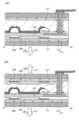
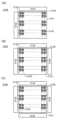
본 발명의 일 형태에 따른 표시 장치(100)의 구성예에 대하여 도 1 내지 도 12를 사용하여 설명하기로 한다. 도 1의 (A)는 외부 전극(124)이 접속된 표시 장치(100)의 사시도이고, 도 1의 (B)는 도 1의 (A)에 도시된 일점 쇄선 A1-A2를 따라 자른 부분의 단면도이다. 또한, 본 명세서에 기재되는 표시 장치(100)는, 표시 소자로서 발광 소자를 사용한 표시 장치이다. 또한, 본 발명의 일 형태에 따른 표시 장치(100)로서 전면 발광 구조(top-emission 구조)의 표시 장치를 예시한다. 또한, 표시 장치(100)를 배면 발광 구조(bottom-emission 구조) 또는 양면 발광 구조(dual-emission 구조)의 표시 장치로 할 수도 있다.A configuration example of a display device (100) according to one embodiment of the present invention will be described using FIGS. 1 to 12. FIG. 1 (A) is a perspective view of a display device (100) to which an external electrode (124) is connected, and FIG. 1 (B) is a cross-sectional view taken along the dashed-dotted line A1-A2 illustrated in FIG. 1 (A). In addition, the display device (100) described in this specification is a display device that uses a light-emitting element as a display element. In addition, a display device having a top-emission structure is exemplified as the display device (100) according to one embodiment of the present invention. In addition, the display device (100) may be a display device having a bottom-emission structure or a dual-emission structure.
<표시 장치의 구성><Composition of display device>
본 실시형태에서 나타내는 표시 장치(100)는 표시 영역(131)을 갖는다. 또한, 표시 영역(131)은 복수의 화소(130)를 갖는다. 하나의 화소(130)는 적어도 하나의 발광 소자(125)를 갖는다.The display device (100) shown in this embodiment has a display area (131). In addition, the display area (131) has a plurality of pixels (130). One pixel (130) has at least one light-emitting element (125).
본 실시형태에서 나타내는 표시 장치(100)는 전극(115), EL층(117), 전극(118), 격벽(114), 및 전극(116)을 갖는다. 또한, 전극(116) 위에 절연층(141)을 갖고, 절연층(141)에 제공된 개구(128)에서 전극(115)과 전극(116)이 전기적으로 접속된다. 또한, 격벽(114)은 전극(115) 위에 제공되고, 전극(115) 및 격벽(114) 위에 EL층(117)이 제공되고, EL층(117) 위에 전극(118)이 제공된다.The display device (100) shown in the present embodiment has an electrode (115), an EL layer (117), an electrode (118), a partition wall (114), and an electrode (116). In addition, an insulating layer (141) is provided over the electrode (116), and the electrode (115) and the electrode (116) are electrically connected through an opening (128) provided in the insulating layer (141). In addition, the partition wall (114) is provided over the electrode (115), an EL layer (117) is provided over the electrode (115) and the partition wall (114), and an electrode (118) is provided over the EL layer (117).
기판(111) 위에는 접착층(112), 절연층(119), 및 절연층(141)을 개재하여 발광 소자(125)가 제공된다. 발광 소자(125)는 전극(115), EL층(117), 및 전극(118)을 포함한다.A light-emitting element (125) is provided on a substrate (111) with an adhesive layer (112), an insulating layer (119), and an insulating layer (141) interposed therebetween. The light-emitting element (125) includes an electrode (115), an EL layer (117), and an electrode (118).
또한, 본 실시형태에서 나타내는 표시 장치(100)는 접착층(120)을 개재하여 전극(118) 위에 제공된 기판(121)을 갖는다. 또한, 기판(121)에는, 접착층(122) 및 절연층(129)을 개재하여 차광층(264), 착색층('컬러 필터'라고도 함)(266), 및 오버코트층(268)이 제공된다.In addition, the display device (100) shown in the present embodiment has a substrate (121) provided on an electrode (118) with an adhesive layer (120) interposed therebetween. In addition, a light-shielding layer (264), a coloring layer (also called a 'color filter') (266), and an overcoat layer (268) are provided on the substrate (121) with an adhesive layer (122) and an insulating layer (129) interposed therebetween.
본 실시형태에서 나타내는 표시 장치(100)는, 전면 발광 구조의 표시 장치이므로, EL층(117)으로부터 사출된 광(151)은 기판(121) 측으로부터 사출된다. EL층(117)으로부터 사출된 광(151)(예를 들어 백색광)은 착색층(266)을 투과할 때 그 일부가 흡수되어 특정한 색의 광으로 변환된다. 바꿔 말하면, 착색층(266)은 특정한 파장 영역의 광을 투과시킨다. 착색층(266)은, 광(151)을 다른 색의 광으로 변환하기 위한 광학 필터층으로서 기능할 수 있다.Since the display device (100) shown in this embodiment is a display device of a front-emitting structure, light (151) emitted from the EL layer (117) is emitted from the substrate (121) side. When the light (151) (e.g., white light) emitted from the EL layer (117) passes through the coloring layer (266), a portion of it is absorbed and converted into light of a specific color. In other words, the coloring layer (266) transmits light of a specific wavelength range. The coloring layer (266) can function as an optical filter layer for converting the light (151) into light of a different color.
또한, 본 실시형태에서는 전극(116)을 단층 구조로 설명하였지만 전극(116)을 2층 이상의 적층 구조로 하여도 좋다.In addition, in this embodiment, the electrode (116) is described as having a single-layer structure, but the electrode (116) may have a laminated structure of two or more layers.
또한, 기판(121), 접착층(122), 절연층(129), 접착층(120), 및 절연층(141)은 각각 개구부를 갖는다. 각 개구부는 서로 중첩되는 영역을 갖고, 또한 전극(116)과 중첩되는 영역을 갖는다. 본 명세서 등에서는 이들 개구부를 합쳐서 개구(132)로 부른다. 개구(132)에서, 외부 전극(124)과 전극(116)은 이방성 도전 접속층(138)을 통하여 전기적으로 접속된다.In addition, the substrate (121), the adhesive layer (122), the insulating layer (129), the adhesive layer (120), and the insulating layer (141) each have an opening. Each opening has an area overlapping with each other and also has an area overlapping with the electrode (116). In this specification and the like, these openings are collectively referred to as an opening (132). In the opening (132), the external electrode (124) and the electrode (116) are electrically connected through the anisotropic conductive connection layer (138).
또한, 도 2에 도시된 바와 같이, 표시 장치(100)의 구성을 차광층(264), 착색층(266), 및 오버코트층(268)을 제공하지 않는 구성으로 할 수도 있다. 도 2의 (A)는, 차광층(264), 착색층(266), 및 오버코트층(268)을 제공하지 않는 표시 장치(100)의 사시도이고, 도 2의 (B)는 도 2의 (A)에 도시된 일점 쇄선 A3-A4를 따라 자른 단면도이다.In addition, as illustrated in FIG. 2, the configuration of the display device (100) may be configured not to provide a light-shielding layer (264), a coloring layer (266), and an overcoat layer (268). FIG. 2 (A) is a perspective view of the display device (100) that does not provide a light-shielding layer (264), a coloring layer (266), and an overcoat layer (268), and FIG. 2 (B) is a cross-sectional view taken along the dashed-dotted line A3-A4 illustrated in FIG. 2 (A).
특히, 화소마다 다른 색의 광(151)이 사출되도록, EL층(117)을 형성(side by side patterning)하는 경우, 착색층(266)을 제공하여도 좋고 제공하지 않아도 된다.In particular, when forming the EL layer (117) (side by side patterning) so that light (151) of a different color is emitted for each pixel, a coloring layer (266) may or may not be provided.
차광층(264), 착색층(266), 및 오버코트층(268) 중 적어도 하나 또는 모두를 제공하지 않으면, 표시 장치(100)의 제작 비용의 저감, 또는 수율 향상 등을 구현할 수 있다. 또한, 착색층(266)을 제공하지 않음으로써 광(151)을 효율적으로 사출할 수 있어, 휘도 향상이나 소비 전력의 저감 등을 구현할 수 있다.If at least one or all of the light-shielding layer (264), the coloring layer (266), and the overcoat layer (268) are not provided, the manufacturing cost of the display device (100) can be reduced, or the yield can be improved. In addition, by not providing the coloring layer (266), light (151) can be efficiently emitted, so that brightness improvement, reduction in power consumption, etc. can be implemented.
한편, 차광층(264), 착색층(266), 및 오버코트층(268)을 제공하면, 외광의 반사를 경감하고, 콘트라스트비의 향상, 색재현성의 향상 등을 구현할 수 있다.Meanwhile, by providing a light-blocking layer (264), a coloring layer (266), and an overcoat layer (268), reflection of external light can be reduced, and improvements in contrast ratio and color reproducibility can be realized.
또한, 표시 장치(100)를 배면 발광 구조의 표시 장치로 하는 경우, 기판(111) 측에 차광층(264), 착색층(266), 및 오버코트층(268)을 제공하여도 좋다(도 3의 (A) 참조). 또한, 표시 장치(100)를 양면 발광 구조의 표시 장치로 하는 경우, 기판(111) 측 및 기판(121) 측의 어느 한쪽 또는 양쪽 모두에 차광층(264), 착색층(266), 및 오버코트층(268)을 제공하여도 좋다(도 3의 (B) 참조).In addition, when the display device (100) is a display device having a back-emitting structure, a light-shielding layer (264), a coloring layer (266), and an overcoat layer (268) may be provided on the substrate (111) side (see (A) of FIG. 3). In addition, when the display device (100) is a display device having a double-sided emission structure, a light-shielding layer (264), a coloring layer (266), and an overcoat layer (268) may be provided on one or both of the substrate (111) side and the substrate (121) side (see (B) of FIG. 3).
또한, 발광 소자(125)와 전극(116) 사이에, 발광 소자(125)에 신호를 공급하는 기능을 갖는 스위칭 소자를 제공하여도 좋다. 예를 들어, 발광 소자(125)와 전극(116) 사이에 트랜지스터를 제공하여도 좋다.In addition, a switching element having a function of supplying a signal to the light emitting element (125) may be provided between the light emitting element (125) and the electrode (116). For example, a transistor may be provided between the light emitting element (125) and the electrode (116).
트랜지스터는 반도체 소자의 일종이며, 전류 및/또는 전압의 증폭이나, 도통 또는 비도통을 제어하는 스위칭 동작 등을 구현할 수 있다. 발광 소자(125)와 전극(116) 사이에 트랜지스터를 제공함으로써 표시 영역(131)의 대면적화나 고정세(高精細)화 등을 용이하게 구현할 수 있다. 또한, 트랜지스터 등 스위칭 소자에 한정되지 않고, 저항 소자, 인덕터, 커패시터, 정류 소자 등을 표시 영역(131) 내에 제공할 수도 있다.A transistor is a type of semiconductor element, and can implement a switching operation for controlling amplification of current and/or voltage, or conduction or non-conduction. By providing a transistor between a light-emitting element (125) and an electrode (116), it is possible to easily implement a large area or high definition of a display area (131). In addition, it is not limited to switching elements such as transistors, and a resistance element, an inductor, a capacitor, a rectifier element, etc. may be provided within the display area (131).
[기판(111), 기판(121)][Substrate (111), Substrate (121)]
기판(111) 및 기판(121)으로서는, 유기 수지 재료나 가요성을 가질 정도의 두께를 갖는 유리 재료 등을 사용할 수 있다. 표시 장치(100)를 배면 발광 구조의 표시 장치 또는 양면 발광 구조의 표시 장치로 하는 경우, 기판(111)에는 EL층(117)으로부터의 발광에 대하여 투광성을 갖는 재료를 사용한다. 또한, 표시 장치(100)를 전면 발광 구조의 표시 장치 또는 양면 발광 구조의 표시 장치로 하는 경우, 기판(121)에는 EL층(117)으로부터의 발광에 대하여 투광성을 갖는 재료를 사용한다.As the substrate (111) and the substrate (121), an organic resin material or a glass material having a thickness sufficient to have flexibility can be used. When the display device (100) is a display device having a back-emitting structure or a display device having a double-sided emission structure, a material having light transmittance with respect to light emission from the EL layer (117) is used for the substrate (111). Furthermore, when the display device (100) is a display device having a front-emitting structure or a double-sided emission structure, a material having light transmittance with respect to light emission from the EL layer (117) is used for the substrate (121).
기판(111) 및 기판(121)에 사용할 수 있는 가요성 및 가시광에 대한 투광성을 갖는 재료로서는, 폴리에틸렌테레프탈레이트 수지(PET), 폴리에틸렌나프탈레이트 수지(PEN), 폴리에터설폰 수지(PES), 폴리아크릴로나이트릴 수지, 아크릴 수지, 폴리이미드 수지, 폴리메틸메타크릴레이트 수지, 폴리카보네이트 수지, 폴리아마이드 수지, 폴리사이클로올레핀 수지, 폴리스타이렌 수지, 폴리아마이드이미드 수지, 폴리프로필렌 수지, 폴리에스터 수지, 폴리할로젠화바이닐 수지, 아라미드 수지, 에폭시 수지 등을 사용할 수 있다. 또한, 이들 재료를 혼합 또는 적층시켜 사용하여도 좋다. 또한, 기판(111) 및 기판(121)에는 각각 같은 재료를 사용하여도 좋고, 서로 다른 재료를 사용하여도 좋다.As materials having flexibility and visible light transmittance that can be used for the substrate (111) and the substrate (121), polyethylene terephthalate resin (PET), polyethylene naphthalate resin (PEN), polyether sulfone resin (PES), polyacrylonitrile resin, acrylic resin, polyimide resin, polymethyl methacrylate resin, polycarbonate resin, polyamide resin, polycycloolefin resin, polystyrene resin, polyamideimide resin, polypropylene resin, polyester resin, polyhalogenated vinyl resin, aramid resin, epoxy resin, etc. can be used. In addition, these materials may be mixed or laminated and used. In addition, the same material may be used for the substrate (111) and the substrate (121), or different materials may be used.
또한, 기판(121) 및 기판(111)의 열팽창 계수는 바람직하게는 30ppm/K 이하, 더 바람직하게는 10ppm/K 이하로 한다. 또한, 기판(121) 및 기판(111)의 표면에, 질화 실리콘이나 산화질화 실리콘 등 질소와 실리콘을 포함하는 막이나, 질화 알루미늄 등의 질소와 알루미늄을 포함하는 막 등의 투수성이 낮은 보호막을 형성하여도 좋다. 또한, 기판(121) 및 기판(111)으로서 섬유체에 유기 수지가 함침(含浸)된 구조물(소위, 프리프레그라고도 함)을 사용하여도 좋다.In addition, the thermal expansion coefficient of the substrate (121) and the substrate (111) is preferably 30 ppm/K or less, more preferably 10 ppm/K or less. In addition, a protective film having low water permeability, such as a film containing nitrogen and silicon, such as silicon nitride or silicon oxide nitride, or a film containing nitrogen and aluminum, such as aluminum nitride, may be formed on the surface of the substrate (121) and the substrate (111). In addition, a structure in which a fiber body is impregnated with an organic resin (also called a prepreg) may be used as the substrate (121) and the substrate (111).
[절연층(119)][Insulating layer (119)]
절연층(119)은, 산화 알루미늄, 산화 마그네슘, 산화 실리콘, 산화질화 실리콘, 산화 갈륨, 산화 저마늄, 산화 이트륨, 산화 지르코늄, 산화 란타넘, 산화 네오디뮴, 산화 하프늄, 산화 탄탈럼 등의 산화물 재료나, 질화 실리콘, 질화산화 실리콘, 질화 알루미늄, 질화산화 알루미늄 등의 질화물 재료 등을 사용하여 단층 구조 또는 적층 구조로 형성할 수 있다. 예를 들어, 절연층(119)은 산화 실리콘과 질화 실리콘을 적층한 2층 구조로 하여도 좋고, 상술한 재료를 조합한 5층 구조로 하여도 좋다. 절연층(119)은 스퍼터링법이나 CVD법, 열 산화법, 도포법, 인쇄법 등을 사용하여 형성하는 것이 가능하다.The insulating layer (119) can be formed in a single-layer structure or a laminated structure using oxide materials such as aluminum oxide, magnesium oxide, silicon oxide, silicon nitride, gallium oxide, germanium oxide, yttrium oxide, zirconium oxide, lanthanum oxide, neodymium oxide, hafnium oxide, and tantalum oxide; or nitride materials such as silicon nitride, silicon nitride oxide, aluminum nitride, and aluminum nitride oxide. For example, the insulating layer (119) may have a two-layer structure in which silicon oxide and silicon nitride are laminated, or may have a five-layer structure in which the above-described materials are combined. The insulating layer (119) can be formed using a sputtering method, a CVD method, a thermal oxidation method, a coating method, a printing method, or the like.
절연층(119)에 의하여, 기판(111)이나 접착층(112) 등으로부터 발광 소자(125)로 불순물 원소가 확산되는 것을 방지 또는 저감할 수 있다.By means of the insulating layer (119), diffusion of impurity elements from the substrate (111) or the adhesive layer (112) to the light-emitting element (125) can be prevented or reduced.
또한, 본 명세서에서, 질화 산화물이란, 산소보다 질소의 함유량이 많은 화합물을 말한다. 또한, 산화 질화물이란, 질소보다 산소의 함유량이 많은 화합물을 말한다. 또한, 각 원소의 함유량은, 예를 들어 러더퍼드 후방 산란법(RBS: Rutherford Backscattering Spectrometry) 등을 사용하여 측정할 수 있다.In addition, in this specification, the term "nitride oxide" refers to a compound having a higher nitrogen content than oxygen. In addition, the term "oxynitride oxide" refers to a compound having a higher oxygen content than nitrogen. In addition, the content of each element can be measured using, for example, Rutherford backscattering spectrometry (RBS).
[전극(116)][Electrode (116)]
전극(116)은 도전성 재료를 사용하여 형성할 수 있다. 예를 들어, 알루미늄, 크로뮴, 구리, 은, 금, 백금, 탄탈럼, 니켈, 타이타늄, 몰리브데넘, 텅스텐, 하프늄, 바나듐, 나이오븀, 망가니즈, 마그네슘, 지르코늄, 베릴륨 등으로부터 선택된 금속 원소, 상술한 금속 원소를 성분으로 하는 합금, 또는 상술한 금속 원소를 조합한 합금 등을 사용할 수 있다. 또한, 인 등의 불순물 원소를 함유시킨 다결정 실리콘으로 대표되는 반도체, 니켈 실리사이드 등의 실리사이드를 사용하여도 좋다. 도전성 재료의 형성 방법은 특별히 한정되지 않고, 증착법, CVD법, 스퍼터링법, 스핀 코팅법 등의 각종 형성 방법을 사용할 수 있다.The electrode (116) can be formed using a conductive material. For example, a metal element selected from aluminum, chromium, copper, silver, gold, platinum, tantalum, nickel, titanium, molybdenum, tungsten, hafnium, vanadium, niobium, manganese, magnesium, zirconium, beryllium, etc., an alloy containing the above-described metal elements as a component, or an alloy combining the above-described metal elements, etc. can be used. In addition, a semiconductor represented by polycrystalline silicon containing an impurity element such as phosphorus, or a silicide such as nickel silicide may be used. The method for forming the conductive material is not particularly limited, and various forming methods such as a deposition method, a CVD method, a sputtering method, and a spin coating method can be used.
또한, 전극(116)에는, 인듐 주석 산화물, 산화 텅스텐을 포함하는 인듐 산화물, 산화 텅스텐을 포함하는 인듐 아연 산화물, 산화 타이타늄을 포함하는 인듐 산화물, 산화 타이타늄을 포함하는 인듐 주석 산화물, 인듐 아연 산화물, 산화 실리콘을 첨가한 인듐 주석 산화물 등 산소를 포함하는 도전성 재료를 적용할 수도 있다. 또한, 질화 타이타늄, 질화 탄탈럼, 질화 텅스텐 등 질소를 포함하는 도전성 재료를 적용할 수도 있다. 또한, 상기 산소를 포함하는 도전성 재료와, 상술한 금속 원소를 포함하는 재료의 적층 구조로 할 수도 있다.In addition, a conductive material containing oxygen, such as indium tin oxide, indium oxide containing tungsten oxide, indium zinc oxide containing tungsten oxide, indium oxide containing titanium oxide, indium tin oxide containing titanium oxide, indium zinc oxide, and indium tin oxide with silicon oxide added, can be applied to the electrode (116). In addition, a conductive material containing nitrogen, such as titanium nitride, tantalum nitride, and tungsten nitride, can be applied. In addition, a laminated structure of the conductive material containing the oxygen and the material containing the above-described metal element can also be used.
전극(116)은 단층 구조로 하여도 좋고, 2층 이상의 적층 구조로 하여도 좋다. 예를 들어, 실리콘을 포함하는 알루미늄층의 단층 구조, 알루미늄층 위에 타이타늄층을 적층하는 2층 구조, 질화 타이타늄층 위에 타이타늄층을 적층하는 2층 구조, 질화 타이타늄층 위에 텅스텐층을 적층하는 2층 구조, 질화 탄탈럼층 위에 텅스텐층을 적층하는 2층 구조, 타이타늄층과, 그 타이타늄층 위에 알루미늄층을 적층하고, 그 위에 타이타늄층을 형성하는 3층 구조 등이 있다. 또한, 전극(116)에, 타이타늄, 탄탈럼, 텅스텐, 몰리브데넘, 크로뮴, 네오디뮴, 스칸듐 중에서 선택된 하나 또는 복수의 원소를 포함하는 알루미늄 합금을 사용하여도 좋다.The electrode (116) may have a single-layer structure or a laminated structure of two or more layers. For example, there may be a single-layer structure of an aluminum layer including silicon, a two-layer structure in which a titanium layer is laminated on an aluminum layer, a two-layer structure in which a titanium layer is laminated on a titanium nitride layer, a two-layer structure in which a tungsten layer is laminated on a titanium nitride layer, a two-layer structure in which a tungsten layer is laminated on a tantalum nitride layer, a three-layer structure in which a titanium layer is laminated on an aluminum layer on the titanium layer, and a titanium layer is formed thereon, etc. In addition, an aluminum alloy including one or more elements selected from titanium, tantalum, tungsten, molybdenum, chromium, neodymium, and scandium may be used for the electrode (116).
[절연층(127)][Insulating layer (127)]
절연층(127)은 절연층(119)과 같은 재료를 사용하여 같은 방법으로 형성할 수 있다. 또한, 절연층(127)에는 산소를 포함하는 재료를 사용하는 것이 바람직하다.The insulating layer (127) can be formed using the same material as the insulating layer (119) and in the same manner. In addition, it is preferable to use a material containing oxygen for the insulating layer (127).
[전극(115)][Electrode (115)]
전극(115)은 나중에 형성되는 EL층(117)으로부터 사출되는 광을 효율적으로 반사하는 도전성 재료를 사용하여 형성하는 것이 바람직하다. 또한, 전극(115)은 단층 구조에 한정되지 않고, 복수 층의 적층 구조로 하여도 좋다. 예를 들어, 전극(115)을 양극으로서 사용하는 경우에는 EL층(117)에 접촉하는 층을, 인듐 주석 산화물 등의 투광성을 갖는 층으로 하고, 그 층에 접촉하도록 반사율이 높은 층(알루미늄, 알루미늄을 포함하는 합금, 또는 은 등)을 제공하여도 좋다.It is preferable that the electrode (115) be formed using a conductive material that efficiently reflects light emitted from the EL layer (117) that is formed later. In addition, the electrode (115) is not limited to a single-layer structure, and may have a multi-layer laminated structure. For example, when the electrode (115) is used as an anode, the layer that contacts the EL layer (117) may be a light-transmitting layer such as indium tin oxide, and a layer with a high reflectivity (aluminum, an alloy containing aluminum, or silver, etc.) may be provided to contact that layer.
또한, 본 실시형태에서는 전면 발광 구조의 표시 장치에 대하여 예시하지만, 표시 장치를 배면 발광 구조 또는 양면 발광 구조로 하는 경우 전극(115)에 투광성을 갖는 도전성 재료를 사용하면 좋다.In addition, although this embodiment exemplifies a display device having a front-emitting structure, if the display device has a back-emitting structure or a double-sided emitting structure, it is preferable to use a conductive material having light-transmitting properties for the electrode (115).
[격벽(114)][Bulkhead (114)]
격벽(114)은 인접하는 전극(118)간의 전기적 단락을 방지하기 위하여 제공된다. 또한, 후술하는 EL층(117)의 형성에 메탈 마스크를 사용하는 경우, 메탈 마스크가 발광 소자(125)를 형성하는 영역에 접촉하지 않도록 하는 기능도 갖는다. 격벽(114)은 에폭시 수지, 아크릴 수지, 이미드 수지 등의 유기 수지 재료나, 산화 실리콘 등의 무기 재료로 형성할 수 있다. 격벽(114)은 그 측벽이 테이퍼 또는 연속한 곡률을 갖는 경사면이 되도록 형성되는 것이 바람직하다. 격벽(114)의 측벽을 이와 같은 형상으로 함으로써, 나중에 형성되는 EL층(117)이나 전극(118)의 피복성을 양호하게 할 수 있다.The partition wall (114) is provided to prevent electrical short-circuiting between adjacent electrodes (118). In addition, when a metal mask is used to form the EL layer (117) described later, it also has a function of preventing the metal mask from contacting the area where the light-emitting element (125) is formed. The partition wall (114) can be formed of an organic resin material such as an epoxy resin, an acrylic resin, an imide resin, or an inorganic material such as silicon oxide. It is preferable that the partition wall (114) be formed so that its side wall becomes a tapered or inclined surface having a continuous curvature. By forming the side wall of the partition wall (114) into such a shape, the covering property of the EL layer (117) or electrode (118) formed later can be improved.
[EL층(117)][EL floor (117)]
EL층(117)의 구성에 대해서는 실시형태 5에서 설명하기로 한다.The configuration of the EL layer (117) will be described in embodiment 5.
[전극(118)][Electrode (118)]
본 실시형태에서는 전극(118)을 음극으로서 사용한다. 전극(118)은, 후술하는 EL층(117)에 전자를 주입할 수 있는 일함수가 작은 재료를 사용하여 형성하는 것이 바람직하다. 또한, 일함수가 작은 금속 단체가 아니라, 일함수가 작은 알칼리 금속, 또는 알칼리 토금속을 수nm로 형성한 층을 완충층으로서 형성하고, 그 위에 알루미늄 등의 금속 재료, 인듐 주석 산화물 등 도전성을 갖는 산화물 재료, 또는 반도체 재료를 사용하여 형성하여도 좋다. 또한, 완충층으로서 알칼리 토금속의 산화물, 할로젠화물 또는 마그네슘-은 등을 사용할 수도 있다.In this embodiment, the electrode (118) is used as a cathode. It is preferable that the electrode (118) be formed using a material having a small work function that can inject electrons into the EL layer (117) described later. In addition, instead of a single metal having a small work function, a layer in which an alkali metal or an alkaline earth metal having a small work function is formed to a thickness of several nm may be formed as a buffer layer, and a metal material such as aluminum, an oxide material having conductivity such as indium tin oxide, or a semiconductor material may be used thereon. In addition, an oxide, a halide, or magnesium-silver of an alkaline earth metal may be used as the buffer layer.
또한, EL층(117)으로부터 사출되는 광을 전극(118)을 통하여 추출하는 경우에는, 전극(118)은 가시광에 대하여 투광성을 갖는 것이 바람직하다.In addition, when extracting light emitted from the EL layer (117) through the electrode (118), it is preferable that the electrode (118) has light-transmitting properties for visible light.
[접착층(120, 112, 122)][Adhesive layer (120, 112, 122)]
접착층(120), 접착층(112), 및 접착층(122)으로서는 광 경화성의 접착제, 반응 경화성 접착제, 열 경화성 접착제, 또는 혐기성 접착제를 사용할 수 있다. 예를 들어, 에폭시 수지, 아크릴 수지, 이미드 수지 등을 사용할 수 있다. 전면 발광 구조의 경우는 접착층(120)에, 배면 발광 구조의 경우는 접착층(112)에, 광의 파장 이하의 크기를 갖는 건조제(제올라이트 등)나 굴절률이 큰 필러(산화 타이타늄이나 지르코늄 등)를 혼합하면, EL층(117)으로부터 사출되는 광의 추출 효율이 저하되기 어렵고, 또한 표시 장치의 신뢰성이 향상되므로 바람직하다.As the adhesive layer (120), the adhesive layer (112), and the adhesive layer (122), a photocurable adhesive, a reaction-curable adhesive, a thermosetting adhesive, or an anaerobic adhesive can be used. For example, an epoxy resin, an acrylic resin, an imide resin, or the like can be used. In the case of a front-emitting structure, it is preferable to mix a desiccant (such as zeolite) having a size smaller than the wavelength of light or a filler with a high refractive index (such as titanium oxide or zirconium) in the adhesive layer (120), and in the case of a back-emitting structure, in the adhesive layer (112), because this makes it difficult for the extraction efficiency of light emitted from the EL layer (117) to decrease, and also improves the reliability of the display device.
[이방성 도전 접속층(138)][Alien Challenge Access Layer (138)]
이방성 도전 접속층(138)은, 다양한 이방성 도전 필름(ACF: Anisotropic Conductive Film)이나, 이방성 도전 페이스트(ACP: Anisotropic Conductive Paste) 등을 사용하여 형성할 수 있다.The anisotropic conductive connection layer (138) can be formed using various anisotropic conductive films (ACF: Anisotropic Conductive Films) or anisotropic conductive pastes (ACP: Anisotropic Conductive Pastes).
이방성 도전 접속층(138)은 열 경화성 수지에, 또는 열 경화성과 광 경화성을 갖는 수지에 도전성 입자를 혼합시킨 페이스트 형상 또는 시트 형상의 재료를 경화시킨 것이다. 이방성 도전 접속층(138)은, 광 조사나 열 압착에 의하여 이방성 도전성을 나타내는 재료가 된다. 이방성 도전 접속층(138)에 사용되는 도전성 입자로서는, 예를 들어 구(球) 형상의 유기 수지를 Au나 Ni, Co 등 박막 형상의 금속으로 피복한 입자를 사용할 수 있다.The anisotropic conductive connection layer (138) is a paste-like or sheet-like material that is cured by mixing conductive particles in a thermosetting resin or a thermosetting and photocuring resin. The anisotropic conductive connection layer (138) becomes a material that exhibits anisotropic conductivity by light irradiation or thermal compression. As the conductive particles used in the anisotropic conductive connection layer (138), for example, particles that cover a spherical organic resin with a thin film-like metal such as Au, Ni, or Co can be used.
<표시 장치의 제작 방법><Method of making a display device>
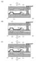
다음에, 도 4 내지 도 12를 사용하여 표시 장치(100)의 제작 방법을 예시한다. 도 7을 제외하고, 도 4 내지 도 12는 도 1에 도시된 일점 쇄선 A1-A2를 따라 자른 부분의 단면에 상당한다. 또한, 이하에서는 제작 중의 표시 장치(100)를 가공 부재(150)라고 부르는 경우가 있다.Next, a method of manufacturing a display device (100) is exemplified using FIGS. 4 to 12. Except for FIG. 7, FIGS. 4 to 12 correspond to cross sections of portions cut along the dashed-dotted line A1-A2 illustrated in FIG. 1. In addition, in the following, the display device (100) being manufactured may be referred to as a processed member (150).
[박리층(113)의 형성][Formation of peeling layer (113)]
우선, 기판(101) 위에 박리층(113)을 형성한다(도 4의 (A) 참조). 기판의 일례로서는 반도체 기판(예를 들어 단결정 기판 또는 실리콘 기판), SOI 기판, 유리 기판, 석영 기판, 사파이어 기판, 세라믹 기판, 본 실시형태의 처리 온도에 견딜 수 있는 내열성을 갖는 플라스틱 기판, 금속 기판, 스테인리스강 기판, 스테인리스강박을 갖는 기판, 텅스텐 기판, 텅스텐박을 갖는 기판 등이 있다. 유리 기판의 일례로서는, 바륨보로실리케이트 유리, 알루미노보로실리케이트 유리, 또는 소다석회 유리 등이 있다.First, a release layer (113) is formed on a substrate (101) (see (A) of FIG. 4). Examples of the substrate include a semiconductor substrate (e.g., a single crystal substrate or a silicon substrate), an SOI substrate, a glass substrate, a quartz substrate, a sapphire substrate, a ceramic substrate, a plastic substrate having heat resistance that can withstand the processing temperature of the present embodiment, a metal substrate, a stainless steel substrate, a substrate having a stainless steel foil, a tungsten substrate, a substrate having a tungsten foil, and the like. Examples of the glass substrate include barium borosilicate glass, aluminoborosilicate glass, or soda-lime glass.
박리층(113)은 텅스텐, 몰리브데넘, 타이타늄, 탄탈럼, 나이오븀, 니켈, 코발트, 지르코늄, 루테늄, 로듐, 팔라듐, 오스뮴, 이리듐, 실리콘 중에서 선택된 원소, 또는 상기 원소를 포함하는 합금 재료, 또는 상기 원소를 포함하는 화합물 재료를 사용하여 형성할 수 있다. 또한, 이들 재료를 사용하여 단층 구조로 또는 적층 구조로 형성할 수 있다. 또한, 박리층(113)의 결정 구조는 비정질, 미결정, 다결정 중 어느 것이라도 좋다. 또한, 박리층(113)을 산화 알루미늄, 산화 갈륨, 산화 아연, 이산화 타이타늄, 산화 인듐, 산화 인듐 주석, 산화 인듐 아연, 또는 인듐, 갈륨, 및 아연을 포함하는 산화물(In-Ga-Zn-O, IGZO) 등의 금속 산화물을 사용하여 형성할 수도 있다.The peeling layer (113) can be formed using an element selected from tungsten, molybdenum, titanium, tantalum, niobium, nickel, cobalt, zirconium, ruthenium, rhodium, palladium, osmium, iridium, and silicon, or an alloy material containing the above elements, or a compound material containing the above elements. In addition, it can be formed in a single-layer structure or a laminated structure using these materials. In addition, the crystal structure of the peeling layer (113) may be any of amorphous, microcrystalline, and polycrystalline. In addition, the peeling layer (113) can also be formed using a metal oxide such as aluminum oxide, gallium oxide, zinc oxide, titanium dioxide, indium oxide, indium tin oxide, indium zinc oxide, or an oxide containing indium, gallium, and zinc (In-Ga-Zn-O, IGZO).
박리층(113)은 스퍼터링법이나 CVD법, 도포법, 인쇄법 등에 의하여 형성할 수 있다. 또한, 도포법은 스핀 코팅법, 액적 토출법, 및 디스펜스법을 포함한다.The peeling layer (113) can be formed by a sputtering method, a CVD method, a coating method, a printing method, etc. In addition, the coating method includes a spin coating method, a droplet discharge method, and a dispensing method.
박리층(113)을 단층 구조로 형성하는 경우, 텅스텐, 몰리브데넘, 또는 텅스텐과 몰리브데넘을 포함하는 재료를 사용하는 것이 바람직하다. 또는, 박리층(113)을 단층 구조로 형성하는 경우, 텅스텐의 산화물 또는 산화질화물, 몰리브데넘의 산화물 또는 산화질화물, 또는 텅스텐과 몰리브데넘을 포함하는 재료의 산화물 또는 산화질화물을 사용하는 것이 바람직하다.When forming the peeling layer (113) in a single-layer structure, it is preferable to use tungsten, molybdenum, or a material containing tungsten and molybdenum. Alternatively, when forming the peeling layer (113) in a single-layer structure, it is preferable to use an oxide or oxynitride of tungsten, an oxide or oxynitride of molybdenum, or an oxide or oxynitride of a material containing tungsten and molybdenum.
또한, 박리층(113)을 예를 들어 텅스텐을 포함하는 층과 텅스텐의 산화물을 포함하는 층의 적층 구조로 하는 경우, 텅스텐을 포함하는 층에 접촉하도록 절연성 산화물층을 형성함으로써, 텅스텐을 포함하는 층과 절연성 산화물층의 계면에, 텅스텐의 산화물을 포함하는 층이 형성되는 것을 활용하여도 좋다. 또한, 텅스텐을 포함하는 층의 표면에 열 산화 처리, 산소 플라스마 처리, 오존수 등 산화력을 갖는 용액을 사용한 처리 등을 수행하여 텅스텐의 산화물을 포함하는 층을 형성하여도 좋다. 또한, 기판(101)과 박리층(113) 사이에 절연층을 제공하여도 좋다.In addition, when the peeling layer (113) has a laminated structure of, for example, a layer including tungsten and a layer including tungsten oxide, it is possible to utilize the formation of a layer including tungsten oxide at the interface between the layer including tungsten and the insulating oxide layer by forming an insulating oxide layer so as to be in contact with the layer including tungsten. In addition, the layer including tungsten oxide may be formed by performing thermal oxidation treatment, oxygen plasma treatment, treatment using a solution having an oxidizing power such as ozone water, on the surface of the layer including tungsten. In addition, an insulating layer may be provided between the substrate (101) and the peeling layer (113).
본 실시형태에서는, 기판(101)에 알루미노보로실리케이트 유리가 사용된다. 또한, 기판(101) 위에 형성하는 박리층(113)으로서, 스퍼터링법에 의하여 텅스텐막을 형성한다.In this embodiment, aluminoborosilicate glass is used for the substrate (101). In addition, as the peeling layer (113) formed on the substrate (101), a tungsten film is formed by a sputtering method.
[절연층(119)의 형성][Formation of insulating layer (119)]
다음에, 박리층(113) 위에 절연층(119)을 형성한다(도 4의 (A) 참조). 절연층(119)은 기판(101) 등으로부터의 불순물 원소의 확산을 방지 또는 저감할 수 있다. 또한, 기판(101)을 기판(111)으로 치환한 후에도 기판(111)이나 접착층(112) 등으로부터 발광 소자(125)로 불순물 원소가 확산되는 것을 방지 또는 저감할 수 있다. 절연층(119)의 두께는 바람직하게는 30nm 이상 2μm 이하, 더 바람직하게는 50nm 이상 1μm 이하, 더욱 바람직하게는 50nm 이상 500nm 이하로 하면 좋다. 본 실시형태에서는, 절연층(119)으로서, 기판(101) 측으로부터 플라스마 CVD법에 의하여, 두께 600nm의 산화질화 실리콘, 두께 200nm의 질화 실리콘, 두께 200nm의 산화질화 실리콘, 두께 140nm의 질화산화 실리콘, 두께 100nm의 산화질화 실리콘의 적층막을 형성한다.Next, an insulating layer (119) is formed on the peeling layer (113) (see (A) of FIG. 4). The insulating layer (119) can prevent or reduce diffusion of impurity elements from the substrate (101) or the like. In addition, even after replacing the substrate (101) with the substrate (111), diffusion of impurity elements from the substrate (111) or the adhesive layer (112) or the like to the light-emitting element (125) can be prevented or reduced. The thickness of the insulating layer (119) is preferably 30 nm or more and 2 μm or less, more preferably 50 nm or more and 1 μm or less, and even more preferably 50 nm or more and 500 nm or less. In this embodiment, as an insulating layer (119), a laminated film of silicon oxynitride having a thickness of 600 nm, silicon nitride having a thickness of 200 nm, silicon oxynitride having a thickness of 200 nm, silicon nitride oxide having a thickness of 140 nm, and silicon oxynitride having a thickness of 100 nm is formed from the substrate (101) side by plasma CVD.
또한, 절연층(119)을 형성하기 전에, 박리층(113)의 표면을, 산소를 포함하는 분위기에 노출시키는 것이 바람직하다.Additionally, before forming the insulating layer (119), it is preferable to expose the surface of the peeling layer (113) to an atmosphere containing oxygen.
산소를 포함하는 분위기에 사용하는 가스로서는 산소, 일산화이질소, 이산화질소, 이산화탄소, 일산화탄소 등을 사용할 수 있다. 또한, 산소를 포함하는 가스와 다른 가스의 혼합 가스를 사용하여도 좋다. 예를 들어, 이산화탄소와 아르곤의 혼합 가스 등, 산소를 포함하는 가스와 희가스의 혼합 가스를 사용할 수 있다. 박리층(113)의 표면을 산화함으로써, 나중의 공정에서 수행되는 기판(101)의 박리를 용이하게 할 수 있다.As the gas used in the atmosphere containing oxygen, oxygen, dinitrogen monoxide, nitrogen dioxide, carbon dioxide, carbon monoxide, etc. can be used. In addition, a mixed gas of a gas containing oxygen and another gas may be used. For example, a mixed gas of a gas containing oxygen and a rare gas, such as a mixed gas of carbon dioxide and argon, can be used. By oxidizing the surface of the peeling layer (113), peeling of the substrate (101) performed in a later process can be facilitated.
[전극(116)의 형성][Formation of electrode (116)]
다음에, 절연층(119) 위에 전극(116)을 형성하기 위한 도전층(126)을 형성한다. 예를 들어, 도전층(126)으로서는, 절연층(119) 위에 스퍼터링법에 의하여 2층의 몰리브데넘 사이에 알루미늄을 끼운 3층의 금속막을 형성한다(도 4의 (A) 참조).Next, a conductive layer (126) for forming an electrode (116) is formed on the insulating layer (119). For example, as the conductive layer (126), a three-layer metal film in which aluminum is sandwiched between two layers of molybdenum is formed on the insulating layer (119) by a sputtering method (see (A) of Fig. 4).
이어서, 도전층(126) 위에 레지스트 마스크를 형성하고, 상기 레지스트 마스크를 사용하여 도전층(126)을 원하는 형상으로 에칭하여, 전극(116)을 형성할 수 있다. 레지스트 마스크의 형성은 리소그래피법, 인쇄법, 잉크젯법 등을 적절히 사용하여 수행할 수 있다. 레지스트 마스크를 잉크젯법으로 형성하면 포토마스크를 사용하지 않으므로, 제작 비용을 저감할 수 있다.Next, a resist mask is formed on the conductive layer (126), and the conductive layer (126) is etched into a desired shape using the resist mask to form the electrode (116). The formation of the resist mask can be performed appropriately using a lithography method, a printing method, an inkjet method, or the like. If the resist mask is formed using an inkjet method, a photomask is not used, so the manufacturing cost can be reduced.
도전층(126)의 에칭은 드라이 에칭법과 웨트 에칭법 중 어느 쪽을 사용하여도 좋고, 양쪽 모두를 사용하여도 좋다. 웨트 에칭법에 의하여 도전층(126)의 에칭을 수행하는 경우, 에칭액으로서 인산과 초산과 질산을 섞은 용액이나, 옥살산을 포함하는 용액, 인산을 포함하는 용액 등을 사용할 수 있다. 에칭 처리가 끝난 후에 레지스트 마스크를 제거한다(도 4의 (B) 참조).The etching of the conductive layer (126) may be performed using either a dry etching method or a wet etching method, or may be performed using both. When the etching of the conductive layer (126) is performed using a wet etching method, a solution containing phosphoric acid, acetic acid, and nitric acid, a solution containing oxalic acid, a solution containing phosphoric acid, or the like may be used as the etching solution. After the etching process is completed, the resist mask is removed (see (B) of FIG. 4).
또한, 전극(116)(이들과 같은 층으로 형성되는 다른 전극 또는 배선을 포함함)의 단부를 테이퍼 형상으로 함으로써, 전극(116)의 측면을 피복하는 층의 피복성을 향상시킬 수 있다. 구체적으로는, 단부의 테이퍼각 θ를 80° 이하, 바람직하게는 60° 이하, 더 바람직하게는 45° 이하로 한다. 또한, 테이퍼각이란, 상기 층의 측면과 저면이 이루는 각도를 말한다. 또한, 테이퍼각이 90° 미만인 단부 형상을 순 테이퍼 형상이라고 하고, 테이퍼 각이 90° 이상인 단부 형상을 역 테이퍼 형상이라고 한다. 도 4의 (B)는 전극(116)의 단부가 순 테이퍼 형상인 경우를 도시한 것이다.In addition, by forming the end of the electrode (116) (including other electrodes or wiring formed in the same layer as these) into a tapered shape, the covering property of the layer covering the side surface of the electrode (116) can be improved. Specifically, the taper angle θ of the end surface is set to 80° or less, preferably 60° or less, and more preferably 45° or less. In addition, the taper angle refers to the angle formed by the side surface and the bottom surface of the layer. In addition, an end surface shape having a taper angle of less than 90° is called a true taper shape, and an end surface shape having a taper angle of 90° or more is called a reverse taper shape. Fig. 4 (B) illustrates a case where the end surface of the electrode (116) has a true taper shape.
또한, 전극(116)의 단부의 단면 형상을 복수의 단을 갖는 계단 형상으로 함으로써 그 위에 형성되는 층의 피복성을 향상시킬 수도 있다. 또한, 전극(116)에 한정되지 않고 각 층의 단부의 단면 형상을 순 테이퍼 형상 또는 계단 형상으로 함으로써 상기 단부를 덮어 형성되는 층이 상기 단부에서 끊어지는 현상(단절)을 방지하여 피복성을 양호하게 할 수 있다.In addition, by making the cross-sectional shape of the end of the electrode (116) into a step shape having multiple steps, the covering property of the layer formed thereon can be improved. In addition, not limited to the electrode (116), by making the cross-sectional shape of the end of each layer into a pure tapered shape or a step shape, the phenomenon of the layer formed by covering the end being cut off at the end (cutoff) can be prevented, thereby improving the covering property.
[절연층(127)의 형성][Formation of insulating layer (127)]
다음에, 전극(116) 위에 절연층(127)을 형성한다(도 4의 (C) 참조). 본 실시형태에서는 절연층(127)으로서 플라스마 CVD법으로 산화질화 실리콘막을 형성한다.Next, an insulating layer (127) is formed on the electrode (116) (see (C) of Fig. 4). In this embodiment, a silicon oxide nitride film is formed as the insulating layer (127) by the plasma CVD method.
다음에, 절연층(127) 위에 레지스트마스크를 형성하고, 이 레지스트마스크를 사용하여 전극(116)과 중첩되는 절연층(127)의 일부를 선택적으로 제거함으로써 개구(128) 및 개구(137)를 갖는 절연층(141)을 형성한다(도 4의 (D) 참조). 절연층(127)의 에칭은 드라이 에칭법과 웨트 에칭법 중 어느 쪽을 사용하여도 좋고 양쪽 모두를 사용하여도 좋다.Next, a resist mask is formed over the insulating layer (127), and a part of the insulating layer (127) overlapping the electrode (116) is selectively removed using the resist mask to form an insulating layer (141) having an opening (128) and an opening (137) (see (D) of FIG. 4). The etching of the insulating layer (127) may be performed using either a dry etching method or a wet etching method, or both.
[전극(115)의 형성][Formation of electrode (115)]
다음에, 절연층(141) 위에 전극(115)을 형성하기 위한 도전층(145)을 형성한다(도 4의 (E) 참조). 도전층(145)은 도전층(126)(전극(116))과 같은 재료를 사용하여 같은 방법으로 형성할 수 있다.Next, a conductive layer (145) for forming an electrode (115) is formed on the insulating layer (141) (see (E) of FIG. 4). The conductive layer (145) can be formed using the same material as the conductive layer (126) (electrode (116)) and in the same manner.
다음에, 도전층(145) 위에 레지스트마스크를 형성하고, 이 레지스트마스크를 사용하여 도전층(145)의 일부를 선택적으로 제거함으로써 전극(115)을 형성한다(도 5의 (A) 참조). 도전층(145)의 에칭은 드라이 에칭법과 웨트 에칭법 중 어느 쪽을 사용하여도 좋고 양쪽 모두를 사용하여도 좋다. 본 실시형태에서는 은 위에 인듐 주석 산화물을 적층한 재료를 사용하여 도전층(145)(전극(115))을 형성한다. 전극(115)과 전극(116)은 개구(128)에서 전기적으로 접속된다.Next, a resist mask is formed over the conductive layer (145), and a part of the conductive layer (145) is selectively removed using the resist mask to form the electrode (115) (see (A) of FIG. 5). The etching of the conductive layer (145) may be performed using either a dry etching method or a wet etching method, or both. In the present embodiment, the conductive layer (145) (electrode (115)) is formed using a material in which indium tin oxide is laminated on silver. The electrode (115) and the electrode (116) are electrically connected at the opening (128).
[격벽(114)의 형성][Formation of bulkhead (114)]
다음에, 격벽(114)을 형성한다(도 5의 (B) 참조). 본 실시형태에서는 도포법에 의하여 감광성 유기 수지 재료를 도포하고 원하는 형상으로 가공함으로써 격벽(114)을 형성한다. 본 실시형태에서는 감광성 폴리이미드 수지를 사용하여 격벽(114)을 형성한다.Next, a partition wall (114) is formed (see (B) of FIG. 5). In the present embodiment, a photosensitive organic resin material is applied by a coating method and processed into a desired shape to form a partition wall (114). In the present embodiment, a photosensitive polyimide resin is used to form a partition wall (114).
[EL층(117), 전극(118), 및 박리층(110)의 형성][Formation of EL layer (117), electrode (118), and peeling layer (110)]
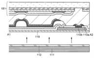
본 실시형태에서는 EL층(117)과 같은 재료를 사용하여 형성되는 박리층(110a)과, 전극(118)과 같은 재료를 사용하여 형성되는 박리층(110b)을 적층한 구조의 박리층(110)을 형성한다. 이로써 제작 공정을 늘리지 않고 박리층(110)을 형성할 수 있어 바람직하다.In this embodiment, a peeling layer (110) having a laminated structure is formed by using a material similar to that of the EL layer (117) and a peeling layer (110b) formed using a material similar to that of the electrode (118). This makes it possible to form the peeling layer (110) without increasing the manufacturing process, which is preferable.
격벽(114)을 형성한 후에 전극(115) 및 격벽(114) 위에 EL층(117)을 형성하고, 이와 동시에 전극(116)에서 개구(137)와 중첩되는 영역 위에 박리층(110a)을 형성한다(도 5의 (C) 참조).After forming the partition wall (114), an EL layer (117) is formed on the electrode (115) and the partition wall (114), and at the same time, a peeling layer (110a) is formed on an area overlapping the opening (137) in the electrode (116) (see (C) of FIG. 5).
다음에, EL층(117) 위에 전극(118)을 형성하고, 이와 동시에 박리층(110a) 위에 박리층(110b)을 형성한다. 본 실시형태에서는 전극(118) 및 박리층(110b)에 마그네슘과 은의 합금을 사용한다. 전극(118) 및 박리층(110b)은 증착법, 스퍼터링법 등으로 형성할 수 있다(도 5의 (D) 참조).Next, an electrode (118) is formed on the EL layer (117), and at the same time, a peeling layer (110b) is formed on the peeling layer (110a). In the present embodiment, an alloy of magnesium and silver is used for the electrode (118) and the peeling layer (110b). The electrode (118) and the peeling layer (110b) can be formed by a deposition method, a sputtering method, or the like (see (D) of FIG. 5).
또한, 전극(116) 위의 개구(137)에 형성하는 박리층(110)은 단층 구조로 하여도 좋고 2층 이상의 적층 구조로 하여도 좋다. 박리층(110)을 단층 구조로 하는 경우에는 전극(116)과 밀착성이 낮은 재료를 사용할 수 있다. 또한, 박리층(110)을 적층 구조로 형성하는 경우에는 적층을 구성하는 층들 사이의 밀착성이 낮게 되도록 복수의 재료를 사용할 수 있다.In addition, the peeling layer (110) formed in the opening (137) above the electrode (116) may have a single-layer structure or a laminated structure of two or more layers. In the case where the peeling layer (110) has a single-layer structure, a material having low adhesion to the electrode (116) can be used. In addition, in the case where the peeling layer (110) is formed in a laminated structure, a plurality of materials can be used so that the adhesion between the layers constituting the laminate is low.
본 실시형태에서는 발광 소자(125)가 형성된 기판(101)을 소자 기판(171)이라고 부른다.In this embodiment, the substrate (101) on which the light-emitting element (125) is formed is called an element substrate (171).
이어서 대향 기판(181)의 제작 방법에 대하여 설명하기로 한다.Next, the method for manufacturing the opposing substrate (181) will be described.
[박리층(143)의 형성][Formation of peeling layer (143)]
먼저, 기판(102) 위에 박리층(143)을 형성한다(도 6의 (A) 참조). 기판(102)에는 기판(101)과 같은 재료를 사용할 수 있다. 또한, 기판(101)과 기판(102)에는 각각 같은 재료를 사용하여도 좋고, 상이한 재료를 사용하여도 좋다. 또한, 박리층(143)은 박리층(113)과 마찬가지로 형성할 수 있다. 기판(102)과 박리층(143) 사이에 절연층을 제공하여도 좋다. 본 실시형태에서는 기판(102)에 알루미노보로실리케이트 유리를 사용한다. 또한, 기판(102) 위에 형성하는 박리층(143)으로서 스퍼터링법에 의하여 텅스텐막을 형성한다.First, a peeling layer (143) is formed on the substrate (102) (see (A) of FIG. 6). The same material as the substrate (101) can be used for the substrate (102). In addition, the same material may be used for the substrate (101) and the substrate (102), or different materials may be used. In addition, the peeling layer (143) can be formed in the same manner as the peeling layer (113). An insulating layer may be provided between the substrate (102) and the peeling layer (143). In the present embodiment, aluminoborosilicate glass is used for the substrate (102). In addition, a tungsten film is formed by a sputtering method as the peeling layer (143) formed on the substrate (102).
또한, 박리층(143)을 형성한 후에 박리층(143) 표면을 산소를 포함하는 분위기 또는 산소를 포함하는 플라스마 분위기에 노출시키는 것(즉, 플라스마 처리를 수행하는 것)이 바람직하다. 박리층(143) 표면을 산화시킴으로써 나중의 공정에서 수행되는 기판(102)의 박리를 용이하게 수행할 수 있다. 또한, 상술한 박리층(113)의 형성 후에 기판(101)에 대하여 상기 플라스마 처리를 수행하는 대신에, 박리층(143)의 형성 후에 기판(102)에 대하여 상기 플라스마 처리를 수행하여도 좋다.In addition, after forming the peeling layer (143), it is preferable to expose the surface of the peeling layer (143) to an atmosphere containing oxygen or a plasma atmosphere containing oxygen (i.e., perform plasma treatment). By oxidizing the surface of the peeling layer (143), peeling of the substrate (102) performed in a later process can be easily performed. In addition, instead of performing the plasma treatment on the substrate (101) after forming the above-described peeling layer (113), the plasma treatment may be performed on the substrate (102) after forming the peeling layer (143).
[절연층(149)의 형성][Formation of insulating layer (149)]
다음에 박리층(143) 위에 절연층(149)을 형성한다(도 6의 (A) 참조). 절연층(149)은 절연층(119)과 같은 재료를 사용하여 같은 방법으로 형성할 수 있다. 본 실시형태에서는, 절연층(149)으로서, 기판(102) 측으로부터 플라스마 CVD법에 의하여, 두께 200nm의 산화질화 실리콘, 두께 140nm의 질화산화 실리콘, 두께 100nm의 산화질화 실리콘의 적층막을 형성한다.Next, an insulating layer (149) is formed on the peeling layer (143) (see (A) of FIG. 6). The insulating layer (149) can be formed using the same material as the insulating layer (119) and by the same method. In the present embodiment, as the insulating layer (149), a laminated film of silicon oxynitride having a thickness of 200 nm, silicon nitride oxide having a thickness of 140 nm, and silicon oxynitride having a thickness of 100 nm is formed from the substrate (102) side by the plasma CVD method.
[박리층(123) 및 절연층(129)의 형성][Formation of peeling layer (123) and insulating layer (129)]
이어서, 절연층(149) 위에 레지스트 마스크를 형성하고, 이 레지스트 마스크를 사용하여 절연층(149) 및 박리층(143)의 일부를 선택적으로 제거하여, 개구(139)를 갖는 박리층(123) 및 절연층(129)을 형성한다. 레지스트 마스크의 형성은 리소그래피법, 인쇄법, 잉크젯법 등을 적절히 사용하여 수행할 수 있다. 레지스트 마스크를 잉크젯법으로 형성하면 포토마스크를 사용하지 않으므로, 제작 비용을 저감할 수 있다.Next, a resist mask is formed on the insulating layer (149), and a portion of the insulating layer (149) and the peeling layer (143) is selectively removed using the resist mask, thereby forming a peeling layer (123) and an insulating layer (129) having an opening (139). The formation of the resist mask can be performed appropriately using a lithography method, a printing method, an inkjet method, or the like. If the resist mask is formed using an inkjet method, a photomask is not used, so the manufacturing cost can be reduced.
절연층(149) 및 박리층(143)의 에칭은 드라이 에칭법과 웨트 에칭법 중 어느 쪽을 사용하여도 좋고, 양쪽 모두를 사용하여도 좋다. 에칭 처리가 끝난 후에 레지스트 마스크를 제거한다(도 6의 (B) 참조).The etching of the insulating layer (149) and the peeling layer (143) may be performed using either a dry etching method or a wet etching method, or both. After the etching process is completed, the resist mask is removed (see (B) of Fig. 6).
또한, 개구(139)는 상면 형상이 제 1 모서리부 및 제 2 모서리부를 갖는 다각형으로 하는 것이 바람직하다. 구체적으로는 제 1 모서리부 및 제 2 모서리부를 갖는, 평행사변형 또는 육각형으로 하는 것이 바람직하다(도 11의 (A) 및 (B) 참조). 제 1 모서리부 및 제 2 모서리부의 각도는 30° 이상 150° 이하인 것이 바람직하다.In addition, it is preferable that the opening (139) has a polygonal shape having a first corner portion and a second corner portion. Specifically, it is preferable that it has a parallelogram or a hexagon having a first corner portion and a second corner portion (see (A) and (B) of FIG. 11). It is preferable that the angle between the first corner portion and the second corner portion is 30° or more and 150° or less.
[차광층(264)의 형성][Formation of a light-shielding layer (264)]
다음에, 절연층(129) 위에, 차광층(264)을 형성하기 위한 층(274)을 형성한다(도 6의 (C) 참조). 층(274)은, 단층 구조라도 좋고 2층 이상의 적층 구조라도 좋다. 층(274)에 사용할 수 있는 재료로서는, 예를 들어 크로뮴, 타이타늄, 또는 니켈 등을 포함하는 금속 재료, 또는, 크로뮴, 타이타늄, 또는 니켈 등을 포함하는 산화물 재료 등을 들 수 있다.Next, a layer (274) for forming a light-shielding layer (264) is formed on the insulating layer (129) (see (C) of FIG. 6). The layer (274) may have a single-layer structure or a laminated structure of two or more layers. Examples of materials that can be used for the layer (274) include a metal material including chromium, titanium, or nickel, or an oxide material including chromium, titanium, or nickel.
층(274)을 금속 재료나 산화물 재료로 형성하는 경우, 층(274) 위에 레지스트 마스크를 형성하고, 이 레지스트 마스크를 사용하여 층(274)을 원하는 형상으로 에칭하여 차광층(264)을 형성할 수 있다(도 6의 (D) 참조). 또한, 카본 블랙이 분산된 고분자 재료를 사용하면, 잉크젯법에 의하여 절연층(129) 위에 차광층(264)을 직접 묘화할 수 있다.When the layer (274) is formed of a metal material or an oxide material, a resist mask can be formed on the layer (274), and the layer (274) can be etched into a desired shape using this resist mask to form a light-shielding layer (264) (see (D) of FIG. 6). In addition, when a polymer material having carbon black dispersed therein is used, the light-shielding layer (264) can be directly drawn on the insulating layer (129) by an inkjet method.
[착색층(266)의 형성][Formation of the coloring layer (266)]
다음에, 절연층(129) 위에 착색층(266)을 형성한다(도 6의 (E) 참조). 착색층(266)은 다양한 재료를 사용하여, 인쇄법, 잉크젯법, 포토리소그래피법으로 각각 원하는 위치에 형성된다. 이때, 착색층(266)의 일부는 차광층(264)과 중첩되도록 제공되는 것이 바람직하다. 화소마다 착색층(266)의 색을 다르게 함으로써 컬러 표시를 수행할 수 있다.Next, a coloring layer (266) is formed on the insulating layer (129) (see (E) of FIG. 6). The coloring layer (266) is formed at a desired location using various materials, by a printing method, an inkjet method, or a photolithography method. At this time, it is preferable that a part of the coloring layer (266) is provided so as to overlap with the light-shielding layer (264). Color display can be performed by making the color of the coloring layer (266) different for each pixel.
여기서, 컬러 표시를 구현하기 위한 화소 구성의 일례를 도 7을 사용하여 설명하기로 한다. 도 7의 (A), (B), 및 (C)는 도 1의 (A)의 표시 영역(131) 내의 영역(170)을 확대한 평면도이다. 예를 들어, 도 7의 (A)에 도시된 바와 같이 스트라이프 형태로 배열된 3개의 화소(130)를 부화소로서 기능시켜 합쳐서 하나의 화소(140)로서 사용할 수 있다. 3개의 화소(130) 각각에 대응하는 착색층(266)을 적색, 녹색, 청색으로 함으로써 풀컬러 표시를 구현할 수 있다. 또한, 도 7의 (A)에는, 적색의 광을 발하는 화소(130)를 화소(130R)로 나타내고, 녹색의 광을 발하는 화소(130)를 화소(130G)로 나타내고, 청색의 광을 발하는 화소(130)를 화소(130B)로 나타내었다. 또한, 착색층(266)의 색은, 적색, 녹색, 청색 이외의 색이라도 좋고, 예를 들어 황색, 시안, 마젠타 등이 사용되어도 좋다.Here, an example of a pixel configuration for implementing color display will be described using Fig. 7. Fig. 7 (A), (B), and (C) are enlarged plan views of an area (170) within the display area (131) of Fig. 1 (A). For example, as shown in Fig. 7 (A), three pixels (130) arranged in a stripe shape can be combined to function as subpixels and used as one pixel (140). By making the coloring layers (266) corresponding to each of the three pixels (130) red, green, and blue, full-color display can be implemented. In addition, in Fig. 7 (A), a pixel (130) emitting red light is represented as a pixel (130R), a pixel (130) emitting green light is represented as a pixel (130G), and a pixel (130) emitting blue light is represented as a pixel (130B). Additionally, the color of the coloring layer (266) may be a color other than red, green, and blue, and for example, yellow, cyan, magenta, etc. may be used.
또한, 도 7의 (B)에 도시된 바와 같이, 4개의 화소(130)를 부화소로서 기능시켜 합쳐서 하나의 화소(140)로 사용하여도 좋다. 예를 들어, 4개의 화소(130) 각각에 대응하는 착색층(266)을 적색, 녹색, 청색, 황색으로 하여도 좋다. 또한, 도 7의 (B)에는 적색의 광을 발하는 화소(130)를 화소(130R)로서 나타내고, 녹색의 광을 발하는 화소(130)를 화소(130G)로서 나타내고, 청색의 광을 발하는 화소(130)를 화소(130B)로서 나타내고, 황색의 광을 발하는 화소(130)를 화소(130Y)로서 나타내었다. 하나의 화소(140)로서 사용하는 화소(130)의 개수를 늘림으로써, 특히 색의 재현 범위를 넓힐 수 있다. 따라서, 표시 장치의 표시 품위를 높일 수 있다.In addition, as shown in (B) of Fig. 7, four pixels (130) may be combined to function as subpixels and used as one pixel (140). For example, the coloring layers (266) corresponding to each of the four pixels (130) may be red, green, blue, and yellow. In addition, in (B) of Fig. 7, a pixel (130) emitting red light is represented as a pixel (130R), a pixel (130) emitting green light is represented as a pixel (130G), a pixel (130) emitting blue light is represented as a pixel (130B), and a pixel (130) emitting yellow light is represented as a pixel (130Y). By increasing the number of pixels (130) used as one pixel (140), the color reproduction range can be expanded in particular. Therefore, the display quality of the display device can be improved.
또한, 도 7의 (B)에서 4개의 화소(130) 각각에 대응하는 착색층(266)을 적색, 녹색, 청색, 백색으로 하여도 좋다. 백색의 광을 발하는 화소(130)(화소(130W))를 제공함으로써 표시 영역의 발광 휘도를 높일 수 있다. 또한, 백색의 광을 발하는 화소(130)의 경우, 착색층(266)을 제공하지 않아도 된다. 백색의 착색층(266)을 제공하지 않으면, 광이 착색층(266)을 투과할 때의 휘도 저하가 없어지므로, 표시 장치의 소비 전력을 저감할 수 있다. 한편, 백색의 착색층(266)을 제공함으로써, 백색광의 색 온도를 제어할 수 있다. 따라서, 표시 장치의 표시 품위를 높일 수 있다. 또한, 표시 장치의 용도에 따라, 4개의 화소(130) 중 임의의 2개의 화소(130)를 하나의 화소(140)로서 사용하여도 좋다.In addition, the coloring layers (266) corresponding to each of the four pixels (130) in Fig. 7 (B) may be red, green, blue, and white. By providing a pixel (130) (pixel (130W)) that emits white light, the luminance of the display area can be increased. In addition, in the case of the pixel (130) that emits white light, the coloring layer (266) does not need to be provided. If the white coloring layer (266) is not provided, the luminance decrease when light passes through the coloring layer (266) disappears, so that the power consumption of the display device can be reduced. Meanwhile, by providing the white coloring layer (266), the color temperature of the white light can be controlled. Therefore, the display quality of the display device can be improved. In addition, depending on the purpose of the display device, any two pixels (130) among the four pixels (130) may be used as one pixel (140).
또한, 각 화소(130)의 점유 면적이나 형상 등은 각각 같아도 좋고 달라도 좋다. 또한, 배열 방법으로서 스트라이프 배열 이외의 방법을 사용하여도 좋다. 예를 들어, 델타(delta) 배열, 베이어(Bayer) 배열, 펜타일(pentile) 배열 등을 적용할 수도 있다. 3개의 화소(130)에 펜타일 배열을 적용한 경우의 예를 도 7의 (C)에 도시하였다.In addition, the occupied area or shape of each pixel (130) may be the same or different. In addition, a method other than the stripe arrangement may be used as the arrangement method. For example, a delta arrangement, a Bayer arrangement, a pentile arrangement, etc. may be applied. An example of a case where a pentile arrangement is applied to three pixels (130) is illustrated in (C) of Fig. 7.
[오버코트층(268)의 형성][Formation of the overcoat layer (268)]
다음에 차광층(264) 및 착색층(266) 위에 오버코트층(268)을 형성한다(도 6의 (F) 참조).Next, an overcoat layer (268) is formed over the light-shielding layer (264) and the coloring layer (266) (see (F) of FIG. 6).
오버코트층(268)으로서는, 예를 들어 아크릴 수지, 에폭시 수지, 폴리이미드 등의 유기 절연층을 사용할 수 있다. 오버코트층(268)을 형성함으로써, 예를 들어 착색층(266)에 포함되는 불순물 등이 발광 소자(125) 측으로 확산되는 것을 억제할 수 있다. 다만, 오버코트층(268)은 반드시 제공할 필요는 없으며, 오버코트층(268)을 형성하지 않는 구조로 하여도 된다.As the overcoat layer (268), an organic insulating layer such as an acrylic resin, an epoxy resin, or a polyimide can be used, for example. By forming the overcoat layer (268), it is possible to suppress, for example, impurities included in the coloring layer (266) from diffusing toward the light-emitting element (125). However, the overcoat layer (268) does not necessarily need to be provided, and a structure in which the overcoat layer (268) is not formed may be used.
또한, 오버코트층(268)으로서 투광성 도전막을 형성하여도 좋다. 이로써 발광 소자(125)로부터 사출된 광(151)을 투과시키고, 또한 이온화된 불순물의 투과를 방지할 수 있다.In addition, a light-transmitting conductive film may be formed as an overcoat layer (268). This allows light (151) emitted from a light-emitting element (125) to be transmitted, and also prevents transmission of ionized impurities.
투광성 도전막은, 예를 들어 산화 인듐, 인듐 주석 산화물, 인듐 아연 산화물, 산화 아연, 갈륨이 첨가된 산화 아연 등을 사용하여 형성할 수 있다. 또한, 그래핀 등 외에 투광성을 가질 정도로 얇게 형성된 금속막을 사용하여도 좋다.The transparent conductive film can be formed using, for example, indium oxide, indium tin oxide, indium zinc oxide, zinc oxide, gallium-doped zinc oxide, etc. In addition, a metal film formed thin enough to have transparent properties may be used in addition to graphene, etc.
본 실시형태에서는 착색층(266) 등이 형성된 기판(102)을 대향 기판(181)이라고 한다. 상술한 공정을 거쳐 대향 기판(181)을 형성할 수 있다. 다만, 대향 기판(181)에 착색층(266) 등을 제공하지 않는 경우가 있다.In this embodiment, the substrate (102) on which the coloring layer (266) and the like are formed is called a counter substrate (181). The counter substrate (181) can be formed through the above-described process. However, there are cases where the coloring layer (266) and the like are not provided on the counter substrate (181).
[소자 기판(171)과 대향 기판(181)의 접합][Bonding of the component substrate (171) and the opposing substrate (181)]
다음은, 접착층(120)을 개재하여 소자 기판(171)과 대향 기판(181)을 접합한다. 이때, 소자 기판(171) 위의 발광 소자(125)와, 대향 기판(181) 위의 착색층(266)을 서로 대향하도록 배치한다(도 8의 (A) 참조).Next, the element substrate (171) and the counter substrate (181) are bonded by interposing an adhesive layer (120). At this time, the light-emitting element (125) on the element substrate (171) and the coloring layer (266) on the counter substrate (181) are arranged to face each other (see (A) of FIG. 8).
[기판(101)의 박리][Delamination of substrate (101)]
다음에, 소자 기판(171)이 갖는 기판(101)을, 박리층(113)과 함께 절연층(119)으로부터 박리한다(도 8의 (B) 참조). 박리 방법으로서는 기계적인 힘을 가하는 것(인간의 손이나 지그(治具)로 떼어내는 처리나, 롤러를 회전시키면서 분리하는 처리, 초음파 등)을 사용하여 수행하면 좋다. 예를 들어, 소자 기판(171)의 측면에서 박리층(113)과 절연층(119)의 계면에 예리한 날붙이 또는 레이저광 조사 등으로 칼집을 내고, 그 칼집에 물을 주입한다. 모세관 현상에 의하여 물이 박리층(113)과 절연층(119)의 계면에 스며듦으로써, 박리층(113)과 함께 기판(101)을 절연층(119)으로부터 용이하게 박리할 수 있다.Next, the substrate (101) of the element substrate (171) is peeled off from the insulating layer (119) together with the peeling layer (113) (see (B) of FIG. 8). As a peeling method, it is preferable to perform it by applying mechanical force (processing of peeling off with a human hand or a jig, processing of separating while rotating a roller, ultrasonic waves, etc.). For example, a cut is made at the interface between the peeling layer (113) and the insulating layer (119) on the side surface of the element substrate (171) using a sharp blade or laser light irradiation, and water is injected into the cut. Since water seeps into the interface between the peeling layer (113) and the insulating layer (119) by capillary phenomenon, the substrate (101) can be easily peeled off from the insulating layer (119) together with the peeling layer (113).
[기판(111)의 접합][Bonding of substrate (111)]
다음에, 접착층(112)을 개재하여 기판(111)을 절연층(119)에 접합한다(도 9 참조).Next, the substrate (111) is bonded to the insulating layer (119) through an adhesive layer (112) (see Fig. 9).
[기판(102)의 박리][Delamination of substrate (102)]
다음에, 대향 기판(181)이 갖는 기판(102)을 박리층(123)과 함께 절연층(129)으로부터 박리한다(이하, 이 공정을 기판 박리라고도 함).Next, the substrate (102) of the opposing substrate (181) is peeled off from the insulating layer (129) together with the peeling layer (123) (hereinafter, this process is also referred to as substrate peeling).
도 10의 (A)는 기판 박리가 진행되고 있는 동안의 가공 부재(150)의 사시도를 도시한 것이다. 도 10의 (B)는 도 10의 (A)에서의 일점 쇄선 P-Q를 따라 자른 단면도이다. 이때, 개구(139)와 대략 중첩되는 영역의 접착층(120)과, 개구(139)와 대략 중첩되는 영역의 박리층(110b)도 함께 제거되고, 개구(132a)가 형성된다(도 10의 (B) 참조). 접착층(120) 및 박리층(110b)을 박리층(110a)으로부터 박리하는 공정을 이하, 단자부 박리라고도 한다. 기판 박리가 진행되는 동안에 단자부 박리가 수행되기 때문에, 기판 박리의 진행 방향과 단자부 박리의 진행 방향은 같다. 또한, 상면 형상에서, 개구(139)의 윤곽이 박리층(110a)과 박리층(110b)이 접하는 영역의 윤곽보다 안쪽에 있으면, 박리층(110a)으로부터 박리층(110b)을 쉽게 박리할 수 있어 바람직하다.Fig. 10(A) is a perspective view of the workpiece (150) while substrate peeling is in progress. Fig. 10(B) is a cross-sectional view taken along the dashed line P-Q in Fig. 10(A). At this time, the adhesive layer (120) in the area roughly overlapping with the opening (139) and the peeling layer (110b) in the area roughly overlapping with the opening (139) are also removed together, and the opening (132a) is formed (see Fig. 10(B)). The process of peeling the adhesive layer (120) and the peeling layer (110b) from the peeling layer (110a) is also referred to as terminal peeling below. Since the terminal peeling is performed while the substrate peeling is in progress, the progress direction of the substrate peeling and the progress direction of the terminal peeling are the same. In addition, in the top surface shape, if the outline of the opening (139) is inside the outline of the area where the peeling layer (110a) and the peeling layer (110b) come into contact, it is preferable that the peeling layer (110b) can be easily peeled from the peeling layer (110a).
도 10의 (A)에는, 개구(139)의 상면 형상이 제 1 모서리부(192) 및 제 2 모서리부(193)를 갖는 육각형인 경우가 도시되었다. 또한, 기판(102) 및 박리층(123)의 박리의 진행 방향은 도 10의 (A)에 도시된 화살표(194)로 나타내고, 개구(139)의 상면 형상의 긴 변과 대략 평행하다.In Fig. 10 (A), a case is illustrated where the upper surface shape of the opening (139) is a hexagon having a first corner portion (192) and a second corner portion (193). In addition, the direction in which the substrate (102) and the peeling layer (123) progress is indicated by an arrow (194) illustrated in Fig. 10 (A), and is approximately parallel to the long side of the upper surface shape of the opening (139).
기판(102) 위에 박리층(123)을 갖는 영역에서의 기판 박리는, 박리층(123) 및 절연층(129)의 계면(이하, 제 1 계면이라고도 함)에서 일어난다. 한편으로, 개구(139)와 중첩되는 영역에서의 단자부 박리는, 박리층(110a) 및 박리층(110b)의 계면(이하, 제 2 계면이라고도 함)에서 일어난다. 제 1 계면 및 제 2 계면은 동일 평면 위에 없으므로, 기판 박리의 제 1 계면으로부터 제 2 계면으로의 진행, 또는 제 2 계면으로부터 제 1 계면으로의 진행이 원활하게 수행되지 않는 경우가 있다. 구체적으로는, 개구(139)의 근방에서 기판 박리의 진행이 멈춰질 수 있고, 그 멈춰질 수 있는 지점으로부터 박리하고자 하는 계면과는 상이한 계면에서 박리가 발생되는 경우가 있다.In the region having the peeling layer (123) on the substrate (102), the substrate peeling occurs at the interface (hereinafter, also referred to as the first interface) between the peeling layer (123) and the insulating layer (129). On the other hand, the terminal peeling in the region overlapping with the opening (139) occurs at the interface (hereinafter, also referred to as the second interface) between the peeling layer (110a) and the peeling layer (110b). Since the first interface and the second interface are not on the same plane, there are cases where the progress of the substrate peeling from the first interface to the second interface, or from the second interface to the first interface, is not performed smoothly. Specifically, the progress of the substrate peeling may stop near the opening (139), and there are cases where the peeling occurs at an interface different from the interface to be peeled from the point where the stop is possible.
개구(139)의 상면 형상의 제 1 모서리부(192)가 박리의 진행 방향과 반대쪽으로 돌출됨으로써, 기판 박리에서의 단자부 박리의 시작점(190)에서 진행이 막히는 것을 저감할 수 있다. 또한, 개구(139)의 상면 형상의 제 2 모서리부(193)가 박리의 진행 방향으로 돌출됨으로써, 단자부 박리의 종료점에서 진행이 막히는 것을 저감할 수 있다. 따라서, 본 발명의 일 형태에 의하여, 제작 수율이 높은 표시 장치를 제작할 수 있다.Since the first edge portion (192) of the upper surface shape of the opening (139) protrudes in the opposite direction to the progress of peeling, it is possible to reduce blockage of progress at the starting point (190) of terminal peeling in substrate peeling. In addition, since the second edge portion (193) of the upper surface shape of the opening (139) protrudes in the progress of peeling, it is possible to reduce blockage of progress at the end point of terminal peeling. Therefore, by one embodiment of the present invention, a display device with a high production yield can be manufactured.
제 1 모서리부(192) 및 제 2 모서리부(193)가 지나치게 작으면, 단자부 박리에서의 시작점 또는 종료점 부근의 제 2 계면의 폭이 좁아지고, 단자부 박리가 불안정하게 된다. 또한, 제 1 모서리부(192) 및 제 2 모서리부(193)가 지나치게 크면, 상술한 진행이 막히는 것을 저감시키는 효과가 저감된다. 따라서, 제 1 모서리부(192) 및 제 2 모서리부(193)의 각도는 30° 이상 150° 이하인 것이 바람직하다.If the first edge portion (192) and the second edge portion (193) are too small, the width of the second interface near the starting point or the end point of terminal peeling becomes narrow, and the terminal peeling becomes unstable. In addition, if the first edge portion (192) and the second edge portion (193) are too large, the effect of reducing the blockage of the above-described progress is reduced. Therefore, it is preferable that the angle of the first edge portion (192) and the second edge portion (193) be 30° or more and 150° or less.
도 11의 (A)는, 기판 박리를 수행하기 전의 가공 부재(150)의 상면 모식도를 도시한 것이다. 가공 부재(150)의 최표면은 기판(111)이고, 도 11은 표시 영역(131) 및 개구(139)의 윤곽을 도시한 것이다. 개구(139)가 갖는 기판 박리의 진행 방향(도 11의 (A)에 도시된 화살표(194))과 반대쪽으로 돌출되는 제 1 모서리부(192)의 단부, 및 상기 진행 방향으로 돌출되는 제 2 모서리부(193)의 단부가 각각, 단자부 박리의 시작점(190) 및 종료점(191)이 된다. 바꿔 말하면, 기판 박리는, 단자부 박리가 개구(139)의 제 1 모서리부(192)의 단부인 시작점(190)에서 시작되고, 개구(139)의 제 2 모서리부(193)의 단부인 종료점(191)에서 종료되는 방향과 같은 방향으로 진행된다. 또한, 개구(139)의 상면 형상이 평행사변형이어도 좋다(도 11의 (B) 참조). 또한, 개구(139)의 상면 형상이, 시작점(190) 및 종료점(191)에서 돌출되고, 시작점(190) 및 종료점(191)이 각각 안쪽을 향해 완만하게 부풀어 연장된 폐곡선이어도 좋다(도 11의 (C) 참조). 도 11의 (D)는, 도 11의 (C)에 도시된 종료점(191) 근방의 영역(195)을 확대한 상면 모식도이다.Fig. 11(A) is a schematic diagram of the upper surface of the processing member (150) before performing substrate peeling. The uppermost surface of the processing member (150) is the substrate (111), and Fig. 11 illustrates the outline of the display area (131) and the opening (139). The end of the first edge portion (192) protruding in the opposite direction of the substrate peeling progress direction (arrow (194) shown in Fig. 11(A)) of the opening (139), and the end of the second edge portion (193) protruding in the progress direction become the starting point (190) and the ending point (191) of terminal peeling, respectively. In other words, the substrate peeling progresses in the same direction as the terminal peeling starting from the starting point (190) which is the end of the first edge (192) of the opening (139) and ending at the ending point (191) which is the end of the second edge (193) of the opening (139). In addition, the upper surface shape of the opening (139) may be a parallelogram (see (B) of FIG. 11). In addition, the upper surface shape of the opening (139) may be a closed curve which protrudes from the starting point (190) and the ending point (191) and is gently bulged inwardly from the starting point (190) and the ending point (191) respectively (see (C) of FIG. 11). (D) of FIG. 11 is an enlarged schematic diagram of the upper surface of the region (195) near the ending point (191) illustrated in (C) of FIG. 11.
또한, 기판(102)을 절연층(129)으로부터 박리한 후에 박리층(110a)이 전극(116) 위에 잔존하는 경우가 있다. 박리층(110a)이 전극(116) 위에 잔존하면 전극(116)과 이방성 도전 접속층(138) 사이에서 접촉 불량이 생길 수 있다. 그러므로, 기판(102)을 박리한 후에는 전극(116) 위에 잔존하여 부착된 박리층(110a)을 아세톤 등의 유기 용매 등을 사용하여 제거하는 것이 바람직하다. 본 실시형태에서는 아세톤을 사용하여 전극(116) 위의 박리층(110a)을 제거한다. 또한, 박리층(110a)이 전극(116) 위에 잔존하더라도 전극(116)과 이방성 도전 접속층(138) 사이의 전기적 접속에 문제가 생기지 않는 경우에는 전극(116) 위에 잔존한 박리층(110a)을 제거하지 않아도 된다.In addition, after the substrate (102) is peeled off from the insulating layer (129), there are cases where the peeling layer (110a) remains on the electrode (116). If the peeling layer (110a) remains on the electrode (116), poor contact may occur between the electrode (116) and the anisotropic conductive connection layer (138). Therefore, after peeling the substrate (102), it is preferable to remove the peeling layer (110a) remaining and attached on the electrode (116) using an organic solvent such as acetone. In the present embodiment, the peeling layer (110a) on the electrode (116) is removed using acetone. In addition, even if the peeling layer (110a) remains on the electrode (116), if there is no problem with the electrical connection between the electrode (116) and the anisotropic conductive connection layer (138), the peeling layer (110a) remaining on the electrode (116) does not need to be removed.
[기판(121)의 접합][Bonding of substrate (121)]
다음에, 접착층(122)을 개재하여, 개구(132b)를 갖는 기판(121)을 절연층(129)에 접합한다(도 12의 (A) 참조). 이때, 개구(132a)와 개구(132b)가 중첩되도록 접합한다. 본 실시형태에서는, 개구(132a)와 개구(132b)를 합쳐서 개구(132)로 부른다. 개구(132)에서, 전극(116)의 표면이 노출된다.Next, the substrate (121) having the opening (132b) is bonded to the insulating layer (129) via the adhesive layer (122) (see (A) of Fig. 12). At this time, the bonding is performed so that the opening (132a) and the opening (132b) overlap each other. In this embodiment, the opening (132a) and the opening (132b) are collectively referred to as the opening (132). In the opening (132), the surface of the electrode (116) is exposed.
기판(121)과 절연층(129)을 접합하였을 때, 도 12의 (B)에 도시된 바와 같이 개구(132a)에서의 각 층의 측면이 접착층(122)으로 덮이도록, 개구(132b)의 폭이나 접착층(122)으로서 사용하는 접착제의 양 등을 조정하는 것이 바람직하다. 이로써 개구(132a)의 측면에서 노출된 절연층(129) 등에 균열이 생기거나 금이 가는 것을 억제할 수 있다. 또한, 박리층(110b)을 제거한 후에 절연층(141) 위의 개구(132a) 근방에 잔존하는 박리층(110)을 접착층(122)으로 덮음으로써, 박리층(110)을 구성하는 재료가 이방성 도전 접속층(138)으로 확산되는 것 등을 억제할 수 있다. 예를 들어, 개구(132b)의 폭 W1은 개구(132)의 폭 W2보다 작은 것이 바람직하다(도 12의 (B) 참조). 도 12의 (B)는 기판(121)과 절연층(129)을 접합한 후의 표시 장치(100)의 단면도이다.When the substrate (121) and the insulating layer (129) are bonded, it is preferable to adjust the width of the opening (132b) or the amount of adhesive used as the adhesive layer (122) so that the side surface of each layer in the opening (132a) is covered with the adhesive layer (122) as shown in (B) of Fig. 12. This makes it possible to suppress cracks or fractures in the insulating layer (129) exposed at the side surface of the opening (132a). In addition, by covering the peeling layer (110) remaining near the opening (132a) on the insulating layer (141) after removing the peeling layer (110b) with the adhesive layer (122), it is possible to suppress the material constituting the peeling layer (110) from diffusing into the anisotropic conductive connection layer (138), etc. For example, it is preferable that the width W1 of the opening (132b) is smaller than the width W2 of the opening (132) (see (B) of FIG. 12). (B) of FIG. 12 is a cross-sectional view of the display device (100) after bonding the substrate (121) and the insulating layer (129).
또한, 본 발명의 일 형태에 따른 표시 장치(100)는, 하나의 개구(132) 내에 전극(116)을 복수로 제공하는 것이 바람직하다. 도 13의 (A)는 하나의 개구(132) 내에 복수의 전극(116)을 제공한 표시 장치(100)의 사시도이고, 도 13의 (B)는 도 13의 (A)에 도시된 일점 쇄선 B1-B2 부분의 단면도이다.In addition, it is preferable that the display device (100) according to one embodiment of the present invention provides a plurality of electrodes (116) within one opening (132). Fig. 13 (A) is a perspective view of the display device (100) providing a plurality of electrodes (116) within one opening (132), and Fig. 13 (B) is a cross-sectional view taken along the dashed-dotted line B1-B2 illustrated in Fig. 13 (A).
평면도에서, 개구(132)를 기판(121)의 윤곽보다 안쪽에 제공함으로써 개구(132)의 윤곽을 기판(121)과 기판(111)으로 지탱하는 구조로 할 수 있다. 따라서, 외부 전극(124)과 전극(116)이 접속되는 영역의 기계적 강도가 저하되기 어렵고, 이 영역의 의도하지 않은 변형을 경감할 수 있다. 본 발명의 일 형태에 의하여 표시 장치(100)의 파손을 방지하고, 표시 장치(100)의 신뢰성을 높일 수 있다.In the plan view, by providing the opening (132) inside the outline of the substrate (121), the outline of the opening (132) can be structured to be supported by the substrate (121) and the substrate (111). Accordingly, the mechanical strength of the area where the external electrode (124) and the electrode (116) are connected is unlikely to decrease, and unintended deformation of this area can be reduced. According to one embodiment of the present invention, damage to the display device (100) can be prevented, and the reliability of the display device (100) can be increased.
또한, 기판(111) 및 기판(121) 중에서, 광(151)이 사출되는 측의 기판의 외측에, 반사 방지층, 광확산층, 마이크로 렌즈 어레이, 프리즘 시트, 위상차판, 편광판 등 특정한 기능을 갖는 재료로 형성된 층(이하, '기능층'이라고도 함)을 일종 이상 제공하여도 좋다. 반사 방지층으로서, 예를 들어 원편광판 등을 사용할 수 있다. 기능층을 제공함으로써, 표시 품위가 더 양호한 표시 장치를 구현할 수 있다. 또는, 표시 장치의 소비 전력을 저감할 수 있다.In addition, among the substrate (111) and the substrate (121), at least one layer formed of a material having a specific function, such as an anti-reflection layer, a light diffusion layer, a micro lens array, a prism sheet, a phase difference plate, a polarizing plate, etc. (hereinafter, also referred to as a 'functional layer') may be provided on the outer side of the substrate on the side from which light (151) is emitted. As the anti-reflection layer, for example, a circular polarizing plate or the like can be used. By providing the functional layer, a display device with better display quality can be implemented. Or, power consumption of the display device can be reduced.
도 14의 (A)는, 기능층(161)을 갖는 전면 발광 구조의 표시 장치(100)의 단면도이다. 또한, 도 14의 (B)는, 기능층(161)을 갖는 배면 발광 구조의 표시 장치(100)의 단면도이다. 또한, 도 14의 (C)는, 기능층(161)을 갖는 양면 발광 구조의 표시 장치(100)의 단면도이다.Fig. 14(A) is a cross-sectional view of a display device (100) having a front-emitting structure with a functional layer (161). In addition, Fig. 14(B) is a cross-sectional view of a display device (100) having a back-emitting structure with a functional layer (161). In addition, Fig. 14(C) is a cross-sectional view of a display device (100) having a double-sided emitting structure with a functional layer (161).
또한, 기판(111) 또는 기판(121)에는 특정한 기능을 갖는 재료를 사용하여도 좋다. 예를 들어, 기판(111) 또는 기판(121)으로서 원편광판을 사용하여도 좋다. 또한, 예를 들어 위상차판을 사용하여 기판(111) 또는 기판(121)을 형성하고, 상기 기판과 중첩하도록 편광판을 제공하여도 좋다. 또한, 예를 들어 프리즘 시트를 사용하여 기판(111) 또는 기판(121)을 형성하고, 상기 기판과 중첩하도록 원편광판을 제공하여도 좋다. 기판(111) 또는 기판(121)에 특정한 기능을 갖는 재료를 사용함으로써, 표시 품위의 향상과 제작 비용의 저감을 구현할 수 있다.In addition, a material having a specific function may be used for the substrate (111) or the substrate (121). For example, a circular polarizing plate may be used as the substrate (111) or the substrate (121). In addition, for example, a phase difference plate may be used to form the substrate (111) or the substrate (121), and a polarizing plate may be provided so as to overlap with the substrate. In addition, for example, a prism sheet may be used to form the substrate (111) or the substrate (121), and a circular polarizing plate may be provided so as to overlap with the substrate. By using a material having a specific function for the substrate (111) or the substrate (121), improvement in display quality and reduction in manufacturing cost can be realized.
[외부 전극(124)의 형성][Formation of external electrode (124)]
다음에, 개구(132)에 이방성 도전 접속층(138)을 형성하고, 이방성 도전 접속층(138) 위에, 표시 장치(100)에 전력이나 신호를 입력하기 위한 외부 전극(124)을 형성한다(도 1 참조). 이방성 도전 접속층(138)을 통하여 외부 전극(124)과 전극(116)을 전기적으로 접속한다. 이와 같이 하면, 표시 장치(100)에 전력이나 신호를 입력하는 것이 가능하게 된다. 또한, 외부 전극(124)으로서 FPC를 사용할 수 있다. 또한, 외부 전극(124)으로서 금속선을 사용할 수도 있다. 상기 금속선과 전극(116)의 접속에는 이방성 도전 접속층(138)을 사용하여도 좋지만, 이방성 도전 접속층(138)을 사용하지 않고 와이어 본딩법에 의하여 접속하여도 좋다. 또한, 상기 금속선과 전극(116)의 접속을 납땜에 의하여 수행하여도 좋다.Next, an anisotropic conductive connection layer (138) is formed in the opening (132), and an external electrode (124) for inputting power or a signal to the display device (100) is formed on the anisotropic conductive connection layer (138) (see FIG. 1). The external electrode (124) and the electrode (116) are electrically connected through the anisotropic conductive connection layer (138). In this way, it becomes possible to input power or a signal to the display device (100). In addition, an FPC can be used as the external electrode (124). In addition, a metal wire can be used as the external electrode (124). The anisotropic conductive connection layer (138) may be used for the connection between the metal wire and the electrode (116), but the connection may be made by a wire bonding method without using the anisotropic conductive connection layer (138). In addition, the connection between the metal wire and the electrode (116) may be performed by soldering.
개구(132)의 상면 형상은, 도 11에 도시된 개구(139)와 대략 일치한다. 개구(132)의 상면 형상은 제 1 모서리부(192) 및 제 2 모서리부(193)를 갖는 육각형인 것이 바람직하다. 또한, 제 1 모서리부(192) 및 제 2 모서리부(193)의 각도는 30° 이상 150° 이하인 것이 바람직하다. 또한, 개구(132)의 상면 형상은 제 1 모서리부(192) 및 제 2 모서리부(193)를 갖는 평행사변형이어도 좋다.The upper surface shape of the opening (132) is approximately the same as the opening (139) illustrated in Fig. 11. It is preferable that the upper surface shape of the opening (132) be a hexagon having a first corner portion (192) and a second corner portion (193). In addition, it is preferable that the angle between the first corner portion (192) and the second corner portion (193) is 30° or more and 150° or less. In addition, the upper surface shape of the opening (132) may be a parallelogram having a first corner portion (192) and a second corner portion (193).
또한, 상술한 표시 장치(100)의 제작 방법에서는, 박리층(123)이 갖는 개구(139)의 상면도에서의 단부가 박리층(123)의 단부보다 안쪽에 있는 예를 나타내었지만, 이에 한정되지 않는다. 도 15의 (A)에 도시된 바와 같이, 개구(139)의 윤곽의 일부가 박리층(123)의 윤곽과 일치하여도 좋다. 도 15의 (A)는 기판 박리 전의 가공 부재(155)의 상면 모식도이고, 도면에 도시된 화살표(194)는 기판 박리의 진행 방향을 도시한 것이다. 또한, 도 15의 (B)는 기판 박리 후의 기판(111)을 갖는 측의 가공 부재(155)의 상면 모식도이다. 도 15의 (B)에 도시된 상태로부터, 이점 쇄선(196) 및 이점 쇄선(197)을 따라 가공 부재(155)를 분단함으로써, 박리층(110a)을 노출시킨 영역의 3변을 기판(111)의 윤곽과 일치시킬 수 있다(도 15의 (C) 참조). 도 15의 (A) 및 (B)에 도시된 기판 박리 및 도 15의 (C)에 도시된 분단을 거쳐 제작할 수 있는 표시 장치(160)의 사시도는 도 16의 (A)에 도시되었다. 도 16의 (B)는 도 16의 (A)에 도시된 일점 쇄선 S-T의 부분의 단면도이다. 또한, 상기 기판 박리 및 상기 분단을 제외한 도 16의 표시 장치(160)의 제작 방법에 대해서는, 상술한 표시 장치(100)의 제작 방법에 관한 기술을 참조할 수 있다.In addition, in the manufacturing method of the display device (100) described above, an example is shown in which the end of the opening (139) of the peeling layer (123) in the upper surface view is located inside the end of the peeling layer (123), but this is not limited thereto. As shown in (A) of Fig. 15, a part of the outline of the opening (139) may coincide with the outline of the peeling layer (123). (A) of Fig. 15 is a schematic diagram of the upper surface of the processing member (155) before substrate peeling, and the arrow (194) shown in the drawing shows the direction in which the substrate peeling progresses. In addition, (B) of Fig. 15 is a schematic diagram of the upper surface of the processing member (155) on the side having the substrate (111) after substrate peeling. From the state illustrated in (B) of Fig. 15, by dividing the workpiece (155) along the dashed-dotted line (196) and the dashed-dotted line (197), the three sides of the region where the peeling layer (110a) is exposed can be aligned with the outline of the substrate (111) (see (C) of Fig. 15). A perspective view of a display device (160) that can be manufactured through the substrate peeling illustrated in (A) and (B) of Figs. 15 and the division illustrated in (C) of Fig. 15 is illustrated in (A) of Fig. 16. (B) of Fig. 16 is a cross-sectional view of a portion taken along the dashed-dotted line S-T illustrated in (A) of Fig. 16. In addition, with respect to a method for manufacturing the display device (160) of Fig. 16 excluding the substrate peeling and the division, reference may be made to the technology regarding a method for manufacturing the display device (100) described above.
<표시 장치의 레이아웃의 구성예><Example of layout of display device>
그런데, 본 발명의 일 형태에 따른 표시 장치의 마스크용 도면(레이아웃도)이 도 17에 도시되었다. 도 17에는, 상기 표시 장치가 갖는 표시 영역(531) 및 전극(116)이 도시되었다. 또한, 도 17에는, 상기 제작 방법에서의 박리층(123) 및 절연층(129)의 형성에 사용하는 마스크 패턴(501)이 도시되었다. 마스크 패턴(501)은 상면도에서 전극(116)을 안쪽에 포함하도록 개구를 4개 갖고, 각 개구의 상면 형상은 2개의 예각을 갖는 육각형이다. 마스크 패턴(501)이 상기 개구를 가짐으로써, 도 6의 (B)에 도시된 바와 같이 박리층(123) 및 절연층(129)에 개구(139)를 형성할 수 있다.However, a drawing (layout diagram) for a mask of a display device according to one embodiment of the present invention is illustrated in FIG. 17. In FIG. 17, a display area (531) and an electrode (116) of the display device are illustrated. In addition, FIG. 17 illustrates a mask pattern (501) used for forming a peeling layer (123) and an insulating layer (129) in the manufacturing method. The mask pattern (501) has four openings so as to include the electrode (116) inside in a top view, and the shape of the upper surface of each opening is a hexagon having two acute angles. Since the mask pattern (501) has the above openings, an opening (139) can be formed in the peeling layer (123) and the insulating layer (129) as illustrated in FIG. 6 (B).
본 실시형태는 다른 실시형태에 기재된 구성과 적절히 조합하여 실시할 수 있다.This embodiment can be implemented by appropriately combining it with the configurations described in other embodiments.
(실시형태 2)(Embodiment 2)
본 실시형태에서는 상기 실시형태에 기재된 표시 장치(100)와 다른 구성의 표시 장치(200)에 대하여 도 18을 사용하여 설명하기로 한다. 도 18의 (A)는 표시 장치(200)의 사시도이고, 도 18의 (B)는 도 18의 (A)에 도시된 일점 쇄선 A5-A6을 따라 자른 부분의 단면도이다.In this embodiment, a display device (200) having a different configuration from the display device (100) described in the above embodiment will be described using Fig. 18. Fig. 18 (A) is a perspective view of the display device (200), and Fig. 18 (B) is a cross-sectional view taken along the dashed-dotted line A5-A6 illustrated in Fig. 18 (A).
<표시 장치의 구성><Composition of display device>
본 실시형태에 기재된 표시 장치(200)는 표시 영역(231)과 주변 회로(251)를 포함한다. 또한, 표시 장치(200)는, 전극(115), EL층(117), 및 전극(118)을 포함하는 발광 소자(125)와, 전극(116)을 포함한다. 발광 소자(125)는 표시 영역(231) 내에 복수 형성되어 있다. 또한, 각 발광 소자(125)에는, 발광 소자(125)의 발광량을 제어하는 트랜지스터(232)가 접속된다.The display device (200) described in the present embodiment includes a display area (231) and a peripheral circuit (251). In addition, the display device (200) includes a light-emitting element (125) including an electrode (115), an EL layer (117), and an electrode (118), and an electrode (116). The light-emitting elements (125) are formed in plurality within the display area (231). In addition, a transistor (232) that controls the amount of light emitted by the light-emitting element (125) is connected to each light-emitting element (125).
전극(116)은, 개구(132)에 형성된 이방성 도전 접속층(138)을 통하여 외부 전극(124)에 전기적으로 접속된다. 또한, 전극(116)은 주변 회로(251)에 전기적으로 접속된다(미도시).The electrode (116) is electrically connected to the external electrode (124) through an anisotropic conductive connection layer (138) formed in the opening (132). In addition, the electrode (116) is electrically connected to a peripheral circuit (251) (not shown).
주변 회로(251)는 복수의 트랜지스터(252)에 의하여 구성된다. 주변 회로(251)는, 외부 전극(124)으로부터 공급된 신호를 표시 영역(231)의 어느 발광 소자(125)에 공급할지 결정하는 기능을 갖는다.The peripheral circuit (251) is composed of a plurality of transistors (252). The peripheral circuit (251) has a function of determining which light-emitting element (125) of the display area (231) to supply a signal supplied from the external electrode (124).
도 18에 도시된 표시 장치(200)는, 접착층(120)을 개재하여 기판(111)과 기판(121)이 접합된 구조를 갖는다. 기판(111) 위에는 접착층(112)을 개재하여 절연층(205)이 형성된다. 절연층(205)은 산화 실리콘, 질화 실리콘, 산화질화 실리콘, 질화산화 실리콘, 산화 알루미늄, 산화질화 알루미늄, 또는 질화산화 알루미늄 등을 단층 또는 적층 구조로 형성하는 것이 바람직하다. 절연층(205)은 스퍼터링법이나 CVD법, 열 산화법, 도포법, 인쇄법 등을 사용하여 형성할 수 있다.The display device (200) illustrated in Fig. 18 has a structure in which a substrate (111) and a substrate (121) are bonded with an adhesive layer (120) interposed therebetween. An insulating layer (205) is formed on the substrate (111) with an adhesive layer (112) interposed therebetween. It is preferable that the insulating layer (205) be formed of silicon oxide, silicon nitride, silicon oxynitride, silicon nitride oxide, aluminum oxide, aluminum oxynitride, or aluminum nitride oxide in a single layer or laminated structure. The insulating layer (205) can be formed using a sputtering method, a CVD method, a thermal oxidation method, a coating method, a printing method, or the like.
또한, 절연층(205)은 하지층으로서 기능하며, 기판(111)이나 접착층(112) 등으로부터 트랜지스터나 발광 소자로의 불순물 원소의 확산을 방지 또는 저감할 수 있다.In addition, the insulating layer (205) functions as a substrate layer and can prevent or reduce diffusion of impurity elements from the substrate (111) or the adhesive layer (112) to the transistor or light-emitting element.
또한, 절연층(205) 위에 트랜지스터(232), 트랜지스터(252), 전극(116), 및 배선(219)이 형성된다. 또한, 본 실시형태에서는 트랜지스터(232) 및/또는 트랜지스터(252)로서 보텀 게이트형 트랜지스터 중 하나인 채널 에치형 트랜지스터를 예시하지만, 채널 보호형 트랜지스터나 톱 게이트형 트랜지스터 등을 사용할 수도 있다. 또한, 역 스태거형 트랜지스터나 순 스태거형 트랜지스터를 사용할 수도 있다. 또한, 2개의 게이트 전극 사이에, 채널이 형성되는 반도체층을 끼우는 구조인 듀얼 게이트형 트랜지스터를 사용할 수도 있다. 또한, 싱글 게이트 구조의 트랜지스터에 한정되지 않고, 복수의 채널 형성 영역을 갖는 멀티 게이트형 트랜지스터, 예를 들어 더블 게이트형 트랜지스터라도 좋다.In addition, a transistor (232), a transistor (252), an electrode (116), and a wiring (219) are formed on the insulating layer (205). In addition, in this embodiment, a channel etch type transistor, which is one of bottom gate type transistors, is exemplified as the transistor (232) and/or the transistor (252), but a channel protection type transistor or a top gate type transistor, etc. may also be used. In addition, a reverse stagger type transistor or a forward stagger type transistor may also be used. In addition, a dual gate type transistor having a structure in which a semiconductor layer in which a channel is formed is sandwiched between two gate electrodes may also be used. In addition, it is not limited to a transistor having a single gate structure, and a multi-gate type transistor having a plurality of channel formation regions, for example, a double gate type transistor, may also be used.
또한, 트랜지스터(232) 및 트랜지스터(252)로서, 플레이너형, FIN형, TRI-GATE형 등 다양한 구성의 트랜지스터를 사용할 수 있다.Additionally, as the transistor (232) and the transistor (252), transistors of various configurations such as planar type, FIN type, and TRI-GATE type can be used.
트랜지스터(232) 및 트랜지스터(252)는 각각 같은 구조를 가져도 좋고, 다른 구조를 가져도 좋다. 트랜지스터의 크기(예를 들어 채널 길이 및 채널 폭) 등은 각 트랜지스터에서 적절히 조정할 수 있다.Transistor (232) and transistor (252) may have the same structure or different structures. The size of the transistor (e.g., channel length and channel width) can be appropriately adjusted for each transistor.
트랜지스터(232) 및 트랜지스터(252)는, 게이트 전극으로서 기능할 수 있는 전극(206), 게이트 절연층으로서 기능할 수 있는 절연층(207), 반도체층(208), 소스 전극 및 드레인 전극 중 한쪽으로서 기능할 수 있는 전극(214), 소스 전극 및 드레인 전극 중 다른 쪽으로서 기능할 수 있는 전극(215)을 갖는다.The transistor (232) and the transistor (252) have an electrode (206) that can function as a gate electrode, an insulating layer (207) that can function as a gate insulating layer, a semiconductor layer (208), an electrode (214) that can function as one of a source electrode and a drain electrode, and an electrode (215) that can function as the other of the source electrode and the drain electrode.
배선(219), 전극(214), 및 전극(215)은, 전극(116)을 형성하기 위한 도전층의 일부를 사용하여 전극(116)과 동시에 형성할 수 있다. 또한, 절연층(207)은, 절연층(205)과 같은 재료 및 방법으로 형성할 수 있다.The wiring (219), electrode (214), and electrode (215) can be formed simultaneously with the electrode (116) by using a portion of the conductive layer for forming the electrode (116). In addition, the insulating layer (207) can be formed using the same material and method as the insulating layer (205).
반도체층(208)은, 단결정 반도체, 다결정 반도체, 미결정 반도체, 나노크리스털(nanocrystal) 반도체, 세미어모퍼스(semi-amorphous) 반도체, 비정질 반도체 등을 사용하여 형성할 수 있다. 예를 들어, 비정질 실리콘이나 미결정 저마늄 등을 사용할 수 있다. 또한, 탄소화 실리콘, 갈륨 비소, 산화물 반도체, 질화물 반도체 등의 화합물 반도체나, 유기 반도체 등을 사용할 수 있다. 또한, 반도체층(208)에 산화물 반도체를 사용하는 경우에는, CAAC-OS(C-Axis Aligned Crystalline Oxide Semiconductor), 다결정 산화물 반도체, 미결정 산화물 반도체, nc-OS(nanocrystalline Oxide Semiconductor), 비정질 산화물 반도체 등을 사용할 수 있다.The semiconductor layer (208) can be formed using a single crystal semiconductor, a polycrystalline semiconductor, a microcrystalline semiconductor, a nanocrystal semiconductor, a semi-amorphous semiconductor, an amorphous semiconductor, etc. For example, amorphous silicon or microcrystalline germanium can be used. In addition, a compound semiconductor such as silicon carbide, gallium arsenide, an oxide semiconductor, a nitride semiconductor, an organic semiconductor, etc. can be used. In addition, when an oxide semiconductor is used for the semiconductor layer (208), a CAAC-OS (C-Axis Aligned Crystalline Oxide Semiconductor), a polycrystalline oxide semiconductor, a microcrystalline oxide semiconductor, a nc-OS (nanocrystalline oxide semiconductor), an amorphous oxide semiconductor, etc. can be used.
또한, 산화물 반도체는 에너지 갭이 3.0eV 이상으로 크고, 가시광에 대한 투과율이 높다. 또한, 산화물 반도체를 적절한 조건에 따라 가공하여 얻어진 트랜지스터에서는 오프 전류(트랜지스터가 오프 상태일 때 소스와 드레인 사이에 흐르는 전류)를 매우 작게 할 수 있다. 예를 들어, 소스와 드레인 사이의 전압이 3.5V, 온도 25℃에 있어서 채널 폭 1μm당 100zA(1×10-19A) 이하, 또는 10zA(1×10-20A) 이하, 또는 1zA(1×10-21A) 이하로 할 수 있다. 그러므로, 소비 전력이 낮은 표시 장치를 제공할 수 있다.In addition, oxide semiconductors have a large energy gap of 3.0 eV or more and high transmittance for visible light. In addition, in a transistor obtained by processing an oxide semiconductor under appropriate conditions, the off-current (current flowing between the source and the drain when the transistor is in the off state) can be made very small. For example, when the voltage between the source and the drain is 3.5 V and the temperature is 25°C, the off-current can be 100zA (1×10-19 A) or less, or 10zA (1×10-20 A) or less, or 1zA (1×10-21 A) or less per 1 μm of channel width. Therefore, a display device with low power consumption can be provided.
또한, 반도체층(208)에 산화물 반도체를 사용하는 경우, 반도체층(208)에 접하는 절연층에, 산소를 포함하는 절연층을 사용하는 것이 바람직하다. 또한, 반도체층(208)에 접하는 절연층으로서, 가열 처리에 의하여 산소를 방출하는 절연층을 사용하는 것이 특히 바람직하다.In addition, when an oxide semiconductor is used in the semiconductor layer (208), it is preferable to use an insulating layer containing oxygen as the insulating layer in contact with the semiconductor layer (208). In addition, it is particularly preferable to use an insulating layer that releases oxygen by heat treatment as the insulating layer in contact with the semiconductor layer (208).
또한, 트랜지스터(232) 및 트랜지스터(252) 위에 절연층(210)이 형성되고, 절연층(210) 위에 절연층(211)이 형성된다. 절연층(210) 및 절연층(211)은 보호 절연층으로서 기능하고, 절연층(211)보다 위에 있는 층으로부터 트랜지스터(232) 및 트랜지스터(252)로 불순물 원소가 확산되는 것을 방지 또는 저감할 수 있다. 절연층(210) 및 절연층(211)은 절연층(205)과 같은 재료 및 방법으로 형성할 수 있다.In addition, an insulating layer (210) is formed over the transistor (232) and the transistor (252), and an insulating layer (211) is formed over the insulating layer (210). The insulating layer (210) and the insulating layer (211) function as protective insulating layers, and can prevent or reduce diffusion of impurity elements from a layer above the insulating layer (211) into the transistor (232) and the transistor (252). The insulating layer (210) and the insulating layer (211) can be formed using the same materials and methods as the insulating layer (205).
절연층(211) 위에 층간 절연층(212)이 형성된다. 층간 절연층(212)은 트랜지스터(232)나 트랜지스터(252)에 기인하는 요철을 흡수할 수 있다. 층간 절연층(212) 표면에 평탄화 처리를 수행하여도 좋다. 평탄화 처리로서는 특별히 한정되지 않지만, 연마 처리(예를 들어, 화학적 기계 연마(CMP: Chemical Mechanical Polishing)법)나 드라이 에칭 처리에 의하여 수행할 수 있다.An interlayer insulating layer (212) is formed on the insulating layer (211). The interlayer insulating layer (212) can absorb unevenness caused by the transistor (232) or the transistor (252). A planarization treatment may be performed on the surface of the interlayer insulating layer (212). The planarization treatment is not particularly limited, but may be performed by a polishing treatment (for example, a chemical mechanical polishing (CMP) method) or a dry etching treatment.
또한, 평탄화 기능을 갖는 절연 재료를 사용하여 층간 절연층(212)을 형성함으로써 연마 처리를 생략할 수도 있다. 평탄화 기능을 갖는 절연 재료로서, 예를 들어 폴리이미드 수지나 아크릴 수지 등 유기 재료를 사용할 수 있다. 또한, 상기 유기 재료 이외에, 저유전율 재료(low-k 재료) 등을 사용할 수 있다. 또한, 이들 재료로 형성되는 절연막을 복수 적층시킴으로써 층간 절연층(212)을 형성하여도 좋다.In addition, the polishing treatment can be omitted by forming the interlayer insulating layer (212) using an insulating material having a flattening function. As the insulating material having a flattening function, for example, an organic material such as a polyimide resin or an acrylic resin can be used. In addition to the organic material, a low-k material, etc. can be used. In addition, the interlayer insulating layer (212) can be formed by laminating a plurality of insulating films formed of these materials.
또한, 층간 절연층(212) 위에는, 발광 소자(125)와, 인접하는 발광 소자(125)들을 이격하기 위한 격벽(114)이 형성된다. 전극(115)은 전극(116)과 중첩되도록 개구(132)에 형성된다.In addition, a partition (114) is formed on the interlayer insulating layer (212) to separate the light emitting element (125) and adjacent light emitting elements (125). The electrode (115) is formed in the opening (132) so as to overlap with the electrode (116).
또한, 기판(121)에는 차광층(264), 착색층(266), 및 오버코트층(268)이 형성된다. 표시 장치(200)는, 발광 소자(125)로부터의 광을 착색층(266)을 통하여 기판(121) 측으로부터 사출하는, 소위 전면 발광 구조의 표시 장치이다.In addition, a light-blocking layer (264), a coloring layer (266), and an overcoat layer (268) are formed on the substrate (121). The display device (200) is a display device having a so-called front-emitting structure in which light from a light-emitting element (125) is emitted from the substrate (121) side through the coloring layer (266).
또한, 발광 소자(125)는 층간 절연층(212), 절연층(211), 및 절연층(210)에 제공된 개구를 통하여 트랜지스터(232)와 전기적으로 접속된다.Additionally, the light emitting element (125) is electrically connected to the transistor (232) through an opening provided in the interlayer insulating layer (212), the insulating layer (211), and the insulating layer (210).
또한, 발광 소자(125)가 EL층(117)으로부터 사출되는 광을 공진시키는 미세 광 공진기('마이크로 캐비티'라고도 함) 구조를 가짐으로써, 다른 발광 소자(125)에 같은 EL층(117)이 사용되어도, 다른 파장의 광을 좁게 하여 얻을 수 있다.In addition, since the light-emitting element (125) has a micro-optical resonator (also called a 'micro cavity') structure that resonates light emitted from the EL layer (117), even if the same EL layer (117) is used in another light-emitting element (125), light of a different wavelength can be obtained by narrowing it.
일례로서, 도 19에 발광 소자(125)를 마이크로 캐비티 구조로 한 표시 장치(200)의 단면도를 도시하였다. 또한, 도 19의 (A)는 도 18의 (A)에 도시된 일점 쇄선 A5-A6을 따라 자른 부분 근방의 단면도에 상당한다. 또한, 도 19의 (B)는 도 19의 (A)에 도시된 부위(280)의 확대도이다.As an example, Fig. 19 illustrates a cross-sectional view of a display device (200) having a micro-cavity structure as a light-emitting element (125). In addition, (A) of Fig. 19 corresponds to a cross-sectional view near a portion cut along the dashed-dotted line A5-A6 illustrated in Fig. 18 (A). In addition, (B) of Fig. 19 is an enlarged view of a portion (280) illustrated in (A) of Fig. 19.
발광 소자(125)를 마이크로 캐비티 구조로 하는 경우, 전극(118)은 입사광량 중에서 일정한 광량의 광을 투과시키고 일정한 광량의 광을 반사하는(반투과) 도전성 재료를 사용하여 형성하고, 전극(115)은 반사율이 높은(가시광의 반사율이 50% 이상 100% 이하, 바람직하게는 70% 이상 100% 이하) 도전성 재료와, 투과율이 높은(가시광의 투과율이 50% 이상 100% 이하, 바람직하게는 70% 이상 100% 이하) 도전성 재료의 적층 구조로 형성한다. 여기서 전극(115)은, 광을 반사하는 도전성 재료로 형성된 전극(115a)과, 광을 투과시키는 도전성 재료로 형성된 전극(115b)의 적층 구조로 한다. 전극(115b)은, EL층(117)과 전극(115a) 사이에 제공한다(도 19의 (B) 참조). 전극(118)은 반반사 전극으로서, 전극(115a)은 반사 전극으로서 기능할 수 있다.When the light-emitting element (125) has a micro-cavity structure, the electrode (118) is formed using a conductive material that transmits a certain amount of light from among the incident light amounts and reflects a certain amount of light (semi-transmitting), and the electrode (115) is formed with a laminated structure of a conductive material having a high reflectivity (visible light reflectivity of 50% or more and 100% or less, preferably 70% or more and 100% or less) and a conductive material having a high transmittance (visible light transmittance of 50% or more and 100% or less, preferably 70% or more and 100% or less). Here, the electrode (115) has a laminated structure of an electrode (115a) formed of a conductive material that reflects light and an electrode (115b) formed of a conductive material that transmits light. The electrode (115b) is provided between the EL layer (117) and the electrode (115a) (see Fig. 19 (B)). Electrode (118) can function as a semi-reflective electrode, and electrode (115a) can function as a reflective electrode.
예를 들어, 전극(118)에는, 두께 1nm 내지 30nm, 바람직하게는 1nm 내지 15nm의 은(Ag)을 포함하는 도전성 재료, 또는 알루미늄(Al)을 포함하는 도전성 재료 등을 사용하면 좋다. 본 실시형태에서는, 전극(118)으로서 두께 10nm의 은과 마그네슘을 포함하는 도전성 재료를 사용한다.For example, for the electrode (118), it is preferable to use a conductive material including silver (Ag) having a thickness of 1 nm to 30 nm, preferably 1 nm to 15 nm, or a conductive material including aluminum (Al). In the present embodiment, a conductive material including silver and magnesium having a thickness of 10 nm is used as the electrode (118).
또한, 전극(115a)에는, 두께 50nm 내지 500nm, 바람직하게는 50nm 내지 200nm의 은(Ag)을 포함하는 도전성 재료, 또는 알루미늄(Al)을 포함하는 도전성 재료 등을 사용하면 좋다. 본 실시형태에서는, 전극(115a)으로서 두께 100nm의 은을 포함하는 도전성 재료를 사용한다.In addition, for the electrode (115a), it is preferable to use a conductive material including silver (Ag) having a thickness of 50 nm to 500 nm, preferably 50 nm to 200 nm, or a conductive material including aluminum (Al). In the present embodiment, a conductive material including silver having a thickness of 100 nm is used as the electrode (115a).
또한, 전극(115b)에는, 두께 1nm 내지 200nm, 바람직하게는 5nm 내지 100nm의 인듐(In)을 포함하는 도전성 산화물, 또는 아연(Zn)을 포함하는 도전성 산화물 등을 사용하면 좋다. 본 실시형태에서는, 전극(115b)에 인듐 주석 산화물을 사용한다. 또한, 전극(115a) 아래에 도전성 산화물을 더 제공하여도 좋다.In addition, for the electrode (115b), it is preferable to use a conductive oxide containing indium (In) having a thickness of 1 nm to 200 nm, preferably 5 nm to 100 nm, or a conductive oxide containing zinc (Zn). In the present embodiment, indium tin oxide is used for the electrode (115b). In addition, a conductive oxide may be further provided under the electrode (115a).
전극(115b)의 두께 t를 변경함으로써, 전극(118)과 EL층(117)의 계면에서 전극(115a)과 전극(115b)의 계면까지의 거리 d를 임의의 값으로 조정할 수 있다. 화소마다 전극(115b)의 두께 t를 변경함으로써, 같은 EL층(117)을 사용하여도, 화소마다 다른 발광 스펙트럼을 갖는 발광 소자(125)를 제공할 수 있다. 따라서, 각 발광색의 색순도를 높이고, 색재현성이 양호한 표시 장치를 구현할 수 있다. 또한, 화소마다(발광색마다) EL층(117)을 형성할 필요가 없기 때문에 표시 장치의 제작 공정을 적게 하며 생산성을 높일 수 있다. 또한, 표시 장치를 용이하게 고정세화할 수 있다.By changing the thickness t of the electrode (115b), the distance d from the interface of the electrode (118) and the EL layer (117) to the interface of the electrode (115a) and the electrode (115b) can be adjusted to an arbitrary value. By changing the thickness t of the electrode (115b) for each pixel, even if the same EL layer (117) is used, a light-emitting element (125) having a different emission spectrum for each pixel can be provided. Accordingly, the color purity of each emission color can be increased, and a display device having good color reproducibility can be implemented. In addition, since there is no need to form an EL layer (117) for each pixel (for each emission color), the manufacturing process of the display device can be reduced, and productivity can be increased. In addition, the display device can be easily made high-definition.
또한, 광학적 거리 d의 조정 방법은 상술한 방법에 한정되지 않는다. 예를 들어, EL층(117)의 막 두께를 변경하여 광학적 거리 d를 조정하여도 좋다.In addition, the method for adjusting the optical distance d is not limited to the above-described method. For example, the optical distance d may be adjusted by changing the film thickness of the EL layer (117).
도 19의 (A)는 적색 광(151R)을 발광할 수 있는 화소(130R), 녹색 광(151G)을 발광할 수 있는 화소(130G), 청색 광(151B)을 발광할 수 있는 화소(130B), 및 황색 광(151Y)을 발광할 수 있는 화소(130Y)를 하나의 화소(140)로서 사용하는 경우를 예시한 것이다. 또한, 본 발명의 일 형태는 이에 한정되지 않고 화소(140)로서 적색, 녹색, 청색, 황색, 시안, 마젠타, 또는 백색 등의 광을 발광할 수 있는 부화소를 적절히 조합하여 사용하면 좋다. 예를 들어, 화소(130R), 화소(130G), 및 화소(130B)의 3개의 부화소로 화소(140)를 구성하여도 좋다.Fig. 19(A) illustrates a case where a pixel (130R) capable of emitting red light (151R), a pixel (130G) capable of emitting green light (151G), a pixel (130B) capable of emitting blue light (151B), and a pixel (130Y) capable of emitting yellow light (151Y) are used as one pixel (140). In addition, one embodiment of the present invention is not limited thereto, and it is acceptable to appropriately combine and use subpixels capable of emitting light of red, green, blue, yellow, cyan, magenta, or white, etc., as the pixel (140). For example, the pixel (140) may be configured with three subpixels of a pixel (130R), a pixel (130G), and a pixel (130B).
또한, 발광 소자(125)와 중첩되는 위치에 착색층(266)을 제공하고, 광(151)이 착색층(266)을 투과하여 외부에 사출되는 구성으로 하여도 좋다. 도 20에는, 도 19에 도시된 표시 장치(200)에 착색층(266)을 조합한 경우의 일례를 도시하였다. 도 20에 도시된 표시 장치(200)에서는, 적색의 광(151R)을 발광할 수 있는 화소(130R)와 중첩되도록 적색의 파장 대역의 광을 투과시키는 착색층(266R)이 제공되고, 녹색의 광(151G)을 발광할 수 있는 화소(130G)와 중첩되도록 녹색의 파장 대역의 광을 투과시키는 착색층(266G)이 제공되고, 청색의 광(151B)을 발광할 수 있는 화소(130B)와 중첩되도록 청색의 파장 대역의 광을 투과시키는 착색층(266B)이 제공되고, 황색의 광(151Y)을 발광할 수 있는 화소(130Y)와 중첩되도록 황색의 파장 대역의 광을 투과시키는 착색층(266Y)이 제공된다.In addition, a coloring layer (266) may be provided at a position overlapping the light-emitting element (125), and a configuration may be made in which light (151) passes through the coloring layer (266) and is emitted to the outside. Fig. 20 illustrates an example of a case in which a coloring layer (266) is combined with the display device (200) illustrated in Fig. 19. In the display device (200) illustrated in FIG. 20, a coloring layer (266R) that transmits light in a red wavelength band is provided so as to overlap with a pixel (130R) that can emit red light (151R), a coloring layer (266G) that transmits light in a green wavelength band is provided so as to overlap with a pixel (130G) that can emit green light (151G), a coloring layer (266B) that transmits light in a blue wavelength band is provided so as to overlap with a pixel (130B) that can emit blue light (151B), and a coloring layer (266Y) that transmits light in a yellow wavelength band is provided so as to overlap with a pixel (130Y) that can emit yellow light (151Y).
화소(130R), 화소(130G), 및 화소(130B)에 더하여 화소(130Y)를 사용함으로써, 표시 장치의 색재현성을 높일 수 있다. 또한, 화소(140)를 화소(130R), 화소(130G), 및 화소(130B)만으로 구성하고 화소(140)의 발광색을 백색으로 할 때에는, 화소(130R), 화소(130G), 및 화소(130B) 모두를 발광시킬 필요가 있다. 한편, 화소(130R), 화소(130G), 및 화소(130B)에 더하여 화소(130Y)를 제공함으로써 화소(130B)와 화소(130Y)만을 발광시켜 백색광을 얻을 수 있다. 따라서, 화소(130R)와 화소(130G)를 발광시키지 않아도 백색광을 얻을 수 있기 때문에, 표시 장치의 소비 전력을 저감할 수 있다.By using pixel (130Y) in addition to pixel (130R), pixel (130G), and pixel (130B), the color reproducibility of the display device can be improved. In addition, when pixel (140) is composed of only pixel (130R), pixel (130G), and pixel (130B) and the emission color of pixel (140) is set to white, it is necessary to cause all of pixel (130R), pixel (130G), and pixel (130B) to emit light. On the other hand, by providing pixel (130Y) in addition to pixel (130R), pixel (130G), and pixel (130B), only pixel (130B) and pixel (130Y) can emit light to obtain white light. Accordingly, since white light can be obtained even without causing pixel (130R) and pixel (130G) to emit light, the power consumption of the display device can be reduced.
또한, 화소(130Y) 대신, 백색광(151W)을 발광할 수 있는 화소(130W)를 사용하여도 좋다. 화소(130Y) 대신 화소(130W)를 사용함으로써, 화소(130W)의 발광만으로 백색광을 얻을 수 있기 때문에, 표시 장치의 소비 전력을 더 저감할 수 있다.In addition, instead of the pixel (130Y), a pixel (130W) capable of emitting white light (151W) may be used. By using the pixel (130W) instead of the pixel (130Y), white light can be obtained only by the emission of the pixel (130W), so the power consumption of the display device can be further reduced.
또한, 화소(130W)를 사용하는 경우, 화소(130W)에 착색층을 제공하지 않아도 된다. 착색층을 제공하지 않으면, 표시 영역의 휘도가 향상되고, 시인성이 양호한 표시 장치를 구현할 수 있다. 또한, 표시 장치의 소비 전력을 더 저감할 수 있다.In addition, when using a pixel (130W), a coloring layer does not need to be provided on the pixel (130W). If a coloring layer is not provided, the brightness of the display area is improved, and a display device with good visibility can be implemented. In addition, the power consumption of the display device can be further reduced.
또한, 화소(130W)에 가시광 영역의 거의 전체를 투과시키는 착색층(266W)을 제공하여도 좋다. 이로써 백색광(151W)의 색 온도를 변화시킬 수 있다. 따라서, 표시 품위가 양호한 표시 장치를 구현할 수 있다.In addition, it is also possible to provide a coloring layer (266W) that transmits almost the entire visible light range to the pixel (130W). This makes it possible to change the color temperature of white light (151W). Accordingly, a display device with good display quality can be implemented.
또한, 마이크로 캐비티 구조의 발광 소자(125)와 착색층(266)을 조합하여 사용함으로써, 광(151)의 색순도를 더 높일 수 있다. 따라서, 표시 장치(200)의 색재현성을 높일 수 있다. 또한, 외부로부터 입사된 광의 대부분은 착색층(266)에서 흡수되므로, 외부로부터 입사된 광의 표시 영역(231)에서의 반사를 경감하며 표시 장치의 시인성을 높일 수 있다. 따라서, 표시 품위가 양호한 표시 장치를 구현할 수 있다.In addition, by combining and using the light emitting element (125) of the micro-cavity structure and the coloring layer (266), the color purity of the light (151) can be further increased. Accordingly, the color reproducibility of the display device (200) can be improved. In addition, since most of the light incident from the outside is absorbed by the coloring layer (266), the reflection of the light incident from the outside in the display area (231) can be reduced, and the visibility of the display device can be improved. Accordingly, a display device with good display quality can be implemented.
또한, 본 실시형태에서는 표시 장치의 일례로서 액티브 매트릭스형 표시 장치에 대하여 예시하였지만, 패시브 매트릭스형 표시 장치에 적용할 수도 있다. 또한, 배면 발광 구조의 표시 장치, 양면 발광 구조의 표시 장치에도 적용할 수 있다.In addition, although the present embodiment exemplifies an active matrix type display device as an example of a display device, it can also be applied to a passive matrix type display device. In addition, it can also be applied to a display device of a back-emitting structure and a display device of a double-sided emitting structure.
본 실시형태는 다른 실시형태에 기재된 구성과 적절히 조합하여 실시할 수 있다.This embodiment can be implemented by appropriately combining it with the configuration described in other embodiments.
(실시형태 3)(Embodiment 3)
본 실시형태에서는, 표시 장치(200)의 더 구체적인 구성예에 대하여 도 21 및 도 22를 사용하여 설명하기로 한다.In this embodiment, a more specific configuration example of the display device (200) will be described using FIG. 21 and FIG. 22.
<화소 회로 구성예><Pixel circuit configuration example>
도 21의 (A)는 표시 장치(3100)의 구성을 설명하기 위한 블록도이다. 표시 장치(3100)는 표시 영역(3131), 회로(3132), 및 회로(3133)를 갖는다. 회로(3132)는 예를 들어 주사선 구동 회로로서 기능한다. 또한, 회로(3133)는 예를 들어 신호선 구동 회로로서 기능한다.Fig. 21(A) is a block diagram for explaining the configuration of a display device (3100). The display device (3100) has a display area (3131), a circuit (3132), and a circuit (3133). The circuit (3132) functions as a scan line driving circuit, for example. In addition, the circuit (3133) functions as a signal line driving circuit, for example.
또한, 표시 장치(3100)는, 각각 대략 평행하게 배치되며 회로(3132)에 의하여 전위가 제어되는 m개의 주사선(3135)과, 각각 대략 평행하게 배치되며 회로(3133)에 의하여 전위가 제어되는 n개의 신호선(3136)을 갖는다. 또한, 표시 영역(3131)은 m행 n열의 매트릭스로 배치된 복수의 화소(3130)를 갖는다. 또한, m 및 n은 둘 다 2 이상의 지연수이다.In addition, the display device (3100) has m scan lines (3135) arranged approximately in parallel and having their potentials controlled by a circuit (3132), and n signal lines (3136) arranged approximately in parallel and having their potentials controlled by a circuit (3133). In addition, the display area (3131) has a plurality of pixels (3130) arranged in a matrix of m rows and n columns. In addition, both m and n are delay numbers of 2 or more.
표시 영역(3131)에 있어서, 각 주사선(3135)은 화소(3130) 중, 어느 행에 배치된 n개의 화소(3130)와 전기적으로 접속된다. 또한, 각 신호선(3136)은 화소(3130) 중, 어느 열에 배치된 m개의 화소(3130)에 전기적으로 접속된다.In the display area (3131), each scan line (3135) is electrically connected to n pixels (3130) arranged in a certain row among the pixels (3130). In addition, each signal line (3136) is electrically connected to m pixels (3130) arranged in a certain column among the pixels (3130).
또한, 도 21의 (B)에 도시된 바와 같이, 표시 영역(3131)을 개재하여 회로(3132)와 대향하는 위치에 회로(3152)를 제공하여도 좋다. 또한, 도 21의 (C)에 도시된 바와 같이, 표시 영역(3131)을 개재하여 회로(3133)와 대향하는 위치에 회로(3153)를 제공하여도 좋다. 도 21의 (B) 및 (C)에는 회로(3152)가 회로(3132)와 마찬가지로 주사선(3135)에 접속되는 예가 도시되었다. 다만, 이에 한정되지 않고, 예를 들어 주사선(3135)에 접속되는 회로(3132)와 회로(3152)를 몇 행마다 바꿔도 좋다. 도 21의 (C)에는 회로(3153)가 회로(3133)와 마찬가지로 신호선(3136)에 접속되는 예가 도시되었다. 다만, 이에 한정되지 않고, 예를 들어 신호선(3136)에 접속되는 회로(3133)와 회로(3153)를, 몇 행마다 바꿔도 좋다. 또한, 회로(3132), 회로(3133), 회로(3152), 및 회로(3153)는 화소(3130)를 구동하는 이외의 기능을 가져도 좋다.In addition, as illustrated in (B) of Fig. 21, the circuit (3152) may be provided at a position opposing the circuit (3132) through the display area (3131). In addition, as illustrated in (C) of Fig. 21, the circuit (3153) may be provided at a position opposing the circuit (3133) through the display area (3131). In Figs. 21 (B) and (C), an example is illustrated in which the circuit (3152) is connected to the scan line (3135) in the same manner as the circuit (3132). However, the present invention is not limited thereto, and for example, the circuit (3132) and the circuit (3152) connected to the scan line (3135) may be switched every few rows. In Fig. 21 (C), an example is illustrated in which the circuit (3153) is connected to the signal line (3136) in the same manner as the circuit (3133). However, the invention is not limited thereto, and for example, the circuit (3133) and the circuit (3153) connected to the signal line (3136) may be changed every few rows. In addition, the circuit (3132), the circuit (3133), the circuit (3152), and the circuit (3153) may have functions other than driving the pixel (3130).
또한, 회로(3132), 회로(3133), 회로(3152) 및 회로(3153)를 구동 회로부라고 하는 경우가 있다. 화소(3130)는 화소 회로(3137) 및 표시 소자를 갖는다. 화소 회로(3137)는 표시 소자를 구동하는 회로이다. 구동 회로부가 갖는 트랜지스터는 화소 회로(3137)를 구성하는 트랜지스터와 동시에 형성할 수 있다. 또한, 구동 회로부의 일부 또는 전부를 다른 기판 위에 형성하고, 표시 장치(3100)와 전기적으로 접속하여도 좋다. 예를 들어, 구동 회로부의 일부 또는 전부를 단결정 기판을 사용하여 형성하고, 표시 장치(3100)와 전기적으로 접속하여도 좋다.In addition, the circuit (3132), the circuit (3133), the circuit (3152), and the circuit (3153) are sometimes referred to as a driving circuit section. The pixel (3130) has a pixel circuit (3137) and a display element. The pixel circuit (3137) is a circuit that drives the display element. The transistors included in the driving circuit section can be formed simultaneously with the transistors constituting the pixel circuit (3137). In addition, part or all of the driving circuit section may be formed on a different substrate and electrically connected to the display device (3100). For example, part or all of the driving circuit section may be formed using a single crystal substrate and electrically connected to the display device (3100).
도 22의 (A1), (A2), (B1), 및 (B2)는 표시 장치(3100)의 화소(3130)에 사용할 수 있는 회로 구성을 도시한 것이다.Figures 22 (A1), (A2), (B1), and (B2) illustrate circuit configurations that can be used for pixels (3130) of a display device (3100).
<발광 표시 장치용 화소 회로의 일례><Example of pixel circuit for light-emitting display device>
도 22의 (A1) 및 (A2)는 발광 표시 장치에 사용할 수 있는 화소 회로의 일례를 도시한 것이다. 도 22의 (A1) 및 (A2)에 도시된 화소 회로(3137)는 트랜지스터(3431), 용량 소자(3233), 트랜지스터(3232), 및 트랜지스터(3434)를 갖는다. 도 22의 (A2)는 트랜지스터(3431), 트랜지스터(3232), 및 트랜지스터(3434)에, 백 게이트 전극을 갖는 트랜지스터를 사용한 경우의 회로도이다. 또한, 화소 회로(3137)는, 표시 소자로서 기능할 수 있는 발광 소자(3125)와 전기적으로 접속된다.Fig. 22 (A1) and (A2) illustrate examples of pixel circuits that can be used in a light-emitting display device. The pixel circuit (3137) illustrated in Fig. 22 (A1) and (A2) has a transistor (3431), a capacitor element (3233), a transistor (3232), and a transistor (3434). Fig. 22 (A2) is a circuit diagram in the case where a transistor having a back gate electrode is used for the transistor (3431), the transistor (3232), and the transistor (3434). In addition, the pixel circuit (3137) is electrically connected to a light-emitting element (3125) that can function as a display element.
트랜지스터(3431)의 소스 전극 및 드레인 전극 중 한쪽은, 데이터 신호가 공급되는 n번째 열의 신호선(3136)(이하, 신호선(DL_n)이라고 함)에 전기적으로 접속된다. 또한 트랜지스터(3431)의 게이트 전극은, 게이트 신호가 공급되는 m번째 행의 주사선(3135)(이하, 주사선(GL_m)이라고 함)에 전기적으로 접속된다.One of the source electrode and the drain electrode of the transistor (3431) is electrically connected to a signal line (3136) of the nth column to which a data signal is supplied (hereinafter, referred to as a signal line (DL_n)). In addition, the gate electrode of the transistor (3431) is electrically connected to a scan line (3135) of the mth row to which a gate signal is supplied (hereinafter, referred to as a scan line (GL_m)).
트랜지스터(3431)는, 노드(3435)에 대한 데이터 신호의 기록을 제어하는 기능을 갖는다.Transistor (3431) has a function of controlling the recording of a data signal to node (3435).
용량 소자(3233)의 한 쌍의 전극 중 한쪽은 노드(3435)에 전기적으로 접속되고, 다른 쪽은 노드(3437)에 전기적으로 접속된다. 또한, 트랜지스터(3431)의 소스 전극 및 드레인 전극 중 다른 쪽은 노드(3435)에 전기적으로 접속된다.One of a pair of electrodes of the capacitor element (3233) is electrically connected to node (3435), and the other is electrically connected to node (3437). Additionally, the other of the source electrode and the drain electrode of the transistor (3431) is electrically connected to node (3435).
용량 소자(3233)는 노드(3435)에 기록된 데이터를 유지하는 유지 용량으로서 기능한다.The capacitance element (3233) functions as a retention capacitor that maintains data recorded in the node (3435).
트랜지스터(3232)의 소스 전극 및 드레인 전극 중 한쪽은 전위 공급선(VL_a)에 전기적으로 접속되고, 다른 쪽은 노드(3437)에 전기적으로 접속된다. 또한 트랜지스터(3232)의 게이트 전극은 노드(3435)에 전기적으로 접속된다.One of the source electrode and the drain electrode of the transistor (3232) is electrically connected to the potential supply line (VL_a), and the other is electrically connected to the node (3437). In addition, the gate electrode of the transistor (3232) is electrically connected to the node (3435).
트랜지스터(3434)의 소스 전극 및 드레인 전극 중 한쪽은 전위 공급선(VL_c)에 전기적으로 접속되고, 다른 쪽은 노드(3437)에 전기적으로 접속된다. 또한 트랜지스터(3434)의 게이트 전극은 주사선(GL_m)에 전기적으로 접속된다.One of the source electrode and the drain electrode of the transistor (3434) is electrically connected to a potential supply line (VL_c), and the other is electrically connected to a node (3437). In addition, the gate electrode of the transistor (3434) is electrically connected to a scan line (GL_m).
발광 소자(3125)의 애노드(anode) 및 캐소드(cathode) 중 한쪽은 전위 공급선(VL_b)에 전기적으로 접속되고, 다른 쪽은 노드(3437)에 전기적으로 접속된다.One of the anode and cathode of the light emitting element (3125) is electrically connected to the potential supply line (VL_b), and the other is electrically connected to the node (3437).
발광 소자(3125)로서는, 예를 들어 유기 일렉트로루미네선스 소자(유기 EL 소자라고도 함) 등을 사용할 수 있다. 다만, 발광 소자(3125)는 이에 한정되지 않고, 예를 들어 무기 재료로 이루어지는 무기 EL 소자를 사용하여도 좋다.As the light-emitting element (3125), for example, an organic electroluminescent element (also called an organic EL element) can be used. However, the light-emitting element (3125) is not limited to this, and for example, an inorganic EL element made of an inorganic material may be used.
예를 들어, 전위 공급선(VL_a)은 VDD를 공급하는 기능을 갖는다. 또한, 전위 공급선(VL_b)은 VSS를 공급하는 기능을 갖는다. 또한, 전위 공급선(VL_c)은 VSS를 공급하는 기능을 갖는다.For example, the potential supply line (VL_a) has the function of supplying VDD. In addition, the potential supply line (VL_b) has the function of supplying VSS. In addition, the potential supply line (VL_c) has the function of supplying VSS.
여기서, 도 22의 (A1) 및 (A2)의 화소 회로(3137)를 갖는 표시 장치의 동작예에 대하여 설명하기로 한다. 우선, 회로(3132)에 의하여 각 행의 화소 회로(3137)를 순차적으로 선택하고, 트랜지스터(3431)를 온 상태로 하여 데이터 신호(전위)를 노드(3435)에 기록한다. 다음에, 트랜지스터(3434)를 온 상태로 하여 노드(3437)의 전위를 VSS로 한다.Here, an operation example of a display device having pixel circuits (3137) of (A1) and (A2) of Fig. 22 will be described. First, pixel circuits (3137) of each row are sequentially selected by circuit (3132), and a data signal (potential) is written to node (3435) by turning on transistor (3431). Next, transistor (3434) is turned on and the potential of node (3437) is set to VSS.
그 후, 트랜지스터(3431)를 오프 상태로 하여 노드(3435)에 기록된 데이터 신호를 유지한다. 다음에, 트랜지스터(3434)를 오프 상태로 한다. 트랜지스터(3232)의 소스와 드레인 사이에 흐르는 전류량은 노드(3435)에 기록된 데이터 신호에 따라 결정된다. 따라서, 발광 소자(3125)는 흐르는 전류량에 따른 휘도로 발광한다. 이것을 행마다 순차적으로 수행함으로써, 화상이 표시될 수 있다.After that, the transistor (3431) is turned off to maintain the data signal written to the node (3435). Next, the transistor (3434) is turned off. The amount of current flowing between the source and drain of the transistor (3232) is determined according to the data signal written to the node (3435). Therefore, the light-emitting element (3125) emits light with a brightness according to the amount of current flowing. By performing this sequentially for each row, an image can be displayed.
또한, 복수의 화소(3130)를 각각 부화소로서 사용하여, 파장 대역이 상이한 광을 각각의 부화소로부터 발광시킴으로써, 컬러 화상을 표시할 수 있다. 예를 들어, 적색의 파장 대역의 광을 발하는 화소(3130), 녹색의 파장 대역의 광을 발하는 화소(3130), 및 청색의 파장 대역의 광을 발하는 화소(3130)를 하나의 화소로서 사용한다.In addition, a color image can be displayed by using a plurality of pixels (3130) as sub-pixels, respectively, and causing light of different wavelength bands to be emitted from each sub-pixel. For example, a pixel (3130) emitting light of a red wavelength band, a pixel (3130) emitting light of a green wavelength band, and a pixel (3130) emitting light of a blue wavelength band are used as one pixel.
또한, 조합하는 광의 파장 대역은 적색, 녹색, 및 청색에 한정되지 않고, 시안, 황색, 및 마젠다라도 좋다. 하나의 화소에, 적어도 파장 대역이 상이한 3종류의 광을 발하는 부화소를 제공함으로써 풀컬러 화상을 표시할 수 있다.In addition, the wavelength band of the light to be combined is not limited to red, green, and blue, and may also be cyan, yellow, and magenta. By providing a sub-pixel that emits at least three types of light with different wavelength bands in one pixel, a full-color image can be displayed.
또한, 적색, 녹색, 및 청색에 더하여, 황색의 파장 대역의 광을 발하는 부화소를 제공하여도 좋다. 또한, 시안, 황색 및 마젠다에 더하여, 청색의 파장 대역의 광을 발하는 부화소를 제공하여도 좋다. 하나의 화소에, 파장 대역이 상이한 4종류 이상의 광을 발하는 부화소를 제공함으로써 표시하는 화상의 색재현성을 더욱 높일 수 있다.In addition, in addition to red, green, and blue, a subpixel emitting light in a yellow wavelength band may be provided. In addition, in addition to cyan, yellow, and magenta, a subpixel emitting light in a blue wavelength band may be provided. By providing subpixels emitting four or more types of light with different wavelength bands in one pixel, the color reproducibility of the displayed image can be further improved.
또한, 하나의 화소에 사용하는 적색, 녹색, 청색의 화소수비(또는 발광 면적비)는, 반드시 1:1:1일 필요는 없다. 예를 들어, 화소수비(발광 면적비)를 적색:녹색:청색=1:1:2로 하여도 좋다. 또한, 화소수비(수광 면적비)를 적색:녹색:청색=1:2:3으로 하여도 좋다.In addition, the pixel ratio (or light-emitting area ratio) of red, green, and blue used in one pixel does not necessarily have to be 1:1:1. For example, the pixel ratio (light-emitting area ratio) may be red:green:blue = 1:1:2. In addition, the pixel ratio (light-receiving area ratio) may be red:green:blue = 1:2:3.
또한, 백색의 광을 발광하는 부화소에, 적색, 녹색, 청색 등의 컬러 필터를 조합하여, 풀컬러 표시를 구현할 수도 있다. 또한, 적색, 녹색, 또는 청색의 파장 대역의 광을 발하는 부화소 각각에 적색, 녹색, 또는 청색의 파장 대역의 광을 투과하는 컬러 필터를 조합하여도 좋다.In addition, full-color display can be implemented by combining color filters such as red, green, and blue with subpixels that emit white light. In addition, color filters that transmit light in a red, green, or blue wavelength band can be combined with each subpixel that emits light in a red, green, or blue wavelength band.
<액정 표시 장치용 화소 회로의 일례><Example of pixel circuit for liquid crystal display device>
도 22의 (B1) 및 (B2)에, 액정 표시 장치에 사용할 수 있는 화소 회로의 일례가 도시되었다. 도 22의 (B1) 및 (B2)에 도시된 화소 회로(3137)는 트랜지스터(3431) 및 용량 소자(3233)를 갖는다. 도 22의 (B2)는 트랜지스터(3431)에, 백 게이트 전극을 갖는 트랜지스터를 사용한 경우의 회로도이다. 또한, 화소 회로(3137)는 표시 소자로서 기능할 수 있는 액정 소자(3432)와 전기적으로 접속된다.An example of a pixel circuit that can be used in a liquid crystal display device is illustrated in (B1) and (B2) of Fig. 22. The pixel circuit (3137) illustrated in (B1) and (B2) of Fig. 22 has a transistor (3431) and a capacitor element (3233). Fig. 22 (B2) is a circuit diagram in the case where a transistor having a back gate electrode is used for the transistor (3431). In addition, the pixel circuit (3137) is electrically connected to a liquid crystal element (3432) that can function as a display element.
액정 소자(3432)의 한 쌍의 전극 중 한쪽의 전위는 화소 회로(3137)의 사양에 따라 적절히 설정된다. 액정 소자(3432)에 포함되는 액정은, 노드(3436)에 기록되는 데이터에 따라 배향 상태가 설정된다. 또한, 복수의 화소 회로(3137) 각각이 갖는 액정 소자(3432)의 한 쌍의 전극 중 한쪽에 공통 전위(코먼 전위)를 공급하여도 좋다.The potential of one of the pair of electrodes of the liquid crystal element (3432) is appropriately set according to the specifications of the pixel circuit (3137). The liquid crystal included in the liquid crystal element (3432) has its alignment state set according to data written to the node (3436). In addition, a common potential (common potential) may be supplied to one of the pair of electrodes of the liquid crystal element (3432) of each of the plurality of pixel circuits (3137).
예를 들어, 액정 소자(3432)의 모드로서는, TN 모드, STN 모드, VA 모드, ASM(Axially Symmetric Aligned Micro-cell) 모드, OCB(Optically Compensated Birefringence) 모드, FLC(Ferroelectric Liquid Crystal) 모드, AFLC(AntiFerroelectric Liquid Crystal) 모드, MVA 모드, PVA(Patterned Vertical Alignment) 모드, IPS 모드, FFS 모드, 또는 TBA(Transverse Bend Alignment) 모드 등을 사용하여도 좋다. 또한, 상술한 모드 외에, ECB(Electrically Controlled Birefringence) 모드, PDLC(Polymer-Dispersed Liquid Crystal) 모드, PNLC(Polymer Network Liquid Crystal) 모드, 게스트 호스트 모드 등이 있다. 다만, 이에 한정되지 않고, 여러 가지 모드를 사용할 수 있다.For example, as a mode of the liquid crystal element (3432), a TN mode, an STN mode, a VA mode, an ASM (Axially Symmetric Aligned Micro-cell) mode, an OCB (Optically Compensated Birefringence) mode, an FLC (Ferroelectric Liquid Crystal) mode, an AFLC (AntiFerroelectric Liquid Crystal) mode, an MVA mode, a PVA (Patterned Vertical Alignment) mode, an IPS mode, a FFS mode, or a TBA (Transverse Bend Alignment) mode may be used. In addition to the above-described modes, there may be an ECB (Electrically Controlled Birefringence) mode, a PDLC (Polymer-Dispersed Liquid Crystal) mode, a PNLC (Polymer Network Liquid Crystal) mode, a guest host mode, or the like. However, the present invention is not limited thereto, and various modes may be used.
m행 n열째의 화소 회로(3137)에서, 트랜지스터(3431)의 소스 전극 및 드레인 전극 중 한쪽은 신호선(DL_n)에 전기적으로 접속되고, 다른 쪽은 노드(3436)에 전기적으로 접속된다. 트랜지스터(3431)의 게이트 전극은, 주사선(GL_m)에 전기적으로 접속된다. 트랜지스터(3431)는, 노드(3436)에 대한 데이터 신호의 기록을 제어하는 기능을 갖는다.In the pixel circuit (3137) of the mth row and nth column, one of the source electrode and the drain electrode of the transistor (3431) is electrically connected to the signal line (DL_n), and the other is electrically connected to the node (3436). The gate electrode of the transistor (3431) is electrically connected to the scan line (GL_m). The transistor (3431) has a function of controlling the writing of a data signal to the node (3436).
용량 소자(3233)의 한 쌍의 전극 중 한쪽은 특정한 전위가 공급되는 배선(이하에서 용량선(CL)이라고도 함)에 전기적으로 접속되고, 다른 쪽은 노드(3436)에 전기적으로 접속된다. 또한, 액정 소자(3432)의 한 쌍의 전극 중 다른 쪽은 노드(3436)에 전기적으로 접속된다. 또한, 용량선(CL)의 전위값은 화소 회로(3137)의 사양에 따라 적절히 설정된다. 용량 소자(3233)는 노드(3436)에 기록된 데이터를 유지하는 유지 용량으로서의 기능을 갖는다.One of a pair of electrodes of a capacitor element (3233) is electrically connected to a wiring (hereinafter also referred to as a capacitor line (CL)) to which a specific potential is supplied, and the other is electrically connected to a node (3436). In addition, the other of a pair of electrodes of a liquid crystal element (3432) is electrically connected to the node (3436). In addition, the potential value of the capacitor line (CL) is appropriately set according to the specifications of the pixel circuit (3137). The capacitor element (3233) has a function as a holding capacitor that holds data recorded in the node (3436).
여기서 도 21의 (C)에 도시된 화소 회로(3137)를 갖는 표시 장치의 동작예에 대하여 설명하기로 한다. 우선, 회로(3132)에 의하여 각 행의 화소 회로(3137)를 순차적으로 선택하고, 트랜지스터(3431)를 온 상태로 하여 노드(3436)에 데이터 신호를 기록한다.Here, an operation example of a display device having a pixel circuit (3137) as shown in (C) of Fig. 21 will be described. First, pixel circuits (3137) of each row are sequentially selected by circuit (3132), and a data signal is written to node (3436) by turning on transistor (3431).
다음에, 트랜지스터(3431)를 오프 상태로 하여 노드(3436)에 기록된 데이터 신호를 유지한다. 노드(3436)에 기록된 데이터 신호에 따라 액정 소자(3432)의 투과광량이 결정된다. 이것을 행마다 순차적으로 수행함으로써 표시 영역(3131)에 화상을 표시할 수 있다.Next, the transistor (3431) is turned off to maintain the data signal written to the node (3436). The amount of light transmitted through the liquid crystal element (3432) is determined according to the data signal written to the node (3436). By performing this sequentially for each row, an image can be displayed in the display area (3131).
[표시 소자][Display element]
본 발명의 일 형태에 따른 표시 장치는, 다양한 형태가 적용될 수 있거나, 또는 다양한 표시 소자를 가질 수 있다. 표시 소자로서는, 예를 들어 LED(백색 LED, 적색 LED, 녹색 LED, 청색 LED 등) 등을 포함하는 EL(일렉트로루미네선스) 소자(유기물 및 무기물을 포함하는 EL 소자, 유기 EL 소자, 무기 EL 소자), 트랜지스터(전류에 따라 발광하는 트랜지스터), PDP(plasma display panel), 전자 방출 소자, 액정 소자, 전기 영동(泳動) 소자, GLV(grating light valve)나 DMD(digital micromirror device), DMS(digital micro shutter) 소자, MIRASOL(등록 상표) 디스플레이, IMOD(간섭 변조) 소자, 압전 세라믹 디스플레이 등의 MEMS(micro electro mechanical systems)를 사용한 표시 소자, 일렉트로웨팅 소자 등을 들 수 있다. 이들 외에도, 전기적 또는 자기적 작용에 의하여 콘트라스트, 휘도, 반사율, 투과율 등이 변화되는 표시 매체를 가져도 좋다. 또한, 표시 소자로서 퀀텀닷을 사용하여도 좋다. EL 소자를 사용한 표시 장치의 일례로서는 EL 디스플레이 등이 있다. 전자 방출 소자를 사용한 표시 장치의 일례로서는, FED(field emission display) 또는 SED 방식 평면형 디스플레이(SED: Surface-conduction Electron-emitter Display) 등이 있다. 퀀텀닷을 사용한 표시 장치의 일례로서는 퀀텀닷 디스플레이 등이 있다. 액정 소자를 사용한 표시 장치의 일례로서는 액정 디스플레이(투과형 액정 디스플레이, 반투과형 액정 디스플레이, 반사형 액정 디스플레이, 직시형 액정 디스플레이, 투사형 액정 디스플레이) 등이 있다. 전기 영동 소자를 사용한 표시 장치의 일례로서는 전자 페이퍼 등이 있다. 또한, 반투과형 액정 디스플레이나 반사형 액정 디스플레이를 구현하는 경우에는, 화소 전극의 일부 또는 전부가, 반사 전극으로서의 기능을 갖도록 하면 좋다. 예를 들어, 화소 전극의 일부 또는 전부가 알루미늄이나 은 등을 갖도록 하면 좋다. 또한 이 경우, 반사 전극 아래에 SRAM 등의 기억 회로를 제공하는 것도 가능하다. 이에 의하여, 소비 전력을 더 저감할 수 있다.A display device according to one embodiment of the present invention can be applied in various forms or can have various display elements. As the display element, for example, an EL (electroluminescence) element (EL element including organic and inorganic materials, organic EL element, inorganic EL element) including an LED (white LED, red LED, green LED, blue LED, etc.), a transistor (a transistor that emits light according to current), a PDP (plasma display panel), an electron emission element, a liquid crystal element, an electrophoretic element, a GLV (grating light valve), a DMD (digital micromirror device), a DMS (digital micro shutter) element, a MIRASOL (registered trademark) display, an IMOD (interference modulation) element, a display element using MEMS (micro electro mechanical systems) such as a piezoelectric ceramic display, an electrowetting element, etc. In addition to these, a display medium whose contrast, brightness, reflectivity, transmittance, etc. change by an electrical or magnetic action may be mentioned. In addition, quantum dots may be used as display elements. An example of a display device using an EL element is an EL display. An example of a display device using an electron-emitting element is a field emission display (FED) or a surface-conduction electron-emitter display (SED). An example of a display device using a quantum dot is a quantum dot display. An example of a display device using a liquid crystal element is a liquid crystal display (a transmissive liquid crystal display, a semi-transmissive liquid crystal display, a reflective liquid crystal display, a direct-view liquid crystal display, a projection liquid crystal display). An example of a display device using an electrophoretic element is an electronic paper. In addition, when implementing a transmissive liquid crystal display or a reflective liquid crystal display, it is preferable that some or all of the pixel electrodes have a function as reflective electrodes. For example, it is preferable that some or all of the pixel electrodes have aluminum or silver. In this case, it is also possible to provide a memory circuit such as an SRAM under the reflective electrode. Thereby, power consumption can be further reduced.
본 실시형태는 다른 실시형태에 기재되는 구성과 적절히 조합하여 실시할 수 있다.This embodiment can be implemented by appropriately combining it with the configuration described in other embodiments.
(실시형태 4)(Embodiment 4)
본 실시형태에서는, 상기 실시형태에 기재된 트랜지스터(232) 대신 사용할 수 있는 트랜지스터의 일례에 대하여 도 23 내지 도 31을 사용하여 설명하기로 한다. 또한, 본 명세서 등에 기재되는 트랜지스터는 트랜지스터(3431)나 트랜지스터(3434) 등에도 사용할 수 있다.In this embodiment, an example of a transistor that can be used instead of the transistor (232) described in the above embodiment will be described using FIGS. 23 to 31. In addition, the transistor described in this specification and the like can also be used as a transistor (3431), a transistor (3434), and the like.
본 발명의 일 형태의 표시 장치(100)는, 보텀 게이트형 트랜지스터나, 톱 게이트형 트랜지스터 등의 다양한 형태의 트랜지스터를 사용하여 제작할 수 있다. 따라서, 기존의 제작 라인에 맞추어, 사용하는 반도체층의 재료나 트랜지스터 구조를 용이하게 변경할 수 있다.A display device (100) of one embodiment of the present invention can be manufactured using various types of transistors, such as bottom gate type transistors and top gate type transistors. Accordingly, the materials of the semiconductor layers used and the transistor structure can be easily changed to suit an existing manufacturing line.
[보텀 게이트형 트랜지스터][Bottom gate transistor]
도 23의 (A1)은, 보텀 게이트형 트랜지스터의 일종인 채널 보호형 트랜지스터(410)의 단면도이다. 도 23의 (A1)에서, 트랜지스터(410)는 기판(271) 위에 형성된다. 또한, 트랜지스터(410)는, 기판(271) 위에 절연층(272)을 개재하여 전극(246)을 갖는다. 또한, 전극(246) 위에 절연층(226)을 개재하여 반도체층(242)을 갖는다. 전극(246)은 게이트 전극으로서 기능할 수 있다. 절연층(226)은 게이트 절연층으로서 기능할 수 있다.Fig. 23 (A1) is a cross-sectional view of a channel protection transistor (410), which is a type of bottom-gate transistor. In Fig. 23 (A1), the transistor (410) is formed on a substrate (271). In addition, the transistor (410) has an electrode (246) with an insulating layer (272) interposed over the substrate (271). In addition, the transistor (410) has a semiconductor layer (242) with an insulating layer (226) interposed over the electrode (246). The electrode (246) can function as a gate electrode. The insulating layer (226) can function as a gate insulating layer.
또한, 반도체층(242)의 채널 형성 영역 위에 절연층(241)을 갖는다. 또한, 반도체층(242)의 일부와 접하여 절연층(226) 위에 전극(244a) 및 전극(244b)을 갖는다. 전극(244a)은, 소스 전극 및 드레인 전극 중 한쪽으로서 기능할 수 있다. 전극(244b)은, 소스 전극 및 드레인 전극 중 다른 쪽으로서 기능할 수 있다. 전극(244a)의 일부, 및 전극(244b)의 일부는, 절연층(241) 위에 형성된다.In addition, an insulating layer (241) is provided over the channel forming region of the semiconductor layer (242). In addition, an electrode (244a) and an electrode (244b) are provided over the insulating layer (226) in contact with a part of the semiconductor layer (242). The electrode (244a) can function as one of the source electrode and the drain electrode. The electrode (244b) can function as the other of the source electrode and the drain electrode. A part of the electrode (244a) and a part of the electrode (244b) are formed over the insulating layer (241).
절연층(241)은 채널 보호층으로서 기능할 수 있다. 채널 형성 영역 위에 절연층(241)을 제공함으로써 전극(244a) 및 전극(244b)을 형성할 때 일어나는 반도체층(242)의 노출을 방지할 수 있다. 따라서, 전극(244a) 및 전극(244b)을 형성할 때 반도체층(242)의 채널 형성 영역이 에칭되는 것을 방지할 수 있다. 본 발명의 일 형태에 따르면, 전기 특성이 양호한 트랜지스터를 구현할 수 있다.The insulating layer (241) can function as a channel protection layer. By providing the insulating layer (241) over the channel formation region, it is possible to prevent the semiconductor layer (242) from being exposed when forming the electrode (244a) and the electrode (244b). Accordingly, it is possible to prevent the channel formation region of the semiconductor layer (242) from being etched when forming the electrode (244a) and the electrode (244b). According to one embodiment of the present invention, a transistor having good electrical characteristics can be implemented.
또한, 트랜지스터(410)는 전극(244a), 전극(244b), 및 절연층(241) 위에 절연층(228)을 갖고, 절연층(228) 위에 절연층(229)을 갖는다.Additionally, the transistor (410) has an insulating layer (228) over the electrode (244a), the electrode (244b), and the insulating layer (241), and has an insulating layer (229) over the insulating layer (228).
예를 들어, 절연층(272)은, 절연층(222)이나 절연층(205)과 같은 재료를 사용하여 같은 방법으로 형성될 수 있다. 또한, 절연층(272)은 복수의 절연층의 적층이어도 좋다. 또한, 예를 들어, 반도체층(242)은, 반도체층(208)과 같은 재료를 사용하여 같은 방법으로 형성될 수 있다. 또한, 반도체층(242)은 복수의 반도체층의 적층이어도 좋다. 또한, 예를 들어, 전극(246)은, 전극(206)과 같은 재료를 사용하여 같은 방법으로 형성될 수 있다. 또한, 전극(246)은 복수의 도전층의 적층이어도 좋다. 또한, 예를 들어, 절연층(226)은, 절연층(207)과 같은 재료를 사용하여 같은 방법으로 형성될 수 있다. 또한, 절연층(226)은 복수의 절연층의 적층이어도 좋다. 또한, 예를 들어, 전극(244a) 및 전극(244b)은, 전극(214) 또는 전극(215)과 같은 재료를 사용하여 같은 방법으로 형성될 수 있다. 또한, 전극(244a) 및 전극(244b)은 복수의 도전층의 적층이어도 좋다. 또한, 예를 들어, 절연층(241)은, 절연층(226)과 같은 재료를 사용하여 같은 방법으로 형성될 수 있다. 또한, 절연층(241)은 복수의 절연층의 적층이어도 좋다. 또한, 예를 들어, 절연층(228)은, 절연층(210)과 같은 재료를 사용하여 같은 방법으로 형성될 수 있다. 또한, 절연층(228)은 복수의 절연층의 적층이어도 좋다. 또한, 예를 들어, 절연층(229)은, 절연층(211)과 같은 재료를 사용하여 같은 방법으로 형성될 수 있다. 또한, 절연층(229)은 복수의 절연층의 적층이어도 좋다.For example, the insulating layer (272) can be formed using the same material as the insulating layer (222) or the insulating layer (205) and by the same method. In addition, the insulating layer (272) may be a laminate of a plurality of insulating layers. In addition, for example, the semiconductor layer (242) can be formed using the same material as the semiconductor layer (208) and by the same method. In addition, the semiconductor layer (242) may be a laminate of a plurality of semiconductor layers. In addition, for example, the electrode (246) can be formed using the same material as the electrode (206) and by the same method. In addition, the electrode (246) may be a laminate of a plurality of conductive layers. In addition, for example, the insulating layer (226) can be formed using the same material as the insulating layer (207) and by the same method. In addition, the insulating layer (226) may be a laminate of a plurality of insulating layers. In addition, for example, the electrode (244a) and the electrode (244b) can be formed using the same material as the electrode (214) or the electrode (215) and by the same method. In addition, the electrode (244a) and the electrode (244b) may be a laminate of a plurality of conductive layers. In addition, for example, the insulating layer (241) can be formed using the same material as the insulating layer (226) and by the same method. In addition, the insulating layer (241) may be a laminate of a plurality of insulating layers. In addition, for example, the insulating layer (228) can be formed using the same material as the insulating layer (210) and by the same method. In addition, the insulating layer (228) may be a laminate of a plurality of insulating layers. In addition, for example, the insulating layer (229) can be formed using the same material as the insulating layer (211) and by the same method. In addition, the insulating layer (229) may be a laminate of a plurality of insulating layers.
본 실시형태에 기재되는 트랜지스터를 구성하는 전극, 반도체층, 절연층 등은, 다른 실시형태에 기재된 재료 및 방법을 사용하여 형성할 수 있다.The electrodes, semiconductor layers, insulating layers, etc. that constitute the transistor described in this embodiment can be formed using the materials and methods described in other embodiments.
반도체층(242)에 산화물 반도체를 사용하는 경우, 전극(224a) 및 전극(224b)의, 적어도 반도체층(242)과 접하는 부분에, 반도체층(242)의 일부로부터 산소를 빼앗음으로써 산소 결손을 발생시키는 것이 가능한 재료를 사용하는 것이 바람직하다. 반도체층(242) 내의 산소 결손이 발생된 영역은 캐리어 농도가 증가되고, 상기 영역은 n형화되어, n형 영역(n+층)이 된다. 따라서, 상기 영역은 소스 영역 또는 드레인 영역으로서 기능할 수 있다. 반도체층(242)에 산화물 반도체를 사용하는 경우, 반도체층(242)으로부터 산소를 빼앗음으로써 산소 결손을 발생시키는 것이 가능한 재료의 일례로서 텅스텐, 타이타늄 등을 들 수 있다.When an oxide semiconductor is used for the semiconductor layer (242), it is preferable to use a material capable of generating an oxygen vacancy by taking oxygen from a part of the semiconductor layer (242) at least in the portions of the electrode (224a) and the electrode (224b) that are in contact with the semiconductor layer (242). The region in which an oxygen vacancy is generated in the semiconductor layer (242) has an increased carrier concentration, and the region becomes n-type and becomes an n-type region (n+ layer). Therefore, the region can function as a source region or a drain region. When an oxide semiconductor is used for the semiconductor layer (242), examples of materials capable of generating an oxygen vacancy by taking oxygen from the semiconductor layer (242) include tungsten and titanium.
반도체층(242)에 소스 영역 및 드레인 영역이 형성됨으로써, 전극(224a) 및 전극(224b)과 반도체층(242)의 접촉 저항을 저감할 수 있다. 따라서, 전계 효과 이동도나, 문턱 전압 등의, 트랜지스터의 전기 특성을 양호한 것으로 할 수 있다.By forming a source region and a drain region in the semiconductor layer (242), the contact resistance between the electrode (224a) and the electrode (224b) and the semiconductor layer (242) can be reduced. Accordingly, the electrical characteristics of the transistor, such as field effect mobility and threshold voltage, can be improved.
반도체층(242)에 실리콘 등의 반도체를 사용하는 경우는, 반도체층(242)과 전극(224a) 사이, 및 반도체층(242)과 전극(224b) 사이에, n형 반도체 또는 p형 반도체로서 기능하는 층을 제공하는 것이 바람직하다. n형 반도체 또는 p형 반도체로서 기능하는 층은, 트랜지스터의 소스 영역 또는 드레인 영역으로서 기능할 수 있다.When a semiconductor such as silicon is used in the semiconductor layer (242), it is preferable to provide a layer functioning as an n-type semiconductor or a p-type semiconductor between the semiconductor layer (242) and the electrode (224a), and between the semiconductor layer (242) and the electrode (224b). The layer functioning as an n-type semiconductor or a p-type semiconductor can function as a source region or a drain region of a transistor.
절연층(229)은, 외부로부터 트랜지스터로의 불순물의 확산을 방지하거나, 또는 저감하는 기능을 갖는 재료를 사용하여 형성하는 것이 바람직하다. 또한, 필요에 따라 절연층(229)을 생략할 수도 있다.It is preferable to form the insulating layer (229) using a material having a function of preventing or reducing diffusion of impurities from the outside into the transistor. In addition, the insulating layer (229) may be omitted as needed.
또한, 반도체층(242)에 산화물 반도체를 사용하는 경우, 절연층(229)의 형성 전 또는 형성 후, 또는 절연층(229)의 형성 전후에 가열 처리를 수행하여도 좋다. 가열 처리를 수행함으로써, 절연층(229)이나 다른 절연층 내에 포함되는 산소를 반도체층(242) 내로 확산시켜, 반도체층(242) 내의 산소 결손을 보전할 수 있다. 또는, 절연층(229)을 가열하면서 성막함으로써, 반도체층(242) 내의 산소 결손을 보전할 수 있다.In addition, when an oxide semiconductor is used for the semiconductor layer (242), heat treatment may be performed before or after the formation of the insulating layer (229), or before or after the formation of the insulating layer (229). By performing the heat treatment, oxygen contained in the insulating layer (229) or another insulating layer can be diffused into the semiconductor layer (242), thereby preserving oxygen vacancies in the semiconductor layer (242). Alternatively, by forming a film while heating the insulating layer (229), oxygen vacancies in the semiconductor layer (242) can be preserving.
또한, 일반적으로 CVD법은, 플라스마를 이용하는 플라스마 CVD(PECVD: Plasma Enhanced CVD)법, 열을 이용하는 열 CVD(TCVD: Thermal CVD)법 등으로 나눌 수 있다. 또한, 사용하는 원료 가스에 의하여 금속 CVD(MCVD: Metal CVD)법, 유기 금속 CVD(MOCVD: Metal Organic CVD)법 등으로 나눌 수 있다.In addition, CVD methods can generally be divided into plasma enhanced CVD (PECVD) methods that utilize plasma, thermal CVD (TCVD) methods that utilize heat, etc. In addition, they can be divided into metal CVD (MCVD) methods and metal organic CVD (MOCVD) methods depending on the raw material gas used.
또한, 일반적으로 증착법은, 저항 가열 증착법, 전자선 증착법, MBE(Molecular Beam Epitaxy)법, PLD(Pulsed Laser Deposition)법, IAD(Ion beam Assisted Deposition)법, ALD(Atomic Layer Deposition)법 등으로 나눌 수 있다.In addition, deposition methods can generally be divided into resistance heating deposition, electron beam deposition, MBE (Molecular Beam Epitaxy), PLD (Pulsed Laser Deposition), IAD (Ion Beam Assisted Deposition), ALD (Atomic Layer Deposition), etc.
플라스마CVD법은, 비교적 저온으로 품질이 높은 막이 얻어진다. 또한, MOCVD법이나 증착법 등의, 성막시에 플라스마를 사용하지 않는 성막 방법을 사용하면, 피형성면에 대미지가 생기기 어렵고, 또한, 결함이 적은 막이 얻어진다.The plasma CVD method can obtain a high-quality film at a relatively low temperature. In addition, if a film forming method that does not use plasma during film formation, such as the MOCVD method or the deposition method, is used, damage to the surface to be formed is unlikely to occur, and a film with fewer defects can be obtained.
또한, 일반적으로 스퍼터링법은, DC 스퍼터링법, 마그네트론 스퍼터링법, RF 스퍼터링법, 이온빔 스퍼터링법, ECR(Electron Cyclotron Resonance) 스퍼터링법, 대향 타깃 스퍼터링법 등으로 나눌 수 있다.In addition, sputtering methods can generally be divided into DC sputtering, magnetron sputtering, RF sputtering, ion beam sputtering, ECR (Electron Cyclotron Resonance) sputtering, and facing target sputtering.
대향 타깃 스퍼터링법에서는, 플라스마가 타깃들 사이에 갇히기 때문에, 기판으로의 플라스마 대미지를 저감할 수 있다. 또한, 타깃의 기울기에 따라서는 스퍼터링 입자가 기판에 입사되는 각도를 작게 할 수 있어, 단차 피복성을 높일 수 있다.In the opposed target sputtering method, since the plasma is trapped between the targets, the plasma damage to the substrate can be reduced. In addition, depending on the inclination of the target, the angle at which the sputtering particles are incident on the substrate can be reduced, so that the step coverage can be improved.
도 23의 (A2)에 도시된 트랜지스터(411)는, 절연층(229) 위에 백 게이트 전극으로서 기능할 수 있는 전극(223)을 갖는 점에서 트랜지스터(410)와 다르다. 전극(223)은 전극(246)과 같은 재료를 사용하여 같은 방법으로 형성할 수 있다.The transistor (411) illustrated in (A2) of Fig. 23 differs from the transistor (410) in that it has an electrode (223) that can function as a back gate electrode on an insulating layer (229). The electrode (223) can be formed using the same material as the electrode (246) and in the same manner.
일반적으로, 백 게이트 전극은 도전층으로 형성되고, 게이트 전극과 백 게이트 전극으로 반도체층의 채널 형성 영역을 끼우도록 배치된다. 따라서, 백 게이트 전극은 게이트 전극과 마찬가지로 기능시킬 수 있다. 백 게이트 전극의 전위는 게이트 전극과 같은 전위로 하여도 좋고, 접지 전위(GND 전위)나 임의의 전위로 하여도 좋다. 또한, 백 게이트 전극의 전위를 게이트 전극과 연동시키지 않고 독립적으로 변화시킴으로써, 트랜지스터의 문턱 전압을 변화시킬 수 있다.In general, the back gate electrode is formed as a conductive layer, and is arranged so as to sandwich the channel forming region of the semiconductor layer with the gate electrode and the back gate electrode. Therefore, the back gate electrode can function in the same manner as the gate electrode. The potential of the back gate electrode may be the same as that of the gate electrode, or may be the ground potential (GND potential) or an arbitrary potential. In addition, by independently changing the potential of the back gate electrode without linking it with the gate electrode, the threshold voltage of the transistor can be changed.
전극(246) 및 전극(223)은 양쪽 모두 게이트 전극으로서 기능할 수 있다. 따라서, 절연층(226), 절연층(228), 및 절연층(229)은 각각 게이트 절연층으로서 기능할 수 있다. 또한, 전극(223)은 절연층(228)과 절연층(229) 사이에 제공하여도 좋다.The electrode (246) and the electrode (223) can both function as gate electrodes. Therefore, the insulating layer (226), the insulating layer (228), and the insulating layer (229) can each function as gate insulating layers. In addition, the electrode (223) may be provided between the insulating layer (228) and the insulating layer (229).
또한, 전극(246) 및 전극(223) 중 한쪽을 '게이트 전극'이라고 하는 경우, 다른 쪽을 '백 게이트 전극'이라고 한다. 예를 들어, 트랜지스터(411)에서 전극(223)을 '게이트 전극'이라고 하는 경우, 전극(246)을 '백 게이트 전극'이라고 한다. 또한, 전극(223)을 '게이트 전극'이라고 하는 경우, 트랜지스터(411)를 톱 게이트형 트랜지스터의 일종이라고 생각할 수 있다. 또한, 전극(246) 및 전극(223) 중 어느 한쪽을 '제 1 게이트 전극'이라고 하고, 다른 쪽을 '제 2 게이트 전극'이라고 하는 경우가 있다.In addition, when one of the electrodes (246) and (223) is called a 'gate electrode', the other is called a 'back gate electrode'. For example, when the electrode (223) in the transistor (411) is called a 'gate electrode', the electrode (246) is called a 'back gate electrode'. In addition, when the electrode (223) is called a 'gate electrode', the transistor (411) can be considered as a type of top gate transistor. In addition, there are cases where one of the electrodes (246) and (223) is called a 'first gate electrode', and the other is called a 'second gate electrode'.
반도체층(242)을 개재하여 전극(246) 및 전극(223)을 제공함으로써, 또한 전극(246) 및 전극(223)을 같은 전위로 함으로써, 반도체층(242)에서 캐리어가 흐르는 영역이 막 두께 방향에 있어서 더 커지기 때문에, 캐리어의 이동량이 증가된다. 이 결과, 트랜지스터(411)의 온 전류가 크게 됨과 함께, 전계 효과 이동도가 높게 된다.By providing the electrode (246) and the electrode (223) through the semiconductor layer (242) and by making the electrode (246) and the electrode (223) have the same potential, the area in which carriers flow in the semiconductor layer (242) becomes larger in the film thickness direction, so that the amount of carrier movement increases. As a result, the on-state current of the transistor (411) becomes large, and the field-effect mobility becomes high.
따라서, 트랜지스터(411)는 점유 면적에 대하여 온 전류가 큰 트랜지스터이다. 즉, 요구되는 온 전류에 대하여 트랜지스터(411)의 점유 면적을 작게 할 수 있다. 본 발명의 일 형태에 따르면, 트랜지스터의 점유 면적을 작게 할 수 있다. 따라서, 본 발명의 일 형태에 따르면 집적도가 높은 반도체 장치를 구현할 수 있다.Therefore, the transistor (411) is a transistor having a large on-state current relative to the occupied area. That is, the occupied area of the transistor (411) can be made small relative to the required on-state current. According to one embodiment of the present invention, the occupied area of the transistor can be made small. Therefore, according to one embodiment of the present invention, a semiconductor device having a high degree of integration can be implemented.
또한, 게이트 전극과 백 게이트 전극은 도전층으로 형성되기 때문에 트랜지스터의 외부에서 발생되는 전계가, 채널이 형성되는 반도체층에 작용되지 않도록 하는 기능(특히, 정전기에 대한 정전 차폐 기능)을 갖는다. 또한, 백 게이트 전극을 반도체층보다 크게 하고 백 게이트 전극으로 반도체층을 덮음으로써 전계 차폐 기능을 높일 수 있다.In addition, since the gate electrode and the back gate electrode are formed as conductive layers, they have a function (particularly, an electrostatic shielding function against static electricity) of preventing an electric field generated outside the transistor from being applied to the semiconductor layer where the channel is formed. In addition, the electric field shielding function can be enhanced by making the back gate electrode larger than the semiconductor layer and covering the semiconductor layer with the back gate electrode.
또한, 전극(246) 및 전극(223) 각각은 외부로부터의 전계를 차폐하는 기능을 갖기 때문에, 절연층(272) 측 또는 전극(223) 위 쪽에 생기는 하전(荷電) 입자 등의 전하가 반도체층(242)의 채널 형성 영역에 영향을 미치지 않는다. 이 결과, BT 스트레스 시험(예를 들어, 게이트에 음의 전하를 인가하는 -GBT(Gate Bias-Temperature) 스트레스 시험)에 의한 열화가 억제된다. 또한, 드레인 전압의 크기에 따라 온 전류가 흐르기 시작하는 게이트 전압(상승 전압)이 변화되는 현상을 경감할 수 있다. 또한, 이 효과는 전극(246) 및 전극(223)이 같은 전위, 또는 다른 전위인 경우에 발생된다.In addition, since each of the electrode (246) and the electrode (223) has a function of shielding an electric field from the outside, charges such as charged particles generated on the insulating layer (272) side or above the electrode (223) do not affect the channel formation region of the semiconductor layer (242). As a result, deterioration due to a BT stress test (for example, a -GBT (Gate Bias-Temperature) stress test that applies a negative charge to the gate) is suppressed. In addition, the phenomenon in which the gate voltage (rising voltage) at which the on current starts to flow changes depending on the size of the drain voltage can be alleviated. In addition, this effect occurs when the electrode (246) and the electrode (223) are at the same potential or different potentials.
또한, BT 스트레스 시험은 가속 시험의 일종이며, 오랫동안 사용함으로써 일어나는 트랜지스터의 특성 변화(즉, 시간 경과에 따른 변화)를 단시간에 평가할 수 있다. 특히 BT 스트레스 시험 전후의 트랜지스터의 문턱 전압의 변동량은 신뢰성을 알아보기 위한 중요한 지표이다. BT 스트레스 시험 전후에 있어서 문턱 전압의 변동량이 적을수록 신뢰성이 높은 트랜지스터라고 할 수 있다.In addition, the BT stress test is a type of accelerated test, and can evaluate the change in the characteristics of the transistor (i.e., change over time) that occurs due to long-term use in a short period of time. In particular, the change in the threshold voltage of the transistor before and after the BT stress test is an important indicator for determining reliability. The smaller the change in the threshold voltage before and after the BT stress test, the more reliable the transistor is.
또한, 전극(246) 및 전극(223)을 갖고, 또한 전극(246) 및 전극(223)을 같은 전위로 함으로써, 문턱 전압의 변동량이 저감된다. 그러므로, 복수의 트랜지스터에서의 전기 특성의 편차도 동시에 저감된다.In addition, by having electrodes (246) and electrodes (223) and also making electrodes (246) and electrodes (223) at the same potential, the variation of threshold voltage is reduced. Therefore, the variation of electrical characteristics in multiple transistors is also reduced at the same time.
또한, 백 게이트 전극을 갖는 트랜지스터는, 백 게이트 전극을 갖지 않는 트랜지스터에 비하여, 게이트에 양의 전하를 인가하는 +GBT 스트레스 시험 전후의 문턱 전압의 변동도 작다.Additionally, transistors having a back gate electrode have smaller threshold voltage fluctuations before and after a +GBT stress test in which a positive charge is applied to the gate than transistors not having a back gate electrode.
또한, 차광성을 갖는 도전막으로 백 게이트 전극을 형성함으로써, 백 게이트 전극 측에서 반도체층에 광이 입사되는 것을 방지할 수 있다. 따라서, 반도체층의 광 열화를 방지하고 트랜지스터의 문턱 전압이 시프트되는 등 전기 특성의 열화를 방지할 수 있다.In addition, by forming the back gate electrode with a conductive film having light-blocking properties, light can be prevented from being incident on the semiconductor layer from the back gate electrode side. Accordingly, photo-deterioration of the semiconductor layer can be prevented, and deterioration of electrical characteristics such as shifting of the threshold voltage of the transistor can be prevented.
본 발명의 일 형태에 따르면, 신뢰성이 양호한 트랜지스터를 구현할 수 있다. 또한, 신뢰성이 양호한 반도체 장치를 구현할 수 있다.According to one embodiment of the present invention, a transistor having good reliability can be implemented. In addition, a semiconductor device having good reliability can be implemented.
도 23의 (B1)은 보텀 게이트형 트랜지스터 중 하나인 채널 보호형 트랜지스터(420)의 단면도이다. 트랜지스터(420)는, 트랜지스터(410)와 거의 같은 구조를 갖지만 절연층(229)이 반도체층(242)을 덮는 점에서 다르다. 또한, 반도체층(242)과 중첩되는 절연층(229)의 일부를 선택적으로 제거하여 형성된 개구부에서, 반도체층(242)과 전극(244a)이 전기적으로 접속된다. 또한, 반도체층(242)과 중첩되는 절연층(229)의 일부를 선택적으로 제거하여 형성된 다른 개구부에서, 반도체층(242)과 전극(244b)이 전기적으로 접속된다. 절연층(229)에서 채널 형성 영역과 중첩되는 영역은, 채널 보호층으로서 기능할 수 있다.Fig. 23 (B1) is a cross-sectional view of a channel protection transistor (420), which is one of bottom-gate transistors. The transistor (420) has almost the same structure as the transistor (410), but is different in that the insulating layer (229) covers the semiconductor layer (242). In addition, the semiconductor layer (242) and the electrode (244a) are electrically connected in an opening formed by selectively removing a part of the insulating layer (229) overlapping the semiconductor layer (242). In addition, the semiconductor layer (242) and the electrode (244b) are electrically connected in another opening formed by selectively removing a part of the insulating layer (229) overlapping the semiconductor layer (242). The region of the insulating layer (229) that overlaps the channel formation region can function as a channel protection layer.
도 23의 (B2)에 도시된 트랜지스터(421)는, 절연층(229) 위에 백 게이트 전극으로서 기능할 수 있는 전극(223)을 갖는 점에서 트랜지스터(420)와 다르다.The transistor (421) illustrated in (B2) of Fig. 23 differs from the transistor (420) in that it has an electrode (223) that can function as a back gate electrode on an insulating layer (229).
절연층(229)을 제공함으로써, 전극(244a) 및 전극(244b)을 형성할 때 발생되는 반도체층(242)의 노출을 방지할 수 있다. 따라서, 전극(244a) 및 전극(244b)을 형성할 때의 반도체층(242)의 박막화를 방지할 수 있다.By providing an insulating layer (229), exposure of the semiconductor layer (242) that occurs when forming the electrode (244a) and the electrode (244b) can be prevented. Accordingly, thinning of the semiconductor layer (242) can be prevented when forming the electrode (244a) and the electrode (244b).
또한, 트랜지스터(420) 및 트랜지스터(421)는, 트랜지스터(410) 및 트랜지스터(411)보다 전극(244a)과 전극(246) 사이의 거리, 및 전극(244b)과 전극(246) 사이의 거리가 길게 된다. 따라서, 전극(244a)과 전극(246) 사이에 발생되는 기생 용량을 작게 할 수 있다. 또한, 전극(244b)과 전극(246) 사이에 발생되는 기생 용량을 작게 할 수 있다. 본 발명의 일 형태에 따르면, 전기 특성이 양호한 트랜지스터를 구현할 수 있다.In addition, the transistor (420) and the transistor (421) have a longer distance between the electrode (244a) and the electrode (246) and a longer distance between the electrode (244b) and the electrode (246) than the transistor (410) and the transistor (411). Therefore, the parasitic capacitance generated between the electrode (244a) and the electrode (246) can be reduced. In addition, the parasitic capacitance generated between the electrode (244b) and the electrode (246) can be reduced. According to one embodiment of the present invention, a transistor having good electrical characteristics can be implemented.
도 23의 (C1)에 도시된 트랜지스터(425)는, 보텀 게이트형 트랜지스터 중 하나인 채널 에칭형 트랜지스터이다. 트랜지스터(425)는, 절연층(229)을 사용하지 않고 전극(244a) 및 전극(244b)을 형성한다. 따라서, 전극(244a) 및 전극(244b)을 형성할 때 노출되는 반도체층(242)의 일부가 에칭되는 경우가 있다. 한편, 절연층(229)을 제공하지 않기 때문에, 트랜지스터의 생산성을 높일 수 있다.The transistor (425) illustrated in (C1) of Fig. 23 is a channel etching type transistor, which is one of the bottom gate type transistors. The transistor (425) forms the electrode (244a) and the electrode (244b) without using an insulating layer (229). Therefore, when forming the electrode (244a) and the electrode (244b), there are cases where a part of the semiconductor layer (242) that is exposed is etched. On the other hand, since the insulating layer (229) is not provided, the productivity of the transistor can be increased.
도 23의 (C2)에 도시된 트랜지스터(425)는, 절연층(229) 위에 백 게이트 전극으로서 기능할 수 있는 전극(223)을 갖는 점에서, 트랜지스터(420)와 다르다.The transistor (425) illustrated in (C2) of Fig. 23 differs from the transistor (420) in that it has an electrode (223) that can function as a back gate electrode on an insulating layer (229).
[톱 게이트형 트랜지스터][Top gate transistor]
도 24의 (A1)은 톱 게이트형 트랜지스터 중 하나인 트랜지스터(430)의 단면도이다. 트랜지스터(430)는, 절연층(272) 위에 반도체층(242)을 갖고, 반도체층(242) 및 절연층(272) 위에, 반도체층(242)의 일부에 접하는 전극(244a) 및 반도체층(242)의 일부에 접하는 전극(244b)을 갖고, 반도체층(242), 전극(244a), 및 전극(244b) 위에 절연층(226)을 갖고, 절연층(226) 위에 전극(246)을 갖는다.Fig. 24 (A1) is a cross-sectional view of a transistor (430), which is one of the top gate type transistors. The transistor (430) has a semiconductor layer (242) over an insulating layer (272), an electrode (244a) in contact with a part of the semiconductor layer (242) and an electrode (244b) in contact with a part of the semiconductor layer (242) over the semiconductor layer (242) and the insulating layer (272), an insulating layer (226) over the semiconductor layer (242), the electrode (244a), and the electrode (244b), and an electrode (246) over the insulating layer (226).
트랜지스터(430)는, 전극(246)과 전극(244a) 그리고 전극(246)과 전극(244b)이 중첩되지 않기 때문에, 전극(246)과 전극(244a) 사이에 발생되는 기생 용량, 그리고 전극(246)과 전극(244b) 사이에 발생되는 기생 용량을 작게 할 수 있다. 또한, 전극(246)을 형성한 후에, 전극(246)을 마스크로 사용하여 불순물(255)을 반도체층(242)에 도입함으로써, 반도체층(242) 내에 자기 정합적(셀프 얼라인)으로 불순물 영역을 형성할 수 있다(도 24의 (A3) 참조). 본 발명의 일 형태에 따르면, 전기 특성이 양호한 트랜지스터를 구현할 수 있다.In the transistor (430), since the electrodes (246) and (244a) and the electrodes (246) and (244b) do not overlap, the parasitic capacitance occurring between the electrodes (246) and (244a) and the parasitic capacitance occurring between the electrodes (246) and (244b) can be reduced. In addition, after forming the electrode (246), by introducing an impurity (255) into the semiconductor layer (242) using the electrode (246) as a mask, an impurity region can be formed in a self-aligned manner within the semiconductor layer (242) (see (A3) of FIG. 24). According to one embodiment of the present invention, a transistor having good electrical characteristics can be implemented.
또한, 불순물(255)의 도입은, 이온 주입 장치, 이온 도핑 장치, 또는 플라스마 처리 장치를 사용하여 수행할 수 있다.Additionally, the introduction of impurities (255) can be performed using an ion implantation device, an ion doping device, or a plasma treatment device.
불순물(255)로서는, 예를 들어 제 13 족 원소 또는 제 15 족 원소 중 적어도 일종의 원소를 사용할 수 있다. 또한, 반도체층(242)에 산화물 반도체를 사용하는 경우, 불순물(255)로서 희가스, 수소, 및 질소 중 적어도 일종의 원소를 사용할 수도 있다.As the impurity (255), for example, at least one element among the 13th group element or the 15th group element can be used. In addition, when an oxide semiconductor is used for the semiconductor layer (242), at least one element among noble gases, hydrogen, and nitrogen can be used as the impurity (255).
도 24의 (A2)에 도시된 트랜지스터(431)는 전극(223) 및 절연층(227)을 갖는 점에서 트랜지스터(430)와 다르다. 트랜지스터(431)는, 절연층(272) 위에 형성된 전극(223)을 갖고, 전극(223) 위에 형성된 절연층(227)을 갖는다. 전극(223)은 백 게이트 전극으로서 기능할 수 있다. 따라서, 절연층(227)은 게이트 절연층으로서 기능할 수 있다. 또한, 절연층(227)은 절연층(226)과 같은 재료를 사용하여 같은 방법으로 형성할 수 있다.The transistor (431) illustrated in (A2) of Fig. 24 differs from the transistor (430) in that it has an electrode (223) and an insulating layer (227). The transistor (431) has an electrode (223) formed on an insulating layer (272), and an insulating layer (227) formed on the electrode (223). The electrode (223) can function as a back gate electrode. Accordingly, the insulating layer (227) can function as a gate insulating layer. In addition, the insulating layer (227) can be formed using the same material as the insulating layer (226) and by the same method.
트랜지스터(431)는, 트랜지스터(411)와 마찬가지로 점유 면적에 대하여 온 전류가 큰 트랜지스터이다. 즉, 요구되는 온 전류에 대하여 트랜지스터(431)의 점유 면적을 작게 할 수 있다. 본 발명의 일 형태에 따르면 트랜지스터의 점유 면적을 작게 할 수 있다. 따라서, 본 발명의 일 형태에 따르면 집적도가 높은 반도체 장치를 구현할 수 있다.Transistor (431), like transistor (411), is a transistor having a large on-state current relative to the occupied area. That is, the occupied area of transistor (431) can be made small relative to the required on-state current. According to one embodiment of the present invention, the occupied area of the transistor can be made small. Therefore, according to one embodiment of the present invention, a semiconductor device having a high degree of integration can be implemented.
도 24의 (B1)에 도시된 트랜지스터(440)는, 톱 게이트형 트랜지스터의 하나이다. 트랜지스터(440)는, 전극(244a) 및 전극(244b)을 형성한 후에 반도체층(242)을 형성하는 점에서 트랜지스터(430)와 다르다. 또한, 도 24의 (B2)에 도시된 트랜지스터(441)는, 전극(223) 및 절연층(227)을 갖는 점에서 트랜지스터(440)와 다르다. 트랜지스터(440) 및 트랜지스터(441)에서, 반도체층(242)의 일부는 전극(244a) 위에 형성되고 반도체층(242)의 다른 일부는 전극(244b) 위에 형성된다.The transistor (440) illustrated in (B1) of Fig. 24 is one of the top gate type transistors. The transistor (440) differs from the transistor (430) in that the semiconductor layer (242) is formed after the electrodes (244a) and (244b) are formed. In addition, the transistor (441) illustrated in (B2) of Fig. 24 differs from the transistor (440) in that it has the electrode (223) and the insulating layer (227). In the transistors (440) and (441), a part of the semiconductor layer (242) is formed over the electrode (244a), and another part of the semiconductor layer (242) is formed over the electrode (244b).
트랜지스터(411)와 마찬가지로 트랜지스터(441)는 점유 면적에 대하여 온 전류가 큰 트랜지스터이다. 즉, 요구되는 온 전류에 대하여 트랜지스터(441)의 점유 면적을 작게 할 수 있다. 본 발명의 일 형태에 따르면 트랜지스터의 점유 면적을 작게 할 수 있다. 따라서, 본 발명의 일 형태에 따르면 집적도가 높은 반도체 장치를 구현할 수 있다.Like the transistor (411), the transistor (441) is a transistor having a large on-state current relative to its occupied area. That is, the occupied area of the transistor (441) can be made small relative to the required on-state current. According to one embodiment of the present invention, the occupied area of the transistor can be made small. Therefore, according to one embodiment of the present invention, a semiconductor device having a high degree of integration can be implemented.
도 25의 (A1)에 도시된 트랜지스터(442)는, 톱 게이트형 트랜지스터 중 하나이다. 트랜지스터(442)는 절연층(229)을 형성한 후에 전극(244a) 및 전극(244b)을 형성하는 점에서 트랜지스터(430)나 트랜지스터(440)와 다르다. 전극(244a) 및 전극(244b)은, 절연층(228) 및 절연층(229)에 형성된 개구부에 있어서 반도체층(242)과 전기적으로 접속한다.The transistor (442) illustrated in (A1) of Fig. 25 is one of the top gate type transistors. The transistor (442) differs from the transistor (430) or the transistor (440) in that the electrode (244a) and the electrode (244b) are formed after the insulating layer (229) is formed. The electrode (244a) and the electrode (244b) are electrically connected to the semiconductor layer (242) in the openings formed in the insulating layer (228) and the insulating layer (229).
또한, 전극(246)과 중첩되지 않는 절연층(226)의 일부를 제거하고, 전극(246)과 나머지 절연층(226)을 마스크로서 사용하여 불순물(255)을 반도체층(242)에 도입함으로써, 반도체층(242) 내에 자기 정합적(셀프 얼라인)으로 불순물 영역을 형성할 수 있다(도 25의 (A3) 참조). 트랜지스터(442)는, 절연층(226)이 전극(246)의 단부를 넘어 연장되는 영역을 갖는다. 불순물(255)을 반도체층(242)에 도입할 때, 반도체층(242)의 절연층(226)을 통하여 불순물(255)이 도입된 영역의 불순물 농도는, 절연층(226)을 통하지 않고 불순물(255)이 도입된 영역보다 작게 된다. 따라서, 전극(246)에 인접되는 반도체층(242)의 영역에 LDD(Lightly Doped Drain)영역이 형성된다.In addition, by removing a part of the insulating layer (226) that does not overlap with the electrode (246) and introducing an impurity (255) into the semiconductor layer (242) using the electrode (246) and the remaining insulating layer (226) as a mask, an impurity region can be formed in a self-aligned manner within the semiconductor layer (242) (see (A3) of FIG. 25). The transistor (442) has a region in which the insulating layer (226) extends beyond the end of the electrode (246). When introducing the impurity (255) into the semiconductor layer (242), the impurity concentration in the region into which the impurity (255) is introduced through the insulating layer (226) of the semiconductor layer (242) becomes smaller than the region into which the impurity (255) is introduced without passing through the insulating layer (226). Therefore, an LDD (Lightly Doped Drain) region is formed in the region of the semiconductor layer (242) adjacent to the electrode (246).
도 25의 (A2)에 도시된 트랜지스터(443)는, 전극(223)을 갖는 점에서 트랜지스터(442)와 다르다. 트랜지스터(443)는, 기판(271)의 위에 형성된 전극(223)을 갖고, 절연층(272)을 개재하여 반도체층(242)과 중첩된다. 전극(223)은, 백 게이트 전극으로서 기능할 수 있다.The transistor (443) illustrated in (A2) of Fig. 25 differs from the transistor (442) in that it has an electrode (223). The transistor (443) has an electrode (223) formed on a substrate (271) and overlaps the semiconductor layer (242) with an insulating layer (272) interposed therebetween. The electrode (223) can function as a back gate electrode.
또한, 도 25의 (B1)에 도시된 트랜지스터(444) 및 도 25의 (B2)에 도시된 트랜지스터(445)와 같이, 전극(246)과 중첩되지 않는 영역의 절연층(226)을 모두 제거하여도 좋다. 또한, 도 25의 (C1)에 도시된 트랜지스터(446) 및 도 25의 (C2)에 도시된 트랜지스터(447)와 같이, 절연층(226)을 남겨도 좋다.In addition, as in the transistor (444) illustrated in (B1) of Fig. 25 and the transistor (445) illustrated in (B2) of Fig. 25, the insulating layer (226) in the area that does not overlap the electrode (246) may be removed entirely. In addition, as in the transistor (446) illustrated in (C1) of Fig. 25 and the transistor (447) illustrated in (C2) of Fig. 25, the insulating layer (226) may be left.
트랜지스터(442) 내지 트랜지스터(447)도 전극(246)을 형성한 후에 전극(246)을 마스크로서 사용하여 불순물(255)을 반도체층(242)으로 도입함으로써 반도체층(242) 내에 자기 정합적(셀프 얼라인)으로 불순물 영역을 형성할 수 있다. 본 발명의 일 형태에 따르면, 전기 특성이 양호한 트랜지스터를 구현할 수 있다. 또한, 본 발명의 일 형태에 따르면, 집적도가 높은 반도체 장치를 구현할 수 있다.Transistors (442) to (447) can also form impurity regions in a self-aligned manner within the semiconductor layer (242) by introducing impurities (255) into the semiconductor layer (242) using the electrode (246) as a mask after forming the electrode (246). According to one embodiment of the present invention, a transistor having good electrical characteristics can be implemented. In addition, according to one embodiment of the present invention, a semiconductor device having a high degree of integration can be implemented.
[s-channel형 트랜지스터][s-channel type transistor]
도 26은 반도체층(242)으로서 산화물 반도체를 사용한 트랜지스터 구조의 일례를 도시한 것이다. 도 26에 도시된 트랜지스터(450)는, 반도체층(242a) 위에 반도체층(242b)이 형성되고, 반도체층(242b)의 상면, 및 반도체층(242a)과 반도체층(242b)의 측면이 반도체층(242c)으로 덮인 구조를 갖는다. 도 26의 (A)는 트랜지스터(450)의 상면도이다. 도 26의 (B)는, 도 26의 (A)에 도시된 일점 쇄선 X1-X2를 따라 자른 부분의 단면도(채널 길이 방향의 단면도)이다. 도 26의 (C)는, 도 26의 (A)에 도시된 일점 쇄선 Y1-Y2를 따라 자른 부분의 단면도(채널 폭 방향의 단면도)이다.Fig. 26 illustrates an example of a transistor structure using an oxide semiconductor as a semiconductor layer (242). The transistor (450) illustrated in Fig. 26 has a structure in which a semiconductor layer (242b) is formed on a semiconductor layer (242a), and the upper surface of the semiconductor layer (242b) and the side surfaces of the semiconductor layer (242a) and the semiconductor layer (242b) are covered with a semiconductor layer (242c). Fig. 26 (A) is a top view of the transistor (450). Fig. 26 (B) is a cross-sectional view (a cross-sectional view in the channel length direction) taken along the dashed-dotted line X1-X2 illustrated in Fig. 26 (A). Fig. 26 (C) is a cross-sectional view (a cross-sectional view in the channel width direction) taken along the dashed-dotted line Y1-Y2 illustrated in Fig. 26 (A).
또한, 트랜지스터(450)는 게이트 전극으로서 기능하는 전극(243)을 갖는다. 전극(243)은, 전극(246)과 같은 재료를 사용하여 같은 방법으로 형성될 수 있다. 본 실시형태에서는, 전극(243)을 2층의 도전층의 적층으로 한다.In addition, the transistor (450) has an electrode (243) that functions as a gate electrode. The electrode (243) can be formed using the same material as the electrode (246) and in the same manner. In the present embodiment, the electrode (243) is formed by laminating two conductive layers.
반도체층(242a), 반도체층(242b), 및 반도체층(242c)은, In 및 Ga 중 한쪽, 또는 양쪽을 포함하는 재료로 형성된다. 대표적으로는, In-Ga산화물(In과 Ga을 포함하는 산화물), In-Zn산화물(In과 Zn을 포함하는 산화물), In-M-Zn산화물(In과, 원소M과, Zn을 포함하는 산화물. 원소M은, Al, Ti, Ga, Y, Zr, La, Ce, Nd 및 Hf 중에서 선택된 일종 이상의 원소이고, In보다 산소와의 결합력이 강한 금속 원소이다.)이 있다.The semiconductor layer (242a), the semiconductor layer (242b), and the semiconductor layer (242c) are formed of a material including one or both of In and Ga. Representative examples thereof include an In-Ga oxide (an oxide including In and Ga), an In-Zn oxide (an oxide including In and Zn), and an In-M-Zn oxide (an oxide including In, an element M, and Zn. The element M is at least one element selected from Al, Ti, Ga, Y, Zr, La, Ce, Nd, and Hf, and is a metal element having a stronger bonding force with oxygen than In.).
반도체층(242a) 및 반도체층(242c)은 반도체층(242b)을 구성하는 금속 원소 중, 일종 이상의 같은 금속 원소를 포함하는 재료에 의하여 형성되는 것이 바람직하다. 이와 같은 재료를 사용하면, 반도체층(242a) 및 반도체층(242b)의 계면, 그리고, 반도체층(242c) 및 반도체층(242b)의 계면에 계면 준위가 생기기 어렵게 할 수 있다. 따라서, 계면에서의 캐리어의 산란이나 포획이 발생되기 어렵고, 트랜지스터의 전계 효과 이동도를 향상시킬 수 있게 된다. 또한, 트랜지스터의 문턱 전압의 편차를 저감할 수 있게 된다. 따라서, 양호한 전기 특성을 갖는 반도체 장치를 구현할 수 있게 된다.The semiconductor layer (242a) and the semiconductor layer (242c) are preferably formed of a material containing at least one of the same metal elements among the metal elements constituting the semiconductor layer (242b). Using such a material makes it difficult for an interface state to be generated at the interface between the semiconductor layer (242a) and the semiconductor layer (242b), and at the interface between the semiconductor layer (242c) and the semiconductor layer (242b). Therefore, scattering or capture of carriers at the interface is difficult to occur, and the field effect mobility of the transistor can be improved. In addition, the deviation of the threshold voltage of the transistor can be reduced. Therefore, a semiconductor device having good electrical characteristics can be implemented.
반도체층(242a) 및 반도체층(242c)의 두께는, 3nm 이상 100nm 이하, 바람직하게는3nm 이상 50nm 이하로 한다. 또한, 반도체층(242b)의 두께는, 3nm 이상 200nm 이하, 바람직하게는 3nm 이상 100nm 이하, 더 바람직하게는 3nm 이상 50nm 이하로 한다.The thickness of the semiconductor layer (242a) and the semiconductor layer (242c) is 3 nm or more and 100 nm or less, preferably 3 nm or more and 50 nm or less. In addition, the thickness of the semiconductor layer (242b) is 3 nm or more and 200 nm or less, preferably 3 nm or more and 100 nm or less, more preferably 3 nm or more and 50 nm or less.
또한, 반도체층(242b)이 In-M-Zn산화물이고, 반도체층(242a) 및 반도체층(242c)도 In-M-Zn산화물일 때, 반도체층(242a) 및 반도체층(242c)을 In:M:Zn=x1:y1:z1[원자수비], 반도체층(242b)을 In:M:Zn=x2:y2:z2[원자수비]로 하면, y1/x1이 y2/x2보다 크게 되도록 반도체층(242a), 반도체층(242b), 및 반도체층(242c)을 선택할 수 있다. 바람직하게는, y1/x1이 y2/x2보다 1.5배 이상 크게 되도록 반도체층(242a), 반도체층(242b), 및 반도체층(242c)을 선택한다. 더 바람직하게는, y1/x1이 y2/x2보다 2배 이상 크게 되도록 반도체층(242a), 반도체층(242b), 및 반도체층(242c)을 선택한다. 더 바람직하게는, y1/x1이 y2/x2보다 3배 이상 크게 되도록 반도체층(242a), 반도체층(242b), 및 반도체층(242c)을 선택한다. y1이 x1 이상이면 트랜지스터에 안정된 전기 특성을 부여할 수 있어 바람직하다. 다만, y1이 x1의 3배 이상이 되면, 트랜지스터의 전계 효과 이동도가 저하되기 때문에, y1은 x1의 3배 미만인 것이 바람직하다. 반도체층(242a) 및 반도체층(242c)을 상기 구성으로 함으로써, 반도체층(242a) 및 반도체층(242c)을 반도체층(242b)보다 산소 결손이 발생되기 어려운 층으로 할 수 있다.In addition, when the semiconductor layer (242b) is In-M-Zn oxide and the semiconductor layer (242a) and the semiconductor layer (242c) are also In-M-Zn oxides, when the semiconductor layer (242a) and the semiconductor layer (242c) are In:M:Zn=x1 :y1 :z1 [atomic ratio] and the semiconductor layer (242b) is In:M:Zn=x2 :y2 :z2 [atomic ratio], the semiconductor layer (242a), the semiconductor layer (242b), and the semiconductor layer (242c) can be selected so that y1 /x1 becomes larger than y2 /x2 . Preferably, the semiconductor layer (242a), the semiconductor layer (242b), and the semiconductor layer (242c) are selected so that y1 /x1 becomes larger than y2 /x2 by 1.5 times or more. More preferably, the semiconductor layer (242a), the semiconductor layer (242b), and the semiconductor layer (242c) are selected so that y1 /x1 is at least twice as large as y2 /x2 . More preferably, the semiconductor layer (242a), the semiconductor layer (242b), and the semiconductor layer (242c) are selected so that y1 /x1 is at least three times as large as y2 /x2 . When y1 is at least x1 , stable electrical characteristics can be provided to the transistor, which is preferable. However, when y1 is at least three times x1 , the field effect mobility of the transistor deteriorates, so it is preferable that y1 is less than three times x1 . By forming the semiconductor layer (242a) and the semiconductor layer (242c) into the above configuration, the semiconductor layer (242a) and the semiconductor layer (242c) can be made into layers in which oxygen vacancies are less likely to occur than the semiconductor layer (242b).
또한, 반도체층(242a) 및 반도체층(242c)이 In-M-Zn산화물일 때, In과 원소M의 함유율은, In 및 M의 합을 100atmoic%로 할 때, 바람직하게는 In이 50atomic% 미만, 원소M이 50atomic% 이상, 더 바람직하게는 In이 25atomic% 미만, 원소M이 75atomic% 이상으로 한다. 또한, 반도체층(242b)이 In-M-Zn산화물일 때, In과 원소M의 함유율은, In 및 M의 합을 100atmoic%로 할 때, 바람직하게는 In이 25atomic% 이상, 원소M이 75atomic% 미만, 더 바람직하게는 In이 34atomic% 이상, 원소M이 66atomic% 미만으로 한다.In addition, when the semiconductor layer (242a) and the semiconductor layer (242c) are In-M-Zn oxide, the content of In and element M is preferably less than 50 atomic% and the element M is 50 atomic% or more, and more preferably less than 25 atomic% and the element M is 75 atomic% or more, when the sum of In and M is 100 atmoc%. In addition, when the semiconductor layer (242b) is In-M-Zn oxide, the content of In and element M is preferably 25 atomic% or more and the element M is less than 75 atomic%, and more preferably 34 atomic% or more and the element M is less than 66 atomic%, when the sum of In and M is 100 atmoc%.
예를 들어, In 또는 Ga을 포함하는 반도체층(242a), 및 In 또는 Ga을 포함하는 반도체층(242c)으로서 In:Ga:Zn=1:3:2, 1:3:4, 1:3:6, 1:6:4, 또는 1:9:6 등의 원자수비의 타깃을 사용하여 형성된In-Ga-Zn산화물이나, In:Ga=1:9 등의 원자수비의 타깃을 사용하여 형성된 In-Ga산화물이나, 산화 갈륨 등을 사용할 수 있다. 또한, 반도체층(242b)으로서 In:Ga:Zn=3:1:2, 1:1:1, 5:5:6, 또는 4:2:4.1 등의 원자수비의 타깃을 사용하여 형성된 In-Ga-Zn산화물을 사용할 수 있다. 또한, 반도체층(242a), 반도체층(242b), 및 반도체층(242c)의 원자수비는 각각, 상기 원자수비의 ±20%의 오차 변동을 포함한다.For example, as the semiconductor layer (242a) including In or Ga and the semiconductor layer (242c) including In or Ga, an In-Ga-Zn oxide formed using a target having an atomic ratio of In:Ga:Zn=1:3:2, 1:3:4, 1:3:6, 1:6:4, or 1:9:6, an In-Ga oxide formed using a target having an atomic ratio of In:Ga=1:9, gallium oxide, or the like can be used. In addition, as the semiconductor layer (242b), an In-Ga-Zn oxide formed using a target having an atomic ratio of In:Ga:Zn=3:1:2, 1:1:1, 5:5:6, or 4:2:4.1 can be used. In addition, the atomic ratios of the semiconductor layer (242a), the semiconductor layer (242b), and the semiconductor layer (242c) each include an error variation of ±20% of the atomic ratio.
반도체층(242b)을 사용한 트랜지스터에 안정된 전기 특성을 부여하기 위해서는, 반도체층(242b) 내의 불순물 및 산소 결손을 저감하여 고순도 진성화시켜, 반도체층(242b)을 진성 또는 실질적으로 진성이라고 간주할 수 있는 산화물 반도체층으로 하는 것이 바람직하다. 또한, 적어도 반도체층(242b) 내의 채널 형성 영역이 진성 또는 실질적으로 진성이라고 간주할 수 있는 반도체층으로 하는 것이 바람직하다.In order to provide stable electrical characteristics to a transistor using a semiconductor layer (242b), it is preferable to reduce impurities and oxygen vacancies in the semiconductor layer (242b) to make it intrinsically pure and to make the semiconductor layer (242b) an oxide semiconductor layer that can be considered intrinsic or substantially intrinsic. In addition, it is preferable to make at least a channel forming region in the semiconductor layer (242b) a semiconductor layer that can be considered intrinsic or substantially intrinsic.
또한, 실질적으로 진성이라고 간주할 수 있는 산화물 반도체층이란, 산화물 반도체층 내의 캐리어 밀도가 8×10¹¹/cm3 미만, 바람직하게는 1×10¹¹/cm3 미만, 더 바람직하게는 1×10¹⁰/cm3 미만이고, 1×10⁻⁹/cm3 이상인 산화물 반도체층을 가리킨다.In addition, an oxide semiconductor layer that can be substantially considered to be intrinsic refers to an oxide semiconductor layer in which the carrier density within the oxide semiconductor layer is less than 8×10¹¹ /cm3 , preferably less than 1×10¹¹ /cm3 , more preferably less than 1×10¹⁰ /cm3 , and 1×10⁻⁹ /cm3 or more.
도 27은, 반도체층(242)으로서 산화물 반도체를 사용한 트랜지스터 구조의 일례를 도시한 것이다. 도 27에 도시된 트랜지스터(422)는, 반도체층(242a) 위에 반도체층(242b)이 형성된다. 트랜지스터(422)는, 백 게이트 전극을 갖는 보텀 게이트형 트랜지스터의 일종이다. 도 27의 (A)는 트랜지스터(422)의 상면도이다. 도 27의 (B)는, 도 27의 (A)에 도시된 일점 쇄선 X1-X2를 따라 자른 부분의 단면도(채널 길이 방향의 단면도)이다. 도 27의 (C)는, 도 27의 (A)에 도시된 일점 쇄선 Y1-Y2를 따라 자른 부분의 단면도(채널 폭 방향의 단면도)이다.Fig. 27 illustrates an example of a transistor structure using an oxide semiconductor as a semiconductor layer (242). In the transistor (422) illustrated in Fig. 27, a semiconductor layer (242b) is formed on a semiconductor layer (242a). The transistor (422) is a type of bottom-gate transistor having a back gate electrode. Fig. 27 (A) is a top view of the transistor (422). Fig. 27 (B) is a cross-sectional view (a cross-sectional view in the channel length direction) taken along the dashed-dotted line X1-X2 illustrated in Fig. 27 (A). Fig. 27 (C) is a cross-sectional view (a cross-sectional view in the channel width direction) taken along the dashed-dotted line Y1-Y2 illustrated in Fig. 27 (A).
절연층(229) 위에 제공된 전극(223)은 절연층(226), 절연층(228), 및 절연층(229)에 제공된 개구(247a) 및 개구(247b)에 있어서, 전극(246)과 전기적으로 접속된다. 따라서, 전극(223)과 전극(246)에는 같은 전위가 공급된다. 또한, 개구(247a) 및 개구(247b)는, 어느 한쪽을 제공하지 않아도 된다. 또한, 개구(247a) 및 개구(247b) 양쪽을 제공하지 않아도 된다. 개구(247a) 및 개구(247b) 양쪽을 제공하지 않는 경우는, 전극(223)과 전극(246)에 서로 다른 전위를 공급할 수 있다.The electrode (223) provided on the insulating layer (229) is electrically connected to the electrode (246) at the openings (247a) and (247b) provided in the insulating layer (226), the insulating layer (228), and the insulating layer (229). Therefore, the same potential is supplied to the electrode (223) and the electrode (246). In addition, either one of the openings (247a) and the opening (247b) need not be provided. In addition, both the openings (247a) and (247b) need not be provided. In the case where both the openings (247a) and (247b) are not provided, different potentials can be supplied to the electrode (223) and the electrode (246).
[산화물 반도체의 에너지 밴드 구조][Energy band structure of oxide semiconductors]
여기서, 반도체층(242a), 반도체층(242b), 및 반도체층(242c)의 적층에 의하여 구성되는 반도체층(242)의 기능 및 그 효과에 대하여, 도 31의 (A) 및 (B)에 도시된 에너지 밴드 구조도를 사용하여 설명하기로 한다. 도 31의 (A)는, 도 26의 (B)에 도시된 일점 쇄선 D1-D2를 따라 자른 부분의 에너지 밴드 구조도이다. 도 31의 (A)는, 트랜지스터(450)의 채널 형성 영역의 에너지 밴드 구조를 도시한 것이다.Here, the function and effect of the semiconductor layer (242) formed by laminating the semiconductor layer (242a), the semiconductor layer (242b), and the semiconductor layer (242c) will be described using the energy band structure diagrams illustrated in (A) and (B) of Fig. 31. (A) of Fig. 31 is an energy band structure diagram of a portion cut along the dashed-dotted line D1-D2 illustrated in (B) of Fig. 26. (A) of Fig. 31 illustrates the energy band structure of the channel formation region of the transistor (450).
도 31의 (A)에 도시된 Ec(382), Ec(383a), Ec(383b), Ec(383c), 및 Ec(386)는 각각 절연층(272), 반도체층(242a), 반도체층(242b), 반도체층(242c), 및 절연층(226)의 전도대 하단의 에너지를 나타낸 것이다.Ec(382), Ec(383a), Ec(383b), Ec(383c), and Ec(386) shown in (A) of Fig. 31 represent the energies at the bottom of the conduction band of the insulating layer (272), the semiconductor layer (242a), the semiconductor layer (242b), the semiconductor layer (242c), and the insulating layer (226), respectively.
여기서, 진공 준위와 전도대 하단의 에너지와의 차이('전자 친화력'이라고도 함)는, 진공 준위와 가전자대 상단의 에너지와의 차이(이온화 퍼텐셜이라고도 함)로부터 에너지 갭을 뺀 값이 된다. 또한, 에너지 갭은, 분광 엘립소미터(예를 들어, UT-300, HORIBA JOBIN YVON사 제)를 사용하여 측정할 수 있다. 또한, 진공 준위와 가전자대 상단의 에너지 차이는, 자외선 광전자 분광 분석(UPS: Ultraviolet Photoelectron Spectroscopy) 장치(예를 들어, VersaProbe, PHI사 제)를 사용하여 측정할 수 있다.Here, the energy difference between the vacuum level and the bottom of the conduction band (also called the 'electron affinity') is the value obtained by subtracting the energy gap from the energy difference between the vacuum level and the top of the valence band (also called the ionization potential). In addition, the energy gap can be measured using a spectroscopic ellipsometer (e.g., UT-300, manufactured by HORIBA JOBIN YVON). In addition, the energy difference between the vacuum level and the top of the valence band can be measured using an ultraviolet photoelectron spectroscopy (UPS) device (e.g., VersaProbe, manufactured by PHI).
또한, 원자수비가 In:Ga:Zn=1:3:2의 타깃을 사용하여 형성된 In-Ga-Zn산화물의 에너지 갭은 약 3.5eV, 전자 친화력은 약 4.5eV이다. 또한, 원자수비가 In:Ga:Zn=1:3:4의 타깃을 사용하여 형성된 In-Ga-Zn산화물의 에너지 갭은 약 3.4eV, 전자 친화력은 약 4.5eV이다. 또한, 원자수비가 In:Ga:Zn=1:3:6의 타깃을 사용하여 형성된 In-Ga-Zn산화물의 에너지 갭은 약 3.3eV, 전자 친화력은 약 4.5eV이다. 또한, 원자수비가 In:Ga:Zn=1:6:2의 타깃을 사용하여 형성된 In-Ga-Zn산화물의 에너지 갭은 약 3.9eV, 전자 친화력은 약 4.3eV이다. 또한, 원자수비가 In:Ga:Zn=1:6:8의 타깃을 사용하여 형성된 In-Ga-Zn산화물의 에너지 갭은 약 3.5eV, 전자 친화력은 약 4.4eV이다. 또한, 원자수비가 In:Ga:Zn=1:6:10의 타깃을 사용하여 형성된 In-Ga-Zn산화물의 에너지 갭은 약 3.5eV, 전자 친화력은 약 4.5eV이다. 또한, 원자수비가 In:Ga:Zn=1:1:1의 타깃을 사용하여 형성된 In-Ga-Zn산화물의 에너지 갭은 약 3.2eV, 전자 친화력은 약 4.7eV이다. 또한, 원자수비가 In:Ga:Zn=3:1:2의 타깃을 사용하여 형성된 In-Ga-Zn산화물의 에너지 갭은 약 2.8eV, 전자 친화력은 약 5.0eV이다.In addition, the energy gap of the In-Ga-Zn oxide formed using the target having an atomic ratio of In:Ga:Zn=1:3:2 is about 3.5 eV, and the electron affinity is about 4.5 eV. In addition, the energy gap of the In-Ga-Zn oxide formed using the target having an atomic ratio of In:Ga:Zn=1:3:4 is about 3.4 eV, and the electron affinity is about 4.5 eV. In addition, the energy gap of the In-Ga-Zn oxide formed using the target having an atomic ratio of In:Ga:Zn=1:3:6 is about 3.3 eV, and the electron affinity is about 4.5 eV. In addition, the energy gap of the In-Ga-Zn oxide formed using the target having an atomic ratio of In:Ga:Zn=1:6:2 is about 3.9 eV, and the electron affinity is about 4.3 eV. In addition, the energy gap of the In-Ga-Zn oxide formed using the target having an atomic ratio of In:Ga:Zn=1:6:8 is about 3.5 eV, and the electron affinity is about 4.4 eV. In addition, the energy gap of the In-Ga-Zn oxide formed using the target having an atomic ratio of In:Ga:Zn=1:6:10 is about 3.5 eV, and the electron affinity is about 4.5 eV. In addition, the energy gap of the In-Ga-Zn oxide formed using the target having an atomic ratio of In:Ga:Zn=1:1:1 is about 3.2 eV, and the electron affinity is about 4.7 eV. In addition, the energy gap of the In-Ga-Zn oxide formed using the target having an atomic ratio of In:Ga:Zn=3:1:2 is about 2.8 eV, and the electron affinity is about 5.0 eV.
절연층(272)과 절연층(226)은 절연물이기 때문에, Ec(382)와 Ec(386)는, Ec(383a), Ec(383b), 및 Ec(383c)보다 진공 준위에 가깝다(전자 친화력이 작다).Since the insulating layer (272) and the insulating layer (226) are insulating materials, Ec(382) and Ec(386) are closer to the vacuum level (have lower electron affinity) than Ec(383a), Ec(383b), and Ec(383c).
또한, Ec(383a)는, Ec(383b)보다 진공 준위에 가깝다. 구체적으로 Ec(383a)는 Ec(383b)보다 0.05eV 이상, 0.07eV 이상, 0.1eV 이상, 또는 0.15eV 이상, 그리고 2eV 이하, 1eV 이하, 0.5eV 이하, 또는 0.4eV 이하 진공 준위에 가까운 것이 바람직하다.In addition, Ec(383a) is closer to the vacuum level than Ec(383b). Specifically, Ec(383a) is preferably closer to the vacuum level by 0.05 eV or more, 0.07 eV or more, 0.1 eV or more, or 0.15 eV or more, and 2 eV or less, 1 eV or less, 0.5 eV or less, or 0.4 eV or less than Ec(383b).
또한, Ec(383c)는, Ec(383b)보다 진공 준위에 가깝다. 구체적으로 Ec(383c)는 Ec(383b)보다 0.05eV 이상, 0.07eV 이상, 0.1eV 이상, 또는 0.15eV 이상, 그리고 2eV 이하, 1eV 이하, 0.5eV 이하 또는 0.4eV 이하 진공 준위에 가까운 것이 바람직하다.In addition, Ec(383c) is closer to the vacuum level than Ec(383b). Specifically, Ec(383c) is preferably closer to the vacuum level by 0.05 eV or more, 0.07 eV or more, 0.1 eV or more, or 0.15 eV or more, and 2 eV or less, 1 eV or less, 0.5 eV or less, or 0.4 eV or less than Ec(383b).
또한, 반도체층(242a)과 반도체층(242b)의 계면 근방, 및 반도체층(242b)과 반도체층(242c)의 계면 근방에서는, 혼합 영역이 형성되기 때문에, 전도대 하단의 에너지는 연속적으로 변화된다. 즉, 이들의 계면에서, 준위는 존재하지 않거나, 거의 없다.In addition, since a mixed region is formed near the interface between the semiconductor layer (242a) and the semiconductor layer (242b), and near the interface between the semiconductor layer (242b) and the semiconductor layer (242c), the energy at the bottom of the conduction band changes continuously. That is, at these interfaces, there is no level or almost no level.
따라서, 상기 에너지 밴드 구조를 갖는 적층 구조에 있어서, 전자는 주로 반도체층(242b)을 이동하게 된다. 따라서, 반도체층(242a)과 절연층(272)의 계면, 또는, 반도체층(242c)과 절연층(226)의 계면에 준위가 존재하더라도, 상기 준위는 전자의 이동에 거의 영향을 미치지 않는다. 또한, 반도체층(242a)과 반도체층(242b)의 계면, 및 반도체층(242c)과 반도체층(242b)의 계면에 준위가 존재하지 않거나, 거의 없기 때문에, 상기 영역에서 전자의 이동을 저해하지 않는다. 따라서, 상기 산화물 반도체의 적층 구조를 갖는 트랜지스터는 높은 전계 효과 이동도를 구현할 수 있다.Therefore, in the laminated structure having the above energy band structure, electrons mainly move through the semiconductor layer (242b). Therefore, even if a level exists at the interface between the semiconductor layer (242a) and the insulating layer (272), or at the interface between the semiconductor layer (242c) and the insulating layer (226), the level has little effect on the movement of electrons. In addition, since no level exists or hardly exists at the interface between the semiconductor layer (242a) and the semiconductor layer (242b), and the interface between the semiconductor layer (242c) and the semiconductor layer (242b), the movement of electrons in the above region is not inhibited. Therefore, the transistor having the above oxide semiconductor laminated structure can implement high field-effect mobility.
또한, 도 31의 (A)에 도시된 바와 같이, 반도체층(242a)과 절연층(272)의 계면, 및 반도체층(242c)과 절연층(226)의 계면 근방에는, 불순물이나 결함에 기인한 트랩 준위(390)가 형성될 수 있지만, 반도체층(242a) 및 반도체층(242c)이 존재함으로써, 반도체층(242b)과 상기 트랩 준위를 멀리 떨어지게 할 수 있다.In addition, as illustrated in (A) of FIG. 31, a trap level (390) due to an impurity or defect may be formed near the interface between the semiconductor layer (242a) and the insulating layer (272), and the interface between the semiconductor layer (242c) and the insulating layer (226), but the presence of the semiconductor layer (242a) and the semiconductor layer (242c) allows the semiconductor layer (242b) and the trap level to be separated from each other.
특히, 본 실시형태에 예시되는 트랜지스터는, 반도체층(242b)의 상면과 측면이 반도체층(242c)과 접하고, 반도체층(242b)의 아래 쪽의 면이 반도체층(242a)과 접하여 형성된다. 이와 같이, 반도체층(242b)을 반도체층(242a)과 반도체층(242c)으로 덮는 구성으로 함으로써, 상기 트랩 준위의 영향을 더 저감할 수 있다.In particular, the transistor exemplified in this embodiment is formed such that the upper surface and side surfaces of the semiconductor layer (242b) are in contact with the semiconductor layer (242c), and the lower surface of the semiconductor layer (242b) is in contact with the semiconductor layer (242a). In this way, by forming a configuration in which the semiconductor layer (242b) is covered by the semiconductor layer (242a) and the semiconductor layer (242c), the influence of the trap level can be further reduced.
다만, Ec(383a) 또는 Ec(383c)와, Ec(383b)와의 에너지 차이가 작은 경우, 반도체층(242b)의 전자가 상기 에너지 차이를 넘어 트랩 준위에 도달하는 경우가 있다. 트랩 준위에 전자가 포획됨으로써, 절연층의 계면에 마이너스의 고정 전하가 생겨, 트랜지스터의 문턱 전압은 플러스 방향으로 시프트하게 된다.However, when the energy difference between Ec(383a) or Ec(383c) and Ec(383b) is small, there are cases where electrons in the semiconductor layer (242b) reach the trap level by overcoming the energy difference. When electrons are captured at the trap level, negative fixed charges are generated at the interface of the insulating layer, and the threshold voltage of the transistor shifts in the positive direction.
따라서, Ec(383a) 및 Ec(383c)와, Ec(383b)와의 에너지 차이를 각각0.1eV 이상, 바람직하게는0.15eV 이상으로 하면, 트랜지스터의 문턱 전압의 변동이 저감되고, 트랜지스터의 전기 특성을 양호하게 할 수 있어 바람직하다.Therefore, it is preferable that the energy difference between Ec(383a) and Ec(383c) and Ec(383b) be 0.1 eV or more, preferably 0.15 eV or more, because this reduces fluctuations in the threshold voltage of the transistor and improves the electrical characteristics of the transistor.
또한, 반도체층(242a) 및 반도체층(242c)의 밴드 갭은, 반도체층(242b)의 밴드 갭보다 넓은 것이 바람직하다.Additionally, it is preferable that the band gaps of the semiconductor layer (242a) and the semiconductor layer (242c) be wider than the band gap of the semiconductor layer (242b).
도 31의 (B)는, 도 27의 (B)에 도시된 일점 쇄선 D3-D4를 따라 자른 부분의 에너지 밴드 구조도이다. 도 31의 (B)는, 트랜지스터(422)의 채널 형성 영역의 에너지 밴드 구조를 도시한 것이다.Fig. 31(B) is an energy band structure diagram of a portion cut along the dashed-dotted line D3-D4 illustrated in Fig. 27(B). Fig. 31(B) illustrates the energy band structure of the channel formation region of the transistor (422).
도 31의 (B)에 도시된 Ec(387)는 절연층(228)의 전도대 하단의 에너지를 도시한 것이다. 반도체층(242)을 반도체층(242a)과 반도체층(242b)의 2층으로 함으로써, 트랜지스터의 생산성을 높일 수 있다. 또한, 반도체층(242c)을 제공하지 않기 때문에 트랩 준위(390)의 영향을 받기 쉽게 되지만 반도체층(242)을 단층 구조로 한 경우보다 높은 전계 효과 이동도를 구현할 수 있다.Ec(387) illustrated in (B) of Fig. 31 illustrates the energy at the bottom of the conduction band of the insulating layer (228). By forming the semiconductor layer (242) into two layers of the semiconductor layer (242a) and the semiconductor layer (242b), the productivity of the transistor can be increased. In addition, since the semiconductor layer (242c) is not provided, it is easy to be affected by the trap level (390), but a higher field effect mobility can be implemented than when the semiconductor layer (242) is formed into a single layer structure.
본 발명의 일 형태에 따르면, 전기 특성의 편차가 적은 트랜지스터를 구현할 수 있다. 따라서, 전기 특성의 편차가 적은 반도체 장치를 구현할 수 있다. 본 발명의 일 형태에 따르면, 신뢰성이 양호한 트랜지스터를 구현할 수 있다. 따라서, 신뢰성이 양호한 반도체 장치를 구현할 수 있다.According to one embodiment of the present invention, a transistor having a small variation in electrical characteristics can be implemented. Accordingly, a semiconductor device having a small variation in electrical characteristics can be implemented. According to one embodiment of the present invention, a transistor having good reliability can be implemented. Accordingly, a semiconductor device having good reliability can be implemented.
또한, 산화물 반도체는 에너지 갭이 3.0eV 이상으로 크고, 가시광에 대한 투과율이 크다. 또한, 산화물 반도체를 적절한 조건으로 가공하여 얻어진 트랜지스터에서는, 오프 전류를 사용할 때의 온도 조건하(예를 들어, 25℃)에서, 100zA(1×10-19A) 이하, 또는 10zA(1×10-20A) 이하, 또는 1zA(1×10-21A) 이하로 할 수 있다. 따라서, 소비 전력이 적은 반도체 장치를 제공할 수 있다.In addition, oxide semiconductors have a large energy gap of 3.0 eV or more and a large transmittance for visible light. In addition, in a transistor obtained by processing an oxide semiconductor under appropriate conditions, the off-state current can be 100zA (1×10-19 A) or less, or 10zA (1×10 -20 A) or less, or 1zA (1×10-21 A) or less under temperature conditions when using the oxide semiconductor (for example, 25°C). Therefore, a semiconductor device with low power consumption can be provided.
본 발명의 일 형태에 따르면, 소비 전력이 적은 트랜지스터를 구현할 수 있다. 따라서, 소비 전력이 적은 표시 소자나 표시 장치 등의 반도체 장치를 구현할 수 있다. 또는, 신뢰성이 양호한 표시 소자나 표시 장치 등의 반도체 장치를 구현할 수 있다.According to one embodiment of the present invention, a transistor with low power consumption can be implemented. Accordingly, a semiconductor device such as a display element or a display device with low power consumption can be implemented. Alternatively, a semiconductor device such as a display element or a display device with good reliability can be implemented.
도 26에 도시된 트랜지스터(450)에 대하여 다시 설명하기로 한다. 절연층(272)에 제공된 볼록부 위에 반도체층(242b)을 제공함으로써, 반도체층(242b)의 측면도 전극(243)으로 덮을 수 있다. 즉, 트랜지스터(450)는 전극(243)의 전계에 의하여, 반도체층(242b)을 전기적으로 둘러쌀 수 있는 구조를 갖는다. 이와 같이, 도전막의 전계에 의하여, 채널이 형성되는 반도체층을 전기적으로 둘러싸는 트랜지스터의 구조를 surrounded channel(s-channel)구조라고 부른다. 또한, s-channel구조를 갖는 트랜지스터를, 's-channel형 트랜지스터' 또는 's-channel트랜지스터'라고도 한다.The transistor (450) illustrated in Fig. 26 will be described again. By providing a semiconductor layer (242b) on the convex portion provided on the insulating layer (272), the side surface of the semiconductor layer (242b) can also be covered with the electrode (243). That is, the transistor (450) has a structure in which the semiconductor layer (242b) can be electrically surrounded by the electric field of the electrode (243). In this way, the structure of the transistor in which the semiconductor layer in which the channel is formed is electrically surrounded by the electric field of the conductive film is called a surrounded channel (s-channel) structure. In addition, a transistor having an s-channel structure is also called an 's-channel type transistor' or an 's-channel transistor'.
s-channel구조에서는, 반도체층(242b) 전체(벌크)에 채널을 형성할 수도 있다. s-channel구조에서는, 트랜지스터의 드레인 전류를 크게 할 수 있고, 더 큰 온 전류를 얻을 수 있다. 또한, 전극(243)의 전계에 의하여, 반도체층(242b)에 형성되는 채널 형성 영역 전체를 공핍화할 수 있다. 따라서, s-channel구조에서는, 트랜지스터의 오프 전류를 더 작게 할 수 있다.In the s-channel structure, a channel can be formed in the entire (bulk) of the semiconductor layer (242b). In the s-channel structure, the drain current of the transistor can be increased, and a larger on-current can be obtained. In addition, the entire channel formation region formed in the semiconductor layer (242b) can be depleted by the electric field of the electrode (243). Therefore, in the s-channel structure, the off-current of the transistor can be made smaller.
또한, 절연층(272)의 볼록부를 높이고, 또한 채널 폭을 작게 함으로써, s-channel구조에 의한 온 전류의 증대 효과, 오프 전류의 저감 효과 등을 더 높일 수 있다. 또한, 반도체층(242b)을 형성할 때, 노출되는 반도체층(242a)을 제거하여도 좋다. 이 경우, 반도체층(242a)과 반도체층(242b)의 측면이 일치하는 경우가 있다.In addition, by increasing the convex portion of the insulating layer (272) and reducing the channel width, the effect of increasing the on-current and reducing the off-current due to the s-channel structure can be further increased. In addition, when forming the semiconductor layer (242b), the exposed semiconductor layer (242a) may be removed. In this case, there are cases where the side surfaces of the semiconductor layer (242a) and the semiconductor layer (242b) coincide.
또한, 도 28에 도시된 트랜지스터(451)와 같이, 반도체층(242)의 아래 쪽에 절연층을 개재하여 전극(223)을 제공하여도 좋다. 도 28의 (A)는 트랜지스터(451)의 상면도이다. 도 28의 (B)는, 도 28의 (A)에 도시된 일점 쇄선 X1-X2를 따라 자른 부분의 단면도이다. 도 28의 (C)는, 도 28의 (A)에 도시된 일점 쇄선 Y1-Y2를 따라 자른 부분의 단면도이다.In addition, as in the transistor (451) illustrated in Fig. 28, an electrode (223) may be provided by interposing an insulating layer under the semiconductor layer (242). Fig. 28 (A) is a top view of the transistor (451). Fig. 28 (B) is a cross-sectional view taken along the dashed-dotted line X1-X2 illustrated in Fig. 28 (A). Fig. 28 (C) is a cross-sectional view taken along the dashed-dotted line Y1-Y2 illustrated in Fig. 28 (A).
또한, 도 29에 도시된 트랜지스터(452)와 같이, 전극(243)의 위 쪽에 절연층(275)을 제공하고, 절연층(275) 위에 층(225)을 제공하여도 좋다. 도 29의 (A)는 트랜지스터(452)의 상면도이다. 도 29의 (B)는, 도 29의 (A)에 도시된 일점 쇄선 X1-X2를 따라 자른 부분의 단면도이다. 도 29의 (C)는, 도 29의 (A)에 도시된 일점 쇄선 Y1-Y2를 따라 자른 부분의 단면도이다.In addition, as in the transistor (452) illustrated in FIG. 29, an insulating layer (275) may be provided above the electrode (243), and a layer (225) may be provided on the insulating layer (275). (A) of FIG. 29 is a top view of the transistor (452). (B) of FIG. 29 is a cross-sectional view taken along the dashed-dotted line X1-X2 illustrated in (A) of FIG. 29. (C) of FIG. 29 is a cross-sectional view taken along the dashed-dotted line Y1-Y2 illustrated in (A) of FIG.
또한, 도 29에서는, 층(225)을 절연층(275) 위에 제공하였지만, 절연층(228) 위, 또는 절연층(229) 위에 제공하여도 좋다. 층(225)을, 차광성을 갖는 재료로 형성함으로써, 광 조사에 의한 트랜지스터의 특성 변동이나, 신뢰성의 저하 등을 방지할 수 있다. 또한, 층(225)을 적어도 반도체층(242b)보다 크게 형성하고, 층(225)으로 반도체층(242b)을 덮음으로써 상술한 효과를 높일 수 있다. 층(225)은, 유기물 재료, 무기물 재료, 또는 금속 재료를 사용하여 제작할 수 있다. 또한, 층(225)을 도전성 재료로 제작한 경우, 층(225)에 전압을 공급하여도 좋고, 전기적으로 부유된(플로팅) 상태로 하여도 좋다.In addition, in Fig. 29, the layer (225) is provided on the insulating layer (275), but it may be provided on the insulating layer (228) or the insulating layer (229). By forming the layer (225) with a material having light-blocking properties, it is possible to prevent fluctuations in the characteristics of the transistor due to light irradiation, deterioration in reliability, etc. In addition, by forming the layer (225) to be at least larger than the semiconductor layer (242b) and covering the semiconductor layer (242b) with the layer (225), the above-described effect can be enhanced. The layer (225) can be manufactured using an organic material, an inorganic material, or a metal material. In addition, when the layer (225) is manufactured with a conductive material, voltage may be supplied to the layer (225), or it may be made to be in an electrically floating state.
도 30은 s-channel구조를 갖는 트랜지스터의 일례를 도시한 것이다. 도 30에 도시된 트랜지스터(448)는 상술한 트랜지스터(447)와 거의 같은 구성을 갖는다. 트랜지스터(448)는 절연층(272)에 제공된 볼록부 위에 반도체층(242)이 형성된다. 트랜지스터(448)는 백 게이트 전극을 갖는 톱 게이트형 트랜지스터의 일종이다. 도 30의 (A)는 트랜지스터(448)의 상면도이다. 도 30의 (B)는, 도 30의 (A)에 도시된 일점 쇄선 X1-X2를 따라 자른 부분의 단면도이다. 도 30의 (C)는, 도 30의 (A)에 도시된 일점 쇄선 Y1-Y2를 따라 자른 부분의 단면도이다.Fig. 30 illustrates an example of a transistor having an s-channel structure. The transistor (448) illustrated in Fig. 30 has almost the same configuration as the transistor (447) described above. The transistor (448) has a semiconductor layer (242) formed on a convex portion provided on an insulating layer (272). The transistor (448) is a type of top gate type transistor having a back gate electrode. Fig. 30 (A) is a top view of the transistor (448). Fig. 30 (B) is a cross-sectional view taken along the dashed-dotted line X1-X2 illustrated in Fig. 30 (A). Fig. 30 (C) is a cross-sectional view taken along the dashed-dotted line Y1-Y2 illustrated in Fig. 30 (A).
절연층(229) 위에 제공된 전극(244a)은 절연층(226), 절연층(228), 및 절연층(229)에 제공된 개구(247c)에서, 반도체층(242)과 전기적으로 접속된다. 또한, 절연층(229) 위에 제공된 전극(244b)은 절연층(226), 절연층(228), 및 절연층(229)에 제공된 개구(247d)에서 반도체층(242)과 전기적으로 접속된다.An electrode (244a) provided on an insulating layer (229) is electrically connected to a semiconductor layer (242) at an opening (247c) provided in the insulating layer (226), the insulating layer (228), and the insulating layer (229). In addition, an electrode (244b) provided on an insulating layer (229) is electrically connected to a semiconductor layer (242) at an opening (247d) provided in the insulating layer (226), the insulating layer (228), and the insulating layer (229).
절연층(226) 위에 제공된 전극(243)은 절연층(226), 및 절연층(272)에 제공된 개구(247a) 및 개구(247b)에서 전극(223)과 전기적으로 접속된다. 따라서, 전극(246)과 전극(223)에는, 같은 전위가 공급된다. 또한, 개구(247a) 및 개구(247b)는, 어느 한쪽을 제공하지 않아도 된다. 또한, 개구(247a) 및 개구(247b) 양쪽을 제공하지 않아도 된다. 개구(247a) 및 개구(247b) 양쪽을 제공하지 않는 경우는, 전극(223)과 전극(246)에 상이한 전위를 공급할 수 있다.The electrode (243) provided on the insulating layer (226) is electrically connected to the electrode (223) at the opening (247a) and the opening (247b) provided in the insulating layer (226) and the insulating layer (272). Therefore, the same potential is supplied to the electrode (246) and the electrode (223). In addition, either one of the openings (247a) and the opening (247b) need not be provided. In addition, both the openings (247a) and the openings (247b) need not be provided. In the case where both the openings (247a) and the openings (247b) are not provided, different potentials can be supplied to the electrode (223) and the electrode (246).
또한, s-channel구조를 갖는 트랜지스터에 사용하는 반도체층은, 산화물 반도체에 한정되는 것이 아니다.Additionally, the semiconductor layer used in a transistor having an s-channel structure is not limited to oxide semiconductors.
본 실시형태는 다른 실시형태에 기재된 구성과 적절히 조합하여 실시할 수 있다.This embodiment can be implemented by appropriately combining it with the configurations described in other embodiments.
(실시형태 5)(Embodiment 5)
<CAC-OS의 구성><CAC-OS Configuration>
이하에서는, 본 발명의 일 형태에 되는 트랜지스터에 사용할 수 있는 CAC-OS(cloud aligned complementary oxide semiconductor)의 구성에 대하여 설명한다.Below, the configuration of a CAC-OS (cloud aligned complementary oxide semiconductor) that can be used in a transistor according to one embodiment of the present invention is described.
본 명세서 등에서, 금속 산화물(metal oxide)이란, 넓은 표현으로는 금속의 산화물이다. 금속 산화물은 산화물 절연체, 산화물 도전체(투명 산화물 도전체를 포함함), 산화물 반도체(Oxide Semiconductor 또는 단순히 OS라고도 함) 등으로 분류된다. 예를 들어, 트랜지스터의 활성층에 금속 산화물을 사용한 경우, 상기 금속 산화물을 산화물 반도체라고 부르는 경우가 있다. 즉, OS FET라고 기재한 경우에는, 금속 산화물 또는 산화물 반도체를 갖는 트랜지스터라고 바꿔 말할 수 있다.In this specification and elsewhere, a metal oxide is, broadly speaking, a metal oxide. Metal oxides are classified into oxide insulators, oxide conductors (including transparent oxide conductors), oxide semiconductors (also called oxide semiconductors or simply OS), etc. For example, when a metal oxide is used in the active layer of a transistor, the metal oxide is sometimes called an oxide semiconductor. That is, when it is described as an OS FET, it can be rephrased as a transistor having a metal oxide or oxide semiconductor.
본 명세서에서, 금속 산화물은, 도전체의 기능을 갖는 영역과 유전체의 기능을 갖는 영역이 혼합되어 금속 산화물 전체로는 반도체로서 기능하는 경우, CAC(Cloud Aligned Complementary)-OS(Oxide Semiconductor), 또는 CAC-metal oxide로 정의한다.In this specification, a metal oxide is defined as a CAC (Cloud Aligned Complementary)-OS (Oxide Semiconductor), or CAC-metal oxide, when a region having a conductor function and a region having a dielectric function are mixed and the metal oxide as a whole functions as a semiconductor.
즉 CAC-OS란, 예를 들어, 산화물 반도체를 구성하는 원소가 0.5nm 이상 10nm 이하, 바람직하게는 0.5nm 이상 3nm 이하, 또는 그 근방의 크기로 편재(偏在)한 재료의 하나의 구성을 말한다. 또한, 이하에서는, 산화물 반도체에서 하나 또는 그 이상의 원소가 편재하고, 상기 원소를 갖는 영역이 0.5nm 이상 10nm 이하, 바람직하게는 0.5nm 이상 3nm 이하, 또는 그 근방의 크기로 혼재한 상태를 모자이크 패턴 또는 패치 패턴이라고도 한다.That is, CAC-OS refers to a configuration of a material in which, for example, elements constituting an oxide semiconductor are uniformly distributed in a size of 0.5 nm to 10 nm, preferably 0.5 nm to 3 nm, or in the vicinity thereof. In addition, hereinafter, a state in which one or more elements are uniformly distributed in an oxide semiconductor and a region having the elements is mixed in a size of 0.5 nm to 10 nm, preferably 0.5 nm to 3 nm, or in the vicinity thereof is also referred to as a mosaic pattern or a patch pattern.
특정한 원소가 편재한 영역은 상기 원소가 갖는 성질로 물리 특성이 결정된다. 예를 들어, 금속 산화물을 구성하는 원소 중에서도 비교적 절연체가 되는 경향이 있는 원소가 편재한 영역은 유전체 영역이 된다. 한편, 금속 산화물을 구성하는 원소 중에서도 비교적 도체가 되는 경향이 있는 원소가 편재한 영역은 도전체 영역이 된다. 또한, 도전체 영역과 유전체 영역이 모자이크 패턴으로 혼합됨으로써, 재료는 반도체로서 기능한다.The region where a specific element is prevalent has physical properties determined by the properties of the element. For example, the region where elements that make up a metal oxide are prevalent, which tend to be relatively insulators, becomes a dielectric region. On the other hand, the region where elements that make up a metal oxide are prevalent, which tend to be relatively conductors, becomes a conductor region. In addition, when the conductor region and the dielectric region are mixed in a mosaic pattern, the material functions as a semiconductor.
즉, 본 발명의 일 형태에 따른 금속 산화물은, 물리 특성이 상이한 재료가 혼합된, 매트릭스 복합재(matrix composite) 또는 금속 매트릭스 복합재(metal matrix composite)의 일종이다.That is, the metal oxide according to one embodiment of the present invention is a type of matrix composite or metal matrix composite in which materials having different physical properties are mixed.
또한, 산화물 반도체는 적어도 인듐을 포함하는 것이 바람직하다. 특히, 인듐 및 아연을 포함하는 것이 바람직하다. 또한, 이들에 더하여, 원소 M(M은 갈륨, 알루미늄, 실리콘, 붕소, 이트륨, 구리, 바나듐, 베릴륨, 타이타늄, 철, 니켈, 저마늄, 지르코늄, 몰리브데넘, 란타넘, 세륨, 네오디뮴, 하프늄, 탄탈럼, 텅스텐, 및 마그네슘 등에서 선택된 1종 또는 복수의 종류)이 포함되어도 좋다.In addition, it is preferable that the oxide semiconductor contains at least indium. In particular, it is preferable that it contains indium and zinc. In addition to these, it may contain an element M (M is one or more kinds selected from gallium, aluminum, silicon, boron, yttrium, copper, vanadium, beryllium, titanium, iron, nickel, germanium, zirconium, molybdenum, lanthanum, cerium, neodymium, hafnium, tantalum, tungsten, and magnesium).
예를 들어, In-Ga-Zn 산화물에서의 CAC-OS(CAC-OS 중에서도 In-Ga-Zn 산화물을 특히 CAC-IGZO라고 불러도 좋음)란, 인듐 산화물(이하, InOX1(X1은 0보다 큰 실수(實數))로 함) 또는 인듐 아연 산화물(이하, InX2ZnY2OZ2(X2, Y2, 및 Z2는 0보다 큰 실수)로 함)과, 갈륨 산화물(이하, GaOX3(X3은 0보다 큰 실수)으로 함) 또는 갈륨 아연 산화물(이하, GaX4ZnY4OZ4(X4, Y4, 및 Z4는 0보다 큰 실수)로 함) 등으로 재료가 분리함으로써 모자이크 패턴이 되고, 모자이크 패턴의 InOX1 또는 InX2ZnY2OZ2가 막 내에 균일하게 분포된 구성(이하, 클라우드상(cloud-like)이라고도 함)을 말한다.For example, CAC-OS in In-Ga-Zn oxide (among CAC-OS, In-Ga-Zn oxide may be specifically referred to as CAC-IGZO) refers to a configuration (hereinafter also referred to as cloud-like) in which a mosaic pattern is formed by separating materials such as indium oxide (hereinafter referred to as InOX1 (X1 is a real number greater than 0)) or indium zinc oxide (hereinafter referred to as InX2 ZnY2 OZ2 (X2, Y2, and Z2 are real numbers greater than 0)) and gallium oxide (hereinafter referred to as GaOX3 (X3 is a real number greater than 0)) or gallium zinc oxide (hereinafter referred to as GaX4 ZnY4 OZ4 (X4, Y4, and Z4 are real numbers greater than 0)), and InOX1 or InX2 ZnY2 OZ2 of the mosaic pattern is uniformly distributed within the film.
즉, CAC-OS는 GaOX3이 주성분인 영역과, InX2ZnY2OZ2 또는 InOX1이 주성분인 영역이 혼재하는 구성을 갖는 복합 산화물 반도체이다. 또한, 본 명세서에서, 예를 들어, 제 1 영역의 원소 M에 대한 In의 원자수비가, 제 2 영역의 원소 M에 대한 In의 원자수비보다 큰 것을 "제 1 영역은 제 2 영역에 비하여 In의 농도가 높다"라고 한다.That is, CAC-OS is a composite oxide semiconductor having a configuration in which a region mainly composed of GaOX3 and a region mainly composed of InX2 ZnY2 OZ2 or InOX1 are mixed. In addition, in this specification, for example, when the atomic ratio of In to the element M in the first region is higher than the atomic ratio of In to the element M in the second region, it is said that "the first region has a higher In concentration than the second region."
또한, IGZO는 통칭이며, In, Ga, Zn, 및 O로 이루어지는 하나의 화합물을 말하는 경우가 있다. 대표적인 예로서, InGaO3(ZnO)m1(m1은 자연수), 또는 In(1+x0)Ga(1-x0)O3(ZnO)m0(-1≤x0≤1, m0은 임의의 수)으로 나타내어지는 결정성 화합물을 들 수 있다.Also, IGZO is a general term, and sometimes refers to a single compound composed of In, Ga, Zn, and O. Representative examples include crystalline compounds represented by InGaO3 (ZnO)m1 (m1 is a natural number) or In(1+x0) Ga(1-x0) O3 (ZnO)m0 (-1≤x0≤1, m0 is an arbitrary number).
상기 결정성 화합물은, 단결정 구조, 다결정 구조, 또는 CAAC 구조를 갖는다. 또한, CAAC 구조란, 복수의 IGZO의 나노 결정이 c축 배향을 갖고, 또한 a-b면에서는 배향하지 않고 연결된 결정 구조를 말한다.The above crystalline compound has a single crystal structure, a polycrystalline structure, or a CAAC structure. In addition, the CAAC structure refers to a crystal structure in which a plurality of IGZO nanocrystals have a c-axis orientation and are connected without being oriented in the a-b plane.
한편, CAC-OS는 산화물 반도체의 재료 구성에 관한 것이다. CAC-OS란, In, Ga, Zn, 및 O를 포함하는 재료 구성에서, 일부에 Ga를 주성분으로 하는 나노 입자상으로 관찰되는 영역과, 일부에 In을 주성분으로 하는 나노 입자상으로 관찰되는 영역이, 각각 모자이크 패턴으로 무작위로 분산되어 있는 구성을 말한다. 따라서, CAC-OS에서 결정 구조는 부차적인 요소이다.Meanwhile, CAC-OS is about the material composition of oxide semiconductors. CAC-OS refers to a configuration in which, in a material composition including In, Ga, Zn, and O, a region in which some parts are observed as nanoparticles mainly composed of Ga and a region in which some parts are observed as nanoparticles mainly composed of In are randomly dispersed in a mosaic pattern. Therefore, in CAC-OS, the crystal structure is a secondary factor.
또한, CAC-OS는 조성이 상이한 2종류 이상의 막의 적층 구조를 포함하지 않는 것으로 한다. 예를 들어, In을 주성분으로 하는 막과, Ga를 주성분으로 하는 막의 2층으로 이루어지는 구조를 포함하지 않는다.In addition, CAC-OS does not include a laminated structure of two or more types of films with different compositions. For example, it does not include a structure composed of two layers: a film mainly composed of In and a film mainly composed of Ga.
또한, GaOX3이 주성분인 영역과, InX2ZnY2OZ2 또는 InOX1이 주성분인 영역에서는 명확한 경계가 관찰되지 않는 경우가 있다.Additionally, there are cases where no clear boundary is observed between the region where GaOX3 is the main component and the region where InX2 ZnY2 OZ2 or InOX1 is the main component.
또한, 갈륨 대신에, 알루미늄, 실리콘, 붕소, 이트륨, 구리, 바나듐, 베릴륨, 타이타늄, 철, 니켈, 저마늄, 지르코늄, 몰리브데넘, 란타넘, 세륨, 네오디뮴, 하프늄, 탄탈럼, 텅스텐, 및 마그네슘 등에서 선택된 1종 또는 복수의 종류가 포함되는 경우, CAC-OS는 일부에 상기 원소를 주성분으로 하는 나노 입자상 영역이 관찰되고, 일부에 In을 주성분으로 하는 나노 입자상 영역이 관찰되고, 각각 모자이크 패턴으로 무작위로 분산되어 있는 구성을 말한다.In addition, when one or more kinds selected from aluminum, silicon, boron, yttrium, copper, vanadium, beryllium, titanium, iron, nickel, germanium, zirconium, molybdenum, lanthanum, cerium, neodymium, hafnium, tantalum, tungsten, and magnesium are included instead of gallium, CAC-OS refers to a configuration in which nano-particle regions mainly composed of the above elements are observed in some parts, and nano-particle regions mainly composed of In are observed in some parts, each randomly dispersed in a mosaic pattern.
<CAC-OS의 해석><Interpretation of CAC-OS>
이어서, 각종 측정 방법에 의하여, 기판 위에 성막한 산화물 반도체에 대하여 측정한 결과에 대하여 설명한다.Next, the results of measurements on oxide semiconductor films formed on a substrate using various measurement methods are described.
≪시료의 구성과 제작 방법≫≪Composition and production method of the sample≫
이하에서는, 본 발명의 일 형태에 따른 9개의 시료에 대하여 설명한다. 각 시료는 각각 산화물 반도체 성막 시의 기판 온도 및 산소 가스 유량비가 상이한 조건으로 제작된다. 또한, 시료는 기판 및 기판 위의 산화물 반도체를 갖는 구조이다.Below, nine samples according to one embodiment of the present invention are described. Each sample is manufactured under different conditions of substrate temperature and oxygen gas flow rate during oxide semiconductor film formation. In addition, the sample has a structure having a substrate and an oxide semiconductor on the substrate.
각 시료의 제작 방법에 대하여 설명한다.The method of producing each sample is explained.
우선, 기판에는 유리 기판을 사용한다. 이어서, 스퍼터링 장치를 사용하여 유리 기판 위에 산화물 반도체로서 두께 100nm의 In-Ga-Zn 산화물을 형성한다. 성막 조건은 체임버 내의 압력이 0.6Pa이며, 타깃으로 산화물 타깃(In:Ga:Zn=4:2:4.1[원자수비])을 사용한다. 또한, 스퍼터링 장치 내에 설치된 산화물 타깃에 2500W의 AC 전력을 공급한다.First, a glass substrate is used as the substrate. Next, a sputtering device is used to form an In-Ga-Zn oxide having a thickness of 100 nm as an oxide semiconductor on the glass substrate. The deposition conditions are that the pressure in the chamber is 0.6 Pa, and an oxide target (In:Ga:Zn = 4:2:4.1 [atomic ratio]) is used as the target. In addition, 2,500 W of AC power is supplied to the oxide target installed in the sputtering device.
또한, 산화물을 성막하는 조건으로서, 기판의 온도를, 의도적으로 가열하지 않는 온도(이하, 실온 또는 R.T.라고도 함), 130℃, 또는 170℃로 하였다. 또한, Ar과 산소의 혼합 가스에 대한 산소 가스의 유량비(이하, 산소 가스 유량비라고도 함)를 10%, 30%, 또는 100%로 함으로써, 9개의 시료를 제작한다.In addition, as a condition for forming an oxide film, the temperature of the substrate was set to a temperature that is not intentionally heated (hereinafter also referred to as room temperature or R.T.), 130°C, or 170°C. In addition, by setting the flow rate ratio of oxygen gas to the mixed gas of Ar and oxygen (hereinafter also referred to as the oxygen gas flow rate ratio) to 10%, 30%, or 100%, nine samples were produced.
≪X선 회절에 의한 해석≫≪Interpretation by X-ray diffraction≫
본 항목에서는, 9개의 시료에 대하여 X선 회절(XRD: X-ray diffraction) 측정을 수행한 결과에 대하여 설명한다. 또한, XRD 장치로서 D8 ADVANCE(Bruker AXS사제)를 사용하였다. 또한, 조건은 out-of-plane법에 의한 θ/2θ 스캔에서, 주사 범위를 15deg.~50deg.로 하고, 스텝 폭을 0.02deg.로 하고, 주사 속도를 3.0deg./min으로 하였다.This article describes the results of X-ray diffraction (XRD) measurements performed on nine samples. In addition, D8 ADVANCE (manufactured by Bruker AXS) was used as the XRD device. In addition, the conditions were θ/2θ scan by the out-of-plane method, the scan range was 15 deg. to 50 deg., the step width was 0.02 deg., and the scan speed was 3.0 deg./min.
도 38에 out-of-plane법에 의하여 XRD 스펙트럼을 측정한 결과를 나타내었다. 또한, 도 38에서, 상단에는 성막 시의 기판 온도의 조건이 170℃의 시료에서의 측정 결과, 중단에는 성막 시의 기판 온도의 조건이 130℃의 시료에서의 측정 결과, 하단에는 성막 시의 기판 온도의 조건이 R.T.의 시료에서의 측정 결과를 나타내었다. 또한, 왼쪽 열에는 산소 가스 유량비의 조건이 10%인 시료에서의 측정 결과, 중앙 열에는 산소 가스 유량비의 조건이 30%인 시료에서의 측정 결과, 오른쪽 열에는 산소 가스 유량비의 조건이 100%인 시료에서의 측정 결과를 나타내었다.Fig. 38 shows the results of measuring the XRD spectrum by the out-of-plane method. In addition, in Fig. 38, the upper row shows the measurement results for a sample with a substrate temperature of 170°C during film formation, the middle row shows the measurement results for a sample with a substrate temperature of 130°C during film formation, and the lower row shows the measurement results for a sample with a substrate temperature of R.T. during film formation. In addition, the left column shows the measurement results for a sample with an oxygen gas flow rate ratio of 10%, the middle column shows the measurement results for a sample with an oxygen gas flow rate ratio of 30%, and the right column shows the measurement results for a sample with an oxygen gas flow rate ratio of 100%.
도 38에 도시된 XRD 스펙트럼은 성막 시의 기판 온도를 높게 하거나, 또는 성막 시의 산소 가스 유량비의 비율을 크게 함으로써, 2θ=31° 부근의 피크 강도가 높게 된다. 또한, 2θ=31° 부근의 피크는, 피형성면 또는 상면에 실질적으로 수직인 방향에 대하여 c축 배향된 결정성 IGZO 화합물(CAAC(c-axis aligned crystalline)-IGZO라고도 함)인 것에서 유래하는 것이 알려져 있다.The XRD spectrum illustrated in Fig. 38 shows that the peak intensity around 2θ=31° increases when the substrate temperature during film formation is increased or when the ratio of the oxygen gas flow rate during film formation is increased. In addition, it is known that the peak around 2θ=31° is derived from a crystalline IGZO compound whose c-axis is oriented substantially perpendicular to the formation surface or the upper surface (also called CAAC (c-axis aligned crystalline)-IGZO).
또한, 도 38에 도시된 XRD 스펙트럼은 성막 시의 기판 온도가 낮을수록, 또는 산소 가스 유량비가 작을수록 명확한 피크가 나타나지 않았다. 따라서, 성막 시의 기판 온도가 낮거나 또는 산소 가스 유량비가 작은 시료는 측정 영역의 a-b면 방향 및 c축 방향의 배향은 보이지 않는다는 것을 알 수 있다.In addition, the XRD spectrum illustrated in Fig. 38 did not show a clear peak when the substrate temperature during film formation was low or the oxygen gas flow rate was small. Therefore, it can be seen that samples with low substrate temperature during film formation or small oxygen gas flow rate do not show orientation in the a-b plane direction and c-axis direction of the measurement region.
≪전자 현미경에 의한 해석≫≪Interpretation by electron microscope≫
본 항목에서는, 성막 시의 기판 온도 R.T., 산소 가스 유량비 10%로 제작한 시료를, HAADF(high-angle annular dark field)-STEM(scanning transmission electron microscope)에 의하여 관찰 및 해석한 결과에 대하여 설명한다(이하, HAADF-STEM에 의하여 취득한 이미지는 TEM 이미지라고도 함).In this article, the results of observation and analysis of a sample manufactured at a substrate temperature R.T. during film formation and an oxygen gas flow rate of 10% using a high-angle annular dark field (HAADF)-scanning transmission electron microscope (STEM) are described (hereinafter, images acquired using a HAADF-STEM are also referred to as TEM images).
HAADF-STEM에 의하여 취득한 평면 이미지(이하, 평면 TEM 이미지라고도 함) 및 단면 이미지(이하, 단면 TEM 이미지라고도 함)의 이미지 해석을 수행한 결과에 대하여 설명한다. 또한, TEM 이미지는 구면 수차 보정 기능을 사용하여 관찰하였다. 또한, HAADF-STEM 이미지의 촬영에는 원자 분해능 분석 전자 현미경(일본전자 주식회사 제조, JEM-ARM200F)을 사용하여, 가속 전압 200kV, 빔 직경 약 0.1nmφ의 전자선을 조사하여 수행하였다.The results of image analysis of planar images (hereinafter also referred to as planar TEM images) and cross-sectional images (hereinafter also referred to as cross-sectional TEM images) acquired by HAADF-STEM are described. In addition, the TEM images were observed using the spherical aberration correction function. In addition, the HAADF-STEM images were captured using an atomic resolution analytical electron microscope (JEM-ARM200F, manufactured by Nippon Electronics Co., Ltd.) by irradiating an electron beam with an acceleration voltage of 200 kV and a beam diameter of approximately 0.1 nmφ.
도 39의 (A)는 성막 시의 기판 온도 R.T., 산소 가스 유량비 10%로 제작한 시료의 평면 TEM 이미지이다. 도 39의 (B)는 성막 시의 기판 온도 R.T., 산소 가스 유량비 10%로 제작한 시료의 단면 TEM 이미지이다.Figure 39 (A) is a planar TEM image of a sample manufactured at a substrate temperature R.T. during film formation and an oxygen gas flow rate of 10%. Figure 39 (B) is a cross-sectional TEM image of a sample manufactured at a substrate temperature R.T. during film formation and an oxygen gas flow rate of 10%.
≪전자선 회절 패턴의 해석≫≪Interpretation of electron diffraction patterns≫
본 항목에서는 성막 시의 기판 온도 R.T., 산소 가스 유량비 10%로 제작한 시료에 프로브 직경이 1nm의 전자선(나노 빔 전자선이라고도 함)을 조사함으로써, 전자선 회절 패턴을 취득한 결과에 대하여 설명한다.This article describes the results of obtaining an electron diffraction pattern by irradiating an electron beam with a probe diameter of 1 nm (also called a nanobeam electron beam) on a sample manufactured at a substrate temperature R.T. during film formation and an oxygen gas flow rate of 10%.
도 39의 (A)에 도시된, 성막 시의 기판 온도 R.T, 산소 가스 유량비 10%로 제작한 시료의 평면 TEM 이미지에서, 흑점 a1, 흑점 a2, 흑점 a3, 흑점 a4, 및 흑점 a5로 나타내는 전자선 회절 패턴을 관찰한다. 또한, 전자선 회절 패턴은 전자선을 조사하면서 0초의 위치에서 35초의 위치까지 일정한 속도로 이동시키면서 관찰한다. 흑점 a1의 결과를 도 39의 (C)에, 흑점 a2의 결과를 도 39의 (D)에, 흑점 a3의 결과를 도 39의 (E)에, 흑점 a4의 결과를 도 39의 (F)에, 및 흑점 a5의 결과를 도 39의 (G)에 나타내었다.In the planar TEM image of the sample produced at the substrate temperature R.T. and the oxygen gas flow rate of 10% during the film formation, as shown in Fig. 39 (A), electron diffraction patterns represented by black spot a1, black spot a2, black spot a3, black spot a4, and black spot a5 are observed. In addition, the electron diffraction pattern is observed while moving at a constant speed from the position of 0 seconds to the position of 35 seconds while irradiating the electron beam. The result of black spot a1 is shown in Fig. 39 (C), the result of black spot a2 is shown in Fig. 39 (D), the result of black spot a3 is shown in Fig. 39 (E), the result of black spot a4 is shown in Fig. 39 (F), and the result of black spot a5 is shown in Fig. 39 (G).
도 39의 (C), (D), (E), (F), 및 (G)로부터, 원을 그리듯이(링 형상으로) 휘도가 높은 영역이 관측된다. 또한, 링 형상의 영역에 복수의 스폿이 관측된다.From (C), (D), (E), (F), and (G) of Fig. 39, a region of high brightness is observed in a circular (ring-shaped) manner. In addition, multiple spots are observed in the ring-shaped region.
또한, 도 39의 (B)에 도시된, 성막 시의 기판 온도 R.T., 산소 가스 유량비 10%로 제작한 시료의 단면 TEM 이미지에서, 흑점 b1, 흑점 b2, 흑점 b3, 흑점 b4, 및 흑점 b5로 나타낸 전자선 회절 패턴을 관찰한다. 흑점 b1의 결과를 도 39의 (H)에, 흑점 b2의 결과를 도 39의 (I)에, 흑점 b3의 결과를 도 39의 (J)에, 흑점 b4의 결과를 도 39의 (K)에, 및 흑점 b5의 결과를 도 39의 (L)에 나타내었다.In addition, in the cross-sectional TEM image of the sample manufactured at the substrate temperature R.T. and the oxygen gas flow rate of 10% during the film formation, which is shown in Fig. 39 (B), electron diffraction patterns represented by black spot b1, black spot b2, black spot b3, black spot b4, and black spot b5 are observed. The result of black spot b1 is shown in Fig. 39 (H), the result of black spot b2 is shown in Fig. 39 (I), the result of black spot b3 is shown in Fig. 39 (J), the result of black spot b4 is shown in Fig. 39 (K), and the result of black spot b5 is shown in Fig. 39 (L).
도 39의 (H), (I), (J), (K), 및 (L)로부터, 링 형상으로 휘도가 높은 영역이 관측된다. 또한, 링 형상의 영역에 복수의 스폿이 관측된다.From (H), (I), (J), (K), and (L) of Fig. 39, a high-luminance region in a ring shape is observed. In addition, multiple spots are observed in the ring-shaped region.
여기서, 예를 들어, InGaZnO4의 결정을 갖는 CAAC-OS에 대하여 프로브 직경 300nm의 전자선을 시료면에 평행하게 입사시키면, InGaZnO4의 결정의 (009)면에 기인하는 스폿이 포함되는 회절 패턴이 확인된다. 즉, CAAC-OS는 c축 배향성을 갖고, c축이 피형성면 또는 상면에 실질적으로 수직인 방향을 향하고 있다는 것을 알 수 있다. 한편, 같은 시료에 대하여 프로브 직경 300nm의 전자선을 시료면에 수직으로 입사시키면, 링 형상의 회절 패턴이 확인된다. 즉, CAAC-OS에서 a축 및 b축은 배향성을 갖지 않는다는 것을 알 수 있다.Here, for example, when an electron beam with a probe diameter of 300 nm is incident parallel to the sample surface on a CAAC-OS having a crystal of InGaZnO4 , a diffraction pattern including a spot attributed to the (009) plane of the InGaZnO4 crystal is confirmed. That is, it can be seen that the CAAC-OS has a c-axis orientation, and that the c-axis is directed in a direction substantially perpendicular to the formation surface or the upper surface. On the other hand, when an electron beam with a probe diameter of 300 nm is incident perpendicularly to the sample surface on the same sample, a ring-shaped diffraction pattern is confirmed. That is, it can be seen that the a-axis and b-axis in the CAAC-OS have no orientation.
또한, 미결정을 갖는 산화물 반도체(nano crystalline oxide semiconductor, 이하 nc-OS라고 함)에 대하여 프로브 직경이 큰(예를 들어, 50nm 이상) 전자선을 사용하는 전자선 회절을 수행하면, 헤일로 패턴(halo pattern)과 같은 회절 패턴이 관측된다. 또한, nc-OS에 대하여 프로브 직경이 작은(예를 들어, 50nm 미만) 전자선을 사용하는 나노 빔 전자선 회절을 수행하면, 휘점(스폿)이 관측된다. 또한, nc-OS에 대하여 나노 빔 전자 회절을 수행하면, 원을 그리듯이(링 형상으로) 휘도가 높은 영역이 관측되는 경우가 있다. 또한, 링 형상의 영역에 복수의 휘점이 관측되는 경우가 있다.In addition, when electron diffraction using an electron beam with a large probe diameter (for example, 50 nm or more) is performed on a nano crystalline oxide semiconductor (hereinafter referred to as nc-OS) having a fine grain, a diffraction pattern such as a halo pattern is observed. In addition, when nano-beam electron diffraction using an electron beam with a small probe diameter (for example, less than 50 nm) is performed on nc-OS, a bright spot is observed. In addition, when nano-beam electron diffraction is performed on nc-OS, a region with high brightness in a circular shape (in a ring shape) is sometimes observed. In addition, there are cases where multiple bright spots are observed in a ring-shaped region.
성막 시의 기판 온도 R.T., 산소 가스 유량비 10%로 제작한 시료의 전자선 회절 패턴은 링 형상으로 휘도가 높은 영역과, 상기 링 영역에 복수의 휘점을 갖는다. 따라서, 성막 시의 기판 온도 R.T., 산소 가스 유량비 10%로 제작한 시료는, 전자선 회절 패턴이 nc-OS와 같게 되고, 평면 방향 및 단면 방향에서 배향성을 갖지 않는다.The electron diffraction pattern of the sample produced at the substrate temperature R.T. during deposition and the oxygen gas flow rate of 10% has a ring-shaped high-brightness region and multiple bright spots in the ring region. Therefore, the sample produced at the substrate temperature R.T. during deposition and the oxygen gas flow rate of 10% has the same electron diffraction pattern as nc-OS and has no orientation in the planar direction and cross-sectional direction.
상술한 바와 같이, 성막 시의 기판 온도가 낮거나 또는 산소 가스 유량비가 작은 산화물 반도체는, 비정질 구조의 산화물 반도체막과 단결정 구조의 산화물 반도체막과도 명확히 상이한 성질을 갖는다고 추정할 수 있다.As described above, it can be estimated that an oxide semiconductor having a low substrate temperature or a small oxygen gas flow rate during film formation has properties that are clearly different from those of an oxide semiconductor film having an amorphous structure and an oxide semiconductor film having a single crystal structure.
≪원소 분석≫≪Elemental Analysis≫
본 항목에서는, 에너지 분산형 X선 분광법(EDX: energy dispersive X-ray spectroscopy)을 사용하고, EDX 매핑(mapping)을 취득하여 평가함으로써, 성막 시의 기판 온도 R.T., 산소 가스 유량비 10%로 제작한 시료의 원소 분석을 수행한 결과에 대하여 설명한다. 또한, EDX 측정에는, 원소 분석 장치로서 에너지 분산형 X선 분석 장치(일본전자 주식회사 제조, JED-2300T)를 사용한다. 또한, 시료로부터 방출된 X선의 검출에는 Si 드리프트 검출기를 사용한다.In this article, the results of elemental analysis of a sample fabricated at a substrate temperature R.T. and an oxygen gas flow rate of 10% during film formation are described by using energy dispersive X-ray spectroscopy (EDX) and obtaining and evaluating EDX mapping. In addition, for the EDX measurement, an energy dispersive X-ray analyzer (JED-2300T, manufactured by Nippon Electronics Co., Ltd.) is used as an elemental analysis device. In addition, a Si drift detector is used to detect X-rays emitted from the sample.
EDX 측정에서는, 시료의 분석 대상 영역의 각 점에 전자선 조사를 실시하고, 이에 의하여 발생되는 시료의 특성 X선 에너지와 발생 횟수를 측정하고, 각 점에 대응하는 EDX 스펙트럼을 얻는다. 본 실시형태에서는, 각 점의 EDX 스펙트럼의 피크를 In 원자의 L껍질로의 전자 전이(electron transition), Ga 원자의 K껍질로의 전자 전이, Zn 원자의 K껍질로의 전자 전이, 및 O 원자의 K껍질로의 전자 전이에 귀속시켜, 각 점에서의 각 원자의 비율을 산출한다. 이를 시료의 분석 대상 영역에 대하여 실시함으로써, 각 원자의 비율의 분포가 나타내어진 EDX 매핑을 얻을 수 있다.In EDX measurement, electron beam irradiation is performed on each point of the analysis target area of the sample, the characteristic X-ray energy of the sample and the number of occurrences thereby are measured, and an EDX spectrum corresponding to each point is obtained. In the present embodiment, the peak of the EDX spectrum at each point is attributed to the electron transition of the In atom to the L shell, the electron transition of the Ga atom to the K shell, the electron transition of the Zn atom to the K shell, and the electron transition of the O atom to the K shell, and the ratio of each atom at each point is calculated. By performing this for the analysis target area of the sample, EDX mapping showing the distribution of the ratio of each atom can be obtained.
도 40에는, 성막 시의 기판 온도 R.T., 산소 가스 유량비 10%로 제작한 시료의 단면에서의 EDX 매핑을 나타내었다. 도 40의 (A)는 Ga 원자의 EDX 매핑(모든 원자에 대한 Ga 원자의 비율은 1.18~18.64[atomic%]의 범위로 함)이다. 도 40의 (B)는 In 원자의 EDX 매핑(모든 원자에 대한 In 원자의 비율은 9.28~33.74[atomic%]의 범위로 함)이다. 도 40의 (C)는 Zn 원자의 EDX 매핑(모든 원자에 대한 Zn 원자의 비율은 6.69~24.99[atomic%]의 범위로 함)이다. 또한, 도 40의 (A), (B), 및 (C)는 성막 시의 기판 온도 R.T., 산소 가스 유량비 10%로 제작한 시료의 단면에서, 같은 범위의 영역을 나타낸 것이다. 또한, EDX 매핑은, 범위에서의 측정 원소가 많을수록 밝아지고 측정 원소가 적을수록 어두워지도록, 명암으로 원소의 비율을 나타낸다. 또한, 도 40에 나타낸 EDX 매핑의 배율은 720만배이다.Fig. 40 shows EDX mapping in the cross-section of a sample manufactured at the substrate temperature R.T. during film formation and an oxygen gas flow rate of 10%. Fig. 40 (A) is EDX mapping of Ga atoms (the ratio of Ga atoms to all atoms is in the range of 1.18 to 18.64 [atomic%]). Fig. 40 (B) is EDX mapping of In atoms (the ratio of In atoms to all atoms is in the range of 9.28 to 33.74 [atomic%]). Fig. 40 (C) is EDX mapping of Zn atoms (the ratio of Zn atoms to all atoms is in the range of 6.69 to 24.99 [atomic%]). In addition, Figs. 40 (A), (B), and (C) show areas in the same range in the cross-section of a sample manufactured at the substrate temperature R.T. during film formation and an oxygen gas flow rate of 10%. In addition, EDX mapping shows the ratio of elements in terms of brightness, so that the more measured elements in the range, the brighter it becomes, and the fewer measured elements, the darker it becomes. In addition, the magnification of the EDX mapping shown in Fig. 40 is 7.2 million times.
도 40의 (A), (B), 및 (C)에 나타낸 EDX 매핑에서는, 화상에 상대적인 명암의 분포가 확인되고, 성막 시의 기판 온도 R.T., 산소 가스 유량비 10%로 제작한 시료에서 각 원자가 분포를 갖도록 존재하는 것을 확인할 수 있다. 여기서, 도 40의 (A), (B), 및 (C)에 나타낸 실선으로 둘러싸인 범위와, 파선으로 둘러싸인 범위에 주목한다.In the EDX mapping shown in (A), (B), and (C) of Fig. 40, the distribution of light and dark relative to the image is confirmed, and it can be confirmed that each atom exists to have a distribution in the sample produced with the substrate temperature R.T. and the oxygen gas flow rate ratio of 10% during film formation. Here, attention is paid to the range surrounded by the solid line and the range surrounded by the broken line shown in (A), (B), and (C) of Fig. 40.
도 40의 (A)에서는, 실선으로 둘러싸인 범위는 상대적으로 어두운 영역을 많이 포함하고, 파선으로 둘러싸인 범위는 상대적으로 밝은 영역을 많이 포함한다. 또한, 도 40의 (B)에서는, 실선으로 둘러싸인 범위는 상대적으로 밝은 영역을 많이 포함하고, 파선으로 둘러싸인 범위는 상대적으로 어두운 영역을 많이 포함한다.In (A) of Fig. 40, the range surrounded by the solid line includes relatively many dark areas, and the range surrounded by the dashed line includes relatively many bright areas. Also, in (B) of Fig. 40, the range surrounded by the solid line includes relatively many bright areas, and the range surrounded by the dashed line includes relatively many dark areas.
즉, 실선으로 둘러싸인 범위는 In 원자가 상대적으로 많은 영역이고, 파선으로 둘러싸인 범위는 In 원자가 상대적으로 적은 영역이다. 여기서, 도 40의 (C)에서는, 실선으로 둘러싸인 범위에서 오른쪽은 상대적으로 밝은 영역이고, 왼쪽은 상대적으로 어두운 영역이다. 따라서, 실선으로 둘러싸인 범위는 InX2ZnY2OZ2 또는 InOX1 등이 주성분인 영역이다.That is, the range surrounded by the solid line is a region with relatively many In atoms, and the range surrounded by the dashed line is a region with relatively few In atoms. Here, in Fig. 40(C), the right side of the range surrounded by the solid line is a relatively bright region, and the left side is a relatively dark region. Therefore, the range surrounded by the solid line is a region whose main components are InX2 ZnY2 OZ2 or InOX1 .
또한, 실선으로 둘러싸인 범위는 Ga 원자가 상대적으로 적은 영역이고, 파선으로 둘러싸인 범위는 Ga 원자가 상대적으로 많은 영역이다. 도 40의 (C)에서는, 파선으로 둘러싸인 범위에서, 왼쪽 위의 영역은 상대적으로 밝은 영역이고, 오른쪽 아래의 영역은 상대적으로 어두운 영역이다. 따라서, 파선으로 둘러싸인 범위는, GaOX3 또는GaX4ZnY4OZ4 등이 주성분인 영역이다.In addition, the area surrounded by the solid line is an area with relatively few Ga atoms, and the area surrounded by the dashed line is an area with relatively many Ga atoms. In Fig. 40(C), in the area surrounded by the dashed line, the area on the upper left is a relatively bright area, and the area on the lower right is a relatively dark area. Therefore, the area surrounded by the dashed line is an area whose main component is GaOX3 or GaX4 ZnY4 OZ4 .
또한, 도 40의 (A), (B), 및 (C)로부터, In 원자의 분포는 Ga 원자보다 비교적 균일하게 분포되고, InOX1이 주성분인 영역은 InX2ZnY2OZ2가 주성분이 되는 영역을 개재하여 서로 연결되도록 형성되는 것과 같이 보인다. 이와 같이, InX2ZnY2OZ2 또는 InOX1이 주성분인 영역은 클라우드상으로 퍼져 형성되어 있다.Also, from (A), (B), and (C) of Fig. 40, it appears that the distribution of In atoms is relatively more uniform than that of Ga atoms, and that regions in which InOX1 is the main component are formed to be connected to each other via regions in which InX2 ZnY2 OZ2 is the main component. In this way, regions in which InX2 ZnY2 OZ2 or InOX1 is the main component are formed to spread out in a cloud shape.
이와 같이, GaOX3 등이 주성분인 영역과, InX2ZnY2OZ2 또는 InOX1이 주성분인 영역이 편재되어 혼재하는 구조를 갖는 In-Ga-Zn 산화물을 CAC-OS라고 부를 수 있다.In this way, the In-Ga-Zn oxide having a structure in which a region mainly composed of GaOX3 and a region mainly composed of InX2 ZnY2 OZ2 or InOX1 are distributed and mixed can be called CAC-OS.
또한, CAC-OS에서의 결정 구조는 nc 구조를 갖는다. CAC-OS가 갖는 nc 구조는, 전자선 회절 이미지에서, 단결정, 다결정, 또는 CAAC 구조를 포함하는 IGZO에 기인하는 휘점(스폿) 외에도, 몇 군데 이상의 휘점(스폿)을 갖는다. 또는, 몇 군데 이상의 휘점(스폿)에 더하여, 링 형상으로 휘도가 높은 영역이 나타나는 것으로 결정 구조가 정의된다.In addition, the crystal structure in CAC-OS has an nc structure. The nc structure of CAC-OS has, in an electron diffraction image, several or more bright spots (spots) in addition to the bright spots (spots) attributed to IGZO including a single crystal, polycrystal, or CAAC structure. Or, in addition to several or more bright spots (spots), the crystal structure is defined as a region with high brightness in a ring shape.
또한, 도 40의 (A), (B), 및 (C)로부터, GaOX3 등이 주성분인 영역, 및 InX2ZnY2OZ2 또는 InOX1이 주성분인 영역의 크기는 0.5nm 이상 10nm 이하, 또는 1nm 이상 3nm 이하로 관찰된다. 또한, EDX 매핑에서, 각 원소가 주성분인 영역의 직경은 바람직하게는 1nm 이상 2nm 이하로 한다.In addition, from (A), (B), and (C) of Fig. 40, the sizes of regions in which GaOX3 etc. are the main components, and regions in which InX2 ZnY2 OZ2 or InOX1 are the main components are observed to be 0.5 nm or more and 10 nm or less, or 1 nm or more and 3 nm or less. In addition, in EDX mapping, the diameter of regions in which each element is the main component is preferably 1 nm or more and 2 nm or less.
상술한 바와 같이, CAC-OS는 금속 원소가 균일하게 분포된 IGZO 화합물과 상이한 구조이고, IGZO 화합물과 상이한 성질을 갖는다. 즉, CAC-OS는 GaOX3 등이 주성분인 영역과, InX2ZnY2OZ2 또는 InOX1이 주성분인 영역으로 서로 상분리(相分離)되어, 각 원소를 주성분으로 하는 영역이 모자이크 패턴인 구조를 갖는다.As described above, CAC-OS has a different structure from the IGZO compound in which metal elements are uniformly distributed, and has different properties from the IGZO compound. That is, CAC-OS has a structure in which a region mainly composed of GaOX3, etc., and a region mainly composed of InX2 ZnY2 OZ2 or InOX1 are phase-separated from each other, and the regions mainly composed of each element are in a mosaic pattern.
여기서, InX2ZnY2OZ2 또는 InOX1이 주성분인 영역은 GaOX3 등이 주성분인 영역에 비하여 도전성이 높은 영역이다. 즉, InX2ZnY2OZ2 또는 InOX1이 주성분인 영역에 캐리어가 흐름으로써, 산화물 반도체로서의 도전성이 나타난다. 따라서, InX2ZnY2OZ2 또는 InOX1이 주성분인 영역이 산화물 반도체 내에 클라우드상으로 분포됨으로써, 높은 전계 효과 이동도(μ)가 구현될 수 있다.Here, the region in which InX2 ZnY2 OZ2 or InOX1 is the main component is a region with higher conductivity than the region in which GaOX3 etc. is the main component. That is, since carriers flow in the region in which InX2 ZnY2 OZ2 or InOX1 is the main component, conductivity as an oxide semiconductor appears. Therefore, since the region in which InX2 ZnY2 OZ2 or InOX1 is the main component is distributed in a cloud shape within the oxide semiconductor, a high field-effect mobility (μ) can be implemented.
한편, GaOX3 등이 주성분인 영역은 InX2ZnY2OZ2 또는 InOX1이 주성분인 영역에 비하여 절연성이 높은 영역이다. 즉, GaOX3 등이 주성분인 영역이 산화물 반도체 내에 분포됨으로써, 누설 전류가 억제되어, 양호한 스위칭 동작이 구현될 수 있다.Meanwhile, the region in which GaOX3 etc. are the main components is a region with higher insulating properties than the region in which InX2 ZnY2 OZ2 or InOX1 are the main components. That is, since the region in which GaOX3 etc. are the main components is distributed within the oxide semiconductor, the leakage current is suppressed, and good switching operation can be implemented.
따라서, CAC-OS를 반도체 소자에 사용한 경우, GaOX3 등에 기인하는 절연성과, InX2ZnY2OZ2 또는 InOX1에 기인하는 도전성이 상보적으로 작용함으로써, 높은 온 전류(Ion) 및 높은 전계 효과 이동도(μ)를 구현할 수 있다.Therefore, when CAC-OS is used in a semiconductor device, the insulating property due to GaOX3, etc., and the conductive property due to InX2 ZnY2 OZ2 or InOX1 work complementarily, so that high on-state current (Ion ) and high field-effect mobility (μ) can be realized.
또한, CAC-OS를 사용한 반도체 소자는 신뢰성이 높다. 따라서, CAC-OS는 디스플레이를 비롯한 다양한 반도체 장치에 최적이다.In addition, semiconductor devices using CAC-OS have high reliability. Therefore, CAC-OS is optimal for various semiconductor devices including displays.
본 실시형태는 적어도 그 일부가 본 명세서 내에 기재되는 다른 실시형태와 적절히 조합되어 실시될 수 있다.This embodiment may be implemented in appropriate combination with other embodiments, at least some of which are described in this specification.
(실시형태 6)(Embodiment 6)
본 실시형태에서는, 발광 소자(125)에 사용할 수 있는 발광 소자의 구성예에 대하여 설명하기로 한다. 또한, 본 실시형태에 기재되는 EL층(320)은 다른 실시형태에 기재된 EL층(117)에 상당한다.In this embodiment, an example of a configuration of a light-emitting element that can be used for a light-emitting element (125) will be described. In addition, the EL layer (320) described in this embodiment corresponds to the EL layer (117) described in another embodiment.
<발광 소자의 구성><Composition of light-emitting element>
도 32의 (A)에 도시된 발광 소자(330)는 한 쌍의 전극(전극(318), 전극(322)) 사이에 EL층(320)이 끼워진 구조를 갖는다. 또한, 이하의 본 실시형태의 설명에서는, 예로서, 전극(318)을 양극으로서 사용하고, 전극(322)을 음극으로서 사용하는 것으로 한다.The light-emitting element (330) illustrated in (A) of Fig. 32 has a structure in which an EL layer (320) is sandwiched between a pair of electrodes (electrode (318), electrode (322)). In addition, in the description of the present embodiment below, as an example, the electrode (318) is used as an anode, and the electrode (322) is used as a cathode.
또한, EL층(320)은 적어도 발광층을 포함하여 형성되면 좋고, 발광층 이외의 기능층을 포함하는 적층 구조라도 좋다. 발광층 이외의 기능층으로서는 정공 주입성이 높은 물질, 정공 수송성이 높은 물질, 전자 수송성이 높은 물질, 전자 주입성이 높은 물질, 바이폴러성 물질(전자 수송성 및 정공 수송성이 높은 물질) 등을 포함하는 층을 사용할 수 있다. 구체적으로는, 정공 주입층, 정공 수송층, 전자 수송층, 전자 주입층 등의 기능층을 적절히 조합하여 사용할 수 있다.In addition, the EL layer (320) is preferably formed by including at least a light-emitting layer, and may have a laminated structure including a functional layer other than the light-emitting layer. As the functional layer other than the light-emitting layer, a layer including a material with high hole injection properties, a material with high hole transport properties, a material with high electron transport properties, a material with high electron injection properties, a bipolar material (a material with high electron transport properties and hole transport properties), etc. can be used. Specifically, functional layers such as a hole injection layer, a hole transport layer, an electron transport layer, and an electron injection layer can be appropriately combined and used.
도 32의 (A)에 도시된 발광 소자(330)는 전극(318)과 전극(322) 사이에 주어진 전위차에 의하여 전류가 흐르고, EL층(320)에서 정공과 전자가 재결합되어, 발광이 이루어진다. 즉, EL층(320)에 발광 영역이 형성되는 구성이다.The light-emitting element (330) illustrated in (A) of Fig. 32 is configured such that current flows between the electrode (318) and the electrode (322) due to a potential difference, and holes and electrons recombine in the EL layer (320) to emit light. In other words, the configuration is such that a light-emitting region is formed in the EL layer (320).
본 발명에서, 발광 소자(330)로부터의 발광은, 전극(318), 또는 전극(322) 측으로부터 외부로 추출된다. 따라서, 전극(318) 및 전극(322) 중 어느 한쪽은 투광성을 갖는 물질로 이루어진다.In the present invention, light emission from the light-emitting element (330) is extracted to the outside from the electrode (318) or electrode (322) side. Therefore, either one of the electrode (318) or the electrode (322) is made of a material having light-transmitting properties.
또한, 도 32의 (B)에 도시된 발광 소자(331)와 같이, 전극(318)과 전극(322) 사이에 복수의 EL층(320)이 적층되어도 좋다. n층(n은 2 이상의 자연수)의 적층 구조를 갖는 경우에는, m번째(m은, 1 이상 n보다 작은 자연수)의 EL층(320)과, (m+1)번째의 EL층(320) 사이에는 각각 전하 발생층(320a)을 제공하는 것이 바람직하다. 전극(318)과 전극(322) 이외의 구성이 상술한 실시형태에서의 EL층(117)에 상당한다.In addition, as in the light-emitting element (331) illustrated in (B) of Fig. 32, a plurality of EL layers (320) may be laminated between the electrodes (318) and (322). In the case of having a laminated structure of n layers (n is a natural number greater than or equal to 2), it is preferable to provide a charge generation layer (320a) between the m-th (m is a natural number greater than or equal to 1 and less than n) EL layer (320) and the (m+1)-th EL layer (320). The configuration other than the electrodes (318) and (322) corresponds to the EL layer (117) in the above-described embodiment.
전하 발생층(320a)은 유기 화합물과 금속 산화물의 복합 재료를 사용하여 형성할 수 있다. 금속 산화물로서는 산화 바나듐이나 산화 몰리브데넘이나 산화 텅스텐 등을 들 수 있다. 유기 화합물로서는, 방향족 아민 화합물, 카바졸 유도체, 방향족 탄화수소, 또는 이들을 기본 골격으로 하는 올리고머, 덴드리머, 중합체 등, 다양한 화합물을 사용할 수 있다. 또한, 유기 화합물로서, 정공 수송성 유기 화합물로 정공 이동도가 10-6cm2/Vs 이상인 것을 적용하는 것이 바람직하다. 다만, 전자보다 정공의 수송성이 높은 물질이기만 하면, 이 이외를 사용하여도 좋다. 또한, 전하 발생층(320a)에 사용되는 이들 재료는 캐리어 주입성, 캐리어 수송성이 우수하기 때문에 발광 소자(330)의 저전류 구동 및 저전압 구동을 구현할 수 있다. 상술한 복합 재료 이외에 알칼리 금속, 알칼리 토금속, 알칼리 금속 화합물, 알칼리 토금속 화합물 등을 전하 발생층(320a)에 사용하여도 좋다.The charge generation layer (320a) can be formed using a composite material of an organic compound and a metal oxide. As the metal oxide, vanadium oxide, molybdenum oxide, or tungsten oxide can be exemplified. As the organic compound, various compounds can be used, such as an aromatic amine compound, a carbazole derivative, an aromatic hydrocarbon, or an oligomer, dendrimer, or polymer having these as a basic skeleton. In addition, as the organic compound, it is preferable to use a hole-transporting organic compound having a hole mobility of 10-6 cm2 /Vs or more. However, other materials may be used as long as they have a higher hole transport property than an electron transport property. In addition, since these materials used in the charge generation layer (320a) have excellent carrier injection and carrier transport properties, they can realize low-current driving and low-voltage driving of the light-emitting element (330). In addition to the composite materials described above, alkali metals, alkaline earth metals, alkali metal compounds, alkaline earth metal compounds, etc. may be used in the charge generating layer (320a).
또한, 전하 발생층(320a)은 유기 화합물과 금속 산화물의 복합 재료와 다른 재료를 조합하여 형성하여도 좋다. 예를 들어, 유기 화합물과 금속 산화물의 복합 재료를 포함하는 층과, 전자 공여성 물질 중에서 선택된 하나의 화합물과 전자 수송성이 높은 화합물을 포함하는 층을 조합하여 형성하여도 좋다. 또한, 유기 화합물과 금속 산화물의 복합 재료를 포함하는 층과, 투명 도전막을 조합하여 형성하여도 좋다.In addition, the charge generation layer (320a) may be formed by combining a composite material of an organic compound and a metal oxide with another material. For example, it may be formed by combining a layer including a composite material of an organic compound and a metal oxide with a layer including one compound selected from electron-donating substances and a compound having high electron transport properties. In addition, it may be formed by combining a layer including a composite material of an organic compound and a metal oxide with a transparent conductive film.
이와 같은 구성을 갖는 발광 소자(331)는, 인접하는 EL층(320)들 사이에서의 에너지의 이동이 일어나기 어려워, 높은 발광 효율과 긴 수명을 겸비한 발광 소자로 하는 것이 용이하다. 또한, 한쪽 발광층에서 인광 발광, 다른 쪽 발광층에서 형광 발광을 얻는 것도 용이하다.A light-emitting element (331) having such a configuration is easy to make into a light-emitting element having both high luminous efficiency and long lifespan, since energy transfer between adjacent EL layers (320) is difficult to occur. In addition, it is easy to obtain phosphorescence emission from one luminous layer and fluorescence emission from the other luminous layer.
또한, 전하 발생층(320a)은, 전극(318)과 전극(322)에 전압을 인가하였을 때에, 전하 발생층(320a)에 접촉하여 형성되는 한쪽의 EL층(320)에 대하여 정공을 주입하는 기능을 갖고, 다른 쪽의 EL층(320)에 전자를 주입하는 기능을 갖는다.In addition, the charge generation layer (320a) has a function of injecting holes into one EL layer (320) formed by contacting the charge generation layer (320a) when voltage is applied to the electrode (318) and the electrode (322), and has a function of injecting electrons into the other EL layer (320).
도 32의 (B)에 도시된 발광 소자(331)는, EL층(320)에 사용하는 발광 물질의 종류를 바꿈으로써 다양한 발광색을 얻을 수 있다. 또한, 발광 물질로서 발광색이 상이한 복수의 발광 물질을 사용함으로써 스펙트럼이 넓은 발광이나 백색 발광을 얻을 수도 있다.The light-emitting element (331) illustrated in (B) of Fig. 32 can obtain various light-emitting colors by changing the type of light-emitting material used in the EL layer (320). In addition, by using multiple light-emitting materials with different light-emitting colors as light-emitting materials, light emission with a wide spectrum or white light emission can also be obtained.
도 32의 (B)에 도시된 발광 소자(331)를 사용하여 백색 발광을 얻는 경우, 복수의 EL층의 조합으로서는 적색, 청색, 및 녹색의 광을 포함하여 백색으로 발광하는 구성이면 좋고, 예를 들어, 청색 형광 재료를 발광 물질로서 포함하는 EL층과, 녹색과 적색의 인광 재료를 발광 물질로서 포함하는 EL층을 갖는 구성을 들 수 있다. 또한, 적색 발광을 나타내는 EL층과, 녹색 발광을 나타내는 EL층과, 청색 발광을 나타내는 EL층을 갖는 구성으로 할 수도 있다. 또는, 서로 보색 관계에 있는 광을 사출하는 EL층을 갖는 구성에서도 백색 발광을 얻을 수 있다. EL층이 2층 적층된 적층형 소자에 있어서, 이들 EL층으로부터의 발광색을 보색의 관계로 하는 경우, 보색의 관계로서는, 청색과 황색, 또는 청록색과 적색의 조합 등을 들 수 있다.When white light emission is obtained using the light-emitting element (331) illustrated in (B) of Fig. 32, the combination of a plurality of EL layers may be a configuration that includes red, blue, and green light and emits white light. For example, a configuration may be provided that includes an EL layer that includes a blue fluorescent material as a light-emitting material and an EL layer that includes green and red phosphorescent materials as light-emitting materials. In addition, a configuration may be provided that includes an EL layer that exhibits red light emission, an EL layer that exhibits green light emission, and an EL layer that exhibits blue light emission. Alternatively, white light emission can also be obtained in a configuration that includes EL layers that emit light that has complementary colors. In a laminated element in which two EL layers are laminated, when the emission colors from these EL layers have a complementary color relationship, examples of the complementary color relationship include a combination of blue and yellow, or cyan and red.
또한, 상술한 적층형 소자의 구성에 있어서, 적층되는 발광층들 사이에 전하 발생층을 배치함으로써, 전류 밀도를 낮게 유지한 채 고휘도 발광이 얻어지고, 또한 수명이 긴 소자를 구현할 수 있다.In addition, in the configuration of the above-described laminated device, by arranging a charge generation layer between the laminated light-emitting layers, high-brightness light emission is obtained while maintaining a low current density, and a device with a long lifespan can be implemented.
본 실시형태는 다른 실시형태에 기재된 구성과 적절히 조합하여 실시할 수 있다.This embodiment can be implemented by appropriately combining it with the configurations described in other embodiments.
(실시형태 7)(Embodiment 7)
본 실시형태에서는 본 발명의 일 형태에 따른 표시 장치를 사용한 표시 모듈에 대하여 도 33을 사용하여 설명하기로 한다.In this embodiment, a display module using a display device according to one embodiment of the present invention will be described using FIG. 33.
도 33에 도시된 표시 모듈(8000)은, 상부 커버(8001)와 하부 커버(8002) 사이에, FPC(8003)에 접속된 터치 센서(8004), FPC(8005)에 접속된 셀(8006), 백 라이트 유닛(8007), 프레임(8009), 프린트 기판(8010), 배터리(8011)를 갖는다. 또한, 상부 커버(8001), 하부 커버(8002), 백 라이트 유닛(8007), 프레임(8009), 프린트 기판(8010), 배터리(8011), 터치 센서(8004) 등 중 적어도 하나를 갖지 않는 경우도 있다.The display module (8000) illustrated in FIG. 33 has a touch sensor (8004) connected to an FPC (8003), a cell (8006) connected to an FPC (8005), a backlight unit (8007), a frame (8009), a printed circuit board (8010), and a battery (8011) between an upper cover (8001) and a lower cover (8002). In addition, there are cases where at least one of the upper cover (8001), the lower cover (8002), the backlight unit (8007), the frame (8009), the printed circuit board (8010), the battery (8011), the touch sensor (8004), etc. is not present.
본 발명의 일 형태에 따른 표시 장치는 예를 들어 셀(8006)에 사용할 수 있다.A display device according to one embodiment of the present invention can be used, for example, in a cell (8006).
상부 커버(8001) 및 하부 커버(8002)는, 터치 센서(8004) 및 셀(8006)의 크기에 맞추어, 형상이나 치수를 적절히 변경할 수 있다.The shape or dimensions of the upper cover (8001) and the lower cover (8002) can be appropriately changed to fit the size of the touch sensor (8004) and the cell (8006).
터치 센서(8004)는, 저항막 방식 또는 정전 용량 방식의 터치 센서를 셀(8006)에 중첩시켜 사용할 수 있다. 또한, 셀(8006)의 대향 기판(밀봉 기판)에 터치 센서 기능을 갖게 할 수도 있다. 또는, 셀(8006)의 각 화소 내에 광 센서를 제공하여 광학식 터치 센서로 할 수도 있다. 또는 셀(8006)의 각 화소 내에 터치 센서용 전극을 제공하여 정전 용량 방식의 터치 센서로 할 수도 있다.The touch sensor (8004) can be used by overlapping a resistive film type or electrostatic capacitance type touch sensor on the cell (8006). In addition, a touch sensor function can be provided on the opposite substrate (sealing substrate) of the cell (8006). Alternatively, an optical sensor can be provided in each pixel of the cell (8006) to make it an optical touch sensor. Alternatively, an electrode for a touch sensor can be provided in each pixel of the cell (8006) to make it an electrostatic capacitance type touch sensor.
백 라이트 유닛(8007)은 광원(8008)을 갖는다. 광원(8008)을 백 라이트 유닛(8007)의 단부에 제공하고, 광 확산판을 사용하는 구성으로 하여도 좋다. 또한, 셀(8006)로서 발광 소자 등을 갖는 표시 장치를 사용하는 경우, 백 라이트 유닛(8007)을 제공하지 않아도 된다.The backlight unit (8007) has a light source (8008). The light source (8008) may be provided at an end of the backlight unit (8007) and may be configured to use a light diffusion plate. In addition, when a display device having a light-emitting element or the like is used as the cell (8006), the backlight unit (8007) may not be provided.
프레임(8009)은 셀(8006)의 보호 기능 외에, 프린트 기판(8010)의 동작에 의하여 발생하는 전자기파를 차단하기 위한 전자 실드로서의 기능을 가져도 좋다. 또한 프레임(8009)은 방열판으로서의 기능을 가져도 좋다.In addition to the protective function of the cell (8006), the frame (8009) may have a function as an electromagnetic shield for blocking electromagnetic waves generated by the operation of the printed circuit board (8010). In addition, the frame (8009) may have a function as a heat sink.
프린트 기판(8010)은 전원 회로, 비디오 신호 및 클럭 신호를 출력하기 위한 신호 처리 회로를 갖는다. 전원 회로에 전력을 공급하는 전원으로서는, 외부 전원이라도 좋고, 별도로 제공한 배터리(8011)에 의한 전원이라도 좋다. 외부 전원을 사용하는 경우에는, 배터리(8011)를 갖지 않아도 된다.The printed circuit board (8010) has a power circuit, a signal processing circuit for outputting a video signal and a clock signal. As a power source for supplying power to the power circuit, an external power source may be used, or a power source by a separately provided battery (8011) may be used. When using an external power source, the battery (8011) may not be provided.
또한, 표시 모듈(8000)에는, 편광판, 위상차판, 프리즘 시트 등의 부재를 추가하여 제공하여도 좋다.Additionally, the display module (8000) may be provided with additional components such as a polarizing plate, a phase difference plate, and a prism sheet.
본 실시형태는 다른 실시형태에 기재된 구성과 적절히 조합하여 실시할 수 있다.This embodiment can be implemented by appropriately combining it with the configurations described in other embodiments.
(실시형태 8)(Embodiment 8)
본 실시형태에서는, 본 발명의 일 형태에 따른 표시 장치가 적용된 전자 기기나 조명 장치의 예에 대하여, 도면을 참조하여 설명하기로 한다.In this embodiment, examples of electronic devices or lighting devices to which a display device according to one embodiment of the present invention is applied will be described with reference to the drawings.
본 발명의 일 형태에 따른 표시 장치를 사용한 전자 기기로서, 텔레비전이나 모니터 등의 표시 장치, 조명 장치, 데스크톱 또는 노트북 퍼스널 컴퓨터, 워드 프로세서, DVD(Digital Versatile Disc) 등의 기록 매체에 기억된 정지 화상 또는 동영상을 재생하는 화상 재생 장치, 휴대형 CD 플레이어, 라디오, 테이프 리코더, 헤드폰 스테레오, 스테레오, 탁상 시계, 벽걸이 시계, 무선 전화 핸드셋, 트랜스시버, 휴대 전화, 자동차 전화, 휴대형 게임기, 태블릿 단말, 파친코기 등의 대형 게임기, 계산기, 휴대 정보 단말, 전자 수첩, 전자 서적 단말, 전자 번역기, 음성 입력 기기, 비디오 카메라, 디지털 스틸 카메라, 전기 면도기, 전자 레인지 등의 고주파 가열 장치, 전기 밥솥, 전기 세탁기, 전기 청소기, 온수기, 선풍기, 헤어드라이어, 에어컨디셔너, 가습기, 제습기 등의 공기 조절 설비, 식기 세척기, 식기 건조기, 의류 건조기, 이불 건조기, 전기 냉장고, 전기 냉동고, 전기 냉동 냉장고, DNA 보존용 냉동고, 회중 전등, 체인 톱 등의 공구, 연기 감지기, 투석 장치 등의 의료 기기 등을 들 수 있다. 또한 유도등, 신호기, 벨트 컨베이어, 엘리베이터, 에스컬레이터, 산업용 로봇, 전력 저장 시스템, 및 전력의 평준화나 스마트 그리드를 위한 축전 장치 등의 산업 기기를 들 수 있다. 또한, 축전체로부터의 전력을 사용한 전동기에 의하여 추진하는 이동체 등도, 전자 기기의 범주에 포함되는 것으로 한다. 상기 이동체로서 예를 들어, 전기 자동차(EV), 내연 기관과 전동기를 겸비한 하이브리드 자동차(HEV), 플러그인 하이브리드 자동차(PHEV), 이들의 타이어 차륜이 무한 궤도로 대체된 궤도 차량(tracked vehicle), 전동 어시스트 자전거를 포함한 원동기 부착 자전거, 자동 이륜차, 전동 휠체어, 골프 카트, 소형 또는 대형 선박, 잠수함, 헬리콥터, 항공기, 로켓, 인공 위성, 우주 탐사기나 혹성 탐사기, 우주선 등을 들 수 있다.An electronic device using a display device according to one embodiment of the present invention, the electronic device comprising: a display device such as a television or a monitor, a lighting device, a desktop or notebook personal computer, a word processor, an image reproduction device that reproduces still images or moving images stored on a recording medium such as a DVD (Digital Versatile Disc), a portable CD player, a radio, a tape recorder, a headphone stereo, a stereo, a table clock, a wall clock, a cordless telephone handset, a transceiver, a mobile telephone, a car telephone, a portable game machine, a tablet terminal, a large game machine such as a pachinko machine, a calculator, a portable information terminal, an electronic notebook, an electronic book terminal, an electronic translator, a voice input device, a video camera, a digital still camera, an electric razor, a microwave oven, a high-frequency heating device such as an electric rice cooker, an electric washing machine, an electric vacuum cleaner, a water heater, an electric fan, a hair dryer, an air conditioner, a humidifier, a dehumidifier, an air conditioning device such as a dishwasher, a dish dryer, a clothes dryer, a blanket dryer, an electric refrigerator, an electric freezer, an electric refrigerator-freezer, a freezer for DNA preservation, a flashlight, a tool such as a chain saw, Examples of such devices include medical devices such as smoke detectors and dialysis machines. Examples of such devices include industrial devices such as guide lights, signaling devices, belt conveyors, elevators, escalators, industrial robots, power storage systems, and storage devices for power equalization or smart grids. In addition, moving objects propelled by electric motors using electric power from an electric storage device are also included in the category of electronic devices. Examples of such moving objects include electric vehicles (EVs), hybrid vehicles (HEVs) equipped with both an internal combustion engine and an electric motor, plug-in hybrid vehicles (PHEVs), tracked vehicles in which the tires and wheels of these vehicles are replaced with caterpillars, motor-mounted bicycles including electric-assist bicycles, motorcycles, electric wheelchairs, golf carts, small or large ships, submarines, helicopters, aircraft, rockets, artificial satellites, space explorers or planetary explorers, spacecraft, etc.
특히, 플렉시블한 형상을 갖는 표시 장치를 적용한 전자 기기로서, 예를 들어 텔레비전 장치(텔레비전, 또는 텔레비전 수신기라고도 함), 컴퓨터용 등의 모니터, 디지털 카메라, 디지털 비디오 카메라, 디지털 포토 프레임, 휴대 전화기(휴대 전화, 휴대 전화 장치라고도 함), 휴대형 게임기, 휴대 정보 단말, 음향 재생 장치, 파친코기 등의 대형 게임기 등을 들 수 있다.In particular, examples of electronic devices that apply a display device having a flexible shape include television devices (also called televisions or television receivers), monitors for computers, digital cameras, digital video cameras, digital photo frames, mobile phones (also called mobile phones or mobile phone devices), portable game machines, portable information terminals, audio reproduction devices, and large game machines such as pachinko machines.
또한, 조명 장치나 표시 장치를 집이나 빌딩의 내벽 또는 외벽이나, 자동차의 내장 또는 외장의 곡면을 따라 제공할 수도 있다.Additionally, lighting devices or display devices may be provided along the curved surfaces of interior or exterior walls of a house or building, or the interior or exterior of a car.
도 34의 (A)는 휴대 전화기의 일례를 도시한 것이다. 휴대 전화기(7400)는, 하우징(7401)에 제공된 표시부(7402) 이외에, 조작 버튼(7403), 외부 접속 포트(7404), 스피커(7405), 마이크(7406) 등을 구비한다. 또한, 휴대 전화기(7400)는, 표시 장치를 표시부(7402)에 사용함으로써 제작된다.Fig. 34(A) illustrates an example of a mobile phone. The mobile phone (7400) is provided with, in addition to a display portion (7402) provided on a housing (7401), an operation button (7403), an external connection port (7404), a speaker (7405), a microphone (7406), and the like. In addition, the mobile phone (7400) is manufactured by using a display device in the display portion (7402).
도 34의 (A)에 도시된 휴대 전화기(7400)는 표시부(7402)를 손가락 등으로 터치함으로써 정보를 입력할 수 있다. 또한, 전화를 걸거나 문자를 입력하는 등의 다양한 조작은, 표시부(7402)를 손가락 등으로 터치하여 수행할 수 있다.The mobile phone (7400) illustrated in (A) of Fig. 34 can input information by touching the display portion (7402) with a finger or the like. In addition, various operations, such as making a phone call or entering a text message, can be performed by touching the display portion (7402) with a finger or the like.
또한, 조작 버튼(7403)을 조작함으로써 전원의 ON, OFF나 표시부(7402)에 표시되는 화상의 종류를 전환시킬 수 있다. 예를 들, 메일 작성 화면에서 메인 메뉴 화면으로 전환시킬 수 있다.In addition, by operating the operation button (7403), the power can be turned ON or OFF, or the type of image displayed on the display unit (7402) can be switched. For example, the mail writing screen can be switched to the main menu screen.
여기서, 표시부(7402)에는, 본 발명의 일 형태에 따른 표시 장치가 제공된다. 그러므로 만곡된 표시부를 구비하며 신뢰성이 높은 휴대 전화기로 할 수 있다.Here, a display device according to one embodiment of the present invention is provided in the display portion (7402). Therefore, a highly reliable mobile phone can be provided with a curved display portion.
도 34의 (B)는 리스트 밴드형 표시 장치의 일례를 도시한 것이다. 휴대 표시 장치(7100)는 하우징(7101), 표시부(7102), 조작 버튼(7103), 및 송수신 장치(7104)를 구비한다.Fig. 34 (B) illustrates an example of a list band type display device. The portable display device (7100) has a housing (7101), a display portion (7102), an operation button (7103), and a transmitting/receiving device (7104).
휴대 표시 장치(7100)는 송수신 장치(7104)에 의하여 영상 신호를 수신할 수 있고 수신한 영상을 표시부(7102)에 표시할 수 있다. 또한, 음성 신호를 다른 수신 기기로 송신할 수도 있다.The portable display device (7100) can receive a video signal by a transceiver (7104) and display the received video on the display unit (7102). In addition, it can also transmit an audio signal to another receiving device.
또한, 조작 버튼(7103)에 의하여 전원의 ON, OFF 동작이나 표시하는 영상의 전환, 또는 음성의 음량 조정 등을 수행할 수 있다.In addition, power ON/OFF operations, switching of displayed images, or adjustment of sound volume can be performed using the operation button (7103).
여기서 표시부(7102)에는 본 발명의 일 형태에 따른 표시 장치가 제공된다. 따라서, 만곡된 표시부를 구비하며 신뢰성이 높은 휴대 표시 장치로 할 수 있다.Here, a display device according to one embodiment of the present invention is provided in the display portion (7102). Accordingly, a portable display device having a curved display portion and high reliability can be achieved.
도 34의 (C), (D) 및 (E)는 조명 장치의 일례를 도시한 것이다. 조명 장치(7200), 조명 장치(7210), 조명 장치(7220)는 각각 조작 스위치(7203)를 구비한 스테이지부(7201)와, 스테이지부(7201)에 지탱되는 발광부를 갖는다.Figures 34 (C), (D), and (E) illustrate examples of lighting devices. The lighting device (7200), the lighting device (7210), and the lighting device (7220) each have a stage portion (7201) having an operating switch (7203), and a light-emitting portion supported by the stage portion (7201).
도 34의 (C)에 도시된 조명 장치(7200)는 파상(波狀)의 발광면을 갖는 발광부(7202)를 구비하므로, 디자인성이 높은 조명 장치이다.The lighting device (7200) illustrated in (C) of Fig. 34 is a lighting device with high designability since it has a light-emitting portion (7202) having a wave-shaped light-emitting surface.
도 34의 (D)에 도시된 조명 장치(7210)가 구비하는 발광부(7212)는 볼록 형태로 만곡된 2개의 발광부가 대칭적으로 배치된 구성을 갖는다. 따라서, 조명 장치(7210)를 중심으로 하여 모든 방향을 비출 수 있다.The light emitting portion (7212) of the lighting device (7210) illustrated in (D) of Fig. 34 has a configuration in which two light emitting portions are symmetrically arranged in a convex shape. Accordingly, it can illuminate all directions with the lighting device (7210) as the center.
도 34의 (E)에 도시된 조명 장치(7220)는 오목 형상으로 만곡된 발광부(7222)를 구비한다. 따라서, 발광부(7222)로부터의 발광을 조명 장치(7220)의 앞쪽 면에 집광하기 때문에 특정한 범위를 밝게 비추기에 적합하다.The lighting device (7220) illustrated in (E) of Fig. 34 has a light-emitting portion (7222) that is curved in a concave shape. Accordingly, since light from the light-emitting portion (7222) is focused on the front surface of the lighting device (7220), it is suitable for brightly illuminating a specific range.
또한, 조명 장치(7200), 조명 장치(7210), 및 조명 장치(7220)가 구비하는 각각의 발광부는 플렉시블성을 갖기 때문에, 상기 발광부를 가소성의 부재나 가동 프레임 등의 부재로 고정하고, 용도에 따라 발광부의 발광면을 자유롭게 만곡 가능한 구성으로 하여도 좋다.In addition, since each of the light emitting parts of the lighting device (7200), lighting device (7210), and lighting device (7220) has flexibility, the light emitting parts may be fixed using a flexible member or a member such as a movable frame, and the light emitting surface of the light emitting part may be configured to be freely bendable depending on the intended use.
여기서, 조명 장치(7200), 조명 장치(7210), 및 조명 장치(7220)가 구비하는 각각의 발광부에는, 본 발명의 일 형태에 따른 표시 장치가 제공된다. 따라서, 표시부를 임의의 형태로 만곡시키거나 굴곡시킬 수 있으며 신뢰성이 높은 조명 장치로 할 수 있다.Here, each of the light-emitting units provided in the lighting device (7200), the lighting device (7210), and the lighting device (7220) is provided with a display device according to one embodiment of the present invention. Accordingly, the display unit can be bent or curved into any shape, and a highly reliable lighting device can be formed.
도 35의 (A)는 휴대형 표시 장치의 일례를 도시한 것이다. 표시 장치(7300)는 하우징(7301), 표시부(7302), 조작 버튼(7303), 인출 부재(7304), 제어부(7305)를 구비한다.Fig. 35 (A) illustrates an example of a portable display device. The display device (7300) has a housing (7301), a display portion (7302), an operation button (7303), a withdrawal member (7304), and a control portion (7305).
표시 장치(7300)는 통 형상의 하우징(7301) 내에 롤 형상으로 말린 플렉시블한 표시부(7302)를 구비한다.The display device (7300) has a flexible display portion (7302) rolled into a roll shape inside a tubular housing (7301).
또한, 표시 장치(7300)는 제어부(7305)에 의하여 영상 신호를 수신하는 것이 가능하고, 수신한 영상을 표시부(7302)에 표시할 수 있다. 또한, 제어부(7305)에는 축전 장치를 구비한다. 또한, 제어부(7305)에 커넥터를 구비하고 영상 신호나 전력을 직접 공급하는 구성으로 하여도 좋다.In addition, the display device (7300) can receive an image signal by the control unit (7305) and display the received image on the display unit (7302). In addition, the control unit (7305) is equipped with a power storage device. In addition, the control unit (7305) may be equipped with a connector and configured to directly supply an image signal or power.
또한, 조작 버튼(7303)에 의하여 전원의 ON, OFF 동작이나 표시하는 영상의 전환 등을 수행할 수 있다.In addition, power ON/OFF operations or switching of displayed images can be performed using the operation button (7303).
도 35의 (B)는 표시부(7302)를 인출 부재(7304)에 의하여 꺼낸 상태를 도시한 것이다. 이 상태에서 표시부(7302)에 영상을 표시할 수 있다. 또한, 하우징(7301)의 표면에 배치된 조작 버튼(7303)에 의하여 한 손으로 용이하게 조작할 수 있다.Figure 35 (B) illustrates a state in which the display portion (7302) is pulled out by the withdrawal member (7304). In this state, an image can be displayed on the display portion (7302). In addition, it can be easily operated with one hand by the operation button (7303) arranged on the surface of the housing (7301).
또한, 표시부(7302)를 꺼내었을 때 표시부(7302)가 만곡되지 않도록 표시부(7302)의 단부에 보강하기 위한 프레임을 제공하여도 좋다.In addition, a frame may be provided to reinforce the end of the display portion (7302) so that the display portion (7302) is not bent when the display portion (7302) is taken out.
또한 이 구성 이외에 하우징에 스피커를 제공하고 영상 신호와 함께 수신한 음성 신호에 의하여 음성을 출력하는 구성으로 하여도 좋다.In addition to this configuration, a speaker may be provided in the housing and a configuration may be used to output sound by an audio signal received together with a video signal.
표시부(7302)에는, 본 발명의 일 형태에 따른 표시 장치가 제공된다. 따라서, 표시부(7302)는 플렉시블하고, 또한 신뢰성이 높은 표시 장치이므로 표시 장치(7300)는 경량이며 신뢰성이 높은 표시 장치로 할 수 있다.In the display portion (7302), a display device according to one embodiment of the present invention is provided. Accordingly, since the display portion (7302) is a flexible and highly reliable display device, the display device (7300) can be a lightweight and highly reliable display device.
도 36의 (A), (B) 및 (C)는 접을 수 있는 휴대 정보 단말(3310)을 도시한 것이다. 도 36의 (A)에 전개한 상태의 휴대 정보 단말(3310)을 도시하였다. 도 36의 (B)에 전개한 상태 또는 접은 상태로부터 다른 쪽 상태로 변화해 가는 중간 상태의 휴대 정보 단말(3310)을 도시하였다. 도 36의 (C)에 접은 상태의 휴대 정보 단말(3310)을 도시하였다. 휴대 정보 단말(3310)은 접은 상태에서는 가반성이 우수하고, 전개한 상태에서는 이음매가 없는 큰 표시 영역에 의하여 표시의 일람성이 우수하다.FIG. 36(A), (B), and (C) illustrate a foldable portable information terminal (3310). FIG. 36(A) illustrates a portable information terminal (3310) in an unfolded state. FIG. 36(B) illustrates a portable information terminal (3310) in an intermediate state changing from an unfolded state or a folded state to the other state. FIG. 36(C) illustrates a portable information terminal (3310) in a folded state. The portable information terminal (3310) has excellent portability in the folded state, and has excellent display readability due to a large display area without a seam in the unfolded state.
표시 패널(3316)은 힌지(3313)에 의하여 연결된 3개의 하우징(3315)에 지지된다. 힌지(3313)를 통하여 2개의 하우징(3315) 사이를 굴곡시킴으로써, 휴대 정보 단말(3310)을 전개한 상태로부터 접은 상태로 가역적으로 변형시킬 수 있다. 본 발명의 일 형태에 따른 발광 장치를 표시 패널(3316)에 사용할 수 있다. 예를 들어, 곡률 반경 1mm 이상 150mm 이하로 만곡시킬 수 있는 발광 장치를 적용할 수 있다.The display panel (3316) is supported by three housings (3315) connected by hinges (3313). By bending between the two housings (3315) through the hinges (3313), the portable information terminal (3310) can be reversibly transformed from an unfolded state to a folded state. A light-emitting device according to one embodiment of the present invention can be used for the display panel (3316). For example, a light-emitting device capable of being bent with a radius of curvature of 1 mm or more and 150 mm or less can be applied.
도 36의 (D) 및 (E)에, 접을 수 있는 휴대 정보 단말(3320)을 도시하였다. 도 36의 (D)에 표시부(3322)가 외측이 되도록 접은 상태의 휴대 정보 단말(3320)을 도시하였다. 도 36의 (E)에, 표시부(3322)가 안쪽이 되도록 접은 상태의 휴대 정보 단말(3320)을 도시하였다. 휴대 정보 단말(3320)을 사용하지 않을 때, 비표시부(3325)를 외측으로 접음으로써, 표시부(3322)가 더러워지거나 표시부(3322)에 흠집이 나는 것을 억제할 수 있다. 본 발명의 일 형태에 따른 발광 장치를 사용할 수 있다.In Fig. 36(D) and (E), a foldable portable information terminal (3320) is illustrated. In Fig. 36(D), a portable information terminal (3320) is illustrated in a folded state with the display portion (3322) facing outward. In Fig. 36(E), a portable information terminal (3320) is illustrated in a folded state with the display portion (3322) facing inward. When the portable information terminal (3320) is not in use, by folding the non-display portion (3325) outward, the display portion (3322) can be prevented from becoming dirty or scratched. A light-emitting device according to one embodiment of the present invention can be used.
도 36의 (F)는 휴대 정보 단말(3330)의 외형을 설명하는 사시도이다. 도 36의 (G)는, 휴대 정보 단말(3330)의 상면도이다. 도 36의 (H)는 휴대 정보 단말(3340)의 외형을 설명하는 사시도이다.Fig. 36 (F) is a perspective view illustrating the external appearance of a portable information terminal (3330). Fig. 36 (G) is a top view of the portable information terminal (3330). Fig. 36 (H) is a perspective view illustrating the external appearance of a portable information terminal (3340).
휴대 정보 단말(3330, 3340)은, 예를 들어 전화기, 수첩, 또는 정보 열람 장치 등으로부터 선택된 하나 또는 복수의 기능을 갖는다. 구체적으로는, 스마트폰으로서 각각 사용할 수 있다.The portable information terminal (3330, 3340) has one or more functions selected from, for example, a telephone, a notebook, or an information viewing device. Specifically, each can be used as a smartphone.
휴대 정보 단말(3330, 3340)은, 문자나 화상 정보를 그 복수의 면에 표시할 수 있다. 예를 들어 3개의 조작 버튼(3339)을 하나의 면에 표시할 수 있다(도 36의 (F) 및 (H) 참조). 또한, 파선 직사각형으로 나타낸 정보(3337)가 또 다른 면에 표시될 수도 있다(도 36의 (G) 및 (H) 참조). 또한, 정보(3337)의 예로서는, SNS(social networking service)의 통지, 전자 메일이나 전화 등의 착신을 알리는 표시, 전자 메일 등의 제목 또는 송신자명, 일시, 시각, 배터리의 잔량, 안테나 수신의 강도 등이 있다. 또는, 정보(3337)가 표시되는 위치에 정보(3337) 대신에 조작 버튼(3339)이나 아이콘 등을 표시시켜도 좋다. 또한, 도 36의 (F) 및 (G)에서는, 위 측에 정보(3337)가 표시되는 예를 도시하였지만, 본 발명의 일 형태는 이에 한정되지 않는다. 예를 들어, 도 36의 (H)에 도시된 휴대 정보 단말(3340)과 같이, 옆 측에 표시되어도 좋다.The portable information terminal (3330, 3340) can display text or image information on its multiple surfaces. For example, three operation buttons (3339) can be displayed on one surface (see (F) and (H) of FIG. 36). In addition, information (3337) indicated by a broken rectangle may be displayed on another surface (see (G) and (H) of FIG. 36). In addition, examples of the information (3337) include a notification of SNS (social networking service), a display notifying an incoming call such as an e-mail or a phone call, a title or sender name of an e-mail, etc., date and time, time, remaining battery level, antenna reception strength, etc. Alternatively, an operation button (3339) or an icon, etc. may be displayed instead of the information (3337) at the location where the information (3337) is displayed. In addition, although FIG. 36 (F) and (G) illustrate an example in which the information (3337) is displayed on the upper side, one embodiment of the present invention is not limited to this. For example, it may be displayed on the side, such as in the portable information terminal (3340) shown in (H) of Fig. 36.
예를 들어, 휴대 정보 단말(3330)의 사용자는 상의 포켓에 휴대 정보 단말(3330)을 넣은 채 그 표시(여기서는 정보(3337))를 확인할 수 있다.For example, a user of a portable information terminal (3330) can check the display (here, information (3337)) while putting the portable information terminal (3330) in the upper pocket.
구체적으로는, 착신한 전화의 발신자의 전화 번호 또는 이름 등을 휴대 정보 단말(3330)의 위 쪽으로부터 관찰할 수 있는 위치에 표시한다. 사용자는 휴대 정보 단말(3330)을 포켓으로부터 꺼내지 않고, 표시를 확인하고, 전화를 받을지 여부를 판단할 수 있다.Specifically, the caller's phone number or name, etc. of an incoming call is displayed at a location that can be observed from the top of the portable information terminal (3330). The user can check the display and decide whether to answer the call without taking the portable information terminal (3330) out of the pocket.
휴대 정보 단말(3330)의 하우징(3335), 휴대 정보 단말(3340)의 하우징(3336)이 각각 갖는 표시부(3333)에는, 본 발명의 일 형태에 따른 발광 장치를 사용할 수 있다. 본 발명의 일 형태에 의하여, 만곡된 표시부를 구비하며 신뢰성이 높은 터치 패널을 제공할 수 있다.The display portion (3333) of the housing (3335) of the portable information terminal (3330) and the housing (3336) of the portable information terminal (3340) can each use a light-emitting device according to one embodiment of the present invention. According to one embodiment of the present invention, a highly reliable touch panel having a curved display portion can be provided.
또한, 도 36의 (I)에 도시된 휴대 정보 단말(3345)과 같이, 3면 이상에 정보를 표시하여도 좋다. 여기서는 정보(3355), 정보(3356), 및 정보(3357)가 각각 다른 면에 표시되는 경우의 예를 도시하였다.In addition, information may be displayed on three or more sides, such as the portable information terminal (3345) illustrated in (I) of Fig. 36. Here, an example is illustrated in which information (3355), information (3356), and information (3357) are displayed on different sides.
휴대 정보 단말(3345)의 하우징(3354)이 갖는 표시부(3358)에는, 본 발명의 일 형태에 따른 발광 장치를 사용할 수 있다. 본 발명의 일 형태에 의하여, 만곡된 표시부를 구비하며 신뢰성이 높은 터치 패널을 제공할 수 있다.A light-emitting device according to one embodiment of the present invention can be used in the display portion (3358) of the housing (3354) of the portable information terminal (3345). According to one embodiment of the present invention, a highly reliable touch panel having a curved display portion can be provided.
도 37의 (A)에 도시된 퍼스널 컴퓨터(2800)는 하우징(2801), 하우징(2802), 표시부(2803), 키보드(2804), 및 포인팅 디바이스(2805) 등을 갖는다. 하우징(2801)의 안쪽에 배터리(2806)를 구비하고, 하우징(2802)의 안쪽에 배터리(2807)를 구비한다. 또한, 표시부(2803)에는 터치 패널이 적용된다. 퍼스널 컴퓨터(2800)는, 도 37의 (B)에 도시된 바와 같이, 하우징(2801)과 하우징(2802)을 떼어내어 하우징(2802)만을 태블릿 단말로서 사용할 수 있다.The personal computer (2800) illustrated in (A) of Fig. 37 has a housing (2801), a housing (2802), a display portion (2803), a keyboard (2804), a pointing device (2805), etc. A battery (2806) is provided inside the housing (2801), and a battery (2807) is provided inside the housing (2802). In addition, a touch panel is applied to the display portion (2803). As illustrated in (B) of Fig. 37, the personal computer (2800) can be used as a tablet terminal by separating the housing (2801) and the housing (2802) and using only the housing (2802).
또한, 하우징(2802)의 표시부(2803)에는 플렉시블 디스플레이가 적용된다. 또한, 배터리(2807)에는, 굽히거나 펴거나할 수 있는 배터리가 적용된다. 따라서, 도 37의 (C)에 도시된 바와 같이, 하우징(2802)을 접어 퍼스널 컴퓨터(2800)를 사용할 수 있다. 이때, 도 37의 (C)에 도시된 바와 같이, 표시부(2803)의 일부를 키보드로서 사용할 수도 있다.In addition, a flexible display is applied to the display portion (2803) of the housing (2802). In addition, a battery (2807) that can be bent or unfolded is applied. Therefore, as shown in (C) of Fig. 37, the personal computer (2800) can be used by folding the housing (2802). At this time, as shown in (C) of Fig. 37, a part of the display portion (2803) can also be used as a keyboard.
또한, 도 37의 (D)에 도시된 바와 같이 표시부(2803)가 안쪽이 되도록 하우징(2802)을 접거나, 도 37의 (E)에 도시된 바와 같이 표시부(2803)가 외측이 되도록 하우징(2802)을 접을 수도 있다.Additionally, the housing (2802) may be folded so that the display portion (2803) is on the inside, as illustrated in (D) of FIG. 37, or the housing (2802) may be folded so that the display portion (2803) is on the outside, as illustrated in (E) of FIG. 37.
본 실시형태는 다른 실시형태에 기재된 구성과 적절히 조합하여 실시할 수 있다.This embodiment can be implemented by appropriately combining it with the configurations described in other embodiments.
또한, 어느 하나의 실시형태에서 설명하는 내용(일부의 내용이라도 좋음)은, 그 실시형태에서 설명하는 다른 내용(일부의 내용이라도 좋음), 및/또는 하나 또는 복수의 다른 실시형태에서 설명하는 내용(일부의 내용이라도 좋음)에 대하여, 적용, 조합, 또는 치환 등을 수행할 수 있다.In addition, the content (or part of the content) described in one embodiment can be applied, combined, or substituted, etc., with respect to other content (or part of the content) described in that embodiment and/or with respect to content (or part of the content) described in one or more other embodiments.
또한, 실시형태에서 설명하는 내용이란, 각 실시형태에서, 다양한 도면을 사용하여 설명하는 내용, 또는 명세서에 기재되는 문장을 사용하여 설명하는 내용을 말한다.In addition, the content described in the embodiment refers to the content described using various drawings in each embodiment, or the content described using sentences described in the specification.
또한, 어느 하나의 실시형태에서 설명하는 도면(일부라도 좋음)은, 그 도면의 다른 부분, 그 실시형태에서 설명하는 다른 도면(일부라도 좋음), 및/또는, 하나 또는 복수의 다른 실시형태에서 설명하는 도면(일부라도 좋음)에 대하여 조합함으로써, 더 많은 도면을 구성할 수 있다.Additionally, a drawing (or part of a drawing) described in one embodiment may be combined with another part of that drawing, another drawing (or part of a drawing) described in that embodiment, and/or a drawing (or part of a drawing) described in one or more other embodiments to form more drawings.
또한, 본 명세서 등에 있어서는, 어떤 하나의 실시형태에서 설명하는 도면 또는 문장에 있어서, 적어도 하나의 구체예가 기재되는 경우, 그 구체예의 상위 개념을 도출하는 것은, 당업자라면 용이하게 이해된다. 따라서, 어떤 하나의 실시형태에서 설명하는 도면 또는 문장에 있어서 적어도 하나의 구체예가 기재되는 경우, 그 구체예의 상위 개념도 발명의 일 형태로서 설명되는 것이고, 발명의 일 형태를 구성할 수 있다. 그리고, 그 발명의 일 형태는, 명확하다고 할 수 있다.In addition, in this specification and the like, when at least one specific example is described in a drawing or sentence explaining one embodiment, it is easily understood by those skilled in the art to derive a higher concept of the specific example. Accordingly, when at least one specific example is described in a drawing or sentence explaining one embodiment, the higher concept of the specific example is also explained as one form of the invention and can constitute one form of the invention. And, it can be said that one form of the invention is clear.
또한, 본 명세서 등에 있어서는, 적어도 도면에 기재된 내용(도면 중 일부라도 좋음)은, 발명의 일 형태로서 설명되는 것이고, 발명의 일 형태를 구성하는 것이 가능하다. 따라서, 어떤 내용에 대하여 도면에 도시되어 있으면 문장을 사용하여 설명하지 않더라도 그 내용은 발명의 일 형태로서 설명되는 것이며, 발명의 일 형태를 구성하는 것이 가능하다. 마찬가지로 도면의 일부를 추출한 도면에 대해서도 발명의 일 형태로서 설명된 것이고, 발명의 일 형태를 구성하는 것이 가능하다. 그리고, 그 발명의 일 형태는 명확하다고 할 수 있다.In addition, in this specification and the like, at least the contents described in the drawings (even a part of the drawings may be used) are described as one embodiment of the invention, and can constitute one embodiment of the invention. Therefore, if any content is depicted in the drawings, even if it is not described using sentences, the contents are described as one embodiment of the invention, and can constitute one embodiment of the invention. Similarly, a drawing in which a part of the drawings is extracted is also described as one embodiment of the invention, and can constitute one embodiment of the invention. And it can be said that the embodiment of the invention is clear.
100: 표시 장치
101: 기판
102: 기판
110: 박리층
110a: 박리층
110b: 박리층
111: 기판
112: 접착층
113: 박리층
114: 격벽
115: 전극
115a: 전극
115b: 전극
116: 전극
117: EL층
118: 전극
119: 절연층
120: 접착층
121: 기판
122: 접착층
123: 박리층
124: 외부전극
125: 발광 소자
126: 도전층
127: 절연층
128: 개구
129: 절연층
130: 화소
130B: 화소
130G: 화소
130R: 화소
130W: 화소
130Y: 화소
131: 표시 영역
132: 개구
132a: 개구
132b: 개구
137: 개구
138: 이방성 도전 접속층
139: 개구
140: 화소
141: 절연층
143: 박리층
145: 도전층
149: 절연층
150: 가공 부재
151: 광
151B: 광
151G: 광
151R: 광
151W: 광
151Y: 광
155: 가공 부재
160: 표시 장치
161: 기능층
170: 영역
171: 소자 기판
181: 대향 기판
190: 시작점
191: 종료점
192: 제 1 모서리부
193: 제 2 모서리부
194: 화살표
195: 영역
196: 이점 쇄선
197: 이점 쇄선
200: 표시 장치
205: 절연층
206: 전극
207: 절연층
208: 반도체층
210: 절연층
211: 절연층
212: 층간 절연층
214: 전극
215: 전극
219: 배선
222: 절연층
223: 전극
224a: 전극
224b: 전극
225: 층
226: 절연층
227: 절연층
228: 절연층
229: 절연층
231: 표시 영역
232: 트랜지스터
241: 절연층
242: 반도체층
242a: 반도체층
242b: 반도체층
242c: 반도체층
243: 전극
244a: 전극
244b: 전극
246: 전극
247a: 개구
247b: 개구
247c: 개구
247d: 개구
251: 주변 회로
252: 트랜지스터
264: 차광층
266: 착색층
266B: 착색층
266G: 착색층
266R: 착색층
266W: 착색층
266Y: 착색층
268: 오버코트층
271: 기판
272: 절연층
274: 층
275: 절연층
280: 부위
318: 전극
320: EL층
320a: 전하 발생층
322: 전극
330: 발광 소자
331: 발광 소자
382: Ec
383a: Ec
383b: Ec
383c: Ec
386: Ec
387: Ec
390: 트랩 준위
410: 트랜지스터
411: 트랜지스터
420: 트랜지스터
421: 트랜지스터
422: 트랜지스터
425: 트랜지스터
430: 트랜지스터
431: 트랜지스터
440: 트랜지스터
441: 트랜지스터
442: 트랜지스터
443: 트랜지스터
444: 트랜지스터
445: 트랜지스터
446: 트랜지스터
447: 트랜지스터
448: 트랜지스터
450: 트랜지스터
451: 트랜지스터
452: 트랜지스터
501: 마스크 패턴
531: 표시 영역
2800: 퍼스널 컴퓨터
2801: 하우징
2802: 하우징
2803: 표시부
2804: 키보드
2805: 포인팅 디바이스
2806: 배터리
2807: 배터리
3100: 표시 장치
3125: 발광 소자
3130: 화소
3131: 표시 영역
3132: 회로
3133: 회로
3135: 주사선
3136: 신호선
3137: 화소 회로
3152: 회로
3153: 회로
3232: 트랜지스터
3233: 용량 소자
3310: 휴대 정보 단말
3313: 힌지
3315: 하우징
3316: 표시 패널
3320: 휴대 정보 단말
3322: 표시부
3325: 비표시부
3330: 휴대 정보 단말
3333: 표시부
3335: 하우징
3336: 하우징
3337: 정보
3339: 조작 버튼
3340: 휴대 정보 단말
3345: 휴대 정보 단말
3354: 하우징
3355: 정보
3356: 정보
3357: 정보
3358: 표시부
3431: 트랜지스터
3432: 액정 소자
3434: 트랜지스터
3435: 노드
3436: 노드
3437: 노드
7100: 휴대 표시 장치
7101: 하우징
7102: 표시부
7103: 조작 버튼
7104: 송수신 장치
7200: 조명 장치
7201: 스테이지부
7202: 발광부
7203: 조작 스위치
7210: 조명 장치
7212: 발광부
7220: 조명 장치
7222: 발광부
7300: 표시 장치
7301: 하우징
7302: 표시부
7303: 조작 버튼
7304: 부재
7305: 제어부
7400: 휴대 전화기
7401: 하우징
7402: 표시부
7403: 조작 버튼
7404: 외부 접속 포트
7405: 스피커
7406: 마이크
8000: 표시 모듈
8001: 상부 커버
8002: 하부 커버
8003: FPC
8004: 터치 센서
8005: FPC
8006: 셀
8007: 백 라이트 유닛
8008: 광원
8009: 프레임
8010: 프린트 기판
8011: 배터리100: Display device
101: Substrate
102: Substrate
110: Peeling layer
110a: Peeling layer
110b: Peeling layer
111: Substrate
112: Adhesive layer
113: Peeling layer
114: Bulkhead
115: Electrode
115a: Electrode
115b: Electrode
116: Electrode
117: EL floor
118: Electrode
119: Insulation layer
120: Adhesive layer
121: Substrate
122: Adhesive layer
123: Peeling layer
124: External electrode
125: Light-emitting element
126: Challenge layer
127: Insulating layer
128: Opening
129: Insulation layer
130: pixels
130B: Pixel
130G: Pixels
130R: Pixels
130W: Pixels
130Y: Pixels
131: Display area
132: Opening
132a: Opening
132b: Aperture
137: Opening
138: Alien challenge connection layer
139: Opening
140: pixels
141: Insulating layer
143: Peeling layer
145: Challenge layer
149: Insulating layer
150: Machining Absence
151: Light
151B: Light
151G: Optical
151R: Light
151W: Light
151Y: Light
155: Processed Absence
160: Display device
161: Functional layer
170: Area
171: Component Board
181: Opposite substrate
190: Starting point
191: End point
192: First corner
193: Second corner
194: Arrow
195: Area
196: Advantage Chain
197: Advantage Chain
200: Display device
205: Insulation layer
206: Electrode
207: Insulation layer
208: Semiconductor layer
210: Insulation layer
211: Insulating layer
212: Interlayer insulation layer
214: Electrode
215: Electrode
219: Wiring
222: Insulation layer
223: Electrode
224a: Electrode
224b: Electrode
225: Floor
226: Insulating layer
227: Insulating layer
228: Insulating layer
229: Insulation layer
231: Display area
232: Transistor
241: Insulating layer
242: Semiconductor layer
242a: Semiconductor layer
242b: Semiconductor layer
242c: Semiconductor layer
243: Electrode
244a: Electrode
244b: Electrode
246: Electrode
247a: Aperture
247b: Aperture
247c: Opening
247d: Opening
251: Peripheral Circuit
252: Transistor
264: Shading layer
266: Color layer
266B: Color layer
266G: Color layer
266R: Color layer
266W: Color layer
266Y: Color layer
268: Overcoat layer
271: Substrate
272: Insulation layer
274: Floor
275: Insulation layer
280: Part
318: Electrode
320: EL floor
320a: Charge generating layer
322: Electrode
330: Light-emitting element
331: Light-emitting element
382: Ec
383a: Ec
383b: Ec
383c: Ec
386: Ec
387: Ec
390: Trap Sergeant
410: Transistor
411: Transistor
420: Transistor
421: Transistor
422: Transistor
425: Transistor
430: Transistor
431: Transistor
440: Transistor
441: Transistor
442: Transistor
443: Transistor
444: Transistor
445: Transistor
446: Transistor
447: Transistor
448: Transistor
450: Transistor
451: Transistor
452: Transistor
501: Mask Pattern
531: Display area
2800: Personal Computer
2801: Housing
2802: Housing
2803: Display
2804: Keyboard
2805: Pointing Device
2806: Battery
2807: Battery
3100: Display Device
3125: Light-emitting element
3130: pixels
3131: Display area
3132: Circuit
3133: Circuit
3135: Injection line
3136: Signal line
3137: Pixel Circuit
3152: Circuit
3153: Circuit
3232: Transistor
3233: Capacitive element
3310: Mobile Information Terminal
3313: Hinge
3315: Housing
3316: Display Panel
3320: Mobile Information Terminal
3322: Display
3325: Non-display area
3330: Mobile Information Terminal
3333: Display
3335: Housing
3336: Housing
3337: Information
3339: Operation Buttons
3340: Mobile Information Terminal
3345: Mobile Information Terminal
3354: Housing
3355: Information
3356: Information
3357: Information
3358: Display
3431: Transistor
3432: Liquid crystal element
3434: Transistor
3435: Node
3436: Node
3437: Node
7100: Portable display device
7101: Housing
7102: Display section
7103: Operation Buttons
7104: Transmitter and receiver device
7200: Lighting Device
7201: Stage Department
7202: Light source
7203: Operation Switch
7210: Lighting Device
7212: Light source
7220: Lighting Device
7222: Light source
7300: Display Device
7301: Housing
7302: Display section
7303: Operation Buttons
7304: Absence
7305: Control Unit
7400: Cellular phone
7401: Housing
7402: Display section
7403: Operation Buttons
7404: External access port
7405: Speaker
7406: Mike
8000: Display module
8001: Top cover
8002: Lower Cover
8003: FPC
8004: Touch Sensor
8005: FPC
8006: Cell
8007: Back light unit
8008: Light source
8009: Frame
8010: Printed Circuit Board
8011: Battery
Claims (9)
Translated fromKorean제 1 내지 제 7 공정을 포함하고,
상기 제 1 공정은,
제 1 기판의 제 1 표면 위에 제 1 층을 제공하는 단계와;
상기 제 1 층 위에 제 1 절연층을 제공하는 단계와;
상기 제 1 절연층 위에 전극을 제공하는 단계와;
상기 전극 위에 제 2 절연층을 제공하는 단계와;
상기 제 2 절연층의 일부를 제거하여 제 1 개구를 제공하는 단계와;
상기 제 2 절연층 위에 표시 소자 및 제 2 층을 제공하는 단계를 포함하고,
상기 제 2 공정은,
제 2 기판의 제 2 표면 위에 제 3 층을 제공하는 단계와;
상기 제 3 층 위에 제 3 절연층을 제공하는 단계와;
상기 제 3 층의 일부 및 상기 제 3 절연층의 일부를 제거하여 제 2 개구를 제공하는 단계를 포함하고,
상기 제 3 공정은, 상기 제 1 표면과 상기 제 2 표면을 대향시켜 상기 제 1 개구와 상기 제 2 개구가 중첩되는 영역을 갖도록, 접착층을 개재(介在)하여 상기 제 1 기판과 상기 제 2 기판을 중첩하는 단계를 포함하고,
상기 제 4 공정은, 상기 제 1 기판 및 상기 제 1 층을 상기 제 1 절연층으로부터 박리하는 단계를 포함하고,
상기 제 5 공정은, 상기 제 1 절연층과 제 3 기판이 서로 중첩되도록 상기 제 3 기판을 제공하는 단계를 포함하고,
상기 제 6 공정은, 상기 제 2 기판과 상기 제 3 층을 상기 제 3 절연층으로부터 박리하는 단계를 포함하고,
상기 제 7 공정은, 상기 제 3 절연층과 제 4 기판이 서로 중첩되도록 상기 제 4 기판을 제공하는 단계를 포함하고,
상기 제 1 공정에 있어서, 상기 전극과 상기 제 2 층은 적어도 일부가 서로 접하여 제공되고,
상기 제 2 공정에 있어서, 상기 제 2 개구의 상면 형상은 제 1 모서리부 및 제 2 모서리부를 갖는 다각형이고, 상기 제 2 개구는 위에서 볼 때 상기 제 2 층보다 안쪽에 위치하고, 상기 제 1 모서리부 및 상기 제 2 모서리부의 각도는 각각 30° 이상 150° 이하이고,
상기 제 3 공정에 있어서, 상기 접착층은 상기 제 2 개구와 중첩되는 제 1 영역을 포함하고, 상기 제 2 층은 상기 제 2 개구와 중첩되는 제 2 영역을 포함하고,
상기 제 6 공정에 있어서, 상기 접착층의 상기 제 1 영역의 적어도 일부, 상기 제 2 층의 상기 제 2 영역의 적어도 일부, 및 상기 제 2 기판은 상기 제 1 기판으로부터 박리되고,
상기 제 6 공정에 있어서, 상기 제 2 기판의 박리는, 상기 제 1 모서리부의 단부에서 시작되고, 상기 제 2 모서리부의 단부에서 끝나는, 상기 접착층의 상기 제 1 영역의 적어도 일부 및 상기 제 2 층의 상기 제 2 영역의 적어도 일부의 박리와 같은 방향으로 진행되고,
상기 제 6 공정에 있어서, 상기 전극의 적어도 일부가 노출되는, 표시 장치의 제작 방법.A method for manufacturing a display device including a display area,
Comprising processes 1 to 7,
The above first process is,
A step of providing a first layer on a first surface of a first substrate;
A step of providing a first insulating layer on the first layer;
A step of providing an electrode on the first insulating layer;
A step of providing a second insulating layer on the above electrode;
A step of removing a portion of the second insulating layer to provide a first opening;
Comprising a step of providing a display element and a second layer on the second insulating layer,
The second process above is,
A step of providing a third layer on a second surface of a second substrate;
A step of providing a third insulating layer on the third layer;
comprising a step of removing a portion of the third layer and a portion of the third insulating layer to provide a second opening;
The third process includes a step of overlapping the first substrate and the second substrate by interposing an adhesive layer so that the first surface and the second surface face each other and the first opening and the second opening have an overlapping area,
The fourth process comprises a step of peeling the first substrate and the first layer from the first insulating layer,
The fifth process includes a step of providing the third substrate so that the first insulating layer and the third substrate overlap each other,
The sixth process includes a step of peeling the second substrate and the third layer from the third insulating layer,
The seventh process includes a step of providing the fourth substrate so that the third insulating layer and the fourth substrate overlap each other,
In the above first process, the electrode and the second layer are provided so that at least a portion thereof is in contact with each other,
In the second process, the upper surface shape of the second opening is a polygon having a first corner portion and a second corner portion, the second opening is located inside the second layer when viewed from above, and the angles of the first corner portion and the second corner portion are each 30° or more and 150° or less,
In the third process, the adhesive layer includes a first region overlapping the second opening, and the second layer includes a second region overlapping the second opening.
In the sixth process, at least a part of the first region of the adhesive layer, at least a part of the second region of the second layer, and the second substrate are peeled off from the first substrate,
In the sixth process, the peeling of the second substrate proceeds in the same direction as the peeling of at least a part of the first region of the adhesive layer and at least a part of the second region of the second layer, starting from an end of the first edge portion and ending at an end of the second edge portion.
A method for manufacturing a display device, wherein in the sixth process, at least a portion of the electrode is exposed.
상기 제 2 공정에 있어서, 상기 제 2 개구의 상면 형상은 상기 제 1 모서리부 및 상기 제 2 모서리부를 갖는 평행사변형 또는 육각형이고,
상기 제 6 공정에 있어서, 상기 제 2 기판의 박리가 상기 제 2 개구의 상면 형상의 긴 변과 평행한 방향으로 진행되는, 표시 장치의 제작 방법.In paragraph 1,
In the second process, the upper surface shape of the second opening is a parallelogram or hexagon having the first corner portion and the second corner portion,
A method for manufacturing a display device, wherein in the sixth process, the peeling of the second substrate proceeds in a direction parallel to the long side of the upper surface shape of the second opening.
상기 제 2 층이 EL층 및 도전층의 적층인, 표시 장치의 제작 방법.In paragraph 1,
A method for manufacturing a display device, wherein the second layer is a laminate of an EL layer and a conductive layer.
상기 제 1 기판 및 상기 제 2 기판은 각각 유리 기판, 석영 기판, 사파이어 기판, 세라믹 기판, 금속 기판, 반도체 기판, 또는 플라스틱 기판인, 표시 장치의 제작 방법.In paragraph 1,
A method for manufacturing a display device, wherein the first substrate and the second substrate are each a glass substrate, a quartz substrate, a sapphire substrate, a ceramic substrate, a metal substrate, a semiconductor substrate, or a plastic substrate.
상기 제 3 기판 및 상기 제 4 기판이 가요성을 갖는, 표시 장치의 제작 방법.In paragraph 1,
A method for manufacturing a display device, wherein the third substrate and the fourth substrate have flexibility.
상기 제 1 층 및 상기 제 3 층은 각각 텅스텐, 몰리브데넘, 타이타늄, 탄탈럼, 나이오븀, 니켈, 코발트, 지르코늄, 루테늄, 로듐, 팔라듐, 오스뮴, 이리듐, 또는 실리콘을 포함하는, 표시 장치의 제작 방법.In paragraph 1,
A method for manufacturing a display device, wherein the first layer and the third layer each include tungsten, molybdenum, titanium, tantalum, niobium, nickel, cobalt, zirconium, ruthenium, rhodium, palladium, osmium, iridium, or silicon.
상기 표시 소자는 발광 소자인, 표시 장치의 제작 방법.In paragraph 1,
A method for manufacturing a display device, wherein the above display element is a light-emitting element.
상기 표시 장치는 제 1 항에 따른 방법에 의하여 제작되는, 전자 기기의 제작 방법.A method for manufacturing an electronic device including a display device, a battery, a touch sensor, or a housing,
A method for manufacturing an electronic device, wherein the display device is manufactured by the method according to claim 1.
Applications Claiming Priority (4)
| Application Number | Priority Date | Filing Date | Title |
|---|---|---|---|
| JP2015149188 | 2015-07-29 | ||
| JPJP-P-2015-149188 | 2015-07-29 | ||
| JPJP-P-2016-120176 | 2016-06-16 | ||
| JP2016120176AJP6764704B2 (en) | 2015-07-29 | 2016-06-16 | How to make a display device |
Publications (2)
| Publication Number | Publication Date |
|---|---|
| KR20170015205A KR20170015205A (en) | 2017-02-08 |
| KR102723104B1true KR102723104B1 (en) | 2024-10-30 |
Family
ID=57988694
Family Applications (1)
| Application Number | Title | Priority Date | Filing Date |
|---|---|---|---|
| KR1020160095740AActiveKR102723104B1 (en) | 2015-07-29 | 2016-07-27 | Method for manufacturing display device and method for manufacturing electronic device |
Country Status (2)
| Country | Link |
|---|---|
| JP (1) | JP6764704B2 (en) |
| KR (1) | KR102723104B1 (en) |
Families Citing this family (1)
| Publication number | Priority date | Publication date | Assignee | Title |
|---|---|---|---|---|
| CN111164666B (en)* | 2017-09-29 | 2022-06-07 | 夏普株式会社 | display screen |
Citations (1)
| Publication number | Priority date | Publication date | Assignee | Title |
|---|---|---|---|---|
| JP2002162652A (en)* | 2000-01-31 | 2002-06-07 | Fujitsu Ltd | Sheet display device, resin spherical body, and microcapsule |
Family Cites Families (5)
| Publication number | Priority date | Publication date | Assignee | Title |
|---|---|---|---|---|
| JP3809712B2 (en)* | 1996-08-27 | 2006-08-16 | セイコーエプソン株式会社 | Thin film device transfer method |
| JP4027740B2 (en) | 2001-07-16 | 2007-12-26 | 株式会社半導体エネルギー研究所 | Method for manufacturing semiconductor device |
| JP2012178262A (en)* | 2011-02-25 | 2012-09-13 | Canon Inc | Manufacturing method of light emitting device |
| JP6490901B2 (en)* | 2013-03-14 | 2019-03-27 | 株式会社半導体エネルギー研究所 | Method for manufacturing light emitting device |
| KR20150021000A (en)* | 2013-08-19 | 2015-02-27 | 가부시키가이샤 한도오따이 에네루기 켄큐쇼 | Display device |
- 2016
- 2016-06-16JPJP2016120176Apatent/JP6764704B2/ennot_activeExpired - Fee Related
- 2016-07-27KRKR1020160095740Apatent/KR102723104B1/enactiveActive
Patent Citations (1)
| Publication number | Priority date | Publication date | Assignee | Title |
|---|---|---|---|---|
| JP2002162652A (en)* | 2000-01-31 | 2002-06-07 | Fujitsu Ltd | Sheet display device, resin spherical body, and microcapsule |
Also Published As
| Publication number | Publication date |
|---|---|
| JP6764704B2 (en) | 2020-10-07 |
| KR20170015205A (en) | 2017-02-08 |
| JP2017033924A (en) | 2017-02-09 |
Similar Documents
| Publication | Publication Date | Title |
|---|---|---|
| JP7157186B2 (en) | Electronics | |
| US11800747B2 (en) | Display device and electronic device | |
| JP6768874B2 (en) | Display device | |
| US10243012B2 (en) | Method for manufacturing display device and method for manufacturing electronic device | |
| KR102432641B1 (en) | Display device, light-emitting device, and electronic appliance | |
| KR102480052B1 (en) | Transistor | |
| US9941475B2 (en) | Method for manufacturing display device and method for manufacturing electronic device | |
| US10522574B2 (en) | Manufacturing method of display device and manufacturing method of electronic device | |
| KR102723104B1 (en) | Method for manufacturing display device and method for manufacturing electronic device |
Legal Events
| Date | Code | Title | Description |
|---|---|---|---|
| PA0109 | Patent application | St.27 status event code:A-0-1-A10-A12-nap-PA0109 | |
| PG1501 | Laying open of application | St.27 status event code:A-1-1-Q10-Q12-nap-PG1501 | |
| A201 | Request for examination | ||
| PA0201 | Request for examination | St.27 status event code:A-1-2-D10-D11-exm-PA0201 | |
| E902 | Notification of reason for refusal | ||
| PE0902 | Notice of grounds for rejection | St.27 status event code:A-1-2-D10-D21-exm-PE0902 | |
| P11-X000 | Amendment of application requested | St.27 status event code:A-2-2-P10-P11-nap-X000 | |
| P13-X000 | Application amended | St.27 status event code:A-2-2-P10-P13-nap-X000 | |
| E902 | Notification of reason for refusal | ||
| PE0902 | Notice of grounds for rejection | St.27 status event code:A-1-2-D10-D21-exm-PE0902 | |
| T11-X000 | Administrative time limit extension requested | St.27 status event code:U-3-3-T10-T11-oth-X000 | |
| E13-X000 | Pre-grant limitation requested | St.27 status event code:A-2-3-E10-E13-lim-X000 | |
| P11-X000 | Amendment of application requested | St.27 status event code:A-2-2-P10-P11-nap-X000 | |
| P13-X000 | Application amended | St.27 status event code:A-2-2-P10-P13-nap-X000 | |
| E701 | Decision to grant or registration of patent right | ||
| PE0701 | Decision of registration | St.27 status event code:A-1-2-D10-D22-exm-PE0701 | |
| PR0701 | Registration of establishment | St.27 status event code:A-2-4-F10-F11-exm-PR0701 | |
| PR1002 | Payment of registration fee | St.27 status event code:A-2-2-U10-U11-oth-PR1002 Fee payment year number:1 | |
| PG1601 | Publication of registration | St.27 status event code:A-4-4-Q10-Q13-nap-PG1601 |