KR102719586B1 - Semiconductor device having buried gate structure and method for manufacturing the same - Google Patents
Semiconductor device having buried gate structure and method for manufacturing the sameDownload PDFInfo
- Publication number
- KR102719586B1 KR102719586B1KR1020190108106AKR20190108106AKR102719586B1KR 102719586 B1KR102719586 B1KR 102719586B1KR 1020190108106 AKR1020190108106 AKR 1020190108106AKR 20190108106 AKR20190108106 AKR 20190108106AKR 102719586 B1KR102719586 B1KR 102719586B1
- Authority
- KR
- South Korea
- Prior art keywords
- gate
- insulating layer
- gate insulating
- semiconductor device
- trench
- Prior art date
- Legal status (The legal status is an assumption and is not a legal conclusion. Google has not performed a legal analysis and makes no representation as to the accuracy of the status listed.)
- Active
Links
Images


Classifications
- H—ELECTRICITY
- H10—SEMICONDUCTOR DEVICES; ELECTRIC SOLID-STATE DEVICES NOT OTHERWISE PROVIDED FOR
- H10D—INORGANIC ELECTRIC SEMICONDUCTOR DEVICES
- H10D64/00—Electrodes of devices having potential barriers
- H10D64/20—Electrodes characterised by their shapes, relative sizes or dispositions
- H10D64/27—Electrodes not carrying the current to be rectified, amplified, oscillated or switched, e.g. gates
- H10D64/311—Gate electrodes for field-effect devices
- H10D64/411—Gate electrodes for field-effect devices for FETs
- H10D64/511—Gate electrodes for field-effect devices for FETs for IGFETs
- H10D64/512—Disposition of the gate electrodes, e.g. buried gates
- H10D64/513—Disposition of the gate electrodes, e.g. buried gates within recesses in the substrate, e.g. trench gates, groove gates or buried gates
- H01L29/4236—
- H—ELECTRICITY
- H10—SEMICONDUCTOR DEVICES; ELECTRIC SOLID-STATE DEVICES NOT OTHERWISE PROVIDED FOR
- H10D—INORGANIC ELECTRIC SEMICONDUCTOR DEVICES
- H10D30/00—Field-effect transistors [FET]
- H10D30/01—Manufacture or treatment
- H10D30/021—Manufacture or treatment of FETs having insulated gates [IGFET]
- H—ELECTRICITY
- H01—ELECTRIC ELEMENTS
- H01L—SEMICONDUCTOR DEVICES NOT COVERED BY CLASS H10
- H01L21/00—Processes or apparatus adapted for the manufacture or treatment of semiconductor or solid state devices or of parts thereof
- H01L21/02—Manufacture or treatment of semiconductor devices or of parts thereof
- H01L21/02104—Forming layers
- H01L21/02107—Forming insulating materials on a substrate
- H01L21/02109—Forming insulating materials on a substrate characterised by the type of layer, e.g. type of material, porous/non-porous, pre-cursors, mixtures or laminates
- H01L21/02112—Forming insulating materials on a substrate characterised by the type of layer, e.g. type of material, porous/non-porous, pre-cursors, mixtures or laminates characterised by the material of the layer
- H01L21/02123—Forming insulating materials on a substrate characterised by the type of layer, e.g. type of material, porous/non-porous, pre-cursors, mixtures or laminates characterised by the material of the layer the material containing silicon
- H01L21/0217—Forming insulating materials on a substrate characterised by the type of layer, e.g. type of material, porous/non-porous, pre-cursors, mixtures or laminates characterised by the material of the layer the material containing silicon the material being a silicon nitride not containing oxygen, e.g. SixNy or SixByNz
- H—ELECTRICITY
- H01—ELECTRIC ELEMENTS
- H01L—SEMICONDUCTOR DEVICES NOT COVERED BY CLASS H10
- H01L21/00—Processes or apparatus adapted for the manufacture or treatment of semiconductor or solid state devices or of parts thereof
- H01L21/02—Manufacture or treatment of semiconductor devices or of parts thereof
- H01L21/02104—Forming layers
- H01L21/02107—Forming insulating materials on a substrate
- H01L21/02109—Forming insulating materials on a substrate characterised by the type of layer, e.g. type of material, porous/non-porous, pre-cursors, mixtures or laminates
- H01L21/02112—Forming insulating materials on a substrate characterised by the type of layer, e.g. type of material, porous/non-porous, pre-cursors, mixtures or laminates characterised by the material of the layer
- H01L21/02172—Forming insulating materials on a substrate characterised by the type of layer, e.g. type of material, porous/non-porous, pre-cursors, mixtures or laminates characterised by the material of the layer the material containing at least one metal element, e.g. metal oxides, metal nitrides, metal oxynitrides or metal carbides
- H—ELECTRICITY
- H01—ELECTRIC ELEMENTS
- H01L—SEMICONDUCTOR DEVICES NOT COVERED BY CLASS H10
- H01L21/00—Processes or apparatus adapted for the manufacture or treatment of semiconductor or solid state devices or of parts thereof
- H01L21/02—Manufacture or treatment of semiconductor devices or of parts thereof
- H01L21/02104—Forming layers
- H01L21/02107—Forming insulating materials on a substrate
- H01L21/02225—Forming insulating materials on a substrate characterised by the process for the formation of the insulating layer
- H01L21/0226—Forming insulating materials on a substrate characterised by the process for the formation of the insulating layer formation by a deposition process
- H01L21/02263—Forming insulating materials on a substrate characterised by the process for the formation of the insulating layer formation by a deposition process deposition from the gas or vapour phase
- H01L21/02266—Forming insulating materials on a substrate characterised by the process for the formation of the insulating layer formation by a deposition process deposition from the gas or vapour phase deposition by physical ablation of a target, e.g. sputtering, reactive sputtering, physical vapour deposition or pulsed laser deposition
- H—ELECTRICITY
- H01—ELECTRIC ELEMENTS
- H01L—SEMICONDUCTOR DEVICES NOT COVERED BY CLASS H10
- H01L21/00—Processes or apparatus adapted for the manufacture or treatment of semiconductor or solid state devices or of parts thereof
- H01L21/02—Manufacture or treatment of semiconductor devices or of parts thereof
- H01L21/02104—Forming layers
- H01L21/02107—Forming insulating materials on a substrate
- H01L21/02225—Forming insulating materials on a substrate characterised by the process for the formation of the insulating layer
- H01L21/0226—Forming insulating materials on a substrate characterised by the process for the formation of the insulating layer formation by a deposition process
- H01L21/02263—Forming insulating materials on a substrate characterised by the process for the formation of the insulating layer formation by a deposition process deposition from the gas or vapour phase
- H01L21/02271—Forming insulating materials on a substrate characterised by the process for the formation of the insulating layer formation by a deposition process deposition from the gas or vapour phase deposition by decomposition or reaction of gaseous or vapour phase compounds, i.e. chemical vapour deposition
- H01L21/02274—Forming insulating materials on a substrate characterised by the process for the formation of the insulating layer formation by a deposition process deposition from the gas or vapour phase deposition by decomposition or reaction of gaseous or vapour phase compounds, i.e. chemical vapour deposition in the presence of a plasma [PECVD]
- H—ELECTRICITY
- H01—ELECTRIC ELEMENTS
- H01L—SEMICONDUCTOR DEVICES NOT COVERED BY CLASS H10
- H01L21/00—Processes or apparatus adapted for the manufacture or treatment of semiconductor or solid state devices or of parts thereof
- H01L21/02—Manufacture or treatment of semiconductor devices or of parts thereof
- H01L21/04—Manufacture or treatment of semiconductor devices or of parts thereof the devices having potential barriers, e.g. a PN junction, depletion layer or carrier concentration layer
- H01L21/18—Manufacture or treatment of semiconductor devices or of parts thereof the devices having potential barriers, e.g. a PN junction, depletion layer or carrier concentration layer the devices having semiconductor bodies comprising elements of Group IV of the Periodic Table or AIIIBV compounds with or without impurities, e.g. doping materials
- H01L21/28—Manufacture of electrodes on semiconductor bodies using processes or apparatus not provided for in groups H01L21/20 - H01L21/268
- H01L21/28008—Making conductor-insulator-semiconductor electrodes
- H01L21/28017—Making conductor-insulator-semiconductor electrodes the insulator being formed after the semiconductor body, the semiconductor being silicon
- H01L21/28026—Making conductor-insulator-semiconductor electrodes the insulator being formed after the semiconductor body, the semiconductor being silicon characterised by the conductor
- H01L21/28088—Making conductor-insulator-semiconductor electrodes the insulator being formed after the semiconductor body, the semiconductor being silicon characterised by the conductor the final conductor layer next to the insulator being a composite, e.g. TiN
- H—ELECTRICITY
- H01—ELECTRIC ELEMENTS
- H01L—SEMICONDUCTOR DEVICES NOT COVERED BY CLASS H10
- H01L21/00—Processes or apparatus adapted for the manufacture or treatment of semiconductor or solid state devices or of parts thereof
- H01L21/02—Manufacture or treatment of semiconductor devices or of parts thereof
- H01L21/04—Manufacture or treatment of semiconductor devices or of parts thereof the devices having potential barriers, e.g. a PN junction, depletion layer or carrier concentration layer
- H01L21/18—Manufacture or treatment of semiconductor devices or of parts thereof the devices having potential barriers, e.g. a PN junction, depletion layer or carrier concentration layer the devices having semiconductor bodies comprising elements of Group IV of the Periodic Table or AIIIBV compounds with or without impurities, e.g. doping materials
- H01L21/30—Treatment of semiconductor bodies using processes or apparatus not provided for in groups H01L21/20 - H01L21/26
- H01L21/302—Treatment of semiconductor bodies using processes or apparatus not provided for in groups H01L21/20 - H01L21/26 to change their surface-physical characteristics or shape, e.g. etching, polishing, cutting
- H01L21/306—Chemical or electrical treatment, e.g. electrolytic etching
- H01L21/30604—Chemical etching
- H—ELECTRICITY
- H01—ELECTRIC ELEMENTS
- H01L—SEMICONDUCTOR DEVICES NOT COVERED BY CLASS H10
- H01L21/00—Processes or apparatus adapted for the manufacture or treatment of semiconductor or solid state devices or of parts thereof
- H01L21/02—Manufacture or treatment of semiconductor devices or of parts thereof
- H01L21/04—Manufacture or treatment of semiconductor devices or of parts thereof the devices having potential barriers, e.g. a PN junction, depletion layer or carrier concentration layer
- H01L21/18—Manufacture or treatment of semiconductor devices or of parts thereof the devices having potential barriers, e.g. a PN junction, depletion layer or carrier concentration layer the devices having semiconductor bodies comprising elements of Group IV of the Periodic Table or AIIIBV compounds with or without impurities, e.g. doping materials
- H01L21/30—Treatment of semiconductor bodies using processes or apparatus not provided for in groups H01L21/20 - H01L21/26
- H01L21/31—Treatment of semiconductor bodies using processes or apparatus not provided for in groups H01L21/20 - H01L21/26 to form insulating layers thereon, e.g. for masking or by using photolithographic techniques; After treatment of these layers; Selection of materials for these layers
- H01L21/3105—After-treatment
- H01L21/31051—Planarisation of the insulating layers
- H01L21/31053—Planarisation of the insulating layers involving a dielectric removal step
- H01L21/31055—Planarisation of the insulating layers involving a dielectric removal step the removal being a chemical etching step, e.g. dry etching
- H01L21/31056—Planarisation of the insulating layers involving a dielectric removal step the removal being a chemical etching step, e.g. dry etching the removal being a selective chemical etching step, e.g. selective dry etching through a mask
- H—ELECTRICITY
- H01—ELECTRIC ELEMENTS
- H01L—SEMICONDUCTOR DEVICES NOT COVERED BY CLASS H10
- H01L21/00—Processes or apparatus adapted for the manufacture or treatment of semiconductor or solid state devices or of parts thereof
- H01L21/02—Manufacture or treatment of semiconductor devices or of parts thereof
- H01L21/04—Manufacture or treatment of semiconductor devices or of parts thereof the devices having potential barriers, e.g. a PN junction, depletion layer or carrier concentration layer
- H01L21/18—Manufacture or treatment of semiconductor devices or of parts thereof the devices having potential barriers, e.g. a PN junction, depletion layer or carrier concentration layer the devices having semiconductor bodies comprising elements of Group IV of the Periodic Table or AIIIBV compounds with or without impurities, e.g. doping materials
- H01L21/30—Treatment of semiconductor bodies using processes or apparatus not provided for in groups H01L21/20 - H01L21/26
- H01L21/31—Treatment of semiconductor bodies using processes or apparatus not provided for in groups H01L21/20 - H01L21/26 to form insulating layers thereon, e.g. for masking or by using photolithographic techniques; After treatment of these layers; Selection of materials for these layers
- H01L21/3205—Deposition of non-insulating-, e.g. conductive- or resistive-, layers on insulating layers; After-treatment of these layers
- H01L21/321—After treatment
- H01L21/3213—Physical or chemical etching of the layers, e.g. to produce a patterned layer from a pre-deposited extensive layer
- H01L21/32133—Physical or chemical etching of the layers, e.g. to produce a patterned layer from a pre-deposited extensive layer by chemical means only
- H01L21/32135—Physical or chemical etching of the layers, e.g. to produce a patterned layer from a pre-deposited extensive layer by chemical means only by vapour etching only
- H01L21/32136—Physical or chemical etching of the layers, e.g. to produce a patterned layer from a pre-deposited extensive layer by chemical means only by vapour etching only using plasmas
- H—ELECTRICITY
- H01—ELECTRIC ELEMENTS
- H01L—SEMICONDUCTOR DEVICES NOT COVERED BY CLASS H10
- H01L21/00—Processes or apparatus adapted for the manufacture or treatment of semiconductor or solid state devices or of parts thereof
- H01L21/67—Apparatus specially adapted for handling semiconductor or electric solid state devices during manufacture or treatment thereof; Apparatus specially adapted for handling wafers during manufacture or treatment of semiconductor or electric solid state devices or components ; Apparatus not specifically provided for elsewhere
- H01L21/67005—Apparatus not specifically provided for elsewhere
- H01L21/67011—Apparatus for manufacture or treatment
- H01L21/67017—Apparatus for fluid treatment
- H01L21/67063—Apparatus for fluid treatment for etching
- H01L21/67075—Apparatus for fluid treatment for etching for wet etching
- H01L21/823437—
- H01L29/4991—
- H—ELECTRICITY
- H10—SEMICONDUCTOR DEVICES; ELECTRIC SOLID-STATE DEVICES NOT OTHERWISE PROVIDED FOR
- H10B—ELECTRONIC MEMORY DEVICES
- H10B12/00—Dynamic random access memory [DRAM] devices
- H10B12/01—Manufacture or treatment
- H10B12/02—Manufacture or treatment for one transistor one-capacitor [1T-1C] memory cells
- H10B12/05—Making the transistor
- H10B12/053—Making the transistor the transistor being at least partially in a trench in the substrate
- H—ELECTRICITY
- H10—SEMICONDUCTOR DEVICES; ELECTRIC SOLID-STATE DEVICES NOT OTHERWISE PROVIDED FOR
- H10B—ELECTRONIC MEMORY DEVICES
- H10B12/00—Dynamic random access memory [DRAM] devices
- H10B12/30—DRAM devices comprising one-transistor - one-capacitor [1T-1C] memory cells
- H10B12/31—DRAM devices comprising one-transistor - one-capacitor [1T-1C] memory cells having a storage electrode stacked over the transistor
- H—ELECTRICITY
- H10—SEMICONDUCTOR DEVICES; ELECTRIC SOLID-STATE DEVICES NOT OTHERWISE PROVIDED FOR
- H10B—ELECTRONIC MEMORY DEVICES
- H10B12/00—Dynamic random access memory [DRAM] devices
- H10B12/30—DRAM devices comprising one-transistor - one-capacitor [1T-1C] memory cells
- H10B12/34—DRAM devices comprising one-transistor - one-capacitor [1T-1C] memory cells the transistor being at least partially in a trench in the substrate
- H—ELECTRICITY
- H10—SEMICONDUCTOR DEVICES; ELECTRIC SOLID-STATE DEVICES NOT OTHERWISE PROVIDED FOR
- H10D—INORGANIC ELECTRIC SEMICONDUCTOR DEVICES
- H10D30/00—Field-effect transistors [FET]
- H10D30/60—Insulated-gate field-effect transistors [IGFET]
- H—ELECTRICITY
- H10—SEMICONDUCTOR DEVICES; ELECTRIC SOLID-STATE DEVICES NOT OTHERWISE PROVIDED FOR
- H10D—INORGANIC ELECTRIC SEMICONDUCTOR DEVICES
- H10D64/00—Electrodes of devices having potential barriers
- H10D64/20—Electrodes characterised by their shapes, relative sizes or dispositions
- H10D64/27—Electrodes not carrying the current to be rectified, amplified, oscillated or switched, e.g. gates
- H10D64/311—Gate electrodes for field-effect devices
- H10D64/411—Gate electrodes for field-effect devices for FETs
- H10D64/511—Gate electrodes for field-effect devices for FETs for IGFETs
- H10D64/514—Gate electrodes for field-effect devices for FETs for IGFETs characterised by the insulating layers
- H10D64/516—Gate electrodes for field-effect devices for FETs for IGFETs characterised by the insulating layers the thicknesses being non-uniform
- H—ELECTRICITY
- H10—SEMICONDUCTOR DEVICES; ELECTRIC SOLID-STATE DEVICES NOT OTHERWISE PROVIDED FOR
- H10D—INORGANIC ELECTRIC SEMICONDUCTOR DEVICES
- H10D64/00—Electrodes of devices having potential barriers
- H10D64/20—Electrodes characterised by their shapes, relative sizes or dispositions
- H10D64/27—Electrodes not carrying the current to be rectified, amplified, oscillated or switched, e.g. gates
- H10D64/311—Gate electrodes for field-effect devices
- H10D64/411—Gate electrodes for field-effect devices for FETs
- H10D64/511—Gate electrodes for field-effect devices for FETs for IGFETs
- H10D64/517—Gate electrodes for field-effect devices for FETs for IGFETs characterised by the conducting layers
- H10D64/519—Gate electrodes for field-effect devices for FETs for IGFETs characterised by the conducting layers characterised by their top-view geometrical layouts
- H—ELECTRICITY
- H10—SEMICONDUCTOR DEVICES; ELECTRIC SOLID-STATE DEVICES NOT OTHERWISE PROVIDED FOR
- H10D—INORGANIC ELECTRIC SEMICONDUCTOR DEVICES
- H10D64/00—Electrodes of devices having potential barriers
- H10D64/60—Electrodes characterised by their materials
- H10D64/66—Electrodes having a conductor capacitively coupled to a semiconductor by an insulator, e.g. MIS electrodes
- H10D64/667—Electrodes having a conductor capacitively coupled to a semiconductor by an insulator, e.g. MIS electrodes the conductor comprising a layer of alloy material, compound material or organic material contacting the insulator, e.g. TiN workfunction layers
- H—ELECTRICITY
- H10—SEMICONDUCTOR DEVICES; ELECTRIC SOLID-STATE DEVICES NOT OTHERWISE PROVIDED FOR
- H10D—INORGANIC ELECTRIC SEMICONDUCTOR DEVICES
- H10D64/00—Electrodes of devices having potential barriers
- H10D64/60—Electrodes characterised by their materials
- H10D64/66—Electrodes having a conductor capacitively coupled to a semiconductor by an insulator, e.g. MIS electrodes
- H10D64/675—Gate sidewall spacers
- H10D64/679—Gate sidewall spacers comprising air gaps
- H—ELECTRICITY
- H10—SEMICONDUCTOR DEVICES; ELECTRIC SOLID-STATE DEVICES NOT OTHERWISE PROVIDED FOR
- H10D—INORGANIC ELECTRIC SEMICONDUCTOR DEVICES
- H10D64/00—Electrodes of devices having potential barriers
- H10D64/60—Electrodes characterised by their materials
- H10D64/66—Electrodes having a conductor capacitively coupled to a semiconductor by an insulator, e.g. MIS electrodes
- H10D64/68—Electrodes having a conductor capacitively coupled to a semiconductor by an insulator, e.g. MIS electrodes characterised by the insulator, e.g. by the gate insulator
- H10D64/687—Electrodes having a conductor capacitively coupled to a semiconductor by an insulator, e.g. MIS electrodes characterised by the insulator, e.g. by the gate insulator having cavities, e.g. porous gate dielectrics having gasses therein
- H—ELECTRICITY
- H10—SEMICONDUCTOR DEVICES; ELECTRIC SOLID-STATE DEVICES NOT OTHERWISE PROVIDED FOR
- H10D—INORGANIC ELECTRIC SEMICONDUCTOR DEVICES
- H10D84/00—Integrated devices formed in or on semiconductor substrates that comprise only semiconducting layers, e.g. on Si wafers or on GaAs-on-Si wafers
- H10D84/01—Manufacture or treatment
- H10D84/0123—Integrating together multiple components covered by H10D12/00 or H10D30/00, e.g. integrating multiple IGBTs
- H10D84/0126—Integrating together multiple components covered by H10D12/00 or H10D30/00, e.g. integrating multiple IGBTs the components including insulated gates, e.g. IGFETs
- H10D84/0135—Manufacturing their gate conductors
Landscapes
- Engineering & Computer Science (AREA)
- Physics & Mathematics (AREA)
- Manufacturing & Machinery (AREA)
- Power Engineering (AREA)
- Condensed Matter Physics & Semiconductors (AREA)
- General Physics & Mathematics (AREA)
- Computer Hardware Design (AREA)
- Microelectronics & Electronic Packaging (AREA)
- Chemical & Material Sciences (AREA)
- Chemical Kinetics & Catalysis (AREA)
- General Chemical & Material Sciences (AREA)
- Plasma & Fusion (AREA)
- Composite Materials (AREA)
- Optics & Photonics (AREA)
- Electrodes Of Semiconductors (AREA)
- Insulated Gate Type Field-Effect Transistor (AREA)
- Materials Engineering (AREA)
Abstract
Translated fromKoreanDescription
Translated fromKorean본 발명은 반도체 장치에 관한 것으로서, 상세하게는 매립 게이트 구조를 구비한 반도체 장치 및 그 제조 방법에 관한 것이다.The present invention relates to a semiconductor device, and more particularly, to a semiconductor device having a buried gate structure and a method for manufacturing the same.
트랜지스터의 고성능을 위해 금속게이트전극(Metal gate electrode)을 적용하고 있다. 특히, 매립게이트형 트랜지스터(Buried gate type transistor)에서는 고성능 동작을 위해 문턱전압(Threshhold voltage)의 제어가 요구된다. 또한, 게이트유도드레인누설(Gate Induced Drain Leakage; GIDL) 특성이 매립게이트형 트랜지스터의 성능에 큰 영향을 미치고 있다.Metal gate electrodes are applied to achieve high performance of transistors. In particular, threshold voltage control is required for high performance operation in buried gate type transistors. In addition, gate induced drain leakage (GIDL) characteristics have a significant impact on the performance of buried gate type transistors.
본 실시예들은, 게이트유도드레인누설(GIDL)을 개선할 수 있는 반도체 장치 및 그 제조 방법을 제공한다.The present embodiments provide a semiconductor device capable of improving gate-induced drain leakage (GIDL) and a method of manufacturing the same.
본 실시예에 따른 반도체 장치 제조 방법은 기판에 트렌치를 형성하는 단계; 상기 트렌치의 표면을 초기 게이트절연층으로 라이닝하는 단계; 상기 라인드 트렌치를 부분적으로 채우는 게이트전극을 형성하는 단계; 상기 게이트전극의 상부 표면으로부터 이격되어 상기 라인드 트렌치의 탑코너를 선택적으로 커버링하는 희생물질을 형성하는 단계; 수직형 에어갭을 형성하기 위해 상기 희생물질에 의해 노출된 상기 라인드 트렌치의 초기 게이트절연층의 일부를 제거하는 단계; 및 상기 게이트전극 상에 상기 수직형 에어갭의 일측면을 캡핑하는 캡핑층을 형성하는 단계를 포함할 수 있다.A method for manufacturing a semiconductor device according to the present embodiment may include the steps of forming a trench in a substrate; lining a surface of the trench with an initial gate insulating layer; forming a gate electrode partially filling the lined trench; forming a sacrificial material spaced apart from an upper surface of the gate electrode and selectively covering a top corner of the lined trench; removing a portion of the initial gate insulating layer of the lined trench exposed by the sacrificial material to form a vertical air gap; and forming a capping layer on the gate electrode to cap one side of the vertical air gap.
본 실시예에 따른 반도체 장치 제조 방법은 기판에 트렌치를 형성하는 단계; 상기 트렌치의 표면을 초기 게이트절연층으로 라이닝하는 단계; 상기 라인드 트렌치를 부분적으로 채우는 하부 게이트를 형성하는 단계; 상기 하부 게이트 상에 상부 게이트를 형성하는 단계; 상기 상부 게이트의 상부 표면으로부터 이격되어 상기 라인드 트렌치의 탑코너를 선택적으로 커버링하는 희생물질을 형성하는 단계; 상기 상부 게이트의 측벽들과 수평적으로 오버랩되는 수직형 에어갭을 형성하기 위해 상기 희생물질에 의해 노출된 상기 라인드 트렌치의 초기 게이트절연층의 일부를 제거하는 단계; 및 상기 상부 게이트 상에 상기 수직형 에어갭의 일측면을 캡핑하는 캡핑층을 형성하는 단계를 포함할 수 있다.A method for manufacturing a semiconductor device according to the present embodiment may include the steps of forming a trench in a substrate; lining a surface of the trench with an initial gate insulating layer; forming a lower gate partially filling the lined trench; forming an upper gate on the lower gate; forming a sacrificial material spaced apart from an upper surface of the upper gate to selectively cover a top corner of the lined trench; removing a portion of the initial gate insulating layer of the lined trench exposed by the sacrificial material to form a vertical air gap horizontally overlapping sidewalls of the upper gate; and forming a capping layer capping one side of the vertical air gap on the upper gate.
본 실시예에 따른 반도체 장치는 제1도핑영역, 제2도핑영역 및 상기 제1도핑영역과 제2도핑영역 사이의 트렌치를 포함하는 기판; 상기 트렌치를 채우도록 차례로 적층된 게이트전극 및 캡핑층; 및 상기 트렌치의 표면을 따라 컨포멀하게 형성되고, 상기 게이트전극의 측벽들 및 상기 캡핑층의 측벽들을 부분적으로 커버링하는 에어갭을 포함하는 게이트절연구조물을 포함할 수 있다.A semiconductor device according to the present embodiment may include a substrate including a first doped region, a second doped region, and a trench between the first doped region and the second doped region; a gate electrode and a capping layer sequentially stacked to fill the trench; and a gate insulating structure including an air gap conformally formed along a surface of the trench and partially covering sidewalls of the gate electrode and sidewalls of the capping layer.
본 기술은 게이트절연구조물의 플라즈마유도데미지를 제거하므로써 게이트유도드레인누설(GIDL)을 감소시킬 수 있다.The present technology can reduce gate-induced drain leakage (GIDL) by eliminating plasma-induced damage to the gate insulating structure.
본 기술은 에어갭을 포함하는 게이트절연구조물을 형성하므로써 게이트유도드레인누설(GIDL)을 더욱 감소시킬 수 있다.The present technology can further reduce gate-induced drain leakage (GIDL) by forming a gate insulating structure including an air gap.
또한, 본 기술은 저일함수 게이트전극을 형성하므로써 게이트유도드레인누설을 더욱 감소시킬 수 있다.In addition, the present technology can further reduce gate-induced drain leakage by forming a low-work function gate electrode.
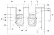
도 1은 본 실시예들에 따른 반도체 장치를 도시한 평면도이다.
도 2a는 도 1의 A-A'선에 따른 단면도이다.
도 2b를 도 1의 B-B'선에 따른 단면도이다.
도 3 내지 도 7은 다른 실시예들에 따른 반도체 장치를 도시한 단면도이다.
도 8a 내지 도 8k는 일실시예에 따른 반도체 장치를 형성하는 방법의 일 예를 설명하기 위한 도면이다.
도 9a 및 도 9b는 반도체 장치를 형성하는 방법의 다른 예를 설명하기 위한 도면이다.
도 10은 메모리셀을 설명하기 위한 도면이다.FIG. 1 is a plan view illustrating a semiconductor device according to the present embodiments.
Fig. 2a is a cross-sectional view taken along line A-A' of Fig. 1.
Fig. 2b is a cross-sectional view taken along line B-B' of Fig. 1.
FIGS. 3 to 7 are cross-sectional views illustrating semiconductor devices according to other embodiments.
FIGS. 8A to 8K are drawings for explaining an example of a method for forming a semiconductor device according to one embodiment.
FIGS. 9A and 9B are drawings for explaining another example of a method for forming a semiconductor device.
Figure 10 is a drawing for explaining a memory cell.
본 명세서에서 기재하는 실시예들은 본 발명의 이상적인 개략도인 단면도, 평면도 및 블록도를 참고하여 설명될 것이다. 따라서, 제조 기술 및/또는 허용 오차 등에 의해 예시도의 형태가 변형될 수 있다. 따라서, 본 발명의 실시예들은 도시된 특정 형태로 제한되는 것이 아니라 제조 공정에 따라 생성되는 형태의 변화도 포함하는 것이다. 따라서, 도면에서 예시된 영역들은 개략적인 속성을 가지며, 도면에서 예시된 영역들의 모양은 소자의 영역의 특정 형태를 예시하기 위한 것이고, 발명의 범주를 제한하기 위한 것은 아니다.The embodiments described in this specification will be described with reference to the cross-sectional views, plan views and block diagrams, which are ideal schematic diagrams of the present invention. Accordingly, the forms of the exemplary drawings may be modified due to manufacturing techniques and/or tolerances, etc. Accordingly, the embodiments of the present invention are not limited to the specific forms illustrated, but also include changes in forms produced according to the manufacturing process. Accordingly, the regions illustrated in the drawings have schematic properties, and the shapes of the regions illustrated in the drawings are intended to illustrate specific forms of regions of the elements, and are not intended to limit the scope of the invention.
이하, 실시예들에서, 문턱전압(Threshold voltage; Vt)은 플랫밴드전압(Flat-band voltage; VFB)에 의존한다. 플랫밴드전압(VFB)은 일함수(workfunction)에 의존한다. 일함수는 다양한 방법에 의해 엔지니어링될 수 있다. 예컨대, 일함수는 게이트전극의 물질, 게이트전극과 채널 사이의 물질 등에 의해 조절될 수 있다. 일함수를 증가시키거나 또는 감소시키므로써 플랫밴드전압이 쉬프트될 수 있다. 고일함수는 플랫밴드전압을 파지티브(positive) 방향으로 쉬프트시킬 수 있고, 저일함수는 플랫밴드전압을 네가티브(negative) 방향으로 쉬프트시킬 수 있다. 위와 같이 플랫밴드전압의 쉬프트에 의해, 문턱전압을 조절할 수 있다. 실시예들은, 채널 농도를 감소시키거나 채널 도핑을 생략하더라도, 플랫밴드전압 쉬프트에 의해 문턱전압을 조절할 수 있다. 특히, 저일함수물질 또는 에어갭에 의해 플랫밴드전압을 낮출 수 있고, 이로 인해 게이트유도드레인누설(GIDL)을 개선할 수 있다.In the following embodiments, the threshold voltage (Vt) depends on the flat-band voltage (VFB). The flat-band voltage (VFB) depends on the work function. The work function can be engineered in various ways. For example, the work function can be adjusted by the material of the gate electrode, the material between the gate electrode and the channel, etc. The flat-band voltage can be shifted by increasing or decreasing the work function. A high work function can shift the flat-band voltage in the positive direction, and a low work function can shift the flat-band voltage in the negative direction. As described above, the threshold voltage can be adjusted by the shift of the flat-band voltage. In the embodiments, the threshold voltage can be adjusted by the shift of the flat-band voltage even when the channel concentration is reduced or channel doping is omitted. In particular, the flat band voltage can be lowered by a low work function material or an air gap, thereby improving gate-induced drain leakage (GIDL).
이하, 실시예들에서 매립 게이트 구조(buried gate structure)는 트렌치 내에 위치할 수 있다. 매립 게이트 구조는 게이트절연층, 게이트전극 및 캡핑층의 스택을 포함할 수 있다. 게이트절연층은 트렌치의 표면을 커버링할 수 있고, 게이트전극은 게이트절연층 상에서 트렌치를 부분적으로 채울 수 있으며, 캡핑층은 게이트전극 상에서 트렌치의 나머지부분을 채울 수 있다. 따라서, 게이트전극을 '매립 게이트 전극(buried gate electrode)'이라고 지칭할 수 있다.Hereinafter, in the embodiments, a buried gate structure may be positioned within a trench. The buried gate structure may include a stack of a gate insulating layer, a gate electrode, and a capping layer. The gate insulating layer may cover a surface of the trench, the gate electrode may partially fill the trench on the gate insulating layer, and the capping layer may fill the remainder of the trench on the gate electrode. Accordingly, the gate electrode may be referred to as a 'buried gate electrode.'
게이트전극은 싱글 게이트(Single gate) 또는 듀얼 게이트(Dual gate)를 포함할 수 있다. 싱글 게이트는 폴리실리콘 또는 금속-베이스 물질 단독으로 이루어진 게이트를 지칭할 수 있다. 싱글 게이트는 폴리실리콘 싱글 게이트 또는 금속 싱글 게이트를 포함할 수 있다. 듀얼 게이트는 서로 다른 게이트전극의 이중 스택(bilayer stack)을 지칭할 수 있다. 듀얼 게이트는 동일 금속의 스택으로 이루어진 동일 금속 듀얼 게이트, 서로 다른 금속의 스택으로 이루어진 이종 금속 듀얼 게이트 또는 금속과 폴리실리콘의 스택으로 이루어진 이종 물질 듀얼 게이트를 포함할 수 있다.The gate electrode may include a single gate or a dual gate. A single gate may refer to a gate made solely of polysilicon or a metal-based material. The single gate may include a polysilicon single gate or a metal single gate. The dual gate may refer to a bilayer stack of different gate electrodes. The dual gate may include a same-metal dual gate made of a stack of the same metal, a dissimilar-metal dual gate made of a stack of different metals, or a dissimilar-material dual gate made of a stack of metal and polysilicon.
게이트전극은 배리어층 및 저저항 물질을 포함할 수 있다. 배리어층은 저저항물질로부터 확산되는 불순물을 차단하거나 서로 다른 물질들간의 상호 확산 및 반응을 방지하는 역할을 할 수 있다. 저저항 물질은 게이트전극의 시트저항을 감소시키는 역할을 할 수 있다.The gate electrode may include a barrier layer and a low-resistance material. The barrier layer may serve to block impurities diffusing from the low-resistance material or prevent mutual diffusion and reaction between different materials. The low-resistance material may serve to reduce the sheet resistance of the gate electrode.
게이트전극은 일함수가 엔지니어링된 물질을 포함할 수 있다. 일함수 엔지니어링은 감소된 일함수(즉, 저일함수) 또는 증가된 일함수(즉, 고일함수)를 갖도록 일함수를 조절할 수 있는 물질 또는 방법을 지칭할 수 있다.The gate electrode may comprise a material having an engineered work function. Work function engineering may refer to a material or method capable of adjusting the work function to have a reduced work function (i.e., a low work function) or an increased work function (i.e., a high work function).
본 실시예에서, 게이트전극은 하부 게이트(Lower Buried portion; LB) 및 상부 게이트(Upper Buried portion; UB)를 포함할 수 있다. 하부 게이트는 트렌치의 하부(lower portion)를 채울 수 있고, 상부 게이트는 하부 게이트 상에서 트렌치의 중간부(middle portion) 또는 상부(upper portion)를 채울 수 있다. 위와 같이, 게이트전극은 하부 게이트 상에 상부 게이트가 위치하는 듀얼 게이트일 수 있다. 하부 게이트는 채널과 오버랩될 수 있고, 상부 게이트는 제1 및 제2도핑영역(즉, 소스/드레인영역)과 수평하게 오버랩(Laterally overlap)될 수 있다.In the present embodiment, the gate electrode may include a lower buried portion (LB) and an upper buried portion (UB). The lower gate may fill a lower portion of the trench, and the upper gate may fill a middle portion or an upper portion of the trench on the lower gate. As described above, the gate electrode may be a dual gate in which the upper gate is positioned on the lower gate. The lower gate may overlap with the channel, and the upper gate may laterally overlap with the first and second doped regions (i.e., source/drain regions).
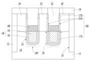
도 1은 본 실시예들에 따른 반도체 장치를 도시한 평면도이다. 도 2a는 도 1의 A-A'선에 따른 단면도이다. 도 2b를 도 1의 B-B'선에 따른 단면도이다.FIG. 1 is a plan view illustrating a semiconductor device according to the present embodiments. FIG. 2a is a cross-sectional view taken along line A-A' of FIG. 1. FIG. 2b is a cross-sectional view taken along line B-B' of FIG. 1.
도 1a 내지 도 2b를 참조하면, 반도체 장치(100)는 기판(101) 및 기판(101)에 내장된 매립게이트구조(100G)를 포함할 수 있다. 반도체 장치(100)는 메모리셀의 일부일 수 있다. 예컨대, 반도체 장치(100)는 DRAM의 메모리셀의 일부일 수 있다.Referring to FIGS. 1A to 2B, the semiconductor device (100) may include a substrate (101) and a buried gate structure (100G) embedded in the substrate (101). The semiconductor device (100) may be a part of a memory cell. For example, the semiconductor device (100) may be a part of a memory cell of a DRAM.
기판(101)은 반도체프로세싱에 적합한 물질일 수 있다. 기판(101)은 반도체기판을 포함할 수 있다. 기판(101)은 실리콘을 함유하는 물질로 이루어질 수 있다. 기판(101)은 실리콘, 단결정 실리콘, 폴리실리콘, 비정질 실리콘, 실리콘저마늄, 단결정 실리콘저마늄, 다결정 실리콘저마늄, 탄소 도핑된 실리콘, 그들의 조합 또는 그들의 다층을 포함할 수 있다. 기판(101)은 저마늄과 같은 다른 반도체물질을 포함할 수도 있다. 기판(101)은 Ⅲ/Ⅴ족 반도체기판, 예컨대 GaAs과 같은 화합물반도체기판을 포함할 수도 있다. 기판(101)은 SOI(Silicon On Insulator) 기판을 포함할 수도 있다.The substrate (101) may be a material suitable for semiconductor processing. The substrate (101) may include a semiconductor substrate. The substrate (101) may be made of a material containing silicon. The substrate (101) may include silicon, single crystal silicon, polysilicon, amorphous silicon, silicon germanium, single crystal silicon germanium, polycrystalline silicon germanium, carbon doped silicon, combinations thereof, or multilayers thereof. The substrate (101) may also include other semiconductor materials, such as germanium. The substrate (101) may also include a III/V group semiconductor substrate, for example, a compound semiconductor substrate, such as GaAs. The substrate (101) may also include a SOI (Silicon On Insulator) substrate.
기판(101)에 소자분리층(102) 및 활성영역(104)이 형성될 수 있다. 소자분리층(102)에 의해 활성영역(104)이 정의될 수 있다. 소자분리층(102)은 트렌치 식각에 의해 형성된 STI 영역(Shallow Trench Isolation region)일 수 있다. 소자분리층(102)은 얕은 트렌치, 예들 들어, 분리트렌치(Isolation trench, 103)에 절연물질을 채워 형성할 수 있다. 소자분리층(102)은 실리콘산화물, 실리콘질화물 또는 이들의 조합을 포함할 수 있다.A device isolation layer (102) and an active region (104) may be formed on a substrate (101). The active region (104) may be defined by the device isolation layer (102). The device isolation layer (102) may be a shallow trench isolation region (STI) formed by trench etching. The device isolation layer (102) may be formed by filling a shallow trench, for example, an isolation trench (103), with an insulating material. The device isolation layer (102) may include silicon oxide, silicon nitride, or a combination thereof.
기판(101) 내에 트렌치(105)가 형성될 수 있다. 도 1의 평면도로 볼 때, 트렌치(105)는 어느 한 방향으로 연장된 라인 형상(line shaped)일 수 있다. 트렌치(105)는 활성영역(104)과 소자분리층(102)을 횡단하는 라인형상일 수 있다. 트렌치(105)는 분리트렌치(103)보다 더 얕은 깊이를 가질 수 있다. 다른 실시예에서, 트렌치(105)의 저부는 곡률을 가질 수 있다. 트렌치(105)는 매립 게이트 구조(100G)가 형성되는 공간으로서, '게이트 트렌치'라고 지칭할 수 있다.A trench (105) may be formed within the substrate (101). When viewed in the plan view of FIG. 1, the trench (105) may have a line shape extending in one direction. The trench (105) may have a line shape crossing the active region (104) and the device isolation layer (102). The trench (105) may have a shallower depth than the isolation trench (103). In another embodiment, the bottom of the trench (105) may have a curvature. The trench (105) is a space where a buried gate structure (100G) is formed, and may be referred to as a 'gate trench'.
활성영역(104) 내에 제1도핑영역(107)과 제2도핑영역(108)이 형성될 수 있다. 제1도핑영역(107)과 제2도핑영역(108)은 도전형 도펀트가 도핑된 영역이다. 예컨대, 도전형 도펀트는 인(P), 비소(As), 안티몬(Sb) 또는 붕소(B)를 포함할 수 있다. 제1도핑영역(107)과 제2도핑영역(108)은 동일 도전형의 도펀트로 도핑될 수 있다. 트렌치(105) 양측의 활성영역(104) 내에 제1도핑영역(107)과 제2도핑영역(108)이 위치할 수 있다. 제1도핑영역(107)과 제2도핑영역(108)의 저면은 활성영역(104)의 상부 표면(top surface)으로부터 소정의 깊이에 위치할 수 있다. 제1도핑영역(107)과 제2도핑영역(108)은 트렌치(105)의 측벽에 접할 수 있다. 제1도핑영역(107)과 제2도핑영역(108)의 저면은 트렌치(105)의 바닥면보다 높을 수 있다. 제1도핑영역(107)은 '제1소스/드레인영역'이라고 지칭할 수 있고, 제2도핑영역(108)은 '제2소스/드레인영역'이라고 지칭할 수 있다. 매립 게이트구조(100G)에 의해 제1도핑영역(107)과 제2도핑영역(108) 사이에 채널(106)이 정의될 수 있다. 채널(106)은 트렌치(105)의 프로파일을 따라 정의될 수 있다.A first doping region (107) and a second doping region (108) may be formed in the active region (104). The first doping region (107) and the second doping region (108) are regions doped with a conductive dopant. For example, the conductive dopant may include phosphorus (P), arsenic (As), antimony (Sb), or boron (B). The first doping region (107) and the second doping region (108) may be doped with a dopant of the same conductive type. The first doping region (107) and the second doping region (108) may be located in the active region (104) on both sides of the trench (105). The bottom surfaces of the first doping region (107) and the second doping region (108) may be located at a predetermined depth from the top surface of the active region (104). The first doped region (107) and the second doped region (108) may be in contact with the sidewall of the trench (105). The bottom surfaces of the first doped region (107) and the second doped region (108) may be higher than the bottom surface of the trench (105). The first doped region (107) may be referred to as a 'first source/drain region', and the second doped region (108) may be referred to as a 'second source/drain region'. A channel (106) may be defined between the first doped region (107) and the second doped region (108) by the buried gate structure (100G). The channel (106) may be defined along the profile of the trench (105).
트렌치(105)는 제1트렌치(T1)와 제2트렌치(T2)를 포함할 수 있다. 제1트렌치(T1)는 활성영역(104) 내에 형성된다. 제2트렌치(T2)는 소자분리층(102) 내에 형성된다. 제1트렌치(T1)로부터 제2트렌치(T2)로 연속적으로 연장될 수 있다. 트렌치(105)에서, 제1트렌치(T1)와 제2트렌치(T2)는 서로 다른 레벨에 위치하는 바닥면을 가질 수 있다. 예를 들어, 제1트렌치(T1)의 바닥면은 제2트렌치(T2)의 바닥면보다 높은 레벨에 위치할 수 있다. 제1트렌치(T1)와 제2트렌치(T2)의 높이 차이는 소자분리층(102)이 리세스됨에 따라 형성된다. 따라서, 제2트렌치(T2)는 제1트렌치(T1)의 바닥면보다 낮은 바닥면을 갖는 리세스영역(R)을 포함할 수 있다. 제1트렌치(T1)와 제2트렌치(T2) 사이의 단차로 인하여 활성영역(104)에 핀영역(Fin, 104F)이 형성된다. 따라서, 활성영역(104)은 핀영역(104F)을 포함할 수 있다.The trench (105) may include a first trench (T1) and a second trench (T2). The first trench (T1) is formed in the active region (104). The second trench (T2) is formed in the device isolation layer (102). The trench may extend continuously from the first trench (T1) to the second trench (T2). In the trench (105), the first trench (T1) and the second trench (T2) may have bottom surfaces positioned at different levels. For example, the bottom surface of the first trench (T1) may be positioned at a higher level than the bottom surface of the second trench (T2). The height difference between the first trench (T1) and the second trench (T2) is formed as the device isolation layer (102) is recessed. Accordingly, the second trench (T2) may include a recess region (R) having a bottom surface lower than the bottom surface of the first trench (T1). Due to the step between the first trench (T1) and the second trench (T2), a fin region (Fin, 104F) is formed in the active region (104). Accordingly, the active region (104) may include the fin region (104F).
이와 같이, 제1트렌치(T1) 아래에 핀영역(104F)이 형성되고, 핀영역(104F)의 측벽은 리세스된 소자분리층(102F)에 의해 노출된다. 핀영역(104F)은 채널(106)의 일부가 형성되는 부분이다. 핀영역(104F)은 새들핀(Saddle Fin)이라고 일컫는다. 핀영역(104F)에 의해 채널 폭을 증가시킬 수 있고, 전기적 특성을 향상시킬 수 있다.In this way, a fin region (104F) is formed under the first trench (T1), and a side wall of the fin region (104F) is exposed by the recessed device isolation layer (102F). The fin region (104F) is a portion where a part of the channel (106) is formed. The fin region (104F) is referred to as a saddle fin. The channel width can be increased and the electrical characteristics can be improved by the fin region (104F).
다른 실시예에서, 핀영역(104F)은 생략될 수 있다.In other embodiments, the pin area (104F) may be omitted.
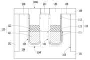
매립게이트구조(100G)는 트렌치(105)의 저면 및 측벽을 커버링하는 게이트절연구조물(110), 게이트절연구조물(110) 상에서 트렌치(105)를 채우도록 순차적으로 적층된 게이트전극(120) 및 캡핑층(130)을 포함할 수 있다. 게이트전극(120)은 하부 게이트(121)와 상부 게이트(122)를 포함할 수 있다. 하부 게이트(121)는 게이트절연구조물(110) 상에 트렌치(105)의 하부(Lower portion)를 채울 수 있고, 상부 게이트(122)는 하부 게이트(121) 상에서 트렌치(105)의 중간부(middle portion)를 채울 수 있다. 캡핑층(130)은 상부 게이트(122) 상에서 트렌치(105)의 상부(upper portion)를 채울 수 있다. 트렌치(105)의 하부, 중간부 및 상부는 설명의 편의를 위한 것으로서, 각각의 높이(또는 깊이)는 서로 동일하거나 다를 수 있다.The buried gate structure (100G) may include a gate insulating structure (110) covering a bottom surface and side walls of a trench (105), a gate electrode (120) and a capping layer (130) sequentially stacked on the gate insulating structure (110) to fill the trench (105). The gate electrode (120) may include a lower gate (121) and an upper gate (122). The lower gate (121) may fill a lower portion of the trench (105) on the gate insulating structure (110), and the upper gate (122) may fill a middle portion of the trench (105) on the lower gate (121). The capping layer (130) may fill an upper portion of the trench (105) on the upper gate (122). The lower, middle and upper parts of the trench (105) are for convenience of explanation, and the height (or depth) of each may be the same or different.
게이트절연구조물(110)은 제1게이트절연층(111), 제2게이트절연층(112) 및 에어갭(113)을 포함할 수 있다. 에어갭(113)은 제1게이트절연층(111)과 제2게이트절연층(112) 사이에 위치할 수 있다. 에어갭(113)은 제1게이트절연층(111)과 제2게이트절연층(112) 사이에서 수직하게 형성될 수 있다. 에어갭(113)은 수직형 에어갭이라고 지칭할 수 있다.The gate insulating structure (110) may include a first gate insulating layer (111), a second gate insulating layer (112), and an air gap (113). The air gap (113) may be positioned between the first gate insulating layer (111) and the second gate insulating layer (112). The air gap (113) may be formed vertically between the first gate insulating layer (111) and the second gate insulating layer (112). The air gap (113) may be referred to as a vertical air gap.
제1게이트절연층(111)은 트렌치(105)의 하부에 형성될 수 있다. 예를 들어, 제1게이트절연층(111)은 트렌치(105)의 바닥면 및 하부 측벽들 상에 컨포멀하게 형성될 수 있다. 제1게이트절연층(111)은 실리콘산화물(Silicon oxide), 실리콘질화물(Silicon nitride), 실리콘산화질화물(Silicon oxynitride), 고유전물질(High-k material) 또는 이들의 조합을 포함할 수 있다. 고유전물질은 실리콘산화물의 유전상수(dielectric constant)보다 더 큰 유전상수를 갖는 물질을 포함할 수 있다. 예컨대, 고유전물질은 3.9보다 큰 유전상수를 갖는 물질을 포함할 수 있다. 다른 예에서, 고유전물질은 10보다 큰 유전상수를 갖는 물질을 포함할 수 있다. 또다른 예에서, 고유전물질은 10 내지 30의 유전상수를 갖는 물질을 포함할 수 있다. 고유전물질은 적어도 하나의 금속성 원소(at least one metallic element)를 포함할 수 있다. 고유전물질은 하프늄함유물질(hafnium-containing material)을 포함할 수 있다. 하프늄함유물질은 하프늄산화물(hafnium oxide), 하프늄실리콘산화물(hafnium silicon oxide), 하프늄실리콘산화질화물(hafnium silicon oxynitride) 또는 그들의 조합을 포함할 수 있다. 다른 실시예에서, 고유전물질은 란타늄산화물(lanthanum oxide), 란타늄알루미늄산화물(lanthanum aluminum oxide), 지르코늄산화물(zirconium oxide), 지르코늄실리콘산화물(zirconium silicon oxide), 지르코늄실리콘산화질화물(zirconium silicon oxynitride), 알루미늄산화물(aluminum oxide) 또는 그들의 조합을 포함할 수 있다. 고유전물질로는 공지된 다른 고유전물질이 선택적으로 사용될 수도 있다. 제1게이트절연층(111)은 금속산화물을 포함할 수 있다. 제1게이트절연층(111)은 하부 게이트(121)의 저면 및 측벽들을 에워싸는 형상일 수 있다. 제1게이트절연층(111)은 채널(106)과 하부 게이트(121) 사이에 위치할 수 있다.The first gate insulating layer (111) may be formed at the bottom of the trench (105). For example, the first gate insulating layer (111) may be conformally formed on the bottom surface and lower sidewalls of the trench (105). The first gate insulating layer (111) may include silicon oxide, silicon nitride, silicon oxynitride, a high-k material, or a combination thereof. The high-k material may include a material having a dielectric constant greater than a dielectric constant of silicon oxide. For example, the high-k material may include a material having a dielectric constant greater than 3.9. In another example, the high-k material may include a material having a dielectric constant greater than 10. In another example, the high-k material may include a material having a dielectric constant of 10 to 30. The high-k dielectric material may include at least one metallic element. The high-k dielectric material may include a hafnium-containing material. The hafnium-containing material may include hafnium oxide, hafnium silicon oxide, hafnium silicon oxynitride, or a combination thereof. In another embodiment, the high-k dielectric material may include lanthanum oxide, lanthanum aluminum oxide, zirconium oxide, zirconium silicon oxide, zirconium silicon oxynitride, aluminum oxide, or a combination thereof. Other known high-k dielectric materials may optionally be used as the high-k dielectric material. The first gate insulating layer (111) may include a metal oxide. The first gate insulating layer (111) may have a shape that surrounds the bottom surface and side walls of the lower gate (121). The first gate insulating layer (111) may be located between the channel (106) and the lower gate (121).
제2게이트절연층(112)은 트렌치(105)의 상부에 형성될 수 있다. 예를 들어, 제2게이트절연층(112)은 트렌치(105)의 상부 측벽들 상에 형성될 수 있다. 제1게이트절연층(111)과 제2게이트절연층(112)은 동일 물질로 형성될 수 있다. 제2게이트절연층(112)은 실리콘산화물(Silicon oxide), 실리콘질화물(Silicon nitride), 실리콘산화질화물(Silicon oxynitride), 고유전물질(High-k material) 또는 이들의 조합을 포함할 수 있다. 제2게이트절연층(112)은 제1 및 제2도핑영역(107, 108)에 접촉할 수 있다. 제2게이트절연층(112)은 캡핑층(130)의 측벽들에 접촉할 수 있다. 제2게이트절연층(112)은 캡핑층(130)의 측벽들을 부분적으로 커버링할 수 있다. 제2게이트절연층(112)은 제1 및 제2도핑영역(107, 108)의 측벽들을 부분적으로 커버링할 수 있다.The second gate insulating layer (112) may be formed on the upper portion of the trench (105). For example, the second gate insulating layer (112) may be formed on upper sidewalls of the trench (105). The first gate insulating layer (111) and the second gate insulating layer (112) may be formed of the same material. The second gate insulating layer (112) may include silicon oxide, silicon nitride, silicon oxynitride, a high-k material, or a combination thereof. The second gate insulating layer (112) may be in contact with the first and second doped regions (107, 108). The second gate insulating layer (112) may be in contact with sidewalls of the capping layer (130). The second gate insulating layer (112) can partially cover the sidewalls of the capping layer (130). The second gate insulating layer (112) can partially cover the sidewalls of the first and second doped regions (107, 108).
에어갭(113)은 제1게이트절연층(111)과 제2게이트절연층(112) 사이에 형성될 수 있다. 에어갭(113)은 캡핑층(130)의 측벽들을 부분적으로 커버링할 수 있다. 에어갭(113)은 제1 및 제2도핑영역(107, 108)의 측벽들을 부분적으로 커버링할 수 있다. 에어갭(113)은 상부 게이트(122)의 측벽들을 부분적으로 커버링할 수 있다.An air gap (113) may be formed between the first gate insulating layer (111) and the second gate insulating layer (112). The air gap (113) may partially cover sidewalls of the capping layer (130). The air gap (113) may partially cover sidewalls of the first and second doped regions (107, 108). The air gap (113) may partially cover sidewalls of the upper gate (122).
위와 같이, 에어갭(113)은 캡핑층(130)의 측벽들, 제1 및 제2도핑영역(107, 108)의 측벽들 및 상부 게이트(122)의 측벽들을 모두 부분적으로 커버링하는 형상일 수 있다. 에어갭(113)의 저면은 하부 게이트(121)의 상부 표면보다 높은 레벨 또는 동일 레벨에 위치할 수 있다. 에어갭(113)의 상부 표면은 상부 게이트(122)의 상부 표면보다 높은 레벨에 위치할 수 있다.As described above, the air gap (113) may have a shape that partially covers all of the sidewalls of the capping layer (130), the sidewalls of the first and second doping regions (107, 108), and the sidewalls of the upper gate (122). The lower surface of the air gap (113) may be located at a level higher than or the same level as the upper surface of the lower gate (121). The upper surface of the air gap (113) may be located at a level higher than the upper surface of the upper gate (122).
제1,2도핑영역(107, 108)과 상부 게이트(122) 사이에 수평하게 에어갭(113)이 위치할 수 있다. 캡핑층(130)의 측벽들과 제1,2도핑영역(107, 108)의 측벽들 사이에 에어갭(113)이 위치할 수 있다.An air gap (113) may be positioned horizontally between the first and second doping regions (107, 108) and the upper gate (122). An air gap (113) may be positioned between the side walls of the capping layer (130) and the side walls of the first and second doping regions (107, 108).
게이트전극(120)은 활성영역(104)의 상부 표면보다 낮은 레벨일 수 있다. 하부 게이트(121)는 트렌치(105)의 저부를 채우는 형상일 수 있다. 하부 게이트(121)는 게이트시트저항을 낮추기 위해 저저항 물질일 수 있다. 하부 게이트(121)는 금속-베이스 물질일 수 있다. 하부 게이트(121)는 금속, 금속질화물 또는 이들의 조합을 포함할 수 있다. 하부 게이트(121)는 탄탈륨질화물(TaN), 티타늄질화물(TiN), 텅스텐(W), 텅스텐질화물(WN) 또는 이들의 조합을 포함할 수 있다. 하부 게이트(121)는 티타늄질화물 단독으로 형성될 수 있다. 또한, 하부 게이트(121)는 티타늄질화물과 텅스텐의 스택(즉, TiN/W)으로 형성될 수 있다.The gate electrode (120) may be at a level lower than the upper surface of the active region (104). The lower gate (121) may have a shape that fills the bottom of the trench (105). The lower gate (121) may be a low-resistance material to lower the gate sheet resistance. The lower gate (121) may be a metal-based material. The lower gate (121) may include a metal, a metal nitride, or a combination thereof. The lower gate (121) may include tantalum nitride (TaN), titanium nitride (TiN), tungsten (W), tungsten nitride (WN), or a combination thereof. The lower gate (121) may be formed of titanium nitride alone. Additionally, the lower gate (121) may be formed of a stack of titanium nitride and tungsten (i.e., TiN/W).
다른 실시예에서, 하부 게이트(121)는 고일함수(High workfunction)를 가질 수 있다. 여기서, 고일함수란 실리콘의 미드갭일함수(Mid-gap Work Function)보다 높은 일함수를 지칭한다. 저일함수는 실리콘의 미드갭일함수보다 낮은 일함수를 지칭한다. 부연 설명하면, 고일함수는 4.5eV보다 높은 일함수를 갖고, 저일함수는 4.5eV보다 낮은 일함수를 가질 수 있다. 하부 게이트(121)는 P형 폴리실리콘을 포함할 수 있다.In another embodiment, the lower gate (121) may have a high work function. Here, the high work function refers to a work function higher than the mid-gap work function of silicon. The low work function refers to a work function lower than the mid-gap work function of silicon. In further explanation, the high work function may have a work function higher than 4.5 eV, and the low work function may have a work function lower than 4.5 eV. The lower gate (121) may include P-type polysilicon.
다른 실시예에서, 하부 게이트(121)는 증가된 고일함수를 가질 수 있다. 하부 게이트(121)는 금속실리콘질화물을 포함할 수 있다. 금속실리콘질화물은 금속질화물에 실리콘이 도핑될 수 있다. 하부 게이트(121)는 실리콘의 함량이 조절된 금속실리콘질화물을 포함할 수 있다. 예컨대, 하부 게이트(121)는 탄탈륨실리콘질화물(TaSiN) 또는 티타늄실리콘질화물(TiSiN)을 포함할 수 있다. 티타늄질화물은 고일함수를 갖고, 티타늄질화물의 일함수를 더욱 증가시키기 위해, 티타늄질화물에 실리콘이 함유될 수 있다. 티타늄실리콘질화물은 증가된 고일함수를 갖기 위해, 실리콘의 함량이 조절될 수 있다. 증가된 고일함수를 갖기 위해, 티타늄실리콘질화물 내 실리콘의 함량(atomic percent; at%)은 21at% 이하일 수 있다. 비교예로서, 저일함수를 갖기 위해, 티타늄실리콘질화물 내 실리콘의 함량은 30at% 이상일 수 있다.In another embodiment, the lower gate (121) can have an increased work function. The lower gate (121) can include metal silicon nitride. The metal silicon nitride can be doped with silicon in the metal nitride. The lower gate (121) can include metal silicon nitride having an adjusted silicon content. For example, the lower gate (121) can include tantalum silicon nitride (TaSiN) or titanium silicon nitride (TiSiN). Titanium nitride has a high work function, and silicon can be contained in the titanium nitride to further increase the work function of the titanium nitride. The titanium silicon nitride can have an adjusted silicon content to have an increased work function. In order to have an increased work function, the silicon content (atomic percent; at%) in the titanium silicon nitride can be 21 at% or less. As a comparative example, in order to have a low work function, the silicon content in titanium silicon nitride can be 30 at% or more.
상부 게이트(122)는 하부 게이트(121) 상에 형성될 수 있고, 상부 게이트(122)의 상부 표면은 활성영역(104)의 상부 표면보다 낮은 레벨일 수 있다. 상부 게이트(122)는 트렌치(105)의 중간부를 부분적으로 채우는 형상일 수 있다. 상부 게이트(122)와 하부 게이트(121)는 동일 물질이거나 서로 다른 물질일 수 있다.The upper gate (122) may be formed on the lower gate (121), and the upper surface of the upper gate (122) may be at a lower level than the upper surface of the active region (104). The upper gate (122) may have a shape that partially fills the middle portion of the trench (105). The upper gate (122) and the lower gate (121) may be made of the same material or different materials.
상부 게이트(122)는 게이트시트저항을 낮추기 위해 저저항 물질일 수 있다. 상부 게이트(122)는 금속-베이스 물질일 수 있다. 상부 게이트(122)는 금속, 금속질화물 또는 이들의 조합을 포함할 수 있다. 상부 게이트(122)는 탄탈륨질화물(TaN), 티타늄질화물(TiN), 텅스텐, 텅스텐질화물 또는 이들의 조합을 포함할 수 있다. 상부 게이트(UB)는 티타늄질화물 단독으로 형성될 수 있다. 또한, 상부 게이트(UB)는 티타늄질화물과 텅스텐의 스택(즉, TiN/W)으로 형성될 수 있다. 일부 실시예에서, 하부 게이트(121)와 상부 게이트(122)는 각각 티타늄질화물 단독으로 형성될 수 있다. 또한, 하부 게이트(121) 및 상부 게이트(122)는 각각 티타늄질화물과 텅스텐의 스택(TiN/W)으로 형성될 수 있다. 상부 게이트(122)는 하부 게이트(121)보다 낮은 높이를 가질 수 있고, 이에 따라 트렌치(105) 내에서 차지하는 하부 게이트(121)의 체적이 더 클 수 있다.The upper gate (122) may be a low-resistance material to lower the gate sheet resistance. The upper gate (122) may be a metal-based material. The upper gate (122) may include a metal, a metal nitride, or a combination thereof. The upper gate (122) may include tantalum nitride (TaN), titanium nitride (TiN), tungsten, tungsten nitride, or a combination thereof. The upper gate (UB) may be formed of titanium nitride alone. Additionally, the upper gate (UB) may be formed of a stack of titanium nitride and tungsten (i.e., TiN/W). In some embodiments, the lower gate (121) and the upper gate (122) may each be formed of titanium nitride alone. Additionally, the lower gate (121) and the upper gate (122) may each be formed of a stack of titanium nitride and tungsten (TiN/W). The upper gate (122) may have a lower height than the lower gate (121), and thus the volume of the lower gate (121) occupied within the trench (105) may be larger.
다른 실시예에서, 상부 게이트(122)는 저일함수(Low workfunction)를 가질 수 있다. 상부 게이트(122)는 N형 폴리실리콘을 포함할 수 있다. 일부 실시예에서, 하부 게이트(121)는 P형 폴리실리콘일 수 있고, 상부 게이트(122)는 N형 폴리실리콘일 수 있다. 또한, 하부 게이트(121)는 티타늄질화물과 텅스텐의 스택(TiN/W)으로 형성될 수 있고, 상부 게이트(122)는 N형 폴리실리콘일 수 있다.In another embodiment, the upper gate (122) can have a low workfunction. The upper gate (122) can include N-type polysilicon. In some embodiments, the lower gate (121) can be P-type polysilicon, and the upper gate (122) can be N-type polysilicon. Additionally, the lower gate (121) can be formed of a stack of titanium nitride and tungsten (TiN/W), and the upper gate (122) can be N-type polysilicon.
본 실시예에서, 하부 게이트(121)는 저저항 금속-베이스 물질일 수 있고, 상부 게이트(122)는 저일함수 물질일 수 있다. 하부 게이트(121)는 TiN 또는 TiN/W 스택일 수 있고, 상부 게이트(122)는 N형 폴리실리콘일 수 있다.In this embodiment, the lower gate (121) can be a low-resistance metal-based material, and the upper gate (122) can be a low-work-function material. The lower gate (121) can be TiN or a TiN/W stack, and the upper gate (122) can be N-type polysilicon.
캡핑층(130)은 상부 게이트(122)를 보호하는 역할을 한다. 캡핑층(130)은 상부 게이트(122) 상에서 트렌치(105)의 상부를 채울 수 있다. 캡핑층(130)의 상부 표면은 제1 및 제2도핑영역(107, 108)의 상부 표면과 동일 레벨에 위치할 수 있다. 캡핑층(130)은 절연물질을 포함할 수 있다. 캡핑층(130)은 실리콘질화물, 실리콘산화질화물 또는 이들의 조합을 포함할 수 있다. 다른 실시예에서, 캡핑층(130)은 실리콘질화물과 실리콘산화물의 조합을 포함할 수 있다. 캡핑층(130)은 실리콘질화물라이너 및 스핀온절연물질(Spin On Dielectric; SOD)을 포함할 수 있다. 캡핑층(130)의 측벽들 일부는 제2게이트절연층(112)에 직접 접촉할 수 있다. 캡핑층(130)의 저면은 상부 게이트(122)에 직접 접촉할 수 있다.The capping layer (130) serves to protect the upper gate (122). The capping layer (130) can fill the upper portion of the trench (105) on the upper gate (122). The upper surface of the capping layer (130) can be located at the same level as the upper surfaces of the first and second doped regions (107, 108). The capping layer (130) can include an insulating material. The capping layer (130) can include silicon nitride, silicon oxynitride, or a combination thereof. In another embodiment, the capping layer (130) can include a combination of silicon nitride and silicon oxide. The capping layer (130) can include a silicon nitride liner and a spin-on dielectric (SOD). Some of the sidewalls of the capping layer (130) can be in direct contact with the second gate insulating layer (112). The lower surface of the capping layer (130) can directly contact the upper gate (122).
캡핑층(130)의 양측에 하드마스크층(109)이 형성될 수 있다. 하드마스크층(109)은 절연물질일 수 있다. 하드마스크층(109)는 기판(101) 상에 형성될 수 있으며, 활성영역(104) 및 소자분리층(102)을 커버링할 수 있다.A hard mask layer (109) may be formed on both sides of the capping layer (130). The hard mask layer (109) may be an insulating material. The hard mask layer (109) may be formed on the substrate (101) and may cover the active region (104) and the device isolation layer (102).
상술한 바에 따르면, 게이트절연구조물(110)은 에어갭(113)을 포함할 수 있고, 에어갭(113)에 의해 게이트유도드레인누설(GIDL)을 개선할 수 있다.As described above, the gate insulating structure (110) may include an air gap (113), and gate-induced drain leakage (GIDL) may be improved by the air gap (113).
구체적으로, 게이트전극(120)과 제1,2도핑영역(107, 108) 사이에는 강한 전기장이 생성된다. 이러한 강한 전기장으로 인해서, 게이트유도드레인누설(GIDL)이 발생될 수 있다.Specifically, a strong electric field is generated between the gate electrode (120) and the first and second doping regions (107, 108). Due to this strong electric field, gate-induced drain leakage (GIDL) may occur.
본 실시예에 따른 반도체 장치(100)는 게이트 전극(120)과 제1,2도핑영역(107, 108) 사이에 에어갭(113)이 배치되는 경우, 게이트 전극(120)과 제1,2도핑영역(107, 108) 사이의 유전율이 감소된다. 이러한 유전율 감소에 의해 전기장이 감소되므로 누설전류를 감소시킬 수 있다. 특히, 상부 게이트(122)와 제1,2도핑영역(107, 108) 사이에 에어갭(113) 외에 다른 절연물질이 형성되지 않으므로, 게이트유도드레인누설(GIDL)을 더욱 개선할 수 있다. 비교예로서, 에어갭(113) 및 에어갭(113)보다 높은 유전율을 갖는 절연물질이 존재하는 경우에는 에어갭(113) 단독으로 존재하는 경우보다 게이트유도드레인누설을 감소시키는데 한계가 있다.In the semiconductor device (100) according to the present embodiment, when an air gap (113) is arranged between the gate electrode (120) and the first and second doped regions (107, 108), the dielectric constant between the gate electrode (120) and the first and second doped regions (107, 108) is reduced. Since the electric field is reduced by this reduction in the dielectric constant, the leakage current can be reduced. In particular, since no other insulating material is formed between the upper gate (122) and the first and second doped regions (107, 108) other than the air gap (113), the gate-induced drain leakage (GIDL) can be further improved. As a comparative example, when the air gap (113) and an insulating material having a higher dielectric constant than the air gap (113) are present, there is a limit to reducing the gate-induced drain leakage compared to when the air gap (113) exists alone.
도 3은 다른 실시예에 따른 반도체 장치를 도시한 단면도이다. 도 3의 반도체 장치(200)는 매립 게이트 구조(200G)를 제외한 나머지 구성요소가 도 2a의 반도체 장치(100)와 유사할 수 있다. 이하, 중복되는 구성요소에 대한 자세한 설명은 생략하기로 한다.Fig. 3 is a cross-sectional view illustrating a semiconductor device according to another embodiment. The semiconductor device (200) of Fig. 3 may be similar to the semiconductor device (100) of Fig. 2a in terms of the remaining components except for the buried gate structure (200G). Hereinafter, a detailed description of the overlapping components will be omitted.
도 3을 참조하면, 반도체 장치(200)는 매립 게이트 구조(200G), 제1도핑영역(107) 및 제2도핑영역(108)을 포함할 수 있다. 기판(101)에 소자분리층(102) 및 활성영역(104)이 형성될 수 있다. 활성영역(104) 내에 제1도핑영역(107) 및 제2도핑영역(108)이 형성될 수 있다. 활성영역(104)과 소자분리층(102)을 가로지르는 트렌치, 즉 트렌치(105)가 형성될 수 있다. 트렌치(105) 내에 매립 게이트 구조(200G)가 형성될 수 있다. 매립 게이트 구조(200G)에 의해 제1도핑영역(107)과 제2도핑영역(108) 사이에 채널(106)이 형성될 수 있다. 채널(106)은 트렌치(105)의 프로파일을 따라 정의될 수 있다.Referring to FIG. 3, the semiconductor device (200) may include a buried gate structure (200G), a first doped region (107), and a second doped region (108). A device isolation layer (102) and an active region (104) may be formed on a substrate (101). A first doped region (107) and a second doped region (108) may be formed in the active region (104). A trench, i.e., a trench (105) crossing the active region (104) and the device isolation layer (102), may be formed. A buried gate structure (200G) may be formed in the trench (105). A channel (106) may be formed between the first doped region (107) and the second doped region (108) by the buried gate structure (200G). The channel (106) can be defined along the profile of the trench (105).
트렌치(105) 내에 매립 게이트 구조(200G)가 내장될 수 있다. 매립 게이트 구조(200G)는 제1도핑영역(107)과 제2도핑영역(108) 사이의 활성영역(104) 내에 배치되면서 소자분리층(102) 내로 연장될 수 있다. 매립 게이트 구조(200G) 아래의 활성영역(104) 내에 핀영역(104F)이 위치할 수 있다.A buried gate structure (200G) may be embedded in the trench (105). The buried gate structure (200G) may be positioned in the active region (104) between the first doped region (107) and the second doped region (108) and may extend into the device isolation layer (102). A fin region (104F) may be located in the active region (104) under the buried gate structure (200G).
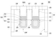
매립 게이트 구조(200G)는 트렌치(105)의 저면 및 측벽을 커버링하는 게이트절연구조물(210), 게이트절연구조물(210) 상에서 트렌치(105)를 채우도록 순차적으로 적층된 게이트전극(120) 및 캡핑층(130)을 포함할 수 있다. 게이트전극(120)은 하부 게이트(121) 및 상부 게이트(122)의 스택을 포함할 수 있다.The buried gate structure (200G) may include a gate insulating structure (210) covering the bottom and side walls of the trench (105), a gate electrode (120) and a capping layer (130) sequentially stacked on the gate insulating structure (210) to fill the trench (105). The gate electrode (120) may include a stack of a lower gate (121) and an upper gate (122).
게이트절연구조물(210)은 제1게이트절연층(211), 제2게이트절연층(212) 및 에어갭(213)을 포함할 수 있다. 에어갭(213)은 제1게이트절연층(211)과 제2게이트절연층(212) 사이에 위치할 수 있다. 에어갭(213)은 제1게이트절연층(211)과 제2게이트절연층(212) 사이에서 수직하게 형성될 수 있다.The gate insulating structure (210) may include a first gate insulating layer (211), a second gate insulating layer (212), and an air gap (213). The air gap (213) may be located between the first gate insulating layer (211) and the second gate insulating layer (212). The air gap (213) may be formed vertically between the first gate insulating layer (211) and the second gate insulating layer (212).
제1게이트절연층(211)은 하부 게이트(121)의 저면 및 측벽들을 에워싸는 형상일 수 있다. 제1게이트절연층(211)은 채널(106)과 하부 게이트(121) 사이에 위치할 수 있다.The first gate insulating layer (211) may have a shape that surrounds the bottom surface and side walls of the lower gate (121). The first gate insulating layer (211) may be located between the channel (106) and the lower gate (121).
제2게이트절연층(212)은 트렌치(105)의 상부에 형성될 수 있다. 예를 들어, 제2게이트절연층(212)은 트렌치(105)의 상부 측벽들 상에 형성될 수 있다. 제1게이트절연층(211)과 제2게이트절연층(212)은 동일 물질로 형성될 수 있다. 제1 및 제2게이트절연층(211, 212)은 실리콘산화물(Silicon oxide), 실리콘질화물(Silicon nitride), 실리콘산화질화물(Silicon oxynitride), 고유전물질(High-k material) 또는 이들의 조합을 포함할 수 있다. 제2게이트절연층(212)은 제1 및 제2도핑영역(107, 108)에 접촉할 수 있다. 제2게이트절연층(212)은 캡핑층(130)의 측벽들에 접촉할 수 있다. 제2게이트절연층(212)은 캡핑층(130)의 측벽들을 부분적으로 커버링할 수 있다. 제2게이트절연층(212)은 제1 및 제2도핑영역(107, 108)의 측벽들을 부분적으로 커버링할 수 있다.The second gate insulating layer (212) may be formed on the upper portion of the trench (105). For example, the second gate insulating layer (212) may be formed on upper sidewalls of the trench (105). The first gate insulating layer (211) and the second gate insulating layer (212) may be formed of the same material. The first and second gate insulating layers (211, 212) may include silicon oxide, silicon nitride, silicon oxynitride, a high-k material, or a combination thereof. The second gate insulating layer (212) may be in contact with the first and second doped regions (107, 108). The second gate insulating layer (212) may be in contact with sidewalls of the capping layer (130). The second gate insulating layer (212) can partially cover the sidewalls of the capping layer (130). The second gate insulating layer (212) can partially cover the sidewalls of the first and second doped regions (107, 108).
에어갭(213)은 캡핑층(130)의 측벽들을 부분적으로 커버링할 수 있다. 에어갭(213)은 제1 및 제2도핑영역(107, 108)의 측벽들을 부분적으로 커버링할 수 있다. 에어갭(213)은 상부 게이트(122)의 측벽들을 완전히 커버링할 수 있다. 에어갭(213)은 하부 게이트(121)의 상부측벽들을 부분적으로 커버링할 수 있다.The air gap (213) may partially cover the sidewalls of the capping layer (130). The air gap (213) may partially cover the sidewalls of the first and second doping regions (107, 108). The air gap (213) may completely cover the sidewalls of the upper gate (122). The air gap (213) may partially cover the upper sidewalls of the lower gate (121).
위와 같이, 에어갭(213)은 캡핑층(130)의 측벽들, 제1 및 제2도핑영역(107, 108)의 측벽들 및 하부 게이트(121)의 측벽들을 모두 부분적으로 커버링하는 형상일 수 있다. 아울러, 에어갭(213)은 상부 게이트(122)의 측벽들을 완전히 커버링할 수 있다. 도 2a의 에어갭(113)은 하부 게이트(121)의 상부측벽들을 커버링하지 않으나, 도 3의 에어갭(213)은 하부 게이트(121)의 상부측벽들을 부분적으로 커버링할 수 있다. 도 3의 에어갭(213)은 도 2a의 에어갭(113)보다 높이가 더 클 수 있다. 에어갭(213)의 저면은 하부 게이트(121)의 상부 표면보다 낮은 레벨에 위치할 수 있다. 에어갭(213)의 상부 표면은 상부 게이트(122)의 상부 표면보다 높은 레벨에 위치할 수 있다.As described above, the air gap (213) may have a shape that partially covers all of the sidewalls of the capping layer (130), the sidewalls of the first and second doping regions (107, 108), and the sidewalls of the lower gate (121). In addition, the air gap (213) may completely cover the sidewalls of the upper gate (122). The air gap (113) of FIG. 2A does not cover the upper sidewalls of the lower gate (121), but the air gap (213) of FIG. 3 may partially cover the upper sidewalls of the lower gate (121). The air gap (213) of FIG. 3 may have a greater height than the air gap (113) of FIG. 2A. The bottom surface of the air gap (213) may be located at a level lower than the upper surface of the lower gate (121). The upper surface of the air gap (213) may be located at a higher level than the upper surface of the upper gate (122).
제1,2도핑영역(107, 108)과 상부 게이트(122) 사이에 수평하게 에어갭(113)이 위치할 수 있다. 캡핑층(130)의 측벽들과 제1,2도핑영역(107, 108)의 측벽들 사이에 수평하게 에어갭(113)이 위치할 수 있다.An air gap (113) may be positioned horizontally between the first and second doping regions (107, 108) and the upper gate (122). An air gap (113) may be positioned horizontally between the side walls of the capping layer (130) and the side walls of the first and second doping regions (107, 108).
도 4는 다른 실시예에 따른 반도체 장치를 도시한 단면도이다. 도 4의 반도체 장치(300)는 매립 게이트 구조(300G)를 제외한 나머지 구성요소가 도 2a의 반도체 장치(100)와 유사할 수 있다. 이하, 중복되는 구성요소에 대한 자세한 설명은 생략하기로 한다.Fig. 4 is a cross-sectional view illustrating a semiconductor device according to another embodiment. The semiconductor device (300) of Fig. 4 may be similar to the semiconductor device (100) of Fig. 2a in terms of the remaining components except for the buried gate structure (300G). Hereinafter, a detailed description of the overlapping components will be omitted.
도 4를 참조하면, 반도체 장치(300)는 매립 게이트 구조(300G)를 포함할 수 있다.Referring to FIG. 4, the semiconductor device (300) may include a buried gate structure (300G).
매립게이트구조(300G)는 트렌치(105)의 저면 및 측벽을 커버링하는 게이트절연구조물(110), 게이트절연구조물(110) 상에서 트렌치(105)를 채우도록 순차적으로 적층된 게이트전극(320) 및 캡핑층(130)을 포함할 수 있다. 게이트전극(320)은 하부 게이트(321) 및 상부 게이트(322)의 스택을 포함할 수 있다. 하부 게이트(321)는 배리어층(323) 및 저저항 게이트전극(324)을 포함할 수 있다.The buried gate structure (300G) may include a gate insulating structure (110) covering the bottom and side walls of the trench (105), a gate electrode (320) and a capping layer (130) sequentially stacked on the gate insulating structure (110) to fill the trench (105). The gate electrode (320) may include a stack of a lower gate (321) and an upper gate (322). The lower gate (321) may include a barrier layer (323) and a low-resistance gate electrode (324).
배리어층(323) 및 저저항 게이트전극(324)은 게이트전극(320)의 시트저항을 낮추기 위해 저저항 물질을 포함할 수 있다. 배리어층(323) 및 저저항 게이트전극(324)은 금속-베이스 물질일 수 있다. 배리어층(323)은 금속질화물을 포함할 수 있다. 배리어층(323)은 탄탈륨질화물(TaN) 또는 티타늄질화물(TiN)로 형성될 수 있다. 다른 실시예에서, 배리어층(323)은 고일함수(High workfunction)를 가질 수 있다. 여기서, 고일함수란 실리콘의 미드갭일함수(Mid-gap Work Function)보다 높은 일함수를 지칭한다. 저일함수는 실리콘의 미드갭일함수보다 낮은 일함수를 지칭한다. 부연 설명하면, 고일함수는 4.5eV보다 높은 일함수를 갖고, 저일함수는 4.5eV보다 낮은 일함수를 가질 수 있다. 다른 실시예에서, 배리어층(323)은 증가된 고일함수를 가질 수 있다. 배리어층(323)은 금속실리콘질화물을 포함할 수 있다. 금속실리콘질화물은 금속질화물에 실리콘이 도핑될 수 있다. 배리어층(323)은 실리콘의 함량이 조절된 금속실리콘질화물일 수 있다. 예컨대, 배리어층(323)은 탄탈륨실리콘질화물(TaSiN) 또는 티타늄실리콘질화물(TiSiN)일 수 있다. 티타늄질화물은 고일함수를 갖고, 티타늄질화물의 일함수를 더욱 증가시키기 위해, 티타늄질화물에 실리콘이 함유될 수 있다. 티타늄실리콘질화물은 증가된 고일함수를 갖기 위해, 실리콘의 함량이 조절될 수 있다. 증가된 고일함수를 갖기 위해, 티타늄실리콘질화물 내 실리콘의 함량(atomic percent; at%)은 21at% 이하일 수 있다. 비교예로서, 저일함수를 갖기 위해, 티타늄실리콘질화물 내 실리콘의 함량은 30at% 이상일 수 있다.The barrier layer (323) and the low-resistance gate electrode (324) may include a low-resistance material to lower the sheet resistance of the gate electrode (320). The barrier layer (323) and the low-resistance gate electrode (324) may be a metal-based material. The barrier layer (323) may include a metal nitride. The barrier layer (323) may be formed of tantalum nitride (TaN) or titanium nitride (TiN). In another embodiment, the barrier layer (323) may have a high work function. Here, the high work function refers to a work function higher than the mid-gap work function of silicon. The low work function refers to a work function lower than the mid-gap work function of silicon. In further explanation, the high work function may have a work function higher than 4.5 eV, and the low work function may have a work function lower than 4.5 eV. In another embodiment, the barrier layer (323) can have an increased work function. The barrier layer (323) can include metal silicon nitride. The metal silicon nitride can be doped with silicon in the metal nitride. The barrier layer (323) can be a metal silicon nitride having an adjusted silicon content. For example, the barrier layer (323) can be tantalum silicon nitride (TaSiN) or titanium silicon nitride (TiSiN). Titanium nitride has a high work function, and silicon can be contained in the titanium nitride to further increase the work function of the titanium nitride. The titanium silicon nitride can have an adjusted silicon content to have an increased work function. In order to have an increased work function, the silicon content (atomic percent; at%) in the titanium silicon nitride can be 21 at% or less. As a comparative example, in order to have a low work function, the silicon content in titanium silicon nitride can be 30 at% or more.
저저항 게이트전극(324)은 금속 또는 금속질화물을 포함할 수 있다. 저저항 게이트전극(324)은 텅스텐 또는 티타늄질화물을 포함할 수 있다. 저저항 게이트전극(324)으로서 텅스텐이 사용되는 경우, 제1게이트절연층(111)에 어택을 줄수 있다. 예컨대, 텅스텐층은 육불화텅스텐(WF6) 가스를 이용하여 증착할 수 있고, 이때 불소(Fluorine)에 의해 제1게이트절연층(111)이 어택받을 수 있다. 따라서, 불소 어택을 방지하기 위해 저저항 게이트전극(324)과 제1게이트절연층(111) 사이에 배리어층(323)이 형성될 수 있다. 본 실시예에서, 저저항 게이트전극(324)은 텅스텐(W)으로 형성될 수 있고, 배리어층(323)은 티타늄질화물(TiN)로 형성될 수 있다. 따라서, 하부 게이트(321)는 'TiN/W 스택'을 포함할 수 있다. 상부 게이트(322)는 저일함수 물질을 포함할 수 있다. 상부 게이트(322)는 N형 폴리실리콘을 포함할 수 있다.The low-resistance gate electrode (324) may include a metal or a metal nitride. The low-resistance gate electrode (324) may include tungsten or titanium nitride. When tungsten is used as the low-resistance gate electrode (324), it may attack the first gate insulating layer (111). For example, the tungsten layer may be deposited using tungsten hexafluoride (WF6 ) gas, and at this time, the first gate insulating layer (111) may be attacked by fluorine. Therefore, a barrier layer (323) may be formed between the low-resistance gate electrode (324) and the first gate insulating layer (111) to prevent fluorine attack. In the present embodiment, the low-resistance gate electrode (324) may be formed of tungsten (W), and the barrier layer (323) may be formed of titanium nitride (TiN). Therefore, the lower gate (321) may include a 'TiN/W stack'. The upper gate (322) may include a low work function material. The upper gate (322) may include N-type polysilicon.
도 4에서 에어갭(113)은 도 3의 에어갭(213)과 동일하게 높이가 증가될 수도 있다.In Fig. 4, the air gap (113) may be increased in height in the same manner as the air gap (213) in Fig. 3.
도 5는 다른 실시예에 따른 반도체 장치를 도시한 단면도이다. 도 5의 반도체 장치(400)는 매립 게이트 구조(400G)를 제외한 나머지 구성요소가 도 4의 반도체 장치(300)와 유사할 수 있다. 이하, 중복되는 구성요소에 대한 자세한 설명은 생략하기로 한다. 도 5를 참조하면, 반도체 장치(400)는 매립 게이트 구조(400G)를 포함할 수 있다.FIG. 5 is a cross-sectional view illustrating a semiconductor device according to another embodiment. The semiconductor device (400) of FIG. 5 may be similar to the semiconductor device (300) of FIG. 4 in terms of the remaining components except for the buried gate structure (400G). Hereinafter, a detailed description of the overlapping components will be omitted. Referring to FIG. 5, the semiconductor device (400) may include the buried gate structure (400G).
매립게이트구조(400G)는 트렌치(105)의 저면 및 측벽을 커버링하는 게이트절연구조물(110), 게이트절연구조물(110) 상에서 트렌치(105)를 채우도록 순차적으로 적층된 게이트전극(420) 및 캡핑층(130)을 포함할 수 있다. 게이트전극(420)은 하부 게이트(421) 및 상부 게이트(422)의 스택을 포함할 수 있다. 하부 게이트(421)는 제1배리어층(423) 및 저저항 게이트전극(424)을 포함할 수 있다. 하부 게이트(421)과 상부 게이트(422) 사이에 제2배리어층(425)이 형성될 수 있다.The buried gate structure (400G) may include a gate insulating structure (110) covering a bottom surface and side walls of a trench (105), a gate electrode (420) and a capping layer (130) sequentially stacked on the gate insulating structure (110) to fill the trench (105). The gate electrode (420) may include a stack of a lower gate (421) and an upper gate (422). The lower gate (421) may include a first barrier layer (423) and a low-resistance gate electrode (424). A second barrier layer (425) may be formed between the lower gate (421) and the upper gate (422).
제1배리어층(423) 및 저저항 게이트전극(424)은 도 4의 배리어층(323) 및 저저항 게이트전극(324)에 대응될 수 있다. 예를 들어, 저저항 게이트전극(424)은 텅스텐(W)으로 형성될 수 있고, 제1배리어층(423)은 티타늄질화물(TiN)로 형성될 수 있다. 따라서, 하부 게이트(421)는 'TiN/W 스택'을 포함할 수 있다. 상부 게이트(422)는 저일함수 물질을 포함할 수 있다. 상부 게이트(422)는 N형 폴리실리콘을 포함할 수 있다.The first barrier layer (423) and the low-resistance gate electrode (424) may correspond to the barrier layer (323) and the low-resistance gate electrode (324) of FIG. 4. For example, the low-resistance gate electrode (424) may be formed of tungsten (W), and the first barrier layer (423) may be formed of titanium nitride (TiN). Accordingly, the lower gate (421) may include a 'TiN/W stack'. The upper gate (422) may include a low work function material. The upper gate (422) may include N-type polysilicon.
제2배리어층(425)은 저저항 게이트전극(424) 상에 형성될 수 있다. 제2배리어층(425)은 저저항 게이트전극(424)과 상부 게이트(422) 사이에 형성될 수 있다. 제1배리어층(423)과 제2배리어층(425)은 동일 물질이거나 서로 다른 물질일 수 있다. 제2배리어층(425)은 금속질화물을 포함할 수 있다. 제2배리어층(425)은 탄탈륨질화물(TaN) 또는 티타늄질화물(TiN)로 형성될 수 있다. 후술하겠지만, 제2배리어층(425)은 물리기상증착법과 같은 증착법에 의해 형성될 수 있다.The second barrier layer (425) may be formed on the low-resistance gate electrode (424). The second barrier layer (425) may be formed between the low-resistance gate electrode (424) and the upper gate (422). The first barrier layer (423) and the second barrier layer (425) may be the same material or different materials. The second barrier layer (425) may include a metal nitride. The second barrier layer (425) may be formed of tantalum nitride (TaN) or titanium nitride (TiN). As will be described later, the second barrier layer (425) may be formed by a deposition method such as a physical vapor deposition method.
다른 실시예에서, 도 5에서 에어갭(113)은 도 3의 에어갭(213)과 동일하게 높이가 증가될 수도 있다.In another embodiment, the air gap (113) in FIG. 5 may be increased in height in the same manner as the air gap (213) in FIG. 3.
도 6은 다른 실시예에 따른 반도체 장치를 도시한 단면도이다. 도 6의 반도체 장치(500)는 매립 게이트 구조(500G)를 제외한 나머지 구성요소가 도 4의 반도체 장치(300)와 유사할 수 있다. 이하, 중복되는 구성요소에 대한 자세한 설명은 생략하기로 한다. 도 6을 참조하면, 반도체 장치(500)는 매립 게이트 구조(500G)를 포함할 수 있다.Fig. 6 is a cross-sectional view illustrating a semiconductor device according to another embodiment. The semiconductor device (500) of Fig. 6 may be similar to the semiconductor device (300) of Fig. 4 in terms of the remaining components except for the buried gate structure (500G). Hereinafter, a detailed description of the overlapping components will be omitted. Referring to Fig. 6, the semiconductor device (500) may include the buried gate structure (500G).
매립게이트구조(500G)는 트렌치(105)의 저면 및 측벽을 커버링하는 게이트절연구조물(110), 게이트절연구조물(110) 상에서 트렌치(105)를 채우도록 순차적으로 적층된 게이트전극(520) 및 캡핑층(130)을 포함할 수 있다. 게이트전극(520)은 하부 게이트(521) 및 상부 게이트(522)의 스택을 포함할 수 있다. 하부 게이트(521)는 제1배리어층(523) 및 저저항 게이트전극(524)을 포함할 수 있다. 하부 게이트(521)과 상부 게이트(522) 사이에 제2배리어층(525)이 형성될 수 있다.The buried gate structure (500G) may include a gate insulating structure (110) covering a bottom surface and side walls of a trench (105), a gate electrode (520) and a capping layer (130) sequentially stacked on the gate insulating structure (110) to fill the trench (105). The gate electrode (520) may include a stack of a lower gate (521) and an upper gate (522). The lower gate (521) may include a first barrier layer (523) and a low-resistance gate electrode (524). A second barrier layer (525) may be formed between the lower gate (521) and the upper gate (522).
제1배리어층(523) 및 저저항 게이트전극(524)은 도 4의 배리어층(323) 및 저저항 게이트전극(324)에 대응될 수 있다. 예를 들어, 저저항 게이트전극(524)은 텅스텐(W)으로 형성될 수 있고, 제1배리어층(523)은 티타늄질화물(TiN)로 형성될 수 있다. 따라서, 하부 게이트(521)는 'TiN/W 스택'을 포함할 수 있다. 상부 게이트(522)는 저일함수 물질을 포함할 수 있다. 상부 게이트(522)는 N형 폴리실리콘을 포함할 수 있다.The first barrier layer (523) and the low-resistance gate electrode (524) may correspond to the barrier layer (323) and the low-resistance gate electrode (324) of FIG. 4. For example, the low-resistance gate electrode (524) may be formed of tungsten (W), and the first barrier layer (523) may be formed of titanium nitride (TiN). Accordingly, the lower gate (521) may include a 'TiN/W stack'. The upper gate (522) may include a low work function material. The upper gate (522) may include N-type polysilicon.
제2배리어층(525)은 저저항 게이트전극(524) 상에 형성될 수 있다. 제2배리어층(525)은 저저항 게이트전극(524)과 상부 게이트(522) 사이에 형성될 수 있다. 제1배리어층(523)과 제2배리어층(525)은 동일 물질이거나 서로 다른 물질일 수 있다. 제2배리어층(525)은 금속질화물을 포함할 수 있다. 제2배리어층(525)은 하부 게이트(521)의 질화물일 수 있다. 즉, 제2배리어층(525)은 하부 게이트(521)의 상부 표면을 질화시킨 물질일 수 있다. 저저항 게이트전극(524)이 텅스텐을 포함하는 경우, 제2배리어층(525)은 텅스텐질화물일 수 있다. 제2배리어층(525)은 플라즈마질화에 의해 형성될 수 있다. 다른 실시예에서, 제2배리어층(525)은 플라즈마산화에 의해 형성될 수도 있다. 저저항 게이트전극(524)이 텅스텐을 포함하는 경우, 제2배리어층(525)은 텅스텐산화물일 수 있다. 제2배리어층(525)은 극히 얇을 수 있다. 제2배리어층(525)은 저저항 게이트전극(524)의 상부 표면에만 선택적으로 형성될 수 있다. 다른 실시예에서, 제2배리어층(525)은 제1배리어층(523)의 상부 표면에도 형성될 수 있다. 제1배리어층(523)이 티타늄질화물을 포함하는 경우, 제2배리어층(525)은 질소 리치(Nitrogen-rich) 티타늄질화물을 포함할 수 있다.The second barrier layer (525) may be formed on the low-resistance gate electrode (524). The second barrier layer (525) may be formed between the low-resistance gate electrode (524) and the upper gate (522). The first barrier layer (523) and the second barrier layer (525) may be the same material or different materials. The second barrier layer (525) may include a metal nitride. The second barrier layer (525) may be a nitride of the lower gate (521). That is, the second barrier layer (525) may be a material that nitrides the upper surface of the lower gate (521). When the low-resistance gate electrode (524) includes tungsten, the second barrier layer (525) may be tungsten nitride. The second barrier layer (525) may be formed by plasma nitridation. In another embodiment, the second barrier layer (525) may be formed by plasma oxidation. When the low-resistance gate electrode (524) includes tungsten, the second barrier layer (525) may be tungsten oxide. The second barrier layer (525) may be extremely thin. The second barrier layer (525) may be selectively formed only on the upper surface of the low-resistance gate electrode (524). In another embodiment, the second barrier layer (525) may also be formed on the upper surface of the first barrier layer (523). When the first barrier layer (523) includes titanium nitride, the second barrier layer (525) may include nitrogen-rich titanium nitride.
다른 실시예에서, 도 6에서 에어갭(113)은 도 3의 에어갭(213)과 동일하게 높이가 증가될 수도 있다.In another embodiment, the air gap (113) in FIG. 6 may be increased in height in the same manner as the air gap (213) in FIG. 3.
도 7은 다른 실시예에 따른 반도체 장치를 도시한 단면도이다. 도 7의 반도체 장치(600)는 매립 게이트 구조(600G)를 제외한 나머지 구성요소가 도 2a의 반도체 장치(100)와 유사할 수 있다. 이하, 중복되는 구성요소에 대한 자세한 설명은 생략하기로 한다. 도 7을 참조하면, 반도체 장치(600)는 매립 게이트 구조(600G)를 포함할 수 있다.Fig. 7 is a cross-sectional view illustrating a semiconductor device according to another embodiment. The semiconductor device (600) of Fig. 7 may be similar to the semiconductor device (100) of Fig. 2a in terms of the remaining components except for the buried gate structure (600G). Hereinafter, a detailed description of the overlapping components will be omitted. Referring to Fig. 7, the semiconductor device (600) may include the buried gate structure (600G).
매립게이트구조(600G)는 트렌치(105)의 저면 및 측벽을 커버링하는 게이트절연구조물(110), 게이트절연구조물(110) 상에서 트렌치(105)를 채우도록 순차적으로 적층된 게이트전극(620) 및 캡핑층(130)을 포함할 수 있다. 게이트전극(620)은 배리어층(621) 및 저저항 게이트전극(622)의 스택을 포함할 수 있다. 배리어층(621)과 저저항 게이트전극(622)는 금속-베이스 물질을 포함할 수 있다. 예를 들어, 저저항 게이트전극(622)은 텅스텐(W)으로 형성될 수 있고, 배리어층(621)은 티타늄질화물(TiN)로 형성될 수 있다. 따라서, 게이트전극(620)은 'TiN/W 스택'을 포함할 수 있다. 게이트전극(620)은 싱글 게이트일 수 있다. 도 2a 내지 도 6의 게이트전극들은 듀얼 게이트일 수 있다.The buried gate structure (600G) may include a gate insulating structure (110) covering a bottom surface and side walls of a trench (105), a gate electrode (620) and a capping layer (130) sequentially stacked on the gate insulating structure (110) to fill the trench (105). The gate electrode (620) may include a stack of a barrier layer (621) and a low-resistance gate electrode (622). The barrier layer (621) and the low-resistance gate electrode (622) may include a metal-based material. For example, the low-resistance gate electrode (622) may be formed of tungsten (W), and the barrier layer (621) may be formed of titanium nitride (TiN). Therefore, the gate electrode (620) may include a 'TiN/W stack'. The gate electrode (620) may be a single gate. The gate electrodes of FIGS. 2A to 6 may be dual gates.
에어갭(113)은 게이트전극(620)의 상부측벽 일부를 커버링할 수 있다.The air gap (113) can cover a portion of the upper side wall of the gate electrode (620).
다른 실시예에서, 도 7에서 에어갭(113)은 도 3의 에어갭(213)과 동일하게 높이가 증가될 수도 있다.In another embodiment, the air gap (113) in FIG. 7 may be increased in height in the same manner as the air gap (213) in FIG. 3.
도 8a 내지 도 8k는 일실시예에 따른 반도체 장치를 형성하는 방법의 일 예를 설명하기 위한 도면이다. 도 8a 내지 도 8k는 도 4의 반도체 장치(300)를 형성하는 방법의 일예를 설명하고 있다.FIGS. 8A to 8K are drawings for explaining an example of a method for forming a semiconductor device according to one embodiment. FIGS. 8A to 8K explain an example of a method for forming a semiconductor device (300) of FIG. 4.
도 8a에 도시된 바와 같이, 기판(11)에 소자분리층(12)이 형성된다. 소자분리층(12)에 의해 활성영역(14)이 정의된다. 소자분리층(12)은 STI 공정에 의해 형성될 수 있다. 예를 들어, 기판(11)을 식각하여, 분리트렌치(13)를 형성한다. 분리트렌치(13)는 절연물질로 채워지고, 이에 따라 소자분리층(12)이 형성된다. 소자분리층(12)은 실리콘산화물, 실리콘질화물 또는 이들의 조합을 포함할 수 있다. 화학기상증착(CVD) 또는 다른 증착공정은 절연물질로 분리트렌치(13)를 채우는데 사용될 수 있다. CMP(chemical-mechanical polishing)와 같은 평탄화 공정(planarization process)이 부가적으로 사용될 수 있다.As illustrated in FIG. 8a, a device isolation layer (12) is formed on a substrate (11). An active region (14) is defined by the device isolation layer (12). The device isolation layer (12) can be formed by an STI process. For example, the substrate (11) is etched to form an isolation trench (13). The isolation trench (13) is filled with an insulating material, thereby forming the device isolation layer (12). The device isolation layer (12) can include silicon oxide, silicon nitride, or a combination thereof. Chemical vapor deposition (CVD) or another deposition process can be used to fill the isolation trench (13) with the insulating material. A planarization process such as chemical-mechanical polishing (CMP) can be additionally used.
기판(11) 내에 트렌치(15)가 형성된다. 트렌치(15)는 활성영역(14) 및 소자분리층(12)을 횡단하는 라인 형상으로 형성될 수 있다. 트렌치(15)는 하드마스크층(16)을 식각 마스크로 이용한 기판(11)의 식각 공정에 의해 형성될 수 있다. 하드마스크층(16)은 기판(11) 상에 형성될 수 있고, 라인 형상의 오프닝을 가질 수 있다. 하드마스크층(16)은 기판(11)에 대해 식각선택비를 갖는 물질로 형성될 수 있다. 하드마스크층(16)은 TEOS(Tetra-Ethyl-Ortho-Silicate)와 같은 실리콘산화물일 수 있다. 트렌치(15)는 분리트렌치(13)보다 얕게 형성될 수 있다. 트렌치(15)의 깊이는 후속 게이트전극의 평균 단면적을 크게 할 수 있는 충분한 깊이를 가질 수 있다. 이에 따라, 게이트전극의 저항을 감소시킬 수 있다. 다른 실시예의 트렌치(15)의 저부 에지는 곡률을 가질 수 있다.A trench (15) is formed in the substrate (11). The trench (15) may be formed in a line shape crossing the active region (14) and the device isolation layer (12). The trench (15) may be formed by an etching process of the substrate (11) using a hard mask layer (16) as an etching mask. The hard mask layer (16) may be formed on the substrate (11) and may have a line-shaped opening. The hard mask layer (16) may be formed of a material having an etching selectivity with respect to the substrate (11). The hard mask layer (16) may be silicon oxide such as TEOS (Tetra-Ethyl-Ortho-Silicate). The trench (15) may be formed shallower than the isolation trench (13). The depth of the trench (15) may be sufficient to increase the average cross-sectional area of a subsequent gate electrode. Accordingly, the resistance of the gate electrode can be reduced. The lower edge of the trench (15) of another embodiment may have a curvature.
후속하여, 핀영역(14F)을 형성할 수 있다. 핀영역(14F)을 형성하기 위해, 트렌치(15) 아래의 소자분리층(12)을 선택적으로 리세스시킬 수 있다. 핀영역(14F)의 구조는 도 2b의 핀영역(104F)을 참조하기로 한다.Subsequently, a fin region (14F) can be formed. To form the fin region (14F), the device isolation layer (12) under the trench (15) can be selectively recessed. The structure of the fin region (14F) will be referred to as the fin region (104F) of Fig. 2b.
도 8b에 도시된 바와 같이, 트렌치(15)의 표면 상에 초기 게이트절연층(17)이 형성될 수 있다. 트렌치(15)의 저면 및 측벽들은 초기 게이트절연층(17)으로 라이닝될 수 있다. 초기 게이트절연층(17)을 형성하기 전에, 트렌치(15) 표면의 식각손상을 치유할 수 있다. 예컨대, 열산화 처리에 의해 희생산화물을 형성한 후, 희생산화물을 제거할 수 있다.As shown in FIG. 8b, an initial gate insulating layer (17) can be formed on the surface of the trench (15). The bottom and side walls of the trench (15) can be lined with the initial gate insulating layer (17). Before forming the initial gate insulating layer (17), etching damage on the surface of the trench (15) can be healed. For example, after forming a sacrificial oxide by thermal oxidation treatment, the sacrificial oxide can be removed.
초기 게이트절연층(17)은 열산화 공정(Thermal Oxidation)에 의해 형성될 수 있다. 초기 게이트절연층(17)은 실리콘산화물을 포함할 수 있다.The initial gate insulating layer (17) may be formed by a thermal oxidation process. The initial gate insulating layer (17) may include silicon oxide.
다른 실시예에서, 초기 게이트절연층(17)은 화학기상증착(Chemical Vapor Deposition; CVD) 또는 원자층증착(Atomic Layer Deposition; ALD)에 의해 형성될 수 있다. 증착법에 의해 형성되는 초기 게이트절연층(17)은 고유전물질, 산화물, 질화물, 산화 질화물 또는 이들의 조합을 포함할 수 있다. 고유전물질은 하프늄함유물질을 포함할 수 있다. 하프늄함유물질은 하프늄산화물, 하프늄실리콘산화물, 하프늄실리콘산화질화물 또는 그들의 조합을 포함할 수 있다. 다른 실시예에서, 고유전물질은 란타늄산화물, 란타늄알루미늄산화물, 지르코늄산화물, 지르코늄실리콘산화물, 지르코늄실리콘산화질화물, 알루미늄산화물 또는 그들의 조합을 포함할 수 있다. 고유전물질로는 공지된 다른 고유전물질이 선택적으로 사용될 수도 있다. 초기 게이트절연층(17)은 산소원자면밀도가 높은 물질을 포함할 수 있다.In another embodiment, the initial gate insulating layer (17) may be formed by chemical vapor deposition (CVD) or atomic layer deposition (ALD). The initial gate insulating layer (17) formed by the deposition method may include a high-k material, an oxide, a nitride, an oxynitride, or a combination thereof. The high-k material may include a hafnium-containing material. The hafnium-containing material may include hafnium oxide, hafnium silicon oxide, hafnium silicon oxynitride, or a combination thereof. In another embodiment, the high-k material may include lanthanum oxide, lanthanum aluminum oxide, zirconium oxide, zirconium silicon oxide, zirconium silicon oxynitride, aluminum oxide, or a combination thereof. Other known high-k materials may optionally be used as the high-k material. The initial gate insulating layer (17) may include a material having a high atomic surface density of oxygen.
초기 게이트절연층(17)으로 라이닝된 트렌치(15)를 '라인드 트렌치(lined trench)'라고 지칭할 수 있다.A trench (15) lined with an initial gate insulating layer (17) may be referred to as a ‘lined trench.’
도 8c에 도시된 바와 같이, 초기 게이트절연층(17) 및 하드마스크층(16) 상에 배리어물질(18A)이 형성될 수 있다. 배리어물질(18A)은 초기 게이트절연층(17)의 표면 상에 컨포멀하게 형성될 수 있다. 배리어물질(18A)은 금속-베이스 물질을 포함할 수 있다. 배리어물질(18A)은 금속질화물을 포함할 수 있다. 배리어물질(18A)은 티타늄질화물 또는 탄탈륨질화물을 포함할 수 있다. 배리어물질(18A)은 원자층증착법(ALD) 또는 화학기상증착법(CVD)을 이용하여 형성될 수 있다.As illustrated in FIG. 8c, a barrier material (18A) may be formed on the initial gate insulating layer (17) and the hard mask layer (16). The barrier material (18A) may be conformally formed on the surface of the initial gate insulating layer (17). The barrier material (18A) may include a metal-based material. The barrier material (18A) may include a metal nitride. The barrier material (18A) may include titanium nitride or tantalum nitride. The barrier material (18A) may be formed using atomic layer deposition (ALD) or chemical vapor deposition (CVD).
배리어물질(18A) 상에 제1도전층(19A)이 형성될 수 있다. 제1도전층(19A)은 배리어물질(18A) 상에서 트렌치(15)를 채울 수 있다. 제1도전층(19A)은 저저항 금속물질을 포함한다. 제1도전층(19A)은 텅스텐을 포함할 수 있다. 제1도전층(19A)은 화학기상증착법(CVD) 또는 원자층증착법(ALD)에 의해 형성될 수 있다.A first conductive layer (19A) may be formed on a barrier material (18A). The first conductive layer (19A) may fill a trench (15) on the barrier material (18A). The first conductive layer (19A) includes a low-resistance metal material. The first conductive layer (19A) may include tungsten. The first conductive layer (19A) may be formed by chemical vapor deposition (CVD) or atomic layer deposition (ALD).
도 8d에 도시된 바와 같이, 트렌치(15) 내부에 배리어층(18) 및 하부 게이트전극(19)이 형성될 수 있다. 배리어층(18) 및 하부 게이트전극(19)을 형성하기 위해, 리세싱 공정(recessing process)이 수행될 수 있다. 리세싱 공정은 건식식각, 예컨대, 에치백공정에 의해 진행될 수 있다. 에치백 공정은 플라즈마를 이용하여 수행될 수 있다. 배리어층(18)은 배리어물질(18A)의 에치백공정에 의해 형성될 수 있다. 하부 게이트전극(19)은 제1도전층(19A)의 에치백공정에 의해 형성된다. 다른 실시예에서, 리세싱 공정은 하드마스크층(16)의 상부 표면이 노출되도록 평탄화 공정을 먼저 진행한 후에, 후속하여 에치백 공정을 진행할 수 있다. 배리어층(18)과 하부 게이트전극(19)의 상부 표면 높이는 동일 레벨일 수 있다.As shown in FIG. 8d, a barrier layer (18) and a lower gate electrode (19) may be formed inside a trench (15). To form the barrier layer (18) and the lower gate electrode (19), a recessing process may be performed. The recessing process may be performed by dry etching, for example, an etch-back process. The etch-back process may be performed using plasma. The barrier layer (18) may be formed by an etch-back process of a barrier material (18A). The lower gate electrode (19) is formed by an etch-back process of a first conductive layer (19A). In another embodiment, the recessing process may first perform a planarization process so that an upper surface of the hard mask layer (16) is exposed, and then the etch-back process may be performed. The upper surface heights of the barrier layer (18) and the lower gate electrode (19) may be at the same level.
배리어층(18)와 하부 게이트전극(19)의 상부 표면은 활성영역(14)의 상부 표면보다 낮게 리세스될 수 있다. 배리어층(18)과 하부 게이트전극(19)은 '하부 게이트(LB)'라고 약칭할 수 있다.The upper surface of the barrier layer (18) and the lower gate electrode (19) may be recessed lower than the upper surface of the active region (14). The barrier layer (18) and the lower gate electrode (19) may be abbreviated as 'lower gate (LB)'.
배리어층(18) 및 하부 게이트전극(19)을 형성한 후에, 초기 게이트절연층(17)의 일부 표면들이 노출될 수 있다. 초기 게이트절연층(17)의 노출된 표면들은 하부 게이트(LB)를 형성하는 공정 도중에 어택받은 부분일 수 있다. 예를 들어, 에치백 공정시 플라즈마유도데미지(Plasma Induced Damage, PID)를 받은 부분일 수 있다.After forming the barrier layer (18) and the lower gate electrode (19), some surfaces of the initial gate insulating layer (17) may be exposed. The exposed surfaces of the initial gate insulating layer (17) may be portions that have been attacked during the process of forming the lower gate (LB). For example, they may be portions that have been subjected to plasma induced damage (PID) during the etch-back process.
도 8e에 도시된 바와 같이, 하부 게이트(LB) 상에 상부 게이트(UB)가 형성될 수 있다. 상부 게이트(UB)를 형성하기 위해, 하부 게이트(LB) 상에 트렌치(15)를 채우도록 제2도전층(UB')을 증착한 후 제2도전층(UB')의 리세싱 공정을 수행할 수 있다. 제2도전층(UB')의 리세싱 공정은 건식식각, 예컨대, 에치백공정에 의해 진행될 수 있다. 상부 게이트(UB)는 제2도전층(UB')의 에치백공정에 의해 형성될 수 있다. 다른 실시예에서, 제2도전층(UB')의 리세싱 공정은 하드마스크층(16)의 상부 표면이 노출되도록 평탄화 공정을 먼저 진행한 후에, 후속하여 에치백 공정을 진행할 수 있다. 상부 게이트(UB)의 상부 표면은 활성영역(14)의 상부 표면보다 낮은 레벨일 수 있다.As illustrated in FIG. 8e, an upper gate (UB) may be formed on a lower gate (LB). In order to form the upper gate (UB), a second conductive layer (UB') may be deposited to fill a trench (15) on the lower gate (LB), and then a recessing process of the second conductive layer (UB') may be performed. The recessing process of the second conductive layer (UB') may be performed by dry etching, for example, an etch-back process. The upper gate (UB) may be formed by an etch-back process of the second conductive layer (UB'). In another embodiment, the recessing process of the second conductive layer (UB') may first be performed by a planarization process so that an upper surface of the hard mask layer (16) is exposed, and then an etch-back process may be performed subsequently. The upper surface of the upper gate (UB) may be at a lower level than the upper surface of the active region (14).
상부 게이트(UB)로서 제2도전층(UB')은 저일함수 물질을 포함할 수 있다. 제2도전층(UB')은 저일함수 폴리실리콘, 예컨대, N형 불순물이 도핑된 폴리실리콘을 포함할 수 있다. 제2도전층(UB')은 화학기상증착법(CVD) 또는 원자층증착법(ALD)에 의해 형성될 수 있다.The second conductive layer (UB') as the upper gate (UB) may include a low work function material. The second conductive layer (UB') may include low work function polysilicon, for example, polysilicon doped with N-type impurities. The second conductive layer (UB') may be formed by chemical vapor deposition (CVD) or atomic layer deposition (ALD).
상부 게이트(UB)는 상부 게이트전극이라고 지칭할 수 있다. 상부 게이트(UB)는 하부 게이트(LB)와 직접 접촉할 수 있다. 상부 게이트(UB)는 배리어층(18) 및 하부 게이트전극(19)과 직접 접촉할 수 있다.The upper gate (UB) may be referred to as an upper gate electrode. The upper gate (UB) may be in direct contact with the lower gate (LB). The upper gate (UB) may be in direct contact with the barrier layer (18) and the lower gate electrode (19).
상부 게이트(UB)를 형성한 후에, 초기 게이트절연층(17)의 일부 표면들이 노출될 수 있다. 초기 게이트절연층(17)의 노출된 표면들은 상부 게이트(UB)를 형성하는 공정 도중에 어택받은 부분일 수 있다. 예를 들어, 제2도전층(UB')의 에치백 공정시 플라즈마유도데미지(PID)를 받은 부분일 수 있다.After forming the upper gate (UB), some surfaces of the initial gate insulating layer (17) may be exposed. The exposed surfaces of the initial gate insulating layer (17) may be portions that have been attacked during the process of forming the upper gate (UB). For example, they may be portions that have been subjected to plasma-induced damage (PID) during the etch-back process of the second conductive layer (UB').
도 8f에 도시된 바와 같이, 희생물질(20)이 형성될 수 있다. 희생물질(20)은 초기 게이트절연층(17)의 식각 공정에 대해 선택비를 갖는 물질을 포함할 수 있다. 희생물질(20)은 초기 게이트절연층(17)의 습식식각에 대해 선택비를 갖는 물질을 포함할 수 있다. 희생물질(20)은 금속, 금속질화물 또는 질화물을 포함할 수 있다. 희생물질(20)은 티타늄질화물, 탄탈륨질화물, 텅스텐질화물 또는 실리콘질화물을 포함할 수 있다. 본 실시예에서, 희생물질(20)은 티타늄질화물(TiN)을 포함할 수 있다.As illustrated in FIG. 8f, a sacrificial material (20) may be formed. The sacrificial material (20) may include a material having a selectivity for the etching process of the initial gate insulating layer (17). The sacrificial material (20) may include a material having a selectivity for the wet etching of the initial gate insulating layer (17). The sacrificial material (20) may include a metal, a metal nitride, or a nitride. The sacrificial material (20) may include titanium nitride, tantalum nitride, tungsten nitride, or silicon nitride. In the present embodiment, the sacrificial material (20) may include titanium nitride (TiN).
희생물질(20)은 단차피복성(Step coverage)이 열악한(poor) 물질(poor step coverage material)을 포함할 수 있다. 단차피복성이 열악한 물질은 플라즈마화학기상증착법 또는 물리기상증착법에 의해 얻어질 수 있다. 예를 들어, 희생물질(20)로서 실리콘질화물은 플라즈마화학기상증착법(PECVD)에 의해 형성될 수 있고, 플라즈마화학기상증착법에 의해 증착된 실리콘질화물은 단차피복성이 열악하다. 다른 예로서, 희생물질(20)로서 티타늄질화물은 물리기상증착법(PVD)에 의해 형성될 수 있고, 물리기상증착법에 의해 증착된 티타늄질화물은 단차피복성이 열악하다. 단차피복성이 열악한 물질의 증착은 비컨포멀하게 형성됨을 지칭할 수도 있다.The sacrificial material (20) may include a poor step coverage material. The poor step coverage material may be obtained by plasma enhanced chemical vapor deposition (PECVD) or physical vapor deposition. For example, silicon nitride as the sacrificial material (20) may be formed by plasma enhanced chemical vapor deposition (PECVD), and the silicon nitride deposited by the plasma enhanced chemical vapor deposition has poor step coverage. As another example, titanium nitride as the sacrificial material (20) may be formed by physical vapor deposition (PVD), and the titanium nitride deposited by the physical vapor deposition has poor step coverage. The deposition of a material with poor step coverage may also refer to being formed non-conformally.
희생물질(20)은 제1희생부분 내지 제3희생부분(20A, 20B, 20C)을 포함할 수 있다. 제1희생부분(20A)은 하드마스크층(16)의 상부 표면을 커버링할 수 있고, 제2희생부분(20B)은 제1희생부분(20A)으로부터 연장되어 하드마스크층(16)의 측벽을 커버링할 수 있으며, 제3희생부분(20C)은 제2희생부분(20B)으로부터 연장되어 초기 게이트절연층(17)의 상부 일부를 커버링할 수 있다. 희생물질(20)은 상부 게이트(UB)의 표면을 커버링하지 않을 수 있다. 희생물질(20)은 트렌치(15)의 탑코너에서 초기 게이트절연층(17)을 부분적으로 커버링하기 위해 오버행 형상(overhang shape)을 갖고 형성될 수 있다.The sacrificial material (20) may include a first sacrificial portion, a third sacrificial portion (20A), and a third sacrificial portion (20C). The first sacrificial portion (20A) may cover an upper surface of the hard mask layer (16), the second sacrificial portion (20B) may extend from the first sacrificial portion (20A) to cover a sidewall of the hard mask layer (16), and the third sacrificial portion (20C) may extend from the second sacrificial portion (20B) to cover an upper portion of the initial gate insulating layer (17). The sacrificial material (20) may not cover a surface of the upper gate (UB). The sacrificial material (20) may be formed with an overhang shape to partially cover the initial gate insulating layer (17) at the top corner of the trench (15).
상술한 바와 같이, 희생물질(20)을 비-컨포멀하게 형성하므로써, 초기 게이트절연층(17)의 일부분이 노출될 수 있다. 초기 게이트절연층(17)의 노출부(17E)는 희생물질(20)과 상부 게이트(UB) 사이에 위치할 수 있다. 초기 게이트절연층(17)의 노출부(17E)는 후속 습식케미컬이 흘러들어갈 수 있는 최소한의 크기를 가질 수 있다. 초기 게이트절연층(17)의 노출부(17E)는 도 8e에서 플라즈마유도데미지를 받은 부분을 포함할 수 있다.As described above, by forming the sacrificial material (20) non-conformally, a portion of the initial gate insulating layer (17) may be exposed. The exposed portion (17E) of the initial gate insulating layer (17) may be located between the sacrificial material (20) and the upper gate (UB). The exposed portion (17E) of the initial gate insulating layer (17) may have a minimum size through which subsequent wet chemicals may flow. The exposed portion (17E) of the initial gate insulating layer (17) may include a portion that has received plasma-induced damage in FIG. 8E.
도 8g에 도시된 바와 같이, 사이드 리세스(side recess, 21)가 형성될 수 있다. 사이드 리세스(21)는 초기 게이트절연층(17)의 노출부(17E)를 제거하여 형성될 수 있다. 제거되는 초기 게이트절연층(17)의 노출부(17E)는 플라즈마유도데미지를 받은 부분일 수 있다. 사이드 리세스(21)를 형성하기 위해 습식식각이 수행될 수 있다. 습식식각은 초기 게이트절연층(17)의 노출부(17E)를 선택적으로 제거할 수 있다. 습식식각은 불산(HF)을 포함하는 습식케미컬을 이용하여 수행할 수 있다.As illustrated in FIG. 8g, a side recess (21) may be formed. The side recess (21) may be formed by removing an exposed portion (17E) of an initial gate insulating layer (17). The exposed portion (17E) of the initial gate insulating layer (17) to be removed may be a portion that has received plasma-induced damage. Wet etching may be performed to form the side recess (21). Wet etching may selectively remove an exposed portion (17E) of the initial gate insulating layer (17). Wet etching may be performed using a wet chemical including hydrofluoric acid (HF).
사이드 리세스(21)는 트렌치(15)의 측벽을 부분적으로 노출시킬 수 있다. 또한, 사이드 리세스(21)는 상부 게이트(UB)의 측벽을 부분적으로 노출시킬 수 있다. 사이드 리세스(21)의 저면은 하부 게이트(LB)의 상부면보다 높은 레벨에 위치할 수 있다.The side recess (21) can partially expose the side wall of the trench (15). In addition, the side recess (21) can partially expose the side wall of the upper gate (UB). The bottom surface of the side recess (21) can be located at a higher level than the top surface of the lower gate (LB).
사이드 리세스(21)에 의해 초기 게이트절연층은 제1게이트절연층(17L)과 제2게이트절연층(17D)으로 분할될 수 있다. 제1게이트절연층(17L)은 하부 게이트(LB)의 측벽 및 저면을 커버링하는 'U자' 형상을 가질 수 있다. 제1게이트절연층(17L)은 트렌치(15)의 하부 측벽 및 저면에 직접 접촉할 수 있다. 트렌치(15)의 최상부 측벽에 제2게이트절연층(17D)이 잔류할 수 있다. 제2게이트절연층(17D)과 제1게이트절연층(17L) 사이에 사이드 리세스(21)가 위치할 수 있다. 즉, 사이드 리세스(21)에 의해 제2게이트절연층(17D)과 제1게이트절연층(17L)은 서로 불연속될 수 있다.The initial gate insulating layer may be divided into a first gate insulating layer (17L) and a second gate insulating layer (17D) by the side recess (21). The first gate insulating layer (17L) may have a 'U' shape covering the sidewall and the bottom surface of the lower gate (LB). The first gate insulating layer (17L) may be in direct contact with the lower sidewall and the bottom surface of the trench (15). The second gate insulating layer (17D) may remain on the uppermost sidewall of the trench (15). The side recess (21) may be positioned between the second gate insulating layer (17D) and the first gate insulating layer (17L). That is, the second gate insulating layer (17D) and the first gate insulating layer (17L) may be discontinuous with each other by the side recess (21).
상술한 바와 같이, 사이드 리세스(21)를 형성함에 따라 초기 게이트절연층(17)의 노출부(17E), 즉 플라즈마유도데미지를 받은 부분을 제거할 수 있다.As described above, by forming the side recess (21), the exposed portion (17E) of the initial gate insulating layer (17), i.e., the portion that has received plasma-induced damage, can be removed.
도 8h에 도시된 바와 같이, 희생물질(20)을 제거할 수 있다. 희생물질(20)은 습식식각을 통해 제거될 수 있고, 이때, 하드마스크층(16), 제2게이트절연층(17D), 제1게이트절연층(17L) 및 상부 게이트전극(UB)은 손실되지 않을 수 있다. 희생물질(20)을 제거하기 위한 습식케미컬은 제2게이트절연층(17D), 제1게이트절연층(17L) 및 상부 게이트전극(UB)에 대해 식각선택비를 가질 수 있다. 즉, 희생물질(20)만을 선택적으로 제거할 수 있다.As shown in FIG. 8h, the sacrificial material (20) can be removed. The sacrificial material (20) can be removed through wet etching, and at this time, the hard mask layer (16), the second gate insulating layer (17D), the first gate insulating layer (17L), and the upper gate electrode (UB) may not be lost. The wet chemical for removing the sacrificial material (20) can have an etching selectivity with respect to the second gate insulating layer (17D), the first gate insulating layer (17L), and the upper gate electrode (UB). That is, only the sacrificial material (20) can be selectively removed.
도 8i에 도시된 바와 같이, 상부 게이트(UB) 상에 캡핑층(22A)이 형성된다. 캡핑층(22A)은 절연물질을 포함한다. 캡핑층(22A)은 실리콘질화물을 포함할 수 있다. 캡핑층(22A)은 ONO(Oxide-Nitride-Oxide) 구조일 수도 있다.As shown in Fig. 8i, a capping layer (22A) is formed on the upper gate (UB). The capping layer (22A) includes an insulating material. The capping layer (22A) may include silicon nitride. The capping layer (22A) may also have an ONO (Oxide-Nitride-Oxide) structure.
캡핑층(22A)을 형성함에 따라 사이드 리세스(21)는 에어갭(21A)으로 잔류할 수 있다. 에어갭(21A)의 일측면은 캡핑층(22A)에 의해 커버링될 수 있다. 에어갭(21A)은 상부 게이트(UB)와 트렌치(15)의 상부 측벽 사이에 위치할 수 있고, 캡핑층(22A)과 트렌치(15)의 상부 측벽 사이에 위치하도록 상향 연장될 수 있다. 에어갭(21A)의 최상부는 제2게이트절연층(17D)에 직접 접촉할 수 있고, 에어갭(21A)의 최하부는 제1게이트절연층(17L)에 직접 접촉할 수 있다.As the capping layer (22A) is formed, the side recess (21) may remain as an air gap (21A). One side of the air gap (21A) may be covered by the capping layer (22A). The air gap (21A) may be positioned between the upper gate (UB) and the upper sidewall of the trench (15), and may extend upward to be positioned between the capping layer (22A) and the upper sidewall of the trench (15). The uppermost portion of the air gap (21A) may be in direct contact with the second gate insulating layer (17D), and the lowermost portion of the air gap (21A) may be in direct contact with the first gate insulating layer (17L).
에어갭(21A) 내에 캡핑층(22A)이 채워지지 않을 수 있고, 이에 따라 에어갭(21A)의 크기를 충분히 확보할 수 있다. 캡핑층(22A)은 단차피복성이 열악한 물질을 포함할 수 있고, 이에 따라 에어갭(21A)을 채우지 않을 수 있다.The capping layer (22A) may not be filled within the air gap (21A), and thus the size of the air gap (21A) may be sufficiently secured. The capping layer (22A) may include a material with poor step coverage, and thus may not fill the air gap (21A).
제1게이트절연층(17L), 제2게이트절연층(17D) 및 에어갭(21A)은 게이트절연구조물(GD)이 될 수 있다. 에어갭(21A)은 제1게이트절연층(17L)과 제2게이트절연층(17D) 사이에서 수직하게 형성될 수 있다. 에어갭(21A)은 수직형 에어갭이라고 지칭할 수 있다.The first gate insulating layer (17L), the second gate insulating layer (17D), and the air gap (21A) may be a gate insulating structure (GD). The air gap (21A) may be formed vertically between the first gate insulating layer (17L) and the second gate insulating layer (17D). The air gap (21A) may be referred to as a vertical air gap.
후속하여, 도 8j에 도시된 바와 같이, 하드마스크층(16)의 상부 표면이 노출되도록 캡핑층(22A)의 평탄화가 진행될 수 있다. 이에 따라, 트렌치(15)를 채우는 캡핑층(22)이 잔류할 수 있다.Subsequently, as illustrated in FIG. 8j, planarization of the capping layer (22A) may be performed so that the upper surface of the hard mask layer (16) is exposed. Accordingly, the capping layer (22) filling the trench (15) may remain.
상술한 바와 같은 일련의 공정에 의해, 매립 게이트 구조가 형성된다. 매립 게이트 구조는 제1게이트절연층(17L), 배리어층(18), 하부 게이트전극(19), 상부 게이트(UB) 및 캡핑층(22)을 포함할 수 있다. 상부 게이트(UB)의 상부 표면은 활성영역(14)의 상부 표면보다 낮게 위치한다. 이와 같이, 상부 게이트(UB)의 상부 표면을 낮게 리세스시킴에 따라, 상부 게이트(UB)와 주변 도전물(예, 콘택플러그) 간의 물리적 거리를 충분히 확보할 수 있다.By a series of processes as described above, a buried gate structure is formed. The buried gate structure may include a first gate insulating layer (17L), a barrier layer (18), a lower gate electrode (19), an upper gate (UB), and a capping layer (22). An upper surface of the upper gate (UB) is positioned lower than an upper surface of an active region (14). In this way, by recessing the upper surface of the upper gate (UB) low, a sufficient physical distance between the upper gate (UB) and a surrounding conductive material (e.g., a contact plug) can be secured.
캡핑층(22) 형성 후에, 도 8k에 도시된 바와 같이, 임플란트 또는 기타 다른 도핑기술에 의해 불순물의 도핑공정이 수행된다. 이에 따라 기판(11) 내에 제1도핑영역(23)과 제2도핑영역(24)이 형성된다. 제1도핑영역(23)과 제2도핑영역(24)은 상부 게이트(UB)와 수평하게 오버랩되는 깊이를 가질 수 있다. 에어갭(21A)은 제1 및 제2도핑영역(23, 24)에 수평하게 오버랩될 수 있다. 배리어층(18) 및 하부 게이트전극(19)은 제1 및 제2도핑영역(23, 24)에 수평하게 오버랩되지 않을 수 있다.After the formation of the capping layer (22), the doping process of an impurity is performed by an implant or other doping technique, as shown in FIG. 8k. Accordingly, a first doping region (23) and a second doping region (24) are formed in the substrate (11). The first doping region (23) and the second doping region (24) may have a depth that horizontally overlaps the upper gate (UB). The air gap (21A) may horizontally overlap the first and second doping regions (23, 24). The barrier layer (18) and the lower gate electrode (19) may not horizontally overlap the first and second doping regions (23, 24).
제1 및 제2도핑영역(23, 24)을 형성함에 따라, 트렌치(15)의 표면을 따라 채널(25)이 정의될 수 있다. 채널(25)의 길이는 하부 게이트(LB)에 의해 정의될 수 있다.As the first and second doping regions (23, 24) are formed, a channel (25) can be defined along the surface of the trench (15). The length of the channel (25) can be defined by the lower gate (LB).
하부 게이트(LB)와 채널(25) 사이에는 제1게이트절연층(17L)이 위치하고, 상부 게이트(UB)와 제1,2도핑영역(23, 24) 사이에는 에어갭(21A)이 위치할 수 있다. 부연하면, 하부 게이트(LB)와 채널(25) 사이에는 제1게이트절연층(17L)으로 이루어진 게이트절연구조가 위치하고, 상부 게이트(UB)과 제1,2도핑영역(23, 24) 사이에는 에어갭(21A)으로 이루어진 게이트절연구조가 위치할 수 있다.A first gate insulating layer (17L) may be positioned between the lower gate (LB) and the channel (25), and an air gap (21A) may be positioned between the upper gate (UB) and the first and second doped regions (23, 24). In detail, a gate insulating structure formed of a first gate insulating layer (17L) may be positioned between the lower gate (LB) and the channel (25), and a gate insulating structure formed of an air gap (21A) may be positioned between the upper gate (UB) and the first and second doped regions (23, 24).
제2게이트절연층(17D)은 후속 공정, 예를 들어, 제1 및 제2도핑영역(23, 24)에 접속되는 콘택플러그(도시 생략)를 형성하는 동안에 에어갭(21A)이 노출되는 것을 방지하는 역할을 할 수 있다.The second gate insulating layer (17D) can serve to prevent the air gap (21A) from being exposed during a subsequent process, for example, forming a contact plug (not shown) connected to the first and second doped regions (23, 24).
본 실시예는, 하부 게이트(LB) 및 상부 게이트(UB) 형성 동안에 플라즈마유도데미지를 받은 초기 게이트절연층(17)의 어택부분을 제거하므로, 게이트드레인유도누설을 개선할 수 있고, 아울러 상부 게이트(UB)와 제1,2도핑영역(23, 24) 사이에 에어갭(21A)을 형성하므로써 게이트유도드레인누설(GIDL)을 더욱 개선할 수 있다. 또한, 에어갭(21A)의 두께(또는 폭)를 초기 게이트절연층(17)과 동등한 수준으로 얇게 제어할 수 있으므로, TWR(Write-Recovery Time)와 같은 신뢰성을 개선할 수 있다.In this embodiment, since the attack portion of the initial gate insulating layer (17) that received plasma-induced damage during the formation of the lower gate (LB) and the upper gate (UB) is removed, the gate-drain-induced leakage can be improved, and further, the gate-induced drain leakage (GIDL) can be improved by forming an air gap (21A) between the upper gate (UB) and the first and second doping regions (23, 24). In addition, since the thickness (or width) of the air gap (21A) can be controlled to be thin enough to be equivalent to that of the initial gate insulating layer (17), reliability such as the write-recovery time (TWR) can be improved.
고집적화에 따라 초기 게이트절연층(17)의 두께가 감소하더라도 에어갭(21A)을 용이하게 형성할 수 있다.Even if the thickness of the initial gate insulating layer (17) is reduced due to high integration, an air gap (21A) can be easily formed.
도 9a 및 도 9b는 반도체 장치를 형성하는 방법의 다른 예를 설명하기 위한 도면이다. 도 9a 및 도 9d에 도시된 방법은 도 8a 내지 도 8j에 도시된 방법과 유사할 수 있다.FIGS. 9A and 9B are drawings for explaining another example of a method for forming a semiconductor device. The methods illustrated in FIGS. 9A and 9D may be similar to the methods illustrated in FIGS. 8A to 8J.
먼저, 도 8a 내지 도 8d에 도시된 방법에 의해, 하부 게이트(LB)를 형성할 수 있다.First, the lower gate (LB) can be formed by the method shown in FIGS. 8a to 8d.
다음으로, 도 9a에 도시된 바와 같이, 플라즈마처리(31)가 수행될 수 있다. 플라즈마처리(31)는 질소함유가스 또는 산소함유가스 분위기에서 수행될 수 있다. 플라즈마처리(31)는 플라즈마질화 또는 플라즈마산화를 포함할 수 있다.Next, as shown in Fig. 9a, plasma treatment (31) can be performed. Plasma treatment (31) can be performed in a nitrogen-containing gas or oxygen-containing gas atmosphere. Plasma treatment (31) can include plasma nitridation or plasma oxidation.
플라즈마처리(31)에 의해 하부 게이트(LB)의 상부 표면이 개질될 수 있다. 예를 들어, 플라즈마질화에 의해 하부 게이트(LB)의 상부표면이 질화될 수 있다. 이와 같은 플라즈마질화에 의해 질화 배리어층(19N)이 형성될 수 있다. 질화 배리어층(19N)은 하부 게이트전극(19)의 상부 표면이 질화된 부분일 수 있다. 질화 배리어층(19N)은 하부 게이트전극(19)의 표면 질화물일 수 있다. 하부 게이트전극(19)이 텅스텐을 포함하는 경우, 질화 배리어층(19N)은 텅스텐질화물일 수 있다.The upper surface of the lower gate (LB) may be modified by plasma treatment (31). For example, the upper surface of the lower gate (LB) may be nitrided by plasma nitridation. A nitridation barrier layer (19N) may be formed by such plasma nitridation. The nitridation barrier layer (19N) may be a portion where the upper surface of the lower gate electrode (19) is nitrided. The nitridation barrier layer (19N) may be a surface nitride of the lower gate electrode (19). When the lower gate electrode (19) includes tungsten, the nitridation barrier layer (19N) may be tungsten nitride.
위와 같이, 질화 배리어층(19N)은 하부 게이트(LB)의 상부 표면에만 선택적으로 형성될 수 있다.As above, the nitride barrier layer (19N) can be selectively formed only on the upper surface of the lower gate (LB).
도 9b에 도시된 바와 같이, 질화 배리어층(19N) 상에 상부 게이트(UB)가 형성될 수 있다. 상부 게이트(UB)를 형성하는 방법은 도 8e를 참조하기로 한다. 질화배리어층(19N)은 하부 게이트(LB)와 상부 게이트(UB) 사이에 위치할 수 있다.As illustrated in Fig. 9b, an upper gate (UB) may be formed on a nitride barrier layer (19N). A method of forming the upper gate (UB) will be described with reference to Fig. 8e. The nitride barrier layer (19N) may be positioned between the lower gate (LB) and the upper gate (UB).
후속하여, 도 8f 내지 도 8j에 도시된 일련의 공정을 수행할 수 있다. 도 8f 내지 도 8j에 도시된 방법에 의해, 에어갭(21A) 및 캡핑층(22)이 형성될 수 있다. 다음으로, 도 8k에 도시된 방법에 의해 제1 및 제2도핑영역(23, 24)을 형성할 수 있다.Subsequently, a series of processes illustrated in FIGS. 8f to 8j can be performed. By the methods illustrated in FIGS. 8f to 8j, an air gap (21A) and a capping layer (22) can be formed. Next, the first and second doped regions (23, 24) can be formed by the method illustrated in FIG. 8k.
도 10은 메모리셀을 설명하기 위한 도면이다.Figure 10 is a drawing for explaining a memory cell.
도 10을 참조하면, 메모리셀(100M)이 도시된다. 메모리셀(100M)은 셀트랜지스터, 비트라인(BL) 및 캐패시터(CAP)를 포함할 수 있다. 셀트랜지스터는 도 4의 반도체 장치(300)를 포함할 수 있다. 따라서, 셀트랜지스터는 매립 게이트 구조(BWL), 채널(106), 제1도핑영역(107) 및 제2도핑영역(108)을 포함할 수 있다. 제1도핑영역(107)은 비트라인(BL)에 전기적으로 연결될 수 있다. 제2도핑영역(108)은 캐패시터(CAP)에 전기적으로 연결될 수 있다.Referring to FIG. 10, a memory cell (100M) is illustrated. The memory cell (100M) may include a cell transistor, a bit line (BL), and a capacitor (CAP). The cell transistor may include the semiconductor device (300) of FIG. 4. Accordingly, the cell transistor may include a buried gate structure (BWL), a channel (106), a first doped region (107), and a second doped region (108). The first doped region (107) may be electrically connected to the bit line (BL). The second doped region (108) may be electrically connected to the capacitor (CAP).
메모리셀(100M)에서, 매립 게이트 구조(BWL)는 매립워드라인구조(BWL)라고 지칭할 수 있다. 매립 워드라인 구조(BWL)는 트렌치(105) 내에 내장될 수 있다. 매립 워드라인 구조(BWL)는 게이트절연구조물(110), 게이트전극(320) 및 캡핑층(130)을 포함할 수 있다. 게이트전극(320)은 하부 게이트(321) 및 상부 게이트(322)를 포함할 수 있고, 하부 게이트(321)는 배리어층(323) 및 하부 게이트전극(324)을 포함할 수 있다.In the memory cell (100M), the buried gate structure (BWL) may be referred to as a buried word line structure (BWL). The buried word line structure (BWL) may be embedded in a trench (105). The buried word line structure (BWL) may include a gate insulating structure (110), a gate electrode (320), and a capping layer (130). The gate electrode (320) may include a lower gate (321) and an upper gate (322), and the lower gate (321) may include a barrier layer (323) and a lower gate electrode (324).
게이트절연구조물(110)은 제1게이트절연층(111), 제2게이트절연층(112) 및 에어갭(113)을 포함할 수 있다.The gate insulating structure (110) may include a first gate insulating layer (111), a second gate insulating layer (112), and an air gap (113).
매립 워드라인 구조(BWL)는 전술한 실시예들의 매립 게이트 구조들(100G, 200G, 400G, 500G, 600G) 중 어느 하나로 대체될 수도 있다.The buried wordline structure (BWL) may be replaced with any one of the buried gate structures (100G, 200G, 400G, 500G, 600G) of the embodiments described above.
캐패시터(CAP)는 스토리지노드, 유전층 및 플레이트노드를 포함할 수 있다. 스토리지노드는 실린더 또는 필라 형태일 수 있다. 스토리지노드의 표면상에 캐패시터 유전층이 형성될 수 있다. 유전층은 지르코늄산화물, 알루미늄산화물 또는 하프늄산화물 중에서 선택된 적어도 어느 하나를 포함할 수 있다. 예를 들어, 유전층은 제1지르코늄산화물, 알루미늄산화물 및 제2지르코늄산화물이 적층된 ZAZ 구조가 될 수 있다. 유전층 상에 플레이트노드가 형성된다. 스토리지노드와 플레이트노드는 금속함유물질을 포함할 수 있다.A capacitor (CAP) may include a storage node, a dielectric layer, and a plate node. The storage node may be in the shape of a cylinder or a pillar. A capacitor dielectric layer may be formed on a surface of the storage node. The dielectric layer may include at least one selected from zirconium oxide, aluminum oxide, and hafnium oxide. For example, the dielectric layer may have a ZAZ structure in which first zirconium oxide, aluminum oxide, and second zirconium oxide are stacked. A plate node is formed on the dielectric layer. The storage node and the plate node may include a metal-containing material.
메모리셀(100M)은 DRAM의 일부일 수 있다. 메모리셀(100M)이 DRAM에 적용된 경우, DRAM의 리프레쉬 특성을 개선할 수 있다. 또한, 오프누설을 방지하여 리텐션타임(retention time)을 향상시킬 수 있다.The memory cell (100M) may be a part of a DRAM. When the memory cell (100M) is applied to a DRAM, the refresh characteristics of the DRAM can be improved. In addition, the retention time can be improved by preventing off-leakage.
전술한 본 발명은 전술한 실시예 및 첨부된 도면에 의해 한정되는 것이 아니고, 본 발명의 기술적 사상을 벗어나지 않는 범위 내에서 여러 가지 치환, 변형 및 변경이 가능하다는 것이 본 발명이 속하는 기술분야에서 통상의 지식을 가진 자에게 있어 명백할 것이다.The present invention described above is not limited to the above-described embodiments and the attached drawings, and it will be apparent to a person skilled in the art to which the present invention pertains that various substitutions, modifications, and changes are possible within a scope that does not depart from the technical spirit of the present invention.
101 : 기판 102 : 소자분리층
103 : 분리트렌치 104 : 활성영역
104F : 핀영역 105 : 트렌치
106 : 채널 107 : 제1도핑영역
108 : 제2도핑영역 109 : 하드마스크층
110 : 게이트절연구조물 111 : 제1게이트절연층
112 : 제2게이트절연층 113 : 에어갭
120 : 게이트전극 121 : 하부 게이트
122 : 상부 게이트101: Substrate 102: Device isolation layer
103: Separation trench 104: Active area
104F: Pin area 105: Trench
106: Channel 107: 1st Doping Area
108: Second doping region 109: Hard mask layer
110: Gate insulation structure 111: First gate insulation layer
112: Second gate insulation layer 113: Air gap
120: Gate electrode 121: Lower gate
122 : Upper Gate
Claims (35)
Translated fromKorean상기 트렌치의 표면을 초기 게이트절연층으로 라이닝하는 단계;
상기 라이닝된 트렌치를 부분적으로 채우는 게이트전극을 형성하는 단계;
상기 게이트전극의 상부 표면으로부터 이격되어 상기 라이닝된 트렌치의 탑코너를 선택적으로 커버링하는 희생물질을 형성하는 단계;
수직형 에어갭을 형성하기 위해 상기 희생물질에 의해 노출된 상기 라이닝된 트렌치의 초기 게이트절연층의 일부를 제거하는 단계; 및
상기 게이트전극 상에 상기 수직형 에어갭의 측면을 캡핑하는 캡핑층을 형성하는 단계
를 포함하는 반도체 장치 제조 방법.
A step of forming a trench in a substrate;
A step of lining the surface of the above trench with an initial gate insulating layer;
A step of forming a gate electrode that partially fills the above-mentioned lined trench;
A step of forming a sacrificial material that selectively covers a top corner of the lined trench and is spaced apart from the upper surface of the gate electrode;
A step of removing a portion of the initial gate insulating layer of the lined trench exposed by the sacrificial material to form a vertical air gap; and
A step of forming a capping layer that caps the side surface of the vertical air gap on the gate electrode.
A method for manufacturing a semiconductor device comprising:
상기 수직형 에어갭의 저면은 상기 게이트전극의 상부 표면보다 낮은 레벨에 위치하고, 상기 수직형 에어갭의 상부 표면은 상기 게이트전극의 상부 표면보다 높은 레벨에 위치하는 반도체 장치 제조 방법.
In the first paragraph,
A method for manufacturing a semiconductor device, wherein a lower surface of the vertical air gap is located at a level lower than an upper surface of the gate electrode, and an upper surface of the vertical air gap is located at a level higher than an upper surface of the gate electrode.
상기 희생물질은, 상기 라이닝된 트렌치의 탑코너를 선택적으로 커버링하기 위해 오버행 형상을 갖고 형성되는 반도체 장치 제조 방법.
In the first paragraph,
A method for manufacturing a semiconductor device, wherein the sacrificial material is formed to have an overhang shape to selectively cover the top corner of the lined trench.
상기 희생물질은 상기 초기 게이트절연층에 대해 식각선택비를 갖는 물질을 포함하는 반도체 장치 제조 방법.
In the first paragraph,
A method for manufacturing a semiconductor device, wherein the sacrificial material includes a material having an etching selectivity with respect to the initial gate insulating layer.
상기 희생물질은 금속질화물 또는 실리콘질화물을 포함하는 반도체 장치 제조 방법.
In the first paragraph,
A method for manufacturing a semiconductor device, wherein the sacrificial material comprises a metal nitride or silicon nitride.
상기 희생물질은 물리기상증착법 또는 플라즈마화학기상증착법을 이용하여 형성되는 반도체 장치 제조 방법.
In the first paragraph,
A method for manufacturing a semiconductor device in which the above sacrificial material is formed using a physical vapor deposition method or a plasma chemical vapor deposition method.
상기 라이닝된 트렌치의 초기 게이트절연층의 일부를 제거하는 단계는,
상기 라이닝된 트렌치의 초기 게이트절연층의 일부를 습식식각하는 단계를 포함하는 반도체 장치 제조 방법.
In the first paragraph,
The step of removing a portion of the initial gate insulating layer of the above-mentioned lined trench is:
A method for manufacturing a semiconductor device, comprising the step of wet etching a portion of an initial gate insulating layer of the lined trench.
상기 라이닝된 트렌치의 초기 게이트절연층의 일부를 제거하는 단계에서,
상기 초기 게이트절연층은 상기 수직형 에어갭의 저면에 접촉하는 제1게이트절연층 및 상기 에어갭의 상부 표면에 접촉하는 제2게이트절연층으로 분할되는 반도체 장치 제조 방법.
In the first paragraph,
In the step of removing a portion of the initial gate insulating layer of the above-mentioned lined trench,
A method for manufacturing a semiconductor device, wherein the initial gate insulating layer is divided into a first gate insulating layer contacting a lower surface of the vertical air gap and a second gate insulating layer contacting an upper surface of the air gap.
상기 제1게이트절연층과 제2게이트절연층은 상기 수직형 에어갭을 사이에 두고 수직하게 위치하는 반도체 장치 제조 방법.
In Article 8,
A method for manufacturing a semiconductor device, wherein the first gate insulating layer and the second gate insulating layer are positioned vertically with the vertical air gap therebetween.
상기 제1게이트절연층은 상기 게이트전극의 측벽들 및 저면에 접촉하며, 상기 제2게이트절연층은 상기 캡핑층의 측벽들 일부에 접촉하는 반도체 장치 제조 방법.
In Article 8,
A method for manufacturing a semiconductor device, wherein the first gate insulating layer contacts sidewalls and a bottom surface of the gate electrode, and the second gate insulating layer contacts part of the sidewalls of the capping layer.
상기 트렌치의 표면을 초기 게이트절연층으로 라이닝하는 단계;
상기 라이닝된 트렌치를 부분적으로 채우는 하부 게이트를 형성하는 단계;
상기 하부 게이트 상에 상부 게이트를 형성하는 단계;
상기 상부 게이트의 상부 표면으로부터 이격되어 상기 라이닝된 트렌치의 탑코너를 선택적으로 커버링하는 희생물질을 형성하는 단계;
상기 상부 게이트의 측벽들과 수평적으로 오버랩되는 수직형 에어갭을 형성하기 위해 상기 희생물질에 의해 노출된 상기 라이닝된 트렌치의 초기 게이트절연층의 일부를 제거하는 단계; 및
상기 상부 게이트 상에 상기 수직형 에어갭의 측면을 캡핑하는 캡핑층을 형성하는 단계
를 포함하는 반도체 장치 제조 방법.
A step of forming a trench in a substrate;
A step of lining the surface of the above trench with an initial gate insulating layer;
A step of forming a lower gate partially filling the above lined trench;
A step of forming an upper gate on the lower gate;
A step of forming a sacrificial material spaced apart from the upper surface of the upper gate and selectively covering the top corner of the lined trench;
A step of removing a portion of the initial gate insulating layer of the lined trench exposed by the sacrificial material to form a vertical air gap horizontally overlapping the sidewalls of the upper gate; and
A step of forming a capping layer that caps the side surface of the vertical air gap on the upper gate.
A method for manufacturing a semiconductor device comprising:
상기 수직형 에어갭의 저면은 상기 상부 게이트의 상부 표면보다 낮은 레벨에 위치하고, 상기 수직형 에어갭의 상부 표면은 상기 상부 게이트의 상부 표면보다 높은 레벨에 위치하는 반도체 장치 제조 방법.
In Article 11,
A method for manufacturing a semiconductor device, wherein a lower surface of the vertical air gap is located at a level lower than an upper surface of the upper gate, and an upper surface of the vertical air gap is located at a level higher than an upper surface of the upper gate.
상기 희생물질은 상기 초기 게이트절연층에 대해 식각선택비를 갖는 물질을 포함하는 반도체 장치 제조 방법.
In Article 11,
A method for manufacturing a semiconductor device, wherein the sacrificial material includes a material having an etching selectivity with respect to the initial gate insulating layer.
상기 희생물질은 금속질화물 또는 실리콘질화물을 포함하는 반도체 장치 제조 방법.
In Article 11,
A method for manufacturing a semiconductor device, wherein the sacrificial material comprises a metal nitride or silicon nitride.
상기 희생물질은 상기 라이닝된 트렌치의 탑코너를 선택적으로 커버링하기 위해 오버행 형상을 갖고 형성되며, 상기 오버행 형상을 형성하기 위해 물리기상증착법 또는 플라즈마화학기상증착법이 수행되는 반도체 장치 제조 방법.
In Article 11,
A method for manufacturing a semiconductor device, wherein the sacrificial material is formed to have an overhang shape to selectively cover the top corner of the lined trench, and a physical vapor deposition method or a plasma-assisted chemical vapor deposition method is performed to form the overhang shape.
상기 라이닝된 트렌치의 초기 게이트절연층의 일부를 제거하는 단계는,
상기 라이닝된 트렌치의 초기 게이트절연층의 일부를 습식식각하는 단계를 포함하는 반도체 장치 제조 방법.
In Article 11,
The step of removing a portion of the initial gate insulating layer of the above-mentioned lined trench is:
A method for manufacturing a semiconductor device, comprising the step of wet etching a portion of an initial gate insulating layer of the lined trench.
상기 라이닝된 트렌치의 초기 게이트절연층의 일부를 제거하는 단계에서,
상기 초기 게이트절연층은 상기 수직형 에어갭의 저면에 접촉하는 제1게이트절연층 및 상기 에어갭의 상부 표면에 접촉하는 제2게이트절연층으로 분할되며,
상기 제1게이트절연층과 제2게이트절연층은 상기 수직형 에어갭을 사이에 두고 수직하게 위치하는 반도체 장치 제조 방법.
In Article 11,
In the step of removing a portion of the initial gate insulating layer of the above-mentioned lined trench,
The above initial gate insulating layer is divided into a first gate insulating layer contacting the lower surface of the vertical air gap and a second gate insulating layer contacting the upper surface of the air gap.
A method for manufacturing a semiconductor device, wherein the first gate insulating layer and the second gate insulating layer are positioned vertically with the vertical air gap therebetween.
상기 하부 게이트는 금속-베이스 물질을 포함하고, 상기 상부 게이트는 저일함수 물질을 포함하는 반도체 장치 제조 방법.
In Article 11,
A method for manufacturing a semiconductor device, wherein the lower gate comprises a metal-based material and the upper gate comprises a low-work-function material.
상기 하부 게이트와 상부 게이트 사이에 배리어층을 형성하기 위해 플라즈마처리를 수행하는 단계를 더 포함하는 반도체 장치 제조 방법.
In Article 11,
A method for manufacturing a semiconductor device further comprising the step of performing plasma treatment to form a barrier layer between the lower gate and the upper gate.
상기 트렌치를 채우도록 차례로 적층된 게이트전극 및 캡핑층; 및
상기 트렌치의 표면을 따라 컨포멀하게 형성되고, 상기 게이트전극의 측벽들 및 상기 캡핑층의 측벽들을 부분적으로 커버링하는 에어갭을 포함하는 게이트절연구조물을 포함하며,
상기 게이트절연구조물은,
상기 에어갭을 사이에 두고 수직하게 형성된 제1게이트절연층 및 제2게이트절연층을 더 포함하는 반도체 장치.
A substrate including a trench;
Gate electrodes and capping layers sequentially stacked to fill the trench; and
A gate insulating structure is formed conformally along the surface of the trench and includes an air gap that partially covers sidewalls of the gate electrode and sidewalls of the capping layer.
The above gate insulation structure is,
A semiconductor device further comprising a first gate insulating layer and a second gate insulating layer formed vertically with the air gap therebetween.
상기 제1게이트절연층은 상기 게이트전극의 측벽들 및 저면에 접촉하고, 상기 제1게이트절연층의 상부 표면은 상기 게이트전극의 상부 표면보다 낮은 레벨인 반도체 장치.
In Article 20,
A semiconductor device wherein the first gate insulating layer contacts sidewalls and a bottom surface of the gate electrode, and an upper surface of the first gate insulating layer is at a lower level than an upper surface of the gate electrode.
상기 제2게이트절연층은 상기 캡핑층의 측벽들에 접촉하고, 상기 제2게이트절연층의 저면은 상기 게이트전극의 상부 표면보다 높은 레벨인 반도체 장치.
In Article 20,
A semiconductor device wherein the second gate insulating layer contacts sidewalls of the capping layer, and a bottom surface of the second gate insulating layer is at a level higher than an upper surface of the gate electrode.
상기 제2게이트절연층과 상기 에어갭은 상기 캡핑층의 측벽들을 완전히 커버링하는 반도체 장치.
In Article 20,
A semiconductor device in which the second gate insulating layer and the air gap completely cover the sidewalls of the capping layer.
상기 제1게이트절연층과 상기 에어갭은 상기 게이트전극의 측벽들을 완전히 커버링하는 반도체 장치.
In Article 20,
A semiconductor device in which the first gate insulating layer and the air gap completely cover the sidewalls of the gate electrode.
상기 제1 및 제2게이트절연층은 동일 물질을 포함하는 반도체 장치.
In Article 20,
A semiconductor device wherein the first and second gate insulating layers comprise the same material.
상기 게이트전극은, 금속-베이스 물질, 배리어물질, 저저항 물질, 저일함수 물질 및 고일함수 물질 중에서 적어도 어느 하나를 포함하는 반도체 장치.
In Article 20,
A semiconductor device wherein the gate electrode includes at least one of a metal-based material, a barrier material, a low-resistance material, a low-work function material, and a high-work function material.
상기 게이트전극은,
저저항 게이트전극; 및
상기 저저항 게이트전극 상의 저일함수 게이트전극을 포함하되,
상기 저일함수 게이트전극의 측벽들과 상기 에어갭은 수평하게 오버랩되는 반도체 장치.
In Article 20,
The above gate electrode is,
low resistance gate electrode; and
Including a low work function gate electrode on the above low resistance gate electrode,
A semiconductor device in which the side walls of the low-work function gate electrode and the air gap horizontally overlap.
상기 게이트전극은,
하부 게이트; 및
상기 하부 게이트 상의 상부 게이트를 포함하되,
상기 상부 게이트의 측벽들은 상기 에어갭에 접촉하는 반도체 장치.
In Article 20,
The above gate electrode is,
lower gate; and
Including an upper gate on the lower gate,
A semiconductor device in which the sidewalls of the upper gate contact the air gap.
상기 게이트전극은,
하부 게이트;
상기 하부 게이트 상의 상부 게이트; 및
상기 하부 게이트와 상부 게이트 사이의 배리어층을 포함하되,
상기 상부 게이트의 측벽들은 상기 에어갭에 접촉하는 반도체 장치.
In Article 20,
The above gate electrode is,
lower gate;
an upper gate on the lower gate; and
Including a barrier layer between the lower gate and the upper gate,
A semiconductor device in which the sidewalls of the upper gate contact the air gap.
상기 배리어층은 상기 하부 게이트의 상부 표면을 질화시킨 질화물을 포함하는 반도체 장치.
In Article 30,
A semiconductor device wherein the barrier layer includes a nitride that nitrides the upper surface of the lower gate.
상기 게이트전극 아래에 위치하는 핀영역을 더 포함하고, 상기 핀영역의 상부면 및 측벽들은 상기 게이트절연구조물의 일부에 의해 커버링되는 반도체 장치.
In Article 20,
A semiconductor device further comprising a fin region positioned below the gate electrode, wherein an upper surface and side walls of the fin region are covered by a portion of the gate insulating structure.
상기 기판에 형성된 제1도핑영역 및 제2도핑영역을 더 포함하고,
상기 제1도핑영역과 제2도핑영역은 상기 트렌치에 의해 서로 분리되며,
상기 에어갭은 상기 게이트전극과 제1,2도핑영역 사이에 위치하는 반도체 장치.
In Article 20,
Further comprising a first doping region and a second doping region formed on the substrate,
The first doping region and the second doping region are separated from each other by the trench,
A semiconductor device in which the air gap is located between the gate electrode and the first and second doping regions.
상기 에어갭은 상기 캡핑층과 제1,2도핑영역 사이에 위치하고, 상기 게이트전극과 제1,2도핑영역 사이에 위치하도록 수직하게 연장된
반도체 장치.
In Article 33,
The above air gap is positioned between the capping layer and the first and second doping regions, and is vertically extended to be positioned between the gate electrode and the first and second doping regions.
Semiconductor devices.
상기 제1도핑영역에 접속된 비트라인; 및
상기 제2도핑영역에 접속된 캐패시터
를 더 포함하는 반도체 장치.
In Article 33,
A bit line connected to the first doping region; and
Capacitor connected to the second doping region
A semiconductor device further comprising:
Priority Applications (4)
| Application Number | Priority Date | Filing Date | Title |
|---|---|---|---|
| KR1020190108106AKR102719586B1 (en) | 2019-09-02 | 2019-09-02 | Semiconductor device having buried gate structure and method for manufacturing the same |
| US16/828,250US11211466B2 (en) | 2019-09-02 | 2020-03-24 | Semiconductor device having an air gap and method for fabricating the same |
| CN202010348814.XACN112447521B (en) | 2019-09-02 | 2020-04-28 | Semiconductor device having buried gate structure and method of manufacturing the same |
| US17/530,275US11791390B2 (en) | 2019-09-02 | 2021-11-18 | Semiconductor device having an air gap and method for fabricating the same |
Applications Claiming Priority (1)
| Application Number | Priority Date | Filing Date | Title |
|---|---|---|---|
| KR1020190108106AKR102719586B1 (en) | 2019-09-02 | 2019-09-02 | Semiconductor device having buried gate structure and method for manufacturing the same |
Publications (2)
| Publication Number | Publication Date |
|---|---|
| KR20210026808A KR20210026808A (en) | 2021-03-10 |
| KR102719586B1true KR102719586B1 (en) | 2024-10-17 |
Family
ID=74682697
Family Applications (1)
| Application Number | Title | Priority Date | Filing Date |
|---|---|---|---|
| KR1020190108106AActiveKR102719586B1 (en) | 2019-09-02 | 2019-09-02 | Semiconductor device having buried gate structure and method for manufacturing the same |
Country Status (3)
| Country | Link |
|---|---|
| US (2) | US11211466B2 (en) |
| KR (1) | KR102719586B1 (en) |
| CN (1) | CN112447521B (en) |
Families Citing this family (34)
| Publication number | Priority date | Publication date | Assignee | Title |
|---|---|---|---|---|
| KR102704119B1 (en)* | 2019-06-17 | 2024-09-10 | 에스케이하이닉스 주식회사 | Semiconductor device having buried gate structure and method for manufacturing the same |
| US11227926B2 (en)* | 2020-06-01 | 2022-01-18 | Nanya Technology Corporation | Semiconductor device and method for fabricating the same |
| KR20220014588A (en)* | 2020-07-29 | 2022-02-07 | 삼성전자주식회사 | A semiconductor device |
| EP3975252B1 (en)* | 2020-08-14 | 2024-01-10 | Changxin Memory Technologies, Inc. | Semiconductor structure and manufacturing method for semiconductor structure |
| US12041764B2 (en)* | 2020-09-16 | 2024-07-16 | Changxin Memory Technologies, Inc. | Method for manufacturing buried word line transistor, transistor and memory |
| US11469307B2 (en)* | 2020-09-29 | 2022-10-11 | Taiwan Semiconductor Manufacturing Company, Ltd. | Thicker corner of a gate dielectric structure around a recessed gate electrode for an MV device |
| CN114582867B (en)* | 2020-12-02 | 2025-07-04 | 华邦电子股份有限公司 | Semiconductor structure and method for forming the same |
| TWI753736B (en)* | 2021-01-05 | 2022-01-21 | 華邦電子股份有限公司 | Dynamic random access memory and method for manufacturing the same |
| US11812605B2 (en)* | 2021-01-12 | 2023-11-07 | Winbond Electronics Corp. | Semiconductor structure with air gaps for buried semiconductor gate and method for forming the same |
| TWI809359B (en)* | 2021-02-25 | 2023-07-21 | 華邦電子股份有限公司 | Method of manufacturing dyanmic random access memory |
| US12119386B2 (en)* | 2021-03-26 | 2024-10-15 | Taiwan Semiconductor Manufacturing Co., Ltd. | Conductive capping for work function layer and method forming same |
| CN115172276B (en)* | 2021-04-02 | 2024-05-24 | 长鑫存储技术有限公司 | Semiconductor structure and forming method thereof |
| CN115274835B (en)* | 2021-04-30 | 2024-05-21 | 长鑫存储技术有限公司 | Preparation method and measurement method of semiconductor structure and semiconductor structure |
| CN115346982B (en)* | 2021-05-13 | 2024-12-27 | 华邦电子股份有限公司 | Dynamic random access memory and manufacturing method thereof |
| KR102774107B1 (en)* | 2021-08-05 | 2025-03-04 | 에스케이하이닉스 주식회사 | Semiconductor device with buried gate structure |
| CN116133363A (en)* | 2021-08-06 | 2023-05-16 | 长鑫存储技术有限公司 | Semiconductor structure and manufacturing method thereof |
| US12191350B2 (en) | 2021-10-15 | 2025-01-07 | Changxin Memory Technologies, Inc. | Method of manufacturing semiconductor structure and semiconductor structure |
| CN115995486A (en)* | 2021-10-15 | 2023-04-21 | 长鑫存储技术有限公司 | Semiconductor structure manufacturing method and semiconductor structure |
| US12432903B2 (en)* | 2022-01-12 | 2025-09-30 | Changxin Memory Technologies, Inc. | Semiconductor structure and method for fabricating same |
| US12232312B2 (en) | 2022-03-03 | 2025-02-18 | Nanya Technology Corporation | Method of manufacturing semiconductor device having active area in strip |
| TWI825725B (en)* | 2022-03-03 | 2023-12-11 | 南亞科技股份有限公司 | Method of manufacturing memory device having active area in strip |
| US12224328B2 (en)* | 2022-03-21 | 2025-02-11 | Nanya Technology Corporation | Semiconductor device having word line structure |
| TW202401756A (en)* | 2022-03-23 | 2024-01-01 | 美商應用材料股份有限公司 | Support layer for small pitch fill |
| TWI825912B (en)* | 2022-08-10 | 2023-12-11 | 華邦電子股份有限公司 | Buried gate structure and method for forming the same and dynamic random access memory structure having buried gate structure |
| CN115312453B (en)* | 2022-08-11 | 2025-09-02 | 上海华力集成电路制造有限公司 | Method for manufacturing a memory |
| US12396151B2 (en)* | 2022-11-01 | 2025-08-19 | Nanya Technology Corporation | Method of manufacturing semiconductor device |
| US12426253B2 (en)* | 2022-11-30 | 2025-09-23 | Winbond Electronics Corp. | Dynamic random access memory structure and a method for forming the same |
| TWI845158B (en)* | 2023-02-13 | 2024-06-11 | 華邦電子股份有限公司 | Dynamic random access memory and method of fabficating the same |
| CN115966463B (en)* | 2023-02-28 | 2023-06-16 | 杭州芯迈半导体技术有限公司 | A kind of air gap isolation structure of trench type MOSFET and its manufacturing method |
| US20240334679A1 (en)* | 2023-03-29 | 2024-10-03 | Nanya Technology Corporation | Memory cell with reduced parasitic capacitance |
| CN117133717B (en)* | 2023-10-27 | 2024-03-01 | 合肥晶合集成电路股份有限公司 | Manufacturing method of semiconductor structure |
| CN117529102B (en)* | 2024-01-03 | 2024-05-14 | 长鑫新桥存储技术有限公司 | Semiconductor structure and preparation method thereof |
| CN119050143A (en)* | 2024-08-22 | 2024-11-29 | 福建省晋华集成电路有限公司 | Semiconductor structure |
| CN119521659A (en)* | 2024-11-08 | 2025-02-25 | 长鑫科技集团股份有限公司 | Semiconductor structure and method for manufacturing the same |
Citations (1)
| Publication number | Priority date | Publication date | Assignee | Title |
|---|---|---|---|---|
| US20180145080A1 (en) | 2016-11-18 | 2018-05-24 | Samsung Electronics Co., Ltd. | Semiconductor device and method for fabricating the same |
Family Cites Families (12)
| Publication number | Priority date | Publication date | Assignee | Title |
|---|---|---|---|---|
| US6596599B1 (en)* | 2001-07-16 | 2003-07-22 | Taiwan Semiconductor Manufacturing Company | Gate stack for high performance sub-micron CMOS devices |
| US9245799B2 (en)* | 2012-05-31 | 2016-01-26 | Intel Deutschland Gmbh | Semiconductor device and method of manufacturing thereof |
| KR101847630B1 (en)* | 2013-04-01 | 2018-05-24 | 삼성전자주식회사 | Semiconductor device and semiconductor module |
| GB201322931D0 (en)* | 2013-12-23 | 2014-02-12 | Spts Technologies Ltd | Method of etching |
| KR102181609B1 (en)* | 2014-02-04 | 2020-11-23 | 삼성전자주식회사 | Semiconductor device and fabricating method thereof |
| KR20150093384A (en)* | 2014-02-07 | 2015-08-18 | 에스케이하이닉스 주식회사 | Transistor having low resistivity tungsten base-bruied gate structure, method for manufacturing the same and electronic device having the same |
| KR102242989B1 (en)* | 2014-12-16 | 2021-04-22 | 에스케이하이닉스 주식회사 | Semiconductor device having dual work function gate structure and method for manufacturing the same, memory cell having the same and electronic device having the same |
| KR102321390B1 (en)* | 2014-12-18 | 2021-11-04 | 에스케이하이닉스 주식회사 | Semiconductor device with air gap and method for fabricating the same |
| KR102455869B1 (en)* | 2015-12-23 | 2022-10-20 | 에스케이하이닉스 주식회사 | Semiconductor device having buried gate structure and method for manufacturing the same, memory cell having the same |
| TWI567979B (en)* | 2016-06-22 | 2017-01-21 | 大中積體電路股份有限公司 | Trench power transistor |
| KR102450577B1 (en)* | 2016-08-12 | 2022-10-11 | 삼성전자주식회사 | Semiconductor devices |
| EP3621116B1 (en)* | 2018-09-06 | 2022-11-02 | Infineon Technologies Austria AG | Semiconductor device and manufacturing method thereof |
- 2019
- 2019-09-02KRKR1020190108106Apatent/KR102719586B1/enactiveActive
- 2020
- 2020-03-24USUS16/828,250patent/US11211466B2/enactiveActive
- 2020-04-28CNCN202010348814.XApatent/CN112447521B/enactiveActive
- 2021
- 2021-11-18USUS17/530,275patent/US11791390B2/enactiveActive
Patent Citations (1)
| Publication number | Priority date | Publication date | Assignee | Title |
|---|---|---|---|---|
| US20180145080A1 (en) | 2016-11-18 | 2018-05-24 | Samsung Electronics Co., Ltd. | Semiconductor device and method for fabricating the same |
Also Published As
| Publication number | Publication date |
|---|---|
| KR20210026808A (en) | 2021-03-10 |
| US20220077294A1 (en) | 2022-03-10 |
| US11791390B2 (en) | 2023-10-17 |
| US20210066466A1 (en) | 2021-03-04 |
| US11211466B2 (en) | 2021-12-28 |
| CN112447521B (en) | 2024-02-23 |
| CN112447521A (en) | 2021-03-05 |
Similar Documents
| Publication | Publication Date | Title |
|---|---|---|
| KR102719586B1 (en) | Semiconductor device having buried gate structure and method for manufacturing the same | |
| KR102777034B1 (en) | Semiconductor device having buried gate structure and method for manufacturing the same | |
| US11600710B2 (en) | Semiconductor device having buried gate structure and method for fabricating the same | |
| US12154948B2 (en) | Semiconductor device having buried gate structure and method for fabricating the same | |
| US11935939B2 (en) | Semiconductor device having buried gate structure and method for fabricating the same | |
| KR102848714B1 (en) | Semiconductor device having buried gate structure and method for fabricating the same | |
| KR20250087884A (en) | Semiconductor device |
Legal Events
| Date | Code | Title | Description |
|---|---|---|---|
| PA0109 | Patent application | St.27 status event code:A-0-1-A10-A12-nap-PA0109 | |
| PG1501 | Laying open of application | St.27 status event code:A-1-1-Q10-Q12-nap-PG1501 | |
| A201 | Request for examination | ||
| PA0201 | Request for examination | St.27 status event code:A-1-2-D10-D11-exm-PA0201 | |
| E902 | Notification of reason for refusal | ||
| PE0902 | Notice of grounds for rejection | St.27 status event code:A-1-2-D10-D21-exm-PE0902 | |
| E13-X000 | Pre-grant limitation requested | St.27 status event code:A-2-3-E10-E13-lim-X000 | |
| P11-X000 | Amendment of application requested | St.27 status event code:A-2-2-P10-P11-nap-X000 | |
| P13-X000 | Application amended | St.27 status event code:A-2-2-P10-P13-nap-X000 | |
| E701 | Decision to grant or registration of patent right | ||
| PE0701 | Decision of registration | St.27 status event code:A-1-2-D10-D22-exm-PE0701 | |
| PR0701 | Registration of establishment | St.27 status event code:A-2-4-F10-F11-exm-PR0701 | |
| PR1002 | Payment of registration fee | St.27 status event code:A-2-2-U10-U11-oth-PR1002 Fee payment year number:1 | |
| PG1601 | Publication of registration | St.27 status event code:A-4-4-Q10-Q13-nap-PG1601 | |
| P22-X000 | Classification modified | St.27 status event code:A-4-4-P10-P22-nap-X000 |