KR102717019B1 - Memory controller and operating method thereof - Google Patents
Memory controller and operating method thereofDownload PDFInfo
- Publication number
- KR102717019B1 KR102717019B1KR1020190113717AKR20190113717AKR102717019B1KR 102717019 B1KR102717019 B1KR 102717019B1KR 1020190113717 AKR1020190113717 AKR 1020190113717AKR 20190113717 AKR20190113717 AKR 20190113717AKR 102717019 B1KR102717019 B1KR 102717019B1
- Authority
- KR
- South Korea
- Prior art keywords
- memory
- map data
- memory controller
- data
- block
- Prior art date
- Legal status (The legal status is an assumption and is not a legal conclusion. Google has not performed a legal analysis and makes no representation as to the accuracy of the status listed.)
- Active
Links
Images


Classifications
- G—PHYSICS
- G06—COMPUTING OR CALCULATING; COUNTING
- G06F—ELECTRIC DIGITAL DATA PROCESSING
- G06F12/00—Accessing, addressing or allocating within memory systems or architectures
- G06F12/02—Addressing or allocation; Relocation
- G06F12/0223—User address space allocation, e.g. contiguous or non contiguous base addressing
- G06F12/023—Free address space management
- G06F12/0238—Memory management in non-volatile memory, e.g. resistive RAM or ferroelectric memory
- G06F12/0246—Memory management in non-volatile memory, e.g. resistive RAM or ferroelectric memory in block erasable memory, e.g. flash memory
- G—PHYSICS
- G06—COMPUTING OR CALCULATING; COUNTING
- G06F—ELECTRIC DIGITAL DATA PROCESSING
- G06F3/00—Input arrangements for transferring data to be processed into a form capable of being handled by the computer; Output arrangements for transferring data from processing unit to output unit, e.g. interface arrangements
- G06F3/06—Digital input from, or digital output to, record carriers, e.g. RAID, emulated record carriers or networked record carriers
- G06F3/0601—Interfaces specially adapted for storage systems
- G06F3/0628—Interfaces specially adapted for storage systems making use of a particular technique
- G06F3/0629—Configuration or reconfiguration of storage systems
- G06F3/0631—Configuration or reconfiguration of storage systems by allocating resources to storage systems
- G—PHYSICS
- G06—COMPUTING OR CALCULATING; COUNTING
- G06F—ELECTRIC DIGITAL DATA PROCESSING
- G06F12/00—Accessing, addressing or allocating within memory systems or architectures
- G06F12/02—Addressing or allocation; Relocation
- G06F12/06—Addressing a physical block of locations, e.g. base addressing, module addressing, memory dedication
- G06F12/0615—Address space extension
- G06F12/063—Address space extension for I/O modules, e.g. memory mapped I/O
- G—PHYSICS
- G06—COMPUTING OR CALCULATING; COUNTING
- G06F—ELECTRIC DIGITAL DATA PROCESSING
- G06F12/00—Accessing, addressing or allocating within memory systems or architectures
- G06F12/02—Addressing or allocation; Relocation
- G06F12/08—Addressing or allocation; Relocation in hierarchically structured memory systems, e.g. virtual memory systems
- G06F12/0802—Addressing of a memory level in which the access to the desired data or data block requires associative addressing means, e.g. caches
- G06F12/0866—Addressing of a memory level in which the access to the desired data or data block requires associative addressing means, e.g. caches for peripheral storage systems, e.g. disk cache
- G06F12/0873—Mapping of cache memory to specific storage devices or parts thereof
- G—PHYSICS
- G06—COMPUTING OR CALCULATING; COUNTING
- G06F—ELECTRIC DIGITAL DATA PROCESSING
- G06F12/00—Accessing, addressing or allocating within memory systems or architectures
- G06F12/02—Addressing or allocation; Relocation
- G06F12/08—Addressing or allocation; Relocation in hierarchically structured memory systems, e.g. virtual memory systems
- G06F12/0802—Addressing of a memory level in which the access to the desired data or data block requires associative addressing means, e.g. caches
- G06F12/0877—Cache access modes
- G06F12/0882—Page mode
- G—PHYSICS
- G06—COMPUTING OR CALCULATING; COUNTING
- G06F—ELECTRIC DIGITAL DATA PROCESSING
- G06F3/00—Input arrangements for transferring data to be processed into a form capable of being handled by the computer; Output arrangements for transferring data from processing unit to output unit, e.g. interface arrangements
- G06F3/06—Digital input from, or digital output to, record carriers, e.g. RAID, emulated record carriers or networked record carriers
- G06F3/0601—Interfaces specially adapted for storage systems
- G06F3/0602—Interfaces specially adapted for storage systems specifically adapted to achieve a particular effect
- G06F3/0608—Saving storage space on storage systems
- G—PHYSICS
- G06—COMPUTING OR CALCULATING; COUNTING
- G06F—ELECTRIC DIGITAL DATA PROCESSING
- G06F3/00—Input arrangements for transferring data to be processed into a form capable of being handled by the computer; Output arrangements for transferring data from processing unit to output unit, e.g. interface arrangements
- G06F3/06—Digital input from, or digital output to, record carriers, e.g. RAID, emulated record carriers or networked record carriers
- G06F3/0601—Interfaces specially adapted for storage systems
- G06F3/0602—Interfaces specially adapted for storage systems specifically adapted to achieve a particular effect
- G06F3/061—Improving I/O performance
- G—PHYSICS
- G06—COMPUTING OR CALCULATING; COUNTING
- G06F—ELECTRIC DIGITAL DATA PROCESSING
- G06F3/00—Input arrangements for transferring data to be processed into a form capable of being handled by the computer; Output arrangements for transferring data from processing unit to output unit, e.g. interface arrangements
- G06F3/06—Digital input from, or digital output to, record carriers, e.g. RAID, emulated record carriers or networked record carriers
- G06F3/0601—Interfaces specially adapted for storage systems
- G06F3/0628—Interfaces specially adapted for storage systems making use of a particular technique
- G06F3/0638—Organizing or formatting or addressing of data
- G06F3/064—Management of blocks
- G—PHYSICS
- G06—COMPUTING OR CALCULATING; COUNTING
- G06F—ELECTRIC DIGITAL DATA PROCESSING
- G06F3/00—Input arrangements for transferring data to be processed into a form capable of being handled by the computer; Output arrangements for transferring data from processing unit to output unit, e.g. interface arrangements
- G06F3/06—Digital input from, or digital output to, record carriers, e.g. RAID, emulated record carriers or networked record carriers
- G06F3/0601—Interfaces specially adapted for storage systems
- G06F3/0628—Interfaces specially adapted for storage systems making use of a particular technique
- G06F3/0653—Monitoring storage devices or systems
- G—PHYSICS
- G06—COMPUTING OR CALCULATING; COUNTING
- G06F—ELECTRIC DIGITAL DATA PROCESSING
- G06F3/00—Input arrangements for transferring data to be processed into a form capable of being handled by the computer; Output arrangements for transferring data from processing unit to output unit, e.g. interface arrangements
- G06F3/06—Digital input from, or digital output to, record carriers, e.g. RAID, emulated record carriers or networked record carriers
- G06F3/0601—Interfaces specially adapted for storage systems
- G06F3/0628—Interfaces specially adapted for storage systems making use of a particular technique
- G06F3/0655—Vertical data movement, i.e. input-output transfer; data movement between one or more hosts and one or more storage devices
- G06F3/0658—Controller construction arrangements
- G—PHYSICS
- G06—COMPUTING OR CALCULATING; COUNTING
- G06F—ELECTRIC DIGITAL DATA PROCESSING
- G06F3/00—Input arrangements for transferring data to be processed into a form capable of being handled by the computer; Output arrangements for transferring data from processing unit to output unit, e.g. interface arrangements
- G06F3/06—Digital input from, or digital output to, record carriers, e.g. RAID, emulated record carriers or networked record carriers
- G06F3/0601—Interfaces specially adapted for storage systems
- G06F3/0628—Interfaces specially adapted for storage systems making use of a particular technique
- G06F3/0655—Vertical data movement, i.e. input-output transfer; data movement between one or more hosts and one or more storage devices
- G06F3/0659—Command handling arrangements, e.g. command buffers, queues, command scheduling
- G—PHYSICS
- G06—COMPUTING OR CALCULATING; COUNTING
- G06F—ELECTRIC DIGITAL DATA PROCESSING
- G06F3/00—Input arrangements for transferring data to be processed into a form capable of being handled by the computer; Output arrangements for transferring data from processing unit to output unit, e.g. interface arrangements
- G06F3/06—Digital input from, or digital output to, record carriers, e.g. RAID, emulated record carriers or networked record carriers
- G06F3/0601—Interfaces specially adapted for storage systems
- G06F3/0668—Interfaces specially adapted for storage systems adopting a particular infrastructure
- G06F3/0671—In-line storage system
- G06F3/0673—Single storage device
- G06F3/0679—Non-volatile semiconductor memory device, e.g. flash memory, one time programmable memory [OTP]
- G—PHYSICS
- G06—COMPUTING OR CALCULATING; COUNTING
- G06F—ELECTRIC DIGITAL DATA PROCESSING
- G06F3/00—Input arrangements for transferring data to be processed into a form capable of being handled by the computer; Output arrangements for transferring data from processing unit to output unit, e.g. interface arrangements
- G06F3/06—Digital input from, or digital output to, record carriers, e.g. RAID, emulated record carriers or networked record carriers
- G06F3/0601—Interfaces specially adapted for storage systems
- G06F3/0668—Interfaces specially adapted for storage systems adopting a particular infrastructure
- G06F3/0671—In-line storage system
- G06F3/0683—Plurality of storage devices
- G06F3/0688—Non-volatile semiconductor memory arrays
- G—PHYSICS
- G06—COMPUTING OR CALCULATING; COUNTING
- G06N—COMPUTING ARRANGEMENTS BASED ON SPECIFIC COMPUTATIONAL MODELS
- G06N3/00—Computing arrangements based on biological models
- G06N3/02—Neural networks
- G06N3/04—Architecture, e.g. interconnection topology
- G06N3/044—Recurrent networks, e.g. Hopfield networks
- G06N3/0442—Recurrent networks, e.g. Hopfield networks characterised by memory or gating, e.g. long short-term memory [LSTM] or gated recurrent units [GRU]
- G—PHYSICS
- G06—COMPUTING OR CALCULATING; COUNTING
- G06N—COMPUTING ARRANGEMENTS BASED ON SPECIFIC COMPUTATIONAL MODELS
- G06N3/00—Computing arrangements based on biological models
- G06N3/02—Neural networks
- G06N3/04—Architecture, e.g. interconnection topology
- G06N3/045—Combinations of networks
- G—PHYSICS
- G06—COMPUTING OR CALCULATING; COUNTING
- G06N—COMPUTING ARRANGEMENTS BASED ON SPECIFIC COMPUTATIONAL MODELS
- G06N3/00—Computing arrangements based on biological models
- G06N3/02—Neural networks
- G06N3/04—Architecture, e.g. interconnection topology
- G06N3/049—Temporal neural networks, e.g. delay elements, oscillating neurons or pulsed inputs
- G—PHYSICS
- G06—COMPUTING OR CALCULATING; COUNTING
- G06N—COMPUTING ARRANGEMENTS BASED ON SPECIFIC COMPUTATIONAL MODELS
- G06N3/00—Computing arrangements based on biological models
- G06N3/02—Neural networks
- G06N3/06—Physical realisation, i.e. hardware implementation of neural networks, neurons or parts of neurons
- G—PHYSICS
- G06—COMPUTING OR CALCULATING; COUNTING
- G06N—COMPUTING ARRANGEMENTS BASED ON SPECIFIC COMPUTATIONAL MODELS
- G06N3/00—Computing arrangements based on biological models
- G06N3/02—Neural networks
- G06N3/08—Learning methods
- G—PHYSICS
- G06—COMPUTING OR CALCULATING; COUNTING
- G06N—COMPUTING ARRANGEMENTS BASED ON SPECIFIC COMPUTATIONAL MODELS
- G06N3/00—Computing arrangements based on biological models
- G06N3/02—Neural networks
- G06N3/08—Learning methods
- G06N3/09—Supervised learning
- G—PHYSICS
- G11—INFORMATION STORAGE
- G11C—STATIC STORES
- G11C16/00—Erasable programmable read-only memories
- G11C16/02—Erasable programmable read-only memories electrically programmable
- G11C16/06—Auxiliary circuits, e.g. for writing into memory
- G11C16/10—Programming or data input circuits
- H—ELECTRICITY
- H03—ELECTRONIC CIRCUITRY
- H03M—CODING; DECODING; CODE CONVERSION IN GENERAL
- H03M7/00—Conversion of a code where information is represented by a given sequence or number of digits to a code where the same, similar or subset of information is represented by a different sequence or number of digits
- H03M7/30—Compression; Expansion; Suppression of unnecessary data, e.g. redundancy reduction
- G—PHYSICS
- G06—COMPUTING OR CALCULATING; COUNTING
- G06F—ELECTRIC DIGITAL DATA PROCESSING
- G06F2212/00—Indexing scheme relating to accessing, addressing or allocation within memory systems or architectures
- G06F2212/10—Providing a specific technical effect
- G06F2212/1016—Performance improvement
- G06F2212/1024—Latency reduction
- G—PHYSICS
- G06—COMPUTING OR CALCULATING; COUNTING
- G06F—ELECTRIC DIGITAL DATA PROCESSING
- G06F2212/00—Indexing scheme relating to accessing, addressing or allocation within memory systems or architectures
- G06F2212/40—Specific encoding of data in memory or cache
- G06F2212/401—Compressed data
- G—PHYSICS
- G06—COMPUTING OR CALCULATING; COUNTING
- G06F—ELECTRIC DIGITAL DATA PROCESSING
- G06F2212/00—Indexing scheme relating to accessing, addressing or allocation within memory systems or architectures
- G06F2212/72—Details relating to flash memory management
- G06F2212/7201—Logical to physical mapping or translation of blocks or pages
- G—PHYSICS
- G06—COMPUTING OR CALCULATING; COUNTING
- G06F—ELECTRIC DIGITAL DATA PROCESSING
- G06F2212/00—Indexing scheme relating to accessing, addressing or allocation within memory systems or architectures
- G06F2212/72—Details relating to flash memory management
- G06F2212/7204—Capacity control, e.g. partitioning, end-of-life degradation
- G—PHYSICS
- G06—COMPUTING OR CALCULATING; COUNTING
- G06F—ELECTRIC DIGITAL DATA PROCESSING
- G06F2212/00—Indexing scheme relating to accessing, addressing or allocation within memory systems or architectures
- G06F2212/72—Details relating to flash memory management
- G06F2212/7205—Cleaning, compaction, garbage collection, erase control
- G—PHYSICS
- G06—COMPUTING OR CALCULATING; COUNTING
- G06F—ELECTRIC DIGITAL DATA PROCESSING
- G06F2212/00—Indexing scheme relating to accessing, addressing or allocation within memory systems or architectures
- G06F2212/72—Details relating to flash memory management
- G06F2212/7209—Validity control, e.g. using flags, time stamps or sequence numbers
- Y—GENERAL TAGGING OF NEW TECHNOLOGICAL DEVELOPMENTS; GENERAL TAGGING OF CROSS-SECTIONAL TECHNOLOGIES SPANNING OVER SEVERAL SECTIONS OF THE IPC; TECHNICAL SUBJECTS COVERED BY FORMER USPC CROSS-REFERENCE ART COLLECTIONS [XRACs] AND DIGESTS
- Y02—TECHNOLOGIES OR APPLICATIONS FOR MITIGATION OR ADAPTATION AGAINST CLIMATE CHANGE
- Y02D—CLIMATE CHANGE MITIGATION TECHNOLOGIES IN INFORMATION AND COMMUNICATION TECHNOLOGIES [ICT], I.E. INFORMATION AND COMMUNICATION TECHNOLOGIES AIMING AT THE REDUCTION OF THEIR OWN ENERGY USE
- Y02D10/00—Energy efficient computing, e.g. low power processors, power management or thermal management
Landscapes
- Engineering & Computer Science (AREA)
- Theoretical Computer Science (AREA)
- Physics & Mathematics (AREA)
- General Physics & Mathematics (AREA)
- General Engineering & Computer Science (AREA)
- Human Computer Interaction (AREA)
- Health & Medical Sciences (AREA)
- Life Sciences & Earth Sciences (AREA)
- Biomedical Technology (AREA)
- Biophysics (AREA)
- General Health & Medical Sciences (AREA)
- Molecular Biology (AREA)
- Computing Systems (AREA)
- Evolutionary Computation (AREA)
- Data Mining & Analysis (AREA)
- Mathematical Physics (AREA)
- Software Systems (AREA)
- Computational Linguistics (AREA)
- Artificial Intelligence (AREA)
- Neurology (AREA)
- Read Only Memory (AREA)
Abstract
Translated fromKoreanDescription
Translated fromKorean본 발명은 전자 장치에 관한 것으로, 보다 구체적으로 본 발명은 메모리 컨트롤러 및 그것의 동작 방법에 관한 것이다.The present invention relates to an electronic device, and more specifically, to a memory controller and an operating method thereof.
저장 장치는 컴퓨터나 스마트폰 등과 같은 호스트 장치의 제어에 따라 데이터를 저장하는 장치이다. 저장 장치는 데이터가 저장되는 메모리 장치와 메모리 장치를 제어하는 메모리 컨트롤러를 포함할 수 있다. 메모리 장치는 휘발성 메모리 장치 (Volatile Memory)와 비휘발성 메모리 장치 (Non Volatile Memory)로 구분된다.A storage device is a device that stores data under the control of a host device such as a computer or smartphone. The storage device may include a memory device in which data is stored and a memory controller that controls the memory device. Memory devices are divided into volatile memory devices and nonvolatile memory devices.
휘발성 메모리 장치는 전원이 공급된 경우에만 데이터를 저장하고, 전원 공급이 차단되면 저장된 데이터가 소멸되는 메모리 장치이다. 휘발성 메모리 장치는 정적 랜덤 액세스 메모리 (Static Random Access Memory; SRAM), 동적 랜덤 액세스 메모리 (Dynamic Random Access Memory; DRAM) 등이 있다.Volatile memory devices are memory devices that store data only when power is supplied, and the stored data is lost when the power supply is cut off. Volatile memory devices include static random access memory (SRAM) and dynamic random access memory (DRAM).
비휘발성 메모리 장치는 전원이 차단되어도 데이터가 소멸되지 않는 메모리 장치로서, 롬(Read Only Memory; ROM), PROM (Programmable ROM), EPROM (Electrically Programmable ROM), EEPROM (Electrically Erasable and Programmable ROM) 및 플래시 메모리(Flash Memory) 등이 있다.Nonvolatile memory devices are memory devices whose data does not disappear even when power is cut off, and include ROM (Read Only Memory; ROM), PROM (Programmable ROM), EPROM (Electrically Programmable ROM), EEPROM (Electrically Erasable and Programmable ROM), and flash memory.
본 발명의 실시 예는 향상된 입출력 요청의 응답시간 및 증가된 잔여 동적 랜덤 액세스 메모리(DRAM) 용량을 갖는 메모리 컨트롤러 및 그 동작 방법을 제공한다.Embodiments of the present invention provide a memory controller having improved input/output request response time and increased residual dynamic random access memory (DRAM) capacity and a method of operating the same.
본 발명의 실시 예에 따른 호스트로부터 입출력 요청 정보를 입력 받는 메모리 컨트롤러는, 가용시간 예측부 및 데이터 압축 제어부를 포함할 수 있다. 가용시간 예측부는 순환 신경망(Recurrent Neural Network, RNN)을 이용한 머신 러닝을 통해 상기 호스트로부터 입출력 요청이 없을 것으로 예상되는 유휴시간을 예측하고, 데이터 압축 제어부는 유휴시간이 미리 설정된 기준시간보다 길면, 데이터 블록의 논리적 위치를 지정하는 논리 주소와 실제 데이터 블록의 물리적 위치를 지정하는 물리 주소와의 맵핑 정보인 맵 데이터를 압축할 수 있다.A memory controller that receives input/output request information from a host according to an embodiment of the present invention may include an available time prediction unit and a data compression control unit. The available time prediction unit predicts an idle time during which no input/output requests are expected from the host through machine learning using a recurrent neural network (RNN), and the data compression control unit may compress map data, which is mapping information between a logical address that specifies a logical location of a data block and a physical address that specifies a physical location of an actual data block, if the idle time is longer than a preset reference time.
본 발명의 실시 예에 따른 메모리 컨트롤러의 동작 방법은, 호스트로부터 입출력 요청 정보를 수신하는 단계, 머신 러닝을 통해 호스트로부터 입출력 요청이 없을 것으로 예상되는 시간인 유휴시간을 예측하는 단계 및 유휴시간이 미리 설정된 기준시간보다 길면, 데이터 블록의 논리적 위치를 지정하는 논리 주소와 실제 데이터 블록의 물리적 위치를 지정하는 물리 주소와의 맵핑 정보인 맵 데이터를 압축하는 단계를 포함한다.A method of operating a memory controller according to an embodiment of the present invention includes the steps of receiving input/output request information from a host, predicting an idle time, which is a time during which no input/output requests are expected from the host, through machine learning, and, if the idle time is longer than a preset reference time, compressing map data, which is mapping information between a logical address specifying a logical location of a data block and a physical address specifying a physical location of an actual data block.
본 기술에 따르면 향상된 입출력 요청의 응답시간 및 증가된 잔여 동적 랜덤 액세스 메모리(DRAM) 용량을 갖는 메모리 컨트롤러 및 그 동작 방법이 제공된다.According to the present technology, a memory controller having improved input/output request response time and increased residual dynamic random access memory (DRAM) capacity and an operating method thereof are provided.
도 1은 본 발명의 실시 예에 따른 저장 장치를 설명하기 위한 도면이다.
도 2는 도 1의 메모리 장치의 구조를 설명하기 위한 도면이다.
도 3은 도 2의 메모리 셀 어레이의 일 실시 예를 나타낸 도면이다.
도 4는 도 3의 메모리 블록들(BLK1~BLKz) 중 어느 하나의 메모리 블록(BLKa)을 보여주는 회로도이다.
도 5는 도 3의 메모리 블록들(BLK1~BLKz) 중 어느 하나의 메모리 블록(BLKb)의 다른 실시 예를 보여주는 회로도이다.
도 6은 종래의 리드 요청에 따른 메모리 컨트롤러의 동작을 설명하기 위한 도면이다.
도 7은 본 발명의 실시 예에 따른 메모리 컨트롤러의 동작을 설명하기 위한 도면이다.
도 8은 본 발명의 실시 예에 따른 메모리 컨트롤러의 동작을 설명하기 위한 장치도이다.
도 9는 도 8의 가용시간 예측부(210)의 동작을 설명하기 위한 도면이다.
도 10은 도 8의 데이터 압축 제어부(220)의 동작을 설명하기 위한 도면이다.
도 11은 유효 페이지 개수에 따른 블록 선택부의 실시 예를 설명하기 위한 도면이다.
도 12는 리드 횟수에 따른 블록 선택부의 실시 예를 설명하기 위한 도면이다.
도 13은 본 발명의 실시 예에 따른 메모리 컨트롤러의 동작을 설명하기 위한 순서도이다.
도 14는 도 13의 가용시간 예측 정보의 생성하는 단계를 상세하게 설명하기 위한 순서도이다.
도 15는 도 13의 맵 데이터를 압축하는 단계를 상세하게 설명하기 위한 순서도이다.
도 16은 도 1의 메모리 컨트롤러의 다른 실시 예를 설명하기 위한 도면이다.
도 17은 본 발명의 실시 예에 따른 저장장치가 적용된 메모리 카드 시스템을 보여주는 블록도이다.
도 18은 본 발명의 실시 예에 따른 저장장치가 적용된 SSD(Solid State Drive) 시스템을 보여주는 블록도이다.
도 19는 본 발명의 실시 예에 따른 저장장치가 적용된 사용자 시스템을 보여주는 블록도이다.FIG. 1 is a drawing for explaining a storage device according to an embodiment of the present invention.
FIG. 2 is a drawing for explaining the structure of the memory device of FIG. 1.
FIG. 3 is a drawing showing one embodiment of the memory cell array of FIG. 2.
FIG. 4 is a circuit diagram showing one memory block (BLKa) among the memory blocks (BLK1 to BLKz) of FIG. 3.
FIG. 5 is a circuit diagram showing another embodiment of one memory block (BLKb) among the memory blocks (BLK1 to BLKz) of FIG. 3.
Figure 6 is a drawing for explaining the operation of a memory controller according to a conventional lead request.
FIG. 7 is a diagram for explaining the operation of a memory controller according to an embodiment of the present invention.
FIG. 8 is a device diagram for explaining the operation of a memory controller according to an embodiment of the present invention.
Figure 9 is a drawing for explaining the operation of the availability time prediction unit (210) of Figure 8.
Figure 10 is a drawing for explaining the operation of the data compression control unit (220) of Figure 8.
Fig. 11 is a drawing for explaining an example of a block selection unit according to the number of valid pages.
Fig. 12 is a drawing for explaining an example of a block selection unit according to the number of leads.
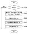
FIG. 13 is a flowchart for explaining the operation of a memory controller according to an embodiment of the present invention.
Figure 14 is a flowchart for explaining in detail the steps for generating the availability time prediction information of Figure 13.
Figure 15 is a flowchart for explaining in detail the steps for compressing the map data of Figure 13.
FIG. 16 is a drawing for explaining another embodiment of the memory controller of FIG. 1.
FIG. 17 is a block diagram showing a memory card system to which a storage device according to an embodiment of the present invention is applied.
FIG. 18 is a block diagram showing an SSD (Solid State Drive) system to which a storage device according to an embodiment of the present invention is applied.
FIG. 19 is a block diagram showing a user system to which a storage device according to an embodiment of the present invention is applied.
본 명세서 또는 출원에 개시되어 있는 본 발명의 개념에 따른 실시 예들에 대해서 특정한 구조적 내지 기능적 설명들은 단지 본 발명의 개념에 따른 실시 예를 설명하기 위한 목적으로 예시된 것으로, 본 명세서 또는 출원에 설명된 실시 예들에 한정되는 것으로 해석되어서는 아니 된다.Any specific structural or functional descriptions of embodiments according to the concept of the present invention disclosed in this specification or application are merely illustrative for the purpose of explaining embodiments according to the concept of the present invention and should not be construed as being limited to the embodiments described in this specification or application.
이하, 첨부한 도면을 참조하여 본 발명의 바람직한 실시 예를 설명함으로써, 본 발명을 상세히 설명한다. 이하, 본 발명의 실시 예를 첨부된 도면을 참조하여 상세하게 설명한다.Hereinafter, the present invention will be described in detail by describing preferred embodiments of the present invention with reference to the attached drawings. Hereinafter, embodiments of the present invention will be described in detail by referring to the attached drawings.
도 1은 본 발명의 실시 예에 따른 저장 장치를 설명하기 위한 도면이다.FIG. 1 is a drawing for explaining a storage device according to an embodiment of the present invention.
도 1을 참조하면, 저장 장치(50)는 메모리 장치(100) 및 메모리 컨트롤러(200)를 포함할 수 있다. 저장 장치(50)는 휴대폰, 스마트폰, MP3 플레이어, 랩탑 컴퓨터, 데스크탑 컴퓨터, 게임기, TV, 테블릿 PC 또는 차량용 인포테인먼트(in-vehicle infotainment) 시스템 등과 같은 호스트(300)의 제어에 따라 데이터를 저장하는 장치일 수 있다.Referring to FIG. 1, the storage device (50) may include a memory device (100) and a memory controller (200). The storage device (50) may be a device that stores data under the control of a host (300), such as a mobile phone, a smart phone, an MP3 player, a laptop computer, a desktop computer, a game console, a TV, a tablet PC, or an in-vehicle infotainment system.
저장 장치(50)는 호스트(300)와의 통신 방식인 호스트 인터페이스에 따라서 다양한 종류의 데이터 저장 장치들 중 어느 하나로 제조될 수 있다. 예를 들면, 저장 장치(50)는 SSD, MMC, eMMC, RS-MMC, micro-MMC 형태의 멀티 미디어 카드(multimedia card), SD, mini-SD, micro-SD 형태의 시큐어 디지털(secure digital) 카드, USB(universal storage bus) 저장 장치, UFS(universal flash storage) 장치, PCMCIA(personal computer memory card international association) 카드 형태의 저장 장치, PCI(peripheral component interconnection) 카드 형태의 저장 장치, PCI-E(PCI express) 카드 형태의 저장 장치, CF(compact flash) 카드, 스마트 미디어(smart media) 카드, 메모리 스틱(memory stick) 등과 같은 다양한 종류의 저장 장치들 중 어느 하나로 구성될 수 있다.The storage device (50) may be manufactured as one of various types of data storage devices depending on the host interface, which is a method of communication with the host (300). For example, the storage device (50) may be configured as one of various types of storage devices, such as a multimedia card in the form of an SSD, an MMC, an eMMC, an RS-MMC, a micro-MMC, a secure digital card in the form of an SD, a mini-SD, a micro-SD, a universal storage bus (USB) storage device, a universal flash storage (UFS) device, a personal computer memory card international association (PCMCIA) card, a peripheral component interconnection (PCI) card, a PCI-E (PCI express) card, a CF (compact flash) card, a smart media card, a memory stick, etc.
저장 장치(50)는 다양한 종류의 패키지(package) 형태들 중 어느 하나로 제조될 수 있다. 예를 들면, 저장 장치(50)는 POP(package on package), SIP(system in package), SOC(system on chip), MCP(multi-chip package), COB(chip on board), WFP(wafer-level fabricated package), WSP(wafer-level stack package) 등과 같은 다양한 종류의 패키지 형태들 중 어느 하나로 제조될 수 있다.The storage device (50) may be manufactured in any one of various types of package forms. For example, the storage device (50) may be manufactured in any one of various types of package forms, such as a package on package (POP), a system in package (SIP), a system on chip (SOC), a multi-chip package (MCP), a chip on board (COB), a wafer-level fabricated package (WFP), a wafer-level stack package (WSP), etc.
메모리 장치(100)는 데이터를 저장할 수 있다. 메모리 장치(100)는 메모리 컨트롤러(200)의 제어에 응답하여 동작할 수 있다. 메모리 장치(100)는 데이터를 저장하는 복수의 메모리 셀들을 포함하는 메모리 셀 어레이를 포함할 수 있다.The memory device (100) can store data. The memory device (100) can operate in response to the control of the memory controller (200). The memory device (100) can include a memory cell array including a plurality of memory cells that store data.
메모리 셀은 하나의 데이터 비트를 저장하는 싱글 레벨 셀(Single Level Cell; SLC), 두 개의 데이터 비트들을 저장하는 멀티 레벨 셀(Multi Level Cell; MLC), 세 개의 데이터 비트들을 저장하는 트리플 레벨 셀(Triple Level Cell; TLC) 또는 네 개의 데이터 비트를 저장할 수 있는 쿼드 레벨 셀(Quad Level Cell; QLC) 중 어느 하나로 동작할 수 있다.A memory cell can operate as either a single-level cell (SLC) that stores one bit of data, a multi-level cell (MLC) that stores two bits of data, a triple-level cell (TLC) that stores three bits of data, or a quad-level cell (QLC) that can store four bits of data.
메모리 셀 어레이는 복수의 메모리 블록들을 포함할 수 있다. 메모리 블록은 복수의 메모리 셀들을 포함할 수 있다. 메모리 블록은 메모리 장치(100)에 저장된 데이터를 지우는 단위일 수 있다. 실시 예에서, 메모리 블록은 복수의 페이지들을 포함할 수 있다. 페이지는 메모리 장치(100)에 데이터를 저장하거나, 메모리 장치(100)에 저장된 데이터를 리드하는 단위일 수 있다.A memory cell array may include a plurality of memory blocks. A memory block may include a plurality of memory cells. A memory block may be a unit for erasing data stored in a memory device (100). In an embodiment, a memory block may include a plurality of pages. A page may be a unit for storing data in a memory device (100) or reading data stored in a memory device (100).
실시 예에서, 메모리 장치(100)는 DDR SDRAM(Double Data Rate Synchronous Dynamic Random Access Memory), LPDDR4(Low Power Double Data Rate4) SDRAM, GDDR(Graphics Double Data Rate) SDRAM, LPDDR(Low Power DDR), RDRAM(Rambus Dynamic Random Access Memory), 낸드 플래시 메모리(NAND flash memory), 수직형 낸드 플래시 메모리(Vertical NAND), 노아 플래시 메모리(NOR flash memory), 저항성 램(resistive random access memory: RRAM), 상변화 메모리(phase-change memory: PRAM), 자기저항 메모리(magnetoresistive random access memory: MRAM), 강유전체 메모리(ferroelectric random access memory: FRAM), 스핀주입 자화반전 메모리(spin transfer torque random access memory: STT-RAM) 등이 될 수 있다. 본 명세서에서는 설명의 편의를 위해, 메모리 장치(100)가 낸드 플래시 메모리인 경우를 가정하여 설명한다.In an embodiment, the memory device (100) may be DDR SDRAM (Double Data Rate Synchronous Dynamic Random Access Memory), LPDDR4 (Low Power Double Data Rate4) SDRAM, GDDR (Graphics Double Data Rate) SDRAM, LPDDR (Low Power DDR), RDRAM (Rambus Dynamic Random Access Memory), NAND flash memory, Vertical NAND, NOR flash memory, resistive random access memory (RRAM), phase-change memory (PRAM), magnetoresistive random access memory (MRAM), ferroelectric random access memory (FRAM), spin transfer torque random access memory (STT-RAM), etc. In this specification, for convenience of explanation, it is assumed that the memory device (100) is NAND flash memory.
메모리 장치(100)는 메모리 컨트롤러(200)로부터 커맨드 및 어드레스를 수신하고, 메모리 셀 어레이 중 어드레스에 의해 선택된 영역을 액세스하도록 구성된다. 즉, 메모리 장치(100)는 어드레스에 의해 선택된 영역에 대해 수신된 커맨드에 해당하는 동작을 수행할 수 있다. 예를 들면, 메모리 장치(100)는 프로그램 동작, 리드 동작 및 소거 동작을 수행할 수 있다. 프로그램 동작은 메모리 장치(100)에 포함된 메모리 셀들에 데이터를 저장하는 동작일 수 있다. 메모리 장치(100)는 메모리 컨트롤러(200)로부터 입력되는 프로그램 커맨드에 따라 어드레스에 의해 선택된 영역에 데이터를 저장하는 프로그램 동작을 수행할 수 있다. 리드 동작은 메모리 셀들에 저장된 데이터를 리드 전압을 이용하여 센싱하는 동작일 수 있다. 메모리 장치(100)는 메모리 컨트롤러(200)로부터 입력되는 리드 커맨드에 따라 어드레스에 의해 선택된 영역에 저장된 데이터를 센싱할 수 있다. 소거 동작은 메모리 셀들에 저장된 데이터를 삭제하는 동작일 수 있다. 메모리 장치(100)는 메모리 컨트롤러(200)로부터 입력되는 소거 커맨드에 따라 어드레스에 의해 선택된 영역에 저장된 데이터를 삭제할 것이다. 실시 예에서, 메모리 셀들에 저장된 데이터를 삭제한다는 것은 메모리 셀들의 문턱전압이 소거 상태에 대응하는 문턱전압분포에 속하도록 메모리 셀들의 문턱전압을 낮추는 것일 수 있다.The memory device (100) is configured to receive a command and an address from the memory controller (200) and access an area selected by the address among the memory cell arrays. That is, the memory device (100) can perform an operation corresponding to the received command for the area selected by the address. For example, the memory device (100) can perform a program operation, a read operation, and an erase operation. The program operation may be an operation of storing data in memory cells included in the memory device (100). The memory device (100) may perform a program operation of storing data in an area selected by the address according to a program command input from the memory controller (200). The read operation may be an operation of sensing data stored in memory cells using a read voltage. The memory device (100) may sense data stored in an area selected by the address according to a read command input from the memory controller (200). The erase operation may be an operation of deleting data stored in memory cells. The memory device (100) will delete data stored in an area selected by an address according to an erase command input from the memory controller (200). In an embodiment, deleting data stored in memory cells may mean lowering the threshold voltage of the memory cells so that the threshold voltage of the memory cells falls into a threshold voltage distribution corresponding to an erase state.
메모리 컨트롤러(200)는 메모리 장치(100)의 전반적인 동작을 제어할 수 있다.The memory controller (200) can control the overall operation of the memory device (100).
저장 장치(50)에 전원이 인가되면, 메모리 컨트롤러(200)는 사전에 저장된 펌웨어(firmware, FW)를 실행할 수 있다.When power is applied to the storage device (50), the memory controller (200) can execute pre-stored firmware (FW).
펌웨어(FW)는 호스트(300)로부터 입력된 요청을 수신하거나 호스트(300)로 응답을 출력하는 호스트 장치 인터페이스 레이어(Host Interface Layer, HIL), 호스트(300)의 인터페이스와 메모리 장치(100)의 인터페이스 사이의 동작을 관리하는 플래시 변환 레이어(Flash Translation Layer, FTL) 및 메모리 장치(100)에 커맨드를 제공하거나, 메모리 장치(100)로부터 응답을 수신하는 플래시 인터페이스 레이어(Flash Interface Layer, FIL)를 포함할 수 있다.The firmware (FW) may include a host interface layer (HIL) that receives a request input from a host (300) or outputs a response to the host (300), a flash translation layer (FTL) that manages operations between the interface of the host (300) and the interface of the memory device (100), and a flash interface layer (FIL) that provides a command to the memory device (100) or receives a response from the memory device (100).
호스트(300)로부터 쓰기 요청이 입력되면, 메모리 컨트롤러(200)는 호스트(300)로부터 저장될 데이터와 해당 데이터를 식별하기 위한 논리 어드레스(Logical Address, LA)를 입력 받을 수 있다. 메모리 컨트롤러(200)는 입력된 논리 어드레스를 메모리 장치(100)에 포함된 메모리 셀들 중 데이터가 저장될 메모리 셀들의 물리적인 주소를 나타내는 물리 어드레스(Physical Address, PA)로 변환할 수 있다. 메모리 컨트롤러(200)는 데이터를 저장하기 위한 프로그램 커맨드, 변환된 물리 어드레스 및 저장할 데이터를 메모리 장치(100)에 제공할 수 있다.When a write request is input from the host (300), the memory controller (200) can receive data to be stored and a logical address (LA) for identifying the data from the host (300). The memory controller (200) can convert the input logical address into a physical address (PA) that indicates the physical address of memory cells in which data is to be stored among memory cells included in the memory device (100). The memory controller (200) can provide a program command for storing data, a converted physical address, and the data to be stored to the memory device (100).
실시 예에서, 호스트(300)로부터 리드 요청이 입력되면, 메모리 컨트롤러(200)는 호스트(300)로부터 리드할 데이터를 식별하는 논리 어드레스를 입력 받을 수 있다. 메모리 컨트롤러(200)는 입력된 논리 어드레스에 대응되는 물리 어드레스를 획득하고, 메모리 장치(100)에 리드 커맨드 및 물리 어드레스를 제공할 수 있다.In an embodiment, when a read request is input from a host (300), the memory controller (200) may receive a logical address that identifies data to be read from the host (300). The memory controller (200) may obtain a physical address corresponding to the input logical address and provide a read command and the physical address to the memory device (100).
실시 예에서, 메모리 컨트롤러(200)는 호스트(300)로부터의 요청과 무관하게 자체적으로 프로그램 동작, 리드 동작 또는 소거 동작을 수행하도록 메모리 장치(100)를 제어할 수 있다. 예를 들면, 메모리 컨트롤러(200)는 웨어 레벨링(wear leveling), 가비지 컬렉션(garbage collection) 또는 리드 리클레임(read reclaim)과 같은 배경 동작(background operation)들을 수행하기 위해 메모리 장치(100)를 제어할 수 있다.In an embodiment, the memory controller (200) may control the memory device (100) to perform a program operation, a read operation, or an erase operation independently of a request from the host (300). For example, the memory controller (200) may control the memory device (100) to perform background operations such as wear leveling, garbage collection, or read reclaim.
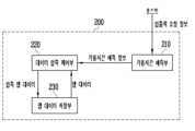
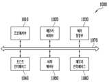
실시 예에서, 메모리 컨트롤러(200)는 가용시간 예측부(210) 및 데이터 압축 제어부(220)를 포함할 수 있다.In an embodiment, the memory controller (200) may include an availability time prediction unit (210) and a data compression control unit (220).
가용시간 예측부(210)는 호스트로부터 입력 받은 입출력 요청 정보를 이용하여 가용시간 예측 정보를 생성할 수 있다. 구체적으로, 가용 시간 예측부(210)는 순환 인공 신경망(Recurrent Neural Network, RNN) 기반의 머신 러닝(Machine learning)을 이용하여 가용시간 예측 정보를 생성할 수 있다. 머신 러닝은 인공지능의 분야 중 하나로, 경험적 데이터를 기반으로 학습을 하고 예측을 수행하고 스스로의 성능을 향상시키는 시스템과 이를 위한 알고리즘의 집합으로 정의될 수 있다. 가용시간 예측부(210)가 이용하는 모델은 이러한 머신 러닝의 모델들 중 순환 인공 신경망(Reccurent Neural Network, RNN)을 이용한 것일 수 있다.The availability time prediction unit (210) can generate availability time prediction information using input/output request information received from the host. Specifically, the availability time prediction unit (210) can generate availability time prediction information using machine learning based on a recurrent neural network (RNN). Machine learning is one of the fields of artificial intelligence, and can be defined as a system that learns based on empirical data, performs predictions, and improves its own performance, and a set of algorithms for this. The model used by the availability time prediction unit (210) can be one of these machine learning models using a recurrent neural network (RNN).
가용시간 예측부(210)는 입출력 요청이 입력된 시간 간격을 머신 러닝을 통해 학습하고, 호스트로부터 입출력 요청이 없는 시간인 유휴시간을 예측할 수 있다. 새로운 입출력 요청 정보가 입력될 때마다, 머신 러닝을 통하여 예측된 유휴시간은 새로운 입출력 요청 정보가 입력된 시간을 반영하여 변경될 수 있다. 가용시간 예측부(210)는 맵 데이터가 압축되는데 소요되는 평균적인 시간에 해당하는 기준시간에 대한 정보를 더 포함할 수 있다. 가용시간 예측부(210)는 예측된 유휴시간과 기준시간을 비교하여 맵 데이터의 압축 여부에 대한 정보를 포함하는 가용시간 예측 정보를 출력할 수 있다. 구체적으로, 예측된 유휴시간이 기준시간보다 길면, 예측된 유휴시간을 맵 데이터를 압축할 수 있는 시간인 가용시간이라고 판단할 수 있다. 예측된 유휴시간이 기준시간보다 짧으면, 가용시간이 아니라고 판단할 수 있다. 가용시간 예측부(210)는 예측된 유휴시간이 가용시간에 해당하는지에 관한 정보인 가용시간 예측 정보를 생성하고 데이터 압축 제어부(220)에 제공할 수 있다.The availability time prediction unit (210) learns the time interval at which input/output requests are input through machine learning, and can predict the idle time, which is the time during which there is no input/output request from the host. Whenever new input/output request information is input, the idle time predicted through machine learning can be changed to reflect the time at which the new input/output request information is input. The availability time prediction unit (210) can further include information on a reference time corresponding to the average time required for compressing map data. The availability time prediction unit (210) can compare the predicted idle time with the reference time, and output the availability time prediction information including information on whether the map data is compressed. Specifically, if the predicted idle time is longer than the reference time, the predicted idle time can be determined as the available time, which is the time during which map data can be compressed. If the predicted idle time is shorter than the reference time, the predicted idle time can be determined not to be the available time. The availability time prediction unit (210) can generate availability time prediction information, which is information on whether the predicted idle time corresponds to the available time, and provide it to the data compression control unit (220).
데이터 압축 제어부(220)는 가용시간 예측부(210)로부터 입력 받은 가용시간 예측 정보에 따라 맵 데이터를 압축할 수 있다. 구체적으로, 예측된 유휴시간이 가용시간에 해당하면 맵 데이터를 압축할 수 있고, 가용시간에 해당하지 않으면 맵 데이터의 압축을 생략할 수 있다.The data compression control unit (220) can compress map data according to the available time prediction information received from the available time prediction unit (210). Specifically, if the predicted idle time corresponds to the available time, the map data can be compressed, and if it does not correspond to the available time, the compression of the map data can be omitted.
데이터 압축 제어부(220)는 맵 데이터를 압축하기에 앞서, 먼저 맵 데이터가 지칭하는 메모리 블록에 관한 정보인 블록 정보를 이용하여 압축할 맵 데이터를 결정할 수 있다. 예를 들어, 블록 정보에는 유효 페이지 개수 또는 리드 횟수가 포함될 수 있다. 유효 페이지들이 적게 포함된 블록일수록 가비지 컬렉션(Garbage Collection, GC) 동작이 수행될 가능성이 높고, 리드 횟수가 많은 페이지가 많이 포함된 블록일수록 리드 리클레임(Read Reclaim) 동작이 수행될 가능성이 높을 수 있다. 따라서, 이러한 메모리 블록에 대한 맵 데이터는 어차피 가까운 시간 내에 변경될 데이터이므로, 데이터를 압축하는 것이 비효율적일 수 있다. 따라서, 유효 페이지의 개수가 기준 개수보다 적거나, 리드 횟수가 기준 횟수를 초과하는 메모리 블록에 대한 맵 데이터는 데이터 압축 동작의 대상에서 제외될 수 있다.The data compression control unit (220) may determine map data to be compressed using block information, which is information about a memory block indicated by the map data, before compressing the map data. For example, the block information may include the number of valid pages or the number of reads. The fewer valid pages a block contains, the more likely it is that a garbage collection (GC) operation will be performed, and the more pages a block contains, the more likely it is that a read reclaim operation will be performed. Accordingly, since the map data for such memory blocks is data that will be changed in the near future anyway, compressing the data may be inefficient. Accordingly, map data for memory blocks in which the number of valid pages is less than a reference number or the number of reads exceeds a reference number may be excluded from the target of the data compression operation.
데이터 압축 제어부(220)는 예측된 유휴시간이 맵 데이터를 압축할 수 있는 가용시간에 해당되고, 맵 데이터가 압축의 대상이 된다고 판단되면, 다양한 압축 기법을 이용하여 맵 데이터를 압축할 수 있다. 다양한 압축 기법에는 델타 압축(Delta compression) 또는 지집(GZIP)이 포함될 수 있으나 이에 한정되지 않을 수 있다. 맵 데이터가 압축되는 과정에 대해서는 후술하기로 한다.The data compression control unit (220) may compress the map data using various compression techniques if it is determined that the predicted idle time corresponds to the available time for compressing the map data and that the map data is a target for compression. The various compression techniques may include, but are not limited to, Delta compression or GZIP. The process of compressing the map data will be described later.
호스트(300)는 USB (Universal Serial Bus), SATA (Serial AT Attachment), SAS (Serial Attached SCSI), HSIC (High Speed Interchip), SCSI (Small Computer System Interface), PCI (Peripheral Component Interconnection), PCIe (PCI express), NVMe (NonVolatile Memory express), UFS (Universal Flash Storage), SD (Secure Digital), MMC (MultiMedia Card), eMMC (embedded MMC), DIMM (Dual In-line Memory Module), RDIMM (Registered DIMM), LRDIMM (Load Reduced DIMM) 등과 같은 다양한 통신 방식들 중 적어도 하나를 이용하여 저장 장치(50)와 통신할 수 있다.The host (300) can communicate with the storage device (50) using at least one of various communication methods, such as USB (Universal Serial Bus), SATA (Serial AT Attachment), SAS (Serial Attached SCSI), HSIC (High Speed Interchip), SCSI (Small Computer System Interface), PCI (Peripheral Component Interconnection), PCIe (PCI express), NVMe (NonVolatile Memory express), UFS (Universal Flash Storage), SD (Secure Digital), MMC (MultiMedia Card), eMMC (embedded MMC), DIMM (Dual In-line Memory Module), RDIMM (Registered DIMM), LRDIMM (Load Reduced DIMM), etc.
도 2는 도 1의 메모리 장치의 구조를 설명하기 위한 도면이다.FIG. 2 is a drawing for explaining the structure of the memory device of FIG. 1.
도 2를 참조하면, 메모리 장치(100)는 메모리 셀 어레이(110), 주변 회로(120) 및 제어 로직(130)을 포함할 수 있다.Referring to FIG. 2, a memory device (100) may include a memory cell array (110), a peripheral circuit (120), and control logic (130).
메모리 셀 어레이(110)는 복수의 메모리 블록들(BLK1~BLKz)을 포함할 수 있다. 복수의 메모리 블록들(BLK1~BLKz)은 행 라인들(RL)을 통해 로우 디코더(121)에 연결될 수 있다. 복수의 메모리 블록들(BLK1~BLKz)은 비트라인들(BL1 내지 BLm)을 통해 읽기 및 쓰기 회로(123)에 연결될 수 있다. 복수의 메모리 블록들(BLK1~BLKz) 각각은 복수의 메모리 셀들을 포함할 수 있다. 실시 예에서, 복수의 메모리 셀들은 불휘발성 메모리 셀들일 수 있다. 복수의 메모리 셀들 중 같은 워드라인에 연결된 메모리 셀들은 하나의 물리 페이지를 구성하는 것으로 정의될 수 있다. 따라서, 하나의 메모리 블록은 복수의 물리 페이지들을 포함할 수 있다. 메모리 블록에 포함된 하나의 메모리 셀은 1 비트의 데이터를 저장하는 싱글 레벨 셀(Single Level Cell; SLC), 2 비트의 데이터를 저장하는 멀티 레벨 셀(Multi Level Cell; MLC), 3 비트의 데이터를 저장하는 저장하는 트리플 레벨 셀(Triple Level Cell; TLC) 또는 4비트의 데이터를 저장하는 쿼드 레벨 셀(Quad Level Cell; QLC) 중 어느 하나의 방식으로 사용될 수 있다.The memory cell array (110) may include a plurality of memory blocks (BLK1 to BLKz). The plurality of memory blocks (BLK1 to BLKz) may be connected to a row decoder (121) through row lines (RL). The plurality of memory blocks (BLK1 to BLKz) may be connected to a read and write circuit (123) through bit lines (BL1 to BLm). Each of the plurality of memory blocks (BLK1 to BLKz) may include a plurality of memory cells. In an embodiment, the plurality of memory cells may be nonvolatile memory cells. Memory cells connected to the same word line among the plurality of memory cells may be defined as constituting one physical page. Therefore, one memory block may include a plurality of physical pages. A single memory cell included in a memory block can be used in any of the following ways: a single level cell (SLC) that stores 1 bit of data, a multi level cell (MLC) that stores 2 bits of data, a triple level cell (TLC) that stores 3 bits of data, or a quad level cell (QLC) that stores 4 bits of data.
주변 회로(120)는 로우 디코더(121), 전압 생성부(122), 읽기 및 쓰기 회로(123), 컬럼 디코더(124), 입출력 회로(125) 및 센싱 회로(126)를 포함할 수 있다.The peripheral circuit (120) may include a row decoder (121), a voltage generator (122), a read and write circuit (123), a column decoder (124), an input/output circuit (125), and a sensing circuit (126).
주변 회로(120)는 메모리 셀 어레이(110)를 구동할 수 있다. 예를 들어 주변 회로(120)는 프로그램 동작, 리드 동작 및 소거 동작을 수행하도록 메모리 셀 어레이(110)를 구동할 수 있다.The peripheral circuit (120) can drive the memory cell array (110). For example, the peripheral circuit (120) can drive the memory cell array (110) to perform a program operation, a read operation, and an erase operation.
전압 생성부(122)는 메모리 장치(100)에 공급되는 외부 전원 전압을 이용하여 복수의 동작 전압(Vop)들을 생성할 수 있다. 전압 생성부(122)는 제어 로직(130)의 제어에 응답하여 동작한다. 구체적으로, 전압 생성부(122)는 동작 신호(OPSIG)에 응답하여 프로그램 동작, 리드 동작 및 소거 동작들에 사용되는 동작 전압(Vop)들을 생성할 수 있다. 예를 들면, 전압 생성부(122)는 제어 로직(130)의 제어에 따라 프로그램 전압, 검증 전압, 프로그램 패스 전압, 검증 패스 전압, 리드 전압, 소거 전압 등을 생성할 수 있다.The voltage generation unit (122) can generate a plurality of operating voltages (Vop) using an external power supply voltage supplied to the memory device (100). The voltage generation unit (122) operates in response to the control of the control logic (130). Specifically, the voltage generation unit (122) can generate operating voltages (Vop) used for program operations, read operations, and erase operations in response to an operation signal (OPSIG). For example, the voltage generation unit (122) can generate a program voltage, a verification voltage, a program pass voltage, a verification pass voltage, a read voltage, an erase voltage, etc. in response to the control of the control logic (130).
실시 예에서, 전압 생성부(122)는 다양한 전압 레벨들을 갖는 복수의 동작 전압(Vop)들을 생성하기 위해서, 복수의 펌핑 커패시터들을 포함할 수 있다. 전압 생성부(122)는 제어 로직(130)의 제어에 응답하여 복수의 펌핑 커패시터들을 선택적으로 활성화시킴으로써 복수의 동작 전압(Vop)들을 생성할 수 있다. 생성된 복수의 동작 전압(Vop)들은 로우 디코더(121)에 의해 메모리 셀 어레이(110)에 공급될 수 있다.In an embodiment, the voltage generation unit (122) may include a plurality of pumping capacitors to generate a plurality of operating voltages (Vop) having various voltage levels. The voltage generation unit (122) may generate a plurality of operating voltages (Vop) by selectively activating the plurality of pumping capacitors in response to the control of the control logic (130). The generated plurality of operating voltages (Vop) may be supplied to the memory cell array (110) by the row decoder (121).
로우 디코더(121)는 행 라인들(RL)을 통해 메모리 셀 어레이(110)에 연결된다. 행 라인들(RL)은 드레인 선택 라인들, 워드 라인들, 소스 선택 라인들 및 공통 소스 라인을 포함할 수 있다. 다양한 실시 예에서, 워드라인들은 노멀 워드라인들과 더미 워드라인들을 포함할 수 있다. 또한, 행 라인들(RL)은 파이프 선택 라인을 더 포함할 수 있다.The row decoder (121) is connected to the memory cell array (110) via row lines (RL). The row lines (RL) may include drain select lines, word lines, source select lines, and a common source line. In various embodiments, the word lines may include normal word lines and dummy word lines. In addition, the row lines (RL) may further include a pipe select line.
로우 디코더(121)는 제어 로직(130)의 제어에 응답하여 동작할 수 있다. 로우 디코더(121)는 제어 로직(130)으로부터 로우 어드레스(RADD)에 응답하여, 전압 생성부(122)가 생성한 동작 전압(Vop)들을 복수의 메모리 블록들(BLK1~BLKz) 중 선택된 메모리 블록에 연결된 행라인들(RL)에 전달할 수 있다.The row decoder (121) can operate in response to the control of the control logic (130). The row decoder (121) can transmit the operating voltages (Vop) generated by the voltage generation unit (122) to the row lines (RL) connected to a selected memory block among the plurality of memory blocks (BLK1 to BLKz) in response to the row address (RADD) from the control logic (130).
읽기 및 쓰기 회로(123)는 제1 내지 제 n 페이지 버퍼들(PB1~PBn)을 포함할 수 있다. 제1 내지 제 n 페이지 버퍼들(PB1~PBn)은 각각 제1 내지 제 n 비트라인들(BL1~BLn)을 통해 메모리 셀 어레이(110)에 연결될 수 있다. 제1 내지 제 n 페이지 버퍼들(PB1~PBn)은 제어 로직(130)의 제어에 응답하여 동작한다. 예를 들어, 제1 내지 제 n 페이지 버퍼들(PB1~PBn)은 페이지 버퍼 제어 신호들(PBSIGNALS)에 응답하여 동작할 수 있다.The read and write circuit (123) may include first to nth page buffers (PB1 to PBn). The first to nth page buffers (PB1 to PBn) may be connected to the memory cell array (110) via first to nth bit lines (BL1 to BLn), respectively. The first to nth page buffers (PB1 to PBn) operate in response to the control of the control logic (130). For example, the first to nth page buffers (PB1 to PBn) may operate in response to page buffer control signals (PBSIGNALS).
실시 예에서, 제1 내지 제 n 페이지 버퍼들(PB1~PBn)은 제1 내지 제 n 비트라인들(BL1~BLn)의 전압 또는 전류를 센싱함으로써, 메모리 셀 어레이(110)에 저장된 데이터를 센싱할 수 있다. 제1 내지 제 n 페이지 버퍼들(PB1~PBn)은 센싱된 데이터를 임시로 저장할 수 있다. 제1 내지 제 n 페이지 버퍼들(PB1~PBn)은 센싱된 데이터를 데이터 라인들(DL)을 통해 컬럼 디코더(124)에 제공할 수 있다.In an embodiment, the first to nth page buffers (PB1 to PBn) can sense data stored in the memory cell array (110) by sensing voltage or current of the first to nth bit lines (BL1 to BLn). The first to nth page buffers (PB1 to PBn) can temporarily store the sensed data. The first to nth page buffers (PB1 to PBn) can provide the sensed data to the column decoder (124) through the data lines (DL).
실시 예에서, 제1 내지 제 n 페이지 버퍼들(PB1~PBn)은 입출력 회로(125)로부터 컬럼 디코더(124) 및 데이터 라인들(DL)을 통해 저장할 데이터를 수신할 수 있다. 프로그램 동작의 수행을 통해 제1 내지 제 n 페이지 버퍼들(PB1~PBn)가 수신한 데이터는 메모리 셀 어레이(110)에 저장될 수 있다.In an embodiment, the first to nth page buffers (PB1 to PBn) can receive data to be stored from an input/output circuit (125) through a column decoder (124) and data lines (DL). Data received by the first to nth page buffers (PB1 to PBn) through execution of a program operation can be stored in the memory cell array (110).
메모리 셀에 데이터를 저장하는 프로그램 동작은 프로그램 전압 인가 단계와 검증 단계를 포함할 수 있다. 프로그램 전압 인가단계에서, 제1 내지 제 n 페이지 버퍼들(PB1~PBn)은 선택된 워드라인에 프로그램 전압이 인가될 때, 저장될 데이터를 선택된 메모리 셀들에 전달할 수 있다. 프로그램 허용 전압(예를 들면, 접지 전압)이 인가되는 비트라인과 연결된 메모리 셀은 상승된 문턱전압을 가질 수 있다. 프로그램 금지 전압(예를 들면, 전원 전압)이 인가되는 비트라인과 연결된 메모리 셀의 문턱전압은 유지될 수 있다. 프로그램 동작을 검증하는 검증 단계에서, 제1 내지 제 n 페이지 버퍼들(PB1~PBn)은 선택된 메모리 셀들로부터 비트라인들(BL1~BLn)을 통해 메모리 셀들에 저장된 데이터를 센싱할 수 있다.A program operation for storing data in a memory cell may include a program voltage application step and a verification step. In the program voltage application step, the first to nth page buffers (PB1 to PBn) may transfer data to be stored to selected memory cells when a program voltage is applied to a selected word line. A memory cell connected to a bit line to which a program allowance voltage (e.g., a ground voltage) is applied may have an elevated threshold voltage. A threshold voltage of a memory cell connected to a bit line to which a program inhibit voltage (e.g., a power supply voltage) is applied may be maintained. In the verification step for verifying the program operation, the first to nth page buffers (PB1 to PBn) may sense data stored in the memory cells from the selected memory cells through the bit lines (BL1 to BLn).
센싱 회로(126)는 검증 단계에서, 허용 비트(VRYBIT)에 응답하여 기준 전류를 생성하고, 읽기 및 쓰기 회로(123)으로부터 수신된 센싱 전압(VPB)과 기준 전류에 의해 생성된 기준 전압을 비교하여 패스 신호(PASS) 또는 페일 신호(FAIL)를 출력할 수 있다.The sensing circuit (126) can generate a reference current in response to an allowable bit (VRYBIT) in the verification step, and compare a sensing voltage (VPB) received from the read and write circuit (123) with a reference voltage generated by the reference current to output a pass signal (PASS) or a fail signal (FAIL).
입출력 회로(125)는 컬럼 디코더(124) 및 데이터 라인들(DL)을 통해 제1 내지 제 n 페이지 버퍼들(PB1~PBn)에 연결될 수 있다. 입출력 회로(125)는 제어 로직(130)의 제어에 응답하여 동작한다.The input/output circuit (125) can be connected to the first to nth page buffers (PB1 to PBn) through the column decoder (124) and data lines (DL). The input/output circuit (125) operates in response to the control of the control logic (130).
입출력 회로(125)는 도 1의 메모리 컨트롤러(200)로부터 수신한 커맨드(CMD) 및 어드레스(ADDR)를 제어 로직(130)에 전달하거나, 도 1의 메모리 컨트롤러(200)로부터 수신한 데이터(DATA)를 읽기 및 쓰기 회로(123)에 제공할 수 있다.The input/output circuit (125) can transmit a command (CMD) and an address (ADDR) received from the memory controller (200) of Fig. 1 to the control logic (130), or provide data (DATA) received from the memory controller (200) of Fig. 1 to the read and write circuit (123).
실시 예에서, 입출력 회로(125)는 데이터(DATA)를 수신하는 복수의 입출력 버퍼들(미도시)을 포함할 수 있다. 프로그램 동작 시, 입출력 회로(125)는 메모리 컨트롤러(200)로부터 저장될 데이터(DATA)를 수신한다. 입출력 회로(125)는 리드 동작 시, 읽기 및 쓰기 회로(123)에 포함된 제1 내지 제 n 페이지 버퍼들(PB1~PBn)로부터 전달된 데이터를 메모리 컨트롤러(200)로 출력할 수 있다.In an embodiment, the input/output circuit (125) may include a plurality of input/output buffers (not shown) that receive data (DATA). During a program operation, the input/output circuit (125) receives data (DATA) to be stored from the memory controller (200). During a read operation, the input/output circuit (125) may output data transferred from the first to nth page buffers (PB1 to PBn) included in the read and write circuit (123) to the memory controller (200).
제어 로직(130)은 로우 디코더(121), 전압 생성부(122), 읽기 및 쓰기 회로(123), 컬럼 디코더(124), 입출력 회로(125) 및 센싱 회로(126)에 연결될 수 있다. 제어 로직(130)은 메모리 장치(100)의 전반적인 동작을 제어하도록 구성될 수 있다.The control logic (130) may be connected to the row decoder (121), the voltage generator (122), the read and write circuit (123), the column decoder (124), the input/output circuit (125), and the sensing circuit (126). The control logic (130) may be configured to control the overall operation of the memory device (100).
제어 로직(130)은 커맨드(CMD) 및 어드레스(ADDR)에 응답하여 주변 회로(120)를 제어할 복수의 제어신호들을 생성할 수 있다. 예를 들면, 제어 로직(130)은 커맨드(CMD) 및 어드레스(ADDR)에 응답하여 동작 신호(OPSIG), 로우 어드레스(RADD), 페이지 버퍼 제어 신호들(PBSIGNALS) 및 허용 비트(VRYBIT)를 생성할 수 있다. 제어 로직(130)은 센싱 회로(126)가 출력한 패스 또는 페일 신호(PASS/FAIL)에 응답하여 검증 동작이 패스 또는 페일 되었는지를 판단할 수 있다.The control logic (130) can generate a plurality of control signals to control the peripheral circuit (120) in response to the command (CMD) and the address (ADDR). For example, the control logic (130) can generate an operation signal (OPSIG), a row address (RADD), page buffer control signals (PBSIGNALS), and a permission bit (VRYBIT) in response to the command (CMD) and the address (ADDR). The control logic (130) can determine whether the verification operation has passed or failed in response to a pass or fail signal (PASS/FAIL) output by the sensing circuit (126).
도 3은 도 2의 메모리 셀 어레이의 일 실시 예를 나타낸 도면이다.FIG. 3 is a drawing showing one embodiment of the memory cell array of FIG. 2.
도 3을 참조하면, 메모리 셀 어레이(110)는 복수의 메모리 블록들(BLK1~BLKz)을 포함한다. 각 메모리 블록은 3차원 구조를 가질 수 있다. 각 메모리 블록은 기판 위에 적층된 복수의 메모리 셀들을 포함한다. 이러한 복수의 메모리 셀들은 +X 방향, +Y 방향 및 +Z 방향을 따라 배열된다. 각 메모리 블록의 구조는 도 4 및 도 5를 참조하여 더 상세히 설명된다.Referring to FIG. 3, the memory cell array (110) includes a plurality of memory blocks (BLK1 to BLKz). Each memory block may have a three-dimensional structure. Each memory block includes a plurality of memory cells stacked on a substrate. These plurality of memory cells are arranged along the +X direction, the +Y direction, and the +Z direction. The structure of each memory block is described in more detail with reference to FIGS. 4 and 5.
도 4는 도 3의 메모리 블록들(BLK1~BLKz) 중 어느 하나의 메모리 블록(BLKa)을 보여주는 회로도이다.FIG. 4 is a circuit diagram showing one memory block (BLKa) among the memory blocks (BLK1 to BLKz) of FIG. 3.
도 4를 참조하면 메모리 블록(BLKa)은 복수의 셀 스트링들(CS11~CS1m, CS21~CS2m)을 포함한다. 실시 예로서, 복수의 셀 스트링들(CS11~CS1m, CS21~CS2m) 각각은 'U'자형으로 형성될 수 있다. 메모리 블록(BLKa) 내에서, 행 방향(즉 +X 방향)으로 m개의 셀 스트링들이 배열된다. 도 4에서, 열 방향(즉 +Y 방향)으로 2개의 셀 스트링들이 배열되는 것으로 도시되었다. 하지만 이는 설명의 편의를 위한 것으로서 열 방향으로 3개 이상의 셀 스트링들이 배열될 수 있음이 이해될 것이다.Referring to FIG. 4, the memory block (BLKa) includes a plurality of cell strings (CS11 to CS1m, CS21 to CS2m). As an example, each of the plurality of cell strings (CS11 to CS1m, CS21 to CS2m) may be formed in a 'U' shape. Within the memory block (BLKa), m cell strings are arranged in the row direction (i.e., +X direction). In FIG. 4, two cell strings are illustrated as being arranged in the column direction (i.e., +Y direction). However, this is for convenience of explanation, and it will be understood that three or more cell strings may be arranged in the column direction.
복수의 셀 스트링들(CS11~CS1m, CS21~CS2m) 각각은 적어도 하나 이상의 소스 선택 트랜지스터(SST), 제 1 내지 제 n 메모리 셀들(MC1~MCn), 파이프 트랜지스터(PT), 그리고 적어도 하나의 드레인 선택 트랜지스터(DST)을 포함한다.Each of the plurality of cell strings (CS11 to CS1m, CS21 to CS2m) includes at least one source select transistor (SST), first to nth memory cells (MC1 to MCn), a pipe transistor (PT), and at least one drain select transistor (DST).
선택 트랜지스터들(SST, DST) 및 메모리 셀들(MC1~MCn) 각각은 유사한 구조를 가질 수 있다. 실시 예로서, 선택 트랜지스터들(SST, DST) 및 메모리 셀들(MC1~MCn) 각각은 채널층, 터널링 절연막, 전하 저장막 및 블로킹 절연막을 포함할 수 있다. 실시 예로서, 채널층을 제공하기 위한 필라(pillar)가 각 셀 스트링(each cell string)에 제공될 수 있다. 실시 예로서, 채널층, 터널링 절연막, 전하 저장막 및 블로킹 절연막 중 적어도 하나를 제공하기 위한 필라가 각 셀 스트링에 제공될 수 있다.Each of the selection transistors (SST, DST) and the memory cells (MC1 to MCn) may have a similar structure. As an embodiment, each of the selection transistors (SST, DST) and the memory cells (MC1 to MCn) may include a channel layer, a tunneling insulating film, a charge storage film, and a blocking insulating film. As an embodiment, a pillar for providing the channel layer may be provided for each cell string. As an embodiment, a pillar for providing at least one of the channel layer, the tunneling insulating film, the charge storage film, and the blocking insulating film may be provided for each cell string.
각 셀 스트링의 소스 선택 트랜지스터(SST)는 공통 소스 라인(CSL)과 메모리 셀들(MC1~MCp) 사이에 연결된다.The source select transistor (SST) of each cell string is connected between the common source line (CSL) and the memory cells (MC1 to MCp).
실시 예로서, 동일한 행에 배열된 셀 스트링들의 소스 선택 트랜지스터들은 행 방향으로 신장되는 소스 선택 라인에 연결되고, 상이한 행에 배열된 셀 스트링들의 소스 선택 트랜지스터들은 상이한 소스 선택 라인들에 연결된다. 도 4에서, 제 1 행의 셀 스트링들(CS11~CS1m)의 소스 선택 트랜지스터들은 제 1 소스 선택 라인(SSL1)에 연결되어 있다. 제 2 행의 셀 스트링들(CS21~CS2m)의 소스 선택 트랜지스터들은 제 2 소스 선택 라인(SSL2)에 연결되어 있다.As an example, the source selection transistors of the cell strings arranged in the same row are connected to a source selection line extending in the row direction, and the source selection transistors of the cell strings arranged in different rows are connected to different source selection lines. In Fig. 4, the source selection transistors of the cell strings (CS11 to CS1m) in the first row are connected to the first source selection line (SSL1). The source selection transistors of the cell strings (CS21 to CS2m) in the second row are connected to the second source selection line (SSL2).
다른 실시 예로서, 셀 스트링들(CS11~CS1m, CS21~CS2m)의 소스 선택 트랜지스터들은 하나의 소스 선택 라인에 공통 연결될 수 있다.As another embodiment, the source select transistors of the cell strings (CS11 to CS1m, CS21 to CS2m) can be commonly connected to one source select line.
각 셀 스트링의 제 1 내지 제 n 메모리 셀들(MC1~MCn)은 소스 선택 트랜지스터(SST)와 드레인 선택 트랜지스터(DST) 사이에 연결된다.The first to nth memory cells (MC1 to MCn) of each cell string are connected between a source select transistor (SST) and a drain select transistor (DST).
제 1 내지 제 n 메모리 셀들(MC1~MCn)은 제 1 내지 제 p 메모리 셀들(MC1~MCp)과 제 p+1 내지 제 n 메모리 셀들(MCp+1~MCn)로 구분될 수 있다. 제 1 내지 제 p 메모리 셀들(MC1~MCp)은 +Z 방향과 역방향으로 순차적으로 배열되며, 소스 선택 트랜지스터(SST)와 파이프 트랜지스터(PT) 사이에서 직렬 연결된다. 제 p+1 내지 제 n 메모리 셀들(MCp+1~MCn)은 +Z 방향으로 순차적으로 배열되며, 파이프 트랜지스터(PT)와 드레인 선택 트랜지스터(DST) 사이에서 직렬 연결된다. 제 1 내지 제 p 메모리 셀들(MC1~MCp)과 제 p+1 내지 제 n 메모리 셀들(MCp+1~MCn)은 파이프 트랜지스터(PT)를 통해 연결된다. 각 셀 스트링의 제 1 내지 제 n 메모리 셀들(MC1~MCn)의 게이트들은 각각 제 1 내지 제 n 워드 라인들(WL1~WLn)에 연결된다.The first to nth memory cells (MC1 to MCn) can be divided into the first to pth memory cells (MC1 to MCp) and the p+1 to nth memory cells (MCp+1 to MCn). The first to pth memory cells (MC1 to MCp) are sequentially arranged in the +Z direction and in the reverse direction, and are connected in series between a source select transistor (SST) and a pipe transistor (PT). The p+1 to nth memory cells (MCp+1 to MCn) are sequentially arranged in the +Z direction and are connected in series between a pipe transistor (PT) and a drain select transistor (DST). The first to pth memory cells (MC1 to MCp) and the p+1 to nth memory cells (MCp+1 to MCn) are connected via the pipe transistor (PT). The gates of the first to nth memory cells (MC1 to MCn) of each cell string are respectively connected to the first to nth word lines (WL1 to WLn).
각 셀 스트링의 파이프 트랜지스터(PT)의 게이트는 파이프 라인(PL)에 연결된다.The gate of the pipe transistor (PT) of each cell string is connected to a pipeline (PL).
각 셀 스트링의 드레인 선택 트랜지스터(DST)은 해당 비트 라인과 메모리 셀들(MCp+1~MCn) 사이에 연결된다. 행 방향으로 배열되는 셀 스트링들은 행 방향으로 신장되는 드레인 선택 라인에 연결된다. 제 1 행의 셀 스트링들(CS11~CS1m)의 드레인 선택 트랜지스터들은 제 1 드레인 선택 라인(DSL1)에 연결된다. 제 2 행의 셀 스트링들(CS21~CS2m)의 드레인 선택 트랜지스터들은 제 2 드레인 선택 라인(DSL2)에 연결된다.A drain select transistor (DST) of each cell string is connected between the corresponding bit line and the memory cells (MCp+1 to MCn). The cell strings arranged in the row direction are connected to a drain select line extending in the row direction. The drain select transistors of the cell strings (CS11 to CS1m) of the first row are connected to the first drain select line (DSL1). The drain select transistors of the cell strings (CS21 to CS2m) of the second row are connected to the second drain select line (DSL2).
열 방향으로 배열되는 셀 스트링들은 열 방향으로 신장되는 비트 라인에 연결된다. 도 4에서, 제 1 열의 셀 스트링들(CS11, CS21)은 제 1 비트 라인(BL1)에 연결되어 있다. 제 m 열의 셀 스트링들(CS1m, CS2m)은 제 m 비트 라인(BLm)에 연결되어 있다.The cell strings arranged in the column direction are connected to bit lines extending in the column direction. In Fig. 4, the cell strings (CS11, CS21) of the first column are connected to the first bit line (BL1). The cell strings (CS1m, CS2m) of the m-th column are connected to the m-th bit line (BLm).
행 방향으로 배열되는 셀 스트링들 내에서 동일한 워드 라인에 연결되는 메모리 셀들은 하나의 페이지를 구성한다. 예를 들면, 제 1 행의 셀 스트링들(CS11~CS1m) 중 제 1 워드 라인(WL1)과 연결된 메모리 셀들은 하나의 페이지를 구성한다. 제 2 행의 셀 스트링들(CS21~CS2m) 중 제 1 워드 라인(WL1)과 연결된 메모리 셀들은 다른 하나의 페이지를 구성한다. 드레인 선택 라인들(DSL1, DSL2) 중 어느 하나가 선택됨으로써 하나의 행 방향으로 배열되는 셀 스트링들이 선택될 것이다. 워드 라인들(WL1~WLn) 중 어느 하나가 선택됨으로써 선택된 셀 스트링들 중 하나의 페이지가 선택될 것이다.Memory cells connected to the same word line in cell strings arranged in the row direction constitute one page. For example, memory cells connected to the first word line (WL1) among the cell strings (CS11 to CS1m) of the first row constitute one page. Memory cells connected to the first word line (WL1) among the cell strings (CS21 to CS2m) of the second row constitute another page. Cell strings arranged in one row direction will be selected by selecting any one of the drain select lines (DSL1, DSL2). One page among the selected cell strings will be selected by selecting any one of the word lines (WL1 to WLn).
다른 실시 예로서, 제 1 내지 제 m 비트 라인들(BL1~BLm) 대신 이븐 비트 라인들 및 오드 비트 라인들이 제공될 수 있다. 그리고 행 방향으로 배열되는 셀 스트링들(CS11~CS1m 또는 CS21~CS2m) 중 짝수 번째 셀 스트링들은 이븐 비트 라인들에 각각 연결되고, 행 방향으로 배열되는 셀 스트링들(CS11~CS1m 또는 CS21~CS2m) 중 홀수 번째 셀 스트링들은 오드 비트 라인들에 각각 연결될 수 있다.As another embodiment, even bit lines and odd bit lines may be provided instead of the first to m-th bit lines (BL1 to BLm). And, among the cell strings (CS11 to CS1m or CS21 to CS2m) arranged in the row direction, even-numbered cell strings may be respectively connected to the even bit lines, and among the cell strings (CS11 to CS1m or CS21 to CS2m) arranged in the row direction, odd-numbered cell strings may be respectively connected to the odd bit lines.
실시 예로서, 제 1 내지 제 n 메모리 셀들(MC1~MCn) 중 적어도 하나 이상은 더미 메모리 셀로서 이용될 수 있다. 예를 들어, 적어도 하나 이상의 더미 메모리 셀들은 소스 선택 트랜지스터(SST)와 메모리 셀들(MC1~MCp) 사이의 전계(electric field)를 감소시키기 위해 제공된다. 또는, 적어도 하나 이상의 더미 메모리 셀들은 더미 메모리 셀들은 드레인 선택 트랜지스터(DST)와 메모리 셀들(MCp+1~MCn) 사이의 전계를 감소시키기 위해 제공된다. 더 많은 더미 메모리 셀들이 제공될수록, 메모리 블록(BLKa)에 대한 동작의 신뢰성이 향상되는 반면, 메모리 블록(BLKa)의 크기는 증가한다. 더 적은 메모리 셀들이 제공될수록, 메모리 블록(BLKa)의 크기는 감소하는 반면 메모리 블록(BLKa)에 대한 동작의 신뢰성은 저하될 수 있다.As an example, at least one of the first to nth memory cells (MC1 to MCn) may be used as a dummy memory cell. For example, at least one dummy memory cell is provided to reduce an electric field between a source select transistor (SST) and the memory cells (MC1 to MCp). Alternatively, at least one dummy memory cell is provided to reduce an electric field between a drain select transistor (DST) and the memory cells (MCp+1 to MCn). As more dummy memory cells are provided, the reliability of the operation for the memory block (BLKa) improves, while the size of the memory block (BLKa) increases. As fewer memory cells are provided, the size of the memory block (BLKa) decreases, while the reliability of the operation for the memory block (BLKa) may deteriorate.
적어도 하나 이상의 더미 메모리 셀들을 효율적으로 제어하기 위해, 더미 메모리 셀들 각각은 요구되는 문턱 전압을 가질 수 있다. 메모리 블록(BLKa)에 대한 소거 동작 이전 또는 이후에, 더미 메모리 셀들 중 전부 혹은 일부에 대한 프로그램 동작들이 수행될 수 있다. 프로그램 동작이 수행된 뒤에 소거 동작이 수행되는 경우, 더미 메모리 셀들의 문턱 전압은 각각의 더미 메모리 셀들에 연결된 더미 워드 라인들에 인가되는 전압을 제어함으로써 더미 메모리 셀들은 요구되는 문턱 전압을 가질 수 있다.In order to efficiently control at least one or more dummy memory cells, each of the dummy memory cells can have a required threshold voltage. Before or after an erase operation for the memory block (BLKa), program operations can be performed on all or some of the dummy memory cells. When an erase operation is performed after the program operation, the threshold voltages of the dummy memory cells can have a required threshold voltage by controlling a voltage applied to dummy word lines connected to each of the dummy memory cells.
도 5는 도 3의 메모리 블록들(BLK1~BLKz) 중 어느 하나의 메모리 블록(BLKb)의 다른 실시 예를 보여주는 회로도이다.FIG. 5 is a circuit diagram showing another embodiment of one memory block (BLKb) among the memory blocks (BLK1 to BLKz) of FIG. 3.
도 5를 참조하면 메모리 블록(BLKb)은 복수의 셀 스트링들(CS11'~CS1m', CS21'~CS2m')을 포함한다. 복수의 셀 스트링들(CS11'~CS1m', CS21'~CS2m') 각각은 +Z 방향을 따라 신장된다. 복수의 셀 스트링들(CS11'~CS1m', CS21'~CS2m') 각각은, 메모리 블록(BLK1') 하부의 기판(미도시) 위에 적층된, 적어도 하나의 소스 선택 트랜지스터(SST), 제 1 내지 제 n 메모리 셀들(MC1~MCn) 그리고 적어도 하나의 드레인 선택 트랜지스터(DST)를 포함한다.Referring to FIG. 5, the memory block (BLKb) includes a plurality of cell strings (CS11' to CS1m', CS21' to CS2m'). Each of the plurality of cell strings (CS11' to CS1m', CS21' to CS2m') extends along the +Z direction. Each of the plurality of cell strings (CS11' to CS1m', CS21' to CS2m') includes at least one source select transistor (SST), first to nth memory cells (MC1 to MCn), and at least one drain select transistor (DST) stacked on a substrate (not shown) under the memory block (BLK1').
각 셀 스트링의 소스 선택 트랜지스터(SST)은 공통 소스 라인(CSL)과 메모리 셀들(MC1~MCn) 사이에 연결된다. 동일한 행에 배열된 셀 스트링들의 소스 선택 트랜지스터들은 동일한 소스 선택 라인에 연결된다. 제 1 행에 배열된 셀 스트링들(CS11'~CS1m')의 소스 선택 트랜지스터들은 제 1 소스 선택 라인(SSL1)에 연결된다. 제 2 행에 배열된 셀 스트링들(CS21'~CS2m')의 소스 선택 트랜지스터들은 제 2 소스 선택 라인(SSL2)에 연결된다. 다른 실시 예로서, 셀 스트링들(CS11'~CS1m', CS21'~CS2m')의 소스 선택 트랜지스터들은 하나의 소스 선택 라인에 공통 연결될 수 있다.A source select transistor (SST) of each cell string is connected between a common source line (CSL) and the memory cells (MC1 to MCn). The source select transistors of the cell strings arranged in the same row are connected to the same source select line. The source select transistors of the cell strings (CS11' to CS1m') arranged in the first row are connected to the first source select line (SSL1). The source select transistors of the cell strings (CS21' to CS2m') arranged in the second row are connected to the second source select line (SSL2). As another embodiment, the source select transistors of the cell strings (CS11' to CS1m', CS21' to CS2m') may be commonly connected to one source select line.
각 셀 스트링의 제 1 내지 제 n 메모리 셀들(MC1~MCn)은 소스 선택 트랜지스터(SST)과 드레인 선택 트랜지스터(DST) 사이에서 직렬 연결된다. 제 1 내지 제 n 메모리 셀들(MC1~MCn)의 게이트들은 각각 제 1 내지 제 n 워드 라인들(WL1~WLn)에 연결된다.The first to nth memory cells (MC1 to MCn) of each cell string are connected in series between a source select transistor (SST) and a drain select transistor (DST). The gates of the first to nth memory cells (MC1 to MCn) are connected to the first to nth word lines (WL1 to WLn), respectively.
각 셀 스트링의 드레인 선택 트랜지스터(DST)는 해당 비트 라인과 메모리 셀들(MC1~MCn) 사이에 연결된다. 행 방향으로 배열되는 셀 스트링들의 드레인 선택 트랜지스터들은 행 방향으로 신장되는 드레인 선택 라인에 연결된다. 제 1 행의 셀 스트링들(CS11'~CS1m')의 드레인 선택 트랜지스터들은 제 1 드레인 선택 라인(DSL1)에 연결된다. 제 2 행의 셀 스트링들(CS21'~CS2m')의 드레인 선택 트랜지스터들은 제 2 드레인 선택 라인(DSL2)에 연결된다.A drain select transistor (DST) of each cell string is connected between the corresponding bit line and the memory cells (MC1 to MCn). The drain select transistors of the cell strings arranged in the row direction are connected to a drain select line extending in the row direction. The drain select transistors of the cell strings (CS11' to CS1m') of the first row are connected to the first drain select line (DSL1). The drain select transistors of the cell strings (CS21' to CS2m') of the second row are connected to the second drain select line (DSL2).
결과적으로, 각 셀 스트링에 파이프 트랜지스터(PT)가 제외된 것을 제외하면 도 5의 메모리 블록(BLKb)은 도 4의 메모리 블록(BLKa)과 유사한 등가 회로를 갖는다.As a result, the memory block (BLKb) of Fig. 5 has a similar equivalent circuit as the memory block (BLKa) of Fig. 4, except that the pipe transistor (PT) is excluded from each cell string.
다른 실시 예로서, 제 1 내지 제 m 비트 라인들(BL1~BLm) 대신 이븐 비트 라인들 및 오드 비트 라인들이 제공될 수 있다. 그리고 행 방향으로 배열되는 셀 스트링들(CS11'~CS1m' 또는 CS21'~CS2m') 중 짝수 번째 셀 스트링들은 이븐 비트 라인들에 각각 연결되고, 행 방향으로 배열되는 셀 스트링들(CS11'~CS1m' 또는 CS21'~CS2m') 중 홀수 번째 셀 스트링들은 오드 비트 라인들에 각각 연결될 수 있다.As another embodiment, even bit lines and odd bit lines may be provided instead of the first to m-th bit lines (BL1 to BLm). And, among the cell strings (CS11' to CS1m' or CS21' to CS2m') arranged in the row direction, even-numbered cell strings may be respectively connected to the even bit lines, and among the cell strings (CS11' to CS1m' or CS21' to CS2m') arranged in the row direction, odd-numbered cell strings may be respectively connected to the odd bit lines.
실시 예로서, 제 1 내지 제 n 메모리 셀들(MC1~MCn) 중 적어도 하나 이상은 더미 메모리 셀로서 이용될 수 있다. 예를 들어, 적어도 하나 이상의 더미 메모리 셀들은 소스 선택 트랜지스터(SST)와 메모리 셀들(MC1~MCn) 사이의 전계(electric field)를 감소시키기 위해 제공된다. 또는, 적어도 하나 이상의 더미 메모리 셀들은 더미 메모리 셀들은 드레인 선택 트랜지스터(DST)와 메모리 셀들(MC1~MCn) 사이의 전계를 감소시키기 위해 제공된다. 더 많은 더미 메모리 셀들이 제공될수록, 메모리 블록(BLKb)에 대한 동작의 신뢰성이 향상되는 반면, 메모리 블록(BLKb)의 크기는 증가한다. 더 적은 메모리 셀들이 제공될수록, 메모리 블록(BLKb)의 크기는 감소하는 반면 메모리 블록(BLKb)에 대한 동작의 신뢰성은 저하될 수 있다.As an example, at least one of the first to nth memory cells (MC1 to MCn) may be used as a dummy memory cell. For example, at least one dummy memory cell is provided to reduce an electric field between a source select transistor (SST) and the memory cells (MC1 to MCn). Alternatively, at least one dummy memory cell is provided to reduce an electric field between a drain select transistor (DST) and the memory cells (MC1 to MCn). As more dummy memory cells are provided, the reliability of the operation for the memory block (BLKb) improves, while the size of the memory block (BLKb) increases. As fewer memory cells are provided, the size of the memory block (BLKb) decreases, while the reliability of the operation for the memory block (BLKb) may deteriorate.
적어도 하나 이상의 더미 메모리 셀들을 효율적으로 제어하기 위해, 더미 메모리 셀들 각각은 요구되는 문턱 전압을 가질 수 있다. 메모리 블록(BLKb)에 대한 소거 동작 이전 또는 이후에, 더미 메모리 셀들 중 전부 혹은 일부에 대한 프로그램 동작들이 수행될 수 있다. 프로그램 동작이 수행된 뒤에 소거 동작이 수행되는 경우, 더미 메모리 셀들의 문턱 전압은 각각의 더미 메모리 셀들에 연결된 더미 워드 라인들에 인가되는 전압을 제어함으로써 더미 메모리 셀들은 요구되는 문턱 전압을 가질 수 있다.In order to efficiently control at least one or more dummy memory cells, each of the dummy memory cells can have a required threshold voltage. Before or after an erase operation for the memory block (BLKb), program operations can be performed on all or some of the dummy memory cells. When an erase operation is performed after the program operation, the threshold voltages of the dummy memory cells can have a required threshold voltage by controlling a voltage applied to dummy word lines connected to each of the dummy memory cells.
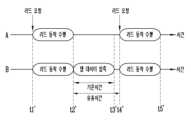
도 6은 종래의 리드 요청에 따른 메모리 컨트롤러의 동작을 설명하기 위한 도면이다.Figure 6 is a drawing for explaining the operation of a memory controller according to a conventional lead request.
도 6을 참조하면, 도 6은 호스트로부터 입력된 리드 요청에 응답하여 리드 동작을 수행하는 메모리 컨트롤러의 동작을 설명하는 도면에 해당할 수 있다. 구체적으로, A는 호스트로부터 입력된 리드 요청만을 처리하는 타이밍도를, B는 호스트로부터 입력된 리드 요청과 맵 데이터의 압축을 처리하는 타이밍도를 나타낸 것이다.Referring to FIG. 6, FIG. 6 may correspond to a drawing explaining the operation of a memory controller that performs a read operation in response to a read request input from a host. Specifically, A represents a timing diagram that processes only a read request input from a host, and B represents a timing diagram that processes a read request input from a host and compression of map data.
A를 참조하면, t1에서 호스트로부터 리드 요청이 입력될 수 있다. 메모리 컨트롤러는 입력된 리드 요청에 응답하여 리드 동작을 수행할 수 있다. 메모리 컨트롤러가 수행하는 리드 동작은, 메모리 장치가 메모리 셀들에 저장된 데이터를 리드 전압을 이용하여 센싱하는 동작일 수 있다.Referring to A, a read request may be input from the host at t1. The memory controller may perform a read operation in response to the input read request. The read operation performed by the memory controller may be an operation in which the memory device senses data stored in memory cells using a read voltage.
t3에서 t1에서 입력된 리드 요청에 대응되는 리드 동작의 수행이 종료될 수 있다. 이후, t5에서, 호스트로부터 다음 리드 요청이 입력 되면, 메모리 컨트롤러는 상술한 리드 동작을 수행하고, t6에서, 리드 동작의 수행이 종료될 수 있다.At t3, the performance of the read operation corresponding to the read request input at t1 may be terminated. Thereafter, at t5, when the next read request is input from the host, the memory controller performs the read operation described above, and at t6, the performance of the read operation may be terminated.
B는 메모리 컨트롤러에 저장된 맵 데이터가 압축되고 있을 때 리드 요청이 입력된 경우에 해당할 수 있다. 메모리 컨트롤러가 맵 데이터를 압축하고 있는 도중인 t1에서 호스트로부터 리드 요청이 입력되면, 리드 동작은 바로 수행되지 않고 맵 데이터의 압축이 끝나는 t2까지 대기할 수 있다. 이후 t2에서 맵 데이터의 압축이 끝나면, 비로소 t1에서 입력된 리드 요청에 대응되는 리드 동작이 수행될 수 있다. t4에서 t1에 입력된 리드 요청에 대응되는 리드 동작의 수행이 종료될 수 있다.B may correspond to a case where a read request is input while map data stored in the memory controller is being compressed. If a read request is input from the host at t1 while the memory controller is compressing the map data, the read operation may not be performed immediately but may wait until t2 when the compression of the map data is completed. After the compression of the map data is completed at t2, the read operation corresponding to the read request input at t1 may be performed. At t4, the performance of the read operation corresponding to the read request input at t1 may be terminated.
맵 데이터가 압축되고 있는 도중에 리드 요청이 입력되면 수행 중이던 맵 데이터 압축이 끝날 때까지 리드 동작의 수행이 지연되고, 이에 따라 리드 레이턴시(Read latency)가 발생될 수 있다. 즉, B의 경우는 해당 맵 데이터 압축이 끝날 때까지 호스트로부터 입력된 리드 요청을 처리할 수 없어, 호스트로부터 입력된 리드 요청만을 처리하는 A의 경우보다 t3-t4만큼의 리드 레이턴시가 발생될 수 있다.If a read request is input while map data is being compressed, the execution of the read operation is delayed until the map data compression that was being performed is completed, which may result in read latency. That is, in case B, the read request input from the host cannot be processed until the map data compression is completed, and thus a read latency of t3-t4 may occur compared to case A, which only processes read requests input from the host.
도 7은 본 발명의 실시 예에 따른 메모리 컨트롤러의 동작을 설명하기 위한 도면이다.FIG. 7 is a diagram for explaining the operation of a memory controller according to an embodiment of the present invention.
도 7을 참조하면, A는 호스트로부터 입력된 리드 요청만을 처리하는 타이밍도를, B는 호스트로부터 입력된 리드 요청과 맵 데이터의 압축을 처리하는 타이밍도를 나타낸 것이다.Referring to Figure 7, A represents a timing diagram for processing only a read request input from a host, and B represents a timing diagram for processing a read request input from a host and compression of map data.
B를 참조하면, t1'에 호스트로부터 리드 요청이 입력될 수 있다. 메모리 컨트롤러는 입력된 리드 요청에 응답하여 즉시 리드 동작을 수행할 수 있다. 이후 t2'에서 수행 중이던 리드 동작이 종료될 수 있다. 리드 동작이 종료되고 t4'에서 다음 리드 요청이 들어올 때까지 메모리 컨트롤러는 호스트로부터 입출력 요청이 없는 시간인 유휴시간을 가질 수 있다. 유휴시간은 t1'이전에 호스트로부터 입력된 입출력 요청 정보를 기초로 머신 러닝을 수행하여 호스트로부터 입출력 요청이 없을 것으로 예측된 시간에 해당될 수 있다. 구체적으로, 머신 러닝은 순환 인공 신경망(Recurrent Neural Network, RNN)을 이용하여 수행될 수 있다.Referring to B, a read request may be input from a host at t1'. The memory controller may immediately perform a read operation in response to the input read request. Thereafter, the read operation being performed at t2' may be terminated. After the read operation is terminated and until the next read request comes in at t4', the memory controller may have an idle time during which there is no input/output request from the host. The idle time may correspond to a time during which there is predicted to be no input/output request from the host by performing machine learning based on input/output request information input from the host before t1'. Specifically, the machine learning may be performed using a recurrent neural network (RNN).
맵 데이터가 압축되는데 소요되는 평균시간이 기준시간에 해당될 수 있다. 기준시간 동안 메모리 컨트롤러는 맵 데이터 저장부에 저장된 맵 데이터를 압축할 수 있다. 기준시간은 실시 예에 따라 맵 데이터를 압축하는 평균시간 외에 다양한 값으로 정의될 수 있다. 메모리 컨트롤러는 기준시간과 유휴시간을 비교하여 리드 동작의 수행이 t2'에 종료된 이후, 맵 데이터를 압축할지 여부를 결정할 수 있다. 유휴시간이 기준시간보다 짧으면, 다음 리드 요청이 입력될 때까지 맵 데이터의 압축이 종료되지 않을 수 있으므로 맵 데이터의 압축을 생략할 수 있다. 반대로, 유휴시간이 기준시간보다 길면, 다음 리드 요청이 입력되기 전에 맵 데이터의 압축이 종료될 수 있으므로 맵 데이터를 압축할 수 있다. 도 7은 기준시간이 유휴시간보다 짧은 경우를 도시하고 있다. 따라서, t2'에 리드 동작의 수행이 종료되고 맵 데이터의 압축이 시작될 수 있다. t3'에 맵 데이터의 압축이 종료되고, 이후 t4'에 다음 리드 요청에 응답하여 새로운 리드 동작이 수행될 수 있다.The average time required for compressing map data may correspond to the reference time. During the reference time, the memory controller may compress map data stored in the map data storage unit. The reference time may be defined as various values other than the average time for compressing map data, depending on the embodiment. The memory controller may compare the reference time with the idle time to determine whether to compress the map data after the performance of the read operation ends at t2'. If the idle time is shorter than the reference time, the compression of the map data may not end until the next read request is input, so the compression of the map data may be omitted. Conversely, if the idle time is longer than the reference time, the compression of the map data may end before the next read request is input, so the map data may be compressed. Fig. 7 illustrates a case where the reference time is shorter than the idle time. Accordingly, the performance of the read operation may end at t2' and the compression of the map data may start. The compression of the map data may end at t3', and then a new read operation may be performed in response to the next read request at t4'.
도 6과 비교하여, 도 7의 실시 예에 따르면, 메모리 컨트롤러는 입출력 요청 정보를 기초로 머신 러닝을 수행하고, 예측된 유휴시간 내에 맵 데이터를 압축할 수 있다. 따라서, 맵 데이터의 압축이 종료될 때까지 리드 동작을 지연시킴으로 인해 발생하는 리드 레이턴시를 개선할 수 있다.Compared to FIG. 6, according to the embodiment of FIG. 7, the memory controller can perform machine learning based on input/output request information and compress map data within the predicted idle time. Accordingly, the read latency caused by delaying the read operation until the compression of the map data is completed can be improved.
도 8은 본 발명의 실시 예에 따른 메모리 컨트롤러의 동작을 설명하기 위한 장치도이다.FIG. 8 is a device diagram for explaining the operation of a memory controller according to an embodiment of the present invention.
도 8을 참조하면, 메모리 컨트롤러(200)는 가용시간 예측부(210), 데이터 압축 제어부(220) 및 맵 데이터 저장부(230)를 포함할 수 있다.Referring to FIG. 8, the memory controller (200) may include an availability time prediction unit (210), a data compression control unit (220), and a map data storage unit (230).
가용시간 예측부(210)는 호스트로부터 입출력 요청 정보를 입력 받고, 가용시간 예측 정보를 생성할 수 있다. 가용시간 예측 정보는 데이터 압축 제어부(220)가 맵 데이터를 압축할지 여부에 관한 정보를 포함할 수 있다. 구체적으로, 호스트로부터 입출력 요청이 없을 것으로 예측되는 유휴시간과 맵 데이터가 압축되는데 소요되는 평균적인 시간인 기준시간을 비교한 정보에 해당될 수 있다. 이때, 가용시간 예측부(210)는 머신 러닝을 이용하여 유휴시간을 예측할 수 있다. 구체적으로, 머신 러닝의 모델 중 순환 인공 신경망(Reccurent Neural Network, RNN)을 이용한 것일 수 있다.The availability time prediction unit (210) can receive input/output request information from the host and generate availability time prediction information. The availability time prediction information can include information on whether the data compression control unit (220) will compress map data. Specifically, it can correspond to information comparing an idle time in which there is expected to be no input/output request from the host and a reference time, which is an average time required for compressing map data. At this time, the availability time prediction unit (210) can predict the idle time using machine learning. Specifically, it can be one that uses a recurrent neural network (RNN) among machine learning models.
데이터 압축 제어부(220)은 가용시간 예측부(210)로부터 입력 받은 가용시간 예측 정보에 따라 맵 데이터 저장부(230)에 저장된 맵 데이터를 압축할 수 있다. 가용시간 예측 정보가 머신 러닝을 통해 예측된 유휴시간이 가용시간에 해당하면 맵 데이터를 압축할 수 있고, 가용시간에 해당되지 않으면 맵 데이터의 압축을 생략할 수 있다. 맵 데이터의 압축에는 델타 압축(Delta compression), 지집(GZIP) 방식을 포함하는 다양한 압축 기법이 사용될 수 있다. 이후, 데이터 압축 제어부(220)는 압축된 맵 데이터를 다시 맵 데이터 저장부(230)에 저장할 수 있다.The data compression control unit (220) can compress map data stored in the map data storage unit (230) according to the available time prediction information received from the available time prediction unit (210). If the idle time predicted by the available time prediction information through machine learning corresponds to the available time, the map data can be compressed, and if it does not correspond to the available time, the compression of the map data can be omitted. Various compression techniques including delta compression and GZIP can be used to compress the map data. Thereafter, the data compression control unit (220) can store the compressed map data again in the map data storage unit (230).
맵 데이터 저장부(230)는 데이터 블록의 논리 주소와 물리 주소와의 맵핑 정보인 맵 데이터를 저장할 수 있다. 논리 주소는 호스트 입장에서 관리하는 데이터 블록의 논리적 위치를 지정하는 어드레스에 해당될 수 있다. 물리 주소는 메모리 컨트롤러가 메모리 장치의 실제 데이터 블록의 물리적 위치를 지정하는 어드레스에 해당될 수 있다.The map data storage unit (230) can store map data, which is mapping information between the logical address of a data block and the physical address. The logical address may correspond to an address that specifies a logical location of a data block managed by the host. The physical address may correspond to an address that specifies a physical location of an actual data block of a memory device by the memory controller.
도 9는 도 8의 가용시간 예측부(210)의 동작을 설명하기 위한 도면이다.Figure 9 is a drawing for explaining the operation of the availability time prediction unit (210) of Figure 8.
도 9를 참조하면, 가용시간 예측부(210)는 제1 전처리부(211), 제1 정보 처리부(212), 제2 전처리부(213), 제2 정보 처리부(214), 제3 정보 처리부(215) 및 제4 정보 처리부(216)를 포함할 수 있다.Referring to FIG. 9, the availability time prediction unit (210) may include a first preprocessing unit (211), a first information processing unit (212), a second preprocessing unit (213), a second information processing unit (214), a third information processing unit (215), and a fourth information processing unit (216).
가용 시간 예측부(210)는 순환 인공 신경망(Recurrent Neural Network, RNN) 기반의 머신 러닝(Machine learning)을 이용하여 가용시간 예측 정보를 생성할 수 있다. RNN 구조의 출력값은 현재 입력 값뿐만 아니라 시간적으로 이전 데이터의 결과 값에도 영향을 받을 수 있다. RNN의 일종인 장단기 메모리 방식(Long Short Term Memory, LSTM)은 시간이 길어지고 계층이 깊어져도 데이터를 유실하지 않고 유지하는 특징이 있는 유닛에 해당할 수 있다. 즉, LSTM은 장기 또는 단기 기억이 가능하도록 설계된 머신 러닝 유닛에 해당할 수 있다. 본 발명의 실시 예에서는, 복수의 전처리부들(211, 213)에 의해 입출력 요청 정보가 수집되고, LSTM을 적용한 복수의 정보 처리부들(212, 214, 215, 216)을 이용하여 호스트로부터 입출력 요청이 없는 시간인 유휴시간을 예측하기 위한 머신 러닝이 수행될 수 있다.The availability time prediction unit (210) can generate availability time prediction information using machine learning based on a recurrent neural network (RNN). The output value of the RNN structure can be affected not only by the current input value but also by the result value of the previous data in terms of time. Long Short Term Memory (LSTM), which is a type of RNN, can correspond to a unit that has the characteristic of not losing data and maintaining it even when time becomes long and the layer becomes deep. In other words, LSTM can correspond to a machine learning unit designed to enable long-term or short-term memory. In an embodiment of the present invention, input/output request information is collected by a plurality of preprocessing units (211, 213), and machine learning can be performed to predict idle time, which is a time when there is no input/output request from the host, using a plurality of information processing units (212, 214, 215, 216) to which LSTM is applied.
제1 전처리부(211)는 가용시간 예측 정보를 생성하기 직전에 입력된 입출력 요청 정보인 현재 입출력 요청 정보를 저장할 수 있다. 제1 전처리부(211)는 현재 입출력 요청 정보를 RNN 방식의 머신 러닝에 최적화되도록 처리하는 동작을 수행할 수 있다.The first preprocessing unit (211) can store current input/output request information, which is input/output request information entered immediately before generating available time prediction information. The first preprocessing unit (211) can perform an operation to process the current input/output request information so as to be optimized for RNN-type machine learning.
제2 전처리부(213)는 제1 전처리부(211)로부터 입력 받은 과거 입출력 정보를 저장할 수 있다. 과거 입출력 요청 정보는 호스트로부터 현재 입출력 요청 정보가 입력 되기 이전에 입력된 입출력 요청 정보에 해당할 수 있다. 제2 전처리부(213)는 과거 입출력 정보를 RNN 방식의 머신 러닝에 최적화되도록 처리하는 동작을 수행할 수 있다.The second preprocessing unit (213) can store past input/output information received from the first preprocessing unit (211). The past input/output request information may correspond to input/output request information input before the current input/output request information is input from the host. The second preprocessing unit (213) can perform an operation of processing the past input/output information to be optimized for RNN-type machine learning.
제1 정보 처리부(212)는 제1 전처리부(211)에 저장된 현재 입출력 요청 정보에 대하여 머신 러닝을 수행할 수 있다. 제1 정보 처리부(212)의 노드들은 이전 계층인 제1 전처리부(211)의 노드들과 완전하게 연결된 구조(Fully Connected Layer)로 구성될 수 있다.The first information processing unit (212) can perform machine learning on the current input/output request information stored in the first preprocessing unit (211). The nodes of the first information processing unit (212) can be configured in a structure (Fully Connected Layer) that is fully connected to the nodes of the first preprocessing unit (211), which is the previous layer.
제2 정보 처리부(214)는 제2 전처리부(213)에 저장된 현재 입출력 요청 정보에 대하여 머신 러닝을 수행할 수 있다. 제2 정보 처리부(214)의 노드들은 이전 계층인 제2 전처리부(213)의 노드들과 완전하게 연결된 구조(Fully Connected Layer)로 구성될 수 있다.The second information processing unit (214) can perform machine learning on the current input/output request information stored in the second preprocessing unit (213). The nodes of the second information processing unit (214) can be configured in a structure (Fully Connected Layer) that is fully connected to the nodes of the second preprocessing unit (213), which is the previous layer.
제3 정보 처리부(215)는 제2 정보 처리부(214)로부터 입력 받은, 1차적으로 머신 러닝이 수행된 과거 입출력 요청 정보에 대하여 머신 러닝을 수행할 수 있다. 제3 정보 처리부(215)의 노드들은 이전 계층인 제2 정보 처리부(214)의 노드들과 완전하게 연결된 구조(Fully Connected Layer)로 구성될 수 있다.The third information processing unit (215) can perform machine learning on past input/output request information received from the second information processing unit (214) on which machine learning was first performed. The nodes of the third information processing unit (215) can be configured in a structure (Fully Connected Layer) that is fully connected to the nodes of the second information processing unit (214), which is the previous layer.
제4 정보 처리부(216)는 머신 러닝이 수행된 과거 입출력 요청 정보 및 현재 입출력 요청 정보에 대하여 머신 러닝을 수행할 수 있다. 제4 정보 처리부(216)의 노드들은 이전 계층인 제3 정보 처리부(215)의 노드들 및 제1 정보 처리부(212)의 노드들과 완전하게 연결된 구조(Fully Connected Layer)로 구성될 수 있다. 제4 정보 처리부(216)는 반복적인 머신 러닝을 통하여 예측된 유휴시간을, 미리 설정된 기준시간과 비교하여 가용시간 예측 정보를 생성할 수 있다. 가용시간 예측 정보는 예측된 유휴시간이 맵 데이터 압축을 수행될 수 있는 시간에 해당하는지에 관한 정보를 포함할 수 있다. 머신 러닝을 통해 예측된 유휴시간이 기준시간보다 길면, 유휴시간이 가용시간에 해당한다는 가용시간 예측 정보를 생성할 수 있다. 머신 러닝을 통해 예측된 유휴시간이 기준시간보다 짧으면, 유휴시간이 가용시간에 해당하지 않는다는 가용시간 예측 정보를 생성할 수 있다.The fourth information processing unit (216) can perform machine learning on past input/output request information and current input/output request information on which machine learning was performed. The nodes of the fourth information processing unit (216) can be configured as a structure that is fully connected with the nodes of the third information processing unit (215), which is a previous layer, and the nodes of the first information processing unit (212). The fourth information processing unit (216) can generate available time prediction information by comparing the predicted idle time through repeated machine learning with a preset reference time. The available time prediction information can include information on whether the predicted idle time corresponds to a time during which map data compression can be performed. If the predicted idle time through machine learning is longer than the reference time, available time prediction information indicating that the idle time corresponds to the available time can be generated. If the predicted idle time through machine learning is shorter than the reference time, available time prediction information indicating that the idle time does not correspond to the available time can be generated.
가용시간 예측부(210)는 두 개의 전처리부(211, 213)와 네 개의 정보 처리부(212, 214, 215, 216)을 포함하는 것으로 도시하였지만, 이에 한정되지 않을 수 있다.The availability time prediction unit (210) is illustrated as including two preprocessing units (211, 213) and four information processing units (212, 214, 215, 216), but may not be limited thereto.
도 10은 도 8의 데이터 압축 제어부(220)의 동작을 설명하기 위한 도면이다.Figure 10 is a drawing for explaining the operation of the data compression control unit (220) of Figure 8.
도 10을 참조하면, 데이터 압축 제어부(220)는 블록 선택부(221), 유사 검출부(222) 및 압축부(223)을 포함할 수 있다.Referring to FIG. 10, the data compression control unit (220) may include a block selection unit (221), a similarity detection unit (222), and a compression unit (223).
데이터 압축 제어부(220)는 맵 데이터 저장부(230)로부터 맵 데이터를 입력 받고, 압축 맵 데이터를 맵 데이터 저장부(230)로 출력할 수 있다.The data compression control unit (220) can receive map data from the map data storage unit (230) and output compressed map data to the map data storage unit (230).
구체적으로, 블록 선택부(221)는 가용시간 예측부(210)로부터 맵 데이터의 압축 여부에 관한 정보인 가용시간 예측 정보를 입력 받을 수 있다. 가용시간 예측 정보에 따라, 유휴시간이 가용시간이면, 맵 데이터가 지시하는 블록 정보를 기초로 해당 맵 데이터가 압축 대상 맵 데이터인지 결정할 수 있다. 블록 선택부(221)는 맵 데이터가 지시하는 메모리 블록의 블록 정보를 저장할 수 있다. 예를 들어, 블록 정보는 유효 페이지 개수 또는 리드 횟수가 기준 값 이상인 페이지 개수가 포함될 수 있다.Specifically, the block selection unit (221) can receive availability time prediction information, which is information on whether map data is compressed, from the availability time prediction unit (210). According to the availability time prediction information, if the idle time is the available time, it can be determined whether the corresponding map data is the map data to be compressed based on the block information indicated by the map data. The block selection unit (221) can store the block information of the memory block indicated by the map data. For example, the block information can include the number of valid pages or the number of pages whose read count is greater than or equal to a reference value.
유사 검출부(222)는 블록 선택부(221)로부터 블록 선택 정보를 입력 받고, 압축 대상 맵 데이터의 유사 검출 정보를 출력할 수 있다. 유사 검출 정보는 데이터 간의 차이에 관한 정보에 해당할 수 있다. 델타 압축 방식은 순차적인 데이터 간의 차이(differences) 형식으로 데이터를 압축할 수 있다. 따라서, 데이터 간의 차이가 적을수록 델타 압축 방식은 데이터 간의 중복성을 줄이고 저장되는 데이터의 용량을 감소시킬 수 있다.The similarity detection unit (222) can receive block selection information from the block selection unit (221) and output similarity detection information of the compression target map data. The similarity detection information can correspond to information about differences between data. The delta compression method can compress data in the form of differences between sequential data. Therefore, the smaller the difference between data, the more the delta compression method can reduce redundancy between data and reduce the capacity of stored data.
압축부(223)는 유사 검출부(222)가 출력한 유사 검출 정보에 따라 맵 데이터를 압축할 수 있다. 압축부(223)는 델타 압축(Delta compression), 지집(GZIP) 을 포함한 다양한 압축 방식에 따라 압축 동작을 수행할 수 있다. 압축부(223)는 유사 검출 정보에 따라 델타 압축 방식을 생략할 수 있다. 예를 들어, 맵 데이터 간의 차이가 일정 기준 값 이상이면, 델타 압축에 따라 압축된 데이터의 크기가 충분히 작지 않을 수 있으므로 델타 압축 방식이 생략될 수 있다. 실시 예에 따라, 델타 압축 또는 지집을 포함한 다양한 압축 방식이 선택적으로 수행될 수 있다. 실시 예에 따라, 다양한 압축 방식들이 중첩적으로 수행될 수도 있다.The compression unit (223) can compress map data according to the similarity detection information output by the similarity detection unit (222). The compression unit (223) can perform a compression operation according to various compression methods including delta compression and GZIP. The compression unit (223) can omit the delta compression method according to the similarity detection information. For example, if the difference between the map data is greater than a certain reference value, the size of the data compressed according to the delta compression may not be sufficiently small, so the delta compression method may be omitted. Depending on the embodiment, various compression methods including delta compression or GZIP may be selectively performed. Depending on the embodiment, various compression methods may be performed in an overlapping manner.
도 11은 유효 페이지 개수에 따른 블록 선택부의 실시 예를 설명하기 위한 도면이다.Fig. 11 is a drawing for explaining an example of a block selection unit according to the number of valid pages.
도 11을 참조하면, 블록 선택부(221)는 유효 페이지의 개수에 따른 대상 블록 정보를 저장할 수 있다.Referring to FIG. 11, the block selection unit (221) can store target block information according to the number of valid pages.
실시 예에서, 가용시간 예측 정보에 따라 맵 데이터가 압축되기 전에, 압축 대상 맵 데이터가 결정되는 동작이 수행될 수 있다. 압축 대상 맵 데이터는 해당 맵 데이터가 지정하는 메모리 블록들의 블록 정보를 기초로 결정될 수 있다. 블록 정보에는 유효 페이지 개수에 따라 가비지 컬랙션(Garbage Collection, GC)의 대상이 되는 메모리 블록인지 여부가 포함될 수 있으나, 이에 한정되지 않을 수 있다. 이때, 유효 페이지를 적게 포함하는 메모리 블록을 프리 블록으로 만드는 것이, 유효 페이지를 상대적으로 더 많이 포함하는 메모리 블록을 프리 블록으로 만드는 것보다 카피될 유효 페이지의 개수가 적기 때문에 더 효율적일 수 있다. 따라서, GC의 대상이 되는 메모리 블록은 유효 페이지를 적게 포함하는 메모리 블록에 해당할 수 있다. GC를 수행하기 위해서는 해당 메모리 블록에 관한 맵 데이터가 필요할 수 있다. 따라서, GC 수행의 대상이 되는 메모리 블록을 지정하는 맵 데이터는 압축되지 않고 원본 상태로 남아있는 것이 유리할 수 있다.In an embodiment, before the map data is compressed according to the availability time prediction information, an operation of determining the map data to be compressed may be performed. The map data to be compressed may be determined based on the block information of the memory blocks specified by the corresponding map data. The block information may include whether the memory block is a target of garbage collection (GC) according to the number of valid pages, but may not be limited thereto. At this time, making a memory block containing fewer valid pages into a free block may be more efficient than making a memory block containing relatively more valid pages into a free block because the number of valid pages to be copied is smaller. Therefore, the memory block to be subject to GC may correspond to a memory block containing fewer valid pages. In order to perform GC, map data regarding the corresponding memory block may be required. Therefore, it may be advantageous for the map data specifying the memory block to be subject to GC to remain in its original state without being compressed.
도 11은 다섯 개의 블록이 각각 포함하는 유효 페이지의 개수를 도시하고 있다. 구체적으로, 제1 블록(BLK1)은 7개의 유효 페이지를, 제2 블록(BLK2)은 4개의 유효 페이지를, 제3 블록(BLK3)은 15개의 유효 페이지를, 제4 블록(BLK4)은 11개의 유효 페이지를, 제5 블록(BLK5)은 19개의 유효 페이지를 포함할 수 있다. 유효 페이지를 가장 적게 포함하는 제2 블록은 카피될 유효 페이지의 수가 4개로 가장 적으므로, 다섯 개의 블록 중 가장 먼저 GC가 수행될 수 있다. 반대로, 가장 많은 유효 페이지를 포함하는 제5 블록은 카피될 유효 페이지의 수가 19개로 가장 많으므로, 다섯 개의 블록 중 가장 나중에 GC가 수행될 수 있다. 제2 블록은 GC의 대상 블록의 우선순위가 가장 높으므로 제2 블록을 지정하는 맵 데이터는 압축되지 않고 원본 데이터 형태로 남아있는 것이 유리할 수 있다. 제5 블록은 GC의 대상 블록의 우선순위가 가장 낮으므로 제5 블록을 지정하는 맵 데이터는 압축 데이터 형태로 저장되는 것이 유리할 수 있다. 따라서, 블록 선택부(221)는 다섯 개의 블록들을 지정하는 맵 데이터 중 제5 블록을 지정하는 맵 데이터를 압축의 대상으로 선택할 수 있다. 블록 선택부(221)가 선택하는 맵 데이터는 하나의 블록을 지정하는 맵 데이터에 한정되지 않을 수 있고, 유효 페이지를 적게 포함하는 순서대로 복수의 메모리 블록들을 지정하는 맵 데이터가 선택될 수 있다.Fig. 11 illustrates the number of valid pages each of the five blocks contains. Specifically, the first block (BLK1) may contain 7 valid pages, the second block (BLK2) may contain 4 valid pages, the third block (BLK3) may contain 15 valid pages, the fourth block (BLK4) may contain 11 valid pages, and the fifth block (BLK5) may contain 19 valid pages. The second block, which contains the fewest valid pages, has the smallest number of valid pages to be copied, 4, and thus may be subjected to GC first among the five blocks. Conversely, the fifth block, which contains the most valid pages, has the largest number of valid pages to be copied, 19, and thus may be subjected to GC last among the five blocks. Since the second block has the highest priority as a target block for GC, it may be advantageous for the map data specifying the second block to remain in the original data form without being compressed. Since the fifth block has the lowest priority as a target block of GC, it may be advantageous for the map data specifying the fifth block to be stored in the form of compressed data. Accordingly, the block selection unit (221) may select the map data specifying the fifth block among the map data specifying five blocks as a target of compression. The map data selected by the block selection unit (221) may not be limited to map data specifying one block, and map data specifying a plurality of memory blocks in the order of including the least valid pages may be selected.
도 12는 리드 횟수에 따른 블록 선택부의 실시 예를 설명하기 위한 도면이다.Fig. 12 is a drawing for explaining an example of a block selection unit according to the number of leads.
도 12를 참조하면, 블록 선택부(221)는 리드 횟수에 따른 대상 블록 정보를 저장할 수 있다.Referring to Fig. 12, the block selection unit (221) can store target block information according to the number of reads.
실시 예에서, 가용시간 예측 정보에 따라 맵 데이터가 압축되기 전에, 압축될 맵 데이터가 선택되는 동작이 수행될 수 있다. 압축될 맵 데이터는 해당 맵 데이터가 지정하는 메모리 블록들의 블록 정보를 기초로 결정될 수 있다. 블록 정보에는 리드 횟수에 따른 리드 리클레임(Read Reclaim)의 대상이 되는 메모리 블록인지 여부가 포함될 수 있으나, 이에 한정되지 않을 수 있다. 메모리 블록에 포함된 특정 페이지의 리드 횟수가 미리 설정된 기준 값을 초과하면 리드 디스터브(Read disturb)가 일정 수준 이상으로 증가할 수 있다. 따라서, 메모리 컨트롤러는 원본 데이터를 보존하기 위하여, 리드 횟수가 기준 값 이상으로 증가한 페이지가 일정 개수 이상 포함된 메모리 블록에 저장된 데이터를, 다른 메모리 블록에 옮겨 쓰기를 하는 리드 리클레임을 수행할 수 있다. 이때, 리드 리클레임을 수행하기 위해서는 해당 메모리 블록에 관한 맵 데이터가 필요할 수 있다. 따라서, 리드 리클레임 수행의 대상이 되는 메모리 블록을 지정하는 맵 데이터는 압축되지 않고 원본 데이터 형태로 남아있는 것이 유리할 수 있다.In an embodiment, before the map data is compressed according to the availability time prediction information, an operation of selecting the map data to be compressed may be performed. The map data to be compressed may be determined based on the block information of the memory blocks designated by the corresponding map data. The block information may include, but may not be limited to, whether the memory block is a target of read reclaim according to the number of reads. If the number of reads of a specific page included in the memory block exceeds a preset reference value, read disturbance may increase to a certain level or more. Therefore, the memory controller may perform read reclaim to transfer and write data stored in a memory block including a certain number or more of pages whose number of reads has increased to a certain number or more than the reference value to another memory block in order to preserve the original data. At this time, map data regarding the corresponding memory block may be required in order to perform read reclaim. Therefore, it may be advantageous for the map data designating the memory block to be a target of read reclaim to remain in the form of original data without being compressed.
도 12는 다섯 개의 블록이 각각 포함하는 리드 횟수가 기준 값보다 많은 페이지 개수를 도시하고 있다. 구체적으로, 제1 블록(BLK1)은 7개의 리드 횟수가 기준 값보다 많은 페이지를, 제2 블록(BLK2)은 4개의 리드 횟수가 기준 값보다 많은 페이지를, 제3 블록(BLK3)은 15개의 리드 횟수가 기준 값보다 많은 페이지를, 제4 블록(BLK4)은 11개의 리드 횟수가 기준 값보다 많은 페이지를, 제5 블록(BLK5)은 19개의 리드 횟수가 기준 값보다 많은 페이지를 포함할 수 있다. 리드 횟수가 기준 값보다 많은 페이지를 가장 많이 포함하는 제5 블록은 리드 디스터브가 발생할 가능성이 가장 크기 때문에 리드 리클레임이 가장 먼저 수행될 수 있다. 리드 횟수가 기준 값보다 많은 페이지를 가장 적게 포함하는 제2 블록은 리드 디스터브가 발생할 가능성이 가장 적기 때문에 리드 리클레임이 가장 나중에 수행될 수 있다. 따라서, 제5 블록은 리드 리클레임의 우선순위가 가장 높으므로, 제5 블록을 지정하는 맵 데이터는 원본 데이터 형태로 저장되는 것이 유리할 수 있다. 제2 블록은 리드 리클레임의 우선순위가 가장 낮으므로, 제2 블록을 지정하는 맵 데이터는 압축 데이터 형태로 저장되는 것이 유리할 수 있다. 따라서, 블록 선택부(221)는 다섯 개의 블록들을 지정하는 맵 데이터 중 제2 블록을 지정하는 맵 데이터를 압축의 대상으로 선택할 수 있다. 블록 선택부(221)가 선택하는 맵 데이터는 하나의 블록을 지정하는 맵 데이터에 한정되지 않을 수 있고, 리드 횟수가 기준 값보다 많은 페이지를 적게 포함하는 순서대로, 복수의 메모리 블록들을 지정하는 맵 데이터가 선택될 수 있다.FIG. 12 illustrates the number of pages whose read counts are greater than a reference value, respectively, of five blocks. Specifically, the first block (BLK1) may include pages whose read counts are greater than a reference value by 7, the second block (BLK2) may include pages whose read counts are greater than a reference value by 4, the third block (BLK3) may include pages whose read counts are greater than a reference value by 15, the fourth block (BLK4) may include pages whose read counts are greater than a reference value by 11, and the fifth block (BLK5) may include pages whose read counts are greater than a reference value by 19. The fifth block, which includes the largest number of pages whose read counts are greater than a reference value, may have read reclaim performed first because it is most likely to experience read disturb. The second block, which includes the fewest number of pages whose read counts are greater than a reference value, may have read reclaim performed last because it is least likely to experience read disturb. Accordingly, since the fifth block has the highest priority for read reclaim, it may be advantageous to store the map data specifying the fifth block in the form of original data. Since the second block has the lowest priority for read reclaim, it may be advantageous to store the map data specifying the second block in the form of compressed data. Accordingly, the block selection unit (221) may select the map data specifying the second block among the map data specifying five blocks as the target of compression. The map data selected by the block selection unit (221) may not be limited to map data specifying one block, and map data specifying a plurality of memory blocks may be selected in the order in which the number of reads is smaller than a reference value.
도 13은 본 발명의 실시 예에 따른 메모리 컨트롤러의 동작을 설명하기 위한 순서도이다.FIG. 13 is a flowchart for explaining the operation of a memory controller according to an embodiment of the present invention.
도 13을 참조하면, S1301단계에서, 메모리 컨트롤러는 호스트로부터 입출력 요청이 없을 것으로 예측되는 유휴시간에 관한 정보인 가용시간 예측정보를 생성할 수 있다. 메모리 컨트롤러는 호스트로부터 입출력 요청 정보를 입력 받고, 머신 러닝을 통해 유휴시간을 예측할 수 있다. 예측된 유휴시간을 맵 데이터가 압축되는데 소요되는 평균시간에 해당할 수 있는 기준시간과 비교하여, 맵 데이터의 압축 여부에 관한 정보를 포함하는 가용시간 예측 정보를 생성할 수 있다.Referring to FIG. 13, in step S1301, the memory controller can generate available time prediction information, which is information about an idle time during which no input/output requests are expected from the host. The memory controller can receive input/output request information from the host and predict the idle time through machine learning. By comparing the predicted idle time with a reference time that can correspond to an average time required for map data to be compressed, available time prediction information including information about whether the map data is compressed can be generated.
S1303단계에서, 메모리 컨트롤러는 생성된 가용시간 예측 정보에 따라 맵 데이터를 압축할 수 있다. 예측된 유휴시간이 가용시간이라는 가용시간 예측 정보가 생성되면, 메모리 컨트롤러는 맵 데이터를 압축할 수 있다. 예측된 유휴시간이 가용시간이 아니라는 가용시간 예측 정보가 생성되면, 메모리 컨트롤러는 맵 데이터의 압축을 생략할 수 있다.In step S1303, the memory controller can compress the map data according to the generated availability time prediction information. If the generated availability time prediction information indicates that the predicted idle time is the availability time, the memory controller can compress the map data. If the generated availability time prediction information indicates that the predicted idle time is not the availability time, the memory controller can omit compressing the map data.
각각의 단계는 아래의 도 14 및 도 15를 통하여 상세하게 설명될 수 있다.Each step can be described in detail through Figures 14 and 15 below.
도 14는 도 13의 가용시간 예측 정보의 생성하는 단계를 상세하게 설명하기 위한 순서도이다.Figure 14 is a flowchart for explaining in detail the steps for generating the availability time prediction information of Figure 13.
도 14를 참조하면, S1401단계에서, 메모리 컨트롤러는 호스트로부터 입출력 요청 정보를 수신할 수 있다. 입출력 요청 정보는 호스트가 저장 장치에 프로그램, 리드 동작 등을 요청하는 정보에 해당될 수 있다.Referring to FIG. 14, in step S1401, the memory controller may receive input/output request information from the host. The input/output request information may correspond to information requesting a program, read operation, etc. from the host to the storage device.
S1403단계에서, 메모리 컨트롤러는 입출력 요청 정보를 제1 전처리부에 저장할 수 있다. 제1 전처리부에 저장되는 입출력 요청 정보는, 가용시간 예측 정보가 생성되기 직전에 호스트로부터 입력된 입출력 요청 정보에 해당될 수 있다. 제1 전처리부는 입출력 요청 정보를 순환 인공 신경망(RNN) 방식의 머신 러닝에 최적화되도록 처리하는 동작을 수행할 수 있다.In step S1403, the memory controller may store input/output request information in the first preprocessing unit. The input/output request information stored in the first preprocessing unit may correspond to input/output request information input from the host immediately before the availability time prediction information is generated. The first preprocessing unit may perform an operation of processing the input/output request information to be optimized for machine learning in the form of a recurrent artificial neural network (RNN).
S1405단계에서, 메모리 컨트롤러는 입출력 요청 정보를 제2 전처리부에 저장할 수 있다. 제2 전처리부에 저장되는 입출력 요청 정보는, 제1 전처리부로부터 입력된 입출력 요청 정보에 해당될 수 있다. 제2 전처리부는 입출력 요청 정보를 순환 인공 신경망(RNN)방식의 머신 러닝에 최적화되도록 처리하는 동작을 수행할 수 있다.In step S1405, the memory controller may store input/output request information in the second preprocessing unit. The input/output request information stored in the second preprocessing unit may correspond to the input/output request information input from the first preprocessing unit. The second preprocessing unit may perform an operation of processing the input/output request information to be optimized for machine learning in the form of a recurrent artificial neural network (RNN).
S1407단계에서, 메모리 컨트롤러는 제1 전처리부에 저장된 입출력 요청 정보에 대하여 머신 러닝을 수행할 수 있다. 머신 러닝에는 순환 인공 신경망(RNN) 방식이 이용될 수 있다. 머신 러닝은 제1 전처리로부터 입출력 요청 정보가 입력될 때마다 수행될 수 있다.In step S1407, the memory controller may perform machine learning on the input/output request information stored in the first preprocessing unit. A recurrent artificial neural network (RNN) method may be used for the machine learning. The machine learning may be performed whenever input/output request information is input from the first preprocessing unit.
S1409단계에서, 메모리 컨트롤러는 제2 전처리부에 저장된 입출력 요청 정보에 대하여 머신 러닝을 수행할 수 있다. 머신 러닝에는 순환 인공 신경망(RNN) 방식이 이용될 수 있다. 머신 러닝은 제2 전처리로부터 입출력 요청 정보가 입력될 때마다 수행될 수 있다.In step S1409, the memory controller may perform machine learning on the input/output request information stored in the second preprocessing unit. A recurrent artificial neural network (RNN) method may be used for the machine learning. The machine learning may be performed whenever input/output request information is input from the second preprocessing unit.
S1411단계에서, 메모리 컨트롤러는 입출력 요청 정보가 입력된 시간 간격을 경험적으로 학습하고, 호스트로부터 다음 입출력 요청 정보가 입력될 때까지의 유휴시간을 예측할 수 있다. 머신 러닝은 호스트로부터 입출력 요청 정보가 입력될 때마다 수행될 수 있고, 예측된 유휴시간은 그에 따라 증감될 수 있다.In step S1411, the memory controller can empirically learn the time interval at which input/output request information is input, and predict the idle time until the next input/output request information is input from the host. Machine learning can be performed every time input/output request information is input from the host, and the predicted idle time can be increased or decreased accordingly.
S1413단계에서, 메모리 컨트롤러는 예측된 유휴시간과 미리 설정된 기준시간을 비교하여 가용시간 예측 정보를 생성할 수 있다. 기준시간은 메모리 컨트롤러가 맵 데이터를 압축하는데 소요되는 평균적인 시간에 해당될 수 있으나, 이에 한정되지 않을 수 있다. 예측된 유휴시간이 기준시간보다 길면, 유휴시간 내에 맵 데이터의 압축이 종료될 수 있다고 판단될 수 있다. 따라서, 예측된 유휴시간이 맵 데이터를 압축할 수 있는 가용시간에 해당된다는 정보를 포함하는 가용시간 예측 정보가 생성될 수 있다. 예측된 유휴시간이 기준시간보다 짧으면, 유휴시간 내에 맵 데이터의 압축이 종료될 수 없다고 판단될 수 있다. 따라서, 예측된 유휴시간이 맵 데이터를 압축할 수 있는 가용시간에 해당되지 않는다는 정보를 포함하는 가용시간 예측 정보가 생성될 수 있다.In step S1413, the memory controller can generate available time prediction information by comparing the predicted idle time with a preset reference time. The reference time may correspond to an average time taken by the memory controller to compress map data, but may not be limited thereto. If the predicted idle time is longer than the reference time, it may be determined that the compression of the map data can be completed within the idle time. Accordingly, available time prediction information including information that the predicted idle time corresponds to the available time for compressing the map data can be generated. If the predicted idle time is shorter than the reference time, it may be determined that the compression of the map data cannot be completed within the idle time. Accordingly, available time prediction information including information that the predicted idle time does not correspond to the available time for compressing the map data can be generated.
도 15는 도 13의 맵 데이터를 압축하는 단계를 상세하게 설명하기 위한 순서도이다.Figure 15 is a flowchart for explaining in detail the steps for compressing the map data of Figure 13.
도 15를 참조하면, S1501단계에서, 메모리 컨트롤러는 가용시간 예측 정보를 기초로 예측된 유휴시간이 가용시간에 해당하는지 판단할 수 있다. 유휴시간이 가용시간에 해당되면 S1503단계가 수행될 수 있다. 유휴시간이 가용시간에 해당되지 않으면 맵 데이터가 압축되지 않고 단계가 종료될 수 있다.Referring to FIG. 15, in step S1501, the memory controller can determine whether the predicted idle time corresponds to the available time based on the available time prediction information. If the idle time corresponds to the available time, step S1503 can be performed. If the idle time does not correspond to the available time, the map data may not be compressed and the step may be terminated.
S1503단계에서, 메모리 컨트롤러는 맵 데이터가 지정하는 메모리 블록들의 블록 정보를 기초로, 압축될 맵 데이터를 결정할 수 있다. 예를 들어, 메모리 블록이 유효 페이지를 많이 포함할수록 가비지 컬랙션의 대상 블록에 해당되지 않을 가능성이 높으므로, 해당 맵 데이터는 압축 대상으로 결정될 수 있다. 또한, 메모리 블록이 기준 값 이상의 리드 횟수를 포함하는 페이지를 적게 포함할수록 리드 리클레임의 대상 블록에 해당되지 않을 가능성이 높으므로, 해당 맵 데이터는 압축 대상으로 결정될 수 있다.In step S1503, the memory controller can determine map data to be compressed based on block information of memory blocks specified by the map data. For example, the more valid pages a memory block includes, the more likely it is that it will not be a target block for garbage collection, and thus the corresponding map data can be determined as a compression target. In addition, the fewer pages a memory block includes that include a number of reads greater than a reference value, the more likely it is that it will not be a target block for read reclaim, and thus the corresponding map data can be determined as a compression target.
S1505단계에서, 메모리 컨트롤러는 맵 데이터의 유사성을 검출할 수 있다. 유사성은 맵 데이터 간의 차이(differences)에 해당될 수 있다.In step S1505, the memory controller can detect similarity of map data. The similarity may correspond to differences between map data.
S1507단계에서, 메모리 컨트롤러는 검출한 맵 데이터 간의 차이를 기초로 맵 데이터를 압축할 수 있다. 맵 데이터의 압축에는 델타 압축(Delta compression) 방식을 예를 들어 설명될 수 있다. 델타 압축은 파일 전체가 아니라, 순차적인 데이터 간의 차이 형식으로 데이터를 압축하는 방법에 해당될 수 있다. 델타 압축은 데이터 간의 차이를 저장하므로, 차이가 적을수록 데이터 간의 중복성을 줄이고 저장 용량을 감소시킬 수 있다. 실시 예에 따라, 상술한 델타 압축 방식은 생략되고 다른 압축 기법이 사용될 수 있다. 예를 들어, 지집(GZIP) 방식으로 맵 데이터가 압축될 수 있다.In step S1507, the memory controller can compress the map data based on the difference between the detected map data. The compression of the map data can be explained by way of example using the delta compression method. Delta compression can correspond to a method of compressing data in the form of differences between sequential data, rather than the entire file. Since delta compression stores the differences between data, the smaller the differences, the less redundancy between data can be reduced and the storage capacity can be reduced. According to an embodiment, the above-described delta compression method may be omitted and another compression technique may be used. For example, the map data may be compressed using the GZIP method.
S1509단계에서, 메모리 컨트롤러는 압축된 맵 데이터를 맵 데이터 저장부에 저장할 수 있다. 맵 데이터를 압축 데이터의 형태로 저장함으로써, 맵 데이터 저장부의 저장 용량을 효율적으로 관리하고, 추가적인 맵 데이터 저장부의 구비에 따른 저장 장치의 크기 증가, 전력 소모 및 비용 증가를 개선할 수 있다.In step S1509, the memory controller can store the compressed map data in the map data storage. By storing the map data in the form of compressed data, the storage capacity of the map data storage can be efficiently managed, and the increase in the size of the storage device, power consumption, and cost due to the provision of an additional map data storage can be improved.
도 16은 도 1의 메모리 컨트롤러의 다른 실시 예를 설명하기 위한 도면이다.FIG. 16 is a drawing for explaining another embodiment of the memory controller of FIG. 1.
도 16을 참조하면, 메모리 컨트롤러(1000)는 호스트(Host) 및 메모리 장치에 연결된다. 호스트(Host)로부터의 요청에 응답하여, 메모리 컨트롤러(1000)는 메모리 장치를 액세스하도록 구성된다. 메모리 컨트롤러(1000)는 메모리 장치 및 호스트(Host) 사이에 인터페이스를 제공할 수 있다. 메모리 컨트롤러(1000)는 메모리 장치를 제어하기 위한 펌웨어(firmware)를 구동할 수 있다.Referring to FIG. 16, a memory controller (1000) is connected to a host and a memory device. In response to a request from the host, the memory controller (1000) is configured to access the memory device. The memory controller (1000) may provide an interface between the memory device and the host. The memory controller (1000) may drive firmware for controlling the memory device.
메모리 컨트롤러(1000)는 프로세서부(Processor; 1010), 메모리 버퍼부(Memory Buffer; 1020), 에러 정정부(ECC; 1030), 호스트 인터페이스(Host Interface; 1040), 버퍼 제어부(Buffer Control Circuit; 1050), 메모리 인터페이스(Memory Interface; 1060) 그리고 버스(Bus; 1070)를 포함할 수 있다.The memory controller (1000) may include a processor (1010), a memory buffer (1020), an error correction circuit (ECC) (1030), a host interface (1040), a buffer control circuit (Buffer Control Circuit) (1050), a memory interface (1060), and a bus (Bus) (1070).
버스(1070)는 메모리 컨트롤러(1000)의 구성 요소들 사이에 채널(channel)을 제공하도록 구성될 수 있다.The bus (1070) may be configured to provide a channel between components of the memory controller (1000).
프로세서부(1010)는 메모리 컨트롤러(1000)의 제반 동작을 제어하고, 논리 연산을 수행할 수 있다. 프로세서부(1010)는 호스트 인터페이스(1040)를 통해 외부의 호스트와 통신하고, 메모리 인터페이스(1060)를 통해 메모리 장치와 통신할 수 있다. 또한 프로세서부(1010)는 버퍼 제어부(1050)를 통해 메모리 버퍼부(1020)와 통신할 수 있다. 프로세서부(1010)는 메모리 버퍼부(1020)를 동작 메모리, 캐시 메모리(cache memory) 또는 버퍼 메모리(buffer memory)로 사용하여 저장장치의 동작을 제어할 수 있다.The processor unit (1010) can control the overall operation of the memory controller (1000) and perform logical operations. The processor unit (1010) can communicate with an external host through a host interface (1040) and communicate with a memory device through a memory interface (1060). In addition, the processor unit (1010) can communicate with a memory buffer unit (1020) through a buffer control unit (1050). The processor unit (1010) can use the memory buffer unit (1020) as an operating memory, a cache memory, or a buffer memory to control the operation of a storage device.
프로세서부(1010)는 플래시 변환 계층(FTL)의 기능을 수행할 수 있다. 프로세서부(1010)는 플래시 변환 계층(FTL)을 통해 호스트가 제공한 논리 어드레스(logical address, LA)를 물리 어드레스(physical address, PA)로 변환할 수 있다. 플래시 변환 계층(FTL)은 맵핑 테이블을 이용하여 논리 어드레스(LA)를 입력 받아, 물리 어드레스(PA)로 변환시킬 수 있다. 플래시 변환 계층의 주소 맵핑 방법에는 맵핑 단위에 따라 여러 가지가 있다. 대표적인 어드레스 맵핑 방법에는 페이지 맵핑 방법(Page mapping method), 블록 맵핑 방법(Block mapping method), 그리고 혼합 맵핑 방법(Hybrid mapping method)이 있다.The processor unit (1010) can perform the function of a flash translation layer (FTL). The processor unit (1010) can convert a logical address (LA) provided by a host into a physical address (PA) through the flash translation layer (FTL). The flash translation layer (FTL) can receive a logical address (LA) using a mapping table and convert it into a physical address (PA). There are various address mapping methods of the flash translation layer depending on the mapping unit. Representative address mapping methods include a page mapping method, a block mapping method, and a hybrid mapping method.
프로세서부(1010)는 호스트(Host)로부터 수신된 데이터를 랜더마이즈하도록 구성된다. 예를 들면, 프로세서부(1010)는 랜더마이징 시드(seed)를 이용하여 호스트(Host)로부터 수신된 데이터를 랜더마이즈할 것이다. 랜더마이즈된 데이터는 저장될 데이터로서 메모리 장치에 제공되어 메모리 셀 어레이에 프로그램된다.The processor unit (1010) is configured to randomize data received from the host. For example, the processor unit (1010) will randomize data received from the host using a randomizing seed. The randomized data is provided to a memory device as data to be stored and programmed into a memory cell array.
프로세서부(1010)는 리드 동작 시 메모리 장치로부터 수신된 데이터를 디랜더마이즈하도록 구성된다. 예를 들면, 프로세서부(1010)는 디랜더마이징 시드를 이용하여 메모리 장치로부터 수신된 데이터를 디랜더마이즈할 것이다. 디랜더마이즈된 데이터는 호스트(Host)로 출력될 것이다.The processor unit (1010) is configured to derandomize data received from a memory device during a read operation. For example, the processor unit (1010) will derandomize data received from the memory device using a derandomizing seed. The derandomized data will be output to the host.
실시 예로서, 프로세서부(1010)는 소프트웨어(software) 또는 펌웨어(firmware)를 구동함으로써 랜더마이즈 및 디랜더마이즈를 수행할 수 있다.As an example, the processor unit (1010) can perform randomization and derandomization by running software or firmware.
메모리 버퍼부(1020)는 프로세서부(1010)의 동작 메모리, 캐시 메모리 또는 버퍼 메모리로 사용될 수 있다. 메모리 버퍼부(1020)는 프로세서부(1010)가 실행하는 코드들 및 커맨드들을 저장할 수 있다. 메모리 버퍼부(1020)는 프로세서부(1010)에 의해 처리되는 데이터를 저장할 수 있다. 메모리 버퍼부(1020)는 SRAM(Static RAM), 또는 DRAM(Dynamic RAM)을 포함할 수 있다.The memory buffer unit (1020) can be used as an operating memory, cache memory, or buffer memory of the processor unit (1010). The memory buffer unit (1020) can store codes and commands executed by the processor unit (1010). The memory buffer unit (1020) can store data processed by the processor unit (1010). The memory buffer unit (1020) can include a SRAM (Static RAM) or a DRAM (Dynamic RAM).
에러 정정부(1030)는 에러 정정을 수행할 수 있다. 에러 정정부(1030)는 메모리 인터페이스(1060)를 통해 메모리 장치에 기입될 데이터에 기반하여 에러 정정 인코딩(ECC encoding)을 수행할 수 있다. 에러 정정 인코딩 된 데이터는 메모리 인터페이스(1060)를 통해 메모리 장치로 전달될 수 있다. 에러 정정부(1030)는 메모리 장치로부터 메모리 인터페이스(1060)를 통해 수신되는 데이터에 대해 에러 정정 디코딩(ECC decoding)을 수행할 수 있다. 예시적으로, 에러 정정부(1030)는 메모리 인터페이스(1060)의 구성 요소로서 메모리 인터페이스(1060)에 포함될 수 있다.The error correction unit (1030) can perform error correction. The error correction unit (1030) can perform error correction encoding (ECC encoding) based on data to be written to the memory device through the memory interface (1060). The error correction encoded data can be transmitted to the memory device through the memory interface (1060). The error correction unit (1030) can perform error correction decoding (ECC decoding) on data received from the memory device through the memory interface (1060). For example, the error correction unit (1030) can be included in the memory interface (1060) as a component of the memory interface (1060).
호스트 인터페이스(1040)는 프로세서부(1010)의 제어에 따라, 외부의 호스트와 통신하도록 구성된다. 호스트 인터페이스(1040)는 USB (Universal Serial Bus), SATA (Serial AT Attachment), SAS (Serial Attached SCSI), HSIC (High Speed Interchip), SCSI (Small Computer System Interface), PCI (Peripheral Component Interconnection), PCIe (PCI express), NVMe (NonVolatile Memory express), UFS (Universal Flash Storage), SD (Secure Digital), MMC (MultiMedia Card), eMMC (embedded MMC), DIMM (Dual In-line Memory Module), RDIMM (Registered DIMM), LRDIMM (Load Reduced DIMM) 등과 같은 다양한 통신 방식들 중 적어도 하나를 이용하여 통신하도록 구성될 수 있다.The host interface (1040) is configured to communicate with an external host under the control of the processor unit (1010). The host interface (1040) may be configured to communicate using at least one of various communication methods, such as USB (Universal Serial Bus), SATA (Serial AT Attachment), SAS (Serial Attached SCSI), HSIC (High Speed Interchip), SCSI (Small Computer System Interface), PCI (Peripheral Component Interconnection), PCIe (PCI express), NVMe (NonVolatile Memory express), UFS (Universal Flash Storage), SD (Secure Digital), MMC (MultiMedia Card), eMMC (embedded MMC), DIMM (Dual In-line Memory Module), RDIMM (Registered DIMM), LRDIMM (Load Reduced DIMM), etc.
버퍼 제어부(1050)는 프로세서부(1010)의 제어에 따라, 메모리 버퍼부(1020)를 제어하도록 구성된다.The buffer control unit (1050) is configured to control the memory buffer unit (1020) under the control of the processor unit (1010).
메모리 인터페이스(1060)는 프로세서부(1010)의 제어에 따라, 메모리 장치와 통신하도록 구성된다. 메모리 인터페이스(1060)는 채널을 통해 커맨드, 어드레스 및 데이터를 메모리 장치와 통신할 수 있다.The memory interface (1060) is configured to communicate with a memory device under the control of the processor unit (1010). The memory interface (1060) can communicate commands, addresses, and data with the memory device through a channel.
예시적으로, 메모리 컨트롤러(1000)는 메모리 버퍼부(1020) 및 버퍼 제어부(1050)를 포함하지 않을 수 있다.For example, the memory controller (1000) may not include a memory buffer unit (1020) and a buffer control unit (1050).
예시적으로, 프로세서부(1010)는 코드들을 이용하여 메모리 컨트롤러(1000)의 동작을 제어할 수 있다. 프로세서부(1010)는 메모리 컨트롤러(1000)의 내부에 제공되는 비휘발성 메모리 장치(예를 들어, Read Only Memory)로부터 코드들을 로드할 수 있다. 다른 예로서, 프로세서부(1010)는 메모리 장치로부터 메모리 인터페이스(1060)를 통해 코드들을 로드(load)할 수 있다.For example, the processor unit (1010) may control the operation of the memory controller (1000) using codes. The processor unit (1010) may load codes from a nonvolatile memory device (e.g., Read Only Memory) provided inside the memory controller (1000). As another example, the processor unit (1010) may load codes from the memory device through the memory interface (1060).
예시적으로, 메모리 컨트롤러(1000)의 버스(1070)는 제어 버스(control bus) 및 데이터 버스(data bus)로 구분될 수 있다. 데이터 버스는 메모리 컨트롤러(1000) 내에서 데이터를 전송하고, 제어 버스는 메모리 컨트롤러(1000) 내에서 커맨드, 어드레스와 같은 제어 정보를 전송하도록 구성될 수 있다. 데이터 버스와 제어 버스는 서로 분리되며, 상호간에 간섭하거나 영향을 주지 않을 수 있다. 데이터 버스는 호스트 인터페이스(1040), 버퍼 제어부(1050), 에러 정정부(1030) 및 메모리 인터페이스(1060)에 연결될 수 있다. 제어 버스는 호스트 인터페이스(1040), 프로세서부(1010), 버퍼 제어부(1050), 메모리 버퍼부(1020) 및 메모리 인터페이스(1060)에 연결될 수 있다.For example, the bus (1070) of the memory controller (1000) may be divided into a control bus and a data bus. The data bus may be configured to transmit data within the memory controller (1000), and the control bus may be configured to transmit control information such as commands and addresses within the memory controller (1000). The data bus and the control bus are separated from each other, and may not interfere with or affect each other. The data bus may be connected to the host interface (1040), the buffer control unit (1050), the error correction unit (1030), and the memory interface (1060). The control bus may be connected to the host interface (1040), the processor unit (1010), the buffer control unit (1050), the memory buffer unit (1020), and the memory interface (1060).
도 17은 본 발명의 실시 예에 따른 저장장치가 적용된 메모리 카드 시스템을 보여주는 블록도이다.FIG. 17 is a block diagram showing a memory card system to which a storage device according to an embodiment of the present invention is applied.
도 17을 참조하면, 메모리 카드 시스템(2000)은 메모리 컨트롤러(2100), 메모리 장치 (2200), 및 커넥터(2300)를 포함한다.Referring to FIG. 17, a memory card system (2000) includes a memory controller (2100), a memory device (2200), and a connector (2300).
메모리 컨트롤러(2100)는 메모리 장치(2200)와 연결된다. 메모리 컨트롤러(2100)는 메모리 장치(2200)를 액세스하도록 구성된다. 메모리 컨트롤러(2100)는 도 1을 참조하여 설명된 메모리 컨트롤러(200)와 동일하게 구현될 수 있다.A memory controller (2100) is connected to a memory device (2200). The memory controller (2100) is configured to access the memory device (2200). The memory controller (2100) can be implemented in the same manner as the memory controller (200) described with reference to FIG. 1.
예시적으로, 메모리 컨트롤러(2100)는 램(RAM, Random Access Memory), 프로세싱 유닛(processing unit), 호스트 인터페이스(host interface), 메모리 인터페이스(memory interface), 에러 정정부와 같은 구성 요소들을 포함할 수 있다.For example, the memory controller (2100) may include components such as a RAM (Random Access Memory), a processing unit, a host interface, a memory interface, and an error correction unit.
메모리 컨트롤러(2100)는 커넥터(2300)를 통해 외부 장치와 통신할 수 있다. 메모리 컨트롤러(2100)는 특정한 통신 규격에 따라 외부 장치(예를 들어, 호스트)와 통신할 수 있다. 예시적으로, 메모리 컨트롤러(2100)는 USB (Universal Serial Bus), MMC (multimedia card), eMMC(embeded MMC), PCI (peripheral component interconnection), PCI-E (PCI-express), ATA (Advanced Technology Attachment), Serial-ATA, Parallel-ATA, SCSI (small computer small interface), ESDI (enhanced small disk interface), IDE (Integrated Drive Electronics), 파이어와이어(Firewire), UFS(Universal Flash Storage), WIFI, Bluetooth, NVMe 등과 같은 다양한 통신 규격들 중 적어도 하나를 통해 외부 장치와 통신하도록 구성된다. 예시적으로, 커넥터(2300)는 상술된 다양한 통신 규격들 중 적어도 하나에 의해 정의될 수 있다.The memory controller (2100) can communicate with an external device through the connector (2300). The memory controller (2100) can communicate with an external device (e.g., a host) according to a specific communication standard. For example, the memory controller (2100) is configured to communicate with an external device through at least one of various communication standards, such as USB (Universal Serial Bus), MMC (multimedia card), eMMC (embedded MMC), PCI (peripheral component interconnection), PCI-E (PCI-express), ATA (Advanced Technology Attachment), Serial-ATA, Parallel-ATA, SCSI (small computer small interface), ESDI (enhanced small disk interface), IDE (Integrated Drive Electronics), Firewire, UFS (Universal Flash Storage), WIFI, Bluetooth, NVMe, etc. For example, the connector (2300) can be defined by at least one of the various communication standards described above.
예시적으로, 메모리 장치(2200)는 EEPROM (Electrically Erasable and Programmable ROM), 낸드 플래시 메모리, 노어 플래시 메모리, PRAM (Phase-change RAM), ReRAM (Resistive RAM), FRAM (Ferroelectric RAM), STT-MRAM(Spin-Torque Magnetic RAM) 등과 같은 다양한 비휘발성 메모리 소자들로 구성될 수 있다.For example, the memory device (2200) may be composed of various nonvolatile memory elements such as EEPROM (Electrically Erasable and Programmable ROM), NAND flash memory, NOR flash memory, PRAM (Phase-change RAM), ReRAM (Resistive RAM), FRAM (Ferroelectric RAM), STT-MRAM (Spin-Torque Magnetic RAM), etc.
메모리 컨트롤러(2100) 및 메모리 장치(2200)는 하나의 반도체 장치로 집적되어, 메모리 카드를 구성할 수 있다. 예를 들면, 메모리 컨트롤러(2100) 및 메모리 장치(2200)는 하나의 반도체 장치로 집적되어 PC 카드(PCMCIA, personal computer memory card international association), 컴팩트 플래시 카드(CF), 스마트 미디어 카드(SM, SMC), 메모리 스틱, 멀티미디어 카드(MMC, RS-MMC, MMCmicro, eMMC), SD 카드(SD, miniSD, microSD, SDHC), 범용 플래시 기억장치(UFS) 등과 같은 메모리 카드를 구성할 수 있다.The memory controller (2100) and the memory device (2200) may be integrated into a single semiconductor device to configure a memory card. For example, the memory controller (2100) and the memory device (2200) may be integrated into a single semiconductor device to configure a memory card such as a PC card (PCMCIA, personal computer memory card international association), a compact flash card (CF), a smart media card (SM, SMC), a memory stick, a multimedia card (MMC, RS-MMC, MMCmicro, eMMC), an SD card (SD, miniSD, microSD, SDHC), a universal flash memory device (UFS), etc.
도 17의 메모리 컨트롤러(2100)는 도 1을 참조하여 설명된 메모리 컨트롤러(200) 또는 도 16를 참조하여 설명된 메모리 컨트롤러(1000)일 수 있다. 또한, 메모리 장치(2200)는 도 1을 참조하여 설명된 메모리 장치(100)일 수 있다.The memory controller (2100) of FIG. 17 may be the memory controller (200) described with reference to FIG. 1 or the memory controller (1000) described with reference to FIG. 16. Additionally, the memory device (2200) may be the memory device (100) described with reference to FIG. 1.
도 18은 본 발명의 실시 예에 따른 저장장치가 적용된 SSD(Solid State Drive) 시스템을 보여주는 블록도이다.FIG. 18 is a block diagram showing an SSD (Solid State Drive) system to which a storage device according to an embodiment of the present invention is applied.
도 18을 참조하면, SSD 시스템(3000)은 호스트(3100) 및 SSD(3200)를 포함한다. SSD(3200)는 신호 커넥터(3001)를 통해 호스트(3100)와 신호(SIG)를 주고 받고, 전원 커넥터(3002)를 통해 전원(PWR)을 입력 받는다. SSD(3200)는 SSD 컨트롤러(3210), 복수의 플래시 메모리들(3221~322n), 보조 전원 장치(3230), 및 버퍼 메모리(3240)를 포함한다.Referring to FIG. 18, the SSD system (3000) includes a host (3100) and an SSD (3200). The SSD (3200) exchanges signals (SIG) with the host (3100) through a signal connector (3001) and receives power (PWR) through a power connector (3002). The SSD (3200) includes an SSD controller (3210), a plurality of flash memories (3221 to 322n), an auxiliary power supply (3230), and a buffer memory (3240).
본 발명의 실시 예에 따르면, SSD 컨트롤러(3210)는 도 1을 참조하여 설명된 메모리 컨트롤러(200)의 기능을 수행할 수 있다.According to an embodiment of the present invention, the SSD controller (3210) can perform the function of the memory controller (200) described with reference to FIG. 1.
SSD 컨트롤러(3210)는 호스트(3100)로부터 수신된 신호(SIG)에 응답하여 복수의 플래시 메모리들(3221~322n)을 제어할 수 있다. 예시적으로, 신호(SIG)는 호스트(3100) 및 SSD(3200)의 인터페이스에 기반된 신호들일 수 있다. 예를 들어, 신호(SIG)는 USB (Universal Serial Bus), MMC (multimedia card), eMMC(embeded MMC), PCI (peripheral component interconnection), PCI-E (PCI-express), ATA (Advanced Technology Attachment), Serial-ATA, Parallel-ATA, SCSI (small computer small interface), ESDI (enhanced small disk interface), IDE (Integrated Drive Electronics), 파이어와이어(Firewire), UFS(Universal Flash Storage), WIFI, Bluetooth, NVMe 등과 같은 인터페이스들 중 적어도 하나에 의해 정의된 신호일 수 있다.The SSD controller (3210) can control a plurality of flash memories (3221 to 322n) in response to a signal (SIG) received from the host (3100). For example, the signal (SIG) may be signals based on an interface of the host (3100) and the SSD (3200). For example, the signal (SIG) may be a signal defined by at least one of interfaces such as USB (Universal Serial Bus), MMC (multimedia card), eMMC (embedded MMC), PCI (peripheral component interconnection), PCI-E (PCI-express), ATA (Advanced Technology Attachment), Serial-ATA, Parallel-ATA, SCSI (small computer small interface), ESDI (enhanced small disk interface), IDE (Integrated Drive Electronics), Firewire, UFS (Universal Flash Storage), WIFI, Bluetooth, NVMe, etc.
보조 전원 장치(3230)는 전원 커넥터(3002)를 통해 호스트(3100)와 연결된다. 보조 전원 장치(3230)는 호스트(3100)로부터 전원(PWR)을 입력 받고, 충전할 수 있다. 보조 전원 장치(3230)는 호스트(3100)로부터의 전원 공급이 원활하지 않을 경우, SSD(3200)의 전원을 제공할 수 있다. 예시적으로, 보조 전원 장치(3230)는 SSD(3200) 내에 위치할 수도 있고, SSD(3200) 밖에 위치할 수도 있다. 예를 들면, 보조 전원 장치(3230)는 메인 보드에 위치하며, SSD(3200)에 보조 전원을 제공할 수도 있다.The auxiliary power supply (3230) is connected to the host (3100) through the power connector (3002). The auxiliary power supply (3230) can receive power (PWR) from the host (3100) and charge the host. The auxiliary power supply (3230) can provide power to the SSD (3200) when the power supply from the host (3100) is not smooth. For example, the auxiliary power supply (3230) can be located inside the SSD (3200) or outside the SSD (3200). For example, the auxiliary power supply (3230) can be located on the main board and can provide auxiliary power to the SSD (3200).
버퍼 메모리(3240)는 SSD(3200)의 버퍼 메모리로 동작한다. 예를 들어, 버퍼 메모리(3240)는 호스트(3100)로부터 수신된 데이터 또는 복수의 플래시 메모리들(3221~322n)로부터 수신된 데이터를 임시 저장하거나, 플래시 메모리들(3221~322n)의 메타 데이터(예를 들어, 매핑 테이블)를 임시 저장할 수 있다. 버퍼 메모리(3240)는 DRAM, SDRAM, DDR SDRAM, LPDDR SDRAM, GRAM 등과 같은 휘발성 메모리 또는 FRAM, ReRAM, STT-MRAM, PRAM 등과 같은 비휘발성 메모리들을 포함할 수 있다.The buffer memory (3240) operates as a buffer memory of the SSD (3200). For example, the buffer memory (3240) may temporarily store data received from the host (3100) or data received from a plurality of flash memories (3221 to 322n), or temporarily store metadata (e.g., a mapping table) of the flash memories (3221 to 322n). The buffer memory (3240) may include volatile memories such as DRAM, SDRAM, DDR SDRAM, LPDDR SDRAM, GRAM, etc., or nonvolatile memories such as FRAM, ReRAM, STT-MRAM, PRAM, etc.
도 19는 본 발명의 실시 예에 따른 저장장치가 적용된 사용자 시스템을 보여주는 블록도이다.FIG. 19 is a block diagram showing a user system to which a storage device according to an embodiment of the present invention is applied.
도 19를 참조하면, 사용자 시스템(4000)은 애플리케이션 프로세서(4100), 메모리 모듈(4200), 네트워크 모듈(4300), 스토리지 모듈(4400), 및 사용자 인터페이스(4500)를 포함한다.Referring to FIG. 19, the user system (4000) includes an application processor (4100), a memory module (4200), a network module (4300), a storage module (4400), and a user interface (4500).
애플리케이션 프로세서(4100)는 사용자 시스템(4000)에 포함된 구성 요소들, 운영체제(OS; Operating System), 또는 사용자 프로그램 등을 구동시킬 수 있다. 예시적으로, 애플리케이션 프로세서(4100)는 사용자 시스템(4000)에 포함된 구성 요소들을 제어하는 컨트롤러들, 인터페이스들, 그래픽 엔진 등을 포함할 수 있다. 애플리케이션 프로세서(4100)는 시스템-온-칩(SoC; System-on-Chip)으로 제공될 수 있다.The application processor (4100) may drive components included in the user system (4000), an operating system (OS), or a user program. For example, the application processor (4100) may include controllers, interfaces, a graphics engine, etc. that control components included in the user system (4000). The application processor (4100) may be provided as a system-on-chip (SoC).
메모리 모듈(4200)은 사용자 시스템(4000)의 주 메모리, 동작 메모리, 버퍼 메모리, 또는 캐쉬 메모리로 동작할 수 있다. 메모리 모듈(4200)은 DRAM, SDRAM, DDR SDRAM, DDR2 SDRAM, DDR3 SDRAM, LPDDR SDARM, LPDDR3 SDRAM, LPDDR3 SDRAM 등과 같은 휘발성 랜덤 액세스 메모리 또는 PRAM, ReRAM, MRAM, FRAM 등과 같은 비휘발성 랜덤 액세스 메모리를 포함할 수 있다. 예시적으로 애플리케이션 프로세서(4100) 및 메모리 모듈(4200)은 POP(Package on Package)를 기반으로 패키지화되어 하나의 반도체 패키지로 제공될 수 있다.The memory module (4200) may function as a main memory, an operating memory, a buffer memory, or a cache memory of the user system (4000). The memory module (4200) may include a volatile random access memory such as DRAM, SDRAM, DDR SDRAM, DDR2 SDRAM, DDR3 SDRAM, LPDDR SDARM, LPDDR3 SDRAM, LPDDR3 SDRAM, etc., or a nonvolatile random access memory such as PRAM, ReRAM, MRAM, FRAM, etc. For example, the application processor (4100) and the memory module (4200) may be packaged based on POP (Package on Package) and provided as a single semiconductor package.
네트워크 모듈(4300)은 외부 장치들과 통신을 수행할 수 있다. 예시적으로, 네트워크 모듈(4300)은 CDMA(Code Division Multiple Access), GSM(Global System for Mobile communication), WCDMA(wideband CDMA), CDMA-2000, TDMA(Time Dvision Multiple Access), LTE(Long Term Evolution), Wimax, WLAN, UWB, 블루투스, Wi-Fi 등과 같은 무선 통신을 지원할 수 있다. 예시적으로, 네트워크 모듈(4300)은 애플리케이션 프로세서(4100)에 포함될 수 있다.The network module (4300) can communicate with external devices. For example, the network module (4300) can support wireless communications such as CDMA (Code Division Multiple Access), GSM (Global System for Mobile communication), WCDMA (wideband CDMA), CDMA-2000, TDMA (Time Division Multiple Access), LTE (Long Term Evolution), Wimax, WLAN, UWB, Bluetooth, Wi-Fi, etc. For example, the network module (4300) can be included in the application processor (4100).
스토리지 모듈(4400)은 데이터를 저장할 수 있다. 예를 들어, 스토리지 모듈(4400)은 애플리케이션 프로세서(4100)로부터 수신한 데이터를 저장할 수 있다. 또는 스토리지 모듈(4400)은 스토리지 모듈(4400)에 저장된 데이터를 애플리케이션 프로세서(4100)로 전송할 수 있다. 예시적으로, 스토리지 모듈(4400)은 PRAM(Phase-change RAM), MRAM(Magnetic RAM), RRAM(Resistive RAM), NAND flash, NOR flash, 3차원 구조의 NAND 플래시 등과 같은 비휘발성 반도체 메모리 소자로 구현될 수 있다. 예시적으로, 스토리지 모듈(4400)은 사용자 시스템(4000)의 메모리 카드, 외장형 드라이브 등과 같은 탈착식 저장 매체(removable drive)로 제공될 수 있다.The storage module (4400) can store data. For example, the storage module (4400) can store data received from the application processor (4100). Alternatively, the storage module (4400) can transmit data stored in the storage module (4400) to the application processor (4100). For example, the storage module (4400) can be implemented as a nonvolatile semiconductor memory device such as a PRAM (Phase-change RAM), an MRAM (Magnetic RAM), an RRAM (Resistive RAM), a NAND flash, a NOR flash, a NAND flash having a three-dimensional structure, etc. For example, the storage module (4400) can be provided as a removable storage medium such as a memory card of the user system (4000), an external drive, etc.
예시적으로, 스토리지 모듈(4400)은 복수의 비휘발성 메모리 장치들을 포함할 수 있고, 복수의 비휘발성 메모리 장치들은 도 1을 참조하여 설명된 메모리 장치(100)와 동일하게 동작할 수 있다. 스토리지 모듈(4400)은 도 1을 참조하여 설명된 저장장치(50)와 동일하게 동작할 수 있다.For example, the storage module (4400) may include a plurality of nonvolatile memory devices, and the plurality of nonvolatile memory devices may operate identically to the memory device (100) described with reference to FIG. 1. The storage module (4400) may operate identically to the storage device (50) described with reference to FIG. 1.
사용자 인터페이스(4500)는 애플리케이션 프로세서(4100)에 데이터 또는 명령어를 입력하거나 또는 외부 장치로 데이터를 출력하는 인터페이스들을 포함할 수 있다. 예시적으로, 사용자 인터페이스(4500)는 키보드, 키패드, 버튼, 터치 패널, 터치 스크린, 터치 패드, 터치 볼, 카메라, 마이크, 자이로스코프 센서, 진동 센서, 압전 소자 등과 같은 사용자 입력 인터페이스들을 포함할 수 있다. 사용자 인터페이스(4500)는 LCD (Liquid Crystal Display), OLED (Organic Light Emitting Diode) 표시 장치, AMOLED (Active Matrix OLED) 표시 장치, LED, 스피커, 모니터 등과 같은 사용자 출력 인터페이스들을 포함할 수 있다.The user interface (4500) may include interfaces for inputting data or commands into the application processor (4100) or outputting data to an external device. For example, the user interface (4500) may include user input interfaces such as a keyboard, a keypad, a button, a touch panel, a touch screen, a touch pad, a touch ball, a camera, a microphone, a gyroscope sensor, a vibration sensor, a piezoelectric element, and the like. The user interface (4500) may include user output interfaces such as an LCD (Liquid Crystal Display), an OLED (Organic Light Emitting Diode) display device, an AMOLED (Active Matrix OLED) display device, an LED, a speaker, a monitor, and the like.
50: 저장 장치
100: 메모리 장치
200: 메모리 컨트롤러
210: 가용시간 예측부
220: 데이터 압축 제어부
300: 호스트50: Storage Device
100: Memory device
200: Memory Controller
210: Availability Prediction Unit
220: Data Compression Control Unit
300: Host
Claims (19)
Translated fromKorean호스트로부터 입력된 입출력 요청에 관한 정보인 입출력 요청 정보를 기초로 순환 신경망(Recurrent Neural Network, RNN)을 이용한 머신 러닝 동작을 수행하고, 상기 호스트로부터의 입출력 요청 없을 것으로 예상되는 유휴시간을 예측하는 가용시간 예측부; 및
상기 유휴시간이 미리 설정된 기준시간보다 길면, 상기 메모리 장치에 포함된 메모리 블록의 블록 정보에 따라 상기 호스트가 제공하는 논리 주소와 상기 메모리 블록의 물리적인 위치를 나타내는 물리 주소와의 맵핑관계를 나타내는 맵 데이터 중 압축할 데이터인 압축 대상 맵 데이터를 결정하고, 상기 압축 대상 맵 데이터를 압축한 압축 맵 데이터를 생성하는 데이터 압축 제어부를 포함하는 메모리 컨트롤러.In a memory controller that controls a memory device,
An availability time prediction unit that performs machine learning operation using a recurrent neural network (RNN) based on input/output request information, which is information about input/output requests input from a host, and predicts idle time during which no input/output requests are expected from the host; and
A memory controller including a data compression control unit that determines compression target map data, which is data to be compressed, from map data indicating a mapping relationship between a logical address provided by the host and a physical address indicating a physical location of the memory block according to block information of a memory block included in the memory device when the idle time is longer than a preset reference time, and generates compression map data that compresses the compression target map data.
상기 입출력 요청 정보를 머신 러닝에 사용되는 데이터로 변환하는 복수의 전처리부들; 및
상기 복수의 전처리부들의 출력을 이용하여 상기 유휴시간을 예측하는 머신 러닝을 수행하고, 상기 유휴시간이 상기 맵 데이터를 압축할 수 있는 시간인 가용시간에 해당하는지에 관한 가용시간 예측 정보를 출력하는 복수의 정보 처리부들을 포함하는 메모리 컨트롤러.In the first paragraph, the available time prediction unit,
A plurality of preprocessing units that convert the above input/output request information into data used for machine learning; and
A memory controller including a plurality of information processing units that perform machine learning to predict the idle time using the output of the plurality of preprocessing units and output available time prediction information regarding whether the idle time corresponds to available time, which is a time during which the map data can be compressed.
상기 순환 신경망(Recurrent Neural Network, RNN) 방식으로 머신 러닝을 수행하는 메모리 컨트롤러.In the second paragraph, the plurality of information processing units,
A memory controller that performs machine learning using the above recurrent neural network (RNN) method.
장기 또는 단기 기억이 가능하도록 설계된 순환 신경망 방식인 장단기 메모리(Long Short Term Memory, LSTM) 방식으로 머신 러닝을 수행하는 메모리 컨트롤러.In the third paragraph, the plurality of information processing units,
A memory controller that performs machine learning using the Long Short Term Memory (LSTM) method, a recurrent neural network method designed to enable long-term or short-term memory.
이전 계층의 노드와 현재 계층이 노드가 완전하게 연결된 구조(Fully Connected Layer, FCL)로 구성된 메모리 컨트롤러.In the second paragraph, the plurality of information processing units,
A memory controller in which the nodes of the previous layer and the current layer are structured as fully connected nodes (Fully Connected Layer, FCL).
상기 유휴시간이 상기 미리 설정된 기준시간보다 긴 시간이면, 상기 메모리 블록의 블록 정보에 따라 상기 압축 대상 맵 데이터를 결정하는 블록 선택부;
상기 압축 대상 맵 데이터간의 차이점을 검출하는 유사 검출부; 및
상기 압축 대상 맵 데이터를 압축하는 압축부를 포함하는 메모리 컨트롤러.In the second paragraph, the data compression control unit,
A block selection unit that determines the compression target map data according to the block information of the memory block if the idle time is longer than the preset reference time;
A similarity detection unit that detects differences between the above compression target map data; and
A memory controller including a compression unit that compresses the above compression target map data.
델타 압축(Delta compression) 방식으로 상기 압축 대상 맵 데이터를 압축하는 메모리 컨트롤러.In the sixth paragraph, the compression part,
A memory controller that compresses the compression target map data using the delta compression method.
지집(GZIP) 방식으로 상기 압축 대상 맵 데이터를 압축하는 메모리 컨트롤러.In the sixth paragraph, the compression part,
A memory controller that compresses the compression target map data using the GZIP method.
상기 메모리 블록에 포함된 유효 페이지들의 개수 또는 상기 메모리 블록에 포함된 페이지들에 대한 리드 횟수에 관한 정보를 포함하는 메모리 컨트롤러.In the 6th paragraph, the block information is,
A memory controller including information about the number of valid pages included in the memory block or the number of reads for pages included in the memory block.
상기 맵 데이터가 압축되는데 소요되는 평균적인 시간인 메모리 컨트롤러.In the first paragraph, the standard time is,
Memory controller, which is the average time it takes for the above map data to be compressed.
순환 신경망(Recurrent Neural Network)을 이용한 머신 러닝을 기초로 상기 호스트로부터 입출력 요청이 없을 것으로 예상되는 시간인 유휴시간을 예측하는 단계; 및
상기 유휴시간이 미리 설정된 기준시간보다 길면, 데이터 블록의 논리적 위치를 지정하는 논리 주소와 실제 데이터 블록의 물리적 위치를 지정하는 물리 주소와의 맵핑 정보인 맵 데이터를 압축하는 단계를 포함하고,
상기 맵 데이터를 압축하는 단계는,
상기 맵 데이터가 지정하는 블록들의 블록 정보를 기초로, 압축 대상 맵 데이터를 결정하는 단계를 포함하는 메모리 컨트롤러의 동작 방법.A step of receiving input/output request information from a host;
A step for predicting idle time, which is a time during which no input/output requests are expected from the host, based on machine learning using a recurrent neural network; and
If the above idle time is longer than a preset reference time, a step of compressing map data, which is mapping information between a logical address specifying a logical location of a data block and a physical address specifying a physical location of an actual data block, is included.
The step of compressing the above map data is:
An operating method of a memory controller, comprising a step of determining map data to be compressed based on block information of blocks specified by the above map data.
상기 입출력 요청 정보를 머신 러닝에 최적화되도록 처리하는 단계;
상기 입출력 요청 정보를 기초로 상기 유휴시간을 예측하는 머신 러닝을 수행하는 단계; 및
상기 유휴시간이 상기 맵 데이터를 압축할 수 있는 시간인 가용시간에 해당하는지에 관한 가용시간 예측 정보를 생성하는 단계를 포함하는 메모리 컨트롤러의 동작 방법.In the 11th paragraph, the step of predicting the idle time is,
A step of processing the above input/output request information to be optimized for machine learning;
A step of performing machine learning to predict the idle time based on the input/output request information; and
A method of operating a memory controller, comprising the step of generating availability time prediction information regarding whether the idle time corresponds to the available time, which is the time during which the map data can be compressed.
장기 또는 단기 기억이 가능하도록 설계된 순환 신경망 방식인 장단기 메모리(Long Short Term Memory) 방식인 메모리 컨트롤러의 동작 방법.In the 12th paragraph, the step of performing the machine learning comprises:
A method of operation of a memory controller in the form of a long short-term memory (LSTM) method, which is a recurrent neural network method designed to enable long-term or short-term memory.
이전 계층의 노드와 현재 계층이 노드가 완전하게 연결된 구조(Fully Connected Layer)에서 수행되는 메모리 컨트롤러의 동작 방법.In the 12th paragraph, the step of performing the machine learning comprises:
A method of operation of a memory controller in which the nodes of the previous layer and the current layer are fully connected in a structure (Fully Connected Layer).
이전 계층의 노드와 현재 계층이 노드가 완전하게 연결된 구조(Fully Connected Layer)에서 수행되는 메모리 컨트롤러의 동작 방법.In the 12th paragraph, the step of generating the availability time prediction information is:
A method of operation of a memory controller in which the nodes of the previous layer and the current layer are fully connected in a structure (Fully Connected Layer).
순차적인 데이터 간의 차이를 기초로 데이터를 압축하는 델타 압축(delta compression) 방식인 메모리 컨트롤러의 동작 방법.In the 11th paragraph, the step of compressing the map data is:
A method of operation of a memory controller that uses delta compression to compress data based on the differences between sequential data.
지집(GZIP) 방식으로 데이터를 압축하는 단계를 포함하는 메모리 컨트롤러의 동작 방법.In the 16th paragraph, the step of compressing the map data is:
A method of operating a memory controller, comprising the step of compressing data in a GZIP manner.
상기 블록들에 포함된 유효 페이지 개수 또는 상기 블록들에 포함된 페이지들에 대한 리드 횟수에 관한 정보를 포함하는 메모리 컨트롤러의 동작 방법.In the 11th paragraph, the block information is,
A method of operating a memory controller including information about the number of valid pages included in the blocks or the number of reads for pages included in the blocks.
Priority Applications (3)
| Application Number | Priority Date | Filing Date | Title |
|---|---|---|---|
| KR1020190113717AKR102717019B1 (en) | 2019-09-16 | 2019-09-16 | Memory controller and operating method thereof |
| US16/856,851US11301371B2 (en) | 2019-09-16 | 2020-04-23 | Memory controller and operating method thereof |
| CN202010578829.5ACN112506421B (en) | 2019-09-16 | 2020-06-23 | Memory controller and method of operating the same |
Applications Claiming Priority (1)
| Application Number | Priority Date | Filing Date | Title |
|---|---|---|---|
| KR1020190113717AKR102717019B1 (en) | 2019-09-16 | 2019-09-16 | Memory controller and operating method thereof |
Publications (2)
| Publication Number | Publication Date |
|---|---|
| KR20210032222A KR20210032222A (en) | 2021-03-24 |
| KR102717019B1true KR102717019B1 (en) | 2024-10-15 |
Family
ID=74869503
Family Applications (1)
| Application Number | Title | Priority Date | Filing Date |
|---|---|---|---|
| KR1020190113717AActiveKR102717019B1 (en) | 2019-09-16 | 2019-09-16 | Memory controller and operating method thereof |
Country Status (3)
| Country | Link |
|---|---|
| US (1) | US11301371B2 (en) |
| KR (1) | KR102717019B1 (en) |
| CN (1) | CN112506421B (en) |
Families Citing this family (9)
| Publication number | Priority date | Publication date | Assignee | Title |
|---|---|---|---|---|
| WO2021168094A1 (en)* | 2020-02-18 | 2021-08-26 | Elemental LED, Inc. | Output stabilization of mixed color temperature led lighting systems |
| US20220237506A1 (en)* | 2021-01-27 | 2022-07-28 | Salesforce.Com, Inc. | Using container and model information to select containers for executing models |
| CN114443151B (en)* | 2022-01-14 | 2024-12-27 | 山东云海国创云计算装备产业创新中心有限公司 | A polling method, device and computer readable storage medium |
| EP4280465B1 (en)* | 2022-05-18 | 2025-08-13 | Yokogawa Electric Corporation | Data recording apparatus, data recording method, and data recording program |
| US20240061582A1 (en)* | 2022-08-17 | 2024-02-22 | Intel Corporation | Bi-modal memory idle hysteresis for optimal add-in card accelerator performance and power |
| KR20240071891A (en) | 2022-11-16 | 2024-05-23 | 에스케이하이닉스 주식회사 | Storage device |
| US20250181497A1 (en)* | 2023-12-05 | 2025-06-05 | Microchip Technology Incorporated | Identifying wordlines susceptible to deeper erase conditions |
| CN118101421B (en)* | 2023-12-20 | 2024-08-23 | 福建省电子政务建设运营有限公司 | Intelligent alarm threshold self-adaption method based on machine learning |
| CN118642668B (en)* | 2024-08-16 | 2024-10-18 | 山东浪潮科学研究院有限公司 | A dynamic data allocation method for multi-channel LPDDR storage management |
Family Cites Families (17)
| Publication number | Priority date | Publication date | Assignee | Title |
|---|---|---|---|---|
| EP0634075B1 (en)* | 1992-02-11 | 1998-01-07 | Intelligent Instruments Corporation | Adaptive video file server and methods for its use |
| US7652395B2 (en)* | 2004-09-03 | 2010-01-26 | Watlow Electric Manufacturing Company | Integrally coupled power control system having a solid state relay |
| KR101649357B1 (en)* | 2010-05-10 | 2016-08-19 | 삼성전자주식회사 | Data storage device, operating method thereof, and storage server including the same |
| KR101718024B1 (en)* | 2010-08-12 | 2017-04-05 | 엘지전자 주식회사 | Method for data compressing and mobile terminal using this method |
| US9417999B2 (en)* | 2012-12-17 | 2016-08-16 | International Business Machines Corporation | Write peformance in solid state storage by recognizing copy source to target operations and only storing updates instead of entire block |
| KR102023351B1 (en) | 2013-03-19 | 2019-11-04 | 삼성전자 주식회사 | Method and apparatus for analyzing data to facilitate allocation in a storage device |
| US9703594B1 (en)* | 2015-03-02 | 2017-07-11 | Amazon Technologies, Inc. | Processing of long running processes |
| KR102262550B1 (en)* | 2015-03-03 | 2021-06-10 | 에스케이하이닉스 주식회사 | Semiconductor device including plurality of funcion blocks and operating method thereof |
| KR102656190B1 (en) | 2016-11-24 | 2024-04-11 | 삼성전자주식회사 | Storage device including nonvolatile memory device and access method for nonvolatile memory device |
| US11010431B2 (en)* | 2016-12-30 | 2021-05-18 | Samsung Electronics Co., Ltd. | Method and apparatus for supporting machine learning algorithms and data pattern matching in ethernet SSD |
| US10732871B2 (en)* | 2017-11-01 | 2020-08-04 | Western Digital Technologies, Inc. | Storage device and method for adaptive sleep mode transitions |
| KR102507140B1 (en)* | 2017-11-13 | 2023-03-08 | 에스케이하이닉스 주식회사 | Data storage device and operating method thereof |
| US11591894B2 (en)* | 2017-11-15 | 2023-02-28 | Schlumberger Technology Corporation | Field operations system with particle filter |
| US11080611B2 (en)* | 2017-12-22 | 2021-08-03 | Intel Corporation | Compression for deep learning in case of sparse values mapped to non-zero value |
| US10963394B2 (en)* | 2018-04-16 | 2021-03-30 | Samsung Electronics Co., Ltd. | System and method for optimizing performance of a solid-state drive using a deep neural network |
| CN110109616B (en)* | 2019-04-02 | 2022-03-01 | 天津大学 | Named data network content storage pool data deletion method based on neural network |
| US11327886B2 (en)* | 2019-07-10 | 2022-05-10 | Board Of Trustees Of The University Of Illinois | Capturing time-varying storage of data in memory device for data recovery purposes |
- 2019
- 2019-09-16KRKR1020190113717Apatent/KR102717019B1/enactiveActive
- 2020
- 2020-04-23USUS16/856,851patent/US11301371B2/enactiveActive
- 2020-06-23CNCN202010578829.5Apatent/CN112506421B/enactiveActive
Also Published As
| Publication number | Publication date |
|---|---|
| CN112506421B (en) | 2024-05-21 |
| CN112506421A (en) | 2021-03-16 |
| US11301371B2 (en) | 2022-04-12 |
| KR20210032222A (en) | 2021-03-24 |
| US20210081313A1 (en) | 2021-03-18 |
Similar Documents
| Publication | Publication Date | Title |
|---|---|---|
| KR102717019B1 (en) | Memory controller and operating method thereof | |
| KR102596407B1 (en) | Storage device and operating method thereof | |
| KR102806973B1 (en) | Memory controller and operating method thereof | |
| KR102535627B1 (en) | Memory controller and operating method thereof | |
| KR102713215B1 (en) | Storage device and operating method thereof | |
| CN111105832B (en) | Storage device and method of operating storage device | |
| US10996881B2 (en) | Storage device and method of operating the same | |
| KR102809393B1 (en) | Storage device and operating method thereof | |
| CN111580744A (en) | Memory controller and operating method thereof | |
| KR20230139153A (en) | Storage device including memory controller and operating method thereof | |
| CN112445420B (en) | Memory controller, memory device and method of operating the same | |
| CN111445939B (en) | Storage device and method of operation thereof | |
| KR20220048377A (en) | Storage device and operating method thereof | |
| CN112783435A (en) | Storage device and method of operating storage device | |
| KR20210128780A (en) | Memory controller and storage device having the same | |
| KR20210119630A (en) | Memory controller and operating method thereof | |
| KR20210131618A (en) | Storage device and operating method thereof | |
| KR102732891B1 (en) | Memory controller and operating method thereof | |
| KR20190125859A (en) | Storage device and operating method thereof | |
| KR102716788B1 (en) | Memory system, memory device, memory controller and operating method of thereof | |
| KR20210054399A (en) | Storage device and operating method thereof | |
| KR20220170671A (en) | Storage device and operating method thereof | |
| KR20210151372A (en) | Storage device and operating method thereof |
Legal Events
| Date | Code | Title | Description |
|---|---|---|---|
| PA0109 | Patent application | Patent event code:PA01091R01D Comment text:Patent Application Patent event date:20190916 | |
| PG1501 | Laying open of application | ||
| PA0201 | Request for examination | Patent event code:PA02012R01D Patent event date:20220914 Comment text:Request for Examination of Application Patent event code:PA02011R01I Patent event date:20190916 Comment text:Patent Application | |
| E902 | Notification of reason for refusal | ||
| PE0902 | Notice of grounds for rejection | Comment text:Notification of reason for refusal Patent event date:20240325 Patent event code:PE09021S01D | |
| E701 | Decision to grant or registration of patent right | ||
| PE0701 | Decision of registration | Patent event code:PE07011S01D Comment text:Decision to Grant Registration Patent event date:20240801 | |
| GRNT | Written decision to grant | ||
| PR0701 | Registration of establishment | Comment text:Registration of Establishment Patent event date:20241008 Patent event code:PR07011E01D | |
| PR1002 | Payment of registration fee | Payment date:20241010 End annual number:3 Start annual number:1 | |
| PG1601 | Publication of registration |