KR102716788B1 - Memory system, memory device, memory controller and operating method of thereof - Google Patents
Memory system, memory device, memory controller and operating method of thereofDownload PDFInfo
- Publication number
- KR102716788B1 KR102716788B1KR1020190039823AKR20190039823AKR102716788B1KR 102716788 B1KR102716788 B1KR 102716788B1KR 1020190039823 AKR1020190039823 AKR 1020190039823AKR 20190039823 AKR20190039823 AKR 20190039823AKR 102716788 B1KR102716788 B1KR 102716788B1
- Authority
- KR
- South Korea
- Prior art keywords
- word line
- memory
- program
- time
- delay time
- Prior art date
- Legal status (The legal status is an assumption and is not a legal conclusion. Google has not performed a legal analysis and makes no representation as to the accuracy of the status listed.)
- Active
Links
- 230000015654memoryEffects0.000titleclaimsabstractdescription404
- 238000011017operating methodMethods0.000titleabstractdescription10
- 238000000034methodMethods0.000description28
- 238000010586diagramMethods0.000description26
- 238000012937correctionMethods0.000description18
- 101100481702Arabidopsis thaliana TMK1 geneProteins0.000description15
- 230000003044adaptive effectEffects0.000description15
- 238000001514detection methodMethods0.000description15
- 239000000872bufferSubstances0.000description13
- 230000004044responseEffects0.000description8
- 230000003936working memoryEffects0.000description8
- 238000013507mappingMethods0.000description7
- 230000003252repetitive effectEffects0.000description7
- 238000013519translationMethods0.000description7
- 238000004891communicationMethods0.000description4
- 230000006870functionEffects0.000description4
- 230000015556catabolic processEffects0.000description3
- 230000008859changeEffects0.000description3
- 238000006731degradation reactionMethods0.000description3
- 238000012545processingMethods0.000description3
- 238000007667floatingMethods0.000description2
- 239000007787solidSubstances0.000description2
- 230000001360synchronised effectEffects0.000description2
- 230000009897systematic effectEffects0.000description2
- 238000006243chemical reactionMethods0.000description1
- 230000003111delayed effectEffects0.000description1
- 238000005516engineering processMethods0.000description1
- 239000012212insulatorSubstances0.000description1
- 239000011159matrix materialSubstances0.000description1
- 238000012986modificationMethods0.000description1
- 230000004048modificationEffects0.000description1
- 230000002093peripheral effectEffects0.000description1
- 238000000926separation methodMethods0.000description1
- 230000008054signal transmissionEffects0.000description1
- 230000003068static effectEffects0.000description1
- 238000006467substitution reactionMethods0.000description1
- 238000012546transferMethods0.000description1
- 238000012795verificationMethods0.000description1
Images


Classifications
- G—PHYSICS
- G11—INFORMATION STORAGE
- G11C—STATIC STORES
- G11C16/00—Erasable programmable read-only memories
- G11C16/02—Erasable programmable read-only memories electrically programmable
- G11C16/06—Auxiliary circuits, e.g. for writing into memory
- G11C16/10—Programming or data input circuits
- G—PHYSICS
- G11—INFORMATION STORAGE
- G11C—STATIC STORES
- G11C16/00—Erasable programmable read-only memories
- G11C16/02—Erasable programmable read-only memories electrically programmable
- G11C16/04—Erasable programmable read-only memories electrically programmable using variable threshold transistors, e.g. FAMOS
- G11C16/0483—Erasable programmable read-only memories electrically programmable using variable threshold transistors, e.g. FAMOS comprising cells having several storage transistors connected in series
- G—PHYSICS
- G11—INFORMATION STORAGE
- G11C—STATIC STORES
- G11C16/00—Erasable programmable read-only memories
- G11C16/02—Erasable programmable read-only memories electrically programmable
- G11C16/06—Auxiliary circuits, e.g. for writing into memory
- G11C16/08—Address circuits; Decoders; Word-line control circuits
- G—PHYSICS
- G11—INFORMATION STORAGE
- G11C—STATIC STORES
- G11C16/00—Erasable programmable read-only memories
- G11C16/02—Erasable programmable read-only memories electrically programmable
- G11C16/06—Auxiliary circuits, e.g. for writing into memory
- G11C16/32—Timing circuits
- G—PHYSICS
- G11—INFORMATION STORAGE
- G11C—STATIC STORES
- G11C16/00—Erasable programmable read-only memories
- G11C16/02—Erasable programmable read-only memories electrically programmable
- G11C16/06—Auxiliary circuits, e.g. for writing into memory
- G11C16/34—Determination of programming status, e.g. threshold voltage, overprogramming or underprogramming, retention
- G11C16/3436—Arrangements for verifying correct programming or erasure
- G11C16/3454—Arrangements for verifying correct programming or for detecting overprogrammed cells
- G11C16/3459—Circuits or methods to verify correct programming of nonvolatile memory cells
- G—PHYSICS
- G11—INFORMATION STORAGE
- G11C—STATIC STORES
- G11C16/00—Erasable programmable read-only memories
- G11C16/02—Erasable programmable read-only memories electrically programmable
- G11C16/06—Auxiliary circuits, e.g. for writing into memory
- G11C16/34—Determination of programming status, e.g. threshold voltage, overprogramming or underprogramming, retention
- G11C16/3436—Arrangements for verifying correct programming or erasure
- G11C16/3468—Prevention of overerasure or overprogramming, e.g. by verifying whilst erasing or writing
- G11C16/3481—Circuits or methods to verify correct programming of nonvolatile memory cells whilst programming is in progress, e.g. by detecting onset or cessation of current flow in cells and using the detector output to terminate programming
Landscapes
- Engineering & Computer Science (AREA)
- Microelectronics & Electronic Packaging (AREA)
- Read Only Memory (AREA)
Abstract
Translated fromKoreanDescription
Translated fromKorean본 발명의 실시예들은 메모리 시스템, 메모리 장치 및 메모리 컨트롤러에 관한 것이다.Embodiments of the present invention relate to a memory system, a memory device, and a memory controller.
저장 장치에 해당하는 메모리 시스템은 컴퓨터와, 스마트 폰, 태블릿 등의 모바일 단말, 또는 각종 전자 기기와 같은 호스트(host)의 요청을 기초로 데이터를 저장하는 장치이다. 메모리 시스템은 하드 디스크 드라이브(HDD: Hard Disk Drive)와 같이 자기 디스크에 데이터를 저장하는 장치뿐 아니라, 솔리드 스테이트 드라이브(SSD: Solid State Drive), UFS(Universal Flash Storage) 장치, eMMC(embedded MMC) 장치 등과 같이 비휘발성 메모리에 데이터를 저장하는 장치 등을 포함할 수 있다.A memory system corresponding to a storage device is a device that stores data based on a request from a host such as a computer, a mobile terminal such as a smart phone or tablet, or various electronic devices. The memory system may include not only a device that stores data on a magnetic disk such as a hard disk drive (HDD), but also a device that stores data in non-volatile memory such as a solid state drive (SSD), a universal flash storage (UFS) device, and an embedded MMC (eMMC) device.
메모리 시스템에 포함된 비휘발성 메모리는 ROM(Read Only Memory), PROM(Programmable ROM), EPROM (Electrically Programmable ROM), EEPROM(Electrically Erasable and Programmable ROM), 플래시 메모리, PRAM(Phase-change RAM), MRAM(Magnetic RAM), RRAM(Resistive RAM), FRAM(Ferroelectric RAM) 등을 포함할 수 있다.Nonvolatile memory included in the memory system may include Read Only Memory (ROM), Programmable ROM (PROM), Electrically Programmable ROM (EPROM), Electrically Erasable and Programmable ROM (EEPROM), flash memory, Phase-change RAM (PRAM), Magnetic RAM (MRAM), Resistive RAM (RRAM), Ferroelectric RAM (FRAM), etc.
메모리 시스템은 메모리 장치를 제어하기 위한 메모리 컨트롤러를 더 포함할 수 있으며, 이러한 메모리 컨트롤러는 호스트로부터 커맨드(Command)를 입력 받아, 입력 받은 커맨드에 기초하여 메모리 시스템에 포함된 휘발성 메모리 또는 비휘발성 메모리에 데이터를 리드(Read), 라이트(Write), 또는 소거(Erase) 하기 위한 동작들을 실행하거나 제어할 수 있다.The memory system may further include a memory controller for controlling a memory device, and the memory controller may receive a command from a host and execute or control operations for reading, writing, or erasing data in volatile memory or non-volatile memory included in the memory system based on the received command.
한편, 종래의 메모리 시스템의 경우, 메모리 장치로 데이터의 프로그램(쓰기) 시, 프로그램 동작과 관련한 시스템 성능 향상을 위하여, 프로그램 동작이 정상 완료되었는지를 확인하는 상태 체크 동작이 효율적으로 진행될 필요가 있으나, 현재 다양한 이유로 인하여, 상태 체크 동작이 효율적으로 진행되지 못하고, 이로 인해, 시스템 상의 여러 성능 저하 문제를 발생시키고 있는 실정이다.
한편, 메모리 장치는 다수의 메모리 블록들을 포함할 수 있고 다수의 워드 라인들 및 다수의 비트 라인들이 배치될 수 있다. 다수의 워드 라인들은 각각 하나 이상의 메모리 셀에 대응할 수 있다. 이때, 서로 다른 워드 라인에 대응하는 메모리 셀들의 동작 특성은 서로 다를 수 있다.Meanwhile, in the case of conventional memory systems, when programming (writing) data to a memory device, a status check operation to confirm whether the program operation has been completed normally needs to be performed efficiently in order to improve system performance related to the program operation. However, currently, due to various reasons, the status check operation is not performed efficiently, and as a result, various performance degradation problems occur in the system.
Meanwhile, the memory device may include a plurality of memory blocks, and a plurality of word lines and a plurality of bit lines may be arranged. Each of the plurality of word lines may correspond to one or more memory cells. At this time, the operating characteristics of the memory cells corresponding to different word lines may be different from each other.
본 발명의 실시예들은 데이터의 프로그램(쓰기) 동작을 효율적으로 관리할 수 있는 메모리 시스템, 메모리 장치 및 메모리 컨트롤러를 제공한다.Embodiments of the present invention provide a memory system, a memory device, and a memory controller capable of efficiently managing a program (write) operation of data.
또한, 본 발명의 실시예들은 데이터의 프로그램 동작과 관련한 상태 체크 동작을 효율적으로 수행하는 메모리 시스템, 메모리 장치 및 메모리 컨트롤러를 제공한다.In addition, embodiments of the present invention provide a memory system, a memory device, and a memory controller that efficiently perform a status check operation related to a program operation of data.
또한, 본 발명의 실시예들은 메모리 장치 내 워드 라인 특성을 고려하여, 데이터의 프로그램 동작과 관련한 상태 체크 동작을 효과적으로 제어할 수 있는 메모리 시스템, 메모리 장치 및 메모리 컨트롤러를 제공한다.In addition, embodiments of the present invention provide a memory system, a memory device, and a memory controller capable of effectively controlling a status check operation related to a program operation of data by taking into account word line characteristics in a memory device.
또한, 본 발명의 실시예들은 데이터의 프로그램 동작과 관련한 상태 체크 동작이 보다 신속하게 수행될 수 있도록 하는 메모리 시스템, 메모리 장치 및 메모리 컨트롤러를 제공한다.In addition, embodiments of the present invention provide a memory system, a memory device, and a memory controller that enable a status check operation related to a program operation of data to be performed more quickly.
또한, 본 발명의 실시예들은 데이터의 프로그램 동작과 관련한 상태 체크 동작이 불필요하게 반복적으로 수행되는 것을 방지해줄 수 있는 메모리 시스템, 메모리 장치 및 메모리 컨트롤러를 제공한다.In addition, embodiments of the present invention provide a memory system, a memory device, and a memory controller that can prevent a status check operation related to a program operation of data from being unnecessarily repeatedly performed.
일 측면에서, 본 발명의 실시예들은, 다수의 워드 라인과 다수의 비트 라인이 배치되며 다수의 메모리 셀이 배열되는 메모리 장치와, 메모리 장치를 제어하는 메모리 컨트롤러를 포함하는 메모리 시스템을 제공할 수 있다.In one aspect, embodiments of the present invention can provide a memory system including a memory device in which a plurality of word lines and a plurality of bit lines are arranged and a plurality of memory cells are arranged, and a memory controller that controls the memory device.
다수의 워드 라인은 제1 워드 라인과 제2 워드 라인을 포함할 수 있다.The plurality of word lines may include a first word line and a second word line.
메모리 컨트롤러는, 제1 워드 라인에 대응되는 제1 메모리 셀에 대한 데이터의 프로그램이 시작된 시점으로부터 제1 지연 시간이 경과하면 상태 체크 신호를 메모리 장치로 출력할 수 있다.The memory controller can output a status check signal to the memory device when a first delay time has elapsed from the time at which programming of data for a first memory cell corresponding to a first word line is started.
메모리 컨트롤러는, 제2 워드 라인에 대응되는 제2 메모리 셀에 대한 데이터의 프로그램이 시작된 시점으로부터 제1 지연 시간과 다른 제2 지연 시간이 경과하면 상태 체크 신호를 메모리 장치로 출력할 수 있다.The memory controller can output a status check signal to the memory device when a second delay time, different from the first delay time, has elapsed from the time when programming of data for a second memory cell corresponding to the second word line is started.
제1 워드 라인에 대응되는 제1 메모리 셀에 데이터를 프로그램 하는데 걸리는 제1 프로그램 시간과, 제2 워드 라인에 대응되는 제2 메모리 셀에 데이터를 프로그램 하는데 걸리는 제2 프로그램 시간은 서로 다를 수 있다.A first program time taken to program data into a first memory cell corresponding to a first word line and a second program time taken to program data into a second memory cell corresponding to a second word line may be different from each other.
제2 프로그램 시간은 제1 프로그램 시간보다 길고, 제2 지연 시간은 제1 지연 시간보다 길 수 있다.The second program time can be longer than the first program time, and the second delay time can be longer than the first delay time.
제1 워드 라인 및 제2 워드 라인은 동일한 메모리 블록 내에 배치될 수 있다. 또는, 제1 워드 라인 및 제2 워드 라인은 위치가 서로 다른 메모리 블록 내에 배치될 수 있다.The first word line and the second word line may be arranged within the same memory block. Alternatively, the first word line and the second word line may be arranged within different memory blocks.
다수의 워드 라인은 제3 워드 라인 및 제4 워드 라인을 더 포함할 수 있으며, 이 경우, 메모리 컨트롤러는, 제3 워드 라인에 대응되는 제3 메모리 셀에 대한 데이터의 프로그램이 시작된 제3 시점으로부터 제3 지연 시간이 경과하면 상태 체크 신호를 출력할 수 있다. 그리고, 메모리 컨트롤러는, 제4 워드 라인에 대응되는 제4 메모리 셀에 대한 데이터의 프로그램이 시작된 제4 시점으로부터 제3 지연 시간과 다른 제4 지연 시간이 경과하면 상태 체크 신호를 출력할 수 있다.The plurality of word lines may further include a third word line and a fourth word line, in which case, the memory controller may output a status check signal when a third delay time has elapsed from a third time point at which programming of data for a third memory cell corresponding to the third word line has started. Furthermore, the memory controller may output a status check signal when a fourth delay time different from the third delay time has elapsed from a fourth time point at which programming of data for a fourth memory cell corresponding to the fourth word line has started.
제3 지연 시간은 제1 지연 시간과 대응되고, 제4 지연 시간은 제2 지연 시간과 대응될 수 있다.The third delay time may correspond to the first delay time, and the fourth delay time may correspond to the second delay time.
제3 워드 라인에 대응되는 제3 메모리 셀에 데이터를 프로그램 하는데 걸리는 제3 프로그램 시간과, 제4 워드 라인에 대응되는 제4 메모리 셀에 데이터를 프로그램 하는데 걸리는 제4 프로그램 시간은 서로 다를 수 있다.The third program time taken to program data into the third memory cell corresponding to the third word line and the fourth program time taken to program data into the fourth memory cell corresponding to the fourth word line may be different from each other.
제1 프로그램 시간과 제3 프로그램 시간의 차이는 제1 프로그램 시간과 제2 프로그램 시간의 차이보다 작을 수 있다.The difference between the first program time and the third program time may be less than the difference between the first program time and the second program time.
제2 프로그램 시간과 제4 프로그램 시간의 차이는 제2 프로그램 시간과 제3 프로그램 시간의 차이보다는 작을 수 있다.The difference between the 2nd program time and the 4th program time may be smaller than the difference between the 2nd program time and the 3rd program time.
제1 워드 라인, 제2 워드 라인, 제3 워드 라인 및 제4 워드 라인은 동일한 제1 메모리 블록 내에 배치될 수 있다.The first word line, the second word line, the third word line, and the fourth word line can be arranged within the same first memory block.
또는, 제1 워드 라인 및 제3 워드 라인은 제1 메모리 블록 내에 배치되고, 제2 워드 라인 및 제4 워드 라인은 제1 메모리 블록과 위치가 다른 제2 메모리 블록 내에 배치될 수 있다.Alternatively, the first word line and the third word line may be arranged within the first memory block, and the second word line and the fourth word line may be arranged within a second memory block having a different location from the first memory block.
다른 측면에서, 본 발명의 실시예들은, 호스트와 통신하기 위한 호스트 인터페이스와, 메모리 장치와 통신하기 위한 메모리 인터페이스와, 메모리 장치를 제어하기 위한 제어 회로를 포함하는 메모리 컨트롤러를 제공할 수 있다.In another aspect, embodiments of the present invention can provide a memory controller including a host interface for communicating with a host, a memory interface for communicating with a memory device, and a control circuit for controlling the memory device.
메모리 장치는 다수의 워드 라인과 다수의 비트 라인이 배치되며 다수의 메모리 셀이 배열될 수 있다.A memory device may have a plurality of word lines and a plurality of bit lines arranged, and a plurality of memory cells may be arranged.
제어 회로는, 다수의 워드 라인 중 제1 워드 라인에 대응되는 제1 메모리 셀에 대한 데이터의 프로그램이 시작된 시점으로부터 제1 지연 시간이 경과하면 상태 체크 신호를 메모리 장치로 출력할 수 있다.The control circuit can output a status check signal to the memory device when a first delay time has elapsed from the time at which programming of data for a first memory cell corresponding to a first word line among a plurality of word lines is started.
제어 회로는, 다수의 워드 라인 중 제1 워드 라인과 다른 제2 워드 라인에 대응되는 제2 메모리 셀에 대한 데이터의 프로그램이 시작된 시점으로부터 제1 지연 시간과 다른 제2 지연 시간이 경과하면 상태 체크 신호를 메모리 장치로 출력할 수 있다.The control circuit can output a status check signal to the memory device when a second delay time, which is different from a first delay time, has elapsed from a time at which programming of data for a second memory cell corresponding to a second word line different from a first word line among a plurality of word lines is started.
또 다른 측면에서, 본 발명의 실시예들은, 다수의 워드 라인과, 다수의 워드 라인과 교차하여 배치되는 다수의 비트 라인과, 다수의 워드 라인과 다수의 비트 라인에 의해 정의되는 다수의 메모리 셀을 포함하는 메모리 장치를 제공할 수 있다.In another aspect, embodiments of the present invention can provide a memory device including a plurality of word lines, a plurality of bit lines arranged to intersect the plurality of word lines, and a plurality of memory cells defined by the plurality of word lines and the plurality of bit lines.
다수의 워드 라인은 제1 워드 라인과 제2 워드 라인을 포함하고, 제1 워드 라인에 대응되는 제1 메모리 셀에 대한 데이터의 프로그램이 시작된 시점으로부터 상태 체크 신호가 메모리 컨트롤러로부터 수신되는 데까지 걸리는 제1 지연 시간과, 제2 워드 라인에 대응되는 제2 메모리 셀에 대한 데이터의 프로그램이 시작된 시점으로부터 상태 체크 신호가 메모리 컨트롤러로부터 수신되는 데까지 걸리는 제2 지연 시간은 서로 다를 수 있다.The plurality of word lines include a first word line and a second word line, and a first delay time taken from a time point when programming of data for a first memory cell corresponding to the first word line begins until a status check signal is received from a memory controller, and a second delay time taken from a time point when programming of data for a second memory cell corresponding to the second word line begins until a status check signal is received from the memory controller may be different from each other.
또 다른 측면에서, 본 발명의 실시예들은, 메모리 장치에서의 다수의 워드 라인 중 제1 워드 라인에 대응되는 제1 메모리 셀에 대한 데이터의 프로그램을 제1 시점에 시작하는 단계와, 제1 시점으로부터 제1 지연 시간 후에 상태 체크 신호를 메모리 장치로 출력하는 단계와, 다수의 워드 라인 중 제1 워드 라인과 다른 제2 워드 라인에 대응되는 제2 메모리 셀에 대한 데이터의 프로그램을 제2 시점에 시작하는 단계와, 제2 시점으로부터 제1 지연 시간과 다른 제2 지연 시간 후에 상태 체크 신호를 메모리 장치로 출력하는 단계를 포함하는 메모리 컨트롤러의 동작 방법을 제공할 수 있다.In another aspect, embodiments of the present invention can provide a method of operating a memory controller, including the steps of: starting a program of data for a first memory cell corresponding to a first word line among a plurality of word lines in a memory device at a first time point; outputting a status check signal to the memory device after a first delay time from the first time point; starting a program of data for a second memory cell corresponding to a second word line different from the first word line among the plurality of word lines at a second time point; and outputting the status check signal to the memory device after a second delay time different from the first delay time from the second time point.
또 다른 측면에서, 본 발명의 실시예들은, 메모리 장치에서의 각 워드 라인 또는 각 워드 라인 그룹 별 프로그램 시간을 저장 관리하는 단계와, 각 워드 라인 또는 각 워드 라인 그룹 별 프로그램 시간에 근거하여, 각 워드 라인 또는 각 워드 라인 그룹 별로 메모리 장치의 프로그램 진행 또는 완료 상태를 체크하기 위한 상태 체크 타이밍을 독립적으로 제어하는 단계를 포함하는 메모리 컨트롤러의 동작 방법을 제공할 수 있다.In another aspect, embodiments of the present invention may provide an operating method of a memory controller, including a step of managing a program time for each word line or each word line group in a memory device, and a step of independently controlling a status check timing for checking a program progress or completion status of the memory device for each word line or each word line group based on the program time for each word line or each word line group.
또 다른 측면에서, 본 발명의 실시예들은, 메모리 장치에서의 각 메모리 블록 별 프로그램 시간을 저장 관리하는 단계와, 각 메모리 블록 별 프로그램 시간에 근거하여, 각 메모리 블록 별로 메모리 장치의 프로그램 진행 또는 완료 상태를 체크하기 위한 상태 체크 타이밍을 독립적으로 제어하는 단계를 포함하는 메모리 컨트롤러의 동작 방법을 제공할 수 있다.In another aspect, embodiments of the present invention can provide an operating method of a memory controller, including a step of storing and managing a program time for each memory block in a memory device, and a step of independently controlling a status check timing for checking a program progress or completion status of the memory device for each memory block based on the program time for each memory block.
본 발명의 실시예들은 데이터의 프로그램(쓰기) 동작을 효율적으로 관리할 수 있는 메모리 시스템, 메모리 장치 및 메모리 컨트롤러를 제공할 수 있다.Embodiments of the present invention can provide a memory system, a memory device, and a memory controller capable of efficiently managing a program (write) operation of data.
또한, 본 발명의 실시예들은 데이터의 프로그램 동작과 관련한 상태 체크 동작을 효율적으로 수행하는 메모리 시스템, 메모리 장치 및 메모리 컨트롤러를 제공할 수 있다.In addition, embodiments of the present invention can provide a memory system, a memory device, and a memory controller that efficiently perform a status check operation related to a program operation of data.
또한, 본 발명의 실시예들은 메모리 장치 내 워드 라인 특성을 고려하여, 데이터의 프로그램 동작과 관련한 상태 체크 동작을 효과적으로 제어할 수 있는 메모리 시스템, 메모리 장치 및 메모리 컨트롤러를 제공할 수 있다.In addition, embodiments of the present invention can provide a memory system, a memory device, and a memory controller capable of effectively controlling a status check operation related to a program operation of data by taking into account word line characteristics in a memory device.
또한, 본 발명의 실시예들은 데이터의 프로그램 동작과 관련한 상태 체크 동작이 보다 신속하게 수행될 수 있도록 하는 메모리 시스템, 메모리 장치 및 메모리 컨트롤러를 제공할 수 있다.In addition, embodiments of the present invention can provide a memory system, a memory device, and a memory controller that enable a status check operation related to a program operation of data to be performed more quickly.
또한, 본 발명의 실시예들은 데이터의 프로그램 동작과 관련한 상태 체크 동작이 불필요하게 반복적으로 수행되는 것을 방지해줄 수 있는 메모리 시스템, 메모리 장치 및 메모리 컨트롤러를 제공할 수 있다.In addition, embodiments of the present invention can provide a memory system, a memory device, and a memory controller that can prevent a status check operation related to a program operation of data from being unnecessarily repeatedly performed.
도 1은 본 발명의 실시예들에 따른 메모리 시스템을 개략적으로 나타낸 블록도이다.
도 2는 본 발명의 실시예들에 따른 메모리 장치를 개략적으로 나타낸 블록도이다.
도 3은 본 발명의 실시예들에 따른 메모리 장치의 메모리 블록을 개략적으로 나타낸 도면이다.
도 4는 본 발명의 실시예들에 따른 메모리 시스템의 프로그램 동작과 프로그램에 대한 상태 체크 동작에 관한 타이밍을 나타낸 도면이다.
도 5는 본 발명의 실시예들에 따른 메모리 장치에서 각 워드 라인 별 프로그램 시간의 분포를 나타낸 도면이다.
도 6은 본 발명의 실시예들에 따른 메모리 시스템에서, 서로 다른 프로그램 시간을 갖는 제1 워드 라인과 제2 워드 라인 각각에 대한 상태 체크 타이밍을 나타낸 도면이다.
도 7은 본 발명의 실시예들에 따른 메모리 장치 내 다수의 메모리 다이와 메모리 컨트롤러 간의 채널 사용을 설명하기 위한 다이어그램이다.
도 8은 본 발명의 실시예들에 따른 메모리 컨트롤러의 동작 방법에 대한 흐름도이다.
도 9는 본 발명의 실시예들에 따른 메모리 컨트롤러의 적응적인 상태 체크 타이밍 제어를 설명하기 위한 예시적인 도면이다.
도 10은 본 발명의 실시예들에 따른 메모리 장치에서 각 워드 라인 별 프로그램 시간의 분포와, 이를 고려한 워드 라인 그룹들을 나타낸 도면이다.
도 11은 본 발명의 실시예들에 따른 메모리 시스템에서, 제1 워드 라인 그룹에 포함되는 제1 및 제3 워드 라인에 대한 상태 체크 타이밍을 나타낸 도면이다.
도 12는 본 발명의 실시예들에 따른 메모리 시스템에서, 제3 워드 라인 그룹에 포함되는 제2 및 제4 워드 라인에 대한 상태 체크 타이밍을 나타낸 도면이다.
도 13 내지 도 15는 본 발명의 실시예들에 따른 메모리 장치에서, 제1 워드 라인 그룹에 포함되는 제1 및 제3 워드 라인과, 제3 워드 라인 그룹에 포함되는 제2 및 제4 워드 라인에 대한 메모리 블록 위치를 예시적으로 나타낸 도면들이다.
도 16은 본 발명의 실시예들에 따른 메모리 컨트롤러의 각 워드 라인 또는 각 워드 라인 그룹 별 적응적인 상태 체크 타이밍 제어를 위한 동작 방법에 대한 흐름도이다.
도 17은 본 발명의 실시예들에 따른 메모리 컨트롤러의 각 메모리 블록 별 적응적인 상태 체크 타이밍 제어를 위한 동작 방법에 대한 흐름도이다.
도 18은 본 발명의 실시예들에 따른 메모리 컨트롤러의 개략적인 기능 블록도이다.
도 19는 본 발명의 실시예들에 따른 컴퓨팅 시스템을 개략적으로 나타낸 블록도이다.FIG. 1 is a block diagram schematically illustrating a memory system according to embodiments of the present invention.
FIG. 2 is a block diagram schematically illustrating a memory device according to embodiments of the present invention.
FIG. 3 is a diagram schematically illustrating a memory block of a memory device according to embodiments of the present invention.
FIG. 4 is a diagram showing timing for a program operation and a status check operation for a program of a memory system according to embodiments of the present invention.
FIG. 5 is a diagram showing the distribution of program times for each word line in a memory device according to embodiments of the present invention.
FIG. 6 is a diagram showing status check timing for each of a first word line and a second word line having different program times in a memory system according to embodiments of the present invention.
FIG. 7 is a diagram illustrating channel usage between a plurality of memory dies and a memory controller in a memory device according to embodiments of the present invention.
FIG. 8 is a flowchart of an operation method of a memory controller according to embodiments of the present invention.
FIG. 9 is an exemplary diagram for explaining adaptive state check timing control of a memory controller according to embodiments of the present invention.
FIG. 10 is a diagram showing the distribution of program times for each word line and word line groups considering the distribution of program times for each word line in a memory device according to embodiments of the present invention.
FIG. 11 is a diagram showing status check timing for first and third word lines included in a first word line group in a memory system according to embodiments of the present invention.
FIG. 12 is a diagram showing status check timing for the second and fourth word lines included in the third word line group in a memory system according to embodiments of the present invention.
FIGS. 13 to 15 are drawings exemplarily showing memory block locations for first and third word lines included in a first word line group and second and fourth word lines included in a third word line group in a memory device according to embodiments of the present invention.
FIG. 16 is a flowchart of an operation method for adaptive state check timing control for each word line or each word line group of a memory controller according to embodiments of the present invention.
FIG. 17 is a flowchart of an operation method for adaptive status check timing control for each memory block of a memory controller according to embodiments of the present invention.
FIG. 18 is a schematic functional block diagram of a memory controller according to embodiments of the present invention.
FIG. 19 is a block diagram schematically illustrating a computing system according to embodiments of the present invention.
본 발명의 이점 및 특징, 그리고 그것들을 달성하는 방법은 첨부되는 도면과 함께 상세하게 후술되어 있는 실시예들을 참조하면 명확해질 것이다. 그러나 본 발명은 이하에서 개시되는 실시예들에 한정되는 것이 아니라 서로 다른 다양한 형태로 구현될 것이며, 단지 본 실시예들은 본 발명의 개시가 완전하도록 하며, 본 발명이 속하는 기술분야에서 통상의 지식을 가진 자에게 발명의 범주를 완전하게 알려주기 위해 제공되는 것이며, 본 발명은 청구항의 범주에 의해 정의될 뿐이다.The advantages and features of the present invention, and the method for achieving them, will become clear with reference to the embodiments described in detail below together with the accompanying drawings. However, the present invention is not limited to the embodiments disclosed below, but may be implemented in various different forms, and these embodiments are provided only to make the disclosure of the present invention complete and to fully inform a person having ordinary skill in the art to which the present invention belongs of the scope of the invention, and the present invention is defined only by the scope of the claims.
또한, 본 발명의 실시예들을 설명하기 위한 도면에 개시된 형상, 크기, 비율, 각도, 개수 등은 예시적인 것이므로 본 발명이 도시된 사항에 한정되는 것은 아니다. 명세서 전체에 걸쳐 동일 참조 부호는 동일 구성 요소를 지칭한다. 또한, 본 발명을 설명함에 있어서, 관련된 공지 기술에 대한 구체적인 설명이 본 발명의 요지를 불필요하게 흐릴 수 있다고 판단되는 경우 그 상세한 설명은 생략한다. 본 명세서 상에서 언급된 '포함한다', '갖는다', '이루어진다' 등이 사용되는 경우 '~만'이 사용되지 않는 이상 다른 부분이 추가될 수 있다. 구성 요소를 단수로 표현한 경우에 특별히 명시적인 기재 사항이 없는 한 복수를 포함하는 경우를 포함할 수 있다.In addition, the shapes, sizes, ratios, angles, numbers, etc. disclosed in the drawings for explaining embodiments of the present invention are exemplary, and therefore the present invention is not limited to the matters illustrated. Like reference numerals refer to like components throughout the specification. In addition, in describing the present invention, if it is determined that a detailed description of a related known technology may unnecessarily obscure the gist of the present invention, the detailed description will be omitted. When the terms “includes,” “has,” “consists of,” etc. are used in this specification, other parts may be added unless “only” is used. When a component is expressed in singular, it may include a case where it includes plural unless there is a specifically explicit description.
또한, 본 발명의 실시예들에서의 구성 요소들을 해석함에 있어서, 별도의 명시적 기재가 없더라도 오차 범위를 포함하는 것으로 해석되어야 할 것이다.In addition, when interpreting the components in the embodiments of the present invention, they should be interpreted as including an error range even if there is no separate explicit description.
또한, 본 발명의 구성 요소를 설명하는 데 있어서, 제 1, 제 2, A, B, (a), (b) 등의 용어를 사용할 수 있다. 이러한 용어는 그 구성 요소를 다른 구성 요소와 구별하기 위한 것일 뿐, 그 용어에 의해 해당 구성 요소의 본질, 차례, 순서 또는 개수 등이 한정되지 않는다. 어떤 구성 요소가 다른 구성 요소에 "연결", "결합" 또는 "접속"된다고 기재된 경우, 그 구성 요소는 그 다른 구성 요소에 직접적으로 연결되거나 또는 접속될 수 있지만, 각 구성 요소 사이에 다른 구성 요소가 "개재"되거나, 각 구성 요소가 다른 구성 요소를 통해 "연결", "결합" 또는 "접속"될 수도 있다고 이해되어야 할 것이다. 위치 관계에 대한 설명일 경우, 예를 들어, '~상에', '~상부에', '~하부에', '~옆에' 등으로 두 부분의 위치 관계가 설명되는 경우, '바로' 또는 '직접'이 사용되지 않는 이상 두 부분 사이에 하나 이상의 다른 부분이 위치할 수도 있다.In addition, when describing the components of the present invention, terms such as first, second, A, B, (a), (b), etc. may be used. These terms are only intended to distinguish the components from other components, and the nature, order, sequence, or number of the components are not limited by the terms. When a component is described as being "connected," "coupled," or "connected" to another component, it should be understood that the component may be directly connected or connected to the other component, but that another component may be "interposed" between each component, or that each component may be "connected," "coupled," or "connected" through another component. In the case of a description of a positional relationship, for example, when the positional relationship between two parts is described as "on," "above," "below," or "next to," one or more other parts may be located between the two parts unless "directly" or "directly" is used.
또한, 본 발명의 실시예들에서의 구성 요소들은 이들 용어에 의해 제한되지 않는다. 이들 용어들은 단지 하나의 구성 요소를 다른 구성 요소와 구별하기 위하여 사용하는 것일 뿐이다. 따라서, 이하에서 언급되는 제1 구성 요소는 본 발명의 기술적 사상 내에서 제2 구성 요소일 수도 있다.In addition, the components in the embodiments of the present invention are not limited by these terms. These terms are only used to distinguish one component from another. Accordingly, the first component mentioned below may also be the second component within the technical idea of the present invention.
또한, 본 발명의 실시예들에서의 특징들(구성들)이 부분적으로 또는 전체적으로 서로 결합 또는 조합 또는 분리 가능하고, 기술적으로 다양한 연동 및 구동이 가능하며, 각 실시예는 서로에 대하여 독립적으로 실시 가능할 수도 있고 연관 관계로 함께 실시 가능할 수도 있다.In addition, the features (configurations) in the embodiments of the present invention can be partially or wholly combined or combined or separated from each other, and various technical connections and operations are possible, and each embodiment can be implemented independently of each other or implemented together in a related relationship.
이하에서는, 본 발명의 실시예들을 첨부된 도면을 참조하여 상세히 설명한다.Hereinafter, embodiments of the present invention will be described in detail with reference to the attached drawings.
도 1은 본 발명의 실시예들에 따른 메모리 시스템(100)을 개략적으로 나타낸 블록도다.FIG. 1 is a block diagram schematically illustrating a memory system (100) according to embodiments of the present invention.
도 1을 참조하면, 본 발명의 실시예들에 따른 메모리 시스템(100)은 데이터를 저장하는 메모리 장치(110)와, 메모리 장치(110)를 제어하는 메모리 컨트롤러(120) 등을 포함할 수 있다.Referring to FIG. 1, a memory system (100) according to embodiments of the present invention may include a memory device (110) that stores data, a memory controller (120) that controls the memory device (110), etc.
메모리 장치(110)는 다수의 메모리 블록을 포함하며, 메모리 컨트롤러(120)의 제어에 응답하여 동작한다. 여기서, 메모리 장치(110)의 동작은 일 예로, 리드 동작(Read Operation), 프로그램 동작(Program Operation, Write Operation이라고도 함) 및 소거 동작(Erasure Operation) 등을 포함할 수 있다.The memory device (110) includes a plurality of memory blocks and operates in response to the control of the memory controller (120). Here, the operation of the memory device (110) may include, for example, a read operation, a program operation (also called a write operation), and an erase operation.
메모리 장치(110)는 데이터를 저장하는 복수의 메모리 셀을 포함하는 메모리 셀 어레이를 포함할 수 있다. 이러한 메모리 셀 어레이는 메모리 블록 내에 존재할 수 있다.The memory device (110) may include a memory cell array including a plurality of memory cells for storing data. This memory cell array may be present within a memory block.
예를 들어, 메모리 장치(110)는 DDR SDRAM(Double Data Rate Synchronous Dynamic Random Access Memory), LPDDR4(Low Power Double Data Rate4) SDRAM, GDDR(Graphics Double Data Rate) SDRAM, LPDDR(Low Power DDR), RDRAM(Rambus Dynamic Random Access Memory), 낸드 플래시 메모리(NAND Flash Memory), 수직형 낸드 플래시 메모리(Vertical NAND), 노아 플래시 메모리(NOR Flash memory), 저항성 램(Resistive Random Access Memory: RRAM), 상변화 메모리(Phase-Change Memory: PRAM), 자기저항 메모리(Magnetoresistive Random Access Memory: MRAM), 강유전체 메모리(Ferroelectric Random Access Memory: FRAM), 스핀주입 자화반전 메모리(Spin Transfer Torque Random Access Memory: STT-RAM) 등으로 구현될 수 있다.For example, the memory device (110) may be implemented as DDR SDRAM (Double Data Rate Synchronous Dynamic Random Access Memory), LPDDR4 (Low Power Double Data Rate4) SDRAM, GDDR (Graphics Double Data Rate) SDRAM, LPDDR (Low Power DDR), RDRAM (Rambus Dynamic Random Access Memory), NAND Flash Memory, Vertical NAND Flash Memory, NOR Flash Memory, Resistive Random Access Memory (RRAM), Phase-Change Memory (PRAM), Magnetoresistive Random Access Memory (MRAM), Ferroelectric Random Access Memory (FRAM), Spin Transfer Torque Random Access Memory (STT-RAM), etc.
한편, 메모리 장치(110)는 3차원 어레이 구조(three-dimensional array structure)로 구현될 수 있다. 본 발명의 실시예들은 전하 저장층이 전도성 부유 게이트(Floating Gate)로 구성된 플래시 메모리 장치는 물론, 전하 저장층이 절연막으로 구성된 차지 트랩형 플래시(Charge Trap Flash; CTF)에도 적용될 수 있다.Meanwhile, the memory device (110) may be implemented as a three-dimensional array structure. Embodiments of the present invention may be applied to a flash memory device in which a charge storage layer is composed of a conductive floating gate, as well as a charge trap flash (CTF) in which a charge storage layer is composed of an insulating film.
메모리 장치(110)는 메모리 컨트롤러(120)로부터 커맨드 및 어드레스를 수신하고, 메모리 셀 어레이 중 어드레스에 의해 선택된 영역을 액세스하도록 구성된다. 즉, 메모리 장치(110)는 어드레스에 의해 선택된 영역에 대해 커맨드에 해당하는 동작을 수행할 수 있다.The memory device (110) receives a command and an address from the memory controller (120) and is configured to access an area selected by the address among the memory cell array. That is, the memory device (110) can perform an operation corresponding to the command for an area selected by the address.
예를 들면, 메모리 장치(110)는 프로그램 동작, 리드 동작 및 소거 동작 등을 수행할 수 있다. 이와 관련하여, 프로그램 동작 시, 메모리 장치(110)는 어드레스에 의해 선택된 영역에 데이터를 프로그램 할 것이다. 읽기 동작 시, 메모리 장치(110)는 어드레스에 의해 선택된 영역으로부터 데이터를 읽을 것이다. 소거 동작 시, 메모리 장치(110)는 어드레스에 의해 선택된 영역에 저장된 데이터를 소거할 것이다.For example, the memory device (110) can perform a program operation, a read operation, an erase operation, etc. In this regard, during a program operation, the memory device (110) will program data in an area selected by an address. During a read operation, the memory device (110) will read data from an area selected by an address. During an erase operation, the memory device (110) will erase data stored in an area selected by an address.
메모리 컨트롤러(120)는 호스트(HOST)의 요청에 따라 또는 호스트(HOST)의 요청과 무관하게 메모리 장치(110)의 동작을 제어할 수 있다.The memory controller (120) can control the operation of the memory device (110) according to a request of the host (HOST) or regardless of a request of the host (HOST).
예를 들면, 메모리 컨트롤러(120)는 메모리 장치(110)에 대한 라이트(프로그램), 리드, 소거 및 백그라운드(background) 동작을 제어할 수 있다. 여기서, 백그라운드 동작은 일 예로 가비지 컬렉션(GC, Garbage Collection), 웨어 레벨링(WL, Wear Leveling), 배드 블록 관리(BBM, Bad Block Management) 동작 등이 될 수 있다.For example, the memory controller (120) can control write (program), read, erase, and background operations for the memory device (110). Here, the background operations can be, for example, garbage collection (GC), wear leveling (WL), and bad block management (BBM) operations.
도 1을 참조하면, 메모리 컨트롤러(120)는 호스트 인터페이스(121), 메모리 인터페이스(122), 제어 회로(123) 등을 포함할 수 있다.Referring to FIG. 1, the memory controller (120) may include a host interface (121), a memory interface (122), a control circuit (123), etc.
호스트 인터페이스(121)는 호스트(HOST)와의 통신을 위한 인터페이스를 제공한다. 제어 회로(123)는 호스트(HOST)로부터 커맨드를 수신할 때, 호스트 인터페이스(121)를 통해서 커맨드를 수신하여, 수신된 커맨드를 처리하는 동작을 수행할 수 있다.The host interface (121) provides an interface for communication with the host (HOST). When the control circuit (123) receives a command from the host (HOST), it can receive the command through the host interface (121) and perform an operation for processing the received command.
메모리 인터페이스(122)는, 메모리 장치(110)와 연결되어 메모리 장치(110)와의 통신을 위한 인터페이스를 제공한다. 즉, 메모리 인터페이스(122)는 제어 회로(123)의 제어에 응답하여 메모리 장치(110)와 메모리 컨트롤러(120)를 인터페이스를 제공하도록 구성될 수 있다.The memory interface (122) is connected to the memory device (110) and provides an interface for communication with the memory device (110). That is, the memory interface (122) may be configured to provide an interface between the memory device (110) and the memory controller (120) in response to the control of the control circuit (123).
제어 회로(123)는 메모리 컨트롤러(120)의 전반적인 제어 동작을 수행하여 메모리 장치(110)의 동작을 제어한다. 이를 위해, 일 예로, 제어 회로(123)는 프로세서(124), 워킹 메모리(125) 등 중 하나 이상을 포함할 수 있으며, 경우에 따라서, 에러 검출 및 정정 회로(ECC Circuit, 126) 등을 더 포함할 수 있다.The control circuit (123) performs overall control operations of the memory controller (120) to control the operation of the memory device (110). For this purpose, as an example, the control circuit (123) may include one or more of a processor (124), a working memory (125), etc., and in some cases, may further include an error detection and correction circuit (ECC Circuit, 126), etc.
프로세서(124)는 메모리 컨트롤러(120)의 제반 동작을 제어하고, 논리 연산을 수행할 수 있다. 프로세서(124)는 호스트 인터페이스(121)를 통해 호스트(HOST)와 통신하고, 메모리 인터페이스(122)를 통해 메모리 장치(110)와 통신할 수 있다.The processor (124) can control all operations of the memory controller (120) and perform logical operations. The processor (124) can communicate with the host (HOST) through the host interface (121) and communicate with the memory device (110) through the memory interface (122).
프로세서(124)는 플래시 변환 레이어(FTL: Flash Translation Layer)의 기능을 수행할 수 있다. 프로세서(124)는 플래시 변환 계층(FTL)을 통해 호스트가 제공한 논리 블록 어드레스(LBA, logical block address)를 물리 블록 어드레스(PBA, physical block address)로 변환할 수 있다. 플래시 변환 계층(FTL)은 맵핑 테이블을 이용하여 논리 블록 어드레스(LBA)를 입력 받아, 물리 블록 어드레스(PBA)로 변환시킬 수 있다. 플래시 변환 계층의 주소 맵핑 방법에는 맵핑 단위에 따라 여러 가지가 있다. 대표적인 어드레스 맵핑 방법에는 페이지 맵핑 방법(Page mapping method), 블록 맵핑 방법(Block mapping method), 그리고 혼합 맵핑 방법(Hybrid mapping method)이 있다.The processor (124) can perform the function of a flash translation layer (FTL). The processor (124) can convert a logical block address (LBA) provided by a host into a physical block address (PBA) through the flash translation layer (FTL). The flash translation layer (FTL) can receive a logical block address (LBA) using a mapping table and convert it into a physical block address (PBA). There are various address mapping methods of the flash translation layer depending on the mapping unit. Representative address mapping methods include a page mapping method, a block mapping method, and a hybrid mapping method.
프로세서(124)는 호스트(HOST)로부터 수신된 데이터를 랜더마이즈하도록 구성된다. 예를 들면, 프로세서(124)는 랜더마이징 시드(seed)를 이용하여 호스트로부터 수신된 데이터를 랜더마이즈할 것이다. 랜더마이즈된 데이터는 저장될 데이터로서 메모리 장치에 제공되어 메모리 셀 어레이에 프로그램된다.The processor (124) is configured to randomize data received from the host (HOST). For example, the processor (124) will randomize data received from the host using a randomizing seed. The randomized data is provided to a memory device as data to be stored and programmed into a memory cell array.
프로세서(124)는 읽기 동작 시 메모리 장치로부터 수신된 데이터를 디랜더마이즈하도록 구성된다. 예를 들면, 프로세서(124)는 디랜더마이징 시드를 이용하여 메모리 장치로부터 수신된 데이터를 디랜더마이즈할 것이다. 디랜더마이즈된 데이터는 호스트(HOST)로 출력될 것이다.The processor (124) is configured to derandomize data received from the memory device during a read operation. For example, the processor (124) will derandomize data received from the memory device using a derandomizing seed. The derandomized data will be output to the host (HOST).
프로세서(124)는 펌웨어(FirmWare)를 실행하여 메모리 컨트롤러(120)의 동작을 제어할 수 있다. 다시 말해, 프로세서(124)는, 메모리 컨트롤러(120)의 제반 동작을 제어하고, 논리 연산을 수행하기 위하여, 부팅 시 워킹 메모리(125)에 로딩 된 펌웨어를 실행(구동)할 수 있다. 일 예로, 펌웨어는 메모리 장치(110)에 저장되어 있다가 워킹 메모리(125)에 로딩 될 수 있다.The processor (124) can control the operation of the memory controller (120) by executing firmware (FirmWare). In other words, the processor (124) can execute (drive) firmware loaded into the working memory (125) at boot time in order to control the overall operation of the memory controller (120) and perform logical operations. For example, the firmware can be stored in the memory device (110) and then loaded into the working memory (125).
펌웨어(FirmWare)는 메모리 시스템(100) 내에서 실행되는 프로그램으로서, 일 예로, 호스트(HOST)에서 메모리 시스템(100)에 요구하는 논리 주소(Logical Address)와 메모리 장치(110)의 물리주소(Physical Address) 간의 변환 기능을 하는 플래시 변환 레이어(FTL: Flash Translation Layer), 호스트(HOST)에서 저장 장치인 메모리 시스템(100)에 요구하는 커맨드를 해석하여 플래시 변환 레이어(FTL)에 전달하는 역할을 하는 호스트 인터페이스 레이어(HIL: Host Interface Layer), 플래시 변환 레이어(FTL)에서 지시하는 커맨드를 메모리 장치(110)로 전달하는 플래시 인터페이스 레이어(FIL: Flash Interface Layer) 등을 포함할 수 있다.Firmware is a program that runs within the memory system (100), and may include, for example, a flash translation layer (FTL) that performs a conversion function between a logical address requested from the host to the memory system (100) and a physical address of the memory device (110), a host interface layer (HIL) that interprets a command requested from the host to the memory system (100), which is a storage device, and transmits it to the flash translation layer (FTL), and a flash interface layer (FIL) that transmits a command instructed by the flash translation layer (FTL) to the memory device (110).
워킹 메모리(125)는 메모리 컨트롤러(120)를 구동하기 위해 필요한 펌웨어, 프로그램 코드, 커맨드 또는 데이터들을 저장할 수 있다.The working memory (125) can store firmware, program code, commands, or data required to drive the memory controller (120).
이러한 워킹 메모리(125)는, 일 예로, 휘발성 메모리로서, SRAM (Static RAM), DRAM (Dynamic RAM) 및 SDRAM(Synchronous DRAM) 등 중 하나 이상을 포함할 수 있다.This working memory (125) may include, for example, one or more of volatile memory such as SRAM (Static RAM), DRAM (Dynamic RAM), and SDRAM (Synchronous DRAM).
에러 검출 및 정정 회로(126)는 에러 정정 코드(Error Correction Code)를 이용하여 워킹 메모리(125)에 저장된 데이터(즉, 메모리 장치(110)로부터 전달된 리드 데이터)의 에러 비트를 검출하고, 검출된 에러 비트를 정정하도록 구성될 수 있다.An error detection and correction circuit (126) may be configured to detect error bits of data stored in the working memory (125) (i.e., read data transmitted from the memory device (110)) using an error correction code, and to correct the detected error bits.
에러 검출 및 정정 회로(126)는 에러 정정 코드로 데이터를 디코딩하도록 구현될 수 있다. 에러 검출 및 정정 회로(126)는 다양한 코드 디코더로 구현될 수 있다. 예를 들어, 비체계적 코드 디코딩을 수행하는 디코더 또는 체계적 코드 디코딩을 수행하는 디코더가 이용될 수 있다.The error detection and correction circuit (126) may be implemented to decode data with an error correction code. The error detection and correction circuit (126) may be implemented with various code decoders. For example, a decoder that performs non-systematic code decoding or a decoder that performs systematic code decoding may be used.
예를 들면, 에러 검출 및 정정 회로(126)는 리드 데이터들 각각에 대해 섹터 단위로 에러 비트를 검출할 수 있다. 즉, 각각의 리드 데이터는 복수의 섹터(sector)로 구성될 수 있다. 섹터(sector)는 플래시 메모리의 읽기 단위인 페이지(page)보다 더 작은 데이터 단위를 의미할 수 있다. 각각의 리드 데이터를 구성하는 섹터들은 어드레스를 매개로 서로 대응될 수 있다.For example, the error detection and correction circuit (126) can detect an error bit for each read data on a sector basis. That is, each read data can be composed of a plurality of sectors. A sector can mean a data unit smaller than a page, which is a read unit of a flash memory. The sectors constituting each read data can correspond to each other through an address.
에러 검출 및 정정 회로(126)는 비트 에러율(Bit Error Rate, BER)을 산출하고, 섹터 단위로 정정 가능 여부를 판단할 수 있다. 에러 검출 및 정정 회로(126)는 예를 들어, 비트 에러율(BER)이 기준값(reference value)보다 높은 경우 해당 섹터를 정정 불가능(Uncorrectable or Fail)으로 판단할 것이다. 반면에, 비트 에러율(BER)이 기준값보다 낮은 경우 해당 섹터를 정정 가능(Correctable or Pass)으로 판단할 것이다.The error detection and correction circuit (126) can calculate the bit error rate (BER) and determine whether or not correction is possible on a sector-by-sector basis. For example, if the bit error rate (BER) is higher than a reference value, the error detection and correction circuit (126) will determine the sector as uncorrectable (or Fail). On the other hand, if the bit error rate (BER) is lower than the reference value, the sector will be determined as correctable (or Pass).
에러 검출 및 정정 회로(126)는 모든 리드 데이터들에 대해 순차적으로 에러 검출 및 정정 동작을 수행할 수 있다. 에러 검출 및 정정 회로(126)는 리드 데이터에 포함된 섹터가 정정 가능한 경우 다음 리드 데이터에 대해서는 해당 섹터에 대한 에러 검출 및 정정 동작을 생략할 수 있다. 이렇게 모든 리드 데이터들에 대한 에러 검출 및 정정 동작이 종료되면, 에러 검출 및 정정 회로(126)는 마지막까지 정정 불가능으로 판단된 섹터를 검출할 수 있다. 정정 불가능한 것으로 판단된 섹터는 하나 또는 그 이상일 수 있다. 에러 검출 및 정정 회로(126)는 정정 불가능으로 판단된 섹터에 대한 정보(ex. 어드레스 정보)를 프로세서(124)로 전달할 수 있다.The error detection and correction circuit (126) can sequentially perform error detection and correction operations on all read data. If a sector included in the read data is correctable, the error detection and correction circuit (126) can omit the error detection and correction operation for the corresponding sector for the next read data. When the error detection and correction operations for all read data are completed in this way, the error detection and correction circuit (126) can detect the sectors determined to be uncorrectable until the end. The number of sectors determined to be uncorrectable may be one or more. The error detection and correction circuit (126) can transmit information (ex. address information) on the sectors determined to be uncorrectable to the processor (124).
버스(127)는 메모리 컨트롤러(120)의 구성 요소들(121, 122, 124, 125, 126) 사이의 채널을 제공하도록 구성될 수 있다. 이러한 버스(127)는, 일 예로, 각종 제어 신호, 커맨드 등을 전달하기 위한 제어 버스와, 각종 데이터를 전달하기 위한 데이터 버스 등을 포함할 수 있다.The bus (127) may be configured to provide a channel between components (121, 122, 124, 125, 126) of the memory controller (120). This bus (127) may include, for example, a control bus for transmitting various control signals, commands, etc., and a data bus for transmitting various data.
메모리 컨트롤러(120)의 전술한 구성 요소들(121, 122, 124, 125, 126)은 예시일 뿐, 위에서 언급된 구성 요소들(121, 122, 124, 125, 126) 중 일부의 구성 요소는 삭제되거나, 위에서 언급된 구성 요소들(121, 122, 124, 125, 126) 중 몇몇 구성 요소들이 하나로 통합되거나, 하나 이상의 구성 요소가 추가될 수도 있다.The above-described components (121, 122, 124, 125, 126) of the memory controller (120) are only examples, and some of the components (121, 122, 124, 125, 126) mentioned above may be deleted, some of the components (121, 122, 124, 125, 126) mentioned above may be integrated into one, or one or more components may be added.
아래에서는, 도 2를 참조하여 메모리 장치(110)에 대하여 더욱 상세하게 설명한다.Below, the memory device (110) is described in more detail with reference to FIG. 2.
도 2는 본 발명의 실시예들에 따른 메모리 장치(110)를 개략적으로 나타낸 블록도다.FIG. 2 is a block diagram schematically illustrating a memory device (110) according to embodiments of the present invention.
도 2를 참조하면, 본 발명의 실시예들에 따른 메모리 장치(110)는, 메모리 셀 어레이(Memory Cell Array, 210), 어드레스 디코더(Address Decoder, 220), 리드 앤 라이트 회로(Read and Write Circuit, 230), 제어 로직(Control Logic, 240) 및 전압 생성 회로(Voltage Generation Circuit, 250) 등을 포함할 수 있다.Referring to FIG. 2, a memory device (110) according to embodiments of the present invention may include a memory cell array (210), an address decoder (220), a read and write circuit (230), a control logic (240), and a voltage generation circuit (250).
메모리 셀 어레이(210)는 다수의 메모리 블록(BLK1~BLKz, z는 2 이상의 자연수)을 포함할 수 있다.The memory cell array (210) may include a plurality of memory blocks (BLK1 to BLKz, z is a natural number greater than or equal to 2).
다수의 메모리 블록(BLK1~BLKz)에는, 다수의 워드 라인(WL)과 다수의 비트 라인(BL)이 배치되며 다수의 메모리 셀(MC)이 배열될 수 있다.In a plurality of memory blocks (BLK1 to BLKz), a plurality of word lines (WL) and a plurality of bit lines (BL) are arranged, and a plurality of memory cells (MC) can be arranged.
다수의 메모리 블록(BLK1~BLKz)은 다수의 워드 라인(WL)을 통해 어드레스 디코더(220)에 연결될 수 있다. 다수의 메모리 블록(BLK1~BLKz)은 다수의 비트 라인(BL)을 통해 리드 앤 라이트 회로(230)에 연결될 수 있다.A plurality of memory blocks (BLK1 to BLKz) can be connected to an address decoder (220) through a plurality of word lines (WL). A plurality of memory blocks (BLK1 to BLKz) can be connected to a read and write circuit (230) through a plurality of bit lines (BL).
다수의 메모리 블록(BLK1~BLKz) 각각은 다수의 메모리 셀을 포함할 수 있다. 예를 들어, 다수의 메모리 셀은 불휘발성 메모리 셀들이며, 수직 채널 구조를 갖는 불휘발성 메모리 셀들로 구성될 수 있다. 메모리 셀 어레이(210)는 2차원 구조의 메모리 셀 어레이로 구성될 수 있으며, 경우에 따라서는, 3차원 구조의 메모리 셀 어레이로 구성될 수도 있다.Each of the plurality of memory blocks (BLK1 to BLKz) may include a plurality of memory cells. For example, the plurality of memory cells are nonvolatile memory cells and may be configured with nonvolatile memory cells having a vertical channel structure. The memory cell array (210) may be configured as a two-dimensional memory cell array, and in some cases, may be configured as a three-dimensional memory cell array.
한편, 메모리 셀 어레이에 포함되는 복수의 메모리 셀 각각은 적어도 1비트의 데이터를 저장할 수 있다. 일 예로, 메모리 셀 어레이(210)에 포함되는 복수의 메모리 셀 각각은 1비트의 데이터를 저장하는 싱글-레벨 셀(SLC: Single-Level Cell)일 수 있다. 다른 예로, 메모리 셀 어레이(210)에 포함되는 복수의 메모리 셀 각각은 2비트의 데이터를 저장하는 멀티-레벨 셀(MLC: Multi-Level Cell)일 수 있다. 또 다른 예로, 메모리 셀 어레이(210)에 포함되는 복수의 메모리 셀 각각은 3비트의 데이터를 저장하는 트리플-레벨 셀(TLC: Triple-Level Cell)일 수 있다. 또 다른 예로, 메모리 셀 어레이(210)에 포함되는 복수의 메모리 셀 각각은 4비트의 데이터를 저장하는 쿼드-레벨 셀(QLC: Quad-Level Cell)일 수 있다. 또 다른 예로, 메모리 셀 어레이(210)는 5비트 이상의 데이터를 각각 저장하는 복수의 메모리 셀을 포함할 수도 있다.Meanwhile, each of the plurality of memory cells included in the memory cell array can store at least 1 bit of data. For example, each of the plurality of memory cells included in the memory cell array (210) may be a single-level cell (SLC: Single-Level Cell) that stores 1 bit of data. As another example, each of the plurality of memory cells included in the memory cell array (210) may be a multi-level cell (MLC: Multi-Level Cell) that stores 2 bits of data. As another example, each of the plurality of memory cells included in the memory cell array (210) may be a triple-level cell (TLC: Triple-Level Cell) that stores 3 bits of data. As another example, each of the plurality of memory cells included in the memory cell array (210) may be a quad-level cell (QLC: Quad-Level Cell) that stores 4 bits of data. As another example, the memory cell array (210) may include a plurality of memory cells that each store 5 or more bits of data.
도 2를 참조하면, 어드레스 디코더(220), 리드 앤 라이트 회로(230), 제어 로직(240) 및 전압 생성 회로(250) 등은 메모리 셀 어레이(210)를 구동하는 주변 회로로서 동작할 수 있다.Referring to FIG. 2, an address decoder (220), a read and write circuit (230), a control logic (240), and a voltage generation circuit (250) may operate as peripheral circuits that drive a memory cell array (210).
어드레스 디코더(220)는 다수의 워드 라인(WL)을 통해 메모리 셀 어레이(210)에 연결될 수 있다. 어드레스 디코더(220)는 제어 로직(240)의 제어에 응답하여 동작하도록 구성될 수 있다. 어드레스 디코더(220)는 메모리 장치(110) 내부의 입출력 버퍼를 통해 어드레스(Address)를 수신할 수 있다.The address decoder (220) may be connected to the memory cell array (210) via a plurality of word lines (WL). The address decoder (220) may be configured to operate in response to the control of the control logic (240). The address decoder (220) may receive an address via an input/output buffer within the memory device (110).
어드레스 디코더(220)는 수신된 어드레스 중 블록 어드레스(Block Address)를 디코딩 하도록 구성될 수 있다. 어드레스 디코더(220)는 디코딩된 블록 어드레스에 따라 적어도 하나의 메모리 블록을 선택할 수 있다. 또한 어드레스 디코더(220)는 리드 동작 중 리드 전압 인가 동작 시 선택된 메모리 블록 중 선택된 워드 라인에 전압 생성 회로(250)에서 발생된 리드 전압(Vread)를 선택된 워드 라인에 인가하고, 나머지 비 선택된 워드 라인들에는 패스 전압(Vpass)을 인가할 수 있다. 또한 프로그램 검증 동작 시에는 선택된 메모리 블록 중 선택된 워드 라인에 전압 생성 회로(250)에서 발생된 검증 전압을 선택된 워드 라인에 인가하고, 나머지 비 선택된 워드 라인들에는 패스 전압(Vpass)을 인가할 수 있다.The address decoder (220) may be configured to decode a block address among the received addresses. The address decoder (220) may select at least one memory block according to the decoded block address. In addition, the address decoder (220) may apply a read voltage (Vread) generated by a voltage generation circuit (250) to a selected word line among the selected memory blocks during a read voltage application operation during a read operation, and may apply a pass voltage (Vpass) to the remaining non-selected word lines. In addition, during a program verification operation, the address decoder may apply a verification voltage generated by a voltage generation circuit (250) to a selected word line among the selected memory blocks, and may apply a pass voltage (Vpass) to the remaining non-selected word lines.
어드레스 디코더(220)는 수신된 어드레스 중 열 어드레스를 디코딩 하도록 구성될 수 있다. 어드레스 디코더(220)는 디코딩 된 열 어드레스를 리드 앤 라이트 회로(230)에 전송할 수 있다.The address decoder (220) may be configured to decode a column address among the received addresses. The address decoder (220) may transmit the decoded column address to the read and write circuit (230).
메모리 장치(110)의 리드 동작 및 프로그램 동작은 페이지 단위로 수행될 수 있다. 리드 동작 및 프로그램 동작 요청 시에 수신되는 어드레스는 블록 어드레스, 행 어드레스 및 열 어드레스를 포함할 수 있다.The read operation and program operation of the memory device (110) can be performed in units of pages. The address received when requesting the read operation and program operation can include a block address, a row address, and a column address.
어드레스 디코더(220)는 블록 어드레스 및 행 어드레스에 따라 하나의 메모리 블록 및 하나의 워드 라인을 선택할 수 있다. 열 어드레스는 어드레스 디코더(220)에 의해 디코딩되어 리드 앤 라이트 회로(230)에 제공될 수 있다.The address decoder (220) can select one memory block and one word line according to the block address and row address. The column address can be decoded by the address decoder (220) and provided to the read and write circuit (230).
어드레스 디코더(220)는 블록 디코더, 행 디코더, 열 디코더 및 어드레스 버퍼 등 중 하나 이상을 포함할 수 있다.The address decoder (220) may include one or more of a block decoder, a row decoder, a column decoder, and an address buffer.
리드 앤 라이트 회로(230)는 다수의 페이지 버퍼(PB)를 포함할 수 있다. 리드 앤 라이트 회로(230)는 메모리 셀 어레이(210)의 리드 동작(Read Operation) 시에는 "리드 회로(read circuit)"로 동작하고, 라이트 동작(Write Operation) 시에는 "라이트 회로(write circuit)"로 동작할 수 있다.The read and write circuit (230) may include a plurality of page buffers (PBs). The read and write circuit (230) may operate as a “read circuit” during a read operation of the memory cell array (210) and may operate as a “write circuit” during a write operation.
전술한 리드 앤 라이트 회로(230)는 페이지 버퍼 회로(Page Buffer Circuit) 또는 데이터 레지스터 회로(Data Register Circuit)를 포함할 수 있다. 예를 들어, 데이터 레지스터 회로는 데이터 처리 기능을 담당하는 데이터 버퍼(Data Buffer)를 포함할 수 있고, 경우에 따라서, 캐싱 기능을 담당하는 캐쉬 버퍼(Cache Buffer)를 추가로 더 포함할 수 있다.The aforementioned read and write circuit (230) may include a page buffer circuit or a data register circuit. For example, the data register circuit may include a data buffer that handles data processing functions, and in some cases, may additionally include a cache buffer that handles caching functions.
다수의 페이지 버퍼(PB)는 다수의 비트 라인(BL)을 통해 메모리 셀 어레이(210)에 연결될 수 있다. 다수의 페이지 버퍼(PB)는 리드 동작 및 프로그램 검증 동작 시 메모리 셀들의 문턱전압(Vth)을 센싱하기 위하여 메모리 셀들과 연결된 비트라인들에 센싱 전류를 계속적으로 공급하면서 대응하는 메모리 셀의 프로그램 상태에 따라 흐르는 전류량이 변화되는 것 센싱 노드를 통해 감지하여 센싱 데이터로 래치할 수 있다. 리드 앤 라이트 회로(230)는 제어 로직(240)에서 출력되는 페이지 버퍼 제어 신호들에 응답하여 동작할 수 있다.A plurality of page buffers (PBs) may be connected to a memory cell array (210) via a plurality of bit lines (BLs). The plurality of page buffers (PBs) may continuously supply sensing currents to bit lines connected to memory cells in order to sense threshold voltages (Vth) of memory cells during read operations and program verification operations, and may detect changes in the amount of current flowing according to the program status of the corresponding memory cell via a sensing node and latch the changes as sensing data. The read and write circuit (230) may operate in response to page buffer control signals output from the control logic (240).
리드 앤 라이트 회로(230)는 리드 동작시 메모리 셀의 데이터를 센싱하여 독출 데이터를 임시 저장한 후 메모리 장치(110)의 입출력 버퍼로 데이터(DATA)를 출력한다. 예시적인 실시 예로서, 리드 앤 라이트 회로(230)는 페이지 버퍼들(또는 페이지 레지스터들) 이외에도 열 선택 회로 등을 포함할 수 있다.The read and write circuit (230) senses data of a memory cell during a read operation, temporarily stores the read data, and then outputs data (DATA) to an input/output buffer of the memory device (110). As an exemplary embodiment, the read and write circuit (230) may include a column selection circuit, etc. in addition to page buffers (or page registers).
제어 로직(240)은 어드레스 디코더(220), 리드 앤 라이트 회로(230), 및 전압 생성 회로(250) 등과 연결될 수 있다. 제어 로직(240)은 메모리 장치(110)의 입출력 버퍼를 통해 커맨드(CMD) 및 제어 신호(CTRL)를 수신할 수 있다.The control logic (240) may be connected to an address decoder (220), a read and write circuit (230), and a voltage generation circuit (250). The control logic (240) may receive a command (CMD) and a control signal (CTRL) through an input/output buffer of the memory device (110).
제어 로직(240)은 제어 신호(CTRL)에 응답하여 메모리 장치(110)의 제반 동작을 제어하도록 구성될 수 있다. 또한 제어 로직(240)은 다수의 페이지 버퍼(PB)의 센싱 노드 프리차지 전위 레벨을 조절하기 위한 제어 신호를 출력할 수 있다.The control logic (240) may be configured to control the overall operation of the memory device (110) in response to a control signal (CTRL). In addition, the control logic (240) may output a control signal for adjusting the sensing node precharge potential level of a plurality of page buffers (PBs).
제어 로직(240)은 메모리 셀 어레이(210)의 리드 동작을 수행하도록 리드 앤 라이트 회로(230)를 제어할 수 있다.The control logic (240) can control the read and write circuit (230) to perform a read operation of the memory cell array (210).
전압 생성 회로(250)는 제어 로직(240)에서 출력되는 전압 생성 회로 제어 신호에 응답하여 리드 동작 시 리드 전압(Vread) 및 패스 전압(Vpass)을 생성할 수 있다The voltage generation circuit (250) can generate a read voltage (Vread) and a pass voltage (Vpass) during a read operation in response to a voltage generation circuit control signal output from the control logic (240).
도 3은 본 발명의 실시예들에 따른 메모리 장치(110)의 다수의 메모리 블록(BLK1~BLKz) 중 하나를 개략적으로 나타낸 도면이다.FIG. 3 is a diagram schematically illustrating one of a plurality of memory blocks (BLK1 to BLKz) of a memory device (110) according to embodiments of the present invention.
도 3을 참조하면, 메모리 장치(110)에 포함된 다수의 메모리 블록(BLK1~BLKz) 각각은 다수의 페이지(PG)와 다수의 스트링(STR)이 매트릭스 형태로 배치되어 구성될 수 있다.Referring to FIG. 3, each of a plurality of memory blocks (BLK1 to BLKz) included in a memory device (110) may be configured with a plurality of pages (PG) and a plurality of strings (STR) arranged in a matrix form.
다수의 페이지(PG)는 다수의 워드 라인(WL)과 대응되고, 다수의 스트링(STR)은 다수의 비트 라인(BL)과 대응된다.A number of pages (PG) correspond to a number of word lines (WL), and a number of strings (STR) correspond to a number of bit lines (BL).
즉, 다수의 메모리 블록(BLK1~BLKz) 각각에는 다수의 워드 라인(WL)과 다수의 비트 라인(BL)이 교차하면서 배치될 수 있다. 예를 들어, 다수의 워드 라인(WL) 각각은 행 방향으로 배치되고, 다수의 비트 라인(BL) 각각은 열 방향으로 배치될 수 있다. 다른 예를 들어, 다수의 워드 라인(WL) 각각은 열 방향으로 배치되고, 다수의 비트 라인(BL) 각각은 행 방향으로 배치될 수 있다.That is, in each of a plurality of memory blocks (BLK1 to BLKz), a plurality of word lines (WL) and a plurality of bit lines (BL) may be arranged while intersecting each other. For example, each of a plurality of word lines (WL) may be arranged in a row direction, and each of a plurality of bit lines (BL) may be arranged in a column direction. In another example, each of a plurality of word lines (WL) may be arranged in a column direction, and each of a plurality of bit lines (BL) may be arranged in a row direction.
다수의 워드 라인(WL)과 다수의 비트 라인(BL)이 서로 교차하여, 다수의 메모리 셀(MC)이 정의될 수 있다. 각 메모리 셀(MC)에는 트랜지스터가 배치될 수 있다. 예를 들어, 각 메모리 셀(MC)에 배치된 트랜지스터는 드레인, 소스 및 게이트 등을 포함할 수 있는데, 트랜지스터의 드레인(또는 소스)은 해당 비트 라인과 직접 또는 다른 트랜지스터를 경유하여 연결될 수 있고, 트랜지스터의 소스(또는 드레인)는 소스 라인(그라운드일 수 있음)과 직접 또는 다른 트랜지스터를 경유하여 연결될 수 있으며, 트랜지스터의 게이트는 절연체에 둘러싸인 플로팅 게이트(Floating Gate)와 게이트 전압이 인가되는 컨트롤 게이트(Control Gate)를 포함할 수 있다.A plurality of word lines (WL) and a plurality of bit lines (BL) may intersect each other to define a plurality of memory cells (MC). A transistor may be arranged in each memory cell (MC). For example, the transistor arranged in each memory cell (MC) may include a drain, a source, and a gate, and the drain (or source) of the transistor may be directly connected to the corresponding bit line or via another transistor, the source (or drain) of the transistor may be directly connected to the source line (which may be ground) or via another transistor, and the gate of the transistor may include a floating gate surrounded by an insulator and a control gate to which a gate voltage is applied.
리드(Read) 동작 및 프로그램(Program) 동작(라이트 동작)은 페이지 단위로 수행될 수 있으며, 소거(Erasure) 동작은 메모리 블록 단위로 수행될 수 있다.Read operations and program operations (write operations) can be performed in page units, and erase operations can be performed in memory block units.
도 3을 참조하면, 다수의 메모리 블록(BLK1~BLKz) 각각에는, 2개의 최외곽 워드 라인 중 리드 앤 라이트 회로(230)와 더 인접한 제1 최외곽 워드 라인의 바깥쪽에는 제1 선택 라인(소스 선택 라인 또는 드레인 선택 라인이라고도 함)이 더 배치될 수 있으며, 다른 제2 최외곽 워드 라인의 바깥쪽에는 제2 선택 라인(드레인 선택 라인 또는 소스 선택 라인이라고도 함)이 더 배치될 수 있다.Referring to FIG. 3, in each of a plurality of memory blocks (BLK1 to BLKz), a first selection line (also called a source selection line or a drain selection line) may be further arranged outside a first outermost word line that is closer to a read and write circuit (230) among the two outermost word lines, and a second selection line (also called a drain selection line or a source selection line) may be further arranged outside a second outermost word line.
한편, 경우에 따라서, 제1 최외곽 워드 라인과 제1 선택 라인 사이에는 하나 이상의 더미 워드 라인이 더 배치될 수 있다. 또한, 제2 최외곽 워드 라인과 제2 선택 라인 사이에도 하나 이상의 더미 워드 라인이 더 배치될 수 있다.Meanwhile, in some cases, one or more dummy word lines may be further arranged between the first outermost word line and the first selection line. In addition, one or more dummy word lines may also be further arranged between the second outermost word line and the second selection line.
도 4는 본 발명의 실시예들에 따른 메모리 시스템(100)의 프로그램 동작과 프로그램에 대한 상태 체크 동작에 관한 타이밍을 나타낸 도면이다.FIG. 4 is a diagram showing the timing of a program operation and a status check operation for a program of a memory system (100) according to embodiments of the present invention.
도 4를 참조하면, 본 발명의 실시예들에 따른 메모리 시스템(100)에서, 메모리 장치(100)로 데이터의 프로그램(쓰기)이 시작된 이후, 미리 정해진 "지연 시간(tDELAY)"이 경과하면, 메모리 컨트롤러(120)는 메모리 장치(100)에 데이터의 프로그램이 완료 되었는지를 체크할 수 있다. 이러한 체크를 "상태 체크(Status Check)"라고 한다.Referring to FIG. 4, in a memory system (100) according to embodiments of the present invention, after a program (write) of data to a memory device (100) has started, when a predetermined “delay time (tDELAY)” has elapsed, the memory controller (120) can check whether the program of data to the memory device (100) has been completed. This check is called a “status check.”
메모리 컨트롤러(120)는 상태 체크(Status Check)를 위하여 상태 체크 신호(SCS: Status Check Signal)을 메모리 장치(110)로 출력할 수 있다.The memory controller (120) can output a status check signal (SCS: Status Check Signal) to the memory device (110) for status check.
메모리 장치(110)는 상태 체크 신호(SCS)를 수신하게 되면, 프로그램 완료 여부에 따라, 프로그램 완료 또는 프로그램 미 완료를 나타내는 응답 신호를 메모리 컨트롤러(120)로 출력할 수 있다.When the memory device (110) receives a status check signal (SCS), it can output a response signal indicating program completion or program incompletion to the memory controller (120) depending on whether the program is completed.
한편, 메모리 장치(100)에는 다수의 메모리 셀(MC)이 존재하며, 다수의 메모리 셀(MC) 각각에 데이터가 프로그램(쓰기) 되는데 걸리는 "프로그램 시간"이 서로 다를 수 있다.Meanwhile, a memory device (100) has a plurality of memory cells (MC), and the “program time” required for data to be programmed (written) to each of the plurality of memory cells (MC) may be different.
예를 들어, 다수의 워드 라인(WL) 간의 특성 편차가 존재할 수 있다. 이러한 다수의 워드 라인(WL) 간의 특성 편차로 인해, 다수의 워드 라인(WL) 각각에 대응되는 메모리 셀(MC) 간의 프로그램 시간 편차가 존재할 수 있다. 여기서, 워드 라인(WL)의 특성은, 일 예로, 신호 전달 특성일 수 있으며, 시정수(Time Constant), 저항, 캐패시턴스 등을 포함할 수 있다.For example, there may be a characteristic deviation between a plurality of word lines (WL). Due to the characteristic deviation between the plurality of word lines (WL), a program time deviation may exist between memory cells (MC) corresponding to each of the plurality of word lines (WL). Here, the characteristic of the word line (WL) may be, for example, a signal transmission characteristic, and may include a time constant, resistance, capacitance, etc.
도 5는 본 발명의 실시예들에 따른 메모리 장치(110)에서 다수의 워드 라인(WL) 각각의 프로그램 시간(tPGM)의 분포를 나타낸 도면이다.FIG. 5 is a diagram showing the distribution of the program time (tPGM) of each of a plurality of word lines (WL) in a memory device (110) according to embodiments of the present invention.
도 5를 참조하면, 메모리 장치(110)에서, 다수의 워드 라인(WL) 간의 특성 편차로 인해 다수의 워드 라인(WL) 각각에 대응되는 메모리 셀(MC)에 데이터가 프로그램이 되는데 걸리는 프로그램 시간(tPGM)의 편차가 발생할 수 있다.Referring to FIG. 5, in a memory device (110), a deviation in the program time (tPGM) required for data to be programmed in a memory cell (MC) corresponding to each of the plurality of word lines (WL) may occur due to a characteristic deviation between the plurality of word lines (WL).
예를 들어, 다수의 워드 라인(WL) 중 제1 워드 라인(WL1)에 일정 전압을 인가하여 제1 워드 라인(WL1)에 대응되는 메모리 셀(MC)에 데이터를 프로그램 하는데 걸리는 제1 프로그램 시간(tPGM1)은, 모든 워드 라인(WL)에 대한 프로그램 시간들(tPGM)의 평균 프로그램 시간(tPGM_AVG)보다 짧을 수 있다.For example, a first program time (tPGM1) taken to program data in a memory cell (MC) corresponding to the first word line (WL1) by applying a constant voltage to the first word line (WL1) among a plurality of word lines (WL) may be shorter than an average program time (tPGM_AVG) of program times (tPGM) for all word lines (WL).
다수의 워드 라인(WL) 중 제2 워드 라인(WL2)에 일정 전압을 인가하여 제2 워드 라인(WL2)에 대응되는 메모리 셀(MC)에 데이터를 프로그램 하는데 걸리는 제2 프로그램 시간(tPGM2)은 평균 프로그램 시간(tPGM_AVG)보다 길 수 있다.A second program time (tPGM2) taken to program data in a memory cell (MC) corresponding to a second word line (WL2) by applying a constant voltage to a second word line (WL2) among a plurality of word lines (WL) may be longer than an average program time (tPGM_AVG).
즉, 다수의 워드 라인(WL)에 포함된 제1 워드 라인(WL1)과 제2 워드 라인(WL2)에서, 제1 워드 라인(WL1)에 대응되는 메모리 셀(MC)에 데이터가 프로그램이 되는데 걸리는 제1 프로그램 시간(tPGM1)은 제2 워드 라인(WL2)에 대응되는 메모리 셀(MC)에 데이터가 프로그램이 되는데 걸리는 제2 프로그램 시간(tPGM2) 보다 짧다.That is, among the first word line (WL1) and the second word line (WL2) included in the plurality of word lines (WL), the first program time (tPGM1) taken for data to be programmed in the memory cell (MC) corresponding to the first word line (WL1) is shorter than the second program time (tPGM2) taken for data to be programmed in the memory cell (MC) corresponding to the second word line (WL2).
전술한 바와 같이, 메모리 장치(110)에 포함된 다수의 워드 라인(WL)에 대응되는 메모리 셀들(MC)에 데이터가 프로그램이 되는데 걸리는 프로그램 시간들(tPGM)이 편차가 있기 때문에, 프로그램을 시작한 시점으로부터 상태 체크 신호(SCS)를 출력함으로써 상태 체크를 시작하는 시점까지의 지연 시간(tDELAY)는 평균 프로그램 시간(tPGM_AVG)으로 설정될 수 있다.As described above, since there is a deviation in the program times (tPGM) required for data to be programmed into memory cells (MC) corresponding to a plurality of word lines (WL) included in the memory device (110), the delay time (tDELAY) from the time of starting the program to the time of starting the status check by outputting the status check signal (SCS) can be set to the average program time (tPGM_AVG).
다시 말해, 메모리 컨트롤러(120)가 프로그램을 시작한 시점으로부터 평균 프로그램 시간(tPGM_AVG)에 해당하는 지연 시간(tDELAY)이 경과한 이후 상태 체크 신호(SCS)를 출력함으로써 상태 체크를 시작할 수 있다.In other words, the memory controller (120) can start the status check by outputting a status check signal (SCS) after a delay time (tDELAY) corresponding to the average program time (tPGM_AVG) has elapsed from the time the program is started.
전술한 바와 같이, 메모리 컨트롤러(120)가 지연 시간(tDELAY)으로서 평균 프로그램 시간(tPGM_AVG)을 이용하여 상태 체크 타이밍을 제어하는 경우에 대하여, 예시를 도 6을 참조하여 설명한다.As described above, an example is described with reference to FIG. 6 for a case where the memory controller (120) controls the status check timing using the average program time (tPGM_AVG) as the delay time (tDELAY).
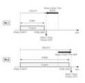
도 6은 본 발명의 실시예들에 따른 메모리 시스템(100)에서, 서로 다른 프로그램 시간을 갖는 제1 워드 라인(WL1)과 제2 워드 라인(WL2) 각각에 대한 상태 체크 타이밍을 나타낸 도면이다.FIG. 6 is a diagram showing status check timing for each of a first word line (WL1) and a second word line (WL2) having different program times in a memory system (100) according to embodiments of the present invention.
도 6을 참조하면, 제1 워드 라인(WL1)에 대응되는 메모리 셀(MC)에 데이터를 프로그램 하는 상황을 고려하면, 메모리 컨트롤러(120)는 제1 워드 라인(WL1)에 대응되는 메모리 셀(MC)에 데이터의 프로그램이 시작되는 제1 시점(tPGM_START1)으로부터 평균 프로그램 시간(tPGM_AVG)에 해당하는 지연 시간(tDELAY)이 경과한 이후 상태 체크 신호(SCS)를 출력함으로써 상태 체크를 시작할 수 있다.Referring to FIG. 6, considering a situation in which data is programmed in a memory cell (MC) corresponding to a first word line (WL1), the memory controller (120) can start a status check by outputting a status check signal (SCS) after a delay time (tDELAY) corresponding to an average program time (tPGM_AVG) has elapsed from a first time point (tPGM_START1) at which data programming in a memory cell (MC) corresponding to the first word line (WL1) begins.
또한, 도 6을 참조하면, 제2 워드 라인(WL2)에 대응되는 메모리 셀(MC)에 데이터를 프로그램 하는 상황을 고려하면, 메모리 컨트롤러(120)는 제2 워드 라인(WL2)에 대응되는 메모리 셀(MC)에 데이터의 프로그램이 시작되는 제2 시점(tPGM_START2)으로부터 평균 프로그램 시간(tPGM_AVG)에 해당하는 지연 시간(tDELAY)이 경과한 이후 상태 체크 신호(SCS)를 출력함으로써 상태 체크를 시작할 수 있다.In addition, referring to FIG. 6, when considering a situation in which data is programmed in a memory cell (MC) corresponding to a second word line (WL2), the memory controller (120) can start the status check by outputting a status check signal (SCS) after a delay time (tDELAY) corresponding to an average program time (tPGM_AVG) has elapsed from a second time point (tPGM_START2) at which data programming in a memory cell (MC) corresponding to the second word line (WL2) begins.
일반적으로, 제1 시점(tPGM_START1)과 제2 시점(tPGM_START2)은 서로 다른 시각일 수 있다. 경우에 따라서, 둘 이상의 페이지(PG)에 대한 프로그램 동작이 동시에 진행될 수 있는데, 이 경우, 제1 시점(tPGM_START1)과 제2 시점(tPGM_START2)은 동일한 시각일 수도 있다.In general, the first point in time (tPGM_START1) and the second point in time (tPGM_START2) can be different times. In some cases, program operations for two or more pages (PGs) can be performed simultaneously, in which case the first point in time (tPGM_START1) and the second point in time (tPGM_START2) can be the same time.
제1 워드 라인(WL1)에 대응되는 제1 프로그램 시간(tPGM1)은 제1 시점(tPGM_START1)에 해당하는 제1 프로그램 시작 시점에서 제1 프로그램 완료 시점(tPGM_END1)까지 시간적인 길이다.The first program time (tPGM1) corresponding to the first word line (WL1) is the time length from the first program start time corresponding to the first time point (tPGM_START1) to the first program end time (tPGM_END1).
제2 워드 라인(WL2)에 대응되는 제2 프로그램 시간(tPGM2)은 제2 시점(tPGM_START2)에 해당하는 제2 프로그램 시작 시점에서 제2 프로그램 완료 시점(tPGM_END2)까지 시간적인 길이다.The second program time (tPGM2) corresponding to the second word line (WL2) is the time length from the second program start time corresponding to the second time point (tPGM_START2) to the second program end time (tPGM_END2).
도 6을 참조하면, 앞에서 살펴보았다시피, 제1 워드 라인(WL1)에 대응되는 제1 프로그램 시간(tPGM1)은 평균 프로그램 시간(tPGM_AVG)보다 짧다.Referring to FIG. 6, as discussed above, the first program time (tPGM1) corresponding to the first word line (WL1) is shorter than the average program time (tPGM_AVG).
메모리 컨트롤러(120)는, 제1 워드 라인(WL1)에 대응되는 메모리 셀(MC)에 대한 프로그램이 완료되었음에도 불구하고, 이를 인지하지 못한다.The memory controller (120) does not recognize that the program for the memory cell (MC) corresponding to the first word line (WL1) has been completed.
이에 따라, 메모리 컨트롤러(120)는, 제1 워드 라인(WL1)에 대응되는 메모리 셀(MC)에 대한 프로그램이 완료된 상태에서, 지연 시간(tDELAY)이 완전히 경과할 때까지, 일정 시간 동안의 유휴 시간(Idle Time)을 기다린 이후, 상태 체크를 수행하게 된다.Accordingly, the memory controller (120) waits for an idle time of a certain period of time until the delay time (tDELAY) has completely elapsed after the program for the memory cell (MC) corresponding to the first word line (WL1) is completed, and then performs a status check.
이와 같이, 메모리 컨트롤러(120)는 제1 워드 라인(WL1)에 대응되는 메모리 셀(MC)에 대한 프로그램이 완료되었음에도 불구하고, 프로그램 완료 여부를 확인하기 위한 상태 체크를 바로 수행하지 못하고, 유휴 시간(Idle Time) 동안 불필요한 대기해야 하기 때문에, 전체적인 프로그램 동작 속도가 느려지고 메모리 시스템(100)의 성능 저하를 야기할 수 있다.In this way, even though the memory controller (120) has completed the program for the memory cell (MC) corresponding to the first word line (WL1), it cannot immediately perform a status check to confirm whether the program is complete and must wait unnecessarily during the idle time, which may slow down the overall program operation speed and cause a decrease in the performance of the memory system (100).
한편, 도 6을 참조하면, 앞에서 살펴보았다시피, 제2 워드 라인(WL2)에 대응되는 제2 프로그램 시간(tPGM2)은 평균 프로그램 시간(tPGM_AVG)보다 길다.Meanwhile, referring to FIG. 6, as examined above, the second program time (tPGM2) corresponding to the second word line (WL2) is longer than the average program time (tPGM_AVG).
메모리 컨트롤러(120)는, 제2 워드 라인(WL2)에 대응되는 메모리 셀(MC)에 대한 프로그램이 완료되지 않았음에도 불구하고, 이를 인지하지 못한다.The memory controller (120) does not recognize that the program for the memory cell (MC) corresponding to the second word line (WL2) has not been completed.
이에 따라, 메모리 컨트롤러(120)는, 제2 워드 라인(WL2)에 대응되는 메모리 셀(MC)에 대한 프로그램이 완료되지 않은 상태에서, 지연 시간(tDELAY)이 경과해버린 관계로, 지연 시간(tDELAY)이 경과한 시점으로부터 프로그램 완료를 지시하는 정상적인 응답 신호를 수신할 때까지 상태 체크 신호(SCS)를 반복적으로 출력하여 반복적인 상태 체크를 수행하게 된다.Accordingly, the memory controller (120) repeatedly outputs a status check signal (SCS) until it receives a normal response signal indicating completion of the program from the time when the delay time (tDELAY) has elapsed while the program for the memory cell (MC) corresponding to the second word line (WL2) has not been completed, thereby performing a repetitive status check.
전술한 바와 같이, 메모리 컨트롤러(120)는 제2 워드 라인(WL2)에 대응되는 메모리 셀(MC)에 대한 프로그램이 미 완료되었음에도 불구하고, 프로그램 완료 여부를 확인하기 위한 반복적인 상태 체크를 불필요하게 수행한다. 이러한 불필요한 반복적인 상태 체크는 메모리 컨트롤러(120)의 부하로 작용하고 메모리 시스템(100)의 성능 저하를 야기할 수 있다.As described above, the memory controller (120) unnecessarily performs repetitive status checks to determine whether a program is completed, even though the program for the memory cell (MC) corresponding to the second word line (WL2) is not completed. Such unnecessary repetitive status checks may act as a load on the memory controller (120) and cause a decrease in the performance of the memory system (100).
도 7은 본 발명의 실시예들에 따른 메모리 장치(110) 내 다수의 메모리 다이와 메모리 컨트롤러(120) 간의 채널 사용을 설명하기 위한 다이어그램이다.FIG. 7 is a diagram illustrating channel usage between a plurality of memory dies and a memory controller (120) in a memory device (110) according to embodiments of the present invention.
도 7을 참조하면, 메모리 장치(110)는 다수의 메모리 다이(DIE #1 ~ DIE #K, K는 2 이상의 자연수)를 포함할 수 있다.Referring to FIG. 7, the memory device (110) may include a plurality of memory dies (
메모리 컨트롤러(120)와 다수의 메모리 다이(DIE #1 ~ DIE #K)는 하나의 채널(CH)을 통해 연결될 수 있다.A memory controller (120) and a plurality of memory dies (
이 경우, 일 예로, 상태 체크 신호(SCS)가 메모리 컨트롤러(120)에서 다수의 메모리 다이(DIE #1 ~ DIE #K) 중 어떠한 하나의 제2 메모리 다이(DIE #2)로 출력될 때, 채널(CH)은 해당 제2 메모리 다이(DIE #2)에 의해 점유될 수 있다.In this case, for example, when a status check signal (SCS) is output from the memory controller (120) to any one of the second memory die (DIE #2) among a plurality of memory dies (
아래에서는, 이러한 채널 점유와 도 6의 불필요한 반복적인 상태 체크 동작 간의 관계를 설명한다. 예를 들어, 도 6의 제2 워드 라인(WL2)과 이에 대응되는 메모리 셀(MC)이 제2 메모리 다이(DIE #2)에 포함된다고 가정한다.Below, we describe the relationship between this channel occupancy and the unnecessary repetitive state check operation of Fig. 6. For example, assume that the second word line (WL2) and its corresponding memory cell (MC) of Fig. 6 are included in a second memory die (DIE #2).
전술한 바와 같이, 메모리 컨트롤러(120)는 제2 워드 라인(WL2)에 대응되는 메모리 셀(MC)에 대한 프로그램이 미 완료되었음에도 불구하고, 프로그램 완료 여부를 확인하기 위한 반복적인 상태 체크를 불필요하게 수행하게 되는데, 이러한 불필요한 반복적인 상태 체크는 메모리 컨트롤러(120)의 부하로 작용할 뿐만 아니라, 동일 채널(CH) 내 다른 메모리 다이(DIE #1, DIE #3, ... , DIE #K)에 채널 점유 시간을 할당해줄 수 없게 되어, 메모리 시스템(100)의 전체적인 성능을 떨어뜨릴 수 있다.As described above, the memory controller (120) unnecessarily performs repetitive status checks to confirm whether a program is completed even though the program for the memory cell (MC) corresponding to the second word line (WL2) is not completed. Such unnecessary repetitive status checks not only act as a load on the memory controller (120), but also make it impossible to allocate channel occupancy time to other memory dies (
아래에서는, 메모리 컨트롤러(120)가 하나의 평균 프로그램 시간(tPGM_AVG)만을 지연 시간(tDELAY)으로서 이용하여 상태 체크 타이밍을 제어하는 경우에 발생하는 성능 저하 및 부하 등을 줄여주거나 방지할 수 있는 적응적인 상태 체크 타이밍 제어 방법에 대하여 설명한다.Below, an adaptive status check timing control method is described that can reduce or prevent performance degradation and load that occurs when a memory controller (120) controls the status check timing using only one average program time (tPGM_AVG) as a delay time (tDELAY).
도 8은 본 발명의 실시예들에 따른 메모리 컨트롤러(120)의 동작 방법에 대한 흐름도이고, 도 9는 본 발명의 실시예들에 따른 메모리 컨트롤러(120)의 적응적인 상태 체크 타이밍 제어를 설명하기 위한 예시적인 도면이다.FIG. 8 is a flowchart of an operation method of a memory controller (120) according to embodiments of the present invention, and FIG. 9 is an exemplary diagram for explaining adaptive state check timing control of a memory controller (120) according to embodiments of the present invention.
본 발명의 실시예들에 따른 메모리 컨트롤러(120)는 데이터의 프로그램 동작이 개시된 이후 프로그램 완료 여부를 확인하기 위한 상태 체크 동작을 수행함에 있어서, 상태 체크 동작과 관련한 성능 저하 또는 부하 증가를 방지할 수 있는 적응적인 상태 체크 타이밍 제어를 수행할 수 있다.The memory controller (120) according to embodiments of the present invention can perform adaptive state check timing control that can prevent performance degradation or load increase related to the state check operation when performing a state check operation to check whether a program operation is completed after a data program operation is initiated.
이를 위해, 본 발명의 실시예들에 따른 메모리 컨트롤러(120)의 동작 방법은, 메모리 장치(110)에서의 다수의 워드 라인(WL) 중 제1 워드 라인(WL1)에 대응되는 제1 메모리 셀(MC)에 대한 데이터의 프로그램을 제1 시점(tPGM_START1)에 시작하는 단계(S810)와, 제1 시점(tPGM_START1)으로부터 제1 지연 시간(tDELAY1) 후에 상태 체크 신호(SCS)를 메모리 장치(110)로 출력하는 단계(S820)와, 다수의 워드 라인(WL) 중 제1 워드 라인(WL1)과 다른 제2 워드 라인(WL2)에 대응되는 제2 메모리 셀(MC)에 대한 데이터의 프로그램을 제2 시점(tPGM_START2)에 시작하는 단계(S830)와, 제2 시점(tPGM_START2)으로부터 제1 지연 시간(tDELAY1)과 다른 제2 지연 시간(tDELAY2) 후에 상태 체크 신호(SCS)를 메모리 장치(110)로 출력하는 단계(S840) 등을 포함할 수 있다.To this end, the operating method of the memory controller (120) according to the embodiments of the present invention includes a step (S810) of starting a program of data for a first memory cell (MC) corresponding to a first word line (WL1) among a plurality of word lines (WL) in a memory device (110) at a first time point (tPGM_START1), a step (S820) of outputting a status check signal (SCS) to the memory device (110) after a first delay time (tDELAY1) from the first time point (tPGM_START1), a step (S830) of starting a program of data for a second memory cell (MC) corresponding to a second word line (WL2) different from the first word line (WL1) among the plurality of word lines (WL) at a second time point (tPGM_START2), and a step (S840) of outputting a status check signal (SCS) after a second delay time (tDELAY2) different from the first delay time (tDELAY1) from the second time point (tPGM_START2). It may include a step (S840) of outputting a signal (SCS) to a memory device (110).
도 9를 참조하면, 제1 워드 라인(WL1)에 대응되는 제1 메모리 셀(MC)에 데이터를 프로그램 하는데 걸리는 제1 프로그램 시간(tPGM1)과, 제2 워드 라인(WL2)에 대응되는 제2 메모리 셀(MC)에 데이터를 프로그램 하는데 걸리는 제2 프로그램 시간(tPGM2)은 서로 다를 수 있다.Referring to FIG. 9, a first program time (tPGM1) taken to program data in a first memory cell (MC) corresponding to a first word line (WL1) and a second program time (tPGM2) taken to program data in a second memory cell (MC) corresponding to a second word line (WL2) may be different from each other.
예를 들어, 도 9를 참조하면, 제2 프로그램 시간(tPGM2)은 제1 프로그램 시간(tPGM1)보다 길수 있다. 이 경우, 제2 지연 시간(tDELAY2)은 제1 지연 시간(tDELAY1)보다 길 수 있다.For example, referring to FIG. 9, the second program time (tPGM2) may be longer than the first program time (tPGM1). In this case, the second delay time (tDELAY2) may be longer than the first delay time (tDELAY1).
전술한 바에 따르면, 도 9를 참조하면, 상대적으로 짧은 제1 프로그램 시간(tPGM1)을 발생시킬 수 있는 제1 워드 라인(WL1)의 경우, 상대적으로 짧은 제1 지연 시간(tDELAY1)의 설정을 통해 상태 체크 시점이 보다 앞당겨져서, 상태 체크 동작이 보다 신속하게 진행될 수 있다.As described above, referring to FIG. 9, in the case of the first word line (WL1) that can generate a relatively short first program time (tPGM1), the status check time point can be brought forward by setting the relatively short first delay time (tDELAY1), so that the status check operation can be performed more quickly.
또한, 도 9를 참조하면, 상대적으로 긴 제2 프로그램 시간(tPGM2)을 발생시킬 수 있는 제2 워드 라인(WL2)의 경우, 상대적으로 긴 제2 지연 시간(tDELAY2)의 설정을 통해 상태 체크 시점이 늦추어지게 되어, 불필요한 반복적인 상태 체크 동작이 방지되고 채널 점유 시간도 줄여줄 수 있다.In addition, referring to FIG. 9, in the case of a second word line (WL2) that can generate a relatively long second program time (tPGM2), the status check time point is delayed by setting a relatively long second delay time (tDELAY2), thereby preventing unnecessary repetitive status check operations and reducing the channel occupancy time.
한편, 도 8에서는, S810 단계 및 S820 단계가 S830 단계 및 S840 단계보다 앞서서 실행되는 것처럼 도시되어 있으나, 이는 설명의 편의를 위한 것일 뿐, S810 단계 및 S820 단계가 S830 단계 및 S840 단계보다 뒤에 실행될 수도 있다.Meanwhile, in FIG. 8, steps S810 and S820 are depicted as being executed before steps S830 and S840, but this is only for convenience of explanation, and steps S810 and S820 may be executed after steps S830 and S840.
전술한 적응적 상태 체크 타이밍 제어는 메모리 컨트롤러(120) 내 제어 회로(123)에 의해 실행될 수 있다.The adaptive state check timing control described above can be executed by a control circuit (123) within the memory controller (120).
다시 말해, 메모리 컨트롤러(120) 내 제어 회로(123)는, 다수의 워드 라인(WL) 중 제1 워드 라인(WL1)에 대응되는 제1 메모리 셀(MC)에 대한 데이터의 프로그램이 시작된 제1 시점(tPGM_START1)으로부터 제1 지연 시간(tDELAY1)이 경과하면 상태 체크 신호(SCS)를 메모리 장치(110)로 출력하고, 다수의 워드 라인(WL) 중 제1 워드 라인(WL1)과 다른 제2 워드 라인(WL2)에 대응되는 제2 메모리 셀(MC)에 대한 데이터의 프로그램이 시작된 제2 시점(tPGM_START2)으로부터 제1 지연 시간(tDELAY1)과 다른 제2 지연 시간(tDELAY2)이 경과하면 상태 체크 신호(SCS)를 메모리 장치(110)로 출력할 수 있다.In other words, the control circuit (123) in the memory controller (120) can output a status check signal (SCS) to the memory device (110) when a first delay time (tDELAY1) has elapsed from a first point in time (tPGM_START1) at which data programming for a first memory cell (MC) corresponding to a first word line (WL1) among a plurality of word lines (WL) has started, and can output a status check signal (SCS) to the memory device (110) when a second delay time (tDELAY2) different from the first delay time (tDELAY1) has elapsed from a second point in time (tPGM_START2) at which data programming for a second memory cell (MC) corresponding to a second word line (WL2) different from the first word line (WL1) among a plurality of word lines (WL) has started.
메모리 컨트롤러(120)에 포함된 제어 회로(123) 내 프로세서(124)가 워킹 메모리(125)에 로딩 된 펌웨어를 실행하여 적응적인 상태 체크 타이밍 제어를 수행할 수 있다.A processor (124) in a control circuit (123) included in a memory controller (120) can perform adaptive status check timing control by executing firmware loaded into a working memory (125).
전술한 메모리 컨트롤러(120)와 연동하는 메모리 장치(110)는, 다수의 워드 라인(WL)과, 다수의 워드 라인(WL)과 교차하여 배치되는 다수의 비트 라인(BL)과, 다수의 워드 라인(WL)과 다수의 비트 라인(BL)이 교차하여 정의되는 다수의 메모리 셀(MC)을 포함할 수 있다.A memory device (110) that is linked to the aforementioned memory controller (120) may include a plurality of word lines (WL), a plurality of bit lines (BL) arranged to intersect the plurality of word lines (WL), and a plurality of memory cells (MC) defined by intersecting the plurality of word lines (WL) and the plurality of bit lines (BL).
다수의 워드 라인(WL)은 제1 워드 라인(WL1)과 제2 워드 라인(WL2)을 포함할 수 있다.The plurality of word lines (WLs) may include a first word line (WL1) and a second word line (WL2).
제1 워드 라인(WL1)에 대응되는 제1 메모리 셀(MC)에 대한 데이터의 프로그램이 시작된 제1 시점(tPGM_START1)으로부터 상태 체크 신호(SCS)가 메모리 컨트롤러(120)로부터 수신되는 데까지 걸리는 제1 지연 시간(tDELAY1)과, 제2 워드 라인(WL2)에 대응되는 제2 메모리 셀(MC)에 대한 데이터의 프로그램이 시작된 제2 시점(tPGM_START2)으로부터 상태 체크 신호(SCS)가 메모리 컨트롤러(120)로부터 수신되는 데까지 걸리는 제2 지연 시간(tDELAY2)은 서로 다를 수 있다.A first delay time (tDELAY1) taken from a first point in time (tPGM_START1) at which data programming for a first memory cell (MC) corresponding to a first word line (WL1) is started until a status check signal (SCS) is received from a memory controller (120), and a second delay time (tDELAY2) taken from a second point in time (tPGM_START2) at which data programming for a second memory cell (MC) corresponding to a second word line (WL2) is started until a status check signal (SCS) is received from the memory controller (120) may be different from each other.
전술한 바와 같이, 제1 워드 라인(WL1)에 대응되는 제1 메모리 셀(MC)에 데이터를 프로그램 하는데 걸리는 제1 프로그램 시간(tPGM1)과, 제2 워드 라인(WL2)에 대응되는 제2 메모리 셀(MC)에 데이터를 프로그램 하는데 걸리는 제2 프로그램 시간(tPGM2)은 서로 다를 수 있다.As described above, the first program time (tPGM1) taken to program data into the first memory cell (MC) corresponding to the first word line (WL1) and the second program time (tPGM2) taken to program data into the second memory cell (MC) corresponding to the second word line (WL2) may be different from each other.
예를 들어, 제2 프로그램 시간(tPGM2)은 제1 프로그램 시간(tPGM1)보다 길 수 있으며, 이 경우, 제2 지연 시간(tDELAY2)은 제1 지연 시간(tDELAY1)보다 길 수 있다.For example, the second program time (tPGM2) may be longer than the first program time (tPGM1), in which case the second delay time (tDELAY2) may be longer than the first delay time (tDELAY1).
한편, 일 예로, 제1 워드 라인(WL1) 및 제2 워드 라인(WL2)은 다수의 메모리 블록(BLK1~BLKz) 중 하나의 동일한 메모리 블록 내에 배치될 수 있다.Meanwhile, as an example, the first word line (WL1) and the second word line (WL2) may be arranged within the same memory block among a plurality of memory blocks (BLK1 to BLKz).
다른 예로, 제1 워드 라인(WL1) 및 제2 워드 라인(WL2)은 다수의 메모리 블록(BLK1~BLKz) 중 위치가 서로 다른 메모리 블록 내에 각각 배치될 수 있다.As another example, the first word line (WL1) and the second word line (WL2) may be respectively placed in different memory blocks among a plurality of memory blocks (BLK1 to BLKz).
한편, 제1 프로그램 시간(tPGM1) 및/또는 제2 프로그램 시간(tPGM2)은 항상 고정된 값일 수도 있고, 메모리 장치(110)의 동작 시간(구동 시간)에 따라 변할 수 있는 값일 수도 있다. 이에 따라, 제1 지연 시간(tDELAY1) 및/또는 제2 지연 시간(tDELAY2)은 항상 고정된 값일 수도 있고, 제1 프로그램 시간(tPGM1) 및/또는 제2 프로그램 시간(tPGM2)의 변화에 따라 가변 되는 값일 수도 있다.Meanwhile, the first program time (tPGM1) and/or the second program time (tPGM2) may always be a fixed value, or may be a value that can change depending on the operation time (driving time) of the memory device (110). Accordingly, the first delay time (tDELAY1) and/or the second delay time (tDELAY2) may always be a fixed value, or may be a value that changes depending on the change in the first program time (tPGM1) and/or the second program time (tPGM2).
전술한 적응적인 상태 체크 타이밍 제어는, 프로그램 시간(tPGM)의 길고 짧음에 따라 지연 시간(tDELAY)을 길고 짧게 적응적으로 설정하는 기법을 필요로 한다.The adaptive state check timing control described above requires a technique to adaptively set the delay time (tDELAY) to be long or short depending on the length of the program time (tPGM).
이를 위해, 메모리 컨트롤러(120)는 메모리 장치(110) 내 다수의 워드 라인(WL) 또는 다수의 메모리 셀(MC) 각각에 대하여 지연 시간(tDELAY)의 길이를 개별적으로 적응적으로 제어할 수 있다. 이러한 제어 방식을 개별 제어 방식이라고 한다.To this end, the memory controller (120) can individually and adaptively control the length of the delay time (tDELAY) for each of a plurality of word lines (WL) or a plurality of memory cells (MC) within the memory device (110). This control method is called an individual control method.
본 발명의 실시예들에 따른 메모리 컨트롤러(120)는, 제어 효율을 더욱 높이기 위하여, 개별 제어 방식 대신에 그룹 제어 방식으로 적응적인 상태 체크 타이밍 제어를 수행할 수도 있다.The memory controller (120) according to embodiments of the present invention may perform adaptive state check timing control in a group control manner instead of an individual control manner in order to further increase control efficiency.
보다 구체적으로, 메모리 컨트롤러(120)는, 메모리 장치(110) 내 다수의 워드 라인(WL)을 둘 이상의 워드 라인 그룹으로 그룹화하여 둘 이상의 워드 라인 그룹 각각에 대하여 지연 시간(tDELAY)의 길이를 적응적으로 제어하는 그룹 제어 방식으로 적응적인 상태 체크 타이밍 제어를 수행할 수 있다.More specifically, the memory controller (120) can perform adaptive state check timing control in a group control manner by grouping a plurality of word lines (WL) within the memory device (110) into two or more word line groups and adaptively controlling the length of a delay time (tDELAY) for each of the two or more word line groups.
아래에서는, 본 발명의 실시예들에 따른 그룹 제어 방식의 적응적인 상태 체크 타이밍 제어 방법을 설명한다.Below, an adaptive state check timing control method of a group control scheme according to embodiments of the present invention is described.
도 10은 본 발명의 실시예들에 따른 메모리 장치(110)에서 각 워드 라인 별 프로그램 시간(tPGM)의 분포와, 이를 고려한 워드 라인 그룹들을 나타낸 도면이다.FIG. 10 is a diagram showing the distribution of program time (tPGM) per word line and word line groups considering the distribution in a memory device (110) according to embodiments of the present invention.
도 10을 참조하면, 전술한 바와 같이, 메모리 장치(110)에 포함된 다수의 워드 라인(WL) 각각에 대응되는 메모리 셀(MC)에 데이터가 프로그램 되는데 걸리는 프로그램 시간(tPGM)은 편차를 가진다.Referring to FIG. 10, as described above, the program time (tPGM) taken for data to be programmed in a memory cell (MC) corresponding to each of a plurality of word lines (WL) included in the memory device (110) has a deviation.
따라서, 도 10에 도시된 바와 같이, 메모리 장치(110)에 포함된 다수의 워드 라인(WL) 각각에 대응되는 프로그램 시간(tPGM)은 소정의 분포를 가질 수 있다.Accordingly, as illustrated in FIG. 10, the program time (tPGM) corresponding to each of a plurality of word lines (WL) included in the memory device (110) may have a predetermined distribution.
도 10에 예시된 워드 라인 별 프로그램 시간(tPGM)의 분포도를 참조하면, 프로그램 시간(tPGM)의 크기에 따라, 다수의 워드 라인(WL)은 둘 이상의 워드 라인 그룹(GR #A, GR #B, GR #C)으로 그룹화될 수 있다.Referring to the distribution of the program time (tPGM) per word line illustrated in Fig. 10, depending on the size of the program time (tPGM), a plurality of word lines (WL) can be grouped into two or more word line groups (GR #A, GR #B, GR #C).
예를 들어, 제1 임계값(tPGB_TH1) 미만의 프로그램 시간(tPGM)이 걸리는 메모리 셀(MC)과 대응되는 워드 라인들(WL)은 제1 워드 라인 그룹(GR #A)으로 그룹화 될 수 있다. 제1 임계값(tPGB_TH1) 이상이고 제2 임계값(tPGM_TH2) 미만의 프로그램 시간(tPGM)이 걸리는 메모리 셀(MC)과 대응되는 워드 라인들(WL)은 제2 워드 라인 그룹(GR #B)으로 그룹화 될 수 있다. 제2 임계값(tPGB_TH2) 이상의 프로그램 시간(tPGM)이 걸리는 메모리 셀(MC)과 대응되는 워드 라인들(WL)은 제3 워드 라인 그룹(GR #C)으로 그룹화 될 수 있다. 또는, 제2 임계값(tPGB_TH2) 이상이고 제3 임계값(tPGM_TH3) 미만의 프로그램 시간(tPGM)이 걸리는 메모리 셀(MC)과 대응되는 워드 라인들(WL)은, 제3 워드 라인 그룹(GR #C)으로 그룹화 될 수 있다.For example, word lines (WL) corresponding to memory cells (MC) that take a program time (tPGM) less than a first threshold value (tPGB_TH1) may be grouped into a first word line group (GR #A). Word lines (WL) corresponding to memory cells (MC) that take a program time (tPGM) greater than or equal to the first threshold value (tPGB_TH1) and less than or equal to the second threshold value (tPGM_TH2) may be grouped into a second word line group (GR #B). Word lines (WL) corresponding to memory cells (MC) that take a program time (tPGM) greater than or equal to the second threshold value (tPGB_TH2) may be grouped into a third word line group (GR #C). Alternatively, word lines (WL) corresponding to memory cells (MC) that take a program time (tPGM) greater than or equal to the second threshold value (tPGB_TH2) and less than or equal to the third threshold value (tPGM_TH3) may be grouped into a third word line group (GR #C).
도 10의 워드 라인 그룹 예시의 경우, 메모리 장치(110)에 포함된 다수의 워드 라인(WL)이 3개의 워드 라인 그룹(GR #A, GR #B, GR #C)으로 그룹화 되는 경우를 예시한 것으로서, 2개의 임계값(tPGM_TH1, tPGM_TH2) 또는 3개 이상의 임계값(tPGM_TH1, tPGM_TH2, tPGM_TH3)을 기준으로 3개의 워드 라인 그룹(GR #A, GR #B, GR #C)이 정해질 수 있다.In the case of the word line group example of FIG. 10, a case is exemplified where a plurality of word lines (WL) included in a memory device (110) are grouped into three word line groups (GR #A, GR #B, GR #C), and the three word line groups (GR #A, GR #B, GR #C) can be determined based on two threshold values (tPGM_TH1, tPGM_TH2) or three or more threshold values (tPGM_TH1, tPGM_TH2, tPGM_TH3).
도 10의 워드 라인 그룹 예시와 다르게, 워드 라인 그룹 개수가 2개일 수도 있고, 4개 이상일 수도 있다.Unlike the word line group example of Fig. 10, the number of word line groups may be two or four or more.
아래에서는, 그룹 제어 방식의 적응적인 상태 체크 타이밍 제어 방법을 설명함에 있어서, 제1 워드 라인(WL1)이 제1 워드 라인 그룹(GR #A)에 포함되고, 제2 워드 라인(WL2)이 제3 워드 라인 그룹(GR #C)에 포함되는 것으로 예를 든다. 또한, 다수의 워드 라인(WL)은 제3 워드 라인(WL3) 및 제4 워드 라인(WL4)을 더 포함하는데, 제3 워드 라인(WL3)이 제1 워드 라인 그룹(GR #A)에 포함되고, 제4 워드 라인(WL4)이 제3 워드 라인 그룹(GR #C)에 포함되는 것으로 예를 든다.Below, in explaining an adaptive state check timing control method of a group control scheme, an example is given in which a first word line (WL1) is included in a first word line group (GR #A) and a second word line (WL2) is included in a third word line group (GR #C). In addition, the plurality of word lines (WLs) further include a third word line (WL3) and a fourth word line (WL4), and an example is given in which the third word line (WL3) is included in the first word line group (GR #A) and the fourth word line (WL4) is included in the third word line group (GR #C).
도 11은 본 발명의 실시예들에 따른 메모리 시스템(100)에서, 제1 워드 라인 그룹(GR #A)에 포함되는 제1 워드 라인(WL1) 및 제3 워드 라인(WL3)에 대한 상태 체크 타이밍을 나타낸 도면이고, 도 12는 본 발명의 실시예들에 따른 메모리 시스템(100)에서, 제3 워드 라인 그룹(GR #C)에 포함되는 제2 워드 라인(WL2) 및 제4 워드 라인(WL4)에 대한 상태 체크 타이밍을 나타낸 도면이다.FIG. 11 is a diagram showing status check timing for a first word line (WL1) and a third word line (WL3) included in a first word line group (GR #A) in a memory system (100) according to embodiments of the present invention, and FIG. 12 is a diagram showing status check timing for a second word line (WL2) and a fourth word line (WL4) included in a third word line group (GR #C) in a memory system (100) according to embodiments of the present invention.
도 11을 참조하면, 메모리 컨트롤러(120)는, 제3 워드 라인(WL3)에 대응되는 제3 메모리 셀(MC)에 대한 데이터의 프로그램이 시작된 제3 시점(tPGM_START3)으로부터 제3 지연 시간(tDELAY3)이 경과하면 상태 체크 신호(SCS)를 출력할 수 있다.Referring to FIG. 11, the memory controller (120) can output a status check signal (SCS) when a third delay time (tDELAY3) has elapsed from a third time point (tPGM_START3) at which programming of data for a third memory cell (MC) corresponding to a third word line (WL3) is started.
제3 지연 시간(tDELAY3)은 제1 지연 시간(tDELAY1)과 대응될 수 있다.The third delay time (tDELAY3) can correspond to the first delay time (tDELAY1).
그룹 제어 방식의 경우, 제3 지연 시간(tDELAY3)은 제1 지연 시간(tDELAY1)과 동일한 값일 수 있다. 만약, 개별 제어 방식의 경우, 제3 지연 시간(tDELAY3)은 제1 지연 시간(tDELAY1)과 동일할 수도 있고 다를 수도 있다.In the case of the group control method, the third delay time (tDELAY3) may be the same value as the first delay time (tDELAY1). In the case of the individual control method, the third delay time (tDELAY3) may be the same as or different from the first delay time (tDELAY1).
도 12를 참조하면, 메모리 컨트롤러(120)는, 제4 워드 라인(WL4)에 대응되는 제4 메모리 셀(MC)에 대한 데이터의 프로그램이 시작된 제4 시점(tPGM_START4)으로부터 제3 지연 시간(tDELAY3)과 다른 제4 지연 시간(tDELAY4)이 경과하면 상태 체크 신호(SCS)를 출력할 수 있다.Referring to FIG. 12, the memory controller (120) can output a status check signal (SCS) when a fourth delay time (tDELAY4) different from a third delay time (tDELAY3) has elapsed from a fourth time point (tPGM_START4) at which programming of data for a fourth memory cell (MC) corresponding to a fourth word line (WL4) is started.
제4 지연 시간(tDELAY4)은 제2 지연 시간(tDELAY2)과 대응될 수 있다.The fourth delay time (tDELAY4) can correspond to the second delay time (tDELAY2).
그룹 제어 방식의 경우, 제4 지연 시간(tDELAY4)은 제2 지연 시간(tDELAY2)과 동일한 값일 수 있다. 만약, 개별 제어 방식의 경우, 제4 지연 시간(tDELAY4)은 제2 지연 시간(tDELAY2)과 동일할 수도 있고 다를 수도 있다.In the case of the group control method, the fourth delay time (tDELAY4) may be the same value as the second delay time (tDELAY2). In the case of the individual control method, the fourth delay time (tDELAY4) may be the same as or different from the second delay time (tDELAY2).
도 11 및 도 12를 참조하면, 제3 워드 라인(WL3)에 대응되는 제3 메모리 셀(MC)에 데이터를 프로그램 하는데 걸리는 제3 프로그램 시간(tPGM3)과, 제4 워드 라인(WL4)에 대응되는 제4 메모리 셀(MC)에 데이터를 프로그램 하는데 걸리는 제4 프로그램 시간(tPGM4)은 서로 다를 수 있다.Referring to FIGS. 11 and 12, a third program time (tPGM3) taken to program data in a third memory cell (MC) corresponding to a third word line (WL3) and a fourth program time (tPGM4) taken to program data in a fourth memory cell (MC) corresponding to a fourth word line (WL4) may be different from each other.
도 11 및 도 12를 참조하면, 제1 프로그램 시간(tPGM1)과 제3 프로그램 시간(tPGM3)의 차이는, 제1 프로그램 시간(tPGM1)과 제2 프로그램 시간(tPGM2)의 차이보다 작고, 제1 프로그램 시간(tPGM1)과 제4 프로그램 시간(tPGM4)의 차이보다 작고, 제3 프로그램 시간(tPGM3)과 제2 프로그램 시간(tPGM2)의 차이보다 작고, 제3 프로그램 시간(tPGM3)과 제4 프로그램 시간(tPGM4)의 차이보다 작을 수 있다.Referring to FIGS. 11 and 12, the difference between the first program time (tPGM1) and the third program time (tPGM3) may be smaller than the difference between the first program time (tPGM1) and the second program time (tPGM2), smaller than the difference between the first program time (tPGM1) and the fourth program time (tPGM4), smaller than the difference between the third program time (tPGM3) and the second program time (tPGM2), and smaller than the difference between the third program time (tPGM3) and the fourth program time (tPGM4).
도 11 및 도 12를 참조하면, 제2 프로그램 시간(tPGM2)과 제4 프로그램 시간(tPGM4)의 차이는, 제2 프로그램 시간(tPGM2)과 제1 프로그램 시간(tPGM1)의 차이보다는 작고, 제2 프로그램 시간(tPGM2)과 제3 프로그램 시간(tPGM3)의 차이보다는 작고, 제4 프로그램 시간(tPGM4)과 제1 프로그램 시간(tPGM1)의 차이보다는 작고, 제4 프로그램 시간(tPGM4)과 제3 프로그램 시간(tPGM3)의 차이보다는 작을 수 있다.Referring to FIGS. 11 and 12, the difference between the second program time (tPGM2) and the fourth program time (tPGM4) may be smaller than the difference between the second program time (tPGM2) and the first program time (tPGM1), smaller than the difference between the second program time (tPGM2) and the third program time (tPGM3), smaller than the difference between the fourth program time (tPGM4) and the first program time (tPGM1), and smaller than the difference between the fourth program time (tPGM4) and the third program time (tPGM3).
도 13 내지 도 15는 본 발명의 실시예들에 따른 메모리 장치(110)에서, 제1 워드 라인 그룹(GR #A)에 포함되는 제1 워드 라인(WL1) 및 제3 워드 라인(WL3)과, 제3 워드 라인 그룹(GR #C)에 포함되는 제2 워드 라인(WL2) 및 제4 워드 라인(WL4)에 대한 메모리 블록 위치를 예시적으로 나타낸 도면들이다.FIGS. 13 to 15 are drawings exemplarily showing memory block locations for a first word line (WL1) and a third word line (WL3) included in a first word line group (GR #A), and a second word line (WL2) and a fourth word line (WL4) included in a third word line group (GR #C), in a memory device (110) according to embodiments of the present invention.
도 13을 참조하면, 메모리 장치(110)에 포함되는 다수의 메모리 블록(BLK1~BLKz) 각각은 둘 이상의 워드 라인 그룹(GR #A, GR #B, ...)을 포함할 수 있다.Referring to FIG. 13, each of a plurality of memory blocks (BLK1 to BLKz) included in a memory device (110) may include two or more word line groups (GR #A, GR #B, ...).
즉, 다수의 메모리 블록(BLK1~BLKz) 중 임의의 하나의 제1 메모리 블록(BLKi) 내에 배치된 다수의 워드 라인(WL)은 둘 이상의 워드 라인 그룹(GR #A, GR #B, ...)으로 그룹화 될 수 있다.That is, a plurality of word lines (WL) arranged within any one first memory block (BLKi) among a plurality of memory blocks (BLK1 to BLKz) can be grouped into two or more word line groups (GR #A, GR #B, ...).
이 경우, 예를 들어, 유사한 프로그램 시간(tPGM)을 유발하게 되어 동일한 제1 워드 라인 그룹(GR #A)에 포함될 수 있는 제1 워드 라인(WL1) 및 제3 워드 라인(WL3)과, 유사한 프로그램 시간(tPGM)을 유발하게 되어 동일한 제3 워드 라인 그룹(GR #C)에 포함될 수 있는 제2 워드 라인(WL2) 및 제4 워드 라인(WL4)은, 동일한 다수의 메모리 블록(BLK1~BLKz) 중 하나의 제1 메모리 블록(BLKi) 내에 배치될 수 있다.In this case, for example, the first word line (WL1) and the third word line (WL3), which may be included in the same first word line group (GR #A) because they cause similar program times (tPGM), and the second word line (WL2) and the fourth word line (WL4), which may be included in the same third word line group (GR #C) because they cause similar program times (tPGM), may be arranged in one first memory block (BLKi) among the same plurality of memory blocks (BLK1 to BLKz).
도 14를 참조하면, 메모리 장치(110)에 포함되는 모든 워드 라인(WL)은 메모리 블록과 무관하게, 둘 이상의 워드 라인 그룹(GR #A, GR #B, ...)으로 그룹화 될 수 있다.Referring to FIG. 14, all word lines (WL) included in the memory device (110) can be grouped into two or more word line groups (GR #A, GR #B, ...), regardless of the memory block.
이 경우, 예를 들어, 유사한 프로그램 시간(tPGM)을 유발하게 되어 동일한 제1 워드 라인 그룹(GR #A)에 포함될 수 있는 제1 워드 라인(WL1) 및 제3 워드 라인(WL3) 중에서, 제1 워드 라인(WL1)은 제1 메모리 블록(BLKi)에 배치되고, 제3 워드 라인(WL3)은 제1 메모리 블록(BLKi)과 다른 제2 메모리 블록(BLKj)에 배치될 수 있다. 그리고, 유사한 프로그램 시간(tPGM)을 유발하게 되어 동일한 제3 워드 라인 그룹(GR #C)에 포함될 수 있는 제2 워드 라인(WL2) 및 제4 워드 라인(WL4) 모두는 제2 메모리 블록(BLKj)에 배치될 수 있다.In this case, for example, among the first word line (WL1) and the third word line (WL3) that may be included in the same first word line group (GR #A) because they induce similar program times (tPGM), the first word line (WL1) may be placed in the first memory block (BLKi), and the third word line (WL3) may be placed in the second memory block (BLKj) that is different from the first memory block (BLKi). In addition, both the second word line (WL2) and the fourth word line (WL4) that may be included in the same third word line group (GR #C) because they induce similar program times (tPGM) may be placed in the second memory block (BLKj).
도 15를 참조하면, 메모리 장치(110)에 포함되는 다수의 메모리 블록(BLK1~BLKz)은 다수의 워드 라인 그룹(GR #A, GR #B, ...)과 대응될 수 있다. 이 경우, 메모리 블록 개수는 워드 라인 그룹 개수와 동일할 수 있다.Referring to FIG. 15, a plurality of memory blocks (BLK1 to BLKz) included in a memory device (110) may correspond to a plurality of word line groups (GR #A, GR #B, ...). In this case, the number of memory blocks may be equal to the number of word line groups.
이 경우, 예를 들어, 유사한 프로그램 시간(tPGM)을 유발하게 되어 동일한 제1 워드 라인 그룹(GR #A)에 포함될 수 있는 제1 워드 라인(WL1) 및 제3 워드 라인(WL3)은 제1 메모리 블록(BLKi)에 배치될 수 있다. 그리고, 유사한 프로그램 시간(tPGM)을 유발하게 되어 동일한 제3 워드 라인 그룹(GR #C)에 포함될 수 있는 제2 워드 라인(WL2) 및 제4 워드 라인(WL4) 모두는 제2 메모리 블록(BLKj)에 배치될 수 있다.In this case, for example, the first word line (WL1) and the third word line (WL3), which may be included in the same first word line group (GR #A) because they cause similar program times (tPGM), may be placed in the first memory block (BLKi). And, both the second word line (WL2) and the fourth word line (WL4), which may be included in the same third word line group (GR #C), may be placed in the second memory block (BLKj).
이 경우, 제1 워드 라인 그룹(GR #A)은 제1 메모리 블록(BLKi)과 대응된다. 그리고, 제3 워드 라인 그룹(GR #C)은 제2 메모리 블록(BLKj)과 대응될 수 있다.In this case, the first word line group (GR #A) corresponds to the first memory block (BLKi). And, the third word line group (GR #C) may correspond to the second memory block (BLKj).
이상에서 전술한 그룹 제어 방식 기반의 상태 체크 타이밍 제어 방법을 도 16과 도 17을 참조하여 간략하게 다시 설명한다.The status check timing control method based on the group control method described above is briefly described again with reference to FIGS. 16 and 17.
도 16은 본 발명의 실시예들에 따른 메모리 컨트롤러(120)의 각 워드 라인 또는 각 워드 라인 그룹 별 적응적인 상태 체크 타이밍 제어를 위한 동작 방법에 대한 흐름도이다.FIG. 16 is a flowchart of an operation method for adaptive state check timing control for each word line or each word line group of a memory controller (120) according to embodiments of the present invention.
도 16을 참조하면, 본 발명의 실시예들에 따른 메모리 장치(110)를 제어하기 위한 메모리 컨트롤러(120)의 동작 방법은, 메모리 장치(110)에서의 각 워드 라인 또는 각 워드 라인 그룹 별 프로그램 시간을 저장 관리하는 단계(S1610)와, 각 워드 라인 또는 각 워드 라인 그룹 별 프로그램 시간에 근거하여, 각 워드 라인 또는 각 워드 라인 그룹 별로 메모리 장치(110)의 프로그램 진행 또는 완료 상태를 체크하기 위한 상태 체크 타이밍을 독립적으로 제어하는 단계(S1620) 등을 포함할 수 있다.Referring to FIG. 16, the operation method of the memory controller (120) for controlling the memory device (110) according to embodiments of the present invention may include a step (S1610) of storing and managing the program time for each word line or each word line group in the memory device (110), and a step (S1620) of independently controlling the status check timing for checking the program progress or completion status of the memory device (110) for each word line or each word line group based on the program time for each word line or each word line group.
도 17은 본 발명의 실시예들에 따른 메모리 컨트롤러(120)의 각 메모리 블록 별 적응적인 상태 체크 타이밍 제어를 위한 동작 방법에 대한 흐름도이다.FIG. 17 is a flowchart of an operation method for adaptive status check timing control for each memory block of a memory controller (120) according to embodiments of the present invention.
도 17을 참조하면, 본 발명의 실시예들에 따른 메모리 장치(110)를 제어하기 위한 메모리 컨트롤러(120)의 동작 방법은, 메모리 장치(110)에서의 각 메모리 블록 별 프로그램 시간을 저장 관리하는 단계(S1710)와, 각 메모리 블록 별 프로그램 시간에 근거하여, 각 메모리 블록 별로 메모리 장치(110)의 프로그램 진행 또는 완료 상태를 체크하기 위한 상태 체크 타이밍을 독립적으로 제어하는 단계(S1720) 등을 포함할 수 있다.Referring to FIG. 17, the operation method of the memory controller (120) for controlling the memory device (110) according to embodiments of the present invention may include a step (S1710) of storing and managing the program time for each memory block in the memory device (110), and a step (S1720) of independently controlling the status check timing for checking the program progress or completion status of the memory device (110) for each memory block based on the program time for each memory block.
도 18은 본 발명의 실시예들에 따른 메모리 컨트롤러(120)의 개략적인 기능 블록도이다.FIG. 18 is a schematic functional block diagram of a memory controller (120) according to embodiments of the present invention.
도 18을 참조하면, 본 발명의 실시예들에 따른 메모리 컨트롤러(120)는 프로그램 관리부(1810), 프로그램 시간 관리부(1820) 및 상태 체크 관리부(1830) 등을 포함할 수 있다.Referring to FIG. 18, a memory controller (120) according to embodiments of the present invention may include a program management unit (1810), a program time management unit (1820), and a status check management unit (1830).
프로그램 관리부(1810)는 메모리 장치(100) 내 메모리 셀 어레이(210)에 데이터를 프로그램 하기 위한 프로그램 동작을 제어할 수 있다.The program management unit (1810) can control a program operation for programming data into a memory cell array (210) within a memory device (100).
프로그램 시간 관리부(1820)는 메모리 장치(100) 내 메모리 셀 어레이(210)에 포함되는 각 메모리 셀(MC)에 대한 데이터의 프로그램 시간(tPGM)과 이의 분포 정보를 관리할 수 있다.The program time management unit (1820) can manage the program time (tPGM) of data for each memory cell (MC) included in the memory cell array (210) in the memory device (100) and its distribution information.
또한, 프로그램 시간 관리부(1820)는 메모리 장치(100) 내 메모리 셀 어레이(210)에 포함되는 각 메모리 셀(MC)에 대한 데이터의 프로그램 시간(tPGM)을 해당 워드 라인(WL)과 매칭시켜 저장 관리할 수 있다.In addition, the program time management unit (1820) can store and manage the program time (tPGM) of data for each memory cell (MC) included in the memory cell array (210) in the memory device (100) by matching it with the corresponding word line (WL).
또한, 프로그램 시간 관리부(1820)는 메모리 장치(100) 내 메모리 셀 어레이(210)에 포함되는 각 메모리 셀(MC)에 대한 데이터의 프로그램 시간(tPGM)에 대한 평균값에 해당하는 평균 프로그램 시간(tPGM_AVG)을 관리할 수 있다. 여기서, 평균 프로그램 시간(tPGM_AVG)은 최초로 설정된 값일 수도 있고, 각 메모리 셀(MC)에 대한 데이터의 프로그램 시간(tPGM)이 변하는 경우, 이에 따라, 일정 주기 또는 비주기적으로 산출되는 값일 수도 있다.In addition, the program time management unit (1820) can manage an average program time (tPGM_AVG) corresponding to an average value of the program time (tPGM) of data for each memory cell (MC) included in the memory cell array (210) in the memory device (100). Here, the average program time (tPGM_AVG) may be a value that is initially set, or may be a value that is calculated periodically or non-periodically when the program time (tPGM) of data for each memory cell (MC) changes.
상태 체크 관리부(1830)는 워드 라인 별 또는 워드 라인 그룹 별 또는 메모리 블록 별로 지연 시간(tDELAY)을 대응시켜 관리하고, 관리되는 지연 시간(tDELAY)을 기초로 프로그램 완료 여부 확인을 위하여 상태 체크를 실행할 수 있다.The status check management unit (1830) can manage the delay time (tDELAY) by word line, word line group, or memory block, and execute a status check to confirm whether the program is completed based on the managed delay time (tDELAY).
전술한 프로그램 관리부(1810), 프로그램 시간 관리부(1820) 및 상태 체크 관리부(1830) 등은 프로세서(124)의 내부 모듈일 수도 있다.The aforementioned program management unit (1810), program time management unit (1820), and status check management unit (1830) may be internal modules of the processor (124).
또한, 전술한 프로그램 관리부(1810), 프로그램 시간 관리부(1820) 및 상태 체크 관리부(1830) 등은 소프트웨어 모듈일 수 있으며, 펌웨어(Firmware) 내 프로그램 형태로 구현될 수도 있다.In addition, the aforementioned program management unit (1810), program time management unit (1820), and status check management unit (1830) may be software modules and may be implemented in the form of a program within firmware.
도 19는 본 발명의 실시예들에 따른 컴퓨팅 시스템(1900)을 개략적으로 나타낸 블록도다.FIG. 19 is a block diagram schematically illustrating a computing system (1900) according to embodiments of the present invention.
도 19를 참조하면, 본 발명의 실시예들에 따른 컴퓨팅 시스템(1900)은 시스템 버스(1960)에 전기적으로 연결된 메모리 시스템(100), 중앙처리장치(CPU, 1910), 램(RAM, 1920), UI/UX (User Interface/User Experience) 모듈(1930), 하나 이상의 통신 방식의 통신 모듈(1940), 파워 관리 모듈(1950) 등을 포함할 수 있다.Referring to FIG. 19, a computing system (1900) according to embodiments of the present invention may include a memory system (100), a central processing unit (CPU, 1910), random access memory (RAM, 1920), a UI/UX (User Interface/User Experience) module (1930), a communication module (1940) of one or more communication methods, a power management module (1950), etc., all of which are electrically connected to a system bus (1960).
본 발명의 실시예들에 따른 컴퓨팅 시스템(1900)은 PC(Personal Computer)이거나, 스마트 폰, 태블릿 등의 모바일 단말, 또는 각종 전자 기기 등을 포함할 수 있다.A computing system (1900) according to embodiments of the present invention may include a PC (Personal Computer), a mobile terminal such as a smart phone or tablet, or various electronic devices.
본 발명의 실시예들에 따른 컴퓨팅 시스템(1900)은, 동작 전압을 공급하기 위한 배터리를 더 포함할 수 있으며, 응용 칩셋(Application Chipset), 그래픽 관련 모듈, 카메라 이미지 프로세서(Camera Image Processor: CIS), 디램 등을 더 포함할 수도 있다. 이외에도, 이 분야의 통상적인 지식을 습득한 자들에게 자명하다.The computing system (1900) according to embodiments of the present invention may further include a battery for supplying an operating voltage, and may further include an application chipset, a graphic-related module, a camera image processor (CIS), a DRAM, etc. In addition, it is obvious to those who have acquired general knowledge in this field.
한편, 이상에서 설명한 메모리 시스템(100)은, 하드 디스크 드라이브(HDD: Hard Disk Drive)와 같이 자기 디스크에 데이터를 저장하는 장치뿐 아니라, 솔리드 스테이트 드라이브(SSD: Solid State Drive), UFS(Universal Flash Storage) 장치, eMMC(embedded MMC) 장치 등과 같이 비휘발성 메모리에 데이터를 저장하는 장치 등을 포함할 수 있다. 비휘발성 메모리는 ROM(Read Only Memory), PROM(Programmable ROM), EPROM (Electrically Programmable ROM), EEPROM(Electrically Erasable and Programmable ROM), 플래시 메모리, PRAM(Phase-change RAM), MRAM(Magnetic RAM), RRAM(Resistive RAM), FRAM(Ferroelectric RAM) 등을 포함할 수 있다. 이뿐만 아니라, 메모리 시스템(100)은 다양한 형태의 저장 장치로 구현되어, 다양한 전자 기기 내에 탑재될 수 있다.Meanwhile, the memory system (100) described above may include not only a device that stores data on a magnetic disk, such as a hard disk drive (HDD), but also a device that stores data on non-volatile memory, such as a solid state drive (SSD), a universal flash storage (UFS) device, and an embedded MMC (eMMC) device. The non-volatile memory may include a read only memory (ROM), a programmable ROM (PROM), an electrically programmable ROM (EPROM), an electrically erasable and programmable ROM (EEPROM), a flash memory, a phase-change RAM (PRAM), a magnetic RAM (MRAM), a resistive RAM (RRAM), a ferroelectric RAM (FRAM), and the like. In addition, the memory system (100) may be implemented as various types of storage devices and may be mounted in various electronic devices.
이상에 설명한 본 발명의 실시예들은 데이터의 프로그램(쓰기) 동작을 효율적으로 관리할 수 있는 메모리 시스템(100), 메모리 장치(110), 메모리 컨트롤러(120) 및 그 동작 방법을 제공할 수 있다.The embodiments of the present invention described above can provide a memory system (100), a memory device (110), a memory controller (120), and an operating method thereof that can efficiently manage a program (write) operation of data.
또한, 본 발명의 실시예들은 데이터의 프로그램 동작과 관련한 상태 체크 동작을 효율적으로 수행하는 메모리 시스템(100), 메모리 장치(110), 메모리 컨트롤러(120) 및 그 동작 방법을 제공할 수 있다.In addition, embodiments of the present invention can provide a memory system (100), a memory device (110), a memory controller (120), and an operating method thereof that efficiently perform a status check operation related to a program operation of data.
또한, 본 발명의 실시예들은 메모리 장치 내 워드 라인 특성을 고려하여, 데이터의 프로그램 동작과 관련한 상태 체크 동작을 효과적으로 제어할 수 있는 메모리 시스템(100), 메모리 장치(110), 메모리 컨트롤러(120) 및 그 동작 방법을 제공할 수 있다.In addition, embodiments of the present invention can provide a memory system (100), a memory device (110), a memory controller (120), and an operating method thereof that can effectively control a status check operation related to a program operation of data by taking into account word line characteristics in a memory device.
또한, 본 발명의 실시예들은 데이터의 프로그램 동작과 관련한 상태 체크 동작이 보다 신속하게 수행될 수 있도록 하는 메모리 시스템(100), 메모리 장치(110), 메모리 컨트롤러(120) 및 그 동작 방법을 제공할 수 있다.In addition, embodiments of the present invention can provide a memory system (100), a memory device (110), a memory controller (120), and an operating method thereof that enable a status check operation related to a program operation of data to be performed more quickly.
또한, 본 발명의 실시예들은 데이터의 프로그램 동작과 관련한 상태 체크 동작이 불필요하게 반복적으로 수행되는 것을 방지해줄 수 있는 메모리 시스템(100), 메모리 장치(110), 메모리 컨트롤러(120) 및 그 동작 방법을 제공할 수 있다.In addition, embodiments of the present invention can provide a memory system (100), a memory device (110), a memory controller (120), and an operating method thereof that can prevent a status check operation related to a program operation of data from being unnecessarily repeatedly performed.
이상에서의 설명 및 첨부된 도면은 본 발명의 기술 사상을 예시적으로 나타낸 것에 불과한 것으로서, 본 발명이 속하는 기술 분야에서 통상의 지식을 가진 자라면 본 발명의 본질적인 특성에서 벗어나지 않는 범위에서 구성의 결합, 분리, 치환 및 변경 등의 다양한 수정 및 변형이 가능할 것이다. 따라서, 본 발명에 개시된 실시예들은 본 발명의 기술 사상을 한정하기 위한 것이 아니라 설명하기 위한 것이고, 이러한 실시예에 의하여 본 발명의 기술 사상의 범위가 한정되는 것은 아니다. 본 발명의 보호 범위는 아래의 청구범위에 의하여 해석되어야 하며, 그와 동등한 범위 내에 있는 모든 기술 사상은 본 발명의 권리범위에 포함되는 것으로 해석되어야 할 것이다.The above description and the attached drawings are merely illustrative of the technical idea of the present invention, and those skilled in the art will appreciate that various modifications and variations, such as combination, separation, substitution, and change of the configuration, may be made without departing from the essential characteristics of the present invention. Accordingly, the embodiments disclosed in the present invention are not intended to limit the technical idea of the present invention but to explain it, and the scope of the technical idea of the present invention is not limited by these embodiments. The protection scope of the present invention should be interpreted by the following claims, and all technical ideas within a scope equivalent thereto should be interpreted as being included in the scope of the rights of the present invention.
100: 메모리 시스템
110: 메모리 장치
120: 메모리 컨트롤러
121: 호스트 인터페이스
122: 메모리 인터페이스
123: 제어 회로
124: 프로세서
125: 워킹 메모리
126: 에러 검출 및 정정 회로
210: 메모리 셀 어레이
220: 어드레스 디코더
230: 리드 앤 라이트 회로
240: 컨트롤 로직
250: 전압 생성 회로100: Memory System
110: Memory device
120: Memory Controller
121: Host Interface
122: Memory Interface
123: Control circuit
124: Processor
125: Working Memory
126: Error detection and correction circuit
210: Memory cell array
220: Address Decoder
230: Lead and Light Circuit
240: Control Logic
250: Voltage generation circuit
Claims (20)
Translated fromKorean상기 메모리 장치를 제어하는 메모리 컨트롤러를 포함하고,
상기 다수의 워드 라인은 제1 워드 라인과 제2 워드 라인을 포함하고,
상기 메모리 컨트롤러는,
상기 제1 워드 라인에 대응되는 제1 메모리 셀에 대한 데이터의 프로그램이 시작된 시점으로부터 제1 지연 시간이 경과하면 상태 체크 신호를 상기 메모리 장치로 출력하고,
상기 제2 워드 라인에 대응되는 제2 메모리 셀에 대한 데이터의 프로그램이 시작된 시점으로부터 상기 제1 지연 시간과 다른 제2 지연 시간이 경과하면 상기 상태 체크 신호를 상기 메모리 장치로 출력하는 메모리 시스템.
A memory device in which a plurality of word lines and a plurality of bit lines are arranged and a plurality of memory cells are arranged; and
comprising a memory controller that controls the above memory device;
The above plurality of word lines include a first word line and a second word line,
The above memory controller,
When a first delay time has elapsed from the time when the program of data for the first memory cell corresponding to the first word line starts, a status check signal is output to the memory device,
A memory system that outputs the status check signal to the memory device when a second delay time different from the first delay time has elapsed from the time at which programming of data for a second memory cell corresponding to the second word line is started.
상기 제1 워드 라인에 대응되는 상기 제1 메모리 셀에 데이터를 프로그램 하는데 걸리는 제1 프로그램 시간과, 상기 제2 워드 라인에 대응되는 상기 제2 메모리 셀에 데이터를 프로그램 하는데 걸리는 제2 프로그램 시간은 서로 다른 메모리 시스템.
In the first paragraph,
A memory system in which a first program time taken to program data into the first memory cell corresponding to the first word line and a second program time taken to program data into the second memory cell corresponding to the second word line are different from each other.
상기 제2 프로그램 시간은 상기 제1 프로그램 시간보다 길고,
상기 제2 지연 시간은 상기 제1 지연 시간보다 긴 메모리 시스템.
In the second paragraph,
The above second program time is longer than the above first program time,
A memory system wherein the second delay time is longer than the first delay time.
상기 제1 워드 라인 및 상기 제2 워드 라인은 동일한 메모리 블록 내에 배치되는 메모리 시스템.
In the first paragraph,
A memory system wherein the first word line and the second word line are arranged within the same memory block.
상기 제1 워드 라인 및 상기 제2 워드 라인은 위치가 서로 다른 메모리 블록 내에 배치되는 메모리 시스템.
In the first paragraph,
A memory system wherein the first word line and the second word line are arranged in different memory blocks.
상기 다수의 워드 라인은 제3 워드 라인 및 제4 워드 라인을 더 포함하고,
상기 메모리 컨트롤러는,
상기 제3 워드 라인에 대응되는 제3 메모리 셀에 대한 데이터의 프로그램이 시작된 제3 시점으로부터 제3 지연 시간이 경과하면 상기 상태 체크 신호를 출력하고,
상기 제4 워드 라인에 대응되는 제4 메모리 셀에 대한 데이터의 프로그램이 시작된 제4 시점으로부터 상기 제3 지연 시간과 다른 제4 지연 시간이 경과하면 상기 상태 체크 신호를 출력하고,
상기 제3 지연 시간은 상기 제1 지연 시간과 대응되고, 상기 제4 지연 시간은 상기 제2 지연 시간과 대응되는 메모리 시스템.
In the first paragraph,
The above plurality of word lines further include a third word line and a fourth word line,
The above memory controller,
When a third delay time has elapsed from the third point in time when the program of data for the third memory cell corresponding to the third word line starts, the status check signal is output,
When a fourth delay time different from the third delay time has elapsed from the fourth point in time when the program of data for the fourth memory cell corresponding to the fourth word line has started, the status check signal is output,
A memory system wherein the third delay time corresponds to the first delay time, and the fourth delay time corresponds to the second delay time.
상기 다수의 워드 라인은 제3 워드 라인 및 제4 워드 라인을 더 포함하고,
상기 메모리 컨트롤러는,
상기 제3 워드 라인에 대응되는 제3 메모리 셀에 대한 데이터의 프로그램이 시작된 제3 시점으로부터 제3 지연 시간이 경과하면 상기 상태 체크 신호를 출력하고,
상기 제4 워드 라인에 대응되는 제4 메모리 셀에 대한 데이터의 프로그램이 시작된 제4 시점으로부터 상기 제3 지연 시간과 다른 제4 지연 시간이 경과하면 상기 상태 체크 신호를 출력하고,
상기 제3 지연 시간은 상기 제1 지연 시간과 대응되고, 상기 제4 지연 시간은 상기 제2 지연 시간과 대응되고,
상기 제3 워드 라인에 대응되는 상기 제3 메모리 셀에 데이터를 프로그램 하는데 걸리는 제3 프로그램 시간과, 상기 제4 워드 라인에 대응되는 상기 제4 메모리 셀에 데이터를 프로그램 하는데 걸리는 제4 프로그램 시간은 서로 다르고,
상기 제1 프로그램 시간과 상기 제3 프로그램 시간의 차이는 상기 제1 프로그램 시간과 상기 제2 프로그램 시간의 차이보다 작고,
상기 제2 프로그램 시간과 상기 제4 프로그램 시간의 차이는 상기 제2 프로그램 시간과 상기 제3 프로그램 시간의 차이보다는 작은 메모리 시스템.
In the second paragraph,
The above plurality of word lines further include a third word line and a fourth word line,
The above memory controller,
When a third delay time has elapsed from the third point in time when the program of data for the third memory cell corresponding to the third word line starts, the status check signal is output,
When a fourth delay time different from the third delay time has elapsed from the fourth point in time when the program of data for the fourth memory cell corresponding to the fourth word line has started, the status check signal is output,
The third delay time corresponds to the first delay time, the fourth delay time corresponds to the second delay time,
A third program time taken to program data into the third memory cell corresponding to the third word line and a fourth program time taken to program data into the fourth memory cell corresponding to the fourth word line are different from each other,
The difference between the first program time and the third program time is smaller than the difference between the first program time and the second program time,
A memory system wherein the difference between the second program time and the fourth program time is smaller than the difference between the second program time and the third program time.
상기 제1 워드 라인, 상기 제2 워드 라인, 상기 제3 워드 라인 및 상기 제4 워드 라인은 동일한 제1 메모리 블록 내에 배치되는 메모리 시스템.
In Article 6,
A memory system wherein the first word line, the second word line, the third word line, and the fourth word line are arranged within the same first memory block.
상기 제1 워드 라인 및 상기 제3 워드 라인은 제1 메모리 블록 내에 배치되고,
상기 제2 워드 라인 및 상기 제4 워드 라인은 상기 제1 메모리 블록과 위치가 다른 제2 메모리 블록 내에 배치되는 메모리 시스템.
In Article 6,
The first word line and the third word line are arranged within the first memory block,
A memory system wherein the second word line and the fourth word line are arranged in a second memory block having a different location from the first memory block.
상기 메모리 장치는 다수의 메모리 다이를 포함하고,
상기 메모리 컨트롤러와 상기 다수의 메모리 다이는 하나의 채널을 통해 연결되고,
상기 상태 체크 신호가 상기 메모리 컨트롤러에서 상기 다수의 메모리 다이 중 하나의 메모리 다이로 출력될 때, 상기 채널은 상기 하나의 메모리 다이에 의해 점유되는 메모리 시스템.
In the first paragraph,
The memory device comprises a plurality of memory dies,
The above memory controller and the plurality of memory dies are connected through one channel,
A memory system in which, when the status check signal is output from the memory controller to one of the plurality of memory dies, the channel is occupied by the one memory die.
메모리 장치와 통신하기 위한 메모리 인터페이스; 및
상기 메모리 장치를 제어하기 위한 제어 회로를 포함하고,
상기 메모리 장치는 다수의 워드 라인과 다수의 비트 라인이 배치되며 다수의 메모리 셀이 배열되고,
상기 제어 회로는,
상기 다수의 워드 라인 중 제1 워드 라인에 대응되는 제1 메모리 셀에 대한 데이터의 프로그램이 시작된 시점으로부터 제1 지연 시간이 경과하면 상태 체크 신호를 상기 메모리 장치로 출력하고,
상기 다수의 워드 라인 중 상기 제1 워드 라인과 다른 제2 워드 라인에 대응되는 제2 메모리 셀에 대한 데이터의 프로그램이 시작된 시점으로부터 상기 제1 지연 시간과 다른 제2 지연 시간이 경과하면 상기 상태 체크 신호를 상기 메모리 장치로 출력하는 메모리 컨트롤러.
Host interface for communicating with the host;
A memory interface for communicating with a memory device; and
A control circuit for controlling the above memory device is included,
The above memory device has a plurality of word lines and a plurality of bit lines arranged and a plurality of memory cells arranged,
The above control circuit,
When a first delay time has elapsed from the time when the program of data for the first memory cell corresponding to the first word line among the plurality of word lines is started, a status check signal is output to the memory device,
A memory controller that outputs the status check signal to the memory device when a second delay time, which is different from the first delay time, has elapsed from the time at which programming of data for a second memory cell corresponding to a second word line different from the first word line among the plurality of word lines is started.
상기 제1 워드 라인에 대응되는 상기 제1 메모리 셀에 데이터를 프로그램 하는데 걸리는 제1 프로그램 시간과, 상기 제2 워드 라인에 대응되는 상기 제2 메모리 셀에 데이터를 프로그램 하는데 걸리는 제2 프로그램 시간은 서로 다른 메모리 컨트롤러.
In Article 11,
A memory controller in which a first program time taken to program data into the first memory cell corresponding to the first word line and a second program time taken to program data into the second memory cell corresponding to the second word line are different from each other.
상기 제2 프로그램 시간은 상기 제1 프로그램 시간보다 길고,
상기 제2 지연 시간은 상기 제1 지연 시간보다 긴 메모리 컨트롤러.
In Article 12,
The above second program time is longer than the above first program time,
A memory controller wherein the second delay time is longer than the first delay time.
상기 다수의 워드 라인은 제3 워드 라인 및 제4 워드 라인을 더 포함하고,
상기 제어 회로는,
상기 제3 워드 라인에 대응되는 제3 메모리 셀에 대한 데이터의 프로그램이 시작된 제3 시점으로부터 제3 지연 시간이 경과하면 상기 상태 체크 신호를 출력하고,
상기 제4 워드 라인에 대응되는 제4 메모리 셀에 대한 데이터의 프로그램이 시작된 제4 시점으로부터 상기 제3 지연 시간과 다른 제4 지연 시간이 경과하면 상기 상태 체크 신호를 출력하고,
상기 제3 지연 시간은 상기 제1 지연 시간과 대응되고, 상기 제4 지연 시간은 상기 제2 지연 시간과 대응되는 메모리 컨트롤러.
In Article 11,
The above plurality of word lines further include a third word line and a fourth word line,
The above control circuit,
When a third delay time has elapsed from the third point in time when the program of data for the third memory cell corresponding to the third word line starts, the status check signal is output,
When a fourth delay time different from the third delay time has elapsed from the fourth point in time when the program of data for the fourth memory cell corresponding to the fourth word line has started, the status check signal is output,
A memory controller wherein the third delay time corresponds to the first delay time, and the fourth delay time corresponds to the second delay time.
상기 다수의 워드 라인은 제3 워드 라인 및 제4 워드 라인을 더 포함하고,
상기 제어 회로는,
상기 제3 워드 라인에 대응되는 제3 메모리 셀에 대한 데이터의 프로그램이 시작된 제3 시점으로부터 제3 지연 시간이 경과하면 상기 상태 체크 신호를 출력하고,
상기 제4 워드 라인에 대응되는 제4 메모리 셀에 대한 데이터의 프로그램이 시작된 제4 시점으로부터 상기 제3 지연 시간과 다른 제4 지연 시간이 경과하면 상기 상태 체크 신호를 출력하고,
상기 제3 지연 시간은 상기 제1 지연 시간과 대응되고, 상기 제4 지연 시간은 상기 제2 지연 시간과 대응되고,
상기 제3 워드 라인에 대응되는 상기 제3 메모리 셀에 데이터를 프로그램 하는데 걸리는 제3 프로그램 시간과, 상기 제4 워드 라인에 대응되는 상기 제4 메모리 셀에 데이터를 프로그램 하는데 걸리는 제4 프로그램 시간은 서로 다르고,
상기 제1 프로그램 시간과 상기 제3 프로그램 시간의 차이는 상기 제1 프로그램 시간과 상기 제2 프로그램 시간의 차이보다 작고,
상기 제2 프로그램 시간과 상기 제4 프로그램 시간의 차이는 상기 제2 프로그램 시간과 상기 제3 프로그램 시간의 차이보다는 작은 메모리 컨트롤러.
In Article 12,
The above plurality of word lines further include a third word line and a fourth word line,
The above control circuit,
When a third delay time has elapsed from the third point in time when the program of data for the third memory cell corresponding to the third word line starts, the status check signal is output,
When a fourth delay time different from the third delay time has elapsed from the fourth point in time when the program of data for the fourth memory cell corresponding to the fourth word line has started, the status check signal is output,
The third delay time corresponds to the first delay time, the fourth delay time corresponds to the second delay time,
A third program time taken to program data into the third memory cell corresponding to the third word line and a fourth program time taken to program data into the fourth memory cell corresponding to the fourth word line are different from each other,
The difference between the first program time and the third program time is smaller than the difference between the first program time and the second program time,
A memory controller wherein the difference between the second program time and the fourth program time is smaller than the difference between the second program time and the third program time.
상기 제1 워드 라인, 상기 제2 워드 라인, 상기 제3 워드 라인 및 상기 제4 워드 라인은 동일한 메모리 블록 내에 배치되는 메모리 컨트롤러.
In Article 14,
A memory controller wherein the first word line, the second word line, the third word line, and the fourth word line are arranged within the same memory block.
상기 제1 워드 라인 및 상기 제3 워드 라인은 제1 메모리 블록 내에 배치되고,
상기 제2 워드 라인 및 상기 제4 워드 라인은 상기 제1 메모리 블록과 위치가 다른 제2 메모리 블록 내에 배치되는 메모리 컨트롤러.
In Article 14,
The first word line and the third word line are arranged within the first memory block,
A memory controller wherein the second word line and the fourth word line are arranged in a second memory block having a different location from the first memory block.
상기 다수의 워드 라인과 교차하여 배치되는 다수의 비트 라인; 및
상기 다수의 워드 라인과 상기 다수의 비트 라인에 의해 정의되는 다수의 메모리 셀을 포함하고,
상기 다수의 워드 라인은 제1 워드 라인과 제2 워드 라인을 포함하고,
상기 제1 워드 라인에 대응되는 제1 메모리 셀에 대한 데이터의 프로그램이 시작된 시점으로부터 상태 체크 신호가 메모리 컨트롤러로부터 수신되는 데까지 걸리는 제1 지연 시간과,
상기 제2 워드 라인에 대응되는 제2 메모리 셀에 대한 데이터의 프로그램이 시작된 시점으로부터 상기 상태 체크 신호가 상기 메모리 컨트롤러로부터 수신되는 데까지 걸리는 제2 지연 시간은 서로 다른 메모리 장치.
multiple word lines;
a plurality of bit lines arranged to intersect the plurality of word lines; and
comprising a plurality of memory cells defined by the plurality of word lines and the plurality of bit lines;
The above plurality of word lines include a first word line and a second word line,
A first delay time from the time when data programming for the first memory cell corresponding to the first word line is started until a status check signal is received from the memory controller,
A second delay time from the time when the programming of data for the second memory cell corresponding to the second word line is started until the status check signal is received from the memory controller is different from each other in the memory device.
상기 제1 워드 라인 및 상기 제2 워드 라인은 동일한 메모리 블록 내에 배치되는 메모리 장치.
In Article 18,
A memory device wherein the first word line and the second word line are arranged within the same memory block.
상기 제1 워드 라인 및 상기 제2 워드 라인은 위치가 서로 다른 메모리 블록 내에 배치되는 메모리 장치.In Article 18,
A memory device wherein the first word line and the second word line are arranged in different memory blocks.
Priority Applications (3)
| Application Number | Priority Date | Filing Date | Title |
|---|---|---|---|
| KR1020190039823AKR102716788B1 (en) | 2019-04-04 | 2019-04-04 | Memory system, memory device, memory controller and operating method of thereof |
| CN201911184100.3ACN111798903B (en) | 2019-04-04 | 2019-11-27 | Memory system, memory device, and memory controller |
| US16/707,959US10964395B2 (en) | 2019-04-04 | 2019-12-09 | Memory system, memory device and memory controller |
Applications Claiming Priority (1)
| Application Number | Priority Date | Filing Date | Title |
|---|---|---|---|
| KR1020190039823AKR102716788B1 (en) | 2019-04-04 | 2019-04-04 | Memory system, memory device, memory controller and operating method of thereof |
Publications (2)
| Publication Number | Publication Date |
|---|---|
| KR20200117555A KR20200117555A (en) | 2020-10-14 |
| KR102716788B1true KR102716788B1 (en) | 2024-10-15 |
Family
ID=72663208
Family Applications (1)
| Application Number | Title | Priority Date | Filing Date |
|---|---|---|---|
| KR1020190039823AActiveKR102716788B1 (en) | 2019-04-04 | 2019-04-04 | Memory system, memory device, memory controller and operating method of thereof |
Country Status (3)
| Country | Link |
|---|---|
| US (1) | US10964395B2 (en) |
| KR (1) | KR102716788B1 (en) |
| CN (1) | CN111798903B (en) |
Families Citing this family (1)
| Publication number | Priority date | Publication date | Assignee | Title |
|---|---|---|---|---|
| KR102798504B1 (en) | 2019-10-08 | 2025-04-22 | 에스케이하이닉스 주식회사 | Memory system, memory controller, and operating method |
Citations (2)
| Publication number | Priority date | Publication date | Assignee | Title |
|---|---|---|---|---|
| US20020051389A1 (en) | 2000-10-27 | 2002-05-02 | Seiko Epson Corporation | Activation of word lines in semiconductor memory device |
| US20060227642A1 (en) | 2001-08-08 | 2006-10-12 | Hitachi Device Engineering Co., Ltd. | Semiconductor memory device |
Family Cites Families (14)
| Publication number | Priority date | Publication date | Assignee | Title |
|---|---|---|---|---|
| US8493783B2 (en)* | 2008-03-18 | 2013-07-23 | Apple Inc. | Memory device readout using multiple sense times |
| US8446773B2 (en)* | 2009-02-25 | 2013-05-21 | Samsung Electronics Co., Ltd. | Memory system and programming method thereof |
| KR101658619B1 (en) | 2010-04-27 | 2016-09-23 | 에스케이하이닉스 주식회사 | Method of erasing a semiconductor memory device |
| KR20140005050A (en)* | 2012-07-04 | 2014-01-14 | 에스케이하이닉스 주식회사 | Non volatile memory device and operating method thereof |
| WO2015002897A1 (en)* | 2013-07-02 | 2015-01-08 | Sandisk Technologies Inc. | Write operations for defect management in nonvolatile memory |
| JP6121857B2 (en)* | 2013-09-20 | 2017-04-26 | 株式会社東芝 | Memory system |
| KR20170065076A (en) | 2015-12-02 | 2017-06-13 | 에스케이하이닉스 주식회사 | Memory system and operating method of memory system |
| KR102628239B1 (en)* | 2016-05-02 | 2024-01-24 | 삼성전자주식회사 | Storage device, operating method of storage device and operating method of computing system including storage device and host device |
| KR102593352B1 (en)* | 2016-05-04 | 2023-10-26 | 에스케이하이닉스 주식회사 | Memory system and operating method of memory system |
| US10277258B2 (en)* | 2016-09-09 | 2019-04-30 | Toshiba Memory Corporation | Information processing device and host device |
| KR20180111157A (en)* | 2017-03-31 | 2018-10-11 | 에스케이하이닉스 주식회사 | Controller and operating method of controller |
| KR20190019427A (en)* | 2017-08-17 | 2019-02-27 | 에스케이하이닉스 주식회사 | Memory device and operating method thereof |
| KR20190028997A (en)* | 2017-09-11 | 2019-03-20 | 에스케이하이닉스 주식회사 | Semiconductor memory device and method for operating the same |
| KR102711283B1 (en) | 2019-04-30 | 2024-09-27 | 에스케이하이닉스 주식회사 | Storage device, controller and operating method of controller thereof |
- 2019
- 2019-04-04KRKR1020190039823Apatent/KR102716788B1/enactiveActive
- 2019-11-27CNCN201911184100.3Apatent/CN111798903B/enactiveActive
- 2019-12-09USUS16/707,959patent/US10964395B2/enactiveActive
Patent Citations (2)
| Publication number | Priority date | Publication date | Assignee | Title |
|---|---|---|---|---|
| US20020051389A1 (en) | 2000-10-27 | 2002-05-02 | Seiko Epson Corporation | Activation of word lines in semiconductor memory device |
| US20060227642A1 (en) | 2001-08-08 | 2006-10-12 | Hitachi Device Engineering Co., Ltd. | Semiconductor memory device |
Also Published As
| Publication number | Publication date |
|---|---|
| US20200321056A1 (en) | 2020-10-08 |
| CN111798903B (en) | 2023-10-13 |
| KR20200117555A (en) | 2020-10-14 |
| CN111798903A (en) | 2020-10-20 |
| US10964395B2 (en) | 2021-03-30 |
Similar Documents
| Publication | Publication Date | Title |
|---|---|---|
| US11513738B2 (en) | Memory system for processing a write request and migrating data in read-intensive state and operating method thereof | |
| US11409470B2 (en) | Memory system, memory controller, and method of operating memory system | |
| US11775221B2 (en) | Memory system, memory controller, and method for operating same | |
| US11342013B2 (en) | Memory system and operating method to set target command delay time to merge and process read commands | |
| US12072809B2 (en) | Memory system, memory controller, and operation method of memory system for loading and updating mapping information to host memory area | |
| KR20210017181A (en) | Memory system, memory controller, and operating method | |
| US12118217B2 (en) | Memory system, memory controller and method for operating memory system, capable of determining target meta memory block on the basis of detected target state | |
| KR102716788B1 (en) | Memory system, memory device, memory controller and operating method of thereof | |
| US11880599B2 (en) | Memory system and operating method of the memory system inputting an additional read enable toggle signal to output status information of memory device | |
| US11507509B2 (en) | Memory system, memory controller and method for operating memory system for determining whether to perform direct write based on reference write size | |
| US11474726B2 (en) | Memory system, memory controller, and operation method thereof | |
| US11386000B2 (en) | Memory system, memory controller and method for operating memory system in which different processors search for mapping information using different map search engines | |
| KR102724235B1 (en) | Memory system, memory device, and operating method of memory system | |
| KR102708947B1 (en) | Memory system, memory controller, and memory device | |
| US12086416B2 (en) | Memory system for determining read wait time, memory controller, and method for operating memory system | |
| US12216936B2 (en) | Storage device controlling target operation based on collected performance information and operating method thereof | |
| US11404137B1 (en) | Memory system and operating method of memory system | |
| US12056047B2 (en) | Memory system, memory controller and operating method thereof for determining garbage collection victim block | |
| US20240395292A1 (en) | Storage device based on daisy chain topology | |
| US20250315374A1 (en) | Controller and operating method thereof |
Legal Events
| Date | Code | Title | Description |
|---|---|---|---|
| PA0109 | Patent application | Patent event code:PA01091R01D Comment text:Patent Application Patent event date:20190404 | |
| PG1501 | Laying open of application | ||
| PA0201 | Request for examination | Patent event code:PA02012R01D Patent event date:20220325 Comment text:Request for Examination of Application Patent event code:PA02011R01I Patent event date:20190404 Comment text:Patent Application | |
| E902 | Notification of reason for refusal | ||
| PE0902 | Notice of grounds for rejection | Comment text:Notification of reason for refusal Patent event date:20231130 Patent event code:PE09021S01D | |
| E701 | Decision to grant or registration of patent right | ||
| PE0701 | Decision of registration | Patent event code:PE07011S01D Comment text:Decision to Grant Registration Patent event date:20240827 | |
| GRNT | Written decision to grant | ||
| PR0701 | Registration of establishment | Comment text:Registration of Establishment Patent event date:20241008 Patent event code:PR07011E01D | |
| PR1002 | Payment of registration fee | Payment date:20241010 End annual number:3 Start annual number:1 | |
| PG1601 | Publication of registration |