KR102716630B1 - Display device and method of manufacturing the same - Google Patents
Display device and method of manufacturing the sameDownload PDFInfo
- Publication number
- KR102716630B1 KR102716630B1KR1020180145302AKR20180145302AKR102716630B1KR 102716630 B1KR102716630 B1KR 102716630B1KR 1020180145302 AKR1020180145302 AKR 1020180145302AKR 20180145302 AKR20180145302 AKR 20180145302AKR 102716630 B1KR102716630 B1KR 102716630B1
- Authority
- KR
- South Korea
- Prior art keywords
- gate
- barrier layer
- electrode
- display device
- layer
- Prior art date
- Legal status (The legal status is an assumption and is not a legal conclusion. Google has not performed a legal analysis and makes no representation as to the accuracy of the status listed.)
- Active
Links
Images


Classifications
- H01L27/1214—
- H01L29/78606—
- H01L29/7869—
- H01L29/78696—
- H—ELECTRICITY
- H10—SEMICONDUCTOR DEVICES; ELECTRIC SOLID-STATE DEVICES NOT OTHERWISE PROVIDED FOR
- H10D—INORGANIC ELECTRIC SEMICONDUCTOR DEVICES
- H10D30/00—Field-effect transistors [FET]
- H10D30/60—Insulated-gate field-effect transistors [IGFET]
- H10D30/67—Thin-film transistors [TFT]
- H10D30/6704—Thin-film transistors [TFT] having supplementary regions or layers in the thin films or in the insulated bulk substrates for controlling properties of the device
- H—ELECTRICITY
- H10—SEMICONDUCTOR DEVICES; ELECTRIC SOLID-STATE DEVICES NOT OTHERWISE PROVIDED FOR
- H10D—INORGANIC ELECTRIC SEMICONDUCTOR DEVICES
- H10D30/00—Field-effect transistors [FET]
- H10D30/60—Insulated-gate field-effect transistors [IGFET]
- H10D30/67—Thin-film transistors [TFT]
- H10D30/6729—Thin-film transistors [TFT] characterised by the electrodes
- H10D30/673—Thin-film transistors [TFT] characterised by the electrodes characterised by the shapes, relative sizes or dispositions of the gate electrodes
- H—ELECTRICITY
- H10—SEMICONDUCTOR DEVICES; ELECTRIC SOLID-STATE DEVICES NOT OTHERWISE PROVIDED FOR
- H10D—INORGANIC ELECTRIC SEMICONDUCTOR DEVICES
- H10D30/00—Field-effect transistors [FET]
- H10D30/60—Insulated-gate field-effect transistors [IGFET]
- H10D30/67—Thin-film transistors [TFT]
- H10D30/6729—Thin-film transistors [TFT] characterised by the electrodes
- H10D30/6737—Thin-film transistors [TFT] characterised by the electrodes characterised by the electrode materials
- H10D30/6739—Conductor-insulator-semiconductor electrodes
- H—ELECTRICITY
- H10—SEMICONDUCTOR DEVICES; ELECTRIC SOLID-STATE DEVICES NOT OTHERWISE PROVIDED FOR
- H10D—INORGANIC ELECTRIC SEMICONDUCTOR DEVICES
- H10D30/00—Field-effect transistors [FET]
- H10D30/60—Insulated-gate field-effect transistors [IGFET]
- H10D30/67—Thin-film transistors [TFT]
- H10D30/674—Thin-film transistors [TFT] characterised by the active materials
- H10D30/6755—Oxide semiconductors, e.g. zinc oxide, copper aluminium oxide or cadmium stannate
- H—ELECTRICITY
- H10—SEMICONDUCTOR DEVICES; ELECTRIC SOLID-STATE DEVICES NOT OTHERWISE PROVIDED FOR
- H10D—INORGANIC ELECTRIC SEMICONDUCTOR DEVICES
- H10D30/00—Field-effect transistors [FET]
- H10D30/60—Insulated-gate field-effect transistors [IGFET]
- H10D30/67—Thin-film transistors [TFT]
- H10D30/6757—Thin-film transistors [TFT] characterised by the structure of the channel, e.g. transverse or longitudinal shape or doping profile
- H—ELECTRICITY
- H10—SEMICONDUCTOR DEVICES; ELECTRIC SOLID-STATE DEVICES NOT OTHERWISE PROVIDED FOR
- H10D—INORGANIC ELECTRIC SEMICONDUCTOR DEVICES
- H10D86/00—Integrated devices formed in or on insulating or conducting substrates, e.g. formed in silicon-on-insulator [SOI] substrates or on stainless steel or glass substrates
- H10D86/01—Manufacture or treatment
- H10D86/021—Manufacture or treatment of multiple TFTs
- H—ELECTRICITY
- H10—SEMICONDUCTOR DEVICES; ELECTRIC SOLID-STATE DEVICES NOT OTHERWISE PROVIDED FOR
- H10D—INORGANIC ELECTRIC SEMICONDUCTOR DEVICES
- H10D86/00—Integrated devices formed in or on insulating or conducting substrates, e.g. formed in silicon-on-insulator [SOI] substrates or on stainless steel or glass substrates
- H10D86/40—Integrated devices formed in or on insulating or conducting substrates, e.g. formed in silicon-on-insulator [SOI] substrates or on stainless steel or glass substrates characterised by multiple TFTs
- H10D86/421—Integrated devices formed in or on insulating or conducting substrates, e.g. formed in silicon-on-insulator [SOI] substrates or on stainless steel or glass substrates characterised by multiple TFTs having a particular composition, shape or crystalline structure of the active layer
- H10D86/423—Integrated devices formed in or on insulating or conducting substrates, e.g. formed in silicon-on-insulator [SOI] substrates or on stainless steel or glass substrates characterised by multiple TFTs having a particular composition, shape or crystalline structure of the active layer comprising semiconductor materials not belonging to the Group IV, e.g. InGaZnO
- H—ELECTRICITY
- H10—SEMICONDUCTOR DEVICES; ELECTRIC SOLID-STATE DEVICES NOT OTHERWISE PROVIDED FOR
- H10D—INORGANIC ELECTRIC SEMICONDUCTOR DEVICES
- H10D86/00—Integrated devices formed in or on insulating or conducting substrates, e.g. formed in silicon-on-insulator [SOI] substrates or on stainless steel or glass substrates
- H10D86/40—Integrated devices formed in or on insulating or conducting substrates, e.g. formed in silicon-on-insulator [SOI] substrates or on stainless steel or glass substrates characterised by multiple TFTs
- H10D86/441—Interconnections, e.g. scanning lines
- H—ELECTRICITY
- H10—SEMICONDUCTOR DEVICES; ELECTRIC SOLID-STATE DEVICES NOT OTHERWISE PROVIDED FOR
- H10D—INORGANIC ELECTRIC SEMICONDUCTOR DEVICES
- H10D86/00—Integrated devices formed in or on insulating or conducting substrates, e.g. formed in silicon-on-insulator [SOI] substrates or on stainless steel or glass substrates
- H10D86/40—Integrated devices formed in or on insulating or conducting substrates, e.g. formed in silicon-on-insulator [SOI] substrates or on stainless steel or glass substrates characterised by multiple TFTs
- H10D86/481—Integrated devices formed in or on insulating or conducting substrates, e.g. formed in silicon-on-insulator [SOI] substrates or on stainless steel or glass substrates characterised by multiple TFTs integrated with passive devices, e.g. auxiliary capacitors
- H—ELECTRICITY
- H10—SEMICONDUCTOR DEVICES; ELECTRIC SOLID-STATE DEVICES NOT OTHERWISE PROVIDED FOR
- H10D—INORGANIC ELECTRIC SEMICONDUCTOR DEVICES
- H10D86/00—Integrated devices formed in or on insulating or conducting substrates, e.g. formed in silicon-on-insulator [SOI] substrates or on stainless steel or glass substrates
- H10D86/40—Integrated devices formed in or on insulating or conducting substrates, e.g. formed in silicon-on-insulator [SOI] substrates or on stainless steel or glass substrates characterised by multiple TFTs
- H10D86/60—Integrated devices formed in or on insulating or conducting substrates, e.g. formed in silicon-on-insulator [SOI] substrates or on stainless steel or glass substrates characterised by multiple TFTs wherein the TFTs are in active matrices
- H—ELECTRICITY
- H10—SEMICONDUCTOR DEVICES; ELECTRIC SOLID-STATE DEVICES NOT OTHERWISE PROVIDED FOR
- H10D—INORGANIC ELECTRIC SEMICONDUCTOR DEVICES
- H10D99/00—Subject matter not provided for in other groups of this subclass
- H—ELECTRICITY
- H10—SEMICONDUCTOR DEVICES; ELECTRIC SOLID-STATE DEVICES NOT OTHERWISE PROVIDED FOR
- H10K—ORGANIC ELECTRIC SOLID-STATE DEVICES
- H10K59/00—Integrated devices, or assemblies of multiple devices, comprising at least one organic light-emitting element covered by group H10K50/00
- H10K59/10—OLED displays
- H10K59/12—Active-matrix OLED [AMOLED] displays
- H10K59/121—Active-matrix OLED [AMOLED] displays characterised by the geometry or disposition of pixel elements
- H10K59/1213—Active-matrix OLED [AMOLED] displays characterised by the geometry or disposition of pixel elements the pixel elements being TFTs
- H—ELECTRICITY
- H10—SEMICONDUCTOR DEVICES; ELECTRIC SOLID-STATE DEVICES NOT OTHERWISE PROVIDED FOR
- H10K—ORGANIC ELECTRIC SOLID-STATE DEVICES
- H10K59/00—Integrated devices, or assemblies of multiple devices, comprising at least one organic light-emitting element covered by group H10K50/00
- H10K59/10—OLED displays
- H10K59/12—Active-matrix OLED [AMOLED] displays
- H10K59/123—Connection of the pixel electrodes to the thin film transistors [TFT]
- H—ELECTRICITY
- H10—SEMICONDUCTOR DEVICES; ELECTRIC SOLID-STATE DEVICES NOT OTHERWISE PROVIDED FOR
- H10K—ORGANIC ELECTRIC SOLID-STATE DEVICES
- H10K71/00—Manufacture or treatment specially adapted for the organic devices covered by this subclass
- H—ELECTRICITY
- H10—SEMICONDUCTOR DEVICES; ELECTRIC SOLID-STATE DEVICES NOT OTHERWISE PROVIDED FOR
- H10K—ORGANIC ELECTRIC SOLID-STATE DEVICES
- H10K59/00—Integrated devices, or assemblies of multiple devices, comprising at least one organic light-emitting element covered by group H10K50/00
- H10K59/10—OLED displays
- H10K59/12—Active-matrix OLED [AMOLED] displays
- H10K59/1201—Manufacture or treatment
- H—ELECTRICITY
- H10—SEMICONDUCTOR DEVICES; ELECTRIC SOLID-STATE DEVICES NOT OTHERWISE PROVIDED FOR
- H10K—ORGANIC ELECTRIC SOLID-STATE DEVICES
- H10K59/00—Integrated devices, or assemblies of multiple devices, comprising at least one organic light-emitting element covered by group H10K50/00
- H10K59/10—OLED displays
- H10K59/12—Active-matrix OLED [AMOLED] displays
- H10K59/121—Active-matrix OLED [AMOLED] displays characterised by the geometry or disposition of pixel elements
- H10K59/1216—Active-matrix OLED [AMOLED] displays characterised by the geometry or disposition of pixel elements the pixel elements being capacitors
Landscapes
- Engineering & Computer Science (AREA)
- Microelectronics & Electronic Packaging (AREA)
- Physics & Mathematics (AREA)
- Geometry (AREA)
- Manufacturing & Machinery (AREA)
- Thin Film Transistor (AREA)
Abstract
Translated fromKorean
Description
Translated fromKorean본 발명은 표시 장치에 관한 것이다. 보다 상세하게는, 본 발명은 신뢰성 향상 및 공정 단순화를 위한 표시 장치 및 이의 제조 방법에 관한 것이다.The present invention relates to a display device. More specifically, the present invention relates to a display device and a manufacturing method thereof for improving reliability and simplifying the process.
일반적으로, 박막 트랜지스터(thin film transistor, TFT)는 액정 표시 장치(liquid crystal display, LCD), 유기 발광 표시 장치(organic light emitting display, OLED) 등의 평판 표시 장치에서 각 화소를 독립적으로 구동하기 위한 스위칭 소자로 사용될 수 있다. 박막 트랜지스터를 포함하는 표시 기판은 박막 트랜지스터와 이에 연결되는 화소 전극 외에도, 박막 트랜지스터에 게이트 신호를 전달하는 게이트 배선, 데이터 전압을 전달하는 데이터 배선 등의 다양한 신호 배선들을 포함할 수 있다.In general, a thin film transistor (TFT) can be used as a switching element for independently driving each pixel in a flat panel display device such as a liquid crystal display (LCD) or an organic light emitting display (OLED). A display substrate including a thin film transistor may include, in addition to the thin film transistor and the pixel electrode connected thereto, various signal wires such as a gate wire for transmitting a gate signal to the thin film transistor and a data wire for transmitting a data voltage.
박막 트랜지스터는 게이트 전극, 소스 전극, 드레인 전극, 그리고 소스 전극 및 드레인 전극에 전기적으로 연결되는 액티브층을 포함할 수 있다. 액티브층은 트랜지스터의 특성을 결정하는 중요한 요소이다.A thin film transistor may include a gate electrode, a source electrode, a drain electrode, and an active layer electrically connected to the source electrode and the drain electrode. The active layer is an important element that determines the characteristics of the transistor.
이러한 액티브층은 실리콘(Si)을 포함할 수 있다. 실리콘은 결정 형태에 따라 비정질 실리콘 및 다결정 실리콘으로 나누어질 수 있다. 비정질 실리콘은 제조 공정이 단순한 반면에 전하 이동도가 낮아 고성능 트랜지스터를 제조하는데 한계가 있다. 다결정 실리콘은 전하 이동도가 높은 반면에 실리콘을 결정화하는 단계가 요구되어 제조 비용이 높고 공정이 복잡하다.These active layers may include silicon (Si). Silicon can be divided into amorphous silicon and polycrystalline silicon depending on the crystal form. Amorphous silicon has a simple manufacturing process, but has low charge mobility, which limits the manufacturing of high-performance transistors. Polycrystalline silicon has high charge mobility, but requires a step of crystallizing silicon, so the manufacturing cost is high and the process is complex.
비정질 실리콘과 다결정 실리콘을 보완하기 위하여 비정질 실리콘보다 전하 이동도가 높고 온/오프 비율이 높으며, 다결정 실리콘보다 원가가 저렴하고 균일도가 높은 산화물 반도체를 이용하는 트랜지스터에 대한 연구가 진행되고 있다.To complement amorphous silicon and polycrystalline silicon, research is being conducted on transistors using oxide semiconductors that have higher charge mobility and higher on/off ratio than amorphous silicon, and are cheaper and more uniform than polycrystalline silicon.
본 발명의 일 목적은 신뢰성 향상 및 공정 단순화를 위한 표시장치를 제공하는 것이다.One object of the present invention is to provide a display device for improving reliability and simplifying the process.
본 발명의 일 목적은 상기 표시 장치의 제조 방법을 제공하는 것이다.One object of the present invention is to provide a method for manufacturing the display device.
상기 일 목적을 달성하기 위해, 본 발명의 실시예들에 따른 표시 장치는 기판 상에 배치되고 산화물 반도체를 포함하는 액티브 패턴, 상기 액티브 패턴 상의 채널 영역과 중첩하고, 상기 액티브 패턴과 동일한 산화물을 포함하는 제1 게이트 베리어층, 금속 산화물 합금을 포함하는 제2 게이트 베리어층 및 게이트 금속층이 순차적으로 적층된 3 중막 구조를 갖는 게이트 전극을 포함하는 트랜지스터, 상기 트랜지스터와 전기적으로 연결된 화소 전극, 및 상기 화소 전극과 대향하는 공통 전극을 포함한다.To achieve the above object, a display device according to embodiments of the present invention includes a transistor including an active pattern disposed on a substrate and including an oxide semiconductor, a gate electrode having a triple-layer structure in which a first gate barrier layer including the same oxide as the active pattern, a second gate barrier layer including a metal oxide alloy, and a gate metal layer are sequentially laminated and overlapped with a channel region on the active pattern, a pixel electrode electrically connected to the transistor, and a common electrode facing the pixel electrode.
일 실시예에 따르면, 상기 표시 장치는 상기 액티브 패턴 상의 채널 영역과 중첩하고 상기 액티브 패턴과 상기 제1 게이트 베리어층 사이에 배치된 게이트 절연 패턴을 더 포함할 수 있다.According to one embodiment, the display device may further include a gate insulating pattern overlapping a channel region on the active pattern and disposed between the active pattern and the first gate barrier layer.
일 실시예에 따르면, 상기 액티브 패턴 및 상기 제1 게이트 베리어층 각각은 인듐-갈륨-아연 산화물(IGZO)을 포함할 수 있다.According to one embodiment, each of the active pattern and the first gate barrier layer may include indium-gallium-zinc oxide (IGZO).
일 실시예에 따르면, 상기 제2 게이트 베리어층은 아연 산화물(ZnOx) 및 인듐 산화물(InOx)의 합금을 포함할 수 있다.According to one embodiment, the second gate barrier layer may include an alloy of zinc oxide (ZnOx) and indium oxide (InOx).
일 실시예에 따르면, 상기 제2 게이트 베리어층의 아연 산화물(ZnOx) 및 인듐 산화물(InOx) 조성비는 9 : 1일 수 있다.According to one embodiment, the composition ratio of zinc oxide (ZnOx) and indium oxide (InOx) of the second gate barrier layer may be 9:1.
일 실시예에 따르면, 상기 제1 게이트 베리어층은 200 Å 이하의 두께를 가질 수 있다.In one embodiment, the first gate barrier layer can have a thickness of less than or equal to 200 Å.
일 실시예에 따르면, 상기 제2 게이트 베리어층은 200 Å 이하의 두께를 가질 수 있다.In one embodiment, the second gate barrier layer can have a thickness of less than or equal to 200 Å.
일 실시예에 따르면, 상기 표시 장치는 상기 기판과 상기 액티브 패턴 사이에 배치되고, 상기 채널 영역과 중첩하는 바텀 게이트 전극을 더 포함할 수 있다.According to one embodiment, the display device may further include a bottom gate electrode disposed between the substrate and the active pattern and overlapping the channel region.
일 실시예에 따르면, 상기 표시 장치는 상기 화소 전극과 상기 공통 전극 사이에 배치된 유기 발광층을 더 포함할 수 있다.According to one embodiment, the display device may further include an organic light-emitting layer disposed between the pixel electrode and the common electrode.
일 실시예에 따르면, 상기 표시 장치는 제1 스토리지 전극과 제2 스토리지 전극을 포함하는 스토리지 커패시터 및 상기 게이트 전극과 연결되는 게이트 라인을 더 포함할 수 있고, 상기 제1 스토리지 전극 및 상기 게이트 라인은 상기 제1 게이트 베리어층, 금속 산화물 합금을 포함하는 제2 게이트 베리어층 및 게이트 금속층이 순차적으로 적층된 3 중막 구조를 가질 수 있다.According to one embodiment, the display device may further include a storage capacitor including a first storage electrode and a second storage electrode, and a gate line connected to the gate electrode, and the first storage electrode and the gate line may have a triple-layer structure in which the first gate barrier layer, a second gate barrier layer including a metal oxide alloy, and a gate metal layer are sequentially laminated.
상기 일 목적을 달성하기 위해, 본 발명의 실시예들에 따른 표시 장치의 제조 방법은 기판 상에 저산소 분압 조건에서 산화물 반도체층을 형성하는 단계, 상기 산화물 반도체층을 패터닝하여 트랜지스터의 액티브 패턴을 형성하는 단계, 상기 액티브 패턴 상에 고산소 분압 조건에서 상기 액티브 패턴과 동일한 산화물을 포함하는 제1 게이트 베리어층을 형성하는 단계, 상기 제1 게이트 베리어층 상에 금속 산화물 합금을 포함하는 제2 게이트 베리어층을 형성하는 단계, 상기 제2 게이트 베리어층 상에 게이트 금속층을 형성하는 단계, 상기 제1 게이트 베리어층, 상기 제2 게이트 베리어층 및 상기 게이트 금속층을 동시에 패터닝하여 상기 액티브 패턴의 채널 영역 상에 3 중막 구조의 게이트 전극을 형성하는 단계, 상기 트랜지스터와 연결되는 화소 전극을 형성하는 단계, 및 상기 화소 전극과 대향하는 공통 전극을 형성하는 단계를 포함한다.In order to achieve the above object, a method for manufacturing a display device according to embodiments of the present invention includes the steps of forming an oxide semiconductor layer under low oxygen partial pressure conditions on a substrate, patterning the oxide semiconductor layer to form an active pattern of a transistor, forming a first gate barrier layer including the same oxide as the active pattern under high oxygen partial pressure conditions on the active pattern, forming a second gate barrier layer including a metal oxide alloy on the first gate barrier layer, forming a gate metal layer on the second gate barrier layer, simultaneously patterning the first gate barrier layer, the second gate barrier layer, and the gate metal layer to form a gate electrode having a triple-layer structure on a channel region of the active pattern, forming a pixel electrode connected to the transistor, and forming a common electrode facing the pixel electrode.
일 실시예에 따르면, 상기 저산소 분압 조건은 40 % 이하일 수 있다.In one embodiment, the hypoxic partial pressure condition may be less than or equal to 40%.
일 실시예에 따르면, 상기 고산소 분압 조건은 약 60 % 이상일 수 있다.In one embodiment, the high oxygen partial pressure condition may be greater than or equal to about 60%.
일 실시예에 따르면, 상기 게이트 전극을 형성하는 단계는 상기 액티브 패턴 상의 채널 영역과 상기 제1 게이트 베리어층 사이에 배치된 게이트 절연 패턴을 형성하는 단계를 더 포함할 수 있다.According to one embodiment, the step of forming the gate electrode may further include the step of forming a gate insulating pattern disposed between a channel region on the active pattern and the first gate barrier layer.
일 실시예에 따르면, 상기 액티브 패턴 및 상기 제1 게이트 베리어층 각각은 인듐-갈륨-아연 산화물(IGZO)을 포함할 수 있다.According to one embodiment, each of the active pattern and the first gate barrier layer may include indium-gallium-zinc oxide (IGZO).
일 실시예에 따르면, 상기 제2 게이트 베리어층은 아연 산화물(ZnOx) 및 인듐 산화물(InOx)의 합금을 포함할 수 있다.According to one embodiment, the second gate barrier layer may include an alloy of zinc oxide (ZnOx) and indium oxide (InOx).
일 실시예에 따르면, 상기 제2 게이트 베리어층의 아연 산화물(ZnOx) 및 인듐 산화물(InOx) 조성비는 9 : 1 일 수 있다.According to one embodiment, the composition ratio of zinc oxide (ZnOx) and indium oxide (InOx) of the second gate barrier layer may be 9:1.
일 실시예에 따르면, 상기 제1 게이트 베리어층은 200 Å 이하의 두께를 가질 수 있다.In one embodiment, the first gate barrier layer can have a thickness of less than or equal to 200 Å.
일 실시예에 따르면, 상기 제2 게이트 베리어층은 200 Å 이하의 두께를 가질 수 있다.In one embodiment, the second gate barrier layer can have a thickness of less than or equal to 200 Å.
일 실시예에 따르면, 상기 게이트 전극을 형성하는 단계는 제1 스토리지 전극과 제2 스토리지 전극을 포함하는 스토리지 커패시터 및 상기 게이트 전극과 연결되는 게이트 라인을 형성하는 단계를 더 포함하고, 상기 제1 스토리지 전극 및 상기 게이트 라인은 상기 제1 게이트 베리어층, 금속 산화물 합금을 포함하는 제2 게이트 베리어층 및 게이트 금속층이 순차적으로 적층된 3 중막 구조를 가질 수 있다.According to one embodiment, the step of forming the gate electrode further includes the step of forming a storage capacitor including a first storage electrode and a second storage electrode and a gate line connected to the gate electrode, wherein the first storage electrode and the gate line may have a triple-layer structure in which the first gate barrier layer, a second gate barrier layer including a metal oxide alloy, and a gate metal layer are sequentially laminated.
상기와 같은 본 발명의 실시예들에 따른 표시 장치 및 이의 제조 방법에 따르면, 게이트 전극을 제1 게이트 베리어층, 제2 게이트 베리어층 및 게이트 금속층이 순차적으로 적층된 3 중막 구조를 가질 수 있다.According to the display device and the manufacturing method thereof according to the embodiments of the present invention as described above, the gate electrode may have a triple-layer structure in which a first gate barrier layer, a second gate barrier layer, and a gate metal layer are sequentially laminated.
따라서, 상기 산화물 반도체를 포함하는 액티브 패턴을 저산소 분압 조건에서 형성하여 트랜지스터의 신뢰성을 향상시킬 수 있다. 또한, 게이트 전극이 고산소 분압 조건에서 형성되는 제1 게이트 베리어층을 포함함으로써 상기 저산소 분압 조건에서 형성된 액티브 패턴의 산소 결함을 보상할 수 있다. 또한, 상기 게이트 전극이 게이트 금속층의 산화를 방지하기 위한 제2 게이트 베리어층을 포함함으로써 상기 게이트 전극 및 상기 게이트 라인의 산화를 방지할 수 있다. 또한, 상기 제1 게이트 베리어층, 상기 제2 게이트 베리어층 및 상기 게이트 금속층을 동시에 식각함으로써 제조 공정을 단순화할 수 있다.Accordingly, the reliability of the transistor can be improved by forming the active pattern including the oxide semiconductor under low oxygen partial pressure conditions. In addition, since the gate electrode includes a first gate barrier layer formed under high oxygen partial pressure conditions, oxygen defects of the active pattern formed under the low oxygen partial pressure conditions can be compensated for. In addition, since the gate electrode includes a second gate barrier layer for preventing oxidation of the gate metal layer, oxidation of the gate electrode and the gate line can be prevented. In addition, the manufacturing process can be simplified by simultaneously etching the first gate barrier layer, the second gate barrier layer, and the gate metal layer.
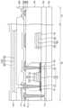
도 1은 본 발명의 일 실시예에 따른 표시 장치의 평면도이다.
도 2은 도 1의 I-I'선을 따라 절단한 표시 장치의 단면도이다.
도 3a 내지 도 3c는 산화물 반도체층의 산소 분압 감소에 따른 트랜지스터의 소자 특성을 설명하기 위한 그래프들이다.
도 4 내지 도 10은 본 발명의 일 실시예에 따른 표시 장치의 제조 방법을 설명하기 위한 단면도들이다.
도 11은 본 발명의 일 실시예에 따른 표시 장치의 단면도이다.
도 12는 본 발명의 일 실시예에 따른 표시 장치의 단면도이다.Figure 1 is a plan view of a display device according to one embodiment of the present invention.
Figure 2 is a cross-sectional view of the display device taken along line I-I' of Figure 1.
Figures 3a to 3c are graphs for explaining the device characteristics of a transistor according to a decrease in the oxygen partial pressure of an oxide semiconductor layer.
FIGS. 4 to 10 are cross-sectional views illustrating a method for manufacturing a display device according to one embodiment of the present invention.
Figure 11 is a cross-sectional view of a display device according to one embodiment of the present invention.
Figure 12 is a cross-sectional view of a display device according to one embodiment of the present invention.
이하, 첨부한 도면들을 참조하여, 본 발명의 실시예를 보다 상세하게 설명하고자 한다.Hereinafter, with reference to the attached drawings, embodiments of the present invention will be described in more detail.
도 1은 본 발명의 일 실시예에 따른 표시 장치의 평면도이다.Figure 1 is a plan view of a display device according to one embodiment of the present invention.
도 1을 참조하면, 상기 표시 장치(1000)는 표시 패널(100) 및 소스 구동부(400)를 포함한다.Referring to FIG. 1, the display device (1000) includes a display panel (100) and a source driving unit (400).
상기 표시 패널(100)은 표시 영역(DA) 및 상기 표시 영역(DA)을 둘러싸는 주변 영역(PA)을 포함한다.The above display panel (100) includes a display area (DA) and a peripheral area (PA) surrounding the display area (DA).
상기 표시 패널(100)은 상기 표시 영역(DA)에 배열된 복수의 데이터 라인들(DL), 복수의 게이트 라인들(GL) 및 복수의 화소들(P)을 포함할 수 있다.The above display panel (100) may include a plurality of data lines (DL), a plurality of gate lines (GL), and a plurality of pixels (P) arranged in the display area (DA).
상기 복수의 데이터 라인들(DL)은 제1 방향(D1)으로 연장되고 상기 제1 방향(D1)과 교차하는 제2 방향(D2)으로 배열될 수 있다.The above-described plurality of data lines (DL) can be extended in a first direction (D1) and arranged in a second direction (D2) intersecting the first direction (D1).
상기 복수의 게이트 라인들(GL)은 상기 제2 방향(D2)으로 연장되고 상기 제1 방향(D1)으로 배열될 수 있다.The above plurality of gate lines (GL) can extend in the second direction (D2) and be arranged in the first direction (D1).
상기 복수의 화소들(P)은 상기 제1 방향(D1)으로 배열된 화소들을 포함하는 화소 열과 상기 제2 방향(D2)으로 배열된 화소들을 포함하는 화소 행을 포함할 수 있다.The above plurality of pixels (P) may include a pixel column including pixels arranged in the first direction (D1) and a pixel row including pixels arranged in the second direction (D2).
예를 들면, 각 화소는 화소 회로를 포함하고, 상기 화소 회로는 적어도 하나의 트랜지스터(T1, R2), 스토리지 커패시터(CST) 및 광을 이용하여 영상을 표시하는 표시 소자를 포함할 수 있다. 상기 표시 소자는 액정 커패시터 및 유기 발광 다이오드일 수 있다.For example, each pixel may include a pixel circuit, and the pixel circuit may include at least one transistor (T1, R2), a storage capacitor (CST), and a display element that displays an image using light. The display element may be a liquid crystal capacitor and an organic light-emitting diode.
일 실시예에서, 상기 표시 소자는 유기 발광 다이오드(OLED)일 수 있다.In one embodiment, the display element may be an organic light emitting diode (OLED).
제1 트랜지스터(TR1)는 상기 유기 발광 다이오드(OLED)를 발광하기 위해 상기 유기 발광 다이오드(OLED)에 구동 전류를 제공할 수 있다.The first transistor (TR1) can provide a driving current to the organic light emitting diode (OLED) to emit light.
제2 트랜지스터(TR2)는 상기 게이트 라인(GL)과 상기 데이터 라인(DL)에 연결되고, 상기 데이터 라인(DL)에 인가된 데이터 전압을 상기 제1 트랜지스터(TR1)에 제공할 수 있다.The second transistor (TR2) is connected to the gate line (GL) and the data line (DL), and can provide a data voltage applied to the data line (DL) to the first transistor (TR1).
일 실시예에서, 상기 트랜지스터들(TR1, TR2)은 산화물 반도체를 포함하는 액티브 패턴을 포함한다.In one embodiment, the transistors (TR1, TR2) include an active pattern comprising an oxide semiconductor.
일 실시예에서, 상기 트랜지스터들(TR1, TR2)의 게이트 전극, 상기 스토리지 커패시터(CST)의 제1 스토리지 전극 및 상기 게이트 라인(GL)은 제1 게이트 베리어층, 제2 게이트 베리어층 및 게이트 금속층이 순차적으로 적층된 3 중막 구조의 게이트 전극층을 가질 수 있다.In one embodiment, the gate electrodes of the transistors (TR1, TR2), the first storage electrode of the storage capacitor (CST), and the gate line (GL) may have a gate electrode layer having a triple-layer structure in which a first gate barrier layer, a second gate barrier layer, and a gate metal layer are sequentially laminated.
일 실시예에서, 상기 게이트 전극층은 IGZO/ZIO 합금/Cu 구조의 3중막 구조를 가질 수 있다.In one embodiment, the gate electrode layer may have a triple-layer structure of IGZO/ZIO alloy/Cu.
상기 게이트 라인(GL)에 게이트 신호를 제공하는 게이트 구동부(300)는 상기 표시 패널(100)의 주변 영역(PA)에 배치될 수 있다. 상기 게이트 구동부(300)는 상기 트랜지스터와 동일한 제조 공정을 통해 상기 주변 영역(PA)에 직접 형성된 복수의 회로 트랜지스터들을 포함할 수 있다.A gate driver (300) that provides a gate signal to the gate line (GL) may be placed in a peripheral area (PA) of the display panel (100). The gate driver (300) may include a plurality of circuit transistors that are directly formed in the peripheral area (PA) through the same manufacturing process as the transistor.
일 실시예에서, 상기 복수의 회로 트랜지스터들은 산화물 반도체를 포함하는 액티브 패턴을 포함할 수 있다.In one embodiment, the plurality of circuit transistors may include an active pattern comprising an oxide semiconductor.
일 실시예에서, 상기 복수의 회로 트랜지스터들의 게이트 전극은 제1 게이트 베리어층, 제2 게이트 베리어층 및 게이트 금속층이 순차적으로 적층된 3중 구조의 게이트 전극층을 포함할 수 있다.In one embodiment, the gate electrodes of the plurality of circuit transistors may include a triple-structured gate electrode layer in which a first gate barrier layer, a second gate barrier layer, and a gate metal layer are sequentially stacked.
상기 소스 구동부(400)는 상기 표시 패널(100)의 주변 영역(PA)에 형성된 복수의 패드들과 연결될 수 있다.The above source driving unit (400) can be connected to a plurality of pads formed in the peripheral area (PA) of the display panel (100).
상기 소스 구동부(400)는 상기 데이터 라인(DL)에 제공되는 데이터 전압을 생성하는 데이터 구동 회로가 실장될 수 있다.The above source driving unit (400) may be equipped with a data driving circuit that generates a data voltage provided to the data line (DL).
도 2는 도 1에 도시된 표시 패널을 설명하기 위한 단면도이다.Figure 2 is a cross-sectional view for explaining the display panel shown in Figure 1.
도 1 및 도 2를 참조하면, 상기 표시 패널(100)은 기판(101) 상의 표시 영역(DA)에 배치된 트랜지스터(TR), 스토리지 커패시터(CST), 유기 발광 다이오드(OLED)를 포함하고, 상기 기판(101) 상의 주변 영역(PA)에 배치된 패드(PD)를 포함할 수 있다.Referring to FIGS. 1 and 2, the display panel (100) may include a transistor (TR), a storage capacitor (CST), and an organic light-emitting diode (OLED) arranged in a display area (DA) on a substrate (101), and may include a pad (PD) arranged in a peripheral area (PA) on the substrate (101).
구체적으로, 기판(101) 상에는 버퍼층(120)이 배치될 수 있다. 버퍼층(120)은 기판(101)을 통해 산소, 수분 등과 같은 불순물이 침투하는 것을 방지할 수 있다.Specifically, a buffer layer (120) may be arranged on the substrate (101). The buffer layer (120) may prevent impurities such as oxygen and moisture from penetrating through the substrate (101).
버퍼층(120)은 상기 기판(101) 상에 평탄한 면을 제공할 수 있다. 상기 버퍼층(120)은 실리콘 질화물(SiNx), 실리콘 산화물(SiOx) 등을 포함할 수 있다.The buffer layer (120) can provide a flat surface on the substrate (101). The buffer layer (120) can include silicon nitride (SiNx), silicon oxide (SiOx), or the like.
일 실시예에 있어서, 트랜지스터(TR)는 n 채널 트랜지스터일 수 있다. 그러나, 본 발명은 이에 한정되지 아니하고, 다른 실시예에 있어서, 트랜지스터(TR)는 p 채널 트랜지스터일 수도 있다. 상기 트랜지스터(TR)는 탑 게이트 구조를 가지며, 액티브 패턴, 게이트 전극, 소스 전극 및 드레인 전극을 포함할 수 있다.In one embodiment, the transistor (TR) may be an n-channel transistor. However, the present invention is not limited thereto, and in another embodiment, the transistor (TR) may be a p-channel transistor. The transistor (TR) may have a top gate structure and may include an active pattern, a gate electrode, a source electrode, and a drain electrode.
버퍼층(120) 상에는 액티브 패턴(130)이 배치될 수 있다. 상기 액티브 패턴(130)은 소스 영역(131), 드레인 영역(132), 및 이들 사이에 위치하는 채널 영역(133)을 포함할 수 있다.An active pattern (130) may be arranged on the buffer layer (120). The active pattern (130) may include a source region (131), a drain region (132), and a channel region (133) located between them.
액티브 패턴(130)은 산화물 반도체를 포함할 수 있다.The active pattern (130) may include an oxide semiconductor.
상기 액티브 패턴(130)은 금속 산화물, 또는 금속과 금속 산화물의 조합을 포함할 수 있다.The above active pattern (130) may include a metal oxide or a combination of a metal and a metal oxide.
예를 들면, 상기 금속 산화물은 주석 산화물(SnO2), 아연-주석 산화물(ZTO), 인듐-아연-주석 산화물(IZTO), 인듐-갈륨-아연-주석 산화물(IGZTO), 아연 산화물(ZnO), 인듐 산화물(InO), 갈륨 산화물(GaO), 인듐-아연 산화물(IZO), 인듐-갈륨 산화물(IGO), 인듐-갈륨-아연 산화물(IGZO) 등을 포함할 수 있다.For example, the metal oxide may include tin oxide (SnO2), zinc-tin oxide (ZTO), indium-zinc-tin oxide (IZTO), indium-gallium-zinc-tin oxide (IGZTO), zinc oxide (ZnO), indium oxide (InO), gallium oxide (GaO), indium-zinc oxide (IZO), indium-gallium oxide (IGO), indium-gallium-zinc oxide (IGZO), and the like.
일 실시예에서, 상기 액티브 패턴(130)은 인듐-갈륨-아연 산화물(IGZO)을 포함할 수 있다.In one embodiment, the active pattern (130) may include indium-gallium-zinc oxide (IGZO).
일 실시예에서, 상기 액티브 패턴(130)은 이동도 향상을 위해 저산소 조건에서 형성된 금속 산화물을 포함할 수 있다.In one embodiment, the active pattern (130) may include a metal oxide formed under low-oxygen conditions to improve mobility.
일 실시예에서, 상기 액티브 패턴(130)은 산소 분압은 약40 % 이하의 조건에서 형성된 금속 산화물을 포함할 수 있다.In one embodiment, the active pattern (130) may include a metal oxide formed under conditions of an oxygen partial pressure of about 40% or less.
상기 액티브 패턴(130) 상에는 제1 게이트 절연 패턴(151) 및 제2 게이트 절연 패턴(153)이 배치될 수 있다. 상기 제1 및 제2 게이트 절연 패턴(151)은 실리콘 산화물(SiOx), 실리콘 질화물(SiNx) 등의 절연 물질을 포함할 수 있다.A first gate insulating pattern (151) and a second gate insulating pattern (153) may be arranged on the active pattern (130). The first and second gate insulating patterns (151) may include an insulating material such as silicon oxide (SiOx) or silicon nitride (SiNx).
상기 제1 게이트 절연 패턴(151)은 상기 채널 영역(133)과 중첩할 수 있다.The above first gate insulating pattern (151) can overlap with the channel region (133).
상기 제2 게이트 절연 패턴(153)은 상기 스토리지 커패시터(CST)의 제1 스토리지 전극(169)이 형성되는 영역에 대응하여 배치될 수 있다. 또한, 도시되지 않았으나, 상기 게이트 라인(GL)이 형성되는 영역에 대응하여 배치될 수 있다.The second gate insulating pattern (153) may be arranged corresponding to an area where the first storage electrode (169) of the storage capacitor (CST) is formed. Also, although not shown, it may be arranged corresponding to an area where the gate line (GL) is formed.
상기 제1 게이트 절연 패턴(151) 상에는 게이트 전극(165)이 배치될 수 있다. 상기 게이트 전극(165)은 채널 영역(133)과 중첩할 수 있다.A gate electrode (165) may be placed on the first gate insulating pattern (151). The gate electrode (165) may overlap with the channel region (133).
상기 게이트 전극(165)은 제1 게이트 베리어층(161), 제2 게이트 베리어층(162) 및 게이트 금속층(163)이 상기 제1 게이트 절연 패턴(151)상에 순차적으로 적층된 3 중막 구조를 가질 수 있다.The above gate electrode (165) may have a triple-layer structure in which a first gate barrier layer (161), a second gate barrier layer (162), and a gate metal layer (163) are sequentially laminated on the first gate insulating pattern (151).
상기 제1 게이트 베리어층(161)은 상기 액티브 패턴(130)과 동일한 금속 산화물을 포함할 수 있다.The above first gate barrier layer (161) may include the same metal oxide as the above active pattern (130).
일 실시예에서, 상기 제1 게이트 베리어층(161)은 인듐-갈륨-아연 산화물(IGZO)을 포함할 수 있다.In one embodiment, the first gate barrier layer (161) may include indium-gallium-zinc oxide (IGZO).
일 실시예에서, 상기 제1 게이트 베리어층(161)은 상기 액티브 패턴(130)의 저산소 조건 보다 높은 고산소 분압 조건에서 형성될 수 있다.In one embodiment, the first gate barrier layer (161) may be formed under high oxygen partial pressure conditions higher than the low oxygen conditions of the active pattern (130).
상기 제1 게이트 베리어층(161)을 상기 액티브 패턴(130)의 저산소 조건 보다 높은 고산소 분압 조건에서 형성함으로써 상기 액티브 패턴(130)의 저산소 분압 공정에서 발생된 산소 결함을 채울 수 있다.By forming the first gate barrier layer (161) under high oxygen partial pressure conditions higher than the low oxygen conditions of the active pattern (130), oxygen defects generated in the low oxygen partial pressure process of the active pattern (130) can be filled.
일 실시예에서, 상기 제1 게이트 베리어층(161)은 산소 분압은 약 60 % 이상에서 형성될 수 있다.In one embodiment, the first gate barrier layer (161) can be formed at an oxygen partial pressure of about 60% or more.
상기 제2 게이트 베리어층(162)은 상기 금속 산화물 합금을 포함할 수 있다. 상기 제2 게이트 베리어층(162)은 상부에 배치되는 상기 게이트 금속층(163)과의 산화를 방지할 수 있다.The second gate barrier layer (162) may include the metal oxide alloy. The second gate barrier layer (162) may prevent oxidation with the gate metal layer (163) disposed thereon.
일 실시예에서, 상기 제2 게이트 베리어층(162)은 아연 산화물(ZnOx) 및 인듐 산화물(InOx)의 합금(ZIO alloy)을 포함할 수 있다.In one embodiment, the second gate barrier layer (162) may include an alloy of zinc oxide (ZnOx) and indium oxide (InOx) (ZIO alloy).
일 실시예에서, 상기 아연 산화물(ZnOx) 및 인듐 산화물(InOx)의 조성비는 9 : 1일 수 있다. 상기 조성비는 상기 게이트 전극(165)의 3 중막을 동시에 식각하는 식각 공정에서 식각 프로파일을 고려하여 설정될 수 있다.In one embodiment, the composition ratio of the zinc oxide (ZnOx) and indium oxide (InOx) may be 9:1. The composition ratio may be set by considering the etching profile in an etching process that simultaneously etches the triple layer of the gate electrode (165).
상기 게이트 금속층(163)은 구리(Cu), 구리 합금, 알루미늄(Al), 알루미늄 합금, 몰리브덴(Mo), 및 몰리브덴 합금 중에서 적어도 하나를 포함할 수 있다.The above gate metal layer (163) may include at least one of copper (Cu), a copper alloy, aluminum (Al), an aluminum alloy, molybdenum (Mo), and a molybdenum alloy.
일 실시예에서, 상기 게이트 금속층(163)은 구리(Cu)를 포함할 수 있다.In one embodiment, the gate metal layer (163) may include copper (Cu).
상기 제2 게이트 절연 패턴(153) 상에는 상기 스토리지 커패시터(CST)의 제1 스토리지 전극(169)이 배치될 수 있다.A first storage electrode (169) of the storage capacitor (CST) may be placed on the second gate insulating pattern (153).
상기 스토리지 커패시터(CST)의 상기 제1 스토리지 전극(169)은 제1 게이트 베리어층(166), 제2 게이트 베리어층(167) 및 게이트 금속층(168)이 상기 제2 게이트 절연 패턴(153) 상에 순차적으로 적층된 3 중막 구조를 가질 수 있다.The first storage electrode (169) of the storage capacitor (CST) may have a triple-layer structure in which a first gate barrier layer (166), a second gate barrier layer (167), and a gate metal layer (168) are sequentially laminated on the second gate insulating pattern (153).
또한, 도시되지 않았으나, 제2 게이트 절연 패턴(153) 상에는 상기 게이트 라인(GL)이 배치될 수 있다. 상기 게이트 라인(GL)은 제1 게이트 베리어층(166), 제2 게이트 베리어층(167) 및 게이트 금속층(168)이 상기 제2 게이트 절연 패턴(153) 상에 순차적으로 적층된 3 중막 구조를 가질 수 있다.In addition, although not shown, the gate line (GL) may be arranged on the second gate insulating pattern (153). The gate line (GL) may have a triple-layer structure in which a first gate barrier layer (166), a second gate barrier layer (167), and a gate metal layer (168) are sequentially laminated on the second gate insulating pattern (153).
상기 제1 게이트 베리어층(166)은 상기 액티브 패턴(130)과 동일한 금속 산화물을 포함할 수 있다.The above first gate barrier layer (166) may include the same metal oxide as the above active pattern (130).
일 실시예에서, 상기 제1 게이트 베리어층(166)은 인듐-갈륨-아연 산화물(IGZO)을 포함할 수 있다.In one embodiment, the first gate barrier layer (166) may include indium-gallium-zinc oxide (IGZO).
일 실시예에서, 상기 제1 게이트 베리어층(166)은 상기 액티브 패턴(130)의 저산소 분압 조건 보다 높은 고산소 분압 조건에서 형성될 수 있다.In one embodiment, the first gate barrier layer (166) may be formed under high oxygen partial pressure conditions higher than the low oxygen partial pressure conditions of the active pattern (130).
일 실시예에서, 상기 제1 게이트 베리어층(166)은 산소 분압은 약 60 % 이상에서 형성될 수 있다.In one embodiment, the first gate barrier layer (166) can be formed at an oxygen partial pressure of about 60% or more.
상기 제2 게이트 베리어층(167)은 상기 금속 산화물 합금을 포함할 수 있다. 상기 제2 게이트 베리어층(167)은 상부에 배치되는 상기 게이트 금속층(168)의 산화를 방지할 수 있다.The second gate barrier layer (167) may include the metal oxide alloy. The second gate barrier layer (167) may prevent oxidation of the gate metal layer (168) disposed thereon.
일 실시예에서, 상기 제2 게이트 베리어층(167)은 아연 산화물(ZnOx) 및 인듐 산화물(InOx)의 합금(ZIO alloy)을 포함할 수 있다.In one embodiment, the second gate barrier layer (167) may include an alloy of zinc oxide (ZnOx) and indium oxide (InOx) (ZIO alloy).
일 실시예에서, 상기 아연 산화물(ZnOx) 및 인듐 산화물(InOx)의 조성비는 9 : 1일 수 있다. 상기 조성비는 상기 제1 스토리지 전극(169) 및 상기 게이트 라인(GL)의 3 중막을 동시에 식각하는 식각 공정에서 식각 프로파일을 고려하여 설정될 수 있다.In one embodiment, the composition ratio of the zinc oxide (ZnOx) and indium oxide (InOx) may be 9:1. The composition ratio may be set by considering the etching profile in an etching process that simultaneously etches the triple layer of the first storage electrode (169) and the gate line (GL).
상기 게이트 금속층(168)은 구리(Cu), 구리 합금, 알루미늄(Al), 알루미늄 합금, 몰리브덴(Mo), 및 몰리브덴 합금 중에서 적어도 하나를 포함할 수 있다.The above gate metal layer (168) may include at least one of copper (Cu), a copper alloy, aluminum (Al), an aluminum alloy, molybdenum (Mo), and a molybdenum alloy.
일 실시예에서, 상기 게이트 금속층(168)은 구리(Cu)를 포함할 수 있다.In one embodiment, the gate metal layer (168) may include copper (Cu).
층간 절연층(170)은 상기 게이트 전극(165) 및 상기 제1 스토리지 전극(169)이 형성된 상기 기판(101) 상에 형성될 수 있다. 상기 층간 절연층(170)은 실리콘 산화물(SiOx), 실리콘 질화물(SiNx) 등의 절연 물질을 포함할 수 있다.An interlayer insulating layer (170) may be formed on the substrate (101) on which the gate electrode (165) and the first storage electrode (169) are formed. The interlayer insulating layer (170) may include an insulating material such as silicon oxide (SiOx) or silicon nitride (SiNx).
소스 전극(181), 드레인 전극(182) 및 스토리지 커패시터(CST)의 제2 스토리지 전극(183)은 상기 층간 절연층(170) 상의 표시 영역(DA)에 배치될 수 있다. 라인 단부(185)는 상기 층간 절연층(170) 상의 주변 영역(PA)에 배치될 수 있다.The source electrode (181), the drain electrode (182), and the second storage electrode (183) of the storage capacitor (CST) may be arranged in the display area (DA) on the interlayer insulating layer (170). The line end (185) may be arranged in the peripheral area (PA) on the interlayer insulating layer (170).
상기 소스 전극(181), 상기 드레인 전극(182), 제2 스토리지 전극(183) 및 상기 라인 단부(185)는 구리(Cu), 구리 합금, 알루미늄(Al), 알루미늄 합금, 몰리브덴(Mo), 및 몰리브덴 합금 중에서 적어도 하나를 포함할 수 있다.The source electrode (181), the drain electrode (182), the second storage electrode (183), and the line end (185) may include at least one of copper (Cu), a copper alloy, aluminum (Al), an aluminum alloy, molybdenum (Mo), and a molybdenum alloy.
상기 소스 전극(181) 및 상기 드레인 전극(182)은 상기 층간 절연층(170)에 형성된 콘택홀들을 통해서 상기 액티브 패턴(130)의 소스 영역(131) 및 드레인 영역(132)에 각각 전기적으로 연결될 수 있다.The source electrode (181) and the drain electrode (182) can be electrically connected to the source region (131) and the drain region (132) of the active pattern (130), respectively, through contact holes formed in the interlayer insulating layer (170).
상기 제2 스토리지 전극(183)은 상기 제1 스토리지 전극(169)과 중첩되는 영역에 배치될 수 있다.The second storage electrode (183) may be placed in an area overlapping the first storage electrode (169).
상기 라인 단부(185)는 상기 표시 영역(DA)에 배치된 신호 라인의 단부에 대응될 수 있다. 상기 신호 라인은 데이터 라인, 전압 라인 등을 포함할 수 있다.The above line end (185) may correspond to an end of a signal line arranged in the display area (DA). The signal line may include a data line, a voltage line, etc.
보호층(190)은 상기 소스 전극(181), 상기 드레인 전극(182), 제2 스토리지 전극(183) 및 상기 라인 단부(185)가 형성된 상기 기판(101) 상에 배치될 수 있다. 상기 보호층(190)은 실리콘 산화물(SiOx), 실리콘 질화물(SiNx) 등의 절연 물질을 포함할 수 있다.A protective layer (190) may be disposed on the substrate (101) on which the source electrode (181), the drain electrode (182), the second storage electrode (183), and the line end (185) are formed. The protective layer (190) may include an insulating material such as silicon oxide (SiOx), silicon nitride (SiNx), etc.
연결 전극(211)은 상기 보호층(190) 상의 표시 영역(DA)에 배치될 수 있다. 패드 전극(215)은 상기 보호층(190) 상의 주변 영역(PA)에 배치될 수 있다. 상기 연결 전극(211) 및 상기 패드 전극(215)은 ITO(Indium Tin Oxide), IZO(Indium Zinc Oxide), ZnO(Zinc Oxide) 등의 투명한 도전 물질을 포함할 수 있다.The connection electrode (211) may be placed in the display area (DA) on the protective layer (190). The pad electrode (215) may be placed in the peripheral area (PA) on the protective layer (190). The connection electrode (211) and the pad electrode (215) may include a transparent conductive material such as ITO (Indium Tin Oxide), IZO (Indium Zinc Oxide), or ZnO (Zinc Oxide).
상기 연결 전극(211)은 상기 보호층(190)에 형성된 콘택홀을 통해 상기 트랜지스터의 전극, 예컨대, 소스 전극(131)과 전기적으로 연결될 수 있다. 상기 패드 전극(215)은 상기 보호층(190)에 형성된 콘택홀을 통해 상기 라인 단부(185)와 전기적으로 연결될 수 있다.The above connecting electrode (211) can be electrically connected to an electrode of the transistor, for example, a source electrode (131), through a contact hole formed in the protective layer (190). The pad electrode (215) can be electrically connected to the line end (185) through a contact hole formed in the protective layer (190).
평탄화막(220)은 상기 연결 전극(211) 및 상기 패드 전극(215)이 형성된 상기 기판(101) 상에 상부면을 평탄하게 하기 위해 두꺼운 두께로 배치될 수 있다. 상기 평탄화막(220)은 아크릴계 수지, 에폭시계 수지, 폴리이미드계 수지, 폴리에스테르계 수지 등의 유기 물질을 포함할 수 있다.The flattening film (220) may be placed with a thick thickness on the substrate (101) on which the connecting electrode (211) and the pad electrode (215) are formed to flatten the upper surface. The flattening film (220) may include an organic material such as an acrylic resin, an epoxy resin, a polyimide resin, or a polyester resin.
상기 평탄화막(220)은 표시 영역(DA)에서 상기 연결 전극(211)을 노출하는 비아 홀을 포함하고, 상기 주변 영역(PA)에서는 제거될 수 있다. 도시된 바와 같이, 상기 평탄화막(220)은 상기 패드 전극(215)을 노출하도록 제거될 수 있다.The above planarization film (220) includes a via hole exposing the connection electrode (211) in the display area (DA) and can be removed in the peripheral area (PA). As illustrated, the planarization film (220) can be removed to expose the pad electrode (215).
화소 전극(230)은 상기 평탄화막(220) 상의 화소 영역에 배치될 수 있다. 상기 화소 전극(230)은 반사 전극으로 제공될 수 있다. 이 경우, 상기 화소 전극(230)은 Al, Ag, W, Cu, Ni, Cr, Mo, Ti, Pt, Ta, Nd, Sc 등과 같은 금속 또는 상기 금속의 합금을 포함할 수 있다. 또한, 상기 화소 전극(230)은 일함수가 높은 투명 도전성 물질을 포함할 수도 있다. 예를 들면, 상기 화소 전극(230)은 인듐 주석 산화물(Indium Tin Oxide, ITO), 인듐 아연 산화물(Indium Zinc Oxide, IZO), 아연 산화물 또는 인듐 산화물을 포함할 수도 있다.The pixel electrode (230) may be arranged in a pixel area on the flattening film (220). The pixel electrode (230) may be provided as a reflective electrode. In this case, the pixel electrode (230) may include a metal such as Al, Ag, W, Cu, Ni, Cr, Mo, Ti, Pt, Ta, Nd, Sc, or an alloy of the metal. In addition, the pixel electrode (230) may include a transparent conductive material having a high work function. For example, the pixel electrode (230) may include indium tin oxide (ITO), indium zinc oxide (IZO), zinc oxide, or indium oxide.
일 실시예에 있어서, 상기 화소 전극(230)은 상기 금속 및 상기 투명 도전성 물질을 포함하는 복층 구조를 가질 수도 있다.In one embodiment, the pixel electrode (230) may have a multilayer structure including the metal and the transparent conductive material.
상기 화소 전극(230)은 상기 비아 홀을 통해 상기 연결 전극(211)과 전기적으로 연결될 수 있다. 즉, 상기 화소 전극(230)은 트랜지스터(TR)와 전기적으로 연결될 수 있다.The above pixel electrode (230) can be electrically connected to the connection electrode (211) through the via hole. That is, the pixel electrode (230) can be electrically connected to the transistor (TR).
화소 정의막(240)은 상기 평탄화막(220) 상의 표시 영역(DA)에 배치되고, 상기 화소 영역을 정의하기 위해 상기 화소 전극(230)을 노출하는 개구를 포함할 수 있다. 상기 화소 정의막(220)은 폴리이미드 수지 또는 아크릴 수지와 같은 투명 유기 물질을 포함할 수 있다.The pixel defining film (240) is arranged in the display area (DA) on the planarizing film (220) and may include an opening that exposes the pixel electrode (230) to define the pixel area. The pixel defining film (220) may include a transparent organic material such as a polyimide resin or an acrylic resin.
유기 발광층(250)은 상기 화소 전극(230)을 노출하는 상기 화소 정의막(240)의 개구 내에 배치될 수 있다. 상기 유기 발광층(250)은 정공 및 전자에 의해 여기되는 호스트(host) 물질, 그리고 에너지의 흡수 및 방출을 통해 발광효율을 증가시키는 도펀트(dopant) 물질을 포함할 수 있다.The organic light-emitting layer (250) may be placed within the opening of the pixel defining film (240) exposing the pixel electrode (230). The organic light-emitting layer (250) may include a host material excited by holes and electrons, and a dopant material that increases light-emitting efficiency through absorption and emission of energy.
공통 전극(260)은 상기 화소 전극(230)과 대향하여 배치되고, 상기 유기 발광층(250)이 형성된 상기 기판(101) 상 복수의 화소 영역들에 공통으로 배치될 수 있다. 상기 공통 전극(260)은Al, Ag, W, Cu, Ni, Cr, Mo, Ti, Pt, Ta, Nd, Sc 등과 같은 일 함수가 낮은 금속 또는 상기 금속의 합금을 포함할 수 있다.The common electrode (260) is arranged to face the pixel electrode (230) and may be commonly arranged in a plurality of pixel areas on the substrate (101) on which the organic light-emitting layer (250) is formed. The common electrode (260) may include a metal having a low work function, such as Al, Ag, W, Cu, Ni, Cr, Mo, Ti, Pt, Ta, Nd, Sc, or an alloy of the metal.
일 실시예에 있어서, 상기 화소 전극(230)과 유기 발광층(250) 사이에는 정공 수송층(hole transport layer, HTL)이 배치될 수 있다. 또한, 유기 발광층 유기 발광층(250)과 상기 공통 전극(260) 사이에는 전자 수송층(electron transport layer, ETL)이 배치될 수 있다. 상기 정공 수송층 및/또는 상기 전자 수송층은 복수의 화소들에 공통적으로 연속적으로 제공될 수 있다.In one embodiment, a hole transport layer (HTL) may be disposed between the pixel electrode (230) and the organic light-emitting layer (250). In addition, an electron transport layer (ETL) may be disposed between the organic light-emitting layer (250) and the common electrode (260). The hole transport layer and/or the electron transport layer may be continuously provided commonly to a plurality of pixels.
상기 화소 전극(230), 유기 발광층(250) 및 상기 공통 전극(260)에 의해 발광 소자(OLED)가 정의될 수 있다. 상기 화소 전극(230) 및 상기 공통 전극(260)은 각각 유기 발광 다이오드(OLED)의 양극(anode) 및 음극(cathode)으로 제공될 수 있다.A light-emitting element (OLED) can be defined by the pixel electrode (230), the organic light-emitting layer (250), and the common electrode (260). The pixel electrode (230) and the common electrode (260) can be provided as an anode and a cathode of an organic light-emitting diode (OLED), respectively.
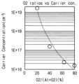
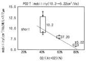
도 3a 내지 도 3c는 산화물 반도체층의 산소 분압 감소에 따른 트랜지스터의 소자 특성을 설명하기 위한 그래프들이다.Figures 3a to 3c are graphs for explaining the device characteristics of a transistor according to a decrease in the oxygen partial pressure of an oxide semiconductor layer.
도 3a는 산소 분압 공정에 따른 캐리어 농도 변화를 나타낸 그래프이고, 도 3b는 산소 분압 공정에 따른 이동도 변화를 나타낸 그래프이고, 도 3c는 산소 분압 공정에 따른 문턱 전압 변화를 나타낸 그래프이다.Figure 3a is a graph showing the change in carrier concentration according to the oxygen partial pressure process, Figure 3b is a graph showing the change in mobility according to the oxygen partial pressure process, and Figure 3c is a graph showing the change in threshold voltage according to the oxygen partial pressure process.
도 3a, 도 3b 및 도 3c를 참조하면, 트랜지스터의 액티브층으로 산화물 반도체층을 형성하는 공정에서, 산소 분압 조건이 감소할수록 산화물 반도체층의 캐리어 농도가 점점 증가함을 확인할 수 있다.Referring to FIGS. 3a, 3b, and 3c, in the process of forming an oxide semiconductor layer as an active layer of a transistor, it can be confirmed that the carrier concentration of the oxide semiconductor layer gradually increases as the oxygen partial pressure conditions decrease.
아래 표는 에너지 밴드 옵셋으로 계산된 산소 분압 조건(%)에 따른 반도체 캐리어 농도이다.The table below shows the semiconductor carrier concentration according to the oxygen partial pressure condition (%) calculated by energy band offset.
<표><Table>
상기 산소 분압 조건(%)이 저산소 조건인 40 % 이하에서 캐리어 농도가 급격히 증가하는 것을 알 수 있다. 상기 캐리어 농도가 증가하면 결과적으로 반도체의 전도도가 증가할 수 있다.It can be seen that the carrier concentration increases rapidly when the oxygen partial pressure condition (%) is 40% or less, which is a low-oxygen condition. As the carrier concentration increases, the conductivity of the semiconductor can increase as a result.
상기 전도도가 증가하면 트랜지스터의 특성인 이동도가 증가할 수 있고, 또한, 문턱 전압(Vth)이 네가티브측으로 이동할 수 있다. 따라서, 트랜지스터의 신뢰성이 향상될 수 있다.As the above conductivity increases, the mobility, which is a characteristic of the transistor, can increase, and also the threshold voltage (Vth) can move to the negative side. Accordingly, the reliability of the transistor can be improved.
한편, 도 3b 및 도 3c에 도시된 바와 같이, 상기 산소 분압 조건(%)이 낮아질수록 이동도 및 문턱 전압과 같은 트랜지스터의 신뢰성이 향상할 수 있으나, 상기 산소 분압 조건(%)이 약 20% 이하에서는 소스 및 드레인 사이에 단락(short)이 발생할 수 있다.Meanwhile, as shown in FIG. 3b and FIG. 3c, as the oxygen partial pressure condition (%) decreases, the reliability of the transistor, such as mobility and threshold voltage, may improve; however, when the oxygen partial pressure condition (%) is about 20% or less, a short may occur between the source and drain.
따라서, 상기 산화물 반도체층의 형성 공정에서, 저산소 분압 조건을 적용하기 위해서는 소자 안정성 확보를 위한 추가 공정 및 추가 층이 필요할 수 있다.Therefore, in the process of forming the oxide semiconductor layer, additional processes and additional layers may be required to secure device stability in order to apply low oxygen partial pressure conditions.
일 실시예에서 있어서, 상기 산화물 반도체를 포함하는 액티브층을 트랜지스터의 신뢰성을 향상시키기 위해 약 40 % 이하의 저산소 분압 조건으로 형성하고, 후속 공정인 게이트 전극을 형성하는 공정에서, 저산소 분압 조건에서 형성된 액티브층의 산소 결함을 보상하기 위해 약60% 이상의 고산소 분압 조건에서 제1 게이트 베리어층을 형성할 수 있다. 상기 제1 게이트 베리어층은 상기 트랜지스터의 액티브층에 사용되는 산화물 반도체를 포함할 수 있다.In one embodiment, an active layer including the oxide semiconductor is formed under a low oxygen partial pressure condition of about 40% or less to improve the reliability of the transistor, and in a subsequent process of forming a gate electrode, a first gate barrier layer can be formed under a high oxygen partial pressure condition of about 60% or more to compensate for oxygen defects in the active layer formed under the low oxygen partial pressure condition. The first gate barrier layer can include an oxide semiconductor used in the active layer of the transistor.
도 4 내지 도 11은 본 발명의 일 실시예에 따른 표시 장치의 제조 방법을 설명하기 위한 단면도들이다.FIGS. 4 to 11 are cross-sectional views illustrating a method for manufacturing a display device according to one embodiment of the present invention.
도 4를 참조하면, 기판(101) 상에 버퍼층(120)을 형성할 수 있다. 예를 들면, 기판(101) 상에 화학 기상 증착(CVD), 스퍼터링(sputtering) 등을 이용하여 실리콘 산화물(SiOx), 실리콘 질화물(SiNx) 등으로 버퍼층(120)을 형성할 수 있다.Referring to FIG. 4, a buffer layer (120) can be formed on a substrate (101). For example, the buffer layer (120) can be formed on the substrate (101) using silicon oxide (SiOx), silicon nitride (SiNx), or the like, using chemical vapor deposition (CVD), sputtering, or the like.
상기 버퍼층(120)이 형성된 기판(101) 상에 산화물 반도체층(130a)을 형성할 수 있다.An oxide semiconductor layer (130a) can be formed on a substrate (101) on which the above buffer layer (120) is formed.
예를 들면, 화학 기상 증착(CVD)을 이용하여 아연 산화물(ZnO), 인듐 산화물(InO), 갈륨 산화물(GaO), 인듐-아연 산화물(IZO), 인듐-갈륨 산화물(IGO), 인듐-갈륨-아연 산화물(IGZO) 등으로 산화물 반도체층(130a)을 형성할 수 있다.For example, an oxide semiconductor layer (130a) can be formed using chemical vapor deposition (CVD) using zinc oxide (ZnO), indium oxide (InO), gallium oxide (GaO), indium-zinc oxide (IZO), indium-gallium oxide (IGO), indium-gallium-zinc oxide (IGZO), or the like.
상기 산화물 반도체층을 형성하는 공정에서, 산소 분압 조건은 약40 % 이하의 설정할 수 있다.In the process of forming the above oxide semiconductor layer, the oxygen partial pressure condition can be set to about 40% or less.
상기 산화물 반도체층(130a)은 약 40 % 이하의 산소 분압 조건에 의해 형성됨으로써 트랜지스터의 이동도 및 문턱 전압 등과 같은 신뢰성은 향상될 수 있다. 한편, 상기 약 40 % 이하의 저산소 분압 조건에 의해 상기 산화물 반도체층(130a)은 캐리어 농도가 증가되어 산소 결합이 많이 발생할 수 있다.The above oxide semiconductor layer (130a) is formed under an oxygen partial pressure condition of about 40% or less, so that reliability such as mobility and threshold voltage of the transistor can be improved. Meanwhile, under the low oxygen partial pressure condition of about 40% or less, the oxide semiconductor layer (130a) can have an increased carrier concentration and thus generate a lot of oxygen bonding.
상기 산화물 반도체층(130a)은 포토 공정(photolithography)을 통해 패터닝 되고, 상기 버퍼층(120) 상에 액티브 패턴(130)을 형성할 수 있다.The above oxide semiconductor layer (130a) can be patterned through a photolithography process, and an active pattern (130) can be formed on the buffer layer (120).
도 5를 참조하면, 상기 액티브 패턴(130)이 형성된 기판(101) 상에 게이트 절연층(150)을 형성한다.Referring to Fig. 5, a gate insulating layer (150) is formed on a substrate (101) on which the active pattern (130) is formed.
상기 게이트 절연층(150)은 화학 기상 증착(chemical vapor deposition, CVD)을 이용하여 형성될 수 있다.The above gate insulating layer (150) can be formed using chemical vapor deposition (CVD).
상기 게이트 절연층(150)이 형성된 기판(101) 상에 제1 게이트 베리어층(160a)을 형성할 수 있다.A first gate barrier layer (160a) can be formed on a substrate (101) on which the above gate insulating layer (150) is formed.
상기 제1 게이트 베리어층(160a)은 상기 액티브 패턴(130)과 동일한 금속 산화물을 포함할 수 있다.The above first gate barrier layer (160a) may include the same metal oxide as the active pattern (130).
일 실시예에서, 상기 제1 게이트 베리어층(160a)은 인듐-갈륨-아연 산화물(IGZO)을 포함할 수 있다.In one embodiment, the first gate barrier layer (160a) may include indium-gallium-zinc oxide (IGZO).
일 실시예에서, 상기 제1 게이트 베리어층(160a)은 식각 공정시 언더 컷(under cut)을 고려하여 200 옹스트롱(Å) 이하의 두께를 가질 수 있다.In one embodiment, the first gate barrier layer (160a) may have a thickness of 200 angstroms (Å) or less in consideration of under cut during the etching process.
예를 들면, 상기 제1 게이트 베리어층(160a)은 화학 기상 증착(CVD)을 이용하여 형성될 수 있다. 상기 제1 게이트 베리어층(160a)의 형성 공정시 산소 분압 조건은 약 60 % 이상의 고산소 분압 조건으로 설정할 수 있다.For example, the first gate barrier layer (160a) may be formed using chemical vapor deposition (CVD). During the formation process of the first gate barrier layer (160a), the oxygen partial pressure condition may be set to a high oxygen partial pressure condition of about 60% or more.
상기 제1 게이트 베리어층(160a)은 상기 고산소 분압 조건에서 증착될 때 발생된 산소는 저산소 분압 조건에서 형성된 상기 액티브 패턴(130)에 산소를 공급해 줄 수 있다. 따라서 상기 제1 게이트 베리어층(160a)은 저산소 분압 조건에서 형성된 상기 액티브 패턴(130)의 산소 결합을 보상해줄 수 있다.The oxygen generated when the first gate barrier layer (160a) is deposited under the high oxygen partial pressure condition can supply oxygen to the active pattern (130) formed under the low oxygen partial pressure condition. Therefore, the first gate barrier layer (160a) can compensate for the oxygen bonding of the active pattern (130) formed under the low oxygen partial pressure condition.
제2 게이트 베리어층(160b)은 상기 제1 게이트 베리어층(160a)이 형성된 기판(101) 상에 형성할 수 있다.The second gate barrier layer (160b) can be formed on the substrate (101) on which the first gate barrier layer (160a) is formed.
일 실시예에서, 상기 제2 게이트 베리어층(160b)은 식각 공정시 언더 컷(under cut)을 고려하여 200 옹스트롱(Å) 이하의 두께를 가질 수 있다.In one embodiment, the second gate barrier layer (160b) may have a thickness of 200 angstroms (Å) or less in consideration of under cut during the etching process.
상기 제2 게이트 베리어층(160b)은 상기 금속 산화물 합금을 포함할 수 있다. 상기 제2 게이트 베리어층(160b)은 상기 제2 게이트 베리어층(160b)의 상부에 배치되는 상기 게이트 금속층(168)과의 산화를 방지할 수 있다.The second gate barrier layer (160b) may include the metal oxide alloy. The second gate barrier layer (160b) may prevent oxidation with the gate metal layer (168) disposed on top of the second gate barrier layer (160b).
일 실시예에서, 상기 제2 게이트 베리어층(160b)은 아연 산화물(ZnOx) 및 인듐 산화물(InOx)의 합금(ZIO alloy)을 포함할 수 있다.In one embodiment, the second gate barrier layer (160b) may include an alloy of zinc oxide (ZnOx) and indium oxide (InOx) (ZIO alloy).
일 실시예에서, 상기 아연 산화물(ZnOx) 및 인듐 산화물(InOx)의 조성비는 9 : 1일 수 있다. 상기 조성비는 식각 공정시 하부의 제1 게이트 베리어층(160a)과 상부의 게이트 금속층(160c)의 식각 프로파일을 고려하여 설정될 수 있다.In one embodiment, the composition ratio of the zinc oxide (ZnOx) and indium oxide (InOx) may be 9:1. The composition ratio may be set by considering the etching profile of the first gate barrier layer (160a) at the bottom and the gate metal layer (160c) at the top during the etching process.
상기 제2 게이트 베리어층(160b)이 형성된 기판(101) 상에 게이트 금속층(160c)을 형성한다.A gate metal layer (160c) is formed on the substrate (101) on which the second gate barrier layer (160b) is formed.
상기 게이트 금속층(160c)은 구리(Cu), 구리 합금, 알루미늄(Al), 알루미늄 합금, 몰리브덴(Mo) 및 몰리브덴 합금 중에서 적어도 하나를 포함할 수 있다.The above gate metal layer (160c) may include at least one of copper (Cu), a copper alloy, aluminum (Al), an aluminum alloy, molybdenum (Mo), and a molybdenum alloy.
일 실시예에서, 상기 게이트 금속층(160c)은 구리(Cu)를 포함할 수 있다.In one embodiment, the gate metal layer (160c) may include copper (Cu).
상기 게이트 금속층(160c)이 형성된 기판(101) 상에 포토레지스트층을 형성할 수 있다. 상기 포토레지스트층은 감광성 유기물로 형성될 수 있다.A photoresist layer can be formed on the substrate (101) on which the gate metal layer (160c) is formed. The photoresist layer can be formed of a photosensitive organic material.
상기 포토레지스트층을 패터닝하여 상기 게이트 전극이 형성되는 제1 영역(A1)에 제1 포토레지스트 패턴(PR1)을 형성하고, 상기 스토리지 커패시터(CST)가 형성된 제2 영역(A2)에 제2 포토레지스트 패턴(PR2)을 형성한다. 또한, 도시되지 않았으나, 상기 제2 포토레지스트 패턴(PR2)은 상기 게이트 라인(GL)이 형성되는 영역에 형성될 수 있다.The photoresist layer is patterned to form a first photoresist pattern (PR1) in a first region (A1) where the gate electrode is formed, and a second photoresist pattern (PR2) is formed in a second region (A2) where the storage capacitor (CST) is formed. In addition, although not shown, the second photoresist pattern (PR2) may be formed in a region where the gate line (GL) is formed.
상기 제1 및 제2 포토레지스트 패턴들(PR1, PR2)을 이용한 식각 공정으로, 상기 게이트 절연층(150), 상기 제1 게이트 베리어층(160a), 상기 제2 게이트 베리어층(160b) 및 상기 게이트 금속층(160c)을 동시에 패터닝할 수 있다. 상기 식각 공정은 습식 식각 공정일 수 있다.By an etching process using the first and second photoresist patterns (PR1, PR2), the gate insulating layer (150), the first gate barrier layer (160a), the second gate barrier layer (160b), and the gate metal layer (160c) can be patterned simultaneously. The etching process may be a wet etching process.
도 6을 참조하면, 상기 액티브 패턴(130)의 채널 영역(133) 상에는 제1 게이트 베리어층(161), 제2 게이트 베리어층(162) 및 게이트 금속층(163)이 순차적으로 적층된 3 중막 구조의 게이트 전극(165)이 형성될 수 있다. 상기 액티브 패턴(130)과 상기 게이트 전극(165)의 제1 게이트 베리어층(161) 사이에는 제1 게이트 절연 패턴(151)이 배치될 수 있다.Referring to FIG. 6, a gate electrode (165) having a triple-layer structure in which a first gate barrier layer (161), a second gate barrier layer (162), and a gate metal layer (163) are sequentially laminated may be formed on a channel region (133) of the active pattern (130). A first gate insulating pattern (151) may be arranged between the active pattern (130) and the first gate barrier layer (161) of the gate electrode (165).
또한, 상기 스토리지 커패시터의 형성 영역에 대응하는 상기 버퍼층(120) 상에는 제1 게이트 베리어층(166), 제2 게이트 베리어층(167) 및 게이트 금속층(168)이 순차적으로 적층된 3 중막 구조의 제1 스토리지 전극(169)이 형성될 수 있다. 상기 버퍼층(120)과 상기 제1 스토리지 전극(169)의 제1 게이트 베리어층(166) 사이에는 제2 게이트 절연 패턴(153)이 배치될 수 있다.In addition, a first storage electrode (169) having a triple-layer structure in which a first gate barrier layer (166), a second gate barrier layer (167), and a gate metal layer (168) are sequentially laminated may be formed on the buffer layer (120) corresponding to the formation area of the storage capacitor. A second gate insulating pattern (153) may be arranged between the buffer layer (120) and the first gate barrier layer (166) of the first storage electrode (169).
또한, 도시되지 않았으나, 상기 게이트 라인(GL)의 형성 영역에 대응하는 상기 버퍼층(120) 상에는 제1 게이트 베리어층(166), 제2 게이트 베리어층(167) 및 게이트 금속층(168)이 순차적으로 적층된 3 중막 구조의 게이트 라인 (GL)이 형성될 수 있다. 상기 버퍼층(120)과 상기 게이트 라인 (GL)의 제1 게이트 베리어층(166) 사이에는 제2 게이트 절연 패턴(153)이 배치될 수 있다.In addition, although not shown, a gate line (GL) having a triple-layer structure in which a first gate barrier layer (166), a second gate barrier layer (167), and a gate metal layer (168) are sequentially laminated on the buffer layer (120) corresponding to the formation area of the gate line (GL) may be formed. A second gate insulating pattern (153) may be arranged between the buffer layer (120) and the first gate barrier layer (166) of the gate line (GL).
앞서 설명된 바와 같이, 상기 제1 게이트 베리어층(160a), 상기 제2 게이트 베리어층(160b) 및 상기 게이트 금속층(160c)을 한 번의 식각 공정으로 동시에 패터닝함으로써 제조 공정을 단순화할 수 있다.As described above, the manufacturing process can be simplified by simultaneously patterning the first gate barrier layer (160a), the second gate barrier layer (160b), and the gate metal layer (160c) in one etching process.
이어, 도핑 공정을 이용하여 상기 게이트 전극(165)과 중첩하는 상기 액티브 패턴(130)의 채널 영역(133)의 양단부에 소스 영역(131) 및 드레인 영역(133)을 형성할 수 있다. 상기 액티브 패턴(130)은 소스 영역(131), 드레인 영역(132) 및 채널 영역(133)을 포함할 수 있다.Next, a source region (131) and a drain region (133) can be formed at both ends of the channel region (133) of the active pattern (130) overlapping the gate electrode (165) using a doping process. The active pattern (130) can include a source region (131), a drain region (132), and a channel region (133).
도 7을 참조하면, 상기 게이트 전극(165) 및 상기 제1 스토리지 전극(169)이 형성된 기판(101) 상에 층간 절연층(170)을 형성한다.Referring to Fig. 7, an interlayer insulating layer (170) is formed on the substrate (101) on which the gate electrode (165) and the first storage electrode (169) are formed.
상기 층간 절연층(170)은 화학 기상 증착(CVD), 스퍼터링(sputtering) 등을 이용하여 실리콘 산화물(SiOx), 실리콘 질화물(SiNx) 등으로 형성될 수 있다.The above interlayer insulating layer (170) can be formed of silicon oxide (SiOx), silicon nitride (SiNx), or the like using chemical vapor deposition (CVD), sputtering, or the like.
상기 층간 절연층(170)을 식각하여, 상기 액티브 패턴(130)의 상기 소스 영역(131) 및 상기 드레인 영역(132)을 노출하는 콘택홀들을 형성할 수 있다.By etching the interlayer insulating layer (170), contact holes can be formed that expose the source region (131) and the drain region (132) of the active pattern (130).
소스 금속층을 상기 콘택홀들이 형성된 상기 층간 절연층(170) 상에 형성한다. 상기 소스 금속층은 화학 기상 증착(CVD), 스퍼터링(sputtering) 등을 이용하여 상기 층간 절연층(170)에 구리(Cu), 알루미늄(Al), 몰리브덴(Mo) 등으로 형성될 수 있다.A source metal layer is formed on the interlayer insulating layer (170) in which the contact holes are formed. The source metal layer can be formed on the interlayer insulating layer (170) using copper (Cu), aluminum (Al), molybdenum (Mo), etc. by using chemical vapor deposition (CVD), sputtering, etc.
상기 소스 금속층을 패터닝하여 상기 소스 영역(131)과 콘택홀을 통해 연결되는 소스 전극(181)을 형성하고, 상기 드레인 영역(132)과 콘택홀을 통해 연결되는 드레인 전극(182)을 형성한다. 또한, 상기 소스 금속층을 패터닝하여 상기 스토리지 커패시터(CST)의 제2 스토리지 전극(183)을 상기 제1 스토리지 전극(169)과 중첩하여 형성한다. 또한, 상기 소스 금속층을 패터닝하여 데이터 라인을 포함하는 복수의 신호 라인들을 형성할 수 있다. 상기 신호 라인의 단부인 라인 단부(185)는 상기 주변 영역(PA)에 형성될 수 있다.The source metal layer is patterned to form a source electrode (181) connected to the source region (131) through a contact hole, and a drain electrode (182) connected to the drain region (132) through a contact hole. In addition, the source metal layer is patterned to form a second storage electrode (183) of the storage capacitor (CST) overlapping the first storage electrode (169). In addition, the source metal layer may be patterned to form a plurality of signal lines including a data line. The line end (185), which is an end of the signal line, may be formed in the peripheral area (PA).
도 8을 참조하면, 상기 소스 전극(181), 상기 드레인 전극(182), 제2 전극(183) 및 상기 라인 단부(185)가 형성된 상기 기판(101) 상에 보호층(190)을 형성한다. 상기 보호층(190)은 화학 기상 증착(CVD), 스퍼터링(sputtering) 등을 이용하여 실리콘 산화물(SiOx), 실리콘 질화물(SiNx) 등으로 형성될 수 있다.Referring to Fig. 8, a protective layer (190) is formed on the substrate (101) on which the source electrode (181), the drain electrode (182), the second electrode (183), and the line end (185) are formed. The protective layer (190) can be formed of silicon oxide (SiOx), silicon nitride (SiNx), or the like using chemical vapor deposition (CVD), sputtering, or the like.
상기 보호층(190)을 식각하여 상기 트랜지스터의 전극, 예컨대 소스 전극(181) 및 상기 라인 단부(185)를 노출하는 콘택홀들을 형성할 수 있다.The protective layer (190) may be etched to form contact holes exposing the electrodes of the transistor, such as the source electrode (181) and the line end (185).
투명 도전층을 상기 콘택홀들이 형성된 상기 보호층(190) 상에 형성한다. 상기 투명 도전층은 ITO(Indium Tin Oxide), IZO(Indium Zinc Oxide), ZnO(Zinc Oxide) 등을 포함할 수 있다.A transparent conductive layer is formed on the protective layer (190) in which the contact holes are formed. The transparent conductive layer may include ITO (Indium Tin Oxide), IZO (Indium Zinc Oxide), ZnO (Zinc Oxide), etc.
상기 투명 도전층을 식각하여, 상기 소스 전극(181)과 콘택홀을 통해 연결되는 연결 전극(211) 및 상기 라인 단부(185)와 콘택홀을 통해 연결되는 패드 전극(215)을 형성할 수 있다.By etching the above transparent conductive layer, a connection electrode (211) connected to the source electrode (181) through a contact hole and a pad electrode (215) connected to the line end (185) through a contact hole can be formed.
도 9를 참조하면, 평탄화막(220)은 상기 연결 전극(211) 및 상기 패드 전극(215)이 형성된 상기 기판(101) 상에 상부면을 평탄화하기 위해 두꺼운 두께로 형성될 수 있다.Referring to FIG. 9, a flattening film (220) can be formed with a thick thickness to flatten the upper surface of the substrate (101) on which the connecting electrode (211) and the pad electrode (215) are formed.
상기 평탄화막(220)은 아크릴계 수지, 에폭시계 수지, 폴리이미드계 수지, 폴리에스테르계 수지 등의 유기 물질을 포함할 수 있다.The above flattening film (220) may include an organic material such as an acrylic resin, an epoxy resin, a polyimide resin, or a polyester resin.
상기 평탄화막(220)은 식각하여 상기 연결 전극(211)을 노출하는 비아 홀을 형성하고, 상기 주변 영역(PA)에서는 상기 패드 전극(215)을 노출하도록 제거될 수 있다.The above flattening film (220) can be etched to form a via hole exposing the connecting electrode (211), and can be removed in the peripheral area (PA) to expose the pad electrode (215).
화소 전극층은 상기 평탄화막(220) 상에 형성될 수 있다. 상기 화소 전극층은 예를 들면, 인듐 주석 산화물(Indium Tin Oxide, ITO), 인듐 아연 산화물(Indium Zinc Oxide, IZO), 아연 산화물 또는 인듐 산화물을 포함할 수도 있다.A pixel electrode layer may be formed on the planarization film (220). The pixel electrode layer may include, for example, indium tin oxide (ITO), indium zinc oxide (IZO), zinc oxide, or indium oxide.
상기 화소 전극층은 패터닝되어 화소 전극(230)을 형성할 수 있다. 상기 화소 전극(230)은 상기 평탄화막(220) 상의 화소 영역에 형성되고, 상기 비아 홀을 통해서 상기 연결 전극(211)과 전기적으로 연결될 수 있다. 상기 화소 전극(230)은 상기 연결 전극(211)을 통해 트랜지스터와 전기적으로 연결될 수 있다.The above pixel electrode layer can be patterned to form a pixel electrode (230). The pixel electrode (230) is formed in a pixel area on the planarization film (220) and can be electrically connected to the connection electrode (211) through the via hole. The pixel electrode (230) can be electrically connected to a transistor through the connection electrode (211).
도 10을 참조하면, 화소 정의막(240)은 상기 화소 전극(230)이 형성된 평탄화막(220) 상에 형성될 수 있다. 상기 화소 정의막(220)은 폴리이미드 수지 또는 아크릴 수지와 같은 투명 유기 물질을 포함할 수 있다.Referring to FIG. 10, a pixel defining film (240) may be formed on a planarizing film (220) on which the pixel electrode (230) is formed. The pixel defining film (220) may include a transparent organic material such as a polyimide resin or an acrylic resin.
상기 화소 정의막(240)은 패터닝되고, 상기 화소 전극(230)을 노출하는 개구를 형성할 수 있다.The above pixel defining film (240) can be patterned and form an opening that exposes the pixel electrode (230).
유기 발광층(250)은 상기 화소 전극(230)을 노출하는 상기 화소 정의막(240)의 개구 내에 형성될 수 있다. 상기 유기 발광층(250)은 잉크젯 프린팅 방식으로 형성될 수 있다. 상기 유기 발광층(250)은 정공 및 전자에 의해 여기되는 호스트(host) 물질, 그리고 에너지의 흡수 및 방출을 통해 발광효율을 증가시키는 도펀트(dopant) 물질을 포함할 수 있다.The organic light-emitting layer (250) may be formed within the opening of the pixel defining film (240) exposing the pixel electrode (230). The organic light-emitting layer (250) may be formed by an inkjet printing method. The organic light-emitting layer (250) may include a host material excited by holes and electrons, and a dopant material that increases light-emitting efficiency through absorption and emission of energy.
도 2를 참조하면, 공통 전극(260)은 상기 유기 발광층(250)이 형성된 상기 기판(101) 상의 복수의 화소 영역들에 공통으로 형성될 수 있다. 상기 공통 전극(260)은Al, Ag, W, Cu, Ni, Cr, Mo, Ti, Pt, Ta, Nd, Sc 등과 같은 일 함수가 낮은 금속 또는 상기 금속의 합금을 포함할 수 있다.Referring to FIG. 2, a common electrode (260) may be commonly formed in a plurality of pixel areas on the substrate (101) on which the organic light-emitting layer (250) is formed. The common electrode (260) may include a metal having a low work function, such as Al, Ag, W, Cu, Ni, Cr, Mo, Ti, Pt, Ta, Nd, Sc, or an alloy of the metal.
이상의 실시예에 따르면, 게이트 전극을 제1 게이트 베리어층, 제2 게이트 베리어층 및 게이트 금속층이 순차적으로 적층된 3 중막 구조를 가질 수 있다.According to the above embodiment, the gate electrode may have a triple-layer structure in which a first gate barrier layer, a second gate barrier layer, and a gate metal layer are sequentially laminated.
따라서, 상기 산화물 반도체를 포함하는 액티브 패턴을 저산소 분압 조건에서 형성하여 트랜지스터의 신뢰성을 향상시킬 수 있다.Therefore, the reliability of the transistor can be improved by forming an active pattern including the oxide semiconductor under low oxygen partial pressure conditions.
또한, 게이트 전극이 고산소 분압 조건에서 형성되는 제1 게이트 베리어층을 포함함으로써 상기 저산소 분압 조건에서 형성된 액티브 패턴의 산소 결함을 보상할 수 있다.In addition, since the gate electrode includes a first gate barrier layer formed under high oxygen partial pressure conditions, oxygen defects of the active pattern formed under low oxygen partial pressure conditions can be compensated.
또한, 상기 게이트 전극이 게이트 금속층의 산화를 방지하기 위한 제2 게이트 베리어층을 포함함으로써 상기 게이트 전극 및 상기 게이트 라인의 산화를 방지할 수 있다.In addition, since the gate electrode includes a second gate barrier layer for preventing oxidation of the gate metal layer, oxidation of the gate electrode and the gate line can be prevented.
또한, 상기 제1 게이트 베리어층, 상기 제2 게이트 베리어층 및 상기 게이트 금속층을 동시에 식각함으로써 제조 공정을 단순화할 수 있다.In addition, the manufacturing process can be simplified by etching the first gate barrier layer, the second gate barrier layer, and the gate metal layer simultaneously.
이하에서는 이전 실시예와 동일한 구성 요소는 동일한 도면 부호를 부여하고, 반복되는 상세한 설명은 생략한다.In the following, components that are identical to those in the previous embodiment are given the same drawing reference numerals, and repetitive detailed descriptions are omitted.
도 11은 본 발명의 일 실시예에 따른 표시 장치의 단면도이다.Figure 11 is a cross-sectional view of a display device according to one embodiment of the present invention.
도 11을 참조하면, 상기 표시 장치는 트랜지스터(TR_1)를 포함한다.Referring to FIG. 11, the display device includes a transistor (TR_1).
상기 트랜지스터(TR_1)는 바텀 게이트 전극(110), 액티브 패턴(130), 게이트 전극(165), 소스 전극(181) 및 드레인 전극(182)을 포함할 수 있다.The above transistor (TR_1) may include a bottom gate electrode (110), an active pattern (130), a gate electrode (165), a source electrode (181), and a drain electrode (182).
상기 바텀 게이트 전극(110)은 상기 액티브 패턴(130)의 하부에 배치되고, 상기 게이트 전극(165)은 상기 액티브 패턴(130)의 상부에 배치될 수 있다.The bottom gate electrode (110) may be placed below the active pattern (130), and the gate electrode (165) may be placed above the active pattern (130).
구체적으로, 상기 바텀 게이트 전극(110)은 상기 기판(101)과 상기 버퍼층(120) 사이에 배치될 수 있다. 즉, 상기 바텀 게이트 전극(110)은 상기 기판(101) 상에 배치되고, 상기 바텀 게이트 전극(110) 상에 상기 버퍼층(120)이 배치되고, 상기 버퍼층(120) 상에 상기 액티브 패턴(130)이 배치되고, 상기 액티브 패턴(130)상에 상기 게이트 전극(165)이 배치될 수 있다.Specifically, the bottom gate electrode (110) may be disposed between the substrate (101) and the buffer layer (120). That is, the bottom gate electrode (110) may be disposed on the substrate (101), the buffer layer (120) may be disposed on the bottom gate electrode (110), the active pattern (130) may be disposed on the buffer layer (120), and the gate electrode (165) may be disposed on the active pattern (130).
상기 바텀 게이트 전극(110)과 상기 액티브 패턴(130)의 채널 영역(133) 및 상기 게이트 전극(165)은 서로 중첩될 수 있다.The bottom gate electrode (110), the channel region (133) of the active pattern (130), and the gate electrode (165) may overlap each other.
상기 바텀 게이트 전극(110)은 구리(Cu), 구리 합금, 알루미늄(Al), 알루미늄 합금, 몰리브덴(Mo), 및 몰리브덴 합금 중에서 적어도 하나를 포함할 수 있다.The bottom gate electrode (110) may include at least one of copper (Cu), a copper alloy, aluminum (Al), an aluminum alloy, molybdenum (Mo), and a molybdenum alloy.
상기 바텀 게이트 전극(110)은 상기 트랜지스터의 다른 전극, 예컨대, 소스 전극(181)과 콘택홀을 통해 전기적으로 연결될 수 있다. 또는 도시되지 않았으나, 상기 바텀 게이트 전극(110)은 상기 게이트 전극(165)과 전기적으로 연결될 수 있다.The bottom gate electrode (110) may be electrically connected to another electrode of the transistor, for example, the source electrode (181), through a contact hole. Alternatively, although not shown, the bottom gate electrode (110) may be electrically connected to the gate electrode (165).
게이트 전극에 인접하는 액티브 패턴의 일부에는 전류 이동 경로가 형성될 수 있다. 상기 바텀 게이트 전극(110)을 포함하는 트랜지스터(TR_1)에 있어서, 게이트 전극(165)에 인접한 채널 영역(133)의 상부 및 상기 바텀 게이트 전극(110)에 인접한 채널 영역(133)의 하부가 전류 이동 경로로 사용되므로, 전류 이동 경로가 확장되고, 액티브 패턴(130)의 전하 이동도가 증가할 수 있다.A current movement path may be formed in a part of the active pattern adjacent to the gate electrode. In the transistor (TR_1) including the bottom gate electrode (110), the upper part of the channel region (133) adjacent to the gate electrode (165) and the lower part of the channel region (133) adjacent to the bottom gate electrode (110) are used as the current movement path, so the current movement path is expanded and the charge mobility of the active pattern (130) may increase.
도 12는 본 발명의 일 실시예에 따른 표시 장치의 단면도이다.Figure 12 is a cross-sectional view of a display device according to one embodiment of the present invention.
도 12를 참조하면, 상기 표시 장치는 트랜지스터(TR_2)를 포함한다.Referring to FIG. 12, the display device includes a transistor (TR_2).
상기 트랜지스터(TR_1)는 바텀 게이트 전극(110), 액티브 패턴(130), 게이트 전극(165), 소스 전극(181) 및 드레인 전극(182)을 포함할 수 있다.The above transistor (TR_1) may include a bottom gate electrode (110), an active pattern (130), a gate electrode (165), a source electrode (181), and a drain electrode (182).
상기 바텀 게이트 전극(110)과 상기 액티브 패턴(130)의 채널 영역(133) 및 상기 게이트 전극(165)은 서로 중첩될 수 있다.The bottom gate electrode (110), the channel region (133) of the active pattern (130), and the gate electrode (165) may overlap each other.
상기 바텀 게이트 전극(110)은 독립적인 바이어스 전압 라인(BVL)과 전기적으로 연결될 수 있다.The above bottom gate electrode (110) can be electrically connected to an independent bias voltage line (BVL).
상기 바이어스 전압 라인(BVL)은 상기 트랜지스터(TR_2)의 특성을 개선하기 위해 설정된 바이어스 전압이 인가될 수 있다.The above bias voltage line (BVL) can be applied with a bias voltage set to improve the characteristics of the transistor (TR_2).
상기 바이어스 전압 라인(BVL)은 소스 금속층으로부터 형성된 신호 라인일 수 있다. 상기 바이어스 전압 라인(BVL)은 콘택홀을 통해 상기 바텀 게이트 전극(110)과 전기적으로 연결될 수 있다.The above bias voltage line (BVL) may be a signal line formed from a source metal layer. The above bias voltage line (BVL) may be electrically connected to the bottom gate electrode (110) through a contact hole.
이상의 본 발명의 실시예들에 따르면, 게이트 전극을 제1 게이트 베리어층, 제2 게이트 베리어층 및 게이트 금속층이 순차적으로 적층된 3 중막 구조를 가질 수 있다.According to the embodiments of the present invention described above, the gate electrode may have a triple-layer structure in which a first gate barrier layer, a second gate barrier layer, and a gate metal layer are sequentially laminated.
따라서, 상기 산화물 반도체를 포함하는 액티브 패턴을 저산소 분압 조건에서 형성하여 트랜지스터의 신뢰성을 향상시킬 수 있다. 또한, 게이트 전극이 고산소 분압 조건에서 형성되는 제1 게이트 베리어층을 포함함으로써 상기 저산소 분압 조건에서 형성된 액티브 패턴의 산소 결함을 보상할 수 있다. 또한, 상기 게이트 전극이 게이트 금속층의 산화를 방지하기 위한 제2 게이트 베리어층을 포함함으로써 상기 게이트 전극 및 상기 게이트 라인의 산화를 방지할 수 있다. 또한, 상기 제1 게이트 베리어층, 상기 제2 게이트 베리어층 및 상기 게이트 금속층을 동시에 식각함으로써 제조 공정을 단순화할 수 있다.Accordingly, the reliability of the transistor can be improved by forming the active pattern including the oxide semiconductor under low oxygen partial pressure conditions. In addition, since the gate electrode includes a first gate barrier layer formed under high oxygen partial pressure conditions, oxygen defects of the active pattern formed under the low oxygen partial pressure conditions can be compensated for. In addition, since the gate electrode includes a second gate barrier layer for preventing oxidation of the gate metal layer, oxidation of the gate electrode and the gate line can be prevented. In addition, the manufacturing process can be simplified by simultaneously etching the first gate barrier layer, the second gate barrier layer, and the gate metal layer.
본 발명은 표시 장치 및 이를 포함하는 다양한 장치 및 시스템에 적용될 수 있다. 따라서 본 발명은 휴대폰, 스마트 폰, PDA, PMP, 디지털 카메라, 캠코더, PC, 서버 컴퓨터, 워크스테이션, 노트북, 디지털 TV, 셋-탑 박스, 음악 재생기, 휴대용 게임 콘솔, 네비게이션 시스템, 스마트 카드, 프린터 등과 같은 다양한 전자 기기에 유용하게 이용될 수 있다.The present invention can be applied to a display device and various devices and systems including the same. Therefore, the present invention can be usefully utilized in various electronic devices such as a mobile phone, a smart phone, a PDA, a PMP, a digital camera, a camcorder, a PC, a server computer, a workstation, a notebook, a digital TV, a set-top box, a music player, a portable game console, a navigation system, a smart card, a printer, and the like.
상기에서는 본 발명의 바람직한 실시예를 참조하여 설명하였지만, 해당 기술분야의 숙련된 당업자는 하기의 특허청구범상에 기재된 본 발명의 사상 및 영역으로부터 벗어나지 않는 범위 내에서 본 발명을 다양하게 수정 및 변경시킬 수 있음을 이해할 것이다.Although the present invention has been described above with reference to preferred embodiments thereof, it will be understood by those skilled in the art that various modifications and changes may be made to the present invention without departing from the spirit and scope of the present invention as set forth in the claims below.
Claims (20)
Translated fromKorean상기 액티브 패턴 상의 채널 영역과 중첩하고, 상기 액티브 패턴과 동일한 금속 산화물로 형성된 제1 게이트 베리어층, 금속 산화물 합금을 포함하는 제2 게이트 베리어층 및 게이트 금속층이 순차적으로 적층된 3 중막 구조를 갖는 게이트 전극을 포함하는 트랜지스터;
상기 트랜지스터와 전기적으로 연결된 화소 전극; 및
상기 화소 전극과 대향하는 공통 전극을 포함하는 표시 장치.An active pattern disposed on a substrate and including an oxide semiconductor;
A transistor including a gate electrode having a triple-layer structure in which a first gate barrier layer formed of the same metal oxide as the active pattern, a second gate barrier layer including a metal oxide alloy, and a gate metal layer are sequentially laminated, overlapping a channel region on the active pattern;
a pixel electrode electrically connected to the above transistor; and
A display device including a common electrode facing the pixel electrode.
상기 제1 스토리지 전극 및 상기 게이트 라인은 상기 제1 게이트 베리어층, 금속 산화물 합금을 포함하는 제2 게이트 베리어층 및 게이트 금속층이 순차적으로 적층된 3 중막 구조를 갖는 것을 특징으로 하는 표시 장치.In the first paragraph, a storage capacitor including a first storage electrode and a second storage electrode and a gate line connected to the gate electrode are further included,
A display device characterized in that the first storage electrode and the gate line have a triple-layer structure in which the first gate barrier layer, a second gate barrier layer including a metal oxide alloy, and a gate metal layer are sequentially laminated.
상기 산화물 반도체층을 패터닝하여 트랜지스터의 액티브 패턴을 형성하는 단계;
상기 액티브 패턴 상에 상기 저산소 분압 조건보다 높은 고산소 분압 조건에서 상기 액티브 패턴과 동일한 금속 산화물로 제1 게이트 베리어층을 형성하는 단계;
상기 제1 게이트 베리어층 상에 금속 산화물 합금을 포함하는 제2 게이트 베리어층을 형성하는 단계;
상기 제2 게이트 베리어층 상에 게이트 금속층을 형성하는 단계;
상기 제1 게이트 베리어층, 상기 제2 게이트 베리어층 및 상기 게이트 금속층을 동시에 패터닝하여 상기 액티브 패턴의 채널 영역 상에 3 중막 구조의 게이트 전극을 형성하는 단계;
상기 트랜지스터와 연결되는 화소 전극을 형성하는 단계; 및
상기 화소 전극과 대향하는 공통 전극을 형성하는 단계를 포함하는 표시 장치의 제조 방법.A step of forming an oxide semiconductor layer under low oxygen partial pressure conditions on a substrate;
A step of forming an active pattern of a transistor by patterning the oxide semiconductor layer;
A step of forming a first gate barrier layer using the same metal oxide as the active pattern under high oxygen partial pressure conditions higher than the low oxygen partial pressure conditions on the active pattern;
A step of forming a second gate barrier layer including a metal oxide alloy on the first gate barrier layer;
A step of forming a gate metal layer on the second gate barrier layer;
A step of simultaneously patterning the first gate barrier layer, the second gate barrier layer, and the gate metal layer to form a gate electrode having a triple-layer structure on the channel region of the active pattern;
a step of forming a pixel electrode connected to the above transistor; and
A method for manufacturing a display device, comprising the step of forming a common electrode facing the pixel electrode.
상기 액티브 패턴 상의 채널 영역과 상기 제1 게이트 베리어층 사이에 배치된 게이트 절연 패턴을 형성하는 단계를 더 포함하는 표시 장치의 제조 방법.In the 11th paragraph, the step of forming the gate electrode is
A method for manufacturing a display device further comprising the step of forming a gate insulating pattern disposed between a channel region on the active pattern and the first gate barrier layer.
제1 스토리지 전극과 제2 스토리지 전극을 포함하는 스토리지 커패시터 및 상기 게이트 전극과 연결되는 게이트 라인을 형성하는 단계를 더 포함하고,
상기 제1 스토리지 전극 및 상기 게이트 라인은 상기 제1 게이트 베리어층, 금속 산화물 합금을 포함하는 제2 게이트 베리어층 및 게이트 금속층이 순차적으로 적층된 3 중막 구조를 갖는 것을 특징으로 하는 표시 장치의 제조 방법.
In the 11th paragraph, the step of forming the gate electrode is
Further comprising a step of forming a storage capacitor including a first storage electrode and a second storage electrode and a gate line connected to the gate electrode;
A method for manufacturing a display device, wherein the first storage electrode and the gate line have a triple-layer structure in which the first gate barrier layer, a second gate barrier layer including a metal oxide alloy, and a gate metal layer are sequentially laminated.
Priority Applications (4)
| Application Number | Priority Date | Filing Date | Title |
|---|---|---|---|
| KR1020180145302AKR102716630B1 (en) | 2018-11-22 | 2018-11-22 | Display device and method of manufacturing the same |
| US16/584,828US11018263B2 (en) | 2018-11-22 | 2019-09-26 | Display device and method of manufacturing the same |
| CN201911144581.5ACN111293125B (en) | 2018-11-22 | 2019-11-20 | Display device and method for manufacturing the same |
| US17/242,207US20210265506A1 (en) | 2018-11-22 | 2021-04-27 | Display device and method of manufacturing the same |
Applications Claiming Priority (1)
| Application Number | Priority Date | Filing Date | Title |
|---|---|---|---|
| KR1020180145302AKR102716630B1 (en) | 2018-11-22 | 2018-11-22 | Display device and method of manufacturing the same |
Publications (2)
| Publication Number | Publication Date |
|---|---|
| KR20200060629A KR20200060629A (en) | 2020-06-01 |
| KR102716630B1true KR102716630B1 (en) | 2024-10-15 |
Family
ID=70771579
Family Applications (1)
| Application Number | Title | Priority Date | Filing Date |
|---|---|---|---|
| KR1020180145302AActiveKR102716630B1 (en) | 2018-11-22 | 2018-11-22 | Display device and method of manufacturing the same |
Country Status (3)
| Country | Link |
|---|---|
| US (2) | US11018263B2 (en) |
| KR (1) | KR102716630B1 (en) |
| CN (1) | CN111293125B (en) |
Families Citing this family (7)
| Publication number | Priority date | Publication date | Assignee | Title |
|---|---|---|---|---|
| KR102569929B1 (en)* | 2018-07-02 | 2023-08-24 | 삼성디스플레이 주식회사 | Display apparatus |
| KR102716630B1 (en)* | 2018-11-22 | 2024-10-15 | 삼성디스플레이 주식회사 | Display device and method of manufacturing the same |
| KR102661283B1 (en)* | 2018-11-26 | 2024-05-02 | 삼성디스플레이 주식회사 | Display substrate, method of manufacturing the same, and display device including the same |
| CN114759047B (en)* | 2021-01-08 | 2025-06-27 | 京东方科技集团股份有限公司 | Flat panel detector, driving method, driving device and flat panel detection device |
| CN115206994A (en)* | 2021-04-09 | 2022-10-18 | 株式会社日本显示器 | display device |
| CN114122014A (en)* | 2021-11-12 | 2022-03-01 | 惠州华星光电显示有限公司 | Array substrate, preparation method thereof and display panel |
| CN115548029A (en)* | 2022-08-30 | 2022-12-30 | 深圳市华星光电半导体显示技术有限公司 | Array substrate and display panel |
Citations (2)
| Publication number | Priority date | Publication date | Assignee | Title |
|---|---|---|---|---|
| US20130126975A1 (en) | 2011-11-21 | 2013-05-23 | Au Optronics Corporation | Thin film transistor array and circuit structure thereof |
| JP2018170324A (en) | 2017-03-29 | 2018-11-01 | 株式会社ジャパンディスプレイ | Display device |
Family Cites Families (12)
| Publication number | Priority date | Publication date | Assignee | Title |
|---|---|---|---|---|
| KR20080008562A (en)* | 2006-07-20 | 2008-01-24 | 삼성전자주식회사 | Manufacturing Method of Array Substrate, Array Substrate and Display Device Having Same |
| US8569754B2 (en)* | 2010-11-05 | 2013-10-29 | Semiconductor Energy Laboratory Co., Ltd. | Semiconductor device and manufacturing method thereof |
| JP5404963B2 (en) | 2011-03-01 | 2014-02-05 | シャープ株式会社 | Thin film transistor and display device |
| US9040981B2 (en)* | 2012-01-20 | 2015-05-26 | Semiconductor Energy Laboratory Co., Ltd. | Semiconductor device |
| JP5912046B2 (en)* | 2012-01-26 | 2016-04-27 | 株式会社Shカッパープロダクツ | THIN FILM TRANSISTOR, MANUFACTURING METHOD THEREOF, AND DISPLAY DEVICE USING THE THIN FILM TRANSISTOR |
| TWI604609B (en) | 2012-02-02 | 2017-11-01 | 半導體能源研究所股份有限公司 | Semiconductor device |
| KR101948750B1 (en)* | 2012-05-23 | 2019-02-15 | 엘지디스플레이 주식회사 | Array substrate and method of fabricating the same |
| KR20140032155A (en)* | 2012-09-06 | 2014-03-14 | 삼성디스플레이 주식회사 | Thin-film transistor substrate and method of manufacturing the same |
| KR102118461B1 (en)* | 2013-11-25 | 2020-06-09 | 엘지디스플레이 주식회사 | Array substrate including oxide thin film transitor and method of fabricating the same |
| JP6417125B2 (en)* | 2014-06-25 | 2018-10-31 | 株式会社ジャパンディスプレイ | Semiconductor device |
| KR102477631B1 (en)* | 2015-12-09 | 2022-12-14 | 삼성디스플레이 주식회사 | Organic light emitting display and method for manufacturing the same |
| KR102716630B1 (en)* | 2018-11-22 | 2024-10-15 | 삼성디스플레이 주식회사 | Display device and method of manufacturing the same |
- 2018
- 2018-11-22KRKR1020180145302Apatent/KR102716630B1/enactiveActive
- 2019
- 2019-09-26USUS16/584,828patent/US11018263B2/enactiveActive
- 2019-11-20CNCN201911144581.5Apatent/CN111293125B/enactiveActive
- 2021
- 2021-04-27USUS17/242,207patent/US20210265506A1/ennot_activeAbandoned
Patent Citations (2)
| Publication number | Priority date | Publication date | Assignee | Title |
|---|---|---|---|---|
| US20130126975A1 (en) | 2011-11-21 | 2013-05-23 | Au Optronics Corporation | Thin film transistor array and circuit structure thereof |
| JP2018170324A (en) | 2017-03-29 | 2018-11-01 | 株式会社ジャパンディスプレイ | Display device |
Also Published As
| Publication number | Publication date |
|---|---|
| US11018263B2 (en) | 2021-05-25 |
| CN111293125A (en) | 2020-06-16 |
| US20200168737A1 (en) | 2020-05-28 |
| KR20200060629A (en) | 2020-06-01 |
| US20210265506A1 (en) | 2021-08-26 |
| CN111293125B (en) | 2024-10-29 |
Similar Documents
| Publication | Publication Date | Title |
|---|---|---|
| KR102716630B1 (en) | Display device and method of manufacturing the same | |
| US11056509B2 (en) | Display device having a plurality of thin-film transistors with different semiconductors | |
| JP6019329B2 (en) | Display device and electronic device | |
| JP5766481B2 (en) | Display device and electronic device | |
| US9659967B2 (en) | Thin-film transistor and display device having the same | |
| JP7152448B2 (en) | display device | |
| KR20200023573A (en) | Display device and method for manufacturing the same | |
| KR102070148B1 (en) | Display device and method of manufacturing the same | |
| JP6330207B2 (en) | Display device and thin film transistor substrate | |
| JP2015108731A (en) | SEMICONDUCTOR DEVICE, ITS MANUFACTURING METHOD, DISPLAY DEVICE, AND ELECTRONIC DEVICE | |
| KR20210040202A (en) | Display device | |
| KR20210086342A (en) | Display apparatus having an oxide semiconductor pattern | |
| KR20200133890A (en) | Display device and method for manufacturing the same | |
| US9570624B2 (en) | Thin film transistor and method for fabricating the same | |
| JP2015122417A (en) | Semiconductor device and method of manufacturing the same, display device, and electronic apparatus | |
| US20250184417A1 (en) | Display apparatus including substrate hole | |
| US20250017054A1 (en) | Display device and method for manufacturing the same | |
| JP6019331B2 (en) | Transistor, semiconductor device, display device, electronic device, and method for manufacturing semiconductor device | |
| KR20220070082A (en) | Display device | |
| US12068334B2 (en) | Display device and method for manufacturing the same | |
| US20240164158A1 (en) | Display panel and manufacturing method thereof | |
| US20240074234A1 (en) | Display device and method of providing the same | |
| US20230387320A1 (en) | Semiconductor device | |
| US8643005B2 (en) | Organic light emitting display device and method for manufacturing the same | |
| CN118284133A (en) | Display apparatus |
Legal Events
| Date | Code | Title | Description |
|---|---|---|---|
| PA0109 | Patent application | Patent event code:PA01091R01D Comment text:Patent Application Patent event date:20181122 | |
| PG1501 | Laying open of application | ||
| A201 | Request for examination | ||
| PA0201 | Request for examination | Patent event code:PA02012R01D Patent event date:20211005 Comment text:Request for Examination of Application Patent event code:PA02011R01I Patent event date:20181122 Comment text:Patent Application | |
| E902 | Notification of reason for refusal | ||
| PE0902 | Notice of grounds for rejection | Comment text:Notification of reason for refusal Patent event date:20231031 Patent event code:PE09021S01D | |
| E701 | Decision to grant or registration of patent right | ||
| PE0701 | Decision of registration | Patent event code:PE07011S01D Comment text:Decision to Grant Registration Patent event date:20240722 | |
| GRNT | Written decision to grant | ||
| PR0701 | Registration of establishment | Comment text:Registration of Establishment Patent event date:20241008 Patent event code:PR07011E01D | |
| PR1002 | Payment of registration fee | Payment date:20241010 End annual number:3 Start annual number:1 | |
| PG1601 | Publication of registration |