KR102711020B1 - Display device and method of manufacturing the same - Google Patents
Display device and method of manufacturing the sameDownload PDFInfo
- Publication number
- KR102711020B1 KR102711020B1KR1020180146247AKR20180146247AKR102711020B1KR 102711020 B1KR102711020 B1KR 102711020B1KR 1020180146247 AKR1020180146247 AKR 1020180146247AKR 20180146247 AKR20180146247 AKR 20180146247AKR 102711020 B1KR102711020 B1KR 102711020B1
- Authority
- KR
- South Korea
- Prior art keywords
- layer
- pattern
- blocking pattern
- display device
- blocking
- Prior art date
- Legal status (The legal status is an assumption and is not a legal conclusion. Google has not performed a legal analysis and makes no representation as to the accuracy of the status listed.)
- Active
Links
Images


Classifications
- H—ELECTRICITY
- H10—SEMICONDUCTOR DEVICES; ELECTRIC SOLID-STATE DEVICES NOT OTHERWISE PROVIDED FOR
- H10K—ORGANIC ELECTRIC SOLID-STATE DEVICES
- H10K59/00—Integrated devices, or assemblies of multiple devices, comprising at least one organic light-emitting element covered by group H10K50/00
- H10K59/10—OLED displays
- H10K59/12—Active-matrix OLED [AMOLED] displays
- H10K59/126—Shielding, e.g. light-blocking means over the TFTs
- G—PHYSICS
- G06—COMPUTING OR CALCULATING; COUNTING
- G06F—ELECTRIC DIGITAL DATA PROCESSING
- G06F3/00—Input arrangements for transferring data to be processed into a form capable of being handled by the computer; Output arrangements for transferring data from processing unit to output unit, e.g. interface arrangements
- G06F3/01—Input arrangements or combined input and output arrangements for interaction between user and computer
- G06F3/03—Arrangements for converting the position or the displacement of a member into a coded form
- G06F3/041—Digitisers, e.g. for touch screens or touch pads, characterised by the transducing means
- G06F3/044—Digitisers, e.g. for touch screens or touch pads, characterised by the transducing means by capacitive means
- G06F3/0446—Digitisers, e.g. for touch screens or touch pads, characterised by the transducing means by capacitive means using a grid-like structure of electrodes in at least two directions, e.g. using row and column electrodes
- G—PHYSICS
- G02—OPTICS
- G02F—OPTICAL DEVICES OR ARRANGEMENTS FOR THE CONTROL OF LIGHT BY MODIFICATION OF THE OPTICAL PROPERTIES OF THE MEDIA OF THE ELEMENTS INVOLVED THEREIN; NON-LINEAR OPTICS; FREQUENCY-CHANGING OF LIGHT; OPTICAL LOGIC ELEMENTS; OPTICAL ANALOGUE/DIGITAL CONVERTERS
- G02F1/00—Devices or arrangements for the control of the intensity, colour, phase, polarisation or direction of light arriving from an independent light source, e.g. switching, gating or modulating; Non-linear optics
- G02F1/01—Devices or arrangements for the control of the intensity, colour, phase, polarisation or direction of light arriving from an independent light source, e.g. switching, gating or modulating; Non-linear optics for the control of the intensity, phase, polarisation or colour
- G02F1/13—Devices or arrangements for the control of the intensity, colour, phase, polarisation or direction of light arriving from an independent light source, e.g. switching, gating or modulating; Non-linear optics for the control of the intensity, phase, polarisation or colour based on liquid crystals, e.g. single liquid crystal display cells
- G02F1/133—Constructional arrangements; Operation of liquid crystal cells; Circuit arrangements
- G02F1/136—Liquid crystal cells structurally associated with a semi-conducting layer or substrate, e.g. cells forming part of an integrated circuit
- G02F1/1362—Active matrix addressed cells
- G02F1/136204—Arrangements to prevent high voltage or static electricity failures
- G—PHYSICS
- G06—COMPUTING OR CALCULATING; COUNTING
- G06F—ELECTRIC DIGITAL DATA PROCESSING
- G06F3/00—Input arrangements for transferring data to be processed into a form capable of being handled by the computer; Output arrangements for transferring data from processing unit to output unit, e.g. interface arrangements
- G06F3/01—Input arrangements or combined input and output arrangements for interaction between user and computer
- G06F3/03—Arrangements for converting the position or the displacement of a member into a coded form
- G06F3/041—Digitisers, e.g. for touch screens or touch pads, characterised by the transducing means
- G06F3/0412—Digitisers structurally integrated in a display
- G—PHYSICS
- G06—COMPUTING OR CALCULATING; COUNTING
- G06F—ELECTRIC DIGITAL DATA PROCESSING
- G06F3/00—Input arrangements for transferring data to be processed into a form capable of being handled by the computer; Output arrangements for transferring data from processing unit to output unit, e.g. interface arrangements
- G06F3/01—Input arrangements or combined input and output arrangements for interaction between user and computer
- G06F3/03—Arrangements for converting the position or the displacement of a member into a coded form
- G06F3/041—Digitisers, e.g. for touch screens or touch pads, characterised by the transducing means
- G06F3/044—Digitisers, e.g. for touch screens or touch pads, characterised by the transducing means by capacitive means
- G06F3/0445—Digitisers, e.g. for touch screens or touch pads, characterised by the transducing means by capacitive means using two or more layers of sensing electrodes, e.g. using two layers of electrodes separated by a dielectric layer
- G—PHYSICS
- G09—EDUCATION; CRYPTOGRAPHY; DISPLAY; ADVERTISING; SEALS
- G09G—ARRANGEMENTS OR CIRCUITS FOR CONTROL OF INDICATING DEVICES USING STATIC MEANS TO PRESENT VARIABLE INFORMATION
- G09G3/00—Control arrangements or circuits, of interest only in connection with visual indicators other than cathode-ray tubes
- G09G3/20—Control arrangements or circuits, of interest only in connection with visual indicators other than cathode-ray tubes for presentation of an assembly of a number of characters, e.g. a page, by composing the assembly by combination of individual elements arranged in a matrix no fixed position being assigned to or needed to be assigned to the individual characters or partial characters
- G09G3/22—Control arrangements or circuits, of interest only in connection with visual indicators other than cathode-ray tubes for presentation of an assembly of a number of characters, e.g. a page, by composing the assembly by combination of individual elements arranged in a matrix no fixed position being assigned to or needed to be assigned to the individual characters or partial characters using controlled light sources
- G09G3/30—Control arrangements or circuits, of interest only in connection with visual indicators other than cathode-ray tubes for presentation of an assembly of a number of characters, e.g. a page, by composing the assembly by combination of individual elements arranged in a matrix no fixed position being assigned to or needed to be assigned to the individual characters or partial characters using controlled light sources using electroluminescent panels
- G09G3/32—Control arrangements or circuits, of interest only in connection with visual indicators other than cathode-ray tubes for presentation of an assembly of a number of characters, e.g. a page, by composing the assembly by combination of individual elements arranged in a matrix no fixed position being assigned to or needed to be assigned to the individual characters or partial characters using controlled light sources using electroluminescent panels semiconductive, e.g. using light-emitting diodes [LED]
- G09G3/3208—Control arrangements or circuits, of interest only in connection with visual indicators other than cathode-ray tubes for presentation of an assembly of a number of characters, e.g. a page, by composing the assembly by combination of individual elements arranged in a matrix no fixed position being assigned to or needed to be assigned to the individual characters or partial characters using controlled light sources using electroluminescent panels semiconductive, e.g. using light-emitting diodes [LED] organic, e.g. using organic light-emitting diodes [OLED]
- G09G3/3225—Control arrangements or circuits, of interest only in connection with visual indicators other than cathode-ray tubes for presentation of an assembly of a number of characters, e.g. a page, by composing the assembly by combination of individual elements arranged in a matrix no fixed position being assigned to or needed to be assigned to the individual characters or partial characters using controlled light sources using electroluminescent panels semiconductive, e.g. using light-emitting diodes [LED] organic, e.g. using organic light-emitting diodes [OLED] using an active matrix
- H—ELECTRICITY
- H10—SEMICONDUCTOR DEVICES; ELECTRIC SOLID-STATE DEVICES NOT OTHERWISE PROVIDED FOR
- H10D—INORGANIC ELECTRIC SEMICONDUCTOR DEVICES
- H10D89/00—Aspects of integrated devices not covered by groups H10D84/00 - H10D88/00
- H10D89/60—Integrated devices comprising arrangements for electrical or thermal protection, e.g. protection circuits against electrostatic discharge [ESD]
- H10D89/601—Integrated devices comprising arrangements for electrical or thermal protection, e.g. protection circuits against electrostatic discharge [ESD] for devices having insulated gate electrodes, e.g. for IGFETs or IGBTs
- H10D89/911—Integrated devices comprising arrangements for electrical or thermal protection, e.g. protection circuits against electrostatic discharge [ESD] for devices having insulated gate electrodes, e.g. for IGFETs or IGBTs using passive elements as protective elements
- H—ELECTRICITY
- H10—SEMICONDUCTOR DEVICES; ELECTRIC SOLID-STATE DEVICES NOT OTHERWISE PROVIDED FOR
- H10K—ORGANIC ELECTRIC SOLID-STATE DEVICES
- H10K50/00—Organic light-emitting devices
- H10K50/10—OLEDs or polymer light-emitting diodes [PLED]
- H10K50/11—OLEDs or polymer light-emitting diodes [PLED] characterised by the electroluminescent [EL] layers
- H—ELECTRICITY
- H10—SEMICONDUCTOR DEVICES; ELECTRIC SOLID-STATE DEVICES NOT OTHERWISE PROVIDED FOR
- H10K—ORGANIC ELECTRIC SOLID-STATE DEVICES
- H10K50/00—Organic light-emitting devices
- H10K50/80—Constructional details
- H10K50/84—Passivation; Containers; Encapsulations
- H—ELECTRICITY
- H10—SEMICONDUCTOR DEVICES; ELECTRIC SOLID-STATE DEVICES NOT OTHERWISE PROVIDED FOR
- H10K—ORGANIC ELECTRIC SOLID-STATE DEVICES
- H10K50/00—Organic light-emitting devices
- H10K50/80—Constructional details
- H10K50/84—Passivation; Containers; Encapsulations
- H10K50/844—Encapsulations
- H—ELECTRICITY
- H10—SEMICONDUCTOR DEVICES; ELECTRIC SOLID-STATE DEVICES NOT OTHERWISE PROVIDED FOR
- H10K—ORGANIC ELECTRIC SOLID-STATE DEVICES
- H10K59/00—Integrated devices, or assemblies of multiple devices, comprising at least one organic light-emitting element covered by group H10K50/00
- H10K59/10—OLED displays
- H10K59/12—Active-matrix OLED [AMOLED] displays
- H10K59/131—Interconnections, e.g. wiring lines or terminals
- H—ELECTRICITY
- H10—SEMICONDUCTOR DEVICES; ELECTRIC SOLID-STATE DEVICES NOT OTHERWISE PROVIDED FOR
- H10K—ORGANIC ELECTRIC SOLID-STATE DEVICES
- H10K59/00—Integrated devices, or assemblies of multiple devices, comprising at least one organic light-emitting element covered by group H10K50/00
- H10K59/30—Devices specially adapted for multicolour light emission
- H10K59/35—Devices specially adapted for multicolour light emission comprising red-green-blue [RGB] subpixels
- H10K59/351—Devices specially adapted for multicolour light emission comprising red-green-blue [RGB] subpixels comprising more than three subpixels, e.g. red-green-blue-white [RGBW]
- H—ELECTRICITY
- H10—SEMICONDUCTOR DEVICES; ELECTRIC SOLID-STATE DEVICES NOT OTHERWISE PROVIDED FOR
- H10K—ORGANIC ELECTRIC SOLID-STATE DEVICES
- H10K59/00—Integrated devices, or assemblies of multiple devices, comprising at least one organic light-emitting element covered by group H10K50/00
- H10K59/40—OLEDs integrated with touch screens
- H—ELECTRICITY
- H10—SEMICONDUCTOR DEVICES; ELECTRIC SOLID-STATE DEVICES NOT OTHERWISE PROVIDED FOR
- H10K—ORGANIC ELECTRIC SOLID-STATE DEVICES
- H10K59/00—Integrated devices, or assemblies of multiple devices, comprising at least one organic light-emitting element covered by group H10K50/00
- H10K59/50—OLEDs integrated with light modulating elements, e.g. with electrochromic elements, photochromic elements or liquid crystal elements
- H—ELECTRICITY
- H10—SEMICONDUCTOR DEVICES; ELECTRIC SOLID-STATE DEVICES NOT OTHERWISE PROVIDED FOR
- H10K—ORGANIC ELECTRIC SOLID-STATE DEVICES
- H10K59/00—Integrated devices, or assemblies of multiple devices, comprising at least one organic light-emitting element covered by group H10K50/00
- H10K59/80—Constructional details
- H10K59/87—Passivation; Containers; Encapsulations
- H10K59/871—Self-supporting sealing arrangements
- H10K59/8722—Peripheral sealing arrangements, e.g. adhesives, sealants
- G—PHYSICS
- G06—COMPUTING OR CALCULATING; COUNTING
- G06F—ELECTRIC DIGITAL DATA PROCESSING
- G06F2203/00—Indexing scheme relating to G06F3/00 - G06F3/048
- G06F2203/041—Indexing scheme relating to G06F3/041 - G06F3/045
- G06F2203/04103—Manufacturing, i.e. details related to manufacturing processes specially suited for touch sensitive devices
- G—PHYSICS
- G06—COMPUTING OR CALCULATING; COUNTING
- G06F—ELECTRIC DIGITAL DATA PROCESSING
- G06F2203/00—Indexing scheme relating to G06F3/00 - G06F3/048
- G06F2203/041—Indexing scheme relating to G06F3/041 - G06F3/045
- G06F2203/04107—Shielding in digitiser, i.e. guard or shielding arrangements, mostly for capacitive touchscreens, e.g. driven shields, driven grounds
- G—PHYSICS
- G06—COMPUTING OR CALCULATING; COUNTING
- G06F—ELECTRIC DIGITAL DATA PROCESSING
- G06F2203/00—Indexing scheme relating to G06F3/00 - G06F3/048
- G06F2203/041—Indexing scheme relating to G06F3/041 - G06F3/045
- G06F2203/04112—Electrode mesh in capacitive digitiser: electrode for touch sensing is formed of a mesh of very fine, normally metallic, interconnected lines that are almost invisible to see. This provides a quite large but transparent electrode surface, without need for ITO or similar transparent conductive material
- H—ELECTRICITY
- H10—SEMICONDUCTOR DEVICES; ELECTRIC SOLID-STATE DEVICES NOT OTHERWISE PROVIDED FOR
- H10K—ORGANIC ELECTRIC SOLID-STATE DEVICES
- H10K59/00—Integrated devices, or assemblies of multiple devices, comprising at least one organic light-emitting element covered by group H10K50/00
- H10K59/10—OLED displays
- H10K59/12—Active-matrix OLED [AMOLED] displays
- H10K59/1201—Manufacture or treatment
- H—ELECTRICITY
- H10—SEMICONDUCTOR DEVICES; ELECTRIC SOLID-STATE DEVICES NOT OTHERWISE PROVIDED FOR
- H10K—ORGANIC ELECTRIC SOLID-STATE DEVICES
- H10K71/00—Manufacture or treatment specially adapted for the organic devices covered by this subclass
Landscapes
- Engineering & Computer Science (AREA)
- Physics & Mathematics (AREA)
- Theoretical Computer Science (AREA)
- General Engineering & Computer Science (AREA)
- General Physics & Mathematics (AREA)
- Human Computer Interaction (AREA)
- Optics & Photonics (AREA)
- Microelectronics & Electronic Packaging (AREA)
- Nonlinear Science (AREA)
- Computer Hardware Design (AREA)
- Chemical & Material Sciences (AREA)
- Crystallography & Structural Chemistry (AREA)
- Mathematical Physics (AREA)
- Electroluminescent Light Sources (AREA)
- Devices For Indicating Variable Information By Combining Individual Elements (AREA)
Abstract
Translated fromKorean
Description
Translated fromKorean본 발명은 표시 장치 및 이의 제조 방법에 관한 것으로, 상세하게는 신뢰성이 향상된 표시 패널 및 이의 제조 방법에 관한 것이다.The present invention relates to a display device and a manufacturing method thereof, and more particularly, to a display panel with improved reliability and a manufacturing method thereof.
표시 장치는 전기적 신호에 따라 활성화된다. 표시 장치는 영상을 표시하는 표시 패널을 포함할 수 있다. 표시 패널에 있어서, 유기 발광 표시 패널은 낮은 소비 전력, 높은 휘도 및 높은 반응 속도를 가진다.The display device is activated by an electrical signal. The display device may include a display panel that displays an image. In the display panel, an organic light-emitting display panel has low power consumption, high brightness, and high response speed.
유기 발광 표시 패널은 적색 화소 영역, 녹색 화소 영역 및 청색 화소 영역에 대응되는 광을 각각 발광하는 적색 유기 발광층, 녹색 유기 발광층 및 청색 유기 발광층을 형성하는 방식과 적색 화소 영역, 녹색 화소 영역 및 청색 화소 영역에 백색광을 발광하는 유기 발광층을 형성하고, 적색 컬러 필터, 녹색 컬러 필터 및 청색 컬러 필터를 형성하는 방식이 사용되고 있다.Organic light-emitting display panels are formed by forming a red organic light-emitting layer, a green organic light-emitting layer, and a blue organic light-emitting layer that respectively emit light corresponding to a red pixel area, a green pixel area, and a blue pixel area, and by forming an organic light-emitting layer that emits white light in the red pixel area, the green pixel area, and the blue pixel area, and by forming a red color filter, a green color filter, and a blue color filter.
본 발명은 표시 장치 내부에서 발생 되는 정전기를 효율적으로 제거함으로써, 신뢰성이 향상된 표시 장치를 제공하는데 그 목적이 있다.The purpose of the present invention is to provide a display device with improved reliability by efficiently removing static electricity generated inside the display device.
본 발명의 일 실시예에 따른 표시 장치는, 액티브 영역 및 상기 액티브 영역과 인접한 주변 영역으로 정의된 베이스층, 상기 베이스층 상에 배치된 회로 소자층, 상기 회로 소자층과 전기적으로 연결되어 광을 제공하는 표시 소자층을 포함하는 표시 기판, 상기 표시 기판 상에 배치된 봉지 기판, 상기 표시 기판 및 상기 봉지 기판 사이에 배치되고, 상기 주변 영역과 중첩하는 실링부, 상기 봉지 기판 상에 배치되고, 감지 절연층을 사이에 두고 서로 이격된 제1 도전층 및 제2 도전층을 포함하는 입력 감지층, 및 상기 봉지 기판 상에 배치되고, 상기 주변 영역과 중첩하는 정전기 차단부를 포함하고, 상기 정전기 차단부는, 상기 제1 도전층과 동일 층 상에 배치되고 소정의 이격 공간을 갖고 서로 이격되어 배치된 제1 차단 패턴 및 제2 차단 패턴, 상기 제1 차단 패턴 및 상기 제2 차단 패턴을 연결하는 연결 패턴을 포함하고, 상기 실링부의 적어도 일부는 상기 이격 공간과 중첩한다.According to one embodiment of the present invention, a display device includes a display substrate including a base layer defined by an active region and a peripheral region adjacent to the active region, a circuit element layer disposed on the base layer, a display element layer electrically connected to the circuit element layer and providing light, an encapsulation substrate disposed on the display substrate, a sealing portion disposed between the display substrate and the encapsulation substrate and overlapping the peripheral region, an input sensing layer disposed on the encapsulation substrate and including a first conductive layer and a second conductive layer spaced apart from each other with a sensing insulating layer interposed therebetween, and a static electricity blocking portion disposed on the encapsulation substrate and overlapping the peripheral region, wherein the static electricity blocking portion includes a first blocking pattern and a second blocking pattern disposed on the same layer as the first conductive layer and spaced apart from each other with a predetermined separation space, and a connection pattern connecting the first blocking pattern and the second blocking pattern, and at least a portion of the sealing portion overlaps the separation space.
상기 제1 차단 패턴 및 상기 제2 차단 패턴 중 적어도 어느 하나는 제1 저항을 갖고, 상기 연결 패턴은 상기 제1 저항보다 큰 제2 저항을 갖는 것을 특징으로 할 수 있다.At least one of the first blocking pattern and the second blocking pattern may have a first resistance, and the connecting pattern may have a second resistance greater than the first resistance.
상기 연결 패턴의 일부는 평면상에서 상기 실링부와 중첩하는 것을 특징으로 할 수 있다.A portion of the above connection pattern may be characterized by overlapping the sealing portion on a plane.
상기 연결 패턴은 투명한 도전 물질을 포함하는 것을 특징으로 할 수 있다.The above connection pattern may be characterized by including a transparent challenging material.
상기 연결 패턴은 서로 이격되어 복수로 제공되는 것을 특징으로 할 수 있다. 복수로 제공된 연결 패턴들 각각은 평면 상에서 상기 실링부를 가로지르는 것을 특징으로 할 수 있다.The above connection patterns may be characterized in that they are provided in multiples and spaced apart from each other. Each of the connection patterns provided in multiples may be characterized in that it crosses the sealing portion on a plane.
상기 연결 패턴은, 서로 다른 방향으로 연장되고, 지그재그(zig-zag) 형상을 갖는 것을 특징으로 할 수 있다.The above connection pattern may be characterized by extending in different directions and having a zig-zag shape.
상기 연결 패턴은, 일 방향으로 연장된 굴곡진 형상을 갖는 것을 특징으로 할 수 있다.The above connection pattern may be characterized by having a curved shape extending in one direction.
상기 제1 차단 패턴은 상기 제2 차단 패턴 보다 상기 액티브 영역에 인접하여 배치되는 것을 특징으로 할 수 있다.The first blocking pattern may be characterized in that it is arranged closer to the active area than the second blocking pattern.
상기 제1 차단 패턴 및 상기 제2 차단 패턴 중 적어도 어느 하나는, 평면상에서 볼 때, 상기 액티브 영역과 마주하는 상부, 상기 상부와 대향하는 하부, 상기 상부 및 상기 하부를 연결하는 측부를 포함하고, 상기 측부는 상기 하부에서부터 상기 상부를 향해 경사진 것을 특징으로 할 수 있다.At least one of the first blocking pattern and the second blocking pattern may include, when viewed in a plan view, an upper portion facing the active region, a lower portion opposite the upper portion, and a side portion connecting the upper portion and the lower portion, and the side portion may be characterized by being inclined from the lower portion toward the upper portion.
상기 정전기 차단부는 상기 제2 차단 패턴과 상기 입력 감지층을 사이에 두고 이격된 추가 차단 패턴을 더 포함하고, 상기 추가 차단 패턴은 상기 제1 도전층과 동일층 상에 배치되는 것을 특징으로 할 수 있다.The above electrostatic shielding member may further include an additional shielding pattern spaced apart from the second shielding pattern and the input sensing layer, and the additional shielding pattern may be disposed on the same layer as the first conductive layer.
상기 회로 소자층은 반도체층을 포함하는 트랜지스터를 포함하고, 상기 표시 소자층은 상기 트랜지스터와 연결된 제1 전극, 상기 제1 전극과 대향하는 제2 전극 및 상기 제1 전극과 상기 제2 전극 사이에 배치된 발광 패턴을 포함하는 유기발광소자를 포함하고, 상기 발광 패턴은, 상기 제1 도전층 및 상기 제2 도전층과 평면상에서 비 중첩 하는 것을 특징으로 할 수 있다.The circuit element layer may include a transistor including a semiconductor layer, and the display element layer may include an organic light-emitting element including a first electrode connected to the transistor, a second electrode facing the first electrode, and a light-emitting pattern disposed between the first electrode and the second electrode, wherein the light-emitting pattern may be characterized by not overlapping with the first conductive layer and the second conductive layer in a plane.
상기 실링부는 프릿(frit)을 포함하는 것을 특징으로 할 수 있다.The above sealing portion may be characterized by including a frit.
상기 감지 절연층은 상기 제1 차단 패턴 및 상기 제2 차단 패턴 각각에 중첩하는 컨택홀들이 정의되고, 상기 연결 패턴은, 상기 컨택홀들을 통해 상기 제1 차단 패턴 및 상기 제2 차단 패턴과 연결되는 것을 특징으로 할 수 있다.The above detection insulating layer may be characterized in that contact holes are defined that overlap each of the first blocking pattern and the second blocking pattern, and the connection pattern is connected to the first blocking pattern and the second blocking pattern through the contact holes.
본 발명의 일 실시예에 따른 표시 장치는, 액티브 영역 및 상기 액티브 영역과 인접한 주변 영역으로 정의된 베이스층 및 상기 베이스층 상에 배치된 복수의 화소들을 포함하는 표시 기판, 상기 표시 기판을 커버하는 봉지 기판, 및 표시 기판 및 상기 봉지 기판 사이에 배치되고 상기 주변 영역과 중첩하는 실링부를 포함하는 표시 패널, 상기 봉지 기판 상에 배치되고, 감지 절연층을 사이에 두고 서로 이격된 제1 도전층 및 제2 도전층을 포함하는 입력 감지층, 및 상기 봉지 기판 상에 배치되고, 상기 주변 영역과 중첩하는 정전기 차단부를 포함하고, 상기 정전기 차단부는, 각이 제1 저항을 갖고 소정의 이격 공간을 갖고 서로 이격되어 배치된 제1 차단 패턴 및 제2 차단 패턴, 제2 저항을 갖고 상기 제1 차단 패턴 및 상기 제2 차단 패턴을 연결하는 연결 패턴을 포함하고, 상기 제2 저항은 상기 제1 저항보다 크다.According to one embodiment of the present invention, a display device includes a display substrate including a base layer defined by an active area and a peripheral area adjacent to the active area, and a plurality of pixels arranged on the base layer, an encapsulation substrate covering the display substrate, and a sealing portion arranged between the display substrate and the encapsulation substrate and overlapping the peripheral area, an input sensing layer arranged on the encapsulation substrate and including a first conductive layer and a second conductive layer spaced apart from each other with a sensing insulating layer therebetween, and a static electricity blocking portion arranged on the encapsulation substrate and overlapping the peripheral area, wherein the static electricity blocking portion includes a first blocking pattern and a second blocking pattern each having a first resistance and spaced apart from each other with a predetermined separation space, and a connecting pattern having a second resistance and connecting the first blocking pattern and the second blocking pattern, wherein the second resistance is greater than the first resistance.
상기 실링부의 적어도 일부는 상기 이격 공간과 중첩하는 것을 특징으로 할 수 있다.At least a portion of the above sealing portion may be characterized by overlapping the separation space.
상기 제1 차단 패턴 및 상기 제2 차단 패턴은 상기 제1 도전층과 동일층 상에 배치되고, 상기 연결 패턴은 상기 제2 도전층과 동일층 상에 배치되는 것을 특징으로 할 수 있다.The first blocking pattern and the second blocking pattern may be disposed on the same layer as the first conductive layer, and the connecting pattern may be disposed on the same layer as the second conductive layer.
상기 연결 패턴의 일부는 평면상에서 상기 실링부와 중첩하는 것을 특징으로 할 수 있다.A portion of the above connection pattern may be characterized by overlapping the sealing portion on a plane.
상기 연결 패턴은 투명한 도전 물질을 포함하는 것을 특징으로 할 수 있다.The above connection pattern may be characterized by including a transparent challenging material.
본 발명의 일 실시예에 따른 표시 장치 제조 방법은, 복수의 화소들을 포함하고 상기 화소들이 형성된 액티브 영역 및 상기 액티브 영역과 인접한 주변 영역으로 구분되는 표시 기판, 상기 표시 기판을 커버하는 봉지 기판, 및 상기 주변 영역 중 상기 표시 기판 및 상기 봉지 기판 사이에 형성된 예비 실링부를 포함하는 표시 패널을 제공하는 단계;A method for manufacturing a display device according to one embodiment of the present invention comprises the steps of: providing a display panel including a display substrate including a plurality of pixels and divided into an active area in which the pixels are formed and a peripheral area adjacent to the active area, an encapsulation substrate covering the display substrate, and a preliminary sealing portion formed between the display substrate and the encapsulation substrate among the peripheral areas;
봉지 기판 상에 예비 제1 도전층을 형성하는 단계, 상기 예비 제1 도전층 중 상기 액티브 영역과 중첩하는 예비 제1 도전층을 패터닝 하여, 제1 도전층을 형성하는 단계, 상기 예비 제1 도전층 중 상기 주변 영역과 중첩하는 예비 제1 도전층을 패터닝 하여, 소정의 이격 공간을 갖고 서로 이격되어 배치된 복수의 차단 패턴들을 형성하는 단계, 상기 제1 도전층 상에 예비 제2 도전층을 형성하는 단계, 상기 예비 제2 도전층 중 상기 액티브 영역과 중첩하는 예비 제2 도전층을 패터닝 하여, 제2 도전층을 형성하는 단계, 상기 예비 제2 도전층 중 상기 주변 영역과 중첩하는 예비 제2 도전층을 패터닝 하여, 상기 차단 패턴들을 연결하는 연결 패턴을 형성하는 단계, 및 상기 예비 실링부에 레이저를 조사하여 실링부를 형성하는 단계를 포함하고, 상기 실링부는, 상기 이격 공간으로 상기 레이저를 조사하여 상기 예비 실링부를 경화시켜 형성된다.A method of forming a first conductive layer on a sealing substrate, comprising: forming a first conductive layer by patterning a first conductive layer among the first conductive layers that overlaps the active region; forming a plurality of blocking patterns that are spaced apart from each other with a predetermined separation space by patterning a first conductive layer among the first conductive layers that overlaps the peripheral region; forming a second conductive layer among the first conductive layers that overlaps the active region by patterning a second conductive layer among the second conductive layers that overlaps the peripheral region; forming a connecting pattern that connects the blocking patterns by patterning a second conductive layer among the second conductive layers that overlaps the peripheral region; and forming a sealing portion by irradiating a laser to the first sealing portion, wherein the sealing portion is formed by irradiating the laser to the separation space to harden the first conductive layer.
상기 제1 도전층과 상기 차단 패턴들은 제1 마스크에 의해 형성되고, 상기 제2 도전층과 상기 연결 패턴은 상기 제1 마스크와 상이한 제2 마스크에 의해 형성되는 것을 특징으로 할 수 있다.It may be characterized in that the first conductive layer and the blocking patterns are formed by a first mask, and the second conductive layer and the connecting pattern are formed by a second mask different from the first mask.
본 발명에 따르면, 서로 다른 저항을 가진 구성들을 포함하는 정전기 차단부를 포함함으로써, 외부로부터 유입되는 정전기를 효율적으로 차단할 수 있다.According to the present invention, by including an electrostatic blocking unit including components having different resistances, static electricity introduced from the outside can be efficiently blocked.
또한, 입력 감지층에 포함된 구성들과 정전기 차단부에 포함된 구성들을 동일 공정에 의해 형성함으로써 표시 장치 제조에 요구되는 비용 및 시간을 감소시킬 수 있다.In addition, by forming the components included in the input sensing layer and the components included in the electrostatic shielding section through the same process, the cost and time required for manufacturing the display device can be reduced.
도 1은 본 발명의 일 실시예에 따른 표시 장치의 분해 사시도이다.
도 2는 본 발명의 일 실시예에 따른 표시 패널의 평면도이다.
도 3은 본 발명의 일 실시예에 따른 화소의 등가 회로도이다.
도 4는 본 발명의 일 실시예에 따른 입력 감지층의 평면도이다.
도 5a는 도 4의 I-I'를 따라 절단한 단면도이다.
도 5b는 본 발명의 일 실시예에 따른 표시 장치의 일 구성들의 평면도이다.
도 5c는 본 발명의 일 실시예에 따른 표시 장치의 단면도이다.
도 6a은 도 4의 II-II'를 따라 절단한 단면도이다.
도 6b는 일 실시예에 따른 표시 장치의 단면도이다.
도 7a는 본 발명의 일 실시예에 따른 표시 장치의 구성들의 확대도이다.
도 7b 및 도 7c는 본 발명의 일 실시예에 따른 정전기 차단부의 평면도들이다.
도 8a 내지 도 8c는 본 발명의 일 실시예에 따른 정전기 차단부의 평면도들이다.
도 9는 본 발명의 일 실시예에 따른 정전기 차단부의 평면도이다.
도 10a 내지 도 10g는 본 발명의 일 실시예에 따른 표시 장치 제조 방법의 단면도들이다.Figure 1 is an exploded perspective view of a display device according to one embodiment of the present invention.
FIG. 2 is a plan view of a display panel according to one embodiment of the present invention.
FIG. 3 is an equivalent circuit diagram of a pixel according to one embodiment of the present invention.
FIG. 4 is a plan view of an input sensing layer according to one embodiment of the present invention.
Figure 5a is a cross-sectional view taken along line I-I' of Figure 4.
FIG. 5b is a plan view of one configuration of a display device according to one embodiment of the present invention.
FIG. 5c is a cross-sectional view of a display device according to one embodiment of the present invention.
Fig. 6a is a cross-sectional view taken along line II-II' of Fig. 4.
FIG. 6b is a cross-sectional view of a display device according to one embodiment.
FIG. 7a is an enlarged view of the configurations of a display device according to one embodiment of the present invention.
FIGS. 7b and 7c are plan views of an electrostatic shielding unit according to one embodiment of the present invention.
FIGS. 8A to 8C are plan views of a static electricity blocking unit according to one embodiment of the present invention.
Figure 9 is a plan view of a static electricity blocking unit according to one embodiment of the present invention.
FIGS. 10A to 10G are cross-sectional views of a method for manufacturing a display device according to one embodiment of the present invention.
본 명세서에서, 어떤 구성요소(또는 영역, 층, 부분 등)가 다른 구성요소 "상에 있다", "연결 된다", 또는 "결합된다"고 언급되는 경우에 그 은 다른 구성요소 상에 직접 배치/연결/결합될 수 있거나 또는 그들 사이에 제3의 구성요소가 배치될 수도 있다는 것을 의미한다.In this specification, when a component (or region, layer, portion, etc.) is referred to as being "on," "connected to," or "coupled to" another component, it means that it can be directly disposed/connected/coupled to the other component, or that a third component may be disposed between them.
동일한 도면부호는 동일한 구성요소를 지칭한다. 또한, 도면들에 있어서, 구성요소들의 두께, 비율, 및 치수는 기술적 내용의 효과적인 설명을 위해 과장된 것이다.Identical drawing symbols refer to identical components. Also, in the drawings, the thicknesses, proportions, and dimensions of the components are exaggerated for the purpose of effectively explaining the technical contents.
"및/또는"은 연관된 구성들이 정의할 수 있는 하나 이상의 조합을 모두 포함한다.“And/or” includes any combination of one or more of the associated constructs that can be defined.
제1, 제2 등의 용어는 다양한 구성요소들을 설명하는데 사용될 수 있지만, 상기 구성요소들은 상기 용어들에 의해 한정되어서는 안 된다. 상기 용어들은 하나의 구성요소를 다른 구성요소로부터 구별하는 목적으로만 사용된다. 예를 들어, 본 발명의 권리 범위를 벗어나지 않으면서 제1 구성요소는 제2 구성요소로 명명될 수 있고, 유사하게 제2 구성요소도 제1 구성요소로 명명될 수 있다. 단수의 표현은 문맥상 명백하게 다르게 뜻하지 않는 한, 복수의 표현을 포함한다.The terms first, second, etc. may be used to describe various components, but the components should not be limited by the terms. The terms are only used to distinguish one component from another. For example, without departing from the scope of the present invention, the first component may be referred to as the second component, and similarly, the second component may also be referred to as the first component. The singular expression includes the plural expression unless the context clearly indicates otherwise.
또한, "아래에", "하측에", "위에", "상측에" 등의 용어는 도면에 도시된 구성들의 연관관계를 설명하기 위해 사용된다. 상기 용어들은 상대적인 개념으로, 도면에 표시된 방향을 기준으로 설명된다.Additionally, terms such as "below," "lower," "above," and "upper," are used to describe the relationships between components depicted in the drawings. These terms are relative concepts and are described based on the directions indicated in the drawings.
다르게 정의되지 않는 한, 본 명세서에서 사용된 모든 용어 (기술 용어 및 과학 용어 포함)는 본 발명이 속하는 기술 분야의 당업자에 의해 일반적으로 이해되는 것과 동일한 의미를 갖는다. 또한, 일반적으로 사용되는 사전에서 정의된 용어와 같은 용어는 관련 기술의 맥락에서 의미와 일치하는 의미를 갖는 것으로 해석되어야 하고, 이상적인 또는 지나치게 형식적인 의미로 해석되지 않는 한, 명시적으로 여기에서 정의됩니다.Unless otherwise defined, all terms (including technical and scientific terms) used herein have the same meaning as commonly understood by one of ordinary skill in the art to which this invention belongs. In addition, terms that are defined in commonly used dictionaries, such as terms, should be interpreted as having a meaning consistent with the meaning in the context of the relevant art, and are explicitly defined herein, unless interpreted in an idealized or overly formal sense.
"포함하다" 또는 "가지다" 등의 용어는 명세서 상에 기재된 특징, 숫자, 단계, 동작, 구성요소, 부품 또는 이들을 조합한 것이 존재함을 지정하려는 것이지, 하나 또는 그 이상의 다른 특징들이나 숫자, 단계, 동작, 구성요소, 부분품 또는 이들을 조합한 것들의 존재 또는 부가 가능성을 미리 배제하지 않는 것으로 이해되어야 한다. 이하, 도면을 참조하여 본 발명의 실시예들을 설명한다.It should be understood that terms such as "include" or "have" are intended to specify the presence of a feature, number, step, operation, component, part or combination thereof described in the specification, but do not exclude in advance the possibility of the presence or addition of one or more other features, numbers, steps, operations, components, parts or combinations thereof. Hereinafter, embodiments of the present invention will be described with reference to the drawings.
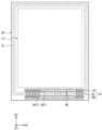
도 1은 본 발명의 일 실시예에 따른 표시 장치의 분해 사시도이다. 도 2는 본 발명의 일 실시예에 따른 표시 패널의 평면도이다. 도 3은 본 발명의 일 실시예에 따른 화소의 등가 회로도이다. 도 4는 본 발명의 일 실시예에 따른 입력 감지층의 평면도이다. 도 5a는 도 4의 I-I'를 따라 절단한 단면도이다. 도 5b는 본 발명의 일 실시예에 따른 표시 장치의 일 구성들의 평면도이다.FIG. 1 is an exploded perspective view of a display device according to an embodiment of the present invention. FIG. 2 is a plan view of a display panel according to an embodiment of the present invention. FIG. 3 is an equivalent circuit diagram of a pixel according to an embodiment of the present invention. FIG. 4 is a plan view of an input sensing layer according to an embodiment of the present invention. FIG. 5A is a cross-sectional view taken along line II' of FIG. 4. FIG. 5B is a plan view of one component of a display device according to an embodiment of the present invention.
도 1을 참조하면, 본 발명에 따른 표시 장치(EA)는 윈도우층(WM) 표시 모듈(DU), 정전기 차단부(LB), 및 커버 케이스(EDC)를 포함한다.Referring to FIG. 1, a display device (EA) according to the present invention includes a window layer (WM), a display module (DU), an electrostatic shielding unit (LB), and a cover case (EDC).
윈도우층(WM)은 단층 또는 다층구조를 가질 수 있다. 예를 들어, 윈도우층(WM)은 접착제로 결합된 복수의 플라스틱 필름의 적층 구조를 가지거나, 접착제로 결합된 유리 기판과 플라스틱 필름의 적층 구조를 가질 수도 있다. 윈도우층(WM)은 광학적으로 투명할 수 있다. 예를 들어, 윈도우층(WM)은 유리 또는 플라스틱을 포함할 수 있다.The window layer (WM) may have a single-layer or multi-layer structure. For example, the window layer (WM) may have a laminated structure of a plurality of plastic films bonded with an adhesive, or may have a laminated structure of a glass substrate and a plastic film bonded with an adhesive. The window layer (WM) may be optically transparent. For example, the window layer (WM) may include glass or plastic.
윈도우층(WM)의 전면은 평면상에서 투과 영역(TA) 및 베젤 영역(BZA)으로 구분될 수 있다. 투과 영역(TA)은 표시 패널(DP)로부터 제공된 광을 투과시키는 영역일 수 있다. 투과 영역(TA)은 표시 패널(DP)의 액티브 영역(AA)과 대응되는 형상을 가질 수 있다. 예를 들어, 투과 영역(TA)은 액티브 영역(AA)의 전 면 또는 적어도 일부와 중첩한다. 따라, 표시 패널(DP)의 액티브 영역(AA)에 표시되는 영상은 투과 영역(TA)을 통해 외부에서 시인될 수 있다.The front surface of the window layer (WM) may be divided into a transparent area (TA) and a bezel area (BZA) on a planar surface. The transparent area (TA) may be an area that transmits light provided from the display panel (DP). The transparent area (TA) may have a shape corresponding to the active area (AA) of the display panel (DP). For example, the transparent area (TA) overlaps the front surface or at least a portion of the active area (AA). Accordingly, an image displayed on the active area (AA) of the display panel (DP) may be viewed from the outside through the transparent area (TA).
베젤 영역(BZA)은 투과 영역(TA)에 비해 상대적으로 광 투과율이 낮은 영역일 수 있다. 베젤 영역(BZA)은 투과 영역(TA)의 형상을 정의한다. 베젤 영역(BZA)은 투과 영역(TA)에 인접하며, 투과 영역(TA)을 에워는 폐 라인 형상을 가질 수 있다.The bezel area (BZA) may be an area with relatively low light transmittance compared to the transmissive area (TA). The bezel area (BZA) defines the shape of the transmissive area (TA). The bezel area (BZA) is adjacent to the transmissive area (TA) and may have a closed line shape surrounding the transmissive area (TA).
베젤 영역(BZA)은 소정의 컬러를 가질 수 있다. 베젤 영역(BZA)은 표시 패널(DP)의 주변 영역(NAA)을 커버하여 주변 영역(NAA)이 외부에서 시인되는 것을 차단할 수 있다. 예를 들어, 표시 패널(DP)에서 생성된 광이 주변 영역(NAA)으로 누설되는 경우, 베젤 영역(BZA)에 의해 누설되는 광을 차단하여 주변 영역(NAA)이 외부에서 시인되는 것을 차단할 수 있다.The bezel area (BZA) can have a predetermined color. The bezel area (BZA) covers the peripheral area (NAA) of the display panel (DP) to block the peripheral area (NAA) from being viewed from the outside. For example, when light generated from the display panel (DP) leaks into the peripheral area (NAA), the light leaked by the bezel area (BZA) can be blocked to block the peripheral area (NAA) from being viewed from the outside.
다만, 이에 한정되는 것은 아니며, 일 실시예에 따른 베젤 영역(BZA)은 생략될 수 있다. 또한, 베젤 영역(BZA)은 투과 영역(TA)을 정의하는 네 개의 변 중 적어도 어느 하나의 변과 인접하는 영역의 베젤 영역(BZA)이 생략될 수 있으며, 베젤 영역(BZA)의 형상은 어느 하나에 한정되지 않는다.However, it is not limited thereto, and the bezel area (BZA) according to one embodiment may be omitted. In addition, the bezel area (BZA) of an area adjacent to at least one of the four sides defining the transmission area (TA) may be omitted, and the shape of the bezel area (BZA) is not limited to any one.
표시 모듈(DU)은 표시 패널(DP) 및 입력 감지층(TU)을 포함한다. 일 실시예에 따른 표시 패널(DP)은 표시 기판(DS) 및 봉지 기판(EN)을 포함한다. 봉지 기판(EN)은 표시 기판(DS) 상에 배치되어 표시 기판(DS)을 커버한다. 입력 감지층(TU)은 봉지 기판(EN) 상에 배치된다.A display module (DU) includes a display panel (DP) and an input sensing layer (TU). The display panel (DP) according to one embodiment includes a display substrate (DS) and an encapsulation substrate (EN). The encapsulation substrate (EN) is disposed on the display substrate (DS) and covers the display substrate (DS). The input sensing layer (TU) is disposed on the encapsulation substrate (EN).
정전기 차단부(LB)는 봉지 기판(EN) 상에 배치된다. 정전기 차단부(LB)는 주변 영역(NAA)과 중첩한다. 정전기 차단부(LB)는 후술할 입력 감지층(TU)의 감지 센서와 이격되어 배치된다.The electrostatic shielding unit (LB) is placed on the encapsulation substrate (EN). The electrostatic shielding unit (LB) overlaps with the peripheral area (NAA). The electrostatic shielding unit (LB) is placed apart from the detection sensor of the input detection layer (TU) described later.
정전기 차단부(LB)는 외부로부터 유입되는 정전기가 통과되는 패스를 제공하여 정전기를 효율적으로 상쇄시킬 수 있다. 본 발명에 따른 표시 장치(EA)의 구성들은 정전기 차단부(LB)로 인해 정전기를 효율적으로 상쇄 시킴으로써 신뢰성이 향상될 수 있다.The electrostatic shielding unit (LB) can effectively cancel out static electricity by providing a path for static electricity flowing in from the outside to pass through. The configurations of the display device (EA) according to the present invention can improve reliability by effectively canceling out static electricity due to the electrostatic shielding unit (LB).
정전기 차단부(LB)는 서로 다른 저항을 갖는 도전층들을 포함할 수 있다. 도 1에는 정전기 차단부(LB)의 형상을 대략적으로 도시하였으며, 이에 관한 설명은 후술한다.The electrostatic shielding unit (LB) may include conductive layers having different resistances. Fig. 1 schematically illustrates the shape of the electrostatic shielding unit (LB), which will be described later.
커버 케이스(EDC)는 윈도우층(WM)과 결합될 수 있다. 커버 케이스(EDC)는 표시 장치(EA)의 배면을 제공한다. 커버 케이스(EDC)는 윈도우층(WM)과 결합되어 내부 공간을 제공한다. 표시 모듈(DU)의 구성들은 내부 공간에 수용될 수 있다. 커버 케이스(EDC)는 소정의 강성을 가진 물질을 포함할 수 있다. 예를 들어, 커버 케이스(EDC)는 글라스, 플라스틱, 메탈로 구성된 복수의 프레임 및/또는 플레이트를 포함할 수 있다. 커버 케이스(EDC)는 내부 공간에 수용된 표시 장치(EA)의 구성들을 외부 충격으로부터 안정적으로 보호할 수 있다.The cover case (EDC) can be combined with the window layer (WM). The cover case (EDC) provides a back surface of the display device (EA). The cover case (EDC) is combined with the window layer (WM) to provide an internal space. Components of the display module (DU) can be accommodated in the internal space. The cover case (EDC) can include a material having a predetermined rigidity. For example, the cover case (EDC) can include a plurality of frames and/or plates made of glass, plastic, and metal. The cover case (EDC) can stably protect the components of the display device (EA) accommodated in the internal space from external impact.
도 2 및 도 3을 참조하면, 일 실시예에 따른 표시 패널(DP)은 액티브 영역(AA) 및 주변 영역(NAA)을 포함한다. 본 실시예에서 주변 영역(NAA)은 액티브 영역(AA)의 에워는 폐 라인 형상을 가질 수 있다. 표시 패널(DP)의 액티브 영역(AA) 및 주변 영역(NAA)은 실질적으로 표시 패널(DP)의 일 구성인 베이스층(BS: 도 5a 참조)에 정의된 영역들 일 수 있다.Referring to FIGS. 2 and 3, a display panel (DP) according to one embodiment includes an active area (AA) and a peripheral area (NAA). In the present embodiment, the peripheral area (NAA) may have a closed line shape surrounding the active area (AA). The active area (AA) and the peripheral area (NAA) of the display panel (DP) may be areas defined in a base layer (BS: see FIG. 5A), which is substantially a component of the display panel (DP).
표시 패널(DP)은 구동회로(GDC), 복수의 신호 라인들(SGL), 복수의 화소들(PX) 및 복수의 패드들(PD)를 포함할 수 있다. 화소들(PX)은 액티브 영역(AA)에 배치된다. 화소들(PX) 각각은 유기발광소자와 그에 연결된 화소 구동회로를 포함한다. 구동회로(GDC), 신호 라인들(SGL), 및 화소 구동회로는 도 5a에 도시된 회로 소자층(CL)에 포함될 수 있다.A display panel (DP) may include a driving circuit (GDC), a plurality of signal lines (SGL), a plurality of pixels (PX), and a plurality of pads (PD). The pixels (PX) are arranged in an active area (AA). Each of the pixels (PX) includes an organic light-emitting element and a pixel driving circuit connected thereto. The driving circuit (GDC), the signal lines (SGL), and the pixel driving circuit may be included in a circuit element layer (CL) illustrated in FIG. 5A.
구동회로(GDC)는 주사 구동회로를 포함할 수 있다. 주사 구동회로는 복수 개의 주사 신호들을 생성하고, 주사 신호들을 후술하는 복수 개의 주사 라인들(GL)에 순차적으로 출력한다. 주사 구동회로는 화소들(PX)의 구동회로에 또 다른 제어 신호를 더 출력할 수 있다. 구동회로(GDC)는 화소들(PX)의 구동회로 공정 내에서 동일한 공정으로 형성될 수 있다.The driving circuit (GDC) may include a scan driving circuit. The scan driving circuit generates a plurality of scan signals and sequentially outputs the scan signals to a plurality of scan lines (GL) to be described later. The scan driving circuit may further output another control signal to the driving circuit of the pixels (PX). The driving circuit (GDC) may be formed in the same process as the driving circuit process of the pixels (PX).
신호 라인들(SGL)은 주사 라인들(GL), 데이터 라인들(DL), 전원 라인(PI), 및 제어신호 라인(CSL)을 포함한다. 주사 라인들(GL)은 화소들(PX) 중 대응하는 화소(PX)에 각각 연결되고, 데이터 라인들(DL)은 화소들(PX) 중 대응하는 화소(PX)에 각각 연결된다. 전원 라인(PI)은 화소들(PX)에 연결된다. 제어신호 라인(CSL)은 주사 구동회로에 제어신호들을 제공할 수 있다.The signal lines (SGL) include scan lines (GL), data lines (DL), a power line (PI), and a control signal line (CSL). The scan lines (GL) are respectively connected to corresponding pixels (PX) among the pixels (PX), and the data lines (DL) are respectively connected to corresponding pixels (PX) among the pixels (PX). The power line (PI) is connected to the pixels (PX). The control signal line (CSL) can provide control signals to the scan driving circuit.
신호 라인들(SGL)은 미도시된 회로기판과 연결될 수 있다. 신호 라인들(SGL)은 회로기판에 실장된 집적 칩 형태의 타이밍 제어회로와 연결될 수 있다. 다만, 이는 예시적으로 설명한 것이고, 본 발명의 일 실시예에서 이러한 집적 칩은 주변 영역(NAA)에 배치되어 신호 라인들(SGL)과 연결될 수도 있다.The signal lines (SGL) may be connected to a circuit board (not shown). The signal lines (SGL) may be connected to a timing control circuit in the form of an integrated chip mounted on the circuit board. However, this is described by way of example, and in one embodiment of the present invention, such an integrated chip may be placed in the peripheral area (NAA) and connected to the signal lines (SGL).
패드들(PD)는 대응되는 신호 라인들(SGL)과 연결되어 미도시된 구동칩들이 실장 된 연성 회로 기판과 연결될 수 있다. 신호 라인들(SGL) 각각은 대응되는 패드들(PD)을 통해 연성 회로 기판으로부터 제공되는 데이터를 송/수신 할 수 있다.The pads (PD) can be connected to corresponding signal lines (SGL) and connected to a flexible circuit board on which unillustrated driving chips are mounted. Each of the signal lines (SGL) can transmit/receive data provided from the flexible circuit board through the corresponding pads (PD).
도 3에는 어느 하나의 주사 라인(GL), 어느 하나의 데이터 라인(DL), 전원 라인(PI), 및 이들에 연결된 화소(PX)를 도시하였다. 화소(PX)의 구성은 이에 제한되지 않고 변형되어 실시될 수 있다.Figure 3 illustrates one scanning line (GL), one data line (DL), a power line (PI), and a pixel (PX) connected to them. The configuration of the pixel (PX) is not limited thereto and may be modified and implemented.
화소(PX)는 유기유기발광소자(OLED)를 구동하기 위한 화소 구동회로로써 제1 트랜지스터(T1, 또는 스위칭 트랜지스터), 제2 트랜지스터(T2, 또는 구동 트랜지스터), 및 커패시터(Cst)를 포함한다. 제2 트랜지스터(T2)는 전원 라인(PI)을 통해 제1 전원 전압(ELVDD)을 제공받고, 유기발광소자(OLED)는 제2 전원 전압(ELVSS)을 제공 받는다. 제2 전원 전압(ELVSS)은 제1 전원 전압(ELVDD) 보다 낮은 전압일 수 있다.A pixel (PX) is a pixel driving circuit for driving an organic light-emitting diode (OLED) and includes a first transistor (T1, or switching transistor), a second transistor (T2, or driving transistor), and a capacitor (Cst). The second transistor (T2) receives a first power voltage (ELVDD) through a power line (PI), and the organic light-emitting diode (OLED) receives a second power voltage (ELVSS). The second power voltage (ELVSS) may be a lower voltage than the first power voltage (ELVDD).
제1 트랜지스터(T1)는 주사 라인(GL)에 인가된 주사 신호에 응답하여 데이터 라인(DL)에 인가된 데이터 신호를 출력한다. 커패시터(Cst)는 제1 트랜지스터(T1)로부터 수신한 데이터 신호에 대응하는 전압을 충전한다. 제2 트랜지스터(T2)는 유기발광소자(OLED)에 연결된다. 제2 트랜지스터(T2)는 커패시터(Cst)에 저장된 전하량에 대응하여 유기발광소자(OLED)에 흐르는 구동전류를 제어한다.A first transistor (T1) outputs a data signal applied to a data line (DL) in response to a scan signal applied to a scan line (GL). A capacitor (Cst) charges a voltage corresponding to a data signal received from the first transistor (T1). A second transistor (T2) is connected to an organic light-emitting device (OLED). The second transistor (T2) controls a driving current flowing to the organic light-emitting device (OLED) in response to the amount of charge stored in the capacitor (Cst).
등가회로는 하나의 일 실시예에 불과하며 이에 제한되지 않는다. 화소(PX)는 복수 개의 트랜지스터들을 더 포함할 수 있고, 더 많은 개수의 커패시터들을 포함할 수 있다. 유기발광소자(OLED)는 전원 라인(PI)과 제2 트랜지스터(T2) 사이에 접속될 수도 있다.The equivalent circuit is only one embodiment and is not limited thereto. The pixel (PX) may further include a plurality of transistors and may include a greater number of capacitors. An organic light emitting diode (OLED) may also be connected between the power line (PI) and the second transistor (T2).
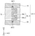
도 4를 참조하면, 본 발명에 따른 입력 감지층(TU)은 표시 패널(DP) 상에 배치된다. 예를 들어, 입력 감지층(TU)은 봉지 기판(EN) 상에 배치된다. 일 실시예에 따른 입력 감지층(TU)은 봉지 기판(EN) 상에 직접 배치될 수 있다. 입력 감지층(TU) 봉지 기판(EN)이 형성된 이후에, 봉지 기판(EN) 상에 연속 공정을 통해 형성될 수 있다. 이에 따라, 입력 감지층(TU)과 봉지 기판(EN) 사이에는 별도의 접착층이 생략될 수 있다.Referring to FIG. 4, the input sensing layer (TU) according to the present invention is disposed on the display panel (DP). For example, the input sensing layer (TU) is disposed on the encapsulation substrate (EN). The input sensing layer (TU) according to one embodiment may be directly disposed on the encapsulation substrate (EN). After the input sensing layer (TU) encapsulation substrate (EN) is formed, it may be formed on the encapsulation substrate (EN) through a continuous process. Accordingly, a separate adhesive layer may be omitted between the input sensing layer (TU) and the encapsulation substrate (EN).
입력 감지층(TU)은 외부에서 인가되는 입력을 감지할 수 있다. 외부에서 인가되는 입력은 다양한 형태로 제공될 수 있다. 예를 들어, 입력은 사용자의 손 등 신체의 일부에 의한 접촉은 물론 표시 장치(EA)와 근접하거나, 소정의 거리로 인접하여 인가되는 외부 입력(예를 들어, 호버링)을 포함할 수 있다. 또한, 외부 입력은 힘, 압력, 광 등 다양한 형태를 가질 수 있으며, 어느 하나의 실시예로 한정되지 않는다.The input detection layer (TU) can detect an input applied from the outside. The input applied from the outside can be provided in various forms. For example, the input can include a contact by a part of the body such as a user's hand, as well as an external input (e.g., hovering) applied in proximity to the display device (EA) or at a predetermined distance. In addition, the external input can have various forms such as force, pressure, and light, and is not limited to any one embodiment.
입력 감지층(TU)은 표시 패널(DP)의 액티브 영역(AA)과 중첩하는 감지 영역(SA) 및 감지 영역(SA)과 인접한 비감지 영역(NSA)을 포함할 수 있다. 감지 영역(SA)은 외부에서 인가되는 입력을 감지하는 영영일 수 있다.The input sensing layer (TU) may include a sensing area (SA) overlapping an active area (AA) of a display panel (DP) and a non-sensing area (NSA) adjacent to the sensing area (SA). The sensing area (SA) may be an area that senses an input applied from the outside.
입력 감지층(TU)은 복수의 도전층들을 포함하는 감지 센서 및 도전층들 사이에 배치된 복수의 감지 절연층들(SIL1, SIL2)을 포함할 수 있다. 감지 절연층들(SIL1, SIL2) 각각은 단층구조를 갖거나 제3 방향(D3)을 따라 적층된 다층구조를 가질 수 있다.The input sensing layer (TU) may include a sensing sensor including a plurality of conductive layers and a plurality of sensing insulating layers (SIL1, SIL2) disposed between the conductive layers. Each of the sensing insulating layers (SIL1, SIL2) may have a single-layer structure or a multi-layer structure laminated along a third direction (D3).
도전층들은 제1 감지전극들(IE1), 제1 감지전극들(IE1)에 연결된 제1 신호라인들(SL1), 제2 감지전극들(IE2), 및 제2 감지전극들(IE2)에 연결된 제2 신호라인들(SL2)을 포함할 수 있다. 또한, 제1 신호라인들(SL1) 및 제2 신호라인들(SL2)에 연결된 감지 패드들(TD)을 포함할 수 있다.The challenge layers may include first sensing electrodes (IE1), first signal lines (SL1) connected to the first sensing electrodes (IE1), second sensing electrodes (IE2), and second signal lines (SL2) connected to the second sensing electrodes (IE2). In addition, the challenge layers may include sensing pads (TD) connected to the first signal lines (SL1) and the second signal lines (SL2).
일 실시예에 따른 제1 감지전극들(IE1) 및 제2 감지전극들(IE2)은 감지 영역(SA)에 중첩하고, 제1 신호라인들(SL1), 제2 신호라인들(SL2), 및 감지 패드들(TD)은 비감지 영역(NSA)에 중첩할 수 있다. 감지 패드들(TD)은 미도시된 구동칩들이 실장 된 연성 회로 기판과 연결될 수 있다. 신호라인들(SL1, SL2) 각각은 대응되는 감지 패드들(TD)을 통해 연성 회로 기판으로부터 제공되는 데이터를 송/수신하여 대응되는 감지 전극들(IE1, IE2)에 제공할 수 있다.According to one embodiment, the first detection electrodes (IE1) and the second detection electrodes (IE2) may overlap a detection area (SA), and the first signal lines (SL1), the second signal lines (SL2), and the detection pads (TD) may overlap a non-detection area (NSA). The detection pads (TD) may be connected to a flexible circuit board on which driving chips (not shown) are mounted. Each of the signal lines (SL1, SL2) may transmit/receive data provided from the flexible circuit board through the corresponding detection pads (TD) and provide the data to the corresponding detection electrodes (IE1, IE2).
제1 감지전극들(IE1)과 제2 감지전극들(IE2)은 서로 교차한다. 제1 감지전극들(IE1)은 제2 방향(D2)을 따라 배열되고, 각각이 제1 방향(D1)을 따라 연장된다. 제1 감지전극들(IE1) 각각은 제1 센서부들(SP1) 및 제1 연결부들(CP1)을 포함한다.The first sensing electrodes (IE1) and the second sensing electrodes (IE2) intersect each other. The first sensing electrodes (IE1) are arranged along the second direction (D2) and each extends along the first direction (D1). Each of the first sensing electrodes (IE1) includes first sensor portions (SP1) and first connecting portions (CP1).
제1 연결부들(CP1)은 제1 방향(D1)을 따라 배열된 서로 다른 제1 센서부들을 연결한다. 일 실시예에 따른 제1 연결부들(CP1)은 감지 절연층을 사이에 두고 제1 센서부들(SP1)과 서로 다른 층 상에 배치될 수 있다.The first connecting portions (CP1) connect different first sensor portions arranged along the first direction (D1). According to one embodiment, the first connecting portions (CP1) may be arranged on a different layer from the first sensor portions (SP1) with a detection insulating layer interposed therebetween.
제2 감지전극들(IE2)은 제1 방향(D1)을 따라 배열되고, 각각이 제2 방향(D2)을 따라 연장된다. 제2 감지전극들(IE2) 각각은 제2 센서부들(SP2) 및 제2 연결부들(CP2)을 포함한다.The second sensing electrodes (IE2) are arranged along the first direction (D1) and each extends along the second direction (D2). Each of the second sensing electrodes (IE2) includes second sensor portions (SP2) and second connecting portions (CP2).
제2 연결부들(CP2)은 제2 방향(D2)으로 배열된 서로 다른 제2 센서부들을 연결한다. 제2 연결부들(CP2) 각각의 일부는 제1 연결부들(CP1) 중 대응되는 제1 연결부와 중첩한다. 일 실시예에 따르면, 제2 연결부들(CP2)은 감지 절연층을 사이에 두고 제1 센서부들(SP1) 서로 다른 층 상에 배치될 수 있다. 또한, 제2 연결부들(CP2)은 제1 감지전극들(IE1) 및 제2 감지전극들(IE2)과 동일층 상에 배치될 수 있다.The second connecting portions (CP2) connect different second sensor portions arranged in the second direction (D2). A portion of each of the second connecting portions (CP2) overlaps a corresponding first connecting portion of the first connecting portions (CP1). According to one embodiment, the second connecting portions (CP2) may be arranged on a different layer from the first sensor portions (SP1) with a sensing insulating layer therebetween. Additionally, the second connecting portions (CP2) may be arranged on the same layer as the first sensing electrodes (IE1) and the second sensing electrodes (IE2).
일 실시예에 따른 제1 감지전극들(IE1) 및 제2 감지전극들(IE2) 각각은 메쉬 라인들을 포함할 수 있다. 따라서, 제1 감지전극들(IE1)에 포함된 제1 센서부들(SP1) 및 제1 연결부들(CP1) 각각은 메쉬 라인들을 포함하고, 제2 감지전극들(IE2)에 포함된 제2 센서부들(SP2) 및 제2 연결부들(CP2) 각각은 메쉬 라인들을 포함한다.According to one embodiment, each of the first detection electrodes (IE1) and the second detection electrodes (IE2) may include mesh lines. Accordingly, each of the first sensor portions (SP1) and the first connecting portions (CP1) included in the first detection electrodes (IE1) include mesh lines, and each of the second sensor portions (SP2) and the second connecting portions (CP2) included in the second detection electrodes (IE2) include mesh lines.
제1 감지전극들(IE1) 및 제2 감지전극들(IE2)이 메쉬 라인들을 가짐으로써 유기발광소자(OLED)의 제2 전극(CE, 도 5a 참조)과의 기생 커패시턴스가 감소될 수 있다.Since the first sensing electrodes (IE1) and the second sensing electrodes (IE2) have mesh lines, the parasitic capacitance with respect to the second electrode (CE, see FIG. 5a) of the organic light-emitting device (OLED) can be reduced.
입력 감지층(TU)은 뮤추얼 캡 방식 또는 셀프 캡 방식으로 외부 입력을 감지할 수 있다. 또는, 입력 감지층(TU)은 제1 구간 동안에 뮤추얼 캡 방식 이나 셀프 캡 방식 중 어느 하나의 방식으로 외부 입력의 좌표를 산출한 후 제2 구간 동안에 다른 하나의 방식으로 외부 입력의 좌표를 재 산출할 수도 있다. 또한, 후술하는 것과 같이, 제1 감지전극들(IE1) 및 제2 감지전극들(IE2) 각각의 메쉬 라인들은 발광영역(PXA, 도 5a 참조)과 비 중첩하므로 입력 감지층(TU)의 감지 센서는 사용자에게 시인되지 않는다.The input sensing layer (TU) can detect an external input in a mutual capping manner or a self-capping manner. Alternatively, the input sensing layer (TU) may calculate the coordinates of the external input in one of the mutual capping manner and the self-capping manner during a first period and then recalculate the coordinates of the external input in the other manner during a second period. In addition, as described below, since the mesh lines of each of the first sensing electrodes (IE1) and the second sensing electrodes (IE2) do not overlap with the light-emitting area (PXA, see FIG. 5a), the detection sensor of the input sensing layer (TU) is not visible to the user.
본 발명에 따르면, 정전기 차단부(LB)는 입력 감지층(TU)의 감지 센서와 이격되어 배치된다. 즉, 정전기 차단부(LB)는 감지 센서에 포함된 제1 감지전극들(IE1), 제1 신호라인들(SL1), 제2 감지전극들(IE2), 제2 신호라인들(SL2), 및 감지 패드들(TD)과 이격된다. 이에 따라, 외부로부터 유입되는 정전기는 정전기 차단부(LB)를 통해 상쇄 됨에 따라, 신뢰성이 향상된 입력 감지층(TU)을 제공할 수 있다.According to the present invention, the electrostatic shielding unit (LB) is arranged to be spaced apart from the detection sensor of the input detection layer (TU). That is, the electrostatic shielding unit (LB) is spaced apart from the first detection electrodes (IE1), the first signal lines (SL1), the second detection electrodes (IE2), the second signal lines (SL2), and the detection pads (TD) included in the detection sensor. Accordingly, static electricity introduced from the outside is canceled out by the electrostatic shielding unit (LB), thereby providing an input detection layer (TU) with improved reliability.
도 5a를 참조하면, 본 발명에 따른 표시 모듈(DU)은 표시 패널(DP) 및 입력 감지층(TU)을 포함한다. 일 실시예에 따른 표시 패널(DP)은 표시 기판(DS), 실링부(SL) 및 봉지 기판(EN)을 포함한다. 표시 기판(DS)은 베이스층(BS), 회로 소자층(CL) 및 표시 소자층(PL)을 포함한다.Referring to FIG. 5a, a display module (DU) according to the present invention includes a display panel (DP) and an input sensing layer (TU). The display panel (DP) according to one embodiment includes a display substrate (DS), a sealing portion (SL), and an encapsulation substrate (EN). The display substrate (DS) includes a base layer (BS), a circuit element layer (CL), and a display element layer (PL).
베이스층(BS)은 회로 소자층(CL) 및 표시 소자층(PL)의 구성들이 형성되는 기저층일 수 있다. 베이스층(BS)은 유리 기판, 금속 기판, 또는 유/무기 복합재료 기판 등을 포함할 수 있다. 그밖에 베이스층(BS)은 합성수지 필름을 포함할 수 있다. 합성수지층은 열 경화성 수지를 포함할 수 있다.The base layer (BS) may be a base layer on which the circuit element layer (CL) and the display element layer (PL) are formed. The base layer (BS) may include a glass substrate, a metal substrate, or an organic/inorganic composite material substrate. In addition, the base layer (BS) may include a synthetic resin film. The synthetic resin layer may include a thermosetting resin.
도시되지 않았으나, 베이스층(BS) 상에는 무기층인 배리어층 및/또는 버퍼층을 포함할 수 있다. 알루미늄 옥사이드(AlOX), 티타늄 옥사이드(TiOX), 실리콘 옥사이드(SiOX), 실리콘옥시나이트라이드(SiNXOY), 지르코늄옥사이드(ZnOX), 및 하프늄 옥사이드(HfOX) 중 적어도 하나를 포함할 수 있다. 무기층은 다층으로 형성될 수 있다. 다층의 무기층들은 배리어층 및/또는 버퍼층을 구성할 수 있다. 배리어층과 버퍼층은 선택적으로 배치될 수 있다.Although not shown, the base layer (BS) may include an inorganic layer, which is a barrier layer and/or a buffer layer. It may include at least one of aluminum oxide (AlOX ), titanium oxide (TiOX ), silicon oxide (SiOX ), silicon oxynitride (SiNX OY ), zirconium oxide (ZnOX ), and hafnium oxide (HfOX ). The inorganic layer may be formed as a multilayer. The multilayer inorganic layers may constitute a barrier layer and/or a buffer layer. The barrier layer and the buffer layer may be selectively arranged.
배리어층은 외부로부터 이물질이 유입되는 것을 방지한다. 배리어층은 실리콘 옥사이드층 및 실리콘 나이트라이드층을 포함할 수 있다. 실리콘 옥사이드층과 실리콘 나이트라이드층은 교번하게 적층될 수 있다.The barrier layer prevents foreign substances from entering from the outside. The barrier layer may include a silicon oxide layer and a silicon nitride layer. The silicon oxide layer and the silicon nitride layer may be alternately laminated.
버퍼층은 버퍼층 상/하에 배치되는 구성들의 결합력을 향상시킨다. 버퍼층은 실리콘 옥사이드층 및 실리콘 나이트라이드층을 포함할 수 있다. 실리콘 옥사이드층과 실리콘 나이트라이드층은 교번하게 적층될 수 있다.The buffer layer improves the bonding strength of the components disposed above and below the buffer layer. The buffer layer may include a silicon oxide layer and a silicon nitride layer. The silicon oxide layer and the silicon nitride layer may be alternately laminated.
회로 소자층(CL)은 트랜지스터(T2) 및 복수의 절연층들(IL1, IL2, IL3)을 포함한다. 도 5a는 도 3에 설명한 트랜지스터들(T1, T2) 중 구동 트랜지스터에 해당하는 제2 트랜지스터(T2) 만을 도시하였다.The circuit element layer (CL) includes a transistor (T2) and a plurality of insulating layers (IL1, IL2, IL3). Fig. 5a illustrates only the second transistor (T2), which corresponds to a driving transistor among the transistors (T1, T2) described in Fig. 3.
트랜지스터(T2)는 반도체 패턴(SP), 제어 전극(GE), 입력 전극(SE), 및 출력 전극(DE)을 포함한다. 반도체 패턴(SP)은 베이스층(BS) 상에 배치된다. 반도체 패턴(SP)은 결정질 반도체 물질 또는 비정질 실리콘을 포함할 수 있다.The transistor (T2) includes a semiconductor pattern (SP), a control electrode (GE), an input electrode (SE), and an output electrode (DE). The semiconductor pattern (SP) is disposed on a base layer (BS). The semiconductor pattern (SP) may include a crystalline semiconductor material or amorphous silicon.
제1 절연층(IL1)은 베이스층(BS) 상에 배치된다. 제1 절연층(IL1)은 각각의 화소들(PX)에 공통적으로 중첩하며, 화소들(PX) 각각의 반도체 패턴(SP)을 커버한다. 제1 절연층(IL1)은 무기층 및/또는 유기층일 수 있으며, 단층 또는 다층 구조를 가질 수 있다. 제1 절연층(IL1)은 알루미늄 옥사이드(AlOX), 티타늄 옥사이드(TiOX), 실리콘 옥사이드(SiOX), 실리콘옥시나이트라이드(SiNXOY), 지르코늄옥사이드(ZnOX), 및 하프늄 옥사이드(HfOX) 중 적어도 하나를 포함할 수 있다.A first insulating layer (IL1) is disposed on the base layer (BS). The first insulating layer (IL1) commonly overlaps each of the pixels (PX) and covers the semiconductor pattern (SP) of each of the pixels (PX). The first insulating layer (IL1) may be an inorganic layer and/or an organic layer, and may have a single-layer or multi-layer structure. The first insulating layer (IL1) may include at least one of aluminum oxide (AlOX ), titanium oxide (TiOX ), silicon oxide (SiOX ), silicon oxynitride (SiNX OY ), zirconium oxide (ZnOX ), and hafnium oxide (HfOX ).
제어 전극(GE)은 제1 절연층(IL1) 상에 배치된다. 제어 전극(GE)은 반도체 패턴(SP)과 중첩한다.The control electrode (GE) is disposed on the first insulating layer (IL1). The control electrode (GE) overlaps the semiconductor pattern (SP).
제2 절연층(IL2)은 제1 절연층(IL1) 상에 배치된다. 제2 절연층(IL2)은 제1 절연층(IL1) 및 제어 전극(GE)를 커버한다. 제2 절연층(IL2)은 각각의 화소들(PX)에 공통으로 중첩한다. 제2 절연층(20)은 무기층 및/또는 유기층일 수 있으며, 단층 또는 다층 구조를 가질 수 있다. 제2 절연층(20)은 알루미늄 옥사이드(AlOX), 티타늄 옥사이드(TiOX), 실리콘 옥사이드(SiOX), 실리콘옥시나이트라이드(SiNXOY), 지르코늄옥사이드(ZnOX), 및 하프늄 옥사이드(HfOX) 중 적어도 하나를 포함할 수 있다.The second insulating layer (IL2) is disposed on the first insulating layer (IL1). The second insulating layer (IL2) covers the first insulating layer (IL1) and the control electrode (GE). The second insulating layer (IL2) commonly overlaps each of the pixels (PX). The second insulating layer (20) may be an inorganic layer and/or an organic layer, and may have a single-layer or multi-layer structure. The second insulating layer (20) may include at least one of aluminum oxide (AlOX ), titanium oxide (TiOX ), silicon oxide (SiOX ), silicon oxynitride (SiNX OY ), zirconium oxide (ZnOX ), and hafnium oxide (HfOX ).
입력 전극(SE) 및 출력 전극(DE)은 제2 절연층(IL2) 상에 배치된다. 입력 전극(SE) 및 출력 전극(DE) 각각은 절연층들(IL1, IL2)에 정의된 복수의 컨택홀들을 통해 반도체 패턴(SP)과 접속한다.The input electrode (SE) and the output electrode (DE) are arranged on the second insulating layer (IL2). Each of the input electrode (SE) and the output electrode (DE) is connected to the semiconductor pattern (SP) through a plurality of contact holes defined in the insulating layers (IL1, IL2).
제3 절연층(IL3)은 제2 절연층(IL2) 상에 배치된다. 제3 절연층(IL3)은 제2 트랜지스터(T2)를 커버한다. 제3 절연층(IL3)은 무기층 및/또는 유기층일 수 있으며, 단층 또는 다층 구조를 가질 수 있다. 제3 절연층(IL3)은 알루미늄 옥사이드(AlOX), 티타늄 옥사이드(TiOX), 실리콘 옥사이드(SiOX), 실리콘옥시나이트라이드(SiNXOY), 지르코늄옥사이드(ZnOX), 및 하프늄 옥사이드(HfOX) 중 적어도 하나를 포함할 수 있다.A third insulating layer (IL3) is disposed on the second insulating layer (IL2). The third insulating layer (IL3) covers the second transistor (T2). The third insulating layer (IL3) may be an inorganic layer and/or an organic layer, and may have a single-layer or multi-layer structure. The third insulating layer (IL3) may include at least one of aluminum oxide (AlOX ), titanium oxide (TiOX ), silicon oxide (SiOX ), silicon oxynitride (SiNX OY ), zirconium oxide (ZnOX ), and hafnium oxide (HfOX ).
도 5a는 제2 트랜지스터(T2)의 구조를 탑 게이트 트랜지스터(top gate transistor) 구조로 설명하였으나, 이에 한정되는 것이 아니고, 바텀 게이트 트랜지스터(bottom gate transistor) 등 다른 구조의 트랜지스터가 구비될 수 있다.FIG. 5a illustrates the structure of the second transistor (T2) as a top gate transistor structure, but is not limited thereto, and a transistor of a different structure, such as a bottom gate transistor, may be provided.
표시 소자층(PL)은 유기발광소자(OLED) 및 화소 정의막(PDL)을 포함한다. 유기발광소자(OLED)는 제3 절연층(IL3) 상에 배치된다. 유기발광소자(OLED)는 제1 전극(AE), 제1 전하 제어층(HCL), 발광층(EML), 제2 전하 제어층(ECL), 및 제2 전극(CE)을 포함한다. 본 실시예에서, 제1 전극(AE), 제1 전하 제어층(HCL), 발광층(EML), 제2 전하 제어층(ECL), 제2 전극(CE) 각각은 애노드 전극(AE), 정공 제어층(HCL), 발광층(EML), 전자 제어층(ECL), 및 캐소드 전극(CE)에 대응될 수 있다.The display element layer (PL) includes an organic light emitting diode (OLED) and a pixel defining layer (PDL). The organic light emitting diode (OLED) is disposed on a third insulating layer (IL3). The organic light emitting diode (OLED) includes a first electrode (AE), a first charge control layer (HCL), an emission layer (EML), a second charge control layer (ECL), and a second electrode (CE). In the present embodiment, each of the first electrode (AE), the first charge control layer (HCL), the emission layer (EML), the second charge control layer (ECL), and the second electrode (CE) may correspond to an anode electrode (AE), a hole control layer (HCL), an emission layer (EML), an electron control layer (ECL), and a cathode electrode (CE).
제1 전극(AE)은 제3 절연층(IL3) 상에 배치된다. 제1 전극(AE)은 제3 절연층(IL3)을 관통하는 컨택홀을 통해서 출력 전극(DE)에 연결된다.The first electrode (AE) is placed on the third insulating layer (IL3). The first electrode (AE) is connected to the output electrode (DE) through a contact hole penetrating the third insulating layer (IL3).
화소 정의막(PDL)은 제3 절연층(IL3) 상에 배치된다. 화소 정의막(PDL)의 개구부(OP)는 제1 전극(AE)의 적어도 일부분을 노출시킨다. 화소 정의막(PDL)의 개구부(OP)는 화소(PX)의 발광영역(PXA)을 정의할 수 있다. 베이스층(BS) 상에서 화소들(PX)이 배치된 영역은 액티브 영역(AA)으로 정의될 수 있고, 액티브 영역(AA)은 발광 영역(PXA)과 발광 영역(PXA)에 인접한 비발광 영역(NPXA)을 포함할 수 있다. 비발광 영역(NPXA)은 발광 영역(PXA)을 에워 싸을 수 있다.A pixel defining layer (PDL) is disposed on a third insulating layer (IL3). An opening (OP) of the pixel defining layer (PDL) exposes at least a portion of a first electrode (AE). The opening (OP) of the pixel defining layer (PDL) can define an emission area (PXA) of a pixel (PX). An area on a base layer (BS) where pixels (PX) are disposed can be defined as an active area (AA), and the active area (AA) can include an emission area (PXA) and a non-emission area (NPXA) adjacent to the emission area (PXA). The non-emission area (NPXA) can surround the emission area (PXA).
제1 전하 제어층(HCL)은 발광 영역(PXA)과 비발광 영역(NPXA)에 공통으로 배치될 수 있다. 제1 전하 제어층(HCL)과 같은 공통층은 복수 개의 화소들(PX)에 공통으로 형성될 수 있다. 제1 전하 제어층(HCL)은 정공의 이동을 제어할 수 있다. 예를 들어, 제1 전하 제어층(HCL)은 정공 수송층 및 정공 주입층을 포함할 수 있다.The first charge control layer (HCL) can be commonly arranged in the light-emitting area (PXA) and the non-light-emitting area (NPXA). A common layer such as the first charge control layer (HCL) can be commonly formed in a plurality of pixels (PX). The first charge control layer (HCL) can control the movement of holes. For example, the first charge control layer (HCL) can include a hole transport layer and a hole injection layer.
발광층(EML)은 제1 전하 제어층(HCL) 상에 배치된다. 발광층(EML)은 개구부(OP)에 대응하는 영역에만 배치될 수 있다. 발광층(EML)은 복수 개의 화소들(PX) 각각에 분리되어 형성될 수 있다.The emission layer (EML) is disposed on the first charge control layer (HCL). The emission layer (EML) may be disposed only in an area corresponding to the aperture (OP). The emission layer (EML) may be formed separately for each of a plurality of pixels (PX).
제2 전하 제어층(ECL)은 발광층(EML) 상에 배치된다. 제2 전하 제어층(ECL)은 전자의 이동을 제어할 수 있다. 예를 들어, 제2 전하 제어층(ECL)은 전자 수송층 및 전자 주입층을 포함할 수 있다.A second charge control layer (ECL) is disposed on the emitting layer (EML). The second charge control layer (ECL) can control the movement of electrons. For example, the second charge control layer (ECL) can include an electron transport layer and an electron injection layer.
제2 전극(CE)은 제2 전하 제어층(ECL) 상에 배치된다. 제2 전극(CE)은 공통 전극 또는 음극일 수 있다. 제2 전극(CE)은 발광 영역(PXA)과 비발광 영역(NPXA)에 공통으로 배치될 수 있다. 제2 전극(CE)과 같은 공통층은 복수 개의 화소들(PX)에 공통으로 형성될 수 있다.The second electrode (CE) is disposed on the second charge control layer (ECL). The second electrode (CE) may be a common electrode or a cathode. The second electrode (CE) may be disposed commonly in the light-emitting area (PXA) and the non-light-emitting area (NPXA). A common layer such as the second electrode (CE) may be formed commonly in a plurality of pixels (PX).
유기발광소자(OLED)가 전면 발광형일 경우, 제1 전극(AE)은 반사형 전극이고, 제2 전극(CE)은 투과형 전극 또는 반투과형 전극일 수 있다. 유기발광소자(OLED)가 배면 발광형일 경우, 제1 전극(AE)은 투과형 전극 또는 반투과형 전극이고, 제2 전극(CE)은 반사형 전극일 수 있다.When the organic light-emitting device (OLED) is a top-emitting type, the first electrode (AE) may be a reflective electrode, and the second electrode (CE) may be a transmissive electrode or a semi-transmissive electrode. When the organic light-emitting device (OLED) is a bottom-emitting type, the first electrode (AE) may be a transmissive electrode or a semi-transmissive electrode, and the second electrode (CE) may be a reflective electrode.
표시 기판(DS) 상에 봉지 기판(EN)이 배치된다. 봉지 기판(EN)는 표시 영역(DA)을 커버할 수 있다. 봉지 기판(EN)는 유리나 플라스틱으로 이루어진 기판으로 제공될 수 있다. 다만, 이에 제한되는 것은 아니고, 봉지 기판(EN)은 유기막 또는 무기막으로 이루어질 수 있다.An encapsulation substrate (EN) is placed on a display substrate (DS). The encapsulation substrate (EN) can cover a display area (DA). The encapsulation substrate (EN) can be provided as a substrate made of glass or plastic. However, the present invention is not limited thereto, and the encapsulation substrate (EN) can be made of an organic film or an inorganic film.
표시 기판(DS) 및 봉지 기판(EN)는 실링부(SL)에 의해 접합된다. 실링부(SL)는 봉지 기판(EN)의 제1 방향(D1) 및 제2 방향(D2)으로 정의된 엣지를 따라 배치된다. 일 실시예에서 엣지는 표시 기판(DS)의 주변 영역(NAA)과 평면상에서 중첩하는 봉지 기판(EN)의 외곽을 의미한다. 따라서, 실링부(SL)는 표시 기판(DS)의 주변 영역(NAA)과 평면상에서 중첩한다. 실링부(SL)는 프릿(frit)을 포함할 수 있다. 실링부(SL)는 봉지 기판(EN)과 함께 유기발광소자(OLED)를 외부의 수분 및 공기 등에 노출되는 것을 차단할 수 있다.The display substrate (DS) and the encapsulation substrate (EN) are joined by a sealing portion (SL). The sealing portion (SL) is arranged along an edge of the encapsulation substrate (EN) defined in a first direction (D1) and a second direction (D2). In one embodiment, the edge means an outer edge of the encapsulation substrate (EN) that overlaps a peripheral area (NAA) of the display substrate (DS) in a plane. Accordingly, the sealing portion (SL) overlaps a peripheral area (NAA) of the display substrate (DS) in a plane. The sealing portion (SL) may include a frit. The sealing portion (SL) together with the encapsulation substrate (EN) may block the organic light-emitting device (OLED) from being exposed to external moisture and air.
실링부(SL)는 표시 기판(DS) 및 봉지 기판(EN)의 사이에서 소정의 두께를 갖는다. 따라서, 표시 기판(DS), 봉지 기판(EN) 및 실링부(SL)에 의해 정의되는 내부공간(AR)을 형성한다. 내부공간(AR)은 진공으로 형성될 수 있다. 다만, 이에 제한되는 것은 아니고, 내부공간(AR)은 질소(N2)로 채워지거나, 절연 물질로 채워질 수 있다.The sealing portion (SL) has a predetermined thickness between the display substrate (DS) and the encapsulation substrate (EN). Accordingly, an internal space (AR) defined by the display substrate (DS), the encapsulation substrate (EN), and the sealing portion (SL) is formed. The internal space (AR) may be formed in a vacuum. However, the present invention is not limited thereto, and the internal space (AR) may be filled with nitrogen (N2 ) or an insulating material.
도 5a에는 실링부(SL)가 유기발광소자(OLED)의 제2 전극(CE) 상에 배치되는 것을 도시하였으나, 이에 한정되는 것은 아니다. 예를 들어, 제2 전극(CE)을 커버하는 무기 및/또는 유기를 포함하는 절연층이 더 포함될 수 있으며, 실링부(SL)는 제2 전극(CE)를 커버하는 절연층 상에 배치될 수 있다. 또한, 일 실시예로 주변 영역(NAA)에 대응되는 영역에서 화소 정의막(PDL) 및 절연층들(IL1, IL2, IL3)이 생략될 수 있으며, 실링부(SL)는 베이스층(BS) 상에 직접 배치될 수 있다.Although FIG. 5A illustrates that the sealing portion (SL) is disposed on the second electrode (CE) of the organic light-emitting diode (OLED), it is not limited thereto. For example, an insulating layer including an inorganic and/or organic material covering the second electrode (CE) may be further included, and the sealing portion (SL) may be disposed on the insulating layer covering the second electrode (CE). In addition, as an embodiment, the pixel defining film (PDL) and the insulating layers (IL1, IL2, IL3) may be omitted in an area corresponding to the peripheral area (NAA), and the sealing portion (SL) may be disposed directly on the base layer (BS).
입력 감지층(TU)은 봉지 기판(EN) 상에 배치된다. 일 실시예에 따른 입력 감지층(TU)은 제1 도전층(SE1), 제2 도전층(SE2), 제1 감지 절연층(SIL1) 및 제2 감지 절연층(SIL2)을 포함한다.The input sensing layer (TU) is disposed on the encapsulation substrate (EN). According to one embodiment, the input sensing layer (TU) includes a first conductive layer (SE1), a second conductive layer (SE2), a first sensing insulating layer (SIL1), and a second sensing insulating layer (SIL2).
제1 도전층(SE1)은 봉지 기판(EN) 상에 배치된다. 일 실시예에 따른 제1 도전층(SE1)은 봉지 기판(EN) 상에 직접 배치될 수 있다. 제1 도전층(SE1)은 상술한 제1 감지전극들(IE1) 및 제2 감지전극들(IE2) 중 적어도 어느 하나를 포함한 층일 수 있다. 제1 도전층(SE1)은 메쉬 라인을 포함한다. 따라서, 제1 도전층(SE1)은 발광 영역(PXA)과 비중첩한다.The first conductive layer (SE1) is disposed on the encapsulation substrate (EN). The first conductive layer (SE1) according to one embodiment may be disposed directly on the encapsulation substrate (EN). The first conductive layer (SE1) may be a layer including at least one of the first sensing electrodes (IE1) and the second sensing electrodes (IE2) described above. The first conductive layer (SE1) includes a mesh line. Therefore, the first conductive layer (SE1) does not overlap with the light-emitting area (PXA).
제1 도전층(SE1)은 도전 물질을 포함한다. 예를 들어, 몰리브덴(Mo), 몰리 옥사이드(MoOx), 몰리브덴 니오븀(MoNb), APC(Ag-Pd-Cu)합금, 니켈(Ni), 구리(Cu) 중 어느 하나 또는 이들의 합금 중 어느 하나를 포함할 수 있다.The first conductive layer (SE1) includes a conductive material. For example, it may include one of molybdenum (Mo), molybdenum oxide (MoOx), molybdenum niobium (MoNb), APC (Ag-Pd-Cu) alloy, nickel (Ni), copper (Cu), or an alloy thereof.
제1 감지 절연층(SIL1)은 봉지 기판(EN) 상에 배치된다. 제1 감지 절연층(SIL1)은 제1 도전층(SE1)을 커버한다. 제1 감지 절연층(SIL1)은 무기층 및/또는 유기층일 수 있으며, 단층 또는 다층 구조를 가질 수 있다. 제1 감지 절연층(SIL1)은 알루미늄 옥사이드(AlOX), 티타늄 옥사이드(TiOX), 실리콘 옥사이드(SiOX), 실리콘옥시나이트라이드(SiNXOY), 지르코늄옥사이드(ZnOX), 및 하프늄 옥사이드(HfOX) 중 적어도 하나를 포함할 수 있다.A first sensing insulating layer (SIL1) is disposed on a sealing substrate (EN). The first sensing insulating layer (SIL1) covers the first conductive layer (SE1). The first sensing insulating layer (SIL1) may be an inorganic layer and/or an organic layer, and may have a single-layer or multi-layer structure. The first sensing insulating layer (SIL1) may include at least one of aluminum oxide (AlOX ), titanium oxide (TiOX ), silicon oxide (SiOX ), silicon oxynitride (SiNX OY ), zirconium oxide (ZnOX ), and hafnium oxide (HfOX ).
제2 도전층(SE2)은 제1 감지 절연층(SIL1) 상에 배치된다. 제2 도전층(SE2)은 상술한 제1 감지전극들(IE1) 및 제2 감지전극들(IE2) 중 적어도 어느 하나를 포함한 층일 수 있다. 제2 도전층(SE2)은 메쉬 라인을 포함한다. 따라서, 제2 도전층(SE2)은 발광 영역(PXA)과 비중첩한다.The second conductive layer (SE2) is disposed on the first sensing insulating layer (SIL1). The second conductive layer (SE2) may be a layer including at least one of the first sensing electrodes (IE1) and the second sensing electrodes (IE2) described above. The second conductive layer (SE2) includes a mesh line. Therefore, the second conductive layer (SE2) does not overlap with the light-emitting area (PXA).
제2 도전층(SE2)은 제1 도전층(SE1)과 제1 감지 절연층(SIL1)을 사이에 두고 서로 다른 층 상에 배치된다. 제2 도전층(SE2)은 제1 도전층(SE1)과 평면상에서 중첩할 수 있으며, 서로 이격될 수 있다.The second conductive layer (SE2) is disposed on a different layer from the first conductive layer (SE1) with the first sensing insulating layer (SIL1) interposed therebetween. The second conductive layer (SE2) may overlap the first conductive layer (SE1) in a plane and may be spaced apart from each other.
제2 도전층(SE2)은 투명한 도전 물질을 포함한다. 예를 들어, 인듐 주석 산화물(Indium Tin Oxide), 인듐 아연 산화물(Indium Zinc Oxide), 인듐 갈륨 아연 산화물(Indium Gallium Zinc Oxide), 플루오르 아연 산화물(Fluorine Zinc Oxide), 갈륨 아연 산화물(Gallium Zinc Oxide), 또는 주석 산화물(Tin Oxide) 중 적어도 어느 하나를 포함할 수 있다. 그 밖에 투명 도전층은 전도성 고분자, 금속 나노 와이어, 그라핀 등을 포함할 수 있다.The second conductive layer (SE2) includes a transparent conductive material. For example, it may include at least one of Indium Tin Oxide, Indium Zinc Oxide, Indium Gallium Zinc Oxide, Fluorine Zinc Oxide, Gallium Zinc Oxide, or Tin Oxide. In addition, the transparent conductive layer may include a conductive polymer, a metal nanowire, graphene, or the like.
제2 감지 절연층(SIL2)은 제1 감지 절연층(SIL1) 상에 배치된다. 제2 감지 절연층(SIL2)은 제2 도전층(SE2)을 커버한다. 제2 감지 절연층(SIL2)은 무기층 및/또는 유기층일 수 있으며, 단층 또는 다층 구조를 가질 수 있다. 제2 감지 절연층(SIL2)은 알루미늄 옥사이드(AlOX), 티타늄 옥사이드(TiOX), 실리콘 옥사이드(SiOX), 실리콘옥시나이트라이드(SiNXOY), 지르코늄옥사이드(ZnOX), 및 하프늄 옥사이드(HfOX) 중 적어도 하나를 포함할 수 있다.The second sensing insulating layer (SIL2) is disposed on the first sensing insulating layer (SIL1). The second sensing insulating layer (SIL2) covers the second conductive layer (SE2). The second sensing insulating layer (SIL2) may be an inorganic layer and/or an organic layer, and may have a single-layer or multi-layer structure. The second sensing insulating layer (SIL2) may include at least one of aluminum oxide (AlOX ), titanium oxide (TiOX ), silicon oxide (SiOX ), silicon oxynitride (SiNX OY ), zirconium oxide (ZnOX ), and hafnium oxide (HfOX ).
일 실시예에 따른 입력 감지층(TU)의 감지 절연층들(SIL1, SIL2)은 봉지 기판(EN)의 전 면을 커버할 수 있다. 따라서, 감지 절연층들(SIL1, SIL2)은 액티브 영역(AA) 및 주변 영역(NAA)을 커버할 수 있다. 다만, 도 1에는 설명의 편의를 위하여 주변 영역(NAA)에 배치된 감지 절연층들(SIL1, SIL2)을 생략하고, 입력 감지층(TU)을 별도의 층으로 도시하였다.The sensing insulating layers (SIL1, SIL2) of the input sensing layer (TU) according to one embodiment can cover the entire surface of the encapsulation substrate (EN). Accordingly, the sensing insulating layers (SIL1, SIL2) can cover the active area (AA) and the peripheral area (NAA). However, in Fig. 1, for convenience of explanation, the sensing insulating layers (SIL1, SIL2) arranged in the peripheral area (NAA) are omitted, and the input sensing layer (TU) is illustrated as a separate layer.
본 발명에 따른 정전기 차단부(LB)는 제1 차단 패턴(IB), 제2 차단 패턴(OB), 및 연결 패턴(BL)을 포함한다.The electrostatic shielding unit (LB) according to the present invention includes a first blocking pattern (IB), a second blocking pattern (OB), and a connection pattern (BL).
제1 차단 패턴(IB) 및 제2 차단 패턴(OB)은 봉지 기판(EN) 상에 배치된다. 일 실시예에 따른 제1 차단 패턴(IB) 및 제2 차단 패턴(OB)은 봉지 기판(EN) 상에 직접 배치될 수 있다. 제1 차단 패턴(IB) 및 제2 차단 패턴(OB)은 주변 영역(NAA)과 중첩한다. 제1 차단 패턴(IB) 및 제2 차단 패턴(OB)은 동일층 상에서 서로 이격되어 배치된다. 따라서, 제1 차단 패턴(IB) 및 제2 차단 패턴(OB)은 소정의 이격 공간(BG)을 갖는다. 제1 차단 패턴(IB)은 제2 차단 패턴(OB)에 비해 상대적으로 액티브 영역(AA)에 인접하여 배치된다.A first blocking pattern (IB) and a second blocking pattern (OB) are arranged on an encapsulation substrate (EN). According to one embodiment, the first blocking pattern (IB) and the second blocking pattern (OB) may be arranged directly on the encapsulation substrate (EN). The first blocking pattern (IB) and the second blocking pattern (OB) overlap with a peripheral area (NAA). The first blocking pattern (IB) and the second blocking pattern (OB) are arranged to be spaced apart from each other on the same layer. Therefore, the first blocking pattern (IB) and the second blocking pattern (OB) have a predetermined spacing space (BG). The first blocking pattern (IB) is arranged relatively adjacent to the active area (AA) compared to the second blocking pattern (OB).
일 실시예에 따른 제1 차단 패턴(IB) 및 제2 차단 패턴(OB)은 제1 도전층(SE1)과 동일층 상에 배치된다. 제1 차단 패턴(IB) 및 제2 차단 패턴(OB)은 입력 감지층(TU)의 제1 감지 절연층(SIL1)에 의해 커버된다.According to one embodiment, the first blocking pattern (IB) and the second blocking pattern (OB) are arranged on the same layer as the first conductive layer (SE1). The first blocking pattern (IB) and the second blocking pattern (OB) are covered by the first sensing insulating layer (SIL1) of the input sensing layer (TU).
제1 차단 패턴(IB) 및 제2 차단 패턴(OB) 중 적어도 어느 하나는 제1 도전층(SE1)과 동일한 도전 물질을 포함한다. 예를 들어, 몰리브덴(Mo), 몰리 옥사이드(MoOx), 몰리브덴 니오븀(MoNb), APC(Ag-Pd-Cu)합금, 니켈(Ni), 구리(Cu) 중 어느 하나 또는 이들의 합금 중 어느 하나를 포함할 수 있다.At least one of the first blocking pattern (IB) and the second blocking pattern (OB) includes the same conductive material as the first conductive layer (SE1). For example, it may include one of molybdenum (Mo), molybdenum oxide (MoOx), molybdenum niobium (MoNb), APC (Ag-Pd-Cu) alloy, nickel (Ni), copper (Cu), or one of their alloys.
연결 패턴(BL)은 제1 감지 절연층(SIL1) 상에 배치된다. 연결 패턴(BL)은 주변 영역(NAA)과 중첩한다. 연결 패턴(BL)은 제1 감지 절연층(SIL1)에 정의된 컨택홀들(SNT1, SNT2)에 의해 제1 차단 패턴(IB) 및 제2 차단 패턴(OB)과 연결된다.The connection pattern (BL) is arranged on the first sensing insulating layer (SIL1). The connection pattern (BL) overlaps the peripheral area (NAA). The connection pattern (BL) is connected to the first blocking pattern (IB) and the second blocking pattern (OB) by contact holes (SNT1, SNT2) defined in the first sensing insulating layer (SIL1).
연결 패턴(BL)은 제2 도전층(SE2)과 동일한 도전 물질, 즉 투명한 도전 물질을 포함할 수 있다. 예를 들어, 연결 패턴(BL)은 인듐 주석 산화물(Indium Tin Oxide), 인듐 아연 산화물(Indium Zinc Oxide), 인듐 갈륨 아연 산화물(Indium Gallium Zinc Oxide), 플루오르 아연 산화물(Fluorine Zinc Oxide), 갈륨 아연 산화물(Gallium Zinc Oxide), 또는 주석 산화물(Tin Oxide) 중 적어도 어느 하나를 포함할 수 있다. 그 밖에 투명 도전층은 전도성 고분자, 금속 나노 와이어, 그라핀 등을 포함할 수 있다.The connection pattern (BL) may include the same conductive material as the second conductive layer (SE2), i.e., a transparent conductive material. For example, the connection pattern (BL) may include at least one of Indium Tin Oxide, Indium Zinc Oxide, Indium Gallium Zinc Oxide, Fluorine Zinc Oxide, Gallium Zinc Oxide, or Tin Oxide. In addition, the transparent conductive layer may include a conductive polymer, a metal nanowire, graphene, or the like.
본 발명에 따른 실링부(SL)의 적어도 일부는 제1 차단 패턴(IB) 및 제2 차단 패턴(OB) 사이에 형성된 이격 공간(BG)과 평면상에서 중첩할 수 있다. 실링부(SL)는 단면상에서 연결 패턴(BL)과 중첩한다.At least a portion of the sealing portion (SL) according to the present invention can overlap in a plane with a gap space (BG) formed between the first blocking pattern (IB) and the second blocking pattern (OB). The sealing portion (SL) overlaps with the connecting pattern (BL) in a cross-section.
도 5b를 참조하면, 표시 패널(DP)의 표시 기판(DS) 및 봉지 기판(EN) 사이에 배치된 실링부(SL)를 음영으로 표시 하였다. 또한, 표시 패널(DP) 상에 배치된 입력 감지층(TU)을 점선으로 표시하였다.Referring to Fig. 5b, a sealing portion (SL) disposed between a display substrate (DS) and an encapsulation substrate (EN) of a display panel (DP) is indicated by a shade. In addition, an input sensing layer (TU) disposed on the display panel (DP) is indicated by a dotted line.
일 실시예에 따른 실링부(SL)는 봉지 기판(EN)의 엣지를 따라 연장되어 표시 기판(DS) 및 봉지 기판(EN)을 접합시킨다. 일 실시예에 따르면, 실링부(SL)의 일 측은 평면상에서 제1 차단 패턴(IB) 및 제2 차단 패턴(OB) 사이에 형성된 이격 공간(BG)과 중첩한다.According to one embodiment, a sealing portion (SL) extends along an edge of an encapsulation substrate (EN) to join the display substrate (DS) and the encapsulation substrate (EN). According to one embodiment, one side of the sealing portion (SL) overlaps a gap (BG) formed between a first blocking pattern (IB) and a second blocking pattern (OB) on a plane.
연결 패턴(BL)은 제2 방향(D2)로 연장되어 이격 공간(BG)과 중첩하여 배치된다. 연결 패턴(BL)은 제1 감지 절연층(SIL1)에 정의된 컨택홀들(SNT1, SNT2)을 통해 제1 차단 패턴(IB) 및 제2 차단 패턴(OB)과 연결된다. 연결 패턴(BL)은 복수로 제공될 수 있다. 복수로 제공된 연결 패턴들은 제1 방향(D1)을 따라 배열되고, 서로 이격되어 배치될 수 있다. 따라서, 실링부(SL)는 연결 패턴(BL)과 중첩하여 배치된다.The connection pattern (BL) is arranged to extend in the second direction (D2) and overlap with the separation space (BG). The connection pattern (BL) is connected to the first blocking pattern (IB) and the second blocking pattern (OB) through contact holes (SNT1, SNT2) defined in the first sensing insulating layer (SIL1). The connection pattern (BL) may be provided in multiple numbers. The connection patterns provided in multiple numbers may be arranged along the first direction (D1) and spaced apart from each other. Accordingly, the sealing portion (SL) is arranged to overlap with the connection pattern (BL).
실링부(SL)는 입력 감지층(TU)의 제2 감지 절연층(SIL2)이 형성된 뒤, 제1 차단 패턴(IB) 및 제2 차단 패턴(OB) 사이의 이격 공간(BG)으로 노출된 실링부(SL)에 레이저를 조하사여 경화 시킨다. 이때, 레이저가 조사되는 면적에 따라, 실링부(SL)가 액티브 영역(AA)을 향하는 방향 및/또는 표시 기판(DS)의 엣지를 향하는 방향으로 실링부(SL)가 돌출된다. 이로 인해, 실링부(SL)가 차지하는 불필요한 공간이 발생하게 된다. 슬림화된 주변 영역(NAA)을 제공하기 위해 실링부(SL)에 조사되는 레이저의 면적을 제어하는 구성이 필요하다.After the second sensing insulating layer (SIL2) of the input sensing layer (TU) is formed, the sealing portion (SL) is hardened by irradiating a laser onto the sealing portion (SL) exposed in the gap (BG) between the first blocking pattern (IB) and the second blocking pattern (OB). At this time, depending on the area to which the laser is irradiated, the sealing portion (SL) protrudes in the direction toward the active area (AA) and/or toward the edge of the display substrate (DS). This causes unnecessary space occupied by the sealing portion (SL). In order to provide a slim peripheral area (NAA), a configuration is required that controls the area of the laser irradiated onto the sealing portion (SL).
본 발명에 따르면, 실링부(SL)를 사이에 두고 배치된 제1 차단 패턴(IB) 및 제2 차단 패턴(OB)을 포함한다. 제1 차단 패턴(IB) 및 제2 차단 패턴(OB) 사이에 형성된 이격 공간(BG)의 너비를 실링부(SL)의 너비에 따라 다양하게 제어함으로써, 실링부(SL)에 조사되는 레이저의 면적을 제어할 수 있다. 이에 따라, 실링부(SL)가 경화과정에서 돌출됨에 따라 발생하는 불필요한 공간 발생을 방지함으로써, 슬림한 주변 영역(NAA)을 갖는 표시 장치를 제공할 수 있다.According to the present invention, a first blocking pattern (IB) and a second blocking pattern (OB) are included, which are arranged with a sealing portion (SL) therebetween. By controlling the width of a gap space (BG) formed between the first blocking pattern (IB) and the second blocking pattern (OB) in various ways according to the width of the sealing portion (SL), an area of a laser irradiated to the sealing portion (SL) can be controlled. Accordingly, by preventing unnecessary space from being generated due to the sealing portion (SL) protruding during the curing process, a display device having a slim peripheral area (NAA) can be provided.
연결 패턴(BL)은 실링부(SL)과 중첩하여 배치된다. 따라서, 실링부(SL)의 경화 시 레이저는 연결 패턴(BL)에 조사되어 실링부(SL)의 경화에 영향을 미칠 수 있으나, 본 발명에 따르면, 연결 패턴(BL)은 투과율이 높은 투명한 도전 물질을 포함함으로써, 레이저가 실링부(SL)에 조사되는데 영향을 미치지 않을 수 있다.The connection pattern (BL) is arranged to overlap with the sealing portion (SL). Therefore, when the sealing portion (SL) is cured, the laser may be irradiated to the connection pattern (BL) and affect the curing of the sealing portion (SL). However, according to the present invention, since the connection pattern (BL) includes a transparent conductive material with high transmittance, the laser may not be irradiated to the sealing portion (SL).
본 발명에 따르면, 제1 차단 패턴(IB) 및 제2 차단 패턴(OB) 중 적어도 어느 하나는 제1 저항을 갖고, 연결 패턴(BL)은 제2 저항을 가질 수 있다. 일 실시예에 따르면, 제1 저항의 크기는 제2 저항의 크기보다 작은 값을 가질 수 있다. 예를 들어, 제1 차단 패턴(IB)이 몰리브덴 니오븀(MoNb)을 포함하는 경우, 제1 저항은 0.76Ω을 가질 수 있다. 제2 차단 패턴(OB)이 인듐 주석 산화물(Indium Tin Oxide)을 포함하는 경우, 제2 저항은 50.08Ω을 가질 수 있다.According to the present invention, at least one of the first blocking pattern (IB) and the second blocking pattern (OB) may have a first resistance, and the connecting pattern (BL) may have a second resistance. According to one embodiment, the magnitude of the first resistance may have a smaller value than the magnitude of the second resistance. For example, when the first blocking pattern (IB) includes molybdenum niobium (MoNb), the first resistance may have 0.76Ω. When the second blocking pattern (OB) includes indium tin oxide (Indium Tin Oxide), the second resistance may have 50.08Ω.
본 발명에 따른 정전기 차단부(LB)는 외부로부터 유입되는 정전기가 통과되는 패스를 제공할 수 있다. 예를 들어, 정전기가 정전기 차단부(LB)를 경유하여 입력 감지층(TU)으로 유입되는 경우, 제2 차단 패턴(OB)을 통과하여 제2 차단 패턴(OB) 보다 높은 저항을 갖는 제1 차단 패턴(IB)을 경유하게 된다. 이때, 정전기는 제2 차단 패턴(OB), 제2 컨택홀(SNT2), 연결 패턴(BL), 제1 컨택홀(SNT1), 및 제1 차단 패턴(IB) 순으로 연결된 패스를 따라 유입되면서 상쇄되게 된다.The static electricity blocking unit (LB) according to the present invention can provide a path through which static electricity introduced from the outside passes. For example, when static electricity is introduced into the input sensing layer (TU) through the static electricity blocking unit (LB), it passes through the second blocking pattern (OB) and then passes through the first blocking pattern (IB) having higher resistance than the second blocking pattern (OB). At this time, the static electricity is canceled out as it is introduced along a path sequentially connected to the second blocking pattern (OB), the second contact hole (SNT2), the connection pattern (BL), the first contact hole (SNT1), and the first blocking pattern (IB).
본 발명에 따르면, 저항이 상대적으로 높은 연결 패턴(BL) 및 컨택홀들(SNT1, SNT2)에서 정전기는 점차 상쇄되게 된다. 이에 따라, 정전기로부터 입력 감지층(TU)의 구성들을 효율적으로 보호할 수 있으므로, 신뢰성이 향상된 입력 감지층(TU)을 제공할 수 있다.According to the present invention, static electricity is gradually canceled out in the connection pattern (BL) and contact holes (SNT1, SNT2) having relatively high resistance. Accordingly, the components of the input sensing layer (TU) can be efficiently protected from static electricity, thereby providing an input sensing layer (TU) with improved reliability.
정전기 차단부(LB)를 실링부(SL)에 의해 표시 기판(DS)과 결합된 봉지 기판(EN) 상에 배치됨을 도시 하였으나, 이에 한정되는 것은 아니다. 예를 들어, 일 실시예에 따른 정진기 차단부(LB)는 미도시된 봉지층 상에 배치될 수 있다.Although the electrostatic shielding unit (LB) is illustrated as being placed on the sealing substrate (EN) coupled to the display substrate (DS) by the sealing unit (SL), it is not limited thereto. For example, the static electricity shielding unit (LB) according to one embodiment may be placed on a sealing layer that is not illustrated.
봉지층은 표시 기판(DS)에 수분 및 산소의 유입을 차단하는 밀봉 층으로서 복수의 무기막들 및 무기막들 사이에 배치된 적어도 하나의 유기막을 포함할 수 있다.The encapsulation layer may include a plurality of inorganic films and at least one organic film disposed between the inorganic films as a sealing layer that blocks the inflow of moisture and oxygen into the display substrate (DS).
봉지층이 본 발명의 입력 감지층(TU)이 형성되는 기저층으로 이용 되는 경우 정전기 차단부(LB)는 봉지층 상에 배치될 수 있다.When the encapsulation layer is used as a base layer on which the input sensing layer (TU) of the present invention is formed, the electrostatic blocking unit (LB) can be placed on the encapsulation layer.
도 5c를 참조하면, 일 실시예에 따른 정전기 차단부(LB-S)는 추가 차단 패턴(OB-S)을 더 포함할 수 있다. 추가 차단 패턴(OB-S)은 입력 감지층(TU)을 사이에 두고 제2 차단 패턴(OB)과 이격되어 배치된다. 예를 들어, 제1 차단 패턴(IB) 및 제2 차단 패턴(OB)은 평면상에서 제2 방향(D2)을 따라 입력 감지층(TU)의 하단에 배치되고, 추가 차단 패턴(OB-S)은 평면상에서 제2 방향(D2)을 따라 입력 감지층(TU)의 상단에 배치될 수 있다. 추가 차단 패턴(OB-S)은 입력 감지층(TU)의 상부로 유입되는 정전기를 차단할 수 있다.Referring to FIG. 5c, the static electricity blocking unit (LB-S) according to one embodiment may further include an additional blocking pattern (OB-S). The additional blocking pattern (OB-S) is arranged to be spaced apart from the second blocking pattern (OB) with the input sensing layer (TU) therebetween. For example, the first blocking pattern (IB) and the second blocking pattern (OB) may be arranged at the bottom of the input sensing layer (TU) along the second direction (D2) on a plane, and the additional blocking pattern (OB-S) may be arranged at the top of the input sensing layer (TU) along the second direction (D2) on a plane. The additional blocking pattern (OB-S) may block static electricity flowing into the upper portion of the input sensing layer (TU).
일 실시예에 따른 추가 차단 패턴(OB-S)은 제2 차단 패턴(OB)과 동일층 상에 배치될 수 있다. 추가 차단 패턴(OB-S)은 제2 차단 패턴(OB)과 동일 물질을 포함한다. 예를 들어, 추가 차단 패턴(OB-S)은 몰리브덴(Mo), 몰리 옥사이드(MoOx), 몰리브덴 니오븀(MoNb), APC(Ag-Pd-Cu)합금, 니켈(Ni), 구리(Cu) 중 어느 하나 또는 이들의 합금 중 어느 하나를 포함할 수 있다.The additional blocking pattern (OB-S) according to one embodiment may be arranged on the same layer as the second blocking pattern (OB). The additional blocking pattern (OB-S) includes the same material as the second blocking pattern (OB). For example, the additional blocking pattern (OB-S) may include any one of molybdenum (Mo), molybdenum oxide (MoOx), molybdenum niobium (MoNb), APC (Ag-Pd-Cu) alloy, nickel (Ni), copper (Cu), or any one of their alloys.
도 6a은 도 4의 II-II'를 따라 절단한 단면도이다. 도 6a에는 도 5a에서 설명한 도전층들(SE1, SE2) 중 도 4의 II-II'를 따라 절단한 단면에 대응되는 입력 감지층(TU)의 구성들을 도시하였다. 그밖에 투명 도전층은 전도성 고분자, 금속 나노 와이어, 그라핀 등을 포함할 수 있다.Fig. 6a is a cross-sectional view taken along line II-II' of Fig. 4. Fig. 6a illustrates configurations of an input sensing layer (TU) corresponding to a cross-section taken along line II-II' of Fig. 4 among the conductive layers (SE1, SE2) described in Fig. 5a. In addition, the transparent conductive layer may include a conductive polymer, a metal nanowire, graphene, or the like.
일 실시예에 따른 제1 도전층(SE1, 도 5a 참조)은 제1 연결부(CP1)를 포함할 수 있다. 제1 연결부(CP1)는 봉지 기판(EN) 상에 배치된다. 일 실시예에 따른 제1 연결부(CP1)는 봉지 기판(EN) 상에 직접 배치될 수 있다.According to one embodiment, a first challenge layer (SE1, see FIG. 5a) may include a first connecting portion (CP1). The first connecting portion (CP1) is disposed on an encapsulating substrate (EN). According to one embodiment, the first connecting portion (CP1) may be disposed directly on the encapsulating substrate (EN).
제2 도전층(SE2, 도 5a 참조)은 제1 센서부(SP1), 제2 센서부(SP2), 제2 연결부(CP2), 및 제2 신호라인(SL2)을 포함할 수 있다.The second challenge layer (SE2, see FIG. 5a) may include a first sensor portion (SP1), a second sensor portion (SP2), a second connection portion (CP2), and a second signal line (SL2).
제2 센서부(SP2), 및 제2 연결부(CP2)는 제1 감지 절연층(SIL1)을 사이에 두고 제1 연결부(CP1)과 이격되어 배치된다. 제1 센서부(SP1)는 제1 연결부(CP1)와 다른층 상에 배치되어 서로 연결될 수 있다. 예를 들어, 제1 센서부(SP1)는 제1 감지 절연층(SIL1)에 정의된 감지 컨택홀(SCH)을 통해 제1 연결부(CP1)와 연결될 수 있다. 제1 센서부(SP1)는 동일층 상에서 제2 센서부(SP2) 및 제2 연결부(CP2)와 이격되어 배치된다. 제1 센서부(SP1)는 미도시된 영역 상에서 서로 연결된 메쉬 라인을 포함한다.The second sensor unit (SP2) and the second connection unit (CP2) are disposed spaced apart from the first connection unit (CP1) with the first detection insulating layer (SIL1) therebetween. The first sensor unit (SP1) may be disposed on a different layer from the first connection unit (CP1) and connected to each other. For example, the first sensor unit (SP1) may be connected to the first connection unit (CP1) through a detection contact hole (SCH) defined in the first detection insulating layer (SIL1). The first sensor unit (SP1) is disposed spaced apart from the second sensor unit (SP2) and the second connection unit (CP2) on the same layer. The first sensor unit (SP1) includes a mesh line that is connected to each other in an unillustrated area.
제2 센서부(SP2) 및 제2 연결부(CP2)는 미도시된 영역 상에서 서로 연결된 메쉬 라인을 포함한다. 제2 신호라인(SL2)은 미도시된 영역 상에서 제2 센서부(SP2)와 서로 연결된 메쉬 라인을 포함한다.The second sensor unit (SP2) and the second connection unit (CP2) include mesh lines that are connected to each other in an area not shown. The second signal line (SL2) includes a mesh line that is connected to the second sensor unit (SP2) in an area not shown.
제1 센서부(SP1), 제1 연결부(CP1), 제2 센서부(SP2), 및 제2 연결부(CP2)는 액티브 영역(AA)과 중첩할 수 있으며, 제2 신호라인(SL2)은 주변 영역(NAA)과 중첩할 수 있다. 다만, 이에 한정되는 것은 아니며, 제1 연결부(CP1)와 제2 연결부(CP2)의 위치는 변경될 수 있으며, 어느 하나의 실시예로 한정되지 않는다.The first sensor portion (SP1), the first connection portion (CP1), the second sensor portion (SP2), and the second connection portion (CP2) may overlap with the active area (AA), and the second signal line (SL2) may overlap with the peripheral area (NAA). However, this is not limited thereto, and the positions of the first connection portion (CP1) and the second connection portion (CP2) may be changed and are not limited to any one embodiment.
일 실시예에 따르면, 제1 차단 패턴(IB) 및 제2 차단 패턴(OB)는 제1 연결부(CP1)와 동일층 상에 배치될 수 있다. 또한, 제1 감지 절연층(SIL1)은 봉지 기판(EN) 중 주변 영역(NAA)과 중첩하는 영역까지 연장되어 배치될 수 있다. 따라서, 제1 감지 절연층(SIL1)은 제1 차단 패턴(IB) 및 제2 차단 패턴(OB)을 커버한다.According to one embodiment, the first blocking pattern (IB) and the second blocking pattern (OB) may be arranged on the same layer as the first connecting portion (CP1). In addition, the first sensing insulating layer (SIL1) may be arranged to extend to an area overlapping the peripheral area (NAA) of the sealing substrate (EN). Accordingly, the first sensing insulating layer (SIL1) covers the first blocking pattern (IB) and the second blocking pattern (OB).
제1 차단 패턴(IB) 및 제2 차단 패턴(OB)은 서로 이격되어 소정의 이격 공간(BG)를 갖는다. 일 실시예에 따른 실링부(SL)는 이격 공간(BG)과 중첩한다.The first blocking pattern (IB) and the second blocking pattern (OB) are spaced apart from each other and have a predetermined space (BG). According to one embodiment, the sealing portion (SL) overlaps the space (BG).
연결 패턴(BL)은 제1 센서부(SP1), 제2 센서부(SP2), 및 제2 연결부(CP2)와 동일층 상에 배치될 수 있다. 또한, 제2 감지 절연층(SIL2)은 봉지 기판(EN) 중 주변 영역(NAA)과 중첩하는 영역까지 연장되어 배치될 수 있다. 따라서, 제2 감지 절연층(SIL2)은 연결 패턴(BL)을 커버한다.The connection pattern (BL) may be arranged on the same layer as the first sensor portion (SP1), the second sensor portion (SP2), and the second connection portion (CP2). In addition, the second sensing insulating layer (SIL2) may be arranged to extend to an area overlapping the peripheral area (NAA) of the encapsulation substrate (EN). Accordingly, the second sensing insulating layer (SIL2) covers the connection pattern (BL).
연결 패턴(BL)은 제1 감지 절연층(SIL1)에 정의된 컨택홀들(SNT1, SNT2)을 통해 제1 차단 패턴(IB) 및 제2 차단 패턴(OB)과 연결된다.The connection pattern (BL) is connected to the first blocking pattern (IB) and the second blocking pattern (OB) through contact holes (SNT1, SNT2) defined in the first sensing insulating layer (SIL1).
도 6b는 일 실시예에 따른 표시 장치의 단면도이다. 도 6b는 도 6a와 동일한 영역을 도시한 것이다. 도 1 내지 도 6a와 동일/유사한 구성에 대해 동일/유사한 참조 부호를 사용하며, 중복된 설명은 생략한다.Fig. 6b is a cross-sectional view of a display device according to one embodiment. Fig. 6b illustrates the same area as Fig. 6a. The same/similar reference numerals are used for the same/similar configurations as those in Figs. 1 to 6a, and duplicate descriptions are omitted.
일 실시예에 따른 정전기 차단부(BL-S)는 연결 패턴(BL-S), 제1 차단 패턴(IB-S), 및 제2 차단 패턴(OB-S)을 포함한다.According to one embodiment, a static electricity shielding unit (BL-S) includes a connection pattern (BL-S), a first blocking pattern (IB-S), and a second blocking pattern (OB-S).
일 실시예에 따른 연결 패턴(BL-S)은 제1 연결부(CP1)와 동일층 상에 배치될 수 있다. 연결 패턴(BL-S)은 제1 감지 절연층(SIL1)에 의해 커버될 수 있다.According to one embodiment, the connection pattern (BL-S) may be arranged on the same layer as the first connection portion (CP1). The connection pattern (BL-S) may be covered by the first sensing insulating layer (SIL1).
제1 차단 패턴(IB-S) 및 제2 차단 패턴(OB-S)은 제1 센서부(SP1), 제2 센서부(SP2), 및 제2 연결부(CP2)와 동일층 상에 배치될 수 있다. 제1 차단 패턴(IB-S)은 제1 감지 절연층(SIL1)에 정의된 제1 컨택홀(SNT1)을 통해 연결 패턴(BL-S)과 연결되며, 제2 차단 패턴(OB-S)은 제1 감지 절연층(SIL1)에 정의된 제2 컨택홀(SNT2) 통해 연결 패턴(BL-S)과 연결된다. 제1 차단 패턴(IB-S) 및 제2 차단 패턴(OB-S)은 제2 감지 절연층(SIL2)에 의해 커버될 수 있다.The first blocking pattern (IB-S) and the second blocking pattern (OB-S) may be arranged on the same layer as the first sensor portion (SP1), the second sensor portion (SP2), and the second connection portion (CP2). The first blocking pattern (IB-S) is connected to the connection pattern (BL-S) through the first contact hole (SNT1) defined in the first sensing insulating layer (SIL1), and the second blocking pattern (OB-S) is connected to the connection pattern (BL-S) through the second contact hole (SNT2) defined in the first sensing insulating layer (SIL1). The first blocking pattern (IB-S) and the second blocking pattern (OB-S) may be covered by the second sensing insulating layer (SIL2).
도 7a는 본 발명의 일 실시예에 따른 표시 장치의 구성들의 확대도이다. 도 7b 및 도 7c는 본 발명의 일 실시예에 따른 정전기 차단부의 평면도들이다. 도 7a 내지 도 7c는 투영된 실링부(SL)를 점선으로 도시하였다. 도 1 내지 도 6a와 동일/유사한 구성에 대해 동일/유사한 참조 부호를 사용하며, 중복된 설명은 생략한다.Fig. 7a is an enlarged view of the configurations of a display device according to an embodiment of the present invention. Figs. 7b and 7c are plan views of a static electricity blocking unit according to an embodiment of the present invention. Figs. 7a to 7c illustrate a projected sealing unit (SL) with a dotted line. The same/similar reference numerals are used for configurations that are the same/similar to those in Figs. 1 to 6a, and duplicate descriptions are omitted.
도 7a를 참조하면, 일 실시예에 따른 제1 차단 패턴(IB) 및 제2 차단 패턴(OB) 각각은 실링부(SL)과 평면상에서 서로 이격될 수 있다. 예를 들어, 제1 차단 패턴(IB)은 실링부(SL)와 제2 방향(D2)을 따라 이격되어 제1 너비(L1)을 가질 수 있다. 제1 너비(L1)는 40um일 수 있다. 도시되지 않았으나, 제2 차단 패턴(OB)은 실링부(SL)와 제2 방향(D2)을 따라 이격되어 상기 제1 너비(L1)과 동일한 너비로 이격될 수 있다.Referring to FIG. 7a, each of the first blocking pattern (IB) and the second blocking pattern (OB) according to one embodiment may be spaced apart from the sealing portion (SL) on a plane. For example, the first blocking pattern (IB) may be spaced apart from the sealing portion (SL) along a second direction (D2) and may have a first width (L1). The first width (L1) may be 40 um. Although not shown, the second blocking pattern (OB) may be spaced apart from the sealing portion (SL) along a second direction (D2) and may have a width equal to the first width (L1).
일 실시예에 따른 실링부(SL)는 제2 방향(D2)에서 제2 너비(L2)를 가질 수 있다. 제2 너비는 530um일 수 있다. 다만, 이에 한정되는 것은 아니며, 제1 너비(L1) 및 제2 너비(L2)는 실링부(SL)의 목적에 따라 다양하게 변할 수 있으며, 어느 하나의 실시예로 한정되지 않는다.According to one embodiment, the sealing portion (SL) may have a second width (L2) in the second direction (D2). The second width may be 530 um. However, the present invention is not limited thereto, and the first width (L1) and the second width (L2) may vary depending on the purpose of the sealing portion (SL), and are not limited to any one embodiment.
일 실시예에 따른 연결 패턴(BL)은 제1 방향(D1)을 따라 제1 너비(W1)를 가질 수 있다. 또한, 연결 패턴(BL)은 복수로 제공되어 서로 이격될 수 있다. 서로 다른 연결 패턴들은 제1 방향(D1)에서 제1 간격(TW1)만큼 이격될 수 있다.A connection pattern (BL) according to one embodiment may have a first width (W1) along a first direction (D1). In addition, a plurality of connection patterns (BL) may be provided and spaced apart from each other. Different connection patterns may be spaced apart from each other by a first interval (TW1) in the first direction (D1).
도 7b를 참조하면, 일 실시예에 따른 정전기 차단부(LB-1)는 제1 차단 패턴(IB), 제2 차단 패턴(OB), 및 연결 패턴(BL-1)을 포함한다. 연결 패턴(BL-1)은 제1 방향(D1)을 따라 제2 너비(W2)를 가질 수 있다. 제2 너비(W2)는 도 7a의 연결 패턴(BL)이 갖는 제1 너비(W1) 보다 상대적으로 클 수 있다.Referring to FIG. 7b, an electrostatic shielding unit (LB-1) according to one embodiment includes a first blocking pattern (IB), a second blocking pattern (OB), and a connection pattern (BL-1). The connection pattern (BL-1) may have a second width (W2) along the first direction (D1). The second width (W2) may be relatively larger than the first width (W1) of the connection pattern (BL) of FIG. 7a.
연결 패턴(BL-1)이 도 7a의 연결 패턴(BL)이 갖는 제1 너비(W1) 보다 상대적으로 큰 제2 너비(W2)을 가짐으로써 연결 패턴(BL-1)이 갖는 저항이 증가할 수 있다. 이에 따라, 외부로부터 유입되는 정전기를 효율적으로 상쇄 시킬 수 있다.Since the connection pattern (BL-1) has a second width (W2) that is relatively larger than the first width (W1) of the connection pattern (BL) of Fig. 7a, the resistance of the connection pattern (BL-1) can increase. Accordingly, static electricity introduced from the outside can be efficiently canceled out.
도 7c를 참조하면, 일 실시예에 따른 정전기 차단부(LB-2)는 제1 차단 패턴(IB), 제2 차단 패턴(OB), 및 연결 패턴(BL-2)을 포함한다. 연결 패턴(BL-2)은 복수로 제공되어 서로 이격될 수 있다. 서로 다른 연결 패턴들은 제1 방향(D1)에서 제2 간격(TW2)만큼 이격될 수 있다. 제2 간격(TW2)은 도 7a의 연결 패턴들 중 서로 다른 연결 패턴들 사이의 제1 간격(TW1) 보다 상대적으로 클 수 있다.Referring to FIG. 7c, an electrostatic shielding unit (LB-2) according to one embodiment includes a first blocking pattern (IB), a second blocking pattern (OB), and a connection pattern (BL-2). The connection patterns (BL-2) may be provided in multiple numbers and spaced apart from each other. Different connection patterns may be spaced apart from each other by a second interval (TW2) in the first direction (D1). The second interval (TW2) may be relatively larger than the first interval (TW1) between different connection patterns among the connection patterns of FIG. 7a.
연결 패턴들 사이의 간격이 상대적으로 넓어짐에 따라, 실링부(SL)를 경화시키는 공정에서 실링부(SL)에 조사되는 레이저의 투과율이 증가될 수 있다. 따라서, 표시 기판(DS, 도 5a 참조) 및 봉지 기판(EN, 도 5a 참조) 사이의 접착력이 강화되어 외부 충격에 대한 강도가 향상된 표시 장치를 제공할 수 있다.As the gap between the connection patterns becomes relatively wider, the transmittance of the laser irradiated on the sealing portion (SL) in the process of curing the sealing portion (SL) can increase. Accordingly, the adhesive strength between the display substrate (DS, see FIG. 5a) and the encapsulation substrate (EN, see FIG. 5a) is strengthened, so that a display device with improved strength against external impact can be provided.
도 8a 내지 도 8c는 본 발명의 일 실시예에 따른 정전기 차단부의 평면도들이다. 도 8a 내지 도 8c는 투영된 실링부(SL)를 점선으로 도시하였다. 도 1 내지 도 6a와 동일/유사한 구성에 대해 동일/유사한 참조 부호를 사용하며, 중복된 설명은 생략한다.FIGS. 8A to 8C are plan views of an electrostatic shield according to one embodiment of the present invention. FIGS. 8A to 8C illustrate a projected sealing portion (SL) with a dotted line. The same/similar reference numerals are used for the same/similar configurations as those in FIGS. 1 to 6A, and duplicate descriptions are omitted.
도 8a를 참조하면, 일 실시예에 따른 정전기 차단부(LB-A)는 제1 차단 패턴(IB), 제2 차단 패턴(OB), 및 연결 패턴(BL-A)을 포함한다. 연결 패턴(BL-A)은 제1 서브 패턴(SBL1) 및 제2 서브 패턴(SBL2)을 포함한다.Referring to FIG. 8A, a static electricity shielding unit (LB-A) according to one embodiment includes a first blocking pattern (IB), a second blocking pattern (OB), and a connection pattern (BL-A). The connection pattern (BL-A) includes a first sub-pattern (SBL1) and a second sub-pattern (SBL2).
제1 서브 패턴(SBL1)은 제2 방향(D2)으로 연장된다. 제2 서브 패턴(SBL2)은 제1 방향(D1)을 따라 연장된다. 제1 서브 패턴(SBL1)의 일 측은 제2 서브 패턴(SBL2)의 일 측과 연결되어 "ㄱ" 또는 "ㄴ"형상을 가진 하나의 패턴을 갖는다. 제1 서브 패턴(SBL1) 및 제2 서브 패턴(SBL2) 각각은 복수로 제공되고, 복수의 패턴들이 교번하여 배치될 수 있다. 이에 따라, 연결 패턴(BL-A)은 제2 방향(D2)로 연장된 지그재그(zig-zag) 형상을 가질 수 있다.The first sub-pattern (SBL1) extends in the second direction (D2). The second sub-pattern (SBL2) extends along the first direction (D1). One side of the first sub-pattern (SBL1) is connected to one side of the second sub-pattern (SBL2) to have one pattern having an “ㄱ” or “ㄴ” shape. Each of the first sub-pattern (SBL1) and the second sub-pattern (SBL2) is provided in plural, and the plural patterns can be alternately arranged. Accordingly, the connection pattern (BL-A) can have a zig-zag shape extending in the second direction (D2).
도 8b를 참조하면, 일 실시예에 따른 정전기 차단부(LB-B)는 제1 차단 패턴(IB), 제2 차단 패턴(OB), 및 연결 패턴(BL-B)을 포함한다. 연결 패턴(BL-A) 제3 서브 패턴(SBL3) 및 제4 서브 패턴(SBL4)을 포함한다.Referring to FIG. 8B, a static electricity shielding unit (LB-B) according to one embodiment includes a first blocking pattern (IB), a second blocking pattern (OB), and a connection pattern (BL-B). The connection pattern (BL-A) includes a third sub-pattern (SBL3) and a fourth sub-pattern (SBL4).
제3 서브 패턴(SBL3)은 제4 방향(D4)으로 연장된다. 제4 서브 패턴(SBL4)은 제5 방향(D5)을 따라 연장된다. 제3 서브 패턴(SBL3)의 일 측은 제4 서브 패턴(SBL4)의 일 측과 연결되어 ">" 또는 "<"형상을 가진 하나의 패턴을 갖는다. 제1 서브 패턴(SBL1) 및 제2 서브 패턴(SBL2) 각각은 복수로 제공되고, 복수의 패턴들이 교번하여 배치될 수 있다. 이에 따라, 연결 패턴(BL-B)은 제2 방향(D2)로 연장된 지그재그(zig-zag) 형상을 가질 수 있다.The third sub-pattern (SBL3) extends in the fourth direction (D4). The fourth sub-pattern (SBL4) extends along the fifth direction (D5). One side of the third sub-pattern (SBL3) is connected to one side of the fourth sub-pattern (SBL4) to have one pattern having a “>” or “<” shape. Each of the first sub-pattern (SBL1) and the second sub-pattern (SBL2) is provided in plural, and the plural patterns can be alternately arranged. Accordingly, the connection pattern (BL-B) can have a zig-zag shape extending in the second direction (D2).
도 8c를 참조하면, 일 실시예에 따른 정전기 차단부(LB-C)는 제1 차단 패턴(IB), 제2 차단 패턴(OB), 및 연결 패턴(BL-C)을 포함한다. 연결 패턴(BL-C)은 제2 방향(D2)을 따라 연장된 굴곡진 형상을 가질 수 있다.Referring to FIG. 8C, a static electricity shielding unit (LB-C) according to one embodiment includes a first blocking pattern (IB), a second blocking pattern (OB), and a connection pattern (BL-C). The connection pattern (BL-C) may have a curved shape extending along the second direction (D2).
일 실시예에 따르면, 연결 패턴(BL-A, BL-B, BL-C)의 길이를 길게 함으로써, 외부로부터 유입되는 정전기가 정전기 차단부(LB-A, LB-B, LB-C)를 통과하는 경로가 증가시킬 수 있다. 연결 패턴(BL-A, BL-B, BL-C)의 길이가 증가함에 따라 연결 패턴(BL-A, BL-B, BL-C)이 포함하는 저항은 커지게 된다. 이에 따라, 입력 감지층(TU)으로 유입되는 정전기는 연결 패턴(BL-A, BL-B, BL-C)을 경유하면서 점차적으로 상쇄 되어 신뢰성이 향상된 표시 장치를 제공할 수 있다.According to one embodiment, by increasing the length of the connection patterns (BL-A, BL-B, BL-C), a path for static electricity flowing in from the outside to pass through the static electricity blocking portion (LB-A, LB-B, LB-C) can be increased. As the length of the connection patterns (BL-A, BL-B, BL-C) increases, the resistance included in the connection patterns (BL-A, BL-B, BL-C) increases. Accordingly, static electricity flowing into the input sensing layer (TU) is gradually canceled out while passing through the connection patterns (BL-A, BL-B, BL-C), thereby providing a display device with improved reliability.
도 9는 본 발명의 일 실시예에 따른 정전기 차단부의 평면도이다. 도 9는 투영된 실링부(SL-D)를 점선으로 도시하였다. 도 1 내지 도 6와 동일/유사한 구성에 대해 동일/유사한 참조 부호를 사용하며, 중복된 설명은 생략한다.Fig. 9 is a plan view of a static electricity blocking unit according to one embodiment of the present invention. Fig. 9 illustrates a projected sealing unit (SL-D) in a dotted line. The same/similar reference numerals are used for the same/similar configurations as those in Figs. 1 to 6, and duplicate descriptions are omitted.
도 9를 참조하면, 일 실시예에 따른 실링부(SL-D)는 표시 패널(DP, 도 5a 참조)의 형상에 따라, 다양하게 변할 수 있다. 예를 들어, 표시 패널(DP)이 커브드된 형상을 갖는 경우 실링부(SL-D)는 표시 패널(DP)의 엣지를 따라 커브드된 형상을 가질 수 있다. 일 실시예에 따른 실링부(SL-D)는 제1 방향(D1) 및 제6 방향(D6)으로 연장되어 커브드된 형상을 가질 수 있다.Referring to FIG. 9, the sealing portion (SL-D) according to one embodiment may vary depending on the shape of the display panel (DP, see FIG. 5a). For example, when the display panel (DP) has a curved shape, the sealing portion (SL-D) may have a curved shape along the edge of the display panel (DP). The sealing portion (SL-D) according to one embodiment may have a curved shape by extending in the first direction (D1) and the sixth direction (D6).
일 실시예에 따른 정전기 차단부(LB-D)는 제1 차단 패턴(IB-D), 제2 차단 패턴(OB-D), 및 연결 패턴(BL)을 포함한다. 제1 차단 패턴(IB-D)는 제1 상부(IB1-U), 제1 하부(IB1-B), 및 제1 측부(IB1-S)를 포함한다. 제1 상부(IB1-U)는 제1 하부(IB1-B)에 비해 상대적으로 제2 차단 패턴(OB-D)과 이격될 수 있다. 제1 측부(IB1-S)는 제1 상부(IB1-U) 및 제1 하부(IB1-B)를 연결한다.A static electricity shielding portion (LB-D) according to one embodiment includes a first blocking pattern (IB-D), a second blocking pattern (OB-D), and a connecting pattern (BL). The first blocking pattern (IB-D) includes a first upper portion (IB1-U), a first lower portion (IB1-B), and a first side portion (IB1-S). The first upper portion (IB1-U) may be relatively spaced apart from the second blocking pattern (OB-D) compared to the first lower portion (IB1-B). The first side portion (IB1-S) connects the first upper portion (IB1-U) and the first lower portion (IB1-B).
일 실시예에 따른 제1 측부(IB1-S)는 제1 하부(IB1-B)에서부터 제1 상부(IB1-U)를 향해 경사질 수 있다.According to one embodiment, the first side (IB1-S) can be inclined from the first lower part (IB1-B) toward the first upper part (IB1-U).
제2 차단 패턴(OB-D)는 제2 상부(OB1-U), 제2 하부(OB1-B), 및 제2 측부(OB1-S)를 포함한다. 제2 상부(OB1-U)는 제2 하부(OB1-B)에 비해 상대적으로 제1 차단 패턴(IB-D)과 이격될 수 있다. 제2 측부(OB1-S)는 제2 상부(OB1-U) 및 제2 하부(OB1-B)를 연결한다.The second blocking pattern (OB-D) includes a second upper portion (OB1-U), a second lower portion (OB1-B), and a second side portion (OB1-S). The second upper portion (OB1-U) may be relatively spaced apart from the first blocking pattern (IB-D) compared to the second lower portion (OB1-B). The second side portion (OB1-S) connects the second upper portion (OB1-U) and the second lower portion (OB1-B).
일 실시예에 따른 제2 측부(OB1-S)는 제2 하부(OB1-B)에서부터 제2 상부(OB1-U) 를 향해 경사질 수 있다.According to one embodiment, the second side (OB1-S) can be inclined from the second lower part (OB1-B) toward the second upper part (OB1-U).
도 9에는 일 방향으로 커브드된 실링부(SL-D) 및 실링부(SL-D)의 형상에 대응되는 측부들(IB1-S, OB1-S)을 도시하였으나, 이에 한정되는 것은 아니며, 실링부(SL-D)의 형상 및 차단 패턴들(IB-D, OB-D)의 형상은 목적에 따라 다양하게 변화될 수 있다.FIG. 9 illustrates a sealing portion (SL-D) curved in one direction and side portions (IB1-S, OB1-S) corresponding to the shape of the sealing portion (SL-D), but is not limited thereto, and the shape of the sealing portion (SL-D) and the shapes of the blocking patterns (IB-D, OB-D) may be varied depending on the purpose.
도 10a 내지 도 10g는 본 발명의 일 실시예에 따른 표시 장치 제조 방법의 단면도들이다. 도 1 내지 도 6a와 동일한 구성에 대해 동일한 참조 부호를 사용하며, 중복된 설명은 생략한다. 이하, 도 10a 내지 도 10g를 참조하여 본 발명에 따른 표시 장치 제조 방법을 설명한다.FIGS. 10A to 10G are cross-sectional views of a method for manufacturing a display device according to one embodiment of the present invention. The same reference numerals are used for the same components as in FIGS. 1 to 6A, and duplicate descriptions are omitted. Hereinafter, a method for manufacturing a display device according to the present invention will be described with reference to FIGS. 10A to 10G.
도 10a를 참조하면, 본 발명에 따른 표시 장치 제조 방법은 표시 패널 제공 단계를 포함한다. 표시 패널 제공 단계는 표시 기판(DS), 봉지 기판(EN), 및 예비 실링부(SL-A)가 형성된 표시 패널(DP)이 제공될 수 있다. 표시 기판(DS) 및 봉지 기판(EN) 각각은 도 5a에 설명한 표시 기판(DS) 및 봉지 기판(EN)과 대응되는 구성일 수 있다.Referring to FIG. 10a, a method for manufacturing a display device according to the present invention includes a display panel providing step. In the display panel providing step, a display panel (DP) may be provided in which a display substrate (DS), an encapsulation substrate (EN), and a preliminary sealing portion (SL-A) are formed. Each of the display substrate (DS) and the encapsulation substrate (EN) may have a configuration corresponding to the display substrate (DS) and the encapsulation substrate (EN) described in FIG. 5a.
예비 실링부(SL-A)는 표시 기판(DS) 및 봉지 기판(EN) 사이에 형성된다. 예비 실링부(SL-A)는 프릿(frit)을 포함한다. 예비 실링부(SL-A)는 레이저가 조사되기 이전 단계로서, 실링부(SL-A)경화 되기 전 상태일 수 있다.The preliminary sealing portion (SL-A) is formed between the display substrate (DS) and the encapsulation substrate (EN). The preliminary sealing portion (SL-A) includes frit. The preliminary sealing portion (SL-A) is a step before the laser is irradiated, and may be in a state before the sealing portion (SL-A) is cured.
이후, 도 10b를 참조하면, 표시 장치 제조 방법은 예비 도전층을 형성하는 단계를 포함한다. 예비 제1 도전층(DM1)은 봉지 기판(EN) 상에 형성된다. 예비 제1 도전층(DM1)은 액티브 영역(AA) 및 주변 영역(NAA)과 중첩하는 봉지 기판(EN) 상에 형성될 수 있다. 예비 제1 도전층(DM1)은 도전 물질을 포함한다. 예를 들어, 예비 제1 도전층(DM1)은, 몰리브덴(Mo), 몰리 옥사이드(MoOx), 몰리브덴 니오븀(MoNb), APC(Ag-Pd-Cu)합금, 니켈(Ni), 구리(Cu) 중 어느 하나 또는 이들의 합금 중 어느 하나를 포함할 수 있다.Hereinafter, referring to FIG. 10b, the method for manufacturing a display device includes a step of forming a preliminary conductive layer. The preliminary first conductive layer (DM1) is formed on the encapsulation substrate (EN). The preliminary first conductive layer (DM1) may be formed on the encapsulation substrate (EN) overlapping the active area (AA) and the peripheral area (NAA). The preliminary first conductive layer (DM1) includes a conductive material. For example, the preliminary first conductive layer (DM1) may include any one of molybdenum (Mo), molybdenum oxide (MoOx), molybdenum niobium (MoNb), APC (Ag-Pd-Cu) alloy, nickel (Ni), copper (Cu), or any one of alloys thereof.
이후, 도 10c를 참조하면, 표시 장치 제조 방법은 제1 도전층을 형성하는 단계를 포함한다. 제1 도전층은 액티브 영역(AA)과 중첩하는 예비 제1 도전층(DM1)을 패터닝 하여 형성될 수 있다.Thereafter, referring to FIG. 10c, the method for manufacturing a display device includes a step of forming a first conductive layer. The first conductive layer can be formed by patterning a preliminary first conductive layer (DM1) overlapping the active area (AA).
제1 도전층은 도 5a에 설명한 제1 도전층(SE1)과 대응될 수 있다. 도 10c에는 제1 도전층(SE1, 도 5a 참조)의 일 실시예로 도 6a에 설명한 제1 연결부(CP1)를 예시적으로 도시하였다.The first conductive layer may correspond to the first conductive layer (SE1) described in Fig. 5a. Fig. 10c illustrates an example of the first connecting portion (CP1) described in Fig. 6a as an embodiment of the first conductive layer (SE1, see Fig. 5a).
표시 장치 제조 방법은 복수의 차단 패턴들을 형성하는 단계를 포함한다. 복수의 차단 패턴들(IB, OB)은 서로 이격되어 소정의 이격 공간(BG)을 가지며 형성된다. 차단 패턴들(IB, OB)은 주변 영역(NAA)과 중첩하는 예비 제1 도전층(DM1)을 패터닝 하여 형성될 수 있다. 예비 실링부(SL-A)의 적어도 일부는 이격 공간(BG)과 중첩할 수 있다.A method of manufacturing a display device includes a step of forming a plurality of blocking patterns. The plurality of blocking patterns (IB, OB) are formed spaced apart from each other and having a predetermined spaced space (BG). The blocking patterns (IB, OB) can be formed by patterning a preliminary first conductive layer (DM1) overlapping a peripheral area (NAA). At least a portion of a preliminary sealing portion (SL-A) can overlap the spaced space (BG).
일 실시예에 따르면, 제1 도전층에 포함된 제1 연결부(CP1) 및 차단 패턴들(IB, OB)은 동일 공정에 의해 형성된다. 예를 들어, 제1 도전층 및 차단 패턴들(IB, OB)은 동일한 제1 마스크를 통해 예비 제1 도전층(DM1)을 패터닝하여 형성될 수 있다. 따라서, 제1 도전층 및 차단 패턴들(IB, OB)은 제3 방향(D3)을 따라 동일한 두께를 가지며, 동일 물질을 포함할 수 있다.According to one embodiment, the first connection portion (CP1) and the blocking patterns (IB, OB) included in the first conductive layer are formed by the same process. For example, the first conductive layer and the blocking patterns (IB, OB) may be formed by patterning the preliminary first conductive layer (DM1) through the same first mask. Accordingly, the first conductive layer and the blocking patterns (IB, OB) may have the same thickness along the third direction (D3) and may include the same material.
이후, 도 10d를 참조하면, 표시 장치 제조 방법은 예비 제2 도전층을 형성하는 단계를 포함한다. 예비 제2 도전층(DM2)은 액티브 영역(AA) 및 주변 영역(NAA)과 중첩하는 봉지 기판(EN) 상에 형성될 수 있다. 예비 제2 도전층(DM2)은 제1 감지 절연층(SIL1)이 형성된 뒤에 형성될 수 있다.Thereafter, referring to FIG. 10d, the method for manufacturing a display device includes a step of forming a preliminary second conductive layer. The preliminary second conductive layer (DM2) may be formed on an encapsulation substrate (EN) overlapping the active area (AA) and the peripheral area (NAA). The preliminary second conductive layer (DM2) may be formed after the first sensing insulating layer (SIL1) is formed.
제1 감지 절연층(SIL1)은 액티브 영역(AA) 및 주변 영역(NAA)과 중첩하는 봉지 기판(EN) 상에 형성될 수 있다. 이에 따라, 제1 감지 절연층(SIL1)은 제1 연결부(CP1) 및 차단 패턴들(IB, OB)를 커버할 수 있다. 제1 감지 절연층(SIL1)은 제1 감지 절연층(SIL1)이 관통된 복수의 컨택홀들(SCH, SNT1, SNT2)이 형성될 수 있다.The first sensing insulating layer (SIL1) can be formed on the encapsulation substrate (EN) overlapping the active area (AA) and the peripheral area (NAA). Accordingly, the first sensing insulating layer (SIL1) can cover the first connection portion (CP1) and the blocking patterns (IB, OB). The first sensing insulating layer (SIL1) can have a plurality of contact holes (SCH, SNT1, SNT2) formed through the first sensing insulating layer (SIL1).
예비 제2 도전층(DM2)은 제1 감지 절연층(SIL1) 상에 형성된다. 예비 제2 도전층(DM2)은 투명한 도전 물질을 포함한다. 예를 들어, 인듐 주석 산화물(Indium Tin Oxide), 인듐 아연 산화물(Indium Zinc Oxide), 인듐 갈륨 아연 산화물(Indium Gallium Zinc Oxide), 플루오르 아연 산화물(Fluorine Zinc Oxide), 갈륨 아연 산화물(Gallium Zinc Oxide), 또는 주석 산화물(Tin Oxide) 중 적어도 어느 하나를 포함할 수 있다. 그 밖에 투명 도전층은 전도성 고분자, 금속 나노 와이어, 그라핀 등을 포함할 수 있다.The second preliminary conductive layer (DM2) is formed on the first sensing insulating layer (SIL1). The second preliminary conductive layer (DM2) includes a transparent conductive material. For example, it may include at least one of Indium Tin Oxide, Indium Zinc Oxide, Indium Gallium Zinc Oxide, Fluorine Zinc Oxide, Gallium Zinc Oxide, or Tin Oxide. In addition, the transparent conductive layer may include a conductive polymer, a metal nanowire, graphene, or the like.
이후, 도 10e를 참조하면, 표시 장치 제조 방법은 제2 도전층을 형성하는 단계를 포함한다. 제2 도전층은 액티브 영역(AA)과 중첩하는 예비 제2 도전층(DM2)을 패터닝 하여 형성될 수 있다.Thereafter, referring to FIG. 10e, the method for manufacturing a display device includes a step of forming a second conductive layer. The second conductive layer can be formed by patterning a preliminary second conductive layer (DM2) overlapping the active area (AA).
제2 도전층은 도 5a에 설명한 제2 도전층(SE2)과 대응될 수 있다. 도 10e에는 제2 도전층(SE2, 도 5a 참조)의 일 실시예로 도 6a에 설명한 제1 센서부(SP1), 제2 센서부(SP2), 및 제2 연결부(CP2)를 예시적으로 도시하였다. 제1 센서부(SP1)는 제1 감지 절연층(SIL1)에 형성된 컨택홀(SCH)을 통해 제1 연결부(CP1)과 연결된다.The second conductive layer may correspond to the second conductive layer (SE2) described in FIG. 5a. FIG. 10e illustrates an example of the second conductive layer (SE2, see FIG. 5a), including the first sensor portion (SP1), the second sensor portion (SP2), and the second connection portion (CP2) described in FIG. 6a. The first sensor portion (SP1) is connected to the first connection portion (CP1) through a contact hole (SCH) formed in the first sensing insulating layer (SIL1).
표시 장치 제조 방법은 연결 패턴을 형성하는 단계를 포함한다. 연결 패턴(BL)은 주변 영역(NAA)과 중첩하는 예비 제2 도전층(DM2)을 패터닝 하여 형성될 수 있다. 연결 패턴(BL)은 예비 실링부(SL-A)와 중첩할 수 있다. 연결 패턴(BL)은 제1 감지 절연층(SIL1)에 형성된 컨택홀들(SNT1, SNT2)을 통해 차단 패턴들(IB, OB)과 연결된다.A method for manufacturing a display device includes a step of forming a connection pattern. The connection pattern (BL) can be formed by patterning a preliminary second conductive layer (DM2) overlapping a peripheral area (NAA). The connection pattern (BL) can overlap a preliminary sealing portion (SL-A). The connection pattern (BL) is connected to the blocking patterns (IB, OB) through contact holes (SNT1, SNT2) formed in a first sensing insulating layer (SIL1).
일 실시예에 따르면, 제2 도전층에 포함된 제1 센서부(SP1), 제2 센서부(SP2), 및 제2 연결부(CP2)는 연결 패턴(BL)은 동일 공정에 의해 형성된다. 예를 들어, 제2 도전층 및 연결 패턴(BL)은 동일한 제2 마스크를 통해 예비 제2 도전층(DM2)을 패터닝하여 형성될 수 있다. 따라서, 제2 도전층 및 연결 패턴(BL)은 제3 방향(D3)을 따라 동일한 두께를 가지며, 동일 물질을 포함할 수 있다.According to one embodiment, the first sensor portion (SP1), the second sensor portion (SP2), and the second connection portion (CP2) included in the second conductive layer and the connection pattern (BL) are formed by the same process. For example, the second conductive layer and the connection pattern (BL) may be formed by patterning the preliminary second conductive layer (DM2) through the same second mask. Accordingly, the second conductive layer and the connection pattern (BL) may have the same thickness along the third direction (D3) and may include the same material.
이후, 도 10f 및 도 10g를 참조하면, 실링부를 형성하는 단계를 포함한다. 실링부(SL)는 차단 패턴들(IB, OB) 사이에 형성된 이격 공간(BG)으로 레이저(LS)를 조사하여 예비 실링부(SL)을 경화시켜 형성될 수 있다. 도 10f 및 도 10g에는 예비 실링부(SL-A)에 레이저를 조사하여 경화된 형성된 실링부(SL)을 음영 차이로 표시하였다.Thereafter, referring to FIGS. 10f and 10g, a step of forming a sealing portion is included. The sealing portion (SL) can be formed by irradiating a laser (LS) into a gap space (BG) formed between the blocking patterns (IB, OB) to harden a preliminary sealing portion (SL). In FIGS. 10f and 10g, the formed sealing portion (SL) that is hardened by irradiating a laser to the preliminary sealing portion (SL-A) is indicated by a difference in shade.
본 발명에 따르면, 차단 패턴들(IB, OB) 사이에 형성된 이격 공간(BG)의 너비를 목적하고자 하는 실링부(SL)의 너비에 따라 제어함으로써, 예비 실링부(SL-A)에 조사되는 레이저의 면적을 제어할 수 있다. 이에 따라, 실링부(SL)가 경화과정에서 돌출됨에 따라 발생하는 불필요한 공간 발생을 방지함으로써, 슬림한 주변 영역(NAA)을 갖는 표시 장치를 제공할 수 있다.According to the present invention, the area of the laser irradiated to the preliminary sealing portion (SL-A) can be controlled by controlling the width of the gap space (BG) formed between the blocking patterns (IB, OB) according to the width of the intended sealing portion (SL). Accordingly, by preventing the generation of unnecessary space resulting from the protrusion of the sealing portion (SL) during the curing process, a display device having a slim peripheral area (NAA) can be provided.
본 발명에 따르면, 예비 실링부(SL-A)의 레이저(LS)를 조사할 때, 예비 실링부(SL-A)와 중첩하는 연결 패턴(BL)에 레이저가 조사되어 예비 실링부(SL-A)의 경화에 영향을 미칠 수 있으나, 본 발명에 따르면, 연결 패턴(BL)은 투과율이 높은 투명한 도전 물질을 포함함으로써, 레이저가 실링부(SL)에 조사되는데 영향을 미치지 않을 수 있다.According to the present invention, when irradiating the laser (LS) on the preliminary sealing portion (SL-A), the laser may be irradiated on the connecting pattern (BL) overlapping the preliminary sealing portion (SL-A), thereby affecting the curing of the preliminary sealing portion (SL-A). However, according to the present invention, since the connecting pattern (BL) includes a transparent conductive material with high transmittance, the laser may not be irradiated on the sealing portion (SL).
또한, 본 발명에 따르면, 입력 감지층(TU, 도 5a 참조)의 구성들과 정전기 차단부(LB)의 구성들을 동일 공정에 의해 형성함으로써 표시 장치 제조 방법에 요구되는 비용 및 시간을 단축시킬 수 있다.In addition, according to the present invention, the cost and time required for a method of manufacturing a display device can be shortened by forming the configurations of the input sensing layer (TU, see FIG. 5a) and the configurations of the electrostatic blocking part (LB) by the same process.
이상에서는 본 발명의 바람직한 실시예를 참조하여 설명하였지만, 해당 기술 분야의 숙련된 당업자 또는 해당 기술 분야에 통상의 지식을 갖는 자라면, 후술될 특허청구범위에 기재된 본 발명의 사상 및 기술 영역으로부터 벗어나지 않는 범위 내에서 본 발명을 다양하게 수정 및 변경시킬 수 있음을 이해할 수 있을 것이다.Although the present invention has been described above with reference to preferred embodiments thereof, it will be understood by those skilled in the art or having ordinary knowledge in the art that various modifications and changes may be made to the present invention without departing from the spirit and technical scope of the present invention as set forth in the claims below.
따라서, 본 발명의 기술적 범위는 명세서의 상세한 설명에 기재된 내용으로 한정되는 것이 아니라 특허청구범위에 의해 정하여져야만 할 것이다.Therefore, the technical scope of the present invention should not be limited to the contents described in the detailed description of the specification, but should be defined by the scope of the patent claims.
EA: 표시 장치DP: 표시 패널
TU: 입력 감지층DS: 표시 기판
EN: 봉지 기판SL: 실링부
LB: 정전기 차단부IB: 제1 차단 패턴
OB: 제2 차단 패턴LB: 연결 패턴EA: Display Device DP: Display Panel
TU: Input sensing layer DS: Display substrate
EN: Encapsulation substrate SL: Sealing part
LB: Electrostatic shielding IB: First blocking pattern
OB: 2nd blocking pattern LB: Connection pattern
Claims (20)
Translated fromKorean상기 표시 기판 상에 배치된 봉지 기판;
상기 표시 기판 및 상기 봉지 기판 사이에 배치되고, 상기 주변 영역과 중첩하는 실링부;
상기 봉지 기판 상에 배치되고, 감지 절연층을 사이에 두고 서로 이격된 제1 도전층 및 제2 도전층을 포함하는 입력 감지층; 및
상기 봉지 기판 상에 배치되고, 상기 주변 영역과 중첩하는 정전기 차단부를 포함하고,
상기 정전기 차단부는,
상기 제1 도전층과 동일 층 상에 배치되고 소정의 이격 공간을 갖고 서로 이격되어 배치된 제1 차단 패턴 및 제2 차단 패턴, 상기 제1 차단 패턴 및 상기 제2 차단 패턴을 연결하는 연결 패턴을 포함하고,
상기 실링부의 적어도 일부는 상기 이격 공간과 중첩하고,
상기 연결 패턴은 서로 이격되어 복수로 제공되고, 복수로 제공된 연결 패턴들 각각은 평면 상에서 상기 실링부를 가로지르는 표시 장치.A display substrate including a base layer defined by an active region and a peripheral region adjacent to the active region, a circuit element layer disposed on the base layer, and a display element layer electrically connected to the circuit element layer and providing light;
A sealing substrate arranged on the above display substrate;
A sealing portion disposed between the display substrate and the encapsulation substrate and overlapping the peripheral area;
An input sensing layer including a first conductive layer and a second conductive layer, which are arranged on the above-mentioned bag substrate and are spaced apart from each other with a sensing insulating layer therebetween; and
It comprises an electrostatic shielding portion arranged on the above-mentioned bag substrate and overlapping with the surrounding area,
The above electrostatic shielding part,
It includes a first blocking pattern and a second blocking pattern arranged on the same layer as the first challenge layer and spaced apart from each other with a predetermined space, and a connecting pattern connecting the first blocking pattern and the second blocking pattern.
At least a portion of the above sealing portion overlaps the above separation space,
The above connection patterns are provided in multiple numbers spaced apart from each other, and each of the multiple connection patterns provided is a display device that crosses the sealing portion on a plane.
상기 제1 차단 패턴 및 상기 제2 차단 패턴 중 적어도 어느 하나는 제1 저항을 갖고,
상기 연결 패턴은 상기 제1 저항보다 큰 제2 저항을 갖는 것을 특징으로 하는 표시 장치.In the first paragraph,
At least one of the first blocking pattern and the second blocking pattern has a first resistance,
A display device, characterized in that the above connection pattern has a second resistance greater than the first resistance.
상기 연결 패턴의 일부는 평면상에서 상기 실링부와 중첩하는 것을 특징으로 하는 표시 장치.In the first paragraph,
A display device characterized in that a part of the above connection pattern overlaps the above sealing portion on a plane.
상기 연결 패턴은 투명한 도전 물질을 포함하는 것을 특징으로 하는 표시 장치.In the first paragraph,
A display device characterized in that the above connection pattern includes a transparent conductive material.
상기 연결 패턴은,
서로 다른 방향으로 연장되고, 지그재그(zig-zag) 형상을 갖는 것을 특징으로 하는 표시 장치.In the first paragraph,
The above connection pattern is,
A display device characterized by extending in different directions and having a zig-zag shape.
상기 연결 패턴은,
일 방향으로 연장된 굴곡진 형상을 갖는 것을 특징으로 하는 표시 장치.In the first paragraph,
The above connection pattern is,
A display device characterized by having a curved shape extending in one direction.
상기 제1 차단 패턴은 상기 제2 차단 패턴보다 상기 액티브 영역에 인접하여 배치되는 것을 특징으로 하는 표시 장치.In the first paragraph,
A display device, characterized in that the first blocking pattern is arranged closer to the active area than the second blocking pattern.
상기 제1 차단 패턴 및 상기 제2 차단 패턴 중 적어도 어느 하나는,
평면상에서 볼 때, 상기 액티브 영역과 마주하는 상부, 상기 상부와 대향하는 하부, 상기 상부 및 상기 하부를 연결하는 측부를 포함하고,
상기 측부는 상기 하부에서부터 상기 상부를 향해 경사진 것을 특징으로 하는 표시 장치.In the first paragraph,
At least one of the first blocking pattern and the second blocking pattern,
When viewed on a plane, it includes an upper portion facing the active area, a lower portion opposite the upper portion, and a side portion connecting the upper portion and the lower portion,
A display device characterized in that the side is inclined from the lower part toward the upper part.
상기 정전기 차단부는 상기 제2 차단 패턴과 상기 입력 감지층을 사이에 두고 이격된 추가 차단 패턴을 더 포함하고,
상기 추가 차단 패턴은 상기 제1 도전층과 동일층 상에 배치되는 것을 특징으로 하는 표시 장치.In the first paragraph,
The above electrostatic shielding unit further includes an additional shielding pattern spaced apart from the second shielding pattern and the input sensing layer,
A display device, characterized in that the additional blocking pattern is arranged on the same layer as the first challenging layer.
상기 회로 소자층은 반도체층을 포함하는 트랜지스터를 포함하고,
상기 표시 소자층은 상기 트랜지스터와 연결된 제1 전극, 상기 제1 전극과 대향하는 제2 전극 및 상기 제1 전극과 상기 제2 전극 사이에 배치된 발광 패턴을 포함하는 유기발광소자를 포함하고,
상기 발광 패턴은,
상기 제1 도전층 및 상기 제2 도전층과 평면상에서 비 중첩 하는 것을 특징으로 하는 표시 장치.In the first paragraph,
The above circuit element layer includes a transistor including a semiconductor layer,
The display element layer includes an organic light-emitting element including a first electrode connected to the transistor, a second electrode facing the first electrode, and a light-emitting pattern disposed between the first electrode and the second electrode,
The above luminescence pattern is,
A display device characterized in that the first conductive layer and the second conductive layer do not overlap on a plane.
상기 실링부는 프릿(frit)을 포함하는 것을 특징으로 하는 표시 장치.In the first paragraph,
A display device characterized in that the sealing portion includes a frit.
상기 감지 절연층은 상기 제1 차단 패턴 및 상기 제2 차단 패턴 각각에 중첩하는 컨택홀들이 정의되고,
상기 연결 패턴은,
상기 컨택홀들을 통해 상기 제1 차단 패턴 및 상기 제2 차단 패턴과 연결되는 것을 특징으로 하는 표시 장치.In the first paragraph,
The above sensing insulating layer defines contact holes overlapping each of the first blocking pattern and the second blocking pattern,
The above connection pattern is,
A display device characterized in that it is connected to the first blocking pattern and the second blocking pattern through the contact holes.
상기 봉지 기판 상에 배치되고, 감지 절연층을 사이에 두고 서로 이격된 제1 도전층 및 제2 도전층을 포함하는 입력 감지층; 및
상기 봉지 기판 상에 배치되고, 상기 주변 영역과 중첩하는 정전기 차단부를 포함하고,
상기 정전기 차단부는,
각각이 제1 저항을 갖고 소정의 이격 공간을 갖고 서로 이격되어 배치된 제1 차단 패턴 및 제2 차단 패턴, 제2 저항을 갖고 상기 제1 차단 패턴 및 상기 제2 차단 패턴을 연결하는 연결 패턴을 포함하고,
상기 제2 저항은 상기 제1 저항보다 크고,
상기 연결 패턴은 서로 이격되어 복수로 제공되고, 복수로 제공된 연결 패턴들 각각은 평면 상에서 상기 실링부를 가로지르는 표시 장치.A display panel comprising a display substrate including a base layer defined by an active area and a peripheral area adjacent to the active area, and a plurality of pixels arranged on the base layer, an encapsulation substrate covering the display substrate, and a sealing portion arranged between the display substrate and the encapsulation substrate and overlapping the peripheral area;
An input sensing layer including a first conductive layer and a second conductive layer, which are arranged on the above-mentioned bag substrate and are spaced apart from each other with a sensing insulating layer therebetween; and
It comprises an electrostatic shielding portion arranged on the above-mentioned bag substrate and overlapping with the surrounding area,
The above electrostatic shielding part,
Each of the first blocking pattern and the second blocking pattern, which have a first resistance and are spaced apart from each other with a predetermined spacing space, includes a connection pattern having a second resistance and connecting the first blocking pattern and the second blocking pattern,
The above second resistance is greater than the above first resistance,
The above connection patterns are provided in multiple numbers spaced apart from each other, and each of the multiple connection patterns provided is a display device that crosses the sealing portion on a plane.
상기 실링부의 적어도 일부는 상기 이격 공간과 중첩하는 것을 특징으로 하는 표시 장치.In Article 14,
A display device characterized in that at least a portion of the sealing portion overlaps the separation space.
상기 제1 차단 패턴 및 상기 제2 차단 패턴은 상기 제1 도전층과 동일층 상에 배치되고,
상기 연결 패턴은 상기 제2 도전층과 동일층 상에 배치되는 것을 특징으로 하는 표시 장치.In Article 14,
The first blocking pattern and the second blocking pattern are arranged on the same layer as the first conductive layer,
A display device, characterized in that the above connection pattern is arranged on the same layer as the second conductive layer.
상기 연결 패턴의 일부는 평면상에서 상기 실링부와 중첩하는 것을 특징으로 하는 표시 장치.In Article 14,
A display device characterized in that a part of the above connection pattern overlaps the above sealing portion on a plane.
상기 연결 패턴은 투명한 도전 물질을 포함하는 것을 특징으로 하는 표시 장치.In Article 14,
A display device characterized in that the above connection pattern includes a transparent conductive material.
봉지 기판 상에 예비 제1 도전층을 형성하는 단계;
상기 예비 제1 도전층 중 상기 액티브 영역과 중첩하는 예비 제1 도전층을 패터닝 하여, 제1 도전층을 형성하는 단계;
상기 예비 제1 도전층 중 상기 주변 영역과 중첩하는 예비 제1 도전층을 패터닝 하여, 소정의 이격 공간을 갖고 서로 이격되어 배치된 복수의 차단 패턴들을 형성하는 단계;
상기 제1 도전층 상에 예비 제2 도전층을 형성하는 단계;
상기 예비 제2 도전층 중 상기 액티브 영역과 중첩하는 예비 제2 도전층을 패터닝 하여, 제2 도전층을 형성하는 단계;
상기 예비 제2 도전층 중 상기 주변 영역과 중첩하는 예비 제2 도전층을 패터닝 하여, 상기 차단 패턴들을 연결하는 연결 패턴을 형성하는 단계; 및
상기 예비 실링부에 레이저를 조사하여 실링부를 형성하는 단계를 포함하고,
상기 실링부는,
상기 이격 공간으로 상기 레이저를 조사하여 상기 예비 실링부를 경화시켜 형성되고,
상기 연결 패턴은 서로 이격되어 복수로 제공되고, 복수로 제공된 연결 패턴들 각각은 평면 상에서 상기 실링부를 가로지르는 표시 장치 제조 방법.A step for providing a display panel including a display substrate including a plurality of pixels and divided into an active area in which the pixels are formed and a peripheral area adjacent to the active area, an encapsulation substrate covering the display substrate, and a preliminary sealing portion formed between the display substrate and the encapsulation substrate among the peripheral areas;
A step of forming a preliminary first conductive layer on a bag substrate;
A step of forming a first conductive layer by patterning a first conductive layer overlapping the active region among the first conductive layers;
A step of patterning a preliminary first conductive layer overlapping the peripheral area among the preliminary first conductive layers to form a plurality of blocking patterns spaced apart from each other with a predetermined spacing space;
A step of forming a preliminary second conductive layer on the first conductive layer;
A step of forming a second conductive layer by patterning a second conductive layer overlapping the active region among the second conductive layers;
A step of patterning a second preliminary conductive layer overlapping the peripheral area among the second preliminary conductive layers to form a connecting pattern connecting the blocking patterns; and
It includes a step of forming a sealing part by irradiating a laser to the above preliminary sealing part,
The above sealing part,
The laser is irradiated into the above-mentioned space to harden the preliminary sealing portion, thereby forming the
A method for manufacturing a display device, wherein the above connection patterns are provided in multiple numbers spaced apart from each other, and each of the multiple connection patterns provided crosses the sealing portion on a plane.
상기 제1 도전층과 상기 차단 패턴들은 제1 마스크에 의해 형성되고,
상기 제2 도전층과 상기 연결 패턴은 상기 제1 마스크와 상이한 제2 마스크에 의해 형성되는 것을 특징으로 하는 표시 장치 제조 방법.
In Article 19,
The above first challenge layer and the above blocking patterns are formed by a first mask,
A method for manufacturing a display device, characterized in that the second challenging layer and the connection pattern are formed by a second mask different from the first mask.
Priority Applications (3)
| Application Number | Priority Date | Filing Date | Title |
|---|---|---|---|
| KR1020180146247AKR102711020B1 (en) | 2018-11-23 | 2018-11-23 | Display device and method of manufacturing the same |
| US16/660,541US11145248B2 (en) | 2018-11-23 | 2019-10-22 | Display device and method for manufacturing same |
| CN201911156455.1ACN111223898A (en) | 2018-11-23 | 2019-11-22 | Display device including electrostatic blocking unit and method of manufacturing the same |
Applications Claiming Priority (1)
| Application Number | Priority Date | Filing Date | Title |
|---|---|---|---|
| KR1020180146247AKR102711020B1 (en) | 2018-11-23 | 2018-11-23 | Display device and method of manufacturing the same |
Publications (2)
| Publication Number | Publication Date |
|---|---|
| KR20200061443A KR20200061443A (en) | 2020-06-03 |
| KR102711020B1true KR102711020B1 (en) | 2024-09-30 |
Family
ID=70771214
Family Applications (1)
| Application Number | Title | Priority Date | Filing Date |
|---|---|---|---|
| KR1020180146247AActiveKR102711020B1 (en) | 2018-11-23 | 2018-11-23 | Display device and method of manufacturing the same |
Country Status (3)
| Country | Link |
|---|---|
| US (1) | US11145248B2 (en) |
| KR (1) | KR102711020B1 (en) |
| CN (1) | CN111223898A (en) |
Families Citing this family (14)
| Publication number | Priority date | Publication date | Assignee | Title |
|---|---|---|---|---|
| KR102755456B1 (en)* | 2019-01-04 | 2025-01-20 | 삼성디스플레이 주식회사 | Display apparatus and method of manufacturing the same |
| US20200241677A1 (en)* | 2019-01-25 | 2020-07-30 | Wuhan China Star Optoelectronics Semiconductor Display Technology Co., Ltd. | Polarized light touch device, method for manufacturing same and flexible display device |
| CN109920935B (en)* | 2019-03-18 | 2021-08-10 | 上海天马有机发光显示技术有限公司 | Display panel and display device |
| KR102841198B1 (en)* | 2020-07-31 | 2025-07-31 | 삼성디스플레이 주식회사 | Display device |
| KR20220023895A (en)* | 2020-08-21 | 2022-03-03 | 삼성디스플레이 주식회사 | Display device |
| CN119883047A (en) | 2020-09-18 | 2025-04-25 | 群创光电股份有限公司 | Electronic Devices |
| CN114388679B (en)* | 2021-04-16 | 2023-05-30 | 友达光电股份有限公司 | display device |
| CN113360020B (en)* | 2021-06-01 | 2024-03-26 | 武汉天马微电子有限公司 | Display panels and display devices |
| KR20220168639A (en) | 2021-06-16 | 2022-12-26 | 삼성디스플레이 주식회사 | Display device, electronic device, and fabricating method of the display device |
| KR20230016731A (en)* | 2021-07-26 | 2023-02-03 | 삼성디스플레이 주식회사 | Display device |
| USD1075762S1 (en)* | 2021-08-05 | 2025-05-20 | Samsung Display Co., Ltd. | Display module |
| KR20230067762A (en)* | 2021-11-08 | 2023-05-17 | 삼성디스플레이 주식회사 | Display device and method of manufacturing the same |
| US20240334776A1 (en)* | 2022-01-30 | 2024-10-03 | Chengdu Boe Optoelectronics Technology Co., Ltd. | Display panel and display apparatus |
| TWI866252B (en)* | 2023-06-02 | 2024-12-11 | 群創光電股份有限公司 | Electronic device |
Citations (2)
| Publication number | Priority date | Publication date | Assignee | Title |
|---|---|---|---|---|
| US20140176825A1 (en)* | 2012-12-26 | 2014-06-26 | Hannstouch Solution Incorporated | Touch panel |
| CN108766994A (en)* | 2018-06-20 | 2018-11-06 | 武汉天马微电子有限公司 | Organic light emitting display panel and organic light emitting display device |
Family Cites Families (10)
| Publication number | Priority date | Publication date | Assignee | Title |
|---|---|---|---|---|
| KR101307963B1 (en) | 2007-11-08 | 2013-09-12 | 엘지디스플레이 주식회사 | An array substrate of Organic Electroluminescent Display Device and the method for fabricating thereof |
| KR101729717B1 (en) | 2010-08-31 | 2017-04-25 | 삼성디스플레이 주식회사 | A mask for sealant hardening and the flat display device manufacturing method using the same |
| TW201327312A (en)* | 2011-12-19 | 2013-07-01 | Wintek Corp | Touch panel having electrostatic protecting structure |
| KR102200403B1 (en) | 2014-11-18 | 2021-01-07 | 엘지디스플레이 주식회사 | Liquid crystal display |
| KR102491874B1 (en) | 2015-11-26 | 2023-01-27 | 삼성디스플레이 주식회사 | Display apparatus and method for manufacturing the same |
| KR102610710B1 (en)* | 2016-06-10 | 2023-12-08 | 삼성디스플레이 주식회사 | Display device and fabricating method thereof |
| KR102601207B1 (en)* | 2016-07-29 | 2023-11-13 | 삼성디스플레이 주식회사 | Display device |
| KR102668848B1 (en)* | 2016-08-04 | 2024-05-24 | 삼성디스플레이 주식회사 | Liquid crystal display device |
| KR20180058432A (en) | 2016-11-24 | 2018-06-01 | 삼성전기주식회사 | Esd protection circuit |
| CN108700972B (en)* | 2017-01-25 | 2019-11-19 | 昆山工研院新型平板显示技术中心有限公司 | Touch display panel, manufacturing method thereof, and touch display device |
- 2018
- 2018-11-23KRKR1020180146247Apatent/KR102711020B1/enactiveActive
- 2019
- 2019-10-22USUS16/660,541patent/US11145248B2/enactiveActive
- 2019-11-22CNCN201911156455.1Apatent/CN111223898A/enactivePending
Patent Citations (2)
| Publication number | Priority date | Publication date | Assignee | Title |
|---|---|---|---|---|
| US20140176825A1 (en)* | 2012-12-26 | 2014-06-26 | Hannstouch Solution Incorporated | Touch panel |
| CN108766994A (en)* | 2018-06-20 | 2018-11-06 | 武汉天马微电子有限公司 | Organic light emitting display panel and organic light emitting display device |
Also Published As
| Publication number | Publication date |
|---|---|
| CN111223898A (en) | 2020-06-02 |
| KR20200061443A (en) | 2020-06-03 |
| US20200168689A1 (en) | 2020-05-28 |
| US11145248B2 (en) | 2021-10-12 |
Similar Documents
| Publication | Publication Date | Title |
|---|---|---|
| KR102711020B1 (en) | Display device and method of manufacturing the same | |
| US12349552B2 (en) | Display device with ring-shape spacer surrounding transmission area and island-shape spacers in non-display area | |
| CN111599838B (en) | Display device and method of manufacturing the same | |
| KR102757334B1 (en) | Display panel | |
| CN110034164B (en) | Display apparatus | |
| CN111554702B (en) | Display device | |
| KR102737089B1 (en) | Display apparatus | |
| US20210399059A1 (en) | Display device | |
| KR102818639B1 (en) | Display panel | |
| KR102804494B1 (en) | Display device | |
| CN107579094B (en) | Display device with protective structure | |
| CN111446272A (en) | display device | |
| KR102812392B1 (en) | Display panel and device including the same | |
| KR102779967B1 (en) | Display apparatus | |
| KR102774908B1 (en) | Electronic device | |
| KR102820737B1 (en) | Display apparatus | |
| KR102714129B1 (en) | Display apparatus and Method of manufacturing of the display apparatus | |
| KR20200136548A (en) | Display device | |
| KR20220089777A (en) | Display device | |
| CN118159075A (en) | Display device and method for providing the same | |
| US11825708B2 (en) | Display panel and display device including first and second wirings | |
| KR20230108763A (en) | Display apparatus | |
| CN111916481B (en) | Display device and method of manufacturing the same | |
| KR102820735B1 (en) | Display apparatus | |
| KR102874148B1 (en) | Foldable display device |
Legal Events
| Date | Code | Title | Description |
|---|---|---|---|
| PA0109 | Patent application | Patent event code:PA01091R01D Comment text:Patent Application Patent event date:20181123 | |
| PG1501 | Laying open of application | ||
| A201 | Request for examination | ||
| PA0201 | Request for examination | Patent event code:PA02012R01D Patent event date:20211123 Comment text:Request for Examination of Application Patent event code:PA02011R01I Patent event date:20181123 Comment text:Patent Application | |
| E902 | Notification of reason for refusal | ||
| PE0902 | Notice of grounds for rejection | Comment text:Notification of reason for refusal Patent event date:20230919 Patent event code:PE09021S01D | |
| PE0701 | Decision of registration | Patent event code:PE07011S01D Comment text:Decision to Grant Registration Patent event date:20240701 | |
| GRNT | Written decision to grant | ||
| PR0701 | Registration of establishment | Comment text:Registration of Establishment Patent event date:20240924 Patent event code:PR07011E01D | |
| PR1002 | Payment of registration fee | Payment date:20240925 End annual number:3 Start annual number:1 | |
| PG1601 | Publication of registration |