KR102708773B1 - Flexible display device - Google Patents
Flexible display deviceDownload PDFInfo
- Publication number
- KR102708773B1 KR102708773B1KR1020160178884AKR20160178884AKR102708773B1KR 102708773 B1KR102708773 B1KR 102708773B1KR 1020160178884 AKR1020160178884 AKR 1020160178884AKR 20160178884 AKR20160178884 AKR 20160178884AKR 102708773 B1KR102708773 B1KR 102708773B1
- Authority
- KR
- South Korea
- Prior art keywords
- layer
- conductor
- display device
- flexible display
- sub
- Prior art date
- Legal status (The legal status is an assumption and is not a legal conclusion. Google has not performed a legal analysis and makes no representation as to the accuracy of the status listed.)
- Active
Links
Images


Classifications
- G—PHYSICS
- G09—EDUCATION; CRYPTOGRAPHY; DISPLAY; ADVERTISING; SEALS
- G09F—DISPLAYING; ADVERTISING; SIGNS; LABELS OR NAME-PLATES; SEALS
- G09F9/00—Indicating arrangements for variable information in which the information is built-up on a support by selection or combination of individual elements
- G09F9/30—Indicating arrangements for variable information in which the information is built-up on a support by selection or combination of individual elements in which the desired character or characters are formed by combining individual elements
- G09F9/301—Indicating arrangements for variable information in which the information is built-up on a support by selection or combination of individual elements in which the desired character or characters are formed by combining individual elements flexible foldable or roll-able electronic displays, e.g. thin LCD, OLED
- H—ELECTRICITY
- H10—SEMICONDUCTOR DEVICES; ELECTRIC SOLID-STATE DEVICES NOT OTHERWISE PROVIDED FOR
- H10K—ORGANIC ELECTRIC SOLID-STATE DEVICES
- H10K59/00—Integrated devices, or assemblies of multiple devices, comprising at least one organic light-emitting element covered by group H10K50/00
- H10K59/10—OLED displays
- H10K59/12—Active-matrix OLED [AMOLED] displays
- H10K59/131—Interconnections, e.g. wiring lines or terminals
- H—ELECTRICITY
- H10—SEMICONDUCTOR DEVICES; ELECTRIC SOLID-STATE DEVICES NOT OTHERWISE PROVIDED FOR
- H10D—INORGANIC ELECTRIC SEMICONDUCTOR DEVICES
- H10D86/00—Integrated devices formed in or on insulating or conducting substrates, e.g. formed in silicon-on-insulator [SOI] substrates or on stainless steel or glass substrates
- H10D86/40—Integrated devices formed in or on insulating or conducting substrates, e.g. formed in silicon-on-insulator [SOI] substrates or on stainless steel or glass substrates characterised by multiple TFTs
- H10D86/421—Integrated devices formed in or on insulating or conducting substrates, e.g. formed in silicon-on-insulator [SOI] substrates or on stainless steel or glass substrates characterised by multiple TFTs having a particular composition, shape or crystalline structure of the active layer
- H10D86/423—Integrated devices formed in or on insulating or conducting substrates, e.g. formed in silicon-on-insulator [SOI] substrates or on stainless steel or glass substrates characterised by multiple TFTs having a particular composition, shape or crystalline structure of the active layer comprising semiconductor materials not belonging to the Group IV, e.g. InGaZnO
- G—PHYSICS
- G06—COMPUTING OR CALCULATING; COUNTING
- G06F—ELECTRIC DIGITAL DATA PROCESSING
- G06F1/00—Details not covered by groups G06F3/00 - G06F13/00 and G06F21/00
- G06F1/16—Constructional details or arrangements
- G06F1/1613—Constructional details or arrangements for portable computers
- G06F1/1633—Constructional details or arrangements of portable computers not specific to the type of enclosures covered by groups G06F1/1615 - G06F1/1626
- G06F1/1637—Details related to the display arrangement, including those related to the mounting of the display in the housing
- G06F1/1641—Details related to the display arrangement, including those related to the mounting of the display in the housing the display being formed by a plurality of foldable display components
- G—PHYSICS
- G06—COMPUTING OR CALCULATING; COUNTING
- G06F—ELECTRIC DIGITAL DATA PROCESSING
- G06F1/00—Details not covered by groups G06F3/00 - G06F13/00 and G06F21/00
- G06F1/16—Constructional details or arrangements
- G06F1/1613—Constructional details or arrangements for portable computers
- G06F1/1633—Constructional details or arrangements of portable computers not specific to the type of enclosures covered by groups G06F1/1615 - G06F1/1626
- G06F1/1637—Details related to the display arrangement, including those related to the mounting of the display in the housing
- G06F1/1652—Details related to the display arrangement, including those related to the mounting of the display in the housing the display being flexible, e.g. mimicking a sheet of paper, or rollable
- G—PHYSICS
- G09—EDUCATION; CRYPTOGRAPHY; DISPLAY; ADVERTISING; SEALS
- G09F—DISPLAYING; ADVERTISING; SIGNS; LABELS OR NAME-PLATES; SEALS
- G09F9/00—Indicating arrangements for variable information in which the information is built-up on a support by selection or combination of individual elements
- G09F9/30—Indicating arrangements for variable information in which the information is built-up on a support by selection or combination of individual elements in which the desired character or characters are formed by combining individual elements
- G09F9/33—Indicating arrangements for variable information in which the information is built-up on a support by selection or combination of individual elements in which the desired character or characters are formed by combining individual elements being semiconductor devices, e.g. diodes
- H—ELECTRICITY
- H10—SEMICONDUCTOR DEVICES; ELECTRIC SOLID-STATE DEVICES NOT OTHERWISE PROVIDED FOR
- H10D—INORGANIC ELECTRIC SEMICONDUCTOR DEVICES
- H10D86/00—Integrated devices formed in or on insulating or conducting substrates, e.g. formed in silicon-on-insulator [SOI] substrates or on stainless steel or glass substrates
- H10D86/40—Integrated devices formed in or on insulating or conducting substrates, e.g. formed in silicon-on-insulator [SOI] substrates or on stainless steel or glass substrates characterised by multiple TFTs
- H10D86/60—Integrated devices formed in or on insulating or conducting substrates, e.g. formed in silicon-on-insulator [SOI] substrates or on stainless steel or glass substrates characterised by multiple TFTs wherein the TFTs are in active matrices
- H—ELECTRICITY
- H10—SEMICONDUCTOR DEVICES; ELECTRIC SOLID-STATE DEVICES NOT OTHERWISE PROVIDED FOR
- H10K—ORGANIC ELECTRIC SOLID-STATE DEVICES
- H10K50/00—Organic light-emitting devices
- H10K50/80—Constructional details
- H10K50/84—Passivation; Containers; Encapsulations
- H10K50/844—Encapsulations
- H—ELECTRICITY
- H10—SEMICONDUCTOR DEVICES; ELECTRIC SOLID-STATE DEVICES NOT OTHERWISE PROVIDED FOR
- H10K—ORGANIC ELECTRIC SOLID-STATE DEVICES
- H10K59/00—Integrated devices, or assemblies of multiple devices, comprising at least one organic light-emitting element covered by group H10K50/00
- H10K59/10—OLED displays
- H10K59/12—Active-matrix OLED [AMOLED] displays
- H10K59/131—Interconnections, e.g. wiring lines or terminals
- H10K59/1315—Interconnections, e.g. wiring lines or terminals comprising structures specially adapted for lowering the resistance
- H—ELECTRICITY
- H10—SEMICONDUCTOR DEVICES; ELECTRIC SOLID-STATE DEVICES NOT OTHERWISE PROVIDED FOR
- H10K—ORGANIC ELECTRIC SOLID-STATE DEVICES
- H10K59/00—Integrated devices, or assemblies of multiple devices, comprising at least one organic light-emitting element covered by group H10K50/00
- H10K59/10—OLED displays
- H10K59/17—Passive-matrix OLED displays
- H10K59/179—Interconnections, e.g. wiring lines or terminals
- H—ELECTRICITY
- H10—SEMICONDUCTOR DEVICES; ELECTRIC SOLID-STATE DEVICES NOT OTHERWISE PROVIDED FOR
- H10K—ORGANIC ELECTRIC SOLID-STATE DEVICES
- H10K77/00—Constructional details of devices covered by this subclass and not covered by groups H10K10/80, H10K30/80, H10K50/80 or H10K59/80
- H10K77/10—Substrates, e.g. flexible substrates
- H10K77/111—Flexible substrates
- G—PHYSICS
- G06—COMPUTING OR CALCULATING; COUNTING
- G06F—ELECTRIC DIGITAL DATA PROCESSING
- G06F2203/00—Indexing scheme relating to G06F3/00 - G06F3/048
- G06F2203/041—Indexing scheme relating to G06F3/041 - G06F3/045
- G06F2203/04102—Flexible digitiser, i.e. constructional details for allowing the whole digitising part of a device to be flexed or rolled like a sheet of paper
- H—ELECTRICITY
- H10—SEMICONDUCTOR DEVICES; ELECTRIC SOLID-STATE DEVICES NOT OTHERWISE PROVIDED FOR
- H10K—ORGANIC ELECTRIC SOLID-STATE DEVICES
- H10K2102/00—Constructional details relating to the organic devices covered by this subclass
- H10K2102/301—Details of OLEDs
- H10K2102/311—Flexible OLED
- H—ELECTRICITY
- H10—SEMICONDUCTOR DEVICES; ELECTRIC SOLID-STATE DEVICES NOT OTHERWISE PROVIDED FOR
- H10K—ORGANIC ELECTRIC SOLID-STATE DEVICES
- H10K59/00—Integrated devices, or assemblies of multiple devices, comprising at least one organic light-emitting element covered by group H10K50/00
- H10K59/10—OLED displays
- H10K59/12—Active-matrix OLED [AMOLED] displays
- H10K59/1201—Manufacture or treatment
- H—ELECTRICITY
- H10—SEMICONDUCTOR DEVICES; ELECTRIC SOLID-STATE DEVICES NOT OTHERWISE PROVIDED FOR
- H10K—ORGANIC ELECTRIC SOLID-STATE DEVICES
- H10K59/00—Integrated devices, or assemblies of multiple devices, comprising at least one organic light-emitting element covered by group H10K50/00
- H10K59/10—OLED displays
- H10K59/12—Active-matrix OLED [AMOLED] displays
- H10K59/126—Shielding, e.g. light-blocking means over the TFTs
- H—ELECTRICITY
- H10—SEMICONDUCTOR DEVICES; ELECTRIC SOLID-STATE DEVICES NOT OTHERWISE PROVIDED FOR
- H10K—ORGANIC ELECTRIC SOLID-STATE DEVICES
- H10K59/00—Integrated devices, or assemblies of multiple devices, comprising at least one organic light-emitting element covered by group H10K50/00
- H10K59/40—OLEDs integrated with touch screens
- Y—GENERAL TAGGING OF NEW TECHNOLOGICAL DEVELOPMENTS; GENERAL TAGGING OF CROSS-SECTIONAL TECHNOLOGIES SPANNING OVER SEVERAL SECTIONS OF THE IPC; TECHNICAL SUBJECTS COVERED BY FORMER USPC CROSS-REFERENCE ART COLLECTIONS [XRACs] AND DIGESTS
- Y02—TECHNOLOGIES OR APPLICATIONS FOR MITIGATION OR ADAPTATION AGAINST CLIMATE CHANGE
- Y02E—REDUCTION OF GREENHOUSE GAS [GHG] EMISSIONS, RELATED TO ENERGY GENERATION, TRANSMISSION OR DISTRIBUTION
- Y02E10/00—Energy generation through renewable energy sources
- Y02E10/50—Photovoltaic [PV] energy
- Y02E10/549—Organic PV cells
Landscapes
- Engineering & Computer Science (AREA)
- Theoretical Computer Science (AREA)
- Physics & Mathematics (AREA)
- Computer Hardware Design (AREA)
- General Physics & Mathematics (AREA)
- Human Computer Interaction (AREA)
- General Engineering & Computer Science (AREA)
- Microelectronics & Electronic Packaging (AREA)
- Optics & Photonics (AREA)
- Devices For Indicating Variable Information By Combining Individual Elements (AREA)
- Electroluminescent Light Sources (AREA)
Abstract
Translated fromKoreanDescription
Translated fromKorean본 명세서는 플렉서블 표시장치에 관한 것이다.This specification relates to a flexible display device.
다양한 정보를 화면으로 구현해 주는 영상표시장치는 정보 통신 시대의 핵심 기술로 더 얇고 더 가볍고 휴대가 가능하면서도 고성능의 방향으로 발전하고 있다. 이에 유기발광 소자의 발광량을 제어하여 영상을 표시하는 유기발광 표시장치 등이 각광받고 있다.The video display device that implements various information on the screen is a core technology of the information and communication era and is developing in the direction of thinner, lighter, more portable, and more high-performance. Accordingly, organic light-emitting display devices that display images by controlling the amount of light emitted by the organic light-emitting element are in the spotlight.
유기발광 소자는 전극 사이의 얇은 발광층을 이용한 자발광 소자로 박막화가 가능하다는 장점이 있다. 일반적인 유기발광 표시장치는 기판에 화소구동 회로와 유기발광 소자가 형성된 구조를 갖고, 유기발광 소자에서 방출된 빛이 기판 또는 배리어층을 통과하면서 화상을 표시하게 된다.Organic light-emitting elements are self-luminous elements that utilize a thin light-emitting layer between electrodes, and have the advantage of being able to be made thin. A typical organic light-emitting display device has a structure in which a pixel driver circuit and an organic light-emitting element are formed on a substrate, and the light emitted from the organic light-emitting element passes through the substrate or barrier layer to display an image.
유기발광 표시장치는 별도의 광원장치 없이 구현되기 때문에, 플렉서블(flexible) 표시장치로 구현되기에 용이하다. 이때, 플라스틱, 박막 금속(metal foil) 등의 플렉서블 재료가 유기발광 표시장치의 기판으로 사용된다.Since the organic light-emitting display device is implemented without a separate light source device, it is easy to implement it as a flexible display device. At this time, flexible materials such as plastic and thin film metal (metal foil) are used as the substrate of the organic light-emitting display device.
한편, 유기발광 표시장치가 플렉서블(flexible) 표시장치로 구현되는 경우에, 그 유연한 성질을 이용하여 표시장치의 여러 부분을 휘거나 구부리려는 연구가 수행되고 있다. 이러한 연구는 주로 새로운 디자인과 UI/UX를 위해 수행되고 있으며, 일각에서는 표시장치 모서리의 면적을 줄이기 위해 이러한 연구가 수행되기도 한다.Meanwhile, when an organic light-emitting display device is implemented as a flexible display device, research is being conducted to use its flexible properties to bend or fold various parts of the display device. This research is mainly being conducted for new designs and UI/UX, and some are conducting this research to reduce the area of the corners of the display device.
본 명세서는 플렉서블 표시장치의 구부림 구조 및 그에 사용되는 도선 설계를 제안하는 것을 목적으로 한다. 본 명세서의 과제들은 이상에서 언급한 과제들로 제한되지 않으며, 언급되지 않은 또 다른 과제들은 아래의 기재로부터 당업자에게 명확하게 이해될 수 있을 것이다.The purpose of this specification is to propose a bending structure of a flexible display device and a wire design used therein. The tasks of this specification are not limited to the tasks mentioned above, and other tasks not mentioned will be clearly understood by those skilled in the art from the description below.
본 명세서의 일 실시예에 따라 플렉서블 표시장치가 제공된다. 상기 플렉서블 표시장치는, 유기발광 소자가 제1 면에 배치된 제1 부분, 및 상기 제1 면의 반대편인 제2 면을 향해 구부러진 굴곡 구간을 갖는, 상기 제1 부분의 바깥쪽의 제2 부분을 포함하는 플렉서블 기판으로 이루어진 베이스 층; 상기 굴곡 구간에 복수의 층으로 배치된 도선들을 포함하며, 상기 도선들은 상기 굴곡 구간이 구부러진 방향과 평행하지 않는 방향으로 연장된다.According to one embodiment of the present specification, a flexible display device is provided. The flexible display device comprises: a base layer made of a flexible substrate including a first portion having an organic light-emitting element arranged on a first surface, and a second portion outside the first portion, the second portion having a bending section bent toward a second surface opposite the first surface; and a plurality of conductive lines arranged in the bending section, the conductive lines extending in a direction not parallel to a direction in which the bending section is bent.
타 실시예의 구체적인 사항들은 상세한 설명 및 도면들에 포함되어 있다.Specific details of other embodiments are included in the detailed description and drawings.
본 명세서의 실시예들은, 플렉서블 표시장치의 굴곡 부분에서 발생하는 불량을 최소화하는 구조를 제공할 수 있다. 더 구체적으로, 본 명세서의 실시예들은, 굴곡 스트레스에 강하면서도 제한된 공간에 효율적으로 배치될 수 있는 도선 배치 설계를 제공할 수 있다. 이에 따라 본 명세서의 실시예에 따른 플렉서블 표시장치는 제품 신뢰성이 향상될 수 있다. 본 명세서의 실시예들에 따른 효과는 이상에서 예시된 내용에 의해 제한되지 않으며 더욱 다양한 효과들이 본 명세서 내에 포함되어 있다.The embodiments of the present specification can provide a structure that minimizes defects occurring in a bending portion of a flexible display device. More specifically, the embodiments of the present specification can provide a wire arrangement design that is resistant to bending stress and can be efficiently arranged in a limited space. Accordingly, the flexible display device according to the embodiments of the present specification can have improved product reliability. The effects according to the embodiments of the present specification are not limited to the contents exemplified above, and further diverse effects are included in the present specification.
도 1은 전자장치에 포함될 수 있는 예시적인 플렉서블 표시장치를 도시한다.
도 2는 평평한 부분과 굴곡 부분의 예시적인 배치를 나타낸다.
도 3a 및 3b는 본 명세서의 실시예에 따른 플렉서블 표시장치의 표시 영역의 배치를 나타낸다.
도 4는 본 명세서의 일 실시예에 따른 플렉서블 표시장치의 적층 구조를 개략적으로 나타낸 단면도이다.
도 5는 변형 저감 설계의 몇몇 예를 도시한다.
도 6은 다수의 부배선을 갖는 배선 구조의 개략적인 도면을 나타낸다.
도 7a 및 7b는 구동 회로와 픽셀 사이의 전기적 연결을 예시한 도면이다.
도 8은 도 7과 다른 변형 저감 설계를 가진 도선을 나타낸 도면이다.
도 9a 및 9b는 본 명세서의 일 실시예에 따른 변형 저감 도선 설계를 나타낸 도면이다.
도 10a 내지 10c는 본 명세서의 일 실시예에 따른 플렉서블 표시장치 및 그에 적용된 변형 저감 도선 설계의 구현 공정 중 일부를 나타낸 도면이다.FIG. 1 illustrates an exemplary flexible display device that may be included in an electronic device.
Figure 2 shows an exemplary arrangement of flat and curved portions.
Figures 3a and 3b illustrate the arrangement of display areas of a flexible display device according to an embodiment of the present specification.
FIG. 4 is a cross-sectional view schematically illustrating a laminated structure of a flexible display device according to one embodiment of the present specification.
Figure 5 illustrates some examples of deformation reduction designs.
Figure 6 shows a schematic drawing of a wiring structure having multiple sub-wiring lines.
Figures 7a and 7b are diagrams illustrating electrical connections between a driving circuit and a pixel.
Fig. 8 is a drawing showing a conductor having a different deformation reduction design from Fig. 7.
FIGS. 9a and 9b are drawings illustrating a strain-reducing conductor design according to one embodiment of the present specification.
FIGS. 10A to 10C are diagrams illustrating some of the implementation processes of a flexible display device and a strain-reducing conductor design applied thereto according to one embodiment of the present specification.
본 명세서의 이점 및 특징, 그리고 그것들을 달성하는 방법은 첨부되는 도면과 함께 상세하게 후술되어 있는 실시예들을 참조하면 명확해질 것이다. 그러나 본 발명은 이하에서 개시되는 실시예들에 한정되는 것이 아니라 서로 다른 다양한 형태로 구현될 것이며, 단지 본 실시예들은 본 발명의 개시가 완전하도록 하며, 본 발명이 속하는 기술분야에서 통상의 지식을 가진 자에게 발명의 범주를 완전하게 알려주기 위해 제공되는 것이며, 본 발명은 청구항의 범주에 의해 정의될 뿐이다.The advantages and features of the present specification and the method for achieving them will become clear with reference to the embodiments described in detail below together with the accompanying drawings. However, the present invention is not limited to the embodiments disclosed below, but may be implemented in various different forms, and the present embodiments are provided only to make the disclosure of the present invention complete and to fully inform a person having ordinary skill in the art to which the present invention belongs of the scope of the invention, and the present invention is defined only by the scope of the claims.
본 명세서의 실시예를 설명하기 위한 도면에 개시된 형상, 크기, 비율, 각도, 개수 등은 예시적인 것이므로 본 명세서가 도시된 사항에 한정되는 것은 아니다. 명세서 전체에 걸쳐 동일 참조 부호는 동일 구성 요소를 지칭한다. 또한, 본 발명을 설명함에 있어서, 관련된 공지 기술에 대한 구체적인 설명이 본 발명의 요지를 불필요하게 흐릴 수 있다고 판단되는 경우 그 상세한 설명은 생략한다. 본 명세서 상에서 언급된 '포함한다', '갖는다', '이루어진다' 등이 사용되는 경우 '~만'이 사용되지 않는 이상 다른 부분이 추가될 수 있다. 구성 요소를 단수로 표현한 경우에 특별히 명시적인 기재 사항이 없는 한 복수를 포함하는 경우를 포함한다. 구성 요소를 해석함에 있어서, 별도의 명시적 기재가 없더라도 오차 범위를 포함하는 것으로 해석한다.The shapes, sizes, ratios, angles, numbers, etc. disclosed in the drawings for explaining the embodiments of the present specification are illustrative and therefore the present specification is not limited to the matters illustrated. Like reference numerals refer to like elements throughout the specification. In addition, in describing the present invention, if it is determined that a detailed description of a related known technology may unnecessarily obscure the gist of the present invention, the detailed description will be omitted. When the terms “include,” “have,” “consist of,” etc. are used in this specification, other parts may be added unless “only” is used. When a component is expressed in the singular, it includes a case where the plural is included unless there is a specifically explicit description. When interpreting a component, it is interpreted to include a range of errors even if there is no separate explicit description.
위치 관계에 대한 설명일 경우, 예를 들어, '~상에', '~상부에', '~하부에', '~옆에' 등으로 두 부분의 위치 관계가 설명되는 경우, '바로' 또는 '직접'이 사용되지 않는 이상 두 부분 사이에 하나 이상의 다른 부분이 위치할 수도 있다. 소자 또는 층이 다른 소자 또는 층 "위 (on)"로 지칭되는 것은 다른 소자 바로 위에 또는 중간에 다른 층 또는 다른 소자를 개재한 경우를 모두 포함한다. 어떤 구성 요소가 다른 구성요소에 "연결", "결합" 또는 "접속"된다고 기재된 경우, 그 구성 요소는 그 다른 구성요소에 직접적으로 연결되거나 또는 접속될 수 있지만, 각 구성 요소 사이에 다른 구성 요소가 "개재"되거나, 각 구성 요소가 다른 구성 요소를 통해 "연결", "결합" 또는 "접속"될 수도 있다고 이해되어야 할 것이다.When describing a positional relationship, for example, when the positional relationship between two parts is described as "on", "above", "below", "next to", etc., one or more other parts may be located between the two parts unless "directly" or "directly" is used. When an element or layer is referred to as "on" another element or layer, it includes both cases where it is directly on the other element or where another layer or other element is interposed. When a component is described as being "connected", "coupled", or "connected" to another component, it should be understood that the component may be directly connected or connected to the other component, but it should also be understood that other components may be "interposed" between each component, or each component may be "connected", "coupled", or "connected" through the other component.
비록 제1, 제2 등이 다양한 구성요소들을 서술하기 위해서 사용되나, 이들 구성요소들은 이들 용어에 의해 제한되지 않는다. 이들 용어들은 단지 하나의 구성요소를 다른 구성요소와 구별하기 위하여 사용하는 것이다. 따라서, 이하에서 언급되는 제1 구성요소는 본 발명의 기술적 사상 내에서 제2 구성요소일 수도 있다.Although the terms first, second, etc. are used to describe various components, these components are not limited by these terms. These terms are only used to distinguish one component from another. Accordingly, a first component referred to below may also be a second component within the technical concept of the present invention.
도면에서 나타난 각 구성의 크기 및 두께는 설명의 편의를 위해 도시된 것이며, 본 발명이 도시된 구성의 크기 및 두께에 반드시 한정되는 것은 아니다. 이하, 첨부된 도면을 참조하여 본 발명의 다양한 실시예들을 상세히 설명한다.The size and thickness of each component shown in the drawings are shown for convenience of explanation, and the present invention is not necessarily limited to the size and thickness of the components shown. Hereinafter, various embodiments of the present invention will be described in detail with reference to the attached drawings.
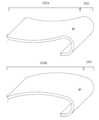
도 1은 전자장치에 포함될 수 있는 예시적인 플렉서블 표시장치를 도시한다.FIG. 1 illustrates an exemplary flexible display device that may be included in an electronic device.
상기 플렉서블(flexible) 표시장치는 가요성(flexibility)이 부여된 표시장치를 의미하는 것으로, 구부릴 수 있는(bendable) 표시장치, 말수있는(rollable) 표시장치, 깨지지 않는(unbreakable) 표시장치, 접을 수 있는 (foldable) 표시장치 등과 동일한 의미로 사용될 수 있다. 도 1을 참조하면, 상기 플렉서블 표시장치(100)는 적어도 하나의 표시 영역(active area)을 포함하고, 상기 표시 영역에는 픽셀들의 어레이(array)가 형성된다. 하나 이상의 비표시 영역(in표시 영역)이 상기 표시 영역의 주위에 배치될 수 있다. 즉, 상기 비표시 영역은, 표시 영역의 하나 이상의 측면에 인접할 수 있다. 도 1에서, 상기 비표시 영역은 사각형 형태의 표시 영역을 둘러싸고 있다. 그러나, 표시 영역의 형태 및 표시 영역에 인접한 비표시 영역의 형태/배치는 도 1에 도시된 예에 한정되지 않는다. 상기 표시 영역 및 상기 비표시 영역은, 상기 플렉서블 표시장치(100)를 탑재한 전자장치의 디자인에 적합한 형태일 수 있다. 상기 표시 영역의 예시적 형태는 오각형, 육각형, 원형, 타원형 등이다.The flexible display device above refers to a display device provided with flexibility, and can be used with the same meaning as a bendable display device, a rollable display device, an unbreakable display device, a foldable display device, etc. Referring to FIG. 1, the flexible display device (100) includes at least one active area, and an array of pixels is formed in the active area. One or more non-display areas (in-display areas) may be arranged around the active area. That is, the non-display areas may be adjacent to one or more side surfaces of the active area. In FIG. 1, the non-display areas surround a rectangular display area. However, the shape of the active area and the shape/arrangement of the non-display areas adjacent to the active area are not limited to the example illustrated in FIG. 1. The above display area and the non-display area may have shapes suitable for the design of an electronic device equipped with the flexible display device (100). Exemplary shapes of the display area include a pentagon, a hexagon, a circle, an oval, etc.
상기 표시 영역 내의 각 픽셀은 픽셀 회로와 연관될 수 있다. 상기 픽셀 회로는, 백플레인(backplane) 상의 하나 이상의 스위칭 트랜지스터 및 하나 이상의 구동 트랜지스터를 포함할 수 있다. 각 픽셀 회로는, 상기 비표시 영역에 위치한 게이트 드라이버 및 데이터 드라이버와 같은 하나 이상의 구동 회로와 통신하기 위해, 게이트 라인 및 데이터 라인과 전기적으로 연결될 수 있다.Each pixel within the display area may be associated with a pixel circuit. The pixel circuit may include one or more switching transistors and one or more driving transistors on a backplane. Each pixel circuit may be electrically connected to a gate line and a data line to communicate with one or more driving circuits, such as a gate driver and a data driver, located in the non-display area.
상기 구동 회로는, 도 1에 도시된 것처럼, 상기 비표시 영역에 TFT(thin film transistor)로 구현될 수 있다. 이러한 구동 회로는 GIP(gate-in-panel)로 지칭될 수 있다. 또한, 데이터 드라이버 IC와 같은 몇몇 부품들은, 분리된 인쇄 회로 기판에 탑재되고, FPCB(flexible printed circuit board), COF(chip-on-film), TCP(tape-carrier-package) 등과 같은 회로 필름을 이용하여 상기 비표시 영역에 배치된 연결 인터페이스(패드/범프, 핀 등)와 결합될 수 있다. 상기 비표시 영역은 상기 연결 인터페이스와 함께 구부러져서, 상기 인쇄 회로(COF, PCB 등)는 상기 플렉서블 표시장치(100)의 뒤편에 위치될 수 있다.The above driving circuit may be implemented as a TFT (thin film transistor) in the non-display area, as illustrated in FIG. 1. Such a driving circuit may be referred to as a GIP (gate-in-panel). In addition, several components, such as a data driver IC, may be mounted on a separate printed circuit board and may be combined with a connection interface (pad/bump, pin, etc.) arranged in the non-display area using a circuit film, such as a flexible printed circuit board (FPCB), a chip-on-film (COF), a tape-carrier-package (TCP), etc. The non-display area may be bent together with the connection interface, so that the printed circuit (COF, PCB, etc.) may be positioned at the back of the flexible display device (100).
상기 플렉서블 표시장치(100)는, 다양한 신호를 생성하거나 표시 영역내의 픽셀을 구동하기 위한, 다양한 부가 요소들 포함할 수 있다. 상기 픽셀을 구동하기 위한 부가 요소는 인버터 회로, 멀티플렉서, 정전기 방전 회로(electro static discharge) 등을 포함할 수 있다. 상기 플렉서블 표시장치(100)는 픽셀 구동 이외의 기능과 연관된 부가 요소도 포함할 수 있다. 예를 들어, 상기 플렉서블 표시장치(100)는 터치 감지 기능, 사용자 인증 기능(예: 지문 인식), 멀티 레벨 압력 감지 기능, 촉각 피드백(tactile feedback) 기능 등을 제공하는 부가 요소들을 포함할 수 있다. 상기 언급된 부가 요소들은 상기 비표시 영역 및/또는 상기 연결 인터페이스와 연결된 외부 회로에 위치할 수 있다.The flexible display device (100) may include various additional elements for generating various signals or driving pixels within a display area. Additional elements for driving the pixels may include an inverter circuit, a multiplexer, an electro static discharge circuit, etc. The flexible display device (100) may also include additional elements associated with functions other than pixel driving. For example, the flexible display device (100) may include additional elements that provide a touch detection function, a user authentication function (e.g., fingerprint recognition), a multi-level pressure detection function, a tactile feedback function, etc. The above-mentioned additional elements may be located in the non-display area and/or an external circuit connected to the connection interface.
상기 플렉서블 표시장치(100)의 여러 부분들은 굴곡선(BL)을 따라 구부러질 수 있다. 상기 굴곡선(BL)은 수평으로(예: 도 1의 X 방향), 수직으로(예: 도 1의 Y 방향), 또는 대각선으로 연장될 수 있다 따라서, 상기 플렉서블 표시장치(100)는, 요구되는 디자인에 기초하여, 수평, 수직, 대각선 방향의 조합으로 구부러질 수 있다.Various parts of the flexible display device (100) can be bent along a bending line (BL). The bending line (BL) can extend horizontally (e.g., in the X direction of FIG. 1), vertically (e.g., in the Y direction of FIG. 1), or diagonally. Accordingly, the flexible display device (100) can be bent in a combination of horizontal, vertical, and diagonal directions based on a required design.
언급한 대로, 상기 플렉서블 표시장치(100)의 하나 이상의 모서리(edge)는, 상기 굴곡선(BL)을 따라 중앙 부분(central portion, 101)에서 멀어지도록 구부러질 수 있다. 비록 상기 굴곡선(BL)이 상기 플렉서블 표시장치(100)의 모서리와 가깝게 위치하도록 도시되었지만, 상기 굴곡선(BL)은 상기 중앙 부분(101)을 가로질러 연장되거나, 상기 플렉서블 표시장치(100)의 하나 이상의 꼭지점(corner)에서 대각선으로 연장될 수 있다. 이러한 구조는 상기 플렉서블 표시장치(100)가 폴더블(foldable) 표시장치가 되거나, 또는 접히는 양면에 표시가 이뤄지는 표시장치가 되도록 할 수 있다.As mentioned, one or more edges of the flexible display device (100) can be bent away from the central portion (101) along the bend line (BL). Although the bend line (BL) is illustrated as being positioned close to a corner of the flexible display device (100), the bend line (BL) can extend across the central portion (101), or can extend diagonally from one or more corners of the flexible display device (100). This structure can enable the flexible display device (100) to be a foldable display device, or a display device in which displays are formed on both sides when folded.
상기 플렉서블 표시장치(100)의 하나 이상의 부분이 구부러질 수 있으므로, 상기 플렉서블 표시장치(100)는 실질적으로 평평한(flat) 부분 및 굴곡진 부분으로 정의될 수 있다. 플렉서블 표시장치(100)의 일 부분은 실질적으로 평평(flat)한, 중앙 부분(101)으로 지칭될 수 있다. 플렉서블 표시장치(100)의 일 부분은 소정의 각도로 구부러지며, 이러한 부분은 굴곡 부분(102)으로 지칭될 수 있다. 상기 굴곡 부분(102)은, 소정의 굴곡 반지름으로 실제로 휘어지는 굴곡 구간(bended section)을 포함한다.Since one or more portions of the flexible display device (100) can be bent, the flexible display device (100) can be defined as a substantially flat portion and a curved portion. One portion of the flexible display device (100) can be referred to as a central portion (101) that is substantially flat. One portion of the flexible display device (100) is bent at a predetermined angle, and this portion can be referred to as a curved portion (102). The curved portion (102) includes a bent section that is actually bent at a predetermined bending radius.
“실질적으로 평평한” 이라는 용어에는 완벽히 평평하지는 않은 부분도 포함된다. 예를 들어, 도 2에 묘사된 오목한 중앙 부분(101a) 및 볼록한 중앙 부분(101b)도 어떤 실시예에서는 실질적으로 평평한 부분으로 기술될 수 있다. 도 2에서, 하나 이상의 굴곡 부분(102)이 오목한 중앙 부분(101a) 또는 볼록한 중앙 부분(101b)의 옆에 존재하고, 굴곡선(BL)을 따라 굴곡 축에 대한 각도를 갖고 안쪽 또는 바깥쪽으로 구부러진다. 굴곡 부분(102)의 굴곡 반지름은 중앙 부분(101a, 101b)의 굴곡 반지름보다 작다. 다시 말해서, “실질적으로 평평한 부분” 이라는 용어는 인접한 구간보다 더 작은 곡률을 갖는 부분을 의미한다.The term “substantially flat” includes portions that are not perfectly flat. For example, the concave central portion (101a) and the convex central portion (101b) depicted in FIG. 2 may also be described as substantially flat portions in some embodiments. In FIG. 2, one or more curved portions (102) are present next to the concave central portion (101a) or the convex central portion (101b) and are curved inwardly or outwardly at an angle relative to the curve axis along the curve line (BL). The curve radius of the curved portion (102) is smaller than the curve radii of the central portions (101a, 101b). In other words, the term “substantially flat portion” means a portion that has a smaller curvature than an adjacent section.
굴곡선(BL)의 위치에 따라서 굴곡선의 일 측에 있는 부분은 플렉서블 표시장치(100)의 중앙을 향해 위치하는 반면, 굴곡선의 타 측에 있는 부분은 플렉서블 표시장치(100)의 모서리을 향해 위치한다. 플렉서블 표시장치(100)의 중앙을 향해 놓이는 부분은 중앙 부분이라 언급될 수 있고 플렉서블 표시장치(100)의 모서리를 향해 놓이는 부분은 모서리 부분이라 언급될 수 있다. 항상 그런 것은 아니지만, 플렉서블 표시장치(100)의 중앙부분은 실질적으로 평평하고, 모서리 부분은 굴곡 부분일수 있다. 실질적으로 평평한 부분은 모서리 부분에도 위치할 수 있다는 점은 언급되어야 한다. 그리고, 플렉서블 표시장치(100)의 몇몇 형상에서, 굴곡 구간은 두 개의 실질적으로 평평한 부분 사이에 놓일 수 있다.Depending on the position of the bend line (BL), a portion on one side of the bend line is positioned toward the center of the flexible display device (100), while a portion on the other side of the bend line is positioned toward the corner of the flexible display device (100). The portion positioned toward the center of the flexible display device (100) may be referred to as a center portion, and the portion positioned toward the corner of the flexible display device (100) may be referred to as a corner portion. Although not always the case, the center portion of the flexible display device (100) may be substantially flat, and the corner portion may be a curved portion. It should be noted that the substantially flat portion may also be positioned at the corner portion. And, in some shapes of the flexible display device (100), the curved section may be positioned between two substantially flat portions.
언급한 대로, 비표시 영역을 구부리면, 비표시 영역이 표시장치의 앞면에서는 안보이거나 최소로만 보이게 된다. 비표시 영역 중 표시장치의 앞면에서 보이는 일부는 베젤(bezel)로 가려질 수 있다. 상기 베젤은 독자적인 구조물, 또는 하우징이나 다른 적합한 요소로 형성될 수 있다. 비표시 영역 중 표시장치의 앞면에서 보이는 일부는 블랙 잉크(예: 카본 블랙으로 채워진 폴리머)와 같은 불투명한 마스크 층 아래에 숨겨질 수도 있다. 이러한 불투명한 마스크 층은 플렉서블 표시장치(100)에 포함된 다양한 층(터치센서층, 편광층, 덮개층 등) 상에 마련될 수 있다.As mentioned, when the non-display area is bent, the non-display area becomes invisible or minimally visible on the front side of the display device. A portion of the non-display area that is visible on the front side of the display device may be covered by a bezel. The bezel may be formed by an independent structure, a housing, or other suitable elements. A portion of the non-display area that is visible on the front side of the display device may be hidden under an opaque mask layer, such as black ink (e.g., a polymer filled with carbon black). Such an opaque mask layer may be provided on various layers (e.g., a touch sensor layer, a polarizing layer, a cover layer, etc.) included in the flexible display device (100).
몇몇 실시예에서 플렉서블 표시장치(100)의 굴곡 부분은, 이미지를 표시할 수 있는 표시 영역을 포함할 수 있다. 이러한 표시 영역을 이하에서는 제2 표시 영역이라 호칭한다. 즉, 표시 영역의 적어도 일부 픽셀이 굴곡 부분에 포함되도록 굴곡선(BL)이 표시 영역 내에 놓일 수 있다.In some embodiments, the curved portion of the flexible display device (100) may include a display area capable of displaying an image. This display area is hereinafter referred to as a second display area. That is, a curved line (BL) may be placed within the display area so that at least some pixels of the display area are included in the curved portion.
도 3a 및 3b는 각각 본 명세서의 실시예에 따른 플렉서블 표시장치(100)의 표시 영역의 배치를 나타낸다.Figures 3a and 3b each illustrate the arrangement of a display area of a flexible display device (100) according to an embodiment of the present specification.
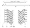
도 3a의 형상에서, 제2 표시 영역 내의 픽셀 매트릭스는, 중앙 부분(101)의 표시 영역으로부터 연속적으로 연장될 수 있다. 또 다르게는, 도 3b의 형상에서, 굴곡 부분(102) 내의 제2 표시 영역과 중앙 부분(101) 내의 표시 영역은, 굴곡 구간을 사이에 두고 서로 분리될 수 있다. 중앙 부분(101)과 굴곡 부분(102)은 몇몇 부품들은, 굴곡 구간을 가로질러 놓인 하나 이상의 도선(120)을 통해 전기적으로 연결될 수 있다.In the shape of FIG. 3a, the pixel matrix within the second display area may extend continuously from the display area of the central portion (101). Alternatively, in the shape of FIG. 3b, the second display area within the curved portion (102) and the display area within the central portion (101) may be separated from each other with a curved section therebetween. The central portion (101) and the curved portion (102) may be electrically connected to some components via one or more conductors (120) laid across the curved section.
제2 표시 영역의 픽셀과 중앙 표시 영역의 픽셀은 구동 회로(예: 게이트 드라이버, 데이터 드라이버 등)에 의해 마치 동일 매트릭스에 있는 것처럼 구동될 수 있다. 이때, 제2 표시 영역의 픽셀과 중앙 표시 영역의 동일한 구동 회로들에 의해 동작될 수 있다. 예를 들어, 중앙 표시 영역의 N번째 행 픽셀과 제2 표시 영역의 N번째 행 픽셀은, 같은 게이트 드라이버로부터 게이트 신호를 수신하도록 구비될 수 있다. 도 3B와 같이, 굴곡 구간을 가로지르는 게이트 배선의 일부 또는 상기 두 표시 영역들의 게이트 배선을 연결하는 브릿지(bridge)는 변형 저감 형상을 가질 수 있다.The pixels of the second display area and the pixels of the central display area can be driven as if they were in the same matrix by a driving circuit (e.g., a gate driver, a data driver, etc.). At this time, the pixels of the second display area and the pixels of the central display area can be operated by the same driving circuits. For example, the Nth row pixel of the central display area and the Nth row pixel of the second display area can be provided to receive a gate signal from the same gate driver. As in Fig. 3B, a part of the gate wiring crossing the curved section or a bridge connecting the gate wirings of the two display areas can have a deformation-reducing shape.
제2 표시 영역의 기능에 따라서는, 제2 표시 영역의 픽셀이 중앙 표시 영역의 픽셀과 분리되어 구동될 수도 있다. 즉, 제2 표시 영역의 픽셀은, 표시 영역의 픽셀 매트릭스와는 분리된 독립된 매트릭스로 구동 회로에 인식될 수 있다. 이 경우, 제2 표시 영역의 픽셀은, 중앙 표시 영역의 픽셀에 신호를 공급하는 구동 회로와는 다른 하나 이상의 분리된 구동 회로로부터 신호를 수신할 수 있다.Depending on the function of the second display area, the pixels of the second display area may be driven separately from the pixels of the central display area. That is, the pixels of the second display area may be recognized by the driving circuit as an independent matrix separate from the pixel matrix of the display area. In this case, the pixels of the second display area may receive signals from one or more separate driving circuits that are different from the driving circuit that supplies signals to the pixels of the central display area.
그 형상에 상관없이, 굴곡 부분의 제2 표시 영역은 플렉서블 표시장치(100)의 2차 표시 영역으로 기능할 수 있다. 또한, 제2 표시 영역의 크기는 특별히 제한되지 않는다. 제2 표시 영역의 크기는 전자장치에 내장된 기능에 의존할 수 있다. 예를 들어, 제2 표시 영역은 GUI(graphical user interface), 버튼, 문자 메시지 등과 같은 이미지 및/또는 문자를 제공하는 데에 사용될 수 있다. 몇몇 경우에, 제2 표시 영역은 여러 목적(예: 상태 표시)의 다양한 색의 빛을 제공하는 데에 사용될 수 있고, 이때 제2 표시 영역의 크기는 중앙 부분 내의 표시 영역만큼 클 필요는 없다.Regardless of its shape, the second display area of the curved portion can function as a secondary display area of the flexible display device (100). In addition, the size of the second display area is not particularly limited. The size of the second display area can depend on functions built into the electronic device. For example, the second display area can be used to provide images and/or text, such as a graphical user interface (GUI), buttons, text messages, etc. In some cases, the second display area can be used to provide various colored lights for various purposes (e.g., status indication), and in this case, the size of the second display area need not be as large as the display area within the central portion.
도 4는 본 명세서의 일 실시예에 따른 플렉서블 표시장치의 적층 구조를 개략적으로 나타낸 단면도이다.FIG. 4 is a cross-sectional view schematically illustrating a laminated structure of a flexible display device according to one embodiment of the present specification.
도 4에서는 설명의 편의를 위하여, 상기 중앙 부분(central portion, 101)은 실질적으로 평평하고, 상기 굴곡 부분(102)은 상기 플렉서블 표시장치(100)의 모서리에 있는 것으로 도시되었다. 도시된 것처럼, 하나 이상의 굴곡 부분(102)은, 굴곡축에 대한 굴곡각 θ 및 굴곡 반지름 R을 갖고 상기 중앙 부분(101)으로부터 바깥쪽으로 구부러질 수 있다. 상기 각 굴곡 부분(102)의 크기는 동일할 필요는 없다. 즉, 각 굴곡 부분(102)에서 굴곡선(BL)으로부터 베이스 층(106)의 외곽 모서리까지의 길이는 서로 다를 수 있다. 또한, 굴곡 축 둘레의 굴곡 각 θ 및 상기 굴곡축으로부터의 곡률 반지름 R은 굴곡 부분(102)마다 다를 수 있다.In FIG. 4, for convenience of explanation, the central portion (101) is illustrated as being substantially flat, and the curved portion (102) is illustrated as being at an edge of the flexible display device (100). As illustrated, one or more curved portions (102) may be bent outwardly from the central portion (101) with a bend angle θ and a bend radius R with respect to a bend axis. The sizes of each curved portion (102) need not be the same. That is, the length from the bend line (BL) to the outer edge of the base layer (106) in each curved portion (102) may be different. In addition, the bend angle θ around the bend axis and the radius of curvature R from the bend axis may be different for each curved portion (102).
도 4에 도시된 예에서, 상기 굴곡 부분(102)의 오른쪽은 90°의 굴곡각 θ를 갖고, 상기 굴곡 부분(102)은 실질적으로 평면인 구간을 포함한다. 굴곡 부분(102)은 더 큰 굴곡각 θ로 구부러져, 상기 플렉서블 표시장치(100)의 왼쪽 굴곡 부분(102)과 같이, 굴곡 부분(102)의 일 부분이 중앙 부분(101)의 아래로 갈 수 있다. 또한, 굴곡 부분(102)은 90° 이하의 굴곡각 θ로 구부러질 수도 있다.In the example illustrated in FIG. 4, the right side of the bent portion (102) has a bend angle θ of 90°, and the bent portion (102) includes a substantially flat section. The bent portion (102) may be bent at a larger bend angle θ, such that a portion of the bent portion (102) may go below the central portion (101), like the left bent portion (102) of the flexible display device (100). Additionally, the bent portion (102) may be bent at a bend angle θ of 90° or less.
몇몇 실시예에서, 상기 굴곡 부분(102)의 곡률 반지름(radius of curvatures)은 약 0.1 mm에서 약 10 mm 사이일 수 있고, 바람직하게는 약 0.1 mm에서 약 5 mm 사이 또는, 약 0.1 mm에서 약 1 mm 사이, 또는 약 0.1 mm에서 약 0.5 mm 사이일 수 있다. 몇몇 실시예에서, 굴곡 부분(102)에서의 곡률 반지름은 0.5 mm보다 작을 수 있다.In some embodiments, the radius of curvature of the bent portion (102) can be between about 0.1 mm and about 10 mm, preferably between about 0.1 mm and about 5 mm, or between about 0.1 mm and about 1 mm, or between about 0.1 mm and about 0.5 mm. In some embodiments, the radius of curvature at the bent portion (102) can be less than 0.5 mm.
상기 플렉서블 표시장치(100)의 특정 부분에서의 강도 및/또는 견고성을 증가시키기 위해, 하나 이상의 지지층(108)이 상기 베이스 층(106)의 하부에 제공될 수 있다. 예를 들어, 상기 지지층(108)은 상기 중앙 부분(101)의 아래쪽 면에 제공될 수 있다. 상기 지지층(108)은 더 큰 유연성이 필요한 굴곡 구간에는 제공되지 않을 수 있다. 상기 지지층(108)은 상기 중앙 부분(101) 아래에 위치한 굴곡 부분(102) 상에 제공될 수 있다. 특정 부분의 강도를 높이면, 상기 플렉서블 표시장치(100)에 다양한 부품들을 정확히 구성하고 배치하는 데에 도움이 된다. 상기 베이스 층(106)이 상기 지지층(108)보다 더 큰 탄성을 갖는 경우에, 상기 지지층(108)은 상기 베이스 층(106)에서의 갈라짐(crack) 발생을 억제하는 데에 기여할 수 있다.In order to increase the strength and/or rigidity of a specific portion of the flexible display device (100), one or more support layers (108) may be provided under the base layer (106). For example, the support layer (108) may be provided on the lower surface of the central portion (101). The support layer (108) may not be provided in a bending section that requires greater flexibility. The support layer (108) may be provided on a bending section (102) located under the central portion (101). Increasing the strength of a specific portion helps in accurately configuring and arranging various components in the flexible display device (100). In the case where the base layer (106) has greater elasticity than the support layer (108), the support layer (108) may contribute to suppressing cracking in the base layer (106).
상기 베이스 층(106) 및 상기 지지층(108)은 폴리이미드, 폴리에틸렌 나프탈레이트(PEN), 폴리에틸렌 테레플레이트, 기타 적합한 폴리머의 조합으로 구성된 박형 플라스틱 필름으로 만들어질 수 있다. 상기 베이스 층(106) 및 상기 지지층(108)의 형성에 사용될 수 있는 다른 적합한 물질은 박형 유리, 유전체로 차폐된 금속 호일(metal foil), 다층 폴리머, 나노 파티클 또는 마이크로 파티클과 조합된 고분자 물질이 포함된 고분자 필름 등일 수 있다. 상기 플렉서블 표시장치(100)의 여러 부분에 제공되는 지지층(108)이 모두 동일한 물질일 필요는 없다. 예를 들어, 박형 유리층이 중앙 부분(101)에 대한 지지층(108)으로 사용되면서, 플라스틱 필름이 모서리 부분에 대한 지지층(108)으로 사용될 수 있다.The base layer (106) and the support layer (108) can be made of a thin plastic film composed of a combination of polyimide, polyethylene naphthalate (PEN), polyethylene terephthalate, and other suitable polymers. Other suitable materials that can be used to form the base layer (106) and the support layer (108) can be thin glass, a metal foil shielded with a dielectric, a multilayer polymer, a polymer film containing a polymer material combined with nano-particles or micro-particles, etc. The support layers (108) provided at various portions of the flexible display device (100) do not all need to be of the same material. For example, a thin glass layer can be used as the support layer (108) for the central portion (101), while a plastic film can be used as the support layer (108) for the corner portions.
상기 베이스 층(106) 및 상기 지지층(108)의 두께 또한 상기 플렉서블 표시장치(100)의 디자인에 있어서 고려할 사항이다. 한 관점에서, 만약 상기 베이스 층(106)이 과도한 두께를 갖는다면, 상기 베이스 층(106)이 작은 곡률 반경으로 구부러지는 것이 어렵다. 또, 상기 베이스 층(106)의 과도한 두께는, 굴곡 시에 그 위에 배치된 부품에 기계적 스트레스를 가중시킨다. 그러나, 다른 관점에서, 상기 베이스 층(106)이 너무 얇다면, 그 위에 배치된 부품들을 지탱할 기판으로서 너무 약하다.The thickness of the base layer (106) and the support layer (108) is also a consideration in the design of the flexible display device (100). From one perspective, if the base layer (106) has an excessive thickness, it is difficult for the base layer (106) to bend with a small radius of curvature. In addition, the excessive thickness of the base layer (106) increases mechanical stress on components placed thereon when bent. However, from another perspective, if the base layer (106) is too thin, it is too weak as a substrate to support components placed thereon.
이와 같은 요구 조건을 만족시키기 위해, 상기 베이스 층(106)은 약 5μm에서 약 50μm의 두께를 가질 수 있다, 바람직하게는, 상기 베이스 층(106)은 약 5μm에서 약 30μm의 범위나, 약 5μm에서 약 16μm의 범위의 두께를 가질 수 있다. 상기 지지층(108)은 약 100μm에서 약 125μm, 약 50μm에서 약 150μm, 약 75μm에서 200μm, 150μm 이하, 또는 100μm 이상의 두께를 가질 수 있다.To satisfy such requirements, the base layer (106) can have a thickness of about 5 μm to about 50 μm, preferably, the base layer (106) can have a thickness in a range of about 5 μm to about 30 μm, or in a range of about 5 μm to about 16 μm. The support layer (108) can have a thickness of about 100 μm to about 125 μm, about 50 μm to about 150 μm, about 75 μm to 200 μm, less than or equal to 150 μm, or greater than or equal to 100 μm.
일 실시예에서, 약 10μm에서 약 16μm 사이의 두께를 갖는 폴리이미드 층이 상기 베이스 층(106)으로 사용되고, 약 50μm에서 약 125μm 사이의 두께를 갖는 폴리에틸렌 테레프탈레이트(PET) 층이 상기 지지층(108)으로 사용된다. 다른 실시예에서, 약 10μm에서 약 16μm 사이의 두께를 갖는 폴리이미드 층이 상기 베이스 층(106)으로 사용되고, 약 50μm에서 약 200μm 사이의 두께를 갖는 박형 유리가 상기 지지층(108)으로 사용된다. 또 다른 실시예에서는, 박형 유리가 상기 베이스 층(106)으로 사용되고, 상기 베이스 층(106)은 파손을 피하기 위해 상기 지지층(108)으로 기능하는 폴리이미드 층을 가진다.In one embodiment, a polyimide layer having a thickness of between about 10 μm and about 16 μm is used as the base layer (106), and a polyethylene terephthalate (PET) layer having a thickness of between about 50 μm and about 125 μm is used as the support layer (108). In another embodiment, a polyimide layer having a thickness of between about 10 μm and about 16 μm is used as the base layer (106), and a thin glass having a thickness of between about 50 μm and about 200 μm is used as the support layer (108). In yet another embodiment, a thin glass is used as the base layer (106), and the base layer (106) has a polyimide layer that functions as the support layer (108) to avoid breakage.
제조 과정에서 상기 플렉서블 표시장치(100)의 몇몇 부분들은 외부 광에 노출될 수 있다. 상기 부품들을 제조하는데 쓰이는 물질 또는 상기 부품들 그 자체는, 플렉서블 표시장치(100) 제조 중의 광 노출에 의해 원치 않는 상태 변화(예: TFT에서의 임계 전압 천이 등)를 겪는다. 상기 플렉서블 표시장치(100)의 몇몇 부분은, 다른 부분에 비하여 상기 외부 광에 과도하게 노출된다. 그리고 이는 표시 불균일(예: mura, shadow defects 등)을 야기할 수 있다. 이러한 문제를 최소화하기 위해, 상기 베이스 층(106) 및/또는 상기 지지층(108)은, 외부 광의 양을 줄일 수 있는 물질을 하나 이상 포함할 수 있다.During the manufacturing process, some parts of the flexible display device (100) may be exposed to external light. The materials used to manufacture the parts or the parts themselves undergo undesirable state changes (e.g., threshold voltage transition in TFT, etc.) due to light exposure during the manufacturing of the flexible display device (100). Some parts of the flexible display device (100) are excessively exposed to the external light compared to other parts. This may cause display unevenness (e.g., mura, shadow defects, etc.). To minimize this problem, the base layer (106) and/or the support layer (108) may include one or more materials that can reduce the amount of external light.
예를 들어, 상기 광 차단 물질은, 상기 베이스 층(106)의 구성 물질(폴리이미드, 기타 폴리머)에 혼합된 염화 카본 블랙이다. 이와 같이 상기 베이스 층(106), 광 차단 기능을 제공하는 셰이드(shade)를 가진 폴로이미드로부터 형성될 수 있다. 이러한 베이스 층(106)은, 상기 플렉서블 표시장치(100)의 전면에서 입사하는 외부 광의 반사를 줄임으로써, 가시성(visibility)을 향상시킬 수 있다.For example, the light-blocking material is carbon black chloride mixed into the constituent material (polyimide, other polymer) of the base layer (106). In this way, the base layer (106) can be formed from polyimide having a shade that provides a light-blocking function. This base layer (106) can improve visibility by reducing reflection of external light incident on the front surface of the flexible display device (100).
상기 베이스 층(106) 대신에, 상기 플렉서블 표시장치(100)의 후면(즉, 상기 지지층(108)이 부착된 면)으로부터 입사하는 광의 양을 줄이기 위해, 상기 지지층(108)이 광 차단 물질을 포함할 수도 있다. 상기 지지층(108)의 구성 물질은, 위에서 설명한 것과 유사하게, 하나 이상의 광 차단 물질과 혼합될 수 있다. 더 나아가, 상기 베이스 층(106) 및 상기 지지층(108)이 모두 하나 이상의 광 차단 물질을 포함할 수 있다. 여기서, 상기 베이스 층(106) 및 상기 지지층(108)에 사용되는 광 차단 물질이 동일할 필요는 없다.Instead of the base layer (106), the support layer (108) may include a light blocking material to reduce the amount of light incident from the back surface of the flexible display device (100) (i.e., the surface to which the support layer (108) is attached). The constituent material of the support layer (108) may be mixed with one or more light blocking materials, similarly to what was described above. Furthermore, both the base layer (106) and the support layer (108) may include one or more light blocking materials. Here, the light blocking materials used in the base layer (106) and the support layer (108) need not be the same.
상기 베이스 층(106) 및 상기 지지층(108)이 불요한 외부 광을 차단하게 만드는 것은 표시 균일성을 향상시키고 반사를 감소시키지만, 부품들을 정확하게 배치하기 위한 정렬 표식(alignment marks), 또는 제조 공정의 수행을 위한 정렬 표식을 인식하는 것이 어려워질 수 있다. 예를 들어, 상기 층(layer)들의 배치는 중첩 부분의 외곽을 비교하여 결정되기 때문에, 부품들을 상기 베이스 층(106) 상에 정확히 배치하거나, 또는 상기 플렉서블 표시장치(100)의 구부러짐 중에 정렬하는 것이 더 어려울 수 있다. 이에 더하여, 만약 상기 베이스 층(106) 및/또는 상기 지지층(108)이 과도한 범위의 광 스펙트럼(즉, 가시광, 자외선, 적외선 스펙트럼의 파장)을 차단한다면 상기 플렉서블 표시장치(100)내의 잔해 또는 이물질을 확인하는 것이 문제될 수 있다.Although blocking unwanted external light by the base layer (106) and the support layer (108) improves display uniformity and reduces reflection, it may become difficult to recognize alignment marks for accurately placing components, or for performing manufacturing processes. For example, since the placement of the layers is determined by comparing the perimeter of the overlapping portions, it may be more difficult to accurately place components on the base layer (106), or to align them during bending of the flexible display device (100). Additionally, if the base layer (106) and/or the support layer (108) block excessive ranges of the light spectrum (i.e., wavelengths in the visible, ultraviolet, and infrared spectrums), identifying debris or foreign matter within the flexible display device (100) may be problematic.
따라서, 몇몇 실시예에서, 상기 베이스 층(106) 및/또는 상기 지지층(108)에 포함되는 광 차단 물질은, 특정 편광 및/또는 하나 이상의 제조/검사 과정에서 사용되는 특정 파장 범위 이내의 광은 통과하도록 구성된다. 일 예로서, 상기 지지층(108)은 품질 검사 및/또는 정렬 과정에서 사용되는 광(예: UV, IR)은 통과시키되, 가시광 파장 범위의 광은 차단할 수 있다. 상기 제한된 범위의 파장은, 상기 베이스 층(106)이 광 차단 물질을 포함하였을 경우에. 베이스 층(106)에 부착된 인쇄 회로 필름에 의해 생기는 음영이 야기하는, 표시장치의 불균일성 문제를 줄이는데 도움이 된다.Thus, in some embodiments, the light blocking material included in the base layer (106) and/or the support layer (108) is configured to allow light to pass through a particular polarization and/or within a particular wavelength range used in one or more of the manufacturing/inspection processes. As an example, the support layer (108) may allow light (e.g., UV, IR) used in quality inspection and/or alignment processes to pass through, while blocking light in the visible wavelength range. The limited range of wavelengths helps reduce display non-uniformity issues caused by shading by the printed circuit film attached to the base layer (106) when the base layer (106) includes the light blocking material.
상기 베이스 층(106) 및 상기 지지층(108)은 특정 형태의 광을 차단시키거나 통과시키는 일을 함께 수행할 수 있다. 예를 들어, 상기 지지층(108)는 해당 광이 상기 베이스 층(106)을 통과하지 못하도록, 광의 편광을 변화시킬 수 있다. 이와 같이, 특정 형태의 광은, 상기 플렉서블 표시장치(100)의 제조 중에 여러 가지 목적을 위해 상기 지지층(108)을 통과할 수 있지만, 상기 베이스 층(106)의 반대 면에 배치된 부품들에 불필요한 영향을 주지 않도록, 상기 베이스 층(106)을 통과할 수는 없다.The base layer (106) and the support layer (108) can work together to block or transmit a specific type of light. For example, the support layer (108) can change the polarization of light so that the light cannot pass through the base layer (106). In this way, a specific type of light can pass through the support layer (108) for various purposes during the manufacturing of the flexible display device (100), but cannot pass through the base layer (106) so as not to unnecessarily affect components arranged on the opposite side of the base layer (106).
상기 플렉서블 표시장치(100)의 백플레인(backplane)이 상기 베이스 층(106) 상에 구현된다. 몇몇 실시예에서, 상기 플렉서블 표시장치(100)의 백플레인은, LTPS(low temperature poly silicon) 반도체 층을 활성층(active layer)으로서 사용한 TFT와 함께 구현된다. 일 예에서, 상기 베이스 층(106) 상의 픽셀 회로 및 구동 회로(예: GIP)들은 NMOS LTPS TFT로 구현될 수 있다. 다른 예에서, 상기 플렉서블 표시장치(100)의 백플레인은 NMOS LTPS TFT 및 PMOS LTPS TFT의 조합으로 구현될 수 있다. 예를 들어, 상기 베이스 층(106) 상의 구동 회로(예: GIP)는, 게이트 라인 상의 스캔 신호를 제어하기 위한 배선 수를 줄이기 위해, 하나 이상의 CMOS 회로를 포함할 수 있다.The backplane of the flexible display device (100) is implemented on the base layer (106). In some embodiments, the backplane of the flexible display device (100) is implemented with a TFT using a low temperature poly silicon (LTPS) semiconductor layer as an active layer. In one example, the pixel circuit and the driver circuit (e.g., GIP) on the base layer (106) may be implemented with an NMOS LTPS TFT. In another example, the backplane of the flexible display device (100) may be implemented with a combination of an NMOS LTPS TFT and a PMOS LTPS TFT. For example, the driver circuit (e.g., GIP) on the base layer (106) may include one or more CMOS circuits in order to reduce the number of wirings for controlling a scan signal on a gate line.
그리고, 몇몇 실시예에서, 상기 플렉서블 표시장치(100)는, 비표시 영역 및/또는 표시 영역 내의 픽셀 회로에 구동 회로들을 구현하기 위해, 여러 종류의 TFT를 채용할 수 있다. 즉, 상기 플렉서블 표시장치(100)의 백플레인을 구현하기 위해, 산화물(oxide) 반도체 TFT 및 LTPS TFT의 조합이 사용될 수 있다. 상기 백플레인에서, 상기 TFT의 유형은 동작 조건 및/또는 관련된 회로 내의 TFT 요구 조건에 따라서 선택될 수 있다And, in some embodiments, the flexible display device (100) may employ various types of TFTs to implement driving circuits in pixel circuits in the non-display area and/or the display area. That is, a combination of oxide semiconductor TFTs and LTPS TFTs may be used to implement the backplane of the flexible display device (100). In the backplane, the type of TFT may be selected according to the operating conditions and/or TFT requirements in the related circuit.
LTPS TFT는 일반적으로 작은 프로파일(profile)에서도 우수한 캐리어(carrier)이동도(mobility)를 나타내어, 집적된 구동 회로를 구현하는데 적합하다. 상기 우수한 캐리어 이동도는 LTPS TFT를 빠른 동작 속도를 요하는 부품에 이상적으로 만든다. 상기 언급된 장점에도 불구하고, 다결정 실리콘 반도체 층의 그레인 경계(grain boundary) 때문에 초기 임계 전압(initial threshold voltage)이 LTPS TFT들 간에 다를 수 있다.LTPS TFTs generally exhibit excellent carrier mobility even at small profiles, making them suitable for implementing integrated driving circuits. The excellent carrier mobility makes LTPS TFTs ideal for components requiring high operating speeds. Despite the above-mentioned advantages, the initial threshold voltage may differ among LTPS TFTs due to the grain boundaries of the polycrystalline silicon semiconductor layer.
IGZO(indium-gallium-zinc-oxide) 반도체 층(이하에서는 산화물 TFT로 지칭)과 같은 산화물(oxide) 기반의 반도체 층을 채용한 TFT는, 상기 LTPS TFT와 많은 측면에서 다르다. 상기 LTPS TFT에 비하여 낮은 이동도에도 불구하고, 상기 산화물 TFT는 일반적으로 전력 효율에서 상기 LTPS TFT보다 더 유리하다. 오프 상태에서 상기 산화물 TFT의 낮은 누설 전류(leakage current)는 액티브 상태를 더 오래 지속시킨다. 이는 픽셀을 구동하기 위해 높은 프레임 레이트(frame rate)가 필요하지 않을 때, 감소된 프레임 레이트에서 픽셀을 구동하는 데에 중요한 장점이 될 수 있다.A TFT employing an oxide-based semiconductor layer, such as an indium-gallium-zinc-oxide (IGZO) semiconductor layer (hereinafter referred to as oxide TFT), differs from the LTPS TFT in many aspects. Despite its lower mobility compared to the LTPS TFT, the oxide TFT is generally more advantageous than the LTPS TFT in terms of power efficiency. The low leakage current of the oxide TFT in the off state allows it to remain active for a longer time. This can be a significant advantage in driving pixels at a reduced frame rate when a high frame rate is not required to drive the pixels.
일 예로서, 상기 플렉서블 표시장치(100)는 표시 영역의 전부 또는 일부의 픽셀이 특정 조건 하에서는 감소된 프레임 레이트에서 구동되는 특성을 지닐 수 있다. 이러한 설정에서, 상기 픽셀은, 상기 플렉서블 표시장치(100)에 표시되는 컨텐츠에 의존하여 감소된 비율로 새로 고침(refresh)될 수 있다. 또한, 정지된 이미지 데이터(예: 사용자 인터페이스, 텍스트)를 표시하는 일부의 표시 영역은, 빨리 변하는 이미지 데이터(예: 영화)를 표시하는 다른 부분의 표시 영역에 비해 더 낮은 비율로 새로 고침될 수 있다. 감소된 새로 고침 비율로 구동되는 픽셀은, 데이터 신호가 픽셀에 제공되지 않는 공백 기간(blank period)이 증가할 수 있다. 이는 픽셀에 같은 이미지 데이터를 제공함으로써 소비되는 전력을 최소화할 것이다. 이러한 실시예에서, 픽셀 회로 및/또는 상기 구동 회로를 구현하는 몇몇 TFT는, 상기 공백 기간 동안의 누설 전류를 최소화하기 위해, 산화물 TFT로 형성될 수 있다 상기 픽셀 회로 및/또는 상기 구동 회로에서 누설 전류를 줄임으로써, 상기 픽셀은 디스플레이가 감소된 비율로 새로 고침될 때에도 더 안정적인 휘도 레벨을 달성할 수 있다.As an example, the flexible display device (100) may have a characteristic in which pixels in all or part of the display area are driven at a reduced frame rate under certain conditions. In such a setting, the pixels may be refreshed at a reduced rate depending on the content displayed on the flexible display device (100). Additionally, a portion of the display area that displays still image data (e.g., a user interface, text) may be refreshed at a lower rate than other portions of the display area that display fast-changing image data (e.g., a movie). The pixels driven at a reduced refresh rate may have an increased blank period during which no data signal is provided to the pixels. This will minimize power consumption by providing the same image data to the pixels. In these embodiments, some of the TFTs implementing the pixel circuit and/or the driver circuit may be formed of oxide TFTs to minimize leakage current during the blank period. By reducing leakage current in the pixel circuit and/or the driver circuit, the pixels can achieve more stable brightness levels even when the display is refreshed at a reduced rate.
상기 산화물 TFT의 다른 특성은, 트랜지스터 간의 초기 임계 전압 변화 문제를 LTPS TFT만큼 많이 겪지 않는다는 점이다. 이러한 측면은 상기 플렉서블 표시장치(100)의 크기가 증가할 때 중대한 장점이 될 수 있다 또한, 바이어스 스트레스(bias stress) 하에서의 LTPS TFT와 산화물 TFT 사이의 임계값 이동이 다르다.Another characteristic of the oxide TFT is that it does not suffer from the problem of initial threshold voltage variation between transistors as much as the LTPS TFT. This aspect can be a significant advantage when the size of the flexible display device (100) increases. In addition, the threshold shift between the LTPS TFT and the oxide TFT under bias stress is different.
상기 언급된 LTPS TFT 및 산화물 TFT의 특징을 고려하여, 상기 플렉서블 표시장치(100)의 몇몇 실시예들은 하나의 백플레인에 LTPS TFT 및 산화물 TFT을 조합하여 적용할 수 있다. 특히, 상기 플렉서블 표시장치(100)의 몇몇 실시예는, 비표시 영역에 구동 회로(예: GIP)를 구현하기 위해 LTPS TFT를 채용하고, 표시 영역에 픽셀 회로를 구현하기 위해 산화물 TFT를 적용할 수 있다. LTPS TFT의 우수한 캐리어 이동도 때문에, 산화물 TFTs로 구현된 구동 회로에 비해, LTPS TFT로 구현된 구동 회로는 더 빠른 속도로 동작할 수 있다. 이에 더하여, LTPS TFT에 의해 더 집적된 구동 회로가 제공될 수 있고, 이로써 비표시 영역의 크기가 감소될 수 있다. 픽셀 회로에 사용되는 산화물 TFT의 우수한 전압 유지 비율에 의해, 픽셀에서의 누설 전류는 감소될 수 있다. 또한 이는 누설 전류에 의해 야기되는 디스플레이 결함을 최소화하면서, 표시 영역의 특정 부분에서, 또는 기 설정된 조건(예: 정지 영상을 표시할 때) 하에서 감소된 프레임 레이트로 픽셀을 구동하도록 한다Considering the characteristics of the above-mentioned LTPS TFT and oxide TFT, some embodiments of the flexible display device (100) may apply a combination of LTPS TFT and oxide TFT to one backplane. In particular, some embodiments of the flexible display device (100) may employ LTPS TFT to implement a driving circuit (e.g., GIP) in a non-display area, and may apply oxide TFT to implement a pixel circuit in a display area. Due to the excellent carrier mobility of the LTPS TFT, a driving circuit implemented with an LTPS TFT can operate at a faster speed than a driving circuit implemented with oxide TFTs. In addition, a more integrated driving circuit can be provided by the LTPS TFT, and thereby the size of the non-display area can be reduced. Due to the excellent voltage holding ratio of the oxide TFT used in the pixel circuit, leakage current in the pixel can be reduced. It also allows pixels to be driven at a reduced frame rate in certain parts of the display area or under pre-determined conditions (e.g. when displaying still images), while minimizing display artifacts caused by leakage current.
몇몇 실시예에서, 픽셀 회로는 산화물 TFT로 구현되면서, 구동 회로는, N-형 LTPS TFT 및 P-형 LTPS TFT의 조합으로 구현될 수 있다. 예를 들어, N-형 LTPS TFT 및 P-형 LTPS TFT는 CMOS 게이트 드라이버(예: CMOS GIP, 데이터 드라이버)를 구현하기 위해 사용될 수 있다. 반면, 산화물 TFT는 상기 픽셀 회로의 적어도 몇몇 부분에 적용될 수 있다. 전체가 P-형 또는 N-형 LTPS TFT로 형성된 GIP와는 다르게, 상기 CMOS 게이트 드라이버로부터의 게이트 출력 신호는, DC 신호 또는 논리 하이(high)/로우(low) 신호에 의해 제어될 수 있다. 이로써 게이트 라인이 공백 기간 중에 더 안정적으로 제어되어, 픽셀 회로로부터의 전류 누설과 의도하지 않은 픽셀의 활성화가 억제된다.In some embodiments, the pixel circuit may be implemented with an oxide TFT, while the driver circuit may be implemented with a combination of an N-type LTPS TFT and a P-type LTPS TFT. For example, the N-type LTPS TFT and the P-type LTPS TFT may be used to implement a CMOS gate driver (e.g., a CMOS GIP, a data driver). On the other hand, the oxide TFT may be applied to at least some parts of the pixel circuit. Unlike a GIP formed entirely of a P-type or N-type LTPS TFT, a gate output signal from the CMOS gate driver may be controlled by a DC signal or a logic high/low signal. This allows the gate line to be more stably controlled during a blank period, thereby suppressing current leakage from the pixel circuit and unintended pixel activation.
상기 백플레인 상의 CMOS 게이트 드라이버 또는 인버터 회로는 LTPS TFT 및 산화물 TFT의 조합으로 구현될 수 있다. 예를 들어, P-형 LTPS TFT 및 N-형 산화물 TFT가 CMOS 회로를 구현하기 위해 사용될 수 있다. 또한, 상기 표시 영역의 픽셀 회로는, LTPS TFT 및 산화물 TFT를 모두 사용하여 구현될 수 있다. 픽셀 회로 및/또는 구동 회로에 두 종류의 TFT를 적용할 때, 오프 상태 중에 산화물 TFT들 사이의 노드에 남아있는 바이어스를 없애고, 바이어스 스트레스(예: PBTS, NBTS)를 최소화하기 위해, LTPS TFT는 전략적으로 회로 내부에 놓일 수 있다. 추가적으로, 회로 내의 저장 커패시터(storage capacitor)와 연결되는 TFT는, 누설 전류를 최소화하기 위해 산화물 TFT로 형성될 수 있다.The CMOS gate driver or inverter circuit on the above backplane can be implemented by a combination of LTPS TFTs and oxide TFTs. For example, a P-type LTPS TFT and an N-type oxide TFT can be used to implement a CMOS circuit. In addition, the pixel circuit of the display area can be implemented by using both the LTPS TFT and the oxide TFT. When applying two types of TFTs to the pixel circuit and/or the driver circuit, the LTPS TFT can be strategically placed within the circuit to eliminate the bias remaining at the node between the oxide TFTs during the off state and to minimize bias stress (e.g., PBTS, NBTS). Additionally, a TFT connected to a storage capacitor within the circuit can be formed of an oxide TFT to minimize leakage current.
유기발광소자(OLED)층은 상기 베이스 층(106)상에 배치된다. 상기 유기발광소자층(150)은 다수 개의 OLED 소자를 포함한다. OLED 소자는, 베이스 층(106) 상에 구현된 픽셀 회로 및 구동 회로, 상기 베이스 층(106) 상의 연결 인터페이스와 연결된 외부의 다른 구동회로에 의해 제어된다. 상기 OLED층은 특정 색상(예: red, green, blue)의 광을 방출하는 유기발광물질 층을 포함한다. 몇몇 실시예에서, 상기 유기발광물질 층은 백색 광(본질적으로는 여러 색상의 광의 조합)을 방출할 수 있는 적층 구조를 가질 수 있다.An organic light emitting diode (OLED) layer is disposed on the base layer (106). The organic light emitting diode layer (150) includes a plurality of OLED elements. The OLED elements are controlled by pixel circuits and driver circuits implemented on the base layer (106) and other external driver circuits connected to the connection interface on the base layer (106). The OLED layer includes an organic light emitting material layer that emits light of a specific color (e.g., red, green, blue). In some embodiments, the organic light emitting material layer may have a laminated structure capable of emitting white light (essentially a combination of light of various colors).
상기 봉지층(104)은 상기 유기발광소자층(150)을 공기와 습기로부터 보호하기 위해 제공된다. 상기 봉지층(104)은 공기와 습기의 침투를 감소시키기 위한 여러 물질 층을 포함할 수 있다. 몇몇 실시예에서, 상기 봉지층(104)은 박형 필름 형상으로 제공될 수 있다.The encapsulating layer (104) is provided to protect the organic light-emitting element layer (150) from air and moisture. The encapsulating layer (104) may include several material layers to reduce the penetration of air and moisture. In some embodiments, the encapsulating layer (104) may be provided in a thin film shape.
상기 플렉서블 표시장치(100)는 표시 특성(예: 외부 광 반사, 색 정확도, 휘도 등)을 제어하기 위해 편광층(110)을 포함할 수 있다. 또한, 상기 커버층(114)은 상기 플렉서블 표시장치(100)를 보호하기 위해 사용될 수 있다.The flexible display device (100) may include a polarizing layer (110) to control display characteristics (e.g., external light reflection, color accuracy, brightness, etc.). In addition, the cover layer (114) may be used to protect the flexible display device (100).
커버층(114)의 일 면 및/또는 상기 편광층(110)의 적어도 한 면의 내부에, 사용자의 터치 입력을 감지하기 위한 전극이 형성될 수 있다. 필요하다면, 터치 감지 전극 및/또는 터치 입력 감지와 연관된 다른 부품이 구비된 독립된 층(이하에서는 터치센서층(112)으로 지칭)이 상기 플렉서블 표시장치(100) 내에 제공될 수 있다. 상기 터치 감지 전극(예: 터치 구동/감지 전극)은 인듐 주석 산화물, 그래핀(graphene)과 같은 탄소 기반 물질, 탄소 나노튜브, 전도성 고분자, 다양한 전도성/비전도성 물질의 혼합물로 만들어진 하이브리드 물질 등의 투명 전도성 물질로 형성될 수 있다. 또한, 금속 메쉬(metal mesh), 예컨대, 알루미늄 메쉬, 은 메쉬 등이 상기 터치 감지 전극으로 사용될 수 있다.An electrode for detecting a user's touch input may be formed on one side of the cover layer (114) and/or inside at least one side of the polarizing layer (110). If necessary, an independent layer (hereinafter referred to as a touch sensor layer (112)) equipped with a touch detection electrode and/or other components related to touch input detection may be provided within the flexible display device (100). The touch detection electrode (e.g., touch drive/detect electrode) may be formed of a transparent conductive material, such as indium tin oxide, a carbon-based material such as graphene, carbon nanotubes, a conductive polymer, a hybrid material made of a mixture of various conductive/non-conductive materials, etc. In addition, a metal mesh, such as an aluminum mesh, a silver mesh, etc., may be used as the touch detection electrode.
상기 터치센서층(112)은 하나 이상의 변형 유전체 물질을 포함할 수 있다. 하나 이상의 전극은 상기 터치센서층(112)과 인터페이스 되거나 상기 터치센서층(112) 부근에 위치할 수 있고, 전극 상의 전기적 변화를 측정하는 신호를 읽을 수 있다. 상기 측정은 분석되어 상기 플렉서블 표시장치(100)에 입력된 압력의 양이 여러 례벨로 평가된다.The touch sensor layer (112) may include one or more deformable dielectric materials. One or more electrodes may be interfaced with the touch sensor layer (112) or positioned near the touch sensor layer (112) and may read signals measuring electrical changes on the electrodes. The measurements are analyzed to evaluate the amount of pressure input to the flexible display device (100) at various levels.
몇몇 실시예에서, 상기 터치 감지 전극은 사용자 입력의 위치를 확인하고, 사용자 입력의 압력을 평가하는 데에 활용될 수 있다. 상기 터치 입력 위치 확인과 터치 압력 측정은, 상기 터치센서층(112)의 일 면에 있는 터치 감지 전극의 커패시턴스 변화를 측정함으로써 수행될 수 있다. 상기 터치 감지 전극 및/또는 다른 전극은 터치 입력에 의한 플렉서블 표시장치(100) 상의 압력을 나타내는 신호를 측정하는 데에 사용될 수 있다. 이러한 신호는 터치 신호와 동시에 또는 다른 타이밍에 터치 감지 전극으로부터 획득된다.In some embodiments, the touch sensing electrodes may be utilized to identify a location of a user input and to evaluate a pressure of the user input. The touch input location identification and touch pressure measurement may be performed by measuring a change in capacitance of the touch sensing electrodes on one surface of the touch sensor layer (112). The touch sensing electrodes and/or other electrodes may be used to measure a signal representing a pressure on the flexible display device (100) due to a touch input. This signal is acquired from the touch sensing electrodes simultaneously with the touch signal or at a different timing.
상기 터치센서층(112)에 포함된 변형 물질은 전기 활성화 물질일 수 있고, 상기 물질의 진폭 및/또는 진동수는 전기 신호 및/또는 전기장에 의해 제어된다 이러한 변형 물질은 피에조 세라믹(piezo ceramic), 전기 활성화 고분자(electro-active-polymer) 등을 포함한다. 따라서, 상기 터치 감지 전극 및/또는 별도의 전극은 상기 변형 물질을 활성화하여 상기 플렉서블 표시장치(100)를 원하는 방향으로 구부리도록 할 수 있다. 추가적으로, 상기 전기 활성화 물질은 활성화되어 원하는 진동수로 진동하여, 플렉서블 표시장치(100) 상에서 촉각(tactile) 및/또는 감촉(texture) 피드백을 제공한다. 상기 플렉서블 표시장치(100)는 다수의 전기 활성화 물질을 채용하여 상기 플렉서블 표시장치(100)의 구부러짐이나 진동이 동시에 또는 다른 타이밍에 제공되도록 할 수 있다. 이러한 조합은 상기 플렉서블 표시장치(100)로부터 사운드 웨이브(sound wave)를 만드는 데에 사용될 수 있다.The deformable material included in the touch sensor layer (112) may be an electrically active material, and the amplitude and/or frequency of the material is controlled by an electric signal and/or an electric field. Such deformable materials include piezo ceramics, electro-active polymers, etc. Accordingly, the touch sensing electrode and/or the separate electrode can activate the deformable material to bend the flexible display device (100) in a desired direction. Additionally, the electrically active material is activated and vibrates at a desired frequency to provide tactile and/or texture feedback on the flexible display device (100). The flexible display device (100) can employ a plurality of electrically active materials so that bending or vibration of the flexible display device (100) is provided simultaneously or at different timings. This combination can be used to create a sound wave from the flexible display device (100).
일부 구성 요소들은 굴곡선(BL)을 따른 플렉서블 표시장치(100)의 굴곡을 어렵게 할 수 있다. 지지층(108), 터치센서층(112), 편광층(110) 등과 같은 몇몇 구성 요소들은, 플렉서블 표시장치(100)에 강도를 추가할 수 있다. 또한, 상기 구성 요소들의 두께는 상기 플렉서블 표시장치(100)의 중립 면(neutral plane)을 이동시키고, 그에 따라 상기 구성요소 중 일부는 다른 요소보다 더 큰 굴곡 스트레스를 만든다.Some components may make it difficult to bend the flexible display (100) along the bend line (BL). Some components, such as the support layer (108), the touch sensor layer (112), and the polarizing layer (110), may add strength to the flexible display (100). Additionally, the thickness of the components may shift the neutral plane of the flexible display (100), and thus some of the components may create greater bending stress than others.
상기 플렉서블 표시장치(100)의 더 용이한 굴곡 및 신뢰성 향상을 위해, 굴곡 부분(102)에서 구성 요소들의 구성은 상기 중앙 부분(101)에서와 다르다. 상기 중앙 부분(101)에 존재하는 몇몇 구성 요소들은 상기 굴곡 부분(102)에는 배치되지 않거나, 다른 두께로 제공된다. 상기 지지층(108), 상기 편광층(110), 상기 터치센서층(112), 컬러필터층 및/또는 플렉서블 표시장치(100)의 굴곡을 방해하는 다른 구성 요소들은 상기 굴곡 부분(102)에 없을 수 있다. 상기 굴곡 부분(102)을 사용자가 볼 수 없거나 액세스할 수 없다면, 위와 같은 구성 요소들은 필요하지 않다.In order to facilitate easier bending and improve reliability of the flexible display device (100), the configuration of components in the bend portion (102) is different from that in the central portion (101). Some components present in the central portion (101) are not arranged in the bend portion (102) or are provided with different thicknesses. The support layer (108), the polarizing layer (110), the touch sensor layer (112), the color filter layer, and/or other components that impede bending of the flexible display device (100) may not be present in the bend portion (102). If the bend portion (102) is not visible or accessible to a user, the above components are not necessary.
사용자에게 정보를 제공하기 위해, 제2 표시 영역이 상기 굴곡 부분(102)에 있지만, 상기 제2 표시 영역에 의해 제공되는 정보의 용도 및/또는 형태에 따라 상기의 구성 요소들 중 일부는 필요치 않다. 예를 들어, 상기 제2 표시 영역이 단지 색상을 발광하거나, 명암 조합(예: 흰색 바탕에 검정색 텍스트 또는 아이콘)으로만 텍스트 또는 단순한 GUI를 표시한다면, 편광층(110) 및/또는 컬러필터층은 상기 굴곡 부분(102)에 불필요하다. 또한, 상기 굴곡 부분(102)에는, 터치 기능이 불필요하다면, 터치센서층(112)이 없을 수 있다. 정보를 표시하기 위한 보조 표시 영역이 굴곡 부분(102)에 제공되지 않더라도, 필요하다면, 상기 굴곡 부분(102)은 터치센서층(112) 및/또는 전기 활성화 물질 층을 포함할 수 있다.In order to provide information to the user, a second display area is provided in the curved portion (102), but some of the above components may not be necessary depending on the purpose and/or form of the information provided by the second display area. For example, if the second display area only emits color, or displays text or a simple GUI with only a light-dark combination (e.g., black text or icons on a white background), the polarizing layer (110) and/or the color filter layer are not necessary in the curved portion (102). In addition, the curved portion (102) may not have the touch sensor layer (112) if the touch function is not necessary. Even if an auxiliary display area for displaying information is not provided in the curved portion (102), if necessary, the curved portion (102) may include the touch sensor layer (112) and/or the electrically active material layer.
굴곡 구간은 굴곡 스트레스에 의해 가장 큰 영향을 받기 때문에, 굴곡 구간 상의 부품에 여러 가지 스트레스 저감 구조가 적용된다. 이를 위해서, 상기 중앙 부분(101)에 있는 구성 요소 중 일부는, 상기 굴곡 부분(102) 상의 적어도 일 부분에 존재하지 않는다. 상기 굴곡 구간에서 구성 요소를 선택적으로 제거하여, 상기 중앙 부분(101)과 상기 굴곡 부분(102) 있는 부품들 사이의 분리가 이루어짐으로써, 상기 굴곡 구간이 각 구성 요소들로부터 자유롭게 된다.Since the bending section is most affected by bending stress, various stress-reducing structures are applied to the components on the bending section. For this purpose, some of the components in the central portion (101) are not present in at least a portion on the bending section (102). By selectively removing the components in the bending section, separation is achieved between the components in the central portion (101) and the bending section (102), thereby freeing the bending section from each component.
도 4에 도시된 바와 같이, 상기 중앙 부분(101)에 있는 지지층(108) 및 상기 굴곡 부분(102)에 있는 지지층(108)은, 상기 굴곡 구간(102b)에 지지층(108)이 없음으로 인하여 서로 이격될 수 있다. 상기 베이스 층(106)에 부착된 지지층(108) 대신에, 상기 베이스 층(106)의 아래 굴곡 구간에 끝 부분이 둥근(rounded) 지지 부재(116)가 배치될 수 있다. 다양한 다른 구성 요소들, 예를 들어 상기 편광층(110), 상기 터치센서층(112) 등이 상기 굴곡 구간에 존재하지 않을 수 있다. 상기 구성 요소의 제거는 절단, 에칭(wet etching, dry etching), 스크라이빙(scribing), 기타 적절한 방식을 통해 이루어질 수 있다. 절단이나 기타 제거 대신에, 상기 구성 요소의 분할 조각이 선택된 부분에(예: 중앙 부분 및 굴곡 부분) 형성되어, 굴곡 구간에 해당 구성 요소가 없도록 할 수 있다. 상기 굴곡 부분(102)으로부터 완전히 제거되는 대신에, 몇몇 구성 요소들은 굴곡 스트레스를 줄이기 위해 굴곡선 및/또는 굴곡 구간 내의 일 부분을 따라 굴곡 패턴을 가질 수 있다.As illustrated in FIG. 4, the support layer (108) in the central portion (101) and the support layer (108) in the curved portion (102) may be spaced apart from each other because the support layer (108) is absent in the curved section (102b). Instead of the support layer (108) attached to the base layer (106), a support member (116) having a rounded end may be disposed in the lower curved section of the base layer (106). Various other components, such as the polarizing layer (110), the touch sensor layer (112), etc., may not be present in the curved section. The removal of the components may be accomplished by cutting, etching (wet etching, dry etching), scribing, or any other suitable method. Instead of cutting or other removal, split pieces of the components may be formed in selected sections (e.g., the central portion and the curved section) so that the corresponding components are absent in the curved section. Instead of being completely removed from the above bend portion (102), some components may have a bend pattern along a portion of the bend line and/or within the bend section to reduce bending stress.
언급한 바와 같이, 상기 지지층(108)은 상기 베이스 층(106)의 용이한 굴곡을 위해 상기 굴곡 구간에 존재하지 않는다. 그러나, 상기 지지층(108)의 부재함으로 인해, 상기 굴곡 구간의 곡률(curvature)은 외력에 의해 쉽게 변형된다. 상기 베이스 층(106)을 지지하고 상기 굴곡 구간의 곡률을 유지하기 위해, 상기 플렉서블 표시장치(100)는 지지 부재(116)를 포함할 수 있고, 상기 지지 부재는 맨드릴(mandrel)로 호칭될 수 있다. 도 2에 도시된 상기 지지 부재(116)는, 몸통 부분(body portion) 및 끝 부분(end portion)을 포함한다. 상기 베이스 층(106) 및 상기 지지 부재(116)는, 둥근(rounded) 끝 부분이 상기 굴곡 구간에 대응하여 상기 베이스 층(106)의 아래 면에 위치하도록 배치된다.As mentioned, the support layer (108) is not present in the bending section for easy bending of the base layer (106). However, due to the absence of the support layer (108), the curvature of the bending section is easily deformed by an external force. In order to support the base layer (106) and maintain the curvature of the bending section, the flexible display device (100) may include a support member (116), and the support member may be referred to as a mandrel. The support member (116) illustrated in FIG. 2 includes a body portion and an end portion. The base layer (106) and the support member (116) are arranged such that the rounded end portions are positioned on the lower surface of the base layer (106) corresponding to the bending section.
굴곡 부분(102)이 플렉서블 표시장치(100)의 모서리에 있는 실시예에서, 상기 지지 부재(116)는 상기 플렉서블 표시장치(100)의 모서리에 위치할 수 있다. 이러한 설정에서, 상기 베이스 층(106)의 일 부분은, 도 2에 도시된 것처럼, 상기 지지 부재(116)의 끝 부분을 감싸고 상기 지지 부재(116)의 아래 면에 위치하게 된다. 상기 비표시 영역에 있는 다양한 회로 및 부품들(구동 IC, COF(connecting chip-on-flex)과의 연결 인터페이스, 인쇄 회로 기판 등)은 플렉서블 표시장치(100)의 뒤 편에 위치한 베이스 층(106) 상에 제공될 수 있다. 이와 같은 방식으로, 연성 부품이 아니더라도 상기 표시 영역의 아래에 위치할 수 있다.In an embodiment where the bending portion (102) is at a corner of the flexible display device (100), the support member (116) may be positioned at the corner of the flexible display device (100). In this setting, a portion of the base layer (106) wraps around an end portion of the support member (116) and is positioned on a lower surface of the support member (116), as illustrated in FIG. 2. Various circuits and components (driver ICs, connection interfaces with COFs (connecting chip-on-flex), printed circuit boards, etc.) in the non-display area may be provided on the base layer (106) positioned at the back of the flexible display device (100). In this manner, even non-flexible components may be positioned below the display area.
상기 지지 부재(116)는 폴리카보네이트(PC), 폴리이미드(PI), 폴리에틸렌 나프탈레이트(PEN), 폴리에틸렌 테레프탈레이트(PET) 등과 같은 플라스틱 물질로 형성될 수 있다. 상기 플라스틱 물질로 만들어진 지지 부재(116)의 강도는, 상기 지지 부재(116) 두께 및/또는 강도를 증가시키는 첨가물에 의해 제어될 수 있다. 상기 지지 부재(116)는 원하는 색상(예: 검정, 흰색 등)으로 형성될 수 있다. 그리고, 상기 지지 부재(116)는 유리, 세라믹, 금속 등 단단한 물질 또는 그 조합으로 만들어질 수 있다.The support member (116) may be formed of a plastic material such as polycarbonate (PC), polyimide (PI), polyethylene naphthalate (PEN), polyethylene terephthalate (PET), etc. The strength of the support member (116) made of the plastic material may be controlled by an additive that increases the thickness and/or strength of the support member (116). The support member (116) may be formed in a desired color (e.g., black, white, etc.). In addition, the support member (116) may be made of a hard material such as glass, ceramic, metal, or a combination thereof.
상기 지지 부재(116)의 끝 부분의 크기 및 형태는, 상기 굴곡 구간에서 원하는 최저 곡률에 의존하여 변할 수 있다. 몇몇 실시예에서, 상기 끝 부분 및 상기 몸통 부분의 두께는 실질적으로 동일할 수 있다. 다른 실시예에서, 상기 평면 형상의 몸통 부분은 끝 부분보다 얇을 수 있다. 더 얇은 몸통 부분을 가지고, 상기 지지 부재(116)는, 플렉서블 표시장치(100)의 불필요한 두께 증가를 피하면서 상기 굴곡 구간(102b)을 지지할 수 있다.The size and shape of the end portion of the support member (116) can vary depending on the desired minimum curvature in the bending section. In some embodiments, the thicknesses of the end portion and the body portion can be substantially the same. In other embodiments, the body portion of the flat shape can be thinner than the end portion. With a thinner body portion, the support member (116) can support the bending section (102b) while avoiding an unnecessary increase in the thickness of the flexible display device (100).
상기 지지 부재(116)의 끝 부분에 의해 상기 굴곡 구간이 지지되기 때문에, 상기 플렉서블 표시장치(100)의 중앙 부분(101)을 향해 연장된 상기 몸통 부분은, 표시 영역까지 연장될 필요는 없다. 상기 몸통 부분이 여러 가지 이유로 상기 표시 영역 아래까지 연장될 수 있다면, 상기 끝 부분으로부터 반대쪽 끝을 향한 상기 몸통 부분의 길이는, 상기 지지 부재(116)를 지지할 표면 영역까지의 길이면 충분하다.Since the bending section is supported by the end portion of the support member (116), the body portion extending toward the central portion (101) of the flexible display device (100) does not need to extend to the display area. If the body portion can extend below the display area for various reasons, the length of the body portion from the end portion toward the opposite end is sufficient as the length to the surface area that supports the support member (116).
상기 플렉서블 표시장치(100) 내에서 상기 지지 부재(116)를 안전하게 하기 위해, 상기 지지 부재(116)의 표면에 접착층(118)이 제공될 수 있다. 상기 접착층(118)은 감압 접착제(pressure-sensitive adhesive), 거품형 접착제(foam-type adhesive), 액상 접착제(liquid adhesive), 광 경화 접착제(light-cured adhesive) 또는 다른 적합한 접착 물질을 포함할 수 있다. 몇몇 실시예에서, 상기 접착층(118)은 압축될 수 있는 물질로 형성되거나 그를 포함하여, 상기 접착층(118)에 의해 접착된 부분에 대해 완충재로 기능할 수 있다 일 예로서, 상기 접착층(118)의 구성 물질은 압축 가능할 수 있다. 상기 접착층(118)은 다층 구조로 형성될 수 있고, 상기 다층 구조는, 접착 물질 층의 상부 및 하부 층 사이에 놓인 완충층(예: polyolefin foam)을 포함한다.In order to secure the support member (116) within the flexible display device (100), an adhesive layer (118) may be provided on a surface of the support member (116). The adhesive layer (118) may include a pressure-sensitive adhesive, a foam-type adhesive, a liquid adhesive, a light-cured adhesive, or other suitable adhesive material. In some embodiments, the adhesive layer (118) may be formed of or include a compressible material, so as to function as a buffering material for a portion bonded by the adhesive layer (118). As an example, the constituent material of the adhesive layer (118) may be compressible. The adhesive layer (118) may be formed in a multilayer structure, and the multilayer structure may include a buffer layer (e.g., polyolefin foam) placed between upper and lower layers of the adhesive material layer.
상기 접착층(118)은 상기 지지 부재(116)의 몸통 부분의 상부 및 하부 표면 중 어느 하나 이상에 위치할 수 있다. 상기 플렉서블 표시장치(100)의 굴곡 부분(102)이 상기 지지 부재의 끝 부분을 감쌀 때, 접착층(118)은 몸통 부분의 하부 표면(즉, 후면과 마주하는 면) 및 상부 표면(즉, 전면과 마주하는 면) 모두에 제공될 수 있다. 필요하다면, 상기 지지 부재(116)의 끝 부분과 상기 베이스 층(106)의 안쪽 표면 사이에 접착층(118)이 제공될 수 있다.The adhesive layer (118) may be positioned on at least one of the upper and lower surfaces of the body portion of the support member (116). When the curved portion (102) of the flexible display device (100) wraps around the end portion of the support member, the adhesive layer (118) may be provided on both the lower surface (i.e., the surface facing the rear surface) and the upper surface (i.e., the surface facing the front surface) of the body portion. If necessary, the adhesive layer (118) may be provided between the end portion of the support member (116) and the inner surface of the base layer (106).
굴곡되는 중에, 상기 지지 부재(116)의 일 면 상에 있는 플렉서블 표시장치(100)의 일 부분은 상기 지지 부재(116)를 향해 당겨질 수 있고, 상기 베이스 층(106)은 상기 끝 부분의 최상단 및 최하단 모서리에 의해 충격을 받을 수 있다. 이에 상기 접착층(118)의 높이와, 상기 지지 부재(116) 및 상기 베이스 층(106) 사이의 지지층(108)의 높이는, 끝 부분의 최상단 모서리와 상기 접착층(118)이 위치한 몸통 부분의 표면 사이의 수직 거리 이상이다. 다시 말해, 상기 끝 부분과 상기 몸통 부분 사이의 두께 차이로 생기는 공간의 높이는, 상기 지지층(108)과 상기 접착층(118)의 두께를 합한 것 보다 작거나 같다.During bending, a part of the flexible display device (100) on one side of the support member (116) may be pulled toward the support member (116), and the base layer (106) may be impacted by the uppermost and lowermost edges of the end portion. Accordingly, the height of the adhesive layer (118) and the height of the support layer (108) between the support member (116) and the base layer (106) are greater than or equal to the vertical distance between the uppermost edge of the end portion and the surface of the body portion where the adhesive layer (118) is located. In other words, the height of the space created by the thickness difference between the end portion and the body portion is less than or equal to the sum of the thicknesses of the support layer (108) and the adhesive layer (118).
상기 지지 부재(116)의 형태에 따라, 상기 몸통 부분의 상부 및 하부 표면 상에 있는 상기 접착층(118)의 두께는 다를 수 있다. 예를 들어, 상기 끝 부분보다 얇은 몸통 부분은, 상기 끝 부분의 중심에서는 존재하지 않을 수 있다. 이 경우에, 상기 지지 부재(116)의 일 측 상의 공간은 반대 측 상의 공간보다 클 수 있다.Depending on the shape of the support member (116), the thickness of the adhesive layer (118) on the upper and lower surfaces of the body portion may be different. For example, a body portion that is thinner than the end portion may not exist at the center of the end portion. In this case, the space on one side of the support member (116) may be larger than the space on the opposite side.
다른 예에서, 상기 끝 부분의 가장 낮은 모서리는 상기 몸통 부분의 바닥 선 안쪽에 있어서, 오직 몸통 부분의 일 측 상에만 공간이 만들어진다. 이 경우에, 상기 몸통 부분의 일 측 상에 있는 접착층(118)은 반대 측 보다 두꺼울 수 있다.In another example, the lowest edge of the end portion is within the bottom line of the body portion, so that space is created only on one side of the body portion. In this case, the adhesive layer (118) on one side of the body portion may be thicker than on the opposite side.
복수의 도선들이 다양한 부품들 사이의 전기적 연결을 위해 플렉서블 표시장치(100)에 포함된다. 표시 영역 및 비표시 영역에 제조되는 회로들은 하나 이상의 도선을 통해 다양한 신호들을 전송하여 여러 기능을 제공할 수 있다. 몇몇 도선들은 중앙 부분 및 굴곡 부분에 있는 회로 및/또는 다른 부품들 사이의 상호연결을 위해 사용될 수 있다.A plurality of conductors are included in the flexible display device (100) for electrical connection between various components. Circuits fabricated in the display area and non-display area can transmit various signals through one or more conductors to provide various functions. Several conductors can be used for interconnection between circuits and/or other components in the central portion and the bend portion.
도선(conductive line)은 플렉서블 표시장치(100) 내의 한 지점에서 다른 지점으로 전기적 신호, 전력 및/또는 전압을 전달하는 도전성 경로를 지칭한다. 상기 도선은, 비표시 영역의 표시구동 회로(예: 게이트 드라이버, 데이터 드라이버)에서 표시 영역의 픽셀 회로로 신호를 전달하는 게이트 라인/데이터 라인, TFT의 소스/드레인 전극을 포함할 수 있다. 마찬가지로 터치감지 전극, 압력감지 전극, 지문감지 전극과 같은 도선들이 플렉서블 표시장치(100) 상의 터치입력 감지 또는 지문 인식을 위한 신호를 제공할 수 있다 또한, 도선들은 중앙 부분 표시 영역의 부품과 굴곡 부분 제2 표시 영역의 부품 사이의 상호연결을 제공할 수 있다.A conductive line refers to a conductive path that transmits electrical signals, power, and/or voltage from one point to another within the flexible display device (100). The conductive line may include a gate line/data line that transmits a signal from a display driving circuit (e.g., a gate driver, a data driver) of a non-display area to a pixel circuit of a display area, and a source/drain electrode of a TFT. Similarly, conductive lines such as a touch sensing electrode, a pressure sensing electrode, and a fingerprint sensing electrode may provide a signal for detecting a touch input or recognizing a fingerprint on the flexible display device (100). In addition, the conductive lines may provide an interconnection between components of a central portion display area and components of a second display area of a curved portion.
도선의 배선 설계(trace design)는, 도선의 전기적/기계적 성질에 영향을 미칠 수 있는 중요한 요인이다. 전기적/기계적 요구를 만족하기 위해, 도선의 일 부분은 다른 부분과 다르게 구성될 수 있다. 플렉서블 표시장치(100)의 굴곡 구간에 또는 부근에 있는 도선의 일 부분에는 굴곡 스트레스 조절을 위한 구조가 마련된다.The trace design of the conductor is an important factor that can affect the electrical/mechanical properties of the conductor. In order to satisfy the electrical/mechanical requirements, a portion of the conductor may be configured differently from other portions. A portion of the conductor located in or near the bend section of the flexible display device (100) is provided with a structure for controlling bending stress.
도선 부근 절연층의 굴곡 스트레스 조절은 도선 자체의 변형 조절만큼 중요하다. 도선(120)의 위 및/또는 아래에 놓인 버퍼층(126), 보호 층(128), 게이트 절연층(GI), 층간 절연층(ILD)과 같은 다양한 절연층은 무기 물질을 포함할 수 있다 무기 물질로 형성된 층, 예컨대 산화실리콘(silicon oxide) 층, 질화실리콘(silicon nitride) 층은 일반적으로 도선의 금속 층보다 더 갈라지기 쉽다. 도선이 갈라짐(crack) 없이 굴곡 스트레스를 견딜만한 충분한 유연성을 가질 때조차, 절연층에서 발생한 갈라짐이 도선으로 전파되어 전기적 연결이 나쁜 곳을 만들 수 있다.Controlling the bending stress of the insulating layer around the conductor is as important as controlling the strain of the conductor itself. Various insulating layers, such as a buffer layer (126), a passivation layer (128), a gate insulating layer (GI), and an interlayer insulating layer (ILD) placed over and/or under the conductor (120), may include inorganic materials. Layers formed of inorganic materials, such as silicon oxide layers and silicon nitride layers, are generally more prone to cracking than metal layers of the conductor. Even when the conductor has sufficient flexibility to withstand the bending stress without cracking, cracking that occurs in the insulating layer can propagate into the conductor, creating a poor electrical connection.
도선의 굴곡 스트레스를 감소시키는 배선 설계로서, 도선(120)의 위 및/또는 아래의 절연층 중 일부는, 갈라짐을 최소화하기 위해 패터닝될 수 있다. 습식 식각(wet etching) 및/또는 건식 식각(dry etching) 같은 다양한 절연층 패터닝 기법이 배선 구조에 대응하는 절연층의 형상을 만들기 위해 사용될 수 있다. 절연층, 특히 도선 주위의 무기 물질 기반의 절연층의 생략은, 갈라짐 발생 기회를 줄일 뿐만 아니라 그 전파 경로도 없앤다. 설명의 편의를 위해, 도선(120) 및 도선(120)의 적어도 일부를 덮는 절연층의 배치 구성을 이하에서는 “배선 구조(wire trace)” 라 칭한다.As a wiring design for reducing bending stress of a conductor, a portion of an insulating layer above and/or below a conductor (120) may be patterned to minimize cracking. Various insulating layer patterning techniques, such as wet etching and/or dry etching, may be used to create a shape of the insulating layer corresponding to the wiring structure. Omission of the insulating layer, particularly the inorganic material-based insulating layer around the conductor, not only reduces the chance of cracking but also eliminates its propagation path. For convenience of explanation, the arrangement configuration of the conductor (120) and the insulating layer covering at least a portion of the conductor (120) is hereinafter referred to as a “wire trace.”
언급한 바와 같이 도선 및 도선을 덮는 절연층에 대한 설계는 배선 구조의 견고함을 증가시키는 데에 중요한 역할을 한다. 두께와 폭부터 각각의 굴곡 방향에 대한 배선 조각의 펼쳐짐 각도에 이르기까지 다양한 요인들이 배선 구조의 설계와 연관되어 있다. 이에 더하여, 도선(120) 및 절연층 배치와 관련된 많은 다른 요인들이 배선의 설치 및 방향에 기반하여 특별히 조율된다.As mentioned, the design of the conductor and the insulating layer covering the conductor plays a significant role in increasing the robustness of the wiring structure. Various factors are related to the design of the wiring structure, ranging from the thickness and width to the spread angle of the wire piece for each bend direction. In addition, many other factors related to the arrangement of the conductor (120) and the insulating layer are specifically tuned based on the installation and orientation of the wire.
배선 구조가 연장되는 방향이 곡률의 접선 벡터(tangent vector)에 더 맞춰질수록, 굴곡 스트레스에 기인한 배선의 변형은 더 커질 것이다. 다시 말해서, 곡률의 접선 벡터에 평행한 배선 조각의 길이가 줄어들면, 배선 구조는 굴곡 스트레스에 더 잘 견딜 것이다. 배선 구조가 연장되는 방향과 무관하게, 언제나 배선 구조 내에 굴곡 방향에서 측정되는 부분이 있다. 그러나, 배선 구조에 변형 저감 설계를 적용함으로써, 굴곡 방향에 평행하게 정렬된 각 연속적인 측정가능 부분(즉, 조각)의 길이는 줄어들 수 있다.The more the direction in which the wire structure extends is aligned with the tangent vector of the curvature, the greater the strain of the wire due to the bending stress will be. In other words, if the length of the wire segment parallel to the tangent vector of the curvature is reduced, the wire structure will withstand the bending stress better. Regardless of the direction in which the wire structure extends, there is always a portion within the wire structure that is measured in the bend direction. However, by applying a strain-reducing design to the wire structure, the length of each successive measurable portion (i.e., segment) aligned parallel to the bend direction can be reduced.
도 5는 변형 저감 배선 설계의 몇몇 예를 도시한다.Figure 5 illustrates some examples of strain-reducing wiring designs.
도 5에 도시된 사인파(sine-wave), 구형파(square-wave), 톱니, 물결, 빗금 형상 중 하나 이상의 설계가 배선 구조에 사용될 수 있다. 이러한 변형 저감 설계를 적용하면, 곡률의 접선 벡터에 비스듬한 방향으로 정렬된 배선 부분이 증가된다. 이는 굴곡 방향에 평행하게 직선으로 연장하는 배선 조각의 길이를 제한한다.One or more of the sine-wave, square-wave, sawtooth, ripple, and diagonal shapes shown in Fig. 5 can be used in the wiring structure. Applying these strain-reducing designs increases the portion of the wiring aligned in a direction oblique to the tangent vector of the curvature. This limits the length of the wiring segment extending in a straight line parallel to the direction of the bend.
플렉서블 표시장치를 구부림으로 인한 배선 구조 내의 갈라짐은 통상적으로 무기 절연층(inorganic insulation layer)에서 시작하기 때문에, 곡률의 접선 벡터와 나란한 절연층의 길이도 최소화되는 것이 중요하다. 한 선의 변형 저감 설계 내에서, 도선의 표면과 만나는 패턴화된 무기 절연층의 너비뿐만 아니라 도선의 너비 및 형상도 최소로 유지되어야 한다.Since the cracking within the wiring structure due to bending of the flexible display device typically starts in the inorganic insulation layer, it is important that the length of the insulation layer parallel to the tangent vector of the curvature is also minimized. In the strain-reduction design of a single wire, not only the width of the patterned inorganic insulation layer that meets the surface of the wire, but also the width and shape of the wire must be kept to a minimum.
도 5에 도시된 변형 저감 배치 설계는 단지 예시적이며, 플렉서블 표시장치(100)의 여러 실시예에서 굴곡 방향에 평행한 배선 조각을 줄이기 위한 다른 배치 설계들이 사용될 수 있다. 그리고, 몇몇 배선 구조는, 전기적 및/또는 기계적 요구에 따라, 플렉서블 표시장치(100) 내의 다른 배선 구조와는 상이한 변형 저감 배치 설계를 채용할 수 있다. 예를 들어, 데이터 신호 라인에 사용되는 변형 저감 배치 설계는 전원 라인의 변형 저감 배치 설계와 다를 수 있다.The strain-reducing layout design illustrated in FIG. 5 is merely exemplary, and other layout designs may be used to reduce the wire segments parallel to the bending direction in various embodiments of the flexible display device (100). And, some wiring structures may employ different strain-reducing layout designs than other wiring structures within the flexible display device (100), depending on electrical and/or mechanical requirements. For example, the strain-reducing layout design used for data signal lines may be different from the strain-reducing layout design for power lines.
견고성을 더 향상하기 위해, 배선 구조는, 특정한 간격으로 반복하여 나눠지고 모여드는 배치 설계를 이용할 수 있다. 다시 말해서, 배선 구조는, 연결 링크가 이어진 사슬을 닮은 배선을 형성하도록, 적어도 두 개의 부배선(sub-trace)을 포함한다. 나눠지고 모이는 각도가 각 링크의 모양을 정의하고, 각 링크의 모양은 굴곡 방향에 평행한 직선에서 측정 가능한 배선 조각의 길이를 제한한다.To further enhance robustness, the wiring structure can utilize a layout design in which the wires are divided and gathered repeatedly at specific intervals. In other words, the wiring structure includes at least two sub-traces so that the wiring resembles a chain with connecting links. The angles of the division and gathering define the shape of each link, and the shape of each link limits the length of the wire segment that can be measured in a straight line parallel to the direction of bending.
도 6을 참조하면, 도선(120)은 각 마디(joint) X에서 나눠지고 모이는 부배선 A 및 부배선 B를 포함한다. 제1 마디 X(1) 및 제2 마디 X(2) 사이에, 부배선 A의 일 부분이 곡률의 접선 벡터로부터 멀어지는 각도로 제1 방향에서 기설정된 거리만큼 확장되고 부배선 A의 또 다른 부분은 제2 방향으로 확장된다. 부배선 B는 부배선 A와 유사한 방식으로, 하지만 곡률의 접선 벡터에 대해서는 반대 방향으로 꺾인다. 두 인접한 마디 사이에 부배선이 배열되는 거리 및 방향은, 부배선에 의해 둘러싸인 개방 영역뿐만 아니라 사슬에서 링크의 모양과 크기를 정의한다. 이 예에서, 제1 마디 X(1) 및 제2 마디 X(2), 즉, 링크 사이에서 도선(120)의 모양은 부배선 A와 부배선 B로 둘러싸인 개방 영역을 가진 다이아몬드 모양이다. 추가적인 마디 X와 함께, 도선(120)은 다이아몬드 모양 링크의 사슬을 형성하고, 이러한 배선은 다이아몬드 배선으로 지칭될 수 있다.Referring to FIG. 6, the conductor (120) includes sub-wires A and sub-wires B that divide and converge at each joint X. Between the first joint X(1) and the second joint X(2), a portion of the sub-wire A extends in a first direction at an angle away from a tangent vector of curvature for a predetermined distance, and another portion of the sub-wire A extends in a second direction. The sub-wire B bends in a similar manner as the sub-wire A, but in the opposite direction with respect to the tangent vector of curvature. The distance and direction in which the sub-wires are arranged between two adjacent joints define the shape and size of the links in the chain, as well as the open area surrounded by the sub-wires. In this example, the shape of the conductor (120) between the first joint X(1) and the second joint X(2), i.e., the links, is a diamond shape with an open area surrounded by the sub-wires A and the sub-wires B. With the additional node X, the conductor (120) forms a chain of diamond-shaped links, and such wiring may be referred to as diamond wiring.
도 5에 도시된 나눠짐이 없는 변형 저감 배선 설계와 비교하여, 도 6에 도시된 변형 저감 배선 설계는 전기적 특성에 중대한 이점을 제공할 수 있다. 예를 들어, 나뉨/모임 배선 설계가 있는 배선 구조는, 도 5의 산 배선, 사인파 배선, 또는 다른 단일 도선 형태의 변형 저감 설계가 적용된 배선 구조에 비해 훨씬 더 낮은 전기 저항을 갖는다. 이에 더하여, 부배선은 한쪽 배선이 손상되었을 경우에 예비 통로로 기능할 수 있다.Compared to the strain-reducing wiring design without the split illustrated in FIG. 5, the strain-reducing wiring design illustrated in FIG. 6 can provide significant advantages in electrical properties. For example, a wiring structure with a split/gather wiring design has a much lower electrical resistance than a wiring structure with the strain-reducing design of the mountain wiring, sine-wave wiring, or other single-conductor type of the mountain wiring of FIG. 5 applied. In addition, the sub-wiring can function as a backup path in case one of the wirings is damaged.
도선(120)의 표면을 덮는 절연층 또한 도선(120)의 배선 구조에 대응하는 배치 설계로 패턴화된다 이때, 부배선 A와 부배선 B로 둘러싸인 개방 영역은 무기 절연층이 없거나, 도선(120) 구조의 아래 및/또는 위의 영역에 비해 더 얇은 무기 절연층을 갖는다. 이때, 굴곡 방향에 평행한 직선에서 측정 가능한 절연층의 길이는, 갈라짐 발생 및 전파를 줄이도록, 제한될 수 있다.The insulating layer covering the surface of the conductor (120) is also patterned with a layout design corresponding to the wiring structure of the conductor (120). At this time, the open area surrounded by the sub-wiring A and the sub-wiring B has no inorganic insulating layer or has a thinner inorganic insulating layer compared to the area below and/or above the conductor (120) structure. At this time, the length of the insulating layer measurable in a straight line parallel to the bending direction can be limited to reduce the occurrence and propagation of cracking.
다수의 부배선에 기초한 변형 저감 설계에 대하여 다양한 추가적 요인들이 고려되어야 한다. 나뉨/모임 각도 및 두 인접 마디 X 사이에 있는 부배선의 길이는, 마디 X 및 부배선이 두 인접 마디 X. 사이에서 방향을 바꾸는 바깥쪽 꼭지점에서, 무기 절연층을 위한 오프셋(offset)을 제공해야 한다. 달리 말하면, 두 마디 X 사이에서 부배선으로 둘러싸인 개방 영역은, 배선의 무기 절연층 구조가 굴곡 방향에 평행하게 연장하는 길이를 최소화하는 크기 및 모양을 가져야 한다.Several additional factors must be considered for the strain-reduction design based on multiple subwires. The split/gathering angles and the length of the subwire between two adjacent nodes X must provide an offset for the inorganic insulation at the node X and the outer vertices where the subwire changes direction between two adjacent nodes X. In other words, the open area enclosed by the subwire between two nodes X must be sized and shaped to minimize the length that the inorganic insulation layer structure of the wire extends parallel to the bend direction.
도 6에 설명된 다이아몬드 배선 설계에서, 도선(120)을 덮는 버퍼층(126) 및 보호 층(128)은 도선(120)의 바깥쪽 구조(즉, 바깥쪽 모서리)로부터 소정의 여유(margin)를 두고 패터닝된다. 소정의 여유을 갖고 도선(120)을 덮으며 남아있는 절연층 외에는, 부배선 A와 B로 둘러싸인 개방 영역(FA2)에는 절연층이 없다. 이와 같이, 절연층의 배치 구조는 도선(120)의 배치 설계와 상응하여 형성된다. 굴곡 방향과 직교하는 방향으로 측정된, 절연층이 없는 개방 영역의 길이는. 같은 방향으로 측정된 마디 X에서의 무기 절연층 구조의 폭보다 더 크다. 이 설정에서, 마디 X 옆의 영역뿐만 아니라 부배선 A와 B로 둘러싸인 개방 영역(FA2)은 무가 절연층이 없거나, 감소된 수의 무기 절연층을 갖게 될 수 있다.In the diamond wiring design described in FIG. 6, the buffer layer (126) and the protective layer (128) covering the conductor (120) are patterned with a predetermined margin from the outer structure (i.e., the outer edge) of the conductor (120). Except for the remaining insulating layer covering the conductor (120) with a predetermined margin, there is no insulating layer in the open area (FA2) surrounded by the sub-wirings A and B. In this way, the arrangement structure of the insulating layer is formed corresponding to the arrangement design of the conductor (120). The length of the open area without the insulating layer measured in the direction orthogonal to the bending direction is greater than the width of the inorganic insulating layer structure at node X measured in the same direction. In this setting, not only the area next to node X but also the open area (FA2) surrounded by the sub-wirings A and B can have no inorganic insulating layer or a reduced number of inorganic insulating layers.
도 6을 참조하면, 절연층 없는 영역 FA1은, 두 마디 X(1)와 X(2) 사이의 부배선 A 및 부배선 B의 절연층이 연속적인 직선으로 확장되는 것을 막는다. 마찬가지로, 절연층 없는 영역 FA2는 두 마디 X(1)와 X(2) 사이의 절연층이 연속적인 직선으로 확장되는 것을 막는다. 따라서, 곡률의 접선 벡터에 대해 정렬된 각 절연층 배열 조각들의 길이는 최소화된다. 곡률의 접선 벡터에 대해 정렬된 각 절연층 배열 조각들의 길이를 더 줄이는 것은, 도선(120)의 폭 및 도선(120)의 모서리 너머 절연층의 마진을 줄임으로써 얻어진다.Referring to FIG. 6, the insulation-free region FA1 prevents the insulation layers of the sub-wiring A and the sub-wiring B between the two nodes X(1) and X(2) from extending in a continuous straight line. Similarly, the insulation-free region FA2 prevents the insulation layers between the two nodes X(1) and X(2) from extending in a continuous straight line. Therefore, the length of each insulation layer array piece aligned with respect to the tangent vector of curvature is minimized. Further reduction in the length of each insulation layer array piece aligned with respect to the tangent vector of curvature is obtained by reducing the width of the conductor (120) and the margin of the insulation layer beyond the edge of the conductor (120).
부배선의 굴곡 방향에 대한 더 큰 나뉨/모임 각도는, 곡률의 접선 벡터를 따라 연장하는 도선(120) 및 절연층 구조의 길이를 크게 줄인다. 따라서, 높은 굴곡 스트레스 지역에서 부배선의 나뉨/모임 각도를 선택적으로 증가시킴으로써, 배선 구조에서 갈라짐(crack) 발생할 가능성이 더 낮아진다.A larger split/meeting angle with respect to the bend direction of the sub-wiring significantly reduces the length of the conductor (120) and the insulation layer structure extending along the tangent vector of the curvature. Therefore, by selectively increasing the split/meeting angle of the sub-wiring in the high bending stress region, the possibility of crack occurrence in the wiring structure is further reduced.
부배선의 나뉨 각도는 다이아몬드 배선 설계에서 두 인접 마디 X 사이의 거리에 영향을 줄 수 있다. 마디 X 사이의 거리가 전체 배선에 걸쳐 균일할 필요는 없다. 배선이 나눠지고 모이는 간격은, 배선 구조의 특정 부분에 가해지는 굴곡 스트레스의 정도에 기초하여 한 배선 내에서 변할 수 있다. 더 큰 굴곡 스트레스가 가해지는 영역(예: 더 작은 굴곡 반지름을 갖는 영역, 더 큰 굴곡 각을 갖는 영역)을 향하는 배선의 특정 부분에서 마디 X 사이의 거리는 점진적으로 짧아질 수 있다. 반대로, 더 작은 굴곡 스트레스가 가해지는 영역을 향할 때, 마디 X 사이의 거리는 점진적으로 멀어질 수 있다.The split angle of a sub-wiring can affect the distance between two adjacent nodes X in a diamond wiring design. The distance between nodes X need not be uniform throughout the entire wiring. The spacing at which the wires split and come together can vary within a wiring structure based on the degree of bending stress imposed on that particular portion of the wiring structure. The distance between nodes X can be progressively shorter toward a particular portion of the wiring structure toward an area of greater bending stress (e.g., an area with a smaller bend radius, an area with a larger bend angle). Conversely, the distance between nodes X can be progressively longer toward an area of less bending stress.
변형 저감 배선 설계를 가져도, 배선의 일부 지점(즉, 스트레스 점)에 불가피한 굴곡 스트레스는 남아있다. 스트레스 점의 위치는 굴곡 방향과 배선의 모양에 크게 의존한다. 이에 따라, 주어진 굴곡 방향에 대해, 배선 구조는 남아있는 굴곡 스트레스가 원하는 부분에 집중되도록 설계될 수 있다. 배선 내의 스트레스 점을 알면, 배선 구조가 굴곡 스트레스를 더 오래 견디도록, 갈라짐 저지 영역이 그 스트레스 점에 마련될 수 있다.Even with a strain-reducing wiring design, unavoidable bending stresses remain at some points (i.e., stress points) in the wiring. The location of the stress points is highly dependent on the bend direction and the shape of the wiring. Accordingly, for a given bend direction, the wiring structure can be designed so that the remaining bending stress is concentrated at a desired location. Knowing the stress points in the wiring, a crack arresting region can be provided at the stress points so that the wiring structure can withstand the bending stress longer.
도 6을 다시 참조하면, 다이아몬드 배선 설계를 갖는 배선 구조가 굴곡 방향으로 구부러질 때, 굴곡 스트레스는 각진 꼭지점(즉, 각 다이아몬드 모양 링크의 정점)에 집중되는 경향이 있는데, 이를 스트레스 점 A 및 스트레스 점 B로 표시하였다. 이와 같이, 갈라짐은 배선 구조의 안쪽과 바깥쪽 사이에서 시작되고 확대되기 쉽다. 예를 들어, 스트레스 점 A에서, 갈라짐은 안쪽 배선 120(IN)에서 시작되어 바깥쪽 배선 120(OUT)으로 진행될 수 있다. 유사하게, 스트레스 점 B에서, 갈라짐은 바깥쪽 배선 120(OUT)에서 시작되어 안쪽 배선 120(IN)으로 진행될 수 있다.Referring again to FIG. 6, when a wiring structure having a diamond wiring design is bent in a bending direction, the bending stress tends to be concentrated at the angled vertices (i.e., the vertices of each diamond-shaped link), which are indicated as stress points A and B. As such, cracking is likely to initiate and propagate between the inner and outer sides of the wiring structure. For example, at stress point A, the cracking may initiate at the inner wiring 120 (IN) and progress to the outer wiring 120 (OUT). Similarly, at stress point B, the cracking may initiate at the outer wiring 120 (OUT) and progress to the inner wiring 120 (IN).
따라서, 스트레스 점 A에서 도선(120)의 폭은, 갈라짐 저지 영역 역할을 위해, 선택적으로 증가할 수 있다. 도 6에서 설명하였듯이, 굴곡 방향에 수직으로 측정된, 스트레스 점 A 및 B에서 도선(120)의 폭(WA, WB)은, 스트레스 점 A와 B 사이 부분에서의 도선(120) 폭(W) 보다 더 클 수 있다. 스트레스 점에서의 추가 폭은, 스트레스 점에서의 갈라짐이 커져서 완전히 절단되기 전까지 도선(120)이 더 오래 지탱하도록 만들 수 있다.Accordingly, the width of the conductor (120) at stress point A can optionally be increased to act as a crack arresting region. As illustrated in FIG. 6, the width (WA, WB) of the conductor (120) at stress points A and B, measured perpendicular to the bending direction, can be greater than the width (W) of the conductor (120) between stress points A and B. The additional width at the stress points can allow the conductor (120) to withstand longer before the crack at the stress point becomes larger and breaks completely.
굴곡 방향에 정렬된 절연층 구조의 연속적인 부분의 길이는 최소로 유지되어야 한다. 스트레스 점 A 및 B에서 도선(120)의 폭을 증가시키면, 각각의 절연층 구조의 폭이 필연적으로 증가하고, 이는 굴곡 방향에 평행하게 정렬된 절연층 구조를 길어지도록 만든다.The length of the continuous portion of the insulation layer structure aligned in the bend direction should be kept to a minimum. Increasing the width of the conductor (120) at stress points A and B inevitably increases the width of each insulation layer structure, which causes the insulation layer structure aligned parallel to the bend direction to become longer.
따라서, 몇몇 실시예에서, 스트레스 점 A에서 곡률의 접선 벡터에 수직 방향으로 측정된 도선(120)의 폭은, 약 2.5 마이크로미터(um)에서 약 8 um 사이, 바람직하게는 약 3.5 um 에서 약 6 um 사이, 더 바람직하게는 약 4.5 um 에서 약 8.5 um 사이일 수 있고, 보다 더 바람직하게는 약 4.0 um 일 수 있다. 스트레스 점 B에서 도선(120)의 폭은 스트레스 점 A에서의 도선(120) 폭과 비슷하게 유지되어야 한다. 이와 같이, 스트레스 점 B에서 도선(120)의 폭은 약 2.5 um 에서 약 8 um 사이, 바람직하게는 약 3.5 um 에서 약 6 um 사이, 더 바람직하게는 약 4.5 um 에서 약 8.5 um 사이일 수 있고, 보다 더 바람직하게는 약 4.0 um 일 수 있다. 부배선 A와 부배선 B가 스트레스 점 B에서 모이기 때문에, 스트레스 점 B에서 도선(120)의 폭은 스트레스 점 A에서의 폭보다 더 길 수 있다.Thus, in some embodiments, the width of the conductor (120) measured perpendicular to the tangent vector of the curvature at stress point A can be between about 2.5 micrometers (um) and about 8 um, preferably between about 3.5 um and about 6 um, more preferably between about 4.5 um and about 8.5 um, and even more preferably about 4.0 um. The width of the conductor (120) at stress point B should remain similar to the width of the conductor (120) at stress point A. As such, the width of the conductor (120) at stress point B can be between about 2.5 um and about 8 um, preferably between about 3.5 um and about 6 um, more preferably between about 4.5 um and about 8.5 um, and even more preferably about 4.0 um. Since sub-wires A and B meet at stress point B, the width of the conductor (120) at stress point B can be longer than the width at stress point A.
몇몇 실시예에서, 안쪽 배선 120(IN) 및 바깥쪽 배선 120(OUT) 중 하나는, 갈라짐이 양쪽 측면에서 발생할 경우를 최소화하기 위해, 스트레스 점 A에서의 다른 배선만큼 날카롭게 꺾이지 않을 수 있다. 도 6에서 설명된 실시예에서, 안쪽 배선 120(IN)은, 스트레스 점 A에서의 바깥쪽 배선 120(OUT)보다 보다 더 날카롭게 꺾인다. 그러나, 다른 실시예에서, 바깥쪽 배선 120(OUT)이 스트레스 점 A에서의 안쪽 배선 120(IN)보다 더 날카롭게 꺾일 수 있다. 도 6의 묘사에서 두 경우에, 덜 날카롭게 꺾인 배선은, 바깥쪽 배선 120(OUT)처럼 직선보다는 더 둥글게 될 수 있다. 그리고, 스트레스 점 A에서 안쪽 배선 120(IN)과 바깥쪽 배선 120(OUT) 모두 둥글게 될 수 있다.In some embodiments, one of the inner wire 120(IN) and the outer wire 120(OUT) may not be as sharply bent as the other wire at stress point A to minimize the possibility that splitting will occur on either side. In the embodiment illustrated in FIG. 6, the inner wire 120(IN) is bent more sharply than the outer wire 120(OUT) at stress point A. However, in other embodiments, the outer wire 120(OUT) may be bent more sharply than the inner wire 120(IN) at stress point A. In both cases depicted in FIG. 6, the less sharply bent wire may be more rounded rather than straight like the outer wire 120(OUT). And, both the inner wire 120(IN) and the outer wire 120(OUT) may be rounded at stress point A.
도 7a 및 7b는 구동 회로와 픽셀 사이의 전기적 연결을 예시한 도면이다.Figures 7a and 7b are diagrams illustrating electrical connections between a driving circuit and a pixel.
도 7a에는, 굴곡 구간에 배치된, 변형 저감 설계를 가진 도선(120)이 예시되어 있다. 상기 예시된 도선(120)은 도 6에서 설명된 다이아몬드 형상의 변형 저감 설계가 적용된 도선들이다. 상기 도선(120)들은, 구동 회로에서 발생된 제어 신호를 픽셀에 전달하는 배선일 수 있다. 이 경우 상기 구동 회로는 인터페이스 영역에 위치하거나, 또는 회로 기판에 탑재되어 인터페이스 영역과 연결될 수 있다. 한편, 상기 도선(120)들은 상부 방향으로는 라우팅 영역을 지나 픽셀 회로와 연결되고, 하부 방향으로는 구동 회로와 연결될 수 있다.In Fig. 7a, a conductor (120) having a deformation-reducing design, arranged in a bend section, is illustrated. The conductor (120) illustrated above is a conductor to which the diamond-shaped deformation-reducing design described in Fig. 6 is applied. The conductor (120) may be a wiring that transmits a control signal generated from a driving circuit to a pixel. In this case, the driving circuit may be located in an interface area, or may be mounted on a circuit board and connected to the interface area. Meanwhile, the conductor (120) may be connected to a pixel circuit through a routing area in an upper direction, and may be connected to a driving circuit in a lower direction.
도 7b는 도 7a의 일 부분(A)을 확대하여 나타낸 도면이다. 도 7b에 도시된 것처럼, 굴곡 구간(102b)을 가로질러 놓인, 변형 저감 구조를 갖는 도선(120)은 구동 회로(230)와 연결될 수 있다. 상기 구동 회로는, 데이터 구동회로, 게이트 구동회로, 터치 구동회로 등일 수 있다. 또는 상기 도선(120)은 연결 인터페이스(패드, 범프, 핀 등)를 통해 회로 기판에 탑재된 구동 회로와 연결될 수도 있다. 상기 도선의 좌우 폭, 패턴 형상(예: 다이아몬드)의 모양/크기, 각 도선 사이의 간격(pitch) 등은 표시장치의 특성에 맞추어 설계될 수 있다. 예컨대, 상대적으로 픽셀 수가 적은 표시장치(예: 소형 표시장치 등)는, 데이터 라인의 수가 적게 필요하므로, 상기 도선 간격을 비교적 넓게 설계할 수 있다. 이 경우, 설계 자유도가 높아서 다이아몬드 형상의 벌어짐 각도를 더 크게 설계하거나, 각 도선(데이터 라인)의 폭을 더 굵게 설계할 수도 있다.FIG. 7b is an enlarged view of a portion (A) of FIG. 7a. As illustrated in FIG. 7b, a conductor (120) having a deformation-reducing structure and placed across a bend section (102b) may be connected to a driving circuit (230). The driving circuit may be a data driving circuit, a gate driving circuit, a touch driving circuit, etc. Alternatively, the conductor (120) may be connected to a driving circuit mounted on a circuit board through a connection interface (a pad, a bump, a pin, etc.). The left-right width of the conductor, the shape/size of the pattern shape (e.g., a diamond), the spacing (pitch) between each conductor, etc. may be designed according to the characteristics of the display device. For example, a display device having a relatively small number of pixels (e.g., a small display device, etc.) requires a small number of data lines, and therefore the conductor spacing can be designed relatively widely. In this case, the degree of design freedom is high, so the diamond-shaped opening angle can be designed to be larger, or the width of each wire (data line) can be designed to be thicker.
근래에 요구되는 대면적/고해상도의 표시장치에서는 제어 정보 전달에 필요한 도선(게이트 라인, 데이터 라인 등)의 수가 대폭 증가한다. 따라서, 도 7과 같은 변형 저감을 위한 도선 설계에 있어 여러가지 제약이 있다. 특히 다수의 도선이 한정된 공간에 배열되기 위해서는 도선 사이의 간격(pitch)이 좁아질 수 밖에 없는데, 이 경우에 도 6 내지 도 7에 예시된 다이아몬드 형상의 변형 저감 설계는 좌우 폭이 커서 좁은 간격에 적용되기 어렵다.In recent large-area/high-resolution display devices, the number of wires (gate lines, data lines, etc.) required to transmit control information has increased significantly. Therefore, there are various restrictions on wire design for deformation reduction as in Fig. 7. In particular, in order for a large number of wires to be arranged in a limited space, the spacing (pitch) between the wires cannot but be narrow. In this case, the deformation reduction design of the diamond shape exemplified in Figs. 6 and 7 is difficult to apply to narrow spacing because the left-right width is large.
도 8은, 도 7과 다른 변형 저감 설계를 가진 도선을 나타낸 도면이다.Fig. 8 is a drawing showing a conductor having a different deformation reduction design from Fig. 7.
도 8에 도시된 도선 배치 구조는, 협소한 도선 간격을 감안하여 설계된, 다이아몬드 형상 대신 평행사변형 형상으로 만들어진 변형 저감 구조(패턴)이다. 상기 변형 저감 구조가 적용된 도선은, 굴곡 시에 가해지는 응력의 분산을 위해, 굴곡 방향과 평행하지 않도록 연장된다. 즉, 상기 도선(120)은 굴곡 방향에 대해 일정 각도를 갖고 지그재그로 연장된다. 또 상기 도선은, 서로 연결된 2개의 부배선(sub-trace)으로 구성된다. 도 8에는, 2개의 부배선이 한 쌍이 되어 각각의 도선을 이룬 3개의 도선이 도시되어 있다. 이와 같은 구조에 의해, 한 쪽 부배선이 손상되었을 경우에 나머지 부배선이 예비 통로로 기능할 수 있다.The conductor arrangement structure illustrated in Fig. 8 is a deformation-reducing structure (pattern) made in a parallelogram shape instead of a diamond shape, designed in consideration of the narrow conductor spacing. The conductor to which the deformation-reducing structure is applied is extended not parallel to the bending direction in order to disperse the stress applied during bending. That is, the conductor (120) is extended in a zigzag manner at a certain angle with respect to the bending direction. In addition, the conductor is composed of two sub-trace connected to each other. Fig. 8 illustrates three conductors in which two sub-trace pairs form each conductor. With this structure, when one sub-trace is damaged, the remaining sub-trace can function as a spare path.
그러나, 이러한 배치 설계에도 불구하고 도선을 배치할 공간이 협소함에서 비롯되는 어려움은 여전히 남는다. 도선의 연장방향이 굴곡 방향에 대해 이루는 각(θ1)은, 도 9에서 후술할 설계 구조에서의 각(θ2)에 비해 작은 것이 그 중 하나이다. 굴곡 방향에 대해 이루는 각도(θ1)가 작을수록 응력에 견디는 성능이 낮아지기 때문이다. 이러한 약점으로 인해 굴곡으로 인해 도선에 손상(크랙 등)이 발생하여 전기적, 기구적 불량이 유발될 수도 있다.However, despite this arrangement design, there are still difficulties arising from the narrow space for laying the conductors. One of them is that the angle (θ1 ) formed by the extension direction of the conductor with respect to the bending direction is smaller than the angle (θ2 ) in the design structure described later in Fig. 9. This is because the smaller the angle (θ1 ) formed with respect to the bending direction, the lower the stress-resistant performance. Due to this weakness, damage (such as cracks) may occur in the conductor due to bending, which may cause electrical and mechanical failures.
도 9a 및 9b는 본 명세서의 일 실시예에 따른 변형 저감 도선 설계를 나타낸 도면이다.FIGS. 9a and 9b are drawings illustrating a strain-reducing conductor design according to one embodiment of the present specification.
도 9a 및 9b에 도시된 도선에는, 도 8에 예시된 도선 설계의 약점을 보완하기 위한 설계(디자인)가 적용된다. 즉, 본 명세서의 일 실시예에 따라 굴곡 구간에 배치된 도선들은 공간적 제약을 피하기 위해 복층(multi-layer, multi-plane)으로 배열된 구조를 갖는다. 도 9a는 상기 도선 구조의 단면도이고 9b는 상기 도선 구조의 평면도이다.The conductors illustrated in FIGS. 9a and 9b are designed to complement the weaknesses of the conductor design illustrated in FIG. 8. That is, the conductors arranged in the bend section according to one embodiment of the present specification have a structure arranged in a multi-layer (multi-plane) manner to avoid spatial constraints. FIG. 9a is a cross-sectional view of the conductor structure, and FIG. 9b is a plan view of the conductor structure.
도 9a 및 9b에는 2개의 층에 배치된 도선들(120-1 및 120-2)을 도시하였다. 상기 도선들은 각각 2개의 부배선(120-1a와 120-1b, 120-2a와 120-2b)을 갖는다. 제1 도선(120-1)은 제1 층에 배열되고. 제2 도선(120-2)은 제2 층에 배열된다. 일 예로, 제1 도선(120-1)은 베이스 층(106) 상에 있고, 절연층(107)이 상기 제1 도선(120-1) 상에 위치하며, 제2 도선(120-2)이 상기 절연층(107) 상에 위치한다. 각 도선(또는 부배선)은 보호층(128-1, 128-2)이 덮을 수 있고, 제1 도선(120-1)과 제2 도선(120-2) 사이에는 절연층(107)이 놓인다. 상기 절연층(107)은 포토아크릴(photo acryl) 등의 유기막 또는 무기막으로 구성될 수 있으며, 제1 도선(120-1)과 제2 도선(120-2) 사이의 전기적 절연을 제공한다. 상기 절연층(107)의 두께는 인접 도선 간의 커플링(coupling)을 고려하여 결정될 수 있다. 상기 절연층(107)이 표시 영역의 평탄화 층(planarization layer)과 동일한 물질(예: 포토아크릴)로 구성되는 경우에는, 그와 동일 공정을 통해 형성될 수 있다. 한편, 제1 도선(120-1) 및/또는 제2 도선(120-2)의 하부에는 버퍼층이 있을 수도 있다.Figures 9a and 9b illustrate conductors (120-1 and 120-2) arranged in two layers. Each of the conductors has two sub-wirings (120-1a and 120-1b, 120-2a and 120-2b). The first conductor (120-1) is arranged in the first layer, and the second conductor (120-2) is arranged in the second layer. For example, the first conductor (120-1) is on the base layer (106), an insulating layer (107) is located on the first conductor (120-1), and the second conductor (120-2) is located on the insulating layer (107). Each conductor (or sub-wiring) may be covered with a protective layer (128-1, 128-2), and an insulating layer (107) is placed between the first conductor (120-1) and the second conductor (120-2). The insulating layer (107) may be composed of an organic film or an inorganic film such as photo acryl, and provides electrical insulation between the first conductor (120-1) and the second conductor (120-2). The thickness of the insulating layer (107) may be determined in consideration of coupling between adjacent conductors. When the insulating layer (107) is composed of the same material as the planarization layer of the display area (e.g., photo acryl), it may be formed through the same process. Meanwhile, a buffer layer may be present under the first conductor (120-1) and/or the second conductor (120-2).
상기 제1 도선(120-1)과 상기 제2 도선(120-2)의 부배선들은 서로 평행하게 연장될 수 있다. 도 9b를 보면, 상기 제1 도선(120-1)과 상기 제2 도선(120-2)은, 각각 2개의 부배선(sub-trace)으로 구성되어 있고, 각 부배선들은 서로 평행함을 알 수 있다. 또한 상기 부배선들은, 제1 방향(예: ↙방향)으로 연장하는 부분 및 제2 방향(예: ↘방향)으로 연장하는 부분이 번갈아 이어진 형상일 수 있다. 상기 제1 도선(120-1)과 상기 제2 도선(120-2)은, 부배선들이 연장하는 방향이 바뀌는 곳(제1 방향에서 제2 방향, 및/또는 제2 방향에서 제1 방향)에는, 서로 다른 부배선들 사이를 연결하는 마디를 포함할 수 있다. 상기 부배선들은, 시작 및 끝 부분에서 하나의 도선으로 모인다. 다른 관점에서 보면 하나의 도선은 시작 및 끝 부분에서 두 개의 부배선으로 나누어진다.The sub-trace of the first conductor (120-1) and the second conductor (120-2) may extend parallel to each other. Referring to FIG. 9b, it can be seen that the first conductor (120-1) and the second conductor (120-2) are each composed of two sub-trace, and that each sub-trace is parallel to each other. In addition, the sub-trace may have a shape in which a portion extending in a first direction (e.g., ↙ direction) and a portion extending in a second direction (e.g., ↘ direction) are alternately connected. The first conductor (120-1) and the second conductor (120-2) may include a node connecting different sub-trace at a location where the extending direction of the sub-trace changes (from the first direction to the second direction, and/or from the second direction to the first direction). The above sub-wires are gathered into one conductor at the beginning and end. From another perspective, one conductor is divided into two sub-wires at the beginning and end.
제2 도선(120-2)의 상부에는 보호 코팅층(132)이 놓일 수 있다. 플렉서블 표시장치(100)의 굴곡 부분에 여러 층들이 없으면, 도선들, 특히 굴곡 구간의 배선 구조들을 위해 보호층이 필요할 수도 있다. 또한, 무기 절연층들이 플렉서블 표시장치(100)의 굴곡 부분에서 식각될 수 있기 때문에, 굴곡 부분의 도선들은 수분 및 다른 이물질에 취약할 수 있다. 특히, 플렉서블 표시장치(100)의 제조과정에서 부품들을 테스트하기 위한 다양한 패드들 및 도선들이 모따기(chamfering)될 수도 있고, 이는 플렉서블 표시장치(100)의 파여진 모서리로 연장된 도선을 남길 수 있다. 이러한 도선들은 수분에 의해 쉽게 부식될 수 있고, 부식은 근방의 도선들로 확장될 수 있다. 따라서, “마이크로 코팅층(micro-coating layer)”으로 지칭될 수도 있는, 보호 코팅층이 굴곡 부분의 도선 및/또는 배선 구조 위에 마련될 수 있다.A protective coating layer (132) may be placed on the upper portion of the second conductor (120-2). If there are no multiple layers in the bent portion of the flexible display device (100), a protective layer may be required for the conductors, particularly the wiring structures in the bent portion. In addition, since the inorganic insulating layers may be etched in the bent portion of the flexible display device (100), the conductors in the bent portion may be vulnerable to moisture and other foreign substances. In particular, various pads and conductors for testing components may be chamfered during the manufacturing process of the flexible display device (100), which may leave conductors extending to the dug-in corners of the flexible display device (100). Such conductors may be easily corroded by moisture, and the corrosion may extend to nearby conductors. Accordingly, a protective coating layer, which may be referred to as a “micro-coating layer,” may be provided over the conductor and/or wiring structures of the bend portion.
상기 보호 코팅층(132)은, 굴곡 부분에서 플렉서블 표시장치(100)의 중립면을 조정하도록 결정된 두께로 굴곡 구간 위에 코팅될 수 있다. 굴곡 부분에서 보호 코팅층(132)으로 부가된 두께는, 도선 및/또는 배선 구조의 평면을 중립면(neutral plane)에 더 가깝게 이동시킬 수 있다.The protective coating layer (132) may be coated over the bend section with a thickness determined to adjust the neutral plane of the flexible display device (100) at the bend section. The thickness added to the protective coating layer (132) at the bend section may move the plane of the conductor and/or wiring structure closer to the neutral plane.
도 9a 및 9b와 같이 평면상 바로 인접한 두 도선이 상하층에 나누어져 배치되기 때문에, 인접 도선 간에 충분한 간격을 가질 수 있어 상호 간섭이 줄어든다. 따라서, 도선 배치 설계의 자유도가 증가한다. 이에 따라 도 9b의 도선 배치 설계에서는, 도선들이 도 8의 설계에 비해 굴곡방향에 대해 더 큰 각도로(θ2>θ1) 비스듬히 연장할 수 있다. 이러한 구조는 굴곡 응력에 대해 더 강한 특성을 갖는다.Since two conductors that are directly adjacent on the plane, as shown in Figs. 9a and 9b, are arranged in upper and lower layers, sufficient spacing can be provided between adjacent conductors, thereby reducing mutual interference. Accordingly, the degree of freedom in conductor arrangement design increases. Accordingly, in the conductor arrangement design of Fig. 9b, the conductors can extend obliquely at a larger angle (θ2 >θ1 ) with respect to the bending direction compared to the design of Fig. 8. This structure has stronger characteristics with respect to bending stress.
도 10a 내지 10c는 본 명세서의 일 실시예에 따른 플렉서블 표시장치 및 그에 적용된 도선 설계의 구현 공정 중 일부를 나타낸 도면이다.FIGS. 10A to 10C are drawings showing some of the implementation processes of a flexible display device and a wire design applied thereto according to one embodiment of the present specification.
상기 플렉서블 표시장치는 베이스 층(106), 편광층(110), 보호 코팅층(132), 인쇄 회로 기판 등을 포함할 수 있다. 필요에 따라 상기 플렉서블 표시장치는 상기 베이스 층(106)을 지지하는 지지층(108), 지지 부재(예: mandrel) 등을 더 포함할 수 있다. 상기 베이스 층(106)이 플라스틱으로 이루어진 경우, 플라스틱 필름 또는 플라스틱 기판으로 지칭될 수 있다. 예를 들어, 상기 베이스 층(106)은 폴리이미드 계 고분자, 폴리에스터계 고분자, 실리콘계 고분자, 아크릴계 고분자, 폴리올레핀계 고분자 및 이들의 공중합체로 이루어진 군에서 선택된 하나를 포함하는 필름 형태일 수 있다. 이 물질 중에서, 폴리이미드는 고온의 공정에 적용될 수 있고, 코팅이 가능한 재료이기에 플라스틱 기판으로 많이 사용된다.The flexible display device may include a base layer (106), a polarizing layer (110), a protective coating layer (132), a printed circuit board, etc. If necessary, the flexible display device may further include a support layer (108) supporting the base layer (106), a support member (e.g., a mandrel), etc. When the base layer (106) is made of plastic, it may be referred to as a plastic film or a plastic substrate. For example, the base layer (106) may be in the form of a film including one selected from the group consisting of a polyimide-based polymer, a polyester-based polymer, a silicone-based polymer, an acrylic-based polymer, a polyolefin-based polymer, and a copolymer thereof. Among these materials, polyimide is widely used as a plastic substrate because it can be applied to a high-temperature process and is a material that can be coated.
상기 플렉서블 표시장치의 베이스 층(106)은 제1 부분(101) 및 제2 부분(102)을 포함할 수 있다. 도 3a, 4 및 10a는 제2 부분(102)이 제1 부분(101)의 바깥쪽으로 연장되고 있는 것으로 도시하였지만 본 명세서의 사상이 이에 제한되는 것은 아니다. 상기 제1 부분(101)은 유기발광 소자, 편광층(110) 등이 배치되는 표시 영역(A/A)을 포함한다. 이때 유기발광 소자, 편광층(110) 등은 상기 제1 부분(101)의 제1 면(상면) 위에 배치된다. 유기발광 소자는 제1 전극, 유기발광층, 제2 전극이 순차적으로 배치된 형태일 수 있다. 즉, 유기발광 소자는 구동 박막트랜지스터(Driving TFT)와 전기적으로 연결된 제1 전극, 제1 전극 상에 위치한 유기발광층 및 유기발광층 상에 위치한 제2 전극으로 구성될 수 있다. 상기 유기발광 소자 위에는 봉지층이 놓이고, 상기 봉지층 위에 편광층(110)이 위치할 수 있다. 상기 편광층(110) 위에는 접착층이 있고, 그 위에 커버층(예: cover glass)이 놓일 수 있다.The base layer (106) of the flexible display device may include a first portion (101) and a second portion (102). Although FIGS. 3A, 4, and 10A illustrate that the second portion (102) extends outside the first portion (101), the invention is not limited thereto. The first portion (101) includes a display area (A/A) on which an organic light-emitting element, a polarizing layer (110), etc. are disposed. At this time, the organic light-emitting element, the polarizing layer (110), etc. are disposed on a first surface (upper surface) of the first portion (101). The organic light-emitting element may be in a form in which a first electrode, an organic light-emitting layer, and a second electrode are sequentially disposed. That is, the organic light-emitting element may be composed of a first electrode electrically connected to a driving thin film transistor (Driving TFT), an organic light-emitting layer positioned on the first electrode, and a second electrode positioned on the organic light-emitting layer. An encapsulating layer may be placed on the organic light-emitting element, and a polarizing layer (110) may be positioned on the encapsulating layer. An adhesive layer may be placed on the polarizing layer (110), and a cover layer (e.g., cover glass) may be placed on the adhesive layer.
한편, 상기 제2 부분(102)은, 상기 제1 부분의 바깥쪽의 비표시 영역일 수 있으며 상기 제1 부분(101)의 제2 면(하면, 상기 제1 면의 반대편)을 향해 구부러지는 부분(굴곡 구간)을 갖는다. 이때 상기 제2 부분(102)은 상기 제1 부분(101)의 바깥쪽으로 연장되도록 구비될 수 있다. 상기 제2 부분(102)은, 소정의 곡률로 구부러지는 굴곡 구간(102b) 및 구부러지지는 않는 평평한 구간(지지층(108)이 지지하는 구간)을 포함할 수 있다.Meanwhile, the second portion (102) may be a non-display area outside the first portion and has a portion (curved section) that is bent toward the second surface (the opposite side of the first surface) of the first portion (101). At this time, the second portion (102) may be provided to extend outside the first portion (101). The second portion (102) may include a curved section (102b) that is bent at a predetermined curvature and a flat section (section supported by the support layer (108)) that is not bent.
굴곡 구간에 대응되는 구간(B)에 변형 저감 구조를 갖는 도선들이 배치된다. 상기 도선들은 제1 부분(101) 방향으로는 픽셀들과 연결되고, 제2 부분(102) 방향으로는 구동 회로(데이터 구동회로, 게이트 구동회로 등)와 연결된다.Conductors having a deformation-reducing structure are arranged in a section (B) corresponding to a bending section. The conductors are connected to pixels in the first portion (101) direction and to a driving circuit (data driving circuit, gate driving circuit, etc.) in the second portion (102) direction.
상기 B 구간은 굴곡 구간과 동일한 구간일 수 있다. 그러나 필요에 따라, 상기 B 구간은 굴곡 구간보다 조금 더 크거나, 또는 조금 더 작을 수도 있다. 이하에서는 상기 B 구간은 굴곡 구간과 동일한 것으로 가정하고 설명하나, 본 명세서의 사상이 이에 제한되지는 않는다. 상기 B 구간에는 도선들(120-1, 120-2)이 복수의 층으로 배치된다. 상기 도선들은 상기 굴곡 구간이 구부러진 방향(굴곡 방향, 곡률의 접선 벡터)과 평행하지 않은 방향으로 연장된다. 이는 전술하였듯이 굴곡으로 인해 도선들에 가해지는 스트레스를 최소화하기 위함이다.The above B section may be the same section as the bend section. However, if necessary, the B section may be slightly larger or smaller than the bend section. Hereinafter, the B section is described assuming that it is the same as the bend section, but the idea of the present specification is not limited thereto. In the B section, conductors (120-1, 120-2) are arranged in multiple layers. The conductors extend in a direction that is not parallel to the direction in which the bend section is bent (the bending direction, the tangent vector of the curvature). This is to minimize the stress applied to the conductors due to the bend, as described above.
굴곡 구간의 도선들(120-1, 120-2)은 도 9a와 같이 2개 층으로 배치될 수 있다. 이 경우에, 상기 도선들은 제1 층에 있는 제1 도선(120-1) 및 제2 층에 있는 제2 도선(120-2)을 포함하고, 상기 제1 도선(120-1)과 상기 제2 도선(120-2) 사이에는 절연층이 위치한다. 상기 제1 층은 베이스 층(106), 제2 층은 절연층(107)일 수 있다. 즉, 상기 제1 도선(120-1)은 베이스 층 상에 있고, 상기 제2 도선(120-2)은 상기 절연층 상에 있을 수 있다. 한편, 상기 제1 도선을 덮는 제1 보호층, 상기 제2 도선을 덮는 제2 보호층, 상기 제2 보호층 및 상기 절연층을 덮는 보호 코팅층이 더 존재할 수 있다.The conductors (120-1, 120-2) of the bend section may be arranged in two layers as shown in FIG. 9a. In this case, the conductors include a first conductor (120-1) in a first layer and a second conductor (120-2) in a second layer, and an insulating layer is positioned between the first conductor (120-1) and the second conductor (120-2). The first layer may be a base layer (106), and the second layer may be an insulating layer (107). That is, the first conductor (120-1) may be on the base layer, and the second conductor (120-2) may be on the insulating layer. Meanwhile, a first protective layer covering the first conductor, a second protective layer covering the second conductor, a protective coating layer covering the second protective layer and the insulating layer may further be present.
상기 제1 도선(120-1)과 상기 제2 도선(120-2)은 각각 둘 이상의 부배선들을 포함할 수 있다. 이때 상기 부배선들은 서로 평행하게 연장될 수 있다. 도 10a를 보면, 상기 제1 도선(120-1)과 상기 제2 도선(120-2)은, B 구간에서 각각 2개의 부배선(sub-trace)으로 구성되어 있고, 각 부배선들은 서로 평행함을 알 수 있다. 또한 상기 부배선들은, 제1 방향(예: ↙방향)으로 연장하는 부분 및 제2 방향(예: ↘방향)으로 연장하는 부분이 번갈아 이어진 형상일 수 있다. 상기 제1 도선(120-1)과 상기 제2 도선(120-2)은, 부배선들이 연장하는 방향이 바뀌는 곳(제1 방향에서 제2 방향, 또는 제2 방향에서 제1 방향)에는, 서로 다른 부배선들 사이를 연결하는 마디(bridge)를 포함할 수 있다. 이러한 연결을 통해 한쪽 부배선이 손상되었을 경우에 나머지 부배선이 예비 통로로 기능할 수 있게 된다. 상기 부배선들은, 절연층의 끝 부분(C1 및/또는 C2)에서 하나의 도선으로 모인다. 다른 관점에서 보면 하나의 도선은 C1 및/또는 C2에서 두 개의 부배선으로 나누어진다.The first conductor (120-1) and the second conductor (120-2) may each include two or more sub-trace. At this time, the sub-trace may extend parallel to each other. Referring to FIG. 10a, the first conductor (120-1) and the second conductor (120-2) are each composed of two sub-trace in the B section, and it can be seen that each sub-trace is parallel to each other. In addition, the sub-trace may have a shape in which a portion extending in a first direction (e.g., ↙ direction) and a portion extending in a second direction (e.g., ↘ direction) are alternately connected. The above first conductor (120-1) and the above second conductor (120-2) may include a bridge connecting different sub-wires at a place where the direction in which the sub-wires extend changes (from the first direction to the second direction, or from the second direction to the first direction). Through this connection, if one sub-wire is damaged, the remaining sub-wire can function as a spare path. The sub-wires are gathered into one conductor at the end portion (C1 and/or C2) of the insulating layer. From another perspective, one conductor is divided into two sub-wires at C1 and/or C2.
상기 절연층은 도선이 복층으로 배치되는 구간에만 존재할 수 있다. 도 10a에서 상기 절연층은 B 구간에만 존재할 수 있다. 이 경우 상기 제1 도선(120-1)은 제1 층 상에 배치되고, 상기 제2 도선(120-2)은 굴곡 구간(B)에서는 제2 층 상에, 상기 굴곡 구간 이외의 구간에서는 제1 층 상에 배치될 수 있다. 즉, 상기 제1 도선(120-1)은 제 1층(예: 베이스 층)에 부배선 및 라우팅 배선(부배선과 픽셀/구동회로를 연결하는 배선)이 모두 놓이는 반면, 상기 제2 도선(120-2)은 부배선은 제2 층(예: 절연층 상)에 놓이고, 라우팅 배선은 제1 층에 놓일 수 있다. 이러한 설계는, 부배선은 일종의 리던던시(redundancy) 구조로서, 더 넓은 공간을 점유하기 때문에 고안된 것이다.The above-mentioned insulating layer may exist only in the section where the conductors are arranged in multiple layers. In FIG. 10a, the insulating layer may exist only in the B section. In this case, the first conductor (120-1) may be arranged on the first layer, and the second conductor (120-2) may be arranged on the second layer in the bend section (B) and on the first layer in sections other than the bend section. That is, the first conductor (120-1) may have both the sub-wiring and the routing wiring (the wiring connecting the sub-wiring and the pixel/driver circuit) arranged on the first layer (e.g., the base layer), whereas the second conductor (120-2) may have the sub-wiring arranged on the second layer (e.g., on the insulating layer) and the routing wiring arranged on the first layer. This design is devised because the sub-wiring, as a type of redundancy structure, occupies a wider space.
이와 같은 설계는 도 10b 및 10c에 도시되어 있다. 도면을 보면, 절연층(107)의 말단(C1)에서 상층 배선과 하층 배선이 연결된다. 도 10b의 경우에는, 제 2 도선(120-2)이 절연층(107)의 측벽을 타고 오르는 형태를 갖게 된다. 이때 패터닝 과정 중에 일부 영역에서 포토 레지스트(300)가 완전히 제거되지 못하여 잔막(300')이 남으면, 그 부분에 식각되었어야 할 도선의 일부(120-2')가 잔존하여 불량(예: 인접 전선간 단락)을 야기할 수도 있다.Such a design is illustrated in FIGS. 10b and 10c. As shown in the drawings, the upper layer wiring and the lower layer wiring are connected at the end (C1) of the insulating layer (107). In the case of FIG. 10b, the second conductor (120-2) has a form that goes up along the side wall of the insulating layer (107). At this time, if the photoresist (300) is not completely removed in some areas during the patterning process and a residual film (300') remains, a part of the conductor (120-2') that should have been etched in that area may remain, causing a defect (e.g., a short circuit between adjacent wires).
상술한 문제를 피하기 위해, 제2 도선의 부배선(120-2)과 라우팅 배선(120-2')은 도 10c와 같이 연결될 수 있다. 즉, 상기 제2 도선은, 제2 층에 배치된 부분(120-2)과 제1 층에 배치된 부분(120-2')이 절연층(107)을 관통하는 컨택 홀(contact hole)을 통해 연결된다. 이때 상기 컨택 홀을 절연층(107)이 둘러싸고 있는 모양이 나타난다. 이와 같은 연결에서는 상술한 잔막(300') 및 금속성 잔존물(120-2')이 발생하더라도, 절연층(107)과 보호층(128)에 의해 인접 전선간 단락 발생 위험이 줄어들게 된다. 제1 층에 배치된 부분(120-2')은 제1 도선(120-1)과 동일한 물질로 동일한 공정에서 형성될 수 있다. 또한 제1 층에 배치된 부분(120-2')은 제2 층에 배치된 부분(120-2)과 다른 물질로 구성될 수도 있다.In order to avoid the above-described problem, the sub-wiring (120-2) and the routing wiring (120-2') of the second conductor can be connected as shown in Fig. 10c. That is, the second conductor is connected through a contact hole penetrating the insulating layer (107) between the portion (120-2) disposed on the second layer and the portion (120-2') disposed on the first layer. At this time, the contact hole is surrounded by the insulating layer (107). In such a connection, even if the above-described residual film (300') and metallic residue (120-2') occur, the risk of a short circuit occurring between adjacent wires is reduced by the insulating layer (107) and the protective layer (128). The portion (120-2') disposed on the first layer can be formed using the same material as the first conductor (120-1) in the same process. Additionally, the portion (120-2') placed on the first layer may be composed of a different material from the portion (120-2) placed on the second layer.
이상 첨부된 도면을 참조하여 본 명세서의 실시예들을 상세하게 설명하였으나, 본 명세서는 반드시 이러한 실시예로 국한되는 것은 아니고, 그 기술사상을 벗어나지 않는 범위 내에서 다양하게 변형 실시될 수 있다. 따라서, 본 명세서에 개시된 실시예들은 본 발명의 기술 사상을 한정하기 위한 것이 아니라 설명하기 위한 것이고, 이러한 실시예에 의하여 본 발명의 기술 사상의 범위가 한정되는 것은 아니다. 본 발명의 여러 실시예들의 각각 특징들이 부분적으로 또는 전체적으로 서로 결합 또는 조합 가능하고, 당업자에 의해 기술적으로 다양하게 연동 및 구동될 수 있으며, 각 실시예들이 서로에 대하여 독립적으로 실시되거나 연관 관계로 함께 실시될 수도 있다. 본 발명의 보호 범위는 아래의 청구범위에 의하여 해석되어야 하며, 그와 동등한 범위 내에 있는 모든 기술 사상은 본 발명의 권리범위에 포함되는 것으로 해석되어야 할 것이다.Although the embodiments of the present specification have been described in detail with reference to the attached drawings, the present specification is not necessarily limited to these embodiments, and various modifications may be made without departing from the technical idea thereof. Accordingly, the embodiments disclosed in this specification are not intended to limit the technical idea of the present invention but to explain it, and the scope of the technical idea of the present invention is not limited by these embodiments. The respective features of the various embodiments of the present invention may be partially or wholly combined or combined with each other, and may be technically linked and operated in various ways by those skilled in the art, and the respective embodiments may be implemented independently of each other or implemented together in a related relationship. The protection scope of the present invention should be interpreted by the following claims, and all technical ideas within a scope equivalent thereto should be interpreted as being included in the scope of the rights of the present invention.
Claims (12)
Translated fromKorean상기 제1 면의 반대편인 제2 면을 향해 굴곡 방향으로 구부러진 굴곡 구간을 갖는, 상기 제1 부분의 바깥쪽의 제2 부분을 포함하는 플렉서블 기판으로 이루어진 베이스 층;
상기 굴곡 구간에 배치되고, 제1 층에 있는 제1 도선 및 제2 층에 있는 제2 도선을 포함하는 도선들; 및
상기 제1 도선과 상기 제2 도선 사이에 위치하는 절연층을 포함하며,
상기 도선들은 상기 굴곡 방향과 상이한 방향으로 연장되고,
상기 제1 도선은 상기 제1 층 상에 배치되고,
상기 제2 도선은 상기 굴곡 구간에서는 상기 제2 층 상에, 상기 굴곡 구간 이외의 구간에서는 상기 제1 층 상에 배치되고,
상기 제2 도선은 상기 굴곡 구간의 말단에서 상기 제2 층에 배치된 부분과 상기 제1 층에 배치된 부분이 상기 절연층을 관통하는 컨택 홀을 통해 연결된 플렉서블 표시장치.A first part having an organic light-emitting element arranged on a first surface, and
A base layer made of a flexible substrate including a second portion on the outside of the first portion, the second portion having a curved section that is curved in a curved direction toward a second surface opposite to the first surface;
Conductors arranged in the above-mentioned bend section, including a first conductor in the first layer and a second conductor in the second layer; and
Including an insulating layer positioned between the first conductor and the second conductor,
The above conductors extend in a direction different from the bending direction,
The above first conductor is placed on the first layer,
The second conductor is placed on the second layer in the bend section, and on the first layer in sections other than the bend section.
A flexible display device in which the second conductor is connected through a contact hole penetrating the insulating layer at a portion disposed in the second layer and a portion disposed in the first layer at the end of the bend section.
상기 제1 도선은 상기 베이스 층 상에 있고, 상기 제2 도선은 상기 절연층 상에 있는 플렉서블 표시장치.In the first paragraph,
A flexible display device wherein the first conductor is on the base layer and the second conductor is on the insulating layer.
상기 제1 도선을 덮는 제1 보호층;
상기 제2 도선을 덮는 제2 보호층; 및
상기 제2 보호층 및 상기 절연층을 덮는 보호 코팅층을 더 포함하는 플렉서블 표시장치.In the third paragraph,
A first protective layer covering the first conductor;
a second protective layer covering the second conductor; and
A flexible display device further comprising a protective coating layer covering the second protective layer and the insulating layer.
상기 제1 도선과 상기 제2 도선은 각각 둘 이상의 부배선들을 포함하고,
상기 부배선들은 서로 평행하게 연장된 플렉서블 표시장치.In the first paragraph,
The above first conductor and the above second conductor each include two or more sub-conductors,
The above sub-wires are a flexible display device extending parallel to each other.
상기 부배선들은, 제1 방향으로 연장하는 부분 및 제2 방향으로 연장하는 부분이 번갈아 이어진 형상인 플렉서블 표시장치.In clause 5,
The above-mentioned sub-wirings are a flexible display device having a shape in which parts extending in a first direction and parts extending in a second direction are alternately connected.
상기 제1 도선과 상기 제2 도선은, 상기 부배선들이 연장하는 방향이 바뀌는 곳에 서로 다른 부배선들을 연결하는 마디를 포함하는 플렉서블 표시장치.In clause 5,
A flexible display device in which the first conductor and the second conductor include a node connecting different sub-wires at a location where the direction in which the sub-wires extend changes.
상기 부배선들은, 상기 절연층의 끝 부분에서 하나의 도선으로 모이는 플렉서블 표시장치.In clause 5,
A flexible display device in which the above sub-wirings are gathered into a single conductor at the end of the above insulating layer.
상기 컨택 홀을 상기 절연층이 둘러싸고 있는 플렉서블 표시장치.In the first paragraph,
A flexible display device in which the contact hole is surrounded by the insulating layer.
Priority Applications (7)
| Application Number | Priority Date | Filing Date | Title |
|---|---|---|---|
| KR1020160178884AKR102708773B1 (en) | 2016-12-26 | 2016-12-26 | Flexible display device |
| EP25188416.9AEP4608110A2 (en) | 2016-12-26 | 2017-12-12 | Flexible display device |
| EP21212577.7AEP3982433B1 (en) | 2016-12-26 | 2017-12-12 | Flexible display device |
| EP17206726.6AEP3340328B1 (en) | 2016-12-26 | 2017-12-12 | Flexible display device |
| US15/849,398US10411084B2 (en) | 2016-12-26 | 2017-12-20 | Flexible display device providing structures to minimize failure generated in bent portion |
| CN202210666315.4ACN115050792A (en) | 2016-12-26 | 2017-12-22 | Flexible display device |
| CN201711403253.3ACN108258016B (en) | 2016-12-26 | 2017-12-22 | Flexible display device |
Applications Claiming Priority (1)
| Application Number | Priority Date | Filing Date | Title |
|---|---|---|---|
| KR1020160178884AKR102708773B1 (en) | 2016-12-26 | 2016-12-26 | Flexible display device |
Publications (2)
| Publication Number | Publication Date |
|---|---|
| KR20180075733A KR20180075733A (en) | 2018-07-05 |
| KR102708773B1true KR102708773B1 (en) | 2024-09-23 |
Family
ID=60673296
Family Applications (1)
| Application Number | Title | Priority Date | Filing Date |
|---|---|---|---|
| KR1020160178884AActiveKR102708773B1 (en) | 2016-12-26 | 2016-12-26 | Flexible display device |
Country Status (4)
| Country | Link |
|---|---|
| US (1) | US10411084B2 (en) |
| EP (3) | EP3982433B1 (en) |
| KR (1) | KR102708773B1 (en) |
| CN (2) | CN115050792A (en) |
Families Citing this family (52)
| Publication number | Priority date | Publication date | Assignee | Title |
|---|---|---|---|---|
| US10261370B2 (en)* | 2011-10-05 | 2019-04-16 | Apple Inc. | Displays with minimized border regions having an apertured TFT layer for signal conductors |
| US20180090720A1 (en)* | 2016-09-27 | 2018-03-29 | Universal Display Corporation | Flexible OLED Display Module |
| KR102388902B1 (en)* | 2017-05-26 | 2022-04-22 | 삼성디스플레이 주식회사 | Display device and electronic device having the same |
| KR102534428B1 (en)* | 2017-11-29 | 2023-05-22 | 삼성디스플레이 주식회사 | Organic light emitting display device |
| CN109933232A (en)* | 2018-01-16 | 2019-06-25 | 京东方科技集团股份有限公司 | Touch Sensors and Electronic Devices |
| CN108231800B (en)* | 2018-02-02 | 2019-10-29 | 京东方科技集团股份有限公司 | A kind of flexible display panels and preparation method thereof, display device |
| CN108054193B (en)* | 2018-02-09 | 2020-11-06 | 武汉华星光电半导体显示技术有限公司 | Flexible display panel and flexible display device |
| KR102277928B1 (en)* | 2018-04-25 | 2021-07-16 | 삼성전자주식회사 | Flexible display and electronic device having the same |
| KR102386452B1 (en)* | 2018-05-02 | 2022-04-14 | 삼성디스플레이 주식회사 | Display device |
| CN108807485B (en)* | 2018-06-25 | 2020-12-29 | 武汉天马微电子有限公司 | Display panel and display device |
| KR102513324B1 (en) | 2018-07-10 | 2023-03-24 | 삼성디스플레이 주식회사 | Display device |
| EP3613514B1 (en)* | 2018-08-20 | 2025-05-21 | LG Display Co., Ltd. | Method of manufacturing a flexible vibration module |
| KR102846212B1 (en)* | 2018-09-21 | 2025-08-14 | 삼성디스플레이 주식회사 | Display device |
| CN110970462B (en)* | 2018-09-29 | 2022-10-14 | 京东方科技集团股份有限公司 | Display substrate, method for manufacturing the same, and display device |
| CN109494314B (en)* | 2018-10-16 | 2020-12-08 | 武汉华星光电半导体显示技术有限公司 | Flexible OLED display panel and preparation method thereof |
| CN109859625A (en)* | 2018-11-06 | 2019-06-07 | 武汉华星光电半导体显示技术有限公司 | A kind of flexible display panels and display device |
| KR102637116B1 (en)* | 2018-11-20 | 2024-02-14 | 엘지디스플레이 주식회사 | Organic light emitting display device |
| US11158281B2 (en)* | 2018-11-26 | 2021-10-26 | Fuzhou Boe Optoelectronics Technology Co., Ltd. | Display panel and driving method for driving the display panel |
| KR102559089B1 (en)* | 2018-12-19 | 2023-07-24 | 엘지디스플레이 주식회사 | Stretchable display device |
| KR102661702B1 (en)* | 2018-12-28 | 2024-05-02 | 삼성디스플레이 주식회사 | Foldable display device and manufacturing method thereof |
| JP2020140007A (en)* | 2019-02-27 | 2020-09-03 | レノボ・シンガポール・プライベート・リミテッド | Electronic apparatus and manufacturing method of electronic apparatus |
| US10712862B1 (en)* | 2019-03-22 | 2020-07-14 | Stmicroelectronics Asia Pacific Pte Ltd | Open/close detection of foldable touch screen using touch screen controller |
| KR102441330B1 (en)* | 2019-03-27 | 2022-09-13 | 삼성디스플레이 주식회사 | flexible display device |
| US11073869B2 (en)* | 2019-03-29 | 2021-07-27 | Samsung Electronics Co., Ltd. | Electronic device with coating for protection of window |
| CN113272965A (en)* | 2019-03-29 | 2021-08-17 | 深圳市柔宇科技股份有限公司 | Display panel and display device |
| KR102709147B1 (en)* | 2019-05-24 | 2024-09-26 | 삼성디스플레이 주식회사 | Display device |
| KR102770067B1 (en)* | 2019-06-05 | 2025-02-21 | 삼성디스플레이 주식회사 | Display device including protective window |
| KR102812509B1 (en)* | 2019-06-07 | 2025-05-26 | 삼성디스플레이 주식회사 | Display device |
| KR102835594B1 (en)* | 2019-07-17 | 2025-07-21 | 삼성디스플레이 주식회사 | Insup sensing device and display device including the same |
| CN110610662B (en)* | 2019-08-30 | 2021-08-24 | 武汉华星光电半导体显示技术有限公司 | Display device and method of manufacturing the same |
| WO2021081952A1 (en) | 2019-10-31 | 2021-05-06 | 京东方科技集团股份有限公司 | Display device |
| KR102688752B1 (en)* | 2019-11-05 | 2024-07-26 | 삼성디스플레이 주식회사 | Cover window and method for manufacturing the same and display device comrpising cover window |
| CN110957330B (en)* | 2019-12-17 | 2022-10-11 | 京东方科技集团股份有限公司 | Substrate, display device and manufacturing method |
| KR20210083883A (en) | 2019-12-27 | 2021-07-07 | 엘지디스플레이 주식회사 | Foldable display device |
| KR102752245B1 (en)* | 2019-12-31 | 2025-01-10 | 엘지디스플레이 주식회사 | Electroluminescence display device and manufacturing method for the same |
| KR20210096725A (en)* | 2020-01-28 | 2021-08-06 | 삼성디스플레이 주식회사 | Foldable display device |
| CN113299664A (en)* | 2020-02-24 | 2021-08-24 | 群创光电股份有限公司 | Electronic device |
| US20220123088A1 (en)* | 2020-05-14 | 2022-04-21 | Chengdu Boe Optoelectronics Technology Co., Ltd. | Display panel and manufacturing method thereof |
| TWI741775B (en)* | 2020-09-02 | 2021-10-01 | 友達光電股份有限公司 | Display device |
| CN112289951B (en)* | 2020-10-28 | 2022-07-12 | 武汉华星光电半导体显示技术有限公司 | Display device and backboard thereof |
| KR20220059051A (en)* | 2020-11-02 | 2022-05-10 | 엘지디스플레이 주식회사 | Display device |
| KR20220120804A (en)* | 2021-02-23 | 2022-08-31 | 삼성디스플레이 주식회사 | Display panel and display device having same |
| TWI811972B (en) | 2021-04-23 | 2023-08-11 | 元太科技工業股份有限公司 | Flexible display device |
| WO2022229885A1 (en)* | 2021-04-27 | 2022-11-03 | Oti Lumionics Inc. | Opto-electronic device including em radiation transmissive regions between emissive regions |
| CN119677270A (en)* | 2021-06-15 | 2025-03-21 | 京东方科技集团股份有限公司 | Light-emitting module and display device |
| KR20230048189A (en)* | 2021-10-01 | 2023-04-11 | 삼성디스플레이 주식회사 | Display device |
| KR20230064069A (en)* | 2021-11-02 | 2023-05-10 | 삼성디스플레이 주식회사 | Display device |
| KR20230083374A (en)* | 2021-12-02 | 2023-06-12 | 삼성디스플레이 주식회사 | Stretchable display device |
| KR20230089119A (en)* | 2021-12-13 | 2023-06-20 | 엘지디스플레이 주식회사 | Display apparatus having an oxide semiconductor |
| CN114758582A (en)* | 2022-05-17 | 2022-07-15 | 云谷(固安)科技有限公司 | Display panel and manufacturing method thereof |
| CN115000042B (en)* | 2022-07-01 | 2024-10-15 | Tcl华星光电技术有限公司 | Chip-on-film and display modules |
| JP2024010491A (en)* | 2022-07-12 | 2024-01-24 | 株式会社ジャパンディスプレイ | stretchable array substrate |
Citations (2)
| Publication number | Priority date | Publication date | Assignee | Title |
|---|---|---|---|---|
| US20160093685A1 (en)* | 2014-09-30 | 2016-03-31 | Lg Display Co., Ltd. | Flexible display device with bend stress reduction member and manufacturing method for the same |
| WO2016057231A1 (en)* | 2014-10-10 | 2016-04-14 | Apple Inc. | Signal trace patterns for flexible substrates |
Family Cites Families (192)
| Publication number | Priority date | Publication date | Assignee | Title |
|---|---|---|---|---|
| US4085302A (en) | 1976-11-22 | 1978-04-18 | Control Data Corporation | Membrane-type touch panel |
| US4066855B1 (en) | 1976-11-22 | 1997-05-13 | St Clair Intellectual Property | Vented membrane-type touch panel |
| EP0196915B1 (en) | 1985-03-29 | 1991-08-14 | Matsushita Electric Industrial Co., Ltd. | Thin film transistor array and method of manufacturing same |
| US5075237A (en) | 1990-07-26 | 1991-12-24 | Industrial Technology Research Institute | Process of making a high photosensitive depletion-gate thin film transistor |
| US5483261A (en) | 1992-02-14 | 1996-01-09 | Itu Research, Inc. | Graphical input controller and method with rear screen image detection |
| US5488204A (en) | 1992-06-08 | 1996-01-30 | Synaptics, Incorporated | Paintbrush stylus for capacitive touch sensor pad |
| US5880411A (en) | 1992-06-08 | 1999-03-09 | Synaptics, Incorporated | Object position detector with edge motion feature and gesture recognition |
| US5235451A (en) | 1992-09-09 | 1993-08-10 | Litton Systems Canada Limited | Liquid crystal display module |
| US5592199A (en) | 1993-01-27 | 1997-01-07 | Sharp Kabushiki Kaisha | Assembly structure of a flat type device including a panel having electrode terminals disposed on a peripheral portion thereof and method for assembling the same |
| TW269743B (en) | 1994-04-26 | 1996-02-01 | Toshiba Eng Co | |
| GB2292004A (en) | 1994-07-29 | 1996-02-07 | Ibm Uk | Electronic circuit package |
| JPH08186336A (en) | 1994-12-28 | 1996-07-16 | Mitsubishi Electric Corp | Circuit board, drive circuit module, liquid crystal display device using the same, and manufacturing method thereof |
| JP2606177B2 (en) | 1995-04-26 | 1997-04-30 | 日本電気株式会社 | Printed wiring board |
| US5990492A (en) | 1995-05-30 | 1999-11-23 | Samsung Electronics Co., Ltd. | Self-aligned thin-film transistor for a liquid crystal display having source and drain electrodes of different material |
| US5825352A (en) | 1996-01-04 | 1998-10-20 | Logitech, Inc. | Multiple fingers contact sensing method for emulating mouse buttons and mouse operations on a touch sensor pad |
| JP3350352B2 (en) | 1996-05-27 | 2002-11-25 | 富士通株式会社 | Supporting base of semiconductor device having wiring pattern |
| US5835079A (en) | 1996-06-13 | 1998-11-10 | International Business Machines Corporation | Virtual pointing device for touchscreens |
| US6310610B1 (en) | 1997-12-04 | 2001-10-30 | Nortel Networks Limited | Intelligent touch display |
| US7663607B2 (en) | 2004-05-06 | 2010-02-16 | Apple Inc. | Multipoint touchscreen |
| KR100595922B1 (en) | 1998-01-26 | 2006-07-05 | 웨인 웨스터만 | Method and apparatus for integrating manual input |
| US8479122B2 (en) | 2004-07-30 | 2013-07-02 | Apple Inc. | Gestures for touch sensitive input devices |
| US6188391B1 (en) | 1998-07-09 | 2001-02-13 | Synaptics, Inc. | Two-layer capacitive touchpad and method of making same |
| JP4542637B2 (en) | 1998-11-25 | 2010-09-15 | セイコーエプソン株式会社 | Portable information device and information storage medium |
| US6351029B1 (en) | 1999-05-05 | 2002-02-26 | Harlan R. Isaak | Stackable flex circuit chip package and method of making same |
| JP4497596B2 (en) | 1999-09-30 | 2010-07-07 | 三洋電機株式会社 | Thin film transistor and display device |
| WO2001069577A2 (en) | 2000-03-14 | 2001-09-20 | Sarnoff Corporation | Fiber display module and panel assembly |
| US6633360B2 (en) | 2000-03-30 | 2003-10-14 | Yoshihiro Okada | Active matrix type liquid crystal display apparatus |
| US6500701B2 (en) | 2000-04-28 | 2002-12-31 | Casio Computer Co., Ltd. | Method of manufacturing thin film transistor panel having protective film of channel region |
| US6372636B1 (en) | 2000-06-05 | 2002-04-16 | Chartered Semiconductor Manufacturing Ltd. | Composite silicon-metal nitride barrier to prevent formation of metal fluorides in copper damascene |
| JP3739640B2 (en) | 2000-08-28 | 2006-01-25 | シャープ株式会社 | Manufacturing method of liquid crystal module |
| KR20020081562A (en) | 2001-04-17 | 2002-10-28 | 닛본 덴기 가부시끼가이샤 | Liquid-crystal display device and method of fabricating same |
| JP3800984B2 (en) | 2001-05-21 | 2006-07-26 | ソニー株式会社 | User input device |
| JP2003057661A (en) | 2001-08-10 | 2003-02-26 | Seiko Epson Corp | Liquid crystal device and its manufacturing apparatus |
| US6803245B2 (en) | 2001-09-28 | 2004-10-12 | Osram Opto Semiconductors Gmbh | Procedure for encapsulation of electronic devices |
| JP2003173237A (en) | 2001-09-28 | 2003-06-20 | Ricoh Co Ltd | Information input / output system, program and storage medium |
| US6690387B2 (en) | 2001-12-28 | 2004-02-10 | Koninklijke Philips Electronics N.V. | Touch-screen image scrolling system and method |
| JP3803596B2 (en) | 2002-03-14 | 2006-08-02 | 日本電気株式会社 | Package type semiconductor device |
| US11275405B2 (en) | 2005-03-04 | 2022-03-15 | Apple Inc. | Multi-functional hand-held device |
| US6970219B1 (en) | 2002-07-26 | 2005-11-29 | Alien Technology Corporation | Flexible display and method of making the same |
| JP3931780B2 (en) | 2002-09-27 | 2007-06-20 | 株式会社デンソー | Multilayer printed circuit board |
| US20040063001A1 (en) | 2002-09-30 | 2004-04-01 | Wu Wei E. | Method of making an integrated circuit using a photomask having a dual antireflective coating |
| US7799369B2 (en) | 2002-11-19 | 2010-09-21 | Daniels John J | Organic and inorganic light active devices and methods for making the same |
| TWI303909B (en) | 2002-11-25 | 2008-12-01 | Nichia Corp | Ridge waveguide semiconductor laser diode |
| US7550842B2 (en) | 2002-12-12 | 2009-06-23 | Formfactor, Inc. | Integrated circuit assembly |
| US7152957B2 (en) | 2002-12-18 | 2006-12-26 | Canon Kabushiki Kaisha | Recording device board having a plurality of bumps for connecting an electrode pad and an electrode lead, liquid ejection head, and manufacturing method for the same |
| US6869825B2 (en) | 2002-12-31 | 2005-03-22 | Intel Corporation | Folded BGA package design with shortened communication paths and more electrical routing flexibility |
| KR100528326B1 (en) | 2002-12-31 | 2005-11-15 | 삼성전자주식회사 | Thin film semiconductor device with protective cap over flexible substrate and electronic device using the same and manufacturing method thereof |
| JP3996535B2 (en) | 2003-03-20 | 2007-10-24 | Nec液晶テクノロジー株式会社 | Liquid crystal display |
| US7465678B2 (en) | 2003-03-28 | 2008-12-16 | The Trustees Of Princeton University | Deformable organic devices |
| US6879032B2 (en) | 2003-07-18 | 2005-04-12 | Agilent Technologies, Inc. | Folded flex circuit interconnect having a grid array interface |
| JP2005079472A (en) | 2003-09-02 | 2005-03-24 | Seiko Epson Corp | Wiring board, electro-optical device and electronic apparatus |
| US7453542B2 (en) | 2003-09-09 | 2008-11-18 | Citizen Holdings Co., Ltd. | Display device having first and second offsetting transfer-connections connected between driving electrodes and wiring lines and bent respectively in different directions to adjust wiring line resistances |
| KR100961268B1 (en) | 2003-12-30 | 2010-06-03 | 엘지디스플레이 주식회사 | Array Board for Liquid Crystal Display |
| TWI232065B (en) | 2003-12-31 | 2005-05-01 | Toppoly Optoelectronics Corp | An organic light emitting diode panel |
| US7258549B2 (en) | 2004-02-20 | 2007-08-21 | Matsushita Electric Industrial Co., Ltd. | Connection member and mount assembly and production method of the same |
| US6927344B1 (en) | 2004-02-27 | 2005-08-09 | Motorola, Inc. | Flexible circuit board assembly |
| US20060283212A1 (en) | 2004-03-13 | 2006-12-21 | Wilson Rodney W | Tile sponge washing and conditioning apparatus |
| JP4661076B2 (en) | 2004-04-16 | 2011-03-30 | 三菱電機株式会社 | TFT array substrate, liquid crystal display panel, and liquid crystal display device |
| US7173678B2 (en) | 2004-06-25 | 2007-02-06 | Northrop Grumman Corporation | Non-ruggedized COTS display packaging for severe environment applications |
| JP2006064791A (en) | 2004-08-25 | 2006-03-09 | Nec Lcd Technologies Ltd | Manufacturing apparatus and manufacturing method of liquid crystal display device |
| JP4407815B2 (en) | 2004-09-10 | 2010-02-03 | 信越化学工業株式会社 | Photomask blank and photomask |
| JP4576185B2 (en) | 2004-09-22 | 2010-11-04 | オリンパス株式会社 | Ultrasonic transducer |
| US7291907B2 (en) | 2005-02-28 | 2007-11-06 | Infineon Technologies, Ag | Chip stack employing a flex circuit |
| US7541671B2 (en) | 2005-03-31 | 2009-06-02 | General Electric Company | Organic electronic devices having external barrier layer |
| KR100645718B1 (en) | 2005-04-28 | 2006-11-14 | 삼성에스디아이 주식회사 | Thin Film Transistor and Manufacturing Method Thereof |
| JPWO2006120858A1 (en) | 2005-05-10 | 2008-12-18 | 松下電器産業株式会社 | Image forming apparatus |
| JP2008197125A (en) | 2005-05-24 | 2008-08-28 | Sharp Corp | Liquid crystal display |
| KR100655218B1 (en) | 2005-07-01 | 2006-12-08 | 삼성전자주식회사 | 3D semiconductor module with a polygonal ground block |
| TW200705001A (en) | 2005-07-20 | 2007-02-01 | Ind Tech Res Inst | Pixel layout structure with flexibility for display |
| KR100658267B1 (en) | 2005-08-31 | 2006-12-14 | 삼성에스디아이 주식회사 | Film Tray for Flexible Display Manufacturing |
| TWI281586B (en) | 2005-09-13 | 2007-05-21 | Ind Tech Res Inst | Pixel array |
| TWI318698B (en) | 2005-10-06 | 2009-12-21 | Au Optronics Corp | Display panels |
| KR100730152B1 (en) | 2005-10-14 | 2007-06-19 | 삼성에스디아이 주식회사 | Flexible flat panel display |
| US7462939B2 (en) | 2005-10-20 | 2008-12-09 | Honeywell International Inc. | Interposer for compliant interfacial coupling |
| US20080185705A1 (en) | 2005-12-23 | 2008-08-07 | Tessera, Inc. | Microelectronic packages and methods therefor |
| JP2007173652A (en) | 2005-12-23 | 2007-07-05 | Mitsubishi Electric Corp | THIN FILM TRANSISTOR DEVICE, MANUFACTURING METHOD THEREOF, AND DISPLAY DEVICE HAVING THE THIN FILM TRANSISTOR DEVICE |
| JP5344360B2 (en) | 2006-01-24 | 2013-11-20 | セイコーエプソン株式会社 | Thin film circuit device, electronic device and manufacturing method |
| US7482186B2 (en) | 2006-04-07 | 2009-01-27 | Chunghwa Picture Tubes, Ltd. | Method for fabricating active matrix organic light emitting diode display device and structure of such device |
| GB0612777D0 (en) | 2006-06-28 | 2006-08-09 | Polymertronics Ltd | Multi-layered ultra-violet cured organic electronic device |
| KR100821042B1 (en) | 2006-09-22 | 2008-04-08 | 삼성에스디아이 주식회사 | LCD and portable display device using same |
| JP5068067B2 (en) | 2006-11-22 | 2012-11-07 | 株式会社ジャパンディスプレイイースト | Display device and flat display device |
| KR101319088B1 (en) | 2006-11-30 | 2013-10-17 | 엘지디스플레이 주식회사 | Picture Mode Controller for Flat Panel and Flat Panel Display Device Including the same |
| US7787917B2 (en) | 2006-12-28 | 2010-08-31 | Intel Corporation | Folding electronic device with continuous display |
| TWI306364B (en) | 2006-12-29 | 2009-02-11 | Ind Tech Res Inst | Flexible display panel device |
| KR101356238B1 (en) | 2007-03-26 | 2014-01-28 | 삼성전자주식회사 | Method of manufacturing uv pattenable conductive polymer film and conductive polymer film made therefrom |
| KR100882909B1 (en) | 2007-06-27 | 2009-02-10 | 삼성모바일디스플레이주식회사 | Thin film transistor, manufacturing method thereof, organic light emitting display device comprising same, and manufacturing method thereof |
| JP5074129B2 (en) | 2007-08-21 | 2012-11-14 | 株式会社ジャパンディスプレイイースト | Display device |
| JP2009094099A (en) | 2007-10-03 | 2009-04-30 | Nec Lcd Technologies Ltd | Flexible substrate connection part structure, flexible substrate, flat panel display device |
| US8434909B2 (en) | 2007-10-09 | 2013-05-07 | Flex Lighting Ii, Llc | Light emitting display with light mixing within a film |
| JP5093725B2 (en) | 2007-10-29 | 2012-12-12 | Nltテクノロジー株式会社 | Liquid crystal display |
| JP2009116090A (en) | 2007-11-07 | 2009-05-28 | Hitachi Displays Ltd | Liquid crystal display device |
| US20090167171A1 (en) | 2007-11-22 | 2009-07-02 | Samsung Mobile Display Co., Ltd. | Display device, organic light emitting diode display and manufacturing method of the same |
| KR101415567B1 (en) | 2007-12-11 | 2014-07-04 | 삼성디스플레이 주식회사 | Flexible printed circuit and display device including the same |
| TW201001624A (en) | 2008-01-24 | 2010-01-01 | Soligie Inc | Silicon thin film transistors, systems, and methods of making same |
| KR100942553B1 (en) | 2008-02-11 | 2010-02-12 | 삼성모바일디스플레이주식회사 | Flat Panel Display |
| JP2009230108A (en) | 2008-02-29 | 2009-10-08 | Canon Inc | Drive circuit of display panel and display apparatus |
| KR100932981B1 (en) | 2008-04-11 | 2009-12-21 | 삼성모바일디스플레이주식회사 | The organic light emitting display module |
| JP5502289B2 (en) | 2008-05-14 | 2014-05-28 | 株式会社ジャパンディスプレイ | Liquid crystal display |
| WO2010001812A1 (en) | 2008-06-30 | 2010-01-07 | 新日鐵化学株式会社 | Flexible circuit board and method for producing same and bend structure of flexible circuit board |
| KR101274709B1 (en) | 2008-07-08 | 2013-06-12 | 엘지디스플레이 주식회사 | Liquid crystal display |
| JP5258436B2 (en) | 2008-07-30 | 2013-08-07 | 株式会社東芝 | Display device and manufacturing method thereof |
| KR20100023559A (en) | 2008-08-22 | 2010-03-04 | 삼성전자주식회사 | Organic light emitting diode display and method for manufacturing the same |
| JP2010060866A (en) | 2008-09-04 | 2010-03-18 | Epson Imaging Devices Corp | Electro-optical panel, electro-optical device, and electronic equipment |
| EP2346913B1 (en) | 2008-10-27 | 2014-03-12 | Arkema France | Nano-structure coated sheets/films for optical electronic displays and photovoltaic modules |
| KR100965254B1 (en) | 2008-10-28 | 2010-06-22 | 삼성모바일디스플레이주식회사 | Flat panel display panel sealing device and method thereof |
| JP2010153813A (en) | 2008-11-18 | 2010-07-08 | Semiconductor Energy Lab Co Ltd | Light-emitting device, method of manufacturing the same, and portable telephone |
| JP5620921B2 (en) | 2008-12-05 | 2014-11-05 | コーニンクレッカ フィリップス エヌ ヴェ | Electronic device having plastic substrate and manufacturing method thereof |
| TW201033707A (en) | 2009-03-04 | 2010-09-16 | Au Optronics Corp | Flat display panel |
| JP4543115B1 (en) | 2009-03-06 | 2010-09-15 | 株式会社東芝 | Electronic device and flexible printed wiring board |
| CN104597651B (en) | 2009-05-02 | 2017-12-05 | 株式会社半导体能源研究所 | Display device |
| JP5436935B2 (en) | 2009-05-28 | 2014-03-05 | 株式会社ジャパンディスプレイ | Liquid crystal display |
| US20100315399A1 (en) | 2009-06-10 | 2010-12-16 | Jacobson Joseph M | Flexible Electronic Device and Method of Manufacture |
| US8576209B2 (en) | 2009-07-07 | 2013-11-05 | Semiconductor Energy Laboratory Co., Ltd. | Display device |
| KR101791370B1 (en) | 2009-07-10 | 2017-10-27 | 가부시키가이샤 한도오따이 에네루기 켄큐쇼 | Semiconductor device |
| KR101615379B1 (en) | 2009-10-14 | 2016-04-26 | 삼성전자주식회사 | A wireless terminal having flexible display and method for displaying information in the wireless terminal |
| WO2011049182A1 (en) | 2009-10-23 | 2011-04-28 | シャープ株式会社 | Active matrix substrate, liquid crystal panel, and television receiver |
| WO2011071198A1 (en) | 2009-12-10 | 2011-06-16 | 경기대학교 산학협력단 | Transistor, and organic electroluminescent display device and flat panel display device comprising the transistor |
| KR20110068169A (en) | 2009-12-15 | 2011-06-22 | 엘지디스플레이 주식회사 | Manufacturing Method of Flexible Display |
| US10020374B2 (en) | 2009-12-25 | 2018-07-10 | Ricoh Company, Ltd. | Field-effect transistor, semiconductor memory display element, image display device, and system |
| JP5611811B2 (en) | 2009-12-31 | 2014-10-22 | 三星ディスプレイ株式會社Samsung Display Co.,Ltd. | Barrier film composite and display device including the same |
| JP5370944B2 (en) | 2010-03-17 | 2013-12-18 | 株式会社ジャパンディスプレイ | Touch panel and manufacturing method thereof |
| US9564531B2 (en) | 2010-03-22 | 2017-02-07 | Samsung Electronics Co., Ltd. | Thin film transistors, methods of manufacturing thin film transistors, and semiconductor device including thin film transistors |
| KR101587541B1 (en) | 2010-04-23 | 2016-01-22 | 삼성디스플레이 주식회사 | Information detectable display |
| KR101130697B1 (en) | 2010-05-07 | 2012-04-02 | 삼성전자주식회사 | Multilayer stretchable cable |
| KR101245424B1 (en) | 2010-06-02 | 2013-03-22 | 샤프 가부시키가이샤 | Contact structure, substrate, display device, and methods for manufacturing the contact structure and the substrate |
| EP2426720A1 (en) | 2010-09-03 | 2012-03-07 | Applied Materials, Inc. | Staggered thin film transistor and method of forming the same |
| TWI419094B (en) | 2010-09-10 | 2013-12-11 | Au Optronics Corp | Flexible display panel |
| US9213428B2 (en) | 2010-11-19 | 2015-12-15 | Blackberry Limited | Portable electronic device including flexible display |
| CN103348398A (en) | 2010-12-06 | 2013-10-09 | 创造者科技有限公司 | Illuminators for flexible displays |
| JP5720222B2 (en) | 2010-12-13 | 2015-05-20 | ソニー株式会社 | Display device and electronic device |
| CN102593182A (en) | 2011-01-07 | 2012-07-18 | 元太科技工业股份有限公司 | Thin film transistor structure and manufacturing method thereof |
| JP5382010B2 (en) | 2011-01-24 | 2014-01-08 | ブラザー工業株式会社 | WIRING BOARD AND WIRING BOARD MANUFACTURING METHOD |
| US8716932B2 (en) | 2011-02-28 | 2014-05-06 | Apple Inc. | Displays with minimized borders |
| US9178970B2 (en) | 2011-03-21 | 2015-11-03 | Apple Inc. | Electronic devices with convex displays |
| US8816977B2 (en) | 2011-03-21 | 2014-08-26 | Apple Inc. | Electronic devices with flexible displays |
| US8934228B2 (en) | 2011-03-21 | 2015-01-13 | Apple Inc. | Display-based speaker structures for electronic devices |
| US9866660B2 (en) | 2011-03-21 | 2018-01-09 | Apple Inc. | Electronic devices with concave displays |
| WO2012147672A1 (en) | 2011-04-28 | 2012-11-01 | シャープ株式会社 | Display module and display device |
| US9176535B2 (en) | 2011-06-03 | 2015-11-03 | Microsoft Technology Licensing, Llc | Flexible display flexure assembly |
| US8373181B2 (en) | 2011-06-29 | 2013-02-12 | General Electric Company | Method and device for a cathode structure for flexible organic light emitting diode (OLED) device |
| US8787016B2 (en) | 2011-07-06 | 2014-07-22 | Apple Inc. | Flexible display devices |
| KR101774278B1 (en) | 2011-07-18 | 2017-09-04 | 엘지디스플레이 주식회사 | Manufacturing method of flexible display device |
| US9400576B2 (en) | 2011-07-19 | 2016-07-26 | Apple Inc. | Touch sensor arrangements for organic light-emitting diode displays |
| US8804347B2 (en) | 2011-09-09 | 2014-08-12 | Apple Inc. | Reducing the border area of a device |
| TWI440186B (en) | 2011-09-23 | 2014-06-01 | E Ink Holdings Inc | Driving substrate and display device using same |
| US8723824B2 (en) | 2011-09-27 | 2014-05-13 | Apple Inc. | Electronic devices with sidewall displays |
| US8929085B2 (en) | 2011-09-30 | 2015-01-06 | Apple Inc. | Flexible electronic devices |
| US10245776B2 (en) | 2011-09-30 | 2019-04-02 | Apple Inc. | Methods for forming electronic devices with bent display edges |
| US9098242B2 (en) | 2011-09-30 | 2015-08-04 | Apple Inc. | Electronic devices with cover layers mounted to displays |
| US9756733B2 (en) | 2011-10-04 | 2017-09-05 | Apple Inc. | Display and multi-layer printed circuit board with shared flexible substrate |
| US10261370B2 (en) | 2011-10-05 | 2019-04-16 | Apple Inc. | Displays with minimized border regions having an apertured TFT layer for signal conductors |
| US8947627B2 (en) | 2011-10-14 | 2015-02-03 | Apple Inc. | Electronic devices having displays with openings |
| US8922523B2 (en) | 2011-11-29 | 2014-12-30 | Apple Inc. | Embedded force measurement |
| US9864403B2 (en) | 2011-12-02 | 2018-01-09 | Apple Inc. | Electronic devices with structural glass members |
| KR101838736B1 (en) | 2011-12-20 | 2018-03-15 | 삼성전자 주식회사 | Tape wiring substrate and chip on film package including the same |
| TWI515910B (en) | 2011-12-22 | 2016-01-01 | 群創光電股份有限公司 | Thin film transistor substrate, manufacturing method thereof, and display |
| US8724304B2 (en) | 2012-04-20 | 2014-05-13 | Apple Inc. | Electronic devices with flexible displays having fastened bent edges |
| US9072165B2 (en) | 2012-06-19 | 2015-06-30 | Apple Inc. | Hollow conductive gaskets with curves and openings |
| US9226347B2 (en) | 2012-06-25 | 2015-12-29 | Apple Inc. | Displays with vias |
| JP2014011242A (en) | 2012-06-28 | 2014-01-20 | Nitto Denko Corp | Led manufacturing method |
| JP2012238005A (en) | 2012-07-02 | 2012-12-06 | Japan Display East Co Ltd | Display device |
| US9419065B2 (en) | 2012-08-07 | 2016-08-16 | Apple Inc. | Flexible displays |
| US8823003B2 (en) | 2012-08-10 | 2014-09-02 | Apple Inc. | Gate insulator loss free etch-stop oxide thin film transistor |
| US9110320B2 (en) | 2012-08-14 | 2015-08-18 | Apple Inc. | Display with bent inactive edge regions |
| KR101971201B1 (en) | 2012-08-20 | 2019-04-23 | 삼성디스플레이 주식회사 | Dual display device and method for manufacturing thereof |
| US9195108B2 (en) | 2012-08-21 | 2015-11-24 | Apple Inc. | Displays with bent signal lines |
| KR102004409B1 (en) | 2012-08-23 | 2019-07-29 | 삼성전자주식회사 | Flexible display apparatus and contorlling method thereof |
| KR101932127B1 (en) | 2012-09-19 | 2018-12-26 | 삼성디스플레이 주식회사 | Display device and method of manufacturing the same |
| US9601557B2 (en) | 2012-11-16 | 2017-03-21 | Apple Inc. | Flexible display |
| KR102005484B1 (en) | 2012-12-05 | 2019-07-31 | 삼성디스플레이 주식회사 | Cubic display and manufacturing method thereof |
| KR102117890B1 (en) | 2012-12-28 | 2020-06-02 | 엘지디스플레이 주식회사 | Flexible display device and method for manufacturing the same |
| US9093360B2 (en) | 2013-01-11 | 2015-07-28 | Analog Devices, Inc. | Compact device package |
| US9349969B2 (en) | 2013-02-01 | 2016-05-24 | Lg Display Co., Ltd. | Electronic devices with flexible display and method for manufacturing the same |
| KR102222680B1 (en) | 2013-02-01 | 2021-03-03 | 엘지디스플레이 주식회사 | Flexible display substrate, flexible organic light emitting display device and method for manufacturing the same |
| KR102097150B1 (en)* | 2013-02-01 | 2020-04-03 | 엘지디스플레이 주식회사 | Flexible display substrate, flexible organic light emitting display device and method for manufacturing the same |
| KR102023896B1 (en) | 2013-02-15 | 2019-09-24 | 삼성디스플레이 주식회사 | Display substrate andmethod of manufacturing the same |
| KR101796812B1 (en)* | 2013-02-15 | 2017-11-10 | 엘지디스플레이 주식회사 | Flexible organic light emitting display device and method of manufacturing the same |
| US9740035B2 (en) | 2013-02-15 | 2017-08-22 | Lg Display Co., Ltd. | Flexible organic light emitting display device and method for manufacturing the same |
| KR102081650B1 (en) | 2013-04-10 | 2020-02-26 | 엘지디스플레이 주식회사 | Flexible display device and method of manufacturing the same |
| KR102076666B1 (en) | 2013-04-11 | 2020-02-12 | 엘지디스플레이 주식회사 | Flexible display panel |
| KR102032383B1 (en) | 2013-06-03 | 2019-11-11 | 삼성디스플레이 주식회사 | Display panel and manufacturing method thereof |
| KR102150533B1 (en) | 2013-11-21 | 2020-09-01 | 엘지디스플레이 주식회사 | Organic light emitting display device and method of manufacturing organic light emmiting display device |
| KR102086644B1 (en)* | 2013-12-31 | 2020-03-09 | 엘지디스플레이 주식회사 | Flexible display device and manufacturing method thereof |
| US9372584B2 (en) | 2014-01-09 | 2016-06-21 | Synaptics Incorporated | Mitigating electrode interference in an integrated input device |
| US10582612B2 (en)* | 2014-06-30 | 2020-03-03 | Lg Display Co., Ltd. | Flexible display device with reduced bend stress wires and manufacturing method for the same |
| US9276055B1 (en)* | 2014-08-31 | 2016-03-01 | Lg Display Co., Ltd. | Display device with micro cover layer and manufacturing method for the same |
| US9349758B2 (en) | 2014-09-30 | 2016-05-24 | Lg Display Co., Ltd. | Flexible display device with divided power lines and manufacturing method for the same |
| US9627463B2 (en) | 2014-11-28 | 2017-04-18 | Lg Display Co., Ltd. | Flexible display device with space reducing wire configuration |
| US9379355B1 (en)* | 2014-12-15 | 2016-06-28 | Lg Display Co., Ltd. | Flexible display device having support layer with rounded edge |
| US9780157B2 (en)* | 2014-12-23 | 2017-10-03 | Lg Display Co., Ltd. | Flexible display device with gate-in-panel circuit |
| US9716932B2 (en) | 2015-06-11 | 2017-07-25 | Oculus Vr, Llc | Detachable audio system for head-mounted displays |
| US10181504B2 (en)* | 2015-10-14 | 2019-01-15 | Apple Inc. | Flexible display panel with redundant bent signal lines |
- 2016
- 2016-12-26KRKR1020160178884Apatent/KR102708773B1/enactiveActive
- 2017
- 2017-12-12EPEP21212577.7Apatent/EP3982433B1/enactiveActive
- 2017-12-12EPEP17206726.6Apatent/EP3340328B1/enactiveActive
- 2017-12-12EPEP25188416.9Apatent/EP4608110A2/enactivePending
- 2017-12-20USUS15/849,398patent/US10411084B2/enactiveActive
- 2017-12-22CNCN202210666315.4Apatent/CN115050792A/enactivePending
- 2017-12-22CNCN201711403253.3Apatent/CN108258016B/enactiveActive
Patent Citations (2)
| Publication number | Priority date | Publication date | Assignee | Title |
|---|---|---|---|---|
| US20160093685A1 (en)* | 2014-09-30 | 2016-03-31 | Lg Display Co., Ltd. | Flexible display device with bend stress reduction member and manufacturing method for the same |
| WO2016057231A1 (en)* | 2014-10-10 | 2016-04-14 | Apple Inc. | Signal trace patterns for flexible substrates |
Also Published As
| Publication number | Publication date |
|---|---|
| US20180182838A1 (en) | 2018-06-28 |
| CN108258016B (en) | 2022-07-01 |
| CN108258016A (en) | 2018-07-06 |
| EP3982433B1 (en) | 2025-07-23 |
| EP3340328A1 (en) | 2018-06-27 |
| US10411084B2 (en) | 2019-09-10 |
| KR20180075733A (en) | 2018-07-05 |
| CN115050792A (en) | 2022-09-13 |
| EP4608110A2 (en) | 2025-08-27 |
| EP3340328B1 (en) | 2022-02-02 |
| EP3982433A1 (en) | 2022-04-13 |
Similar Documents
| Publication | Publication Date | Title |
|---|---|---|
| KR102708773B1 (en) | Flexible display device | |
| KR102785281B1 (en) | Flexible display device and method of manufacturing the same | |
| US10522783B2 (en) | Flexible display including protective coating layer having different thickness in bend section | |
| KR102631989B1 (en) | Organic light emitting display device and method of manufacturing the same | |
| KR102414712B1 (en) | Flexible display device having support layer with rounded edge | |
| KR102445361B1 (en) | Flexible display device with corrosion resistant printed circuit film | |
| KR102651930B1 (en) | Organic light emitting display device and method of manufacturing the same | |
| KR102414003B1 (en) | Flexible display device with briged wire traces | |
| KR102414171B1 (en) | Flexible display device with multiple types of micro-coating layers | |
| KR102668243B1 (en) | Flexible display device with wire having reinforced portion and manufacturing method for the same | |
| KR102675322B1 (en) | Flexible display device | |
| KR20230019993A (en) | Flexible display device | |
| KR20230047224A (en) | Flexible display device with gate-in-panel circuit | |
| KR20180061856A (en) | Flexible display device | |
| KR102602681B1 (en) | Flexible display device and method of manufacturing the same | |
| KR20230167003A (en) | Flexible display device | |
| KR20180061961A (en) | Flexible display device |
Legal Events
| Date | Code | Title | Description |
|---|---|---|---|
| PA0109 | Patent application | Patent event code:PA01091R01D Comment text:Patent Application Patent event date:20161226 | |
| PG1501 | Laying open of application | ||
| A201 | Request for examination | ||
| PA0201 | Request for examination | Patent event code:PA02012R01D Patent event date:20211129 Comment text:Request for Examination of Application Patent event code:PA02011R01I Patent event date:20161226 Comment text:Patent Application | |
| E902 | Notification of reason for refusal | ||
| PE0902 | Notice of grounds for rejection | Comment text:Notification of reason for refusal Patent event date:20230822 Patent event code:PE09021S01D | |
| E701 | Decision to grant or registration of patent right | ||
| PE0701 | Decision of registration | Patent event code:PE07011S01D Comment text:Decision to Grant Registration Patent event date:20240709 | |
| GRNT | Written decision to grant | ||
| PR0701 | Registration of establishment | Comment text:Registration of Establishment Patent event date:20240913 Patent event code:PR07011E01D | |
| PR1002 | Payment of registration fee | Payment date:20240913 End annual number:3 Start annual number:1 | |
| PG1601 | Publication of registration |