KR102706584B1 - Backplane for display device and method of manufacturing the same - Google Patents
Backplane for display device and method of manufacturing the sameDownload PDFInfo
- Publication number
- KR102706584B1 KR102706584B1KR1020160155810AKR20160155810AKR102706584B1KR 102706584 B1KR102706584 B1KR 102706584B1KR 1020160155810 AKR1020160155810 AKR 1020160155810AKR 20160155810 AKR20160155810 AKR 20160155810AKR 102706584 B1KR102706584 B1KR 102706584B1
- Authority
- KR
- South Korea
- Prior art keywords
- pad
- film
- electrode
- backplane
- display device
- Prior art date
- Legal status (The legal status is an assumption and is not a legal conclusion. Google has not performed a legal analysis and makes no representation as to the accuracy of the status listed.)
- Active
Links
- 238000004519manufacturing processMethods0.000titleclaimsabstractdescription32
- 229920002120photoresistant polymerPolymers0.000claimsabstractdescription88
- 238000000034methodMethods0.000claimsabstractdescription40
- 230000001681protective effectEffects0.000claimsabstractdescription31
- 239000000758substrateSubstances0.000claimsabstractdescription29
- 239000007789gasSubstances0.000claimsdescription32
- 239000000463materialSubstances0.000claimsdescription32
- 238000005530etchingMethods0.000claimsdescription28
- 238000006243chemical reactionMethods0.000claimsdescription21
- 239000003792electrolyteSubstances0.000claimsdescription14
- 229910052710siliconInorganic materials0.000claimsdescription14
- 239000010703siliconSubstances0.000claimsdescription14
- QVGXLLKOCUKJST-UHFFFAOYSA-Natomic oxygenChemical compound[O]QVGXLLKOCUKJST-UHFFFAOYSA-N0.000claimsdescription8
- 239000001301oxygenSubstances0.000claimsdescription8
- 229910052760oxygenInorganic materials0.000claimsdescription8
- 239000000460chlorineSubstances0.000claimsdescription7
- 230000007797corrosionEffects0.000claimsdescription7
- 238000005260corrosionMethods0.000claimsdescription7
- ZAMOUSCENKQFHK-UHFFFAOYSA-NChlorine atomChemical compound[Cl]ZAMOUSCENKQFHK-UHFFFAOYSA-N0.000claimsdescription4
- PXGOKWXKJXAPGV-UHFFFAOYSA-NFluorineChemical compoundFFPXGOKWXKJXAPGV-UHFFFAOYSA-N0.000claimsdescription4
- 229910052801chlorineInorganic materials0.000claimsdescription4
- 229910052731fluorineInorganic materials0.000claimsdescription4
- 239000011737fluorineSubstances0.000claimsdescription4
- 238000005498polishingMethods0.000claimsdescription4
- 239000000126substanceSubstances0.000claimsdescription3
- 239000010408filmSubstances0.000description273
- 239000010410layerSubstances0.000description92
- 238000002161passivationMethods0.000description35
- VYPSYNLAJGMNEJ-UHFFFAOYSA-NSilicium dioxideChemical compoundO=[Si]=OVYPSYNLAJGMNEJ-UHFFFAOYSA-N0.000description26
- 229910052814silicon oxideInorganic materials0.000description26
- 229910052709silverInorganic materials0.000description24
- 239000004332silverSubstances0.000description24
- 229910052782aluminiumInorganic materials0.000description16
- XAGFODPZIPBFFR-UHFFFAOYSA-NaluminiumChemical compound[Al]XAGFODPZIPBFFR-UHFFFAOYSA-N0.000description16
- 239000010936titaniumSubstances0.000description16
- BQCADISMDOOEFD-UHFFFAOYSA-NSilverChemical compound[Ag]BQCADISMDOOEFD-UHFFFAOYSA-N0.000description15
- XUIMIQQOPSSXEZ-UHFFFAOYSA-NSiliconChemical compound[Si]XUIMIQQOPSSXEZ-UHFFFAOYSA-N0.000description12
- 239000011229interlayerSubstances0.000description11
- -1silver ionsChemical class0.000description9
- 229910052581Si3N4Inorganic materials0.000description8
- RTAQQCXQSZGOHL-UHFFFAOYSA-NTitaniumChemical compound[Ti]RTAQQCXQSZGOHL-UHFFFAOYSA-N0.000description8
- 239000011347resinSubstances0.000description8
- 229920005989resinPolymers0.000description8
- HQVNEWCFYHHQES-UHFFFAOYSA-Nsilicon nitrideChemical compoundN12[Si]34N5[Si]62N3[Si]51N64HQVNEWCFYHHQES-UHFFFAOYSA-N0.000description8
- 229910052719titaniumInorganic materials0.000description8
- 238000006479redox reactionMethods0.000description7
- NBIIXXVUZAFLBC-UHFFFAOYSA-NPhosphoric acidChemical compoundOP(O)(O)=ONBIIXXVUZAFLBC-UHFFFAOYSA-N0.000description6
- 239000002245particleSubstances0.000description6
- 239000010409thin filmSubstances0.000description6
- 229910052751metalInorganic materials0.000description5
- 239000002184metalSubstances0.000description5
- 238000006722reduction reactionMethods0.000description5
- 239000004973liquid crystal related substanceSubstances0.000description4
- 230000002093peripheral effectEffects0.000description4
- 229910021645metal ionInorganic materials0.000description3
- 150000002739metalsChemical class0.000description3
- 239000011368organic materialSubstances0.000description3
- 238000001039wet etchingMethods0.000description3
- 239000004642PolyimideSubstances0.000description2
- NIXOWILDQLNWCW-UHFFFAOYSA-Nacrylic acid groupChemical groupC(C=C)(=O)ONIXOWILDQLNWCW-UHFFFAOYSA-N0.000description2
- 229910000147aluminium phosphateInorganic materials0.000description2
- 238000001505atmospheric-pressure chemical vapour depositionMethods0.000description2
- 238000005229chemical vapour depositionMethods0.000description2
- 238000007796conventional methodMethods0.000description2
- 230000007423decreaseEffects0.000description2
- KPUWHANPEXNPJT-UHFFFAOYSA-NdisiloxaneChemical class[SiH3]O[SiH3]KPUWHANPEXNPJT-UHFFFAOYSA-N0.000description2
- 238000001312dry etchingMethods0.000description2
- 230000000694effectsEffects0.000description2
- 239000012535impuritySubstances0.000description2
- AMGQUBHHOARCQH-UHFFFAOYSA-Nindium;oxotinChemical compound[In].[Sn]=OAMGQUBHHOARCQH-UHFFFAOYSA-N0.000description2
- 239000011810insulating materialSubstances0.000description2
- 238000004518low pressure chemical vapour depositionMethods0.000description2
- 239000011159matrix materialSubstances0.000description2
- 238000000059patterningMethods0.000description2
- 235000011007phosphoric acidNutrition0.000description2
- 238000005240physical vapour depositionMethods0.000description2
- 238000000623plasma-assisted chemical vapour depositionMethods0.000description2
- 229920002647polyamidePolymers0.000description2
- 229910021420polycrystalline siliconInorganic materials0.000description2
- 229920001721polyimidePolymers0.000description2
- 150000003377silicon compoundsChemical class0.000description2
- 229910045601alloyInorganic materials0.000description1
- 239000000956alloySubstances0.000description1
- 229910021417amorphous siliconInorganic materials0.000description1
- 238000002425crystallisationMethods0.000description1
- 230000008025crystallizationEffects0.000description1
- 230000007547defectEffects0.000description1
- 238000000151depositionMethods0.000description1
- 230000006866deteriorationEffects0.000description1
- 238000009792diffusion processMethods0.000description1
- RHZWSUVWRRXEJF-UHFFFAOYSA-Nindium tinChemical compound[In].[Sn]RHZWSUVWRRXEJF-UHFFFAOYSA-N0.000description1
- 238000010030laminatingMethods0.000description1
- 229910044991metal oxideInorganic materials0.000description1
- 150000004706metal oxidesChemical class0.000description1
- 150000004767nitridesChemical class0.000description1
- 230000002265preventionEffects0.000description1
- 239000004065semiconductorSubstances0.000description1
- 238000004544sputter depositionMethods0.000description1
- 229910001887tin oxideInorganic materials0.000description1
- 239000013585weight reducing agentSubstances0.000description1
Images


Classifications
- H—ELECTRICITY
- H01—ELECTRIC ELEMENTS
- H01L—SEMICONDUCTOR DEVICES NOT COVERED BY CLASS H10
- H01L21/00—Processes or apparatus adapted for the manufacture or treatment of semiconductor or solid state devices or of parts thereof
- H01L21/02—Manufacture or treatment of semiconductor devices or of parts thereof
- H01L21/027—Making masks on semiconductor bodies for further photolithographic processing not provided for in group H01L21/18 or H01L21/34
- H01L21/0271—Making masks on semiconductor bodies for further photolithographic processing not provided for in group H01L21/18 or H01L21/34 comprising organic layers
- H01L21/0272—Making masks on semiconductor bodies for further photolithographic processing not provided for in group H01L21/18 or H01L21/34 comprising organic layers for lift-off processes
- H—ELECTRICITY
- H01—ELECTRIC ELEMENTS
- H01L—SEMICONDUCTOR DEVICES NOT COVERED BY CLASS H10
- H01L21/00—Processes or apparatus adapted for the manufacture or treatment of semiconductor or solid state devices or of parts thereof
- H01L21/02—Manufacture or treatment of semiconductor devices or of parts thereof
- H01L21/04—Manufacture or treatment of semiconductor devices or of parts thereof the devices having potential barriers, e.g. a PN junction, depletion layer or carrier concentration layer
- H01L21/18—Manufacture or treatment of semiconductor devices or of parts thereof the devices having potential barriers, e.g. a PN junction, depletion layer or carrier concentration layer the devices having semiconductor bodies comprising elements of Group IV of the Periodic Table or AIIIBV compounds with or without impurities, e.g. doping materials
- H01L21/30—Treatment of semiconductor bodies using processes or apparatus not provided for in groups H01L21/20 - H01L21/26
- H01L21/31—Treatment of semiconductor bodies using processes or apparatus not provided for in groups H01L21/20 - H01L21/26 to form insulating layers thereon, e.g. for masking or by using photolithographic techniques; After treatment of these layers; Selection of materials for these layers
- H01L21/3105—After-treatment
- H01L21/311—Etching the insulating layers by chemical or physical means
- H01L21/31105—Etching inorganic layers
- H01L21/31111—Etching inorganic layers by chemical means
- H01L21/31116—Etching inorganic layers by chemical means by dry-etching
- H—ELECTRICITY
- H01—ELECTRIC ELEMENTS
- H01L—SEMICONDUCTOR DEVICES NOT COVERED BY CLASS H10
- H01L21/00—Processes or apparatus adapted for the manufacture or treatment of semiconductor or solid state devices or of parts thereof
- H01L21/02—Manufacture or treatment of semiconductor devices or of parts thereof
- H01L21/04—Manufacture or treatment of semiconductor devices or of parts thereof the devices having potential barriers, e.g. a PN junction, depletion layer or carrier concentration layer
- H01L21/18—Manufacture or treatment of semiconductor devices or of parts thereof the devices having potential barriers, e.g. a PN junction, depletion layer or carrier concentration layer the devices having semiconductor bodies comprising elements of Group IV of the Periodic Table or AIIIBV compounds with or without impurities, e.g. doping materials
- H01L21/30—Treatment of semiconductor bodies using processes or apparatus not provided for in groups H01L21/20 - H01L21/26
- H01L21/31—Treatment of semiconductor bodies using processes or apparatus not provided for in groups H01L21/20 - H01L21/26 to form insulating layers thereon, e.g. for masking or by using photolithographic techniques; After treatment of these layers; Selection of materials for these layers
- H01L21/3205—Deposition of non-insulating-, e.g. conductive- or resistive-, layers on insulating layers; After-treatment of these layers
- H01L21/321—After treatment
- H01L21/3213—Physical or chemical etching of the layers, e.g. to produce a patterned layer from a pre-deposited extensive layer
- H01L21/32133—Physical or chemical etching of the layers, e.g. to produce a patterned layer from a pre-deposited extensive layer by chemical means only
- H01L21/32135—Physical or chemical etching of the layers, e.g. to produce a patterned layer from a pre-deposited extensive layer by chemical means only by vapour etching only
- H—ELECTRICITY
- H01—ELECTRIC ELEMENTS
- H01L—SEMICONDUCTOR DEVICES NOT COVERED BY CLASS H10
- H01L21/00—Processes or apparatus adapted for the manufacture or treatment of semiconductor or solid state devices or of parts thereof
- H01L21/02—Manufacture or treatment of semiconductor devices or of parts thereof
- H01L21/04—Manufacture or treatment of semiconductor devices or of parts thereof the devices having potential barriers, e.g. a PN junction, depletion layer or carrier concentration layer
- H01L21/18—Manufacture or treatment of semiconductor devices or of parts thereof the devices having potential barriers, e.g. a PN junction, depletion layer or carrier concentration layer the devices having semiconductor bodies comprising elements of Group IV of the Periodic Table or AIIIBV compounds with or without impurities, e.g. doping materials
- H01L21/30—Treatment of semiconductor bodies using processes or apparatus not provided for in groups H01L21/20 - H01L21/26
- H01L21/31—Treatment of semiconductor bodies using processes or apparatus not provided for in groups H01L21/20 - H01L21/26 to form insulating layers thereon, e.g. for masking or by using photolithographic techniques; After treatment of these layers; Selection of materials for these layers
- H01L21/3205—Deposition of non-insulating-, e.g. conductive- or resistive-, layers on insulating layers; After-treatment of these layers
- H01L21/321—After treatment
- H01L21/3213—Physical or chemical etching of the layers, e.g. to produce a patterned layer from a pre-deposited extensive layer
- H01L21/32139—Physical or chemical etching of the layers, e.g. to produce a patterned layer from a pre-deposited extensive layer using masks
- H01L27/124—
- H—ELECTRICITY
- H10—SEMICONDUCTOR DEVICES; ELECTRIC SOLID-STATE DEVICES NOT OTHERWISE PROVIDED FOR
- H10D—INORGANIC ELECTRIC SEMICONDUCTOR DEVICES
- H10D86/00—Integrated devices formed in or on insulating or conducting substrates, e.g. formed in silicon-on-insulator [SOI] substrates or on stainless steel or glass substrates
- H10D86/01—Manufacture or treatment
- H10D86/021—Manufacture or treatment of multiple TFTs
- H10D86/0212—Manufacture or treatment of multiple TFTs comprising manufacture, treatment or coating of substrates
- H—ELECTRICITY
- H10—SEMICONDUCTOR DEVICES; ELECTRIC SOLID-STATE DEVICES NOT OTHERWISE PROVIDED FOR
- H10D—INORGANIC ELECTRIC SEMICONDUCTOR DEVICES
- H10D86/00—Integrated devices formed in or on insulating or conducting substrates, e.g. formed in silicon-on-insulator [SOI] substrates or on stainless steel or glass substrates
- H10D86/40—Integrated devices formed in or on insulating or conducting substrates, e.g. formed in silicon-on-insulator [SOI] substrates or on stainless steel or glass substrates characterised by multiple TFTs
- H10D86/441—Interconnections, e.g. scanning lines
- H—ELECTRICITY
- H10—SEMICONDUCTOR DEVICES; ELECTRIC SOLID-STATE DEVICES NOT OTHERWISE PROVIDED FOR
- H10K—ORGANIC ELECTRIC SOLID-STATE DEVICES
- H10K50/00—Organic light-emitting devices
- H10K50/80—Constructional details
- H10K50/805—Electrodes
- H—ELECTRICITY
- H10—SEMICONDUCTOR DEVICES; ELECTRIC SOLID-STATE DEVICES NOT OTHERWISE PROVIDED FOR
- H10K—ORGANIC ELECTRIC SOLID-STATE DEVICES
- H10K50/00—Organic light-emitting devices
- H10K50/80—Constructional details
- H10K50/805—Electrodes
- H10K50/81—Anodes
- H—ELECTRICITY
- H10—SEMICONDUCTOR DEVICES; ELECTRIC SOLID-STATE DEVICES NOT OTHERWISE PROVIDED FOR
- H10K—ORGANIC ELECTRIC SOLID-STATE DEVICES
- H10K50/00—Organic light-emitting devices
- H10K50/80—Constructional details
- H10K50/84—Passivation; Containers; Encapsulations
- H10K50/844—Encapsulations
- H—ELECTRICITY
- H10—SEMICONDUCTOR DEVICES; ELECTRIC SOLID-STATE DEVICES NOT OTHERWISE PROVIDED FOR
- H10K—ORGANIC ELECTRIC SOLID-STATE DEVICES
- H10K59/00—Integrated devices, or assemblies of multiple devices, comprising at least one organic light-emitting element covered by group H10K50/00
- H10K59/10—OLED displays
- H10K59/12—Active-matrix OLED [AMOLED] displays
- H10K59/131—Interconnections, e.g. wiring lines or terminals
- H—ELECTRICITY
- H10—SEMICONDUCTOR DEVICES; ELECTRIC SOLID-STATE DEVICES NOT OTHERWISE PROVIDED FOR
- H10K—ORGANIC ELECTRIC SOLID-STATE DEVICES
- H10K59/00—Integrated devices, or assemblies of multiple devices, comprising at least one organic light-emitting element covered by group H10K50/00
- H10K59/80—Constructional details
- H10K59/87—Passivation; Containers; Encapsulations
- H10K59/873—Encapsulations
- H—ELECTRICITY
- H10—SEMICONDUCTOR DEVICES; ELECTRIC SOLID-STATE DEVICES NOT OTHERWISE PROVIDED FOR
- H10K—ORGANIC ELECTRIC SOLID-STATE DEVICES
- H10K71/00—Manufacture or treatment specially adapted for the organic devices covered by this subclass
- H—ELECTRICITY
- H10—SEMICONDUCTOR DEVICES; ELECTRIC SOLID-STATE DEVICES NOT OTHERWISE PROVIDED FOR
- H10K—ORGANIC ELECTRIC SOLID-STATE DEVICES
- H10K71/00—Manufacture or treatment specially adapted for the organic devices covered by this subclass
- H10K71/20—Changing the shape of the active layer in the devices, e.g. patterning
- H10K71/221—Changing the shape of the active layer in the devices, e.g. patterning by lift-off techniques
- H—ELECTRICITY
- H10—SEMICONDUCTOR DEVICES; ELECTRIC SOLID-STATE DEVICES NOT OTHERWISE PROVIDED FOR
- H10K—ORGANIC ELECTRIC SOLID-STATE DEVICES
- H10K71/00—Manufacture or treatment specially adapted for the organic devices covered by this subclass
- H10K71/20—Changing the shape of the active layer in the devices, e.g. patterning
- H10K71/231—Changing the shape of the active layer in the devices, e.g. patterning by etching of existing layers
- H10K71/233—Changing the shape of the active layer in the devices, e.g. patterning by etching of existing layers by photolithographic etching
- H—ELECTRICITY
- H10—SEMICONDUCTOR DEVICES; ELECTRIC SOLID-STATE DEVICES NOT OTHERWISE PROVIDED FOR
- H10K—ORGANIC ELECTRIC SOLID-STATE DEVICES
- H10K99/00—Subject matter not provided for in other groups of this subclass
- H—ELECTRICITY
- H10—SEMICONDUCTOR DEVICES; ELECTRIC SOLID-STATE DEVICES NOT OTHERWISE PROVIDED FOR
- H10K—ORGANIC ELECTRIC SOLID-STATE DEVICES
- H10K59/00—Integrated devices, or assemblies of multiple devices, comprising at least one organic light-emitting element covered by group H10K50/00
- H10K59/10—OLED displays
- H10K59/12—Active-matrix OLED [AMOLED] displays
- H10K59/1201—Manufacture or treatment
Landscapes
- Engineering & Computer Science (AREA)
- Manufacturing & Machinery (AREA)
- Physics & Mathematics (AREA)
- Microelectronics & Electronic Packaging (AREA)
- Computer Hardware Design (AREA)
- General Physics & Mathematics (AREA)
- Condensed Matter Physics & Semiconductors (AREA)
- Power Engineering (AREA)
- Chemical & Material Sciences (AREA)
- Chemical Kinetics & Catalysis (AREA)
- General Chemical & Material Sciences (AREA)
- Optics & Photonics (AREA)
- Inorganic Chemistry (AREA)
- Devices For Indicating Variable Information By Combining Individual Elements (AREA)
- Electroluminescent Light Sources (AREA)
Abstract
Translated fromKorean
Description
Translated fromKorean본 발명은 표시 장치에 관한 것이다. 보다 상세하게는, 본 발명은 표시 장치용 백플레인 및 이러한 표시 장치용 백플레인의 제조 방법에 관한 것이다.The present invention relates to a display device. More specifically, the present invention relates to a backplane for a display device and a method for manufacturing a backplane for such a display device.
최근, 박형화, 경량화, 저 소비전력화 등의 우수한 특성을 가지는 평판 표시 장치의 중요성이 증대되고 있다. 평판 표시 장치 중 액정 표시 장치 및 유기 발광 표시 장치는 해상도, 화질 등이 우수하여 널리 상용화되고 있다. 특히, 유기 발광 표시 장치는 응답 속도가 빠르고, 소비 전력이 낮으며, 자체 발광하므로 시야각이 우수하여 차세대 평판 표시 장치로 주목 받고 있다.Recently, the importance of flat panel displays with excellent characteristics such as thinness, weight reduction, and low power consumption is increasing. Among flat panel displays, liquid crystal displays and organic light-emitting diode displays are widely commercialized due to their excellent resolution and image quality. In particular, organic light-emitting diode displays are receiving attention as next-generation flat panel displays due to their fast response speed, low power consumption, and excellent viewing angles because they are self-luminous.
유기 발광 표시 장치는 영상을 표시하는 표시 영역 및 표시 영역을 둘러싸는 주변 영역을 포함하고, 주변 영역은 표시 영역에 신호를 전달하는 패드 영역을 포함할 수 있다. 표시 영역에는 스캔 라인 및 데이터 라인 사이에 매트릭스 방식으로 연결되는 화소를 구성하는 유기 발광 소자가 형성되며, 유기 발광 소자는 화소 전극, 공통 전극, 그리고 화소 전극과 공통 전극 사이에 형성되는 유기 발광층을 포함할 수 있다. 패드 영역에는 상기 스캔 라인 및 상기 데이터 라인에 연결되어 신호를 제공하는 패드 전극이 형성될 수 있다.An organic light-emitting display device includes a display area for displaying an image and a peripheral area surrounding the display area, and the peripheral area may include a pad area for transmitting a signal to the display area. In the display area, an organic light-emitting element is formed that constitutes a pixel that is connected in a matrix manner between scan lines and data lines, and the organic light-emitting element may include a pixel electrode, a common electrode, and an organic light-emitting layer formed between the pixel electrode and the common electrode. In the pad area, a pad electrode that is connected to the scan lines and the data lines to provide a signal may be formed.
화소 전극막을 식각하여 화소 전극을 형성하는 경우에, 노출된 패드 전극과 이에 인접한 영역의 화소 전극막은 전해질인 식각액에 의해 갈바닉 반응을 일으킬 수 있다. 갈바닉 반응은 표준 환원 전위가 다른 두 금속이 전해질로 연결되는 경우에, 산화-환원 반응에 의해 전자의 이동이 일어나 금속 이온이 환원되는 현상을 말한다. 화소 전극막과 패드 전극을 구성하는 물질의 표준 환원 전위가 크게 차이가 나는 경우에 갈바닉 반응이 발생할 수 있다.When forming a pixel electrode by etching a pixel electrode film, the exposed pad electrode and the pixel electrode film in the adjacent area can undergo a galvanic reaction due to the etchant, which is an electrolyte. A galvanic reaction refers to a phenomenon in which, when two metals with different standard reduction potentials are connected by an electrolyte, electrons move through an oxidation-reduction reaction and metal ions are reduced. A galvanic reaction can occur when the standard reduction potentials of the materials constituting the pixel electrode film and the pad electrode are significantly different.
예를 들면, 화소 전극막이 은(Ag)을 포함하고, 패드 전극이 알루미늄(Al)을 포함하는 경우에, 은(Ag)과 알루미늄(Al)의 표준 환원 전위가 크게 차이나기 때문에 전해질에 두 물질이 함께 접촉되는 경우에 갈바닉 반응이 일어날 수 있고, 은 이온(Ag+)이 알루미늄(Al)으로부터 전자를 받아들여 은(Ag) 입자로 환원될 수 있다. 이러한 은(Ag) 입자는 패드 전극의 부식 및 단락과 같은 패드 전극의 손상의 원인이 될 수 있다.For example, when the pixel electrode film contains silver (Ag) and the pad electrode contains aluminum (Al), since the standard reduction potentials of silver (Ag) and aluminum (Al) are greatly different, a galvanic reaction may occur when the two materials come into contact with the electrolyte, and silver ions (Ag+ ) may accept electrons from aluminum (Al) and be reduced to silver (Ag) particles. These silver (Ag) particles may cause damage to the pad electrode, such as corrosion and short-circuiting of the pad electrode.
본 발명의 일 목적은 화소 전극을 형성하는 단계에서 패드 전극의 손상을 방지하는 표시 장치용 백플레인의 제조 방법을 제공하는 것이다.One object of the present invention is to provide a method for manufacturing a backplane for a display device that prevents damage to a pad electrode in a step of forming a pixel electrode.
본 발명의 일 목적은 화소 전극을 형성하는 단계에서 손상되지 않는 패드 전극을 포함하는 표시 장치용 백플레인을 제공하는 것이다.One object of the present invention is to provide a backplane for a display device including a pad electrode that is not damaged in a step of forming a pixel electrode.
다만, 본 발명의 목적이 이와 같은 목적들에 한정되는 것은 아니며, 본 발명의 사상 및 영역으로부터 벗어나지 않는 범위에서 다양하게 확장될 수 있을 것이다.However, the purpose of the present invention is not limited to these purposes, and may be expanded in various ways without departing from the spirit and scope of the present invention.
전술한 본 발명의 일 목적을 달성하기 위하여, 예시적인 실시예들에 따른 표시 영역 및 패드 영역을 포함하는 표시 장치용 백플레인의 제조 방법에 의하면, 기판 상에 절연막을 형성하고, 상기 절연막 상에 패드 전극막을 형성할 수 있다. 상기 패드 영역의 상기 패드 전극막 상에 포토레지스트 패턴을 형성하고, 상기 포토레지스트 패턴을 식각 방지막으로 이용하여 상기 패드 전극막 및 상기 절연막의 일부를 식각함으로써 패드 전극 및 상기 패드 전극의 측면을 커버하는 측면 보호막을 실질적으로 동시에 형성할 수 있다. 상기 포토레지스트 패턴을 박리할 수 있다.In order to achieve the above-described object of the present invention, according to a method for manufacturing a backplane for a display device including a display area and a pad area according to exemplary embodiments, an insulating film can be formed on a substrate, and a pad electrode film can be formed on the insulating film. A photoresist pattern can be formed on the pad electrode film in the pad area, and a part of the pad electrode film and the insulating film can be etched using the photoresist pattern as an etch-preventive film, thereby forming a pad electrode and a side protective film covering a side surface of the pad electrode substantially simultaneously. The photoresist pattern can be peeled.
예시적인 실시예들에 있어서, 상기 절연막의 상기 일부는 제1 가스를 사용하여 식각되고, 상기 측면 보호막은 상기 제1 가스에 의해 식각되는 상기 절연막의 상기 일부에 포함되는 물질 및 상기 포토레지스트 패턴에 포함되는 물질의 결합에 의해 형성될 수 있다.In exemplary embodiments, the portion of the insulating film may be etched using a first gas, and the side passivation film may be formed by combining a material included in the portion of the insulating film etched by the first gas and a material included in the photoresist pattern.
예시적인 실시예들에 있어서, 상기 제1 가스는 염소를 포함하고, 상기 절연막의 상기 일부는 실리콘을 포함하며, 상기 포토레지스트 패턴은 산소를 포함할 수 있다.In exemplary embodiments, the first gas may include chlorine, the portion of the insulating film may include silicon, and the photoresist pattern may include oxygen.
예시적인 실시예들에 있어서, 상기 포토레지스트 패턴의 저면과 측면 사이의 테이퍼 각(taper angle)은 약 60도 내지 약 90도일 수 있다.In exemplary embodiments, the taper angle between the bottom and side surfaces of the photoresist pattern can be from about 60 degrees to about 90 degrees.
예시적인 실시예들에 있어서, 상기 절연막의 상기 일부는 제2 가스를 사용하여 식각되고, 상기 측면 보호막은 상기 제2 가스에 의해 식각되는 상기 절연막의 상기 일부에 포함되는 물질 및 상기 제2 가스에 포함되는 물질의 결합에 의해 형성될 수 있다.In exemplary embodiments, the portion of the insulating film is etched using a second gas, and the side protective film can be formed by combining a material included in the portion of the insulating film etched by the second gas and a material included in the second gas.
예시적인 실시예들에 있어서, 상기 제2 가스는 불소 및 산소를 포함하고, 상기 절연막의 상기 일부는 실리콘을 포함할 수 있다.In exemplary embodiments, the second gas may include fluorine and oxygen, and the portion of the insulating film may include silicon.
예시적인 실시예들에 있어서, 상기 제2 가스는 상기 패드 전극의 부식을 방지할 수 있다.In exemplary embodiments, the second gas can prevent corrosion of the pad electrode.
예시적인 실시예들에 있어서, 화학기계적 연마(chemical mechanical polishing; CMP)법을 이용하여 상기 측면 보호막을 연마할 수 있다.In exemplary embodiments, the side protective film can be polished using a chemical mechanical polishing (CMP) method.
예시적인 실시예들에 있어서, 상기 표시 영역 및 상기 패드 영역의 상기 기판 상에 상기 패드 전극 및 상기 측면 보호막을 커버하는 화소 전극막을 형성하고, 식각액을 사용하여 상기 화소 전극막을 식각함으로써 상기 표시 영역에 화소 전극을 형성할 수 있다.In exemplary embodiments, a pixel electrode film covering the pad electrode and the side protective film is formed on the substrate in the display area and the pad area, and a pixel electrode can be formed in the display area by etching the pixel electrode film using an etchant.
예시적인 실시예들에 있어서, 상기 패드 전극은 주 패드층 및 상기 주 패드층의 하부 및 상부를 커버하는 보조 패드층을 포함하고, 상기 주 패드층과 상기 화소 전극막은 상기 식각액에서 서로 갈바닉 반응을 일으키는 물질을 포함할 수 있다.In exemplary embodiments, the pad electrode includes a main pad layer and an auxiliary pad layer covering a lower portion and an upper portion of the main pad layer, and the main pad layer and the pixel electrode film may include a material that causes a galvanic reaction with each other in the etching solution.
전술한 본 발명의 일 목적을 달성하기 위하여, 예시적인 실시예들에 따른 표시 영역 및 패드 영역을 포함하는 표시 장치용 백플레인의 제조 방법에 의하면, 기판 상에 패드 전극막을 형성하고, 상기 패드 영역의 상기 패드 전극막 상에 포토레지스트 패턴을 형성할 수 있다. 상기 포토레지스트 패턴을 식각 방지막으로 이용하여 상기 패드 전극막을 식각함으로써 패드 전극을 형성하고, 상기 기판 상에 상기 포토레지스트 패턴 및 상기 패드 전극의 측면을 커버하는 절연막을 형성할 수 있다. 상기 포토레지스트 패턴 및 상기 포토레지스트 패턴을 커버하는 상기 절연막을 함께 박리하여 상기 패드 전극의 측면을 커버하는 측면 보호막을 형성할 수 있다.In order to achieve the above-described object of the present invention, according to a method for manufacturing a backplane for a display device including a display area and a pad area according to exemplary embodiments, a pad electrode film can be formed on a substrate, and a photoresist pattern can be formed on the pad electrode film of the pad area. The pad electrode can be formed by etching the pad electrode film using the photoresist pattern as an etch-preventive film, and an insulating film covering a side surface of the photoresist pattern and the pad electrode can be formed on the substrate. The photoresist pattern and the insulating film covering the photoresist pattern can be peeled off together to form a side protective film covering a side surface of the pad electrode.
예시적인 실시예들에 있어서, 상기 포토레지스트 패턴 및 상기 포토레지스트 패턴을 커버하는 상기 절연막은 리프트-오프(lift-off)법을 사용하여 일체로 박리될 수 있다.In exemplary embodiments, the photoresist pattern and the insulating film covering the photoresist pattern can be peeled off integrally using a lift-off method.
예시적인 실시예들에 있어서, 상기 패드 전극에는 상기 패드 전극이 상기 포토레지스트 패턴보다 작은 폭을 가지도록 언더컷(undercut)이 형성될 수 있다.In exemplary embodiments, the pad electrode may have an undercut formed such that the pad electrode has a width smaller than the photoresist pattern.
전술한 본 발명의 다른 목적을 달성하기 위하여, 예시적인 실시예들에 따른 표시 영역 및 패드 영역을 포함하는 표시 장치용 백플레인은 기판 상에 배치되는 절연막, 상기 패드 영역의 상기 절연막 상에 배치되는 패드 전극, 및 상기 패드 전극의 측면을 커버하는 측면 보호막을 포함할 수 있다.In order to achieve another object of the present invention described above, a backplane for a display device including a display area and a pad area according to exemplary embodiments may include an insulating film disposed on a substrate, a pad electrode disposed on the insulating film in the pad area, and a side protective film covering a side surface of the pad electrode.
예시적인 실시예들에 있어서, 상기 측면 보호막은 상기 패드 전극의 측면만을 커버할 수 있다.In exemplary embodiments, the side protective film may cover only the side surface of the pad electrode.
예시적인 실시예들에 있어서, 상기 측면 보호막은 상기 패드 전극의 측면 및 상기 절연막의 상면을 커버할 수 있다.In exemplary embodiments, the side protective film may cover a side surface of the pad electrode and an upper surface of the insulating film.
예시적인 실시예들에 있어서, 상기 표시 장치용 백플레인은 상기 표시 영역의 상기 절연막 상에 배치되는 드레인 전극, 및 상기 표시 영역의 상기 드레인 전극 상에 배치되어 상기 드레인 전극에 전기적으로 연결되는 화소 전극을 더 포함할 수 있다.In exemplary embodiments, the backplane for the display device may further include a drain electrode disposed on the insulating film of the display area, and a pixel electrode disposed on the drain electrode of the display area and electrically connected to the drain electrode.
예시적인 실시예들에 있어서, 상기 패드 전극은 주 패드층 및 상기 주 패드층의 하부 및 상부를 커버하는 보조 패드층을 포함하고, 상기 주 패드층과 상기 화소 전극은 전해질에서 서로 갈바닉 반응을 일으키는 물질을 포함할 수 있다.In exemplary embodiments, the pad electrode includes a main pad layer and an auxiliary pad layer covering a lower portion and an upper portion of the main pad layer, and the main pad layer and the pixel electrode may include a material that causes a galvanic reaction with each other in an electrolyte.
예시적인 실시예들에 있어서, 상기 패드 전극은 상기 드레인 전극과 실질적으로 동일한 레벨에 실질적으로 동일한 물질로 형성될 수 있다.In exemplary embodiments, the pad electrode can be formed of substantially the same material and at substantially the same level as the drain electrode.
예시적인 실시예들에 있어서, 상기 측면 보호막의 높이는 상기 패드 전극의 높이와 실질적으로 같을 수 있다.In exemplary embodiments, the height of the side protective film may be substantially equal to the height of the pad electrode.
본 발명의 예시적인 실시예들에 따른 표시 장치용 백플레인의 제조 방법에 따르면, 패드 전극막 및 절연막의 일부를 식각함으로써 패드 전극 및 측면 보호막을 실질적으로 동시에 형성하거나, 포토레지스트 패턴 및 포토레지스트 패턴을 커버하는 절연막을 함께 박리함으로써, 패드 전극의 측면을 커버하여 패드 전극의 손상을 방지하는 측면 보호막을 제조할 수 있다.According to a method for manufacturing a backplane for a display device according to exemplary embodiments of the present invention, a pad electrode and a side passivation film can be formed substantially simultaneously by etching a portion of a pad electrode film and an insulating film, or a side passivation film that covers a side surface of a pad electrode and prevents damage to the pad electrode can be manufactured by peeling off a photoresist pattern and an insulating film covering the photoresist pattern together.
본 발명의 예시적인 실시예들에 따른 표시 장치용 백플레인은 패드 전극의 측면을 커버하는 측면 보호막을 포함함으로써, 패드 전극의 손상을 방지할 수 있다.A backplane for a display device according to exemplary embodiments of the present invention can prevent damage to the pad electrode by including a side protective film covering a side surface of the pad electrode.
다만, 본 발명의 효과가 전술한 효과에 한정되는 것이 아니며, 본 발명의 사상 및 영역으로부터 벗어나지 않는 범위에서 다양하게 확장될 수 있을 것이다.However, the effects of the present invention are not limited to the effects described above, and may be expanded in various ways without departing from the spirit and scope of the present invention.
도 1은 본 발명의 예시적인 실시예들에 따른 표시 장치용 백플레인을 나타내는 평면도이다.
도 2는 본 발명의 예시적인 실시예들에 따른 표시 장치용 백플레인을 나타내는 평면도이다.
도 3은 본 발명의 예시적인 실시예들에 따른 표시 장치용 백플레인을 나타내는 단면도이다.
도 4 내지 도 9는 본 발명의 예시적인 실시예들에 따른 표시 장치용 백플레인의 제조 방법을 나타내는 단면도들이다.
도 10은 본 발명의 다른 예시적인 실시예들에 따른 표시 장치용 백플레인을 나타내는 단면도이다.
도 11 내지 도 16은 본 발명의 다른 예시적인 실시예들에 따른 표시 장치용 백플레인의 제조 방법을 나타내는 단면도들이다.FIG. 1 is a plan view showing a backplane for a display device according to exemplary embodiments of the present invention.
FIG. 2 is a plan view showing a backplane for a display device according to exemplary embodiments of the present invention.
FIG. 3 is a cross-sectional view showing a backplane for a display device according to exemplary embodiments of the present invention.
FIGS. 4 to 9 are cross-sectional views showing a method for manufacturing a backplane for a display device according to exemplary embodiments of the present invention.
FIG. 10 is a cross-sectional view showing a backplane for a display device according to other exemplary embodiments of the present invention.
FIGS. 11 to 16 are cross-sectional views showing a method of manufacturing a backplane for a display device according to other exemplary embodiments of the present invention.
이하, 첨부한 도면들을 참조하여, 본 발명의 예시적인 실시예들에 따른 표시 장치용 백플레인들 및 이러한 표시 장치용 백플레인들의 제조 방법들을 보다 상세하게 설명한다. 첨부된 도면들 상의 동일한 구성 요소들에 대해서는 동일하거나 유사한 참조 부호들을 사용한다.Hereinafter, with reference to the attached drawings, backplanes for display devices according to exemplary embodiments of the present invention and methods for manufacturing backplanes for such display devices will be described in more detail. Identical or similar reference numerals are used for identical components in the attached drawings.
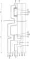
도 1은 본 발명의 예시적인 실시예들에 따른 표시 장치용 백플레인을 나타내는 평면도이다. 도 2는 본 발명의 예시적인 실시예들에 따른 표시 장치용 백플레인을 나타내는 평면도이다. 예를 들면, 도 2는 도 1의 II 영역을 확대한 평면도일 수 있다.FIG. 1 is a plan view illustrating a backplane for a display device according to exemplary embodiments of the present invention. FIG. 2 is a plan view illustrating a backplane for a display device according to exemplary embodiments of the present invention. For example, FIG. 2 may be an enlarged plan view of area II of FIG. 1.
도 1 및 도 2를 참조하면, 본 발명의 예시적인 실시예들에 따른 표시 장치용 백플레인은 표시 영역(10) 및 표시 영역(10)을 둘러싸는 주변 영역(11)을 포함할 수 있다. 또한, 주변 영역(11)은 패드 영역(20)을 포함할 수 있다.Referring to FIGS. 1 and 2, a backplane for a display device according to exemplary embodiments of the present invention may include a display area (10) and a peripheral area (11) surrounding the display area (10). In addition, the peripheral area (11) may include a pad area (20).
표시 영역(10)에는 스캔 신호를 전달하는 스캔 라인, 데이터 신호를 전달하는 데이터 라인, 및 구동 전압을 전달하는 구동 전압 라인 사이에 매트릭스 방식으로 배열되는 복수의 화소들(50)이 형성될 수 있다. 각 화소(50)는 화소(50)의 동작을 제어하기 위한 적어도 하나의 박막 트랜지스터를 포함할 수 있다.In the display area (10), a plurality of pixels (50) arranged in a matrix manner between scan lines transmitting scan signals, data lines transmitting data signals, and driving voltage lines transmitting driving voltages may be formed. Each pixel (50) may include at least one thin film transistor for controlling the operation of the pixel (50).
패드 영역(20)에는 상기 스캔 라인, 상기 데이터 라인 또는 상기 구동 전압 라인에 연결되어 상기 스캔 신호, 상기 데이터 신호 또는 상기 구동 전압을 제공하는 복수의 패드 전극들(170)이 형성될 수 있다.A plurality of pad electrodes (170) connected to the scan line, the data line or the driving voltage line to provide the scan signal, the data signal or the driving voltage may be formed in the pad area (20).
도 3은 본 발명의 예시적인 실시예들에 따른 표시 장치용 백플레인을 나타내는 단면도이다. 예를 들면, 도 3은 도 2의 표시 장치용 백플레인을 III-III' 라인을 따라 자른 단면도일 수 있다.FIG. 3 is a cross-sectional view showing a backplane for a display device according to exemplary embodiments of the present invention. For example, FIG. 3 may be a cross-sectional view of the backplane for the display device of FIG. 2 taken along line III-III'.
도 3을 참조하면, 본 발명의 예시적인 실시예들에 따른 표시 장치용 백플레인은 기판(100) 상에 배치되는 제1 절연막(145), 패드 영역(20)의 제1 절연막(145) 상에 배치되는 패드 전극(170), 및 패드 전극(170)의 측면을 커버하는 측면 보호막(182)을 포함할 수 있다.Referring to FIG. 3, a backplane for a display device according to exemplary embodiments of the present invention may include a first insulating film (145) disposed on a substrate (100), a pad electrode (170) disposed on the first insulating film (145) of a pad region (20), and a side protection film (182) covering a side surface of the pad electrode (170).
기판(100) 상에는 버퍼막(110)이 배치될 수 있다. 버퍼막(110)은 표시 영역(10)에서 패드 영역(20)까지 연장될 수 있다. 버퍼막(110)은 불순물의 확산을 방지할 수 있고, 액티브 패턴(120)을 형성하기 위한 결정화 공정에서 열의 전달 속도를 조절하는 역할을 할 수 있다. 또한, 버퍼막(110)은 기판(100)의 표면의 평탄도를 향상시키는 역할을 할 수 있다. 실시예들에 따라, 버퍼막(110)은 생략될 수도 있다.A buffer film (110) may be arranged on the substrate (100). The buffer film (110) may extend from the display area (10) to the pad area (20). The buffer film (110) may prevent diffusion of impurities and may play a role in controlling the heat transfer rate in a crystallization process for forming an active pattern (120). In addition, the buffer film (110) may play a role in improving the flatness of the surface of the substrate (100). According to embodiments, the buffer film (110) may be omitted.
버퍼막(110) 상에는 박막 트랜지스터(thin film transistor; TFT)가 배치될 수 있다. 도 3에는 하나의 박막 트랜지스터가 도시되어 있으나, 이는 설명의 편의를 위한 것이며, 버퍼막(110) 상에는 복수의 박막 트랜지스터들이 배치될 수도 있다. 상기 박막 트랜지스터는 액티브 패턴(120), 게이트 전극(135), 소스 전극(150) 및 드레인 전극(160)으로 구성될 수 있다. 상기 박막 트랜지스터는 화소 전극(200)에 화소를 구동시키기 위한 구동 신호를 전달할 수 있다.A thin film transistor (TFT) may be placed on the buffer film (110). Although one thin film transistor is illustrated in FIG. 3, this is for convenience of explanation, and a plurality of thin film transistors may be placed on the buffer film (110). The thin film transistor may be composed of an active pattern (120), a gate electrode (135), a source electrode (150), and a drain electrode (160). The thin film transistor may transmit a driving signal for driving a pixel to the pixel electrode (200).
버퍼막(110) 상에는 액티브 패턴(120)이 배치될 수 있다. 액티브 패턴(120)은 표시 영역(10)에 위치할 수 있다.An active pattern (120) may be arranged on a buffer film (110). The active pattern (120) may be located in the display area (10).
액티브 패턴(120)의 상부에는 게이트 전극(135)이 배치되고, 액티브 패턴(120)과 게이트 전극(135)의 사이에는 액티브 패턴(120)과 게이트 전극(135)을 절연시키는 게이트 절연막(130)이 배치될 수 있다. 게이트 전극(135)은 액티브 패턴(120)의 중심부에 중첩될 수 있다. 게이트 절연막(130)은 표시 영역(10)에서 패드 영역(20)까지 연장될 수 있다.A gate electrode (135) may be arranged on an upper portion of an active pattern (120), and a gate insulating film (130) may be arranged between the active pattern (120) and the gate electrode (135) to insulate the active pattern (120) and the gate electrode (135). The gate electrode (135) may overlap the center of the active pattern (120). The gate insulating film (130) may extend from the display area (10) to the pad area (20).
게이트 전극(135)의 상부에는 소스 전극(150) 및 드레인 전극(160)이 배치되고, 게이트 전극(135)과 소스/드레인 전극들(150, 160) 사이에는 층간 절연막(140)이 배치될 수 있다.A source electrode (150) and a drain electrode (160) are arranged on top of the gate electrode (135), and an interlayer insulating film (140) may be arranged between the gate electrode (135) and the source/drain electrodes (150, 160).
소스 전극(150) 및 드레인 전극(160)은 액티브 패턴(120)과 전기적으로 연결될 수 있다. 예를 들면, 게이트 절연막(130)과 층간 절연막(140)에 액티브 패턴(120)의 양 측부들을 각기 노출시키는 컨택 홀들을 형성하고, 상기 컨택 홀들을 통해 소스 전극(150) 및 드레인 전극(160)이 각기 액티브 패턴(120)과 접촉될 수 있다.The source electrode (150) and the drain electrode (160) can be electrically connected to the active pattern (120). For example, contact holes are formed in the gate insulating film (130) and the interlayer insulating film (140) to expose both sides of the active pattern (120), and the source electrode (150) and the drain electrode (160) can each come into contact with the active pattern (120) through the contact holes.
예시적인 실시예들에 있어서, 소스 전극(150)은 순차적으로 적층되는 제1 층(151), 제2 층(152) 및 제3 층(153)을 포함하고, 드레인 전극(160)은 순차적으로 적층되는 제1 층(161), 제2 층(162) 및 제3 층(163)을 포함할 수 있다. 소스/드레인 전극들(150, 160)의 제2 층들(152, 162)은 주 전극층의 역할을 하고, 소스/드레인 전극들(150, 160)의 제1 층들(151, 161) 및 제3 층들(153, 163)은 각기 제2 층들(152, 162)의 저면 및 상면을 보호하는 보조 전극층의 역할을 할 수 있다. 예를 들면, 소스/드레인 전극들(150, 160)은 각기 티타늄(Ti)/알루미늄(Al)/티타늄(Ti)의 삼중층으로 구성될 수 있다.In exemplary embodiments, the source electrode (150) may include a first layer (151), a second layer (152), and a third layer (153) that are sequentially stacked, and the drain electrode (160) may include a first layer (161), a second layer (162), and a third layer (163) that are sequentially stacked. The second layers (152, 162) of the source/drain electrodes (150, 160) may serve as a main electrode layer, and the first layers (151, 161) and the third layers (153, 163) of the source/drain electrodes (150, 160) may serve as auxiliary electrode layers that protect the bottom and top surfaces of the second layers (152, 162), respectively. For example, the source/drain electrodes (150, 160) may each be composed of a triple layer of titanium (Ti)/aluminum (Al)/titanium (Ti).
기판(100)의 상부에는 제1 절연막(145)이 배치될 수 있다. 제1 절연막(145)은 패드 영역(20)에 위치할 수 있다. 예시적인 실시예들에 있어서, 제1 절연막(145)은 층간 절연막(140)과 기판(100) 상의 실질적으로 동일한 레벨에 위치할 수 있다. 일 실시예에 있어서, 제1 절연막(145)은 표시 영역(10)에서 패드 영역(20)까지 연장되는 층간 절연막(140)의 일부일 수 있다.A first insulating film (145) may be disposed on an upper portion of the substrate (100). The first insulating film (145) may be positioned in the pad region (20). In exemplary embodiments, the first insulating film (145) may be positioned at substantially the same level as the interlayer insulating film (140) on the substrate (100). In one embodiment, the first insulating film (145) may be a portion of the interlayer insulating film (140) that extends from the display region (10) to the pad region (20).
예시적인 실시예들에 있어서, 제1 절연막(145)은 실리콘 화합물과 같은 무기 절연 물질을 포함할 수 있다. 예를 들면, 제1 절연막(145)은 실리콘 질화물(SiNx), 실리콘 산화물(SiOx), 및/또는 실리콘 산질화물(SiOxNy)을 포함할 수 있다.In exemplary embodiments, the first insulating film (145) may include an inorganic insulating material such as a silicon compound. For example, the first insulating film (145) may include silicon nitride (SiNx), silicon oxide (SiOx), and/or silicon oxynitride (SiOxNy).
제1 절연막(145) 상에는 패드 전극(170)이 배치될 수 있다. 패드 전극(170)은 패드 영역(20)에 위치할 수 있다. 예시적인 실시예들에 있어서, 패드 전극(170)은 소스/드레인 전극들(150, 160)과 기판(100) 상의 실질적으로 동일한 레벨에 위치하고, 실질적으로 동일한 물질을 포함할 수 있다.A pad electrode (170) may be placed on the first insulating film (145). The pad electrode (170) may be located in the pad region (20). In exemplary embodiments, the pad electrode (170) may be located at substantially the same level as the source/drain electrodes (150, 160) on the substrate (100) and may include substantially the same material.
예시적인 실시예들에 있어서, 패드 전극(170)은 주 패드층(172) 및 주 패드층(172)의 하부 및 상부를 커버하는 보조 패드층들(171, 173)을 포함할 수 있다. 주 패드층(172)은 주 전극층의 역할을 할 수 있고, 보조 패드층들(171, 173)은 각기 주 패드층(172)의 저면 및 상면을 보호하는 보조 전극층의 역할을 할 수 있다. 예를 들면, 패드 전극(170)은 티타늄(Ti)/알루미늄(Al)/티타늄(Ti)의 삼중층으로 구성될 수 있다.In exemplary embodiments, the pad electrode (170) may include a main pad layer (172) and auxiliary pad layers (171, 173) covering the lower and upper surfaces of the main pad layer (172). The main pad layer (172) may function as a main electrode layer, and the auxiliary pad layers (171, 173) may function as auxiliary electrode layers protecting the lower surface and the upper surface of the main pad layer (172), respectively. For example, the pad electrode (170) may be composed of a triple layer of titanium (Ti)/aluminum (Al)/titanium (Ti).
예시적인 실시예들에 있어서, 주 패드층(172)은 화소 전극(200)과 전해질에서 갈바닉 반응을 일으키는 물질을 포함할 수 있다. 이러한 갈바닉 반응이 일어나는 경우에 패드 전극(170)의 부식 또는 단락과 같은 패드 전극(170)의 손상이 발생될 수 있다.In exemplary embodiments, the main pad layer (172) may include a material that causes a galvanic reaction in the pixel electrode (200) and the electrolyte. When such a galvanic reaction occurs, damage to the pad electrode (170), such as corrosion or short circuit of the pad electrode (170), may occur.
제1 절연막(145) 상에는 패드 전극(170)의 측면을 커버하는 측면 보호막(182)이 배치될 수 있다. 예를 들면, 측면 보호막(182)은 패드 전극(170)의 주 패드층(172)의 측면을 전체적으로 커버할 수 있다. 측면 보호막(182)은 주 패드층(172)이 노출되는 것을 방지하고, 주 패드층(172)을 보호할 수 있다. 이에 따라, 전술한 바와 같이, 주 패드층(172)과 화소 전극(200)이 전해질에서 갈바닉 반응을 일으키는 물질을 포함하는 경우에도, 보조 패드층들(171, 173)이 주 패드층(172)의 저면 및 상면을 커버하고, 측면 보호막(182)이 주 패드층(172)의 측면을 커버함에 따라, 패드 전극(170)의 손상을 방지할 수 있다.A side passivation film (182) covering the side surface of the pad electrode (170) may be disposed on the first insulating film (145). For example, the side passivation film (182) may entirely cover the side surface of the main pad layer (172) of the pad electrode (170). The side passivation film (182) may prevent the main pad layer (172) from being exposed and protect the main pad layer (172). Accordingly, as described above, even when the main pad layer (172) and the pixel electrode (200) include a material that causes a galvanic reaction in the electrolyte, the auxiliary pad layers (171, 173) cover the bottom and top surfaces of the main pad layer (172), and the side passivation film (182) covers the side surface of the main pad layer (172), thereby preventing damage to the pad electrode (170).
측면 보호막(182)은 실리콘 산화물(SiOx)을 포함할 수 있다. 예시적인 실시예들에 있어서, 측면 보호막(182)의 높이는 패드 전극(170)의 높이와 실질적으로 같을 수 있다.The side passivation layer (182) may include silicon oxide (SiOx). In exemplary embodiments, the height of the side passivation layer (182) may be substantially equal to the height of the pad electrode (170).
예시적인 실시예들에 있어서, 측면 보호막(182)은 패드 전극(170)의 측면만을 커버할 수 있다. 예를 들면, 측면 보호막(182)은 패드 전극(170)의 측면 상에만 배치되고, 제1 절연막(145)의 상면 및 패드 전극(170)의 상면 상에는 배치되지 않을 수 있다.In exemplary embodiments, the side passivation film (182) may cover only the side surface of the pad electrode (170). For example, the side passivation film (182) may be disposed only on the side surface of the pad electrode (170), and may not be disposed on the upper surface of the first insulating film (145) and the upper surface of the pad electrode (170).
소스/드레인 전극들(150, 160)의 상부에는 화소 전극(200)이 배치되고, 소스/드레인 전극들(150, 160)과 화소 전극(200) 사이에는 소스/드레인 전극들(150, 160)과 화소 전극(200)을 절연시키는 평탄화막(190)이 배치될 수 있다. 평탄화막(190)은 표시 영역(10)에만 선택적으로 위치할 수 있다.A pixel electrode (200) may be arranged on top of the source/drain electrodes (150, 160), and a planarization film (190) may be arranged between the source/drain electrodes (150, 160) and the pixel electrode (200) to insulate the source/drain electrodes (150, 160) and the pixel electrode (200). The planarization film (190) may be selectively positioned only in the display area (10).
화소 전극(200)은 드레인 전극(160)과 전기적으로 연결될 수 있다. 예를 들면, 평탄화막(190)에 드레인 전극(160)의 일부를 노출시키는 비아 홀을 형성하고, 상기 비아 홀을 통해 화소 전극(200)이 드레인 전극(160)과 접촉될 수 있다.The pixel electrode (200) can be electrically connected to the drain electrode (160). For example, a via hole exposing a portion of the drain electrode (160) is formed in the planarization film (190), and the pixel electrode (200) can be brought into contact with the drain electrode (160) through the via hole.
예시적인 실시예들에 있어서, 화소 전극(200)은 순차적으로 적층되는 제1 층(201), 제2 층(202) 및 제3 층(203)을 포함할 수 있다. 화소 전극(200)의 제2 층(202)은 주 전극층의 역할을 할 수 있고, 화소 전극(200)의 제1 층(201) 및 제3 층(203)은 각기 제2 층(202)의 저면 및 상면을 보호하는 보조 전극층의 역할을 할 수 있다. 예를 들면, 화소 전극(200)은 인듐 주석 산화물(ITO)/은(Ag)/인듐 주석 산화물(ITO)의 삼중층으로 구성될 수 있다.In exemplary embodiments, the pixel electrode (200) may include a first layer (201), a second layer (202), and a third layer (203) that are sequentially laminated. The second layer (202) of the pixel electrode (200) may function as a main electrode layer, and the first layer (201) and the third layer (203) of the pixel electrode (200) may function as auxiliary electrode layers that protect the bottom and top surfaces of the second layer (202), respectively. For example, the pixel electrode (200) may be composed of a triple layer of indium tin oxide (ITO)/silver (Ag)/indium tin oxide (ITO).
예시적인 실시예들에 있어서, 패드 전극(170)의 주 패드층(172)과 화소 전극(200)의 제2층(202)은 전해질에서 서로 갈바닉 반응을 일으키는 물질을 포함할 수 있다. 예를 들면, 주 패드층(172)과 화소 전극(200)의 제2 층(202)은 각기 전해질에서 서로 갈바닉 반응을 일으키는 알루미늄(Al) 및 은(Ag)을 포함할 수 있다.In exemplary embodiments, the main pad layer (172) of the pad electrode (170) and the second layer (202) of the pixel electrode (200) may include materials that cause a galvanic reaction with each other in the electrolyte. For example, the main pad layer (172) and the second layer (202) of the pixel electrode (200) may include aluminum (Al) and silver (Ag), respectively, that cause a galvanic reaction with each other in the electrolyte.
평탄화막(190) 상에는 화소 전극(200)을 부분적으로 커버하는 화소 정의막(210)이 배치될 수 있다. 상세하게는, 화소 정의막(210)은 화소 전극(200)의 주변부를 커버하고, 화소 전극(200)의 중심부를 노출시킬 수 있다. 화소 정의막(210)은 표시 영역(10)에만 선택적으로 위치할 수 있다.A pixel defining film (210) that partially covers the pixel electrode (200) may be placed on the flattening film (190). Specifically, the pixel defining film (210) may cover the periphery of the pixel electrode (200) and expose the center of the pixel electrode (200). The pixel defining film (210) may be selectively positioned only in the display area (10).
본 발명의 예시적인 실시예들에 따른 표시 장치용 백플레인은 다양한 표시 장치들에 적용될 수 있다. 일 실시예에서, 상기 노출된 화소 전극(200) 상에 유기 발광층이 형성되고, 상기 유기 발광층을 개재하여 화소 전극(200)에 대향하는 대향 전극이 형성되는 경우에, 본 발명의 예시적인 실시예들에 따른 표시 장치용 백플레인은 유기 발광 표시 장치용 백플레인으로 사용될 수 있다. 또한, 다른 실시예에서, 상기 노출된 화소 전극(200) 상에 액정층이 형성되고, 상기 액정층을 개재하여 화소 전극(200)에 대향하는 공통 전극이 형성되는 경우에, 본 발명의 예시적인 실시예들에 따른 표시 장치용 백플레인은 액정 표시 장치용 백플레인으로 사용될 수도 있다. 다만, 이에 한정되는 것은 아니고, 본 발명의 예시적인 실시예들에 따른 표시 장치용 백플레인은 다양한 표시 장치에 사용될 수 있다.The backplane for a display device according to exemplary embodiments of the present invention can be applied to various display devices. In one embodiment, when an organic light-emitting layer is formed on the exposed pixel electrode (200) and a counter electrode is formed opposing the pixel electrode (200) with the organic light-emitting layer interposed therebetween, the backplane for a display device according to exemplary embodiments of the present invention can be used as a backplane for an organic light-emitting display device. In addition, in another embodiment, when a liquid crystal layer is formed on the exposed pixel electrode (200) and a common electrode is formed opposing the pixel electrode (200) with the liquid crystal layer interposed therebetween, the backplane for a display device according to exemplary embodiments of the present invention can also be used as a backplane for a liquid crystal display device. However, the present invention is not limited thereto, and the backplane for a display device according to exemplary embodiments of the present invention can be used in various display devices.
도 4 내지 도 9는 본 발명의 예시적인 실시예들에 따른 표시 장치용 백플레인의 제조 방법을 나타내는 단면도들이다.FIGS. 4 to 9 are cross-sectional views showing a method for manufacturing a backplane for a display device according to exemplary embodiments of the present invention.
도 4를 참조하면, 기판(100)은 표시 영역(10) 및 패드 영역(20)을 구비할 수 있다. 기판(100) 상에는 제1 절연막(145)이 형성되고, 제1 절연막(145) 상에는 패드 전극막(170')이 형성되며, 패드 영역(20)의 패드 전극막(170') 상에는 포토레지스트 패턴(310)이 형성될 수 있다.Referring to FIG. 4, the substrate (100) may have a display area (10) and a pad area (20). A first insulating film (145) may be formed on the substrate (100), a pad electrode film (170') may be formed on the first insulating film (145), and a photoresist pattern (310) may be formed on the pad electrode film (170') of the pad area (20).
버퍼막(110)은 기판(100) 상에 형성되고, 표시 영역(10)에서 패드 영역(20)까지 연장될 수 있다. 예를 들면, 버퍼막(110)은 실리콘 산화물(SiOx), 실리콘 질화물(SiNx) 등을 사용하여 플라즈마 화학 기상 증착법(PECVD), 상압 화학 기상 증착법(APCVD), 저압 화학 기상 증착법(LPCVD) 등의 다양한 증착 방법에 의하여 형성될 수 있다. 버퍼막(110)은 필요에 따라 형성되지 않을 수도 있다.The buffer film (110) is formed on the substrate (100) and may extend from the display area (10) to the pad area (20). For example, the buffer film (110) may be formed by various deposition methods, such as plasma enhanced chemical vapor deposition (PECVD), atmospheric pressure chemical vapor deposition (APCVD), and low pressure chemical vapor deposition (LPCVD), using silicon oxide (SiOx), silicon nitride (SiNx), and the like. The buffer film (110) may not be formed as needed.
액티브 패턴(120)은 표시 영역(10)의 버퍼막(110) 상에 형성될 수 있다. 예를 들면, 액티브 패턴(120)은 실리콘을 함유하는 물질, 산화물 반도체 등을 포함하는 막을 버퍼막(110)의 전면(全面)에 형성하고, 이를 패터닝하여 형성될 수 있다. 실리콘을 함유하는 물질을 사용하여 액티브 패턴(120)을 형성하는 경우에, 비정질 실리콘막을 버퍼막(110)의 전면에 형성하고, 이를 결정화하여 다결정 실리콘막을 형성하며, 이를 패터닝한 후에 상기 패터닝된 다결정 실리콘막의 양 측부들에 불순물을 도핑하여 소스 영역, 드레인 영역, 및 그들 사이에 채널 영역을 포함하는 액티브 패턴(120)이 형성될 수 있다.The active pattern (120) can be formed on the buffer film (110) of the display area (10). For example, the active pattern (120) can be formed by forming a film including a material containing silicon, an oxide semiconductor, etc., on the entire surface of the buffer film (110), and patterning it. In the case of forming the active pattern (120) using a material containing silicon, an amorphous silicon film is formed on the entire surface of the buffer film (110), crystallized to form a polycrystalline silicon film, and after patterning it, impurities are doped on both sides of the patterned polycrystalline silicon film, so that an active pattern (120) including a source region, a drain region, and a channel region therebetween can be formed.
게이트 절연막(130)은 버퍼막(110) 상에 형성되고, 액티브 패턴(120)을 커버하며, 표시 영역(10)에서 패드 영역(20)까지 연장될 수 있다. 예를 들면, 게이트 절연막(130)은 실리콘 산화물(SiOx), 실리콘 질화물(SiNx) 등을 사용하여 형성될 수 있다.The gate insulating film (130) is formed on the buffer film (110), covers the active pattern (120), and can extend from the display area (10) to the pad area (20). For example, the gate insulating film (130) can be formed using silicon oxide (SiOx), silicon nitride (SiNx), or the like.
게이트 전극(135)은 표시 영역(10)의 게이트 절연막(130) 상에 형성되고, 액티브 패턴(120)과 중첩되도록 위치할 수 있다. 예를 들면, 게이트 전극(135)은 금속, 합금, 금속 질화물, 도전성 금속 산화물, 투명 도전성 산화물 등을 사용하여 형성될 수 있다.The gate electrode (135) is formed on the gate insulating film (130) of the display area (10) and may be positioned to overlap with the active pattern (120). For example, the gate electrode (135) may be formed using a metal, an alloy, a metal nitride, a conductive metal oxide, a transparent conductive oxide, or the like.
층간 절연막(140)은 게이트 절연막(130) 상에 형성되고, 게이트 전극(135)을 커버할 수 있다. 예를 들면, 층간 절연막(140)은 실리콘 산화물(SiOx), 실리콘 질화물(SiNx) 등을 사용하여 형성될 수 있다.An interlayer insulating film (140) is formed on the gate insulating film (130) and can cover the gate electrode (135). For example, the interlayer insulating film (140) can be formed using silicon oxide (SiOx), silicon nitride (SiNx), or the like.
제1 절연막(145)은 기판(100)의 상부에 형성되고, 패드 영역(20)에 위치할 수 있다. 예를 들면, 제1 절연막(145)은 실리콘 산화물(SiOx), 실리콘 질화물(SiNx) 등을 사용하여 형성될 수 있다. 예시적인 실시예들에 있어서, 제1 절연막(145)은 표시 영역(10)에서 패드 영역(20)까지 연장되는 층간 절연막(140)의 일부일 수 있다.The first insulating film (145) may be formed on an upper portion of the substrate (100) and positioned in the pad region (20). For example, the first insulating film (145) may be formed using silicon oxide (SiOx), silicon nitride (SiNx), or the like. In exemplary embodiments, the first insulating film (145) may be a part of an interlayer insulating film (140) extending from the display region (10) to the pad region (20).
게이트 절연막(130)과 층간 절연막(140)에는 액티브 패턴(120)의 일부들을 노출시키는 컨택 홀들이 형성될 수 있다. 예를 들면, 상기 컨택 홀들은 각기 액티브 패턴(120)의 양 측부들을 노출시킬 수 있다.Contact holes that expose parts of the active pattern (120) may be formed in the gate insulating film (130) and the interlayer insulating film (140). For example, the contact holes may each expose both sides of the active pattern (120).
패드 전극막(170')은 제1 절연막(145) 상에 형성될 수 있다. 예시적인 실시예들에 있어서, 패드 전극막(170')은 제1 절연막(145)을 일부로 포함하는 층간 절연막(140) 상에 형성되고, 상기 컨택 홀들을 통해 액티브 패턴(120)과 접촉할 수 있다. 일 실시예에 있어서, 층간 절연막(140) 상에 표시 영역(10)에서 패드 영역(20)까지 연장되는 제1 서브 도전막(171'), 제2 서브 도전막(172') 및 제3 서브 도전막(173')을 순차적으로 적층할 수 있다. 예를 들면, 제1 내지 제3 서브 도전막들(171', 172', 173')은 각기 티타늄(Ti), 알루미늄(Al) 및 티타늄(Ti)을 포함할 수 있다.The pad electrode film (170') may be formed on the first insulating film (145). In exemplary embodiments, the pad electrode film (170') is formed on the interlayer insulating film (140) including the first insulating film (145) as a part, and may be in contact with the active pattern (120) through the contact holes. In one embodiment, a first sub-conductive film (171'), a second sub-conductive film (172'), and a third sub-conductive film (173') may be sequentially laminated on the interlayer insulating film (140) extending from the display area (10) to the pad area (20). For example, the first to third sub-conductive films (171', 172', 173') may include titanium (Ti), aluminum (Al), and titanium (Ti), respectively.
포토레지스트 패턴(310)은 패드 영역(20)의 패드 전극막(170') 상에 형성될 수 있다. 예를 들면, 패드 전극막(170') 상에 표시 영역(10)에서 패드 영역(20)까지 연장되는 포토레지스트막을 형성하고, 마스크를 사용하여 상기 포토레지스트막을 노광 및 현상하여, 소스 전극(150), 드레인 전극(160), 및 패드 전극(170)에 각기 대응되는 포토레지스트 패턴들(310, 315)을 형성할 수 있다.The photoresist pattern (310) may be formed on the pad electrode film (170') of the pad area (20). For example, a photoresist film extending from the display area (10) to the pad area (20) may be formed on the pad electrode film (170'), and the photoresist film may be exposed and developed using a mask to form photoresist patterns (310, 315) corresponding to the source electrode (150), the drain electrode (160), and the pad electrode (170), respectively.
도 5를 참조하면, 포토레지스트 패턴(310)을 식각 방지막으로 이용하여 패드 전극막(170') 및 제1 절연막(145)의 일부를 식각함으로써 패드 전극(170) 및 패드 전극(170)의 측면을 커버하는 측면 보호막(182)을 실질적으로 동시에 형성할 수 있다.Referring to FIG. 5, by etching a portion of the pad electrode film (170') and the first insulating film (145) using the photoresist pattern (310) as an etch-preventive film, the pad electrode (170) and the side protective film (182) covering the side surface of the pad electrode (170) can be formed substantially simultaneously.
예시적인 실시예들에 있어서, 식각 가스를 사용하는 건식 식각 방법으로 패드 전극막(170')을 식각하여 패드 전극(170)을 형성할 수 있다. 예를 들면, 제1 서브 도전막(171'), 제2 서브 도전막(172') 및 제3 서브 도전막(173')이 건식 식각 방법으로 식각되어, 주 패드층(172) 및 주 패드층(172)의 하부 및 상부를 커버하는 보조 패드층들(171, 173)을 포함하는 패드 전극(170)이 형성될 수 있다. 예를 들면, 패드 전극(170)은 티타늄(Ti)/알루미늄(Al)/티타늄(Ti)의 삼중층으로 구성될 수 있다.In exemplary embodiments, the pad electrode (170) may be formed by etching the pad electrode film (170') by a dry etching method using an etching gas. For example, a first sub-conductive film (171'), a second sub-conductive film (172'), and a third sub-conductive film (173') may be etched by a dry etching method to form a pad electrode (170) including a main pad layer (172) and auxiliary pad layers (171, 173) covering the lower and upper portions of the main pad layer (172). For example, the pad electrode (170) may be composed of a triple layer of titanium (Ti)/aluminum (Al)/titanium (Ti).
예시적인 실시예들에 있어서, 제1 절연막(145)의 상기 일부는 제1 가스를 사용하여 식각되고, 측면 보호막(182)은 상기 제1 가스에 의해 식각되는 제1 절연막(145)의 상기 일부에 포함되는 물질 및 포토레지스트 패턴(310)에 포함되는 물질의 결합에 의해 형성될 수 있다. 일 실시예에 있어서, 상기 제1 가스는 패드 전극막(170') 및 제1 절연막(145)의 상기 일부를 식각하는 식각 가스의 기능을 할 수 있다.In exemplary embodiments, the part of the first insulating film (145) is etched using the first gas, and the side passivation film (182) can be formed by combining a material included in the part of the first insulating film (145) etched by the first gas and a material included in the photoresist pattern (310). In one embodiment, the first gas can function as an etching gas that etches the pad electrode film (170') and the part of the first insulating film (145).
일 실시예에 있어서, 상기 제1 가스는 염소(Cl)를 포함하고, 제1 절연막(145)의 상기 일부는 실리콘을 포함하며, 포토레지스트 패턴(310)은 산소(O)를 포함할 수 있다. 예를 들면, 상기 제1 가스는 BCl3 및/또는 Cl2를 포함하고, 제1 절연막(145)은 실리콘 질화물(SiNx), 실리콘 산화물(SiOx) 및/또는 실리콘 산질화물(SiOxNy)을 포함할 수 있다. 이 경우, 실리콘 산화물(SiOx)을 포함하는 측면 보호막(182)이 형성될 수 있다. 예를 들면, 상기 제1 가스에 포함되는 염소(Cl)에 의해 식각되는 제1 절연막(145)으로부터 방출되는 실리콘(Si)과 포토레지스트 패턴(310)으로부터 방출되는 산소(O)가 결합하여, 패드 전극(170)의 측면 상에 실리콘 산화물(SiOx)을 포함하는 측면 보호막(182)이 형성될 수 있다.In one embodiment, the first gas may include chlorine (Cl), the part of the first insulating film (145) may include silicon, and the photoresist pattern (310) may include oxygen (O). For example, the first gas may include BCl3 and/or Cl2 , and the first insulating film (145) may include silicon nitride (SiNx), silicon oxide (SiOx), and/or silicon oxynitride (SiOxNy). In this case, a side passivation film (182) including silicon oxide (SiOx) may be formed. For example, silicon (Si) released from the first insulating film (145) that is etched by chlorine (Cl) included in the first gas and oxygen (O) released from the photoresist pattern (310) may combine to form a side passivation film (182) including silicon oxide (SiOx) on the side surface of the pad electrode (170).
일 실시예에 있어서, 포토레지스트 패턴(310)의 저면과 측면 사이의 테이퍼 각(taper angle, θ1)은 약 60도 내지 약 90도일 수 있다. 상기 테이퍼 각(θ1)이 약 60도 미만인 경우에는, 측면 보호막(182)이 형성되지 않을 수 있다. 또한, 상기 테이퍼 각(θ1)이 약 90도 초과인 경우에는, 패드 전극막(170')이 불균일하게 식각될 수 있다.In one embodiment, the taper angle (θ1) between the bottom surface and the side surface of the photoresist pattern (310) may be from about 60 degrees to about 90 degrees. When the taper angle (θ1) is less than about 60 degrees, the side protective film (182) may not be formed. In addition, when the taper angle (θ1) is greater than about 90 degrees, the pad electrode film (170') may be etched unevenly.
다른 예시적인 실시예들에 있어서, 제1 절연막(145)의 상기 일부는 제2 가스를 사용하여 식각되고, 측면 보호막(182)은 상기 제2 가스에 의해 식각되는 제1 절연막(145)의 상기 일부에 포함되는 물질 및 상기 제2 가스에 포함되는 물질의 결합에 의해 형성될 수 있다. 일 실시예에 있어서, 상기 제2 가스는 패드 전극(170)의 부식을 방지하는 기능을 할 수 있다. 이에 따라, 후술하는 포토레지스트 패턴(310)의 박리 단계에서 패드 전극(170)이 부식되는 것을 방지할 수 있다.In other exemplary embodiments, the part of the first insulating film (145) may be etched using the second gas, and the side passivation film (182) may be formed by a combination of a material included in the part of the first insulating film (145) etched by the second gas and a material included in the second gas. In one embodiment, the second gas may have a function of preventing corrosion of the pad electrode (170). Accordingly, the pad electrode (170) may be prevented from being corroded in the peeling step of the photoresist pattern (310) described below.
일 실시예에 있어서, 상기 제2 가스는 불소(F) 및 산소(O)를 포함하고, 제1 절연막(145)의 상기 일부는 실리콘을 포함할 수 있다. 예를 들면, 상기 제2 가스는 CF4 및 O2를 포함하고, 제1 절연막(145)은 실리콘 질화물(SiNx), 실리콘 산화물(SiOx) 및/또는 실리콘 산질화물(SiOxNy)을 포함할 수 있다. 이 경우, 실리콘 산화물(SiOx)을 포함하는 측면 보호막(182)이 형성될 수 있다. 예를 들면, 상기 제2 가스에 포함되는 불소(F)에 의해 식각되는 제1 절연막(145)으로부터 방출되는 실리콘(Si)과 상기 제2 가스로부터 방출되는 산소(O)가 결합하여, 패드 전극(170)의 측면 상에 실리콘 산화물(SiOx)을 포함하는 측면 보호막(182)이 형성될 수 있다.In one embodiment, the second gas may include fluorine (F) and oxygen (O), and the part of the first insulating film (145) may include silicon. For example, the second gas may include CF4 and O2 , and the first insulating film (145) may include silicon nitride (SiNx), silicon oxide (SiOx), and/or silicon oxynitride (SiOxNy). In this case, a side passivation film (182) including silicon oxide (SiOx) may be formed. For example, silicon (Si) released from the first insulating film (145) that is etched by fluorine (F) included in the second gas and oxygen (O) released from the second gas may combine to form a side passivation film (182) including silicon oxide (SiOx) on the side surface of the pad electrode (170).
예시적인 실시예들에 있어서, 포토레지스트 패턴(315)을 식각 방지막으로 이용하여 패드 전극막(170')을 식각함으로써 소스 전극(150) 및 드레인 전극(160)을 형성할 수 있다. 예를 들면, 포토레지스트 패턴들(310, 315)을 이용하여 패드 전극막(170')을 식각함으로써 소스 전극(150), 드레인 전극(160) 및 패드 전극(170)을 실질적으로 동시에 형성할 수 있다.In exemplary embodiments, the source electrode (150) and the drain electrode (160) can be formed by etching the pad electrode film (170') using the photoresist pattern (315) as an etch-preventive film. For example, the source electrode (150), the drain electrode (160), and the pad electrode (170) can be formed substantially simultaneously by etching the pad electrode film (170') using the photoresist patterns (310, 315).
도 6을 참조하면, 포토레지스트 패턴(310)을 박리(strip)할 수 있다. 예를 들면, 포토레지스트 박리액을 사용하여 포토레지스트 패턴(310)을 패드 전극(170)으로부터 박리할 수 있다. 예시적인 실시예들에 있어서, 소스 전극(150), 드레인 전극(160) 및 패드 전극(170) 상에 배치되는 포토레지스트 패턴들(310, 315)이 실질적으로 동시에 박리될 수 있다.Referring to FIG. 6, the photoresist pattern (310) can be stripped. For example, the photoresist pattern (310) can be stripped from the pad electrode (170) using a photoresist stripping solution. In exemplary embodiments, the photoresist patterns (310, 315) disposed on the source electrode (150), the drain electrode (160), and the pad electrode (170) can be stripped substantially simultaneously.
도 7을 참조하면, 화학기계적 연마(chemical mechanical polishing; CMP)법을 사용하여 측면 보호막(182)을 연마할 수 있다.Referring to FIG. 7, the side protective film (182) can be polished using a chemical mechanical polishing (CMP) method.
일 실시예에 있어서, 측면 보호막(182)은 상면이 패드 전극(170)의 상면보다 높게 형성될 수 있다. 이 경우, 측면 보호막(182)의 상부를 연마하여 패드 전극(170)의 상면보다 높은 위치의 측면 보호막(182)을 제거할 수 있다. 측면 보호막(182)을 연마함에 따라, 측면 보호막(182)의 상면이 패드 전극(170)의 상면과 실질적으로 같은 높이에 위치할 수 있다. 이에 따라, 후속 공정에서 측면 보호막(182)과 패드 전극(170) 사이의 단차에 따라 패드 전극(170) 상에 형성되는 구조물에 발생될 수 있는 결함 등을 방지할 수 있다.In one embodiment, the side passivation film (182) may be formed so that its upper surface is higher than the upper surface of the pad electrode (170). In this case, the upper portion of the side passivation film (182) may be polished to remove the side passivation film (182) at a position higher than the upper surface of the pad electrode (170). As the side passivation film (182) is polished, the upper surface of the side passivation film (182) may be positioned at substantially the same height as the upper surface of the pad electrode (170). Accordingly, defects that may occur in a structure formed on the pad electrode (170) due to a step difference between the side passivation film (182) and the pad electrode (170) in a subsequent process may be prevented.
도 8을 참조하면, 표시 영역(10) 및 패드 영역(20)의 기판(100) 상에 패드 전극(170) 및 측면 보호막(182)을 커버하는 화소 전극막(200')을 형성할 수 있다.Referring to FIG. 8, a pixel electrode film (200') covering a pad electrode (170) and a side protective film (182) can be formed on a substrate (100) in a display area (10) and a pad area (20).
표시 영역(10)의 층간 절연막(140) 상에 소스 전극(150) 및 드레인 전극(160)을 커버하는 평탄화막(190)을 형성할 수 있다. 평탄화막(190)에는 드레인 전극(160)의 일부를 노출시키는 비아 홀이 형성될 수 있다. 예를 들면, 상기 비아 홀은 드레인 전극(160)의 상면을 노출시킬 수 있다. 평탄화막(190)은 유기 물질로 형성될 수 있다. 예를 들면, 평탄화막(190)은 폴리이미드(polyimide)계 수지, 포토레지스트(photoresist), 아크릴(acrylic)계 수지, 폴리아미드(polyamide)계 수지 및/또는 실록산(siloxane)계 수지를 포함할 수 있다.A planarization film (190) covering the source electrode (150) and the drain electrode (160) may be formed on the interlayer insulating film (140) of the display area (10). A via hole exposing a portion of the drain electrode (160) may be formed in the planarization film (190). For example, the via hole may expose the upper surface of the drain electrode (160). The planarization film (190) may be formed of an organic material. For example, the planarization film (190) may include a polyimide-based resin, a photoresist, an acrylic-based resin, a polyamide-based resin, and/or a siloxane-based resin.
평탄화막(190)은 표시 영역(10)에만 선택적으로 형성되고, 패드 영역(20)까지 연장되지 않을 수 있다. 유기 물질을 포함하는 평탄화막(190)이 패드 영역(20)까지 연장되고, 외부로부터 표시 장치용 백플레인의 측부에 수분 등이 유입되는 경우에, 이러한 수분이 평탄화막(190)을 통해 패드 영역(20)에서 표시 영역(10)으로 이동하여 화소를 열화시킬 수 있다. 이에 따라, 화소의 열화를 방지하기 위하여, 보호막(180)이 패드 영역(20)에는 배치되지 않을 수 있다.The planarization film (190) is selectively formed only in the display area (10) and may not extend to the pad area (20). If the planarization film (190) including an organic material extends to the pad area (20) and moisture or the like flows into the side of the backplane for the display device from the outside, the moisture may move from the pad area (20) to the display area (10) through the planarization film (190) and deteriorate the pixels. Accordingly, in order to prevent deterioration of the pixels, the protective film (180) may not be disposed in the pad area (20).
평탄화막(190) 및 제1 절연막(145) 상에 표시 영역(10)에서 패드 영역(20)까지 연장되는 화소 전극막(200')을 형성할 수 있다. 화소 전극막(200')은 보호막(180)의 상기 비아 홀에 의해 노출된 드레인 전극(160)과 접촉할 수 있다. 또한, 화소 전극막(200')은 패드 전극(170) 및 측면 보호막(182)을 커버할 수 있다. 구체적으로, 화소 전극막(200')은 패드 전극(170)의 상면 및 측면 보호막(182)의 상면 및 노출된 측면을 커버할 수 있다. 예를 들면, 화소 전극막(200')은 스퍼터링, 화학 기상 증착법(CVD), 물리 기상 증착법(PVD) 등의 방법에 의하여 형성될 수 있다.A pixel electrode film (200') extending from the display area (10) to the pad area (20) can be formed on the flattening film (190) and the first insulating film (145). The pixel electrode film (200') can be in contact with the drain electrode (160) exposed by the via hole of the passivation film (180). In addition, the pixel electrode film (200') can cover the pad electrode (170) and the side passivation film (182). Specifically, the pixel electrode film (200') can cover the upper surface of the pad electrode (170) and the upper surface and the exposed side surface of the side passivation film (182). For example, the pixel electrode film (200') can be formed by a method such as sputtering, chemical vapor deposition (CVD), or physical vapor deposition (PVD).
예시적인 실시예들에 있어서, 화소 전극막(200')은 제1 막(201'), 제2 막(202') 및 제3 막(203')을 순차적으로 적층하여 형성될 수 있다. 예를 들면, 제1 막(201') 및 제3 막(203')은 인듐 주석 산화물(ITO)을 포함하고, 제2 막(202')은 은(Ag)을 포함할 수 있다.In exemplary embodiments, the pixel electrode film (200') may be formed by sequentially laminating a first film (201'), a second film (202'), and a third film (203'). For example, the first film (201') and the third film (203') may include indium tin oxide (ITO), and the second film (202') may include silver (Ag).
도 9를 참조하면, 식각액을 이용하여 화소 전극막(200')을 식각하여 표시 영역(10)에 화소 전극(200)을 형성할 수 있다.Referring to FIG. 9, a pixel electrode film (200') can be etched using an etchant to form a pixel electrode (200) in the display area (10).
화소 전극(200)이 형성되는 영역에 대응되도록 화소 전극막(200') 상에 포토레지스트 패턴을 형성할 수 있다. 예를 들면, 화소 전극막(200') 상에 표시 영역(10)에서 패드 영역(20)까지 연장되는 포토레지스트막을 형성하고, 마스크를 이용하여 상기 포토레지스트막을 노광 및 현상하여, 상기 포토레지스트 패턴을 형성할 수 있다. 그 다음, 상기 포토레지스트 패턴을 식각 방지막으로 이용하여 화소 전극막(200')을 식각함으로써 화소 전극(200)을 형성할 수 있다. 화소 전극막(200')은 식각액을 사용하는 습식 식각 방법에 의해 식각될 수 있다.A photoresist pattern can be formed on the pixel electrode film (200') to correspond to the area where the pixel electrode (200) is formed. For example, a photoresist film extending from the display area (10) to the pad area (20) can be formed on the pixel electrode film (200'), and the photoresist film can be exposed and developed using a mask to form the photoresist pattern. Then, the pixel electrode (200) can be formed by etching the pixel electrode film (200') using the photoresist pattern as an etching prevention film. The pixel electrode film (200') can be etched by a wet etching method using an etchant.
예시적인 실시예들에 있어서, 패드 전극(170)의 주 패드층(172)과 화소 전극막(200')은 상기 식각액에서 서로 갈바닉 반응을 일으키는 물질을 포함할 수 있다. 예를 들면, 주 패드층(172)과 화소 전극막(200')의 제2 막(202')은 각기 상기 식각액에서 서로 갈바닉 반응을 일으키는 알루미늄(Al) 및 은(Ag)을 포함할 수 있다. 갈바닉 반응은 표준 환원 전위가 다른 두 금속이 전해질로 연결되는 경우에, 산화-환원 반응에 의해 전자의 이동이 일어나 금속 이온이 환원되는 현상을 말한다.In exemplary embodiments, the main pad layer (172) of the pad electrode (170) and the pixel electrode film (200') may include materials that cause a galvanic reaction with each other in the etching solution. For example, the main pad layer (172) and the second film (202') of the pixel electrode film (200') may include aluminum (Al) and silver (Ag), which cause a galvanic reaction with each other in the etching solution, respectively. The galvanic reaction refers to a phenomenon in which, when two metals having different standard reduction potentials are connected through an electrolyte, electrons move through an oxidation-reduction reaction and metal ions are reduced.
화소 전극막(200')의 제2 막(202')에 포함되는 은(Ag)이 전해질인 상기 식각액과 접촉하는 경우에, 상기 식각액에 포함된 인산(H3PO4) 등에 의해 은 이온(Ag+)이 발생되고, 상기 은 이온(Ag+)이 주 패드층(172)에 포함되는 알루미늄(Al)과 접촉하는 경우에 산화-환원 반응에 의해 은 이온(Ag+)이 환원되어 은(Ag) 입자가 생성되고, 알루미늄(Al)이 산화될 수 있다.When silver (Ag) included in the second film (202') of the pixel electrode film (200') comes into contact with the etching solution, which is an electrolyte, silver ions (Ag+ ) are generated byphosphoric acid (H3PO4 ) included in the etching solution, and when the silver ions (Ag+ ) come into contact with aluminum (Al) included in the main pad layer (172), the silver ions (Ag+ ) are reduced by an oxidation-reduction reaction to generate silver (Ag) particles, and aluminum (Al) can be oxidized.
종래의 표시 장치용 백플레인의 제조 방법에서는 전술한 은 이온(Ag+)과 알루미늄(Al)의 산화-환원 반응에 의해, 패드 전극의 주 패드층이 부식되고, 패드 전극들 사이에 환원된 은(Ag) 입자에 의한 도전 경로가 형성되어 패드 전극들 사이에 단락이 발생할 수 있다. 이러한 패드 전극의 부식 및 단락과 같은 패드 전극의 손상을 방지하기 위하여, 본 발명의 예시적인 실시예들에 따른 표시 장치용 백플레인의 제조 방법에서는, 전술하는 바와 같이, 패드 전극(170)의 측면을 커버하는 측면 보호막(182)을 형성할 수 있다. 이에 따라, 패드 전극의 보조 패드층들(171, 173)이 주 패드층(172)의 저면 및 상면을 커버하고, 측면 보호막(182)이 주 패드층(172)의 측면을 커버함에 따라, 주 패드층(172)이 화소 전극막(200')이 습식 식각되어 생성되는 물질에 노출되지 않음으로써, 패드 전극(170)의 손상을 방지할 수 있다.In a conventional method for manufacturing a backplane for a display device, the main pad layer of the pad electrode may be corroded by the oxidation-reduction reaction of the silver ions (Ag+ ) and aluminum (Al) described above, and a conductive path may be formed between the pad electrodes by the reduced silver (Ag) particles, which may cause a short circuit between the pad electrodes. In order to prevent damage to the pad electrodes, such as corrosion and short circuit of the pad electrodes, in a method for manufacturing a backplane for a display device according to exemplary embodiments of the present invention, as described above, a side protection film (182) covering a side surface of the pad electrode (170) may be formed. Accordingly, since the auxiliary pad layers (171, 173) of the pad electrode cover the lower and upper surfaces of the main pad layer (172), and the side protective film (182) covers the side surface of the main pad layer (172), the main pad layer (172) is not exposed to the material generated by wet etching of the pixel electrode film (200'), thereby preventing damage to the pad electrode (170).
도 3을 참조하면, 표시 영역(10)의 평탄화막(190) 상에 화소 전극(200)을 커버하는 화소 정의막(210)을 형성할 수 있다.Referring to FIG. 3, a pixel definition film (210) covering a pixel electrode (200) can be formed on a flattening film (190) of a display area (10).
화소 정의막(210)에는 화소 전극(200)의 일부를 노출시키는 개구부가 형성될 수 있다. 예를 들면, 상기 개구부는 화소 전극(200)의 중심부를 노출시킬 수 있다. 화소 정의막(210)은 유기 물질로 형성될 수 있다. 예를 들면, 화소 정의막(210)은 폴리이미드(polyimide)계 수지, 포토레지스트(photoresist), 아크릴(acrylic)계 수지, 폴리아미드(polyamide)계 수지 및/또는 실록산(siloxane)계 수지로 형성될 수 있다.An opening that exposes a part of the pixel electrode (200) may be formed in the pixel defining film (210). For example, the opening may expose a center of the pixel electrode (200). The pixel defining film (210) may be formed of an organic material. For example, the pixel defining film (210) may be formed of a polyimide-based resin, a photoresist, an acrylic-based resin, a polyamide-based resin, and/or a siloxane-based resin.
도 10은 본 발명의 다른 예시적인 실시예들에 따른 표시 장치용 백플레인을 나타내는 단면도이다. 도 10은 도 2의 표시 장치용 백플레인을 III-III' 라인을 따라 자른 단면도일 수 있다.FIG. 10 is a cross-sectional view showing a backplane for a display device according to other exemplary embodiments of the present invention. FIG. 10 may be a cross-sectional view of the backplane for the display device of FIG. 2 taken along line III-III'.
도 10에 도시된 표시 장치용 백플레인은 측면 보호막(184)의 구조를 제외하고 도 3에 도시된 표시 장치용 백플레인과 실질적으로 동일하거나 유사한 구성 및/또는 구조를 가질 수 있다. 이에 따라, 중복되는 구성 및/또는 구조에 대한 상세한 설명은 생략되며, 동일하거나 유사한 구성 요소들에 대해서는 동일하거나 유사한 참조부호들을 사용한다.The backplane for the display device illustrated in FIG. 10 may have a configuration and/or structure substantially the same as or similar to that of the backplane for the display device illustrated in FIG. 3, except for the structure of the side protection film (184). Accordingly, detailed descriptions of overlapping configurations and/or structures are omitted, and identical or similar reference numerals are used for identical or similar components.
도 10을 참조하면, 본 발명의 다른 예시적인 실시예들에 따른 표시 장치용 백플레인은 기판(100) 상에 배치되는 제1 절연막(145), 패드 영역(20)의 제1 절연막(145) 상에 배치되는 패드 전극(170), 및 패드 전극(170)의 측면을 커버하는 측면 보호막(184)을 포함할 수 있다.Referring to FIG. 10, a backplane for a display device according to other exemplary embodiments of the present invention may include a first insulating film (145) disposed on a substrate (100), a pad electrode (170) disposed on the first insulating film (145) of a pad region (20), and a side protection film (184) covering a side surface of the pad electrode (170).
제1 절연막(145) 상에는 패드 전극(170)의 측면을 커버하는 측면 보호막(184)이 배치될 수 있다. 예를 들면, 측면 보호막(184)은 패드 전극(170)의 주 패드층(172)의 측면을 전체적으로 커버할 수 있다. 측면 보호막(184)은 주 패드층(172)이 노출되는 것을 방지하고, 주 패드층(172)을 보호할 수 있다. 이에 따라, 주 패드층(172)과 화소 전극(200)이 전해질에서 갈바닉 반응을 일으키는 물질을 포함하는 경우에도, 보조 패드층들(171, 173)이 주 패드층(172)의 저면 및 상면을 커버하고, 측면 보호막(184)이 주 패드층(172)의 측면을 커버함에 따라, 패드 전극(170)의 손상을 방지할 수 있다.A side passivation film (184) covering the side surface of the pad electrode (170) may be disposed on the first insulating film (145). For example, the side passivation film (184) may entirely cover the side surface of the main pad layer (172) of the pad electrode (170). The side passivation film (184) may prevent the main pad layer (172) from being exposed and protect the main pad layer (172). Accordingly, even when the main pad layer (172) and the pixel electrode (200) include a material that causes a galvanic reaction in the electrolyte, the auxiliary pad layers (171, 173) cover the lower surface and upper surface of the main pad layer (172), and the side passivation film (184) covers the side surface of the main pad layer (172), thereby preventing damage to the pad electrode (170).
측면 보호막(184)은 실리콘 화합물과 같은 무기 절연 물질을 포함할 수 있다. 예를 들면, 제1 절연막(145)은 실리콘 질화물(SiNx), 실리콘 산화물(SiOx), 및/또는 실리콘 산질화물(SiOxNy)을 포함할 수 있다. 예시적인 실시예들에 있어서, 측면 보호막(184)의 높이는 패드 전극(170)의 높이와 실질적으로 같을 수 있다.The side passivation layer (184) may include an inorganic insulating material such as a silicon compound. For example, the first insulating layer (145) may include silicon nitride (SiNx), silicon oxide (SiOx), and/or silicon oxynitride (SiOxNy). In exemplary embodiments, the height of the side passivation layer (184) may be substantially equal to the height of the pad electrode (170).
예시적인 실시예들에 있어서, 측면 보호막(184)은 패드 전극(170)의 측면 및 제1 절연막(145)의 상면을 커버할 수 있다. 예를 들면, 측면 보호막(184)은 패드 전극(170)의 상면을 제외한 패드 영역(20)의 제1 절연막(145)의 전면을 커버할 수 있다.In exemplary embodiments, the side passivation film (184) may cover the side of the pad electrode (170) and the upper surface of the first insulating film (145). For example, the side passivation film (184) may cover the entire surface of the first insulating film (145) of the pad area (20) excluding the upper surface of the pad electrode (170).
도 11 내지 도 16은 본 발명의 다른 예시적인 실시예들에 따른 표시 장치용 백플레인의 제조 방법을 나타내는 단면도들이다.FIGS. 11 to 16 are cross-sectional views showing a method of manufacturing a backplane for a display device according to other exemplary embodiments of the present invention.
도 11 내지 도 16에 도시된 표시 장치용 백플레인의 제조 방법은 일부 구성 및/또는 단계를 제외하고 도 4 내지 도 9에 도시된 표시 장치용 백플레인의 제조 방법과 실질적으로 동일하거나 유사한 구성 및/또는 단계를 가질 수 있다. 이에 따라, 중복되는 구성 및/또는 단계에 대한 상세한 설명은 생략되며, 동일하거나 유사한 구성 요소들에 대해서는 동일하거나 유사한 참조부호들을 사용한다.The method for manufacturing a backplane for a display device illustrated in FIGS. 11 to 16 may have substantially the same or similar configurations and/or steps as the method for manufacturing a backplane for a display device illustrated in FIGS. 4 to 9, except for some configurations and/or steps. Accordingly, detailed descriptions of overlapping configurations and/or steps are omitted, and identical or similar reference numerals are used for identical or similar components.
도 11을 참조하면, 기판(100)은 표시 영역(10) 및 패드 영역(20)을 구비할 수 있다. 기판(100) 상에는 패드 전극막(170')이 형성되고, 패드 영역(20)의 패드 전극막(170') 상에는 포토레지스트 패턴(320)이 형성될 수 있다.Referring to FIG. 11, the substrate (100) may have a display area (10) and a pad area (20). A pad electrode film (170') may be formed on the substrate (100), and a photoresist pattern (320) may be formed on the pad electrode film (170') of the pad area (20).
포토레지스트 패턴(320)은 패드 영역(20)의 패드 전극막(170') 상에 형성될 수 있다. 예를 들면, 패드 전극막(170') 상에 표시 영역(10)에서 패드 영역(20)까지 연장되는 포토레지스트막을 형성하고, 마스크를 사용하여 상기 포토레지스트막을 노광 및 현상하여, 소스 전극(150), 드레인 전극(160), 및 패드 전극(170)에 각기 대응되는 포토레지스트 패턴들(320, 325)을 형성할 수 있다.The photoresist pattern (320) may be formed on the pad electrode film (170') of the pad area (20). For example, a photoresist film extending from the display area (10) to the pad area (20) may be formed on the pad electrode film (170'), and the photoresist film may be exposed and developed using a mask to form photoresist patterns (320, 325) corresponding to the source electrode (150), the drain electrode (160), and the pad electrode (170), respectively.
도 12를 참조하면, 포토레지스트 패턴(320)을 식각 방지막으로 이용하여 패드 전극막(170')을 식각함으로써 패드 전극(170)을 형성할 수 있다.Referring to FIG. 12, a pad electrode (170) can be formed by etching a pad electrode film (170') using a photoresist pattern (320) as an etch-preventive film.
예시적인 실시예들에 있어서, 패드 전극(170)에는 패드 전극(170)이 포토레지스트 패턴(320)보다 작은 폭을 가지도록 언더컷(undercut)이 형성될 수 있다. 예를 들면, 패드 전극(170)은 측면이 포토레지스트 패턴(320)의 측면보다 안쪽에 위치하도록 식각되어, 패드 전극(170)의 상면의 폭이 포토레지스트 패턴(320)의 저면의 폭보다 작을 수 있다. 패드 전극(170)의 상면의 폭이 포토레지스트 패턴(320)의 저면의 폭보다 작아질수록, 후술하는 포토레지스트 패턴(320)의 박리가 쉬워질 수 있다.In exemplary embodiments, an undercut may be formed in the pad electrode (170) so that the pad electrode (170) has a smaller width than the photoresist pattern (320). For example, the pad electrode (170) may be etched so that a side surface is positioned inside the side surface of the photoresist pattern (320), so that the width of the upper surface of the pad electrode (170) may be smaller than the width of the lower surface of the photoresist pattern (320). As the width of the upper surface of the pad electrode (170) becomes smaller than the width of the lower surface of the photoresist pattern (320), the peeling of the photoresist pattern (320) described below may become easier.
도 13을 참조하면, 기판(100) 상에 포토레지스트 패턴(320) 및 패드 전극(170)의 측면을 커버하는 제2 절연막(183)을 형성할 수 있다.Referring to FIG. 13, a second insulating film (183) covering the side of the photoresist pattern (320) and the pad electrode (170) can be formed on the substrate (100).
일 실시예에서, 제2 절연막(183)은 패드 영역(20)의 제1 절연막(145)의 상면, 패드 전극(170)의 측면, 및 포토레지스트 패턴(320)의 상면을 커버하고, 포토레지스트 패턴(320)의 측면은 커버하지 않을 수 있다. 다른 실시예에서, 제2 절연막(183)은 패드 영역(20)의 제1 절연막(145)의 상면, 패드 전극(170)의 측면, 그리고 포토레지스트 패턴(320)의 측면 및 상면을 커버할 수 있다. 이 경우, 포토레지스트 패턴(320)의 측면을 커버하는 제2 절연막(183)의 두께는 제1 절연막(145)의 상면, 패드 전극(170)의 측면 및 포토레지스트 패턴(320)의 상면을 커버하는 제2 절연막(183)의 두께보다 작을 수 있다.In one embodiment, the second insulating film (183) may cover the upper surface of the first insulating film (145) of the pad region (20), the side surface of the pad electrode (170), and the upper surface of the photoresist pattern (320), and may not cover the side surface of the photoresist pattern (320). In another embodiment, the second insulating film (183) may cover the upper surface of the first insulating film (145) of the pad region (20), the side surface of the pad electrode (170), and the side surface and the upper surface of the photoresist pattern (320). In this case, the thickness of the second insulating film (183) covering the side surface of the photoresist pattern (320) may be smaller than the thickness of the second insulating film (183) covering the upper surface of the first insulating film (145), the side surface of the pad electrode (170), and the upper surface of the photoresist pattern (320).
포토레지스트 패턴(320)의 저면과 측면 사이의 테이퍼 각(taper angle, θ2)이 커질수록, 포토레지스트 패턴(320)의 측면을 커버하는 제2 절연막(183)의 두께는 작아지거나 포토레지스트 패턴(320)의 측면 상에 제2 절연막(183)이 형성되지 않을 수 있다. 포토레지스트 패턴(320)의 측면을 커버하는 제2 절연막(183)의 두께가 작아질수록, 후술하는 포토레지스트 패턴(320)의 박리가 쉬워질 수 있다. 예를 들면, 도 13에 도시된 바와 같이, 상기 테이퍼 각(θ2)이 약 90도에 가까운 경우에는, 포토레지스트 패턴(320)의 측면 상에 제2 절연막(183)이 형성되지 않거나, 형성되더라도 제2 절연막(183)의 폭이 상대적으로 작을 수 있다.As the taper angle (θ2) between the bottom surface and the side surface of the photoresist pattern (320) increases, the thickness of the second insulating film (183) covering the side surface of the photoresist pattern (320) may decrease, or the second insulating film (183) may not be formed on the side surface of the photoresist pattern (320). As the thickness of the second insulating film (183) covering the side surface of the photoresist pattern (320) decreases, the peeling of the photoresist pattern (320) described later may become easier. For example, as illustrated in FIG. 13, when the taper angle (θ2) is close to about 90 degrees, the second insulating film (183) may not be formed on the side surface of the photoresist pattern (320), or even if formed, the width of the second insulating film (183) may be relatively small.
도 14를 참조하면, 포토레지스트 패턴(320) 및 포토레지스트 패턴(320)을 커버하는 제2 절연막(183)을 함께 박리하여 패드 전극(170)의 측면을 커버하는 측면 보호막(184)을 형성할 수 있다.Referring to FIG. 14, a photoresist pattern (320) and a second insulating film (183) covering the photoresist pattern (320) can be peeled off together to form a side protective film (184) covering the side surface of the pad electrode (170).
예시적인 실시예들에 있어서, 포토레지스트 패턴(320) 및 포토레지스트 패턴(320)을 커버하는 제2 절연막(183)은 리프트-오프(lift off)법을 사용하여 일체로 박리될 수 있다. 도 13에 도시된 바와 같이, 포토레지스트 패턴(320)을 커버하는 제2 절연막(183)과 제1 절연막(145)의 상면 및 패드 전극(170)의 측면을 커버하는 제2 절연막(183)이 분리되어 있는 경우에, 리프트-오프법에 의해 포토레지스트 패턴(320)이 제거될 때, 포토레지스트 패턴(320)을 커버하는 제2 절연막(183)도 함께 제거될 수 있다.In exemplary embodiments, the photoresist pattern (320) and the second insulating film (183) covering the photoresist pattern (320) may be peeled off integrally using a lift-off method. As illustrated in FIG. 13, when the second insulating film (183) covering the photoresist pattern (320) and the second insulating film (183) covering the upper surface of the first insulating film (145) and the side surface of the pad electrode (170) are separated, when the photoresist pattern (320) is removed by the lift-off method, the second insulating film (183) covering the photoresist pattern (320) may also be removed together.
도 15를 참조하면, 표시 영역(10) 및 패드 영역(20)의 기판(100) 상에 패드 전극(170) 및 측면 보호막(184)을 커버하는 화소 전극막(200')을 형성할 수 있다.Referring to FIG. 15, a pixel electrode film (200') covering a pad electrode (170) and a side protective film (184) can be formed on a substrate (100) in a display area (10) and a pad area (20).
도 16을 참조하면, 식각액을 이용하여 화소 전극막(200')을 식각하여 표시 영역(10)에 화소 전극(200)을 형성할 수 있다.Referring to FIG. 16, a pixel electrode film (200') can be etched using an etchant to form a pixel electrode (200) in the display area (10).
예시적인 실시예들에 있어서, 패드 전극(170)의 주 패드층(172)과 화소 전극막(200')은 상기 식각액에서 서로 갈바닉 반응을 일으키는 물질을 포함할 수 있다. 예를 들면, 주 패드층(172)과 화소 전극막(200')의 제2 막(202')은 각기 상기 식각액에서 서로 갈바닉 반응을 일으키는 알루미늄(Al) 및 은(Ag)을 포함할 수 있다. 갈바닉 반응은 표준 환원 전위가 다른 두 금속이 전해질로 연결되는 경우에, 산화-환원 반응에 의해 전자의 이동이 일어나 금속 이온이 환원되는 현상을 말한다.In exemplary embodiments, the main pad layer (172) of the pad electrode (170) and the pixel electrode film (200') may include materials that cause a galvanic reaction with each other in the etching solution. For example, the main pad layer (172) and the second film (202') of the pixel electrode film (200') may include aluminum (Al) and silver (Ag), which cause a galvanic reaction with each other in the etching solution, respectively. The galvanic reaction refers to a phenomenon in which, when two metals having different standard reduction potentials are connected through an electrolyte, electrons move through an oxidation-reduction reaction and metal ions are reduced.
화소 전극막(200')의 제2 막(202')에 포함되는 은(Ag)이 전해질인 상기 식각액과 접촉하는 경우에, 상기 식각액에 포함된 인산(H3PO4) 등에 의해 은 이온(Ag+)이 발생되고, 상기 은 이온(Ag+)이 주 패드층(172)에 포함되는 알루미늄(Al)과 접촉하는 경우에 산화-환원 반응에 의해 은 이온(Ag+)이 환원되어 은(Ag) 입자가 생성되고, 알루미늄(Al)이 산화될 수 있다.When silver (Ag) included in the second film (202') of the pixel electrode film (200') comes into contact with the etching solution, which is an electrolyte, silver ions (Ag+ ) are generated byphosphoric acid (H3PO4 ) included in the etching solution, and when the silver ions (Ag+ ) come into contact with aluminum (Al) included in the main pad layer (172), the silver ions (Ag+ ) are reduced by an oxidation-reduction reaction to generate silver (Ag) particles, and aluminum (Al) can be oxidized.
종래의 표시 장치용 백플레인의 제조 방법에서는 전술한 은 이온(Ag+)과 알루미늄(Al)의 산화-환원 반응에 의해, 패드 전극의 주 패드층이 부식되고, 패드 전극들 사이에 환원된 은(Ag) 입자에 의한 도전 경로가 형성되어 패드 전극들 사이에 단락이 발생할 수 있다. 이러한 패드 전극의 부식 및 단락과 같은 패드 전극의 손상을 방지하기 위하여, 본 발명의 예시적인 실시예들에 따른 표시 장치용 백플레인의 제조 방법에서는, 전술하는 바와 같이, 패드 전극(170)의 측면을 커버하는 측면 보호막(184)을 형성할 수 있다. 이에 따라, 패드 전극의 보조 패드층들(171, 173)이 주 패드층(172)의 저면 및 상면을 커버하고, 측면 보호막(184)이 주 패드층(172)의 측면을 커버함에 따라, 주 패드층(172)이 화소 전극막(200')이 습식 식각되어 생성되는 물질에 노출되지 않음으로써, 패드 전극(170)의 손상을 방지할 수 있다.In a conventional method for manufacturing a backplane for a display device, the main pad layer of the pad electrode may be corroded by the oxidation-reduction reaction of the silver ions (Ag+ ) and aluminum (Al) described above, and a conductive path may be formed between the pad electrodes by the reduced silver (Ag) particles, which may cause a short circuit between the pad electrodes. In order to prevent damage to the pad electrodes, such as corrosion and short circuit of the pad electrodes, in a method for manufacturing a backplane for a display device according to exemplary embodiments of the present invention, as described above, a side passivation film (184) covering the side surface of the pad electrode (170) may be formed. Accordingly, since the auxiliary pad layers (171, 173) of the pad electrode cover the lower and upper surfaces of the main pad layer (172), and the side protective film (184) covers the side surface of the main pad layer (172), the main pad layer (172) is not exposed to the material generated by wet etching of the pixel electrode film (200'), thereby preventing damage to the pad electrode (170).
도 10을 참조하면, 표시 영역(10)의 평탄화막(190) 상에 화소 전극(200)을 커버하는 화소 정의막(210)을 형성할 수 있다.Referring to FIG. 10, a pixel definition film (210) covering a pixel electrode (200) can be formed on a flat film (190) of a display area (10).
본 발명의 예시적인 실시예들에 따른 표시 장치용 백플레인은 컴퓨터, 노트북, 휴대폰, 스마트폰, 스마트패드, 피엠피(PMP), 피디에이(PDA), MP3 플레이어 등에 포함되는 표시 장치에 적용될 수 있다.A backplane for a display device according to exemplary embodiments of the present invention can be applied to a display device included in a computer, a laptop, a mobile phone, a smart phone, a smart pad, a PMP, a PDA, an MP3 player, and the like.
이상, 본 발명의 예시적인 실시예들에 따른 표시 장치용 백플레인들 및 표시 장치용 백플레인들의 제조 방법들에 대하여 도면들을 참조하여 설명하였지만, 설시한 실시예들은 예시적인 것으로서 하기의 청구범위에 기재된 본 발명의 기술적 사상을 벗어나지 않는 범위에서 해당 기술 분야에서 통상의 지식을 가진 자에 의하여 수정 및 변경될 수 있을 것이다.Above, although the backplanes for display devices and the manufacturing methods for the backplanes for display devices according to exemplary embodiments of the present invention have been described with reference to the drawings, the described embodiments are exemplary and may be modified and changed by a person skilled in the art without departing from the technical spirit of the present invention as set forth in the claims below.
10: 표시 영역20: 패드 영역
100: 기판145: 제1 절연막
160: 드레인 전극170: 패드 전극
170': 패드 전극막171, 173: 보조 패드층
172: 주 패드층182, 184: 측면 보호막
183: 제2 절연막200: 화소 전극
200': 화소 전극막310, 320: 포토레지스트 패턴10: Display area 20: Pad area
100: Substrate 145: First insulating film
160: Drain electrode 170: Pad electrode
170':
172:
183: Second insulating film 200: Pixel electrode
200':
Claims (20)
Translated fromKorean기판 상에 절연막을 형성하는 단계;
상기 절연막 상에 패드 전극막을 형성하는 단계;
상기 패드 영역의 상기 패드 전극막 상에 포토레지스트 패턴을 형성하는 단계;
상기 포토레지스트 패턴을 식각 방지막으로 이용하여 상기 패드 전극막 및 상기 절연막의 일부를 식각함으로써 패드 전극 및 상기 패드 전극의 측면을 커버하는 측면 보호막을 동시에 형성하는 단계;
상기 포토레지스트 패턴을 박리하는 단계;
상기 표시 영역 및 상기 패드 영역의 상기 기판 상에 상기 패드 전극 및 상기 측면 보호막을 커버하는 화소 전극막을 형성하는 단계; 및
식각액을 사용하여 상기 화소 전극막을 식각함으로써 상기 표시 영역에 화소 전극을 형성하는 단계를 포함하고,
상기 패드 전극은 주 패드층 및 상기 주 패드층의 하부 및 상부를 커버하는 보조 패드층을 포함하고,
상기 주 패드층과 상기 화소 전극막은 상기 식각액에서 서로 갈바닉 반응을 일으키는 물질을 포함하는 것을 특징으로 하는 표시 장치용 백플레인의 제조 방법.A method for manufacturing a backplane for a display device including a display area and a pad area,
A step of forming an insulating film on a substrate;
A step of forming a pad electrode film on the above insulating film;
A step of forming a photoresist pattern on the pad electrode film of the pad area;
A step of simultaneously forming a pad electrode and a side protective film covering a side surface of the pad electrode by etching a portion of the pad electrode film and the insulating film using the photoresist pattern as an etch-preventive film;
A step of peeling off the above photoresist pattern;
A step of forming a pixel electrode film covering the pad electrode and the side protective film on the substrate in the display area and the pad area; and
A step of forming a pixel electrode in the display area by etching the pixel electrode film using an etchant,
The above pad electrode includes a main pad layer and an auxiliary pad layer covering the lower and upper portions of the main pad layer,
A method for manufacturing a backplane for a display device, characterized in that the main pad layer and the pixel electrode film include a material that causes a galvanic reaction with each other in the etching solution.
상기 측면 보호막은 상기 제1 가스에 의해 식각되는 상기 절연막의 상기 일부에 포함되는 물질 및 상기 포토레지스트 패턴에 포함되는 물질의 결합에 의해 형성되는 것을 특징으로 하는 표시 장치용 백플레인의 제조 방법.In the first paragraph, the part of the insulating film is etched using the first gas,
A method for manufacturing a backplane for a display device, characterized in that the side protective film is formed by combining a material included in the part of the insulating film etched by the first gas and a material included in the photoresist pattern.
상기 측면 보호막은 상기 제2 가스에 의해 식각되는 상기 절연막의 상기 일부에 포함되는 물질 및 상기 제2 가스에 포함되는 물질의 결합에 의해 형성되는 것을 특징으로 하는 표시 장치용 백플레인의 제조 방법.In the first paragraph, the part of the insulating film is etched using a second gas,
A method for manufacturing a backplane for a display device, characterized in that the side protective film is formed by combining a material included in the part of the insulating film etched by the second gas and a material included in the second gas.
기판 상에 패드 전극막을 형성하는 단계;
상기 패드 영역의 상기 패드 전극막 상에 포토레지스트 패턴을 형성하는 단계;
상기 포토레지스트 패턴을 식각 방지막으로 이용하여 상기 패드 전극막을 식각함으로써 패드 전극을 형성하는 단계;
상기 기판 상에 상기 포토레지스트 패턴 및 상기 패드 전극의 측면을 커버하는 절연막을 형성하는 단계;
상기 포토레지스트 패턴 및 상기 포토레지스트 패턴을 커버하는 상기 절연막을 함께 박리하여 상기 패드 전극의 측면을 커버하는 측면 보호막을 형성하는 단계;
상기 표시 영역 및 상기 패드 영역의 상기 기판 상에 상기 패드 전극 및 상기 측면 보호막을 커버하는 화소 전극막을 형성하는 단계; 및
식각액을 사용하여 상기 화소 전극막을 식각함으로써 상기 표시 영역에 화소 전극을 형성하는 단계를 포함하고,
상기 패드 전극은 주 패드층 및 상기 주 패드층의 하부 및 상부를 커버하는 보조 패드층을 포함하고,
상기 주 패드층과 상기 화소 전극막은 상기 식각액에서 서로 갈바닉 반응을 일으키는 물질을 포함하는 것을 특징으로 하는 표시 장치용 백플레인의 제조 방법.A method for manufacturing a backplane for a display device including a display area and a pad area,
A step of forming a pad electrode film on a substrate;
A step of forming a photoresist pattern on the pad electrode film of the pad area;
A step of forming a pad electrode by etching the pad electrode film using the above photoresist pattern as an etch-preventive film;
A step of forming an insulating film covering the side surface of the photoresist pattern and the pad electrode on the substrate;
A step of forming a side protective film covering a side surface of the pad electrode by peeling off the photoresist pattern and the insulating film covering the photoresist pattern together;
A step of forming a pixel electrode film covering the pad electrode and the side protective film on the substrate in the display area and the pad area; and
A step of forming a pixel electrode in the display area by etching the pixel electrode film using an etchant,
The above pad electrode includes a main pad layer and an auxiliary pad layer covering the lower and upper portions of the main pad layer,
A method for manufacturing a backplane for a display device, characterized in that the main pad layer and the pixel electrode film include a material that causes a galvanic reaction with each other in the etching solution.
기판 상에 배치되는 절연막;
상기 패드 영역의 상기 절연막 상에 배치되는 패드 전극;
상기 패드 전극의 측면을 커버하는 측면 보호막; 및
상기 표시 영역의 상기 절연막 상에 배치되는 화소 전극을 포함하고,
상기 패드 전극은 주 패드층 및 상기 주 패드층의 하부 및 상부를 커버하는 보조 패드층을 포함하고,
상기 주 패드층과 상기 화소 전극은 전해질에서 서로 갈바닉 반응을 일으키는 물질을 포함하는 것을 특징으로 하는 표시 장치용 백플레인.In a backplane for a display device including a display area and a pad area,
An insulating film placed on a substrate;
A pad electrode disposed on the insulating film of the above pad area;
A side protective film covering the side of the above pad electrode; and
Including a pixel electrode arranged on the insulating film of the above display area,
The above pad electrode includes a main pad layer and an auxiliary pad layer covering the lower and upper portions of the main pad layer,
A backplane for a display device, characterized in that the main pad layer and the pixel electrode include a material that causes a galvanic reaction with each other in an electrolyte.
상기 표시 영역의 상기 절연막과 상기 화소 전극 사이에 배치되어 상기 화소 전극에 전기적으로 연결되는 드레인 전극을 더 포함하는 것을 특징으로 하는 표시 장치용 백플레인.In Article 14,
A backplane for a display device, characterized in that it further includes a drain electrode disposed between the insulating film of the display area and the pixel electrode and electrically connected to the pixel electrode.
A backplane for a display device, characterized in that in claim 14, the height of the side protective film is the same as the height of the pad electrode.
Priority Applications (3)
| Application Number | Priority Date | Filing Date | Title |
|---|---|---|---|
| KR1020160155810AKR102706584B1 (en) | 2016-11-22 | 2016-11-22 | Backplane for display device and method of manufacturing the same |
| US15/715,495US10692954B2 (en) | 2016-11-22 | 2017-09-26 | Backplane for display device and method of manufacturing the same |
| US16/871,185US11164932B2 (en) | 2016-11-22 | 2020-05-11 | Backplane for display device and method of manufacturing the same |
Applications Claiming Priority (1)
| Application Number | Priority Date | Filing Date | Title |
|---|---|---|---|
| KR1020160155810AKR102706584B1 (en) | 2016-11-22 | 2016-11-22 | Backplane for display device and method of manufacturing the same |
Publications (2)
| Publication Number | Publication Date |
|---|---|
| KR20180057805A KR20180057805A (en) | 2018-05-31 |
| KR102706584B1true KR102706584B1 (en) | 2024-09-19 |
Family
ID=62147192
Family Applications (1)
| Application Number | Title | Priority Date | Filing Date |
|---|---|---|---|
| KR1020160155810AActiveKR102706584B1 (en) | 2016-11-22 | 2016-11-22 | Backplane for display device and method of manufacturing the same |
Country Status (2)
| Country | Link |
|---|---|
| US (2) | US10692954B2 (en) |
| KR (1) | KR102706584B1 (en) |
Families Citing this family (17)
| Publication number | Priority date | Publication date | Assignee | Title |
|---|---|---|---|---|
| CN109037233B (en)* | 2017-06-09 | 2022-02-08 | 京东方科技集团股份有限公司 | Array substrate, method for making the same, and display device |
| JP6530156B1 (en) | 2018-03-28 | 2019-06-12 | 堺ディスプレイプロダクト株式会社 | Organic EL Display Device and Method of Manufacturing Organic EL Display Device |
| US11114517B2 (en)* | 2018-03-28 | 2021-09-07 | Sakai Display Products Corporation | Organic EL display apparatus and method of manufacturing organic EL display apparatus |
| KR102711652B1 (en)* | 2018-10-23 | 2024-10-02 | 삼성디스플레이 주식회사 | Display device and method of manufacturing the same |
| CN110299377B (en)* | 2019-07-03 | 2022-12-16 | 京东方科技集团股份有限公司 | Display substrate, manufacturing method, and display device |
| CN110444684B (en)* | 2019-07-30 | 2022-02-11 | 苏州清越光电科技股份有限公司 | Anode plate, preparation method thereof and display panel |
| WO2021077332A1 (en)* | 2019-10-23 | 2021-04-29 | 京东方科技集团股份有限公司 | Display substrate, preparation method therefor, and display device |
| KR20210057879A (en)* | 2019-11-12 | 2021-05-24 | 삼성디스플레이 주식회사 | Display device and method of manufacturing display device |
| US12010886B2 (en)* | 2020-01-22 | 2024-06-11 | Chengdu Boe Optoelectronics Technology Co., Ltd. | Display panel and display device |
| CN111682050B (en)* | 2020-06-22 | 2022-04-01 | 武汉华星光电半导体显示技术有限公司 | Touch display device and manufacturing method thereof |
| WO2022048538A1 (en)* | 2020-09-07 | 2022-03-10 | 京东方科技集团股份有限公司 | Array substrate and manufacturing method therefor, display panel, and backlight module |
| CN112242498A (en)* | 2020-10-20 | 2021-01-19 | 安徽熙泰智能科技有限公司 | Silicon-based OLED micro-display craft product and preparation method thereof |
| CN112289815A (en)* | 2020-10-29 | 2021-01-29 | 合肥京东方卓印科技有限公司 | OLED substrate, manufacturing method and display panel |
| CN112467060B (en)* | 2020-11-20 | 2022-11-01 | 安徽熙泰智能科技有限公司 | Method for opening pad area of silicon-based OLED, silicon-based OLED and manufacturing method thereof |
| KR102862548B1 (en)* | 2020-12-30 | 2025-09-22 | 삼성디스플레이 주식회사 | Method for manufacturing a display device |
| KR20220153155A (en) | 2021-05-10 | 2022-11-18 | 삼성디스플레이 주식회사 | Display device |
| US20230345786A1 (en)* | 2022-04-22 | 2023-10-26 | Taiwan Semiconductor Manufacturing Company, Ltd. | Defect Reduction Through Scheme Of Conductive Pad Layer And Capping Layer |
Citations (3)
| Publication number | Priority date | Publication date | Assignee | Title |
|---|---|---|---|---|
| US20100277659A1 (en)* | 2005-12-27 | 2010-11-04 | Joon-Young Yang | Liquid crystal display and fabrication method thereof |
| US20130134425A1 (en)* | 2011-11-28 | 2013-05-30 | Au Optronics Corp. | Array substrate and manufacturing method thereof |
| US20140159034A1 (en)* | 2012-12-10 | 2014-06-12 | Lg Display Co., Ltd. | Array substrate and method of fabricating the same |
Family Cites Families (10)
| Publication number | Priority date | Publication date | Assignee | Title |
|---|---|---|---|---|
| KR0155831B1 (en)* | 1995-06-20 | 1998-12-01 | 김광호 | Fabrication method of semiconductor device |
| TWI232991B (en)* | 2002-11-15 | 2005-05-21 | Nec Lcd Technologies Ltd | Method for manufacturing an LCD device |
| KR100711889B1 (en) | 2005-07-18 | 2007-04-25 | 삼성에스디아이 주식회사 | OLED display device and manufacturing method thereof |
| KR20070019457A (en)* | 2005-08-12 | 2007-02-15 | 삼성전자주식회사 | Thin film transistor array panel and liquid crystal display including the same |
| JP2008165940A (en)* | 2007-01-04 | 2008-07-17 | Hitachi Global Storage Technologies Netherlands Bv | CPP type magnetoresistive head and manufacturing method thereof |
| KR100936810B1 (en)* | 2007-05-23 | 2010-01-14 | 삼성전자주식회사 | Multi-bit electromechanical memory device and manufacturing method thereof |
| KR101499235B1 (en) | 2008-06-23 | 2015-03-06 | 삼성디스플레이 주식회사 | Organic light emitting display and manufacturing method thereof |
| US8871590B2 (en)* | 2009-12-31 | 2014-10-28 | Lg Display Co., Ltd. | Thin film transistor array substrate, liquid crystal display device including the same and fabricating methods thereof |
| US20150316804A1 (en)* | 2012-12-28 | 2015-11-05 | Sharp Kabushiki Kaisha | Conductive structure, method for producing conductive structure, and display device |
| US9385168B2 (en) | 2013-01-18 | 2016-07-05 | Universal Display Corporation | High resolution low power consumption OLED display with extended lifetime |
- 2016
- 2016-11-22KRKR1020160155810Apatent/KR102706584B1/enactiveActive
- 2017
- 2017-09-26USUS15/715,495patent/US10692954B2/enactiveActive
- 2020
- 2020-05-11USUS16/871,185patent/US11164932B2/enactiveActive
Patent Citations (3)
| Publication number | Priority date | Publication date | Assignee | Title |
|---|---|---|---|---|
| US20100277659A1 (en)* | 2005-12-27 | 2010-11-04 | Joon-Young Yang | Liquid crystal display and fabrication method thereof |
| US20130134425A1 (en)* | 2011-11-28 | 2013-05-30 | Au Optronics Corp. | Array substrate and manufacturing method thereof |
| US20140159034A1 (en)* | 2012-12-10 | 2014-06-12 | Lg Display Co., Ltd. | Array substrate and method of fabricating the same |
Also Published As
| Publication number | Publication date |
|---|---|
| US11164932B2 (en) | 2021-11-02 |
| US20200273943A1 (en) | 2020-08-27 |
| US10692954B2 (en) | 2020-06-23 |
| KR20180057805A (en) | 2018-05-31 |
| US20180144950A1 (en) | 2018-05-24 |
Similar Documents
| Publication | Publication Date | Title |
|---|---|---|
| KR102706584B1 (en) | Backplane for display device and method of manufacturing the same | |
| US10707429B2 (en) | Flexible display panel and flexible display apparatus | |
| KR102553981B1 (en) | Backplane for display device and method of manufacturing the same | |
| CN113270462B (en) | Display panel and display device | |
| KR102661283B1 (en) | Display substrate, method of manufacturing the same, and display device including the same | |
| US11251257B2 (en) | Manufacturing method of display panel having pad comprising embedded part and protruded part | |
| TWI412294B (en) | Organic light emitting device and method of manufacturing same | |
| CN103515395B (en) | Display unit and manufacture method thereof | |
| US20110227085A1 (en) | Substrate for use in display panel, and display panel including same | |
| US10825876B2 (en) | Display device and method of manufacturing the same | |
| JP5275517B2 (en) | Substrate, manufacturing method thereof, and display device | |
| KR102550322B1 (en) | Display device and manufacturing method thereof | |
| CN111092166B (en) | Display device and method of manufacturing the same | |
| EP3664137B1 (en) | Array substrate and manufacturing method thereof, and display device | |
| JPWO2017051791A1 (en) | Semiconductor device and manufacturing method thereof | |
| CN110867467B (en) | Display device and method of manufacturing the same | |
| KR102230692B1 (en) | Organic light emitting display device and method of manufacturing the same | |
| CN110289285B (en) | Display substrate and preparation method thereof, and display panel | |
| KR102081103B1 (en) | Method for forming contact hole and for manufacturing thin film transistor array substrate | |
| US12193270B2 (en) | Flexible display panel with open pores and flexible array substrate | |
| KR102313004B1 (en) | Display device and method of manufacturing the same | |
| KR20160059818A (en) | Organic light emitting display device | |
| CN113497090B (en) | A display substrate and a manufacturing method thereof, and a display panel | |
| JP7483359B2 (en) | Semiconductor Device | |
| US20240423069A1 (en) | Electroluminescent display device |
Legal Events
| Date | Code | Title | Description |
|---|---|---|---|
| PA0109 | Patent application | Patent event code:PA01091R01D Comment text:Patent Application Patent event date:20161122 | |
| PG1501 | Laying open of application | ||
| A201 | Request for examination | ||
| PA0201 | Request for examination | Patent event code:PA02012R01D Patent event date:20211006 Comment text:Request for Examination of Application Patent event code:PA02011R01I Patent event date:20161122 Comment text:Patent Application | |
| E902 | Notification of reason for refusal | ||
| PE0902 | Notice of grounds for rejection | Comment text:Notification of reason for refusal Patent event date:20231128 Patent event code:PE09021S01D | |
| E701 | Decision to grant or registration of patent right | ||
| PE0701 | Decision of registration | Patent event code:PE07011S01D Comment text:Decision to Grant Registration Patent event date:20240621 | |
| GRNT | Written decision to grant | ||
| PR0701 | Registration of establishment | Comment text:Registration of Establishment Patent event date:20240910 Patent event code:PR07011E01D | |
| PR1002 | Payment of registration fee | Payment date:20240911 End annual number:3 Start annual number:1 | |
| PG1601 | Publication of registration |