KR102704499B1 - semiconductor devices - Google Patents
semiconductor devicesDownload PDFInfo
- Publication number
- KR102704499B1 KR102704499B1KR1020207017423AKR20207017423AKR102704499B1KR 102704499 B1KR102704499 B1KR 102704499B1KR 1020207017423 AKR1020207017423 AKR 1020207017423AKR 20207017423 AKR20207017423 AKR 20207017423AKR 102704499 B1KR102704499 B1KR 102704499B1
- Authority
- KR
- South Korea
- Prior art keywords
- layer
- insulating layer
- film
- semiconductor
- addition
- Prior art date
- Legal status (The legal status is an assumption and is not a legal conclusion. Google has not performed a legal analysis and makes no representation as to the accuracy of the status listed.)
- Active
Links
Images


Classifications
- H01L29/7869—
- H—ELECTRICITY
- H10—SEMICONDUCTOR DEVICES; ELECTRIC SOLID-STATE DEVICES NOT OTHERWISE PROVIDED FOR
- H10D—INORGANIC ELECTRIC SEMICONDUCTOR DEVICES
- H10D30/00—Field-effect transistors [FET]
- H10D30/60—Insulated-gate field-effect transistors [IGFET]
- H10D30/67—Thin-film transistors [TFT]
- H10D30/674—Thin-film transistors [TFT] characterised by the active materials
- H10D30/6755—Oxide semiconductors, e.g. zinc oxide, copper aluminium oxide or cadmium stannate
- H—ELECTRICITY
- H01—ELECTRIC ELEMENTS
- H01L—SEMICONDUCTOR DEVICES NOT COVERED BY CLASS H10
- H01L21/00—Processes or apparatus adapted for the manufacture or treatment of semiconductor or solid state devices or of parts thereof
- H01L21/02—Manufacture or treatment of semiconductor devices or of parts thereof
- H01L21/02104—Forming layers
- H01L21/02365—Forming inorganic semiconducting materials on a substrate
- H01L21/02436—Intermediate layers between substrates and deposited layers
- H01L21/02439—Materials
- H01L21/02488—Insulating materials
- H—ELECTRICITY
- H01—ELECTRIC ELEMENTS
- H01L—SEMICONDUCTOR DEVICES NOT COVERED BY CLASS H10
- H01L21/00—Processes or apparatus adapted for the manufacture or treatment of semiconductor or solid state devices or of parts thereof
- H01L21/02—Manufacture or treatment of semiconductor devices or of parts thereof
- H01L21/02104—Forming layers
- H01L21/02365—Forming inorganic semiconducting materials on a substrate
- H01L21/02436—Intermediate layers between substrates and deposited layers
- H01L21/02494—Structure
- H01L21/02513—Microstructure
- H—ELECTRICITY
- H01—ELECTRIC ELEMENTS
- H01L—SEMICONDUCTOR DEVICES NOT COVERED BY CLASS H10
- H01L21/00—Processes or apparatus adapted for the manufacture or treatment of semiconductor or solid state devices or of parts thereof
- H01L21/02—Manufacture or treatment of semiconductor devices or of parts thereof
- H01L21/02104—Forming layers
- H01L21/02365—Forming inorganic semiconducting materials on a substrate
- H01L21/02518—Deposited layers
- H01L21/02521—Materials
- H01L21/02565—Oxide semiconducting materials not being Group 12/16 materials, e.g. ternary compounds
- H—ELECTRICITY
- H01—ELECTRIC ELEMENTS
- H01L—SEMICONDUCTOR DEVICES NOT COVERED BY CLASS H10
- H01L21/00—Processes or apparatus adapted for the manufacture or treatment of semiconductor or solid state devices or of parts thereof
- H01L21/02—Manufacture or treatment of semiconductor devices or of parts thereof
- H01L21/02104—Forming layers
- H01L21/02365—Forming inorganic semiconducting materials on a substrate
- H01L21/02612—Formation types
- H01L21/02617—Deposition types
- H01L21/02631—Physical deposition at reduced pressure, e.g. MBE, sputtering, evaporation
- H—ELECTRICITY
- H01—ELECTRIC ELEMENTS
- H01L—SEMICONDUCTOR DEVICES NOT COVERED BY CLASS H10
- H01L21/00—Processes or apparatus adapted for the manufacture or treatment of semiconductor or solid state devices or of parts thereof
- H01L21/70—Manufacture or treatment of devices consisting of a plurality of solid state components formed in or on a common substrate or of parts thereof; Manufacture of integrated circuit devices or of parts thereof
- H01L21/71—Manufacture of specific parts of devices defined in group H01L21/70
- H01L21/768—Applying interconnections to be used for carrying current between separate components within a device comprising conductors and dielectrics
- H01L21/76801—Applying interconnections to be used for carrying current between separate components within a device comprising conductors and dielectrics characterised by the formation and the after-treatment of the dielectrics, e.g. smoothing
- H01L21/76829—Applying interconnections to be used for carrying current between separate components within a device comprising conductors and dielectrics characterised by the formation and the after-treatment of the dielectrics, e.g. smoothing characterised by the formation of thin functional dielectric layers, e.g. dielectric etch-stop, barrier, capping or liner layers
- H01L21/76834—Applying interconnections to be used for carrying current between separate components within a device comprising conductors and dielectrics characterised by the formation and the after-treatment of the dielectrics, e.g. smoothing characterised by the formation of thin functional dielectric layers, e.g. dielectric etch-stop, barrier, capping or liner layers formation of thin insulating films on the sidewalls or on top of conductors
- H01L29/4908—
- H01L29/78606—
- H—ELECTRICITY
- H10—SEMICONDUCTOR DEVICES; ELECTRIC SOLID-STATE DEVICES NOT OTHERWISE PROVIDED FOR
- H10D—INORGANIC ELECTRIC SEMICONDUCTOR DEVICES
- H10D30/00—Field-effect transistors [FET]
- H10D30/60—Insulated-gate field-effect transistors [IGFET]
- H10D30/67—Thin-film transistors [TFT]
- H10D30/6704—Thin-film transistors [TFT] having supplementary regions or layers in the thin films or in the insulated bulk substrates for controlling properties of the device
- H—ELECTRICITY
- H10—SEMICONDUCTOR DEVICES; ELECTRIC SOLID-STATE DEVICES NOT OTHERWISE PROVIDED FOR
- H10D—INORGANIC ELECTRIC SEMICONDUCTOR DEVICES
- H10D30/00—Field-effect transistors [FET]
- H10D30/60—Insulated-gate field-effect transistors [IGFET]
- H10D30/67—Thin-film transistors [TFT]
- H10D30/6729—Thin-film transistors [TFT] characterised by the electrodes
- H10D30/673—Thin-film transistors [TFT] characterised by the electrodes characterised by the shapes, relative sizes or dispositions of the gate electrodes
- H10D30/6733—Multi-gate TFTs
- H10D30/6734—Multi-gate TFTs having gate electrodes arranged on both top and bottom sides of the channel, e.g. dual-gate TFTs
- H—ELECTRICITY
- H10—SEMICONDUCTOR DEVICES; ELECTRIC SOLID-STATE DEVICES NOT OTHERWISE PROVIDED FOR
- H10D—INORGANIC ELECTRIC SEMICONDUCTOR DEVICES
- H10D30/00—Field-effect transistors [FET]
- H10D30/60—Insulated-gate field-effect transistors [IGFET]
- H10D30/67—Thin-film transistors [TFT]
- H10D30/6729—Thin-film transistors [TFT] characterised by the electrodes
- H10D30/6737—Thin-film transistors [TFT] characterised by the electrodes characterised by the electrode materials
- H10D30/6739—Conductor-insulator-semiconductor electrodes
- H—ELECTRICITY
- H10—SEMICONDUCTOR DEVICES; ELECTRIC SOLID-STATE DEVICES NOT OTHERWISE PROVIDED FOR
- H10D—INORGANIC ELECTRIC SEMICONDUCTOR DEVICES
- H10D30/00—Field-effect transistors [FET]
- H10D30/60—Insulated-gate field-effect transistors [IGFET]
- H10D30/67—Thin-film transistors [TFT]
- H10D30/6757—Thin-film transistors [TFT] characterised by the structure of the channel, e.g. transverse or longitudinal shape or doping profile
- H—ELECTRICITY
- H10—SEMICONDUCTOR DEVICES; ELECTRIC SOLID-STATE DEVICES NOT OTHERWISE PROVIDED FOR
- H10D—INORGANIC ELECTRIC SEMICONDUCTOR DEVICES
- H10D30/00—Field-effect transistors [FET]
- H10D30/60—Insulated-gate field-effect transistors [IGFET]
- H10D30/67—Thin-film transistors [TFT]
- H10D30/6758—Thin-film transistors [TFT] characterised by the insulating substrates
- H—ELECTRICITY
- H10—SEMICONDUCTOR DEVICES; ELECTRIC SOLID-STATE DEVICES NOT OTHERWISE PROVIDED FOR
- H10D—INORGANIC ELECTRIC SEMICONDUCTOR DEVICES
- H10D86/00—Integrated devices formed in or on insulating or conducting substrates, e.g. formed in silicon-on-insulator [SOI] substrates or on stainless steel or glass substrates
- H10D86/01—Manufacture or treatment
- H10D86/021—Manufacture or treatment of multiple TFTs
- H10D86/0221—Manufacture or treatment of multiple TFTs comprising manufacture, treatment or patterning of TFT semiconductor bodies
- H—ELECTRICITY
- H10—SEMICONDUCTOR DEVICES; ELECTRIC SOLID-STATE DEVICES NOT OTHERWISE PROVIDED FOR
- H10D—INORGANIC ELECTRIC SEMICONDUCTOR DEVICES
- H10D86/00—Integrated devices formed in or on insulating or conducting substrates, e.g. formed in silicon-on-insulator [SOI] substrates or on stainless steel or glass substrates
- H10D86/40—Integrated devices formed in or on insulating or conducting substrates, e.g. formed in silicon-on-insulator [SOI] substrates or on stainless steel or glass substrates characterised by multiple TFTs
- H10D86/421—Integrated devices formed in or on insulating or conducting substrates, e.g. formed in silicon-on-insulator [SOI] substrates or on stainless steel or glass substrates characterised by multiple TFTs having a particular composition, shape or crystalline structure of the active layer
- H10D86/423—Integrated devices formed in or on insulating or conducting substrates, e.g. formed in silicon-on-insulator [SOI] substrates or on stainless steel or glass substrates characterised by multiple TFTs having a particular composition, shape or crystalline structure of the active layer comprising semiconductor materials not belonging to the Group IV, e.g. InGaZnO
- H—ELECTRICITY
- H10—SEMICONDUCTOR DEVICES; ELECTRIC SOLID-STATE DEVICES NOT OTHERWISE PROVIDED FOR
- H10D—INORGANIC ELECTRIC SEMICONDUCTOR DEVICES
- H10D86/00—Integrated devices formed in or on insulating or conducting substrates, e.g. formed in silicon-on-insulator [SOI] substrates or on stainless steel or glass substrates
- H10D86/40—Integrated devices formed in or on insulating or conducting substrates, e.g. formed in silicon-on-insulator [SOI] substrates or on stainless steel or glass substrates characterised by multiple TFTs
- H10D86/60—Integrated devices formed in or on insulating or conducting substrates, e.g. formed in silicon-on-insulator [SOI] substrates or on stainless steel or glass substrates characterised by multiple TFTs wherein the TFTs are in active matrices
- H—ELECTRICITY
- H10—SEMICONDUCTOR DEVICES; ELECTRIC SOLID-STATE DEVICES NOT OTHERWISE PROVIDED FOR
- H10D—INORGANIC ELECTRIC SEMICONDUCTOR DEVICES
- H10D99/00—Subject matter not provided for in other groups of this subclass
- G—PHYSICS
- G02—OPTICS
- G02F—OPTICAL DEVICES OR ARRANGEMENTS FOR THE CONTROL OF LIGHT BY MODIFICATION OF THE OPTICAL PROPERTIES OF THE MEDIA OF THE ELEMENTS INVOLVED THEREIN; NON-LINEAR OPTICS; FREQUENCY-CHANGING OF LIGHT; OPTICAL LOGIC ELEMENTS; OPTICAL ANALOGUE/DIGITAL CONVERTERS
- G02F1/00—Devices or arrangements for the control of the intensity, colour, phase, polarisation or direction of light arriving from an independent light source, e.g. switching, gating or modulating; Non-linear optics
- G02F1/01—Devices or arrangements for the control of the intensity, colour, phase, polarisation or direction of light arriving from an independent light source, e.g. switching, gating or modulating; Non-linear optics for the control of the intensity, phase, polarisation or colour
- G02F1/13—Devices or arrangements for the control of the intensity, colour, phase, polarisation or direction of light arriving from an independent light source, e.g. switching, gating or modulating; Non-linear optics for the control of the intensity, phase, polarisation or colour based on liquid crystals, e.g. single liquid crystal display cells
- G02F1/133—Constructional arrangements; Operation of liquid crystal cells; Circuit arrangements
- G02F1/136—Liquid crystal cells structurally associated with a semi-conducting layer or substrate, e.g. cells forming part of an integrated circuit
- G02F1/1362—Active matrix addressed cells
- G02F1/1368—Active matrix addressed cells in which the switching element is a three-electrode device
- H—ELECTRICITY
- H01—ELECTRIC ELEMENTS
- H01L—SEMICONDUCTOR DEVICES NOT COVERED BY CLASS H10
- H01L21/00—Processes or apparatus adapted for the manufacture or treatment of semiconductor or solid state devices or of parts thereof
- H01L21/02—Manufacture or treatment of semiconductor devices or of parts thereof
- H01L21/02104—Forming layers
- H01L21/02365—Forming inorganic semiconducting materials on a substrate
- H01L21/02518—Deposited layers
- H01L21/02521—Materials
- H01L21/02551—Group 12/16 materials
- H01L21/02554—Oxides
- H—ELECTRICITY
- H10—SEMICONDUCTOR DEVICES; ELECTRIC SOLID-STATE DEVICES NOT OTHERWISE PROVIDED FOR
- H10K—ORGANIC ELECTRIC SOLID-STATE DEVICES
- H10K59/00—Integrated devices, or assemblies of multiple devices, comprising at least one organic light-emitting element covered by group H10K50/00
- H10K59/10—OLED displays
- H10K59/12—Active-matrix OLED [AMOLED] displays
- H10K59/121—Active-matrix OLED [AMOLED] displays characterised by the geometry or disposition of pixel elements
- H10K59/1213—Active-matrix OLED [AMOLED] displays characterised by the geometry or disposition of pixel elements the pixel elements being TFTs
Landscapes
- Engineering & Computer Science (AREA)
- Physics & Mathematics (AREA)
- Microelectronics & Electronic Packaging (AREA)
- General Physics & Mathematics (AREA)
- Manufacturing & Machinery (AREA)
- Computer Hardware Design (AREA)
- Condensed Matter Physics & Semiconductors (AREA)
- Power Engineering (AREA)
- Chemical & Material Sciences (AREA)
- Crystallography & Structural Chemistry (AREA)
- Geometry (AREA)
- Thin Film Transistor (AREA)
- Liquid Crystal (AREA)
Abstract
Translated fromKorean
Description
Translated fromKorean본 발명의 일 형태는 반도체 장치에 관한 것이다. 본 발명의 일 형태는 표시 장치에 관한 것이다. 본 발명의 일 형태는 반도체 장치 또는 표시 장치의 제작 방법에 관한 것이다.One embodiment of the present invention relates to a semiconductor device. One embodiment of the present invention relates to a display device. One embodiment of the present invention relates to a method for manufacturing a semiconductor device or a display device.
또한 본 발명의 일 형태는 상기 기술분야에 한정되지 않는다. 본 명세서 등에 개시(開示)되는 본 발명의 일 형태의 기술분야로서는 반도체 장치, 표시 장치, 발광 장치, 축전 장치, 기억 장치, 전자 기기, 조명 장치, 입력 장치, 입출력 장치, 이들의 구동 방법, 또는 이들의 제조 방법을 일례로서 들 수 있다. 반도체 장치란 반도체 특성을 이용함으로써 기능할 수 있는 장치 전반을 가리킨다.In addition, one embodiment of the present invention is not limited to the above technical fields. As technical fields of one embodiment of the present invention disclosed in this specification and the like, semiconductor devices, display devices, light-emitting devices, storage devices, memory devices, electronic devices, lighting devices, input devices, input/output devices, driving methods thereof, or manufacturing methods thereof, there may be mentioned, for example, semiconductor devices. A semiconductor device refers to all devices that can function by utilizing semiconductor characteristics.
트랜지스터에 적용 가능한 반도체 재료로서 금속 산화물을 사용한 산화물 반도체가 주목을 받고 있다. 예를 들어 특허문헌 1에서는, 복수의 산화물 반도체층을 적층하고, 상기 복수의 산화물 반도체층 중에서 채널이 되는 산화물 반도체층이 인듐 및 갈륨을 포함하며, 인듐의 비율을 갈륨의 비율보다 크게 함으로써 전계 효과 이동도(단순히 이동도 또는 μFE라고 하는 경우가 있음)를 높인 반도체 장치가 개시되어 있다.Oxide semiconductors using metal oxides are attracting attention as semiconductor materials applicable to transistors. For example,
반도체층에 사용할 수 있는 금속 산화물은 스퍼터링법 등을 사용하여 형성할 수 있으므로, 대형 표시 장치를 구성하는 트랜지스터의 반도체층에 사용할 수 있다. 또한 다결정 실리콘이나 비정질 실리콘을 사용한 트랜지스터의 생산 설비의 일부를 개량하여 이용할 수 있기 때문에 설비 투자를 줄일 수 있다. 또한 금속 산화물을 사용한 트랜지스터는 비정질 실리콘을 사용한 경우와 비교하여 높은 전계 효과 이동도를 가지므로 구동 회로가 제공된 고성능의 표시 장치를 실현할 수 있다.Since the metal oxide that can be used in the semiconductor layer can be formed using a sputtering method or the like, it can be used in the semiconductor layer of the transistor that constitutes a large display device. In addition, since it is possible to improve and utilize some of the production facilities for transistors using polycrystalline silicon or amorphous silicon, investment in facilities can be reduced. In addition, since the transistor using the metal oxide has a higher field effect mobility than the case using amorphous silicon, it is possible to realize a high-performance display device provided with a driving circuit.
또한 특허문헌 2에는, 소스 영역 및 드레인 영역에 알루미늄, 붕소, 갈륨, 인듐, 타이타늄, 실리콘, 저마늄, 주석, 및 납으로 이루어진 그룹 중 적어도 하나를 도펀트로서 포함하는 저저항 영역을 가지는 산화물 반도체막이 적용된 박막 트랜지스터가 개시되어 있다.In addition,
본 발명의 일 형태는 전기 특성이 양호한 반도체 장치를 제공하는 것을 과제 중 하나로 한다. 또는 전기 특성이 안정된 반도체 장치를 제공하는 것을 과제 중 하나로 한다. 또는 본 발명의 일 형태는 신뢰성이 높은 반도체 장치를 제공하는 것을 과제 중 하나로 한다.One aspect of the present invention has as one of its objects the provision of a semiconductor device having good electrical characteristics. Or, one aspect of the present invention has as one of its objects the provision of a semiconductor device having stable electrical characteristics. Or, one aspect of the present invention has as one of its objects the provision of a highly reliable semiconductor device.
또한 이들 과제의 기재는 다른 과제의 존재를 방해하는 것은 아니다. 또한 본 발명의 일 형태는 이들 과제의 모두를 해결할 필요는 없는 것으로 한다. 또한 이들 외의 과제는 명세서, 도면, 및 청구항 등의 기재로부터 추출될 수 있다.In addition, the description of these tasks does not preclude the existence of other tasks. In addition, one embodiment of the present invention does not need to solve all of these tasks. In addition, tasks other than these can be extracted from the description of the specification, drawings, and claims, etc.
본 발명의 일 형태는 제 1 절연층과, 제 2 절연층과, 제 3 절연층과, 반도체층과, 제 1 도전층을 가지는 반도체 장치이다. 제 2 절연층은 제 1 절연층 위에 위치하며, 섬 형상을 가진다. 반도체층은 제 2 절연층 상면에 접하는 부분과, 제 1 절연층 상면에 접하는 부분을 가지며, 섬 형상을 가진다. 제 3 절연층 및 제 1 도전층은 반도체층 위에, 이 순서대로 적층하여 제공된다. 제 2 절연층은 적어도 제 1 도전층과 반도체층이 중첩되는 영역에 제공된다. 또한 반도체층은 채널 길이 방향에서 제 2 절연층의 한 쌍의 단부를 넘어 외측으로 연장되고, 채널 폭 방향에서 제 2 절연층의 한 쌍의 단부보다 내측에 위치한다. 또한 반도체층은 금속 산화물을 포함하고, 제 1 절연층은 금속 산화물 또는 질화물을 포함하고, 제 2 절연층 및 제 3 절연층은 산화물을 포함한다.One embodiment of the present invention is a semiconductor device having a first insulating layer, a second insulating layer, a third insulating layer, a semiconductor layer, and a first conductive layer. The second insulating layer is positioned on the first insulating layer and has an island shape. The semiconductor layer has a portion in contact with an upper surface of the second insulating layer and a portion in contact with an upper surface of the first insulating layer, and has an island shape. The third insulating layer and the first conductive layer are provided by laminating them in this order on the semiconductor layer. The second insulating layer is provided in at least a region where the first conductive layer and the semiconductor layer overlap. Furthermore, the semiconductor layer extends outwardly beyond a pair of end portions of the second insulating layer in a channel length direction and is positioned inwardly of a pair of end portions of the second insulating layer in a channel width direction. Furthermore, the semiconductor layer includes a metal oxide, the first insulating layer includes a metal oxide or a nitride, and the second insulating layer and the third insulating layer include an oxide.
또한 상기에서 제 2 도전층 및 제 3 도전층을 가지는 것이 바람직하다. 이때, 제 2 도전층 및 제 3 도전층은 제 2 절연층을 사이에 두고 서로 이격되어 제공되고, 각각 제 2 절연층이 제공되지 않는 영역에서 반도체층과 접하는 것이 바람직하다.In addition, it is preferable to have a second conductive layer and a third conductive layer as described above. At this time, it is preferable that the second conductive layer and the third conductive layer are provided spaced apart from each other with the second insulating layer therebetween, and each comes into contact with the semiconductor layer in an area where the second insulating layer is not provided.
또한 상기에서 제 4 절연층을 가지는 것이 바람직하다. 이때 제 4 절연층은 제 2 절연층, 반도체층, 제 3 절연층, 및 제 1 도전층을 덮고, 제 2 절연층이 제공되지 않는 영역에서 반도체층 상면의 일부와 접하는 부분을 가지며, 반도체층의 단부보다 외측에서 제 1 절연층과 접하는 부분을 가지는 것이 바람직하다. 또한 제 4 절연층은 금속 산화물 또는 질화물을 포함하는 것이 바람직하다.In addition, it is preferable to have a fourth insulating layer in the above. At this time, the fourth insulating layer covers the second insulating layer, the semiconductor layer, the third insulating layer, and the first conductive layer, and has a portion that contacts a part of the upper surface of the semiconductor layer in a region where the second insulating layer is not provided, and has a portion that contacts the first insulating layer on the outer side than the end of the semiconductor layer. In addition, it is preferable that the fourth insulating layer includes a metal oxide or a nitride.
또한 상기에서 제 4 절연층은 질화 실리콘 또는 질화 알루미늄을 포함하는 것이 바람직하다.Additionally, it is preferable that the fourth insulating layer above includes silicon nitride or aluminum nitride.
또한 상기에서 제 1 절연층은 질화 실리콘 또는 산화 알루미늄을 포함하는 것이 바람직하다.Additionally, it is preferable that the first insulating layer above includes silicon nitride or aluminum oxide.
또한 상기에서 제 1 절연층보다 아래에 제 4 도전층을 가지는 것이 바람직하다. 이때 제 4 도전층은 반도체층, 제 1 도전층, 및 제 2 절연층 모두와 중첩되는 영역을 가지는 것이 바람직하다.In addition, it is preferable to have a fourth conductive layer below the first insulating layer. At this time, it is preferable that the fourth conductive layer has a region overlapping all of the semiconductor layer, the first conductive layer, and the second insulating layer.
또한 상기에서 반도체층이 제공되지 않는 영역이며, 제 2 도전층과 제 4 도전층이 중첩되는 영역에 제 5 절연층을 가지는 것이 바람직하다. 이때 제 5 절연층은 제 2 절연층과 동일면 위에 위치하며, 제 2 절연층과 동일 재료를 포함하는 것이 바람직하다.In addition, it is preferable to have a fifth insulating layer in a region where the semiconductor layer is not provided in the above, and where the second conductive layer and the fourth conductive layer overlap. At this time, it is preferable that the fifth insulating layer is positioned on the same surface as the second insulating layer and includes the same material as the second insulating layer.
또한 상기에서 제 3 절연층과 제 1 도전층 사이에 금속 산화물층을 가지는 것이 바람직하다. 이때 금속 산화물층과 반도체층은 같은 금속 원소를 포함하는 것이 바람직하다. 또는 상기 금속 산화물층은 알루미늄 또는 하프늄을 포함하는 것이 바람직하다.In addition, it is preferable to have a metal oxide layer between the third insulating layer and the first conductive layer. At this time, it is preferable that the metal oxide layer and the semiconductor layer contain the same metal element. Alternatively, it is preferable that the metal oxide layer contains aluminum or hafnium.
본 발명의 일 형태에 따르면, 전기 특성이 양호한 반도체 장치를 제공할 수 있다. 또는 전기 특성이 안정된 반도체 장치를 제공할 수 있다. 또는 신뢰성이 높은 표시 장치를 제공할 수 있다.According to one embodiment of the present invention, a semiconductor device having good electrical characteristics can be provided. Or, a semiconductor device having stable electrical characteristics can be provided. Or, a display device having high reliability can be provided.
또한 이들 효과의 기재는 다른 효과의 존재를 방해하는 것은 아니다. 또한 본 발명의 일 형태는 이들 효과 모두를 반드시 가질 필요는 없다. 또한 이들 외의 효과는 명세서, 도면, 및 청구항 등의 기재로부터 추출될 수 있다.In addition, the description of these effects does not preclude the existence of other effects. In addition, one embodiment of the present invention does not necessarily have to have all of these effects. In addition, effects other than these can be extracted from the description of the specification, drawings, and claims, etc.
도 1은 트랜지스터의 구성예이다.
도 2는 트랜지스터의 구성예이다.
도 3은 트랜지스터의 구성예이다.
도 4는 트랜지스터의 구성예이다.
도 5는 화소의 구성예이다.
도 6은 트랜지스터의 제작 방법을 설명하는 도면이다.
도 7은 트랜지스터의 제작 방법을 설명하는 도면이다.
도 8은 트랜지스터의 제작 방법을 설명하는 도면이다.
도 9는 표시 장치의 상면도이다.
도 10은 표시 장치의 단면도이다.
도 11은 표시 장치의 단면도이다.
도 12는 표시 장치의 단면도이다.
도 13은 표시 장치의 블록도 및 회로도이다.
도 14는 표시 장치의 회로도이다.
도 15는 표시 모듈의 구성예이다.
도 16은 전자 기기의 구성예이다.
도 17은 전자 기기의 구성예이다.
도 18은 전자 기기의 구성예이다.
도 19는 실시예에 따른 트랜지스터의 전기 특성이다.Figure 1 is an example of a transistor configuration.
Figure 2 is an example of a transistor configuration.
Figure 3 is an example of a transistor configuration.
Figure 4 is an example of a transistor configuration.
Figure 5 is an example of a pixel configuration.
Figure 6 is a drawing explaining a method of manufacturing a transistor.
Figure 7 is a drawing explaining a method of manufacturing a transistor.
Figure 8 is a drawing explaining a method of manufacturing a transistor.
Figure 9 is a top view of the display device.
Figure 10 is a cross-sectional view of the display device.
Figure 11 is a cross-sectional view of the display device.
Figure 12 is a cross-sectional view of the display device.
Figure 13 is a block diagram and circuit diagram of the display device.
Figure 14 is a circuit diagram of the display device.
Figure 15 is an example of a configuration of a display module.
Fig. 16 is an example of a configuration of an electronic device.
Fig. 17 is an example of a configuration of an electronic device.
Fig. 18 is an example of a configuration of an electronic device.
Figure 19 shows the electrical characteristics of a transistor according to an embodiment.
이하에서, 실시형태에 대하여 도면을 참조하면서 설명한다. 다만, 실시형태는 많은 상이한 형태에서 실시하는 것이 가능하고, 취지 및 그 범위에서 벗어남이 없이 그 형태 및 상세한 사항을 다양하게 변경할 수 있는 것은 통상의 기술자라면 용이하게 이해할 수 있다. 따라서, 본 발명은 이하의 실시형태의 기재 내용에 한정하여 해석되는 것은 아니다.Hereinafter, embodiments will be described with reference to the drawings. However, it will be readily understood by those skilled in the art that the embodiments can be implemented in many different forms, and that the forms and details can be variously changed without departing from the spirit and scope thereof. Therefore, the present invention should not be interpreted as being limited to the description of the embodiments below.
또한 본 명세서에서 설명하는 각 도면에서 각 구성의 크기, 층의 두께, 또는 영역은 명료화를 위하여 과장되어 있는 경우가 있다.Additionally, in each drawing described in this specification, the size of each component, the thickness of a layer, or the area may be exaggerated for clarity.
또한 본 명세서에서 사용하는 "제 1", "제 2", "제 3"이라는 서수사는 구성 요소의 혼동을 피하기 위하여 붙인 것이고, 수적으로 한정하는 것이 아니다.In addition, the ordinal numbers “first,” “second,” and “third” used in this specification are added to avoid confusion among the components and do not limit them numerically.
또한 본 명세서에서, '위에', '아래에' 등 배치를 나타내는 말은, 구성끼리의 위치 관계를 도면을 참조하여 설명하기 위하여, 편의상 사용한다. 또한 구성끼리의 위치 관계는 각 구성을 묘사하는 방향에 따라 적절히 변화되는 것이다. 따라서, 명세서에서 설명한 어구에 한정되지 않고, 상황에 따라 적절히 바꿔 말할 수 있다.In addition, in this specification, words indicating arrangement such as 'above' and 'below' are used for convenience in explaining the positional relationship between components with reference to drawings. In addition, the positional relationship between components changes appropriately depending on the direction in which each component is described. Therefore, it is not limited to the phrases described in the specification, and can be appropriately changed according to the situation.
또한 본 명세서 등에서 트랜지스터가 가지는 소스와 드레인의 기능은, 상이한 극성의 트랜지스터를 채용하는 경우나, 회로 동작에서 전류의 방향이 변화되는 경우 등에는 바뀌는 경우가 있다. 그러므로 소스나 드레인이라는 용어는 서로 바꿔 사용할 수 있는 것으로 한다.In addition, the functions of the source and drain of the transistor in this specification and elsewhere may change when transistors of different polarities are used, or when the direction of current changes in circuit operation. Therefore, the terms source and drain may be used interchangeably.
또한 본 명세서 등에서 "전기적으로 접속"에는, "어떠한 전기적 작용을 가지는 것"을 통하여 접속되어 있는 경우가 포함된다. 여기서, "어떠한 전기적 작용을 가지는 것"은 접속 대상 간에서의 전기 신호의 주고받음을 가능하게 하는 것이면 특별한 제한을 받지 않는다. 예를 들어, "어떠한 전기적 작용을 가지는 것"에는 전극이나 배선을 비롯하여 트랜지스터 등의 스위칭 소자, 저항 소자, 인덕터, 커패시터, 이들 외 각종 기능을 가지는 소자 등이 포함된다.In addition, in this specification and the like, "electrically connected" includes a case where it is connected through "something having some electrical action." Here, "something having some electrical action" is not particularly limited as long as it enables the exchange of electrical signals between connection objects. For example, "something having some electrical action" includes electrodes or wiring, as well as switching elements such as transistors, resistor elements, inductors, capacitors, and various other elements having various functions.
또한 본 명세서 등에서, '막'이라는 용어와 '층'이라는 용어는 서로 바꿀 수 있다. 예를 들어, "도전층"이나 절연층"이라는 용어는 "도전막"이나 "절연막"이라는 용어로 서로 바꿀 수 있는 경우가 있다.In addition, in this specification and elsewhere, the term "film" and the term "layer" can be interchanged. For example, the term "conductive layer" or "insulating layer" can sometimes be interchanged with the term "conductive film" or "insulating film."
또한 본 명세서 등에서 오프 전류란, 특별히 언급하지 않는 한, 트랜지스터가 오프 상태(비도통 상태, 차단 상태라고도 함)일 때의 드레인 전류를 말한다. 오프 상태란 특별히 언급하지 않는 한 n채널 트랜지스터에서는 게이트와 소스 사이의 전압(Vgs)이 문턱 전압(Vth)보다 낮은(p채널 트랜지스터에서는 Vth보다 높은) 상태를 말한다.In addition, in this specification and elsewhere, unless otherwise specified, the off current refers to the drain current when the transistor is in the off state (also called the non-conducting state or cut-off state). The off state refers to a state in which, for an n-channel transistor, the voltage between the gate and the source (Vgs ) is lower than the threshold voltage (Vth ) (higher than Vth in a p-channel transistor), unless otherwise specified.
본 명세서 등에서 표시 장치의 일 형태인 표시 패널은 표시면에 화상 등을 표시(출력)하는 기능을 가지는 것이다. 따라서 표시 패널은 출력 장치의 일 형태이다.In this specification and the like, a display panel, which is a type of display device, has a function of displaying (outputting) images, etc. on the display surface. Therefore, the display panel is a type of output device.
또한 본 명세서 등에서는, 표시 패널의 기판에 예를 들어, FPC(Flexible Printed Circuit) 또는 TCP(Tape Carrier Package) 등의 커넥터가 장착된 것, 또는 기판에 COG(Chip On Glass) 방식 등에 의하여 IC(집적 회로)가 실장된 것을 표시 패널 모듈, 표시 모듈, 또는 단순히 표시 패널 등이라고 부르는 경우가 있다.In addition, in this specification and the like, a display panel substrate equipped with a connector, such as an FPC (Flexible Printed Circuit) or TCP (Tape Carrier Package), or an IC (Integrated Circuit) mounted on the substrate by a COG (Chip On Glass) method, is sometimes referred to as a display panel module, display module, or simply a display panel, etc.
또한 본 명세서 등에서 표시 장치의 일 형태인 터치 패널은 표시면에 화상 등을 표시하는 기능과, 표시면에 손가락이나 스타일러스 등의 피검지체가 접촉되거나, 가압되거나, 또는 근접되는 것을 검출하는 터치 센서로서의 기능을 가진다. 따라서 터치 패널은 입출력 장치의 일 형태이다.In addition, a touch panel, which is a type of display device in this specification, etc., has a function of displaying an image, etc. on the display surface, and a function as a touch sensor that detects when a detectable object, such as a finger or stylus, comes into contact with, presses on, or approaches the display surface. Therefore, the touch panel is a type of input/output device.
터치 패널은, 예를 들어 터치 센서를 구비한 표시 패널(또는 표시 장치), 터치 센서 기능을 구비한 표시 패널(또는 표시 장치)이라고도 부를 수 있다. 터치 패널은 표시 패널과 터치 센서 패널을 가지는 구성으로 할 수도 있다. 또는, 표시 패널의 내부 또는 표면에 터치 센서로서의 기능을 가지는 구성으로 할 수도 있다.A touch panel may also be called, for example, a display panel (or display device) equipped with a touch sensor, or a display panel (or display device) equipped with a touch sensor function. A touch panel may be configured to have a display panel and a touch sensor panel. Alternatively, it may be configured to have a function as a touch sensor on the inside or surface of the display panel.
또한 본 명세서 등에서는 터치 패널의 기판에, 커넥터나 IC가 장착된 것을 터치 패널 모듈, 표시 모듈, 또는 단순히 터치 패널 등이라고 부르는 경우가 있다.In addition, in this specification and other documents, a touch panel substrate on which a connector or IC is mounted is sometimes referred to as a touch panel module, display module, or simply a touch panel.
(실시형태 1)(Embodiment 1)
본 실시형태에서는 본 발명의 일 형태의 반도체 장치, 표시 장치, 및 그 제작 방법에 대하여 설명한다.In this embodiment, a semiconductor device, a display device, and a method for manufacturing the same according to one embodiment of the present invention are described.
본 발명의 일 형태는 피형성면(formation surface) 위에 채널이 형성되는 반도체층과, 반도체층 위의 게이트 절연층(제 3 절연층이라고도 함)과, 게이트 절연층 위의 게이트 전극을 가지는 트랜지스터이다. 반도체층은 반도체 특성을 나타내는 금속 산화물(이하, 산화물 반도체라고도 함)을 포함하여 구성되는 것이 바람직하다.One embodiment of the present invention is a transistor having a semiconductor layer on which a channel is formed on a formation surface, a gate insulating layer (also referred to as a third insulating layer) on the semiconductor layer, and a gate electrode on the gate insulating layer. It is preferable that the semiconductor layer be composed of a metal oxide exhibiting semiconductor properties (hereinafter also referred to as an oxide semiconductor).
게이트 전극과 게이트 절연층은 각각 상면 형상이 대략 일치되는 것이 바람직하다. 바꿔 말하면, 게이트 전극과 게이트 절연층은 측면이 연속되도록 가공되는 것이 바람직하다. 예를 들어 게이트 절연층이 되는 절연막과, 게이트 전극이 되는 도전막을 적층한 후에, 같은 에칭 마스크를 사용하여 연속적으로 가공함으로써 형성할 수 있다. 또는 먼저 가공한 게이트 전극을 하드 마스크로 하고 상기 절연막을 가공함으로써 게이트 절연층을 형성하여도 좋다.It is preferable that the gate electrode and the gate insulating layer have approximately the same top surface shape. In other words, it is preferable that the gate electrode and the gate insulating layer are processed so that their sides are continuous. For example, the gate insulating layer can be formed by stacking an insulating film to be the gate insulating layer and a conductive film to be the gate electrode, and then processing them continuously using the same etching mask. Alternatively, the gate insulating layer can be formed by processing the insulating film using the previously processed gate electrode as a hard mask.
또한 반도체층은 채널이 형성될 수 있는 채널 형성 영역과, 소스 영역 및 드레인 영역으로서 기능하는 한 쌍의 저저항 영역을 가진다. 채널 형성 영역은 반도체층에서의 게이트 전극과 중첩되는 영역이다. 한 쌍의 저저항 영역은 채널 형성 영역을 사이에 두고 제공되고, 채널 형성 영역보다 저항이 낮은 영역이다.In addition, the semiconductor layer has a channel formation region in which a channel can be formed, and a pair of low-resistance regions that function as a source region and a drain region. The channel formation region is a region that overlaps with a gate electrode in the semiconductor layer. The pair of low-resistance regions is a region that is provided with the channel formation region interposed therebetween, and has lower resistance than the channel formation region.
또한 본 명세서 등에서, 트랜지스터의 채널 길이 방향이란 소스 영역과 드레인 영역 사이를 최단 거리로 연결하는 직선에 대하여 평행한 방향 중 하나를 말한다. 즉 채널 길이 방향이란 트랜지스터가 온 상태일 때 반도체층을 흐르는 전류의 방향 중 하나에 상당한다. 또한 채널 폭 방향이란, 상기 채널 길이 방향에 직교하는 방향을 가리킨다. 또한 트랜지스터의 구조나 형상에 따라서는, 채널 길이 방향 및 채널 폭 방향은 하나에 정해지지 않는 경우가 있다.In addition, in this specification and the like, the channel length direction of the transistor refers to one of the directions parallel to the straight line connecting the source region and the drain region with the shortest distance. In other words, the channel length direction corresponds to one of the directions of current flowing in the semiconductor layer when the transistor is in the on state. In addition, the channel width direction refers to the direction orthogonal to the channel length direction. In addition, depending on the structure or shape of the transistor, the channel length direction and the channel width direction may not be determined to be one.
여기서 반도체층의 하면에 접하고, 산화물을 포함하는 섬 형상의 절연층(제 2 절연층이라고도 함)이 제공되는 것이 바람직하다. 산화물을 포함하는 제 2 절연층을 반도체층에 접하여 제공함으로써 가열에 의하여 이탈되는 산소를 효과적으로 반도체층에 공급하고, 반도체층 내의 산소 결손을 보전할 수 있다.Here, it is preferable to provide an island-shaped insulating layer (also called a second insulating layer) containing an oxide, which is in contact with the lower surface of the semiconductor layer. By providing the second insulating layer containing an oxide in contact with the semiconductor layer, oxygen released by heating can be effectively supplied to the semiconductor layer, and oxygen vacancies within the semiconductor layer can be preserved.
또한 산화물을 포함하는 제 2 절연층은, 반도체층의 채널 형성 영역이 되는 부분에 접하여 제공되며, 저저항 영역이 되는 부분에는 제공되지 않는 것이 바람직하다. 이에 의하여, 저저항 영역은 채널 형성 영역보다 많은 산소 결손을 가지는 영역이 되기 때문에 캐리어가 발생되기 쉽고, 더 효과적으로 저저항 영역으로 할 수 있다.In addition, it is preferable that the second insulating layer including the oxide is provided in contact with a portion that becomes a channel forming region of the semiconductor layer, and is not provided in a portion that becomes a low resistance region. Accordingly, the low resistance region becomes a region that has more oxygen vacancies than the channel forming region, so carriers are easily generated, and it can be made into a low resistance region more effectively.
또한 반도체층의 저저항 영역 표면은 질화물을 포함하는 절연층(제 4 절연층이라고도 함)이 접하여 제공되는 구성으로 한다. 반도체층에 접하여 질화물을 포함하는 절연층을 제공함으로써, 저저항 영역의 도전성을 더 높이는 효과를 나타낸다. 또한 반도체층에 접하여 질화물을 포함하는 절연층을 제공한 상태에서 가열 처리를 수행하면 저저항화가 더 촉진되기 때문에 바람직하다.In addition, the surface of the low-resistance region of the semiconductor layer is configured to be provided with an insulating layer containing a nitride (also called a fourth insulating layer). By providing an insulating layer containing a nitride in contact with the semiconductor layer, the effect of further increasing the conductivity of the low-resistance region is exhibited. In addition, it is preferable to perform heat treatment in a state where an insulating layer containing a nitride is provided in contact with the semiconductor layer because this further promotes lowering of the resistance.
제 4 절연층은 제 1 도전층을 덮어 제공되는 것이 바람직하다. 이에 의하여, 반도체층의 제 1 도전층이 제공되는 부분, 즉 채널 형성 영역에는 접하지 않고, 채널 형성 영역 이외의 부분에만 접하도록, 제 4 절연층을 형성할 수 있다. 그 결과, 자기 정합(自己整合)적으로 저저항화한 저저항 영역을 형성할 수 있다.It is preferable that the fourth insulating layer be provided so as to cover the first conductive layer. As a result, the fourth insulating layer can be formed so as not to be in contact with the portion of the semiconductor layer where the first conductive layer is provided, i.e., the channel formation region, but only in contact with a portion other than the channel formation region. As a result, a low-resistance region that is self-aligningly low-resistance can be formed.
질화물로서는 예를 들어 질화 실리콘이나 질화 갈륨 등의 반도체 재료의 질화물, 또는 질화 알루미늄 등의 금속 질화물을 사용하는 것이 특히 바람직하다. 예를 들어, 질화 실리콘을 사용하는 경우에는 수소를 포함하는 질화 실리콘을 사용하는 것이 더 바람직하다. 질화 실리콘은 수소나 산소에 대한 블로킹성을 가지기 때문에, 외부로부터 반도체층으로의 수소의 확산과, 반도체층으로부터 외부로의 산소의 이탈 양쪽을 방지할 수 있어, 신뢰성이 높은 트랜지스터를 실현할 수 있다.As the nitride, it is particularly preferable to use, for example, a nitride of a semiconductor material such as silicon nitride or gallium nitride, or a metal nitride such as aluminum nitride. For example, when using silicon nitride, it is more preferable to use silicon nitride containing hydrogen. Since silicon nitride has blocking properties for hydrogen and oxygen, it is possible to prevent both diffusion of hydrogen from the outside into the semiconductor layer and escape of oxygen from the semiconductor layer to the outside, thereby realizing a highly reliable transistor.
또한 금속 질화물을 사용하는 경우, 알루미늄을 포함하는 것이 특히 바람직하다. 예를 들어, 알루미늄을 스퍼터링 타깃에 사용하고, 성막 가스로서 질소를 포함하는 가스를 사용한 반응 스퍼터링법으로 형성한 질화 알루미늄막은, 성막 가스의 유량 전체에 대한 질소 가스의 유량을 적절히 제어함으로써, 극히 높은 절연성과, 수소나 산소에 대한 극히 높은 블로킹성을 겸비한 막으로 할 수 있다. 그러므로 이와 같은 금속 질화물을 포함하는 절연막을, 반도체층에 접하여 제공함으로써 반도체층을 저저항화할 수 있을 뿐만 아니라, 반도체층으로부터 산소가 이탈되는 것, 및 반도체층으로 수소가 확산되는 것을 적합하게 방지할 수 있다.Also, when using a metal nitride, it is particularly preferable to include aluminum. For example, an aluminum nitride film formed by a reactive sputtering method using aluminum as a sputtering target and a gas containing nitrogen as a film-forming gas can be made into a film having extremely high insulating properties and extremely high blocking properties for hydrogen or oxygen by appropriately controlling the flow rate of the nitrogen gas with respect to the entire flow rate of the film-forming gas. Therefore, by providing an insulating film containing such a metal nitride in contact with a semiconductor layer, not only can the semiconductor layer be made to have a low resistance, but also oxygen can be suitably prevented from being released from the semiconductor layer and hydrogen can be suitably prevented from being diffused into the semiconductor layer.
금속 질화물로서, 질화 알루미늄을 사용한 경우, 상기 질화 알루미늄을 포함하는 절연층의 두께를 5nm 이상으로 하는 것이 바람직하다. 이와 같이 얇은 막이어도, 수소 및 산소에 대한 높은 블로킹성과, 반도체층의 저저항화의 기능을 양립할 수 있다. 또한 상기 절연층의 두께는 얼마나 두꺼워도 좋지만, 생산성을 고려하여, 500nm 이하, 바람직하게는 200nm 이하, 더 바람직하게는 50nm 이하로 하는 것이 바람직하다.When aluminum nitride is used as the metal nitride, it is preferable that the thickness of the insulating layer containing the aluminum nitride be 5 nm or more. Even with such a thin film, it is possible to achieve both high blocking properties for hydrogen and oxygen and the function of reducing the resistance of the semiconductor layer. In addition, the thickness of the insulating layer may be as thick as desired, but considering productivity, it is preferable that it be 500 nm or less, preferably 200 nm or less, and more preferably 50 nm or less.
상술한 바와 같이, 본 발명의 일 형태는 제 2 절연층이 섬 형상을 가지는 구성으로 한다. 또한 제 2 절연층 아래에는 물, 수소, 및 산소에 대한 블로킹성이 높은 절연층(제 1 절연층이라고도 함)을 제공하는 것이 바람직하다. 제 1 절연층으로서는 금속 산화물 또는 상술한 질화물을 사용할 수 있다. 금속 산화물로서는 산화 알루미늄, 산화 하프늄 등의 수소나 산소에 대하여 높은 블로킹성을 가지는 재료를 포함하는 것이 특히 바람직하다.As described above, one embodiment of the present invention has a configuration in which the second insulating layer has an island shape. In addition, it is preferable to provide an insulating layer (also referred to as a first insulating layer) having high blocking properties against water, hydrogen, and oxygen under the second insulating layer. As the first insulating layer, a metal oxide or the nitride described above can be used. As the metal oxide, it is particularly preferable to include a material having high blocking properties against hydrogen or oxygen, such as aluminum oxide or hafnium oxide.
또한 섬 형상의 반도체층 및 섬 형상의 제 2 절연층보다 외측에서, 제 1 절연층과 제 4 절연층이 접하는 구성으로 하는 것이 바람직하다. 바꿔 말하면, 반도체층 및 제 2 절연층을 제 1 절연층과 제 4 절연층으로 둘러싸는(밀봉하는) 구성으로 하는 것이 바람직하다. 이에 의하여, 제 2 절연층으로부터 방출되는 산소가 외부로 방출되는 것을 효과적으로 억제하고, 그 산소 중 대부분을 반도체층의 채널 형성 영역이 되는 부분에 공급할 수 있는 구성으로 할 수 있다.In addition, it is preferable to have a configuration in which the first insulating layer and the fourth insulating layer are in contact with each other on the outside of the island-shaped semiconductor layer and the island-shaped second insulating layer. In other words, it is preferable to have a configuration in which the semiconductor layer and the second insulating layer are surrounded (sealed) by the first insulating layer and the fourth insulating layer. As a result, it is possible to have a configuration in which oxygen released from the second insulating layer is effectively suppressed from being released to the outside, and most of the oxygen can be supplied to a portion that becomes a channel forming region of the semiconductor layer.
여기까지의 구성으로 함으로써 전기 특성이 우수하며, 신뢰성이 높은 반도체 장치를 실현할 수 있다.By configuring it this way, a semiconductor device with excellent electrical characteristics and high reliability can be realized.
이하에서는 더 구체적인 예에 대하여 도면을 참조하여 설명한다.Below, more specific examples are described with reference to the drawings.
[구성예 1][Configuration Example 1]
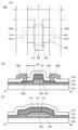
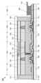
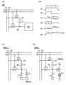
도 1의 (A)는 트랜지스터(100)의 상면도이고, 도 1의 (B)는 도 1의 (A)에 도시된 일점쇄선 A1-A2에서의 절단면의 단면도에 상당하고, 도 1의 (C)는 도 1의 (A)에 도시된 일점쇄선 B1-B2에서의 절단면의 단면도에 상당한다. 또한 도 1의 (A)에서, 트랜지스터(100)의 구성 요소의 일부(게이트 절연층 등)를 생략하여 도시하였다. 또한 일점쇄선 A1-A2의 방향은 채널 길이 방향에 상당하고, 일점쇄선 B1-B2의 방향은 채널 폭 방향에 상당한다. 또한 트랜지스터의 상면도에 대해서는 이후 도면에 있어서도, 도 1의 (A)와 마찬가지로, 구성 요소의 일부를 생략하여 도시하였다.Fig. 1(A) is a top view of a transistor (100), Fig. 1(B) corresponds to a cross-sectional view taken along dashed-dotted line A1-A2 in Fig. 1(A), and Fig. 1(C) corresponds to a cross-sectional view taken along dashed-dotted line B1-B2 in Fig. 1(A). In addition, in Fig. 1(A), some of the components of the transistor (100) (such as a gate insulating layer) are omitted and illustrated. In addition, the direction of dashed-dotted line A1-A2 corresponds to the channel length direction, and the direction of dashed-dotted line B1-B2 corresponds to the channel width direction. In addition, in the subsequent drawings, as with Fig. 1(A), some of the components are omitted and illustrated for the top view of the transistor.
트랜지스터(100)는 기판(102) 위에 제공되고 절연층(103), 절연층(104), 반도체층(108), 절연층(110), 금속 산화물층(114), 도전층(112), 절연층(116), 절연층(118) 등을 가진다. 절연층(104)은 절연층(103) 위에 제공되고, 반도체층(108)은 절연층(103) 및 절연층(104) 상면에 접하여 제공된다. 절연층(110), 금속 산화물층(114), 및 도전층(112)은 이 순서대로 반도체층(108)의 일부를 덮어 적층되어 있다. 절연층(116)은 절연층(104), 반도체층(108) 상면 및 측면, 절연층(110) 측면, 금속 산화물층(114) 측면, 및 도전층(112) 상면 및 측면을 덮어 제공된다. 절연층(118)은 절연층(116)을 덮어 제공된다.A transistor (100) is provided on a substrate (102) and has an insulating layer (103), an insulating layer (104), a semiconductor layer (108), an insulating layer (110), a metal oxide layer (114), a conductive layer (112), an insulating layer (116), an insulating layer (118), etc. The insulating layer (104) is provided on the insulating layer (103), and the semiconductor layer (108) is provided in contact with the upper surfaces of the insulating layer (103) and the insulating layer (104). The insulating layer (110), the metal oxide layer (114), and the conductive layer (112) are laminated in this order to cover a part of the semiconductor layer (108). The insulating layer (116) is provided to cover the upper surfaces and side surfaces of the insulating layer (104), the semiconductor layer (108), the side surface of the insulating layer (110), the side surface of the metal oxide layer (114), and the upper surfaces and side surfaces of the conductive layer (112). An insulating layer (118) is provided to cover the insulating layer (116).
도전층(112)의 일부는 게이트 전극으로서 기능한다. 절연층(110)의 일부는 게이트 절연층으로서 기능한다. 트랜지스터(100)는 반도체층(108) 위에 게이트 전극이 제공되는, 소위 톱 게이트 트랜지스터이다.A portion of the conductive layer (112) functions as a gate electrode. A portion of the insulating layer (110) functions as a gate insulating layer. The transistor (100) is a so-called top gate transistor in which a gate electrode is provided on a semiconductor layer (108).
반도체층(108)은 금속 산화물을 포함하는 것이 바람직하다.It is preferable that the semiconductor layer (108) contains a metal oxide.
예를 들어 반도체층(108)은 인듐과 M(M은 갈륨, 알루미늄, 실리콘, 붕소, 이트륨, 주석, 구리, 바나듐, 베릴륨, 타이타늄, 철, 니켈, 저마늄, 지르코늄, 몰리브데넘, 란타넘, 세륨, 네오디뮴, 하프늄, 탄탈럼, 텅스텐, 또는 마그네슘 중에서 선택되는 1종류 또는 복수 종류)과, 아연을 가지는 것이 바람직하다. 특히 M은 알루미늄, 갈륨, 이트륨, 또는 주석으로 하는 것이 바람직하다.For example, it is preferable that the semiconductor layer (108) has indium and M (M is one or more kinds selected from gallium, aluminum, silicon, boron, yttrium, tin, copper, vanadium, beryllium, titanium, iron, nickel, germanium, zirconium, molybdenum, lanthanum, cerium, neodymium, hafnium, tantalum, tungsten, or magnesium), and zinc. In particular, it is preferable that M is aluminum, gallium, yttrium, or tin.
특히, 반도체층(108)으로서 인듐, 갈륨, 및 아연을 포함하는 산화물을 사용하는 것이 바람직하다.In particular, it is preferable to use an oxide containing indium, gallium, and zinc as the semiconductor layer (108).
반도체층(108)으로서, 조성이 상이한 층, 또는 결정성이 상이한 층, 또는 불순물 농도가 상이한 층을 적층한 적층 구조로 하여도 좋다.As the semiconductor layer (108), a laminated structure may be formed by laminating layers having different compositions, layers having different crystallinities, or layers having different impurity concentrations.
반도체층(108)은 도전층(112)과 중첩되는 영역, 및 이 영역을 끼우는 저저항 영역(108n)을 가진다. 영역(108n)에는 절연층(116)이 접하여 제공되어 있다. 반도체층(108) 중 도전층(112)과 중첩되는 영역은 트랜지스터(100)의 채널 형성 영역으로서 기능한다. 한편으로 영역(108n)은 트랜지스터(100)의 소스 영역 또는 드레인 영역으로서 기능한다.The semiconductor layer (108) has a region overlapping with the conductive layer (112) and a low-resistance region (108n) sandwiching this region. An insulating layer (116) is provided in contact with the region (108n). The region of the semiconductor layer (108) overlapping with the conductive layer (112) functions as a channel forming region of the transistor (100). On the other hand, the region (108n) functions as a source region or a drain region of the transistor (100).
또한 도 1의 (A), (B)에 도시된 바와 같이, 트랜지스터(100)는 절연층(118) 위에 도전층(120a) 및 도전층(120b)을 가져도 좋다. 도전층(120a) 및 도전층(120b)은 소스 전극 또는 드레인 전극으로서 기능한다. 도전층(120a) 및 도전층(120b)은 각각 절연층(118) 및 절연층(116)에 제공된 개구부(141a) 또는 개구부(141b)를 통하여 영역(108n)과 전기적으로 접속된다.In addition, as illustrated in (A) and (B) of FIG. 1, the transistor (100) may have a conductive layer (120a) and a conductive layer (120b) on the insulating layer (118). The conductive layer (120a) and the conductive layer (120b) function as a source electrode or a drain electrode. The conductive layer (120a) and the conductive layer (120b) are electrically connected to the region (108n) through an opening (141a) or an opening (141b) provided in the insulating layer (118) and the insulating layer (116), respectively.
도전층(112), 금속 산화물층(114), 및 절연층(110)은 상면 형상이 서로 대략 일치된다.The top surface shapes of the conductive layer (112), the metal oxide layer (114), and the insulating layer (110) are approximately identical to each other.
또한 본 명세서 등에서 "상면 형상이 실질적으로 일치"란, 적층한 층과 층 사이에서 적어도 윤곽의 일부가 중첩되는 것을 말한다. 예를 들어 상층과 하층이 동일한 마스크 패턴, 또는 일부가 동일한 마스크 패턴을 사용하여 가공된 경우를 그 범주에 포함한다. 다만, 엄밀하게 말하면 윤곽이 중첩되지 않고 상층이 하층의 내측에 위치하거나 상층이 하층의 외측에 위치하는 경우도 있어, 이 경우도 "상면 형상이 실질적으로 일치"라고 한다.In addition, in this specification and the like, "the shape of the upper surface is substantially the same" means that at least a part of the outline overlaps between the laminated layers. For example, this category includes cases where the upper layer and the lower layer are processed using the same mask pattern, or parts of the same mask pattern. However, strictly speaking, there are cases where the outlines do not overlap and the upper layer is located on the inside of the lower layer, or the upper layer is located on the outside of the lower layer, and in these cases, "the shape of the upper surface is substantially the same."
절연층(110)과 도전층(112) 사이에 위치하는 금속 산화물층(114)은 절연층(110)에 포함되는 산소가 도전층(112) 측으로 확산되는 것을 방지하는 배리어막으로서 기능한다. 또한 금속 산화물층(114)은 도전층(112)에 포함되는 수소나 물이 절연층(110) 측으로 확산되는 것을 방지하는 배리어막으로서도 기능한다. 금속 산화물층(114)은 예를 들어 적어도 절연층(110)보다 산소 및 수소를 투과시키기 어려운 재료를 사용할 수 있다.The metal oxide layer (114) positioned between the insulating layer (110) and the conductive layer (112) functions as a barrier film that prevents oxygen included in the insulating layer (110) from diffusing toward the conductive layer (112). In addition, the metal oxide layer (114) also functions as a barrier film that prevents hydrogen or water included in the conductive layer (112) from diffusing toward the insulating layer (110). The metal oxide layer (114) may be formed of, for example, a material that is at least less permeable to oxygen and hydrogen than the insulating layer (110).
금속 산화물층(114)에 의하여 도전층(112)에 알루미늄이나 구리 등의 산소를 흡인하기 쉬운 재료를 사용한 경우에도 절연층(110)으로부터 도전층(112)으로 산소가 확산되는 것을 방지할 수 있다. 또한 도전층(112)이 수소를 포함하는 경우에도, 절연층(110)을 통하여 도전층(112)으로부터 반도체층(108)에 수소가 공급되는 것이 억제된다. 그 결과, 반도체층(108)의 채널 형성 영역의 캐리어 밀도를 극히 낮은 것으로 할 수 있다.Even when a material that easily absorbs oxygen, such as aluminum or copper, is used in the conductive layer (112) by the metal oxide layer (114), oxygen can be prevented from diffusing from the insulating layer (110) to the conductive layer (112). In addition, even when the conductive layer (112) contains hydrogen, hydrogen is suppressed from being supplied to the semiconductor layer (108) from the conductive layer (112) through the insulating layer (110). As a result, the carrier density in the channel formation region of the semiconductor layer (108) can be made extremely low.
금속 산화물층(114)으로서는, 절연성 재료 또는 도전성 재료를 사용할 수 있다. 금속 산화물층(114)이 절연성을 가지는 경우에는 게이트 절연층의 일부로서 기능한다. 한편으로, 금속 산화물층(114)이 도전성을 가지는 경우에는 게이트 전극의 일부로서 기능한다.As the metal oxide layer (114), an insulating material or a conductive material can be used. When the metal oxide layer (114) has insulating properties, it functions as a part of the gate insulating layer. On the other hand, when the metal oxide layer (114) has conductive properties, it functions as a part of the gate electrode.
특히 금속 산화물층(114)으로서, 산화 실리콘보다 비유전율이 높은 절연성 재료를 사용하는 것이 바람직하다. 특히, 산화 알루미늄막, 산화 하프늄막, 또는 하프늄알루미네이트막 등을 사용하는 것이 바람직하다.In particular, as the metal oxide layer (114), it is preferable to use an insulating material having a higher dielectric constant than silicon oxide. In particular, it is preferable to use an aluminum oxide film, a hafnium oxide film, or a hafnium aluminate film.
또한 금속 산화물층(114)은 스퍼터링 장치를 사용하여 형성하는 것이 바람직하다. 예를 들어, 스퍼터링 장치를 사용하여 산화 알루미늄막을 형성하는 경우, 산소 가스를 포함한 분위기하에서 형성함으로써, 절연층(110)이나 반도체층(108) 내에 적합하게 산소를 첨가할 수 있다. 또한 스퍼터링 장치를 사용하여 산화 알루미늄막을 형성하는 경우, 막 밀도를 높일 수 있어 적합하다.In addition, it is preferable to form the metal oxide layer (114) using a sputtering device. For example, when forming an aluminum oxide film using a sputtering device, oxygen can be suitably added to the insulating layer (110) or the semiconductor layer (108) by forming it in an atmosphere containing oxygen gas. In addition, when forming an aluminum oxide film using a sputtering device, it is suitable because the film density can be increased.
또한 금속 산화물층(114)으로서는 상기 반도체층(108)에 적용 기능한 산화물 반도체 재료를 사용할 수 있다. 이때, 반도체층(108)과 같은 스퍼터링 타깃을 사용하여 형성한 금속 산화물막을 적용함으로써 장치를 공통화시킬 수 있어 바람직하다.In addition, as the metal oxide layer (114), an oxide semiconductor material applied to the semiconductor layer (108) can be used. At this time, it is preferable that the device be standardized by applying a metal oxide film formed using the same sputtering target as the semiconductor layer (108).
또는 반도체층(108) 및 금속 산화물층(114)의 양쪽에 인듐 및 갈륨을 포함한 금속 산화물 재료를 사용하는 경우, 반도체층(108)보다 갈륨의 조성(함유 비율)이 높은 재료를 사용하면, 산소에 대한 블로킹성을 더 높일 수 있어 바람직하다. 이때, 반도체층(108)에는 금속 산화물층(114)보다 인듐의 조성이 높은 재료를 사용함으로써 트랜지스터(100)의 전계 효과 이동도를 높일 수 있다.Or, when using a metal oxide material including indium and gallium on both sides of the semiconductor layer (108) and the metal oxide layer (114), it is preferable to use a material having a higher composition (content ratio) of gallium than that of the semiconductor layer (108), so that the blocking property against oxygen can be further increased. At this time, by using a material having a higher composition of indium than that of the metal oxide layer (114) in the semiconductor layer (108), the field effect mobility of the transistor (100) can be increased.
절연층(116)은 질화물을 포함하는 절연막을 사용하는 것이 바람직하다. 예를 들어, 질화 실리콘이나 질화 갈륨 등의 반도체 재료의 질화물, 또는 질화 알루미늄 등의 금속 질화물을 사용할 수 있다. 금속 질화물을 포함하는 절연막은 예를 들어 알루미늄, 타이타늄, 탄탈럼, 텅스텐, 크로뮴, 및 루테늄 등의 금속 원소 중 적어도 하나와, 질소를 포함하는 것이 바람직하다. 특히, 알루미늄과 질소를 포함하는 막을 사용하면, 절연성이 극히 높아 바람직하다.It is preferable that the insulating layer (116) uses an insulating film containing a nitride. For example, a nitride of a semiconductor material such as silicon nitride or gallium nitride, or a metal nitride such as aluminum nitride can be used. The insulating film containing a metal nitride preferably contains at least one of metal elements such as aluminum, titanium, tantalum, tungsten, chromium, and ruthenium, and nitrogen. In particular, it is preferable to use a film containing aluminum and nitrogen because the insulating property is extremely high.
절연층(116)에 질화 알루미늄막을 사용하는 경우, 조성식이 AlNx(x는 0보다 크고 2 이하의 실수(實數), 바람직하게는, x는 0.5보다 크고 1.5 이하의 실수)를 만족시키는 막을 사용하는 것이 바람직하다. 이에 의하여, 절연성이 우수하며, 열 전도성이 우수한 막으로 할 수 있기 때문에, 트랜지스터(100)를 구동하였을 때 발생되는 열의 방열성을 높일 수 있다.When using an aluminum nitride film for the insulating layer (116), it is preferable to use a film whose composition formula satisfies AlNx (x is a real number greater than 0 and less than or equal to 2, preferably, x is a real number greater than 0.5 and less than or equal to 1.5). Accordingly, since a film having excellent insulation properties and excellent thermal conductivity can be formed, the heat dissipation properties of heat generated when the transistor (100) is driven can be improved.
또는, 절연층(116)으로서 질화 알루미늄 타이타늄막, 질화 타이타늄막 등을 사용할 수 있다.Alternatively, an aluminum titanium nitride film, a titanium nitride film, or the like can be used as the insulating layer (116).
영역(108n)은 반도체층(108)의 일부이고, 채널 형성 영역보다 저항이 낮은 영역이다.The region (108n) is a part of the semiconductor layer (108) and has lower resistance than the channel formation region.
여기서 반도체층(108)으로서 인듐을 포함하는 금속 산화물막을 사용한 경우, 영역(108n)의 절연층(116) 측의 계면 근방에 산화 인듐이 석출한 영역, 또는 인듐 농도가 높은 영역이 형성되는 경우가 있다. 예를 들어, X선 광전자 분광법(XPS: X-ray Photoelectron Spectroscopy) 등의 분석법으로 관측할 수 있는 경우가 있다.Here, when a metal oxide film containing indium is used as the semiconductor layer (108), there are cases where a region where indium oxide is precipitated or a region with a high indium concentration is formed near the interface on the insulating layer (116) side of the region (108n). For example, there are cases where this can be observed by an analysis method such as X-ray photoelectron spectroscopy (XPS).
또한 영역(108n)은 채널 형성 영역보다 캐리어 농도가 높은 영역, 산소 결함 밀도가 높은 영역, 또는 n형 영역이라고 할 수도 있다.Additionally, the region (108n) may be referred to as a region having a higher carrier concentration than the channel forming region, a region having a higher oxygen defect density, or an n-type region.
또한 반도체층(108)의 채널 형성 영역에 접하는 절연층(104)과 절연층(110)에는 산화물막을 사용하는 것이 바람직하다. 예를 들어 산화 실리콘막, 산화 질화 실리콘막, 산화 알루미늄막 등의 산화물 막을 사용할 수 있다. 이로써 트랜지스터(100)의 제작 공정에서의 가열 처리 등에 의하여, 절연층(104)이나 절연층(110)으로부터 이탈된 산소를 반도체층(108)의 채널 형성 영역에 공급하여, 반도체층(108) 내의 산소 결손을 저감시킬 수 있다.In addition, it is preferable to use an oxide film for the insulating layer (104) and the insulating layer (110) that come into contact with the channel formation region of the semiconductor layer (108). For example, an oxide film such as a silicon oxide film, a silicon nitride oxide film, or an aluminum oxide film can be used. As a result, oxygen released from the insulating layer (104) or the insulating layer (110) by heat treatment or the like in the manufacturing process of the transistor (100) can be supplied to the channel formation region of the semiconductor layer (108), thereby reducing oxygen vacancies in the semiconductor layer (108).
절연층(104)보다 하측(기판(102) 측)에 제공되는 절연층(103)으로서는 산소 및 수소를 확산시키기 어려운 절연막을 사용하는 것이 바람직하다. 특히, 산화 알루미늄막, 산화 하프늄막, 또는 하프늄 알루미네이트막 등의 금속 산화물막, 또는 질화 알루미늄, 질화산화 알루미늄, 질화 실리콘, 질화산화 실리콘 등의 질소를 포함하는 절연막을 사용할 수 있다.As the insulating layer (103) provided on the lower side (on the substrate (102) side) than the insulating layer (104), it is preferable to use an insulating film that is difficult to diffuse oxygen and hydrogen into. In particular, a metal oxide film such as an aluminum oxide film, a hafnium oxide film, or a hafnium aluminate film, or an insulating film containing nitrogen such as aluminum nitride, aluminum nitride oxide, silicon nitride, or silicon nitride oxide can be used.
산화 알루미늄막, 산화 하프늄막, 및 하프늄 알루미네이트막 등은 막 두께가 얇은 경우에도 매우 높은 배리어성을 가진다. 그러므로, 그 두께를 0.5nm 이상 50nm 이하, 바람직하게는 1nm 이상 40nm 이하, 더 바람직하게는 2nm 이상 30nm 이하의 두께로 할 수 있다. 특히, 산화 알루미늄막은 수소 등에 대한 배리어성이 높으므로, 매우 얇게(예를 들어 0.5nm 이상 1.5nm 이하) 하여도, 충분한 효과를 얻을 수 있다. 예를 들어, 스퍼터링법 또는 원자층 퇴적법(ALD: Atomic Layer Deposition) 등의 성막 방법으로 형성할 수 있다.Aluminum oxide films, hafnium oxide films, and hafnium aluminate films have very high barrier properties even when the film thickness is thin. Therefore, the thickness can be 0.5 nm or more and 50 nm or less, preferably 1 nm or more and 40 nm or less, and more preferably 2 nm or more and 30 nm or less. In particular, since the aluminum oxide film has high barrier properties against hydrogen and the like, a sufficient effect can be obtained even if it is made very thin (for example, 0.5 nm or more and 1.5 nm or less). For example, it can be formed by a film forming method such as sputtering or atomic layer deposition (ALD).
여기서 반도체층(108)과 절연층(104)은 각각 섬 형상으로 가공된다. 도 1의 (A)에서는, 절연층(104)의 윤곽을 파선으로 나타내었다.Here, the semiconductor layer (108) and the insulating layer (104) are each processed into an island shape. In Fig. 1 (A), the outline of the insulating layer (104) is indicated by a broken line.
절연층(104)은 채널 길이 방향의 단부가 반도체층(108)의 단부보다 내측에 위치한다. 한편으로 채널 폭 방향의 단부는 반도체층(108)의 단부보다 외측에 위치한다. 바꿔 말하면, 반도체층(108)은 채널 길이 방향에서 절연층(104)의 한 쌍의 단부를 넘어 외측으로 연장하고, 채널 폭 방향에서 절연층(104)의 한 쌍의 단부보다 내측에 위치한다고 말할 수도 있다.The insulating layer (104) has an end portion in the channel length direction positioned inside the end portion of the semiconductor layer (108). On the other hand, the end portion in the channel width direction is positioned outside the end portion of the semiconductor layer (108). In other words, it can be said that the semiconductor layer (108) extends outward beyond a pair of end portions of the insulating layer (104) in the channel length direction and is positioned inside the pair of end portions of the insulating layer (104) in the channel width direction.
반도체층(108)의 채널 형성 영역과 중첩되도록 절연층(104)이 제공된다. 또한 반도체층(108)의 영역(108n)은 절연층(104)과 중첩되지 않는 영역을 가진다. 적어도, 영역(108n)의 도전층(120a)과 접하는 부분, 및 도전층(120b)과 접하는 부분에는 절연층(104)이 제공되지 않는 것이 바람직하다.An insulating layer (104) is provided so as to overlap with the channel forming region of the semiconductor layer (108). In addition, the region (108n) of the semiconductor layer (108) has a region that does not overlap with the insulating layer (104). At least, it is preferable that the insulating layer (104) is not provided in a portion of the region (108n) that is in contact with the conductive layer (120a) and a portion that is in contact with the conductive layer (120b).
또한 도 1의 (B), (C)에 도시된 바와 같이, 반도체층(108) 및 절연층(104)보다 외측의 영역에서 절연층(103)과 절연층(116)이 접하여 제공된다. 이에 의하여 반도체층(108) 및 절연층(104) 등이, 절연층(103) 및 절연층(116)으로 밀봉된 구조로 할 수 있다. 이와 같은 구조에 의하여, 외부로부터 트랜지스터(100)의 반도체층(108) 및 절연층(104) 등으로 수소가 확산되는 것, 및 반도체층(108) 및 절연층(104) 내의 산소가 외부로 확산되는 것을 효과적으로 억제할 수 있다.In addition, as shown in (B) and (C) of FIG. 1, the insulating layer (103) and the insulating layer (116) are provided in contact in an area outside the semiconductor layer (108) and the insulating layer (104). As a result, the semiconductor layer (108) and the insulating layer (104) can have a structure in which they are sealed by the insulating layer (103) and the insulating layer (116). With such a structure, it is possible to effectively suppress hydrogen from diffusing from the outside into the semiconductor layer (108) and the insulating layer (104) of the transistor (100), and oxygen from diffusing from the outside within the semiconductor layer (108) and the insulating layer (104).
또한 절연층(118) 내에는 수소가 포함되는 경우가 있지만, 반도체층(108)에 접하는 산화물막을 포함하는 절연층(104)이나 절연층(110)은 절연층(116)에 의하여 절연층(118)과 접하지 않는 구성이 되어 있다. 그러므로, 절연층(118) 내에 수소가 포함되는 경우에도, 트랜지스터(100)의 제작 공정에 가해지는 열 등에 의하여, 상기 수소가 절연층(104) 및 절연층(110)을 통하여 반도체층(108)으로 확산되는 것을 효과적으로 방지할 수 있다.In addition, although hydrogen may be included in the insulating layer (118), the insulating layer (104) or the insulating layer (110) including the oxide film in contact with the semiconductor layer (108) is configured not to be in contact with the insulating layer (118) due to the insulating layer (116). Therefore, even if hydrogen is included in the insulating layer (118), the hydrogen can be effectively prevented from diffusing into the semiconductor layer (108) through the insulating layer (104) and the insulating layer (110) due to heat, etc. applied during the manufacturing process of the transistor (100).
여기서 반도체층(108), 및 반도체층(108) 내에 형성될 수 있는 산소 결손에 대하여 설명한다.Here, the semiconductor layer (108) and the oxygen vacancies that may be formed within the semiconductor layer (108) are described.
반도체층(108)에 형성되는 산소 결손은 트랜지스터 특성에 영향을 미치기 때문에 문제가 된다. 예를 들어 반도체층(108) 내에 산소 결손이 형성되면, 상기 산소 결손에 수소가 결합되어 캐리어 공급원이 될 수 있다. 반도체층(108) 내에 캐리어 공급원이 생성되면, 트랜지스터(100)의 전기 특성의 변동, 대표적으로는 문턱 전압의 변동이 발생한다. 따라서, 반도체층(108)에서는 산소 결손이 적을수록 바람직하다.Oxygen vacancies formed in the semiconductor layer (108) are problematic because they affect transistor characteristics. For example, if oxygen vacancies are formed in the semiconductor layer (108), hydrogen may bond to the oxygen vacancies and become a carrier source. If a carrier source is created in the semiconductor layer (108), variations in the electrical characteristics of the transistor (100), typically a threshold voltage, occur. Therefore, the fewer oxygen vacancies there are in the semiconductor layer (108), the more desirable it is.
따라서 본 발명의 일 형태에서는 반도체층(108) 근방의 절연막, 구체적으로는 반도체층(108) 상방에 위치하는 절연층(110), 및 하방에 위치하는 절연층(104)이 산화물막을 포함한 구성이다. 제작 공정 중의 열 등으로 인하여 절연층(104) 및 절연층(110)으로부터 반도체층(108)으로 산소를 이동시킴으로써 반도체층(108) 내의 산소 결손을 저감시킬 수 있다.Therefore, in one embodiment of the present invention, the insulating film near the semiconductor layer (108), specifically, the insulating layer (110) positioned above the semiconductor layer (108) and the insulating layer (104) positioned below the semiconductor layer (108), are configured to include an oxide film. By moving oxygen from the insulating layer (104) and the insulating layer (110) to the semiconductor layer (108) due to heat or the like during the manufacturing process, oxygen vacancies in the semiconductor layer (108) can be reduced.
또한 반도체층(108)은 In의 원자수비가 M의 원자수비보다 많은 영역을 가지는 것이 바람직하다. In의 원자수비가 많을수록 트랜지스터의 전계 효과 이동도를 향상시킬 수 있다.In addition, it is preferable that the semiconductor layer (108) have a region in which the atomic ratio of In is greater than the atomic ratio of M. The higher the atomic ratio of In, the higher the field effect mobility of the transistor can be improved.
여기서, In, Ga, Zn을 포함하는 금속 산화물인 경우, In과 산소의 결합력은 Ga과 산소의 결합력보다 약하므로, In의 원자수비가 큰 경우에는, 금속 산화물막 내에 산소 결손이 형성되기 쉽다. 또한 Ga 대신에, 상기 M으로 나타내는 금속 원소를 사용한 경우에도 같은 경향이 있다. 금속 산화물막 내에 산소 결손이 많이 존재하면, 트랜지스터의 전기 특성의 저하나, 신뢰성의 저하가 일어난다.Here, in the case of a metal oxide containing In, Ga, or Zn, the bonding force between In and oxygen is weaker than the bonding force between Ga and oxygen, so when the atomic ratio of In is large, oxygen vacancies are easily formed in the metal oxide film. In addition, the same tendency occurs when a metal element represented by M is used instead of Ga. If there are many oxygen vacancies in the metal oxide film, the electrical characteristics of the transistor deteriorate or the reliability deteriorates.
그러나, 본 발명의 일 형태에서는 금속 산화물을 포함하는 반도체층(108) 내에 매우 많은 산소를 공급할 수 있으므로, In의 원자수비가 큰 금속 산화물 재료를 사용할 수 있게 된다. 이에 의하여, 매우 높은 전계 효과 이동도와, 안정된 전기 특성과, 높은 신뢰성을 겸비한 트랜지스터를 실현할 수 있다.However, in one embodiment of the present invention, since a very large amount of oxygen can be supplied into the semiconductor layer (108) including the metal oxide, a metal oxide material having a high atomic ratio of In can be used. As a result, a transistor having a very high field effect mobility, stable electrical characteristics, and high reliability can be realized.
예를 들어 In의 원자수비가 M의 원자수비에 대하여 1.5배 이상, 또는 2배 이상, 또는 3배 이상, 또는 3.5배 이상, 또는 4배 이상인 금속 산화물을 적합하게 사용할 수 있다.For example, a metal oxide in which the atomic ratio of In is 1.5 times or more, or 2 times or more, or 3 times or more, or 3.5 times or more, or 4 times or more relative to the atomic ratio of M can be suitably used.
특히, 반도체층(108)의 In, M, 및 Zn의 원자수비를 In:M:Zn=5:1:6 또는 그 근방(In이 5인 경우, M이 0.5 이상 1.5 이하이며, Zn이 5 이상 7 이하를 포함함)으로 하는 것이 바람직하다. 또는 In, M, 및 Zn의 원자수비를 In:M:Zn=4:2:3 또는 그 근방으로 하는 것이 바람직하다. 또한 반도체층(108)의 조성으로서, 반도체층(108)의 In, M, 및 Zn의 원자수비를 실질적으로 같게 하여도 좋다. 즉, In, M, 및 Zn의 원자수비가 In:M:Zn=1:1:1 또는 그 근방의 재료를 포함하여도 좋다.In particular, it is preferable that the atomic ratio of In, M, and Zn in the semiconductor layer (108) be In:M:Zn=5:1:6 or thereabouts (when In is 5, M is 0.5 or more and 1.5 or less, and Zn is 5 or more and 7 or less). Alternatively, it is preferable that the atomic ratio of In, M, and Zn be In:M:Zn=4:2:3 or thereabouts. In addition, as a composition of the semiconductor layer (108), the atomic ratios of In, M, and Zn in the semiconductor layer (108) may be made substantially the same. That is, the semiconductor layer may include a material in which the atomic ratio of In, M, and Zn is In:M:Zn=1:1:1 or thereabouts.
예를 들어 상기 전계 효과 이동도가 높은 트랜지스터를, 게이트 신호를 생성하는 게이트 드라이버에 사용함으로써, 베젤 폭이 좁은 (슬림 베젤이라고도 함) 표시 장치를 제공할 수 있다. 또한 상기 전계 효과 이동도가 높은 트랜지스터를, 소스 드라이버(특히, 소스 드라이버가 가지는 시프트 레지스터의 출력 단자에 접속되는 디멀티플렉서)에 사용함으로써, 표시 장치에 접속되는 배선수가 적은 표시 장치를 제공할 수 있다.For example, by using the transistor having the high field-effect mobility described above in a gate driver that generates a gate signal, a display device having a narrow bezel width (also called a slim bezel) can be provided. In addition, by using the transistor having the high field-effect mobility described above in a source driver (particularly, a demultiplexer connected to an output terminal of a shift register of the source driver), a display device having a reduced number of wires connected to the display device can be provided.
또한 반도체층(108)이, In의 원자수비가 M의 원자수비보다 많은 영역을 가져도, 반도체층(108)의 결정성이 높은 경우, 전계 효과 이동도가 낮아지는 경우가 있다. 반도체층(108)의 결정성은, 예를 들어 X선 회절(XRD: X-Ray Diffraction)을 사용하여 분석하거나, 또는 투과형 전자 현미경(TEM: Transmission Electron Microscope)을 사용하여 분석함으로써 해석할 수 있다.In addition, even if the semiconductor layer (108) has a region where the atomic ratio of In is greater than the atomic ratio of M, if the crystallinity of the semiconductor layer (108) is high, the field effect mobility may be reduced. The crystallinity of the semiconductor layer (108) can be analyzed, for example, by using X-ray diffraction (XRD) or by using a transmission electron microscope (TEM).
여기서, 반도체층(108)에 혼입되는 수소 또는 수분 등의 불순물은 트랜지스터 특성에 영향을 미치기 때문에 문제가 된다. 따라서, 반도체층(108)에서는 수소 또는 수분 등의 불순물이 적을수록 바람직하다. 불순물 농도가 낮으며 결함 준위 밀도가 낮은 금속 산화물막을 사용함으로써, 우수한 전기 특성을 가지는 트랜지스터를 제작할 수 있어 바람직하다. 불순물 농도를 낮게, 결함 준위 밀도를 낮게(산소 결손을 적게) 함으로써 막 내의 캐리어 밀도를 낮출 수 있다. 이와 같은 금속 산화물막을 반도체층에 사용한 트랜지스터는 문턱 전압이 음이 되는 전기 특성(노멀리 온(normally on)이라고도 함)이 되는 경우가 적다. 또한 이와 같은 금속 산화물을 사용한 트랜지스터는 오프 전류가 현저하게 작은 특성을 얻을 수 있다.Here, impurities such as hydrogen or moisture mixed into the semiconductor layer (108) are problematic because they affect the transistor characteristics. Therefore, it is preferable that the semiconductor layer (108) contain fewer impurities such as hydrogen or moisture. By using a metal oxide film having a low impurity concentration and a low defect state density, a transistor having excellent electrical characteristics can be manufactured, which is preferable. By lowering the impurity concentration and the defect state density (reducing oxygen vacancies), the carrier density within the film can be lowered. A transistor using such a metal oxide film in the semiconductor layer rarely has an electrical characteristic in which the threshold voltage becomes negative (also called normally on). In addition, a transistor using such a metal oxide can obtain a characteristic in which the off-state current is remarkably small.
또한 반도체층(108)이 2층 이상의 적층 구조를 가져도 좋다.Additionally, the semiconductor layer (108) may have a laminated structure of two or more layers.
예를 들어, 조성이 상이한 2 이상의 금속 산화물막이 적층된 반도체층(108)을 사용할 수 있다. 예를 들어 In-Ga-Zn 산화물을 사용한 경우에 In, M, 및 Zn의 원자수비가 In:M:Zn=5:1:6, In:M:Zn=4:2:3, In:M:Zn=1:1:1, In:M:Zn=2:2:1, In:M:Zn=1:3:4, In:M:Zn=1:3:2, 또는 이들의 근방인 스퍼터링 타깃으로 형성하는 막 중, 2 이상을 적층하여 사용하는 것이 바람직하다.For example, a semiconductor layer (108) in which two or more metal oxide films having different compositions are laminated can be used. For example, in the case of using In-Ga-Zn oxide, it is preferable to laminate and use two or more films formed by a sputtering target in which the atomic ratios of In, M, and Zn are In:M:Zn=5:1:6, In:M:Zn=4:2:3, In:M:Zn=1:1:1, In:M:Zn=2:2:1, In:M:Zn=1:3:4, In:M:Zn=1:3:2, or near these.
또한 결정성이 상이한 2 이상의 금속 산화물막을 적층한 반도체층(108)을 사용할 수 있다. 이 경우, 같은 산화물 타깃을 사용하고, 성막 조건을 다르게 함으로써 대기에 접촉되지 않고 연속적으로 형성되는 것이 바람직하다.In addition, a semiconductor layer (108) in which two or more metal oxide films having different crystallinities are laminated can be used. In this case, it is preferable to use the same oxide target and form the film continuously without contacting the atmosphere by differentiating the film formation conditions.
예를 들어 먼저 형성하는 제 1 금속 산화물막의 성막 시의 산소 유량비를, 그 다음에 형성하는 제 2 금속 산화물막의 성막 시의 산소 유량비보다 작게 한다. 또는 제 1 금속 산화물막의 성막 시에 산소를 흘리지 않는 조건으로 한다. 이로써 제 2 금속 산화물막의 성막 시에 산소를 효과적으로 공급할 수 있다. 또한 제 1 금속 산화물막을 제 2 금속 산화물막보다 결정성이 낮고 전기 전도성이 높은 막으로 할 수 있다. 한편으로, 상부에 제공되는 제 2 금속 산화물막을 제 1 금속 산화물막보다 결정성이 높은 막으로 함으로써, 반도체층(108)의 가공 시나 게이트 절연층(110)의 성막 시에 받는 대미지를 억제할 수 있다.For example, the oxygen flow rate during the deposition of the first metal oxide film formed first is made smaller than the oxygen flow rate during the deposition of the second metal oxide film formed subsequently. Or, a condition is set such that oxygen does not flow during the deposition of the first metal oxide film. As a result, oxygen can be effectively supplied during the deposition of the second metal oxide film. In addition, the first metal oxide film can be made into a film having lower crystallinity and higher electrical conductivity than the second metal oxide film. On the other hand, by making the second metal oxide film provided on the upper side into a film having higher crystallinity than the first metal oxide film, damage received during the processing of the semiconductor layer (108) or the deposition of the gate insulating layer (110) can be suppressed.
더 구체적으로는, 제 1 금속 산화물막의 성막 시의 산소 유량비를 0% 이상 50% 미만, 바람직하게는 0% 이상 30% 이하, 더 바람직하게는 0% 이상 20% 이하, 대표적으로는 10%로 한다. 또한 제 2 금속 산화물막의 성막 시의 산소 유량비를 50% 이상 100% 이하, 바람직하게는 60% 이상 100% 이하, 더 바람직하게는 80% 이상 100% 이하, 더 바람직하게는 90% 이상 100% 이하, 대표적으로는 100%로 한다. 또한 제 1 금속 산화물막과 제 2 금속 산화물막에서, 성막 시의 압력, 온도, 전력 등의 조건을 다르게 하여도 좋지만, 산소 유량비 외의 조건을 같게 함으로써, 성막 공정에 걸리는 시간을 단축할 수 있어 바람직하다.More specifically, the oxygen flow rate during the deposition of the first metal oxide film is set to 0% or more and less than 50%, preferably 0% or more and 30% or less, more preferably 0% or more and 20% or less, and typically 10%. In addition, the oxygen flow rate during the deposition of the second metal oxide film is set to 50% or more and 100% or less, preferably 60% or more and 100% or less, more preferably 80% or more and 100% or less, more preferably 90% or more and 100% or less, and typically 100%. In addition, although conditions such as pressure, temperature, and power during deposition may be different in the first metal oxide film and the second metal oxide film, it is preferable that conditions other than the oxygen flow rate be the same, because the time required for the deposition process can be shortened.
이와 같은 구성으로 함으로써 전기 특성이 우수하고, 또한 신뢰성이 높은 트랜지스터(100)를 실현할 수 있다.By configuring in this manner, a transistor (100) having excellent electrical characteristics and high reliability can be realized.
여기까지가 구성예 1에 대한 설명이다.This concludes the explanation of Configuration Example 1.
[구성예 2][Configuration Example 2]
이하에서는 상기 구성예 1과 일부의 구성이 다른 트랜지스터의 구성예에 대하여 설명한다. 또한 이하에서는, 상기 구성예 1과 중복되는 부분은 설명을 생략하는 경우가 있다. 또한 이하에서 제시하는 도면에 있어서, 상기 구성예와 같은 기능을 가지는 부분에 대해서는 해칭 패턴을 같게 하고, 부호를 붙이지 않는 경우도 있다.Below, a description is given of a configuration example of a transistor that has a different configuration from the above configuration example 1. Also, below, there are cases where explanation of parts that overlap with the above configuration example 1 is omitted. Also, in the drawings presented below, parts that have the same function as the above configuration example are sometimes given the same hatching pattern and not given a symbol.
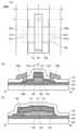
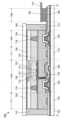
도 2의 (A)는 트랜지스터(100A)의 상면도이고, 도 2의 (B)는 트랜지스터(100A)의 채널 길이 방향을 포함하는 단면도이고, 도 2의 (C)는 트랜지스터(100A)의 채널 폭 방향의 단면도이다.Fig. 2 (A) is a top view of a transistor (100A), Fig. 2 (B) is a cross-sectional view including the channel length direction of the transistor (100A), and Fig. 2 (C) is a cross-sectional view in the channel width direction of the transistor (100A).
트랜지스터(100A)는 주로 기판(102)과 절연층(103) 사이에 도전층(106)을 가지는 점에서, 구성예 1과 상이하다. 도전층(106)은 절연층(104) 및 절연층(103)을 개재하여 반도체층(108) 및 도전층(112)과 중첩되는 영역을 가진다.The transistor (100A) differs from the configuration example 1 mainly in that it has a conductive layer (106) between the substrate (102) and the insulating layer (103). The conductive layer (106) has a region overlapping with the semiconductor layer (108) and the conductive layer (112) through the insulating layer (104) and the insulating layer (103).
트랜지스터(100A)에서, 도전층(106)은 제 1 게이트 전극(보텀 게이트 전극이라고도 함)으로서의 기능을 가지고, 도전층(112)은 제 2 게이트 전극(톱 게이트 전극이라고도 함)으로서의 기능을 가진다. 또한 절연층(103) 및 절연층(104)의 일부는 제 1 게이트 절연층으로서 기능하고, 절연층(110)의 일부는 제 2 게이트 절연층으로서 기능한다.In the transistor (100A), the conductive layer (106) functions as a first gate electrode (also called a bottom gate electrode), and the conductive layer (112) functions as a second gate electrode (also called a top gate electrode). In addition, a part of the insulating layer (103) and the insulating layer (104) functions as a first gate insulating layer, and a part of the insulating layer (110) functions as a second gate insulating layer.
반도체층(108)에서 도전층(112) 및 도전층(106) 중 적어도 한쪽과 중첩되는 부분은 채널 형성 영역으로서 기능한다. 또한 이하에서는 설명을 용이하게 하기 위하여, 반도체층(108)에서 도전층(112)과 중첩되는 부분을 채널 형성 영역이라고 부르는 경우가 있지만, 실제로는 도전층(112)과 중첩되지 않고, 도전층(106)과 중첩되는 부분(영역(108n)을 포함한 부분)에도 채널이 형성될 수 있다.A portion of the semiconductor layer (108) that overlaps at least one of the conductive layer (112) and the conductive layer (106) functions as a channel formation region. In addition, for ease of explanation, in the following, a portion of the semiconductor layer (108) that overlaps the conductive layer (112) is sometimes referred to as a channel formation region, but in reality, a channel may also be formed in a portion (a portion including the region (108n)) that does not overlap the conductive layer (112) but overlaps the conductive layer (106).
또한 도 2의 (C)에 도시된 바와 같이 도전층(106)은 금속 산화물층(114), 절연층(110), 및 절연층(103)에 제공된 개구부(142)를 통하여 도전층(112)과 전기적으로 접속되어도 좋다. 이에 의하여, 도전층(106)과 도전층(112)에는 같은 전위를 공급할 수 있다.In addition, as illustrated in (C) of Fig. 2, the conductive layer (106) may be electrically connected to the conductive layer (112) through the metal oxide layer (114), the insulating layer (110), and the opening (142) provided in the insulating layer (103). As a result, the same potential can be supplied to the conductive layer (106) and the conductive layer (112).
도전층(106)에는 도전층(112), 도전층(120a), 또는 도전층(120b)과 같은 재료를 사용할 수 있다. 특히 도전층(106)에 구리를 포함한 재료를 사용하면 배선 저항을 낮출 수 있어 바람직하다.The conductive layer (106) may use a material similar to that of the conductive layer (112), the conductive layer (120a), or the conductive layer (120b). In particular, it is preferable to use a material containing copper in the conductive layer (106) because this can lower the wiring resistance.
또한, 도 2의 (A), (C)에 도시된 바와 같이, 채널 폭 방향에서 도전층(112) 및 도전층(106)이 반도체층(108)의 단부보다 외측에 돌출하는 것이 바람직하다. 이때, 도 2의 (C)에 도시된 바와 같이, 반도체층(108)의 채널 폭 방향의 전체가 절연층(110)과 절연층(104)을 개재하여 도전층(112)과 도전층(106)에 의하여 덮인 구성이 된다.In addition, as shown in (A) and (C) of FIG. 2, it is preferable that the conductive layer (112) and the conductive layer (106) protrude further outward than the end of the semiconductor layer (108) in the channel width direction. At this time, as shown in (C) of FIG. 2, the entirety of the semiconductor layer (108) in the channel width direction is covered by the conductive layer (112) and the conductive layer (106) with the insulating layer (110) and the insulating layer (104) interposed therebetween.
이와 같은 구성으로 함으로써 반도체층(108)을 한 쌍의 게이트 전극에 의하여 생기는 전계로 전기적으로 둘러쌀 수 있다. 이때 특히 도전층(106)과 도전층(112)에 같은 전위를 공급하는 것이 바람직하다. 이로써, 채널을 유발시키기 위한 전계를 반도체층(108)에 효과적으로 인가할 수 있기 때문에 트랜지스터(100A)의 온 전류를 증대시킬 수 있다. 그러므로 트랜지스터(100A)를 미세화할 수도 있게 된다.By forming the structure in this way, the semiconductor layer (108) can be electrically surrounded by an electric field generated by a pair of gate electrodes. At this time, it is particularly preferable to supply the same potential to the conductive layer (106) and the conductive layer (112). Accordingly, since the electric field for inducing a channel can be effectively applied to the semiconductor layer (108), the on-state current of the transistor (100A) can be increased. Therefore, the transistor (100A) can also be miniaturized.
또한, 도전층(112)과 도전층(106)을 접속시키지 않는 구성으로 하여도 좋다. 이때, 한 쌍의 게이트 전극의 한쪽에 정전위를 공급하고, 다른 쪽에 트랜지스터(100A)를 구동하기 위한 신호를 공급하여도 좋다. 이때 한쪽 전극에 공급하는 전위에 의하여 트랜지스터(100A)를 다른 쪽 전극으로 구동할 때의 문턱 전압을 제어할 수도 있다.In addition, a configuration in which the conductive layer (112) and the conductive layer (106) are not connected may be used. At this time, a static potential may be supplied to one side of a pair of gate electrodes, and a signal for driving the transistor (100A) may be supplied to the other side. At this time, the threshold voltage when driving the transistor (100A) with the other electrode may be controlled by the potential supplied to one electrode.
트랜지스터(100A)는 절연층(104)이 도전층(106)보다 내측에 제공되는 예를 나타내었다. 즉, 트랜지스터(100A)의 채널 길이 방향에서 절연층(104)의 단부는 도전층(106)의 단부보다 내측에 위치하고, 채널 폭 방향에서도 절연층(104)의 단부가 도전층(106)의 단부보다 내측에 위치하도록 가공된다.The transistor (100A) shows an example in which the insulating layer (104) is provided on the inner side than the conductive layer (106). That is, in the channel length direction of the transistor (100A), the end of the insulating layer (104) is positioned on the inner side than the end of the conductive layer (106), and in the channel width direction, the end of the insulating layer (104) is processed to be positioned on the inner side than the end of the conductive layer (106).
또한 도 2의 (A)에 도시된 바와 같이, 도전층(106)과 도전층(120a)의 교차부, 및 도전층(106)과 도전층(120b)의 교차부에는 절연층(104a)이 제공된다.In addition, as shown in (A) of Fig. 2, an insulating layer (104a) is provided at the intersection of the conductive layer (106) and the conductive layer (120a), and at the intersection of the conductive layer (106) and the conductive layer (120b).
도 2의 (B)에 도전층(120b)과 도전층(106)의 교차부를 도시하였다. 절연층(104a)은 절연층(104)과 동일면 위에 위치하며, 동일 재료를 포함하는 절연층이다. 예를 들어 절연층(104a)은 절연층(104)과 동일한 절연막을 가공하여 형성할 수 있다. 절연층(104a)을 도전층(120b)과 도전층(106)이 교차되는 부분에 배치함으로써, 도전층(120b)과 도전층(106) 사이의 기생 용량을 저감할 수 있다.The intersection of the conductive layer (120b) and the conductive layer (106) is illustrated in (B) of Fig. 2. The insulating layer (104a) is located on the same surface as the insulating layer (104) and is an insulating layer containing the same material. For example, the insulating layer (104a) can be formed by processing the same insulating film as the insulating layer (104). By arranging the insulating layer (104a) at the intersection of the conductive layer (120b) and the conductive layer (106), the parasitic capacitance between the conductive layer (120b) and the conductive layer (106) can be reduced.
또한 여기서는 도전층(106)과 도전층(120a) 또는 도전층(120b)의 교차부에 절연층(104a)을 배치하는 경우를 예시하였지만, 이에 한정되지 않는다. 예를 들어 도전층(112)(또는 도전층(112)과 같은 도전막을 가공하여 얻어지는 배선)이나, 반도체층(108)과 같은 반도체막을 가공하여 얻어지는 배선 등과 도전층(106)의 교차부에, 절연층(104a)을 배치함으로써, 상기와 마찬가지로 기생 용량을 저감할 수 있다.In addition, although the case where the insulating layer (104a) is disposed at the intersection of the conductive layer (106) and the conductive layer (120a) or the conductive layer (120b) is exemplified here, it is not limited thereto. For example, by disposing the insulating layer (104a) at the intersection of the conductive layer (106) and the conductive layer (112) (or wiring obtained by processing a conductive film such as the conductive layer (112)) or the wiring obtained by processing a semiconductor film such as the semiconductor layer (108), the parasitic capacitance can be reduced in the same manner as described above.
여기까지가 구성예 2에 대한 설명이다.This concludes the explanation of Configuration Example 2.
[변형예][Variation]
다음으로 구성예 2의 변형예에 대하여 설명한다.Next, a variation of configuration example 2 is described.
[변형예 1][Variation 1]
도 3의 (A), (B), (C)에 도시된 트랜지스터(100B)는 절연층(104)을 도전층(112)과 같은 포토 마스크를 사용하여 가공한 경우의 예이다.The transistor (100B) illustrated in (A), (B), and (C) of FIG. 3 is an example in which the insulating layer (104) is processed using the same photo mask as the conductive layer (112).
절연층(104)과 도전층(112)은 평면에서 볼 때 그 윤곽이 대략 일치된다. 또한 절연층(104)이나 도전층(112)의 가공 조건에 따라서는 절연층(104)의 윤곽이 도전층(112)의 윤곽의 내측에 위치하는 경우나, 반대로 외측에 위치하는 경우가 있다.The outlines of the insulating layer (104) and the conductive layer (112) are roughly identical when viewed from a plane. In addition, depending on the processing conditions of the insulating layer (104) or the conductive layer (112), the outline of the insulating layer (104) may be located on the inside of the outline of the conductive layer (112), or conversely, may be located on the outside.
이와 같이, 절연층(104)과 도전층(112)의 가공에 사용하는 포토 마스크를 공통화함으로써, 제조 비용을 저감할 수 있다.In this way, by commonizing the photo mask used for processing the insulating layer (104) and the conductive layer (112), the manufacturing cost can be reduced.
또한 여기서는 도전층(112)이 섬 형상을 가지고, 도전층(106)의 일부가 배선으로서 기능하는 경우에 대하여 나타내었지만, 도전층(106)을 섬 형상으로 하고, 도전층(112)의 일부를 배선으로서 사용하는 레이아웃 패턴을 적용할 수도 있다. 그 경우, 절연층(104)은 도전층(106)과 같은 포토 마스크를 사용하여 가공하면 좋다.In addition, although the conductive layer (112) has an island shape and a part of the conductive layer (106) functions as a wiring, a layout pattern in which the conductive layer (106) has an island shape and a part of the conductive layer (112) is used as a wiring may also be applied. In that case, the insulating layer (104) may be processed using the same photo mask as the conductive layer (106).
[변형예 2][Variation 2]
도 4의 (A)에 도시된 채널 폭 방향의 단면은 주로 절연층(104)의 채널 폭 방향의 길이가 다르다는 점에서, 도 2의 (C)와 상이하다.The cross-section in the channel width direction shown in Fig. 4 (A) differs from Fig. 2 (C) mainly in that the length of the insulating layer (104) in the channel width direction is different.
도 4의 (A)에서는 절연층(104)의 채널 폭 방향의 단부가 도전층(112)의 채널 폭 방향의 단부보다 외측에 위치하며, 도전층(106)의 채널 폭 방향의 단부보다 내측에 위치하는 경우를 도시하였다.In Fig. 4 (A), the case is illustrated where the end portion of the insulating layer (104) in the channel width direction is located outside the end portion of the conductive layer (112) in the channel width direction and inside the end portion of the conductive layer (106) in the channel width direction.
또한 도전층(112)과 도전층(106)은 금속 산화물층(114), 절연층(110), 절연층(104), 및 절연층(103)에 제공된 개구부(142)를 통하여 전기적으로 접속된다.Additionally, the conductive layer (112) and the conductive layer (106) are electrically connected through the opening (142) provided in the metal oxide layer (114), the insulating layer (110), the insulating layer (104), and the insulating layer (103).
[변형예 3][Variation 3]
도 4의 (B)는 절연층(104)의 채널 폭 방향의 단부가 도전층(112)의 채널 폭 방향의 단부, 및 도전층(106)의 채널 폭 방향의 단부보다 내측에 위치하며, 개구부(142)가 제공되는 부분에 절연층(104)이 위치하는 예이다.FIG. 4 (B) is an example in which an end portion of the insulating layer (104) in the channel width direction is located inside the end portion of the conductive layer (112) in the channel width direction and the end portion of the conductive layer (106) in the channel width direction, and the insulating layer (104) is located in a portion where an opening (142) is provided.
[변형예 4][Variation 4]
도 4의 (C)는 절연층(104)의 채널 폭 방향의 단부가 도전층(112)의 채널 폭 방향의 단부, 및 도전층(106)의 채널 폭 방향의 단부보다 외측에 위치하는 예이다.Figure 4 (C) is an example in which the end portion of the insulating layer (104) in the channel width direction is located outside the end portion of the conductive layer (112) in the channel width direction and the end portion of the conductive layer (106) in the channel width direction.
여기까지가 변형예에 대한 설명이다.This concludes the explanation of the variant examples.
[응용예][Application Example]
다음으로 상술한 트랜지스터를 표시 장치의 화소에 적용한 경우의 예에 대하여 설명한다.Next, an example of applying the above-described transistor to a pixel of a display device is described.
도 5는 복수의 부화소가 매트릭스로 배치된 표시 장치의 상면 개략도이다. 하나의 부화소는 적어도 하나의 트랜지스터(100)와, 이 트랜지스터(100)와 전기적으로 접속하는 화소 전극으로서 기능하는 도전층(131)을 가진다. 또한 여기서는 간략화한 부화소의 구성을 나타내었지만, 부화소에 적용하는 표시 소자에 따라, 다른 트랜지스터나 용량 소자 등을 적절히 제공할 수 있다.Fig. 5 is a schematic diagram of a top surface of a display device in which a plurality of subpixels are arranged in a matrix. One subpixel has at least one transistor (100) and a conductive layer (131) that functions as a pixel electrode electrically connected to the transistor (100). In addition, although a simplified configuration of a subpixel is shown here, other transistors or capacitive elements, etc., can be appropriately provided depending on the display element applied to the subpixel.
도 5에서, 도전층(112)은 게이트선(주사선이라고도 함)으로서 기능하고, 도전층(120a)은 소스선(신호선, 비디오 신호선이라고도 함)으로서 기능하고, 도전층(120b)은 트랜지스터(100)와 도전층(131)을 전기적으로 접속하는 배선으로서 기능한다.In Fig. 5, the conductive layer (112) functions as a gate line (also called a scan line), the conductive layer (120a) functions as a source line (also called a signal line or video signal line), and the conductive layer (120b) functions as a wiring that electrically connects the transistor (100) and the conductive layer (131).
도 5에서는 섬 형상을 가지는 절연층(104)이, 하나의 트랜지스터마다 하나 제공된다. 절연층(104)은 트랜지스터(100)의 반도체층(108)의 채널 형성 영역을 포함하도록 배치되며, 도전층(120a) 및 도전층(120b)과 반도체층(108)의 접속부(개구부(141a), 개구부(141b))에는 배치되지 않도록 제공된다.In Fig. 5, an insulating layer (104) having an island shape is provided for each transistor. The insulating layer (104) is arranged to include a channel forming region of the semiconductor layer (108) of the transistor (100), and is provided so as not to be arranged at a connection portion (opening (141a), opening (141b)) between the conductive layer (120a) and the conductive layer (120b) and the semiconductor layer (108).
또한 도 5에서는 도전층(112)과 도전층(120a)의 교차부에서, 절연층(104a)이 제공된다.Additionally, in Fig. 5, an insulating layer (104a) is provided at the intersection of the conductive layer (112) and the conductive layer (120a).
본 발명의 일 형태의 트랜지스터는, 표시 장치뿐만 아니라, 다양한 회로나 장치에 적용할 수 있다. 예를 들어 전자 기기 등에 실장되는 IC 칩 내의 연산 회로, 메모리 회로, 구동 회로, 및 인터페이스 회로 등의 각종 회로, 또는 액정 소자나 유기 EL 소자 등이 적용된 디스플레이 디바이스나, 각종 센서 디바이스에서의 구동 회로 등에 적합하게 사용할 수 있다.A transistor of one form of the present invention can be applied not only to display devices but also to various circuits or devices. For example, it can be suitably used in various circuits such as operation circuits, memory circuits, driving circuits, and interface circuits in IC chips mounted in electronic devices, or in display devices to which liquid crystal elements or organic EL elements are applied, or in driving circuits in various sensor devices.
여기까지가 응용예에 대한 설명이다.This concludes the explanation of the application examples.
[반도체 장치의 구성 요소][Components of semiconductor devices]
다음으로, 본 실시형태의 반도체 장치에 포함되는 구성 요소에 대하여 자세히 설명한다.Next, components included in the semiconductor device of the present embodiment will be described in detail.
[기판][Substrate]
기판(102)의 재질 등에 큰 제한은 없지만, 적어도 나중의 열처리에 견딜 수 있을 정도의 내열성을 가질 필요가 있다. 예를 들어 실리콘이나 탄소화 실리콘을 재료로 한 단결정 반도체 기판 및 다결정 반도체 기판, 실리콘 저마늄 등의 화합물 반도체 기판, SOI 기판, 유리 기판, 세라믹 기판, 석영 기판, 사파이어 기판 등을 기판(102)으로서 사용하여도 좋다. 또한 이들 기판 위에 반도체 소자가 제공된 것을 기판(102)으로서 사용하여도 좋다.There are no major restrictions on the material of the substrate (102), but it is necessary to have at least a heat resistance that can withstand later heat treatment. For example, a single crystal semiconductor substrate and a polycrystalline semiconductor substrate made of silicon or silicon carbide, a compound semiconductor substrate such as silicon germanium, an SOI substrate, a glass substrate, a ceramic substrate, a quartz substrate, a sapphire substrate, etc. may be used as the substrate (102). In addition, a substrate on which a semiconductor element is provided may be used as the substrate (102).
또한 기판(102)으로서 가요성 기판을 사용하고, 가요성 기판 위에 직접 트랜지스터(100) 등을 형성하여도 좋다. 또는 기판(102)과 트랜지스터(100) 등 사이에 박리층을 제공하여도 좋다. 박리층은 그 위에 반도체 장치를 일부 또는 전부 완성시킨 후, 기판(102)으로부터 분리하고 다른 기판에 전재(轉載)하는 데 사용할 수 있다. 그때 트랜지스터(100) 등은 내열성이 떨어지는 기판이나 가요성 기판에도 전재할 수 있다.In addition, a flexible substrate may be used as the substrate (102), and the transistor (100), etc. may be formed directly on the flexible substrate. Alternatively, a peeling layer may be provided between the substrate (102) and the transistor (100), etc. The peeling layer may be used to separate the semiconductor device from the substrate (102) after it is partially or completely completed, and to transfer it to another substrate. At that time, the transistor (100), etc. may be transferred to a substrate with poor heat resistance or a flexible substrate.
[절연층(104)][Insulating layer (104)]
절연층(104)으로서는 스퍼터링법, CVD법, 증착법, 펄스 레이저 퇴적(PLD)법 등을 적절히 사용하여 형성할 수 있다. 또한 절연층(104)으로서는 예를 들어, 산화물 절연막 또는 질화물 절연막을 단층으로 또는 적층하여 형성할 수 있다. 또한 반도체층(108)과의 계면 특성을 향상시키기 위하여, 절연층(104)에서 적어도 반도체층(108)과 접하는 영역은 산화물 절연막으로 형성되는 것이 바람직하다. 또한 절연층(104)에는 가열됨으로써 산소를 방출하는 막이 사용되는 것이 바람직하다.The insulating layer (104) can be formed by appropriately using a sputtering method, a CVD method, a vapor deposition method, a pulsed laser deposition (PLD) method, or the like. In addition, the insulating layer (104) can be formed by, for example, forming an oxide insulating film or a nitride insulating film as a single layer or by laminating the same. In addition, in order to improve the interface characteristics with the semiconductor layer (108), it is preferable that at least a region of the insulating layer (104) that comes into contact with the semiconductor layer (108) is formed of an oxide insulating film. In addition, it is preferable that a film that releases oxygen when heated is used for the insulating layer (104).
절연층(104)으로서, 예를 들어 산화 실리콘, 산화질화 실리콘, 질화산화 실리콘, 질화 실리콘, 산화 알루미늄, 산화 하프늄, 산화 갈륨 또는 Ga-Zn 산화물 등을 사용하면 좋고, 단층 또는 적층으로 제공할 수 있다.As the insulating layer (104), for example, silicon oxide, silicon oxynitride, silicon nitride oxide, silicon nitride, aluminum oxide, hafnium oxide, gallium oxide, or Ga-Zn oxide may be used, and may be provided in a single layer or laminated form.
또한 절연층(104)에서 반도체층(108)과 접하는 측에 질화 실리콘막 등의 산화물막 외의 막을 사용한 경우, 반도체층(108)과 접하는 표면에 대하여 산소 플라스마 처리 등의 전 처리를 수행하여 상기 표면 또는 표면 근방을 산화시키는 것이 바람직하다.In addition, when a film other than an oxide film such as a silicon nitride film is used on the side of the insulating layer (104) that comes into contact with the semiconductor layer (108), it is preferable to perform pretreatment such as oxygen plasma treatment on the surface coming into contact with the semiconductor layer (108) to oxidize the surface or the vicinity of the surface.
[도전막][Challenge curtain]
게이트 전극으로서 기능하는 도전층(112) 및 도전층(106), 소스 전극으로서 기능하는 도전층(120a), 드레인 전극으로서 기능하는 도전층(120b)으로서는 크로뮴, 구리, 알루미늄, 금, 은, 아연, 몰리브데넘, 탄탈럼, 타이타늄, 텅스텐, 망가니즈, 니켈, 철, 코발트 중에서 선택되는 금속 원소, 또는 상술한 금속 원소를 성분으로 하는 합금, 또는 상술한 금속 원소를 조합한 합금 등을 사용하여 각각 형성할 수 있다.The conductive layer (112) and the conductive layer (106) functioning as gate electrodes, the conductive layer (120a) functioning as source electrodes, and the conductive layer (120b) functioning as drain electrodes can each be formed using a metal element selected from among chromium, copper, aluminum, gold, silver, zinc, molybdenum, tantalum, titanium, tungsten, manganese, nickel, iron, and cobalt, or an alloy containing the above-described metal elements as a component, or an alloy combining the above-described metal elements.
또한 도전층(112), 도전층(106), 도전층(120a), 및 도전층(120b)에는 In-Sn 산화물, In-W 산화물, In-W-Zn 산화물, In-Ti 산화물, In-Ti-Sn 산화물, In-Zn 산화물, In-Sn-Si 산화물, In-Ga-Zn 산화물 등의 산화물 도전체 또는 금속 산화물막을 적용할 수도 있다.In addition, an oxide conductor or a metal oxide film such as In-Sn oxide, In-W oxide, In-W-Zn oxide, In-Ti oxide, In-Ti-Sn oxide, In-Zn oxide, In-Sn-Si oxide, or In-Ga-Zn oxide may be applied to the conductive layer (112), the conductive layer (106), the conductive layer (120a), and the conductive layer (120b).
여기서 산화물 도전체(OC: Oxide Conductor)에 대하여 설명한다. 예를 들어 반도체 특성을 가지는 금속 산화물에 산소 결손을 형성하고, 상기 산소 결손에 수소를 첨가하면 전도대 근방에 도너 준위가 형성된다. 그 결과, 금속 산화물은 도전성이 높아져 도전체화된다. 도전체화된 금속 산화물을 산화물 도전체라고 할 수 있다.Here, oxide conductors (OC) are explained. For example, if an oxygen vacancy is formed in a metal oxide having semiconductor properties and hydrogen is added to the oxygen vacancy, a donor level is formed near the conduction band. As a result, the metal oxide becomes conductive and becomes a conductor. A conductive metal oxide can be called an oxide conductor.
또한 도전층(112) 등으로서 상기 산화물 도전체(금속 산화물)를 포함한 도전막과, 금속 또는 합금을 포함한 도전막의 적층 구조로 하여도 좋다. 금속 또는 합금을 포함한 도전막을 사용함으로써 배선 저항을 작게 할 수 있다. 이때, 게이트 절연막으로서 기능하는 절연층과 접하는 측에는 산화물 도전체를 포함한 도전막을 적용하는 것이 바람직하다.In addition, a conductive film including the oxide conductor (metal oxide) as the conductive layer (112) and a conductive film including a metal or alloy may be laminated. By using the conductive film including a metal or alloy, the wiring resistance can be reduced. At this time, it is preferable to apply a conductive film including an oxide conductor to the side that comes into contact with the insulating layer functioning as the gate insulating film.
또한 도전층(112), 도전층(106), 도전층(120a), 도전층(120b)에는 상술한 금속 원소 중에서도 특히 타이타늄, 텅스텐, 탄탈럼, 및 몰리브데넘 중에서 선택되는 어느 하나 또는 복수를 가지면 바람직하다. 특히, 질화 탄탈럼막을 사용하는 것이 적합하다. 상기 질화 탄탈럼막은 도전성을 가지고, 또한 구리, 산소 또는 수소에 대한 배리어성이 높고, 그 자체로부터의 수소 방출이 적기 때문에, 반도체층(108)과 접하는 도전막 또는 반도체층(108) 근방의 도전막으로서 적합하게 사용할 수 있다.In addition, it is preferable that the conductive layer (112), the conductive layer (106), the conductive layer (120a), and the conductive layer (120b) contain one or more of the above-described metal elements, particularly titanium, tungsten, tantalum, and molybdenum. In particular, it is suitable to use a tantalum nitride film. The tantalum nitride film has conductivity, and also has high barrier properties against copper, oxygen, or hydrogen, and emits little hydrogen from itself, so it can be suitably used as a conductive film in contact with the semiconductor layer (108) or as a conductive film near the semiconductor layer (108).
[절연층(110)][Insulating layer (110)]
트랜지스터(100) 등의 게이트 절연막으로서 기능하는 절연층(110)은 PECVD법, 스퍼터링법 등으로 형성할 수 있다. 절연층(110)으로서는 산화 실리콘막, 산화질화 실리콘막, 질화산화 실리콘막, 질화 실리콘막, 산화 알루미늄막, 산화 하프늄막, 산화 이트륨막, 산화 지르코늄막, 산화 갈륨막, 산화 탄탈럼막, 산화 마그네슘막, 산화 란타넘막, 산화 세륨막, 및 산화 네오디뮴막 중 1종류 이상을 포함한 절연층을 사용할 수 있다. 또한 절연층(110)을 2층의 적층 구조 또는 3층 이상의 적층 구조로 하여도 좋다.The insulating layer (110) functioning as a gate insulating film of a transistor (100) or the like can be formed by a PECVD method, a sputtering method, or the like. As the insulating layer (110), an insulating layer including at least one type of a silicon oxide film, a silicon oxynitride film, a silicon nitride oxide film, a silicon nitride film, an aluminum oxide film, a hafnium oxide film, a yttrium oxide film, a zirconium oxide film, a gallium oxide film, a tantalum oxide film, a magnesium oxide film, a lanthanum oxide film, a cerium oxide film, and a neodymium oxide film can be used. In addition, the insulating layer (110) may have a two-layer laminated structure or a three-layer or more laminated structure.
또한 반도체층(108)과 접하는 절연층(110)은 산화물 절연막인 것이 바람직하고, 화학량론적 조성보다 과잉으로 산소를 함유하는 영역을 가지는 것이 더 바람직하다. 바꿔 말하면, 절연층(110)은 산소를 방출할 수 있는 절연막이다. 예를 들어 산소 분위기하에서 절연층(110)을 형성하거나, 성막 후의 절연층(110)에 대하여 산소 분위기하에서의 가열 처리, 플라스마 처리 등을 행하거나, 또는 절연층(110) 위에 산소 분위기하에서 산화물막을 성막함으로써 절연층(110) 내에 산소를 공급할 수도 있다.In addition, it is preferable that the insulating layer (110) in contact with the semiconductor layer (108) is an oxide insulating film, and it is more preferable that it has a region containing oxygen in excess of the stoichiometric composition. In other words, the insulating layer (110) is an insulating film that can release oxygen. For example, oxygen can be supplied into the insulating layer (110) by forming the insulating layer (110) in an oxygen atmosphere, performing heat treatment, plasma treatment, etc. on the insulating layer (110) after film formation in an oxygen atmosphere, or forming an oxide film on the insulating layer (110) in an oxygen atmosphere.
또한 절연층(110)으로서, 산화 실리콘이나 산화질화 실리콘과 비교하여 비유전율이 높은 산화 하프늄 등의 재료를 사용할 수도 있다. 이로써 절연층(110)의 막 두께를 두껍게 하여 터널 전류로 인한 누설 전류를 억제할 수 있다. 특히 결정성을 가지는 산화 하프늄은 비정질 산화 하프늄과 비교하여 비유전율이 높아 바람직하다.In addition, as an insulating layer (110), a material such as hafnium oxide having a higher dielectric constant than silicon oxide or silicon nitride oxide can be used. This makes it possible to increase the film thickness of the insulating layer (110) and suppress leakage current due to tunneling current. In particular, hafnium oxide having crystallinity is preferable because it has a higher dielectric constant than amorphous hafnium oxide.
[반도체층][Semiconductor layer]
반도체층(108)이 In-M-Zn 산화물인 경우, In-M-Zn 산화물을 성막하기 위하여 사용하는 스퍼터링 타깃은 In의 원자수비가 M의 원자수비 이상인 것이 바람직하다. 이와 같은 스퍼터링 타깃의 금속 원소의 원자수비로서, In:M:Zn=1:1:1, In:M:Zn=1:1:1.2, In:M:Zn=2:1:3, In:M:Zn=3:1:2, In:M:Zn=4:2:4.1, In:M:Zn=5:1:6, In:M:Zn=5:1:7, In:M:Zn=5:1:8, In:M:Zn=6:1:6, In:M:Zn=5:2:5 등을 들 수 있다.When the semiconductor layer (108) is In-M-Zn oxide, it is preferable that the sputtering target used to form the In-M-Zn oxide film has an In atomic ratio greater than or equal to the M atomic ratio. As the atomic ratio of the metal elements of such a sputtering target, examples thereof include In:M:Zn=1:1:1, In:M:Zn=1:1:1.2, In:M:Zn=2:1:3, In:M:Zn=3:1:2, In:M:Zn=4:2:4.1, In:M:Zn=5:1:6, In:M:Zn=5:1:7, In:M:Zn=5:1:8, In:M:Zn=6:1:6, In:M:Zn=5:2:5, etc.
또한 스퍼터링 타깃으로서는 다결정 산화물을 포함한 타깃을 사용하면, 결정성을 갖는 반도체층(108)을 형성하기 쉬워지기 때문에 바람직하다. 또한 성막되는 반도체층(108)의 원자수비는 상기 스퍼터링 타깃에 포함되는 금속 원소의 원자수비의 ±40%의 변동을 포함한다. 예를 들어 반도체층(108)에 사용하는 스퍼터링 타깃의 조성이 In:Ga:Zn=4:2:4.1[원자수비]인 경우, 성막되는 반도체층(108)의 조성은 In:Ga:Zn=4:2:3[원자수비] 근방인 경우가 있다.In addition, it is preferable to use a target including a polycrystalline oxide as a sputtering target because it becomes easy to form a semiconductor layer (108) having crystallinity. In addition, the atomic ratio of the semiconductor layer (108) to be formed includes a variation of ±40% of the atomic ratio of the metal elements included in the sputtering target. For example, when the composition of the sputtering target used for the semiconductor layer (108) is In:Ga:Zn=4:2:4.1 [atomic ratio], the composition of the semiconductor layer (108) to be formed may be in the vicinity of In:Ga:Zn=4:2:3 [atomic ratio].
또한 원자수비가 In:Ga:Zn=4:2:3 또는 그 근방이라고 기재된 경우, In의 원자수비를 4로 하였을 때, Ga의 원자수비가 1 이상 3 이하이고, Zn의 원자수비가 2 이상 4 이하인 경우를 포함한다. 또한 원자수비가 In:Ga:Zn=5:1:6 또는 그 근방이라고 기재된 경우, In의 원자수비를 5로 하였을 때, Ga의 원자수비가 0.1보다 크고 2 이하이고, Zn의 원자수비가 5 이상 7 이하인 경우를 포함한다. 또한 원자수비가 In:Ga:Zn=1:1:1 또는 그 근방이라고 기재하는 경우, In의 원자수비를 1로 하였을 때, Ga의 원자수비가 0.1보다 크고 2 이하이고, Zn의 원자수비가 0.1보다 크고 2 이하인 경우를 포함한다.In addition, when the atomic ratio is described as In:Ga:Zn=4:2:3 or its vicinity, when the atomic ratio of In is 4, the case where the atomic ratio of Ga is 1 or more and 3 or less, and the atomic ratio of Zn is 2 or more and 4 or less is included. In addition, when the atomic ratio is described as In:Ga:Zn=5:1:6 or its vicinity, when the atomic ratio of In is 5, the case where the atomic ratio of Ga is greater than 0.1 and 2 or less, and the atomic ratio of Zn is 5 or more and 7 or less is included. In addition, when the atomic ratio is described as In:Ga:Zn=1:1:1 or its vicinity, when the atomic ratio of In is 1, the case where the atomic ratio of Ga is greater than 0.1 and 2 or less, and the atomic ratio of Zn is greater than 0.1 and 2 or less is included.
또한 반도체층(108)은 에너지 갭이 2eV 이상, 바람직하게는 2.5eV 이상이다. 이와 같이, 실리콘보다 에너지 갭이 넓은 금속 산화물을 사용함으로써, 트랜지스터의 오프 전류를 저감할 수 있다.In addition, the semiconductor layer (108) has an energy gap of 2 eV or more, preferably 2.5 eV or more. In this way, by using a metal oxide having a wider energy gap than silicon, the off-state current of the transistor can be reduced.
또한 반도체층(108)은 비단결정 구조인 것이 바람직하다. 비단결정 구조는 예를 들어, 후술하는 CAAC구조, 다결정 구조, 미결정 구조, 또는 비정질 구조를 포함한다. 비단결정 구조 중, 비정질 구조는 가장 결함 준위 밀도가 높고 CAAC 구조는 가장 결함 준위 밀도가 낮다.In addition, it is preferable that the semiconductor layer (108) has a non-single crystal structure. The non-single crystal structure includes, for example, a CAAC structure, a polycrystalline structure, a microcrystalline structure, or an amorphous structure, which will be described later. Among the non-single crystal structures, the amorphous structure has the highest density of defect states, and the CAAC structure has the lowest density of defect states.
이하에서는, CAAC(c-axis aligned crystal)에 대하여 설명한다. CAAC는 결정 구조의 일례를 나타낸다.Below, CAAC (c-axis aligned crystal) is described. CAAC represents an example of a crystal structure.
CAAC 구조란, 복수의 나노 결정(최대 직경이 10nm 미만인 결정 영역)을 가지는 박막 등의 결정 구조의 하나이고, 각 나노 결정은 c축이 특정 방향으로 배향하고, 또한 a축 및 b축은 배향성을 가지지 않고, 나노 결정끼리가 입계를 형성하지 않고 연속적으로 연결된다는 특징을 가지는 결정 구조이다. 특히 CAAC 구조를 가지는 박막은 각 나노 결정의 c축이 박막의 두께 방향, 피형성면의 법선 방향, 또는 박막의 표면의 법선 방향으로 배향하기 쉽다는 특징을 가진다.A CAAC structure is a type of crystal structure of a thin film having multiple nanocrystals (crystal regions with a maximum diameter of less than 10 nm), wherein each nanocrystal has its c-axis oriented in a specific direction, and its a-axis and b-axis have no orientation, and the nanocrystals are continuously connected without forming grain boundaries. In particular, a thin film having a CAAC structure has the characteristic that the c-axis of each nanocrystal is likely to be oriented in the thickness direction of the thin film, the normal direction of the formation surface, or the normal direction of the surface of the thin film.
CAAC-OS(Oxide Semiconductor)는 결정성이 높은 산화물 반도체이다. 한편으로, CAAC-OS는 명확한 결정립계를 확인할 수 없기 때문에, 결정립계에 기인하는 전자 이동도의 저하가 일어나기 어렵다고 할 수 있다. 또한 산화물 반도체의 결정성은 불순물의 혼입이나 결함의 생성 등에 의하여 저하하는 경우가 있기 때문에, CAAC-OS는 불순물이나 결함(산소 결손 등)이 적은 산화물 반도체라고도 할 수 있다. 따라서, CAAC-OS를 가지는 산화물 반도체는 물리적 성질이 안정된다. 그러므로, CAAC-OS를 가지는 산화물 반도체는 열에 강하고 신뢰성이 높다.CAAC-OS (Oxide Semiconductor) is a highly crystalline oxide semiconductor. On the other hand, since CAAC-OS does not have clear grain boundaries, it can be said that it is difficult for electron mobility to decrease due to grain boundaries. In addition, since the crystallinity of oxide semiconductors may decrease due to the mixing of impurities or the creation of defects, CAAC-OS can also be said to be an oxide semiconductor with few impurities or defects (oxygen vacancies, etc.). Therefore, oxide semiconductors having CAAC-OS have stable physical properties. Therefore, oxide semiconductors having CAAC-OS are heat-resistant and highly reliable.
여기서, 결정학에 있어서 단위 격자를 구성하는 a축, b축, 및 c축의 3개의 축(결정축)에 대하여, 특이적인 축을 c축으로 한 단위 격자를 취하는 것이 일반적이다. 특히 층상 구조를 가지는 결정에서는, 층의 면 방향에 대하여 평행한 2개의 축을 a축 및 b축으로 하고, 층과 교차하는 축을 c축으로 하는 것이 일반적이다. 이와 같은 층상 구조를 가지는 결정의 대표적인 예로서, 육방정계로 분류되는 그래파이트가 있고, 그 단위 격자의 a축 및 b축은 벽개(劈開)면에 대하여 평행하고, c축은 벽개면과 직교한다. 예를 들어 층상 구조인 YbFe2O4형 결정 구조를 취하는 InGaZnO4의 결정은 육방정계로 분류할 수 있고, 그 단위 격자의 a축 및 b축은 층의 면 방향에 대하여 평행하고, c축은 층(즉 a축 및 b축)과 직교한다.Here, in crystallography, it is common to take a unit cell with a specific axis as the c-axis for the three axes (crystal axes) of the a-axis, b-axis, and c-axis that constitute the unit cell. In particular, in crystals having a layered structure, it is common to take two axes parallel to the plane direction of the layers as the a-axis and b-axis, and the axis intersecting the layers as the c-axis. A representative example of a crystal having such a layered structure is graphite, which is classified as a hexagonal crystal, and the a-axis and b-axis of its unit cell are parallel to the cleavage plane, and the c-axis is orthogonal to the cleavage plane. For example, a crystal of InGaZnO4 , which takes a YbFe2 O4 type crystal structure, which is a layered structure, can be classified as a hexagonal crystal, and the a-axis and b-axis of its unit cell are parallel to the plane direction of the layers, and the c-axis is orthogonal to the layers (i.e., the a-axis and b-axis).
금속 산화물의 결정 구조의 일례에 대하여 설명한다. 또한 이하에서는, In-Ga-Zn 산화물 타깃(In:Ga:Zn=4:2:4.1[원자수비])을 사용하여 스퍼터링법으로 성막된 금속 산화물을 일례로서 설명한다. 상기 타깃을 사용하여, 기판 온도를 100℃ 이상 130℃ 이하로 하고 스퍼터링법으로 형성한 금속 산화물은, nc(nano crystal) 구조 및 CAAC 구조 중 어느 한쪽의 결정 구조, 또는 이들이 혼재된 구조를 가지기 쉽다. 한편으로, 기판 온도를 실온(R.T.)으로 하고, 스퍼터링법으로 형성한 금속 산화물은 nc의 결정 구조를 가지기 쉽다. 또한 여기서 실온(R.T.)은 기판을 의도적으로 가열하지 않은 경우의 온도를 포함한다.An example of the crystal structure of a metal oxide is described. In addition, below, a metal oxide formed as a film by a sputtering method using an In-Ga-Zn oxide target (In:Ga:Zn=4:2:4.1 [atomic ratio]) is described as an example. Using the above target, the metal oxide formed by a sputtering method at a substrate temperature of 100°C or more and 130°C or less tends to have a crystal structure of either an nc (nano crystal) structure or a CAAC structure, or a structure in which these are mixed. On the other hand, the metal oxide formed by a sputtering method at a substrate temperature of room temperature (R.T.) tends to have an nc crystal structure. In addition, here, room temperature (R.T.) includes a temperature in the case where the substrate is not intentionally heated.
[제작 방법의 예][Example of production method]
이하에서는, 본 발명의 일 형태의 트랜지스터의 제작 방법의 예에 대하여 설명한다. 여기서는, 구성예 2에서 예시한 트랜지스터(100A)를 예로 들어 설명한다.Below, an example of a method for manufacturing a transistor of one type of the present invention is described. Here, the transistor (100A) illustrated in Configuration Example 2 is described as an example.
또한 반도체 장치를 구성하는 박막(절연막, 반도체막, 도전막 등)은 스퍼터링법, 화학 기상 퇴적(CVD: Chemical Vapor Deposition)법, 진공 증착법, 펄스 레이저 퇴적(PLD: Pulse Laser Deposition)법, 원자층 퇴적(ALD: Atomic Layer Deposition)법 등을 사용하여 형성할 수 있다. CVD법으로서는, 플라스마 화학 기상 퇴적(PECVD: Plasma Enhanced CVD)법이나, 열 CVD법 등이 있다. 또한 열 CVD법의 하나에 유기 금속 화학 기상 퇴적(MOCVD: Metal Organic CVD)법이 있다.In addition, thin films (insulating films, semiconductor films, conductive films, etc.) that constitute semiconductor devices can be formed using sputtering, chemical vapor deposition (CVD), vacuum deposition, pulse laser deposition (PLD), atomic layer deposition (ALD), etc. CVD methods include plasma enhanced CVD (PECVD) and thermal CVD. In addition, one of the thermal CVD methods is metal organic chemical vapor deposition (MOCVD).
또한 반도체 장치를 구성하는 박막(절연막, 반도체막, 도전막 등)은, 스핀 코팅, 딥, 스프레이 도포, 잉크젯, 디스펜스, 스크린 인쇄, 오프셋 인쇄 등의 방법, 닥터 나이프, 슬릿 코터, 롤 코터, 커튼 코터, 나이프 코터 등에 의하여 형성할 수 있다.In addition, thin films (insulating films, semiconductor films, conductive films, etc.) that constitute semiconductor devices can be formed by methods such as spin coating, dip coating, spray coating, inkjet, dispensing, screen printing, offset printing, doctor knife, slit coater, roll coater, curtain coater, knife coater, etc.
또한 반도체 장치를 구성하는 박막을 가공할 때는 포토리소그래피법 등을 사용하여 가공할 수 있다. 이 외에, 나노 임프린트법, 샌드 블라스트법(sandblasting method), 리프트 오프법 등에 의하여 박막을 가공하여도 좋다. 또한 메탈 마스크 등 차폐 마스크를 사용하는 성막 방법에 의하여 섬 형상의 박막을 직접 형성하여도 좋다.In addition, when processing a thin film that constitutes a semiconductor device, processing can be done using a photolithography method, etc. In addition, the thin film may be processed using a nanoimprint method, a sandblasting method, a lift-off method, etc. In addition, an island-shaped thin film may be directly formed using a film formation method that uses a shielding mask such as a metal mask.
포토리소그래피법으로서 대표적으로는 다음 2가지 방법이 있다. 하나는 가공하고자 하는 박막 위에 레지스트 마스크를 형성하고, 에칭 등에 의하여 상기 박막을 가공하고, 레지스트 마스크를 제거하는 방법이다. 다른 하나는 감광성을 가지는 박막을 형성한 후에, 노광, 현상을 수행하여 상기 박막을 원하는 형상으로 가공하는 방법이다.There are two representative methods of photolithography. One is a method of forming a resist mask on a thin film to be processed, processing the thin film by etching or the like, and removing the resist mask. The other is a method of forming a thin film having photosensitivity, and then processing the thin film into a desired shape by performing exposure and development.
포토리소그래피법에서, 노광에 사용되는 광에는 예를 들어 i선(파장 365nm), g선(파장 436nm), h선(파장 405nm), 또는 이들을 혼합시킨 광을 사용할 수 있다. 그 외에, 자외선이나 KrF 레이저 광, 또는 ArF 레이저 광 등을 사용할 수도 있다. 또한 액침 노광 기술에 의하여 노광을 수행하여도 좋다. 또한 노광에 사용하는 광으로서, 극단 자외광(EUV: Extreme Ultra-violet)이나 X선을 사용하여도 좋다. 또한 노광에 사용하는 광 대신에, 전자 빔을 사용할 수도 있다. 극단 자외광, X선, 또는 전자 빔을 사용하면, 매우 미세히 가공할 수 있기 때문에 바람직하다. 또한 전자 빔 등의 빔을 주사함으로써 노광을 수행하는 경우에는, 포토 마스크는 불필요하다.In photolithography, the light used for exposure may be, for example, i-line (wavelength 365 nm), g-line (wavelength 436 nm), h-line (wavelength 405 nm), or a mixture of these. In addition, ultraviolet rays, KrF laser light, or ArF laser light may be used. In addition, exposure may be performed using an immersion exposure technique. In addition, extreme ultraviolet (EUV) light or X-rays may be used as the light used for exposure. In addition, an electron beam may be used instead of the light used for exposure. The use of extreme ultraviolet (EUV) light, X-rays, or electron beams is preferable because very fine processing is possible. In addition, when exposure is performed by scanning a beam such as an electron beam, a photomask is unnecessary.
박막의 에칭에는, 드라이 에칭법, 웨트 에칭법, 샌드 블라스트법 등을 사용할 수 있다.For etching of thin films, dry etching, wet etching, sand blasting, etc. can be used.
도 6 내지 도 8 각각에는 트랜지스터(100A)의 제작 공정의 각 단계에서의 채널 길이 방향 및 채널 폭 방향의 단면을 나란히 도시하였다.Figures 6 to 8 each show cross-sections in the channel length direction and the channel width direction at each stage of the manufacturing process of the transistor (100A) side by side.
[도전층(106)의 형성][Formation of challenge layer (106)]
기판(102) 위에 도전막을 성막하고, 이를 에칭에 의하여 가공하여, 게이트 전극으로서 기능하는 도전층(106)을 형성한다(도 6의 (A)).A conductive film is formed on a substrate (102) and processed by etching to form a conductive layer (106) that functions as a gate electrode (Fig. 6 (A)).
[절연층(103), 절연층(104)의 형성][Formation of insulating layer (103), insulating layer (104)]
이어서, 기판(102), 도전층(106)을 덮어 절연층(103)과 절연막(104f)을 적층하여 형성한다(도 6의 (B)). 절연층(103) 및 절연막(104f)은 각각 PECVD법, ALD법, 스퍼터링법 등을 사용하여 형성할 수 있다.Next, the substrate (102) and the conductive layer (106) are covered to form an insulating layer (103) and an insulating film (104f) by laminating them (Fig. 6 (B)). The insulating layer (103) and the insulating film (104f) can be formed using a PECVD method, an ALD method, a sputtering method, etc., respectively.
예를 들어, 절연층(103)은 ALD법, PECVD법, 또는 스퍼터링을 사용하여 형성하고, 절연막(104f)은 PECVD법 또는 스퍼터링법을 사용하여 형성할 수 있다.For example, the insulating layer (103) can be formed using the ALD method, the PECVD method, or sputtering, and the insulating film (104f) can be formed using the PECVD method or the sputtering method.
이어서, 절연막(104f)의 일부를 에칭에 의하여 제거하고, 섬 형상으로 가공하여 절연층(104) 및 절연층(104a)을 형성한다(도 6의 (C)).Next, a portion of the insulating film (104f) is removed by etching and processed into an island shape to form an insulating layer (104) and an insulating layer (104a) (Fig. 6 (C)).
[반도체층(108)의 형성][Formation of semiconductor layer (108)]
이어서 절연층(104) 및 절연층(103) 위에 금속 산화물막을 성막하고, 이를 가공함으로써 반도체층(108)을 형성한다(도 7의 (A)).Next, a metal oxide film is formed on the insulating layer (104) and the insulating layer (103), and the semiconductor layer (108) is formed by processing the film (Fig. 7 (A)).
금속 산화물막은 금속 산화물 타깃을 사용하는 스퍼터링법으로 형성하는 것이 바람직하다.It is preferable to form the metal oxide film by a sputtering method using a metal oxide target.
또한 금속 산화물막을 성막할 때, 산소 가스에 더하여 불활성 가스(예를 들어 헬륨 가스, 아르곤 가스, 또는 제논 가스 등)를 혼합시켜도 좋다. 또한 금속 산화물막을 성막할 때의 성막 가스 전체에서 차지하는 산소 가스의 비율(이후 산소 유량비라고도 함)이 높을수록 금속 산화물막의 결정성을 높일 수 있어 신뢰성이 높은 트랜지스터를 실현할 수 있다. 한편으로, 산소 유량비가 낮을수록 금속 산화물막의 결정성이 낮아져 온 전류가 높인 트랜지스터로 할 수 있다.In addition, when forming a metal oxide film, in addition to oxygen gas, an inert gas (such as helium gas, argon gas, or xenon gas) may be mixed. In addition, the higher the proportion of oxygen gas in the entire film forming gas when forming a metal oxide film (hereinafter also referred to as the oxygen flow rate), the higher the crystallinity of the metal oxide film can be, and thus a highly reliable transistor can be realized. On the other hand, the lower the oxygen flow rate, the lower the crystallinity of the metal oxide film, and thus a transistor with a high on-current can be realized.
또한 금속 산화물막의 형성 조건으로서는, 기판 온도를 실온 이상 200℃ 미만, 바람직하게는 기판 온도를 실온 이상 140℃ 이하로 하면 좋다. 예를 들어 성막 온도를 실온 이상 140℃ 미만으로 하면 생산성이 높아져 바람직하다. 또한 기판 온도를 실온으로 하거나 또는 의도적으로 가열하지 않는 상태에서, 금속 산화물막을 성막함으로써 결정성을 낮게 할 수 있다.In addition, as a condition for forming a metal oxide film, it is preferable to set the substrate temperature to room temperature or higher and lower than 200°C, preferably to room temperature or higher and lower than 140°C. For example, setting the film formation temperature to room temperature or higher and lower than 140°C is preferable because it increases productivity. In addition, by forming a metal oxide film at room temperature or without intentionally heating the substrate, the crystallinity can be reduced.
또한 금속 산화물막을 성막하기 전에 절연층(104) 표면에 흡착된 물이나 수소, 유기물 등을 이탈시키기 위한 처리나, 절연층(104) 내에 산소를 공급하는 처리를 수행하는 것이 바람직하다. 예를 들어 감압 분위기하에서 70℃ 이상 200℃ 이하의 온도에서 가열 처리를 수행할 수 있다. 또는 산소를 포함한 분위기하에서 플라스마 처리를 수행하여도 좋다. 또한 N2O 가스를 포함한 분위기하에서 플라스마 처리를 수행하면 절연층(104) 표면의 유기물을 적합하게 제거할 수 있다. 이와 같은 처리를 수행한 후, 절연층(104) 표면을 대기에 노출시키지 않고 연속적으로 금속 산화물막을 성막하는 것이 바람직하다.In addition, before forming a metal oxide film, it is preferable to perform a treatment to remove water, hydrogen, organic substances, etc. adsorbed on the surface of the insulating layer (104), or a treatment to supply oxygen into the insulating layer (104). For example, heat treatment can be performed at a temperature of 70° C. or higher and 200° C. or lower in a reduced pressure atmosphere. Alternatively, plasma treatment may be performed in an atmosphere containing oxygen. In addition, if plasma treatment is performed in an atmosphere containing N2 O gas, organic substances on the surface of the insulating layer (104) can be suitably removed. After performing such a treatment, it is preferable to continuously form a metal oxide film without exposing the surface of the insulating layer (104) to the atmosphere.
금속 산화물막의 가공에는 웨트 에칭법 및 드라이 에칭법 중 어느 한쪽 또는 양쪽을 사용하면 좋다. 이때 반도체층(108)과 중첩되지 않는 절연층(104)의 일부가 에칭되어 얇아지는 경우가 있다.For processing of the metal oxide film, it is preferable to use either or both of the wet etching method and the dry etching method. In this case, there are cases where a part of the insulating layer (104) that does not overlap with the semiconductor layer (108) is etched and becomes thinner.
또한 금속 산화물막을 형성한 후, 또는 반도체층(108)으로 가공한 후, 금속 산화물막 또는 반도체층(108) 내의 수소 또는 물을 제거하기 위한 가열 처리를 수행하여도 좋다. 가열 처리의 온도는 대표적으로는 150℃ 이상의 기반의 변형점 미만, 또는 250℃ 이상 450℃ 이하, 또는 300℃ 이상 450℃ 이하이다.In addition, after forming a metal oxide film or processing into a semiconductor layer (108), a heat treatment may be performed to remove hydrogen or water within the metal oxide film or semiconductor layer (108). The temperature of the heat treatment is typically 150°C or higher and lower than the deformation point of the substrate, or 250°C or higher and 450°C or lower, or 300°C or higher and 450°C or lower.
가열 처리는 희가스 또는 질소를 포함한 분위기하에서 수행할 수 있다. 또는 상기 분위기하에서 가열한 후, 산소를 포함한 분위기하에서 가열하여도 좋다. 또한 상기 가열 처리 분위기하에 수소, 물 등이 포함되지 않는 것이 바람직하다. 상기 가열 처리는 전기로, RTA 장치 등을 사용할 수 있다. RTA 장치를 사용함으로써 가열 처리 시간을 단축할 수 있다.The heat treatment can be performed in an atmosphere containing a rare gas or nitrogen. Alternatively, after heating in the above atmosphere, it may be performed in an atmosphere containing oxygen. In addition, it is preferable that the heat treatment atmosphere does not contain hydrogen, water, etc. The heat treatment can be performed using an electric furnace, an RTA device, etc. By using an RTA device, the heat treatment time can be shortened.
[절연막(110f), 금속 산화물막(114f)의 형성][Formation of insulating film (110f) and metal oxide film (114f)]
이어서 절연층(103), 절연층(104), 및 반도체층(108)을 덮어 절연층(110)이 되는 절연막(110f)과 금속 산화물층(114)이 되는 금속 산화물막(114f)을 적층하여 성막한다.Next, an insulating film (110f) that becomes an insulating layer (110) and a metal oxide film (114f) that becomes a metal oxide layer (114) are laminated and formed by covering an insulating layer (103), an insulating layer (104), and a semiconductor layer (108).
절연막(110f)으로서는 예를 들어 산화 실리콘막 또는 산화질화 실리콘막 등의 산화물막을 플라스마 화학 기상 퇴적 장치(PECVD 장치, 또는 단순히 플라스마 CVD 장치라고 함)를 사용하여 형성하는 것이 바람직하다. 또한 마이크로파를 사용한 PECVD법을 사용하여 형성하여도 좋다.As the insulating film (110f), it is preferable to form an oxide film, such as a silicon oxide film or a silicon oxynitride film, using a plasma chemical vapor deposition device (PECVD device, or simply referred to as a plasma CVD device). It may also be formed using a PECVD method using microwaves.
금속 산화물막(114f)은 예를 들어 산소를 포함한 분위기하에서 성막하는 것이 바람직하다. 특히 산소를 포함한 분위기하에서 스퍼터링법으로 형성하는 것이 바람직하다. 이로써 금속 산화물막(114f)의 성막 시에 절연막(110f)에 산소를 공급할 수 있다.It is preferable to form the metal oxide film (114f) in an atmosphere containing oxygen, for example. In particular, it is preferable to form it by a sputtering method in an atmosphere containing oxygen. This makes it possible to supply oxygen to the insulating film (110f) when forming the metal oxide film (114f).
금속 산화물막(114f)을 상기 반도체층(108)의 경우와 마찬가지로 금속 산화물을 포함한 산화물 타깃을 사용하는 스퍼터링법으로 형성하는 경우에는 상술한 내용을 원용할 수 있다.In the case where the metal oxide film (114f) is formed by a sputtering method using an oxide target including a metal oxide, as in the case of the semiconductor layer (108), the above-described content can be used.
예를 들어 금속 산화물막(114f)의 성막 조건으로서 성막 가스에 산소를 사용하고 금속 타깃을 사용하는 반응성 스퍼터링법으로 금속 산화물막을 형성하는 것이 바람직하다. 금속 타깃으로서 예를 들어 알루미늄을 사용한 경우에는, 산화 알루미늄막을 성막할 수 있다.For example, as a deposition condition for a metal oxide film (114f), it is preferable to form a metal oxide film by a reactive sputtering method using oxygen as a deposition gas and a metal target. When aluminum, for example, is used as a metal target, an aluminum oxide film can be formed.
금속 산화물막(114f)의 성막 시에 성막 장치의 성막실 내에 도입하는 성막 가스의 유량 전체에 대한 산소 유량의 비율(산소 유량비) 또는 성막실 내의 산소 분압이 높을수록 절연막(110f) 내에 공급되는 산소를 증가시킬 수 있다. 산소 유량비 또는 산소 분압은 예를 들어 50% 이상 100% 이하, 바람직하게는 65% 이상 100% 이하, 더 바람직하게는 80% 이상 100% 이하, 더욱 바람직하게는 90% 이상 100% 이하로 한다. 특히 산소 유량비를 100%로 하고, 산소 분압을 가능한 한 100%에 가깝게 하는 것이 바람직하다.When forming a metal oxide film (114f), the ratio of the oxygen flow rate to the total flow rate of the film forming gas introduced into the film forming chamber of the film forming apparatus (oxygen flow rate ratio) or the higher the oxygen partial pressure within the film forming chamber, the more the oxygen supplied to the insulating film (110f) can be increased. The oxygen flow rate ratio or the oxygen partial pressure is, for example, 50% or more and 100% or less, preferably 65% or more and 100% or less, more preferably 80% or more and 100% or less, and even more preferably 90% or more and 100% or less. In particular, it is preferable to make the oxygen
이와 같이, 산소를 포함한 분위기하에서 스퍼터링법으로 금속 산화물막(114f)을 형성함으로써, 금속 산화물막(114f)의 성막 시에 절연막(110f)에 산소를 공급하면서 절연막(110f)으로부터 산소가 이탈되는 것을 방지할 수 있다. 결과적으로 절연막(110f)에 매우 많은 산소를 가둘 수 있다. 그리고, 나중의 가열 처리에 의하여 반도체층(108)에 많은 산소를 공급할 수 있다. 결과적으로 반도체층(108) 내의 산소 결손을 저감시킬 수 있어 신뢰성이 높은 트랜지스터를 실현할 수 있다.In this way, by forming the metal oxide film (114f) by a sputtering method in an atmosphere containing oxygen, oxygen can be supplied to the insulating film (110f) during the deposition of the metal oxide film (114f), while preventing oxygen from being released from the insulating film (110f). As a result, a large amount of oxygen can be trapped in the insulating film (110f). In addition, a large amount of oxygen can be supplied to the semiconductor layer (108) by a later heat treatment. As a result, oxygen vacancies in the semiconductor layer (108) can be reduced, and a highly reliable transistor can be realized.
이어서, 금속 산화물막(114f)의 성막 후에 금속 산화물막(114f), 절연막(110f), (절연층(104)) 및 절연층(103)의 일부를 에칭함으로써 도전층(106)에 도달되는 개구를 형성한다. 이로써 나중에 형성되는 도전층(112)과 도전층(106)을 상기 개구를 통하여 전기적으로 접속시킬 수 있다.Next, after the metal oxide film (114f) is formed, an opening that reaches the conductive layer (106) is formed by etching the metal oxide film (114f), the insulating film (110f), (the insulating layer (104)) and a part of the insulating layer (103). As a result, the conductive layer (112) and the conductive layer (106) formed later can be electrically connected through the opening.
이 단계에서의 단면 개략도가 도 7의 (B)에 상당한다.The cross-sectional schematic diagram at this stage corresponds to Fig. 7 (B).
[도전층(112), 금속 산화물층(114), 절연층(110)의 형성][Formation of a conductive layer (112), a metal oxide layer (114), and an insulating layer (110)]
이어서, 금속 산화물막(114f) 위에 도전층(112)이 되는 도전막을 성막한다. 상기 도전막은 금속 또는 합금의 스퍼터링 타깃을 사용한 스퍼터링법으로 성막되는 것이 바람직하다.Next, a conductive film to be a conductive layer (112) is formed on the metal oxide film (114f). It is preferable that the conductive film is formed by a sputtering method using a sputtering target of a metal or alloy.
이어서 도전막, 금속 산화물막(114f), 및 절연막(110f)의 일부를 에칭한다(도 7의 (C)). 도전막, 금속 산화물막(114f), 및 절연막(110f)은 각각 같은 레지스트 마스크를 사용하여 가공하는 것이 바람직하다. 또는 에칭 후의 도전층(112)을 하드 마스크로서 사용하고, 금속 산화물막(114f)과 절연막(110f)을 에칭하여도 좋다.Next, a portion of the conductive film, the metal oxide film (114f), and the insulating film (110f) are etched (Fig. 7 (C)). It is preferable that the conductive film, the metal oxide film (114f), and the insulating film (110f) are processed using the same resist mask. Alternatively, the conductive layer (112) after etching may be used as a hard mask, and the metal oxide film (114f) and the insulating film (110f) may be etched.
이로써 상면 형상이 대략 일치된 섬 형상의 도전층(112), 금속 산화물막(114), 및 절연막(110)을 형성할 수 있다.In this way, an island-shaped conductive layer (112), a metal oxide film (114), and an insulating film (110) whose top surface shapes are approximately identical can be formed.
또한 반도체막, 금속 산화물막(114f), 및 절연막(110f)의 에칭 시에 절연층(110)으로 덮이지 않는 반도체층(108) 등도 에칭되어, 박막화되는 경우가 있다.In addition, when etching the semiconductor film, metal oxide film (114f), and insulating film (110f), there are cases where the semiconductor layer (108) not covered by the insulating layer (110) is also etched and becomes thin.
[절연층(116)의 형성][Formation of insulating layer (116)]
이어서, 절연층(104), 반도체층(108), 절연층(110)의 측면, 금속 산화물층(114)의 측면, 및 도전층(112) 등을 덮어 절연층(116)을 형성한다. 또한 이때 반도체층(108) 및 절연층(104)의 단부보다 외측에서 절연층(103)과 절연층(116)이 접하는 영역이 형성된다(도 8의 (A)).Next, an insulating layer (116) is formed by covering the side surface of the insulating layer (104), the semiconductor layer (108), the insulating layer (110), the side surface of the metal oxide layer (114), and the conductive layer (112). In addition, at this time, an area where the insulating layer (103) and the insulating layer (116) come into contact is formed on the outer side than the ends of the semiconductor layer (108) and the insulating layer (104) (Fig. 8 (A)).
절연층(116)은 상술한 금속 원소를 포함한 스퍼터링 타깃을 사용하고, 질소 가스와 희석 가스인 희가스 등의 혼합 가스를 성막 가스로서 사용한 반응성 스퍼터링법으로 형성하는 것이 바람직하다. 이에 의하여, 성막 가스의 유량비를 제어함으로써, 절연층(116)의 막질을 제어하는 것이 용이해진다.It is preferable to form the insulating layer (116) by a reactive sputtering method using a sputtering target including the above-described metal element and using a mixed gas such as nitrogen gas and a rare gas as a dilution gas as a film forming gas. Accordingly, by controlling the flow rate ratio of the film forming gas, it becomes easy to control the film quality of the insulating layer (116).
예를 들어, 절연층(116)으로서 알루미늄 타깃을 사용한 반응성 스퍼터링에 의하여 형성한 질화 알루미늄막을 사용하는 경우, 성막 가스의 유량 전체에 대한 질소 가스의 유량을 30% 이상 100% 이하, 바람직하게는 40% 이상 100% 이하, 더 바람직하게는 50% 이상 100% 이하로 하는 것이 바람직하다.For example, when using an aluminum nitride film formed by reactive sputtering using an aluminum target as an insulating layer (116), it is preferable that the flow rate of nitrogen gas be 30% or more and 100% or less, preferably 40% or more and 100% or less, and more preferably 50% or more and 100% or less, relative to the total flow rate of the film forming gas.
또는, 절연층(116)으로서 질화 실리콘을 사용하는 경우에는 실레인 등의 실리콘을 포함하는 가스와, 암모니아나 일산화 이질소 등의 질소를 포함하는 가스를 포함하는 혼합 가스를 성막 가스에 사용한 PECVD법으로 형성하여도 좋다. 이때 성막되는 질화 실리콘 내에 수소가 포함되는 것이 바람직하다. 이에 의하여, 절연층(116) 내의 수소가 반도체층(108)으로 확산됨으로써, 반도체층(108)의 일부를 저저항화하는 것이 용이해진다.Alternatively, when using silicon nitride as the insulating layer (116), it may be formed by a PECVD method using a mixed gas containing a gas containing silicon such as silane and a gas containing nitrogen such as ammonia or dinitrogen monoxide as the film forming gas. At this time, it is preferable that hydrogen is contained in the silicon nitride to be formed. As a result, hydrogen in the insulating layer (116) diffuses into the semiconductor layer (108), making it easy to reduce the resistance of a part of the semiconductor layer (108).
절연층(116)을 성막한 시점에서, 반도체층(108)의 절연층(116)과 접하는 계면 및 그 근방의 영역에, 저저항 영역(108n)이 형성된다.At the time of forming the insulating layer (116), a low-resistance region (108n) is formed at the interface where the semiconductor layer (108) comes into contact with the insulating layer (116) and the region nearby.
[제 1 가열 처리][First heat treatment]
이어서, 가열 처리를 행하는 것이 바람직하다. 가열 처리에 의하여 반도체층(108)의 영역(108n)의 저저항화를 더 촉진시킬 수 있다.Next, it is preferable to perform a heat treatment. The heat treatment can further promote the lowering of the resistance of the region (108n) of the semiconductor layer (108).
가열 처리는 질소 또는 희가스 등의 불활성 가스 분위기하에서 수행하는 것이 바람직하다. 가열 처리의 온도는 높을수록 바람직하지만, 기판(102), 도전층(106), 도전층(112) 등의 내열성을 고려한 온도로 할 수 있다. 예를 들어 120℃ 이상 500℃ 이하, 바람직하게는 150℃ 이상 450℃ 이하, 더 바람직하게는 200℃ 이상 400℃ 이하, 더 바람직하게는 250℃ 이상 400℃ 이하의 온도로 할 수 있다. 예를 들어 가열 처리의 온도를 350℃ 정도로 함으로써 대향 유리 기판을 사용한 생산 설비에서 반도체 장치를 수율 좋게 생산할 수 있다.The heat treatment is preferably performed under an inert gas atmosphere such as nitrogen or a rare gas. The temperature of the heat treatment is preferably higher, but may be a temperature that takes into account the heat resistance of the substrate (102), the conductive layer (106), the conductive layer (112), etc. For example, the temperature may be 120°C or higher and 500°C or lower, preferably 150°C or higher and 450°C or lower, more preferably 200°C or higher and 400°C or lower, and even more preferably 250°C or higher and 400°C or lower. For example, by setting the temperature of the heat treatment to about 350°C, semiconductor devices can be produced with a good yield in a production facility using a facing glass substrate.
또한 가열 처리는 절연층(116)의 형성 후라면, 언제든 수행하여도 좋다. 또한 다른 가열 처리와 겸하여도 좋다.In addition, the heat treatment may be performed at any time after the formation of the insulating layer (116). It may also be performed in conjunction with other heat treatments.
예를 들어 가열 처리에 의하여, 반도체층(108) 내의 산소가 절연층(116) 측으로 추출됨으로써 산소 결손이 생성된다. 상기 산소 결손과, 반도체층(108) 내에 포함된 수소, 또는 절연층(116)으로부터 공급되는 수소가 결합함으로써 캐리어 농도가 높아져 절연층(116)과 접하는 부분이 저저항화될 수 있다.For example, by heat treatment, oxygen in the semiconductor layer (108) is extracted toward the insulating layer (116), thereby generating an oxygen vacancy. The oxygen vacancy and hydrogen contained in the semiconductor layer (108) or hydrogen supplied from the insulating layer (116) combine to increase the carrier concentration, thereby lowering the resistance of the portion in contact with the insulating layer (116).
또는 가열 처리에 의하여 반도체층(108)에 포함되는 금속 원소가 절연층(116)과의 계면 근방을 향하여 확산되고, 상기 금속 원소의 농도가 높은 영역이 형성됨으로써, 반도체층(108)의 절연층(116)과 접하는 부분이 저저항화되는 경우도 있다. 예를 들어 반도체층(108)에 인듐을 포함하는 금속 산화물막을 사용한 경우, 인듐 농도가 높은 영역이 반도체층(108)의 절연층(116)과의 계면 근방에서 관측되는 경우가 있다.Alternatively, the metal element included in the semiconductor layer (108) may diffuse toward the vicinity of the interface with the insulating layer (116) by heat treatment, and a region with a high concentration of the metal element may be formed, thereby lowering the resistance of the portion of the semiconductor layer (108) that comes into contact with the insulating layer (116). For example, when a metal oxide film containing indium is used for the semiconductor layer (108), a region with a high indium concentration may be observed near the interface with the insulating layer (116) of the semiconductor layer (108).
이와 같은 복합적인 작용에 의하여 저저항화된 영역(108n)은 극히 안정된 저저항 영역이 된다. 이와 같이 형성된 영역(108n)은 예를 들어 나중의 공정에서 산소가 공급되는 처리가 수행되더라도, 다시 고저항화시키기 어렵다는 특징을 가진다.The low-resistance region (108n) through such a complex action becomes an extremely stable low-resistance region. The region (108n) formed in this way has the characteristic that it is difficult to make the resistance high again, even if, for example, oxygen is supplied in a later process.
[절연층(118)의 형성][Formation of insulating layer (118)]
이어서, 절연층(116)을 덮도록 절연층(118)을 형성한다. 절연층(118)은 예를 들어 PECVD법으로 형성할 수 있다.Next, an insulating layer (118) is formed to cover the insulating layer (116). The insulating layer (118) can be formed, for example, by a PECVD method.
[개구부(141a), 개구부(141b)의 형성][Formation of opening (141a), opening (141b)]
다음으로 절연층(118) 및 절연층(116)의 일부를 에칭함으로써 영역(108n)에 도달되는 개구부(141a), 개구부(141b)를 형성한다.Next, an opening (141a) and an opening (141b) reaching the area (108n) are formed by etching a portion of the insulating layer (118) and the insulating layer (116).
[도전층(120a), 도전층(120b)의 형성][Formation of challenge layer (120a), challenge layer (120b)]
이어서, 개구(141a), 개구부(141b)를 덮도록 절연층(118) 위에 도전막을 성막하고, 이 도전막을 원하는 형상으로 가공함으로써, 도전층(120a), 도전층(120b)을 형성한다(도 8의 (B)).Next, a conductive film is formed on the insulating layer (118) to cover the opening (141a) and the opening (141b), and the conductive film is processed into a desired shape to form a conductive layer (120a) and a conductive layer (120b) (Fig. 8 (B)).
여기까지의 공정을 거쳐 트랜지스터(100A)를 제작할 수 있다.Through the process up to this point, a transistor (100A) can be manufactured.
또한 구성예 1에서 예시한 트랜지스터(100)로 하는 경우에는 상기 제작 방법의 예에서의 도전층(106)의 형성 공정, 및 개구부(142)의 형성 공정을 생략하면 좋다.In addition, in the case of using the transistor (100) exemplified in Configuration Example 1, the formation process of the conductive layer (106) and the formation process of the opening (142) in the example of the above manufacturing method may be omitted.
여기까지가 제작 방법예에 대한 설명이다.This concludes the explanation of the production method example.
본 실시형태에서 예시한 구성예, 제작 방법의 예, 및 이들에 대응하는 도면 등은 적어도 그 일부를 다른 구성예, 제작 방법의 예, 또는 도면 등과 적절히 조합하여 실시할 수 있다.The configuration examples, manufacturing method examples, and drawings corresponding thereto exemplified in this embodiment can be implemented by appropriately combining at least some of them with other configuration examples, manufacturing method examples, or drawings.
본 실시형태는 적어도 그 일부를 본 명세서 중에 기재되는 다른 실시형태와 적절히 조합하여 실시할 수 있다.This embodiment can be implemented by appropriately combining at least part of it with other embodiments described in this specification.
(실시형태 2)(Embodiment 2)
본 실시형태에서는 상술한 실시형태에서 예시한 트랜지스터를 가지는 표시 장치의 일례에 대하여 설명한다.In this embodiment, an example of a display device having the transistor exemplified in the above-described embodiment is described.
[구성예][Example of configuration]
도 9의 (A)에 표시 장치(700)의 상면도를 도시하였다. 표시 장치(700)는 실재(712)에 의하여 접합된 제 1 기판(701)과 제 2 기판(705)을 가진다. 또한 제 1 기판(701), 제 2 기판(705), 및 실재(712)로 밀봉되는 영역에서, 제 1 기판(701) 위에 화소부(702), 소스 드라이버 회로부(704), 및 게이트 드라이버 회로부(706)가 제공된다. 또한 화소부(702)에는 복수의 표시 소자가 제공된다.A top view of a display device (700) is illustrated in (A) of Fig. 9. The display device (700) has a first substrate (701) and a second substrate (705) joined by a substrate (712). In addition, in an area sealed by the first substrate (701), the second substrate (705), and the substrate (712), a pixel portion (702), a source driver circuit portion (704), and a gate driver circuit portion (706) are provided on the first substrate (701). In addition, a plurality of display elements are provided in the pixel portion (702).
또한 제 1 기판(701)에서 제 2 기판(705)과 중첩되지 않는 부분에, FPC(Flexible printed circuit)(716)가 접속되는 FPC 단자부(708)가 제공된다. FPC(716)에 의하여, FPC 단자부(708) 및 신호선(710)을 통하여 화소부(702), 소스 드라이버 회로부(704), 및 게이트 드라이버 회로부(706) 각각에 각종 신호 등이 공급된다.In addition, an FPC terminal portion (708) to which an FPC (Flexible printed circuit) (716) is connected is provided in a portion of the first substrate (701) that does not overlap with the second substrate (705). Various signals, etc. are supplied to each of the pixel portion (702), the source driver circuit portion (704), and the gate driver circuit portion (706) through the FPC terminal portion (708) and the signal line (710) by the FPC (716).
게이트 드라이버 회로부(706)는 복수로 제공되어도 좋다. 또한 게이트 드라이버 회로부(706) 및 소스 드라이버 회로부(704)는 각각 반도체 기판 등에 별도로 형성되고 패키징된 IC칩의 형태이어도 좋다. 상기 IC칩은 제 1 기판(701) 위 또는 FPC(716)에 실장할 수 있다.The gate driver circuit unit (706) may be provided in multiple units. In addition, the gate driver circuit unit (706) and the source driver circuit unit (704) may each be in the form of an IC chip that is separately formed and packaged on a semiconductor substrate or the like. The IC chip may be mounted on the first substrate (701) or on the FPC (716).
화소부(702), 소스 드라이버 회로부(704), 및 게이트 드라이버 회로부(706)가 가지는 트랜지스터에 본 발명의 일 형태의 반도체 장치인 트랜지스터를 적용할 수 있다.A transistor, which is a semiconductor device of one form of the present invention, can be applied to the transistors included in the pixel portion (702), the source driver circuit portion (704), and the gate driver circuit portion (706).
화소부(702)에 제공되는 표시 소자로서는 액정 소자, 발광 소자 등을 들 수 있다. 액정 소자로서는 투과형의 액정 소자, 반사형의 액정 소자, 반투과형의 액정 소자 등을 사용할 수 있다. 또한 발광 소자로서는 LED(Light Emitting Diode), OLED(Organic LED), QLED(Quantum-dot LED), 반도체 레이저 등의 자발광형 발광 소자를 들 수 있다. 또한 셔터 방식 또는 광간섭 방식의 MEMS(Micro Electro Mechanical Systems) 소자나, 마이크로캡슐 방식, 전기 영동 방식, 일렉트로 웨팅 방식, 또는 전자 분류체(電子粉流體, Electronic Liquid Powder(등록 상표)) 방식 등을 적용한 표시 소자 등을 사용할 수도 있다.As display elements provided in the pixel portion (702), liquid crystal elements, light-emitting elements, etc. can be used. As liquid crystal elements, transmissive liquid crystal elements, reflective liquid crystal elements, semi-transmissive liquid crystal elements, etc. can be used. In addition, as light-emitting elements, self-luminous light-emitting elements such as LED (Light Emitting Diode), OLED (Organic LED), QLED (Quantum-dot LED), and semiconductor lasers can be used. In addition, display elements using a shutter method or an optical interference method, a MEMS (Micro Electro Mechanical Systems) element, a microcapsule method, an electrophoretic method, an electrowetting method, or an electronic liquid powder (registered trademark) method, etc. can also be used.
도 9의 (B)에 도시된 표시 장치(700A)는 대형의 화면을 가지는 전자 기기에 적합하게 사용할 수 있는 표시 장치이다. 표시 장치(700A)는 예를 들어 텔레비전 장치, 모니터 장치, 퍼스널 컴퓨터(노트북형 또는 데스크톱형을 포함함), 태블릿 단말, 디지털사이니지 등에 적합하게 사용할 수 있다.The display device (700A) illustrated in (B) of Fig. 9 is a display device that can be suitably used for electronic devices having a large screen. The display device (700A) can be suitably used for, for example, a television device, a monitor device, a personal computer (including a notebook type or desktop type), a tablet terminal, a digital signage, etc.
표시 장치(700A)는 복수의 소스 드라이버 IC(721)와, 한 쌍의 게이트 드라이버 회로부(722)를 가진다.The display device (700A) has a plurality of source driver ICs (721) and a pair of gate driver circuits (722).
복수의 소스 드라이버 IC(721)는 각각 FPC(723)에 장착된다. 또한 복수의 FPC(723)는 한쪽 단자가 제 1 기판(701)에, 다른 쪽 단자가 인쇄 기판(724)에 각각 접속된다. FPC(723)를 접음으로써, 인쇄 기판(724)을 화소부(702)의 뒷면에 배치하여 전자 기기에 실장할 수 있어 전자 기기의 공간 절약을 도모할 수 있다.A plurality of source driver ICs (721) are each mounted on an FPC (723). In addition, a plurality of FPCs (723) are each connected to a first substrate (701) at one terminal and to a printed circuit board (724) at the other terminal. By folding the FPC (723), the printed circuit board (724) can be mounted on the back surface of the pixel portion (702) and mounted on the electronic device, thereby contributing to saving space in the electronic device.
한편으로, 게이트 드라이버 회로부(722)는 제 1 기판(701) 위에 형성된다. 이에 의하여, 슬림 베젤의 전자 기기를 실현할 수 있다.On the other hand, the gate driver circuit (722) is formed on the first substrate (701). As a result, an electronic device with a slim bezel can be realized.
이와 같은 구성으로 함으로써, 대형이며 고해상도의 표시 장치를 실현할 수 있다. 예를 들어 화면 크기가 대각선 30인치 이상, 40인치 이상, 50인치 이상, 또는 60인치 이상의 표시 장치에 적용할 수 있다. 또한 해상도가 4K2K 또는 8K4K 등 해상도가 매우 높은 표시 장치를 실현할 수 있다.By configuring in this way, a large, high-resolution display device can be realized. For example, it can be applied to a display device with a screen size of 30 inches or more, 40 inches or more, 50 inches or more, or 60 inches or more diagonally. In addition, a display device with a very high resolution such as 4K2K or 8K4K can be realized.
[단면 구성예][Cross-section configuration example]
이하에서는, 표시 소자로서 액정 소자 및 EL 소자를 사용하는 구성에 대하여 도 10 내지 도 12를 사용하여 설명한다. 또한 도 10 내지 도 12는 각각 도 9의 (A)에 도시된 일점쇄선 Q-R에서의 단면도이다. 도 10 및 도 11은 표시 소자로서 액정 소자를 사용한 구성이고, 도 12는 EL 소자를 사용한 구성이다.Hereinafter, a configuration using a liquid crystal element and an EL element as display elements will be described using FIGS. 10 to 12. In addition, FIGS. 10 to 12 are cross-sectional views taken along the dashed-dotted line Q-R shown in FIG. 9 (A), respectively. FIGS. 10 and 11 show configurations using a liquid crystal element as a display element, and FIG. 12 shows a configuration using an EL element.
[표시 장치의 공통 부분에 관한 설명][Description of common parts of display devices]
도 10 내지 도 12에 도시된 표시 장치(700)는 리드 배선부(711)와, 화소부(702)와, 소스 드라이버 회로부(704)와, FPC 단자부(708)를 가진다. 리드 배선부(711)는 신호선(710)을 가진다. 화소부(702)는 트랜지스터(750) 및 용량 소자(790)를 가진다. 소스 드라이버 회로부(704)는 트랜지스터(752)를 가진다.The display device (700) illustrated in FIGS. 10 to 12 has a lead wiring portion (711), a pixel portion (702), a source driver circuit portion (704), and an FPC terminal portion (708). The lead wiring portion (711) has a signal line (710). The pixel portion (702) has a transistor (750) and a capacitor (790). The source driver circuit portion (704) has a transistor (752).
트랜지스터(750) 및 트랜지스터(752)에는 실시형태 1에서 예시한 트랜지스터를 적용할 수 있다.The transistors exemplified in
본 실시형태에서 사용하는 트랜지스터는 고순도화되고, 산소 결손의 형성이 억제된 산화물 반도체막을 가진다. 상기 트랜지스터는 오프 전류를 낮게 할 수 있다. 따라서, 화상 신호 등의 전기 신호의 유지 시간을 길게 할 수 있고, 전원 온 상태에서는 화상 신호 등의 기록 간격도 길게 설정할 수 있다. 그러므로 리프레시 동작의 빈도를 적게 할 수 있기 때문에 소비전력을 저감시키는 효과를 가진다.The transistor used in this embodiment has a highly purified oxide semiconductor film in which the formation of oxygen vacancies is suppressed. The transistor can lower the off-state current. Therefore, the retention time of an electric signal such as an image signal can be lengthened, and the recording interval of an image signal can also be set long in the power-on state. Therefore, the frequency of the refresh operation can be reduced, thereby having the effect of reducing power consumption.
또한 본 실시형태에서 사용되는 트랜지스터는, 비교적 높은 전계 효과 이동도를 얻을 수 있기 때문에, 고속 구동이 가능하다. 예를 들어 이와 같은 고속 구동이 가능한 트랜지스터를 표시 장치에 사용함으로써, 화소부의 스위칭 트랜지스터와 구동 회로부에 사용하는 드라이버 트랜지스터를 동일 기판 위에 형성할 수 있다. 즉, 구동 회로로서 실리콘 웨이퍼 등에 의하여 형성된 반도체 장치를 별도로 사용할 필요가 없기 때문에 표시 장치의 부품 점수를 삭감할 수 있다. 또한 화소부에서도, 고속 구동이 가능한 트랜지스터를 사용함으로써, 고화질의 화상을 제공할 수 있다.In addition, since the transistor used in this embodiment can obtain a relatively high field effect mobility, high-speed driving is possible. For example, by using such a high-speed driving-capable transistor in a display device, the switching transistor of the pixel portion and the driver transistor used in the driving circuit portion can be formed on the same substrate. That is, since there is no need to separately use a semiconductor device formed by a silicon wafer or the like as the driving circuit, the number of parts of the display device can be reduced. In addition, in the pixel portion as well, by using a transistor capable of high-speed driving, high-quality images can be provided.
용량 소자(790)는 트랜지스터(750)가 가지는 반도체층과 동일한 막을 가공하여 형성되며 저저화화된 하부 전극과, 소스 전극 또는 드레인 전극과 동일한 도전막을 가공하여 형성된 상부 전극을 가진다. 또한 하부 전극과 상부 전극 사이에는, 트랜지스터(750)를 덮는 2층의 절연막이 제공된다. 즉, 용량 소자(790)는 한 쌍의 전극 사이에 유전체막으로서 기능하는 절연막이 협지된 적층형의 구조이다.The capacitor element (790) is formed by processing a film identical to the semiconductor layer of the transistor (750), and has a lower electrode that is low-temperature, and an upper electrode that is formed by processing a conductive film identical to the source electrode or the drain electrode. In addition, a two-layer insulating film covering the transistor (750) is provided between the lower electrode and the upper electrode. That is, the capacitor element (790) has a laminated structure in which an insulating film functioning as a dielectric film is sandwiched between a pair of electrodes.
또한 트랜지스터(750), 트랜지스터(752), 및 용량 소자(790) 위에는 평탄화 절연막(770)이 제공된다.Additionally, a planarizing insulating film (770) is provided over the transistor (750), transistor (752), and capacitor element (790).
화소부(702)가 가지는 트랜지스터(750)와, 소스 드라이버 회로부(704)가 가지는 트랜지스터(752)에는 상이한 구조의 트랜지스터를 사용하여도 좋다. 예를 들어 이들 중 한쪽에 톱 게이트 트랜지스터를 적용하고 다른 쪽에 보텀 게이트 트랜지스터를 적용한 구성으로 하여도 좋다. 또한 상기 소스 드라이버 회로부(704)를 게이트 드라이버 회로부로 바꿔 읽어도 좋다.Transistors (750) of the pixel portion (702) and transistors (752) of the source driver circuit portion (704) may use transistors of different structures. For example, a configuration may be used in which a top gate transistor is applied to one of them and a bottom gate transistor is applied to the other. In addition, the source driver circuit portion (704) may be read as a gate driver circuit portion.
신호선(710)은 트랜지스터(750, 752)의 소스 전극 및 드레인 전극 등과 같은 도전막으로 형성된다. 이때 구리 원소를 포함한 재료 등 저항이 낮은 재료를 사용하면, 배선 저항에 기인하는 신호 지연 등이 적어 대화면 표시가 가능하게 되므로 바람직하다.The signal line (710) is formed of a conductive film such as the source electrode and drain electrode of the transistor (750, 752). At this time, it is preferable to use a material with low resistance, such as a material containing copper elements, because this reduces signal delay caused by wiring resistance, thereby enabling large-screen display.
또한 FPC 단자부(708)는 접속 전극(760), 이방성 도전막(780), 및 FPC(716)를 가진다. 접속 전극(760)은 이방성 도전막(780)을 통하여, FPC(716)가 가지는 단자와 전기적으로 접속된다. 여기서 접속 전극(760)은 트랜지스터(750, 752)의 소스 전극 및 드레인 전극 등과 같은 도전막으로 형성된다.In addition, the FPC terminal portion (708) has a connection electrode (760), an anisotropic conductive film (780), and an FPC (716). The connection electrode (760) is electrically connected to a terminal of the FPC (716) through the anisotropic conductive film (780). Here, the connection electrode (760) is formed of a conductive film such as a source electrode and a drain electrode of a transistor (750, 752).
제 1 기판(701) 및 제 2 기판(705)으로서는 예를 들어 유리 기판 또는 플라스틱 기판 등의 가요성을 가지는 기판을 사용할 수 있다.As the first substrate (701) and the second substrate (705), flexible substrates such as a glass substrate or a plastic substrate can be used.
또한 제 2 기판(705) 측에는 차광막(738), 착색막(736), 이들과 접하는 절연막(734)이 제공된다.Additionally, a light-shielding film (738), a coloring film (736), and an insulating film (734) in contact with these are provided on the second substrate (705) side.
[액정 소자를 사용하는 표시 장치의 구성예][Example of a display device configuration using liquid crystal elements]
도 10에 도시된 표시 장치(700)는 액정 소자(775)를 가진다. 액정 소자(775)는 도전막(772), 도전막(774), 및 이들 사이의 액정층(776)을 가진다. 도전막(774)은 제 2 기판(705) 측에 제공되고, 공통 전극으로서의 기능을 가진다. 또한 도전막(772)은 트랜지스터(750)가 가지는 소스 전극 또는 드레인 전극과 전기적으로 접속된다. 도전막(772)은 평탄화 절연막(770) 위에 형성되고 화소 전극으로서 기능한다.The display device (700) illustrated in FIG. 10 has a liquid crystal element (775). The liquid crystal element (775) has a conductive film (772), a conductive film (774), and a liquid crystal layer (776) therebetween. The conductive film (774) is provided on the second substrate (705) side and functions as a common electrode. In addition, the conductive film (772) is electrically connected to a source electrode or a drain electrode of a transistor (750). The conductive film (772) is formed on a planarizing insulating film (770) and functions as a pixel electrode.
도전막(772)으로서는, 가시광에 대하여 투광성이 있는 재료, 또는 가시광에 대하여 반사성이 있는 재료를 사용할 수 있다. 투과성이 있는 재료로서는 예를 들어 In, Zn, Sn 등을 포함한 산화물 재료를 사용하는 것이 좋다. 반사성이 있는 재료로서는 예를 들어 Al, Ag 등을 포함한 재료를 사용하는 것이 좋다.As the conductive film (772), a material that is transparent to visible light or a material that is reflective to visible light can be used. As the transparent material, it is preferable to use an oxide material containing, for example, In, Zn, Sn, etc. As the reflective material, it is preferable to use a material containing, for example, Al, Ag, etc.
도전막(772)에 반사성이 있는 재료를 사용하면, 표시 장치(700)는 반사형 액정 표시 장치가 된다. 한편으로, 도전막(772)에 투과성이 있는 재료를 사용하면 투과형 액정 표시 장치가 된다. 반사형 액정 표시 장치의 경우, 시인 측에 편광판을 제공한다. 한편으로, 투과형 액정 표시 장치의 경우, 액정 소자를 끼우도록 한 쌍의 편광판을 제공한다.If a reflective material is used for the conductive film (772), the display device (700) becomes a reflective liquid crystal display device. On the other hand, if a transmissive material is used for the conductive film (772), the display device becomes a transmissive liquid crystal display device. In the case of a reflective liquid crystal display device, a polarizing plate is provided on the viewing side. On the other hand, in the case of a transmissive liquid crystal display device, a pair of polarizing plates is provided to sandwich the liquid crystal element.
도 11에 도시된 표시 장치(700)는 횡전계 방식(예를 들어 FFS 모드)의 액정 소자(775)를 사용한 예를 나타낸 것이다. 도전막(772) 위에 절연막(773)을 개재하여 공통 전극으로서 기능하는 도전막(774)이 제공된다. 도전막(772)과 도전막(774) 사이에 생기는 전계에 의하여 액정층(776)의 배향 상태를 제어할 수 있다.The display device (700) illustrated in Fig. 11 shows an example using a liquid crystal element (775) of a transverse electric field mode (e.g., FFS mode). A conductive film (774) that functions as a common electrode is provided by interposing an insulating film (773) over a conductive film (772). The alignment state of the liquid crystal layer (776) can be controlled by the electric field generated between the conductive film (772) and the conductive film (774).
또한 도 10 및 도 11에 도시하지 않았지만, 액정층(776)과 접하는 배향막을 제공하는 구성으로 하여도 좋다. 또한 편광 부재, 위상차 부재, 반사 방지 부재 등의 광학 부재(광학 기판), 그리고 백라이트, 사이드 라이트 등의 광원을 적절히 제공할 수 있다.Also, although not shown in FIGS. 10 and 11, a configuration may be provided that provides an alignment film in contact with the liquid crystal layer (776). In addition, optical members (optical substrates) such as polarizing members, phase difference members, and anti-reflection members, and light sources such as backlights and side lights can be appropriately provided.
액정층(776)에는 서모트로픽 액정, 저분자 액정, 고분자 액정, 고분자 분산형 액정, 고분자 네트워크형 액정, 강유전성 액정, 반강유전성 액정 등을 사용할 수 있다. 또한 횡전계 방식을 채용하는 경우, 배향막을 사용하지 않는 블루상을 나타내는 액정을 사용하여도 좋다.The liquid crystal layer (776) may use a thermotropic liquid crystal, a low-molecular liquid crystal, a polymer liquid crystal, a polymer-dispersed liquid crystal, a polymer network liquid crystal, a ferroelectric liquid crystal, an antiferroelectric liquid crystal, etc. In addition, when adopting a transverse electric field method, a liquid crystal that exhibits a blue phase without using an alignment film may be used.
또한 액정 소자의 모드로서는 TN(Twisted Nematic) 모드, VA(Vertical Alignment) 모드, IPS(In-Plane-Switching) 모드, FFS(Fringe Field Switching) 모드, ASM(Axially Symmetric aligned Micro-cell) 모드, OCB(Optical Compensated Birefringence) 모드, ECB(Electrically Controlled Birefringence) 모드, 게스트 호스트 모드 등을 사용할 수 있다.In addition, the modes of the liquid crystal element can be used, such as TN (Twisted Nematic) mode, VA (Vertical Alignment) mode, IPS (In-Plane-Switching) mode, FFS (Fringe Field Switching) mode, ASM (Axially Symmetric aligned Micro-cell) mode, OCB (Optical Compensated Birefringence) mode, ECB (Electrically Controlled Birefringence) mode, and guest host mode.
[발광 소자를 사용하는 표시 장치][Display device using light-emitting element]
도 12에 도시된 표시 장치(700)는 발광 소자(782)를 가진다. 발광 소자(782)는 도전막(772), EL층(786), 및 도전막(788)을 가진다. EL층(786)은 유기 화합물 또는 퀀텀닷(quantum dot) 등의 무기 화합물을 가진다.The display device (700) illustrated in Fig. 12 has a light-emitting element (782). The light-emitting element (782) has a conductive film (772), an EL layer (786), and a conductive film (788). The EL layer (786) has an organic compound or an inorganic compound such as a quantum dot.
유기 화합물에 사용할 수 있는 재료로서는, 형광성 재료 또는 인광성 재료 등을 들 수 있다. 또한 퀀텀닷에 사용할 수 있는 재료로서는 콜로이드상 퀀텀닷 재료, 합금형 퀀텀닷 재료, 코어 셸형 퀀텀닷 재료, 코어형 퀀텀닷 재료 등을 들 수 있다.Materials that can be used for organic compounds include fluorescent materials or phosphorescent materials. In addition, materials that can be used for quantum dots include colloidal quantum dot materials, alloy-type quantum dot materials, core-shell-type quantum dot materials, and core-type quantum dot materials.
도 12에 도시된 표시 장치(700)에는 평탄화 절연막(770) 위에 도전막(772)의 일부를 덮는 절연막(730)이 제공된다. 여기서 발광 소자(782)는 투광성이 있는 도전막(788)을 가지는 톱 이미션 발광 소자이다. 또한 발광 소자(782)는 도전막(772) 측으로 광을 사출하는 보텀 이미션 구조나, 도전막(772) 측 및 도전막(788) 측의 양쪽으로 광을 사출하는 듀얼 이미션 구조로 하여도 좋다.In the display device (700) illustrated in Fig. 12, an insulating film (730) covering a portion of a conductive film (772) is provided on a flat insulating film (770). Here, the light-emitting element (782) is a top-emission light-emitting element having a light-transmitting conductive film (788). In addition, the light-emitting element (782) may have a bottom-emission structure that emits light toward the conductive film (772) side, or a dual-emission structure that emits light toward both the conductive film (772) side and the conductive film (788) side.
또한 착색막(736)은 발광 소자(782)와 중첩되는 위치에 제공되고, 차광막(738)은 절연막(730)과 중첩되는 위치, 리드 배선부(711), 및 소스 드라이버 회로부(704)에 제공된다. 또한 착색막(736) 및 차광막(738)은 절연막(734)으로 덮여 있다. 또한 발광 소자(782)와 절연막(734) 사이는 밀봉막(732)으로 충전되어 있다. 또한 EL층(786)을 화소마다 섬 형상 또는 화소 열마다 줄무늬 형상으로 형성하는, 즉 개별 도포에 의하여 형성하는 경우에는 착색막(736)을 제공하지 않는 구성으로 하여도 좋다.In addition, a coloring film (736) is provided at a position overlapping with a light-emitting element (782), and a light-shielding film (738) is provided at a position overlapping with an insulating film (730), in a lead wiring portion (711), and in a source driver circuit portion (704). In addition, the coloring film (736) and the light-shielding film (738) are covered with an insulating film (734). In addition, a space between the light-emitting element (782) and the insulating film (734) is filled with a sealing film (732). In addition, when the EL layer (786) is formed in an island shape for each pixel or a stripe shape for each pixel column, that is, formed by individual application, a configuration in which a coloring film (736) is not provided may be adopted.
[표시 장치에 입력 장치를 제공하는 구성예][Configuration example providing input device to display device]
또한 도 10 내지 도 12에 도시된 표시 장치(700)에 입력 장치를 제공하여도 좋다. 상기 입력 장치로서는 예를 들어 터치 센서 등을 들 수 있다.In addition, an input device may be provided in the display device (700) illustrated in FIGS. 10 to 12. As the input device, a touch sensor or the like may be mentioned, for example.
예를 들어 센서의 방식으로서는, 정전 용량 방식, 저항막 방식, 표면 탄성파 방식, 적외선 방식, 광학 방식, 감압 방식 등 다양한 방식을 사용할 수 있다. 또는 이들 중 2개 이상을 조합하여 사용하여도 좋다.For example, as a sensor method, various methods such as electrostatic capacitance method, resistive film method, surface acoustic wave method, infrared method, optical method, and pressure sensitive method can be used. Or, two or more of these can be used in combination.
또한 터치 패널의 구성은 입력 장치를 한 쌍의 기판 내측에 형성하는, 소위 인셀형 터치 패널, 입력 장치를 표시 장치(700) 위에 형성하는, 소위 온셀형 터치 패널, 또는 표시 장치(700)에 접합하여 사용하는, 소위 아웃셀형 터치 패널 등이 있다.In addition, the configuration of the touch panel includes a so-called in-cell type touch panel in which the input device is formed on the inside of a pair of substrates, a so-called on-cell type touch panel in which the input device is formed on top of the display device (700), or a so-called out-cell type touch panel in which the input device is used by being attached to the display device (700).
본 실시형태에서 예시한 구성예, 및 그들에 대응하는 도면 등은 적어도 그 일부를 다른 구성예, 또는 도면 등과 적절히 조합하여 실시할 수 있다.The configuration examples exemplified in this embodiment, and the drawings corresponding to them, etc., can be implemented by appropriately combining at least some of them with other configuration examples, drawings, etc.
본 실시형태는 적어도 그 일부를 본 명세서 중에 기재하는 다른 실시형태와 적절히 조합하여 실시할 수 있다.This embodiment can be implemented by appropriately combining at least part of it with other embodiments described in this specification.
(실시형태 3)(Embodiment 3)
본 실시형태에서는 본 발명의 일 형태의 반도체 장치를 가지는 표시 장치에 대하여 도 13을 참조하여 설명한다.In this embodiment, a display device having a semiconductor device of one form of the present invention is described with reference to FIG. 13.
도 13의 (A)에 도시된 표시 장치는 화소부(502), 구동 회로부(504), 보호 회로(506), 단자부(507)를 가진다. 또한 보호 회로(506)를 제공하지 않는 구성으로 하여도 좋다.The display device illustrated in (A) of Fig. 13 has a pixel portion (502), a driving circuit portion (504), a protection circuit (506), and a terminal portion (507). Additionally, a configuration without providing a protection circuit (506) may be used.
화소부(502)나 구동 회로부(504)에 가지는 트랜지스터에 본 발명의 일 형태의 트랜지스터를 적용할 수 있다. 또한 보호 회로(506)에도 본 발명의 일 형태의 트랜지스터를 적용하여도 좋다.A transistor of one embodiment of the present invention can be applied to a transistor in a pixel portion (502) or a driving circuit portion (504). In addition, a transistor of one embodiment of the present invention can also be applied to a protection circuit (506).
화소부(502)는 X행 Y열(X, Y는 각각 독립적으로 2 이상의 자연수임)로 배치된 복수의 표시 소자를 구동시키는 복수의 화소 회로(501)를 가진다.The pixel unit (502) has a plurality of pixel circuits (501) that drive a plurality of display elements arranged in X rows and Y columns (X and Y are each independently natural numbers greater than or equal to 2).
구동 회로부(504)는 게이트선 GL_1 내지 게이트선 GL_X에 주사 신호를 출력하는 게이트 드라이버(504a), 데이터선 DL_1 내지 데이터선 DL_Y에 데이터 신호를 공급하는 소스 드라이버(504b) 등의 구동 회로를 가진다. 게이트 드라이버(504a)는 적어도 시프트 레지스터를 가지는 구성으로 하면 좋다. 또한, 소스 드라이버(504b)는 예를 들어 복수의 아날로그 스위치 등을 사용하여 구성된다. 또한 시프트 레지스터 등을 사용하여 소스 드라이버(504b)를 구성하여도 좋다.The driving circuit unit (504) has driving circuits such as a gate driver (504a) that outputs a scan signal to the gate line GL_1 to the gate line GL_X, and a source driver (504b) that supplies a data signal to the data line DL_1 to the data line DL_Y. The gate driver (504a) may be configured to have at least a shift register. In addition, the source driver (504b) is configured using, for example, a plurality of analog switches, etc. In addition, the source driver (504b) may be configured using a shift register, etc.
단자부(507)란 외부의 회로로부터 표시 장치에 전원, 제어 신호, 및 화상 신호 등을 입력하기 위한 단자가 제공된 부분을 말한다.The terminal section (507) refers to a section provided with terminals for inputting power, control signals, and image signals, etc. from an external circuit to the display device.
보호 회로(506)는 자체가 접속되는 배선에 일정한 범위 외의 전위가 공급되었을 때, 상기 배선과 다른 배선을 도통 상태로 하는 회로이다. 도 13의 (A)에 도시된 보호 회로(506)는 예를 들어 게이트 드라이버(504a)와 화소 회로(501) 사이의 배선인 주사선 GL, 또는 소스 드라이버(504b)와 화소 회로(501) 사이의 배선인 데이터선 DL 등의 각종 배선에 접속된다.The protection circuit (506) is a circuit that makes the wiring and other wiring conductive when a potential outside a certain range is supplied to the wiring to which it is connected. The protection circuit (506) illustrated in Fig. 13 (A) is connected to various wirings, such as, for example, the scanning line GL, which is the wiring between the gate driver (504a) and the pixel circuit (501), or the data line DL, which is the wiring between the source driver (504b) and the pixel circuit (501).
또한 게이트 드라이버(504a)와 소스 드라이버(504b)는 각각 화소부(502)와 같은 기판 위에 제공되어도 좋고, 게이트 드라이버 회로 또는 소스 드라이버 회로가 별도로 형성된 기판(예를 들어 단결정 반도체막 또는 다결정 반도체막으로 형성된 구동 회로 기판)을 COG나 TAB(Tape Automated Bonding)에 의하여 기판에 실장되는 구성으로 하여도 좋다.In addition, the gate driver (504a) and the source driver (504b) may each be provided on the same substrate as the pixel portion (502), or a substrate on which the gate driver circuit or the source driver circuit is formed separately (for example, a driving circuit substrate formed of a single crystal semiconductor film or a polycrystalline semiconductor film) may be mounted on the substrate by COG or TAB (Tape Automated Bonding).
또한 도 13의 (A)에 도시된 복수의 화소 회로(501)는, 예를 들어 도 13의 (B), (C)에 도시된 구성으로 할 수 있다.In addition, the plurality of pixel circuits (501) illustrated in (A) of Fig. 13 may have a configuration illustrated in (B) and (C) of Fig. 13, for example.
도 13의 (B)에 도시된 화소 회로(501)는 액정 소자(570)와, 트랜지스터(550)와, 용량 소자(560)를 가진다. 또한 화소 회로(501)에는 데이터선(DL_n), 주사선(GL_m), 전위 공급선(VL) 등이 접속된다.The pixel circuit (501) illustrated in (B) of Fig. 13 has a liquid crystal element (570), a transistor (550), and a capacitor element (560). In addition, a data line (DL_n), a scan line (GL_m), a potential supply line (VL), etc. are connected to the pixel circuit (501).
액정 소자(570)의 한 쌍의 전극 중 한쪽 전위는, 화소 회로(501)의 사양에 따라 적절히 설정된다. 액정 소자(570)는 기록되는 데이터에 따라 배향 상태가 설정된다. 또한 복수의 화소 회로(501) 각각이 가지는 액정 소자(570)의 한 쌍의 전극 중 한쪽에 공통 전위(커먼 전위)를 공급하여도 좋다. 또한 각 행의 화소 회로(501)의 액정 소자(570)의 한 쌍의 전극 중 한쪽에 상이한 전위를 공급하여도 좋다.The potential of one of the pair of electrodes of the liquid crystal element (570) is appropriately set according to the specifications of the pixel circuit (501). The alignment state of the liquid crystal element (570) is set according to the data to be recorded. In addition, a common potential may be supplied to one of the pair of electrodes of the liquid crystal element (570) of each of the plurality of pixel circuits (501). In addition, a different potential may be supplied to one of the pair of electrodes of the liquid crystal element (570) of the pixel circuit (501) of each row.
또한 도 13의 (C)에 도시된 화소 회로(501)는 트랜지스터(552, 554)와, 용량 소자(562)와, 발광 소자(572)를 가진다. 또한 화소 회로(501)에는 데이터선 DL_n, 주사선 GL_m, 전위 공급선 VL_a, 전원 공급선 VL_b 등이 접속된다.In addition, the pixel circuit (501) illustrated in (C) of Fig. 13 has transistors (552, 554), a capacitive element (562), and a light-emitting element (572). In addition, a data line DL_n, a scan line GL_m, a potential supply line VL_a, a power supply line VL_b, etc. are connected to the pixel circuit (501).
또한 전위 공급선(VL_a) 및 전위 공급선(VL_b) 중 한쪽에는 고전원 전위(VDD)가 공급되고, 다른 쪽에는 저전원 전위(VSS)가 공급된다. 트랜지스터(554)의 게이트에 공급되는 전위에 따라 발광 소자(572)를 흐르는 전류가 제어됨으로써 발광 소자(572)로부터의 발광 휘도가 제어된다.In addition, a high power potential (VDD) is supplied to one of the potential supply lines (VL_a) and (VL_b), and a low power potential (VSS) is supplied to the other. The current flowing through the light-emitting element (572) is controlled according to the potential supplied to the gate of the transistor (554), thereby controlling the luminance of light emitted from the light-emitting element (572).
본 실시형태에서 예시한 구성예, 및 그들에 대응하는 도면 등은 적어도 그 일부를 다른 구성예, 또는 도면 등과 적절히 조합하여 실시할 수 있다.The configuration examples exemplified in this embodiment, and the drawings corresponding to them, etc., can be implemented by appropriately combining at least some of them with other configuration examples, drawings, etc.
본 실시형태는 적어도 그 일부를 본 명세서 중에 기재하는 다른 실시형태와 적절히 조합하여 실시할 수 있다.This embodiment can be implemented by appropriately combining at least part of it with other embodiments described in this specification.
(실시형태 4)(Embodiment 4)
이하에서는 화소에 표시되는 계조를 보정하기 위한 메모리를 구비한 화소 회로와, 이를 가지는 표시 장치에 대하여 설명한다. 실시형태 1에서 예시한 트랜지스터는 이하에서 예시하는 화소 회로에 사용되는 트랜지스터에 적용할 수 있다.Below, a pixel circuit having a memory for correcting the gradation displayed on the pixel and a display device having the same are described. The transistor exemplified in
[회로 구성][Circuit configuration]
도 14의 (A)에 화소 회로(400)의 회로도를 도시하였다. 화소 회로(400)는 트랜지스터 M1, 트랜지스터 M2, 용량 C1, 및 회로(401)를 가진다. 또한 화소 회로(400)에는 배선 S1, 배선 S2, 배선 G1, 및 배선 G2가 접속된다.A circuit diagram of a pixel circuit (400) is illustrated in Fig. 14 (A). The pixel circuit (400) has a transistor M1, a transistor M2, a capacitor C1, and a circuit (401). In addition, a wiring S1, a wiring S2, a wiring G1, and a wiring G2 are connected to the pixel circuit (400).
트랜지스터 M1은 게이트가 배선 G1에 접속되고, 소스 및 드레인 중 한쪽이 배선 S1에 접속되고, 다른 쪽이 용량 C1의 한쪽 전극과 접속된다. 트랜지스터 M2는 게이트가 배선 G2에 접속되고, 소스 및 드레인 중 한쪽이 배선 S2에 접속되고, 다른 쪽이 용량 C1의 다른 쪽 전극 및 회로(401)에 접속된다.Transistor M1 has a gate connected to wiring G1, one of its source and drain is connected to wiring S1, and the other is connected to one electrode of capacitor C1. Transistor M2 has a gate connected to wiring G2, one of its source and drain is connected to wiring S2, and the other is connected to the other electrode of capacitor C1 and circuit (401).
회로(401)는 적어도 하나의 표시 소자를 포함한 회로이다. 표시 소자로서 다양한 소자를 사용할 수 있지만 대표적으로는 유기 EL 소자나 LED 소자 등의 발광 소자, 액정 소자, 또는 MEMS(Micro Electro Mechanical Systems) 소자 등을 적용할 수 있다.The circuit (401) is a circuit including at least one display element. Various elements can be used as the display element, but representative examples include light-emitting elements such as organic EL elements or LED elements, liquid crystal elements, or MEMS (Micro Electro Mechanical Systems) elements.
트랜지스터 M1과 용량 C1을 접속시키는 노드를 N1로 하고, 트랜지스터 M2와 회로(401)를 접속시키는 노드를 노드 N2로 한다.The node connecting the transistor M1 and the capacitor C1 is designated as N1, and the node connecting the transistor M2 and the circuit (401) is designated as node N2.
화소 회로(400)는 트랜지스터 M1을 오프 상태로 함으로써 노드 N1을 유지할 수 있다. 또한 트랜지스터 M2를 오프 상태로 함으로써 노드 N2의 전위를 유지할 수 있다. 또한 트랜지스터 M2를 오프 상태로 한 상태에서 트랜지스터 M1을 통하여 노드 N1에 소정의 전위를 기록함으로써, 용량 C1을 통한 용량 결합에 의하여 노드 N1의 전위의 변위에 따라 노드 N2의 전위를 변화시킬 수 있다.The pixel circuit (400) can maintain node N1 by turning transistor M1 off. In addition, the potential of node N2 can be maintained by turning transistor M2 off. In addition, by writing a predetermined potential to node N1 through transistor M1 while transistor M2 is turned off, the potential of node N2 can be changed according to the displacement of the potential of node N1 by capacitive coupling through capacitor C1.
여기서 트랜지스터 M1 및 트랜지스터 M2 중 한쪽 또는 양쪽에 실시형태 1에서 예시한 산화물 반도체가 적용된 트랜지스터를 적용할 수 있다. 그래서 오프 전류가 매우 낮기 때문에, 노드 N1 및 노드 N2의 전위를 장기간 유지할 수 있다. 또한 각 노드의 전위를 유지하는 기간이 짧은 경우(구체적으로는 프레임 주파수가 30Hz 이상인 경우 등)에는 실리콘 등의 반도체를 적용한 트랜지스터를 사용하여도 좋다.Here, a transistor to which an oxide semiconductor as exemplified in
[구동 방법의 예][Example of driving method]
이어서 도 14의 (B)를 사용하여 화소 회로(400)의 동작 방법의 일례를 설명한다. 도 14의 (B)는 화소 회로(400)의 동작에 따른 타이밍 차트이다. 또한 여기서는 설명을 간단하게 하기 위하여 배선 저항 등의 각종 저항, 트랜지스터나 배선 등의 기생 용량, 및 트랜지스터의 문턱 전압 등의 영향은 고려하지 않는다.Next, an example of an operation method of a pixel circuit (400) is explained using (B) of Fig. 14. (B) of Fig. 14 is a timing chart according to the operation of a pixel circuit (400). In addition, in order to simplify the explanation, various types of resistance such as wiring resistance, parasitic capacitance of transistors or wiring, and the influence of threshold voltage of transistors are not considered here.
도 14의 (B)에 도시된 동작에서는, 1프레임 기간을 기간 T1과 기간 T2로 나눈다. 기간 T1은 노드 N2에 전위를 기록하는 기간이고, 기간 T2는 노드 N1에 전위를 기록하는 기간이다.In the operation illustrated in (B) of Fig. 14, one frame period is divided into periods T1 and T2. Period T1 is a period for recording a potential to node N2, and period T2 is a period for recording a potential to node N1.
[기간 T1][Period T1]
기간 T1에서는, 배선 G1 및 배선 G2의 양쪽에 트랜지스터를 온 상태로 하는 전위를 공급한다. 또한 배선 S1에는 고정 전위인 전위 Vref를 공급하고, 배선 S2에는 제 1 데이터 전위 Vw를 공급한다.In period T1, a potential that turns on the transistor is supplied to both wires G1 and G2. In addition, a fixed potential, potential Vref , is supplied to wire S1, and a first data potential Vw is supplied to wire S2.
노드 N1에는 트랜지스터 M1을 통하여 배선 S1으로부터 전위 Vref가 공급된다. 또한 노드 N2에는 트랜지스터 M2를 통하여 제 1 데이터 전위 Vw가 공급된다. 따라서 용량 C1에 전위차 Vw-Vref가 유지된 상태가 된다.Node N1 is supplied with a potential Vref from wiring S1 through transistor M1. Also, node N2 is supplied with a first data potential Vw through transistor M2. Therefore, a potential difference Vw -Vref is maintained across capacitor C1.
[기간 T2][Period T2]
이어서 기간 T2에서는, 배선 G1에 트랜지스터 M1을 온 상태로 하는 전위를 공급하고, 배선 G2에 트랜지스터 M2를 오프 상태로 하는 전위를 공급한다. 또한 배선 S1에는 제 2 데이터 전위 Vdata를 공급한다. 배선 S2에는 소정의 정전위를 공급하거나 또는 부유 상태로 하여도 좋다.Subsequently, in a period T2, a potential for turning on transistor M1 is supplied to wiring G1, and a potential for turning off transistor M2 is supplied to wiring G2. In addition, a second data potential Vdata is supplied to wiring S1. A predetermined constant potential may be supplied to wiring S2, or it may be placed in a floating state.
노드 N1에는 트랜지스터 M1을 통하여 제 2 데이터 전위 Vdata가 공급된다. 이때 용량 소자(C1)에 의한 용량 결합에 의하여 제 2 데이터 전위 Vdata에 따라 노드 N2의 전위가 전위 dV만큼 변화된다. 즉 회로(401)에는 제 1 데이터 전위 Vw과 전위 dV를 합한 전위가 입력된다. 또한 도 14의 (B)에서는 dV를 양의 값으로 나타내었지만, 음의 값이어도 좋다. 즉 전위 Vdata가 전위 Vref보다 낮아도 좋다.The second data potential Vdata is supplied to the node N1 through the transistor M1. At this time, the potential of the node N2 changes by the potential dV according to the second data potential Vdata due to the capacitive coupling by the capacitive element (C1). That is, the potential that adds the first data potential Vw and the potential dV is input to the circuit (401). In addition, although dV is represented as a positive value in (B) of Fig. 14, it may be a negative value. That is, the potential Vdata may be lower than the potential Vref .
여기서 전위 dV는 용량 C1의 용량값과 회로 401의 용량값에 따라 대략 결정된다. 용량 C1의 용량값이 회로(401)의 용량값보다 충분히 큰 경우, 전위 dV는 제 2 데이터 전위 Vdata에 가까운 전위가 된다.Here, the potential dV is roughly determined based on the capacitance value of the capacitor C1 and the capacitance value of the
이와 같이, 화소 회로(400)는 2종류의 데이터 신호를 조합하여, 표시 소자를 포함한 회로(401)에 공급하는 전위를 생성할 수 있으므로, 화소 회로(400) 내에서 계조의 보정을 수행할 수 있다.In this way, the pixel circuit (400) can generate a potential to be supplied to a circuit (401) including a display element by combining two types of data signals, so that gradation correction can be performed within the pixel circuit (400).
또한 화소 회로(400)는 배선 S1 및 배선 S2에 공급 가능한 최대 전위를 넘는 전위를 생성할 수도 있다. 예를 들어 발광 소자를 사용한 경우에는, 하이 다이내믹 레인지(HDR) 표시 등을 수행할 수 있다. 또한 액정 소자를 사용한 경우에는, 오버드라이브 구동 등을 실현할 수 있다.In addition, the pixel circuit (400) can also generate a potential exceeding the maximum potential that can be supplied to the wiring S1 and the wiring S2. For example, when a light-emitting element is used, high dynamic range (HDR) display, etc. can be performed. In addition, when a liquid crystal element is used, overdrive operation, etc. can be realized.
[적용예][Application Example]
[액정 소자를 사용한 예][Example using liquid crystal elements]
도 14의 (C)에 도시된 화소 회로(400LC)는 회로(401LC)를 가진다. 회로(401LC)는 액정 소자 LC와 용량 C2를 가진다.The pixel circuit (400LC) illustrated in (C) of Fig. 14 has a circuit (401LC). The circuit (401LC) has a liquid crystal element LC and a capacitor C2.
액정 소자 LC는 한쪽 전극이 노드 N2 및 용량 C2의 한쪽 전극에 접속되고, 다른 쪽 전극이 전위 Vcom2가 공급되는 배선에 접속된다. 용량 C2는 다른 쪽 전극이 전위 Vcom1이 공급되는 배선에 접속된다.The liquid crystal element LC has one electrode connected to one electrode of node N2 and capacitor C2, and the other electrode connected to a wiring to which a potential Vcom2 is supplied. The other electrode of capacitor C2 is connected to a wiring to which a potential Vcom1 is supplied.
용량 C2는 저장 용량으로서 기능한다. 또한 용량 C2는 불필요하면 생략할 수 있다.Capacity C2 functions as a storage capacity. Also, capacity C2 can be omitted if unnecessary.
화소 회로(400LC)는 액정 소자 LC에 높은 전압을 공급할 수 있으므로 예를 들어 오버드라이브 구동에 의한 고속 표시의 실현, 구동 전압이 높은 액정 재료의 적용 등이 가능하다. 또한 배선 S1 또는 배선 S2에 보정 신호를 공급함으로써 사용 온도나 액정 소자 LC의 열화 상태 등에 따라 계조를 보정할 수도 있다.The pixel circuit (400LC) can supply a high voltage to the liquid crystal element LC, so that, for example, high-speed display can be realized by overdrive driving, application of liquid crystal materials with high driving voltage, etc. In addition, by supplying a correction signal to the wiring S1 or wiring S2, the gradation can be corrected according to the usage temperature or the deterioration state of the liquid crystal element LC.
[발광 소자를 사용한 예][Example using light-emitting elements]
도 14의 (D)에 도시된 화소 회로(400EL)는 회로(401EL)를 가진다. 회로(401EL)는 발광 소자 EL, 트랜지스터 M3, 및 용량 C2를 가진다.The pixel circuit (400EL) illustrated in (D) of Fig. 14 has a circuit (401EL). The circuit (401EL) has a light-emitting element EL, a transistor M3, and a capacitor C2.
트랜지스터 M3은 게이트가 노드 N2 및 용량 C2의 한쪽 전극에 접속되고, 소스 및 드레인 중 한쪽이 전위 VH가 공급되는 배선에 접속되고, 다른 쪽이 발광 소자 EL의 한쪽 전극에 접속된다. 용량 C2는 다른 쪽 전극이 전위 Vcom가 공급되는 배선에 접속된다. 발광 소자 EL은 다른 쪽 전극이 전위 VL이 공급되는 배선에 접속된다.Transistor M3 has its gate connected to one electrode of node N2 and capacitor C2, one of its source and drain is connected to a wiring to which a potential VH is supplied, and the other is connected to one electrode of a light-emitting element EL. The other electrode of capacitor C2 is connected to a wiring to which a potentialVcom is supplied. The other electrode of the light-emitting element EL is connected to a wiring to which a potentialVL is supplied.
트랜지스터 M3은 발광 소자 EL에 공급되는 전류를 제어하는 기능을 가진다. 용량 C2는 저장 용량으로서 기능한다. 용량 C2는 불필요하면 생략할 수 있다.Transistor M3 has the function of controlling the current supplied to the light-emitting element EL. Capacitor C2 functions as a storage capacitor. Capacitor C2 can be omitted if unnecessary.
또한 여기서는 발광 소자 EL의 애노드 측이 트랜지스터 M3에 접속되는 구성을 나타내었지만, 캐소드 측이 트랜지스터 M3에 접속되어도 좋다. 이때, 전위 VH와 전위 VL의 값을 적절히 변경할 수 있다.Also, although the configuration in which the anode side of the light-emitting element EL is connected to the transistor M3 is shown here, the cathode side may be connected to the transistor M3. At this time, the values of the potential VH and the potential VL can be appropriately changed.
화소 회로(400EL)는 트랜지스터 M3의 게이트에 높은 전위를 공급함으로써 발광 소자 EL에 큰 전류를 흘릴 수 있기 때문에 예를 들어 HDR 표시 등을 실현할 수 있다. 또한 배선 S1 또는 배선 S2에 보정 신호를 공급함으로써 트랜지스터 M3이나 발광 소자 EL의 전기 특성의 편차를 보정할 수도 있다.The pixel circuit (400EL) can realize, for example, HDR display, etc., because it can cause a large current to flow to the light-emitting element EL by supplying a high potential to the gate of the transistor M3. In addition, it is also possible to correct deviations in the electrical characteristics of the transistor M3 or the light-emitting element EL by supplying a correction signal to the wiring S1 or wiring S2.
또한 도 14의 (C), (D)에서 예시한 회로에 한정되지 않고, 트랜지스터나 용량 소자 등을 별도로 추가한 구성으로 하여도 좋다.In addition, the circuit is not limited to the circuits exemplified in (C) and (D) of Fig. 14, and may be configured by separately adding transistors or capacitors.
본 실시형태는 적어도 그 일부를 본 명세서 중에 기재하는 다른 실시형태와 적절히 조합하여 실시할 수 있다.This embodiment can be implemented by appropriately combining at least part of it with other embodiments described in this specification.
(실시형태 5)(Embodiment 5)
본 실시형태에서는 본 발명의 일 형태를 사용하여 제작할 수 있는 표시 모듈에 대하여 설명한다.In this embodiment, a display module that can be manufactured using one embodiment of the present invention is described.
도 15의 (A)에 도시된 표시 모듈(6000)은 상부 커버(6001)와 하부 커버(6002) 사이에 FPC(6005)가 접속된 표시 장치(6006), 프레임(6009), 프린트 기판(6010), 및 배터리(6011)를 가진다.The display module (6000) illustrated in (A) of Fig. 15 has a display device (6006) with an FPC (6005) connected between an upper cover (6001) and a lower cover (6002), a frame (6009), a printed circuit board (6010), and a battery (6011).
예를 들어, 본 발명의 일 형태를 사용하여 제작된 표시 장치를 표시 장치(6006)에 사용할 수 있다. 표시 장치(6006)에 의하여 소비전력이 매우 낮은 표시 모듈을 실현할 수 있다.For example, a display device manufactured using one embodiment of the present invention can be used in a display device (6006). By means of the display device (6006), a display module with extremely low power consumption can be realized.
상부 커버(6001) 및 하부 커버(6002)는 표시 장치(6006)의 크기에 맞추어 형상이나 치수를 적절히 변경할 수 있다.The shape or dimensions of the upper cover (6001) and the lower cover (6002) can be appropriately changed to fit the size of the display device (6006).
표시 장치(6006)는 터치 패널로서의 기능을 가져도 좋다.The display device (6006) may function as a touch panel.
프레임(6009)은 표시 장치(6006)의 보호 기능, 프린트 기판(6010)의 동작에 의하여 발생하는 전자기파를 차단하기 위한 기능, 및 방열판으로서의 기능 등을 가져도 좋다.The frame (6009) may have a function of protecting the display device (6006), a function of blocking electromagnetic waves generated by the operation of the printed circuit board (6010), and a function of serving as a heat sink.
프린트 기판(6010)은 전원 회로, 비디오 신호 및 클록 신호를 출력하기 위한 신호 처리 회로, 배터리 제어 회로 등을 가진다.The printed circuit board (6010) has a power circuit, a signal processing circuit for outputting a video signal and a clock signal, a battery control circuit, etc.
도 15의 (B)는 광학식 터치 센서를 가지는 표시 모듈(6000)의 단면 개략도이다.Figure 15 (B) is a cross-sectional schematic diagram of a display module (6000) having an optical touch sensor.
표시 모듈(6000)은 인쇄 기판(6010)에 제공된 발광부(6015) 및 수광부(受光部)(6016)를 가진다. 또한 상부 커버(6001)와 하부 커버(6002)에 의하여 둘러싸인 영역에 한 쌍의 도광부(導光部)(도광부(6017a), 도광부(6017b))를 가진다.The display module (6000) has a light emitting portion (6015) and a light receiving portion (6016) provided on a printed circuit board (6010). It also has a pair of light guiding portions (light guiding portion (6017a), light guiding portion (6017b)) in an area surrounded by an upper cover (6001) and a lower cover (6002).
표시 장치(6006)는 프레임(6009)을 개재하여 인쇄 기판(6010)이나 배터리(6011)와 중첩시켜 제공된다. 표시 장치(6006)와 프레임(6009)은 도광부(6017a) 및 도광부(6017b)에 고정된다.The display device (6006) is provided by overlapping a printed circuit board (6010) or a battery (6011) with a frame (6009) interposed therebetween. The display device (6006) and the frame (6009) are fixed to a light guide portion (6017a) and a light guide portion (6017b).
발광부(6015)로부터 방출된 광(6018)은 도광부(6017a)에 의하여 표시 장치(6006) 상부를 경유하고 도광부(6017b)를 통하여 수광부(6016)에 도달한다. 예를 들어 손가락이나 스타일러스 등의 피검지체에 의하여 광(6018)이 차광됨으로써 터치 조작을 검출할 수 있다.Light (6018) emitted from the light emitting portion (6015) passes through the upper portion of the display device (6006) via the light guiding portion (6017a) and reaches the light receiving portion (6016) via the light guiding portion (6017b). For example, a touch operation can be detected when the light (6018) is blocked by a detectable object such as a finger or a stylus.
발광부(6015)는 예를 들어 표시 장치(6006)의 인접한 2변을 따라 복수로 제공된다. 수광부(6016)는 발광부(6015)와 대향되는 위치에 복수로 제공된다. 이에 의하여 터치 조작이 수행된 위치의 정보를 취득할 수 있다.The light-emitting portion (6015) is provided in multiple numbers along, for example, two adjacent sides of the display device (6006). The light-receiving portion (6016) is provided in multiple numbers at positions opposite to the light-emitting portion (6015). As a result, information on the position where a touch operation is performed can be acquired.
발광부(6015)에는 예를 들어 LED 소자 등의 광원을 사용할 수 있고, 특히 적외선을 발하는 광원을 사용하는 것이 바람직하다. 수광부(6016)에는 발광부(6015)가 발하는 광을 수광하고 전기 신호로 변환하는 광전 소자를 사용할 수 있다. 바람직하게는 적외선을 수광 가능한 포토다이오드를 사용할 수 있다.For the light-emitting unit (6015), a light source such as an LED element can be used, and in particular, a light source that emits infrared rays is preferably used. For the light-receiving unit (6016), a photoelectric element that receives the light emitted by the light-emitting unit (6015) and converts it into an electric signal can be used. Preferably, a photodiode capable of receiving infrared rays can be used.
광(6018)을 투과시키는 도광부(6017a), 도광부(6017b)에 의하여, 발광부(6015)와 수광부(6016)를 표시 장치(6006) 하측에 배치할 수 있고, 외광이 수광부(6016)에 도달하여 터치 센서가 오동작하는 것을 억제할 수 있다. 특히 가시광을 흡수하고 적외선을 투과시키는 수지를 사용하면 터치 센서의 오동작을 효과적으로 억제할 수 있다.By means of a light-emitting portion (6015) and a light-receiving portion (6016) that transmit light (6018), the light-emitting portion (6015) and the light-receiving portion (6016) can be arranged on the lower side of the display device (6006), and external light reaching the light-receiving portion (6016) can be prevented from causing a malfunction of the touch sensor. In particular, by using a resin that absorbs visible light and transmits infrared rays, the malfunction of the touch sensor can be effectively prevented.
본 실시형태는 적어도 그 일부를 본 명세서 중에 기재하는 다른 실시형태와 적절히 조합하여 실시할 수 있다.This embodiment can be implemented by appropriately combining at least part of it with other embodiments described in this specification.
(실시형태 6)(Embodiment 6)
본 실시형태에서는 본 발명의 일 형태를 사용하여 제작된 표시 장치를 구비하는 전기 기기에 대하여 설명한다.In this embodiment, an electric device having a display device manufactured using one embodiment of the present invention is described.
이하에서 예시하는 전자 기기는 표시부에 본 발명의 일 형태의 표시 장치를 구비하는 것이다. 따라서, 높은 해상도가 실현된 전자 기기이다. 또한 높은 해상도와 큰 화면이 양립된 전자 기기로 할 수 있다.The electronic device exemplified below has a display device of one form of the present invention in its display section. Accordingly, it is an electronic device that realizes high resolution. In addition, it can be an electronic device that combines high resolution and a large screen.
본 발명의 일 형태의 전자 기기의 표시부에는, 예를 들어 풀 하이비전, 4K 2K, 8K 4K, 16K 8K, 또는 그 이상의 해상도를 가지는 영상을 표시시킬 수 있다.The display unit of one form of the electronic device of the present invention can display an image having a resolution of, for example, full high-definition, 4K 2K, 8K 4K, 16K 8K, or higher.
전자 기기로서는 예를 들어 텔레비전 장치, 노트북형 퍼스널 컴퓨터, 모니터 장치, 디지털 사이니지, 파칭코기, 게임기 등 비교적 큰 화면을 가지는 전자 기기 외에, 디지털 카메라, 디지털 비디오 카메라, 디지털 액자, 휴대 전화기, 휴대용 게임기, 휴대 정보 단말기, 음향 재생 장치 등을 들 수 있다.Electronic devices include, for example, televisions, laptop personal computers, monitors, digital signage, pachinko machines, game consoles, and other electronic devices with relatively large screens, as well as digital cameras, digital video cameras, digital picture frames, mobile phones, portable game consoles, portable information terminals, and audio playback devices.
본 발명의 일 형태가 적용된 전자 기기는 가옥 또는 빌딩의 내벽 또는 외벽, 자동차 등의 내장 또는 외장 등이 가지는 평면 또는 곡면을 따라 제공할 수 있다.An electronic device to which one form of the present invention is applied can be provided along a flat or curved surface of an inner or outer wall of a house or building, an interior or exterior of a car, etc.
도 16의 (A)는 파인더(8100)가 장착된 상태의 카메라(8000)의 외관을 도시한 도면이다.Figure 16 (A) is a drawing showing the appearance of a camera (8000) with a finder (8100) mounted.
카메라(8000)는 하우징(8001), 표시부(8002), 조작 버튼(8003), 셔터 버튼(8004) 등을 가진다. 또한 카메라(8000)에는 탈착 가능한 렌즈(8006)가 장착된다.The camera (8000) has a housing (8001), a display unit (8002), an operation button (8003), a shutter button (8004), etc. The camera (8000) is also equipped with a detachable lens (8006).
또한 카메라(8000)는 렌즈(8006)와 하우징이 일체화되어도 좋다.Additionally, the camera (8000) may have the lens (8006) and the housing integrated.
카메라(8000)는 셔터 버튼(8004)을 누르거나 터치 패널로서 기능하는 표시부(8002)를 터치함으로써 촬상할 수 있다.The camera (8000) can capture images by pressing the shutter button (8004) or touching the display unit (8002) that functions as a touch panel.
하우징(8001)은 전극을 가지는 마운트를 가지고, 파인더(8100) 외에 스트로보 장치 등을 접속할 수 있다.The housing (8001) has a mount having an electrode, and can connect a strobe device or the like in addition to the finder (8100).
파인더(8100)는 하우징(8101), 표시부(8102), 버튼(8103) 등을 가진다.The finder (8100) has a housing (8101), a display (8102), a button (8103), etc.
하우징(8101)은 카메라(8000)의 마운트와 결합하는 마운트에 의하여 카메라(8000)에 장착되어 있다. 파인더(8100)는 카메라(8000)로부터 수신한 영상 등을 표시부(8102)에 표시시킬 수 있다.The housing (8101) is mounted on the camera (8000) by a mount that is coupled with the mount of the camera (8000). The finder (8100) can display images, etc. received from the camera (8000) on the display unit (8102).
버튼(8103)은 전원 버튼 등으로서의 기능을 가진다.The button (8103) functions as a power button, etc.
카메라(8000)의 표시부(8002), 및 파인더(8100)의 표시부(8102)에 본 발명의 일 형태에 따른 표시 장치를 적용할 수 있다. 또한 파인더가 내장된 카메라(8000)이어도 좋다.A display device according to one embodiment of the present invention can be applied to a display portion (8002) of a camera (8000) and a display portion (8102) of a finder (8100). It may also be a camera (8000) with a built-in finder.
도 16의 (B)는 헤드 마운트 디스플레이(8200)의 외관을 도시한 도면이다.Figure 16 (B) is a drawing illustrating the appearance of a head mounted display (8200).
헤드마운트 디스플레이(8200)는 장착부(8201), 렌즈(8202), 본체(8203), 표시부(8204), 및 케이블(8205) 등을 가진다. 또한 장착부(8201) 내에는 배터리(8206)가 제공되어 있다.The head-mounted display (8200) has a mounting portion (8201), a lens (8202), a body (8203), a display portion (8204), and a cable (8205). In addition, a battery (8206) is provided within the mounting portion (8201).
케이블(8205)은 배터리(8206)로부터 본체(8203)에 전력을 공급한다. 본체(8203)는 무선 수신기 등을 구비하고, 수신한 영상 정보를 표시부(8204)에 표시시킬 수 있다. 또한 본체(8203)는 카메라를 구비하고, 사용자의 안구나 눈꺼풀의 움직임의 정보를 입력 수단으로서 사용할 수 있다.Cable (8205) supplies power from battery (8206) to main body (8203). Main body (8203) is equipped with a wireless receiver, etc., and can display received image information on a display unit (8204). In addition, main body (8203) is equipped with a camera, and can use information on the movement of the user's eyes or eyelids as an input means.
또한 장착부(8201)는 사용자와 접하는 위치에 사용자의 안구의 움직임에 따라 흐르는 전류를 검지할 수 있는 복수의 전극이 제공되고, 시선을 인식하는 기능을 가져도 좋다. 또한 전극을 흐르는 전류에 의하여 사용자의 맥박을 모니터링하는 기능을 가져도 좋다. 또한 장착부(8201)는 온도 센서, 압력 센서, 가속도 센서 등의 각종 센서를 가져도 좋고, 사용자의 생체 정보를 표시부(8204)에 표시하는 기능이나, 사용자의 머리의 움직임에 맞추어 표시부(8204)에 표시되는 영상을 변화시키는 기능을 가져도 좋다.In addition, the mounting part (8201) may be provided with a plurality of electrodes capable of detecting current flowing according to the movement of the user's eyeballs at a location in contact with the user, and may have a function of recognizing the gaze. In addition, it may have a function of monitoring the user's pulse by the current flowing through the electrodes. In addition, the mounting part (8201) may have various sensors such as a temperature sensor, a pressure sensor, and an acceleration sensor, and may have a function of displaying the user's biometric information on the display part (8204), or a function of changing the image displayed on the display part (8204) according to the movement of the user's head.
표시부(8204)에 본 발명의 일 형태의 표시 장치를 적용할 수 있다.A display device of one form of the present invention can be applied to a display portion (8204).
도 16의 (C), (D), (E)는 헤드 마운트 디스플레이(8300)의 외관을 도시한 도면이다. 헤드마운트 디스플레이(8300)는 하우징(8301), 표시부(8302), 밴드상의 고정구(8304), 한 쌍의 렌즈(8305)를 가진다.Figures 16 (C), (D), and (E) are drawings illustrating the appearance of a head mounted display (8300). The head mounted display (8300) has a housing (8301), a display portion (8302), a band-shaped fixing member (8304), and a pair of lenses (8305).
사용자는 렌즈(8305)를 통하여 표시부(8302)의 표시를 시인할 수 있다. 또한 표시부(8302)를 만곡시켜 배치하면, 사용자가 높은 임장감을 느낄 수 있어 바람직하다. 또한 표시부(8302)의 상이한 영역에 표시된 다른 화상을 렌즈(8305)를 통하여 시인함으로써 시차를 사용한 3차원 표시 등을 할 수도 있다. 또한 하나의 표시부(8302)를 제공하는 구성에 한정되지 않고, 2개의 표시부(8302)를 제공하고 사용자의 한쪽 눈마다 하나의 표시부를 배치하여도 좋다.The user can recognize the display of the display unit (8302) through the lens (8305). In addition, it is preferable to arrange the display unit (8302) in a curved manner, so that the user can feel a high sense of presence. In addition, by recognizing different images displayed in different areas of the display unit (8302) through the lens (8305), it is also possible to perform a three-dimensional display using parallax, etc. In addition, the configuration is not limited to providing one display unit (8302), and two display units (8302) may be provided and one display unit may be arranged for each eye of the user.
또한 표시부(8302)에 본 발명의 일 형태의 표시 장치를 적용할 수 있다. 본 발명의 일 형태의 반도체 장치를 가지는 표시 장치는 정세(精細)도가 매우 높기 때문에, 도 16의 (E)와 같이, 렌즈(8305)를 사용하여 확대하더라도 사용자에게 화소가 인식되지 않고, 더 현실감이 높은 영상을 표시할 수 있다.In addition, a display device of one embodiment of the present invention can be applied to a display portion (8302). Since a display device having a semiconductor device of one embodiment of the present invention has a very high resolution, even when magnified using a lens (8305), as shown in Fig. 16 (E), the user does not recognize pixels and can display a more realistic image.
도 17의 (A) 내지 (G)에 도시된 전자 기기는 하우징(9000), 표시부(9001), 스피커(9003), 조작 키(9005)(전원 스위치 또는 조작 스위치를 포함함), 접속 단자(9006), 센서(9007)(힘, 변위, 위치, 속도, 가속도, 각속도, 회전 수, 거리, 광, 액체, 자기, 온도, 화학 물질, 음성, 시간, 경도, 전기장, 전류, 전압, 전력, 방사선, 유량, 습도, 경사도, 진동, 냄새, 또는 적외선을 측정하는 기능을 포함하는 것), 마이크로폰(9008) 등을 가진다.The electronic device illustrated in (A) to (G) of FIG. 17 has a housing (9000), a display portion (9001), a speaker (9003), an operation key (9005) (including a power switch or an operation switch), a connection terminal (9006), a sensor (9007) (including a function of measuring force, displacement, position, velocity, acceleration, angular velocity, rotational speed, distance, light, liquid, magnetism, temperature, chemical substance, voice, time, hardness, electric field, current, voltage, power, radiation, flow rate, humidity, inclination, vibration, odor, or infrared), a microphone (9008), and the like.
도 17의 (A) 내지 (G)에 도시된 전자 기기는 다양한 기능을 가진다. 예를 들어, 다양한 정보(정지 화상, 동영상, 텍스트 화상 등)를 표시부에 표시하는 기능, 터치 패널 기능, 달력, 날짜, 또는 시각 등을 표시하는 기능, 다양한 소프트웨어(프로그램)에 의하여 처리를 제어하는 기능, 무선 통신 기능, 기록 매체에 기록되는 프로그램 또는 데이터를 판독하여 처리하는 기능 등을 가질 수 있다. 또한 전자 기기의 기능은 이들에 한정되지 않고, 다양한 기능을 가질 수 있다. 전자 기기는 복수의 표시부를 가져도 좋다. 또한 전자 기기는 카메라 등이 제공되고, 정지 화상이나 동영상을 촬영하고 기록 매체(외부 기록 매체 또는 카메라에 내장된 기록 매체)에 저장하는 기능, 촬영한 화상을 표시부에 표시하는 기능 등을 가져도 좋다.The electronic devices illustrated in (A) to (G) of FIG. 17 have various functions. For example, they may have a function for displaying various information (still images, moving images, text images, etc.) on a display unit, a touch panel function, a function for displaying a calendar, date, or time, a function for controlling processing by various software (programs), a wireless communication function, a function for reading and processing programs or data recorded on a recording medium, etc. In addition, the functions of the electronic device are not limited to these, and may have various functions. The electronic device may have a plurality of display units. In addition, the electronic device may be provided with a camera, etc., and may have a function for shooting still images or moving images and storing them on a recording medium (an external recording medium or a recording medium built into the camera), a function for displaying the shot image on a display unit, etc.
도 17의 (A) 내지 (G)에 도시된 전자 기기의 자세한 사항에 대하여 이하에서 설명한다.Details of the electronic devices illustrated in (A) to (G) of FIG. 17 are described below.
도 17의 (A)는 텔레비전 장치(9100)를 도시한 사시도이다. 텔레비전 장치(9100)는 대화면, 예를 들어, 50인치 이상 또는 100인치 이상의 표시부(9001)를 제공할 수 있다.Fig. 17(A) is a perspective view illustrating a television device (9100). The television device (9100) can provide a display unit (9001) having a large screen, for example, 50 inches or more or 100 inches or more.
도 17의 (B)는 휴대 정보 단말기(9101)를 도시한 사시도이다. 휴대 정보 단말기(9101)는 예를 들어 스마트폰으로서 사용할 수 있다. 또한 휴대 정보 단말기(9101)에는 스피커(9003), 접속 단자(9006), 센서(9007) 등을 제공하여도 좋다. 또한 휴대 정보 단말기(9101)는 문자나 화상 정보를 그 복수의 면에 표시할 수 있다. 도 17의 (B)에는 3개의 아이콘(9050)을 표시한 예를 도시하였다. 또한 파선의 직사각형으로 나타낸 정보(9051)를 표시부(9001)의 다른 면에 표시할 수도 있다. 정보(9051)의 예로서는 전자 메일, SNS(소셜 네트워크 서비스) 메시지, 전화 등의 착신의 알림, 전자 메일이나 SNS 메시지 등의 제목, 또는 송신자명, 일시, 시각, 배터리의 잔량, 안테나 수신의 강도 등이 있다. 또는 정보(9051)가 표시되는 위치에는 아이콘(9050) 등을 표시하여도 좋다.Fig. 17(B) is a perspective view illustrating a portable information terminal (9101). The portable information terminal (9101) can be used, for example, as a smartphone. In addition, the portable information terminal (9101) may be provided with a speaker (9003), a connection terminal (9006), a sensor (9007), and the like. In addition, the portable information terminal (9101) can display text or image information on its multiple surfaces. Fig. 17(B) illustrates an example in which three icons (9050) are displayed. In addition, information (9051) indicated by a broken rectangle can also be displayed on another surface of the display portion (9001). Examples of the information (9051) include notifications of incoming calls such as e-mails, SNS (social network service) messages, and phone calls, titles of e-mails or SNS messages, or sender names, date and time, time, remaining battery level, antenna reception strength, and the like. Alternatively, an icon (9050) or the like may be displayed at the location where information (9051) is displayed.
도 17의 (C)는 휴대 정보 단말기(9102)를 도시한 사시도이다. 휴대 정보 단말기(9102)는 표시부(9001)의 3면 이상에 정보를 표시하는 기능을 가진다. 여기서는 정보(9052), 정보(9053), 정보(9054)가 각각 다른 면에 표시되어 있는 예를 나타내었다. 예를 들어, 사용자는 옷의 가슴 포켓에 휴대 정보 단말기(9102)를 수납한 상태에서, 휴대 정보 단말기(9102) 위쪽에서 볼 수 있는 위치에 표시된 정보(9053)를 확인할 수 있다. 사용자는 휴대 정보 단말기(9102)를 포켓으로부터 꺼내지 않고 표시를 확인하고, 예를 들어 전화를 받을지 여부를 판단할 수 있다.Fig. 17(C) is a perspective view illustrating a portable information terminal (9102). The portable information terminal (9102) has a function of displaying information on three or more surfaces of the display portion (9001). Here, an example is shown in which information (9052), information (9053), and information (9054) are displayed on different surfaces. For example, a user can check information (9053) displayed at a position that can be seen from above the portable information terminal (9102) while storing the portable information terminal (9102) in a breast pocket of clothing. The user can check the display without taking the portable information terminal (9102) out of the pocket, and can determine, for example, whether to answer a call.
도 17의 (D)는 손목시계형 휴대 정보 단말기(9200)를 도시한 사시도이다. 휴대 정보 단말기(9200)는 예를 들어 스마트 워치로서 사용할 수 있다. 또한 표시부(9001)는 그 표시면이 만곡되어 제공되고, 만곡된 표시면을 따라 표시를 수행할 수 있다. 또한 휴대 정보 단말기(9200)를 예를 들어 무선 통신이 가능한 헤드세트와 상호 통신시킴으로써 핸즈프리로 통화를 할 수도 있다. 또한 휴대 정보 단말기(9200)는 접속 단자(9006)에 의하여 다른 정보 단말가와 직접 데이터를 주고받고 하거나 충전할 수도 있다. 또한 무선 급전에 의하여 충전하여도 좋다.Fig. 17(D) is a perspective view illustrating a wristwatch-type portable information terminal (9200). The portable information terminal (9200) can be used, for example, as a smart watch. In addition, the display portion (9001) is provided with a curved display surface, and can perform display along the curved display surface. In addition, the portable information terminal (9200) can communicate with, for example, a headset capable of wireless communication, so that hands-free calling can be made. In addition, the portable information terminal (9200) can directly exchange data with another information terminal or charge it via a connection terminal (9006). In addition, it can be charged via wireless power supply.
도 17의 (E), (F), (G)는 접을 수 있는 휴대 정보 단말기(9201)를 도시한 사시도이다. 또한 도 17의 (E)는 휴대 정보 단말기(9201)가 펼쳐진 상태의 사시도이고, 도 17의 (G)는 접힌 상태의 사시도이고, 도 17의 (F)는 도 17의 (E) 및 (G) 중 한쪽으로부터 다른 쪽으로 변화되는 도중의 상태의 사시도이다. 휴대 정보 단말기(9201)는 접힌 상태에서는 휴대성이 우수하고, 펼쳐진 상태에서는 이음매가 없는 넓은 표시 영역에 의하여 표시의 일람성이 우수하다. 휴대 정보 단말기(9201)가 가지는 표시부(9001)는 힌지(9055)에 의하여 연결된 3개의 하우징(9000)으로 지지된다. 예를 들어, 표시부(9001)는 곡률반경 1mm 이상 150mm 이하로 구부릴 수 있다.FIG. 17(E), (F), and (G) are perspective views illustrating a foldable portable information terminal (9201). In addition, FIG. 17(E) is a perspective view of the portable information terminal (9201) in an unfolded state, FIG. 17(G) is a perspective view of the portable information terminal (9201) in a folded state, and FIG. 17(F) is a perspective view of a state in the middle of changing from one of FIG. 17(E) and (G) to the other. The portable information terminal (9201) has excellent portability in the folded state, and has excellent display readability due to a wide display area without a seam in the unfolded state. The display portion (9001) of the portable information terminal (9201) is supported by three housings (9000) connected by hinges (9055). For example, the display portion (9001) can be bent with a radius of curvature of 1 mm or more and 150 mm or less.
도 18의 (A)에 텔레비전 장치의 일례를 도시하였다. 텔레비전 장치(7100)는 하우징(7101)에 표시부(7500)가 제공된다. 여기서는 스탠드(7103)에 의하여 하우징(7101)을 지지한 구성을 나타내었다.An example of a television device is illustrated in (A) of Fig. 18. A television device (7100) is provided with a display portion (7500) in a housing (7101). Here, a configuration in which the housing (7101) is supported by a stand (7103) is illustrated.
도 18의 (A)에 도시된 텔레비전 장치(7100)는 하우징(7101)이 구비하는 조작 스위치나 별체의 리모트 컨트롤러(7111)에 의하여 조작할 수 있다. 또는, 표시부(7500)에 터치 패널을 적용하고, 이를 터치함으로써 텔레비전 장치(7100)를 조작하여도 좋다. 리모트 컨트롤러(7111)는 조작 버튼에 더하여 표시부를 가져도 좋다.The television device (7100) illustrated in (A) of Fig. 18 can be operated by an operation switch provided in the housing (7101) or a separate remote controller (7111). Alternatively, a touch panel may be applied to the display portion (7500) and the television device (7100) may be operated by touching it. The remote controller (7111) may have a display portion in addition to operation buttons.
또한 텔레비전 장치(7100)는 텔레비전 방송의 수신기나, 네트워크 접속을 위한 통신 장치를 가져도 좋다.Additionally, the television device (7100) may have a television broadcast receiver or a communication device for network connection.
도 18의 (B)에, 노트북형 퍼스널 컴퓨터(7200)를 도시하였다. 노트북형 퍼스널 컴퓨터(7200)는 하우징(7211), 키보드(7212), 포인팅 디바이스(7213), 외부 접속 포트(7214) 등을 가진다. 하우징(7211)에 표시부(7500)가 제공된다.In Fig. 18 (B), a notebook-type personal computer (7200) is illustrated. The notebook-type personal computer (7200) has a housing (7211), a keyboard (7212), a pointing device (7213), an external connection port (7214), etc. A display portion (7500) is provided on the housing (7211).
도 18의 (C), (D)에 디지털 사이니지(Digital Signage: 전자 간판)의 일례를 도시하였다.An example of digital signage (electronic signage) is shown in (C) and (D) of Fig. 18.
도 18의 (C)에 도시된 디지털 사이니지(7300)는 하우징(7301), 표시부(7500), 및 스피커(7303) 등을 가진다. 또한 LED 램프, 조작 키(전원 스위치 또는 조작 스위치를 포함함), 접속 단자, 각종 센서, 마이크로폰 등을 가질 수 있다.The digital signage (7300) illustrated in (C) of Fig. 18 has a housing (7301), a display unit (7500), a speaker (7303), etc. In addition, it may have an LED lamp, an operation key (including a power switch or an operation switch), a connection terminal, various sensors, a microphone, etc.
도 18의 (D)는 원기둥 모양의 기둥(7401)에 장착된 디지털 사이니지(7400)이다. 디지털 사이니지(7400)는 기둥(7401)의 곡면을 따라 제공된 표시부(7500)를 가진다.Fig. 18 (D) is a digital signage (7400) mounted on a cylindrical pillar (7401). The digital signage (7400) has a display portion (7500) provided along the curved surface of the pillar (7401).
표시부(7500)가 넓을수록 한번에 제공할 수 있는 정보량을 증가시킬 수 있고, 또한 사람의 눈에 띄기 쉬워, 예를 들어 광고의 선전(宣傳) 효과를 높이는 효과를 나타낸다.The wider the display area (7500), the more information can be provided at one time, and it is also easier for people to see it, which has the effect of increasing the promotional effect of an advertisement, for example.
표시부(7500)에 터치 패널을 적용하고, 사용자가 조작할 수 있는 구성으로 하는 것이 바람직하다. 이에 의하여, 광고 용도뿐만 아니라, 노선 정보나 교통 정보, 상용 시설의 안내 정보 등, 사용자가 원하는 정보를 제공하기 위한 용도에도 사용할 수 있다.It is desirable to apply a touch panel to the display unit (7500) and configure it so that the user can operate it. Accordingly, it can be used not only for advertising purposes but also for purposes of providing information desired by the user, such as route information, traffic information, and guidance information for commercial facilities.
또한 도 18의 (C), (D)에 도시된 바와 같이, 디지털 사이니지(7300) 또는 디지털 사이니지(7400)는 사용자가 소유하는 스마트폰 등의 정보 단말기(7311)와 무선 통신에 의하여 연계할 수 있는 것이 바람직하다. 예를 들어, 표시부(7500)에 표시되는 광고의 정보를 정보 단말기(7311)의 화면에 표시시키거나, 정보 단말기(7311)를 조작함으로써 표시부(7500)의 표시를 전환할 수 있다.In addition, as shown in (C) and (D) of FIG. 18, it is preferable that the digital signage (7300) or digital signage (7400) be connected to an information terminal (7311), such as a smartphone, owned by a user, through wireless communication. For example, the information of an advertisement displayed on the display unit (7500) can be displayed on the screen of the information terminal (7311), or the display of the display unit (7500) can be switched by operating the information terminal (7311).
또한 디지털 사이니지(7300) 또는 디지털 사이니지(7400)에 정보 단말기(7311)를 조작 수단(컨트롤러)으로 한 게임을 실행시킬 수도 있다. 이에 의하여, 불특정 다수의 사용자가 동시에 게임에 참여하여, 즐길 수 있다.In addition, a game can be run using an information terminal (7311) as a control means (controller) on a digital signage (7300) or digital signage (7400). As a result, an unspecified number of users can participate in the game at the same time and enjoy it.
도 18의 (A) 내지 (D)에서의 표시부(7500)에 본 발명의 일 형태의 표시 장치를 적용할 수 있다.A display device of one form of the present invention can be applied to the display portion (7500) in (A) to (D) of FIG. 18.
본 실시형태의 전자 기기는 표시부를 가지는 구성으로 하였지만, 표시부를 가지지 않는 전자 기기에도 본 발명의 일 형태를 적용할 수 있다.Although the electronic device of the present embodiment has a configuration having a display portion, one embodiment of the present invention can also be applied to an electronic device that does not have a display portion.
본 실시형태는 적어도 그 일부를 본 명세서 중에 기재하는 다른 실시형태와 적절히 조합하여 실시할 수 있다.This embodiment can be implemented by appropriately combining at least part of it with other embodiments described in this specification.
(실시예)(Example)
본 실시예에서는, 본 발명의 일 형태의 트랜지스터를 제작하고, 그 전기 특성을 평가하였다.In this embodiment, a transistor of one form of the present invention was manufactured and its electrical characteristics were evaluated.
[시료의 제작][Sample production]
제작한 트랜지스터의 구성은 실시형태 1 및 도 3에서 예시한 트랜지스터(100B)를 원용할 수 있다. 또한 비교로서 절연층(104)에 대응하는 산화물막을 가공하지 않는 트랜지스터도 제작하였다.The configuration of the manufactured transistor can be based on the transistor (100B) exemplified in
제 1 게이트 전극에는 유리 기판 위에 스퍼터링법으로 형성한 두께 100nm의 텅스텐막을 사용하였다.For the first gate electrode, a 100 nm thick tungsten film formed by sputtering on a glass substrate was used.
제 1 게이트 절연층으로서는 플라스마 CVD법으로 형성한 두께 약 400nm의 질화 실리콘막과 두께 약 50nm의 산화질화 실리콘막을 사용하였다. 또한 상기 산화질화 실리콘막은, 나중의 제 2 게이트 전극과 같은 포토 마스크를 사용하여 가공하였다.As the first gate insulating layer, a silicon nitride film with a thickness of about 400 nm and a silicon oxynitride film with a thickness of about 50 nm formed by the plasma CVD method were used. In addition, the silicon oxynitride film was processed using the same photomask as the second gate electrode later.
반도체층에는 In-Ga-Zn 산화물 타깃을 사용한 스퍼터링법으로 성막한, 두께 약 40nm의 금속 산화물막을 사용하였다.For the semiconductor layer, a metal oxide film with a thickness of approximately 40 nm was used, formed by sputtering using an In-Ga-Zn oxide target.
제 2 게이트 절연층에는 플라스마 CVD법으로 성막한 두께 약 150nm의 산화질화 실리콘막을 사용하였다. 또한 제 2 게이트 절연층 및 제 1 게이트 절연층에는 제 1 게이트 전극에 도달하는 개구를 형성하였다.For the second gate insulating layer, a silicon nitride film with a thickness of approximately 150 nm formed by the plasma CVD method was used. In addition, an opening reaching the first gate electrode was formed in the second gate insulating layer and the first gate insulating layer.
제 2 게이트 전극은 반도체층의 형성에 사용한 것과 같은 In-Ga-Zn 산화물 타깃을 사용한 스퍼터링법으로 성막한 금속 산화물막을 사용하였다.The second gate electrode used a metal oxide film formed by sputtering using the same In-Ga-Zn oxide target used for forming the semiconductor layer.
제 2 게이트 전극과 제 2 게이트 절연층은 같은 마스크를 사용하여 가공하고, 반도체층의 소스 영역 및 드레인 영역이 되는 부분을 노출시켰다. 또한 상기 개구를 통하여 제 2 게이트 전극과 제 1 게이트 전극이 전기적으로 접속하는 구성으로 하였다.The second gate electrode and the second gate insulating layer were processed using the same mask, and the portions that become the source region and drain region of the semiconductor layer were exposed. In addition, the second gate electrode and the first gate electrode were configured to be electrically connected through the opening.
보호 절연층은 각각 플라스마 CVD법으로 형성한 두께 약 100nm의 수소를 포함하는 질화 실리콘막과, 두께 약 300nm의 산화 질화 실리콘막의 적층을 사용하였다. 또한 보호 절연층에는 반도체층에 도달하는 개구를 형성하였다.The protective insulating layer was formed using a laminate of a silicon nitride film containing hydrogen with a thickness of approximately 100 nm and a silicon nitride oxide film with a thickness of approximately 300 nm, each formed by the plasma CVD method. In addition, an opening was formed in the protective insulating layer to reach the semiconductor layer.
소스 전극 및 드레인 전극은 각각 스퍼터링법으로 형성한 두께 약 50nm의 타이타늄막과, 두께 약 400nm의 알루미늄막과, 두께 약 100nm의 타이타늄막의 적층 구조를 사용하였다. 또한 소스 전극 및 드레인 전극 위에, 보호막으로서 아크릴막을 형성하였다.The source electrode and the drain electrode used a laminated structure of a titanium film with a thickness of about 50 nm, an aluminum film with a thickness of about 400 nm, and a titanium film with a thickness of about 100 nm, each formed by a sputtering method. In addition, an acrylic film was formed as a protective film on the source electrode and the drain electrode.
여기까지의 공정에 의하여, 유리 기판 위에 형성한 트랜지스터를 포함하는 시료 A를 제작하였다. 또한 상기 게이트 절연층에서의 산화질화 실리콘막을 가공하지 않는 비교 시료를 마찬가지로 제작하였다.By the process up to this point, sample A including a transistor formed on a glass substrate was manufactured. In addition, a comparative sample in which the silicon oxynitride film in the gate insulating layer was not processed was manufactured in the same manner.
[트랜지스터의 Id-Vg 특성][Id-Vg characteristics of transistor]
상기에서 제작한 시료 A와 비교 시료에 대하여 Id-Vg 특성을 측정하였다. 측정한 트랜지스터의 크기는 채널 길이 약 3μm, 채널 폭 약 3μm이다. 또한 측정 수는 20으로 하였다.The Id-Vg characteristics were measured for the sample A manufactured above and the comparison sample. The measured transistor size was about 3 μm in channel length and about 3 μm in channel width. In addition, the number of measurements was 20.
트랜지스터의 Id-Vg 특성의 측정 조건으로서는, 제 1 게이트 전극 및 제 2 게이트 전극에 인가하는 전압(이하, 게이트 전압(Vg)이라고도 함)을 -15V에서 +20V까지 0.25V의 스텝으로 인가하였다. 또한 소스 전극에 인가하는 전압(이하, 소스 전압(Vs)이라고도 함)을 0V(comm)로 하고, 드레인 전압에 인가하는 전압(이하, 드레인 전압(Vd)이라고도 함)을 0.1V 및 10V로 하였다.As the measurement conditions of the Id-Vg characteristics of the transistor, the voltage applied to the first gate electrode and the second gate electrode (hereinafter also referred to as gate voltage (Vg)) was applied from -15 V to +20 V in steps of 0.25 V. In addition, the voltage applied to the source electrode (hereinafter also referred to as source voltage (Vs)) was set to 0 V (comm), and the voltage applied to the drain voltage (hereinafter also referred to as drain voltage (Vd)) was set to 0.1 V and 10 V.
도 19의 (A)에 비교 시료(Reference Sample)의 Id-Vg 특성을 도시하고, 도 19의 (B)에 시료 A(Sample A)의 Id-Vg 특성을 도시하였다.Figure 19 (A) shows the Id-Vg characteristics of the Reference Sample, and Figure 19 (B) shows the Id-Vg characteristics of Sample A.
도 19의 (A), (B)에 도시된 바와 같이, 시료 A에서는 특성 편차가 약간 크기는 하지만, 비교 시료보다 높은 전류-전압 특성을 나타내고, 양호한 트랜지스터 특성을 얻어진 것을 알 수 있었다.As shown in (A) and (B) of Fig. 19, it was found that sample A exhibited higher current-voltage characteristics than the comparative sample, although the characteristic deviation was slightly large, and good transistor characteristics were obtained.
이상의 결과로부터, 반도체층의 하측에 제공하는 산화물층을, 채널 형성 영역에 접하며, 소스 영역 및 드레인 영역에는 접하지 않도록 가공함으로써, 소스 영역 및 드레인 영역의 고저항화가 억제되어 높은 전류-전압 특성을 실현할 수 있다는 것이 확인되었다.From the above results, it was confirmed that by processing the oxide layer provided on the lower side of the semiconductor layer so that it is in contact with the channel formation region and not in contact with the source region and drain region, high resistance in the source region and drain region can be suppressed, thereby realizing high current-voltage characteristics.
100: 트랜지스터, 100A: 트랜지스터, 100B: 트랜지스터, 102: 기판, 103: 절연층, 104: 절연층, 104a: 절연층, 110: 절연층, 116: 절연층, 118: 절연층, 104f: 절연막, 110f: 절연막, 106: 도전층, 112: 도전층, 120a: 도전층, 120b: 도전층, 131: 도전층, 108: 반도체층, 108n: 영역, 114: 금속 산화물층, 114f: 금속 산화물막, 141a: 개구부, 141b: 개구부, 142: 개구부100: transistor, 100A: transistor, 100B: transistor, 102: substrate, 103: insulating layer, 104: insulating layer, 104a: insulating layer, 110: insulating layer, 116: insulating layer, 118: insulating layer, 104f: insulating film, 110f: insulating film, 106: conductive layer, 112: conductive layer, 120a: conductive layer, 120b: conductive layer, 131: conductive layer, 108: semiconductor layer, 108n: region, 114: metal oxide layer, 114f: metal oxide film, 141a: opening, 141b: opening, 142: opening
Claims (9)
Translated fromKorean제 1 절연층과, 제 2 절연층과, 제 3 절연층과, 반도체층과, 제 1 도전층과, 제 2 도전층과, 제 3 도전층과, 상기 제 1 절연층 아래의 제 4 도전층과, 제 4 절연층을 가지고,
상기 제 2 절연층은 상기 제 1 절연층 위에 있고, 섬 형상을 가지고,
상기 반도체층은 상기 제 2 절연층 상면에 접하는 부분과, 상기 제 1 절연층 상면에 접하는 부분을 가지며, 섬 형상을 가지고,
상기 제 3 절연층 및 상기 제 1 도전층은 상기 반도체층 위에, 이 순서대로 적층되고,
상기 제 2 절연층은 적어도 상기 제 1 도전층과 상기 반도체층이 중첩되는 영역에 제공되고,
채널 길이 방향에서 상기 반도체층은 상기 제 2 절연층의 한 쌍의 단부를 넘어 외측으로 연장되고,
채널 폭 방향에서 상기 반도체층은 상기 제 2 절연층의 한 쌍의 단부보다 내측에 위치하고,
상기 제 2 도전층 및 상기 제 3 도전층은 상기 제 2 도전층과 상기 제 3 도전층 사이에 상기 제 2 절연층을 개재하여 서로 이격되고,
상기 제 2 도전층 및 상기 제 3 도전층은 각각 상기 제 2 절연층이 제공되지 않는 영역에서 상기 반도체층과 접하고,
상기 제 4 도전층은 상기 반도체층, 상기 제 1 도전층, 및 상기 제 2 절연층과 중첩되는 영역을 가지고,
상기 반도체층이 제공되지 않는 영역이고 상기 제 2 도전층 및 상기 제 4 도전층이 중첩되는 영역에, 상기 제 4 절연층이 있고,
상기 반도체층은 금속 산화물을 포함하고,
상기 제 1 절연층은 금속 산화물 또는 질화물을 포함하고,
상기 제 2 절연층 및 상기 제 3 절연층은 산화물을 포함하고,
상기 제 4 절연층은 상기 제 2 절연층과 동일면 위에 위치되고 상기 제 2 절연층과 동일 재료를 포함하는, 반도체 장치.As a semiconductor device,
Having a first insulating layer, a second insulating layer, a third insulating layer, a semiconductor layer, a first conductive layer, a second conductive layer, a third conductive layer, a fourth conductive layer under the first insulating layer, and a fourth insulating layer,
The second insulating layer is located on the first insulating layer and has an island shape,
The semiconductor layer has a portion in contact with the upper surface of the second insulating layer and a portion in contact with the upper surface of the first insulating layer, and has an island shape.
The third insulating layer and the first conductive layer are laminated in this order on the semiconductor layer,
The second insulating layer is provided at least in an area where the first conductive layer and the semiconductor layer overlap,
In the channel length direction, the semiconductor layer extends outwardly beyond a pair of ends of the second insulating layer,
In the channel width direction, the semiconductor layer is located inside a pair of ends of the second insulating layer,
The second conductive layer and the third conductive layer are spaced apart from each other with the second insulating layer interposed between the second conductive layer and the third conductive layer,
The second conductive layer and the third conductive layer are each in contact with the semiconductor layer in an area where the second insulating layer is not provided,
The fourth conductive layer has a region overlapping with the semiconductor layer, the first conductive layer, and the second insulating layer,
In a region where the semiconductor layer is not provided and where the second conductive layer and the fourth conductive layer overlap, the fourth insulating layer is provided.
The above semiconductor layer contains a metal oxide,
The first insulating layer comprises a metal oxide or nitride,
The second insulating layer and the third insulating layer contain oxide,
A semiconductor device, wherein the fourth insulating layer is positioned on the same surface as the second insulating layer and includes the same material as the second insulating layer.
제 5 절연층을 더 가지고,
상기 제 5 절연층은 상기 제 2 절연층, 상기 반도체층, 상기 제 3 절연층, 및 상기 제 1 도전층을 덮고,
상기 제 5 절연층은 상기 제 2 절연층이 제공되지 않는 영역에서 상기 반도체층 상면의 일부와 접하는 부분 및 상기 반도체층의 단부보다 외측에서 상기 제 1 절연층과 접하는 부분을 가지고,
상기 제 5 절연층은 금속 산화물 또는 질화물을 포함하는, 반도체 장치.In paragraph 1,
With a fifth layer of insulation,
The fifth insulating layer covers the second insulating layer, the semiconductor layer, the third insulating layer, and the first conductive layer,
The fifth insulating layer has a portion that contacts a part of the upper surface of the semiconductor layer in an area where the second insulating layer is not provided and a portion that contacts the first insulating layer from an outer side than an end of the semiconductor layer.
A semiconductor device, wherein the fifth insulating layer comprises a metal oxide or nitride.
상기 제 5 절연층은 질화 실리콘 또는 질화 알루미늄을 포함하는, 반도체 장치.In the third paragraph,
A semiconductor device, wherein the fifth insulating layer comprises silicon nitride or aluminum nitride.
상기 제 1 절연층은 질화 실리콘 또는 산화 알루미늄을 포함하는, 반도체 장치.In paragraph 1,
A semiconductor device, wherein the first insulating layer comprises silicon nitride or aluminum oxide.
상기 제 3 절연층과 상기 제 1 도전층 사이에 금속 산화물층을 더 가지고,
상기 금속 산화물층과 상기 반도체층은 같은 금속 원소를 포함하는, 반도체 장치.In paragraph 1,
Further comprising a metal oxide layer between the third insulating layer and the first conductive layer;
A semiconductor device, wherein the metal oxide layer and the semiconductor layer contain the same metal element.
상기 제 3 절연층과 상기 제 1 도전층 사이에 금속 산화물층을 더 가지고,
상기 금속 산화물층은 알루미늄 또는 하프늄을 포함하는, 반도체 장치.In paragraph 1,
Further comprising a metal oxide layer between the third insulating layer and the first conductive layer;
A semiconductor device, wherein the metal oxide layer comprises aluminum or hafnium.
Priority Applications (1)
| Application Number | Priority Date | Filing Date | Title |
|---|---|---|---|
| KR1020247029431AKR20240137109A (en) | 2017-12-22 | 2018-12-12 | Semiconductor device |
Applications Claiming Priority (3)
| Application Number | Priority Date | Filing Date | Title |
|---|---|---|---|
| JP2017246181 | 2017-12-22 | ||
| JPJP-P-2017-246181 | 2017-12-22 | ||
| PCT/IB2018/059899WO2019123109A1 (en) | 2017-12-22 | 2018-12-12 | Semiconductor device |
Related Child Applications (1)
| Application Number | Title | Priority Date | Filing Date |
|---|---|---|---|
| KR1020247029431ADivisionKR20240137109A (en) | 2017-12-22 | 2018-12-12 | Semiconductor device |
Publications (2)
| Publication Number | Publication Date |
|---|---|
| KR20200097727A KR20200097727A (en) | 2020-08-19 |
| KR102704499B1true KR102704499B1 (en) | 2024-09-11 |
Family
ID=66993995
Family Applications (2)
| Application Number | Title | Priority Date | Filing Date |
|---|---|---|---|
| KR1020207017423AActiveKR102704499B1 (en) | 2017-12-22 | 2018-12-12 | semiconductor devices |
| KR1020247029431APendingKR20240137109A (en) | 2017-12-22 | 2018-12-12 | Semiconductor device |
Family Applications After (1)
| Application Number | Title | Priority Date | Filing Date |
|---|---|---|---|
| KR1020247029431APendingKR20240137109A (en) | 2017-12-22 | 2018-12-12 | Semiconductor device |
Country Status (5)
| Country | Link |
|---|---|
| US (2) | US11349032B2 (en) |
| JP (3) | JP7183184B2 (en) |
| KR (2) | KR102704499B1 (en) |
| CN (1) | CN111480217A (en) |
| WO (1) | WO2019123109A1 (en) |
Families Citing this family (7)
| Publication number | Priority date | Publication date | Assignee | Title |
|---|---|---|---|---|
| CN111742397B (en)* | 2018-03-02 | 2024-06-28 | 株式会社半导体能源研究所 | Semiconductor device and method for manufacturing the same |
| CN112186004A (en)* | 2019-07-04 | 2021-01-05 | 乐金显示有限公司 | Display device |
| KR20210004795A (en) | 2019-07-04 | 2021-01-13 | 엘지디스플레이 주식회사 | Display apparatus having an oxide semiconductor pattern |
| US12015066B2 (en)* | 2020-06-17 | 2024-06-18 | Taiwan Semiconductor Manufacturing Co., Ltd. | Triple layer high-k gate dielectric stack for workfunction engineering |
| US11696448B2 (en)* | 2020-06-18 | 2023-07-04 | Taiwan Semiconductor Manufacturing Company, Ltd. | Memory device and method of forming the same |
| KR102764319B1 (en)* | 2020-09-02 | 2025-02-07 | 삼성전자주식회사 | Semiconductor device and semiconductor apparatus inclduing the same |
| KR20240032037A (en) | 2021-07-09 | 2024-03-08 | 가부시키가이샤 한도오따이 에네루기 켄큐쇼 | transistor |
Citations (3)
| Publication number | Priority date | Publication date | Assignee | Title |
|---|---|---|---|---|
| JP2012049513A (en)* | 2010-07-26 | 2012-03-08 | Semiconductor Energy Lab Co Ltd | Semiconductor device and method of manufacturing the same |
| JP2017028252A (en)* | 2015-05-22 | 2017-02-02 | 株式会社半導体エネルギー研究所 | Semiconductor device and display device having the semiconductor device |
| JP2017076788A (en)* | 2015-10-12 | 2017-04-20 | 株式会社半導体エネルギー研究所 | Semiconductor device manufacturing method |
Family Cites Families (12)
| Publication number | Priority date | Publication date | Assignee | Title |
|---|---|---|---|---|
| JP5708910B2 (en) | 2010-03-30 | 2015-04-30 | ソニー株式会社 | THIN FILM TRANSISTOR, MANUFACTURING METHOD THEREOF, AND DISPLAY DEVICE |
| US9443984B2 (en)* | 2010-12-28 | 2016-09-13 | Semiconductor Energy Laboratory Co., Ltd. | Semiconductor device and manufacturing method thereof |
| US9111795B2 (en) | 2011-04-29 | 2015-08-18 | Semiconductor Energy Laboratory Co., Ltd. | Semiconductor device with capacitor connected to memory element through oxide semiconductor film |
| KR102014876B1 (en)* | 2011-07-08 | 2019-08-27 | 가부시키가이샤 한도오따이 에네루기 켄큐쇼 | Semiconductor device and method for manufacturing the same |
| US8860023B2 (en) | 2012-05-01 | 2014-10-14 | Semiconductor Energy Laboratory Co., Ltd. | Semiconductor device |
| CN104380473B (en) | 2012-05-31 | 2017-10-13 | 株式会社半导体能源研究所 | Semiconductor device |
| KR102207028B1 (en)* | 2012-12-03 | 2021-01-22 | 가부시키가이샤 한도오따이 에네루기 켄큐쇼 | Semiconductor device |
| JP2014229814A (en)* | 2013-05-24 | 2014-12-08 | ソニー株式会社 | Thin-film transistor, display device, and electronic apparatus |
| JP2015005705A (en)* | 2013-06-24 | 2015-01-08 | パナソニック株式会社 | Thin film transistor element and manufacturing method thereof |
| US10147823B2 (en)* | 2015-03-19 | 2018-12-04 | Semiconductor Energy Laboratory Co., Ltd. | Semiconductor device |
| US11024725B2 (en) | 2015-07-24 | 2021-06-01 | Semiconductor Energy Laboratory Co., Ltd. | Semiconductor device including metal oxide film |
| CN111357086A (en)* | 2017-11-02 | 2020-06-30 | 株式会社半导体能源研究所 | semiconductor device |
- 2018
- 2018-12-12KRKR1020207017423Apatent/KR102704499B1/enactiveActive
- 2018-12-12KRKR1020247029431Apatent/KR20240137109A/enactivePending
- 2018-12-12JPJP2019560506Apatent/JP7183184B2/enactiveActive
- 2018-12-12USUS16/772,982patent/US11349032B2/enactiveActive
- 2018-12-12WOPCT/IB2018/059899patent/WO2019123109A1/ennot_activeCeased
- 2018-12-12CNCN201880080451.7Apatent/CN111480217A/enactivePending
- 2021
- 2021-07-16JPJP2021118032Apatent/JP2021166313A/ennot_activeWithdrawn
- 2022
- 2022-05-16USUS17/744,812patent/US11935962B2/enactiveActive
- 2023
- 2023-09-29JPJP2023170305Apatent/JP2023178328A/ennot_activeWithdrawn
Patent Citations (3)
| Publication number | Priority date | Publication date | Assignee | Title |
|---|---|---|---|---|
| JP2012049513A (en)* | 2010-07-26 | 2012-03-08 | Semiconductor Energy Lab Co Ltd | Semiconductor device and method of manufacturing the same |
| JP2017028252A (en)* | 2015-05-22 | 2017-02-02 | 株式会社半導体エネルギー研究所 | Semiconductor device and display device having the semiconductor device |
| JP2017076788A (en)* | 2015-10-12 | 2017-04-20 | 株式会社半導体エネルギー研究所 | Semiconductor device manufacturing method |
Also Published As
| Publication number | Publication date |
|---|---|
| CN111480217A (en) | 2020-07-31 |
| US20200388708A1 (en) | 2020-12-10 |
| JP2021166313A (en) | 2021-10-14 |
| US11349032B2 (en) | 2022-05-31 |
| KR20240137109A (en) | 2024-09-19 |
| US20220278236A1 (en) | 2022-09-01 |
| WO2019123109A1 (en) | 2019-06-27 |
| JP7183184B2 (en) | 2022-12-05 |
| US11935962B2 (en) | 2024-03-19 |
| JPWO2019123109A1 (en) | 2020-12-10 |
| JP2023178328A (en) | 2023-12-14 |
| KR20200097727A (en) | 2020-08-19 |
Similar Documents
| Publication | Publication Date | Title |
|---|---|---|
| KR102704499B1 (en) | semiconductor devices | |
| JP7668404B2 (en) | Semiconductor Device | |
| JP7599859B2 (en) | Semiconductor Device | |
| KR102804116B1 (en) | Method for manufacturing semiconductor device | |
| JP7642709B2 (en) | Semiconductor Device | |
| KR102797576B1 (en) | semiconductor devices | |
| JP2024153634A (en) | Semiconductor Device | |
| JP7690642B2 (en) | Method for manufacturing a semiconductor device | |
| JP7711267B2 (en) | Semiconductor Device | |
| JP7686827B2 (en) | Semiconductor Device | |
| JP2024153637A (en) | Semiconductor Device | |
| JP7275112B2 (en) | semiconductor equipment |
Legal Events
| Date | Code | Title | Description |
|---|---|---|---|
| PA0105 | International application | St.27 status event code:A-0-1-A10-A15-nap-PA0105 | |
| PG1501 | Laying open of application | St.27 status event code:A-1-1-Q10-Q12-nap-PG1501 | |
| P11-X000 | Amendment of application requested | St.27 status event code:A-2-2-P10-P11-nap-X000 | |
| P13-X000 | Application amended | St.27 status event code:A-2-2-P10-P13-nap-X000 | |
| PA0201 | Request for examination | St.27 status event code:A-1-2-D10-D11-exm-PA0201 | |
| E902 | Notification of reason for refusal | ||
| PE0902 | Notice of grounds for rejection | St.27 status event code:A-1-2-D10-D21-exm-PE0902 | |
| T11-X000 | Administrative time limit extension requested | St.27 status event code:U-3-3-T10-T11-oth-X000 | |
| T11-X000 | Administrative time limit extension requested | St.27 status event code:U-3-3-T10-T11-oth-X000 | |
| E13-X000 | Pre-grant limitation requested | St.27 status event code:A-2-3-E10-E13-lim-X000 | |
| P11-X000 | Amendment of application requested | St.27 status event code:A-2-2-P10-P11-nap-X000 | |
| P13-X000 | Application amended | St.27 status event code:A-2-2-P10-P13-nap-X000 | |
| E701 | Decision to grant or registration of patent right | ||
| PE0701 | Decision of registration | St.27 status event code:A-1-2-D10-D22-exm-PE0701 | |
| PA0104 | Divisional application for international application | St.27 status event code:A-0-1-A10-A18-div-PA0104 St.27 status event code:A-0-1-A10-A16-div-PA0104 | |
| PR0701 | Registration of establishment | St.27 status event code:A-2-4-F10-F11-exm-PR0701 | |
| PR1002 | Payment of registration fee | St.27 status event code:A-2-2-U10-U12-oth-PR1002 Fee payment year number:1 | |
| PG1601 | Publication of registration | St.27 status event code:A-4-4-Q10-Q13-nap-PG1601 | |
| P22-X000 | Classification modified | St.27 status event code:A-4-4-P10-P22-nap-X000 |