KR102702093B1 - Semiconductor package - Google Patents
Semiconductor packageDownload PDFInfo
- Publication number
- KR102702093B1 KR102702093B1KR1020190154074AKR20190154074AKR102702093B1KR 102702093 B1KR102702093 B1KR 102702093B1KR 1020190154074 AKR1020190154074 AKR 1020190154074AKR 20190154074 AKR20190154074 AKR 20190154074AKR 102702093 B1KR102702093 B1KR 102702093B1
- Authority
- KR
- South Korea
- Prior art keywords
- chip
- semiconductor
- structures
- package
- semiconductor package
- Prior art date
- Legal status (The legal status is an assumption and is not a legal conclusion. Google has not performed a legal analysis and makes no representation as to the accuracy of the status listed.)
- Active
Links
Images


Classifications
- H—ELECTRICITY
- H01—ELECTRIC ELEMENTS
- H01L—SEMICONDUCTOR DEVICES NOT COVERED BY CLASS H10
- H01L25/00—Assemblies consisting of a plurality of semiconductor or other solid state devices
- H01L25/03—Assemblies consisting of a plurality of semiconductor or other solid state devices all the devices being of a type provided for in a single subclass of subclasses H10B, H10D, H10F, H10H, H10K or H10N, e.g. assemblies of rectifier diodes
- H01L25/04—Assemblies consisting of a plurality of semiconductor or other solid state devices all the devices being of a type provided for in a single subclass of subclasses H10B, H10D, H10F, H10H, H10K or H10N, e.g. assemblies of rectifier diodes the devices not having separate containers
- H01L25/065—Assemblies consisting of a plurality of semiconductor or other solid state devices all the devices being of a type provided for in a single subclass of subclasses H10B, H10D, H10F, H10H, H10K or H10N, e.g. assemblies of rectifier diodes the devices not having separate containers the devices being of a type provided for in group H10D89/00
- H01L25/0652—Assemblies consisting of a plurality of semiconductor or other solid state devices all the devices being of a type provided for in a single subclass of subclasses H10B, H10D, H10F, H10H, H10K or H10N, e.g. assemblies of rectifier diodes the devices not having separate containers the devices being of a type provided for in group H10D89/00 the devices being arranged next and on each other, i.e. mixed assemblies
- H—ELECTRICITY
- H01—ELECTRIC ELEMENTS
- H01L—SEMICONDUCTOR DEVICES NOT COVERED BY CLASS H10
- H01L25/00—Assemblies consisting of a plurality of semiconductor or other solid state devices
- H01L25/03—Assemblies consisting of a plurality of semiconductor or other solid state devices all the devices being of a type provided for in a single subclass of subclasses H10B, H10D, H10F, H10H, H10K or H10N, e.g. assemblies of rectifier diodes
- H01L25/04—Assemblies consisting of a plurality of semiconductor or other solid state devices all the devices being of a type provided for in a single subclass of subclasses H10B, H10D, H10F, H10H, H10K or H10N, e.g. assemblies of rectifier diodes the devices not having separate containers
- H01L25/065—Assemblies consisting of a plurality of semiconductor or other solid state devices all the devices being of a type provided for in a single subclass of subclasses H10B, H10D, H10F, H10H, H10K or H10N, e.g. assemblies of rectifier diodes the devices not having separate containers the devices being of a type provided for in group H10D89/00
- H01L25/0657—Stacked arrangements of devices
- H—ELECTRICITY
- H01—ELECTRIC ELEMENTS
- H01L—SEMICONDUCTOR DEVICES NOT COVERED BY CLASS H10
- H01L23/00—Details of semiconductor or other solid state devices
- H01L23/28—Encapsulations, e.g. encapsulating layers, coatings, e.g. for protection
- H01L23/31—Encapsulations, e.g. encapsulating layers, coatings, e.g. for protection characterised by the arrangement or shape
- H—ELECTRICITY
- H01—ELECTRIC ELEMENTS
- H01L—SEMICONDUCTOR DEVICES NOT COVERED BY CLASS H10
- H01L23/00—Details of semiconductor or other solid state devices
- H01L23/48—Arrangements for conducting electric current to or from the solid state body in operation, e.g. leads, terminal arrangements ; Selection of materials therefor
- H01L23/482—Arrangements for conducting electric current to or from the solid state body in operation, e.g. leads, terminal arrangements ; Selection of materials therefor consisting of lead-in layers inseparably applied to the semiconductor body (electrodes)
- H01L23/485—Arrangements for conducting electric current to or from the solid state body in operation, e.g. leads, terminal arrangements ; Selection of materials therefor consisting of lead-in layers inseparably applied to the semiconductor body (electrodes) consisting of layered constructions comprising conductive layers and insulating layers, e.g. planar contacts
- H—ELECTRICITY
- H01—ELECTRIC ELEMENTS
- H01L—SEMICONDUCTOR DEVICES NOT COVERED BY CLASS H10
- H01L24/00—Arrangements for connecting or disconnecting semiconductor or solid-state bodies; Methods or apparatus related thereto
- H01L24/01—Means for bonding being attached to, or being formed on, the surface to be connected, e.g. chip-to-package, die-attach, "first-level" interconnects; Manufacturing methods related thereto
- H01L24/26—Layer connectors, e.g. plate connectors, solder or adhesive layers; Manufacturing methods related thereto
- H01L24/31—Structure, shape, material or disposition of the layer connectors after the connecting process
- H01L24/32—Structure, shape, material or disposition of the layer connectors after the connecting process of an individual layer connector
- H—ELECTRICITY
- H01—ELECTRIC ELEMENTS
- H01L—SEMICONDUCTOR DEVICES NOT COVERED BY CLASS H10
- H01L24/00—Arrangements for connecting or disconnecting semiconductor or solid-state bodies; Methods or apparatus related thereto
- H01L24/01—Means for bonding being attached to, or being formed on, the surface to be connected, e.g. chip-to-package, die-attach, "first-level" interconnects; Manufacturing methods related thereto
- H01L24/42—Wire connectors; Manufacturing methods related thereto
- H01L24/44—Structure, shape, material or disposition of the wire connectors prior to the connecting process
- H01L24/45—Structure, shape, material or disposition of the wire connectors prior to the connecting process of an individual wire connector
- H—ELECTRICITY
- H01—ELECTRIC ELEMENTS
- H01L—SEMICONDUCTOR DEVICES NOT COVERED BY CLASS H10
- H01L24/00—Arrangements for connecting or disconnecting semiconductor or solid-state bodies; Methods or apparatus related thereto
- H01L24/80—Methods for connecting semiconductor or other solid state bodies using means for bonding being attached to, or being formed on, the surface to be connected
- H01L24/83—Methods for connecting semiconductor or other solid state bodies using means for bonding being attached to, or being formed on, the surface to be connected using a layer connector
- H—ELECTRICITY
- H01—ELECTRIC ELEMENTS
- H01L—SEMICONDUCTOR DEVICES NOT COVERED BY CLASS H10
- H01L25/00—Assemblies consisting of a plurality of semiconductor or other solid state devices
- H01L25/03—Assemblies consisting of a plurality of semiconductor or other solid state devices all the devices being of a type provided for in a single subclass of subclasses H10B, H10D, H10F, H10H, H10K or H10N, e.g. assemblies of rectifier diodes
- H01L25/04—Assemblies consisting of a plurality of semiconductor or other solid state devices all the devices being of a type provided for in a single subclass of subclasses H10B, H10D, H10F, H10H, H10K or H10N, e.g. assemblies of rectifier diodes the devices not having separate containers
- H01L25/065—Assemblies consisting of a plurality of semiconductor or other solid state devices all the devices being of a type provided for in a single subclass of subclasses H10B, H10D, H10F, H10H, H10K or H10N, e.g. assemblies of rectifier diodes the devices not having separate containers the devices being of a type provided for in group H10D89/00
- H01L25/0655—Assemblies consisting of a plurality of semiconductor or other solid state devices all the devices being of a type provided for in a single subclass of subclasses H10B, H10D, H10F, H10H, H10K or H10N, e.g. assemblies of rectifier diodes the devices not having separate containers the devices being of a type provided for in group H10D89/00 the devices being arranged next to each other
- H—ELECTRICITY
- H01—ELECTRIC ELEMENTS
- H01L—SEMICONDUCTOR DEVICES NOT COVERED BY CLASS H10
- H01L2224/00—Indexing scheme for arrangements for connecting or disconnecting semiconductor or solid-state bodies and methods related thereto as covered by H01L24/00
- H01L2224/01—Means for bonding being attached to, or being formed on, the surface to be connected, e.g. chip-to-package, die-attach, "first-level" interconnects; Manufacturing methods related thereto
- H01L2224/02—Bonding areas; Manufacturing methods related thereto
- H01L2224/04—Structure, shape, material or disposition of the bonding areas prior to the connecting process
- H01L2224/04042—Bonding areas specifically adapted for wire connectors, e.g. wirebond pads
- H—ELECTRICITY
- H01—ELECTRIC ELEMENTS
- H01L—SEMICONDUCTOR DEVICES NOT COVERED BY CLASS H10
- H01L2224/00—Indexing scheme for arrangements for connecting or disconnecting semiconductor or solid-state bodies and methods related thereto as covered by H01L24/00
- H01L2224/01—Means for bonding being attached to, or being formed on, the surface to be connected, e.g. chip-to-package, die-attach, "first-level" interconnects; Manufacturing methods related thereto
- H01L2224/02—Bonding areas; Manufacturing methods related thereto
- H01L2224/04—Structure, shape, material or disposition of the bonding areas prior to the connecting process
- H01L2224/05—Structure, shape, material or disposition of the bonding areas prior to the connecting process of an individual bonding area
- H01L2224/0554—External layer
- H01L2224/0555—Shape
- H01L2224/05552—Shape in top view
- H01L2224/05554—Shape in top view being square
- H—ELECTRICITY
- H01—ELECTRIC ELEMENTS
- H01L—SEMICONDUCTOR DEVICES NOT COVERED BY CLASS H10
- H01L2224/00—Indexing scheme for arrangements for connecting or disconnecting semiconductor or solid-state bodies and methods related thereto as covered by H01L24/00
- H01L2224/01—Means for bonding being attached to, or being formed on, the surface to be connected, e.g. chip-to-package, die-attach, "first-level" interconnects; Manufacturing methods related thereto
- H01L2224/02—Bonding areas; Manufacturing methods related thereto
- H01L2224/04—Structure, shape, material or disposition of the bonding areas prior to the connecting process
- H01L2224/05—Structure, shape, material or disposition of the bonding areas prior to the connecting process of an individual bonding area
- H01L2224/0554—External layer
- H01L2224/05599—Material
- H—ELECTRICITY
- H01—ELECTRIC ELEMENTS
- H01L—SEMICONDUCTOR DEVICES NOT COVERED BY CLASS H10
- H01L2224/00—Indexing scheme for arrangements for connecting or disconnecting semiconductor or solid-state bodies and methods related thereto as covered by H01L24/00
- H01L2224/01—Means for bonding being attached to, or being formed on, the surface to be connected, e.g. chip-to-package, die-attach, "first-level" interconnects; Manufacturing methods related thereto
- H01L2224/10—Bump connectors; Manufacturing methods related thereto
- H01L2224/12—Structure, shape, material or disposition of the bump connectors prior to the connecting process
- H01L2224/13—Structure, shape, material or disposition of the bump connectors prior to the connecting process of an individual bump connector
- H01L2224/13001—Core members of the bump connector
- H01L2224/13099—Material
- H—ELECTRICITY
- H01—ELECTRIC ELEMENTS
- H01L—SEMICONDUCTOR DEVICES NOT COVERED BY CLASS H10
- H01L2224/00—Indexing scheme for arrangements for connecting or disconnecting semiconductor or solid-state bodies and methods related thereto as covered by H01L24/00
- H01L2224/01—Means for bonding being attached to, or being formed on, the surface to be connected, e.g. chip-to-package, die-attach, "first-level" interconnects; Manufacturing methods related thereto
- H01L2224/10—Bump connectors; Manufacturing methods related thereto
- H01L2224/15—Structure, shape, material or disposition of the bump connectors after the connecting process
- H01L2224/16—Structure, shape, material or disposition of the bump connectors after the connecting process of an individual bump connector
- H01L2224/161—Disposition
- H01L2224/16135—Disposition the bump connector connecting between different semiconductor or solid-state bodies, i.e. chip-to-chip
- H01L2224/16145—Disposition the bump connector connecting between different semiconductor or solid-state bodies, i.e. chip-to-chip the bodies being stacked
- H01L2224/16146—Disposition the bump connector connecting between different semiconductor or solid-state bodies, i.e. chip-to-chip the bodies being stacked the bump connector connecting to a via connection in the semiconductor or solid-state body
- H—ELECTRICITY
- H01—ELECTRIC ELEMENTS
- H01L—SEMICONDUCTOR DEVICES NOT COVERED BY CLASS H10
- H01L2224/00—Indexing scheme for arrangements for connecting or disconnecting semiconductor or solid-state bodies and methods related thereto as covered by H01L24/00
- H01L2224/01—Means for bonding being attached to, or being formed on, the surface to be connected, e.g. chip-to-package, die-attach, "first-level" interconnects; Manufacturing methods related thereto
- H01L2224/10—Bump connectors; Manufacturing methods related thereto
- H01L2224/15—Structure, shape, material or disposition of the bump connectors after the connecting process
- H01L2224/16—Structure, shape, material or disposition of the bump connectors after the connecting process of an individual bump connector
- H01L2224/161—Disposition
- H01L2224/16151—Disposition the bump connector connecting between a semiconductor or solid-state body and an item not being a semiconductor or solid-state body, e.g. chip-to-substrate, chip-to-passive
- H01L2224/16221—Disposition the bump connector connecting between a semiconductor or solid-state body and an item not being a semiconductor or solid-state body, e.g. chip-to-substrate, chip-to-passive the body and the item being stacked
- H01L2224/16225—Disposition the bump connector connecting between a semiconductor or solid-state body and an item not being a semiconductor or solid-state body, e.g. chip-to-substrate, chip-to-passive the body and the item being stacked the item being non-metallic, e.g. insulating substrate with or without metallisation
- H01L2224/16227—Disposition the bump connector connecting between a semiconductor or solid-state body and an item not being a semiconductor or solid-state body, e.g. chip-to-substrate, chip-to-passive the body and the item being stacked the item being non-metallic, e.g. insulating substrate with or without metallisation the bump connector connecting to a bond pad of the item
- H—ELECTRICITY
- H01—ELECTRIC ELEMENTS
- H01L—SEMICONDUCTOR DEVICES NOT COVERED BY CLASS H10
- H01L2224/00—Indexing scheme for arrangements for connecting or disconnecting semiconductor or solid-state bodies and methods related thereto as covered by H01L24/00
- H01L2224/01—Means for bonding being attached to, or being formed on, the surface to be connected, e.g. chip-to-package, die-attach, "first-level" interconnects; Manufacturing methods related thereto
- H01L2224/26—Layer connectors, e.g. plate connectors, solder or adhesive layers; Manufacturing methods related thereto
- H01L2224/28—Structure, shape, material or disposition of the layer connectors prior to the connecting process
- H01L2224/29—Structure, shape, material or disposition of the layer connectors prior to the connecting process of an individual layer connector
- H01L2224/29001—Core members of the layer connector
- H01L2224/29099—Material
- H01L2224/2919—Material with a principal constituent of the material being a polymer, e.g. polyester, phenolic based polymer, epoxy
- H—ELECTRICITY
- H01—ELECTRIC ELEMENTS
- H01L—SEMICONDUCTOR DEVICES NOT COVERED BY CLASS H10
- H01L2224/00—Indexing scheme for arrangements for connecting or disconnecting semiconductor or solid-state bodies and methods related thereto as covered by H01L24/00
- H01L2224/01—Means for bonding being attached to, or being formed on, the surface to be connected, e.g. chip-to-package, die-attach, "first-level" interconnects; Manufacturing methods related thereto
- H01L2224/26—Layer connectors, e.g. plate connectors, solder or adhesive layers; Manufacturing methods related thereto
- H01L2224/31—Structure, shape, material or disposition of the layer connectors after the connecting process
- H01L2224/32—Structure, shape, material or disposition of the layer connectors after the connecting process of an individual layer connector
- H01L2224/321—Disposition
- H01L2224/32135—Disposition the layer connector connecting between different semiconductor or solid-state bodies, i.e. chip-to-chip
- H01L2224/32145—Disposition the layer connector connecting between different semiconductor or solid-state bodies, i.e. chip-to-chip the bodies being stacked
- H—ELECTRICITY
- H01—ELECTRIC ELEMENTS
- H01L—SEMICONDUCTOR DEVICES NOT COVERED BY CLASS H10
- H01L2224/00—Indexing scheme for arrangements for connecting or disconnecting semiconductor or solid-state bodies and methods related thereto as covered by H01L24/00
- H01L2224/01—Means for bonding being attached to, or being formed on, the surface to be connected, e.g. chip-to-package, die-attach, "first-level" interconnects; Manufacturing methods related thereto
- H01L2224/26—Layer connectors, e.g. plate connectors, solder or adhesive layers; Manufacturing methods related thereto
- H01L2224/31—Structure, shape, material or disposition of the layer connectors after the connecting process
- H01L2224/32—Structure, shape, material or disposition of the layer connectors after the connecting process of an individual layer connector
- H01L2224/321—Disposition
- H01L2224/32151—Disposition the layer connector connecting between a semiconductor or solid-state body and an item not being a semiconductor or solid-state body, e.g. chip-to-substrate, chip-to-passive
- H01L2224/32221—Disposition the layer connector connecting between a semiconductor or solid-state body and an item not being a semiconductor or solid-state body, e.g. chip-to-substrate, chip-to-passive the body and the item being stacked
- H01L2224/32225—Disposition the layer connector connecting between a semiconductor or solid-state body and an item not being a semiconductor or solid-state body, e.g. chip-to-substrate, chip-to-passive the body and the item being stacked the item being non-metallic, e.g. insulating substrate with or without metallisation
- H—ELECTRICITY
- H01—ELECTRIC ELEMENTS
- H01L—SEMICONDUCTOR DEVICES NOT COVERED BY CLASS H10
- H01L2224/00—Indexing scheme for arrangements for connecting or disconnecting semiconductor or solid-state bodies and methods related thereto as covered by H01L24/00
- H01L2224/01—Means for bonding being attached to, or being formed on, the surface to be connected, e.g. chip-to-package, die-attach, "first-level" interconnects; Manufacturing methods related thereto
- H01L2224/42—Wire connectors; Manufacturing methods related thereto
- H01L2224/44—Structure, shape, material or disposition of the wire connectors prior to the connecting process
- H01L2224/45—Structure, shape, material or disposition of the wire connectors prior to the connecting process of an individual wire connector
- H01L2224/45001—Core members of the connector
- H01L2224/45099—Material
- H—ELECTRICITY
- H01—ELECTRIC ELEMENTS
- H01L—SEMICONDUCTOR DEVICES NOT COVERED BY CLASS H10
- H01L2224/00—Indexing scheme for arrangements for connecting or disconnecting semiconductor or solid-state bodies and methods related thereto as covered by H01L24/00
- H01L2224/01—Means for bonding being attached to, or being formed on, the surface to be connected, e.g. chip-to-package, die-attach, "first-level" interconnects; Manufacturing methods related thereto
- H01L2224/42—Wire connectors; Manufacturing methods related thereto
- H01L2224/47—Structure, shape, material or disposition of the wire connectors after the connecting process
- H01L2224/48—Structure, shape, material or disposition of the wire connectors after the connecting process of an individual wire connector
- H01L2224/4805—Shape
- H01L2224/4809—Loop shape
- H01L2224/48091—Arched
- H—ELECTRICITY
- H01—ELECTRIC ELEMENTS
- H01L—SEMICONDUCTOR DEVICES NOT COVERED BY CLASS H10
- H01L2224/00—Indexing scheme for arrangements for connecting or disconnecting semiconductor or solid-state bodies and methods related thereto as covered by H01L24/00
- H01L2224/01—Means for bonding being attached to, or being formed on, the surface to be connected, e.g. chip-to-package, die-attach, "first-level" interconnects; Manufacturing methods related thereto
- H01L2224/42—Wire connectors; Manufacturing methods related thereto
- H01L2224/47—Structure, shape, material or disposition of the wire connectors after the connecting process
- H01L2224/48—Structure, shape, material or disposition of the wire connectors after the connecting process of an individual wire connector
- H01L2224/481—Disposition
- H01L2224/48151—Connecting between a semiconductor or solid-state body and an item not being a semiconductor or solid-state body, e.g. chip-to-substrate, chip-to-passive
- H01L2224/48221—Connecting between a semiconductor or solid-state body and an item not being a semiconductor or solid-state body, e.g. chip-to-substrate, chip-to-passive the body and the item being stacked
- H01L2224/48225—Connecting between a semiconductor or solid-state body and an item not being a semiconductor or solid-state body, e.g. chip-to-substrate, chip-to-passive the body and the item being stacked the item being non-metallic, e.g. insulating substrate with or without metallisation
- H01L2224/48227—Connecting between a semiconductor or solid-state body and an item not being a semiconductor or solid-state body, e.g. chip-to-substrate, chip-to-passive the body and the item being stacked the item being non-metallic, e.g. insulating substrate with or without metallisation connecting the wire to a bond pad of the item
- H—ELECTRICITY
- H01—ELECTRIC ELEMENTS
- H01L—SEMICONDUCTOR DEVICES NOT COVERED BY CLASS H10
- H01L2224/00—Indexing scheme for arrangements for connecting or disconnecting semiconductor or solid-state bodies and methods related thereto as covered by H01L24/00
- H01L2224/01—Means for bonding being attached to, or being formed on, the surface to be connected, e.g. chip-to-package, die-attach, "first-level" interconnects; Manufacturing methods related thereto
- H01L2224/42—Wire connectors; Manufacturing methods related thereto
- H01L2224/47—Structure, shape, material or disposition of the wire connectors after the connecting process
- H01L2224/49—Structure, shape, material or disposition of the wire connectors after the connecting process of a plurality of wire connectors
- H01L2224/491—Disposition
- H01L2224/4912—Layout
- H01L2224/49171—Fan-out arrangements
- H—ELECTRICITY
- H01—ELECTRIC ELEMENTS
- H01L—SEMICONDUCTOR DEVICES NOT COVERED BY CLASS H10
- H01L2224/00—Indexing scheme for arrangements for connecting or disconnecting semiconductor or solid-state bodies and methods related thereto as covered by H01L24/00
- H01L2224/73—Means for bonding being of different types provided for in two or more of groups H01L2224/10, H01L2224/18, H01L2224/26, H01L2224/34, H01L2224/42, H01L2224/50, H01L2224/63, H01L2224/71
- H01L2224/732—Location after the connecting process
- H01L2224/73201—Location after the connecting process on the same surface
- H01L2224/73203—Bump and layer connectors
- H01L2224/73204—Bump and layer connectors the bump connector being embedded into the layer connector
- H—ELECTRICITY
- H01—ELECTRIC ELEMENTS
- H01L—SEMICONDUCTOR DEVICES NOT COVERED BY CLASS H10
- H01L2224/00—Indexing scheme for arrangements for connecting or disconnecting semiconductor or solid-state bodies and methods related thereto as covered by H01L24/00
- H01L2224/73—Means for bonding being of different types provided for in two or more of groups H01L2224/10, H01L2224/18, H01L2224/26, H01L2224/34, H01L2224/42, H01L2224/50, H01L2224/63, H01L2224/71
- H01L2224/732—Location after the connecting process
- H01L2224/73251—Location after the connecting process on different surfaces
- H01L2224/73253—Bump and layer connectors
- H—ELECTRICITY
- H01—ELECTRIC ELEMENTS
- H01L—SEMICONDUCTOR DEVICES NOT COVERED BY CLASS H10
- H01L2224/00—Indexing scheme for arrangements for connecting or disconnecting semiconductor or solid-state bodies and methods related thereto as covered by H01L24/00
- H01L2224/73—Means for bonding being of different types provided for in two or more of groups H01L2224/10, H01L2224/18, H01L2224/26, H01L2224/34, H01L2224/42, H01L2224/50, H01L2224/63, H01L2224/71
- H01L2224/732—Location after the connecting process
- H01L2224/73251—Location after the connecting process on different surfaces
- H01L2224/73265—Layer and wire connectors
- H—ELECTRICITY
- H01—ELECTRIC ELEMENTS
- H01L—SEMICONDUCTOR DEVICES NOT COVERED BY CLASS H10
- H01L2224/00—Indexing scheme for arrangements for connecting or disconnecting semiconductor or solid-state bodies and methods related thereto as covered by H01L24/00
- H01L2224/80—Methods for connecting semiconductor or other solid state bodies using means for bonding being attached to, or being formed on, the surface to be connected
- H01L2224/83—Methods for connecting semiconductor or other solid state bodies using means for bonding being attached to, or being formed on, the surface to be connected using a layer connector
- H01L2224/8312—Aligning
- H01L2224/83136—Aligning involving guiding structures, e.g. spacers or supporting members
- H01L2224/83138—Aligning involving guiding structures, e.g. spacers or supporting members the guiding structures being at least partially left in the finished device
- H01L2224/8314—Guiding structures outside the body
- H—ELECTRICITY
- H01—ELECTRIC ELEMENTS
- H01L—SEMICONDUCTOR DEVICES NOT COVERED BY CLASS H10
- H01L2224/00—Indexing scheme for arrangements for connecting or disconnecting semiconductor or solid-state bodies and methods related thereto as covered by H01L24/00
- H01L2224/80—Methods for connecting semiconductor or other solid state bodies using means for bonding being attached to, or being formed on, the surface to be connected
- H01L2224/83—Methods for connecting semiconductor or other solid state bodies using means for bonding being attached to, or being formed on, the surface to be connected using a layer connector
- H01L2224/8338—Bonding interfaces outside the semiconductor or solid-state body
- H01L2224/83385—Shape, e.g. interlocking features
- H—ELECTRICITY
- H01—ELECTRIC ELEMENTS
- H01L—SEMICONDUCTOR DEVICES NOT COVERED BY CLASS H10
- H01L2224/00—Indexing scheme for arrangements for connecting or disconnecting semiconductor or solid-state bodies and methods related thereto as covered by H01L24/00
- H01L2224/80—Methods for connecting semiconductor or other solid state bodies using means for bonding being attached to, or being formed on, the surface to be connected
- H01L2224/83—Methods for connecting semiconductor or other solid state bodies using means for bonding being attached to, or being formed on, the surface to be connected using a layer connector
- H01L2224/8338—Bonding interfaces outside the semiconductor or solid-state body
- H01L2224/83399—Material
- H01L2224/8349—Material with a principal constituent of the material being a polymer, e.g. polyester, phenolic based polymer, epoxy
- H—ELECTRICITY
- H01—ELECTRIC ELEMENTS
- H01L—SEMICONDUCTOR DEVICES NOT COVERED BY CLASS H10
- H01L2224/00—Indexing scheme for arrangements for connecting or disconnecting semiconductor or solid-state bodies and methods related thereto as covered by H01L24/00
- H01L2224/80—Methods for connecting semiconductor or other solid state bodies using means for bonding being attached to, or being formed on, the surface to be connected
- H01L2224/83—Methods for connecting semiconductor or other solid state bodies using means for bonding being attached to, or being formed on, the surface to be connected using a layer connector
- H01L2224/838—Bonding techniques
- H01L2224/8385—Bonding techniques using a polymer adhesive, e.g. an adhesive based on silicone, epoxy, polyimide, polyester
- H—ELECTRICITY
- H01—ELECTRIC ELEMENTS
- H01L—SEMICONDUCTOR DEVICES NOT COVERED BY CLASS H10
- H01L2224/00—Indexing scheme for arrangements for connecting or disconnecting semiconductor or solid-state bodies and methods related thereto as covered by H01L24/00
- H01L2224/80—Methods for connecting semiconductor or other solid state bodies using means for bonding being attached to, or being formed on, the surface to be connected
- H01L2224/85—Methods for connecting semiconductor or other solid state bodies using means for bonding being attached to, or being formed on, the surface to be connected using a wire connector
- H01L2224/8538—Bonding interfaces outside the semiconductor or solid-state body
- H01L2224/85399—Material
- H01L2224/854—Material with a principal constituent of the material being a metal or a metalloid, e.g. boron (B), silicon (Si), germanium (Ge), arsenic (As), antimony (Sb), tellurium (Te) and polonium (Po), and alloys thereof
- H01L2224/85417—Material with a principal constituent of the material being a metal or a metalloid, e.g. boron (B), silicon (Si), germanium (Ge), arsenic (As), antimony (Sb), tellurium (Te) and polonium (Po), and alloys thereof the principal constituent melting at a temperature of greater than or equal to 400°C and less than 950°C
- H01L2224/85424—Aluminium (Al) as principal constituent
- H—ELECTRICITY
- H01—ELECTRIC ELEMENTS
- H01L—SEMICONDUCTOR DEVICES NOT COVERED BY CLASS H10
- H01L2224/00—Indexing scheme for arrangements for connecting or disconnecting semiconductor or solid-state bodies and methods related thereto as covered by H01L24/00
- H01L2224/80—Methods for connecting semiconductor or other solid state bodies using means for bonding being attached to, or being formed on, the surface to be connected
- H01L2224/85—Methods for connecting semiconductor or other solid state bodies using means for bonding being attached to, or being formed on, the surface to be connected using a wire connector
- H01L2224/8538—Bonding interfaces outside the semiconductor or solid-state body
- H01L2224/85399—Material
- H01L2224/854—Material with a principal constituent of the material being a metal or a metalloid, e.g. boron (B), silicon (Si), germanium (Ge), arsenic (As), antimony (Sb), tellurium (Te) and polonium (Po), and alloys thereof
- H01L2224/85438—Material with a principal constituent of the material being a metal or a metalloid, e.g. boron (B), silicon (Si), germanium (Ge), arsenic (As), antimony (Sb), tellurium (Te) and polonium (Po), and alloys thereof the principal constituent melting at a temperature of greater than or equal to 950°C and less than 1550°C
- H01L2224/85447—Copper (Cu) as principal constituent
- H—ELECTRICITY
- H01—ELECTRIC ELEMENTS
- H01L—SEMICONDUCTOR DEVICES NOT COVERED BY CLASS H10
- H01L2224/00—Indexing scheme for arrangements for connecting or disconnecting semiconductor or solid-state bodies and methods related thereto as covered by H01L24/00
- H01L2224/80—Methods for connecting semiconductor or other solid state bodies using means for bonding being attached to, or being formed on, the surface to be connected
- H01L2224/85—Methods for connecting semiconductor or other solid state bodies using means for bonding being attached to, or being formed on, the surface to be connected using a wire connector
- H01L2224/8538—Bonding interfaces outside the semiconductor or solid-state body
- H01L2224/85399—Material
- H01L2224/854—Material with a principal constituent of the material being a metal or a metalloid, e.g. boron (B), silicon (Si), germanium (Ge), arsenic (As), antimony (Sb), tellurium (Te) and polonium (Po), and alloys thereof
- H01L2224/85438—Material with a principal constituent of the material being a metal or a metalloid, e.g. boron (B), silicon (Si), germanium (Ge), arsenic (As), antimony (Sb), tellurium (Te) and polonium (Po), and alloys thereof the principal constituent melting at a temperature of greater than or equal to 950°C and less than 1550°C
- H01L2224/85455—Nickel (Ni) as principal constituent
- H—ELECTRICITY
- H01—ELECTRIC ELEMENTS
- H01L—SEMICONDUCTOR DEVICES NOT COVERED BY CLASS H10
- H01L2224/00—Indexing scheme for arrangements for connecting or disconnecting semiconductor or solid-state bodies and methods related thereto as covered by H01L24/00
- H01L2224/80—Methods for connecting semiconductor or other solid state bodies using means for bonding being attached to, or being formed on, the surface to be connected
- H01L2224/85—Methods for connecting semiconductor or other solid state bodies using means for bonding being attached to, or being formed on, the surface to be connected using a wire connector
- H01L2224/85909—Post-treatment of the connector or wire bonding area
- H01L2224/8592—Applying permanent coating, e.g. protective coating
- H—ELECTRICITY
- H01—ELECTRIC ELEMENTS
- H01L—SEMICONDUCTOR DEVICES NOT COVERED BY CLASS H10
- H01L2224/00—Indexing scheme for arrangements for connecting or disconnecting semiconductor or solid-state bodies and methods related thereto as covered by H01L24/00
- H01L2224/91—Methods for connecting semiconductor or solid state bodies including different methods provided for in two or more of groups H01L2224/80 - H01L2224/90
- H01L2224/92—Specific sequence of method steps
- H01L2224/922—Connecting different surfaces of the semiconductor or solid-state body with connectors of different types
- H01L2224/9222—Sequential connecting processes
- H01L2224/92242—Sequential connecting processes the first connecting process involving a layer connector
- H01L2224/92247—Sequential connecting processes the first connecting process involving a layer connector the second connecting process involving a wire connector
- H—ELECTRICITY
- H01—ELECTRIC ELEMENTS
- H01L—SEMICONDUCTOR DEVICES NOT COVERED BY CLASS H10
- H01L2225/00—Details relating to assemblies covered by the group H01L25/00 but not provided for in its subgroups
- H01L2225/03—All the devices being of a type provided for in the same main group of the same subclass of class H10, e.g. assemblies of rectifier diodes
- H01L2225/04—All the devices being of a type provided for in the same main group of the same subclass of class H10, e.g. assemblies of rectifier diodes the devices not having separate containers
- H01L2225/065—All the devices being of a type provided for in the same main group of the same subclass of class H10
- H01L2225/06503—Stacked arrangements of devices
- H01L2225/0651—Wire or wire-like electrical connections from device to substrate
- H—ELECTRICITY
- H01—ELECTRIC ELEMENTS
- H01L—SEMICONDUCTOR DEVICES NOT COVERED BY CLASS H10
- H01L2225/00—Details relating to assemblies covered by the group H01L25/00 but not provided for in its subgroups
- H01L2225/03—All the devices being of a type provided for in the same main group of the same subclass of class H10, e.g. assemblies of rectifier diodes
- H01L2225/04—All the devices being of a type provided for in the same main group of the same subclass of class H10, e.g. assemblies of rectifier diodes the devices not having separate containers
- H01L2225/065—All the devices being of a type provided for in the same main group of the same subclass of class H10
- H01L2225/06503—Stacked arrangements of devices
- H01L2225/06513—Bump or bump-like direct electrical connections between devices, e.g. flip-chip connection, solder bumps
- H—ELECTRICITY
- H01—ELECTRIC ELEMENTS
- H01L—SEMICONDUCTOR DEVICES NOT COVERED BY CLASS H10
- H01L2225/00—Details relating to assemblies covered by the group H01L25/00 but not provided for in its subgroups
- H01L2225/03—All the devices being of a type provided for in the same main group of the same subclass of class H10, e.g. assemblies of rectifier diodes
- H01L2225/04—All the devices being of a type provided for in the same main group of the same subclass of class H10, e.g. assemblies of rectifier diodes the devices not having separate containers
- H01L2225/065—All the devices being of a type provided for in the same main group of the same subclass of class H10
- H01L2225/06503—Stacked arrangements of devices
- H01L2225/06517—Bump or bump-like direct electrical connections from device to substrate
- H—ELECTRICITY
- H01—ELECTRIC ELEMENTS
- H01L—SEMICONDUCTOR DEVICES NOT COVERED BY CLASS H10
- H01L2225/00—Details relating to assemblies covered by the group H01L25/00 but not provided for in its subgroups
- H01L2225/03—All the devices being of a type provided for in the same main group of the same subclass of class H10, e.g. assemblies of rectifier diodes
- H01L2225/04—All the devices being of a type provided for in the same main group of the same subclass of class H10, e.g. assemblies of rectifier diodes the devices not having separate containers
- H01L2225/065—All the devices being of a type provided for in the same main group of the same subclass of class H10
- H01L2225/06503—Stacked arrangements of devices
- H01L2225/06541—Conductive via connections through the device, e.g. vertical interconnects, through silicon via [TSV]
- H—ELECTRICITY
- H01—ELECTRIC ELEMENTS
- H01L—SEMICONDUCTOR DEVICES NOT COVERED BY CLASS H10
- H01L2225/00—Details relating to assemblies covered by the group H01L25/00 but not provided for in its subgroups
- H01L2225/03—All the devices being of a type provided for in the same main group of the same subclass of class H10, e.g. assemblies of rectifier diodes
- H01L2225/04—All the devices being of a type provided for in the same main group of the same subclass of class H10, e.g. assemblies of rectifier diodes the devices not having separate containers
- H01L2225/065—All the devices being of a type provided for in the same main group of the same subclass of class H10
- H01L2225/06503—Stacked arrangements of devices
- H01L2225/06555—Geometry of the stack, e.g. form of the devices, geometry to facilitate stacking
- H01L2225/06558—Geometry of the stack, e.g. form of the devices, geometry to facilitate stacking the devices having passive surfaces facing each other, i.e. in a back-to-back arrangement
- H—ELECTRICITY
- H01—ELECTRIC ELEMENTS
- H01L—SEMICONDUCTOR DEVICES NOT COVERED BY CLASS H10
- H01L2225/00—Details relating to assemblies covered by the group H01L25/00 but not provided for in its subgroups
- H01L2225/03—All the devices being of a type provided for in the same main group of the same subclass of class H10, e.g. assemblies of rectifier diodes
- H01L2225/04—All the devices being of a type provided for in the same main group of the same subclass of class H10, e.g. assemblies of rectifier diodes the devices not having separate containers
- H01L2225/065—All the devices being of a type provided for in the same main group of the same subclass of class H10
- H01L2225/06503—Stacked arrangements of devices
- H01L2225/06555—Geometry of the stack, e.g. form of the devices, geometry to facilitate stacking
- H01L2225/06565—Geometry of the stack, e.g. form of the devices, geometry to facilitate stacking the devices having the same size and there being no auxiliary carrier between the devices
- H—ELECTRICITY
- H01—ELECTRIC ELEMENTS
- H01L—SEMICONDUCTOR DEVICES NOT COVERED BY CLASS H10
- H01L2225/00—Details relating to assemblies covered by the group H01L25/00 but not provided for in its subgroups
- H01L2225/03—All the devices being of a type provided for in the same main group of the same subclass of class H10, e.g. assemblies of rectifier diodes
- H01L2225/04—All the devices being of a type provided for in the same main group of the same subclass of class H10, e.g. assemblies of rectifier diodes the devices not having separate containers
- H01L2225/065—All the devices being of a type provided for in the same main group of the same subclass of class H10
- H01L2225/06503—Stacked arrangements of devices
- H01L2225/06575—Auxiliary carrier between devices, the carrier having no electrical connection structure
- H—ELECTRICITY
- H01—ELECTRIC ELEMENTS
- H01L—SEMICONDUCTOR DEVICES NOT COVERED BY CLASS H10
- H01L2225/00—Details relating to assemblies covered by the group H01L25/00 but not provided for in its subgroups
- H01L2225/03—All the devices being of a type provided for in the same main group of the same subclass of class H10, e.g. assemblies of rectifier diodes
- H01L2225/04—All the devices being of a type provided for in the same main group of the same subclass of class H10, e.g. assemblies of rectifier diodes the devices not having separate containers
- H01L2225/065—All the devices being of a type provided for in the same main group of the same subclass of class H10
- H01L2225/06503—Stacked arrangements of devices
- H01L2225/06582—Housing for the assembly, e.g. chip scale package [CSP]
- H01L2225/06586—Housing with external bump or bump-like connectors
- H—ELECTRICITY
- H01—ELECTRIC ELEMENTS
- H01L—SEMICONDUCTOR DEVICES NOT COVERED BY CLASS H10
- H01L2225/00—Details relating to assemblies covered by the group H01L25/00 but not provided for in its subgroups
- H01L2225/03—All the devices being of a type provided for in the same main group of the same subclass of class H10, e.g. assemblies of rectifier diodes
- H01L2225/04—All the devices being of a type provided for in the same main group of the same subclass of class H10, e.g. assemblies of rectifier diodes the devices not having separate containers
- H01L2225/065—All the devices being of a type provided for in the same main group of the same subclass of class H10
- H01L2225/06503—Stacked arrangements of devices
- H01L2225/06589—Thermal management, e.g. cooling
- H—ELECTRICITY
- H01—ELECTRIC ELEMENTS
- H01L—SEMICONDUCTOR DEVICES NOT COVERED BY CLASS H10
- H01L24/00—Arrangements for connecting or disconnecting semiconductor or solid-state bodies; Methods or apparatus related thereto
- H01L24/01—Means for bonding being attached to, or being formed on, the surface to be connected, e.g. chip-to-package, die-attach, "first-level" interconnects; Manufacturing methods related thereto
- H01L24/10—Bump connectors ; Manufacturing methods related thereto
- H01L24/15—Structure, shape, material or disposition of the bump connectors after the connecting process
- H01L24/16—Structure, shape, material or disposition of the bump connectors after the connecting process of an individual bump connector
- H—ELECTRICITY
- H01—ELECTRIC ELEMENTS
- H01L—SEMICONDUCTOR DEVICES NOT COVERED BY CLASS H10
- H01L24/00—Arrangements for connecting or disconnecting semiconductor or solid-state bodies; Methods or apparatus related thereto
- H01L24/01—Means for bonding being attached to, or being formed on, the surface to be connected, e.g. chip-to-package, die-attach, "first-level" interconnects; Manufacturing methods related thereto
- H01L24/26—Layer connectors, e.g. plate connectors, solder or adhesive layers; Manufacturing methods related thereto
- H01L24/28—Structure, shape, material or disposition of the layer connectors prior to the connecting process
- H01L24/29—Structure, shape, material or disposition of the layer connectors prior to the connecting process of an individual layer connector
- H—ELECTRICITY
- H01—ELECTRIC ELEMENTS
- H01L—SEMICONDUCTOR DEVICES NOT COVERED BY CLASS H10
- H01L24/00—Arrangements for connecting or disconnecting semiconductor or solid-state bodies; Methods or apparatus related thereto
- H01L24/01—Means for bonding being attached to, or being formed on, the surface to be connected, e.g. chip-to-package, die-attach, "first-level" interconnects; Manufacturing methods related thereto
- H01L24/42—Wire connectors; Manufacturing methods related thereto
- H01L24/47—Structure, shape, material or disposition of the wire connectors after the connecting process
- H01L24/48—Structure, shape, material or disposition of the wire connectors after the connecting process of an individual wire connector
- H—ELECTRICITY
- H01—ELECTRIC ELEMENTS
- H01L—SEMICONDUCTOR DEVICES NOT COVERED BY CLASS H10
- H01L24/00—Arrangements for connecting or disconnecting semiconductor or solid-state bodies; Methods or apparatus related thereto
- H01L24/01—Means for bonding being attached to, or being formed on, the surface to be connected, e.g. chip-to-package, die-attach, "first-level" interconnects; Manufacturing methods related thereto
- H01L24/42—Wire connectors; Manufacturing methods related thereto
- H01L24/47—Structure, shape, material or disposition of the wire connectors after the connecting process
- H01L24/49—Structure, shape, material or disposition of the wire connectors after the connecting process of a plurality of wire connectors
- H—ELECTRICITY
- H01—ELECTRIC ELEMENTS
- H01L—SEMICONDUCTOR DEVICES NOT COVERED BY CLASS H10
- H01L24/00—Arrangements for connecting or disconnecting semiconductor or solid-state bodies; Methods or apparatus related thereto
- H01L24/73—Means for bonding being of different types provided for in two or more of groups H01L24/10, H01L24/18, H01L24/26, H01L24/34, H01L24/42, H01L24/50, H01L24/63, H01L24/71
- H—ELECTRICITY
- H01—ELECTRIC ELEMENTS
- H01L—SEMICONDUCTOR DEVICES NOT COVERED BY CLASS H10
- H01L24/00—Arrangements for connecting or disconnecting semiconductor or solid-state bodies; Methods or apparatus related thereto
- H01L24/80—Methods for connecting semiconductor or other solid state bodies using means for bonding being attached to, or being formed on, the surface to be connected
- H01L24/85—Methods for connecting semiconductor or other solid state bodies using means for bonding being attached to, or being formed on, the surface to be connected using a wire connector
- H—ELECTRICITY
- H01—ELECTRIC ELEMENTS
- H01L—SEMICONDUCTOR DEVICES NOT COVERED BY CLASS H10
- H01L24/00—Arrangements for connecting or disconnecting semiconductor or solid-state bodies; Methods or apparatus related thereto
- H01L24/91—Methods for connecting semiconductor or solid state bodies including different methods provided for in two or more of groups H01L24/80 - H01L24/90
- H01L24/92—Specific sequence of method steps
- H—ELECTRICITY
- H01—ELECTRIC ELEMENTS
- H01L—SEMICONDUCTOR DEVICES NOT COVERED BY CLASS H10
- H01L2924/00—Indexing scheme for arrangements or methods for connecting or disconnecting semiconductor or solid-state bodies as covered by H01L24/00
- H01L2924/0001—Technical content checked by a classifier
- H01L2924/00014—Technical content checked by a classifier the subject-matter covered by the group, the symbol of which is combined with the symbol of this group, being disclosed without further technical details
- H—ELECTRICITY
- H01—ELECTRIC ELEMENTS
- H01L—SEMICONDUCTOR DEVICES NOT COVERED BY CLASS H10
- H01L2924/00—Indexing scheme for arrangements or methods for connecting or disconnecting semiconductor or solid-state bodies as covered by H01L24/00
- H01L2924/06—Polymers
- H01L2924/078—Adhesive characteristics other than chemical
- H01L2924/07802—Adhesive characteristics other than chemical not being an ohmic electrical conductor
- H—ELECTRICITY
- H01—ELECTRIC ELEMENTS
- H01L—SEMICONDUCTOR DEVICES NOT COVERED BY CLASS H10
- H01L2924/00—Indexing scheme for arrangements or methods for connecting or disconnecting semiconductor or solid-state bodies as covered by H01L24/00
- H01L2924/15—Details of package parts other than the semiconductor or other solid state devices to be connected
- H01L2924/151—Die mounting substrate
- H01L2924/153—Connection portion
- H01L2924/1531—Connection portion the connection portion being formed only on the surface of the substrate opposite to the die mounting surface
- H01L2924/15311—Connection portion the connection portion being formed only on the surface of the substrate opposite to the die mounting surface being a ball array, e.g. BGA
- H—ELECTRICITY
- H01—ELECTRIC ELEMENTS
- H01L—SEMICONDUCTOR DEVICES NOT COVERED BY CLASS H10
- H01L2924/00—Indexing scheme for arrangements or methods for connecting or disconnecting semiconductor or solid-state bodies as covered by H01L24/00
- H01L2924/15—Details of package parts other than the semiconductor or other solid state devices to be connected
- H01L2924/181—Encapsulation
Landscapes
- Engineering & Computer Science (AREA)
- Microelectronics & Electronic Packaging (AREA)
- Power Engineering (AREA)
- Computer Hardware Design (AREA)
- Physics & Mathematics (AREA)
- Condensed Matter Physics & Semiconductors (AREA)
- General Physics & Mathematics (AREA)
- Structures Or Materials For Encapsulating Or Coating Semiconductor Devices Or Solid State Devices (AREA)
- Die Bonding (AREA)
Abstract
Translated fromKoreanDescription
Translated fromKorean본 개시는 반도체 패키지에 관한 것으로서, 칩 스택 구조를 갖는 반도체 패키지에 관한 것이다.The present disclosure relates to a semiconductor package, and more particularly, to a semiconductor package having a chip stack structure.
최근 전자 제품 시장은 휴대용 장치의 수요가 급격하게 증가하고 있으며, 이로 인하여 이들 전자 제품에 실장되는 전자 부품들의 소형화 및 경량화가 지속적으로 요구되고 있다. 전자 부품들의 소형화 및 경량화를 위하여 이에 탑재되는 반도체 패키지는 그 부피가 점점 작아지면서도 고용량의 데이터를 처리할 것이 요구되고 있다. 이러한 반도체 패키지에 실장되는 반도체 칩들의 고집적화 및 단일 패키지화가 요구되고 있다. 이에 따라, 한정적인 반도체 패키지의 구조 내에 반도체 칩들을 효율적으로 배치하기 위해서 스택 구조를 갖는 반도체 패키지가 활용되고 있다.Recently, the demand for portable devices in the electronic product market has been rapidly increasing, and this has led to continuous demands for miniaturization and lightweight electronic components mounted on these electronic products. In order to miniaturize and lightweight electronic components, semiconductor packages mounted on them are required to have increasingly smaller volumes while processing large amounts of data. High integration and single packaging of semiconductor chips mounted on these semiconductor packages are required. Accordingly, semiconductor packages having a stack structure are being utilized in order to efficiently arrange semiconductor chips within the limited structure of the semiconductor package.
본 개시에서 기술적 사상이 해결하고자 하는 과제들 중 하나는, 제안적인 패키지의 공간에서 반도체 칩들을 효율적으로 배치하면서도 신뢰성을 유지할 수 있는 반도체 패키지를 제공하는 것이다.One of the challenges that the technical idea of the present disclosure seeks to solve is to provide a semiconductor package capable of maintaining reliability while efficiently arranging semiconductor chips in a space of the proposed package.
본 개시의 일 실시예는, 패키지 기판;과, 상기 패키지 기판 상에 배치된 복수의 하부 칩 구조체들(chip structures);과, 상기 복수의 하부 칩 구조체들 상에 배치되며, 상기 복수의 하부 칩 구조체들의 상면들을 덮는 상부 칩 구조체;와, 상기 상부 칩 구조체의 하면에 배치되며, 상기 복수의 하부 칩 구조체들의 상부 영역이 수용된 비전도성 접착층;과, 상기 복수의 하부 칩 구조체들과 상기 상부 칩 구조체를 둘러싸는 몰딩 부재;를 포함하는 반도체 패키지를 제공한다.One embodiment of the present disclosure provides a semiconductor package including: a package substrate; a plurality of lower chip structures disposed on the package substrate; an upper chip structure disposed on the plurality of lower chip structures and covering upper surfaces of the plurality of lower chip structures; a non-conductive adhesive layer disposed on a lower surface of the upper chip structure and containing upper areas of the plurality of lower chip structures; and a molding member surrounding the plurality of lower chip structures and the upper chip structure.
본 개시의 일 실시예는, 패키지 기판;과, 상기 패키지 기판 상에 배치되며, 서로 다른 높이를 갖는 제1 및 제2 칩 구조체들;과, 상기 제1 및 제2 칩 구조체들 상에 배치되며, 상기 제1 및 제2 칩 구조체들의 상면들을 덮는 반도체 칩;과, 상기 반도체 칩의 하면에 배치되며, 상기 제1 및 제2 칩 구조체들의 상부 영역이 수용되고, 상기 제1 및 제2 칩 구조체들 사이에 위치한 부분의 두께가 상기 수용된 부분의 두께보다 큰 비전도성 접착층;과, 상기 패키지 기판 상에 배치되어 상기 제1 및 제2 칩 구조체들과 상기 반도체 칩을 둘러싸는 몰딩 부재;를 포함하는 반도체 패키지를 제공한다.One embodiment of the present disclosure provides a semiconductor package including: a package substrate; first and second chip structures disposed on the package substrate and having different heights; a semiconductor chip disposed on the first and second chip structures and covering upper surfaces of the first and second chip structures; a non-conductive adhesive layer disposed on a lower surface of the semiconductor chip, receiving upper regions of the first and second chip structures, the thickness of a portion located between the first and second chip structures being greater than a thickness of the received portion; and a molding member disposed on the package substrate and surrounding the first and second chip structures and the semiconductor chip.
본 개시의 일 실시예는, 패키지 기판;과, 상기 패키지 기판 상에 배치되며, 서로 다른 높이를 갖는 제1 및 제2 칩 구조체들;과, 상기 제1 및 제2 칩 구조체들 상에 배치되며, 상기 제1 및 제2 칩 구조체들의 상면들을 덮는 반도체 칩;과. 상기 반도체 칩의 하면에 배치된 제1 접착 물질층과 상기 제1 접착 물질층 상에 배치되며 상기 제1 및 제2 칩 구조체들의 상부 영역이 수용된 제2 접착 물질층을 갖는 비전도성 접착층;과, 상기 패키지 기판 상에 배치되어 상기 제1 및 제2 칩 구조체들과 상기 반도체 칩을 둘러싸는 몰딩 부재;를 포함하는 반도체 패키지를 제공한다.One embodiment of the present disclosure provides a semiconductor package including: a package substrate; first and second chip structures disposed on the package substrate and having different heights; a semiconductor chip disposed on the first and second chip structures and covering upper surfaces of the first and second chip structures; a non-conductive adhesive layer having a first adhesive material layer disposed on a lower surface of the semiconductor chip and a second adhesive material layer disposed on the first adhesive material layer and receiving upper regions of the first and second chip structures; and a molding member disposed on the package substrate and surrounding the first and second chip structures and the semiconductor chip.
패키지 기판 상에 복수의 하부 칩 구조체들이 서로 다른 높이로 배열되더라도 상대적으로 점도가 낮은 비전도성 접착층을 이용하여 상부 칩 구조체를 스택함으로써 하부 칩 구조체들의 높이 차이로 인한 일부 하부 칩 구조체(특히, 낮은 높이를 갖는 하부 칩 구조체)의 접착 불량이나 보이드(voids) 발생(몰딩 부재 적용 후)으로 인한 신뢰성 저하를 해소할 수 있다.Even when a plurality of lower chip structures are arranged at different heights on a package substrate, by stacking upper chip structures using a non-conductive adhesive layer having relatively low viscosity, it is possible to resolve reliability degradation due to poor adhesion of some lower chip structures (particularly, lower chip structures having low heights) or occurrence of voids (after application of molding materials) due to differences in heights among the lower chip structures.
본 발명의 다양하면서도 유익한 장점과 효과는 상술한 내용에 한정되지 않으며, 본 발명의 구체적인 실시예를 설명하는 과정에서 보다 쉽게 이해될 수 있을 것이다.The various advantageous and beneficial effects of the present invention are not limited to the above-described contents, and will be more easily understood in the course of explaining specific embodiments of the present invention.
도 1은 본 개시의 일 실시예에 따른 반도체 패키지의 평면도이다.
도 2는 도 1의 반도체 패키지를 Ⅰ-Ⅰ'로 절개하여 본 단면도이다.
도 3은 도 2의 반도체 패키지의 "A" 부분을 확대하여 본 부분 확대도이다.
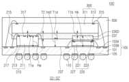
도 4는 본 개시의 일 실시예에 따른 반도체 패키지의 평면도이다.
도 5a 및 도 5b는 각각 도 4의 반도체 패키지를 Ⅰ1-Ⅰ1' 및 Ⅰ2-Ⅰ2'로 절개하여 본 단면도들이다.
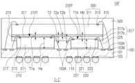
도 6은 본 개시의 일 실시예에 따른 반도체 패키지의 평면도이다.
도 7은 도 6의 반도체 패키지를 Ⅱ-Ⅱ'로 절개하여 본 단면도이다.
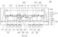
도 8은 본 개시의 일 실시예에 따른 반도체 패키지의 평면도이다.
도 9a 및 도 9b는 각각 도 4의 반도체 패키지를 Ⅱ1-Ⅱ1' 및 Ⅱ2-Ⅱ2'로 절개하여 본 단면도들이다.
도 10은 본 개시의 일 실시예에 따른 반도체 패키지의 평면도이다.
도 11은 도 10의 반도체 패키지를 Ⅲ-Ⅲ'로 절개하여 본 단면도이다.
도 12는 본 개시의 일 실시예에 따른 반도체 패키지의 단면도이다.
도 13은 본 개시의 일 실시예에 따른 반도체 패키지의 단면도이다.
도 14a 및 도 14b는 본 개시의 일 실시예에 따른 반도체 패키지의 단면도들이다.FIG. 1 is a plan view of a semiconductor package according to one embodiment of the present disclosure.
Figure 2 is a cross-sectional view taken along line Ⅰ-Ⅰ' of the semiconductor package of Figure 1.
Figure 3 is an enlarged view of part “A” of the semiconductor package of Figure 2.
FIG. 4 is a plan view of a semiconductor package according to one embodiment of the present disclosure.
Figures 5a and 5b are cross-sectional views taken along lines I1-I1' and I2-I2' of the semiconductor package of Figure 4, respectively.
FIG. 6 is a plan view of a semiconductor package according to one embodiment of the present disclosure.
Fig. 7 is a cross-sectional view of the semiconductor package of Fig. 6 taken along line II-II'.
FIG. 8 is a plan view of a semiconductor package according to one embodiment of the present disclosure.
Figures 9a and 9b are cross-sectional views taken along lines II1-II1' and II2-II2' of the semiconductor package of Figure 4, respectively.
FIG. 10 is a plan view of a semiconductor package according to one embodiment of the present disclosure.
Fig. 11 is a cross-sectional view taken along line Ⅲ-Ⅲ' of the semiconductor package of Fig. 10.
FIG. 12 is a cross-sectional view of a semiconductor package according to one embodiment of the present disclosure.
FIG. 13 is a cross-sectional view of a semiconductor package according to one embodiment of the present disclosure.
FIGS. 14A and 14B are cross-sectional views of a semiconductor package according to one embodiment of the present disclosure.
이하, 첨부된 도면을 참조하여 본 발명의 실시예들을 상세히 설명하기로 한다.Hereinafter, embodiments of the present invention will be described in detail with reference to the attached drawings.
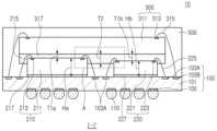
도 1은 본 개시의 일 실시예에 따른 반도체 패키지의 평면도이며, 도 2는 도 1의 반도체 패키지를 Ⅰ-Ⅰ'로 절개하여 본 단면도이다.FIG. 1 is a plan view of a semiconductor package according to one embodiment of the present disclosure, and FIG. 2 is a cross-sectional view taken along line Ⅰ-Ⅰ' of the semiconductor package of FIG. 1.
도 1 및 도 2를 참조하면, 본 실시예에 따른 반도체 패키지(10)는, 패키지 기판(100)과, 상기 패키지 기판(100) 상에 배치된 제1 및 제2 하부 반도체 칩들(210,220)과, 상기 제1 및 제2 하부 반도체 칩들(210,220) 상에 배치된 상부 반도체 칩(300)을 포함한다. 도 1의 평면은 제1 및 제2 하부 반도체 칩들(210,220)의 배열 중심으로 도시하고, 상부 반도체 칩(300)은 점선으로 개략 도시한다.Referring to FIGS. 1 and 2, a semiconductor package (10) according to the present embodiment includes a package substrate (100), first and second lower semiconductor chips (210, 220) arranged on the package substrate (100), and an upper semiconductor chip (300) arranged on the first and second lower semiconductor chips (210, 220). The plane of FIG. 1 is illustrated with the arrangement of the first and second lower semiconductor chips (210, 220) as the center, and the upper semiconductor chip (300) is schematically illustrated with a dotted line.
상기 패키지 기판(100)은 몸체부(101), 상기 몸체부(101)의 상면에 상부 기판 패드(103) 및 상기 몸체부(101)의 하면에 하부 기판 패드(105)를 포함할 수 있다. 또한, 상기 패키지 기판(100)은 상기 상부 기판 패드(103)와 상기 하부 기판 패드(105)를 전기적으로 연결하는 배선 패턴(미도시) 및 접속 비아(미도시)를 가질 수 있다. 상기 상부 기판 패드(103) 및 하부 기판 패드(105)의 일부는 접지 패드(104)일 수 있다.The package substrate (100) may include a body portion (101), an upper substrate pad (103) on an upper surface of the body portion (101), and a lower substrate pad (105) on a lower surface of the body portion (101). In addition, the package substrate (100) may have a wiring pattern (not shown) and a connecting via (not shown) electrically connecting the upper substrate pad (103) and the lower substrate pad (105). Some of the upper substrate pad (103) and the lower substrate pad (105) may be ground pads (104).
예를 들어, 상기 패키지 기판(100)은 인쇄회로기판(Printed Circuit Board)일 수 있다. 상기 패키지 기판(100)이 인쇄회로기판에 한정되는 것은 아니며, 다양한 형태의 배선 기판일 수 있다.For example, the package substrate (100) may be a printed circuit board. The package substrate (100) is not limited to a printed circuit board and may be a wiring board of various forms.
상기 패키지 기판(100)은 페놀 수지, 에폭시 수지, 폴리이미드 중에서 선택되는 적어도 하나의 물질로 이루어질 수 있다. 예를 들어, 상기 패키지 기판(100)은, FR4, 4관능성 에폭시 수지(Tetrafunctional epoxy), 폴리페닐렌 에테르(Polyphenylene ether), 에폭시/폴리페닐렌 옥사이드(Epoxy/polyphenylene oxide), 비스말라이미드 트리아진(Bismaleimidetriazine, BT), Thermount, 시아네이트 에스테르(Cyanate ester), 폴리이미드(Polyimide) 또는 액정 폴리머(Liquid crystal polymer)를 포함할 수 있다. 또한, 상부 기판 패드(103), 하부 기판 패드(105), 배선 패턴, 및 접속 비아는 예를 들어, 구리(Cu), 니켈(Ni), 알루미늄(Al), 또는 베릴륨 구리(beryllium copper)를 포함할 수 있다.The package substrate (100) may be made of at least one material selected from a phenol resin, an epoxy resin, and a polyimide. For example, the package substrate (100) may include FR4, a tetrafunctional epoxy, polyphenylene ether, epoxy/polyphenylene oxide, bismaleimidetriazine (BT), Thermount, cyanate ester, polyimide, or a liquid crystal polymer. In addition, the upper substrate pad (103), the lower substrate pad (105), the wiring pattern, and the connection via may include, for example, copper (Cu), nickel (Ni), aluminum (Al), or beryllium copper.
상기 패키지 기판(100)의 상기 하부 기판 패드(105) 상에 외부 접속 단자(110)가 형성될 수 있다. 상기 외부 접속 단자(110)는 예를 들어, 솔더 볼(solder ball), 도전성 범프(conductive bump), 도전성 페이스트, 비지에이(ball grid array, BGA), 엘지에이(lead grid array, LGA), 피지에이(pin grid array, PGA), 또는 이들의 조합을 포함할 수 있다. 일부 실시예들에서, 상기 외부 접속 단자(110)는 생략될 수 있다.An external connection terminal (110) may be formed on the lower substrate pad (105) of the package substrate (100). The external connection terminal (110) may include, for example, a solder ball, a conductive bump, a conductive paste, a ball grid array (BGA), a lead grid array (LGA), a pin grid array (PGA), or a combination thereof. In some embodiments, the external connection terminal (110) may be omitted.
상기 제1 및 제2 하부 반도체 칩들(210,220)은 각각 활성면 및 상기 활성면과 반대에 위치한 비활성면을 갖는 반도체 기판(211,221)을 포함할 수 있다. 상기 반도체 기판(211,221)의 상기 활성면에는 다수의 능동/수동 소자들(예, 트랜지스터)와 이들과 연결된 본딩 패드(213,223)가 형성될 수 있다. 상기 제1 및 제2 하부 반도체 칩들(210,220)의 상기 비활성면은 상기 패키지 기판(100)의 상면과 마주보는 면일 수 있다. 상기 제1 및 제2 하부 반도체 칩들(210,220)은 접착층들(217,227)을 이용하여 상기 패키지 기판(100)의 상면에 접합될 수 있다.The first and second lower semiconductor chips (210, 220) may each include a semiconductor substrate (211, 221) having an active surface and an inactive surface opposite to the active surface. A plurality of active/passive elements (e.g., transistors) and bonding pads (213, 223) connected thereto may be formed on the active surface of the semiconductor substrate (211, 221). The inactive surfaces of the first and second lower semiconductor chips (210, 220) may be surfaces facing the upper surface of the package substrate (100). The first and second lower semiconductor chips (210, 220) may be bonded to the upper surface of the package substrate (100) using adhesive layers (217, 227).
상기 제1 및 제2 하부 반도체 칩들(210,220)은 각각 와이어(215,225)에 의해 패키지 기판(100)에 전기적으로 연결될 수 있다. 상기 와이어(215,225)는 각각 제1 및 제2 하부 반도체 칩들(210,220)의 본딩 패드들(213,223)과 상기 상부 기판 패드(103) 중 제1 패드들(103A)을 연결할 수 있다.The first and second lower semiconductor chips (210, 220) may be electrically connected to the package substrate (100) by wires (215, 225), respectively. The wires (215, 225) may connect the bonding pads (213, 223) of the first and second lower semiconductor chips (210, 220) and the first pads (103A) of the upper substrate pads (103), respectively.
제1 및 제2 하부 반도체 칩들(210,220)과 유사하게, 상기 상부 반도체 칩(300)은 활성면 및 상기 활성면과 반대에 위치한 비활성면을 갖는 반도체 기판(311)을 포함할 수 있다. 상기 반도체 기판(311)의 상기 활성면에는 다수의 능동/수동 소자들(예, 트랜지스터)와 이들과 연결된 본딩 패드(313)가 형성될 수 있다. 상기 상부 반도체 칩(300)의 상기 비활성면은 상기 패키지 기판(100)의 상면과 마주보는 면일 수 있다. 상기 상부 반도체 칩(300)은 비전도성 접착층(317)을 이용하여 제1 및 제2 하부 반도체 칩들(210,220)의 상면들에 접합될 수 있다. 상기 비전도성 접착층(317)은 상부 반도체 칩(300)의 하면에 먼저 제공된 후에, 이어 제1 및 제2 하부 반도체 칩들(210,220)에 접합되는 방식으로 형성될 수 있다.Similar to the first and second lower semiconductor chips (210, 220), the upper semiconductor chip (300) may include a semiconductor substrate (311) having an active surface and a non-active surface located opposite the active surface. A plurality of active/passive elements (e.g., transistors) and bonding pads (313) connected thereto may be formed on the active surface of the semiconductor substrate (311). The non-active surface of the upper semiconductor chip (300) may be a surface facing the upper surface of the package substrate (100). The upper semiconductor chip (300) may be bonded to the upper surfaces of the first and second lower semiconductor chips (210, 220) using a non-conductive adhesive layer (317). The non-conductive adhesive layer (317) may be formed in such a way that it is first provided on the lower surface of the upper semiconductor chip (300) and then bonded to the first and second lower semiconductor chips (210, 220).
제1 및 제2 하부 반도체 칩들(210,220)과 유사하게, 상기 상부 반도체 칩(300)은 와이어(315)에 의해 패키지 기판(100)에 전기적으로 연결될 수 있다. 상기 와이어(315)는 상기 상부 반도체 칩(300)의 본딩 패드들(313)과 상기 상부 기판 패드(103) 중 제2 패드들(103B)을 연결할 수 있다.Similar to the first and second lower semiconductor chips (210, 220), the upper semiconductor chip (300) can be electrically connected to the package substrate (100) by a wire (315). The wire (315) can connect the bonding pads (313) of the upper semiconductor chip (300) and the second pads (103B) among the upper substrate pads (103).
본 실시예에 채용된 반도체 패키지(10)는, 상기 제1 및 제2 하부 반도체 칩들(210,220)과 상기 상부 반도체 칩(300)을 둘러싸는 몰딩 부재(500)를 더 포함할 수 있다.The semiconductor package (10) employed in this embodiment may further include a molding member (500) surrounding the first and second lower semiconductor chips (210, 220) and the upper semiconductor chip (300).
몰딩 부재(500)는 제1 및 제2 하부 반도체 칩(210) 및 상부 반도체 칩(300)을 둘러싸 외부 환경으로부터 보호하는 역할을 수행할 수 있다. 상기 몰딩 부재(500)는 주입 공정에 의하여 적절한 양의 몰딩 수지가 패키지 기판(100) 상에 주입되고, 경화 공정을 통해 반도체 패키지(10)의 외형을 형성할 수 있다. 일부 실시예에서, 프레스와 같은 가압 공정에서 상기 몰딩 수지에 압력을 가하여 반도체 패키지(10)의 외형을 형성할 수있다. 여기서, 상기 몰딩 수지 주입과 가압 사이의 지연시간, 주입되는 몰딩 수지의 양, 및 가압 온도/압력 등의 공정 조건은 몰딩 수지의 점도 등의 물리적 성질을 고려하여 설정할 수 있다.The molding member (500) can surround the first and second lower semiconductor chips (210) and the upper semiconductor chip (300) and play a role of protecting them from the external environment. The molding member (500) can inject an appropriate amount of molding resin onto the package substrate (100) through an injection process and form the outer shape of the semiconductor package (10) through a curing process. In some embodiments, the outer shape of the semiconductor package (10) can be formed by applying pressure to the molding resin in a pressurizing process such as a press. Here, the delay time between the injection of the molding resin and the pressurizing, the amount of the molding resin to be injected, and the process conditions such as the pressurizing temperature/pressure can be set in consideration of the physical properties of the molding resin such as the viscosity.
상기 몰딩 부재(500)는 에폭시계(epoxy-group) 성형 수지 또는 폴리이미드계(polyimide-group) 성형 수지을 포함할 수 있다. 예를 들면, 상기 몰딩 부재(500)는 에폭시 몰딩 컴파운드(Epoxy Molding Compound, EMC) 또는 하이케이(High-K) 에폭시 몰딩 컴파운드를 포함할 수 있다.The molding member (500) may include an epoxy-group molding resin or a polyimide-group molding resin. For example, the molding member (500) may include an epoxy molding compound (EMC) or a high-K epoxy molding compound.
상기 상부 반도체 칩(300)은 상기 제1 및 제2 하부 반도체 칩들(210,220)의 활성면에 상기 비전도성 접착층(317)에 의해 접합될 수 있다. 상기 상부 반도체 칩(300)은 상기 제1 및 제2 하부 반도체 칩들(210,220)의 상면들을 덮도록 배치될 수 있다. 이에 한정되지는 않으나, 상기 상부 반도체 칩(300)은 상기 제1 및 제2 하부 반도체 칩들(210,220)의 실장 영역보다 큰 면적을 가질 수 있다.The upper semiconductor chip (300) may be bonded to the active surfaces of the first and second lower semiconductor chips (210, 220) by the non-conductive adhesive layer (317). The upper semiconductor chip (300) may be arranged to cover the upper surfaces of the first and second lower semiconductor chips (210, 220). Although not limited thereto, the upper semiconductor chip (300) may have an area larger than the mounting areas of the first and second lower semiconductor chips (210, 220).
본 실시예에서, 상기 제1 및 제2 하부 반도체 칩들(210,220)의 상부 영역은 상기 비전도성 접착층(317)의 내부에 수용(receive)될 수 있다. 여기서, "상부 영역이 수용된다(the upper portions are received)"는 의미는 상기 제1 및 제2 하부 반도체 칩들(210,220)의 상면들에만 접합된 상태가 아니라, 그 상면들뿐만 아니라 인접한 측면들의 일부 영역까지 비전도성 접착층(317)의 내부에 인입(income)된 상태를 말한다.In the present embodiment, the upper portions of the first and second lower semiconductor chips (210, 220) can be received inside the non-conductive adhesive layer (317). Here, the meaning of "the upper portions are received" is not a state in which only the upper surfaces of the first and second lower semiconductor chips (210, 220) are bonded, but a state in which not only the upper surfaces but also some areas of adjacent side surfaces are imported into the interior of the non-conductive adhesive layer (317).
이러한 특징은 상기 비전도성 접착층(317)의 영역별 두께로도 표현될 수 있다. 상기 비전도성 접착층(317)에서, 상기 제1 및 제2 하부 반도체 칩들(210,220) 사이의 부분의 두께(T2)는 상기 제1 및 제2 하부 반도체 칩들(210,220)에 각각 접합된 부분의 두께(T1a,T1b)보다 클 수 있다.This feature can also be expressed as the area-specific thickness of the non-conductive adhesive layer (317). In the non-conductive adhesive layer (317), the thickness (T2) of the portion between the first and second lower semiconductor chips (210, 220) can be greater than the thickness (T1a, T1b) of the portion bonded to the first and second lower semiconductor chips (210, 220), respectively.
본 실시예에 채용된 제1 및 제2 하부 반도체 칩들(210,220)은 서로 다른 높이(Ha,Hb)를 갖는 다른 종류의 반도체 칩일 수 있다. 도 2에 도시된 바와 같이, 상기 제1 하부 반도체 칩(210)의 상면은 상기 제2 하부 반도체 칩(220)의 상면보다 높은 레벨을 가질 수 있으며, 상기 제1 하부 반도체 칩(210)의 수용된 깊이는 상기 제2 하부 반도체 칩(220)에 수용된 깊이보다 클 수 있다.The first and second lower semiconductor chips (210, 220) employed in the present embodiment may be different types of semiconductor chips having different heights (Ha, Hb). As illustrated in FIG. 2, the upper surface of the first lower semiconductor chip (210) may have a higher level than the upper surface of the second lower semiconductor chip (220), and the depth accommodated in the first lower semiconductor chip (210) may be greater than the depth accommodated in the second lower semiconductor chip (220).
이러한 특징을 상기 비전도성 접착층(317)의 영역별 두께로 표현하면, 상기 비전도성 접착층(317)에서, 상기 제1 하부 반도체 칩들(210)과 접합된 부분의 두께(T1a)는 상기 제2 하부 반도체 칩들(220)과 접합된 부분의 두께(T1b)보다 작을 수 있다. 따라서, 상기 상부 반도체 칩(300)은 상기 제1 및 제2 하부 반도체 칩들의 상면 레벨의 큰 차이에도 불구하고 비교적 수평하게 정렬될 수 있다.When these characteristics are expressed as the area-specific thickness of the non-conductive adhesive layer (317), the thickness (T1a) of the portion of the non-conductive adhesive layer (317) bonded to the first lower semiconductor chips (210) may be smaller than the thickness (T1b) of the portion bonded to the second lower semiconductor chips (220). Accordingly, the upper semiconductor chip (300) may be aligned relatively horizontally despite a large difference in the upper surface levels of the first and second lower semiconductor chips.
본 실시예에 따른 반도체 패키지(10)는 비전도성 접착층(317)으로 인해 발생되는 기계적 신뢰성 저하요인을 해소할 수 있다. 이러한 효과는 도 3을 참조하여 상세히 설명될 수 있다.The semiconductor package (10) according to the present embodiment can eliminate the mechanical reliability deterioration factor caused by the non-conductive adhesive layer (317). This effect can be explained in detail with reference to FIG. 3.
앞서 설명한 바와 같이, 패키지 기판(100) 상에 제1 및 제2 하부 반도체 칩들(210,220)은 서로 다른 높이(Ha,Hb)로 실장될 수 있다. 이와 같이, 제1 및 제2 하부 반도체 칩들(210,220)의 높이 편차가 큰 경우에, 일반적인 비전도성 접착층은 상대적으로 높은 점도로 인하여 제1 및 제2 하부 반도체 칩들(210,220)(특히, 낮은 높이를 갖는 제2 하부 반도체 칩(220))을 충분히 수용하지 못할 수 있다.As described above, the first and second lower semiconductor chips (210, 220) may be mounted on the package substrate (100) at different heights (Ha, Hb). In this way, when the height difference between the first and second lower semiconductor chips (210, 220) is large, a general non-conductive adhesive layer may not be able to sufficiently accommodate the first and second lower semiconductor chips (210, 220) (particularly, the second lower semiconductor chip (220) having a low height) due to its relatively high viscosity.
도 3은 도 2의 반도체 패키지의 "A" 부분을 확대하여 본 부분 확대도이다. 도 3에는 종래의 비전도성 필름(317L)의 하면이 점선으로 도시되어 있다.Fig. 3 is an enlarged view of a portion “A” of the semiconductor package of Fig. 2. In Fig. 3, the lower surface of a conventional non-conductive film (317L) is shown in a dotted line.
도 3을 참조하면, 종래의 비전도성 필름(317L)(그 하면이 점선으로 표시됨)은 낮은 높이를 갖는 제2 하부 반도체 칩(210)의 상면에만 접하며, 그 인접한 측면 영역까지 연장되지 못한다. 따라서, 상부 반도체 칩(300)과 제2 하부 반도체 칩(220)의 견고한 접합을 기대하기 어렵다.Referring to Fig. 3, the conventional non-conductive film (317L) (the lower surface of which is indicated by a dotted line) only contacts the upper surface of the second lower semiconductor chip (210) having a low height, and does not extend to the adjacent side area. Therefore, it is difficult to expect a firm bonding between the upper semiconductor chip (300) and the second lower semiconductor chip (220).
특히, 종래의 비전도성 필름(317L)은 제2 하부 반도체 칩(210)의 모서리 상에서 오목하게 패인 부분(CV)을 가질 수 있다. 이러한 패인 부분(CV)은 몰딩 부재(500)가 적용될 때에 패인 부분(CV)까지 채워지기 어려우므로 몰딩 부재(500)을 적용한 후에도, 상부 반도체 칩(300)과 제2 하부 반도체 칩(220) 사이에 보이드를 발생시킬 수 있으며, 이로 인해 반도체 패키지(10)의 기계적 신뢰성이 크게 저하될 수 있다.In particular, the conventional non-conductive film (317L) may have a concave portion (CV) on the edge of the second lower semiconductor chip (210). Since it is difficult to fill the concave portion (CV) when the molding member (500) is applied, a void may be generated between the upper semiconductor chip (300) and the second lower semiconductor chip (220) even after the molding member (500) is applied, and as a result, the mechanical reliability of the semiconductor package (10) may be significantly reduced.
이와 달리, 본 실시예에 따른 반도체 패키지(10)에서는, 앞서 설명한 바와 같이, 상부 반도체 칩(300)의 하면에 위치한 비전도성 접착층(317)에 제1 및 제2 하부 반도체 칩들(210,220)의 상부 영역이 수용됨으로써 제1 및 제2 하부 반도체 칩들(210,220)(특히, 낮은 높이(Hb)를 갖는 제2 하부 반도체 칩(220))과 상부 반도체 칩(300)의 견고한 접합을 보장할 수 있을 뿐만 아니라, 몰딩 부재(500)를 적용한 후에 보이드로 인한 패키지 신뢰성 저하를 효과적으로 방지할 수 있다.In contrast, in the semiconductor package (10) according to the present embodiment, as described above, the upper areas of the first and second lower semiconductor chips (210, 220) are accommodated in the non-conductive adhesive layer (317) located on the lower surface of the upper semiconductor chip (300), thereby ensuring a firm bonding between the first and second lower semiconductor chips (210, 220) (particularly, the second lower semiconductor chip (220) having a low height (Hb)) and the upper semiconductor chip (300), and effectively preventing a decrease in package reliability due to voids after applying the molding member (500).
이러한 신뢰성 저하는 상기 제1 및 제2 하부 반도체 칩들(210,220)의 상면 레벨의 차이가 클수록 크게 발생될 수 있으므로, 그 레벨의 차이가 큰 경우에 본 실시예가 더 유익하게 적용될 수 있다. 예를 들어, 상기 제1 및 제2 하부 반도체 칩들(210,220)의 상면 레벨의 차이가 적어도 10 ㎛인 경우에 더욱 유익하게 적용될 수있다.Since this reliability degradation can occur more significantly as the difference in the upper surface levels of the first and second lower semiconductor chips (210, 220) becomes greater, the present embodiment can be more advantageously applied when the difference in levels is large. For example, the present embodiment can be more advantageously applied when the difference in the upper surface levels of the first and second lower semiconductor chips (210, 220) is at least 10 μm.
본 실시예에 채용된 비전도성 접착층(317)은 종래의 비전도성 접착층에 비해 낮은 점도(예, 120℃에서 1,800~5,000 Pa.s)보다 상대적으로 낮은 점도를 갖는 접착 필름을 이용하여 형성함으로써 제1 및 제2 하부 반도체 칩들(210,220)의 상부 영역을 수용하도록 구성할 수 있다. 예를 들어, 비전도성 접착층(317)을 위한 접착 필름은 약 1,500Pa·s 이하의 점도를 가질 수 있다. 여기서, 점도는 그 점도가 최저점이 되는 때의 점도를 의미하고, 약 120℃의 온도 조건에서 측정한 값이다. 상기 측정 온도는 120℃를 기준으로 약 ±5℃의 오차 범위를 가질 수 있다.The non-conductive adhesive layer (317) employed in this embodiment may be configured to accommodate upper regions of the first and second lower semiconductor chips (210, 220) by forming an adhesive film having a relatively lower viscosity (e.g., 1,800 to 5,000 Pa.s at 120°C) than conventional non-conductive adhesive layers. For example, the adhesive film for the non-conductive adhesive layer (317) may have a viscosity of about 1,500 Pa.s or less. Here, the viscosity refers to the viscosity when the viscosity becomes the lowest point, and is a value measured under a temperature condition of about 120°C. The measurement temperature may have an error range of about ±5°C based on 120°C.
상기 비전도성 접착층(317)은 제1 및 제2 하부 반도체 칩들(210,220)과 상기 상부 반도체 칩(300)을 고정하는 접착층으로 제공되며, 예를 들어 비전도성 필름(non-conductive film, NCF)일 수 있다. 상기 비전도성 접착층(317)은 접착 수지를 포함할 수 있다. 예를 들면, 상기 접착 수지는 비스페놀형 에폭시 수지, 노블락형 에폭시 수지, 페놀 수지, 우레아 수지, 멜라민 수지, 불포화 폴리에스테르 수지 및 레조시놀 수지 및 그 조합을 포함할 수 있다.The above non-conductive adhesive layer (317) is provided as an adhesive layer that fixes the first and second lower semiconductor chips (210, 220) and the upper semiconductor chip (300), and may be, for example, a non-conductive film (NCF). The above non-conductive adhesive layer (317) may include an adhesive resin. For example, the adhesive resin may include a bisphenol-type epoxy resin, a novolak-type epoxy resin, a phenol resin, a urea resin, a melamine resin, an unsaturated polyester resin, a resorcinol resin, and a combination thereof.
상기 비전도성 접착층(317) 중 상기 제1 및 제2 하부 반도체 칩들(210,220)에 각각 접합된 부분은 와이어(215,225)를 위한 공간을 제공할 수 있다. 일부 실시예에서, 상기 제1 하부 반도체 칩들(210)의 수용된 깊이는 상기 비전도성 접착층(317)의 두께(T2)의 10% 내지 50% 범위일 수 있다.The portions of the non-conductive adhesive layer (317) bonded to the first and second lower semiconductor chips (210, 220), respectively, can provide a space for wires (215, 225). In some embodiments, the accommodated depth of the first lower semiconductor chips (210) can be in the range of 10% to 50% of the thickness (T2) of the non-conductive adhesive layer (317).
일부 실시예에서, 상기 제1 및 제2 하부 반도체 칩들(210,220)은 휘발성 메모리 칩 및/또는 비휘발성 메모리 칩일 수 있다. 예를 들어, 상기 휘발성 메모리 칩은 DRAM(dynamic random access memory), SRAM(static RAM), TRAM(thyristor RAM), ZRAM(zero capacitor RAM), 또는 TTRAM(Twin Transistor RAM)을 포함할 수 있다. 또한, 상기 비휘발성 메모리 칩은 예를 들어, 플래시(flash) 메모리, MRAM(magnetic RAM), STT-MRAM(spin-transfer torque MRAM), FRAM(ferroelectric RAM), PRAM(phase change RAM), RRAM(resistive RAM), 나노튜브 RRAM(nanotube RRAM), 폴리머 RAM(polymer RAM), 나노 플로팅 게이트 메모리(nano floating gate memory), 홀로그래픽 메모리(holographic memory), 분자 전자 메모리(molecular electronics memory) 또는 절연 저항 변화 메모리(insulator resistance change memory)을 포함할 수 있다.In some embodiments, the first and second lower semiconductor chips (210, 220) may be volatile memory chips and/or nonvolatile memory chips. For example, the volatile memory chip may include dynamic random access memory (DRAM), static RAM (SRAM), thyristor RAM (TRAM), zero capacitor RAM (ZRAM), or twin transistor RAM (TTRAM). In addition, the nonvolatile memory chip may include, for example, flash memory, magnetic RAM (MRAM), spin-transfer torque MRAM (STT-MRAM), ferroelectric RAM (FRAM), phase change RAM (PRAM), resistive RAM (RRAM), nanotube RRAM, polymer RAM, nano floating gate memory, holographic memory, molecular electronics memory, or insulator resistance change memory.
일부 실시예에서, 상기 상부 반도체 칩(300)은 프로세서 칩일 수 있다. 예를 들어, 상기 상부 반도체 칩(300)은 마이크로프로세서, 그래픽 프로세서, 신호 프로세서, 네트워크 프로세서, 칩셋, 오디오 코덱, 비디오 코덱, 애플리케이션 프로세서 또는 시스템 온 칩(System on Chip)을 포함할 수 있으나, 이에 한정되는 것은 아니다. 예를 들어, 상기 마이크로프로세서는 싱글 코어 또는 멀티 코어를 포함할 수 있다.In some embodiments, the upper semiconductor chip (300) may be a processor chip. For example, the upper semiconductor chip (300) may include, but is not limited to, a microprocessor, a graphics processor, a signal processor, a network processor, a chipset, an audio codec, a video codec, an application processor, or a system on chip. For example, the microprocessor may include a single core or multi-core.
상술된 실시예에서, 반도체 패키지(10)는 제1 및 제2 하부 반도체 칩들(210,220)과 상기 제1 및 제2 하부 반도체 칩들(210,220)의 상면에 접합된 상부 반도체 칩(300)을 포함하는 것으로 예시되어 있으나, 일부 실시예에서, 반도체 패키지(10)에서, 적어도 하나의 반도체 칩은 보강 부재(stiff member) 또는 방열 부재(heat spreader)와 같은 더미 칩(dummy chip)으로 대체되거나(도 4, 도 8 및 도 12 참조), 상기 더미 칩이 추가적으로 배치될 수 있다(도 10 참조). 한편, 다른 일부 실시예에서는, 적어도 하나의 반도체 칩은 복수의 반도체 칩이 스택된 칩 스택(chip stack)일 수 있다(도 7 참조).In the above-described embodiment, the semiconductor package (10) is exemplified as including first and second lower semiconductor chips (210, 220) and an upper semiconductor chip (300) bonded to the upper surfaces of the first and second lower semiconductor chips (210, 220). However, in some embodiments, in the semiconductor package (10), at least one semiconductor chip may be replaced with a dummy chip such as a stiff member or a heat spreader (see FIGS. 4, 8, and 12), or the dummy chip may be additionally arranged (see FIG. 10). Meanwhile, in some other embodiments, the at least one semiconductor chip may be a chip stack in which a plurality of semiconductor chips are stacked (see FIG. 7).
본 명세서에서 상기 반도체 칩, 상기 더미 칩 및 상기 칩 스택와 같은 칩 형태의 구조체를 지칭하는 용어로 "칩 구조체(chip sturcture)"를 사용한다. 예를 들어, 반도체 패키지에서 배치된 위치에 따라 하부 칩 구조체 또는 상부 칩 구조체라고 할 수 있다.In this specification, the term "chip structure" is used to refer to a chip-shaped structure such as the semiconductor chip, the dummy chip, and the chip stack. For example, it may be referred to as a lower chip structure or an upper chip structure depending on the position where it is arranged in a semiconductor package.
도 4는 본 개시의 일 실시예에 따른 반도체 패키지의 평면도이며, 도 5a 및 도 5b는 각각 도 4의 반도체 패키지를 Ⅰ1-Ⅰ1' 및 Ⅰ2-Ⅰ2'로 절개하여 본 단면도들이다.FIG. 4 is a plan view of a semiconductor package according to one embodiment of the present disclosure, and FIGS. 5a and 5b are cross-sectional views taken along lines I1-I1' and I2-I2' of the semiconductor package of FIG. 4, respectively.
도 4와 도 5a 및 도 5b를 참조하면, 본 실시예에 따른 반도체 패키지(10A)는, 하부 칩 구조체로서 더미 칩(230D)을 더 포함하는 것을 제외하고, 도 1 및 도 2에 도시된 실시예와 유사한 구조로 이해할 수 있다. 따라서, 도 1 내지 도 3에 도시된 실시예의 설명은 특별히 반대되는 설명이 없는 한, 본 실시예에 대한 설명에 결합될 수 있다.Referring to FIGS. 4 and 5A and 5B, the semiconductor package (10A) according to the present embodiment can be understood to have a structure similar to that of the embodiment illustrated in FIGS. 1 and 2, except that it further includes a dummy chip (230D) as a lower chip structure. Accordingly, the description of the embodiment illustrated in FIGS. 1 to 3 can be combined with the description of the present embodiment, unless there is a specifically contrary description.
본 실시예에 따른 반도체 패키지(10A)는 패키지 기판(100)과, 상기 패키지 기판(100) 상에 배치된 제1 및 제2 하부 반도체 칩들(210,220)과, 상기 패키지 기판(100) 상에 배치된 더미 칩(230D)과, 상기 제1 및 제2 하부 반도체 칩들(210,220) 및 상기 더미 칩(230D) 상에 배치된 상부 반도체 칩(300)을 포함한다. 상기 더미 칩(230D)은 상부 반도체 칩(300)을 안정적으로 지지하도록 제1 및 제2 하부 반도체 칩들(210,220)과 함께 하부 칩 구조체로 제공될 수 있다.A semiconductor package (10A) according to the present embodiment includes a package substrate (100), first and second lower semiconductor chips (210, 220) arranged on the package substrate (100), a dummy chip (230D) arranged on the package substrate (100), and an upper semiconductor chip (300) arranged on the first and second lower semiconductor chips (210, 220) and the dummy chip (230D). The dummy chip (230D) may be provided as a lower chip structure together with the first and second lower semiconductor chips (210, 220) to stably support the upper semiconductor chip (300).
도 5a 및 도 5b를 참조하면, 상기 상부 반도체 칩(300)은 상기 제1 및 제2 하부 반도체 칩들(210,220)의 활성면과 상기 더미 칩(230D)의 상면에 상기 비전도성 접착층(317)에 의해 접합될 수 있다. 상기 상부 반도체 칩(300)은 상기 제1 및 제2 하부 반도체 칩들(210,220)의 상면들을 덮도록 배치될 수 있다. 상기 상부 반도체 칩(300)은 상기 제1 및 제2 하부 반도체 칩들(210,220)과 더미 칩(230D)의 실장 영역보다 큰 면적을 가질 수 있다.Referring to FIGS. 5A and 5B, the upper semiconductor chip (300) can be bonded to the active surfaces of the first and second lower semiconductor chips (210, 220) and the upper surface of the dummy chip (230D) by the non-conductive adhesive layer (317). The upper semiconductor chip (300) can be arranged to cover the upper surfaces of the first and second lower semiconductor chips (210, 220). The upper semiconductor chip (300) can have an area larger than the mounting areas of the first and second lower semiconductor chips (210, 220) and the dummy chip (230D).
상기 패키지 기판(100) 상에 실장된 제1 및 제2 하부 반도체 칩들(210,220) 및 더미 칩(230D)은 서로 다른 높이(Ha,Hb,Hc)를 가질 수 있다. 상기 제1 및 제2 하부 반도체 칩들(210,220)의 상부 영역들과 함께 더미 칩(230D)의 상부 영역은 상기 비전도성 접착층(317)의 내부에 수용될 수 있다. 상기 비전도성 접착층(317)의 영역별 두께 관점에서, 상기 제1 및 제2 하부 반도체 칩들(210,220) 사이의 부분의 두께(T2)는 상기 제1 및 제2 하부 반도체 칩들(210,220)와 상기 더미 칩(230D)에 각각 접합된 부분의 두께(T1a,T1b,T1c)보다 클 수 있다.The first and second lower semiconductor chips (210, 220) and the dummy chip (230D) mounted on the package substrate (100) may have different heights (Ha, Hb, Hc). The upper region of the dummy chip (230D) together with the upper regions of the first and second lower semiconductor chips (210, 220) may be accommodated inside the non-conductive adhesive layer (317). In terms of the thickness of each region of the non-conductive adhesive layer (317), the thickness (T2) of the portion between the first and second lower semiconductor chips (210, 220) may be greater than the thicknesses (T1a, T1b, T1c) of the portions bonded to the first and second lower semiconductor chips (210, 220) and the dummy chip (230D), respectively.
제1 및 제2 하부 반도체 칩들(210,220) 및 더미 칩(230D)의 수용된 깊이는 상이할 수 있다. 구체적으로, 상기 수용된 깊이는 상기 실장 높이(Ha,Hb,Hc)와 비례하며, 상기 비전도성 접착층(317)의 영역별 두께(T1a<T1b<T1c)는 상기 실장 높이(Ha>Hb>Hc)와 반비례할 수 있다.The depths accommodated in the first and second lower semiconductor chips (210, 220) and the dummy chip (230D) may be different. Specifically, the depth accommodated is proportional to the mounting height (Ha, Hb, Hc), and the area-wise thickness (T1a<T1b<T1c) of the non-conductive adhesive layer (317) may be inversely proportional to the mounting height (Ha>Hb>Hc).
본 실시예에서, 상기 상부 반도체 칩(300)은 상기 제1 및 제2 하부 반도체 칩들(210,220)와 더미 칩(230D)의 상면 레벨의 차이에도 불구하고 비교적 수평하게 정렬될 수 있다.In this embodiment, the upper semiconductor chip (300) can be aligned relatively horizontally despite the difference in the upper surface level of the first and second lower semiconductor chips (210, 220) and the dummy chip (230D).
또한, 본 실시예에 따른 반도체 패키지(10A)에서는, 상부 반도체 칩(300)의 하면에 위치한 비전도성 접착층(317)에 제1 및 제2 하부 반도체 칩들(210,220) 및 더미 칩(230D)의 상부 영역이 모두 수용됨으로써 이들 하부 칩 구조체 모두와 상부 반도체 칩(300)의 견고한 접합을 보장할 수 있으며, 몰딩 부재(500)를 적용한 후에 보이드 발생을 억제할 수 있다.In addition, in the semiconductor package (10A) according to the present embodiment, the upper regions of the first and second lower semiconductor chips (210, 220) and the dummy chip (230D) are all accommodated in the non-conductive adhesive layer (317) located on the lower surface of the upper semiconductor chip (300), thereby ensuring a firm bonding of all of these lower chip structures and the upper semiconductor chip (300), and suppressing the occurrence of voids after applying the molding member (500).
도 6은 본 개시의 일 실시예에 따른 반도체 패키지의 평면도이며, 도 7은 도 6의 반도체 패키지를 Ⅱ-Ⅱ'로 절개하여 본 단면도이다.FIG. 6 is a plan view of a semiconductor package according to one embodiment of the present disclosure, and FIG. 7 is a cross-sectional view of the semiconductor package of FIG. 6 taken along line II-II'.
도 6 및 도 7을 참조하면, 본 실시예에 따른 반도체 패키지(10B)는, 하부 칩 구조체로서 제1 및 제2 칩 스택이 채용된 것을 제외하고, 도 1 및 도 2에 도시된 실시예와 유사한 구조로 이해할 수 있다. 따라서, 도 1 내지 도 3에 도시된 실시예의 설명은 특별히 반대되는 설명이 없는 한, 본 실시예에 대한 설명에 결합될 수 있다.Referring to FIGS. 6 and 7, the semiconductor package (10B) according to the present embodiment can be understood as having a structure similar to that of the embodiment illustrated in FIGS. 1 and 2, except that the first and second chip stacks are employed as lower chip structures. Accordingly, the description of the embodiment illustrated in FIGS. 1 to 3 can be combined with the description of the present embodiment, unless there is a specifically contrary description.
본 실시예에 따른 반도체 패키지(10B)는 패키지 기판(100)과, 상기 패키지 기판(100) 상에 배치된 제1 및 제2 칩 스택들(210S,220S)과, 상기 제1 및 제2 칩 스택들(210S,220S) 상에 배치된 상부 반도체 칩(300)을 포함한다. 상기 제1 및 제2 칩 스택들(210S,220S)은 동일한 반도체 칩들(210A-210D,220A-220D)을 동일한 수로 적층하여도 공정 오차(예, 접착층(217)의 두께 및/또는 본딩 공정의 차이)로 인해 다른 실장 높이(Ha,Hb)를 가질 수 있다.A semiconductor package (10B) according to the present embodiment includes a package substrate (100), first and second chip stacks (210S, 220S) arranged on the package substrate (100), and an upper semiconductor chip (300) arranged on the first and second chip stacks (210S, 220S). Even if the same number of identical semiconductor chips (210A-210D, 220A-220D) are stacked, the first and second chip stacks (210S, 220S) may have different mounting heights (Ha, Hb) due to process errors (e.g., differences in the thickness of the adhesive layer (217) and/or bonding processes).
제1 및 제2 칩 스택(210S,220S)는, 순차적으로 적층된 제1 내지 제4 반도체 칩들(210A-210D,220A-220D)과 그 사이에 각각 배치된 접착 필름들(217)을 포함할 수 있다. 제1 내지 제4 반도체 칩들(210A-210D,220A-220D)은 메모리 칩들일 수 있다. 제1 내지 제4 반도체 칩들(210A-210D,220A-220D)은 서로 실질적으로 동일한 평면 형상 및 평면적을 가질 수 있다. 다만, 제4 반도체 칩(210D,220D)은 제1 내지 제3 반도체 칩들(210A-210C,220A-220C)보다 더 큰 두께를 가질 수 있다.The first and second chip stacks (210S, 220S) may include first to fourth semiconductor chips (210A-210D, 220A-220D) sequentially stacked and adhesive films (217) respectively disposed therebetween. The first to fourth semiconductor chips (210A-210D, 220A-220D) may be memory chips. The first to fourth semiconductor chips (210A-210D, 220A-220D) may have substantially the same planar shape and planar area. However, the fourth semiconductor chip (210D, 220D) may have a greater thickness than the first to third semiconductor chips (210A-210C, 220A-220C).
제1 내지 제4 반도체 칩들(210A-210D,220A-220D) 각각은, 패키지 기판(100)을 향하는 활성면과 상기 활성면에 반대에 위치한 비활성면을 갖는 반도체 기판(201)을 포함할 수 있다. 상기 반도체 기판(201)의 활성면에는 능동/수동 소자(예, 트랜지스터들) 및 이들과 연결된 배선층들을 포함할 수 있다. 능동/수동 소자 및 배선층은 메모리 회로를 구성할 수 있다.Each of the first to fourth semiconductor chips (210A-210D, 220A-220D) may include a semiconductor substrate (201) having an active surface facing the package substrate (100) and a passive surface positioned opposite the active surface. The active surface of the semiconductor substrate (201) may include active/passive elements (e.g., transistors) and wiring layers connected thereto. The active/passive elements and wiring layers may constitute a memory circuit.
제1 내지 제3 반도체 칩들(210A-210C,220A-220C) 각각은, 반도체 기판(201)을 관통하여 상기 메모리 회로와 전기적으로 연결되는 관통 비아들(TV)을 포함할 수 있다. 제4 반도체 칩(210D,220D)은 관통 비아들을 포함하지 않을 수 있으나, 이는 한정되는 것은 아니다.Each of the first to third semiconductor chips (210A-210C, 220A-220C) may include through vias (TV) that penetrate the semiconductor substrate (201) and are electrically connected to the memory circuit. The fourth semiconductor chip (210D, 220D) may not include through vias, but this is not limited.
제1 내지 제4 반도체 칩들(210A-210D,220A-220D) 각각은, 반도체 기판(201)의 활성면에 본딩 패드(BP)를 포함한다. 제1 반도체 칩(210A,220A)은 활성면이 패키지 기판(100)을 마주하도록 페이스다운(face-down) 상태로 패키지 기판(100) 상에 실장되며, 제1 반도체 칩(210A,220A)의 본딩 패드(BP)와 상기 상부 기판 패드(103) 중 제1 패드들(103A)은 접착 필름(217)을 관통하여 연결될 수 있다.Each of the first to fourth semiconductor chips (210A-210D, 220A-220D) includes a bonding pad (BP) on an active surface of a semiconductor substrate (201). The first semiconductor chip (210A, 220A) is mounted on a package substrate (100) in a face-down state so that the active surface faces the package substrate (100), and the bonding pad (BP) of the first semiconductor chip (210A, 220A) and the first pads (103A) of the upper substrate pads (103) can be connected by penetrating an adhesive film (217).
이와 유사하게, 제2 내지 제4 반도체 칩들(210B-210D,220B-220D)의 본딩 패드들(BP)은 제1 내지 제3 반도체 칩들(210A-210C,220A-220C)의 관통 비아들(TV)에 접착 필름(217)을 관통하여 연결될 수 있다Similarly, the bonding pads (BP) of the second to fourth semiconductor chips (210B-210D, 220B-220D) can be connected to the through vias (TV) of the first to third semiconductor chips (210A-210C, 220A-220C) by penetrating the adhesive film (217).
이와 같이, 상기 제1 및 제2 칩 스택들(210S,220S)은 동일한 종류의 반도체 칩들(210A-210D,220A-220D)을 동일하게 4개로 적층하여도 공정 오차로 인해 다른 실장 높이(Ha,Hb)를 가질 수 있다. 이러한 실장 높이의 편차(Hb-Ha)는 보이드 발생을 유발할 수 있는 정도가 될 수 있다. 예를 들어, 이러한 실장 높이의 편차(Hb-Ha)는 10㎛ 이상일 수 있다.In this way, the first and second chip stacks (210S, 220S) may have different mounting heights (Ha, Hb) due to process errors even though they are made by stacking four of the same type of semiconductor chips (210A-210D, 220A-220D). This mounting height deviation (Hb-Ha) may be such that voids may occur. For example, this mounting height deviation (Hb-Ha) may be 10㎛ or more.
도 7을 참조하면, 상기 상부 반도체 칩(300)은 서로 다른 높이(Ha,Hb)를 갖는 상기 제1 및 제2 칩 스택들(210S,220S)의 상면에 상기 비전도성 접착층(317)에 의해 접합될 수 있다. 상기 상부 반도체 칩(300)은 상기 제1 및 제2 칩 스택들(210S,220S) 상면들을 덮도록 배치될 수 있다.Referring to FIG. 7, the upper semiconductor chip (300) may be bonded to the upper surfaces of the first and second chip stacks (210S, 220S) having different heights (Ha, Hb) by the non-conductive adhesive layer (317). The upper semiconductor chip (300) may be arranged to cover the upper surfaces of the first and second chip stacks (210S, 220S).
제1 및 제2 칩 스택들(210S,220S)의 상부 영역들은 앞선 실시예와 유사하게 상기 비전도성 접착층(317)의 내부에 수용될 수 있다. 상기 비전도성 접착층(317)의 영역별 두께 관점에서, 상기 제1 및 제2 칩 스택들(210S,220S) 사이의 부분의 두께(T2)는 상기 제1 및 제2 칩 스택들(210S,220S)에 각각 접합된 부분의 두께(T1a,T1b)보다 클 수 있다.The upper regions of the first and second chip stacks (210S, 220S) may be accommodated within the non-conductive adhesive layer (317) similarly to the previous embodiment. In terms of the thickness of the non-conductive adhesive layer (317) per region, the thickness (T2) of the portion between the first and second chip stacks (210S, 220S) may be greater than the thickness (T1a, T1b) of the portion bonded to the first and second chip stacks (210S, 220S), respectively.
본 실시예에서, 제1 및 제2 칩 스택들(210S,220S)의 수용된 깊이는 그 실장 높이(Ha,Hb)와 비례하며, 상기 비전도성 접착층(317)의 영역별 두께(T1a<T1b)는 상기 실장 높이(Ha>Hb)와 반비례할 수 있다.In the present embodiment, the received depth of the first and second chip stacks (210S, 220S) is proportional to their mounting heights (Ha, Hb), and the area-wise thickness (T1a<T1b) of the non-conductive adhesive layer (317) may be inversely proportional to the mounting heights (Ha>Hb).
본 실시예에서, 상기 상부 반도체 칩(300)은 상기 제1 및 제2 칩 스택들(210S,220S)의 상면 레벨의 차이에도 불구하고 비교적 수평하게 정렬될 수 있다.In this embodiment, the upper semiconductor chip (300) can be aligned relatively horizontally despite the difference in the upper surface levels of the first and second chip stacks (210S, 220S).
또한, 본 실시예에 따른 반도체 패키지(10B)에서는, 상부 반도체 칩(300)의 하면에 위치한 비전도성 접착층(317)에 제1 및 제2 칩 스택들(210S,220S)의 상부 영역이 모두 수용됨으로써 제1 및 제2 칩 스택들(210S,220S)과 상부 반도체 칩(300)의 견고한 접합을 보장할 수 있으며, 몰딩 부재(500)를 적용한 후에 보이드 발생을 억제할 수 있다.In addition, in the semiconductor package (10B) according to the present embodiment, the upper areas of the first and second chip stacks (210S, 220S) are all accommodated in the non-conductive adhesive layer (317) located on the lower surface of the upper semiconductor chip (300), thereby ensuring a firm bonding between the first and second chip stacks (210S, 220S) and the upper semiconductor chip (300), and suppressing the occurrence of voids after applying the molding member (500).
도 8은 본 개시의 일 실시예에 따른 반도체 패키지의 평면도이며, 도 9a 및 도 9b는 각각 도 4의 반도체 패키지를 Ⅱ1-Ⅱ1' 및 Ⅱ2-Ⅱ2'로 절개하여 본 단면도들이다.FIG. 8 is a plan view of a semiconductor package according to one embodiment of the present disclosure, and FIGS. 9a and 9b are cross-sectional views taken along lines II1-II1' and II2-II2' of the semiconductor package of FIG. 4, respectively.
도 8과 도 9a 및 도 9b를 참조하면, 본 실시예에 따른 반도체 패키지(10C)는, 하부 칩 구조체로서 더욱 복잡한 배열(3개의 반도체 칩(210,220,230)과 2개의 더미 칩(240D1,240D2))을 포함하는 것을 제외하고, 도 1 및 도 2에 도시된 실시예와 유사한 구조로 이해할 수 있다. 따라서, 도 1 내지 도 3에 도시된 실시예의 설명은 특별히 반대되는 설명이 없는 한, 본 실시예에 대한 설명에 결합될 수 있다.Referring to FIGS. 8 and 9A and 9B, the semiconductor package (10C) according to the present embodiment can be understood to have a similar structure to the embodiment illustrated in FIGS. 1 and 2, except that it includes a more complex arrangement (three semiconductor chips (210, 220, 230) and two dummy chips (240D1, 240D2)) as the lower chip structure. Accordingly, the description of the embodiment illustrated in FIGS. 1 to 3 can be combined with the description of the present embodiment, unless there is a specifically contrary description.
본 실시예에 따른 반도체 패키지(10C)는 패키지 기판(100)과, 상기 패키지 기판(100) 상에 배치된 제1 내지 제3 하부 반도체 칩들(210,220,230)과, 상기 패키지 기판(100) 상에 배치된 제1 및 제2 더미 칩(240D1,240D2)과, 제1 내지 제3 하부 반도체 칩들(210,220,230) 및 상기 제1 및 제2 더미 칩(240D1,240D2) 상에 배치된 상부 반도체 칩(300)을 포함한다. 상기 제1 및 제2 더미 칩(240D1,240D2)은 상부 반도체 칩(300)을 안정적으로 지지하도록 제1 내지 제3 하부 반도체 칩들(210,220,230))과 함께 대칭 구조로 배치될 수 있다.A semiconductor package (10C) according to the present embodiment includes a package substrate (100), first to third lower semiconductor chips (210, 220, 230) arranged on the package substrate (100), first and second dummy chips (240D1, 240D2) arranged on the package substrate (100), and an upper semiconductor chip (300) arranged on the first to third lower semiconductor chips (210, 220, 230) and the first and second dummy chips (240D1, 240D2). The first and second dummy chips (240D1, 240D2) may be arranged in a symmetrical structure together with the first to third lower semiconductor chips (210, 220, 230) so as to stably support the upper semiconductor chip (300).
도 9a 및 도 9b를 참조하면, 상기 상부 반도체 칩(300)은 상기 제1 내지 제3 하부 반도체 칩들(210,220,230)의 활성면과 제1 및 제2 더미 칩(240D1,240D2)의 상면에 상기 비전도성 접착층(317)에 의해 접합될 수 있다. 상기 상부 반도체 칩(300)은 상기 제1 내지 제3 하부 반도체 칩들(210,220,230)의 상면들을 덮도록 배치될 수 있다. 상기 상부 반도체 칩(300)은 상기 제1 내지 제3 하부 반도체 칩들(210,220,230)과 제1 및 제2 더미 칩(240D1,240D2)의 실장 영역보다 큰 면적을 갖는 것으로 예시되어 있으나, 다른 실시예에서는, 상기 상부 반도체 칩(300)은 상기 제1 내지 제3 하부 반도체 칩들(210,220,230)의 일부 및/또는 제1 및 제2 더미 칩(240D1,240D2)의 일부의 실장 영역만을 덮는 크기로 제공될 수 있다.Referring to FIGS. 9A and 9B, the upper semiconductor chip (300) can be bonded to the active surfaces of the first to third lower semiconductor chips (210, 220, 230) and the upper surfaces of the first and second dummy chips (240D1, 240D2) by the non-conductive adhesive layer (317). The upper semiconductor chip (300) can be arranged to cover the upper surfaces of the first to third lower semiconductor chips (210, 220, 230). The upper semiconductor chip (300) is exemplified as having a larger area than the mounting areas of the first to third lower semiconductor chips (210, 220, 230) and the first and second dummy chips (240D1, 240D2), but in another embodiment, the upper semiconductor chip (300) may be provided in a size that covers only the mounting areas of a portion of the first to third lower semiconductor chips (210, 220, 230) and/or a portion of the first and second dummy chips (240D1, 240D2).
상기 패키지 기판(100) 상에 실장된 제1 및 제2 하부 반도체 칩들(210,220)은 서로 유사한 높이(Ha,Hb)를 갖더라도, 제1 및 제2 하부 반도체 칩들(210,220)의 높이(Ha,Hb)는 제3 하부 반도체 칩(230)의 높이(Hc) 및/또는 제1 및 제2 더미 칩(240D1,240D2)의 높이(Hd)와 상이할 수 있으며, 상기 제3 하부 반도체 칩(230)의 높이(Hc)와 제1 및 제2 더미 칩(240D1,240D2)의 높이(Hd)도 상이할 수 있다.Even if the first and second lower semiconductor chips (210, 220) mounted on the package substrate (100) have similar heights (Ha, Hb), the heights (Ha, Hb) of the first and second lower semiconductor chips (210, 220) may be different from the height (Hc) of the third lower semiconductor chip (230) and/or the heights (Hd) of the first and second dummy chips (240D1, 240D2), and the height (Hc) of the third lower semiconductor chip (230) and the heights (Hd) of the first and second dummy chips (240D1, 240D2) may also be different.
상기 제1 내지 제3 하부 반도체 칩들(210,220,230)의 상부 영역들과 제1 및 제2 더미 칩(240D1,240D2)의 상부 영역들은 상기 비전도성 접착층(317)의 내부에 수용될 수 있다. 상기 비전도성 접착층(317)의 영역별 두께 관점에서, 상기 제1 및 제2 하부 반도체 칩들(210,220)과 제3 하부 반도체 칩(230) 사이 부분의 두께(T2)는 상기 제1 내지 제3 하부 반도체 칩들(210,220,230)에 각각 접합된 부분의 두께(T1a,T1b,T1c)와 상기 제1 및 제2 더미 칩(240D1,240D2)에 각각 접합된 부분의 두께(T1d)보다 클 수 있다.The upper regions of the first to third lower semiconductor chips (210, 220, 230) and the upper regions of the first and second dummy chips (240D1, 240D2) may be accommodated inside the non-conductive adhesive layer (317). In terms of the thickness of each region of the non-conductive adhesive layer (317), the thickness (T2) of the portion between the first and second lower semiconductor chips (210, 220) and the third lower semiconductor chip (230) may be greater than the thickness (T1a, T1b, T1c) of the portion bonded to the first to third lower semiconductor chips (210, 220, 230), respectively, and the thickness (T1d) of the portion bonded to the first and second dummy chips (240D1, 240D2), respectively.
상기 제1 내지 제3 하부 반도체 칩들(210,220,230) 및 상기 제1 및 제2 더미 칩(240D1,240D2)의 수용된 깊이는 상기 실장 높이(Ha=Hb>Hd>Hc)와 비례하며, 상기 비전도성 접착층(317)의 영역별 두께(Tc>Td>Ta=Tb)는 상기 실장 높이(Ha=Hb>Hd>Hc)와 반비례할 수 있다.The depth of the first to third lower semiconductor chips (210, 220, 230) and the first and second dummy chips (240D1, 240D2) accommodated therein is proportional to the mounting height (Ha=Hb>Hd>Hc), and the area-wise thickness (Tc>Td>Ta=Tb) of the non-conductive adhesive layer (317) may be inversely proportional to the mounting height (Ha=Hb>Hd>Hc).
본 실시예에 따른 반도체 패키지(10C)에서는, 상부 반도체 칩(300)의 하면에 위치한 비전도성 접착층(317)에 상기 제1 내지 제3 하부 반도체 칩들(210,220,230)의 상부 영역들과 제1 및 제2 더미 칩(240D1,240D2)의 상부 영역들이 모두 수용됨으로써 이들 하부 칩 구조체 모두와 상부 반도체 칩(300)의 견고한 접합을 보장할 수 있으며, 몰딩 부재(500)를 적용한 후에 보이드 발생을 억제할 수 있다.In the semiconductor package (10C) according to the present embodiment, the upper regions of the first to third lower semiconductor chips (210, 220, 230) and the upper regions of the first and second dummy chips (240D1, 240D2) are all accommodated in the non-conductive adhesive layer (317) located on the lower surface of the upper semiconductor chip (300), thereby ensuring a firm bonding of all of these lower chip structures and the upper semiconductor chip (300), and suppressing the occurrence of voids after applying the molding member (500).
도 10은 본 개시의 일 실시예에 따른 반도체 패키지의 평면도이며, 도 11은 도 10의 반도체 패키지를 Ⅲ-Ⅲ'로 절개하여 본 단면도이다.FIG. 10 is a plan view of a semiconductor package according to one embodiment of the present disclosure, and FIG. 11 is a cross-sectional view taken along line Ⅲ-Ⅲ' of the semiconductor package of FIG. 10.
도 10 및 도 11을 참조하면, 본 실시예에 따른 반도체 패키지(10D)는, 하부 칩 구조체들 중 하나가 반도체 칩(제2 반도체 칩(220))과 더미 칩(230D)의 스택 구조인 것을 제외하고, 도 1 및 도 2에 도시된 실시예와 유사한 구조로 이해할 수 있다. 따라서, 도 1 내지 도 3에 도시된 실시예의 설명은 특별히 반대되는 설명이 없는 한, 본 실시예에 대한 설명에 결합될 수 있다.Referring to FIGS. 10 and 11, the semiconductor package (10D) according to the present embodiment can be understood to have a structure similar to that of the embodiment illustrated in FIGS. 1 and 2, except that one of the lower chip structures is a stack structure of a semiconductor chip (second semiconductor chip (220)) and a dummy chip (230D). Accordingly, the description of the embodiment illustrated in FIGS. 1 to 3 can be combined with the description of the present embodiment, unless there is a specifically contrary description.
본 실시예에 따른 반도체 패키지(10D)는 패키지 기판(100)과, 상기 패키지 기판(100) 상에 배치된 제1 및 제2 하부 반도체 칩들(210,220)과, 상기 제2 하부 반도체 칩(220) 상에 배치된 더미 칩(230D)과, 상기 제1 하부 반도체 칩들(210) 및 상기 더미 칩(230D) 상에 배치된 상부 반도체 칩(300)을 포함한다.A semiconductor package (10D) according to the present embodiment includes a package substrate (100), first and second lower semiconductor chips (210, 220) arranged on the package substrate (100), a dummy chip (230D) arranged on the second lower semiconductor chip (220), and an upper semiconductor chip (300) arranged on the first lower semiconductor chips (210) and the dummy chip (230D).
본 실시예에서, 제1 및 제2 하부 반도체 칩들(210,220)이 실장 높이의 차이가 현저히 크므로, 제2 하부 반도체 칩(220) 상에 상기 더미 칩(230D)을 배치함으로써 그 차이를 감소시킬 수 있다. 상기 더미 칩(230D)은 접착층(237)을 이용하여 상기 제2 하부 반도체 칩(220)의 활성면에 배치될 수 있다. 그 결과, 제2 하부 반도체 칩(220)과 더미 칩(230D)의 스택 구조의 높이(Hb)는 상기 제1 하부 반도체 칩(210)의 높이(Ha)에 가깝지만, 여전히 편차가 존재할 수 있다.In the present embodiment, since the first and second lower semiconductor chips (210, 220) have a significantly large difference in mounting height, the difference can be reduced by placing the dummy chip (230D) on the second lower semiconductor chip (220). The dummy chip (230D) can be placed on the active surface of the second lower semiconductor chip (220) using an adhesive layer (237). As a result, the height (Hb) of the stack structure of the second lower semiconductor chip (220) and the dummy chip (230D) is close to the height (Ha) of the first lower semiconductor chip (210), but a deviation may still exist.
도 11을 참조하면, 상기 상부 반도체 칩(300)은 상기 제1 하부 반도체 칩들(210)의 활성면과 상기 더미 칩(230D)의 상면에 상기 비전도성 접착층(317)에 의해 접합될 수 있다. 상기 상부 반도체 칩(300)은 상기 제1 하부 반도체 칩(210)의 활성면과 상기 더미 칩(230D)의 상면들을 덮도록 배치될 수 있다.Referring to FIG. 11, the upper semiconductor chip (300) can be bonded to the active surface of the first lower semiconductor chips (210) and the upper surface of the dummy chip (230D) by the non-conductive adhesive layer (317). The upper semiconductor chip (300) can be arranged to cover the active surface of the first lower semiconductor chip (210) and the upper surfaces of the dummy chip (230D).
상기 제1 하부 반도체 칩(210) 및 상기 더미 칩(230D)의 상부 영역들은 상기 비전도성 접착층(317)의 내부에 수용될 수 있다. 상기 비전도성 접착층(317)의 영역별 두께 관점에서, 상기 제1 하부 반도체 칩(210) 및 더미 칩(230D) 사이의 부분의 두께(T2)는 상기 제1 하부 반도체 칩(210)과 상기 더미 칩(230D)에 각각 접합된 부분의 두께(T1a,T1b)보다 클 수 있다.The upper regions of the first lower semiconductor chip (210) and the dummy chip (230D) may be accommodated within the non-conductive adhesive layer (317). In terms of the thickness of each region of the non-conductive adhesive layer (317), the thickness (T2) of the portion between the first lower semiconductor chip (210) and the dummy chip (230D) may be greater than the thicknesses (T1a, T1b) of the portions bonded to the first lower semiconductor chip (210) and the dummy chip (230D), respectively.
제1 하부 반도체 칩들(210) 및 더미 칩(230D)의 수용된 깊이는 상기 실장 높이(Ha,Hb)와 비례하며, 상기 비전도성 접착층(317)의 영역별 두께(T1a<T1b)는 상기 실장 높이(Ha>Hb)와 반비례할 수 있다.The depth of the first lower semiconductor chips (210) and the dummy chip (230D) accommodated is proportional to the mounting height (Ha, Hb), and the area-wise thickness (T1a<T1b) of the non-conductive adhesive layer (317) may be inversely proportional to the mounting height (Ha>Hb).
본 실시예에 따른 반도체 패키지(10D)에서는, 상부 반도체 칩(300)의 하면에 위치한 비전도성 접착층(317)에 제1 하부 반도체 칩들(210) 및 더미 칩(230D)의 상부 영역이 모두 수용됨으로써 제1 하부 반도체 칩들(210) 및 더미 칩(230D)과 상부 반도체 칩(300)의 견고한 접합을 보장할 수 있으며, 몰딩 부재(500)를 적용한 후에 보이드 발생을 억제할 수 있다.In the semiconductor package (10D) according to the present embodiment, the upper regions of the first lower semiconductor chips (210) and the dummy chip (230D) are all accommodated in the non-conductive adhesive layer (317) located on the lower surface of the upper semiconductor chip (300), thereby ensuring a firm bonding between the first lower semiconductor chips (210) and the dummy chip (230D) and the upper semiconductor chip (300), and suppressing the occurrence of voids after applying the molding member (500).
도 12는 본 개시의 일 실시예에 따른 반도체 패키지의 단면도이다.FIG. 12 is a cross-sectional view of a semiconductor package according to one embodiment of the present disclosure.
도 12를 참조하면, 본 실시예에 따른 반도체 패키지(10E)는, 상부 칩 구조체로서 더미 칩(400)을 더 포함하는 것을 제외하고, 도 1 및 도 2에 도시된 실시예와 유사한 구조로 이해할 수 있다. 따라서, 도 1 내지 도 3에 도시된 실시예의 설명은 특별히 반대되는 설명이 없는 한, 본 실시예에 대한 설명에 결합될 수 있다.Referring to FIG. 12, the semiconductor package (10E) according to the present embodiment can be understood to have a structure similar to that of the embodiment illustrated in FIGS. 1 and 2, except that it further includes a dummy chip (400) as an upper chip structure. Accordingly, the description of the embodiment illustrated in FIGS. 1 to 3 can be combined with the description of the present embodiment, unless there is a specifically contrary description.
상기 반도체 패키지(10E)의 하부 칩 구조체들은 도 2에 도시된 실시예와 유사하게, 패키지 기판(100) 상에 나란히(side by side) 배치된 제1 및 제2 하부 반도체 칩들(210,220)을 포함할 수 있다. 다만, 상부 칩 구조체로는 보강 부재 또는 방열 부재와 같은 더미 칩(400)이 채용될 수 있다. 상기 더미 칩(400)은 상기 제1 및 제2 하부 반도체 칩들(210,220)의 활성면(또는 상면)에 배치될 수 있다.The lower chip structures of the semiconductor package (10E) may include first and second lower semiconductor chips (210, 220) arranged side by side on the package substrate (100), similar to the embodiment illustrated in FIG. 2. However, a dummy chip (400) such as a reinforcing member or a heat dissipation member may be employed as the upper chip structure. The dummy chip (400) may be arranged on the active surface (or upper surface) of the first and second lower semiconductor chips (210, 220).
본 실시예에서, 상기 더미 칩(400)은 방열 부재일 수있다. 상기 더미 칩(400)의 상면(400T)은 몰딩 부재(500)의 상면(500T)으로부터 노출될 수 있다. 상기 더미 칩(400)의 상면(400T)은 몰딩 부재(500)의 상면(500T)과 실질적으로 평탄한 면(coplanar)을 가질 수 있다.In this embodiment, the dummy chip (400) may be a heat dissipation member. The upper surface (400T) of the dummy chip (400) may be exposed from the upper surface (500T) of the molding member (500). The upper surface (400T) of the dummy chip (400) may have a substantially flat surface (coplanar) with the upper surface (500T) of the molding member (500).
상기 패키지 기판(100) 상에 실장된 제1 및 제2 하부 반도체 칩들(210,220)은 서로 다른 높이(Ha,Hb)를 가질 수 있다. 상기 제1 및 제2 하부 반도체 칩들(210,220)의 상부 영역들은 상기 비전도성 접착층(317)의 내부에 수용될 수 있다. 상기 비전도성 접착층(317)의 영역별 두께 관점에서, 상기 제1 및 제2 하부 반도체 칩들(210,220) 사이의 부분의 두께(T2)는 상기 제1 및 제2 하부 반도체 칩들(210,220)에 각각 접합된 부분의 두께(T1a,T1b,T1c)보다 클 수 있다.The first and second lower semiconductor chips (210, 220) mounted on the package substrate (100) may have different heights (Ha, Hb). Upper regions of the first and second lower semiconductor chips (210, 220) may be accommodated within the non-conductive adhesive layer (317). In terms of the thickness of each region of the non-conductive adhesive layer (317), the thickness (T2) of the portion between the first and second lower semiconductor chips (210, 220) may be greater than the thicknesses (T1a, T1b, T1c) of the portions bonded to the first and second lower semiconductor chips (210, 220), respectively.
제1 및 제2 하부 반도체 칩들(210,220)의 수용된 깊이는 상기 실장 높이(Ha,Hb)와 비례하며, 상기 비전도성 접착층(317)의 영역별 두께(T1a<T1b)는 상기 실장 높이(Ha>Hb)와 반비례할 수 있다.The depth of the first and second lower semiconductor chips (210, 220) accommodated is proportional to the mounting height (Ha, Hb), and the area-wise thickness (T1a<T1b) of the non-conductive adhesive layer (317) may be inversely proportional to the mounting height (Ha>Hb).
본 실시예에서, 상기 더미 칩(400)은 상기 제1 및 제2 하부 반도체 칩들(210,220)의 상면 레벨의 차이에도 불구하고 비교적 수평하게 정렬될 수 있다.In this embodiment, the dummy chip (400) can be aligned relatively horizontally despite the difference in the upper surface levels of the first and second lower semiconductor chips (210, 220).
또한, 본 실시예에 따른 반도체 패키지(10E)에서는, 더미 칩(400)의 하면에 위치한 비전도성 접착층(317)에 제1 및 제2 하부 반도체 칩들(210,220)의 상부 영역들이 모두 수용됨으로써 제1 및 제2 하부 반도체 칩들(210,220)과 상부 반도체 칩(300)의 견고한 접합을 보장할 수 있으며, 몰딩 부재(500)를 적용한 후에 보이드 발생을 억제할 수 있다.In addition, in the semiconductor package (10E) according to the present embodiment, the upper regions of the first and second lower semiconductor chips (210, 220) are all accommodated in the non-conductive adhesive layer (317) located on the lower surface of the dummy chip (400), thereby ensuring a firm bonding between the first and second lower semiconductor chips (210, 220) and the upper semiconductor chip (300), and suppressing the occurrence of voids after applying the molding member (500).
도 13은 본 개시의 일 실시예에 따른 반도체 패키지의 단면도이다.FIG. 13 is a cross-sectional view of a semiconductor package according to one embodiment of the present disclosure.
도 13을 참조하면, 본 실시예에 따른 반도체 패키지(10F)는, 상부 반도체 칩(300)의 하면에 순차적으로 배치된 제1 및 제2 접착 물질층들(317a,317b)을 포함하는 비전도성 접착층(317)을 제외하고, 도 1 및 도 2에 도시된 실시예와 유사한 구조로 이해할 수 있다. 따라서, 도 1 내지 도 3에 도시된 실시예의 설명은 특별히 반대되는 설명이 없는 한, 본 실시예에 대한 설명에 결합될 수 있다.Referring to FIG. 13, the semiconductor package (10F) according to the present embodiment can be understood to have a structure similar to that of the embodiment illustrated in FIGS. 1 and 2, except for the non-conductive adhesive layer (317) including first and second adhesive material layers (317a, 317b) sequentially arranged on the lower surface of the upper semiconductor chip (300). Accordingly, the description of the embodiment illustrated in FIGS. 1 to 3 can be combined with the description of the present embodiment, unless there is a specifically contrary description.
본 실시예에 따른 반도체 패키지(10F)는 도 2에 도시된 실시예와 유사하게, 패키지 기판(100)과, 상기 패키지 기판(100) 상에 배치된 제1 및 제2 하부 반도체 칩들(210,220), 상기 제1 및 제2 하부 반도체 칩들(210,220) 상에 배치된 상부 반도체 칩(300)을 포함한다.A semiconductor package (10F) according to the present embodiment includes, similarly to the embodiment illustrated in FIG. 2, a package substrate (100), first and second lower semiconductor chips (210, 220) arranged on the package substrate (100), and an upper semiconductor chip (300) arranged on the first and second lower semiconductor chips (210, 220).
상기 상부 반도체 칩(300)은 상기 제1 및 제2 하부 반도체 칩들(210,220)의 활성면과 상기 더미 칩(230D)의 상면에 상기 비전도성 접착층(317)에 의해 접합될 수 있다.The upper semiconductor chip (300) can be bonded to the active surfaces of the first and second lower semiconductor chips (210, 220) and the upper surface of the dummy chip (230D) by the non-conductive adhesive layer (317).
상기 패키지 기판(100) 상에 실장된 제1 및 제2 하부 반도체 칩들(210,220) 및 더미 칩(230D)은 서로 다른 높이(Ha,Hb,Hc)를 가질 수 있다. 상기 제1 및 제2 하부 반도체 칩들(210,220)의 상부 영역들은 상기 비전도성 접착층(317)의 내부에 수용될 수 있다. 상기 비전도성 접착층(317)의 영역별 두께 관점에서, 상기 제1 및 제2 하부 반도체 칩들(210,220) 사이의 부분의 두께(T2)는 상기 제1 및 제2 하부 반도체 칩들(210,220)에 각각 접합된 부분의 두께(T1a,T1b)보다 클 수 있다.The first and second lower semiconductor chips (210, 220) and the dummy chip (230D) mounted on the package substrate (100) may have different heights (Ha, Hb, Hc). Upper regions of the first and second lower semiconductor chips (210, 220) may be accommodated inside the non-conductive adhesive layer (317). In terms of the thickness of each region of the non-conductive adhesive layer (317), the thickness (T2) of the portion between the first and second lower semiconductor chips (210, 220) may be greater than the thickness (T1a, T1b) of the portion bonded to the first and second lower semiconductor chips (210, 220), respectively.
제1 및 제2 하부 반도체 칩들(210,220)의 수용된 깊이는 상기 실장 높이(Ha,Hb)와 비례하며, 상기 비전도성 접착층(317)의 영역별 두께(T1a<T1b)는 상기 실장 높이(Ha>Hb)와 반비례할 수 있다.The depth of the first and second lower semiconductor chips (210, 220) accommodated is proportional to the mounting height (Ha, Hb), and the area-wise thickness (T1a<T1b) of the non-conductive adhesive layer (317) may be inversely proportional to the mounting height (Ha>Hb).
본 실시예에 채용된 비전도성 접착층(317)은 상부 반도체 칩(300)의 하면에 순차적으로 배치된 제1 및 제2 접착 물질층들(317a,317b)을 포함할 수 있다.The non-conductive adhesive layer (317) employed in this embodiment may include first and second adhesive material layers (317a, 317b) sequentially arranged on the lower surface of the upper semiconductor chip (300).
상기 제1 접착 물질층(317a)과 상기 제2 접착 물질층(317b)은 다른 물질로 구성될 수 있다. 경화시키기 전에 상기 제1 접착 물질층(317a)은 상기 제2 접착 물질층(317b)의 점도보다 작은 점도를 갖도록 구성될 수 있다. 상기 제2 접착 물질층(317b)은 상대적으로 높은 점도를 가지므로, 상기 제2 접착 물질층(317b)의 두께(Tb)을 이용하여 상기 제1 및 제2 하부 반도체 칩들(210,220)과 상기 상부 반도체 칩(300) 사이의 간격이 확보할 수 있다. 이러한 간격에 와이어(215,225)가 위치할 수 있다.The first adhesive material layer (317a) and the second adhesive material layer (317b) may be composed of different materials. Before curing, the first adhesive material layer (317a) may be composed to have a viscosity lower than that of the second adhesive material layer (317b). Since the second adhesive material layer (317b) has a relatively high viscosity, a gap between the first and second lower semiconductor chips (210, 220) and the upper semiconductor chip (300) may be secured using the thickness (Tb) of the second adhesive material layer (317b). A wire (215, 225) may be positioned in this gap.
상기 제1 접착 물질층(317a)은 상기 제1 및 제2 하부 반도체 칩들(210,220)의 상부 영역이 수용되기에 충분한 두께(Tb)를 가질 수 있다. 상기 제1 및 제2 하부 반도체 칩들(210,220)의 상면들은 상기 제1 접착 물질층(317a) 내에서 다른 레벨에 위치할 수 있다. 본 실시예에서, 상기 제1 하부 반도체 칩(210)의 상면(210T)은 상기 제2 하부 반도체 칩(220)의 상면(220T)보다 높으며, 상기 제1 하부 반도체 칩(210)의 상면(210T)은 제1 및 제2 접착 물질층(317a,317b)의 계면과 실질적으로 동일한 레벨에 위치할 수 있다.The first adhesive material layer (317a) may have a thickness (Tb) sufficient to accommodate upper regions of the first and second lower semiconductor chips (210, 220). The upper surfaces of the first and second lower semiconductor chips (210, 220) may be positioned at different levels within the first adhesive material layer (317a). In the present embodiment, the upper surface (210T) of the first lower semiconductor chip (210) is higher than the upper surface (220T) of the second lower semiconductor chip (220), and the upper surface (210T) of the first lower semiconductor chip (210) may be positioned at substantially the same level as the interface of the first and second adhesive material layers (317a, 317b).
이와 같이, 점도가 상이한 상기 제1 접착 물질층(317a)과 상기 제2 접착 물질층(317b)을 이용하여, 상기 제1 및 제2 하부 반도체 칩들(210,220)을 다른 깊이로 수용하는 과정에서 상기 제1 및 제2 하부 반도체 칩들(210,220)과 상기 상부 반도체 칩(300) 사이의 간격을 안정적으로 보장할 수 있다.In this way, by using the first adhesive material layer (317a) and the second adhesive material layer (317b) having different viscosities, the gap between the first and second lower semiconductor chips (210, 220) and the upper semiconductor chip (300) can be stably guaranteed in the process of accommodating the first and second lower semiconductor chips (210, 220) at different depths.
도 14a 및 도 14b는 본 개시의 일 실시예에 따른 반도체 패키지의 단면도들이다.FIGS. 14A and 14B are cross-sectional views of a semiconductor package according to one embodiment of the present disclosure.
도 14a 및 도 14b을 참조하면, 본 실시예에 따른 반도체 패키지(10G)는, 상부 반도체 칩(300)의 하면에 순차적으로 배치된 제1 및 제2 접착 물질층들(317a,317b)을 포함하는 비전도성 접착층(317)을 제외하고, 도 9a 및 도 9b에 도시된 실시예와 유사한 구조로 이해할 수 있다. 따라서, 도 8과 도 9a 및 도 9b에 도시된 실시예의 설명은 특별히 반대되는 설명이 없는 한, 본 실시예에 대한 설명에 결합될 수 있다.Referring to FIGS. 14a and 14b, the semiconductor package (10G) according to the present embodiment can be understood to have a similar structure to the embodiment illustrated in FIGS. 9a and 9b, except for the non-conductive adhesive layer (317) including first and second adhesive material layers (317a, 317b) sequentially arranged on the lower surface of the upper semiconductor chip (300). Accordingly, the description of the embodiment illustrated in FIGS. 8 and 9a and 9b can be combined with the description of the present embodiment, unless there is a specifically contrary description.
본 실시예에 따른 반도체 패키지(10G)는 도 8과 도 9a 및 도 9b에 도시된 실시예와 유사하게, 패키지 기판(100)과, 상기 패키지 기판(100) 상에 배치된 제1 내지 제3 하부 반도체 칩들(210,220,230)과, 상기 패키지 기판(100) 상에 배치된 제1 및 제2 더미 칩(240D1,240D2)과, 제1 내지 제3 하부 반도체 칩들(210,220,230) 및 상기 제1 및 제2 더미 칩(240D1,240D2) 상에 배치된 상부 반도체 칩(300)을 포함ㅎ할 수 있다.A semiconductor package (10G) according to the present embodiment may include, similarly to the embodiments illustrated in FIGS. 8, 9a, and 9b, a package substrate (100), first to third lower semiconductor chips (210, 220, 230) arranged on the package substrate (100), first and second dummy chips (240D1, 240D2) arranged on the package substrate (100), and an upper semiconductor chip (300) arranged on the first to third lower semiconductor chips (210, 220, 230) and the first and second dummy chips (240D1, 240D2).
상기 상부 반도체 칩(300)은 상기 제1 내지 제3 하부 반도체 칩들(210,220,230)의 활성면과 제1 및 제2 더미 칩(240D1,240D2)의 상면에 상기 비전도성 접착층(317)에 의해 접합될 수 있다.The upper semiconductor chip (300) can be bonded to the active surfaces of the first to third lower semiconductor chips (210, 220, 230) and the upper surfaces of the first and second dummy chips (240D1, 240D2) by the non-conductive adhesive layer (317).
본 실시예에 채용된 비전도성 접착층(317)은 상부 반도체 칩(300)의 하면에 순차적으로 배치된 제1 및 제2 접착 물질층들(317a,317b)을 포함할 수 있다.The non-conductive adhesive layer (317) employed in this embodiment may include first and second adhesive material layers (317a, 317b) sequentially arranged on the lower surface of the upper semiconductor chip (300).
상기 제1 접착 물질층(317a)은 상기 제2 접착 물질층(317b)의 점도보다 작은 점도를 갖도록 구성될 수 있다. 상대적으로 높은 점도를 갖는 제2 접착 물질층(317b)을 이용하여 상기 제1 내지 제3 하부 반도체 칩들(210,220,230) 및 제1 및 제2 더미 칩(240D1,240D2)과 상기 상부 반도체 칩(300) 사이의 간격이 확보할 수 있으며, 그 확보된 간격에 와이어(215,225,235)가 위치할 수 있다.The first adhesive material layer (317a) may be configured to have a lower viscosity than that of the second adhesive material layer (317b). By using the second adhesive material layer (317b) having a relatively high viscosity, a gap between the first to third lower semiconductor chips (210, 220, 230) and the first and second dummy chips (240D1, 240D2) and the upper semiconductor chip (300) can be secured, and a wire (215, 225, 235) can be positioned in the secured gap.
상기 제1 및 제2 하부 반도체 칩들(210,220)의 상면들(210T,220T)과 상기 제3 하부 반도체 칩(230)의 상면(230T)은 상기 제1 접착 물질층(317a) 내에서 다른 레벨에 위치할 수 있다. 본 실시예에서, 상기 제1 하부 반도체 칩(210)의 상면(210T)은 상기 제2 하부 반도체 칩(220)의 상면(220T)과 제1 및 제2 더미 칩들(240D1,240D2)의 상면들(240T)보다 높게 위치하며, 제1 및 제2 접착 물질층(317a,317b)의 계면과 실질적으로 동일한 레벨에 위치할 수 있다.The upper surfaces (210T, 220T) of the first and second lower semiconductor chips (210, 220) and the upper surface (230T) of the third lower semiconductor chip (230) may be positioned at different levels within the first adhesive material layer (317a). In the present embodiment, the upper surface (210T) of the first lower semiconductor chip (210) is positioned higher than the upper surface (220T) of the second lower semiconductor chip (220) and the upper surfaces (240T) of the first and second dummy chips (240D1, 240D2), and may be positioned at substantially the same level as the interface of the first and second adhesive material layers (317a, 317b).
이와 같이, 점도가 상이한 상기 제1 접착 물질층(317a)과 상기 제2 접착 물질층(317b)을 이용하여, 하부 칩 구조체들(210,220,230,240D1,240D2)을 다른 깊이로 수용하는 과정에서 상기 하부 칩 구조체들(210,220,230,240D1,240D2)과 상기 상부 반도체 칩(300) 사이의 간격을 안정적으로 보장할 수 있다.In this way, by using the first adhesive material layer (317a) and the second adhesive material layer (317b) having different viscosities, the gap between the lower chip structures (210, 220, 230, 240D1, 240D2) and the upper semiconductor chip (300) can be stably guaranteed in the process of accommodating the lower chip structures (210, 220, 230, 240D1, 240D2) at different depths.
본 발명은 상술한 실시예 및 첨부된 도면에 의해 한정되는 것이 아니며 첨부된 청구범위에 의해 한정하고자 한다. 따라서, 청구범위에 기재된 본 발명의 기술적 사상을 벗어나지 않는 범위 내에서 당 기술분야의 통상의 지식을 가진 자에 의해 다양한 형태의 치환, 변형 및 변경이 가능할 것이며, 이 또한 본 발명의 범위에 속한다고 할 것이다.The present invention is not limited to the above-described embodiments and the attached drawings, but is intended to be limited by the appended claims. Accordingly, various forms of substitution, modification, and change may be made by those skilled in the art within the scope that does not depart from the technical idea of the present invention described in the claims, and this will also be considered to fall within the scope of the present invention.
Claims (20)
Translated fromKorean상기 패키지 기판 상에 배치된 복수의 하부 칩 구조체들(chip structures);
상기 복수의 하부 칩 구조체들 상에 배치되며, 상기 복수의 하부 칩 구조체들의 상면들을 덮는 상부 칩 구조체;
상기 상부 칩 구조체의 하면에 배치되며, 상기 복수의 하부 칩 구조체들의 상부 영역이 수용된 비전도성 접착층; 및
상기 복수의 하부 칩 구조체들과 상기 상부 칩 구조체를 둘러싸는 몰딩 부재;를 포함하고,
상기 복수의 하부 칩 구조체들은 서로 다른 레벨에 위치한 상면을 갖는 제1 및 제2 칩 구조체들을 가지며, 상기 제1 칩 구조체의 상면은 상기 제2 칩 구조체의 상면보다 높은 레벨을 가지며,
상기 제1 칩 구조체의 수용된 깊이는 상기 제2 칩 구조체의 수용된 깊이보다 큰 반도체 패키지.
package substrate;
A plurality of lower chip structures arranged on the package substrate;
An upper chip structure disposed on the plurality of lower chip structures and covering upper surfaces of the plurality of lower chip structures;
A non-conductive adhesive layer disposed on the lower surface of the upper chip structure and containing upper areas of the plurality of lower chip structures; and
A molding member surrounding the plurality of lower chip structures and the upper chip structure is included;
The above plurality of lower chip structures have first and second chip structures having upper surfaces located at different levels, and the upper surface of the first chip structure has a higher level than the upper surface of the second chip structure,
A semiconductor package wherein the accommodated depth of the first chip structure is greater than the accommodated depth of the second chip structure.
상기 비전도성 접착층에서 상기 제1 및 제2 칩 구조체들 사이의 부분은 상기 제1 및 제2 칩 구조체들과 각각 접합된 부분의 두께보다 큰 두께를 갖는 반도체 패키지.
In the first paragraph,
A semiconductor package in which a portion between the first and second chip structures in the non-conductive adhesive layer has a thickness greater than a thickness of a portion bonded to the first and second chip structures, respectively.
상기 제1 및 제2 칩 구조체들의 상면 레벨의 차이는 적어도 10 ㎛인 반도체 패키지.
In the first paragraph,
A semiconductor package wherein the difference between the upper surface levels of the first and second chip structures is at least 10 μm.
상기 제1 및 제2 칩 구조체들은 서로 다른 칩 구조체를 포함하는 반도체 패키지.
In the first paragraph,
A semiconductor package including the first and second chip structures having different chip structures.
상기 제1 및 제2 칩 구조체들은 동일한 칩 구조체를 포함하며,
상기 동일한 칩 구조체는 복수의 반도체 칩이 스택된 칩 스택 구조체를 포함하는 반도체 패키지.
In the first paragraph,
The above first and second chip structures include the same chip structure,
The above identical chip structure is a semiconductor package including a chip stack structure in which a plurality of semiconductor chips are stacked.
상기 제1 칩 구조체의 수용된 깊이는 상기 비전도성 접착층의 두께의 10∼50% 범위인 반도체 패키지.
In the first paragraph,
A semiconductor package wherein the depth of the first chip structure is within a range of 10 to 50% of the thickness of the non-conductive adhesive layer.
상기 제1 및 제2 하부 칩 구조체들 중 하나는 더미 칩을 포함하는 반도체 패키지.
In the first paragraph,
A semiconductor package, wherein one of the first and second sub-chip structures includes a dummy chip.
상기 제1 및 제2 하부 칩 구조체들 중 적어도 하나는 복수의 반도체 칩들이 스택된 칩 스택 구조체를 포함하는 반도체 패키지.
In the first paragraph,
A semiconductor package, wherein at least one of the first and second lower chip structures includes a chip stack structure in which a plurality of semiconductor chips are stacked.
상기 제1 및 제2 하부 칩 구조체들은 각각 반도체 칩과 더미 칩을 갖는 스택 구조체를 포함하는 반도체 패키지.
In the first paragraph,
A semiconductor package, wherein the first and second lower chip structures each include a stack structure having a semiconductor chip and a dummy chip.
상기 상기 제1 및 제2 하부 칩 구조체들 중 적어도 하나는 와이어를 통해서 상기 패키지 기판의 회로에 연결되는 반도체 패키지.
In the first paragraph,
A semiconductor package, wherein at least one of the first and second lower chip structures is connected to a circuit of the package substrate via a wire.
상기 상부 칩 구조체는 와이어에 의해 상기 패키지 기판의 회로에 연결된 반도체 칩을 포함하는 반도체 패키지.
In the first paragraph,
The upper chip structure is a semiconductor package including a semiconductor chip connected to a circuit of the package substrate by wires.
상기 상부 칩 구조체는 더미 칩을 포함하는 반도체 패키지.
In the first paragraph,
The upper chip structure is a semiconductor package including a dummy chip.
상기 패키지 기판 상에 배치되며, 서로 다른 높이를 갖는 제1 및 제2 칩 구조체들;
상기 제1 및 제2 칩 구조체들 상에 배치되며, 상기 제1 및 제2 칩 구조체들의 상면들을 덮는 반도체 칩;
상기 반도체 칩의 하면에 배치되며, 상기 제1 및 제2 칩 구조체들의 상부 영역이 수용되고, 상기 제1 및 제2 칩 구조체들 사이에 위치한 부분의 두께가 상기 수용된 부분의 두께보다 큰 비전도성 접착층; 및
상기 패키지 기판 상에 배치되어 상기 제1 및 제2 칩 구조체들과 상기 반도체 칩을 둘러싸는 몰딩 부재;를 포함하고,
상기 제1 칩 구조체의 상면은 상기 제2 칩 구조체의 상면보다 높은 레벨을 가지며, 상기 비전도성 접착층은 상기 제1 칩 구조체과 상기 반도체 칩 사이의 두께가 상기 제2 칩 구조체과 상기 반도체 칩 사이의 두께보다 작은 두께를 갖는 반도체 패키지.
package substrate;
First and second chip structures having different heights and arranged on the package substrate;
A semiconductor chip disposed on the first and second chip structures and covering upper surfaces of the first and second chip structures;
A non-conductive adhesive layer disposed on the lower surface of the semiconductor chip, wherein the upper regions of the first and second chip structures are received, and the thickness of the portion located between the first and second chip structures is greater than the thickness of the received portion; and
A molding member is disposed on the package substrate and surrounds the first and second chip structures and the semiconductor chip;
A semiconductor package wherein the upper surface of the first chip structure has a higher level than the upper surface of the second chip structure, and the non-conductive adhesive layer has a thickness between the first chip structure and the semiconductor chip that is smaller than the thickness between the second chip structure and the semiconductor chip.
상기 제1 및 제2 칩 구조체들은 동일한 칩 구조체를 포함하며, 상기 동일한 칩 구조체는 복수의 반도체 칩이 스택된 칩 스택 구조체를 포함하는 반도체 패키지.
In Article 15,
A semiconductor package wherein the first and second chip structures include the same chip structure, and the same chip structure includes a chip stack structure in which a plurality of semiconductor chips are stacked.
상기 패키지 기판 상에 배치되며, 서로 다른 높이를 갖는 제1 및 제2 칩 구조체들;
상기 제1 및 제2 칩 구조체들 상에 배치되며, 상기 제1 및 제2 칩 구조체들의 상면들을 덮는 반도체 칩;
상기 반도체 칩의 하면에 배치된 제1 접착 물질층과 상기 제1 접착 물질층 상에 배치되며 상기 제1 및 제2 칩 구조체들의 상부 영역이 수용된 제2 접착 물질층을 갖는 비전도성 접착층; 및
상기 패키지 기판 상에 배치되어 상기 제1 및 제2 칩 구조체들과 상기 반도체 칩을 둘러싸는 몰딩 부재;를 포함하고,
상기 제2 접착 물질층은 상기 제1 및 제2 칩 구조체들 사에 위치한 부분의 두께가 상기 수용된 부분의 두께보다 큰 두께를 갖는 반도체 패키지.
package substrate;
First and second chip structures having different heights and arranged on the package substrate;
A semiconductor chip disposed on the first and second chip structures and covering upper surfaces of the first and second chip structures;
A non-conductive adhesive layer having a first adhesive material layer disposed on the lower surface of the semiconductor chip and a second adhesive material layer disposed on the first adhesive material layer and containing upper regions of the first and second chip structures; and
A molding member is disposed on the package substrate and surrounds the first and second chip structures and the semiconductor chip;
A semiconductor package in which the second adhesive material layer has a thickness greater than the thickness of the received portion at a portion located between the first and second chip structures.
상기 제1 및 제2 칩 구조체들 중 적어도 하나는 와이어에 의해 상기 패키지 기판의 회로에 연결되며, 상기 와이어는 상기 제2 접착 물질층 내에 위치하는 반도체 패키지.
In Article 17,
A semiconductor package, wherein at least one of the first and second chip structures is connected to a circuit of the package substrate by a wire, the wire being located within the second adhesive material layer.
상기 제1 및 제2 칩 구조체들의 상면들은 상기 제1 접착 물질층 내에서 다른 레벨에 위치하는 반도체 패키지.
In Article 17,
A semiconductor package wherein the upper surfaces of the first and second chip structures are positioned at different levels within the first adhesive material layer.
상기 제1 칩 구조체의 상면은 상기 제2 칩 구조체의 상면보다 높으며,
상기 제1 칩 구조체의 상면은 제1 및 제2 접착 물질층의 계면과 동일한 레벨에 위치하는 반도체 패키지.In Article 17,
The upper surface of the first chip structure is higher than the upper surface of the second chip structure,
A semiconductor package wherein the upper surface of the first chip structure is positioned at the same level as the interface of the first and second adhesive material layers.
Priority Applications (2)
| Application Number | Priority Date | Filing Date | Title |
|---|---|---|---|
| KR1020190154074AKR102702093B1 (en) | 2019-11-27 | 2019-11-27 | Semiconductor package |
| US17/001,978US11862603B2 (en) | 2019-11-27 | 2020-08-25 | Semiconductor packages with chips partially embedded in adhesive |
Applications Claiming Priority (1)
| Application Number | Priority Date | Filing Date | Title |
|---|---|---|---|
| KR1020190154074AKR102702093B1 (en) | 2019-11-27 | 2019-11-27 | Semiconductor package |
Publications (2)
| Publication Number | Publication Date |
|---|---|
| KR20210066049A KR20210066049A (en) | 2021-06-07 |
| KR102702093B1true KR102702093B1 (en) | 2024-09-04 |
Family
ID=75974311
Family Applications (1)
| Application Number | Title | Priority Date | Filing Date |
|---|---|---|---|
| KR1020190154074AActiveKR102702093B1 (en) | 2019-11-27 | 2019-11-27 | Semiconductor package |
Country Status (2)
| Country | Link |
|---|---|
| US (1) | US11862603B2 (en) |
| KR (1) | KR102702093B1 (en) |
Families Citing this family (8)
| Publication number | Priority date | Publication date | Assignee | Title |
|---|---|---|---|---|
| JP2022146312A (en)* | 2021-03-22 | 2022-10-05 | キオクシア株式会社 | Semiconductor device |
| US11848246B2 (en)* | 2021-03-24 | 2023-12-19 | Taiwan Semiconductor Manufacturing Co., Ltd. | Integrated circuit package and method |
| KR20220167977A (en)* | 2021-06-15 | 2022-12-22 | 삼성전자주식회사 | Semiconductor package |
| KR20230008932A (en)* | 2021-07-07 | 2023-01-17 | 삼성전자주식회사 | Semiconductor package |
| US11742325B2 (en)* | 2021-08-31 | 2023-08-29 | Taiwan Semiconductor Manufacturing Company Limited | Semiconductor device including a plurality of dielectric materials between semiconductor dies and methods of forming the same |
| KR20240088997A (en)* | 2021-10-26 | 2024-06-20 | 소니 세미컨덕터 솔루션즈 가부시키가이샤 | Semiconductor devices, instruments and methods of manufacturing semiconductor devices |
| US12040300B2 (en)* | 2021-11-04 | 2024-07-16 | Airoha Technology Corp. | Semiconductor package using hybrid-type adhesive |
| CN114023704B (en)* | 2022-01-05 | 2022-04-01 | 长鑫存储技术有限公司 | Non-conductive film, forming method thereof, chip packaging structure and method |
Family Cites Families (29)
| Publication number | Priority date | Publication date | Assignee | Title |
|---|---|---|---|---|
| US6496373B1 (en)* | 1999-11-04 | 2002-12-17 | Amerasia International Technology, Inc. | Compressible thermally-conductive interface |
| JP2001172398A (en)* | 1999-12-17 | 2001-06-26 | Polymatech Co Ltd | Thermal conduction molded product and its production method |
| US6627477B1 (en) | 2000-09-07 | 2003-09-30 | International Business Machines Corporation | Method of assembling a plurality of semiconductor devices having different thickness |
| US6707671B2 (en)* | 2001-05-31 | 2004-03-16 | Matsushita Electric Industrial Co., Ltd. | Power module and method of manufacturing the same |
| JP4076841B2 (en)* | 2002-11-07 | 2008-04-16 | シャープ株式会社 | Manufacturing method of semiconductor device |
| JP3819851B2 (en) | 2003-01-29 | 2006-09-13 | 松下電器産業株式会社 | Semiconductor device and manufacturing method thereof |
| US6930378B1 (en) | 2003-11-10 | 2005-08-16 | Amkor Technology, Inc. | Stacked semiconductor die assembly having at least one support |
| US20050205981A1 (en) | 2004-03-18 | 2005-09-22 | Kabushiki Kaisha Toshiba | Stacked electronic part |
| US7629695B2 (en)* | 2004-05-20 | 2009-12-08 | Kabushiki Kaisha Toshiba | Stacked electronic component and manufacturing method thereof |
| US7230334B2 (en) | 2004-11-12 | 2007-06-12 | International Business Machines Corporation | Semiconductor integrated circuit chip packages having integrated microchannel cooling modules |
| TW200723495A (en)* | 2005-12-07 | 2007-06-16 | Chipmos Technologies Inc | Chip package structure |
| US7633144B1 (en)* | 2006-05-24 | 2009-12-15 | Amkor Technology, Inc. | Semiconductor package |
| KR100744147B1 (en) | 2006-08-22 | 2007-08-01 | 삼성전자주식회사 | Semiconductor Chip Pickup Assembly and Attachment Method of Semiconductor Chip |
| JP2008192853A (en)* | 2007-02-05 | 2008-08-21 | Sharp Corp | Semiconductor device provided with a plurality of semiconductor elements, and method for manufacturing the semiconductor device |
| KR100885918B1 (en) | 2007-04-19 | 2009-02-26 | 삼성전자주식회사 | Semiconductor device stack package, electric device and manufacturing method using the same |
| US8618653B2 (en) | 2008-01-30 | 2013-12-31 | Stats Chippac Ltd. | Integrated circuit package system with wafer scale heat slug |
| JP5147677B2 (en)* | 2008-12-24 | 2013-02-20 | 新光電気工業株式会社 | Manufacturing method of resin-sealed package |
| KR101766725B1 (en)* | 2010-10-06 | 2017-08-09 | 삼성전자 주식회사 | Semiconductor device having a chip stack, Semiconductor system and fabrication method thereof |
| JP5665511B2 (en) | 2010-12-10 | 2015-02-04 | 株式会社東芝 | Semiconductor device manufacturing method, manufacturing program, and manufacturing apparatus |
| US8581287B2 (en)* | 2011-01-24 | 2013-11-12 | Stanley Electric Co., Ltd. | Semiconductor light emitting device having a reflective material, wavelength converting layer and optical plate with rough and plane surface regions, and method of manufacturing |
| JP2014179419A (en) | 2013-03-14 | 2014-09-25 | Alpha- Design Kk | Method for bonding electronic component |
| JP6276151B2 (en)* | 2014-09-17 | 2018-02-07 | 東芝メモリ株式会社 | Semiconductor device |
| US9812410B2 (en) | 2015-12-31 | 2017-11-07 | Taiwan Semiconductor Manufacturing Company, Ltd. | Lid structure for a semiconductor device package and method for forming the same |
| KR20170121777A (en) | 2016-04-25 | 2017-11-03 | 삼성전자주식회사 | Semiconductor light emitting device |
| KR102576764B1 (en) | 2016-10-28 | 2023-09-12 | 에스케이하이닉스 주식회사 | Semiconductor packages of asymmetric chip stacks |
| KR20180130043A (en) | 2017-05-25 | 2018-12-06 | 에스케이하이닉스 주식회사 | Semiconductor package with chip stacks |
| KR102358343B1 (en)* | 2017-08-09 | 2022-02-07 | 삼성전자주식회사 | Semiconductor package |
| US10580738B2 (en)* | 2018-03-20 | 2020-03-03 | International Business Machines Corporation | Direct bonded heterogeneous integration packaging structures |
| JP2021048195A (en)* | 2019-09-17 | 2021-03-25 | キオクシア株式会社 | Semiconductor devices and methods for manufacturing semiconductor devices |
- 2019
- 2019-11-27KRKR1020190154074Apatent/KR102702093B1/enactiveActive
- 2020
- 2020-08-25USUS17/001,978patent/US11862603B2/enactiveActive
Also Published As
| Publication number | Publication date |
|---|---|
| US20210159213A1 (en) | 2021-05-27 |
| KR20210066049A (en) | 2021-06-07 |
| US11862603B2 (en) | 2024-01-02 |
Similar Documents
| Publication | Publication Date | Title |
|---|---|---|
| KR102702093B1 (en) | Semiconductor package | |
| US9515057B2 (en) | Semiconductor package and method of manufacturing the semiconductor package | |
| US20150221625A1 (en) | Semiconductor package having a dissipating plate | |
| US8901732B2 (en) | Semiconductor device package and method | |
| US8178960B2 (en) | Stacked semiconductor package and method of manufacturing thereof | |
| US7663217B2 (en) | Semiconductor device package | |
| US9165916B2 (en) | Semiconductor package and method of fabricating the same | |
| US20230061795A1 (en) | Semiconductor package | |
| KR102840204B1 (en) | Semiconductor package | |
| US11984426B2 (en) | Semiconductor package | |
| US12057408B2 (en) | Semiconductor packages | |
| CN103227164A (en) | Semiconductor package structure and manufacturing method thereof | |
| US11664346B2 (en) | Semiconductor package including semiconductor chips and dummy pad | |
| KR20120005340A (en) | Semiconductor Chip & Stacked Chip Packages | |
| KR20150071934A (en) | Package on package suppressing warpage | |
| US20200118972A1 (en) | Semiconductor package | |
| KR20130038581A (en) | Semiconductor package | |
| KR20230016089A (en) | Semiconductor package | |
| US20250174609A1 (en) | Package structure and manufacturing method thereof | |
| US20250038100A1 (en) | Semiconductor package and method of manufacturing the semiconductor package | |
| US20240038648A1 (en) | Semiconductor package using substrate block integration | |
| US20230422521A1 (en) | Stack-type semiconductor package | |
| US20250140635A1 (en) | Electronic package and manufacturing method thereof | |
| CN120184097A (en) | Stacked package structure |
Legal Events
| Date | Code | Title | Description |
|---|---|---|---|
| PA0109 | Patent application | Patent event code:PA01091R01D Comment text:Patent Application Patent event date:20191127 | |
| PG1501 | Laying open of application | ||
| PA0201 | Request for examination | Patent event code:PA02012R01D Patent event date:20220506 Comment text:Request for Examination of Application Patent event code:PA02011R01I Patent event date:20191127 Comment text:Patent Application | |
| E902 | Notification of reason for refusal | ||
| PE0902 | Notice of grounds for rejection | Comment text:Notification of reason for refusal Patent event date:20231019 Patent event code:PE09021S01D | |
| E701 | Decision to grant or registration of patent right | ||
| PE0701 | Decision of registration | Patent event code:PE07011S01D Comment text:Decision to Grant Registration Patent event date:20240604 | |
| GRNT | Written decision to grant | ||
| PR0701 | Registration of establishment | Comment text:Registration of Establishment Patent event date:20240829 Patent event code:PR07011E01D | |
| PR1002 | Payment of registration fee | Payment date:20240830 End annual number:3 Start annual number:1 | |
| PG1601 | Publication of registration |