KR102700803B1 - A method for improving deposition-induced CD imbalance using spatially selective ashing of carbon-based films - Google Patents
A method for improving deposition-induced CD imbalance using spatially selective ashing of carbon-based filmsDownload PDFInfo
- Publication number
- KR102700803B1 KR102700803B1KR1020207018635AKR20207018635AKR102700803B1KR 102700803 B1KR102700803 B1KR 102700803B1KR 1020207018635 AKR1020207018635 AKR 1020207018635AKR 20207018635 AKR20207018635 AKR 20207018635AKR 102700803 B1KR102700803 B1KR 102700803B1
- Authority
- KR
- South Korea
- Prior art keywords
- deposition
- carbon
- tuning
- oxide
- based deposition
- Prior art date
- Legal status (The legal status is an assumption and is not a legal conclusion. Google has not performed a legal analysis and makes no representation as to the accuracy of the status listed.)
- Active
Links
Images


Classifications
- H—ELECTRICITY
- H01—ELECTRIC ELEMENTS
- H01L—SEMICONDUCTOR DEVICES NOT COVERED BY CLASS H10
- H01L21/00—Processes or apparatus adapted for the manufacture or treatment of semiconductor or solid state devices or of parts thereof
- H01L21/02—Manufacture or treatment of semiconductor devices or of parts thereof
- H01L21/027—Making masks on semiconductor bodies for further photolithographic processing not provided for in group H01L21/18 or H01L21/34
- H01L21/033—Making masks on semiconductor bodies for further photolithographic processing not provided for in group H01L21/18 or H01L21/34 comprising inorganic layers
- H01L21/0334—Making masks on semiconductor bodies for further photolithographic processing not provided for in group H01L21/18 or H01L21/34 comprising inorganic layers characterised by their size, orientation, disposition, behaviour, shape, in horizontal or vertical plane
- H01L21/0337—Making masks on semiconductor bodies for further photolithographic processing not provided for in group H01L21/18 or H01L21/34 comprising inorganic layers characterised by their size, orientation, disposition, behaviour, shape, in horizontal or vertical plane characterised by the process involved to create the mask, e.g. lift-off masks, sidewalls, or to modify the mask, e.g. pre-treatment, post-treatment
- H—ELECTRICITY
- H01—ELECTRIC ELEMENTS
- H01J—ELECTRIC DISCHARGE TUBES OR DISCHARGE LAMPS
- H01J37/00—Discharge tubes with provision for introducing objects or material to be exposed to the discharge, e.g. for the purpose of examination or processing thereof
- H01J37/32—Gas-filled discharge tubes
- H01J37/32009—Arrangements for generation of plasma specially adapted for examination or treatment of objects, e.g. plasma sources
- H01J37/32082—Radio frequency generated discharge
- H01J37/32174—Circuits specially adapted for controlling the RF discharge
- H—ELECTRICITY
- H01—ELECTRIC ELEMENTS
- H01L—SEMICONDUCTOR DEVICES NOT COVERED BY CLASS H10
- H01L21/00—Processes or apparatus adapted for the manufacture or treatment of semiconductor or solid state devices or of parts thereof
- H01L21/02—Manufacture or treatment of semiconductor devices or of parts thereof
- H01L21/02104—Forming layers
- H01L21/02107—Forming insulating materials on a substrate
- H01L21/02109—Forming insulating materials on a substrate characterised by the type of layer, e.g. type of material, porous/non-porous, pre-cursors, mixtures or laminates
- H01L21/02112—Forming insulating materials on a substrate characterised by the type of layer, e.g. type of material, porous/non-porous, pre-cursors, mixtures or laminates characterised by the material of the layer
- H01L21/02115—Forming insulating materials on a substrate characterised by the type of layer, e.g. type of material, porous/non-porous, pre-cursors, mixtures or laminates characterised by the material of the layer the material being carbon, e.g. alpha-C, diamond or hydrogen doped carbon
- H—ELECTRICITY
- H01—ELECTRIC ELEMENTS
- H01L—SEMICONDUCTOR DEVICES NOT COVERED BY CLASS H10
- H01L21/00—Processes or apparatus adapted for the manufacture or treatment of semiconductor or solid state devices or of parts thereof
- H01L21/02—Manufacture or treatment of semiconductor devices or of parts thereof
- H01L21/02104—Forming layers
- H01L21/02107—Forming insulating materials on a substrate
- H01L21/02109—Forming insulating materials on a substrate characterised by the type of layer, e.g. type of material, porous/non-porous, pre-cursors, mixtures or laminates
- H01L21/02112—Forming insulating materials on a substrate characterised by the type of layer, e.g. type of material, porous/non-porous, pre-cursors, mixtures or laminates characterised by the material of the layer
- H01L21/02123—Forming insulating materials on a substrate characterised by the type of layer, e.g. type of material, porous/non-porous, pre-cursors, mixtures or laminates characterised by the material of the layer the material containing silicon
- H01L21/02164—Forming insulating materials on a substrate characterised by the type of layer, e.g. type of material, porous/non-porous, pre-cursors, mixtures or laminates characterised by the material of the layer the material containing silicon the material being a silicon oxide, e.g. SiO2
- H—ELECTRICITY
- H01—ELECTRIC ELEMENTS
- H01L—SEMICONDUCTOR DEVICES NOT COVERED BY CLASS H10
- H01L21/00—Processes or apparatus adapted for the manufacture or treatment of semiconductor or solid state devices or of parts thereof
- H01L21/02—Manufacture or treatment of semiconductor devices or of parts thereof
- H01L21/02104—Forming layers
- H01L21/02107—Forming insulating materials on a substrate
- H01L21/02109—Forming insulating materials on a substrate characterised by the type of layer, e.g. type of material, porous/non-porous, pre-cursors, mixtures or laminates
- H01L21/02205—Forming insulating materials on a substrate characterised by the type of layer, e.g. type of material, porous/non-porous, pre-cursors, mixtures or laminates the layer being characterised by the precursor material for deposition
- H01L21/02208—Forming insulating materials on a substrate characterised by the type of layer, e.g. type of material, porous/non-porous, pre-cursors, mixtures or laminates the layer being characterised by the precursor material for deposition the precursor containing a compound comprising Si
- H01L21/02219—Forming insulating materials on a substrate characterised by the type of layer, e.g. type of material, porous/non-porous, pre-cursors, mixtures or laminates the layer being characterised by the precursor material for deposition the precursor containing a compound comprising Si the compound comprising silicon and nitrogen
- H—ELECTRICITY
- H01—ELECTRIC ELEMENTS
- H01L—SEMICONDUCTOR DEVICES NOT COVERED BY CLASS H10
- H01L21/00—Processes or apparatus adapted for the manufacture or treatment of semiconductor or solid state devices or of parts thereof
- H01L21/02—Manufacture or treatment of semiconductor devices or of parts thereof
- H01L21/02104—Forming layers
- H01L21/02107—Forming insulating materials on a substrate
- H01L21/02225—Forming insulating materials on a substrate characterised by the process for the formation of the insulating layer
- H01L21/0226—Forming insulating materials on a substrate characterised by the process for the formation of the insulating layer formation by a deposition process
- H01L21/02263—Forming insulating materials on a substrate characterised by the process for the formation of the insulating layer formation by a deposition process deposition from the gas or vapour phase
- H01L21/02271—Forming insulating materials on a substrate characterised by the process for the formation of the insulating layer formation by a deposition process deposition from the gas or vapour phase deposition by decomposition or reaction of gaseous or vapour phase compounds, i.e. chemical vapour deposition
- H01L21/02274—Forming insulating materials on a substrate characterised by the process for the formation of the insulating layer formation by a deposition process deposition from the gas or vapour phase deposition by decomposition or reaction of gaseous or vapour phase compounds, i.e. chemical vapour deposition in the presence of a plasma [PECVD]
- H—ELECTRICITY
- H01—ELECTRIC ELEMENTS
- H01L—SEMICONDUCTOR DEVICES NOT COVERED BY CLASS H10
- H01L21/00—Processes or apparatus adapted for the manufacture or treatment of semiconductor or solid state devices or of parts thereof
- H01L21/02—Manufacture or treatment of semiconductor devices or of parts thereof
- H01L21/02104—Forming layers
- H01L21/02107—Forming insulating materials on a substrate
- H01L21/02225—Forming insulating materials on a substrate characterised by the process for the formation of the insulating layer
- H01L21/0226—Forming insulating materials on a substrate characterised by the process for the formation of the insulating layer formation by a deposition process
- H01L21/02263—Forming insulating materials on a substrate characterised by the process for the formation of the insulating layer formation by a deposition process deposition from the gas or vapour phase
- H01L21/02271—Forming insulating materials on a substrate characterised by the process for the formation of the insulating layer formation by a deposition process deposition from the gas or vapour phase deposition by decomposition or reaction of gaseous or vapour phase compounds, i.e. chemical vapour deposition
- H01L21/0228—Forming insulating materials on a substrate characterised by the process for the formation of the insulating layer formation by a deposition process deposition from the gas or vapour phase deposition by decomposition or reaction of gaseous or vapour phase compounds, i.e. chemical vapour deposition deposition by cyclic CVD, e.g. ALD, ALE, pulsed CVD
- H—ELECTRICITY
- H01—ELECTRIC ELEMENTS
- H01L—SEMICONDUCTOR DEVICES NOT COVERED BY CLASS H10
- H01L21/00—Processes or apparatus adapted for the manufacture or treatment of semiconductor or solid state devices or of parts thereof
- H01L21/02—Manufacture or treatment of semiconductor devices or of parts thereof
- H01L21/027—Making masks on semiconductor bodies for further photolithographic processing not provided for in group H01L21/18 or H01L21/34
- H01L21/0271—Making masks on semiconductor bodies for further photolithographic processing not provided for in group H01L21/18 or H01L21/34 comprising organic layers
- H01L21/0273—Making masks on semiconductor bodies for further photolithographic processing not provided for in group H01L21/18 or H01L21/34 comprising organic layers characterised by the treatment of photoresist layers
- H—ELECTRICITY
- H01—ELECTRIC ELEMENTS
- H01L—SEMICONDUCTOR DEVICES NOT COVERED BY CLASS H10
- H01L21/00—Processes or apparatus adapted for the manufacture or treatment of semiconductor or solid state devices or of parts thereof
- H01L21/02—Manufacture or treatment of semiconductor devices or of parts thereof
- H01L21/04—Manufacture or treatment of semiconductor devices or of parts thereof the devices having potential barriers, e.g. a PN junction, depletion layer or carrier concentration layer
- H01L21/18—Manufacture or treatment of semiconductor devices or of parts thereof the devices having potential barriers, e.g. a PN junction, depletion layer or carrier concentration layer the devices having semiconductor bodies comprising elements of Group IV of the Periodic Table or AIIIBV compounds with or without impurities, e.g. doping materials
- H01L21/30—Treatment of semiconductor bodies using processes or apparatus not provided for in groups H01L21/20 - H01L21/26
- H01L21/31—Treatment of semiconductor bodies using processes or apparatus not provided for in groups H01L21/20 - H01L21/26 to form insulating layers thereon, e.g. for masking or by using photolithographic techniques; After treatment of these layers; Selection of materials for these layers
- H01L21/3105—After-treatment
- H01L21/311—Etching the insulating layers by chemical or physical means
- H01L21/31144—Etching the insulating layers by chemical or physical means using masks
- H—ELECTRICITY
- H01—ELECTRIC ELEMENTS
- H01L—SEMICONDUCTOR DEVICES NOT COVERED BY CLASS H10
- H01L21/00—Processes or apparatus adapted for the manufacture or treatment of semiconductor or solid state devices or of parts thereof
- H01L21/02—Manufacture or treatment of semiconductor devices or of parts thereof
- H01L21/04—Manufacture or treatment of semiconductor devices or of parts thereof the devices having potential barriers, e.g. a PN junction, depletion layer or carrier concentration layer
- H01L21/18—Manufacture or treatment of semiconductor devices or of parts thereof the devices having potential barriers, e.g. a PN junction, depletion layer or carrier concentration layer the devices having semiconductor bodies comprising elements of Group IV of the Periodic Table or AIIIBV compounds with or without impurities, e.g. doping materials
- H01L21/30—Treatment of semiconductor bodies using processes or apparatus not provided for in groups H01L21/20 - H01L21/26
- H01L21/31—Treatment of semiconductor bodies using processes or apparatus not provided for in groups H01L21/20 - H01L21/26 to form insulating layers thereon, e.g. for masking or by using photolithographic techniques; After treatment of these layers; Selection of materials for these layers
- H01L21/3105—After-treatment
- H01L21/311—Etching the insulating layers by chemical or physical means
- H01L21/31127—Etching organic layers
- H01L21/31133—Etching organic layers by chemical means
- H01L21/31138—Etching organic layers by chemical means by dry-etching
Landscapes
- Engineering & Computer Science (AREA)
- Physics & Mathematics (AREA)
- Microelectronics & Electronic Packaging (AREA)
- General Physics & Mathematics (AREA)
- Manufacturing & Machinery (AREA)
- Computer Hardware Design (AREA)
- Condensed Matter Physics & Semiconductors (AREA)
- Power Engineering (AREA)
- Chemical & Material Sciences (AREA)
- Chemical Kinetics & Catalysis (AREA)
- Plasma & Fusion (AREA)
- Inorganic Chemistry (AREA)
- Analytical Chemistry (AREA)
- Drying Of Semiconductors (AREA)
Abstract
Translated fromKoreanDescription
Translated fromKorean관련된 출원에 대한 교차 참조Cross-reference to related applications
본 출원은 2017년 11월 29일에 출원된 미국 특허 가출원 번호 제 62/591,949 호, 및 2018년 5월 8일에 출원된 미국 특허 출원 번호 제 15/974,172 호의 우선권의 이익을 주장하고, 이는 모든 목적들을 위해 참조로서 본 명세서에 인용된다.This application claims the benefit of U.S. Provisional Patent Application No. 62/591,949, filed November 29, 2017, and U.S. Patent Application No. 15/974,172, filed May 8, 2018, which are incorporated herein by reference for all purposes.
본 개시는 반도체 디바이스들의 형성에 관한 것이다. 보다 구체적으로, 본 개시는 패턴 증배 (multiplication) 가 마스크 밀도 또는 라인 주파수를 두 배 또는 네 배가 되도록 사용되는 반도체 디바이스들의 형성에 관한 것이다. 이러한 패턴 증배는 탄소 피처들 주위에 옥사이드 스페이서들을 형성하고 이후 탄소 피처들을 제거할 수도 있어서, 마스크로서 작용하도록 옥사이드 스페이서들을 남긴다.The present disclosure relates to the formation of semiconductor devices. More specifically, the present disclosure relates to the formation of semiconductor devices in which pattern multiplication is used to double or quadruple the mask density or line frequency. Such pattern multiplication may form oxide spacers around carbon features and then remove the carbon features, leaving the oxide spacers to act as a mask.
본 개시의 목적에 따라 그리고 전술한 것을 달성하기 위해, 탄소 기반 증착을 갖는 웨이퍼 위에 피처들을 형성하기 위한 방법이 제공된다. 탄소 기반 증착은 사전튜닝되고, 사전튜닝은 탄소 기반 증착 중 일부의 불균일한 제거를 유발한다. 실리콘 옥사이드 (SiO2) 기반 재료의 옥사이드 증착이 ALD (Atomic Layer Deposition) 프로세스를 통해 증착되고, 옥사이드 증착을 증착하는 것은 사전튜닝에 의해 탄소 기반 증착 중 일부의 불균일한 제거에 상보적인 탄소 기반 증착 중 일부의 불균일한 제거를 유발한다.In accordance with the objects of the present disclosure and to achieve the foregoing, a method is provided for forming features on a wafer having a carbon-based deposition. The carbon-based deposition is pre-tuned, and the pre-tuning causes non-uniform removal of a portion of the carbon-based deposition. An oxide deposition of a silicon oxide (SiO2 )-based material is deposited via an atomic layer deposition (ALD) process, and depositing the oxide deposition causes non-uniform removal of a portion of the carbon-based deposition that is complementary to the non-uniform removal of a portion of the carbon-based deposition by the pre-tuning.
또 다른 현상에서, 탄소 기반 증착을 갖는 웨이퍼 위에 피처들을 형성하기 위한 방법이 제공된다. 탄소 기반 증착은 사전튜닝되고, 사전튜닝은 탄소 기반 증착 중 일부의 불균일한 제거를 유발한다. 옥사이드 증착이 ALD 프로세스를 통해 증착되고, 옥사이드 증착을 증착하는 것은 탄소 기반 증착 중 일부의 불균일한 제거를 유발한다. 적어도 하나의 부가적인 프로세스가 제공되고, 적어도 하나의 부가적인 프로세스는 웨이퍼 위에 피처들의 형성을 완료하고, 피처들은 사전튜닝 없이 형성될 피처들보다 균일하다.In another embodiment, a method is provided for forming features on a wafer having a carbon-based deposition. The carbon-based deposition is pre-tuned, and the pre-tuning causes non-uniform removal of some of the carbon-based deposition. An oxide deposition is deposited via an ALD process, and depositing the oxide deposition causes non-uniform removal of some of the carbon-based deposition. At least one additional process is provided, and the at least one additional process completes the formation of the features on the wafer, wherein the features are more uniform than features that would be formed without the pre-tuning.
본 개시의 이들 및 다른 특징들은 본 개시의 상세한 기술 (description) 및 이하의 도면들과 함께 아래에 보다 상세하게 기술될 것이다.These and other features of the present disclosure will be described in more detail below in conjunction with the detailed description of the present disclosure and the drawings below.
본 개시는 유사한 참조 번호들이 유사한 엘리먼트들을 참조하는, 첨부한 도면들의 도면들에 제한이 아니라 예로서 예시된다.
도 1은 일 실시예의 고 레벨 플로우차트이다.
도 2는 일 실시예에서 사용될 수도 있는 프로세스 챔버의 개략적인 도면이다.
도 3은 일 실시예의 실시에 사용될 수도 있는 컴퓨터 시스템의 개략적인 도면이다.
도 4a 내지 도 4f는 일 실시예에 따라 프로세싱된 스택 (stack) 의 개략적인 단면도들이다.
도 5는 사전튜닝 프로세스의 보다 상세한 플로우차트이다.
도 6은 보다 저 에너지 옥사이드 증착의 보다 상세한 플로우차트이다.
도 7은 보다 고 에너지 옥사이드 증착의 보다 상세한 플로우차트이다.
도 8은 일 실시예에 따른 탄소 제거의 그래프이다.
도 9는 또 다른 실시예의 플로우차트이다.The present disclosure is illustrated by way of example and not limitation in the drawings of the accompanying drawings in which like reference numerals refer to similar elements.
Figure 1 is a high-level flowchart of one embodiment.
Figure 2 is a schematic drawing of a process chamber that may be used in one embodiment.
FIG. 3 is a schematic diagram of a computer system that may be used to implement one embodiment.
FIGS. 4A through 4F are schematic cross-sectional views of a processed stack according to one embodiment.
Figure 5 is a more detailed flowchart of the pre-tuning process.
Figure 6 is a more detailed flow chart of lower energy oxide deposition.
Figure 7 is a more detailed flow chart of higher energy oxide deposition.
Figure 8 is a graph of carbon removal according to one embodiment.
Figure 9 is a flow chart of another embodiment.
본 개시는 첨부한 도면들에 예시된 바와 같이 개시의 일부 바람직한 실시예들을 참조하여 이제 상세하게 기술될 것이다. 이하의 기술에서, 본 개시의 완전한 이해를 제공하기 위해 수많은 구체적 상세들이 제시된다. 그러나, 본 개시가 이들 구체한 상세들의 일부 또는 전부 없이 실시될 수도 있다는 것이 당업자들에게 명백할 것이다. 다른 예들에서, 공지된 프로세스 단계들 및/또는 구조체들은 본 개시를 불필요하게 모호하게 하지 않기 위해 상세히 기술되지 않았다.The present disclosure will now be described in detail with reference to certain preferred embodiments of the disclosure as illustrated in the accompanying drawings. In the following description, numerous specific details are set forth in order to provide a thorough understanding of the present disclosure. However, it will be apparent to those skilled in the art that the present disclosure may be practiced without some or all of these specific details. In other instances, well-known process steps and/or structures have not been described in detail so as not to unnecessarily obscure the present disclosure.
일반적인 멀티-패터닝 스킴 (multi-patterning scheme) 에서, 탄소 기반 막이 초기 구조체를 규정하기 위해 증착되고 패터닝된다. 옥사이드 스페이서 (spacer) 막이 이어서 탄소 기반 막 위에 증착된다. 옥사이드 스페이서 막은 탄소 기반 막을 노출하도록 에칭될 수도 있어서, 탄소 기반 막 피처들의 측면들 상에 옥사이드 스페이서들을 남긴다. 탄소 기반 막은 두 배의 빈도, 피처들 간의 간격 및 CD가 반인 옥사이드 스페이서들을 남기면서 제거된다. 프로세스가 N 회로 반복되면, 최종 구조체의 CD는 탄소 막의 초기 구조체의 2-N일 수도 있다. 옥사이드 스페이서 막의 증착 및 후속 에칭은 웨이퍼에 걸쳐 불균일한 방식으로 탄소 막의 일부를 제거한다. 이러한 탄소의 불균일한 제거는 웨이퍼에 걸쳐 손실 NU (non-uniformity) 로 불린다. 일례에서, 웨이퍼의 나머지 부분들과 비교하여 웨이퍼의 에지 (edge) 의 3 cm 내에서 보다 많은 탄소 막이 제거된다.In a typical multi-patterning scheme, a carbon-based film is deposited and patterned to define an initial structure. An oxide spacer film is then deposited over the carbon-based film. The oxide spacer film may be etched to expose the carbon-based film, leaving oxide spacers on the sides of the carbon-based film features. The carbon-based film is removed leaving oxide spacers with twice the frequency, spacing between features, and CD. If the process is repeated N times, the CD of the final structure may be 2-N of the initial structure of the carbon film. The deposition and subsequent etching of the oxide spacer film removes some of the carbon film in a non-uniform manner across the wafer. This non-uniform removal of carbon is referred to as loss NU (non-uniformity) across the wafer. In one example, more carbon film is removed within 3 cm of the edge of the wafer compared to the rest of the wafer.
종래의 기술은 웨이퍼에 걸친 손실 NU를 최소화하기 위한 시도를 위해 증착 플라즈마 자체를 튜닝하는 것에 의존한다. 이 접근법의 명백한 문제는 탄소 코어 손실 프로파일과 옥사이드 막 두께 프로파일의 커플링이다. 플라즈마가 막 두께 NU를 최소화하기 위해 이미 최적화되었으면, 손실 NU를 최소화하기 위한 재최적화는 전자를 상당히 열화시킬 수도 있다. 이는 한 개의 노브 (knob) 가 두 개의 파라미터들을 동시에 최적화하려고 하는 전형적인 경우이다.Conventional techniques rely on tuning the deposition plasma itself in an attempt to minimize the loss NU across the wafer. An obvious problem with this approach is the coupling of the carbon core loss profile to the oxide film thickness profile. If the plasma has already been optimized to minimize the film thickness NU, re-optimizing to minimize the loss NU may significantly degrade the former. This is a typical case where one knob attempts to optimize two parameters simultaneously.
또 다른 종래의 방법은 증착 프로세스에 의해 부여된 손실 NU를 보상하기 위해 웨이퍼에 걸쳐 탄소 코어 에칭 프로파일을 튜닝하는 것일 수도 있다. 그러나, 에칭 프로파일 튜닝은 종종 사소하지 않고, 증착 프로세스에서의 결점들을 보상하기 위해 복잡한 에칭 프로세스를 수정하는 것에 일반적인 저항이 있다.Another conventional approach might be to tune the carbon core etch profile across the wafer to compensate for the loss NU introduced by the deposition process. However, etch profile tuning is often non-trivial, and there is general resistance to modifying the complex etch process to compensate for imperfections in the deposition process.
상기 스킴을 사용한 문제들 중 하나는 PEALD (Plasma-Enhanced ALD) 옥사이드 증착 동안 발생할 수 있는 탄소 코어 손실이다. 손실은 옥사이드 막을 성장시키기 위해 필요한 산소 라디칼들에 의해 주로 유발되지만, 플라즈마 내에 또한 존재할 수도 있는 아르곤 (Ar) 과 같은 중이온들에 의해 또한 유발될 수도 있다. 손실은 옥사이드 증착 프로세스의 부정적인 결과이고, 웨이퍼에 걸쳐 가변할 수도 있다. 이는 결국, 최종 구조체의 CD를 웨이퍼에 걸쳐 차등적으로 이동시킬 수 있다; 예를 들어, CD|edge < CD|center. 따라서, 증착 플라즈마를 매우 균일하게 만들지 않고 웨이퍼 상의 어느 곳에서나 타겟 CD를 달성하는 것이 어려울 것이다.One of the issues with the above scheme is carbon core loss that can occur during plasma-enhanced ALD (PEALD) oxide deposition. The loss is primarily caused by the oxygen radicals required to grow the oxide film, but can also be caused by heavy ions, such as argon (Ar), that may also be present in the plasma. The loss is a negative consequence of the oxide deposition process and can vary across the wafer. This can ultimately cause the CD of the final structure to shift differentially across the wafer; for example, CD|edge < CD|center . Therefore, it will be difficult to achieve the target CD anywhere on the wafer without making the deposition plasma very uniform.
이해를 용이하게 하기 위해, 도 1은 일 실시예의 고 레벨 플로우차트이다. 탄소 기반 증착이 웨이퍼 위에 증착된다 (단계 (104)). 탄소 기반 증착이 사전튜닝되고, 사전튜닝은 탄소 기반 증착의 일부의 불균일한 제거를 유발한다 (단계 (108)). 보다 저 에너지 ALD 프로세스는 옥사이드 증착을 증착하도록 사용되고 (단계 (110)), 보다 저 에너지 ALD 프로세스는 탄소 기반 증착의 일부를 제거하지 않거나 최소로 제거한다. 보다 고 에너지의 ALD 프로세스가 옥사이드 증착을 증착하도록 사용되고 (단계 (112)), 옥사이드 증착을 증착하는 것은 사전튜닝에 의한 탄소 기반 증착의 일부의 불균일한 제거에 상보적인 탄소 기반 증착의 일부의 불균일한 제거를 유발한다. 옥사이드 증착은 실리콘 옥사이드 기반 재료이다. 옥사이드 증착은 에칭 백된다 (etched back) (단계 (116)). 탄소 기반 증착은 제거된다 (단계 (120)). 하부 층이 에칭되고, 옥사이드 증착은 마스크로서 사용된다 (단계 (124)).For ease of understanding, FIG. 1 is a high level flow chart of one embodiment. A carbon-based deposition is deposited on a wafer (step (104)). The carbon-based deposition is pre-tuned, wherein the pre-tuning causes non-uniform removal of a portion of the carbon-based deposition (step (108)). A lower energy ALD process is used to deposit the oxide deposition (step (110)), wherein the lower energy ALD process does not remove or minimally remove a portion of the carbon-based deposition. A higher energy ALD process is used to deposit the oxide deposition (step (112)), wherein depositing the oxide deposition causes non-uniform removal of a portion of the carbon-based deposition complementary to the non-uniform removal of a portion of the carbon-based deposition by the pre-tuning. The oxide deposition is a silicon oxide-based material. The oxide deposition is etched back (step (116)). The carbon-based deposition is removed (step (120)). The lower layer is etched and the oxide deposition is used as a mask (step (124)).
예yes
도 2는 일 실시예에서 사용될 수도 있는 프로세스 챔버의 개략적인 도면이다. 하나 이상의 실시예들에서, 프로세스 챔버 (200) 가 챔버 벽 (252) 에 의해 둘러싸인 챔버 (249) 내에 가스 유입구를 제공하는 가스 분배 플레이트 (206) 및 웨이퍼 지지부 (208) 를 포함한다. 챔버 (249) 내부에, 웨이퍼 (203) 가 웨이퍼 지지부 (208) 위에 포지셔닝된다. 에지 링 (209) 이 웨이퍼 지지부 (208) 를 둘러싼다. 가스 소스 (210) 가 가스 분배 플레이트 (206) 를 통해 챔버 (249) 에 연결된다. 지지부 온도 제어기 (250) 가 웨이퍼 지지부 (208) 에 연결된다. RF (Radio Frequency) 소스 (230) 가 이 실시예에서 가스 분배 플레이트 (206) 인, 상부 전극에 RF 전력을 제공한다. 일 예시적인 실시예에서, 400 ㎑, 13.56 ㎒, 및 선택 가능하게 2 ㎒, 27 ㎒ 전력 소스들이 RF 소스 (230) 를 구성한다. 이 실시예에서, 웨이퍼 지지부 (208) 는 접지된다. 이 실시예에서, 일 생성기가 주파수 각각에 대해 제공된다. 다른 실시예들에서, 생성기들은 개별적인 RF 소스들 내에 있을 수도 있고, 또는 개별적인 RF 생성기들이 상이한 전극들에 연결될 수도 있다. 예를 들어, 상부 전극은 상이한 RF 소스들에 연결된 내측 전극 및 외측 전극을 가질 수도 있다. RF 소스들 및 전극들의 다른 배열들이 다른 실시예들에서 사용될 수도 있다. 제어기 (235) 가 RF 소스 (230), 배기 펌프 (220), 및 가스 소스 (210) 에 제어 가능하게 연결된다. 이러한 챔버의 일 예는 CA, Fremont의 Lam Research Corporation에 의해 제조된 StrikerTM Oxide system이다.FIG. 2 is a schematic drawing of a process chamber that may be used in one embodiment. In one or more embodiments, the process chamber (200) includes a gas distribution plate (206) providing a gas inlet into the chamber (249) surrounded by chamber walls (252) and a wafer support (208). Within the chamber (249), a wafer (203) is positioned over the wafer support (208). An edge ring (209) surrounds the wafer support (208). A gas source (210) is connected to the chamber (249) through the gas distribution plate (206). A support temperature controller (250) is connected to the wafer support (208). A radio frequency (RF) source (230) provides RF power to an upper electrode, which in this embodiment is the gas distribution plate (206). In one exemplary embodiment, 400 kHz, 13.56 MHz, and optionally 2 MHz, 27 MHz power sources constitute the RF source (230). In this embodiment, the wafer support (208) is grounded. In this embodiment, a generator is provided for each frequency. In other embodiments, the generators may be within individual RF sources, or individual RF generators may be connected to different electrodes. For example, the upper electrode may have an inner electrode and an outer electrode connected to different RF sources. Other arrangements of RF sources and electrodes may be used in other embodiments. A controller (235) is controllably connected to the RF source (230), the exhaust pump (220), and the gas source (210). An example of such a chamber is the StrikerTM Oxide system manufactured by Lam Research Corporation of Fremont, CA.
도 3은 실시예들에서 사용된 제어기 (235) 를 구현하기에 적합한 컴퓨터 시스템 (300) 을 도시하는 고 레벨 블록도이다. 컴퓨터 시스템은 집적 회로, 인쇄 회로 기판, 및 소형 휴대용 디바이스로부터, 대형 슈퍼 컴퓨터까지의 범위의 다양한 물리적 형태들을 가질 수도 있다. 컴퓨터 시스템 (300) 은 하나 이상의 프로세서들 (302) 을 포함하고, (그래픽들, 텍스트, 및 다른 데이터를 디스플레이하기 위한) 전자 디스플레이 디바이스 (304), 메인 메모리 (306) (예를 들어, RAM (Random Access Memory)), 저장 디바이스 (308) (예를 들어, 하드 디스크 드라이브), 이동식 저장 디바이스 (310) (예를 들어, 광학 디스크 드라이브), 사용자 인터페이스 디바이스들 (312) (예를 들어, 키보드들, 터치 스크린들, 키패드들, 마우스들 또는 다른 포인팅 디바이스들, 등), 및 통신 인터페이스 (314) (예를 들어, 무선 네트워크 인터페이스) 를 더 포함할 수 있다. 통신 인터페이스 (314) 는 소프트웨어 및 데이터로 하여금 링크를 통해 컴퓨터 시스템 (300) 과 외부 디바이스들 사이에서 이송되게 한다. 시스템은 또한 전술한 디바이스들/모듈들이 연결되는 통신 인프라스트럭처 (316) (예를 들어, 통신 버스, 크로스-오버 바 (cross-over bar), 또는 네트워크) 를 포함할 수도 있다.FIG. 3 is a high-level block diagram illustrating a computer system (300) suitable for implementing the controller (235) used in the embodiments. The computer system may take various physical forms ranging from integrated circuits, printed circuit boards, and small portable devices to large supercomputers. The computer system (300) includes one or more processors (302), and may further include an electronic display device (304) (for displaying graphics, text, and other data), main memory (306) (e.g., Random Access Memory (RAM)), storage device (308) (e.g., a hard disk drive), removable storage device (310) (e.g., an optical disk drive), user interface devices (312) (e.g., keyboards, touch screens, keypads, mice or other pointing devices, etc.), and a communications interface (314) (e.g., a wireless network interface). A communications interface (314) allows software and data to be transferred between the computer system (300) and external devices via a link. The system may also include a communications infrastructure (316) (e.g., a communications bus, cross-over bar, or network) to which the aforementioned devices/modules are connected.
통신 인터페이스 (314) 를 통해 전송된 정보는 신호들을 반송하고 전선 또는 케이블, 광섬유, 전화선, 휴대전화 링크, 무선 주파수 링크, 및/또는 다른 통신 채널들을 사용하여 구현될 수도 있는 통신 링크를 통해, 통신 인터페이스 (314) 에 의해 수신될 수 있는 전자, 전자기, 광학, 또는 다른 신호들과 같은 신호들의 형태일 수도 있다. 이러한 통신 인터페이스를 사용하여, 하나 이상의 프로세서들 (302) 이 네트워크로부터 정보를 수신할 수도 있고, 또는 상기 기술된 방법 단계들을 수행하는 동안 네트워크에 정보를 출력할 수도 있다는 것이 고려된다. 또한, 방법 실시예들은 프로세서들 상에서만 실행될 수도 있거나, 프로세싱의 일부를 공유하는 원격 프로세서들과 함께 인터넷과 같은 네트워크를 통해 실행될 수도 있다.Information transmitted via the communications interface (314) may be in the form of signals, such as electronic, electromagnetic, optical, or other signals, that can be received by the communications interface (314) via a communications link that may be implemented using wires or cables, fiber optics, telephone lines, cellular links, radio frequency links, and/or other communications channels. Using such a communications interface, it is contemplated that one or more of the processors (302) may receive information from a network, or may output information to a network while performing the method steps described above. Furthermore, the method embodiments may be executed solely on the processors, or may be executed over a network, such as the Internet, with remote processors that share some of the processing.
용어 “비일시적 컴퓨터 판독가능 매체”는 일반적으로 메인 메모리, 보조 메모리, 이동식 저장장치, 및 하드 디스크들, 플래시 메모리, 디스크 드라이브 메모리, CD-ROM 및 다른 형태들의 영구 메모리와 같은 저장 디바이스들과 같은 매체를 지칭하도록 사용되고, 반송파들 또는 신호들과 같은 일시적 주제를 커버하는 것으로 해석되지 않아야 한다. 컴퓨터 코드의 예들은 컴파일러에 의해 생성된 것과 같은 기계 코드, 및 인터프리터 (interpreter) 를 사용하여 컴퓨터에 의해 실행되는 보다 고 레벨 코드를 포함하는 파일들을 포함한다. 컴퓨터 판독가능 매체는 또한 반송파에 구현된 컴퓨터 데이터 신호에 의해 송신되고, 프로세서에 의해 실행 가능한 인스트럭션들의 시퀀스를 나타내는 컴퓨터 코드일 수도 있다.The term "non-transitory computer-readable medium" is used generally to refer to media such as main memory, secondary memory, removable storage, and storage devices such as hard disks, flash memory, disk drive memory, CD-ROMs, and other forms of persistent memory, and should not be construed to cover transitory subject matter such as carrier waves or signals. Examples of computer code include machine code, such as that produced by a compiler, and files containing higher-level code that are executed by a computer using an interpreter. A computer-readable medium may also be computer code transmitted by a computer data signal embodied on a carrier wave, representing a sequence of instructions executable by a processor.
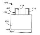
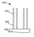
본 실시예의 구현의 일례에서, 탄소 기반 증착이 웨이퍼 위에 형성된다 (단계 (104)). 도 4a는 탄소 기반 증착 (412) 아래에 배치되고, 중간 층 (408) 아래에 배치된 웨이퍼 (404) 를 갖는 스택 (400) 의 부분의 개략적 단면도이다. 이 예에서, 탄소 기반 증착 (412) 은 제 1 마스크 피처 (414) 와 제 2 마스크 피처(416) 를 갖는, 포토레지스트 마스크와 같은 유기 패터닝된 마스크이다. 하나 이상의 층들 (미도시) 이 웨이퍼 (404) 와 중간 층 (408) 사이에 배치될 수도 있다. 반사방지 코팅과 같은 하나 이상의 층들 (미도시) 이 또한 중간 층 (408) 과 탄소 기반 증착 (412) 사이에 배치될 수도 있다.In one embodiment of the present invention, a carbon-based deposition is formed over a wafer (step (104)). FIG. 4A is a schematic cross-sectional view of a portion of a stack (400) having a wafer (404) disposed beneath the carbon-based deposition (412) and beneath an intermediate layer (408). In this example, the carbon-based deposition (412) is an organic patterned mask, such as a photoresist mask, having a first mask feature (414) and a second mask feature (416). One or more layers (not shown) may be disposed between the wafer (404) and the intermediate layer (408). One or more layers (not shown), such as an antireflective coating, may also be disposed between the intermediate layer (408) and the carbon-based deposition (412).
탄소 기반 증착은 사전튜닝되고, 사전튜닝은 탄소 기반 증착의 일부의 불균일한 제거를 유발한다. 도 5는 사전튜닝의 단계의 보다 상세한 플로우차트이다. 사전튜닝 가스가 프로세스 챔버 내로 흐른다 (단계 (504)). 이 예에서, 사전튜닝 가스는 1000 sccm의 O2, 1500 sccm의 Ar, 및 25,000 sccm의 N2이다. 사전튜닝 가스는 플라즈마로 변환된다 (단계 (508)). 이 예에서, 750 W의 RF가 13.56 ㎒의 주파수로 제공된다. 15 V의 바이어스가 제공된다. 3 초 후, 프로세스 챔버 내로의 사전튜닝 가스의 플로우는 중단된다 (단계 (512)). 도 4b는 탄소 기반 증착 (412) 이 사전튜닝된 (단계 (108)) 후 스택 (400) 의 단면도이다. 일반적으로, NU는 웨이퍼 (404) 에 걸치고, 웨이퍼 (404) 의 중심부가 웨이퍼의 에지에서 피처들에 대해 균일하게 프로세싱되지 않을 수도 있다. 도 4b는 이러한 불균일성이 서로 이격되는 피처들에 실제로 있는, 나란하게 예시되는 피처들 내의 불균일성을 개략적으로 예시한다. 또한, 특정한 양태들은 실시예의 일반적인 양태들을 예시하기 위해 과장되었다. 이 예에서, 제 1 마스크 피처 (114) 중 일부는 사전튜닝에 의해 제거되고, 제 2 마스크 피처 (416) 중 아무 것도 사전튜닝에 의해 제거되지 않는다.The carbon-based deposition is pre-tuned, and the pre-tuning causes non-uniform removal of some of the carbon-based deposition. Figure 5 is a more detailed flow chart of the steps of the pre-tuning. A pre-tuning gas is flowed into the process chamber (step (504)). In this example, the pre-tuning gas is 1000 sccm of O2 , 1500 sccm of Ar, and 25,000 sccm of N2 . The pre-tuning gas is converted to a plasma (step (508)). In this example, 750 W of RF is provided at a frequency of 13.56 MHz. A bias of 15 V is provided. After 3 seconds, the flow of the pre-tuning gas into the process chamber is stopped (step (512)). Figure 4b is a cross-sectional view of the stack (400) after the carbon-based deposition (412) has been pre-tuned (step (108)). In general, the NU spans the wafer (404), and the center of the wafer (404) may not be processed uniformly relative to the features at the edge of the wafer. FIG. 4B schematically illustrates the non-uniformity within parallel illustrated features, where such non-uniformity is actually present in features that are spaced apart from each other. Also, certain aspects are exaggerated to illustrate general aspects of the embodiment. In this example, some of the first mask features (114) are removed by pre-tuning, and none of the second mask features (416) are removed by pre-tuning.
보다 저 에너지 증착이 ALD 프로세스를 통해 탄소 기반 증착 상에 증착된다 (단계 (110)). 도 6은 보다 저 에너지 옥사이드 증착 (단계 (110)) 의 보다 상세한 플로우차트이다. 전구체 가스가 프로세스 챔버 내로 흐른다 (단계 (604)). 이 예에서 전구체 가스는 400 sccm의 아미노실란이다. 0.4 초 후, 프로세스 챔버 내로의 전구체 가스의 플로우는 중단된다 (단계 (612)). 실리콘 함유 전구체 층이 탄소 기반 증착 (412) 위에 증착된다. 제 1 퍼지 가스가 프로세스 챔버 내로 흐른다 (단계 (616)). 이 예에서, 제 1 퍼지 가스는 아르곤 및 산소 (O2) 이다. 제 1 퍼지 가스의 플로우가 중단된다 (단계 (620)). 산화 가스가 프로세스 챔버 내로 흐른다 (단계 (624)). 이 예에서 산화 가스는 13,000 sccm의 Ar 및 1500 sccm의 O2이다. 산화 가스는 플라즈마로 변환된다 (단계 (628)). 이 예에서, 100 내지 500 W의 RF가 13.56 ㎒의 주파수로 제공된다. 0.25 초 후, 프로세스 챔버 내로의 산화 가스의 플로우는 중단된다 (단계 (632)). 산화 가스로부터의 플라즈마는 증착된 실리콘 함유 전구체 층을 실리콘 옥사이드로 변환한다. 제 2 퍼지 가스가 프로세스 챔버 내로 흐른다 (단계 (636)). 제 2 퍼지 가스의 플로우가 중단된다 (단계 (640)). 사이클은 이후 전구체 가스를 프로세스 챔버로 흘리는 단계 (단계 (604)) 로부터 반복된다. 이 예에서, 프로세스는 2 내지 10 사이클들로 반복된다. 보다 저 에너지 옥사이드 증착 (단계 (110)) 은 탄소 기반 증착 (412) 에 최소 손상으로 실리콘 옥사이드 층을 증착하기에 충분한 저 에너지로 수행된다.A lower energy deposition is deposited on a carbon-based deposition via an ALD process (step (110)). FIG. 6 is a more detailed flow chart of the lower energy oxide deposition (step (110)). A precursor gas is flowed into a process chamber (step (604)). In this example, the precursor gas is 400 sccm of aminosilane. After 0.4 seconds, the flow of the precursor gas into the process chamber is stopped (step (612)). A silicon-containing precursor layer is deposited over the carbon-based deposition (412). A first purge gas is flowed into the process chamber (step (616)). In this example, the first purge gas is argon and oxygen (O2 ). The flow of the first purge gas is stopped (step (620)). An oxidizing gas is flowed into the process chamber (step (624)). In this example, the oxidizing gas is 13,000 sccm of Ar and 1500 sccm of O2 . The oxidizing gas is converted to plasma (step (628)). In this example, 100 to 500 W of RF is provided at a frequency of 13.56 MHz. After 0.25 seconds, the flow of oxidizing gas into the process chamber is stopped (step (632)). The plasma from the oxidizing gas converts the deposited silicon-containing precursor layer to silicon oxide. A second purge gas is flowed into the process chamber (step (636)). The flow of the second purge gas is stopped (step (640)). The cycle is repeated from the step of flowing the precursor gas into the process chamber (step (604)). In this example, the process is repeated for 2 to 10 cycles. The lower energy oxide deposition (step (110)) is performed at low energy sufficient to deposit a silicon oxide layer with minimal damage to the carbon-based deposition (412).
보다 고 에너지 옥사이드 증착 (단계 (112)) 이 ALD 프로세스를 통해 탄소 기반 증착 상에 증착된다. 도 7은 보다 고 에너지 옥사이드 증착 (단계 (112)) 의 보다 상세한 플로우차트이다. 전구체 가스가 프로세스 챔버 내로 흐른다 (단계 (704)). 이 예에서 전구체 가스는 400 sccm의 아미노실란이다. 0.25 초 후, 프로세스 챔버 내로의 전구체 가스의 플로우는 중단된다 (단계 (712)). 실리콘 함유 전구체 층이 탄소 기반 증착 (412) 위에 증착된다. 제 1 퍼지 가스가 프로세스 챔버 내로 흐른다 (단계 (716)). 이 예에서, 제 1 퍼지 가스는 아르곤 및 산소이다. 제 1 퍼지 가스의 플로우가 중단된다 (단계 (720)). 산화 가스가 프로세스 챔버 내로 흐른다 (단계 (724)). 이 예에서 산화 가스는 13,000 sccm의 Ar 및 1500 sccm의 O2이다. 산화 가스는 플라즈마로 변환된다 (단계 (728)). 이 예에서, 800 내지 1200 W의 RF가 13.56 ㎒의 주파수로 제공된다. 이 예에서, 보다 고 에너지 옥사이드 증착 동안 제공된 RF 전력은 보다 저 에너지 옥사이드 증착 동안 제공된 RF 전력보다 높다. 보다 바람직하게, 보다 고 에너지 옥사이드 증착 동안 제공된 RF 전력은 보다 저 에너지 옥사이드 증착 동안 제공된 RF 전력보다 적어도 300 W 높다. 일부 실시예들에서, 보다 고 에너지 옥사이드 증착 동안 제공된 RF 전력은 보다 저 에너지 옥사이드 증착 동안 제공된 RF 전력의 적어도 2 배이다. 0.4 초 후, 프로세스 챔버 내로의 산화 가스의 플로우는 중단된다 (단계 (732)). 산화 가스로부터의 플라즈마는 증착된 실리콘 함유 전구체 층을 실리콘 옥사이드로 변환한다. 제 2 퍼지 가스가 프로세스 챔버 내로 흐른다 (단계 (736)). 제 2 퍼지 가스의 플로우가 중단된다 (단계 (740)). 사이클은 이후 전구체 가스를 프로세스 챔버로 흘리는 단계 (단계 (704)) 로부터 반복된다. 이 예에서, 프로세스는 126 내지 134 사이클들로 반복된다. 보다 고 에너지 옥사이드 증착 (단계 (112)) 은 앞선 보다 저 에너지 옥사이드 증착 동안 형성된 보호 막으로 인해 탄소 기반 증착 (412) 에 손상을 거의 주지 않는다.A higher energy oxide deposition (step (112)) is deposited over the carbon-based deposition via an ALD process. FIG. 7 is a more detailed flow chart of the higher energy oxide deposition (step (112)). A precursor gas is flowed into a process chamber (step (704)). In this example, the precursor gas is 400 sccm of aminosilane. After 0.25 seconds, the flow of the precursor gas into the process chamber is stopped (step (712)). A silicon-containing precursor layer is deposited over the carbon-based deposition (412). A first purge gas is flowed into the process chamber (step (716)). In this example, the first purge gas is argon and oxygen. The flow of the first purge gas is stopped (step (720)). An oxidizing gas is flowed into the process chamber (step (724)). In this example, the oxidizing gas is 13,000 sccm of Ar and 1500 sccm of O2 . The oxidizing gas is converted to plasma (step (728)). In this example, 800 to 1200 W of RF is provided at a frequency of 13.56 MHz. In this example, the RF power provided during the higher energy oxide deposition is higher than the RF power provided during the lower energy oxide deposition. More preferably, the RF power provided during the higher energy oxide deposition is at least 300 W higher than the RF power provided during the lower energy oxide deposition. In some embodiments, the RF power provided during the higher energy oxide deposition is at least twice the RF power provided during the lower energy oxide deposition. After 0.4 seconds, the flow of oxidizing gas into the process chamber is stopped (step (732)). The plasma from the oxidizing gas converts the deposited silicon-containing precursor layer to silicon oxide. A second purge gas is flowed into the process chamber (step (736)). The flow of the second purge gas is stopped (step (740)). The cycle is then repeated from step (704) of flowing a precursor gas into the process chamber. In this example, the process is repeated for 126 to 134 cycles. The higher energy oxide deposition (step (112)) causes little damage to the carbon-based deposition (412) due to the protective film formed during the preceding lower energy oxide deposition.
도 4c는 보다 고 에너지 옥사이드 증착 (단계 (112)) 이 탄소 기반 증착 (412) 상에 증착된 후 스택 (400) 의 단면도이다. 이 예에서, 옥사이드 증착 (420) 은 제 1 마스크 피처 (414) 보다 제 2 마스크 피처 (416) 를 더 제거함으로써, 탄소 기반 증착 (412) 을 불균일하게 제거했다. 옥사이드 증착 (420) 의 증착에 의한 탄소 기반 증착의 불균일한 제거는, 옥사이드 증착의 증착에 의한 탄소 기반 증착 중 일부의 불균일한 제거와 사전튜닝에 의한 탄소 기반 증착 중 일부의 불균일한 제거의 조합이 옥사이드 증착 단독 증착에 의해 탄소 기반 증착 중 일부의 불균일한 제거보다 탄소 기반 증착의 보다 균일한 제거를 발생시킨다는 점에서, 사전튜닝에 의한 탄소 기반 증착 (412) 중 일부의 불균일한 제거에 상보적이다. 이 예에서, 제 1 마스크 피처 (414) 로부터 제거된 양은 제 2 마스크 피처 (416) 로부터 제거된 양과 대략 동일하다.FIG. 4C is a cross-sectional view of the stack (400) after a higher energy oxide deposition (step (112)) is deposited over the carbon-based deposition (412). In this example, the oxide deposition (420) non-uniformly removed the carbon-based deposition (412) by removing more of the second mask feature (416) than the first mask feature (414). The non-uniform removal of the carbon-based deposition by the deposition of the oxide deposition (420) is complementary to the non-uniform removal of some of the carbon-based deposition (412) by the pre-tuning in that the combination of the non-uniform removal of some of the carbon-based deposition by the oxide deposition and the non-uniform removal of some of the carbon-based deposition by the pre-tuning results in more uniform removal of the carbon-based deposition than the non-uniform removal of some of the carbon-based deposition by the oxide deposition alone. In this example, the amount removed from the first mask feature (414) is approximately equal to the amount removed from the second mask feature (416).
이 예에서, 개별적인 단계가 탄소 기반 증착 (412) 의 부분을 노출시키기 위해 옥사이드 증착 (420) 을 에칭 백하도록 (단계 (116)) 사용된다. 옥사이드 증착 (420) 을 에칭 백하기 위한 예시적인 레시피는 불소 함유 종을 사용한 RIE (Reactive Ion Etching) 이다. 도 4d는 옥사이드 증착 (420) 이 에칭 백된 후 스택 (400) 의 단면도이다.In this example, a separate step is used to etch back the oxide deposition (420) to expose a portion of the carbon-based deposition (412) (step (116)). An exemplary recipe for etching back the oxide deposition (420) is Reactive Ion Etching (RIE) using a fluorine-containing species. FIG. 4d is a cross-sectional view of the stack (400) after the oxide deposition (420) has been etched back.
탄소 기반 증착이 제거된다 (단계 (120)). 레시피의 일 예는 산소 함유 종을 사용한 플라즈마 애싱일 것이다. 도 4e는 탄소 기반 증착이 제거된 후 스택 (400) 의 단면도이다.The carbon-based deposition is removed (step (120)). An example of a recipe would be plasma ashing using an oxygen-containing species. Figure 4e is a cross-sectional view of the stack (400) after the carbon-based deposition has been removed.
옥사이드 증착이 마스크로 사용된 하부 층이 에칭된다 (단계 (124)). 이 예에서, 에칭되는 하부 층은 이 예에서 폴리실리콘인 중간 층 (408) 이다. 도 4f는 중간 층 (408) 이 에칭된 후 스택 (400) 의 단면도이다.The underlying layer, which is used as a mask for oxide deposition, is etched (step (124)). In this example, the underlying layer to be etched is the intermediate layer (408), which is polysilicon in this example. Figure 4f is a cross-sectional view of the stack (400) after the intermediate layer (408) has been etched.
도 8은 최종 탄소 기반 증착 제거 프로파일이 사전튜닝 및 옥사이드 증착 증착의 손실 프로파일들을 중첩함으로써 어떻게 평평하게 될 수 있는지 보여준다. 도 8은 사전튜닝에 의해 유발된 탄소 제거 대 웨이퍼의 중심으로부터 거리의 그래프 (804) 를 도시한다. 보다 고 에너지 옥사이드 증착에 의해 유발된 탄소 제거 대 웨이퍼의 중심으로부터 거리의 그래프 (808) 가 또한 도시된다. 사전튜닝 및 보다 고 에너지 옥사이드 증착 모두에 의해 제거된 탄소의 합계가 또한 도시된다 (812). 사전튜닝 및 보다 고 에너지 옥사이드 증착 모두에 의해 제거된 탄소의 합 (812) 은 두 프로세스들을 차례로 실행하는 것과 동일하다.Figure 8 shows how the final carbon based deposition removal profile can be flattened by superimposing the loss profiles of the pre-tuning and oxide deposition depositions. Figure 8 shows a graph (804) of carbon removal versus distance from the center of the wafer caused by pre-tuning. A graph (808) of carbon removal versus distance from the center of the wafer caused by higher energy oxide deposition is also shown. The sum of carbon removed by both pre-tuning and higher energy oxide deposition is also shown (812). The sum of carbon removed by both pre-tuning and higher energy oxide deposition (812) is the same as running both processes sequentially.
표 1은 일례에서 보다 고 에너지 옥사이드 증착 단독에 의해 유발된 탄소 기반 증착의 옹스트롬의 평균 손실 및 손실 범위 및 사전튜닝과 보다 고 에너지 옥사이드 증착의 합계를 도시한다. 이 예에서, 보다 높은 에너지 옥사이드 증착 프로세스의 보울 (bowl) 형상 손실 프로파일은 사전튜닝의 돔 (dome) 형상 프로파일에 의해 보상된다. 최종 프로파일은 보다 고 에너지 옥사이드 증착 단독의 프로파일보다 실질적으로 평평하고, 보다 고 에너지 옥사이드 증착 단독에 대해 12.5 Å로부터 사전튜닝 및 보다 고 에너지 옥사이드 증착으로 인한 손실의 합계에 대해 6.0 Å로 손실 범위의 대응하는 개선이 관찰된다. 이 예에서, 개선된 균일성은 보다 낮은 범위에 의해 나타난다. 이용 가능한 (입력들을 튜닝하는) 프로세스 노브들을 사용하여 사전튜닝을 적절하게 맞춤으로써, 사전튜닝으로부터의 탄소 기반 증착의 제거는 최소화될 수도 있다. 바람직하게, 탄소 기반 증착의 두께의 총 20 Å 미만이 사전튜닝에 의해 제거된다. 보다 바람직하게, 탄소 기반 증착의 두께의 총 10 Å 미만이 사전튜닝에 의해 제거된다. 바람직하게, 사전튜닝 및 보다 고 에너지 옥사이드 증착에 의한 탄소 증착의 제거 또는 손실 범위는 10 Å 미만이다. 보다 바람직하게, 사전튜닝 및 보다 고 에너지 옥사이드 증착에 의한 탄소 증착의 제거 또는 손실 범위는 5 Å 미만이다. 다양한 실시예들에서, 타겟 제거 깊이가 복잡한 제작 프로세스를 결정하는데 사용되기 때문에, 타겟 제거 깊이가 제공된다. 제거된 탄소의 두께가 타겟 제거 깊이보다 상당히 보다 크거나 보다 적은 프로세스를 제공하는 것은 수율을 감소시키는 방식으로 복잡한 제작 프로세스를 변화시킨다. 일부 실시예들에서, 사전튜닝을 제공하는 것은 제거된 탄소의 두께를 증가시킨다. 표준의 보다 고 에너지 옥사이드 증착만이 사용되면, 제거된 탄소는 타겟 두께보다 클 것이다. 보다 저 에너지 옥사이드 증착을 제공하는 것은 제거되는 탄소의 두께를 감소시킨다. 보다 저 에너지 옥사이드 증착 및 보다 고 에너지 옥사이드 증착의 조합을 제공함으로써 타겟 제거 깊이가 달성된다.Table 1 illustrates the average loss and loss range in Angstroms of carbon-based deposition induced by the higher energy oxide deposition alone and the sum of pre-tuning and the higher energy oxide deposition in one example. In this example, the bowl-shaped loss profile of the higher energy oxide deposition process is compensated for by the dome-shaped profile of the pre-tuning. The final profile is substantially flatter than the profile of the higher energy oxide deposition alone, and a corresponding improvement in loss range is observed from 12.5 Å for the higher energy oxide deposition alone to 6.0 Å for the sum of the losses due to pre-tuning and the higher energy oxide deposition. In this example, the improved uniformity is indicated by the lower range. By properly tuning the pre-tuning using the available process knobs (which tune the inputs), the removal of carbon-based deposition from the pre-tuning can be minimized. Preferably, less than 20 Å of the total thickness of the carbon-based deposition is removed by the pre-tuning. More preferably, less than a total of 10 Å of the carbon-based deposition thickness is removed by the pre-tuning. Preferably, the extent of the carbon deposition removed or lost by the pre-tuning and higher energy oxide deposition is less than 10 Å. More preferably, the extent of the carbon deposition removed or lost by the pre-tuning and higher energy oxide deposition is less than 5 Å. In various embodiments, the target removal depth is provided because the target removal depth is used to determine the complex fabrication process. Providing a process in which the thickness of the carbon removed is significantly greater than or less than the target removal depth changes the complex fabrication process in a manner that reduces yield. In some embodiments, providing the pre-tuning increases the thickness of the carbon removed. If only the standard higher energy oxide deposition were used, the carbon removed would be greater than the target thickness. Providing the lower energy oxide deposition reduces the thickness of the carbon removed. The target removal depth is achieved by providing a combination of the lower energy oxide deposition and the higher energy oxide deposition.
옥사이드 증착에 의한 탄소 기반 증착의 불균일한 제거에 대하여 탄소 기반 증착의 불균일한 상보적인 제거를 갖는 사전튜닝을 제공함으로써, 상기 실시예는 보다 균일한 패턴을 제공한다. 디바이스 사이즈들이 축소함에 따라, 이러한 개선은 균일성을 증가시키고 결함을 감소시킨다.By providing pre-tuning with non-uniform complementary removal of carbon-based deposition for non-uniform removal of carbon-based deposition by oxide deposition, the above embodiments provide more uniform patterns. As device sizes shrink, this improvement increases uniformity and reduces defects.
다양한 실시예들에서, 사전튜닝은 옥사이드 증착을 증착하기 직전에인-시츄 (in-situ)로 행해질 수 있다. 다양한 실시예들에서, 사전튜닝하고 옥사이드 증착을 증착한 후 누적되는 탄소 기반 증착 제거는 실질적으로 균일하거나, 그렇지 않으면 미리 결정된 통합 요건들을 충족시키기 위해 맞춤된다. 일 실시예에서, 사전튜닝에 의한 탄소 기반 증착의 제거는 옥사이드 증착의 증착에 의해 유발된 제거가 최소화되는 에칭 프로파일을 최대로 바이어싱함으로써 (biasing) 최소화된다. 다양한 실시예들에서, 사전튜닝은 산소, 질소, 또는 아르곤 중 적어도 하나를 포함하는 사전튜닝 가스를 사용할 수도 있다. 사전튜닝은 가스 컴포넌트들의 각각의 비들을 가변시킴으로써 조절되고 맞춰질 수 있는, 에칭 프로파일의 튜닝을 허용한다. 또한, 사전튜닝의 압력 및 RF 전력은 에칭 프로파일을 더 튜닝하기 위해 또한 활용될 수 있다.In various embodiments, the pre-tuning can be performedin-situ, immediately prior to depositing the oxide deposition. In various embodiments, the cumulative carbon-based deposition removal after pre-tuning and depositing the oxide deposition is substantially uniform or otherwise tailored to meet predetermined integration requirements. In one embodiment, the removal of the carbon-based deposition by the pre-tuning is minimized by biasing the etch profile so that the removal induced by the deposition of the oxide deposition is minimized. In various embodiments, the pre-tuning may utilize a pre-tuning gas comprising at least one of oxygen, nitrogen, or argon. The pre-tuning allows for tuning of the etch profile, which can be controlled and tailored by varying the ratios of each of the gas components. Additionally, the pressure and RF power of the pre-tuning can also be utilized to further tune the etch profile.
다양한 실시예들에서, 피드포워드 (feedforward) 스킴 및 피드백 스킴 모두는 프로세스 구현예들의 일부로서 활용될 수 있다. 전자에 대해, 선행하는 에칭 단계 후 검사 결과들은 사전튜닝을 위한 최적의 설정들을 결정하는 제어기들에 입력들로서 사용될 수 있다. 후자에 대해, 옥사이드 증착 및 에칭 후 최종 CD 측정값들이 입력들로서 사용될 수 있다.In various embodiments, both a feedforward scheme and a feedback scheme may be utilized as part of the process implementations. For the former, the post-etch step inspection results may be used as inputs to the controllers to determine optimal settings for pre-tuning. For the latter, the final CD measurements after oxide deposition and etch may be used as inputs.
다양한 실시예들은 탄소 증착 제거의 독립적인 제어 가능성을 제공한다. 플라즈마 사전튜닝은 달성할 수 있는 프로파일들 (예를 들어, 보울, 돔, 및 평평한) 의 측면에서 유연성을 주는, 손실 프로파일을 사전 튜닝하는 것 이외에 다른 기능이 없다. 일부 실시예들에서, 사전튜닝은 옥사이드 증착과 동일한 모듈 내에서인-시츄로 수행되고, 부가적인 하드웨어나 설비들을 요구하지 않는다. 통상적인 목표된 프로파일들에 대해, 사전튜닝은 총 증착 시간에 10 초 미만을 부가하고, 이에 따라 임의의 시간 영향을 최소화한다. 사전튜닝 가스에 대해 Ar, N2, 및 O2와 같은 상이한 가스들의 상대적인 흐름 비들 및 레이트들은 탄소 기반 증착의 불균일한 사전튜닝을 튜닝하기 위한 제어 파라미터들로서 사용된다.Various embodiments provide the possibility of independent control of carbon deposition removal. Plasma pre-tuning has no other function than to pre-tune the loss profile, which provides flexibility in terms of the achievable profiles (e.g., bowl, dome, and flat). In some embodiments, pre-tuning is performed in-situ within the same module as the oxide deposition and requires no additional hardware or equipment. For typical targeted profiles, pre-tuning adds less than 10 seconds to the total deposition time, thus minimizing any time impact. The relative flow ratios and rates of different gases, such as Ar, N2 , and O2 for the pre-tuning gas, are used as control parameters to tune the non-uniform pre-tuning of the carbon-based deposition.
도 9는 또 다른 실시예의 고 레벨 플로우차트이다. 탄소 기반 증착이 웨이퍼 위에 증착된다 (단계 (904)). 탄소 기반 증착은 사전튜닝되고 (단계 (908)), 사전튜닝은 탄소 기반 증착 중 일부의 불균일한 제거를 유발한다. 옥사이드 증착이 ALD 프로세스를 통해 증착되고 (단계 (912)), 옥사이드 증착을 증착하는 것은 탄소 기반 증착 중 일부의 불균일한 제거를 유발한다. 옥사이드 증착은 실리콘 옥사이드 기반 증착이다. 적어도 하나의 부가적인 프로세스가 제공되고 (단계 (916)), 적어도 하나의 부가적인 프로세스는 웨이퍼 위의 피처들의 형성을 완료하고, 피처들은 사전튜닝 없이 형성되는 피처들보다 균일하다. 상이한 프로세스 챔버에 대해, 프로세스 챔버는 적어도 하나의 부가적인 프로세스로 불균일한 프로세스를 제공할 수도 있다. 이러한 경우에서, 실리콘 옥사이드를 증착한 후 균일한 평평한 프로파일 대신, 프로세스 챔버가 적어도 하나의 부가적인 프로세스 후 웨이퍼에 걸쳐 보다 균일한 반도체들을 제공하기 위해 맞춤된 프로파일을 사용하기 때문에, 적어도 하나의 부가적인 프로세스의 불균일성을 보완하는 맞춤된 프로파일이 옥사이드 증착을 증착한 후 목표된다. 사전튜닝은 옥사이드 증착을 증착한 후 맞춤된 프로파일을 제공하기 위해 설계되어, 발생하는 피처들은 사전튜닝 없이 형성된 피처들보다 균일하다.FIG. 9 is a high level flow chart of another embodiment. A carbon-based deposition is deposited on a wafer (step (904)). The carbon-based deposition is pre-tuned (step (908)), wherein the pre-tuning causes non-uniform removal of some of the carbon-based deposition. An oxide deposition is deposited via an ALD process (step (912)), wherein depositing the oxide deposition causes non-uniform removal of some of the carbon-based deposition. The oxide deposition is a silicon oxide-based deposition. At least one additional process is provided (step (916)), wherein the at least one additional process completes formation of features on the wafer, wherein the features are more uniform than features formed without the pre-tuning. For different process chambers, the process chambers may also provide the non-uniform process with the at least one additional process. In these cases, instead of a uniform flat profile after depositing the silicon oxide, a tailored profile that compensates for the non-uniformity of the at least one additional process is targeted after depositing the oxide deposition, since the process chamber uses a tailored profile to provide more uniform semiconductors across the wafer after the at least one additional process. The pre-tuning is designed to provide a tailored profile after depositing the oxide deposition, such that the resulting features are more uniform than features formed without the pre-tuning.
다양한 실시예들에서, 사전튜닝 가스 내의 산소는 사전튜닝 동안 일부 탄소 기반 증착 제거를 유발하도록 일부 애싱을 제공한다. 사전튜닝 가스 내의 아르곤 및 질소는 균일성 제어를 위해 사용될 수도 있고, 산소 대 아르곤 대 질소의 비는 탄소 기반 증착의 프로파일을 튜닝하기 위해 사용된다. 일부 실시예들에서, 사전튜닝 가스에서 산소 대 아르곤의 비는 2:1 내지 1:2이다.In various embodiments, the oxygen in the pre-tuning gas provides some ashing to cause some carbon-based deposition removal during the pre-tuning. The argon and nitrogen in the pre-tuning gas may be used for uniformity control, and the ratio of oxygen to argon to nitrogen is used to tune the profile of the carbon-based deposition. In some embodiments, the ratio of oxygen to argon in the pre-tuning gas is from 2:1 to 1:2.
다양한 실시예들에서 탄소 기반 증착 (412) 은 비정질 탄소, 포토레지스트, 스핀 온 (spin on) 탄소, 또는 CVD (Chemical Vapor Deposition) 탄소, 또는 애싱 가능한 하드마스크 (hardmask) 일 수도 있다.In various embodiments, the carbon-based deposition (412) may be amorphous carbon, photoresist, spin on carbon, or Chemical Vapor Deposition (CVD) carbon, or an ashing capable hardmask.
본 개시가 몇몇의 바람직한 실시예들의 측면에서 기술되었지만, 본 개시의 범위 내에 속하는 변경들, 수정들, 치환들, 및 다양한 대체 등가물들이 있다. 또한 본 개시의 방법들 및 장치들을 구현하는 많은 대안적인 방식들이 있다는 것에 유의해야 한다. 따라서 이하의 첨부된 청구항들은 본 개시의 진정한 정신 및 범위 내에 속하는 이러한 변경들, 수정들, 치환들, 및 다양한 대체 등가물들을 모두 포함하는 것으로 해석된다는 것이 의도된다.While the present disclosure has been described in terms of several preferred embodiments, there are alterations, modifications, substitutions, and various alternative equivalents that fall within the scope of the present disclosure. It should also be noted that there are many alternative ways of implementing the methods and devices of the present disclosure. It is therefore intended that the following appended claims be interpreted to embrace all such alterations, modifications, substitutions, and various alternative equivalents that fall within the true spirit and scope of the present disclosure.
Claims (19)
Translated fromKorean탄소 기반 증착을 사전튜닝 (pretuning) 하는 단계로서, 상기 사전튜닝은 상기 탄소 기반 증착 중 일부의 제 1 불균일한 제거를 유발하는, 상기 사전튜닝 (pretuning) 하는 단계; 및
ALD (Atomic Layer Deposition) 프로세스를 통해 실리콘 옥사이드 기반 재료의 옥사이드 증착을 증착하는 단계로서, 상기 옥사이드 증착을 증착하는 단계는 상기 사전튜닝에 의한 상기 탄소 기반 증착 중 일부의 상기 제 1 불균일한 제거에 상보적인 상기 탄소 기반 증착 중 일부의 제 2 불균일한 제거를 유발하는, 상기 증착하는 단계를 포함하는, 피처들을 형성하기 위한 방법.A method for forming features on a wafer having carbon-based deposition, comprising:
A step of pretuning a carbon-based deposition, wherein the pretuning step causes a first non-uniform removal of a portion of the carbon-based deposition; and
A method for forming features, comprising the steps of depositing an oxide deposition of a silicon oxide-based material via an ALD (Atomic Layer Deposition) process, wherein the depositing the oxide deposition causes a second non-uniform removal of a portion of the carbon-based deposition complementary to the first non-uniform removal of a portion of the carbon-based deposition by the pre-tuning.
상기 옥사이드 증착에 의한 상기 탄소 기반 증착 중 일부의 상기 제 2 불균일한 제거는, 상기 옥사이드 증착의 증착에 의한 상기 탄소 기반 증착 중 일부의 상기 제 2 불균일한 제거와 상기 사전튜닝에 의한 상기 탄소 기반 증착 중 일부의 상기 제 1 불균일한 제거의 조합이 상기 옥사이드 증착의 증착에 의한 상기 탄소 기반 증착 중 일부의 상기 제 2 불균일한 제거보다 상기 탄소 기반 증착의 보다 균일한 제거를 발생시킨다는 점에서, 상기 사전튜닝에 의한 상기 탄소 기반 증착 중 일부의 상기 제 1 불균일한 제거에 상보적인, 피처들을 형성하기 위한 방법.In paragraph 1,
A method for forming features wherein said second non-uniform removal of said portion of said carbon-based deposition by said oxide deposition is complementary to said first non-uniform removal of said portion of said carbon-based deposition by said pre-tuning, in that the combination of said second non-uniform removal of said portion of said carbon-based deposition by said oxide deposition and said first non-uniform removal of said portion of said carbon-based deposition by said pre-tuning results in more uniform removal of said carbon-based deposition than said second non-uniform removal of said portion of said carbon-based deposition by said oxide deposition.
상기 보다 균일한 제거는 상기 웨이퍼에 걸쳐 보다 균일한 제거인, 피처들을 형성하기 위한 방법.In the second paragraph,
A method for forming features, wherein the more uniform removal is more uniform removal across the wafer.
상기 탄소 기반 증착을 제거하는 단계; 및
마스크로서 상기 옥사이드 증착을 사용하여, 상기 옥사이드 증착 아래에 에칭 층을 에칭하는 단계를 더 포함하는, 피처들을 형성하기 위한 방법.In paragraph 1,
a step of removing the above carbon-based deposition; and
A method for forming features, further comprising the step of etching an etching layer beneath the oxide deposition, using the oxide deposition as a mask.
상기 탄소 기반 증착을 사전튜닝하는 단계는,
산소, 및 Ar 또는 질소 중 적어도 하나를 포함하는 사전튜닝 가스를 제공하는 단계,
상기 탄소 기반 증착 중 일부의 불균일한 제거를 유발하는 플라즈마로 상기 사전튜닝 가스를 변환하는 단계, 및
상기 사전튜닝 가스를 중단하는 단계를 포함하는, 피처들을 형성하기 위한 방법.In paragraph 1,
The step of pre-tuning the above carbon-based deposition is:
A step of providing a pre-tuning gas comprising oxygen and at least one of Ar or nitrogen;
A step of converting said pre-tuning gas into a plasma causing non-uniform removal of some of said carbon-based deposition, and
A method for forming features, comprising the step of discontinuing the pre-tuning gas.
상기 사전튜닝 가스는 산소 및 아르곤을 포함하고, 상기 산소 대 상기 아르곤의 비는 2:1 내지 1:2인, 피처들을 형성하기 위한 방법.In paragraph 5,
A method for forming features, wherein the pre-tuning gas comprises oxygen and argon, and the ratio of the oxygen to the argon is 2:1 to 1:2.
상기 사전튜닝하는 단계는 상기 탄소 기반 증착의 20 Å 미만의 두께를 제거하는, 피처들을 형성하기 위한 방법.In paragraph 1,
A method for forming features, wherein the pre-tuning step removes less than 20 Å of the carbon-based deposition.
상기 옥사이드 증착을 증착하는 단계 및 상기 사전튜닝하는 단계는 10 Å 미만의 상기 탄소 기반 증착의 상기 웨이퍼에 걸친 제거 범위를 제공하는, 피처들을 형성하기 위한 방법.In paragraph 7,
A method for forming features, wherein the steps of depositing the oxide deposition and the steps of pretuning provide a removal range across the wafer of the carbon-based deposition of less than 10 Å.
상기 사전튜닝하는 단계는 돔 (dome) 형상 프로파일의 상기 탄소 기반 증착을 제거하고, 상기 옥사이드 증착을 증착하는 단계는 보울 (bowl) 형상 프로파일의 상기 탄소 기반 증착을 제거하는, 피처들을 형성하기 위한 방법.In paragraph 1,
A method for forming features, wherein the pre-tuning step removes the carbon-based deposition having a dome-shaped profile, and the depositing the oxide deposition step removes the carbon-based deposition having a bowl-shaped profile.
상기 옥사이드 증착을 증착하는 단계는,
복수의 사이클들의 보다 저 에너지 옥사이드 증착을 제공하는 단계로서, 사이클 각각은,
전구체 가스를 흘리는 단계;
산화 가스를 흘리는 단계;
플라즈마로 상기 산화 가스를 변환하도록 제 1 RF 전력을 제공하는 단계를 포함하는, 상기 보다 저 에너지 옥사이드 증착을 제공하는 단계, 및
복수의 사이클들의 보다 고 에너지 옥사이드 증착을 제공하는 단계로서, 사이클 각각은,
전구체 가스를 흘리는 단계;
산화 가스를 흘리는 단계; 및
플라즈마로 상기 산화 가스를 변환하도록 제 2 RF 전력을 제공하는 단계를 포함하고, 상기 제 2 RF 전력은 상기 제 1 RF 전력보다 높은, 상기 보다 고 에너지 옥사이드 증착을 제공하는 단계를 포함하는, 피처들을 형성하기 위한 방법.In paragraph 1,
The step of depositing the above oxide deposition is:
A step for providing lower energy oxide deposition of multiple cycles, each cycle comprising:
Step of flowing precursor gas;
Step of flowing oxidizing gas;
a step of providing a lower energy oxide deposition, comprising the step of providing a first RF power to convert said oxidizing gas into plasma; and
A step providing higher energy oxide deposition of multiple cycles, each cycle comprising:
Step of flowing precursor gas;
Step of flowing oxidizing gas; and
A method for forming features, comprising the step of providing a second RF power to convert said oxidizing gas into a plasma, said second RF power being higher than said first RF power, thereby providing said higher energy oxide deposition.
상기 사전튜닝을 조정하기 위해 피드백 또는 피드포워드 (feedforward) 입력 중 적어도 하나를 제공하는 단계를 더 포함하는, 피처들을 형성하기 위한 방법.In paragraph 1,
A method for forming features, further comprising the step of providing at least one of a feedback or feedforward input to adjust said pre-tuning.
탄소 기반 증착을 사전튜닝하는 단계로서, 상기 사전튜닝은 상기 탄소 기반 증착 중 일부의 불균일한 제거를 유발하는, 상기 사전튜닝하는 단계;
ALD 프로세스를 통해 옥사이드 증착을 증착하는 단계로서, 상기 옥사이드 증착을 증착하는 단계는 상기 탄소 기반 증착 중 일부의 불균일한 제거를 유발하는, 상기 증착하는 단계; 및
적어도 하나의 부가적인 프로세스를 제공하는 단계로서, 상기 적어도 하나의 부가적인 프로세스는 상기 웨이퍼 위에 피처들의 형성을 완료하고, 상기 피처들은 사전튜닝 없이 형성되는 피처들보다 균일한, 상기 적어도 하나의 부가적인 프로세스를 제공하는 단계를 포함하는, 피처들을 형성하기 위한 방법.A method for forming features on a wafer having carbon-based deposition, comprising:
A step of pre-tuning a carbon-based deposition, wherein the pre-tuning causes non-uniform removal of a portion of the carbon-based deposition;
A step of depositing an oxide deposition using an ALD process, wherein the step of depositing the oxide deposition causes non-uniform removal of a portion of the carbon-based deposition; and
A method for forming features, comprising the step of providing at least one additional process, wherein the at least one additional process completes the formation of features on the wafer, wherein the features are more uniform than features formed without pre-tuning.
상기 피처들은 상기 웨이퍼에 걸쳐 보다 균일한, 피처들을 형성하기 위한 방법.In Article 12,
The above features are a method for forming features more uniformly across the wafer.
상기 탄소 기반 증착을 제거하는 단계; 및
마스크로서 상기 옥사이드 증착을 사용하여, 상기 옥사이드 증착 아래에 에칭 층을 에칭하는 단계를 더 포함하는, 피처들을 형성하기 위한 방법.In Article 12,
a step of removing the above carbon-based deposition; and
A method for forming features, further comprising the step of etching an etching layer beneath the oxide deposition, using the oxide deposition as a mask.
상기 탄소 기반 증착을 사전튜닝하는 단계는,
산소, 및 Ar 또는 질소 중 적어도 하나를 포함하는 사전튜닝 가스를 제공하는 단계,
상기 탄소 기반 증착 중 일부의 불균일한 제거를 유발하는 플라즈마로 상기 사전튜닝 가스를 변환하는 단계, 및
상기 사전튜닝 가스를 중단하는 단계를 포함하는, 피처들을 형성하기 위한 방법.In Article 12,
The step of pre-tuning the above carbon-based deposition is:
A step of providing a pre-tuning gas comprising oxygen and at least one of Ar or nitrogen;
A step of converting said pre-tuning gas into a plasma causing non-uniform removal of some of said carbon-based deposition, and
A method for forming features, comprising the step of discontinuing the pre-tuning gas.
상기 사전튜닝 가스는 산소 및 아르곤을 포함하고, 상기 산소 대 상기 아르곤의 비는 2:1 내지 1:2인, 피처들을 형성하기 위한 방법.In Article 15,
A method for forming features, wherein the pre-tuning gas comprises oxygen and argon, and the ratio of the oxygen to the argon is 2:1 to 1:2.
상기 사전튜닝하는 단계는 상기 탄소 기반 증착의 20 Å 미만의 두께를 제거하는, 피처들을 형성하기 위한 방법.In Article 12,
A method for forming features, wherein the pre-tuning step removes less than 20 Å of the carbon-based deposition.
상기 옥사이드 증착을 증착하는 단계는,
복수의 사이클들의 보다 저 에너지 옥사이드 증착을 제공하는 단계로서, 사이클 각각은,
전구체 가스를 흘리는 단계;
산화 가스를 흘리는 단계;
상기 산화 가스를 플라즈마로 변환하도록 제 1 RF 전력을 제공하는 단계를 포함하는, 상기 보다 저 에너지 옥사이드 증착을 제공하는 단계, 및
복수의 사이클들의 보다 고 에너지 옥사이드 증착을 제공하는 단계로서, 사이클 각각은,
전구체 가스를 흘리는 단계;
산화 가스를 흘리는 단계; 및
상기 산화 가스를 플라즈마로 변환하도록 제 2 RF 전력을 제공하는 단계를 포함하고, 상기 제 2 RF 전력은 상기 제 1 RF 전력보다 높은, 상기 보다 고 에너지 옥사이드 증착을 제공하는 단계를 포함하는, 피처들을 형성하기 위한 방법.In Article 12,
The step of depositing the above oxide deposition is:
A step for providing lower energy oxide deposition of multiple cycles, each cycle comprising:
Step of flowing precursor gas;
Step of flowing oxidizing gas;
A step of providing a lower energy oxide deposition, comprising the step of providing a first RF power to convert the oxidizing gas into plasma, and
A step providing higher energy oxide deposition of multiple cycles, each cycle comprising:
Step of flowing precursor gas;
Step of flowing oxidizing gas; and
A method for forming features, comprising the step of providing a second RF power to convert said oxidizing gas into a plasma, said second RF power being higher than said first RF power, said step of providing a higher energy oxide deposition.
상기 사전튜닝을 조정하기 위해 피드백 또는 피드포워드 입력 중 적어도 하나를 제공하는 단계를 더 포함하는, 피처들을 형성하기 위한 방법.In Article 12,
A method for forming features, further comprising the step of providing at least one of a feedback or feedforward input to adjust said pre-tuning.
Applications Claiming Priority (5)
| Application Number | Priority Date | Filing Date | Title |
|---|---|---|---|
| US201762591949P | 2017-11-29 | 2017-11-29 | |
| US62/591,949 | 2017-11-29 | ||
| US15/974,172 | 2018-05-08 | ||
| US15/974,172US10978302B2 (en) | 2017-11-29 | 2018-05-08 | Method of improving deposition induced CD imbalance using spatially selective ashing of carbon based film |
| PCT/US2018/061347WO2019108406A1 (en) | 2017-11-29 | 2018-11-15 | Method of improving deposition induced cd imbalance using spatially selective ashing of carbon based film |
Publications (2)
| Publication Number | Publication Date |
|---|---|
| KR20200084055A KR20200084055A (en) | 2020-07-09 |
| KR102700803B1true KR102700803B1 (en) | 2024-08-29 |
Family
ID=66633510
Family Applications (1)
| Application Number | Title | Priority Date | Filing Date |
|---|---|---|---|
| KR1020207018635AActiveKR102700803B1 (en) | 2017-11-29 | 2018-11-15 | A method for improving deposition-induced CD imbalance using spatially selective ashing of carbon-based films |
Country Status (4)
| Country | Link |
|---|---|
| US (2) | US10978302B2 (en) |
| KR (1) | KR102700803B1 (en) |
| CN (1) | CN111512413B (en) |
| WO (1) | WO2019108406A1 (en) |
Families Citing this family (1)
| Publication number | Priority date | Publication date | Assignee | Title |
|---|---|---|---|---|
| US10978302B2 (en) | 2017-11-29 | 2021-04-13 | Lam Research Corporation | Method of improving deposition induced CD imbalance using spatially selective ashing of carbon based film |
Citations (1)
| Publication number | Priority date | Publication date | Assignee | Title |
|---|---|---|---|---|
| US20120164846A1 (en)* | 2010-12-28 | 2012-06-28 | Asm Japan K.K. | Method of Forming Metal Oxide Hardmask |
Family Cites Families (14)
| Publication number | Priority date | Publication date | Assignee | Title |
|---|---|---|---|---|
| US7534363B2 (en) | 2002-12-13 | 2009-05-19 | Lam Research Corporation | Method for providing uniform removal of organic material |
| US7135402B2 (en)* | 2005-02-01 | 2006-11-14 | Taiwan Semiconductor Manufacturing Company, Ltd. | Sealing pores of low-k dielectrics using CxHy |
| KR100780944B1 (en) | 2005-10-12 | 2007-12-03 | 삼성전자주식회사 | Carbon-containing film etching method and manufacturing method of semiconductor device using same |
| US7962452B2 (en) | 2007-12-28 | 2011-06-14 | International Business Machines Corporation | Data deduplication by separating data from meta data |
| US9892917B2 (en) | 2010-04-15 | 2018-02-13 | Lam Research Corporation | Plasma assisted atomic layer deposition of multi-layer films for patterning applications |
| CN104465333B (en)* | 2013-09-17 | 2017-12-29 | 中芯国际集成电路制造(上海)有限公司 | The forming method of photoetching offset plate figure, the forming method of transistor gate |
| US9343308B2 (en)* | 2013-10-28 | 2016-05-17 | Asm Ip Holding B.V. | Method for trimming carbon-containing film at reduced trimming rate |
| US9464352B2 (en)* | 2014-05-02 | 2016-10-11 | Asm Ip Holding B.V. | Low-oxidation plasma-assisted process |
| US9875888B2 (en) | 2014-10-03 | 2018-01-23 | Applied Materials, Inc. | High temperature silicon oxide atomic layer deposition technology |
| KR101719407B1 (en) | 2015-01-20 | 2017-03-23 | 재단법인 멀티스케일 에너지시스템 연구단 | Polymeric film having a hybrid structured pattern and manufacturing method of same |
| CN106158595B (en)* | 2015-04-20 | 2019-03-12 | 中芯国际集成电路制造(上海)有限公司 | The forming method of semiconductor devices |
| KR20170019668A (en) | 2015-08-12 | 2017-02-22 | (주)디엔에프 | The manufacturing method of the silicon nitride film by using plasma enhanced atomic layer deposition |
| US20170178899A1 (en)* | 2015-12-18 | 2017-06-22 | Lam Research Corporation | Directional deposition on patterned structures |
| US10978302B2 (en) | 2017-11-29 | 2021-04-13 | Lam Research Corporation | Method of improving deposition induced CD imbalance using spatially selective ashing of carbon based film |
- 2018
- 2018-05-08USUS15/974,172patent/US10978302B2/enactiveActive
- 2018-11-15WOPCT/US2018/061347patent/WO2019108406A1/ennot_activeCeased
- 2018-11-15KRKR1020207018635Apatent/KR102700803B1/enactiveActive
- 2018-11-15CNCN201880077280.2Apatent/CN111512413B/enactiveActive
- 2021
- 2021-03-17USUS17/204,758patent/US11651963B2/enactiveActive
Patent Citations (1)
| Publication number | Priority date | Publication date | Assignee | Title |
|---|---|---|---|---|
| US20120164846A1 (en)* | 2010-12-28 | 2012-06-28 | Asm Japan K.K. | Method of Forming Metal Oxide Hardmask |
Also Published As
| Publication number | Publication date |
|---|---|
| US11651963B2 (en) | 2023-05-16 |
| US10978302B2 (en) | 2021-04-13 |
| US20210202250A1 (en) | 2021-07-01 |
| CN111512413B (en) | 2025-04-15 |
| WO2019108406A1 (en) | 2019-06-06 |
| KR20200084055A (en) | 2020-07-09 |
| US20190164757A1 (en) | 2019-05-30 |
| CN111512413A (en) | 2020-08-07 |
Similar Documents
| Publication | Publication Date | Title |
|---|---|---|
| KR102403856B1 (en) | Method for etching etching layer | |
| TWI758404B (en) | Hydrogen activated atomic layer etching | |
| USRE47650E1 (en) | Method of tungsten etching | |
| KR102836261B1 (en) | Method for conditioning a plasma processing chamber | |
| US10002773B2 (en) | Method for selectively etching silicon oxide with respect to an organic mask | |
| KR102797629B1 (en) | Method for etching features using targeted deposition for selective passivation | |
| KR102418243B1 (en) | Plasma processing apparatus and plasma processing method | |
| US20140179106A1 (en) | In-situ metal residue clean | |
| KR102615854B1 (en) | Porous low-k dielectric etch | |
| KR102700803B1 (en) | A method for improving deposition-induced CD imbalance using spatially selective ashing of carbon-based films | |
| WO2019236213A1 (en) | Method for transferring a pattern from an organic mask | |
| KR20200108361A (en) | Amorphous carbon layer opening process | |
| KR102626483B1 (en) | Silicon-based deposition for semiconductor processing | |
| US10600648B2 (en) | Silicon-based deposition for semiconductor processing | |
| US8431461B1 (en) | Silicon nitride dry trim without top pulldown | |
| US20210265136A1 (en) | Method and apparatus for processing wafers |
Legal Events
| Date | Code | Title | Description |
|---|---|---|---|
| PA0105 | International application | Patent event date:20200626 Patent event code:PA01051R01D Comment text:International Patent Application | |
| PG1501 | Laying open of application | ||
| A201 | Request for examination | ||
| PA0201 | Request for examination | Patent event code:PA02012R01D Patent event date:20211110 Comment text:Request for Examination of Application | |
| E902 | Notification of reason for refusal | ||
| PE0902 | Notice of grounds for rejection | Comment text:Notification of reason for refusal Patent event date:20230830 Patent event code:PE09021S01D | |
| E701 | Decision to grant or registration of patent right | ||
| PE0701 | Decision of registration | Patent event code:PE07011S01D Comment text:Decision to Grant Registration Patent event date:20240531 | |
| GRNT | Written decision to grant | ||
| PR0701 | Registration of establishment | Comment text:Registration of Establishment Patent event date:20240827 Patent event code:PR07011E01D | |
| PR1002 | Payment of registration fee | Payment date:20240827 End annual number:3 Start annual number:1 | |
| PG1601 | Publication of registration |