KR102700523B1 - Structure and method for forming capacitors for 3D NAND - Google Patents
Structure and method for forming capacitors for 3D NANDDownload PDFInfo
- Publication number
- KR102700523B1 KR102700523B1KR1020217037234AKR20217037234AKR102700523B1KR 102700523 B1KR102700523 B1KR 102700523B1KR 1020217037234 AKR1020217037234 AKR 1020217037234AKR 20217037234 AKR20217037234 AKR 20217037234AKR 102700523 B1KR102700523 B1KR 102700523B1
- Authority
- KR
- South Korea
- Prior art keywords
- capacitor
- substrate
- layer
- memory
- trenches
- Prior art date
- Legal status (The legal status is an assumption and is not a legal conclusion. Google has not performed a legal analysis and makes no representation as to the accuracy of the status listed.)
- Active
Links
Images


Classifications
- H—ELECTRICITY
- H01—ELECTRIC ELEMENTS
- H01L—SEMICONDUCTOR DEVICES NOT COVERED BY CLASS H10
- H01L23/00—Details of semiconductor or other solid state devices
- H01L23/52—Arrangements for conducting electric current within the device in operation from one component to another, i.e. interconnections, e.g. wires, lead frames
- H01L23/522—Arrangements for conducting electric current within the device in operation from one component to another, i.e. interconnections, e.g. wires, lead frames including external interconnections consisting of a multilayer structure of conductive and insulating layers inseparably formed on the semiconductor body
- H01L23/5222—Capacitive arrangements or effects of, or between wiring layers
- H01L23/5223—Capacitor integral with wiring layers
- H—ELECTRICITY
- H01—ELECTRIC ELEMENTS
- H01L—SEMICONDUCTOR DEVICES NOT COVERED BY CLASS H10
- H01L21/00—Processes or apparatus adapted for the manufacture or treatment of semiconductor or solid state devices or of parts thereof
- H01L21/70—Manufacture or treatment of devices consisting of a plurality of solid state components formed in or on a common substrate or of parts thereof; Manufacture of integrated circuit devices or of parts thereof
- H01L21/71—Manufacture of specific parts of devices defined in group H01L21/70
- H01L21/76—Making of isolation regions between components
- H01L21/762—Dielectric regions, e.g. EPIC dielectric isolation, LOCOS; Trench refilling techniques, SOI technology, use of channel stoppers
- H01L21/76224—Dielectric regions, e.g. EPIC dielectric isolation, LOCOS; Trench refilling techniques, SOI technology, use of channel stoppers using trench refilling with dielectric materials
- H—ELECTRICITY
- H01—ELECTRIC ELEMENTS
- H01L—SEMICONDUCTOR DEVICES NOT COVERED BY CLASS H10
- H01L23/00—Details of semiconductor or other solid state devices
- H01L23/52—Arrangements for conducting electric current within the device in operation from one component to another, i.e. interconnections, e.g. wires, lead frames
- H01L23/522—Arrangements for conducting electric current within the device in operation from one component to another, i.e. interconnections, e.g. wires, lead frames including external interconnections consisting of a multilayer structure of conductive and insulating layers inseparably formed on the semiconductor body
- H01L23/528—Layout of the interconnection structure
- H—ELECTRICITY
- H01—ELECTRIC ELEMENTS
- H01L—SEMICONDUCTOR DEVICES NOT COVERED BY CLASS H10
- H01L23/00—Details of semiconductor or other solid state devices
- H01L23/58—Structural electrical arrangements for semiconductor devices not otherwise provided for, e.g. in combination with batteries
- H01L23/585—Structural electrical arrangements for semiconductor devices not otherwise provided for, e.g. in combination with batteries comprising conductive layers or plates or strips or rods or rings
- H—ELECTRICITY
- H01—ELECTRIC ELEMENTS
- H01L—SEMICONDUCTOR DEVICES NOT COVERED BY CLASS H10
- H01L23/00—Details of semiconductor or other solid state devices
- H01L23/58—Structural electrical arrangements for semiconductor devices not otherwise provided for, e.g. in combination with batteries
- H01L23/64—Impedance arrangements
- H01L23/642—Capacitive arrangements
- H—ELECTRICITY
- H01—ELECTRIC ELEMENTS
- H01L—SEMICONDUCTOR DEVICES NOT COVERED BY CLASS H10
- H01L24/00—Arrangements for connecting or disconnecting semiconductor or solid-state bodies; Methods or apparatus related thereto
- H01L24/01—Means for bonding being attached to, or being formed on, the surface to be connected, e.g. chip-to-package, die-attach, "first-level" interconnects; Manufacturing methods related thereto
- H01L24/02—Bonding areas ; Manufacturing methods related thereto
- H01L24/07—Structure, shape, material or disposition of the bonding areas after the connecting process
- H01L24/08—Structure, shape, material or disposition of the bonding areas after the connecting process of an individual bonding area
- H—ELECTRICITY
- H01—ELECTRIC ELEMENTS
- H01L—SEMICONDUCTOR DEVICES NOT COVERED BY CLASS H10
- H01L25/00—Assemblies consisting of a plurality of semiconductor or other solid state devices
- H01L25/03—Assemblies consisting of a plurality of semiconductor or other solid state devices all the devices being of a type provided for in a single subclass of subclasses H10B, H10D, H10F, H10H, H10K or H10N, e.g. assemblies of rectifier diodes
- H01L25/04—Assemblies consisting of a plurality of semiconductor or other solid state devices all the devices being of a type provided for in a single subclass of subclasses H10B, H10D, H10F, H10H, H10K or H10N, e.g. assemblies of rectifier diodes the devices not having separate containers
- H01L25/065—Assemblies consisting of a plurality of semiconductor or other solid state devices all the devices being of a type provided for in a single subclass of subclasses H10B, H10D, H10F, H10H, H10K or H10N, e.g. assemblies of rectifier diodes the devices not having separate containers the devices being of a type provided for in group H10D89/00
- H01L25/0657—Stacked arrangements of devices
- H—ELECTRICITY
- H01—ELECTRIC ELEMENTS
- H01L—SEMICONDUCTOR DEVICES NOT COVERED BY CLASS H10
- H01L25/00—Assemblies consisting of a plurality of semiconductor or other solid state devices
- H01L25/16—Assemblies consisting of a plurality of semiconductor or other solid state devices the devices being of types provided for in two or more different subclasses of H10B, H10D, H10F, H10H, H10K or H10N, e.g. forming hybrid circuits
- H—ELECTRICITY
- H01—ELECTRIC ELEMENTS
- H01L—SEMICONDUCTOR DEVICES NOT COVERED BY CLASS H10
- H01L25/00—Assemblies consisting of a plurality of semiconductor or other solid state devices
- H01L25/18—Assemblies consisting of a plurality of semiconductor or other solid state devices the devices being of the types provided for in two or more different main groups of the same subclass of H10B, H10D, H10F, H10H, H10K or H10N
- H—ELECTRICITY
- H01—ELECTRIC ELEMENTS
- H01L—SEMICONDUCTOR DEVICES NOT COVERED BY CLASS H10
- H01L25/00—Assemblies consisting of a plurality of semiconductor or other solid state devices
- H01L25/50—Multistep manufacturing processes of assemblies consisting of devices, the devices being individual devices of subclass H10D or integrated devices of class H10
- H01L28/92—
- H—ELECTRICITY
- H10—SEMICONDUCTOR DEVICES; ELECTRIC SOLID-STATE DEVICES NOT OTHERWISE PROVIDED FOR
- H10B—ELECTRONIC MEMORY DEVICES
- H10B41/00—Electrically erasable-and-programmable ROM [EEPROM] devices comprising floating gates
- H10B41/10—Electrically erasable-and-programmable ROM [EEPROM] devices comprising floating gates characterised by the top-view layout
- H—ELECTRICITY
- H10—SEMICONDUCTOR DEVICES; ELECTRIC SOLID-STATE DEVICES NOT OTHERWISE PROVIDED FOR
- H10B—ELECTRONIC MEMORY DEVICES
- H10B41/00—Electrically erasable-and-programmable ROM [EEPROM] devices comprising floating gates
- H10B41/20—Electrically erasable-and-programmable ROM [EEPROM] devices comprising floating gates characterised by three-dimensional arrangements, e.g. with cells on different height levels
- H10B41/23—Electrically erasable-and-programmable ROM [EEPROM] devices comprising floating gates characterised by three-dimensional arrangements, e.g. with cells on different height levels with source and drain on different levels, e.g. with sloping channels
- H10B41/27—Electrically erasable-and-programmable ROM [EEPROM] devices comprising floating gates characterised by three-dimensional arrangements, e.g. with cells on different height levels with source and drain on different levels, e.g. with sloping channels the channels comprising vertical portions, e.g. U-shaped channels
- H—ELECTRICITY
- H10—SEMICONDUCTOR DEVICES; ELECTRIC SOLID-STATE DEVICES NOT OTHERWISE PROVIDED FOR
- H10B—ELECTRONIC MEMORY DEVICES
- H10B41/00—Electrically erasable-and-programmable ROM [EEPROM] devices comprising floating gates
- H10B41/50—Electrically erasable-and-programmable ROM [EEPROM] devices comprising floating gates characterised by the boundary region between the core region and the peripheral circuit region
- H—ELECTRICITY
- H10—SEMICONDUCTOR DEVICES; ELECTRIC SOLID-STATE DEVICES NOT OTHERWISE PROVIDED FOR
- H10B—ELECTRONIC MEMORY DEVICES
- H10B43/00—EEPROM devices comprising charge-trapping gate insulators
- H10B43/10—EEPROM devices comprising charge-trapping gate insulators characterised by the top-view layout
- H—ELECTRICITY
- H10—SEMICONDUCTOR DEVICES; ELECTRIC SOLID-STATE DEVICES NOT OTHERWISE PROVIDED FOR
- H10B—ELECTRONIC MEMORY DEVICES
- H10B43/00—EEPROM devices comprising charge-trapping gate insulators
- H10B43/20—EEPROM devices comprising charge-trapping gate insulators characterised by three-dimensional arrangements, e.g. with cells on different height levels
- H10B43/23—EEPROM devices comprising charge-trapping gate insulators characterised by three-dimensional arrangements, e.g. with cells on different height levels with source and drain on different levels, e.g. with sloping channels
- H10B43/27—EEPROM devices comprising charge-trapping gate insulators characterised by three-dimensional arrangements, e.g. with cells on different height levels with source and drain on different levels, e.g. with sloping channels the channels comprising vertical portions, e.g. U-shaped channels
- H—ELECTRICITY
- H10—SEMICONDUCTOR DEVICES; ELECTRIC SOLID-STATE DEVICES NOT OTHERWISE PROVIDED FOR
- H10B—ELECTRONIC MEMORY DEVICES
- H10B43/00—EEPROM devices comprising charge-trapping gate insulators
- H10B43/30—EEPROM devices comprising charge-trapping gate insulators characterised by the memory core region
- H10B43/35—EEPROM devices comprising charge-trapping gate insulators characterised by the memory core region with cell select transistors, e.g. NAND
- H—ELECTRICITY
- H10—SEMICONDUCTOR DEVICES; ELECTRIC SOLID-STATE DEVICES NOT OTHERWISE PROVIDED FOR
- H10B—ELECTRONIC MEMORY DEVICES
- H10B43/00—EEPROM devices comprising charge-trapping gate insulators
- H10B43/40—EEPROM devices comprising charge-trapping gate insulators characterised by the peripheral circuit region
- H—ELECTRICITY
- H10—SEMICONDUCTOR DEVICES; ELECTRIC SOLID-STATE DEVICES NOT OTHERWISE PROVIDED FOR
- H10B—ELECTRONIC MEMORY DEVICES
- H10B43/00—EEPROM devices comprising charge-trapping gate insulators
- H10B43/50—EEPROM devices comprising charge-trapping gate insulators characterised by the boundary region between the core and peripheral circuit regions
- H—ELECTRICITY
- H10—SEMICONDUCTOR DEVICES; ELECTRIC SOLID-STATE DEVICES NOT OTHERWISE PROVIDED FOR
- H10D—INORGANIC ELECTRIC SEMICONDUCTOR DEVICES
- H10D1/00—Resistors, capacitors or inductors
- H10D1/01—Manufacture or treatment
- H10D1/041—Manufacture or treatment of capacitors having no potential barriers
- H10D1/043—Manufacture or treatment of capacitors having no potential barriers using patterning processes to form electrode extensions, e.g. etching
- H—ELECTRICITY
- H10—SEMICONDUCTOR DEVICES; ELECTRIC SOLID-STATE DEVICES NOT OTHERWISE PROVIDED FOR
- H10D—INORGANIC ELECTRIC SEMICONDUCTOR DEVICES
- H10D1/00—Resistors, capacitors or inductors
- H10D1/60—Capacitors
- H10D1/68—Capacitors having no potential barriers
- H—ELECTRICITY
- H10—SEMICONDUCTOR DEVICES; ELECTRIC SOLID-STATE DEVICES NOT OTHERWISE PROVIDED FOR
- H10D—INORGANIC ELECTRIC SEMICONDUCTOR DEVICES
- H10D1/00—Resistors, capacitors or inductors
- H10D1/60—Capacitors
- H10D1/68—Capacitors having no potential barriers
- H10D1/692—Electrodes
- H10D1/711—Electrodes having non-planar surfaces, e.g. formed by texturisation
- H10D1/716—Electrodes having non-planar surfaces, e.g. formed by texturisation having vertical extensions
- H—ELECTRICITY
- H01—ELECTRIC ELEMENTS
- H01L—SEMICONDUCTOR DEVICES NOT COVERED BY CLASS H10
- H01L2224/00—Indexing scheme for arrangements for connecting or disconnecting semiconductor or solid-state bodies and methods related thereto as covered by H01L24/00
- H01L2224/01—Means for bonding being attached to, or being formed on, the surface to be connected, e.g. chip-to-package, die-attach, "first-level" interconnects; Manufacturing methods related thereto
- H01L2224/02—Bonding areas; Manufacturing methods related thereto
- H01L2224/07—Structure, shape, material or disposition of the bonding areas after the connecting process
- H01L2224/08—Structure, shape, material or disposition of the bonding areas after the connecting process of an individual bonding area
- H01L2224/081—Disposition
- H01L2224/0812—Disposition the bonding area connecting directly to another bonding area, i.e. connectorless bonding, e.g. bumpless bonding
- H01L2224/08135—Disposition the bonding area connecting directly to another bonding area, i.e. connectorless bonding, e.g. bumpless bonding the bonding area connecting between different semiconductor or solid-state bodies, i.e. chip-to-chip
- H01L2224/08145—Disposition the bonding area connecting directly to another bonding area, i.e. connectorless bonding, e.g. bumpless bonding the bonding area connecting between different semiconductor or solid-state bodies, i.e. chip-to-chip the bodies being stacked
- H—ELECTRICITY
- H01—ELECTRIC ELEMENTS
- H01L—SEMICONDUCTOR DEVICES NOT COVERED BY CLASS H10
- H01L2224/00—Indexing scheme for arrangements for connecting or disconnecting semiconductor or solid-state bodies and methods related thereto as covered by H01L24/00
- H01L2224/80—Methods for connecting semiconductor or other solid state bodies using means for bonding being attached to, or being formed on, the surface to be connected
- H01L2224/80001—Methods for connecting semiconductor or other solid state bodies using means for bonding being attached to, or being formed on, the surface to be connected by connecting a bonding area directly to another bonding area, i.e. connectorless bonding, e.g. bumpless bonding
- H01L2224/80009—Pre-treatment of the bonding area
- H01L2224/8001—Cleaning the bonding area, e.g. oxide removal step, desmearing
- H01L2224/80011—Chemical cleaning, e.g. etching, flux
- H—ELECTRICITY
- H01—ELECTRIC ELEMENTS
- H01L—SEMICONDUCTOR DEVICES NOT COVERED BY CLASS H10
- H01L2224/00—Indexing scheme for arrangements for connecting or disconnecting semiconductor or solid-state bodies and methods related thereto as covered by H01L24/00
- H01L2224/80—Methods for connecting semiconductor or other solid state bodies using means for bonding being attached to, or being formed on, the surface to be connected
- H01L2224/80001—Methods for connecting semiconductor or other solid state bodies using means for bonding being attached to, or being formed on, the surface to be connected by connecting a bonding area directly to another bonding area, i.e. connectorless bonding, e.g. bumpless bonding
- H01L2224/80009—Pre-treatment of the bonding area
- H01L2224/8001—Cleaning the bonding area, e.g. oxide removal step, desmearing
- H01L2224/80013—Plasma cleaning
- H—ELECTRICITY
- H01—ELECTRIC ELEMENTS
- H01L—SEMICONDUCTOR DEVICES NOT COVERED BY CLASS H10
- H01L2224/00—Indexing scheme for arrangements for connecting or disconnecting semiconductor or solid-state bodies and methods related thereto as covered by H01L24/00
- H01L2224/80—Methods for connecting semiconductor or other solid state bodies using means for bonding being attached to, or being formed on, the surface to be connected
- H01L2224/80001—Methods for connecting semiconductor or other solid state bodies using means for bonding being attached to, or being formed on, the surface to be connected by connecting a bonding area directly to another bonding area, i.e. connectorless bonding, e.g. bumpless bonding
- H01L2224/80009—Pre-treatment of the bonding area
- H01L2224/80048—Thermal treatments, e.g. annealing, controlled pre-heating or pre-cooling
- H—ELECTRICITY
- H01—ELECTRIC ELEMENTS
- H01L—SEMICONDUCTOR DEVICES NOT COVERED BY CLASS H10
- H01L2224/00—Indexing scheme for arrangements for connecting or disconnecting semiconductor or solid-state bodies and methods related thereto as covered by H01L24/00
- H01L2224/80—Methods for connecting semiconductor or other solid state bodies using means for bonding being attached to, or being formed on, the surface to be connected
- H01L2224/80001—Methods for connecting semiconductor or other solid state bodies using means for bonding being attached to, or being formed on, the surface to be connected by connecting a bonding area directly to another bonding area, i.e. connectorless bonding, e.g. bumpless bonding
- H01L2224/80053—Bonding environment
- H01L2224/80054—Composition of the atmosphere
- H01L2224/80075—Composition of the atmosphere being inert
- H—ELECTRICITY
- H01—ELECTRIC ELEMENTS
- H01L—SEMICONDUCTOR DEVICES NOT COVERED BY CLASS H10
- H01L2224/00—Indexing scheme for arrangements for connecting or disconnecting semiconductor or solid-state bodies and methods related thereto as covered by H01L24/00
- H01L2224/80—Methods for connecting semiconductor or other solid state bodies using means for bonding being attached to, or being formed on, the surface to be connected
- H01L2224/80001—Methods for connecting semiconductor or other solid state bodies using means for bonding being attached to, or being formed on, the surface to be connected by connecting a bonding area directly to another bonding area, i.e. connectorless bonding, e.g. bumpless bonding
- H01L2224/80053—Bonding environment
- H01L2224/8009—Vacuum
- H—ELECTRICITY
- H01—ELECTRIC ELEMENTS
- H01L—SEMICONDUCTOR DEVICES NOT COVERED BY CLASS H10
- H01L2224/00—Indexing scheme for arrangements for connecting or disconnecting semiconductor or solid-state bodies and methods related thereto as covered by H01L24/00
- H01L2224/80—Methods for connecting semiconductor or other solid state bodies using means for bonding being attached to, or being formed on, the surface to be connected
- H01L2224/80001—Methods for connecting semiconductor or other solid state bodies using means for bonding being attached to, or being formed on, the surface to be connected by connecting a bonding area directly to another bonding area, i.e. connectorless bonding, e.g. bumpless bonding
- H01L2224/808—Bonding techniques
- H01L2224/80801—Soldering or alloying
- H01L2224/8082—Diffusion bonding
- H01L2224/8083—Solid-solid interdiffusion
- H—ELECTRICITY
- H01—ELECTRIC ELEMENTS
- H01L—SEMICONDUCTOR DEVICES NOT COVERED BY CLASS H10
- H01L2224/00—Indexing scheme for arrangements for connecting or disconnecting semiconductor or solid-state bodies and methods related thereto as covered by H01L24/00
- H01L2224/80—Methods for connecting semiconductor or other solid state bodies using means for bonding being attached to, or being formed on, the surface to be connected
- H01L2224/80001—Methods for connecting semiconductor or other solid state bodies using means for bonding being attached to, or being formed on, the surface to be connected by connecting a bonding area directly to another bonding area, i.e. connectorless bonding, e.g. bumpless bonding
- H01L2224/808—Bonding techniques
- H01L2224/80894—Direct bonding, i.e. joining surfaces by means of intermolecular attracting interactions at their interfaces, e.g. covalent bonds, van der Waals forces
- H01L2224/80895—Direct bonding, i.e. joining surfaces by means of intermolecular attracting interactions at their interfaces, e.g. covalent bonds, van der Waals forces between electrically conductive surfaces, e.g. copper-copper direct bonding, surface activated bonding
- H—ELECTRICITY
- H01—ELECTRIC ELEMENTS
- H01L—SEMICONDUCTOR DEVICES NOT COVERED BY CLASS H10
- H01L2224/00—Indexing scheme for arrangements for connecting or disconnecting semiconductor or solid-state bodies and methods related thereto as covered by H01L24/00
- H01L2224/80—Methods for connecting semiconductor or other solid state bodies using means for bonding being attached to, or being formed on, the surface to be connected
- H01L2224/80001—Methods for connecting semiconductor or other solid state bodies using means for bonding being attached to, or being formed on, the surface to be connected by connecting a bonding area directly to another bonding area, i.e. connectorless bonding, e.g. bumpless bonding
- H01L2224/808—Bonding techniques
- H01L2224/80894—Direct bonding, i.e. joining surfaces by means of intermolecular attracting interactions at their interfaces, e.g. covalent bonds, van der Waals forces
- H01L2224/80896—Direct bonding, i.e. joining surfaces by means of intermolecular attracting interactions at their interfaces, e.g. covalent bonds, van der Waals forces between electrically insulating surfaces, e.g. oxide or nitride layers
- H—ELECTRICITY
- H01—ELECTRIC ELEMENTS
- H01L—SEMICONDUCTOR DEVICES NOT COVERED BY CLASS H10
- H01L2224/00—Indexing scheme for arrangements for connecting or disconnecting semiconductor or solid-state bodies and methods related thereto as covered by H01L24/00
- H01L2224/93—Batch processes
- H01L2224/94—Batch processes at wafer-level, i.e. with connecting carried out on a wafer comprising a plurality of undiced individual devices
- H—ELECTRICITY
- H01—ELECTRIC ELEMENTS
- H01L—SEMICONDUCTOR DEVICES NOT COVERED BY CLASS H10
- H01L2225/00—Details relating to assemblies covered by the group H01L25/00 but not provided for in its subgroups
- H01L2225/03—All the devices being of a type provided for in the same main group of the same subclass of class H10, e.g. assemblies of rectifier diodes
- H01L2225/04—All the devices being of a type provided for in the same main group of the same subclass of class H10, e.g. assemblies of rectifier diodes the devices not having separate containers
- H01L2225/065—All the devices being of a type provided for in the same main group of the same subclass of class H10
- H01L2225/06503—Stacked arrangements of devices
- H01L2225/06548—Conductive via connections through the substrate, container, or encapsulation
- H—ELECTRICITY
- H01—ELECTRIC ELEMENTS
- H01L—SEMICONDUCTOR DEVICES NOT COVERED BY CLASS H10
- H01L24/00—Arrangements for connecting or disconnecting semiconductor or solid-state bodies; Methods or apparatus related thereto
- H01L24/80—Methods for connecting semiconductor or other solid state bodies using means for bonding being attached to, or being formed on, the surface to be connected
Landscapes
- Engineering & Computer Science (AREA)
- Microelectronics & Electronic Packaging (AREA)
- Power Engineering (AREA)
- Computer Hardware Design (AREA)
- Physics & Mathematics (AREA)
- Condensed Matter Physics & Semiconductors (AREA)
- General Physics & Mathematics (AREA)
- Manufacturing & Machinery (AREA)
- Geometry (AREA)
- Semiconductor Memories (AREA)
- Internal Circuitry In Semiconductor Integrated Circuit Devices (AREA)
- Semiconductor Integrated Circuits (AREA)
- Metal-Oxide And Bipolar Metal-Oxide Semiconductor Integrated Circuits (AREA)
- Non-Volatile Memory (AREA)
Abstract
Translated fromKorean
Description
Translated fromKorean본 개시내용은 일반적으로 반도체 기술 분야에 관한 것으로, 더 구체적으로는 3차원(3D) 메모리를 형성하기 위한 방법에 관한 것이다.The present disclosure relates generally to the field of semiconductor technology, and more specifically to a method for forming three-dimensional (3D) memory.
메모리 디바이스들이 제조 비용을 감소시키고 저장 밀도를 증가시키기 위해 더 작은 다이 크기로 축소됨에 따라, 평면 메모리 셀들의 스케일링은 공정 기술 제한들 및 신뢰성 문제들로 인해 어려움들에 직면한다. 3차원(3D) 메모리 아키텍처는 평면 메모리 셀들에서의 밀도 및 성능 제한을 해결할 수 있다.As memory devices shrink to smaller die sizes to reduce manufacturing costs and increase storage density, scaling of planar memory cells faces challenges due to process technology limitations and reliability issues. Three-dimensional (3D) memory architectures can address the density and performance limitations in planar memory cells.
종래의 3D 메모리에서, 메모리 셀들의 동작은 높은 전압을 필요로 하고 일반적으로 커패시터들이 전압 부스터로서 구현된다. 3D 메모리를 위한 현재 집적 회로들은 금속-산화물-실리콘(MOS) 커패시터들, 금속-산화물-금속(MOM) 커패시터들 또는 폴리실리콘-산화물-폴리실리콘(POP) 커패시터들과 같은 커패시터들을 주로 사용한다. 고밀도 및 고용량 메모리 셀들을 향한 3D 메모리(예를 들어, 3D NAND 플래시 메모리)의 개발에 따라, 디바이스들(예를 들어, 트랜지스터들)의 수 및 금속 배선들의 수가 계속 증가하고 있다. 한편, 제조 비용을 감소시키기 위해, 메모리 칩의 면적은 대체로 변하지 않고 유지된다. 따라서, 3D 메모리 칩 내의 디바이스들은 점점 더 작은 치수들로 축소되었다. 커패시턴스는 커패시터의 면적에 비례하기 때문에, 2차원(2D) 커패시터는 3D 메모리의 집적 회로에 충분한 커패시턴스를 제공하기 위해 큰 실리콘 면적을 필요로 한다. 커패시턴스를 더 증가시키기 위해, 커패시터의 2개의 전극 사이의 유전체 층(예를 들어, 실리콘 산화물)의 두께가 박형화될 수 있다. 그러나, 매우 얇은 유전체 층을 갖는 커패시터에서는 다양한 신뢰성 문제가 발생할 수 있다. 따라서, 웨이퍼 상의 감소된 실리콘 영역 내에서 3D 메모리를 위해 충분히 큰 커패시턴스를 제공할 수 있는 커패시터가 필요하다.In conventional 3D memory, the operation of memory cells requires high voltage, and capacitors are generally implemented as voltage boosters. Current integrated circuits for 3D memory mainly use capacitors such as metal-oxide-silicon (MOS) capacitors, metal-oxide-metal (MOM) capacitors, or polysilicon-oxide-polysilicon (POP) capacitors. With the development of 3D memory (e.g., 3D NAND flash memory) toward high-density and high-capacity memory cells, the number of devices (e.g., transistors) and the number of metal wirings continue to increase. Meanwhile, in order to reduce the manufacturing cost, the area of the memory chip is generally kept unchanged. Accordingly, the devices in the 3D memory chip have been scaled down to increasingly smaller dimensions. Since the capacitance is proportional to the area of the capacitor, a two-dimensional (2D) capacitor requires a large silicon area to provide sufficient capacitance to the integrated circuit of the 3D memory. To further increase the capacitance, the dielectric layer (e.g., silicon oxide) between the two electrodes of the capacitor can be thinned. However, capacitors with very thin dielectric layers can cause various reliability problems. Therefore, a capacitor that can provide sufficiently large capacitance for 3D memory within a reduced silicon area on the wafer is required.
메모리 디바이스를 위한 3차원(3D) 커패시터 구조 및 이를 형성하기 위한 방법들의 실시예들이 본 개시내용에서 설명된다.Embodiments of three-dimensional (3D) capacitor structures for memory devices and methods for forming the same are described in the present disclosure.
본 개시내용의 일 양태는 메모리 디바이스를 위한 3D 커패시터를 형성하는 방법을 제공하며, 이 방법은 제1 기판의 제1 측면 상에, 복수의 주변 디바이스, 제1 상호접속 층, 딥 웰 및 제1 커패시터 전극을 갖는 주변 회로를 형성하는 단계를 포함한다. 제1 커패시터 전극은 딥 웰과 전기적으로 연결된다. 방법은 또한 제2 기판 상에, 복수의 메모리 셀들 및 제2 상호접속 층을 갖는 메모리 어레이를 형성하는 단계를 포함한다. 방법은 주변 회로의 제1 상호접속 층을 메모리 어레이의 제2 상호접속 층과 본딩하여, 주변 회로의 적어도 하나의 주변 디바이스가 메모리 어레이의 적어도 하나의 메모리 셀과 전기적으로 연결되도록 하는 단계를 더 포함한다. 방법은 또한 제1 기판의 제2 측면 상에, 딥 웰 내부에 하나 이상의 트렌치를 형성하는 단계를 포함하고, 제1 및 제2 측면은 제1 기판의 대향 측면들이다. 이 방법은, 하나 이상의 트렌치의 측벽 상에 커패시터 유전체 층을 배치하는 단계, 및 하나 이상의 트렌치 내부의 커패시터 유전체 층의 측벽 상에 커패시터 접점을 형성하는 단계를 더 포함한다.One aspect of the present disclosure provides a method of forming a 3D capacitor for a memory device, the method comprising: forming peripheral circuitry on a first side of a first substrate, the peripheral circuitry having a plurality of peripheral devices, a first interconnection layer, a deep well, and a first capacitor electrode. The first capacitor electrode is electrically connected to the deep well. The method also comprises forming a memory array on a second substrate, the memory array having a plurality of memory cells and a second interconnection layer. The method further comprises bonding the first interconnection layer of the peripheral circuitry to the second interconnection layer of the memory array, such that at least one peripheral device of the peripheral circuitry is electrically connected to at least one memory cell of the memory array. The method also comprises forming at least one trench within the deep well on the second side of the first substrate, the first and second sides being opposite sides of the first substrate. The method further comprises disposing a capacitor dielectric layer on sidewalls of the at least one trench, and forming capacitor contacts on sidewalls of the capacitor dielectric layer within the at least one trench.
일부 실시예들에서, 3D 커패시터를 형성하는 단계는 또한 제1 및 제2 상호접속 층들을 본딩한 후에 제2 측면으로부터 제1 기판을 박형화하는 단계를 포함한다. 일부 실시예에서, 제1 기판을 박형화하는 단계는 제1 기판의 제2 측면 상의 딥 웰을 노출시키는 단계를 포함한다.In some embodiments, the step of forming the 3D capacitor also includes the step of thinning the first substrate from the second side after bonding the first and second interconnect layers. In some embodiments, the step of thinning the first substrate includes the step of exposing a deep well on the second side of the first substrate.
일부 실시예들에서, 3D 커패시터를 형성하는 단계는 하나 이상의 트렌치를 형성하기 전에 제1 기판의 제2 측면 상에 캡핑 층을 배치하는 단계를 더 포함한다.In some embodiments, the step of forming the 3D capacitor further comprises the step of disposing a capping layer on the second side of the first substrate prior to forming the one or more trenches.
일부 실시예들에서, 3D 커패시터를 형성하는 단계는 또한 3차원 커패시터를 위한 활성 영역을 형성하기 위해 깊은 트렌치 격리부를 형성하는 단계를 포함한다. 일부 실시예들에서, 깊은 트렌치 격리부를 형성하는 단계는 제1 기판을 통해 관통하여 제1 상호접속 층의 일부를 노출시키는 관통-실리콘-트렌치를 형성하는 단계, 및 관통-실리콘-트렌치 내부에 절연 재료를 배치하는 단계를 포함한다. 일부 실시예들에서, 깊은 트렌치 격리부를 형성하는 단계는 하나 이상의 트렌치들을 형성하기 전에 제1 기판을 통해 관통하는 관통-실리콘-트렌치를 형성하는 단계, 및 제1 상호접속 층의 일부를 노출시키는 단계를 포함한다. 일부 실시예들에서, 관통-실리콘-트렌치는 커패시터 유전체 층의 두께의 2배보다 작은 폭을 갖는다.In some embodiments, the step of forming the 3D capacitor further comprises forming a deep trench isolation to form an active region for the 3D capacitor. In some embodiments, the step of forming the deep trench isolation comprises forming a through-silicon trench penetrating through the first substrate and exposing a portion of the first interconnect layer, and disposing an insulating material within the through-silicon trench. In some embodiments, the step of forming the deep trench isolation comprises forming a through-silicon trench penetrating through the first substrate prior to forming the one or more trenches, and exposing a portion of the first interconnect layer. In some embodiments, the through-silicon trench has a width less than twice the thickness of the capacitor dielectric layer.
일부 실시예들에서, 커패시터 접점들을 형성하는 단계는 하나 이상의 트렌치들 내부의 커패시터 유전체 층의 측벽들 상에 전도성 재료를 배치하는 단계, 및 하나 이상의 트렌치들 외부의 전도성 재료를 제거하는 단계를 포함한다. 일부 실시예들에서, 하나 이상의 트렌치들 외부의 전도성 재료를 제거하는 단계는 화학 기계적 연마를 포함한다.In some embodiments, forming capacitor contacts comprises disposing a conductive material on sidewalls of the capacitor dielectric layer within one or more trenches, and removing the conductive material outside the one or more trenches. In some embodiments, removing the conductive material outside the one or more trenches comprises chemical mechanical polishing.
일부 실시예들에서, 3D 커패시터를 형성하는 단계는 또한 제1 기판의 제2 측면 상의 커패시터 접점들 상에 제2 커패시터 전극을 형성하는 단계를 포함한다.In some embodiments, the step of forming a 3D capacitor also includes forming a second capacitor electrode on capacitor contacts on a second side of the first substrate.
일부 실시예들에서, 주변 회로의 제1 상호접속 층과 메모리 어레이의 제2 상호접속 층의 본딩은 본딩 계면에서의 유전체-유전체 본딩 및 금속-금속 본딩을 포함한다.In some embodiments, the bonding of the first interconnect layer of the peripheral circuitry and the second interconnect layer of the memory array includes dielectric-dielectric bonding and metal-metal bonding at the bonding interface.
본 개시내용의 다른 양태는 제1 기판의 제2 측면 상에 형성된 딥 웰을 포함하는 메모리 디바이스를 위한 3D 커패시터를 제공한다. 제2 측면에 대향하는, 제1 기판의 제1 측면은 복수의 주변 디바이스들 및 제1 상호접속 층을 포함한다. 3D 커패시터는 또한 딥 웰과 전기적으로 연결된 제1 커패시터 전극을 포함한다. 3D 커패시터는 딥 웰 내부의 하나 이상의 트렌치, 및 하나 이상의 트렌치의 측벽 상의 커패시터 유전체 층을 더 포함한다. 3D 커패시터는 또한 하나 이상의 트렌치 내부의 커패시터 유전체 층의 측벽들 상의 커패시터 접점들, 및 커패시터 접점들 상에 배치된 제2 커패시터 전극을 포함한다.Another aspect of the present disclosure provides a 3D capacitor for a memory device including a deep well formed on a second side of a first substrate. The first side of the first substrate, opposite the second side, includes a plurality of peripheral devices and a first interconnect layer. The 3D capacitor also includes a first capacitor electrode electrically connected to the deep well. The 3D capacitor further includes one or more trenches within the deep well, and a capacitor dielectric layer on sidewalls of the one or more trenches. The 3D capacitor also includes capacitor contacts on sidewalls of the capacitor dielectric layer within the one or more trenches, and a second capacitor electrode disposed on the capacitor contacts.
일부 실시예들에서, 제1 기판의 제1 측면 상의 제1 상호접속 층은 제2 기판 상의 메모리 어레이의 제2 상호접속 층과 본딩되고, 그래서, 제1 기판 상의 적어도 하나의 주변 디바이스는 메모리 어레이의 적어도 하나의 메모리 셀과 전기적으로 연결된다.In some embodiments, the first interconnect layer on the first side of the first substrate is bonded to the second interconnect layer of the memory array on the second substrate, such that at least one peripheral device on the first substrate is electrically connected to at least one memory cell of the memory array.
일부 실시예들에서, 3D 커패시터는 또한 깊은 트렌치 격리부를 포함한다. 깊은 트렌치 격리부는 제1 기판을 통해 관통하고 3차원 커패시터에 대한 활성 영역을 형성한다.In some embodiments, the 3D capacitor also includes a deep trench isolation. The deep trench isolation penetrates through the first substrate and forms an active area for the 3D capacitor.
일부 실시예들에서, 깊은 트렌치 격리부는 실리콘 산화물, 실리콘 질화물 또는 실리콘 산질화물과 같은 절연 재료로 채워진다.In some embodiments, the deep trench isolation is filled with an insulating material such as silicon oxide, silicon nitride or silicon oxynitride.
일부 실시예들에서, 커패시터 유전체 층은 실리콘 산화물, 실리콘 질화물 또는 실리콘 산질화물을 포함한다.In some embodiments, the capacitor dielectric layer comprises silicon oxide, silicon nitride or silicon oxynitride.
일부 실시예들에서, 커패시터 유전체 층은 하프늄 산화물, 지르코늄 산화물, 알루미늄 산화물, 탄탈륨 산화물, 마그네슘 산화물, 란타늄 산화물, 또는 이들 중 2개 이상의 조합을 포함하는 하이-k 유전체 재료이다.In some embodiments, the capacitor dielectric layer is a high-k dielectric material including hafnium oxide, zirconium oxide, aluminum oxide, tantalum oxide, magnesium oxide, lanthanum oxide, or a combination of two or more thereof.
일부 실시예에서, 하나 이상의 트렌치는 딥 웰을 통해 관통하여 제1 상호접속 층 내로 연장된다.In some embodiments, one or more trenches extend through the deep well into the first interconnect layer.
일부 실시예에서, 하나 이상의 트렌치는 제1 기판 상의 딥 웰의 일부를 통해 관통한다.In some embodiments, one or more trenches penetrate through a portion of a deep well on the first substrate.
일부 실시예에서, 하나 이상의 트렌치 내부의 커패시터 유전체 층의 측벽 상의 커패시터 접점은, 텅스텐, 구리, 알루미늄, 티타늄, 니켈, 코발트, 티타늄 질화물, 탄탈륨 질화물, 또는 이들 중 2개 이상의 조합을 포함한다.In some embodiments, the capacitor contacts on the sidewalls of the capacitor dielectric layer within one or more trenches comprise tungsten, copper, aluminum, titanium, nickel, cobalt, titanium nitride, tantalum nitride, or a combination of two or more of these.
본 기술분야의 통상의 기술자들은 본 개시내용의 설명, 청구항들, 및 도면들을 고려하여 본 개시내용의 다른 양태들을 이해할 수 있다.Those skilled in the art will appreciate other aspects of the present disclosure in light of the description, claims, and drawings of the present disclosure.
본 명세서에 포함되고 본 명세서의 일부를 형성하는 첨부 도면들은 본 개시내용의 실시예들을 예시하고, 추가로 설명과 함께, 본 개시내용의 원리들을 설명하고 관련 기술분야의 통상의 기술자가 본 개시내용을 제조하고 사용할 수 있게 하는 역할을 한다.
도 1은 본 개시내용의 일부 실시예에 따른 예시적인 3차원(3D) 메모리 다이의 개략적인 평면도를 예시한다.
도 2는 본 개시내용의 일부 실시예에 따른 3D 메모리 다이의 영역의 개략적인 평면도를 예시한다.
도 3은 본 개시내용의 일부 실시예들에 따른 예시적인 3D 메모리 어레이 구조의 일부의 사시도를 예시한다.
도 4는 본 개시내용의 일부 실시예에 따른 주변 회로의 단면도를 예시한다.
도 5는 본 개시내용의 일부 실시예들에 따른 메모리 어레이의 단면도를 예시한다.
도 6은 본 개시내용의 일부 실시예들에 따른, 주변 회로와 메모리 어레이를 본딩한 후의 3D 메모리 디바이스의 단면도를 예시한다.
도 7, 도 8 및 도 9a는 본 개시내용의 일부 실시예들에 따른, 다양한 공정 스테이지들에서의 3D 메모리 디바이스의 단면도들을 예시한다.
도 9b 및 도 9c는 본 개시내용의 일부 실시예들에 따른, 3D 메모리 디바이스의 영역의 단면도 및 평면도를 예시한다.
도 9d 및 도 9e는 본 개시내용의 일부 실시예들에 따른, 3D 메모리 디바이스의 영역의 단면도 및 평면도를 예시한다.
도 9f 및 도 9g는 본 개시내용의 일부 실시예에 따른 3D 메모리 디바이스의 영역의 평면도를 예시한다.
도 10 및 도 11a는 본 개시내용의 일부 실시예들에 따른, 다양한 공정 스테이지들에서의 3D 메모리 디바이스의 단면도들을 예시한다.
도 11b 및 도 11c는 본 개시내용의 일부 실시예들에 따른, 3D 메모리 디바이스의 영역의 단면도 및 평면도를 예시한다.
도 12a는 본 개시내용의 일부 실시예들에 따른 특정 공정 스테이지에서의 3D 메모리 디바이스의 단면도를 예시한다.
도 12b 및 도 12c는 본 개시내용의 일부 실시예들에 따른, 3D 메모리 디바이스의 영역의 단면도 및 평면도를 예시한다.
도 13은 본 개시내용의 일부 실시예들에 따른, 3D 커패시터를 갖는 메모리 디바이스를 형성하기 위한 예시적인 방법의 흐름도를 예시한다.
본 발명의 특징들 및 장점들은 도면들과 관련하여 취해질 때 후술하는 상세한 설명으로부터 더 명백해질 것이며, 도면들 전반에서 유사한 참조 문자들은 대응하는 요소들을 식별한다. 도면들에서, 유사한 참조 번호들은 일반적으로 동일한, 기능적으로 유사한, 및/또는 구조적으로 유사한 요소들을 나타낸다. 요소가 처음 나타나는 도면은 대응하는 참조 번호에서 가장 왼쪽 숫자(들)로 표시된다.
본 개시내용의 실시예들은 첨부 도면들을 참조하여 설명될 것이다.The accompanying drawings, which are incorporated in and form a part of this specification, illustrate embodiments of the present disclosure and, together with the description, serve to explain the principles of the present disclosure and to enable a person skilled in the art to make and use the present disclosure.
FIG. 1 illustrates a schematic plan view of an exemplary three-dimensional (3D) memory die according to some embodiments of the present disclosure.
FIG. 2 illustrates a schematic plan view of a region of a 3D memory die according to some embodiments of the present disclosure.
FIG. 3 illustrates a perspective view of a portion of an exemplary 3D memory array structure according to some embodiments of the present disclosure.
FIG. 4 illustrates a cross-sectional view of a peripheral circuit according to some embodiments of the present disclosure.
FIG. 5 illustrates a cross-sectional view of a memory array according to some embodiments of the present disclosure.
FIG. 6 illustrates a cross-sectional view of a 3D memory device after bonding peripheral circuitry and a memory array according to some embodiments of the present disclosure.
FIGS. 7, 8, and 9A illustrate cross-sectional views of a 3D memory device at various process stages according to some embodiments of the present disclosure.
FIGS. 9b and 9c illustrate cross-sectional and plan views of a region of a 3D memory device according to some embodiments of the present disclosure.
FIGS. 9D and 9E illustrate cross-sectional and plan views of a region of a 3D memory device according to some embodiments of the present disclosure.
FIGS. 9f and 9g illustrate plan views of a region of a 3D memory device according to some embodiments of the present disclosure.
FIGS. 10 and 11A illustrate cross-sectional views of a 3D memory device at various process stages according to some embodiments of the present disclosure.
FIGS. 11B and 11C illustrate cross-sectional and plan views of a region of a 3D memory device according to some embodiments of the present disclosure.
FIG. 12A illustrates a cross-sectional view of a 3D memory device at a specific process stage according to some embodiments of the present disclosure.
FIGS. 12b and 12c illustrate cross-sectional and plan views of a region of a 3D memory device according to some embodiments of the present disclosure.
FIG. 13 illustrates a flow diagram of an exemplary method for forming a memory device having a 3D capacitor, according to some embodiments of the present disclosure.
The features and advantages of the present invention will become more apparent from the following detailed description when taken in conjunction with the drawings, wherein like reference characters identify corresponding elements throughout the drawings. In the drawings, like reference numbers generally identify identical, functionally similar, and/or structurally similar elements. The drawing in which an element first appears is indicated by the leftmost digit(s) in the corresponding reference number.
Embodiments of the present disclosure will be described with reference to the accompanying drawings.
특정 구성들 및 배열들이 논의되지만, 이는 단지 예시의 목적으로 이루어진다는 것을 이해해야 한다. 관련 기술분야의 통상의 기술자는 본 개시내용의 사상 및 범위를 벗어나지 않고 다른 구성들 및 배열들이 사용될 수 있다는 것을 인식할 것이다. 관련 기술분야의 통상의 기술자는 본 개시내용이 또한 다양한 다른 응용들에서 채용될 수 있다는 것을 명백히 알 수 있을 것이다.While specific configurations and arrangements are discussed, it should be understood that this is done for illustrative purposes only. Those skilled in the relevant art will recognize that other configurations and arrangements may be used without departing from the spirit and scope of the present disclosure. Those skilled in the relevant art will readily appreciate that the present disclosure may also be employed in a variety of other applications.
본 명세서에서 "하나의 실시예", "실시예", "예시적인 실시예", "일부 실시예들" 등에 대한 언급들은 설명되는 실시예가 특정 특징, 구조 또는 특성을 포함할 수 있지만, 모든 실시예가 반드시 특정 특징, 구조 또는 특성을 포함할 필요는 없다는 것을 나타낸다는 점에 유의한다. 또한, 이러한 문구들이 반드시 동일한 실시예를 지칭하는 것은 아니다. 또한, 특정 특징, 구조 또는 특성이 일 실시예와 관련하여 설명될 때, 명시적으로 설명되어 있든 그렇지 않든 간에 관련 기술분야의 통상의 기술자의 지식 범위 내에서 다른 실시예들과 관련하여 이러한 특징, 구조 또는 특성을 적용할 수 있을 것이다.It should be noted that references in this specification to “one embodiment,” “an embodiment,” “an exemplary embodiment,” “some embodiments,” and the like indicate that the described embodiment may include a particular feature, structure, or characteristic, but not all embodiments necessarily include the particular feature, structure, or characteristic. Furthermore, these phrases do not necessarily refer to the same embodiment. Furthermore, when a particular feature, structure, or characteristic is described in connection with one embodiment, it will be apparent to those skilled in the art that such feature, structure, or characteristic can be applied to other embodiments, whether or not explicitly described herein.
일반적으로, 용어는 적어도 부분적으로 맥락에 따른 용법으로부터 이해될 수 있다. 예를 들어, 본 명세서에서 사용되는 바와 같은 "하나 이상"이라는 용어는 적어도 부분적으로 상황에 따라 단수의 의미의 임의의 특징, 구조 또는 특성을 설명하는 데 사용될 수 있거나, 복수의 의미의 특징들, 구조들 또는 특성들의 조합들을 설명하는 데 사용될 수 있다. 유사하게, 관사("a", "an" 또는 "the") 같은 용어는, 역시, 적어도 부분적으로 맥락에 따라, 단수 용법을 전달하거나 복수 용법을 전달하는 것으로 이해될 수 있다. 또한, "기초하여"이라는 용어는 반드시 배타적인 인자들의 집합을 전달하는 것을 의도하지는 않는 것으로 이해될 수 있으며, 대신에 적어도 부분적으로는 맥락에 따라 역시 반드시 명확히 설명되지는 않는 추가적인 인자들의 존재를 허용할 수 있다.In general, a term can be understood, at least in part, from its usage in context. For example, the term "one or more," as used herein, can be used, at least in part, to describe any feature, structure, or characteristic in the singular sense, or can be used to describe combinations of features, structures, or characteristics in the plural sense, depending on the context. Similarly, terms such as the article ("a," "an," or "the") can also be understood, at least in part, to convey either a singular usage or a plural usage, depending on the context. Additionally, the term "based on" can be understood as not necessarily conveying an exclusive set of factors, but instead allowing, at least in part, for the presence of additional factors that are not necessarily explicitly described in the context.
본 개시내용에서 "상에(on)", "위에(above)", 및 "위쪽에(over)"의 의미는 "상에(on)"가 무언가의 "바로 위에(directly on)"를 의미할 뿐만 아니라, 그 사이에 중간 특징 또는 층을 갖고 무언가의 "상에(on)" 있는 것의 의미를 포함하도록 가장 넓은 방식으로 해석되어야 한다는 점을 당연히 이해하여야 한다. 또한, "위에(above)" 또는 "위쪽에(over)"는 "위에(above)" 또는 "위쪽에(over)" 있는 무언가를 의미할 뿐만 아니라, 사이에 중간 특징 또는 층이 없는(즉, 무언가의 바로 위의) 무언가의 "위에(above)" 또는 "위쪽에(over)"의 의미를 또한 포함할 수 있다.It should be understood that the meaning of "on," "above," and "over" in this disclosure is to be construed in the broadest manner so as to include not only that "on" means "directly on" something, but also that it is "on" something with any intermediate features or layers therebetween. Furthermore, "above" or "over" not only means that it is "above" or "over" something, but can also mean that it is "above" or "over" something without any intermediate features or layers therebetween (i.e., directly on top of the thing).
또한, "아래에(beneath)", "아래쪽에(below)", "하부(lower)", "위에(above)", "상부(upper)" 등과 같은 공간적으로 상대적인 용어들이 도면들에 예시된 바와 같은 다른 요소(들) 또는 특징(들)에 대한 하나의 요소 또는 특징의 관계를 설명하기 위해 설명의 용이함을 위해 본 명세서에서 사용될 수 있다. 공간적으로 상대적인 용어들은 도면들에 도시된 배향에 더하여 사용 또는 공정 단계에서의 디바이스의 상이한 배향들을 포함하도록 의도된다. 장치는 (90도 회전되거나 다른 배향들로) 달리 배향될 수 있고, 본 명세서에서 사용되는 공간적으로 상대적인 기술어들은 마찬가지로 그에 따라 해석될 수 있다.Additionally, spatially relative terms, such as "beneath," "below," "lower," "above," "upper," and the like, may be used herein for ease of description to describe an element or feature in relation to other element(s) or feature(s) as illustrated in the drawings. The spatially relative terms are intended to encompass different orientations of the device during use or processing in addition to the orientation depicted in the drawings. The device may be otherwise oriented (rotated 90 degrees or at other orientations) and the spatially relative descriptors used herein may likewise be interpreted accordingly.
본 명세서에서 사용될 때, 용어 "기판"은 후속 재료 층들이 그 위에 추가되는 재료를 지칭한다. 기판은 "상단" 표면 및 "하단" 표면을 포함한다. 기판의 상단 표면은 통상적으로 반도체 디바이스가 형성되는 곳이고, 따라서, 반도체 디바이스는 달리 언급되지 않는 한 기판의 상단 측면에 형성된다. 하단 표면은 상단 표면에 대향하고, 따라서 기판의 하단 측면은 기판의 상단 측면에 대향한다. 기판 자체는 패터닝될 수 있다. 기판의 상단에 추가된 재료들은 패터닝될 수 있거나 패터닝되지 않은 채로 유지될 수 있다. 또한, 기판은 실리콘, 게르마늄, 갈륨 비소, 인듐 인화물 등과 같은 광범위한 반도체 재료를 포함할 수 있다. 대안적으로, 기판은 유리, 플라스틱, 또는 사파이어 웨이퍼와 같은 전기 비전도성 재료로 만들어질 수 있다.As used herein, the term "substrate" refers to a material upon which subsequent layers of materials are added. The substrate includes a "top" surface and a "bottom" surface. The top surface of the substrate is typically where the semiconductor device is formed, and thus, unless otherwise stated, the semiconductor device is formed on the top side of the substrate. The bottom surface is opposite the top surface, and thus, the bottom side of the substrate is opposite the top side of the substrate. The substrate itself can be patterned. Materials added to the top of the substrate can be patterned or left unpatterned. Additionally, the substrate can include a wide variety of semiconductor materials, such as silicon, germanium, gallium arsenide, indium phosphide, and the like. Alternatively, the substrate can be made of an electrically non-conductive material, such as glass, plastic, or a sapphire wafer.
본 명세서에서 사용되는 바와 같이, "층"이라는 용어는 두께를 갖는 영역을 포함하는 재료 부분을 지칭한다. 층은 상단 측면 및 하단 측면을 갖고, 층의 하단 측면은 기판에 상대적으로 가깝고 상단 측면은 기판으로부터 상대적으로 멀리 있다. 층은 하위 또는 상위 구조의 전체에 걸쳐 연장될 수 있거나, 하위 또는 상위 구조의 범위보다 작은 범위를 가질 수 있다. 또한, 층은 연속 구조의 두께보다 작은 두께를 갖는 균질 또는 비균질 연속 구조의 영역일 수 있다. 예를 들어, 층은, 연속 구조의 상단 표면과 하단 표면 사이의 또는 상단 표면과 하단 표면에 있는 임의의 세트의 수평 평면들 사이에 위치할 수 있다. 층은 수평으로, 수직으로, 및/또는 테이퍼링된 표면을 따라 연장될 수 있다. 기판은 층일 수 있고, 그 안에 하나 이상의 층을 포함할 수 있고 및/또는 그 상에, 그 위에 및/또는 그 아래에 하나 이상의 층을 가질 수 있다. 층은 다수의 층을 포함할 수 있다. 예를 들어, 상호접속 층은(접점들, 상호접속 라인들, 및/또는 VIA들(vertical interconnect accesses)이 형성되는) 하나 이상의 전도성 및 접점 층들 및 하나 이상의 유전체 층들을 포함할 수 있다.As used herein, the term "layer" refers to a portion of a material that includes a region having a thickness. The layer has a top side and a bottom side, with the bottom side of the layer being relatively close to the substrate and the top side being relatively far from the substrate. The layer may extend throughout the entirety of the substructure or the superstructure, or may have a smaller extent than the extent of the substructure or the superstructure. Additionally, the layer may be a region of a homogeneous or heterogeneous continuous structure having a thickness less than the thickness of the continuous structure. For example, the layer may be located between the top surface and the bottom surface of the continuous structure, or between any set of horizontal planes at the top surface and the bottom surface. The layer may extend horizontally, vertically, and/or along a tapered surface. The substrate may be a layer, may include one or more layers therein, and/or may have one or more layers thereon, above, and/or below. The layer may include a plurality of layers. For example, an interconnect layer may include one or more conductive and contact layers and one or more dielectric layers (wherein contacts, interconnect lines, and/or vertical interconnect accesses (VIAs) are formed).
본 개시내용에서, 설명의 용이함을 위해, "계층"은 수직 방향을 따라 실질적으로 동일한 높이의 요소들을 지칭하기 위해 사용된다. 예를 들어, 워드 라인 및 하위 게이트 유전체 층이 "계층"이라 지칭될 수 있거나, 워드 라인 및 하위 절연 층이 함께 "계층"이라 지칭될 수 있거나, "실질적으로 동일한 높이의 워드 라인들"이 "워드 라인들의 계층"으로 지칭될 수 있거나 또는 유사 방식으로 지칭되는 등등이다.In this disclosure, for ease of explanation, "layer" is used to refer to elements of substantially the same height along the vertical direction. For example, a word line and a lower gate dielectric layer may be referred to as a "layer," or a word line and a lower insulating layer may be referred to together as a "layer," or "word lines of substantially the same height" may be referred to as a "layer of word lines," or similarly, etc.
본 명세서에서 사용되는 바와 같이, "공칭/공칭적으로"라는 용어는, 원하는 값을 초과하는 값 및/또는 그 미만의 값의 범위와 함께, 제품 또는 공정의 설계 단계 동안 설정된, 컴포넌트 또는 공정 단계에 대한 특성 또는 파라미터의 원하는 값 또는 목표 값을 지칭한다. 이러한 값들의 범위는 제조 공정들 또는 허용오차들에서의 약간의 변동들로 인한 것일 수 있다. 본 명세서에서 사용될 때, 용어 "약"은 대상 반도체 디바이스와 연관된 특정 기술 노드에 기초하여 변할 수 있는 주어진 양의 값을 나타낸다. 특정 기술 노드에 기초하여, 용어 "약"은 예를 들어, 값의 10-30%(예를 들어, 값의 ±10%, ±20%, 또는 ±30%) 내에서 변화하는 주어진 양의 값을 표시할 수 있다.As used herein, the term "nominal/nominally" refers to a desired or target value of a characteristic or parameter for a component or process step, established during the design phase of a product or process, along with a range of values above and/or below the desired value. This range of values may be due to slight variations in manufacturing processes or tolerances. As used herein, the term "about" indicates a given quantity's value that may vary based on a particular technology node associated with the subject semiconductor device. Based on a particular technology node, the term "about" can indicate a given quantity's value that varies within, for example, 10-30% of the value (e.g., ±10%, ±20%, or ±30%) of the value.
본 개시내용에서, 용어 "수평/수평으로/측방향/측방향으로"는 기판의 측방향 표면에 공칭적으로 평행한 것을 의미하고, 용어 "수직" 또는 "수직으로"는 기판의 측방향 표면에 공칭적으로 수직인 것을 의미한다.In the present disclosure, the term “horizontal/horizontally/laterally/laterally” means nominally parallel to the lateral surface of the substrate, and the term “vertical” or “vertically” means nominally perpendicular to the lateral surface of the substrate.
본 명세서에서 사용되는 바와 같이, "3D 메모리"라는 용어는 메모리 스트링들이 기판에 관해 수직 방향으로 연장되도록 측방향으로 배향된 기판 상에 수직으로 배향된 메모리 셀 트랜지스터들의 스트링들(본 명세서에서 "메모리 스트링들, 예컨대, NAND 스트링들"이라고 지칭됨)을 갖는 3차원(3D) 반도체 디바이스를 지칭한다.As used herein, the term "3D memory" refers to a three-dimensional (3D) semiconductor device having strings of vertically oriented memory cell transistors (referred to herein as "memory strings, e.g., NAND strings") on a substrate that are laterally oriented such that the memory strings extend vertically with respect to the substrate.
본 개시내용에 따른 다양한 실시예들은 밀도가 더 높고 웨이퍼 상의 실리콘 영역을 더 적게 소비하는 수직 커패시터들을 위한 구조들 및 제조 방법들을 제공한다. 종래의 2차원(2D) 커패시터들 대신에 수직 커패시터들을 사용함으로써, 3D NAND 플래시 메모리의 전체 메모리 밀도 및 제조 비용이 개선될 수 있다.Various embodiments according to the present disclosure provide structures and manufacturing methods for vertical capacitors having higher density and consuming less silicon area on a wafer. By using vertical capacitors instead of conventional two-dimensional (2D) capacitors, the overall memory density and manufacturing cost of 3D NAND flash memory can be improved.
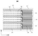
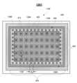
도 1은 본 개시내용의 일부 실시예들에 따른 예시적인 3차원(3D) 메모리 디바이스(100)의 평면도를 예시한다. 3D 메모리 디바이스(100)는 메모리 칩(패키지), 메모리 다이 또는 메모리 다이의 임의의 부분일 수 있고, 하나 이상의 메모리 평면들(101)을 포함할 수 있고, 이들 각각은 복수의 메모리 블록들(103)을 포함할 수 있다. 각각의 메모리 평면(101)에서 동일하고 동시적인 동작들이 발생할 수 있다. 크기가 메가바이트(MB)일 수 있는 메모리 블록(103)은 소거 동작들을 수행하기 위한 가장 작은 크기이다. 도 1에 도시된 바와 같이, 예시적인 3D 메모리 디바이스(100)는 4개의 메모리 평면들(101)을 포함하고, 각각의 메모리 평면(101)은 6개의 메모리 블록들(103)을 포함한다. 각각의 메모리 블록(103)은 복수의 메모리 셀들을 포함할 수 있고, 여기서, 각각의 메모리 셀은 비트 라인들 및 워드 라인들과 같은 상호접속부들을 통해 어드레싱될 수 있다. 비트 라인들 및 워드 라인들은 수직으로(예를 들어, 각각 행들 및 열들로) 레이아웃되어, 금속 라인들의 어레이를 형성할 수 있다. 비트 라인들 및 워드 라인들의 방향은 도 1에서 "BL" 및 "WL"로 표지된다. 본 개시내용에서, 메모리 블록(103)은 "메모리 어레이" 또는 "어레이"라고도 지칭된다. 메모리 어레이는 저장 기능들을 수행하는 메모리 디바이스 내의 코어 영역이다.FIG. 1 illustrates a plan view of an exemplary three-dimensional (3D) memory device (100) according to some embodiments of the present disclosure. The 3D memory device (100) may be a memory chip (package), a memory die, or any portion of a memory die, and may include one or more memory planes (101), each of which may include a plurality of memory blocks (103). Identical and concurrent operations may occur in each memory plane (101). A memory block (103), which may be megabytes (MB) in size, is the smallest size for performing erase operations. As depicted in FIG. 1 , the exemplary 3D memory device (100) includes four memory planes (101), and each memory plane (101) includes six memory blocks (103). Each memory block (103) may include a plurality of memory cells, where each memory cell may be addressed via interconnections such as bit lines and word lines. The bit lines and word lines may be laid out vertically (e.g., in rows and columns, respectively) to form an array of metal lines. The directions of the bit lines and word lines are labeled “BL” and “WL” in FIG. 1. In the present disclosure, the memory block (103) is also referred to as a “memory array” or “array.” A memory array is a core region within a memory device that performs storage functions.
3D 메모리 디바이스(100)는 또한 주변 영역(105), 즉, 메모리 평면들(101)을 둘러싸는 영역을 포함한다. 주변 영역(105)은 메모리 어레이의 기능들을 지원하기 위한 많은 디지털, 아날로그 및/또는 혼합 신호 회로들, 예를 들어 페이지 버퍼들, 행 및 열 디코더들 및 감지 증폭기들을 포함한다. 주변 회로들은 본 기술분야의 통상의 기술자에게 명백한 바와 같이, 트랜지스터들, 다이오드들, 커패시터들, 저항기들 등과 같은 능동 및/또는 수동 반도체 디바이스들을 사용한다.The 3D memory device (100) also includes a peripheral region (105), i.e., a region surrounding the memory planes (101). The peripheral region (105) includes many digital, analog, and/or mixed-signal circuits to support the functions of the memory array, such as page buffers, row and column decoders, and sense amplifiers. The peripheral circuits utilize active and/or passive semiconductor devices, such as transistors, diodes, capacitors, resistors, and the like, as would be apparent to one skilled in the art.
유의할 점은, 3D 메모리 디바이스(100)에서의 메모리 평면들(101)의 배열 및 도 1에 예시된 각각의 메모리 평면(101)에서의 메모리 블록들(103)의 배열이 단지 예로서 사용되고, 이는 본 개시내용의 범위를 제한하지 않는다는 것이다.It should be noted that the arrangement of memory planes (101) in the 3D memory device (100) and the arrangement of memory blocks (103) in each memory plane (101) illustrated in FIG. 1 are merely used as examples and do not limit the scope of the present disclosure.
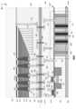
도 2를 참조하면, 본 개시내용의 일부 실시예에 따른 도 1의 영역(108)의 확대 평면도가 예시되어 있다. 3D 메모리 디바이스(100)의 영역(108)은 계단 영역(210) 및 채널 구조 영역(211)을 포함할 수 있다. 채널 구조 영역(211)은 복수의 적층된 메모리 셀들을 각각 포함하는 메모리 스트링들(212)의 어레이를 포함할 수 있다. 계단 영역(210)은 계단 구조 및 계단 구조 상에 형성된 접점 구조들(214)의 어레이를 포함할 수 있다. 일부 실시예들에서, 채널 구조 영역(211) 및 계단 영역(210)에 걸쳐 WL 방향으로 연장되는 복수의 슬릿 구조(216)는 메모리 블록을 다수의 메모리 핑거(218)로 분할할 수 있다. 적어도 일부 슬릿 구조들(216)은 채널 구조 영역들(211) 내의 메모리 스트링들(212)의 어레이에 대한 공통 소스 접점으로서 기능할 수 있다. 상단 선택 게이트 컷(220)이 각각의 메모리 핑거(218)의 중간에 배치되어, 메모리 핑거(218)의 상단 선택 게이트(TSG)를 2개의 부분으로 분할할 수 있으며, 이에 의해 메모리 핑거를 2개의 프로그램 가능한(판독/기입) 페이지로 분할할 수 있다. 3D NAND 메모리의 소거 동작은 메모리 블록 레벨에서 수행될 수 있지만, 판독 및 기입 동작들은 메모리 페이지 레벨에서 수행될 수 있다. 페이지는 크기가 킬로바이트(KB)일 수 있다. 일부 실시예들에서, 영역(108)은 또한 제조 동안 공정 변동 제어를 위한 그리고/또는 추가적인 기계적 지지를 위한 더미 메모리 스트링들을 포함한다.Referring to FIG. 2, an enlarged plan view of a region (108) of FIG. 1 is illustrated according to some embodiments of the present disclosure. The region (108) of the 3D memory device (100) may include a step region (210) and a channel structure region (211). The channel structure region (211) may include an array of memory strings (212), each of which includes a plurality of stacked memory cells. The step region (210) may include an array of contact structures (214) formed on the step structure and the step structure. In some embodiments, a plurality of slit structures (216) extending in the WL direction across the channel structure region (211) and the step region (210) may divide a memory block into a plurality of memory fingers (218). At least some of the slit structures (216) may function as common source contacts for the array of memory strings (212) within the channel structure regions (211). A top select gate cut (220) may be positioned in the middle of each memory finger (218) to divide the top select gate (TSG) of the memory finger (218) into two parts, thereby dividing the memory finger into two programmable (read/write) pages. Erase operations in the 3D NAND memory may be performed at the memory block level, while read and write operations may be performed at the memory page level. A page may be kilobytes (KB) in size. In some embodiments, the region (108) also includes dummy memory strings for process variation control during manufacturing and/or for additional mechanical support.
도 3은 본 개시내용의 일부 실시예들에 따른, 예시적인 3차원(3D) 메모리 어레이 구조(300)의 일부의 사시도를 예시한다. 메모리 어레이 구조(300)는 기판(330), 기판(330) 위의 절연 필름(331), 절연 필름(331) 위의 하부 선택 게이트들(LSG들)(332)의 계층, 및 LSG들(332)의 상단 상에 적층되어 교번하는 전도성 및 유전체 층들의 필름 스택(335)을 형성하는 "워드 라인들(WL들)"로서 또한 지칭되는 제어 게이트들(333)의 복수의 계층들을 포함한다. 제어 게이트들의 계층들에 인접한 유전체 층들은 명료성을 위해 도 3에 도시되지 않는다.FIG. 3 illustrates a perspective view of a portion of an exemplary three-dimensional (3D) memory array structure (300), according to some embodiments of the present disclosure. The memory array structure (300) includes a substrate (330), an insulating film (331) over the substrate (330), a layer of bottom select gates (LSGs) (332) over the insulating film (331), and a plurality of layers of control gates (333), also referred to as “word lines (WLs),” that are stacked on top of the LSGs (332) to form a film stack (335) of alternating conductive and dielectric layers. The dielectric layers adjacent the layers of control gates are not shown in FIG. 3 for clarity.
각각의 계층의 제어 게이트들은 필름 스택(335)을 통해 슬릿 구조들(216-1 및 216-2)에 의해 분리된다. 메모리 어레이 구조(300)는 제어 게이트들(333)의 스택 위의 상단 선택 게이트(TSG)들(334)의 계층을 또한 포함한다. TSG(334), 제어 게이트들(333) 및 LSG(332)의 스택은 "게이트 전극들"이라고도 지칭된다. 메모리 어레이 구조(300)는 인접한 LSG들(332) 사이의 기판(330)의 부분들에서 메모리 스트링들(212) 및 도핑된 소스 라인 영역들(344)을 더 포함한다. 각각의 메모리 스트링들(212)은 교번하는 전도성 및 유전체 층들의 절연 필름(331) 및 필름 스택(335)을 통해 연장되는 채널 홀(336)을 포함한다. 메모리 스트링들(212)은 채널 홀(336)의 측벽 상의 메모리 필름(337), 메모리 필름(337) 위의 채널 층(338), 및 채널 층(338)에 의해 둘러싸인 코어 충전 필름(339)을 또한 포함한다. 메모리 셀(340)은 제어 게이트(333)와 메모리 스트링(212)의 교차점에 형성될 수 있다. 메모리 어레이 구조(300)는 TSG들(334) 상에서 메모리 스트링들(212)과 접속된 복수의 비트 라인들(BL들)(341)을 더 포함한다. 메모리 어레이 구조(300)는 또한 복수의 접점 구조들(214)을 통해 게이트 전극들과 접속되는 복수의 금속 상호접속 라인들(343)을 포함한다. 필름 스택(335)의 에지는 게이트 전극들의 각각의 계층에 대한 전기적 연결을 허용하기 위해 계단 형상으로 구성된다.The control gates of each layer are separated by slit structures (216-1 and 216-2) through a film stack (335). The memory array structure (300) also includes a layer of top select gates (TSGs) (334) above the stack of control gates (333). The stack of TSGs (334), control gates (333), and LSGs (332) are also referred to as “gate electrodes.” The memory array structure (300) further includes memory strings (212) and doped source line regions (344) in portions of the substrate (330) between adjacent LSGs (332). Each of the memory strings (212) includes an insulating film (331) of alternating conductive and dielectric layers and a channel hole (336) extending through the film stack (335). The memory strings (212) also include a memory film (337) on the sidewalls of the channel holes (336), a channel layer (338) over the memory film (337), and a core fill film (339) surrounded by the channel layer (338). A memory cell (340) may be formed at the intersection of the control gate (333) and the memory string (212). The memory array structure (300) further includes a plurality of bit lines (BLs) (341) connected to the memory strings (212) on the TSGs (334). The memory array structure (300) also includes a plurality of metal interconnect lines (343) connected to the gate electrodes via the plurality of contact structures (214). The edge of the film stack (335) is configured in a step shape to allow electrical connection to each layer of the gate electrodes.
도 3에서, 예시의 목적을 위해, 제어 게이트들(333-1, 333-2, 및 333-3)의 3개의 계층이 TSG(334)의 하나의 계층 및 LSG(332)의 하나의 계층과 함께 도시된다. 이 예에서, 각각의 메모리 스트링(212)은 제어 게이트들(333-1, 333-2 및 333-3)에 각각 대응하는 3개의 메모리 셀들(340-1, 340-2 및 340-3)을 포함할 수 있다. 일부 실시예들에서, 제어 게이트들의 수 및 메모리 셀들의 수는 저장 용량을 증가시키기 위해 3개를 초과할 수 있다. 메모리 어레이 구조(300)는 다른 구조들, 예를 들어, TSG 컷, 공통 소스 접점 및 더미 채널 구조를 또한 포함할 수 있다. 이러한 구조들은 단순성을 위해 도 3에 도시되지 않는다.In FIG. 3, for illustrative purposes, three layers of control gates (333-1, 333-2, and 333-3) are shown along with one layer of TSG (334) and one layer of LSG (332). In this example, each memory string (212) may include three memory cells (340-1, 340-2, and 340-3), each corresponding to the control gates (333-1, 333-2, and 333-3). In some embodiments, the number of control gates and the number of memory cells may exceed three to increase storage capacity. The memory array structure (300) may also include other structures, such as TSG cuts, common source contacts, and dummy channel structures. Such structures are not shown in FIG. 3 for simplicity.
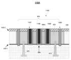
더 높은 저장 밀도를 달성하기 위해, 3D 메모리의 수직 WL 스택들의 수 또는 메모리 스트링 당 메모리 셀들의 수는, 예를 들어, 24개의 적층 WL 층들(즉, 24L)로부터 128개 이상의 층들로 크게 증가되었다. 3D 메모리의 크기를 더 감소시키기 위해, 메모리 어레이는 주변 회로의 상단에 적층될 수 있거나, 그 반대도 가능하다. 예를 들어, 주변 회로는 제1 기판 상에 제조될 수 있고, 메모리 어레이는 제2 기판 상에 제조될 수 있다. 이어서, 메모리 어레이 및 주변 회로는 제1 및 제2 기판들을 함께 본딩함으로써 다양한 상호접속부들을 통해 접속될 수 있다. 이와 같이, 3D 메모리 밀도가 증가될 수 있을 뿐만 아니라, 주변 회로와 메모리 어레이 사이의 통신이 더 높은 대역폭 및 더 낮은 전력 소비를 달성할 수 있는데, 왜냐하면 기판(웨이퍼) 본딩을 통해 상호접속 길이들이 더 짧을 수 있기 때문이다. 도 4 내지 8, 9a-9g, 10, 11a-11c, 12a-12c 및 13은, 본 개시내용의 일부 실시예들에 따라, 주변 회로가 웨이퍼 본딩을 통해 메모리 어레이와 접속되는 3D 메모리 디바이스를 형성하기 위한 구조들 및 방법들을 예시한다.To achieve higher storage density, the number of vertical WL stacks of 3D memory, or the number of memory cells per memory string, has been significantly increased, for example, from 24 stacked WL layers (i.e., 24L) to 128 or more layers. To further reduce the size of the 3D memory, the memory array can be stacked on top of the peripheral circuitry, or vice versa. For example, the peripheral circuitry can be fabricated on a first substrate and the memory array can be fabricated on a second substrate. The memory array and the peripheral circuitry can then be connected via various interconnects by bonding the first and second substrates together. In this way, not only can the 3D memory density be increased, but the communication between the peripheral circuitry and the memory array can achieve higher bandwidth and lower power consumption because the interconnect lengths can be shorter via substrate (wafer) bonding. FIGS. 4 to 8, 9a-9g, 10, 11a-11c, 12a-12c and 13 illustrate structures and methods for forming a 3D memory device in which peripheral circuitry is connected to a memory array via wafer bonding, according to some embodiments of the present disclosure.
3D 메모리 디바이스의 밀도 및 성능의 증가에 따라, 메모리 어레이에 대한 기능 지원, 예를 들어, 메모리 셀들의 데이터의 판독, 기입 및 소거를 제공하기 위해 주변 회로의 개선이 또한 필요하다. 주변 디바이스들 중에서, 커패시터들은 3D 메모리 디바이스에서의 정규 전압들, 예를 들어, 메모리 데이터를 소거하기 위한 부스팅 전압에 사용된다. 따라서, 도 4 내지 8, 9a-9g, 10, 11a-11c, 12a-12c 및 13은, 본 개시내용의 일부 실시예들에 따른, 다양한 공정 스테이지들에서의 메모리 디바이스의 3D 커패시터를 예시한다.With the increase in density and performance of 3D memory devices, improvements in peripheral circuitry are also needed to provide functional support for the memory array, e.g., reading, writing and erasing data of memory cells. Among the peripheral devices, capacitors are used for normal voltages in 3D memory devices, e.g., boosting voltages for erasing memory data. Accordingly, FIGS. 4 to 8, 9a-9g, 10, 11a-11c, 12a-12c and 13 illustrate 3D capacitors of memory devices at various process stages, according to some embodiments of the present disclosure.
도 4는 본 개시내용의 일부 실시예들에 따른 3D 메모리 디바이스의 예시적인 주변 회로(400)의 단면을 예시한다. 주변 회로(400)는 제1 기판(430)을 포함할 수 있고, 여기서 제1 기판(430)은 실리콘(예를 들어, 단결정 실리콘), 실리콘 게르마늄(SiGe), 게르마늄(Ge), 실리콘 온 인슐레이터(SOI), 게르마늄 온 인슐레이터(GOI), 갈륨 비소(GaAs), 갈륨 질화물, 실리콘 탄화물, 유리, III-V 화합물, 임의의 다른 적절한 재료들 또는 이들의 임의의 조합들을 포함할 수 있다. 일부 실시예들에서, 제1 기판(430)은 주변 디바이스 제조 이전에 양면 연마될 수 있다. 이 예에서, 제1 기판(430)은 (각각 제1 측면(430-1) 및 제2 측면(430-2), 또는 전면 및 배면이라고도 지칭되는) 상단 및 하단 측면들 상의 표면들을 포함하며, 이들 양자 모두는 고품질 반도체 디바이스들을 위한 매끄러운 표면을 제공하도록 연마 및 처리된다. 제1 및 제2 측면들은 제1 기판의 대향 측면들이다.FIG. 4 illustrates a cross-section of an exemplary peripheral circuit (400) of a 3D memory device according to some embodiments of the present disclosure. The peripheral circuit (400) may include a first substrate (430), wherein the first substrate (430) may include silicon (e.g., single crystal silicon), silicon germanium (SiGe), germanium (Ge), silicon on insulator (SOI), germanium on insulator (GOI), gallium arsenide (GaAs), gallium nitride, silicon carbide, glass, a III-V compound, any other suitable materials, or any combination thereof. In some embodiments, the first substrate (430) may be double-side polished prior to fabrication of the peripheral device. In this example, the first substrate (430) includes surfaces on top and bottom sides (also referred to as the first side (430-1) and the second side (430-2), or front and back sides, respectively), both of which are polished and processed to provide a smooth surface for high quality semiconductor devices. The first and second sides are opposing sides of the first substrate.
주변 회로(400)는 제1 기판(430)의 제1 측면(430-1) 상에 하나 이상의 주변 디바이스(450)를 포함할 수 있다. 주변 디바이스(450)는 제1 기판(430) "상에" 형성될 수 있고, 여기서 주변 디바이스(450)의 전체 또는 일부는 제1 기판(430)에(예를 들어, 제1 기판(430)의 상단 표면 아래에) 및/또는 제1 기판(430) 상에 직접 형성된다. 주변 디바이스(450)는 임의의 적절한 반도체 디바이스들, 예를 들어, 금속 산화물 반도체 전계 효과 트랜지스터(MOSFET), 바이폴라 접합 트랜지스터(BJT), 다이오드, 저항기, 커패시터, 인덕터 등을 포함할 수 있다. 반도체 디바이스들 중에서, p-형 및/또는 n-형 MOSFET들(즉, CMOS)은 로직 회로 설계에서 널리 구현되고, 본 개시내용에서 주변 디바이스(450)에 대한 예들로서 사용된다. 이 예에서, 주변 회로(400)는 또한 CMOS 웨이퍼(400)로 지칭된다.The peripheral circuit (400) may include one or more peripheral devices (450) on a first side (430-1) of a first substrate (430). The peripheral devices (450) may be formed “on” the first substrate (430), where all or a portion of the peripheral devices (450) are formed on the first substrate (430) (e.g., below a top surface of the first substrate (430)) and/or directly on the first substrate (430). The peripheral devices (450) may include any suitable semiconductor devices, such as a metal oxide semiconductor field effect transistor (MOSFET), a bipolar junction transistor (BJT), a diode, a resistor, a capacitor, an inductor, and the like. Among the semiconductor devices, p-type and/or n-type MOSFETs (i.e., CMOS) are widely implemented in logic circuit design and are used as examples for the peripheral devices (450) in the present disclosure. In this example, the peripheral circuit (400) is also referred to as a CMOS wafer (400).
주변 디바이스(450)는 p-채널 MOSFET 또는 n-채널 MOSFET 중 어느 하나일 수 있고, 얕은 트렌치 격리부(STI)(452)에 의해 둘러싸인 활성 디바이스 영역, n-형 또는 p-형 도핑으로 활성 디바이스 영역에 형성된 웰(454), 게이트 유전체, 게이트 전도체 및/또는 게이트 하드 마스크를 포함하는 게이트 스택(456)을 포함할 수 있지만, 이에 제한되지는 않는다. 주변 디바이스(450)는 또한 소스/드레인 연장부 및/또는 헤일로 영역(도 4에 도시되지 않음), 게이트 스택의 각각의 측면 상에 위치하는 게이트 스페이서(458) 및 소스/드레인(460)을 포함할 수 있다. 주변 디바이스(450)는 소스/드레인의 상단 부분에서 실리사이드 접점 영역(도시되지 않음)을 더 포함할 수 있다. 다른 공지된 디바이스들이 또한 제1 기판(430) 상에 형성될 수 있다. 주변 디바이스(450)의 구조 및 제조 방법은 본 기술분야의 통상의 기술자에게 공지되어 있고, 전체적으로 본원에 포함된다.The peripheral device (450) may be either a p-channel MOSFET or an n-channel MOSFET and may include, but is not limited to, an active device region surrounded by a shallow trench isolation (STI) (452), a well (454) formed in the active device region with n-type or p-type doping, a gate stack (456) including a gate dielectric, a gate conductor, and/or a gate hard mask. The peripheral device (450) may also include source/drain extensions and/or halo regions (not shown in FIG. 4), gate spacers (458) positioned on each side of the gate stack, and a source/drain (460). The peripheral device (450) may further include a silicide contact region (not shown) at the top portion of the source/drain. Other known devices may also be formed on the first substrate (430). The structure and fabrication methods of the peripheral device (450) are well known to those skilled in the art and are incorporated herein in their entirety.
STI(452)는, 리소그래피 및 에칭을 이용하여 기판을 패터닝하고, 절연 재료를 채우고, 절연 재료를 연마하여 제1 기판(430) 상에 동일 평면 표면을 형성하는 것을 통해 형성될 수 있다. STI를 위한 절연 재료는 실리콘 산화물, 실리콘 산질화물, TEOS, 저온 산화물(LTO), 고온 산화물(HTO), 실리콘 질화물 등을 포함할 수 있다. STI(452)를 위한 절연 재료는 CVD(chemical vapor deposition), PVD(physical vapor deposition), PECVD(plasma-enhanced CVD), LPCVD(low pressure chemical vapor deposition), HDP(high density plasma) 화학 기상 증착, RTCVD(rapid thermal chemical vapor deposition), MOCVD(metal organic chemical vapor deposition), ALD(atomic layer deposition), 스퍼터링, 열 산화 또는 질화, 또는 이들의 조합들과 같은 기술들을 사용하여 배치될 수 있다. STI(452)의 형성은 또한, 개선된 전기적 격리부를 위해 배치된 절연 재료를 치밀화하기 위한 고온 어닐링 단계를 포함할 수 있다. 본 기술분야의 통상의 기술자에게 명백한 바와 같이, 다른 STI 구조가 채용될 수 있다.The STI (452) can be formed by patterning a substrate using lithography and etching, filling an insulating material, and polishing the insulating material to form a coplanar surface on the first substrate (430). The insulating material for the STI can include silicon oxide, silicon oxynitride, TEOS, low temperature oxide (LTO), high temperature oxide (HTO), silicon nitride, etc. The insulating material for the STI (452) can be disposed using techniques such as chemical vapor deposition (CVD), physical vapor deposition (PVD), plasma-enhanced CVD (PECVD), low pressure chemical vapor deposition (LPCVD), high density plasma (HDP) chemical vapor deposition, rapid thermal chemical vapor deposition (RTCVD), metal organic chemical vapor deposition (MOCVD), atomic layer deposition (ALD), sputtering, thermal oxidation or nitridation, or combinations thereof. The formation of the STI (452) may also include a high temperature annealing step to densify the insulating material disposed for improved electrical isolation. As will be apparent to one skilled in the art, other STI structures may be employed.
주변 디바이스(450)의 웰(454)은 n-채널 MOSFET에 대한 p-형 도핑 및 p-채널 MOSFET에 대한 n-형 도핑을 포함할 수 있고, 각각 p-웰 및 n-웰로 지칭된다. 웰(454)의 도펀트 프로파일 및 농도는 주변 디바이스(450)의 디바이스 특성에 영향을 미친다. 낮은 임계 전압(Vt)을 갖는 MOSFET 디바이스들에 대해, 웰(454)은 더 낮은 농도로 도핑될 수 있고, 저전압 p-웰 또는 저전압 n-웰을 형성할 수 있다. 높은 Vt를 갖는 MOSFET의 경우, 웰(454)은 더 높은 농도로 도핑될 수 있고, 고전압 p-웰 또는 고전압 n-웰을 형성할 수 있다. 일부 실시예들에서, p-형 기판으로부터의 전기적 격리부를 제공하기 위해, 딥 n-웰은 높은 Vt를 가지는 n-채널 MOSFET에 대한 고전압 p-웰 아래에 형성될 수 있다. 일부 실시예에서, 웰(454)의 깊이는 STI(452)의 깊이보다 깊을 수 있다.The well (454) of the peripheral device (450) can include p-type doping for an n-channel MOSFET and n-type doping for a p-channel MOSFET, and are referred to as a p-well and an n-well, respectively. The dopant profile and concentration of the well (454) affect the device characteristics of the peripheral device (450). For MOSFET devices having a low threshold voltage (Vt ), the well (454) can be doped with a lower concentration, forming a low-voltage p-well or a low-voltage n-well. For MOSFET devices having a high Vt , the well (454) can be doped with a higher concentration, forming a high-voltage p-well or a high-voltage n-well. In some embodiments, a deep n-well can be formed beneath the high-voltage p-well for an n-channel MOSFET having a high Vt to provide electrical isolation from the p-type substrate. In some embodiments, the depth of the well (454) may be deeper than the depth of the STI (452).
n-웰의 형성은 인, 비소, 안티몬 등과 같은 임의의 적절한 n-형 도펀트, 및/또는 이들의 임의의 조합을 포함할 수 있다. p-웰의 형성은 임의의 적절한 p-형 도펀트, 예를 들어 붕소를 포함할 수 있다. 도펀트 혼입은 활성 디바이스 영역에 대한 에피택시 동안 인-시튜 도핑을 통해, 또는 활성화 어닐링이 뒤따르는 이온 주입을 통해 달성될 수 있다.The formation of the n-well may comprise any suitable n-type dopant, such as phosphorus, arsenic, antimony, and/or any combination thereof. The formation of the p-well may comprise any suitable p-type dopant, for example boron. Dopant incorporation may be achieved via in-situ doping during epitaxy into the active device region, or via ion implantation followed by an activation anneal.
주변 디바이스(450)의 게이트 스택(456)은 "게이트 퍼스트" 방식에 의해 형성될 수 있고, 여기서 게이트 스택(456)은 소스/드레인 형성 이전에 배치되고 패터닝된다. 주변 디바이스(450)의 게이트 스택(456)은 또한, 희생 게이트 스택이 먼저 형성된 다음 소스/드레인 형성 이후에 하이-k 유전체 층 및 게이트 전도체로 대체될 수 있는 "대체" 방식에 의해 형성될 수 있다.The gate stack (456) of the peripheral device (450) may be formed by a “gate first” approach, where the gate stack (456) is placed and patterned prior to source/drain formation. The gate stack (456) of the peripheral device (450) may also be formed by a “replacement” approach, where a sacrificial gate stack is formed first and then replaced with a high-k dielectric layer and gate conductor after source/drain formation.
일부 실시예들에서, 게이트 유전체는 실리콘 산화물, 실리콘 질화물, 실리콘 산질화물, 및/또는 하프늄 산화물, 지르코늄 산화물, 알루미늄 산화물, 탄탈륨 산화물, 마그네슘 산화물, 또는 란타늄 산화물 필름들과 같은 하이-k 유전체 필름들, 및/또는 이들의 조합들로 이루어질 수 있다. 게이트 유전체는 CVD, PVD, PECVD, LPCVD, RTCVD, 스퍼터링, MOCVD, ALD, 열 산화 또는 질화, 또는 이들의 조합들과 같은 임의의 적절한 방법들에 의해 배치될 수 있다.In some embodiments, the gate dielectric can be formed of high-k dielectric films, such as silicon oxide, silicon nitride, silicon oxynitride, and/or hafnium oxide, zirconium oxide, aluminum oxide, tantalum oxide, magnesium oxide, or lanthanum oxide films, and/or combinations thereof. The gate dielectric can be deposited by any suitable methods, such as CVD, PVD, PECVD, LPCVD, RTCVD, sputtering, MOCVD, ALD, thermal oxidation or nitridation, or combinations thereof.
일부 실시예들에서, 게이트 전도체는 텅스텐, 코발트, 니켈, 구리, 또는 알루미늄, 및/또는 이들의 조합들과 같은 금속 또는 금속 합금으로 만들어질 수 있다. 일부 실시예들에서, 게이트 전도체는 또한 티타늄 질화물(TiN), 탄탈륨 질화물(TaN) 등과 같은 전도성 재료를 포함할 수 있다. 게이트 전도체는, 임의의 적절한 퇴적 방법, 예를 들어, 스퍼터링, 열 증발, e-빔 증발, ALD, PVD, 및/또는 이들의 조합에 의해 형성될 수 있다.In some embodiments, the gate conductor can be made of a metal or metal alloy, such as tungsten, cobalt, nickel, copper, or aluminum, and/or combinations thereof. In some embodiments, the gate conductor can also include a conductive material, such as titanium nitride (TiN), tantalum nitride (TaN), or the like. The gate conductor can be formed by any suitable deposition method, for example, sputtering, thermal evaporation, e-beam evaporation, ALD, PVD, and/or combinations thereof.
일부 실시예들에서, 게이트 전도체는 또한 다결정 실리콘, 다결정 게르마늄, 다결정 게르마늄 실리콘 및 임의의 다른 적합한 재료, 및/또는 이들의 조합들과 같은 다결정 반도체를 포함할 수 있다. 일부 실시예들에서, 다결정 재료는 붕소, 인, 또는 비소 등과 같은 임의의 적절한 타입들의 도펀트와 함께 포함될 수 있다. 일부 실시예들에서, 게이트 전도체는 또한 전술한 재료들을 갖는 비정질 반도체일 수 있다.In some embodiments, the gate conductor may also include a polycrystalline semiconductor, such as polycrystalline silicon, polycrystalline germanium, polycrystalline germanium silicon, and any other suitable material, and/or combinations thereof. In some embodiments, the polycrystalline material may be included with any suitable types of dopants, such as boron, phosphorus, or arsenic. In some embodiments, the gate conductor may also be an amorphous semiconductor having the materials described above.
일부 실시예들에서, 게이트 전도체는 WSix, CoSix, NiSix, 또는 AlSix 등을 포함하는 금속 실리사이드로 만들어질 수 있다. 금속 실리사이드 재료의 형성은 전술된 유사한 기술들을 이용하여 금속 층 및 다결정 반도체를 형성하는 것을 포함할 수 있다. 금속 실리사이드의 형성은 퇴적된 금속 층 및 다결정 반도체 층 상에 열 어닐링 공정을 적용한 다음, 미반응 금속을 제거하는 단계를 더 포함할 수 있다.In some embodiments, the gate conductor can be made of a metal silicide, including WSix , CoSix , NiSix , or AlSix . Formation of the metal silicide material can include forming the metal layer and the polycrystalline semiconductor using similar techniques described above. Formation of the metal silicide can further include applying a thermal annealing process on the deposited metal layer and the polycrystalline semiconductor layer, followed by removing unreacted metal.
게이트 스페이서(458)는 절연 재료를 배치한 다음 이방성 에칭을 수행하는 것을 통해 형성될 수 있다. 게이트 스페이서(458)를 위한 절연 재료는 실리콘 산화물, 실리콘 질화물, 실리콘 산질화물, TEOS, LTO, HTO 등을 포함하는 임의의 절연체일 수 있다. 게이트 스페이서(458)는, CVD, PVD, PECVD, LPCVD, RTCVD, MOCVD, ALD, 스퍼터링, 또는 이들의 조합 같은 기술을 이용하여 배치될 수 있다. 게이트 스페이서(458)의 이방성 에칭은 건식 에칭, 예를 들어 반응성 이온 에칭(RIE)을 포함한다.The gate spacer (458) can be formed by placing an insulating material and then performing anisotropic etching. The insulating material for the gate spacer (458) can be any insulator including silicon oxide, silicon nitride, silicon oxynitride, TEOS, LTO, HTO, etc. The gate spacer (458) can be placed using a technique such as CVD, PVD, PECVD, LPCVD, RTCVD, MOCVD, ALD, sputtering, or a combination thereof. The anisotropic etching of the gate spacer (458) includes a dry etching, such as reactive ion etching (RIE).
소스/드레인(460) 사이의 게이트 스택(456)의 게이트 길이 L은 MOSFET의 중요한 특징이다. MOSFET의 동작 동안에, 게이트 스택(456) 아래의 웰의 상단 부분은 소스로부터 드레인으로 전류를 전도할 수 있고, 소위 MOSFET의 채널이다. 게이트 길이 L(채널 길이라고도 지칭됨)은 MOSFET의 구동 전류의 크기를 결정하며, 따라서 로직 회로들에 대해 적극적으로 축소된다. 게이트 길이 L은 약 100nm 미만일 수 있다. 일부 실시예들에서, 게이트 길이는 약 5nm 내지 약 30nm의 범위에 있을 수 있다. 그러한 작은 치수를 갖는 게이트 스택의 패터닝은 매우 어려우며, 광학 근접 보정, 이중 노광 및/또는 이중 에칭, 자기 정렬 이중 패터닝 등을 포함하는 기술들을 이용할 수 있다.The gate length L of the gate stack (456) between the source/drain (460) is an important characteristic of the MOSFET. During operation of the MOSFET, the upper portion of the well under the gate stack (456) can conduct current from the source to the drain and is the so-called channel of the MOSFET. The gate length L (also referred to as the channel length) determines the magnitude of the drive current of the MOSFET and is therefore aggressively scaled down for logic circuits. The gate length L can be less than about 100 nm. In some embodiments, the gate length can be in the range of about 5 nm to about 30 nm. Patterning of the gate stack with such small dimensions is very difficult and may utilize techniques including optical proximity correction, double exposure and/or double etching, self-aligned double patterning, etc.
일부 실시예들에서, 주변 디바이스(450)의 소스/드레인(460)은 고농도 도펀트들로 통합된다. n-형 MOSFET의 경우, 소스/드레인(460)용 도펀트는 인, 비소, 안티몬 등과 같은 임의의 적절한 n-형 도펀트 및/또는 이들의 임의의 조합을 포함할 수 있다. p-형 MOSFET들에 대해, 소스/드레인(460)에 대한 도펀트는 임의의 적절한 p-형 도펀트, 예를 들어 붕소를 포함할 수 있다. 도펀트 혼입은 이온 주입과 그 다음의 도펀트 활성화 어닐링을 통해 달성될 수 있다. 소스/드레인(460)은 제1 기판(430)과 동일한 재료, 예를 들어, 실리콘으로 이루어질 수 있다. 일부 실시예들에서, 주변 디바이스(450)의 소스/드레인(460)은 고성능을 달성하기 위해 제1 기판(430)과 상이한 재료로 제조될 수 있다. 예를 들어, 실리콘 기판 상에서, p-형 MOSFET들을 위한 소스/드레인(460)은 SiGe를 포함할 수 있고, n-형 MOSFET들을 위한 소스/드레인(460)은 탄소와 통합될 수 있다. 상이한 재료로 소스/드레인(460)을 형성하는 것은 소스/드레인 영역에서 기판 재료를 에치백하는 것 및 에피택시와 같은 기술들을 사용하여 새로운 소스/드레인 재료를 배치하는 것을 포함할 수 있다. 소스/드레인(460)에 대한 도핑은 또한 에피택시 동안 인-시튜 도핑을 통해 달성될 수 있다.In some embodiments, the source/drain (460) of the peripheral device (450) is incorporated with a high concentration of dopants. For n-type MOSFETs, the dopants for the source/drain (460) may include any suitable n-type dopant, such as phosphorus, arsenic, antimony, and/or any combination thereof. For p-type MOSFETs, the dopants for the source/drain (460) may include any suitable p-type dopant, such as boron. Dopant incorporation may be accomplished via ion implantation followed by a dopant activation annealing. The source/drain (460) may be made of the same material as the first substrate (430), such as silicon. In some embodiments, the source/drain (460) of the peripheral device (450) may be fabricated of a different material than the first substrate (430) to achieve high performance. For example, on a silicon substrate, the source/drain (460) for p-type MOSFETs may include SiGe, and the source/drain (460) for n-type MOSFETs may be integrated with carbon. Forming the source/drain (460) with different materials may include etching back the substrate material in the source/drain regions and depositing new source/drain material using techniques such as epitaxy. Doping of the source/drain (460) may also be accomplished via in-situ doping during epitaxy.
주변 디바이스(450)는 또한 게이트 스택(456)의 각각의 측면을 따라 선택적인 소스/드레인 연장부 및/또는 헤일로 영역(도 4에 도시되지 않음)을 가질 수 있다. 소스/드레인 연장부 및/또는 헤일로 영역은 게이트 스택 아래의 활성 디바이스 영역 내부에 위치하며, 주로 약 0.5μm 미만의 채널 길이를 갖는 주변 디바이스(450)에 대한 개선된 단채널 제어를 위해 구현된다. 소스/드레인 연장부 및/또는 헤일로 영역의 형성은 소스/드레인(460)의 형성과 유사할 수 있지만, 최적화된 도핑 프로파일, 깊이 또는 농도를 얻기 위해 상이한 주입 조건(예를 들어, 도즈, 각도, 에너지, 종 등)을 사용할 수 있다.The peripheral device (450) may also have optional source/drain extensions and/or halo regions (not shown in FIG. 4) along each side of the gate stack (456). The source/drain extensions and/or halo regions are located within the active device region beneath the gate stack and are implemented for improved single-channel control for the peripheral device (450) having a channel length of primarily less than about 0.5 μm. The formation of the source/drain extensions and/or halo regions may be similar to the formation of the source/drain (460), but different implant conditions (e.g., dose, angle, energy, species, etc.) may be used to obtain an optimized doping profile, depth, or concentration.
주변 디바이스(450)는 평면 활성 디바이스 영역(도 4에 도시된 바와 같음)으로 제1 기판(430) 상에 형성될 수 있고, 여기서 MOSFET의 채널 및 전류 흐름의 방향은 제1 기판(430)의 표면에 평행하다. 일부 실시예들에서, 주변 디바이스(450)는 또한 3D 활성 디바이스 영역, 예를 들어 "FIN"(도시되지 않음)과 유사한 형상의 소위 "FINFET"으로 제1 기판(430) 상에 형성될 수 있으며, 여기서 MOSFET의 게이트 스택은 FIN 주위에 랩핑되고, MOSFET의 채널은 FIN의 3개의 측면들(상단 및 게이트 아래의 2개의 측벽들)을 따라 놓인다. FINFET 디바이스에 대한 구조 및 방법들은 본 기술분야의 통상의 기술자들에게 알려져 있고, 본 개시내용에서 추가로 논의되지 않는다.The peripheral device (450) can be formed on the first substrate (430) as a planar active device region (as shown in FIG. 4), wherein the channel and current flow direction of the MOSFET are parallel to the surface of the first substrate (430). In some embodiments, the peripheral device (450) can also be formed on the first substrate (430) as a 3D active device region, for example, a so-called "FINFET" having a shape similar to a "FIN" (not shown), wherein the gate stack of the MOSFET wraps around the FIN and the channel of the MOSFET runs along three sides of the FIN (the top and the two sidewalls below the gate). Structures and methods for FINFET devices are known to those skilled in the art and are not discussed further in the present disclosure.
일부 실시예에서, 주변 회로(400)는, 상이한 주변 디바이스(450)와 외부 디바이스(예를 들어, 전원, 또 다른 칩, I/O 디바이스 등) 사이에 전기적 연결을 제공하기 위해, 주변 디바이스(450) 위에, 제1 측면(430-1) 상의 주변 상호접속 층(462)(또는 제1 상호접속 층)을 포함할 수 있다. 주변 상호접속 층(462)은 하나 이상의 상호접속 구조, 예를 들어 하나 이상의 수직 접점 구조(464) 및 하나 이상의 측방향 전도성 라인(466)을 포함할 수 있다. 접점 구조(464) 및 전도성 라인(466)은, MOL(middle-of-line) 상호접속부들 및 BEOL(back-end-of-line) 상호접속부들과 같은, 임의의 적절한 타입들의 상호접속부들을 광범위하게 포함할 수 있다. 주변 회로(400) 내의 접점 구조(464) 및 전도성 라인(466)은 텅스텐(W), 코발트(Co), 구리(Cu), 티타늄(Ti), 탄탈륨(Ta), 알루미늄(Al), 티타늄 질화물(TiN), 탄탈륨 질화물(TaN), 니켈, 실리사이드(WSix, CoSix, NiSix, AlSix 등), 금속 합금들, 또는 이들의 임의의 조합과 같은 임의의 적절한 전도성 재료들을 포함할 수 있다. 전도성 재료들은 CVD(chemical vapor deposition), PECVD(plasma-enhanced CVD), PVD(physical vapor deposition), ALD(atomic layer deposition), 전기도금, 무전해 도금, 스퍼터링, 증발, 또는 이들의 임의의 조합과 같은 하나 이상의 박막 퇴적 공정에 의해 퇴적될 수 있다.In some embodiments, the peripheral circuit (400) may include a peripheral interconnect layer (462) (or first interconnect layer) on the first side (430-1) above the peripheral device (450) to provide electrical connection between the peripheral device (450) and an external device (e.g., a power supply, another chip, an I/O device, etc.). The peripheral interconnect layer (462) may include one or more interconnect structures, such as one or more vertical contact structures (464) and one or more lateral conductive lines (466). The contact structures (464) and the conductive lines (466) may broadly include any suitable types of interconnects, such as middle-of-line (MOL) interconnects and back-end-of-line (BEOL) interconnects. The contact structures (464) and conductive lines (466) within the peripheral circuit (400) may include any suitable conductive materials, such as tungsten (W), cobalt (Co), copper (Cu), titanium (Ti), tantalum (Ta), aluminum (Al), titanium nitride (TiN), tantalum nitride (TaN), nickel, silicides (WSix , CoSix , NiSix , AlSix , etc.), metal alloys, or any combination thereof. The conductive materials may be deposited by one or more thin film deposition processes, such as chemical vapor deposition (CVD), plasma-enhanced CVD (PECVD), physical vapor deposition (PVD), atomic layer deposition (ALD), electroplating, electroless plating, sputtering, evaporation, or any combination thereof.
주변 상호접속 층(462)은 절연 층(468)을 더 포함할 수 있다. 주변 상호접속 층(462) 내의 절연 층(468)은, 절연 재료, 예를 들어, 실리콘 산화물, 실리콘 질화물, 실리콘 산질화물, 도핑된 실리콘 산화물(예컨대, F-, C-, N- 또는 H-도핑된 산화물), 테트라에톡시실란(TEOS), 폴리이미드, 스핀-온-글래스(SOG), 다공성 SiCOH, 실세스퀴옥산(SSQ) 같은 로우-k 유전체 재료, 또는 이들의 임의의 조합을 포함할 수 있다. 절연 재료들은 CVD, PVD, PECVD, ALD, 고밀도-플라즈마 CVD(HDP-CVD), 스퍼터링, 스핀-코팅, 또는 이들의 임의의 조합과 같은 하나 이상의 박막 퇴적 공정에 의해 퇴적될 수 있다.The peripheral interconnect layer (462) may further include an insulating layer (468). The insulating layer (468) within the peripheral interconnect layer (462) may include an insulating material, such as silicon oxide, silicon nitride, silicon oxynitride, doped silicon oxide (e.g., F-, C-, N- or H-doped oxide), a low-k dielectric material such as tetraethoxysilane (TEOS), polyimide, spin-on-glass (SOG), porous SiCOH, silsesquioxane (SSQ), or any combination thereof. The insulating materials may be deposited by one or more thin film deposition processes, such as CVD, PVD, PECVD, ALD, high-density-plasma CVD (HDP-CVD), sputtering, spin-coating, or any combination thereof.
도 4에서, 2개의 전도성 레벨들(470-1 및 470-2)("금속 레벨들"이라고도 지칭됨)이 예로서 예시되며, 여기서 각각의 금속 레벨(470)(예를 들어, 470-1 또는 470-2)은 접점 구조들(464) 및 전도성 라인들(466)을 포함한다. 동일한 금속 레벨의 전도성 라인들(466)은 제1 기판(430)으로부터 동일한 거리에 위치된다. 주변 회로(400)에 대한 금속 레벨들(470)의 수는 제한되지 않고 3D 메모리의 성능을 위해 최적화된 임의의 수일 수 있다.In FIG. 4, two conductive levels (470-1 and 470-2) (also referred to as “metal levels”) are illustrated as an example, wherein each metal level (470) (e.g., 470-1 or 470-2) includes contact structures (464) and conductive lines (466). The conductive lines (466) of the same metal level are positioned at the same distance from the first substrate (430). The number of metal levels (470) for the peripheral circuit (400) is not limited and can be any number optimized for the performance of the 3D memory.
주변 상호접속 층(462)은 주변 회로(400)의 하단으로부터 상단까지 금속 레벨들(470)을 적층함으로써 형성될 수 있다. 도 4의 주변 회로(400)의 예에서, 하단 금속 레벨(470-1)이 먼저 형성된 다음, 하단 금속 레벨(470-1)의 상단에 상부 금속 레벨(470-2)이 형성될 수 있다. 각각의 금속 레벨(470)의 제조 공정들은 금속 레벨에 대해 요구되는 두께로 절연 층(468)의 일부를 배치하는 것, 접점 구조들(464) 및 전도성 라인들(466)에 대한 접점 홀들을 형성하기 위해 포토 리소그래피 및 건식/습식 에칭을 사용하여 절연 층(468)의 일부를 패터닝하는 것, 접점 구조들(464) 및 전도성 라인들(466)에 대한 접점 홀들을 채우기 위해 전도성 재료들을 배치하는 것, 및 CMP(chemical mechanical polishing) 또는 RIE(reactive ion etching)와 같은 평탄화 공정을 사용하여 접점 홀들 외부의 과잉 전도성 재료들을 제거하는 것을 포함할 수 있지만 이에 제한되지 않는다.The peripheral interconnect layer (462) may be formed by stacking metal levels (470) from the bottom to the top of the peripheral circuit (400). In the example of the peripheral circuit (400) of FIG. 4, the bottom metal level (470-1) may be formed first, and then the top metal level (470-2) may be formed on top of the bottom metal level (470-1). The manufacturing processes for each metal level (470) may include, but are not limited to, disposing a portion of an insulating layer (468) to a thickness required for the metal level, patterning a portion of the insulating layer (468) using photolithography and dry/wet etching to form contact holes for the contact structures (464) and conductive lines (466), disposing conductive materials to fill the contact holes for the contact structures (464) and conductive lines (466), and removing excess conductive materials outside the contact holes using a planarization process such as chemical mechanical polishing (CMP) or reactive ion etching (RIE).
일부 실시예에서, 주변 회로(400)는 또한 하나 이상의 기판 접점(472)을 포함하고, 여기서 기판 접점(472)은 제1 기판(430)으로의 전기적 연결을 제공한다. 기판 접점(472)은 수직 접점 구조(464) 및 측방향 전도성 라인(466)의 다수의 계층을 갖는 하나 이상의 전도성 레벨(470)을 포함할 수 있다. 도 4에서, 하나의 계층의 접점 구조 및 전도성 라인을 갖는 기판 접점(472)이 예로서 도시되며, 여기서 기판 접점(472)의 수직 접점 구조는 절연 층(468)을 통해 연장되고 제1 기판(430)과 전기적으로 접촉한다.In some embodiments, the peripheral circuitry (400) also includes one or more substrate contacts (472), wherein the substrate contacts (472) provide an electrical connection to the first substrate (430). The substrate contacts (472) may include one or more conductive levels (470) having multiple layers of vertical contact structures (464) and lateral conductive lines (466). In FIG. 4 , a substrate contact (472) having one layer of contact structures and conductive lines is illustrated as an example, wherein the vertical contact structures of the substrate contacts (472) extend through an insulating layer (468) and are in electrical contact with the first substrate (430).
일부 실시예들에서, 최상단 전도성 라인들(466)(예를 들어, 도 4의 466-2)은 주변 회로(400)의 상단 표면으로서 노출될 수 있고, 여기서, 최상단 전도성 라인들(466-2)은 다른 칩 또는 외부 디바이스 상의 전도성 라인들과 직접 접속될 수 있다.In some embodiments, the top conductive lines (466) (e.g., 466-2 of FIG. 4) may be exposed as a top surface of the peripheral circuit (400), where the top conductive lines (466-2) may be directly connected to conductive lines on another chip or external device.
일부 실시예에서, 최상단 전도성 라인(466-2)은 (도 4에 도시된 바와 같이) 절연 층(468) 내부에 매립될 수 있고, 여기서, 전도성 라인(466) 상단의 절연 재료는 선적이나 취급 동안에 스크래치 보호를 제공한다. 최상단의 전도성 라인(466)으로의 전기적 연결은, 나중에, 금속 VIA를 형성하거나, 단순히 건식/습식 에칭을 이용하여 절연 층(468)을 에치백함으로써 확립될 수 있다.In some embodiments, the top conductive line (466-2) may be embedded within the insulating layer (468) (as shown in FIG. 4), where the insulating material on top of the conductive line (466) provides scratch protection during shipping or handling. An electrical connection to the top conductive line (466) may be established later by forming a metal VIA, or simply etching back the insulating layer (468) using a dry/wet etch.
그러나, 주변 디바이스(450)는 MOSFET에 제한되지 않는다. 다른 디바이스들, 예를 들어, 다이오드들, 저항기들, 커패시터들, 인덕터들, BJT들 등의 구조들이 상이한 마스크 설계 및 레이아웃을 통해 MOSFET 제조 동안 동시에 형성될 수 있다. MOSFET들 이외의 디바이스들을 형성하기 위해, MOSFET의 공정 흐름, 예를 들어, 상이한 도펀트 프로파일들, 필름 두께들 또는 재료 스택들 등을 획득하기 위한 공정들에서 공정 단계들이 추가되거나 수정될 수 있다. 일부 실시예들에서, MOSFET 이외의 주변 디바이스(450)는 또한 특정 회로 요건들을 달성하기 위해 추가적인 설계 및/또는 리소그래피 마스크 레벨들로 제조될 수 있다.However, the peripheral device (450) is not limited to MOSFETs. Other devices, such as diodes, resistors, capacitors, inductors, BJTs, etc., may be formed concurrently during MOSFET fabrication via different mask designs and layouts. To form devices other than MOSFETs, process steps may be added or modified in the MOSFET process flow, such as to achieve different dopant profiles, film thicknesses, or material stacks. In some embodiments, peripheral devices other than MOSFETs (450) may also be fabricated with additional design and/or lithography mask levels to achieve specific circuit requirements.
일부 실시예에서, 복수의 주변 디바이스(450)는 주변 회로(400)의 동작을 위한 임의의 디지털, 아날로그, 및/또는 혼합 신호 회로를 형성하는데 이용될 수 있다. 주변 회로(400)는, 예를 들어, 메모리 어레이의 데이터의 행/열 디코딩, 타이밍 및 제어, 판독, 기입 및 소거 등을 수행할 수 있다.In some embodiments, a plurality of peripheral devices (450) may be used to form any digital, analog, and/or mixed-signal circuitry for operation of the peripheral circuit (400). The peripheral circuit (400) may perform, for example, row/column decoding, timing and control, reading, writing, and erasing of data in the memory array.
일부 실시예들에서, 주변 회로(400)에 대해 3D 커패시터가 형성될 수 있다. 예를 들어, 딥 웰(455)은 MOSFET에 대한 웰(454)을 형성하면서 제1 기판(430)에 형성될 수 있다. 딥 웰(455)은 p-형 도핑되거나 n-형 도핑될 수 있다. n-형 도펀트는 인, 비소, 안티몬 등일 수 있다. p-형 도펀트는 예를 들어 붕소일 수 있다. 도펀트 혼입은 제1 기판(430)의 제1 측면(430-1)으로부터의 이온 주입, 이어서 활성화 어닐링을 통해 달성될 수 있다. 일부 실시예에서, 딥 웰(455)은 에피택시 및 인-시튜 도핑을 통해 제1 기판(430)의 제1 측면(430-1) 상에 형성될 수 있다. 딥 웰(455)에 대한 주입은 웰(454)에 대한 주입 직전에 또는 직후에 수행될 수 있다. 딥 웰(455)에 대한 도펀트 활성화 어닐링은 웰(454)에 대한 것과 동시에 수행될 수 있다.In some embodiments, a 3D capacitor may be formed for the peripheral circuit (400). For example, a deep well (455) may be formed in the first substrate (430) while forming a well (454) for a MOSFET. The deep well (455) may be p-type doped or n-type doped. The n-type dopant may be phosphorus, arsenic, antimony, etc. The p-type dopant may be boron, for example. The dopant incorporation may be achieved via ion implantation from the first side (430-1) of the first substrate (430), followed by an activation annealing. In some embodiments, the deep well (455) may be formed on the first side (430-1) of the first substrate (430) via epitaxy and in-situ doping. The implantation into the deep well (455) may be performed immediately before or after the implantation into the well (454). The dopant activation annealing for the deep well (455) may be performed simultaneously with that for the well (454).
일부 실시예에서, 딥 웰(455)은 1μm 내지 5μm 범위의 깊이를 가질 수 있다. 일부 실시예들에서, 딥 웰(455)은 고농도로 도핑된다. 예를 들어, 딥 웰(455)은 1x1018cm-3 또는 그 이상으로 도핑될 수 있다.In some embodiments, the deep well (455) can have a depth in the range of 1 μm to 5 μm. In some embodiments, the deep well (455) is heavily doped. For example, the deep well (455) can be doped to 1x1018 cm-3 or more.
일부 실시예에서, 딥 웰 접점(473)은 딥 웰(455)에 전기적 연결을 제공하도록 형성될 수 있고 3D 커패시터의 2개의 전극(예를 들어, 애노드) 중 하나로서 기능할 수 있다. 이와 같이, 딥 웰 접점(473)은 제1 커패시터 전극으로도 지칭된다. 일부 실시예에서, 딥 웰 접점(473)은 딥 웰(455)과 옴 접촉을 형성한다. 딥 웰 접점(473)은, 주변 상호접속 층(462) 내의 접점 구조(464) 및 전도성 라인(466)을 통해 주변 회로(400)의 대응하는 회로와 전기적 연결을 형성할 수 있다. 예를 들어, 딥 웰 접점(473)은, 접지, 제1 기판(430)의 기판 접점(472), 주변 디바이스(450)의 소스 또는 드레인(460) 또는 게이트 스택(456) 등과 접속될 수 있다.In some embodiments, the deep well contact (473) may be formed to provide an electrical connection to the deep well (455) and may function as one of the two electrodes (e.g., the anode) of the 3D capacitor. As such, the deep well contact (473) is also referred to as the first capacitor electrode. In some embodiments, the deep well contact (473) forms an ohmic contact with the deep well (455). The deep well contact (473) may form an electrical connection with corresponding circuitry of the peripheral circuitry (400) via contact structures (464) and conductive lines (466) within the peripheral interconnect layer (462). For example, the deep well contact (473) may be connected to ground, a substrate contact (472) of the first substrate (430), a source or drain (460) of the peripheral device (450), or a gate stack (456).
딥 웰 접점(473)은 절연 층(468) 내부에 형성될 수 있고, 하나 이상의 접점 구조(464) 및 하나 이상의 전도성 라인(466)을 포함할 수 있다. 일부 실시예들에서, 딥 웰 접점(473)은 기판 접점(472)과 유사하고, 한 계층의 수직 접점 구조 및 측방향 전도성 라인을 포함할 수 있다. 일부 실시예에서, 딥 웰 접점(473)은, 접점 구조(464), 전도성 라인(466) 및/또는 기판 접점(472)과 동시에 형성될 수 있다.The deep well contact (473) can be formed within the insulating layer (468) and can include one or more contact structures (464) and one or more conductive lines (466). In some embodiments, the deep well contact (473) can be similar to the substrate contact (472) and can include a layer of vertical contact structures and lateral conductive lines. In some embodiments, the deep well contact (473) can be formed simultaneously with the contact structures (464), the conductive lines (466), and/or the substrate contact (472).
도 5는 본 개시내용의 일부 실시예들에 따른 예시적인 3D 메모리 어레이(500)의 단면을 예시한다. 3D 메모리 어레이(500)(메모리 어레이라고도 지칭됨)는 3D NAND 메모리 어레이일 수 있고, 제2 기판(530), 메모리 셀들(340) 및 어레이 상호접속 층(562)(또는 제2 상호접속 층)을 포함할 수 있다. 제2 기판(530)은 제1 기판(430)과 유사할 수 있다. 어레이 상호접속 층(562)은 주변 상호접속 층(462)과 유사할 수 있으며, 유사한 재료들 및 유사한 공정들을 이용하여 형성될 수 있다. 예를 들어, 어레이 상호접속 층(562)의 상호접속 구조들(예를 들어, 접점 구조들(564) 및 전도성 라인들(566)) 및 절연 층(568)은 주변 상호접속 층(462)의 상호접속 구조들(예를 들어, 접점 구조들(464), 전도성 라인들(466)) 및 절연 층(468)과 각각 유사하다.FIG. 5 illustrates a cross-section of an exemplary 3D memory array (500) according to some embodiments of the present disclosure. The 3D memory array (500) (also referred to as a memory array) may be a 3D NAND memory array and may include a second substrate (530), memory cells (340), and an array interconnect layer (562) (or second interconnect layer). The second substrate (530) may be similar to the first substrate (430). The array interconnect layer (562) may be similar to the peripheral interconnect layer (462) and may be formed using similar materials and similar processes. For example, the interconnect structures (e.g., contact structures (564) and conductive lines (566)) and the insulating layer (568) of the array interconnect layer (562) are similar to the interconnect structures (e.g., contact structures (464), conductive lines (466)) and the insulating layer (468) of the peripheral interconnect layer (462), respectively.
일부 실시예들에서, 3D 메모리 어레이(500)는 메모리 셀들(340)이 메모리 스트링들(212)로서 수직으로 적층될 수 있는 3D NAND 플래시 메모리를 위한 메모리 어레이일 수 있다. 메모리 스트링(212)은 복수의 전도체 층(574) 및 유전체 층(576) 쌍들을 통해 연장된다. 복수의 전도체/유전체 층 쌍은 본 명세서에서 "교번하는 전도체/유전체 스택"(578)이라고도 지칭된다. 교번하는 전도체/유전체 스택(578)에서의 전도체 층들(574) 및 유전체 층들(576)은 수직 방향으로 교번한다. 즉, 교번하는 전도체/유전체 스택(578)의 상단 또는 하단에 있는 것들을 제외하고, 각각의 전도체 층(574)은 양 측면 상의 2개의 유전체 층(576)에 의해 샌드위치될 수 있고, 그리고 각각의 유전체 층(576)은 양 측면 상의 2개의 전도체 층(574)에 의해 샌드위치될 수 있다. 전도체 층들(574) 각각은 동일한 두께를 갖거나 상이한 두께들을 가질 수 있다. 유사하게, 유전체 층(576)들 각각은 동일한 두께를 갖거나 상이한 두께를 가질 수 있다. 일부 실시예들에서, 교번하는 전도체/유전체 스택(578)은 전도체/유전체 층 쌍보다 더 많은 전도체 층들 또는 상이한 재료들 및/또는 두께들을 갖는 더 많은 유전체 층들을 포함한다. 전도체 층들(574)은 W, Co, Cu, Al, Ti, Ta, TiN, TaN, Ni, 도핑된 실리콘, 실리사이드(예를 들어, NiSix, WSix, CoSix, TiSix) 또는 이들의 임의의 조합과 같은 전도체 재료들을 포함할 수 있다. 유전체 층들(576)은 실리콘 산화물, 실리콘 질화물, 실리콘 산질화물, 또는 이들의 임의의 조합과 같은 유전체 재료들을 포함할 수 있다.In some embodiments, the 3D memory array (500) may be a memory array for 3D NAND flash memory in which memory cells (340) may be vertically stacked as memory strings (212). The memory strings (212) extend through a plurality of pairs of conductor layers (574) and dielectric layers (576). The plurality of conductor/dielectric layer pairs are also referred to herein as an “alternating conductor/dielectric stack” (578). The conductor layers (574) and dielectric layers (576) in the alternating conductor/dielectric stack (578) alternate in the vertical direction. That is, each conductor layer (574) can be sandwiched by two dielectric layers (576) on either side, and each dielectric layer (576) can be sandwiched by two conductor layers (574) on either side, except for those on the top or bottom of the alternating conductor/dielectric stack (578). Each of the conductor layers (574) can have the same thickness or different thicknesses. Similarly, each of the dielectric layers (576) can have the same thickness or different thicknesses. In some embodiments, the alternating conductor/dielectric stack (578) includes more conductor layers or more dielectric layers having different materials and/or thicknesses than the conductor/dielectric layer pairs. The conductor layers (574) may include conductor materials such as W, Co, Cu, Al, Ti, Ta, TiN, TaN, Ni, doped silicon, silicides (e.g., NiSix, WSix, CoSix, TiSix), or any combination thereof. The dielectric layers (576) may include dielectric materials such as silicon oxide, silicon nitride, silicon oxynitride, or any combination thereof.
도 5에 도시된 바와 같이, 각각의 메모리 스트링(212)은 채널 층(338) 및 메모리 필름(337)을 포함할 수 있다. 일부 실시예들에서, 채널 층(338)은 비정질 실리콘, 폴리실리콘, 또는 단결정 실리콘과 같은 실리콘을 포함한다. 일부 실시예들에서, 메모리 필름(337)은 터널링 층, 저장 층("전하 트랩/저장 층"이라고도 알려짐), 및 차단 층을 포함하는 복합 층이다. 각각의 메모리 스트링(212)은 원통 형상(예를 들어, 기둥 형상)을 가질 수 있다. 일부 실시예들에 따르면, 채널 층(338), 터널링 층, 저장 층, 및 차단 층은 필러의 중심으로부터 외부 표면을 향하는 방향을 따라 이러한 순서로 배열된다. 터널링 층은 실리콘 산화물, 실리콘 질화물, 또는 이들의 임의의 조합을 포함할 수 있다. 차단 층은 실리콘 산화물, 실리콘 질화물, 높은 유전 상수(하이-k) 유전체들, 또는 이들의 임의의 조합을 포함할 수 있다. 저장 층은 실리콘 질화물, 실리콘 산질화물, 실리콘, 또는 이들의 임의의 조합을 포함할 수 있다. 일부 실시예들에서, 메모리 필름(337)은 ONO 유전체들(예를 들어, 실리콘 산화물을 포함하는 터널링 층, 실리콘 질화물을 포함하는 저장 층, 및 실리콘 산화물을 포함하는 차단 층)을 포함한다.As illustrated in FIG. 5, each memory string (212) may include a channel layer (338) and a memory film (337). In some embodiments, the channel layer (338) comprises silicon, such as amorphous silicon, polysilicon, or single crystal silicon. In some embodiments, the memory film (337) is a composite layer comprising a tunneling layer, a storage layer (also known as a “charge trap/storage layer”), and a blocking layer. Each memory string (212) may have a cylindrical shape (e.g., a pillar shape). According to some embodiments, the channel layer (338), the tunneling layer, the storage layer, and the blocking layer are arranged in this order from the center of the pillar toward the outer surface. The tunneling layer may include silicon oxide, silicon nitride, or any combination thereof. The blocking layer may include silicon oxide, silicon nitride, high dielectric constant (high-k) dielectrics, or any combination thereof. The storage layer may include silicon nitride, silicon oxynitride, silicon, or any combination thereof. In some embodiments, the memory film (337) includes ONO dielectrics (e.g., a tunneling layer including silicon oxide, a storage layer including silicon nitride, and a blocking layer including silicon oxide).
일부 실시예들에서, 교번하는 전도체/유전체 스택(578)에서의 각각의 전도체 층(574)은 메모리 스트링(212)의 각각의 메모리 셀에 대한 제어 게이트(예를 들어, 도 3에서의 제어 게이트들(333))로서 작용할 수 있다. 도 5에 도시된 바와 같이, 메모리 스트링(212)은 메모리 스트링(212)의 하부 단부에 하부 선택 게이트(332)(예를 들어, 소스 선택 게이트)를 포함할 수 있다. 메모리 스트링(212)은 또한 메모리 스트링(212)의 상부 단부에서 상단 선택 게이트(334)(예를 들어, 드레인 선택 게이트)를 포함할 수 있다. 본 명세서에서 사용되는 바와 같이, 컴포넌트(예를 들어, 메모리 스트링(212))의 "상부 단부"는 z-방향으로 제2 기판(530)으로부터 더 멀리 떨어진 단부이고, 컴포넌트(예를 들어, 메모리 스트링(212))의 "하부 단부"는 z-방향으로 제2 기판(530)에 더 가까운 단부이다. 도 5에 도시된 바와 같이, 각각의 메모리 스트링(212)에 대해, 드레인 선택 게이트(334)는 소스 선택 게이트(332) 위에 있을 수 있다. 일부 실시예들에서, 선택 게이트들(332/334)은 W, Co, Cu, Al, 도핑된 실리콘, 실리사이드, 또는 이들의 임의의 조합과 같은 전도체 재료들을 포함한다.In some embodiments, each conductor layer (574) in the alternating conductor/dielectric stack (578) may act as a control gate (e.g., control gates (333) in FIG. 3) for a respective memory cell of the memory string (212). As illustrated in FIG. 5, the memory string (212) may include a lower select gate (332) (e.g., a source select gate) at a lower end of the memory string (212). The memory string (212) may also include a top select gate (334) (e.g., a drain select gate) at an upper end of the memory string (212). As used herein, the “upper end” of a component (e.g., a memory string (212)) is the end that is further away from the second substrate (530) in the z-direction, and the “lower end” of a component (e.g., a memory string (212)) is the end that is closer to the second substrate (530) in the z-direction. As illustrated in FIG. 5 , for each memory string (212), the drain select gate (334) may be above the source select gate (332). In some embodiments, the select gates (332/334) include conductive materials, such as W, Co, Cu, Al, doped silicon, silicide, or any combination thereof.
일부 실시예들에서, 3D 메모리 어레이(500)는 메모리 스트링(212)의 채널 층(338)의 하부 단부 상에 에피택셜 층(580)을 포함한다. 에피택셜 층(580)은 실리콘과 같은 반도체 재료를 포함할 수 있다. 에피택셜 층(580)은 제2 기판(530) 상의 반도체 층(582)으로부터 에피택셜 성장될 수 있다. 반도체 층(582)은 도핑되지 않거나, (두께 방향 및/또는 폭 방향으로) 부분적으로 도핑되거나, p-형 또는 n-형 도펀트에 의해 완전히 도핑될 수 있다. 각각의 메모리 스트링(212)에 대해, 에피택셜 층(580)은 본 명세서에서 "에피택셜 플러그"라고 지칭된다. 각각의 메모리 스트링(212)의 하부 단부에서의 에피택셜 플러그(580)는 채널 층(338) 및 반도체 층(582)의 도핑된 영역 양자 모두와 접촉할 수 있다. 에피택셜 플러그(580)는 메모리 스트링(212)의 하부 단부에서 하부 선택 게이트(332)의 채널로서 기능할 수 있다.In some embodiments, the 3D memory array (500) includes an epitaxial layer (580) on a lower end of a channel layer (338) of a memory string (212). The epitaxial layer (580) may include a semiconductor material, such as silicon. The epitaxial layer (580) may be epitaxially grown from a semiconductor layer (582) on the second substrate (530). The semiconductor layer (582) may be undoped, partially doped (in the thickness direction and/or width direction), or fully doped with a p-type or n-type dopant. For each memory string (212), the epitaxial layer (580) is referred to herein as an “epitaxial plug.” The epitaxial plug (580) at the lower end of each memory string (212) can contact both the channel layer (338) and the doped region of the semiconductor layer (582). The epitaxial plug (580) can function as a channel of the lower select gate (332) at the lower end of the memory string (212).
일부 실시예에서, 어레이 디바이스는 계단 영역(210)에서 (워드 라인 접점이라고도 지칭되는) 워드 라인들의 다수의 접점 구조(214)를 더 포함한다. 각각의 워드 라인 접점 구조(214)는 메모리 셀(340)을 개별적으로 제어하기 위하여 교번하는 전도체/유전체 스택(578)에서의 대응하는 전도체 층(574)과 전기적 접점을 형성할 수 있다. 워드 라인 접점 구조(214)는 접점 홀을 건식/습식 에칭한 다음, 전도체, 예를 들어, W, Ti, TiN, Cu, TaN, Al, Co, Ni, 또는 이들의 임의의 조합으로 채움으로써 형성될 수 있다.In some embodiments, the array device further includes a plurality of contact structures (214) of word lines (also referred to as word line contacts) in the step region (210). Each word line contact structure (214) can form electrical contact with a corresponding conductor layer (574) in the alternating conductor/dielectric stack (578) to individually control a memory cell (340). The word line contact structures (214) can be formed by dry/wet etching the contact holes and then filling them with a conductor, such as W, Ti, TiN, Cu, TaN, Al, Co, Ni, or any combination thereof.
도 5에 도시된 바와 같이, 3D 메모리 어레이(500)는 또한 메모리 스트링들(212)의 채널 층(338)으로의 개별 액세스를 제공하기 위해 메모리 스트링들(212)의 상단에 형성된 비트 라인 접점들(584)을 포함한다. 워드 라인 접점 구조들(214) 및 비트 라인 접점들(584)과 접속된 전도성 라인들은 각각 3D 메모리 어레이(500)의 워드 라인들 및 비트 라인들을 형성한다. 통상적으로, 워드 라인들 및 비트 라인들은 서로 수직으로(예를 들어, 각각 행들 및 열들로) 배치되어, 메모리의 "어레이"를 형성한다.As illustrated in FIG. 5, the 3D memory array (500) also includes bit line contacts (584) formed on top of the memory strings (212) to provide individual access to the channel layer (338) of the memory strings (212). The conductive lines connected to the word line contact structures (214) and the bit line contacts (584) form word lines and bit lines, respectively, of the 3D memory array (500). Typically, the word lines and bit lines are arranged perpendicular to one another (e.g., in rows and columns, respectively), forming an “array” of memory.
일부 실시예들에서, 3D 메모리 어레이(500)는 또한 제2 기판(530)의 기판 접점(572)을 포함한다. 기판 접점(572)은 제1 기판(430)의 기판 접점(472)과 유사한 재료 및 공정을 이용하여 형성될 수 있다. 기판 접점(572)은 3D 메모리 어레이(500)의 제2 기판(530)으로의 전기적 연결을 제공할 수 있다.In some embodiments, the 3D memory array (500) also includes substrate contacts (572) of the second substrate (530). The substrate contacts (572) can be formed using similar materials and processes as the substrate contacts (472) of the first substrate (430). The substrate contacts (572) can provide an electrical connection of the 3D memory array (500) to the second substrate (530).
도 6은 본 개시내용의 일부 실시예들에 따른 예시적인 3D 메모리 디바이스(600)의 단면을 예시한다. 3D 메모리 디바이스(600)는 제1 기판(430) 상에 제조된 주변 회로(400) 및 제2 기판(530) 상에 제조된 3D 메모리 어레이(500)를 포함한다. 이 예에서, 주변 회로(400)는 뒤집혀서 직접 본딩 또는 하이브리드 본딩으로 3D 메모리 어레이(500)와 접합된다. 본딩 계면(688)에서, 주변 회로(400) 및 3D 메모리 어레이(500)는 복수의 상호접속 VIA(486/586)를 통해 전기적으로 연결된다.FIG. 6 illustrates a cross-section of an exemplary 3D memory device (600) according to some embodiments of the present disclosure. The 3D memory device (600) includes peripheral circuitry (400) fabricated on a first substrate (430) and a 3D memory array (500) fabricated on a second substrate (530). In this example, the peripheral circuitry (400) is flipped and bonded to the 3D memory array (500) by direct bonding or hybrid bonding. At the bonding interface (688), the peripheral circuitry (400) and the 3D memory array (500) are electrically connected via a plurality of interconnecting VIAs (486/586).
일부 실시예들에서, 3D 메모리 디바이스(600)의 본딩 계면(688)은 주변 상호접속 층(462)의 절연 층(468)과 어레이 상호접속 층(562)의 절연 층(568) 사이에 위치한다. 상호접속 VIA들(486 및 586)은 본딩 계면(688)에서 접합되어 주변 상호접속 층(462)의 임의의 전도성 라인(466) 또는 접점 구조(464)와 어레이 상호접속 층(562)의 임의의 전도성 라인(566) 또는 접점 구조(564)를 전기적으로 연결할 수 있다. 이와 같이, 주변 회로(400) 및 3D 메모리 어레이(500)는 전기적으로 연결될 수 있다.In some embodiments, the bonding interface (688) of the 3D memory device (600) is positioned between the insulating layer (468) of the peripheral interconnect layer (462) and the insulating layer (568) of the array interconnect layer (562). The interconnecting VIAs (486 and 586) can be bonded at the bonding interface (688) to electrically connect any conductive line (466) or contact structure (464) of the peripheral interconnect layer (462) to any conductive line (566) or contact structure (564) of the array interconnect layer (562). In this way, the peripheral circuitry (400) and the 3D memory array (500) can be electrically connected.
일부 실시예들에서, 3D 메모리 디바이스(600)의 본딩 계면(688)은 본딩 층(690) 내부에 위치한다. 이 예에서, 상호접속 VIA들(486 및 586)은 본딩 층(690)을 통해 연장되고, 또한 주변 상호접속 층(462)의 임의의 전도성 라인(466) 또는 접점 구조(464)와 어레이 상호접속 층(562)의 전도성 라인(566) 또는 접점 구조(564) 사이에 전기적 연결들을 형성한다. 이와 같이, 주변 회로(400) 및 3D 메모리 어레이(500)는 또한 전기적으로 연결될 수 있다.In some embodiments, the bonding interface (688) of the 3D memory device (600) is located within the bonding layer (690). In this example, the interconnecting VIAs (486 and 586) extend through the bonding layer (690) and also form electrical connections between any conductive line (466) or contact structure (464) of the peripheral interconnect layer (462) and a conductive line (566) or contact structure (564) of the array interconnect layer (562). In this way, the peripheral circuitry (400) and the 3D memory array (500) may also be electrically connected.
일부 실시예들에서, 본딩 층(690)은 본딩 공정 전에 주변 회로(400)(도 4) 및/또는 3D 메모리 어레이(500)(도 5)의 상단에 배치될 수 있다. 본딩 층(690)은 실리콘 산화물, 실리콘 질화물, 실리콘 산질화물 또는 이들의 임의의 조합과 같은 유전체 재료들을 포함할 수 있다. 본딩 층(690)은 또한 접착 재료들, 예를 들어, 에폭시 수지, 폴리이미드, 건식 필름, 감광성 폴리머 등을 포함할 수 있다. 본딩 층(690)은 CVD, PVD, PECVD, ALD, 고밀도-플라즈마 CVD(HDP-CVD), 스퍼터링, 스핀-코팅, 또는 이들의 임의의 조합과 같은 하나 이상의 박막 퇴적 공정에 의해 형성될 수 있다.In some embodiments, a bonding layer (690) may be disposed on top of the peripheral circuitry (400) (FIG. 4) and/or the 3D memory array (500) (FIG. 5) prior to the bonding process. The bonding layer (690) may include dielectric materials, such as silicon oxide, silicon nitride, silicon oxynitride, or any combination thereof. The bonding layer (690) may also include adhesive materials, such as epoxy resins, polyimides, dry films, photosensitive polymers, etc. The bonding layer (690) may be formed by one or more thin film deposition processes, such as CVD, PVD, PECVD, ALD, high-density-plasma CVD (HDP-CVD), sputtering, spin-coating, or any combination thereof.
일부 실시예에서, 본딩 층(690)을 형성한 후에, 상호접속 VIA(486 및 586)가 각각 주변 회로(400) 및 3D 메모리 어레이(500)에 대해 형성될 수 있다. 상호접속 VIA들(486/586)은 구리(Cu), 주석(Sn), 니켈(Ni), 금(Au), 은(Ag), 티타늄(Ti), 알루미늄(Al), 티타늄 질화물(TiN), 탄탈륨 질화물(TaN) 등, 또는 이들의 임의의 조합과 같은 금속 또는 금속 합금을 포함할 수 있다. 상호접속 VIA들(486/586)의 금속 또는 금속 합금은, 화학 기상 증착(CVD), 플라즈마-강화된 CVD(PECVD), 물리 기상 증착(PVD), 원자 층 증착(ALD), 전기도금, 무전해 도금, 스퍼터링, 증발, 또는 이들의 임의의 조합 같은 하나 이상의 박막 퇴적 공정에 의해 배치될 수 있다.In some embodiments, after forming the bonding layer (690), interconnecting VIAs (486 and 586) may be formed for the peripheral circuitry (400) and the 3D memory array (500), respectively. The interconnecting VIAs (486/586) may include a metal or a metal alloy, such as copper (Cu), tin (Sn), nickel (Ni), gold (Au), silver (Ag), titanium (Ti), aluminum (Al), titanium nitride (TiN), tantalum nitride (TaN), or the like, or any combination thereof. The metal or metal alloy of the interconnecting VIAs (486/586) may be deposited by one or more thin film deposition processes, such as chemical vapor deposition (CVD), plasma-enhanced CVD (PECVD), physical vapor deposition (PVD), atomic layer deposition (ALD), electroplating, electroless plating, sputtering, evaporation, or any combination thereof.
상호접속 VIA들(486/586)의 제조 공정은, 포토리소그래피, 습식/건식 에칭, 평탄화(예를 들어, CMP 또는 RIE 에치백) 등을 더 포함할 수 있지만, 이에 제한되지 않는다.The manufacturing process of the interconnect VIAs (486/586) may further include, but is not limited to, photolithography, wet/dry etching, planarization (e.g., CMP or RIE etch-back), etc.
일부 실시예에서, 주변 회로(400) 및 3D 메모리 어레이(500)는, 제품 설계 및 제조 전략에 따라, 다이 레벨에서(예를 들어, 다이-대-다이, 또는 칩-대-칩) 또는 웨이퍼 레벨에서(예를 들어, 웨이퍼-대-웨이퍼 또는 칩-대-웨이퍼) 함께 본딩될 수 있다. 웨이퍼 레벨에서의 본딩은 높은 처리량을 제공할 수 있으며, 여기서 주변 회로(400)를 갖는 제1 기판(430) 상의 모든 다이들/칩들은 3D 메모리 어레이(500)를 갖는 제2 기판(530)과 동시에 접합될 수 있다. 개별 3D 메모리 디바이스(600)는 웨이퍼 본딩 후에 다이싱될 수 있다. 한편, 다이싱 및 다이 테스트 후에 다이 레벨에서의 본딩이 수행될 수 있고, 여기서, 주변 회로(400) 및 3D 메모리 어레이(500)의 기능 다이들이 먼저 선택된 후 본딩되어 3D 메모리 디바이스(600)를 형성할 수 있어, 3D 메모리 디바이스(600)의 더 높은 수율을 가능하게 한다.In some embodiments, the peripheral circuitry (400) and the 3D memory array (500) may be bonded together at the die level (e.g., die-to-die, or chip-to-chip) or at the wafer level (e.g., wafer-to-wafer or chip-to-wafer), depending on the product design and manufacturing strategy. Bonding at the wafer level can provide high throughput, where all the dies/chips on the first substrate (430) having the peripheral circuitry (400) can be bonded simultaneously with the second substrate (530) having the 3D memory array (500). The individual 3D memory devices (600) can be diced after wafer bonding. Meanwhile, bonding at the die level can be performed after dicing and die testing, whereby the peripheral circuit (400) and functional dies of the 3D memory array (500) can be first selected and then bonded to form the 3D memory device (600), thereby enabling higher yield of the 3D memory device (600).
일부 실시예들에서, 본딩 공정 동안, 주변 상호접속 층(462)은 주변 회로(400)의 상호접속 VIA들(486)이 3D 메모리 어레이(500)의 대응하는 상호접속 VIA들(586)과 정렬될 때 어레이 상호접속 층(562)과 정렬될 수 있다. 그 결과, 대응하는 상호접속 VIA들(486/586)은 본딩 계면(688)에서 접속될 수 있고 3D 메모리 어레이(500)는 주변 회로(400)와 전기적으로 연결될 수 있다.In some embodiments, during the bonding process, the peripheral interconnect layer (462) may be aligned with the array interconnect layer (562) when the interconnect VIAs (486) of the peripheral circuitry (400) are aligned with the corresponding interconnect VIAs (586) of the 3D memory array (500). As a result, the corresponding interconnect VIAs (486/586) may be connected at the bonding interface (688) and the 3D memory array (500) may be electrically connected with the peripheral circuitry (400).
일부 실시예들에서, 주변 회로(400) 및 3D 메모리 어레이(500)는 하이브리드 본딩에 의해 접합될 수 있다. 하이브리드 본딩, 특히 금속/유전체 하이브리드 본딩은 금속-금속 본딩 및 유전체-유전체 본딩을 동시에 획득하는 직접 본딩 기술(예를 들어, 솔더 또는 접착제와 같은 중간 층들을 사용하지 않고 표면들 사이에 본딩을 형성하는 것)일 수 있다.In some embodiments, the peripheral circuit (400) and the 3D memory array (500) may be joined by hybrid bonding. Hybrid bonding, particularly metal/dielectric hybrid bonding, may be a direct bonding technique that simultaneously obtains metal-metal bonding and dielectric-dielectric bonding (e.g., forming a bond between surfaces without using intermediate layers such as solder or adhesive).
일부 실시예들에서, 주변 회로(400) 및 3D 메모리 어레이(500)는 본딩 층(690)을 사용하여 본딩될 수 있다. 본딩 계면(688)에서, 본딩은, 금속 대 금속 본딩 외에도, 실리콘 질화물 대 실리콘 질화물, 실리콘 산화물 대 실리콘 산화물, 또는 실리콘 질화물 대 실리콘 산화물 사이에서 발생할 수 있다. 일부 실시예들에서, 본딩 층은 또한 본딩 강도를 향상시키기 위한 접착 재료, 예를 들어, 에폭시 수지, 폴리이미드, 건식 필름 등을 포함할 수 있다.In some embodiments, the peripheral circuitry (400) and the 3D memory array (500) may be bonded using a bonding layer (690). At the bonding interface (688), bonding may occur between silicon nitride to silicon nitride, silicon oxide to silicon oxide, or silicon nitride to silicon oxide, in addition to metal-to-metal bonding. In some embodiments, the bonding layer may also include an adhesive material to enhance bonding strength, such as an epoxy resin, polyimide, dry film, or the like.
일부 실시예들에서, 본딩 계면(688)에서의 본딩 강도를 향상시키기 위해 처리 공정이 이용될 수 있다. 처리 공정은 절연 층들(562/462)의 표면들이 화학적 결합들을 형성하도록 어레이 상호접속 층(562) 및 주변 상호접속 층(462)의 표면들을 준비할 수 있다. 처리 공정은 예를 들어 플라즈마 처리 공정(예를 들어, F, Cl 또는 H 함유 플라즈마를 이용함) 또는 화학적 공정(예를 들어, 포름산)을 포함할 수 있다. 일부 실시예들에서, 처리 공정은 진공 또는 불활성 분위기(예를 들어, 질소 또는 아르곤을 이용함)에서 약 250°C 내지 약 600°C의 온도에서 수행될 수 있는 열적 공정을 포함할 수 있다. 열적 공정은 상호접속 VIA들(486 및 586) 사이의 금속 상호확산을 야기할 수 있다. 그 결과, 상호접속 VIA들의 대응하는 쌍들에서의 금속성 재료들은 본딩 공정 후에 서로 혼합되거나 합금을 형성할 수 있다.In some embodiments, a treatment process may be used to enhance the bonding strength at the bonding interface (688). The treatment process may prepare surfaces of the array interconnect layer (562) and the peripheral interconnect layer (462) such that the surfaces of the insulating layers (562/462) form chemical bonds. The treatment process may include, for example, a plasma treatment process (e.g., using an F, Cl, or H containing plasma) or a chemical process (e.g., using formic acid). In some embodiments, the treatment process may include a thermal process, which may be performed at a temperature of about 250° C. to about 600° C. in a vacuum or an inert atmosphere (e.g., using nitrogen or argon). The thermal process may cause metal interdiffusion between the interconnect VIAs (486 and 586). As a result, the metallic materials in corresponding pairs of interconnect VIAs may mix with each other or form an alloy after the bonding process.
주변 및 어레이 상호접속 층들을 함께 본딩한 후, 제1 기판(430) 상에 제조된 주변 회로(400)의 적어도 하나의 주변 디바이스는 제2 기판(530) 상에 제조된 3D 메모리 어레이(500)의 적어도 하나의 메모리 셀과 전기적으로 연결될 수 있다.After bonding the peripheral and array interconnect layers together, at least one peripheral device of the peripheral circuit (400) manufactured on the first substrate (430) can be electrically connected to at least one memory cell of the 3D memory array (500) manufactured on the second substrate (530).
도 6은 주변 회로(400)가 3D 메모리 어레이(500)의 상단에 본딩되는 실시예를 예시한다. 일부 실시예들에서, 3D 메모리 어레이(500)는 주변 회로(400)의 상단에 본딩될 수 있다.FIG. 6 illustrates an embodiment in which a peripheral circuit (400) is bonded to the top of a 3D memory array (500). In some embodiments, the 3D memory array (500) may be bonded to the top of the peripheral circuit (400).
본딩을 통해, 3D 메모리 디바이스(600)는 주변 회로 및 메모리 어레이가(도 1에 도시된 바와 같이) 동일한 기판 상에 제조되는 3D 메모리와 유사하게 기능할 수 있다. 3D 메모리 어레이(500)와 주변 회로(400)를 서로의 상단에 적층함으로써, 3D 메모리 디바이스(600)의 밀도가 증가될 수 있다. 한편, 적층 설계를 사용함으로써 주변 회로(400)와 3D 메모리 어레이(500) 사이의 상호접속 거리가 감소될 수 있기 때문에 3D 메모리 디바이스(600)의 대역폭이 증가될 수 있다.Through bonding, the 3D memory device (600) can function similarly to a 3D memory in which the peripheral circuitry and the memory array are fabricated on the same substrate (as illustrated in FIG. 1). By stacking the 3D memory array (500) and the peripheral circuitry (400) on top of each other, the density of the 3D memory device (600) can be increased. Meanwhile, since the interconnection distance between the peripheral circuitry (400) and the 3D memory array (500) can be reduced by using the stacking design, the bandwidth of the 3D memory device (600) can be increased.
도 7은 본 개시내용의 일부 실시예들에 따른 3D 메모리 디바이스(700)의 단면도를 예시한다. 3D 메모리 디바이스(700)는 주변 회로(400) 및 3D 메모리 어레이(500)를 또한 포함하는 도 6의 3D 메모리 디바이스(600)와 유사하며, 주변 회로(400)는 본딩 계면(688)에서 3D 메모리 어레이(500)에 본딩된다. 3D 메모리 디바이스(700)는 본딩을 통해 3D 메모리 디바이스(600)를 형성한 후에 주변 회로(400)의 제1 기판(430)을 박형화함으로써 형성될 수 있다.FIG. 7 illustrates a cross-sectional view of a 3D memory device (700) according to some embodiments of the present disclosure. The 3D memory device (700) is similar to the 3D memory device (600) of FIG. 6 , which also includes peripheral circuitry (400) and a 3D memory array (500), with the peripheral circuitry (400) being bonded to the 3D memory array (500) at a bonding interface (688). The 3D memory device (700) may be formed by thinning the first substrate (430) of the peripheral circuitry (400) after forming the 3D memory device (600) through bonding.
일부 실시예에서, 주변 회로(400)의 제1 기판(430)은 딥 웰(455)을 노출시키기 위해 배면(430-2)(또는 제2 측면)으로부터 박형화될 수 있다. 일부 실시예에서, 기판 박형화 공정은, 연삭, 건식 에칭, 습식 에칭, 및 화학 기계적 연마(CMP) 중 하나 이상을 포함할 수 있다. 박형화 후의 제1 기판(430)의 두께는 1μm 내지 5μm의 범위에 있을 수 있다.In some embodiments, the first substrate (430) of the peripheral circuit (400) can be thinned from the back surface (430-2) (or second side) to expose the deep well (455). In some embodiments, the substrate thinning process can include one or more of grinding, dry etching, wet etching, and chemical mechanical polishing (CMP). The thickness of the first substrate (430) after thinning can be in the range of 1 μm to 5 μm.
도 8은 본 개시내용의 일부 실시예들에 따른 3D 메모리 디바이스(800)의 단면도를 예시한다. 3D 메모리 디바이스(800)는 제1 기판(430)의 배면(430-2)(또는 제2 측면) 상에 캡핑 층(892)을 배치함으로써 형성될 수 있다. 캡핑 층(892)은, 실리콘 산화물, 실리콘 질화물, 실리콘 산질화물, 도핑된 실리콘 산화물(예컨대, F-, C-, N- 또는 H-도핑된 산화물), 테트라에톡시실란(TEOS), 폴리이미드, 스핀-온-글래스(SOG), 로우-k 유전체 재료, 예컨대, 다공성 SiCOH, 실세스퀴옥산(SSQ), 또는 이들의 임의의 조합 같은 임의의 적절한 절연체일 수 있다. 절연 재료들은 CVD, PVD, PECVD, ALD, 고밀도-플라즈마 CVD(HDP-CVD), 스퍼터링, 스핀-코팅, 또는 이들의 임의의 조합과 같은 하나 이상의 박막 퇴적 공정에 의해 퇴적될 수 있다. 퇴적 후에, 캡핑 층(892)은 딥 웰(455)을 포함하는 제1 기판(430)의 전체 표면을 덮는다.FIG. 8 illustrates a cross-sectional view of a 3D memory device (800) according to some embodiments of the present disclosure. The 3D memory device (800) can be formed by disposing a capping layer (892) on the back surface (430-2) (or second side) of the first substrate (430). The capping layer (892) can be any suitable insulator, such as silicon oxide, silicon nitride, silicon oxynitride, doped silicon oxide (e.g., F-, C-, N- or H-doped oxide), tetraethoxysilane (TEOS), polyimide, spin-on-glass (SOG), a low-k dielectric material, such as porous SiCOH, silsesquioxane (SSQ), or any combination thereof. The insulating materials can be deposited by one or more thin film deposition processes, such as CVD, PVD, PECVD, ALD, high-density-plasma CVD (HDP-CVD), sputtering, spin-coating, or any combination thereof. After deposition, the capping layer (892) covers the entire surface of the first substrate (430) including the deep well (455).
도 9a는 본 개시내용의 일부 실시예들에 따른 3D 메모리 디바이스(900)의 단면도를 예시하고, 여기서 3D 메모리 디바이스(900)는 제1 기판(430)의 배면(430-2)(제2 측면) 상에 형성된 복수의 트렌치들(994) 및 관통-실리콘-트렌치(TST)(995)를 포함한다. 이 예에서, 관통-실리콘-트렌치(995)는 캡핑 층(892) 및 전체 제1 기판(430)을 통해 관통하여, 트렌치들의 하단에서 절연 층(468)을 노출시킨다. 일부 실시예에서, 트렌치(994)는 TST(995)와 유사할 수 있고 캡핑 층(892) 및 전체 제1 기판(430)을 통해 연장되어, (도 9a에 도시된 바와 같이) 트렌치의 하단에서 절연 층(468)을 노출시킬 수 있다. 일부 실시예에서, 트렌치(994)는 캡핑 층(892)을 통해 제1 기판(430)의 딥 웰(455) 내로 연장될 수 있지만, 트렌치의 하단에서 딥 웰(455)의 일부를 남긴다.FIG. 9A illustrates a cross-sectional view of a 3D memory device (900) according to some embodiments of the present disclosure, wherein the 3D memory device (900) includes a plurality of trenches (994) and through-silicon trenches (TSTs) (995) formed on a back surface (430-2) (second side) of a first substrate (430). In this example, the through-silicon trenches (995) penetrate through the capping layer (892) and the entire first substrate (430), exposing the insulating layer (468) at the bottoms of the trenches. In some embodiments, the trenches (994) may be similar to the TSTs (995) and may extend through the capping layer (892) and the entire first substrate (430), exposing the insulating layer (468) at the bottoms of the trenches (as shown in FIG. 9A ). In some embodiments, the trench (994) may extend through the capping layer (892) into the deep well (455) of the first substrate (430), but leave a portion of the deep well (455) at the bottom of the trench.
트렌치들(994) 및 TST(995)는 포토리소그래피 및 에칭을 사용하여 형성될 수 있다. 트렌치(994) 및 TST(995)에 이용되는 에칭 공정은, 습식 화학적 에칭, 반응성 이온 에칭(RIE), 고종횡비 플라즈마 에칭, 또는 이들의 임의의 조합을 포함할 수 있다. 일부 실시예들에서, 제1 기판(430)의 실리콘은 SF6 화학제를 이용하는 플라즈마 에칭 및 C4F8 화학제를 이용하는 보호 필름 퇴적을 교번함으로써 에칭될 수 있다. 일부 실시예들에서, 트렌치들(994) 및 TST(995)가 순차적으로 형성될 수 있고, 예를 들어, TST(995)가 먼저 형성될 수 있고 이어서 트렌치들(994)이 형성될 수 있거나, 그 반대일 수 있다.The trenches (994) and the TST (995) can be formed using photolithography and etching. The etching process utilized for the trenches (994) and the TST (995) can include wet chemical etching, reactive ion etching (RIE), high aspect ratio plasma etching, or any combination thereof. In some embodiments, the silicon of the first substrate (430) can be etched by alternating plasma etching using SF6 chemistry and protective film deposition using C4 F8 chemistry. In some embodiments, the trenches (994) and the TST (995) can be formed sequentially, for example, the TST (995) can be formed first followed by the trenches (994), or vice versa.
일부 실시예들에서, TST(995)의 폭 d1는 트렌치들(994)의 폭 d2보다 좁을 수 있다. 일부 실시예에서, TST(995)는 (도 9a에 도시된 바와 같이) 딥 웰(455) 내부에 형성될 수 있다.In some embodiments, the width d1 of the TST (995) may be narrower than the width d2 of the trenches (994). In some embodiments, the TST (995) may be formed within a deep well (455) (as illustrated in FIG. 9A).
일부 실시예들에서, 트렌치들(994)의 측벽들을 따라 딥 웰(455) 내의 도핑 프로파일 또는 농도를 수정하기 위해 트렌치들(994)을 형성한 후에 이온 주입이 수행될 수 있다.In some embodiments, ion implantation may be performed after forming the trenches (994) to modify the doping profile or concentration within the deep well (455) along the sidewalls of the trenches (994).
도 9a에서, 영역(901)은 본 개시내용의 일부 실시예에 따른 3D 커패시터에 대한 전구체 영역을 강조하고, 더 상세히 논의될 것이다.In FIG. 9a, region (901) highlights a precursor region for a 3D capacitor according to some embodiments of the present disclosure, which will be discussed in more detail.
본 개시내용의 일부 실시예들에 따르면, 도 9b는 도 9a의 3D 메모리 디바이스(900)의 영역(901)의 확대 단면도를 예시하고, 도 9c는 영역(901)의 대응하는 레이아웃을 예시한다. 도 9c에서, 평면도에서 하위 층을 도시하기 위해 캡핑 층(892)이 생략되어 있고, 딥 웰 접점(473)은 참조로서 도시된다.According to some embodiments of the present disclosure, FIG. 9B illustrates an enlarged cross-sectional view of a region (901) of the 3D memory device (900) of FIG. 9A, and FIG. 9C illustrates a corresponding layout of the region (901). In FIG. 9C, the capping layer (892) is omitted to illustrate the lower layer in the plan view, and the deep well contact (473) is illustrated for reference.
일부 실시예들에서, TST(995)는 포위된 영역, 즉, 커패시터 전구체 영역(903)을 형성한다. TST(995)는 제1 기판(430)상의 다른 디바이스들로부터 커패시터 전구체 영역(903)을 격리할 수 있으며, 즉, TST(995)는 3D 커패시터를 위한 활성 영역을 형성한다. 이와 같이, 커패시터 전구체 영역(903)은 3D 커패시터에 대한 활성 영역이라고도 지칭된다.In some embodiments, the TST (995) forms an enclosed region, i.e., a capacitor precursor region (903). The TST (995) can isolate the capacitor precursor region (903) from other devices on the first substrate (430), i.e., the TST (995) forms an active region for the 3D capacitor. As such, the capacitor precursor region (903) is also referred to as an active region for the 3D capacitor.
일부 실시예들에서, TST(995)는 딥 웰(455)을 통해 에칭함으로써 형성될 수 있으며, 즉, (도 9b 및 도 9c에 도시된 바와 같이) TST(995)는 딥 웰(455)에 의해 샌드위치되거나 둘러싸인다.In some embodiments, the TST (995) may be formed by etching through the deep well (455), i.e., the TST (995) is sandwiched or surrounded by the deep well (455) (as shown in FIGS. 9B and 9C ).
일부 실시예에서, TST(995)는 제1 기판(430)의 비교적 저농도로 도핑된 영역을 통해 에칭함으로써 형성될 수 있다, 즉, (도 9d 및 도 9e에 도시된 바와 같이) TST(995)는 딥 웰(455) 외부에 위치한다. 이 예에서, TST(995)에 의해 포위된 커패시터 전구체 영역(903)은 딥 웰(455) 및 저농도로 도핑된 제1 기판(430)의 일부 모두를 포함한다.In some embodiments, the TST (995) can be formed by etching through a relatively lightly doped region of the first substrate (430), i.e., the TST (995) is located outside the deep well (455) (as shown in FIGS. 9D and 9E ). In this example, the capacitor precursor region (903) surrounded by the TST (995) includes both the deep well (455) and a portion of the lightly doped first substrate (430).
도 9c에서, 트렌치들(994)은 정사각형으로 레이아웃되고 어레이로 배열된다. 일부 실시예들에서, 트렌치(994)는 직사각형, 원형, 또는 임의의 다른 형상일 수 있다. 트렌치(994)의 배열은 맞물린 핑거(도 9f에 도시됨), 동심원(도 9g에 도시됨) 등일 수 있다. 단순성을 위해, 도 9c의 레이아웃은 메모리 디바이스를 위한 3D 커패시터를 형성하기 위한 구조 및 방법을 예시하기 위해 다음의 설명에서 예로서 이용될 것이다. 다른 레이아웃들 및 설계들에 대해 유사한 특징들을 재현하는 것이 본 기술분야의 통상의 기술자에게 알려져 있다.In FIG. 9c, the trenches (994) are laid out in a square shape and arranged in an array. In some embodiments, the trenches (994) can be rectangular, circular, or any other shape. The arrangement of the trenches (994) can be interlocked fingers (as shown in FIG. 9f), concentric circles (as shown in FIG. 9g), etc. For simplicity, the layout of FIG. 9c will be used as an example in the following description to illustrate a structure and method for forming a 3D capacitor for a memory device. It is known to those skilled in the art to reproduce similar features for other layouts and designs.
도 10은 본 개시내용의 일부 실시예들에 따른 3D 메모리 디바이스(1000)의 단면도를 예시한다. 3D 메모리 디바이스(1000)는 도 9a의 3D 메모리 디바이스(900) 상에 배치된 커패시터 유전체 층(1096)을 포함한다. 커패시터 유전체 층(1096)은, 임의의 적절한 유전체 재료, 예를 들어, 실리콘 산화물, 실리콘 질화물, 실리콘 산질화물, 및/또는 하프늄 산화물, 지르코늄 산화물, 알루미늄 산화물, 탄탈륨 산화물, 마그네슘 산화물, 또는 란타늄 산화물 필름 같은 하이-k 유전체 필름, 및/또는 이들의 조합일 수 있다. 커패시터 유전체 층(1096)은, CVD, PVD, PECVD, LPCVD, RTCVD, 스퍼터링, MOCVD, ALD, 열 산화 또는 질화, 또는 이들의 조합 같은 임의의 적절한 방법에 의해 배치될 수 있다.FIG. 10 illustrates a cross-sectional view of a 3D memory device (1000) according to some embodiments of the present disclosure. The 3D memory device (1000) includes a capacitor dielectric layer (1096) disposed on the 3D memory device (900) of FIG. 9A. The capacitor dielectric layer (1096) can be any suitable dielectric material, such as silicon oxide, silicon nitride, silicon oxynitride, and/or a high-k dielectric film such as hafnium oxide, zirconium oxide, aluminum oxide, tantalum oxide, magnesium oxide, or lanthanum oxide film, and/or combinations thereof. The capacitor dielectric layer (1096) can be disposed by any suitable method, such as CVD, PVD, PECVD, LPCVD, RTCVD, sputtering, MOCVD, ALD, thermal oxidation or nitriding, or combinations thereof.
일부 실시예에서, 커패시터 유전체 층(1096)은 등각적(conformal)이고, 유사한 두께로 수평 및 수직 표면을 덮고, 즉, t1는 도 10의 t2와 거의 동일한 치수이다. 일부 실시예들에서, 커패시터 유전체 층(1096)은 수평 및 수직 표면들 상에서 상이한 두께를 가질 수 있으며, 즉, t1≠t2이다. 일부 실시예에서, 커패시터 유전체 층(1096)의 두께 t1 및 t2는 10 nm 내지 2000 nm의 범위일 수 있다.In some embodiments, the capacitor dielectric layer (1096) is conformal and covers the horizontal and vertical surfaces with similar thicknesses, i.e., t1 is approximately the same dimension as t2 of FIG. 10. In some embodiments, the capacitor dielectric layer (1096) can have different thicknesses on the horizontal and vertical surfaces, i.e., t1 ≠t2 . In some embodiments, the thicknesses t1 and t2 of the capacitor dielectric layer (1096) can range from 10 nm to 2000 nm.
일부 실시예들에서, 도 9a의 TST(995)의 폭 d1는 트렌치들(994)의 폭 d2보다 좁을 수 있다. 이 예에서, 커패시터 유전체 층(1096)의 두께 t1가 TST(995)의 폭 d1의 절반보다 크다면, 커패시터 유전체 층(1096)은 깊은 트렌치 격리부(DTI)(1093)를 형성하기 위해 TST(995)를 완전히 채울 수 있다. 한편, 커패시터 유전체 층(1096)을 퇴적한 후에, 트렌치(994)는 개구(994')를 가질 수 있고, 여기서 개구(994')는 d2-2t1와 등가의 폭 d3를 가질 수 있다.In some embodiments, the width d1 of the TST (995) of FIG. 9A may be narrower than the width d2 of the trenches (994). In this example, if the thickness t1 of the capacitor dielectric layer (1096) is greater than half the width d1 of the TST (995), the capacitor dielectric layer (1096) may completely fill the TST (995) to form a deep trench isolation (DTI) (1093). Meanwhile, after depositing the capacitor dielectric layer (1096), the trench (994) may have an opening (994'), wherein the opening (994') may have a width d3 equivalent to d2 -2t1 .
일부 실시예에서, DTI(1093)의 형성과 커패시터 유전체 층(1096)의 퇴적은 순차적으로 수행될 수 있다. 예를 들어, TST(995)가 먼저 제1 기판(430)의 배면(430-2)으로부터 형성될 수 있고, 이어서 DTI(1093)를 형성하기 위해 TST(995) 내부에 절연 재료를 퇴적시킬 수 있다. 이 예에서, DTI(1093)를 위한 절연 재료는 TST(995)를 완전히 채우기에 충분히 더 큰 두께를 가질 수 있다. 선택적으로, TST(995) 외부의 DTI(1093)를 위한 절연 재료는 CMP(chemical-mechanical-polishing) 또는 RIE와 같은 평탄화 공정에 의해 제거될 수 있다. 그 다음, 트렌치(994)가 형성될 수 있고, 커패시터 유전체 층(1096)의 퇴적이 후속된다. 이 예에서, DTI(1093)를 위한 절연 재료는 커패시터 유전체 층(1096)과 상이할 수 있다.In some embodiments, the formation of the DTI (1093) and the deposition of the capacitor dielectric layer (1096) may be performed sequentially. For example, the TST (995) may be formed first from the back surface (430-2) of the first substrate (430), followed by deposition of an insulating material inside the TST (995) to form the DTI (1093). In this example, the insulating material for the DTI (1093) may have a thickness sufficiently greater to completely fill the TST (995). Optionally, the insulating material for the DTI (1093) outside the TST (995) may be removed by a planarization process such as chemical-mechanical-polishing (CMP) or RIE. A trench (994) may then be formed, followed by deposition of the capacitor dielectric layer (1096). In this example, the insulating material for the DTI (1093) may be different from the capacitor dielectric layer (1096).
도 11a는 본 개시내용의 일부 실시예들에 따른, 3D 메모리 디바이스(1100)의 단면도를 예시한다. 3D 메모리 디바이스(1100)는 도 10의 3D 메모리 디바이스(1000)의 개구(994') 내부에 형성된 커패시터 접점(1198)을 포함하고, 여기서 커패시터 접점(1198)은 트렌치(994) 내부의 커패시터 유전체 층(1096)의 측벽을 덮는다.FIG. 11A illustrates a cross-sectional view of a 3D memory device (1100) according to some embodiments of the present disclosure. The 3D memory device (1100) includes a capacitor contact (1198) formed within an opening (994') of the 3D memory device (1000) of FIG. 10, wherein the capacitor contact (1198) covers a sidewall of a capacitor dielectric layer (1096) within the trench (994).
커패시터 접점(1198)은, 임의의 적절한 전도성 재료, 예를 들어, 텅스텐, 코발트, 니켈, 구리 또는 알루미늄 같은 금속 또는 금속 합금, 및/또는 이들의 조합으로 형성될 수 있다. 일부 실시예들에서, 커패시터 접점(1198)은 티타늄 질화물(TiN), 탄탈륨 질화물(TaN) 등과 같은 전도성 재료도 포함할 수 있다. 커패시터 접점(1198)은, 임의의 적절한 퇴적 방법, 예를 들어, 스퍼터링, 열 증발, e-빔 증발, ALD, PVD, 및/또는 이들의 조합에 의해 형성될 수 있다.The capacitor contacts (1198) may be formed of any suitable conductive material, for example, a metal or metal alloy such as tungsten, cobalt, nickel, copper or aluminum, and/or combinations thereof. In some embodiments, the capacitor contacts (1198) may also include a conductive material such as titanium nitride (TiN), tantalum nitride (TaN), or the like. The capacitor contacts (1198) may be formed by any suitable deposition method, for example, sputtering, thermal evaporation, e-beam evaporation, ALD, PVD, and/or combinations thereof.
일부 실시예들에서, 커패시터 접점(1198)은 또한 다결정 실리콘, 다결정 게르마늄, 다결정 게르마늄 실리콘 및 임의의 다른 적절한 재료, 및/또는 이들의 조합들과 같은 다결정 반도체를 포함할 수 있다. 일부 실시예들에서, 다결정 재료가 붕소, 인, 또는 비소 등과 같은 임의의 적절한 타입들의 도펀트와 함께 포함될 수 있다. 일부 실시예들에서, 커패시터 접점(1198)은 또한 전술한 재료들의 비정질 반도체일 수 있다. 다결정 및 비정질 반도체는 p-형 또는 n-형 도펀트로 도핑될 수 있다. 도펀트들은 이온 주입, 퇴적 동안의 인-시튜 도핑 등과 같은 공정들에 의해 다결정 및 비정질 반도체들 내부에 혼입될 수 있다. n-형 도펀트는 붕소일 수 있고 p-형 도펀트는 인 또는 비소일 수 있다.In some embodiments, the capacitor contact (1198) may also include a polycrystalline semiconductor, such as polycrystalline silicon, polycrystalline germanium, polycrystalline germanium silicon, and any other suitable material, and/or combinations thereof. In some embodiments, the polycrystalline material may be included with any suitable types of dopants, such as boron, phosphorus, or arsenic. In some embodiments, the capacitor contact (1198) may also be an amorphous semiconductor of the materials described above. The polycrystalline and amorphous semiconductors may be doped with p-type or n-type dopants. The dopants may be incorporated into the polycrystalline and amorphous semiconductors by processes such as ion implantation, in-situ doping during deposition, and the like. The n-type dopant may be boron and the p-type dopant may be phosphorus or arsenic.
일부 실시예들에서, 커패시터 접점(1198)은 WSix, CoSix, NiSix또는 AlSix 등을 포함하는 금속 실리사이드일 수 있다. 금속 실리사이드 재료를 형성하는 단계는 전술된 유사한 기술들을 사용하여 다결정 반도체 및 금속 층을 개구부(994') 내부에 퇴적시키는 단계를 포함할 수 있다. 금속 실리사이드를 형성하는 단계는 퇴적된 금속 층 및 다결정 반도체 층 상에 열 어닐링 공정을 적용하는 단계를 더 포함할 수 있다. 일부 실시예에서, 실리사이드 형성 후의 미반응 금속은, 예를 들어 습식 화학적 에칭에 의해 제거될 수 있다.In some embodiments, the capacitor contact (1198) can be a metal silicide, including, for example, WSix , CoSix , NiSix , or AlSix . The step of forming the metal silicide material can include depositing a polycrystalline semiconductor and a metal layer within the opening (994') using similar techniques described above. The step of forming the metal silicide can further include applying a thermal annealing process on the deposited metal layer and the polycrystalline semiconductor layer. In some embodiments, unreacted metal after the silicide formation can be removed, for example, by wet chemical etching.
일부 실시예들에서, 커패시터 접점(1198)은 커패시터 접점(1198)의 전도성 재료를 퇴적한 후에 평탄화 공정, 예를 들어 CMP 또는 RIE를 구현함으로써 캡핑 층(892)과 동일 평면일 수 있다. 대응하는 구조가 도 11a에 도시되어 있다. 이 예에서, 평탄화 공정은 트렌치(994) 외부의 커패시터 접점(1198)과 커패시터 유전체 층(1096)의 과잉 전도성 재료를 제거한다.In some embodiments, the capacitor contact (1198) can be flush with the capping layer (892) by implementing a planarization process, such as CMP or RIE, after depositing the conductive material of the capacitor contact (1198). A corresponding structure is illustrated in FIG. 11A. In this example, the planarization process removes excess conductive material of the capacitor contact (1198) and the capacitor dielectric layer (1096) outside of the trench (994).
일부 실시예들에서, 평탄화 공정은 트렌치들(994) 외부의 커패시터 접점들(1198)의 과잉 전도성 재료를 제거하고 커패시터 유전체 층(1096) 상에서 또는 내에서 정지한다. 이와 같이, 커패시터 유전체 층(1096)의 적어도 일부가 캡핑 층(892) 상에 남는다. 이 예에서, 커패시터 접점(1198)은 (도 11a에 도시되지 않은) 캡핑 층(892)의 상단의 커패시터 유전체 층(1096)과 동일 평면일 수 있다.In some embodiments, the planarization process removes excess conductive material of the capacitor contacts (1198) outside of the trenches (994) and stops on or within the capacitor dielectric layer (1096). In this way, at least a portion of the capacitor dielectric layer (1096) remains on the capping layer (892). In this example, the capacitor contacts (1198) may be coplanar with the capacitor dielectric layer (1096) on top of the capping layer (892) (not shown in FIG. 11A ).
본 개시내용의 일부 실시예들에 따르면, 도 11b는 도 11a에서의 3D 메모리 디바이스(1100)의 영역(1101)의 확대 단면도를 예시하고, 도 11c는 영역(1101)의 대응하는 평면도를 예시한다. 도 11c에서, 평면도에서 하위 층을 보여주기 위해 캡핑 층(892)이 생략되고, 딥 웰 접점(473)은 참조로서 도시된다.According to some embodiments of the present disclosure, FIG. 11B illustrates an enlarged cross-sectional view of a region (1101) of the 3D memory device (1100) in FIG. 11A, and FIG. 11C illustrates a corresponding plan view of the region (1101). In FIG. 11C, the capping layer (892) is omitted to show the lower layer in the plan view, and the deep well contact (473) is shown for reference.
일부 실시예들에서, 커패시터 접점(1198) 및 커패시터 유전체 층(1096)은 커패시터 접점(1198)의 평탄화 후에 제1 기판(430)의 제2 측면(배면)(430-2)으로부터 노출된다. 이 예에서, 커패시터 접점(1198)은 커패시터 유전체 층(1096)의 측벽을 덮고 커패시터 유전체 층(1096)은 트렌치(994)의 측벽(994s)을 덮는다.In some embodiments, the capacitor contact (1198) and the capacitor dielectric layer (1096) are exposed from the second side (back side) (430-2) of the first substrate (430) after planarization of the capacitor contact (1198). In this example, the capacitor contact (1198) covers the sidewall of the capacitor dielectric layer (1096) and the capacitor dielectric layer (1096) covers the sidewall (994s) of the trench (994).
도 11b 및 도 11c에 도시된 바와 같이, 3D 커패시터(1195)는 3D 메모리 디바이스(1100)의 영역(1101)에 형성된다. 3D 커패시터(1195)는 깊은 트렌치 격리부(1093)에 의해 정의되는 활성 영역(903) 내부에 복수의 수직 커패시터(1197)를 포함하고, DTI(1093)는 3D 커패시터(1195)를 3D 메모리 디바이스(1100)의 다른 디바이스들로부터 분리한다. 각각의 수직 커패시터(1197)는 커패시터 접점(1198)과 딥 웰(455) 사이에 샌드위치된 커패시터 유전체 층(1096)을 포함하고, 여기서 커패시터 접점(1198)은 커패시터 유전체 층(1096)에 의해 둘러싸이고 커패시터 유전체 층(1096)은 딥 웰(455)에 의해 둘러싸인다.As illustrated in FIGS. 11b and 11c, a 3D capacitor (1195) is formed in a region (1101) of a 3D memory device (1100). The 3D capacitor (1195) includes a plurality of vertical capacitors (1197) within an active area (903) defined by a deep trench isolation (1093), wherein the DTI (1093) isolates the 3D capacitor (1195) from other devices of the 3D memory device (1100). Each vertical capacitor (1197) includes a capacitor dielectric layer (1096) sandwiched between capacitor contacts (1198) and a deep well (455), wherein the capacitor contacts (1198) are surrounded by the capacitor dielectric layer (1096) and the capacitor dielectric layer (1096) is surrounded by the deep well (455).
도 12a는 본 개시내용의 일부 실시예들에 따른, 3D 메모리 디바이스(1200)의 단면도를 예시한다. 3D 메모리 디바이스(1200)는 제1 기판(430)의 제2 측면(430-2) 상의 커패시터 접점들(1198) 상에 제2 커패시터 전극(1299)을 포함한다. 제2 커패시터 전극(1299)은 커패시터 접점들(1198)과 전기적 연결들을 형성한다.FIG. 12A illustrates a cross-sectional view of a 3D memory device (1200) according to some embodiments of the present disclosure. The 3D memory device (1200) includes a second capacitor electrode (1299) on capacitor contacts (1198) on a second side (430-2) of a first substrate (430). The second capacitor electrode (1299) forms electrical connections with the capacitor contacts (1198).
일부 실시예에서, 제2 커패시터 전극(1299)은, 금속 또는 금속 합금, 예를 들어, 텅스텐(W), 코발트(Co), 구리(Cu), 티타늄(Ti), 탄탈륨(Ta), 알루미늄(Al), 티타늄 질화물(TiN), 탄탈륨 질화물(TaN), 니켈, 실리사이드(WSix, CoSix, NiSix, AlSix 등), 또는 이들의 임의의 조합 같은 임의의 적절한 전도성 재료로 형성될 수 있다. 전도성 재료들은 CVD, PECVD, PVD, ALD, 전기도금, 무전해 도금, 스퍼터링, 증발, 또는 이들의 임의의 조합과 같은 하나 이상의 박막 퇴적 공정에 의해 퇴적될 수 있다.In some embodiments, the second capacitor electrode (1299) can be formed of any suitable conductive material, such as a metal or metal alloy, for example, tungsten (W), cobalt (Co), copper (Cu), titanium (Ti), tantalum (Ta), aluminum (Al), titanium nitride (TiN), tantalum nitride (TaN), nickel, suicides (WSix , CoSix , NiSix , AlSix , etc.), or any combination thereof. The conductive materials can be deposited by one or more thin film deposition processes, such as CVD, PECVD, PVD, ALD, electroplating, electroless plating, sputtering, evaporation, or any combination thereof.
일부 실시예에서, 제2 커패시터 전극(1299)은, 예를 들어, 포토리소그래피 및 습식/건식 에칭을 이용하여 패터닝될 수 있다. 일부 실시예에서, 제2 커패시터 전극(1299)은 또한, 다마신 공정으로 패터닝될 수 있고, 여기서, 다마신 공정은, 절연 층의 퇴적, 절연 층의 패터닝, 금속 재료의 퇴적 및 CMP 수행을 포함할 수 있지만, 이에 제한되지 않는다.In some embodiments, the second capacitor electrode (1299) can be patterned using, for example, photolithography and wet/dry etching. In some embodiments, the second capacitor electrode (1299) can also be patterned using a damascene process, wherein the damascene process can include, but is not limited to, depositing an insulating layer, patterning the insulating layer, depositing a metal material, and performing CMP.
본 개시내용의 일부 실시예들에 따르면, 도 12b는 도 12a의 3D 메모리 디바이스(1200)의 영역(1201)의 확대 단면도를 예시하고, 도 12c는 영역(1201)의 대응하는 평면도를 예시한다. 도 12c에서, 캡핑 층(892)은 평면도에서 하위 층을 도시하기 위해 생략되고, 딥 웰 접점(473)은 참조로서 도시된다.According to some embodiments of the present disclosure, FIG. 12B illustrates an enlarged cross-sectional view of a region (1201) of the 3D memory device (1200) of FIG. 12A, and FIG. 12C illustrates a corresponding plan view of the region (1201). In FIG. 12C, the capping layer (892) is omitted in the plan view to illustrate the lower layer, and the deep well contact (473) is illustrated for reference.
일부 실시예에서, 제2 커패시터 전극(1299)은 DTI(1093)에 의해 정의되는 활성 영역(903) 내부에 포위되어 있는 모든 커패시터 접점(1198)과 연결되어, 3D 커패시터(1195)에 대한 공통 캐소드를 제공할 수 있는 반면, 딥 웰 접점(473)은 3D 커패시터(1195)에 대한 공통 애노드를 제공한다. 일부 실시예에서, 제2 커패시터 전극(1299)은 애노드일 수 있고, 딥 웰 접점(473)은 3D 커패시터(1195)의 캐소드일 수 있다.In some embodiments, the second capacitor electrode (1299) may be connected to all capacitor contacts (1198) enclosed within the active area (903) defined by the DTI (1093) to provide a common cathode for the 3D capacitor (1195), while the deep well contact (473) provides a common anode for the 3D capacitor (1195). In some embodiments, the second capacitor electrode (1299) may be the anode and the deep well contact (473) may be the cathode of the 3D capacitor (1195).
일부 실시예들에서, 3D 커패시터(1195)의 커패시턴스는 수직 커패시터들(1197)의 합일 수 있다. 이와 같이, 수직 커패시터들(1197)의 수를 증가시키는 것은 3D 커패시터(1195)의 커패시턴스를 증가시킬 수 있다. 또한, 수직 커패시터(1197)의 커패시턴스를 증가시키는 것은 3D 커패시터(1195)의 전체 커패시턴스를 증가시킬 수 있다. 예를 들어, 수직 커패시터들(1197)의 깊이 "h"를 증가시키는 것은 3D 커패시터(1195)의 커패시턴스를 증가시킬 수 있다. 일부 실시예에서, 딥 웰(455)의 두께를 증가시키는 것은 더 깊은 수직 커패시터(1197)를 허용할 수 있다. 일부 실시예에서, 더 높은 유전 상수를 갖는 커패시터 유전체 층(1096)을 이용하는 것은 또한 수직 커패시터(1197)와 3D 커패시터(1195)의 커패시턴스를 증가시킬 수 있다.In some embodiments, the capacitance of the 3D capacitor (1195) may be the sum of the vertical capacitors (1197). As such, increasing the number of vertical capacitors (1197) may increase the capacitance of the 3D capacitor (1195). Additionally, increasing the capacitance of the vertical capacitor (1197) may increase the overall capacitance of the 3D capacitor (1195). For example, increasing the depth “h” of the vertical capacitors (1197) may increase the capacitance of the 3D capacitor (1195). In some embodiments, increasing the thickness of the deep well (455) may allow for a deeper vertical capacitor (1197). In some embodiments, utilizing a capacitor dielectric layer (1096) having a higher dielectric constant may also increase the capacitance of the vertical capacitor (1197) and the 3D capacitor (1195).
일부 실시예에서, 수직 커패시터(1197)는 트렌치(994)의 형성시에 폭 d2가 결정되는 정사각형 단면을 가진다(도 9a 참조). 이 예에서, 수직 커패시터(1197)의 유효 디바이스 면적은 4d2·h에 의해 결정된다. 웨이퍼(예를 들어, 제1 기판(430)) 상의 면적 소비를 감소시키기 위해, 수직 커패시터(1197)의 구조는 깊이 "h"를 증가시킴으로써 커패시턴스를 희생하지 않고 폭 d2를 스케일링하는 것을 허용할 수 있다. 따라서, 종래의 2D 커패시터들과 비교하여, 수직 커패시터(1197) 및 3D 커패시터(1195)는 3D 메모리 디바이스(1200)에 대해 높은 밀도 및 높은 커패시턴스를 제공할 수 있다.In some embodiments, the vertical capacitor (1197) has a square cross-section whose width d2 is determined when the trench (994) is formed (see FIG. 9a). In this example, the effective device area of the vertical capacitor (1197) is determined by 4d2 ·h. To reduce area consumption on a wafer (e.g., the first substrate (430)), the structure of the vertical capacitor (1197) can allow scaling the width d2 without sacrificing capacitance by increasing the depth "h". Therefore, compared to conventional 2D capacitors, the vertical capacitor (1197) and the 3D capacitor (1195) can provide high density and high capacitance for the 3D memory device (1200).
도 13은 일부 실시예들에 따른, 도 4 내지 도 8, 9a-9g, 10, 11a-11c 및 12a-12c에 도시된 3D 메모리 디바이스들을 형성하기 위한 예시적인 제조 공정(1300)을 예시한다. 제조 공정(1300)에 도시된 동작들은 전체를 설명하는 것이 아니며, 예시된 동작들 중 임의의 동작 이전에, 이후에, 또는 이들 사이에서 다른 동작들도 역시 수행될 수 있다는 것을 이해해야 한다. 일부 실시예들에서, 예시적인 제조 공정(1300)의 일부 공정 단계들은 생략될 수 있거나, 단순화를 위해 여기에 설명되지 않은 다른 공정 단계들을 포함할 수 있다. 일부 실시예들에서, 방법(1300)의 공정 단계들은 상이한 순서로 수행될 수 있고 그리고/또는 달라질 수 있다.FIG. 13 illustrates an exemplary fabrication process (1300) for forming the 3D memory devices illustrated in FIGS. 4-8, 9a-9g, 10, 11a-11c, and 12a-12c, according to some embodiments. It should be understood that the operations illustrated in the fabrication process (1300) are not exhaustive and that other operations may also be performed before, after, or between any of the illustrated operations. In some embodiments, some process steps of the exemplary fabrication process (1300) may be omitted or may include other process steps not illustrated herein for simplicity. In some embodiments, the process steps of the method (1300) may be performed in a different order and/or may vary.
도 13에 도시된 바와 같이, 제조 공정(1300)은, 주변 회로가 제1 기판의 제1 측면 상에 형성되는 공정 단계(S1310)에서 시작한다. 일부 실시예들에서, 주변 회로를 형성하는 단계는 하나 이상의 주변 디바이스 및 주변 상호접속 층을 형성하는 단계를 포함한다. 주변 회로를 형성하는 단계는 제1 기판의 제1 측면 상에 딥 웰 및 딥 웰 접점(또는 제1 커패시터 전극)을 형성하는 단계를 더 포함한다. 예로서, 주변 회로는 주변 디바이스(450) 및 주변 상호접속 층(462)을 포함하는, 도 4에 도시된 주변 회로(400)일 수 있다. 주변 회로에 대한 제조 공정은 주변 회로(400)에 대한 제조 공정과 유사할 수 있다.As illustrated in FIG. 13, the manufacturing process (1300) begins with a process step (S1310) in which a peripheral circuit is formed on a first side of a first substrate. In some embodiments, the step of forming the peripheral circuit includes a step of forming one or more peripheral devices and a peripheral interconnect layer. The step of forming the peripheral circuit further includes a step of forming a deep well and a deep well contact (or a first capacitor electrode) on the first side of the first substrate. As an example, the peripheral circuit may be the peripheral circuit (400) illustrated in FIG. 4, which includes a peripheral device (450) and a peripheral interconnect layer (462). The manufacturing process for the peripheral circuit may be similar to the manufacturing process for the peripheral circuit (400).
일부 실시예들에서, 도 4의 딥 웰(455)과 같은 딥 웰은 주변 디바이스들을 위한 웰 주입 이전에 이온 주입에 의해 형성될 수 있다. 딥 웰을 형성하는 단계는 또한 활성화 어닐링을 포함할 수 있다. 딥 웰은 또한 에피택시 및 인-시튜 도핑에 의해 형성될 수 있다. 에피택셜 층은 제1 기판 상에 블랭크 필름으로서 퇴적될 수 있거나, 또는 실리콘 산화물 또는 질화물이 에피택시 공정 동안 마스크로서 이용될 수 있는 제1 기판 상의 선택된 영역에 퇴적될 수 있다.In some embodiments, a deep well, such as deep well (455) of FIG. 4, may be formed by ion implantation prior to well implantation for peripheral devices. The step of forming the deep well may also include an activation anneal. The deep well may also be formed by epitaxy and in-situ doping. The epitaxial layer may be deposited as a blank film on the first substrate, or may be deposited on selected regions on the first substrate where silicon oxide or nitride may be used as a mask during the epitaxy process.
일부 실시예들에서, 도 4의 딥 웰 접점(473)과 같은 딥 웰 접점(또는 제1 커패시터 전극)은 주변 상호접속 층을 위한 MEOL(middle-end-of-line) 및/또는 BEOL(back-end-of-line) 제조 동안 형성될 수 있다. 딥 웰 접점은 하나 이상의 수직 접점 구조 및 측방향 전도성 라인을 포함할 수 있다. 딥 웰 접점의 형성은 절연 층(예를 들어, 절연 층(468))을 통해 에칭하고 트렌치를 전도성 재료로 채움으로써 트렌치를 형성하는 것을 포함할 수 있다. 전도성 재료는 종래의 리소그래피 및 습식/건식 에칭에 의해 또는 CMP 및/또는 RIE 에치백과 같은 평탄화 공정에 의해 패터닝될 수 있다. 딥 웰 접점의 형성은 또한, 이중 다마신 공정, 예를 들어, 전도성 재료의 퇴적 및 평탄화 공정 이전에 수직 접점 구조 및 측방향 전도성 라인 양자 모두에 대해 절연 층(468)을 에칭하는 것을 포함할 수 있다.In some embodiments, deep well contacts (or first capacitor electrodes), such as deep well contacts (473) of FIG. 4, may be formed during middle-end-of-line (MEOL) and/or back-end-of-line (BEOL) fabrication for the peripheral interconnect layer. The deep well contacts may include one or more vertical contact structures and lateral conductive lines. Formation of the deep well contacts may include forming trenches by etching through an insulating layer (e.g., the insulating layer (468)) and filling the trenches with a conductive material. The conductive material may be patterned by conventional lithography and wet/dry etching or by a planarization process such as CMP and/or RIE etch-back. Formation of the deep well contacts may also include etching the insulating layer (468) for both the vertical contact structures and the lateral conductive lines prior to a dual damascene process, e.g., deposition and planarization of the conductive material.
일부 실시예에서, 복수의 주변 상호접속 VIA가 주변 회로(400)를 위해 형성될 수 있다. 주변 상호접속 VIA들은 도 6의 상호접속 VIA들(486)일 수 있고, 유사한 재료로 만들어질 수 있다. 주변 상호접속 VIA들은 주변 회로에 대한 전기적 연결들을 이루도록 형성된다. 주변 상호접속 VIA에 대한 제조 공정들은 리소그래피, 습식/건식 에칭을 이용한 트렌치 형성, 트렌치 내부에 전도성 재료를 배치하고 채우는 것, 및 CMP와 같은 평탄화 공정을 이용하여 트렌치 외부의 과잉 재료들을 제거하는 것을 포함한다.In some embodiments, multiple peripheral interconnect VIAs may be formed for the peripheral circuitry (400). The peripheral interconnect VIAs may be the interconnect VIAs (486) of FIG. 6 and may be made of similar materials. The peripheral interconnect VIAs are formed to make electrical connections to the peripheral circuitry. The fabrication processes for the peripheral interconnect VIAs include forming trenches using lithography, wet/dry etching, placing and filling conductive material within the trenches, and removing excess material outside the trenches using a planarization process such as CMP.
일부 실시예들에서, 주변 회로 상에 본딩 층이 배치될 수 있다. 본딩 층은 도 6의 본딩 층(690)일 수 있고, 유사한 기술을 이용하여 제조될 수 있다.In some embodiments, a bonding layer may be placed on the peripheral circuit. The bonding layer may be the bonding layer (690) of FIG. 6 and may be manufactured using similar techniques.
공정 단계 S1320에서, 3D 메모리 어레이가 제2 기판 상에 형성된다. 일부 실시예들에서, 3D 메모리 어레이는 도 5의 3D 메모리 어레이(500)일 수 있다. 3D 메모리 어레이는 복수의 메모리 셀들 및 어레이 상호접속 층, 예를 들어, 메모리 셀들(340) 및 어레이 상호접속 층(562)을 포함할 수 있다. 일부 실시예들에서, 3D 메모리 어레이는 3D NAND 플래시 메모리이고, 적어도 메모리 스트링(예를 들어, 메모리 스트링(212)) 및 계단 구조를 포함할 수 있다.In process step S1320, a 3D memory array is formed on a second substrate. In some embodiments, the 3D memory array may be the 3D memory array (500) of FIG. 5. The 3D memory array may include a plurality of memory cells and an array interconnect layer, for example, memory cells (340) and an array interconnect layer (562). In some embodiments, the 3D memory array is a 3D NAND flash memory and may include at least a memory string (e.g., a memory string (212)) and a staircase structure.
일부 실시예들에서, 3D 메모리 어레이(500)의 제조는 제1 유전체 층(576) 및 제1 유전체 층(576)과 다른 제2 유전체 층(도면들에 도시되지 않음)을 갖는 복수의 유전체 층 쌍(본 명세서에서 "교번하는 유전 스택"으로도 지칭됨)을 형성하는 단계를 포함할 수 있다. 일부 실시예들에서, 제1 유전체 층은 실리콘 산화물일 수 있고, 제2 유전체 층은 실리콘 질화물일 수 있다. 교번하는 유전체 스택은 CVD, PVD, ALD, 스퍼터링, 또는 이들의 임의의 조합과 같은 하나 이상의 박막 퇴적 공정에 의해 형성될 수 있다.In some embodiments, fabrication of the 3D memory array (500) may include forming a plurality of pairs of dielectric layers (also referred to herein as "alternating dielectric stacks") having a first dielectric layer (576) and a second dielectric layer (not shown in the drawings) that is different from the first dielectric layer (576). In some embodiments, the first dielectric layer may be silicon oxide and the second dielectric layer may be silicon nitride. The alternating dielectric stack may be formed by one or more thin film deposition processes, such as CVD, PVD, ALD, sputtering, or any combination thereof.
일부 실시예들에서, 3D 메모리 어레이(500)의 제조는 또한 다수의 에칭-트림(etch-trim) 공정들을 사용함으로써 교번하는 유전체 스택의 단부에 계단 구조를 형성하는 것을 포함할 수 있다.In some embodiments, the fabrication of the 3D memory array (500) may also include forming step structures at the ends of the alternating dielectric stacks by using multiple etch-trim processes.
일부 실시예들에서, 3D 메모리 어레이(500)의 제조는 제2 유전체 층을 제거하고 전도체 층(574)으로 대체하여 교번하는 전도체/유전체 스택(578)을 형성하는 것을 또한 포함할 수 있다. 제2 유전체 층을 전도체 층(574)으로 대체하는 것은, 제2 유전체 층을 제1 유전체 층(576)에 대해 선택적으로 습식 에칭하고 그 구조를 전도체 층(574)으로 채움으로써 수행될 수 있다. 전도체 층(574)은 폴리실리콘, W, Co, Ti, TiN, Ta, TaN, Al, Ni, 실리사이드들 등을 포함하고, CVD, ALD 등에 의해 채워질 수 있다.In some embodiments, fabrication of the 3D memory array (500) may also include removing the second dielectric layer and replacing it with a conductor layer (574) to form an alternating conductor/dielectric stack (578). Replacing the second dielectric layer with the conductor layer (574) may be accomplished by selectively wet etching the second dielectric layer relative to the first dielectric layer (576) and filling the structure with the conductor layer (574). The conductor layer (574) may include polysilicon, W, Co, Ti, TiN, Ta, TaN, Al, Ni, silicides, and the like, and may be filled by CVD, ALD, and the like.
일부 실시예들에서, 3D 메모리 어레이(500)의 제조는 교번하는 전도체/유전체 스택(578)을 통해 관통하는 복수의 메모리 스트링들(212)을 형성하는 것을 더 포함할 수 있다. 일부 실시예들에서, 메모리 스트링들(212)을 형성하기 위한 제조 공정들은 교번하는 전도체/유전체 스택(578)을 통해 수직으로 연장되는 채널 층(338)을 형성하는 것을 포함할 수 있다. 일부 실시예들에서, 채널 층(338)은 CVD, ALD 등과 같은 박막 퇴적 공정을 사용하여 형성된 폴리실리콘 층 또는 비정질 실리콘 층일 수 있다.In some embodiments, the fabrication of the 3D memory array (500) may further include forming a plurality of memory strings (212) extending through the alternating conductor/dielectric stack (578). In some embodiments, the fabrication processes for forming the memory strings (212) may include forming a channel layer (338) extending vertically through the alternating conductor/dielectric stack (578). In some embodiments, the channel layer (338) may be a polysilicon layer or an amorphous silicon layer formed using a thin film deposition process, such as CVD, ALD, or the like.
일부 실시예들에서, 메모리 스트링들(212)을 형성하기 위한 제조 공정들은 채널 층(338)과, 교번하는 전도체/유전체 스택(578)에서의 복수의 전도체/유전체 층 쌍들 사이에서 메모리 필름(337)을 형성하는 것을 더 포함할 수 있다. 메모리 필름(337)은, 차단 층, 저장 층, 및 터널링 층 같은 다수의 유전체 층들의 조합 같은 복합 유전체 층일 수 있다.In some embodiments, the manufacturing processes for forming the memory strings (212) may further include forming a memory film (337) between the channel layer (338) and the plurality of conductor/dielectric layer pairs in the alternating conductor/dielectric stack (578). The memory film (337) may be a composite dielectric layer, such as a combination of multiple dielectric layers, such as a blocking layer, a storage layer, and a tunneling layer.
차단 층은 전자 전하들의 유출을 차단하기 위해 사용될 수 있다. 일부 실시예들에서, 차단 층은 실리콘 산화물 층 또는 실리콘 산화물/실리콘 산질화물/실리콘 산화물의 조합(SiO2-SiON-SiO2) 다층 스택일 수 있다. 일부 실시예들에서, 차단 층은 높은 유전 상수(하이-k) 유전체들(예를 들어, 알루미늄 산화물)을 포함한다. 일 예에서, 차단 층은 실리콘 질화물 퇴적 공정 후에 ISSG(In-Situ Steam Generation) 산화에 의해 형성된 실리콘 산화물 층을 포함한다.A barrier layer can be used to block the leakage of electronic charges. In some embodiments, the barrier layer can be a silicon oxide layer or a combination of silicon oxide/silicon oxynitride/silicon oxide (SiO2 -SiON-SiO2 ) multilayer stack. In some embodiments, the barrier layer comprises high dielectric constant (high-k) dielectrics (e.g., aluminum oxide). In one example, the barrier layer comprises a silicon oxide layer formed by In-Situ Steam Generation (ISSG) oxidation after a silicon nitride deposition process.
저장 층은 전자 전하들을 저장하기 위해 사용될 수 있다. 저장 층에서의 전하들의 저장 및/또는 제거는 반도체 채널의 온/오프 상태 및/또는 컨덕턴스에 영향을 줄 수 있다. 저장 층은 다결정 실리콘(폴리실리콘) 또는 실리콘 질화물을 포함할 수 있다. 저장 층은 실리콘 질화물, 실리콘 산질화물, 실리콘 산화물과 실리콘 질화물의 조합, 또는 이들의 임의의 조합을 포함하지만, 이에 제한되지는 않는 재료들의 하나 이상의 필름을 포함할 수 있다. 일부 실시예들에서, 저장 층은 하나 이상의 퇴적 공정을 사용하여 형성된 질화물 층을 포함할 수 있다.The storage layer can be used to store electronic charges. Storage and/or removal of charges in the storage layer can affect the on/off state and/or conductance of the semiconductor channel. The storage layer can comprise polycrystalline silicon (polysilicon) or silicon nitride. The storage layer can comprise one or more films of materials including, but not limited to, silicon nitride, silicon oxynitride, a combination of silicon oxide and silicon nitride, or any combination thereof. In some embodiments, the storage layer can comprise a nitride layer formed using one or more deposition processes.
터널링 층은 전자 전하들(전자들 또는 정공들)을 터널링하기 위해 사용될 수 있다. 터널링 층은 실리콘 산화물, 실리콘 질화물, 실리콘 산질화물, 또는 이들의 임의의 조합과 같은 유전체 재료들일 수 있다. 일부 실시예들에서, 터널링 층은 퇴적 공정을 사용하여 형성된 산화물 층일 수 있다.The tunneling layer can be used to tunnel electronic charges (electrons or holes). The tunneling layer can be a dielectric material, such as silicon oxide, silicon nitride, silicon oxynitride, or any combination thereof. In some embodiments, the tunneling layer can be an oxide layer formed using a deposition process.
일부 실시예들에서, 3D 메모리 어레이(500)의 제조는 메모리 스트링(212)의 단부에 에피택셜 층(580)을 형성하는 것을 더 포함할 수 있다. 일부 실시예들에서, 에피택셜 층(580)은 제2 기판에 형성될 수 있고, 에피택셜 플러그(580)로서 각각의 메모리 스트링(212)에 대응할 수 있다. 에피택셜 층(580)은 원하는 도핑 레벨로 주입될 수 있다.In some embodiments, the fabrication of the 3D memory array (500) may further include forming an epitaxial layer (580) at an end of the memory string (212). In some embodiments, the epitaxial layer (580) may be formed on a second substrate and may correspond to each memory string (212) as an epitaxial plug (580). The epitaxial layer (580) may be implanted to a desired doping level.
일부 실시예들에서, 3D 메모리 어레이(500)의 제조는 다수의 워드 라인 접점들을 형성하는 것을 더 포함할 수 있다. 도 5에서 예시된 바와 같이, 각각의 워드 라인 접점 구조(214)는 계단 구조의 대응하는 전도체 층(574)으로의 전기적 접점을 형성하기 위하여 수직으로 연장될 수 있고, 여기서, 각각의 전도체 층(574)은 메모리 스트링들(212)의 메모리 셀을 개별적으로 제어할 수 있다. 일부 실시예들에서, 워드 라인 접점 구조들(214)을 형성하기 위한 제조 공정들은 건식/습식 에칭 공정을 이용하여 절연 층(568)을 통해 수직 개구부를 형성하는 것과, 그 다음으로, W, Co, Cu, Al, 도핑된 폴리-실리콘, 실리사이드들, 또는 이들의 임의의 조합과 같은 전도성 재료들로 개구부를 채우는 것을 포함한다. 전도성 재료들은 ALD, CVD, PVD, 도금, 스퍼터링, 또는 이들의 임의의 조합에 의해 배치될 수 있다.In some embodiments, the fabrication of the 3D memory array (500) may further include forming a plurality of word line contact structures. As illustrated in FIG. 5, each word line contact structure (214) may extend vertically to form an electrical contact to a corresponding conductor layer (574) of the stepped structure, wherein each conductor layer (574) may individually control a memory cell of the memory strings (212). In some embodiments, the fabrication processes for forming the word line contact structures (214) include forming a vertical opening through the insulating layer (568) using a dry/wet etch process, and then filling the opening with conductive materials, such as W, Co, Cu, Al, doped poly-silicon, silicides, or any combination thereof. The conductive materials may be deposited by ALD, CVD, PVD, plating, sputtering, or any combination thereof.
일부 실시예들에서, 3D 메모리 어레이(500)의 제조는 메모리 스트링들을 워드 라인들 및 비트 라인들과 전기적으로 연결시킬 수 있는 어레이 상호접속 층(562)을 형성하는 것을 더 포함할 수 있다. 도 5에 도시된 바와 같이, 일부 실시예들에서, 어레이 상호접속 층(562)은 절연 층(568) 내에 하나 이상의 접점 구조들(564) 및 전도성 라인들(566)을 포함할 수 있다. 일부 실시예들에서, 어레이 상호접속 층(562)을 형성하기 위한 제조 공정들은 절연 층(568)을 형성하고, 이어서 절연 층(568) 내의 메모리 스트링들(212)과 접촉하여 복수의 비트 라인 접점(584)을 형성하는 것을 포함한다. 절연 층(568)은 실리콘 산화물, 실리콘 질화물, 실리콘 산질화물, 또는 이들의 임의의 조합과 같은 유전체 재료들의 하나 이상의 층을 포함할 수 있다. 절연 층(568)은 CVD, PVD, PECVD, ALD, 고밀도-플라즈마 CVD(HDP-CVD), 스퍼터링, 스핀-코팅, 또는 이들의 임의의 조합과 같은 하나 이상의 박막 퇴적 공정에 의해 형성될 수 있다. 비트 라인 접점들(584)은 절연 층(568) 내에 개구들을 형성하고, 이어서 개구들을 CVD, PVD, 스퍼터링, 증발, 도금 또는 이들의 임의의 조합에 의해 퇴적된 W, Co, Cu, Al, Ti, TiN, Ta, TaN, 도핑된 실리콘, 실리사이드 또는 이들의 임의의 조합과 같은 전도성 재료들로 채움으로써 형성될 수 있다.In some embodiments, the fabrication of the 3D memory array (500) may further include forming an array interconnect layer (562) that can electrically connect the memory strings to the word lines and bit lines. As illustrated in FIG. 5 , in some embodiments, the array interconnect layer (562) may include one or more contact structures (564) and conductive lines (566) within an insulating layer (568). In some embodiments, the fabrication processes for forming the array interconnect layer (562) include forming the insulating layer (568) and then contacting the memory strings (212) within the insulating layer (568) to form a plurality of bit line contacts (584). The insulating layer (568) may include one or more layers of dielectric materials, such as silicon oxide, silicon nitride, silicon oxynitride, or any combination thereof. The insulating layer (568) may be formed by one or more thin film deposition processes, such as CVD, PVD, PECVD, ALD, high-density-plasma CVD (HDP-CVD), sputtering, spin-coating, or any combination thereof. The bit line contacts (584) may be formed by forming openings in the insulating layer (568) and then filling the openings with conductive materials, such as W, Co, Cu, Al, Ti, TiN, Ta, TaN, doped silicon, silicides, or any combination thereof, deposited by CVD, PVD, sputtering, evaporation, plating, or any combination thereof.
일부 실시예들에서, 어레이 상호접속 층(562)을 형성하기 위한 제조 공정들은 절연 층(568)에 하나 이상의 전도성 라인(566) 및 하나 이상의 접점 구조(564)를 형성하는 것을 더 포함한다. 전도체 층들 및 접점 층들은 W, Co, Cu, Al, Ti, Ta, TiN, TaN, 도핑된 실리콘, 실리사이드들, 또는 이들의 임의의 조합과 같은 전도체 재료들을 포함할 수 있다. 전도체 층들 및 접점 층들은 임의의 적절한 공지된 BEOL 방법들에 의해 형성될 수 있다.In some embodiments, the manufacturing processes for forming the array interconnect layer (562) further include forming one or more conductive lines (566) and one or more contact structures (564) in an insulating layer (568). The conductor layers and contact layers may include conductive materials such as W, Co, Cu, Al, Ti, Ta, TiN, TaN, doped silicon, suicides, or any combination thereof. The conductor layers and contact layers may be formed by any suitable known BEOL methods.
일부 실시예들에서, 다른 구조들, 예를 들어 본딩 층(690), 상호접속 VIA들(586) 및 기판 접점(572)으로서 도 5 및 도 6에 예시된 본딩 층, 복수의 상호접속 VIA 및 기판 접점이 또한 3D 메모리 어레이 상에 형성될 수 있다.In some embodiments, other structures, such as the bonding layer (690), the interconnecting VIAs (586) and the substrate contacts (572) illustrated in FIGS. 5 and 6 , may also be formed on the 3D memory array.
일부 실시예들에서, 본딩 층(690)은 어레이 상호접속 층(562)을 완성한 후에 3D 메모리 어레이(500) 상에 배치될 수 있다. 본딩 층(690)은 실리콘 산화물, 실리콘 질화물, 실리콘 산질화물 또는 이들의 임의의 조합과 같은 유전체 재료들을 포함할 수 있다. 본딩 층(690)은 또한 접착 재료들, 예를 들어, 에폭시 수지, 폴리이미드, 건식 필름, 감광성 폴리머 등을 포함할 수 있다. 본딩 층(690)은 CVD, PVD, PECVD, ALD, 고밀도-플라즈마 CVD(HDP-CVD), 스퍼터링, 스핀-코팅, 또는 이들의 임의의 조합과 같은 하나 이상의 박막 퇴적 공정에 의해 형성될 수 있다.In some embodiments, a bonding layer (690) may be disposed on the 3D memory array (500) after completing the array interconnect layer (562). The bonding layer (690) may include dielectric materials, such as silicon oxide, silicon nitride, silicon oxynitride, or any combination thereof. The bonding layer (690) may also include adhesive materials, such as epoxy resins, polyimides, dry films, photosensitive polymers, etc. The bonding layer (690) may be formed by one or more thin film deposition processes, such as CVD, PVD, PECVD, ALD, high-density-plasma CVD (HDP-CVD), sputtering, spin-coating, or any combination thereof.
일부 실시예에서, 상호접속 VIA(586)는, 3D 메모리 어레이(500) 상의 전도성 라인(566) 및/또는 접점 구조(564) 중 하나 이상과 전기적으로 연결된 어레이 상호접속 층(562)에 형성될 수 있다. 상호접속 VIA(586)의 제조 공정은 상호접속 VIA(486)와 유사할 수 있다.In some embodiments, an interconnect VIA (586) may be formed in an array interconnect layer (562) electrically connected to one or more of the conductive lines (566) and/or contact structures (564) on the 3D memory array (500). The manufacturing process of the interconnect VIA (586) may be similar to that of the interconnect VIA (486).
공정 단계 S1330에서, 주변 회로가 3D 메모리 어레이에 본딩되어 3D 메모리 디바이스를 형성할 수 있으며, 여기서 3D 메모리 디바이스는 도 6의 3D 메모리 디바이스(600)일 수 있다.In process step S1330, peripheral circuitry may be bonded to the 3D memory array to form a 3D memory device, wherein the 3D memory device may be the 3D memory device (600) of FIG. 6.
일부 실시예에서, 주변 회로(400) 및 3D 메모리 어레이(500)는, 제품 설계 및 제조 전략에 따라, 다이 레벨에서(예를 들어, 다이-대-다이, 또는 칩-대-칩) 또는 웨이퍼 레벨에서(예를 들어, 웨이퍼-대-웨이퍼 또는 칩-대-웨이퍼) 함께 본딩될 수 있다. 웨이퍼 레벨에서의 본딩은 높은 처리량을 제공할 수 있으며, 여기서 주변 회로(400)를 갖는 제1 기판 상의 모든 다이들/칩들은 3D 메모리 어레이(500)를 갖는 제2 기판과 동시에 접합될 수 있다. 개별 3D 메모리 디바이스(600)는 웨이퍼 본딩 후에 다이싱될 수 있다. 한편, 다이싱 및 다이 테스트 후에 다이 레벨에서의 본딩이 수행될 수 있고, 여기서, 주변 회로(400) 및 3D 메모리 어레이(500)의 기능 다이들이 먼저 선택된 후 본딩되어 3D 메모리 디바이스(600)를 형성할 수 있어, 3D 메모리 디바이스(600)의 더 높은 수율을 가능하게 한다.In some embodiments, the peripheral circuitry (400) and the 3D memory array (500) may be bonded together at the die level (e.g., die-to-die, or chip-to-chip) or at the wafer level (e.g., wafer-to-wafer or chip-to-wafer) depending on the product design and manufacturing strategy. Bonding at the wafer level can provide high throughput, where all the dies/chips on the first substrate having the peripheral circuitry (400) can be bonded simultaneously with the second substrate having the 3D memory array (500). The individual 3D memory devices (600) can be diced after wafer bonding. Alternatively, bonding at the die level can be performed after dicing and die testing, where the functional dies of the peripheral circuitry (400) and the 3D memory array (500) can be first selected and then bonded to form the 3D memory device (600), thereby enabling higher yield of the 3D memory device (600).
일부 실시예들에서, 3D 메모리 어레이(500)는 뒤집혀서 주변 회로 위에 위치될 수 있다(또는 그 반대도 가능하다). 3D 메모리 어레이(500)의 어레이 상호접속 층(562)은 주변 회로(400)의 주변 상호접속 층(462)과 정렬될 수 있다.In some embodiments, the 3D memory array (500) may be flipped and positioned over the peripheral circuitry (or vice versa). The array interconnect layer (562) of the 3D memory array (500) may be aligned with the peripheral interconnect layer (462) of the peripheral circuitry (400).
일부 실시예들에서, 어레이 상호접속 층(562)을 주변 상호접속 층(462)과 정렬하는 것은 3D 메모리 어레이(500)의 상호접속 VIA들(586)을 주변 회로(400)의 대응하는 상호접속 VIA들(486)과 정렬함으로써 수행된다. 그 결과, 대응하는 상호접속 VIA들은 본딩 계면(688)에서 접속될 수 있고 3D 메모리 어레이(500)는 주변 회로(400)와 전기적으로 연결될 수 있다.In some embodiments, aligning the array interconnect layer (562) with the peripheral interconnect layer (462) is accomplished by aligning the interconnect VIAs (586) of the 3D memory array (500) with corresponding interconnect VIAs (486) of the peripheral circuitry (400). As a result, the corresponding interconnect VIAs can be connected at the bonding interface (688) and the 3D memory array (500) can be electrically connected with the peripheral circuitry (400).
일부 실시예들에서, 주변 회로(400) 및 3D 메모리 어레이(500)는 하이브리드 본딩에 의해 접합될 수 있다. 하이브리드 본딩, 특히 금속/유전체 하이브리드 본딩은 금속-금속 본딩 및 유전체-유전체 본딩을 동시에 획득하는 직접 본딩 기술(예를 들어, 솔더 또는 접착제와 같은 중간 층들을 사용하지 않고 표면들 사이에 본딩을 형성하는 것)일 수 있다. 도 6에 예시된 바와 같이, 3D 메모리 어레이(500)는 주변 회로(400)와 접합되며, 이에 의해 본딩 계면(688)을 형성할 수 있다.In some embodiments, the peripheral circuit (400) and the 3D memory array (500) may be bonded by hybrid bonding. Hybrid bonding, particularly metal/dielectric hybrid bonding, may be a direct bonding technique that simultaneously achieves metal-to-metal bonding and dielectric-to-dielectric bonding (e.g., forming a bond between surfaces without using intermediate layers such as solder or adhesive). As illustrated in FIG. 6, the 3D memory array (500) may be bonded to the peripheral circuit (400), thereby forming a bonding interface (688).
일부 실시예들에서, 본딩 층은 하이브리드 본딩 전에 주변 회로(400) 및/또는 3D 메모리 어레이(500) 상에 형성될 수 있다. 본딩 계면(688)에서, 본딩은, 금속 대 금속 본딩 외에도, 실리콘 질화물 대 실리콘 질화물, 실리콘 산화물 대 실리콘 산화물, 또는 실리콘 질화물 대 실리콘 산화물 사이에서 발생할 수 있다. 일부 실시예들에서, 본딩 층은 또한 본딩 강도를 향상시키기 위한 접착 재료, 예를 들어, 에폭시 수지, 폴리이미드, 건식 필름 등을 포함할 수 있다.In some embodiments, the bonding layer may be formed on the peripheral circuitry (400) and/or the 3D memory array (500) prior to hybrid bonding. At the bonding interface (688), bonding may occur between silicon nitride to silicon nitride, silicon oxide to silicon oxide, or silicon nitride to silicon oxide, in addition to metal-to-metal bonding. In some embodiments, the bonding layer may also include an adhesive material to enhance bonding strength, such as an epoxy resin, polyimide, dry film, or the like.
일부 실시예들에서, 본딩 계면(688)에서의 본딩 강도를 향상시키기 위해 처리 공정이 이용될 수 있다. 처리 공정은 절연 층들(568/468)의 표면들이 화학적 결합들을 형성하도록 어레이 상호접속 층(562) 및 주변 상호접속 층(462)의 표면들을 준비할 수 있다. 처리 공정은 예를 들어 플라즈마 처리 공정(예를 들어, F, Cl 또는 H 함유 플라즈마를 이용함) 또는 화학적 공정(예를 들어, 포름산)을 포함할 수 있다. 일부 실시예들에서, 처리 공정은 진공 또는 불활성 분위기(예를 들어, 질소 또는 아르곤을 이용함)에서 약 250°C 내지 약 600°C의 온도에서 수행될 수 있는 열적 공정을 포함할 수 있다. 열적 공정은 상호접속 VIA들(586 및 486) 사이의 금속 상호확산을 야기할 수 있다. 그 결과, 상호접속 VIA들의 대응하는 쌍들에서의 금속성 재료들은 본딩 공정 후에 서로 혼합되거나 합금을 형성할 수 있다.In some embodiments, a treatment process may be used to enhance the bonding strength at the bonding interface (688). The treatment process may prepare surfaces of the array interconnect layer (562) and the peripheral interconnect layer (462) such that the surfaces of the insulating layers (568/468) form chemical bonds. The treatment process may include, for example, a plasma treatment process (e.g., using an F, Cl, or H containing plasma) or a chemical process (e.g., using formic acid). In some embodiments, the treatment process may include a thermal process, which may be performed at a temperature of about 250° C. to about 600° C. in a vacuum or an inert atmosphere (e.g., using nitrogen or argon). The thermal process may cause metal interdiffusion between the interconnect VIAs (586 and 486). As a result, the metallic materials in corresponding pairs of interconnect VIAs may mix with each other or form an alloy after the bonding process.
공정 단계 S1340에서, 제1 기판은 본딩 후에 박형화될 수 있다. 박형화 공정은 제1 기판의 제2 측면(또는 배면)으로부터 수행될 수 있고, 여기서, 제1 기판의 제2 측면은 제1 측면에 대향하고, 주변 디바이스들로부터 더 멀리 떨어져 있다. 박형화 후에, 딥 웰은 제1 기판의 제2 측면으로부터 노출될 수 있다.In process step S1340, the first substrate can be thinned after bonding. The thinning process can be performed from a second side (or back side) of the first substrate, wherein the second side of the first substrate is opposite to the first side and is further away from the peripheral devices. After the thinning, the deep well can be exposed from the second side of the first substrate.
일부 실시예들에서, 취급 웨이퍼(예를 들어, 유리, 플라스틱, 또는 실리콘)가 박형화 공정 전에 제2 기판에 부착될 수 있다. 일부 실시예에서, 기판 박형화 공정은, 연삭, 건식 에칭, 습식 에칭, 및 화학 기계적 연마(CMP) 중 하나 이상을 포함할 수 있다.In some embodiments, a handling wafer (e.g., glass, plastic, or silicon) may be attached to a second substrate prior to the thinning process. In some embodiments, the substrate thinning process may include one or more of grinding, dry etching, wet etching, and chemical mechanical polishing (CMP).
제1 기판을 박형화한 후에, 제1 기판의 제2 측면 상에 캡핑 층이 퇴적될 수 있다. 캡핑 층은 도 8의 캡핑 층(892)일 수 있고, 유사한 공정을 이용하여 유사한 재료로 만들어질 수 있다.After the first substrate is thinned, a capping layer can be deposited on the second side of the first substrate. The capping layer can be the capping layer (892) of FIG. 8 and can be made of a similar material using a similar process.
공정 단계 S1350에서, 복수의 트렌치(예를 들어, 도 9a의 트렌치(994))가 딥 웰 내부에 형성된다. 트렌치들은 캡핑 층 및 딥 웰을 패터닝함으로써 형성될 수 있다. 패터닝 공정은 포토리소그래피 및 습식/건식 에칭을 포함할 수 있다. 패터닝 공정은 제1 기판의 제2 측면으로부터 수행될 수 있다. 일부 실시예에서, 트렌치는 딥 웰(455) 또는 제1 기판(430)을 통해 관통한다. 일부 실시예에서, 트렌치는 딥 웰(455)의 일부 내로 연장된다.In process step S1350, a plurality of trenches (e.g., trenches (994) of FIG. 9a) are formed within the deep well. The trenches can be formed by patterning the capping layer and the deep well. The patterning process can include photolithography and wet/dry etching. The patterning process can be performed from the second side of the first substrate. In some embodiments, the trenches penetrate through the deep well (455) or the first substrate (430). In some embodiments, the trenches extend into a portion of the deep well (455).
일부 실시예들에서, 관통-실리콘-트렌치(TST), 예를 들어, 도 9a의 TST(995)는 트렌치들(994)과 동시에 형성될 수 있다. 일부 실시예에서, TST(995)는 트렌치(994)보다 좁은 폭을 가질 수 있다.In some embodiments, a through-silicon trench (TST), for example, TST (995) of FIG. 9A, may be formed simultaneously with the trenches (994). In some embodiments, TST (995) may have a narrower width than trench (994).
공정 단계 S1360에서, 커패시터 유전체 층이 트렌치(994) 및 TST(995)의 측벽들 상에 배치된다. 커패시터 유전체 층은 도 10의 커패시터 유전체 층(1096)일 수 있고, 유사한 공정을 이용하여 유사한 재료로 형성될 수 있다.In process step S1360, a capacitor dielectric layer is disposed on the sidewalls of the trench (994) and the TST (995). The capacitor dielectric layer may be the capacitor dielectric layer (1096) of FIG. 10 and may be formed of a similar material using a similar process.
일부 실시예에서, 깊은 트렌치 격리부(예를 들어, 깊은 트렌치 격리부(1093))는, 도 10에 도시된 바와 같이, TST(995)에 커패시터 유전체 층(1096)을 퇴적한 후에 형성될 수 있다. 이 예에서, 커패시터 유전체 층(1096)은, 트렌치(994)에 개구를 남기면서, TST(995)를 완전히 채운다.In some embodiments, a deep trench isolation (e.g., deep trench isolation (1093)) may be formed after depositing a capacitor dielectric layer (1096) in the TST (995), as illustrated in FIG. 10. In this example, the capacitor dielectric layer (1096) completely fills the TST (995), leaving an opening in the trench (994).
공정 단계 S1370에서, 트렌치(994) 내부의 커패시터 유전체 층(1096)의 측벽 상에 커패시터 접점이 형성된다. 커패시터 접점은 도 11a의 커패시터 접점(1198)일 수 있으며, 유사한 공정을 이용하여 유사한 재료로 형성될 수 있다.At process step S1370, a capacitor contact is formed on a sidewall of the capacitor dielectric layer (1096) within the trench (994). The capacitor contact may be the capacitor contact (1198) of FIG. 11a and may be formed of a similar material using a similar process.
공정 단계 S1380에서, 제2 커패시터 전극(예를 들어, 도 12의 제2 커패시터 전극(1299))이 커패시터 접점들의 상단에 형성되어, 커패시터 접점들(1198)과의 전기적 연결들을 형성한다.In process step S1380, a second capacitor electrode (e.g., the second capacitor electrode (1299) of FIG. 12) is formed on top of the capacitor contacts to form electrical connections with the capacitor contacts (1198).
일부 실시예에서, 깊은 트렌치 격리부는 트렌치(994)의 형성 이전에 형성될 수 있다. 이 예에서, TST(995)가 먼저 제1 기판에 형성될 수 있고, 이어서 TST(995) 내부에 절연 재료가 퇴적될 수 있다. 절연 재료는 임의의 적절한 절연체, 예를 들어, 실리콘 산화물, 실리콘 질화물, 실리콘 산질화물, TEOS, 스핀-온-글래스 등일 수 있다. 트렌치(994)를 패터닝하기 전에, 선택적 평탄화 공정, 예를 들어, 화학 기계적 연마가 이용될 수 있다. 그 후, 트렌치들의 형성으로 공정이 재개될 수 있다(994). 이 예에서, TST(995) 및 트렌치(994)는 상이한 깊이를 가질 수 있고 TST(995)는 커패시터 유전체 층(1096)과는 상이한 절연 재료로 채워질 수 있다.In some embodiments, the deep trench isolation may be formed prior to formation of the trench (994). In this example, the TST (995) may be formed first in the first substrate, and then an insulating material may be deposited within the TST (995). The insulating material may be any suitable insulator, such as silicon oxide, silicon nitride, silicon oxynitride, TEOS, spin-on-glass, etc. Prior to patterning the trench (994), an optional planarization process, such as chemical mechanical polishing, may be utilized. The process may then resume with formation of the trenches (994). In this example, the TST (995) and the trench (994) may have different depths and the TST (995) may be filled with a different insulating material than the capacitor dielectric layer (1096).
본 개시내용은 메모리 디바이스용 3차원(3D) 커패시터 및 그 제조 방법의 다양한 실시예를 설명한다.The present disclosure describes various embodiments of three-dimensional (3D) capacitors for memory devices and methods of manufacturing the same.
일부 실시예에서, 메모리 디바이스를 위한 3D 커패시터를 형성하는 방법은 제1 기판의 제1 측면 상에, 복수의 주변 디바이스, 제1 상호접속 층, 딥 웰 및 제1 커패시터 전극을 포함하는 주변 회로를 형성하는 단계를 포함하고, 제1 커패시터 전극은 딥 웰과 전기적으로 연결된다. 방법은 또한 제2 기판 상에, 복수의 메모리 셀들 및 제2 상호접속 층을 포함하는 메모리 어레이를 형성하는 단계를 포함한다. 방법은 주변 회로의 제1 상호접속 층을 메모리 어레이의 제2 상호접속 층과 본딩하여, 주변 회로의 적어도 하나의 주변 디바이스가 메모리 어레이의 적어도 하나의 메모리 셀과 전기적으로 연결되도록 하는 단계를 더 포함한다. 방법은 또한 제1 기판의 제2 측면 상에, 딥 웰 내부에 하나 이상의 트렌치를 형성하는 단계를 포함하고, 제1 및 제2 측면들은 제1 기판의 대향 측면들이다. 이 방법은, 하나 이상의 트렌치의 측벽 상에 커패시터 유전체 층을 배치하는 단계, 및 하나 이상의 트렌치 내부의 커패시터 유전체 층의 측벽 상에 커패시터 접점을 형성하는 단계를 더 포함한다.In some embodiments, a method of forming a 3D capacitor for a memory device includes forming peripheral circuitry on a first side of a first substrate, the peripheral circuitry comprising a plurality of peripheral devices, a first interconnection layer, a deep well, and a first capacitor electrode, the first capacitor electrode being electrically connected to the deep well. The method also includes forming a memory array on a second substrate, the memory array comprising a plurality of memory cells and a second interconnection layer. The method further includes bonding the first interconnection layer of the peripheral circuitry to the second interconnection layer of the memory array, such that at least one peripheral device of the peripheral circuitry is electrically connected to at least one memory cell of the memory array. The method also includes forming one or more trenches within the deep well on the second side of the first substrate, the first and second sides being opposite sides of the first substrate. The method further includes disposing a capacitor dielectric layer on sidewalls of the one or more trenches, and forming capacitor contacts on sidewalls of the capacitor dielectric layer within the one or more trenches.
일부 실시예에서, 메모리 디바이스를 위한 3D 커패시터는 제1 기판의 제2 측면 상에 형성된 딥 웰을 포함하고, 제2 측면에 대향하는, 제1 기판의 제1 측면은 복수의 주변 디바이스들 및 제1 상호접속 층을 포함한다. 3D 커패시터는 또한 딥 웰과 전기적으로 연결된 제1 커패시터 전극을 포함한다. 3D 커패시터는 딥 웰 내부의 하나 이상의 트렌치, 및 하나 이상의 트렌치의 측벽 상의 커패시터 유전체 층을 더 포함한다. 3D 커패시터는 또한 하나 이상의 트렌치 내부의 커패시터 유전체 층의 측벽들 상의 커패시터 접점들, 및 커패시터 접점들 상에 배치된 제2 커패시터 전극을 포함한다.In some embodiments, a 3D capacitor for a memory device includes a deep well formed on a second side of a first substrate, the first side of the first substrate, opposite the second side, including a plurality of peripheral devices and a first interconnect layer. The 3D capacitor also includes a first capacitor electrode electrically connected to the deep well. The 3D capacitor further includes one or more trenches within the deep well, and a capacitor dielectric layer on sidewalls of the one or more trenches. The 3D capacitor also includes capacitor contacts on sidewalls of the capacitor dielectric layer within the one or more trenches, and a second capacitor electrode disposed on the capacitor contacts.
특정 실시예들의 전술한 설명은, 다른 사람들이, 본 기술분야의 통상의 기술 범위 내의 지식을 적용함으로써, 과도한 실험 없이, 그리고 본 개시내용의 일반적인 개념으로부터 벗어나지 않고, 다양한 응용들에 대해, 그러한 특정 실시예들을 용이하게 수정 및/또는 적응시킬 수 있는 본 개시내용의 일반적인 속성을 완전히 밝힐 것이다. 따라서, 이러한 적응들 및 수정들은, 본 명세서에 제시된 개시내용 및 지침에 기초하여, 개시된 실시예들의 등가물들의 의미 및 범위 내에 있는 것으로 의도된다. 본 명세서에서의 어구 또는 용어는 제한이 아니라 설명의 목적을 위한 것임을 이해해야 하고, 그래서, 통상의 기술자는 본 개시내용 및 지침을 고려하여 본 명세서의 용어 또는 어구를 해석하여야 한다.The foregoing description of the specific embodiments will fully reveal the general nature of the present disclosure, which will enable others, by applying knowledge within the scope of ordinary skill in the art, to readily modify and/or adapt such specific embodiments for various applications, without undue experimentation and without departing from the general inventive concept of the present disclosure. Accordingly, such adaptations and modifications are intended to be within the meaning and range of equivalents of the disclosed embodiments, based on the teachings and guidance presented herein. It is to be understood that the phraseology or terminology herein is for the purpose of description and not limitation, and therefore, those skilled in the art should interpret the terms or phrases herein in light of the teachings and guidance herein.
본 개시내용의 실시예들은 지정된 기능들 및 이들의 관계들의 구현을 예시하는 기능적 빌딩 블록들의 도움으로 전술되었다. 이러한 기능적 빌딩 블록들의 경계들은 설명의 편의를 위해 본 명세서에서 임의로 정의되었다. 지정된 기능들 및 이들의 관계들이 적절히 수행되는 한, 대안적인 경계들이 정의될 수 있다.The embodiments of the present disclosure have been described above with the aid of functional building blocks that illustrate the implementation of the specified functions and their relationships. The boundaries of these functional building blocks have been arbitrarily defined herein for convenience of explanation. Alternative boundaries may be defined as long as the specified functions and their relationships are properly implemented.
발명의 내용 및 요약서 섹션들은 본 개시내용의 전부가 아니라 발명자(들)이 고려하는 바와 같은 하나 이상의 예시적인 실시예들을 설명할 수 있고, 따라서, 본 개시내용 및 첨부된 청구항들을 어떠한 방식으로도 제한하기를 의도하지 않는다.The Summary and Summary sections may describe one or more exemplary embodiments as contemplated by the inventor(s) rather than being exhaustive of the disclosure, and are therefore not intended to limit the disclosure and the appended claims in any way.
본 개시내용의 폭 및 범위는 전술된 예시적인 실시예들 중의 임의의 것에 의해 제한되어야 하는 것이 아니라, 오직 다음의 청구항들 및 이들의 등가물들에 따라 정의되어야 한다.The breadth and scope of the present disclosure should not be limited by any of the above-described exemplary embodiments, but should be defined only in accordance with the following claims and their equivalents.
Claims (20)
Translated fromKorean제1 기판의 제1 측면 상에, 복수의 주변 디바이스들, 제1 상호접속 층, 딥 웰 및 제1 커패시터 전극을 포함하는 주변 회로를 형성하는 단계- 상기 제1 커패시터 전극은 상기 딥 웰과 전기적으로 연결됨 -;
제2 기판 상에, 복수의 메모리 셀들 및 제2 상호접속 층을 포함하는 메모리 어레이를 형성하는 단계;
상기 주변 회로의 상기 제1 상호접속 층을 상기 메모리 어레이의 상기 제2 상호접속 층과 본딩하여, 상기 주변 회로의 적어도 하나의 주변 디바이스가 상기 메모리 어레이의 적어도 하나의 메모리 셀과 전기적으로 연결되도록 하는 단계;
상기 제1 기판의 제2 측면 상에서, 상기 딥 웰 내부에 하나 이상의 트렌치를 형성하는 단계- 상기 제1 및 제2 측면들은 상기 제1 기판의 대향 측면들임 -;
상기 하나 이상의 트렌치들의 측벽들 상에 커패시터 유전체 층을 배치하는 단계;
상기 하나 이상의 트렌치들 내부의 상기 커패시터 유전체 층의 측벽들 상에 커패시터 접점들을 형성하는 단계; 및
상기 3차원 커패시터에 대한 활성 영역을 정의하기 위해 깊은 트렌치 격리부를 형성하는 단계 - 상기 깊은 트렌치 격리부를 형성하는 단계는
상기 제1 기판을 통해 관통하고 상기 제1 상호접속 층의 일부를 노출시키는 관통-실리콘-트렌치를 형성하는 단계; 및
상기 관통-실리콘-트렌치 내부에 절연 재료를 배치하는 단계를 포함함 - 를 포함하는, 방법.A method for forming a three-dimensional capacitor for a memory device,
A step of forming a peripheral circuit on a first side of a first substrate, the peripheral circuit including a plurality of peripheral devices, a first interconnection layer, a deep well, and a first capacitor electrode, the first capacitor electrode being electrically connected to the deep well;
A step of forming a memory array including a plurality of memory cells and a second interconnection layer on a second substrate;
A step of bonding the first interconnection layer of the peripheral circuit to the second interconnection layer of the memory array, so that at least one peripheral device of the peripheral circuit is electrically connected to at least one memory cell of the memory array;
A step of forming one or more trenches within the deep well on a second side of the first substrate, wherein the first and second sides are opposite sides of the first substrate;
A step of disposing a capacitor dielectric layer on sidewalls of one or more of the trenches;
forming capacitor contacts on sidewalls of the capacitor dielectric layer within the one or more trenches; and
A step of forming a deep trench isolation to define an active area for the above three-dimensional capacitor - the step of forming the deep trench isolation
forming a through-silicon trench penetrating through the first substrate and exposing a portion of the first interconnect layer; and
A method comprising the step of placing an insulating material within the through-silicon trench.
상기 제1 및 제2 상호접속 층들을 본딩한 후에 상기 제2 측면으로부터 상기 제1 기판을 박형화하는 단계를 더 포함하는, 방법.In the first paragraph,
A method further comprising the step of thinning the first substrate from the second side after bonding the first and second interconnection layers.
상기 제1 기판을 박형화하는 단계는 상기 제1 기판의 상기 제2 측면 상의 상기 딥 웰을 노출시키는 단계를 포함하는, 방법.In the second paragraph,
A method wherein the step of thinning the first substrate comprises the step of exposing the deep well on the second side of the first substrate.
하나 이상의 트렌치들을 형성하기 전에, 상기 제1 기판의 상기 제2 측면 상에서 캡핑 층을 배치하는 단계를 더 포함하는, 방법.In the first paragraph,
A method further comprising the step of disposing a capping layer on the second side of the first substrate prior to forming the one or more trenches.
상기 하나 이상의 트렌치들 내부의 상기 커패시터 유전체 층의 측벽들 상에 전도성 재료를 배치하는 단계; 및
상기 하나 이상의 트렌치들 외부의 상기 전도성 재료를 제거하는 단계를 포함하는, 방법.In the first paragraph, the step of forming the capacitor contacts is
A step of disposing a conductive material on sidewalls of the capacitor dielectric layer within the one or more trenches; and
A method comprising the step of removing said conductive material outside said one or more trenches.
상기 제1 기판의 상기 제2 측면 상의 상기 커패시터 접점들 상에 제2 커패시터 전극을 형성하는 단계를 더 포함하는, 방법.In the first paragraph,
A method further comprising the step of forming a second capacitor electrode on the capacitor contacts on the second side of the first substrate.
제1 기판의 제2 측면 상에 형성된 딥 웰- 상기 제2 측면에 대향하는, 상기 제1 기판의 제1 측면은 복수의 주변 디바이스들 및 제1 상호접속 층을 포함함 -;
상기 딥 웰과 전기적으로 연결된 제1 커패시터 전극;
상기 딥 웰 내부의 하나 이상의 트렌치;
상기 하나 이상의 트렌치들의 측벽들 상의 커패시터 유전체 층;
상기 하나 이상의 트렌치들 내부의 상기 커패시터 유전체 층의 측벽들 상의 커패시터 접점들;
상기 커패시터 접점들 상에 배치된 제2 커패시터 전극; 및
깊은 트렌치 격리부 - 상기 깊은 트렌치 격리부는 상기 제1 기판을 통해 관통하고 상기 3차원 커패시터에 대한 활성 영역을 정의함 - ;
을 포함하는, 3차원 커패시터.As a three-dimensional capacitor for memory devices,
A deep well formed on a second side of a first substrate, the first side of the first substrate opposite the second side including a plurality of peripheral devices and a first interconnect layer;
A first capacitor electrode electrically connected to the deep well;
One or more trenches within the deep well;
A capacitor dielectric layer on the sidewalls of one or more of the trenches;
Capacitor contacts on sidewalls of said capacitor dielectric layer within said one or more trenches;
a second capacitor electrode disposed on the capacitor contacts; and
A deep trench isolation region - said deep trench isolation region penetrating through said first substrate and defining an active area for said three-dimensional capacitor;
A three-dimensional capacitor comprising:
Applications Claiming Priority (1)
| Application Number | Priority Date | Filing Date | Title |
|---|---|---|---|
| PCT/CN2019/095069WO2021003635A1 (en) | 2019-07-08 | 2019-07-08 | Structure and method for forming capacitors for three-dimensional nand |
Publications (2)
| Publication Number | Publication Date |
|---|---|
| KR20210151955A KR20210151955A (en) | 2021-12-14 |
| KR102700523B1true KR102700523B1 (en) | 2024-08-30 |
Family
ID=68634400
Family Applications (1)
| Application Number | Title | Priority Date | Filing Date |
|---|---|---|---|
| KR1020217037234AActiveKR102700523B1 (en) | 2019-07-08 | 2019-07-08 | Structure and method for forming capacitors for 3D NAND |
Country Status (6)
| Country | Link |
|---|---|
| US (2) | US11437464B2 (en) |
| JP (1) | JP7341253B2 (en) |
| KR (1) | KR102700523B1 (en) |
| CN (1) | CN110520984A (en) |
| TW (1) | TWI698001B (en) |
| WO (1) | WO2021003635A1 (en) |
Families Citing this family (44)
| Publication number | Priority date | Publication date | Assignee | Title |
|---|---|---|---|---|
| EP3140838B1 (en) | 2014-05-05 | 2021-08-25 | 3D Glass Solutions, Inc. | Inductive device in a photo-definable glass structure |
| US12165809B2 (en) | 2016-02-25 | 2024-12-10 | 3D Glass Solutions, Inc. | 3D capacitor and capacitor array fabricating photoactive substrates |
| JP7008824B2 (en) | 2017-12-15 | 2022-01-25 | スリーディー グラス ソリューションズ,インク | Connection transmission line resonant RF filter |
| US10998052B2 (en)* | 2018-04-12 | 2021-05-04 | Samsung Electronics Co., Ltd. | Non-volatile memory device and initialization information reading method thereof |
| JP7140435B2 (en) | 2019-04-05 | 2022-09-21 | スリーディー グラス ソリューションズ,インク | Glass-based empty substrate integrated waveguide device |
| KR102700523B1 (en) | 2019-07-08 | 2024-08-30 | 양쯔 메모리 테크놀로지스 씨오., 엘티디. | Structure and method for forming capacitors for 3D NAND |
| KR102611004B1 (en)* | 2019-07-30 | 2023-12-08 | 에스케이하이닉스 주식회사 | Semiconductor memory device |
| CN111180415B (en)* | 2020-01-02 | 2022-06-03 | 长江存储科技有限责任公司 | Semiconductor integrated device and method for manufacturing the same |
| CN111146201B (en)* | 2020-01-15 | 2021-04-30 | 长江存储科技有限责任公司 | Three-dimensional memory and preparation method thereof |
| CN111557049B (en)* | 2020-03-31 | 2021-11-23 | 长江存储科技有限责任公司 | Three-dimensional memory device and method of forming the same |
| KR20220164800A (en) | 2020-04-17 | 2022-12-13 | 3디 글래스 솔루션즈 인코포레이티드 | broadband inductor |
| KR102832413B1 (en)* | 2020-05-29 | 2025-07-10 | 에스케이하이닉스 주식회사 | Memory device having vertical structire |
| CN111681687B (en) | 2020-06-11 | 2023-08-08 | 武汉新芯集成电路制造有限公司 | a semiconductor structure |
| US11289455B2 (en)* | 2020-06-11 | 2022-03-29 | Taiwan Semiconductor Manufacturing Company, Ltd. | Backside contact to improve thermal dissipation away from semiconductor devices |
| KR102796200B1 (en) | 2020-08-07 | 2025-04-17 | 삼성전자주식회사 | Semiconductor memory device |
| JP2022041054A (en) | 2020-08-31 | 2022-03-11 | キオクシア株式会社 | Semiconductor storage device |
| CN113039643B (en)* | 2020-09-02 | 2024-07-02 | 长江存储科技有限责任公司 | On-chip capacitor in semiconductor device and method of forming the same |
| KR20230012639A (en)* | 2020-09-02 | 2023-01-26 | 양쯔 메모리 테크놀로지스 씨오., 엘티디. | On-Chip Capacitor Structure of Semiconductor Devices |
| KR20220030802A (en)* | 2020-09-03 | 2022-03-11 | 에스케이하이닉스 주식회사 | image sensing device |
| KR20220034273A (en)* | 2020-09-10 | 2022-03-18 | 삼성전자주식회사 | Three-dimensional semiconductor memory device and electronic system including the same |
| CN115997487A (en) | 2020-09-11 | 2023-04-21 | 长江存储科技有限责任公司 | Method for forming top select gate trench |
| JP2022047964A (en)* | 2020-09-14 | 2022-03-25 | キオクシア株式会社 | Semiconductor device and method for manufacturing the same |
| CN112352313B (en)* | 2020-09-27 | 2024-05-21 | 长江存储科技有限责任公司 | On-chip capacitor in three-dimensional semiconductor device and method of forming the same |
| KR20220068056A (en)* | 2020-11-18 | 2022-05-25 | 에스케이하이닉스 주식회사 | Semiconductor memory device and manufacturing method of the same |
| JP2022118569A (en)* | 2021-02-02 | 2022-08-15 | キオクシア株式会社 | Semiconductor device and semiconductor memory device |
| CN112992906B (en)* | 2021-02-19 | 2023-08-01 | 成都皮兆永存科技有限公司 | Preparation method of fully self-aligned high-density 3D multilayer memory |
| JP2022145313A (en)* | 2021-03-19 | 2022-10-04 | キオクシア株式会社 | semiconductor storage device |
| CN115623878A (en)* | 2021-05-12 | 2023-01-17 | 长江存储科技有限责任公司 | Memory peripheral circuit with three-dimensional transistors and method of forming the same |
| US11973019B2 (en) | 2021-05-19 | 2024-04-30 | Qualcomm Incorporated | Deep trench capacitors in an inter-layer medium on an interconnect layer of an integrated circuit die and related methods |
| KR20220167695A (en)* | 2021-06-14 | 2022-12-21 | 삼성전자주식회사 | Vertical Memory Device |
| CN113632169B (en) | 2021-06-30 | 2024-06-18 | 长江存储科技有限责任公司 | Peripheral circuit with recessed gate transistor and method of forming the same |
| CN113678253B (en) | 2021-06-30 | 2025-03-18 | 长江存储科技有限责任公司 | Peripheral circuit with recessed gate transistor and method of forming the same |
| CN113690173B (en)* | 2021-09-07 | 2024-04-05 | 长江存储科技有限责任公司 | Three-dimensional memory and preparation method thereof |
| US20230075263A1 (en)* | 2021-09-09 | 2023-03-09 | Tokyo Electron Limited | Wafer bonding method using selective deposition and surface treatment |
| CN116017985A (en)* | 2021-10-19 | 2023-04-25 | 长江存储科技有限责任公司 | Three-dimensional memory and its preparation method |
| CN114207822A (en) | 2021-11-03 | 2022-03-18 | 长江存储科技有限责任公司 | Three-dimensional memory device and method of manufacture for enhanced reliability |
| WO2023146729A1 (en)* | 2022-01-26 | 2023-08-03 | 3D Glass Solutions, Inc. | 3d capacitor and capacitor array fabricating photoactive substrates |
| US20230282726A1 (en)* | 2022-03-04 | 2023-09-07 | Taiwan Semiconductor Manufacturing Company, Ltd. | Semiconductor device and manufacturing method |
| JP2023138170A (en)* | 2022-03-18 | 2023-09-29 | キオクシア株式会社 | Semiconductor devices and semiconductor storage devices |
| JP2023141616A (en)* | 2022-03-24 | 2023-10-05 | キオクシア株式会社 | memory device |
| KR20230139697A (en)* | 2022-03-28 | 2023-10-05 | 삼성전자주식회사 | Semiconductor memory device |
| EP4283692A1 (en)* | 2022-05-27 | 2023-11-29 | Melexis Technologies NV | Trench capacitor with reduced mechanical stress |
| EP4283693A1 (en)* | 2022-05-27 | 2023-11-29 | Melexis Technologies NV | Trench capacitors |
| CN119943831A (en)* | 2025-01-21 | 2025-05-06 | 北京玄戒技术有限公司 | Packaging structure, electronic device, chip stacking structure and packaging method |
Citations (5)
| Publication number | Priority date | Publication date | Assignee | Title |
|---|---|---|---|---|
| US20100200949A1 (en)* | 2009-02-12 | 2010-08-12 | International Business Machines Corporation | Method for tuning the threshold voltage of a metal gate and high-k device |
| CN109155320A (en)* | 2018-08-16 | 2019-01-04 | 长江存储科技有限责任公司 | The embedded pad structure and its manufacturing method of three-dimensional storage part |
| US20190043903A1 (en) | 2017-08-01 | 2019-02-07 | Semiconductor Components Industries, Llc | Stacked image sensor capacitors and related methods |
| CN109461737A (en) | 2018-11-12 | 2019-03-12 | 长江存储科技有限责任公司 | A kind of semiconductor device and its manufacturing method |
| US20190088589A1 (en)* | 2017-09-15 | 2019-03-21 | Yangtze Memory Technologies Co., Ltd. | Three-Dimensional Memory Devices and Methods for Forming the Same |
Family Cites Families (16)
| Publication number | Priority date | Publication date | Assignee | Title |
|---|---|---|---|---|
| DE102004006484A1 (en)* | 2004-02-10 | 2005-08-25 | Infineon Technologies Ag | Integrated circuit with electrostatic discharge (ESD) resistant capacitor located in N-trough, with certain polarity of capacitor permitting formation depletion zone in trough and high ESD strength of capacitor |
| US7473979B2 (en) | 2006-05-30 | 2009-01-06 | International Business Machines Corporation | Semiconductor integrated circuit devices having high-Q wafer back-side capacitors |
| JP2010098067A (en)* | 2008-10-15 | 2010-04-30 | Toshiba Corp | Semiconductor device |
| US8866260B2 (en)* | 2009-02-27 | 2014-10-21 | Taiwan Semiconductor Manufacturing Company, Ltd. | MIM decoupling capacitors under a contact pad |
| US8691664B2 (en)* | 2009-04-20 | 2014-04-08 | Taiwan Semiconductor Manufacturing Company, Ltd. | Backside process for a substrate |
| FR2968130A1 (en)* | 2010-11-30 | 2012-06-01 | St Microelectronics Sa | SEMICONDUCTOR DEVICE COMPRISING CAPACITOR AND ELECTRICAL CONNECTION VIA AND METHOD FOR MANUFACTURING THE SAME |
| US9178080B2 (en)* | 2012-11-26 | 2015-11-03 | Taiwan Semiconductor Manufacturing Co., Ltd. | Deep trench structure for high density capacitor |
| KR20150042612A (en)* | 2013-10-11 | 2015-04-21 | 삼성전자주식회사 | Semiconductor device having decoupling capacitor and method of forming the same |
| US9240482B2 (en)* | 2014-05-30 | 2016-01-19 | Globalfoundries Inc. | Asymmetric stressor DRAM |
| US9748250B2 (en)* | 2015-06-08 | 2017-08-29 | International Business Machines Corporation | Deep trench sidewall etch stop |
| US20170117282A1 (en)* | 2015-10-26 | 2017-04-27 | Intermolecular, Inc. | DRAM Capacitors and Methods for Forming the Same |
| US10084035B2 (en)* | 2015-12-30 | 2018-09-25 | Teledyne Scientific & Imaging, Llc | Vertical capacitor contact arrangement |
| CN106910746B (en)* | 2017-03-08 | 2018-06-19 | 长江存储科技有限责任公司 | A kind of 3D nand memories part and its manufacturing method, packaging method |
| WO2020056664A1 (en)* | 2018-09-20 | 2020-03-26 | Yangtze Memory Technologies Co., Ltd. | Multi-stack three-dimensional memory devices |
| CN109256392B (en) | 2018-11-20 | 2020-07-14 | 长江存储科技有限责任公司 | Three-dimensional memory and method of forming the same |
| KR102700523B1 (en) | 2019-07-08 | 2024-08-30 | 양쯔 메모리 테크놀로지스 씨오., 엘티디. | Structure and method for forming capacitors for 3D NAND |
- 2019
- 2019-07-08KRKR1020217037234Apatent/KR102700523B1/enactiveActive
- 2019-07-08CNCN201980001349.8Apatent/CN110520984A/enactivePending
- 2019-07-08JPJP2021571425Apatent/JP7341253B2/enactiveActive
- 2019-07-08WOPCT/CN2019/095069patent/WO2021003635A1/ennot_activeCeased
- 2019-08-19TWTW108129461Apatent/TWI698001B/enactive
- 2019-12-30USUS16/729,818patent/US11437464B2/enactiveActive
- 2022
- 2022-03-15USUS17/695,220patent/US12389611B2/enactiveActive
Patent Citations (5)
| Publication number | Priority date | Publication date | Assignee | Title |
|---|---|---|---|---|
| US20100200949A1 (en)* | 2009-02-12 | 2010-08-12 | International Business Machines Corporation | Method for tuning the threshold voltage of a metal gate and high-k device |
| US20190043903A1 (en) | 2017-08-01 | 2019-02-07 | Semiconductor Components Industries, Llc | Stacked image sensor capacitors and related methods |
| US20190088589A1 (en)* | 2017-09-15 | 2019-03-21 | Yangtze Memory Technologies Co., Ltd. | Three-Dimensional Memory Devices and Methods for Forming the Same |
| CN109155320A (en)* | 2018-08-16 | 2019-01-04 | 长江存储科技有限责任公司 | The embedded pad structure and its manufacturing method of three-dimensional storage part |
| CN109461737A (en) | 2018-11-12 | 2019-03-12 | 长江存储科技有限责任公司 | A kind of semiconductor device and its manufacturing method |
Also Published As
| Publication number | Publication date |
|---|---|
| TW202103296A (en) | 2021-01-16 |
| JP2022535515A (en) | 2022-08-09 |
| CN110520984A (en) | 2019-11-29 |
| KR20210151955A (en) | 2021-12-14 |
| TWI698001B (en) | 2020-07-01 |
| US20220208960A1 (en) | 2022-06-30 |
| US11437464B2 (en) | 2022-09-06 |
| WO2021003635A1 (en) | 2021-01-14 |
| US20210013303A1 (en) | 2021-01-14 |
| US12389611B2 (en) | 2025-08-12 |
| JP7341253B2 (en) | 2023-09-08 |
Similar Documents
| Publication | Publication Date | Title |
|---|---|---|
| KR102700523B1 (en) | Structure and method for forming capacitors for 3D NAND | |
| KR102778669B1 (en) | Structure and method for isolating bit line drivers for 3D NAND | |
| KR102691514B1 (en) | Three-dimensional memory devices with backside isolation structures | |
| KR102730142B1 (en) | 3D memory devices with deep isolation structures | |
| US11264455B2 (en) | Backside deep isolation structures for semiconductor device arrays |
Legal Events
| Date | Code | Title | Description |
|---|---|---|---|
| PA0105 | International application | Patent event date:20211115 Patent event code:PA01051R01D Comment text:International Patent Application | |
| PA0201 | Request for examination | ||
| PG1501 | Laying open of application | ||
| E902 | Notification of reason for refusal | ||
| PE0902 | Notice of grounds for rejection | Comment text:Notification of reason for refusal Patent event date:20230926 Patent event code:PE09021S01D | |
| E701 | Decision to grant or registration of patent right | ||
| PE0701 | Decision of registration | Patent event code:PE07011S01D Comment text:Decision to Grant Registration Patent event date:20240528 | |
| GRNT | Written decision to grant | ||
| PR0701 | Registration of establishment | Comment text:Registration of Establishment Patent event date:20240826 Patent event code:PR07011E01D | |
| PR1002 | Payment of registration fee | Payment date:20240827 End annual number:3 Start annual number:1 | |
| PG1601 | Publication of registration |