KR102699441B1 - Device and system for processing a substrate, and method for etching a substrate - Google Patents
Device and system for processing a substrate, and method for etching a substrateDownload PDFInfo
- Publication number
- KR102699441B1 KR102699441B1KR1020187006174AKR20187006174AKR102699441B1KR 102699441 B1KR102699441 B1KR 102699441B1KR 1020187006174 AKR1020187006174 AKR 1020187006174AKR 20187006174 AKR20187006174 AKR 20187006174AKR 102699441 B1KR102699441 B1KR 102699441B1
- Authority
- KR
- South Korea
- Prior art keywords
- substrate
- reactive gas
- plasma chamber
- plasma
- extraction
- Prior art date
- Legal status (The legal status is an assumption and is not a legal conclusion. Google has not performed a legal analysis and makes no representation as to the accuracy of the status listed.)
- Active
Links
Images


Classifications
- H—ELECTRICITY
- H01—ELECTRIC ELEMENTS
- H01J—ELECTRIC DISCHARGE TUBES OR DISCHARGE LAMPS
- H01J37/00—Discharge tubes with provision for introducing objects or material to be exposed to the discharge, e.g. for the purpose of examination or processing thereof
- H01J37/32—Gas-filled discharge tubes
- H01J37/32009—Arrangements for generation of plasma specially adapted for examination or treatment of objects, e.g. plasma sources
- H01J37/32357—Generation remote from the workpiece, e.g. down-stream
- H—ELECTRICITY
- H01—ELECTRIC ELEMENTS
- H01J—ELECTRIC DISCHARGE TUBES OR DISCHARGE LAMPS
- H01J37/00—Discharge tubes with provision for introducing objects or material to be exposed to the discharge, e.g. for the purpose of examination or processing thereof
- H01J37/32—Gas-filled discharge tubes
- H01J37/32431—Constructional details of the reactor
- H01J37/3244—Gas supply means
- H—ELECTRICITY
- H01—ELECTRIC ELEMENTS
- H01J—ELECTRIC DISCHARGE TUBES OR DISCHARGE LAMPS
- H01J37/00—Discharge tubes with provision for introducing objects or material to be exposed to the discharge, e.g. for the purpose of examination or processing thereof
- H01J37/32—Gas-filled discharge tubes
- H01J37/32431—Constructional details of the reactor
- H01J37/32798—Further details of plasma apparatus not provided for in groups H01J37/3244 - H01J37/32788; special provisions for cleaning or maintenance of the apparatus
- H01J37/32816—Pressure
- H01J37/32834—Exhausting
- H—ELECTRICITY
- H01—ELECTRIC ELEMENTS
- H01L—SEMICONDUCTOR DEVICES NOT COVERED BY CLASS H10
- H01L21/00—Processes or apparatus adapted for the manufacture or treatment of semiconductor or solid state devices or of parts thereof
- H01L21/02—Manufacture or treatment of semiconductor devices or of parts thereof
- H01L21/02104—Forming layers
- H01L21/02107—Forming insulating materials on a substrate
- H01L21/02296—Forming insulating materials on a substrate characterised by the treatment performed before or after the formation of the layer
- H01L21/02299—Forming insulating materials on a substrate characterised by the treatment performed before or after the formation of the layer pre-treatment
- H01L21/02312—Forming insulating materials on a substrate characterised by the treatment performed before or after the formation of the layer pre-treatment treatment by exposure to a gas or vapour
- H01L21/02315—Forming insulating materials on a substrate characterised by the treatment performed before or after the formation of the layer pre-treatment treatment by exposure to a gas or vapour treatment by exposure to a plasma
- H—ELECTRICITY
- H01—ELECTRIC ELEMENTS
- H01L—SEMICONDUCTOR DEVICES NOT COVERED BY CLASS H10
- H01L21/00—Processes or apparatus adapted for the manufacture or treatment of semiconductor or solid state devices or of parts thereof
- H01L21/02—Manufacture or treatment of semiconductor devices or of parts thereof
- H01L21/04—Manufacture or treatment of semiconductor devices or of parts thereof the devices having potential barriers, e.g. a PN junction, depletion layer or carrier concentration layer
- H01L21/18—Manufacture or treatment of semiconductor devices or of parts thereof the devices having potential barriers, e.g. a PN junction, depletion layer or carrier concentration layer the devices having semiconductor bodies comprising elements of Group IV of the Periodic Table or AIIIBV compounds with or without impurities, e.g. doping materials
- H01L21/30—Treatment of semiconductor bodies using processes or apparatus not provided for in groups H01L21/20 - H01L21/26
- H01L21/302—Treatment of semiconductor bodies using processes or apparatus not provided for in groups H01L21/20 - H01L21/26 to change their surface-physical characteristics or shape, e.g. etching, polishing, cutting
- H01L21/306—Chemical or electrical treatment, e.g. electrolytic etching
- H01L21/3065—Plasma etching; Reactive-ion etching
- H—ELECTRICITY
- H01—ELECTRIC ELEMENTS
- H01L—SEMICONDUCTOR DEVICES NOT COVERED BY CLASS H10
- H01L21/00—Processes or apparatus adapted for the manufacture or treatment of semiconductor or solid state devices or of parts thereof
- H01L21/02—Manufacture or treatment of semiconductor devices or of parts thereof
- H01L21/04—Manufacture or treatment of semiconductor devices or of parts thereof the devices having potential barriers, e.g. a PN junction, depletion layer or carrier concentration layer
- H01L21/18—Manufacture or treatment of semiconductor devices or of parts thereof the devices having potential barriers, e.g. a PN junction, depletion layer or carrier concentration layer the devices having semiconductor bodies comprising elements of Group IV of the Periodic Table or AIIIBV compounds with or without impurities, e.g. doping materials
- H01L21/30—Treatment of semiconductor bodies using processes or apparatus not provided for in groups H01L21/20 - H01L21/26
- H01L21/302—Treatment of semiconductor bodies using processes or apparatus not provided for in groups H01L21/20 - H01L21/26 to change their surface-physical characteristics or shape, e.g. etching, polishing, cutting
- H01L21/306—Chemical or electrical treatment, e.g. electrolytic etching
- H01L21/308—Chemical or electrical treatment, e.g. electrolytic etching using masks
- H—ELECTRICITY
- H01—ELECTRIC ELEMENTS
- H01L—SEMICONDUCTOR DEVICES NOT COVERED BY CLASS H10
- H01L21/00—Processes or apparatus adapted for the manufacture or treatment of semiconductor or solid state devices or of parts thereof
- H01L21/02—Manufacture or treatment of semiconductor devices or of parts thereof
- H01L21/04—Manufacture or treatment of semiconductor devices or of parts thereof the devices having potential barriers, e.g. a PN junction, depletion layer or carrier concentration layer
- H01L21/18—Manufacture or treatment of semiconductor devices or of parts thereof the devices having potential barriers, e.g. a PN junction, depletion layer or carrier concentration layer the devices having semiconductor bodies comprising elements of Group IV of the Periodic Table or AIIIBV compounds with or without impurities, e.g. doping materials
- H01L21/30—Treatment of semiconductor bodies using processes or apparatus not provided for in groups H01L21/20 - H01L21/26
- H01L21/31—Treatment of semiconductor bodies using processes or apparatus not provided for in groups H01L21/20 - H01L21/26 to form insulating layers thereon, e.g. for masking or by using photolithographic techniques; After treatment of these layers; Selection of materials for these layers
- H01L21/3205—Deposition of non-insulating-, e.g. conductive- or resistive-, layers on insulating layers; After-treatment of these layers
- H01L21/321—After treatment
- H01L21/3213—Physical or chemical etching of the layers, e.g. to produce a patterned layer from a pre-deposited extensive layer
- H01L21/32133—Physical or chemical etching of the layers, e.g. to produce a patterned layer from a pre-deposited extensive layer by chemical means only
- H01L21/32135—Physical or chemical etching of the layers, e.g. to produce a patterned layer from a pre-deposited extensive layer by chemical means only by vapour etching only
- H01L21/32136—Physical or chemical etching of the layers, e.g. to produce a patterned layer from a pre-deposited extensive layer by chemical means only by vapour etching only using plasmas
- H—ELECTRICITY
- H01—ELECTRIC ELEMENTS
- H01L—SEMICONDUCTOR DEVICES NOT COVERED BY CLASS H10
- H01L21/00—Processes or apparatus adapted for the manufacture or treatment of semiconductor or solid state devices or of parts thereof
- H01L21/67—Apparatus specially adapted for handling semiconductor or electric solid state devices during manufacture or treatment thereof; Apparatus specially adapted for handling wafers during manufacture or treatment of semiconductor or electric solid state devices or components ; Apparatus not specifically provided for elsewhere
- H01L21/67005—Apparatus not specifically provided for elsewhere
- H01L21/67011—Apparatus for manufacture or treatment
- H01L21/67017—Apparatus for fluid treatment
- H01L21/67063—Apparatus for fluid treatment for etching
- H01L21/67069—Apparatus for fluid treatment for etching for drying etching
- H—ELECTRICITY
- H01—ELECTRIC ELEMENTS
- H01L—SEMICONDUCTOR DEVICES NOT COVERED BY CLASS H10
- H01L22/00—Testing or measuring during manufacture or treatment; Reliability measurements, i.e. testing of parts without further processing to modify the parts as such; Structural arrangements therefor
- H01L22/10—Measuring as part of the manufacturing process
- H01L22/12—Measuring as part of the manufacturing process for structural parameters, e.g. thickness, line width, refractive index, temperature, warp, bond strength, defects, optical inspection, electrical measurement of structural dimensions, metallurgic measurement of diffusions
- H—ELECTRICITY
- H01—ELECTRIC ELEMENTS
- H01L—SEMICONDUCTOR DEVICES NOT COVERED BY CLASS H10
- H01L22/00—Testing or measuring during manufacture or treatment; Reliability measurements, i.e. testing of parts without further processing to modify the parts as such; Structural arrangements therefor
- H01L22/20—Sequence of activities consisting of a plurality of measurements, corrections, marking or sorting steps
- H—ELECTRICITY
- H01—ELECTRIC ELEMENTS
- H01J—ELECTRIC DISCHARGE TUBES OR DISCHARGE LAMPS
- H01J2237/00—Discharge tubes exposing object to beam, e.g. for analysis treatment, etching, imaging
- H01J2237/32—Processing objects by plasma generation
- H01J2237/327—Arrangements for generating the plasma
Landscapes
- Engineering & Computer Science (AREA)
- Physics & Mathematics (AREA)
- Plasma & Fusion (AREA)
- Manufacturing & Machinery (AREA)
- Computer Hardware Design (AREA)
- Microelectronics & Electronic Packaging (AREA)
- Power Engineering (AREA)
- Chemical & Material Sciences (AREA)
- Analytical Chemistry (AREA)
- General Physics & Mathematics (AREA)
- Condensed Matter Physics & Semiconductors (AREA)
- Chemical Kinetics & Catalysis (AREA)
- General Chemical & Material Sciences (AREA)
- Drying Of Semiconductors (AREA)
- Spectroscopy & Molecular Physics (AREA)
- Plasma Technology (AREA)
Abstract
Translated fromKoreanDescription
Translated fromKorean관련 출원들에 대한 상호 참조Cross-reference to related applications
본 출원은 "Apparatus And Techniques To Treat SubstratesUsing Directional Plasma And Reactive Gas"라는 명칭으로 2015년 08월 07일자로 출원된 미국 가특허 출원 제62/202,261호에 대한 우선권을 주장하며, 이는 그 전체가 본원에 참조로서 포함된다.This application claims priority to U.S. Provisional Patent Application No. 62/202,261, filed August 7, 2015, entitled “Apparatus And Techniques To Treat Substrates Using Directional Plasma And Reactive Gas,” which is incorporated herein by reference in its entirety.
기술분야Technical field
본 실시예들은 디바이스 프로세싱 기술들에 관한 것으로서, 더 구체적으로는, 기판의 표면 처리를 포함하는 기판을 처리하기 위한 장치에 관한 것이다.The present embodiments relate to device processing techniques, and more particularly, to an apparatus for processing a substrate including surface treatment of the substrate.
집적된 디바이스들이 계속해서 더 작은 치수들로 스케일링(scale)함에 따라, 특징부들을 패턴화하기 위한 능력이 점점 더 어려워지고 있다. 이러한 어려움들은, 일 측면에 있어서, 기판 내로 패턴을 전사하거나 또는 보존하기 위하여 특징부들을 에칭하는 능력을 포함한다. 다수의 디바이스 애플리케이션들에 있어서, 패턴화된 특징부는 50 nm 미만의 최소 치수를 가질 수 있으며, 일부 경우들에 있어서 최소 치수는 10 nm 미만일 수 있다. 또한, 디바이스 구조체들을 구축하고 패턴화 하기 위하여 에칭될 층들의 두께는 일부 예들에 있어서 10 nm 미만일 수 있다.As integrated devices continue to scale to smaller dimensions, the ability to pattern features becomes increasingly difficult. These difficulties include, in one aspect, the ability to etch features to transfer or preserve the pattern into the substrate. For many device applications, the patterned features may have minimum dimensions of less than 50 nm, and in some cases may be less than 10 nm. Additionally, the thickness of the layers to be etched to build and pattern the device structures may in some instances be less than 10 nm.
얇은 층들을 제어 가능하게 에칭하기 위하여 개발된 하나의 기술은 원자층 에칭(atomic layer etching; ALE)이며, 여기에서 에칭은 층별로 이루어진다. 제 1 동작에서, ALE 장치 내에서 반응성 가스와 같은 제 1 반응물이 기판으로 도입될 수 있으며, 여기에서 제 1 반응물은 기판의 표면 상에 자기-제어 단분자층(self-limiting monolayer)을 형성한다. 자기-제어 단분자층은 제 1 반응물 및 기판 으로부터의 재료의 상부 층을 포함할 수 있다. 그 후에, 제 1 반응물은 ALE 시스템으로부터 제거될 수 있으며, 추가적인 동작에서 에칭제가 자기-제어 단분자층을 제거하기 위하여 제거될 수 있다. 이러한 방식으로, 한번에 기판의 하나의 단분자층이 에칭될 수 있으며, 이는 제거될 재료의 양의 정확한 제어를 제공한다.One technique that has been developed to controllably etch thin layers is atomic layer etching (ALE), where etching occurs layer by layer. In a first operation, a first reactant, such as a reactive gas, can be introduced into the ALE apparatus, where the first reactant forms a self-limiting monolayer on the surface of the substrate. The self-limiting monolayer can include the first reactant and an overlying layer of material from the substrate. The first reactant can then be removed from the ALE system, and in a further operation, the etchant can be removed to remove the self-limiting monolayer. In this manner, one monolayer of the substrate can be etched at a time, which provides precise control of the amount of material to be removed.
ALE 프로세스를 이용하는 하나의 문제는 기판의 상대적으로 느린 프로세싱 레이트(rate)이며, 이는 반응물 재료를 제거하기 위한 시간을 포함하여 하나의 단분자층을 에칭하기 위하여 몇몇 동작들이 수반되기 때문이다. 추가적으로, 공지된 ALE 프로세스들에서의 자기-제어 단분자층의 제거는 평면 구조체들을 에칭하는데 적절할 수 있지만, 반면 비-평면 구조체들, 예컨대 기하학적 선택성이 희망되는 3 차원(3D) 구조체들을 에칭하기 위한 더 작은 능력을 제공한다.One issue with utilizing ALE processes is the relatively slow processing rate of the substrate, since several operations are involved to etch a single monolayer, including the time to remove the reactant material. Additionally, while the self-limiting monolayer removal in known ALE processes may be suitable for etching planar structures, it provides less ability to etch non-planar structures, such as three-dimensional (3D) structures where geometric selectivity is desired.
이러한 그리고 다른 고려사항들에 관하여 본 개선들이 요구될 수 있다.These and other considerations may require further improvements.
본 요약은 아래의 상세한 설명에서 추가로 설명되는 바와 같은 개념들의 선택을 간략화된 형태로 소개하기 위해 제공된다. 본 요약은 청구되는 내용의 핵심 특징들 또는 본질적인 특징들을 식별하도록 의도되지 않으며, 본 요약이 청구되는 내용의 범위를 결정하는데 도움을 주는 것으로서 의도되지도 않는다.This Summary is provided to introduce a selection of concepts in a simplified form that are further described in the Detailed Description below. This Summary is not intended to identify key features or essential features of the claimed subject matter, nor is this Summary intended to be an aid in determining the scope of the claimed subject matter.
일 실시예에 있어서, 기판을 처리하기 위한 장치는, 프로세스 챔버 내에 배치되는 반응성 가스 출구를 갖는 반응성 가스 소스로서, 반응성 가스 출구는 제 1 반응성 가스를 기판으로 보내기 위한 것인, 반응성 가스 소스; 제 1 방향을 따라 연장하는 추출 개구를 갖는 추출 플레이트를 포함하는 프로세스 챔버에 결합된 플라즈마 챔버; 프로세스 챔버 내에 배치되며 반응성 가스 소스를 향하는 제 1 위치와 추출 개구를 향하는 제 2 위치 사이에서 제 1 방향에 수직인 제 2 방향을 따라 이동이 가능한, 기판을 홀딩하도록 구성된 기판 스테이지; 및 반응성 가스 출구와 추출 개구 사이에 배치되는 가스 흐름 제한기로서, 가스 흐름 제한기는 적어도 플라즈마 챔버와 기판 스테이지 사이에 차동 펌핑 채널을 획정하는, 가스 흐름 제한기를 포함할 수 있다.In one embodiment, an apparatus for processing a substrate may include: a reactive gas source having a reactive gas outlet disposed within a process chamber, the reactive gas outlet delivering a first reactive gas to the substrate; a plasma chamber coupled to the process chamber, the reactive gas source including an extraction plate having an extraction opening extending along a first direction; a substrate stage disposed within the process chamber and configured to hold the substrate, the substrate stage being moveable along a second direction perpendicular to the first direction between a first position facing the reactive gas source and a second position facing the extraction opening; and a gas flow restrictor disposed between the reactive gas outlet and the extraction opening, the gas flow restrictor defining a differential pumping channel at least between the plasma chamber and the substrate stage.
다른 실시예에 있어서, 기판을 처리하기 위한 시스템은, 기판을 하우징하는 프로세스 챔버; 제 1 방향을 따라 연장하는 추출 개구를 갖는 추출 플레이트를 포함하는 플라즈마 챔버; 프로세스 챔버에 결합되는 반응성 가스 출구를 갖는 반응성 가스 소스로서, 반응성 가스 출구는 제 1 반응성 가스를 플라즈마 챔버로 보내기 위한 것인, 반응성 가스 소스; 프로세스 챔버 내에 배치되며 제 1 방향에 수직인 제 2 방향을 따라 이동이 가능한, 기판을 홀딩하도록 구성된 기판 스테이지; 기판 스테이지 및 플라즈마 챔버 중 적어도 하나에 연결되는 바이어스 전원 공급장치로서, 바이어스는 플라즈마 챔버와 기판 스테이지 사이에서 바이어스 전원 공급장치에 의해 생성되는, 바이어스 전원 공급장치; 및 반응성 가스 출구 및 바이어스 전원 공급장치에 결합되는 제어기로서, 제어기는 상기 반응성 가스 출구를 폐쇄하기 위한 폐쇄 신호를 전송하고 반응성 가스 출구가 폐쇄될 때 플라즈마 챔버에 대하여 상기 기판 스테이지를 네거티브하게 바이어싱하기 위한 네거티브 바이어스 신호를 전송하기 위한 동기화기(synchronizer)를 포함하는, 제어기를 포함할 수 있다.In another embodiment, a system for processing a substrate can include a process chamber housing the substrate; a plasma chamber including an extraction plate having an extraction opening extending along a first direction; a reactive gas source having a reactive gas outlet coupled to the process chamber, the reactive gas outlet directing a first reactive gas into the plasma chamber; a substrate stage positioned within the process chamber and configured to hold the substrate, the substrate stage being movable along a second direction perpendicular to the first direction; a bias power supply coupled to at least one of the substrate stage and the plasma chamber, wherein a bias is generated by the bias power supply between the plasma chamber and the substrate stage; and a controller coupled to the reactive gas outlet and the bias power supply, the controller including a synchronizer for transmitting a close signal for closing the reactive gas outlet and for transmitting a negative bias signal for negatively biasing the substrate stage with respect to the plasma chamber when the reactive gas outlet is closed.
다른 실시예에 있어서, 기판을 에칭하는 방법은, 기판이 프로세스 챔버 내에 배치될 때 반응성 가스를 기판으로 보내는 단계로서, 반응성 가스 및 기판으로부터의 재료를 포함하는 제 1 생성물 층이 상기 기판의 외부 표면 상에 형성되는, 단계; 추출 개구를 통해 플라즈마 챔버로부터 기판의 노출된 부분으로 리본 빔을 보내는 단계로서, 리본 빔은 제 1 방향을 따른 장축을 갖는, 단계; 및 반응성 가스를 보내는 단계 및 리본 빔을 보내는 단계 동안 제 1 방향에 수직인 제 2 방향을 따라서 기판을 스캔하는 단계로서, 제 1 생성물 층은 노출된 부분에서 기판으로부터 에칭되며 리본 빔에 노출되지 않는 노출되지 않은 부분에서 기판으로부터 에칭되지 않는, 단계를 포함할 수 있다.In another embodiment, a method of etching a substrate can include: sending a reactive gas to the substrate when the substrate is placed within a process chamber, wherein a first product layer comprising material from the reactive gas and the substrate is formed on an outer surface of the substrate; sending a ribbon beam from the plasma chamber through an extraction aperture to an exposed portion of the substrate, wherein the ribbon beam has a major axis along a first direction; and scanning the substrate along a second direction perpendicular to the first direction during the sending of the reactive gas and the sending of the ribbon beam, wherein the first product layer is etched from the substrate in exposed portions and is not etched from the substrate in unexposed portions that are not exposed to the ribbon beam.
도 1a는 본 개시의 실시예들에 따른 시스템을 도시한다.
도 1b는 도 1a의 시스템의 장치의 평면도를 도시한다.
도 1c는 본 개시의 실시예들에 따른 추가적인 시스템의 동작의 제 1 인스턴스(instance)를 도시한다.
도 1d는 도 1c의 시스템의 동작의 제 2 인스턴스를 도시한다.
도 2a 내지 도 2f는 본 개시의 실시예들에 따른 기판 에칭의 일 예를 도시한다.
도 3은 본 개시의 실시예들에 따른 다른 시스템의 일 실시예를 나타낸다.
도 4는 예시적인 프로세스 흐름을 도시한다.FIG. 1a illustrates a system according to embodiments of the present disclosure.
Figure 1b illustrates a plan view of a device of the system of Figure 1a.
FIG. 1c illustrates a first instance of operation of an additional system according to embodiments of the present disclosure.
Figure 1d illustrates a second instance of the operation of the system of Figure 1c.
FIGS. 2A to 2F illustrate examples of substrate etching according to embodiments of the present disclosure.
FIG. 3 illustrates another embodiment of a system according to embodiments of the present disclosure.
Figure 4 illustrates an exemplary process flow.
이제 이하에서 본 실시예들이, 일부 실시예들이 도시된 첨부된 도면들을 참조하여 더 완전하게 설명될 것이다. 본 개시의 내용이 다수의 상이한 형태들로 구현될 수 있으며, 본원에서 기술되는 실시예들에 한정되는 것으로 해석되지 않아야 한다. 이러한 실시예들은 본 개시가 완전하고 철저해질 수 있도록 제공되며, 본원의 범위를 당업자들에게 완전하게 전달할 것이다. 도면들에서, 유사한 도면번호들이 전체에 걸쳐 유사한 엘리먼트들을 지칭한다.The embodiments described herein will now be described more fully with reference to the accompanying drawings, in which some embodiments are illustrated. The subject matter of the present disclosure may be embodied in many different forms and should not be construed as limited to the embodiments set forth herein. These embodiments are provided so that this disclosure will be thorough and complete, and will fully convey the scope of the present disclosure to those skilled in the art. In the drawings, like reference numerals refer to like elements throughout.
본 실시예들은 기판 상의 표면 특징부를 포함하여 기판을 에칭하기 위한 것과 같은 기판들을 처리하기 위한 신규한 장치 및 신규한 기술들을 제공한다. 본원에서 사용되는 용어 "기판"은 반도체 웨이퍼, 절연 웨이퍼, 세라믹과 같은 엔티티뿐만 아니라 그 위에 배치된 임의의 층들 또는 구조체들을 지칭할 수 있다. 이와 같이, 기판 특징부, 층, 일련의 층들, 또는 다른 엔티티가 기판 상에 배치되는 것으로 여겨질 수 있으며, 여기에서 기판은 실리콘 웨이터, 산화물 층, 등등과 같은 구조체들의 조합을 나타낼 수 있다.The present embodiments provide novel apparatus and novel techniques for processing substrates, such as for etching substrates, including surface features on the substrate. The term "substrate" as used herein may refer to an entity such as a semiconductor wafer, an insulating wafer, a ceramic, as well as any layers or structures disposed thereon. As such, a substrate feature, a layer, a series of layers, or other entity may be considered to be disposed on the substrate, where the substrate may represent a combination of structures such as a silicon wafer, an oxide layer, and the like.
다양한 실시예들에 있어서, 기판의 반응성 가스 처리뿐만 아니라 기판 의 이온 빔(또는 "플라즈마 빈") 처리를 제공하는 장치가 개시된다. 이온 빔 및 반응성 가스는, 전반적으로 원자층 에칭(ALE) 프로세스에 따라서 에칭을 전달하는 구성 및 방식으로 제공될 수 있다.In various embodiments, an apparatus is disclosed that provides ion beam (or "plasma beam") treatment of a substrate as well as reactive gas treatment of the substrate. The ion beam and reactive gas may be provided in a configuration and manner that generally delivers etching in accordance with an atomic layer etching (ALE) process.
도 1a는 본 개시의 실시예들에 따른 시스템(100)으로서 도시된 장치를 도시한다. 다양한 실시예들에 있어서 시스템(100)은 기판의 에칭을 수행하기 위하여 이용될 수 있다. 시스템(100)은 신규하고 개선된 기판(106)의 에칭을 제공하는 장치로서 함께 동작하는 다양한 컴포넌트들을 포함할 수 있다. 예시된 바와 같이, 시스템(100)은 프로세스 챔버(102) 및 프로세스 챔버(102) 내에 배치된 기판 스테이지(stage)(104)를 포함할 수 있다. 기판 스테이지(104)는 적어도 도시된 직교 좌표계에서 Y-축에 평행한 방향을 따라서 이동이 가능할 수 있으며 그리고 Z 축을 따라서 360도 회전 운동이 가능할 수 있다.FIG. 1A illustrates an apparatus depicted as a system (100) according to embodiments of the present disclosure. In various embodiments, the system (100) can be utilized to perform etching of a substrate. The system (100) can include various components that operate together as an apparatus to provide novel and improved etching of a substrate (106). As illustrated, the system (100) can include a process chamber (102) and a substrate stage (104) disposed within the process chamber (102). The substrate stage (104) can be translated at least along a direction parallel to the Y-axis in the depicted rectangular coordinate system and can be rotated 360 degrees along the Z-axis.
시스템(100)은 반응성 가스 소스(108)로서 도시된 적어도 하나의 반응성 가스 소스를 더 포함한다. 반응성 가스 소스(108)는 프로세스 챔버(102) 내에 배치된 반응성 가스 출구(109)를 가질 수 있다. 반응성 가스 소스(108)는, 기판(106)이 반응성 가스 소스(108)에 인접할 때 기판(106)으로 반응성 가스(132)를 전달하기 위하여 이용될 수 있다. 다양한 실시예들에 있어서, 반응성 가스(132)는 기판(106)의 재료와 반응할 수 있으며, 여기에서 반응성 가스(132) 및 기판(106)으로부터의 재료를 포함하는 제 1 생성물 층이 기판의 외부 표면 상에 형성된다. 예를 들어, 하나의 특정한 비-제한적인 실시예에 있어서, 반응성 가스(132)는 염소 또는 염소-함유 재료를 포함하며, 반면 기판(106)은 실리콘이다. 반응성 가스(132)는 중성 종으로서 전달될 수 있거나, 라디칼로서 전달될 수 있거나, 이온으로서 전달될 수 있거나 또는 일부 실시예들에서 중성입자들, 라디칼들 및 이온들의 조합으로서 전달될 수 있다. 생성물 층은 실리콘 종의 하층에 결합된 불소 종의 단분자층으로 구성된 층으로서 형성될 수 있다. 실시예들이 이러한 맥락으로 제한되지 않는다.The system (100) further includes at least one reactive gas source, illustrated as a reactive gas source (108). The reactive gas source (108) can have a reactive gas outlet (109) disposed within the process chamber (102). The reactive gas source (108) can be utilized to deliver a reactive gas (132) to the substrate (106) when the substrate (106) is adjacent to the reactive gas source (108). In various embodiments, the reactive gas (132) can react with a material of the substrate (106), such that a first product layer comprising the reactive gas (132) and material from the substrate (106) is formed on an outer surface of the substrate. For example, in one particular non-limiting embodiment, the reactive gas (132) comprises chlorine or a chlorine-containing material, while the substrate (106) is silicon. The reactive gas (132) may be delivered as a neutral species, may be delivered as a radical, may be delivered as an ion, or in some embodiments may be delivered as a combination of neutral particles, radicals and ions. The product layer may be formed as a layer comprised of a monolayer of a fluorine species bonded to a sublayer of a silicon species. The embodiments are not limited in this context.
시스템(100)은 플라즈마 챔버(110)를 더 포함한다. 플라즈마 챔버(110)는 추출 플레이트(116)를 포함할 수 있다. 도 1a에 예시된 바와 같이, 추출 플레이트(116)는 프로세스 챔버(102)로부터 플라즈마 챔버(110)를 부분적으로 분리한다. 추출 플레이트(116)는 또한 플라즈마 챔버(110)와 프로세스 챔버(102) 사이에 가스 연통을 제공하는 개구(124)를 포함하며, 여기에서 개구(124)는 추출 개구로서 역할한다. 이러한 방식으로, 플라즈마 챔버(110)는 프로세스 챔버(102)에 결합될 수 있다. 개구(124)는 도 1b에 도시된 바와 같이 예컨대 X-축에 평행한 제 1 방향을 따라 연장하는 세장형(elongated) 개구일 수 있다. 예를 들어, 개구(124)는 일부 실시예들에서 100 mm 내지 500 mm 사이의 범위의 폭 W 및 일부 실시예들에서 3 mm 내지 30 mm 범위의 길이 L을 가질 수 있다. 실시예들이 이러한 맥락으로 제한되지 않는다. 개구(124)의 이러한 세장형 구성은 리본 빔으로서 이온 빔("플라즈마 빔")의 추출을 가능하게 하며, 이는 이온 빔이 빔 폭이 빔 길이보다 더 큰 단면을 갖는다는 것을 의미한다.The system (100) further includes a plasma chamber (110). The plasma chamber (110) may include an extraction plate (116). As illustrated in FIG. 1a, the extraction plate (116) partially separates the plasma chamber (110) from the process chamber (102). The extraction plate (116) also includes an opening (124) that provides gas communication between the plasma chamber (110) and the process chamber (102), wherein the opening (124) acts as an extraction opening. In this manner, the plasma chamber (110) may be coupled to the process chamber (102). The opening (124) may be an elongated opening extending, for example, along a first direction parallel to the X-axis, as illustrated in FIG. 1b. For example, the aperture (124) can have a width W in some embodiments ranging from 100 mm to 500 mm and a length L in some embodiments ranging from 3 mm to 30 mm. The embodiments are not limited in this context. This elongated configuration of the aperture (124) allows for extraction of the ion beam (“plasma beam”) as a ribbon beam, meaning that the ion beam has a cross-section whose beam width is larger than its beam length.
도 1a에 추가로 도시된 바와 같이, 시스템(100)은 Ar, He, Ne, Kr, 등과 같은 비활성 가스를 제공하기 위해 플라즈마 챔버(110)에 결합된 비활성 가스 소스(112)를 포함할 수 있다. 시스템(100)은 전력 생성기(114)와 같은 추가적인 컴포넌트들을 더 포함할 수 있으며, 여기에서 컴포넌트들이 함께 플라즈마(122)를 생성하기 위한 플라즈마 소스를 형성한다.As further illustrated in FIG. 1A, the system (100) may include an inert gas source (112) coupled to the plasma chamber (110) to provide an inert gas, such as Ar, He, Ne, Kr, etc. The system (100) may further include additional components, such as a power generator (114), where the components together form a plasma source for generating a plasma (122).
플라즈마(122)는 전력 생성기(114)로부터의 전기 전력을 적절한 플라즈마 여진기(exciter)(미도시)를 통해 플라즈마 챔버(110) 내의 비활성 가스 소스(112)에 의해 제공된 희박 가스에 결합시킴으로써 생성될 수 있다. 본원에서 사용되는 포괄적인 용어 "플라즈마 소스"는 전력 생성기, 플라즈마 여진기, 플라즈마 챔버, 및 플라즈마 그 자체를 포함할 수 있다. 플라즈마 소스는, 유도-결합 플라즈마(inductively-coupled plasma; ICP) 소스, 환상 결합 플라즈마 소스(toroidal coupled plasma source; TCP), 용량 결합 플라즈마(capacitively coupled plasma; CCP) 소스, 헬리콘(helicon) 소스, 전자 사이클트론 공진(electron cyclotron resonance; ECR)) 소스, 간접 가열식 캐소드(indirectly heated cathode; IHC) 소스, 글로우(glow) 방전 소스, 전자 빔 생성 이온 소스, 또는 당업자들에게 공지된 다른 플라즈마 소스들일 수 있다. 따라서, 플라즈마 소스의 성질에 따라서, 전력 생성기(114)는 rf 생성기, dc 전원 공급장치, 마이크로파 생성기일 수 있으며, 동시에 플라즈마 여진기는 rf 안테나, 페라이트 커플러(ferrite coupler), 플레이트들, 가열/냉 캐소드들, 헬리콘 안테나, 또는 마이크로파 런처(launcher)들 일 수 있다. 시스템(100)은 플라즈마 챔버(110)에 또는 기판 스테이지(104)에, 또는 플라즈마 챔버(110) 및 기판 스테이지(104)에 연결된 바이어스 전원 공급장치(154)를 더 포함할 수 있다. 명시적으로 도시되지는 않았지만, 플라즈마 챔버(110)는 프로세스 챔버(102)로부터 전기적으로 분리될 수 있다. 개구(124)를 통한 포지티브(positive) 이온들을 포함하는 플라즈마 (130) 빔의 추출은, 플라즈마 챔버(110)를 포지티브 전위로 상승시키고 기판 스테이지(104)를 직접적으로 또는 프로세스 챔버(102)를 접지시키는 것으로 통해 접지시키거나; 또는 플라즈마 챔버(110)를 접지시키고 기판 스테이지(104) 상에 네거티브 전위를 인가함으로써 달성될 수 있다. 바이어스 전원 공급장치(154)는 dc 모드 또는 가변 주파수 및 듀티 사이클을 갖는 펄스화 모드, 또는 AC 모드로 동작할 수 있다. 추출 플레이트(116)는 전반적으로, 이하에서 상세화되는 바와 같이, 이온 각도 분포, 즉, 기판(106)에 대한 플라즈마 빔(130)의 입사각 및 각도 확산의 제어를 가능하게 하는 방식으로 플라즈마 빔(130) 내의 이온들을 추출하기 위해 공지된 설계에 따라 배열될 수 있다.The plasma (122) can be generated by coupling electrical power from a power generator (114) to a rarefied gas provided by an inert gas source (112) within the plasma chamber (110) via a suitable plasma exciter (not shown). The generic term "plasma source" as used herein can include the power generator, the plasma exciter, the plasma chamber, and the plasma itself. The plasma source can be an inductively-coupled plasma (ICP) source, a toroidal coupled plasma source (TCP), a capacitively coupled plasma (CCP) source, a helicon source, an electron cyclotron resonance (ECR) source, an indirectly heated cathode (IHC) source, a glow discharge source, an electron beam generating ion source, or other plasma sources known to those skilled in the art. Accordingly, depending on the nature of the plasma source, the power generator (114) may be an rf generator, a dc power supply, a microwave generator, and at the same time the plasma exciter may be an rf antenna, a ferrite coupler, plates, hot/cold cathodes, a helicon antenna, or microwave launchers. The system (100) may further include a bias power supply (154) coupled to the plasma chamber (110) or to the substrate stage (104), or to both the plasma chamber (110) and the substrate stage (104). Although not explicitly shown, the plasma chamber (110) may be electrically isolated from the process chamber (102). Extraction of a plasma (130) beam comprising positive ions through the aperture (124) is accomplished by raising the plasma chamber (110) to a positive potential and grounding the substrate stage (104) either directly or by grounding the process chamber (102); Alternatively, the plasma chamber (110) may be grounded and a negative potential applied to the substrate stage (104) may be achieved. The bias power supply (154) may be operated in a dc mode or a pulsed mode with variable frequency and duty cycle, or an AC mode. The extraction plate (116) may be arranged in a known design to extract ions within the plasma beam (130) in a manner that allows for control of the ion angular distribution, i.e., the angle of incidence and angular spread of the plasma beam (130) relative to the substrate (106), as detailed below.
일부 실시예들에 있어서, 오로지 하나의 플라즈마 빔(130)이 개구(124)를 통해 추출될 수 있다. 다른 실시예들에 있어서, 1쌍의 플라즈마 빔들이 개구(124)를 통해 추출될 수 있다. 예를 들어, 도 1a 및 도 1b에 예시된 바와 같이, 빔 차단기(118)가 플라즈마 챔버(110) 내에서 개구(124)에 인접하여 배치될 수 있으며, 여기에서 빔 차단기(118)는 제 1 추출 개구(160) 및 제 2 추출 개구(162)를 획정한다. 도 1a에 도시된 바와 같이, 2개의 플라즈마 빔들(130)이 플라즈마 챔버(110)로부터 추출되어 기판(106)으로 보내질 수 있다.In some embodiments, only one plasma beam (130) may be extracted through the aperture (124). In other embodiments, a pair of plasma beams may be extracted through the aperture (124). For example, as illustrated in FIGS. 1A and 1B , a beam blocker (118) may be positioned adjacent to the aperture (124) within the plasma chamber (110), wherein the beam blocker (118) defines a first extraction aperture (160) and a second extraction aperture (162). As illustrated in FIG. 1A , two plasma beams (130) may be extracted from the plasma chamber (110) and directed to the substrate (106).
도 1a에 추가로 도시된 바와 같이, 시스템(100)은 플라즈마 챔버(110)에 결합된 펌핑 포트(135) 및 펌핑 포트(135)에 연결된 플라즈마 챔버 펌프(134)를 포함할 수 있다. 플라즈마 챔버 펌프(134)는, 예를 들어, 이하에서 논의되는 바와 같이 플라즈마 챔버(110) 내의 특정 종의 농도를 감소시키기 위하여 이용될 수 있다. 시스템(100)은 프로세스 챔버(102)를 배기시키기 위하여 펌핑 포트(137)를 통해 프로세스 챔버(102)에 결합되는 프로세스 챔버 펌프(136)를 더 포함할 수 있다.As further illustrated in FIG. 1A, the system (100) may include a pumping port (135) coupled to the plasma chamber (110) and a plasma chamber pump (134) connected to the pumping port (135). The plasma chamber pump (134) may be utilized, for example, to reduce the concentration of a particular species within the plasma chamber (110), as discussed below. The system (100) may further include a process chamber pump (136) coupled to the process chamber (102) via the pumping port (137) to evacuate the process chamber (102).
시스템(100)은, 가스 흐름 제한기(120)로서 도시되는, 반응성 가스 출구와 추출 개구 사이에 배치되는 가스 흐름 제한기를 더 포함할 수 있다. 도 1a에 도시된 바와 같이, 예를 들어, 가스 흐름 제한기(120)는 기판 스테이지(104)를 향하여 추출 플레이트(116) 외부 상에 배치될 수 있다. 가스 흐름 제한기는 적어도 플라즈마 챔버(110)와 기판 스테이지(104) 사이에 차동 펌핑 채널(differential pumpingchannel )(140)을 획정할 수 있다.The system (100) may further include a gas flow restrictor (120) positioned between the reactive gas outlet and the extraction opening. As illustrated in FIG. 1A, for example, the gas flow restrictor (120) may be positioned outside the extraction plate (116) toward the substrate stage (104). The gas flow restrictor may define a differential pumping channel (140) at least between the plasma chamber (110) and the substrate stage (104).
동작 시에, 기판 스테이지(104)는 추출 플레이트(116)에 대하여 Y-축에 평행하게 기판을 스캔(scan)할 수 있다. 이러한 방식으로, 기판(106)의 상이한 부분들이 상이한 시점들에 반응성 가스(132)에 노출될 수 있다. 예를 들어, 반응성 가스 출구(109)는 도 1b에 도시된 바와 같이 세장형일 수 있으며, 개구(124)의 폭 W와 유사한 X-축을 따른 폭 및 예를 들어, 3 mm의 Y-축을 따른 길이를 가질 수 있다. 다양한 실시예들에 있어서, 반응성 가스 출구(109)는, X-치수를 따른 균일한 가스 분포를 위하여, 점선들에 의해 도시되는 바와 같은 세장형 형상을 획정하기 위해 X 및 Y 치수들에 걸쳐 분포되는 다수의 작은 홀(hole)들로 구성될 수 있다. 또한, Z-축을 따른 반응성 가스 소스(108)와 기판(106) 사이의 거리는 일부 예들에 있어서 5 mm 이하일 수 있다. 실시예들이 이러한 맥락으로 제한되지 않는다. 이러한 방식으로, 반응성 가스(132)는, Y-축에 평행한 방향에서는 단지 수 밀리미터에 걸쳐 기판(106)을 커버하면서 X-축을 따라서는 그 전체에서 기판(106)을 커버하는 좁은 세장형 스트림(stream)으로서 제공될 수 있다. 따라서, Y-축을 따라서 기판을 스캔함으로써 기판(106)의 전체가 순차적인 방식으로 반응성 가스(132)에 노출될 수 있다. 유사하게, 기판(106)의 상이한 부분들이 상이한 시점들에 플라즈마 빔(들)(130)에 노출될 수 있다.In operation, the substrate stage (104) can scan the substrate parallel to the Y-axis with respect to the extraction plate (116). In this manner, different portions of the substrate (106) can be exposed to the reactive gas (132) at different points in time. For example, the reactive gas outlet (109) can be elongated, as illustrated in FIG. 1B , and can have a width along the X-axis similar to the width W of the opening (124) and a length along the Y-axis of, for example, 3 mm. In various embodiments, the reactive gas outlet (109) can be comprised of a number of small holes distributed across the X and Y dimensions to define an elongated shape, as illustrated by the dashed lines, for uniform gas distribution along the X-dimension. Additionally, the distance between the reactive gas source (108) and the substrate (106) along the Z-axis can be less than 5 mm in some examples. Embodiments are not limited in this context. In this manner, the reactive gas (132) may be provided as a narrow elongated stream that covers the substrate (106) along the X-axis, while covering only a few millimeters in the direction parallel to the Y-axis. Thus, by scanning the substrate along the Y-axis, the entire substrate (106) may be exposed to the reactive gas (132) in a sequential manner. Similarly, different portions of the substrate (106) may be exposed to the plasma beam(s) (130) at different points in time.
추가적으로, 도 1b에 예시된 바와 같이, 기판(106)의 영역 A와 같은 주어진 영역이 순차적인 방식으로 반응성 가스(132) 및 플라즈마 빔(130)에 노출될 수 있다. 이러한 방식으로, 하단으로부터 상단으로 기판(106)을 스캔하는 예에 있어서, 반응성 가스(132) 및 기판(106)의 종으로 만들어진 생성물 층은 처음에는 영역 A에 형성될 수 있다. 생성물 층은 이상에서 논의된 바와 같은 ALE 층일 수 있으며, 여기에서 생성물 층은 자기-제어 반응에 의해 형성된 단분자층이다. 영역 A에 형성된 생성물 층은 그 이후에 영역 A가 플라즈마 빔(130) 하에서 위쪽으로 스캔될 때 플라즈마 빔(130)에 의해 에칭될 수 있다. 이러한 방식으로, 기판(106)은, 반응성 가스(132) 및 플라즈마 빔(130) 하에서 기판을 순차적으로 스캔함으로써 단분자층별로 에칭될 수 있다.Additionally, as illustrated in FIG. 1b, a given region, such as region A of the substrate (106), may be sequentially exposed to the reactive gas (132) and the plasma beam (130). In this manner, in an example where the substrate (106) is scanned from bottom to top, a product layer made of the reactive gas (132) and the species of the substrate (106) may be initially formed in region A. The product layer may be an ALE layer as discussed above, wherein the product layer is a monolayer formed by a self-limiting reaction. The product layer formed in region A may then be etched by the plasma beam (130) when region A is scanned upward under the plasma beam (130). In this manner, the substrate (106) may be etched monolayer by monolayer by sequentially scanning the substrate under the reactive gas (132) and the plasma beam (130).
본 개시의 실시예들에 따르면, 가스 흐름 제한기(120)는, 적어도 추출 플레이트(116)와 기판 스테이지(104) 사이에, 차동 펌핑 채널(140)로서 도시된 저 전도도(conductance) 채널을 획정할 수 있다. 이하에서 논의되는 바와 같이, 차동 펌핑 채널(140)은 차동 펌핑 채널(140)의 일 단부와 다른 단부 사이에 큰 압력 차이를 수립할 수 있다. 반응성 가스 소스(108)는 펌핑 소스와 직접 연통하는 고 전도도 개구에 의해 플라즈마 챔버(110)로부터 분리된다. 펌핑 소스는 프로세스 챔버 펌프(136) 또는 개구(142)와 연통하도록 만들어진 임의의 다른 펌핑 소스일 수 있다. 개구(142)의 전도도가 C142에 의해 표현되고 차동 펌핑 채널(140)의 전도도가 C140에 의해 표현되는 경우, 반응성 가스 소스(108)를 빠져 나와 개구(142)를 통해 흐르는 반응성 가스의 흐름은 C142/(C142+C140)에 비례하며, 반면 반응성 가스 소스(108)를 빠져 나와 개구(142)를 통해 흐르는 가스의 양은 C140/(C142+C140)에 비례한다. 다양한 실시예들에 따르면, 개구(142) 및 차동 펌핑 채널(140)의 적절한 설계를 사용하면, 이러한 2개의 공간적 영역들 내의 반응 가스의 분압이 2 내지 3 자릿수만큼 상이할 수 있다. 이러한 차동 펌핑 방법을 사용하면, 시스템(100)은, 예를 들어, 반응성 가스 출구(109)에 인접한 반응성 가스(132)의 분압을 1E-3 토르로 유지하면서 플라즈마 챔버(110)로 이어지는 개구(124)에 인접한 영역(144)에서 1E-6 토르의 분압을 가질 수 있다.According to embodiments of the present disclosure, the gas flow restrictor (120) can define a low conductance channel, illustrated as a differential pumping channel (140), between at least the extraction plate (116) and the substrate stage (104). As discussed below, the differential pumping channel (140) can establish a large pressure differential between one end and the other end of the differential pumping channel (140). The reactive gas source (108) is separated from the plasma chamber (110) by a high conductance aperture in direct communication with the pumping source. The pumping source can be the process chamber pump (136) or any other pumping source configured to communicate with the aperture (142). If the conductivity of the aperture (142) is represented by C142 and the conductivity of the differential pumping channel (140) is represented by C140, the flow of reactive gas exiting the reactive gas source (108) and flowing through the aperture (142) is proportional to C142/(C142+C140), whereas the amount of gas exiting the reactive gas source (108) and flowing through the aperture (142) is proportional to C140/(C142+C140). According to various embodiments, by using an appropriate design of the aperture (142) and the differential pumping channel (140), the partial pressures of the reactive gas within these two spatial regions can differ by two to three orders of magnitude. Using this differential pumping method, the system (100) can have a partial pressure of 1E-6 Torr in a region (144) adjacent to the opening (124) leading to the plasma chamber (110) while maintaining a partial pressure of the reactive gas (132) of, for example, 1E-3 Torr adjacent to the reactive gas outlet (109).
이러한 압력 차의 결과는, 반응성 가스(132)의 종이 영역(144) 내로 또는 플라즈마 챔버(110) 내로 역류(backstreaming)하는 것을 방지할 수 있으며, 우선적으로 펌핑 포트(137)를 통해 펌핑될 수 있다는 것이다. 이는, 예컨대 플라즈마 빔(130)으로부터 반응성 가스 종을 감소시키거나 또는 제거하는 것과 같이 플라즈마 빔(130)의 조성을 제어하기 위한 능력을 가능하게 할 수 있다. 이러한 방식으로, 반응성 가스(132)에 대한 기판(106)의 노출을 플라즈마 빔(130)에 대한 노출과는 별개로 유지함으로써 더 제어가 가능한 에칭 프로세스가 실현될 수 있다. 추가적으로, 또는 대안적으로, 플라즈마 챔버(110)는 플라즈마 챔버 펌프(134)에 의해 배기될 수 있으며, 이는 플라즈마 챔버(110) 내의 반응성 가스(132)로부터 종의 농도를 추가적으로 감소시킨다.The result of this pressure differential is that the reactive gas (132) can be prevented from backstreaming into the paper region (144) or into the plasma chamber (110), and can be preferentially pumped through the pumping port (137). This can enable the ability to control the composition of the plasma beam (130), such as by reducing or eliminating reactive gas species from the plasma beam (130). In this manner, a more controllable etching process can be realized by maintaining the exposure of the substrate (106) to the reactive gas (132) separate from its exposure to the plasma beam (130). Additionally, or alternatively, the plasma chamber (110) can be evacuated by the plasma chamber pump (134), which further reduces the concentration of species from the reactive gas (132) within the plasma chamber (110).
다양한 실시예들에 따르면, 기판 스테이지(104)는, 반응성 가스 소스(108) 및 플라즈마 챔버(110)가 ON 상태로 유지되고 있는 동안 반응성 가스 소스(108) 및 플라즈마 챔버(110) 하에서 순차적으로 스캔될 수 있다. 이러한 방식으로, 시스템(100)은 고 스루풋 ALE 프로세스를 제공할 수 있다. 특히, 그렇지 않았다면 반응성 가스(132)가 공지된 ALE 프로세스들에서와 같이 반응성 가스에 대한 노출과 에칭 프로세스(예를 들어, 플라즈마 빔(130))에 대한 노출 사이에서 제거되었을 제거 사이클(purge cycle)이 회피될 수 있다. 또한, 일부 실시예들에 있어서, 기판 스테이지(104)는 기판(106)으로부터 미리 결정된 양의 재료를 에칭하기 위하여 미리 결정된 수의 스캔 사이클 동안 연속적인 방식으로 기판(106)을 앞뒤로(도 1a에서 위아래로) 스캔할 수 있다. 주어진 생성물 층의 두께가 용이하게 계산될 수 있기 때문에, 에칭될 총 두께가 수행될 스캔 사이클들의 수에 따라서 용이하게 제어될 수 있다.According to various embodiments, the substrate stage (104) can be sequentially scanned under the reactive gas source (108) and the plasma chamber (110) while the reactive gas source (108) and the plasma chamber (110) are kept ON. In this manner, the system (100) can provide a high throughput ALE process. In particular, a purge cycle, which would otherwise occur between exposure to the reactive gas and exposure to the etching process (e.g., the plasma beam (130)) as in known ALE processes, can be avoided. Additionally, in some embodiments, the substrate stage (104) can scan the substrate (106) back and forth (up and down in FIG. 1A) in a sequential manner for a predetermined number of scan cycles to etch a predetermined amount of material from the substrate (106). Since the thickness of a given product layer can be easily calculated, the total thickness to be etched can be easily controlled depending on the number of scan cycles to be performed.
이제 도 1c를 참조하면, 본 개시의 추가적인 실시예들에 따른 다른 시스템(150)이 도시된다. 시스템(150)은 시스템(100)과 유사하게 라벨링된 컴포넌트들을 공유할 수 있다. 시스템(150)과 시스템(100) 사이의 차이는 반응성 가스를 기판(106)에 공급하기 위한 구성에 있다. 시스템(150)에서, 반응성 가스 출구(158)를 갖는 반응성 가스 소스(156)가 플라즈마 챔버(110)에 결합될 수 있으며, 따라서 반응성 가스 출구(158)가 제 1 반응성 가스를 플라즈마 챔버(110)로 보낼 수 있다. 시스템(150)은 반응성 가스 출구(158) 및 바이어스 전원 공급장치(154)에 결합된 제어기(152)를 더 포함할 수 있다. 제어기(152)는, 반응성 가스 출구(158)를 폐쇄하기 위한 폐쇄 신호를 전송하고 반응성 가스 출구가 폐쇄될 때 플라즈마 챔버(110)에 대하여 기판 스테이지(104)를 네거티브하게 바이어싱하기 위한 네거티브 바이어스 신호를 전송하기 위한 동기화기(synchronizer)(170)를 포함할 수 있다. 예를 들어, 기판 스테이지(104)는 플라즈마 챔버(110)에 대하여 - 10V 내지 -10000V 사이의 범위로 바이어싱될 수 있다. 이러한 방식으로, 플라즈마 빔(들)(130)은, 도 1c에서 제안되는 바와 같이, 어떠한 반응성 가스도 기판(106)으로 보내지고 있지 않는 동안 기판(106) 상에 형성된 생성물 층을 에칭하기 위해 적절한 이온 에너지로 플라즈마 챔버(110)로부터 추출될 수 있다. 동기화기(170)는 추가로, 반응성 가스 출구(158)로 개방 신호를 전송하고 반응성 가스 출구(158)가 개방될 때 플라즈마 챔버(110)에 대하여 기판(106)을 포지티브하게 바이어싱하기 위한 포지티브 바이어스 신호를 전송할 수 있다. 이러한 방식으로, 도 1d에 도시된 바와 같이, 반응성 가스 스트림들(172)은, 어떠한 플라즈마 빔들(130)도 플라즈마(122)로부터 추출되지 않는 동안, 심지어 플라즈마(122)가 플라즈마 챔버(110) 내에 존재할 수 있는 동안 기판(106)으로 제공될 수 있다.Referring now to FIG. 1C, another system (150) according to additional embodiments of the present disclosure is illustrated. The system (150) may share similarly labeled components as the system (100). The difference between the system (150) and the system (100) lies in the configuration for supplying the reactive gas to the substrate (106). In the system (150), a reactive gas source (156) having a reactive gas outlet (158) may be coupled to the plasma chamber (110), such that the reactive gas outlet (158) may deliver a first reactive gas to the plasma chamber (110). The system (150) may further include a controller (152) coupled to the reactive gas outlet (158) and a bias power supply (154). The controller (152) may include a synchronizer (170) to transmit a close signal to close the reactive gas outlet (158) and to transmit a negative bias signal to negatively bias the substrate stage (104) with respect to the plasma chamber (110) when the reactive gas outlet is closed. For example, the substrate stage (104) may be biased in a range between -10 V to -10000 V with respect to the plasma chamber (110). In this manner, the plasma beam(s) (130) may be extracted from the plasma chamber (110) with appropriate ion energy to etch the product layer formed on the substrate (106) while no reactive gas is being directed to the substrate (106), as suggested in FIG. 1c. The synchronizer (170) may additionally transmit an open signal to the reactive gas outlet (158) and a positive bias signal to positively bias the substrate (106) with respect to the plasma chamber (110) when the reactive gas outlet (158) is opened. In this manner, reactive gas streams (172) may be provided to the substrate (106) while no plasma beams (130) are extracted from the plasma (122), even while plasma (122) may be present within the plasma chamber (110), as illustrated in FIG. 1D.
하나의 동작 시나리오에 있어서, 도 1d에 도시된 바와 같이, 예를 들어, 하단으로부터 상단으로의 기판(106)의 제 1 스캔 동안, 기판(106)이 반응성 가스 스트림들(172)에 노출될 수 있다. 이러한 노출은 이상에서 논의된 바와 같은 자기-제어 생성물 층을 형성할 수 있다. 상단으로부터 하단으로의 제 2 스캔에서, 생성물 층은, 도 1c에 도시된 바와 같이 플라즈마 빔(들)(130)을 추출하는 동안 반응성 가스 출구(158)를 폐쇄함으로써 에칭될 수 있다. 이러한 방식으로, 기판(106)으로부터 재료의 단분자층을 에칭하는데 효과적인 주어진 에칭 사이클은, 도 1d의 시나리오 하에서의 스캔을 수행한 후에 도 1c의 시나리오 하에서의 스캔을 수행함으로써 완료될 수 있다.In one operational scenario, for example, during a first scan of the substrate (106) from bottom to top, as illustrated in FIG. 1d, the substrate (106) can be exposed to reactive gas streams (172). This exposure can form a self-limiting product layer as discussed above. In a second scan from top to bottom, the product layer can be etched by closing the reactive gas outlets (158) while extracting the plasma beam(s) (130), as illustrated in FIG. 1c. In this manner, a given etch cycle effective to etch a monolayer of material from the substrate (106) can be completed by performing a scan under the scenario of FIG. 1d followed by a scan under the scenario of FIG. 1c.
도 1a, 도 1c 및 도 1d에 추가로 도시된 바와 같이, 시스템(100) 및 시스템(150)은 제어 시스템(174)을 더 포함할 수 있다. 제어 시스템(174)은, 이상에서 설명된 바이어스 전원 공급장치(154), 전력 생성기(114), 및 가스 소스들을 포함하는 시스템(100) 또는 시스템(150)의 다양한 컴포넌트들에 결합될 수 있다. 제어 시스템(174)은 시스템(100) 또는 시스템(150)의 적어도 하나의 시스템 파라미터를 변화시키도록 배열될 수 있다. 시스템 파라미터의 예들은, 플라즈마 챔버(110)에 인가되는 RF 전력의 레벨, RF 파형, 바이어스 전원 공급장치(154)에 의해 인가되는 이온 빔의 추출 전압, 펄스화된 바이어스 전압의 듀티 사이클 및 주파수, 또는 기판(106)과 추출 플레이트(116) 사이의 Z-축을 따른 간격을 의미하는 기판(106)과 추출 플레이트(116) 사이의 z 간격을 포함한다. 추출 플레이트(116)의 구성은 시스템 파라미터의 다른 예이며, 이는 추출 플레이트 내의 개구들의 형상 또는 크기 등을 포함할 수 있다. 이러한 시스템 파라미터들 중 적어도 하나는 제 1 값으로부터 제 2 값으로 변화될 수 있으며, 여기에서 플라즈마 빔(130)은 제 1 값에서 제 1 형상을 가지고 제 2 값에서 제 2 형상을 갖는다. 이러한 방식으로, 기판 상의 입사각, 각도 확산(입사각들의 범위들) 등과 같은 플라즈마 빔(130)의 파라미터들이 제어될 수 있다. 이는, 플라즈마 빔(130)이 애플리케이션에 따라 기판으로 보내지는 것을 가능하게 한다. 예를 들어, 기판(106)이 패턴화된 특징부들(도 1a에는 미도시)을 포함할 때, 패턴화된 특징부의 수직 표면들은 제 1 입사각으로 플라즈마 빔(130)을 보냄으로써 더 양호하게 처리될 수 있으며, 반면 수평 표면들은 제 2 입사각으로 플라즈마 빔(130)을 보냄으로써 더 양호하게 처리될 수 있다.As further illustrated in FIGS. 1A, 1C, and 1D, the system (100) and the system (150) can further include a control system (174). The control system (174) can be coupled to various components of the system (100) or the system (150), including the bias power supply (154), the power generator (114), and the gas sources described above. The control system (174) can be arranged to vary at least one system parameter of the system (100) or the system (150). Examples of system parameters include the level of RF power applied to the plasma chamber (110), the RF waveform, the extraction voltage of the ion beam applied by the bias power supply (154), the duty cycle and frequency of the pulsed bias voltage, or the z-spacing between the substrate (106) and the extraction plate (116), which refers to the spacing along the Z-axis between the substrate (106) and the extraction plate (116). The configuration of the extraction plate (116) is another example of a system parameter, which may include the shape or size of the openings within the extraction plate, etc. At least one of these system parameters may be varied from a first value to a second value, where the plasma beam (130) has a first shape at the first value and a second shape at the second value. In this manner, parameters of the plasma beam (130), such as the angle of incidence on the substrate, the angular spread (the range of angles of incidence), etc., may be controlled. This allows the plasma beam (130) to be directed to the substrate depending on the application. For example, when the substrate (106) includes patterned features (not shown in FIG. 1A), the vertical surfaces of the patterned features may be better treated by directing the plasma beam (130) at the first angle of incidence, whereas the horizontal surfaces may be better treated by directing the plasma beam (130) at the second angle of incidence.
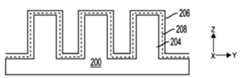
이제 도 2a 내지 도 2f를 참조하면, 기판을 에칭하기 위하여 지향성 ALE 또는 선택적 ALE를 수행하기 위한 본 개시의 실시예들에 따른 하나의 시나리오가 도시된다. 다양한 실시예들에 있어서, 지향성 ALE는 시스템(100) 또는 시스템(150)과 같은 시스템을 사용하여 수행될 수 있다. 도 2a에서, 반응성 가스(202)가 기판(200)으로 보내지는 제 1 인스턴스가 도시된다. 예시의 목적을 위하여, 기판(200)은 실리콘일 수 있다. 기판(200)은, 기판(200)의 기판 평면(212)으로부터 연장하는 기판 특징부들(204)로서 도시된 기판 특징부들의 어레이를 포함할 수 있다. 예를 들어, 기판 특징부들(204)은 일부 실시예들에 있어서 라인 구조체들, 핀(fin)들 또는 메사(mesa)들일 수 있다. 도 2a의 예시에서, 기판(200)은 평평한 부분 및 기판 특징부들(204)이 실리콘인 단일 구조체일 수 있다. 반응성 가스(202)는, 도 2b에 도시된 바와 같이 생성물 층(206)을 형성하기 위하여 실리콘과 반응할 수 있다. 생성물 층(206)은 일부 경우들에서 재료의 단분자층일 수 있으며, 일부 경우들에 있어서는 반응성 가스(202)로부터의 종뿐만 아니라 기판(200) 내의 재료로부터 형성될 수 있다. 기판(200)의 원래의 표면(208)이 도 2b에 도시된다. 예시된 바와 같이, 생성물 층(206)은 기판(200) 내로 연장할 수 있다.Referring now to FIGS. 2A-2F , one scenario according to embodiments of the present disclosure for performing directional ALE or selective ALE to etch a substrate is illustrated. In various embodiments, directional ALE may be performed using a system, such as system (100) or system (150). In FIG. 2A , a first instance is illustrated where a reactive gas (202) is directed to a substrate (200). For illustrative purposes, the substrate (200) may be silicon. The substrate (200) may include an array of substrate features, illustrated as substrate features (204) extending from a substrate plane (212) of the substrate (200). For example, the substrate features (204) may be line structures, fins, or mesas in some embodiments. In the example of FIG. 2a, the substrate (200) can be a single structure having a flat portion and substrate features (204) of silicon. The reactive gas (202) can react with the silicon to form a product layer (206), as illustrated in FIG. 2b. The product layer (206) can in some cases be a monolayer of material, and in some cases can be formed from material within the substrate (200) as well as species from the reactive gas (202). An original surface (208) of the substrate (200) is illustrated in FIG. 2b. As illustrated, the product layer (206) can extend into the substrate (200).
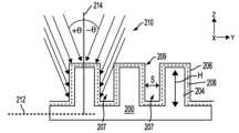
이제 도 2c를 참조하면, 생성물 층(206)의 형성 이후에 이온들(210)이 기판(200)으로 보내지는 추가적인 인스턴스가 도시된다. 일부 실시예들에 있어서, 이온들(210)은, 도시된 바와 같이 기판 평면(212)에 대한 수선(214)에 대하여 비-제로(non-zero) 입사각 +θ 및 입사각 -θ를 형성하는 플라즈마 빔들의 쌍으로서 보내질 수 있다. 특정 실시예들에 있어서, 입사각 +θ 및 입사각 -θ의 절대값이 동일하다. 이온들(210)은 일부 실시예들에서 비활성 가스 이온들일 수 있으며, 여기에서 비활성 가스 이온들은 생성물 층(206)을 에칭하기에 적절한 이온 에너지를 갖는다. 이온들(210)은, 생성물 층(206) 아래의 영역들에서 기판(200)을 에칭하지 않는 이온 에너지 및 이온 도우즈(dose)로 제공될 수 있다. 도 2c에 추가로 예시된 바와 같이, 이온들(210)의 지향성 및 기판 특징부들(204)의 형상은 이온들(210)에 대한 기판(200)의 특정 표면들 또는 부분들의 선택적인 노출을 야기할 수 있으며, 반면 다른 부분들은 이온들(210)에 노출되지 않는다. 도 2c에 의해 제안되는 예와 같이, 기판 특징부들(204)은 높이 H를 가지며 거리 S에 의해 서로 이격되는 특징부들의 어레이로서 배열될 수 있다. 따라서, 이온들(210)이 수선(214)에 대하여 비-제로 입사각으로 보내질 때, 인접한 기판 특징부들이 서로 차단(shadow)할 수 있으며, 이는 이온들(210)이 기판(200)의 특정 영역들 상에 충돌하는 것을 방지한다. 도 2c에 예시된 예에 있어서, 이온들(210)은 적어도 기판 특징부들(204)의 어레이의 영역 내에서 X-Y 평면에 놓인 수평 표면들 상에 충돌하는 것이 차단될 수 있다. 이러한 차단 때문에, 인접한 기판 특징부들 사이의 트렌치(trench)들(207)로서 도시된 트렌치 영역들 내의 또는 수평 표면들 상의 생성물 층(206)의 부분들과 같은 기판(200)의 노출되지 않은 부분들이 에칭되지 않은 채로 남아 있을 수 있다.Referring now to FIG. 2c , an additional instance is illustrated where ions (210) are sent to the substrate (200) after formation of the product layer (206). In some embodiments, the ions (210) may be sent as a pair of plasma beams forming a non-zero angle of incidence +θ and an angle of incidence -θ with respect to a perpendicular (214) to the substrate plane (212), as illustrated. In certain embodiments, the absolute values of the angle of incidence +θ and the angle of incidence -θ are equal. The ions (210) may in some embodiments be noble gas ions, wherein the noble gas ions have an ion energy suitable for etching the product layer (206). The ions (210) may be provided at an ion energy and ion dose that do not etch the substrate (200) in regions beneath the product layer (206). As further illustrated in FIG. 2c, the directionality of the ions (210) and the shape of the substrate features (204) can cause selective exposure of certain surfaces or portions of the substrate (200) to the ions (210), while other portions are not exposed to the ions (210). As suggested by FIG. 2c, the substrate features (204) can be arranged as an array of features having a height H and spaced apart from each other by a distance S. Thus, when the ions (210) are directed at a non-zero angle of incidence with respect to the waterline (214), adjacent substrate features can shadow each other, preventing the ions (210) from impinging on certain regions of the substrate (200). In the example illustrated in FIG. 2c, ions (210) may be blocked from impinging on horizontal surfaces lying in the X-Y plane at least within the region of the array of substrate features (204). Because of this blocking, unexposed portions of the substrate (200), such as portions of the product layer (206) within trench regions depicted as trenches (207) between adjacent substrate features or on horizontal surfaces, may remain unetched.
이제 도 2d를 참조하면, 도 2c에 도시된 인스턴스 다음의 인스턴스가 도시된다. 도 2d에서, 기판(200)은 기판 특징부들(204)을 포함하며, 여기에서 Y-축을 따른 기판 특징부들(204)의 두께는 도 2a에서보다 더 좁고, 반면 트렌치들(207)은 에칭되지 않은 채로 남아 있다. 도 2e 및 도 2f에 추가로 도시된 바와 같이, 지향성 ALE의 에칭 사이클을 포함하는 도 2b 및 도 2c의 동작들이 반복될 수 있다. 도 2e에서, 적어도 하나의 추가적인 에칭 사이클 이후의 기판(200)의 구조체가 도시되며, 여기에서 기판 특징부들(204)은 두께가 추가로 감소되지만 반면 트렌치들(207)은 계속해서 에칭되지 않은 채로 남아 있다. 도 2f에서, 적어도 하나의 추가적인 에칭 사이클이 도 2e의 구조체 상에 수행된 이후의 기판(200)의 구조체가 도시되며, 여기에서 기판 특징부들(204)은 두께가 추가로 감소되지만 반면 트렌치들(207)은 계속해서 에칭되지 않은 채로 남아 있다.Referring now to FIG. 2d , an instance subsequent to the instance depicted in FIG. 2c is depicted. In FIG. 2d , the substrate (200) includes substrate features (204), wherein the thickness of the substrate features (204) along the Y-axis is narrower than in FIG. 2a , while the trenches (207) remain unetched. As further illustrated in FIGS. 2e and 2f , the operations of FIGS. 2b and 2c including an etch cycle of directional ALE can be repeated. In FIG. 2e , the structure of the substrate (200) is depicted after at least one additional etch cycle, wherein the substrate features (204) are further reduced in thickness while the trenches (207) continue to remain unetched. In FIG. 2f, the structure of the substrate (200) is depicted after at least one additional etching cycle has been performed on the structure of FIG. 2e, wherein the substrate features (204) are further reduced in thickness while the trenches (207) remain unetched.
다시 도 2c를 참조하면, 다른 실시예들에 있어서, 이온들(210)의 입사각은 수선(214)에 대하여 더 큰 비-제로 입사각으로 조정될 수 있으며, 따라서 단지 측벽들(209)의 부분들만이 예컨대 상단 부분들만이 이온들(210)에 노출된다. 이러한 방식으로, 지향성 ALE가 기판 특징부들의 상단 부분들만을 에칭하도록 적용될 수 있다.Referring again to FIG. 2c, in other embodiments, the angle of incidence of the ions (210) can be adjusted to a larger non-zero angle of incidence with respect to the waterline (214), such that only portions of the sidewalls (209), for example only the top portions, are exposed to the ions (210). In this manner, directional ALE can be applied to etch only the top portions of the substrate features.
또 다른 추가적인 실시예들에 있어서, 이온들은, 기판(200)의 수평 표면들이 에칭되지만 반면 측벽들(209)은 에칭되지 않은 채로 남아 있도록 수선(214)을 따라 보내질 수 있다. 이러한 수선 지향성은 공지된 ALE 기술들에 비하여 탁월한 "수직" 원자층 에칭 프로세스를 제공할 수 있다. 공지된 ALE 기술들에 있어서, 프로세싱 조건들은 에칭 이온들이 제어되지 않은 방식으로 각도들의 범위에 걸쳐 기판 상에 충돌하는 것을 야기하는 가스 상 산란(gas phase scattering)을 수반하며, 따라서 기판 특징부들의 고도의 수직 에칭이 용이하게 달성되지 않을 수 있다.In yet further embodiments, the ions may be directed along a perpendicular (214) such that the horizontal surfaces of the substrate (200) are etched while the sidewalls (209) remain unetched. This perpendicular directivity may provide a superior “vertical” atomic layer etch process compared to known ALE techniques. In known ALE techniques, the processing conditions involve gas phase scattering which causes the etching ions to impinge on the substrate over a range of angles in an uncontrolled manner, and thus high vertical etching of substrate features may not be readily achieved.
도 3은 지향성 ALE(D-ALE)를 가능하게 하기 위한 시스템(300)의 일 실시예를 제시한다. 기판(1)이 프로세싱 챔버(102) 내에 제공될 수 있다. 기판(1)은 기판 스테이지(2)에 클램핑(clamp)될 수 있으며, 여기에서 기판 스테이지(2)는 이동이 가능하여 기판(1)이 반응성 가스를 가로채기 위하여 위쪽으로 이동할 수 있다. 반응성 가스는, 예를 들어, 조정가능(tunable) 반응성 가스 소스(3) 및 조정가능 반응성 가스 소스(4)에 의해 제공될 수 있다. UV 방사 소스(들)(21)은 UV 방사(22)를 보낼 수 있으며, 여기에서 UV 방사는 기판(1)이 위쪽으로 추가로 스캔될 때 기판(1)에 의해 가로채어 진다. 기판(1)은 추가로, 이온 빔들(7)로서 도시되며 플라즈마 챔버(24) 내에서 형성된 플라즈마(6)로부터 추출되는 이중 각도 이온 빔들에 노출될 수 있다. 기판(1)은 조정가능 반응성 가스 소스(4)로서 또한 도시된 제 2 조정가능 반응성 가스 소스에 의해 출력되는 반응성 가스의 제 2 스트림을 가로채기 위하여 추가로 스캔될 수 있다. 시스템(300)은 이온들의 입사각의 범위뿐만 아니라 주어진 입사각에서의 이온들의 상대적인 양을 의미하는 제어가능 이온 에너지 및 각도 분포로 이온 빔들(7)을 제공할 수 있다. 이온 빔들(7)은 전반적으로 이상에서 설명된 바와 같은 추출 플레이트(9)로 구성된 추출 광학부에 의해 추출될 수 있다. 시스템(300)은 또한 이상에서 설명된 바와 같은 빔 차단기(18)뿐만 아니라 편향 전극(10)을 포함할 수 있다.FIG. 3 presents one embodiment of a system (300) for enabling directional ALE (D-ALE). A substrate (1) may be provided within a processing chamber (102). The substrate (1) may be clamped to a substrate stage (2) that is movable such that the substrate (1) may move upward to intercept a reactive gas. The reactive gas may be provided, for example, by a tunable reactive gas source (3) and a tunable reactive gas source (4). UV radiation source(s) (21) may send UV radiation (22) that is intercepted by the substrate (1) as the substrate (1) is further scanned upward. The substrate (1) may additionally be exposed to dual-angle ion beams, illustrated as ion beams (7) and derived from a plasma (6) formed within a plasma chamber (24). The substrate (1) may be additionally scanned to intercept a second stream of reactive gas output by a second adjustable reactive gas source, also illustrated as a controllable reactive gas source (4). The system (300) may provide ion beams (7) with controllable ion energy and angular distribution, which means a range of incident angles of the ions as well as the relative amount of ions at a given incident angle. The ion beams (7) may be extracted by extraction optics, which generally comprise an extraction plate (9) as described above. The system (300) may also include a deflection electrode (10) as well as a beam blocker (18) as described above.
플라즈마(6)는, rf 안테나(11)로부터의 rf 전력을 유전체 rf 윈도우(12)를 통해 가스 혼합물에 결합시키고 있는 동안 가스 매니폴드(manifold)(5)로부터 플라즈마 챔버(24) 내로의 주어진 가스 혼합물의 투입에 의해 생성될 수 있다. 방전을 점화하고 유지하기 위한 rf 전력은 rf 생성기(13)에 의해 매칭 네트워크(14)를 통해서 제공될 수 있다. 이온 빔들(7) 내의 이온들의 이온 에너지는 펄스화 dc 전원 공급장치(15)에 의해 제어될 수 있고, 여기에서 펄스화 dc 전원 공급장치는 플라즈마 챔버(24)를 상승된 포지티브 정전 전위로 유지할 수 있으며 반면 기판 스테이지(2) 및 기판(1)은 접지 전위로 유지될 수 있다. 시스템(300)은 편향 전극(10)에 결합된 편향 전압 공급부(16)로서 도시된 dc 전원 공급장치를 더 포함할 수 있다. 이온 빔들(7) 내의 이온들의 이온 각도 분포는, 편향 전압 공급부(16)로부터 편향 전극으로 인가되는 네거티브 바이어스 전압을 변화시킴으로써 제어될 수 있다. 구체적으로, 편향 전극(10)은 빔 차단기(18)에 인접하여 배치될 수 있으며, 여기에서 빔 차단기(18)는 플라즈마 챔버(24)와 편향 전극(10) 사이에 배치된다. 편향 전극(10)에 인가되는 전압은, 이온 빔들(7)이 플라즈마(6)로부터 추출될 때 이온 빔들(7)을 편향시키는 전기장을 생성할 수 있다. 특히, 이는, 편향 전극(10)에 대한 편향 전압이 변화될 때 이온 빔들(7)의 입사각을 변화시키도록 역할할 수 있다. 따라서 편향 전극(10)은 단지 전압을 변화시킴으로써 ALE에 의해 에칭되는 기판의 부분들을 편리하게 변화시킬 수 있는 능력을 제공할 수 있다. 다양한 실시예들에 있어서, 전압의 이러한 변화는 기판 또는 기판들의 그룹의 프로세싱 동안 동적인 방식으로 수행될 수 있다.The plasma (6) can be generated by introduction of a given gas mixture from a gas manifold (5) into the plasma chamber (24) while coupling RF power from an RF antenna (11) to the gas mixture through a dielectric RF window (12). RF power to ignite and sustain the discharge can be provided by an RF generator (13) through a matching network (14). The ion energy of the ions within the ion beams (7) can be controlled by a pulsed dc power supply (15), wherein the pulsed dc power supply can maintain the plasma chamber (24) at an elevated positive electrostatic potential while the substrate stage (2) and the substrate (1) can be maintained at ground potential. The system (300) can further include a dc power supply, illustrated as a bias voltage supply (16) coupled to the bias electrode (10). The ion angle distribution of the ions within the ion beams (7) can be controlled by varying the negative bias voltage applied from the deflection voltage supply (16) to the deflection electrode. Specifically, the deflection electrode (10) can be positioned adjacent to the beam blocker (18), wherein the beam blocker (18) is positioned between the plasma chamber (24) and the deflection electrode (10). The voltage applied to the deflection electrode (10) can generate an electric field that deflects the ion beams (7) as they are extracted from the plasma (6). In particular, this can serve to vary the angle of incidence of the ion beams (7) when the deflection voltage to the deflection electrode (10) is varied. Thus, the deflection electrode (10) can provide the ability to conveniently vary the portions of the substrate being etched by ALE simply by varying the voltage. In various embodiments, this variation of voltage can be performed in a dynamic manner during the processing of a substrate or a group of substrates.
저 에너지 이온들 및 반응물들, 플라즈마 챔버(24)로부터의 여기된 분자들 및 라디칼들에 대한 노출 동안, 조정가능 반응성 가스 소스(3) 또는 조정가능 반응성 가스 소스(4)에 대한 노출에 의해 형성된 생성물 단분자층이 에칭될 수 있다. 이온 및 라디칼 플럭스(flux)는 rf 방전으로 전달되는 전력 및/또는 가스 흐름 레이트 중 하나를 조정함으로써 제어될 수 있다. 기판(1)이 받는 조사 도우즈는 Y-축에 평행한 방향을 따른 스캔 속도를 조정함으로써 조정될 수 있다. 독립적인 이온 충돌에 더하여, 특정 반응들에 대하여, UV 광자 조사가 표면 생성물 층의 제거를 위하여 도움이 될 수 있다. UV 방사에 의해 제공되는 수 eV의 광자 에너지는, 기판(1)의 표면 상에 배치된 생성물 층의 단분자층 아래의 재료에 영향을 주지 않으면서 표면 결합들의 파괴를 가능하게 한다. 따라서, UV 방사 소스(들)(21) 중 적어도 하나는 UV 방사(22)를 생성하기 위하여 이용될 수 있다. 최대 300 mm에 이르는 치수들을 갖는 기판들을 프로세싱하기 위한 일부 실시예들에 있어서, UV 방사 소스들(21)은 기판 폭 전체를 균일하게 조사하기 위하여 350 mm만큼 X-축에 평행한 방향으로 연장할 수 있다. 광자 플럭스는 UV 방사 소스들(21)로 전달되는 전력을 조정함으로써 조정될 수 있으며, 반면 조사 도우즈는 Y-축을 따른 스캔 속도를 조정함으로써 조정될 수 있다. 일부 실시예들에 있어서, 기판(1)은 위치 A로부터 위치 B로 그리고 위치 C로 그리고 위치 D로 스캔 방향을 따라서 스캔될 수 있으며, 여기에서 기판(1)은 조정가능 반응성 가스 소스(4)로서 또한 도시된 제 2 조정가능 반응성 가스 소스에 노출될 수 있다. 일부 실시예들에 있어서, 기판(1)은 연속적인 방식으로 스캔될 수 있다. 지향성 ALE 에칭 사이클은 한 번에 위치 A로부터 위치 B로 그리고 위치 C로 그리고 위치 D로 스캔 방향을 따라서 기판을 스캔함으로써 완료될 수 있다. 이러한 에칭 사이클은 기판(1)으로부터 목표 두께의 재료를 에칭하기 위해 필요한 만큼 반복될 수 있다. 일부 변형예들에 있어서, 도 1a와 관련하여 이상에서 논의된 바와 같이 가스 흐름 제한기가 시스템(300) 내에 제공될 수 있다.During exposure to low energy ions and reactants, excited molecules and radicals from the plasma chamber (24), a product monolayer formed by exposure to the adjustable reactive gas source (3) or the adjustable reactive gas source (4) can be etched. The ion and radical flux can be controlled by adjusting either the power delivered to the rf discharge and/or the gas flow rate. The irradiation dose received by the substrate (1) can be adjusted by adjusting the scan speed along the direction parallel to the Y-axis. In addition to the independent ion bombardment, for certain reactions, UV photon irradiation can be helpful for the removal of the surface product layer. The photon energy of several eV provided by UV radiation allows for the breakdown of surface bonds without affecting the material beneath the monolayer of the product layer disposed on the surface of the substrate (1). Thus, at least one of the UV radiation source(s) (21) can be used to generate UV radiation (22). In some embodiments for processing substrates having dimensions up to 300 mm, the UV radiation sources (21) can extend parallel to the X-axis by 350 mm to uniformly irradiate the entire substrate width. The photon flux can be adjusted by adjusting the power delivered to the UV radiation sources (21), while the irradiation dose can be adjusted by adjusting the scan speed along the Y-axis. In some embodiments, the substrate (1) can be scanned along the scan direction from position A to position B to position C to position D, where the substrate (1) can be exposed to a second adjustable reactive gas source, also illustrated as the adjustable reactive gas source (4). In some embodiments, the substrate (1) can be scanned in a continuous manner. A directional ALE etch cycle can be completed by scanning the substrate along the scan direction from position A to position B to position C to position D in one pass. This etching cycle can be repeated as many times as necessary to etch a target thickness of material from the substrate (1). In some variations, a gas flow restrictor may be provided within the system (300) as discussed above with respect to FIG. 1A.
도 4는 본 개시의 실시예들에 따른 예시적인 프로세스 흐름(400)을 도시한다. 블록(402)에서, 기판이 프로세스 챔버 내에 배치될 때 반응성 가스를 기판으로 보내는 동작이 수행되며, 여기에서 반응성 가스 및 기판으로부터의 재료를 포함하는 제 1 생성물 층이 기판의 외부 표면 상에 형성된다. 블록(404)에서, 플라즈마 챔버로부터 추출 개구를 통해 기판의 노출된 부분으로 리본 빔을 보내는 동작이 수행되며, 리본 빔은 제 1 방향을 따른 장축을 갖는다. 블록(406)에서, 반응성 가스를 보내고 리본 빔을 보내는 동안 제 1 방향에 수직인 제 2 방향을 따라서 기판을 스캔하는 동작이 수행되며, 여기에서 제 1 생성물 층은 노출된 부분에서 기판으로부터 에칭되며 리본 빔에 노출되지 않는 노출되지 않은 부분에서 기판으로부터 에칭되지 않는다.FIG. 4 illustrates an exemplary process flow (400) according to embodiments of the present disclosure. At block (402), an operation is performed in which a reactive gas is directed to the substrate when the substrate is placed within a process chamber, wherein a first product layer comprising the reactive gas and material from the substrate is formed on an outer surface of the substrate. At block (404), an operation is performed in which a ribbon beam is directed through an extraction opening from the plasma chamber into an exposed portion of the substrate, wherein the ribbon beam has a longitudinal axis along a first direction. At block (406), an operation is performed in which the substrate is scanned along a second direction perpendicular to the first direction while directing the reactive gas and directing the ribbon beam, wherein the first product layer is etched from the substrate in exposed portions and is not etched from the substrate in unexposed portions that are not exposed to the ribbon beam.
본 실시예들은 기판 내에 특징부들을 획정하기 위한 통상적인 프로세싱을 뛰어 넘는 다양한 이점들을 제공한다. 하나의 이점은, 반응성 가스에 대한 노출 이후에 제거(purge)하는 단계를 수행해야 할 필요 없이 원자층 에칭을 수행하여 더 높은 스루풋 프로세스를 제공하는 능력이다. 다른 이점은, 기판으로 보내지는 이온 빔들의 입사각의 제어에 의해 ALE 프로세스를 사용하여 기판의 선택된 표면들 또는 영역들을 선택적으로 에칭하기 위한 능력이다.The present embodiments provide several advantages over conventional processing for defining features within a substrate. One advantage is the ability to perform atomic layer etching without the need for a purge step following exposure to a reactive gas, thereby providing a higher throughput process. Another advantage is the ability to selectively etch selected surfaces or regions of a substrate using an ALE process by controlling the angle of incidence of the ion beams directed to the substrate.
본 개시는 본원에서 설명된 특정 실시예에 의해 범위가 제한되지 않는다. 오히려, 본원에서 설명된 실시예들에 더하여, 본 개시의 다른 다양한 실시예들 및 이에 대한 수정예들이 이상의 설명 및 첨부된 도면들로부터 당업자들에게 자명해질 것이다. 따라서, 이러한 다른 실시예들 및 수정예들이 본 개시의 범위 내에 속하도록 의도된다. 추가로, 본 개시가 본원에서 특정 목적을 위한 특정 환경에서의 특정 구현예의 맥락에서 설명되었지만, 당업자들은 그 유용함이 이에 한정되지 않으며, 본 개시가 임의의 수의 목적들을 위한 임의의 수의 환경들에서 유익하게 구현될 수 있다는 것을 인식할 것이다. 따라서, 이하에서 기술되는 청구항들은 본원에서 설명된 바와 같은 본 개시의 완전한 폭과 사상의 관점에서 해석되어야만 한다.The present disclosure is not limited in scope by the specific embodiments described herein. Rather, in addition to the embodiments described herein, various other embodiments of the present disclosure and modifications thereof will become apparent to those skilled in the art from the foregoing description and the accompanying drawings. Accordingly, it is intended that such other embodiments and modifications fall within the scope of the present disclosure. Additionally, while the present disclosure has been described herein in the context of specific implementations in particular environments for particular purposes, those skilled in the art will recognize that its utility is not limited thereto, but that the present disclosure may be beneficially implemented in any number of environments for any number of purposes. Accordingly, the claims set forth below should be interpreted in light of the full breadth and spirit of the present disclosure as set forth herein.
Claims (15)
Translated fromKorean프로세스 챔버 내에 배치되는 반응성 가스 출구를 갖는 반응성 가스 소스로서, 상기 반응성 가스 출구는 제 1 반응성 가스를 상기 기판으로 보내기 위한 것인, 상기 반응성 가스 소스;
제 1 방향을 따라 연장하는 추출 개구를 갖는 추출 플레이트를 포함하는 플라즈마 챔버;
상기 프로세스 챔버 내에 배치되며 상기 반응성 가스 소스를 향하는 제 1 위치와 상기 추출 개구를 향하는 제 2 위치 사이에서 상기 제 1 방향에 수직인 제 2 방향을 따라 이동이 가능한, 상기 기판을 홀딩하도록 구성된 기판 스테이지; 및
상기 반응성 가스 출구와 상기 추출 개구 사이에 배치되는 가스 흐름 제한기로서, 상기 가스 흐름 제한기는 적어도 상기 플라즈마 챔버와 상기 기판 스테이지 사이에 차동 펌핑 채널(differential pumpingchannel)을 획정(define)하는, 상기 가스 흐름 제한기를 포함하며,
상기 반응성 가스 소스는 제 1 반응성 가스 소스이며, 상기 장치는 상기 기판으로 상기 제 1 반응성 가스를 보내는 제 2 출구를 갖는 제 2 반응성 가스 소스를 더 포함하고, 상기 플라즈마 챔버는 상기 제 1 반응성 가스 소스와 상기 제 2 반응성 가스 소스 사이에 배치되며, 상기 기판 스테이지는 상기 제 1 위치, 제 2 위치 및 상기 제 2 반응성 가스 소스를 향하는 제 3 위치 사이에서 순차적으로 이동이 가능한, 장치.
As a device for processing a substrate,
A reactive gas source having a reactive gas outlet disposed within a process chamber, the reactive gas outlet sending a first reactive gas to the substrate;
A plasma chamber comprising an extraction plate having an extraction opening extending along a first direction;
a substrate stage configured to hold the substrate, the substrate stage being positioned within the process chamber and being moveable along a second direction perpendicular to the first direction between a first position facing the reactive gas source and a second position facing the extraction opening; and
A gas flow restrictor disposed between the reactive gas outlet and the extraction opening, the gas flow restrictor including the gas flow restrictor defining a differential pumping channel at least between the plasma chamber and the substrate stage,
The device wherein the reactive gas source is a first reactive gas source, the device further comprises a second reactive gas source having a second outlet for sending the first reactive gas to the substrate, the plasma chamber is disposed between the first reactive gas source and the second reactive gas source, and the substrate stage is sequentially moveable between the first position, the second position, and a third position facing the second reactive gas source.
상기 장치는 플라즈마 챔버에 결합된 펌핑 포트 및 상기 펌핑 포트에 연결된 플라즈마 챔버 펌프를 더 포함하는, 장치.
In claim 1,
The device further comprises a pumping port coupled to the plasma chamber and a plasma chamber pump connected to the pumping port.
상기 장치는 상기 프로세스 챔버를 배기시키기 위하여 상기 프로세스 챔버에 결합된 프로세스 챔버 펌프를 더 포함하며, 상기 차동 펌핑 채널 내의 제 1 압력은 상기 추출 개구와 기판 스테이지 사이의 영역 내의 제 2 압력보다 더 작은, 장치.
In claim 1,
The device further comprises a process chamber pump coupled to the process chamber for evacuating the process chamber, wherein a first pressure within the differential pumping channel is less than a second pressure within a region between the extraction opening and the substrate stage.
상기 장치는 비활성 가스를 상기 플라즈마 챔버에 제공하기 위하여 상기 플라즈마 챔버에 결합된 비활성 가스 소스를 더 포함하는, 장치.
In claim 1,
The device further comprises an inert gas source coupled to the plasma chamber for providing an inert gas to the plasma chamber.
상기 장치는 상기 플라즈마 내에 그리고 상기 추출 개구에 인접하여 배치되는 빔 차단기를 더 포함하며, 상기 빔 차단기는 제 1 추출 개구 및 제 2 추출 개구를 획정하는, 장치.
In claim 1,
The device further comprises a beam blocker positioned within the plasma and adjacent the extraction aperture, the beam blocker defining a first extraction aperture and a second extraction aperture.
상기 추출 개구는 상기 제 1 방향을 따라 100 mm 내지 400 mm의 폭 및 상기 제 2 방향을 따라 2 mm 내지 30 mm의 길이를 갖는, 장치.
In claim 1,
A device wherein the extraction opening has a width of 100 mm to 400 mm along the first direction and a length of 2 mm to 30 mm along the second direction.
상기 기판이 프로세스 챔버 내에 배치될 때 반응성 가스를 상기 기판으로 보내는 단계로서, 상기 반응성 가스 및 상기 기판으로부터의 재료를 포함하는 제 1 생성물 층이 상기 기판의 외부 표면 상에 형성되는, 단계;
추출 개구를 통해 플라즈마 챔버로부터 이온 빔을 추출하는 단계로서, 상기 이온 빔은 상기 기판의 노출된 부분에 충돌하는, 단계; 및
상기 추출 개구에 대하여 스캔 방향을 따라 상기 기판을 홀딩하는 기판 스테이지를 스캔하는 단계를 포함하며,
상기 제 1 생성물 층은 노출된 부분에서 상기 기판으로부터 에칭되고 상기 기판의 노출되지 않은 부분에서 상기 기판으로부터 에칭되지 않으며, 상기 노출되지 않은 부분은 상기 이온 빔에 노출되지 않고,
상기 반응성 가스를 상기 기판으로 보내는 단계는 반응성 가스 출구를 통해 상기 플라즈마 챔버 내로 상기 반응성 가스를 전달하는 단계로서, 상기 반응성 가스는 상기 추출 개구를 통해 상기 기판으로 흐르는, 단계를 포함하며,
상기 방법은,
상기 반응성 가스 출구로 개방 신호를 전송하고 상기 반응성 가스 출구가 개방될 때 상기 플라즈마 챔버에 대하여 상기 기판을 포지티브하게 바이어싱하기 위한 포지티브 바이어스 신호를 전송하는 단계; 및
상기 반응성 가스 출구가 폐쇄될 때 상기 플라즈마 챔버에 대하여 상기 기판 스테이지를 네거티브하게 바이어싱하기 위한 네거티브 바이어스 신호를 전송하는 단계를 더 포함하는, 방법.
A method of etching a substrate,
A step of sending a reactive gas to the substrate when the substrate is placed in a process chamber, wherein a first product layer including the reactive gas and a material from the substrate is formed on an outer surface of the substrate;
A step of extracting an ion beam from a plasma chamber through an extraction opening, wherein the ion beam collides with an exposed portion of the substrate; and
A step of scanning a substrate stage holding the substrate along a scan direction with respect to the above extraction opening,
The first product layer is etched from the substrate at exposed portions and is not etched from the substrate at unexposed portions of the substrate, the unexposed portions being not exposed to the ion beam,
The step of sending the reactive gas to the substrate includes the step of delivering the reactive gas into the plasma chamber through the reactive gas outlet, wherein the reactive gas flows to the substrate through the extraction opening,
The above method,
A step of transmitting an open signal to the reactive gas outlet and transmitting a positive bias signal for positively biasing the substrate with respect to the plasma chamber when the reactive gas outlet is opened; and
A method further comprising the step of transmitting a negative bias signal to negatively bias the substrate stage with respect to the plasma chamber when the reactive gas outlet is closed.
상기 이온 빔은 기판 평면에 대한 수선에 대하여 비-제로 입사각을 형성하는, 방법.
In claim 10,
A method wherein the ion beam forms a non-zero angle of incidence with respect to a perpendicular to the substrate plane.
상기 이온 빔은 상기 스캔 방향에 수직인 제 1 방향을 따른 장축을 포함하는, 방법.
In claim 10,
A method wherein the ion beam comprises a longitudinal axis along a first direction perpendicular to the scan direction.
상기 방법은,
상기 반응성 가스 출구와 상기 추출 개구 사이에 가스 흐름 제한기를 배치하는 단계로서, 상기 가스 흐름 제한기는 적어도 상기 플라즈마 챔버와 기판 스테이지 사이에 차동 펌핑 채널을 획정하는, 단계; 및
상기 차동 펌핑 채널을 통해 상기 반응성 가스 출구로부터 상기 반응성 가스를 배기시키는 단계를 더 포함하는, 방법.In claim 10,
The above method,
A step of arranging a gas flow restrictor between the reactive gas outlet and the extraction opening, wherein the gas flow restrictor defines a differential pumping channel at least between the plasma chamber and the substrate stage; and
A method further comprising the step of exhausting the reactive gas from the reactive gas outlet through the differential pumping channel.
Applications Claiming Priority (5)
| Application Number | Priority Date | Filing Date | Title |
|---|---|---|---|
| US201562202261P | 2015-08-07 | 2015-08-07 | |
| US62/202,261 | 2015-08-07 | ||
| US14/970,738 | 2015-12-16 | ||
| US14/970,738US9706634B2 (en) | 2015-08-07 | 2015-12-16 | Apparatus and techniques to treat substrates using directional plasma and reactive gas |
| PCT/US2016/042497WO2017027165A1 (en) | 2015-08-07 | 2016-07-15 | Apparatus and techniques to treat substrates using directional plasma and reactive gas |
Publications (2)
| Publication Number | Publication Date |
|---|---|
| KR20180029261A KR20180029261A (en) | 2018-03-20 |
| KR102699441B1true KR102699441B1 (en) | 2024-08-28 |
Family
ID=57983531
Family Applications (1)
| Application Number | Title | Priority Date | Filing Date |
|---|---|---|---|
| KR1020187006174AActiveKR102699441B1 (en) | 2015-08-07 | 2016-07-15 | Device and system for processing a substrate, and method for etching a substrate |
Country Status (6)
| Country | Link |
|---|---|
| US (2) | US9706634B2 (en) |
| JP (1) | JP6866350B2 (en) |
| KR (1) | KR102699441B1 (en) |
| CN (1) | CN107924838B (en) |
| TW (1) | TWI697047B (en) |
| WO (1) | WO2017027165A1 (en) |
Families Citing this family (39)
| Publication number | Priority date | Publication date | Assignee | Title |
|---|---|---|---|---|
| US20160225652A1 (en) | 2015-02-03 | 2016-08-04 | Applied Materials, Inc. | Low temperature chuck for plasma processing systems |
| US10128082B2 (en) | 2015-07-24 | 2018-11-13 | Varian Semiconductor Equipment Associates, Inc. | Apparatus and techniques to treat substrates using directional plasma and point of use chemistry |
| US9865484B1 (en)* | 2016-06-29 | 2018-01-09 | Applied Materials, Inc. | Selective etch using material modification and RF pulsing |
| US10141161B2 (en)* | 2016-09-12 | 2018-11-27 | Varian Semiconductor Equipment Associates, Inc. | Angle control for radicals and reactive neutral ion beams |
| US10730082B2 (en)* | 2016-10-26 | 2020-08-04 | Varian Semiconductor Equipment Associates, Inc. | Apparatus and method for differential in situ cleaning |
| US10684407B2 (en) | 2017-10-30 | 2020-06-16 | Facebook Technologies, Llc | Reactivity enhancement in ion beam etcher |
| WO2019089639A1 (en)* | 2017-10-30 | 2019-05-09 | Facebook Technologies, Llc | H2-assisted slanted etching of high refractive index material |
| US10815570B2 (en)* | 2017-11-13 | 2020-10-27 | Denton Vacuum, L.L.C. | Linearized energetic radio-frequency plasma ion source |
| EP3843123A1 (en)* | 2017-12-20 | 2021-06-30 | The Swatch Group Research and Development Ltd | Installation for implementing a method for implanting ions on a surface of an object to be treated |
| US10761330B2 (en) | 2018-01-23 | 2020-09-01 | Facebook Technologies, Llc | Rainbow reduction in waveguide displays |
| US10914954B2 (en) | 2018-08-03 | 2021-02-09 | Facebook Technologies, Llc | Rainbow reduction for waveguide displays |
| US10845596B2 (en) | 2018-01-23 | 2020-11-24 | Facebook Technologies, Llc | Slanted surface relief grating for rainbow reduction in waveguide display |
| US10649119B2 (en) | 2018-07-16 | 2020-05-12 | Facebook Technologies, Llc | Duty cycle, depth, and surface energy control in nano fabrication |
| US11137536B2 (en) | 2018-07-26 | 2021-10-05 | Facebook Technologies, Llc | Bragg-like gratings on high refractive index material |
| JP7203531B2 (en)* | 2018-08-08 | 2023-01-13 | 東京エレクトロン株式会社 | Plasma processing method and plasma processing apparatus |
| US11257685B2 (en)* | 2018-09-05 | 2022-02-22 | Tokyo Electron Limited | Apparatus and process for electron beam mediated plasma etch and deposition processes |
| US10468226B1 (en)* | 2018-09-21 | 2019-11-05 | Varian Semiconductor Equipment Associates, Inc. | Extraction apparatus and system for high throughput ion beam processing |
| US11195703B2 (en) | 2018-12-07 | 2021-12-07 | Applied Materials, Inc. | Apparatus and techniques for angled etching using multielectrode extraction source |
| US11640909B2 (en) | 2018-12-14 | 2023-05-02 | Applied Materials, Inc. | Techniques and apparatus for unidirectional hole elongation using angled ion beams |
| US11715621B2 (en) | 2018-12-17 | 2023-08-01 | Applied Materials, Inc. | Scanned angled etching apparatus and techniques providing separate co-linear radicals and ions |
| US11150394B2 (en) | 2019-01-31 | 2021-10-19 | Facebook Technologies, Llc | Duty cycle range increase for waveguide combiners |
| US11391950B2 (en) | 2019-06-26 | 2022-07-19 | Meta Platforms Technologies, Llc | Techniques for controlling effective refractive index of gratings |
| US11056319B2 (en)* | 2019-07-29 | 2021-07-06 | Applied Materials, Inc. | Apparatus and system having extraction assembly for wide angle ion beam |
| JP2021048194A (en) | 2019-09-17 | 2021-03-25 | キオクシア株式会社 | Etching device and etching method |
| US11796922B2 (en)* | 2019-09-30 | 2023-10-24 | Taiwan Semiconductor Manufacturing Co., Ltd. | Method of manufacturing semiconductor devices |
| US11043394B1 (en)* | 2019-12-18 | 2021-06-22 | Applied Materials, Inc. | Techniques and apparatus for selective shaping of mask features using angled beams |
| CN113140458B (en)* | 2020-01-17 | 2024-03-01 | 中芯国际集成电路制造(上海)有限公司 | Method for forming semiconductor structure |
| US11270864B2 (en)* | 2020-03-24 | 2022-03-08 | Applied Materials, Inc. | Apparatus and system including extraction optics having movable blockers |
| WO2021221675A1 (en)* | 2020-04-30 | 2021-11-04 | Hzo, Inc. | Atmospheric plasma systems, apparatuses and processes |
| US11226446B2 (en) | 2020-05-06 | 2022-01-18 | Facebook Technologies, Llc | Hydrogen/nitrogen doping and chemically assisted etching of high refractive index gratings |
| KR102396275B1 (en)* | 2020-06-05 | 2022-05-09 | 성균관대학교산학협력단 | semiconductor light emitting devices and method of fabricating the same |
| US11495430B2 (en) | 2020-07-15 | 2022-11-08 | Applied Materials, Inc. | Tunable extraction assembly for wide angle ion beam |
| CN111994868B (en)* | 2020-08-12 | 2022-05-17 | 天津大学 | Extreme ultraviolet light and plasma composite atomic scale processing method |
| US11361968B2 (en)* | 2020-08-26 | 2022-06-14 | Applied Materials, Inc. | Atomic layer deposition using a substrate scanning system |
| US12014898B2 (en)* | 2021-09-27 | 2024-06-18 | Applied Materials, Inc. | Active temperature control for RF window in immersed antenna source |
| KR102475299B1 (en)* | 2021-10-29 | 2022-12-06 | 박준철 | Wafer scanning method and apparatus, and plasma nozzle and chamber used in the apparatus |
| US12125689B2 (en) | 2022-09-08 | 2024-10-22 | Applied Materials, Inc. | Methods and apparatus for toroidal plasma generation |
| US11930583B1 (en)* | 2022-09-08 | 2024-03-12 | Ali Kaddoura | Heat conditioning through deflection/reflection/absorption of electromagnetic waves |
| JP2024173298A (en)* | 2023-06-02 | 2024-12-12 | 株式会社プラズマイオンアシスト | Plasma Processing Equipment |
Citations (4)
| Publication number | Priority date | Publication date | Assignee | Title |
|---|---|---|---|---|
| JP2012529777A (en) | 2009-12-15 | 2012-11-22 | ユニバーシティ オブ ヒューストン システム | Atomic layer etching using pulsed plasma |
| US20150083581A1 (en) | 2013-09-26 | 2015-03-26 | Varian Semiconductor Equipment Associates, Inc. | Techniques for processing substrates using directional reactive ion etching |
| US20150132961A1 (en) | 2011-11-30 | 2015-05-14 | Applied Materials, Inc. | Methods For Atomic Layer Etching |
| US20150179409A1 (en)* | 2013-12-23 | 2015-06-25 | Varian Semiconductor Equipment Associates, Inc. | In situ control of ion angular distribution in a processing apparatus |
Family Cites Families (20)
| Publication number | Priority date | Publication date | Assignee | Title |
|---|---|---|---|---|
| JPH0770513B2 (en)* | 1985-05-13 | 1995-07-31 | 株式会社日立製作所 | Etching method and etching apparatus |
| JPH0478268U (en)* | 1990-11-14 | 1992-07-08 | ||
| JP4680333B2 (en)* | 1998-12-28 | 2011-05-11 | 東京エレクトロンAt株式会社 | Plasma processing method, etching method, plasma processing apparatus and etching apparatus |
| US7183219B1 (en)* | 1998-12-28 | 2007-02-27 | Tokyo Electron At Limited And Japan Science And Technology Corporation | Method of plasma processing |
| KR20000044933A (en) | 1998-12-30 | 2000-07-15 | 김영환 | Method for etching metal layer |
| US6921722B2 (en) | 2000-05-30 | 2005-07-26 | Ebara Corporation | Coating, modification and etching of substrate surface with particle beam irradiation of the same |
| US6407001B1 (en) | 2000-06-30 | 2002-06-18 | Intel Corporation | Focused ion beam etching of copper |
| FR2842388B1 (en)* | 2002-07-11 | 2004-09-24 | Cit Alcatel | METHOD AND DEVICE FOR ETCHING SUBSTRATE BY INDUCTIVE PLASMA WITH VERY HIGH POWER |
| JP2006054334A (en)* | 2004-08-12 | 2006-02-23 | Seiko Epson Corp | Semiconductor manufacturing apparatus, sputtering apparatus, dry etching apparatus, and semiconductor device manufacturing method |
| WO2008021501A2 (en) | 2006-08-18 | 2008-02-21 | Piero Sferlazzo | Apparatus and method for ultra-shallow implantation in a semiconductor device |
| US8101510B2 (en)* | 2009-04-03 | 2012-01-24 | Varian Semiconductor Equipment Associates, Inc. | Plasma processing apparatus |
| US8603591B2 (en)* | 2009-04-03 | 2013-12-10 | Varian Semiconductor Ewuipment Associates, Inc. | Enhanced etch and deposition profile control using plasma sheath engineering |
| KR20110098355A (en) | 2010-02-26 | 2011-09-01 | 성균관대학교산학협력단 | Atomic Layer Etching Method Using Neutral Beam Etching Equipment |
| US8617411B2 (en) | 2011-07-20 | 2013-12-31 | Lam Research Corporation | Methods and apparatus for atomic layer etching |
| US8288741B1 (en)* | 2011-08-16 | 2012-10-16 | Varian Semiconductor Equipment Associates, Inc. | Apparatus and method for three dimensional ion processing |
| US20150044840A1 (en)* | 2012-03-30 | 2015-02-12 | Hitachi, Ltd. | Method for producing silicon carbide semiconductor device |
| US8497486B1 (en)* | 2012-10-15 | 2013-07-30 | Varian Semiconductor Equipment Associates, Inc. | Ion source having a shutter assembly |
| US9288889B2 (en)* | 2013-03-13 | 2016-03-15 | Varian Semiconductor Equipment Associates, Inc. | Apparatus and techniques for energetic neutral beam processing |
| US9017526B2 (en)* | 2013-07-08 | 2015-04-28 | Lam Research Corporation | Ion beam etching system |
| US9576810B2 (en) | 2013-10-03 | 2017-02-21 | Applied Materials, Inc. | Process for etching metal using a combination of plasma and solid state sources |
- 2015
- 2015-12-16USUS14/970,738patent/US9706634B2/enactiveActive
- 2016
- 2016-07-13TWTW105121980Apatent/TWI697047B/enactive
- 2016-07-15CNCN201680046221.XApatent/CN107924838B/enactiveActive
- 2016-07-15JPJP2018504876Apatent/JP6866350B2/enactiveActive
- 2016-07-15KRKR1020187006174Apatent/KR102699441B1/enactiveActive
- 2016-07-15WOPCT/US2016/042497patent/WO2017027165A1/ennot_activeCeased
- 2017
- 2017-07-07USUS15/644,062patent/US10004133B2/enactiveActive
Patent Citations (4)
| Publication number | Priority date | Publication date | Assignee | Title |
|---|---|---|---|---|
| JP2012529777A (en) | 2009-12-15 | 2012-11-22 | ユニバーシティ オブ ヒューストン システム | Atomic layer etching using pulsed plasma |
| US20150132961A1 (en) | 2011-11-30 | 2015-05-14 | Applied Materials, Inc. | Methods For Atomic Layer Etching |
| US20150083581A1 (en) | 2013-09-26 | 2015-03-26 | Varian Semiconductor Equipment Associates, Inc. | Techniques for processing substrates using directional reactive ion etching |
| US20150179409A1 (en)* | 2013-12-23 | 2015-06-25 | Varian Semiconductor Equipment Associates, Inc. | In situ control of ion angular distribution in a processing apparatus |
Also Published As
| Publication number | Publication date |
|---|---|
| TWI697047B (en) | 2020-06-21 |
| CN107924838A (en) | 2018-04-17 |
| US20170042010A1 (en) | 2017-02-09 |
| JP2018523922A (en) | 2018-08-23 |
| US20170311430A1 (en) | 2017-10-26 |
| JP6866350B2 (en) | 2021-04-28 |
| CN107924838B (en) | 2021-09-07 |
| US9706634B2 (en) | 2017-07-11 |
| US10004133B2 (en) | 2018-06-19 |
| KR20180029261A (en) | 2018-03-20 |
| WO2017027165A1 (en) | 2017-02-16 |
| TW201707085A (en) | 2017-02-16 |
Similar Documents
| Publication | Publication Date | Title |
|---|---|---|
| KR102699441B1 (en) | Device and system for processing a substrate, and method for etching a substrate | |
| JP7385621B2 (en) | Ion-ion plasma atomic layer etching process and reactor | |
| TWI704845B (en) | Process chamber for cyclic and selective material removal and etching | |
| KR102691937B1 (en) | Substrate processing apparatus, system and method | |
| US8968588B2 (en) | Low electron temperature microwave surface-wave plasma (SWP) processing method and apparatus | |
| US20140034611A1 (en) | Enhanced etch and deposition profile control using plasma sheath engineering | |
| JP2018529224A5 (en) | Apparatus, system and method for processing a substrate | |
| US11075057B2 (en) | Device for treating an object with plasma | |
| KR20110135871A (en) | Plasma processing equipment | |
| KR102250213B1 (en) | In-situ spacer reshaping for self-aligned multi-patterning methods and systems | |
| TWI795794B (en) | Processing system and extraction assembly including high angle extraction optics | |
| US9514918B2 (en) | Guard aperture to control ion angular distribution in plasma processing | |
| US20220148843A1 (en) | Apparatus and system including high angle extraction optics | |
| US20140199848A1 (en) | Electron beam plasma chamber | |
| JP4342984B2 (en) | Etching method | |
| KR102868397B1 (en) | Devices and systems comprising high-angle extraction optics | |
| JPH06318564A (en) | Etching equipment |
Legal Events
| Date | Code | Title | Description |
|---|---|---|---|
| PA0105 | International application | St.27 status event code:A-0-1-A10-A15-nap-PA0105 | |
| PG1501 | Laying open of application | St.27 status event code:A-1-1-Q10-Q12-nap-PG1501 | |
| P11-X000 | Amendment of application requested | St.27 status event code:A-2-2-P10-P11-nap-X000 | |
| P13-X000 | Application amended | St.27 status event code:A-2-2-P10-P13-nap-X000 | |
| PA0201 | Request for examination | St.27 status event code:A-1-2-D10-D11-exm-PA0201 | |
| P11-X000 | Amendment of application requested | St.27 status event code:A-2-2-P10-P11-nap-X000 | |
| P13-X000 | Application amended | St.27 status event code:A-2-2-P10-P13-nap-X000 | |
| E902 | Notification of reason for refusal | ||
| PE0902 | Notice of grounds for rejection | St.27 status event code:A-1-2-D10-D21-exm-PE0902 | |
| E13-X000 | Pre-grant limitation requested | St.27 status event code:A-2-3-E10-E13-lim-X000 | |
| P11-X000 | Amendment of application requested | St.27 status event code:A-2-2-P10-P11-nap-X000 | |
| P13-X000 | Application amended | St.27 status event code:A-2-2-P10-P13-nap-X000 | |
| E701 | Decision to grant or registration of patent right | ||
| PE0701 | Decision of registration | St.27 status event code:A-1-2-D10-D22-exm-PE0701 | |
| PR0701 | Registration of establishment | St.27 status event code:A-2-4-F10-F11-exm-PR0701 | |
| PR1002 | Payment of registration fee | St.27 status event code:A-2-2-U10-U12-oth-PR1002 Fee payment year number:1 | |
| PG1601 | Publication of registration | St.27 status event code:A-4-4-Q10-Q13-nap-PG1601 |