KR102698698B1 - Semiconductor package device - Google Patents
Semiconductor package deviceDownload PDFInfo
- Publication number
- KR102698698B1 KR102698698B1KR1020190095025AKR20190095025AKR102698698B1KR 102698698 B1KR102698698 B1KR 102698698B1KR 1020190095025 AKR1020190095025 AKR 1020190095025AKR 20190095025 AKR20190095025 AKR 20190095025AKR 102698698 B1KR102698698 B1KR 102698698B1
- Authority
- KR
- South Korea
- Prior art keywords
- package
- interposer
- package substrate
- semiconductor
- semiconductor chip
- Prior art date
- Legal status (The legal status is an assumption and is not a legal conclusion. Google has not performed a legal analysis and makes no representation as to the accuracy of the status listed.)
- Active
Links
Images


Classifications
- H—ELECTRICITY
- H01—ELECTRIC ELEMENTS
- H01L—SEMICONDUCTOR DEVICES NOT COVERED BY CLASS H10
- H01L25/00—Assemblies consisting of a plurality of semiconductor or other solid state devices
- H01L25/03—Assemblies consisting of a plurality of semiconductor or other solid state devices all the devices being of a type provided for in a single subclass of subclasses H10B, H10D, H10F, H10H, H10K or H10N, e.g. assemblies of rectifier diodes
- H01L25/10—Assemblies consisting of a plurality of semiconductor or other solid state devices all the devices being of a type provided for in a single subclass of subclasses H10B, H10D, H10F, H10H, H10K or H10N, e.g. assemblies of rectifier diodes the devices having separate containers
- H01L25/105—Assemblies consisting of a plurality of semiconductor or other solid state devices all the devices being of a type provided for in a single subclass of subclasses H10B, H10D, H10F, H10H, H10K or H10N, e.g. assemblies of rectifier diodes the devices having separate containers the devices being integrated devices of class H10
- H—ELECTRICITY
- H01—ELECTRIC ELEMENTS
- H01L—SEMICONDUCTOR DEVICES NOT COVERED BY CLASS H10
- H01L23/00—Details of semiconductor or other solid state devices
- H01L23/02—Containers; Seals
- H01L23/10—Containers; Seals characterised by the material or arrangement of seals between parts, e.g. between cap and base of the container or between leads and walls of the container
- H—ELECTRICITY
- H01—ELECTRIC ELEMENTS
- H01L—SEMICONDUCTOR DEVICES NOT COVERED BY CLASS H10
- H01L23/00—Details of semiconductor or other solid state devices
- H01L23/28—Encapsulations, e.g. encapsulating layers, coatings, e.g. for protection
- H01L23/31—Encapsulations, e.g. encapsulating layers, coatings, e.g. for protection characterised by the arrangement or shape
- H01L23/3107—Encapsulations, e.g. encapsulating layers, coatings, e.g. for protection characterised by the arrangement or shape the device being completely enclosed
- H01L23/3121—Encapsulations, e.g. encapsulating layers, coatings, e.g. for protection characterised by the arrangement or shape the device being completely enclosed a substrate forming part of the encapsulation
- H01L23/3128—Encapsulations, e.g. encapsulating layers, coatings, e.g. for protection characterised by the arrangement or shape the device being completely enclosed a substrate forming part of the encapsulation the substrate having spherical bumps for external connection
- H—ELECTRICITY
- H01—ELECTRIC ELEMENTS
- H01L—SEMICONDUCTOR DEVICES NOT COVERED BY CLASS H10
- H01L23/00—Details of semiconductor or other solid state devices
- H01L23/28—Encapsulations, e.g. encapsulating layers, coatings, e.g. for protection
- H01L23/31—Encapsulations, e.g. encapsulating layers, coatings, e.g. for protection characterised by the arrangement or shape
- H01L23/3107—Encapsulations, e.g. encapsulating layers, coatings, e.g. for protection characterised by the arrangement or shape the device being completely enclosed
- H01L23/3135—Double encapsulation or coating and encapsulation
- H—ELECTRICITY
- H01—ELECTRIC ELEMENTS
- H01L—SEMICONDUCTOR DEVICES NOT COVERED BY CLASS H10
- H01L23/00—Details of semiconductor or other solid state devices
- H01L23/28—Encapsulations, e.g. encapsulating layers, coatings, e.g. for protection
- H01L23/31—Encapsulations, e.g. encapsulating layers, coatings, e.g. for protection characterised by the arrangement or shape
- H01L23/3107—Encapsulations, e.g. encapsulating layers, coatings, e.g. for protection characterised by the arrangement or shape the device being completely enclosed
- H01L23/315—Encapsulations, e.g. encapsulating layers, coatings, e.g. for protection characterised by the arrangement or shape the device being completely enclosed the encapsulation having a cavity
- H—ELECTRICITY
- H01—ELECTRIC ELEMENTS
- H01L—SEMICONDUCTOR DEVICES NOT COVERED BY CLASS H10
- H01L23/00—Details of semiconductor or other solid state devices
- H01L23/34—Arrangements for cooling, heating, ventilating or temperature compensation ; Temperature sensing arrangements
- H—ELECTRICITY
- H01—ELECTRIC ELEMENTS
- H01L—SEMICONDUCTOR DEVICES NOT COVERED BY CLASS H10
- H01L23/00—Details of semiconductor or other solid state devices
- H01L23/34—Arrangements for cooling, heating, ventilating or temperature compensation ; Temperature sensing arrangements
- H01L23/36—Selection of materials, or shaping, to facilitate cooling or heating, e.g. heatsinks
- H01L23/367—Cooling facilitated by shape of device
- H—ELECTRICITY
- H01—ELECTRIC ELEMENTS
- H01L—SEMICONDUCTOR DEVICES NOT COVERED BY CLASS H10
- H01L23/00—Details of semiconductor or other solid state devices
- H01L23/34—Arrangements for cooling, heating, ventilating or temperature compensation ; Temperature sensing arrangements
- H01L23/36—Selection of materials, or shaping, to facilitate cooling or heating, e.g. heatsinks
- H01L23/373—Cooling facilitated by selection of materials for the device or materials for thermal expansion adaptation, e.g. carbon
- H01L23/3736—Metallic materials
- H—ELECTRICITY
- H01—ELECTRIC ELEMENTS
- H01L—SEMICONDUCTOR DEVICES NOT COVERED BY CLASS H10
- H01L23/00—Details of semiconductor or other solid state devices
- H01L23/34—Arrangements for cooling, heating, ventilating or temperature compensation ; Temperature sensing arrangements
- H01L23/36—Selection of materials, or shaping, to facilitate cooling or heating, e.g. heatsinks
- H01L23/373—Cooling facilitated by selection of materials for the device or materials for thermal expansion adaptation, e.g. carbon
- H01L23/3738—Semiconductor materials
- H—ELECTRICITY
- H01—ELECTRIC ELEMENTS
- H01L—SEMICONDUCTOR DEVICES NOT COVERED BY CLASS H10
- H01L23/00—Details of semiconductor or other solid state devices
- H01L23/34—Arrangements for cooling, heating, ventilating or temperature compensation ; Temperature sensing arrangements
- H01L23/42—Fillings or auxiliary members in containers or encapsulations selected or arranged to facilitate heating or cooling
- H01L23/433—Auxiliary members in containers characterised by their shape, e.g. pistons
- H01L23/4334—Auxiliary members in encapsulations
- H—ELECTRICITY
- H01—ELECTRIC ELEMENTS
- H01L—SEMICONDUCTOR DEVICES NOT COVERED BY CLASS H10
- H01L23/00—Details of semiconductor or other solid state devices
- H01L23/48—Arrangements for conducting electric current to or from the solid state body in operation, e.g. leads, terminal arrangements ; Selection of materials therefor
- H01L23/488—Arrangements for conducting electric current to or from the solid state body in operation, e.g. leads, terminal arrangements ; Selection of materials therefor consisting of soldered or bonded constructions
- H01L23/498—Leads, i.e. metallisations or lead-frames on insulating substrates, e.g. chip carriers
- H01L23/49811—Additional leads joined to the metallisation on the insulating substrate, e.g. pins, bumps, wires, flat leads
- H01L23/49816—Spherical bumps on the substrate for external connection, e.g. ball grid arrays [BGA]
- H—ELECTRICITY
- H01—ELECTRIC ELEMENTS
- H01L—SEMICONDUCTOR DEVICES NOT COVERED BY CLASS H10
- H01L23/00—Details of semiconductor or other solid state devices
- H01L23/48—Arrangements for conducting electric current to or from the solid state body in operation, e.g. leads, terminal arrangements ; Selection of materials therefor
- H01L23/488—Arrangements for conducting electric current to or from the solid state body in operation, e.g. leads, terminal arrangements ; Selection of materials therefor consisting of soldered or bonded constructions
- H01L23/498—Leads, i.e. metallisations or lead-frames on insulating substrates, e.g. chip carriers
- H01L23/49833—Leads, i.e. metallisations or lead-frames on insulating substrates, e.g. chip carriers the chip support structure consisting of a plurality of insulating substrates
- H—ELECTRICITY
- H01—ELECTRIC ELEMENTS
- H01L—SEMICONDUCTOR DEVICES NOT COVERED BY CLASS H10
- H01L23/00—Details of semiconductor or other solid state devices
- H01L23/52—Arrangements for conducting electric current within the device in operation from one component to another, i.e. interconnections, e.g. wires, lead frames
- H01L23/538—Arrangements for conducting electric current within the device in operation from one component to another, i.e. interconnections, e.g. wires, lead frames the interconnection structure between a plurality of semiconductor chips being formed on, or in, insulating substrates
- H01L23/5389—Arrangements for conducting electric current within the device in operation from one component to another, i.e. interconnections, e.g. wires, lead frames the interconnection structure between a plurality of semiconductor chips being formed on, or in, insulating substrates the chips being integrally enclosed by the interconnect and support structures
- H—ELECTRICITY
- H01—ELECTRIC ELEMENTS
- H01L—SEMICONDUCTOR DEVICES NOT COVERED BY CLASS H10
- H01L23/00—Details of semiconductor or other solid state devices
- H01L23/562—Protection against mechanical damage
- H—ELECTRICITY
- H01—ELECTRIC ELEMENTS
- H01L—SEMICONDUCTOR DEVICES NOT COVERED BY CLASS H10
- H01L24/00—Arrangements for connecting or disconnecting semiconductor or solid-state bodies; Methods or apparatus related thereto
- H01L24/01—Means for bonding being attached to, or being formed on, the surface to be connected, e.g. chip-to-package, die-attach, "first-level" interconnects; Manufacturing methods related thereto
- H01L24/42—Wire connectors; Manufacturing methods related thereto
- H01L24/44—Structure, shape, material or disposition of the wire connectors prior to the connecting process
- H01L24/46—Structure, shape, material or disposition of the wire connectors prior to the connecting process of a plurality of wire connectors
- H—ELECTRICITY
- H01—ELECTRIC ELEMENTS
- H01L—SEMICONDUCTOR DEVICES NOT COVERED BY CLASS H10
- H01L24/00—Arrangements for connecting or disconnecting semiconductor or solid-state bodies; Methods or apparatus related thereto
- H01L24/93—Batch processes
- H01L24/95—Batch processes at chip-level, i.e. with connecting carried out on a plurality of singulated devices, i.e. on diced chips
- H01L24/97—Batch processes at chip-level, i.e. with connecting carried out on a plurality of singulated devices, i.e. on diced chips the devices being connected to a common substrate, e.g. interposer, said common substrate being separable into individual assemblies after connecting
- H—ELECTRICITY
- H01—ELECTRIC ELEMENTS
- H01L—SEMICONDUCTOR DEVICES NOT COVERED BY CLASS H10
- H01L25/00—Assemblies consisting of a plurality of semiconductor or other solid state devices
- H01L25/03—Assemblies consisting of a plurality of semiconductor or other solid state devices all the devices being of a type provided for in a single subclass of subclasses H10B, H10D, H10F, H10H, H10K or H10N, e.g. assemblies of rectifier diodes
- H01L25/04—Assemblies consisting of a plurality of semiconductor or other solid state devices all the devices being of a type provided for in a single subclass of subclasses H10B, H10D, H10F, H10H, H10K or H10N, e.g. assemblies of rectifier diodes the devices not having separate containers
- H01L25/065—Assemblies consisting of a plurality of semiconductor or other solid state devices all the devices being of a type provided for in a single subclass of subclasses H10B, H10D, H10F, H10H, H10K or H10N, e.g. assemblies of rectifier diodes the devices not having separate containers the devices being of a type provided for in group H10D89/00
- H01L25/0657—Stacked arrangements of devices
- H—ELECTRICITY
- H01—ELECTRIC ELEMENTS
- H01L—SEMICONDUCTOR DEVICES NOT COVERED BY CLASS H10
- H01L25/00—Assemblies consisting of a plurality of semiconductor or other solid state devices
- H01L25/18—Assemblies consisting of a plurality of semiconductor or other solid state devices the devices being of the types provided for in two or more different main groups of the same subclass of H10B, H10D, H10F, H10H, H10K or H10N
- H—ELECTRICITY
- H01—ELECTRIC ELEMENTS
- H01L—SEMICONDUCTOR DEVICES NOT COVERED BY CLASS H10
- H01L25/00—Assemblies consisting of a plurality of semiconductor or other solid state devices
- H01L25/50—Multistep manufacturing processes of assemblies consisting of devices, the devices being individual devices of subclass H10D or integrated devices of class H10
- H—ELECTRICITY
- H01—ELECTRIC ELEMENTS
- H01L—SEMICONDUCTOR DEVICES NOT COVERED BY CLASS H10
- H01L2224/00—Indexing scheme for arrangements for connecting or disconnecting semiconductor or solid-state bodies and methods related thereto as covered by H01L24/00
- H01L2224/01—Means for bonding being attached to, or being formed on, the surface to be connected, e.g. chip-to-package, die-attach, "first-level" interconnects; Manufacturing methods related thereto
- H01L2224/10—Bump connectors; Manufacturing methods related thereto
- H01L2224/15—Structure, shape, material or disposition of the bump connectors after the connecting process
- H01L2224/16—Structure, shape, material or disposition of the bump connectors after the connecting process of an individual bump connector
- H01L2224/161—Disposition
- H01L2224/16151—Disposition the bump connector connecting between a semiconductor or solid-state body and an item not being a semiconductor or solid-state body, e.g. chip-to-substrate, chip-to-passive
- H01L2224/16221—Disposition the bump connector connecting between a semiconductor or solid-state body and an item not being a semiconductor or solid-state body, e.g. chip-to-substrate, chip-to-passive the body and the item being stacked
- H01L2224/16225—Disposition the bump connector connecting between a semiconductor or solid-state body and an item not being a semiconductor or solid-state body, e.g. chip-to-substrate, chip-to-passive the body and the item being stacked the item being non-metallic, e.g. insulating substrate with or without metallisation
- H01L2224/16227—Disposition the bump connector connecting between a semiconductor or solid-state body and an item not being a semiconductor or solid-state body, e.g. chip-to-substrate, chip-to-passive the body and the item being stacked the item being non-metallic, e.g. insulating substrate with or without metallisation the bump connector connecting to a bond pad of the item
- H—ELECTRICITY
- H01—ELECTRIC ELEMENTS
- H01L—SEMICONDUCTOR DEVICES NOT COVERED BY CLASS H10
- H01L2224/00—Indexing scheme for arrangements for connecting or disconnecting semiconductor or solid-state bodies and methods related thereto as covered by H01L24/00
- H01L2224/01—Means for bonding being attached to, or being formed on, the surface to be connected, e.g. chip-to-package, die-attach, "first-level" interconnects; Manufacturing methods related thereto
- H01L2224/26—Layer connectors, e.g. plate connectors, solder or adhesive layers; Manufacturing methods related thereto
- H01L2224/28—Structure, shape, material or disposition of the layer connectors prior to the connecting process
- H01L2224/29—Structure, shape, material or disposition of the layer connectors prior to the connecting process of an individual layer connector
- H01L2224/29001—Core members of the layer connector
- H01L2224/29099—Material
- H01L2224/2919—Material with a principal constituent of the material being a polymer, e.g. polyester, phenolic based polymer, epoxy
- H—ELECTRICITY
- H01—ELECTRIC ELEMENTS
- H01L—SEMICONDUCTOR DEVICES NOT COVERED BY CLASS H10
- H01L2224/00—Indexing scheme for arrangements for connecting or disconnecting semiconductor or solid-state bodies and methods related thereto as covered by H01L24/00
- H01L2224/01—Means for bonding being attached to, or being formed on, the surface to be connected, e.g. chip-to-package, die-attach, "first-level" interconnects; Manufacturing methods related thereto
- H01L2224/26—Layer connectors, e.g. plate connectors, solder or adhesive layers; Manufacturing methods related thereto
- H01L2224/31—Structure, shape, material or disposition of the layer connectors after the connecting process
- H01L2224/32—Structure, shape, material or disposition of the layer connectors after the connecting process of an individual layer connector
- H01L2224/3201—Structure
- H01L2224/32012—Structure relative to the bonding area, e.g. bond pad
- H01L2224/32013—Structure relative to the bonding area, e.g. bond pad the layer connector being larger than the bonding area, e.g. bond pad
- H—ELECTRICITY
- H01—ELECTRIC ELEMENTS
- H01L—SEMICONDUCTOR DEVICES NOT COVERED BY CLASS H10
- H01L2224/00—Indexing scheme for arrangements for connecting or disconnecting semiconductor or solid-state bodies and methods related thereto as covered by H01L24/00
- H01L2224/01—Means for bonding being attached to, or being formed on, the surface to be connected, e.g. chip-to-package, die-attach, "first-level" interconnects; Manufacturing methods related thereto
- H01L2224/26—Layer connectors, e.g. plate connectors, solder or adhesive layers; Manufacturing methods related thereto
- H01L2224/31—Structure, shape, material or disposition of the layer connectors after the connecting process
- H01L2224/32—Structure, shape, material or disposition of the layer connectors after the connecting process of an individual layer connector
- H01L2224/3205—Shape
- H01L2224/32057—Shape in side view
- H01L2224/32058—Shape in side view being non uniform along the layer connector
- H—ELECTRICITY
- H01—ELECTRIC ELEMENTS
- H01L—SEMICONDUCTOR DEVICES NOT COVERED BY CLASS H10
- H01L2224/00—Indexing scheme for arrangements for connecting or disconnecting semiconductor or solid-state bodies and methods related thereto as covered by H01L24/00
- H01L2224/01—Means for bonding being attached to, or being formed on, the surface to be connected, e.g. chip-to-package, die-attach, "first-level" interconnects; Manufacturing methods related thereto
- H01L2224/26—Layer connectors, e.g. plate connectors, solder or adhesive layers; Manufacturing methods related thereto
- H01L2224/31—Structure, shape, material or disposition of the layer connectors after the connecting process
- H01L2224/32—Structure, shape, material or disposition of the layer connectors after the connecting process of an individual layer connector
- H01L2224/321—Disposition
- H01L2224/32104—Disposition relative to the bonding area, e.g. bond pad
- H01L2224/32105—Disposition relative to the bonding area, e.g. bond pad the layer connector connecting bonding areas being not aligned with respect to each other
- H—ELECTRICITY
- H01—ELECTRIC ELEMENTS
- H01L—SEMICONDUCTOR DEVICES NOT COVERED BY CLASS H10
- H01L2224/00—Indexing scheme for arrangements for connecting or disconnecting semiconductor or solid-state bodies and methods related thereto as covered by H01L24/00
- H01L2224/01—Means for bonding being attached to, or being formed on, the surface to be connected, e.g. chip-to-package, die-attach, "first-level" interconnects; Manufacturing methods related thereto
- H01L2224/26—Layer connectors, e.g. plate connectors, solder or adhesive layers; Manufacturing methods related thereto
- H01L2224/31—Structure, shape, material or disposition of the layer connectors after the connecting process
- H01L2224/32—Structure, shape, material or disposition of the layer connectors after the connecting process of an individual layer connector
- H01L2224/321—Disposition
- H01L2224/32104—Disposition relative to the bonding area, e.g. bond pad
- H01L2224/32106—Disposition relative to the bonding area, e.g. bond pad the layer connector connecting one bonding area to at least two respective bonding areas
- H—ELECTRICITY
- H01—ELECTRIC ELEMENTS
- H01L—SEMICONDUCTOR DEVICES NOT COVERED BY CLASS H10
- H01L2224/00—Indexing scheme for arrangements for connecting or disconnecting semiconductor or solid-state bodies and methods related thereto as covered by H01L24/00
- H01L2224/01—Means for bonding being attached to, or being formed on, the surface to be connected, e.g. chip-to-package, die-attach, "first-level" interconnects; Manufacturing methods related thereto
- H01L2224/26—Layer connectors, e.g. plate connectors, solder or adhesive layers; Manufacturing methods related thereto
- H01L2224/31—Structure, shape, material or disposition of the layer connectors after the connecting process
- H01L2224/32—Structure, shape, material or disposition of the layer connectors after the connecting process of an individual layer connector
- H01L2224/321—Disposition
- H01L2224/32135—Disposition the layer connector connecting between different semiconductor or solid-state bodies, i.e. chip-to-chip
- H01L2224/32145—Disposition the layer connector connecting between different semiconductor or solid-state bodies, i.e. chip-to-chip the bodies being stacked
- H—ELECTRICITY
- H01—ELECTRIC ELEMENTS
- H01L—SEMICONDUCTOR DEVICES NOT COVERED BY CLASS H10
- H01L2224/00—Indexing scheme for arrangements for connecting or disconnecting semiconductor or solid-state bodies and methods related thereto as covered by H01L24/00
- H01L2224/01—Means for bonding being attached to, or being formed on, the surface to be connected, e.g. chip-to-package, die-attach, "first-level" interconnects; Manufacturing methods related thereto
- H01L2224/26—Layer connectors, e.g. plate connectors, solder or adhesive layers; Manufacturing methods related thereto
- H01L2224/31—Structure, shape, material or disposition of the layer connectors after the connecting process
- H01L2224/32—Structure, shape, material or disposition of the layer connectors after the connecting process of an individual layer connector
- H01L2224/321—Disposition
- H01L2224/32151—Disposition the layer connector connecting between a semiconductor or solid-state body and an item not being a semiconductor or solid-state body, e.g. chip-to-substrate, chip-to-passive
- H01L2224/32221—Disposition the layer connector connecting between a semiconductor or solid-state body and an item not being a semiconductor or solid-state body, e.g. chip-to-substrate, chip-to-passive the body and the item being stacked
- H01L2224/32225—Disposition the layer connector connecting between a semiconductor or solid-state body and an item not being a semiconductor or solid-state body, e.g. chip-to-substrate, chip-to-passive the body and the item being stacked the item being non-metallic, e.g. insulating substrate with or without metallisation
- H—ELECTRICITY
- H01—ELECTRIC ELEMENTS
- H01L—SEMICONDUCTOR DEVICES NOT COVERED BY CLASS H10
- H01L2224/00—Indexing scheme for arrangements for connecting or disconnecting semiconductor or solid-state bodies and methods related thereto as covered by H01L24/00
- H01L2224/01—Means for bonding being attached to, or being formed on, the surface to be connected, e.g. chip-to-package, die-attach, "first-level" interconnects; Manufacturing methods related thereto
- H01L2224/26—Layer connectors, e.g. plate connectors, solder or adhesive layers; Manufacturing methods related thereto
- H01L2224/31—Structure, shape, material or disposition of the layer connectors after the connecting process
- H01L2224/33—Structure, shape, material or disposition of the layer connectors after the connecting process of a plurality of layer connectors
- H01L2224/331—Disposition
- H01L2224/3318—Disposition being disposed on at least two different sides of the body, e.g. dual array
- H01L2224/33181—On opposite sides of the body
- H—ELECTRICITY
- H01—ELECTRIC ELEMENTS
- H01L—SEMICONDUCTOR DEVICES NOT COVERED BY CLASS H10
- H01L2224/00—Indexing scheme for arrangements for connecting or disconnecting semiconductor or solid-state bodies and methods related thereto as covered by H01L24/00
- H01L2224/01—Means for bonding being attached to, or being formed on, the surface to be connected, e.g. chip-to-package, die-attach, "first-level" interconnects; Manufacturing methods related thereto
- H01L2224/42—Wire connectors; Manufacturing methods related thereto
- H01L2224/44—Structure, shape, material or disposition of the wire connectors prior to the connecting process
- H01L2224/45—Structure, shape, material or disposition of the wire connectors prior to the connecting process of an individual wire connector
- H01L2224/45001—Core members of the connector
- H01L2224/45099—Material
- H—ELECTRICITY
- H01—ELECTRIC ELEMENTS
- H01L—SEMICONDUCTOR DEVICES NOT COVERED BY CLASS H10
- H01L2224/00—Indexing scheme for arrangements for connecting or disconnecting semiconductor or solid-state bodies and methods related thereto as covered by H01L24/00
- H01L2224/01—Means for bonding being attached to, or being formed on, the surface to be connected, e.g. chip-to-package, die-attach, "first-level" interconnects; Manufacturing methods related thereto
- H01L2224/42—Wire connectors; Manufacturing methods related thereto
- H01L2224/47—Structure, shape, material or disposition of the wire connectors after the connecting process
- H01L2224/48—Structure, shape, material or disposition of the wire connectors after the connecting process of an individual wire connector
- H01L2224/481—Disposition
- H01L2224/48151—Connecting between a semiconductor or solid-state body and an item not being a semiconductor or solid-state body, e.g. chip-to-substrate, chip-to-passive
- H01L2224/48221—Connecting between a semiconductor or solid-state body and an item not being a semiconductor or solid-state body, e.g. chip-to-substrate, chip-to-passive the body and the item being stacked
- H01L2224/48225—Connecting between a semiconductor or solid-state body and an item not being a semiconductor or solid-state body, e.g. chip-to-substrate, chip-to-passive the body and the item being stacked the item being non-metallic, e.g. insulating substrate with or without metallisation
- H01L2224/48227—Connecting between a semiconductor or solid-state body and an item not being a semiconductor or solid-state body, e.g. chip-to-substrate, chip-to-passive the body and the item being stacked the item being non-metallic, e.g. insulating substrate with or without metallisation connecting the wire to a bond pad of the item
- H—ELECTRICITY
- H01—ELECTRIC ELEMENTS
- H01L—SEMICONDUCTOR DEVICES NOT COVERED BY CLASS H10
- H01L2224/00—Indexing scheme for arrangements for connecting or disconnecting semiconductor or solid-state bodies and methods related thereto as covered by H01L24/00
- H01L2224/73—Means for bonding being of different types provided for in two or more of groups H01L2224/10, H01L2224/18, H01L2224/26, H01L2224/34, H01L2224/42, H01L2224/50, H01L2224/63, H01L2224/71
- H01L2224/732—Location after the connecting process
- H01L2224/73201—Location after the connecting process on the same surface
- H01L2224/73203—Bump and layer connectors
- H01L2224/73204—Bump and layer connectors the bump connector being embedded into the layer connector
- H—ELECTRICITY
- H01—ELECTRIC ELEMENTS
- H01L—SEMICONDUCTOR DEVICES NOT COVERED BY CLASS H10
- H01L2224/00—Indexing scheme for arrangements for connecting or disconnecting semiconductor or solid-state bodies and methods related thereto as covered by H01L24/00
- H01L2224/73—Means for bonding being of different types provided for in two or more of groups H01L2224/10, H01L2224/18, H01L2224/26, H01L2224/34, H01L2224/42, H01L2224/50, H01L2224/63, H01L2224/71
- H01L2224/732—Location after the connecting process
- H01L2224/73201—Location after the connecting process on the same surface
- H01L2224/73215—Layer and wire connectors
- H—ELECTRICITY
- H01—ELECTRIC ELEMENTS
- H01L—SEMICONDUCTOR DEVICES NOT COVERED BY CLASS H10
- H01L2224/00—Indexing scheme for arrangements for connecting or disconnecting semiconductor or solid-state bodies and methods related thereto as covered by H01L24/00
- H01L2224/73—Means for bonding being of different types provided for in two or more of groups H01L2224/10, H01L2224/18, H01L2224/26, H01L2224/34, H01L2224/42, H01L2224/50, H01L2224/63, H01L2224/71
- H01L2224/732—Location after the connecting process
- H01L2224/73251—Location after the connecting process on different surfaces
- H01L2224/73253—Bump and layer connectors
- H—ELECTRICITY
- H01—ELECTRIC ELEMENTS
- H01L—SEMICONDUCTOR DEVICES NOT COVERED BY CLASS H10
- H01L2224/00—Indexing scheme for arrangements for connecting or disconnecting semiconductor or solid-state bodies and methods related thereto as covered by H01L24/00
- H01L2224/73—Means for bonding being of different types provided for in two or more of groups H01L2224/10, H01L2224/18, H01L2224/26, H01L2224/34, H01L2224/42, H01L2224/50, H01L2224/63, H01L2224/71
- H01L2224/732—Location after the connecting process
- H01L2224/73251—Location after the connecting process on different surfaces
- H01L2224/73265—Layer and wire connectors
- H—ELECTRICITY
- H01—ELECTRIC ELEMENTS
- H01L—SEMICONDUCTOR DEVICES NOT COVERED BY CLASS H10
- H01L2225/00—Details relating to assemblies covered by the group H01L25/00 but not provided for in its subgroups
- H01L2225/03—All the devices being of a type provided for in the same main group of the same subclass of class H10, e.g. assemblies of rectifier diodes
- H01L2225/04—All the devices being of a type provided for in the same main group of the same subclass of class H10, e.g. assemblies of rectifier diodes the devices not having separate containers
- H01L2225/065—All the devices being of a type provided for in the same main group of the same subclass of class H10
- H01L2225/06503—Stacked arrangements of devices
- H01L2225/0651—Wire or wire-like electrical connections from device to substrate
- H—ELECTRICITY
- H01—ELECTRIC ELEMENTS
- H01L—SEMICONDUCTOR DEVICES NOT COVERED BY CLASS H10
- H01L2225/00—Details relating to assemblies covered by the group H01L25/00 but not provided for in its subgroups
- H01L2225/03—All the devices being of a type provided for in the same main group of the same subclass of class H10, e.g. assemblies of rectifier diodes
- H01L2225/04—All the devices being of a type provided for in the same main group of the same subclass of class H10, e.g. assemblies of rectifier diodes the devices not having separate containers
- H01L2225/065—All the devices being of a type provided for in the same main group of the same subclass of class H10
- H01L2225/06503—Stacked arrangements of devices
- H01L2225/06555—Geometry of the stack, e.g. form of the devices, geometry to facilitate stacking
- H01L2225/06562—Geometry of the stack, e.g. form of the devices, geometry to facilitate stacking at least one device in the stack being rotated or offset
- H—ELECTRICITY
- H01—ELECTRIC ELEMENTS
- H01L—SEMICONDUCTOR DEVICES NOT COVERED BY CLASS H10
- H01L2225/00—Details relating to assemblies covered by the group H01L25/00 but not provided for in its subgroups
- H01L2225/03—All the devices being of a type provided for in the same main group of the same subclass of class H10, e.g. assemblies of rectifier diodes
- H01L2225/04—All the devices being of a type provided for in the same main group of the same subclass of class H10, e.g. assemblies of rectifier diodes the devices not having separate containers
- H01L2225/065—All the devices being of a type provided for in the same main group of the same subclass of class H10
- H01L2225/06503—Stacked arrangements of devices
- H01L2225/06555—Geometry of the stack, e.g. form of the devices, geometry to facilitate stacking
- H01L2225/06568—Geometry of the stack, e.g. form of the devices, geometry to facilitate stacking the devices decreasing in size, e.g. pyramidical stack
- H—ELECTRICITY
- H01—ELECTRIC ELEMENTS
- H01L—SEMICONDUCTOR DEVICES NOT COVERED BY CLASS H10
- H01L2225/00—Details relating to assemblies covered by the group H01L25/00 but not provided for in its subgroups
- H01L2225/03—All the devices being of a type provided for in the same main group of the same subclass of class H10, e.g. assemblies of rectifier diodes
- H01L2225/04—All the devices being of a type provided for in the same main group of the same subclass of class H10, e.g. assemblies of rectifier diodes the devices not having separate containers
- H01L2225/065—All the devices being of a type provided for in the same main group of the same subclass of class H10
- H01L2225/06503—Stacked arrangements of devices
- H01L2225/06572—Auxiliary carrier between devices, the carrier having an electrical connection structure
- H—ELECTRICITY
- H01—ELECTRIC ELEMENTS
- H01L—SEMICONDUCTOR DEVICES NOT COVERED BY CLASS H10
- H01L2225/00—Details relating to assemblies covered by the group H01L25/00 but not provided for in its subgroups
- H01L2225/03—All the devices being of a type provided for in the same main group of the same subclass of class H10, e.g. assemblies of rectifier diodes
- H01L2225/10—All the devices being of a type provided for in the same main group of the same subclass of class H10, e.g. assemblies of rectifier diodes the devices having separate containers
- H01L2225/1005—All the devices being of a type provided for in the same main group of the same subclass of class H10, e.g. assemblies of rectifier diodes the devices having separate containers the devices being integrated devices of class H10
- H01L2225/1011—All the devices being of a type provided for in the same main group of the same subclass of class H10, e.g. assemblies of rectifier diodes the devices having separate containers the devices being integrated devices of class H10 the containers being in a stacked arrangement
- H01L2225/1041—Special adaptations for top connections of the lowermost container, e.g. redistribution layer, integral interposer
- H—ELECTRICITY
- H01—ELECTRIC ELEMENTS
- H01L—SEMICONDUCTOR DEVICES NOT COVERED BY CLASS H10
- H01L2225/00—Details relating to assemblies covered by the group H01L25/00 but not provided for in its subgroups
- H01L2225/03—All the devices being of a type provided for in the same main group of the same subclass of class H10, e.g. assemblies of rectifier diodes
- H01L2225/10—All the devices being of a type provided for in the same main group of the same subclass of class H10, e.g. assemblies of rectifier diodes the devices having separate containers
- H01L2225/1005—All the devices being of a type provided for in the same main group of the same subclass of class H10, e.g. assemblies of rectifier diodes the devices having separate containers the devices being integrated devices of class H10
- H01L2225/1011—All the devices being of a type provided for in the same main group of the same subclass of class H10, e.g. assemblies of rectifier diodes the devices having separate containers the devices being integrated devices of class H10 the containers being in a stacked arrangement
- H01L2225/1047—Details of electrical connections between containers
- H01L2225/1058—Bump or bump-like electrical connections, e.g. balls, pillars, posts
- H—ELECTRICITY
- H01—ELECTRIC ELEMENTS
- H01L—SEMICONDUCTOR DEVICES NOT COVERED BY CLASS H10
- H01L24/00—Arrangements for connecting or disconnecting semiconductor or solid-state bodies; Methods or apparatus related thereto
- H01L24/01—Means for bonding being attached to, or being formed on, the surface to be connected, e.g. chip-to-package, die-attach, "first-level" interconnects; Manufacturing methods related thereto
- H01L24/10—Bump connectors ; Manufacturing methods related thereto
- H01L24/15—Structure, shape, material or disposition of the bump connectors after the connecting process
- H01L24/16—Structure, shape, material or disposition of the bump connectors after the connecting process of an individual bump connector
- H—ELECTRICITY
- H01—ELECTRIC ELEMENTS
- H01L—SEMICONDUCTOR DEVICES NOT COVERED BY CLASS H10
- H01L24/00—Arrangements for connecting or disconnecting semiconductor or solid-state bodies; Methods or apparatus related thereto
- H01L24/01—Means for bonding being attached to, or being formed on, the surface to be connected, e.g. chip-to-package, die-attach, "first-level" interconnects; Manufacturing methods related thereto
- H01L24/26—Layer connectors, e.g. plate connectors, solder or adhesive layers; Manufacturing methods related thereto
- H01L24/28—Structure, shape, material or disposition of the layer connectors prior to the connecting process
- H01L24/29—Structure, shape, material or disposition of the layer connectors prior to the connecting process of an individual layer connector
- H—ELECTRICITY
- H01—ELECTRIC ELEMENTS
- H01L—SEMICONDUCTOR DEVICES NOT COVERED BY CLASS H10
- H01L24/00—Arrangements for connecting or disconnecting semiconductor or solid-state bodies; Methods or apparatus related thereto
- H01L24/01—Means for bonding being attached to, or being formed on, the surface to be connected, e.g. chip-to-package, die-attach, "first-level" interconnects; Manufacturing methods related thereto
- H01L24/26—Layer connectors, e.g. plate connectors, solder or adhesive layers; Manufacturing methods related thereto
- H01L24/31—Structure, shape, material or disposition of the layer connectors after the connecting process
- H01L24/32—Structure, shape, material or disposition of the layer connectors after the connecting process of an individual layer connector
- H—ELECTRICITY
- H01—ELECTRIC ELEMENTS
- H01L—SEMICONDUCTOR DEVICES NOT COVERED BY CLASS H10
- H01L24/00—Arrangements for connecting or disconnecting semiconductor or solid-state bodies; Methods or apparatus related thereto
- H01L24/01—Means for bonding being attached to, or being formed on, the surface to be connected, e.g. chip-to-package, die-attach, "first-level" interconnects; Manufacturing methods related thereto
- H01L24/26—Layer connectors, e.g. plate connectors, solder or adhesive layers; Manufacturing methods related thereto
- H01L24/31—Structure, shape, material or disposition of the layer connectors after the connecting process
- H01L24/33—Structure, shape, material or disposition of the layer connectors after the connecting process of a plurality of layer connectors
- H—ELECTRICITY
- H01—ELECTRIC ELEMENTS
- H01L—SEMICONDUCTOR DEVICES NOT COVERED BY CLASS H10
- H01L24/00—Arrangements for connecting or disconnecting semiconductor or solid-state bodies; Methods or apparatus related thereto
- H01L24/01—Means for bonding being attached to, or being formed on, the surface to be connected, e.g. chip-to-package, die-attach, "first-level" interconnects; Manufacturing methods related thereto
- H01L24/42—Wire connectors; Manufacturing methods related thereto
- H01L24/47—Structure, shape, material or disposition of the wire connectors after the connecting process
- H01L24/48—Structure, shape, material or disposition of the wire connectors after the connecting process of an individual wire connector
- H—ELECTRICITY
- H01—ELECTRIC ELEMENTS
- H01L—SEMICONDUCTOR DEVICES NOT COVERED BY CLASS H10
- H01L2924/00—Indexing scheme for arrangements or methods for connecting or disconnecting semiconductor or solid-state bodies as covered by H01L24/00
- H01L2924/15—Details of package parts other than the semiconductor or other solid state devices to be connected
- H01L2924/151—Die mounting substrate
- H01L2924/153—Connection portion
- H01L2924/1531—Connection portion the connection portion being formed only on the surface of the substrate opposite to the die mounting surface
- H01L2924/15311—Connection portion the connection portion being formed only on the surface of the substrate opposite to the die mounting surface being a ball array, e.g. BGA
- H—ELECTRICITY
- H01—ELECTRIC ELEMENTS
- H01L—SEMICONDUCTOR DEVICES NOT COVERED BY CLASS H10
- H01L2924/00—Indexing scheme for arrangements or methods for connecting or disconnecting semiconductor or solid-state bodies as covered by H01L24/00
- H01L2924/15—Details of package parts other than the semiconductor or other solid state devices to be connected
- H01L2924/181—Encapsulation
- H01L2924/1815—Shape
- H—ELECTRICITY
- H01—ELECTRIC ELEMENTS
- H01L—SEMICONDUCTOR DEVICES NOT COVERED BY CLASS H10
- H01L2924/00—Indexing scheme for arrangements or methods for connecting or disconnecting semiconductor or solid-state bodies as covered by H01L24/00
- H01L2924/30—Technical effects
- H01L2924/35—Mechanical effects
- H01L2924/351—Thermal stress
- H01L2924/3511—Warping
Landscapes
- Engineering & Computer Science (AREA)
- Microelectronics & Electronic Packaging (AREA)
- Power Engineering (AREA)
- Computer Hardware Design (AREA)
- Physics & Mathematics (AREA)
- Condensed Matter Physics & Semiconductors (AREA)
- General Physics & Mathematics (AREA)
- Chemical & Material Sciences (AREA)
- Materials Engineering (AREA)
- Manufacturing & Machinery (AREA)
- Structures Or Materials For Encapsulating Or Coating Semiconductor Devices Or Solid State Devices (AREA)
Abstract
Translated fromKoreanDescription
Translated fromKorean본 발명은 반도체 패키지 장치에 관한 것으로 보다 상세하게는 인터포저를 포함하는 반도체 패키지 장치에 관한 것이다.The present invention relates to a semiconductor package device, and more particularly, to a semiconductor package device including an interposer.
반도체 패키지는 집적회로 칩을 전자제품에 사용하기 적합한 형태로 구현한 것이다. 통상적으로 반도체 패키지는 인쇄회로기판(PCB) 상에 반도체 칩을 실장하고 본딩 와이어 내지 범프를 이용하여 이들을 전기적으로 연결하는 것이 일반적이다. 전자 산업의 발달로 반도체 패키지의 전기적 특성 및 동작 신뢰성 향상을 위한 다양한 연구가 진행되고 있다.A semiconductor package is an implementation of an integrated circuit chip in a form suitable for use in electronic products. Typically, a semiconductor package mounts a semiconductor chip on a printed circuit board (PCB) and electrically connects them using bonding wires or bumps. With the development of the electronics industry, various studies are being conducted to improve the electrical characteristics and operational reliability of semiconductor packages.
본 발명이 해결하고자 하는 과제는 워페이지(warpage) 완화 및 열적 특성이 향상된 반도체 패키지 장치를 제공하는 것에 있다.The problem to be solved by the present invention is to provide a semiconductor package device with improved warpage mitigation and thermal characteristics.
본 발명이 해결하고자 하는 과제는 이상에서 언급한 과제에 제한되지 않으며, 이상 언급되지 않은 또 다른 과제들은 아래의 기재로부터 당업자에게 명확하게 이해될 수 있을 것이다.The problems to be solved by the present invention are not limited to the problems mentioned above, and other problems not mentioned above will be clearly understood by those skilled in the art from the description below.
본 발명의 일 실시예에 따른 반도체 패키지 장치는 제1 패키지 기판, 상기 제1 패키지 기판 상의 제1 반도체 칩, 상기 제1 반도체 칩 상의 인터포저, 상기 인터포저 상의 휨 방지 부재, 상기 인터포저 및 상기 제1 패키지 기판을 덮는 몰딩 부재, 및 상기 몰딩 부재 상부에 형성된 제2 패키지 기판을 포함하고, 상기 몰딩 부재의 상면의 적어도 일부는 상기 제2 패키지 기판의 하면으로부터 이격될 수 있다.A semiconductor package device according to one embodiment of the present invention includes a first package substrate, a first semiconductor chip on the first package substrate, an interposer on the first semiconductor chip, a warpage prevention member on the interposer, a molding member covering the interposer and the first package substrate, and a second package substrate formed on the molding member, wherein at least a portion of an upper surface of the molding member can be spaced apart from a lower surface of the second package substrate.
일부 실시예들에 따른 반도체 패키지 장치는 제1 패키지 기판, 상기 제1 패키지 기판 상의 제1 반도체 칩, 상기 제1 반도체 칩 상의 인터포저, 상기 인터포저, 제1 반도체 칩 및 제1 패키지 기판을 덮는 몰딩 부재, 상기 인터포저 상의 휨 방지 부재 및 복수개의 연결 단자들, 및 상기 복수개의 연결 단자들과 접촉하는 상기 휨 방지 부재 상부의 제2 패키지 기판을 포함하고, 상기 몰딩 부재의 상면의 적어도 일부는 상기 제2 패키지 기판으로부터 이격되고, 상기 연결 단자들의 상기 제1 패키지 기판의 상면에 수직한 방향으로의 제1 두께는 상기 휨 방지 부재의 두께보다 클 수 있다.A semiconductor package device according to some embodiments includes a first package substrate, a first semiconductor chip on the first package substrate, an interposer on the first semiconductor chip, a molding member covering the interposer, the first semiconductor chip and the first package substrate, a warpage-preventing member and a plurality of connection terminals on the interposer, and a second package substrate on the warpage-preventing member in contact with the plurality of connection terminals, wherein at least a portion of an upper surface of the molding member is spaced apart from the second package substrate, and a first thickness of the connection terminals in a direction perpendicular to the upper surface of the first package substrate may be greater than a thickness of the warpage-preventing member.
일부 실시예들에 따른 반도체 패키지 장치는 제1 패키지, 상기 제1 패키지 상의 제2 패키지, 및 상기 제1 패키지 및 상기 제2 패키지를 전기적으로 연결하는 복수개의 연결 단자들을 포함하되, 상기 제1 패키지는 제1 패키지 기판, 제1 패키지 기판 상의 제1 반도체 칩, 상기 제1 반도체 칩 상의 인터포저, 상기 제1 반도체 칩 및 상기 인터포저 사이에 개재되는 제1 접착층, 상기 인터포저 상의 휨 방지 부재, 상기 휨 방지 부재 및 상기 인터포저 사이의 제2 접착층, 및 상기 인터포저 및 상기 제1 패키지 기판을 덮는 제1 몰딩 부재를 포함하고, 상기 제2 패키지는, 상기 복수개의 연결단자들에 연결되는 제2 패키지 기판, 상기 제2 패키지 기판 상의 서로 이격되어 배치되는 제2 반도체 칩들, 및 상기 제2 반도체 칩들의 사이 및 측면을 덮는 제2 몰딩부재를 포함하되, 상기 제1 몰딩 부재 상부의 적어도 일부는 상기 제2 패키지 기판으로부터 이격되고, 상기 휨 방지 부재의 상면은 상기 제1 몰딩 부재에 의해 노출되고, 상기 휨 방지 부재의 두께 및 열팽창 계수(CTE)는 각각 상기 인터포저의 두께 및 열팽창 계수 보다 클 수 있다.According to some embodiments, a semiconductor package device includes a first package, a second package on the first package, and a plurality of connection terminals electrically connecting the first package and the second package, wherein the first package includes a first package substrate, a first semiconductor chip on the first package substrate, an interposer on the first semiconductor chip, a first adhesive layer interposed between the first semiconductor chip and the interposer, a warpage prevention member on the interposer, a second adhesive layer between the warpage prevention member and the interposer, and a first molding member covering the interposer and the first package substrate, and the second package includes a second package substrate connected to the plurality of connection terminals, second semiconductor chips spaced apart from each other on the second package substrate, and a second molding member covering between and side surfaces of the second semiconductor chips, wherein at least a portion of an upper portion of the first molding member is spaced apart from the second package substrate, an upper surface of the warpage prevention member is exposed by the first molding member, and the warpage prevention member is The thickness and coefficient of thermal expansion (CTE) may be greater than those of the interposer, respectively.
본 발명에 따르면 반도체 패키지 장치의 워페이지(warpage)를 완화시킬 수 있고, 열저항을 향상시킬 수 있다.According to the present invention, warpage of a semiconductor package device can be alleviated and thermal resistance can be improved.
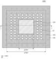
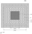
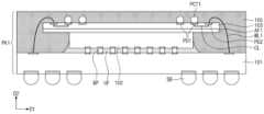
도 1a는 본 발명의 개념에 따른 반도체 패키지 장치의 일 실시예를 나타내는 평면도이다.
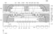
도 1b는 도 1a의 I-I'의 단면도이다.
도 2는 일부 실시예들에 따른 반도체 패키지 장치를 나타내는 단면도이다.
도 3a 내지 도 3d는 본 발명의 일부 실시예들에 따른 반도체 패키지 장치의 제조 방법을 나타내는 단면도들이다.
도 4a는 본 발명의 일부 실시예들에 따른 반도체 패키지 장치를 나타내는 평면도이다.
도 4b는 도 4a의 단면도이다.
도 5a는 본 발명의 일부 실시예들에 따른 반도체 패키지 장치를 나타내는 평면도이다.
도 5b는 도 5a의 단면도이다.
도 6a는 본 발명의 일부 실시예들에 따른 반도체 패키지 장치를 나타내는 평면도이다.
도 6b는 도 6a의 단면도이다.
도 7a 내지 도 7d는 본 발명의 일부 실시예들에 따른 반도체 패키지 장치의 제조 방법을 나타내는 단면도들이다.FIG. 1a is a plan view showing one embodiment of a semiconductor package device according to the concept of the present invention.
Figure 1b is a cross-sectional view taken along line I-I' of Figure 1a.
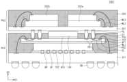
FIG. 2 is a cross-sectional view illustrating a semiconductor package device according to some embodiments.
FIGS. 3A to 3D are cross-sectional views showing a method for manufacturing a semiconductor package device according to some embodiments of the present invention.
FIG. 4a is a plan view illustrating a semiconductor package device according to some embodiments of the present invention.
Fig. 4b is a cross-sectional view of Fig. 4a.
FIG. 5A is a plan view showing a semiconductor package device according to some embodiments of the present invention.
Figure 5b is a cross-sectional view of Figure 5a.
FIG. 6A is a plan view showing a semiconductor package device according to some embodiments of the present invention.
Fig. 6b is a cross-sectional view of Fig. 6a.
FIGS. 7A to 7D are cross-sectional views showing a method of manufacturing a semiconductor package device according to some embodiments of the present invention.
이하, 도면들을 참조하여 본 발명의 개념에 따른 반도체 패키지 장치를 설명한다.Hereinafter, a semiconductor package device according to the concept of the present invention will be described with reference to the drawings.
도 1a는 본 발명의 개념에 따른 반도체 패키지 장치의 일 실시예를 나타내는 평면도이다. 도 1b는 도 1a의 I-I'의 단면도이다. 도 1a는 본 발명을 명확히 표현하기 위해서 도 1b의 일부 구성요소들은 생략되었다.Fig. 1a is a plan view showing one embodiment of a semiconductor package device according to the concept of the present invention. Fig. 1b is a cross-sectional view taken along line I-I' of Fig. 1a. In order to clearly express the present invention, some components of Fig. 1b are omitted in Fig. 1a.
도 1a 및 도 1b를 참조하면, 본 발명의 일부 실시예들에 따른 반도체 패키지 장치(1000)는 제1 패키지(PK1) 및 제1 패키지PK1) 상의 제2 패키지(PK2)를 포함할 수 있다. 제1 패키지(PK1) 및 제2 패키지(PK2)는 이들 사이에 개재된 연결 단자(CT)를 통해서 전기적으로 연결될 수 있다.Referring to FIGS. 1A and 1B, a semiconductor package device (1000) according to some embodiments of the present invention may include a first package (PK1) and a second package (PK2) on the first package (PK1). The first package (PK1) and the second package (PK2) may be electrically connected through a connection terminal (CT) interposed therebetween.
제1 패키지(PK1)는 제1 패키지 기판(101), 제1 반도체 칩(102), 인터포저(103) 및 휨 방지 부재(104)를 포함할 수 있다.The first package (PK1) may include a first package substrate (101), a first semiconductor chip (102), an interposer (103), and a warpage prevention member (104).
제1 패키지 기판(101)은 일 예로 PCB 기판을 포함할 수 있다. 제1 패키지 기판(101)의 하면 상에는 복수개의 솔더볼들(SB)이 배치될 수 있다. 솔더볼들(SB)은 제1 패키지 기판(101)의 가장자리 부분에 배치될 수 있다. 솔더볼들(SB)은 반도체 패키지 장치(1000)가 마더 보드에 부착되는 경우, 연결 단자의 역할을 할 수 있다.The first package substrate (101) may include, for example, a PCB substrate. A plurality of solder balls (SB) may be arranged on a lower surface of the first package substrate (101). The solder balls (SB) may be arranged at an edge portion of the first package substrate (101). The solder balls (SB) may serve as connection terminals when the semiconductor package device (1000) is attached to a motherboard.
제1 반도체 칩(102)은 일 예로 애플리케이션 프로세서(AP) 칩을 포함할 수 있다. 제1 반도체 칩(102)은 제1 반도체 칩(102)의 하면에 부착된 복수개의 범프들(BP)을 통하여 제1 패키지 기판(101)과 전기적으로 연결될 수 있다. 제1 반도체 칩(102)의 하면은 활성면으로 기능할 수 있다. 제1 반도체 칩(102)의 상면은 비활성면일 수 있다. 제1 반도체 칩(102)은 플립칩 본딩(flipchip bonding) 방식으로 제1 패키지 기판(101)에 실장될 수 있다.The first semiconductor chip (102) may include, for example, an application processor (AP) chip. The first semiconductor chip (102) may be electrically connected to a first package substrate (101) through a plurality of bumps (BP) attached to a lower surface of the first semiconductor chip (102). The lower surface of the first semiconductor chip (102) may function as an active surface. The upper surface of the first semiconductor chip (102) may be an inactive surface. The first semiconductor chip (102) may be mounted on the first package substrate (101) by a flipchip bonding method.
언더필막(UF)이 제1 반도체 칩(102) 및 제1 패키지 기판(101) 사이의 갭에 제공되어, 범프들(BP)을 밀봉할 수 있다. 언더필막(UF)은 일 예로 에폭시 물질과 같은 절연성 폴리머를 포함할 수 있다.An underfill film (UF) may be provided in the gap between the first semiconductor chip (102) and the first package substrate (101) to seal the bumps (BP). The underfill film (UF) may include an insulating polymer, such as an epoxy material, for example.
인터포저(interposer)(103)가 제1 반도체 칩(102) 상에 배치될 수 있다. 인터포저(103)는 실리콘 인터포저일 수 있다. 인터포저(103)는 서로 대향하는 상면 및 하면을 가질 수 있다. 인터포저(103)의 하면은 제1 반도체 칩(102)을 향할 수 있다.An interposer (103) may be placed on the first semiconductor chip (102). The interposer (103) may be a silicon interposer. The interposer (103) may have upper and lower surfaces facing each other. The lower surface of the interposer (103) may face the first semiconductor chip (102).
인터포저(103)의 평면적은 제1 반도체 칩(102)의 평면적보다 클 수 있다. 인터포저(103)의 가장자리 부분의 적어도 일부는 제1 반도체 칩(102)과 수직적으로 중첩되지 않을 수 있다.The planar area of the interposer (103) may be larger than the planar area of the first semiconductor chip (102). At least a portion of an edge portion of the interposer (103) may not vertically overlap with the first semiconductor chip (102).
제1 접착층(AF1)이 제1 반도체 칩(102) 및 인터포저(103) 사이에 제공될 수 있다. 인터포저(103)는 제1 접착층(AF1)에 의해 제1 반도체 칩(102)에 부착될 수 있다. 제1 접착층(AF1)은 인터포저(103)의 가장자리 부분의 하면으로 더 연장될 수 있다.A first adhesive layer (AF1) may be provided between the first semiconductor chip (102) and the interposer (103). The interposer (103) may be attached to the first semiconductor chip (102) by the first adhesive layer (AF1). The first adhesive layer (AF1) may further extend to the lower surface of the edge portion of the interposer (103).
인터포저(103)의 상부에는 재배선층(미도시)이 배치될 수 있다. 재배선층(미도시)은 절연층(미도시) 및 재배선 패턴(CL)을 포함할 수 있다. 재배선 패턴(CL)은 비아(미도시) 및 배선 라인(미도시)을 포함할 수 있다.A redistribution layer (not shown) may be arranged on the upper portion of the interposer (103). The redistribution layer (not shown) may include an insulating layer (not shown) and a redistribution pattern (CL). The redistribution pattern (CL) may include a via (not shown) and a wiring line (not shown).
인터포저(103)의 상면 상에는 복수개의 제1 패드들(PD1) 및 제2 패드들(PD2)이 제공될 수 있다. 제2 패드들(PD2)이 제1 패드들(PD1)보다 인터포저(103)의 가장자리에 부근에 배치될 수 있다. 제1 패드(PD1)는 연결 단자(CT)와 접촉하는 패드일 수 있다. 연결 단자(CT)는 제1 패드(PD1)에 수직으로 연결될 수 있다. 제1 패드(PD1)는 재배선 패턴(CL)을 통해서 제2 패드(PD2)와 전기적으로 연결될 수 있다. 제2 패드(PD2)는 제1 와이어(WL1)를 통하여 제1 패키지 기판(101)과 전기적으로 연결될 수 있다.A plurality of first pads (PD1) and second pads (PD2) may be provided on a top surface of an interposer (103). The second pads (PD2) may be arranged closer to an edge of the interposer (103) than the first pads (PD1). The first pad (PD1) may be a pad that contacts a connection terminal (CT). The connection terminal (CT) may be vertically connected to the first pad (PD1). The first pad (PD1) may be electrically connected to the second pad (PD2) through a redistribution pattern (CL). The second pad (PD2) may be electrically connected to the first package substrate (101) through a first wire (WL1).
휨 방지 부재(104)가 인터포저(103) 상에 배치될 수 있다. 휨 방지 부재(104)는 인터포저(103)보다 열팽창 계수(CTE)가 큰 물질을 포함할 수 있다. 휨 방지 부재(104)는 인터포저(103)보다 열전도도가 큰 물질을 포함할 수 있다. 휨 방지 부재(104)는 일 예로 구리 테이프를 포함할 수 있다.An anti-warp member (104) may be placed on the interposer (103). The anti-warp member (104) may include a material having a higher coefficient of thermal expansion (CTE) than the interposer (103). The anti-warp member (104) may include a material having a higher thermal conductivity than the interposer (103). The anti-warp member (104) may include, for example, a copper tape.
제1 패키지(PK1) 상에 제2 패키지(PK2)를 실장하는 과정 또는 마더보드에 반도체 패키지 장치를 실장하는 과정에서 고온에 의해 워페이지(warpage)가 발생할 수 있다. 워페이지(warpage)는 인터포저(103)의 열팽창 계수가 제1 패키지 기판(101)의 열팽창 계수보다 작기 때문에 팽창 정도의 차이 등의 이유로 발생할 수 있다. 따라서 인터포저(103)의 상부에 열팽창 계수(CTE)가 큰 휨 방지 부재(104)를 사용함으로써, 인터포저(103)의 상부가 더 팽창함으로써, 실장시의 워페이지를 감소시킬 수 있다. 더하여, 휨 방지 부재(104)의 열전도율이 인터포저(103)의 열 전도율보다 크기 때문에 발열 효과가 좋은 인터포저(103)의 열을 외부로 발열하여 반도체 패키지 장치의 내부의 온도가 상승하는 것을 방지할 수 있다. 또한 후술할 바와 같이 일정 두께 이상의 휨 방지 부재(104) 구조를 통하여 위와 같은 효과 달성이 가능할 수 있다.In the process of mounting the second package (PK2) on the first package (PK1) or in the process of mounting the semiconductor package device on the motherboard, warpage may occur due to high temperature. Warpage may occur due to reasons such as a difference in the degree of expansion because the coefficient of thermal expansion of the interposer (103) is smaller than that of the first package substrate (101). Therefore, by using a warpage-preventing member (104) having a large coefficient of thermal expansion (CTE) on the upper portion of the interposer (103), the upper portion of the interposer (103) expands more, thereby reducing warpage during mounting. In addition, since the thermal conductivity of the warpage-preventing member (104) is larger than that of the interposer (103), the heat of the interposer (103) with good heat dissipation effect can be dissipated to the outside, thereby preventing the temperature inside the semiconductor package device from increasing. In addition, as will be described later, it is possible to achieve the above effect through a structure of a bending prevention member (104) having a certain thickness or more.
휨 방지 부재(104)는 제1 패키지 기판(101)의 상면에 평행한 제1 방향(D1)으로의 폭(△1041)을 가질 수 있다. 인터포저(103)는 제1 방향(D1)으로의 폭(△1031)을 가질 수 있다. 휨 방지 부재(104)의 제1 방향(D1)으로의 폭(△1041)은 인터포저(103)의 제1 방향(D1)으로의 폭(△1031)보다 작을 수 있다. 휨 방지 부재(104)의 제1 방향(D1)으로의 폭(△1041)은 인터포저(103)의 제1 방향(D1)으로의 폭(△1031)의 0.3배 이상일 수 있다. 휨 방지 부재(104)의 제1 방향(D1)으로의 폭(△1041)은 일 예로 5mm일 수 있다.The warpage prevention member (104) may have a width (△1041) in a first direction (D1) parallel to the upper surface of the first package substrate (101). The interposer (103) may have a width (△1031) in the first direction (D1). The width (△1041) of the warpage prevention member (104) in the first direction (D1) may be smaller than the width (△1031) of the interposer (103) in the first direction (D1). The width (△1041) of the warpage prevention member (104) in the first direction (D1) may be 0.3 times or more the width (△1031) of the interposer (103) in the first direction (D1). The width (△1041) of the warpage prevention member (104) in the first direction (D1) may be, for example, 5 mm.
휨 방지 부재(104)는 제1 패키지 기판(101)의 상면에 수직한 제2 방향(D2)으로의 두께(△1042)를 가질 수 있다. 휨 방지 부재(104)의 제2 방향(D2)으로의 두께(△1042)는 휨 방지 부재(104)의 두께에 해당할 수 있다. 휨 방지 부재(104)의 제2 방향(D2)으로의 두께(△1042)는 인터포저(103)의 제2 방향(D2)으로의 두께(△1032)보다 클 수 있다. 휨 방지 부재(104)의 제2 방향(D2)으로의 두께(△1042)는 100㎛ 내지 150㎛ 일 수 있다.The warpage prevention member (104) may have a thickness (△1042) in a second direction (D2) perpendicular to the upper surface of the first package substrate (101). The thickness (△1042) of the warpage prevention member (104) in the second direction (D2) may correspond to the thickness of the warpage prevention member (104). The thickness (△1042) of the warpage prevention member (104) in the second direction (D2) may be greater than the thickness (△1032) of the interposer (103) in the second direction (D2). The thickness (△1042) of the warpage prevention member (104) in the second direction (D2) may be 100 ㎛ to 150 ㎛.
연결 단자(CT)의 제2 방향(D2)으로의 두께(△CT)는 휨 방지 부재(104)의 제2 방향(D2)의 두께(△H2)와 같거나 더 클 수 있다. 연결 단자(CT)의 제2 방향(D2)으로의 두께(△CT) 및 휨 방지 부재(104)의 제2 방향(D2)으로의 두께(△1042)의 차이는 30㎛ 이내일 수 있다.The thickness (△CT) of the connecting terminal (CT) in the second direction (D2) may be equal to or greater than the thickness (△H2) of the bending prevention member (104) in the second direction (D2). The difference between the thickness (△CT) of the connecting terminal (CT) in the second direction (D2) and the thickness (△1042) of the bending prevention member (104) in the second direction (D2) may be within 30 ㎛.
휨 방지 부재(104) 및 인터포저(103) 사이에는 제2 접착층(AF2)이 제공될 수 있다. 제2 접착층(AF2)의 상면 및 하면은 휨 방지 부재(104)의 하면에 대응하는 면적을 가질 수 있다. 제2 접착층(AF2)은 제2 방향(D2)을 따라서 휨 방지 부재(104)와 오버랩될 수 있다. 제2 접착층(AF2)의 두께는 일 예로 10㎛일 수 있다.A second adhesive layer (AF2) may be provided between the warpage prevention member (104) and the interposer (103). The upper and lower surfaces of the second adhesive layer (AF2) may have areas corresponding to the lower surface of the warpage prevention member (104). The second adhesive layer (AF2) may overlap with the warpage prevention member (104) along the second direction (D2). The thickness of the second adhesive layer (AF2) may be, for example, 10 μm.
인터포저(103), 제1 반도체 칩(102) 및 제1 패키지 기판(101)을 덮는 제1 몰딩 부재(105)가 제공될 수 있다. 제1 몰딩 부재(105)는 복수개의 홀들(HL)을 포함할 수 있다. 복수개의 홀들(HL)에 의해서 인터포저(103) 상의 제1 패드들(PD1)이 노출될 수 있다.A first molding member (105) covering an interposer (103), a first semiconductor chip (102), and a first package substrate (101) may be provided. The first molding member (105) may include a plurality of holes (HL). First pads (PD1) on the interposer (103) may be exposed by the plurality of holes (HL).
제1 몰딩 부재(105)는 휨 방지 부재(104)의 측면의 적어도 일부를 덮을 수 있다. 제1 몰딩 부재(105)는 휨 방지 부재(104)의 상면은 덮지 않을 수 있다. 휨 방지 부재(104)의 상면(104T)의 레벨은 제1 몰딩 부재(105)의 상면(105T)의 레벨과 같거나 더 높을 수 있다. 휨 방지 부재(104)의 측면들 각각의 적어도 일부는 제1 몰딩 부재(105)에 의해 노출될 수 있다.The first molding member (105) may cover at least a portion of a side surface of the warp-preventing member (104). The first molding member (105) may not cover an upper surface of the warp-preventing member (104). The level of the upper surface (104T) of the warp-preventing member (104) may be equal to or higher than the level of the upper surface (105T) of the first molding member (105). At least a portion of each of the side surfaces of the warp-preventing member (104) may be exposed by the first molding member (105).
제1 몰딩 부재(105)의 상면의 적어도 일부는 후술할 제2 패키지 기판(201)의 하면으로부터 이격될 수 있다.At least a portion of the upper surface of the first molding member (105) may be spaced apart from the lower surface of the second package substrate (201) described later.
휨 방지 부재(104)의 상면(104T)의 적어도 일부는 제2 패키지(PK2)의 하면(PK2L)으로부터 이격될 수 있다. 휨 방지 부재(104)의 상면(104T) 및 제2 패키지(PK2) 하면(PK2L) 사이의 제2 방향(D2)로의 이격거리(△GP)는 10㎛ 내지 30㎛일 수 있다. 다른 실시예에 있어서는 휨 방지 부재(104)의 상면(104T) 중 일부는 제2 패키지(PK2)의 하면(PK2L)과 접할 수도 있다.At least a portion of the upper surface (104T) of the warpage prevention member (104) may be spaced apart from the lower surface (PK2L) of the second package (PK2). A distance (△GP) in the second direction (D2) between the upper surface (104T) of the warpage prevention member (104) and the lower surface (PK2L) of the second package (PK2) may be 10 μm to 30 μm. In another embodiment, a portion of the upper surface (104T) of the warpage prevention member (104) may be in contact with the lower surface (PK2L) of the second package (PK2).
제2 패키지(PK2)는 제2 패키지 기판(201), 복수개의 제2 반도체 칩들 (202a) 및 제2 몰딩 부재(205)를 포함할 수 있다. 제2 패키지 기판(201)은 일 예로 PCB 기판일 수 있다. 제2 패키지 기판(201)은 제2 방향(D2)으로의 두께(△201)를 가질 수 있다. 제2 패키지 기판(201)의 제2 방향(D2)으로의 두께(△201)는 제1 패키지 기판(101)의 제2 방향(D2)으로의 두께(△101)보다 더 작을 수 있다.The second package (PK2) may include a second package substrate (201), a plurality of second semiconductor chips (202a), and a second molding member (205). The second package substrate (201) may be, for example, a PCB substrate. The second package substrate (201) may have a thickness (△201) in the second direction (D2). The thickness (△201) of the second package substrate (201) in the second direction (D2) may be smaller than the thickness (△101) of the first package substrate (101) in the second direction (D2).
복수개의 제2 반도체 칩들(202a)은 제2 패키지 기판(201) 상에서 이격되어 배치될 수 있다. 복수개의 제2 반도체 칩들(202a)의 각각은 일 예로 메모리 칩을 포함할 수 있다. 제2 반도체 칩(202a)의 상면은 활성면으로 기능할 수 있다. 제2 반도체 칩(202a)의 하면은 비활성면일 수 있다. 제2 반도체 칩(202a)의 상면 및 제2 패키지 기판(201)의 상면을 연결하는 제2 와이어 본딩(WL2)을 통해서 제2 반도체 칩(202a) 및 제2 패키지 기판(201)은 전기적으로 연결될 수 있다. 즉, 제2 반도체 칩(202a)은 제2 패키지 기판(201) 상에 와이어 본딩(wire bonding) 방식으로 실장될 수 있다.A plurality of second semiconductor chips (202a) may be spaced apart from each other and arranged on a second package substrate (201). Each of the plurality of second semiconductor chips (202a) may include, for example, a memory chip. An upper surface of the second semiconductor chip (202a) may function as an active surface. A lower surface of the second semiconductor chip (202a) may be an inactive surface. The second semiconductor chip (202a) and the second package substrate (201) may be electrically connected through a second wire bonding (WL2) connecting an upper surface of the second semiconductor chip (202a) and an upper surface of the second package substrate (201). That is, the second semiconductor chip (202a) may be mounted on the second package substrate (201) by a wire bonding method.
제2 패키지(PK2)는 복수개의 제3 반도체 칩(202b)들을 더 포함할 수 있다. 복수개의 제3 반도체 칩들(202b)의 각각은 제2 반도체 칩(202a) 상에 제공될 수 있다. 제3 반도체 칩(202b)은 일 예로 메모리 칩을 포함할 수 있다. 제3 반도체 칩(202b) 및 제2 반도체 칩(202a) 사이에는 접착 필름(미도시)이 제공될 수 있다. 제3 반도체 칩(202b)의 상면은 활성면으로 기능할 수 있다. 제3 반도체 칩(202b)의 하면은 비활성면일 수 있다. 제3 반도체 칩(202b)의 상면 및 제2 패키지 기판(201)의 상면을 연결하는 제3 와이어 본딩(WL3)을 통해서 제3 반도체 칩(202b) 및 제2 패키지 기판(201)은 전기적으로 연결될 수 있다. 즉, 제3 반도체 칩(202b)은 제2 패키지 기판(201) 상에 와이어 본딩(wire bonding) 방식으로 실장될 수 있다.The second package (PK2) may further include a plurality of third semiconductor chips (202b). Each of the plurality of third semiconductor chips (202b) may be provided on the second semiconductor chip (202a). The third semiconductor chip (202b) may include, for example, a memory chip. An adhesive film (not shown) may be provided between the third semiconductor chip (202b) and the second semiconductor chip (202a). The upper surface of the third semiconductor chip (202b) may function as an active surface. The lower surface of the third semiconductor chip (202b) may be an inactive surface. The third semiconductor chip (202b) and the second package substrate (201) may be electrically connected through third wire bonding (WL3) connecting the upper surface of the third semiconductor chip (202b) and the upper surface of the second package substrate (201). That is, the third semiconductor chip (202b) can be mounted on the second package substrate (201) using a wire bonding method.
제2 몰딩 부재(205)는 제2 패키지 기판(201), 제2 반도체 칩(202a) 및 제3 반도체 칩(202b)을 덮을 수 있다. 구체적으로 제2 몰딩 부재(205)는 제2 반도체 칩들(202a)의 사이 및 제2 반도체 칩들(202a) 각각의 측면들을 덮을 수 있다. 제2 몰딩 부재(205)는 제3 반도체 칩들(202b)의 사이 및 제3 반도체 칩들(202a)의 각각의 상면 및 측면들을 덮을 수 있다.The second molding member (205) can cover the second package substrate (201), the second semiconductor chip (202a), and the third semiconductor chip (202b). Specifically, the second molding member (205) can cover between the second semiconductor chips (202a) and side surfaces of each of the second semiconductor chips (202a). The second molding member (205) can cover between the third semiconductor chips (202b) and upper surfaces and side surfaces of each of the third semiconductor chips (202a).
도 2는 본 발명의 일부 실시예들에 따른 반도체 패키지 장치(1001) 나타내는 단면도이다. 이하에서 설명하는 것들을 제외하면, 도 1a 및 도 1b를 통하여 상세하게 설명하였으므로 생략하기로 한다.FIG. 2 is a cross-sectional view showing a semiconductor package device (1001) according to some embodiments of the present invention. Except for the details described below, they are omitted since they have been described in detail through FIGS. 1A and 1B.
도 2를 참조하면, 휨 방지 부재(104)는 실리콘을 포함할 수 있다. 휨 방지 부재(104)는 실리콘 더미일 수 있다. 실리콘은 구리 테이프를 대신하여 사용될 수 있다. 실리콘은 제1 반도체 칩(102)으로부터 인터포저(103)로 전달된 열을 외부로 효과적으로 방출함으로서, 발열효과가 개선될 수 있다.Referring to FIG. 2, the warpage prevention member (104) may include silicon. The warpage prevention member (104) may be a silicon dummy. The silicon may be used instead of the copper tape. The silicon may effectively release heat transferred from the first semiconductor chip (102) to the interposer (103) to the outside, thereby improving the heat generation effect.
도 3a 내지 도 3d는 본 발명의 일부 실시예들에 따른 반도체 패키지 장치의 제조 방법을 나타내는 단면도들이다.FIGS. 3A to 3D are cross-sectional views showing a method for manufacturing a semiconductor package device according to some embodiments of the present invention.
도 3a를 참조하면, 인터포저(103) 및 제1 반도체 칩(102)이 실장된 제1 패키지 기판(101)이 준비될 수 있다. 제1 패키지 기판(101) 하면 상에는 복수개의 솔더볼들(SB)이 제공될 수 있다. 제1 반도체 칩(102) 및 제1 패키지 기판(101) 사이에는 복수개의 범프들(BP)들이 제공될 수 있다. 복수개의 범프들(BP) 사이의 갭을 채우는 언더필막(UF)이 제공될 수 있다. 인터포저(103)는 제1 패드(PD1), 제2 패드(PD2), 재배선 패턴(CL)을 포함할 수 있다.인터포저(103) 및 제1 반도체 칩(102) 사이에는 제1 접착층(AF1)이 개재될 수 있다.Referring to FIG. 3A, a first package substrate (101) having an interposer (103) and a first semiconductor chip (102) mounted thereon may be prepared. A plurality of solder balls (SB) may be provided on a lower surface of the first package substrate (101). A plurality of bumps (BP) may be provided between the first semiconductor chip (102) and the first package substrate (101). An underfill film (UF) filling a gap between the plurality of bumps (BP) may be provided. The interposer (103) may include a first pad (PD1), a second pad (PD2), and a redistribution pattern (CL). A first adhesive layer (AF1) may be interposed between the interposer (103) and the first semiconductor chip (102).
휨 방지 부재(104)가 제2 접착층(AF2)을 통해서 인터포저(103) 상에 실장될 수 있다. 휨 방지 부재(104)는 일 예로 구리 테이프를 포함할 수 있다. 구리 테이프는 일 예로 제1 방향(D1)으로의 폭(△1041)이 5㎛이 되도록 준비될 수 있다. 구리 테이프는 제2 방향(D2)으로의 두께(△1042)가 100㎛내지 150㎛을 가지도록 준비될 수 있다. 구리 테이프의 제1 방향(D1)으로의 폭(△1041) 및 제2 방향(D2)으로의 두께(△1042)는 자유롭게 조절될 수 있다.The warpage prevention member (104) may be mounted on the interposer (103) through the second adhesive layer (AF2). The warpage prevention member (104) may include, for example, a copper tape. The copper tape may be prepared to have a width (△1041) of 5 ㎛ in the first direction (D1), for example. The copper tape may be prepared to have a thickness (△1042) of 100 ㎛ to 150 ㎛ in the second direction (D2). The width (△1041) of the copper tape in the first direction (D1) and the thickness (△1042) of the copper tape in the second direction (D2) may be freely adjusted.
도 3b를 참조하면, 제1 패키지 기판(101)을 덮는 제1 몰딩 부재(105)가 형성될 수 있다.Referring to FIG. 3b, a first molding member (105) covering a first package substrate (101) can be formed.
제1 몰딩 부재(105)의 형성동안, 휨 방지 부재(104)의 상면은 휨 방지 부재(104)의 상면 상에 제공되는 마스크(미도시)에 의해서 보호될 수 있다. 즉, 휨 방지 부재(104)가 배치된 제1 패키지 기판(101) 상의 영역(MSK)은 제1 몰딩 부재(105)가 형성되지 않을 수 있다. 마스크(미도시)에 의해 노출된, 제1 패키지 기판(101)의 영역(OP) 상에 제1 몰딩 부재(105)가 선택적으로 형성될 수 있다. 제1 몰딩 부재(105)의 형성시에 제1 몰딩 부재(105)의 상면(105T)의 레벨은 휨 방지 부재(104)의 상면(104T)의 레벨과 같거나 그보다 작게 형성될 수 있다. 제1 몰딩 부재(105)가 형성된 후에 마스크(미도시)는 제거될 수 있다.During the formation of the first molding member (105), the upper surface of the warpage-preventing member (104) may be protected by a mask (not shown) provided on the upper surface of the warpage-preventing member (104). That is, the first molding member (105) may not be formed in the area (MSK) on the first package substrate (101) where the warpage-preventing member (104) is disposed. The first molding member (105) may be selectively formed on the area (OP) of the first package substrate (101) exposed by the mask (not shown). When the first molding member (105) is formed, the level of the upper surface (105T) of the first molding member (105) may be formed to be equal to or smaller than the level of the upper surface (104T) of the warpage-preventing member (104). After the first molding member (105) is formed, the mask (not shown) may be removed.
도 3c를 참조하면, 제1 몰딩 부재(105) 내에 홀들(HL)이 형성될 수 있다. 홀들(HL)은 레이저 드릴링 공정을 통해서 형성될 수 있다. 홀들(HL)에 의해서 인터포저(103) 상부의 제1 패드들(PD1)들이 노출될 수 있다.Referring to FIG. 3c, holes (HL) may be formed in the first molding member (105). The holes (HL) may be formed through a laser drilling process. The first pads (PD1) on the upper portion of the interposer (103) may be exposed by the holes (HL).
도 3d 및 도 1a를 다시 참조하면, 제1 패키지(PK1) 상에 제2 패키지(PK2)가 실장될 수 있다. 제2 패키지(PK2) 하면에 부착된 복수개의 예비 연결 단자들(PCT)이 제1 패키지(PK1)의 제1 패드들(PD1)과 얼라인(align)되어 부착될 수 있다. 예비 연결 단자들(PCT) 각각은 리플로우 과정을 거쳐서 제1 패드들(PD1)과 부착되는 연결 단자들(CT)을 형성할 수 있다. 제2 패키지(PK2)가 실장되는 공정은 압착 공정(PR)을 포함할 수 있다. 제2 패키지(PK2)가 제1 패키지(PK1) 상에 실장되더라도 휨 방지 부재(104)의 상면(104T)은 제2 패키지(PK2)의 하면(PK2L)으로부터 이격될 수 있다. 다른 실시예에 있어서, 리플로우 과정에서 휨 방지 부재(104)의 상면(104T)의 일부가 제2 패키지(PK2)의 하면(PK2L)과 접촉할 수도 있다.Referring again to FIG. 3d and FIG. 1a, a second package (PK2) may be mounted on the first package (PK1). A plurality of spare connection terminals (PCT) attached to a lower surface of the second package (PK2) may be attached while being aligned with the first pads (PD1) of the first package (PK1). Each of the spare connection terminals (PCT) may form connection terminals (CT) attached to the first pads (PD1) through a reflow process. The process of mounting the second package (PK2) may include a pressing process (PR). Even when the second package (PK2) is mounted on the first package (PK1), the upper surface (104T) of the warpage prevention member (104) may be spaced apart from the lower surface (PK2L) of the second package (PK2). In another embodiment, a portion of the upper surface (104T) of the warpage prevention member (104) may come into contact with the lower surface (PK2L) of the second package (PK2) during the reflow process.
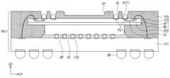
도 4a는 본 발명의 일부 실시예들에 따른 반도체 패키지 장치(2000)를 나타내는 단면도이다. 도 4b는 도 4a의 평면도이다. 도 4b는 본 발명을 명확히 표현하기 위해서 도 4a의 일부 구성요소들은 생략되었다. 이하에서 설명하는 것을 제외하면 도 1a 및 도 1b를 참조하여 상세하게 설명하였으므로 생략하기로 한다.FIG. 4A is a cross-sectional view showing a semiconductor package device (2000) according to some embodiments of the present invention. FIG. 4B is a plan view of FIG. 4A. In order to clearly express the present invention, some components of FIG. 4A are omitted in FIG. 4B. Except for what is described below, since it has been described in detail with reference to FIG. 1A and FIG. 1B, it will be omitted.
도 4a 및 도 4b를 참조하면, 제1 몰딩 부재(105)는 인터포저(103)의 상면을 덮을 수 있다. 제1 몰딩 부재(105)의 상면의 적어도 일부는 제2 패키지 기판(201)의 하면으로부터 이격될 수 있다. 제1 몰딩 부재(105)는 그루브(groove)(gv)를 포함할 수 있고, 그루브(gv)는 인터포저(103) 상에 배치될 수 있다Referring to FIGS. 4A and 4B, the first molding member (105) may cover the upper surface of the interposer (103). At least a portion of the upper surface of the first molding member (105) may be spaced apart from the lower surface of the second package substrate (201). The first molding member (105) may include a groove (gv), and the groove (gv) may be arranged on the interposer (103).
휨 방지 부재(104)는 그루브(gv)내에 배치될 수 있다. 구체적으로, 휨 방지 부재(104) 및 인터포저(103) 사이에는 제1 몰딩 부재(105)의 일부가 개재 될 수 있다. 휨 방지 부재(104)는 제1 몰딩 부재(105)의 일부를 사이에 두고 인터포저(103)으로부터 이격될 수 있다. 휨 방지 부재(104)의 하면은 제1 몰딩 부재(105)의 일부와 접촉할 수 있다. 휨 방지 부재(104)의 측면의 적어도 일부는 제1 몰딩 부재(105)에 의해 둘러싸일 수 있다. 휨 방지 부재(104)의 일부는 제1 몰딩 부재(105)의 그루브(gv)의 측면으로부터 제1 몰딩 부재(105)의 상면 상으로 연장될 수 있다.The warpage prevention member (104) may be arranged in the groove (gv). Specifically, a part of the first molding member (105) may be interposed between the warpage prevention member (104) and the interposer (103). The warpage prevention member (104) may be spaced apart from the interposer (103) with a part of the first molding member (105) therebetween. A lower surface of the warpage prevention member (104) may be in contact with a part of the first molding member (105). At least a part of a side surface of the warpage prevention member (104) may be surrounded by the first molding member (105). A part of the warpage prevention member (104) may extend from the side surface of the groove (gv) of the first molding member (105) onto an upper surface of the first molding member (105).
휨 방지 부재(104)의 상면(104T)은 제2 패키지(PK2)의 하면(PK2L)과 접촉할 수 있다. 휨 방지 부재(104)는 연결 단자(CT)와 접촉하지 않을 수 있다. 평면적 관점에서, 휨 방지 부재(104)는 연결 단자들(CT)에 의해서 둘러싸일 수 있다.The upper surface (104T) of the anti-bending member (104) may be in contact with the lower surface (PK2L) of the second package (PK2). The anti-bending member (104) may not be in contact with the connecting terminal (CT). In a planar view, the anti-bending member (104) may be surrounded by the connecting terminals (CT).
휨 방지 부재(104)는 액상인 비전도성 페이스트(Nonconductive paste)(NCP)가 고상화된 것일 수 있다. 비전도성 페이스트는 일 예로 폴리머를 포함할 수 있다. 고상화된 비전도성 페이스트의 열팽창 계수는 인터포저(103)의 열팽창 계수보다 클 수 있다. 휨 방지 부재(104)는 제1 패키지(PK1) 및 제2 패키지(PK2)를 접착시키는 접착제 역할도 동시에 수행할 수 있다.The warpage prevention member (104) may be a solidified liquid nonconductive paste (NCP). The nonconductive paste may include, for example, a polymer. The thermal expansion coefficient of the solidified nonconductive paste may be greater than the thermal expansion coefficient of the interposer (103). The warpage prevention member (104) may also simultaneously serve as an adhesive for bonding the first package (PK1) and the second package (PK2).
휨 방지 부재(104)의 제1 방향(D1)으로의 폭(△1041)은 인터포저(103)의 제1 방향(D1)로의 폭(△1031)의 0.3배 이상일 수 있다. 휨 방지 부재(104)의 제2 방향(D2)으로의 두께(△1042)는 인터포저(103)의 제2 방향(D2)로의 두께(△1032)보다 클 수 있다. 휨 방지 부재(104)의 제2 방향(D2)으로의 두께(△1042)는 100㎛ 내지 250㎛일 수 있다. 일 예로 휨 방지 부재(104)의 제2 방향(D2)으로의 두께(△1042)는 150㎛일 수 있다.The width (△1041) of the warpage prevention member (104) in the first direction (D1) may be at least 0.3 times the width (△1031) of the interposer (103) in the first direction (D1). The thickness (△1042) of the warpage prevention member (104) in the second direction (D2) may be greater than the thickness (△1032) of the interposer (103) in the second direction (D2). The thickness (△1042) of the warpage prevention member (104) in the second direction (D2) may be 100 ㎛ to 250 ㎛. For example, the thickness (△1042) of the warpage prevention member (104) in the second direction (D2) may be 150 ㎛.
그루브(gv)는 제1 방향(D1)에 따른 폭(△gv1)을 가질 수 있고, 홀(HL)은 제 1 방향(D1)에 따른 폭(△HL1)을 가질 수 있다. 그루브(gv)의 제1 방향(D1)에 따른 폭(△gv1)은 홀(HL)의 제1 방향(D1)에 따른 폭(△HL1)보다 클 수 있다. 그루브(gv)는 제2 방향(D2)에 따른 깊이(△gv2)를 가질 수 있고, 홀(HL)은 제2 방향(D2)에 따른 깊이(△HL2)를 가질 수 있다. 그루브(gv)의 제2 방향(D2)에 따른 깊이(△gv2)는 홀(HL)의 제2 방향(D2)에 따른 깊이(△HL2) 보다 작을 수 있다.The groove (gv) can have a width (△gv1) along the first direction (D1), and the hole (HL) can have a width (△HL1) along the first direction (D1). The width (△gv1) of the groove (gv) along the first direction (D1) can be larger than the width (△HL1) of the hole (HL) along the first direction (D1). The groove (gv) can have a depth (△gv2) along the second direction (D2), and the hole (HL) can have a depth (△HL2) along the second direction (D2). The depth (△gv2) of the groove (gv) along the second direction (D2) can be smaller than the depth (△HL2) of the hole (HL) along the second direction (D2).
도 5a 및 도 5b는 본 발명의 일부 실시예들에 따른 반도체 패키지 장치(2001)를 나타내는 도면들이다. 이하에서 설명하는 것들을 제외하면 도 4a 및 도 4b를 통하여 상세하게 설명하였으므로 생략한다.FIGS. 5A and 5B are drawings showing a semiconductor package device (2001) according to some embodiments of the present invention. Except for the details described below, they are omitted since they have been described in detail through FIGS. 4A and 4B.
도 5a 및 도 5b를 참조하면, 제1 몰딩 부재(105)는 복수개의 제1 그루브들(gv1)을 포함할 수 있다. 각각의 제1 그루브들(gv1) 내에는 제1 휨 방지 부재(104a)가 배치될 수 있다. 제1 휨 방지 부재들(104a) 각각은 평면적으로 원 또는 원에 가까운 형태일 수 있다. 평면적 관점에서, 제1 휨 방지 부재들(104a)은 제1 몰딩 부재(105) 상에서 이차원적으로 배열될 수 있다.Referring to FIGS. 5A and 5B, the first molding member (105) may include a plurality of first grooves (gv1). A first warpage prevention member (104a) may be arranged within each of the first grooves (gv1). Each of the first warpage prevention members (104a) may have a shape that is circular or close to circular in plan view. In plan view, the first warpage prevention members (104a) may be arranged two-dimensionally on the first molding member (105).
도 6a 및 도 6b는 본 발명의 일부 실시예들에 따른 반도체 패키지 장치(2002)를 나타내는 도면들이다. 이하에서 설명하는 것들을 제외하면 도 4a 및 도 4b를 통하여 상세하게 설명하였으므로 생략한다.FIGS. 6A and 6B are drawings showing a semiconductor package device (2002) according to some embodiments of the present invention. Except for the details described below, they are omitted since they have been described in detail through FIGS. 4A and 4B.
도 5a 및 도 5b를 참조하면, 제1 몰딩 부재(105)는 제1 그루브(gv1) 및 제2 그루브(gv2)를 포함할 수 있다. 제2 휨 방지 부재(104b)는 평면적으로 제1 휨 방지 부재들(104a)을 둘러쌀 수 있다. 제2 그루브(gv2)는 평면적 관점에서 링 형태(일 예로, 사각형 형태)를 가질 수 있다.Referring to FIGS. 5a and 5b, the first molding member (105) may include a first groove (gv1) and a second groove (gv2). The second warpage-preventing member (104b) may surround the first warpage-preventing members (104a) in a planar view. The second groove (gv2) may have a ring shape (for example, a square shape) in a planar view.
도 7a 내지 도 7d는 본 발명의 일부 실시예들에 따른 반도체 패키지 장치의 제조방법을 나타내는 단면도들이다.FIGS. 7A to 7D are cross-sectional views showing a method for manufacturing a semiconductor package device according to some embodiments of the present invention.
도 7a를 참조하면, 인터포저(103) 및 제1 반도체 칩(102)이 실장된 제1 패키지 기판(101)이 준비될 수 있다. 제1 패키지 기판(101) 하면 상에는 복수개의 솔더볼들(SB)이 제공될 수 있다. 제1 반도체 칩(102) 및 제1 패키지 기판(101) 사이에는 복수개의 범프들(BP)들이 제공될 수 있다. 복수개의 범프들(BP) 사이의 갭을 채우는 언더필막(UF)이 제공될 수 있다. 인터포저(103)는 제1 패드(PD1), 제2 패드(PD2), 재배선 패턴(CL)을 포함할 수 있다.제1 패드(PD1) 상에는 제1 예비 연결 단자(PCT1)들이 제공될 수 있다. 도 3a에서 도시한 바와 같이 제1 예비 연결 단자(PCT1)는 생략될 수도 있다. 인터포저(103) 및 제1 반도체 칩(102) 사이에는 제1 접착층(AF1)이 개재될 수 있다.Referring to FIG. 7a, a first package substrate (101) having an interposer (103) and a first semiconductor chip (102) mounted thereon may be prepared. A plurality of solder balls (SB) may be provided on a lower surface of the first package substrate (101). A plurality of bumps (BP) may be provided between the first semiconductor chip (102) and the first package substrate (101). An underfill film (UF) filling a gap between the plurality of bumps (BP) may be provided. The interposer (103) may include a first pad (PD1), a second pad (PD2), and a redistribution pattern (CL). First preliminary connection terminals (PCT1) may be provided on the first pad (PD1). As illustrated in FIG. 3a, the first preliminary connection terminal (PCT1) may be omitted. A first adhesive layer (AF1) may be interposed between the interposer (103) and the first semiconductor chip (102).
제1 패키지 기판(101)을 덮는 제1 몰딩 부재(105)가 형성될 수 있다. 제1 몰딩 부재(105)는 인터포저(103)의 상면 및 측면을 덮을 수 있다. 제1 몰딩 부재(105)의 형성은 몰딩 물질(미도시)을 제1 패키지 기판(101) 상에 덮고, 이를 경화시키는 과정을 포함할 수 있다.A first molding member (105) covering the first package substrate (101) may be formed. The first molding member (105) may cover the upper surface and side surfaces of the interposer (103). Formation of the first molding member (105) may include a process of covering a molding material (not shown) on the first package substrate (101) and curing it.
도 7b를 참조하면, 제1 몰딩 부재(105) 상에 그루브(gv) 및 홀들(HL)이 형성될 수 있다. 그루브(gv) 및 홀들(HL)은 레이저 드릴링 공정을 통해서 형성될 수 있다.Referring to FIG. 7b, a groove (gv) and holes (HL) can be formed on the first molding member (105). The groove (gv) and holes (HL) can be formed through a laser drilling process.
다른 실시예에 있어서, 그루브(gv)는 몰딩 물질(미도시)이 경화되기 전에 별도의 금형(미도시)을 이용하여 형성될 수도 있다. 홀들(HL)에 의해서 인터포저(103)의 제1 패드들(PD1)이 노출될 수 있다.In another embodiment, the groove (gv) may be formed using a separate mold (not shown) before the molding material (not shown) is cured. The first pads (PD1) of the interposer (103) may be exposed by the holes (HL).
도 7c를 참조하면, 제1 몰딩 부재(105) 상의 소스(SC)로부터 그루브(gv)를 향하여 액상의 휨 방지 물질(P104)이 분사(dispense)될 수 있다. 액상의 휨 방지 물질(P104)은 일 예로 액상의 비전도성 페이스트(NCP)를 포함할 수 있다. 액상의 휨 방지 물질(P104)은 그루브(gv) 내에 선택적으로 채워질 수 있다. 홀(HL) 내부는 액상의 휨 방지 물질(P104)이 채워지지 않을 수 있다.Referring to FIG. 7c, a liquid warpage prevention material (P104) may be dispensed from a source (SC) on a first molding member (105) toward a groove (gv). The liquid warpage prevention material (P104) may include, for example, a liquid non-conductive paste (NCP). The liquid warpage prevention material (P104) may be selectively filled within the groove (gv). The inside of the hole (HL) may not be filled with the liquid warpage prevention material (P104).
도 7d 및 도 4a를 다시 참조하면 제1 패키지(PK1) 상에 제2 패키지(PK2)가 실장될 수 있다. 제2 패키지(PK2) 하면에 부착된 복수개의 제2 예비 연결 단자들(PCT2)이 제1 패키지(PK1)의 제1 예비 연결 단자들(PCT1)과 얼라인(align)되어 리플로우 공정으로 연결 단자들(CT)이 형성될 수 있다. 제2 패키지(PK2)가 실장되는 공정은 압착 공정(PR)을 포함할 수 있다. 압착 공정(PR)에 의해서 액상의 휨 방지 물질(P104)은 제2 패키지(PK2)의 하면에 접촉할 수 있다. 이 과정에서 액상의 휨 방지 물질(P104)의 일부는 그루브(gv) 주위의 제1 몰딩 부재(105) 상면을 따라 흘러갈 수 있지만, 홀(HL)의 내부까지는 흘러가지 않을 수 있다.Referring again to FIG. 7d and FIG. 4a, a second package (PK2) may be mounted on the first package (PK1). A plurality of second preliminary connection terminals (PCT2) attached to a lower surface of the second package (PK2) may be aligned with the first preliminary connection terminals (PCT1) of the first package (PK1) to form connection terminals (CT) through a reflow process. The process of mounting the second package (PK2) may include a pressing process (PR). The liquid warpage prevention material (P104) may come into contact with the lower surface of the second package (PK2) through the pressing process (PR). During this process, a portion of the liquid warpage prevention material (P104) may flow along the upper surface of the first molding member (105) around the groove (gv), but may not flow into the interior of the hole (HL).
압착 및 리플로우 공정이 이루어진 후에, 큐어(cure) 공정이 더 이루어질 수 있다. 큐어 공정은 리플로우 공정보다는 온도가 더 낮은 열처리 공정일 수 있다. 큐어 공정에 의해서 아직 완전히 고상화되지 않은 액상의 휨 방지 물질(P104)은 완전히 고상화되어 휨 방지 부재(104)가 형성될 수 있다.After the pressing and reflow processes are performed, a cure process may be performed. The cure process may be a heat treatment process having a lower temperature than the reflow process. Through the cure process, the liquid warpage prevention material (P104) that has not yet been completely solidified may be completely solidified to form the warpage prevention member (104).
본 발명의 개념에 따르면 반도체 패키지 장치에서 인터포저의 재료 선택에 있어서, 유기 물질 기반의 기판을 사용하는 것보다 실리콘 인터포저를 사용함으로서 발열이 개선될 수 있다. 실리콘 인터포저를 사용하는 과정에서 워페이지 이슈가 생길 수 있는데, 실리콘 인터포저 상부에 열팽창계수가 큰 물질을 부착함으로써, 워페이지 이슈를 효과적으로 해결할 수 있다.According to the concept of the present invention, in selecting the material of the interposer in a semiconductor package device, heat generation can be improved by using a silicon interposer rather than using an organic material-based substrate. In the process of using a silicon interposer, a warpage issue can occur, but by attaching a material having a large coefficient of thermal expansion on the upper part of the silicon interposer, the warpage issue can be effectively resolved.
특히 실리콘 인터포저 상의 연결 단자가 배치되지 않는 공간의 효과적인 구조를 제안하고, 그 공간에 휨 방지 부재를 부착시킴으로써, 기존 발명과 대비하여 워페이지가 감소할 수 있다. 또한 휨 방지 부재는 특정한 재료 및 두께를 가짐으로서 효과적으로 워페이지가 감소될 수 있다.In particular, by proposing an effective structure for a space where a connection terminal is not arranged on a silicon interposer and attaching a warpage prevention member to that space, warpage can be reduced compared to the existing invention. In addition, the warpage can be effectively reduced by having a specific material and thickness as the warpage prevention member.
이상, 첨부된 도면들을 참조하여 본 발명의 실시예들을 설명하였지만, 본 발명이 속하는 기술분야에서 통상의 지식을 가진 자는 본 발명이 그 기술적 사상이나 필수적인 특징을 변경하지 않고서 다른 구체적인 형태로 실시될 수 있다는 것을 이해할 수 있을 것이다. 그러므로 이상에서 기술한 실시예들은 모든 면에서 예시적인 것이며 한정적이 아닌 것으로 이해해야만 한다.Above, while the embodiments of the present invention have been described with reference to the attached drawings, those skilled in the art to which the present invention pertains will understand that the present invention can be implemented in other specific forms without changing the technical idea or essential features thereof. Therefore, it should be understood that the embodiments described above are exemplary in all respects and not restrictive.
PK1: 제1 패키지
PK2: 제2 패키지
101: 제1 패키지 기판
102: 제1 반도체 칩
103: 인터포저
104: 휨 방지 부재
AF1: 제1 접착층
AF2: 제2 접착층
PD1: 제1 패드
PD2: 제2 패드
CL: 도전 패턴
201: 제2 패키지 기판
WL1, WL2, WL3: 와이어 본딩
105: 제1 몰딩 부재
205: 제2 몰딩 부재
제2, 제3 반도체 칩(202a, 202b)PK1: Package 1
PK2: Package 2
101: 1st package substrate
102: First semiconductor chip
103: Interposer
104: Anti-bending member
AF1: First adhesive layer
AF2: Second adhesive layer
PD1: Pad 1
PD2: Pad 2
CL: Challenge Pattern
201: 2nd package substrate
WL1, WL2, WL3: Wire bonding
105: First molding member
205: Second molding member
Second and third semiconductor chips (202a, 202b)
Claims (10)
Translated fromKorean상기 제1 패키지 기판 상의 제1 반도체 칩;
상기 제1 반도체 칩 상의 인터포저;
상기 인터포저 상의 휨 방지 부재;
상기 인터포저 및 상기 제1 패키지 기판을 덮는 몰딩 부재; 및
상기 몰딩 부재 상부에 형성된 제2 패키지 기판을 포함하고,
상기 몰딩 부재의 상면의 적어도 일부는 상기 제2 패키지 기판의 하면으로부터 이격되고,
상기 휨 방지 부재의 상면의 레벨은 상기 몰딩 부재의 상면의 레벨과 같거나 더 높은 반도체 패키지 장치.1st package substrate;
A first semiconductor chip on the first package substrate;
An interposer on the first semiconductor chip;
An anti-bending member on the above interposer;
A molding member covering the interposer and the first package substrate; and
Including a second package substrate formed on the upper part of the molding member,
At least a portion of the upper surface of the molding member is spaced apart from the lower surface of the second package substrate,
A semiconductor package device wherein the level of the upper surface of the above-mentioned bending prevention member is equal to or higher than the level of the upper surface of the above-mentioned molding member.
상기 휨 방지 부재의 열팽창 계수(CTE)는 상기 인터포저의 열팽창 계수보다 더 큰 반도체 패키지 장치.In the first paragraph,
A semiconductor package device wherein the coefficient of thermal expansion (CTE) of the above-described warpage prevention member is greater than the coefficient of thermal expansion of the interposer.
상기 휨 방지 부재의 열전도도는 상기 인터포저의 열전도도보다 더 큰 반도체 패키지 장치.In the first paragraph,
A semiconductor package device wherein the thermal conductivity of the above-mentioned bending prevention member is greater than the thermal conductivity of the above-mentioned interposer.
상기 휨 방지 부재는 구리 또는 실리콘 더미를 포함하는 반도체 패키지 장치.In the first paragraph,
The above-mentioned bending prevention member is a semiconductor package device including a copper or silicon dummy.
상기 인터포저는 제1 패드, 제2 패드, 및 상기 제1 및 제2 패드들을 전기적으로 연결하는 재배선 패턴을 포함하고,
상기 제2 패드는 와이어 선을 통해서 상기 제1 패키지 기판과 전기적으로 연결되고,
상기 제1 패드에 수직으로 연결되는 연결 단자를 더 포함하고, 상기 연결 단자의 상기 제1 패키지 기판의 상면에 수직한 방향으로의 제1 두께는 상기 휨 방지 부재의 두께보다 크고,
상기 제1 두께 및 상기 휨 방지 부재의 두께의 차이는 30㎛ 이하인 반도체 패키지 장치.
In the first paragraph,
The interposer comprises a first pad, a second pad, and a redistribution pattern electrically connecting the first and second pads,
The above second pad is electrically connected to the first package substrate through a wire line,
Further comprising a connecting terminal vertically connected to the first pad, wherein a first thickness of the connecting terminal in a direction perpendicular to the upper surface of the first package substrate is greater than a thickness of the warpage-preventing member,
A semiconductor package device wherein the difference between the first thickness and the thickness of the warpage prevention member is 30㎛ or less.
상기 제1 패키지 기판 상의 제1 반도체 칩;
상기 제1 반도체 칩 상의 인터포저;
상기 인터포저, 제1 반도체 칩 및 제1 패키지 기판을 덮는 몰딩 부재;
상기 인터포저 상의 휨 방지 부재 및 복수개의 연결 단자들; 및
상기 복수개의 연결 단자들과 접촉하는 상기 휨 방지 부재 상부의 제2 패키지 기판을 포함하고,
상기 몰딩 부재의 상면의 적어도 일부는 상기 제2 패키지 기판으로부터 이격되고,
상기 연결 단자들의 상기 제1 패키지 기판의 상면에 수직한 방향으로의 제1 두께는 상기 휨 방지 부재의 두께보다 큰 반도체 패키지 장치.
1st package substrate;
A first semiconductor chip on the first package substrate;
An interposer on the first semiconductor chip;
A molding member covering the interposer, the first semiconductor chip and the first package substrate;
A bending prevention member and a plurality of connecting terminals on the interposer; and
A second package substrate is included on the upper side of the bending prevention member in contact with the plurality of connecting terminals,
At least a portion of the upper surface of the molding member is spaced apart from the second package substrate,
A semiconductor package device wherein a first thickness of the connecting terminals in a direction perpendicular to the upper surface of the first package substrate is greater than a thickness of the warpage-preventing member.
상기 연결 단자들은 평면적 관점에서 상기 휨 방지 부재를 둘러싸는 반도체 패키지 장치.
In Article 7,
The above connecting terminals are a semiconductor package device surrounding the bending prevention member in a planar view.
상기 몰딩 부재는 그루브 및 홀을 포함하고,
상기 휨 방지 부재는 상기 그루브 내에 배치되고,
상기 연결 단자들은 상기 홀 내에 배치되고,
상기 홀의 깊이는 상기 그루브의 깊이보다 더 큰 반도체 패키지 장치
In Article 8,
The above molding member includes a groove and a hole,
The above-mentioned anti-bending member is placed within the groove,
The above connecting terminals are arranged within the hole,
A semiconductor package device in which the depth of the hole is greater than the depth of the groove
상기 제1 패키지 상의 제2 패키지; 및
상기 제1 패키지 및 상기 제2 패키지를 전기적으로 연결하는 복수개의 연결 단자들을 포함하되,
상기 제1 패키지는:
제1 패키지 기판;
제1 패키지 기판 상의 제1 반도체 칩;
상기 제1 반도체 칩 상의 인터포저;
상기 제1 반도체 칩 및 상기 인터포저 사이에 개재되는 제1 접착층;
상기 인터포저 상의 휨 방지 부재;
상기 휨 방지 부재 및 상기 인터포저 사이의 제2 접착층; 및
상기 인터포저 및 상기 제1 패키지 기판을 덮는 제1 몰딩 부재를 포함하고,
상기 제2 패키지는:
상기 복수개의 연결단자들에 연결되는 제2 패키지 기판;
상기 제2 패키지 기판 상의 서로 이격되어 배치되는 제2 반도체 칩들; 및
상기 제2 반도체 칩들의 사이 및 측면을 덮는 제2 몰딩부재를 포함하되,
상기 제1 몰딩 부재 상부의 적어도 일부는 상기 제2 패키지 기판으로부터 이격되고,
상기 휨 방지 부재의 상면은 상기 제1 몰딩 부재에 의해 노출되고,
상기 휨 방지 부재의 두께 및 열팽창 계수(CTE)는 각각 상기 인터포저의 두께 및 열팽창 계수 보다 큰 반도체 패키지 장치.
Package 1;
A second package on the first package; and
Including a plurality of connection terminals electrically connecting the first package and the second package,
The above first package:
1st package substrate;
A first semiconductor chip on a first package substrate;
An interposer on the first semiconductor chip;
A first adhesive layer interposed between the first semiconductor chip and the interposer;
A bending prevention member on the above interposer;
a second adhesive layer between the above-described anti-bending member and the interposer; and
Including a first molding member covering the interposer and the first package substrate,
The above second package:
A second package substrate connected to the above plurality of connecting terminals;
Second semiconductor chips spaced apart from each other on the second package substrate; and
Including a second molding member covering the space between and the side surfaces of the second semiconductor chips,
At least a portion of the upper portion of the first molding member is spaced from the second package substrate,
The upper surface of the above-mentioned bending prevention member is exposed by the first molding member,
A semiconductor package device wherein the thickness and coefficient of thermal expansion (CTE) of the above-described warpage prevention member are greater than the thickness and coefficient of thermal expansion of the interposer, respectively.
Priority Applications (3)
| Application Number | Priority Date | Filing Date | Title |
|---|---|---|---|
| KR1020190095025AKR102698698B1 (en) | 2019-08-05 | 2019-08-05 | Semiconductor package device |
| US16/845,567US11367714B2 (en) | 2019-08-05 | 2020-04-10 | Semiconductor package device |
| CN202010756040.4ACN112331645B (en) | 2019-08-05 | 2020-07-31 | semiconductor packaging devices |
Applications Claiming Priority (1)
| Application Number | Priority Date | Filing Date | Title |
|---|---|---|---|
| KR1020190095025AKR102698698B1 (en) | 2019-08-05 | 2019-08-05 | Semiconductor package device |
Publications (2)
| Publication Number | Publication Date |
|---|---|
| KR20210018577A KR20210018577A (en) | 2021-02-18 |
| KR102698698B1true KR102698698B1 (en) | 2024-08-27 |
Family
ID=74303746
Family Applications (1)
| Application Number | Title | Priority Date | Filing Date |
|---|---|---|---|
| KR1020190095025AActiveKR102698698B1 (en) | 2019-08-05 | 2019-08-05 | Semiconductor package device |
Country Status (3)
| Country | Link |
|---|---|
| US (1) | US11367714B2 (en) |
| KR (1) | KR102698698B1 (en) |
| CN (1) | CN112331645B (en) |
Families Citing this family (3)
| Publication number | Priority date | Publication date | Assignee | Title |
|---|---|---|---|---|
| KR102713394B1 (en)* | 2019-04-15 | 2024-10-04 | 삼성전자주식회사 | Semiconductor package |
| US12362340B2 (en) | 2019-08-30 | 2025-07-15 | Intel Corporation | Laser ablation-based surface property modification and contamination removal |
| US11527518B2 (en) | 2020-07-27 | 2022-12-13 | Taiwan Semiconductor Manufacturing Co., Ltd. | Heat dissipation in semiconductor packages and methods of forming same |
Citations (3)
| Publication number | Priority date | Publication date | Assignee | Title |
|---|---|---|---|---|
| US20070181991A1 (en) | 2006-01-20 | 2007-08-09 | Elpida Memory, Inc. | Stacked semiconductor device |
| US20100103634A1 (en) | 2007-03-30 | 2010-04-29 | Takuo Funaya | Functional-device-embedded circuit board, method for manufacturing the same, and electronic equipment |
| US20190198437A1 (en)* | 2017-12-27 | 2019-06-27 | Samsung Electronics Co., Ltd. | Interposer substrate and semiconductor package |
Family Cites Families (27)
| Publication number | Priority date | Publication date | Assignee | Title |
|---|---|---|---|---|
| TW579555B (en) | 2000-03-13 | 2004-03-11 | Ibm | Semiconductor chip package and packaging of integrated circuit chip in electronic apparatus |
| CN101278393A (en)* | 2005-09-29 | 2008-10-01 | 日本电气株式会社 | Semiconductor package, substrate, electronic device using such semiconductor package or substrate, and method for correcting warping of semiconductor package |
| US7244636B2 (en)* | 2005-10-19 | 2007-07-17 | Texas Instruments Incorporated | Semiconductor assembly for improved device warpage and solder ball coplanarity |
| KR100702968B1 (en) | 2005-11-24 | 2007-04-03 | 삼성전자주식회사 | Semiconductor package having a floating heat sink, laminated package using the same, and manufacturing method thereof |
| JP5144222B2 (en)* | 2007-11-14 | 2013-02-13 | 新光電気工業株式会社 | Wiring board and manufacturing method thereof |
| US8035210B2 (en) | 2007-12-28 | 2011-10-11 | Stats Chippac Ltd. | Integrated circuit package system with interposer |
| US8270176B2 (en) | 2008-08-08 | 2012-09-18 | Stats Chippac Ltd. | Exposed interconnect for a package on package system |
| US20100244212A1 (en) | 2009-03-27 | 2010-09-30 | Jong-Woo Ha | Integrated circuit packaging system with post type interconnector and method of manufacture thereof |
| US8080446B2 (en) | 2009-05-27 | 2011-12-20 | Stats Chippac Ltd. | Integrated circuit packaging system with interposer interconnections and method of manufacture thereof |
| JP2011061132A (en) | 2009-09-14 | 2011-03-24 | Zycube:Kk | Interposer |
| WO2011049933A1 (en) | 2009-10-19 | 2011-04-28 | The University Of Toledo | Back contact buffer layer for thin-film solar cells |
| US8699232B2 (en) | 2011-09-20 | 2014-04-15 | Stats Chippac Ltd. | Integrated circuit packaging system with interposer and method of manufacture thereof |
| US9748203B2 (en) | 2011-12-15 | 2017-08-29 | STATS ChipPAC Pte. Ltd. | Integrated circuit packaging system with conductive pillars and method of manufacture thereof |
| KR101874803B1 (en) | 2012-01-20 | 2018-08-03 | 삼성전자주식회사 | Package on package assembly |
| KR101867955B1 (en) | 2012-04-13 | 2018-06-15 | 삼성전자주식회사 | Package on package device and method of fabricating the device |
| TWI614858B (en)* | 2012-07-26 | 2018-02-11 | 矽品精密工業股份有限公司 | Semiconductor package and method of forming the same |
| US8963311B2 (en) | 2012-09-26 | 2015-02-24 | Apple Inc. | PoP structure with electrically insulating material between packages |
| KR102186203B1 (en) | 2014-01-23 | 2020-12-04 | 삼성전자주식회사 | Package-on-package device including the same |
| KR101624850B1 (en)* | 2014-02-21 | 2016-05-27 | 앰코 테크놀로지 코리아 주식회사 | Package on package |
| JP2016058627A (en) | 2014-09-11 | 2016-04-21 | 株式会社東芝 | Semiconductor device |
| KR102243287B1 (en) | 2014-10-15 | 2021-04-23 | 삼성전자주식회사 | Semiconductor package and method for manufacturing the same |
| KR102372300B1 (en) | 2015-11-26 | 2022-03-08 | 삼성전자주식회사 | Stacked package and method of manufacturing the same |
| US10002857B2 (en) | 2016-04-12 | 2018-06-19 | Qualcomm Incorporated | Package on package (PoP) device comprising thermal interface material (TIM) in cavity of an encapsulation layer |
| CN106876364A (en)* | 2017-03-15 | 2017-06-20 | 三星半导体(中国)研究开发有限公司 | Semiconductor package assembly and a manufacturing method thereof |
| US10276536B2 (en)* | 2017-04-28 | 2019-04-30 | Taiwan Semiconductor Manufacturing Co., Ltd. | Structure and formation method of chip package with fan-out structure |
| US10332862B2 (en) | 2017-09-07 | 2019-06-25 | Advanced Semiconductor Engineering, Inc. | Semiconductor package structure and method for manufacturing the same |
| KR101933425B1 (en) | 2017-11-30 | 2018-12-28 | 삼성전기 주식회사 | Semiconductor package |
- 2019
- 2019-08-05KRKR1020190095025Apatent/KR102698698B1/enactiveActive
- 2020
- 2020-04-10USUS16/845,567patent/US11367714B2/enactiveActive
- 2020-07-31CNCN202010756040.4Apatent/CN112331645B/enactiveActive
Patent Citations (3)
| Publication number | Priority date | Publication date | Assignee | Title |
|---|---|---|---|---|
| US20070181991A1 (en) | 2006-01-20 | 2007-08-09 | Elpida Memory, Inc. | Stacked semiconductor device |
| US20100103634A1 (en) | 2007-03-30 | 2010-04-29 | Takuo Funaya | Functional-device-embedded circuit board, method for manufacturing the same, and electronic equipment |
| US20190198437A1 (en)* | 2017-12-27 | 2019-06-27 | Samsung Electronics Co., Ltd. | Interposer substrate and semiconductor package |
Also Published As
| Publication number | Publication date |
|---|---|
| CN112331645B (en) | 2025-08-26 |
| CN112331645A (en) | 2021-02-05 |
| KR20210018577A (en) | 2021-02-18 |
| US11367714B2 (en) | 2022-06-21 |
| US20210043612A1 (en) | 2021-02-11 |
Similar Documents
| Publication | Publication Date | Title |
|---|---|---|
| US10840219B2 (en) | Semiconductor package structure and method for manufacturing the same | |
| US10431556B2 (en) | Semiconductor device including semiconductor chips mounted over both surfaces of substrate | |
| JP5579402B2 (en) | Semiconductor device, method for manufacturing the same, and electronic device | |
| US7911047B2 (en) | Semiconductor device and method of fabricating the semiconductor device | |
| US7399658B2 (en) | Pre-molded leadframe and method therefor | |
| JP5215605B2 (en) | Manufacturing method of semiconductor device | |
| US9040361B2 (en) | Chip scale package with electronic component received in encapsulant, and fabrication method thereof | |
| CN101499445B (en) | Semiconductor device and manufacturing method thereof | |
| US9287191B2 (en) | Semiconductor device package and method | |
| US20110156226A1 (en) | Interposer and semiconductor device | |
| KR20070045929A (en) | Electronic component embedded board and its manufacturing method | |
| US20070093000A1 (en) | Pre-molded leadframe and method therefor | |
| KR102698698B1 (en) | Semiconductor package device | |
| CN112420628B (en) | Semiconductor package | |
| CN107978569A (en) | Chip packaging structure and manufacturing method thereof | |
| TW201709434A (en) | Electronic package and method of manufacture thereof | |
| JP2016092300A (en) | Semiconductor device and semiconductor device manufacturing method | |
| KR102617088B1 (en) | Semiconductor package | |
| KR20190139491A (en) | Semiconductor package and a method for manufacturing the same | |
| KR20120001626A (en) | Semiconductor package and manufacturing method thereof | |
| US12412869B2 (en) | Electronic structure having first and second thermal conductive materials covering conductive bumps and manufacturing method thereof, and electronic package having electronic structure and manufacturing method thereof | |
| CN110875278A (en) | semiconductor package | |
| KR20230067324A (en) | Semiconductor device and semiconductor package | |
| JP2000232186A (en) | Semiconductor device and manufacturing method thereof | |
| KR20130050077A (en) | Stacked Packages and Methods for Manufacturing the Same |
Legal Events
| Date | Code | Title | Description |
|---|---|---|---|
| PA0109 | Patent application | Patent event code:PA01091R01D Comment text:Patent Application Patent event date:20190805 | |
| PG1501 | Laying open of application | ||
| PA0201 | Request for examination | Patent event code:PA02012R01D Patent event date:20220714 Comment text:Request for Examination of Application Patent event code:PA02011R01I Patent event date:20190805 Comment text:Patent Application | |
| E902 | Notification of reason for refusal | ||
| PE0902 | Notice of grounds for rejection | Comment text:Notification of reason for refusal Patent event date:20240104 Patent event code:PE09021S01D | |
| E701 | Decision to grant or registration of patent right | ||
| PE0701 | Decision of registration | Patent event code:PE07011S01D Comment text:Decision to Grant Registration Patent event date:20240521 | |
| GRNT | Written decision to grant | ||
| PR0701 | Registration of establishment | Comment text:Registration of Establishment Patent event date:20240821 Patent event code:PR07011E01D | |
| PR1002 | Payment of registration fee | Payment date:20240822 End annual number:3 Start annual number:1 | |
| PG1601 | Publication of registration |