KR102694048B1 - Pixel circuit driving method and pixel circuit therefor and display module using the same - Google Patents
Pixel circuit driving method and pixel circuit therefor and display module using the sameDownload PDFInfo
- Publication number
- KR102694048B1 KR102694048B1KR1020220006497AKR20220006497AKR102694048B1KR 102694048 B1KR102694048 B1KR 102694048B1KR 1020220006497 AKR1020220006497 AKR 1020220006497AKR 20220006497 AKR20220006497 AKR 20220006497AKR 102694048 B1KR102694048 B1KR 102694048B1
- Authority
- KR
- South Korea
- Prior art keywords
- transistor
- terminal
- light
- pixel circuit
- emitting element
- Prior art date
- Legal status (The legal status is an assumption and is not a legal conclusion. Google has not performed a legal analysis and makes no representation as to the accuracy of the status listed.)
- Active
Links
- 238000000034methodMethods0.000titleclaimsabstractdescription167
- 239000003990capacitorSubstances0.000claimsdescription48
- 238000010586diagramMethods0.000description31
- 230000000052comparative effectEffects0.000description17
- 239000010409thin filmSubstances0.000description5
- 241001270131Agaricus moelleriSpecies0.000description4
- 238000012986modificationMethods0.000description4
- 230000004048modificationEffects0.000description4
- 101000806846Homo sapiens DNA-(apurinic or apyrimidinic site) endonucleaseProteins0.000description3
- 101000835083Homo sapiens Tissue factor pathway inhibitor 2Proteins0.000description3
- 102100026134Tissue factor pathway inhibitor 2Human genes0.000description3
- 239000002096quantum dotSubstances0.000description3
- 230000008901benefitEffects0.000description2
- 238000007796conventional methodMethods0.000description1
- 230000007423decreaseEffects0.000description1
- 230000000694effectsEffects0.000description1
- 230000006870functionEffects0.000description1
- 230000007274generation of a signal involved in cell-cell signalingEffects0.000description1
- 239000011159matrix materialSubstances0.000description1
- 230000008569processEffects0.000description1
- 230000009467reductionEffects0.000description1
- 230000004044responseEffects0.000description1
- 239000004065semiconductorSubstances0.000description1
Images


Classifications
- G—PHYSICS
- G09—EDUCATION; CRYPTOGRAPHY; DISPLAY; ADVERTISING; SEALS
- G09G—ARRANGEMENTS OR CIRCUITS FOR CONTROL OF INDICATING DEVICES USING STATIC MEANS TO PRESENT VARIABLE INFORMATION
- G09G3/00—Control arrangements or circuits, of interest only in connection with visual indicators other than cathode-ray tubes
- G09G3/20—Control arrangements or circuits, of interest only in connection with visual indicators other than cathode-ray tubes for presentation of an assembly of a number of characters, e.g. a page, by composing the assembly by combination of individual elements arranged in a matrix no fixed position being assigned to or needed to be assigned to the individual characters or partial characters
- G09G3/2007—Display of intermediate tones
- G09G3/2018—Display of intermediate tones by time modulation using two or more time intervals
- G09G3/2022—Display of intermediate tones by time modulation using two or more time intervals using sub-frames
- G—PHYSICS
- G09—EDUCATION; CRYPTOGRAPHY; DISPLAY; ADVERTISING; SEALS
- G09G—ARRANGEMENTS OR CIRCUITS FOR CONTROL OF INDICATING DEVICES USING STATIC MEANS TO PRESENT VARIABLE INFORMATION
- G09G3/00—Control arrangements or circuits, of interest only in connection with visual indicators other than cathode-ray tubes
- G09G3/20—Control arrangements or circuits, of interest only in connection with visual indicators other than cathode-ray tubes for presentation of an assembly of a number of characters, e.g. a page, by composing the assembly by combination of individual elements arranged in a matrix no fixed position being assigned to or needed to be assigned to the individual characters or partial characters
- G09G3/2007—Display of intermediate tones
- G09G3/2077—Display of intermediate tones by a combination of two or more gradation control methods
- G09G3/2081—Display of intermediate tones by a combination of two or more gradation control methods with combination of amplitude modulation and time modulation
- G—PHYSICS
- G09—EDUCATION; CRYPTOGRAPHY; DISPLAY; ADVERTISING; SEALS
- G09G—ARRANGEMENTS OR CIRCUITS FOR CONTROL OF INDICATING DEVICES USING STATIC MEANS TO PRESENT VARIABLE INFORMATION
- G09G3/00—Control arrangements or circuits, of interest only in connection with visual indicators other than cathode-ray tubes
- G09G3/20—Control arrangements or circuits, of interest only in connection with visual indicators other than cathode-ray tubes for presentation of an assembly of a number of characters, e.g. a page, by composing the assembly by combination of individual elements arranged in a matrix no fixed position being assigned to or needed to be assigned to the individual characters or partial characters
- G09G3/22—Control arrangements or circuits, of interest only in connection with visual indicators other than cathode-ray tubes for presentation of an assembly of a number of characters, e.g. a page, by composing the assembly by combination of individual elements arranged in a matrix no fixed position being assigned to or needed to be assigned to the individual characters or partial characters using controlled light sources
- G09G3/30—Control arrangements or circuits, of interest only in connection with visual indicators other than cathode-ray tubes for presentation of an assembly of a number of characters, e.g. a page, by composing the assembly by combination of individual elements arranged in a matrix no fixed position being assigned to or needed to be assigned to the individual characters or partial characters using controlled light sources using electroluminescent panels
- G09G3/32—Control arrangements or circuits, of interest only in connection with visual indicators other than cathode-ray tubes for presentation of an assembly of a number of characters, e.g. a page, by composing the assembly by combination of individual elements arranged in a matrix no fixed position being assigned to or needed to be assigned to the individual characters or partial characters using controlled light sources using electroluminescent panels semiconductive, e.g. using light-emitting diodes [LED]
- G09G3/3208—Control arrangements or circuits, of interest only in connection with visual indicators other than cathode-ray tubes for presentation of an assembly of a number of characters, e.g. a page, by composing the assembly by combination of individual elements arranged in a matrix no fixed position being assigned to or needed to be assigned to the individual characters or partial characters using controlled light sources using electroluminescent panels semiconductive, e.g. using light-emitting diodes [LED] organic, e.g. using organic light-emitting diodes [OLED]
- G09G3/3225—Control arrangements or circuits, of interest only in connection with visual indicators other than cathode-ray tubes for presentation of an assembly of a number of characters, e.g. a page, by composing the assembly by combination of individual elements arranged in a matrix no fixed position being assigned to or needed to be assigned to the individual characters or partial characters using controlled light sources using electroluminescent panels semiconductive, e.g. using light-emitting diodes [LED] organic, e.g. using organic light-emitting diodes [OLED] using an active matrix
- G09G3/3233—Control arrangements or circuits, of interest only in connection with visual indicators other than cathode-ray tubes for presentation of an assembly of a number of characters, e.g. a page, by composing the assembly by combination of individual elements arranged in a matrix no fixed position being assigned to or needed to be assigned to the individual characters or partial characters using controlled light sources using electroluminescent panels semiconductive, e.g. using light-emitting diodes [LED] organic, e.g. using organic light-emitting diodes [OLED] using an active matrix with pixel circuitry controlling the current through the light-emitting element
- G—PHYSICS
- G09—EDUCATION; CRYPTOGRAPHY; DISPLAY; ADVERTISING; SEALS
- G09G—ARRANGEMENTS OR CIRCUITS FOR CONTROL OF INDICATING DEVICES USING STATIC MEANS TO PRESENT VARIABLE INFORMATION
- G09G3/00—Control arrangements or circuits, of interest only in connection with visual indicators other than cathode-ray tubes
- G09G3/20—Control arrangements or circuits, of interest only in connection with visual indicators other than cathode-ray tubes for presentation of an assembly of a number of characters, e.g. a page, by composing the assembly by combination of individual elements arranged in a matrix no fixed position being assigned to or needed to be assigned to the individual characters or partial characters
- G09G3/22—Control arrangements or circuits, of interest only in connection with visual indicators other than cathode-ray tubes for presentation of an assembly of a number of characters, e.g. a page, by composing the assembly by combination of individual elements arranged in a matrix no fixed position being assigned to or needed to be assigned to the individual characters or partial characters using controlled light sources
- G09G3/30—Control arrangements or circuits, of interest only in connection with visual indicators other than cathode-ray tubes for presentation of an assembly of a number of characters, e.g. a page, by composing the assembly by combination of individual elements arranged in a matrix no fixed position being assigned to or needed to be assigned to the individual characters or partial characters using controlled light sources using electroluminescent panels
- G09G3/32—Control arrangements or circuits, of interest only in connection with visual indicators other than cathode-ray tubes for presentation of an assembly of a number of characters, e.g. a page, by composing the assembly by combination of individual elements arranged in a matrix no fixed position being assigned to or needed to be assigned to the individual characters or partial characters using controlled light sources using electroluminescent panels semiconductive, e.g. using light-emitting diodes [LED]
- G09G3/3208—Control arrangements or circuits, of interest only in connection with visual indicators other than cathode-ray tubes for presentation of an assembly of a number of characters, e.g. a page, by composing the assembly by combination of individual elements arranged in a matrix no fixed position being assigned to or needed to be assigned to the individual characters or partial characters using controlled light sources using electroluminescent panels semiconductive, e.g. using light-emitting diodes [LED] organic, e.g. using organic light-emitting diodes [OLED]
- G09G3/3275—Details of drivers for data electrodes
- G09G3/3291—Details of drivers for data electrodes in which the data driver supplies a variable data voltage for setting the current through, or the voltage across, the light-emitting elements
- H—ELECTRICITY
- H10—SEMICONDUCTOR DEVICES; ELECTRIC SOLID-STATE DEVICES NOT OTHERWISE PROVIDED FOR
- H10K—ORGANIC ELECTRIC SOLID-STATE DEVICES
- H10K59/00—Integrated devices, or assemblies of multiple devices, comprising at least one organic light-emitting element covered by group H10K50/00
- H10K59/10—OLED displays
- H10K59/12—Active-matrix OLED [AMOLED] displays
- H10K59/121—Active-matrix OLED [AMOLED] displays characterised by the geometry or disposition of pixel elements
- H10K59/1213—Active-matrix OLED [AMOLED] displays characterised by the geometry or disposition of pixel elements the pixel elements being TFTs
- G—PHYSICS
- G09—EDUCATION; CRYPTOGRAPHY; DISPLAY; ADVERTISING; SEALS
- G09G—ARRANGEMENTS OR CIRCUITS FOR CONTROL OF INDICATING DEVICES USING STATIC MEANS TO PRESENT VARIABLE INFORMATION
- G09G2300/00—Aspects of the constitution of display devices
- G09G2300/08—Active matrix structure, i.e. with use of active elements, inclusive of non-linear two terminal elements, in the pixels together with light emitting or modulating elements
- G09G2300/0809—Several active elements per pixel in active matrix panels
- G09G2300/0819—Several active elements per pixel in active matrix panels used for counteracting undesired variations, e.g. feedback or autozeroing
- G—PHYSICS
- G09—EDUCATION; CRYPTOGRAPHY; DISPLAY; ADVERTISING; SEALS
- G09G—ARRANGEMENTS OR CIRCUITS FOR CONTROL OF INDICATING DEVICES USING STATIC MEANS TO PRESENT VARIABLE INFORMATION
- G09G2300/00—Aspects of the constitution of display devices
- G09G2300/08—Active matrix structure, i.e. with use of active elements, inclusive of non-linear two terminal elements, in the pixels together with light emitting or modulating elements
- G09G2300/0809—Several active elements per pixel in active matrix panels
- G09G2300/0842—Several active elements per pixel in active matrix panels forming a memory circuit, e.g. a dynamic memory with one capacitor
- G09G2300/0852—Several active elements per pixel in active matrix panels forming a memory circuit, e.g. a dynamic memory with one capacitor being a dynamic memory with more than one capacitor
- G—PHYSICS
- G09—EDUCATION; CRYPTOGRAPHY; DISPLAY; ADVERTISING; SEALS
- G09G—ARRANGEMENTS OR CIRCUITS FOR CONTROL OF INDICATING DEVICES USING STATIC MEANS TO PRESENT VARIABLE INFORMATION
- G09G2300/00—Aspects of the constitution of display devices
- G09G2300/08—Active matrix structure, i.e. with use of active elements, inclusive of non-linear two terminal elements, in the pixels together with light emitting or modulating elements
- G09G2300/0809—Several active elements per pixel in active matrix panels
- G09G2300/0842—Several active elements per pixel in active matrix panels forming a memory circuit, e.g. a dynamic memory with one capacitor
- G09G2300/0861—Several active elements per pixel in active matrix panels forming a memory circuit, e.g. a dynamic memory with one capacitor with additional control of the display period without amending the charge stored in a pixel memory, e.g. by means of additional select electrodes
- G—PHYSICS
- G09—EDUCATION; CRYPTOGRAPHY; DISPLAY; ADVERTISING; SEALS
- G09G—ARRANGEMENTS OR CIRCUITS FOR CONTROL OF INDICATING DEVICES USING STATIC MEANS TO PRESENT VARIABLE INFORMATION
- G09G2310/00—Command of the display device
- G09G2310/02—Addressing, scanning or driving the display screen or processing steps related thereto
- G09G2310/0243—Details of the generation of driving signals
- G09G2310/0259—Details of the generation of driving signals with use of an analog or digital ramp generator in the column driver or in the pixel circuit
- G—PHYSICS
- G09—EDUCATION; CRYPTOGRAPHY; DISPLAY; ADVERTISING; SEALS
- G09G—ARRANGEMENTS OR CIRCUITS FOR CONTROL OF INDICATING DEVICES USING STATIC MEANS TO PRESENT VARIABLE INFORMATION
- G09G2310/00—Command of the display device
- G09G2310/02—Addressing, scanning or driving the display screen or processing steps related thereto
- G09G2310/0264—Details of driving circuits
- G09G2310/027—Details of drivers for data electrodes, the drivers handling digital grey scale data, e.g. use of D/A converters
- G—PHYSICS
- G09—EDUCATION; CRYPTOGRAPHY; DISPLAY; ADVERTISING; SEALS
- G09G—ARRANGEMENTS OR CIRCUITS FOR CONTROL OF INDICATING DEVICES USING STATIC MEANS TO PRESENT VARIABLE INFORMATION
- G09G2320/00—Control of display operating conditions
- G09G2320/02—Improving the quality of display appearance
- G—PHYSICS
- G09—EDUCATION; CRYPTOGRAPHY; DISPLAY; ADVERTISING; SEALS
- G09G—ARRANGEMENTS OR CIRCUITS FOR CONTROL OF INDICATING DEVICES USING STATIC MEANS TO PRESENT VARIABLE INFORMATION
- G09G2320/00—Control of display operating conditions
- G09G2320/06—Adjustment of display parameters
- G09G2320/0626—Adjustment of display parameters for control of overall brightness
- G09G2320/0633—Adjustment of display parameters for control of overall brightness by amplitude modulation of the brightness of the illumination source
Landscapes
- Engineering & Computer Science (AREA)
- Physics & Mathematics (AREA)
- Computer Hardware Design (AREA)
- General Physics & Mathematics (AREA)
- Theoretical Computer Science (AREA)
- Geometry (AREA)
- Microelectronics & Electronic Packaging (AREA)
- Control Of Indicators Other Than Cathode Ray Tubes (AREA)
Abstract
Translated fromKoreanDescription
Translated fromKorean본 발명은 화소 회로 구동 방법에 관한 것으로, 보다 상세하게는, 복수의 서브 픽셀을 각각 가진 복수의 화소를 포함하는 디스플레이 모듈의 각 서브 픽셀에 구비된 자기발광 소자의 동작을 제어하기 위한 화소 회로 구동 방법과 이를 위한 화소 회로 및 이를 이용하는 디스플레이 모듈에 관한 것이다.The present invention relates to a pixel circuit driving method, and more specifically, to a pixel circuit driving method for controlling the operation of a self-luminous element provided in each sub-pixel of a display module including a plurality of pixels, each having a plurality of sub-pixels, a pixel circuit therefor, and a display module using the same.
일반적으로 대부분의 OLED(organic light emitting diode) 디스플레이 모듈의 화소 회로(pixel circuit)는 데이터 전압을 인가받아 구동 트랜지스터의 전류를 조절하여 OLED의 밝기(luminance)를 조절하는 전류 구동 방법을 이용한다.Typically, the pixel circuits of most OLED (organic light emitting diode) display modules use a current-driven method that controls the brightness (luminance) of the OLED by controlling the current of the driving transistor by applying a data voltage.
따라서 기존의 OLED의 구동에서는 OLED의 전류를 구동 시간으로 조절하는 PWM(pulse width modulation) 구동 방법보다 OLED의 전류를 전류 레벨로 조절하는 PAM(pulse amplitude modulation) 구동 방법이 주로 이용되고 있다.Therefore, in driving existing OLEDs, the PAM (pulse amplitude modulation) driving method, which controls the OLED current by the current level, is mainly used rather than the PWM (pulse width modulation) driving method, which controls the OLED current by the driving time.
PAM 구동 방법은 구동 트랜지스터의 제어 단자에 인가되는 전압의 세기를 조절하여 OLED의 전류를 조절한다. PWM 구동 방법은 디지털 구동 방법의 일종으로 각 화소의 계조 표현을 위해 단위 구동 시간에 대응하는 하나의 프레임 내에서 바이너리 가중치로 설계되는 복수의 서브 프레임들을 이용한다.The PAM driving method controls the current of the OLED by controlling the intensity of the voltage applied to the control terminal of the driving transistor. The PWM driving method is a type of digital driving method that uses multiple subframes designed with binary weights within one frame corresponding to the unit driving time for the grayscale expression of each pixel.
그러나, OLED의 경우, 높은 전류를 필요로 하고 상대적으로 큰 가중치로 설계된 고계조와 달리 피코암페어(㎀)의 낮은 전류 레벨을 필요로 하고 상대적으로 작은 가중치로 설계되는 저계조에서는, 노이즈(noise), 누설전류, 소자 간 특성편차로 인해 계조를 조절하기가 매우 어렵다. LED나 QLED(quantum dot light emitting diode)의 경우도 OLED의 경우와 유사하다.However, in the case of OLED, unlike high grayscale which requires high current and is designed with relatively large weights, it is very difficult to control grayscale in low grayscale which requires low current levels of picoamperes (㎀) and is designed with relatively small weights due to noise, leakage current, and characteristic deviation between devices. The case of LED or QLED (quantum dot light emitting diode) is similar to that of OLED.
즉, 아래의 수학식 1과 같이 요구되는 계조에 따라 특정 레벨을 유지해야 하는 OLED의 전류(IEM)는 구동 트랜지스터의 게이트-소스간 전압(VGS)과 문턱 전압(VTH) 간의 전압차에 비례하고, 이러한 전압차는 노이즈, 특성편차, 누설전류, 스트레스 등에 취약한 문제가 있다.That is, as in the

여기서 μ는 구동 트랜지스터의 이동도를, COX는 구동 트랜지스터의 산화막 커패시턴스(oxide capacitance)를, W는 구동 트랜지스터의 채널 폭을, L은 구동 트랜지스터의 채널 길이를, VGS는 구동 트랜지스터의 소스-게이트 간 전압을, VTH는 구동 트랜지스터의 문턱전압(threshold voltage)을, VT는 OLED의 열전압(thermal voltage)을 각각 나타낸다.Here, μ represents the mobility of the driving transistor, COX represents the oxide capacitance of the driving transistor, W represents the channel width of the driving transistor, L represents the channel length of the driving transistor, VGS represents the source-gate voltage of the driving transistor, VTH represents the threshold voltage of the driving transistor, and VT represents the thermal voltage of the OLED.
기존의 PWM 구동 회로는 적어도 두 개의 트랜지스터와 적어도 1개의 캐패시터를 구비하고, 하나의 프레임 시간(frame time)을 예를 들어 8-비트의 바이너리 가중치를 가진 서브프레임 시간들의 합으로 설계하고 이를 통해 256계조를 표현하기 위하여 스캔 시간(scan time)과 OLED의 발광 시간(emission time)을 구분하는 DSP(display period separated) 방식이나 발광 시간과 스캔 시간의 길이에 따라 소거(erase) 동작을 사용하는 SES(simultaneous erasing scan) 방식으로 동작한다.The existing PWM driving circuit has at least two transistors and at least one capacitor, and designs one frame time as the sum of subframe times with, for example, 8-bit binary weights, and operates in the DSP (display period separated) method that separates the scan time and the OLED emission time to express 256 gray levels, or the SES (simultaneous erasing scan) method that uses an erase operation according to the length of the emission time and scan time.
DPS 방식이나 SES 방식의 OLED 구동 방법은 8-비트 서브프레임 등과 같이 미리 설정된 N-비트 서브프레임들을 사용하여 2N의 계조를 표현하게 되므로 256계조에 각각 대응하는 서브프레임을 구현하기가 쉽지 않고, 구동 트랜지스터를 스위치로 사용하므로 발광소자의 애노드 전압이 고전위측 전원전압(VDD)으로 고정되어 있어 발광소자의 편차에 대한 보상이 어렵고, 따라서 발광소자 자체의 오차 등에 의해 통상 10% 정도의 그레이 레벨에서 오차가 발생한다.Since the OLED driving method of the DPS method or the SES method expresses 2N grayscale levels using N-bit subframes set in advance, such as 8-bit subframes, it is not easy to implement subframes each corresponding to 256 grayscale levels. In addition, since the driving transistor is used as a switch, the anode voltage of the light-emitting element is fixed to the high-potential side power supply voltage (VDD), making it difficult to compensate for the deviation of the light-emitting element. Therefore, an error of about 10% usually occurs in the gray level due to errors in the light-emitting element itself.
이와 같이, 기존의 화소 회로에서 OLED에 흐르는 전류(IOLED)는, 예컨대 8-비트 그레이(gray), 즉 256-레벨의 계조를 가정하는 경우, 1-그레이과 같은 저계조에서 여러 조건에 의해 쉽게 편차(V1, V2)를 가질 수 있다. 즉, 도 1에 도시한 바와 같이 OLED에 흐르는 전류(IOLED)는 최소 전류(OLED_MIN)와 최대 전류(OLED_MAX)와 같은 편차를 가질 수 있고, 평균 전류(OLED_AVG)를 기준으로 1-그레이에서 제1 편차(V1)과 제2 편차(V2)를 가질 수 있다.In this way, the current (IOLED ) flowing in the OLED in the existing pixel circuit can easily have deviations (V1, V2) due to various conditions at low grayscales such as 1-gray, for example, assuming 8-bit gray, i.e., 256-level grayscale. That is, as illustrated in Fig. 1, the current (IOLED ) flowing in the OLED can have deviations such as the minimum current (OLED_MIN) and the maximum current (OLED_MAX), and can have the first deviation (V1) and the second deviation (V2) at 1-gray based on the average current (OLED_AVG).
이러한 이유로, 기존의 OLED 패널의 PWM 구동을 위한 화소 회로는 다양한 내부 보상 회로를 구비하는 경우가 많다. 하지만, 내부 보상 회로를 구비하는 경우, 화소 회로의 구성요소의 개수가 증가하여 화소 회로의 크기가 커지거나, 동일한 화소 면적에서는 회로 구성이 복잡해지고, 경우에 따라서 OLED의 발광 면적을 감소시키야 하는 단점이 있다.For this reason, pixel circuits for PWM driving of existing OLED panels often have various internal compensation circuits. However, when internal compensation circuits are provided, the number of components in the pixel circuit increases, which increases the size of the pixel circuit, or the circuit configuration becomes complicated for the same pixel area, and in some cases, the light-emitting area of the OLED must be reduced, which is a disadvantage.
본 발명은 전술한 종래 기술의 문제를 해결하기 위한 도출된 것으로, 본 발명의 목적은 디스플레이 패널의 화소(pixel)에 사용되는 무기 LED(light emitting diode), 마이크로(micro) LED, OLED(organic LED), QLED(quantum dot light emitting diodes) 또는 동종·유사 발광 소자의 효율적인 구동 제어를 위한 새로운 화소 회로 구동 방법을 제공하는데 있다.The present invention has been derived to solve the problems of the above-mentioned prior art, and an object of the present invention is to provide a new pixel circuit driving method for efficient driving control of inorganic LEDs (light emitting diodes), micro LEDs, organic LEDs (OLEDs), quantum dot light emitting diodes (QLEDs) or similar or similar light emitting elements used in pixels of a display panel.
본 발명의 다른 목적은 전술한 화소 회로 구동 방법에 적합한 새로운 화소 회로를 제공하는데 있다.Another object of the present invention is to provide a novel pixel circuit suitable for the above-described pixel circuit driving method.
본 발명의 또 다른 목적은 전술한 화소 회로 구동 방법을 이용하는 디스플레이 모듈을 제공하는데 있다.Another object of the present invention is to provide a display module using the pixel circuit driving method described above.
상기 기술적 과제를 해결하기 위한 본 발명의 일 측면에 따른 화소 회로 구동 방법은, 디스플레이 패널의 화소에 구비되는 발광 소자의 동작을 제어하는 화소 회로의 구동 방법으로서, 상기 발광 소자에 요구되는 계조에 따라 상기 발광 소자를 전류 구동하는 구동 트랜지스터의 제어 단자에 제2 단자가 연결되는 제1 트랜지스터의 제1 단자에 복수 레벨들 가진 PAM(pulse amplitude modulation) 신호를 인가하는 단계; 및 상기 계조에 따라 단일 프레임 내 복수의 서브프레임들을 가진 PWM(pulse width modulation) 신호에 의해 제어되는 상기 제1 트랜지스터의 턴온 시간에 대응하는 각 서브프레임 시간 동안에, 상기 PAM 신호에서 선택된 어느 하나의 레벨의 PAM 신호를 상기 구동 트랜지스터의 제어 단자에 인가하는 단계를 포함한다.According to an aspect of the present invention for solving the above technical problem, a method for driving a pixel circuit for controlling the operation of a light-emitting element provided in a pixel of a display panel is provided, comprising the steps of: applying a PAM (pulse amplitude modulation) signal having multiple levels to a first terminal of a first transistor, a second terminal of which is connected to a control terminal of a driving transistor that drives the light-emitting element with current according to a grayscale required for the light-emitting element; and applying a PAM signal having any one level selected from the PAM signal to the control terminal of the driving transistor during each sub-frame time corresponding to a turn-on time of the first transistor controlled by a PWM (pulse width modulation) signal having multiple sub-frames within a single frame according to the grayscale.
일실시예에서, 상기 PWM 신호의 서브 프레임들의 개수는 상기 발광 소자에 대하여 기설정되는 계조 표현을 위한 비트수보다 작다.In one embodiment, the number of subframes of the PWM signal is smaller than the number of bits for grayscale expression preset for the light-emitting element.
일실시예에서, 상기 화소 회로는 상기 제1 트랜지스터, 상기 구동 트랜지스터 및 커패시터를 포함하고, 상기 제1 트랜지스터는 제1 단자, 제2 단자 및 제1 제어 단자를 구비하고, 상기 구동 트랜지스터는 제1 단자, 제2 단자 및 제2 제어 단자를 구비하고, 상기 구동 트랜지스터의 제1 단자와 제2 단자는 상기 발광 소자와 제1 전원전압에 각각 연결되고, 상기 커패시터의 제1 단자는 상기 구동 트랜지스터의 제1 단자 또는 제2 단자에 연결되고, 상기 커패시터의 제2 단자는 상기 제1 트랜지스터의 제2 단자와 상기 구동 트랜지스터의 제2 제어 단자에 공통 연결될 수 있다.In one embodiment, the pixel circuit includes the first transistor, the driving transistor, and a capacitor, wherein the first transistor has a first terminal, a second terminal, and a first control terminal, the driving transistor has a first terminal, a second terminal, and a second control terminal, the first terminal and the second terminal of the driving transistor are respectively connected to the light-emitting element and the first power supply voltage, the first terminal of the capacitor is connected to the first terminal or the second terminal of the driving transistor, and the second terminal of the capacitor can be commonly connected to the second terminal of the first transistor and the second control terminal of the driving transistor.
일실시예에서, 상기 화소 회로는 커패시터와 제3 트랜지스터를 더 구비할 수 있다. 상기 커패시터는 상기 구동 트랜지스터의 일측 단자와 상기 제1 트랜지스터의 제2 단자 간에 연결되고, 상기 제3 트랜지스터의 제1 단자는 상기 제1 전원전압에 연결되고, 상기 제3 트랜지스터의 제2 단자는 상기 커패시터의 제2 단자와 상기 제1 트랜지스터의 제2 단자와 상기 구동 트랜지스터의 제2 제어 단자에 공통 연결될 수 있다. 이때, 화소 회로 구동 방법은 상기 제3 트랜지스터의 턴온 시켜 상기 커패시터를 충전시키는 단계를 더 포함할 수 있다.In one embodiment, the pixel circuit may further include a capacitor and a third transistor. The capacitor may be connected between one terminal of the driving transistor and a second terminal of the first transistor, a first terminal of the third transistor may be connected to the first power voltage, and a second terminal of the third transistor may be commonly connected to the second terminal of the capacitor, the second terminal of the first transistor, and the second control terminal of the driving transistor. At this time, the pixel circuit driving method may further include a step of turning on the third transistor to charge the capacitor.
일실시예에서, 상기 화소 회로는 커패시터와 제3 트랜지스터를 더 구비하고, 상기 커패시터는 상기 구동 트랜지스터의 일측 단자와 상기 제1 트랜지스터의 제2 단자 간에 연결되고, 상기 제3 트랜지스터는 상기 제1 전원전압과 상기 발광 소자 사이에 직렬 연결될 수 있다. 이때, 화소 회로 구동 방법은, 상기 발광 소자의 발광 시간이 상기 어느 하나의 PWM 신호를 인가하는 스캔 시간과 중첩될 때 상기 제3 트랜지스터를 턴오프 시키는 단계를 더 포함할 수 있다.In one embodiment, the pixel circuit further includes a capacitor and a third transistor, the capacitor being connected between one terminal of the driving transistor and a second terminal of the first transistor, and the third transistor being connected in series between the first power voltage and the light-emitting element. At this time, the pixel circuit driving method may further include a step of turning off the third transistor when the light-emitting time of the light-emitting element overlaps with a scan time for applying any one of the PWM signals.
일실시예에서, 상기 어느 하나의 PWM 신호를 인가하는 스캔 시간은 상기 발광 소자의 발광 시간과 중첩될 수 있다.In one embodiment, the scan time for applying any one of the PWM signals may overlap with the light-emitting time of the light-emitting element.
일실시예에서, 상기 어느 하나의 PWM 신호를 인가하는 스캔 시간은 상기 발광 소자의 발광 시간과 중첩되지 아니할 수 있다.In one embodiment, the scan time for applying any one of the PWM signals may not overlap with the light-emitting time of the light-emitting element.
상기 기술적 과제를 해결하기 위한 본 발명의 다른 측면에 따른 화소 회로는, 디스플레이 패널의 화소에 구비되는 발광 소자의 동작을 제어하기 위한 화소 회로로서, 상기 발광 소자와 제1 전원전압에 제1 단자와 제2 단자가 각각 연결되는 구동 트랜지스터; 상기 구동 트랜지스터의 제어 단자에 제2 단자가 연결되고 제1 단자가 데이터 라인에 연결되는 제1 트랜지스터; 및 상기 제1 전원전압에 제1 단자가 연결되고 상기 제1 트랜지스터의 제2 단자와 상기 구동 트랜지스터의 제어 단자에 제2 단자가 공통 연결되는 커패시터를 포함한다. 여기서, 상기 제1 트랜지스터의 제1 단자에는 상기 데이터 라인을 통해 복수 레벨들 가진 PAM(pulse amplitude modulation) 신호가 레벨 선택적으로 인가될 수 있다. 상기 제1 트랜지스터의 제어 단자에는 상기 계조에 따라 단일 프레임 내 복수의 서브프레임들을 가진 PWM(pulse width modulation) 신호가 제어 단자에 인가될 수 있다. 상기 PWM 신호에 의해 제어되는 상기 제1 트랜지스터의 턴온 시간 동안에, 상기 PWM 신호의 각 서브프레임 기간 동안에 상기 PAM 신호에서 선택된 어느 하나의 레벨의 PAM 신호는 상기 구동 트랜지스터의 제어 단자에 인가될 수 있다.According to another aspect of the present invention for solving the above technical problem, a pixel circuit for controlling the operation of a light-emitting element provided in a pixel of a display panel comprises: a driving transistor having a first terminal and a second terminal respectively connected to the light-emitting element and a first power voltage; a first transistor having a second terminal connected to a control terminal of the driving transistor and a first terminal connected to a data line; and a capacitor having a first terminal connected to the first power voltage and a second terminal commonly connected to the second terminal of the first transistor and the control terminal of the driving transistor. Here, a PAM (pulse amplitude modulation) signal having multiple levels can be level-selectively applied to the first terminal of the first transistor through the data line. A PWM (pulse width modulation) signal having multiple sub-frames within a single frame according to the grayscale can be applied to the control terminal of the first transistor. During the turn-on time of the first transistor controlled by the PWM signal, a PAM signal of any one level selected from the PAM signal can be applied to the control terminal of the driving transistor during each subframe period of the PWM signal.
일실시예에서, 상기 PWM 신호의 서브 프레임들의 개수는 상기 발광 소자에 대하여 기설정되는 계조 표현을 위한 비트수보다 작다.In one embodiment, the number of subframes of the PWM signal is smaller than the number of bits for grayscale expression preset for the light-emitting element.
일실시예에서, 화소 회로는 제3 트랜지스터를 더 포함할 수 있다. 제3 트랜지스터의 제1 단자는 상기 제1 전원전압에 연결되고, 상기 제3 트랜지스터의 제2 단자는 상기 커패시터의 제2 단자와 상기 제1 트랜지스터의 제2 단자와 상기 구동 트랜지스터의 제어 단자에 공통 연결될 수 있다.In one embodiment, the pixel circuit may further include a third transistor. A first terminal of the third transistor may be connected to the first power supply voltage, and a second terminal of the third transistor may be commonly connected to a second terminal of the capacitor, a second terminal of the first transistor, and a control terminal of the driving transistor.
일실시예에서, 상기 커패시터는 상기 제3 트랜지스터의 턴온 구간에서 충전될 수 있다.In one embodiment, the capacitor can be charged during the turn-on period of the third transistor.
일실시예에서, 화소 회로는 상기 발광 소자 및 상기 커패시터의 제1 단자의 공통 연결점과 상기 제1 전원전압과의 사이에 직렬 연결되는 제3 트랜지스터를 더 포함할 수 있다. 상기 제3 트랜지스터는 상기 발광 소자의 발광 시간이 상기 PWM 신호를 인가하는 스캔 시간과 중첩될 때 턴오프될 수 있다.In one embodiment, the pixel circuit may further include a third transistor connected in series between a common connection point of the light-emitting element and the first terminal of the capacitor and the first power supply voltage. The third transistor may be turned off when a light-emitting time of the light-emitting element overlaps with a scan time for applying the PWM signal.
상기 기술적 과제를 해결하기 위한 본 발명의 또 다른 측면에 따른 디스플레이 패널은, 복수의 화소들이 배열되는 화소부; 상기 화소부에 데이터 신호를 공급하는 데이터 드라이버; 상기 화소부에 스캔 신호를 공급하는 게이트 드라이버; 및 상기 데이터 드라이버와 상기 게이트 드라이버의 동작을 제어하는 타이밍 제어기를 포함한다. 상기 데이터 드라이버는 각 화소에 결합된 발광 소자에 요구되는 계조에 따라 구동 트랜지스터의 제어 단자에 제2 단자가 연결된 제1 트랜지스터의 제1 단자에 복수 레벨들 가진 PAM(pulse amplitude modulation) 신호를 인가하도록 구성될 수 있다. 상기 게이트 드라이버는 상기 계조에 따라 단일 프레임 내 복수의 서브 프레임들을 가진 PWM(pulse width modulation) 신호를 상기 제1 트랜지스터의 제어 단자에 인가하도록 구성될 수 있다. 상기 PAM 신호에서 선택된 어느 하나의 레벨의 PAM 신호는 상기 제1 트랜지스터의 턴온 시간 또는 각 서브프레임 동안에 상기 발광 소자에 계조 전류를 공급하는 상기 구동 트랜지스터의 제어 단자에 인가될 수 있다.According to another aspect of the present invention for solving the above technical problem, a display panel includes a pixel unit in which a plurality of pixels are arranged; a data driver for supplying a data signal to the pixel unit; a gate driver for supplying a scan signal to the pixel unit; and a timing controller for controlling operations of the data driver and the gate driver. The data driver may be configured to apply a PAM (pulse amplitude modulation) signal having multiple levels to a first terminal of a first transistor, a second terminal of which is connected to a control terminal of a driving transistor, according to a grayscale required for a light-emitting element coupled to each pixel. The gate driver may be configured to apply a PWM (pulse width modulation) signal having a plurality of sub-frames within a single frame to the control terminal of the first transistor according to the grayscale. A PAM signal of any one level selected from the PAM signals may be applied to the control terminal of the driving transistor for supplying a grayscale current to the light-emitting element during a turn-on time of the first transistor or each sub-frame.
일실시예에서, 상기 PWM 신호의 서브 프레임들의 개수는 적어도 하나의 화소 또는 적어도 하나의 화소에 포함되는 서브화소에 대하여 기설정되는 계조 데이터의 비트수보다 작다.In one embodiment, the number of sub-frames of the PWM signal is smaller than the number of bits of grayscale data preset for at least one pixel or a sub-pixel included in at least one pixel.
일실시예에서, 상기 화소 또는 서브화소의 발광 소자를 전류 구동하는 화소 회로는, 상기 발광 소자와 제1 전원전압에 제1 단자와 제2 단자가 각각 연결되는 구동 트랜지스터; 상기 구동 트랜지스터의 제어 단자에 제2 단자가 연결되고 제1 단자가 데이터 라인에 연결되는 제1 트랜지스터; 및 상기 제1 전원전압에 제1 단자가 연결되고 상기 제1 트랜지스터의 제2 단자와 상기 구동 트랜지스터의 제어 단자에 제2 단자가 공통 연결되는 커패시터를 포함할 수 있다.In one embodiment, a pixel circuit for driving a light-emitting element of the pixel or sub-pixel with current may include a driving transistor having a first terminal and a second terminal respectively connected to the light-emitting element and a first power voltage; a first transistor having a second terminal connected to a control terminal of the driving transistor and a first terminal connected to a data line; and a capacitor having a first terminal connected to the first power voltage and a second terminal commonly connected to a second terminal of the first transistor and a control terminal of the driving transistor.
일실시예에서, 상기 데이터 드라이버에 구비되는 디코더의 출력 채널 개수는 미리 설정되는 소정 비트로 표현가능한 계조의 개수보다 작다.In one embodiment, the number of output channels of the decoder provided in the data driver is smaller than the number of gradations that can be expressed by a preset number of bits.
본 발명에 의하면, 기존의 PWM 구동 방식에 비해 PWM 신호의 서브 프레임 수를 감소시킬 수 있기 때문에 기존 대비 50% 이상의 전력 감소 효과를 얻을 수 있다.According to the present invention, since the number of sub-frames of a PWM signal can be reduced compared to a conventional PWM driving method, a power reduction effect of 50% or more compared to a conventional method can be obtained.
또한, 본 발명에 의하면, 기존의 PWM 구동 방식과 대비하여 스캔 타임을 2배 이상 길게 확보할 수 있어 서브 프레임에 의해 계조 구현이 용이해지는 장점이 있다.In addition, according to the present invention, compared to the existing PWM driving method, the scan time can be secured to be more than twice as long, so there is an advantage in that grayscale implementation becomes easy by sub-frames.
또한, 본 발명에 의하면, 기존의 PAM 구동 방식과 대비할 때 저계조 전류 레벨을 10배 이상 높여 구동하므로 노이즈, 누설전류, 스트레스에 강인하게 되고, 따라서 디스플레이 장치에서 저계조 구현이 용이하고 저계조 구현에 대한 신뢰성을 높일 수 있다.In addition, according to the present invention, since the low-gray current level is increased by more than 10 times compared to the existing PAM driving method, it becomes robust against noise, leakage current, and stress, and therefore, low-gray implementation in a display device can be easily achieved and the reliability of low-gray implementation can be increased.
또한, 본 발명에 의하면, 기존의 PAM 구동 방식과 대비할 때 필요한 데이터 전압 레벨을 약 1/1O 수준으로 낮을 수 있으므로, 데이터 드라이버의 면적을 1/10 수준으로 크게 감소시킬 수 있고, 그에 의해 디스플레이 모듈을 소형화할 수 있는 장점이 있다.In addition, according to the present invention, since the required data voltage level can be lowered to about 1/10 compared to the existing PAM driving method, the area of the data driver can be significantly reduced to 1/10, thereby having the advantage of miniaturizing the display module.
도 1은 일반적인 OLED 편차에 대한 예시도이다.
도 2는 본 발명의 일 실시예에 따른 화소 회로 구동 방법(이하 간략히 '하이브리드 구동 방법'이라고 한다)을 설명하기 위한 화소 회로 구조의 개략도이다.
도 3은 본 실시예의 하이브리드 구동 방법에 채용할 수 있는 기본 구동 원리를 설명하기 위한 도면이다.
도 4는 본 실시예의 하이브리드 구동 방법에 채용할 수 있는 제1 구동 원리를 설명하기 위한 도면이다.
도 5는 도 4의 제1 구동 원리에 사용되는 PWM 구동 서브프레임과 PAM 구동 전류레벨을 개략적으로 보여주는 예시도이다.
도 6은 본 실시예의 하이브리드 구동 방법에 채용할 수 있는 제2 구동 원리를 설명하기 위한 도면이다.
도 7은 도 6의 제2 구동 원리에 사용되는 PWM 구동 서브프레임과 PAM 구동 전류레벨을 개략적으로 보여주는 예시도이다.
도 8은 비교예의 디지털 구동 방법을 설명하기 위한 도면이다.
도 9는 본 실시예의 하이브리드 구동 방법에 채용할 수 있는 3진수 기반 제3 구동 원리를 설명하기 위한 도면이다.
도 10은 본 실시예의 하이브리드 구동 방법에 채용할 수 있는 4진수 기반 제4 구동 원리를 설명하기 위한 도면이다.
도 11은 본 실시예의 하이브리드 구동 방법에 채용할 수 있는 5진수 기반 제5 구동 원리를 설명하기 위한 도면이다.
도 12는 본 실시예의 하이브리드 구동 방법에 채용할 수 있는 6진수 기반 제6 구동 원리를 설명하기 위한 도면이다.
도 13은 본 실시예의 하이브리드 구동 방법에 채용할 수 있는 7진수 기반 제7 구동 원리를 설명하기 위한 도면이다.
도 14 내지 도 16은 본 실시예의 하이브리드 구동 방법에 채용할 수 있는 3진수 기반 제4 구동 원리의 변형예(제8구동 원리)를 설명하기 위한 도면들이다.
도 17은 비교예의 12-비트 기반 디지털 구동 방법을 나타낸 예시도이다.
도 18은 본 실시예의 하이브리드 구동 방법에 채용할 수 있는 12-비트 기반 제9 구동 원리를 설명하기 위한 예시도이다.
도 19는 본 실시예의 하이브리드 구동 방법을 적용할 수 있는 화소 회로에 대한 회로도이다.
도 20은 본 실시예의 하이브리드 구동 방법을 적용할 수 있는 또 다른 회소 회로에 대한 회로도이다.
도 21은 도 20의 화소 회로의 하이브리드 구동 방법에 채용할 수 있는 PWM 구동 서브프레임과 PAM 구동 전류레벨을 나타낸 예시도이다.
도 22는 도 20의 화소 회로의 하이브리드 구동 방법에 채용할 수 있는 PWM 구동 서브프레임과 PAM 구동 전류레벨의 다른 형태를 나타낸 예시도이다.
도 23는 본 실시예의 하이브리드 구동 방법을 적용할 수 있는 또 다른 형태의 화소 회로에 대한 도면이다.
도 24는 도 23의 화소 회로에 적용할 수 있는 작동 타이밍도이다.
도 25는 본 실시예의 하이브리드 구동 방법을 이용하는 디스플레이 모듈에 대한 개략적인 블록도이다.
도 26은 비교예의 디스플레이 모듈의 데이터 드라이버에 사용되는 디코더를 개략적으로 나타낸 예시도이다.
도 27은 도 25의 디스플레이 모듈에 채용할 수 있는 데이터 드라이버의 디코더에 대한 개략적인 예시도이다.
도 28은 도 25의 디스플레이 모듈에 채용할 수 있는 데이터 드라이버의 디코더의 다른 구조에 대한 예시도이다.Figure 1 is an example of typical OLED deviation.
FIG. 2 is a schematic diagram of a pixel circuit structure for explaining a pixel circuit driving method (hereinafter, simply referred to as a “hybrid driving method”) according to one embodiment of the present invention.
Figure 3 is a drawing for explaining the basic driving principle that can be employed in the hybrid driving method of the present embodiment.
FIG. 4 is a drawing for explaining a first driving principle that can be employed in the hybrid driving method of the present embodiment.
Figure 5 is an example diagram schematically showing the PWM driving subframe and PAM driving current level used in the first driving principle of Figure 4.
FIG. 6 is a drawing for explaining a second driving principle that can be employed in the hybrid driving method of the present embodiment.
Figure 7 is an example diagram schematically showing the PWM driving subframe and PAM driving current level used in the second driving principle of Figure 6.
Fig. 8 is a drawing for explaining a digital driving method of a comparative example.
FIG. 9 is a drawing for explaining a ternary-based third driving principle that can be employed in the hybrid driving method of the present embodiment.
Fig. 10 is a drawing for explaining a 4-bit based fourth driving principle that can be adopted in the hybrid driving method of the present embodiment.
Fig. 11 is a drawing for explaining a 5th driving principle based on a 5th base that can be adopted in the hybrid driving method of the present embodiment.
Fig. 12 is a drawing for explaining a hexadecimal-based sixth driving principle that can be adopted in the hybrid driving method of the present embodiment.
Fig. 13 is a drawing for explaining the 7th driving principle based on the heptadic number that can be adopted in the hybrid driving method of the present embodiment.
Figures 14 to 16 are drawings for explaining a modified example (eighth driving principle) of the ternary-based fourth driving principle that can be adopted in the hybrid driving method of the present embodiment.
Figure 17 is an example diagram showing a 12-bit based digital driving method of a comparative example.
Fig. 18 is an exemplary diagram for explaining a 12-bit based ninth driving principle that can be adopted in the hybrid driving method of the present embodiment.
Fig. 19 is a circuit diagram of a pixel circuit to which the hybrid driving method of the present embodiment can be applied.
Fig. 20 is a circuit diagram for another circuit to which the hybrid driving method of the present embodiment can be applied.
Fig. 21 is an example diagram showing a PWM driving subframe and a PAM driving current level that can be employed in the hybrid driving method of the pixel circuit of Fig. 20.
Fig. 22 is an example diagram showing another form of a PWM driving subframe and a PAM driving current level that can be employed in the hybrid driving method of the pixel circuit of Fig. 20.
FIG. 23 is a diagram of another type of pixel circuit to which the hybrid driving method of the present embodiment can be applied.
Fig. 24 is an operating timing diagram applicable to the pixel circuit of Fig. 23.
Figure 25 is a schematic block diagram of a display module using the hybrid driving method of the present embodiment.
Figure 26 is an example diagram schematically showing a decoder used in a data driver of a display module of a comparative example.
Fig. 27 is a schematic example of a decoder of a data driver that can be employed in the display module of Fig. 25.
Fig. 28 is an example diagram of another structure of a decoder of a data driver that can be employed in the display module of Fig. 25.
본 발명은 다양한 변경을 가할 수 있고 여러 가지 실시예를 가질 수 있는 바, 특정 실시예들을 도면에 예시하고 상세하게 설명하고자 한다. 그러나, 이는 본 발명을 특정한 실시 형태에 대해 한정하려는 것이 아니며, 본 발명의 사상 및 기술 범위에 포함되는 모든 변경, 균등물 내지 대체물을 포함하는 것으로 이해되어야 한다.The present invention can have various modifications and various embodiments, and specific embodiments are illustrated in the drawings and described in detail. However, this is not intended to limit the present invention to specific embodiments, but should be understood to include all modifications, equivalents, or substitutes included in the spirit and technical scope of the present invention.
제1, 제2 등의 용어는 다양한 구성요소들을 설명하는데 사용될 수 있지만, 상기 구성요소들은 상기 용어들에 의해 한정되어서는 안 된다. 상기 용어들은 하나의 구성요소를 다른 구성요소로부터 구별하는 목적으로만 사용된다. 예를 들어, 본 발명의 권리 범위를 벗어나지 않으면서 제1 구성요소는 제2 구성요소로 명명될 수 있고, 유사하게 제2 구성요소도 제1 구성요소로 명명될 수 있다. 및/또는 이라는 용어는 복수의 관련된 기재된 항목들의 조합 또는 복수의 관련된 기재된 항목들 중의 어느 항목을 포함한다.The terms first, second, etc. may be used to describe various components, but the components should not be limited by the terms. The terms are only used to distinguish one component from another. For example, without departing from the scope of the present invention, the first component may be referred to as the second component, and similarly, the second component may also be referred to as the first component. The term and/or includes a combination of a plurality of related described items or any item among a plurality of related described items.
본 출원의 실시예들에서, "A 및 B 중에서 적어도 하나"는 "A 또는 B 중에서 적어도 하나" 또는 "A 및 B 중 하나 이상의 조합들 중에서 적어도 하나"를 의미할 수 있다. 또한, 본 출원의 실시예들에서, "A 및 B 중에서 하나 이상"은 "A 또는 B 중에서 하나 이상" 또는 "A 및 B 중 하나 이상의 조합들 중에서 하나 이상"을 의미할 수 있다.In the embodiments of the present application, “at least one of A and B” can mean “at least one of A or B” or “at least one of combinations of one or more of A and B.” Furthermore, in the embodiments of the present application, “at least one of A and B” can mean “at least one of A or B” or “at least one of combinations of one or more of A and B.”
어떤 구성요소가 다른 구성요소에 "연결되어" 있다거나 "접속되어" 있다고 언급된 때에는, 그 다른 구성요소에 직접적으로 연결되어 있거나 또는 접속되어 있을 수도 있지만, 중간에 다른 구성요소가 존재할 수도 있다고 이해되어야 할 것이다. 반면에, 어떤 구성요소가 다른 구성요소에 "직접 연결되어" 있다거나 "직접 접속되어" 있다고 언급된 때에는, 중간에 다른 구성요소가 존재하지 않는 것으로 이해되어야 할 것이다.When it is said that a component is "connected" or "connected" to another component, it should be understood that it may be directly connected or connected to that other component, but that there may be other components in between. On the other hand, when it is said that a component is "directly connected" or "directly connected" to another component, it should be understood that there are no other components in between.
본 출원에서 사용한 용어는 단지 특정한 실시예를 설명하기 위해 사용된 것으로, 본 발명을 한정하려는 의도가 아니다. 단수의 표현은 문맥상 명백하게 다르게 뜻하지 않는 한, 복수의 표현을 포함한다. 본 출원에서, "포함하다" 또는 "가지다" 등의 용어는 명세서상에 기재된 특징, 숫자, 단계, 동작, 구성요소, 부품 또는 이들을 조합한 것이 존재함을 지정하려는 것이지, 하나 또는 그 이상의 다른 특징들이나 숫자, 단계, 동작, 구성요소, 부품 또는 이들을 조합한 것들의 존재 또는 부가 가능성을 미리 배제하지 않는 것으로 이해되어야 한다.The terminology used in this application is only used to describe specific embodiments and is not intended to limit the present invention. The singular expression includes the plural expression unless the context clearly indicates otherwise. In this application, it should be understood that the terms "comprises" or "has" and the like are intended to specify the presence of a feature, number, step, operation, component, part or combination thereof described in the specification, but do not exclude in advance the possibility of the presence or addition of one or more other features, numbers, steps, operations, components, parts or combinations thereof.
다르게 정의되지 않는 한, 기술적이거나 과학적인 용어를 포함해서 여기서 사용되는 모든 용어들은 본 발명이 속하는 기술 분야에서 통상의 지식을 가진 자에 의해 일반적으로 이해되는 것과 동일한 의미를 가지고 있다. 일반적으로 사용되는 사전에 정의되어 있는 것과 같은 용어들은 관련 기술의 문맥 상 가지는 의미와 일치하는 의미를 가진 것으로 해석되어야 하며, 본 출원에서 명백하게 정의하지 않는 한, 이상적이거나 과도하게 형식적인 의미로 해석되지 않는다.Unless otherwise defined, all terms used herein, including technical or scientific terms, have the same meaning as commonly understood by one of ordinary skill in the art to which this invention belongs. Terms defined in commonly used dictionaries, such as those defined in common dictionaries, should be interpreted as having a meaning consistent with the meaning they have in the context of the relevant art, and will not be interpreted in an idealized or overly formal sense unless expressly defined in this application.
이하, 첨부한 도면들을 참조하여, 본 발명의 바람직한 실시예를 보다 상세하게 설명하고자 한다. 본 발명을 설명함에 있어 전체적인 이해를 용이하게 하기 위하여 도면상의 동일한 구성요소에 대해서는 동일한 참조부호를 사용하고 동일한 구성요소에 대해서 중복된 설명은 생략한다.Hereinafter, with reference to the attached drawings, a preferred embodiment of the present invention will be described in more detail. In order to facilitate an overall understanding in describing the present invention, the same reference numerals are used for the same components in the drawings, and redundant descriptions of the same components are omitted.
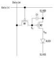
도 2는 본 발명의 일 실시예에 따른 화소 회로 구동 방법(이하 간략히 '하이브리드 구동 방법'이라고 한다)을 설명하기 위한 개략도이다.FIG. 2 is a schematic diagram for explaining a pixel circuit driving method (hereinafter, simply referred to as a 'hybrid driving method') according to one embodiment of the present invention.
도 2를 참조하면, 하이브리드 구동 방법은 LED(light emitting diode), OLED(organic LED), QLED(quantum dot LED) 등의 발광 소자(lighting device)에 구동 전류를 공급하는 화소 회로의 새로운 밝기 조절 방법을 제공한다.Referring to FIG. 2, the hybrid driving method provides a new brightness control method of a pixel circuit that supplies driving current to a lighting device such as an LED (light emitting diode), an OLED (organic LED), or a QLED (quantum dot LED).
하이브리드 구동 방법은 제1 전원전압(VDD)과 제2 전원전압 사이에 전류원(10)과 직렬로 연결되는 발광 소자에 대해 원하는 밝기나 계조에 대응하는 전류를 공급하도록 구성된다. 전류원(10)은 구동 트랜지스터이나 이와 동일한 기능을 수행하는 구성부를 포함할 수 있다. 구동 트랜지스터는 박막 트랜지스터를 포함할 수 있다. 그리고 제2 전원전압은 그라운드 전위를 포함할 수 있다.The hybrid driving method is configured to supply current corresponding to a desired brightness or gradation to a light-emitting element connected in series with a current source (10) between a first power supply voltage (VDD) and a second power supply voltage. The current source (10) may include a driving transistor or a component performing the same function. The driving transistor may include a thin film transistor. And the second power supply voltage may include a ground potential.
이를 위해 하이브리드 구동 방법은 전류원(10)을 제어하기 위한 신호 레벨을 조정하는 스위치(switch, 20)를 구비한다. 스위치는 반도체 트랜지스터 또는 박막 트랜지스터를 포함할 수 있다.For this purpose, the hybrid driving method is provided with a switch (switch, 20) that adjusts a signal level for controlling a current source (10). The switch may include a semiconductor transistor or a thin film transistor.
스위치(20)는 발광 소자를 1회 구동하기 위한 하나의 프레임 또는 하나의 프레임 시간 동안에 복수의 서브 프레임들(sub-frames)를 가진 서브프레임 PWM 신호(sub-frame PWM signal)(이하 간략히 'PWM 신호')에 따라 결정되는 일정 시간동안 턴온 동작하도록 구성될 수 있다.The switch (20) can be configured to be turned on for a certain period of time determined by a sub-frame PWM signal (hereinafter simply referred to as a 'PWM signal') having a plurality of sub-frames during one frame or one frame time for driving the light-emitting element once.
또한, 스위치(20)는 PWM(pulse width modulation) 신호에 따라 일정 시간 동안 서로 다른 적어도 복수의 PAM(pulse amplitude modulation) 신호들에서 선택된 어느 하나의 PAM 신호를 전류원(10)에 인가하도록 구성될 수 있다.Additionally, the switch (20) may be configured to apply one PAM (pulse amplitude modulation) signal selected from at least a plurality of different PAM signals to the current source (10) for a certain period of time according to a PWM (pulse width modulation) signal.
PAM 신호는 데이터 신호로써 전류원(10)이 특정 밝기(luminance)나 특정 계조에 대응하는 세기나 레벨의 전류를 발광 소자에 공급하도록 전류원(10)의 동작을 제어하는데 이용된다.The PAM signal is a data signal used to control the operation of the current source (10) so that the current source (10) supplies current of a specific brightness (luminance) or a level corresponding to a specific gradation to the light-emitting element.
전술한 스위치(20)는 전류원(10)을 제어하기 위한 가장 간단하고 적합한 수단으로서, 전술한 스위치(20)의 동작을 수행할 수 있다면, 다른 스위치 회로나 제어 신호 발생 회로나 제어 구조로 다양하게 변형하거나 대체할 수 있음은 물론이다.The switch (20) described above is the simplest and most suitable means for controlling the current source (10). If the operation of the switch (20) described above can be performed, it can be modified or replaced in various ways with other switch circuits, control signal generation circuits, or control structures.
도 3은 본 실시예의 하이브리드 구동 방법에 채용할 수 있는 기본 구동 원리를 설명하기 위한 도면이다.Figure 3 is a drawing for explaining the basic driving principle that can be employed in the hybrid driving method of the present embodiment.
도 3을 참조하면, 하이브리드 구동 방법은 발광 소자에 결합되는 화소 회로의 스위치(도 2의 20 참조)가 3개의 PAM 구동 전류레벨들과 단일 프레임내에 4개의 서브프레임들을 가진 PWM 신호 예컨대, PWM 스위칭 제어 신호에 의해 동작하도록 구성된다. 여기서, 4개의 서브프레임들 각각은 3개의 PAM 구동 전류레벨들 중 어느 하나가 선택되는 PWM 신호 형태를 가질 수 있다. 이 경우, 하이브리드 구동 방법은 3개의 PAM 구동 전류레벨들과 PWM 신호의 4개의 서브프레임들의 각각의 곱의 합에 의해 결정되는 3진수의 특정 계조를 표현할 수 있다.Referring to FIG. 3, the hybrid driving method is configured such that a switch of a pixel circuit coupled to a light-emitting element (see 20 of FIG. 2) is operated by a PWM signal, e.g., a PWM switching control signal, having three PAM driving current levels and four sub-frames within a single frame. Here, each of the four sub-frames can have a PWM signal form in which any one of the three PAM driving current levels is selected. In this case, the hybrid driving method can express a specific grayscale of a ternary number determined by the sum of the products of the three PAM driving current levels and each of the four sub-frames of the PWM signal.
3개의 PAM 구동 전류레벨들은 데이터 드라이버에 의한 3개의 데이터 소스들(DATA0, DATA1, DATA2)에 의해 스위치의 제1 단자에 각각 인가되는 데이터 전압들(VData0, VData1, VData2)에 대응하여 생성될 수 있다. 이러한 서로 다른 레벨의 데이터 전압들(VData0, VData1, VData2)은 스위치의 제1 단자에 연결되는 적어도 하나의 특정 데이터 라인을 통해 소정 전압이나 전류 또는 데이터 신호를 인가하는 데이터 드라이버에 의해 생성되고 공급될 수 있다.The three PAM driving current levels can be generated in response to data voltages (VData0 , V Data1 , V Data2 ) applied to a first terminal of the switch, respectively, by three data sources (DATA0,DATA1, DATA2) by the data driver. These different levels of data voltages (V Data0 , V Data1, V Data2)canbe generated and supplied by the data driver applying a predetermined voltage or current or data signal through at least one specific data line connected to the first terminal of the switch.
4개의 서브프레임들은 바이너리 가중치를 적용한(binary weighted) 형태로 구성될 수 있다. 예를 들어, 4개의 서브프레임들은 단일 프레임 시간(1 frame time) 내에서 최하위 비트의 서브 프레임(LSB sub-frame)을 기준으로 2의 거듭제곱에 대응하는 시간이 순차적으로 증가하도록 구성될 수 있다. 이 경우, 단일 프레임 내에서 최상위 비트의 서브프레임(MSB sub-frame)은 23의 서브프레임 시간을 가질 수 있고, 최하위 비트의 서브프레임은 20의 서브프레임 시간을 가질 수 있다. 4개의 서브프레임들 각각의 사이에는 스캔 시간이 각각 배치될 수 있으나, 구동 방식에 따라 스캔 시간은 서브프레임 시간과 중첩되는 것도 가능하다. 이러한 복수의 서브프레임들은 스위치의 제어 단자에 연결되는 적어도 하나의 특정 스캔 라인을 통해 소정 전압이나 전류 또는 스캔 신호를 인가하는 스캔 드라이버에 의해 생성되고 공급될 수 있다.The four subframes can be configured in a binary weighted form. For example, the four subframes can be configured such that the time corresponding to a power of 2 sequentially increases based on the least significant bit subframe (LSB subframe) within a single frame time (1 frame time). In this case, the most significant bit subframe (MSB subframe) within a single frame can have a subframe time of 23 , and the least significant bit subframe can have a subframe time of 20 . Scan times can be arranged between each of the four subframes, but the scan time can also overlap with the subframe time depending on the driving method. These multiple subframes can be generated and supplied by a scan driver that applies a predetermined voltage, current, or scan signal through at least one specific scan line connected to a control terminal of the switch.
전술한 데이터 드라이버와 스캔 드라이버는 디스플레이 모듈(도 25의 100 참조)의 일부 구성일 수 있다. 디스플레이 모듈은 데이터 드라이버와 스캔 드라이버에 의해 각각 동작하는 복수의 화소 회로들(130)이 매트릭스 형태로 배열되는 화소부(도 25의 130A 참조)를 구비할 수 있다. 그리고, 화소 회로의 스위치의 제1 단자는 데이터 드라이버에 연결된 데이터 라인에 연결되고, 스위치의 제어 단자는 스캔 라인에 연결된 스캔 라인에 연결되며, 스위치의 제2 단자는 발광 소자에 원하는 계조에 대응하는 전류를 공급하는 전류원(도 2의 10 참조)에 연결된다. 전류원은 구동 트랜지스터로 지칭되고 박막 트랜지스터 구조를 구비할 수 있다.The above-described data driver and scan driver may be part of a display module (see 100 of FIG. 25). The display module may have a pixel section (see 130A of FIG. 25) in which a plurality of pixel circuits (130) operated by the data driver and the scan driver, respectively, are arranged in a matrix form. In addition, a first terminal of a switch of the pixel circuit is connected to a data line connected to the data driver, a control terminal of the switch is connected to a scan line connected to a scan line, and a second terminal of the switch is connected to a current source (see 10 of FIG. 2) that supplies current corresponding to a desired grayscale to a light-emitting element. The current source is referred to as a driving transistor and may have a thin film transistor structure.
이와 같이 본 실시예에 의하면, 2개의 트랜지스터들과 1개의 캐패시터를 포함한 화소 회로 등에서 구동 트랜지스터의 특성 편차에 대한 영향을 최소화하면서 원하는 계조를 효과적으로 표현할 수 있다.According to this embodiment, a desired grayscale can be effectively expressed while minimizing the influence of the characteristic deviation of a driving transistor in a pixel circuit including two transistors and one capacitor.
한편, 본 실시예에서는 데이터 라인을 통해 화소 회로의 스위치의 제1 단자에 인가되는 복수의 PAM 신호레벨들을 3개의 레벨들로 설명하고, 스캔 라인을 통해 스위치의 제어 단자에 인가되는 복수의 PWM 서브프레임들을 4개의 서브프레임들로 설명하였지만, 본 발명은 그러한 구성으로 한정되지 않고, 적어도 2개 이상의 PAM 신호레벨들과 적어도 2개 이상의 서브 프레임들을 이용하여 구성될 수 있음은 물론이다.Meanwhile, in the present embodiment, a plurality of PAM signal levels applied to the first terminal of the switch of the pixel circuit through the data line are described as three levels, and a plurality of PWM subframes applied to the control terminal of the switch through the scan line are described as four subframes. However, the present invention is not limited to such a configuration, and can of course be configured using at least two or more PAM signal levels and at least two or more subframes.
도 4는 본 실시예의 하이브리드 구동 방법에 채용할 수 있는 제1 구동 원리를 설명하기 위한 도면이다. 도 5는 도 4의 제1 구동 원리에 사용되는 PWM 구동 서브프레임과 PAM 구동 전류레벨을 개략적으로 보여주는 예시도이다.Fig. 4 is a diagram for explaining a first driving principle that can be employed in the hybrid driving method of the present embodiment. Fig. 5 is an exemplary diagram schematically showing a PWM driving subframe and a PAM driving current level used in the first driving principle of Fig. 4.
도 4를 참조하면, 하이브리드 구동 방법은 전류원을 제어하여 발광 소자가 특정 밝기나 계조를 표현하도록 하기 위해 4개의 PAM(pluse amplitude modulation) 신호레벨들에서 선택된 어느 하나의 PAM 신호를 단일 프레임 내 4개의 서브프레임들에 대응하는 PWM 신호들에 따른 각각의 스위치 턴온 타이밍에 구동 트랜지스터의 제어 단자에 인가하도록 구성될 수 있다.Referring to FIG. 4, the hybrid driving method can be configured to apply one of four PAM (plus amplitude modulation) signal levels selected from among four PAM signal levels to a control terminal of a driving transistor at each switch turn-on timing according to PWM signals corresponding to four sub-frames within a single frame to control a current source so that the light-emitting element expresses a specific brightness or grayscale.
예를 들면, 도 4의 (a)에 도시한 바와 같이, 일반적인 디지털 구동에서의 11100100을 표현하기 위해 4 진수의 3210으로 하이브리드 구동을 수행할 수 있다. 이 경우, 하이브리드 구동 방법은 최상위 비트(most significant bit, MSB)의 서브프레임 시간(MSB sub-frame time) 동안 3레벨의 크기를 가진 PAM 신호와, 제2 서브프레임 시간 동안 2레벨의 크기를 가진 PAM 신호와, 제3 서브프레임 시간 동안 1레벨의 크기를 가진 PAM 신호와, 최하위 비트(least significant bit, LSB)의 서브 프레임 시간(LSB sub-frame time) 동안 0레벨의 크기를 가진 PAM 신호의 합으로 전류원을 제어할 수 있다.For example, as illustrated in (a) of Fig. 4, hybrid driving can be performed with 3210 in 4-base to express 11100100 in general digital driving. In this case, the hybrid driving method can control the current source by the sum of a PAM signal having a size of 3 levels during the most significant bit (MSB) sub-frame time, a PAM signal having a size of 2 levels during the second sub-frame time, a PAM signal having a size of 1 level during the third sub-frame time, and a PAM signal having a size of 0 level during the least significant bit (LSB) sub-frame time.
또한, 예들 들면 도 4의 (b)에 도시한 바와 같이, 일반적인 디지털 구동에서의 11011000을 표현하기 위해 4 진수의 3120으로 하이브리드 구동을 수행할 수 있다. 이 경우, 하이브리드 구동 방법은 MSB 서브프레임 시간 동안 3레벨의 크기를 가진 PAM 신호와, 제2 서브프레임 시간 동안 1레벨의 크기를 가진 PAM 신호와 제3 서브프레임 시간 동안 2레벨의 크기를 가진 PAM 신호와, LSB 서브 프레임 시간 동안 0레벨의 크기를 가진 PAM 신호의 합으로 전류원을 제어할 수 있다.In addition, for example, as illustrated in (b) of Fig. 4, hybrid driving can be performed with 3120 in 4-base to express 11011000 in general digital driving. In this case, the hybrid driving method can control the current source by the sum of a PAM signal having a size of 3 levels during the MSB subframe time, a PAM signal having a size of 1 level during the second subframe time, a PAM signal having a size of 2 levels during the third subframe time, and a PAM signal having a size of 0 level during the LSB subframe time.
전술한 하이브리드 구동 방법은 도 5에 도시한 바와 같이, 단일 프레임(1 frame)의 4개의 서브프레임들(4 sub-frames)에서 4개의 PAM 신호레벨들(DATA0, DATA1, DATA2, DATA3)에 대응하는 구동 전류레벨들을 각각 가지는 PWM 구동 방식에 대응될 수 있다. 이 경우, 하이브리드 구동 방법은 4개의 구동 전압레벨이나 구동 전류레벨을 가지는 PAM 신호레벨들과 4개의 서브프레임들을 가진 PWM 신호의 서브프레임들에 의해 8-비트의 계조들 중 원하는 계조를 효과적으로 표현할 수 있다.The hybrid driving method described above can correspond to a PWM driving method having driving current levels corresponding to four PAM signal levels (DATA0, DATA1, DATA2, DATA3) in four sub-frames (4 sub-frames) of a single frame (1 frame), as illustrated in FIG. 5. In this case, the hybrid driving method can effectively express a desired grayscale among 8-bit grayscales by PAM signal levels having four driving voltage levels or driving current levels and sub-frames of a PWM signal having four sub-frames.
도 6은 본 실시예의 하이브리드 구동 방법에 채용할 수 있는 제2 구동 원리를 설명하기 위한 도면이다. 도 7은 도 6의 제2 구동 원리에 사용되는 PWM 구동 서브프레임과 PAM 구동 전류레벨을 개략적으로 보여주는 예시도이다.Fig. 6 is a diagram for explaining a second driving principle that can be employed in the hybrid driving method of the present embodiment. Fig. 7 is an exemplary diagram schematically showing a PWM driving subframe and a PAM driving current level used in the second driving principle of Fig. 6.
도 6을 참조하면, 하이브리드 구동 방법은 전류원을 제어하여 발광 소자가 특정 비트의 밝기(luminance)나 계조를 표현하도록 하기 위해 서로 다른 적어도 16개의 PAM(pluse amplitude modulation) 신호들에서 선택된 2개의 PAM 신호레벨들을 단일 프레임 내에 2개의 서브 프레임들을 가진 PWM 신호들의 각 서브프레임에 각각 적용하도록 구성될 수 있다. 여기서, PAM 신호레벨들 중에서 선택된 2개의 특정 PAM 신호레벨들은 PWM 신호의 단일 프레임의 2개의 서브프레임들 각각의 시간 동안에 스위치의 제1 단자에 인가될 수 있다. 스위치의 제2 단자는 발광 소자에 원하는 계조에 대응하는 전류를 공급하는 구동 트랜지스터의 제어 단자에 연결되고, 스위치의 제어 단자에는 상기의 PWM 신호가 인가된다.Referring to FIG. 6, the hybrid driving method can be configured to apply two PAM (plus-amplitude modulation) signal levels selected from at least 16 different PAM signal levels to each subframe of PWM signals having two subframes within a single frame, respectively, in order to control a current source so that a light-emitting element expresses a specific bit of brightness or grayscale. Here, two specific PAM signal levels selected from among the PAM signal levels can be applied to a first terminal of a switch during each of the two subframes of a single frame of the PWM signal. A second terminal of the switch is connected to a control terminal of a driving transistor which supplies a current corresponding to a desired grayscale to the light-emitting element, and the PWM signal is applied to the control terminal of the switch.
전술한 경우, 예를 들면 도 6의 (a)에 도시한 바와 같이, 일반적인 디지털 구동에서의 11100100을 표현하기 위해 16 진수의 14와 4로 하이브리드 구동을 수행할 수 있다. 이 경우, 하이브리드 구동 방법은 단일 프레임 내 2개의 서브 프레임들에 대하여 MSB 서브프레임 시간 동안 14레벨의 크기를 가진 PAM 신호와 LSB 서브프레임 시간 동안 4레벨의 크기를 가진 PAM 신호를 스위치를 통해 전류원 즉 구동 트랜지스터의 제어 단자에 각각 인가하여 구동 트랜지스터에 흐르는 전류를 제어하도록 구성될 수 있다.In the above-described case, for example, as illustrated in (a) of Fig. 6, hybrid driving can be performed with hexadecimal 14 and 4 to express 11100100 in general digital driving. In this case, the hybrid driving method can be configured to control the current flowing in the driving transistor by applying a PAM signal having a size of 14 levels during the MSB subframe time and a PAM signal having a size of 4 levels during the LSB subframe time to the current source, i.e., the control terminal of the driving transistor, through the switch for two subframes within a single frame.
또한, 예들 들면 도 6의 (b)에 도시한 바와 같이, 일반적인 디지털 구동에서의 11011000을 표현하기 위해 16 진수의 12와 8로 하이브리드 구동을 수행할 수 있다. 이 경우, 하이브리드 구동 방법은 스캔 시간의 단일 프레임 내 2개의 서브프레임들에 대해 제1 서브프레임 또는 MSB 서브프레임 시간 동안 12레벨의 크기를 가진 PAM 신호와 제2 서브프레임 또는 LSB 서브프레임 시간 동안 8레벨의 크기를 가진 PAM 신호를, 스위치를 통해, 전류원 즉 구동 트랜지스터의 제어 단자에 각각 인가하여 구동 트랜지스터에 흐르는 전류를 제어하도록 구성될 수 있다.In addition, for example, as illustrated in (b) of FIG. 6, hybrid driving can be performed with hexadecimal 12 and 8 to express 11011000 in general digital driving. In this case, the hybrid driving method can be configured to control the current flowing in the driving transistor by applying a PAM signal having a size of 12 levels during the first subframe or MSB subframe time and a PAM signal having a size of 8 levels during the second subframe or LSB subframe time, respectively, to the current source, i.e., the control terminal of the driving transistor, through the switch, for two subframes within a single frame of the scan time.
여기서, MSB 서브프레임과 LSB 서브프레임으로 구성되는 2개의 서브프레임들 각각은 기재된 순서대로 16(161) 및 1(160)의 서브프레임 시간 길이에 대한 가중치를 각각 가질 수 있다. 그리고 하이브리드 구동 방법에 이용되는 PAM 신호는 0레벨 내지 15레벨의 16개의 신호레벨들을 가질 수 있다.Here, each of the two subframes consisting of the MSB subframe and the LSB subframe can have weights for the subframe time lengths of 16 (161 ) and 1 (160 ) in the order described. And the PAM signal used in the hybrid driving method can have 16 signal levels of 0 to 15 levels.
전술한 하이브리드 구동 방법은 도 7에 도시한 바와 같이, 16개의 PAM 구동 전압레벨들(VDATA0, VDATA1, VDATA2, …, VDATA15)과 2개의 서브프레임들을 가지는 PWM 신호를 이용하도록 구성될 수 있다. 이와 같이, 하이브리드 구동 방법은 발광 소자를 구동하는 화소 회로가 16개의 PAM 구동 전압레벨들과 PWM 신호의 2개의 서브프레임들을 이용하여 구동 트랜지스터의 특성 편차의 영향을 최소화하면서 8-비트의 계조들 중 원하는 계조, 예컨대를 균일하게 표시하도록 구성될 수 있다.The hybrid driving method described above can be configured to use 16 PAM driving voltage levels (VDATA0 , VDATA1 , VDATA2 , …, VDATA15 ) and a PWM signal having two subframes, as illustrated in FIG. 7. In this way, the hybrid driving method can be configured to allow a pixel circuit driving a light-emitting element to uniformly display a desired grayscale, for example, among 8-bit grayscales, while minimizing the influence of characteristic deviation of a driving transistor by using 16 PAM driving voltage levels and two subframes of the PWM signal.
이하에서 일반적인 디지털 구동 방법과 본 실시예의 3진수 내지 16진수 중 어느 하나의 하이브리드 구동 방법을 대비하여 설명하면 다음과 같다.Below, a comparison is made between the general digital driving method and the hybrid driving method of either ternary or hexadecimal of this embodiment.
도 8은 비교예의 디지털 구동 방법을 설명하기 위한 도면이다.Fig. 8 is a drawing for explaining a digital driving method of a comparative example.
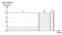
도 8을 참조하면, 비교예의 디지털 구동 방법은 예를 들어 8-비트 계조 중 이진수의 11100100에 대응하는 특정 계조를 표현하기 위해 8개의 서브프레임들 중 MSB 서브프레임과 2번째 내지 4번째 및 6번째 서브프레임들을 각각 레벨 1로 표현하고, 나머지 5번째와 7번째 서브프레임들과 LSB 서브프레임을 각각 레벨 0으로 표현하도록 구성된다. 여기서, 8-비트 계조 표현을 위한 8개의 서브프레임들은 MSB 서브프레임에서 LSB 서브프레임으로 가면서 기재된 순서대로 128(27), 64(26), 32(25), 16(24), 8(23), 4(22), 2(21), 1(20)의 서브프레임 시간 길이에 대한 가중치를 각각 가진다.Referring to FIG. 8, the digital driving method of the comparative example is configured to express, for example, the MSB subframe and the 2nd to 4th and 6th subframes among the 8 subframes as
이와 같이, 비교예의 디지털 구동 방법은 8-비트 계조에서 2진수의 11100100에 대응하는 특정 계조 또는 특정 밝기(luminance)를 표현하기 위해 8개의 서브프레임들 중 MSB 서브프레임과 2번째 내지 4번째 및 6번째 서브프레임들에서 미리 설정된 단일 레벨 1(level 1)의 데이터 신호를 구동 트랜지스터의 제어 단자에 인가하는 것에 대응된다.In this way, the digital driving method of the comparative example corresponds to applying a
도 9는 본 실시예의 하이브리드 구동 방법에 채용할 수 있는 3진수 기반 제3 구동 원리를 설명하기 위한 도면이다.FIG. 9 is a drawing for explaining a ternary-based third driving principle that can be employed in the hybrid driving method of the present embodiment.
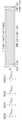
도 9를 참조하면, 하이브리드 구동 방법은, 예를 들어 십진수의 228 또는 이진수의 11100100에 대응하는 3진수의 022110의 계조를 표현하기 위해, 단일 프레임 내 6개의 서브프레임들에 있어서 MSB 서브프레임에 0레벨의 크기를 가진 PAM 신호와, 제2 서브프레임에 2레벨의 PAM 신호와, 제3 서브프레임에 2레벨의 PAM 신호와, 제4 서브프레임에 1레벨의 PAM 신호와, 제5 서브프레임에 1레벨의 PAM 신호, 및 LSM 서브프레임에 0레벨의 PAM 신호를 스위치를 통해 전류원 즉 구동 트랜지스터의 제어 단자에 각각 인가할 수 있다. 이에 의하면, 구동 트랜지스터는 상기의 특정 계조에 대응하는 전류가 발광 소자에 흐르도록 동작할 수 있다.Referring to FIG. 9, the hybrid driving method can apply a PAM signal having a size of 0 level to the MSB subframe, a PAM signal having a size of 2 levels to the second subframe, a PAM signal having a size of 2 levels to the third subframe, a PAM signal having a size of 1 level to the fourth subframe, a PAM signal having a size of 1 level to the fifth subframe, and a PAM signal having a size of 0 level to the LSM subframe, respectively, through a switch to a current source, that is, a control terminal of a driving transistor, in six subframes within a single frame, in order to express a grayscale of, for example, 022110 in ternary corresponding to 228 in decimal or 11100100 in binary. Accordingly, the driving transistor can operate so that a current corresponding to the specific grayscale flows to the light-emitting element.
여기서, 하이브리드 구동 방법에 이용되는 단일 프레임 내 6개의 서브프레임들은 MSB 서브프레임에서 LSB 서브프레임으로 가면서 기재된 순서대로 243(35), 81(34), 27(23), 9(22), 3(31), 1(30)의 서브프레임 시간 길이에 대한 가중치를 각각 가질 수 있다. 그리고 하이브리드 구동 방법에 이용되는 PAM 신호는 0레벨, 1레벨 및 2레벨의 3개의 신호레벨들을 가질 수 있다.Here, the six subframes within a single frame used in the hybrid driving method can have weights for subframe time lengths of 243(35 ), 81(34 ), 27(23 ), 9(22 ), 3(31 ), and 1(30 ) in the order described from the MSB subframe to the LSB subframe, respectively. In addition, the PAM signal used in the hybrid driving method can have three signal levels of 0 level, 1 level, and 2 level.
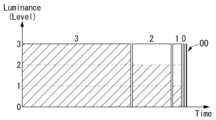
도 10은 본 실시예의 하이브리드 구동 방법에 채용할 수 있는 4진수 기반 제4 구동 원리를 설명하기 위한 도면이다.Fig. 10 is a drawing for explaining a 4-bit based fourth driving principle that can be adopted in the hybrid driving method of the present embodiment.
도 10을 참조하면, 하이브리드 구동 방법은, 예를 들어 십진수의 228 또는 이진수의 11100100에 대응하는 4진수의 3210의 계조를 표현하기 위해, 단일 프레임 내 4개의 서브프레임들에 있어서 MSB 서브프레임에 3레벨의 크기를 가진 PAM 신호와, 제2 서브프레임에 2레벨의 PAM 신호와, 제3 서브프레임에 1레벨의 PAM 신호, 및 LSM 서브프레임에 0레벨의 PAM 신호를 스위치를 통해 구동 트랜지스터의 제어 단자에 각각 인가할 수 있다.Referring to FIG. 10, the hybrid driving method can apply a PAM signal having a size of 3 levels to a MSB subframe, a PAM signal having a size of 2 levels to a second subframe, a PAM signal having a size of 1 level to a third subframe, and a PAM signal having a size of 0 level to an LSM subframe to control terminals of driving transistors through switches in four subframes within a single frame, for example, to express a grayscale of 3210 in binary corresponding to 228 in decimal or 11100100 in binary.
여기서, 하이브리드 구동 방법에 이용되는 단일 프레임 내 4개의 서브프레임들은 MSB 서브프레임에서 LSB 서브프레임으로 가면서 기재된 순서대로 64(43), 16(42), 4(41), 1(40)의 서브프레임 시간 길이에 대한 가중치를 각각 가질 수 있다. 그리고 하이브리드 구동 방법에 이용되는 PAM 신호는 0레벨, 1레벨, 2레벨 및 3레벨의 4개의 신호레벨들을 가질 수 있다.Here, the four subframes within a single frame used in the hybrid driving method can have weights for subframe time lengths of 64(43 ), 16(42 ), 4(41 ), and 1(40 ) in the order described from the MSB subframe to the LSB subframe, respectively. In addition, the PAM signal used in the hybrid driving method can have four signal levels of 0 level, 1 level, 2 level, and 3 level.
도 11은 본 실시예의 하이브리드 구동 방법에 채용할 수 있는 5진수 기반 제5 구동 원리를 설명하기 위한 도면이다.Fig. 11 is a drawing for explaining a 5th driving principle based on a 5th base that can be adopted in the hybrid driving method of the present embodiment.
도 11을 참조하면, 하이브리드 구동 방법은, 예를 들어 십진수의 228 또는 이진수의 11100100에 대응하는 5진수의 1403의 계조를 표현하기 위해, 단일 프레임 내 4개의 서브프레임들에 있어서 MSB 서브프레임에 1레벨의 크기를 가진 PAM 신호와, 제2 서브프레임에 4레벨의 PAM 신호와, 제3 서브프레임에 0레벨의 PAM 신호, 및 LSM 서브프레임에 3레벨의 PAM 신호를 스위치를 통해 구동 트랜지스터의 제어 단자에 각각 인가할 수 있다.Referring to FIG. 11, the hybrid driving method can apply a PAM signal having a size of 1 level to an MSB subframe, a PAM signal having a size of 4 levels to a second subframe, a PAM signal having a size of 0 level to a third subframe, and a PAM signal having a size of 3 levels to an LSM subframe to control terminals of driving transistors, respectively, through switches, in order to express, for example, a grayscale of 1403 in quinary corresponding to 228 in decimal or 11100100 in binary.
여기서, 하이브리드 구동 방법에 이용되는 단일 프레임 내 4개의 서브프레임들은 MSB 서브프레임에서 LSB 서브프레임으로 가면서 기재된 순서대로 125(53), 25(52), 5(51), 1(50)의 서브프레임 시간 길이에 대한 가중치를 각각 가질 수 있다. 그리고 하이브리드 구동 방법에 이용되는 PAM 신호는 0레벨, 1레벨, 2레벨, 3레벨 및 4레벨의 5개의 신호레벨들을 가질 수 있다.Here, the four subframes within a single frame used in the hybrid driving method can have weights for subframe time lengths of 125 (53 ), 25 (52 ), 5 (51 ), and 1 (50 ) in the order described from the MSB subframe to the LSB subframe, respectively. In addition, the PAM signal used in the hybrid driving method can have five signal levels of 0 level, 1 level, 2 level, 3 level, and 4 level.
도 12는 본 실시예의 하이브리드 구동 방법에 채용할 수 있는 6진수 기반 제6 구동 원리를 설명하기 위한 도면이다.Fig. 12 is a drawing for explaining a hexadecimal-based sixth driving principle that can be adopted in the hybrid driving method of the present embodiment.
도 12를 참조하면, 하이브리드 구동 방법은, 예를 들어 십진수의 228 또는 이진수의 11100100에 대응하는 6진수의 1020의 계조를 표현하기 위해, 단일 프레임 내 4개의 서브프레임들에 있어서 MSB 서브프레임에 1레벨의 크기를 가진 PAM 신호와, 제2 서브프레임에 0레벨의 PAM 신호와, 제3 서브프레임에 2레벨의 PAM 신호, 및 LSM 서브프레임에 0레벨의 PAM 신호를 스위치를 통해 구동 트랜지스터의 제어 단자에 각각 인가할 수 있다.Referring to FIG. 12, the hybrid driving method can apply a PAM signal having a size of 1 level to an MSB subframe, a PAM signal having a size of 0 level to a second subframe, a PAM signal having a size of 2 level to a third subframe, and a PAM signal having a size of 0 level to an LSM subframe to control terminals of driving transistors, respectively, through switches, in order to express, for example, a grayscale of 1020 in hexadecimal corresponding to 228 in decimal or 11100100 in binary.
여기서, 하이브리드 구동 방법에 이용되는 단일 프레임 내 4개의 서브프레임들은 MSB 서브프레임에서 LSB 서브프레임으로 가면서 기재된 순서대로 216(63), 36(62), 6(61), 1(60)의 서브프레임 시간 길이에 대한 가중치를 각각 가질 수 있다. 그리고 하이브리드 구동 방법에 이용되는 PAM 신호는 0레벨 내지 5레벨의 6개의 신호레벨들을 가질 수 있다.Here, the four subframes within a single frame used in the hybrid driving method can have weights for subframe time lengths of 216 (63 ), 36 (62 ), 6 (61 ), and 1 (60 ) in the order described from the MSB subframe to the LSB subframe, respectively. In addition, the PAM signal used in the hybrid driving method can have six signal levels of 0 to 5.
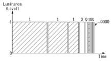
도 13은 본 실시예의 하이브리드 구동 방법에 채용할 수 있는 7진수 기반 제7 구동 원리를 설명하기 위한 도면이다.Fig. 13 is a drawing for explaining the 7th driving principle based on the heptadic number that can be adopted in the hybrid driving method of the present embodiment.
도 13을 참조하면, 하이브리드 구동 방법은, 예를 들어 십진수의 228 또는 이진수의 11100100에 대응하는 7진수의 444의 계조를 표현하기 위해, 단일 프레임 내 3개의 서브프레임들에 있어서 MSB 서브프레임에 4레벨의 크기를 가진 PAM 신호와, 제2 서브프레임에 4레벨의 PAM 신호, 및 LSM 서브프레임에 4레벨의 PAM 신호를 스위치를 통해 구동 트랜지스터의 제어 단자에 각각 인가할 수 있다.Referring to FIG. 13, the hybrid driving method can apply a PAM signal having a size of 4 levels to the MSB subframe, a PAM signal having a size of 4 levels to the second subframe, and a PAM signal having a size of 4 levels to the LSM subframe to the control terminals of the driving transistors through the switches, respectively, in order to express, for example, a grayscale of 444 in heptadic corresponding to 228 in decimal or 11100100 in binary, in three subframes within a single frame.
여기서, 하이브리드 구동 방법에 이용되는 단일 프레임 내 4개의 서브프레임들은 MSB 서브프레임에서 LSB 서브프레임으로 가면서 기재된 순서대로 49(72), 7(71), 1(70)의 서브프레임 시간 길이에 대한 가중치를 각각 가질 수 있다. 그리고 하이브리드 구동 방법에 이용되는 PAM 신호는 0레벨 내지 6레벨의 7개의 신호레벨들을 가질 수 있다.Here, the four subframes within a single frame used in the hybrid driving method can have weights for subframe time lengths of 49 (72 ), 7 (71 ), and 1 (70 ) in the order described from the MSB subframe to the LSB subframe, respectively. In addition, the PAM signal used in the hybrid driving method can have seven signal levels from
한편, 하이브리드 구동 방법은, 8진수의 특정 계조를 표현하기 위해, 단일 프레임 내 3개의 서브프레임들을 이용할 수 있고, 각 서브프레임은 MSB 서브프레임에서 LSB 서브프레임으로 가면서 기재된 순서대로 64(82), 8(81), 1(80)의 서브프레임 시간 길이에 대한 가중치를 각각 가질 수 있다. 그리고 하이브리드 구동 방법에 이용되는 PAM 신호는 0레벨 내지 7레벨의 8개의 신호레벨들을 가질 수 있다.Meanwhile, the hybrid driving method can use three subframes within a single frame to express a specific grayscale of an octal number, and each subframe can have a weight for the subframe time length of 64 (82 ), 8 (81 ), and 1 (80 ) in the order described from the MSB subframe to the LSB subframe. In addition, the PAM signal used in the hybrid driving method can have eight signal levels from
또한, 하이브리드 구동 방법은, 9진수의 특정 계조를 표현하기 위해, 단일 프레임 내 3개의 서브프레임들을 이용할 수 있고, 각 서브프레임은 MSB 서브프레임에서 LSB 서브프레임으로 가면서 기재된 순서대로 81(92), 9(91), 1(90)의 서브프레임 시간 길이에 대한 가중치를 각각 가질 수 있다. 그리고 하이브리드 구동 방법에 이용되는 PAM 신호는 0레벨 내지 8레벨의 9개의 신호레벨들을 가질 수 있다.In addition, the hybrid driving method can use three subframes within a single frame to express a specific grayscale of a 9-bit number, and each subframe can have a weight for the subframe time length of 81 (92 ), 9 (91 ), and 1 (90 ) in the order described from the MSB subframe to the LSB subframe. In addition, the PAM signal used in the hybrid driving method can have nine signal levels from
또한, 하이브리드 구동 방법은, 10진수의 특정 계조를 표현하기 위해, 단일 프레임 내 3개의 서브프레임들을 이용할 수 있고, 각 서브프레임은 MSB 서브프레임에서 LSB 서브프레임으로 가면서 기재된 순서대로 100(102), 10(101), 1(100)의 서브프레임 시간 길이에 대한 가중치를 각각 가질 수 있다. 그리고 하이브리드 구동 방법에 이용되는 PAM 신호는 0레벨 내지 9레벨의 10개의 신호레벨들을 가질 수 있다.In addition, the hybrid driving method can use three subframes within a single frame to express a specific grayscale of a decimal number, and each subframe can have a weight for the subframe time length of 100 (102 ), 10 (101 ), and 1 (100 ) in the order described from the MSB subframe to the LSB subframe. In addition, the PAM signal used in the hybrid driving method can have 10 signal levels of 0 level to 9 level.
또한, 하이브리드 구동 방법은, 11진수의 특정 계조를 표현하기 위해, 단일 프레임 내 3개의 서브프레임들을 이용할 수 있고, 각 서브프레임은 MSB 서브프레임에서 LSB 서브프레임으로 가면서 기재된 순서대로 121(112), 11(111), 1(110)의 서브프레임 시간 길이에 대한 가중치를 각각 가질 수 있다. 그리고 하이브리드 구동 방법에 이용되는 PAM 신호는 0레벨 내지 10레벨의 11개의 신호레벨들을 가질 수 있다.In addition, the hybrid driving method can use three subframes within a single frame to express a specific grayscale of an 11-bit number, and each subframe can have a weight for the subframe time length of 121 (112 ), 11 (111 ), 1 (110 ) in the order described from the MSB subframe to the LSB subframe. In addition, the PAM signal used in the hybrid driving method can have 11 signal levels of 0 level to 10 level.
또한, 하이브리드 구동 방법은, 12진수의 특정 계조를 표현하기 위해, 단일 프레임 내 3개의 서브프레임들을 이용할 수 있고, 각 서브프레임은 MSB 서브프레임에서 LSB 서브프레임으로 가면서 기재된 순서대로 144(122), 12(121), 1(120)의 서브프레임 시간 길이에 대한 가중치를 각각 가질 수 있다. 그리고 하이브리드 구동 방법에 이용되는 PAM 신호는 0레벨 내지 11레벨의 12개의 신호레벨들을 가질 수 있다.In addition, the hybrid driving method can use three subframes within a single frame to express a specific grayscale of a 12-digit number, and each subframe can have a weight for the subframe time length of 144 (122 ), 12 (121 ), and 1 (120 ) in the order described from the MSB subframe to the LSB subframe. In addition, the PAM signal used in the hybrid driving method can have 12 signal levels of 0 level to 11 level.
또한, 하이브리드 구동 방법은, 13진수의 특정 계조를 표현하기 위해, 단일 프레임 내 3개의 서브프레임들을 이용할 수 있고, 각 서브프레임은 MSB 서브프레임에서 LSB 서브프레임으로 가면서 기재된 순서대로 169(132), 13(131), 1(130)의 서브프레임 시간 길이에 대한 가중치를 각각 가질 수 있다. 그리고 하이브리드 구동 방법에 이용되는 PAM 신호는 0레벨 내지 12레벨의 13개의 신호레벨들을 가질 수 있다.In addition, the hybrid driving method can use three subframes within a single frame to express a specific grayscale of a 13-digit number, and each subframe can have a weight for the subframe time length of 169 (132 ), 13 (131 ), and 1 (130 ) in the order described from the MSB subframe to the LSB subframe. In addition, the PAM signal used in the hybrid driving method can have 13 signal levels of 0 level to 12 level.
또한, 하이브리드 구동 방법은, 14진수의 특정 계조를 표현하기 위해, 단일 프레임 내 3개의 서브프레임들을 이용할 수 있고, 각 서브프레임은 MSB 서브프레임에서 LSB 서브프레임으로 가면서 기재된 순서대로 196(142), 14(141), 1(140)의 서브프레임 시간 길이에 대한 가중치를 각각 가질 수 있다. 그리고 하이브리드 구동 방법에 이용되는 PAM 신호는 0레벨 내지 13레벨의 14개의 신호레벨들을 가질 수 있다.In addition, the hybrid driving method can use three subframes within a single frame to express a specific grayscale of a 14-digit number, and each subframe can have a weight for the subframe time length of 196 (142 ), 14 (141 ), and 1 (140 ) in the order described from the MSB subframe to the LSB subframe, respectively. In addition, the PAM signal used in the hybrid driving method can have 14 signal levels of 0 level to 13 level.
또한, 하이브리드 구동 방법은, 15진수의 특정 계조를 표현하기 위해, 단일 프레임 내 3개의 서브프레임들을 이용할 수 있고, 각 서브프레임은 MSB 서브프레임에서 LSB 서브프레임으로 가면서 기재된 순서대로 225(152), 15(151), 1(150)의 서브프레임 시간 길이에 대한 가중치를 각각 가질 수 있다. 그리고 하이브리드 구동 방법에 이용되는 PAM 신호는 0레벨 내지 14레벨의 15개의 신호레벨들을 가질 수 있다.In addition, the hybrid driving method can use three subframes within a single frame to express a specific grayscale of a 15-digit number, and each subframe can have a weight for the subframe time length of 225 (152 ), 15 (151 ), and 1 (150 ) in the order described from the MSB subframe to the LSB subframe. In addition, the PAM signal used in the hybrid driving method can have 15 signal levels of 0 level to 14 level.
그리고, 16진수의 특정 계조를 표현하는 하이브리드 구동 방법은, 도 6의 (a) 및 (b)와 해당 상세 설명을 참조할 수 있다.And, for the hybrid driving method expressing a specific hexadecimal gradation, refer to (a) and (b) of Fig. 6 and the detailed description thereof.
전술한 바와 같이 하이브리드 구동 방법은 PAM 구동과 PWM 구동을 특유의 방식으로 조합하여 구동 트랜지스터의 특성 편차에 의한 영향을 최소화하면서 8-비트의 256 그레이 레벨들을 효과적으로 표현할 수 있다.As described above, the hybrid driving method can effectively express 256 gray levels of 8 bits while minimizing the influence of characteristic deviation of driving transistors by uniquely combining PAM driving and PWM driving.
전술한 실시예에서의 특정 계조 예를 들어 10진수의 228 또는 2진수의 11100100의 계조를 표현하는 하이브리드 구동 방법의 서브프레임 개수와 서브프레임 길이 비율 각각을 비교예와 대비하여 나타내면 다음의 표 1과 같다.The number of subframes and the subframe length ratio of the hybrid driving method for expressing a specific grayscale, for example, a grayscale of 228 in decimal or 11100100 in binary in the above-described embodiment, are shown in Table 1 below in comparison with a comparative example.
표현data
expression
개수Subframe
Number
길이비율Subframe
Length ratio
대응값Decimal
Correspondence value
다만, 각 진수법에 대응하는 복수의 레벨들 각각을 표현하는 방법의 서브프레임의 길이 비는 표 1의 실시예로 한정되지 않고, 4진수의 4레벨과 16진수의 16레벨을 제외하고 다른 진수법의 각 레벨에서 다양하게 변형하여 생성할 수 있다.However, the length ratio of the subframes for expressing each of the multiple levels corresponding to each numeral system is not limited to the example of Table 1, and can be generated by various modifications at each level of other numeral systems except for the 4 levels of the 4-base number and the 16 levels of the hexadecimal number.
도 14 내지 도 16은 본 실시예의 하이브리드 구동 방법에 채용할 수 있는 3진수 기반 제4 구동 원리의 변형예(제8구동 원리)를 설명하기 위한 도면들이다.Figures 14 to 16 are drawings for explaining a modified example (eighth driving principle) of the ternary-based fourth driving principle that can be adopted in the hybrid driving method of the present embodiment.
도 14 내지 도 16을 참조하면, 3진수 또는 3레벨 표현 방법을 이용하는 하이브리드 구동 방법은 8-비트 256 계조 기준으로 3진수의 255레벨의 계조를 표현하기 위해 이용하는 3개의 서브프레임들의 길이 비 혹은 가중치를 [81: 27: 9: 6.5: 3: 1], [81: 27: 8.5: 7: 3: 1] 및 [81: 24.5: 9: 9: 3: 1] 중에서 어느 하나를 선택하여 사용할 수 있다.Referring to FIGS. 14 to 16, a hybrid driving method using a ternary or 3-level representation method can select and use any one of the length ratios or weights of three subframes used to express 255 levels of ternary grayscale based on an 8-bit 256-grayscale standard among [81: 27: 9: 6.5: 3: 1], [81: 27: 8.5: 7: 3: 1], and [81: 24.5: 9: 9: 3: 1].
전술한 본 실시예에 따른 하이브리드 구동 방법은 16진수 이상도 구현이 가능하지만, 16진수 이상의 구현은 8-비트 계조의 표현에 효과적이지 않으므로, 그에 대한 설명은 생략하기로 한다. 한편, 16진수 이상의 구현은 10-비트 1024 계조(gray scale / gradation), 12-비트 4096 계조 등을 표현하는데 효과적이다.The hybrid driving method according to the above-described embodiment can be implemented in hexadecimal or higher, but since implementation in hexadecimal or higher is not effective in expressing 8-bit gradation, its description will be omitted. On the other hand, implementation in hexadecimal or higher is effective in expressing 10-bit 1024 gradation (gray scale / gradation), 12-bit 4096 gradation, etc.
도 17은 비교예의 12-비트 기반 디지털 구동 방법을 나타낸 예시도이다. 도 18은 본 실시예의 하이브리드 구동 방법에 채용할 수 있는 12-비트 기반 제9 구동 원리를 설명하기 위한 예시도이다.Fig. 17 is an exemplary diagram showing a 12-bit based digital driving method of a comparative example. Fig. 18 is an exemplary diagram explaining a 12-bit based ninth driving principle that can be employed in the hybrid driving method of the present embodiment.
도 17에 나타낸 바와 같이 비교예의 12-비트 기반 디지털 구동 방법은 2진수의 특정 계조를 표현하기 위해 단일 프레임 내 12개의 서브프레임들을 배치하고, 각 서브프레임에 1레벨 밝기(luminance)에 대응하는 신호를 인가하거나 인가하지 않도록 구성된다. 예를 들어, 비교예의 12-비트 디지털 구동 방법은 2진수의 111001000000의 계조를 표현하기 위해 MSB 서브프레임과, 2번째, 3번째, 6번째 서브프레임들에서만 1레벨의 휘도에 대응하는 데이터 신호를 구동 트랜지스터의 제어 단자에 인가하도록 구성된다.As shown in Fig. 17, the 12-bit based digital driving method of the comparative example is configured to arrange 12 subframes within a single frame to express a specific grayscale of a binary number, and to apply or not apply a signal corresponding to 1 level of brightness (luminance) to each subframe. For example, the 12-bit digital driving method of the comparative example is configured to apply a data signal corresponding to 1 level of brightness to a control terminal of a driving transistor only in the MSB subframe and the 2nd, 3rd, and 6th subframes to express the grayscale of 111001000000 of a binary number.
따라서, 비교예의 12-비트 기반 디지털 구동 방법은 LSB 서브프레임만으로 제어되는 계조나 LSB 서브프레임과 11번째 서브프레임만으로 제어되는 계조 등의 저계조 동작에서 구동 트랜지스터의 특성 편차에 의해 균일한 밝기의 계조를 제대로 표현하지 못하는 문제를 나타낼 수 있다.Therefore, the 12-bit based digital driving method of the comparative example may exhibit a problem of not being able to properly express gradations of uniform brightness due to the characteristic deviation of the driving transistor in low gradation operations such as gradations controlled only by the LSB subframe or gradations controlled only by the LSB subframe and the 11th subframe.
한편, 본 실시예에 따른 12-비트 기반 하이브리드 구동 방법은, 도 18에 나타낸 바와 같이, 예를 들어 십진수의 3,648 또는 이진수의 111001000000에 대응하는 12진수의 321000의 계조를 표현하기 위해, 단일 프레임 내 6개의 서브프레임들에 있어서 MSB 서브프레임에 3레벨의 크기를 가진 PAM 신호와, 제2 서브프레임에 2레벨의 PAM 신호와, 제3 서브프레임에 1레벨의 PAM 신호와, 제4 서브프레임에 0레벨의 PAM 신호와, 제5 서브프레임에 0레벨의 PAM 신호, 및 LSM 서브프레임에 0레벨의 PAM 신호를, 스위치를 통해 구동 트랜지스터의 제어 단자에 순차적으로 인가하도록 구성될 수 있다.Meanwhile, the 12-bit based hybrid driving method according to the present embodiment can be configured to sequentially apply a PAM signal having a size of 3 levels to the MSB subframe, a PAM signal having a size of 2 levels to the second subframe, a PAM signal having a size of 1 level to the third subframe, a PAM signal having a size of 0 levels to the fourth subframe, a PAM signal having a size of 0 levels to the fifth subframe, and a PAM signal having a size of 0 levels to the LSM subframe to the control terminal of the driving transistor through the switch in six subframes within a single frame, in order to express a grayscale of 321000 in hexadecimal corresponding to, for example, 3,648 in decimal or 111001000000 in binary, as shown in FIG. 18.
여기서, 12-비트 기반 하이브리드 구동 방법에 이용되는 단일 프레임 내 6개의 서브프레임들은 MSB 서브프레임에서 LSB 서브프레임으로 가면서 서브프레임 시간 길이에 대한 가중치가 소정 값의 지수승이 선형적으로 작아지는 값을 각각 가질 수 있다. 그리고 하이브리드 구동 방법에 이용되는 PAM 신호는 0레벨 내지 3레벨의 4개의 신호레벨들을 가질 수 있다.Here, the six subframes within a single frame used in the 12-bit based hybrid driving method can each have a weight value for the subframe time length that linearly decreases as an exponent of a predetermined value from the MSB subframe to the LSB subframe. In addition, the PAM signal used in the hybrid driving method can have four signal levels from
이와 같이, 본 실시예에 따른 하이브리드 구동 방법은 비교예의 디지털 구동 방법의 서브프레임들의 개수보다 작은 서브프레임들의 개수를 사용함으로써 LSB 서브프레임의 시간을 증가시켜 1레벨 그레이의 표현 시 비교예 대비 10배 이상의 저계조 전류를 구동 트랜지스터에 흐르도록 제어함으로써 노이즈(noise), 누설(leakage), 스트레스(stress) 등에 강인한 특성을 가질 수 있다.In this way, the hybrid driving method according to the present embodiment can have robust characteristics against noise, leakage, stress, etc. by controlling low-gray current that is 10 times higher than that of the comparative example to flow through the driving transistor when expressing 1-level gray by increasing the time of the LSB subframe by using a smaller number of subframes than that of the digital driving method of the comparative example.
도 19는 본 실시예의 하이브리드 구동 방법을 적용할 수 있는 화소 회로에 대한 회로도이다.Fig. 19 is a circuit diagram of a pixel circuit to which the hybrid driving method of the present embodiment can be applied.
도 19를 참조하면, 하이브리드 구동 방법에 적용가능한 화소 회로는 2개의 트랜지스터(M1, M2)와 1개의 캐패시터(C1)를 포함한 구조를 포함할 수 있다. 2개의 트랜지스터들 중 제1 트랜지스터(M1)는 스위칭 박막 트랜지스터에 대응하고, 제2 트랜지스터(M2)는 OLED(organic light emitting diode) 등의 발광 소자의 전류량 제어를 위한 구동 트랜지스터 또는 구동 박막 트랜지스터에 대응할 수 있다. 그리고 하나의 커패시터(C1)는 단일 프레임(frame) 동안 제1 트랜지스터(M1)를 통해 제2 트랜지스터(M2)의 제어 단자에 인가되는 데이터(data) 전압을 유지한다.Referring to FIG. 19, a pixel circuit applicable to a hybrid driving method may include a structure including two transistors (M1, M2) and one capacitor (C1). Among the two transistors, the first transistor (M1) may correspond to a switching thin film transistor, and the second transistor (M2) may correspond to a driving transistor or a driving thin film transistor for controlling the amount of current of a light-emitting element such as an organic light emitting diode (OLED). In addition, one capacitor (C1) maintains a data voltage applied to a control terminal of the second transistor (M2) through the first transistor (M1) during a single frame.
화소 회소에서, 제1 트랜지스터(M1)의 제1 단자는 m번째 데이터 라인(data(m))에 연결되고, 제1 트랜지스터(M1)의 제어 단자(이하 제1 제어 단자라고도 함)는 n번째 게이트(gate(n)) 라인 또는 스캔 라인에 연결되며, 제1 트랜지스터(M1)의 제2 단자는 구동 트랜지스터(M2)의 제어 단자(이하 제2 제어 단자라고도 함)와 커패시터(C1)의 제2 단자에 공통 연결된다. 상기의 m 및 n은 임의의 자연수이다. 공통 연결 노드는 소정의 전압(VG)을 가진다.In the pixel circuit, the first terminal of the first transistor (M1) is connected to the m-th data line (data(m)), the control terminal (hereinafter also referred to as the first control terminal) of the first transistor (M1) is connected to the n-th gate (gate(n)) line or scan line, and the second terminal of the first transistor (M1) is commonly connected to the control terminal (hereinafter also referred to as the second control terminal) of the driving transistor (M2) and the second terminal of the capacitor (C1). The m and n above are arbitrary natural numbers. The common connection node has a predetermined voltage (VG ).
그리고, 구동 트랜지스터(M2)의 제1 단자는 제1 전원전압(ELVDD)과 커패시터의 제2 단자에 공통 연결되고, 구동 트랜지스터(M2)의 제2 단자는 OLED(organic light emitting diode)의 애노드와 같이 발광 소자의 제1 단자에 연결된다. 발광 소자의 제2 단자는 제2 전원전압(ELVSS)이나 그라운드에 연결된다.And, the first terminal of the driving transistor (M2) is commonly connected to the first power supply voltage (ELVDD) and the second terminal of the capacitor, and the second terminal of the driving transistor (M2) is connected to the first terminal of the light-emitting element, such as the anode of an OLED (organic light emitting diode). The second terminal of the light-emitting element is connected to the second power supply voltage (ELVSS) or ground.
전술한 화소 회로는 원하는 계조를 표현하기 위해 단일 프레임 내 복수의 서브프레임들에 대한 PWM 신호에 의해 결정되는 시간 동안에 PWM 신호의 각 서브프레임에 대하여 결정되는 복수의 PAM 신호레벨들 중 어느 하나를 제1 트랜지스터(M1)를 통해 구동 트랜지스터(M2)의 제2 제어 단자에 인가하도록 동작한다.The pixel circuit described above operates to apply one of a plurality of PAM signal levels determined for each subframe of the PWM signal to a second control terminal of a driving transistor (M2) through a first transistor (M1) during a time determined by the PWM signal for a plurality of subframes within a single frame in order to express a desired gradation.
전술한 구성의 화소 회로는 DPS(display period separated) 방식으로 구동될 수 있다. DSP 구동은 스캔 시간(scan time)과 발광 소자의 발광 시간(emission time)이 중첩되지 않고 구분되도록 동작하며, 스캔 시간과 발광 시간이 중첩되는 SES(simultaneous erasing scan) 구동 방식에 비해 발광 소자의 발광 시간이 상대적으로 짧다.The pixel circuit of the above-described configuration can be driven in a DPS (display period separated) manner. DSP driving operates so that the scan time and the emission time of the light-emitting element do not overlap but are separated, and the emission time of the light-emitting element is relatively short compared to the SES (simultaneous erasing scan) driving method in which the scan time and the emission time overlap.
이와 같이, 본 실시예에 의한 하이브리드 구동 방법은 LED, OLED, QLED 등의 발광 소자를 구동하기 위한 가장 간소화된 화소 회로에도 효과적으로 적용될 수 있다. 즉, 본 실시예의 하이브리드 구동 방법은 동일 구성의 화소 회로에 적용되는 기존의 화소 회로 구동 방법에 의한 저계조 표현에서 약 10%의 오차를 발생시켜 디스플레이 장치의 밝기 불균일성을 유발시키는 문제를 효과적으로 해결할 수 있다. 또한, 본 발명에 의하면, N-비트 서브프레임에 요구되는 전력을 수배 정도 증가시키고, 서브프레임의 구현을 용이하게 하며, 전류원인 구동 트랜지스터를 스위치와 같이 사용함으로써 발광 소자의 애노드 전압을 실질적으로 일정하게 고정시켜 발광 소자의 편차를 효과적으로 보상할 수 있다.In this way, the hybrid driving method according to the present embodiment can be effectively applied even to the simplest pixel circuit for driving light-emitting elements such as LEDs, OLEDs, and QLEDs. That is, the hybrid driving method according to the present embodiment can effectively solve the problem of causing brightness unevenness of a display device by causing an error of about 10% in low-grayscale expression by the conventional pixel circuit driving method applied to pixel circuits of the same configuration. In addition, according to the present invention, the power required for an N-bit subframe is increased by several times, the implementation of the subframe is facilitated, and the anode voltage of the light-emitting element is substantially fixed constant by using the driving transistor, which is a current source, as a switch, thereby effectively compensating for the deviation of the light-emitting element.
도 20은 본 실시예의 하이브리드 구동 방법을 적용할 수 있는 또 다른 회소 회로에 대한 회로도이다.Fig. 20 is a circuit diagram for another circuit to which the hybrid driving method of the present embodiment can be applied.
도 20을 참조하면, 하이브리드 구동 방법에 적용가능한 화소 회로는 3개의 트랜지스터(M1, M2, M3)와 1개의 캐패시터(C1)를 포함하여 구성될 수 있다.Referring to FIG. 20, a pixel circuit applicable to a hybrid driving method can be configured to include three transistors (M1, M2, M3) and one capacitor (C1).
본 화소 회소에서, 제1 트랜지스터(M1)의 제1 단자는 m번째 데이터 라인(data(m))에 연결되고, 제1 트랜지스터(M1)의 제1 제어 단자는 n번째 게이트(gate(n)) 라인 또는 스캔 라인에 연결되며, 제1 트랜지스터(M1)의 제2 단자는 구동 트랜지스터(M2)의 제어 단자와 커패시터(C1)의 제2 단자에 공통 연결된다.In this pixel circuit, the first terminal of the first transistor (M1) is connected to the m-th data line (data(m)), the first control terminal of the first transistor (M1) is connected to the n-th gate (gate(n)) line or scan line, and the second terminal of the first transistor (M1) is commonly connected to the control terminal of the driving transistor (M2) and the second terminal of the capacitor (C1).
구동 트랜지스터(M2)의 제1 단자는 제1 전원전압(ELVDD)과 커패시터의 제2 단자에 공통 연결되고, 구동 트랜지스터(M2)의 제2 단자는 OLED(organic light emitting diode)의 애노드와 같이 발광 소자의 제1 단자에 연결된다. 발광 소자의 제2 단자는 제2 전원전압(ELVSS)이나 그라운드에 연결된다. 구동 트랜지스터(M2)는 제2 트랜지스터로 지칭될 수 있다.A first terminal of the driving transistor (M2) is commonly connected to a first power supply voltage (ELVDD) and a second terminal of the capacitor, and a second terminal of the driving transistor (M2) is connected to a first terminal of a light-emitting element, such as an anode of an OLED (organic light emitting diode). The second terminal of the light-emitting element is connected to a second power supply voltage (ELVSS) or ground. The driving transistor (M2) may be referred to as a second transistor.
그리고 제3 트랜지스터(M3)의 제1 단자는 제1 전원전압(ELVDD)에 연결되고, 제3 트랜지스터(M3)의 제어 단자(이하 제3 제어 단자라고도 함)는 n번째 소거 라인(ES(n)) 또는 소거 배선에 연결되고, 제3 트랜지스터(M3)의 제2 단자는 제1 트랜지스터(M1)의 제2 단자와 구동 트랜지스터(M2)의 제어 단자와 커패시터(C1)의 제2 단자에 공통 연결된다.And the first terminal of the third transistor (M3) is connected to the first power supply voltage (ELVDD), the control terminal of the third transistor (M3) (hereinafter also referred to as the third control terminal) is connected to the nth erase line (ES(n)) or erase wiring, and the second terminal of the third transistor (M3) is commonly connected to the second terminal of the first transistor (M1), the control terminal of the driving transistor (M2), and the second terminal of the capacitor (C1).
전술한 구성의 화소 회로는 SES(simultanceous erasing scan) 방식으로 구동될 수 있다. SES 구동은 발광 소자의 발광 시간(emission time)과 스캔 시간(scan time)의 길이에 따라 제3 트랜지스터(M3)를 통한 소거(erasing) 동작으로 발광 시간과 스캔 시간이 중첩되도록 동작하며, 발광 소자의 발광 시간이 DPS 방식 대비 상대적으로 길다.The pixel circuit of the above-described configuration can be driven by the SES (simultaneous erasing scan) method. SES driving operates by overlapping the emission time and scan time through an erasing operation via the third transistor (M3) according to the length of the emission time and scan time of the light-emitting element, and the emission time of the light-emitting element is relatively longer than that of the DPS method.
이와 같이, 본 실시예에 의한 하이브리드 구동 방법은 LED, OLED, QLED 등의 발광 소자를 구동하기 위한 3T1C(3 transistors and 1 capacitor)의 화소 회로에도 효과적으로 적용될 수 있다. 즉, 본 실시예의 하이브리드 구동 방법은 동일 구성의 화소 회로에 적용되는 기존의 화소 회로 구동 방법에 비해 저계조 표현에서의 오차를 제거하면서 N-비트 서브프레임에 요구되는 전력을 수배 정도 증가시키고 서브프레임의 구현을 용이하게 하며, 구동 트랜지스터를 스위치로 사용함으로써 발광 소자의 애노드 전압을 실질적으로 일정하게 고정시켜 발광 소자의 편차를 효과적으로 보상할 수 있다.In this way, the hybrid driving method according to the present embodiment can be effectively applied to a 3T1C (3 transistors and 1 capacitor) pixel circuit for driving light-emitting elements such as LEDs, OLEDs, and QLEDs. That is, compared to a conventional pixel circuit driving method applied to a pixel circuit of the same configuration, the hybrid driving method of the present embodiment eliminates errors in low-grayscale expression while increasing the power required for an N-bit subframe by several times, facilitating implementation of the subframe, and effectively compensating for deviation of the light-emitting element by substantially constantly fixing the anode voltage of the light-emitting element by using the driving transistor as a switch.
도 21은 도 20의 화소 회로의 하이브리드 구동 방법에 채용할 수 있는 PWM 구동 서브프레임과 PAM 구동 전류레벨의 일례를 개략적으로 보여주는 예시도이다.FIG. 21 is an exemplary diagram schematically showing an example of a PWM driving subframe and a PAM driving current level that can be employed in the hybrid driving method of the pixel circuit of FIG. 20.
도 21을 참조하면, 하이브리드 구동 방법은 데이터 드라이버의 4개의 순차적이거나 병렬적인 데이터 소스(DATA0, DATA1, DATA2, DATA3)에 의한 4개의 PAM 구동 전류레벨들과 단일 프레임 내 4개의 서브프레임들을 가지는 PWM 신호를 이용한다. 4개의 PAM 구동 전류레벨들은 각각 소정의 데이터 전압(VDATA0, VDATA1, VDATA2, VDATA3)을 구비할 수 있다. 그리고 하이브리드 구동 방법은 SES 구동 방식으로 구동될 수 있다.Referring to FIG. 21, the hybrid driving method uses a PWM signal having four PAM driving current levels by four sequential or parallel data sources (DATA0, DATA1, DATA2, DATA3) of a data driver and four subframes within a single frame. Each of the four PAM driving current levels can have a predetermined data voltage (VDATA0 , VDATA1 , VDATA2 , VDATA3 ). And the hybrid driving method can be driven by an SES driving method.
따라서, 본 실시예의 하이브리드 구동 방법에서 발광 소자의 발광 시간에는 인접한 서브프레임들 사이에는 구분된 스캔 시간이 존재하지 않고, 발광 시간은 스캔 시간과 중첩되고, 발광 시간과 중첩되는 스캔 시간에 커패시터를 충전하도록 제3 트랜지스터가 턴온 동작할 수 있다.Therefore, in the hybrid driving method of the present embodiment, there is no distinct scan time between adjacent subframes in the light-emitting time of the light-emitting element, the light-emitting time overlaps with the scan time, and the third transistor can be turned on to charge the capacitor during the scan time overlapping with the light-emitting time.
도 22는 도 20의 화소 회로의 하이브리드 구동 방법에 채용할 수 있는 PWM 구동 서브프레임과 PAM 구동 전류레벨의 다른 실시예를 개략적으로 보여주는 예시도이다.FIG. 22 is an exemplary diagram schematically showing another embodiment of a PWM driving subframe and a PAM driving current level that can be employed in the hybrid driving method of the pixel circuit of FIG. 20.
도 22를 참조하면, 하이브리드 구동 방법은 16개의 데이터 소스들(DATA0, DATA1, DATA2, …, DATA15)에 의한 16개의 PAM 구동 전류레벨들과 단일 프레임 내 2개의 서브프레임들을 가지는 PWM 신호를 이용한다. 그리고 하이브리드 구동 방법은 SES 구동 방식으로 구동된다.Referring to Fig. 22, the hybrid driving method uses 16 PAM driving current levels by 16 data sources (DATA0, DATA1, DATA2, …, DATA15) and a PWM signal having 2 subframes within a single frame. And the hybrid driving method is driven by the SES driving method.
따라서, 본 실시예의 하이브리드 구동 방법에서 발광 소자의 발광 시간에는 인접한 서브프레임들 사이에는 구분된 스캔 시간이 존재하지 않고, 발광 시간은 스캔 시간과 중첩되고, 발광 시간과 중첩되는 스캔 시간에 커패시터를 충전하도록 제3 트랜지스터가 턴온 동작할 수 있다.Therefore, in the hybrid driving method of the present embodiment, there is no distinct scan time between adjacent subframes in the light-emitting time of the light-emitting element, the light-emitting time overlaps with the scan time, and the third transistor can be turned on to charge the capacitor during the scan time overlapping with the light-emitting time.
도 23은 본 실시예의 하이브리드 구동 방법을 적용할 수 있는 또 다른 형태의 회소 회로에 대한 회로도이다. 도 24는 도 23의 화소 회로의 주요 작동 원리를 설명하기 위한 타이밍도이다.Fig. 23 is a circuit diagram of another type of pixel circuit to which the hybrid driving method of the present embodiment can be applied. Fig. 24 is a timing diagram for explaining the main operating principles of the pixel circuit of Fig. 23.
도 23을 참조하면, 하이브리드 구동 방법에 적용가능한 화소 회로는 3개의 트랜지스터(M1, M2, M3)와 1개의 캐패시터(C1)를 포함한 구조를 구비할 수 있다.Referring to FIG. 23, a pixel circuit applicable to a hybrid driving method may have a structure including three transistors (M1, M2, M3) and one capacitor (C1).
본 화소 회소에서, 제1 트랜지스터(M1)의 제1 단자는 m번째 데이터 라인(data(m))에 연결되고, 제1 트랜지스터(M1)의 제1 제어 단자는 n번째 게이트 라인(gate(n))(스캔 라인이라고도 함)에 연결되며, 제1 트랜지스터(M1)의 제2 단자는 구동 트랜지스터(M2)의 제어 단자와 커패시터(C1)의 제2 단자에 공통 연결된다.In this pixel circuit, the first terminal of the first transistor (M1) is connected to the mth data line (data(m)), the first control terminal of the first transistor (M1) is connected to the nth gate line (gate(n)) (also called a scan line), and the second terminal of the first transistor (M1) is commonly connected to the control terminal of the driving transistor (M2) and the second terminal of the capacitor (C1).
구동 트랜지스터(M2)의 제1 단자는 제1 전원전압(ELVDD)과 커패시터의 제2 단자에 공통 연결되고, 구동 트랜지스터(M2)의 제2 단자는 발광 소자의 제1 단자 즉, OLED(organic light emitting diode)의 애노드에 연결된다. 발광 소자의 제2 단자 즉, OLED의 캐소드는 제2 전원전압(ELVSS)이나 그라운드에 연결된다. 구동 트랜지스터(M2)는 제2 트랜지스터로 지칭될 수 있다.A first terminal of the driving transistor (M2) is commonly connected to a first power supply voltage (ELVDD) and a second terminal of the capacitor, and a second terminal of the driving transistor (M2) is connected to a first terminal of the light-emitting element, that is, an anode of an OLED (organic light emitting diode). A second terminal of the light-emitting element, that is, a cathode of the OLED, is connected to a second power supply voltage (ELVSS) or ground. The driving transistor (M2) may be referred to as a second transistor.
그리고 제3 트랜지스터(M3)의 제1 단자는 제1 전원전압(ELVDD)에 연결되고, 제3 트랜지스터(M3)의 제3 제어 단자는 n번째 소거 라인(ES(n)) 또는 소거 배선에 연결되고, 제3 트랜지스터(M3)의 제2 단자는 제1 트랜지스터(M1)의 제2 단자와 구동 트랜지스터(M2)의 제어 단자와 커패시터(C1)의 제2 단자에 공통 연결된다.And the first terminal of the third transistor (M3) is connected to the first power supply voltage (ELVDD), the third control terminal of the third transistor (M3) is connected to the nth erase line (ES(n)) or erase wiring, and the second terminal of the third transistor (M3) is commonly connected to the second terminal of the first transistor (M1), the control terminal of the driving transistor (M2), and the second terminal of the capacitor (C1).
전술한 구성의 화소 회로는 SES(simultanceous erasing scan) 방식으로 구동될 수 있다. SES 구동은 발광 소자의 발광 시간(emission time)과 스캔 시간(scan time)의 길이에 따라 제3 트랜지스터(M3)를 통한 소거(erasing) 동작으로 발광 시간과 스캔 시간이 중첩되도록 동작하며, 발광 소자의 발광 시간이 DPS 방식 대비 상대적으로 길다.The pixel circuit of the above-described configuration can be driven by the SES (simultaneous erasing scan) method. SES driving operates by overlapping the emission time and scan time through an erasing operation via the third transistor (M3) according to the length of the emission time and scan time of the light-emitting element, and the emission time of the light-emitting element is relatively longer than that of the DPS method.
본 실시예의 하이브리드 구동 방법은 도 24에 도시한 바와 같이 제1 시간 동안의 n번째 스캔 라인(PS(n))의 PWM 신호에 따라 제1 트랜지스터(M1)가 턴온된 상태에서 n번째 소거 라인(ES(n))의 신호에 따라 제3 트랜지스터(M3)가 턴오프 동작하고, 발광 소자가 발광하는 발광(emission) 시간 동안 n번째 스캔 라인(PS(n))의 PWM 신호에 따라 제1 트랜지스터(M1)가 턴오프된 상태에서 n번째 소거 라인(ES(n))의 신호에 따라 제3 트랜지스터(M3)가 턴온 동작하는 과정을 반복하도록 구성될 수 있다. 이러한 구성에 의하면, 소거 라인(ES(n))의 제어 신호의 레벨에 따라 제3 트랜시스터(M3)는 턴오프 동작하고, 발광 소자는 플로팅(floating) 상태로 입력되는 데이터(data)에 따라 소정 레벨의 계조나 밝기를 표현하도록 동작할 수 있다.The hybrid driving method of the present embodiment may be configured to repeat the process of a first transistor (M1) being turned on in accordance with a PWM signal of an nth scan line (PS(n)) during a first time period, a third transistor (M3) being turned off in accordance with a signal of an nth erase line (ES(n)), and a third transistor (M3) being turned on in accordance with a signal of an nth erase line (ES(n)) during an emission time in which a light-emitting element emits light, while the first transistor (M1) being turned off in accordance with a PWM signal of the nth scan line (PS(n)). According to this configuration, the third transistor (M3) is turned off in accordance with the level of the control signal of the erase line (ES(n)), and the light-emitting element can operate to express a predetermined level of gradation or brightness in accordance with data input in a floating state.
도 25는 본 실시예의 하이브리드 구동 방법을 이용하는 디스플레이 모듈에 대한 개략적인 블록도이다.Fig. 25 is a schematic block diagram of a display module using the hybrid driving method of the present embodiment.
도 25를 참조하면, 디스플레이 모듈(100)은, 데이터 드라이버(110), 게이트 드라이버(120), 화소부(130A), 타이밍 제어부(140) 및 전원공급장치(150)를 포함할 수 있다. 게이트 드라이버(120)는 스캔 드라이버로 지칭될 수 있다.Referring to FIG. 25, the display module (100) may include a data driver (110), a gate driver (120), a pixel unit (130A), a timing control unit (140), and a power supply unit (150). The gate driver (120) may be referred to as a scan driver.
화소부(130A)는 데이터 드라이버(110)의 데이터 라인들(112)과 게이트 드라이버(120)의 스캔 라인들(122)이 교차되는 교차점 부근에 각각 위치하는 복수의 화소들(130)를 구비한다. 복수의 화소들(130) 각각은 디스플레이 장치의 화소부(130A)를 구성하는 단위 화소나 단위 화소의 서브 화소들 중 어느 하나에 대응될 수 있다.The pixel portion (130A) has a plurality of pixels (130) each positioned near an intersection where data lines (112) of a data driver (110) and scan lines (122) of a gate driver (120) intersect. Each of the plurality of pixels (130) may correspond to one of the unit pixels constituting the pixel portion (130A) of the display device or the sub-pixels of the unit pixels.
데이터 드라이버(110)는 복수개로 구성되고 화소부(130A)의 일측 가장자리에 나열될 수 있다. 데이터 드라이버(110)는 제1 방향에서 화소부(130A) 내로 연장하는 복수의 데이터 라인들(112)을 구비하고 각 데이터 라인을 통해 각 화소(130)의 화소 회로에 데이터 신호를 공급할 수 있다. 데이터 신호는 서로 다른 적어도 2개 이상의 레벨들을 가진 PAM(pluse amplitude modulation) 신호들에서 선택된 어느 하나의 레벨의 PAM 신호를 포함할 수 있다.The data driver (110) may be configured in multiple units and arranged at one edge of the pixel portion (130A). The data driver (110) may have multiple data lines (112) extending into the pixel portion (130A) in a first direction and may supply a data signal to a pixel circuit of each pixel (130) through each data line. The data signal may include a PAM signal of one level selected from PAM (plus amplitude modulation) signals having at least two different levels.
게이트 드라이버(120)는 복수개로 구성되고 화소부(130A)의 또 다른 일측 가장자리에 나열될 수 있다. 게이트 드라이버(120)는 제1 방향과 대략 직교하는 제2 방향에서 화소부(130A) 내로 연장하는 복수의 스캔 라인들(122)을 구비하고 각 스캔 라인을 통해 각 화소(130)의 화소 회로에 스캔 신호를 공급할 수 있다. 스캔 신호는 표현하고자 하는 계조 데이터를 위한 비트수보다 작은 복수의 서브 프레임들을 가진 PWM(pulse width modulation) 신호를 포함할 수 있다.The gate driver (120) may be configured in multiple units and arranged on another edge of the pixel portion (130A). The gate driver (120) may have multiple scan lines (122) extending into the pixel portion (130A) in a second direction substantially orthogonal to the first direction, and may supply a scan signal to a pixel circuit of each pixel (130) through each scan line. The scan signal may include a PWM (pulse width modulation) signal having multiple sub-frames smaller than the number of bits for grayscale data to be expressed.
타이밍 제어기(140)는 데이터 드라이버(110)와 게이트 드라이버(120)의 동작 타이밍을 제어한다. 타이밍 제어기(140)는 입력되는 매 프레임의 영상 신호에 기초하여 데이터 드라이버(110)에 PAM 신호를 전달하고, 게이트 드라이버(120)에 PWM 신호를 전달할 수 있다.The timing controller (140) controls the operation timing of the data driver (110) and the gate driver (120). The timing controller (140) can transmit a PAM signal to the data driver (110) and a PWM signal to the gate driver (120) based on the image signal of each input frame.
전원공급장치(150)는, 선택적으로 포함될 수 있는 구성요소로서, 배터리 등의 자체 전원을 포함하거나 외부의 상용 전원에 연결될 수 있고, 데이터 드라이버(110), 게이트 드라이버(120), 화소부(130A) 및 타이밍 제어기(140)에 필요한 전원을 공급할 수 있다.The power supply unit (150) is an optional component that may include its own power source such as a battery or may be connected to an external commercial power source, and may supply power required for the data driver (110), the gate driver (120), the pixel unit (130A), and the timing controller (140).
도 26은 비교예의 디스플레이 모듈의 데이터 드라이버에 사용되는 디코더를 개략적으로 나타낸 예시도이다. 도 27은 도 25의 디스플레이 모듈에 채용할 수 있는 데이터 드라이버의 디코더에 대한 개략적인 예시도이다. 그리고 도 28은 도 25의 디스플레이 모듈에 채용할 수 있는 데이터 드라이버의 디코더의 다른 구조에 대한 예시도이다.Fig. 26 is an exemplary diagram schematically showing a decoder used in a data driver of a display module of a comparative example. Fig. 27 is an exemplary diagram schematically showing a decoder of a data driver that can be employed in the display module of Fig. 25. And Fig. 28 is an exemplary diagram for another structure of a decoder of a data driver that can be employed in the display module of Fig. 25.
도 26을 참조하면, 비교예의 디스플레이 모듈의 데이터 드라이버는 각 화소의 화소 회로에서 8-비트 밝기 또는 계조를 표현하기 위해 257개의 저항기들(R0 내지 R256)로 구성된 범용 저항 직렬회로(global R-string)를 통해 기준 전압(VREF1-VREFn)으로부터 분배되는 복수의 기준 입력 전압을 입력받는 8-비트(8-bit) 디코더(decoder)를 구비한다. 8-비트 디코더는 8-비트 내지 256-비트의 서로 다른 레벨들의 데이터 신호를 출력할 수 있고, 그 출력단에 증폭기가 구비될 수 있다.Referring to FIG. 26, the data driver of the display module of the comparative example has an 8-bit decoder that receives a plurality of reference input voltages distributed from a reference voltage (VREF1 -VREFn ) through a global R-string composed of 257 resistors (R0 to R256 ) to express 8-bit brightness or gradation in the pixel circuit of each pixel. The 8-bit decoder can output data signals of different levels of 8 bits to 256 bits, and an amplifier can be provided at its output terminal.
한편, 도 27을 참조하면, 본 실시예의 디스플레이 모듈에 채용할 수 있는 데이터 드라이버의 디코더(decoder)는 5개의 저항기들(R0 내지 R4)로 구성된 범용 저항 직렬회로(global R-string)를 통해 기준 전압(VREF1-VREFn)으로부터 분배되는 복수의 기준 입력 전압을 입력받는 2-비트(2-bit) 디코더를 구비하도록 구성될 수 있다. 2-비트 디코더는 2-비트 내지 4-비트의 서로 다른 레벨들의 데이터 신호를 출력할 수 있고, 그 출력단에 증폭기를 구비할 수 있다.Meanwhile, referring to FIG. 27, a decoder of a data driver that can be employed in the display module of the present embodiment may be configured to include a 2-bit decoder that receives a plurality of reference input voltages distributed from a reference voltage (VREF1 -VREFn ) through a global R-string composed of five resistors (R0 to R4 ). The 2-bit decoder can output data signals of different levels of 2-bit to 4-bit, and may include an amplifier at its output terminal.
이와 유사하게, 도 28을 참조하면, 본 실시예의 디스플레이 모듈에 채용할 수 있는 데이터 드라이버의 디코더(decoder)는 17개의 저항기들(R0 내지 R16)로 구성된 범용 저항 직렬회로(global R-string)를 통해 기준 전압(VREF1-VREFn)으로부터 분배되는 복수의 기준 입력 전압을 입력받는 4-비트(4-bit) 디코더를 구비할 수 있다. 4-비트 디코더는 4-비트 내지 16-비트의 서로 다른 레벨들의 데이터 신호를 출력할 수 있고, 그 출력단에 증폭기를 구비할 수 있다.Similarly, referring to FIG. 28, a decoder of a data driver that can be employed in the display module of the present embodiment may include a 4-bit decoder that receives a plurality of reference input voltages distributed from a reference voltage (VREF1 -VREFn ) through a global R-string composed of 17 resistors (R0 to R16 ). The 4-bit decoder may output data signals of different levels of 4 bits to 16 bits, and may include an amplifier at its output terminal.
이와 같이, 본 실시예의 디스플레이 모듈에 사용되는 데이터 드라이버는, 통상 100개 이상의 디코더가 사용되는 경우를 고려할 때, 비교예의 8-비트 데이터 드라이버의 인코더와 대비하여 약 32배 내지 256배 작은 면적 또는 크기를 가진 인코더를 구비할 수 있다.In this way, the data driver used in the display module of the present embodiment can have an encoder having an area or size that is about 32 to 256 times smaller than the encoder of the 8-bit data driver of the comparative example, considering that 100 or more decoders are typically used.
한편, 전술한 실시예들의 화소 회로에서 제1 트랜지스터나 구동 트랜지스터는 기본적으로 P형 트랜지스터를 중심으로 설명하였으나, 본 발명은 그러한 구성으로 한정되지 않고, N형 트랜지스터를 사용하여 구현될 수 있음은 물론이다. 이 경우, N형 트랜지스터에 적합하게 변경되는 회로 구성이나 제어 신호의 레벨 등의 구성은 본 기술분야의 통상의 지식을 가진 자에게 자명하므로 그에 대한 상세 설명은 생략하기로 한다.Meanwhile, in the pixel circuits of the above-described embodiments, the first transistor or the driving transistor is basically described as a P-type transistor, but the present invention is not limited to such a configuration, and can of course be implemented using an N-type transistor. In this case, the circuit configuration or the level of the control signal, etc., which are changed to suit the N-type transistor, are obvious to those skilled in the art, so a detailed description thereof will be omitted.
전술한 본 발명에 따른 방법들은 디스플레이 모듈에 연결되고 프로세서와 메모리를 가진 다양한 컴퓨터 장치 형태로 구현되거나 이러한 컴퓨터 수단을 통해 수행될 수 있는 프로그램 명령 형태로 구현될 수 있다. 프로그램 명령은 컴퓨터 판독 가능 매체에 기록될 수 있다. 컴퓨터 판독 가능 매체는 프로그램 명령, 데이터 파일, 데이터 구조 등을 단독으로 또는 조합하여 포함할 수 있다. 컴퓨터 판독 가능 매체에 기록되는 프로그램 명령은 본 발명을 위해 특별히 설계되고 구성된 것들이거나 컴퓨터 소프트웨어 당업자에게 공지되어 사용 가능한 것일 수도 있다.The methods according to the present invention described above may be implemented in the form of various computer devices connected to a display module and having a processor and a memory, or may be implemented in the form of program instructions that can be executed through such computer means. The program instructions may be recorded on a computer-readable medium. The computer-readable medium may include program instructions, data files, data structures, etc., either singly or in combination. The program instructions recorded on the computer-readable medium may be those specially designed and configured for the present invention, or may be those known and available to those skilled in the art of computer software.
컴퓨터 판독 가능 매체의 예에는 롬(rom), 램(ram), 플래시 메모리(flash memory) 등과 같이 프로그램 명령을 저장하고 수행하도록 특별히 구성된 하드웨어 장치가 포함된다. 프로그램 명령의 예에는 컴파일러(compiler)에 의해 만들어지는 것과 같은 기계어 코드뿐만 아니라 인터프리터(interpreter) 등을 사용해서 컴퓨터에 의해 실행될 수 있는 고급 언어 코드를 포함한다. 상술한 하드웨어 장치는 본 발명의 동작을 수행하기 위해 적어도 하나의 소프트웨어 모듈로 작동하도록 구성될 수 있으며, 그 역도 마찬가지이다.Examples of computer-readable media include hardware devices specifically configured to store and execute program instructions, such as ROM, RAM, and flash memory. Examples of program instructions include not only machine language codes generated by a compiler, but also high-level language codes that can be executed by a computer using an interpreter, etc. The above-described hardware devices can be configured to operate with at least one software module to perform the operations of the present invention, and vice versa.
이상 실시예를 참조하여 설명하였지만, 해당 기술 분야의 숙련된 당업자는 하기의 특허 청구의 범위에 기재된 본 발명의 사상 및 영역으로부터 벗어나지 않는 범위 내에서 본 발명을 다양하게 수정 및 변경시킬 수 있음을 이해할 수 있을 것이다.Although the present invention has been described with reference to the above embodiments, it will be understood by those skilled in the art that various modifications and changes can be made to the present invention without departing from the spirit and scope of the present invention as set forth in the claims below.
Claims (20)
Translated fromKorean발광 소자에 요구되는 계조에 따라 상기 발광 소자를 전류 구동하는 제2 트랜지스터의 제어 단자에 제2 단자가 연결되는 제1 트랜지스터의 제1 단자에 복수 레벨들 가진 PAM(pulse amplitude modulation) 신호를 인가하는 단계; 및
상기 발광 소자에 요구되는 계조에 따라 단일 프레임 내 복수의 서브프레임들을 가진 PWM(pulse width modulation) 신호에 의해 제어되는 상기 제1 트랜지스터의 턴온 시간에 대응하는 각 서브프레임 시간 동안에, 상기 PAM 신호에서 선택된 어느 하나의 레벨의 PAM 신호를 상기 제2 트랜지스터의 제어 단자에 인가하는 단계;를 포함하는 화소 회로 구동 방법.A method for driving a pixel circuit that controls the operation of a light-emitting element provided in a pixel of a display panel,
A step of applying a PAM (pulse amplitude modulation) signal having multiple levels to a first terminal of a first transistor, the second terminal of which is connected to a control terminal of a second transistor that drives the light emitting element according to the grayscale required for the light emitting element; and
A method for driving a pixel circuit, comprising: a step of applying a PAM signal of any one level selected from the PAM signal to a control terminal of the second transistor during each sub-frame time corresponding to the turn-on time of the first transistor controlled by a PWM (pulse width modulation) signal having a plurality of sub-frames within a single frame according to the grayscale required for the light-emitting element;
상기 PWM 신호의 서브 프레임들의 개수는 상기 발광 소자에 대하여 기설정되는 계조 표현을 위한 비트수보다 작은, 화소 회로 구동 방법.In claim 1,
A method for driving a pixel circuit, wherein the number of sub-frames of the above PWM signal is smaller than the number of bits for grayscale expression preset for the light-emitting element.
상기 화소 회로는 상기 제1 트랜지스터, 상기 제2 트랜지스터 및 커패시터를 포함하고,
상기 제1 트랜지스터는 제1 단자, 제2 단자 및 제1 제어 단자를 구비하고,
상기 제2 트랜지스터는 제1 단자, 제2 단자 및 제2 제어 단자를 구비하고,
상기 제2 트랜지스터의 제1 단자와 제2 단자는 상기 발광 소자와 제1 전원전압에 각각 연결되고,
상기 커패시터의 제1 단자는 상기 제2 트랜지스터의 제1 단자 또는 제2 단자에 연결되고, 상기 커패시터의 제2 단자는 상기 제1 트랜지스터의 제2 단자와 상기 제2 트랜지스터의 제2 제어 단자에 공통 연결되는, 화소 회로 구동 방법.In claim 1,
The above pixel circuit includes the first transistor, the second transistor and a capacitor,
The above first transistor has a first terminal, a second terminal and a first control terminal,
The second transistor has a first terminal, a second terminal, and a second control terminal,
The first terminal and the second terminal of the second transistor are respectively connected to the light-emitting element and the first power supply voltage,
A method for driving a pixel circuit, wherein a first terminal of the capacitor is connected to a first terminal or a second terminal of the second transistor, and a second terminal of the capacitor is commonly connected to a second terminal of the first transistor and a second control terminal of the second transistor.
상기 화소 회로는 커패시터와 제3 트랜지스터를 더 구비하고, 상기 커패시터는 상기 제2 트랜지스터의 일측 단자와 상기 제1 트랜지스터의 제2 단자 간에 연결되고, 상기 제3 트랜지스터의 제1 단자는 상기 제1 전원전압에 연결되고, 상기 제3 트랜지스터의 제2 단자는 상기 커패시터의 제2 단자와 상기 제1 트랜지스터의 제2 단자와 상기 제2 트랜지스터의 제2 제어 단자에 공통 연결되며,
상기 제3 트랜지스터의 턴온 시켜 상기 커패시터를 충전시키는 단계를 더 포함하는, 화소 회로 구동 방법.In claim 3,
The pixel circuit further comprises a capacitor and a third transistor, the capacitor being connected between one terminal of the second transistor and a second terminal of the first transistor, the first terminal of the third transistor being connected to the first power voltage, and the second terminal of the third transistor being commonly connected to the second terminal of the capacitor, the second terminal of the first transistor, and the second control terminal of the second transistor.
A method for driving a pixel circuit, further comprising the step of turning on the third transistor to charge the capacitor.
상기 화소 회로는 커패시터와 제3 트랜지스터를 더 구비하고, 상기 커패시터는 상기 제2 트랜지스터의 일측 단자와 상기 제1 트랜지스터의 제2 단자 간에 연결되고, 상기 제3 트랜지스터는 상기 제1 전원전압과 상기 발광 소자 사이에 직렬 연결되며,
상기 발광 소자의 발광 시간이 상기 어느 하나의 PWM 신호를 인가하는 스캔 시간과 중첩될 때 상기 제3 트랜지스터를 턴오프 시키는 단계를 더 포함하는, 화소 회로 구동 방법.In claim 3,
The pixel circuit further comprises a capacitor and a third transistor, the capacitor being connected between one terminal of the second transistor and the second terminal of the first transistor, and the third transistor being connected in series between the first power voltage and the light-emitting element.
A method for driving a pixel circuit, further comprising the step of turning off the third transistor when the light-emitting time of the light-emitting element overlaps with the scan time for applying any one of the PWM signals.
상기 어느 하나의 PWM 신호를 인가하는 스캔 시간은 상기 발광 소자의 발광 시간과 중첩되는, 화소 회로 구동 방법.In claim 1 or claim 4,
A method for driving a pixel circuit, wherein the scan time for applying any one of the above PWM signals overlaps with the light-emitting time of the light-emitting element.
상기 어느 하나의 PWM 신호를 인가하는 스캔 시간은 상기 발광 소자의 발광 시간과 중첩되지 아니하는, 화소 회로 구동 방법.In claim 1 or claim 3,
A method for driving a pixel circuit, wherein the scan time for applying any one of the above PWM signals does not overlap with the light-emitting time of the light-emitting element.
상기 발광 소자와 제1 전원전압에 제1 단자와 제2 단자가 각각 연결되는 제2 트랜지스터;
상기 제2 트랜지스터의 제어 단자에 제2 단자가 연결되고 제1 단자가 데이터 라인에 연결되는 제1 트랜지스터; 및
상기 제1 전원전압에 제1 단자가 연결되고 상기 제1 트랜지스터의 제2 단자와 상기 제2 트랜지스터의 제어 단자에 제2 단자가 공통 연결되는 커패시터;
를 포함하고,
상기 제1 트랜지스터의 제1 단자에는 상기 데이터 라인을 통해 복수 레벨들 가진 PAM(pulse amplitude modulation) 신호가 레벨 선택적으로 인가되고,
상기 제1 트랜지스터의 제어 단자에는 미리 설정되는 비트수나 레벨들의 계조에 따라 단일 프레임 내 복수의 서브프레임들을 가진 PWM(pulse width modulation) 신호가 제어 단자에 인가되며,
상기 PWM 신호에 의해 제어되는 상기 제1 트랜지스터의 턴온 시간 동안에, 상기 PWM 신호의 각 서브프레임 기간 동안에 상기 PAM 신호에서 선택된 어느 하나의 레벨의 PAM 신호를 상기 제2 트랜지스터의 제어 단자에 인가하는, 화소 회로.A pixel circuit for controlling the operation of a light-emitting element provided in a pixel of a display panel,
A second transistor having a first terminal and a second terminal respectively connected to the light emitting element and the first power supply voltage;
A first transistor having a second terminal connected to the control terminal of the second transistor and a first terminal connected to the data line; and
A capacitor having a first terminal connected to the first power supply voltage and a second terminal commonly connected to the second terminal of the first transistor and the control terminal of the second transistor;
Including,
A PAM (pulse amplitude modulation) signal having multiple levels is level-selectively applied to the first terminal of the first transistor through the data line.
A PWM (pulse width modulation) signal having multiple sub-frames within a single frame according to the preset number of bits or gradation of levels is applied to the control terminal of the first transistor.
A pixel circuit which applies a PAM signal of any one level selected from the PAM signal to the control terminal of the second transistor during the turn-on time of the first transistor controlled by the PWM signal during each sub-frame period of the PWM signal.
상기 PWM 신호의 서브 프레임들의 개수는 상기 발광 소자에 대하여 기설정되는 계조 표현을 위한 비트수보다 작은, 화소 회로.In claim 8,
A pixel circuit in which the number of sub-frames of the above PWM signal is smaller than the number of bits for grayscale expression preset for the light-emitting element.
제3 트랜지스터를 더 포함하고,
상기 제3 트랜지스터의 제1 단자는 상기 제1 전원전압에 연결되고, 상기 제3 트랜지스터의 제2 단자는 상기 커패시터의 제2 단자와 상기 제1 트랜지스터의 제2 단자와 상기 제2 트랜지스터의 제어 단자에 공통 연결되는, 화소 회로.In claim 8,
Including a third transistor,
A pixel circuit, wherein a first terminal of the third transistor is connected to the first power supply voltage, and a second terminal of the third transistor is commonly connected to the second terminal of the capacitor, the second terminal of the first transistor, and the control terminal of the second transistor.
상기 커패시터는 상기 제3 트랜지스터의 턴온 구간에서 충전되는, 화소 회로.In claim 10,
A pixel circuit in which the capacitor is charged during the turn-on period of the third transistor.
상기 발광 소자 및 상기 커패시터의 제1 단자의 공통 연결점과 상기 제1 전원전압과의 사이에 직렬 연결되는 제3 트랜지스터를 더 포함하는, 화소 회로.In claim 8,
A pixel circuit further comprising a third transistor connected in series between a common connection point of the first terminal of the light-emitting element and the first capacitor and the first power supply voltage.
상기 제3 트랜지스터는 상기 발광 소자의 발광 시간이 상기 PWM 신호를 인가하는 스캔 시간과 중첩될 때 턴오프되는, 화소 회로.In claim 12,
A pixel circuit in which the third transistor is turned off when the light-emitting time of the light-emitting element overlaps with the scan time for applying the PWM signal.
상기 화소부에 데이터 신호를 공급하는 데이터 드라이버;
상기 화소부에 스캔 신호를 공급하는 게이트 드라이버; 및
상기 데이터 드라이버와 상기 게이트 드라이버의 동작을 제어하는 타이밍 제어기;를 포함하고,
상기 데이터 드라이버는, 상기 데이터 신호로서, 각 화소에 결합된 발광 소자에 요구되는 계조에 따라 제2 트랜지스터의 제어 단자에 제2 단자가 연결된 제1 트랜지스터의 제1 단자에 복수 레벨들 가진 PAM(pulse amplitude modulation) 신호를 인가하고,
상기 게이트 드라이버는, 상기 스캔 신호로서, 상기 계조에 따라 단일 프레임 내 복수의 서브 프레임들을 가진 PWM(pulse width modulation) 신호를 상기 제1 트랜지스터의 제어 단자에 인가하며,
상기 PAM 신호에서 선택된 어느 하나의 레벨의 PAM 신호가 상기 제1 트랜지스터의 턴온 시간 또는 각 서브프레임 동안에 상기 발광 소자에 계조 전류를 공급하는 상기 제2 트랜지스터의 제어 단자에 인가되는, 디스플레이 모듈.A pixel portion in which multiple pixels are arranged;
A data driver for supplying a data signal to the above pixel portion;
a gate driver for supplying a scan signal to the above pixel portion; and
A timing controller for controlling the operation of the data driver and the gate driver;
The above data driver applies a PAM (pulse amplitude modulation) signal having multiple levels to the first terminal of the first transistor, the second terminal of which is connected to the control terminal of the second transistor, according to the grayscale required for the light-emitting element coupled to each pixel as the data signal,
The above gate driver applies a PWM (pulse width modulation) signal having multiple sub-frames within a single frame according to the grayscale as the scan signal to the control terminal of the first transistor,
A display module, wherein a PAM signal of any one level selected from the above PAM signals is applied to a control terminal of the second transistor which supplies a gray scale current to the light emitting element during the turn-on time of the first transistor or during each sub-frame.
상기 PWM 신호의 서브 프레임들의 개수는 적어도 하나의 화소 또는 적어도 하나의 화소에 포함되는 서브화소에 대하여 설정된 계조 데이터의 비트수보다 작은, 디스플레이 모듈.In claim 14,
A display module, wherein the number of sub-frames of the above PWM signal is smaller than the number of bits of grayscale data set for at least one pixel or for a sub-pixel included in at least one pixel.
상기 화소 또는 서브화소의 발광 소자를 전류 구동하는 화소 회로는,
상기 발광 소자와 제1 전원전압에 제1 단자와 제2 단자가 각각 연결되는 제2 트랜지스터;
상기 제2 트랜지스터의 제어 단자에 제2 단자가 연결되고 제1 단자가 데이터 라인에 연결되는 제1 트랜지스터; 및
상기 제1 전원전압에 제1 단자가 연결되고 상기 제1 트랜지스터의 제2 단자와 상기 제2 트랜지스터의 제어 단자에 제2 단자가 공통 연결되는 커패시터;
를 구비하는 디스플레이 모듈.In claim 14,
A pixel circuit for driving the light-emitting element of the pixel or sub-pixel with current,
A second transistor having a first terminal and a second terminal respectively connected to the light emitting element and the first power supply voltage;
A first transistor having a second terminal connected to the control terminal of the second transistor and a first terminal connected to the data line; and
A capacitor having a first terminal connected to the first power supply voltage and a second terminal commonly connected to the second terminal of the first transistor and the control terminal of the second transistor;
A display module having a .
상기 화소 회로는 제3 트랜지스터를 더 포함하고, 상기 제3 트랜지스터의 제1 단자는 상기 제1 전원전압에 연결되고, 상기 제3 트랜지스터의 제2 단자는 상기 커패시터의 제2 단자와 상기 제1 트랜지스터의 제2 단자와 상기 제2 트랜지스터의 제2 제어 단자에 공통 연결되며, 상기 커패시터는 상기 제3 트랜지스터의 턴온 구간에서 충전되는, 디스플레이 모듈.In claim 16,
A display module, wherein the pixel circuit further includes a third transistor, a first terminal of the third transistor is connected to the first power voltage, a second terminal of the third transistor is commonly connected to a second terminal of the capacitor, a second terminal of the first transistor, and a second control terminal of the second transistor, and the capacitor is charged during a turn-on period of the third transistor.
상기 화소 회로는 상기 발광 소자 및 상기 커패시터의 제1 단자의 공통 연결점과 상기 제1 전원전압과의 사이에 직렬 연결되는 제3 트랜지스터를 더 포함하는, 디스플레이 모듈.In claim 16,
A display module, wherein the pixel circuit further includes a third transistor connected in series between a common connection point of the light-emitting element and the first terminal of the capacitor and the first power supply voltage.
상기 제3 트랜지스터는 상기 발광 소자의 발광 시간이 상기 어느 하나의 PWM 신호를 인가하는 스캔 시간과 중첩될 때 턴오프되는, 디스플레이 모듈.In claim 18,
A display module, wherein the third transistor is turned off when the light-emitting time of the light-emitting element overlaps with the scan time for applying any one of the PWM signals.
상기 데이터 드라이버에 구비되는 디코더의 출력 채널 개수는 미리 설정되는 소정 비트로 표현가능한 계조의 개수보다 작은, 디스플레이 모듈.In claim 14,
A display module in which the number of output channels of the decoder provided in the above data driver is smaller than the number of gradations that can be expressed with a preset number of bits.
Priority Applications (2)
| Application Number | Priority Date | Filing Date | Title |
|---|---|---|---|
| KR1020220006497AKR102694048B1 (en) | 2022-01-17 | 2022-01-17 | Pixel circuit driving method and pixel circuit therefor and display module using the same |
| US17/940,431US11810522B2 (en) | 2022-01-17 | 2022-09-08 | Pixel circuit driving method, pixel circuit therefor, and display module using the same |
Applications Claiming Priority (1)
| Application Number | Priority Date | Filing Date | Title |
|---|---|---|---|
| KR1020220006497AKR102694048B1 (en) | 2022-01-17 | 2022-01-17 | Pixel circuit driving method and pixel circuit therefor and display module using the same |
Publications (2)
| Publication Number | Publication Date |
|---|---|
| KR20230110931A KR20230110931A (en) | 2023-07-25 |
| KR102694048B1true KR102694048B1 (en) | 2024-08-09 |
Family
ID=87162291
Family Applications (1)
| Application Number | Title | Priority Date | Filing Date |
|---|---|---|---|
| KR1020220006497AActiveKR102694048B1 (en) | 2022-01-17 | 2022-01-17 | Pixel circuit driving method and pixel circuit therefor and display module using the same |
Country Status (2)
| Country | Link |
|---|---|
| US (1) | US11810522B2 (en) |
| KR (1) | KR102694048B1 (en) |
Cited By (1)
| Publication number | Priority date | Publication date | Assignee | Title |
|---|---|---|---|---|
| KR102815988B1 (en)* | 2024-04-19 | 2025-06-04 | 한양대학교 산학협력단 | Time error compensation pixel circuit |
Families Citing this family (6)
| Publication number | Priority date | Publication date | Assignee | Title |
|---|---|---|---|---|
| KR102750508B1 (en)* | 2022-12-20 | 2025-01-07 | 주식회사 사피엔반도체 | Display device combining driving methods |
| KR20250051459A (en)* | 2023-10-10 | 2025-04-17 | 삼성전자주식회사 | Modular display apparatus and control method thereof |
| WO2025117511A1 (en)* | 2023-11-28 | 2025-06-05 | Snap Inc. | Modulating a center aligned pwm pulse applying trailing dither |
| KR102816334B1 (en)* | 2023-11-28 | 2025-06-10 | 주식회사 사피엔반도체 | Selective display driving method and apparatus based on the characteristics of light-emitting diode |
| CN117690375A (en)* | 2023-12-29 | 2024-03-12 | 天马新型显示技术研究院(厦门)有限公司 | A display panel and display device |
| KR20250125691A (en) | 2024-02-15 | 2025-08-22 | 충북대학교 산학협력단 | Capacitor ratio-independent switched capacitor N times voltage amplify IC and amplifying method |
Family Cites Families (19)
| Publication number | Priority date | Publication date | Assignee | Title |
|---|---|---|---|---|
| KR100327375B1 (en)* | 2000-03-06 | 2002-03-06 | 구자홍 | apparatus for active driver |
| US7167169B2 (en)* | 2001-11-20 | 2007-01-23 | Toppoly Optoelectronics Corporation | Active matrix oled voltage drive pixel circuit |
| JP2009009049A (en)* | 2007-06-29 | 2009-01-15 | Canon Inc | Active matrix organic EL display and gradation control method thereof |
| JP2014109703A (en)* | 2012-12-03 | 2014-06-12 | Samsung Display Co Ltd | Display device and driving method |
| US9570005B2 (en)* | 2013-04-15 | 2017-02-14 | Chengdu Boe Optoelectronics Technology Co., Ltd. | Pixel circuit, driving method therefor and display device |
| CN103208255B (en)* | 2013-04-15 | 2015-05-20 | 京东方科技集团股份有限公司 | Pixel circuit, driving method for driving the pixel circuit and display device |
| JP2015152699A (en)* | 2014-02-13 | 2015-08-24 | ソニー株式会社 | Light emitting element-driving circuit, display device, and a-d conversion circuit |
| WO2018190503A1 (en)* | 2017-04-11 | 2018-10-18 | Samsung Electronics Co., Ltd. | Pixel circuit of display panel and display device |
| US10861380B2 (en)* | 2018-05-14 | 2020-12-08 | Facebook Technologies, Llc | Display systems with hybrid emitter circuits |
| KR102538488B1 (en)* | 2018-10-04 | 2023-06-01 | 삼성전자주식회사 | Display panel and driving method of the display panel |
| KR102583109B1 (en)* | 2019-02-20 | 2023-09-27 | 삼성전자주식회사 | Display panel and driving method of the display panel |
| EP3754639B1 (en)* | 2019-06-17 | 2023-09-27 | Samsung Electronics Co., Ltd. | Display module and driving method thereof |
| KR102724392B1 (en)* | 2020-02-26 | 2024-11-01 | 삼성전자주식회사 | Display mudule and display apparatus |
| KR102748791B1 (en)* | 2020-04-16 | 2025-01-02 | 삼성전자주식회사 | Display mudule and driving method of the display module |
| KR102779234B1 (en)* | 2020-12-18 | 2025-03-12 | 주식회사 엘엑스세미콘 | Display panel and pixel driving apparatus |
| KR102799423B1 (en)* | 2021-01-15 | 2025-04-25 | 삼성전자주식회사 | Display module and display apparatus having the same |
| KR102859173B1 (en)* | 2021-01-15 | 2025-09-15 | 삼성전자주식회사 | Display module and display apparatus having the same |
| US11663960B2 (en)* | 2021-08-19 | 2023-05-30 | Innolux Corporation | Electronic device |
| CN114241974A (en)* | 2021-12-31 | 2022-03-25 | 上海天马微电子有限公司 | Display panel, driving method thereof and display device |
- 2022
- 2022-01-17KRKR1020220006497Apatent/KR102694048B1/enactiveActive
- 2022-09-08USUS17/940,431patent/US11810522B2/enactiveActive
Cited By (1)
| Publication number | Priority date | Publication date | Assignee | Title |
|---|---|---|---|---|
| KR102815988B1 (en)* | 2024-04-19 | 2025-06-04 | 한양대학교 산학협력단 | Time error compensation pixel circuit |
Also Published As
| Publication number | Publication date |
|---|---|
| US11810522B2 (en) | 2023-11-07 |
| US20230230550A1 (en) | 2023-07-20 |
| KR20230110931A (en) | 2023-07-25 |
Similar Documents
| Publication | Publication Date | Title |
|---|---|---|
| KR102694048B1 (en) | Pixel circuit driving method and pixel circuit therefor and display module using the same | |
| KR101097325B1 (en) | A pixel circuit and a organic electro-luminescent display apparatus | |
| KR101127582B1 (en) | P pixel circuit, organic electro-luminescent display apparatus and controlling method for the same | |
| CN104751790B (en) | Display of organic electroluminescence and its driving method | |
| KR101058116B1 (en) | Pixel circuit and organic electroluminescent display | |
| US11482174B2 (en) | Display device and driving method of the display device | |
| US8284132B2 (en) | Organic light emitting display device and method of driving the same | |
| KR20120094734A (en) | Organic light emitting display and driving method thereof | |
| KR20100009219A (en) | Pixel and organic light emitting display device using the same | |
| KR20150073340A (en) | Organic light emitting display device | |
| KR102852164B1 (en) | Micro led driving circuit | |
| KR102725765B1 (en) | Electroluminescent Display Device | |
| KR20210103826A (en) | Apparatus for generating gamma voltage and display device including the same | |
| KR101984959B1 (en) | Method of controlling a dimming operation and organic light emmiting display device performing the same | |
| JP4880297B2 (en) | Drive system and drive method for organic light emitting diode | |
| US12118936B2 (en) | Pixel circuit and driving method thereof and display panel having the same | |
| KR102397982B1 (en) | Pixel and organic light emittng display device including the same | |
| EP2531995A1 (en) | Oled display device | |
| CN112599078B (en) | Pixel unit and pixel external analog domain compensation display system | |
| KR100894196B1 (en) | Organic electroluminescent display | |
| KR20120110257A (en) | Apparatus and method for driving organic electro luminescence display panel | |
| KR100675645B1 (en) | Driving System and Driving Method of Electroluminescent Device | |
| KR20190079274A (en) | Electroluminescent Display Device And Driving Method Of The Same | |
| US10586487B2 (en) | Driving method of display panel | |
| US20250218377A1 (en) | Pixel circuits and display device using the same |
Legal Events
| Date | Code | Title | Description |
|---|---|---|---|
| PA0109 | Patent application | Patent event code:PA01091R01D Comment text:Patent Application Patent event date:20220117 | |
| PA0201 | Request for examination | Patent event code:PA02012R01D Patent event date:20220609 Comment text:Request for Examination of Application Patent event code:PA02011R01I Patent event date:20220117 Comment text:Patent Application | |
| PG1501 | Laying open of application | ||
| E902 | Notification of reason for refusal | ||
| PE0902 | Notice of grounds for rejection | Comment text:Notification of reason for refusal Patent event date:20230825 Patent event code:PE09021S01D | |
| E701 | Decision to grant or registration of patent right | ||
| PE0701 | Decision of registration | Patent event code:PE07011S01D Comment text:Decision to Grant Registration Patent event date:20240529 | |
| GRNT | Written decision to grant | ||
| PR0701 | Registration of establishment | Comment text:Registration of Establishment Patent event date:20240806 Patent event code:PR07011E01D | |
| PR1002 | Payment of registration fee | Payment date:20240806 End annual number:3 Start annual number:1 | |
| PG1601 | Publication of registration |