KR102687577B1 - Light emitting diode display apparatus and multi screen display apparatus using the same - Google Patents
Light emitting diode display apparatus and multi screen display apparatus using the sameDownload PDFInfo
- Publication number
- KR102687577B1 KR102687577B1KR1020160184458AKR20160184458AKR102687577B1KR 102687577 B1KR102687577 B1KR 102687577B1KR 1020160184458 AKR1020160184458 AKR 1020160184458AKR 20160184458 AKR20160184458 AKR 20160184458AKR 102687577 B1KR102687577 B1KR 102687577B1
- Authority
- KR
- South Korea
- Prior art keywords
- light emitting
- substrate
- display device
- pixel
- subpixel
- Prior art date
- Legal status (The legal status is an assumption and is not a legal conclusion. Google has not performed a legal analysis and makes no representation as to the accuracy of the status listed.)
- Active
Links
Images


Classifications
- H—ELECTRICITY
- H01—ELECTRIC ELEMENTS
- H01L—SEMICONDUCTOR DEVICES NOT COVERED BY CLASS H10
- H01L25/00—Assemblies consisting of a plurality of semiconductor or other solid state devices
- H01L25/03—Assemblies consisting of a plurality of semiconductor or other solid state devices all the devices being of a type provided for in a single subclass of subclasses H10B, H10D, H10F, H10H, H10K or H10N, e.g. assemblies of rectifier diodes
- H01L25/04—Assemblies consisting of a plurality of semiconductor or other solid state devices all the devices being of a type provided for in a single subclass of subclasses H10B, H10D, H10F, H10H, H10K or H10N, e.g. assemblies of rectifier diodes the devices not having separate containers
- H01L25/075—Assemblies consisting of a plurality of semiconductor or other solid state devices all the devices being of a type provided for in a single subclass of subclasses H10B, H10D, H10F, H10H, H10K or H10N, e.g. assemblies of rectifier diodes the devices not having separate containers the devices being of a type provided for in group H10H20/00
- H01L25/0753—Assemblies consisting of a plurality of semiconductor or other solid state devices all the devices being of a type provided for in a single subclass of subclasses H10B, H10D, H10F, H10H, H10K or H10N, e.g. assemblies of rectifier diodes the devices not having separate containers the devices being of a type provided for in group H10H20/00 the devices being arranged next to each other
- H—ELECTRICITY
- H10—SEMICONDUCTOR DEVICES; ELECTRIC SOLID-STATE DEVICES NOT OTHERWISE PROVIDED FOR
- H10H—INORGANIC LIGHT-EMITTING SEMICONDUCTOR DEVICES HAVING POTENTIAL BARRIERS
- H10H29/00—Integrated devices, or assemblies of multiple devices, comprising at least one light-emitting semiconductor element covered by group H10H20/00
- H10H29/10—Integrated devices comprising at least one light-emitting semiconductor component covered by group H10H20/00
- H10H29/14—Integrated devices comprising at least one light-emitting semiconductor component covered by group H10H20/00 comprising multiple light-emitting semiconductor components
- H10H29/142—Two-dimensional arrangements, e.g. asymmetric LED layout
- G—PHYSICS
- G06—COMPUTING OR CALCULATING; COUNTING
- G06F—ELECTRIC DIGITAL DATA PROCESSING
- G06F3/00—Input arrangements for transferring data to be processed into a form capable of being handled by the computer; Output arrangements for transferring data from processing unit to output unit, e.g. interface arrangements
- G06F3/14—Digital output to display device ; Cooperation and interconnection of the display device with other functional units
- G06F3/1423—Digital output to display device ; Cooperation and interconnection of the display device with other functional units controlling a plurality of local displays, e.g. CRT and flat panel display
- G06F3/1446—Digital output to display device ; Cooperation and interconnection of the display device with other functional units controlling a plurality of local displays, e.g. CRT and flat panel display display composed of modules, e.g. video walls
- H—ELECTRICITY
- H05—ELECTRIC TECHNIQUES NOT OTHERWISE PROVIDED FOR
- H05B—ELECTRIC HEATING; ELECTRIC LIGHT SOURCES NOT OTHERWISE PROVIDED FOR; CIRCUIT ARRANGEMENTS FOR ELECTRIC LIGHT SOURCES, IN GENERAL
- H05B33/00—Electroluminescent light sources
- H05B33/12—Light sources with substantially two-dimensional radiating surfaces
- G—PHYSICS
- G02—OPTICS
- G02F—OPTICAL DEVICES OR ARRANGEMENTS FOR THE CONTROL OF LIGHT BY MODIFICATION OF THE OPTICAL PROPERTIES OF THE MEDIA OF THE ELEMENTS INVOLVED THEREIN; NON-LINEAR OPTICS; FREQUENCY-CHANGING OF LIGHT; OPTICAL LOGIC ELEMENTS; OPTICAL ANALOGUE/DIGITAL CONVERTERS
- G02F1/00—Devices or arrangements for the control of the intensity, colour, phase, polarisation or direction of light arriving from an independent light source, e.g. switching, gating or modulating; Non-linear optics
- G02F1/01—Devices or arrangements for the control of the intensity, colour, phase, polarisation or direction of light arriving from an independent light source, e.g. switching, gating or modulating; Non-linear optics for the control of the intensity, phase, polarisation or colour
- G02F1/13—Devices or arrangements for the control of the intensity, colour, phase, polarisation or direction of light arriving from an independent light source, e.g. switching, gating or modulating; Non-linear optics for the control of the intensity, phase, polarisation or colour based on liquid crystals, e.g. single liquid crystal display cells
- G02F1/133—Constructional arrangements; Operation of liquid crystal cells; Circuit arrangements
- G02F1/1333—Constructional arrangements; Manufacturing methods
- G02F1/13336—Combining plural substrates to produce large-area displays, e.g. tiled displays
- G—PHYSICS
- G06—COMPUTING OR CALCULATING; COUNTING
- G06F—ELECTRIC DIGITAL DATA PROCESSING
- G06F1/00—Details not covered by groups G06F3/00 - G06F13/00 and G06F21/00
- G06F1/16—Constructional details or arrangements
- G06F1/1613—Constructional details or arrangements for portable computers
- G06F1/1633—Constructional details or arrangements of portable computers not specific to the type of enclosures covered by groups G06F1/1615 - G06F1/1626
- G06F1/1637—Details related to the display arrangement, including those related to the mounting of the display in the housing
- G06F1/1647—Details related to the display arrangement, including those related to the mounting of the display in the housing including at least an additional display
- G—PHYSICS
- G06—COMPUTING OR CALCULATING; COUNTING
- G06F—ELECTRIC DIGITAL DATA PROCESSING
- G06F3/00—Input arrangements for transferring data to be processed into a form capable of being handled by the computer; Output arrangements for transferring data from processing unit to output unit, e.g. interface arrangements
- G06F3/14—Digital output to display device ; Cooperation and interconnection of the display device with other functional units
- G06F3/1423—Digital output to display device ; Cooperation and interconnection of the display device with other functional units controlling a plurality of local displays, e.g. CRT and flat panel display
- G—PHYSICS
- G09—EDUCATION; CRYPTOGRAPHY; DISPLAY; ADVERTISING; SEALS
- G09F—DISPLAYING; ADVERTISING; SIGNS; LABELS OR NAME-PLATES; SEALS
- G09F9/00—Indicating arrangements for variable information in which the information is built-up on a support by selection or combination of individual elements
- G09F9/30—Indicating arrangements for variable information in which the information is built-up on a support by selection or combination of individual elements in which the desired character or characters are formed by combining individual elements
- G09F9/302—Indicating arrangements for variable information in which the information is built-up on a support by selection or combination of individual elements in which the desired character or characters are formed by combining individual elements characterised by the form or geometrical disposition of the individual elements
- G09F9/3026—Video wall, i.e. stackable semiconductor matrix display modules
- G—PHYSICS
- G09—EDUCATION; CRYPTOGRAPHY; DISPLAY; ADVERTISING; SEALS
- G09G—ARRANGEMENTS OR CIRCUITS FOR CONTROL OF INDICATING DEVICES USING STATIC MEANS TO PRESENT VARIABLE INFORMATION
- G09G3/00—Control arrangements or circuits, of interest only in connection with visual indicators other than cathode-ray tubes
- G09G3/20—Control arrangements or circuits, of interest only in connection with visual indicators other than cathode-ray tubes for presentation of an assembly of a number of characters, e.g. a page, by composing the assembly by combination of individual elements arranged in a matrix no fixed position being assigned to or needed to be assigned to the individual characters or partial characters
- G09G3/22—Control arrangements or circuits, of interest only in connection with visual indicators other than cathode-ray tubes for presentation of an assembly of a number of characters, e.g. a page, by composing the assembly by combination of individual elements arranged in a matrix no fixed position being assigned to or needed to be assigned to the individual characters or partial characters using controlled light sources
- G09G3/30—Control arrangements or circuits, of interest only in connection with visual indicators other than cathode-ray tubes for presentation of an assembly of a number of characters, e.g. a page, by composing the assembly by combination of individual elements arranged in a matrix no fixed position being assigned to or needed to be assigned to the individual characters or partial characters using controlled light sources using electroluminescent panels
- G09G3/32—Control arrangements or circuits, of interest only in connection with visual indicators other than cathode-ray tubes for presentation of an assembly of a number of characters, e.g. a page, by composing the assembly by combination of individual elements arranged in a matrix no fixed position being assigned to or needed to be assigned to the individual characters or partial characters using controlled light sources using electroluminescent panels semiconductive, e.g. using light-emitting diodes [LED]
- H—ELECTRICITY
- H10—SEMICONDUCTOR DEVICES; ELECTRIC SOLID-STATE DEVICES NOT OTHERWISE PROVIDED FOR
- H10D—INORGANIC ELECTRIC SEMICONDUCTOR DEVICES
- H10D86/00—Integrated devices formed in or on insulating or conducting substrates, e.g. formed in silicon-on-insulator [SOI] substrates or on stainless steel or glass substrates
- H10D86/40—Integrated devices formed in or on insulating or conducting substrates, e.g. formed in silicon-on-insulator [SOI] substrates or on stainless steel or glass substrates characterised by multiple TFTs
- H10D86/441—Interconnections, e.g. scanning lines
- H—ELECTRICITY
- H10—SEMICONDUCTOR DEVICES; ELECTRIC SOLID-STATE DEVICES NOT OTHERWISE PROVIDED FOR
- H10D—INORGANIC ELECTRIC SEMICONDUCTOR DEVICES
- H10D86/00—Integrated devices formed in or on insulating or conducting substrates, e.g. formed in silicon-on-insulator [SOI] substrates or on stainless steel or glass substrates
- H10D86/40—Integrated devices formed in or on insulating or conducting substrates, e.g. formed in silicon-on-insulator [SOI] substrates or on stainless steel or glass substrates characterised by multiple TFTs
- H10D86/451—Integrated devices formed in or on insulating or conducting substrates, e.g. formed in silicon-on-insulator [SOI] substrates or on stainless steel or glass substrates characterised by multiple TFTs characterised by the compositions or shapes of the interlayer dielectrics
- H—ELECTRICITY
- H10—SEMICONDUCTOR DEVICES; ELECTRIC SOLID-STATE DEVICES NOT OTHERWISE PROVIDED FOR
- H10H—INORGANIC LIGHT-EMITTING SEMICONDUCTOR DEVICES HAVING POTENTIAL BARRIERS
- H10H20/00—Individual inorganic light-emitting semiconductor devices having potential barriers, e.g. light-emitting diodes [LED]
- H10H20/80—Constructional details
- H10H20/85—Packages
- H10H20/852—Encapsulations
- H10H20/853—Encapsulations characterised by their shape
- H—ELECTRICITY
- H10—SEMICONDUCTOR DEVICES; ELECTRIC SOLID-STATE DEVICES NOT OTHERWISE PROVIDED FOR
- H10H—INORGANIC LIGHT-EMITTING SEMICONDUCTOR DEVICES HAVING POTENTIAL BARRIERS
- H10H20/00—Individual inorganic light-emitting semiconductor devices having potential barriers, e.g. light-emitting diodes [LED]
- H10H20/80—Constructional details
- H10H20/85—Packages
- H10H20/852—Encapsulations
- H10H20/854—Encapsulations characterised by their material, e.g. epoxy or silicone resins
- H—ELECTRICITY
- H10—SEMICONDUCTOR DEVICES; ELECTRIC SOLID-STATE DEVICES NOT OTHERWISE PROVIDED FOR
- H10H—INORGANIC LIGHT-EMITTING SEMICONDUCTOR DEVICES HAVING POTENTIAL BARRIERS
- H10H20/00—Individual inorganic light-emitting semiconductor devices having potential barriers, e.g. light-emitting diodes [LED]
- H10H20/80—Constructional details
- H10H20/85—Packages
- H10H20/855—Optical field-shaping means, e.g. lenses
- H—ELECTRICITY
- H10—SEMICONDUCTOR DEVICES; ELECTRIC SOLID-STATE DEVICES NOT OTHERWISE PROVIDED FOR
- H10H—INORGANIC LIGHT-EMITTING SEMICONDUCTOR DEVICES HAVING POTENTIAL BARRIERS
- H10H20/00—Individual inorganic light-emitting semiconductor devices having potential barriers, e.g. light-emitting diodes [LED]
- H10H20/80—Constructional details
- H10H20/85—Packages
- H10H20/857—Interconnections, e.g. lead-frames, bond wires or solder balls
- H—ELECTRICITY
- H10—SEMICONDUCTOR DEVICES; ELECTRIC SOLID-STATE DEVICES NOT OTHERWISE PROVIDED FOR
- H10K—ORGANIC ELECTRIC SOLID-STATE DEVICES
- H10K59/00—Integrated devices, or assemblies of multiple devices, comprising at least one organic light-emitting element covered by group H10K50/00
- H—ELECTRICITY
- H10—SEMICONDUCTOR DEVICES; ELECTRIC SOLID-STATE DEVICES NOT OTHERWISE PROVIDED FOR
- H10K—ORGANIC ELECTRIC SOLID-STATE DEVICES
- H10K59/00—Integrated devices, or assemblies of multiple devices, comprising at least one organic light-emitting element covered by group H10K50/00
- H10K59/10—OLED displays
- H10K59/12—Active-matrix OLED [AMOLED] displays
- H10K59/128—Active-matrix OLED [AMOLED] displays comprising two independent displays, e.g. for emitting information from two major sides of the display
- H—ELECTRICITY
- H10—SEMICONDUCTOR DEVICES; ELECTRIC SOLID-STATE DEVICES NOT OTHERWISE PROVIDED FOR
- H10K—ORGANIC ELECTRIC SOLID-STATE DEVICES
- H10K77/00—Constructional details of devices covered by this subclass and not covered by groups H10K10/80, H10K30/80, H10K50/80 or H10K59/80
- H10K77/10—Substrates, e.g. flexible substrates
- H10K77/111—Flexible substrates
- G—PHYSICS
- G09—EDUCATION; CRYPTOGRAPHY; DISPLAY; ADVERTISING; SEALS
- G09G—ARRANGEMENTS OR CIRCUITS FOR CONTROL OF INDICATING DEVICES USING STATIC MEANS TO PRESENT VARIABLE INFORMATION
- G09G2300/00—Aspects of the constitution of display devices
- G09G2300/02—Composition of display devices
- G09G2300/026—Video wall, i.e. juxtaposition of a plurality of screens to create a display screen of bigger dimensions
- G—PHYSICS
- G09—EDUCATION; CRYPTOGRAPHY; DISPLAY; ADVERTISING; SEALS
- G09G—ARRANGEMENTS OR CIRCUITS FOR CONTROL OF INDICATING DEVICES USING STATIC MEANS TO PRESENT VARIABLE INFORMATION
- G09G2300/00—Aspects of the constitution of display devices
- G09G2300/04—Structural and physical details of display devices
- G09G2300/0404—Matrix technologies
- G09G2300/0408—Integration of the drivers onto the display substrate
- G—PHYSICS
- G09—EDUCATION; CRYPTOGRAPHY; DISPLAY; ADVERTISING; SEALS
- G09G—ARRANGEMENTS OR CIRCUITS FOR CONTROL OF INDICATING DEVICES USING STATIC MEANS TO PRESENT VARIABLE INFORMATION
- G09G2300/00—Aspects of the constitution of display devices
- G09G2300/04—Structural and physical details of display devices
- G09G2300/0421—Structural details of the set of electrodes
- G09G2300/0426—Layout of electrodes and connections
- G—PHYSICS
- G09—EDUCATION; CRYPTOGRAPHY; DISPLAY; ADVERTISING; SEALS
- G09G—ARRANGEMENTS OR CIRCUITS FOR CONTROL OF INDICATING DEVICES USING STATIC MEANS TO PRESENT VARIABLE INFORMATION
- G09G2320/00—Control of display operating conditions
- G09G2320/02—Improving the quality of display appearance
- G09G2320/0233—Improving the luminance or brightness uniformity across the screen
- G—PHYSICS
- G09—EDUCATION; CRYPTOGRAPHY; DISPLAY; ADVERTISING; SEALS
- G09G—ARRANGEMENTS OR CIRCUITS FOR CONTROL OF INDICATING DEVICES USING STATIC MEANS TO PRESENT VARIABLE INFORMATION
- G09G2360/00—Aspects of the architecture of display systems
- G09G2360/04—Display device controller operating with a plurality of display units
- Y—GENERAL TAGGING OF NEW TECHNOLOGICAL DEVELOPMENTS; GENERAL TAGGING OF CROSS-SECTIONAL TECHNOLOGIES SPANNING OVER SEVERAL SECTIONS OF THE IPC; TECHNICAL SUBJECTS COVERED BY FORMER USPC CROSS-REFERENCE ART COLLECTIONS [XRACs] AND DIGESTS
- Y02—TECHNOLOGIES OR APPLICATIONS FOR MITIGATION OR ADAPTATION AGAINST CLIMATE CHANGE
- Y02E—REDUCTION OF GREENHOUSE GAS [GHG] EMISSIONS, RELATED TO ENERGY GENERATION, TRANSMISSION OR DISTRIBUTION
- Y02E10/00—Energy generation through renewable energy sources
- Y02E10/50—Photovoltaic [PV] energy
- Y02E10/549—Organic PV cells
Landscapes
- Engineering & Computer Science (AREA)
- Theoretical Computer Science (AREA)
- Physics & Mathematics (AREA)
- General Physics & Mathematics (AREA)
- Computer Hardware Design (AREA)
- Human Computer Interaction (AREA)
- General Engineering & Computer Science (AREA)
- Microelectronics & Electronic Packaging (AREA)
- Power Engineering (AREA)
- Multimedia (AREA)
- Condensed Matter Physics & Semiconductors (AREA)
- Devices For Indicating Variable Information By Combining Individual Elements (AREA)
- Electroluminescent Light Sources (AREA)
- Nonlinear Science (AREA)
- Mathematical Physics (AREA)
- Chemical & Material Sciences (AREA)
- Crystallography & Structural Chemistry (AREA)
- Optics & Photonics (AREA)
Abstract
Translated fromKoreanDescription
Translated fromKorean본 출원은 발광 다이오드 표시 장치 및 이를 이용한 멀티 스크린 표시 장치에 관한 것이다.This application relates to a light emitting diode display device and a multi-screen display device using the same.
표시 장치는 텔레비전 또는 모니터의 표시 화면 이외에도 노트북 컴퓨터, 테블릿 컴퓨터, 스마트 폰, 휴대용 표시 기기, 휴대용 정보 기기 등의 표시 화면으로 널리 사용되고 있다.In addition to the display screen of a television or monitor, display devices are widely used as display screens of laptop computers, tablet computers, smart phones, portable display devices, and portable information devices.
액정 표시 장치와 유기 발광 표시 장치는 스위칭 소자로서 트랜지스터(Thin Film Transistor)를 이용하여 영상을 표시한다. 액정 표시 장치는 자체 발광 방식이 아니기 때문에 액정 표시 패널의 하부에 배치된 백라이트 유닛으로부터 조사되는 광을 이용하여 영상을 표시하게 된다. 이러한 액정 표시 장치는 백라이트 유닛을 가지므로 디자인에 제약이 있으며, 휘도 및 응답 속도가 저하될 수 있다. 유기 발광 표시 장치는 유기물을 포함하기 때문에 수분에 취약하여 신뢰성 및 수명이 저하될 수 있다.Liquid crystal displays and organic light emitting display devices display images using transistors (thin film transistors) as switching elements. Since the liquid crystal display device is not self-luminous, images are displayed using light emitted from a backlight unit located at the bottom of the liquid crystal display panel. Since these liquid crystal display devices have a backlight unit, there are limitations in design, and luminance and response speed may be reduced. Because organic light emitting display devices contain organic materials, they are vulnerable to moisture, which may reduce their reliability and lifespan.
최근에는, 마이크로 발광 소자를 이용한 발광 다이오드 표시 장치에 대한 연구 및 개발이 진행되고 있으며, 이러한 발광 다이오드 표시 장치는 고화질과 고신뢰성을 갖기 때문에 차세대 표시로서 각광받고 있다.Recently, research and development on light-emitting diode displays using micro light-emitting elements are in progress, and these light-emitting diode displays are in the spotlight as next-generation displays because they have high image quality and high reliability.
종래의 발광 다이오드 표시 장치는 마이크로 발광 소자를 박막 트랜지스터 어레이 기판에 전사하여 제조하게 되는데, 이러한 마이크로 발광 소자의 전사 공정 시간 등으로 인하여, 현재 전사 기술로는 상대적으로 작은 크기 패널보다는 상대적으로 대형 크기의 표시 장치에 더 유리한 측면이 있다.Conventional light-emitting diode displays are manufactured by transferring micro light-emitting devices to a thin film transistor array substrate. Due to the transfer process time for these micro light-emitting devices, current transfer technology is used to produce relatively large-sized panels rather than relatively small-sized panels. There are more advantageous aspects to the display device.
그러나, 종래의 발광 다이오드 표시 장치는 박막 트랜지스터 어레이 기판의 가장자리에 신호 인가를 위한 패드부가 마련되고 이러한 패드부를 은폐시키기 위한 기구물로 인하여 베젤 영역이 증가하는 문제점이 있다.However, the conventional light emitting diode display device has a problem in that a pad portion for signal application is provided at the edge of the thin film transistor array substrate, and the bezel area increases due to a mechanism for hiding the pad portion.
또한, 종래의 발광 다이오드 표시 장치를 대형 크기로 제조하는 경우, 픽셀 개수의 증가로 인하여 마이크로 발광 소자의 전사 불량률이 증가함에 따라 생산성이 저하되는 문제점이 있다. 이러한 문제점을 해결하기 위해, 최근에는 상대적으로 작은 크기를 갖는 2개 이상의 발광 다이오드 표시 장치를 연결하여 대형 크기의 화면을 구현하는 멀티 스크린 장치에 대한 연구 및 개발이 진행되고 있다. 그러나, 멀티 스크린 장치의 경우, 2개 이상의 발광 다이오드 표시 장치 각각의 베젤 영역으로 인하여 서로 연결된 표시 장치들 사이에 심(Seam)이라는 경계 부분이 존재하게 된다. 이러한 경계 부분은 전체 화면에 하나의 영상을 표시할 경우 전체 화면에 단절감을 주게 되어 영상의 몰입도를 저하시킨다.In addition, when manufacturing a conventional light emitting diode display device in a large size, there is a problem in that productivity decreases as the transfer defect rate of the micro light emitting device increases due to an increase in the number of pixels. To solve this problem, research and development have recently been conducted on multi-screen devices that implement a large screen by connecting two or more relatively small LED display devices. However, in the case of a multi-screen device, a border called a seam exists between display devices connected to each other due to the bezel area of each of two or more LED displays. When one image is displayed on the entire screen, these boundaries create a sense of disconnection in the entire screen, reducing immersion in the video.
본 출원은 배경이 되는 기술의 문제점을 해결하기 위한 것으로, 최소화된 베젤 영역을 갖는 발광 다이오드 표시 장치 및 이를 이용한 멀티 스크린 표시 장치를 제공하는 것을 기술적 과제로 한다.This application is intended to solve background technical problems, and its technical task is to provide a light emitting diode display device with a minimized bezel area and a multi-screen display device using the same.
또한, 본 출원은 배경이 되는 기술의 문제점을 해결하기 위한 것으로, 인접한 표시 장치 사이의 경계 부분이 최소화된 멀티 스크린 표시 장치를 제공하는 것을 기술적 과제로 한다.In addition, this application is intended to solve background technical problems, and its technical task is to provide a multi-screen display device with minimized boundaries between adjacent display devices.
전술한 기술적 과제를 달성하기 위한 본 출원에 따른 발광 다이오드 표시 장치는 제 1 표시 영역과 제 1 표시 영역을 둘러싸는 제 2 표시 영역을 갖는 기판, 복수의 서브 픽셀을 가지면서 제 1 표시 영역에 마련된 복수의 제 1 단위 픽셀, 및 복수의 서브 픽셀을 가지면서 기판의 가장자리와 중첩되는 제 2 표시 영역에 마련되고 제 1 단위 픽셀보다 작은 크기를 갖는 복수의 제 2 단위 픽셀을 포함한다.A light emitting diode display device according to the present application for achieving the above-described technical problem includes a substrate having a first display area and a second display area surrounding the first display area, and a plurality of subpixels provided in the first display area. It includes a plurality of first unit pixels, and a plurality of second unit pixels that have a plurality of subpixels and are provided in a second display area overlapping an edge of the substrate and have a size smaller than the first unit pixel.
일 예에 따른 복수의 제 1 단위 픽셀은 기준 픽셀 피치를 가지도록 마련되고, 제 2 단위 픽셀과 기판의 외측면 사이의 거리는 기준 픽셀 피치의 절반 이하일 수 있다.According to one example, the plurality of first unit pixels are provided to have a reference pixel pitch, and the distance between the second unit pixels and the outer surface of the substrate may be less than half the reference pixel pitch.
전술한 기술적 과제를 달성하기 위한 본 출원에 따른 멀티 스크린 표시 장치는 발광 다이오드 표시 장치를 갖는 복수의 스크린 모듈 및 복수의 스크린 모듈을 측면끼리 연결하는 복수의 모듈 연결 부재를 포함하며, 발광 다이오드 표시 장치는 제 1 표시 영역과 제 1 표시 영역을 둘러싸는 제 2 표시 영역을 갖는 기판, 복수의 서브 픽셀을 가지면서 제 1 표시 영역에 마련된 복수의 제 1 단위 픽셀, 및 복수의 서브 픽셀을 가지면서 기판의 가장자리와 중첩되는 제 2 표시 영역에 마련되고 제 1 단위 픽셀보다 작은 크기를 갖는 복수의 제 2 단위 픽셀을 포함한다.A multi-screen display device according to the present application for achieving the above-described technical problem includes a plurality of screen modules having a light-emitting diode display device and a plurality of module connection members connecting the plurality of screen modules to each other at the sides, the light-emitting diode display device is a substrate having a first display area and a second display area surrounding the first display area, a plurality of first unit pixels having a plurality of subpixels and provided in the first display area, and a substrate having a plurality of subpixels is provided in the second display area overlapping the edge of and includes a plurality of second unit pixels having a size smaller than the first unit pixel.
일 예에 있어서, 모듈 연결 부재를 사이에 두고 인접한 2개의 스크린 모듈 각각의 제 2 단위 픽셀 간의 최대 거리는 제 1 단위 픽셀의 기준 픽셀 피치 이하이며, 기준 픽셀 피치는 인접한 2개의 제 1 단위 픽셀의 중심부 간의 거리일 수 있다.In one example, the maximum distance between the second unit pixels of each of two adjacent screen modules with the module connection member in between is less than or equal to the reference pixel pitch of the first unit pixel, and the reference pixel pitch is the center of the two adjacent first unit pixels. It could be the distance between them.
상기 과제의 해결 수단에 의하면, 본 출원은 멀티 스크린 장치에서 서로 연결된 표시 장치 사이의 경계부를 최소화하는데 적합한 베젤 폭을 갖는 발광 다이오드 표시 장치를 제공할 수 있으며, 마이크로 발광 소자의 실장(또는 전사) 공정시 얼라인 정밀도 및 생산성을 향상시킬 수 있다.According to the solution to the above problem, the present application can provide a light emitting diode display device having a bezel width suitable for minimizing the boundary between display devices connected to each other in a multi-screen device, and a mounting (or transfer) process for micro light emitting devices. Alignment precision and productivity can be improved.
상기 과제의 해결 수단에 의하면, 본 출원은 복수의 스크린 모듈을 격자 형태로 측면끼리 연결하더라도 전체 화면에 단절감이 최소화된 하나의 영상을 표시할 수 있으며, 이를 통해 대형 크기의 화면에 표시되는 영상의 몰입도를 향상시킬 수 있다.According to the means of solving the above problem, the present application can display one image with a minimized sense of disconnection on the entire screen even if a plurality of screen modules are connected side to side in a grid form, and through this, the image displayed on a large screen can be displayed. It can improve immersion.
위에서 언급된 본 출원의 효과 외에도, 본 출원의 다른 특징 및 이점들이 이하에서 기술되거나, 그러한 기술 및 설명으로부터 본 출원이 속하는 기술분야에서 통상의 지식을 가진 자에게 명확하게 이해될 수 있을 것이다.In addition to the effects of the present application mentioned above, other features and advantages of the present application are described below, or can be clearly understood by those skilled in the art from such description and description.
도 1은 본 출원의 일 예에 따른 발광 다이오드 표시 장치의 평면도이다.
도 2는 도 1에 도시된 기판의 후면을 나타내는 도면이다.
도 3은 도 1에 도시된 일 예에 따른 단위 픽셀의 구성을 설명하기 위한 도면이다.
도 4는 도 3에 도시된 하나의 서브 픽셀 구조를 설명하기 위한 단면도이다.
도 5는 도 4에 도시된 마이크로 발광 소자의 구조를 설명하기 위한 단면도이다.
도 6는 본 출원에 따른 단위 픽셀에 마련된 오목부를 설명하기 위한 평면도이다.
도 7은 도 6에 도시된 선 I-I'의 단면도이다.
도 8 및 도 9 각각은 본 출원의 일 예에 따른 오목부의 변형 예를 설명하기 위한 도면들이다.
도 10은 도 2 및 도 7에 도시된 발광 다이오드 표시 장치의 라우팅 라인을 설명하기 위한 도면이다.
도 11a 내지 도 11c는 도 10에 도시된 복수의 제 1 라우팅 라인 각각의 제조 방법을 설명하기 위한 도면이다.
도 12 및 도 13 각각은 도 6에 도시된 선 I-I'의 다른 단면도들이다.
도 14은 본 출원에 따른 멀티 스크린 표시 장치를 설명하기 위한 도면이다.
도 15는 도 14에 도시된 선 II-II'의 단면도이다.
도 16a 및 도 16b는 종래의 멀티 스크린 표시 장치와 본 출원에 따른 멀티 스크린 표시 장치 각각에 표시되는 영상을 나타내는 도면들이다.1 is a plan view of a light emitting diode display device according to an example of the present application.
FIG. 2 is a view showing the rear side of the substrate shown in FIG. 1.
FIG. 3 is a diagram for explaining the configuration of a unit pixel according to an example shown in FIG. 1.
FIG. 4 is a cross-sectional view for explaining one subpixel structure shown in FIG. 3.
FIG. 5 is a cross-sectional view for explaining the structure of the micro light-emitting device shown in FIG. 4.
Figure 6 is a plan view for explaining a concave portion provided in a unit pixel according to the present application.
FIG. 7 is a cross-sectional view taken along line II' shown in FIG. 6.
FIGS. 8 and 9 are diagrams for explaining a modified example of a concave portion according to an example of the present application.
FIG. 10 is a diagram for explaining routing lines of the LED display device shown in FIGS. 2 and 7.
FIGS. 11A to 11C are diagrams for explaining a method of manufacturing each of the plurality of first routing lines shown in FIG. 10 .
Figures 12 and 13 are each different cross-sectional views taken along the line II' shown in Figure 6.
Figure 14 is a diagram for explaining a multi-screen display device according to the present application.
FIG. 15 is a cross-sectional view taken along line II-II' shown in FIG. 14.
16A and 16B are diagrams showing images displayed on a conventional multi-screen display device and a multi-screen display device according to the present application, respectively.
본 출원의 이점 및 특징, 그리고 그것들을 달성하는 방법은 첨부되는 도면과 함께 상세하게 후술되어 있는 일 예들을 참조하면 명확해질 것이다. 그러나 본 출원은 이하에서 개시되는 일 예들에 한정되는 것이 아니라 서로 다른 다양한 형태로 구현될 것이며, 단지 본 출원의 일 예들은 본 출원의 개시가 완전하도록 하며, 본 출원이 속하는 기술분야에서 통상의 지식을 가진 자에게 발명의 범주를 완전하게 알려주기 위해 제공되는 것이며, 본 출원은 청구항의 범주에 의해 정의될 뿐이다.The advantages and features of the present application and methods for achieving them will become clear by referring to examples described in detail below along with the accompanying drawings. However, the present application is not limited to the examples disclosed below and will be implemented in various different forms, and only the examples of the present application are intended to ensure that the disclosure of the present application is complete and are within the scope of common knowledge in the technical field to which the present application pertains. It is provided to fully inform those who have the scope of the invention, and this application is only defined by the scope of the claims.
본 출원의 일 예를 설명하기 위한 도면에 개시된 형상, 크기, 비율, 각도, 개수 등은 예시적인 것이므로 본 출원이 도시된 사항에 한정되는 것은 아니다. 명세서 전체에 걸쳐 동일 참조 부호는 동일 구성 요소를 지칭한다. 또한, 본 출원을 설명함에 있어서, 관련된 공지 기술에 대한 구체적인 설명이 본 출원의 요지를 불필요하게 흐릴 수 있다고 판단되는 경우 그 상세한 설명은 생략한다.The shape, size, ratio, angle, number, etc. disclosed in the drawings for explaining an example of the present application are illustrative, and the present application is not limited to the matters shown. Like reference numerals refer to like elements throughout the specification. Additionally, in describing the present application, if it is determined that a detailed description of related known technology may unnecessarily obscure the gist of the present application, the detailed description will be omitted.
본 명세서에서 언급된 '포함한다', '갖는다', '이루어진다' 등이 사용되는 경우 '~만'이 사용되지 않는 이상 다른 부분이 추가될 수 있다. 구성 요소를 단수로 표현한 경우에 특별히 명시적인 기재 사항이 없는 한 복수를 포함하는 경우를 포함한다.When 'includes', 'has', 'consists of', etc. mentioned in this specification are used, other parts may be added unless 'only' is used. When a component is expressed in the singular, the plural is included unless specifically stated otherwise.
구성 요소를 해석함에 있어서, 별도의 명시적 기재가 없더라도 오차 범위를 포함하는 것으로 해석한다.When interpreting a component, it is interpreted to include the margin of error even if there is no separate explicit description.
위치 관계에 대한 설명일 경우, 예를 들어, '~상에', '~상부에', '~하부에', '~옆에' 등으로 두 부분의 위치 관계가 설명되는 경우, '바로' 또는 '직접'이 사용되지 않는 이상 두 부분 사이에 하나 이상의 다른 부분이 위치할 수도 있다.In the case of a description of a positional relationship, for example, if the positional relationship of two parts is described as 'on top', 'on the top', 'on the bottom', 'next to', etc., 'immediately' Alternatively, there may be one or more other parts placed between the two parts, unless 'directly' is used.
시간 관계에 대한 설명일 경우, 예를 들어, '~후에', '~에 이어서', '~다음에', '~전에' 등으로 시간적 선후 관계가 설명되는 경우, '바로' 또는 '직접'이 사용되지 않는 이상 연속적이지 않은 경우도 포함할 수 있다.In the case of a description of a temporal relationship, for example, if a temporal relationship is described as 'after', 'successfully after', 'after', 'before', etc., 'immediately' or 'directly' Unless used, non-consecutive cases may also be included.
제1, 제2 등이 다양한 구성요소들을 서술하기 위해서 사용되나, 이들 구성요소들은 이들 용어에 의해 제한되지 않는다. 이들 용어들은 단지 하나의 구성요소를 다른 구성요소와 구별하기 위하여 사용하는 것이다. 따라서, 이하에서 언급되는 제1 구성요소는 본 출원의 기술적 사상 내에서 제2 구성요소일 수도 있다.Although first, second, etc. are used to describe various components, these components are not limited by these terms. These terms are merely used to distinguish one component from another. Accordingly, the first component mentioned below may also be the second component within the technical spirit of the present application.
"제1 수평 축 방향", "제2 수평 축 방향" 및 "수직 축 방향"은 서로 간의 관계가 수직으로 이루어진 기하학적인 관계만으로 해석되어서는 아니 되며, 본 출원의 구성이 기능적으로 작용할 수 있는 범위 내에서보다 넓은 방향성을 가지는 것을 의미할 수 있다.“First horizontal axis direction”, “second horizontal axis direction” and “vertical axis direction” should not be interpreted as only geometric relationships in which the relationship between each other is vertical, and the scope in which the configuration of the present application can function functionally It can mean having a broader direction than within.
"적어도 하나"의 용어는 하나 이상의 관련 항목으로부터 제시 가능한 모든 조합을 포함하는 것으로 이해되어야 한다. 예를 들어, "제 1 항목, 제 2 항목 및 제 3 항목 중에서 적어도 하나"의 의미는 제 1 항목, 제 2 항목 또는 제 3 항목 각각 뿐만 아니라 제 1 항목, 제 2 항목 및 제 3 항목 중에서 2개 이상으로부터 제시될 수 있는 모든 항목의 조합을 의미할 수 있다.The term “at least one” should be understood to include all possible combinations from one or more related items. For example, “at least one of the first, second, and third items” means each of the first, second, or third items, as well as two of the first, second, and third items. It can mean a combination of all items that can be presented from more than one.
본 출원의 여러 예들의 각각 특징들이 부분적으로 또는 전체적으로 서로 결합 또는 조합 가능하고, 기술적으로 다양한 연동 및 구동이 가능하며, 각 예들이 서로에 대하여 독립적으로 실시 가능할 수도 있고 연관 관계로 함께 실시할 수도 있다.Each feature of the various examples of the present application can be partially or entirely combined or combined with each other, and various technological interconnections and operations are possible, and each example may be implemented independently of each other or together in a related relationship. .
이하에서는 본 출원에 따른 발광 다이오드 표시 장치 및 이를 이용한 멀티 스크린 표시 장치의 바람직한 예를 첨부된 도면을 참조하여 상세히 설명한다. 각 도면의 구성요소들에 참조부호를 부가함에 있어서, 동일한 구성요소들에 대해서는 비록 다른 도면상에 표시되더라도 가능한 한 동일한 부호를 가질 수 있다Hereinafter, a preferred example of a light emitting diode display device and a multi-screen display device using the same according to the present application will be described in detail with reference to the attached drawings. In adding reference numerals to components in each drawing, identical components may have the same reference numerals as much as possible even if they are shown in different drawings.
도 1은 본 출원의 일 예에 따른 발광 다이오드 표시 장치의 평면도이고, 도 2는 도 1에 도시된 기판의 후면을 나타내는 도면이며, 도 3은 도 1에 도시된 일 예에 따른 단위 픽셀의 구성을 설명하기 위한 도면이다.FIG. 1 is a plan view of a light emitting diode display device according to an example of the present application, FIG. 2 is a view showing the back of the substrate shown in FIG. 1, and FIG. 3 is a configuration of a unit pixel according to an example shown in FIG. 1. This is a drawing to explain.
도 1 내지 도 3을 참조하면, 본 예에 따른 발광 다이오드 표시 장치는 기판(100), 복수의 제 1 단위 픽셀(UP1), 및 복수의 제 2 단위 픽셀(UP2)을 포함한다.Referring to FIGS. 1 to 3 , the light emitting diode display device according to this example includes a
상기 기판(100)은 박막 트랜지스터 어레이 기판으로서, 유리 또는 플라스틱 재질로 이루어질 수 있다. 일 예에 따른 기판(100)은 제 1 표시 영역(AA1)과 제 2 표시 영역(AA2)을 포함한다.The
상기 제 1 표시 영역(AA1)은 기판(100)의 가장자리를 제외한 나머지 중앙 영역으로 정의될 수 있다.The first display area AA1 may be defined as the central area of the
상기 제 2 표시 영역(AA2)은 제 1 표시 영역(AA1)을 둘러싸도록 정의되는 것으로, 기판(100)의 가장자리와 중첩된다.The second display area AA2 is defined to surround the first display area AA1 and overlaps the edge of the
추가로, 상기 기판(100)은 제 2 표시 영역(AA2)을 둘러싸는 비표시 영역(IA)을 더 포함한다. 비표시 영역(IA)은 기판(100)의 외측면과 제 2 표시 영역(AA2) 사이에 마련되는 것으로, 상대적으로 매우 좁은 폭을 가지며, 베젤 영역으로 정의될 수도 있다.Additionally, the
상기 복수의 제 1 단위 픽셀(UP1) 각각은 제 1 표시 영역(AA1)에 마련된다. 이때, 복수의 제 1 단위 픽셀(UP1) 각각은 제 1 수평 축 방향(X)을 따라 미리 설정된 제 1 기준 픽셀 피치를 가지면서 제 2 수평 축 방향(Y)을 따라 미리 설정된 제 2 기준 픽셀 피치를 가지도록 제 1 표시 영역(AA1)에 마련된다. 여기서, 제 1 수평 축 방향(X)은 기판(100)의 제 1 길이 방향(X), 예를 들어, 기판(100)의 장변 길이 방향과 나란할 수 있고, 제 2 수평 축 방향(Y)은 기판(100)의 제 2 길이 방향(Y), 예를 들어, 기판(100)의 단변 길이 방향과 나란할 수 있다. 상기 제 1 기준 픽셀 피치는, 제 1 수평 축 방향(X)을 따라 인접한 2개의 제 1 단위 픽셀(UP1) 각각의 정중앙부 간의 거리로 정의될 수 있으며, 상기 제 2 기준 픽셀 피치는 제 2 수평 축 방향(Y)을 따라 인접한 2개의 제 1 단위 픽셀(UP1) 각각의 정중앙부 간의 거리로 정의될 수 있다.Each of the plurality of first unit pixels UP1 is provided in the first display area AA1. At this time, each of the plurality of first unit pixels UP1 has a first reference pixel pitch preset along the first horizontal axis direction (X) and a second reference pixel pitch preset along the second horizontal axis direction (Y). is provided in the first display area AA1 to have . Here, the first horizontal axis direction (X) may be parallel to the first longitudinal direction (X) of the
상기 복수의 제 2 단위 픽셀(UP2) 각각은 제 2 표시 영역(AA2)에 마련된다. 이때, 제 2 단위 픽셀(UP2)은 제 1 단위 픽셀(UP1)보다 작은 크기를 갖는다. 즉, 제 2 단위 픽셀(UP2)의 중심부(또는 정중앙부)와 기판(100)의 외측면 사이의 거리는 기준 픽셀 피치의 절반 이하로 설정될 수 있다.Each of the plurality of second unit pixels UP2 is provided in the second display area AA2. At this time, the second unit pixel UP2 has a smaller size than the first unit pixel UP1. That is, the distance between the center (or exact center) of the second unit pixel UP2 and the outer surface of the
상기 서로 인접한 제 1 단위 픽셀(UP1)과 제 2 단위 픽셀(UP2)은 기준 픽셀 피치를 가지도록 마련된다. 이에 따라, 본 예에 따른 발광 다이오드 표시 장치는 기판(100) 상에 마련되는 복수의 제 1 단위 픽셀(UP2) 각각을 동일한 기준 픽셀 피치와 동일한 크기로 마련하되, 기판(100)의 외측면과 인접한 복수의 제 2 단위 픽셀(UP2)의 크기를 감소시킴으로써 멀티 스크린 장치에서 서로 연결된 표시 장치 사이의 경계부를 최소화하는데 적합한 베젤 폭을 갖는다.The first unit pixel UP1 and the second unit pixel UP2 adjacent to each other are provided to have a reference pixel pitch. Accordingly, the light emitting diode display device according to the present example provides each of a plurality of first unit pixels UP2 provided on the
일 예에 따른 기판(100)은 픽셀 구동 라인들 및 복수의 서브 픽셀(SP1, SP2, SP3)을 포함한다.The
상기 픽셀 구동 라인들은 기판(100)의 전면(前面)(100a) 상에 마련되어 복수의 서브 픽셀(SP1, SP2, SP3) 각각에 필요한 신호를 공급한다. 일 예에 따른 픽셀 구동 라인들은 복수의 게이트 라인(GL), 복수의 데이터 라인(DL), 복수의 구동 전원 라인(DPL), 및 복수의 공통 전원 라인(CPL)을 포함한다.The pixel driving lines are provided on the
상기 복수의 게이트 라인(GL) 각각은 기판(100)의 전면(前面)(100a) 상에 마련되는 것으로, 기판(100)의 제 1 수평 축 방향(X)을 따라 길게 연장되면서 제 2 수평 축 방향(Y)을 따라 일정한 간격으로 이격된다.Each of the plurality of gate lines GL is provided on the
상기 복수의 데이터 라인(DL)은 복수의 게이트 라인(GL)과 교차하도록 기판(100)의 전면(前面)(100a) 상에 마련되는 것으로, 기판(100)의 제 2 수평 축 방향(Y)을 따라 길게 연장되면서 제 1 수평 축 방향(X)을 따라 일정한 간격으로 이격된다.The plurality of data lines DL are provided on the
상기 복수의 구동 전원 라인(DPL)은 복수의 데이터 라인(DL) 각각과 나란하도록 기판(100) 상에 마련되는 것으로, 복수의 데이터 라인(DL) 각각과 함께 형성될 수 있다. 이러한 복수의 구동 전원 라인(DPL) 각각은 외부로부터 제공되는 픽셀 구동 전원을 인접한 서브 픽셀(SP)에 공급한다.The plurality of driving power lines (DPL) are provided on the
상기 복수의 공통 전원 라인(CPL)은 복수의 게이트 라인(GL) 각각과 나란하도록 기판(100) 상에 마련되는 것으로, 복수의 게이트 라인(GL) 각각과 함께 형성될 수 있다. 이러한 복수의 공통 전원 라인(CPL) 각각은 외부로부터 제공되는 공통 전원을 인접한 서브 픽셀(SP1, SP2, SP3)에 공급한다.The plurality of common power lines (CPL) are provided on the
상기 복수의 서브 픽셀(SP1, SP2, SP3) 각각은 게이트 라인(GL)과 데이터 라인(DL)에 의해 정의되는 서브 픽셀 영역에 마련된다. 복수의 서브 픽셀(SP1, SP2, SP3) 각각은 실제 빛이 발광되는 최소 단위의 영역으로 정의될 수 있다.Each of the plurality of subpixels SP1, SP2, and SP3 is provided in a subpixel area defined by the gate line GL and the data line DL. Each of the plurality of subpixels SP1, SP2, and SP3 may be defined as a minimum unit area where actual light is emitted.
상기 서로 인접한 적어도 3개의 서브 픽셀(SP1, SP2, SP3)는 컬러 표시를 위한 하나의 단위 픽셀(UP)을 구성할 수 있다. 예를 들어, 하나의 단위 픽셀(UP)은 제 1 수평 축 방향(X)을 따라 서로 인접한 적색 서브 픽셀(SP1), 녹색 서브 픽셀(SP2) 및 청색 서브 픽셀(SP3)를 포함하며, 휘도 향상을 위해 백색 서브 픽셀을 더 포함할 수도 있다.The at least three subpixels (SP1, SP2, SP3) adjacent to each other may form one unit pixel (UP) for color display. For example, one unit pixel (UP) includes a red sub-pixel (SP1), a green sub-pixel (SP2), and a blue sub-pixel (SP3) adjacent to each other along the first horizontal axis direction (X), improving luminance. It may further include white subpixels for this purpose.
상기 제 1 표시 영역(AA1) 상에 서로 인접하게 마련된 적어도 3개의 서브 픽셀(SP1, SP2, SP3)은 제 1 단위 픽셀(UP1)로 정의될 수 있으며, 상기 제 2 표시 영역(AA2) 상에 서로 인접하게 마련된 적어도 3개의 서브 픽셀(SP1, SP2, SP3)은 제 2 단위 픽셀(UP2)로 정의될 수 있다.At least three subpixels (SP1, SP2, SP3) provided adjacent to each other on the first display area (AA1) may be defined as a first unit pixel (UP1), and At least three subpixels SP1, SP2, and SP3 arranged adjacent to each other may be defined as the second unit pixel UP2.
선택적으로, 상기 복수의 구동 전원 라인(DPL) 각각은 복수의 제 1 및 제 2 단위 픽셀(UP1, UP2) 각각마다 하나씩 마련될 수 있다. 이 경우, 각 단위 픽셀(UP1, UP2)을 구성하는 적어도 3개의 서브 픽셀(SP1, SP2, SP3)은 하나의 구동 전원 라인(DPL)을 공유한다. 이에 따라, 각 서브 픽셀(SP1, SP2, SP3)의 구동을 위한 구동 전원 라인의 개수를 감소시킬 수 있고, 감소하는 구동 전원 라인의 개수만큼 각 단위 픽셀(UP1, UP2)의 개구율을 증가시키거나 각 단위 픽셀(UP1, UP2)의 크기를 감소시킬 수 있다.Optionally, one driving power line (DPL) may be provided for each of the first and second unit pixels UP1 and UP2. In this case, at least three subpixels (SP1, SP2, SP3) constituting each unit pixel (UP1, UP2) share one driving power line (DPL). Accordingly, the number of driving power lines for driving each subpixel (SP1, SP2, SP3) can be reduced, and the aperture ratio of each unit pixel (UP1, UP2) can be increased by the number of driving power lines that are reduced. The size of each unit pixel (UP1, UP2) can be reduced.
일 예에 따른 복수의 서브 픽셀(SP1, SP2, SP3) 각각은 픽셀 회로(PC), 오목부(130), 및 마이크로 발광 소자(150)를 포함한다.Each of the plurality of subpixels SP1, SP2, and SP3 according to an example includes a pixel circuit (PC), a
상기 픽셀 회로(PC)는 각 서브 픽셀(SP)에 정의된 회로 영역에 마련되어 인접한 게이트 라인(GL)과 데이터 라인(DL) 및 구동 전원 라인(DPL)에 연결된다. 이러한 픽셀 회로(PC)는 구동 전원 라인(DPL)으로부터 공급되는 픽셀 구동 전원을 기반으로, 게이트 라인(GL)으로부터의 스캔 펄스에 응답하여 데이터 라인(DL)으로부터의 데이터 신호에 따라 마이크로 발광 소자(150)에 흐르는 전류를 제어한다. 일 예에 따른 픽셀 회로(PC)는 스위칭 박막 트랜지스터(T1), 구동 박막 트랜지스터(T2), 및 커패시터(Cst)를 포함한다.The pixel circuit (PC) is provided in a circuit area defined in each sub-pixel (SP) and is connected to the adjacent gate line (GL), data line (DL), and driving power line (DPL). This pixel circuit (PC) is based on the pixel driving power supplied from the driving power line (DPL), responds to a scan pulse from the gate line (GL), and generates a micro light emitting element according to a data signal from the data line (DL). 150) to control the current flowing. The pixel circuit (PC) according to one example includes a switching thin film transistor (T1), a driving thin film transistor (T2), and a capacitor (Cst).
상기 스위칭 박막 트랜지스터(T1)는 게이트 라인(GL)에 연결된 게이트 전극, 데이터 라인(DL)에 연결된 제 1 전극, 및 구동 박막 트랜지스터(T2)의 게이트 전극(N1)에 연결된 제 2 전극을 포함한다. 여기서, 상기 스위칭 박막 트랜지스터(T1)의 제 1 및 제 2 전극은 전류의 방향에 따라 소스 전극 또는 드레인 전극이 될 수 있다. 이러한 상기 스위칭 박막 트랜지스터(T1)는 게이트 라인(GL)에 공급되는 스캔 펄스에 따라 스위칭되어 데이터 라인(DL)에 공급되는 데이터 신호를 구동 박막 트랜지스터(T2)에 공급한다.The switching thin film transistor T1 includes a gate electrode connected to the gate line GL, a first electrode connected to the data line DL, and a second electrode connected to the gate electrode N1 of the driving thin film transistor T2. . Here, the first and second electrodes of the switching thin film transistor T1 may be a source electrode or a drain electrode depending on the direction of the current. The switching thin film transistor T1 is switched according to the scan pulse supplied to the gate line GL and supplies the data signal supplied to the data line DL to the driving thin film transistor T2.
상기 구동 박막 트랜지스터(T2)는 스위칭 박막 트랜지스터(T1)로부터 공급되는 전압 및/또는 커패시터(Cst)의 전압에 의해 턴-온됨으로써 구동 전원 라인(DPL)으로부터 마이크로 발광 소자(150)로 흐르는 전류 량을 제어한다. 이를 위해, 일 예에 따른 구동 박막 트랜지스터(T2)는 상기 스위칭 박막 트랜지스터(T1)의 제 2 전극(N1)에 연결된 게이트 전극, 구동 전원 라인(DPL)에 연결된 드레인 전극, 및 마이크로 발광 소자(150)에 연결되는 소스 전극을 포함한다. 이러한 구동 박막 트랜지스터(T2)는 스위칭 박막 트랜지스터(T1)로부터 공급되는 데이터 신호를 기반으로 구동 전원 라인(DPL)으로부터 마이크로 발광 소자(150)로 흐르는 데이터 전류를 제어함으로써 마이크로 발광 소자(150)의 발광을 제어한다.The driving thin film transistor T2 is turned on by the voltage supplied from the switching thin film transistor T1 and/or the voltage of the capacitor Cst, thereby reducing the amount of current flowing from the driving power line DPL to the micro
상기 커패시터(Cst)는 구동 박막 트랜지스터(T2)의 게이트 전극(N1)과 소스 전극 사이의 중첩 영역에 마련되어 구동 박막 트랜지스터(T2)의 게이트 전극에 공급되는 데이터 신호에 대응되는 전압을 저장하고, 저장된 전압으로 구동 박막 트랜지스터(T2)를 턴-온시킨다.The capacitor Cst is provided in the overlapping area between the gate electrode N1 and the source electrode of the driving thin film transistor T2, stores the voltage corresponding to the data signal supplied to the gate electrode of the driving thin film transistor T2, and stores the stored voltage. The driving thin film transistor (T2) is turned on by voltage.
선택적으로, 픽셀 회로(PC)은 구동 박막 트랜지스터(T2)의 문턱 전압 변화를 보상하기 위한 적어도 하나의 보상 박막 트랜지스터를 더 포함할 수 있으며, 나아가 적어도 하나의 보조 커패시터를 더 포함할 수 있다. 이러한 픽셀 회로(PC)는 박막 트랜지스터와 보조 커패시터의 개수에 따라 초기화 전압 등의 보상 전원을 추가로 공급받을 수도 있다. 따라서, 본 예에 따른 픽셀 회로(PC)는 유기 발광 표시 장치의 각 서브 픽셀과 동일하게 전류 구동 방식을 통해 마이크로 발광 소자(150)를 구동하기 때문에 공지된 유기 발광 표시 장치의 픽셀 회로로 변경 가능하다.Optionally, the pixel circuit PC may further include at least one compensation thin film transistor for compensating for a change in the threshold voltage of the driving thin film transistor T2, and may further include at least one auxiliary capacitor. This pixel circuit (PC) may be additionally supplied with compensation power such as an initialization voltage depending on the number of thin film transistors and auxiliary capacitors. Therefore, the pixel circuit (PC) according to this example can be changed to a pixel circuit of a known organic light emitting display device because it drives the micro
상기 오목부(130)는 복수의 서브 픽셀(SP1, SP2, SP3) 각각에 마련되는 것으로, 마이크로 발광 소자(150)를 수납하기 위해 오목하게 마련된다. 이러한 오목부(130)는 복수의 서브 픽셀(SP1, SP2, SP3) 각각에 마이크로 발광 소자(150)를 실장하는 공정시, 마이크로 발광 소자(150)의 이탈을 방지하고, 마이크로 발광 소자(150)의 얼라인 정밀도를 향상시킨다.The
상기 마이크로 발광 소자(150)는 복수의 서브 픽셀(SP1, SP2, SP3) 각각에 마련된 오목부(130)에 실장된다. 이러한 마이크로 발광 소자(150)는 해당 서브 픽셀(SP)의 픽셀 회로(PC)와 공통 전원 라인(CPL)에 전기적으로 연결됨으로써 픽셀 회로(PC), 즉 구동 박막 트랜지스터(T2)로부터 공통 전원 라인(CPL)으로 흐르는 전류에 의해 발광한다. 일 예에 따른 마이크로 발광 소자(150)는 적색 광, 녹색 광, 청색 광, 및 백색 광 중 어느 하나의 광을 방출하는 마이크로 발광 소자 또는 마이크로 발광 다이오드 칩일 수 있다. 여기서, 마이크로 발광 다이오드 칩은 1 내지 100 마이크로 미터의 스케일을 가질 수 있으나, 이에 한정되지 않는 서브 픽셀 영역 중 픽셀 회로(PC)가 차지하는 회로 영역을 제외한 나머지 발광 영역의 크기보다 작은 크기를 가질 수 있다.The micro
본 예에 따른 발광 다이오드 표시 장치는 표시 구동 회로를 더 포함한다.The light emitting diode display device according to this example further includes a display driving circuit.
상기 표시 구동 회로는 기판(100)의 후면에 배치되어 각 서브 픽셀(SP)에 마련된 마이크로 발광 소자(150)를 발광시킨다. 일 예에 따른 표시 구동 회로는 복수의 제 1 패드부(PP1), 복수의 제 1 라우팅 라인(RL1), 복수의 제 2 패드부(PP2), 복수의 제 2 라우팅 라인(RL2), 데이터 구동 회로(210), 게이트 구동 회로(230), 제어 보드(250), 및 타이밍 컨트롤러(270)를 포함한다.The display driving circuit is disposed on the rear surface of the
상기 복수의 제 1 패드부(PP1) 각각은 기판(100)의 제 1 측 후면 가장자리에 일정한 간격으로 가지도록 마련된다. 이러한 복수의 제 1 패드부(PP1) 각각은 복수의 제 1 패드를 포함한다.Each of the plurality of first pad parts PP1 is provided at regular intervals at the rear edge of the first side of the
상기 복수의 제 1 라우팅 라인(RL1)은 기판(100)의 전면(前面)(100a)에 마련된 복수의 픽셀 구동 라인, 보다 구체적으로는 복수의 데이터 라인(DL) 각각의 끝단에 전기적으로 연결되고 기판(100)의 제 1 비표시 영역(IA)과 제 1 외측면과 기판(100)의 후면 가장자리에 마련되어 복수의 제 1 패드부(PP1)에 전기적으로 연결된다. 즉, 복수의 제 1 라우팅 라인(RL1) 각각은 기판(100)의 제 1 외측면을 감싸도록 마련되고, 그 일단은 기판(100)의 제 1 비표시 영역(IA)에서 복수의 데이터 라인(DL) 각각과 일대일로 연결되며, 그 타단은 기판(100)의 후면(100b)에 마련된 해당하는 제 1 패드부(PP1)의 제 1 패드들과 일대일로 연결된다. 여기서, 기판(100)의 제 1 비표시 영역(IA)은 도 1에 도시된 기판(100)의 하측 가장자리 영역이 될 수 있다.The plurality of first routing lines RL1 are electrically connected to each end of a plurality of pixel driving lines provided on the
상기 복수의 제 2 패드부(PP2) 각각은 기판(100)의 제 2 측 후면 가장자리에 일정한 간격으로 가지도록 마련된다. 이러한 복수의 제 2 패드부(PP2) 각각은 복수의 제 2 패드를 포함한다.Each of the plurality of second pad parts PP2 is provided at regular intervals at the rear edge of the second side of the
상기 복수의 제 2 라우팅 라인(RL2)은 기판(100)의 전면(前面)(100a)에 마련된 복수의 픽셀 구동 라인, 보다 구체적으로는 복수의 게이트 라인(GL) 각각의 끝단에 전기적으로 연결되고 기판(100)의 제 2 비표시 영역(IA)과 제 2 외측면과 기판(100)의 후면 가장자리에 마련되어 복수의 제 2 패드부(PP2)에 전기적으로 연결된다. 즉, 복수의 제 2 라우팅 라인(RL2) 각각은 기판(100)의 제 2 외측면을 감싸도록 마련되고, 그 일단은 기판(100)의 제 2 비표시 영역(IA)에서 복수의 게이트 라인(GL) 각각과 일대일로 연결되며, 그 타단은 기판(100)의 후면(100b)에 마련된 해당하는 제 2 패드부(PP2)의 제 1 패드들과 일대일로 연결된다. 여기서, 기판(100)의 제 2 비표시 영역(IA)은 도 1에 도시된 기판(100)의 우측 가장자리 영역이 될 수 있다.The plurality of second routing lines RL2 are electrically connected to each end of a plurality of pixel driving lines provided on the
상기 데이터 구동 회로(210)는 복수의 데이터 연성 회로 필름(211) 및 복수의 데이터 구동 집적 회로(213)를 포함한다.The
상기 복수의 데이터 연성 회로 필름(211) 각각은 필름 부착 공정에 의해 기판(100)의 후면(100b)에 마련된 복수의 제 1 패드부(PP1)에 일대일로 부착된다.Each of the plurality of data
상기 복수의 데이터 구동 집적 회로(213) 각각은 복수의 데이터 연성 회로 필름(211) 각각에 개별적으로 실장된다. 이러한 복수의 데이터 구동 집적 회로(213) 각각은 타이밍 컨트롤러(270)로부터 제공되는 서브 픽셀 데이터와 데이터 제어 신호를 수신하고, 데이터 제어 신호에 따라 서브 픽셀 데이터를 아날로그 형태의 서브 픽셀별 데이터 전압으로 변환하여 해당하는 데이터 라인(DL)에 공급한다.Each of the plurality of data driving
선택적으로, 복수의 데이터 구동 집적 회로(213) 각각은 데이터 연성 회로 필름(211)에 실장되지 않고, 복수의 제 1 패드부(PP1)와 일대일로 연결되도록 기판(100)의 후면(100b)에 직접적으로 실장될 수 있다. 여기서, 복수의 데이터 구동 집적 회로(213) 각각은 칩 온 글라스(chip on glass) 방식에 따른 칩 실장 공정에 의해 기판(100)의 후면(100b)에 실장될 수 있다. 이 경우, 데이터 연성 회로 필름(211)이 삭제될 수 있고, 이로 인해 데이터 구동 회로(210)의 구성이 단순화될 수 있다.Optionally, each of the plurality of data driving
상기 게이트 구동 회로(230)는 복수의 게이트 연성 회로 필름(231) 및 복수의 게이트 구동 집적 회로(233)를 포함한다.The
상기 복수의 게이트 연성 회로 필름(231) 각각은 필름 부착 공정에 의해 기판(100)의 후면(100b)에 마련된 복수의 제 2 패드부(PP2)에 일대일로 부착된다.Each of the plurality of gate
상기 복수의 게이트 구동 집적 회로(233) 각각은 복수의 게이트 연성 회로 필름(231) 각각에 개별적으로 실장된다. 이러한 복수의 게이트 구동 집적 회로(233) 각각은 타이밍 컨트롤러(270)로부터 제공되는 게이트 제어 신호를 기반으로 스캔 펄스를 생성하고, 생성되는 스캔 펄스를 정해진 순서에 해당하는 게이트 라인(GL)에 공급한다.Each of the plurality of gate driving
선택적으로, 복수의 게이트 구동 집적 회로(233) 각각은 게이트 연성 회로 필름(231)에 실장되지 않고, 복수의 제 2 패드부(PP2)와 일대일로 연결되도록 기판(100)의 후면(100b)에 직접적으로 실장될 수 있다. 여기서, 복수의 게이트 구동 집적 회로(233) 각각은 칩 온 글라스(chip on glass) 방식에 따른 칩 실장 공정에 의해 기판(100)의 후면(100b)에 실장될 수 있다. 이 경우, 게이트 연성 회로 필름(231)이 삭제될 수 있고, 이로 인해 게이트 구동 회로(230)의 구성이 단순화될 수 있다.Optionally, each of the plurality of gate driving
상기 제어 보드(250)는 복수의 데이터 연성 회로 필름(211) 각각과 복수의 게이트 연성 회로 필름(231) 각각과 연결된다. 예를 들어, 제어 보드(250)는 복수의 제 1 신호 전송 케이블(STC1)을 통해서 복수의 데이터 연성 회로 필름(211)과 전기적으로 연결되고, 복수의 제 2 신호 전송 케이블(STC2)을 통해서 복수의 게이트 연성 회로 필름(231)와 전기적으로 연결될 수 있다. 이러한 제어 보드(250)는 타이밍 컨트롤러(270)를 지지하고, 표시 구동 회로의 구성들 간의 신호 및 전원을 전달하는 역할을 한다.The
상기 타이밍 컨트롤러(270)는 제어 보드(250)에 실장되고, 제어 보드(250)에 마련된 유저 커넥터를 통해 표시 구동 시스템으로부터 제공되는 영상 데이터와 타이밍 동기 신호를 수신한다. 타이밍 컨트롤러(270)는 타이밍 동기 신호에 기초해 영상 데이터를 제 1 및 제 2 표시 영역(AA1, AA2)의 서브 픽셀 배치 구조에 알맞도록 정렬하여 서브 픽셀 데이터를 생성하고, 생성된 서브 픽셀 데이터를 해당하는 데이터 구동 집적 회로(213)에 제공한다. 또한, 타이밍 컨트롤러(270)는 타이밍 동기 신호에 기초해 데이터 제어 신호와 게이트 제어 신호 각각을 생성하여 복수의 데이터 구동 집적 회로(213) 및 복수의 게이트 구동 집적 회로(233) 각각의 구동 타이밍을 제어한다.The
추가적으로, 복수의 데이터 구동 집적 회로(213)과 복수의 게이트 구동 집적 회로(233) 및 타이밍 컨트롤러(270)는 하나의 통합 구동 집적 회로로 구성될 수도 있다. 이 경우, 하나의 통합 구동 집적 회로는 기판(100)의 후면(100b)에 실장되고, 복수의 제 1 라우팅 라인(RL1)과 복수의 제 2 라우팅 라인(RL2) 각각은 기판(100)의 후면(100b)에 추가적으로 라우팅되어 통합 구동 집적 회로에 마련된 해당하는 채널과 전기적으로 연결될 수 있다. 이 경우, 복수의 제 1 패드부(PP1), 복수의 제 2 패드부(PP2), 복수의 데이터 연성 회로 필름(211) 및 복수의 게이트 연성 회로 필름(231) 각각은 생략된다.Additionally, the plurality of data driving
추가적으로, 본 예에서, 기판(100)의 각 모서리 부분은 일정한 각도 또는 길이를 가지도록 모따기되거나 일정한 곡률를 가지도록 라운딩될 수 있다. 이에 따라, 본 예는 기판(100)의 모서리 부분과 외측면에 복수의 제 1 라우팅 라인(RL1)과 복수의 제 2 라우팅 라인(RL2) 각각을 단선 없이 용이하게 형성할 수 있다.Additionally, in this example, each corner of the
이와 같은, 본 예에 따른 발광 다이오드 표시 장치는 기판(100)의 제 1 표시 영역(AA1)에 마련되는 제 1 단위 픽셀(UP1)의 크기보다 기판(100)의 가장자리와 중첩되는 제 2 표시 영역(AA2)에 마련되는 제 2 단위 픽셀(UP2)의 크기가 작게 형성됨으로써 멀티 스크린 장치에서 서로 연결된 표시 장치 사이의 경계부를 최소화하는데 적합한 베젤 폭을 가질 수 있다. 즉, 본 예에 따른 발광 다이오드 표시 장치는 기판(100)의 외측면에 인접한 복수의 제 2 단위 픽셀(UP2)의 크기가 감소되고, 기판(100)의 후면에 표시 구동 회로가 마련됨으로써 기판(100)의 베젤 영역이 최소화될 수 있으며, 각 서브 픽셀(SP1, SP2, SP3)에 마련된 오목부(130)에 마이크로 발광 소자(150)가 수납됨으로써 마이크로 발광 소자(150)의 실장(또는 전사) 공정시 얼라인 정밀도가 향상되므로 생산성이 향상될 수 있다.As such, the light emitting diode display device according to the present example has a second display area that overlaps the edge of the
도 4는 도 3에 도시된 하나의 서브 픽셀 구조를 설명하기 위한 단면도이며, 도 5는 도 4에 도시된 마이크로 발광 소자의 구조를 설명하기 위한 단면도이다.FIG. 4 is a cross-sectional view for explaining the structure of one subpixel shown in FIG. 3, and FIG. 5 is a cross-sectional view for explaining the structure of the micro light-emitting device shown in FIG. 4.
도 4 및 도 5를 도 3과 결부하면, 본 예에 따른 발광 다이오드 표시 장치의 각 서브 픽셀(SP1, SP2, SP3)은 픽셀 회로(PC), 보호층(110), 오목부(130), 마이크로 발광 소자(150), 평탄화층(160), 픽셀 전극(PE), 및 공통 전극(CE)을 포함한다.4 and 5 in conjunction with FIG. 3, each subpixel (SP1, SP2, SP3) of the light emitting diode display device according to this example includes a pixel circuit (PC), a
먼저, 도 4에서는 기판(100)의 두께를 상대적으로 얇게 도시하였지만, 실질적으로 기판(100)의 두께는 기판(100) 상에 마련된 층 구조의 전체 두께보다 상대적으로 매우 두꺼운 두께를 갖는다.First, although the thickness of the
상기 픽셀 회로(PC)는 스위칭 박막 트랜지스터(T1), 구동 박막 트랜지스터(T2), 및 커패시터(C)를 포함한다. 이러한 픽셀 회로(PC)는 전술한 바와 동일하므로, 이에 대한 구체적인 설명은 생략하기로 하고, 이하 구동 박막 트랜지스터(T2)의 구조를 예를 들어 설명하기로 한다.The pixel circuit (PC) includes a switching thin film transistor (T1), a driving thin film transistor (T2), and a capacitor (C). Since this pixel circuit (PC) is the same as described above, a detailed description thereof will be omitted, and the structure of the driving thin film transistor (T2) will be described below as an example.
상기 구동 박막 트랜지스터(T2)는 게이트 전극(GE), 반도체층(SCL), 오믹 컨택층(OCL), 소스 전극(SE), 및 드레인 전극(DE)을 포함한다.The driving thin film transistor T2 includes a gate electrode (GE), a semiconductor layer (SCL), an ohmic contact layer (OCL), a source electrode (SE), and a drain electrode (DE).
상기 게이트 전극(GE)은 기판(100) 상에 게이트 라인(GL)과 함께 형성된다. 이러한 게이트 전극(GE)은 게이트 절연층(103)에 의해 덮인다. 상기 게이트 절연층(103)은 무기 물질로 이루어진 단일층 또는 복수의 층으로 구성될 수 있으며, 실리콘 산화물(SiOx), 실리콘 질화물(SiNx) 등으로 이루어질 수 있다.The gate electrode GE is formed on the
상기 반도체층(SCL)은 게이트 전극(GE)과 중첩(overlap)되도록 게이트 절연층(103) 상에 미리 설정된 패턴(또는 섬) 형태로 마련된다. 이러한 반도체층(SCL)은 비정질 실리콘(amorphous silicon), 다결정 실리콘(polycrystalline silicon), 산화물(oxide) 및 유기물(organic material) 중 어느 하나로 이루어진 반도체 물질로 구성될 수 있지만, 이에 제한되지 않는다.The semiconductor layer (SCL) is prepared in a preset pattern (or island) shape on the
상기 오믹 컨택층(OCL)은 반도체층(SCL) 상에 미리 설정된 패턴(또는 섬) 형태로 마련된다. 여기서, 오믹 컨택층(PCL)은 반도체층(SCL)과 소스/드레인 전극(SE, DE) 간의 오믹 컨택을 위한 것으로, 생략 가능하다.The ohmic contact layer (OCL) is prepared in a preset pattern (or island) form on the semiconductor layer (SCL). Here, the ohmic contact layer (PCL) is for ohmic contact between the semiconductor layer (SCL) and the source/drain electrodes (SE, DE) and can be omitted.
상기 소스 전극(SE)은 반도체층(SCL)의 일측과 중첩되도록 오믹 컨택층(OCL)의 일측 상에 형성된다. 소스 전극(SE)은 데이터 라인(DL) 및 구동 전원 라인(DPL)과 함께 형성된다.The source electrode (SE) is formed on one side of the ohmic contact layer (OCL) to overlap one side of the semiconductor layer (SCL). The source electrode (SE) is formed together with the data line (DL) and the driving power line (DPL).
상기 드레인 전극(DE)은 반도체층(SCL)의 타측과 중첩되면서 소스 전극(SE)과 이격되도록 오믹 컨택층(OCL)의 타측 상에 형성된다. 상기 드레인 전극(DE)은 소스 전극(SE)과 함께 형성되는 것으로, 인접한 구동 전원 라인(DPL)으로부터 분기되거나 돌출된다.The drain electrode DE is formed on the other side of the ohmic contact layer OCL so as to overlap the other side of the semiconductor layer SCL and be spaced apart from the source electrode SE. The drain electrode DE is formed together with the source electrode SE and branches out or protrudes from the adjacent driving power line DPL.
부가적으로, 픽셀 회로(PC)를 구성하는 스위칭 박막 트랜지스터(T1)는 상기 구동 박막 트랜지스터(T2)와 동일한 구조로 형성된다. 이때, 스위칭 박막 트랜지스터(T1)의 게이트 전극은 게이트 라인(GL)으로부터 분기되거나 돌출되고, 스위칭 박막 트랜지스터(T1)의 제 1 전극은 데이터 라인(DL)으로부터 분기되거나 돌출되며, 스위칭 박막 트랜지스터(T1)의 제 2 전극은 게이트 절연층(103)에 마련된 비아홀을 통해서 구동 박막 트랜지스터(T2)의 게이트 전극(GE)과 연결된다.Additionally, the switching thin film transistor T1 constituting the pixel circuit PC is formed in the same structure as the driving thin film transistor T2. At this time, the gate electrode of the switching thin film transistor T1 branches off or protrudes from the gate line GL, the first electrode of the switching thin film transistor T1 branches off or protrudes from the data line DL, and the switching thin film transistor T1 ) The second electrode is connected to the gate electrode (GE) of the driving thin film transistor (T2) through a via hole provided in the gate insulating layer (103).
상기 픽셀 회로(PC)는 층간 절연층(105)에 의해 덮일 수 있다. 상기 층간 절연층(105)은 구동 박막 트랜지스터(T2)를 포함하는 픽셀 회로(PC)를 덮도록 기판(100)의 전면(全面) 전체에 마련된다. 일 예에 따른 층간 절연층(105)은 실리콘 산화물(SiOx), 실리콘 질화물(SiNx)과 같은 무기 물질로 이루어지거나 벤조사이클로부텐(benzocyclobutene) 또는 포토 아크릴(photo acryl)과 같은 유기 물질로 이루어질 수 있다. 이러한 층간 절연층(105)은 생략 가능하다.The pixel circuit (PC) may be covered by an
상기 보호층(110)은 서브 픽셀(SP), 즉 픽셀 회로(PC)를 덮도록 기판(100)의 전면(全面) 전체에 마련되거나 층간 절연층(105)을 덮도록 기판(100)의 전면(全面) 전체에 마련된다. 이러한 보호층(110)은 픽셀 회로(PC)를 보호하면서 층간 절연층(105) 상에 평탄면을 제공한다. 일 예에 따른 보호층(110)은 벤조사이클로부텐(benzocyclobutene) 또는 포토 아크릴(photo acryl)과 같은 유기 물질로 이루어질 수 있으나, 공정의 편의를 위해 포토 아크릴 물질로 이루어지는 것이 바람직하다.The
상기 오목부(130)는 서브 픽셀(SP)에 정의된 서브 픽셀 영역의 발광 영역에 마련되어 마이크로 발광 소자(150)를 수납한다. 일 예에 따른 오목부(130)는 보호층(110)으로부터 일정한 깊이(D1)를 가지도록 오목하게 마련된다. 이때, 오목부(130)는 마이크로 발광 소자(150)의 두께(또는 전체 높이)에 대응되는 깊이(D1)를 가지도록 보호층(110)의 상면(110a)으로부터 오목하게 마련된 수납 공간을 포함한다. 여기서, 오목부(130)의 바닥면은 마이크로 발광 소자(150)의 두께에 기초하여 설정된 깊이(D1)를 가지도록 보호층(110)의 일부, 보호층(110)의 전체, 보호층(110)의 전체와 층간 절연층(105)의 일부, 또는 보호층(110)과 층간 절연층(105) 및 게이트 절연층(103)의 전체가 제거되어 형성될 수도 있다. 예를 들어, 오목부(130)는 보호층(110)의 상면으로부터 2~6 마이크로 미터의 깊이를 가지도록 마련될 수 있다. 이러한 오목부(130)는 마이크로 발광 소자(150)의 후면(또는 하면)보다 넓은 크기를 갖는 홈(groove) 또는 컵(cup) 형태를 가질 수 있다.The
일 예에 따른 오목부(130)는 바닥면과 보호층(110)의 상면(110a) 사이에 마련된 경사면을 포함할 수 있으며, 이러한 경사면은 마이크로 발광 소자(150)로부터 방출되는 광을 오목부(130)의 전방 쪽으로 진행시키는 역할을 할 수 있다.The
상기 마이크로 발광 소자(150)는 오목부(130)에 실장되어 픽셀 회로(PC)와 공통 전원 라인(CPL)에 전기적으로 연결됨으로써 픽셀 회로(PC), 즉 구동 박막 트랜지스터(T2)로부터 공통 전원 라인(CPL)으로 흐르는 전류에 의해 발광한다. 일 예에 따른 마이크로 발광 소자(150)는 발광층(EL), 제 1 전극(또는 애노드 단자)(E1), 및 제 2 전극(또는 캐소드 단자) (E2)을 포함한다.The micro
상기 발광층(EL)은 제 1 전극(E1)과 제 2 전극(E2) 사이에 흐르는 전류에 따른 전자와 정공의 재결합에 따라 발광한다. 일 예에 따른 발광층(EL)은 제 1 반도체층(151), 활성층(153), 및 제 2 반도체층(155)을 포함한다.The light emitting layer (EL) emits light according to the recombination of electrons and holes according to the current flowing between the first electrode (E1) and the second electrode (E2). The light emitting layer (EL) according to one example includes a
상기 제 1 반도체층(151)은 활성층(153)에 전자를 제공한다. 일 예에 따른 제 1 반도체층(151)은 n-GaN계 반도체 물질로 이루어질 수 있으며, n-GaN계 반도체 물질로는 GaN, AlGaN, InGaN, 또는 AlInGaN 등이 될 수 있다. 여기서, 제 1 반도체층(151)의 도핑에 사용되는 불순물로는 Si, Ge, Se, Te, 또는 C 등이 사용될 수 있다.The
상기 활성층(153)은 제 1 반도체층(151)의 일측 상에 마련된다. 이러한 활성층(153)은 우물층과 우물층보다 밴드 갭이 높은 장벽층을 갖는 다중 양자 우물(MQW; Multi Quantum Well) 구조를 갖는다. 일 예에 따른 활성층(153)은 InGaN/GaN 등의 다중 양자 우물 구조를 가질 수 있다.The active layer 153 is provided on one side of the
상기 제 2 반도체층(155)은 활성층(153) 상에 마련되어, 활성층(153)에 정공을 제공한다. 일 예에 따른 제 2 반도체층(155)은 p-GaN계 반도체 물질로 이루어질 수 있으며, p-GaN계 반도체 물질로는 GaN, AlGaN, InGaN, 또는 AlInGaN 등이 될 수 있다. 여기서, 제 2 반도체층(155)의 도핑에 사용되는 불순물로는 Mg, Zn, 또는 Be 등이 이용될 수 있다.The second semiconductor layer 155 is provided on the active layer 153 and provides holes to the active layer 153. The second semiconductor layer 155 according to one example may be made of a p-GaN-based semiconductor material, and the p-GaN-based semiconductor material may be GaN, AlGaN, InGaN, or AlInGaN. Here, Mg, Zn, or Be may be used as an impurity for doping the second semiconductor layer 155.
상기 제 1 전극(E1)은 제 2 반도체층(155) 상에 마련된다. 이러한 제 1 전극(E1)은 구동 박막 트랜지스터(T2)의 소스 전극(SE)과 연결된다.The first electrode E1 is provided on the second semiconductor layer 155. This first electrode (E1) is connected to the source electrode (SE) of the driving thin film transistor (T2).
상기 제 2 전극(E2)은 활성층(153)과 제 2 반도체층(155)으로부터 전기적으로 분리되도록 제 1 반도체층(151)의 타측 상에 마련된다. 이러한 제 2 전극(E2)은 공통 전원 라인(CPL)과 연결된다.The second electrode E2 is provided on the other side of the
일 예에 따른 제 1 및 제 2 전극(E1, E2) 각각은 Au, W, Pt, Si, Ir, Ag, Cu, Ni, Ti, 또는 Cr 등의 금속 물질 및 그 합금 중 하나 이상을 포함한 물질로 이루어질 수 있다. 다른 예에 따른 제 1 및 제 2 전극(E1, E2) 각각은 투명 도전성 재질로 이루어질 수 있으며, 상기 투명 도전성 재질은 ITO(Indium Tin Oxide) 또는 IZO(Indium Zinc Oxide) 등이 될 수 있지만, 이에 한정되지 않는다.Each of the first and second electrodes (E1, E2) according to an example is a material containing one or more of metal materials such as Au, W, Pt, Si, Ir, Ag, Cu, Ni, Ti, or Cr and alloys thereof. It can be done with Each of the first and second electrodes E1 and E2 according to another example may be made of a transparent conductive material, and the transparent conductive material may be ITO (Indium Tin Oxide) or IZO (Indium Zinc Oxide), etc. It is not limited.
부가적으로, 제 1 반도체층(151)과 활성층(153) 및 제 2 반도체층(155) 각각은 반도체 기판 상에 순차적으로 적층되는 구조로 마련될 수 있다. 여기서, 반도체 기판은 사파이어 기판(sapphire substrate) 또는 실리콘 기판 등의 반도체 물질을 포함한다. 이러한 반도체 기판은 제 1 반도체층(151)과 활성층(153) 및 제 2 반도체층(155) 각각을 성장시키기 위한 성장용 기판으로 사용된 후, 기판 분리 공정에 의해 제 1 반도체층(151)으로부터 분리될 수 있다. 여기서, 기판 분리 공정은 레이저 리프트 오프(Laser Lift Off) 또는 케미컬 리프트 오프(Chemical Lift Off) 등이 될 수 있다. 이에 따라, 마이크로 발광 소자(150)에서 성장용 반도체 기판이 제거됨에 따라 마이크로 발광 소자(150)는 상대적으로 얇은 두께를 가질 수 있으며, 이로 인하여 각 서브 픽셀(SP)에 마련된 오목부(130)에 수납될 수 있다.Additionally, each of the
이와 같은, 마이크로 발광 소자(150)는 제 1 전극(E1)과 제 2 전극(E2) 사이에 흐르는 전류에 따른 전자와 정공의 재결합에 따라 발광한다. 이때, 마이크로 발광 소자(150)에서 방출되는 광은 제 1 및 제 2 전극(E1, E2) 각각을 투과하여 외부로 방출된다. 다시 말하여, 마이크로 발광 소자(150)에서 방출되는 광은 제 1 및 제 2 전극(E1, E2) 각각을 투과하여 오목부(130)의 바닥면을 향하는 제 1 방향과 반대되는 제 2 방향으로 방출되어 영상을 표시한다.As such, the micro
상기 마이크로 발광 소자(150)는 픽셀 회로(PC)와 연결되는 제 1 및 제 2 전극(E1, E2)을 갖는 제 1 부분(또는 전면부)(FP), 및 제 1 부분(FP)과 반대되는 제 2 부분(또는 후면부)(RP)을 포함한다. 이때, 상기 제 1 부분(FP)은 제 2 부분(RP)보다 오목부(130)의 바닥면으로부터 상대적으로 멀리 이격된다. 여기서, 상기 제 1 부분(FP)은 제 2 부분(RP)보다 작은 크기를 가질 수 있으며, 이 경우, 마이크로 발광 소자(150)는 제 1 부분(FP)과 대응되는 윗변과 제 2 부분(RP)과 대응되는 밑변을 갖는 사다리꼴 형태의 단면을 가질 수 있다.The micro
상기 평탄화층(160)은 마이크로 발광 소자(150)를 덮도록 보호층(110) 상에 마련된다. 즉, 평탄화층(160)은 보호층(110)의 상면, 마이크로 발광 소자(150)가 수납된 오목부(130)의 나머지 수납 공간의 전면(前面)을 모두 덮을 수 있을 정도의 두께를 가지도록 보호층(110) 상에 마련된다.The
이와 같은, 평탄화층(160)은 보호층(110) 상에 평탄면을 제공한다. 또한, 평탄화층(160)은 마이크로 발광 소자(150)가 수납된 오목부(130)의 나머지 수납 공간에 매립됨으로써 마이크로 발광 소자(150)의 위치를 고정하는 역할을 한다.As such, the
상기 픽셀 전극(PE)은 마이크로 발광 소자(150)의 제 1 전극(E1)을 구동 박막 트랜지스터(T2)의 소스 전극(SE)에 연결하는 것으로, 애노드 전극으로 정의될 수 있다. 일 예에 따른 픽셀 전극(PE)은 마이크로 발광 소자(150)의 제 1 전극(E1)과 구동 박막 트랜지스터(T2)에 중첩되는 평탄화층(160)의 상면(160a)에 마련된다. 픽셀 전극(PE)은 층간 절연층(105)과 보호층(110) 및 평탄화층(160)을 관통하여 마련된 제 1 회로 컨택홀(CCH1)을 통해서 구동 박막 트랜지스터(T2)의 소스 전극(SE)에 전기적으로 연결되고, 평탄화층(160)에 마련된 제 1 전극 컨택홀(ECH1)을 통해서 마이크로 발광 소자(150)의 제 1 전극(E1)에 전기적으로 연결된다. 이에 따라, 마이크로 발광 소자(150)의 제 1 전극(E1)은 픽셀 전극(PE)을 통해서 구동 박막 트랜지스터(T2)의 소스 전극(SE)과 전기적으로 연결된다. 이러한 픽셀 전극(PE)은 발광 다이오드 표시 장치가 전면 발광(top emission) 방식일 경우, 투명 도전 물질로 이루어지고, 발광 다이오드 표시 장치가 후면 발광(bottom emission) 방식일 경우, 광 반사 도전 물질로 이루어질 수 있다. 여기서, 투명 도전 물질은 ITO(Indium Tin Oxide) 또는 IZO(Indium Zinc Oxide) 등이 될 수 있지만, 이에 한정되지 않는다. 광 반사 도전 물질은 Al, Ag, Au, Pt, 또는 Cu 등이 될 수 있지만, 이에 한정되지 않는다. 광 반사 도전 물질로 이루어진 픽셀 전극(PE)은 광 반사 도전 물질을 포함하는 단일층 또는 상기 단일층이 적층된 다중층으로 이루어질 수 있다.The pixel electrode PE connects the first electrode E1 of the micro
상기 공통 전극(CE)은 마이크로 발광 소자(150)의 제 2 전극(E2)과 공통 전원 라인(CPL)을 전기적으로 연결하는 것으로, 캐소드 전극으로 정의될 수 있다. 공통 전극(CE)은 마이크로 발광 소자(150)의 제 2 전극(E2)과 중첩되면서 공통 전원 라인(CPL)과 중첩되는 평탄화층(160)의 상면(160a)에 마련된다. 여기서, 공통 전극(CE)은 픽셀 전극(PE)과 동일한 물질로 이루어질 수 있다.The common electrode (CE) electrically connects the second electrode (E2) of the micro
일 예에 따른 공통 전극(CE)의 일측은 공통 전원 라인(CPL)과 중첩되는 게이트 절연층(103)과 층간 절연층(105)과 보호층(110) 및 평탄화층(160)을 관통하여 마련된 제 2 회로 컨택홀(CCH2)을 통해서 공통 전원 라인(CPL)에 전기적으로 연결된다. 일 예에 따른 공통 전극(CE)의 타측은 마이크로 발광 소자(150)의 제 2 전극(E2)과 중첩되도록 평탄화층(160)에 마련된 제 2 전극 컨택홀(ECH2)을 통해서 마이크로 발광 소자(150)의 제 2 전극(E2)에 전기적으로 연결된다. 이에 따라, 마이크로 발광 소자(150)의 제 2 전극(E2)은 공통 전극(CE)을 통해서 공통 전원 라인(CPL)과 전기적으로 연결된다.One side of the common electrode (CE) according to an example is provided by penetrating the
일 예에 따른 픽셀 전극(PE)과 공통 전극(CE)은 제 1 및 제 2 회로 컨택홀(CCH1, CCH2), 및 제 1 및 제 2 전극 컨택홀(ECH1, ECH2)을 포함하는 평탄화층(160) 상에 전극 물질을 증착하는 증착 공정과 포토리소그라피 공정 및 식각 공정을 이용한 전극 패터닝 공정에 의해 동시에 마련될 수 있다. 이에 따라, 본 예는 마이크로 발광 소자(150)를 픽셀 회로(PC)에 연결하는 픽셀 전극(PE)과 공통 전극(CE)을 동시에 형성할 수 있으므로, 전극 연결 공정을 단순화할 수 있으며, 마이크로 발광 소자(150)와 픽셀 회로(PC)를 연결하는 공정 시간을 크게 단축시키고, 이를 통해서 발광 다이오드 표시 장치의 생산성을 향상시킬 수 있다.The pixel electrode (PE) and the common electrode (CE) according to one example include a planarization layer ( 160) It can be prepared simultaneously by a deposition process of depositing an electrode material on the surface and an electrode patterning process using a photolithography process and an etching process. Accordingly, in this example, the pixel electrode (PE) and the common electrode (CE) that connect the micro
본 예에 따른 발광 다이오드 표시 장치는 투명 버퍼층(170)를 더 포함한다.The light emitting diode display device according to this example further includes a
상기 투명 버퍼층(170)은 픽셀 전극(PE)과 공통 전극(CE)이 마련된 평탄화층(160)의 전체를 모두 덮도록 기판(100) 상에 마련됨으로써 평탄화층(160) 상에 평탄면을 제공하면서 외부 충격으로부터 마이크로 발광 소자(150) 및 픽셀 회로(PC)를 보호한다. 이에 따라, 픽셀 전극(PE)과 공통 전극(CE) 각각은 평탄화층(160)과 투명 버퍼층(170) 사이에 마련된다. 일 예에 따른 투명 버퍼층(170)은 OCA(optical clear adhesive) 또는 OCR(optical clear resin) 등이 될 수 있지만, 이에 한정되지 않는다.The
본 예에 따른 발광 다이오드 표시 장치는 각 서브 픽셀(SP)의 발광 영역 아래에 마련된 반사층(101)을 더 포함한다.The light emitting diode display device according to this example further includes a
상기 반사층(101)은 마이크로 발광 소자(150)를 포함하는 발광 영역과 중첩되도록 오목부(130)의 바닥면과 기판(100) 사이에 마련된다. 일 예에 따른 반사층(101)은 구동 박막 트랜지스터(T2)의 게이트 전극(GE)과 동일한 물질로 이루어져 게이트 전극(GE)과 동일한 층에 마련될 수 있다. 이러한 반사층(101)은 마이크로 발광 소자(150)로부터 입사되는 광을 마이크로 발광 소자(150)의 제 1 부분(FP) 쪽으로 반사시킨다. 이에 따라, 본 예에 따른 발광 다이오드 표시 장치는 반사층(101)을 포함함에 따라 전면 발광(top emission) 구조를 갖는다. 다만, 본 예에 따른 발광 다이오드 표시 장치가 후면 발광(bottom emission) 구조를 가질 경우, 상기 반사층(101)을 생략된다.The
선택적으로, 상기 반사층(101)은 구동 박막 트랜지스터(T2)의 소스/드레인 전극(SE/DE)과 동일한 물질로 이루어져 소스/드레인 전극(SE/DE)과 동일한 층에 마련될 수도 있다.Optionally, the
본 예에 따른 발광 다이오드 표시 장치는 각 서브 픽셀(SP)에 실장되는 마이크로 발광 소자(150)는 접착 부재(120)에 의해 해당하는 오목부(130)의 바닥면에 접착될 수 있다.In the LED display device according to this example, the micro
상기 접착 부재(120)는 각 서브 픽셀(SP)의 오목부(130)와 마이크로 발광 소자(150) 사이에 개재되어 마이크로 발광 소자(150)를 해당하는 오목부(130)의 바닥면에 접착시킴으로써 마이크로 발광 소자(150)를 1차적으로 고정한다.The
일 예에 따른 접착 부재(120)는 마이크로 발광 소자(150)의 제 2 부분(RP), 즉 제 1 반도체층(310)의 이면에 부착(또는 코팅)되어 마이크로 발광 소자의 실장 공정시 각 서브 픽셀(SP)의 오목부(130)에 접착될 수 있다.The
다른 예에 따른 접착 부재(120)는 각 서브 픽셀(SP)의 오목부(130)에 도팅(dotting)되어 마이크로 발광 소자의 실장 공정시 가해지는 가압력에 의해 퍼짐으로써 마이크로 발광 소자(150)의 제 2 부분(RP)에 접착될 수 있다. 이에 따라, 오목부(130)에 실장된 마이크로 발광 소자(150)는 접착 부재(120)에 의해 1차적으로 위치 고정될 수 있다. 따라서, 본 예에 따르면, 마이크로 발광 소자의 실장 공정은 마이크로 발광 소자(150)를 해당하는 오목부(130)의 바닥면에 단순 접착하는 방식으로 수행됨으로써 마이크로 발광 소자의 실장 공정 시간이 크게 단축될 수 있다.The
다른 예에 따른 접착 부재(120)는 보호층(110)의 상면(110a)과 오목부(130)의 바닥면과 경사면 모두에 코팅된다. 즉, 접착 부재(120)는 보호층(110)의 전면(前面) 중 컨택홀들을 제외한 나머지 전체를 덮도록 마련된다. 다시 말하여, 접착 부재(120)는 보호층(110)과 평탄화층(160) 사이에 개재되고, 마이크로 발광 소자(150)와 보호층(110) 사이에 개재된다. 이러한 다른 예에 따른 접착 부재(120)는 오목부(130)가 마련된 보호층(110)의 상면(110a) 전체에 일정한 두께로 코팅되되, 컨택홀들이 마련될 보호층(110)의 상면(110a)에 코팅된 접착 부재(120)의 일부는 컨택홀들의 형성시 제거된다. 이에 따라, 본 예는 마이크로 발광 소자의 실장 공정 직전에, 접착 부재(120)를 보호층(110)의 상면(110a) 전체에 일정한 두께로 코팅함으로써 접착 부재(120)를 형성하는 공정 시간을 단축시킬 수 있다.The
본 예에서, 접착 부재(120)가 보호층(110)의 상면 전체에 마련되기 때문에 본 예의 평탄화층(160)은 접착 부재(120)를 덮도록 마련된다.In this example, since the
일 예에 따른 마이크로 발광 소자의 실장 공정은 적색 서브 픽셀들(SP1) 각각에 적색의 마이크로 발광 소자를 실장하는 공정, 녹색 서브 픽셀들(SP2) 각각에 녹색의 마이크로 발광 소자를 실장하는 공정, 및 청색 서브 픽셀들(SP3) 각각에 청색의 마이크로 발광 소자를 실장하는 공정을 포함할 수 있으며, 백색 서브 픽셀들 각각에 백색의 마이크로 발광 소자를 실장하는 공정을 더 포함할 수 있다.A process of mounting a micro light emitting device according to an example includes mounting a red micro light emitting device in each of the red subpixels (SP1), mounting a green micro light emitting device in each of the green subpixels (SP2), and The process may include mounting a blue micro light emitting device on each of the blue subpixels SP3, and may further include mounting a white micro light emitting device on each of the white subpixels.
일 예에 따른 마이크로 발광 소자의 실장 공정은 서브 픽셀들 각각에 백색의 마이크로 발광 소자를 실장하는 공정만을 포함할 수 있다. 이 경우, 기판(100)은 각 서브 픽셀과 중첩되는 컬러필터층을 포함한다. 컬러필터층은 백색 광 중에서 해당 서브 픽셀과 대응되는 색상의 파장을 갖는 광만을 투과시킨다.The process of mounting a micro light emitting device according to an example may include only a process of mounting a white micro light emitting device in each subpixel. In this case, the
일 예에 따른 마이크로 발광 소자의 실장 공정은 서브 픽셀들 각각에 제 1 색상의 마이크로 발광 소자를 실장하는 공정만을 포함할 수 있다. 이 경우, 기판(100)은 파장 변환층, 및 각 서브 픽셀과 중첩되는 컬러필터층을 포함한다. 파장 변환층은 마이크로 발광 소자로부터 입사되는 제 1 색상의 광 중 일부를 기반으로 제 2 색상의 광을 방출한다. 컬러필터층은 제 1 색상의 광과 제 2 색상의 광의 혼합에 따른 백색 광 중에서 해당 서브 픽셀과 대응되는 색상의 파장을 갖는 광만을 투과시킨다. 여기서, 제 1 색상은 청색이 될 수 있고, 제 2 색상은 황색이 될 수 있다. 그리고, 파장 변환층은 제 1 색상의 광 중 일부를 기반으로 제 2 색상의 광을 방출하는 형광체 또는 양자점 입자를 포함할 수 있다.A process of mounting a micro light emitting device according to an example may include only a process of mounting a micro light emitting device of a first color in each subpixel. In this case, the
도 6는 본 출원에 따른 단위 픽셀에 마련된 오목부를 설명하기 위한 평면도이고, 도 7은 도 6에 도시된 선 I-I'의 단면도이다.FIG. 6 is a plan view for explaining a concave portion provided in a unit pixel according to the present application, and FIG. 7 is a cross-sectional view taken along line II' shown in FIG. 6.
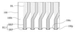
도 6 및 도 7을 참조하면, 본 예에서, 복수의 제 1 단위 픽셀(UP1)를 구성하는 제 1 내지 제 3 서브 픽셀(SP1, SP2, SP3) 각각은 보호층(110)의 상면으로부터 오목하게 마련된 오목부(130)를 포함한다.Referring to FIGS. 6 and 7 , in this example, each of the first to third subpixels SP1, SP2, and SP3 constituting the plurality of first unit pixels UP1 is concave from the upper surface of the
먼저, 각 제 1 단위 픽셀(UP1)에서, 제 2 서브 픽셀(SP2)은 단위 픽셀 영역의 가운데에 마련되고, 제 1 서브 픽셀(SP1)은 제 2 서브 픽셀(SP2)의 일측에 마련되며, 제 3 서브 픽셀(SP3)은 제 2 서브 픽셀(SP2)의 타측에 마련될 수 있다.First, in each first unit pixel UP1, the second subpixel SP2 is provided in the center of the unit pixel area, and the first subpixel SP1 is provided on one side of the second subpixel SP2, The third subpixel SP3 may be provided on the other side of the second subpixel SP2.
상기 제 2 서브 픽셀(SP2)에 마련되는 오목부(130)는 평면적으로 사각 형태를 가지며, 제 1 수평 축 방향(X)을 기준으로 오목부(130)의 중심 라인(CLg2)은 제 2 서브 픽셀(SP2)의 제 2 중심 라인(CL2)과 매칭된다. 예를 들어, 제 2 서브 픽셀(SP2)의 오목부(130)는 제 1 단위 픽셀(UP1)의 정중앙부에 마련될 수 있다. 이에 따라, 제 2 서브 픽셀(SP2)에 마련된 오목부(130)의 중심부(또는 정중앙부)와 기판(100)의 외측면 사이의 거리(L)는 기준 픽셀 피치(P)의 절반 이하(P/2)로 설정될 수 있다.The
상기 제 1 서브 픽셀(SP1)에 마련되는 오목부(130)는 평면적으로 사각 형태를 가지면서 제 2 서브 픽셀(SP2)에 마련되는 오목부(130)에 근접하도록 마련된다. 즉, 제 1 수평 축 방향(X)을 기준으로 제 1 서브 픽셀(SP1)에 마련되는 오목부(130)의 중심 라인(CLg1)은 제 1 서브 픽셀(SP1)의 중심 라인(CL1)으로부터 제 1 거리(d1)만큼 제 2 서브 픽셀(SP2) 쪽으로 이격된 위치에 마련된다.The
상기 제 3 서브 픽셀(SP3)에 마련되는 오목부(130)는 평면적으로 사각 형태를 가지면서 제 2 서브 픽셀(SP2)에 마련되는 오목부(130)에 근접하도록 마련된다. 즉, 제 1 수평 축 방향(X)을 기준으로 제 3 서브 픽셀(SP3)에 마련되는 오목부(130)의 중심 라인(CLg3)은 제 3 서브 픽셀(SP3)의 중심 라인(CL3)으로부터 제 2 거리(d2)만큼 제 2 서브 픽셀(SP2) 쪽으로 이격된 위치에 마련된다.The
상기 각 제 1 단위 픽셀(UP1)의 제 1 내지 제 3 서브 픽셀(SP1, SP2, SP3) 각각은 제 1 수평 축 방향(X)을 기준으로 서로 동일한 폭(Wa)을 갖는다.Each of the first to third subpixels SP1, SP2, and SP3 of each first unit pixel UP1 has the same width Wa based on the first horizontal axis direction X.
이와 같은, 각 제 1 단위 픽셀(UP1)에서, 제 1 내지 제 3 서브 픽셀(SP1, SP2, SP3) 각각에 마련된 오목부(130)는 제 1 단위 픽셀(UP1)의 정중앙부에 집중되도록 마련된다. 각 제 1 단위 픽셀(UP1)은 설정된 해상도에 대응되는 제 1 폭(W1)을 가지며, 복수의 제 1 단위 픽셀(UP1)은 기준 픽셀 피치를 가지도록 마련된다. 여기서, 기준 픽셀 피치는 제 1 수평 축 방향(X) 및 제 2 수평 축 방향(Y)을 기준으로, 인접한 2개의 제 1 단위 픽셀(UP1)의 중심부(또는 정중앙부) 사이의 거리로 정의될 수 있다. 다시 말하여, 기준 픽셀 피치(P)는 제 1 수평 축 방향(X)을 기준으로 인접한 2개의 제 1 단위 픽셀(UP1)에 마련된 동일한 서브 픽셀 사이의 거리로 정의될 수 있다. 즉, 기준 픽셀 피치(P)는 인접한 2개의 제 1 단위 픽셀(UP1) 각각의 제 2 서브 픽셀(SP2)에 배치된 마이크로 발광 소자(150) 사이의 거리로 정의될 수 있다. 예를 들어, 제 1 단위 픽셀(UP1)이 적색 서브 픽셀(SP1), 녹색 서브 픽셀(SP2), 및 청색 서브 픽셀(SP3)로 구성될 수 있는데, 이 경우, 기준 픽셀 피치(P)는 제 1 수평 축 방향(X)을 기준으로, 적색 서브 픽셀(SP1) 각각에 마련된 오목부(130)(또는 마이크로 발광 소자(150))들 간의 거리, 녹색 서브 픽셀(SP2) 각각에 마련된 오목부(130)들 간의 거리, 또는 녹색 서브 픽셀(SP2) 각각에 마련된 오목부(130)들 간의 거리일 수 있다.In this way, in each first unit pixel UP1, the
상기 복수의 제 2 단위 픽셀(UP2)에서, 제 2 서브 픽셀(SP2)은 단위 픽셀 영역의 가운데에 마련되고, 제 1 서브 픽셀(SP1)은 제 2 서브 픽셀(SP2)의 일측에 마련되며, 제 3 서브 픽셀(SP3)은 제 2 서브 픽셀(SP2)의 타측에 마련되면서 기판(100)의 외측면에 인접하게 마련된다. 여기서, 기판(100)의 외측면은 기판(100)의 전면(前面)(100a) 끝단과 수직을 이루는 측벽으로 정의되거나 외부로 노출되는 기판(100)의 최외곽 측면으로 정의될 수 있다. 즉, 기판(100)의 측벽은 외부로 직접 노출될 수 있고, 라우팅 라인과 보호층 등의 구조물에 의해 은폐되어 외부로 직접 노출되지 않을 수 있다. 따라서, 기판(100)의 외측면은 외부로 노출되는 기판(100)의 최외곽 측면으로 정의될 수 있다.In the plurality of second unit pixels UP2, the second subpixel SP2 is provided in the center of the unit pixel area, and the first subpixel SP1 is provided on one side of the second subpixel SP2, The third subpixel SP3 is provided on the other side of the second subpixel SP2 and adjacent to the outer surface of the
상기 각 제 2 단위 픽셀(UP2)에서 제 1 내지 제 3 서브 픽셀(SP1, SP2, SP3) 각각에 마련되는 오목부(130)는 제 1 단위 픽셀(UP1)의 오목부와 동일하므로 이에 대한 중복 설명은 생략하기로 한다.The
상기 각 제 2 단위 픽셀(UP2)에서, 제 1 및 제 2 서브 픽셀(SP1, SP2) 각각은 제 1 단위 픽셀(UP1)과 이웃하기 때문에 제 1 단위 픽셀(UP1)의 서브 픽셀들의 폭과 동일한 폭(Wa)을 갖도록 마련된다.In each second unit pixel UP2, each of the first and second subpixels SP1 and SP2 is adjacent to the first unit pixel UP1, and therefore has a width equal to the width of the subpixels of the first unit pixel UP1. It is prepared to have a width (Wa).
반면에, 각 제 2 단위 픽셀(UP2)의 제 3 서브 픽셀(SP3)은 제 1 및 제 2 서브 픽셀(SP1, SP2)의 폭(Wa)은 좁은 폭(Wb)을 갖도록 마련된다. 구체적으로, 각 제 2 단위 픽셀(UP2)에서 오목부(130)가 단위 픽셀에 정중앙부에 집중적으로 모여 마련되기 때문에 제 3 서브 픽셀(SP3)의 영역 중 기판(100)의 비표시 영역(IA)에 인접한 영역 일부가 제거되더라도 해당 단위 픽셀(UP2)에 표시되는 영상의 화질에 아무런 영향을 미치지 않는다. 이에 따라, 제 1 수평 축 방향(X)을 기준으로 제 3 서브 픽셀(SP3)의 폭(Wb)은 제 3 서브 픽셀(SP3)에 실장되는 마이크로 발광 소자(150)가 제 3 서브 픽셀(SP3)의 중심 라인(CL3)을 기준으로 제 2 서브 픽셀(SP2) 쪽으로 치우치는 거리(d2)만큼 감소될 수 있다. 이때, 제 2 단위 픽셀(UP2)과 기판(100)의 외측면 사이의 최대 거리(L)는 복수의 제 1 단위 픽셀(UP1)들이 갖는 기준 픽셀 피치(P)의 절반(P/2) 이하, 즉 기준 픽셀 피치(P)의 절반과 동일하거나 작도록 설정된다. 따라서, 본 예에 따른 발광 다이오드 표시 장치는 기판(100)의 베젤 영역에 인접한 제 2 단위 픽셀(UP2) 중 제 3 서브 픽셀(SP3)의 크기가 감소됨에 따라 멀티 스크린 장치에서 서로 연결된 표시 장치 사이의 경계부를 최소화하는데 적합한 베젤 폭을 갖는다.On the other hand, the third subpixel SP3 of each second unit pixel UP2 is provided such that the width Wa of the first and second subpixels SP1 and SP2 is narrow Wb. Specifically, since the
추가적으로, 본 출원의 일 예에 따른 발광 다이오드 표시 장치는 측면 실링 부재(107)를 더 포함한다.Additionally, the light emitting diode display device according to an example of the present application further includes a
상기 측면 실링 부재(107)는 기판(100)의 외측면과 투명 버퍼층(170)의 측면을 덮도록 마련된다. 일 예에 따른 측면 실링 부재(107)는 실리콘 계열 또는 자외선(UV) 경화 계열의 실링제(또는 수지(Resin))로 이루어질 수 있으나, 공정 택 타임(Tack Time)을 고려하면 자외선(UV) 경화 계열의 실링제로 이루어지는 것이 바람직하다. 또한, 상기 측면 실링 부재(107)는 유색(예를 들어, 청색, 적색, 청록색, 또는 흑색)이 될 수 있으나, 이에 한정되지 않고, 측면 빛샘을 방지하기 위한 유색 수지 또는 광 차단 수지로 이루어지는 것이 바람직하다. 이러한 측면 실링 부재(107)는 각 서브 픽셀(SP)의 마이크로 발광 소자(150)에서 방출되는 광이 투명 버퍼층(170) 내에서 최외곽 측면으로 진행하는 광에 의해 측면 빛샘을 방지하는 역할을 하며, 나아가 외부 충격을 완충하여 외부 충격에 의한 기판(100)과 투명 버퍼층(170)의 측면 손상을 방지하는 역할도 한다.The
도 8은 본 출원의 일 예에 따른 오목부의 변형 예를 설명하기 위한 도면이다.Figure 8 is a diagram for explaining a modified example of a concave portion according to an example of the present application.
도 8을 참조하면, 변형 예에 따른 각 단위 픽셀(UP1, UP2)의 각 서브 픽셀(SP1, SP2, SP3)에 마련된 오목부(130)는 서로 동일한 형태를 가지되, 각 서브 픽셀(SP)마다 각기 다른 깊이(D1, D2, D3)를 가지도록 보호층(110)으로부터 오목하게 형성될 수 있다.Referring to FIG. 8, the
일 예에 따른 오목부(130)는 해당 서브 픽셀에 배치될 마이크로 발광 소자(150)의 높이를 기반으로, 보호층(110)으로부터 각기 다른 깊이(D1, D2, D3)로 마련됨으로써 색상별 마이크로 발광 소자 간의 높이 편차(또는 단차)를 제거하거나 최소화한다.According to one example, the
본 예에 따른 발광 다이오드 표시 장치는 컬러 영상을 구현하기 위하여, 적색 서브 픽셀(SP1), 녹색 서브 픽셀(SP2), 및 청색 서브 픽셀(SP3)를 포함하며, 마이크로 발광 소자(150)는 색상별로 구분되어 해당하는 색상의 서브 픽셀에 마련된 오목부(130)에 배치된다. 이때, 색상별 마이크로 발광 소자(150)는 제조 공정 상의 공정 오차 등에 의해 각기 다른 높이(또는 두께)를 가질 수 있다. 예를 들어, 색상별 마이크로 발광 소자(150)의 두께는 적색, 녹색, 및 청색의 순서로 두꺼울 수 있다. 이 경우, 오목부(130)의 깊이(D1, D2, D3)는 해당 마이크로 발광 소자(150)의 높이를 기반으로 적색 서브 픽셀(SP1), 녹색 서브 픽셀(SP2), 및 청색 서브 픽셀(SP3)의 순서로 깊게 마련될 수 있다.The light emitting diode display device according to this example includes a red subpixel (SP1), a green subpixel (SP2), and a blue subpixel (SP3) to implement a color image, and the micro
따라서, 본 예는 서브 픽셀에 배치될 마이크로 발광 소자(150)의 높이(또는 두께)를 기반으로 각 서브 픽셀에 마련되는 오목부(130)의 깊이를 각기 다른 깊이로 설정함으로써 각 서브 픽셀에 배치된 색상별 마이크로 발광 소자(150)의 최상부면, 예를 들어 제 1 전극(E1)의 상면을 동일한 수평 선상(HL)에 위치시킬 수 있고, 이를 통해서 상기 제 1 및 제 2 전극 컨택홀의 패터닝 공정에서 색상별 마이크로 발광 소자(150)의 두께 편차로 인하여 색상별 마이크로 발광 소자(150)의 제 1 전극(또는 제 2 전극)이 노출되지 않는 오픈 불량을 방지할 수 있다. 또한, 본 예는 전면 발광(top emission) 구조에서, 각 서브 픽셀에 각기 다른 깊이(D1, D2, D3)로 마련되는 오목부(130)를 통해서 각 서브 픽셀의 색상별 마이크로 발광 소자(150)와 반사층(101) 간의 광학 거리를 최적화함으로써 반사층(101)의 반사 효율을 개선할 수 있으며, 이를 통해서 발광 다이오드 소자의 광효율을 광 효율을 극대화할 수 있다.Therefore, in this example, the depth of the
도 9는 본 출원의 일 예에 따른 오목부의 변형 예를 설명하기 위한 도면이다.Figure 9 is a diagram for explaining a modified example of a concave portion according to an example of the present application.
도 9를 참조하면, 본 예에서, 각 단위 픽셀(UP1, UP2)의 각 서브 픽셀(SP1, SP2, SP3)에 마련된 오목부(130)는 경계부 없이 서로 연통되어 하나의 수납 공간을 가질 수 있다. 즉, 복수의 제 1 단위 픽셀(UP1) 각각과 복수의 제 2 단위 픽셀(UP2) 각각은 제 1 내지 제 3 서브 픽셀(SP1, SP2, SP3)에 걸쳐 마련된 하나의 오목부(130)만을 포함할 수 있다.Referring to FIG. 9, in this example, the
상기 오목부(130)는 각 단위 픽셀(UP1, UP2)의 정중앙부 또는 제 2 서브 픽셀(SP2)의 중심 라인(CL2)을 중심으로 제 1 서브 픽셀(SP1)과 제 3 서브 픽셀(SP3) 쪽으로 확장된 사각 형태를 가질 수 있다. 즉, 제 1 수평 축 방향(X)을 기준으로 오목부(130)의 중심 라인(CLg)은 제 2 서브 픽셀(SP2)의 제 2 중심 라인(CL2)과 매칭된다.The
이와 같은, 본 예는 각 단위 픽셀(UP1, UP2)에 하나의 오목부(130)를 마련함으로써 각 서브 픽셀(SP1, SP2, SP3)에 대응되는 마이크로 발광 소자(150)의 실장 공정시 마이크로 발광 소자(150)의 이탈을 방지하고, 마이크로 발광 소자(150)의 얼라인 정밀도를 향상시킬 수 있다.In this example, one
도 10은 도 2 및 도 7에 도시된 발광 다이오드 표시 장치의 라우팅 라인을 설명하기 위한 도면이다.FIG. 10 is a diagram for explaining routing lines of the LED display device shown in FIGS. 2 and 7.
도 10을 참조하면, 본 예에 따른 발광 다이오드 표시 장치에서, 기판(100)은 제 1 비표시 영역(IA1)에 마련된 복수의 홈부(100c)를 포함한다.Referring to FIG. 10 , in the light emitting diode display device according to this example, the
상기 기판(100)의 제 1 비표시 영역(IA1)은 복수의 데이터 라인(DL) 각각의 가장자리 부분과 중첩되는 기판(100)의 하측 비표시 영역으로 정의될 수 있다.The first non-display area IA1 of the
상기 복수의 홈부(100c) 각각은 제 1 수평 축 방향(X)을 따라 일정한 간격을 가지도록 기판(100)의 외측면으로부터 제 2 표시 영역(AA2) 쪽으로 오목하게 마련된다. 일 예에 따른 복수의 홈부(100c) 각각은 기판 컷팅 공정을 통해 형성될 수 있다. 일 예에 따른 기판 컷팅 공정은 레이저 스크라이빙 공정을 이용하여 복수의 데이터 라인(DL) 사이에 대응되는 기판(100)의 가장자리 일부를 컷팅하여 복수의 홈부(100c)를 형성한다. 이에 따라, 기판(100)의 외측면은 오목하게 마련된 복수의 홈부(100c), 및 복수의 홈부(100c) 사이에 마련되면서 복수의 데이터 라인(DL) 각각의 끝단과 중첩되는 복수의 돌출부(100p)를 포함한다.Each of the plurality of
본 예에 따른 발광 다이오드 표시 장치에서, 복수의 제 1 라우팅 라인(RL1)은 기판(100)에 마련된 복수의 돌출부(100p) 각각을 통해 기판(100)의 전면(前面)(100a)에 마련된 복수의 데이터 라인(DL)과 일대일로 연결된다.In the light emitting diode display device according to this example, the plurality of first routing lines RL1 are provided on the
일 예에 따른 복수의 제 2 라우팅 라인(RL1) 각각은 측면 라우팅 패턴(SRP), 및 후면 라우팅 패턴(RRP)을 포함한다.Each of the plurality of second routing lines RL1 according to an example includes a side routing pattern (SRP) and a rear routing pattern (RRP).
상기 측면 라우팅 패턴(SRP)은 복수의 돌출부(100p) 각각의 절반 이하를 둘러싸도록 마련된다. 즉, 측면 라우팅 패턴(SRP)은 복수의 돌출부(100p) 각각의 절반 정도를 완전히 둘러싸도록 형성되는 것으로, 전도성 용액 또는 실버 페이스트를 이용한 딥핑(dipping) 공정에 의해 마련될 수 있다.The side routing pattern (SRP) is provided to surround less than half of each of the plurality of protrusions (100p). That is, the side routing pattern (SRP) is formed to completely surround about half of each of the plurality of
상기 후면 라우팅 패턴(RRP)은 기판(100)의 후면(100b) 가장자리에 마련되어 측면 라우팅 패턴(SRP)과 전기적으로 연결된다. 또한, 후면 라우팅 패턴(RRP)은 기판(100)의 후면(100b)에 마련된 제 1 패드부의 제 1 패드에 전기적으로 연결된다. 이러한 후면 라우팅 패턴(RRP)은 전도성 페이스트, 예를 들어 실버 페이스트를 이용한 프린팅 공정에 의해 마련될 수 있다.The rear routing pattern (RRP) is provided at the edge of the rear surface (100b) of the
추가적으로, 본 예에 따른 발광 다이오드 표시 장치에서, 기판(100)은 복수의 게이트 라인 각각의 끝단부와 중첩되는 제 2 비표시 영역에 마련된 복수의 홈부와 복수의 홈부 사이에 마련된 복수의 돌출부부를 더 포함하고, 복수의 제 2 라우팅 라인은 전술한 복수의 제 1 라우팅 라인과 동일한 구조와 방법으로 복수의 돌출부 각각에 마련되므로, 이에 대한 설명은 생략하기로 한다.Additionally, in the light emitting diode display device according to the present example, the
도 11a 내지 도 11c는 도 10에 도시된 복수의 제 1 라우팅 라인 각각의 제조 방법을 설명하기 위한 도면이다.FIGS. 11A to 11C are diagrams for explaining a method of manufacturing each of the plurality of first routing lines shown in FIG. 10 .
도 11a 내지 도 11c를 참조하여 본 예에 따른 복수의 제 1 라우팅 라인 각각의 제조 방법을 설명하면 다음과 같다.The manufacturing method of each of the plurality of first routing lines according to this example will be described with reference to FIGS. 11A to 11C as follows.
먼저, 복수의 데이터 배선(DL)을 포함하는 픽셀 구동 라인들을 갖는 기판(100)을 마련한다.First, a
그런 다음, 도 11a에 도시된 바와 같이, 기판 컷팅 공정을 통해 복수의 데이터 라인(DL) 각각의 끝단부가 돌출되도록 복수의 홈부(100c)를 형성한다. 일 예에 따른 기판 컷팅 공정은 레이저 스크라이빙 공정을 이용하여 복수의 데이터 라인(DL) 사이에 대응되는 기판(100)의 가장자리 일부를 컷팅하여 복수의 홈부(100c)를 형성함으로써 복수의 데이터 라인(DL) 각각의 끝단부와 중첩되는 복수의 돌출부(100p)를 마련한다.Then, as shown in FIG. 11A, a plurality of
그런 다음, 도 11b에 도시된 바와 같이, 기판(100)에 마련된 복수의 돌출부(100p) 각각을 일대일로 둘러싸는 복수의 측면 라우팅 패턴(SRP)을 형성한다. 예를 들어, 복수의 측면 라우팅 패턴(SRP) 각각은 전도성 용액에 복수의 돌출부(100p) 각각의 절반 정도를 딥핑(dipping)하여 전도성 용액을 복수의 돌출부(100p) 각각의 전면, 각 측면 및 후면에 코팅하는 딥핑 공정에 의해 형성될 수 있다. 이러한 딥핑 공정을 수행하게 되면, 복수의 데이터 라인(DL) 각각에 전기적으로 연결되는 복수의 측면 라우팅 패턴(SRP) 각각이 개별적으로 마련되고, 이러한 복수의 측면 라우팅 패턴(SPR) 각각은 기판(100)에 마련된 복수의 홈부(100c)에 의해 전기적으로 분리된다. 여기서, 전도성 용액은 전도성 페이스트, 예를 들어 실버 페이스트를 포함할 수 있다.Then, as shown in FIG. 11B, a plurality of side routing patterns (SRP) are formed one-to-one surrounding each of the plurality of
그런 다음, 도 11c에 도시된 바와 같이, 기판(100)의 후면(100b)에 복수의 측면 라우팅 패턴(SPR) 각각과 일대일로 연결되는 복수의 후면 라우팅 패턴(RRP)을 형성함으로써 복수의 데이터 라인(DL) 각각의 끝단부에 연결되면서 기판(100)의 외측면과 후면(100b)으로 이어지는 측면 라우팅 패턴(SPR)과 후면 라우팅 패턴(RRP)을 갖는 복수의 제 1 라우팅 라인(RL1)을 마련한다. 여기서, 일 예에 따른 복수의 후면 라우팅 패턴(RRP) 각각은 전도성 페이스트를 이용한 프린팅 공정에 의해 마련될 수 있다.Then, as shown in FIG. 11C, a plurality of rear routing patterns (RRP) are formed on the
추가적으로, 본 예에 따른 발광 다이오드 표시 장치에서, 복수의 제 2 라우팅 라인은 전술한 복수의 제 1 라우팅 라인과 동일한 제조 방법으로 마련되므로, 이에 대한 설명은 생략하기로 한다.Additionally, in the light emitting diode display device according to this example, the plurality of second routing lines are prepared by the same manufacturing method as the plurality of first routing lines described above, and therefore, description thereof will be omitted.
이와 같은, 본 예에 따른 라우팅 라인 및 이의 제조 방법은 기판(100)의 외측면에 라우팅 라인을 형성하는 공정을 단순화할 수 있고, 인접한 라우팅 라인 간의 전기적 쇼트를 방지할 수 있으며, 기판(100)의 모서리 부분에 대한 모따기 공정 또는 라운딩 공정을 생략할 수 있다.As such, the routing line and its manufacturing method according to the present example can simplify the process of forming the routing line on the outer surface of the
도 12는 도 6에 도시된 선 I-I'의 다른 단면도로서, 이는 본 출원에 따른 발광 다이오드 표시 장치에 컬러필터를 추가로 구성한 것이다. 이에 따라, 이하에서는 본 출원에 따른 발광 다이오드 표시 장치에 추가되는 구성에 대해서만 설명하기로 한다.FIG. 12 is another cross-sectional view taken along line II' shown in FIG. 6, which is a color filter added to the LED display device according to the present application. Accordingly, hereinafter, only the components added to the LED display device according to the present application will be described.
도 12를 도 6과 결부하면, 본 예에 따른 발광 다이오드 표시 장치는 블랙 매트릭스(BM) 및 컬러필터층(CFL)을 더 포함한다.12 in conjunction with FIG. 6, the light emitting diode display device according to this example further includes a black matrix (BM) and a color filter layer (CFL).
먼저, 각 서브 픽셀(SP1, SP2, SP3)에 마련된 마이크로 발광 소자(150)는 백색 광을 방출한다. 즉, 기판(100) 상에 마련된 모든 마이크로 발광 소자(150)는 백색 광을 방출하는 백색 마이크로 발광 소자일 수 있다.First, the micro
상기 블랙 매트릭스(BM)는 각 서브 픽셀(SP1, SP2, SP3)의 개구 영역을 정의하는 것으로, 각 서브 픽셀(SP1, SP2, SP3)에 마련된 마이크로 발광 소자(150)와 일대일로 중첩되는 투명 버퍼층(170)의 상면(170a)에 직접적으로 마련됨으로써 인접한 서브 픽셀(SP1, SP2, SP3) 사이의 혼색을 방지한다. 이러한 블랙 매트릭스(BM)는 광 흡수 물질을 포함할 수 있다.The black matrix (BM) defines the opening area of each subpixel (SP1, SP2, and SP3), and is a transparent buffer layer that overlaps on a one-to-one basis with the micro
선택적으로, 블랙 매트릭스(BM)는 투명 버퍼층(170)의 각 측면과 기판(100)의 외측면을 모두 덮도록 마련될 수 있다. 이 경우, 블랙 매트릭스(BM)는 각 서브 픽셀(SP1, SP2, SP3)의 마이크로 발광 소자(150)에서 방출되는 광이 투명 버퍼층(170) 내에서 최외곽 측면으로 진행하는 광에 의해 측면 빛샘을 방지한다.Optionally, the black matrix BM may be provided to cover each side of the
상기 컬러필터층(CFL)은 블랙 매트릭스(BM)에 의해 정의된 개구 영역과 중첩되는 투명 버퍼층(170)의 상면(170a)에 직접적으로 형성되는 것으로, 각 서브 픽셀(SP1, SP2, SP3) 각각에 정의된 색상에 대응되는 적색 컬러필터(CF1), 녹색 컬러필터(CF2), 및 청색 컬러필터(CF3)를 포함할 수 있다. 이러한 컬러필터층(190)은 각 서브 픽셀(SP1, SP2, SP3)에서 방출되는 방출되는 백색 광 중에서 해당 서브 픽셀에 해당되는 색상의 파장을 갖는 광만을 투과시킨다.The color filter layer (CFL) is formed directly on the
추가적으로, 본 예에 따른 발광 다이오드 표시 장치는 커버층(190)을 더 포함한다.Additionally, the light emitting diode display device according to this example further includes a
상기 커버층(190)은 블랙 매트릭스(BM) 및 컬러필터층(CFL)을 모두 덮도록 기판(100) 상에 마련된다. 일 예에 따른 커버층(190)은 상대적으로 낮은 굴절율을 갖는 물질로 이루어질 수 있다. 예를 들어, 커버층(190)은 LiF, MgF2, CaF2, 또는 ScF3의 물질로 형성될 수 있으며, 서로 다른 굴절율을 갖는 다중층 구조를 가질 수 있다. 이러한 커버층(190)은 블랙 매트릭스(BM) 및 컬러필터층(CFL)을 덮도록 마련되어 각 서브 픽셀(SP1, SP2, SP3)을 보호하면서 각 서브 픽셀(SP1, SP2, SP3)의 마이크로 발광 소자(150)에서 방출되는 광을 효율적으로 외부로 방출시킨다.The
선택적으로, 본 예에 따른 발광 다이오드 표시 장치는 측면 코팅층(109)을 더 포함할 수 있다.Optionally, the light emitting diode display device according to this example may further include a
상기 측면 코팅층(109)은 커버층(190)의 외측면을 덮도록 마련된다. 일 예에 따른 측면 코팅층(109)은 블랙 계열의 광 흡수 물질을 포함하는 블랙 잉크를 이용한 코팅 공정에 의해 커버층(190)의 외측면을 덮도록 마련될 수 있다. 나아가, 측면 코팅층(109)은 기판(100)의 외측면과 블랙 매트릭스(BM)의 측면에 추가로 마련될 수 있다. 이러한 측면 코팅층(109)은 각 서브 픽셀(SP1, SP2, SP3)의 마이크로 발광 소자(150)에서 방출되는 광이 커버층(190) 내에서 최외곽 측면으로 진행하는 광에 의해 측면 빛샘을 방지하는 역할을 한다.The
한편, 상기 커버층(190)은 유리 재질 또는 투명 플라스틱 재질로 이루어진 투명 기판으로 대체될 수 있으며, 이 경우 투명 기판은 투명 점착 부재를 매개로 하여 블랙 매트릭스(BM)와 컬러필터층(CFL) 상에 부착될 수 있다. 나아가, 블랙 매트릭스(BM)와 컬러필터층(CFL) 각각은 투명 버퍼층(170)의 상면(170a)에 직접적으로 형성되지 않고, 상기 투명 기판에 마련될 수도 있으며, 이 경우, 블랙 매트릭스(BM)와 컬러필터층(CFL)을 갖는 투명 기판은 투명 점착 부재를 매개로 하여 투명 버퍼층(170)의 상면(170a)에 부착될 수 있다.Meanwhile, the
이와 같은, 본 예는 모두 동일한 색상의 마이크로 발광 소자(150)를 각 서브 픽셀(SP1, SP2, SP3)에 실장함으로써 색상별 마이크로 발광 소자의 구분 없이 마이크로 발광 소자(150)의 실장 공정을 진행할 수 있으며, 이로 인하여 발광 소자의 실장 공정 시간을 단축시킬 수 있다.In this example, the micro
도 13은 도 6에 도시된 선 I-I'의 다른 단면도로서, 이는 도 12에 도시된 발광 다이오드 표시 장치에 파장 변환층을 추가로 구성한 것이다. 이에 따라, 이하에서는 파장 변환층 및 이와 관련된 구성에 대해서만 설명하기로 한다.FIG. 13 is another cross-sectional view taken along line II' shown in FIG. 6, which is a wavelength conversion layer added to the LED display device shown in FIG. 12. Accordingly, hereinafter only the wavelength conversion layer and its related configuration will be described.
도 13을 참조하면, 본 예에 따른 발광 다이오드 표시 장치에서, 파장 변환층(180)은, 백색을 제외한 제 1 색상의 광을 방출하는 마이크로 발광 소자(150)가 각 서브 픽셀(SP1, SP2, SP3)에 동일하게 배치되는 경우, 단위 픽셀(UP1, UP2)의 컬러 구현을 위해 투명 버퍼층(170)의 상면에 마련된다. 즉, 파장 변환층(180)은 컬러필터층(CFL)과 투명 버퍼층(170) 사이에 마련된다.Referring to FIG. 13, in the light emitting diode display device according to the present example, the
상기 파장 변환층(180)은 각 서브 픽셀(SP1, SP2, SP3)의 마이크로 발광 소자(150)로부터 입사되는 제 1 색상의 광을 기반으로 제 2 색상의 광을 방출한다. 즉, 파장 변환층(180)은 제 1 색상의 광을 흡수하고 재발광하여 제 2 색상의 광을 방출한다. 여기서, 제 1 색상의 광은 청색이고, 제 2 색상의 광은 황색일 수 있다.The
일 예로서, 파장 변환층(180)은 액상 상태로 투명 버퍼층(170)의 상면(170a)에 직접적으로 코팅된 후, 열 및/또는 광을 이용한 경화 공정에 의해 경화될 수 있다. 다른 예로서, 파장 변환층(180)은 시트 형태로 제작되어 투명 버퍼층(170)의 상면(170a)에 직접적으로 부착될 수 있다.As an example, the
일 예에 따른 파장 변환층(180)은 형광체 또는 양자점을 포함할 수 있다.The
일 예에 따른 형광체는 청색의 광에 의해 여기되어 황색의 광을 방출하는 황색의 형광체일 수 있으며, 예를 들면, YAG(Yttrium Aluminum Garnet)계 물질일 수 있다.The phosphor according to one example may be a yellow phosphor that is excited by blue light and emits yellow light. For example, it may be a YAG (Yttrium Aluminum Garnet)-based material.
일 예에 따른 양자점은 청색의 광에 의해 여기되어 황색의 광을 방출하는 황색 파장의 광을 방출하는 크기를 가지며, 예를 들어, CdS, CdSe, CdTe, ZnS, ZnSe, GaAs, GaP, GaAs-P, Ga-Sb, InAs, InP, InSb, AlAs, AlP, 또는 AlSb 등으로 이루어질 수 있다.Quantum dots according to one example have a size that emits yellow wavelength light that is excited by blue light and emits yellow light, for example, CdS, CdSe, CdTe, ZnS, ZnSe, GaAs, GaP, GaAs- It may be made of P, Ga-Sb, InAs, InP, InSb, AlAs, AlP, or AlSb.
본 예에 따른 파장 변환층(180)에서 재발광되어 커버층(190) 쪽으로 방출되는 제 2 색상의 광은 파장 변환층(180)에서 재발광되지 않고 커버층(190) 쪽으로 방출되는 제 1 색상의 광과 혼합되어 백색 광으로 변환된다. 상기 백색 광은 각 서브 픽셀(SP1, SP2, SP3)과 중첩되는 컬러필터에 의해 필터링되어 각 서브 픽셀(SP1, SP2, SP3)에 대응되는 컬러 광으로 방출된다.According to this example, the second color light that is re-emitted from the
상기 블랙 매트릭스(BM) 및 상기 컬러필터층(CFL)은 파장 변환층(180)의 상면(170a)에 마련되는 것을 제외하고는 도 12와 동일하므로, 이에 대한 설명은 생략하기로 한다.Since the black matrix (BM) and the color filter layer (CFL) are the same as those in FIG. 12 except that they are provided on the top surface (170a) of the
이와 같은, 본 예는 모두 동일한 색상의 마이크로 발광 소자(150)를 각 서브 픽셀(SP1, SP2, SP3)에 실장함으로써 색상별 마이크로 발광 소자의 구분 없이 마이크로 발광 소자(150)의 실장 공정을 진행할 수 있으며, 이로 인하여 발광 소자의 실장 공정 시간을 단축시킬 수 있다.In this example, the micro
한편, 상기 커버층(190)은 유리 재질 또는 투명 플라스틱 재질로 이루어진 투명 기판으로 대체될 수 있으며, 이 경우 투명 기판은 투명 점착 부재를 매개로 하여 파장 변환층(180) 상에 부착될 수 있다. 나아가, 파장 변환층(180)은 투명 버퍼층(170)의 상면(170a)에 직접적으로 형성되지 않고, 블랙 매트릭스(BM)와 컬러필터층(CFL)을 갖는 투명 기판에 마련될 수도 있으며, 이 경우, 투명 기판은 투명 점착 부재를 매개로 하여 투명 버퍼층(170)의 상면(170a)에 부착될 수 있다.Meanwhile, the
도 14은 본 출원에 따른 멀티 스크린 표시 장치를 설명하기 위한 도면이며, 도 15는 도 14에 도시된 선 II-II'의 단면도이다.FIG. 14 is a diagram for explaining a multi-screen display device according to the present application, and FIG. 15 is a cross-sectional view taken along line II-II' shown in FIG. 14.
도 14 및 도 15를 도 7과 결부하면, 본 예에 따른 멀티 스크린 표시 장치는 복수의 스크린 모듈(500-1, 500-2, 500-3, 500-4) 및 하우징(600)을 포함한다.14 and 15 with FIG. 7, the multi-screen display device according to this example includes a plurality of screen modules 500-1, 500-2, 500-3, and 500-4 and a
상기 복수의 스크린 모듈(500-1, 500-2, 500-3, 500-4) 각각은 N(N은 2 이상의 양의 정수)×M(M은 2 이상의 양의 정수) 형태로 배치됨으로써 개별 영상을 표시하거나 하나의 영상을 분할하여 표시한다. 이러한 복수의 스크린 모듈(500-1, 500-2, 500-3, 500-4) 각각은 도 1 내지 도 13에 도시된 본 출원에 따른 발광 다이오드 표시 장치를 포함하는 것으로, 이에 대한 중복 설명은 생략하기로 한다.Each of the plurality of screen modules 500-1, 500-2, 500-3, and 500-4 is arranged in the form of N (N is a positive integer of 2 or more) Displays an image or divides and displays one image. Each of these plurality of screen modules 500-1, 500-2, 500-3, and 500-4 includes a light emitting diode display device according to the present application shown in FIGS. 1 to 13, and a duplicate description thereof is provided. Decided to omit it.
일 예에 따른 복수의 스크린 모듈(500-1, 500-2, 500-3, 500-4) 각각은 기판(100)의 외측면에 마련된 모듈 연결 부재(700)를 매개로 하여 측면끼리 서로 부착될 수 있다. 상기 모듈 연결 부재(700)는 격자 형태로 배열된 인접한 2개의 스크린 모듈(500-1, 500-2, 500-3, 500-4)을 측면끼리 연결함으로써 멀티 스크린 표시 장치를 구현한다. 일 예에 따른 모듈 연결 부재(700)는 인접한 2개의 스크린 모듈(500-1, 500-2, 500-3, 500-4) 사이의 공간을 최소화하기 위하여, 상대적으로 얇은 두께로 형성할 수 있는 접착제 또는 양면 테이프로 이루어지는 것이 바람직하다.Each of the plurality of screen modules 500-1, 500-2, 500-3, and 500-4 according to an example is attached side to side via a
상기 복수의 스크린 모듈(500-1, 500-2, 500-3, 500-4) 각각에서, 제 2 단위 픽셀(UP2)과 기판(100)의 외측면 사이의 최대 거리(L)는 복수의 제 1 단위 픽셀(UP1)들이 갖는 기준 픽셀 피치(P)의 절반(P/2) 이하를 갖는다. 이에 따라, 모듈 연결 부재(700)를 사이에 두고 측면끼리 결합된 인접한 2개의 스크린 모듈 각각의 제 2 단위 픽셀(UP2) 간의 최대 거리는 기준 픽셀 피치(P) 이하를 가질 수 있다. 다시 말하여, 인접한 2개의 스크린 모듈 각각의 제 2 단위 픽셀(UP2) 간의 픽셀 피치는 스크린 모듈 각각에 마련된 제 1 단위 픽셀(UP1)의 기준 픽셀 피치(P)와 동일하거나 작게 된다. 따라서, 본 예는 복수의 스크린 모듈(500-1, 500-2, 500-3, 500-4) 사이에 마련되는 경계부에 의한 암부 발생 영역이 최소화되거나 제거될 수 있고, 이로 인하여 전체 화면에 단절감이 최소화된 영상을 표시할 수 있다.In each of the plurality of screen modules 500-1, 500-2, 500-3, and 500-4, the maximum distance L between the second unit pixel UP2 and the outer surface of the
상기 하우징(600)은 복수의 스크린 모듈(500-1, 500-2, 500-3, 500-4) 각각의 후면 가장자리를 지지하면서 복수의 스크린 모듈(500-1, 500-2, 500-3, 500-4)의 후면을 덮는다. 일 예에 따른 하우징(600)은 복수의 스크린 모듈(500-1, 500-2, 500-3, 500-4)의 후면을 덮는 하우징 플레이트(610), 하우징 플레이트(610)에 수직하게 마련되어 복수의 스크린 모듈(500-1, 500-2, 500-3, 500-4) 각각의 후면 가장자리를 지지하는 하우징 측벽(630)을 포함한다.The
일 예에 따른 하우징 플레이트(610)는 복수의 스크린 모듈(500-1, 500-2, 500-3, 500-4) 각각의 후면 전체를 덮는 단일 몸체로 이루어질 수 있다.The
일 예에 따른 하우징 플레이트(610)는 복수의 스크린 모듈(500-1, 500-2, 500-3, 500-4) 각각의 후면과 중첩되도록 복수의 분할 플레이트로 이루어질 수 있다.The
하우징 측벽(630)은 복수의 스크린 모듈(500-1, 500-2, 500-3, 500-4) 각각의 후면 가장자리와 중첩되는 하우징 플레이트(610)의 상면으로부터 수직하게 설치되어 복수의 스크린 모듈(500-1, 500-2, 500-3, 500-4) 각각의 후면 가장자리를 개별적으로 지지한다. 이때, 하우징 측벽은 모듈 지지 부재(650)를 통해서 복수의 스크린 모듈(500-1, 500-2, 500-3, 500-4) 각각의 후면 가장자리를 지지할 수 있다. 여기서, 모듈 지지 부재(650)는 탄성 부재, 폼 패드, 양면 테이프 등이 될 수 있다.The
추가적으로, 하우징(600)은 하우징 플레이트(610)와 하우징 측벽(630)을 포함하는 복수의 모듈 하우징을 포함할 수 있다. 복수의 모듈 하우징 각각은 개별적으로 복수의 스크린 모듈(500-1, 500-2, 500-3, 500-4)의 후면 가장자리를 지지하면서 복수의 스크린 모듈(500-1, 500-2, 500-3, 500-4)의 후면을 덮는다. 이 경우, 하우징(600)은 복수의 모듈 하우징 사이에 마련된 하우징 결합 부재(800)를 포함할 수 있다. 상기 하우징 결합 부재(800)는 인접한 모듈 하우징 사이의 갭 공간에 삽입되고, 볼트 또는 스크류 등의 체결 부재에 의해 인접한 모듈 하우징 각각의 하우징 플레이트(610)에 고정될 수 있다.Additionally, the
추가적으로, 본 예에 따른 멀티 스크린 표시 장치는 통합 제어 보드(900) 및 통합 제어 보드(900)에 실장된 영상 신호 생성부(910)를 더 포함한다.Additionally, the multi-screen display device according to this example further includes an
상기 통합 제어 보드(900)는 하우징(600)에 의해 복수의 스크린 모듈(500-1, 500-2, 500-3, 500-4)의 후면에 마련되는 수납 공간에 배치된다. 통합 제어 보드(900)는 적어도 하나의 신호 케이블(930)을 통해서 복수의 스크린 모듈(500-1, 500-2, 500-3, 500-4) 각각의 제어 보드(250)에 연결된다.The
상기 영상 신호 생성부(910)는 통합 제어 보드(900)에 실장된다. 이러한 영상 신호 생성부(910)는 외부의 호스트 구동 시스템으로부터 공급되는 원시 영상 신호를 수신하고, 수신된 원시 영상 신호를 기반으로 복수의 스크린 모듈(500-1, 500-2, 500-3, 500-4) 각각의 표시 장치에 표시될 모듈별 입력 영상 신호를 생성한다. 즉, 영상 신호 생성부(910)는 복수의 스크린 모듈(500-1, 500-2, 500-3, 500-4) 각각에 대해 제 1 표시 영역(AA1)과 제 2 표시 영역(AA2)을 포함하는 전체 해상도 정보를 수신하고, 원시 영상 신호를 모듈별 전체 해상도 정보에 대응되도록 분할하여 모듈별 입력 영상 신호를 생성하여 해당하는 스크린 모듈(500-1, 500-2, 500-3, 500-4)에 제공한다. 이에 따라, 각 스크린 모듈(500-1, 500-2, 500-3, 500-4)은 영상 신호 생성부(910)로부터 공급되는 입력 영상 신호로부터 모듈별 패널 영상 데이터에 대응되는 모듈별 영상을 표시한다.The
이와 같은, 본 예에 따른 멀티 스크린 장치는 본 출원에 따른 발광 다이오드 표시 장치로 구성된 복수의 스크린 모듈(500-1, 500-2, 500-3, 500-4)를 포함함으로써 스크린 모듈(500-1, 500-2, 500-3, 500-4) 사이에 마련되는 경계부에 의한 암부 발생 영역이 최소화되거나 제거됨에 따라 전체 화면에 단절감이 최소화된 영상을 표시할 수 있다.As such, the multi-screen device according to this example includes a plurality of screen modules 500-1, 500-2, 500-3, and 500-4 composed of a light emitting diode display device according to the present application, thereby forming a screen module 500- 1, 500-2, 500-3, and 500-4), an image with a minimized sense of disconnection can be displayed on the entire screen as the dark area generated by the boundary portion is minimized or eliminated.
도 16a 및 도 16b는 종래의 멀티 스크린 표시 장치와 본 출원에 따른 멀티 스크린 표시 장치 각각에 표시되는 영상을 나타내는 도면들이다.16A and 16B are diagrams showing images displayed on a conventional multi-screen display device and a multi-screen display device according to the present application, respectively.
먼저, 도 16a를 참조하면, 종래의 멀티 스크린 표시 장치는 복수의 표시 장치 각각의 표시 영역(AA)에만 영상이 표시됨으로써 복수의 표시 장치 각각의 전면 케이스에 따른 베젤 영역(BA)으로 인하여 서로 연결된 표시 장치들 사이의 경계 부분에서 암부가 발생하게 되고, 이러한 경계 부분의 암부로 인하여 전체 화면에 단절된 영상이 표시되는 것을 알 수 있다.First, referring to FIG. 16A, a conventional multi-screen display device displays images only in the display area (AA) of each of the plurality of display devices, so that the plurality of display devices are connected to each other due to the bezel area (BA) according to the front case. It can be seen that a dark portion occurs at the boundary between display devices, and a disconnected image is displayed on the entire screen due to the dark portion at the boundary portion.
반면에, 도 16b를 참조하면, 본 출원에 따른 멀티 스크린 표시 장치는 측면끼리 연결된 인접한 2개의 스크린 모듈 각각의 제 2 단위 픽셀 간의 픽셀 피치가 제 1 단위 픽셀의 기준 픽셀 피치와 동일하거나 작음으로써 복수의 스크린 모듈 사이에 마련되는 경계부에 의한 암부 발생 영역이 최소화되거나 제거됨에 따라 전체 화면에 단절감이 최소화된 영상이 표시되는 것을 알 수 있다.On the other hand, referring to FIG. 16b, in the multi-screen display device according to the present application, the pixel pitch between the second unit pixels of each of the two adjacent screen modules connected side to side is the same as or smaller than the reference pixel pitch of the first unit pixel, thereby displaying a plurality of screen modules. It can be seen that an image with a minimized sense of disconnection is displayed on the entire screen as the dark area caused by the boundary between the screen modules is minimized or eliminated.
결과적으로, 본 출원에 따른 멀티 스크린 표시 장치는 복수의 스크린 모듈들이 격자 형태를 가지도록 측면끼리 연결되더라도 전체 화면에 단절감이 최소화된 하나의 영상을 표시할 수 있으며, 이를 통해 대형 크기의 화면에 표시되는 영상의 몰입도를 향상시킬 수 있다.As a result, the multi-screen display device according to the present application can display one image with minimal sense of disconnection on the entire screen even if a plurality of screen modules are connected side to side in a grid form, and through this, can be displayed on a large screen. The immersion of the video can be improved.
이상에서 설명한 본 출원은 전술한 실시 예 및 첨부된 도면에 한정되는 것이 아니고, 본 출원의 기술적 사항을 벗어나지 않는 범위 내에서 여러 가지 치환, 변형 및 변경이 가능하다는 것이 본 출원이 속하는 기술 분야에서 통상의 지식을 가진 자에게 있어 명백할 것이다. 그러므로, 본 출원의 범위는 후술하는 특허청구범위에 의하여 나타내어지며, 특허청구범위의 의미 및 범위 그리고 그 등가 개념으로부터 도출되는 모든 변경 또는 변형된 형태가 본 출원의 범위에 포함되는 것으로 해석되어야 한다.The present application described above is not limited to the above-described embodiments and the accompanying drawings, and it is common in the technical field to which this application belongs that various substitutions, modifications, and changes are possible without departing from the technical details of the present application. It will be clear to those who have the knowledge of. Therefore, the scope of the present application is indicated by the claims described later, and the meaning and scope of the claims and all changes or modified forms derived from the equivalent concept should be interpreted as being included in the scope of the present application.
100: 기판 107: 측면 실링 부재
109: 측면 코팅층 110: 보호층
120: 접착 부재 130: 오목부
150: 마이크로 발광 소자 160: 평탄화층
170: 투명 버퍼층 180: 파장 변환층
190: 커버층 210: 데이터 구동 회로
230: 게이트 구동 회로 250: 제어 보드
270: 타이밍 컨트롤러 500-1 ~ 500-4: 스크린 모듈
900: 통합 제어 보드 910: 영상 신호 생성부100: substrate 107: side sealing member
109: side coating layer 110: protective layer
120: Adhesion member 130: Concave portion
150: micro light emitting device 160: planarization layer
170: transparent buffer layer 180: wavelength conversion layer
190: Cover layer 210: Data driving circuit
230: gate driving circuit 250: control board
270: Timing controller 500-1 ~ 500-4: Screen module
900: Integrated control board 910: Video signal generation unit
Claims (18)
Translated fromKorean마이크로 발광 소자를 갖는 복수의 서브 픽셀로 구성되며 상기 제 1 표시 영역에 마련된 복수의 제 1 단위 픽셀; 및
상기 복수의 서브 픽셀을 가지면서 상기 기판의 가장자리와 중첩되는 상기 제 2 표시 영역에 마련되고 상기 제 1 단위 픽셀보다 작은 크기를 갖는 복수의 제 2 단위 픽셀을 포함하며,
상기 복수의 제 1 단위 픽셀은 기준 픽셀 피치를 가지도록 마련되고,
상기 기준 픽셀 피치는 인접한 2개의 제 1 단위 픽셀 각각의 정중앙부 간의 거리이며,
서로 인접한 제 1 단위 픽셀과 제 2 단위 픽셀은 상기 기준 픽셀 피치를 가지도록 마련된, 발광 다이오드 표시 장치.A substrate having a first display area and a second display area surrounding the first display area;
a plurality of first unit pixels composed of a plurality of sub-pixels having micro light-emitting elements and provided in the first display area; and
a plurality of second unit pixels provided in the second display area having the plurality of subpixels and overlapping an edge of the substrate, and having a size smaller than the first unit pixel;
The plurality of first unit pixels are provided to have a reference pixel pitch,
The reference pixel pitch is the distance between the exact centers of each of two adjacent first unit pixels,
A light emitting diode display device, wherein first unit pixels and second unit pixels adjacent to each other are arranged to have the reference pixel pitch.
상기 제 2 단위 픽셀의 중심부와 상기 기판의 외측면 사이의 거리는 상기 기준 픽셀 피치의 절반 이하인, 발광 다이오드 표시 장치.According to claim 1,
A light emitting diode display device, wherein the distance between the center of the second unit pixel and the outer surface of the substrate is less than half the reference pixel pitch.
상기 복수의 제 1 단위 픽셀과 상기 복수의 제 2 단위 픽셀 각각은 제 1 내지 제 3 서브 픽셀을 가지며,
상기 제 2 단위 픽셀의 제 3 서브 픽셀은 상기 기판의 외측면에 인접하면서 인접한 제 2 서브 픽셀보다 작은 크기를 갖는, 발광 다이오드 표시 장치.According to claim 2,
Each of the plurality of first unit pixels and the plurality of second unit pixels has first to third subpixels,
A light emitting diode display device wherein a third subpixel of the second unit pixel is adjacent to an outer surface of the substrate and has a smaller size than the adjacent second subpixel.
상기 복수의 제 1 단위 픽셀과 상기 복수의 제 2 단위 픽셀 각각은 제 1 내지 제 3 서브 픽셀을 가지며,
상기 제 1 내지 제 3 서브 픽셀 각각은,
구동 박막 트랜지스터를 갖는 픽셀 회로;
상기 픽셀 회로를 덮는 보호층;
상기 보호층에 마련되고 제 1 전극과 제 2 전극을 갖는 상기 마이크로 발광 소자를 수납하는 오목부;
상기 구동 박막 트랜지스터와 상기 마이크로 발광 소자의 제 1 전극을 전기적으로 연결하는 픽셀 전극;
상기 마이크로 발광 소자의 제 2 전극에 연결된 공통 전극을 포함하는, 발광 다이오드 표시 장치.According to claim 2,
Each of the plurality of first unit pixels and the plurality of second unit pixels has first to third subpixels,
Each of the first to third subpixels,
a pixel circuit having a driving thin film transistor;
a protective layer covering the pixel circuit;
a recess provided in the protective layer and accommodating the micro light emitting device having a first electrode and a second electrode;
a pixel electrode electrically connecting the driving thin film transistor and the first electrode of the micro light emitting device;
A light emitting diode display device comprising a common electrode connected to a second electrode of the micro light emitting device.
상기 제 2 서브 픽셀의 오목부는 해당하는 단위 픽셀의 중심부에 마련되고,
상기 제 1 서브 픽셀의 오목부와 상기 제 3 서브 픽셀의 오목부 각각은 상기 서브 픽셀 영역의 중심부를 기준으로 상기 제 2 서브 픽셀의 오목부 쪽으로 치우쳐 마련된, 발광 다이오드 표시 장치.According to claim 5,
The concave portion of the second subpixel is provided at the center of the corresponding unit pixel,
A light emitting diode display device, wherein each of the concave portions of the first subpixel and the concave portion of the third subpixel is biased toward the concave portion of the second subpixel with respect to the center of the subpixel area.
상기 복수의 제 2 단위 픽셀 각각에서, 상기 제 2 서브 픽셀의 오목부 중심부와 상기 기판의 외측면 사이의 거리는 상기 기준 픽셀 피치의 절반 이하인, 발광 다이오드 표시 장치.According to claim 5,
In each of the plurality of second unit pixels, the distance between the center of the concave portion of the second sub-pixel and the outer surface of the substrate is less than half the reference pixel pitch.
상기 제 1 내지 제 3 서브 픽셀 각각에 마련된 오목부는 각기 다른 깊이를 갖는, 발광 다이오드 표시 장치.According to claim 5,
A light emitting diode display device, wherein concave portions provided in each of the first to third subpixels have different depths.
상기 제 1 내지 제 3 서브 픽셀 각각에 마련된 오목부는 서로 연통된 하나의 수납 공간을 갖는, 발광 다이오드 표시 장치.According to claim 5,
A light emitting diode display device, wherein recesses provided in each of the first to third subpixels have one storage space that communicates with each other.
상기 오목부에 수납된 마이크로 발광 소자 및 상기 보호층을 덮는 평탄화층; 및
상기 평탄화층을 덮는 투명 버퍼층을 더 포함하며,
상기 픽셀 전극과 상기 공통 전극 각각은 상기 평탄화층과 상기 투명 버퍼층 사이에 마련된, 발광 다이오드 표시 장치.According to claim 5,
a planarization layer covering the micro light emitting element stored in the concave portion and the protective layer; and
It further includes a transparent buffer layer covering the planarization layer,
Each of the pixel electrode and the common electrode is provided between the planarization layer and the transparent buffer layer.
상기 기판의 외측면과 상기 투명 버퍼층 각각의 측면을 덮는 측면 실링 부재를 더 포함하는, 발광 다이오드 표시 장치.According to claim 10,
A light emitting diode display device further comprising a side sealing member covering an outer surface of the substrate and a side surface of each of the transparent buffer layers.
상기 오목부에 수납된 상기 마이크로 발광 소자와 중첩되도록 상기 투명 버퍼층에 마련된 컬러필터를 더 포함하며,
상기 마이크로 발광 소자는 백색 광을 방출하는, 발광 다이오드 표시 장치.According to claim 10,
Further comprising a color filter provided in the transparent buffer layer to overlap the micro light emitting device stored in the concave portion,
A light emitting diode display device, wherein the micro light emitting element emits white light.
상기 투명 버퍼층과 상기 컬러필터 사이에 마련된 파장 변환층을 더 포함하며,
상기 파장 변환층은 형광체 또는 양자점 입자를 포함하는, 발광 다이오드 표시 장치.According to claim 12,
It further includes a wavelength conversion layer provided between the transparent buffer layer and the color filter,
A light emitting diode display device, wherein the wavelength conversion layer includes phosphor or quantum dot particles.
상기 기판 상에 마련되어 복수의 서브 픽셀 영역을 정의하는 복수의 게이트 라인과 복수의 데이터 라인을 포함하는 픽셀 구동 라인들;
상기 픽셀 구동 라인들과 연결되고 상기 기판의 외측면과 상기 기판의 후면에 마련된 복수의 라우팅 라인;
상기 복수의 라우팅 라인 각각에 마련된 패드를 갖는 패드부; 및
상기 패드부에 연결된 구동 회로를 더 포함하는, 발광 다이오드 표시 장치.According to claim 2,
pixel driving lines including a plurality of gate lines and a plurality of data lines provided on the substrate and defining a plurality of sub-pixel areas;
a plurality of routing lines connected to the pixel driving lines and provided on an outer surface of the substrate and a rear surface of the substrate;
a pad portion having pads provided on each of the plurality of routing lines; and
A light emitting diode display device further comprising a driving circuit connected to the pad portion.
상기 기판은 외측면으로부터 오목하게 마련된 복수의 홈부; 및 상기 복수의 홈부 사이에 마련되면서 상기 픽셀 구동 라인들 각각의 끝단과 중첩되는 복수의 돌출부를 포함하며,
상기 복수의 라우팅 라인 각각은,
상기 픽셀 구동 라인들 각각의 끝단과 전기적으로 연결되면서 상기 복수의 돌출부 각각의 일부를 둘러싸는 측면 라우팅 패턴; 및
상기 측면 라우팅 패턴과 전기적으로 연결되면서 상기 기판의 후면에 마련되고 상기 패드부에 연결된 후면 라우팅 패턴을 포함하는, 발광 다이오드 표시 장치.According to claim 14,
The substrate includes a plurality of grooves concavely provided from an outer surface; and a plurality of protrusions provided between the plurality of grooves and overlapping ends of each of the pixel driving lines,
Each of the plurality of routing lines,
a side routing pattern electrically connected to an end of each of the pixel driving lines and surrounding a portion of each of the plurality of protrusions; and
A light emitting diode display device comprising a rear routing pattern electrically connected to the side routing pattern, provided on a rear surface of the substrate, and connected to the pad portion.
상기 복수의 스크린 모듈을 측면끼리 연결하는 복수의 모듈 연결 부재를 포함하며,
상기 복수의 스크린 모듈 각각은 제 1 항, 제 2 항, 및 제 4 항 내지 제 15 항 중 어느 한 항에 따른 발광 다이오드 표시 장치를 갖는, 멀티 스크린 표시 장치.a plurality of screen modules; and
It includes a plurality of module connection members connecting the plurality of screen modules side to side,
A multi-screen display device, wherein each of the plurality of screen modules has a light emitting diode display device according to any one of claims 1, 2, and 4 to 15.
상기 모듈 연결 부재를 사이에 두고 인접한 2개의 스크린 모듈 각각의 제 2 단위 픽셀 간의 최대 거리는 상기 기준 픽셀 피치 이하인, 멀티 스크린 표시 장치.According to claim 16,
A multi-screen display device, wherein the maximum distance between second unit pixels of each of two adjacent screen modules with the module connection member in between is less than or equal to the reference pixel pitch.
상기 모듈 연결 부재는 접착제 또는 양면 테이프인, 멀티 스크린 표시 장치.According to claim 16,
A multi-screen display device, wherein the module connecting member is adhesive or double-sided tape.
Priority Applications (6)
| Application Number | Priority Date | Filing Date | Title |
|---|---|---|---|
| KR1020160184458AKR102687577B1 (en) | 2016-12-30 | 2016-12-30 | Light emitting diode display apparatus and multi screen display apparatus using the same |
| US15/793,155US10593743B2 (en) | 2016-12-30 | 2017-10-25 | Light emitting diode display device and multi-screen display device using the same |
| EP17201813.7AEP3343551B1 (en) | 2016-12-30 | 2017-11-15 | Light emitting diode display device and multi-screen display device using the same |
| CN201711144620.2ACN108269823B (en) | 2016-12-30 | 2017-11-17 | Light-emitting diode display device and multi-screen display device using the same |
| US16/788,081US11398538B2 (en) | 2016-12-30 | 2020-02-11 | Light emitting diode display device and multi-screen display device using the same |
| KR1020240094880AKR20240116680A (en) | 2016-12-30 | 2024-07-18 | Light emitting diode display apparatus and multi screen display apparatus using the same |
Applications Claiming Priority (1)
| Application Number | Priority Date | Filing Date | Title |
|---|---|---|---|
| KR1020160184458AKR102687577B1 (en) | 2016-12-30 | 2016-12-30 | Light emitting diode display apparatus and multi screen display apparatus using the same |
Related Child Applications (1)
| Application Number | Title | Priority Date | Filing Date |
|---|---|---|---|
| KR1020240094880ADivisionKR20240116680A (en) | 2016-12-30 | 2024-07-18 | Light emitting diode display apparatus and multi screen display apparatus using the same |
Publications (2)
| Publication Number | Publication Date |
|---|---|
| KR20180079078A KR20180079078A (en) | 2018-07-10 |
| KR102687577B1true KR102687577B1 (en) | 2024-07-22 |
Family
ID=60331459
Family Applications (2)
| Application Number | Title | Priority Date | Filing Date |
|---|---|---|---|
| KR1020160184458AActiveKR102687577B1 (en) | 2016-12-30 | 2016-12-30 | Light emitting diode display apparatus and multi screen display apparatus using the same |
| KR1020240094880APendingKR20240116680A (en) | 2016-12-30 | 2024-07-18 | Light emitting diode display apparatus and multi screen display apparatus using the same |
Family Applications After (1)
| Application Number | Title | Priority Date | Filing Date |
|---|---|---|---|
| KR1020240094880APendingKR20240116680A (en) | 2016-12-30 | 2024-07-18 | Light emitting diode display apparatus and multi screen display apparatus using the same |
Country Status (4)
| Country | Link |
|---|---|
| US (2) | US10593743B2 (en) |
| EP (1) | EP3343551B1 (en) |
| KR (2) | KR102687577B1 (en) |
| CN (1) | CN108269823B (en) |
Families Citing this family (85)
| Publication number | Priority date | Publication date | Assignee | Title |
|---|---|---|---|---|
| US12322732B2 (en) | 2017-02-09 | 2025-06-03 | Vuereal Inc. | Circuit and system integration onto a microdevice substrate |
| US11916096B2 (en) | 2017-02-09 | 2024-02-27 | Vuereal Inc. | Circuit and system integration onto a micro-device substrate |
| EP3642825A1 (en) | 2017-06-20 | 2020-04-29 | IMAX Theatres International Limited | Active display with reduced screen-door effect |
| KR102581010B1 (en)* | 2017-08-02 | 2023-09-22 | 서울반도체 주식회사 | Display apparatus, substrate of display apparatus and repairing method of display apparatus |
| US11682369B2 (en)* | 2017-09-20 | 2023-06-20 | Imax Theatres International Limited | Light emitting display with tiles and data processing |
| TWI790297B (en) | 2017-10-16 | 2023-01-21 | 美商康寧公司 | Bezel-free display tile with edge-wrapped conductors and methods of manufacture |
| TWI739931B (en)* | 2017-10-18 | 2021-09-21 | 優顯科技股份有限公司 | Display device |
| KR102523976B1 (en) | 2017-11-21 | 2023-04-20 | 삼성전자주식회사 | Display apparatus |
| US10796643B2 (en)* | 2018-01-30 | 2020-10-06 | Wuhan China Star Optoelectronics Semiconductor Display Technology Co., Ltd. | AMOLED display panel with transmitting goa circuit disposed below effective display region |
| US10665149B2 (en)* | 2018-04-16 | 2020-05-26 | Facebook Technologies, Llc | Translating color selector layer for display resolution enhancement |
| TWI687912B (en)* | 2018-06-08 | 2020-03-11 | 錼創顯示科技股份有限公司 | Display apparatus |
| WO2020004845A1 (en)* | 2018-06-28 | 2020-01-02 | 주식회사 루멘스 | Flexible lighting device and display panel using micro led chips |
| KR102578423B1 (en)* | 2018-07-03 | 2023-09-13 | 엘지디스플레이 주식회사 | Multi-panel organic light emitting display device |
| KR102604659B1 (en)* | 2018-07-13 | 2023-11-21 | 삼성디스플레이 주식회사 | Light emitting diode display device and manufacturing method of same |
| KR102517268B1 (en)* | 2018-07-16 | 2023-04-03 | 삼성전자주식회사 | Display panel |
| WO2020016701A1 (en)* | 2018-07-20 | 2020-01-23 | 株式会社半導体エネルギー研究所 | Display device |
| KR102064806B1 (en) | 2018-10-16 | 2020-01-10 | 엘지디스플레이 주식회사 | Display device and method of manufacturing the same |
| US11727859B2 (en)* | 2018-10-25 | 2023-08-15 | Boe Technology Group Co., Ltd. | Display panel and display device |
| CN109742132B (en)* | 2019-02-28 | 2021-01-22 | 京东方科技集团股份有限公司 | Display panel and display device |
| KR102605559B1 (en)* | 2018-10-30 | 2023-11-23 | 엘지디스플레이 주식회사 | Display apparatus and multi screen display apparatus using the same |
| CN109410771B (en)* | 2018-10-31 | 2021-06-25 | 武汉天马微电子有限公司 | Display panel and display device |
| KR20200054747A (en) | 2018-11-12 | 2020-05-20 | 삼성전자주식회사 | Display module, display apparatus including the same and method of manufacturing display module |
| KR102668561B1 (en)* | 2018-11-27 | 2024-05-22 | 엘지디스플레이 주식회사 | Display apparatus and multi screen display apparatus using the same |
| KR102553231B1 (en)* | 2018-11-27 | 2023-07-11 | 삼성디스플레이 주식회사 | Display device and fabricating method thereof |
| KR20200069125A (en)* | 2018-12-06 | 2020-06-16 | 삼성전자주식회사 | Display apparatus |
| KR102612390B1 (en)* | 2018-12-19 | 2023-12-12 | 엘지디스플레이 주식회사 | Display panel and display device |
| CN111383544B (en)* | 2018-12-29 | 2022-03-25 | 中兴通讯股份有限公司 | Display screen, terminal and display method |
| KR102608216B1 (en)* | 2019-01-15 | 2023-12-01 | 삼성디스플레이 주식회사 | Display apparatus and display system |
| KR102196544B1 (en)* | 2019-02-13 | 2020-12-30 | 삼성전자주식회사 | Display module having glass substrate fored side wiring and manufacturing mathod as the same |
| US11056630B2 (en)* | 2019-02-13 | 2021-07-06 | Samsung Electronics Co., Ltd. | Display module having glass substrate on which side wirings are formed and manufacturing method of the same |
| US11164934B2 (en)* | 2019-03-12 | 2021-11-02 | X Display Company Technology Limited | Tiled displays with black-matrix support screens |
| WO2020202766A1 (en)* | 2019-03-29 | 2020-10-08 | 京セラ株式会社 | Display device |
| CN109994533B (en)* | 2019-04-17 | 2021-01-19 | 京东方科技集团股份有限公司 | Array substrate, display panel and manufacturing method thereof |
| US20200349336A1 (en)* | 2019-05-03 | 2020-11-05 | Innolux Corporation | Electronic device |
| CN111881710A (en)* | 2019-05-03 | 2020-11-03 | 群创光电股份有限公司 | electronic device |
| US11088078B2 (en)* | 2019-05-22 | 2021-08-10 | Nanya Technology Corporation | Semiconductor device and method for manufacturing the same |
| WO2020261409A1 (en)* | 2019-06-26 | 2020-12-30 | 三菱電機株式会社 | Display device and image display method |
| CN120302791A (en)* | 2019-07-09 | 2025-07-11 | 群创光电股份有限公司 | Light-emitting device |
| TWI707466B (en)* | 2019-07-23 | 2020-10-11 | 國立中興大學 | Passive micro light emitting diode array device with uniform brightness |
| WO2021020042A1 (en)* | 2019-07-31 | 2021-02-04 | 京セラ株式会社 | Display device |
| TWI707320B (en)* | 2019-08-07 | 2020-10-11 | 友達光電股份有限公司 | Display apparatus |
| CN110600459A (en)* | 2019-08-20 | 2019-12-20 | 深圳市华星光电半导体显示技术有限公司 | Flexible micro light-emitting diode display panel and micro light-emitting diode display device |
| KR20210028295A (en)* | 2019-09-03 | 2021-03-12 | 삼성디스플레이 주식회사 | Display device and method for manufacturing the same |
| CN110610973A (en)* | 2019-09-20 | 2019-12-24 | 昆山国显光电有限公司 | Display panel and display device |
| KR102852286B1 (en)* | 2019-09-24 | 2025-08-28 | 삼성전자주식회사 | Display device |
| JP2022552799A (en)* | 2019-10-10 | 2022-12-20 | コーニング インコーポレイテッド | Systems and methods for forming wraparound electrodes |
| US11373584B2 (en)* | 2019-11-29 | 2022-06-28 | Boe Technology Group Co., Ltd. | Array substrate, display panel, spliced display panel and display driving method |
| WO2021118268A1 (en)* | 2019-12-13 | 2021-06-17 | Samsung Electronics Co., Ltd. | Display apparatus having display module and method of manufacturing the same |
| KR102825053B1 (en)* | 2019-12-27 | 2025-06-26 | 삼성전자주식회사 | Display appartus having display module and manufacturing method thereof |
| KR20210086309A (en)* | 2019-12-31 | 2021-07-08 | 엘지디스플레이 주식회사 | Light emitting display apparatus and multi screen display apparatus using the same |
| KR102707443B1 (en)* | 2019-12-31 | 2024-09-20 | 엘지디스플레이 주식회사 | Display apparatus and multi screen display apparatus using the same |
| US11444120B2 (en) | 2020-01-14 | 2022-09-13 | Au Optronics Corporation | Display apparatus and method of fabricating the same |
| TW202032226A (en)* | 2020-01-14 | 2020-09-01 | 友達光電股份有限公司 | Structure of flexible circuits |
| US11316003B2 (en)* | 2020-02-25 | 2022-04-26 | Boe Technology Group Co., Ltd. | Array substrate, display device, and method for manufacturing same |
| EP3872797A1 (en)* | 2020-02-27 | 2021-09-01 | Apple Inc. | Local active matrix architecture |
| CN111402743A (en)* | 2020-03-24 | 2020-07-10 | 昆山国显光电有限公司 | Display panel and display device |
| KR102821139B1 (en)* | 2020-04-13 | 2025-06-16 | 삼성디스플레이 주식회사 | Tiled display device |
| KR102792189B1 (en)* | 2020-04-21 | 2025-04-07 | 삼성디스플레이 주식회사 | Tiled display device |
| CN113540325B (en)* | 2020-04-22 | 2023-11-03 | 群创光电股份有限公司 | electronic device |
| KR102717583B1 (en)* | 2020-04-24 | 2024-10-16 | 삼성전자주식회사 | Display module and display appartus having the same |
| KR102788991B1 (en)* | 2020-05-12 | 2025-03-31 | 삼성디스플레이 주식회사 | Tiled display device |
| KR102753710B1 (en) | 2020-06-26 | 2025-01-10 | 엘지디스플레이 주식회사 | Transparent display device |
| CN111696461B (en)* | 2020-06-30 | 2022-05-27 | 武汉天马微电子有限公司 | Display panel and display device |
| KR20220021966A (en) | 2020-08-13 | 2022-02-23 | 삼성디스플레이 주식회사 | Display panel, manufacturing method for the same, and display device including the same |
| KR20220021985A (en)* | 2020-08-14 | 2022-02-23 | 삼성디스플레이 주식회사 | Display device and tiled display device including the same |
| JP2022036709A (en) | 2020-08-24 | 2022-03-08 | 株式会社ジャパンディスプレイ | Display device |
| TWI750838B (en)* | 2020-10-08 | 2021-12-21 | 友達光電股份有限公司 | Display panel and method for manufacturing the same |
| KR20220060067A (en)* | 2020-11-03 | 2022-05-11 | 삼성디스플레이 주식회사 | Display device |
| JP7574317B2 (en)* | 2020-11-18 | 2024-10-28 | 京セラ株式会社 | Wiring board and display device |
| CN112542097A (en)* | 2020-12-04 | 2021-03-23 | Tcl华星光电技术有限公司 | Double-sided display panel and preparation method thereof |
| WO2022124095A1 (en)* | 2020-12-10 | 2022-06-16 | ソニーグループ株式会社 | Display module, manufacturing method, and display device |
| US12183719B2 (en)* | 2020-12-15 | 2024-12-31 | Samsung Electronics Co., Ltd. | Display transferring structure and display device including the same |
| KR20220121394A (en)* | 2021-02-25 | 2022-09-01 | 주식회사 디비하이텍 | Spad pixel structure and manufacturing the same |
| CN115273654B (en)* | 2021-04-30 | 2024-05-03 | 海信视像科技股份有限公司 | Display device |
| KR20230000611A (en)* | 2021-06-25 | 2023-01-03 | 삼성전자주식회사 | Display appartus having display module and manufacturing method thereof |
| CN113376886B (en)* | 2021-06-30 | 2022-12-06 | 武汉华星光电技术有限公司 | Display panel, biological detection method and display device |
| EP4332948A4 (en)* | 2021-10-27 | 2024-11-06 | Samsung Electronics Co., Ltd. | DISPLAY DEVICE COMPRISING A DISPLAY MODULE AND ASSOCIATED MANUFACTURING METHOD |
| CN114420719B (en)* | 2022-02-08 | 2024-08-27 | 厦门天马微电子有限公司 | Display panel and display device |
| CN114927540B (en)* | 2022-04-29 | 2025-08-22 | 广州新视界光电科技有限公司 | Display substrate and display panel |
| CN114975746B (en) | 2022-05-20 | 2025-07-22 | Tcl华星光电技术有限公司 | Display panel, printing device and preparation method of display panel |
| CN115171530B (en)* | 2022-06-30 | 2024-07-05 | 上海天马微电子有限公司 | Display device |
| TWI849626B (en)* | 2022-12-16 | 2024-07-21 | 財團法人工業技術研究院 | Display device |
| KR20240108051A (en)* | 2022-12-30 | 2024-07-09 | 엘지디스플레이 주식회사 | Display apparatus and tiling display apparatus including the same |
| WO2024234302A1 (en)* | 2023-05-16 | 2024-11-21 | 京东方科技集团股份有限公司 | Display panel, display device, and tiled display device |
| US12374277B2 (en) | 2023-07-11 | 2025-07-29 | Apple Inc. | Pulse width modulation and amplitude modulation driving system for display panels |
Citations (1)
| Publication number | Priority date | Publication date | Assignee | Title |
|---|---|---|---|---|
| JP2015172661A (en)* | 2014-03-12 | 2015-10-01 | 株式会社ジャパンディスプレイ | display device |
Family Cites Families (24)
| Publication number | Priority date | Publication date | Assignee | Title |
|---|---|---|---|---|
| US5644327A (en) | 1995-06-07 | 1997-07-01 | David Sarnoff Research Center, Inc. | Tessellated electroluminescent display having a multilayer ceramic substrate |
| US6025901A (en)* | 1995-08-14 | 2000-02-15 | Sharp Kabushiki Kaisha | Liquid crystal display device and method for producing the same |
| US6498592B1 (en) | 1999-02-16 | 2002-12-24 | Sarnoff Corp. | Display tile structure using organic light emitting materials |
| CN101740560B (en) | 2003-04-01 | 2012-11-21 | 夏普株式会社 | Light-emitting apparatus, backlight apparatus, and display apparatus |
| JP4059153B2 (en) | 2003-06-23 | 2008-03-12 | ソニー株式会社 | Manufacturing method of display device |
| KR100583252B1 (en)* | 2003-12-29 | 2006-05-24 | 엘지.필립스 엘시디 주식회사 | Organic EL device and method of manufacturing the same |
| US9058755B2 (en) | 2008-01-04 | 2015-06-16 | Nanolumens Acquisition, Inc. | Lightweight unitary display |
| US9013367B2 (en)* | 2008-01-04 | 2015-04-21 | Nanolumens Acquisition Inc. | Flexible display |
| WO2011082497A1 (en)* | 2010-01-11 | 2011-07-14 | Cooledge Lighting Inc. | Package for light emitting and receiving devices |
| US9159700B2 (en)* | 2012-12-10 | 2015-10-13 | LuxVue Technology Corporation | Active matrix emissive micro LED display |
| TWI537899B (en)* | 2013-02-05 | 2016-06-11 | 業鑫科技顧問股份有限公司 | Display element, display device and joint display |
| US9368070B2 (en)* | 2013-10-07 | 2016-06-14 | Google Inc. | Variable resolution seamless tileable display |
| JP6318665B2 (en)* | 2014-02-10 | 2018-05-09 | セイコーエプソン株式会社 | Electro-optical device, method of manufacturing electro-optical device, and electronic apparatus |
| CN103903549B (en)* | 2014-03-25 | 2016-08-17 | 京东方科技集团股份有限公司 | Display packing |
| GB2531558B (en) | 2014-10-22 | 2021-01-13 | Facebook Tech Llc | Display |
| US9793248B2 (en)* | 2014-11-18 | 2017-10-17 | PlayNitride Inc. | Light emitting device |
| US9557954B2 (en)* | 2014-12-23 | 2017-01-31 | X Development Llc | Display panel using direct emission pixel arrays |
| KR102331566B1 (en)* | 2014-12-31 | 2021-11-26 | 삼성디스플레이 주식회사 | Light emitting display device |
| KR102323679B1 (en)* | 2015-04-21 | 2021-11-10 | 삼성디스플레이 주식회사 | Multi-display device having the same |
| TWI665800B (en)* | 2015-06-16 | 2019-07-11 | 友達光電股份有限公司 | Light emitting diode display and manufacturing method thereof |
| US9472734B1 (en)* | 2015-09-07 | 2016-10-18 | Mikro Mesa Technology Co., Ltd. | Light-emitting diode display |
| TWI581455B (en)* | 2016-01-29 | 2017-05-01 | 友達光電股份有限公司 | Light emitting device and method of manufacturing the same |
| WO2018038967A1 (en)* | 2016-08-22 | 2018-03-01 | Corning Incorporated | Display modules with laser weld seals and modular display |
| TWI606604B (en)* | 2016-12-08 | 2017-11-21 | 錼創科技股份有限公司 | Light-emitting diode chip |
- 2016
- 2016-12-30KRKR1020160184458Apatent/KR102687577B1/enactiveActive
- 2017
- 2017-10-25USUS15/793,155patent/US10593743B2/enactiveActive
- 2017-11-15EPEP17201813.7Apatent/EP3343551B1/enactiveActive
- 2017-11-17CNCN201711144620.2Apatent/CN108269823B/enactiveActive
- 2020
- 2020-02-11USUS16/788,081patent/US11398538B2/enactiveActive
- 2024
- 2024-07-18KRKR1020240094880Apatent/KR20240116680A/enactivePending
Patent Citations (1)
| Publication number | Priority date | Publication date | Assignee | Title |
|---|---|---|---|---|
| JP2015172661A (en)* | 2014-03-12 | 2015-10-01 | 株式会社ジャパンディスプレイ | display device |
Also Published As
| Publication number | Publication date |
|---|---|
| EP3343551A1 (en) | 2018-07-04 |
| EP3343551B1 (en) | 2022-01-12 |
| US20180190747A1 (en) | 2018-07-05 |
| KR20180079078A (en) | 2018-07-10 |
| KR20240116680A (en) | 2024-07-30 |
| US10593743B2 (en) | 2020-03-17 |
| CN108269823A (en) | 2018-07-10 |
| US20200176537A1 (en) | 2020-06-04 |
| US11398538B2 (en) | 2022-07-26 |
| CN108269823B (en) | 2022-01-28 |
Similar Documents
| Publication | Publication Date | Title |
|---|---|---|
| KR102687577B1 (en) | Light emitting diode display apparatus and multi screen display apparatus using the same | |
| KR102769848B1 (en) | Display apparatus and multi screen display apparatus using the same | |
| KR102582059B1 (en) | Display apparatus and multi screen display apparatus using the same | |
| KR102651097B1 (en) | Light emitting diode display apparatus | |
| KR102605174B1 (en) | Light emitting diode display apparatus | |
| KR102633079B1 (en) | Light emitting diode display apparatus | |
| KR102595735B1 (en) | Light emitting diode display apparatus and multi screen display apparatus using the same |
Legal Events
| Date | Code | Title | Description |
|---|---|---|---|
| PA0109 | Patent application | Patent event code:PA01091R01D Comment text:Patent Application Patent event date:20161230 | |
| PG1501 | Laying open of application | ||
| A201 | Request for examination | ||
| PA0201 | Request for examination | Patent event code:PA02012R01D Patent event date:20211125 Comment text:Request for Examination of Application Patent event code:PA02011R01I Patent event date:20161230 Comment text:Patent Application | |
| E902 | Notification of reason for refusal | ||
| PE0902 | Notice of grounds for rejection | Comment text:Notification of reason for refusal Patent event date:20230919 Patent event code:PE09021S01D | |
| E701 | Decision to grant or registration of patent right | ||
| PE0701 | Decision of registration | Patent event code:PE07011S01D Comment text:Decision to Grant Registration Patent event date:20240527 | |
| GRNT | Written decision to grant | ||
| PR0701 | Registration of establishment | Comment text:Registration of Establishment Patent event date:20240718 Patent event code:PR07011E01D | |
| PR1002 | Payment of registration fee | Payment date:20240718 End annual number:3 Start annual number:1 | |
| PG1601 | Publication of registration |