KR102674888B1 - Printed circuit board assembly - Google Patents
Printed circuit board assemblyDownload PDFInfo
- Publication number
- KR102674888B1 KR102674888B1KR1020160100589AKR20160100589AKR102674888B1KR 102674888 B1KR102674888 B1KR 102674888B1KR 1020160100589 AKR1020160100589 AKR 1020160100589AKR 20160100589 AKR20160100589 AKR 20160100589AKR 102674888 B1KR102674888 B1KR 102674888B1
- Authority
- KR
- South Korea
- Prior art keywords
- circuit board
- printed circuit
- heat dissipation
- layer
- dissipation member
- Prior art date
- Legal status (The legal status is an assumption and is not a legal conclusion. Google has not performed a legal analysis and makes no representation as to the accuracy of the status listed.)
- Active
Links
Images


Classifications
- H—ELECTRICITY
- H05—ELECTRIC TECHNIQUES NOT OTHERWISE PROVIDED FOR
- H05K—PRINTED CIRCUITS; CASINGS OR CONSTRUCTIONAL DETAILS OF ELECTRIC APPARATUS; MANUFACTURE OF ASSEMBLAGES OF ELECTRICAL COMPONENTS
- H05K1/00—Printed circuits
- H05K1/02—Details
- H05K1/0201—Thermal arrangements, e.g. for cooling, heating or preventing overheating
- H05K1/0203—Cooling of mounted components
- H05K1/0209—External configuration of printed circuit board adapted for heat dissipation, e.g. lay-out of conductors, coatings
- C—CHEMISTRY; METALLURGY
- C09—DYES; PAINTS; POLISHES; NATURAL RESINS; ADHESIVES; COMPOSITIONS NOT OTHERWISE PROVIDED FOR; APPLICATIONS OF MATERIALS NOT OTHERWISE PROVIDED FOR
- C09K—MATERIALS FOR MISCELLANEOUS APPLICATIONS, NOT PROVIDED FOR ELSEWHERE
- C09K5/00—Heat-transfer, heat-exchange or heat-storage materials, e.g. refrigerants; Materials for the production of heat or cold by chemical reactions other than by combustion
- C09K5/08—Materials not undergoing a change of physical state when used
- C09K5/14—Solid materials, e.g. powdery or granular
- H—ELECTRICITY
- H05—ELECTRIC TECHNIQUES NOT OTHERWISE PROVIDED FOR
- H05K—PRINTED CIRCUITS; CASINGS OR CONSTRUCTIONAL DETAILS OF ELECTRIC APPARATUS; MANUFACTURE OF ASSEMBLAGES OF ELECTRICAL COMPONENTS
- H05K1/00—Printed circuits
- H—ELECTRICITY
- H05—ELECTRIC TECHNIQUES NOT OTHERWISE PROVIDED FOR
- H05K—PRINTED CIRCUITS; CASINGS OR CONSTRUCTIONAL DETAILS OF ELECTRIC APPARATUS; MANUFACTURE OF ASSEMBLAGES OF ELECTRICAL COMPONENTS
- H05K1/00—Printed circuits
- H05K1/02—Details
- H—ELECTRICITY
- H05—ELECTRIC TECHNIQUES NOT OTHERWISE PROVIDED FOR
- H05K—PRINTED CIRCUITS; CASINGS OR CONSTRUCTIONAL DETAILS OF ELECTRIC APPARATUS; MANUFACTURE OF ASSEMBLAGES OF ELECTRICAL COMPONENTS
- H05K1/00—Printed circuits
- H05K1/02—Details
- H05K1/0201—Thermal arrangements, e.g. for cooling, heating or preventing overheating
- H05K1/0203—Cooling of mounted components
- H05K1/0204—Cooling of mounted components using means for thermal conduction connection in the thickness direction of the substrate
- H05K1/0206—Cooling of mounted components using means for thermal conduction connection in the thickness direction of the substrate by printed thermal vias
- H—ELECTRICITY
- H05—ELECTRIC TECHNIQUES NOT OTHERWISE PROVIDED FOR
- H05K—PRINTED CIRCUITS; CASINGS OR CONSTRUCTIONAL DETAILS OF ELECTRIC APPARATUS; MANUFACTURE OF ASSEMBLAGES OF ELECTRICAL COMPONENTS
- H05K1/00—Printed circuits
- H05K1/02—Details
- H05K1/0201—Thermal arrangements, e.g. for cooling, heating or preventing overheating
- H05K1/0203—Cooling of mounted components
- H05K1/0207—Cooling of mounted components using internal conductor planes parallel to the surface for thermal conduction, e.g. power planes
- H—ELECTRICITY
- H05—ELECTRIC TECHNIQUES NOT OTHERWISE PROVIDED FOR
- H05K—PRINTED CIRCUITS; CASINGS OR CONSTRUCTIONAL DETAILS OF ELECTRIC APPARATUS; MANUFACTURE OF ASSEMBLAGES OF ELECTRICAL COMPONENTS
- H05K1/00—Printed circuits
- H05K1/18—Printed circuits structurally associated with non-printed electric components
- H—ELECTRICITY
- H05—ELECTRIC TECHNIQUES NOT OTHERWISE PROVIDED FOR
- H05K—PRINTED CIRCUITS; CASINGS OR CONSTRUCTIONAL DETAILS OF ELECTRIC APPARATUS; MANUFACTURE OF ASSEMBLAGES OF ELECTRICAL COMPONENTS
- H05K7/00—Constructional details common to different types of electric apparatus
- H05K7/20—Modifications to facilitate cooling, ventilating, or heating
- H05K7/2039—Modifications to facilitate cooling, ventilating, or heating characterised by the heat transfer by conduction from the heat generating element to a dissipating body
- H05K7/205—Heat-dissipating body thermally connected to heat generating element via thermal paths through printed circuit board [PCB]
- H—ELECTRICITY
- H05—ELECTRIC TECHNIQUES NOT OTHERWISE PROVIDED FOR
- H05K—PRINTED CIRCUITS; CASINGS OR CONSTRUCTIONAL DETAILS OF ELECTRIC APPARATUS; MANUFACTURE OF ASSEMBLAGES OF ELECTRICAL COMPONENTS
- H05K7/00—Constructional details common to different types of electric apparatus
- H05K7/20—Modifications to facilitate cooling, ventilating, or heating
- H05K7/2039—Modifications to facilitate cooling, ventilating, or heating characterised by the heat transfer by conduction from the heat generating element to a dissipating body
- H05K7/20509—Multiple-component heat spreaders; Multi-component heat-conducting support plates; Multi-component non-closed heat-conducting structures
- H—ELECTRICITY
- H05—ELECTRIC TECHNIQUES NOT OTHERWISE PROVIDED FOR
- H05K—PRINTED CIRCUITS; CASINGS OR CONSTRUCTIONAL DETAILS OF ELECTRIC APPARATUS; MANUFACTURE OF ASSEMBLAGES OF ELECTRICAL COMPONENTS
- H05K1/00—Printed circuits
- H05K1/18—Printed circuits structurally associated with non-printed electric components
- H05K1/181—Printed circuits structurally associated with non-printed electric components associated with surface mounted components
- H—ELECTRICITY
- H05—ELECTRIC TECHNIQUES NOT OTHERWISE PROVIDED FOR
- H05K—PRINTED CIRCUITS; CASINGS OR CONSTRUCTIONAL DETAILS OF ELECTRIC APPARATUS; MANUFACTURE OF ASSEMBLAGES OF ELECTRICAL COMPONENTS
- H05K2201/00—Indexing scheme relating to printed circuits covered by H05K1/00
- H05K2201/06—Thermal details
- H05K2201/066—Heatsink mounted on the surface of the printed circuit board [PCB]
- H—ELECTRICITY
- H05—ELECTRIC TECHNIQUES NOT OTHERWISE PROVIDED FOR
- H05K—PRINTED CIRCUITS; CASINGS OR CONSTRUCTIONAL DETAILS OF ELECTRIC APPARATUS; MANUFACTURE OF ASSEMBLAGES OF ELECTRICAL COMPONENTS
- H05K2201/00—Indexing scheme relating to printed circuits covered by H05K1/00
- H05K2201/10—Details of components or other objects attached to or integrated in a printed circuit board
- H05K2201/10431—Details of mounted components
- H05K2201/1056—Metal over component, i.e. metal plate over component mounted on or embedded in PCB
- H—ELECTRICITY
- H05—ELECTRIC TECHNIQUES NOT OTHERWISE PROVIDED FOR
- H05K—PRINTED CIRCUITS; CASINGS OR CONSTRUCTIONAL DETAILS OF ELECTRIC APPARATUS; MANUFACTURE OF ASSEMBLAGES OF ELECTRICAL COMPONENTS
- H05K3/00—Apparatus or processes for manufacturing printed circuits
- H05K3/30—Assembling printed circuits with electric components, e.g. with resistor
- H05K3/32—Assembling printed circuits with electric components, e.g. with resistor electrically connecting electric components or wires to printed circuits
- H05K3/34—Assembling printed circuits with electric components, e.g. with resistor electrically connecting electric components or wires to printed circuits by soldering
- H05K3/3447—Lead-in-hole components
- H—ELECTRICITY
- H05—ELECTRIC TECHNIQUES NOT OTHERWISE PROVIDED FOR
- H05K—PRINTED CIRCUITS; CASINGS OR CONSTRUCTIONAL DETAILS OF ELECTRIC APPARATUS; MANUFACTURE OF ASSEMBLAGES OF ELECTRICAL COMPONENTS
- H05K3/00—Apparatus or processes for manufacturing printed circuits
- H05K3/40—Forming printed elements for providing electric connections to or between printed circuits
- H05K3/42—Plated through-holes or plated via connections
- H05K3/429—Plated through-holes specially for multilayer circuits, e.g. having connections to inner circuit layers
- Y—GENERAL TAGGING OF NEW TECHNOLOGICAL DEVELOPMENTS; GENERAL TAGGING OF CROSS-SECTIONAL TECHNOLOGIES SPANNING OVER SEVERAL SECTIONS OF THE IPC; TECHNICAL SUBJECTS COVERED BY FORMER USPC CROSS-REFERENCE ART COLLECTIONS [XRACs] AND DIGESTS
- Y02—TECHNOLOGIES OR APPLICATIONS FOR MITIGATION OR ADAPTATION AGAINST CLIMATE CHANGE
- Y02P—CLIMATE CHANGE MITIGATION TECHNOLOGIES IN THE PRODUCTION OR PROCESSING OF GOODS
- Y02P70/00—Climate change mitigation technologies in the production process for final industrial or consumer products
- Y02P70/50—Manufacturing or production processes characterised by the final manufactured product
Landscapes
- Engineering & Computer Science (AREA)
- Microelectronics & Electronic Packaging (AREA)
- Physics & Mathematics (AREA)
- Thermal Sciences (AREA)
- Chemical & Material Sciences (AREA)
- Manufacturing & Machinery (AREA)
- Chemical Kinetics & Catalysis (AREA)
- Combustion & Propulsion (AREA)
- Materials Engineering (AREA)
- Organic Chemistry (AREA)
- Structure Of Printed Boards (AREA)
- Cooling Or The Like Of Electrical Apparatus (AREA)
Abstract
Translated fromKoreanDescription
Translated fromKorean본 발명은 방열성능이 향상된 인쇄회로기판 조립체에 관한 것이다.The present invention relates to a printed circuit board assembly with improved heat dissipation performance.
일반적으로 다양한 종류의 전자기기들은 인쇄회로기판(PCB; Printed Circuit Board) 및 인쇄회로기판에 실장된 다수의 전자부품들을 포함하는 인쇄회로기판 조립체를 구비한다.Generally, various types of electronic devices include a printed circuit board (PCB) and a printed circuit board assembly that includes a number of electronic components mounted on the printed circuit board.
인쇄회로기판에 실장되는 전자부품들 중에서도 중앙처리장치(CPU; Central Processing Unit)나 집적회로(IC; Integrated Circuit)와 같은 다수의 소자들이 집적된 전자부품의 경우, 작동하는 과정에서 많은 열을 발열하게 되며 발생된 열로 인해 주변의 다른 부품들 및 이를 포함하는 전자기기가 오작동을 일으킬 수 있다.Among electronic components mounted on a printed circuit board, those with multiple elements integrated, such as a central processing unit (CPU) or an integrated circuit (IC), generate a lot of heat during operation. This may cause malfunction of other surrounding parts and electronic devices containing them due to the generated heat.
따라서, 발열이 심한 전자부품이 과열되는 것을 방지하기 위하여 열 전도율이 높은 금속재질로 이루어진 히트 싱크(heat sink)를 전자부품의 일면에 접촉하여 방열을 유도하고 있다.Therefore, in order to prevent electronic components that generate a lot of heat from overheating, a heat sink made of a metal material with high thermal conductivity is brought into contact with one surface of the electronic component to induce heat dissipation.
이러한 히트 싱크는 전자부품에서 발생된 열을 공기 중으로 대류시킴으로써 전자부품을 냉각시킨다. 종래의 히트 싱크는 방열성능을 높이기 위해 크기를 대형화함으로써 수용할 수 있는 열용량을 증대시키거나, 외부 공기와의 접촉면적을 증대시키기 위해 많은 수의 방열 핀을 형성함으로써 공기 중으로 열을 효율적으로 전달할 수 있었다.These heat sinks cool electronic components by convecting heat generated from the electronic components into the air. Conventional heat sinks can efficiently transfer heat into the air by increasing the heat capacity they can accommodate by enlarging the size to improve heat dissipation performance, or by forming a large number of heat dissipation fins to increase the contact area with the external air. there was.
하지만, 종래의 히트 싱크를 사용할 경우, 전자기기의 소형화, 경량화, 및 박형화가 요구되는 최근의 경향을 반영할 수 없는 단점이 존재하였다.However, when using a conventional heat sink, there was a disadvantage in that it could not reflect recent trends requiring smaller, lighter, and thinner electronic devices.
본 발명의 목적은 방열부재를 소형화함과 동시에 방열성능이 향상된 인쇄회로기판 조립체를 제공하는 데 있다.The purpose of the present invention is to provide a printed circuit board assembly with improved heat dissipation performance while miniaturizing the heat dissipation member.
상기 목적을 달성하기 위한 본 발명은, 인쇄회로기판; 및 상기 인쇄회로기판에 실장되는 전자부품과 접촉되고, 상기 전자부품으로부터 전도된 열을 상기 인쇄회로기판으로 전도하도록 상기 인쇄회로기판과 연결되는 적어도 하나의 연결부를 포함하는 방열부재;를 포함하는 인쇄회로기판 조립체를 제공한다.The present invention for achieving the above object, a printed circuit board; And a heat dissipation member that is in contact with an electronic component mounted on the printed circuit board and includes at least one connection portion connected to the printed circuit board to conduct heat conducted from the electronic component to the printed circuit board. Printing comprising a. A circuit board assembly is provided.
또한, 상기 목적을 달성하기 위해, 그라운드 층을 포함하는 인쇄회로기판; 및 상기 인쇄회로기판의 일측에 장착되는 전자부품과 연결되어 상기 전자부품으로부터 전도된 열을 방열하는 방열부재;를 포함하고, 상기 방열부재는 상기 전자부품으로부터 전도된 열을 상기 그라운드 층으로 전도하도록 상기 그라운드 층과 연결되는 적어도 하나의 연결부를 포함하는 인쇄회로기판 조립체를 제공할 수 있다.Additionally, in order to achieve the above object, a printed circuit board including a ground layer; And a heat dissipation member connected to an electronic component mounted on one side of the printed circuit board to dissipate heat conducted from the electronic component, wherein the heat dissipation member conducts heat conducted from the electronic component to the ground layer. A printed circuit board assembly including at least one connection portion connected to the ground layer may be provided.
아울러, 상기 목적을 달성하기 위해, 인쇄회로기판; 및 상기 인쇄회로기판의 배선패턴에 실장되는 전자부품과 접촉되는 방열부재;를 포함하고, 상기 방열부재는 상기 전자부품으로부터 전도된 열을 상기 인쇄회로기판으로 전도하도록 상기 인쇄회로기판과 연결되는 다수의 연결부를 포함하며, 상기 다수의 연결부는 상기 배선패턴과의 간섭 없이 상기 전자부품을 중심으로 방사형으로 배치되는 것을 특징으로 하는 인쇄회로기판 조립체를 제공할 수 있다.In addition, in order to achieve the above object, a printed circuit board; and a heat dissipation member in contact with electronic components mounted on the wiring pattern of the printed circuit board, wherein the heat dissipation member is connected to the printed circuit board to conduct heat conducted from the electronic components to the printed circuit board. It is possible to provide a printed circuit board assembly including a connection part, wherein the plurality of connection parts are arranged radially around the electronic component without interfering with the wiring pattern.
도 1은 본 발명의 일 실시 예에 따른 인쇄회로기판 조립체의 사시도이다.
도 2는 도 1에 도시된 인쇄회로기판 조립체의 분해사시도이다.
도 3은 도 1에 도시된 인쇄회로기판 조립체의 Ⅰ-Ⅰ선을 따라 자른 단면을 개략적으로 나타난 단면도이다.
도 4는 본 발명의 다른 실시 예에 따른 인쇄회로기판 조립체의 단면을 개략적으로 나타난 단면도이다.
도 5는 본 발명의 또 다른 실시 예에 따른 인쇄회로기판 조립체의 단면을 개략적으로 나타난 단면도이다.
도 6은 본 발명의 또 다른 실시 예에 따른 인쇄회로기판 조립체의 단면을 개략적으로 나타난 단면도이다.1 is a perspective view of a printed circuit board assembly according to an embodiment of the present invention.
FIG. 2 is an exploded perspective view of the printed circuit board assembly shown in FIG. 1.
FIG. 3 is a cross-sectional view schematically showing a cross-section taken along line I-I of the printed circuit board assembly shown in FIG. 1.
Figure 4 is a cross-sectional view schematically showing a cross-section of a printed circuit board assembly according to another embodiment of the present invention.
Figure 5 is a cross-sectional view schematically showing a cross-section of a printed circuit board assembly according to another embodiment of the present invention.
Figure 6 is a cross-sectional view schematically showing a cross-section of a printed circuit board assembly according to another embodiment of the present invention.
이하, 본 발명의 실시 예들을 첨부된 도면을 참고하여 상세히 설명한다. 이하 설명되는 실시 예들은 본 발명의 기술적인 특징을 이해하기에 가장 적합한 실시 예 들을 기초로 하여 설명될 것이며, 설명되는 실시 예들에 의해 본 발명의 기술적인 특징이 제한되는 것이 아니라, 이하, 설명되는 실시 예들과 같이 본 발명이 구현될 수 있다는 것을 예시한다.Hereinafter, embodiments of the present invention will be described in detail with reference to the attached drawings. The embodiments described below will be explained based on the embodiments most suitable for understanding the technical features of the present invention, and the technical features of the present invention are not limited by the described embodiments. Examples illustrate that the present invention can be implemented.
따라서, 본 발명은 아래 설명된 실시 예들을 통해 본 발명의 기술 범위 내에서 다양한 변형 실시가 가능하며, 이러한 변형 실시 예는 본 발명의 기술 범위 내에 속한다 할 것이다. 그리고 이하 설명되는 실시 예의 이해를 돕기 위하여 첨부된 도면에 기재된 부호에 있어서, 각 실시 예에서 동일한 작용을 하는 구성요소 중 관련된 구성요소는 동일 또는 연장 선상의 숫자로 표기하였다.Accordingly, the present invention can be implemented in various modifications within the technical scope of the present invention through the embodiments described below, and these modified embodiments will be considered to fall within the technical scope of the present invention. In order to facilitate understanding of the embodiments described below, in the symbols shown in the accompanying drawings, related components among components that perform the same function in each embodiment are indicated by numbers on the same or extended lines.
도 1은 본 발명의 일 실시 예에 따른 인쇄회로기판 조립체(1)의 사시도이며, 도 2는 도 1에 도시된 인쇄회로기판 조립체(1)의 인쇄회로기판(10)과 방열부재(20)를 분리한 분해사시도이다.Figure 1 is a perspective view of a printed
도 1 및 도 2에서는 설명의 편의를 위해 본 발명의 주요 구성요소인 방열부재(20)를 중심으로 도시하였으며, 그 외의 구성요소들은 개략적으로 도시하였다.In FIGS. 1 and 2 , for convenience of explanation, the
본 발명의 일 실시 예에 따른 인쇄회로기판 조립체(1)는 인쇄회로기판(10), 방열부재(20) 및 작동과정에서 열을 발생시키는 전자부품(30)을 포함할 수 있다.The printed
인쇄회로기판 조립체(1)는 예를 들어, TV, 스마트폰, PC, 노트북 PC, 디지털 방송용 단말기, 카메라, PDA, 세탁기, 식기세척기, 냉장고 등 다양한 전자기기에 적용될 수 있다.The printed
인쇄회로기판(10)은 전자부품(30)이 실장될 수 있도록 평판의 형태일 수 있으며, 필요에 따라 다양한 형태와 크기로 형성될 수 있다. 아울러, 인쇄회로기판(10)은 경질의(인쇄회로기판(rigid PCB) 또는 유연한 인쇄회로기판(flexible PCB)일 수 있다. 또한, 인쇄회로기판(10)은 단면 인쇄회로기판(single-sided PCB) 또는 양면 인쇄회로기판(double-sided PCB)일 수 있으며, 다층 인쇄회로기판(multi-layer PCB)일 수 있다.The printed
인쇄회로기판(10)의 표면에는 도 1과 같이 전자부품(30)이 실장될 수 있으며, 그 외에도 다수의 전자부품 및 다수의 소자(40)들이 표면 실장 방법 및/또는 삽입 실장 방법에 의해 실장될 수 있다.
이하에서는 설명의 편의를 위해, 전자부품(30)은 인쇄회로기판(10)에 실장될 수 있는 다양한 전자부품들 중에서도 중앙처리장치(CPU; Central Processing Unit)나 집적회로(IC; Integrated Circuit)와 같은 작동과정에서 많은 양의 열을 발열하는 발열성 전자부품(30)인 것을 예로서 설명하겠으며, 열원으로서의 전자부품(30) 외에 인쇄회로기판(10)에 실장될 수 있는 다양한 전자부품들을 다수의 소자(40)로서 통칭하여 설명한다.Hereinafter, for convenience of explanation, the
도 1 및 도 2에 도시된 인쇄회로기판(10)에 실장된 전자부품(30)과 다수의 소자(40)들은 예시적인 것들로서 본 발명이 이에 제한되는 것은 아니며, 인쇄회로기판(10)에 실장되는 전자부품과 소자의 개수 및 배치는 다양하게 변형될 수 있다.The
또한, 다수의 소자(40)들은 다양한 종류의 능동소자와 수동소자들로 구성될 수 있다.Additionally, the plurality of
아울러, 전자부품(30) 및 다수의 소자(40)들은 볼 그리드 어레이 (BGA; ball grid array) 방식, 핀 그리드 어레이(PGA; pin grid array) 방식, 테이프 캐리어 패키지(TCP; tape carrier package) 방식, 칩-온-보드 (COB; chip-on-board) 방식, 쿼드 플랫 패키지(QFD; quad flat package) 방식, 쿼드 플랫 논-레디드(QFN; quad flat non-leaded) 방식 등의 방법을 이용하여 인쇄회로기판(10)에 실장될 수 있다.In addition, the
인쇄회로기판(10)은 실장된 전자부품(30) 및 다수의 소자(40)들을 전기적으로 연결하도록 표면상에 인쇄된 배선패턴(11)을 포함할 수 있다.The printed
배선패턴(11)을 통해 인쇄회로기판(10)의 전기적 회로가 형성될 수 있으며, 배선패턴(11)을 통한 회로의 형성은 전처리, 노광, 에칭, 박리 등의 과정을 거쳐 형성될 수 있다.An electrical circuit of the printed
도 1 및 도 2에서는 설명의 편의를 위해 배선패턴(11)의 일부만을 개략적으로 도시하였으나, 배선패턴(11)은 인쇄회로기판(10)에 다양한 형태로 구성될 수 있으며, 인쇄회로기판이 양면 인쇄회로기판 또는 다층 인쇄회로기판인 경우, 배선패턴은 인쇄회로기판을 구성하는 다수의 층에 포함될 수 있다. 1 and 2 schematically show only a portion of the
방열부재(20)는 인쇄회로기판(10)의 일측에 배치될 수 있으며, 바람직하게는 발열이 심한 전자부품(30)이 실장된 인쇄회로기판(10)의 일측에 배치될 수 있다.The
본 발명의 일 실시 예에 따른 방열부재(20)는 전자부품(30)이 실장된 인쇄회로기판(10)의 일측의 일부를 덮을 수 있는 평판의 형태일 수 있다. 또한, 방열부재(20)는 필요에 따라 다양한 형태와 크기로 형성될 수 있으며, 인쇄회로기판(10)의 전체를 덮는 구성일 수 있다.The
도 1 및 도 2에서는 인쇄회로기판(10)의 상면에 전자부품(30) 및 다수의 소자(40)들이 실장되고, 전자부품(30)의 상부에 인쇄회로기판(10)의 일부를 커버하는 방열부재(20)가 배치되는 것을 일 예로서 도시하였으나, 인쇄회로기판(10)에 실장되는 전자부품(30)의 배치에 따라 방열부재(20)의 배치 및 형상 역시 다양하게 변형될 수 있다.1 and 2,
방열부재(20)는 저면이 전자부품(30)의 상면과 면 접촉되어, 전자부품(30)의 작동에 따라 전자부품(30)으로부터 발생되는 열을 전달받아 이를 외부로 방출시킨다. 이로써 전자부품(30)은 방열부재(20)를 통해 방열하여 냉각 효과를 얻을 수 있다. 또한, 전자부품(30) 주변에 배치된 다른 부품들 및 이를 포함하는 전자기기는 방열부재(20)의 방열 작용을 통해 전자부품(30)의 열로 인한 오작동이 방지될 수 있다.The bottom of the
이를 위해, 방열부재(20)는 열전도율이 높은 물질로 이루어질 수 있으며, 예를 들어, 알루미늄, 구리, 은, 납 등과 같은 금속으로 이루어질 수 있다.To this end, the
방열부재(20)는 인쇄회로기판(10)에 실장된 전자부품(30) 위에 면 접촉 상태로 배치될 수 있다. 이 경우, 전자부품(30)으로부터 전달받은 열이 방열부재(20)의 중심부로부터 주변부를 향해 확산됨에 따라 외부(공기 또는 PCB상에 형성된 그라운드 패턴 등)로 효율적으로 발산될 수 있도록, 방열부재(20)의 중앙부분이 전자부품(30)에 대응하는 위치에 배치될 수 있다.The
전자부품(30)으로부터 발생되는 열은 방열부재(20)로 이동되며, 방열부재(20)로 이동한 열은 방열부재(20)의 중심부로부터 주변부를 따라 확산되어 방열부재(20)의 외부로 방출될 수 있다.The heat generated from the
아울러, 방열부재(20)와 전자부품(30)의 접합부 사이에는 열전달물질(미도시, TIM; Thermal Interface Material)이 배치될 수 있으며, 이를 통해 전자부품(30)에서 방열부재(20)로 전도되는 열의 전도 효율이 극대화될 수 있다.In addition, a heat transfer material (TIM; Thermal Interface Material, not shown) may be disposed between the joint between the
열전달물질은 높은 열전도율을 가진 물질로 이루어질 수 있으며, 예를 들어, 고분자-금속 복합재료, 세라믹 복합재료 및 탄소계 복합 재료 등이 포함될 수 있다.The heat transfer material may be made of a material with high thermal conductivity and may include, for example, polymer-metal composite materials, ceramic composite materials, and carbon-based composite materials.
좀 더 구체적으로, 열전달물질은 에폭시와 탄소섬유 충전제가 혼합된 물질, 질화실리콘(Si3N4; Silicon Nitride), 에폭시와 질화붕소(BN; Boron Nitride) 등으로 이루어 질 수 있다.More specifically, the heat transfer material may be made of a mixture of epoxy and carbon fiber filler, silicon nitride (Si3N4; Silicon Nitride), epoxy and boron nitride (BN; Boron Nitride), etc.
아울러, 열전달물질은 그 형태에 따라 그리스(grease) 타입, 접착제(glue) 타입, 패드(pad) 타입 등으로 구별될 수 있다.In addition, heat transfer materials can be classified into grease type, glue type, pad type, etc. depending on their form.
또한, 열전달물질은 연성을 가지거나 연성재질로 이루어 질 수 있다.Additionally, the heat transfer material may be ductile or made of a ductile material.
방열부재(20)와 전자부품(30)은 서로 접하는 면의 거칠기에 따라 방열부재(20)와 전자부품(30) 사이에 미세한 공극이 형성될 수 있다. 열전달물질은 연성을 가지도록 구성되어 방열부재(20)와 전자부품(30) 사이에 배치되어 상기 공극을 채워줌으로써, 열을 전달하기 위한 면적을 넓힐 수 있어 전자부품(30)으로부터 방열부재(20)로의 열전달이 더욱 효과적으로 이루어 질 수 있다.A fine air gap may be formed between the
방열부재(20)로 전도된 열은 방열부재(20) 내에서 확산될 수 있다. 방열부재(20) 내에서 확산된 열은 방열부재(20)의 전 영역을 통해 외부로 대류됨으로써 전자부품(30)에서 발생되는 열이 인쇄회로기판 조립체(1)의 외부로 방출될 수 있다.Heat conducted to the
도 1 및 도 2에 도시된 바와 같이, 방열부재(20)는 전자부품(20)이 연결 또는 접촉할 수 있는 대략 평판 형상의 방열판(21)과 방열판(21)을 지지하는 적어도 하나의 연결부를 포함할 수 있다.As shown in FIGS. 1 and 2, the
아울러, 본 실시 예에서 연결부는 방열부재(20)와 일체로 형성되는 것으로 설명하지만, 이에 제한되지 않고 별도의 결합부(미도시)를 통해 방열판(21)에 결합될 수 있다. 방열판(21)은 평판의 형상일 수 있으며 중앙부에는 전술한 바와 같이 전자부품(30)이 접하도록 배치될 수 있다.In addition, in this embodiment, the connection part is described as being formed integrally with the
방열판(21)으로 전도된 열은 방열판(21) 내에서 전자부품(30)으로부터 멀어지는 방향으로 확산될 수 있으며, 확산된 열은 평판 형상의 방열판(21)의 전 면적에 걸쳐 외부로 효과적으로 방출될 수 있다.The heat conducted to the
도 1 및 도 2에 도시된 바와 같이, 방열판(21)은 방열판(21)을 관통하는 복수의 소자구멍(H)을 포함할 수 있다.As shown in FIGS. 1 and 2 , the
인쇄회로기판(10)의 실장되는 다양한 종류의 소자들은 그 크기 및 높이가 각각 다를 수 있으며, 전자부품(30)의 주변에 실장되는 일부 소자들 역시 전자부품(30)보다 높이가 높게 구성될 수 있다.Various types of elements mounted on the printed
방열판(21)은 인쇄회로기판(10)에 실장되는 전자부품(30) 및 다수의 소자(40)들 중 그 높이가 가장 높은 부품보다 높게 배치될 수 있으며, 이를 통해, 방열판(21)과 인쇄회로기판(10)에 실장된 전자부품(30) 및 다수의 소자(40)들이 서로 접촉됨으로써 전기적 쇼트 등의 문제가 발생되는 것을 방지할 수 있다.The
다만, 도 1 및 도 2에 도시된 바와 같이, 방열판(21)이 전자부품(30)의 상부에 접하게 배치되고, 일부 소자(40)들의 높이가 전자부품(30)보다 높게 구성되는 경우, 방열판(21)은 방열판(21)의 하부에 배치된 소자(40)들과 접촉되거나 간섭될 수 있으며 쇼트 등이 발생하여 다수의 소자(40)들의 작동에 문제가 생길 수 있다.However, as shown in FIGS. 1 and 2, when the
따라서, 전자부품(30) 위에 배치되는 방열판(21)은 방열판(21)과 간섭될 수 있는 일부 소자(40)들의 배치와 대응하는 위치에 형성된 다수의 소자구멍(H)을 포함할 수 있다.Accordingly, the
다수의 소자구멍(H)에는 예를 들어, 전자부품(30)보다 높이가 높은 소자(40)들이 배치될 수 있으며, 이를 통해, 방열판(21)이 다수의 소자(40)들과 간섭 없이 전자부품(30)과 접할 수 있다.For example,
아울러, 다수의 소자구멍(H)과 대응되는 인쇄회로기판(10)의 위치상에는 열에 약한 소자들을 배치함으로써, 열에 약한 소자들의 상부에 방열판(21)이 배치되는 것을 방지할 수 있으며, 이를 통해, 열에 약한 소자들이 방열판(21)으로 전달된 열에 의해 손상을 입는 것을 방지할 수 있다.In addition, by arranging heat-vulnerable elements on the printed
도 1 및 도 2에서는 다수의 소자(40)들이 다수의 소자구멍(H)에 배치되는 것을 예로서 도시하였으나, 그 외에 다른 소자들 역시 다수의 소자구멍(H)에 배치되거나 방열판(21)의 하부에 배치될 수 있다.1 and 2 show as an example that a plurality of
방열판(21)을 지지하는 연결부는 다수의 연결부(221, 222, 223)를 포함할 수 있다. 연결부의 개수는 방열판(21)의 크기 또는 방열성능을 고려하여 적어도 하나 이상 형성될 수 있다.The connection portion supporting the
아울러, 방열판(21)과 제1 내지 제3 연결부(221, 222, 223)는 일체로 형성될 수 있다. 예를 들어 방열판(21)에서 제1 내지 제3 연결부(221, 222, 223)가 형성될 위치에 일부를 타발(blanking)한 후 다단 절곡하는 판금 작업을 통해 상기 연결부들을 형성할 수 있다.In addition, the
제1 내지 제3 연결부(221, 222, 223)는 방열판(21)의 중심으로부터 벗어난 방열판(21)의 주변부에 배치되어 인쇄회로기판(10)상에서 방열판(21)을 지지할 수 있다.The first to
구체적으로, 제1 내지 제3 연결부(221, 222, 223)는 도 3과 같이 방열판(21)을 지지하는 제1 내지 제3 지지부(2211, 2221, 2231) 및 제1 내지 제3 지지부(2211, 2221, 2231)로부터 각각 절곡된 제1 내지 제3 접촉부(2212, 2222, 2232)를 포함할 수 있다.Specifically, the first to
또한, 제1 내지 제3 지지부(2211, 2221, 2231) 및 제1 내지 제3 접촉부(2212, 2222, 2232)는 전술한 다수의 소자구멍(H)이 형성된 위치에 배치될 수 있다.Additionally, the first to
이를 통해, 평판 형상의 방열판(21)에 소자구멍(H)을 타발하고, 소자구멍(H)의 경계를 구성하는 방열판(21)의 일부를 제1 내지 제3 지지부(2211, 2221, 2231) 및 제1 내지 제3 접촉부(2212, 2222, 2232)로 절곡함으로써, 방열판(21) 및 제1 내지 제3 연결부(221, 222, 223)가 일체로 형성된 방열부재(20)를 용이하게 제작할 수 있다.Through this, a device hole (H) is punched into the
제1 내지 제3 연결부(221, 222, 223)는 방열판(21)과 일체로 제작되지 않고 별도의 부재로 이루어지는 경우, 방열판(21)과 같이 열 전도율이 높은 금속으로 형성될 수 있다. 이 경우, 각 연결부는 소정의 결합부(예를 들면, 나사, 리벳 또는 용접 등)를 통해 방열판(21)에 결합될 수 있고, 이때 결합부 역시 방열판(21)과 같이 열 전도율이 높은 금속으로 형성되는 것이 바람직하다.When the first to
아울러, 도 2에 도시된 바와 같이, 방열부재(20)는 제1 내지 제3 접촉부(2212, 2222, 2232)를 통해 인쇄회로기판(10) 상의 제1 내지 제3 접촉면(101, 102, 103)과 접촉 또는 결합할 수 있다.In addition, as shown in FIG. 2, the
제1 내지 제3 접촉부(2212, 2222, 2232)는 제1 내지 제3 접촉면(101, 102, 103)과의 접촉 면적을 최대화할 수 있도록 면적을 넓게 구성하는 것이 바람직하다.It is preferable that the first to
아울러, 제1 내지 제3 접촉부(2212, 2222, 2232) 없이 제1 내지 제3 지지부(2211, 2221, 2231)가 직접 제1 내지 제3 접촉부(2212, 2222, 2232)와 접하는 구성도 가능하다.In addition, a configuration in which the first to third support parts (2211, 2221, 2231) directly contact the first to third contact parts (2212, 2222, 2232) without the first to third contact parts (2212, 2222, 2232) is also possible. .
이를 통해, 방열판(21)으로 전도된 열은 제1 내지 제3 연결부(221, 222, 223)와 연결된 제1 내지 제3 접촉면(101, 102, 103)을 통해 인쇄회로기판(10)으로 이동할 수 있다.Through this, the heat conducted to the
따라서, 전자부품(30)으로부터 방열판(21)으로 전도된 열은 제1 내지 제3 지지부(2211, 2221, 2231)를 지나 제1 내지 제3 접촉부(2212, 2222, 2232)를 통해 제1 내지 제3 접촉면(101, 102, 103)으로 이동할 수 있으며, 제1 내지 제3 접촉면(101, 102, 103)으로 전달된 열은 인쇄회로기판(10)을 통해 확산될 수 있는바, 이를 통해 인쇄회로기판 조립체(1)의 방열성능이 향상될 수 있다.Accordingly, the heat conducted from the
도 1 및 도 2에 도시된 바와 같이, 제1 내지 제3 접촉면(101, 102, 103)은 발열하는 전자부품(30)을 중심으로 방사형으로 배치될 수 있으며, 이와 대응하여 제1 내지 제3 연결부(221, 222, 223) 역시 전자부품(30)이 배치되는 방열판(21)의 중앙부를 중심으로 방사형으로 배치될 수 있다.As shown in FIGS. 1 and 2, the first to third contact surfaces 101, 102, and 103 may be arranged radially around the heat-generating
이와 같은 연결부들의 방사형 배치에 의해 방열판(21)의 중심부로 전도된 열이 제1 내지 제3 접촉면(101, 102, 103)으로 전달된 열이 인쇄회로기판(10)의 전 영역으로 용이하게 확산될 수 있다.Due to the radial arrangement of such connection parts, the heat conducted to the center of the
또한, 제1 내지 제3 접촉면(101, 102, 103)은 제1 내지 제3 연결부(221, 222, 223)가 용이하게 결합될 수 있도록, 인쇄회로기판(10)에 실장된 다수의 소자(40)들의 배치를 고려하여 형성될 수 있다.In addition, the first to third contact surfaces 101, 102, and 103 are a plurality of elements mounted on the printed
구체적으로, 제1 내지 제3 접촉면(101, 102, 103)은 전자부품(30) 및 다수의 소자(40)들과 간섭됨이 없이 인쇄회로기판(10) 상에 배치되는 것이 바람직하며, 아울러, 배선패턴(11)과도 간섭이 없도록 배치되는 것이 바람직하다.Specifically, the first to third contact surfaces 101, 102, and 103 are preferably disposed on the printed
이를 위해, 도 2에 도시된 바와 같이, 제1 내지 제3 접촉면(101, 102, 103)은 전자부품(30)을 중심으로 방사형으로 배치됨과 동시에, 전자부품(30)으로부터 멀어지는 방향으로 길게 연장된 형상일 수 있다.To this end, as shown in FIG. 2, the first to third contact surfaces 101, 102, and 103 are arranged radially around the
따라서, 제1 내지 제3 접촉면(101, 102, 103)과 접하는 제1 내지 제3 접촉부(2212, 2222, 2232) 역시 제1 내지 제3 접촉면(101, 102, 103)의 형상과 대응하여 전자부품(30)으로부터 멀어지는 방향으로 길게 연장 형성될 수 있다.Accordingly, the first to
이를 통해, 제1 내지 제3 접촉부(2212, 2222, 2232)로부터 제1 내지 제3 접촉면(101, 102, 103)으로의 열 전달이 용이하게 이루어질 수 있다.Through this, heat can be easily transferred from the first to
아울러, 제1 내지 제3 접촉면(101, 102, 103)은 전자부품(30)을 중심으로 방사형으로 배치되며, 배선패턴(11)과의 간섭없이 배치될 수 있는 다양한 형상으로 변형이 가능하다.In addition, the first to third contact surfaces 101, 102, and 103 are arranged radially around the
인쇄회로기판(10)의 제1 내지 제3 접촉면(101, 102, 103)에는 인쇄회로기판(10)을 관통하는 다수의 비아홀(via hole; 1011, 1021, 1031)이 배치될 수 있다.A plurality of via holes (1011, 1021, 1031) penetrating the printed
도 2에 도시된 바와 같이, 제1 내지 제3 접촉면(101, 102, 103)은 전자부품(30)으로부터 멀어지는 방향으로 길게 연장된 형상이므로, 제1 내지 제3 접촉면(101, 102, 103)에 배치된 다수의 비아홀(1011, 1021, 1031) 또한 전자부품(30)으로부터 멀어지는 방향으로 배치될 수 있다.As shown in FIG. 2, the first to third contact surfaces 101, 102, and 103 have a shape that extends in a direction away from the
이를 통해, 방열판(21)의 열이 제1 내지 제3 접촉면(101, 102, 103)과 연결되는 제1 내지 제3 연결부(221, 222, 223)로부터 다수의 비아홀(1011, 1021, 1031)로 전달될 수 있다.Through this, the heat of the
또한, 다수의 비아홀(1011, 1021, 1031)이 전자부품(30)으로부터 멀어지는 방향으로 배치됨으로써, 방열판(21)의 열이 더욱 효율적으로 다수의 비아홀(1011, 1021, 1031)로 전달될 수 있다.In addition, by arranging the plurality of via
다수의 비아홀(1011, 1021, 1031)을 통한 방열구조는 도 3을 통해 이하에서 상세히 설명하기로 한다.The heat dissipation structure through the plurality of via
제1 내지 제3 접촉면(101, 102, 103)과 제1 내지 제3 접촉부(2212, 2222, 2232) 사이에는 제1 내지 제3 열전달물질(51, 52, 53)이 배치될 수 있다.First to third
제1 내지 제3 열전달물질(51, 52, 53)은 전술한 방열부재(20)와 전자부품(30) 사이에 배치된 열전달물질과 동일 또는 유사한 구성일 수 있으므로 중복되는 설명은 생략한다.Since the first to third
열전도성이 높은 물질로 이루어지진 제1 내지 제3 열전달물질(51, 52, 53)은 제1 내지 제3 접촉면(101, 102, 103)과 제1 내지 제3 접촉부(2212, 2222, 2232) 사이의 공극을 메울 수 있다.The first to third heat transfer materials (51, 52, 53) made of a material with high thermal conductivity are connected to the first to third contact surfaces (101, 102, 103) and first to third contact portions (2212, 2222, 2232). The gap between them can be filled.
따라서, 제1 내지 제3 열전달물질(51, 52, 53)을 통해, 제1 내지 제3 연결부(221, 222, 223)로부터 제1 내지 제3 접촉면(101, 102, 103)으로의 열 전달의 효과를 더욱 높일 수 있다.Therefore, heat transfer from the first to
도 2에 도시된 제1 내지 제3 열전달물질(51, 52, 53)은 제1 내지 제3 접촉면(101, 102, 103) 및 제1 내지 제3 접촉부(2212, 2222, 2232)의 형상과 대응되는 형상의 패드 타입으로 도시하였으나, 그 외에도 제1 내지 제3 열전달물질(51, 52, 53)은 그리스 타입 또는 접착제 타입으로서 제1 내지 제3 접촉면(101, 102, 103)과 제1 내지 제3 접촉부(2212, 2222, 2232) 사이에 도포되는 방식일 수 있다.The first to third
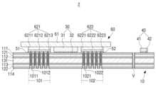
도 3은 도 1에 도시된 인쇄회로기판 조립체(1)의 Ⅰ-Ⅰ선을 따라 자른 단면을 개략적으로 나타난 단면도이다.FIG. 3 is a cross-sectional view schematically showing a cross-section taken along line I-I of the printed
이하에서는 도 1 내지 도 3을 참조하여, 발열하는 전자부품(30), 전자부품(30)과 결합되는 방열부재(20) 및 방열부재(20)와 연결되는 인쇄회로기판(10)을 통한 방열구조를 좀 더 상세히 설명한다.Hereinafter, with reference to FIGS. 1 to 3, heat dissipation through the
도 3에 도시된 인쇄회로기판(10)은 제1층 내지 제4층(111, 112, 113, 114), 제1 및 제2 절연층(121, 122) 및 코어층(131)로 구성된 다층 인쇄회로기판인 것을 일 예로써 도시하였다.The printed
도 3에 도시된 바와 같이, 인쇄회로기판(10)은 전자부품(30) 및 소자(40)들이 실장되는 제1 층(111)과 제1 층(111)이 순차적으로 적층된 제2 내지 제4 층(112, 113, 114)을 포함할 수 있으며, 제1 층(111)과 제2 층(112) 사이에는 제1 절연층(121)이, 제2 층(112)과 제3 층(113) 사이에는 코어층(131)이, 제3 층(113)과 제4 층(114) 사이에는 제2 절연층(122)이 배치될 수 있다.As shown in FIG. 3, the printed
제1 내지 제4 층(111 내지 114)은 전도성의 동박(copper foil)으로 구성될 수 있으며, 이를 통해 회로층을 구성할 수 있다.The first to
아울러, 제1 절연층(121), 제2 절연층(122) 및 코어층(131)은 절연성의 물질로 이루어질 수 있으며, 이를 통해, 제1 층 내지 제4 층(111, 112, 113, 114)이 상호 절연될 수 있다.In addition, the first insulating
인쇄회로기판(10)의 제1 층(111)은 전자부품(30) 및 다수의 소자(40)들이 실장될 수 있으며, 배선패턴(11)과 같은 전기적 신호선이 배치될 수 있다.The
전자부품(30)은 전자부품 본체(31) 및 다수의 커넥터(31)를 포함할 수 있으며, 다수의 커넥터(31)를 통해 제1 층(111)에 실장될 수 있다.The
아울러, 다수의 소자(40) 역시 소자 본체(41) 및 다수의 커넥터(41)를 포함할 수 있으며, 다수의 커넥터(41)를 통해 제1 층(111)에 실장될 수 있다.In addition, the plurality of
전자부품(30) 및 소자(40)의 다수의 커넥터(32, 42)는 솔더 범프(solder bump) 또는 솔더 볼(solder ball)을 포함할 수 있다.The plurality of
제2 층(112)은 인쇄회로기판(10)의 면적 전체를 커버하는 전도성 금속으로 이루어진 그라운드 층일 수 있다.The
이를 통해, 제2 층(112)은 제1 층(111), 제3 층(113), 및 제4 층(114)에 인가되는 전기적 신호가 주변기기에 의해 영향을 받지 않도록 함으로써, 신호의 품질을 확보할 수 있다.Through this, the
아울러, 제3 층(113)은 인쇄회로기판(10)으로 전원을 공급하는 전원배선을 포함하는 전원층 일 수 있으며, 제4 층(114)은 제1 층(111)과 유사한 구조로서 전기적 신호선이 배치될 수 있다.In addition, the
또한, 제4 층(114)의 전기적 신호선에는 다수의 전자부품(미도시) 및 다수의 소자(미도시)들이 실장될 수 있으며, 방열부재(미도시)가 제4 층(114)에 추가로 배치됨으로써 제4 층(114)에 실장된 발열성의 전자부품으로부터 발생되는 열을 추가로 방열할 수 있다.In addition, a number of electronic components (not shown) and a number of devices (not shown) may be mounted on the electrical signal line of the
도 3에 도시된 제1 내지 제4 층(111, 112, 113, 114)의 다층으로 구성된 인쇄회로기판(10)의 구성은 예시적인 것으로서, 필요에 따라 다양하게 변형될 수 있다.The configuration of the printed
인쇄회로기판(10)의 제1 층(111)에는 방열부재(20)의 제1 내지 제3 연결부(221, 222, 223)와 연결될 수 있는 제1 내지 제3 접촉면(101, 102, 103)이 방사형으로 배치될 수 있다.The
제1 내지 제3 접촉면(101, 102, 103)에는 전자부품(30)으로부터 멀어지는 방향으로 배치된 다수의 비아홀(1011, 1021, 1031)이 배치될 수 있다.A plurality of via
또한, 도 3에 도시된 바와 같이 제1 내지 제3 접촉면(101, 102, 103)에 배치된 다수의 비아홀(1011, 1021, 1031) 외에도 인쇄회로기판(10)에는 다수의 층 사이를 전기적으로 연결하는 다른 비아홀(V)을 더 포함할 수 있다.In addition, as shown in FIG. 3, in addition to the plurality of via
도 3에서는 제1 접촉면(101)에 배치된 다수의 비아홀(1011)과 제2 접촉면(102)에 배치된 다수의 비아홀(1021) 만을 도시하였으며, 제3 접촉면(101)에 배치된 다수의 비아홀(도 2의 1031)의 구성은 제1 및 제2 접촉면(101, 102)에 배치된 다수의 비아홀(1011, 1021)과 동일하다.In Figure 3, only the plurality of via
전술한 바와 같이, 제1 내지 제3 접촉면(101, 102, 103)에 배치된 다수의 비아홀(1011, 1021, 1031)은 전자부품(30)이 실장된 인쇄회로기판(10)의 중앙부로부터 멀어지는 방향으로 배치될 수 있다.As described above, the plurality of via
다수의 비아홀(1011, 1021, 1031)은 인쇄회로기판(10)을 관통하는바, 제1 내지 제4 층(111, 112, 113, 114)을 관통할 수 있다.The plurality of via
다수의 비아홀(1011, 1021, 1031)은 전도성 물질로 커버 또는 도금될 수 있다.The plurality of via
구체적으로, 다수의 비아홀(1011, 1021, 1031)은 전도성 물질로 도금된 내주면(1012, 1022, 1032)을 포함할 수 있으며, 이를 통해, 제1 내지 제4 층(111, 112, 113, 114)이 다수의 비아홀(1011, 1021, 1031)을 통해 전기적으로 연결될 수 있다.Specifically, the plurality of via holes (1011, 1021, 1031) may include inner peripheral surfaces (1012, 1022, 1032) plated with a conductive material, through which the first to fourth layers (111, 112, 113, 114) ) can be electrically connected through a plurality of via holes (1011, 1021, 1031).
또한, 다수의 비아홀(1011, 1021, 1031)의 내주면(1012, 1022, 1032)은 열 전도성이 높은 물질로 커버 또는 도금될 수 있다.Additionally, the inner
예를 들어, 다수의 비아홀(1011, 1021, 1031)의 내주면(1012, 1022, 1032)은 알루미늄, 구리 등과 같은 금속으로 커버될 수 있으며, 방열부재(20)와 같은 재질로 이루어 질 수 있다.For example, the inner
이를 통해, 다수의 비아홀(1011, 1021, 1031)로 전달된 열이 내주면(1012, 1022, 1032)을 따라 인쇄회로기판(10)의 내부로 확산될 수 있다.Through this, the heat transferred to the plurality of via holes (1011, 1021, and 1031) can be diffused into the inside of the printed circuit board (10) along the inner peripheral surface (1012, 1022, and 1032).
전자부품(30)으로부터 발생되는 열이 방열부재(20)를 통해 확산되는 구체적인 과정은 다음과 같다.The specific process by which heat generated from the
전자부품(30)을 통해 발생되는 열은 전자부품(30)과 결합된 방열판(21)으로 전도되고, 방열판(21)으로 전도된 열은 방열판(21)의 중앙부로부터 외측으로 확산될 수 있다.Heat generated through the
방열판(21)의 내부를 통해 확산된 열은 방열판(21)의 상부로 대류됨으로써 외부로 배출될 수 있다.Heat diffused through the inside of the
아울러, 방열판(21)은 외측으로 돌출된 다수의 방열핀(미도시)을 포함할 수 있으며, 다수의 방열핀을 통해 외부와의 열 교환 면적을 증대시킴으로써, 외부로의 열 전달의 효과를 더욱 높일 수 있다.In addition, the
아울러, 방열판(21)으로 전도된 열의 일부는 제1 내지 제3 연결부(221, 222, 223)로 이동할 수 있다.In addition, some of the heat conducted to the
제1 내지 제3 연결부(221, 222, 223)로 이동한 열은 제1 내지 제3 지지부(2211, 2221, 2231)를 통해 제1 내지 제3 접촉부(2212, 2222, 2232)로 이동할 수 있다.Heat moving to the first to
이후, 제1 내지 제3 접촉부(2212, 2222, 2232)로부터 제1 내지 제3 접촉면(101, 102, 103)으로 열이 전달될 수 있으며, 이를 통해 방열부재(20)의 열이 인쇄회로기판(10)으로 전달될 수 있다.Thereafter, heat may be transferred from the first to
일반적으로, 전자부품(30)으로부터 방열부재(20)로 전달된 열의 대부분은 외부와의 열 교환이 용이하도록 평판형상으로 이루어진 방열판(21)을 통해 방출될 수 있다.In general, most of the heat transferred from the
다만, 전자부품(30)으로부터 열이 지속적으로 발생함으로써 방열부재(20) 내의 열이 포화되는 경우, 방열부재(20)를 통한 방열성능이 저하될 수 있다.However, if the heat in the
이러한 경우, 방열부재(20)의 포화된 열을 제1 내지 제3 연결부(221, 222, 223)와 제1 내지 제3 접촉면(101, 102, 103)을 통해 인쇄회로기판(10)으로 확산시킴으로써, 인쇄회로기판 조립체(1) 전체의 방열성능을 확보할 수 있다.In this case, the saturated heat of the
전술한 바와 같이, 제1 내지 제3 접촉부(2212, 2222, 2232)로부터 제1 내지 제3 접촉면(101, 102, 103)으로의 열 전달은 제1 내지 제3 열전달물질(51, 52, 53)을 통해 더욱 효과적으로 이루어질 수 있다.As described above, heat transfer from the first to
제1 내지 제3 접촉면(101, 102, 103)으로 전달된 열은 제1 내지 제3 접촉면(101, 102, 103)에 배치된 다수의 비아홀(1011, 1021, 1031)을 통해 인쇄회로기판(10)의 전 영역으로 확산될 수 있다.The heat transferred to the first to third contact surfaces 101, 102, and 103 is transmitted to the printed circuit board ( 10) It can spread to all areas.
구체적으로, 제1 층(111)의 제1 내지 제3 접촉면(101, 102, 103)으로 전달된 열은 제1 내지 제3 접촉면(101, 102, 103)의 다수의 비아홀(1011, 1021, 1031)을 통해 인쇄회로기판(10)의 내부로 확산될 수 있다.Specifically, the heat transferred to the first to third contact surfaces 101, 102, and 103 of the
제1 내지 제3 접촉면(101, 102, 103)에 전달된 열은 다수의 비아홀(1011, 1021, 1031)의 내주면(1012, 1022, 1032)을 통해 제1 층(111)으로부터 제2 절연층(121), 제2 층(112), 코어층(131), 제3 층(113), 제2 절연층(122) 및 제4 층(114)으로 순차적으로 전도될 수 있다.The heat transferred to the first to third contact surfaces 101, 102, and 103 is transferred from the
아울러, 제1 내지 제3 접촉면(101, 102, 103)에 전달된 열의 일부는 제1 내지 제3 접촉면(101, 102, 103)에 배치된 다수의 비아홀(1011, 1021, 1031)의 내부 공간을 통해 대류하여 인쇄회로기판(10)의 내부로 확산될 수 있다.In addition, a portion of the heat transferred to the first to third contact surfaces 101, 102, and 103 is internal space of the plurality of via
전술한 바와 같이, 인쇄회로기판(10)의 전 영역을 커버할 수 있는 그라운드 층으로 구성된 제2 층(112)은 열 전도성이 높은 알루미늄 또는 구리와 같은 금속으로 이루어질 수 있다.As described above, the
따라서, 다수의 비아홀(1011, 1021, 1031)을 통해 제2 층(112)으로 전달된 열은 열 전도성이 높은 제2 층(112)을 통해 더욱 효율적으로 인쇄회로기판(10)의 전 영역으로 확산될 수 있으며, 이를 통해 인쇄회로기판 조립체(1)의 방열성능이 향상될 수 있다.Therefore, the heat transferred to the
아울러, 다수의 비아홀(1011, 1021, 1031)의 내주면(1012, 1022, 1032)과 제2 층(112) 사이에 열전달물질(미도시)을 추가로 배치함으로써, 다수의 비아홀(1011, 1021, 1031)로부터 제2 층(112)으로의 열 전도율을 더욱 높일 수 있다.In addition, by additionally disposing a heat transfer material (not shown) between the inner peripheral surfaces (1012, 1022, 1032) of the plurality of via holes (1011, 1021, 1031) and the
또한, 인쇄회로기판(10)의 전 영역을 커버하는 제2 층(112)에는 다수의 소자(40)들 역시 연결될 수 있는바, 제2 층(112)을 통해 확산되는 열은 제2 층(112)과 연결된 다수의 소자(40)들에도 전달될 수 있다.In addition, a number of
따라서, 다수의 소자(40)들에 전달된 열이 인쇄회로기판(10)의 표면상에 실장된 다수의 소자(40)들을 통해서도 외부로 방출될 수 있다.Accordingly, the heat transferred to the plurality of
아울러, 제2 층(112)에는 열에 대한 내구성이 강한 소자들을 연결하고, 열에 약한 소자들은 제3 층(113) 또는 제4 층(114)으로 분리하여 연결함으로써, 제2 층(112)에 연결된 열에 강한 소자들을 통한 추가적인 방열성능을 확보할 수 있다.In addition, elements with strong durability against heat are connected to the
또한, 다수의 비아홀(1011, 1021, 1031)과 연결되는 제3 층(113), 제4 층(114), 제1 절연층(121), 제2 절연층(122) 및 코어층(131)을 통해서도 제1 내지 제3 접촉면(101, 102, 103)으로 전달된 열이 확산될 수 있는바, 이를 통해 인쇄회로기판 조립체(1)의 방열성능이 향상될 수 있다.In addition, a
아울러, 제1 내지 제3 접촉면(101, 102, 103)에 배치되는 다수의 비아홀(1011, 1021, 1031)은 인쇄회로기판(10) 전체를 관통하는 것이 아닌 인쇄회로기판(10)의 일부 층만을 관통하도록 형성될 수 있다.In addition, the plurality of via
이를 통해, 제1 내지 제3 접촉면(101, 102, 103)의 다수의 비아홀(1011, 1021, 1031)로부터 열이 전달되지 않는 별도의 층을 구성함으로써 인쇄회로기판(10)을 구성하는 다수의 층을 필요에 따라 열적으로 분리할 수 있다.Through this, a separate layer is formed through which heat is not transmitted from the plurality of via
예를 들어, 제1 내지 제3 접촉면(101, 102, 103)에 배치되는 다수의 비아홀(1011, 1021, 1031)을 제1 층(111)으로부터 제2 층(112)까지만 연결되도록 형성함으로써, 제2 층(112)을 통해 방열부재(20)의 열을 추가로 확산시킬 수 있으며, 제3 층(113) 및 제4 층(114)에는 방열부재(20)로부터 열이 전달되지 않게 구성할 수 있다.For example, by forming a plurality of via
이를 통해, 제3 층(113) 및 제4 층(114)에는 열에 약한 구성요소들을 중심으로 연결함으로써, 열에 약한 구성요소들이 제2 층(112)을 통한 방열로 인해 손상을 입는 것을 방지할 수 있다.Through this, the heat-vulnerable components are centrally connected to the
도 4는 본 발명의 다른 실시 예에 따른 인쇄회로기판 조립체(2)의 단면을 개략적으로 나타난 단면도이다.Figure 4 is a cross-sectional view schematically showing a cross-section of a printed
본 발명의 다른 실시 예에 따른 인쇄회로기판 조립체(2)는 인쇄회로기판(10), 방열부재(60), 작동과정에서 많은 양의 열을 발생시키는 전자부품(30) 및 다수의 소자(40)들을 포함할 수 있다.The printed
다만, 인쇄회로기판(10), 전자부품(30) 및 다수의 소자(40)들은 전술한 본 발명의 일 실시 예에 따른 인쇄회로기판 조립체(1)의 구성과 동일하므로 중복되는 설명은 생략하기로 한다.However, since the printed
도 4에 도시된 바와 같이, 방열부재(60)는 방열판(61)과 방열판(61)에 결합되어 방열판(61)을 지지하는 적어도 하나의 연결부를 포함할 수 있다.As shown in FIG. 4, the
방열판(61)을 지지하는 연결부는 다수의 연결부(621, 622, 623)를 포함할 수 있으며, 예를 들어, 제1 내지 제3 연결부(621, 622, 623)를 포함할 수 있다.The connection part supporting the
도 4에서는 제3 연결부(623)가 직접적으로 도시되지 않았으나, 제3 연결부(623)의 구성은 제1 및 제2 연결부(621, 622)와 동일하다.Although the third connection part 623 is not directly shown in FIG. 4, the configuration of the third connection part 623 is the same as that of the first and
제1 내지 제3 연결부(621, 622, 623)는 방열판(61)의 일측에 배치되어 인쇄회로기판(10)상에서 방열판(61)을 지지할 수 있다.The first to
구체적으로, 제1 내지 제3 연결부(621, 622, 623)는 방열판(61)을 지지하는 제1 내지 제3 지지부(6211, 6221, 6231) 및 제1 내지 제3 지지부(6211, 6221, 6231)로부터 절곡된 제1 내지 제3 접촉부(6212, 6222, 6232)를 포함할 수 있다.Specifically, the first to
아울러, 제1 내지 제3 연결부(621, 622, 623)는 제1 내지 제3 접촉부(6212, 6222, 6232)에 결합된 다수의 연결핀(6213, 6223, 6233)을 포함할 수 있다.In addition, the first to
다수의 연결핀(6213, 6223, 6233)은 제1 내지 제3 접촉부(6212, 6222, 6232)로부터 돌출된 구조로서, 다수의 연결핀(6213, 6223, 6233)의 길이는 제1 내지 제3 접촉면(101, 102, 103)의 다수의 비아홀(1011, 1012, 1013)의 길이와 대응되도록 형성될 수 있다.The plurality of connection pins (6213, 6223, 6233) have a structure protruding from the first to third contact portions (6212, 6222, 6232), and the length of the plurality of connection pins (6213, 6223, 6233) is the first to third contact portions (6212, 6222, 6232). It may be formed to correspond to the length of the plurality of via
이를 통해, 다수의 연결핀(6213, 6223, 6233)은 제1 내지 제3 접촉면(101, 102, 103)에 배치된 다수의 비아홀(1011, 1012, 1013)에 삽입될 수 있다.Through this, the plurality of
다수의 연결핀(6213, 6223, 6233)은 제1 내지 제3 접촉면(101, 102, 103)의 다수의 비아홀(1011, 1012, 1013)과 동일한 수로 구성될 수 있으며, 다수의 비아홀(1011, 1012, 1013)의 배치와 대응하여 배치될 수 있다.The plurality of
제1 내지 제3 접촉면(101, 102, 103)의 다수의 비아홀(1011, 1012, 1013)에 다수의 연결핀(6213, 6223, 6233)이 삽입됨으로써, 방열부재(20)가 제1 내지 제3 접촉면(101, 102, 103)에 더욱 견고하게 결합될 수 있다.By inserting a plurality of connection pins (6213, 6223, 6233) into the plurality of via holes (1011, 1012, 1013) of the first to third contact surfaces (101, 102, 103), the heat dissipation member (20) is connected to the first to third contact surfaces (101, 102, 103). 3 It can be more firmly coupled to the contact surfaces (101, 102, 103).
아울러, 다수의 연결핀(6213, 6223, 6233)은 열 전도성이 높은 알루미늄, 구리 또는 은과 같은 금속으로 이루어질 수 있다.In addition, the plurality of
따라서, 제1 내지 제3 접촉부(6212, 6222, 6232)로부터 다수의 연결핀(6213, 6223, 6233)으로 열이 용이하게 전도될 수 있다.Accordingly, heat can be easily conducted from the first to
또한, 다수의 연결핀(6213, 6223, 6233)은 제1 내지 제3 접촉면(101, 102, 103)의 다수의 비아홀(1011, 1012, 1013)에 삽입됨으로써, 다수의 비아홀(1011, 1012, 1013)에 열을 더욱 효과적으로 전달할 수 있다.In addition, the plurality of
도 4에 도시된 바와 같이, 제1 내지 제3 열전달물질(51, 52, 53)은 연성재질로 이루어질 수 있으며, 다수의 연결핀(6213, 6223, 6233)이 제1 내지 제3 열전달물질(51, 52, 53)을 관통할 수 있다.As shown in FIG. 4, the first to third
아울러, 다수의 연결핀(6213, 6223, 6233)이 삽입된 다수의 비아홀(1011, 1012, 1013)에는 열전달물질(미도시)을 추가로 채워줌으로써, 다수의 연결핀(6213, 6223, 6233)으로부터 다수의 비아홀(1011, 1012, 1013)으로의 열 전도율을 더욱 높일 수 있다.In addition, a plurality of via holes (1011, 1012, 1013) into which a plurality of connection pins (6213, 6223, 6233) are inserted are additionally filled with a heat transfer material (not shown), thereby forming a plurality of connection pins (6213, 6223, 6233). The heat conductivity from to the plurality of via holes (1011, 1012, 1013) can be further increased.
이처럼, 본 발명의 다른 실시 예에 따른 방열부재(60)의 다수의 연결핀(6213, 6223, 6233)은 제1 내지 제3 접촉면(101, 102, 103)의 다수의 비아홀(1011, 1012, 1013)에 직접 삽입됨으로써 방열부재(60)의 열이 인쇄회로기판(10)의 내부로 더욱 효과적으로 확산될 수 있으며, 이를 통해 인쇄회로기판 조립체(2)의 방열성능이 향상될 수 있다.In this way, the plurality of
도 5는 본 발명의 또 다른 실시 예에 따른 인쇄회로기판 조립체(3)의 단면을 개략적으로 나타난 단면도이다.Figure 5 is a cross-sectional view schematically showing a cross-section of a printed
본 발명의 또 다른 실시 예에 따른 인쇄회로기판 조립체(3)는 방열부재(70), 인쇄회로기판(80), 작동과정에서 발열하는 전자부품(30) 및 다수의 소자(40)들을 포함할 수 있다.The printed
다만, 전자부품(30) 및 다수의 소자(40)들은 전술한 본 발명의 일 실시 예에 따른 인쇄회로기판 조립체(1)의 구성과 동일하므로 중복되는 설명은 생략하기로 한다.However, since the
방열부재(70)는 방열판(71)과 방열판(71)에 결합되어 방열판(71)을 지지하는 적어도 하나의 연결부를 포함할 수 있다,The
방열판(71)을 지지하는 연결부는 다수의 연결부(721, 722, 723)를 포함할 수 있으며, 예를 들어, 제1 내지 제3 연결부(721, 722, 723)를 포함할 수 있다.The connection part supporting the
도 5에서는 제3 연결부(723)가 직접적으로 도시되지 않았으나, 제3 연결부(723)의 구성은 제1 및 제2 연결부(721, 722)와 동일하다.Although the third connection part 723 is not directly shown in FIG. 5, the configuration of the third connection part 723 is the same as that of the first and
제1 내지 제3 연결부(721, 722, 723)는 방열판(71)의 일측에 배치되어 인쇄회로기판(80)상에서 방열판(71)을 지지할 수 있다.The first to
도 5에 도시된 바와 같이, 인쇄회로기판(80)은 전자부품(30) 및 소자(40)들이 실장되는 제1 층(811)과 제1 층(811)이 순차적으로 적층된 제2 내지 제4 층(812, 813, 814)을 포함할 수 있으며, 제1 층(811)과 제2 층(812) 사이에는 제1 절연층(821)이, 제2 층(812)과 제3 층(813) 사이에는 코어층(831)이, 제3 층(813)과 제4 층(814) 사이에는 제2 절연층(822)이 배치될 수 있다.As shown in FIG. 5, the printed
제1 내지 제4 층(811, 812, 813, 814)은 전도성의 동박(copper foil)으로 구성될 수 있으며, 이를 통해 회로층을 구성할 수 있다.The first to
아울러, 제1 절연층(821), 제2 절연층(822) 및 코어층(831)은 절연성의 물질로 이루어질 수 있으며, 이를 통해, 제1 층 내지 제4 층(811, 812, 813, 814)이 상호 절연될 수 있다.In addition, the first insulating
본 발명의 또 다른 실시 예에 따른 인쇄회로기판(80)은 도 3 및 도 4에 도시된 인쇄회로기판(10)의 구성과 유사한 다층 인쇄회로기판으로서, 제1 층(811)에는 전자부품(30) 및 다수의 소자(40)들이 실장될 수 있으며, 배선패턴(11)과 같은 전기적 신호선이 배치될 수 있다.The printed
또한, 제2 층(812)은 인쇄회로기판(80)의 전 영역을 커버하는 전도성 금속으로 이루어진 그라운드 층일 수 있으며, 제3 층(813)은 인쇄회로기판(80)으로 전원을 공급하는 전원배선을 포함하는 전원층일 수 있고, 제4 층(814)은 제1 층(811)과 유사한 구조로서 전기적 신호선이 배치될 수 있다.Additionally, the
아울러, 인쇄회로기판(80)은 제1 층(811)으로부터 제2 층(812)을 향해 함몰될 단차부를 포함할 수 있다.In addition, the printed
단차부는 방열부재(70)의 제1 내지 제3 연결부(721, 722, 723)의 배치와 대응하는 위치상에 배치되는 제1 내지 제3 단차부(S1, S2, S3)를 포함할 수 있다.The step portion may include first to third step portions S1, S2, and S3 disposed at positions corresponding to the arrangement of the first to
제1 내지 제3 단차부(S1, S2, S3)는 전술한 본 발명의 일 실시 예에 따른 제1 내지 제3 접촉면(101, 102, 103)과 유사하게, 전자부품(30)으로부터 멀어지는 방향으로 연장 형성될 수 있으며, 전자부품(30)을 중심으로 방사형으로 배치될 수 있다.The first to third step portions S1, S2, and S3 are oriented away from the
제1 내지 제3 단차부(S1, S2, S3)를 통해 제2 층(812)의 일부가 직접적으로 인쇄회로기판(80)의 외부로 노출될 수 있다.A portion of the
아울러, 방열부재(70)의 제1 내지 제3 연결부(721, 722, 723)는 제1 내지 제3 단차부(S1, S2, S3)를 통해 제2 층(812)의 일부와 직접적으로 접촉할 수 있다.In addition, the first to
구체적으로, 제1 내지 제3 연결부(721, 722, 723)는 방열판(71)을 지지하는 제1 내지 제3 지지부(7211, 7221, 7231) 및 제1 내지 제3 지지부(7211, 7221, 7231)로부터 절곡된 제1 내지 제3 접촉부(7212, 7222, 7232)를 포함할 수 있다.Specifically, the first to
제1 내지 제3 지지부(7211, 7221, 7231)는 전자부품(30)과 접하는 방열판(71)과 제2 층(812)과 접하는 제1 내지 제3 접촉부(7212, 7222, 7232) 사이를 연결하여, 제2 층(812)으로부터 방열판(71)을 지지할 수 있다.The first to
제1 내지 제3 접촉부(7212, 7222, 7232)는 제1 내지 제3 단차부(S1, S2, S3)의 형상과 대응할 수 있다.The first to
따라서, 제1 내지 제3 접촉부(7212, 7222, 7232)는 전자부품(30)으로부터 멀어지는 방향으로 연장 형성될 수 있으며, 전자부품(30)을 중심으로 방사형으로 배치될 수 있다.Accordingly, the first to
아울러, 제1 내지 제3 접촉부(7212, 7222, 7232)와 제1 내지 제3 접촉부(7212, 7222, 7232)가 접하는 제2 층(812) 사이에는 제1 내지 제3 열전달물질(51, 52, 53)이 배치될 수 있다.In addition, between the first to
이를 통해, 제1 내지 제3 접촉부(7212, 7222, 7232)로부터 제2 층(812)으로의 열 전달이 더욱 용이하게 이루어질 수 있다.Through this, heat transfer from the first to
따라서, 전자부품(30)으로부터 발생되는 열은 방열판(71)으로 전도되어, 방열판(71)의 내부를 통해 확산될 수 있다.Accordingly, the heat generated from the
아울러, 방열판(71)으로 전도된 열의 일부는 제1 내지 제3 연결부(721, 722, 723)로 이동할 수 있으며, 제1 내지 제3 연결부(721, 722, 723)와 결합된 제1 내지 제3 접촉부(7212, 7222, 7232)로 이동할 수 있다.In addition, a portion of the heat conducted to the
제1 내지 제3 접촉부(7212, 7222, 7232)는 제1 내지 제3 단차부(S1, S2, S3)를 통해 제2 층(812)과 직접적으로 연결될 수 있으므로, 제1 내지 제3 접촉부(7212, 7222, 7232)의 열이 제2 층(812)으로 직접 전도될 수 있다.Since the first to
아울러, 제1 내지 제3 열전달물질(51, 52, 53)을 통해 제1 내지 제3 접촉부(7212, 7222, 7232)와 제2 층(812) 사이의 공극을 메워줌으로써 방열부재(70)의 열이 제2 층(812)으로 더욱 효율적으로 전달될 수 있다.In addition, by filling the gap between the first to third contact portions (7212, 7222, 7232) and the second layer (812) through the first to third heat transfer materials (51, 52, and 53), the heat dissipation member (70) Heat can be transferred to the
또한, 제2 층(812)으로 전달된 열은 다수의 비아홀(미도시)을 통해 코어층(831), 제3 층(813), 제2 절연층(822) 및 제4 층(814)으로도 전달될 수 있으며, 이를 통해 인쇄회로기판 조립체(3)의 전체적인 방열성능이 향상될 수 있다.In addition, the heat transferred to the
도 6은 본 발명의 또 다른 실시 예에 따른 인쇄회로기판 조립체(4)의 단면을 개략적으로 나타난 단면도이다.Figure 6 is a cross-sectional view schematically showing a cross-section of a printed circuit board assembly 4 according to another embodiment of the present invention.
본 발명의 또 다른 실시 예에 따른 인쇄회로기판 조립체(4)는 인쇄회로기판(10'), 방열부재(20), 작동과정에서 열을 발생시키는 전자부품(30) 및 다수의 소자(40)들을 포함할 수 있다.The printed circuit board assembly 4 according to another embodiment of the present invention includes a printed circuit board 10', a
다만, 방열부재(20), 전자부품(30) 및 다수의 소자(40)들은 전술한 본 발명의 일 실시 예에 따른 인쇄회로기판 조립체(1)의 구성과 동일하므로 중복되는 설명은 생략하기로 한다.However, since the
도 6에 도시된 인쇄회로기판(10')은 전자부품(30) 및 다수의 소자(40)들이 실장되며 배선패턴(11)과 같은 전기적 신호선이 배치될 수 있는 제1 층(111')과 전원층 및 그라운드 층을 포함할 수 있는 제2 층(112')을 포함할 수 있다.The printed circuit board 10' shown in FIG. 6 includes a
아울러, 인쇄회로기판(10')은 제1 층(111')과 제2 층(112') 사이에 배치되어 제1 층(111')과 제2 층(112')을 상호 절연시키는 절연층(121')을 포함할 수 있다.In addition, the printed circuit board 10' has an insulating layer disposed between the
인쇄회로기판(10')의 제1 층(111')에는 방열부재(20)의 제1 내지 제3 연결부(221, 222, 223)와 연결될 수 있는 제1 내지 제3 접촉면(101', 102', 103')이 방사형으로 배치될 수 있다.The
제1 내지 제3 접촉면(101', 102', 103')에는 전자부품(30)으로부터 멀어지는 방향으로 배치된 다수의 비아홀(1011', 1021', 1031')이 배치될 수 있으며, 다수의 비아홀(1011', 1021', 1031')은 열 전도율이 높은 물질로 커버된 내주면(1012', 1022', 1032')을 포함할 수 있다.A plurality of via holes 1011', 1021', and 1031' arranged in a direction away from the
이를 통해, 방열부재(20)로부터 제1 내지 제3 접촉면(101', 102', 103')으로전달된 열이 다수의 비아홀(1011', 1021', 1031')을 통해 제2 층(112')으로 전달될 수 있으며, 제2 층(112')으로 전달된 열이 외부로 방출될 수 있다.Through this, the heat transferred from the
도 6에 도시된 바와 같이, 인쇄회로기판(10')의 전자부품(30)이 실장된 일측에는 방열부재(20)의 방열판(21)을 통해 인쇄회로기판(10')의 상측으로 열을 대류시킬 수 있다.As shown in FIG. 6, on one side of the printed circuit board 10' on which the
아울러, 제1 내지 제3 연결부(221, 222, 223)로부터 제1 내지 제3 접촉면(101', 102', 103')으로 열이 전달되고, 제1 내지 제3 접촉면(101', 102', 103')으로 전달된 열이 다수의 비아홀(1011', 1021', 1031')을 통해 제1 층(111')과 반대되는 제2 층(112')에 전달됨으로써, 인쇄회로기판(10')의 하측으로 열을 방출시킬 수 있다.In addition, heat is transferred from the first to
이처럼, 전자부품(30)으로부터 발생되는 열이 인쇄회로기판(10')의 양면을 통해 외부로 방출될 수 있는바, 인쇄회로기판 조립체(4)의 방열성능이 향상될 수 있다.In this way, heat generated from the
또한, 본 발명의 또 다른 실시 예에 따른 인쇄회로기판(10')은 도 3에 도시된 다층 구조의 인쇄회로기판(10)과 달리 단층으로 이루어짐으로써, 그 두께가 더 얇아질 수 있으며 인쇄회로기판(10')의 구조 역시 단순화될 수 있다.In addition, the printed circuit board 10' according to another embodiment of the present invention is made of a single layer, unlike the printed
이상에서는 본 발명의 다양한 실시 예를 각각 개별적으로 설명하였으나, 각 실시 예들은 반드시 단독으로 구현되어야만 하는 것은 아니며, 각 실시 예들의 구성 및 동작은 적어도 하나의 다른 실시 예들과 조합되어 구현될 수도 있다.In the above, various embodiments of the present invention have been described individually, but each embodiment does not necessarily have to be implemented alone, and the configuration and operation of each embodiment may be implemented in combination with at least one other embodiment.
또한, 이상에서는 본 발명의 바람직한 실시 예에 대하여 도시하고 설명하였지만, 본 발명은 상술한 특정의 실시 예에 한정되지 아니하며, 청구범위에서 청구하는 본 발명의 요지를 벗어남이 없이 당해 발명이 속하는 기술분야에서 통상의 지식을 가진 자에 의해 다양한 변형실시가 가능한 것은 물론이고, 이러한 변형실시들은 본 발명의 기술적 사상이나 전망으로부터 개별적으로 이해되서는 안될 것이다.In addition, although preferred embodiments of the present invention have been shown and described above, the present invention is not limited to the specific embodiments described above, and the technical field to which the invention pertains without departing from the gist of the present invention as claimed in the claims. Of course, various modifications can be made by those skilled in the art, and these modifications should not be understood individually from the technical idea or perspective of the present invention.
1; 인쇄회로기판 조립체
10; 인쇄회로기판
20; 방열부재
30; 전자부품
40; 소자
51, 52, 53; 제1 내지 제3 열전달물질
101, 103, 103; 제1 내지 제3 접촉면
1011, 1021, 1031; 비아홀
111, 112, 113, 114; 제1 층 내지 제4 층
221, 222, 223; 제1 내지 제3 연결부One; printed circuit board assembly
10; printed circuit board
20; Heat dissipation member
30; Electronic parts
40; device
51, 52, 53; First to third heat transfer materials
101, 103, 103; 1st to 3rd contact surfaces
1011, 1021, 1031; via hole
111, 112, 113, 114; 1st to 4th layers
221, 222, 223; 1st to 3rd connection parts
Claims (20)
Translated fromKorean상기 인쇄회로기판에 실장된 적어도 한 개의 소자;
상기 인쇄회로기판에 실장된 전자부품과 접촉하여, 상기 전자부품에서 발생하는 열을 전달받는 방열부재; 및
상기 인쇄회로기판과 상기 방열부재를 연결하여, 상기 방열부재를 통해 전도되는 열을 상기 인쇄회로기판으로 전달하는 적어도 하나의 연결부;를 포함하며,
상기 방열부재는 상기 전자부품과 상기 적어도 한 개의 소자를 덮을 수 있는 크기로 형성되며, 상기 적어도 한 개의 소자에 대응하는 위치에 상기 적어도 한 개의 소자에 대응하는 크기로 형성된 소자구멍을 포함하며,
상기 적어도 한 개의 연결부는 상기 방열부재의 내측으로 상기 방열부재의 가장자리에서 이격되고, 상기 소자구멍의 가장자리에 마련되며, 상기 인쇄회로기판 상면에서 상기 방열부재를 지지하도록 형성되며,
상기 적어도 한 개의 연결부는 상기 방열부재에 상기 소자구멍을 타발하고 상기 소자구멍의 경계를 구성하는 상기 방열부재의 일부를 절곡하여 형성하는, 인쇄회로기판 조립체.printed circuit board;
at least one element mounted on the printed circuit board;
a heat dissipation member that contacts the electronic components mounted on the printed circuit board and receives heat generated from the electronic components; and
It includes at least one connection part that connects the printed circuit board and the heat dissipation member to transfer heat conducted through the heat dissipation member to the printed circuit board,
The heat dissipation member is formed to a size capable of covering the electronic component and the at least one element, and includes an element hole formed at a position corresponding to the at least one element and having a size corresponding to the at least one element,
The at least one connection portion is spaced apart from an edge of the heat dissipation member to the inside of the heat dissipation member, is provided at an edge of the device hole, and is formed to support the heat dissipation member on the upper surface of the printed circuit board,
A printed circuit board assembly wherein the at least one connection portion is formed by punching the device hole in the heat dissipation member and bending a portion of the heat dissipation member constituting a boundary of the device hole.
상기 인쇄회로기판은 순차적으로 적층된 제1 층, 절연층 및 제2 층을 포함하고,
상기 전자부품은 상기 제1 층에 장착되며,
상기 적어도 하나의 연결부는 상기 방열부재를 통해 전도된 열을 상기 제2 층에 전달하는 것을 특징으로 하는 인쇄회로기판 조립체.According to paragraph 1,
The printed circuit board includes a first layer, an insulating layer, and a second layer sequentially stacked,
The electronic component is mounted on the first layer,
A printed circuit board assembly, wherein the at least one connection portion transfers heat conducted through the heat dissipation member to the second layer.
상기 인쇄회로기판을 관통하는 다수의 비아홀(via hole)을 더 포함하며,
상기 연결부는 상기 다수의 비아홀을 통해 상기 제2 층과 연결되는 것을 특징으로 하는 인쇄회로기판 조립체.According to paragraph 2,
It further includes a plurality of via holes penetrating the printed circuit board,
A printed circuit board assembly, characterized in that the connection portion is connected to the second layer through the plurality of via holes.
상기 다수의 비아홀은 열 전도성 물질로 도금되는 것을 특징으로 하는 인쇄회로기판 조립체.According to paragraph 3,
A printed circuit board assembly, wherein the plurality of via holes are plated with a thermally conductive material.
상기 연결부는 상기 다수의 비아홀에 각각 삽입되는 다수의 연결핀을 포함하는 것을 특징으로 하는 인쇄회로기판 조립체.According to paragraph 4,
A printed circuit board assembly, wherein the connection portion includes a plurality of connection pins each inserted into the plurality of via holes.
상기 연결부와 상기 제1 층 사이에 배치되는 열전달물질(TIM; Thermal Interface Material)을 더 포함하는 것을 특징으로 하는 인쇄회로기판 조립체.According to paragraph 3,
A printed circuit board assembly further comprising a thermal interface material (TIM) disposed between the connection portion and the first layer.
상기 열전달물질은 상기 연결부와 상기 제1 층 사이의 공극을 메우도록 연성재질로 구성되는 것을 특징으로 하는 인쇄회로기판 조립체.According to clause 6,
A printed circuit board assembly, wherein the heat transfer material is made of a soft material to fill the gap between the connection portion and the first layer.
상기 인쇄회로기판은 상기 제1 층으로부터 상기 제2 층을 향해 함몰되어 상기 제2 층의 일부가 노출된 단차부를 포함하고,
상기 연결부는 상기 단차부에 배치되어 상기 제2 층의 일부와 접하는 것을 특징으로 하는 인쇄회로기판 조립체.According to paragraph 2,
The printed circuit board includes a step portion that is recessed from the first layer toward the second layer and exposes a portion of the second layer,
A printed circuit board assembly, wherein the connecting portion is disposed on the stepped portion and comes into contact with a portion of the second layer.
상기 연결부와 상기 제2 층 사이에 배치되는 열전달물질을 더 포함하는 것을 특징으로 하는 인쇄회로기판 조립체.According to clause 8,
A printed circuit board assembly further comprising a heat transfer material disposed between the connection portion and the second layer.
상기 방열부재는 상기 전자부품과 접하는 방열판을 더 포함하고,
상기 연결부는 상기 방열판을 지지하는 것을 특징으로 하는 인쇄회로기판 조립체.According to paragraph 3,
The heat dissipation member further includes a heat sink in contact with the electronic component,
A printed circuit board assembly, wherein the connection portion supports the heat sink.
상기 연결부는 상기 전자부품으로부터 멀어지는 방향으로 연장 형성된 것을 특징으로 하는 인쇄회로기판 조립체.According to clause 10,
A printed circuit board assembly, wherein the connection portion extends in a direction away from the electronic component.
상기 다수의 비아홀은 상기 전자부품으로부터 멀어지는 방향으로 배치되는 것을 특징으로 하는 인쇄회로기판 조립체.According to clause 11,
A printed circuit board assembly, wherein the plurality of via holes are arranged in a direction away from the electronic component.
상기 연결부는,
상기 방열판을 지지하는 지지부; 및
상기 지지부로부터 절곡되어 상기 제1 층과 접하는 접촉부를 포함하는 것을 특징으로 하는 인쇄회로기판 조립체.According to clause 10,
The connection part is,
a support portion supporting the heat sink; and
A printed circuit board assembly comprising a contact part bent from the support part and in contact with the first layer.
상기 방열판과 상기 연결부는 일체로 형성된 것을 특징으로 하는 인쇄회로기판 조립체.According to clause 10,
A printed circuit board assembly, characterized in that the heat sink and the connection portion are formed integrally.
상기 제2 층은 그라운드 층인 것을 특징으로 하는 인쇄회로기판 조립체.According to paragraph 2,
A printed circuit board assembly, characterized in that the second layer is a ground layer.
상기 제2 층과 연결되어 상기 제2 층으로부터 전도된 열을 외부로 방출하는 다수의 소자를 더 포함하는 것을 특징으로 하는 인쇄회로기판 조립체.According to paragraph 3,
A printed circuit board assembly further comprising a plurality of elements connected to the second layer and emitting heat conducted from the second layer to the outside.
상기 인쇄회로기판에 실장된 적어도 한 개의 소자; 및
상기 인쇄회로기판의 일측에 장착되는 전자부품과 연결되어 상기 전자부품으로부터 전도된 열을 방열하는 방열부재;를 포함하고,
상기 방열부재는 상기 전자부품으로부터 전도된 열을 상기 그라운드 층으로 전도하도록 상기 그라운드 층과 연결되는 적어도 하나의 연결부를 포함하며,
상기 방열부재는 상기 전자부품과 상기 적어도 한 개의 소자를 덮을 수 있는 크기로 형성되며, 상기 적어도 한 개의 소자에 대응하는 위치에 상기 적어도 한 개의 소자에 대응하는 크기로 형성된 소자구멍을 포함하며,
상기 적어도 한 개의 연결부는 상기 방열부재의 내측으로 상기 방열부재의 가장자리에서 이격되고, 상기 소자구멍의 가장자리에 마련되며, 상기 인쇄회로기판 상면에서 상기 방열부재를 지지하도록 형성되며,
상기 적어도 한 개의 연결부는 상기 방열부재에 상기 소자구멍을 타발하고 상기 소자구멍의 경계를 구성하는 상기 방열부재의 일부를 절곡하여 형성하는, 인쇄회로기판 조립체.A printed circuit board including a ground layer;
at least one element mounted on the printed circuit board; and
It includes a heat dissipation member connected to an electronic component mounted on one side of the printed circuit board and dissipating heat conducted from the electronic component,
The heat dissipation member includes at least one connection part connected to the ground layer to conduct heat conducted from the electronic component to the ground layer,
The heat dissipation member is formed to a size capable of covering the electronic component and the at least one element, and includes an element hole formed at a position corresponding to the at least one element and having a size corresponding to the at least one element,
The at least one connection portion is spaced apart from an edge of the heat dissipation member to the inside of the heat dissipation member, is provided at an edge of the device hole, and is formed to support the heat dissipation member on the upper surface of the printed circuit board,
A printed circuit board assembly wherein the at least one connection portion is formed by punching the device hole in the heat dissipation member and bending a portion of the heat dissipation member constituting a boundary of the device hole.
상기 인쇄회로기판은 상기 인쇄회로기판을 관통하는 다수의 비아홀을 포함하고,
상기 연결부는 상기 다수의 비아홀 중 적어도 하나의 비아홀과 접함으로써 상기 그라운드 층과 연결되는 것을 특징으로 하는 인쇄회로기판 조립체.According to clause 17,
The printed circuit board includes a plurality of via holes penetrating the printed circuit board,
A printed circuit board assembly, characterized in that the connection part is connected to the ground layer by contacting at least one via hole among the plurality of via holes.
상기 연결부는 상기 전자부품으로부터 멀어지는 방향으로 연장 형성된 것을 특징으로 하는 인쇄회로기판 조립체.According to clause 18,
A printed circuit board assembly, wherein the connection portion extends in a direction away from the electronic component.
상기 인쇄회로기판에 실장된 적어도 한 개의 소자; 및
상기 인쇄회로기판의 배선패턴에 실장되는 전자부품과 접촉되는 방열부재;를 포함하고,
상기 방열부재는 상기 전자부품으로부터 전도된 열을 상기 인쇄회로기판으로 전도하도록 상기 인쇄회로기판과 연결되는 다수의 연결부를 포함하며,
상기 방열부재는 상기 전자부품과 상기 적어도 한 개의 소자를 덮을 수 있는 크기로 형성되며, 상기 적어도 한 개의 소자에 대응하는 위치에 상기 적어도 한 개의 소자에 대응하는 크기로 형성된 소자구멍을 포함하며,
상기 다수의 연결부 중 적어도 한 개의 연결부는 상기 방열부재의 내측으로 상기 방열부재의 가장자리에서 이격되고, 상기 소자구멍의 가장자리에 마련되며, 상기 인쇄회로기판 상면에서 상기 방열부재를 지지하도록 형성되며,
상기 적어도 한 개의 연결부는 상기 방열부재에 상기 소자구멍을 타발하고 상기 소자구멍의 경계를 구성하는 상기 방열부재의 일부를 절곡하여 형성하며,
상기 다수의 연결부는 상기 배선패턴과의 간섭 없이 상기 전자부품을 중심으로 방사형으로 배치되는 것을 특징으로 하는 인쇄회로기판 조립체.printed circuit board;
at least one element mounted on the printed circuit board; and
It includes; a heat dissipation member in contact with electronic components mounted on the wiring pattern of the printed circuit board;
The heat dissipation member includes a plurality of connection parts connected to the printed circuit board to conduct heat conducted from the electronic component to the printed circuit board,
The heat dissipation member is formed to a size capable of covering the electronic component and the at least one element, and includes an element hole formed at a position corresponding to the at least one element and having a size corresponding to the at least one element,
At least one connection part among the plurality of connection parts is spaced apart from an edge of the heat dissipation member to the inside of the heat dissipation member, is provided at an edge of the device hole, and is formed to support the heat dissipation member on the upper surface of the printed circuit board,
The at least one connection portion is formed by punching the device hole in the heat dissipation member and bending a portion of the heat dissipation member constituting a boundary of the device hole,
A printed circuit board assembly, wherein the plurality of connection parts are arranged radially around the electronic component without interfering with the wiring pattern.
Priority Applications (5)
| Application Number | Priority Date | Filing Date | Title |
|---|---|---|---|
| KR1020160100589AKR102674888B1 (en) | 2016-08-08 | 2016-08-08 | Printed circuit board assembly |
| EP17839682.6AEP3459324A4 (en) | 2016-08-08 | 2017-07-19 | PRINTED CIRCUIT BOARD ASSEMBLY |
| PCT/KR2017/007796WO2018030664A1 (en) | 2016-08-08 | 2017-07-19 | Printed circuit board assembly |
| US15/664,369US10925148B2 (en) | 2016-08-08 | 2017-07-31 | Printed circuit board assembly |
| CN201710659704.3ACN107708286B (en) | 2016-08-08 | 2017-08-04 | Printed circuit board assembly |
Applications Claiming Priority (1)
| Application Number | Priority Date | Filing Date | Title |
|---|---|---|---|
| KR1020160100589AKR102674888B1 (en) | 2016-08-08 | 2016-08-08 | Printed circuit board assembly |
Publications (2)
| Publication Number | Publication Date |
|---|---|
| KR20180016799A KR20180016799A (en) | 2018-02-20 |
| KR102674888B1true KR102674888B1 (en) | 2024-06-14 |
Family
ID=61070070
Family Applications (1)
| Application Number | Title | Priority Date | Filing Date |
|---|---|---|---|
| KR1020160100589AActiveKR102674888B1 (en) | 2016-08-08 | 2016-08-08 | Printed circuit board assembly |
Country Status (5)
| Country | Link |
|---|---|
| US (1) | US10925148B2 (en) |
| EP (1) | EP3459324A4 (en) |
| KR (1) | KR102674888B1 (en) |
| CN (1) | CN107708286B (en) |
| WO (1) | WO2018030664A1 (en) |
Families Citing this family (8)
| Publication number | Priority date | Publication date | Assignee | Title |
|---|---|---|---|---|
| CN110557881B (en)* | 2018-05-31 | 2025-04-18 | 欧菲微电子(南昌)有限公司 | Circuit board components, optoelectronic modules, depth cameras and electronic devices |
| DE102018007243B4 (en)* | 2018-09-13 | 2020-08-13 | Diehl Ako Stiftung & Co. Kg | Electrical circuit |
| CN112804851A (en)* | 2019-10-28 | 2021-05-14 | 华为终端有限公司 | Electronic equipment |
| KR102785364B1 (en)* | 2019-12-11 | 2025-03-20 | 동우 화인켐 주식회사 | Printed circuit board, antenna structure including the same and image display device including the same |
| CN113299193B (en)* | 2021-05-26 | 2022-03-22 | 惠科股份有限公司 | Display module and display device |
| US12367569B2 (en)* | 2022-04-27 | 2025-07-22 | Taiwan Semiconductor Manufacturing Co., Ltd. | Automatic optical inspection system and method |
| WO2025165048A1 (en)* | 2024-01-29 | 2025-08-07 | 주식회사 유라코퍼레이션 | Printed circuit board |
| WO2025165046A1 (en)* | 2024-01-29 | 2025-08-07 | 주식회사 유라코퍼레이션 | Printed circuit board |
Citations (5)
| Publication number | Priority date | Publication date | Assignee | Title |
|---|---|---|---|---|
| JP2001160608A (en)* | 1999-12-02 | 2001-06-12 | Sharp Corp | Heat dissipation structure of heat-generating components in electronic equipment unit |
| US20050157469A1 (en)* | 2003-12-19 | 2005-07-21 | Gorak Gracjan | Cooling arrangement for a printed circuit board with a heat-dissipating electronic element |
| US20060133043A1 (en)* | 2004-12-22 | 2006-06-22 | Boudreaux Brent A | Heat spreader with multiple stacked printed circuit boards |
| JP2010027976A (en) | 2008-07-23 | 2010-02-04 | Shinko Electric Ind Co Ltd | Multilayered capacitor and semiconductor package containing the same, and method for manufacturing the same |
| WO2010126410A1 (en) | 2009-04-28 | 2010-11-04 | Telefonaktiebolaget L M Ericsson (Publ) | Assembly for carrying electronic components |
Family Cites Families (23)
| Publication number | Priority date | Publication date | Assignee | Title |
|---|---|---|---|---|
| JPS5661152A (en)* | 1979-10-24 | 1981-05-26 | Hitachi Ltd | Integrated circuit cooler |
| IT1201315B (en)* | 1985-06-17 | 1989-01-27 | M A S Ind Spa | METHOD TO ENSURE THE COOLING OF ELECTRONIC COMPONENTS FIXED ON A MULTILAYER FOR MOLDED AND MULTI-LAYER CIRCUITS REALIZED ACCORDING TO THAT METHOD |
| JP2518031B2 (en)* | 1989-01-19 | 1996-07-24 | 日本電気株式会社 | LSI package cooling structure |
| US6031723A (en)* | 1994-08-18 | 2000-02-29 | Allen-Bradley Company, Llc | Insulated surface mount circuit board construction |
| US5812375A (en)* | 1996-05-06 | 1998-09-22 | Cummins Engine Company, Inc. | Electronic assembly for selective heat sinking and two-sided component attachment |
| US6191478B1 (en)* | 1999-06-07 | 2001-02-20 | Agilent Technologies Inc. | Demountable heat spreader and high reliability flip chip package assembly |
| TW411037U (en)* | 1999-06-11 | 2000-11-01 | Ind Tech Res Inst | Integrated circuit packaging structure with dual directions of thermal conduction path |
| JP2001210763A (en)* | 2000-01-27 | 2001-08-03 | Mitsubishi Electric Corp | Semiconductor module device |
| TW200428623A (en) | 2003-06-11 | 2004-12-16 | Siliconware Precision Industries Co Ltd | Semiconductor package with heat sink |
| JP3102658U (en)* | 2004-01-05 | 2004-07-15 | 船井電機株式会社 | heatsink |
| JP4593616B2 (en) | 2005-01-25 | 2010-12-08 | 富士通株式会社 | Semiconductor device |
| JP2007184351A (en) | 2006-01-05 | 2007-07-19 | Nec Electronics Corp | Semiconductor device and its manufacturing method |
| TWI317996B (en) | 2006-09-06 | 2009-12-01 | Advanced Semiconductor Eng | Chip package structure and heat sink for chip package |
| US8212352B2 (en)* | 2007-03-28 | 2012-07-03 | Stats Chippac Ltd. | Integrated circuit package system with heat sink spacer structures |
| JP4729001B2 (en)* | 2007-05-28 | 2011-07-20 | 株式会社東芝 | Printed wiring board structure, printed wiring board component mounting method, and electronic device |
| TW200847857A (en)* | 2007-05-29 | 2008-12-01 | Acbel Polytech Inc | Heat dissipation structure of electronic components |
| TW201230897A (en)* | 2011-01-14 | 2012-07-16 | Askey Computer Corp | Circuit board |
| TWI502733B (en)* | 2012-11-02 | 2015-10-01 | 環旭電子股份有限公司 | Electronic package module and method of manufacturing the same |
| KR102162812B1 (en)* | 2013-06-28 | 2020-10-07 | 엘지디스플레이 주식회사 | Printed circuit board and Display Device having thereof |
| WO2015023447A2 (en) | 2013-08-16 | 2015-02-19 | Technicolor Usa, Inc. | Multi-layer heat spreader assembly with isolated convective fins |
| US20150257249A1 (en)* | 2014-03-08 | 2015-09-10 | Gerald Ho Kim | Heat Sink With Protrusions On Multiple Sides Thereof And Apparatus Using The Same |
| KR101516615B1 (en) | 2014-12-29 | 2015-05-04 | 주식회사 테크엔 | LED lamp manufacturing method comprising a radiation system using the PCB ground |
| JP6036894B2 (en)* | 2015-03-26 | 2016-11-30 | 日本電気株式会社 | Cooling device and equipment |
- 2016
- 2016-08-08KRKR1020160100589Apatent/KR102674888B1/enactiveActive
- 2017
- 2017-07-19WOPCT/KR2017/007796patent/WO2018030664A1/ennot_activeCeased
- 2017-07-19EPEP17839682.6Apatent/EP3459324A4/enactivePending
- 2017-07-31USUS15/664,369patent/US10925148B2/enactiveActive
- 2017-08-04CNCN201710659704.3Apatent/CN107708286B/enactiveActive
Patent Citations (5)
| Publication number | Priority date | Publication date | Assignee | Title |
|---|---|---|---|---|
| JP2001160608A (en)* | 1999-12-02 | 2001-06-12 | Sharp Corp | Heat dissipation structure of heat-generating components in electronic equipment unit |
| US20050157469A1 (en)* | 2003-12-19 | 2005-07-21 | Gorak Gracjan | Cooling arrangement for a printed circuit board with a heat-dissipating electronic element |
| US20060133043A1 (en)* | 2004-12-22 | 2006-06-22 | Boudreaux Brent A | Heat spreader with multiple stacked printed circuit boards |
| JP2010027976A (en) | 2008-07-23 | 2010-02-04 | Shinko Electric Ind Co Ltd | Multilayered capacitor and semiconductor package containing the same, and method for manufacturing the same |
| WO2010126410A1 (en) | 2009-04-28 | 2010-11-04 | Telefonaktiebolaget L M Ericsson (Publ) | Assembly for carrying electronic components |
Also Published As
| Publication number | Publication date |
|---|---|
| CN107708286A (en) | 2018-02-16 |
| WO2018030664A1 (en) | 2018-02-15 |
| CN107708286B (en) | 2022-01-11 |
| US20180042100A1 (en) | 2018-02-08 |
| KR20180016799A (en) | 2018-02-20 |
| EP3459324A4 (en) | 2019-06-12 |
| EP3459324A1 (en) | 2019-03-27 |
| US10925148B2 (en) | 2021-02-16 |
Similar Documents
| Publication | Publication Date | Title |
|---|---|---|
| KR102674888B1 (en) | Printed circuit board assembly | |
| JP6891274B2 (en) | Electronics | |
| US8520388B2 (en) | Heat-radiating component and electronic component device | |
| KR100833185B1 (en) | Heat sink and memory module using same | |
| KR20160038293A (en) | Circuit board | |
| KR20160038304A (en) | Circuit board | |
| JP2006108356A (en) | Semiconductor device and electronic equipment | |
| JP5709218B2 (en) | Semiconductor device, three-dimensional mounting type semiconductor device, semiconductor module, electronic device, and manufacturing method thereof | |
| KR20120051992A (en) | Radiant heat substrate and method for manufacturing the radiant heat substrate, and package structure with the radiant heat substrate | |
| KR102194720B1 (en) | Circuit Board including the heat dissipation structure | |
| US6778398B2 (en) | Thermal-conductive substrate package | |
| KR20160120486A (en) | Circuit board and method of manufacturing the same | |
| US6700195B1 (en) | Electronic assembly for removing heat from a flip chip | |
| US20150053462A1 (en) | Wiring board structure | |
| KR100302973B1 (en) | Circuit substrate including printed circuit board having heat-shielding portion | |
| JP2006120996A (en) | Circuit module | |
| US7312518B2 (en) | Miniaturized multi-chip module and method for manufacturing the same | |
| JP2012169330A (en) | Electronic device | |
| JP2004079949A (en) | Heat dissipation device for heat generating semiconductor element in memory module | |
| JPH07106721A (en) | Printed circuit board and heat radiating method | |
| US11798873B2 (en) | Semiconductor assembly | |
| JP7223639B2 (en) | electronic controller | |
| JP5115200B2 (en) | Electronic device, package having the same, and electronic device | |
| KR20080004734A (en) | Heat dissipation structure of heating element | |
| CN100505227C (en) | Substrate structure for direct electrical connection of semiconductor package |
Legal Events
| Date | Code | Title | Description |
|---|---|---|---|
| PA0109 | Patent application | St.27 status event code:A-0-1-A10-A12-nap-PA0109 | |
| AMND | Amendment | ||
| P11-X000 | Amendment of application requested | St.27 status event code:A-2-2-P10-P11-nap-X000 | |
| P13-X000 | Application amended | St.27 status event code:A-2-2-P10-P13-nap-X000 | |
| PG1501 | Laying open of application | St.27 status event code:A-1-1-Q10-Q12-nap-PG1501 | |
| A201 | Request for examination | ||
| PA0201 | Request for examination | St.27 status event code:A-1-2-D10-D11-exm-PA0201 | |
| E902 | Notification of reason for refusal | ||
| PE0902 | Notice of grounds for rejection | St.27 status event code:A-1-2-D10-D21-exm-PE0902 | |
| AMND | Amendment | ||
| P11-X000 | Amendment of application requested | St.27 status event code:A-2-2-P10-P11-nap-X000 | |
| P13-X000 | Application amended | St.27 status event code:A-2-2-P10-P13-nap-X000 | |
| E601 | Decision to refuse application | ||
| PE0601 | Decision on rejection of patent | St.27 status event code:N-2-6-B10-B15-exm-PE0601 | |
| AMND | Amendment | ||
| P11-X000 | Amendment of application requested | St.27 status event code:A-2-2-P10-P11-nap-X000 | |
| P13-X000 | Application amended | St.27 status event code:A-2-2-P10-P13-nap-X000 | |
| PX0901 | Re-examination | St.27 status event code:A-2-3-E10-E12-rex-PX0901 | |
| PX0701 | Decision of registration after re-examination | St.27 status event code:A-3-4-F10-F13-rex-PX0701 | |
| X701 | Decision to grant (after re-examination) | ||
| GRNT | Written decision to grant | ||
| PR0701 | Registration of establishment | St.27 status event code:A-2-4-F10-F11-exm-PR0701 | |
| PR1002 | Payment of registration fee | St.27 status event code:A-2-2-U10-U11-oth-PR1002 Fee payment year number:1 | |
| PG1601 | Publication of registration | St.27 status event code:A-4-4-Q10-Q13-nap-PG1601 |