KR102673872B1 - Integrated circuit device and method of manufacturing the same - Google Patents
Integrated circuit device and method of manufacturing the sameDownload PDFInfo
- Publication number
- KR102673872B1 KR102673872B1KR1020190031774AKR20190031774AKR102673872B1KR 102673872 B1KR102673872 B1KR 102673872B1KR 1020190031774 AKR1020190031774 AKR 1020190031774AKR 20190031774 AKR20190031774 AKR 20190031774AKR 102673872 B1KR102673872 B1KR 102673872B1
- Authority
- KR
- South Korea
- Prior art keywords
- punch
- fin
- semiconductor layer
- source
- nanosheet
- Prior art date
- Legal status (The legal status is an assumption and is not a legal conclusion. Google has not performed a legal analysis and makes no representation as to the accuracy of the status listed.)
- Active
Links
- 238000004519manufacturing processMethods0.000titledescription19
- 239000002135nanosheetSubstances0.000claimsabstractdescription241
- 239000004065semiconductorSubstances0.000claimsabstractdescription236
- 239000000463materialSubstances0.000claimsabstractdescription27
- 239000000470constituentSubstances0.000claimsabstract3
- 239000002019doping agentSubstances0.000claimsdescription34
- 239000000758substrateSubstances0.000claimsdescription27
- 238000013459approachMethods0.000claimsdescription5
- 239000010410layerSubstances0.000description250
- 238000000034methodMethods0.000description41
- 125000006850spacer groupChemical group0.000description18
- 229910052751metalInorganic materials0.000description17
- 239000002184metalSubstances0.000description17
- 229910000577Silicon-germaniumInorganic materials0.000description11
- 230000001681protective effectEffects0.000description11
- 238000002955isolationMethods0.000description10
- 238000005530etchingMethods0.000description7
- 229910021332silicideInorganic materials0.000description6
- FVBUAEGBCNSCDD-UHFFFAOYSA-Nsilicide(4-)Chemical compound[Si-4]FVBUAEGBCNSCDD-UHFFFAOYSA-N0.000description6
- 239000011229interlayerSubstances0.000description5
- 150000004767nitridesChemical class0.000description5
- 229910052814silicon oxideInorganic materials0.000description5
- 238000000231atomic layer depositionMethods0.000description4
- 238000010586diagramMethods0.000description4
- 230000005669field effectEffects0.000description4
- 229910052710siliconInorganic materials0.000description4
- VYPSYNLAJGMNEJ-UHFFFAOYSA-NSilicium dioxideChemical compoundO=[Si]=OVYPSYNLAJGMNEJ-UHFFFAOYSA-N0.000description3
- XUIMIQQOPSSXEZ-UHFFFAOYSA-NSiliconChemical compound[Si]XUIMIQQOPSSXEZ-UHFFFAOYSA-N0.000description3
- 230000006866deteriorationEffects0.000description3
- 230000000694effectsEffects0.000description3
- 238000004518low pressure chemical vapour depositionMethods0.000description3
- 239000010703siliconSubstances0.000description3
- 229910052581Si3N4Inorganic materials0.000description2
- 229910003697SiBNInorganic materials0.000description2
- 229910004298SiO 2Inorganic materials0.000description2
- ATJFFYVFTNAWJD-UHFFFAOYSA-NTinChemical compound[Sn]ATJFFYVFTNAWJD-UHFFFAOYSA-N0.000description2
- 230000015572biosynthetic processEffects0.000description2
- 238000005229chemical vapour depositionMethods0.000description2
- 238000010438heat treatmentMethods0.000description2
- 230000010354integrationEffects0.000description2
- 230000003071parasitic effectEffects0.000description2
- 229910021420polycrystalline siliconInorganic materials0.000description2
- 229920005591polysiliconPolymers0.000description2
- 239000002243precursorSubstances0.000description2
- HQVNEWCFYHHQES-UHFFFAOYSA-Nsilicon nitrideChemical compoundN12[Si]34N5[Si]62N3[Si]51N64HQVNEWCFYHHQES-UHFFFAOYSA-N0.000description2
- 229910052718tinInorganic materials0.000description2
- 229910052719titaniumInorganic materials0.000description2
- 239000010936titaniumSubstances0.000description2
- 229910052721tungstenInorganic materials0.000description2
- OKTJSMMVPCPJKN-UHFFFAOYSA-NCarbonChemical compound[C]OKTJSMMVPCPJKN-UHFFFAOYSA-N0.000description1
- 229910052692DysprosiumInorganic materials0.000description1
- 229910052691ErbiumInorganic materials0.000description1
- 229910001218Gallium arsenideInorganic materials0.000description1
- 229910000673Indium arsenideInorganic materials0.000description1
- 229910004166TaNInorganic materials0.000description1
- 229910052771TerbiumInorganic materials0.000description1
- 229910010041TiAlCInorganic materials0.000description1
- 229910052769YtterbiumInorganic materials0.000description1
- 229910045601alloyInorganic materials0.000description1
- 239000000956alloySubstances0.000description1
- 229910052782aluminiumInorganic materials0.000description1
- 229910052785arsenicInorganic materials0.000description1
- 229910052799carbonInorganic materials0.000description1
- 150000001875compoundsChemical class0.000description1
- 229910052802copperInorganic materials0.000description1
- 125000004122cyclic groupChemical group0.000description1
- 230000007423decreaseEffects0.000description1
- 238000000151depositionMethods0.000description1
- 230000008021depositionEffects0.000description1
- BUMGIEFFCMBQDG-UHFFFAOYSA-NdichlorosiliconChemical compoundCl[Si]ClBUMGIEFFCMBQDG-UHFFFAOYSA-N0.000description1
- 239000003989dielectric materialSubstances0.000description1
- PZPGRFITIJYNEJ-UHFFFAOYSA-NdisilaneChemical compound[SiH3][SiH3]PZPGRFITIJYNEJ-UHFFFAOYSA-N0.000description1
- 238000001312dry etchingMethods0.000description1
- 229910000078germaneInorganic materials0.000description1
- 229910052735hafniumInorganic materials0.000description1
- 229910000449hafnium oxideInorganic materials0.000description1
- WIHZLLGSGQNAGK-UHFFFAOYSA-Nhafnium(4+);oxygen(2-)Chemical compound[O-2].[O-2].[Hf+4]WIHZLLGSGQNAGK-UHFFFAOYSA-N0.000description1
- 150000002430hydrocarbonsChemical class0.000description1
- 238000011065in-situ storageMethods0.000description1
- 229910052738indiumInorganic materials0.000description1
- RPQDHPTXJYYUPQ-UHFFFAOYSA-Nindium arsenideChemical compound[In]#[As]RPQDHPTXJYYUPQ-UHFFFAOYSA-N0.000description1
- 239000000203mixtureSubstances0.000description1
- 238000012986modificationMethods0.000description1
- 230000004048modificationEffects0.000description1
- 229910003465moissaniteInorganic materials0.000description1
- 229910052750molybdenumInorganic materials0.000description1
- 229910052759nickelInorganic materials0.000description1
- 230000003647oxidationEffects0.000description1
- 238000007254oxidation reactionMethods0.000description1
- 229910052763palladiumInorganic materials0.000description1
- 230000000149penetrating effectEffects0.000description1
- 229910052697platinumInorganic materials0.000description1
- 229910010271silicon carbideInorganic materials0.000description1
- 229910052715tantalumInorganic materials0.000description1
- 229910021341titanium silicideInorganic materials0.000description1
- VEDJZFSRVVQBIL-UHFFFAOYSA-NtrisilaneChemical compound[SiH3][SiH2][SiH3]VEDJZFSRVVQBIL-UHFFFAOYSA-N0.000description1
- 238000001039wet etchingMethods0.000description1
Images


Classifications
- H—ELECTRICITY
- H10—SEMICONDUCTOR DEVICES; ELECTRIC SOLID-STATE DEVICES NOT OTHERWISE PROVIDED FOR
- H10D—INORGANIC ELECTRIC SEMICONDUCTOR DEVICES
- H10D10/00—Bipolar junction transistors [BJT]
- H10D10/60—Lateral BJTs
- H01L29/735—
- H—ELECTRICITY
- H10—SEMICONDUCTOR DEVICES; ELECTRIC SOLID-STATE DEVICES NOT OTHERWISE PROVIDED FOR
- H10D—INORGANIC ELECTRIC SEMICONDUCTOR DEVICES
- H10D30/00—Field-effect transistors [FET]
- H10D30/60—Insulated-gate field-effect transistors [IGFET]
- H10D30/62—Fin field-effect transistors [FinFET]
- H10D30/6215—Fin field-effect transistors [FinFET] having multiple independently-addressable gate electrodes
- H—ELECTRICITY
- H10—SEMICONDUCTOR DEVICES; ELECTRIC SOLID-STATE DEVICES NOT OTHERWISE PROVIDED FOR
- H10D—INORGANIC ELECTRIC SEMICONDUCTOR DEVICES
- H10D30/00—Field-effect transistors [FET]
- H10D30/01—Manufacture or treatment
- H10D30/021—Manufacture or treatment of FETs having insulated gates [IGFET]
- H10D30/024—Manufacture or treatment of FETs having insulated gates [IGFET] of fin field-effect transistors [FinFET]
- H01L21/823418—
- H01L21/823814—
- H01L29/0669—
- H01L29/1083—
- H01L29/66348—
- H01L29/66568—
- H01L29/785—
- H—ELECTRICITY
- H10—SEMICONDUCTOR DEVICES; ELECTRIC SOLID-STATE DEVICES NOT OTHERWISE PROVIDED FOR
- H10D—INORGANIC ELECTRIC SEMICONDUCTOR DEVICES
- H10D12/00—Bipolar devices controlled by the field effect, e.g. insulated-gate bipolar transistors [IGBT]
- H10D12/01—Manufacture or treatment
- H10D12/031—Manufacture or treatment of IGBTs
- H10D12/032—Manufacture or treatment of IGBTs of vertical IGBTs
- H10D12/038—Manufacture or treatment of IGBTs of vertical IGBTs having a recessed gate, e.g. trench-gate IGBTs
- H—ELECTRICITY
- H10—SEMICONDUCTOR DEVICES; ELECTRIC SOLID-STATE DEVICES NOT OTHERWISE PROVIDED FOR
- H10D—INORGANIC ELECTRIC SEMICONDUCTOR DEVICES
- H10D30/00—Field-effect transistors [FET]
- H10D30/01—Manufacture or treatment
- H10D30/014—Manufacture or treatment of FETs having zero-dimensional [0D] or one-dimensional [1D] channels, e.g. quantum wire FETs, single-electron transistors [SET] or Coulomb blockade transistors
- H—ELECTRICITY
- H10—SEMICONDUCTOR DEVICES; ELECTRIC SOLID-STATE DEVICES NOT OTHERWISE PROVIDED FOR
- H10D—INORGANIC ELECTRIC SEMICONDUCTOR DEVICES
- H10D30/00—Field-effect transistors [FET]
- H10D30/01—Manufacture or treatment
- H10D30/021—Manufacture or treatment of FETs having insulated gates [IGFET]
- H10D30/027—Manufacture or treatment of FETs having insulated gates [IGFET] of lateral single-gate IGFETs
- H—ELECTRICITY
- H10—SEMICONDUCTOR DEVICES; ELECTRIC SOLID-STATE DEVICES NOT OTHERWISE PROVIDED FOR
- H10D—INORGANIC ELECTRIC SEMICONDUCTOR DEVICES
- H10D30/00—Field-effect transistors [FET]
- H10D30/40—FETs having zero-dimensional [0D], one-dimensional [1D] or two-dimensional [2D] charge carrier gas channels
- H10D30/43—FETs having zero-dimensional [0D], one-dimensional [1D] or two-dimensional [2D] charge carrier gas channels having 1D charge carrier gas channels, e.g. quantum wire FETs or transistors having 1D quantum-confined channels
- H—ELECTRICITY
- H10—SEMICONDUCTOR DEVICES; ELECTRIC SOLID-STATE DEVICES NOT OTHERWISE PROVIDED FOR
- H10D—INORGANIC ELECTRIC SEMICONDUCTOR DEVICES
- H10D30/00—Field-effect transistors [FET]
- H10D30/60—Insulated-gate field-effect transistors [IGFET]
- H10D30/62—Fin field-effect transistors [FinFET]
- H—ELECTRICITY
- H10—SEMICONDUCTOR DEVICES; ELECTRIC SOLID-STATE DEVICES NOT OTHERWISE PROVIDED FOR
- H10D—INORGANIC ELECTRIC SEMICONDUCTOR DEVICES
- H10D30/00—Field-effect transistors [FET]
- H10D30/60—Insulated-gate field-effect transistors [IGFET]
- H10D30/67—Thin-film transistors [TFT]
- H10D30/6729—Thin-film transistors [TFT] characterised by the electrodes
- H10D30/673—Thin-film transistors [TFT] characterised by the electrodes characterised by the shapes, relative sizes or dispositions of the gate electrodes
- H10D30/6735—Thin-film transistors [TFT] characterised by the electrodes characterised by the shapes, relative sizes or dispositions of the gate electrodes having gates fully surrounding the channels, e.g. gate-all-around
- H—ELECTRICITY
- H10—SEMICONDUCTOR DEVICES; ELECTRIC SOLID-STATE DEVICES NOT OTHERWISE PROVIDED FOR
- H10D—INORGANIC ELECTRIC SEMICONDUCTOR DEVICES
- H10D30/00—Field-effect transistors [FET]
- H10D30/60—Insulated-gate field-effect transistors [IGFET]
- H10D30/67—Thin-film transistors [TFT]
- H10D30/6757—Thin-film transistors [TFT] characterised by the structure of the channel, e.g. transverse or longitudinal shape or doping profile
- H—ELECTRICITY
- H10—SEMICONDUCTOR DEVICES; ELECTRIC SOLID-STATE DEVICES NOT OTHERWISE PROVIDED FOR
- H10D—INORGANIC ELECTRIC SEMICONDUCTOR DEVICES
- H10D62/00—Semiconductor bodies, or regions thereof, of devices having potential barriers
- H10D62/10—Shapes, relative sizes or dispositions of the regions of the semiconductor bodies; Shapes of the semiconductor bodies
- H10D62/113—Isolations within a component, i.e. internal isolations
- H10D62/115—Dielectric isolations, e.g. air gaps
- H10D62/116—Dielectric isolations, e.g. air gaps adjoining the input or output regions of field-effect devices, e.g. adjoining source or drain regions
- H—ELECTRICITY
- H10—SEMICONDUCTOR DEVICES; ELECTRIC SOLID-STATE DEVICES NOT OTHERWISE PROVIDED FOR
- H10D—INORGANIC ELECTRIC SEMICONDUCTOR DEVICES
- H10D62/00—Semiconductor bodies, or regions thereof, of devices having potential barriers
- H10D62/10—Shapes, relative sizes or dispositions of the regions of the semiconductor bodies; Shapes of the semiconductor bodies
- H10D62/117—Shapes of semiconductor bodies
- H10D62/118—Nanostructure semiconductor bodies
- H10D62/119—Nanowire, nanosheet or nanotube semiconductor bodies
- H10D62/121—Nanowire, nanosheet or nanotube semiconductor bodies oriented parallel to substrates
- H—ELECTRICITY
- H10—SEMICONDUCTOR DEVICES; ELECTRIC SOLID-STATE DEVICES NOT OTHERWISE PROVIDED FOR
- H10D—INORGANIC ELECTRIC SEMICONDUCTOR DEVICES
- H10D62/00—Semiconductor bodies, or regions thereof, of devices having potential barriers
- H10D62/10—Shapes, relative sizes or dispositions of the regions of the semiconductor bodies; Shapes of the semiconductor bodies
- H10D62/124—Shapes, relative sizes or dispositions of the regions of semiconductor bodies or of junctions between the regions
- H—ELECTRICITY
- H10—SEMICONDUCTOR DEVICES; ELECTRIC SOLID-STATE DEVICES NOT OTHERWISE PROVIDED FOR
- H10D—INORGANIC ELECTRIC SEMICONDUCTOR DEVICES
- H10D62/00—Semiconductor bodies, or regions thereof, of devices having potential barriers
- H10D62/10—Shapes, relative sizes or dispositions of the regions of the semiconductor bodies; Shapes of the semiconductor bodies
- H10D62/13—Semiconductor regions connected to electrodes carrying current to be rectified, amplified or switched, e.g. source or drain regions
- H10D62/149—Source or drain regions of field-effect devices
- H10D62/151—Source or drain regions of field-effect devices of IGFETs
- H—ELECTRICITY
- H10—SEMICONDUCTOR DEVICES; ELECTRIC SOLID-STATE DEVICES NOT OTHERWISE PROVIDED FOR
- H10D—INORGANIC ELECTRIC SEMICONDUCTOR DEVICES
- H10D62/00—Semiconductor bodies, or regions thereof, of devices having potential barriers
- H10D62/10—Shapes, relative sizes or dispositions of the regions of the semiconductor bodies; Shapes of the semiconductor bodies
- H10D62/17—Semiconductor regions connected to electrodes not carrying current to be rectified, amplified or switched, e.g. channel regions
- H10D62/213—Channel regions of field-effect devices
- H10D62/221—Channel regions of field-effect devices of FETs
- H10D62/235—Channel regions of field-effect devices of FETs of IGFETs
- H—ELECTRICITY
- H10—SEMICONDUCTOR DEVICES; ELECTRIC SOLID-STATE DEVICES NOT OTHERWISE PROVIDED FOR
- H10D—INORGANIC ELECTRIC SEMICONDUCTOR DEVICES
- H10D62/00—Semiconductor bodies, or regions thereof, of devices having potential barriers
- H10D62/10—Shapes, relative sizes or dispositions of the regions of the semiconductor bodies; Shapes of the semiconductor bodies
- H10D62/17—Semiconductor regions connected to electrodes not carrying current to be rectified, amplified or switched, e.g. channel regions
- H10D62/351—Substrate regions of field-effect devices
- H10D62/357—Substrate regions of field-effect devices of FETs
- H10D62/364—Substrate regions of field-effect devices of FETs of IGFETs
- H10D62/371—Inactive supplementary semiconductor regions, e.g. for preventing punch-through, improving capacity effect or leakage current
- H—ELECTRICITY
- H10—SEMICONDUCTOR DEVICES; ELECTRIC SOLID-STATE DEVICES NOT OTHERWISE PROVIDED FOR
- H10D—INORGANIC ELECTRIC SEMICONDUCTOR DEVICES
- H10D62/00—Semiconductor bodies, or regions thereof, of devices having potential barriers
- H10D62/80—Semiconductor bodies, or regions thereof, of devices having potential barriers characterised by the materials
- H10D62/81—Semiconductor bodies, or regions thereof, of devices having potential barriers characterised by the materials of structures exhibiting quantum-confinement effects, e.g. single quantum wells; of structures having periodic or quasi-periodic potential variation
- H—ELECTRICITY
- H10—SEMICONDUCTOR DEVICES; ELECTRIC SOLID-STATE DEVICES NOT OTHERWISE PROVIDED FOR
- H10D—INORGANIC ELECTRIC SEMICONDUCTOR DEVICES
- H10D84/00—Integrated devices formed in or on semiconductor substrates that comprise only semiconducting layers, e.g. on Si wafers or on GaAs-on-Si wafers
- H10D84/01—Manufacture or treatment
- H10D84/0123—Integrating together multiple components covered by H10D12/00 or H10D30/00, e.g. integrating multiple IGBTs
- H10D84/0126—Integrating together multiple components covered by H10D12/00 or H10D30/00, e.g. integrating multiple IGBTs the components including insulated gates, e.g. IGFETs
- H10D84/013—Manufacturing their source or drain regions, e.g. silicided source or drain regions
- H—ELECTRICITY
- H10—SEMICONDUCTOR DEVICES; ELECTRIC SOLID-STATE DEVICES NOT OTHERWISE PROVIDED FOR
- H10D—INORGANIC ELECTRIC SEMICONDUCTOR DEVICES
- H10D84/00—Integrated devices formed in or on semiconductor substrates that comprise only semiconducting layers, e.g. on Si wafers or on GaAs-on-Si wafers
- H10D84/01—Manufacture or treatment
- H10D84/0123—Integrating together multiple components covered by H10D12/00 or H10D30/00, e.g. integrating multiple IGBTs
- H10D84/0126—Integrating together multiple components covered by H10D12/00 or H10D30/00, e.g. integrating multiple IGBTs the components including insulated gates, e.g. IGFETs
- H10D84/0165—Integrating together multiple components covered by H10D12/00 or H10D30/00, e.g. integrating multiple IGBTs the components including insulated gates, e.g. IGFETs the components including complementary IGFETs, e.g. CMOS devices
- H10D84/0167—Manufacturing their channels
- H—ELECTRICITY
- H10—SEMICONDUCTOR DEVICES; ELECTRIC SOLID-STATE DEVICES NOT OTHERWISE PROVIDED FOR
- H10D—INORGANIC ELECTRIC SEMICONDUCTOR DEVICES
- H10D84/00—Integrated devices formed in or on semiconductor substrates that comprise only semiconducting layers, e.g. on Si wafers or on GaAs-on-Si wafers
- H10D84/01—Manufacture or treatment
- H10D84/0123—Integrating together multiple components covered by H10D12/00 or H10D30/00, e.g. integrating multiple IGBTs
- H10D84/0126—Integrating together multiple components covered by H10D12/00 or H10D30/00, e.g. integrating multiple IGBTs the components including insulated gates, e.g. IGFETs
- H10D84/0165—Integrating together multiple components covered by H10D12/00 or H10D30/00, e.g. integrating multiple IGBTs the components including insulated gates, e.g. IGFETs the components including complementary IGFETs, e.g. CMOS devices
- H10D84/017—Manufacturing their source or drain regions, e.g. silicided source or drain regions
- H—ELECTRICITY
- H10—SEMICONDUCTOR DEVICES; ELECTRIC SOLID-STATE DEVICES NOT OTHERWISE PROVIDED FOR
- H10D—INORGANIC ELECTRIC SEMICONDUCTOR DEVICES
- H10D84/00—Integrated devices formed in or on semiconductor substrates that comprise only semiconducting layers, e.g. on Si wafers or on GaAs-on-Si wafers
- H10D84/01—Manufacture or treatment
- H10D84/02—Manufacture or treatment characterised by using material-based technologies
- H10D84/03—Manufacture or treatment characterised by using material-based technologies using Group IV technology, e.g. silicon technology or silicon-carbide [SiC] technology
- H10D84/038—Manufacture or treatment characterised by using material-based technologies using Group IV technology, e.g. silicon technology or silicon-carbide [SiC] technology using silicon technology, e.g. SiGe
- H—ELECTRICITY
- H10—SEMICONDUCTOR DEVICES; ELECTRIC SOLID-STATE DEVICES NOT OTHERWISE PROVIDED FOR
- H10D—INORGANIC ELECTRIC SEMICONDUCTOR DEVICES
- H10D84/00—Integrated devices formed in or on semiconductor substrates that comprise only semiconducting layers, e.g. on Si wafers or on GaAs-on-Si wafers
- H10D84/80—Integrated devices formed in or on semiconductor substrates that comprise only semiconducting layers, e.g. on Si wafers or on GaAs-on-Si wafers characterised by the integration of at least one component covered by groups H10D12/00 or H10D30/00, e.g. integration of IGFETs
- H10D84/82—Integrated devices formed in or on semiconductor substrates that comprise only semiconducting layers, e.g. on Si wafers or on GaAs-on-Si wafers characterised by the integration of at least one component covered by groups H10D12/00 or H10D30/00, e.g. integration of IGFETs of only field-effect components
- H10D84/83—Integrated devices formed in or on semiconductor substrates that comprise only semiconducting layers, e.g. on Si wafers or on GaAs-on-Si wafers characterised by the integration of at least one component covered by groups H10D12/00 or H10D30/00, e.g. integration of IGFETs of only field-effect components of only insulated-gate FETs [IGFET]
- H10D84/85—Complementary IGFETs, e.g. CMOS
- B—PERFORMING OPERATIONS; TRANSPORTING
- B82—NANOTECHNOLOGY
- B82Y—SPECIFIC USES OR APPLICATIONS OF NANOSTRUCTURES; MEASUREMENT OR ANALYSIS OF NANOSTRUCTURES; MANUFACTURE OR TREATMENT OF NANOSTRUCTURES
- B82Y10/00—Nanotechnology for information processing, storage or transmission, e.g. quantum computing or single electron logic
- H—ELECTRICITY
- H10—SEMICONDUCTOR DEVICES; ELECTRIC SOLID-STATE DEVICES NOT OTHERWISE PROVIDED FOR
- H10D—INORGANIC ELECTRIC SEMICONDUCTOR DEVICES
- H10D62/00—Semiconductor bodies, or regions thereof, of devices having potential barriers
- H10D62/10—Shapes, relative sizes or dispositions of the regions of the semiconductor bodies; Shapes of the semiconductor bodies
- H10D62/17—Semiconductor regions connected to electrodes not carrying current to be rectified, amplified or switched, e.g. channel regions
- H10D62/351—Substrate regions of field-effect devices
- H10D62/357—Substrate regions of field-effect devices of FETs
- H10D62/364—Substrate regions of field-effect devices of FETs of IGFETs
- H—ELECTRICITY
- H10—SEMICONDUCTOR DEVICES; ELECTRIC SOLID-STATE DEVICES NOT OTHERWISE PROVIDED FOR
- H10D—INORGANIC ELECTRIC SEMICONDUCTOR DEVICES
- H10D62/00—Semiconductor bodies, or regions thereof, of devices having potential barriers
- H10D62/80—Semiconductor bodies, or regions thereof, of devices having potential barriers characterised by the materials
- H10D62/82—Heterojunctions
- H10D62/822—Heterojunctions comprising only Group IV materials heterojunctions, e.g. Si/Ge heterojunctions
- H—ELECTRICITY
- H10—SEMICONDUCTOR DEVICES; ELECTRIC SOLID-STATE DEVICES NOT OTHERWISE PROVIDED FOR
- H10D—INORGANIC ELECTRIC SEMICONDUCTOR DEVICES
- H10D62/00—Semiconductor bodies, or regions thereof, of devices having potential barriers
- H10D62/80—Semiconductor bodies, or regions thereof, of devices having potential barriers characterised by the materials
- H10D62/85—Semiconductor bodies, or regions thereof, of devices having potential barriers characterised by the materials being Group III-V materials, e.g. GaAs
Landscapes
- Engineering & Computer Science (AREA)
- Chemical & Material Sciences (AREA)
- Nanotechnology (AREA)
- Physics & Mathematics (AREA)
- Mathematical Physics (AREA)
- Theoretical Computer Science (AREA)
- Crystallography & Structural Chemistry (AREA)
- Insulated Gate Type Field-Effect Transistor (AREA)
- Metal-Oxide And Bipolar Metal-Oxide Semiconductor Integrated Circuits (AREA)
- Thin Film Transistor (AREA)
- Materials Engineering (AREA)
- Design And Manufacture Of Integrated Circuits (AREA)
Abstract
Translated fromKoreanDescription
Translated fromKorean본 발명의 기술적 사상은 집적회로 소자 및 그 제조 방법에 관한 것으로, 특히 수평 나노시트 전계효과 트랜지스터(field-effect transistor)를 구비한 집적회로 소자 및 그 제조 방법에 관한 것이다.The technical idea of the present invention relates to an integrated circuit device and a method of manufacturing the same, and particularly to an integrated circuit device having a horizontal nanosheet field-effect transistor and a method of manufacturing the same.
집적 회로 소자의 크기가 감소함에 따라, 기판 상에 전계효과 트랜지스터의 집적도를 증가시킬 필요가 있으며, 이에 따라 동일한 레이아웃 영역 상에 적층된 복수의 수평 나노시트를 포함하는 수평 나노시트 전계효과 트랜지스터(hNSFET)가 개발되었다. 그러나, 반도체 소자의 집적도가 높아지고 소자의 사이즈가 극한의 상태로 축소됨에 따라 나노시트 전계효과 트랜지스터에서 SCE(short channel effects) 및 펀치쓰루(punch-through) 등으로 인한 전기적 특성 열화를 억제할 수 있는 새로운 구조의 개발이 필요하다.As the size of integrated circuit devices decreases, there is a need to increase the integration of field effect transistors on the substrate, and accordingly, a horizontal nanosheet field effect transistor (hNSFET) comprising a plurality of horizontal nanosheets stacked on the same layout area ) was developed. However, as the degree of integration of semiconductor devices increases and the size of devices shrinks to an extreme level, it is possible to suppress the deterioration of electrical characteristics due to SCE (short channel effects) and punch-through in nanosheet field effect transistors. The development of a new structure is necessary.
본 발명의 기술적 사상이 이루고자 하는 기술적 과제는 누설 전류 및 접합 커패시턴스를 최소화할 수 있으며 활성 영역을 통한 원하지 않는 펀치쓰루를 효과적으로 차단할 수 있는 집적회로 소자를 제공하는 것이다.The technical problem to be achieved by the technical idea of the present invention is to provide an integrated circuit device that can minimize leakage current and junction capacitance and effectively block unwanted punch-through through the active region.
본 발명의 기술적 사상이 이루고자 하는 다른 기술적 과제는 누설 전류 및 접합 커패시턴스를 최소화할 수 있으며 활성 영역을 통한 원하지 않는 펀치쓰루를 효과적으로 차단할 수 있는 집적회로 소자의 제조 방법을 제공하는 것이다.Another technical problem to be achieved by the technical idea of the present invention is to provide a method of manufacturing an integrated circuit device that can minimize leakage current and junction capacitance and effectively block unwanted punch-through through the active area.
본 발명의 기술적 사상에 의한 일 양태에 따른 집적회로 소자는 상부에 핀 상면과 상기 핀 상면보다 낮은 레벨에 있는 안티펀치쓰루(anti-punch through) 리세스를 가지는 핀형 활성 영역과, 상기 핀 상면으로부터 이격된 위치에서 상기 핀 상면과 대면하고 상기 핀 상면으로부터의 수직 거리가 서로 다른 복수의 나노시트를 포함하는 나노시트 스택과, 상기 복수의 나노시트 각각을 포위하는 게이트 구조물과, 상기 복수의 나노시트 중 적어도 하나의 나노시트에 대면하는 측벽을 가지는 소스/드레인 영역과, 상기 안티펀치쓰루 리세스를 채우는 제1 부분과, 상기 복수의 나노시트 중 상기 핀형 활성 영역에 가장 가까운 제1 나노시트의 측벽에 접하는 제2 부분을 포함하고, 상기 소스/드레인 영역의 구성 물질과 다른 구성 물질로 이루어지는 안티펀치쓰루 반도체층을 포함한다.An integrated circuit device according to an aspect according to the technical idea of the present invention includes a fin-type active region having a fin top surface at the top and an anti-punch through recess at a level lower than the fin top surface, and A nanosheet stack that faces the upper surface of the fin at a spaced apart position and includes a plurality of nanosheets having different vertical distances from the upper surface of the fin, a gate structure surrounding each of the plurality of nanosheets, and the plurality of nanosheets. a source/drain region having a sidewall facing at least one nanosheet, a first portion filling the anti-punch-through recess, and a sidewall of the first nanosheet closest to the fin-shaped active region among the plurality of nanosheets. and a second portion in contact with the source/drain region and an anti-punch-through semiconductor layer made of a material different from that of the source/drain region.
본 발명의 기술적 사상에 의한 다른 양태에 따른 집적회로 소자는 기판으로부터 돌출되어 제1 수평 방향으로 연장되고 핀 상면을 가지는 핀형 활성 영역과, 상기 핀 상면으로부터 이격된 위치에서 상기 핀 상면과 대면하고 상기 핀 상면으로부터의 수직 거리가 서로 다른 복수의 나노시트를 각각 포함하는 한 쌍의 나노시트 스택과, 상기 한 쌍의 나노시트 스택을 덮고 상기 제1 수평 방향에 수직인 제2 수평 방향으로 연장되는 한 쌍의 게이트 구조물과, 상기 한 쌍의 나노시트 스택 사이에 개재된 소스/드레인 영역과, 상기 한 쌍의 나노시트 스택 사이에서 상기 핀형 활성 영역의 상부에 형성되고 상기 핀 상면보다 낮은 레벨의 리세스 저면을 가지는 안티펀치쓰루 리세스와, 상기 핀형 활성 영역과 상기 소스/드레인 영역과의 사이에서 상기 안티펀치쓰루 리세스를 채우는 제1 부분을 포함하고, 상기 소스/드레인 영역의 구성 물질과 다른 구성 물질로 이루어지는 안티펀치쓰루 반도체층을 포함한다.An integrated circuit device according to another aspect according to the technical spirit of the present invention includes a fin-shaped active region that protrudes from a substrate, extends in a first horizontal direction, and has a fin upper surface, and faces the upper surface of the fin at a position spaced apart from the upper surface of the fin. A pair of nanosheet stacks each including a plurality of nanosheets having different vertical distances from the upper surface of the fin, and a pair of nanosheet stacks that cover the pair of nanosheet stacks and extend in a second horizontal direction perpendicular to the first horizontal direction. A pair of gate structures, a source/drain region sandwiched between the pair of nanosheet stacks, and a recess formed on top of the fin-shaped active region between the pair of nanosheet stacks and at a level lower than the upper surface of the fin. an anti-punch-through recess having a bottom, and a first portion filling the anti-punch-through recess between the fin-shaped active region and the source/drain region, the material comprising a material different from that of the source/drain region. It includes an anti-punch-through semiconductor layer made of.
본 발명의 기술적 사상에 의한 또 다른 양태에 따른 집적회로 소자는 상기 기판의 제1 영역에서 상기 기판으로부터 돌출되고 상부에 제1 핀 상면과 상기 제1 핀 상면보다 낮은 레벨에 있는 제1 안티펀치쓰루 리세스를 가지는 제1 핀형 활성 영역과, 상기 제1 핀 상면과 대면하고 복수의 나노시트를 포함하는 제1 나노시트 스택과, 상기 제1 나노시트 스택을 덮는 제1 게이트 구조물과, 상기 제1 나노시트 스택에 대면하는 측벽을 가지는 제1 소스/드레인 영역과, 상기 제1 핀형 활성 영역과 상기 제1 소스/드레인 영역과의 사이에서 상기 제1 안티펀치쓰루 리세스를 채우고 상기 제1 소스/드레인 영역의 구성 물질과 다른 구성 물질로 이루어지는 제1 안티펀치쓰루 반도체층과, 상기 기판의 제2 영역에서 상기 기판으로부터 돌출되고 상부에 제2 핀 상면과 상기 제2 핀 상면보다 낮은 레벨에 있는 제2 안티펀치쓰루 리세스를 가지는 제2 핀형 활성 영역과, 상기 제2 핀 상면과 대면하고 복수의 나노시트를 포함하는 제2 나노시트 스택과, 상기 제2 나노시트 스택을 덮는 제2 게이트 구조물과, 상기 제2 나노시트 스택에 대면하는 측벽을 가지는 제2 소스/드레인 영역과, 상기 제2 핀형 활성 영역과 상기 제2 소스/드레인 영역과의 사이에서 상기 제2 안티펀치쓰루 리세스를 채우고 상기 제2 소스/드레인 영역의 구성 물질과 다른 구성 물질로 이루어지는 제2 안티펀치쓰루 반도체층을 포함하고, 상기 제1 안티펀치쓰루 반도체층의 제1 최저 레벨과 상기 제2 안티펀치쓰루 반도체층의 제2 최저 레벨은 서로 다르다.An integrated circuit device according to another aspect according to the technical spirit of the present invention protrudes from the substrate in a first area of the substrate, has a first fin upper surface on the upper surface, and a first anti-punch through at a level lower than the first fin upper surface. a first fin-shaped active region having a recess, a first nanosheet stack facing the first fin upper surface and including a plurality of nanosheets, a first gate structure covering the first nanosheet stack, and the first A first source/drain region having sidewalls facing the nanosheet stack, filling the first anti-punchthrough recess between the first fin-shaped active region and the first source/drain region, and filling the first source/drain region with a sidewall facing the nanosheet stack. A first anti-punch-through semiconductor layer made of a material different from that of the drain region, a second fin top surface protruding from the substrate in a second region of the substrate, and a second fin top surface at a level lower than the second fin top surface. 2 a second fin-shaped active region having an anti-punch-through recess, a second nanosheet stack facing the second fin upper surface and including a plurality of nanosheets, and a second gate structure covering the second nanosheet stack; , a second source/drain region having a sidewall facing the second nanosheet stack, and filling the second anti-punchthrough recess between the second fin-shaped active region and the second source/drain region, and filling the second anti-punchthrough recess. and a second anti-punch through semiconductor layer made of a material different from that of the second source/drain region, wherein the first lowest level of the first anti-punch through semiconductor layer and the second anti-punch through semiconductor layer are formed of a material different from that of the second source/drain region. 2 The lowest levels are different.
본 발명의 기술적 사상에 의한 일 양태에 따른 집적회로 소자의 제조 방법에서는, 기판으로부터 돌출되고 핀 상면을 가지는 핀형 활성 영역과, 상기 핀 상면으로부터 이격된 위치에서 상기 핀 상면과 대면하고 복수의 나노시트를 포함하는 나노시트 스택을 형성한다. 상기 나노시트 스택의 일측에서 상기 핀형 활성 영역을 식각하여 상기 핀 상면보다 낮은 레벨의 리세스 저면을 가지는 안티펀치쓰루 리세스를 형성한다. 상기 안티펀치쓰루 리세스를 채우고 상기 복수의 나노시트 중 적어도 하나의 나노시트의 측벽을 덮는 안티펀치쓰루 반도체층을 형성한다. 상기 안티펀치쓰루 반도체층 위에 상기 안티펀치쓰루 반도체층과 다른 구성 물질로 이루어지는 소스/드레인 영역을 형성한다.In a method of manufacturing an integrated circuit device according to an aspect according to the technical idea of the present invention, a fin-shaped active region protrudes from the substrate and has a fin upper surface, and a plurality of nanosheets facing the fin upper surface at a position spaced apart from the fin upper surface. Form a nanosheet stack containing. The fin-shaped active region is etched from one side of the nanosheet stack to form an anti-punch-through recess having a bottom surface of the recess at a lower level than the top surface of the fin. An anti-punch-through semiconductor layer is formed to fill the anti-punch-through recess and cover a side wall of at least one nanosheet among the plurality of nanosheets. A source/drain region made of a material different from that of the anti-punch-through semiconductor layer is formed on the anti-punch-through semiconductor layer.
본 발명의 기술적 사상에 의한 집적회로 소자는 핀형 활성 영역과 소스/드레인 영역과의 사이에 개재된 안티펀치쓰루 반도체층을 포함함으로써, 핀형 활성 영역과 나노시트 스택과의 사이에 있는 서브 게이트 부분을 포함하는 바텀 트랜지스터가 언더랩(underlap) 상태로 동작될 수 있다. 따라서, 집적회로 소자에서 SCE(short-channel effects) 마진을 확보할 수 있으며, 누설 전류 및 접합 커패시턴스를 최소화할 수 있으며, 핀형 활성 영역을 통한 원하지 않는 펀치쓰루를 효과적으로 차단함으로써 집적회로 소자의 전기적 특성을 향상시킬 수 있다.The integrated circuit device according to the technical idea of the present invention includes an anti-punch-through semiconductor layer interposed between the fin-type active region and the source/drain region, thereby forming a sub-gate portion between the fin-type active region and the nanosheet stack. The bottom transistor included may be operated in an underlap state. Therefore, short-channel effects (SCE) margins can be secured in integrated circuit devices, leakage current and junction capacitance can be minimized, and unwanted punch-through through the fin-type active region can be effectively blocked, thereby improving the electrical characteristics of the integrated circuit device. can be improved.
본 발명의 기술적 사상에 의한 집적회로 소자의 제조 방법에 의하면, 핀형 활성 영역과 소스/드레인 영역과의 사이에 안티펀치쓰루 반도체층이 개재된 구조를 비교적 낮은 제조 단가로 비교적 간단하게 형성할 수 있다. 따라서, 안티펀치쓰루 반도체층에 의해 나노시트 스택의 하부에서 핀형 활성 영역을 통한 원하지 않는 펀치쓰루를 효과적으로 차단할 수 있는 구조를 용이하게 구현할 수 있다.According to the manufacturing method of an integrated circuit device according to the technical idea of the present invention, a structure in which an anti-punch-through semiconductor layer is interposed between a fin-type active region and a source/drain region can be formed relatively simply at a relatively low manufacturing cost. . Therefore, it is possible to easily implement a structure that can effectively block unwanted punch-through through the fin-type active region at the bottom of the nanosheet stack by using the anti-punch-through semiconductor layer.
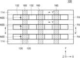
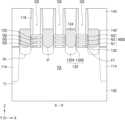
도 1은 본 발명의 기술적 사상에 의한 실시예들에 따른 집적회로 소자의 일부 구성들의 평면 레이아웃 다이어그램이다.
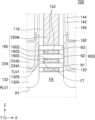
도 2a는 도 1의 X - X' 선 단면도이고, 도 2b는 도 1의 Y - Y' 선 단면도이다.
도 3a 및 도 3b는 본 발명의 기술적 사상에 의한 다른 실시예들에 따른 집적회로 소자를 설명하기 위한 단면도들로서, 도 3a는 도 2a의 "X1"으로 표시한 국부 영역에 대응하는 영역의 확대 단면도이고, 도 3b는 도 1의 Y - Y' 선 단면에 대응하는 부분의 단면도이다.
도 4a 및 도 4b는 본 발명의 기술적 사상에 의한 또 다른 실시예들에 따른 집적회로 소자를 설명하기 위한 단면도들로서, 도 4a는 도 2a의 "X1"으로 표시한 국부 영역에 대응하는 영역의 확대 단면도이고, 도 4b는 도 1의 Y - Y' 선 단면에 대응하는 부분의 단면도이다.
도 5는 본 발명의 기술적 사상에 의한 또 다른 실시예들에 따른 집적회로 소자를 설명하기 위한 단면도이다.
도 6은 본 발명의 기술적 사상에 의한 또 다른 실시예들에 따른 집적회로 소자를 설명하기 위한 단면도이다.
도 7은 본 발명의 기술적 사상에 의한 또 다른 실시예들에 따른 집적회로 소자를 설명하기 위한 단면도이다.
도 8은 본 발명의 기술적 사상에 의한 또 다른 실시예들에 따른 집적회로 소자를 설명하기 위한 단면도이다.
도 9는 본 발명의 기술적 사상에 의한 또 다른 실시예들에 따른 집적회로 소자를 설명하기 위한 단면도이다.
도 10a는 본 발명의 기술적 사상에 의한 또 다른 실시예들에 따른 집적회로 소자의 블록 다이어그램이다.
도 10b는 도 10a에 예시한 집적회로 소자에 포함된 제1 영역 및 제2 영역 각각의 국부 영역의 예시적인 단면 구성을 도시한 단면도이다.
도 11 내지 도 27b는 본 발명의 기술적 사상에 의한 실시예들에 따른 집적회로 소자의 제조 방법을 설명하기 위하여 공정 순서에 따라 도시한 단면도들이다.1 is a plan layout diagram of some components of an integrated circuit device according to embodiments of the technical idea of the present invention.
FIG. 2A is a cross-sectional view taken along line X-X' of FIG. 1, and FIG. 2b is a cross-sectional view taken along line Y-Y' of FIG. 1.
FIGS. 3A and 3B are cross-sectional views for explaining integrated circuit devices according to other embodiments of the technical spirit of the present invention. FIG. 3A is an enlarged cross-sectional view of the area corresponding to the local region indicated by “X1” in FIG. 2A. , and FIG. 3B is a cross-sectional view of a portion corresponding to the cross-section along line Y-Y' of FIG. 1.
FIGS. 4A and 4B are cross-sectional views illustrating integrated circuit devices according to further embodiments of the present invention. FIG. 4A is an enlarged view of the area corresponding to the local area indicated by “X1” in FIG. 2A. It is a cross-sectional view, and FIG. 4b is a cross-sectional view of a portion corresponding to the cross-section along line Y-Y' of FIG. 1.
Figure 5 is a cross-sectional view for explaining an integrated circuit device according to further embodiments of the technical idea of the present invention.
Figure 6 is a cross-sectional view for explaining an integrated circuit device according to further embodiments of the technical idea of the present invention.
7 is a cross-sectional view illustrating an integrated circuit device according to further embodiments of the present invention.
Figure 8 is a cross-sectional view for explaining an integrated circuit device according to further embodiments of the technical idea of the present invention.
9 is a cross-sectional view illustrating an integrated circuit device according to further embodiments of the technical idea of the present invention.
Figure 10a is a block diagram of an integrated circuit device according to further embodiments according to the technical idea of the present invention.
FIG. 10B is a cross-sectional view showing an exemplary cross-sectional configuration of local regions of each of the first and second regions included in the integrated circuit device illustrated in FIG. 10A.
11 to 27B are cross-sectional views shown in process order to explain a method of manufacturing an integrated circuit device according to embodiments of the technical idea of the present invention.
이하, 첨부 도면을 참조하여 본 발명의 실시예들을 상세히 설명한다. 도면상의 동일한 구성요소에 대해서는 동일한 참조부호를 사용하고, 이들에 대한 중복된 설명은 생략한다.Hereinafter, embodiments of the present invention will be described in detail with reference to the accompanying drawings. The same reference numerals are used for the same components in the drawings, and duplicate descriptions thereof are omitted.
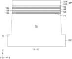
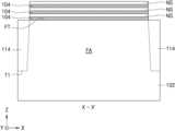
도 1은 본 발명의 기술적 사상에 의한 실시예들에 따른 집적회로 소자(100)의 일부 구성들의 평면 레이아웃 다이어그램이고, 도 2a는 도 1의 X - X' 선 단면도이고, 도 2b는 도 1의 Y - Y' 선 단면도이다.FIG. 1 is a plan layout diagram of some components of the
도 1과 도 2a 및 도 2b를 참조하면, 집적회로 소자(100)는 기판(102)으로부터 돌출되고 제1 수평 방향(X 방향)으로 연장되는 복수의 핀형 활성 영역(FA)과, 복수의 핀형 활성 영역(FA)으로부터 이격된 위치에서 복수의 핀형 활성 영역(FA)의 상면(FT)과 대면하는 복수의 나노시트 스택(NSS)를 포함한다.Referring to FIGS. 1, 2A, and 2B, the
기판(102)은 Si 또는 Ge와 같은 반도체, 또는 SiGe, SiC, GaAs, InAs, 또는 InP와 같은 화합물 반도체를 포함할 수 있다. 기판(102)에는 복수의 핀형 활성 영역(FA)을 한정하는 트렌치(T1)가 형성되고, 트렌치(T1)는 소자분리막(114)으로 채워질 수 있다. 소자분리막(114)은 산화막, 질화막, 또는 이들의 조합으로 이루어질 수 있다.
복수의 핀형 활성 영역(FA) 상에는 복수의 게이트 라인(160)이 제1 수평 방향(X 방향)과 교차하는 제2 수평 방향(Y 방향)으로 연장되어 있다. 복수의 핀형 활성 영역(FA)과 복수의 게이트 라인(160)이 교차하는 영역들에서 복수의 핀형 활성 영역(FA) 각각의 상면(FT) 위에 복수의 나노시트 스택(NSS)이 배치될 수 있다. 복수의 나노시트 스택(NSS)은 핀형 활성 영역(FA)의 핀 상면(FT)으로부터 이격된 위치에서 핀 상면(FT)과 대면하고 있다. 복수의 나노시트 스택(NSS)은 각각 핀형 활성 영역(FA)의 핀 상면(FT)과 평행하게 연장되고 핀 상면(FT)으로부터의 수직 거리(Z 방향 거리)가 서로 다른 복수의 나노시트(N1, N2, N3)를 포함할 수 있다. 복수의 나노시트(N1, N2, N3)는 핀형 활성 영역(FA)의 핀 상면(FT) 위에 차례로 적층된 제1 나노시트(N1), 제2 나노시트(N2), 및 제3 나노시트(N3)를 포함할 수 있다.A plurality of
도 1에는 나노시트 스택(NSS)의 평면 형상이 대략 사각형 형상을 가지는 경우를 예시하였으나, 이에 한정되는 것은 아니다. 나노시트 스택(NSS)은 핀형 활성 영역(FA)의 및 게이트 라인(160) 각각의 평면 형상에 따라 다양한 평면 형상을 가질 수 있다. 본 예에서는 1 개의 핀형 활성 영역(FA) 위에 복수의 나노시트 스택(NSS) 및 복수의 게이트 라인(160)이 형성되고, 1 개의 핀형 활성 영역(FA) 위에서 복수의 나노시트 스택(NSS)이 제1 수평 방향(X 방향)을 따라 일렬로 배치되어 있는 구성을 예시하였다. 그러나, 본 발명의 기술적 사상에 의하면 1 개의 핀형 활성 영역(FA) 위에 배치되는 나노시트 스택(NSS)의 수는 특별히 제한되지 않는다. 예를 들면, 1 개의 핀형 활성 영역(FA) 위에 1 개의 나노시트 스택(NSS)이 형성될 수도 있다. 본 예에서, 복수의 나노시트 스택(NSS)이 각각 3 개의 나노시트(N1, N2, N3)를 포함하는 경우를 예시하였으나, 본 발명의 기술적 사상은 예시한 바에 한정되지 않는다. 예를 들면, 나노시트 스택(NSS)은 적어도 2 개의 나노시트를 포함할 수 있으며, 나노시트 스택(NSS)를 구성하는 나노시트의 개수는 특별히 제한되지 않는다.Figure 1 illustrates the case where the planar shape of the nanosheet stack (NSS) has an approximately square shape, but is not limited thereto. The nanosheet stack (NSS) may have various planar shapes depending on the planar shapes of the fin-type active area (FA) and the
복수의 나노시트(N1, N2, N3)는 각각 채널 영역을 가질 수 있다. 일부 실시예들에서, 복수의 나노시트(N1, N2, N3)는 각각 약 4.5 ∼ 5.5 nm의 범위 내에서 선택되는 수직 방향 두께를 가질 수 있으나, 이에 한정되는 것은 아니다. 일부 실시예들에서, 복수의 나노시트(N1, N2, N3)는 실질적으로 동일한 두께를 가질 수 있다. 복수의 나노시트(N1, N2, N3)는 동일한 물질로 이루어질 수 있다. 일부 실시예들에서, 복수의 나노시트(N1, N2, N3)는 기판(102)과 동일한 물질로 이루어질 수 있다.Each of the plurality of nanosheets (N1, N2, N3) may have a channel region. In some embodiments, each of the plurality of nanosheets N1, N2, and N3 may have a vertical thickness selected within the range of about 4.5 to 5.5 nm, but is not limited thereto. In some embodiments, the plurality of nanosheets N1, N2, and N3 may have substantially the same thickness. The plurality of nanosheets (N1, N2, N3) may be made of the same material. In some embodiments, the plurality of nanosheets N1, N2, and N3 may be made of the same material as the
게이트 라인(160)은 핀형 활성 영역(FA) 위에서 나노시트 스택(NSS)를 덮으면서 복수의 나노시트(N1, N2, N3) 각각을 포위할 수 있다. 복수의 게이트 라인(160)은 각각 나노시트 스택(NSS)의 상면을 덮으며 제2 수평 방향(Y 방향)으로 연장되는 메인 게이트 부분(160M)과, 메인 게이트 부분(160M)에 일체로 연결되고 복수의 나노시트(N1, N2, N3) 각각의 사이, 및 핀형 활성 영역(FA)과 제1 나노시트(N1)와의 사이에 배치된 복수의 서브 게이트 부분(160S)을 포함할 수 있다. 수직 방향(Z 방향)에서, 복수의 서브 게이트 부분(160S)의 각각의 두께는 메인 게이트 부분(160M)의 두께보다 더 작을 수 있다. 복수의 나노시트(N1, N2, N3)는 게이트 라인(160)으로 완전히 포위되는 GAA(gate-all-around) 구조를 가질 수 있다.The
게이트 라인(160)은 금속, 금속 질화물, 금속 탄화물, 또는 이들의 조합으로 이루어질 수 있다. 상기 금속은 Ti, W, Ru, Nb, Mo, Hf, Ni, Co, Pt, Yb, Tb, Dy, Er, 및 Pd 중에서 선택될 수 있다. 상기 금속 질화물은 TiN 및 TaN 중에서 선택될 수 있다. 상기 금속 탄화물은 TiAlC일 수 있다.The
나노시트 스택(NSS)과 게이트 라인(160)과의 사이에는 게이트 유전막(152)이 형성되어 있다. 일부 실시예들에서, 게이트 유전막(152)은 인터페이스막(interfacial layer)과 고유전막의 적층 구조로 이루어질 수 있다. 상기 인터페이스막은 유전율이 약 9 이하인 저유전 물질막, 예를 들면 실리콘 산화막, 실리콘 산질화막, 또는 이들의 조합으로 이루어질 수 있다. 일부 실시예들에서, 상기 인터페이스막은 생략될 수 있다. 상기 고유전막은 실리콘 산화막보다 유전 상수가 더 큰 물질로 이루어질 수 있다. 예를 들면, 상기 고유전막은 약 10 내지 25의 유전 상수를 가질 수 있다. 상기 고유전막은 하프늄 산화물로 이루어질 수 있으나, 이에 한정되는 것은 아니다.A
핀형 활성 영역(FA)의 상부에는 복수의 안티펀치쓰루 리세스(R1)가 형성되어 있다. 복수의 안티펀치쓰루 리세스(R1)의 최저 레벨(RLV1)은 핀형 활성 영역(FA)의 핀 상면(FT)의 레벨보다 더 낮고, 소자분리막(114)의 상면의 레벨보다 더 낮을 수 있다. 본 명세서에서 사용되는 용어 "레벨"은 기판(102)의 상면으로부터 수직 방향(Z 방향 또는 -Z 방향)을 따르는 거리를 의미한다.A plurality of anti-punch-through recesses (R1) are formed on the upper part of the fin-shaped active area (FA). The lowest level (RLV1) of the plurality of anti-punch-through recesses (R1) may be lower than the level of the fin top surface (FT) of the fin-type active area (FA) and lower than the level of the top surface of the
복수의 안티펀치쓰루 리세스(R1)는 복수의 안티펀치쓰루 반도체층(132)으로 채워질 수 있다. 복수의 안티펀치쓰루 반도체층(132)은 나노시트 스택(NSS) 각각의 양 측에 각각 하나씩 배치될 수 있다.The plurality of anti-punch-through recesses R1 may be filled with a plurality of anti-punch-through semiconductor layers 132. A plurality of anti-punch-through
일부 실시예들에서, 복수의 안티펀치쓰루 반도체층(132)은 도핑되지 않은 반도체층으로 이루어질 수 있다. 예를 들면, 복수의 안티펀치쓰루 반도체층(132)은 도핑되지 않은 Si 층 또는 SiGe 층으로 이루어질 수 있다. 다른 일부 실시예들에서, 복수의 안티펀치쓰루 반도체층(132)은 핀형 활성 영역(FA) 상에 구현하고자 하는 트랜지스터의 채널의 도전형과 반대 도전형의 도판트로 도핑된 반도체층으로 이루어질 수 있다. 핀형 활성 영역(FA) 상에 NMOS 트랜지스터를 구현하고자 하는 경우, 안티펀치쓰루 반도체층(132)은 B, In 등과 같은 P 형 도판트로 도핑된 Si 층 또는 SiGe 층으로 이루어질 수 있다. 핀형 활성 영역(FA) 상에 PMOS 트랜지스터를 구현하고자 하는 경우, 안티펀치쓰루 반도체층(132)은 P, As 등과 같은 N 형 도판트로 도핑된 Si 층 또는 SiGe 층으로 이루어질 수 있다.In some embodiments, the plurality of anti-punch-through
복수의 안티펀치쓰루 반도체층(132)은 각각 안티펀치쓰루 리세스(R1)를 채우는 제1 부분(132A)과, 안티펀치쓰루 리세스(R1)의 외부에서 복수의 나노시트(N1, N2, N3) 중 적어도 일부의 측벽을 덮는 제2 부분(132B)을 포함할 수 있다.The plurality of anti-punch-through
복수의 안티펀치쓰루 반도체층(132)은 각각 안티펀치쓰루 리세스(R1)의 내벽 및 복수의 나노시트(N1, N2, N3) 각각의 측벽 위에서 불균일한(non-conformal) 두께를 가지도록 형성될 수 있다. 복수의 안티펀치쓰루 반도체층(132)은 각각 안티펀치쓰루 리세스(R1)의 내벽을 덮는 부분의 두께가 복수의 나노시트(N1, N2, N3) 각각의 측벽을 덮는 부분의 두께보다 더 클 수 있다.The plurality of anti-punch-through
서로 이웃하는 한 쌍의 나노시트 스택(NSS) 사이에 있는 안티펀치쓰루 반도체층(132)은 제1 부분(132A)에 일체로 연결되는 2 개의 제2 부분(132B)을 포함하고, 수평 방향(예를 들면 X 방향)을 따르는 단면에서 U 자형 단면 형상을 가질 수 있다. 상기 2 개의 제2 부분(132B)은 상기 한 쌍의 나노시트 스택(NSS) 중에서 선택되는 하나의 나노시트 스택(NSS)에 포함된 적어도 하나의 나노시트(N1, N2, N3)의 측벽에 접하는 제1 수직 연장부(132B1)와, 상기 한 쌍의 나노시트 스택(NSS) 중에서 선택되는 다른 하나의 나노시트 스택(NSS)에 포함된 적어도 하나의 나노시트(N1, N2, N3)의 측벽에 접하는 제2 수직 연장부(132B2)를 포함할 수 있다.The anti-punch-through
복수의 안티펀치쓰루 반도체층(132)의 상면(132T)에서, 안티펀치쓰루 리세스(R1)의 내벽 중 가장 낮은 레벨에 있는 최저부와 수직으로 오버랩되는 부분의 레벨(TLV1)은 핀 상면(FT)의 레벨과 같거나 더 낮을 수 있다. 상기 레벨(TLV1)은 소자분리막(114)의 상면의 레벨과 같거나 더 낮을 수 있다. 도 2b에서, 안티펀치쓰루 반도체층(132)의 상면(132T)이 제2 수평 방향(Y 방향)을 따라 평탄하게 연장되는 것으로 도시되어 있으나, 본 발명의 기술적 사상은 이에 한정되지 않는다. 예를 들면, 안티펀치쓰루 반도체층(132)의 상면(132T)은 제2 수평 방향(Y 방향)에서 곡면을 이룰 수 있다.On the
복수의 안티펀치쓰루 반도체층(132) 각각의 제2 부분(132B)은 복수의 나노시트(N1, N2, N3) 중 핀형 활성 영역(FA)에 가장 가까운 제1 나노시트(N1)를 제외한 다른 나노시트, 예를 들면 제2 및 제3 나노시트(N2, N3)의 측벽을 약 2 nm 이하의 두께, 예를 들면 약 1 nm 이하의 두께로 덮을 수 있다. 안티펀치쓰루 반도체층(132)이 복수의 나노시트(N1, N2, N3) 중 적어도 일부를 약 2 nm 이하의 두께로 덮을 때 복수의 나노시트(N1, N2, N3)를 포함하는 트랜지스터의 전기적 특성에 미치는 영향을 최소화할 수 있다. 일부 실시예들에서, 복수의 안티펀치쓰루 반도체층(132) 각각의 제2 부분(132B)은 제1 나노시트(N1)의 측벽을 약 2 nm보다 더 큰 두께로 덮을 수 있다. 복수의 안티펀치쓰루 반도체층(132) 각각의 제2 부분(132B)의 두께는 제1 부분(132A)에 가까워질수록 점차 더 커질 수 있다.The second portion (132B) of each of the plurality of anti-punch-through
복수의 안티펀치쓰루 반도체층(132) 위에는 복수의 소스/드레인 영역(134)이 형성되어 있다. 복수의 소스/드레인 영역(134)은 각각 안티펀치쓰루 반도체층(132)에 접할 수 있다. 안티펀치쓰루 반도체층(132)과 소스/드레인 영역(134)과의 계면의 레벨은 핀 상면(FT)의 레벨과 같거나 더 낮을 수 있다.A plurality of source/
복수의 소스/드레인 영역(134)은 복수의 나노시트(N1, N2, N3)에 대면하며, 안티펀치쓰루 반도체층(132)의 제2 부분(132B)을 사이에 두고 복수의 나노시트(N1, N2, N3) 중 적어도 일부와 이격되어 있을 수 있다.The plurality of source/
복수의 소스/드레인 영역(134)은 복수의 안티펀치쓰루 반도체층(132)의 구성 물질과 다른 구성 물질로 이루어질 수 있다. 복수의 소스/드레인 영역(134)은 에피택셜 성장된 반도체층으로 이루어질 수 있다. 예를 들면, 복수의 소스/드레인 영역(134)은 Si 층, SiGe 층, 또는 SiC 층으로 이루어질 수 있다. 일부 실시예들에서, 복수의 소스/드레인 영역(134)은 복수의 안티펀치쓰루 반도체층(132)을 구성하는 반도체 재료와 동일한 반도체 재료를 포함하되, 서로 다른 도전형을 가지는 물질로 이루어질 수 있다. 일부 실시예들에서, 복수의 안티펀치쓰루 반도체층(132)은 도핑되지 않은 Si 층, 또는 P 형 도판트로 도핑된 Si 층으로 이루어지고, 복수의 소스/드레인 영역(134)은 N 형 도판트로 도핑된 Si 층으로 이루어질 수 있다. 다른 일부 실시예들에서, 복수의 안티펀치쓰루 반도체층(132)은 도핑되지 않은 SiGe 층, 또는 N 형 도판트로 도핑된 SiGe 층으로 이루어지고, 복수의 소스/드레인 영역(134)은 P 형 도판트로 도핑된 SiGe 층으로 이루어질 수 있다.The plurality of source/
일부 실시예들에서, 복수의 소스/드레인 영역(134)은 각각 서로 다른 도판트 농도를 가지는 복수의 반도체층으로 이루어질 수 있다. 예를 들면, 복수의 소스/드레인 영역(134)은 각각 안티펀치쓰루 반도체층(132)에 가까울수록 비교적 낮은 도판트 농도를 가지고, 안티펀치쓰루 반도체층(132)으로부터 멀어질수록 비교적 높은 도판트 농도를 가질 수 있다.In some embodiments, the plurality of source/
복수의 소스/드레인 영역(134) 각각의 상면에는 금속 실리사이드막(182)이 형성될 수 있다. 금속 실리사이드막(182)은 티타늄 실리사이드로 이루어질 수 있으나, 이에 한정되는 것은 아니다. 금속 실리사이드막(182)은 생략 가능하다.A
복수의 제1 절연 스페이서(118)가 복수의 나노시트 스택(NSS) 위에 형성될 수 있다. 게이트 라인(160) 중 메인 게이트 부분(160M)의 측벽은 제1 절연 스페이서(118)로 덮일 수 있다. 복수의 제1 절연 스페이서(118) 및 복수의 소스/드레인 영역(134)은 보호 절연막(142)으로 덮일 수 있다. 제1 절연 스페이서(118) 및 보호 절연막(142)은 각각 SiN, SiCN, SiBN, SiON, SiOCN, SiBCN, SiOC, SiO2, 또는 이들의 조합으로 이루어질 수 있다. 보호 절연막(142)은 생략 가능하다.A plurality of first insulating
복수의 나노시트(N1, N2, N3) 각각의 사이, 및 핀형 활성 영역(FA)과 제1 나노시트(N1)와의 사이에는 복수의 제2 절연 스페이서(120)가 개재되어 있다. 복수의 서브 게이트 부분(160S) 각각의 양 측벽은 게이트 유전막(152)을 사이에 두고 제2 절연 스페이서(120)로 덮일 수 있다. 복수의 제2 절연 스페이서(120) 중 적어도 일부는 안티펀치쓰루 반도체층(132)의 제2 부분(132B)과 서브 게이트 부분(160S)과의 사이에 개재될 수 있다. 제2 절연 스페이서(120) 중 적어도 일부는 안티펀치쓰루 반도체층(132)의 제2 부분(132B)을 사이에 두고 소스/드레인 영역(134)과 대면할 수 있다.A plurality of second
일부 실시예들에서, 제1 절연 스페이서(118) 및 제2 절연 스페이서(120)는 동일한 물질로 이루어질 수도 있다. 다른 일부 실시예들에서, 제1 절연 스페이서(118) 및 제2 절연 스페이서(120)는 서로 다른 물질로 이루어질 수 있다. 일부 실시예들에서, 제2 절연 스페이서(120)는 SiN, SiCN, SiBN, SiON, SiOCN, SiBCN, SiOC, SiO2, 또는 이들의 조합으로 이루어질 수 있다. 다른 일부 실시예들에서, 제2 절연 스페이서(120)는 에어 갭을 포함할 수 있다.In some embodiments, the first insulating
복수의 소스/드레인 영역(134)을 덮는 보호 절연막(142) 위에는 게이트간 절연막(144) 및 층간절연막(174)이 차례로 형성되어 있다. 게이트간 절연막(144) 및 층간절연막(174)은 각각 실리콘 산화막으로 이루어질 수 있다.An inter-gate
층간절연막(174), 게이트간 절연막(144), 및 보호 절연막(142)을 관통하는 복수의 콘택홀(180) 내에 복수의 콘택 플러그(184)가 배치될 수 있다. 복수의 콘택 플러그(184)는 복수의 금속 실리사이드막(182)을 통해 복수의 소스/드레인 영역(134)에 연결될 수 있다. 복수의 콘택 플러그(184)는 각각 금속, 도전성 금속 질화물, 또는 이들의 조합으로 이루어질 수 있다. 예를 들면, 복수의 콘택 플러그(184)는 각각 W, Cu, Al, Ti, Ta, TiN, TaN, 이들의 합금, 또는 이들의 조합으로 이루어질 수 있다.A plurality of contact plugs 184 may be disposed in the plurality of
집적회로 소자(100)에서 안티펀치쓰루 반도체층(132)이 핀형 활성 영역(FA)과 소스/드레인 영역(134)과의 사이에 개재되어 있다. 복수의 서브 게이트 부분(160S) 중 핀형 활성 영역(FA)의 핀 상면(FT)에 가장 가까운 서브 게이트 부분(160S)을 포함하는 바텀 트랜지스터는 안티펀치쓰루 반도체층(132)으로 인해 언더랩된 게이트(underlapped gate) 구조를 포함할 수 있다. 이에 따라, 상기 바텀 트랜지스터는 언더랩 상태로 동작하여 SCE(short-channel effects) 마진을 확보할 수 있으며, 오프(off) 상태에서의 전류가 감소되어 누설 전류가 감소되고 접합 커패시턴스가 감소될 수 있다. 또한, 안티펀치쓰루 반도체층(132)에 의해 나노시트 스택(NSS)의 하부에서 핀형 활성 영역(FA)을 통한 펀치쓰루가 효과적으로 차단되어 전기적 특성 열화를 억제할 수 있다.In the
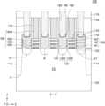
도 3a 및 도 3b는 본 발명의 기술적 사상에 의한 다른 실시예들에 따른 집적회로 소자를 설명하기 위한 단면도들로서, 도 3a는 도 2a의 "X1"으로 표시한 국부 영역에 대응하는 영역의 확대 단면도이고, 도 3b는 도 1의 Y - Y' 선 단면에 대응하는 부분의 단면도이다.FIGS. 3A and 3B are cross-sectional views for explaining integrated circuit devices according to other embodiments of the technical spirit of the present invention. FIG. 3A is an enlarged cross-sectional view of the area corresponding to the local region indicated by “X1” in FIG. 2A. , and FIG. 3B is a cross-sectional view of a portion corresponding to the cross-section along line Y-Y' of FIG. 1.
도 3a 및 도 3b를 참조하면, 집적회로 소자(200)는 도 1과 도 2a 및 도 2b를 참조하여 설명한 집적회로 소자(100)와 대체로 동일한 구성을 가진다. 단, 집적회로 소자(200)는 서로 다른 도판트 농도를 가지는 제1 반도체층(234A) 및 제2 반도체층(234B)을 포함하는 소스/드레인 영역(234)을 포함한다.Referring to FIGS. 3A and 3B, the
제1 반도체층(234A)은 안티펀치쓰루 반도체층(132)에 접하고, 제2 반도체층(234B)은 제1 반도체층(234A)을 사이에 두고 안티펀치쓰루 반도체층(132)으로부터 이격될 수 있다. 일부 실시예들에서, 제1 반도체층(234A) 및 제2 반도체층(234B)은 각각 N 형 도판트로 도핑된 Si 층으로 이루어질 수 있다. 다른 일부 실시예들에서, 제1 반도체층(234A) 및 제2 반도체층(234B)은 각각 P 형 도판트로 도핑된 SiGe 층으로 이루어질 수 있다. 제2 반도체층(234B)에서의 도판트 농도는 제1 반도체층(234A)에서의 도판트 농도보다 더 클 수 있다. 소스/드레인 영역(234)에 대한 보다 상세한 구성은 도 2a 및 도 2b를 참조하여 소스/드레인 영역(134)에 대하여 설명한 바와 대체로 동일하다.The
도 4a 및 도 4b는 본 발명의 기술적 사상에 의한 또 다른 실시예들에 따른 집적회로 소자를 설명하기 위한 단면도들로서, 도 4a는 도 2a의 "X1"으로 표시한 국부 영역에 대응하는 영역의 확대 단면도이고, 도 4b는 도 1의 Y - Y' 선 단면에 대응하는 부분의 단면도이다.FIGS. 4A and 4B are cross-sectional views illustrating integrated circuit devices according to further embodiments of the present invention. FIG. 4A is an enlarged view of the area corresponding to the local area indicated by “X1” in FIG. 2A. It is a cross-sectional view, and FIG. 4b is a cross-sectional view of a portion corresponding to the cross-section along line Y-Y' of FIG. 1.
도 4a 및 도 4b를 참조하면, 집적회로 소자(300)는 도 1과 도 2a 및 도 2b를 참조하여 설명한 집적회로 소자(100)와 대체로 동일한 구성을 가진다. 단, 집적회로 소자(200)는 복수의 안티펀치쓰루 리세스(R1)를 채우는 복수의 안티펀치쓰루 반도체층(332)과, 복수의 안티펀치쓰루 반도체층(332) 위에 배치된 복수의 소스/드레인 영역(334)을 포함한다.Referring to FIGS. 4A and 4B, the
복수의 안티펀치쓰루 반도체층(332)은 각각 안티펀치쓰루 리세스(R1)의 외부에서 제1 나노시트(N1)의 측벽에 접하는 부분을 포함할 수 있다. 안티펀치쓰루 반도체층(332)은 복수의 나노시트(N1, N2, N3) 중 최상층 나노시트인 제3 나노시트(N3)를 포함하는 적어도 하나의 나노시트로부터 이격될 수 있다. 일부 실시예들에서, 안티펀치쓰루 반도체층(332)은 제2 및 제3 나노시트(N2, N3)에는 접하지 않을 수 있다. 도 4a에서, 안티펀치쓰루 반도체층(332)의 상면(332T)이 제1 수평 방향(X 방향)을 따라 평탄하게 연장되는 것으로 도시되어 있으나, 본 발명의 기술적 사상은 이에 한정되지 않는다. 예를 들면, 안티펀치쓰루 반도체층(332)의 상면(332T)은 제1 수평 방향(X 방향)에서 곡면을 이룰 수 있다.Each of the plurality of anti-punch-through
복수의 소스/드레인 영역(334)은 각각 복수의 나노시트(N1, N2, N3) 중 최상층 나노시트인 제3 나노시트(N3)를 포함하는 적어도 하나의 나노시트와 접할 수 있다. 도 4a에 예시한 바와 같이, 복수의 소스/드레인 영역(334)은 각각 제2 및 제3 나노시트(N2, N3)에 접할 수 있다. 일부 실시예들에서, 복수의 소스/드레인 영역(334)은 도 3a 및 도 3b를 참조하여 설명한 소스/드레인 영역(234)과 유사하게 서로 다른 도판트 농도를 가지는 복수의 반도체층을 포함할 수 있다.Each of the plurality of source/
복수의 안티펀치쓰루 반도체층(332)의 상면(332T)은 소스/드레인 영역(334)에 접할 수 있다. 안티펀치쓰루 반도체층(332)의 상면(332T)에서 안티펀치쓰루 리세스(R1)의 내벽 중 가장 낮은 레벨에 있는 최저부와 수직으로 오버랩되는 부분의 레벨은 핀 상면(FT)의 레벨보다 더 높을 수 있다. 안티펀치쓰루 반도체층(332)의 상면(332T)의 레벨(TLV3) 중 적어도 일부는 소자분리막(114)의 상면의 레벨보다 더 높을 수 있다. 일부 실시예들에서, 안티펀치쓰루 반도체층(332)의 상면(332T)의 레벨(TLV3)은 제1 나노시트(N1)의 저면 레벨보다 높고, 제2 나노시트(N2)의 저면 레벨보다 낮을 수 있다. 안티펀치쓰루 반도체층(332)과 소스/드레인 영역(334)과의 사이의 계면의 레벨은 핀 상면(FT)의 레벨보다 더 높을 수 있다.The
복수의 안티펀치쓰루 반도체층(332) 및 복수의 소스/드레인 영역(334)에 대한 보다 상세한 구성은 도 2a 및 도 2b를 참조하여 복수의 안티펀치쓰루 반도체층(132) 및 복수의 소스/드레인 영역(134)에 대하여 설명한 바와 대체로 동일하다.For a more detailed configuration of the plurality of anti-punch-through
도 5는 본 발명의 기술적 사상에 의한 또 다른 실시예들에 따른 집적회로 소자를 설명하기 위한 단면도로서, 도 2a의 "X1"으로 표시한 국부 영역에 대응하는 영역의 확대 단면도이다.FIG. 5 is a cross-sectional view for explaining an integrated circuit device according to further embodiments of the technical spirit of the present invention, and is an enlarged cross-sectional view of a region corresponding to the local region indicated by “X1” in FIG. 2A.
도 5를 참조하면, 집적회로 소자(400)는 도 1과 도 2a 및 도 2b를 참조하여 설명한 집적회로 소자(100)와 대체로 동일한 구성을 가진다. 단, 집적회로 소자(400)는 핀형 활성 영역(FA)에 형성된 복수의 안티펀치쓰루 리세스(R4)와, 복수의 안티펀치쓰루 리세스(R4)를 채우는 복수의 안티펀치쓰루 반도체층(432)을 포함한다. 복수의 안티펀치쓰루 리세스(R4)는 핀형 활성 영역(FA) 내에서 나노시트 스택(NSS)의 하부까지 연장되도록 형성될 수 있다. 복수의 안티펀치쓰루 반도체층(432)은 각각 안티펀치쓰루 리세스(R4)를 채우는 제1 부분(432A)과, 복수의 나노시트(N1, N2, N3) 중 적어도 일부의 측벽을 덮는 제2 부분(432B)을 포함할 수 있다. 제2 부분(432B)은 안티펀치쓰루 리세스(R4)의 외부에 위치될 수 있다. 복수의 안티펀치쓰루 반도체층(432)의 제1 부분(432A)은 나노시트 스택(NSS)과 수직으로 오버랩되는 부분을 포함할 수 있다. 복수의 안티펀치쓰루 반도체층(432)에 대한 보다 상세한 구성은 도 2a 및 도 2b를 참조하여 복수의 안티펀치쓰루 반도체층(132)에 대하여 설명한 바와 대체로 동일하다.Referring to FIG. 5, the
일부 실시예들에서, 복수의 소스/드레인 영역(134)은 도 3a 및 도 3b를 참조하여 설명한 소스/드레인 영역(234)과 유사하게 서로 다른 도판트 농도를 가지는 복수의 반도체층을 포함할 수 있다.In some embodiments, the plurality of source/
도 5에 예시한 집적회로 소자(400)에서는 복수의 안티펀치쓰루 반도체층(432) 중 나노시트 스택(NSS)과 수직으로 오버랩되는 부분들로 인해, 핀형 활성 영역(FA)과 소스/드레인 영역(134)과의 사이에 개재되는 안티펀치쓰루 반도체층(432)의 길이가 증가하고, 이에 따라 도 2a 및 도 2b에 예시한 집적회로 소자(100)의 경우에 비해 핀형 활성 영역(FA)과 소스/드레인 영역(134)과의 사이의 거리가 더욱 증가하여 나노시트 스택(NSS)의 하부에서 핀형 활성 영역(FA)을 통한 펀치쓰루가 더욱 효과적으로 차단될 수 있다.In the
도 6은 본 발명의 기술적 사상에 의한 또 다른 실시예들에 따른 집적회로 소자를 설명하기 위한 단면도로서, 도 2a의 "X1"으로 표시한 국부 영역에 대응하는 영역의 확대 단면도이다.FIG. 6 is a cross-sectional view for explaining an integrated circuit device according to further embodiments of the technical spirit of the present invention, and is an enlarged cross-sectional view of a region corresponding to the local region indicated by “X1” in FIG. 2A.
도 6을 참조하면, 집적회로 소자(500)는 도 4a 및 도 4b를 참조하여 설명한 집적회로 소자(300)와 대체로 동일한 구성을 가진다. 단, 집적회로 소자(500)는 핀형 활성 영역(FA)에 형성된 복수의 안티펀치쓰루 리세스(R5)와, 복수의 안티펀치쓰루 리세스(R5)를 채우는 복수의 안티펀치쓰루 반도체층(532)을 포함한다. 복수의 안티펀치쓰루 리세스(R5)는 핀형 활성 영역(FA) 내에서 나노시트 스택(NSS)의 하부까지 연장되도록 형성될 수 있다. 복수의 안티펀치쓰루 반도체층(532) 중 복수의 안티펀치쓰루 리세스(R5)를 채우는 부분은 나노시트 스택(NSS)과 수직으로 오버랩되는 부분을 포함할 수 있다.Referring to FIG. 6, the
복수의 안티펀치쓰루 반도체층(532)은 각각 안티펀치쓰루 리세스(R5)의 외부에서 제1 나노시트(N1)의 측벽에 접하는 부분을 포함할 수 있다. 안티펀치쓰루 반도체층(532)은 복수의 나노시트(N1, N2, N3) 중 최상층 나노시트인 제3 나노시트(N3)를 포함하는 적어도 하나의 나노시트로부터 이격될 수 있다. 일부 실시예들에서, 안티펀치쓰루 반도체층(532)은 제2 및 제3 나노시트(N2, N3)에는 접하지 않을 수 있다.Each of the plurality of anti-punch-through
복수의 안티펀치쓰루 반도체층(532)의 상면(532T)은 소스/드레인 영역(334)에 접할 수 있다. 안티펀치쓰루 반도체층(532)의 상면(532T) 중 적어도 일부는 핀 상면(FT)의 레벨보다 더 높은 레벨을 가질 수 있다. 일부 실시예들에서, 안티펀치쓰루 반도체층(532)의 상면(532T)의 레벨(TLV5)은 제1 나노시트(N1)의 저면의 레벨보다 높고, 제2 나노시트(N2)의 저면의 레벨보다 낮을 수 있다. 안티펀치쓰루 반도체층(532)에 대한 보다 상세한 구성은 도 2a 및 도 2b를 참조하여 복수의 안티펀치쓰루 반도체층(132)에 대하여 설명한 바와 대체로 동일하다.The
도 7은 본 발명의 기술적 사상에 의한 또 다른 실시예들에 따른 집적회로 소자를 설명하기 위한 단면도로서, 도 2a의 "X1"으로 표시한 국부 영역에 대응하는 영역의 확대 단면도이다.FIG. 7 is a cross-sectional view for explaining an integrated circuit device according to further embodiments of the technical spirit of the present invention, and is an enlarged cross-sectional view of a region corresponding to the local region indicated by “X1” in FIG. 2A.
도 7을 참조하면, 집적회로 소자(600)는 도 6을 참조하여 설명한 집적회로 소자(500)와 대체로 동일한 구성을 가진다. 단, 집적회로 소자(600)는 복수의 안티펀치쓰루 리세스(R5)를 채우는 복수의 안티펀치쓰루 반도체층(632)과, 복수의 안티펀치쓰루 반도체층(632) 위에 배치된 복수의 소스/드레인 영역(634)을 포함한다.Referring to FIG. 7 , the
복수의 안티펀치쓰루 반도체층(632) 중 복수의 안티펀치쓰루 리세스(R5)를 채우는 부분은 나노시트 스택(NSS)과 수직으로 오버랩되는 부분을 포함할 수 있다. 복수의 안티펀치쓰루 반도체층(632)은 각각 나노시트 스택(NSS)에 포함된 복수의 나노시트(N1, N2, N3)의 측벽에 접하지 않을 수 있다.Among the plurality of anti-punch-through
복수의 소스/드레인 영역(634)은 각각 나노시트 스택(NSS)에 포함된 복수의 나노시트(N1, N2, N3)에 접할 수 있다. 일부 실시예들에서, 복수의 소스/드레인 영역(634)은 도 3a 및 도 3b를 참조하여 설명한 소스/드레인 영역(234)과 유사하게 서로 다른 도판트 농도를 가지는 복수의 반도체층을 가질 수 있다.The plurality of source/
안티펀치쓰루 반도체층(632)의 상면(632T)은 소스/드레인 영역(634)에 접할 수 있다. 안티펀치쓰루 반도체층(632)의 상면(632T)에서 안티펀치쓰루 리세스(R5)의 내벽 중 가장 낮은 레벨에 있는 최저부와 수직으로 오버랩되는 부분의 레벨은 핀 상면(FT)의 레벨과 같거나 더 낮을 수 있다. 도 7에서, 안티펀치쓰루 반도체층(632)의 상면(632T)이 제1 수평 방향(X 방향)을 따라 평탄하게 연장되는 것으로 도시되어 있으나, 본 발명의 기술적 사상은 이에 한정되지 않는다. 예를 들면, 안티펀치쓰루 반도체층(632)의 상면(632T)은 제1 수평 방향(X 방향)에서 곡면을 이룰 수 있다.The
복수의 안티펀치쓰루 반도체층(632) 및 복수의 소스/드레인 영역(634)에 대한 보다 상세한 구성은 도 2a 및 도 2b를 참조하여 복수의 안티펀치쓰루 반도체층(132) 및 복수의 소스/드레인 영역(134)에 대하여 설명한 바와 대체로 동일하다.For a more detailed configuration of the plurality of anti-punch-through
도 8은 본 발명의 기술적 사상에 의한 또 다른 실시예들에 따른 집적회로 소자를 설명하기 위한 단면도로서, 도 2a의 "X1"으로 표시한 국부 영역에 대응하는 영역의 확대 단면도이다.FIG. 8 is a cross-sectional view for explaining an integrated circuit device according to further embodiments of the technical spirit of the present invention, and is an enlarged cross-sectional view of a region corresponding to the local region indicated by “X1” in FIG. 2A.
도 8을 참조하면, 집적회로 소자(700)는 도 1과 도 2a 및 도 2b를 참조하여 설명한 집적회로 소자(100)와 대체로 동일한 구성을 가진다. 단, 집적회로 소자(700)는 복수의 핀형 활성 영역(FA)의 상면(FT)과 대면하는 나노시트 스택(NSS7)를 포함하고, 나노시트 스택(NSS7)은 핀 상면(FT)으로부터의 수직 거리(Z 방향 거리)가 서로 다른 복수의 나노시트(N1, N2, N3, N4)를 포함한다. 복수의 나노시트(N1, N2, N3, N4)는 핀형 활성 영역(FA)의 핀 상면(FT) 위에 차례로 적층된 제1 나노시트(N1), 제2 나노시트(N2), 제3 나노시트(N3), 및 제4 나노시트(N4)를 포함한다. 나노시트 스택(NSS7)에 대한 보다 상세한 구성은 도 2a 및 도 2b를 참조하여 나노시트 스택(NSS)에 대하여 설명한 바와 대체로 동일하다.Referring to FIG. 8, the
복수의 게이트 라인(160)은 핀형 활성 영역(FA) 위에서 나노시트 스택(NSS7)를 덮으면서 복수의 나노시트(N1, N2, N3, N4) 각각을 포위할 수 있다.The plurality of
핀형 활성 영역(FA)의 상부에는 복수의 안티펀치쓰루 리세스(R7)가 형성되어 있다. 복수의 안티펀치쓰루 리세스(R7)의 최저부의 레벨(RLV7)은 핀형 활성 영역(FA)의 핀 상면(FT)의 레벨보다 더 낮을 수 있다.A plurality of anti-punch-through recesses (R7) are formed on the upper part of the fin-shaped active area (FA). The level (RLV7) of the lowest part of the plurality of anti-punch-through recesses (R7) may be lower than the level of the fin top surface (FT) of the fin-type active area (FA).
집적회로 소자(700)는 복수의 안티펀치쓰루 리세스(R7)를 채우는 복수의 안티펀치쓰루 반도체층(732)을 포함할 수 있다. 복수의 안티펀치쓰루 반도체층(732)은 각각 안티펀치쓰루 리세스(R7)를 채우는 제1 부분(732A)과, 제1 부분(732A)으로부터 핀형 활성 영역(FA)과 멀어지는 방향으로 연장되는 제2 부분(732B)을 포함할 수 있다. 제1 부분(732A)은 안티펀치쓰루 리세스(R7)의 내부로부터 안티펀치쓰루 리세스(R7)의 외부까지 수직 방향(Z 방향)을 따라 상측으로 연장될 수 있다. 제2 부분(732B)은 안티펀치쓰루 리세스(R7)의 외부에서 복수의 나노시트(N1, N2, N3, N4) 중 적어도 일부의 측벽을 덮을 수 있다. 복수의 안티펀치쓰루 반도체층(732)은 위치에 따라 불균일한(non-conformal) 두께를 가질 수 있다. 복수의 안티펀치쓰루 반도체층(732)은 각각 안티펀치쓰루 리세스(R7)의 내벽을 덮는 부분의 두께가 복수의 나노시트(N1, N2, N3, N4) 각각의 측벽을 덮는 부분의 두께보다 더 클 수 있다.The
복수의 안티펀치쓰루 반도체층(732)의 상면(732T)에서, 안티펀치쓰루 리세스(R7)의 내벽 중 가장 낮은 레벨에 있는 최저부와 수직으로 오버랩되는 부분의 레벨(TLV7)은 핀 상면(FT)의 레벨보다 더 높을 수 있다. 일부 실시예들에서, 안티펀치쓰루 반도체층(732)의 상면(732T)의 최저부의 레벨(TLV7)은 제1 나노시트(N1)의 상면의 레벨보다 더 높고, 제2 나노시트(N2)의 저면의 레벨과 같거나 더 낮을 수 있다.On the
복수의 안티펀치쓰루 반도체층(732) 각각의 제2 부분(732B)은 복수의 나노시트(N1, N2, N3, N4) 중 핀형 활성 영역(FA)에 가장 가까운 2 개의 나노시트인 제1 및 제2 나노시트(N1, N2)를 제외한 다른 나노시트(N3, N4) 중 적어도 일부의 측벽을 약 2 nm 이하의 두께, 예를 들면 약 1 nm 이하의 두께로 덮을 수 있다. 복수의 안티펀치쓰루 반도체층(732) 각각의 제2 부분(732B)은 제1 및 제2 나노시트(N1, N2)의 측벽을 약 2 nm보다 더 큰 두께로 덮을 수 있다. 복수의 안티펀치쓰루 반도체층(732) 각각의 제2 부분(732B)의 두께는 제1 부분(732A)에 가까워질수록 점차 더 커질 수 있다.The
복수의 안티펀치쓰루 반도체층(732) 위에는 복수의 소스/드레인 영역(734)이 형성되어 있다. 복수의 소스/드레인 영역(734)은 각각 안티펀치쓰루 반도체층(732)에 접할 수 있다. 안티펀치쓰루 반도체층(732)과 소스/드레인 영역(734)과의 계면의 레벨은 제2 나노시트(N2)의 저면의 레벨과 같거나 더 낮을 수 있다. 일부 실시예들에서, 복수의 소스/드레인 영역(734)은 도 3a 및 도 3b를 참조하여 설명한 소스/드레인 영역(234)과 유사하게 서로 다른 도판트 농도를 가지는 복수의 반도체층을 포함할 수 있다.A plurality of source/
복수의 안티펀치쓰루 반도체층(732), 복수의 소스/드레인 영역(734), 및 나노시트 스택(NSS7)에 대한 보다 상세한 구성은 도 2a 및 도 2b를 참조하여 복수의 안티펀치쓰루 반도체층(132), 복수의 소스/드레인 영역(134), 및 나노시트 스택(NSS7)에 대하여 설명한 바와 대체로 동일하다.For a more detailed configuration of the plurality of anti-punch-through
집적회로 소자(700)는 핀형 활성 영역(FA)과 소스/드레인 영역(734)과의 사이에 개재된 안티펀치쓰루 반도체층(732)을 포함하므로, 집적회로 소자(700)에서 복수의 나노시트(N1, N2, N3, N4) 중 제2 내지 제4 나노시트(N2, N3, N4)는 이들 각각의 상면 부근 및 저면 부근과, 제1 나노시트(N1)의 상면 부근에서는 채널이 형성될 수 있지만, 핀형 활성 영역(FA)에 대면하는 제1 나노시트(N1)의 저면 부근에서는 안티펀치쓰루 반도체층(732)으로 인해 채널이 형성되지 않을 수 있다. 따라서, 핀형 활성 영역(FA)의 핀 상면(FT) 부근에 원하지 않는 기생 트랜지스터가 형성될 염려가 없으며, 따라서 기생 트랜지스터로 인해 야기될 수 있는 기생 커패시턴스의 증가, 누설 전류 증가, 서브쓰레숄드 스윙(subthreshold swing) 증가 등과 같은 전기적 특성 열화를 방지할 수 있다.Since the
도 9는 본 발명의 기술적 사상에 의한 또 다른 실시예들에 따른 집적회로 소자를 설명하기 위한 단면도로서, 도 2a의 "X1"으로 표시한 국부 영역에 대응하는 영역의 확대 단면도이다.FIG. 9 is a cross-sectional view for explaining an integrated circuit device according to further embodiments of the technical spirit of the present invention, and is an enlarged cross-sectional view of a region corresponding to the local region indicated by “X1” in FIG. 2A.
도 9를 참조하면, 집적회로 소자(800)는 도 8을 참조하여 설명한 집적회로 소자(800)와 대체로 동일한 구성을 가진다. 단, 집적회로 소자(800)는 복수의 안티펀치쓰루 리세스(R7)를 채우는 복수의 안티펀치쓰루 반도체층(832)과, 복수의 안티펀치쓰루 반도체층(832) 위에 배치된 복수의 소스/드레인 영역(834)을 포함한다.Referring to FIG. 9 , the
복수의 안티펀치쓰루 반도체층(832)은 각각 안티펀치쓰루 리세스(R7)의 외부에서 나노시트 스택(NSS7)에 포함된 제1 및 제2 나노시트(N1, N2)의 측벽에 접하는 부분을 포함할 수 있다. 안티펀치쓰루 반도체층(832)은 복수의 나노시트(N1, N2, N3, N4) 중 최상층 나노시트인 제4 나노시트(N4)를 포함하는 적어도 하나의 나노시트로부터 이격될 수 있다. 일부 실시예들에서, 안티펀치쓰루 반도체층(832)은 제3 및 제4 나노시트(N3, N4)에는 접하지 않을 수 있다.The plurality of anti-punch-through
복수의 소스/드레인 영역(834)은 각각 복수의 나노시트(N1, N2, N3, N4) 중 최상층 나노시트인 제4 나노시트(N4)를 포함하는 적어도 하나의 나노시트와 접할 수 있다. 복수의 소스/드레인 영역(834)은 도 3a 및 도 3b를 참조하여 설명한 소스/드레인 영역(234)과 유사하게 서로 다른 도판트 농도를 가지는 복수의 반도체층을 포함할 수 있다.Each of the plurality of source/
복수의 안티펀치쓰루 반도체층(832)은 각각 제1 수평 방향(X 방향)을 따라 비교적 평탄하게 연장되는 상면(832T)을 가질 수 있다. 그러나, 본 발명의 기술적 사상은 이에 한정되지 않는다. 예를 들면, 안티펀치쓰루 반도체층(832)의 상면(832T)은 제1 수평 방향(X 방향)을 따라 곡면을 이룰 수 있다. 안티펀치쓰루 반도체층(832)의 상면(832T)은 소스/드레인 영역(834)에 접할 수 있다. 안티펀치쓰루 반도체층(832)의 상면(832T)에서 안티펀치쓰루 리세스(R7)의 내벽 중 가장 낮은 레벨에 있는 최저부와 수직으로 오버랩되는 부분의 레벨(TLV8)은 제1 나노시트(N1)의 상면의 레벨보다 더 높고, 제2 나노시트(N2)의 저면 레벨보다 더 낮을 수 있다.Each of the plurality of anti-punch-through
복수의 안티펀치쓰루 반도체층(832) 및 복수의 소스/드레인 영역(834)에 대한 보다 상세한 구성은 도 2a 및 도 2b를 참조하여 복수의 안티펀치쓰루 반도체층(132) 및 복수의 소스/드레인 영역(134)에 대하여 설명한 바와 대체로 동일하다.For a more detailed configuration of the plurality of anti-punch-through
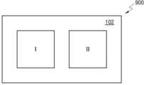
도 10a는 본 발명의 기술적 사상에 의한 또 다른 실시예들에 따른 집적회로 소자의 블록 다이어그램이다.Figure 10a is a block diagram of an integrated circuit device according to further embodiments according to the technical idea of the present invention.
도 10a를 참조하면, 집적회로 소자(900)는 제1 영역(I) 및 제2 영역(II)을 가지는 기판(102)을 포함한다.Referring to FIG. 10A, the
제1 영역(I) 및 제2 영역(II)은 기판(102)의 서로 다른 영역이다. 제1 영역(I) 및 제2 영역(II)은 기판(210) 상에서 서로 다른 기능을 수행하는 영역일 수 있다. 제1 영역(I) 및 제2 영역(II)은 서로 이격된 영역일 수도 있고, 서로 이웃하는 영역일 수도 있다. 제1 영역(I) 및 제2 영역(II)은 서로 다른 문턱 전압이 요구되는 영역들일 수 있다. 예를 들면, 제1 영역(I) 및 제2 영역(II)은 NMOS 트랜지스터 영역 및 PMOS 트랜지스터 영역 중에서 선택되는 서로 다른 영역일 수 있다. 제1 영역(I) 및 제2 영역(II)은 각각 도 1 내지 도 9를 참조하여 설명한 집적회로 소자(100, 200, 300, 400, 500, 600, 700, 800)에 대하여 설명한 구조들 중 어느 하나의 구조를 포함할 수 있다.The first region (I) and the second region (II) are different regions of the
도 10b는 도 10a에 예시한 집적회로 소자(900)에 포함된 제1 영역(I) 및 제2 영역(II) 각각의 국부 영역의 예시적인 단면 구성을 도시한 단면도이다.FIG. 10B is a cross-sectional view showing an exemplary cross-sectional configuration of each local region of the first region (I) and the second region (II) included in the
도 10b를 참조하면, 기판(102)의 제1 영역(I)에는 제1 집적회로 소자부(900A)가 포함되고, 기판(102)의 제2 영역(II)에는 제2 집적회로 소자부(900B)가 포함될 수 있다.Referring to FIG. 10B, the first region (I) of the
제1 집적회로 소자부(900A)는 도 2a 및 도 2b에 예시한 집적회로 소자(100)에 대하여 설명한 바와 동일한 구성을 가질 수 있다.The first integrated
제2 영역(II)에 있는 제2 집적회로 소자부(900B)는 복수의 안티펀치쓰루 리세스(R9)와, 복수의 안티펀치쓰루 리세스(R9)를 채우는 복수의 안티펀치쓰루 반도체층(932)을 포함하는 것을 제외하고, 도 2a 및 도 2b에 예시한 집적회로 소자(100)에 대하여 설명한 바와 대체로 동일한 구성을 가질 수 있다.The second integrated
제2 영역(II)에 있는 제2 집적회로 소자부(900B)에서, 복수의 안티펀치쓰루 리세스(R9)의 최저 레벨(RLV9)은 제1 영역(I)에 있는 복수의 안티펀치쓰루 리세스(R1)의 최저 레벨(RLV1)과 다를 수 있다. 예를 들면, 도 10b에 예시한 바와 같이, 복수의 안티펀치쓰루 리세스(R9)의 최저 레벨(RLV9)은 복수의 안티펀치쓰루 리세스(R1)의 최저 레벨(RLV1)보다 더 낮을 수 있다.In the second integrated
제2 영역(II)에 있는 복수의 안티펀치쓰루 반도체층(932)의 상면(932T)은 안티펀치쓰루 리세스(R9)의 최저부와 수직으로 오버랩되는 부분에서 최저 레벨(TLV9)을 가질 수 있다. 복수의 안티펀치쓰루 반도체층(932)의 상면(932T)의 최저 레벨(TLV9)은 제1 영역(I)에 있는 복수의 안티펀치쓰루 반도체층(132)의 상면(132T)의 최저 레벨(TLV1)과 다를 수 있다. 예를 들면, 도 10b에 예시한 바와 같이, 복수의 안티펀치쓰루 반도체층(932)의 상면(932T)의 최저 레벨(TLV9)은 복수의 안티펀치쓰루 반도체층(132)의 상면(132T)의 최저 레벨(TLV1)보다 더 낮을 수 있다. 복수의 안티펀치쓰루 반도체층(932)의 상면(932T)의 최저 레벨(TLV9)은 핀 상면(FT)의 레벨보다 더 낮을 수 있다.The
제2 영역(II)에서 핀형 활성 영역(FA) 중 나노시트 스택(NSS)의 하부에서 나노시트 스택(NSS)의 양 측에 있는 2 개의 안티펀치쓰루 반도체층(932)에 의해 한정되는 부분의 높이(H92)는 제1 영역(I)에서 핀형 활성 영역(FA) 중 나노시트 스택(NSS)의 하부에서 나노시트 스택(NSS)의 양 측에 있는 2 개의 안티펀치쓰루 반도체층(132)에 의해 한정되는 부분의 높이(H91)보다 더 클 수 있다. 일부 실시예들에서, 제1 영역(I)은 NMOS 트랜지스터 영역이고, 제2 영역(II)은 PMOS 트랜지스터 영역일 수 있다.In the second region (II), the portion of the fin-type active region (FA) defined by the two anti-punch-through
복수의 안티펀치쓰루 반도체층(932)은 각각 안티펀치쓰루 리세스(R9)를 채우는 제1 부분(932A)과, 복수의 나노시트(N1, N2, N3) 중 적어도 일부의 측벽을 덮는 제2 부분(932B)을 포함할 수 있다. 제2 부분(932B) 중 적어도 일부는 안티펀치쓰루 리세스(R9)의 외부에 위치될 수 있다.The plurality of anti-punch-through
제2 영역(II)에서, 복수의 안티펀치쓰루 반도체층(932) 위에 복수의 소스/드레인 영역(934)이 배치될 수 있다. 복수의 안티펀치쓰루 반도체층(932)의 상면(932T)은 소스/드레인 영역(934)에 접할 수 있다. 안티펀치쓰루 반도체층(932)과 소스/드레인 영역(934)과의 계면의 최저 레벨은 핀 상면(FT)의 레벨보다 더 낮을 수 있다. 제2 영역(II)에서의 안티펀치쓰루 반도체층(932)과 소스/드레인 영역(934)과의 계면의 최저 레벨은 제1 영역(I)에서의 안티펀치쓰루 반도체층(132)과 소스/드레인 영역(134)과의 계면의 최저 레벨보다 더 낮을 수 있다.In the second region II, a plurality of source/
일부 실시예들에서, 제2 영역(II)에 있는 복수의 소스/드레인 영역(934) 각각의 크기는 제1 영역(I)에 있는 복수의 소스/드레인 영역(134) 각각의 크기보다 더 클 수 있다. 이에 따라, 제2 영역(II)에서 복수의 소스/드레인 영역(934)에 의해 복수의 나노시트(N1, N2, N3)에 형성되는 복수의 채널 영역에 인가되는 스트레스가 제1 영역(I)에서 복수의 나노시트(N1, N2, N3)에 형성되는 복수의 채널 영역에 인가되는 스트레스에 비해 더 커질 수 있으며, 제2 영역(II)에서 복수의 나노시트(N1, N2, N3)에 형성되는 채널 영역들에서의 캐리어 이동도를 향상시킬 수 있다.In some embodiments, the size of each of the plurality of source/
일부 실시예들에서, 복수의 소스/드레인 영역(934)은 도 3a 및 도 3b를 참조하여 설명한 소스/드레인 영역(234)과 유사하게 서로 다른 도판트 농도를 가지는 복수의 반도체층을 포함할 수 있다.In some embodiments, the plurality of source/
도 11 내지 도 27b는 본 발명의 기술적 사상에 의한 실시예들에 따른 집적회로 소자의 제조 방법을 설명하기 위하여 공정 순서에 따라 도시한 단면도들이다. 도 11a 내지 도 27b를 참조하여, 도 2a 및 도 2b에 예시한 집적회로 소자(100)의 예시적인 제조 방법을 설명한다. 도 11a 내지 도 27b에서, 도 11 내지 도 15, 도 16a, 도 17, 도 18, 도 19a, 도 20a, 도 21 내지 도 26, 및 도 27a는 도 1의 X - X' 선 단면에 대응하는 부분의 공정 순서에 따른 단면도이고, 도 16b, 도 19b, 도 20b, 및 도 27b는 도 1의 Y - Y' 선 단면에 대응하는 부분의 공정 순서에 따른 단면도이다. 도 11 내지 도 27b에서, 도 1에서와 동일한 참조 부호는 동일 부재를 나타내며, 여기서는 이들에 대한 상세한 설명을 생략한다.11 to 27B are cross-sectional views shown in process order to explain a method of manufacturing an integrated circuit device according to embodiments of the technical idea of the present invention. 11A to 27B, an exemplary manufacturing method of the
도 11을 참조하면, 기판(102) 상에 복수의 희생 반도체층(104)과 복수의 나노시트 반도체층(NS)을 한 층씩 교대로 적층한다.Referring to FIG. 11, a plurality of sacrificial semiconductor layers 104 and a plurality of nanosheet semiconductor layers NS are alternately stacked one layer at a time on the
복수의 희생 반도체층(104) 및 복수의 나노시트 반도체층(NS)은 서로 다른 반도체 물질로 이루어질 수 있다. 일부 실시예들에서, 복수의 희생 반도체층(104)은 SiGe로 이루어지고, 복수의 나노시트 반도체층(NS)은 Si로 이루어질 수 있다.The plurality of sacrificial semiconductor layers 104 and the plurality of nanosheet semiconductor layers NS may be made of different semiconductor materials. In some embodiments, the plurality of sacrificial semiconductor layers 104 may be made of SiGe, and the plurality of nanosheet semiconductor layers NS may be made of Si.
도 12를 참조하면, 복수의 희생 반도체층(104) 및 복수의 나노시트 반도체층(NS)의 적층 구조 위에 마스크 패턴(MP)을 형성하고, 마스크 패턴(MP)을 식각 마스크로 이용하여 복수의 희생 반도체층(104), 복수의 나노시트 반도체층(NS), 및 기판(102)의 일부를 식각하여 트렌치(T1)를 형성한다. 그 결과, 트렌치(T1)에 의해 정의되는 핀형 활성 영역(FA)이 형성되고, 핀형 활성 영역(FA)의 핀 상면(FT) 위에는 복수의 희생 반도체층(104) 및 복수의 나노시트 반도체층(NS)의 적층 구조가 남게 된다.Referring to FIG. 12, a mask pattern (MP) is formed on a stacked structure of a plurality of sacrificial semiconductor layers 104 and a plurality of nanosheet semiconductor layers (NS), and the mask pattern (MP) is used as an etch mask to form a plurality of A trench T1 is formed by etching the
마스크 패턴(MP) 및 핀형 활성 영역(FA)은 X 방향으로 길게 연장되는 라인 패턴으로 이루어질 수 있다. 마스크 패턴(MP)은 패드 산화막 패턴(512) 및 하드마스크 패턴(514)을 포함할 수 있다. 하드마스크 패턴(514)은 실리콘 질화물, 폴리실리콘, SOH(spin-on hardmask) 재료, 또는 이들의 조합으로 이루어질 수 있다. 상기 SOH 재료는 탄소 함량이 상기 SOH 재료의 총 중량을 기준으로 약 85 중량% 내지 약 99 중량%의 비교적 높은 탄소 함량을 가지는 탄화수소 화합물로 이루어질 수 있다.The mask pattern MP and the fin-type active area FA may be formed as a line pattern extending long in the X direction. The mask pattern MP may include a
도 13을 참조하면, 트렌치(T1) 내에 소자분리막(114)을 형성한다.Referring to FIG. 13, a
도 14를 참조하면, 도 13의 결과물로부터 마스크 패턴(MP)을 제거한다. 그 후, 소자분리막(114)을 일부 제거하여 소자분리막(114)의 상면의 높이가 핀형 활성 영역(FA)의 핀 상면(FT)과 대략 동일하거나 유사한 레벨로 되도록 할 수 있다.Referring to FIG. 14, the mask pattern MP is removed from the result of FIG. 13. Thereafter, a portion of the
도 15를 참조하면, 핀형 활성 영역(FA) 위에 남아 있는 복수의 희생 반도체층(104) 및 복수의 나노시트 반도체층(NS)의 적층 구조 위에 복수의 더미 게이트 구조체(DGS)을 형성한다.Referring to FIG. 15 , a plurality of dummy gate structures (DGS) are formed on the stacked structure of the plurality of sacrificial semiconductor layers 104 and the plurality of nanosheet semiconductor layers (NS) remaining on the fin-type active area (FA).
복수의 더미 게이트 구조체(DGS)는 각각 핀형 활성 영역(FA)과 교차하는 방향으로 연장될 수 있다. 복수의 더미 게이트 구조체(DGS)는 각각 산화막(D112), 더미 게이트층(D114), 및 캡핑층(D116)이 차례로 적층된 구조를 가질 수 있다. 일부 실시예들에서, 더미 게이트층(D114)은 폴리실리콘으로 이루어지고, 캡핑층(D116)은 실리콘 질화막으로 이루어질 수 있다.Each of the plurality of dummy gate structures DGS may extend in a direction intersecting the fin-type active area FA. Each of the plurality of dummy gate structures DGS may have a structure in which an oxide film D112, a dummy gate layer D114, and a capping layer D116 are sequentially stacked. In some embodiments, the dummy gate layer D114 may be made of polysilicon, and the capping layer D116 may be made of a silicon nitride film.
도 16a 및 도 16b를 참조하면, 복수의 더미 게이트 구조체(DGS) 각각의 양 측벽을 덮는 복수의 제1 절연 스페이서(118)를 형성한다. 그 후, 복수의 더미 게이트 구조체(DGS) 및 복수의 제1 절연 스페이서(118)를 식각 마스크로 이용하여 복수의 희생 반도체층(104) 및 복수의 나노시트 반도체층(NS) 각각의 일부를 제거하여, 복수의 나노시트 반도체층(NS)을 복수의 나노시트(N1, N2, N3)를 포함하는 복수의 나노시트 스택(NSS)로 분할할 수 있다. 그 후, 복수의 나노시트 스택(NSS) 각각의 사이에서 노출되는 핀형 활성 영역(FA)을 식각하여 핀형 활성 영역(FA)의 상부에 복수의 안티펀치쓰루 리세스(R1)를 형성한다. 복수의 안티펀치쓰루 리세스(R1)의 레벨(RLV1)은 핀 상면(FT)의 레벨(TLV0)보다 더 낮고, 소자분리막(114)의 상면의 레벨(114LV)보다 더 낮을 수 있다. 복수의 안티펀치쓰루 리세스(R1)를 형성하기 위하여 핀형 활성 영역(FA)을 건식, 습식, 또는 이들의 조합을 이용하여 식각할 수 있다.Referring to FIGS. 16A and 16B , a plurality of first insulating
도 17을 참조하면, 복수의 나노시트 스택(NSS) 각각의 양 측에서 노출되는 복수의 희생 반도체층(104)을 일부 제거하여, 복수의 나노시트(N1, N2, N3) 각각의 사이, 및 제1 나노시트(N1)와 핀 상면(FT)과의 사이에 복수의 인덴트 영역(104D)을 형성한다.Referring to FIG. 17, the plurality of sacrificial semiconductor layers 104 exposed on both sides of each of the plurality of nanosheet stacks (NSS) are partially removed, between each of the plurality of nanosheets (N1, N2, N3), and A plurality of
복수의 인덴트 영역(104D)을 형성하기 위하여 복수의 희생 반도체층(104)과 복수의 나노시트(N1, N2, N3)와의 사이의 식각 선택비 차이를 이용하여 복수의 희생 반도체층(104)의 일부를 선택적으로 식각할 수 있다.In order to form a plurality of
도 18을 참조하면, 복수의 인덴트 영역(104D)(도 17 참조)을 채우는 복수의 제2 절연 스페이서(120)를 형성한다. 복수의 제2 절연 스페이서(120)를 형성하기 위하여 ALD(atomic layer deposition) 공정, CVD(chemical vapor deposition) 공정, 산화 공정, 또는 이들의 조합을 이용할 수 있다.Referring to FIG. 18, a plurality of second
도 19a 및 도 19b를 참조하면, 복수의 안티펀치쓰루 리세스(R1)를 채우는 복수의 안티펀치쓰루 반도체층(132)을 형성한다. 복수의 안티펀치쓰루 반도체층(132)은 각각 안티펀치쓰루 리세스(R1)를 채우는 제1 부분(132A)과, 안티펀치쓰루 리세스(R1)의 외부에서 복수의 나노시트(N1, N2, N3) 중 적어도 일부의 측벽을 덮는 제2 부분(132B)을 포함할 수 있다.Referring to FIGS. 19A and 19B , a plurality of anti-punch-through
일부 실시예들에서, 복수의 안티펀치쓰루 반도체층(132)을 형성하기 위하여, Si 및/또는 Ge를 포함하는 전구체를 이용한 LPCVD(Low-pressure chemical vapor deposition) 공정, SEG(selective epitaxial growth) 공정, 또는 CDE(cyclic deposition and etching) 공정을 수행할 수 있다. 일 예에서, 실리콘으로 이루어지는 복수의 안티펀치쓰루 반도체층(132)을 형성하기 위하여, 실리콘 소스로서 디실란(Si2H6), 트리실란(Si3H8), 디클로로실란(SiH2Cl2) 등과 같은 Si 함유 가스를 이용할 수 있다. SiGe로 이루어지는 복수의 안티펀치쓰루 반도체층(132)을 형성하기 위하여, GeH4(germane)와 같은 Ge 함유 가스와 H2의 가스 혼합물을 이용할 수 있다. 일부 실시예들에서, CDE 공정에 의해 복수의 안티펀치쓰루 반도체층(132)을 형성하기 위하여 상기 Si 함유 가스 또는 Ge 함유 가스를 사용하는 에피택셜 성장 공정과, 에칭 가스로서 HCl 가스 또는 Cl2 가스를 사용하는 에칭 공정을 교대로 수행할 수 있다. 복수의 안티펀치쓰루 반도체층(132)이 도판트로 도핑된 반도체층으로 이루어지는 경우, 도핑 공정은 에피택셜 성장 공정시 인시튜(in-situ)로 수행될 수 있다.In some embodiments, a low-pressure chemical vapor deposition (LPCVD) process or a selective epitaxial growth (SEG) process using a precursor containing Si and/or Ge is used to form a plurality of anti-punchthrough semiconductor layers 132. , or a CDE (cyclic deposition and etching) process may be performed. In one example, in order to form a plurality of anti-punch-through
도 20a 및 도 20b를 참조하면, 복수의 안티펀치쓰루 반도체층(132)의 노출된 표면으로부터 반도체 물질을 에피택셜 성장시켜 복수의 소스/드레인 영역(134)을 형성한다.Referring to FIGS. 20A and 20B , a plurality of source/
복수의 소스/드레인 영역(134)을 형성하기 위하여, Si 및/또는 Ge를 포함하는 전구체를 이용한 LPCVD 공정, SEG 공정, 또는 CDE 공정을 수행할 수 있다. 복수의 소스/드레인 영역(134)이 형성된 후, 안티펀치쓰루 반도체층(132)과 소스/드레인 영역(134)이 접하는 계면(IF)이 형성될 수 있다. 안티펀치쓰루 리세스(R1)의 내벽 중 가장 낮은 레벨에 있는 최저부와 수직으로 오버랩되는 계면(IF)의 레벨(FLV1)은 핀 상면(FT)의 레벨(TLV0)(도 16a 참조)과 같거나 더 낮을 수 있다.To form a plurality of source/
도 21을 참조하면, 복수의 소스/드레인 영역(134)이 형성된 결과물을 덮는 보호 절연막(142)을 형성하고, 보호 절연막(142) 위에 게이트간 절연막(144)을 형성한 후, 보호 절연막(142) 및 게이트간 절연막(144)을 평탄화하여 캡핑층(D116)의 상면을 노출시킨다.Referring to FIG. 21, a protective
도 22를 참조하면, 도 21의 결과물로부터 캡핑층(D116)을 제거하여 더미 게이트층(D114)을 노출시킨다. 그 후, 보호 절연막(142) 및 게이트간 절연막(144)을 일부 제거하여 게이트간 절연막(144)의 상면과 더미 게이트층(D114)의 상면이 대략 동일한 레벨로 되도록 할 수 있다.Referring to FIG. 22, the capping layer D116 is removed from the result of FIG. 21 to expose the dummy gate layer D114. Thereafter, the protective
도 23을 참조하면, 도 22의 결과물로부터 더미 게이트층(D114) 및 그 하부의 산화막(D112)을 제거하여 게이트 공간(GS)을 마련하고, 게이트 공간(GS)을 통해 복수의 나노시트 스택(NSS)를 노출시킨다. 그 후, 핀형 활성 영역(FA) 상에 남아 있는 복수의 희생 반도체층(104)을 게이트 공간(GS)을 통해 제거하여, 게이트 공간(GS)을 복수의 나노시트(N1, N2, N3) 각각의 사이의 공간과, 제1 나노시트(N1)와 핀 상면(FT)과의 사이의 공간까지 확장한다.Referring to FIG. 23, a gate space GS is prepared by removing the dummy gate layer D114 and the oxide film D112 below the dummy gate layer D114 from the result of FIG. 22, and a plurality of nanosheet stacks ( NSS) is exposed. Thereafter, the plurality of sacrificial semiconductor layers 104 remaining on the fin-type active area FA are removed through the gate space GS, and the gate space GS is formed into a plurality of nanosheets N1, N2, and N3, respectively. It extends to the space between and the space between the first nanosheet (N1) and the fin top surface (FT).
도 24를 참조하면, 복수의 나노시트(N1, N2, N3) 및 핀형 활성 영역(FA)의 노출된 표면들을 덮는 게이트 유전막(152)을 형성한다. 게이트 유전막(152)을 형성하기 위하여 ALD 공정을 이용할 수 있다.Referring to FIG. 24, a
도 25를 참조하면, 게이트 유전막(152) 위에서 게이트 공간(GS)(도 24a 및 도 24b 참조)을 채우면서 게이트간 절연막(144)의 상면을 덮는 게이트 형성용 도전층(160L)을 형성한다. 게이트 형성용 도전층(160L)은 금속, 금속 질화물, 금속 탄화물, 또는 이들의 조합으로 이루어질 수 있다. 게이트 형성용 도전층(160L)을 형성하기 위하여 ALD 공정을 이용할 수 있다.Referring to FIG. 25, a
도 26을 참조하면, 도 25의 결과물에서 게이트간 절연막(144)의 상면이 노출되도록 게이트 형성용 도전층(160L)을 그 상면으로부터 일부 제거하여 복수의 게이트 라인(160)을 형성한다. 복수의 게이트 라인(160)은 각각 메인 게이트 부분(160M) 및 복수의 서브 게이트 부분(160S)을 포함할 수 있다. 복수의 게이트 라인(160)을 형성하는 동안 평탄화 공정을 수행함에 따라 보호 절연막(142) 및 게이트간 절연막(144) 각각의 높이가 낮아질 수 있다.Referring to FIG. 26, in the result of FIG. 25, the
도 27a 및 도 27b를 참조하면, 복수의 게이트 라인(160)을 덮는 층간절연막(174)을 형성한 후, 층간절연막(174), 게이트간 절연막(144), 및 보호 절연막(142)을 일부 식각하여 복수의 소스/드레인 영역(134)을 노출시키는 복수의 콘택홀(180)을 형성한다. 복수의 콘택홀(180)을 통해 노출되는 복수의 소스/드레인 영역(134) 각각의 상면에 금속 실리사이드막(182)을 형성하고, 금속 실리사이드막(182) 위에서 콘택홀(180)을 채우는 콘택 플러그(184)를 형성하여, 도 2a 및 도 2b에 예시한 집적회로 소자(100)를 형성할 수 있다.Referring to FIGS. 27A and 27B, after forming the
도 11 내지 도 27b를 참조하여 설명한 집적회로 소자의 제조 방법에 의하면, 핀형 활성 영역(FA)과 소스/드레인 영역(134)과의 사이에 안티펀치쓰루 반도체층(132)이 개재된 구조를 비교적 낮은 제조 단가로 비교적 간단하게 형성할 수 있다. 따라서, 안티펀치쓰루 반도체층(132)에 의해 나노시트 스택(NSS)의 하부에서 핀형 활성 영역(FA)을 통한 원하지 않는 펀치쓰루를 효과적으로 차단할 수 있는 구조를 용이하게 구현할 수 있다.According to the manufacturing method of the integrated circuit device described with reference to FIGS. 11 to 27B, the structure in which the anti-punch-through
도 3a 및 도 3b에 예시한 집적회로 소자(200)를 제조하기 위하여 도 11 내지 도 27b를 참조하여 설명한 방법을 이용할 수 있다. 단, 도 20a 및 도 20b를 참조하여 설명한 공정에서, 복수의 소스/드레인 영역(134) 대신 서로 다른 도판트 농도를 가지는 제1 반도체층(234A) 및 제2 반도체층(234B)을 포함하는 소스/드레인 영역(234)을 형성할 수 있다.The method described with reference to FIGS. 11 to 27B can be used to manufacture the
도 4a 및 도 4b에 예시한 집적회로 소자(300)를 제조하기 위하여 도 11 내지 도 27b를 참조하여 설명한 방법을 이용할 수 있다. 단, 도 19a 및 도 19b를 참조하여 설명한 바와 같이 복수의 안티펀치쓰루 반도체층(132)을 형성한 후, 열처리를 수반하는 리플로우 공정, 또는 식각 공정을 이용하여 복수의 안티펀치쓰루 반도체층(132)을 변형시켜 복수의 나노시트(N1, N2, N3) 중 제2 및 제3 나노시트(N2, N3) 각각의 측벽이 노출되도록 할 수 있다. 그 후, 도 20a 및 도 20b를 참조하여 복수의 소스/드레인 영역(134)의 형성 공정에 대하여 설명한 바와 유사한 방법으로 복수의 소스/드레인 영역(334)을 형성할 수 있다. 그 후, 도 21 내지 도 27b를 참조하여 설명한 바와 유사한 후속 공정들을 수행할 수 있다.The method described with reference to FIGS. 11 to 27B can be used to manufacture the
도 5에 예시한 집적회로 소자(400)를 제조하기 위하여 도 11 내지 도 27b를 참조하여 설명한 방법을 이용할 수 있다. 특히, 도 16a 및 도 16b를 참조하여 복수의 안티펀치쓰루 리세스(R1)의 형성 공정에 대하여 설명한 바와 유사하게 복수의 안티펀치쓰루 리세스(R4)를 형성할 수 있다. 단, 복수의 안티펀치쓰루 리세스(R4)를 형성하기 위하여 핀형 활성 영역(FA)을 식각할 때, 핀형 활성 영역(FA)을 구성하는 반도체 재료의 면 방향, 식각 조건 등을 고려하여 복수의 안티펀치쓰루 리세스(R4)가 나노시트 스택(NSS)의 하부까지 연장되도록 할 수 있다. 그 후, 도 19a 내지 도 27b를 참조하여 설명한 바와 유사한 후속 공정들을 수행할 수 있다.To manufacture the
도 6 및 도 7에 예시한 집적회로 소자(500, 600)를 제조하기 위하여 도 11 내지 도 27b를 참조하여 설명한 방법을 이용할 수 있다. 특히, 복수의 안티펀치쓰루 리세스(R5)를 형성하기 위하여 도 5에 예시한 집적회로 소자(400)의 제조 방법에 대하여 전술한 바를 참조할 수 있다. 또한, 복수의 안티펀치쓰루 반도체층(532, 632)을 형성하기 위하여, 도 19a 및 도 19b를 참조하여 설명한 바와 유사한 방법으로 복수의 안티펀치쓰루 리세스(R5)를 채우는 복수의 안티펀치쓰루 반도체층을 형성한 후, 열처리를 수반하는 리플로우 공정, 또는 식각 공정을 수행할 수 있다. 그 후, 도 20 내지 도 27b를 참조하여 설명한 바와 유사한 후속 공정들을 수행할 수 있다.To manufacture the
도 8 및 도 9에 예시한 집적회로 소자(700, 800)를 제조하기 위하여 도 11 내지 도 27b를 참조하여 설명한 방법을 이용할 수 있다. 단, 도 11을 참조하여 설명한 공정에서, 기판(102) 상에 복수의 희생 반도체층(104)과 복수의 나노시트 반도체층(NS)을 형성할 때, 4 개의 희생 반도체층(104)과 4 개의 나노시트 반도체층(NS)이 1 개씩 교대로 적층된 구조를 형성할 수 있다. 그 후, 도 12 내지 도 27b를 참조하여 설명한 바와 유사한 공정, 또는 이들로부터 본 발명의 기술적 사상의 범위 내에서 다양하게 변형 및 변경된 후속 공정들을 수행할 수 있다.To manufacture the
도 10a 및 도 10b에 예시한 집적회로 소자(900)를 제조하기 위하여 제1 영역(I) 및 제2 영역(II)을 가지는 기판(102)을 준비할 수 있다. 그 후, 도 11 내지 도 27b를 참조하여 설명한 방법, 또는 이로부터 본 발명의 기술적 사상의 범위 내에서 다양하게 변형 및 변경된 방법들을 이용할 수 있다.In order to manufacture the
이상, 본 발명을 바람직한 실시예를 들어 상세하게 설명하였으나, 본 발명은 상기 실시예에 한정되지 않고, 본 발명의 기술적 사상 및 범위 내에서 당 분야에서 통상의 지식을 가진 자에 의하여 여러가지 변형 및 변경이 가능하다.Above, the present invention has been described in detail with preferred embodiments, but the present invention is not limited to the above embodiments, and various modifications and changes can be made by those skilled in the art within the technical spirit and scope of the present invention. This is possible.
102: 기판, 114: 소자분리막, 132: 안티펀치쓰루 반도체층, 132A: 제1 부분, 132B: 제2 부분, 132B1: 제1 수직 연장부, 132B2: 제2 수직 연장부, 134: 소스/드레인 영역, 152: 게이트 유전막, 160: 게이트 라인, NSS: 나노시트 스택.102: substrate, 114: device isolation film, 132: anti-punch-through semiconductor layer, 132A: first part, 132B: second part, 132B1: first vertical extension, 132B2: second vertical extension, 134: source/drain Region, 152: gate dielectric film, 160: gate line, NSS: nanosheet stack.
Claims (20)
Translated fromKorean상기 핀 상면으로부터 이격된 위치에서 상기 핀 상면과 대면하고 상기 핀 상면으로부터의 수직 거리가 서로 다른 복수의 나노시트를 포함하는 나노시트 스택과,
상기 복수의 나노시트 각각을 포위하는 게이트 구조물과,
상기 복수의 나노시트 중 적어도 하나의 나노시트에 대면하는 측벽을 가지는 소스/드레인 영역과,
상기 안티펀치쓰루 리세스를 채우는 제1 부분과, 상기 복수의 나노시트 중 상기 핀형 활성 영역에 가장 가까운 제1 나노시트의 측벽에 접하는 제2 부분을 포함하고, 상기 소스/드레인 영역의 구성 물질과 다른 구성 물질로 이루어지는 안티펀치쓰루 반도체층을 포함하고,
상기 소스/드레인 영역은 서로 다른 도판트 농도를 가지는 복수의 반도체층으로 이루어지고, 상기 소스/드레인 영역은 상기 안티펀치쓰루 반도체층에 가까울수록 비교적 낮은 도판트 농도를 가지고, 상기 안티펀치쓰루 반도체층으로부터 멀어질수록 비교적 높은 도판트 농도를 가지는 집적회로 소자.a fin-shaped active region having a fin top surface at the top and an anti-punch through recess at a level lower than the fin top surface;
a nanosheet stack facing the fin upper surface at a position spaced apart from the fin upper surface and including a plurality of nanosheets having different vertical distances from the fin upper surface;
A gate structure surrounding each of the plurality of nanosheets,
a source/drain region having a sidewall facing at least one nanosheet among the plurality of nanosheets;
It includes a first part filling the anti-punch-through recess, a second part in contact with a sidewall of the first nanosheet closest to the fin-shaped active region among the plurality of nanosheets, and a constituent material of the source/drain region; It includes an anti-punch-through semiconductor layer made of different constituent materials,
The source/drain region is composed of a plurality of semiconductor layers having different dopant concentrations, and the source/drain region has a relatively lower dopant concentration as it approaches the anti-punch-through semiconductor layer, and the anti-punch-through semiconductor layer An integrated circuit device that has a relatively higher dopant concentration the farther away it is from the other.
상기 소스/드레인 영역은 도판트로 도핑된 반도체층으로 이루어지고, 상기 안티펀치쓰루 반도체층은 도핑되지 않은 반도체층으로 이루어지는 집적회로 소자.According to paragraph 1,
An integrated circuit device wherein the source/drain region is made of a semiconductor layer doped with a dopant, and the anti-punch-through semiconductor layer is made of an undoped semiconductor layer.
상기 소스/드레인 영역은 제1 도전형의 도판트로 도핑된 반도체층으로 이루어지고, 상기 안티펀치쓰루 반도체층은 상기 제1 도전형과 반대인 제2 도전형의 도판트로 도핑되어 있는 집적회로 소자.According to paragraph 1,
The source/drain region is comprised of a semiconductor layer doped with a dopant of a first conductivity type, and the anti-punchthrough semiconductor layer is doped with a dopant of a second conductivity type opposite to the first conductivity type.
상기 안티펀치쓰루 반도체층은 상기 복수의 나노시트 중 상기 제1 나노시트보다 더 높은 레벨에 있는 적어도 하나의 나노시트의 측벽에 접하고,
상기 소스/드레인 영역은 상기 안티펀치쓰루 반도체층을 사이에 두고 상기 나노시트 스택으로부터 이격되어 있는 집적회로 소자.According to paragraph 1,
The anti-punch-through semiconductor layer contacts the sidewall of at least one nanosheet at a higher level than the first nanosheet among the plurality of nanosheets,
The source/drain region is an integrated circuit device spaced apart from the nanosheet stack with the anti-punch-through semiconductor layer interposed therebetween.
상기 안티펀치쓰루 반도체층의 상기 제1 부분의 상면의 레벨은 상기 핀 상면의 레벨과 같거나 상기 핀 상면의 레벨보다 더 낮은 집적회로 소자.According to paragraph 1,
The integrated circuit device wherein the level of the top surface of the first portion of the anti-punchthrough semiconductor layer is equal to or lower than the level of the top surface of the fin.
상기 안티펀치쓰루 반도체층 중 상기 안티펀치쓰루 리세스의 최저부와 수직으로 오버랩되는 부분의 상면의 레벨은 상기 핀 상면의 레벨보다 더 높은 집적회로 소자.According to paragraph 1,
The level of the upper surface of the anti-punch-through semiconductor layer that vertically overlaps the lowest part of the anti-punch-through recess is higher than the level of the upper surface of the fin.
상기 안티펀치쓰루 반도체층은 상기 복수의 나노시트 중 최상층 나노시트를 포함하는 적어도 하나의 나노시트로부터 이격되어 있고,
상기 소스/드레인 영역은 상기 최상층 나노시트를 포함하는 적어도 하나의 나노시트와 접해 있는 집적회로 소자.According to paragraph 1,
The anti-punch-through semiconductor layer is spaced apart from at least one nanosheet including an uppermost nanosheet among the plurality of nanosheets,
The source/drain region is in contact with at least one nanosheet including the uppermost nanosheet.
상기 안티펀치쓰루 반도체층의 상기 제1 부분은 상기 나노시트 스택과 수직으로 오버랩되는 부분을 포함하는 집적회로 소자.According to paragraph 1,
The first portion of the anti-punch-through semiconductor layer includes a portion that vertically overlaps the nanosheet stack.
상기 핀 상면으로부터 이격된 위치에서 상기 핀 상면과 대면하고 상기 핀 상면으로부터의 수직 거리가 서로 다른 복수의 나노시트를 각각 포함하는 한 쌍의 나노시트 스택과,
상기 한 쌍의 나노시트 스택을 덮고 상기 제1 수평 방향에 수직인 제2 수평 방향으로 연장되는 한 쌍의 게이트 구조물과,
상기 한 쌍의 나노시트 스택 사이에 개재된 소스/드레인 영역과,
상기 한 쌍의 나노시트 스택 사이에서 상기 핀형 활성 영역의 상부에 형성되고 상기 핀 상면보다 낮은 레벨의 리세스 저면을 가지는 안티펀치쓰루 리세스와,
상기 핀형 활성 영역과 상기 소스/드레인 영역과의 사이에서 상기 안티펀치쓰루 리세스를 채우는 제1 부분을 포함하고, 상기 소스/드레인 영역의 구성 물질과 다른 구성 물질로 이루어지는 안티펀치쓰루 반도체층을 포함하고,
상기 소스/드레인 영역은 서로 다른 도판트 농도를 가지는 복수의 반도체층으로 이루어지고, 상기 소스/드레인 영역은 상기 안티펀치쓰루 반도체층에 가까울수록 비교적 낮은 도판트 농도를 가지고, 상기 안티펀치쓰루 반도체층으로부터 멀어질수록 비교적 높은 도판트 농도를 가지는 집적회로 소자.a fin-shaped active region protruding from the substrate, extending in a first horizontal direction and having a fin upper surface;
A pair of nanosheet stacks facing the fin upper surface at a position spaced apart from the fin upper surface and each including a plurality of nanosheets having different vertical distances from the fin upper surface;
a pair of gate structures covering the pair of nanosheet stacks and extending in a second horizontal direction perpendicular to the first horizontal direction;
a source/drain region interposed between the pair of nanosheet stacks;
an anti-punch-through recess formed on an upper portion of the fin-shaped active region between the pair of nanosheet stacks and having a bottom surface of the recess at a lower level than the upper surface of the fin;
It includes a first portion filling the anti-punch-through recess between the fin-shaped active region and the source/drain region, and includes an anti-punch-through semiconductor layer made of a material different from that of the source/drain region. do,
The source/drain region is composed of a plurality of semiconductor layers having different dopant concentrations, and the source/drain region has a relatively lower dopant concentration as it approaches the anti-punch-through semiconductor layer, and the anti-punch-through semiconductor layer An integrated circuit device that has a relatively higher dopant concentration the farther away it is from the other.
상기 안티펀치쓰루 반도체층은 상기 소스/드레인 영역에 접하고, 상기 안티펀치쓰루 반도체층과 상기 소스/드레인 영역과의 계면의 최저 레벨은 상기 핀 상면의 레벨과 같거나 더 낮은 집적회로 소자.According to clause 10,
The integrated circuit device wherein the anti-punch-through semiconductor layer is in contact with the source/drain region, and the lowest level of the interface between the anti-punch-through semiconductor layer and the source/drain region is equal to or lower than the level of the top surface of the fin.
상기 안티펀치쓰루 반도체층은 상기 소스/드레인 영역에 접하고, 상기 안티펀치쓰루 반도체층과 상기 소스/드레인 영역과의 계면의 최저 레벨은 상기 핀 상면의 레벨보다 더 높은 집적회로 소자.According to clause 10,
The anti-punch-through semiconductor layer is in contact with the source/drain region, and the lowest level of the interface between the anti-punch-through semiconductor layer and the source/drain region is higher than the level of the upper surface of the fin.
상기 안티펀치쓰루 반도체층은 상기 한 쌍의 나노시트 스택 중 적어도 하나의 나노시트 스택의 측벽에 접하는 제2 부분을 더 포함하는 집적회로 소자.According to clause 10,
The anti-punch-through semiconductor layer further includes a second portion in contact with a sidewall of at least one nanosheet stack among the pair of nanosheet stacks.
상기 안티펀치쓰루 반도체층은 도핑되지 않은 반도체층으로 이루어지는 집적회로 소자.According to clause 10,
The anti-punch-through semiconductor layer is an integrated circuit device made of an undoped semiconductor layer.
상기 소스/드레인 영역은 제1 도전형의 도판트로 도핑된 반도체층으로 이루어지고, 상기 안티펀치쓰루 반도체층은 상기 제1 도전형과 반대인 제2 도전형의 도판트로 도핑되어 있는 집적회로 소자.According to clause 10,
The source/drain region is comprised of a semiconductor layer doped with a dopant of a first conductivity type, and the anti-punchthrough semiconductor layer is doped with a dopant of a second conductivity type opposite to the first conductivity type.
상기 안티펀치쓰루 반도체층은 상기 제1 부분에 일체로 연결되고 상기 한 쌍의 나노시트 스택 중에서 선택되는 하나의 나노시트 스택의 측벽에 접하는 제1 수직 연장부와, 상기 한 쌍의 나노시트 스택 중에서 선택되는 다른 하나의 나노시트 스택의 측벽에 접하는 제2 수직 연장부를 포함하는 집적회로 소자.According to clause 10,
The anti-punch-through semiconductor layer includes a first vertical extension portion integrally connected to the first portion and in contact with a sidewall of one nanosheet stack selected from the pair of nanosheet stacks, An integrated circuit device comprising a second vertical extension abutting a sidewall of another selected nanosheet stack.
상기 안티펀치쓰루 반도체층은 상기 제1 수평 방향을 따르는 단면에서 U 자형 단면 형상을 가지는 집적회로 소자.According to clause 10,
The anti-punch-through semiconductor layer is an integrated circuit device having a U-shaped cross-sectional shape in a cross-section along the first horizontal direction.
상기 제1 핀 상면과 대면하고 복수의 나노시트를 포함하는 제1 나노시트 스택과,
상기 제1 나노시트 스택을 덮는 제1 게이트 구조물과,
상기 제1 나노시트 스택에 대면하는 측벽을 가지는 제1 소스/드레인 영역과,
상기 제1 핀형 활성 영역과 상기 제1 소스/드레인 영역과의 사이에서 상기 제1 안티펀치쓰루 리세스를 채우고 상기 제1 소스/드레인 영역의 구성 물질과 다른 구성 물질로 이루어지는 제1 안티펀치쓰루 반도체층과,
상기 기판의 제2 영역에서 상기 기판으로부터 돌출되고 상부에 제2 핀 상면과 상기 제2 핀 상면보다 낮은 레벨에 있는 제2 안티펀치쓰루 리세스를 가지는 제2 핀형 활성 영역과,
상기 제2 핀 상면과 대면하고 복수의 나노시트를 포함하는 제2 나노시트 스택과,
상기 제2 나노시트 스택을 덮는 제2 게이트 구조물과,
상기 제2 나노시트 스택에 대면하는 측벽을 가지는 제2 소스/드레인 영역과,
상기 제2 핀형 활성 영역과 상기 제2 소스/드레인 영역과의 사이에서 상기 제2 안티펀치쓰루 리세스를 채우고 상기 제2 소스/드레인 영역의 구성 물질과 다른 구성 물질로 이루어지는 제2 안티펀치쓰루 반도체층을 포함하고,
상기 제1 안티펀치쓰루 반도체층의 제1 최저 레벨과 상기 제2 안티펀치쓰루 반도체층의 제2 최저 레벨은 서로 다른 집적회로 소자.a first fin-shaped active region protruding from the substrate in a first region of the substrate and having a first fin top surface thereon and a first anti-punch-through recess at a lower level than the first fin top surface;
A first nanosheet stack facing the upper surface of the first fin and including a plurality of nanosheets,
A first gate structure covering the first nanosheet stack,
a first source/drain region having sidewalls facing the first nanosheet stack;
A first anti-punch-through semiconductor fills the first anti-punch-through recess between the first fin-shaped active region and the first source/drain region and is made of a material different from that of the first source/drain region. floor,
a second fin-shaped active region protruding from the substrate in a second region of the substrate and having a second fin top surface thereon and a second anti-punch-through recess at a lower level than the second fin top surface;
a second nanosheet stack facing the upper surface of the second fin and including a plurality of nanosheets;
a second gate structure covering the second nanosheet stack;
a second source/drain region having sidewalls facing the second nanosheet stack;
A second anti-punch-through semiconductor fills the second anti-punch-through recess between the second fin-shaped active region and the second source/drain region and is made of a material different from that of the second source/drain region. Contains layers,
The first lowest level of the first anti-punch through semiconductor layer and the second lowest level of the second anti-punch through semiconductor layer are different from each other.
상기 제1 영역은 NMOS 트랜지스터 영역이고, 상기 제2 영역은 PMOS 트랜지스터 영역이고, 상기 제2 최저 레벨은 상기 제1 최저 레벨보다 더 낮은 집적회로 소자.According to clause 18,
The first area is an NMOS transistor area, the second area is a PMOS transistor area, and the second lowest level is lower than the first lowest level.
상기 제1 영역은 NMOS 트랜지스터 영역이고, 상기 제2 영역은 PMOS 트랜지스터 영역이고,
상기 제2 안티펀치쓰루 반도체층과 상기 제2 소스/드레인 영역과의 계면의 최저 레벨은 상기 제1 안티펀치쓰루 반도체층과 제1 소스/드레인 영역과의 계면의 최저 레벨보다 더 낮은 집적회로 소자.According to clause 18,
The first area is an NMOS transistor area, and the second area is a PMOS transistor area,
The lowest level of the interface between the second anti-punch through semiconductor layer and the second source/drain region is lower than the lowest level of the interface between the first anti-punch through semiconductor layer and the first source/drain region. .
Priority Applications (5)
| Application Number | Priority Date | Filing Date | Title |
|---|---|---|---|
| KR1020190031774AKR102673872B1 (en) | 2019-03-20 | 2019-03-20 | Integrated circuit device and method of manufacturing the same |
| US16/590,820US11094800B2 (en) | 2019-03-20 | 2019-10-02 | Integrated circuit device and method of manufacturing the same |
| CN201911317074.7ACN111725315B (en) | 2019-03-20 | 2019-12-19 | Integrated circuit devices and manufacturing methods |
| TW109100443ATWI814973B (en) | 2019-03-20 | 2020-01-07 | Integrated circuit device and method of manufacturing the same |
| US17/375,189US11715786B2 (en) | 2019-03-20 | 2021-07-14 | Integrated circuit device and method of manufacturing the same |
Applications Claiming Priority (1)
| Application Number | Priority Date | Filing Date | Title |
|---|---|---|---|
| KR1020190031774AKR102673872B1 (en) | 2019-03-20 | 2019-03-20 | Integrated circuit device and method of manufacturing the same |
Publications (2)
| Publication Number | Publication Date |
|---|---|
| KR20200111997A KR20200111997A (en) | 2020-10-05 |
| KR102673872B1true KR102673872B1 (en) | 2024-06-10 |
Family
ID=72514714
Family Applications (1)
| Application Number | Title | Priority Date | Filing Date |
|---|---|---|---|
| KR1020190031774AActiveKR102673872B1 (en) | 2019-03-20 | 2019-03-20 | Integrated circuit device and method of manufacturing the same |
Country Status (4)
| Country | Link |
|---|---|
| US (2) | US11094800B2 (en) |
| KR (1) | KR102673872B1 (en) |
| CN (1) | CN111725315B (en) |
| TW (1) | TWI814973B (en) |
Families Citing this family (34)
| Publication number | Priority date | Publication date | Assignee | Title |
|---|---|---|---|---|
| US10971493B2 (en)* | 2017-11-27 | 2021-04-06 | Taiwan Semiconductor Manufacturing Company Ltd. | Integrated circuit device with high mobility and system of forming the integrated circuit |
| TWI791078B (en)* | 2018-01-30 | 2023-02-01 | 日商索尼半導體解決方案公司 | Semiconductor device |
| US11349025B2 (en)* | 2018-10-31 | 2022-05-31 | Taiwan Semiconductor Manufacturing Company, Ltd. | Multi-channel device to improve transistor speed |
| KR102673872B1 (en) | 2019-03-20 | 2024-06-10 | 삼성전자주식회사 | Integrated circuit device and method of manufacturing the same |
| US11769836B2 (en)* | 2019-05-07 | 2023-09-26 | Intel Corporation | Gate-all-around integrated circuit structures having nanowires with tight vertical spacing |
| KR102759937B1 (en) | 2019-05-28 | 2025-02-03 | 삼성전자주식회사 | Semiconductor device and method of fabricating the same |
| US11165032B2 (en)* | 2019-09-05 | 2021-11-02 | Taiwan Semiconductor Manufacturing Co., Ltd. | Field effect transistor using carbon nanotubes |
| US11532750B2 (en)* | 2020-02-27 | 2022-12-20 | Taiwan Semiconductor Manufacturing Co., Ltd. | Semiconductor device and method of manufacture |
| US11545555B2 (en)* | 2020-07-31 | 2023-01-03 | Qualcomm Incorporated | Gate-all-around (GAA) transistors with shallow source/drain regions and methods of fabricating the same |
| US11469326B2 (en)* | 2020-09-18 | 2022-10-11 | Taiwan Semiconductor Manufacturing Co., Ltd. | Semiconductor devices and methods of fabrication thereof |
| KR102861818B1 (en)* | 2020-12-11 | 2025-09-17 | 삼성전자주식회사 | Integrated circuit device |
| KR20220107847A (en) | 2021-01-26 | 2022-08-02 | 삼성전자주식회사 | Integrated circuit device and method of manufacturing the same |
| US12243783B2 (en)* | 2021-02-04 | 2025-03-04 | Taiwan Semiconductor Manufacturing Co., Ltd. | Epitaxial source/drain recess formation with metal-comprising masking layers and structures resulting therefrom |
| US11710737B2 (en) | 2021-02-05 | 2023-07-25 | Taiwan Semiconductor Manufacturing Company, Ltd. | Hybrid semiconductor device |
| KR20220114143A (en)* | 2021-02-08 | 2022-08-17 | 삼성전자주식회사 | Semiconductor device |
| US12068395B2 (en) | 2021-04-14 | 2024-08-20 | Taiwan Semiconductor Manufacturing Co., Ltd. | Method for forming an undoped region under a source/drain |
| US12132118B2 (en)* | 2021-04-15 | 2024-10-29 | Taiwan Semiconductor Manufacturing Co., Ltd. | Semiconductor device having a multilayer source/drain region and methods of manufacture |
| US12336237B2 (en)* | 2021-05-05 | 2025-06-17 | Taiwan Semiconductor Manufacturing Co., Ltd. | Source/drain regions of semiconductor device and method of forming the same |
| US12237414B2 (en)* | 2021-05-07 | 2025-02-25 | Taiwan Semicondcutor Manufacturing Co., Ltd. | Source/drain features with improved strain properties |
| US20220392894A1 (en)* | 2021-06-04 | 2022-12-08 | Taiwan Semiconductor Manufacturing Company, Ltd. | Epitaxial Source/Drain Structures for Multigate Devices and Methods of Fabricating Thereof |
| US12300717B2 (en)* | 2021-08-06 | 2025-05-13 | Taiwan Semiconductor Manufacturing Co., Ltd. | Semiconductor device and method of manufacture |
| US20230056694A1 (en)* | 2021-08-20 | 2023-02-23 | Taiwan Semiconductor Manufacturing Company, Ltd. | Revising IC Layout Design to Eliminate Gaps Between Isolation Structures |
| US12278145B2 (en)* | 2021-08-30 | 2025-04-15 | Taiwan Semiconductor Manufacturing Co., Ltd. | Semiconductor devices with a source/drain barrier layer and methods of manufacture |
| KR102859602B1 (en)* | 2021-10-18 | 2025-09-15 | 삼성전자주식회사 | Semiconductor device inclduign plurality of channel layers |
| KR20230066738A (en) | 2021-11-08 | 2023-05-16 | 삼성전자주식회사 | Semiconductor devices |
| US12191370B2 (en) | 2021-12-14 | 2025-01-07 | Taiwan Semiconductor Manufacturing Company, Ltd. | Semiconductor device with tunable channel layer usage and methods of fabrication thereof |
| JP2025511274A (en)* | 2022-03-29 | 2025-04-15 | エイチピエスピ カンパニー リミテッド | Semiconductor device and method for manufacturing the same |
| US20230320056A1 (en)* | 2022-04-05 | 2023-10-05 | International Business Machines Corporation | Nanosheet pull-up transistor in sram |
| US20240032274A1 (en)* | 2022-07-19 | 2024-01-25 | Taiwan Semiconductor Manufacturing Company, Ltd. | Back-end-of-line memory devices and methods of fabricating the same |
| US20240339362A1 (en)* | 2023-04-04 | 2024-10-10 | Taiwan Semiconductor Manufacturing Company, Ltd. | Multi-gate devices with improved performance and methods of fabricating the same |
| US20240339531A1 (en)* | 2023-04-07 | 2024-10-10 | Taiwan Semiconductor Manufacturing Company, Ltd. | Channel width modulation |
| US20240341077A1 (en)* | 2023-04-07 | 2024-10-10 | Nanya Technology Corporation | Memory device having planarized fins and method of manufacturing the same |
| US20240371935A1 (en)* | 2023-05-03 | 2024-11-07 | Taiwan Semiconductor Manufacturing Company, Ltd. | Semiconductor device and methods of fabrication thereof |
| US20250031419A1 (en)* | 2023-07-17 | 2025-01-23 | Taiwan Semiconductor Manufacturing Company, Ltd. | Stacked Multi-Gate Device With Reduced Contact Resistance And Methods For Forming The Same |
Citations (1)
| Publication number | Priority date | Publication date | Assignee | Title |
|---|---|---|---|---|
| US20140312393A1 (en)* | 2013-04-10 | 2014-10-23 | Samsung Electronics Co., Ltd. | Fin-fet transistor with punchthrough barrier and leakage protection regions |
Family Cites Families (17)
| Publication number | Priority date | Publication date | Assignee | Title |
|---|---|---|---|---|
| KR100550343B1 (en) | 2003-11-21 | 2006-02-08 | 삼성전자주식회사 | Method for manufacturing a semiconductor device comprising a multi-channel MOS transistor |
| KR100763542B1 (en) | 2006-10-30 | 2007-10-05 | 삼성전자주식회사 | Method for manufacturing a semiconductor device comprising a multi-channel MOS transistor |
| US8753942B2 (en) | 2010-12-01 | 2014-06-17 | Intel Corporation | Silicon and silicon germanium nanowire structures |
| KR20120092878A (en)* | 2011-02-14 | 2012-08-22 | 에스케이하이닉스 주식회사 | Semiconductor device and method for fabricating the same |
| US8748940B1 (en) | 2012-12-17 | 2014-06-10 | Intel Corporation | Semiconductor devices with germanium-rich active layers and doped transition layers |
| US9263520B2 (en) | 2013-10-10 | 2016-02-16 | Globalfoundries Inc. | Facilitating fabricating gate-all-around nanowire field-effect transistors |
| US10164012B2 (en) | 2015-11-30 | 2018-12-25 | Taiwan Semiconductor Manufacturing Co., Ltd. | Semiconductor device and manufacturing method thereof |
| CN106856170B (en)* | 2015-12-09 | 2019-11-29 | 中芯国际集成电路制造(上海)有限公司 | The forming method of fin formula field effect transistor |
| US9608069B1 (en) | 2016-04-13 | 2017-03-28 | Intenational Business Machines Corporation | Self aligned epitaxial based punch through control |
| KR102527382B1 (en)* | 2016-06-21 | 2023-04-28 | 삼성전자주식회사 | Semiconductor devices |
| KR102575366B1 (en) | 2016-11-09 | 2023-09-05 | 삼성전자주식회사 | Semiconductor device and method for fabricating the same |
| KR102400558B1 (en) | 2017-04-05 | 2022-05-20 | 삼성전자주식회사 | semiconductor device |
| US10121870B1 (en) | 2017-08-31 | 2018-11-06 | Taiwan Semiconductor Manufacturing Co., Ltd. | Semiconductor device structure with strain-relaxed buffer |
| DE102017126225B4 (en)* | 2017-08-31 | 2025-03-27 | Taiwan Semiconductor Manufacturing Co., Ltd. | METHOD FOR MANUFACTURING A SEMICONDUCTOR DEVICE AND A SEMICONDUCTOR DEVICE |
| US10453824B1 (en)* | 2018-05-08 | 2019-10-22 | International Business Machines Corporation | Structure and method to form nanosheet devices with bottom isolation |
| US11588052B2 (en)* | 2018-08-06 | 2023-02-21 | Intel Corporation | Sub-Fin isolation schemes for gate-all-around transistor devices |
| KR102673872B1 (en) | 2019-03-20 | 2024-06-10 | 삼성전자주식회사 | Integrated circuit device and method of manufacturing the same |
- 2019
- 2019-03-20KRKR1020190031774Apatent/KR102673872B1/enactiveActive
- 2019-10-02USUS16/590,820patent/US11094800B2/enactiveActive
- 2019-12-19CNCN201911317074.7Apatent/CN111725315B/enactiveActive
- 2020
- 2020-01-07TWTW109100443Apatent/TWI814973B/enactive
- 2021
- 2021-07-14USUS17/375,189patent/US11715786B2/enactiveActive
Patent Citations (1)
| Publication number | Priority date | Publication date | Assignee | Title |
|---|---|---|---|---|
| US20140312393A1 (en)* | 2013-04-10 | 2014-10-23 | Samsung Electronics Co., Ltd. | Fin-fet transistor with punchthrough barrier and leakage protection regions |
Also Published As
| Publication number | Publication date |
|---|---|
| US11715786B2 (en) | 2023-08-01 |
| US20210343859A1 (en) | 2021-11-04 |
| US11094800B2 (en) | 2021-08-17 |
| TWI814973B (en) | 2023-09-11 |
| CN111725315A (en) | 2020-09-29 |
| CN111725315B (en) | 2023-09-12 |
| KR20200111997A (en) | 2020-10-05 |
| US20200303521A1 (en) | 2020-09-24 |
| TW202036904A (en) | 2020-10-01 |
Similar Documents
| Publication | Publication Date | Title |
|---|---|---|
| KR102673872B1 (en) | Integrated circuit device and method of manufacturing the same | |
| US11923362B2 (en) | Integrated circuit (IC) device | |
| US11211456B2 (en) | Semiconductor devices | |
| CN111933683B (en) | Integrated Circuit Devices | |
| US12261220B2 (en) | Semiconductor devices and methods of manufacturing the same | |
| US10644158B2 (en) | Semiconductor device including fin field effect transistor and method of manufacturing the same | |
| US11757038B2 (en) | Semiconductor memory structure having drain stressor, source stressor and buried gate | |
| KR20200059137A (en) | Transistors with recessed silicon cap and method forming same | |
| US12034043B2 (en) | Integrated circuit device and method of manufacturing the same | |
| US12237385B2 (en) | Semiconductor devices including insulation patterns with different carbon concentrations | |
| KR20160035378A (en) | Semiconductor devices and methods of manufacturing the same | |
| US20240371977A1 (en) | Semiconductor device and manufacturing method thereof | |
| CN111490044B (en) | Semiconductor Devices | |
| US12310075B2 (en) | Integrated circuit devices including vertically stacked field effect transistors | |
| US20230119286A1 (en) | Epitaxial Source/Drain Configurations for Multigate Devices | |
| KR102856354B1 (en) | Integrated circuit device | |
| US20250318259A1 (en) | Integrated circuit device including a fin-shaped active region | |
| US20240178274A1 (en) | Integrated circuit device | |
| US20230317791A1 (en) | Semiconductor device and manufacturing method thereof | |
| KR20240178764A (en) | Integrated circuit device | |
| KR20240143625A (en) | Integrated circuit device | |
| KR20240143580A (en) | Integrated circuit device | |
| KR20240143543A (en) | Integrated circuit device |
Legal Events
| Date | Code | Title | Description |
|---|---|---|---|
| PA0109 | Patent application | Patent event code:PA01091R01D Comment text:Patent Application Patent event date:20190320 | |
| PG1501 | Laying open of application | ||
| A201 | Request for examination | ||
| PA0201 | Request for examination | Patent event code:PA02012R01D Patent event date:20220210 Comment text:Request for Examination of Application Patent event code:PA02011R01I Patent event date:20190320 Comment text:Patent Application | |
| E902 | Notification of reason for refusal | ||
| PE0902 | Notice of grounds for rejection | Comment text:Notification of reason for refusal Patent event date:20240213 Patent event code:PE09021S01D | |
| E701 | Decision to grant or registration of patent right | ||
| PE0701 | Decision of registration | Patent event code:PE07011S01D Comment text:Decision to Grant Registration Patent event date:20240424 | |
| GRNT | Written decision to grant | ||
| PR0701 | Registration of establishment | Comment text:Registration of Establishment Patent event date:20240604 Patent event code:PR07011E01D | |
| PR1002 | Payment of registration fee | Payment date:20240605 End annual number:3 Start annual number:1 | |
| PG1601 | Publication of registration |