KR102673856B1 - Image sensor - Google Patents
Image sensorDownload PDFInfo
- Publication number
- KR102673856B1 KR102673856B1KR1020210087269AKR20210087269AKR102673856B1KR 102673856 B1KR102673856 B1KR 102673856B1KR 1020210087269 AKR1020210087269 AKR 1020210087269AKR 20210087269 AKR20210087269 AKR 20210087269AKR 102673856 B1KR102673856 B1KR 102673856B1
- Authority
- KR
- South Korea
- Prior art keywords
- region
- image sensor
- charge storage
- storage region
- charge
- Prior art date
- Legal status (The legal status is an assumption and is not a legal conclusion. Google has not performed a legal analysis and makes no representation as to the accuracy of the status listed.)
- Active
Links
- 238000003860storageMethods0.000claimsabstractdescription82
- 238000009825accumulationMethods0.000claimsabstractdescription62
- 239000000758substrateSubstances0.000claimsabstractdescription40
- 239000010410layerSubstances0.000claimsdescription108
- 239000012535impuritySubstances0.000claimsdescription24
- 239000011229interlayerSubstances0.000claimsdescription22
- 238000000034methodMethods0.000claimsdescription14
- 229910052751metalInorganic materials0.000claimsdescription12
- 239000002184metalSubstances0.000claimsdescription12
- 238000002955isolationMethods0.000claimsdescription8
- 239000000463materialSubstances0.000claimsdescription7
- 229910021420polycrystalline siliconInorganic materials0.000claimsdescription5
- 229920005591polysiliconPolymers0.000claimsdescription5
- 238000009792diffusion processMethods0.000description13
- VYPSYNLAJGMNEJ-UHFFFAOYSA-NSilicium dioxideChemical compoundO=[Si]=OVYPSYNLAJGMNEJ-UHFFFAOYSA-N0.000description12
- 229910052814silicon oxideInorganic materials0.000description12
- 229910052581Si3N4Inorganic materials0.000description10
- HQVNEWCFYHHQES-UHFFFAOYSA-Nsilicon nitrideChemical compoundN12[Si]34N5[Si]62N3[Si]51N64HQVNEWCFYHHQES-UHFFFAOYSA-N0.000description10
- 238000005530etchingMethods0.000description5
- 230000003287optical effectEffects0.000description5
- 230000003071parasitic effectEffects0.000description5
- 206010034960PhotophobiaDiseases0.000description4
- 208000013469light sensitivityDiseases0.000description4
- 230000000149penetrating effectEffects0.000description4
- 238000005468ion implantationMethods0.000description3
- RYGMFSIKBFXOCR-UHFFFAOYSA-NCopperChemical compound[Cu]RYGMFSIKBFXOCR-UHFFFAOYSA-N0.000description2
- 229910052802copperInorganic materials0.000description2
- 239000010949copperSubstances0.000description2
- 150000004767nitridesChemical class0.000description2
- -1regionsSubstances0.000description2
- 239000004065semiconductorSubstances0.000description2
- WFKWXMTUELFFGS-UHFFFAOYSA-NtungstenChemical compound[W]WFKWXMTUELFFGS-UHFFFAOYSA-N0.000description2
- 229910052721tungstenInorganic materials0.000description2
- 239000010937tungstenSubstances0.000description2
- 229910052782aluminiumInorganic materials0.000description1
- XAGFODPZIPBFFR-UHFFFAOYSA-NaluminiumChemical compound[Al]XAGFODPZIPBFFR-UHFFFAOYSA-N0.000description1
- 230000000295complement effectEffects0.000description1
- 238000001514detection methodMethods0.000description1
- 230000031700light absorptionEffects0.000description1
- 238000004519manufacturing processMethods0.000description1
- 229910044991metal oxideInorganic materials0.000description1
- 150000004706metal oxidesChemical class0.000description1
- 239000000203mixtureSubstances0.000description1
- 238000012986modificationMethods0.000description1
- 230000004048modificationEffects0.000description1
- 238000000059patterningMethods0.000description1
- 238000000926separation methodMethods0.000description1
Images


Classifications
- H01L27/1461—
- H—ELECTRICITY
- H10—SEMICONDUCTOR DEVICES; ELECTRIC SOLID-STATE DEVICES NOT OTHERWISE PROVIDED FOR
- H10F—INORGANIC SEMICONDUCTOR DEVICES SENSITIVE TO INFRARED RADIATION, LIGHT, ELECTROMAGNETIC RADIATION OF SHORTER WAVELENGTH OR CORPUSCULAR RADIATION
- H10F39/00—Integrated devices, or assemblies of multiple devices, comprising at least one element covered by group H10F30/00, e.g. radiation detectors comprising photodiode arrays
- H10F39/80—Constructional details of image sensors
- H10F39/803—Pixels having integrated switching, control, storage or amplification elements
- H10F39/8033—Photosensitive area
- H01L27/14612—
- H01L27/14623—
- H01L27/1463—
- H—ELECTRICITY
- H10—SEMICONDUCTOR DEVICES; ELECTRIC SOLID-STATE DEVICES NOT OTHERWISE PROVIDED FOR
- H10F—INORGANIC SEMICONDUCTOR DEVICES SENSITIVE TO INFRARED RADIATION, LIGHT, ELECTROMAGNETIC RADIATION OF SHORTER WAVELENGTH OR CORPUSCULAR RADIATION
- H10F39/00—Integrated devices, or assemblies of multiple devices, comprising at least one element covered by group H10F30/00, e.g. radiation detectors comprising photodiode arrays
- H10F39/80—Constructional details of image sensors
- H10F39/803—Pixels having integrated switching, control, storage or amplification elements
- H10F39/8037—Pixels having integrated switching, control, storage or amplification elements the integrated elements comprising a transistor
- H—ELECTRICITY
- H10—SEMICONDUCTOR DEVICES; ELECTRIC SOLID-STATE DEVICES NOT OTHERWISE PROVIDED FOR
- H10F—INORGANIC SEMICONDUCTOR DEVICES SENSITIVE TO INFRARED RADIATION, LIGHT, ELECTROMAGNETIC RADIATION OF SHORTER WAVELENGTH OR CORPUSCULAR RADIATION
- H10F39/00—Integrated devices, or assemblies of multiple devices, comprising at least one element covered by group H10F30/00, e.g. radiation detectors comprising photodiode arrays
- H10F39/80—Constructional details of image sensors
- H10F39/805—Coatings
- H10F39/8057—Optical shielding
- H—ELECTRICITY
- H10—SEMICONDUCTOR DEVICES; ELECTRIC SOLID-STATE DEVICES NOT OTHERWISE PROVIDED FOR
- H10F—INORGANIC SEMICONDUCTOR DEVICES SENSITIVE TO INFRARED RADIATION, LIGHT, ELECTROMAGNETIC RADIATION OF SHORTER WAVELENGTH OR CORPUSCULAR RADIATION
- H10F39/00—Integrated devices, or assemblies of multiple devices, comprising at least one element covered by group H10F30/00, e.g. radiation detectors comprising photodiode arrays
- H10F39/80—Constructional details of image sensors
- H10F39/807—Pixel isolation structures
- H—ELECTRICITY
- H10—SEMICONDUCTOR DEVICES; ELECTRIC SOLID-STATE DEVICES NOT OTHERWISE PROVIDED FOR
- H10F—INORGANIC SEMICONDUCTOR DEVICES SENSITIVE TO INFRARED RADIATION, LIGHT, ELECTROMAGNETIC RADIATION OF SHORTER WAVELENGTH OR CORPUSCULAR RADIATION
- H10F39/00—Integrated devices, or assemblies of multiple devices, comprising at least one element covered by group H10F30/00, e.g. radiation detectors comprising photodiode arrays
- H10F39/80—Constructional details of image sensors
- H10F39/811—Interconnections
Landscapes
- Solid State Image Pick-Up Elements (AREA)
Abstract
Translated fromKoreanDescription
Translated fromKorean본 발명의 실시예들은 이미지 센서에 관한 것이다. 보다 상세하게는, 기판 내에 형성된 포토다이오드(photodiode)와 전하 저장 영역을 포함하는 이미지 센서에 관한 것이다.Embodiments of the present invention relate to image sensors. More specifically, it relates to an image sensor including a photodiode and a charge storage region formed within a substrate.
일반적으로, 이미지 센서는 광학적 영상(optical image)을 전기적 신호로 변환하는 반도체 소자로서, 전하결합소자(charge coupled device; CCD)와 씨모스(Complementary Metal Oxide Semiconductor; CMOS) 이미지 센서(Image Sensor; CIS)로 구분될 수 있다. 상기 씨모스 이미지 센서는 화소 영역 내에 포토다이오드와 모스 트랜지스터를 형성하고 스위칭 방식으로 단위 화소의 전기적 신호를 순차적으로 검출함으로써 이미지를 형성할 수 있다.Generally, an image sensor is a semiconductor device that converts an optical image into an electrical signal, including a charge coupled device (CCD) and a complementary metal oxide semiconductor (CMOS) image sensor (CIS). ) can be divided into: The CMOS image sensor can form an image by forming a photodiode and a MOS transistor in a pixel area and sequentially detecting electrical signals of unit pixels using a switching method.
상기 포토다이오드는 입사광에 의해 생성된 전하들이 축적되는 전하 축적 영역을 포함할 수 있다. 예를 들면, 상기 포토다이오드는 전자들이 축적되는 N형 불순물 영역을 포함할 수 있으며, 상기 N형 불순물 영역 상에는 암전류를 감소시키기 위한 피닝 영역(pinning region)으로서 P형 불순물 영역이 형성될 수 있다.The photodiode may include a charge accumulation region in which charges generated by incident light are accumulated. For example, the photodiode may include an N-type impurity region in which electrons accumulate, and a P-type impurity region may be formed on the N-type impurity region as a pinning region to reduce dark current.
일 예로서, 상기 이미지 센서는 기판 상에 형성된 전달 게이트 전극을 포함할 수 있으며, 상기 전달 게이트 전극 아래의 채널 영역을 통해 상기 전하 축적 영역으로부터 전자들이 전하 검출 영역, 예를 들면, 플로팅 확산 영역으로 이동될 수 있다. 다른 예로서, 글로벌 셔터(global shutter) 방식을 사용하는 이미지 센서의 경우 상기 전하 축적 영역과 상기 플로팅 확산 영역 사이에 전자들을 저장하기 위한 전하 저장 영역이 구비될 수 있으며, 상기 전하 축적 영역과 상기 전하 저장 영역 및 상기 플로팅 확산 영역 사이의 상기 기판 표면 부위들 상에 전달 게이트 전극들이 형성될 수 있다.As an example, the image sensor may include a transfer gate electrode formed on a substrate, and electrons may be transferred from the charge accumulation area to a charge detection area, for example, a floating diffusion area, through a channel region under the transfer gate electrode. can be moved As another example, in the case of an image sensor using a global shutter method, a charge storage region for storing electrons may be provided between the charge accumulation region and the floating diffusion region, and the charge accumulation region and the charge Transfer gate electrodes may be formed on portions of the substrate surface between the storage region and the floating diffusion region.
그러나, 상기 전하 저장 영역으로 광이 유입되거나 상기 전하 저장 영역의 아래로 광이 유입되는 경우 상기 전하 저장 영역 또는 상기 전하 저장 영역의 아래에서 전자들이 생성될 수 있다. 특히, 상기 전하 저장 영역의 아래에서 생성된 전자들이 상기 전하 저장 영역으로 이동하는 경우 상기 전자들에 의해 상기 이미지 센서의 동작 특성이 저하되는 문제점이 있다.However, when light flows into or under the charge storage region, electrons may be generated in or under the charge storage region. In particular, when electrons generated below the charge storage region move into the charge storage region, there is a problem in that the operating characteristics of the image sensor are deteriorated by the electrons.
본 발명의 실시예들은 전하 저장 영역의 아래에서 생성된 전하가 상기 전하 저장 영역으로 이동하는 것을 감소시킬 수 있는 이미지 센서를 제공하는데 그 목적이 있다.The purpose of embodiments of the present invention is to provide an image sensor that can reduce charges generated below the charge storage area from moving into the charge storage area.
상기 목적을 달성하기 위한 본 발명의 일 측면에 따른 이미지 센서는, 기판 내에 형성된 제1 도전형을 갖는 전하 축적 영역과, 상기 전하 축적 영역으로부터 일측으로 이격되도록 형성되며 상기 제1 도전형을 갖는 전하 저장 영역과, 상기 전하 축적 영역과 상기 전하 저장 영역 사이의 채널 영역 상에 형성되며 상기 전하 축적 영역으로부터 상기 전하 저장 영역으로 전하를 이동시키기 위한 전달 게이트 전극과, 제2 도전형을 갖고 상기 전하 저장 영역 아래에 형성되며 상기 전하 저장 영역의 아래에서 생성된 전하가 상기 전하 저장 영역으로 이동되는 것을 방지하기 위한 웰 영역을 포함할 수 있다.An image sensor according to an aspect of the present invention for achieving the above object includes a charge accumulation region having a first conductivity type formed in a substrate, a charge accumulation region having a first conductivity type, and a charge accumulation region formed to be spaced apart from the charge accumulation region on one side. a storage region, a transfer gate electrode formed on a channel region between the charge accumulation region and the charge storage region and configured to move charges from the charge accumulation region to the charge storage region, and having a second conductivity type to store the charge. It is formed below the region and may include a well region to prevent charges generated below the charge storage region from moving into the charge storage region.
본 발명의 일부 실시예들에 따르면, 상기 이미지 센서는, 상기 웰 영역의 아래에 형성되며 상기 제2 도전형을 갖는 제2 웰 영역을 더 포함할 수 있다.According to some embodiments of the present invention, the image sensor may further include a second well region formed below the well region and having the second conductivity type.
본 발명의 일부 실시예들에 따르면, 상기 제2 웰 영역은 상기 웰 영역보다 좁은 폭을 가질 수 있다.According to some embodiments of the present invention, the second well area may have a narrower width than the well area.
본 발명의 일부 실시예들에 따르면, 상기 제2 웰 영역은 상기 웰 영역보다 낮은 불순물 농도를 가질 수 있다.According to some embodiments of the present invention, the second well region may have a lower impurity concentration than the well region.
본 발명의 일부 실시예들에 따르면, 상기 기판은 상기 제2 도전형을 갖고 상기 제2 웰 영역보다 낮은 불순물 농도를 가질 수 있다.According to some embodiments of the present invention, the substrate may have the second conductivity type and have a lower impurity concentration than the second well region.
본 발명의 일부 실시예들에 따르면, 상기 이미지 센서는, 상기 제1 도전형을 갖고 상기 웰 영역의 아래에 형성되는 제3 웰 영역을 더 포함할 수 있다.According to some embodiments of the present invention, the image sensor may further include a third well region having the first conductivity type and formed below the well region.
본 발명의 일부 실시예들에 따르면, 상기 제3 웰 영역은 상기 전하 축적 영역보다 낮은 불순물 농도를 가질 수 있다.According to some embodiments of the present invention, the third well region may have a lower impurity concentration than the charge accumulation region.
본 발명의 일부 실시예들에 따르면, 상기 제3 웰 영역은 상기 전하 축적 영역과 인접하는 상기 웰 영역의 일측 부위 아래에 형성될 수 있다.According to some embodiments of the present invention, the third well region may be formed under one side of the well region adjacent to the charge accumulation region.
본 발명의 일부 실시예들에 따르면, 상기 이미지 센서는, 상기 제1 도전형을 갖고 인접하는 이미지 셀의 웰 영역 아래에 형성되는 제4 웰 영역을 더 포함할 수 있다.According to some embodiments of the present invention, the image sensor may further include a fourth well region having the first conductivity type and formed below the well region of an adjacent image cell.
본 발명의 일부 실시예들에 따르면, 상기 이미지 센서는, 인접하는 이미지 셀의 전하 축적 영역 및 상기 전하 저장 영역 사이의 상기 기판의 표면 부위 상에 형성되며 상기 인접하는 이미지 셀로부터 상기 전하 저장 영역으로 광이 유입되는 것을 방지하기 위한 더미 패턴을 더 포함할 수 있다.According to some embodiments of the present invention, the image sensor is formed on a surface portion of the substrate between the charge accumulation region and the charge storage region of an adjacent image cell and is provided from the adjacent image cell to the charge storage region. It may further include a dummy pattern to prevent light from entering.
본 발명의 일부 실시예들에 따르면, 상기 더미 패턴은 상기 전달 게이트 전극과 동일한 물질로 이루어질 수 있다.According to some embodiments of the present invention, the dummy pattern may be made of the same material as the transfer gate electrode.
본 발명의 일부 실시예들에 따르면, 상기 더미 패턴은 상기 광을 흡수하기 위하여 폴리실리콘으로 이루어질 수 있다.According to some embodiments of the present invention, the dummy pattern may be made of polysilicon to absorb the light.
본 발명의 일부 실시예들에 따르면, 상기 이미지 센서는, 상기 기판과 상기 전달 게이트 전극 및 상기 더미 패턴 상에 형성된 절연층과, 상기 절연층 상에 형성되며 상기 전하 저장 영역으로 광이 유입되는 것을 방지하기 위한 광 실드층을 더 포함할 수 있다.According to some embodiments of the present invention, the image sensor includes an insulating layer formed on the substrate, the transfer gate electrode, and the dummy pattern, and the insulating layer is formed on the insulating layer to prevent light from flowing into the charge storage region. It may further include a light shield layer to prevent light.
본 발명의 일부 실시예들에 따르면, 상기 이미지 센서는, 상기 더미 패턴 및 상기 광 실드층 사이에서 상기 절연층을 관통하도록 형성되는 광 실드 패턴을 더 포함할 수 있다.According to some embodiments of the present invention, the image sensor may further include a light shield pattern formed between the dummy pattern and the light shield layer to penetrate the insulating layer.
본 발명의 일부 실시예들에 따르면, 상기 이미지 센서는, 상기 인접하는 이미지 셀과 인접하는 상기 광 실드층의 제1 가장자리 부위로부터 상기 기판을 향하여 연장하는 제2 광 실드 패턴을 더 포함할 수 있다.According to some embodiments of the present invention, the image sensor may further include a second light shield pattern extending toward the substrate from a first edge portion of the light shield layer adjacent to the adjacent image cell. .
본 발명의 일부 실시예들에 따르면, 상기 이미지 센서는, 상기 전하 축적 영역에 인접하는 상기 광 실드층의 제2 가장자리 부위로부터 상기 기판을 향하여 연장하는 제3 광 실드 패턴을 더 포함할 수 있다.According to some embodiments of the present invention, the image sensor may further include a third light shield pattern extending toward the substrate from a second edge portion of the light shield layer adjacent to the charge accumulation region.
본 발명의 일부 실시예들에 따르면, 상기 이미지 센서는, 상기 절연층과 상기 광 실드층 상에 형성된 제2 절연층과, 상기 제2 절연층 상에 형성된 복수의 층간 절연층들과, 상기 층간 절연층들 사이에 형성된 금속 배선층들과, 상기 층간 절연층들을 관통하며 상기 전하 축적 영역과 대응하는 광 가이드 패턴을 더 포함할 수 있다.According to some embodiments of the present invention, the image sensor includes a second insulating layer formed on the insulating layer and the light shield layer, a plurality of interlayer insulating layers formed on the second insulating layer, and the interlayer insulating layer. It may further include metal wiring layers formed between the insulating layers, and a light guide pattern penetrating the interlayer insulating layers and corresponding to the charge accumulation region.
본 발명의 일부 실시예들에 따르면, 상기 이미지 센서는, 상기 인접하는 이미지 셀의 전하 축적 영역 및 상기 전하 저장 영역 사이의 상기 기판의 표면 부위 내에 형성되는 소자 분리 영역을 더 포함하며, 상기 더미 패턴은 상기 소자 분리 영역 상에 형성될 수 있다.According to some embodiments of the present invention, the image sensor further includes a device isolation region formed in a surface region of the substrate between the charge accumulation region and the charge storage region of the adjacent image cell, and the dummy pattern may be formed on the device isolation region.
본 발명의 일부 실시예들에 따르면, 상기 이미지 센서는, 상기 전하 저장 영역 상에 형성되며 상기 전하 저장 영역으로 광이 유입되는 것을 방지하기 위한 제2 더미 패턴과, 상기 전하 저장 영역과 상기 제2 더미 패턴 사이에 형성되며 상기 전하 저장 영역을 상기 제2 더미 패턴으로부터 전기적으로 절연시키기 위한 절연막을 더 포함할 수 있다.According to some embodiments of the present invention, the image sensor includes a second dummy pattern formed on the charge storage region to prevent light from entering the charge storage region, the charge storage region and the second It may further include an insulating film formed between the dummy patterns to electrically insulate the charge storage region from the second dummy pattern.
본 발명의 일부 실시예들에 따르면, 상기 제2 더미 패턴은 상기 더미 패턴과 동일한 물질로 이루어질 수 있다.According to some embodiments of the present invention, the second dummy pattern may be made of the same material as the dummy pattern.
상술한 바와 같은 본 발명의 실시예들에 따르면, 상기 전하 저장 영역의 아래에서 생성된 전하는 상기 웰 영역과 상기 제2 웰 영역 및 상기 기판 사이의 내부 전위 차이에 의해 상기 전하 축적 영역으로 이동될 수 있다. 특히, 상기 제3 웰 영역과 제4 웰 영역에 의해 상기 전하 축적 영역으로 상기 전하의 이동이 보다 용이해질 수 있으며, 이에 의해 상기 이미지 센서의 다이나믹 레인지(dynamic range)와 크로스토크(crosstalk) 및 기생 광 감도(parasitic light sensitivity; PLS)가 크게 개선될 수 있다.According to the embodiments of the present invention as described above, the charge generated below the charge storage region may be moved to the charge accumulation region by an internal potential difference between the well region, the second well region, and the substrate. there is. In particular, the third well region and the fourth well region may facilitate the movement of the charge to the charge accumulation region, thereby reducing the dynamic range, crosstalk, and parasitics of the image sensor. Parasitic light sensitivity (PLS) can be significantly improved.
도 1은 본 발명의 일 실시예에 따른 이미지 센서를 설명하기 위한 개략적인 단면도이다.
도 2는 도 1에 도시된 웰 영역과 제2 웰 영역을 설명하기 위한 개략적인 확대 단면도이다.
도 3은 도 1에 도시된 더미 패턴과 광 실드 패턴 및 제2 광 실드 패턴을 설명하기 위한 개략적인 확대 단면도이다.
도 4는 본 발명의 다른 실시예에 따른 이미지 센서를 설명하기 위한 개략적인 단면도이다.
도 5는 도 4에 도시된 제3 웰 영역과 제4 웰 영역을 설명하기 위한 개략적인 확대 단면도이다.1 is a schematic cross-sectional view illustrating an image sensor according to an embodiment of the present invention.
FIG. 2 is a schematic enlarged cross-sectional view illustrating the well area and the second well area shown in FIG. 1.
FIG. 3 is a schematic enlarged cross-sectional view for explaining the dummy pattern, light shield pattern, and second light shield pattern shown in FIG. 1.
Figure 4 is a schematic cross-sectional view for explaining an image sensor according to another embodiment of the present invention.
FIG. 5 is a schematic enlarged cross-sectional view illustrating the third and fourth well regions shown in FIG. 4.
이하, 본 발명의 실시예들은 첨부 도면들을 참조하여 상세하게 설명된다. 그러나, 본 발명은 하기에서 설명되는 실시예들에 한정된 바와 같이 구성되어야만 하는 것은 아니며 이와 다른 여러 가지 형태로 구체화될 수 있을 것이다. 하기의 실시예들은 본 발명이 온전히 완성될 수 있도록 하기 위하여 제공된다기보다는 본 발명의 기술 분야에서 숙련된 당업자들에게 본 발명의 범위를 충분히 전달하기 위하여 제공된다.Hereinafter, embodiments of the present invention will be described in detail with reference to the accompanying drawings. However, the present invention does not have to be configured as limited to the embodiments described below and may be embodied in various other forms. The following examples are not provided to fully complete the present invention, but rather are provided to fully convey the scope of the present invention to those skilled in the art.
본 발명의 실시예들에서 하나의 요소가 다른 하나의 요소 상에 배치되는 또는 연결되는 것으로 설명되는 경우 상기 요소는 상기 다른 하나의 요소 상에 직접 배치되거나 연결될 수도 있으며, 다른 요소들이 이들 사이에 개재될 수도 있다. 이와 다르게, 하나의 요소가 다른 하나의 요소 상에 직접 배치되거나 연결되는 것으로 설명되는 경우 그들 사이에는 또 다른 요소가 있을 수 없다. 다양한 요소들, 조성들, 영역들, 층들 및/또는 부분들과 같은 다양한 항목들을 설명하기 위하여 제1, 제2, 제3 등의 용어들이 사용될 수 있으나, 상기 항목들은 이들 용어들에 의하여 한정되지는 않을 것이다.In embodiments of the present invention, when one element is described as being disposed or connected to another element, the element may be directly disposed or connected to the other element, and other elements may be interposed between them. It could be. Alternatively, if one element is described as being placed directly on or connected to another element, there cannot be another element between them. The terms first, second, third, etc. may be used to describe various items such as various elements, compositions, regions, layers and/or parts, but the items are not limited by these terms. won't
본 발명의 실시예들에서 사용된 전문 용어는 단지 특정 실시예들을 설명하기 위한 목적으로 사용되는 것이며, 본 발명을 한정하기 위한 것은 아니다. 또한, 달리 한정되지 않는 이상, 기술 및 과학 용어들을 포함하는 모든 용어들은 본 발명의 기술 분야에서 통상적인 지식을 갖는 당업자에게 이해될 수 있는 동일한 의미를 갖는다. 통상적인 사전들에서 한정되는 것들과 같은 상기 용어들은 관련 기술과 본 발명의 설명의 문맥에서 그들의 의미와 일치하는 의미를 갖는 것으로 해석될 것이며, 명확히 한정되지 않는 한 이상적으로 또는 과도하게 외형적인 직감으로 해석되지는 않을 것이다.Technical terms used in the embodiments of the present invention are merely used for the purpose of describing specific embodiments and are not intended to limit the present invention. Additionally, unless otherwise limited, all terms, including technical and scientific terms, have the same meaning that can be understood by a person skilled in the art. The above terms, as defined in common dictionaries, will be construed to have meanings consistent with their meanings in the context of the relevant art and description of the invention, and unless explicitly defined, ideally or excessively by superficial intuition. It will not be interpreted.
본 발명의 실시예들은 본 발명의 이상적인 실시예들의 개략적인 도해들을 참조하여 설명된다. 이에 따라, 상기 도해들의 형상들로부터의 변화들, 예를 들면, 제조 방법들 및/또는 허용 오차들의 변화는 충분히 예상될 수 있는 것들이다. 따라서, 본 발명의 실시예들은 도해로서 설명된 영역들의 특정 형상들에 한정된 바대로 설명되어지는 것은 아니라 형상들에서의 편차를 포함하는 것이며, 도면들에 설명된 요소들은 전적으로 개략적인 것이며 이들의 형상은 요소들의 정확한 형상을 설명하기 위한 것이 아니며 또한 본 발명의 범위를 한정하고자 하는 것도 아니다.Embodiments of the invention are described with reference to schematic illustrations of ideal embodiments of the invention. Accordingly, changes from the shapes of the illustrations, for example changes in manufacturing methods and/or tolerances, are fully to be expected. Accordingly, the embodiments of the present invention are not intended to be described as limited to the specific shapes of the regions illustrated but are intended to include deviations in the shapes, and the elements depicted in the drawings are entirely schematic and represent their shapes. is not intended to describe the exact shape of the elements nor is it intended to limit the scope of the present invention.
도 1은 본 발명의 일 실시예에 따른 이미지 센서를 설명하기 위한 개략적인 단면도이고, 도 2는 도 1에 도시된 웰 영역과 제2 웰 영역을 설명하기 위한 개략적인 확대 단면도이며, 도 3은 도 1에 도시된 더미 패턴과 광 실드 패턴 및 제2 광 실드 패턴을 설명하기 위한 개략적인 확대 단면도이다.FIG. 1 is a schematic cross-sectional view for explaining an image sensor according to an embodiment of the present invention, FIG. 2 is a schematic enlarged cross-sectional view for explaining the well area and the second well area shown in FIG. 1, and FIG. 3 is This is a schematic enlarged cross-sectional view for explaining the dummy pattern, light shield pattern, and second light shield pattern shown in FIG. 1.
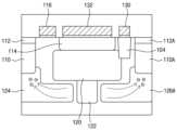
도 1 내지 도 3을 참조하면, 본 발명의 일 실시예에 따른 이미지 센서(100)는 복수의 이미지 셀들(106)과 상기 이미지 셀들(106)을 전기적으로 격리시키기 위한 소자 분리 영역들(104)을 구비할 수 있다. 각각의 상기 이미지 셀들(106)은, 기판(102) 내에 형성된 전하 축적 영역(110)과, 상기 전하 축적 영역(110)으로부터 일측으로 이격되어 형성되는 전하 저장 영역(114)과, 상기 전하 축적 영역(110)과 상기 전하 저장 영역(114) 사이의 채널 영역 상에 형성되며 상기 전하 축적 영역(110)의 전하를 상기 전하 저장 영역(114)으로 이동시키기 위한 전달 게이트 전극(116)을 포함할 수 있다.1 to 3, the
상기 전하 축적 영역(110)은 제1 도전형을 가질 수 있으며, 상기 기판(102)은 제2 도전형을 가질 수 있다. 일 예로서, 상기 전하 축적 영역(110)으로는 N형 불순물 확산 영역이 사용될 수 있으며, 상기 기판(102)으로는 P형 기판이 사용될 수 있다. 또한, 상기 전하 저장 영역(114)은 제1 도전형을 가질 수 있으며, 일 예로서, N형 불순물 확산 영역이 상기 전하 저장 영역(114)으로서 사용될 수 있다. 다른 예로서, 상기 기판(102) 상에는 P형 에피택시얼 층(미도시)이 형성될 수 있으며, 이 경우 상기 전하 축적 영역(110)과 전하 저장 영역(114)은 상기 P형 에피택시얼 층 내에 형성될 수 있다.The
상기 전하 축적 영역(110) 상에는 제2 도전형을 갖는 피닝층(112)이 형성될 수 있으며, 일 예로서, 상기 피닝층(112)으로는 P형 불순물 확산 영역이 사용될 수 있다. 즉, 상기 이미지 센서(100)는 상기 전하 축적 영역(110)과 상기 피닝층(112)으로 이루어지는 핀드 포토다이오드(pinned photodiode; PD)를 포함할 수 있다.A pinning
상기 이미지 센서(100)는, 도시되지는 않았으나, 상기 전하 저장 영역(114)으로부터 이격된 플로팅 확산 영역을 포함할 수 있으며, 상기 전하 저장 영역(114)과 상기 플로팅 확산 영역 사이의 상기 기판(102) 표면 부위 상에는 제2 전달 게이트 전극이 형성될 수 있다. 또한, 상기 이미지 센서(100)는 리셋 게이트 전극과 소스 팔로워 게이트 전극 및 선택 게이트 전극을 포함할 수 있으며, 상기 리셋 게이트 전극과 소스 팔로워 게이트 전극 및 선택 게이트 전극과 인접한 상기 기판(102)의 표면 부위들에는 소스/드레인 영역들로서 기능하는 불순물 확산 영역들이 형성될 수 있다. 또한, 상기 전극들과 상기 기판(102) 사이에는 실리콘 산화물로 이루어지는 게이트 절연막들이 형성될 수 있다.Although not shown, the
본 발명의 일 실시예에 따르면, 상기 전하 저장 영역(114)의 아래에는 상기 전하 저장 영역(114)의 아래에서 생성된 전하가 상기 전하 저장 영역(114)으로 이동되는 것을 방지하기 위한 웰 영역(120)이 형성될 수 있다. 상기 웰 영역(120)은 제2 도전형을 가질 수 있다. 예를 들면, 상기 웰 영역(120)은 P형 불순물 확산 영역일 수 있으며 이온 주입 공정에 의해 형성될 수 있다. 특히, 상기 웰 영역(120)의 아래에는 제2 웰 영역(122)이 형성될 수 있다. 예를 들면, 상기 제2 웰 영역(122)은 상기 웰 영역(120)의 중앙 부위 아래에 형성될 수 있으며, 상기 웰 영역(120)보다 좁은 폭을 가질 수 있다. 아울러, 상기 제2 웰 영역(122)은 제2 도전형을 가질 수 있다. 예를 들면, 제2 웰 영역(122)은 상기 웰 영역(120)보다 낮은 불순물 농도를 갖는 P형 불순물 확산 영역일 수 있다. 이때, 상기 기판(102)은 상기 제2 웰 영역(122)보다 낮은 불순물 농도를 가질 수 있다.According to one embodiment of the present invention, below the
상기 이미지 센서(100)는 상기 전하 저장 영역(114)에 인접하는 이미지 셀(106A)을 포함할 수 있으며, 상기 인접하는 이미지 셀(106A)은 전하 축적 영역(110A)과 피닝층(112A)으로 구성된 핀드 포토다이오드를 포함할 수 있다. 상기 웰 영역(120)과 상기 제2 웰 영역(122)은 상기 이미지 셀(106)과 상기 인접하는 이미지 셀(106A) 사이를 전기적으로 격리시키기 위한 격리 영역들로서 기능할 수 있으며, 상기 전하 저장 영역(114)의 아래에서 도 2에 도시된 바와 같이 상기 웰 영역(120)과 상기 제2 웰 영역(122) 그리고 상기 기판(102) 사이의 내부 전위 차이에 의해 상기 이미지 셀(106)의 전하 축적 영역(110) 또는 상기 인접하는 이미지 셀(106A)의 전하 축적 영역(110A)으로 이동될 수 있다. 결과적으로, 상기 전하 저장 영역(114) 아래에서 생성된 전자들이 상기 전하 저장 영역(114)으로 이동되는 것이 방지될 수 있으며, 이에 의해 상기 이미지 센서(100)의 다이나믹 레인지와 크로스토크 및 기생 광 감도 등이 크게 개선될 수 있다.The
본 발명의 일 실시예에 따르면, 상기 인접하는 이미지 셀(106A)의 전하 축적 영역(110A) 및 상기 전하 저장 영역(114) 사이의 상기 기판(102)의 표면 부위 상에 형성되며 상기 인접하는 이미지 셀(106A)로부터 상기 전하 저장 영역(114)으로 광이 유입되는 것을 방지하기 위한 더미 패턴(130)을 포함할 수 있다.According to one embodiment of the present invention, the
상기 더미 패턴(130)은 상기 전달 게이트 전극(116)과 동일한 물질로 동시에 형성될 수 있다. 특히, 상기 더미 패턴(130)과 상기 전달 게이트 전극(116)은 불순물 도핑된 폴리실리콘으로 이루어질 수 있으며, 상기 인접하는 이미지 셀(106A)로부터 상기 전하 저장 영역(114)으로 향하는 광은 상기 더미 패턴(130)에 의해 흡수될 수 있다. 즉, 상기 더미 패턴(130)은 상기 광을 흡수하기 위한 광 흡수 패턴으로서 기능할 수 있으며, 이에 의해 상기 전하 저장 영역(114)으로 상기 광이 유입되는 것이 방지될 수 있다. 예를 들면, 상기 기판(102) 상에 실리콘 산화막과 불순물 도핑된 폴리실리콘 막을 형성한 후 상기 폴리실리콘 막과 실리콘 산화막을 패터닝함으로써 상기 전달 게이트 전극(116)과 상기 더미 패턴(130)을 형성할 수 있다.The
또한, 상기 전하 저장 영역(114) 상에는 상기 전하 저장 영역(114)으로 광이 유입되는 것을 방지하기 위한 제2 더미 패턴(132)이 형성될 수 있다. 예를 들면, 상기 제2 더미 패턴(132)은 상기 전달 게이트 전극(116) 및 상기 더미 패턴(130)과 동일한 물질로 동시에 형성될 수 있다. 상기 제2 더미 패턴(132)과 상기 전하 저장 영역(114) 사이에는 실리콘 산화막과 같은 절연막(134)이 형성될 수 있으며, 상기 절연막(134)에 의해 상기 제2 더미 패턴(132)과 상기 전하 저장 영역(114)이 전기적으로 서로 절연될 수 있다.Additionally, a
상기 기판(102)과 상기 전달 게이트 전극(116) 및 상기 더미 패턴(130) 상에는 절연층(140)이 형성될 수 있다. 상기 절연층(140)은 상기 기판(102)과 상기 전달 게이트 전극(114) 및 상기 더미 패턴(130) 상에 형성되는 제1 산화막(142)과, 상기 제1 산화막(142) 상에 형성되는 질화막(144) 및 상기 질화막(144) 상에 형성되는 제2 산화막(146)을 포함할 수 있다. 일 예로서, 상기 절연층(140)은 상기 기판(102)과 상기 전달 게이트 전극(116) 및 상기 더미 패턴(130) 상에 형성되는 제1 실리콘 산화막(142)과, 상기 제1 실리콘 산화막(142) 상에 형성되는 실리콘 질화막(144) 및 상기 실리콘 질화막(144) 상에 형성되는 제2 실리콘 산화막(146)을 포함할 수 있다. 추가적으로, 상기 기판(102)과 상기 절연층(140) 사이에는 반사 방지막(148)이 형성될 수 있다. 일 예로서, 상기 반사 방지막(148)은 실리콘 질화물로 이루어질 수 있다.An insulating
상기 절연층(140) 상에는 상기 전하 저장 영역(114)으로 광이 유입되는 것을 방지하기 위한 광 실드층(150)이 형성될 수 있으며, 상기 광 실드층(150)은 금속, 예를 들면, 알루미늄으로 이루어질 수 있다. 특히, 상기 더미 패턴(130) 및 상기 광 실드층(150) 사이에는 상기 절연층(140)을 관통하는 광 실드 패턴(152)이 형성될 수 있으며, 상기 광 실드 패턴(152)은 금속, 예를 들면, 텅스텐 또는 구리로 이루어질 수 있다. 따라서, 상기 인접하는 이미지 셀(106A)로부터 상기 전하 저장 영역(114)으로 향하는 광은 상기 광 실드 패턴(152)에 의해 반사될 수 있다. 즉, 상기 광 실드 패턴(152)은 광 반사 패턴으로서 기능할 수 있다. 예를 들면, 상기 인접하는 이미지 셀(106A)의 전하 축적 영역(110A)과 상기 전하 저장 영역(114) 사이에는 소자 분리 영역(104)이 형성될 수 있으며, 상기 더미 패턴(130)은 상기 소자 분리 영역(104) 상에 형성될 수 있다. 또한, 상기 광 실드 패턴(152)은 상기 더미 패턴(130) 상에 형성될 수 있으며, 상기 광 실드층(150)은 상기 절연층(140)과 상기 광 실드 패턴(152) 상에 형성될 수 있다.A
본 발명의 일 실시예에 따르면, 상기 이미지 센서(100)는, 상기 인접하는 이미지 셀(106A)과 인접하는 상기 광 실드층(150)의 제1 가장자리 부위로부터 상기 기판(102)을 향하여 연장하는 제2 광 실드 패턴(154)과, 상기 전하 축적 영역(112)에 인접하는 상기 광 실드층(150)의 제2 가장자리 부위로부터 상기 기판(102)을 향하여 연장하는 제3 광 실드 패턴(156)을 포함할 수 있다. 예를 들면, 상기 제2 및 제3 광 실드 패턴들(154, 156)은 상기 제2 실리콘 산화막(146)을 관통하여 형성될 수 있다. 또한, 상기 제2 및 제3 광 실드 패턴들(154, 156)은 상기 광 실드 패턴(152)과 동일한 물질로 이루어질 수 있다. 예를 들면, 상기 제2 및 제3 광 실드 패턴들(154, 156)은 텅스텐 또는 구리와 같은 금속으로 이루어질 수 있다. 특히, 상기 실리콘 질화막(144)은 상기 제2 및 제3 광 실드 패턴들(154, 156)을 형성하기 위한 이방성 식각 공정에서 식각 저지막으로서 기능할 수 있다.According to one embodiment of the present invention, the
상기 절연층(140)과 상기 광 실드층(150) 상에는 제2 절연층(160)이 형성될 수 있다. 상기 제2 절연층(160)으로는 실리콘 산화막이 사용될 수 있다. 상기 제2 절연층(160) 상에는 복수의 금속 배선층(162, 166, 170)과 층간 절연층들(164, 168, 172)이 형성될 수 있다. 예를 들면, 상기 제2 절연층(160) 상에는 제1 금속 배선층(162)이 형성될 수 있으며, 상기 제2 절연층(160)과 상기 제1 금속 배선층(162) 상에는 제1 층간 절연층(164)이 형성될 수 있다. 상기 제1 층간 절연층(164) 상에는 제2 금속 배선층(166)이 형성될 수 있으며, 상기 제1 층간 절연층(164)과 상기 제2 금속 배선층(166) 상에는 제2 층간 절연층(168)이 형성될 수 있다. 상기 제2 층간 절연층(168) 상에는 제3 금속 배선층(170)이 형성될 수 있으며, 상기 제2 층간 절연층(168)과 상기 제3 금속 배선층(170) 상에는 제3 층간 절연층(172)이 형성될 수 있다.A second insulating
본 발명의 일 실시예에 따르면, 상기 이미지 센서(100)는 상기 층간 절연층들(164, 168, 172)을 관통하는 광 가이드 패턴층(174)을 포함할 수 있다. 구체적으로, 상기 광 가이드 패턴층(174)은 상기 층간 절연층들(164, 168, 172)을 관통하는 광 가이드 패턴들(176) 및 상기 제3 층간 절연층(172)과 상기 광 가이드 패턴들(176) 상에 형성되는 평탄화층(178)을 포함할 수 있다. 예를 들면, 상기 광 가이드 패턴층(174)은 상기 층간 절연층들(164, 168, 172)을 형성하는 실리콘 산화물보다 굴절률이 큰 유전체로 이루어질 수 있다.According to one embodiment of the present invention, the
한편, 상기 제2 절연층(160) 상에는 실리콘 질화물로 이루어진 식각 저지막(180)이 형성될 수 있다. 상기 광 가이드 패턴들(176)을 형성하기 위한 이방성 식각 공정에서 상기 층간 절연층들(164, 168, 172)은 상기 식각 저지막(180)이 노출될 때까지 부분적으로 제거될 수 있으며, 상기 광 가이드 패턴들(176)은 상기 이방성 식각 공정에 의해 형성된 관통홀들 내에 형성될 수 있다. 결과적으로, 상기 광 가이드 패턴들(176)은 상기 식각 저지막(180) 상에 형성될 수 있다.Meanwhile, an
상기와 다른 예로서, 도시되지는 않았으나, 상기 광 가이드 패턴들(176)은 상기 실리콘 질화막(144)까지 연장될 수 있다. 즉, 상기 광 가이드 패턴들(176)을 형성하기 위한 이방성 식각 공정에서 상기 층간 절연층들(164, 168, 172)과 상기 제2 절연층(160) 및 상기 제2 실리콘 산화막(146)이 상기 실리콘 질화막(144)이 노출될 때까지 부분적으로 제거될 수 있으며, 상기 이방성 식각 공정에서 상기 실리콘 질화막(144)이 식각 저지막으로 사용될 수도 있다. 이 경우, 상기 광 가이드 패턴들(176)은 상기 층간 절연층들(164, 168, 172)과 상기 제2 절연층(160) 및 상기 제2 실리콘 산화막(146)을 관통하여 상기 실리콘 질화막(144) 상에 형성될 수 있으며, 이를 통해 상기 핀드 포토다이오드들과 상기 광 가이드 패턴들(176) 사이의 거리를 크게 단축시킬 수 있다.As a different example from the above, although not shown, the
상기 광 가이드 패턴들(176)은 상기 전하 축적 영역들(112)과 대응하도록 위치될 수 있으며, 상기 광 가이드 패턴층(174) 상에는 복수의 컬러 필터들을 포함하는 컬러 필터층(182)이 형성될 수 있다. 상기 컬러 필터층(182) 상에는 제2 평탄화층(184)이 형성될 수 있으며, 상기 제2 평탄화층(184) 상에 마이크로렌즈 어레이(186)가 형성될 수 있다.The
상술한 같은 본 발명의 일 실시예에 따르면, 상기 인접하는 이미지 셀(106A)로부터 상기 전하 저장 영역(114)으로 향하는 광은 상기 제2 광 실드 패턴(154)에 의해 차단될 수 있으며, 상기 제2 광 실드 패턴(154)과 상기 기판(102) 사이를 통해 상기 전하 저장 영역(114)으로 향하는 광은 상기 더미 패턴(130)과 상기 광 실드 패턴(152)에 의해 차단될 수 있다. 따라서, 상기 전하 저장 영역(114)으로 유입되는 광이 크게 감소될 수 있으며, 이에 따라 상기 이미지 센서(100)의 다이나믹 레인지와 크로스토크 및 기생 광 감도 등이 크게 개선될 수 있다.According to an embodiment of the present invention as described above, light directed from the
도 4는 본 발명의 다른 실시예에 따른 이미지 센서를 설명하기 위한 개략적인 단면도이고, 도 5는 도 4에 도시된 제3 웰 영역과 제4 웰 영역을 설명하기 위한 개략적인 확대 단면도이다.FIG. 4 is a schematic cross-sectional view illustrating an image sensor according to another embodiment of the present invention, and FIG. 5 is a schematic enlarged cross-sectional view illustrating the third and fourth well regions shown in FIG. 4 .
도 4 내지 도 5를 참조하면, 본 발명의 다른 실시예에 따른 이미지 센서(200)는, 기판(102) 내에 형성되며 제1 도전형을 갖는 전하 축적 영역(110)과, 상기 전하 축적 영역(110)으로부터 일측으로 이격되어 형성되며 제1 도전형을 갖는 전하 저장 영역(114)과, 상기 전하 축적 영역(110)과 상기 전하 저장 영역(114) 사이의 채널 영역 상에 형성되는 전달 게이트 전극(116)을 포함할 수 있다. 상기 전하 저장 영역(114)의 아래에는 제2 도전형을 갖는 웰 영역(120)이 형성되며, 상기 웰 영역(120)의 중앙 부위 아래에는 제2 도전형을 갖고 상기 웰 영역(120)보다 낮은 불순물 농도를 갖는 제2 웰 영역(122)이 형성될 수 있다.4 to 5, the
본 발명의 다른 실시예에 따르면, 상기 이미지 센서(200)는 상기 전하 저장 영역(114)의 아래에서 생성된 전자들을 상기 전하 축적 영역(110)으로 이동시키기 위한 제3 웰 영역(124)을 포함할 수 있다. 상기 제3 웰 영역(124)은 제1 도전형을 가질 수 있으며 상기 전하 축적 영역(110)과 연결될 수 있다. 예를 들면, 상기 제3 웰 영역(124)은 이온 주입 공정에 의해 형성된 N형 불순물 확산 영역일 수 있으며, 특히 상기 제3 웰 영역(124)은 상기 전하 축적 영역(110)보다 낮은 불순물 농도를 가질 수 있다. 또한, 도시된 바와 같이 상기 제3 웰 영역(124)은 상기 전하 축적 영역(110)과 인접하는 상기 웰 영역(120)의 일측 부위 아래에서 상기 제2 웰 영역(122)과 인접하도록 형성될 수 있다.According to another embodiment of the present invention, the
또한, 상기 이미지 센서(200)는 인접하는 다른 이미지 셀(106B)의 웰 영역(120B) 아래에 형성되는 제4 웰 영역(126)을 포함할 수 있다. 상기 제4 웰 영역(126)은 제1 도전형을 가질 수 있으며 상기 전하 축적 영역(110)과 연결될 수 있다. 예를 들면, 상기 제4 웰 영역(126)은 이온 주입 공정에 의해 형성된 N형 불순물 확산 영역일 수 있으며, 상기 제4 웰 영역(126)은 상기 전하 축적 영역(110)보다 낮은 불순물 농도를 가질 수 있다. 또한, 도시된 바와 같이 상기 제4 웰 영역(126)은 상기 전하 축적 영역(110)과 인접하는 상기 인접하는 다른 이미지 셀(106B)의 웰 영역(120B)의 일측 부위 아래에서 상기 인접하는 다른 이미지 셀(106B)의 상기 제2 웰 영역(122B)과 인접하도록 형성될 수 있다. 특히, 상기 제4 웰 영역(126)은 상기 제3 웰 영역(124)과 동일한 불순물 농도를 가질 수 있으며, 상기 제3 웰 영역(124)과 동시에 형성될 수 있다.Additionally, the
따라서, 도 5에 도시된 바와 같이, 상기 전하 저장 영역(114)의 아래에서 생성된 전자들은 상기 제3 웰 영역(124)과 상기 인접하는 이미지 셀(106A)의 제4 웰 영역(126A)을 통해 상기 이미지 셀(106)의 전하 축적 영역(110) 또는 상기 인접하는 이미지 셀(106A)의 전하 축적 영역(110A)으로 이동될 수 있다. 결과적으로, 상기 전하 저장 영역(114) 아래에서 생성된 전자들이 상기 전하 저장 영역(114)으로 이동되는 것이 방지될 수 있으며, 이에 의해 상기 이미지 센서(200)의 다이나믹 레인지와 크로스토크 및 기생 광 감도 등이 크게 개선될 수 있다.Therefore, as shown in FIG. 5, electrons generated below the
한편, 상기 제3 웰 영역(124)과 상기 제4 웰 영역(126)을 제외한 다른 구성 요소들은 도 1 내지 도 4를 참조하여 기 설명된 바와 동일하므로 이들에 대한 추가적인 상세 설명은 생략한다.Meanwhile, other components except for the
상기에서는 본 발명의 바람직한 실시예를 참조하여 설명하였지만, 해당 기술 분야의 숙련된 당업자는 하기의 청구범위에 기재된 본 발명의 사상 및 영역으로부터 벗어나지 않는 범위 내에서 본 발명을 다양하게 수정 및 변경시킬 수 있음을 이해할 수 있을 것이다.Although the present invention has been described above with reference to preferred embodiments, those skilled in the art may make various modifications and changes to the present invention without departing from the spirit and scope of the present invention as set forth in the claims below. You will be able to understand that it exists.
100 : 이미지 센서102 : 기판
104 : 소자 분리 영역106 : 이미지 셀
110 : 전하 축적 영역112 : 피닝층
114 : 전하 저장 영역116 : 전달 게이트 전극
120 : 웰 영역122 : 제2 웰 영역
124 : 제3 웰 영역126 : 제4 웰 영역
130 : 더미 패턴132 : 제2 더미 패턴
140 : 절연층150 : 광 실드층
152 : 광 실드 패턴154 : 제2 광 실드 패턴
156 : 제3 광 실드 패턴160 : 제2 절연층
162, 166, 170 : 금속 배선층164, 168, 172 : 층간 절연층
174 : 광 가이드 패턴층176 : 광 가이드 패턴
178 : 평탄화층180 : 식각 저지막
182 : 컬러 필터층184 : 제2 평탄화층
186 : 마이크로렌즈 어레이100: image sensor 102: substrate
104: device isolation area 106: image cell
110: charge accumulation area 112: pinning layer
114: charge storage area 116: transfer gate electrode
120: well area 122: second well area
124: third well area 126: fourth well area
130: Dummy pattern 132: Second dummy pattern
140: insulating layer 150: optical shield layer
152: light shield pattern 154: second light shield pattern
156: Third optical shield pattern 160: Second insulating layer
162, 166, 170:
174: Light guide pattern layer 176: Light guide pattern
178: Planarization layer 180: Etch stop film
182: color filter layer 184: second planarization layer
186: Microlens array
Claims (20)
Translated fromKorean상기 전하 축적 영역으로부터 일측으로 이격되도록 형성되며 상기 제1 도전형을 갖는 전하 저장 영역;
상기 전하 축적 영역과 상기 전하 저장 영역 사이의 채널 영역 상에 형성되며 상기 전하 축적 영역으로부터 상기 전하 저장 영역으로 전하를 이동시키기 위한 전달 게이트 전극;
제2 도전형을 갖고 상기 전하 저장 영역 아래에 형성되며 상기 전하 저장 영역의 아래에서 생성된 전하가 상기 전하 저장 영역으로 이동되는 것을 방지하기 위한 웰 영역; 및
상기 제1 도전형을 갖고 상기 웰 영역의 아래에 형성되는 제3 웰 영역을 포함하는 것을 특징으로 하는 이미지 센서.A charge accumulation region having a first conductivity type formed in the substrate;
a charge storage region formed to be spaced apart from the charge accumulation region on one side and having the first conductivity type;
a transfer gate electrode formed on a channel region between the charge accumulation region and the charge storage region and configured to move charges from the charge accumulation region to the charge storage region;
a well region having a second conductivity type and formed below the charge storage region to prevent charges generated below the charge storage region from moving into the charge storage region; and
An image sensor comprising a third well region having the first conductivity type and formed below the well region.
상기 절연층 상에 형성되며 상기 전하 저장 영역으로 광이 유입되는 것을 방지하기 위한 광 실드층을 더 포함하는 것을 특징으로 하는 이미지 센서.11. The method of claim 10, comprising: an insulating layer formed on the substrate, the transfer gate electrode, and the dummy pattern;
The image sensor is formed on the insulating layer and further includes a light shield layer to prevent light from entering the charge storage region.
상기 제2 절연층 상에 형성된 복수의 층간 절연층들과,
상기 층간 절연층들 사이에 형성된 금속 배선층들과,
상기 층간 절연층들을 관통하며 상기 전하 축적 영역과 대응하는 광 가이드 패턴을 더 포함하는 것을 특징으로 하는 이미지 센서.14. The method of claim 13, comprising: a second insulating layer formed on the insulating layer and the light shield layer;
a plurality of interlayer insulating layers formed on the second insulating layer,
Metal wiring layers formed between the interlayer insulating layers,
The image sensor further includes a light guide pattern that penetrates the interlayer insulating layers and corresponds to the charge accumulation region.
상기 더미 패턴은 상기 소자 분리 영역 상에 형성되는 것을 특징으로 하는 이미지 센서.11. The method of claim 10, further comprising a device isolation region formed in a surface portion of the substrate between the charge accumulation region and the charge storage region of the adjacent image cell,
The image sensor, wherein the dummy pattern is formed on the device isolation region.
상기 전하 저장 영역과 상기 제2 더미 패턴 사이에 형성되며 상기 전하 저장 영역을 상기 제2 더미 패턴으로부터 전기적으로 절연시키기 위한 절연막을 더 포함하는 것을 특징으로 하는 이미지 센서.11. The method of claim 10, further comprising: a second dummy pattern formed on the charge storage region to prevent light from entering the charge storage region;
The image sensor further includes an insulating film formed between the charge storage region and the second dummy pattern to electrically insulate the charge storage region from the second dummy pattern.
Priority Applications (2)
| Application Number | Priority Date | Filing Date | Title |
|---|---|---|---|
| KR1020210087269AKR102673856B1 (en) | 2021-07-02 | 2021-07-02 | Image sensor |
| US17/810,077US12376396B2 (en) | 2021-07-02 | 2022-06-30 | Image sensor |
Applications Claiming Priority (1)
| Application Number | Priority Date | Filing Date | Title |
|---|---|---|---|
| KR1020210087269AKR102673856B1 (en) | 2021-07-02 | 2021-07-02 | Image sensor |
Publications (2)
| Publication Number | Publication Date |
|---|---|
| KR20230006263A KR20230006263A (en) | 2023-01-10 |
| KR102673856B1true KR102673856B1 (en) | 2024-06-10 |
Family
ID=84786446
Family Applications (1)
| Application Number | Title | Priority Date | Filing Date |
|---|---|---|---|
| KR1020210087269AActiveKR102673856B1 (en) | 2021-07-02 | 2021-07-02 | Image sensor |
Country Status (2)
| Country | Link |
|---|---|
| US (1) | US12376396B2 (en) |
| KR (1) | KR102673856B1 (en) |
Citations (3)
| Publication number | Priority date | Publication date | Assignee | Title |
|---|---|---|---|---|
| JP2004165462A (en)* | 2002-11-14 | 2004-06-10 | Sony Corp | Solid-state imaging device and method of manufacturing the same |
| JP2011071437A (en)* | 2009-09-28 | 2011-04-07 | Sony Corp | Solid-state image sensing device and method for manufacturing the same, and electronic apparatus |
| WO2018110258A1 (en)* | 2016-12-15 | 2018-06-21 | パナソニック・タワージャズセミコンダクター株式会社 | Solid-state image pickup element |
Family Cites Families (8)
| Publication number | Priority date | Publication date | Assignee | Title |
|---|---|---|---|---|
| KR20050106928A (en)* | 2004-05-06 | 2005-11-11 | 매그나칩 반도체 유한회사 | Cmos image sensor with reduced leakage current |
| JP2008084962A (en)* | 2006-09-26 | 2008-04-10 | Toshiba Corp | Solid-state imaging device and manufacturing method thereof |
| KR20100072661A (en)* | 2008-12-22 | 2010-07-01 | 주식회사 동부하이텍 | Method for manufacturing image sensor |
| SG10201705879SA (en) | 2012-08-20 | 2017-08-30 | Adc Technology Inc | Apparatuses for transmitting heat between a rail of rack mounted equipment and a channel of acooling rack enclosure, and related components, systems, and methods |
| KR101352436B1 (en) | 2012-10-31 | 2014-01-20 | 주식회사 동부하이텍 | An image sensor |
| KR20150108531A (en)* | 2014-03-18 | 2015-09-30 | 주식회사 동부하이텍 | CMOS image sensor and method of manufacturing the same |
| KR102398688B1 (en) | 2017-05-26 | 2022-05-16 | 주식회사 디비하이텍 | Image sensor and method of manufacturing the same |
| KR102657686B1 (en)* | 2019-05-13 | 2024-04-15 | 주식회사 디비하이텍 | An image sensor and the method of manufacturing the same |
- 2021
- 2021-07-02KRKR1020210087269Apatent/KR102673856B1/enactiveActive
- 2022
- 2022-06-30USUS17/810,077patent/US12376396B2/enactiveActive
Patent Citations (3)
| Publication number | Priority date | Publication date | Assignee | Title |
|---|---|---|---|---|
| JP2004165462A (en)* | 2002-11-14 | 2004-06-10 | Sony Corp | Solid-state imaging device and method of manufacturing the same |
| JP2011071437A (en)* | 2009-09-28 | 2011-04-07 | Sony Corp | Solid-state image sensing device and method for manufacturing the same, and electronic apparatus |
| WO2018110258A1 (en)* | 2016-12-15 | 2018-06-21 | パナソニック・タワージャズセミコンダクター株式会社 | Solid-state image pickup element |
Also Published As
| Publication number | Publication date |
|---|---|
| KR20230006263A (en) | 2023-01-10 |
| US12376396B2 (en) | 2025-07-29 |
| US20230005974A1 (en) | 2023-01-05 |
Similar Documents
| Publication | Publication Date | Title |
|---|---|---|
| US11843015B2 (en) | Image sensors | |
| US10707254B2 (en) | Semiconductor devices | |
| KR100758321B1 (en) | Image sensor with embedded photodiode region and fabrication method thereof | |
| KR102433575B1 (en) | Image sensor | |
| US9030587B2 (en) | Solid-state image sensor with light-guiding portion | |
| US8441052B2 (en) | Color-optimized image sensor | |
| US20200219914A1 (en) | Image sensor and method of fabricating the same | |
| US20210335862A1 (en) | Image sensor | |
| US20190181167A1 (en) | Backside illuminated image sensor and method of manufacturing the same | |
| KR101373905B1 (en) | Solid-state imaging device | |
| KR101997539B1 (en) | Image sensor and method of forming the same | |
| JP2009534836A (en) | N-well barrier pixels that improve protection of dark reference columns and dark reference rows from blooming and crosstalk | |
| US9391113B2 (en) | Image-sensor device structure and method of manufacturing | |
| KR102673856B1 (en) | Image sensor | |
| KR102642229B1 (en) | Image sensor | |
| US20220115422A1 (en) | Image sensor and method of fabricating the same | |
| US11637138B2 (en) | Tilted transfer gate for advanced CMOS image sensor | |
| KR20230132224A (en) | Image sensor | |
| US8716761B2 (en) | Image sensor for semiconductor light-sensitive device, manufacturing thereof, image processing apparatus using the same, and method for detecting color signal | |
| KR100873293B1 (en) | Image sensor to prevent crosstalk | |
| US20230299096A1 (en) | Image sensor and manufacturing method of the same | |
| KR100790229B1 (en) | Image sensor and its manufacturing method | |
| KR20100089748A (en) | Solid-state imaging device, imaging apparatus, and manufacturing method of solid-state imaging device |
Legal Events
| Date | Code | Title | Description |
|---|---|---|---|
| PA0109 | Patent application | Patent event code:PA01091R01D Comment text:Patent Application Patent event date:20210702 | |
| PA0201 | Request for examination | Patent event code:PA02012R01D Patent event date:20220318 Comment text:Request for Examination of Application Patent event code:PA02011R01I Patent event date:20210702 Comment text:Patent Application | |
| PG1501 | Laying open of application | ||
| E902 | Notification of reason for refusal | ||
| PE0902 | Notice of grounds for rejection | Comment text:Notification of reason for refusal Patent event date:20230912 Patent event code:PE09021S01D | |
| E701 | Decision to grant or registration of patent right | ||
| PE0701 | Decision of registration | Patent event code:PE07011S01D Comment text:Decision to Grant Registration Patent event date:20240530 | |
| GRNT | Written decision to grant | ||
| PR0701 | Registration of establishment | Comment text:Registration of Establishment Patent event date:20240604 Patent event code:PR07011E01D | |
| PR1002 | Payment of registration fee | Payment date:20240605 End annual number:3 Start annual number:1 | |
| PG1601 | Publication of registration |