KR102671141B1 - Semiconductor device for managing addresses of nonvolatile memory device - Google Patents
Semiconductor device for managing addresses of nonvolatile memory deviceDownload PDFInfo
- Publication number
- KR102671141B1 KR102671141B1KR1020180078411AKR20180078411AKR102671141B1KR 102671141 B1KR102671141 B1KR 102671141B1KR 1020180078411 AKR1020180078411 AKR 1020180078411AKR 20180078411 AKR20180078411 AKR 20180078411AKR 102671141 B1KR102671141 B1KR 102671141B1
- Authority
- KR
- South Korea
- Prior art keywords
- address
- cold
- area
- semiconductor device
- volatile memory
- Prior art date
- Legal status (The legal status is an assumption and is not a legal conclusion. Google has not performed a legal analysis and makes no representation as to the accuracy of the status listed.)
- Active
Links
Images


Classifications
- G—PHYSICS
- G06—COMPUTING OR CALCULATING; COUNTING
- G06F—ELECTRIC DIGITAL DATA PROCESSING
- G06F12/00—Accessing, addressing or allocating within memory systems or architectures
- G06F12/02—Addressing or allocation; Relocation
- G06F12/0223—User address space allocation, e.g. contiguous or non contiguous base addressing
- G06F12/023—Free address space management
- G06F12/0238—Memory management in non-volatile memory, e.g. resistive RAM or ferroelectric memory
- G—PHYSICS
- G06—COMPUTING OR CALCULATING; COUNTING
- G06F—ELECTRIC DIGITAL DATA PROCESSING
- G06F12/00—Accessing, addressing or allocating within memory systems or architectures
- G06F12/02—Addressing or allocation; Relocation
- G06F12/08—Addressing or allocation; Relocation in hierarchically structured memory systems, e.g. virtual memory systems
- G06F12/10—Address translation
- G06F12/1009—Address translation using page tables, e.g. page table structures
- G—PHYSICS
- G06—COMPUTING OR CALCULATING; COUNTING
- G06F—ELECTRIC DIGITAL DATA PROCESSING
- G06F3/00—Input arrangements for transferring data to be processed into a form capable of being handled by the computer; Output arrangements for transferring data from processing unit to output unit, e.g. interface arrangements
- G06F3/06—Digital input from, or digital output to, record carriers, e.g. RAID, emulated record carriers or networked record carriers
- G06F3/0601—Interfaces specially adapted for storage systems
- G06F3/0628—Interfaces specially adapted for storage systems making use of a particular technique
- G06F3/0655—Vertical data movement, i.e. input-output transfer; data movement between one or more hosts and one or more storage devices
- G06F3/0659—Command handling arrangements, e.g. command buffers, queues, command scheduling
- G—PHYSICS
- G06—COMPUTING OR CALCULATING; COUNTING
- G06F—ELECTRIC DIGITAL DATA PROCESSING
- G06F12/00—Accessing, addressing or allocating within memory systems or architectures
- G06F12/02—Addressing or allocation; Relocation
- G06F12/0223—User address space allocation, e.g. contiguous or non contiguous base addressing
- G06F12/023—Free address space management
- G06F12/0238—Memory management in non-volatile memory, e.g. resistive RAM or ferroelectric memory
- G06F12/0246—Memory management in non-volatile memory, e.g. resistive RAM or ferroelectric memory in block erasable memory, e.g. flash memory
- G—PHYSICS
- G06—COMPUTING OR CALCULATING; COUNTING
- G06F—ELECTRIC DIGITAL DATA PROCESSING
- G06F3/00—Input arrangements for transferring data to be processed into a form capable of being handled by the computer; Output arrangements for transferring data from processing unit to output unit, e.g. interface arrangements
- G06F3/06—Digital input from, or digital output to, record carriers, e.g. RAID, emulated record carriers or networked record carriers
- G06F3/0601—Interfaces specially adapted for storage systems
- G06F3/0602—Interfaces specially adapted for storage systems specifically adapted to achieve a particular effect
- G06F3/0604—Improving or facilitating administration, e.g. storage management
- G—PHYSICS
- G06—COMPUTING OR CALCULATING; COUNTING
- G06F—ELECTRIC DIGITAL DATA PROCESSING
- G06F3/00—Input arrangements for transferring data to be processed into a form capable of being handled by the computer; Output arrangements for transferring data from processing unit to output unit, e.g. interface arrangements
- G06F3/06—Digital input from, or digital output to, record carriers, e.g. RAID, emulated record carriers or networked record carriers
- G06F3/0601—Interfaces specially adapted for storage systems
- G06F3/0602—Interfaces specially adapted for storage systems specifically adapted to achieve a particular effect
- G06F3/0614—Improving the reliability of storage systems
- G06F3/0619—Improving the reliability of storage systems in relation to data integrity, e.g. data losses, bit errors
- G—PHYSICS
- G06—COMPUTING OR CALCULATING; COUNTING
- G06F—ELECTRIC DIGITAL DATA PROCESSING
- G06F3/00—Input arrangements for transferring data to be processed into a form capable of being handled by the computer; Output arrangements for transferring data from processing unit to output unit, e.g. interface arrangements
- G06F3/06—Digital input from, or digital output to, record carriers, e.g. RAID, emulated record carriers or networked record carriers
- G06F3/0601—Interfaces specially adapted for storage systems
- G06F3/0628—Interfaces specially adapted for storage systems making use of a particular technique
- G06F3/0638—Organizing or formatting or addressing of data
- G06F3/064—Management of blocks
- G—PHYSICS
- G06—COMPUTING OR CALCULATING; COUNTING
- G06F—ELECTRIC DIGITAL DATA PROCESSING
- G06F3/00—Input arrangements for transferring data to be processed into a form capable of being handled by the computer; Output arrangements for transferring data from processing unit to output unit, e.g. interface arrangements
- G06F3/06—Digital input from, or digital output to, record carriers, e.g. RAID, emulated record carriers or networked record carriers
- G06F3/0601—Interfaces specially adapted for storage systems
- G06F3/0628—Interfaces specially adapted for storage systems making use of a particular technique
- G06F3/0653—Monitoring storage devices or systems
- G—PHYSICS
- G06—COMPUTING OR CALCULATING; COUNTING
- G06F—ELECTRIC DIGITAL DATA PROCESSING
- G06F3/00—Input arrangements for transferring data to be processed into a form capable of being handled by the computer; Output arrangements for transferring data from processing unit to output unit, e.g. interface arrangements
- G06F3/06—Digital input from, or digital output to, record carriers, e.g. RAID, emulated record carriers or networked record carriers
- G06F3/0601—Interfaces specially adapted for storage systems
- G06F3/0668—Interfaces specially adapted for storage systems adopting a particular infrastructure
- G06F3/0671—In-line storage system
- G06F3/0673—Single storage device
- G06F3/0679—Non-volatile semiconductor memory device, e.g. flash memory, one time programmable memory [OTP]
- G—PHYSICS
- G11—INFORMATION STORAGE
- G11C—STATIC STORES
- G11C16/00—Erasable programmable read-only memories
- G11C16/02—Erasable programmable read-only memories electrically programmable
- G11C16/06—Auxiliary circuits, e.g. for writing into memory
- G11C16/34—Determination of programming status, e.g. threshold voltage, overprogramming or underprogramming, retention
- G11C16/3418—Disturbance prevention or evaluation; Refreshing of disturbed memory data
- G—PHYSICS
- G06—COMPUTING OR CALCULATING; COUNTING
- G06F—ELECTRIC DIGITAL DATA PROCESSING
- G06F2212/00—Indexing scheme relating to accessing, addressing or allocation within memory systems or architectures
- G06F2212/10—Providing a specific technical effect
- G06F2212/1032—Reliability improvement, data loss prevention, degraded operation etc
- G—PHYSICS
- G06—COMPUTING OR CALCULATING; COUNTING
- G06F—ELECTRIC DIGITAL DATA PROCESSING
- G06F2212/00—Indexing scheme relating to accessing, addressing or allocation within memory systems or architectures
- G06F2212/22—Employing cache memory using specific memory technology
- G06F2212/222—Non-volatile memory
- G—PHYSICS
- G06—COMPUTING OR CALCULATING; COUNTING
- G06F—ELECTRIC DIGITAL DATA PROCESSING
- G06F2212/00—Indexing scheme relating to accessing, addressing or allocation within memory systems or architectures
- G06F2212/60—Details of cache memory
- G06F2212/608—Details relating to cache mapping
- G—PHYSICS
- G06—COMPUTING OR CALCULATING; COUNTING
- G06F—ELECTRIC DIGITAL DATA PROCESSING
- G06F2212/00—Indexing scheme relating to accessing, addressing or allocation within memory systems or architectures
- G06F2212/72—Details relating to flash memory management
- G06F2212/7201—Logical to physical mapping or translation of blocks or pages
- G—PHYSICS
- G06—COMPUTING OR CALCULATING; COUNTING
- G06F—ELECTRIC DIGITAL DATA PROCESSING
- G06F2212/00—Indexing scheme relating to accessing, addressing or allocation within memory systems or architectures
- G06F2212/72—Details relating to flash memory management
- G06F2212/7211—Wear leveling
Landscapes
- Engineering & Computer Science (AREA)
- Theoretical Computer Science (AREA)
- Physics & Mathematics (AREA)
- General Engineering & Computer Science (AREA)
- General Physics & Mathematics (AREA)
- Human Computer Interaction (AREA)
- Computer Security & Cryptography (AREA)
- Techniques For Improving Reliability Of Storages (AREA)
Abstract
Translated fromKoreanDescription
Translated fromKorean본 발명은 비휘발성 메모리 장치에 대하여 쓰기 요청이 상대적으로 덜 집중되는 주소를 관리하는 반도체 장치에 관한 것이다.The present invention relates to a semiconductor device that manages addresses where write requests are relatively less concentrated for a non-volatile memory device.
비휘발성 메모리는 셀의 물리적, 화학적 특성으로 인하여 쓰기 횟수가 제한되는 것이 일반적이다.Non-volatile memory generally has a limited number of writes due to the physical and chemical characteristics of the cell.
예를 들어 상변이 메모리의 셀은 쓰기 동작을 약 107회 정도 수행할 정도의 수명을 가진다.For example, a phase-change memory cell has a lifespan of approximately 107 write operations.
메모리 장치의 특정 셀에 쓰기 동작이 집중되는 경우 특정 셀의 수명이 단축됨으로 인하여 전체 메모리 장치의 수명이 감소할 수 있다.When a write operation is concentrated on a specific cell of a memory device, the lifespan of the specific cell may be shortened, thereby reducing the lifespan of the entire memory device.
이에 따라 쓰기 동작을 메모리 장치의 전체 셀에 균등하게 수행하기 위하여 웨어 레벨링 동작을 수행한다.Accordingly, a wear leveling operation is performed to perform a write operation equally on all cells of the memory device.
종래에는 웨어 레벨링을 수행하기 위하여 일정한 주기마다 논리 주소와 물리 주소 사이의 맵핑 관계를 변경하는 방식을 사용한다.Conventionally, a method of changing the mapping relationship between logical addresses and physical addresses at regular intervals is used to perform wear leveling.
특히 종래에는 일정한 주기 내에서 특정 물리 주소에 쓰기 요청이 집중되는 주소(핫 주소)를 탐지하고 이를 이용하여 웨어 레벨링 동작을 수행한다.In particular, in the related art, an address (hot address) where write requests are concentrated on a specific physical address within a certain period is detected and a wear leveling operation is performed using this.
웨어 레벨링을 수행하는 경우 핫 주소는 쓰기 요청이 상대적으로 덜 집중되는 주소(콜드 주소)와 스왑되는 것이 일반적이다.When performing wear leveling, hot addresses are typically swapped with addresses where write requests are relatively less intensive (cold addresses).
그런데 선택된 콜드 주소가 쓰기 동작이 일정한 정도 수행된 속성(웜 속성)을 가지는 경우 웨어 레벨링 동작이 빈번하게 수행될 수 있으므로 웨어 레벨링 수행시 콜드 주소를 적절하게 선택하는 것이 전체적인 성능 향상에 바람직하다.However, if the selected cold address has properties (warm properties) in which write operations have been performed to a certain degree, wear leveling operations may be performed frequently, so it is desirable to appropriately select cold addresses when performing wear leveling to improve overall performance.
종래에는 핫 주소에 대해 관리를 수행하는 것과 별개로 콜드 주소에 대해서는 특별한 관리가 없었다.Conventionally, apart from managing hot addresses, there was no special management for cold addresses.
이에 따라 핫 주소는 물론 콜드 주소에 대해 관리를 효율적으로 수행하고 이를 이용하여 웨어 레벨링 동작의 효율성을 높이는 기술이 필요하다.Accordingly, technology is needed to efficiently manage hot addresses as well as cold addresses and use this to increase the efficiency of wear leveling operations.
본 기술에서는 저장 공간을 효율적으로 사용하면서 주소를 관리하고, 이를 통해 메모리 장치의 웨어 레벨링 성능을 향상시킨다.This technology manages addresses while efficiently using storage space, thereby improving the wear leveling performance of memory devices.
본 기술은 주소를 관리하여 관리된 주소에 대응하는 데이터를 재기록함으로써 드리프트 현상으로 인한 데이터 손상을 줄일 수 있다.This technology can reduce data damage due to drift phenomenon by managing addresses and rewriting data corresponding to the managed addresses.
본 발명의 일 실시예에 의한 반도체 장치는 호스트에서 비휘발성 메모리에 대한 쓰기 요청이 발생하는 경우 쓰기 요청된 주소를 출력하는 미디어 제어기; 및 쓰기 요청된 주소에 대한 메타 정보를 저장하는 스택, 일정한 주기마다 비휘발성 메모리의 주소를 길이가 가변되는 영역으로 나누어 관리하는 영역 정보 저장부, 일정한 주기마다 상기 스택과 영역 정보 저장부를 갱신하여 비휘발성 메모리의 주소가 쓰기 요청이 일정 수준 이하로 수행되는 콜드 주소인지를 탐지하는 콜드 주소 탐지부를 포함하는 콜드 주소 관리부를 포함한다.A semiconductor device according to an embodiment of the present invention includes a media controller that outputs a write requested address when a write request for a non-volatile memory occurs from a host; and a stack that stores meta information about the address requested to write, an area information storage unit that divides and manages the address of the non-volatile memory into areas of variable length at regular intervals, and updates the stack and area information storage unit at regular intervals to It includes a cold address management unit including a cold address detection unit that detects whether the address of the volatile memory is a cold address in which write requests are performed below a certain level.
본 기술에서는 핫 주소와는 별도로 콜드 주소를 관리하여 콜드 주소가 아닌 주소가 웨어 레벨링에 사용되어 웨어 레벨 동작이 빈번하게 수행되는 것을 방지한다.In this technology, cold addresses are managed separately from hot addresses to prevent wear-level operations from being frequently performed because addresses other than cold addresses are used for wear leveling.
본 기술을 통해 콜드 주소 관리를 위한 저장 공간을 효율적으로 사용할 수 있다.This technology allows efficient use of storage space for cold address management.
본 기술을 통해 관리된 콜드 주소를 이용하여 스크러빙 동작을 수행함으로써 드리프트 현상에 의한 데이터 손상을 줄일 수 있다.By performing a scrubbing operation using cold addresses managed through this technology, data damage due to drift phenomenon can be reduced.
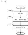
도 1은 본 발명의 일 실시예에 의한 반도체 장치를 나타내는 블록도.
도 2는 도 1의 비휘발성 메모리의 구조를 나타내는 블록도.
도 3은 도 1의 맵핑 테이블의 데이터 구조를 나타내는 도표.
도 4는 도 1의 핫 주소 관리부의 일 예를 나타내는 블록도.
도 5는 도 1의 콜드 주소 관리부의 일 예를 나타내는 블록도.
도 6은 도 5의 스택의 데이터 구조를 나타내는 도표.
도 7은 도 5의 영역 정보 저장부의 일 예를 나타내는 블록도.
도 8은 영역 정보의 데이터 구조를 나타내는 블록도.
도 9는 물리 주소와 영역 정보의 관계를 나타내는 설명도.
도 10은 도 1의 콜드 주소 관리부의 동작을 나타내는 순서도.
도 11은 도 10의 영역 정보 관리 동작을 나타내는 순서도.
도 12는 도 11의 상태 갱신 동작을 나타내는 순서도.
도 13은 도 11의 영역 스플릿 또는 머지 동작을 나타내는 순서도.
도 14는 영역 머지 동작을 설명하는 설명도.
도 15는 영역 스플릿 동작을 설명하는 설명도.
도 16은 영역 스플릿 동작을 나타내는 순서도.1 is a block diagram showing a semiconductor device according to an embodiment of the present invention.
FIG. 2 is a block diagram showing the structure of the non-volatile memory of FIG. 1.
Figure 3 is a diagram showing the data structure of the mapping table in Figure 1.
FIG. 4 is a block diagram showing an example of the hot address management unit of FIG. 1.
FIG. 5 is a block diagram showing an example of the cold address management unit of FIG. 1.
Figure 6 is a diagram showing the data structure of the stack of Figure 5.
FIG. 7 is a block diagram showing an example of the region information storage unit of FIG. 5.
Figure 8 is a block diagram showing the data structure of area information.
Fig. 9 is an explanatory diagram showing the relationship between physical addresses and area information.
Figure 10 is a flowchart showing the operation of the cold address management unit of Figure 1.
FIG. 11 is a flowchart showing the region information management operation of FIG. 10.
FIG. 12 is a flowchart showing the status update operation of FIG. 11.
FIG. 13 is a flowchart showing the region split or merge operation of FIG. 11.
14 is an explanatory diagram illustrating a region merge operation.
15 is an explanatory diagram illustrating a region split operation.
16 is a flowchart showing a region split operation.
이하에서는 첨부한 도면을 참조하여 본 발명의 실시예를 개시한다.Hereinafter, embodiments of the present invention will be disclosed with reference to the attached drawings.
도 1은 본 발명의 일 실시예에 의한 반도체 장치를 나타내는 블록도이다.1 is a block diagram showing a semiconductor device according to an embodiment of the present invention.
본 발명의 일 실시예에 의한 반도체 장치는 맵핑 테이블(100), 미디어 제어기(200), 콜드 주소 관리부(500)를 포함한다.A semiconductor device according to an embodiment of the present invention includes a mapping table 100, a
본 발명의 일 실시예에 의한 반도체 장치는 핫 주소 관리부(300)와 웨어 레벨 제어기(400)를 더 포함할 수 있다.The semiconductor device according to an embodiment of the present invention may further include a hot
본 발명의 일 실시예에 의한 반도체 장치는 스크러빙 제어기(600)를 더 포함할 수 있다.The semiconductor device according to an embodiment of the present invention may further include a
핫 주소 관리부(300), 웨어 레벨 제어기(400), 콜드 주소 관리부(500), 스크러빙 제어기(600)는 각각이 하드웨어, 소프트웨어 또는 이들이 조합된 형태로 구현되어 하나의 제어 모듈(1000)에 포함될 수 있으며, 제어 모듈(1000)은 미디어 제어기(200)와 하나의 모듈 또는 칩에 포함될 수 있다.The hot
미디어 제어기(200)는 호스트(10)에서 제공된 논리 주소와 요청에 따라 비휘발성 메모리(20)에 물리 주소와 요청에 대응하는 명령을 출력한다.The
본 실시예에서 비휘발성 메모리 장치(20)는 도 2와 같이 다수의 페이지(22)를 포함하고 페이지 단위로 쓰기 동작을 수행하는 것으로 가정한다.In this embodiment, it is assumed that the
본 실시예에서 비휘발성 메모리 장치(20)는 플래시 메모리 장치, 상변이 메모리 장치 등과 같이 웨어 레벨링 동작이 요구되는 임의의 메모리 장치일 수 있다.In this embodiment, the
호스트(10)에서 사용하는 논리 주소와 이에 대응하는 비휘발성 메모리(20)의 물리 주소 사이의 관계는 맵핑 테이블(100)을 이용하여 관리한다.The relationship between the logical address used by the
본 실시예에서 맵핑 테이블(100)은 디램과 같은 휘발성 메모리를 이용하여 구현될 수 있다.In this embodiment, the mapping table 100 may be implemented using volatile memory such as DRAM.
도 3은 맵핑 테이블(100)의 데이터 구조를 나타내는 블록도이다.Figure 3 is a block diagram showing the data structure of the mapping table 100.
맵핑 테이블(100)은 논리 주소를 저장하는 논리 주소 필드(110)와 논리 주소에 대응하는 물리 주소를 저장하는 물리 주소 필드(120)를 포함한다.The mapping table 100 includes a
웨어 레벨 동작 시 웨어 레벨 제어기(400)는 맵핑 테이블(100)을 제어하여 논리 주소와 물리 주소 사이의 맵핑 관계를 변경할 수 있다.During wear level operation, the
본 실시예에서 미디어 제어기(200)는 맵핑 테이블(100)을 제어하여 호스트(10)에서 요청한 논리 주소에 대응하는 물리 주소가 맵핑 테이블에 존재하는지 여부 및 대응하는 물리 주소에 관한 정보를 획득할 수 있다.In this embodiment, the
미디어 제어기(200)는 쓰기 요청된 물리 주소를 제어 모듈(1000)에 제공한다.The
핫 주소 관리부(300)는 미디어 제어기(200)에서 제공된 물리 주소를 이용하여 핫 주소를 탐지하고 이를 저장한다.The hot
본 실시예에서 핫 주소 관리부(300)는 쓰기 요청된 물리 주소들로부터 핫 주소를 탐지하여 저장하는 것이면 충분하며 이를 구현하는 기술은 특정한 것으로 한정되지 않는다.In this embodiment, it is sufficient for the hot
예를 들어 핫 주소 관리부(300)는 종래의 기술로 구현된 것일 수도 있다.For example, the hot
핫 주소 관리부(300)는 웨어 레벨 동작 시 탐지된 핫 주소를 웨어 레벨 제어기(400)에 제공할 수 있다.The hot
도 4는 본 발명의 일 실시예에 의한 핫 주소 관리부(300)를 나타내는 블록도이다.Figure 4 is a block diagram showing the hot
핫 주소 관리부(300)는 핫 주소 탐지부(310), 카운터 어레이(320) 및 핫 주소 저장부(330)를 포함한다.The hot
카운터 어레이(320)는 물리 주소에 대응하는 다수의 카운터(321)를 포함한다. 이때 물리 주소는 대응하는 페이지 주소일 수 있다.The
미디어 제어기(200)에서 제공되는 쓰기 요청된 물리 주소에 따라 대응하는 카운터(321) 값이 갱신된다.The
본 실시예에서 핫 주소 탐지부(310)는 카운터 값이 임계점 이상이 되는 물리 주소를 핫 주소로 선택하여 핫 주소 저장부(330)에 저장한다.In this embodiment, the hot
핫 주소 탐지부(310)가 핫 주소를 선택하는 방법과 기준은 실시예에 따라 다양하게 변경될 수 있다.The method and criteria by which the hot
또한 카운터(321)의 개수를 줄이기 위하여 카운터 어레이를 멀티 레벨로 구성하는 등의 다양한 설계 변경도 가능하다.In addition, various design changes are possible, such as configuring the counter array in a multi-level manner to reduce the number of
콜드 주소 관리부(500)는 미디어 제어기(200)에서 제공된 물리 주소를 이용하여 콜드 주소를 탐지하고 이를 저장한다.The cold
콜드 주소 관리부(500)는 탐지된 콜드 주소를 웨어 레벨 제어기(400)에 제공할 수 있다.The cold
콜드 주소 관리부(500)의 구체적인 구성 및 동작 방법은 이하에서 구체적으로 설명한다.The specific configuration and operation method of the cold
웨어 레벨 제어기(400)는 핫 주소와 콜드 주소를 이용하여 웨어 레벨 동작을 제어한다.The
예를 들어 웨어 레벨 제어기(400)는 핫 주소와 콜드 주소에 대한 맵핑 관계가 스왑되도록 맵핑 테이블(100)을 제어할 수 있다.For example, the
본 실시예에서 웨어 레벨 제어기(400)는 콜드 주소 관리부(500)에서 제공된 콜드 주소를 이용하여 웨어 레벨 동작을 수행하면 충분하며 특정한 방식으로 구현되어야 하는 것은 아니다.In this embodiment, it is sufficient for the
본 실시예에서 웨어 레벨 제어기(400)는 웨어 레벨 동작을 진행하는 동안 플래그를 활성화하여 미디어 제어기(200)에 제공할 수 있다.In this embodiment, the
웨어 레벨 동작은 호스트에서 요청이 없는 아이들 상태에서 진행될 수도 있다. 이 경우 미디어 제어기(200)는 아이들 상태를 알리는 플래그를 웨어 레벨 제어기(400)에 먼저 제공할 수 있다.Wear-level operations may proceed in an idle state without a request from the host. In this case, the
웨어 레벨 제어기(400)는 이에 응답하여 웨어 레벨 동작의 진행 여부를 나타내는 플래그를 미디어 제어기(200)에 제공할 수 있다.In response, the
플래그는 멀티 비트 신호로서 아이들 상태를 알리는 플래그 비트와 웨어 레벨 동작의 진행을 나타내는 플래그 비트를 포함할 수 있다.The flag is a multi-bit signal and may include a flag bit indicating an idle state and a flag bit indicating progress of a wear level operation.
스크러빙 제어기(600)는 일정한 주기마다 스크러빙 동작을 수행할 수 있다.The scrubbing
예를 들어 비휘발성 메모리 장치(20)가 상변이 메모리 장치인 경우 드리프트 현상에 의해 셀에 기록된 데이터가 변경될 수 있다.For example, if the
이를 방지하기 위하여 스크러빙 제어기(600)는 일정한 주기마다 디램의 리프레시 동작과 유사하게 비휘발성 메모리에 대해서 데이터를 읽고 다시 쓰는 스크러빙 동작을 진행할 수 있다.To prevent this, the scrubbing
이때 읽은 데이터에 오류가 존재하는 경우 이를 정정하여 다시 쓸 수 있다.At this time, if there is an error in the data read, it can be corrected and rewritten.
본 실시예에서 스크러빙 제어기(600)는 콜드 주소로 식별된 주소에 대해서 한정적으로 스크러빙 동작을 진행할 수 있다.In this embodiment, the scrubbing
이를 위하여 콜드 주소 관리부(500)는 탐지된 콜드 주소를 스크러빙 제어기(600)에 제공할 수 있다.To this end, the cold
스크러빙 제어기(600)는 스크러빙 동작을 나타내는 플래그 신호와 스크러빙 동작을 수행할 콜드 주소를 미디어 제어기(200)에 제공할 수 있다.The scrubbing
미디어 제어기(200)는 이에 따라 비휘발성 메모리(20)에 대한 읽기 및 쓰기 동작을 진행할 수 있다.Accordingly, the
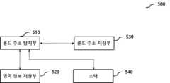
도 5는 도 1의 콜드 주소 관리부(500)의 일 예를 나타내는 블록도이다.FIG. 5 is a block diagram showing an example of the cold
콜드 주소 관리부(500)는 콜드 주소 탐지부(510), 영역 정보 저장부(520), 콜드 주소 저장부(530) 및 스택(540)을 포함한다.The cold
콜드 주소 탐지부(510)는 영역 정보 저장부(520)와 스택(540)을 참조하여 콜드 주소를 탐지하고 탐지된 콜드 주소를 콜드 주소 저장부(530)에 저장한다.The cold
콜드 주소 관리부(500)는 물리 주소를 영역 단위로 관리한다.The cold
본 실시예에서 하나의 영역은 기본적으로 4개의 페이지를 포함하며 관리 동작을 진행하는 도중에 하나의 영역에 포함되는 페이지의 개수는 증감될 수 있다.In this embodiment, one area basically includes four pages, and the number of pages included in one area may increase or decrease during management operations.
스택(540)은 콜드 주소 탐지부(510)에 의해 관리되는 영역 관련 메타 데이터를 저장한다.The
도 6은 도 5의 스택(540)의 데이터 구조를 나타내는 도표이다.FIG. 6 is a diagram showing the data structure of the
스택(540)은 영역 번호(RN) 필드(541), 히트 카운트(HC) 필드(542), 주파수 카운트(FC) 필드(543)를 포함한다.
영역 번호(RN)는 영역을 식별하기 위한 일련 번호를 나타낸다. 본 실시예에서 하나의 영역은 기본적으로 4개의 페이지를 포함한다. 이에 대해서는 도 9를 참조하여 아래에서 다시 구체적으로 설명한다.The area number (RN) represents a serial number to identify the area. In this embodiment, one area basically includes four pages. This will be explained in detail again below with reference to FIG. 9.
히트 카운트(HC)는 대응하는 영역에 대한 쓰기 요청 횟수에 연관된다. 히트 카운트는 일정한 주기마다 초기화될 수 있다.Hit Count (HC) is related to the number of write requests to the corresponding area. The hit count may be reset at regular intervals.
예를 들어 쓰기 요청된 물리 주소에 대응하는 영역 번호가 존재하는 경우 히트, 존재하지 않는 경우 미스로 판단하는데 히트가 발생하는 경우 영역 번호에 대응하는 히트 카운트를 증가시킨다.For example, if the area number corresponding to the physical address requested to write exists, it is judged as a hit, and if it does not exist, it is judged as a miss. If a hit occurs, the hit count corresponding to the area number is increased.
주파수 카운트(FC)는 쓰기 요청 횟수에 연관된다. 쓰기 요청이 발생하는 경우 히트가 발생하면 영역 번호에 대응하는 주파수 카운트를 증가시킨다.Frequency Count (FC) is tied to the number of write requests. When a write request occurs, if a hit occurs, the frequency count corresponding to the area number is increased.
다만 쓰기 요청시 미스가 발생하면 스택에 기록된 모든 영역에 대해서 주파수 카운트를 감소시킬 수 있다.However, if a miss occurs during a write request, the frequency count can be decreased for all areas written to the stack.
이하에서는 스택(540)에 저장된 행의 개수를 스택 크기로 표현할 수 있다. 스택 크기의 최대값은 미리 정할 수 있다.Hereinafter, the number of rows stored in the
본 실시예에서 스택(540)은 동작 초기에 비어있으며 쓰기 요청이 진행될 때마다 새로운 행이 추가되거나 기존의 행이 갱신될 수 있다.In this embodiment, the
이와 같이 스택(540)은 쓰기 동작이 수행된 주소들을 저장하게 되므로 콜드 주소를 선택하는데 있어서 웜 속성을 가진 주소를 걸러내는데 참조할 수 있다.In this way, since the
영역 정보 저장부(520)는 물리 주소와 영역 사이의 관계를 나타내는 영역 정보를 저장한다.The area
본 실시예에서 물리 주소는 페이지 주소를 나타내며 영역 정보는 페이지와 영역 사이의 관계를 저장한다.In this embodiment, the physical address represents the page address, and region information stores the relationship between pages and regions.
도 7은 도 5의 영역 정보 저장부(520)의 일 예를 나타내는 블록도이다.FIG. 7 is a block diagram showing an example of the region
영역 정보 저장부(520)는 제 1 데이터 구조체(521)와 제 2 데이터 구조체(522)를 포함한다.The region
본 실시예에서 제 1 데이터 구조체(521)는 영역 정보(550)를 배열 형태로 저장한다.In this embodiment, the
본 실시예에서 제 2 데이터 구조체(522)는 제 1 데이터 구조체(521)의 영역 정보(550)와 연관된 연결 리스트를 포함한다.In this embodiment, the
연결 리스트는 하나 또는 둘 이상의 영역 정보를 포함하며 연결 리스트에 포함되는 영역 정보의 개수는 스플릿(split) 또는 머지(merge) 동작에 의해 조정될 수 있다.The linked list includes one or more region information, and the number of region information included in the linked list can be adjusted by a split or merge operation.
영역 스플릿 및 영역 머지 동작에 대해서는 이하에서 다시 구체적으로 개시한다.The region split and region merge operations are described in detail again below.
도 7에서 제 1 데이터 구조체(521)의 영역 1은 제 2 데이터 구조체(522)의 영역 x와 연관된다.In FIG. 7,
제 1 데이터 구조체(521)의 영역 2는 제 2 데이터 구조체(522)의 영역 y와 연관되고, 영역 y는 영역 z와 연관된다.
이와 같이 제 2 데이터 구조체(522)에 포함된 연결 리스트의 길이는 가변적으로 조절될 수 있다.In this way, the length of the linked list included in the
영역의 스플릿 또는 머지 동작에 대해서는 아래에서 다시 구체적으로 설명한다.The split or merge operation of the region will be explained in more detail below.
도 8은 영역 정보(550)의 데이터 구조를 나타내는 블록도이다.FIG. 8 is a block diagram showing the data structure of
영역 정보(550)는 대응하는 영역에 대한 정보를 저장하는 데이터 구조체로서 주소(address), 크기(size), 상태(state) 및 포인터(pointer) 정보를 포함한다.
본 실시예에서 주소는 영역에 포함된 첫 번째 페이지 주소를 나타낸다.In this embodiment, the address represents the first page address included in the area.
본 실시예에서 크기는 영역에 포함된 페이지의 개수를 나타낸다.In this embodiment, size indicates the number of pages included in the area.
본 실시예에서 상태 또는 상태 값은 영역의 콜드 정도를 나타내며 콜드 주소 탐지부(510)에 의해 값이 제어된다.In this embodiment, the state or state value indicates the coldness of the area and the value is controlled by the cold
본 실시예에서 포인터는 현재 영역에 연관된 다음 영역의 주소를 나타낸다.In this embodiment, the pointer represents the address of the next area associated with the current area.
초기에 영역 정보 저장부(520)의 제 1 데이터 구조체(521)에는 모든 영역의 정보가 저장된다.Initially, all region information is stored in the
본 실시예에서 제 1 데이터 구조체(521)는 미리 저장 공간이 할당된 배열 구조를 가지므로 저장 공간을 줄이기 위하여 제 1 데이터 구조체(521)에 초기화되어 저장된 영역 사이에서 머지 동작을 수행할 필요는 없다.In this embodiment, the
이 경우 영역에 기본적으로 포함되는 페이지 수를 늘릴수록 제 1 데이터 구조체(521)의 크기를 줄일 수 있다.In this case, as the number of pages basically included in the area increases, the size of the
다만 제 1 데이터 구조체(521)의 영역 사이에서 머지 동작이 진행되는 다른 실시예 역시 본 개시로부터 통상의 기술자가 용이하게 설계 변경할 수 있을 것이다.However, a person skilled in the art can easily design and change other embodiments in which a merge operation is performed between regions of the
예를 들어 제 1 데이터 구조체(521)에 저장된 영역 사이에서 머지 동작이 허용되는 경우 영역의 크기가 임계점 이하인 경우에만 머지 동작이 진행되는 것으로 제한하는 등의 다양한 설계 변경이 가능할 것이다.For example, if a merge operation is allowed between areas stored in the
초기에 제 2 데이터 구조체(522)에는 영역 정보가 저장되지 않으며 제 2 데이터 구조체(522)에는 영역의 스플릿 또는 머지에 의해서 영역 정보의 개수가 가변된다.Initially, no region information is stored in the
전술한 바와 같이 제 2 데이터 구조체(522)에 포함되는 가변 리스트는 제 1 데이터 구조체(521)에 포함된 영역으로부터 스플릿되어 생성되고 길이가 증가한다.As described above, the variable list included in the
본 실시예에서는 스플릿 동작이 영역의 크기가 1이 될 때까지 가능한 것으로 가정하나, 다른 실시예에서는 영역의 크기(size)가 임계점 이상인 경우에 수행되는 것으로 제한할 수도 있다.In this embodiment, it is assumed that the split operation is possible until the size of the area becomes 1, but in other embodiments, it may be limited to being performed when the size of the area is greater than a threshold.
또한 제 2 데이터 구조체(522)에 포함되는 가변 리스트는 거기에 포함된 영역들의 머지 동작에 의해 길이가 감소할 수 있으며, 제 1 데이터 구조체(521)에 포함된 영역과 머지되어 소멸될 수 있다.Additionally, the length of the variable list included in the
도 9는 물리 주소와 영역의 관계를 나타내는 설명도이다.Figure 9 is an explanatory diagram showing the relationship between physical addresses and areas.
본 실시예에서 물리 주소는 페이지 주소를 나타내며 기본적으로 4개의 페이지가 하나의 영역을 구성한다. 하나의 영역에 기본적으로 포함되는 페이지의 개수는 더욱 크게 설정될 수 있다.In this embodiment, the physical address represents a page address, and basically four pages constitute one area. The number of pages included by default in one area can be set larger.
영역 1의 주소는 페이지 1의 주소를 저장하고, 크기는 4를 저장하고, 상태는 3을 저장하고, 포인터는 영역 x의 주소를 저장한다.The address of
이는 영역 1이 페이지 1부터 페이지 4까지 4개의 페이지를 포함하는 것을 나타내고, 영역 1의 콜드 정도는 3이며 영역 1에 연관된 영역 x가 존재함을 의미한다.This indicates that
영역 2의 주소는 페이지 5의 주소를 저장하고, 크기는 4를 저장하고, 상태는 0을 저장하고, 포인터는 영역 y의 주소를 저장한다.The address of
영역 n의 주소는 페이지 k-4의 주소를 저장하고, 크기는 4를 저장하고, 상태는 1을 저장하고, 포인터는 null을 저장한다(n, k는 자연수, k>4, k = 4n).The address of area n stores the address of page k-4, the
포인터의 null은 영역 n에 연관된 영역이 존재하지 않음을 나타낸다.A null pointer indicates that the area associated with area n does not exist.
콜드 주소 탐지부(510)는 영역 정보 저장부(520)와 스택(540)을 관리하면서 콜드 주소를 탐지하고 이를 콜드 주소 저장부(530)에 저장한다.The cold
이하에서는 순서도를 참조하여 콜드 주소 탐지부(510)의 동작을 구체적으로 개시한다.Hereinafter, the operation of the cold
도 10은 콜드 주소 관리부(500)의 동작을 나타내는 순서도이다.Figure 10 is a flowchart showing the operation of the cold
먼저 미디어 제어기(200)로부터 쓰기 요청된 물리 주소가 입력된다(S100).First, the physical address requested to be written from the
쓰기 요청된 물리 주소에 대응하는 영역이 스택(540)에 저장된 것인지를 기준으로 히트 또는 미스 여부를 판단한다(S110).A hit or a miss is determined based on whether the area corresponding to the physical address requested to write is stored in the stack 540 (S110).
판단 결과 히트이면 스택(540)에서 영역 번호에 대응하는 히트 카운트와 주파수 카운트를 증가시키고(S130) 단계(S170)로 이동한다.If the determination result is a hit, the
판단 결과 미스이면 스택(540)에서 모든 영역에 대응하는 주파수 카운트를 감소시킨다(S120). 다만 주파수 카운트가 0인 경우 그대로 유지된다.If the determination result is a miss, the frequency count corresponding to all areas in the
히트 카운트와 주파수 카운트가 증가하는 것은 콜드 속성이 약화되는 것을 나타낸다.Increasing hit count and frequency count indicate that the cold attribute is weakening.
이후 현재 스택 크기가 최대값인지 확인한다(S140).Afterwards, check whether the current stack size is the maximum (S140).
현재 스택 크기가 최대값이 아니면 스택(540)에 새로운 행을 추가하고(S150) 단계(S170)로 진행한다.If the current stack size is not the maximum, a new row is added to the stack 540 (S150) and the process proceeds to step S170.
이때 새로 추가되는 행은 새로 추가된 영역의 번호를 가지고 히트 카운트와 주파수 카운트는 0으로 초기화된다.At this time, the newly added row has the number of the newly added area, and the hit count and frequency count are initialized to 0.
현재 스택 크기가 최대값이면 스택(540)에 저장된 행 중 하나를 선택하여 새 행의 정보로 교체(S160)하고 단계(S170)로 진행한다.If the current stack size is the maximum, one of the rows stored in the
본 실시예에서는 콜드 속성이 가장 덜 약화된 영역을 선택하는 데 이를 위하여 스택(540)에서 주파수 카운트가 최소인 행을 새로운 행 정보로 교체한다.In this embodiment, the area with the least weakened cold attribute is selected. To this end, the row with the minimum frequency count in the
이에 따라 스택(540)에서 기존 영역 번호가 새로운 영역 번호로 교체되고 주파수 카운트, 히트 카운트가 초기화된다.Accordingly, the existing area number is replaced with a new area number in the
이후 1 주기가 종료되었는지 확인한다(S170).Afterwards, check whether one cycle has ended (S170).
1 주기가 종료되었는지는 일정한 횟수의 쓰기 요청이 있었는지를 기준으로 확인할 수 있다.1 Whether a cycle has ended can be checked based on whether a certain number of write requests have been made.
예를 들어 쓰기 요청된 물리 주소가 입력될 때마다 주기를 식별하기 위한 변수를 증가시키고 이를 일정한 기준값과 비교함으로써 1 주기가 종료되었는지 확인할 수 있다.For example, each time a physical address requested for writing is input, a variable for identifying the cycle is increased and compared with a certain reference value to check whether one cycle has ended.
1 주기가 종료되지 않았다면 그대로 동작을 완료한다.If
1 주기가 종료되었다면 영역 정보를 관리한다(S180).If one cycle has ended, area information is managed (S180).
도 11은 도 10의 영역 정보 관리 동작을 나타내는 순서도이다.FIG. 11 is a flowchart showing the region information management operation of FIG. 10.
영역 정보를 관리하는 동작(S190)은 상태(state)를 갱신하는 동작(S200)과 영역 정보를 스플릿 또는 머지하는 동작(S300) 및 히트 카운트 초기화 동작(S400)을 포함한다.The operation S190 of managing area information includes an operation S200 of updating the state, an operation S300 of splitting or merging area information, and a hit count initialization operation S400.
도 12는 도 11의 상태 갱신 동작을 나타내는 순서도이다.FIG. 12 is a flowchart showing the status update operation of FIG. 11.
상태 갱신 동작을 위해 스택(540)을 참조할 수 있다.The
먼저 단계(S210)에서 스택(540)에 없거나 영역 번호에 대응하는 히트 카운트가 0이고 주파수 카운트가 0인 경우(S210) 상태 값을 1 감소시킨다(S220). 이때 상태 값이 0인 경우에는 0을 유지한다.First, in step S210, if it is not in the
이후 히트 카운트가 0보다 크고 주파수 카운트가 0인 경우(S230) 상태 값을 1만큼 증가시킨다(S240).Afterwards, if the hit count is greater than 0 and the frequency count is 0 (S230), the status value is increased by 1 (S240).
이후 히트 카운트가 0보다 크고 주파수 카운트가 0보다 큰 경우(S250) 상태 값을 2만큼 증가시킨다.Afterwards, if the hit count is greater than 0 and the frequency count is greater than 0 (S250), the status value is increased by 2.
나머지 경우에는 상태 값이 기존 값 그대로 유지된다.In the remaining cases, the status value remains at its original value.
이상에서 상태 값을 증가시키는 것은 해당 영역의 콜드 정도가 상대적으로 약화됨을 나타낸다.Increasing the status value above indicates that the degree of cold in the corresponding area is relatively weakened.
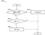
도 13은 도 11의 영역 스플릿 또는 머지 동작을 나타내는 순서도이다.FIG. 13 is a flowchart showing the region split or merge operation of FIG. 11.
먼저 인접한 영역의 상태 값이 모두 0인지 확인한다(S310).First, check whether the status values of adjacent areas are all 0 (S310).
본 실시예에서 상태 값이 0인 영역은 콜드 정도가 가장 강화된 영역에 해당한다.In this embodiment, the area where the status value is 0 corresponds to the area where the cold degree is most strengthened.
본 실시예에서는 인접한 두 영역 정보의 상태 값이 0인 경우 이들을 머지한다(S320).In this embodiment, if the status value of two adjacent areas of information is 0, they are merged (S320).
도 14는 인접한 두 영역을 머지하는 동작을 설명한다.Figure 14 explains the operation of merging two adjacent areas.
도 14에서 인접한 두 영역은 영역 1과 영역 x이다.In Figure 14, the two adjacent areas are
1번 영역에서 주소는 1번 페이지의 주소, 크기는 2, 상태는 0, 포인터는 영역 x의 주소이며, x번 영역에서 주소는 3번 페이지의 주소, 크기는 2, 상태는 0, 포인터는 null이다.In
머지된 영역에서 주소는 머지되기 전 1번 영역의 주소와 동일하고, 크기는 1번 영역의 크기와 x번 영역의 크기의 합과 동일하고, 포인터는 x번 영역의 포인터와 동일하게 설정될 수 있다.In the merged area, the address is the same as the address of
이에 따라 두 영역이 머지된 후 주소는 1번 페이지의 주소, 크기는 4, 상태는 0, 포인터는 null이다.Accordingly, after the two areas are merged, the address is the address of
머지된 후의 영역 정보가 기존의 1번 영역의 정보를 대체하며 x번 영역의 정보는 영역 정보 저장부(520)에서 삭제할 수 있다.The merged area information replaces the existing information of
본 실시예에서는 제 1 데이터 구조체(521)에 포함된 영역 정보는 머지되지 않으므로 삭제되는 영역 정보는 제 2 데이터 구조체(522)에 포함된 것으로 한정된다.In this embodiment, since the region information included in the
이에 따라 스택(540)에서 x번 영역에 대한 행을 삭제하거나 무효화할 수 있다.Accordingly, the row for area x in the
스택(540)에서 1번 영역에 대한 주파수 카운트는 0으로 갱신된다.The frequency count for
도 11의 단계(S400)에서 히트 카운트가 초기화되므로 1번 영역에 대한 히트 카운트는 갱신할 필요가 없다.Since the hit count is initialized in step S400 of FIG. 11, there is no need to update the hit count for
이와 같이 본 실시예에서는 콜드 상태가 유지되는 인접한 영역들을 머지하여 영역 정보 저장부(520) 및 스택(540)의 크기를 감소시킬 수 있다.As such, in this embodiment, the sizes of the region
도 13의 단계(S310)에서 아니오로 판단된 경우 상태 값이 3인지 확인한다(S330).If it is determined as No in step S310 of FIG. 13, it is checked whether the status value is 3 (S330).
본 실시예에서 상태 값이 3인 영역은 콜드 정도가 가장 약화된 영역에 해당한다.In this embodiment, the area with a status value of 3 corresponds to the area where the cold degree is the weakest.
본 실시예에서는 상태 값이 3인 영역 정보를 스플릿한다(S500).In this embodiment, region information with a status value of 3 is split (S500).
도 15는 영역 정보 스플릿 동작을 설명하는 설명도이다.Figure 15 is an explanatory diagram explaining the region information split operation.
도 15에서 스플릿 되기 전의 영역은 3번 영역으로서 주소는 9번 페이지 주소, 크기는 4, 상태는 3, 포인터는 null을 저장한다.In Figure 15, the area before splitting is
스플릿 후 영역의 개수 및 크기는 실시예에 따라 다양하게 변경될 수 있으나, 본 실시예에서는 하나의 영역을 크기가 동일한 두 개의 영역으로 스플릿한다.The number and size of regions after splitting may vary depending on the embodiment, but in this embodiment, one region is split into two regions of the same size.
이에 따라 스플릿 후 영역 3-1이 추가로 생성된다.Accordingly, area 3-1 is additionally created after the split.
스플릿 후 영역 1의 주소는 기존과 동일하고, 크기는 2로 줄어들며 상태는 스플릿 전의 상태를 2로 나눈 값을 올림한 값인 2로 갱신되며, 포인터는 영역 3-1의 주소로 설정된다.After splitting, the address of
스플릿 후 생성된 영역 3-1의 주소는 페이지 9의 주소, 크기는 2, 상태는 동일하게 2로 갱신되며, 포인터는 스플린 전 영역 3의 포인터인 null로 설정된다.The address of area 3-1 created after the split is the address of page 9, the size is 2, the status is updated to 2, and the pointer is set to null, which is the pointer to
도 16은 영역 스플릿 동작을 나타내는 순서도이다.16 is a flowchart showing a region split operation.
먼저 스택 크기가 최대값인지 판단한다(S510).First, determine whether the stack size is the maximum (S510).
스택 크기가 최대값이면 스택(540)에 저장된 기존 행들 중 주파수 카운트 값이 최소인 행을 삭제하여 여유 공간을 확보하고(S520) 새로운 행을 스택(540)에 추가한다(S530).If the stack size is the maximum, the row with the minimum frequency count value among the existing rows stored in the
스택 크기가 최대값이 아니면 곧바로 새로운 행을 스택(540)에 추가한다(S530).If the stack size is not the maximum, a new row is immediately added to the stack 540 (S530).
새로 추가된 행은 스플릿 동작에 의해 새로 추가된 영역에 대응한다.The newly added row corresponds to the area newly added by the split operation.
스택(540)에서 스플릿 후 두 영역에 대응하는 주파수 카운트는 스플릿 전 영역에 대한 주파수 카운트 값의 1/2로 감소한다.In the
이후 영역 정보를 갱신한다(S540).Afterwards, the area information is updated (S540).
영역 정보 갱신 동작은 도 15를 참조하여 설명한 것과 같다.The area information update operation is the same as described with reference to FIG. 15.
이후 도 11로 돌아가 스택(540)에서 히트 카운트의 값을 초기화한다(S400).Afterwards, returning to FIG. 11, the hit count value is initialized in the stack 540 (S400).
이후 도 10으로 돌아가 영역 스플릿 또는 머지 동작 이후 콜드 주소를 저장한다(S190).Then, returning to FIG. 10, the cold address is stored after the region split or merge operation (S190).
일 실시예에서 영역 정보의 상태 값이 임계점 이하인 영역에 대응하는 물리 주소를 콜드 주소로 저장할 수 있다.In one embodiment, the physical address corresponding to the area where the state value of the area information is below the threshold may be stored as a cold address.
이때 콜드 주소 저장부(530)에 저장되는 콜드 주소의 개수가 한정된 경우 상태 값이 작은 순서로 콜드 주소를 선택할 수 있다.At this time, if the number of cold addresses stored in the cold
상태 값이 동일한 경우에는 주파수 카운트와 히트 카운트가 작은 순서로 우선하여 콜드 주소를 선택할 수 있다.If the status values are the same, the cold address can be selected with priority in the order of frequency count and hit count.
도 10에는 1 주기마다 콜드 주소를 저장하는 실시예가 도시되었으나 다른 실시예에서는 콜드 주소를 저장 또는 갱신하는 동작을 쓰기 요청이 있을 때마다 수행할 수도 있다.10 illustrates an embodiment in which a cold address is stored every cycle. However, in another embodiment, the operation of storing or updating a cold address may be performed whenever a write request is made.
스크러빙 동작 또는 웨어 레벨 동작은 도 10의 단계(S190) 이후에 수행될 수도 있다.The scrubbing operation or wear level operation may be performed after step S190 of FIG. 10.
이때 콜드 주소 관리부(500)는 스크러빙 제어기(600)와 웨어 레벨 제어기(400)에 콜드 주소 저장 동작이 종료되었음을 알릴 수 있다.At this time, the cold
이에 대한 응답으로 스크러빙 제어기(600)는 스크러빙 동작을 진행할 수 있고, 웨어 레벨 제어기(400)는 웨어 레벨 동작을 진행할 수 있다.In response, the scrubbing
이때 1 주기는 드리프트 현상에 의해 데이터가 손상되는 시간보다 짧도록 설정될수 있다.At this time, one cycle can be set to be shorter than the time during which data is damaged due to the drift phenomenon.
이상의 개시는 본 발명의 설명을 위한 것일 뿐 본 발명의 권리범위를 한정하기 위한 것은 아니다. 본 발명의 권리범위는 특허청구범위에 문언적으로 기재된 범위와 그 균등범위에 의해 정해진다.The above disclosure is only for explanation of the present invention and is not intended to limit the scope of the present invention. The scope of rights of the present invention is determined by the scope literally stated in the patent claims and the scope of equivalents thereof.
10: 호스트
20: 비휘발성 메모리 장치
100: 맵핑 테이블
200: 미디어 제어기
1000: 제어 모듈
300: 핫 주소 관리부
310: 핫 주소 탐지부
320: 카운터 어레이
330: 핫 주소 저장부
400: 웨어 레벨 제어기
500: 콜드 주소 관리부
510: 콜드 주소 탐지부
520: 영역 정보 관리부
530: 콜드 주소 저장부
540: 스택
600: 스크러빙 제어기10: Host
20: Non-volatile memory device
100: Mapping table
200: media controller
1000: Control module
300: Hot address management unit
310: Hot address detection unit
320: counter array
330: Hot address storage unit
400: wear level controller
500: Cold address management unit
510: Cold address detection unit
520: Area information management department
530: Cold address storage unit
540: stack
600: scrubbing controller
Claims (20)
Translated fromKorean상기 호스트에서 상기 비휘발성 메모리에 대한 쓰기 요청이 발생하는 경우 상기 맵핑 테이블을 참조하여 쓰기 요청된 주소를 출력하는 미디어 제어기; 및
상기 쓰기 요청된 주소에 대한 메타 정보를 저장하는 스택, 일정한 주기마다 상기 비휘발성 메모리의 주소를 길이가 가변되는 영역으로 나누어 관리하는 영역 정보 저장부, 상기 일정한 주기마다 상기 스택과 상기 영역 정보 저장부를 갱신하여 상기 비휘발성 메모리의 주소가 쓰기 요청이 일정 수준 이하로 수행되는 콜드 주소인지를 탐지하는 콜드 주소 탐지부를 포함하는 콜드 주소 관리부
를 포함하되,
상기 영역 정보 저장부는 상기 비휘발성 메모리의 전체 주소가 연관되도록 설정된 다수의 영역 정보를 저장하도록 초기화되고,
상기 다수의 영역 정보 각각은 대응하는 영역에 연관된 상기 비휘발성 메모리의 주소를 식별할 수 있는 정보, 상기 대응하는 영역의 속성을 나타내는 상태 및 상기 대응하는 영역에 연관된 다른 영역의 주소를 나타내는 포인터를 포함하는 반도체 장치.a mapping table that stores a mapping relationship between a logical address identified by the host and a physical address of a non-volatile memory;
a media controller that refers to the mapping table and outputs a write-requested address when a write request for the non-volatile memory occurs from the host; and
A stack that stores meta information about the write requested address, an area information storage unit that divides and manages the address of the non-volatile memory into areas of variable length at regular intervals, and the stack and the area information storage unit at regular intervals. A cold address management unit including a cold address detection unit that updates and detects whether the address of the non-volatile memory is a cold address in which write requests are performed below a certain level.
Including,
The region information storage unit is initialized to store a plurality of region information set to be associated with the entire address of the non-volatile memory,
Each of the plurality of area information includes information that can identify the address of the non-volatile memory associated with the corresponding area, a state indicating attributes of the corresponding area, and a pointer indicating the address of another area associated with the corresponding area. semiconductor device.
The semiconductor device of claim 18, wherein the non-volatile memory is performed every constant cycle, and the constant cycle is set to be shorter than the time until data in the non-volatile memory drifts and becomes damaged.
Priority Applications (2)
| Application Number | Priority Date | Filing Date | Title |
|---|---|---|---|
| KR1020180078411AKR102671141B1 (en) | 2018-07-05 | 2018-07-05 | Semiconductor device for managing addresses of nonvolatile memory device |
| US16/434,001US10877698B2 (en) | 2018-07-05 | 2019-06-06 | Semiconductor device for managing cold addresses of nonvolatile memory device |
Applications Claiming Priority (1)
| Application Number | Priority Date | Filing Date | Title |
|---|---|---|---|
| KR1020180078411AKR102671141B1 (en) | 2018-07-05 | 2018-07-05 | Semiconductor device for managing addresses of nonvolatile memory device |
Publications (2)
| Publication Number | Publication Date |
|---|---|
| KR20200005127A KR20200005127A (en) | 2020-01-15 |
| KR102671141B1true KR102671141B1 (en) | 2024-05-30 |
Family
ID=69101976
Family Applications (1)
| Application Number | Title | Priority Date | Filing Date |
|---|---|---|---|
| KR1020180078411AActiveKR102671141B1 (en) | 2018-07-05 | 2018-07-05 | Semiconductor device for managing addresses of nonvolatile memory device |
Country Status (2)
| Country | Link |
|---|---|
| US (1) | US10877698B2 (en) |
| KR (1) | KR102671141B1 (en) |
Families Citing this family (2)
| Publication number | Priority date | Publication date | Assignee | Title |
|---|---|---|---|---|
| US10983918B2 (en)* | 2018-12-31 | 2021-04-20 | Micron Technology, Inc. | Hybrid logical to physical caching scheme |
| EP4394607A4 (en) | 2021-11-10 | 2024-12-11 | Samsung Electronics Co., Ltd. | METHOD FOR PRESERVING DATA IN THE INITIALIZATION SITUATION OF AN ELECTRONIC DEVICE AND ELECTRONIC DEVICE THEREFOR |
Citations (3)
| Publication number | Priority date | Publication date | Assignee | Title |
|---|---|---|---|---|
| US20150347296A1 (en)* | 2014-05-30 | 2015-12-03 | Sandisk Enterprise Ip Llc | Prioritizing Garbage Collection and Block Allocation Based on I/O History for Logical Address Regions |
| US20160098215A1 (en)* | 2014-10-03 | 2016-04-07 | SanDisk Technologies, Inc. | Method and System for Adaptively Assigning Logical Block Address Read Counters Using a Tree Structure |
| US20170024326A1 (en)* | 2015-07-22 | 2017-01-26 | CNEX-Labs, Inc. | Method and Apparatus for Caching Flash Translation Layer (FTL) Table |
Family Cites Families (9)
| Publication number | Priority date | Publication date | Assignee | Title |
|---|---|---|---|---|
| KR101257691B1 (en)* | 2011-08-12 | 2013-04-24 | 아주대학교산학협력단 | Memory controller and data management method |
| US8788778B1 (en)* | 2012-06-04 | 2014-07-22 | Western Digital Technologies, Inc. | Garbage collection based on the inactivity level of stored data |
| US9032137B2 (en)* | 2012-11-21 | 2015-05-12 | Intel Corporation | Flexible wear management for non-volatile memory |
| KR20150006614A (en)* | 2013-07-09 | 2015-01-19 | 에스케이하이닉스 주식회사 | Data storage device and operating method thereof |
| KR20160008365A (en)* | 2014-07-14 | 2016-01-22 | 삼성전자주식회사 | storage medium, memory system and method for managing storage space in memory system |
| US10409526B2 (en)* | 2014-12-17 | 2019-09-10 | Violin Systems Llc | Adaptive garbage collection |
| US9690656B2 (en)* | 2015-02-27 | 2017-06-27 | Microsoft Technology Licensing, Llc | Data encoding on single-level and variable multi-level cell storage |
| KR20170075835A (en) | 2015-12-23 | 2017-07-04 | 에스케이하이닉스 주식회사 | Memory system and operating method of memory system |
| KR20170078310A (en) | 2015-12-29 | 2017-07-07 | 에스케이하이닉스 주식회사 | Memory system and operation methode for the same |
- 2018
- 2018-07-05KRKR1020180078411Apatent/KR102671141B1/enactiveActive
- 2019
- 2019-06-06USUS16/434,001patent/US10877698B2/enactiveActive
Patent Citations (3)
| Publication number | Priority date | Publication date | Assignee | Title |
|---|---|---|---|---|
| US20150347296A1 (en)* | 2014-05-30 | 2015-12-03 | Sandisk Enterprise Ip Llc | Prioritizing Garbage Collection and Block Allocation Based on I/O History for Logical Address Regions |
| US20160098215A1 (en)* | 2014-10-03 | 2016-04-07 | SanDisk Technologies, Inc. | Method and System for Adaptively Assigning Logical Block Address Read Counters Using a Tree Structure |
| US20170024326A1 (en)* | 2015-07-22 | 2017-01-26 | CNEX-Labs, Inc. | Method and Apparatus for Caching Flash Translation Layer (FTL) Table |
Also Published As
| Publication number | Publication date |
|---|---|
| US10877698B2 (en) | 2020-12-29 |
| US20200012454A1 (en) | 2020-01-09 |
| KR20200005127A (en) | 2020-01-15 |
Similar Documents
| Publication | Publication Date | Title |
|---|---|---|
| US10783071B2 (en) | Data storage device and operating method thereof, wherein mapping table for valid data of source block that has not been copied to destination block has a higher priority than mapping information collected by reverse scanning from end of the destination block | |
| US10991422B2 (en) | Data storage device using a host memory buffer for single-level cell storage and control method for non-volatile memory | |
| CN102693184B (en) | Handling dynamic and static data for a system having a non-volatile memory | |
| US7788441B2 (en) | Method for initializing and operating flash memory file system and computer-readable medium storing related program | |
| US9678676B2 (en) | Method for storage devices to achieve low write amplification with low over provision | |
| US10936203B2 (en) | Memory storage device and system employing nonvolatile read/write buffers | |
| CN108182034B (en) | Storage system and operation method thereof | |
| US7594067B2 (en) | Enhanced data access in a storage device | |
| US11645007B2 (en) | Memory device including plurality of buffer areas for supporting fast write and fast read and storage device including the same | |
| CN101131672A (en) | Filesystem with variable logical block size | |
| US8892816B1 (en) | System and method for writing data to a memory | |
| KR20150042931A (en) | Semiconductor device and operating method thereof | |
| US11615030B2 (en) | Cache memory system and cache memory control method | |
| US20210034513A1 (en) | Storage device and operating method thereof | |
| KR102671141B1 (en) | Semiconductor device for managing addresses of nonvolatile memory device | |
| US10713159B2 (en) | Semiconductor device for managing wear leveling operation of a nonvolatile memory device | |
| KR102321346B1 (en) | Data journaling method for large solid state drive device | |
| KR20150139383A (en) | Semiconductor device | |
| KR20050079991A (en) | An efficient wear-leveling scheme for flash memory(k-leveling) | |
| US8341378B2 (en) | Data storage device and data access method | |
| US12307107B2 (en) | Apparatus and method for dynamically managing host performance booster control mode | |
| US20240036735A1 (en) | Memory device and operation method thereof | |
| JP2017224112A (en) | Memory system and memory management device | |
| HK1176420A (en) | Handling dynamic and static data for a system having non-volatile memory |
Legal Events
| Date | Code | Title | Description |
|---|---|---|---|
| PA0109 | Patent application | Patent event code:PA01091R01D Comment text:Patent Application Patent event date:20180705 | |
| PG1501 | Laying open of application | ||
| A201 | Request for examination | ||
| PA0201 | Request for examination | Patent event code:PA02012R01D Patent event date:20210607 Comment text:Request for Examination of Application Patent event code:PA02011R01I Patent event date:20180705 Comment text:Patent Application | |
| E902 | Notification of reason for refusal | ||
| PE0902 | Notice of grounds for rejection | Comment text:Notification of reason for refusal Patent event date:20230911 Patent event code:PE09021S01D | |
| E701 | Decision to grant or registration of patent right | ||
| PE0701 | Decision of registration | Patent event code:PE07011S01D Comment text:Decision to Grant Registration Patent event date:20240517 | |
| GRNT | Written decision to grant | ||
| PR0701 | Registration of establishment | Comment text:Registration of Establishment Patent event date:20240528 Patent event code:PR07011E01D | |
| PR1002 | Payment of registration fee | Payment date:20240528 End annual number:3 Start annual number:1 | |
| PG1601 | Publication of registration |