KR102669279B1 - Semiconductor device and method for manufacturing same - Google Patents
Semiconductor device and method for manufacturing sameDownload PDFInfo
- Publication number
- KR102669279B1 KR102669279B1KR1020177019786AKR20177019786AKR102669279B1KR 102669279 B1KR102669279 B1KR 102669279B1KR 1020177019786 AKR1020177019786 AKR 1020177019786AKR 20177019786 AKR20177019786 AKR 20177019786AKR 102669279 B1KR102669279 B1KR 102669279B1
- Authority
- KR
- South Korea
- Prior art keywords
- layer
- oxide semiconductor
- insulating layer
- film
- semiconductor layer
- Prior art date
- Legal status (The legal status is an assumption and is not a legal conclusion. Google has not performed a legal analysis and makes no representation as to the accuracy of the status listed.)
- Active
Links
Images


Classifications
- H—ELECTRICITY
- H10—SEMICONDUCTOR DEVICES; ELECTRIC SOLID-STATE DEVICES NOT OTHERWISE PROVIDED FOR
- H10D—INORGANIC ELECTRIC SEMICONDUCTOR DEVICES
- H10D30/00—Field-effect transistors [FET]
- H10D30/60—Insulated-gate field-effect transistors [IGFET]
- H10D30/62—Fin field-effect transistors [FinFET]
- H10D30/6212—Fin field-effect transistors [FinFET] having fin-shaped semiconductor bodies having non-rectangular cross-sections
- H10D30/6213—Fin field-effect transistors [FinFET] having fin-shaped semiconductor bodies having non-rectangular cross-sections having rounded corners
- H—ELECTRICITY
- H10—SEMICONDUCTOR DEVICES; ELECTRIC SOLID-STATE DEVICES NOT OTHERWISE PROVIDED FOR
- H10D—INORGANIC ELECTRIC SEMICONDUCTOR DEVICES
- H10D86/00—Integrated devices formed in or on insulating or conducting substrates, e.g. formed in silicon-on-insulator [SOI] substrates or on stainless steel or glass substrates
- H10D86/40—Integrated devices formed in or on insulating or conducting substrates, e.g. formed in silicon-on-insulator [SOI] substrates or on stainless steel or glass substrates characterised by multiple TFTs
- H10D86/60—Integrated devices formed in or on insulating or conducting substrates, e.g. formed in silicon-on-insulator [SOI] substrates or on stainless steel or glass substrates characterised by multiple TFTs wherein the TFTs are in active matrices
- H01L29/7869—
- H—ELECTRICITY
- H01—ELECTRIC ELEMENTS
- H01L—SEMICONDUCTOR DEVICES NOT COVERED BY CLASS H10
- H01L21/00—Processes or apparatus adapted for the manufacture or treatment of semiconductor or solid state devices or of parts thereof
- H01L21/02—Manufacture or treatment of semiconductor devices or of parts thereof
- H01L21/02104—Forming layers
- H01L21/02107—Forming insulating materials on a substrate
- H01L21/02109—Forming insulating materials on a substrate characterised by the type of layer, e.g. type of material, porous/non-porous, pre-cursors, mixtures or laminates
- H01L21/02112—Forming insulating materials on a substrate characterised by the type of layer, e.g. type of material, porous/non-porous, pre-cursors, mixtures or laminates characterised by the material of the layer
- H01L21/02172—Forming insulating materials on a substrate characterised by the type of layer, e.g. type of material, porous/non-porous, pre-cursors, mixtures or laminates characterised by the material of the layer the material containing at least one metal element, e.g. metal oxides, metal nitrides, metal oxynitrides or metal carbides
- H01L21/02175—Forming insulating materials on a substrate characterised by the type of layer, e.g. type of material, porous/non-porous, pre-cursors, mixtures or laminates characterised by the material of the layer the material containing at least one metal element, e.g. metal oxides, metal nitrides, metal oxynitrides or metal carbides characterised by the metal
- H01L21/02178—Forming insulating materials on a substrate characterised by the type of layer, e.g. type of material, porous/non-porous, pre-cursors, mixtures or laminates characterised by the material of the layer the material containing at least one metal element, e.g. metal oxides, metal nitrides, metal oxynitrides or metal carbides characterised by the metal the material containing aluminium, e.g. Al2O3
- H—ELECTRICITY
- H01—ELECTRIC ELEMENTS
- H01L—SEMICONDUCTOR DEVICES NOT COVERED BY CLASS H10
- H01L21/00—Processes or apparatus adapted for the manufacture or treatment of semiconductor or solid state devices or of parts thereof
- H01L21/02—Manufacture or treatment of semiconductor devices or of parts thereof
- H01L21/02104—Forming layers
- H01L21/02107—Forming insulating materials on a substrate
- H01L21/02225—Forming insulating materials on a substrate characterised by the process for the formation of the insulating layer
- H01L21/0226—Forming insulating materials on a substrate characterised by the process for the formation of the insulating layer formation by a deposition process
- H01L21/02263—Forming insulating materials on a substrate characterised by the process for the formation of the insulating layer formation by a deposition process deposition from the gas or vapour phase
- H01L21/02266—Forming insulating materials on a substrate characterised by the process for the formation of the insulating layer formation by a deposition process deposition from the gas or vapour phase deposition by physical ablation of a target, e.g. sputtering, reactive sputtering, physical vapour deposition or pulsed laser deposition
- H—ELECTRICITY
- H01—ELECTRIC ELEMENTS
- H01L—SEMICONDUCTOR DEVICES NOT COVERED BY CLASS H10
- H01L21/00—Processes or apparatus adapted for the manufacture or treatment of semiconductor or solid state devices or of parts thereof
- H01L21/02—Manufacture or treatment of semiconductor devices or of parts thereof
- H01L21/04—Manufacture or treatment of semiconductor devices or of parts thereof the devices having potential barriers, e.g. a PN junction, depletion layer or carrier concentration layer
- H01L21/18—Manufacture or treatment of semiconductor devices or of parts thereof the devices having potential barriers, e.g. a PN junction, depletion layer or carrier concentration layer the devices having semiconductor bodies comprising elements of Group IV of the Periodic Table or AIIIBV compounds with or without impurities, e.g. doping materials
- H01L21/28—Manufacture of electrodes on semiconductor bodies using processes or apparatus not provided for in groups H01L21/20 - H01L21/268
- H01L21/283—Deposition of conductive or insulating materials for electrodes conducting electric current
- H01L21/285—Deposition of conductive or insulating materials for electrodes conducting electric current from a gas or vapour, e.g. condensation
- H01L21/28506—Deposition of conductive or insulating materials for electrodes conducting electric current from a gas or vapour, e.g. condensation of conductive layers
- H01L21/28512—Deposition of conductive or insulating materials for electrodes conducting electric current from a gas or vapour, e.g. condensation of conductive layers on semiconductor bodies comprising elements of Group IV of the Periodic Table
- H01L21/2855—Deposition of conductive or insulating materials for electrodes conducting electric current from a gas or vapour, e.g. condensation of conductive layers on semiconductor bodies comprising elements of Group IV of the Periodic Table by physical means, e.g. sputtering, evaporation
- H—ELECTRICITY
- H01—ELECTRIC ELEMENTS
- H01L—SEMICONDUCTOR DEVICES NOT COVERED BY CLASS H10
- H01L21/00—Processes or apparatus adapted for the manufacture or treatment of semiconductor or solid state devices or of parts thereof
- H01L21/02—Manufacture or treatment of semiconductor devices or of parts thereof
- H01L21/04—Manufacture or treatment of semiconductor devices or of parts thereof the devices having potential barriers, e.g. a PN junction, depletion layer or carrier concentration layer
- H01L21/18—Manufacture or treatment of semiconductor devices or of parts thereof the devices having potential barriers, e.g. a PN junction, depletion layer or carrier concentration layer the devices having semiconductor bodies comprising elements of Group IV of the Periodic Table or AIIIBV compounds with or without impurities, e.g. doping materials
- H01L21/30—Treatment of semiconductor bodies using processes or apparatus not provided for in groups H01L21/20 - H01L21/26
- H01L21/324—Thermal treatment for modifying the properties of semiconductor bodies, e.g. annealing, sintering
- H—ELECTRICITY
- H01—ELECTRIC ELEMENTS
- H01L—SEMICONDUCTOR DEVICES NOT COVERED BY CLASS H10
- H01L21/00—Processes or apparatus adapted for the manufacture or treatment of semiconductor or solid state devices or of parts thereof
- H01L21/02—Manufacture or treatment of semiconductor devices or of parts thereof
- H01L21/04—Manufacture or treatment of semiconductor devices or of parts thereof the devices having potential barriers, e.g. a PN junction, depletion layer or carrier concentration layer
- H01L21/34—Manufacture or treatment of semiconductor devices or of parts thereof the devices having potential barriers, e.g. a PN junction, depletion layer or carrier concentration layer the devices having semiconductor bodies not provided for in groups H01L21/18, H10D48/04 and H10D48/07, with or without impurities, e.g. doping materials
- H01L21/38—Diffusion of impurity materials, e.g. doping materials, electrode materials, into or out of a semiconductor body, or between semiconductor regions
- H01L21/385—Diffusion of impurity materials, e.g. doping materials, electrode materials, into or out of a semiconductor body, or between semiconductor regions using diffusion into or out of a solid from or into a solid phase, e.g. a doped oxide layer
- H—ELECTRICITY
- H01—ELECTRIC ELEMENTS
- H01L—SEMICONDUCTOR DEVICES NOT COVERED BY CLASS H10
- H01L23/00—Details of semiconductor or other solid state devices
- H01L23/28—Encapsulations, e.g. encapsulating layers, coatings, e.g. for protection
- H01L23/29—Encapsulations, e.g. encapsulating layers, coatings, e.g. for protection characterised by the material, e.g. carbon
- H01L23/291—Oxides or nitrides or carbides, e.g. ceramics, glass
- H—ELECTRICITY
- H01—ELECTRIC ELEMENTS
- H01L—SEMICONDUCTOR DEVICES NOT COVERED BY CLASS H10
- H01L23/00—Details of semiconductor or other solid state devices
- H01L23/28—Encapsulations, e.g. encapsulating layers, coatings, e.g. for protection
- H01L23/31—Encapsulations, e.g. encapsulating layers, coatings, e.g. for protection characterised by the arrangement or shape
- H01L23/3157—Partial encapsulation or coating
- H01L23/3171—Partial encapsulation or coating the coating being directly applied to the semiconductor body, e.g. passivation layer
- H01L29/78618—
- H—ELECTRICITY
- H10—SEMICONDUCTOR DEVICES; ELECTRIC SOLID-STATE DEVICES NOT OTHERWISE PROVIDED FOR
- H10B—ELECTRONIC MEMORY DEVICES
- H10B12/00—Dynamic random access memory [DRAM] devices
- H—ELECTRICITY
- H10—SEMICONDUCTOR DEVICES; ELECTRIC SOLID-STATE DEVICES NOT OTHERWISE PROVIDED FOR
- H10D—INORGANIC ELECTRIC SEMICONDUCTOR DEVICES
- H10D30/00—Field-effect transistors [FET]
- H10D30/60—Insulated-gate field-effect transistors [IGFET]
- H10D30/67—Thin-film transistors [TFT]
- H—ELECTRICITY
- H10—SEMICONDUCTOR DEVICES; ELECTRIC SOLID-STATE DEVICES NOT OTHERWISE PROVIDED FOR
- H10D—INORGANIC ELECTRIC SEMICONDUCTOR DEVICES
- H10D30/00—Field-effect transistors [FET]
- H10D30/60—Insulated-gate field-effect transistors [IGFET]
- H10D30/67—Thin-film transistors [TFT]
- H10D30/674—Thin-film transistors [TFT] characterised by the active materials
- H10D30/6755—Oxide semiconductors, e.g. zinc oxide, copper aluminium oxide or cadmium stannate
- H—ELECTRICITY
- H10—SEMICONDUCTOR DEVICES; ELECTRIC SOLID-STATE DEVICES NOT OTHERWISE PROVIDED FOR
- H10D—INORGANIC ELECTRIC SEMICONDUCTOR DEVICES
- H10D30/00—Field-effect transistors [FET]
- H10D30/60—Insulated-gate field-effect transistors [IGFET]
- H10D30/67—Thin-film transistors [TFT]
- H10D30/6757—Thin-film transistors [TFT] characterised by the structure of the channel, e.g. transverse or longitudinal shape or doping profile
- H—ELECTRICITY
- H10—SEMICONDUCTOR DEVICES; ELECTRIC SOLID-STATE DEVICES NOT OTHERWISE PROVIDED FOR
- H10D—INORGANIC ELECTRIC SEMICONDUCTOR DEVICES
- H10D62/00—Semiconductor bodies, or regions thereof, of devices having potential barriers
- H10D62/80—Semiconductor bodies, or regions thereof, of devices having potential barriers characterised by the materials
- H—ELECTRICITY
- H10—SEMICONDUCTOR DEVICES; ELECTRIC SOLID-STATE DEVICES NOT OTHERWISE PROVIDED FOR
- H10D—INORGANIC ELECTRIC SEMICONDUCTOR DEVICES
- H10D84/00—Integrated devices formed in or on semiconductor substrates that comprise only semiconducting layers, e.g. on Si wafers or on GaAs-on-Si wafers
- H10D84/01—Manufacture or treatment
- H10D84/0123—Integrating together multiple components covered by H10D12/00 or H10D30/00, e.g. integrating multiple IGBTs
- H10D84/0126—Integrating together multiple components covered by H10D12/00 or H10D30/00, e.g. integrating multiple IGBTs the components including insulated gates, e.g. IGFETs
- H10D84/0165—Integrating together multiple components covered by H10D12/00 or H10D30/00, e.g. integrating multiple IGBTs the components including insulated gates, e.g. IGFETs the components including complementary IGFETs, e.g. CMOS devices
- H—ELECTRICITY
- H10—SEMICONDUCTOR DEVICES; ELECTRIC SOLID-STATE DEVICES NOT OTHERWISE PROVIDED FOR
- H10D—INORGANIC ELECTRIC SEMICONDUCTOR DEVICES
- H10D84/00—Integrated devices formed in or on semiconductor substrates that comprise only semiconducting layers, e.g. on Si wafers or on GaAs-on-Si wafers
- H10D84/01—Manufacture or treatment
- H10D84/02—Manufacture or treatment characterised by using material-based technologies
- H10D84/03—Manufacture or treatment characterised by using material-based technologies using Group IV technology, e.g. silicon technology or silicon-carbide [SiC] technology
- H10D84/038—Manufacture or treatment characterised by using material-based technologies using Group IV technology, e.g. silicon technology or silicon-carbide [SiC] technology using silicon technology, e.g. SiGe
- H—ELECTRICITY
- H10—SEMICONDUCTOR DEVICES; ELECTRIC SOLID-STATE DEVICES NOT OTHERWISE PROVIDED FOR
- H10D—INORGANIC ELECTRIC SEMICONDUCTOR DEVICES
- H10D84/00—Integrated devices formed in or on semiconductor substrates that comprise only semiconducting layers, e.g. on Si wafers or on GaAs-on-Si wafers
- H10D84/80—Integrated devices formed in or on semiconductor substrates that comprise only semiconducting layers, e.g. on Si wafers or on GaAs-on-Si wafers characterised by the integration of at least one component covered by groups H10D12/00 or H10D30/00, e.g. integration of IGFETs
- H10D84/82—Integrated devices formed in or on semiconductor substrates that comprise only semiconducting layers, e.g. on Si wafers or on GaAs-on-Si wafers characterised by the integration of at least one component covered by groups H10D12/00 or H10D30/00, e.g. integration of IGFETs of only field-effect components
- H10D84/83—Integrated devices formed in or on semiconductor substrates that comprise only semiconducting layers, e.g. on Si wafers or on GaAs-on-Si wafers characterised by the integration of at least one component covered by groups H10D12/00 or H10D30/00, e.g. integration of IGFETs of only field-effect components of only insulated-gate FETs [IGFET]
- H10D84/85—Complementary IGFETs, e.g. CMOS
- H—ELECTRICITY
- H10—SEMICONDUCTOR DEVICES; ELECTRIC SOLID-STATE DEVICES NOT OTHERWISE PROVIDED FOR
- H10D—INORGANIC ELECTRIC SEMICONDUCTOR DEVICES
- H10D86/00—Integrated devices formed in or on insulating or conducting substrates, e.g. formed in silicon-on-insulator [SOI] substrates or on stainless steel or glass substrates
- H10D86/40—Integrated devices formed in or on insulating or conducting substrates, e.g. formed in silicon-on-insulator [SOI] substrates or on stainless steel or glass substrates characterised by multiple TFTs
- H10D86/421—Integrated devices formed in or on insulating or conducting substrates, e.g. formed in silicon-on-insulator [SOI] substrates or on stainless steel or glass substrates characterised by multiple TFTs having a particular composition, shape or crystalline structure of the active layer
- H10D86/423—Integrated devices formed in or on insulating or conducting substrates, e.g. formed in silicon-on-insulator [SOI] substrates or on stainless steel or glass substrates characterised by multiple TFTs having a particular composition, shape or crystalline structure of the active layer comprising semiconductor materials not belonging to the Group IV, e.g. InGaZnO
- H—ELECTRICITY
- H10—SEMICONDUCTOR DEVICES; ELECTRIC SOLID-STATE DEVICES NOT OTHERWISE PROVIDED FOR
- H10D—INORGANIC ELECTRIC SEMICONDUCTOR DEVICES
- H10D86/00—Integrated devices formed in or on insulating or conducting substrates, e.g. formed in silicon-on-insulator [SOI] substrates or on stainless steel or glass substrates
- H10D86/40—Integrated devices formed in or on insulating or conducting substrates, e.g. formed in silicon-on-insulator [SOI] substrates or on stainless steel or glass substrates characterised by multiple TFTs
- H10D86/481—Integrated devices formed in or on insulating or conducting substrates, e.g. formed in silicon-on-insulator [SOI] substrates or on stainless steel or glass substrates characterised by multiple TFTs integrated with passive devices, e.g. auxiliary capacitors
- H—ELECTRICITY
- H10—SEMICONDUCTOR DEVICES; ELECTRIC SOLID-STATE DEVICES NOT OTHERWISE PROVIDED FOR
- H10D—INORGANIC ELECTRIC SEMICONDUCTOR DEVICES
- H10D99/00—Subject matter not provided for in other groups of this subclass
- H—ELECTRICITY
- H10—SEMICONDUCTOR DEVICES; ELECTRIC SOLID-STATE DEVICES NOT OTHERWISE PROVIDED FOR
- H10F—INORGANIC SEMICONDUCTOR DEVICES SENSITIVE TO INFRARED RADIATION, LIGHT, ELECTROMAGNETIC RADIATION OF SHORTER WAVELENGTH OR CORPUSCULAR RADIATION
- H10F39/00—Integrated devices, or assemblies of multiple devices, comprising at least one element covered by group H10F30/00, e.g. radiation detectors comprising photodiode arrays
- H10F39/10—Integrated devices
- H10F39/12—Image sensors
Landscapes
- Engineering & Computer Science (AREA)
- Physics & Mathematics (AREA)
- Condensed Matter Physics & Semiconductors (AREA)
- General Physics & Mathematics (AREA)
- Computer Hardware Design (AREA)
- Microelectronics & Electronic Packaging (AREA)
- Power Engineering (AREA)
- Manufacturing & Machinery (AREA)
- Chemical & Material Sciences (AREA)
- Ceramic Engineering (AREA)
- Optics & Photonics (AREA)
- Thin Film Transistor (AREA)
- Metal-Oxide And Bipolar Metal-Oxide Semiconductor Integrated Circuits (AREA)
- Semiconductor Memories (AREA)
- Electroluminescent Light Sources (AREA)
- Non-Volatile Memory (AREA)
- Solid State Image Pick-Up Elements (AREA)
Abstract
Translated fromKorean
Description
Translated fromKorean본 발명은, 물건, 방법, 또는 제조 방법에 관한 것이다. 또는, 본 발명은 공정(process), 기계(machine), 제품(manufacture), 또는 조성물(composition of matter)에 관한 것이다. 특히, 본 발명은, 예를 들어, 반도체 장치, 표시 장치, 발광 장치, 축전 장치, 촬상 장치, 그들의 구동 방법, 또는 그들의 제조 방법에 관한 것이다. 특히, 본 발명의 일 형태는, 반도체 장치 또는 그 제작 방법에 관한 것이다.The present invention relates to an article, method, or manufacturing method. Alternatively, the invention relates to a process, machine, manufacture, or composition of matter. In particular, the present invention relates to, for example, semiconductor devices, display devices, light-emitting devices, power storage devices, imaging devices, methods of driving them, or methods of manufacturing them. In particular, one aspect of the present invention relates to a semiconductor device or a manufacturing method thereof.
또한, 본 명세서 등에 있어서 반도체 장치란, 반도체 특성을 이용함으로써 기능할 수 있는 장치 전반을 가리킨다. 트랜지스터, 반도체 회로는 반도체 장치의 일 형태이다. 또한, 기억 장치, 표시 장치, 전자 기기는, 반도체 장치를 가지는 경우가 있다.In addition, in this specification and the like, a semiconductor device refers to a general device that can function by utilizing semiconductor characteristics. A transistor or semiconductor circuit is a type of semiconductor device. Additionally, memory devices, display devices, and electronic devices sometimes include semiconductor devices.
절연 표면을 가지는 기판 위에 형성된 반도체막을 사용하여 트랜지스터를 구성하는 기술이 주목되고 있다. 당해 트랜지스터는 집적 회로(IC)나 화상 표시 장치(표시 장치)와 같은 전자 디바이스에 널리 응용되고 있다. 트랜지스터에 적용 가능한 반도체 박막으로서 실리콘계 반도체 재료가 널리 알려져 있지만, 그 외의 재료로서 산화물 반도체가 주목되고 있다.Technology for constructing a transistor using a semiconductor film formed on a substrate with an insulating surface is attracting attention. The transistor is widely applied to electronic devices such as integrated circuits (ICs) and image display devices (display devices). Silicon-based semiconductor materials are widely known as semiconductor thin films applicable to transistors, but oxide semiconductors are attracting attention as other materials.
예를 들어, 트랜지스터의 활성층으로서, 인듐(In), 갈륨(Ga), 및 아연(Zn)을 포함하는 비정질 산화물 반도체를 사용한 트랜지스터가 특허문헌 1에 개시(開示)되어 있다.For example,
반도체 소자를 미세화하는 데 있어서, 트랜지스터 근방의 기생 용량이 큰 문제가 된다.In miniaturizing semiconductor devices, parasitic capacitance near transistors becomes a major problem.
트랜지스터의 동작에 있어서, 채널 근방(예를 들어, 소스 전극-드레인 전극 간)에 기생 용량이 존재하는 경우, 기생 용량의 충전에 요하는 시간이 필요하게 되어, 트랜지스터의 응답성, 나아가서는 반도체 장치의 응답성을 저하시킨다.In the operation of a transistor, when a parasitic capacitance exists near the channel (for example, between the source electrode and the drain electrode), time is required to charge the parasitic capacitance, which affects the responsiveness of the transistor and, by extension, the semiconductor device. Decreases responsiveness.
또한, 트랜지스터를 형성하는 각종 공정(특히 성막, 가공 등)은, 미세화가 진행될수록 그 제어성은 어려움이 늘어나고 있으며, 제조 공정에 기인한 편차가, 트랜지스터 특성, 나아가서는 신뢰성에 큰 영향을 미친다.In addition, the controllability of various processes for forming transistors (particularly film formation, processing, etc.) becomes increasingly difficult as miniaturization progresses, and deviations due to the manufacturing process have a significant impact on transistor characteristics and, by extension, reliability.
또한, 미세화에 수반하여 노광 장치의 해상 한계 때문에 패턴 형성이 어려워지는 등, 트랜지스터 제조상의 문제도 나타나고 있고, 설비 투자에 따른 비용도 막대해지고 있다.In addition, with miniaturization, problems in transistor manufacturing are appearing, such as pattern formation becoming difficult due to the resolution limit of exposure equipment, and the cost of facility investment is also becoming enormous.
따라서, 본 발명의 일 형태는, 트랜지스터 근방의 기생 용량을 저감하는 것을 목적 중 하나로 한다. 또는, 전기 특성이 양호한 반도체 장치를 제공하는 것을 목적 중 하나로 한다. 또는, 신뢰성이 높은 반도체 장치를 제공하는 것을 목적 중 하나로 한다. 또는, 노광 장치의 해상 한계 이하의 패턴 형성이 가능한 트랜지스터, 또는 반도체 장치의 제조 방법을 제공하는 것을 목적 중 하나로 한다. 또는, 트랜지스터 또는 반도체 장치의, 제조 공정에 기인한 특성의 편차를 저감하는 것을 목적 중 하나로 한다. 또는, 산소 결손이 적은 산화물 반도체층을 가지는 반도체 장치를 제공하는 것을 목적 중 하나로 한다. 또는, 간단한 공정으로 형성할 수 있는 반도체 장치를 제공하는 것을 목적 중 하나로 한다. 또는, 산화물 반도체층 근방의 계면 준위를 저감할 수 있는 구성의 반도체 장치를 제공하는 것을 목적 중 하나로 한다. 또는, 저소비전력의 반도체 장치를 제공하는 것을 목적 중 하나로 한다. 또한, 개발 비용을 억제한 신규 반도체 장치의 제조법을 제공하는 것을 목적 중 하나로 한다. 또는, 신규 반도체 장치 등을 제공하는 것을 목적 중 하나로 한다. 또는 상기 반도체 장치의 제작 방법을 제공하는 것을 목적 중 하나로 한다.Accordingly, one of the purposes of one embodiment of the present invention is to reduce parasitic capacitance near the transistor. Alternatively, one of the purposes is to provide a semiconductor device with good electrical characteristics. Alternatively, one of the purposes is to provide a highly reliable semiconductor device. Alternatively, one of the purposes is to provide a method for manufacturing a transistor or semiconductor device capable of forming a pattern below the resolution limit of an exposure apparatus. Alternatively, one of the purposes is to reduce variation in the characteristics of transistors or semiconductor devices due to the manufacturing process. Alternatively, one of the purposes is to provide a semiconductor device having an oxide semiconductor layer with few oxygen vacancies. Alternatively, one of the purposes is to provide a semiconductor device that can be formed through a simple process. Alternatively, one of the purposes is to provide a semiconductor device configured to reduce the interface level near the oxide semiconductor layer. Alternatively, one of the purposes is to provide a semiconductor device with low power consumption. Additionally, one of the purposes is to provide a manufacturing method for a new semiconductor device that reduces development costs. Alternatively, one of the purposes is to provide new semiconductor devices, etc. Alternatively, one of the purposes is to provide a method for manufacturing the semiconductor device.
또한, 이들 과제의 기재는, 다른 과제의 존재를 방해하는 것은 아니다. 또한, 본 발명의 일 형태는, 이들 과제의 모두를 해결할 필요는 없는 것으로 한다. 또한, 이들 이외의 과제는, 명세서, 도면, 청구항 등의 기재로부터 저절로 명백해질 것이며, 명세서, 도면, 청구항 등의 기재로부터, 이들 이외의 과제를 추출하는 것이 가능하다.Additionally, the description of these problems does not prevent the existence of other problems. Additionally, one embodiment of the present invention does not necessarily solve all of these problems. Additionally, issues other than these will naturally become clear from descriptions in the specification, drawings, claims, etc., and it is possible to extract issues other than these from descriptions in the specification, drawings, claims, etc.
본 발명의 일 형태는, 제 1 절연층과, 제 1 절연층 위의 제 1 산화물 반도체층과, 제 1 산화물 반도체층 위의 제 2 산화물 반도체층과, 제 2 산화물 반도체층 위의 소스 전극층 및 드레인 전극층과, 제 1 절연층, 소스 전극층, 및 드레인 전극층 위의 제 2 절연층과, 제 2 절연층 위의 제 3 절연층과, 제 2 산화물 반도체층 위의 제 3 산화물 반도체층과, 제 3 산화물 반도체층 위의 게이트 절연층과, 게이트 절연층 위의 게이트 전극층을 가지고, 제 2 절연층은, 산소 배리어층이며, 제 1 산화물 반도체층, 제 2 산화물 반도체층, 소스 전극층 및 드레인 전극층의 측면과 접촉하는 영역을 가지고, 제 3 산화물 반도체층은, 제 2 산화물 반도체층, 소스 전극층, 드레인 전극층, 제 2 절연층, 및 제 3 절연층의 측면과 접촉하는 영역을 가지는 것을 특징으로 하는 반도체 장치이다.One form of the present invention includes a first insulating layer, a first oxide semiconductor layer on the first insulating layer, a second oxide semiconductor layer on the first oxide semiconductor layer, a source electrode layer on the second oxide semiconductor layer, and A drain electrode layer, a first insulating layer, a source electrode layer, and a second insulating layer on the drain electrode layer, a third insulating layer on the second insulating layer, a third oxide semiconductor layer on the second oxide semiconductor layer, and a third insulating layer on the second oxide semiconductor layer. 3. It has a gate insulating layer on the oxide semiconductor layer, a gate electrode layer on the gate insulating layer, the second insulating layer is an oxygen barrier layer, and the first oxide semiconductor layer, the second oxide semiconductor layer, the source electrode layer, and the drain electrode layer. A semiconductor having a region in contact with the side surface, wherein the third oxide semiconductor layer has a region in contact with the side surface of the second oxide semiconductor layer, the source electrode layer, the drain electrode layer, the second insulating layer, and the third insulating layer. It is a device.
본 발명의 다른 일 형태는, 제 1 절연층과, 제 1 절연층 위의 제 1 산화물 반도체층과, 제 1 산화물 반도체층 위의 제 2 산화물 반도체층과, 제 2 산화물 반도체층 위의 소스 전극층 및 드레인 전극층과, 제 2 산화물 반도체층의 측면과 접촉하는 영역을 가지는 제 1 도전층 및 제 2 도전층과, 제 1 절연층, 소스 전극층, 및 드레인 전극층 위의 제 2 절연층과, 제 2 절연층 위의 제 3 절연층과, 제 2 산화물 반도체층 위의 제 3 산화물 반도체층과, 제 3 산화물 반도체층 위의 게이트 절연층과, 게이트 절연층 위의 게이트 전극층을 가지고, 제 2 절연층은, 산소 배리어층이며, 제 1 전극층 및 제 2 전극층은, 측면부에 있어서 제 2 절연층과 접촉하고, 제 3 산화물 반도체층은, 제 1 절연층, 제 1 산화물 반도체층, 제 2 산화물 반도체층, 소스 전극층, 드레인 전극층, 제 2 절연층, 및 제 3 절연층의 측면부에 접촉하는 영역을 가지는 것을 특징으로 하는 반도체 장치이다.Another aspect of the present invention includes a first insulating layer, a first oxide semiconductor layer on the first insulating layer, a second oxide semiconductor layer on the first oxide semiconductor layer, and a source electrode layer on the second oxide semiconductor layer. and a drain electrode layer, a first conductive layer and a second conductive layer having a region in contact with a side surface of the second oxide semiconductor layer, a second insulating layer on the first insulating layer, the source electrode layer, and the drain electrode layer, and a second A third insulating layer on the insulating layer, a third oxide semiconductor layer on the second oxide semiconductor layer, a gate insulating layer on the third oxide semiconductor layer, and a gate electrode layer on the gate insulating layer, the second insulating layer is an oxygen barrier layer, the first electrode layer and the second electrode layer are in contact with the second insulating layer at the side surface, and the third oxide semiconductor layer is a first insulating layer, a first oxide semiconductor layer, and a second oxide semiconductor layer. A semiconductor device characterized by having regions in contact with side surfaces of a source electrode layer, a drain electrode layer, a second insulating layer, and a third insulating layer.
본 발명의 다른 일 형태는, 제 1 절연층과, 제 1 절연층 위의 제 1 산화물 반도체층과, 제 1 산화물 반도체층 위의 제 2 산화물 반도체층과, 제 2 산화물 반도체층 위의 소스 전극층 및 드레인 전극층과, 제 1 절연층, 소스 전극층, 및 드레인 전극층 위의 제 2 절연층과, 제 2 절연층 위의 제 3 절연층과, 소스 전극층 및 드레인 전극층 위에 있고, 또한 제 2 절연층, 및 제 3 절연층의 측면에 접촉하도록 형성된 제 4 절연층과, 제 2 산화물 반도체층 위의 제 3 산화물 반도체층과, 제 3 산화물 반도체층 위의 게이트 절연층과, 게이트 절연층 위의 게이트 전극층을 가지고, 제 2 절연층은, 산소 배리어층이며, 제 1 산화물 반도체층, 제 2 산화물 반도체층, 소스 전극층, 및 드레인 전극층의 측면과 접촉하는 영역을 가지고, 제 3 산화물 반도체층은, 제 1 절연층, 제 1 산화물 반도체층, 제 2 산화물 반도체층, 소스 전극층, 드레인 전극층, 및 제 4 절연층의 측면에 접촉하는 영역을 가지는 것을 특징으로 하는 반도체 장치이다.Another aspect of the present invention includes a first insulating layer, a first oxide semiconductor layer on the first insulating layer, a second oxide semiconductor layer on the first oxide semiconductor layer, and a source electrode layer on the second oxide semiconductor layer. and a drain electrode layer, a second insulating layer on the first insulating layer, the source electrode layer, and the drain electrode layer, a third insulating layer on the second insulating layer, and a second insulating layer on the source electrode layer and the drain electrode layer, and a fourth insulating layer formed to contact the side surface of the third insulating layer, a third oxide semiconductor layer on the second oxide semiconductor layer, a gate insulating layer on the third oxide semiconductor layer, and a gate electrode layer on the gate insulating layer. The second insulating layer is an oxygen barrier layer and has a region in contact with the side surfaces of the first oxide semiconductor layer, the second oxide semiconductor layer, the source electrode layer, and the drain electrode layer, and the third oxide semiconductor layer has a first oxide semiconductor layer. A semiconductor device characterized by having regions in contact with side surfaces of an insulating layer, a first oxide semiconductor layer, a second oxide semiconductor layer, a source electrode layer, a drain electrode layer, and a fourth insulating layer.
또한, 제 2 절연층으로서, 산화 알루미늄층을 사용하는 것이 바람직하다.Additionally, as the second insulating layer, it is preferable to use an aluminum oxide layer.
본 발명의 다른 일 형태는, 제 1 도전층과, 제 1 도전층 위의 제 1 절연층과, 제 1 절연층 위의 제 1 산화물 반도체층과, 제 1 산화물 반도체층 위의 제 2 산화물 반도체층과, 제 2 산화물 반도체층 위의 소스 전극층 및 드레인 전극층과, 제 1 절연층, 소스 전극층, 및 드레인 전극층 위의 제 2 절연층과, 제 2 절연층 위의 제 3 절연층과, 제 2 산화물 반도체층 위의 제 3 산화물 반도체층과, 제 3 산화물 반도체층 위의 게이트 절연층과, 게이트 절연층 위의 게이트 전극층과, 제 3 절연층, 제 3 산화물 반도체층, 게이트 절연층, 및 게이트 전극층 위의 제 4 절연층을 가지고, 제 2 절연층은, 산소 배리어층이며, 제 1 산화물 반도체층, 제 2 산화물 반도체층, 소스 전극층, 및 드레인 전극층의 측면부와 접촉하고, 제 3 산화물 반도체층은, 제 1 절연층, 제 1 산화물 반도체층, 제 2 산화물 반도체층, 소스 전극층, 드레인 전극층, 제 2 절연층, 제 3 절연층의 측면부 측면에 접촉하는 영역을 가지고, 제 4 절연층은, 산소 배리어층인 것을 특징으로 하는 반도체 장치이다.Another aspect of the present invention includes a first conductive layer, a first insulating layer on the first conductive layer, a first oxide semiconductor layer on the first insulating layer, and a second oxide semiconductor layer on the first oxide semiconductor layer. a layer, a source electrode layer and a drain electrode layer on the second oxide semiconductor layer, a second insulating layer on the first insulating layer, the source electrode layer, and the drain electrode layer, a third insulating layer on the second insulating layer, and a second insulating layer. A third oxide semiconductor layer on the oxide semiconductor layer, a gate insulating layer on the third oxide semiconductor layer, a gate electrode layer on the gate insulating layer, a third insulating layer, a third oxide semiconductor layer, a gate insulating layer, and a gate. It has a fourth insulating layer on the electrode layer, the second insulating layer is an oxygen barrier layer, is in contact with the side surfaces of the first oxide semiconductor layer, the second oxide semiconductor layer, the source electrode layer, and the drain electrode layer, and the third oxide semiconductor layer has a region in contact with the side surfaces of the first insulating layer, the first oxide semiconductor layer, the second oxide semiconductor layer, the source electrode layer, the drain electrode layer, the second insulating layer, and the third insulating layer, and the fourth insulating layer is: It is a semiconductor device characterized by an oxygen barrier layer.
또한, 제 2 절연층 및 제 4 절연층으로서, 산화 알루미늄막을 사용하는 것이 바람직하다.Additionally, it is preferable to use an aluminum oxide film as the second and fourth insulating layers.
본 발명의 다른 일 형태는, 제 1 절연층을 형성하고, 제 1 절연층 위에 제 1 산화물 반도체막을 형성하고, 제 1 산화물 반도체막 위에 제 2 산화물 반도체막을 형성하고, 제 1 가열 처리를 행하고, 제 2 산화물 반도체막 위에 제 1 도전막을 형성하고, 제 1 마스크 및 제 1 도전막을 사용하여, 제 1 산화물 반도체막 및 제 2 산화물 반도체막의 일부를 에칭하는 것에 의하여, 제 1 산화물 반도체층과, 제 2 산화물 반도체층을 섬 형상으로 형성하고, 제 1 절연층 및 제 1 도전막 위에 제 2 절연층을 형성하고, 제 2 절연층 형성 시에, 제 1 절연층과 제 2 절연막의 혼합층을 형성하고, 그와 동시에 혼합층 또는 제 1 절연층 내에 산소를 첨가하고, 제 2 가열 처리를 행하여, 산소를 제 2 산화물 반도체층 내로 확산시키고, 제 2 절연층 위에 제 3 절연막을 형성하고, 제 3 절연층에 평탄화 처리를 행하여 제 3 절연층을 형성하고, 제 2 마스크를 사용하여 제 3 절연층 및 제 2 절연층을 선택적으로 에칭하고, 제 2 마스크 및 제 2 절연층을 사용하여, 제 1 도전막을 선택적으로 에칭하는 것에 의하여, 소스 전극층 및 드레인 전극층을 형성하고, 제 3 절연층 및 제 2 산화물 반도체층 위에 제 3 산화물 반도체막을 형성하고, 제 3 산화물 반도체막 위에 제 4 절연막을 형성하고, 제 4 절연막 위에 제 2 도전막을 형성하고, 제 2 도전막, 제 3 절연막, 및 제 3 산화물 반도체막에 화학적 기계적 연마 처리를 행하는 것에 의하여, 제 3 산화물 반도체층, 게이트 절연층 및 게이트 전극층을 형성하는 것을 특징으로 하는 반도체 장치의 제조 방법이다.In another aspect of the present invention, a first insulating layer is formed, a first oxide semiconductor film is formed on the first insulating layer, a second oxide semiconductor film is formed on the first oxide semiconductor film, and a first heat treatment is performed, By forming a first conductive film on the second oxide semiconductor film and etching a portion of the first oxide semiconductor film and the second oxide semiconductor film using the first mask and the first conductive film, the first oxide semiconductor layer and the second oxide semiconductor film are formed. A bioxide semiconductor layer is formed in an island shape, a second insulating layer is formed on the first insulating layer and the first conductive film, and when forming the second insulating layer, a mixed layer of the first insulating layer and the second insulating film is formed, , At the same time, oxygen is added into the mixed layer or the first insulating layer, a second heat treatment is performed, oxygen is diffused into the second oxide semiconductor layer, and a third insulating film is formed on the second insulating layer, and the third insulating layer A planarization process is performed to form a third insulating layer, the third insulating layer and the second insulating layer are selectively etched using a second mask, and the first conductive film is etched using the second mask and the second insulating layer. By selective etching, a source electrode layer and a drain electrode layer are formed, a third oxide semiconductor film is formed on the third insulating layer and the second oxide semiconductor layer, a fourth insulating film is formed on the third oxide semiconductor film, and a fourth insulating film is formed on the third insulating layer and the second oxide semiconductor layer. Forming a second conductive film on the insulating film, and subjecting the second conductive film, the third insulating film, and the third oxide semiconductor film to a chemical and mechanical polishing treatment, thereby forming a third oxide semiconductor layer, a gate insulating layer, and a gate electrode layer. A manufacturing method of a semiconductor device characterized by this.
본 발명의 다른 일 형태는, 제 1 절연층을 형성하고, 제 1 절연층 위에 제 1 산화물 반도체막을 형성하고, 제 1 산화물 반도체막 위에 제 2 산화물 반도체막을 형성하고, 제 1 가열 처리를 행하고, 제 2 산화물 반도체막 위에 제 1 도전막을 형성하고, 제 1 마스크 및 제 1 도전막을 사용하여 제 1 산화물 반도체막 및 제 2 산화물 반도체막을 선택적으로 에칭하는 것에 의하여, 제 1 산화물 반도체층과, 제 2 산화물 반도체층을 섬 형상으로 형성하고, 제 1 절연층 및 제 1 도전막 위에 제 2 절연막을 형성하고, 제 2 절연막 형성 시에 제 1 절연층과 제 2 절연막의 혼합층을 형성하고, 혼합층 또는 제 1 절연층 내에 산소를 첨가하고, 제 2 가열 처리를 행하여, 산소를 제 2 산화물 반도체층 내로 확산시켜, 제 2 산화물 반도체층 내의 산소 결손을 저감시키고, 제 2 절연막 위에 제 3 절연막을 형성하고, 제 3 절연막에 평탄화 처리를 행하고, 제 2 마스크를 사용하여 제 3 절연막, 및 제 2 절연막의 일부를 에칭하는 것에 의하여 제 3 절연층 및 제 2 절연층을 형성하고, 제 1 도전층, 제 3 절연층 위에 제 4 절연막을 형성하고, 이방성 에칭하는 것에 의하여, 제 2 절연층, 및 제 3 절연층의 측면에 접촉하는 제 4 절연층을 형성하고, 제 4 절연층을 마스크로서 사용하여, 제 1 도전막의 일부를 에칭하는 것에 의하여, 소스 전극 및 드레인 전극을 형성하고, 제 3 절연층 및 제 2 산화물 반도체층 위에 제 3 산화물 반도체막을 형성하고, 제 3 산화물 반도체막 위에 제 5 절연막을 형성하고, 제 5 절연막 위에 제 2 도전막을 형성하고, 제 2 도전막, 제 3 절연막 및 제 3 산화물 반도체막에 화학적 기계적 연마 처리를 행하는 것에 의하여, 제 3 산화물 반도체층, 게이트 절연층, 게이트 전극층을 형성하는 것을 특징으로 하는 반도체 장치의 제조 방법이다.In another aspect of the present invention, a first insulating layer is formed, a first oxide semiconductor film is formed on the first insulating layer, a second oxide semiconductor film is formed on the first oxide semiconductor film, and a first heat treatment is performed, By forming a first conductive film on the second oxide semiconductor film and selectively etching the first oxide semiconductor film and the second oxide semiconductor film using the first mask and the first conductive film, the first oxide semiconductor layer and the second oxide semiconductor film are formed. An oxide semiconductor layer is formed in an island shape, a second insulating film is formed on the first insulating layer and the first conductive film, and when forming the second insulating film, a mixed layer of the first insulating layer and the second insulating film is formed, and the mixed layer or the second insulating film is formed. Oxygen is added to the first insulating layer, a second heat treatment is performed, oxygen diffuses into the second oxide semiconductor layer, oxygen vacancies in the second oxide semiconductor layer are reduced, and a third insulating film is formed on the second insulating film, A third insulating layer and a second insulating layer are formed by performing planarization treatment on the third insulating film and etching the third insulating film and a portion of the second insulating film using a second mask, and forming the first conductive layer and the third insulating layer. A fourth insulating film is formed on the insulating layer, and anisotropic etching is performed to form a fourth insulating layer in contact with the side surfaces of the second and third insulating layers, and using the fourth insulating layer as a mask, 1 By etching a part of the conductive film, a source electrode and a drain electrode are formed, a third oxide semiconductor film is formed on the third insulating layer and the second oxide semiconductor layer, and a fifth insulating film is formed on the third oxide semiconductor film. , forming a second conductive film on the fifth insulating film, and subjecting the second conductive film, the third insulating film, and the third oxide semiconductor film to a chemical mechanical polishing treatment to form a third oxide semiconductor layer, a gate insulating layer, and a gate electrode layer. A method of manufacturing a semiconductor device characterized by the following.
또한, 제 2 절연막을, 스퍼터링법에 의하여 산소 가스를 사용하여 형성하는 것이 바람직하다.Additionally, it is preferable to form the second insulating film using oxygen gas by a sputtering method.
또한, 제 2 절연막을, 스퍼터링법에 의하여, 산화 알루미늄 타깃을 사용하여, 산소를 50체적% 이상 가진 조건으로, 산화 실리콘막 위에 형성하는 것이 바람직하다.Additionally, it is preferable to form the second insulating film on the silicon oxide film by a sputtering method using an aluminum oxide target under the condition of having 50% by volume or more of oxygen.
또한, 제 2 가열 처리를 300 이상 450 이하에서 처리하는 것이 바람직하다.Additionally, it is preferable to carry out the second heat treatment at a temperature of 300°C or more and 450°C or less.
또한, 반도체 장치와, 마이크로폰과, 스피커와, 하우징을 사용한 구성으로 할 수 있다.Additionally, it can be configured using a semiconductor device, a microphone, a speaker, and a housing.
본 발명의 일 형태를 사용하는 것에 의하여, 트랜지스터 근방의 기생 용량을 저감할 수 있다. 또는, 전기 특성이 양호한 반도체 장치를 제공할 수 있다. 또는, 신뢰성이 높은 반도체 장치를 제공할 수 있다. 또는, 노광 장치의 해상 한계 이하의 패턴 형성이 가능한 트랜지스터, 또는 반도체 장치의 제조 방법을 제공할 수 있다. 또는, 트랜지스터 또는 반도체 장치의, 제조 공정에 기인한 특성의 편차를 저감할 수 있다. 또는, 산소 결손이 적은 산화물 반도체층을 가지는 반도체 장치를 제공할 수 있다. 또는, 간단한 공정으로 형성할 수 있는 반도체 장치를 제공할 수 있다. 또는, 산화물 반도체층 근방의 계면 준위를 저감할 수 있는 구성의 반도체 장치를 제공할 수 있다. 또는, 저소비전력의 반도체 장치를 제공할 수 있다. 또한, 개발 비용을 억제한 신규 반도체 장치의 제조법을 제공할 수 있다. 또는, 신규 반도체 장치 등을 제공할 수 있다. 또는 상기 반도체 장치의 제작 방법을 제공할 수 있다.By using one embodiment of the present invention, parasitic capacitance near the transistor can be reduced. Alternatively, a semiconductor device with good electrical characteristics can be provided. Alternatively, a highly reliable semiconductor device can be provided. Alternatively, a method for manufacturing a transistor or semiconductor device capable of forming a pattern below the resolution limit of an exposure apparatus can be provided. Alternatively, variation in the characteristics of a transistor or semiconductor device due to the manufacturing process can be reduced. Alternatively, a semiconductor device having an oxide semiconductor layer with few oxygen vacancies can be provided. Alternatively, a semiconductor device that can be formed through a simple process can be provided. Alternatively, a semiconductor device configured to reduce the interface level near the oxide semiconductor layer can be provided. Alternatively, a semiconductor device with low power consumption can be provided. Additionally, it is possible to provide a manufacturing method for a new semiconductor device with reduced development costs. Alternatively, a new semiconductor device, etc. can be provided. Alternatively, a method of manufacturing the semiconductor device may be provided.
또한, 이들 효과의 기재는, 다른 효과의 존재를 방해하는 것은 아니다. 또한, 본 발명의 일 형태는, 반드시 이들 효과의 모두를 가질 필요는 없다. 또한, 이들 이외의 효과는, 명세서, 도면, 청구항 등의 기재로부터, 저절로 명백해질 것이며, 명세서, 도면, 청구항 등의 기재로부터, 이들 이외의 효과를 추출하는 것이 가능하다.Additionally, the description of these effects does not prevent the existence of other effects. Additionally, one embodiment of the present invention does not necessarily have all of these effects. In addition, effects other than these will naturally become apparent from the description, drawings, claims, etc., and it is possible to extract effects other than these from the description, drawings, claims, etc.
도 1은 트랜지스터를 설명하는 상면도 및 단면도.
도 2는 트랜지스터를 설명하는 상면도 및 단면도.
도 3은 트랜지스터를 설명하는 상면도 및 단면도.
도 4는 산화물 반도체층의 밴드도. 트랜지스터의 확대 단면도.
도 5는 ALD 성막 원리.
도 6은 ALD 장치의 개요도.
도 7은 트랜지스터의 제작 방법을 설명하는 상면도 및 단면도.
도 8은 트랜지스터의 제작 방법을 설명하는 상면도 및 단면도.
도 9는 트랜지스터의 제작 방법을 설명하는 상면도 및 단면도.
도 10은 트랜지스터의 제작 방법을 설명하는 상면도 및 단면도.
도 11은 트랜지스터의 제작 방법을 설명하는 상면도 및 단면도.
도 12는 트랜지스터의 제작 방법을 설명하는 상면도 및 단면도.
도 13은 트랜지스터의 제작 방법을 설명하는 상면도 및 단면도.
도 14는 트랜지스터를 설명하는 상면도 및 단면도.
도 15는 트랜지스터를 설명하는 상면도 및 단면도.
도 16은 트랜지스터의 제작 방법을 설명하는 상면도 및 단면도.
도 17은 트랜지스터를 설명하는 상면도 및 단면도.
도 18은 트랜지스터를 설명하는 상면도 및 단면도.
도 19는 트랜지스터를 설명하는 상면도 및 단면도.
도 20은 트랜지스터의 제작 방법을 설명하는 상면도 및 단면도.
도 21은 트랜지스터의 제작 방법을 설명하는 상면도 및 단면도.
도 22는 트랜지스터의 제작 방법을 설명하는 상면도 및 단면도.
도 23은 트랜지스터의 제작 방법을 설명하는 상면도 및 단면도.
도 24는 CAAC-OS의 단면에서의 Cs 보정 고분해능 TEM 이미지, 및 CAAC-OS의 단면 모식도.
도 25는 CAAC-OS의 평면에서의 Cs 보정 고분해능 TEM 이미지.
도 26은 CAAC-OS 및 단결정 산화물 반도체의 XRD에 의한 구조 해석을 설명하는 도면.
도 27은 CAAC-OS의 전자 회절 패턴을 나타낸 도면.
도 28은 In-Ga-Zn 산화물의 전자 조사에 의한 결정부의 변화를 나타낸 도면.
도 29는 반도체 장치의 단면도 및 회로도.
도 30은 반도체 장치의 단면도 및 회로도.
도 31은 촬상 장치를 도시한 평면도.
도 32는 촬상 장치의 화소를 도시한 평면도.
도 33은 촬상 장치를 도시한 단면도.
도 34는 촬상 장치를 도시한 단면도.
도 35는 RF 태그의 구성예를 설명하는 도면.
도 36은 CPU의 구성예를 설명하는 도면.
도 37은 기억 소자의 회로도.
도 38은 표시 장치의 구성예를 설명하는 도면 및 화소의 회로도.
도 39는 표시 모듈을 설명하는 도면.
도 40은 리드 프레임형의 인터포저를 사용한 패키지의 단면 구조를 나타낸 사시도.
도 41은 전자 기기를 설명하는 도면.
도 42는 전자 기기를 설명하는 도면.
도 43은 전자 기기를 설명하는 도면.
도 44는 전자 기기를 설명하는 도면.1 is a top view and cross-sectional view illustrating a transistor.
Figure 2 is a top view and cross-sectional view illustrating a transistor.
3 is a top view and cross-sectional view illustrating a transistor.
Figure 4 is a band diagram of an oxide semiconductor layer. Enlarged cross-sectional view of a transistor.
Figure 5 shows the principle of ALD film formation.
6 is a schematic diagram of an ALD device.
7 is a top view and cross-sectional view illustrating a method of manufacturing a transistor.
8 is a top view and cross-sectional view illustrating a method of manufacturing a transistor.
9 is a top view and cross-sectional view illustrating a method of manufacturing a transistor.
10 is a top view and cross-sectional view illustrating a method of manufacturing a transistor.
11 is a top view and cross-sectional view illustrating a method of manufacturing a transistor.
12 is a top view and cross-sectional view illustrating a method of manufacturing a transistor.
13 is a top view and cross-sectional view illustrating a method of manufacturing a transistor.
14 is a top view and cross-sectional view illustrating a transistor.
15 is a top view and cross-sectional view illustrating a transistor.
16 is a top view and cross-sectional view illustrating a method of manufacturing a transistor.
17 is a top view and cross-sectional view illustrating a transistor.
18 is a top view and cross-sectional view illustrating a transistor.
19 is a top view and cross-sectional view illustrating a transistor.
20 is a top view and cross-sectional view illustrating a method of manufacturing a transistor.
21 is a top view and cross-sectional view illustrating a method of manufacturing a transistor.
22 is a top view and cross-sectional view illustrating a method of manufacturing a transistor.
23 is a top view and cross-sectional view illustrating a method of manufacturing a transistor.
Figure 24 is a Cs-corrected high-resolution TEM image of a cross-section of CAAC-OS, and a cross-sectional schematic diagram of CAAC-OS.
Figure 25 is a Cs-corrected high-resolution TEM image in the plane of CAAC-OS.
Figure 26 is a diagram explaining structural analysis of CAAC-OS and single crystal oxide semiconductor by XRD.
Figure 27 is a diagram showing the electron diffraction pattern of CAAC-OS.
Figure 28 is a diagram showing changes in crystal parts of In-Ga-Zn oxide due to electron irradiation.
29 is a cross-sectional view and circuit diagram of a semiconductor device.
30 is a cross-sectional view and circuit diagram of a semiconductor device.
31 is a plan view showing an imaging device.
32 is a top view showing pixels of an imaging device.
Fig. 33 is a cross-sectional view showing the imaging device.
Fig. 34 is a cross-sectional view showing the imaging device.
35 is a diagram explaining an example of the configuration of an RF tag.
Fig. 36 is a diagram explaining a configuration example of a CPU.
37 is a circuit diagram of a memory element.
38 is a diagram illustrating a configuration example of a display device and a circuit diagram of a pixel.
39 is a diagram explaining the display module.
Figure 40 is a perspective view showing the cross-sectional structure of a package using a lead frame type interposer.
41 is a diagram explaining electronic devices.
42 is a diagram explaining electronic devices.
43 is a diagram explaining electronic devices.
44 is a diagram explaining electronic devices.
실시형태에 대하여, 도면을 사용하여 자세히 설명한다. 다만, 본 발명은 이하의 설명에 한정되지 않고, 본 발명의 취지 및 그 범위에서 벗어남이 없이 그 형태 및 자세한 사항을 다양하게 변경할 수 있는 것은 당업자라면 용이하게 이해할 것이다. 따라서, 본 발명은 이하에 기재된 실시형태의 기재 내용에 한정하여 해석되는 것은 아니다. 또한, 이하에서 설명하는 발명의 구성에 있어서, 동일 부분 또는 마찬가지의 기능을 가지는 부분에는 동일한 부호를 상이한 도면 간에서 공통적으로 사용하고, 그 반복되는 설명은 생략하는 경우가 있다. 또한, 도면을 구성하는 같은 요소의 해칭을 상이한 도면 간에서 적절히 생략 또는 변경하는 경우도 있다.Embodiments will be described in detail using drawings. However, the present invention is not limited to the following description, and those skilled in the art will easily understand that the form and details can be changed in various ways without departing from the spirit and scope of the present invention. Accordingly, the present invention should not be construed as limited to the description of the embodiments described below. In addition, in the structure of the invention described below, the same symbols are commonly used in different drawings for identical parts or parts having similar functions, and repeated descriptions thereof may be omitted. Additionally, there are cases where the hatching of the same elements constituting the drawings is appropriately omitted or changed between different drawings.
예를 들어, 본 명세서 등에 있어서, X와 Y가 접속되어 있다고 명시적으로 기재되어 있는 경우는, X와 Y가 전기적으로 접속되어 있는 경우와, X와 Y가 기능적으로 접속되어 있는 경우와, X와 Y가 직접 접속되어 있는 경우가, 본 명세서 등에 개시되어 있는 것으로 한다. 따라서, 소정의 접속 관계, 예를 들어, 도면 또는 문장에 나타난 접속 관계에 한정되지 않고, 도면 또는 문장에 나타난 접속 관계 이외의 것도, 도면 또는 문장에 기재되어 있는 것으로 한다.For example, in this specification, etc., when it is explicitly stated that X and Y are connected, the case where X and Y are electrically connected, the case where The case where and Y are directly connected is assumed to be disclosed in this specification and the like. Therefore, it is not limited to the predetermined connection relationship, for example, the connection relationship shown in the drawing or text, and connection relationships other than those shown in the drawing or text are also described in the drawing or text.
여기서, X, Y는, 대상물(예를 들어, 장치, 소자, 회로, 배선, 전극, 단자, 도전막, 층 등)인 것으로 한다.Here, X and Y are assumed to be objects (e.g., devices, elements, circuits, wiring, electrodes, terminals, conductive films, layers, etc.).
X와 Y가 직접적으로 접속되어 있는 경우의 일례로서는, X와 Y의 전기적인 접속을 가능하게 하는 소자(예를 들어, 스위치, 트랜지스터, 용량 소자, 인덕터, 저항 소자, 다이오드, 표시 소자, 발광 소자, 부하 등)가, X와 Y 사이에 접속되어 있지 않은 경우이며, X와 Y의 전기적인 접속을 가능하게 하는 소자(예를 들어, 스위치, 트랜지스터, 용량 소자, 인덕터, 저항 소자, 다이오드, 표시 소자, 발광 소자, 부하 등)를 통하지 않고, X와 Y가 접속되어 있는 경우이다.An example of a case where X and Y are directly connected is an element that enables electrical connection between , load, etc.) is not connected between X and Y, and elements that enable electrical connection between This is the case where X and Y are connected without passing through an element, light-emitting element, load, etc.).
X와 Y가 전기적으로 접속되어 있는 경우의 일례로서는, X와 Y의 전기적인 접속을 가능하게 하는 소자(예를 들어, 스위치, 트랜지스터, 용량 소자, 인덕터, 저항 소자, 다이오드, 표시 소자, 발광 소자, 부하 등)가, X와 Y 사이에 1개 이상 접속되는 것이 가능하다. 또한, 스위치는, 온 오프가 제어되는 기능을 가지고 있다. 즉, 스위치는, 도통 상태(온 상태), 또는 비도통 상태(오프 상태)가 되어, 전류를 흘릴지 흘리지 않을지를 제어하는 기능을 가지고 있다. 또는, 스위치는, 전류를 흘리는 경로를 선택하여 전환하는 기능을 가지고 있다. 또한, X와 Y가 전기적으로 접속되어 있는 경우는, X와 Y가 직접적으로 접속되어 있는 경우를 포함하는 것으로 한다.An example of a case where X and Y are electrically connected is an element that enables electrical connection between , load, etc.) can be connected between X and Y. Additionally, the switch has a function to control on and off. In other words, the switch has the function of controlling whether or not to flow current by being in a conductive state (on state) or non-conductive state (off state). Alternatively, a switch has the function of selecting and switching a path through which current flows. Additionally, the case where X and Y are electrically connected includes the case where X and Y are directly connected.
X와 Y가 기능적으로 접속되어 있는 경우의 일례로서는, X와 Y의 기능적인 접속을 가능하게 하는 회로(예를 들어, 논리 회로(인버터, NAND 회로, NOR 회로 등), 신호 변환 회로(DA 변환 회로, AD 변환 회로, 감마 보정 회로 등), 전위 레벨 변환 회로(전원 회로(승압 회로, 강압 회로 등), 신호의 전위 레벨을 바꾸는 레벨 시프터 회로 등), 전압원, 전류원, 전환 회로, 증폭 회로(신호 진폭 또는 전류량 등을 크게 할 수 있는 회로, 연산 증폭기, 차동 증폭 회로, 소스 폴로어 회로, 버퍼 회로 등), 신호 생성 회로, 기억 회로, 제어 회로 등)가, X와 Y 사이에 1개 이상 접속되는 것이 가능하다. 또한, 일례로서, X와 Y 사이에 다른 회로를 개재(介在)하더라도, X로부터 출력된 신호가 Y로 전달되는 경우에는, X와 Y는 기능적으로 접속되어 있는 것으로 한다. 또한, X와 Y가 기능적으로 접속되어 있는 경우는, X와 Y가 직접적으로 접속되어 있는 경우와, X와 Y가 전기적으로 접속되어 있는 경우를 포함하는 것으로 한다.An example of a case where X and Y are functionally connected include circuits that enable functional connection of circuit, AD conversion circuit, gamma correction circuit, etc.), potential level conversion circuit (power circuit (boosting circuit, step-down circuit, etc.), level shifter circuit that changes the potential level of the signal, etc.), voltage source, current source, switching circuit, amplification circuit ( At least one circuit (operational amplifier, differential amplifier circuit, source follower circuit, buffer circuit, etc.) that can increase the signal amplitude or current amount, signal generation circuit, memory circuit, control circuit, etc.) between X and Y It is possible to connect. Additionally, as an example, even if another circuit is interposed between X and Y, when a signal output from X is transmitted to Y, X and Y are assumed to be functionally connected. In addition, the case where X and Y are functionally connected includes the case where X and Y are directly connected and the case where X and Y are electrically connected.
또한, X와 Y가 전기적으로 접속되어 있다고 명시적으로 기재되어 있는 경우는, X와 Y가 전기적으로 접속되어 있는 경우(즉, X와 Y 사이에 다른 소자 또는 다른 회로를 개재하여 접속되어 있는 경우)와, X와 Y가 기능적으로 접속되어 있는 경우(즉, X와 Y 사이에 다른 회로를 개재하여 기능적으로 접속되어 있는 경우)와, X와 Y가 직접 접속되어 있는 경우(즉, X와 Y 사이에 다른 소자 또는 다른 회로를 개재하지 않고 접속되어 있는 경우)가, 본 명세서 등에 개시되어 있는 것으로 한다. 즉, 전기적으로 접속되어 있다고 명시적으로 기재되어 있는 경우는, 단순히, 접속되어 있다고만 명시적으로 기재되어 있는 경우와 마찬가지의 내용이, 본 명세서 등에 개시되어 있는 것으로 한다.In addition, when it is explicitly stated that X and Y are electrically connected, it means that ), a case where X and Y are functionally connected (i.e., a case where they are functionally connected through another circuit between X and Y), and a case where X and Y are directly connected (i.e., (connected without intervening other elements or other circuits) is assumed to be disclosed in this specification, etc. In other words, when it is explicitly stated that they are electrically connected, the same content as when it is explicitly stated that they are simply connected is assumed to be disclosed in this specification, etc.
또한, 예를 들어, 트랜지스터의 소스(또는 제 1 단자 등)가, Z1을 통하여(또는 통하지 않고), X와 전기적으로 접속되고, 트랜지스터의 드레인(또는 제 2 단자 등)이, Z2를 통하여(또는 통하지 않고), Y와 전기적으로 접속되어 있는 경우나, 트랜지스터의 소스(또는 제 1 단자 등)가, Z1의 일부와 직접적으로 접속되고, Z1의 다른 일부가 X와 직접적으로 접속되고, 트랜지스터의 드레인(또는 제 2 단자 등)이, Z2의 일부와 직접적으로 접속되고, Z2의 다른 일부가 Y와 직접적으로 접속되어 있는 경우에는, 이하와 같이 표현할 수 있다.Additionally, for example, the source (or first terminal, etc.) of the transistor is electrically connected to X through (or not through) Z1, and the drain (or second terminal, etc.) of the transistor is electrically connected to or not), when electrically connected to Y, or when the source (or first terminal, etc.) of the transistor is directly connected to part of Z1, and another part of Z1 is directly connected to In the case where the drain (or the second terminal, etc.) is directly connected to part of Z2, and the other part of Z2 is directly connected to Y, it can be expressed as follows.
예를 들어, "X와 Y와 트랜지스터의 소스(또는 제 1 단자 등)와 드레인(또는 제 2 단자 등)은, 서로 전기적으로 접속되어 있고, X, 트랜지스터의 소스(또는 제 1 단자 등), 트랜지스터의 드레인(또는 제 2 단자 등), Y의 순서로 전기적으로 접속되어 있다."라고 표현할 수 있다. 또는, "트랜지스터의 소스(또는 제 1 단자 등)는, X와 전기적으로 접속되고, 트랜지스터의 드레인(또는 제 2 단자 등)은 Y와 전기적으로 접속되고, X, 트랜지스터의 소스(또는 제 1 단자 등), 트랜지스터의 드레인(또는 제 2 단자 등), Y는, 이 순서로 전기적으로 접속되어 있다"라고 표현할 수 있다. 또는, "X는, 트랜지스터의 소스(또는 제 1 단자 등)와 드레인(또는 제 2 단자 등)을 통하여, Y와 전기적으로 접속되고, X, 트랜지스터의 소스(또는 제 1 단자 등), 트랜지스터의 드레인(또는 제 2 단자 등), Y는, 이 접속 순서로 제공되어 있다"라고 표현할 수 있다. 이들 예와 마찬가지의 표현 방법을 사용하여, 회로 구성에서의 접속의 순서에 대하여 규정하는 것에 의하여, 트랜지스터의 소스(또는 제 1 단자 등)와, 드레인(또는 제 2 단자 등)을, 구별하여, 기술적 범위를 결정할 수 있다.For example, "X and Y and the source (or first terminal, etc.) and drain (or second terminal, etc.) of the transistor are electrically connected to each other, It can be expressed as “they are electrically connected in that order: the drain (or second terminal, etc.) of the transistor, and Y.” Or, "the source (or first terminal, etc.) of the transistor is electrically connected to X, the drain (or second terminal, etc.) of the transistor is electrically connected to Y, and etc.), the drain (or second terminal, etc.) of the transistor, and Y are electrically connected in this order.” Or, "X is electrically connected to Y through the source (or first terminal, etc.) and drain (or second terminal, etc.) of the transistor, and It can be expressed as “the drain (or second terminal, etc.), Y, is provided in this connection order.” Using the same expression method as in these examples, the source (or first terminal, etc.) and drain (or second terminal, etc.) of the transistor are distinguished by specifying the order of connection in the circuit configuration. The technical scope can be determined.
또는, 다른 표현 방법으로서, 예를 들어, "트랜지스터의 소스(또는 제 1 단자 등)는, 적어도 제 1 접속 경로를 통하여, X와 전기적으로 접속되고, 상기 제 1 접속 경로는, 제 2 접속 경로를 가지지 않고, 상기 제 2 접속 경로는, 트랜지스터를 통하는, 트랜지스터의 소스(또는 제 1 단자 등)와 트랜지스터의 드레인(또는 제 2 단자 등) 사이의 경로이고, 상기 제 1 접속 경로는, Z1을 통하는 경로이고, 트랜지스터의 드레인(또는 제 2 단자 등)은, 적어도 제 3 접속 경로를 통하여, Y와 전기적으로 접속되고, 상기 제 3 접속 경로는, 상기 제 2 접속 경로를 가지지 않고, 상기 제 3 접속 경로는, Z2를 통하는 경로이다."라고 표현할 수 있다. 또는, "트랜지스터의 소스(또는 제 1 단자 등)는, 적어도 제 1 접속 경로에 의하여, Z1을 통하여, X와 전기적으로 접속되고, 상기 제 1 접속 경로는, 제 2 접속 경로를 가지지 않고, 상기 제 2 접속 경로는, 트랜지스터를 통하는 접속 경로를 가지고, 트랜지스터의 드레인(또는 제 2 단자 등)은, 적어도 제 3 접속 경로에 의하여, Z2를 통하여, Y와 전기적으로 접속되고, 상기 제 3 접속 경로는, 상기 제 2 접속 경로를 가지지 않는다."라고 표현할 수 있다. 또는, "트랜지스터의 소스(또는 제 1 단자 등)는, 적어도 제 1 전기적 패스에 의하여, Z1을 통하여, X와 전기적으로 접속되고, 상기 제 1 전기적 패스는, 제 2 전기적 패스를 가지지 않고, 상기 제 2 전기적 패스는, 트랜지스터의 소스(또는 제 1 단자 등)로부터 트랜지스터의 드레인(또는 제 2 단자 등)으로의 전기적 패스이고, 트랜지스터의 드레인(또는 제 2 단자 등)은, 적어도 제 3 전기적 패스에 의하여, Z2를 통하여, Y와 전기적으로 접속되고, 상기 제 3 전기적 패스는, 제 4 전기적 패스를 가지지 않고, 상기 제 4 전기적 패스는, 트랜지스터의 드레인(또는 제 2 단자 등)으로부터 트랜지스터의 소스(또는 제 1 단자 등)로의 전기적 패스이다."라고 표현할 수 있다. 이들 예와 마찬가지의 표현 방법을 사용하여, 회로 구성에서의 접속 경로에 대하여 규정하는 것에 의하여, 트랜지스터의 소스(또는 제 1 단자 등)와, 드레인(또는 제 2 단자 등)을, 구별하여, 기술적 범위를 결정할 수 있다.Or, as another way of expressing it, for example, "the source (or first terminal, etc.) of the transistor is electrically connected to X through at least a first connection path, and the first connection path is a second connection path. Without having, the second connection path is a path between the source (or first terminal, etc.) of the transistor and the drain (or second terminal, etc.) of the transistor through the transistor, and the first connection path is Z1. It is a path that connects the transistor, and the drain (or second terminal, etc.) of the transistor is electrically connected to Y through at least a third connection path, and the third connection path does not have the second connection path, and the third connection path The connection path can be expressed as “the path through Z2.” Or, "the source (or first terminal, etc.) of the transistor is electrically connected to The second connection path has a connection path through the transistor, and the drain (or second terminal, etc.) of the transistor is electrically connected to Y through Z2 by at least a third connection path, and the third connection path It can be expressed as “does not have the second connection path.” Or, "the source (or first terminal, etc.) of the transistor is electrically connected to The second electrical path is an electrical path from the source (or first terminal, etc.) of the transistor to the drain (or second terminal, etc.) of the transistor, and the drain (or second terminal, etc.) of the transistor is at least a third electrical path. is electrically connected to Y through Z2, wherein the third electrical path does not have a fourth electrical path, and the fourth electrical path extends from the drain (or second terminal, etc.) of the transistor to the source of the transistor. (or the first terminal, etc.) is an electrical pass." Using the same expression method as these examples, by specifying the connection path in the circuit configuration, the source (or first terminal, etc.) and drain (or second terminal, etc.) of the transistor are distinguished and described technically. The scope can be determined.
또한, 이들 표현 방법은, 일례이며, 이들 표현 방법에 한정되지 않는다. 여기서, X, Y, Z1, Z2는, 대상물(예를 들어, 장치, 소자, 회로, 배선, 전극, 단자, 도전막, 층 등)인 것으로 한다.Additionally, these expression methods are examples and are not limited to these expression methods. Here, X, Y, Z1, and Z2 are assumed to be objects (e.g., devices, elements, circuits, wiring, electrodes, terminals, conductive films, layers, etc.).
또한, 회로도상에서 독립되어 있는 구성 요소들이 전기적으로 접속되어 있는 것처럼 도시된 경우라도, 하나의 구성 요소가, 복수의 구성 요소의 기능을 겸비하는 경우도 있다. 예를 들어 배선의 일부가 전극으로도 기능하는 경우, 하나의 도전막이, 배선의 기능, 및 전극의 기능의 모든 구성 요소의 기능을 겸비하고 있다. 따라서, 본 명세서에서 전기적으로 접속이란, 이 같은, 하나의 도전막이, 복수의 구성 요소의 기능을 겸비하고 있는 경우도, 그 범주에 포함한다.Additionally, even when independent components are shown as electrically connected on a circuit diagram, there are cases where one component has the functions of multiple components. For example, when a part of the wiring also functions as an electrode, one conductive film combines the functions of all components of the wiring function and the electrode function. Therefore, in this specification, electrical connection also includes cases where a single conductive film functions as a plurality of components.
실시형태에 대하여, 도면을 사용하여 자세히 설명한다. 다만, 본 발명은 이하의 설명에 한정되지 않고, 본 발명의 취지 및 그 범위에서 벗어남이 없이 그 형태 및 자세한 사항을 다양하게 변경할 수 있는 것은 당업자라면 용이하게 이해할 것이다. 따라서, 본 발명은 이하에 기재된 실시형태의 기재 내용에 한정하여 해석되는 것은 아니다. 또한, 이하에서 설명하는 발명의 구성에 있어서, 동일 부분 또는 마찬가지의 기능을 가지는 부분에는 동일한 부호를 상이한 도면 간에서 공통적으로 사용하고, 그 반복되는 설명은 생략한다.Embodiments will be described in detail using drawings. However, the present invention is not limited to the following description, and those skilled in the art will easily understand that the form and details can be changed in various ways without departing from the spirit and scope of the present invention. Accordingly, the present invention should not be construed as limited to the description of the embodiments described below. In addition, in the structure of the invention described below, the same symbols are commonly used in different drawings for identical parts or parts having similar functions, and repeated descriptions thereof are omitted.
<도면을 설명하는 기재에 관한 부기><Additional note regarding description of drawing>
본 명세서에 있어서, "위에", "아래에" 등의 배치를 나타내는 어구는, 구성들끼리의 위치 관계를, 도면을 참조하여 설명하기 위하여, 편의상 사용하고 있다. 또한, 구성들끼리의 위치 관계는, 각 구성을 묘사하는 방향에 따라 적절히 변화하는 것이다. 따라서, 명세서에서 설명한 어구에 한정되지 않고, 상황에 따라 적절히 바꿔 말할 수 있다.In this specification, phrases indicating arrangement such as “above” and “below” are used for convenience to describe the positional relationship between components with reference to the drawings. Additionally, the positional relationship between components changes appropriately depending on the direction in which each component is depicted. Therefore, it is not limited to the phrases described in the specification and can be appropriately rephrased depending on the situation.
또한, "위"나 "아래"의 용어는, 구성 요소의 위치 관계가 직상 또는 직하이고, 또한 직접 접촉하고 있는 것을 한정하는 것은 아니다. 예를 들어, "절연층 A 위의 전극 B"의 표현이라면, 절연층 A 위에 전극 B가 직접 접촉하여 형성되어 있을 필요는 없고, 절연층 A와 전극 B 사이에 다른 구성 요소를 포함하는 것을 제외하지 않는다.Additionally, the terms “above” and “below” do not limit the positional relationship of the components to being directly above or below or in direct contact. For example, if the expression is “electrode B on insulating layer A,” electrode B does not need to be formed in direct contact with insulating layer A, except for including other components between insulating layer A and electrode B. I never do that.
본 명세서에 있어서, "평행"이란, 두 직선이 -10° 이상 10° 이하의 각도로 배치되어 있는 상태를 말한다. 따라서, -5° 이상 5° 이하의 경우도 포함된다. 또한, "대략 평행"이란, 두 직선이 -30° 이상 30° 이하의 각도로 배치되어 있는 상태를 말한다. 또한, "수직"이란, 두 직선이 80° 이상 100° 이하의 각도로 배치되어 있는 상태를 말한다. 따라서, 85° 이상 95° 이하의 경우도 포함된다. 또한, "대략 수직"이란, 두 직선이 60° 이상 120° 이하의 각도로 배치되어 있는 상태를 말한다.In this specification, “parallel” refers to a state in which two straight lines are arranged at an angle of -10° or more and 10° or less. Therefore, cases of -5° or more and 5° or less are also included. Additionally, “approximately parallel” refers to a state in which two straight lines are arranged at an angle of -30° or more and 30° or less. In addition, “perpendicular” refers to a state in which two straight lines are arranged at an angle of 80° or more and 100° or less. Therefore, cases of 85° or more and 95° or less are also included. Additionally, “approximately perpendicular” refers to a state in which two straight lines are arranged at an angle of 60° or more and 120° or less.
또한, 본 명세서에 있어서, 결정이 삼방정 또는 능면체정인 경우, 육방정계로서 나타낸다.Additionally, in this specification, when the crystal is trigonal or rhombohedral, it is indicated as hexagonal.
또한, 도면에 있어서, 크기, 층의 두께, 또는 영역은, 설명의 편의상 임의의 크기로 나타낸 것이다. 따라서, 반드시 그 스케일에 한정되지는 않는다. 또한 도면은 명확성을 기하기 위하여 모식적으로 나타낸 것이며, 도면에 나타난 형상 또는 값 등에 한정되지 않는다.In addition, in the drawings, the size, layer thickness, or area are shown at arbitrary sizes for convenience of explanation. Therefore, it is not necessarily limited to that scale. Additionally, the drawings are schematically shown for clarity and are not limited to the shapes or values shown in the drawings.
또한, 도면에 있어서, 상면도(평면도, 레이아웃 도면이라고도 함)나 사시도 등에 있어서, 도면의 명확성을 기하기 위하여, 일부의 구성 요소의 기재를 생략하고 있는 경우가 있다.Additionally, in the drawings, in top views (also called plan views, layout drawings), perspective views, etc., description of some components may be omitted to ensure clarity of the drawings.
또한, "동일"이란, 동일한 면적을 가져도 좋고, 동일한 형상을 가져도 좋다. 또한, 제조 공정의 관계상, 완전히 동일한 형상이 되지 않는 것도 상정되기 때문에, 대략 동일하더라도 동일하다고 바꿔 발할 수 있다.In addition, “same” may have the same area or may have the same shape. Additionally, due to the manufacturing process, it is assumed that the shapes may not be completely the same, so even if they are substantially the same, they can be called the same.
<바꿔 말할 수 있는 기재에 관한 부기><Additional note regarding paraphrase>
본 명세서 등에 있어서, 트랜지스터의 접속 관계를 설명할 때, 소스와 드레인 중 한쪽을, "소스 또는 드레인의 한쪽"(또는 제 1 전극, 또는 제 1 단자)이라고 표기하고, 소스와 드레인 중 다른 쪽을 "소스 또는 드레인의 다른 쪽"(또는 제 2 전극, 또는 제 2 단자)이라고 표기하였다. 이는, 트랜지스터의 소스와 드레인은, 트랜지스터의 구조 또는 동작 조건 등에 따라 바뀌기 때문이다. 또한 트랜지스터의 소스와 드레인의 호칭에 대해서는, 소스(드레인) 단자나, 소스(드레인) 전극 등, 상황에 따라 적절히 바꿔 말할 수 있다.In this specification, etc., when explaining the connection relationship of a transistor, one of the source and the drain is referred to as "one of the source or the drain" (or the first electrode, or the first terminal), and the other of the source and the drain is referred to as "one of the source and the drain." It is indicated as “the other side of the source or drain” (or second electrode, or second terminal). This is because the source and drain of the transistor change depending on the structure or operating conditions of the transistor. Additionally, the names of the source and drain of a transistor can be appropriately changed depending on the situation, such as the source (drain) terminal or the source (drain) electrode.
또한, 본 명세서 등에 있어서 "전극"이나 "배선"의 용어는, 이들 구성 요소를 기능적으로 한정하는 것은 아니다. 예를 들어, "전극"은 "배선"의 일부로서 사용되는 경우가 있고, 그 반대도 마찬가지이다. 또한, "전극"이나 "배선"의 용어는, 복수의 "전극"이나 "배선"이 일체가 되어 형성되어 있는 경우 등도 포함한다.Additionally, the terms “electrode” and “wiring” in this specification and elsewhere do not functionally limit these components. For example, “electrode” may be used as part of “wiring” and vice versa. Additionally, the terms “electrode” and “wiring” also include cases where a plurality of “electrodes” or “wiring” are formed as one body.
또한, 본 명세서 등에 있어서, 트랜지스터란, 게이트와, 드레인과, 소스를 포함하는 적어도 3개의 단자를 가지는 소자이다. 그리고, 드레인(드레인 단자, 드레인 영역 또는 드레인 전극)과 소스(소스 단자, 소스 영역 또는 소스 전극) 사이에 채널 영역을 가지고 있고, 드레인과 채널 영역과 소스를 통하여 전류를 흘릴 수 있는 것이다.Additionally, in this specification and the like, a transistor is an element having at least three terminals including a gate, drain, and source. Additionally, it has a channel region between the drain (drain terminal, drain region, or drain electrode) and the source (source terminal, source region, or source electrode), and current can flow through the drain, channel region, and source.
여기서, 소스와 드레인은, 트랜지스터의 구조 또는 동작 조건 등에 따라 바뀌기 때문에, 어느 쪽이 소스 또는 드레인인지를 한정하는 것이 어렵다. 그러므로, 소스로서 기능하는 부분, 및 드레인으로서 기능하는 부분을, 소스 또는 드레인이라고 부르지 않고, 소스와 드레인 중 한쪽을 제 1 전극이라고 표기하고, 소스와 드레인 중 다른 쪽을 제 2 전극이라고 표기하는 경우가 있다.Here, since the source and drain change depending on the structure or operating conditions of the transistor, it is difficult to determine which is the source or drain. Therefore, the part that functions as the source and the part that functions as the drain are not called source or drain, but one of the source and drain is denoted as the first electrode, and the other of the source and drain is denoted as the second electrode. There is.
또한 본 명세서에서 사용하는 "제 1", "제 2", "제 3"이라는 서수사는, 구성 요소의 혼동을 피하기 위하여 붙인 것이며, 수적으로 한정하는 것은 아님을 부기한다.Additionally, it should be noted that the ordinal numbers “first,” “second,” and “third” used in this specification are added to avoid confusion between constituent elements and are not numerically limiting.
또한, 본 명세서 등에서는, 표시 패널의 기판에, 예를 들어 FPC(Flexible Printed Circuits) 또는 TCP(Tape Carrier Package) 등이 장착된 것, 또는 기판에 COG(Chip On Glass) 방식에 의하여 IC(집적 회로)가 직접 실장된 것을, 표시 장치라고 부르는 경우가 있다.In addition, in this specification and the like, for example, FPC (Flexible Printed Circuits) or TCP (Tape Carrier Package), etc. are mounted on the substrate of the display panel, or IC (integrated) is installed on the substrate using the COG (Chip On Glass) method. A device in which a circuit is directly mounted is sometimes called a display device.
또한, "막"이라는 말과, "층"이라는 말은, 경우에 따라서는, 또는 상황에 따라서, 서로 바꾸는 것이 가능하다. 예를 들어, "도전층"이라는 용어를, "도전막"이라는 용어로 변경하는 것이 가능한 경우가 있다. 또는, 예를 들어, "절연막"이라는 용어를, "절연층"이라는 용어로 변경하는 것이 가능한 경우가 있다.Additionally, the words "membrane" and "layer" can be interchanged depending on the case or situation. For example, there are cases where it is possible to change the term “conductive layer” to the term “conductive film.” Alternatively, for example, it may be possible to change the term “insulating film” to the term “insulating layer.”
<어구의 정의에 관한 부기><Note on definitions of phrases>
이하에서는, 본 명세서 등에서의 각 어구의 정의에 대하여 설명한다.Below, the definition of each phrase in this specification and the like will be explained.
본 명세서에 있어서, "트렌치" 또는 "홈"이라는 용어를 사용한 경우, 가는 띠 형상의 오목한 부분을 말한다.In this specification, when the term “trench” or “groove” is used, it refers to a concave portion in the shape of a thin strip.
또한, 본 명세서에 있어서, 막으로서 예를 들어 산화 질화 실리콘을 나타내는 경우, SiOxNy라고 기재하는 경우가 있다. 이때, x 및 y는, 자연수이어도 좋고, 소수점을 가지는 수이어도 좋다.In addition, in this specification, when the film represents, for example, silicon oxynitride, it may be described as SiOxNy. At this time, x and y may be natural numbers or numbers with a decimal point.
<접속에 대하여><About connection>
본 명세서에 있어서, A와 B가 접속되어 있다라는 것은, A와 B가 직접 접속되어 있는 것 외에, 전기적으로 접속되어 있는 것을 포함하는 것으로 한다. 여기서, A와 B가 전기적으로 접속되어 있다라는 것은, A와 B 사이에서, 어떠한 전기적 작용을 가지는 대상물이 존재할 때, A와 B의 전기 신호의 수수(授受)를 가능하게 하는 것을 말한다.In this specification, the fact that A and B are connected includes not only that A and B are directly connected, but also that they are electrically connected. Here, the fact that A and B are electrically connected means that when an object with some kind of electrical action exists between A and B, the exchange of electric signals between A and B is possible.
또한, 이들 표현 방법은, 일례이며, 이들 표현 방법에 한정되지 않는다. 여기서, X, Y, Z1, Z2는, 대상물(예를 들어, 장치, 소자, 회로, 배선, 전극, 단자, 도전막, 층 등)인 것으로 한다.Additionally, these expression methods are examples and are not limited to these expression methods. Here, X, Y, Z1, and Z2 are assumed to be objects (e.g., devices, elements, circuits, wiring, electrodes, terminals, conductive films, layers, etc.).
또한, 어떤 하나의 실시형태에서 기술하는 내용(일부의 내용이라도 좋음)은, 그 실시형태에서 기술하는 다른 내용(일부의 내용이라도 좋음), 및/또는 하나 또는 복수의 다른 실시형태에서 기술하는 내용(일부의 내용이라도 좋음)에 대하여, 적용, 조합, 또는 치환 등을 행할 수 있다.In addition, the content described in one embodiment (which may be part of the content) is the other content described in that embodiment (which may be part of the content), and/or the content described in one or more other embodiments. You can apply, combine, or substitute (even part of the content).
또한, 실시형태에서 기술하는 내용이란, 각각의 실시형태에 있어서, 다양한 도면을 사용하여 기술하는 내용, 또는 명세서에 기재되는 문장을 사용하여 기술하는 내용을 가리킨다.In addition, the content described in the embodiment refers to the content described using various drawings or the content described using sentences described in the specification in each embodiment.
또한, 어떤 하나의 실시형태에 있어서 기술하는 도면(일부라도 좋음)은, 그 도면의 다른 부분, 그 실시형태에 있어서 기술하는 다른 도면(일부라도 좋음), 및/또는 하나 또는 복수의 다른 실시형태에 있어서 기술하는 도면(일부라도 좋음)에 대하여, 조합하는 것에 의하여, 더 많은 도면을 구성시킬 수 있다.In addition, a drawing (which may be a part) described in a certain embodiment may refer to other parts of the drawing, other drawings (which may be a part) described in that embodiment, and/or one or more other embodiments. By combining the drawings (even some) described in , more drawings can be formed.
(실시형태 1)(Embodiment 1)
본 실시형태에서는, 본 발명의 일 형태의 반도체 장치와, 그 제조 방법에 대하여 도면을 사용하여 설명한다.In this embodiment, a semiconductor device of one form of the present invention and its manufacturing method will be explained using drawings.
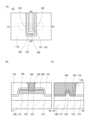
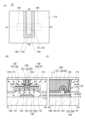
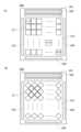
도 1의 (A), 도 1의 (B), 도 1의 (C)는, 본 발명의 일 형태의 트랜지스터(10)의 상면도 및 단면도이다. 도 1의 (A)는 상면도이고, 도 1의 (B)는 도 1의 (A)에 나타낸 일점쇄선 A1-A2간, 도 1의 (C)는 A3-A4간의 단면도이다. 또한, 도 1의 (A)에서는, 도면의 명료화를 위하여 일부의 요소를 확대, 축소, 또는 생략하여 도시하고 있다. 또한, 일점쇄선 A1-A2 방향을 채널 길이 방향, 일점쇄선 A3-A4 방향을 채널 폭 방향이라고 호칭하는 경우가 있다.FIG. 1(A), FIG. 1(B), and FIG. 1(C) are top and cross-sectional views of a
트랜지스터(10)는, 기판(100)과, 절연층(110)과, 산화물 반도체층(121)과, 산화물 반도체층(122)과, 산화물 반도체층(123)과, 소스 전극층(130)과, 드레인 전극층(140)과, 게이트 절연층(150)과, 게이트 전극층(160)과, 절연층(170)과, 절연층(175)을 가진다. 절연층(110)은, 기판(100) 위에 형성된다. 산화물 반도체층(121)은, 절연층(110) 위에 형성된다. 산화물 반도체층(122)은, 산화물 반도체층(121) 위에 형성된다. 소스 전극층(130) 및 드레인 전극층(140)은, 산화물 반도체층(122) 위에 형성되고, 산화물 반도체층(122)과 전기적으로 접속한다. 절연층(170)은, 절연층(110), 소스 전극층(130), 드레인 전극층(140) 위에 형성되고, 산화물 반도체층(121), 산화물 반도체층(122)의 측면과 접촉한다. 절연층(175)은, 절연층(170) 위에 형성되고, 측면부에 있어서 산화물 반도체층(123)과 접촉한다. 산화물 반도체층(123)은, 산화물 반도체층(122) 위에 형성된다. 또한, 산화물 반도체층(123)은 절연층(170)의 측면, 절연층(175)의 측면, 소스 전극층(130)의 측면, 및 드레인 전극층(140)의 측면과 접촉한다. 게이트 절연층(150)은, 산화물 반도체층(123) 위에 형성된다. 게이트 전극층(160)은, 게이트 절연층(150) 위에 형성된다.The
또한, 도 1의 (B)에 있어서, 게이트 전극층(160)은 단층의 예를 도시하였지만 후술하는 게이트 전극층(161) 및 게이트 전극층(162)의 적층이어도 좋다. 트랜지스터(10)에 포함되는 산화물 반도체층(123) 및 게이트 절연층(150)의 단부는, 게이트 전극층(160)보다 외측에 위치한다. 또한, 상술한 구조는, 산화물 반도체층(122) 및 산화물 반도체층(123)과, 소스 전극층(130) 및 드레인 전극층(140)이 접촉하기 때문에, 트랜지스터(10)의 동작 시에 산화물 반도체층(121), 산화물 반도체층(122), 및 산화물 반도체층(123) 내에 발생되는 열에 대하여, 방열 효과가 높은 특징을 가진다.Additionally, in Figure 1(B), the example of the
또한, 트랜지스터(10)는, 절연층(170)이 되는 제 2 절연막을 성막할 때에, 절연층(110)과의 계면에 절연층(110)의 재료와 제 2 절연막의 재료, 또한 제 2 절연막의 성막 시에 사용한 가스 등을 가진 혼합층이 형성되고, 당해 혼합층 또는 절연층(110)에 산소(과잉 산소, exO라고 함)가 첨가된다. 또한, 가열 처리를 행함으로써 당해 산소가 산화물 반도체층(121) 및 산화물 반도체층(122)까지 확산되어, 산화물 반도체층(121), 산화물 반도체층(122) 내에 존재하는 산소 결손에 대하여 당해 산소가 보전할 수 있다. 이에 의하여, 트랜지스터 특성(예를 들어, 문턱 전압, 신뢰성 등)을 향상시킬 수 있다.In addition, when the
또한, 제 2 절연막 성막 시에 첨가되는 당해 과잉 산소는, 예를 들어 스퍼터링법에 의한 성막 시에 인가된 전압, 전력, 플라스마, 또는 기판 온도 등의 영향에 의하여, 산소 라디칼, 산소 이온, 또는 산소 원자 등, 다양한 상태로 존재한다. 이때, 당해 과잉 산소는, 안정적인 상태에 비하여 에너지를 많이 가진 상태이며, 절연층(110) 내에 들어갈 수 있다.In addition, the excess oxygen added during deposition of the second insulating film may be converted into oxygen radicals, oxygen ions, or oxygen due to the influence of voltage, power, plasma, or substrate temperature applied during deposition by the sputtering method, for example. Atoms, etc. exist in various states. At this time, the excess oxygen is in a state with more energy than in a stable state and can enter the insulating
또한, 산소가 첨가되는 방법은, 상기 방법에 한정되지 않고, 절연층(110)은, 성막 시에 당해 과잉 산소를 가져도 좋고, 성막 후에 다른 방법(예를 들어, 이온 주입법, 이온 플라스마 침지법 등)을 사용하여도 좋다.In addition, the method by which oxygen is added is not limited to the above method, and the insulating
트랜지스터(10)는, 도 1의 (C)의 A3-A4 단면도에 도시된 바와 같이, 채널 폭 방향에 있어서, 게이트 전극층(160)은 게이트 절연층(150)을 개재하여 산화물 반도체층(121), 산화물 반도체층(122), 산화물 반도체층(123)의 측면과 대향한다. 즉, 게이트 전극층(160)에 전압이 인가되면, 산화물 반도체층(121), 산화물 반도체층(122), 산화물 반도체층(123)은, 채널 폭 방향에 있어서 게이트 전극층(160)의 전계에 의하여 둘러싸인다. 게이트 전극층(160)의 전계에 의하여 반도체층이 둘러싸이는 트랜지스터의 구조를, surrounded channel(s-channel) 구조라고 부른다. 또한, 트랜지스터(10)는, 홈을 사용하여 셀프 얼라인으로 게이트 전극, 소스 전극, 드레인 전극을 형성할 수 있기 때문에, 위치 맞춤 정밀도가 우수하고, 미세한 트랜지스터를 용이하게 제작할 수 있게 된다. 또한, 이와 같은 구조를 셀프 얼라인 s-channel FET(Self Align s-channel FET, SA s-channel FET) 구조, 또는 트렌치 게이트 s-channel FET(Trench gate s-channel FET), 또는 TGSA FET(Trench Gate Self Align) 구조, 또는 GLSA FET(Gate Last Self Align FET)라고 부른다.In the
여기서, 산화물 반도체층(121)과, 산화물 반도체층(122)과, 산화물 반도체층(123)을 합쳐서 산화물 반도체층(120)으로 한 경우, SA s-channel 구조의 트랜지스터에 있어서, 온 상태에서는 산화물 반도체층(120) 전체(벌크)에 채널이 형성되기 때문에, 온 전류가 증대된다. 한편, 오프 상태의 경우, 산화물 반도체층(120)에 형성되는 채널 영역의 전체 영역을 공핍화하기 때문에, 오프 전류를 더 작게 할 수 있다.Here, when the
이들에 의하여, 홈부(174)에 산화물 반도체층(123), 게이트 절연층(150), 게이트 전극층(160)을 형성할 때에, 각 막의 매립성을 향상시킬 수 있고, 트랜지스터(10)를 용이하게 제작할 수 있다.Due to these, when forming the
또한, 트랜지스터(10)가 TGSA 구조를 가짐으로써, 게이트 전극-소스 전극 간 또는 게이트 전극-드레인 전극 간에서 발생되는 기생 용량이 저감되고, 트랜지스터(10)의 차단 주파수 특성이 향상되는 등, 트랜지스터(10)를 고속 응답시키는 것이 가능해진다.In addition, because the
또한, 소스 전극층(130) 또는 드레인 전극층(140)의 상면의 위치는, 게이트 전극층(160)의 저면의 위치보다 낮아도 좋고, 같아도 좋고, 높아도 좋다.Additionally, the position of the top surface of the
또한, 트랜지스터(10)는, 도 2의 (A)의 홈부(174)가 직선 형상을 가지고 있어도 좋다. 또한, 트랜지스터 도 2의 (B)와 같이 게이트 전극층(160)의 상면이 절연층(175)의 상면보다 아래에 있어도 좋다. 또한, 트랜지스터(10)는, 도 2의 (C)와 같이 절연막(150a) 및 제 3 산화물 반도체막(123a)을 평탄화 처리하지 않아도 된다. 또한, 트랜지스터(10)는, 도 3의 (A)에 도시된 바와 같이, 소스 전극층(130) 및 드레인 전극층의 단부가 산화물 반도체층(122)보다 짧은 형상을 가져도 좋고, 긴 형상을 가져도 좋다.Additionally, in the
<채널 길이에 대하여><About channel length>
또한, 채널 길이란, 예를 들어, 트랜지스터의 상면도에 있어서, 반도체(또는 트랜지스터가 온 상태일 때에 반도체 내에서 전류가 흐르는 부분)와 게이트 전극이 중첩되는 영역, 또는 채널이 형성되는 영역에서의, 소스(소스 영역 또는 소스 전극)와 드레인(드레인 영역 또는 드레인 전극) 사이의 거리를 말한다. 또한, 하나의 트랜지스터에 있어서, 채널 길이가 모든 영역에서 같은 값을 취한다고 할 수는 없다. 즉, 하나의 트랜지스터의 채널 길이는, 하나의 값으로 정해지지 않는 경우가 있다. 그러므로, 본 명세서에서는, 채널 길이는, 채널이 형성되는 영역에서의, 어느 하나의 값, 최대값, 최소값 또는 평균값으로 한다.In addition, the channel length refers to, for example, in the top view of a transistor, the area where the semiconductor (or the part where the current flows in the semiconductor when the transistor is on) and the gate electrode overlap, or the area where the channel is formed. , refers to the distance between the source (source area or source electrode) and the drain (drain area or drain electrode). Additionally, in one transistor, it cannot be said that the channel length takes the same value in all areas. In other words, the channel length of one transistor may not be determined by a single value. Therefore, in this specification, the channel length is defined as any one value, maximum value, minimum value, or average value in the area where the channel is formed.
<채널 폭에 대하여><About channel width>
채널 폭이란, 예를 들어, 반도체(또는 트랜지스터가 온 상태일 때에 반도체 내에서 전류가 흐르는 부분)와 게이트 전극이 중첩되는 영역의 길이를 말한다. 또한, 하나의 트랜지스터에 있어서, 채널 폭이 모든 영역에서 같은 값을 취한다고 할 수는 없다. 즉, 하나의 트랜지스터의 채널 폭은, 하나의 값으로 정해지지 않는 경우가 있다. 그러므로, 본 명세서에서는, 채널 폭은, 채널이 형성되는 영역에서의, 어느 하나의 값, 최대값, 최소값 또는 평균값으로 한다.Channel width refers to, for example, the length of the area where the semiconductor (or the portion where current flows in the semiconductor when the transistor is on) and the gate electrode overlap. Additionally, in one transistor, it cannot be said that the channel width takes the same value in all areas. In other words, the channel width of one transistor may not be set to a single value. Therefore, in this specification, the channel width is defined as one value, maximum value, minimum value, or average value in the area where the channel is formed.
또한, 트랜지스터의 구조에 따라서는, 실제로 채널이 형성되는 영역에서의 채널 폭(이하, 실효적인 채널 폭이라고 부름)과, 트랜지스터의 상면도에 있어서 나타나는 채널 폭(이하, 외관상 채널 폭이라고 부름)이 상이한 경우가 있다. 예를 들어, 입체적인 구조를 가지는 트랜지스터에서는, 실효적인 채널 폭이, 트랜지스터의 상면도에 있어서 나타나는 외관상 채널 폭보다 커지고, 그 영향을 무시할 수 없게 될 경우가 있다. 예를 들어, 미세하고 입체적인 구조를 가지는 트랜지스터에서는, 반도체의 상면에 형성되는 채널 영역의 비율에 대하여, 반도체의 측면에 형성되는 채널 영역의 비율이 커지는 경우가 있다. 그 경우, 상면도에 있어서 나타나는 외관상 채널 폭보다, 실제로 채널이 형성되는 실효적인 채널 폭이 더 커진다.Additionally, depending on the structure of the transistor, the channel width in the area where the channel is actually formed (hereinafter referred to as the effective channel width) and the channel width shown in the top view of the transistor (hereinafter referred to as the apparent channel width) There are different cases. For example, in a transistor with a three-dimensional structure, the effective channel width may be larger than the apparent channel width shown in the top view of the transistor, and the effect may not be negligible. For example, in a transistor with a fine three-dimensional structure, the ratio of the channel area formed on the side surface of the semiconductor may be greater than the ratio of the channel area formed on the top surface of the semiconductor. In that case, the effective channel width where the channel is actually formed becomes larger than the apparent channel width shown in the top view.
그런데, 입체적인 구조를 가지는 트랜지스터에 있어서는, 실효적인 채널 폭의, 실측에 의한 어림잡기가 어려워지는 경우가 있다. 예를 들어, 설계값으로부터 실효적인 채널 폭을 어림잡기 위해서는, 반도체의 형상이 기지(旣知)라는 가정이 필요하다. 따라서, 반도체의 형상을 정확하게 모르는 경우에는, 실효적인 채널 폭을 정확하게 측정하기 어렵다.However, in transistors with a three-dimensional structure, it may be difficult to estimate the effective channel width by actual measurement. For example, in order to estimate the effective channel width from the design value, it is necessary to assume that the shape of the semiconductor is known. Therefore, if the shape of the semiconductor is not accurately known, it is difficult to accurately measure the effective channel width.
<SCW에 대하여><About SCW>
그러므로, 본 명세서에서는, 트랜지스터의 상면도에 있어서, 반도체와 게이트 전극이 중첩되는 영역에서의 외관상 채널 폭을, "둘러싸인 채널 폭(SCW: Surrounded Channel Width)"이라고 부르는 경우가 있다. 또한, 본 명세서에서는, 단순히 채널 폭이라고 기재한 경우에는, 둘러싸인 채널 폭 또는 외관상 채널 폭을 가리키는 경우가 있다. 또는, 본 명세서에서는, 단순히 채널 폭이라고 기재한 경우에는, 실효적인 채널 폭을 가리키는 경우가 있다. 또한, 채널 길이, 채널 폭, 실효적인 채널 폭, 외관상 채널 폭, 둘러싸인 채널 폭 등은, 단면 TEM 이미지 등을 취득하고, 그 화상을 해석하는 것 등에 의하여, 값을 결정할 수 있다.Therefore, in this specification, the apparent channel width in the area where the semiconductor and the gate electrode overlap in the top view of the transistor is sometimes referred to as “surrounded channel width (SCW).” Additionally, in this specification, when simply referring to a channel width, it may refer to an enclosed channel width or an apparent channel width. Alternatively, in this specification, when simply referring to a channel width, the effective channel width may be indicated. Additionally, the values of channel length, channel width, effective channel width, apparent channel width, enclosed channel width, etc. can be determined by acquiring a cross-sectional TEM image or the like and analyzing the image.
또한, 트랜지스터의 전계 효과 이동도나, 채널 폭당 전류값 등을 계산하여 구하는 경우, 둘러싸인 채널 폭을 사용하여 계산하는 경우가 있다. 그 경우에는, 실효적인 채널 폭을 사용하여 계산하는 경우와는 상이한 값을 취하는 경우가 있다.In addition, when calculating the field effect mobility of a transistor, the current value per channel width, etc., the calculation may be done using the surrounded channel width. In that case, it may take a different value than when calculating using the effective channel width.
<미세화에 있어서의 특성 향상><Improvement of characteristics in miniaturization>
반도체 장치를 고집적화하기 위해서는 트랜지스터의 미세화가 필수적이다. 한편, 트랜지스터의 미세화에 따라 트랜지스터의 전기 특성이 악화되는 것이 알려져 있고, 채널 폭이 축소되면 온 전류가 저하된다.In order to highly integrate semiconductor devices, miniaturization of transistors is essential. On the other hand, it is known that the electrical characteristics of the transistor deteriorate as the transistor becomes smaller, and the on-state current decreases when the channel width is reduced.
예를 들어, 도 1에 도시된 본 발명의 일 형태의 트랜지스터에서는, 상술한 바와 같이, 채널이 형성되는 산화물 반도체층(122)을 덮도록 제 3 산화물 반도체층(123)이 형성되어 있고, 채널 형성층과 게이트 절연층이 접촉하지 않는 구성이 되어 있다. 그러므로, 채널 형성층과 게이트 절연층의 계면에서 일어나는 캐리어의 산란을 억제할 수 있고, 트랜지스터의 온 전류를 크게 할 수 있다.For example, in the transistor of one form of the present invention shown in FIG. 1, as described above, the third
또한, 본 발명의 일 형태의 트랜지스터에서는, 채널이 되는 산화물 반도체층(122)의 채널 폭 방향을 전기적으로 둘러싸도록 게이트 전극층(160)이 형성되어 있기 때문에, 산화물 반도체층(1223)에 대해서는 수직 방향으로부터의 게이트 전계에 더하여, 측면 방향으로부터의 게이트 전계가 인가된다. 즉, 산화물 반도체층 전체에 게이트 전계가 인가되고, 전류는 산화물 반도체층(122) 전체에 흐르게 되기 때문에, 온 전류를 더 높일 수 있다.In addition, in the transistor of one embodiment of the present invention, the
또한, 본 발명의 일 형태의 트랜지스터는, 산화물 반도체층(123)을 산화물 반도체층(121), 산화물 반도체층(122) 위에 형성함으로써 계면 준위가 형성되기 어렵게 하는 효과나, 산화물 반도체층(122)을 중간에 위치하는 층으로 함으로써 상하에서의 불순물 혼입의 영향을 배제할 수 있는 효과 등을 겸비한다. 그러므로, 상술한 트랜지스터의 온 전류의 향상에 더하여, 문턱 전압의 안정화나, S값(서브스레숄드 값)을 작게 할 수 있다. 따라서, Icut(게이트 전압(VG)이 0V 시의 전류)를 낮출 수 있고, 소비전력을 저감할 수 있다. 또한, 트랜지스터의 문턱 전압이 안정화되기 때문에, 반도체 장치의 장기 신뢰성을 향상시킬 수 있다.In addition, the transistor of one form of the present invention has the effect of making it difficult to form an interface state by forming the
또한, 본 실시형태에 있어서, 채널 등에 있어서, 산화물 반도체층(120) 등을 사용한 경우의 예를 나타내었지만, 본 발명의 실시형태의 일 형태는, 이에 한정되지 않는다. 예를 들어, 채널이나 그 근방, 소스 영역, 드레인 영역 등을, 경우에 따라서는, 또는 상황에 따라서, 실리콘(변형 실리콘을 포함함), 저마늄, 실리콘 저마늄, 탄소화 실리콘, 갈륨 비소, 알루미늄 갈륨 비소, 인듐 인, 질화 갈륨, 유기 반도체 등을 가지는 재료로 형성하여도 좋다.In addition, in the present embodiment, an example of using the oxide semiconductor layer 120 or the like in a channel or the like has been shown, but one embodiment of the present invention is not limited to this. For example, in a channel or its vicinity, a source region, a drain region, etc., depending on the case or situation, silicon (including strained silicon), germanium, silicon germanium, silicon carbide, gallium arsenide, etc. It may be formed of a material containing aluminum gallium arsenide, indium phosphorus, gallium nitride, organic semiconductor, etc.
<트랜지스터의 구성><Configuration of transistor>
이하에서 본 실시형태의 트랜지스터의 구성에 대하여 나타낸다.The structure of the transistor of this embodiment is shown below.
<<기판(100)>><<Substrate (100)>>
기판(100)에는, 예를 들어, 유리 기판, 세라믹 기판, 석영 기판, 사파이어 기판 등을 사용할 수 있다. 또한, 실리콘이나 탄소화 실리콘으로 이루어지는 단결정 반도체 기판, 다결정 반도체 기판, 실리콘 저마늄으로 이루어지는 화합물 반도체 기판, SOI(Semiconductor On Insulator) 기판 등을 사용하는 것도 가능하며, 이들 기판 위에 반도체 소자가 제공된 것을 사용하여도 좋다. 기판(100)은, 단순한 지지 재료에 한정되지 않고, 다른 트랜지스터 등의 디바이스가 형성된 기판이어도 좋다. 이 경우, 트랜지스터의 게이트 전극층(160), 소스 전극층(130), 및 드레인 전극층(140) 중 하나는, 상기 다른 디바이스와 전기적으로 접속되어 있어도 좋다.For the
또한, 기판(100)으로서, 가요성 기판을 사용하여도 좋다. 또한, 가요성 기판 위에 트랜지스터를 제공하는 방법으로서는, 비가요성의 기판 위에 트랜지스터를 제작한 후, 트랜지스터를 박리하여, 가요성 기판인 기판(100)으로 전치하는 방법도 있다. 그 경우에는, 비가요성 기판과 트랜지스터 사이에 박리층을 제공하면 좋다. 또한, 기판(100)으로서, 섬유를 짠 시트, 필름 또는 박(箔) 등을 사용하여도 좋다. 또한, 기판(100)이 신축성을 가져도 좋다. 또한, 기판(100)은, 구부림이나 잡아당김을 멈췄을 때에, 원래의 형상으로 되돌아가는 성질을 가져도 좋다. 또는, 원래의 형상으로 되돌아가지 않는 성질을 가져도 좋다. 기판(100)의 두께는, 예를 들어, 5μm 이상 700μm 이하, 바람직하게는 10μm 이상 500μm 이하, 더 바람직하게는 15μm 이상 300μm 이하로 한다. 기판(100)을 얇게 하면, 반도체 장치를 경량화할 수 있다. 또한, 기판(100)을 얇게 함으로써, 유리 등을 사용한 경우에도 신축성을 가지는 경우나, 구부림이나 잡아당김을 멈췄을 때에, 원래의 형상으로 되돌아가는 성질을 가지는 경우가 있다. 그러므로, 낙하 등에 의하여 기판(100) 위의 반도체 장치에 가해지는 충격 등을 완화할 수 있다. 즉, 튼튼한 반도체 장치를 제공할 수 있다.Additionally, as the
가요성 기판인 기판(100)으로서는, 예를 들어, 금속, 합금, 수지 또는 유리, 또는 그들의 섬유 등을 사용할 수 있다. 가요성 기판인 기판(100)은, 선팽창률이 낮을수록 환경에 기인한 변형이 억제되므로 바람직하다. 가요성 기판인 기판(100)으로서는, 예를 들어, 선팽창률이 1×10⁻³/K 이하, 5×10⁻⁵/K 이하, 또는 1×10⁻⁵/K 이하인 재질을 사용하면 좋다. 수지로서는, 예를 들어, 폴리에스터, 폴리올레핀, 폴리아마이드(나일론, 아라미드 등), 폴리이미드, 폴리카보네이트, 아크릴, 폴리테트라플루오로에틸렌(PTFE) 등이 있다. 특히, 아라미드는, 선팽창률이 낮기 때문에, 가요성 기판인 기판(100)으로서 적합하다.As the
<<절연층(110)>><<insulating layer (110)>>
절연층(110)은, 기판(100)으로부터의 불순물의 확산을 방지하는 역할을 가지는 외에, 산화물 반도체층(120)에 산소를 공급하는 역할을 할 수 있다. 따라서, 절연층(110)은 산소를 포함하는 절연막인 것이 바람직하고, 화학량론 조성보다 많은 산소를 포함하는 절연막인 것이 더 바람직하다. 예를 들어, TDS법에서, 산소 원자로 환산한 산소 방출량이 1.0×10¹⁹atoms/cm3 이상인 막으로 한다. 또한, 상기 TDS 분석 시에서의 막의 표면 온도로서는 100 이상 700 이하, 또는 100 이상 500 이하의 범위가 바람직하다. 또한, 상술한 바와 같이 기판(100)이 다른 디바이스가 형성된 기판인 경우, 절연층(110)은, 층간 절연막으로서의 기능도 가진다. 그 경우에는, 표면이 평탄해지도록 CMP(Chemical Mechanical Polishing)법 등으로 평탄화 처리를 행하는 것이 바람직하다.In addition to preventing diffusion of impurities from the
<<산화물 반도체층(121, 122, 123)>><<Oxide semiconductor layer (121, 122, 123)>>
산화물 반도체층(122)은, In 또는 Zn을 포함하는 산화물 반도체막이며, 대표적으로는, In-Ga 산화물, In-Zn 산화물, In-Mg 산화물, Zn-Mg 산화물, In-M-Zn 산화물(M은 Al, Ti, Ga, Y, Zr, Sn, La, Ce, Mg, 또는 Nd)이 있다.The
산화물 반도체층(121), 산화물 반도체층(122), 및 산화물 반도체층(123)으로서 사용할 수 있는 산화물 반도체는, 적어도 인듐(In) 또는 아연(Zn)을 포함하는 것이 바람직하다. 또는, In과 Zn의 모두를 포함하는 것이 바람직하다. 또한, 당해 산화물 반도체를 사용한 트랜지스터의 전기 특성의 편차를 줄이기 위하여, 그들과 함께, 스태빌라이저를 포함하는 것이 바람직하다.The oxide semiconductors that can be used as the
스태빌라이저로서는, 갈륨(Ga), 주석(Sn), 하프늄(Hf), 알루미늄(Al), 또는 지르코늄(Zr) 등이 있다. 또한, 다른 스태빌라이저로서는, 란타노이드인, 란타넘(La), 세륨(Ce), 프라세오디뮴(Pr), 네오디뮴(Nd), 사마륨(Sm), 유로퓸(Eu), 가돌리늄(Gd), 터븀(Tb), 디스프로슘(Dy), 홀뮴(Ho), 어븀(Er), 툴륨(Tm), 이터븀(Yb), 루테튬(Lu) 등이 있다.Stabilizers include gallium (Ga), tin (Sn), hafnium (Hf), aluminum (Al), or zirconium (Zr). In addition, other stabilizers include lanthanum (La), cerium (Ce), praseodymium (Pr), neodymium (Nd), samarium (Sm), europium (Eu), gadolinium (Gd), and terbium (Tb). , dysprosium (Dy), holmium (Ho), erbium (Er), thulium (Tm), ytterbium (Yb), and lutetium (Lu).
또한, 산화물 반도체층(123)이 In-M-Zn 산화물일 때, In과 M의 원자의 비율은, 바람직하게는, In이 25atomic% 이상, M이 75atomic% 미만, 더 바람직하게는, In이 34atomic% 이상, M이 66atomic% 미만으로 한다.In addition, when the
산화물 반도체층(123) 내의 인듐이나 갈륨 등의 함유량은, 비행 시간형 이차 이온 질량 분석법(TOF-SIMS)이나, X선 전자 분광법(XPS), ICP 질량 분석(ICP-MS)에 의하여 비교할 수 있다.The content of indium, gallium, etc. in the
산화물 반도체층(122)은, 에너지 갭이 2eV 이상, 바람직하게는 2.5eV 이상, 더 바람직하게는 3eV 이상이기 때문에, 트랜지스터(10)의 오프 전류를 저감할 수 있다.Since the
산화물 반도체층(122)의 두께는, 3nm 이상 200nm 이하, 바람직하게는 3nm 이상 100nm 이하, 더 바람직하게는 3nm 이상 50nm 이하로 한다.The thickness of the
산화물 반도체층(121) 및 산화물 반도체층(123)은, 산화물 반도체층(122)을 구성하는 원소 중 1종류 이상으로 구성되는 산화물 반도체막이다. 이 때문에, 산화물 반도체층(122)과 산화물 반도체층(122) 및 산화물 반도체층(124)의 계면에 있어서, 계면 산란이 일어나기 어렵다. 따라서, 당해 계면에 있어서는 캐리어의 움직임이 저해되지 않기 때문에, 트랜지스터(10)의 전계 효과 이동도가 높아진다.The
산화물 반도체층(121), 산화물 반도체층(123)은, 대표적으로는, In-Ga 산화물, In-Zn 산화물, In-Mg 산화물, Ga-Zn 산화물, Zn-Mg 산화물, In-M-Zn 산화물(M은 Al, Ti, Ga, Y, Zr, Sn, La, Ce, Mg, 또는 Nd)이고, 또한 산화물 반도체층(122)보다 전도대 하단의 에너지 준위가 진공 준위에 가깝고, 대표적으로는, 산화물 반도체층(121), 산화물 반도체층(123)의 전도대 하단의 에너지와, 산화물 반도체층(122)의 전도대 하단의 에너지의 차가, 0.05eV 이상, 0.07eV 이상, 0.1eV 이상, 또는 0.2eV 이상이고 2eV 이하, 1eV 이하, 0.5eV 이하, 또는 0.4eV 이하이다. 즉, 산화물 반도체층(121), 산화물 반도체층(123)의 전자 친화력과, 산화물 반도체층(122)의 전자 친화력의 차가, 0.05eV 이상, 0.07eV 이상, 0.1eV 이상, 또는 0.2eV 이상이고 2eV 이하, 1eV 이하, 0.5eV 이하, 또는 0.4eV 이하이다. 또한, 전자 친화력은, 진공 준위와 전도대 하단의 에너지의 차를 가리킨다.The
산화물 반도체층(121), 산화물 반도체층(123)으로서, Al, Ti, Ga, Y, Zr, Sn, La, Ce, Mg, 또는 Nd를, In보다 높은 원자수비로 가짐으로써, 이하의 효과를 가지는 경우가 있다. (1) 산화물 반도체층(121), 산화물 반도체층(122) 및 산화물 반도체층(124)의 에너지 갭을 크게 한다. (2) 산화물 반도체층(121), 산화물 반도체층(123)의 전자 친화력을 작게 한다. (3) 외부로부터의 불순물을 차폐한다. (4) 산화물 반도체층(122)과 비교하여, 절연성이 높아진다. (5) Al, Ti, Ga, Y, Zr, Sn, La, Ce, Mg, 또는 Nd는, 산소와의 결합력이 센 금속 원소이기 때문에, Al, Ti, Ga, Y, Zr, Sn, La, Ce, Mg, 또는 Nd를 In보다 높은 원자수비로 가짐으로써, 산소 결손이 발생되기 어려워진다.By having Al, Ti, Ga, Y, Zr, Sn, La, Ce, Mg, or Nd at a higher atomic ratio than In as the
또한, 산화물 반도체층(121), 산화물 반도체층(123)은, 산화물 반도체층(122)과 비교하여 절연성이 높기 때문에, 게이트 절연층과 마찬가지의 기능을 가진다.Additionally, since the
산화물 반도체층(121), 산화물 반도체층(123)이 In-M-Zn 산화물일 때, Zn 및 O를 제외한 In 및 M의 원자수비율은, 바람직하게는, In이 50atomic% 이하, M이 50atomic% 이상, 더 바람직하게는, In이 25atomic% 이하, M이 75atomic% 이상으로 한다.When the
또한, 산화물 반도체층(121), 산화물 반도체층(123)이 In-M-Zn 산화물(M은Al, Ti, Ga, Y, Zr, Sn, La, Ce, Mg, 또는 Nd)의 경우, 산화물 반도체층(122)과 비교하여, 산화물 반도체층(121), 산화물 반도체층(123)에 포함되는 M(Al, Ti, Ga, Y, Zr, Sn, La, Ce, Mg, 또는 Nd)의 원자수비가 높고, 대표적으로는, 산화물 반도체층(123)에 포함되는 상기 원자와 비교하여, 1.5배 이상, 바람직하게는 2배 이상, 더 바람직하게는 3배 이상 높은 원자수비이다. 상술한 M으로 나타낸 원소는 인듐보다 산소와 세게 결합되기 때문에, 산소 결손이 산화물 반도체층(121), 산화물 반도체층(123)에 발생되는 것을 억제하는 기능을 가진다. 즉, 산화물 반도체층(121), 산화물 반도체층(123)은 산화물 반도체층(122)보다 산소 결손이 발생되기 어려운 산화물 반도체막이다.In addition, when the
또한, 산화물 반도체층(122)은, 산화물 반도체층(121), 산화물 반도체층(123)보다 인듐의 함유량을 많게 하면 좋다. 산화물 반도체에서는 주로 중금속의 s궤도가 캐리어 전도에 기여하고 있고, In의 함유율을 많게 하는 것에 의하여, 더 많은 s궤도가 중첩되기 때문에, In이 M보다 많은 조성이 되는 산화물은 In이 M과 동등하거나 또는 적은 조성이 되는 산화물과 비교하여 이동도가 높아진다. 그러므로, 산화물 반도체층(122)에 인듐의 함유량이 많은 산화물을 사용함으로써, 높은 전계 효과 이동도의 트랜지스터를 실현할 수 있다.Additionally, the
또한, 산화물 반도체층(122)이 In-M-Zn 산화물(M은, Al, Ti, Ga, Y, Zr, Sn, La, Ce, Mg, 또는 Nd)의 경우, 산화물 반도체층(122)을 성막하기 위하여 사용하는 타깃에 있어서, 금속 원소의 원자수비를 In:M:Zn=x1:y1:z1로 하면, x1/y1은, 1/3 이상 6 이하, 나아가서는 1 이상 6 이하이고, z1/y1은, 1/3 이상 6 이하, 나아가서는 1 이상 6 이하인 것이 바람직하다. 또한, z1/y1을 1 이상 6 이하로 함으로써, 산화물 반도체층(122)으로서 CAAC-OS(C Axis Aligned Crystalline Oxide Semiconductor)막이 형성되기 쉬워진다. 타깃의 금속 원소의 원자수비의 대표적인 예로서는, In:M:Zn=1:1:1, In:M:Zn=1:1:1.2, 2:1:1.5, 2:1:2.3, 2:1:3, 3:1:2, 4:2:3, 4:2:4.1 등이 있다.In addition, if the
또한, 산화물 반도체층(121), 산화물 반도체층(123)이 In-M-Zn 산화물(M은, Al, Ti, Ga, Y, Zr, Sn, La, Ce, Mg, 또는 Nd)의 경우, 산화물 반도체층(121), 산화물 반도체층(123)을 성막하기 위하여 사용하는 타깃에 있어서, 금속 원소의 원자수비를 In:M:Zn=x2:y2:z2로 하면, x2/y2<x1/y1이고, z2/y2는, 1/3 이상 6 이하, 나아가서는 1 이상 6 이하인 것이 바람직하다. 또한, z2/y2를 1 이상 6 이하로 함으로써, 산화물 반도체층(121), 산화물 반도체층(123)으로서 CAAC-OS막이 형성되기 쉬워진다. 타깃의 금속 원소의 원자수비의 대표적인 예로서는, In:M:Zn=1:3:2, 1:3:4, 1:3:6, 1:3:8, 1:4:4, 1:4:5, 1:4:6, 1:4:7, 1:4:8, 1:5:5, 1:5:6, 1:5:7, 1:5:8, 1:6:8, 1:6:4, 1:9:6 등이 있다.In addition, if the
또한, 산화물 반도체층(121), 산화물 반도체층(123)의 원자수비는 각각, 오차로서 상기 원자수비의 ±40%의 변동을 포함한다.In addition, the atomic ratios of the
또한, 산화물 반도체층(123)은, 금속 산화물, 예를 들어 산화 알루미늄(AlOx), 산화 갈륨(GaOx), 산화 하프늄(HfOx), 산화 실리콘(SiOx), 산화 저마늄(GeOx), 또는 산화 지르코니아(ZrOx)로 치환하는 것도 가능하고, 산화물 반도체층(123) 위에 당해 금속 산화물을 가질 수도 있다.Additionally, the
또한, 원자수비는 이들에 한정되지 않고, 필요로 하는 반도체 특성에 따라 적절한 원자수비의 것을 사용하면 좋다.Additionally, the atomic ratio is not limited to these, and an appropriate atomic ratio may be used depending on the required semiconductor properties.
또한, 산화물 반도체층(121), 산화물 반도체층(123)은 같은 조성이어도 좋다. 예를 들어, 산화물 반도체층(121), 산화물 반도체층(123)으로서, 스퍼터링법에서 사용하는 타깃의 금속 원소의 원자수비가 In:Ga:Zn=1:3:2, 1:3:4, 또는 1:4:5인In-Ga-Zn 산화물을 사용하여도 좋다.Additionally, the
또는, 산화물 반도체층(121), 산화물 반도체층(123)은 상이한 조성이어도 좋다. 예를 들어, 산화물 반도체층(121)으로서, 스퍼터링법에서 사용하는 타깃의 금속 원소의 원자수비가 In:Ga:Zn=1:3:4의 In-Ga-Zn 산화물을 사용하고, 산화물 반도체층(123)으로서 타깃의 금속 원소의 원자수비가 In:Ga:Zn=1:3:2의 In-Ga-Zn 산화물을 사용하여도 좋다.Alternatively, the
산화물 반도체층(121), 산화물 반도체층(122), 및 산화물 반도체층(123)의 두께는, 3nm 이상 100nm 이하, 또는 3nm 이상 50nm 이하로 하는 것이 바람직하다.The thickness of the
여기서, 산화물 반도체층(122)의 두께는, 적어도 산화물 반도체층(121)과 비교하여, 얇게 형성하여도 좋고, 같게 하여도 좋고, 두껍게 형성하여도 좋다. 예를 들어, 산화물 반도체층(122)을 두껍게 한 경우, 트랜지스터의 온 전류를 높일 수 있다. 또한, 산화물 반도체층(121)은, 산화물 반도체층(122)의 계면 준위의 생성을 억제하는 효과가 상실되지 않을 정도의 두께라면 좋다. 예를 들어, 산화물 반도체층(122)의 두께는, 산화물 반도체층(121)의 두께에 대하여, 1배보다 크게, 또는 2배 이상, 또는 4배 이상, 또는 6배 이상으로 할 수 있다. 또한, 트랜지스터의 온 전류를 높일 필요가 없는 경우에는 산화물 반도체층(121)의 두께를 산화물 반도체층(122)의 두께 이상으로 하여도 좋다. 예를 들어, 절연층(110) 또는 절연층(175)이 산소를 과잉으로 가진 경우, 가열 처리에 의하여, 당해 산소가 확산되어, 산화물 반도체층(122)에 포함되는 산소 결손량을 저감할 수 있고, 반도체 장치의 전기 특성을 안정시킬 수 있다.Here, the thickness of the
또한, 산화물 반도체층(123)도 산화물 반도체층(121)과 마찬가지로, 산화물 반도체층(122)의 계면 준위의 생성을 억제하는 효과가 상실되지 않을 정도의 두께라면 좋다. 예를 들어, 산화물 반도체층(121)과 동등하거나 또는 그 이하의 두께로 하면 좋다. 산화물 반도체층(123)이 두꺼우면, 게이트 전극층(160)(또는, 게이트 전극층(161), 게이트 전극층(162))에 의한 전계가 산화물 반도체층(122)에 전달되기 어려워질 우려가 있으므로, 산화물 반도체층(123)은 얇게 형성하는 것이 바람직하다. 예를 들어, 산화물 반도체층(123)은 산화물 반도체층(122)의 두께보다 얇게 하면 좋다. 또한, 이에 한정되지 않고, 산화물 반도체층(123)의 두께는 게이트 절연층(150)의 내압을 고려하여, 트랜지스터를 구동시키는 전압에 따라 적절히 설정하면 좋다.Additionally, like the
산화물 반도체층(121), 산화물 반도체층(122), 및 산화물 반도체층(123) 각각의 조성이 상이한 경우, 계면은, 주사형 투과 전자 현미경 STEM(Scanning Transmission Electron Microscope)을 사용하여 관찰할 수 있는 경우가 있다.When the compositions of the
<수소 농도에 대하여><About hydrogen concentration>
산화물 반도체층(121), 산화물 반도체층(122), 및 산화물 반도체층(123)에 포함되는 수소는, 금속 원자와 결합하는 산소와 반응하여 물이 됨과 함께, 산소가 이탈된 격자(또는 산소가 이탈된 부분)에 산소 결손을 형성한다. 당해 산소 결손에 수소가 들어감으로써, 캐리어인 전자가 생성되는 경우가 있다. 또한, 수소의 일부가 금속 원자와 결합하는 산소와 결합함으로써, 캐리어인 전자를 생성하는 경우가 있다. 따라서, 수소가 포함되어 있는 산화물 반도체를 사용한 트랜지스터는 노멀리 온 특성이 되기 쉽다.The hydrogen contained in the
이 때문에, 산화물 반도체층(121), 산화물 반도체층(122), 산화물 반도체층(123), 및 각각의 계면에 있어서, 산소 결손과 함께, 수소가 가능한 한 저감되어 있는 것이 바람직하다. 예를 들어, 산화물 반도체층(121), 산화물 반도체층(122), 산화물 반도체층(123), 및 각각의 계면에 있어서 이차 이온 질량 분석법(SIMS: Secondary Ion Mass Spectrometry)에 의하여 얻어지는 수소 농도는, 1×10¹⁶atoms/cm3 이상 2×10²⁰atoms/cm3 이하, 바람직하게는 1×10¹⁶atoms/cm3 이상 5×10¹⁹atoms/cm3 이하, 더 바람직하게는 1×10¹⁶atoms/cm3 이상 1×10¹⁹atoms/cm3 이하, 더 바람직하게는 1×10¹⁶atoms/cm3 이상 5×10¹⁸atoms/cm3 이하로 하는 것이 바람직하다. 이 결과, 트랜지스터(10)는, 문턱 전압이 양이 되는 전기 특성(노멀리 오프 특성이라고도 함)을 가질 수 있다.For this reason, it is desirable that hydrogen as well as oxygen vacancies be reduced as much as possible in the
<탄소, 실리콘 농도에 대하여><About carbon and silicon concentration>
또한, 산화물 반도체층(121), 산화물 반도체층(122), 산화물 반도체층(123), 및 각각의 계면에 있어서, 제 14족 원소 중 하나인 실리콘이나 탄소가 포함되면, 산화물 반도체층(121), 산화물 반도체층(122), 및 산화물 반도체층(123)에 있어서 산소 결손이 증가되어, n형 영역이 형성된다. 이 때문에, 산화물 반도체층(121), 산화물 반도체층(122), 산화물 반도체층(123), 및 각각의 계면에서의 실리콘, 및 탄소 농도는, 저감하는 것이 바람직하다. 예를 들어, 산화물 반도체층(121), 산화물 반도체층(122), 산화물 반도체층(123), 산화물 반도체층(124), 및 각각의 계면에 있어서 SIMS에 의하여 얻어지는 실리콘이나 탄소의 농도는, 1×10¹⁶atoms/cm3 이상 1×10¹⁹atoms/cm3 이하, 바람직하게는 1×10¹⁶atoms/cm3 이상 5×10¹⁸atoms/cm3 이하, 더 바람직하게는 1×10¹⁶atoms/cm3 이상 2×10¹⁸atoms/cm3 이하로 하는 것이 바람직하다. 이 결과, 트랜지스터(10)는, 문턱 전압이 양이 되는 전기 특성(노멀리 오프 특성이라고도 함)을 가진다.In addition, in the
<알칼리 금속의 농도에 대하여><About the concentration of alkali metal>
또한, 알칼리 금속 및 알칼리 토금속은, 산화물 반도체와 결합하면 캐리어를 생성하는 경우가 있고, 트랜지스터의 오프 전류가 증대되는 경우가 있다. 이 때문에, 산화물 반도체층(121), 산화물 반도체층(122), 산화물 반도체층(123), 및 각각의 계면에서의 알칼리 금속 또는 알칼리 토금속의 농도를 저감하는 것이 바람직하다. 예를 들어, 산화물 반도체층(121), 산화물 반도체층(122), 산화물 반도체층(123), 및 각각의 계면에 있어서, 이차 이온 질량 분석법에 의하여 얻어지는 알칼리 금속 또는 알칼리 토금속의 농도를, 1×10¹⁸atoms/cm3 이하, 바람직하게는 2×10¹⁶atoms/cm3 이하로 하는 것이 바람직하다. 이에 의하여, 트랜지스터(10)는, 문턱 전압이 양이 되는 전기 특성(노멀리 오프 특성이라고도 함)을 가질 수 있다.Additionally, alkali metals and alkaline earth metals may generate carriers when combined with an oxide semiconductor, and the off-state current of the transistor may increase. For this reason, it is desirable to reduce the concentration of alkali metal or alkaline earth metal in the
<질소 농도에 대하여><About nitrogen concentration>
또한, 산화물 반도체층(121), 산화물 반도체층(122), 산화물 반도체층(123), 및 각각의 계면에 질소가 포함되어 있으면, 캐리어인 전자가 발생되고, 캐리어 밀도가 증가되어, n형 영역이 형성된다. 이 결과, 질소가 포함되어 있는 산화물 반도체를 사용한 트랜지스터는 노멀리 온 특성이 되기 쉽다. 따라서, 산화물 반도체층(121), 산화물 반도체층(122), 산화물 반도체층(123) 및 각각의 계면에 있어서, 질소는 가능한 한 저감되어 있는 것이 바람직하고, 예를 들어, 산화물 반도체층(121), 산화물 반도체층(122), 산화물 반도체층(123), 및 각각의 계면에 있어서 SIMS에 의하여 얻어지는 질소 농도는, 1×10¹⁵atoms/cm3 이상 5×10¹⁹atoms/cm3 이하, 바람직하게는 1×10¹⁵atoms/cm3 이상 5×10¹⁸atoms/cm3 이하, 더 바람직하게는 1×10¹⁵atoms/cm3 이상 1×10¹⁸atoms/cm3 이하, 더 바람직하게는 1×10¹⁵atoms/cm3 이상 5×10¹⁷atoms/cm3 이하로 하는 것이 바람직하다. 이에 의하여, 트랜지스터(10)는, 문턱 전압이 양이 되는 전기 특성(노멀리 오프 특성이라고도 함)을 가질 수 있다.In addition, if nitrogen is included in the
<캐리어 밀도에 대하여><About carrier density>
산화물 반도체층(121), 산화물 반도체층(122), 및 산화물 반도체층(123)의 불순물을 저감함으로써, 산화물 반도체층(121), 산화물 반도체층(122), 및 산화물 반도체층(123)의 캐리어 밀도를 저감할 수 있다. 이 때문에, 산화물 반도체층(121), 산화물 반도체층(122), 및 산화물 반도체층(123)은, 캐리어 밀도가 1×10¹⁵개/cm3 이하, 바람직하게는 1×10¹³개/cm3 이하, 더 바람직하게는 8×10¹¹개/cm3 미만, 더 바람직하게는 1×10¹¹개/cm3 미만, 가장 바람직하게는 1×10¹⁰개/cm3 미만이고, 1×10⁻⁹개/cm3 이상으로 한다.By reducing the impurities in the
산화물 반도체층(121), 산화물 반도체층(122), 및 산화물 반도체층(123)으로서, 불순물 농도가 낮고, 결함 준위 밀도가 낮은 산화물 반도체막을 사용함으로써, 더 우수한 전기 특성을 가지는 트랜지스터를 제작할 수 있다. 여기서는, 불순물 농도가 낮고, 결함 준위 밀도가 낮은(산소 결손이 적은) 것을 고순도 진성 또는 실질적으로 고순도 진성이라고 부른다. 고순도 진성 또는 실질적으로 고순도 진성인 산화물 반도체는, 캐리어 발생원이 적기 때문에, 캐리어 밀도를 낮게 할 수 있는 경우가 있다. 따라서, 당해 산화물 반도체막에 채널 영역이 형성되는 트랜지스터는, 문턱 전압이 양이 되는 전기 특성(노멀리 오프 특성이라고도 함)이 되기 쉽다. 또한, 고순도 진성 또는 실질적으로 고순도 진성인 산화물 반도체막은, 결함 준위 밀도가 낮기 때문에, 트랩 준위 밀도도 낮아지는 경우가 있다. 또한, 고순도 진성 또는 실질적으로 고순도 진성인 산화물 반도체막은, 오프 전류가 현저히 작고, 소스 전극과 드레인 전극 사이의 전압(드레인 전압)이 1V에서 10V의 범위에 있어서, 오프 전류가, 반도체 파라미터 애널라이저의 측정 한계 이하, 즉 1×10-13A 이하라는 특성을 얻을 수 있다. 따라서, 당해 산화물 반도체막에 채널 영역이 형성되는 트랜지스터는, 전기 특성의 변동이 작고, 신뢰성이 높은 트랜지스터가 되는 경우가 있다.By using oxide semiconductor films with low impurity concentration and low defect level density as the
또한, 상술한 바와 같이 고순도화된 산화물 반도체막을 채널 형성 영역에 사용한 트랜지스터의 오프 전류는 매우 작다. 예를 들어, 소스와 드레인 사이의 전압을 0.1V, 5V, 또는 10V정도로 한 경우에, 트랜지스터의 채널 폭으로 정규화한 오프 전류를 수yA/μm 내지 수zA/μm까지 저감하는 것이 가능해진다.Additionally, as described above, the off-state current of a transistor using a highly purified oxide semiconductor film in the channel formation region is very small. For example, when the voltage between the source and drain is set to about 0.1 V, 5 V, or 10 V, it is possible to reduce the off current normalized by the channel width of the transistor to several yA/μm to several zA/μm.
산화물 반도체층(121), 산화물 반도체층(122), 및 산화물 반도체층(123)은, 예를 들어 비단결정 구조이어도 좋다. 비단결정 구조는, 예를 들어, 후술하는 CAAC-OS, 다결정 구조, 미결정(microcrystalline) 구조, 또는 비정질 구조를 포함한다. 비단결정 구조에 있어서, 비정질 구조는 가장 결함 준위 밀도가 높고, CAAC-OS는 가장 결함 준위 밀도가 낮다.The
산화물 반도체층(121), 산화물 반도체층(122), 및 산화물 반도체층(123)은, 예를 들어 미결정 구조이어도 좋다. 미결정 구조의 산화물 반도체층(121), 산화물 반도체층(122), 및 산화물 반도체층(123)은, 예를 들어, 1nm 이상 10nm 미만의 사이즈의 미결정을 막 내에 포함한다. 또는, 미결정 구조의 산화물막 및 산화물 반도체막은, 예를 들어 비정질상에 1nm 이상 10nm 미만의 결정부를 가지는 혼상 구조이다.The
산화물 반도체층(121), 산화물 반도체층(122), 및 산화물 반도체층(123)은, 예를 들어 비정질 구조이어도 좋다. 비정질 구조의 산화물 반도체층(121), 산화물 반도체층(122), 및 산화물 반도체층(123)은, 예를 들어, 원자 배열이 무질서하며, 결정 성분을 가지지 않는다. 또는, 비정질 구조의 산화물막은, 예를 들어, 완전한 비정질 구조이며, 결정부를 가지지 않는다.The
또한, 산화물 반도체층(121), 산화물 반도체층(122), 및 산화물 반도체층(123)이, CAAC-OS, 미결정 구조, 및 비정질 구조 중 2개 이상의 구조의 영역을 가지는 혼합막이어도 좋다. 혼합막으로서, 예를 들어, 비정질 구조의 영역과, 미결정 구조의 영역과, CAAC-OS의 영역을 가지는 단층 구조가 있다. 또는, 혼합막으로서, 예를 들어, 비정질 구조의 영역과, 미결정 구조의 영역과, CAAC-OS의 영역의 적층 구조가 있다.Additionally, the
또한, 산화물 반도체층(121), 산화물 반도체층(122), 및 산화물 반도체층(123)은, 예를 들어, 단결정 구조를 가져도 좋다.Additionally, the
산화물 반도체층(122)과 비교하여 산소 결손이 발생되기 어려운 산화물 반도체막을 산화물 반도체층(122) 상하에 접촉하여 제공함으로써, 산화물 반도체층(122)에서의 산소 결손을 저감할 수 있다. 또한, 산화물 반도체층(122)은, 산화물 반도체층(122)을 구성하는 금속 원소 중 하나 이상을 가지는 산화물 반도체층(121), 산화물 반도체층(123)과 접촉하기 때문에, 산화물 반도체층(121)과 산화물 반도체층(122)의 계면, 산화물 반도체층(122)과 산화물 반도체층(123)의 계면에서의 계면 준위 밀도가 매우 낮다. 예를 들어, 절연층(110)에 산소를 첨가한 후, 가열 처리를 행함으로써 당해 산소가 산화물 반도체층(121)을 경유하여 산화물 반도체층(122)으로 산소가 이동하는데, 이때 계면 준위에 있어서 산소가 포획되기 어려워, 효율적으로 산화물 반도체층(121)에 포함되는 산소를 산화물 반도체층(122)으로 이동시키는 것이 가능하다. 이 결과, 산화물 반도체층(122)에 포함되는 산소 결손을 저감하는 것이 가능하다. 또한, 산화물 반도체층(121)에도 산소가 첨가되기 때문에, 산화물 반도체층(121)의 산소 결손을 저감하는 것이 가능하다. 즉, 적어도 산화물 반도체층(122)의 국재 준위(局在準位) 밀도를 저감할 수 있다.By providing an oxide semiconductor film in which oxygen vacancies are less likely to occur compared to the
또한, 산화물 반도체층(122)이, 구성 원소가 상이한 절연막(예를 들어, 산화 실리콘막을 포함하는 게이트 절연층)과 접촉하는 경우, 계면 준위가 형성되고, 당해 계면 준위는 채널을 형성하는 경우가 있다. 이러한 경우, 문턱 전압이 상이한 제 2 트랜지스터가 출현하여, 트랜지스터의 외관상 문턱 전압이 변동하는 경우가 있다. 그러나, 산화물 반도체층(122)을 구성하는 금속 원소를 1종류 이상 포함하는 산화물 반도체층(121) 및 산화물 반도체층(123)이 산화물 반도체층(122)과 접촉하기 때문에, 산화물 반도체층(121)과 산화물 반도체층(122)의 계면, 및 산화물 반도체층(123)과 산화물 반도체층(122)의 계면에 계면 준위가 형성되기 어려워진다.Additionally, when the
또한, 산화물 반도체층(121), 산화물 반도체층(123)은, 각각 절연층(110), 게이트 절연층(150)의 구성 원소가 산화물 반도체층(122)에 혼입되어, 불순물로 인한 준위가 형성되는 것을 억제하기 위한 배리어막으로도 기능한다.In addition, in the
예를 들어, 절연층(110) 또는 게이트 절연층(150)으로서, 실리콘을 포함하는 절연막을 사용하는 경우, 게이트 절연층(150) 내의 실리콘, 또는 절연층(110)과, 게이트 절연층(150) 내에 혼입될 수 있는 탄소가, 산화물 반도체층(121) 또는 산화물 반도체층(123) 내에 계면에서 수nm정도까지 혼입되는 경우가 있다. 실리콘, 탄소 등의 불순물이 산화물 반도체층(122) 내에 들어가면 불순물 준위를 형성하고, 불순물 준위가 도너가 되어 전자를 생성함으로써 n형화하는 경우가 있다.For example, when an insulating film containing silicon is used as the insulating
하지만, 산화물 반도체층(121), 산화물 반도체층(123)의 막 두께가, 수nm보다 두꺼우면, 혼입된 실리콘, 탄소 등의 불순물이 산화물 반도체층(122)까지 도달하지 않아, 불순물 준위의 영향은 저감된다.However, if the film thickness of the
따라서, 산화물 반도체층(121), 산화물 반도체층(123)을 제공하는 것에 의하여, 트랜지스터의 문턱 전압 등의 전기 특성의 편차를 저감할 수 있다.Therefore, by providing the
또한, 게이트 절연층(150)과 산화물 반도체층(122)이 접촉하고, 그 계면에 채널이 형성되는 경우, 당해 계면에서 계면 산란이 일어나, 트랜지스터의 전계 효과 이동도가 낮아진다. 그러나, 산화물 반도체층(122)을 구성하는 금속 원소를 1종류 이상 포함하는 산화물 반도체층(121), 산화물 반도체층(123)이 산화물 반도체층(122)에 접촉하여 제공되기 때문에, 산화물 반도체층(122)과 산화물 반도체층(121), 산화물 반도체층(123)의 계면에서는 캐리어의 산란이 일어나기 어렵고, 트랜지스터의 전계 효과 이동도를 높일 수 있다.Additionally, when the
본 실시형태에 있어서는, 산화물 반도체층(122)의 산소 결손량, 나아가서는 산화물 반도체층(122)에 접촉하는 산화물 반도체층(121), 산화물 반도체층(123)의 산소 결손량을 저감할 수 있고, 산화물 반도체층(122)의 국재 준위 밀도를 저감할 수 있다. 이 결과, 본 실시형태에 기재된 트랜지스터(10)는, 문턱 전압의 변동이 적고, 신뢰성이 높은 특성을 가질 수 있다. 또한, 본 실시형태에 기재된 트랜지스터(10)는 우수한 전기 특성을 가진다.In this embodiment, the amount of oxygen vacancies in the
또한, 트랜지스터의 게이트 절연층으로서는, 실리콘을 포함하는 절연막이 많이 사용되기 때문에, 상기 이유에 의하여 산화물 반도체층의 채널이 되는 영역은, 본 발명의 일 형태의 트랜지스터와 같이 게이트 절연층과 접촉하지 않는 구조가 바람직하다고 할 수 있다. 또한, 게이트 절연층과 산화물 반도체층의 계면에 채널이 형성되는 경우, 당해 계면에서 캐리어의 산란이 일어나, 트랜지스터의 전계 효과 이동도가 낮아지는 경우가 있다. 이러한 관점에서도, 산화물 반도체층의 채널이 되는 영역은 게이트 절연층에서 떨어져 있게 하는 것이 바람직하다고 할 수 있다.Additionally, since an insulating film containing silicon is often used as the gate insulating layer of a transistor, for the above reason, the region that becomes the channel of the oxide semiconductor layer is not in contact with the gate insulating layer, as in the transistor of one embodiment of the present invention. The structure can be said to be desirable. Additionally, when a channel is formed at the interface between the gate insulating layer and the oxide semiconductor layer, scattering of carriers occurs at the interface, which may lower the field effect mobility of the transistor. From this perspective, it can be said that it is desirable to keep the channel area of the oxide semiconductor layer away from the gate insulating layer.
따라서, 산화물 반도체층(120)을 산화물 반도체층(121), 산화물 반도체층(122), 산화물 반도체층(123)의 적층 구조로 함으로써, 산화물 반도체층(123)에 채널을 형성할 수 있고, 높은 전계 효과 이동도 및 안정된 전기 특성을 가진 트랜지스터를 형성할 수 있다.Therefore, by making the oxide semiconductor layer 120 a stacked structure of the
또한, 산화물 반도체는 반드시 3층으로 할 필요는 없고, 단층, 2층, 4층, 나아가서는 5층 이상의 구성으로 하여도 좋다. 단층으로 하는 경우, 본 실시형태에 기재된, 산화물 반도체층(122)에 상당하는 층을 사용하면 좋다.Additionally, the oxide semiconductor does not necessarily have to have three layers, and may have a single-layer, two-layer, four-layer, or even five-layer or more structure. In the case of a single layer, a layer corresponding to the
<밴드도><Banddo>
여기서, 밴드도에 대하여 설명한다. 밴드도에는, 이해를 용이하게 하기 위하여 절연층(110), 산화물 반도체층(121), 산화물 반도체층(122), 산화물 반도체층(123), 및 게이트 절연층(150)의 전도대 하단의 에너지(Ec)를 나타내었다.Here, the band diagram will be explained. In the band diagram, for ease of understanding, the energy ( Ec) is shown.
도 4의 (A), 도 4의 (B)에 도시된 바와 같이, 산화물 반도체층(121), 산화물 반도체층(122), 산화물 반도체층(123)에 있어서, 전도대 하단의 에너지가 연속적으로 변화한다. 이는, 산화물 반도체층(121), 산화물 반도체층(122), 산화물 반도체층(123)을 구성하는 원소가 공통되는 것에 의하여, 산소가 상호적으로 확산되기 쉬운 점에서도 이해된다. 따라서, 산화물 반도체층(121), 산화물 반도체층(122), 산화물 반도체층(123)은 조성이 상이한 막의 적층체이기는 하지만, 물성적으로 연속이라고 할 수도 있다.As shown in Figure 4 (A) and Figure 4 (B), in the
주성분을 공통으로 하여 적층된 산화물 반도체막은, 각 층을 단순히 적층하는 것이 아니라 연속 접합(여기서는 특히 전도대 하단의 에너지가 각 층 사이에서 연속적으로 변화하는 U자형의 우물(U Shape Well) 구조)이 형성되도록 제작한다. 즉, 각 층의 계면에 트랩 중심이나 재결합 중심과 같은 결함 준위를 형성하는 불순물이 존재하지 않도록 적층 구조를 형성한다. 만약에, 적층된 다층막의 층간에 불순물이 혼재되어 있으면, 에너지 밴드의 연속성이 상실되어, 계면에서 캐리어가 트랩되거나 또는 재결합에 의하여 소멸된다.The oxide semiconductor film, which is stacked with a common main component, does not simply stack each layer, but forms a continuous junction (here, a U-shaped well structure in which the energy at the bottom of the conduction band changes continuously between each layer). Produce as much as possible. In other words, a stacked structure is formed so that there are no impurities forming defect levels such as trap centers or recombination centers at the interface of each layer. If impurities are mixed between the layers of the stacked multilayer film, the continuity of the energy band is lost, and carriers are trapped or annihilated by recombination at the interface.
또한, 도 4의 (B)에서는, 산화물 반도체층(121)과, 산화물 반도체층(123)의 Ec가 마찬가지인 경우에 대하여 도시하였지만, 각각이 상이하여도 좋다.Additionally, in Figure 4(B), the case where Ec of the
도 4의 (B), 도 4의 (C)로부터, 산화물 반도체층(122)이 웰(우물)이 되어, 트랜지스터(10)에 있어서, 채널이 산화물 반도체층(122)에 형성되는 것을 알 수 있다. 또한, 산화물 반도체층(122)을 바닥으로 하여 전도대 하단의 에너지가 연속적으로 변화하는 U자형의 우물 구조의 채널을 매몰 채널이라고 할 수도 있다.4(B) and 4(C), it can be seen that the
또한, 산화물 반도체층(121) 및 산화물 반도체층(123)과, 산화 실리콘막 등의 절연막의 계면 근방에는, 불순물이나 결함에 기인한 트랩 준위가 형성될 수 있다. 산화물 반도체층(121), 산화물 반도체층(123)이 있는 것에 의하여, 산화물 반도체층(122)과 당해 트랩 준위를 떨어져 있게 할 수 있다. 다만, 산화물 반도체층(121) 또는 산화물 반도체층(123)의 Ec와, 산화물 반도체층(122)의 Ec의 에너지 차가 작은 경우, 산화물 반도체층(122)의 전자가 당해 에너지 차를 넘어 트랩 준위에 도달하는 경우가 있다. 음의 전하가 되는 전자가 트랩 준위에 포획됨으로써, 절연막 계면에 음의 고정 전하가 발생되어, 트랜지스터의 문턱 전압은 양의 방향으로 시프트된다. 또한, 트랜지스터의 장기 보존 시험에 있어서, 트랩이 고정화되지 않고, 특성에 대한 변동을 일으킬 우려가 있다.Additionally, trap levels due to impurities or defects may be formed near the interface between the
따라서, 트랜지스터의 문턱 전압의 변동을 저감하기 위해서는, 산화물 반도체층(121) 및 산화물 반도체층(123)의 Ec와, 산화물 반도체층(122) 사이에 에너지 차를 제공하는 것이 필요하다. 각각의 당해 에너지 차는, 0.1eV 이상이 바람직하고, 0.2eV 이상이 더 바람직하다.Therefore, in order to reduce the variation in the threshold voltage of the transistor, it is necessary to provide an energy difference between Ec of the
또한, 산화물 반도체층(121), 산화물 반도체층(122), 산화물 반도체층(123)에는, 결정부가 포함되는 것이 바람직하다. 특히 c축 배향한 결정을 사용함으로써 트랜지스터에 안정된 전기 특성을 부여할 수 있다.Additionally, it is preferable that the
또한, 도 4의 (B)에 도시된 바와 같은 밴드도에 있어서, 산화물 반도체층(123)을 제공하지 않고, 산화물 반도체층(123)과 게이트 절연층(150) 사이에 In-Ga 산화물(예를 들어, 원자수비가 In:Ga=7:93의 In-Ga 산화물)을 제공하여도 좋고, 또는 산화 갈륨을 제공하여도 좋다. 또한, 산화물 반도체층(123)을 가지는 상태에서 산화물 반도체층(123)과 게이트 절연층(150) 사이에 In-Ga 산화물을 제공하여도 좋고, 또는 산화 갈륨을 제공하여도 좋다.In addition, in the band diagram as shown in (B) of FIG. 4, the
산화물 반도체층(122)에는, 산화물 반도체층(121) 및 산화물 반도체층(123)보다 전자 친화력이 큰 산화물을 사용한다. 예를 들어, 산화물 반도체층(122)으로서, 산화물 반도체층(121) 및 산화물 반도체층(123)보다 전자 친화력이 0.07eV 이상 1.3eV 이하, 바람직하게는 0.1eV 이상 0.7eV 이하, 더 바람직하게는 0.2eV 이상 0.4eV 이하 큰 산화물을 사용할 수 있다.For the
본 실시형태에 기재된 트랜지스터는, 산화물 반도체층(122)을 구성하는 금속 원소를 1종류 이상 포함하고 있는 산화물 반도체층(121), 산화물 반도체층(123)을 가지고 있기 때문에, 산화물 반도체층(121)과 산화물 반도체층(122)의 계면, 및 산화물 반도체층(123)과 산화물 반도체층(122)의 계면에 계면 준위가 형성되기 어려워진다. 따라서 산화물 반도체층(121), 산화물 반도체층(123)을 제공하는 것에 의하여, 트랜지스터의 문턱 전압 등의 전기 특성의 편차나 변동을 저감할 수 있다.Since the transistor described in this embodiment has an
<<소스 전극층(130), 드레인 전극층(140)>><<
소스 전극층(130), 드레인 전극층(140)에는, 구리(Cu), 텅스텐(W), 몰리브데넘(Mo), 금(Au), 알루미늄(Al), 망가니즈(Mn), 타이타늄(Ti), 탄탈럼(Ta), 니켈(Ni), 크로뮴(Cr), 납(Pb), 주석(Sn), 철(Fe), 코발트(Co), 루테늄(Ru), 백금(Pt), 이리듐(Ir), 스트론튬(Sr)의 재료로 이루어지는 단체, 또는 합금, 또는 이들을 주성분으로 하는 산소, 질소, 플루오린, 실리콘 등의 화합물을 포함하는 도전층의 단층 또는 적층으로 하는 것이 바람직하다. 예를 들어, 적층하는 경우에, 산화물 반도체층(122)과 접촉하는 아래쪽 도전층(예를 들어, 도 15에 도시된 소스 전극층(131), 드레인 전극층(141))은 산소와 결합되기 쉬운 재료를 가지고, 위쪽 도전층(예를 들어, 도 15에 도시된 소스 전극층(132), 드레인 전극층(142))에는 내산화성이 강한 재료를 가질 수 있다. 또한, 내열성과 도전성을 양립하는 텅스텐이나 몰리브데넘 등의 고융점 재료를 사용하는 것이 바람직하다. 또한, 알루미늄이나 구리 등의 저저항 도전성 재료로 형성하는 것이 바람직하다. 또한, Cu-Mn 합금을 사용하면, 산소를 포함하는 절연체와의 계면에 산화 망가니즈가 형성되고, 산화 망가니즈가 Cu의 확산을 억제하는 기능을 가지기 때문에 바람직하다.The
또한, 산소와 결합되기 쉬운 도전 재료와 산화물 반도체층을 접촉시키면, 산화물 반도체층 내의 산소가, 산소와 결합되기 쉬운 도전 재료 쪽으로 확산되는 현상이 일어난다. 산화물 반도체층에서 소스 전극층 또는 드레인 전극층과 접촉한 근방의 영역에 산소 결손이 발생되고, 막 내에 미미하게 포함되는 수소가 당해 산소 결손에 들어가는 것에 의하여 당해 영역은 현저히 n형화된다. 따라서, n형화한 당해 영역을 트랜지스터의 소스 또는 드레인으로서 작용시킬 수 있다.Additionally, when a conductive material that is easily bonded to oxygen is brought into contact with an oxide semiconductor layer, a phenomenon occurs in which oxygen in the oxide semiconductor layer diffuses toward the conductive material that is easily bonded to oxygen. Oxygen vacancies are generated in a region of the oxide semiconductor layer near the contact with the source electrode layer or the drain electrode layer, and hydrogen slightly contained in the film enters the oxygen vacancies, thereby significantly turning the region into n-type. Therefore, the n-type region can be used as the source or drain of the transistor.
예를 들어, 아래쪽 도전층으로서 W를 사용하고, 위쪽 도전층으로서 Pt를 사용한 적층 구조로 함으로써, 접촉한 산화물 반도체를 n형으로 하면서, 절연층(170)과 접촉하는 것으로 인한 도전층의 산화를 억제할 수 있다.For example, by using W as the lower conductive layer and Pt as the upper conductive layer in a laminate structure, the oxide semiconductor in contact is made n-type and oxidation of the conductive layer due to contact with the insulating
<<게이트 절연층(150)>><<Gate insulating layer (150)>>
게이트 절연층(150)에는, 산소(O), 질소(N), 플루오린(F), 알루미늄(Al), 마그네슘(Mg), 실리콘(Si), 갈륨(Ga), 저마늄(Ge), 이트륨(Y), 지르코늄(Zr), 란타넘(La), 네오디뮴(Nd), 하프늄(Hf), 탄탈럼(Ta), 타이타늄(Ti) 등을 가질 수 있다. 예를 들어, 산화 알루미늄(AlOx), 산화 마그네슘(MgOx), 산화 실리콘(SiOx), 산화 질화 실리콘(SiOxNy), 질화 산화 실리콘(SiNxOy), 질화 실리콘(SiNx), 산화 갈륨(GaOx), 산화 저마늄(GeOx), 산화 이트륨(YOx), 산화 지르코늄(ZrOx), 산화 란타넘(LaOx), 산화 네오디뮴(NdOx), 산화 하프늄(HfOx) 및 산화 탄탈럼(TaOx)을 1종류 이상 포함하는 절연막을 사용할 수 있다. 또한, 게이트 절연층(150)은 상기 재료의 적층이어도 좋다. 또한, 게이트 절연층(150)에, 란타넘(La), 질소, 지르코늄(Zr) 등이 불순물로서 포함되어도 좋다.In the
또한, 게이트 절연층(150)의 적층 구조의 일례에 대하여 설명한다. 게이트 절연층(150)은, 예를 들어, 산소, 질소, 실리콘, 하프늄 등을 가진다. 구체적으로는, 산화 하프늄, 및 산화 실리콘 또는 산화 질화 실리콘을 포함하면 바람직하다.Additionally, an example of the stacked structure of the
산화 하프늄은, 산화 실리콘이나 산화 질화 실리콘에 비하여 비유전율이 높다. 따라서 등가 산화막 두께에 대하여 물리적인 막 두께를 크게 할 수 있기 때문에 등가 산화막 두께를 10nm 이하 또는 5nm 이하로 한 경우에도, 터널 전류로 인한 누설 전류를 작게 할 수 있다. 즉, 오프 전류의 작은 트랜지스터를 실현할 수 있다. 또한, 결정 구조를 가지는 산화 하프늄은, 비정질 구조를 가지는 산화 하프늄에 비하여 높은 비유전율을 구비한다. 따라서, 오프 전류가 작은 트랜지스터로 하기 위해서는, 결정 구조를 가지는 산화 하프늄을 사용하는 것이 바람직하다. 결정 구조의 예로서는, 단사정계나 입방정계 등을 들 수 있다. 다만, 본 발명의 일 형태는, 이들에 한정되지 않는다.Hafnium oxide has a higher relative dielectric constant than silicon oxide or silicon oxynitride. Therefore, since the physical film thickness can be increased relative to the equivalent oxide film thickness, the leakage current due to the tunnel current can be reduced even when the equivalent oxide film thickness is set to 10 nm or less or 5 nm or less. In other words, a transistor with a small off-current can be realized. Additionally, hafnium oxide with a crystalline structure has a higher relative dielectric constant than hafnium oxide with an amorphous structure. Therefore, in order to produce a transistor with a small off-current, it is desirable to use hafnium oxide having a crystal structure. Examples of crystal structures include monoclinic system and cubic system. However, one embodiment of the present invention is not limited to these.
그런데, 결정 구조를 가지는 산화 하프늄의 피형성면은, 결함에 기인한 계면 준위를 가지는 경우가 있다. 당해 계면 준위는 트랩 센터로서 기능하는 경우가 있다. 그러므로, 산화 하프늄이 트랜지스터의 채널 영역에 근접하여 배치될 때, 당해 계면 준위에 의하여 트랜지스터의 전기 특성이 열화되는 경우가 있다. 그러므로, 당해 계면 준위의 영향을 저감하기 위하여, 트랜지스터의 채널 영역과 산화 하프늄 사이에, 다른 막을 배치하는 것에 의하여 서로 이격시키는 것이 바람직한 경우가 있다. 이 막은, 완충 기능을 가진다. 완충 기능을 가지는 막은, 게이트 절연층(150)에 포함되는 막이어도 좋고, 산화물 반도체막에 포함되는 막이어도 좋다. 즉, 완충 기능을 가지는 막으로서는, 산화 실리콘, 산화 질화 실리콘, 산화물 반도체 등을 사용할 수 있다. 또한, 완충 기능을 가지는 막에는, 예를 들어, 채널 영역이 되는 반도체보다 에너지 갭이 큰 반도체 또는 절연체를 사용한다. 또는, 완충 기능을 가지는 막에는, 예를 들어, 채널 영역이 되는 반도체보다 전자 친화력이 작은 반도체 또는 절연체를 사용한다. 또는, 완충 기능을 가지는 막에는, 예를 들어, 채널 영역이 되는 반도체보다 이온화 에너지가 큰 반도체 또는 절연체를 사용한다.However, the formation surface of hafnium oxide with a crystal structure may have an interface level due to defects. The interface level may function as a trap center. Therefore, when hafnium oxide is disposed close to the channel region of a transistor, the electrical characteristics of the transistor may deteriorate due to the interface level. Therefore, in order to reduce the influence of the interface level, it may be desirable to space the channel region of the transistor and the hafnium oxide by disposing another film. This membrane has a buffering function. The film having a buffering function may be a film included in the
한편, 상술한 결정 구조를 가지는 산화 하프늄의 피형성면에서의 계면 준위(트랩 센터)에 전하를 트랩시킴으로써, 트랜지스터의 문턱 전압을 제어할 수 있는 경우가 있다. 당해 전하가 안정적으로 존재하게 하기 위해서는, 예를 들어, 채널 영역과 산화 하프늄 사이에, 산화 하프늄보다 에너지 갭이 큰 절연체를 배치하면 좋다. 또는, 산화 하프늄보다 전자 친화력이 작은 반도체 또는 절연체를 배치하면 좋다. 또는, 완충 기능을 가지는 막에는, 산화 하프늄보다 이온화 에너지가 큰 반도체 또는 절연체를 배치하면 좋다. 이러한 절연체를 사용함으로써, 계면 준위에 트랩된 전하의 방출이 일어나기 어려워져, 장기간에 걸쳐 전하를 유지할 수 있다.On the other hand, there are cases where the threshold voltage of the transistor can be controlled by trapping charges at the interface level (trap center) on the formation surface of hafnium oxide having the above-described crystal structure. In order for the charge to exist stably, for example, an insulator with a larger energy gap than the hafnium oxide may be placed between the channel region and the hafnium oxide. Alternatively, a semiconductor or insulator with a smaller electron affinity than hafnium oxide may be placed. Alternatively, a semiconductor or insulator with a larger ionization energy than hafnium oxide may be placed in the film having a buffering function. By using such an insulator, it becomes difficult for charges trapped in the interface level to occur, and the charges can be maintained over a long period of time.
그러한 절연체로서, 예를 들어, 산화 실리콘, 산화 질화 실리콘을 들 수 있다. 게이트 절연층(150) 내의 계면 준위에 전하를 포획시키기 위해서는, 산화물 반도체막으로부터 게이트 전극층(160)을 향하여 전자를 이동시키면 좋다. 구체적인 예로서는, 높은 온도(예를 들어, 125 이상 450 이하, 대표적으로는 150 이상 300 이하) 하에서, 게이트 전극층(160)의 전위를 소스 전극층(130)이나 드레인 전극층(140)의 전위보다 높은 상태로 1초 이상, 대표적으로는 1분 이상 유지하면 좋다.Examples of such insulators include silicon oxide and silicon oxynitride. In order to trap charges at the interface level within the
이와 같이 게이트 절연층(150) 등의 계면 준위에 원하는 양의 전자를 포획시킨 트랜지스터는, 문턱 전압이 양의 쪽으로 시프트된다. 게이트 전극층(160)의 전압이나, 전압을 인가하는 시간을 조정하는 것에 의하여, 전자를 포획시키는 양(문턱 전압의 변동량)을 제어할 수 있다. 또한, 전하를 포획시킬 수 있으면, 게이트 절연층(150) 내가 아니어도 된다. 마찬가지의 구조를 가지는 적층막을, 다른 절연층에 사용하여도 좋다.In this way, the threshold voltage of a transistor in which a desired amount of electrons are trapped in the interface level of the
<<게이트 전극층(160)>><<
게이트 전극층(160)에는, 예를 들어, 알루미늄(Al), 타이타늄(Ti), 크로뮴(Cr), 코발트(Co), 니켈(Ni), 구리(Cu), 이트륨(Y), 지르코늄(Zr), 몰리브데넘(Mo), 루테늄(Ru), 은(Ag), 탄탈럼(Ta) 및 텅스텐(W) 등의 도전막을 사용할 수 있다. 또한, 당해 게이트 전극층(160)은, 적층으로 할 수 있다. 예를 들어, 도 15에 도시된 바와 같이 게이트 전극층(162)은 상기 재료를 사용하여도 좋고, 게이트 전극층(161), 게이트 전극층(163)에는, 상기 재료의 질화물 등, 질소를 포함한 도전막을 사용하여도 좋다.The
<<절연층(170)>><<insulating layer (170)>>
절연층(170)에는, 산소(O), 질소(N), 플루오린(F), 알루미늄(Al), 마그네슘(Mg), 실리콘(Si), 갈륨(Ga), 저마늄(Ge), 이트륨(Y), 지르코늄(Zr), 란타넘(La), 네오디뮴(Nd), 하프늄(Hf), 탄탈럼(Ta), 타이타늄(Ti) 등을 가질 수 있다. 예를 들어, 산화 알루미늄(AlOx), 산화 마그네슘(MgOx), 산화 실리콘(SiOx), 산화 질화 실리콘(SiOxNy), 질화 산화 실리콘(SiNxOy), 질화 실리콘(SiNx), 산화 갈륨(GaOx), 산화 저마늄(GeOx), 산화 이트륨(YOx), 산화 지르코늄(ZrOx), 산화 란타넘(LaOx), 산화 네오디뮴(NdOx), 산화 하프늄(HfOx) 및 산화 탄탈럼(TaOx)을 1종류 이상 포함하는 절연막을 사용할 수 있다. 또한, 절연층(170)은 상기 재료의 적층이어도 좋다.The insulating
절연층(170)에는, 산화 알루미늄막을 포함하는 것이 바람직하다. 산화 알루미늄막은, 수소, 수분 등의 불순물, 및 산소의 모두에 대하여 막을 투과시키지 않는 차단 효과를 가질 수 있다. 따라서, 산화 알루미늄막은, 트랜지스터의 제작 공정 중 및 제작 후에 있어서, 트랜지스터의 전기 특성의 변동 요인이 되는 수소, 수분 등의 불순물의 산화물 반도체층(121), 산화물 반도체층(122)으로의 혼입 방지, 주성분 재료인 산소의 산화물 반도체층(121), 산화물 반도체층(122)으로부터의 방출 방지, 절연층(110)으로부터의 산소의 불필요한 방출 방지의 효과를 가지는 보호막으로서 사용하기 적합하다.The insulating
또한, 절연층(170)은, 산소 공급 능력을 가지는 막으로 하는 것이 바람직하다. 절연층(170)이 되는 제 2 절연막을 성막할 때에, 혼합층이 형성되고, 당해 혼합층 또는 절연층(110)에 산소가 첨가되고, 그 후의 가열 처리에 의하여, 산소가 산화물 반도체 내로 확산되어, 산화물 반도체 내의 산소 결손에 대하여, 산소를 보전할 수 있고, 트랜지스터 특성(예를 들어, 문턱 전압, 신뢰성 등)을 향상시킬 수 있다.Additionally, the insulating
또한, 절연층(170)의 위쪽, 또는 아래쪽에 다른 절연층을 가져도 좋다. 예를 들어, 산화 마그네슘, 산화 실리콘, 산화 질화 실리콘, 질화 산화 실리콘, 질화 실리콘, 산화 갈륨, 산화 저마늄, 산화 이트륨, 산화 지르코늄, 산화 란타넘, 산화 네오디뮴, 산화 하프늄 및 산화 탄탈럼을 1종류 이상 포함하는 절연막을 사용할 수 있다. 산소(O), 질소(N), 플루오린(F), 알루미늄(Al), 마그네슘(Mg), 실리콘(Si), 갈륨(Ga), 저마늄(Ge), 이트륨(Y), 지르코늄(Zr), 란타넘(La), 네오디뮴(Nd), 하프늄(Hf), 탄탈럼(Ta), 타이타늄(Ti) 등을 가질 수 있다. 예를 들어, 산화 알루미늄(AlOx), 산화 마그네슘(MgOx), 산화 실리콘(SiOx), 산화 질화 실리콘(SiOxNy), 질화 산화 실리콘(SiNxOy), 질화 실리콘(SiNx), 산화 갈륨(GaOx), 산화 저마늄(GeOx), 산화 이트륨(YOx), 산화 지르코늄(ZrOx), 산화 란타넘(LaOx), 산화 네오디뮴(NdOx), 산화 하프늄(HfOx) 및 산화 탄탈럼(TaOx)을 1종류 이상 포함하는 절연막을 사용할 수 있다. 또한, 절연층(170)은 상기 재료의 적층이어도 좋다. 절연층(170)은, 화학량론 조성보다 많은 산소를 가지는 것이 바람직하다. 당해 절연층으로부터 방출되는 산소는 게이트 절연층(150)을 경유하여 산화물 반도체층(120)의 채널 형성 영역으로 확산시킬 수 있기 때문에, 채널 형성 영역에 형성된 산소 결손에 산소를 보전할 수 있다. 따라서, 안정된 트랜지스터의 전기 특성을 얻을 수 있다.Additionally, another insulating layer may be provided above or below the insulating
<<절연층(175)>><<insulating layer (175)>>
절연층(175)에는, 산소(O), 질소(N), 플루오린(F), 알루미늄(Al), 마그네슘(Mg), 실리콘(Si), 갈륨(Ga), 저마늄(Ge), 이트륨(Y), 지르코늄(Zr), 란타넘(La), 네오디뮴(Nd), 하프늄(Hf), 탄탈럼(Ta), 타이타늄(Ti) 등을 가질 수 있다. 예를 들어, 산화 마그네슘(MgOx), 산화 실리콘(SiOx), 산화 질화 실리콘(SiOxNx), 질화 산화 실리콘(SiNxOx), 질화 실리콘(SiNx), 산화 갈륨(GaOx), 산화 저마늄(GeOx), 산화 이트륨(YOx), 산화 지르코늄(ZrOx), 산화 란타넘(LaOx), 산화 네오디뮴(NdOx), 산화 하프늄(HfOx) 및 산화 탄탈럼(TaOx), 산화 알루미늄(AlOx)을 1종류 이상 포함하는 절연막을 사용할 수 있다. 또한, 절연층(175)은 상기 재료의 적층이어도 좋다. 당해 절연층은, 화학량론 조성보다 많은 산소를 가지는 것이 바람직하다.The insulating
또는, 절연층(175)은, 저유전율의 재료(Low-k 재료)를 사용하여도 좋다. 예를 들어, 수%의 플루오린(F)을 도입한 산화 실리콘(SiOF), 수%의 탄소(C)를 도입한 산화 실리콘(SiOC), 플루오린화 실리케이트 유리(FSG), 유기 실리케이트 유리(OSG), 수소화실세스퀴옥산(HSQ), 메틸실세스퀴옥산(MSQ), 유기 폴리머, 폴리이미드, 플루오린 수지(폴리테트라플루오로에틸렌 등), 플루오린을 첨가한 어모퍼스 카본 등을 사용하여 형성할 수 있다. 절연층(175)에, Low-k 재료를 사용함으로써, 트랜지스터(10)의 용량을 더 저감할 수 있다.Alternatively, the insulating
<트랜지스터의 제조 방법><Transistor manufacturing method>
다음으로, 본 실시형태의 반도체 장치의 제조 방법에 대하여 도 5 내지 도 13을 사용하여 설명한다. 또한, 상기 트랜지스터의 구성에 있어서 설명한 부분과 중복되는 부분에 대해서는, 생략한다. 또한, 도 7 내지 도 13에 나타낸 A1-A2 방향은 도 1의 (A), 도 1의 (B)에 나타낸 채널 길이 방향이라고 호칭하는 경우가 있다. 또한, 도 7 내지 도 13에 나타낸 A3-A4 방향은, 도 1의 (A) 및 도 1의 (C)에 나타낸 채널 폭 방향이라고 호칭하는 경우가 있다.Next, the manufacturing method of the semiconductor device of this embodiment will be explained using FIGS. 5 to 13. Additionally, parts that overlap with those described in the configuration of the transistor above will be omitted. In addition, the A1-A2 direction shown in FIGS. 7 to 13 may be referred to as the channel length direction shown in FIG. 1 (A) and FIG. 1 (B). In addition, the A3-A4 direction shown in FIGS. 7 to 13 may be referred to as the channel width direction shown in FIG. 1 (A) and FIG. 1 (C).
본 실시형태에 있어서, 트랜지스터를 구성하는 각 층(절연층, 산화물 반도체층, 도전층 등)은, 스퍼터링법, 화학 기상 퇴적(CVD)법, 진공 증착법, 펄스 레이저 퇴적(PLD)법을 사용하여 형성할 수 있다. 또는, 도포법이나 인쇄법으로 형성할 수 있다. 성막 방법으로서는, 스퍼터링법, 플라스마 화학 기상 퇴적(PECVD)법이 대표적이지만, 열CVD법이어도 좋다. 열CVD법의 예로서, MOCVD(유기 금속 화학 퇴적)법이나 ALD(원자층 성막)법을 사용하여도 좋다.In this embodiment, each layer (insulating layer, oxide semiconductor layer, conductive layer, etc.) constituting the transistor is formed using a sputtering method, a chemical vapor deposition (CVD) method, a vacuum deposition method, or a pulsed laser deposition (PLD) method. can be formed. Alternatively, it can be formed by a coating method or a printing method. Representative film formation methods include sputtering and plasma chemical vapor deposition (PECVD), but thermal CVD may also be used. As an example of a thermal CVD method, a MOCVD (metal organic chemical deposition) method or an ALD (atomic layer deposition) method may be used.
<열CVD법><Thermal CVD method>
열CVD법은, 플라스마를 사용하지 않는 성막 방법이기 때문에, 플라스마 대미지에 의하여 결함이 생성되는 일이 없다는 이점을 가진다.Since the thermal CVD method is a film forming method that does not use plasma, it has the advantage that defects are not created due to plasma damage.
또한, 열CVD법에서는, 원료 가스와 산화제를 동시에 체임버 내로 공급하고, 체임버 내를 대기압 또는 감압하로 하고, 기판 근방 또는 기판 위에서 반응시켜 기판 위에 퇴적시킴으로써 성막을 행하여도 좋다.In addition, in the thermal CVD method, film formation may be performed by simultaneously supplying the raw material gas and the oxidizing agent into the chamber, putting the inside of the chamber under atmospheric pressure or reduced pressure, reacting near or on the substrate, and depositing it on the substrate.
또한, MOCVD법이나 ALD법 등의 열CVD법은, 여기까지 기재한 실시형태에 개시된 금속막, 반도체막, 무기 절연막 등 다양한 막을 형성할 수 있고, 예를 들어, In-Ga-Zn-O막을 성막하는 경우에는, 트라이메틸인듐, 트라이메틸갈륨, 및 다이메틸아연을 사용할 수 있다. 또한, 트라이메틸인듐의 화학식은, In(CH3)3이다. 또한, 트라이메틸갈륨의 화학식은, Ga(CH3)3이다. 또한, 다이메틸아연의 화학식은, Zn(CH3)2이다. 또한, 이들 조합에 한정되지 않고, 트라이메틸갈륨 대신에 트라이에틸갈륨(화학식 Ga(C2H5)3)을 사용할 수도 있고, 다이메틸아연 대신에 다이에틸아연(화학식 Zn(C2H5)2)을 사용할 수도 있다.In addition, thermal CVD methods such as MOCVD and ALD can form various films such as metal films, semiconductor films, and inorganic insulating films disclosed in the embodiments described so far, for example, In-Ga-Zn-O films. When forming a film, trimethyl indium, trimethyl gallium, and dimethyl zinc can be used. Additionally, the chemical formula of trimethylindium is In(CH3 )3 . Additionally, the chemical formula of trimethyl gallium is Ga(CH3 )3 . Additionally, the chemical formula of dimethylzinc is Zn(CH3 )2 . In addition, it is not limited to these combinations, and triethyl gallium (chemical formula Ga(C2 H5 )3 ) can be used instead of trimethyl gallium, and diethyl zinc (chemical formula Zn(C2 H5 ) can be used instead of dimethyl zinc.2 ) can also be used.
<ALD법><ALD method>
종래의 CVD법을 이용한 성막 장치는, 성막 시에, 반응을 위한 원료 가스(전구체)의 1종류 또는 복수 종류가 체임버에 동시에 공급된다. ALD법을 이용한 성막 장치는, 반응을 위한 전구체가 순차적으로 체임버에 도입되고, 그 가스 도입의 순서를 반복함으로써 성막을 행한다. 예를 들어, 각각의 스위칭 밸브(고속 밸브라고도 부름)를 전환하여 2종류 이상의 전구체를 순차적으로 체임버에 공급하고, 복수 종류의 전구체가 섞이지 않도록 제 1 전구체 다음에 불활성 가스(아르곤 또는 질소 등) 등을 도입하고, 제 2 전구체를 도입한다. 또한, 불활성 가스를 도입하는 대신 진공 배기에 의하여 제 1 전구체를 배출한 후, 제 2 전구체를 도입할 수 있다.In a film formation apparatus using a conventional CVD method, one or more types of raw material gas (precursor) for reaction are simultaneously supplied to the chamber during film formation. In a film formation device using the ALD method, precursors for reaction are sequentially introduced into the chamber and film formation is performed by repeating the gas introduction sequence. For example, two or more types of precursors are sequentially supplied to the chamber by switching each switching valve (also called a high-speed valve), and an inert gas (argon or nitrogen, etc.) is applied after the first precursor to prevent multiple types of precursors from mixing. is introduced, and the second precursor is introduced. Additionally, instead of introducing an inert gas, the second precursor may be introduced after the first precursor is discharged by vacuum evacuation.
도 5의 (A), (B), (C), (D)에 ALD법의 성막 과정을 도시하였다. 제 1 전구체(601)가 기판 표면에 흡착되어(도 5의 (A) 참조), 제 1 단일층이 성막된다(도 5의 (B) 참조). 이때, 전구체 내에 함유되는 금속 원자 등이 기판 표면에 존재하는 수산기와 결합될 수 있다. 금속 원자에는 메틸기나 에틸기 등의 알킬기가 결합되어 있어도 좋다. 제 1 전구체(601)를 배기한 후에 도입되는 제 2 전구체(602)와 반응하여(도 5의 (C) 참조), 제 2 단일층이 제 1 단일층 위에 적층되어 박막이 형성된다(도 5의 (D) 참조). 예를 들어, 제 2 전구체로서 산화제가 포함되어 있는 경우에는 제 1 전구체 내에 존재하는 금속 원자 또는 금속 원자와 결합한 알킬기와, 산화제 사이에서 화학 반응이 일어나, 산화막을 형성할 수 있다. 또한, 제 2 전구체에 수소를 가지는 가스가 사용되어 있으면, 환원 반응에 의하여 금속막을 형성할 수 있다.Figures 5 (A), (B), (C), and (D) show the film forming process of the ALD method. The
ALD법은 표면 화학 반응에 기초한 성막 방법으로, 전구체가 피성막 표면에 흡착되고, 자기 정지 기구가 작용함으로써, 1층을 형성한다. 예를 들어, 트라이메틸 알루미늄과 같은 전구체와 당해 피성막 표면에 존재하는 수산기(OH기)가 반응한다. 이때, 열에 의한 표면 반응만이 일어나기 때문에, 전구체가 당해 피성막 표면과 접촉하여, 열 에너지에 의하여 당해 피성막 표면에 전구체 내의 금속 원자 등이 흡착될 수 있다. 또한, 전구체는, 높은 습기압을 가지고, 성막 전의 단계에서는 열적으로 안정되어 있어 자기 분해하지 않고, 기판에 대한 화학 흡착이 빠른 등의 특징을 가진다. 또한, 전구체는 가스로서 도입되기 때문에, 번갈아 도입되는 전구체가 충분히 확산될 시간을 가질 수 있으면, 고애스펙트비의 요철을 가지는 영역에도, 피복성 좋게 성막할 수 있다.The ALD method is a film formation method based on a surface chemical reaction. A precursor is adsorbed to the surface of a film to be formed, and a magnetic stopping mechanism acts to form a layer. For example, a precursor such as trimethyl aluminum reacts with a hydroxyl group (OH group) present on the surface of the film to be formed. At this time, since only surface reaction due to heat occurs, the precursor comes into contact with the surface of the film-forming film, and metal atoms in the precursor may be adsorbed to the surface of the film-forming film by thermal energy. In addition, the precursor has characteristics such as having a high moisture pressure, being thermally stable at the stage before film formation, not self-decomposing, and having rapid chemical adsorption to the substrate. Additionally, since the precursor is introduced as a gas, if the alternately introduced precursors have sufficient time to diffuse, a film can be formed with good coverage even in areas with unevenness of a high aspect ratio.
또한, ALD법에 있어서는, 가스 도입 순서를 제어하면서, 원하는 두께가 될 때까지 복수회 반복함으로써, 단차 피복성이 우수한 박막을 형성할 수 있다. 박막의 두께는, 반복하는 횟수에 의하여 조절할 수 있기 때문에, 정밀한 막 두께 조절이 가능하다. 또한, 배기 능력을 높임으로써 성막 속도를 높일 수 있고, 또한 막 내의 불순물 농도를 저감할 수 있다.Additionally, in the ALD method, a thin film with excellent step coverage can be formed by controlling the gas introduction sequence and repeating the process multiple times until the desired thickness is reached. Since the thickness of the thin film can be adjusted by the number of repetitions, precise film thickness control is possible. Additionally, by increasing the exhaust capacity, the film formation speed can be increased and the impurity concentration in the film can be reduced.
또한, ALD법에는, 열을 사용한 ALD법(열ALD법), 플라스마를 사용한 ALD법(플라스마 ALD법)이 있다. 열ALD법은, 열 에너지를 사용하여 전구체의 반응을 행하는 것이고, 플라스마 ALD법은 전구체의 반응을 라디칼의 상태에서 행하는 것이다.Additionally, the ALD method includes an ALD method using heat (thermal ALD method) and an ALD method using plasma (plasma ALD method). The thermal ALD method performs the reaction of the precursor using heat energy, and the plasma ALD method performs the reaction of the precursor in the state of radicals.
ALD법은, 매우 얇은 막을 정밀도 좋게 성막할 수 있다. 요철을 가지는 면에 대해서도, 표면 피복률이 높고, 막 밀도가 높다.The ALD method can form very thin films with high precision. Even for surfaces with irregularities, the surface coverage is high and the film density is high.
<플라스마 ALD><Plasma ALD>
또한, 플라스마 ALD법에 의하여 성막함으로써, 열을 사용한 ALD법(열ALD법)에 비하여 더 저온에서의 성막이 가능해진다. 플라스마 ALD법은, 예를 들어, 100 이하에서도 성막 속도를 저하시키지 않고 성막할 수 있다. 또한, 플라스마 ALD법에서는, N2를 플라스마에 의하여 라디칼화할 수 있기 때문에, 산화물뿐만 아니라 질화물을 성막할 수 있다.Additionally, by forming a film using the plasma ALD method, film formation becomes possible at a lower temperature compared to the ALD method using heat (thermal ALD method). The plasma ALD method can form a film without lowering the film formation speed even at, for example, 100 or less. In addition, in the plasma ALD method, since N2 can be radicalized by plasma, not only oxide but also nitride can be formed into a film.
또한, 플라스마 ALD에서는, 산화제의 산화력을 높일 수 있다. 이에 의하여 ALD로 막 형성을 행하는 경우에 막 내에 잔류하는 전구체, 또는 전구체에서 이탈된 유기 성분을 저감할 수 있고, 또한 막 내의 탄소, 염소, 수소 등을 저감할 수 있고, 불순물 농도가 낮은 막을 가질 수 있다.Additionally, in plasma ALD, the oxidizing power of the oxidizing agent can be increased. As a result, when forming a film by ALD, the precursor remaining in the film or the organic component separated from the precursor can be reduced, carbon, chlorine, hydrogen, etc. in the film can be reduced, and a film with a low impurity concentration can be obtained. You can.
또한, 플라스마 ALD를 행하는 경우에는, 라디칼 종을 발생시키고, ICP(Inductively Coupled Plasma) 등과 같이 기판에서 떨어져 있는 상태로 플라스마를 발생시킬 수도 있고, 기판 또는 당해 보호막이 형성되는 막에 대한 플라스마 대미지를 억제할 수 있다.In addition, when performing plasma ALD, radical species are generated, and plasma can be generated in a state away from the substrate, such as ICP (Inductively Coupled Plasma), and plasma damage to the substrate or the film on which the protective film is formed is suppressed. can do.
이상으로부터, 플라스마 ALD법을 사용함으로써, 다른 성막 방법에 비하여, 프로세스 온도를 낮출 수 있고, 또한 표면 피복률을 높일 수 있고, 당해 막을 성막할 수 있다. 이에 의하여, 외부로부터의 물, 수소의 침입을 억제할 수 있다. 따라서, 트랜지스터 특성의 신뢰성을 향상시킬 수 있다.From the above, by using the plasma ALD method, compared to other film formation methods, the process temperature can be lowered, the surface coverage can be increased, and the film can be formed. Thereby, the intrusion of water and hydrogen from the outside can be suppressed. Therefore, the reliability of transistor characteristics can be improved.
<ALD 장치에 관한 설명><Description of ALD device>
도 6의 (A)에 ALD법을 이용한 성막 장치의 일례를 도시하였다. ALD법을 이용한 성막 장치는, 성막실(체임버(1701))과, 원료 공급부(1711a), 원료 공급부(1711b)와, 유량 제어기인 고속 밸브(1712a), 고속 밸브(1712b)와, 원료 도입구(1713a), 원료 도입구(1713b)와, 원료 배출구(1714)와, 배기 장치(1715)를 가진다. 체임버(1701) 내에 설치되는 원료 도입구(1713a, 1713b)는 공급관이나 밸브를 통하여 원료 공급부(1711a, 1711b)와 각각 접속되어 있고, 원료 배출구(1714)는, 배출관이나 밸브나 압력 조정기를 통하여 배기 장치(1715)와 접속되어 있다.Figure 6(A) shows an example of a film forming device using the ALD method. The film forming apparatus using the ALD method includes a film forming chamber (chamber 1701), a raw
체임버 내부에는 히터를 구비한 기판 홀더(1716)가 있고, 그 기판 홀더 위에 피성막 기판(1700)을 배치한다.Inside the chamber, there is a
원료 공급부(1711a), 원료 공급부(1711b)에서는, 기화기나 가열 수단 등에 의하여 고체의 원료나 액체의 원료로부터 원료 가스를 형성한다. 또는, 원료 공급부(1711a), 원료 공급부(1711b)는, 기체의 원료 가스를 공급하는 구성으로 하여도 좋다.In the raw
또한, 원료 공급부(1711a), 원료 공급부(1711b)를 2개 제공한 예를 도시하였지만 특별히 한정되지 않고, 3개 이상 제공하여도 좋다. 또한, 고속 밸브(1712a), 고속 밸브(1712b)는 시간에 의하여 정밀하게 제어할 수 있고, 원료 가스와 불활성 가스의 어느 한쪽을 공급하는 구성이 되어 있다. 고속 밸브(1712a, 1712b)는 원료 가스의 유량 제어기이고, 또한 불활성 가스의 유량 제어기라고도 할 수 있다.In addition, an example in which two raw
도 6의 (A)에 도시된 성막 장치에서는, 피성막 기판(1700)을 기판 홀더(1716) 위로 반입하고, 체임버(1701)를 밀폐 상태로 한 후, 기판 홀더(1716)의 히터 가열에 의하여 피성막 기판(1700)을 원하는 온도(예를 들어, 100 이상 또는 150 이상)로 하고, 원료 가스의 공급과, 배기 장치(1715)에 의한 배기와, 불활성 가스의 공급과, 배기 장치(1715)에 의한 배기를 반복함으로써 박막을 기판 표면에 형성한다.In the film forming apparatus shown in FIG. 6A, the
도 6의 (A)에 도시된 성막 장치에서는, 원료 공급부(1711a), 원료 공급부(1711b)에 준비하는 원료(휘발성 유기 금속 화합물 등)를 적절히 선택하는 것에 의하여, 하프늄(Hf), 알루미늄(Al), 탄탈럼(Ta), 지르코늄(Zr) 등 중에서 선택된 1종류 이상의 원소를 포함하는 산화물(복합 산화물도 포함함)을 포함하여 구성되는 절연층을 성막할 수 있다. 구체적으로는, 산화 하프늄을 포함하여 구성되는 절연층, 산화 알루미늄을 포함하여 구성되는 절연층, 하프늄 실리케이트를 포함하여 구성되는 절연층, 또는 알루미늄 실리케이트를 포함하여 구성되는 절연층 등을 성막할 수 있다. 또한, 원료 공급부(1711a), 원료 공급부(1711b)에 준비하는 원료(휘발성 유기 금속 화합물 등)를 적절히 선택하는 것에 의하여, 텅스텐층, 타이타늄층 등의 금속층이나, 질화 타이타늄층 등의 질화물층 등의 박막을 성막할 수도 있다.In the film forming apparatus shown in FIG. 6A, hafnium (Hf) and aluminum (Al) are formed by appropriately selecting raw materials (volatile organometallic compounds, etc.) prepared in the raw
예를 들어, ALD법을 이용한 성막 장치에 의하여 산화 하프늄층을 형성하는 경우에는, 용매와 하프늄 전구체 화합물을 포함하는 액체(하프늄 알콕사이드나, 테트라키스다이메틸아마이드 하프늄(TDMAH) 등의 하프늄 아마이드)를 기화시킨 원료 가스와, 산화제로서 오존(O3)의 2종류의 가스를 사용한다. 이 경우, 원료 공급부(1711a)로부터 공급하는 제 1 원료 가스가 TDMAH이고, 원료 공급부(1711b)로부터 공급하는 제 2 원료 가스가 오존이 된다. 또한, 테트라키스다이메틸아마이드 하프늄의 화학식은 Hf[N(CH3)2]4이다. 또한, 다른 재료로서는, 테트라키스(에틸메틸아마이드) 하프늄 등이 있다. 또한, 질소는 전하 포획 준위를 소실시키는 기능을 가진다. 따라서, 원료 가스가 질소를 포함함으로써, 전하 포획 준위 밀도가 낮은 산화 하프늄을 성막할 수 있다.For example, when forming a hafnium oxide layer using a film formation device using the ALD method, a liquid containing a solvent and a hafnium precursor compound (hafnium alkoxide or hafnium amide such as tetrakisdimethylamide hafnium (TDMAH)) is used. Two types of gas are used: a vaporized raw material gas and ozone (O3 ) as an oxidizing agent. In this case, the first raw material gas supplied from the raw
예를 들어, ALD법을 이용한 성막 장치에 의하여 산화 알루미늄층을 형성하는 경우에는, 용매와 알루미늄 전구체 화합물을 포함하는 액체(TMA 등)를 기화시킨 원료 가스와, 산화제로서 H2O의 2종류의 가스를 사용한다. 이 경우, 원료 공급부(1711a)로부터 공급하는 제 1 원료 가스가 TMA이고, 원료 공급부(1711b)로부터 공급하는 제 2 원료 가스가 H2O가 된다. 또한, 트라이메틸알루미늄의 화학식은 Al(CH3)3이다. 또한, 다른 재료액으로서는, 트리스(다이메틸아마이드) 알루미늄, 트라이아이소뷰틸 알루미늄, 알루미늄트리스(2,2,6,6-테트라메틸-3,5-헵테인다이오네이트) 등이 있다.For example, when forming an aluminum oxide layer using a film formation device using the ALD method, two types of gas are used: a raw material gas obtained by vaporizing a liquid (TMA, etc.) containing a solvent and an aluminum precursor compound, and H2 O as an oxidizing agent. Use gas. In this case, the first raw material gas supplied from the raw
예를 들어, ALD를 이용한 성막 장치에 의하여 산화 실리콘막을 형성하는 경우에는, 헥사클로로다이실레인을 피성막면에 흡착시키고, 흡착물에 포함되는 염소를 제거하고, 산화성 가스(O2, 일산화 이질소)의 라디칼을 공급하여 흡착물과 반응시킨다.For example, when forming a silicon oxide film using a film forming apparatus using ALD, hexachlorodisilane is adsorbed on the film forming surface, chlorine contained in the adsorbed material is removed, and oxidizing gas (O2 , heterogeneous monoxide) is removed. (small) radicals are supplied to react with the adsorbent.
예를 들어, ALD를 이용한 성막 장치에 의하여 텅스텐막을 성막하는 경우에는, WF6 가스와 B2H6 가스를 순차적으로 반복하여 도입하여 초기 텅스텐막을 형성하고, 그 후 WF6 가스와 H2 가스를 동시에 도입하여 텅스텐막을 형성한다. 또한, B2H6 가스 대신에 SiH4 가스를 사용하여도 좋다.For example, when forming a tungsten film using a film forming apparatus using ALD, WF6 gas and B2 H6 gas are sequentially and repeatedly introduced to form an initial tungsten film, and then WF6 gas and H2 gas are introduced. It is introduced simultaneously to form a tungsten film. Additionally, SiH4 gas may be used instead of B2 H6 gas.
예를 들어, ALD를 이용한 성막 장치에 의하여 산화물 반도체막, 예를 들어In-Ga-Zn-O막을 성막하는 경우에는, In(CH3)3 가스와 O3 가스를 순차적으로 반복하여 도입하여 In-O층을 형성하고, 그 후 Ga(CH3)3 가스와 O3 가스를 동시에 도입하여 GaO층을 형성하고, 그 후 Zn(CH3)2와 O3 가스를 동시에 도입하여 ZnO층을 형성한다. 또한, 이들 층의 순서는 이 예에 한정되지 않는다. 또한, 이들 가스를 섞어서 In-Ga-O층이나 In-Zn-O층, Ga-Zn-O층 등의 혼합 화합물층을 형성하여도 좋다. 또한, O3 가스 대신에 Ar 등의 불활성 가스로 버블링하여 얻어진 H2O 가스를 사용하여도 좋지만, H를 포함하지 않는 O3 가스를 사용하는 것이 더 바람직하다. 또한, In(CH3)3 가스 대신에 In(C2H5)3 가스를 사용하여도 좋다. 또한, Ga(CH3)3 가스 대신에 Ga(C2H5)3 가스를 사용하여도 좋다. 또한, Zn(CH3)2 가스를 사용하여도 좋다.For example, when forming an oxide semiconductor film, for example, an In-Ga-Zn-O film, using a film formation device using ALD, In(CH3 )3 gas and O3 gas are sequentially and repeatedly introduced to form In -O layer is formed, and then Ga(CH3 )3 gas and O3 gas are introduced simultaneously to form the GaO layer, and then Zn(CH3 )2 and O3 gas are simultaneously introduced to form the ZnO layer. do. Additionally, the order of these layers is not limited to this example. Additionally, these gases may be mixed to form a mixed compound layer such as an In-Ga-O layer, In-Zn-O layer, or Ga-Zn-O layer. Additionally, instead of O3 gas, H2 O gas obtained by bubbling with an inert gas such as Ar may be used, but it is more preferable to use O3 gas that does not contain H. Additionally, In(C2 H5 )3 gas may be used instead of In(CH3 )3 gas. Additionally, Ga(C2 H5 )3 gas may be used instead of Ga(CH3 )3 gas. Additionally, Zn(CH3 )2 gas may be used.
<<멀티 체임버 성막 장치>><<Multi-chamber tabernacle device>>
또한, 도 6의 (A)에 도시된 성막 장치를 적어도 하나 가지는 멀티 체임버의 제조 장치의 일례를 도 6의 (B)에 도시하였다.Additionally, an example of a multi-chamber manufacturing apparatus having at least one film forming device shown in FIG. 6(A) is shown in FIG. 6(B).
도 6의 (B)에 도시된 제조 장치는, 적층막을 대기에 접촉시키지 않고 연속 성막할 수 있고, 불순물의 혼입 방지나 스루풋의 향상을 도모하고 있다.The manufacturing apparatus shown in FIG. 6B can continuously form a laminated film without contacting it with the atmosphere, and aims to prevent contamination of impurities and improve throughput.
도 6의 (B)에 도시된 제조 장치는, 로드실(1702), 반송실(1720), 전처리실(1703), 성막실인 체임버(1701), 언로드실(1706)을 적어도 가진다. 또한, 제조 장치의 체임버(로드실, 처리실, 반송실, 성막실, 언로드실 등을 포함함)는, 수분의 부착 등을 방지하기 위하여, 이슬점이 관리된 불활성 가스(질소 가스 등)를 충전시켜 두는 것이 바람직하고, 바람직하게는 감압을 유지시킨다.The manufacturing apparatus shown in FIG. 6B has at least a
또한, 체임버(1704, 1705)는, 체임버(1701)와 같은 ALD법을 이용한 성막 장치로 하여도 좋고, 플라스마 CVD법을 이용한 성막 장치로 하여도 좋고, 스퍼터링법을 이용한 성막 장치로 하여도 좋고, 유기 금속 기상 성장법(MOCVD: Metal Organic Chemical Vapor Deposition)법을 이용한 성막 장치로 하여도 좋다.In addition, the
예를 들어, 체임버(1704)는 플라스마 CVD법을 이용한 성막 장치로 하고, 체임버(1705)는 MOCVD법을 이용한 성막 장치로 하고, 적층막을 성막하는 일례를 이하에서 나타낸다.For example, the
도 6의 (B)에서는 반송실(1720)의 상면도가 육각형인 예를 도시하였지만, 적층막의 층 수에 따라, 그 이상의 다각형으로 하여 더 많은 체임버와 연결시킨 제조 장치로 하여도 좋다. 또한, 도 6의 (B)에서는 기판의 상면 형상을 구형(矩形)으로 나타내었지만, 특별히 한정되지 않는다. 또한, 도 6의 (B)에서는 매엽식의 예를 도시하였지만, 복수개의 기판을 한번에 성막하는 배치식의 성막 장치로 하여도 좋다.In Figure 6(B), the top view of the
<절연층(110)의 형성><Formation of insulating
먼저, 기판(100) 위에 절연층(110)을 성막한다. 절연층(110)은, 플라스마 CVD법, 열CVD법(MOCVD법, ALD법), 또는 스퍼터링법 등에 의하여, 예를 들어, 산화 알루미늄, 산화 마그네슘, 산화 실리콘, 산화 질화 실리콘, 산화 갈륨, 산화 저마늄, 산화 이트륨, 산화 지르코늄, 산화 란타넘, 산화 네오디뮴, 산화 하프늄 및 산화 탄탈럼 등의 산화물 절연막, 질화 실리콘, 질화 산화 실리콘, 질화 알루미늄, 질화 산화 알루미늄 등의 질화물 절연막, 또는 이들의 혼합 재료를 사용하여 형성할 수 있다. 또한, 상기 재료의 적층이어도 좋고, 적어도 후에 산화물 반도체층(121)이 되는 제 1 산화물 반도체막과 접촉하는 적층의 상층은 산화물 반도체층(122)으로의 산소의 공급원이 될 수 있는 과잉의 산소를 포함하는 재료로 형성하는 것이 바람직하다.First, an insulating
예를 들어, 절연층(110)으로서 플라스마 CVD법에 의하여 두께 100nm의 산화 질화 실리콘막을 사용할 수 있다.For example, a silicon oxynitride film with a thickness of 100 nm can be used as the insulating
다음에, 가열 처리를 행하여, 절연층(110)에 포함되는 물, 수소 등을 이탈시켜도 좋다. 이 결과, 절연층(110)에 포함되는 물, 수소 등의 농도를 저감할 수 있고, 가열 처리에 의하여, 후에 형성되는 제 1 산화물 반도체막으로의 물, 수소 등의 확산량을 저감할 수 있다.Next, heat treatment may be performed to remove water, hydrogen, etc. contained in the insulating
<제 1 산화물 반도체막, 제 2 산화물 반도체막의 형성><Formation of the first oxide semiconductor film and the second oxide semiconductor film>
이어서, 절연층(110) 위에 후에 산화물 반도체층(121)이 되는 제 1 산화물 반도체막, 후에 산화물 반도체층(122)이 되는 제 2 산화물 반도체막을 성막한다. 제 1 산화물 반도체막, 제 2 산화물 반도체막은, 스퍼터링법, MOCVD법, PLD법 등에 의하여 형성할 수 있고, 스퍼터링법을 사용하여 형성하는 것이 더 바람직하다. 스퍼터링법으로서는, RF 스퍼터링법, DC 스퍼터링법, AC 스퍼터링법 등을 사용할 수 있다. 또한, 스퍼터링법에 있어서, 대향 타깃 방식(대향 전극 방식, 기상 스퍼터링 방식, VDSP(Vapor Deposition Spattering) 방식이라고도 함)에 의하여 형성하는 것에 의하여, 성막 시의 플라스마 대미지를 저감할 수 있다.Next, a first oxide semiconductor film, which will later become the
예를 들어, 제 1 산화물 반도체막을 스퍼터링법에 의하여 형성하는 경우, 스퍼터링 장치에서의 각 체임버는, 산화물 반도체에서 불순물이 되는 물 등을 가능한 한 제거하기 위하여, 크라이오펌프(cryopump)와 같은 흡착식의 진공 배기 펌프를 사용하여 고진공화(5×10⁻⁷Pa 내지 1×10⁻⁴Pa정도까지)할 수 있는 것, 또한 성막되는 기판을 100 이상, 바람직하게는 400 이상으로 가열할 수 있는 것이 바람직하다. 또는, 터보 분자 펌프와 콜드 트랩을 조합하여 배기계로부터 체임버 내로 탄소 성분이나 수분 등을 포함하는 기체가 역류하지 않도록 해 두는 것이 바람직하다. 또한, 터보 분자 펌프와 크라이오펌프를 조합한 배기계를 사용하여도 좋다.For example, when forming the first oxide semiconductor film by the sputtering method, each chamber in the sputtering device is equipped with an adsorption type such as a cryopump to remove as much as possible water, etc., which becomes an impurity in the oxide semiconductor. It is desirable that high vacuum can be achieved (about 5×10⁻⁷ Pa to 1×10⁻⁴ Pa) using a vacuum exhaust pump, and that the substrate on which the film is being formed can be heated to 100°C or higher, preferably 400°C or higher. do. Alternatively, it is desirable to prevent gas containing carbon components, moisture, etc. from flowing back into the chamber from the exhaust system by combining a turbomolecular pump and a cold trap. Additionally, an exhaust system combining a turbo molecular pump and a cryopump may be used.
고순도 진성 산화물 반도체를 얻기 위해서는, 체임버 내를 고진공 배기할 뿐만 아니라 스퍼터링 가스의 고순도화도 필요하다. 스퍼터링 가스로서 사용하는 산소 가스나 아르곤 가스는, 이슬점이 -40 이하, 바람직하게는 -80 이하, 더 바람직하게는 -100 이하까지 고순도화한 가스를 사용함으로써 산화물 반도체막에 수분 등이 들어가는 것을 가능한 한 방지할 수 있다.In order to obtain a high-purity intrinsic oxide semiconductor, it is necessary not only to evacuate the chamber to a high vacuum but also to highly purify the sputtering gas. The oxygen gas and argon gas used as the sputtering gas are highly purified to a dew point of -40 or lower, preferably -80 or lower, and more preferably -100 or lower, making it possible to prevent moisture, etc. from entering the oxide semiconductor film. It can be prevented.
스퍼터링 가스는, 희가스(대표적으로는 아르곤), 산소, 희가스 및 산소의 혼합 가스를 적절히 사용한다. 또한, 희가스 및 산소의 혼합 가스의 경우, 희가스에 대하여 산소의 가스비를 높이는 것이 바람직하다.As sputtering gas, a noble gas (typically argon), oxygen, and a mixed gas of rare gas and oxygen are appropriately used. Additionally, in the case of a mixed gas of a rare gas and oxygen, it is desirable to increase the gas ratio of oxygen to the rare gas.
또한, 산화물 반도체막을 형성할 때에, 예를 들어, 스퍼터링법을 사용하는 경우, 기판 온도를 150 이상 750 이하, 바람직하게는 150 이상 450 이하, 더 바람직하게는 200 이상 420 이하로 하여, 산화물 반도체막을 성막함으로써, CAAC-OS막을 형성할 수 있다.In addition, when forming the oxide semiconductor film, for example, when using the sputtering method, the substrate temperature is set to 150 to 750 C, preferably 150 to 450 C, more preferably 200 to 420 C, and the oxide semiconductor film is formed. By forming the film, a CAAC-OS film can be formed.
제 1 산화물 반도체막은, 제 2 산화물 반도체막보다 전자 친화력이 작아지도록 재료를 선택할 수 있다.The material of the first oxide semiconductor film can be selected so that the electron affinity is smaller than that of the second oxide semiconductor film.
또한, 제 2 산화물 반도체막은, 제 1 산화물 반도체막, 제 3 산화물 반도체막보다 인듐의 함유량을 많이 가져도 좋다. 산화물 반도체에서는 주로 중금속의 s궤도가 캐리어 전도에 기여하고 있고, In의 함유율을 많게 하는 것에 의하여, 더 많은 s궤도가 중첩되기 때문에, In이 Ga보다 많은 조성이 되는 산화물은 In이 Ga와 동등하거나 또는 적은 조성이 되는 산화물과 비교하여 이동도가 높아진다. 그러므로, 산화물 반도체층(122)에 인듐의 함유량이 많은 산화물을 사용함으로써, 높은 이동도의 트랜지스터를 실현할 수 있다.Additionally, the second oxide semiconductor film may have a larger indium content than the first oxide semiconductor film and the third oxide semiconductor film. In oxide semiconductors, the s orbitals of heavy metals mainly contribute to carrier conduction, and by increasing the In content, more s orbitals overlap. Therefore, in oxides with a composition containing more In than Ga, In is equal to or equal to Ga. Alternatively, the mobility increases compared to oxides with a small composition. Therefore, by using an oxide with a high indium content in the
또한, 제 1 산화물 반도체막, 제 2 산화물 반도체막에 있어서, 예를 들어 스퍼터링법에 의하여 성막하는 경우, 멀티 체임버 방식의 스퍼터링 장치를 사용함으로써, 제 1 산화물 반도체막과 제 2 산화물 반도체막을 대기에 노출시키지 않고 연속 성막할 수 있다. 그 경우, 제 1 산화물 반도체막과 제 2 산화물 반도체막의 계면에는 불필요한 불순물 등이 들어가는 것을 억제할 수 있고, 계면 준위를 저감할 수 있다. 이 결과, 트랜지스터의 전기 특성, 특히 신뢰성 시험에 있어서 특성을 안정화시킬 수 있다.In addition, in the case of forming the first oxide semiconductor film and the second oxide semiconductor film by, for example, a sputtering method, the first oxide semiconductor film and the second oxide semiconductor film can be exposed to the atmosphere by using a multi-chamber type sputtering device. Continuous film formation can be performed without exposure. In that case, it is possible to suppress unnecessary impurities, etc. from entering the interface between the first oxide semiconductor film and the second oxide semiconductor film, and the interface level can be reduced. As a result, the electrical characteristics of the transistor, especially in reliability tests, can be stabilized.
또한, 산소를 첨가한 제 1 산화물 반도체막에 있어서 산소 첨가 시에 당해 산화물 반도체막 내에 대미지가 있는 경우에, 산화물 반도체층(122)이 있음으로써 주요 전도 패스가 되는 산화물 반도체층(123)을 대미지부에서 떨어져 있게 할 수 있고, 그 결과 트랜지스터의 전기 특성, 특히 신뢰성 시험에 있어서 특성을 안정화시킬 수 있다.In addition, in the case of the first oxide semiconductor film to which oxygen is added, when there is damage in the oxide semiconductor film when oxygen is added, the presence of the
예를 들어, 제 1 산화물 반도체막으로서, 스퍼터링법에 의하여, In:Ga:Zn=1:3:4(원자수비)의 타깃을 사용하여 두께 20nm로 성막한 산화물 반도체막을 사용할 수 있다. 또한, 제 2 산화물 반도체막으로서, 스퍼터링법에 의하여, In:Ga:Zn=1:1:1(원자수비)의 타깃을 사용하여 두께 15nm로 성막한 산화물 반도체막을 사용할 수 있다.For example, as the first oxide semiconductor film, an oxide semiconductor film formed to a thickness of 20 nm by sputtering using a target of In:Ga:Zn = 1:3:4 (atomic ratio) can be used. Additionally, as the second oxide semiconductor film, an oxide semiconductor film formed to a thickness of 15 nm by sputtering using a target of In:Ga:Zn=1:1:1 (atomic ratio) can be used.
또한, 제 1 산화물 반도체막, 제 2 산화물 반도체막 성막 후의 가열 처리에 의하여, 제 2 산화물 반도체막의 산소 결손량을 저감할 수 있다.Additionally, the amount of oxygen vacancies in the second oxide semiconductor film can be reduced by heat treatment after forming the first oxide semiconductor film and the second oxide semiconductor film.
다음에, 제 1 가열 처리를 행하여, 산소의 일부를 제 2 산화물 반도체막으로 이동시켜, 제 2 산화물 반도체막의 산소 결손을 저감시킬 수 있다. 산소 결손이 저감된 제 2 산화물 반도체막을, 제 2 산화물 반도체막으로 한다. 또한, 이때, 제 1 산화물 반도체막의 산소 결손도 저감시킬 수 있다. 또한, 제 1 가열 처리에 의하여 산소가 첨가된 제 1 산화물 반도체막 및 제 2 산화물 반도체막에 포함되는 수소, 물 등을 이탈시킬 수 있다. 이 결과, 산소가 첨가된 제 1 산화물 반도체막, 제 2 산화물 반도체막에 포함되는 불순물의 함유량을 저감할 수 있다.Next, a first heat treatment is performed to move part of the oxygen to the second oxide semiconductor film, thereby reducing oxygen vacancies in the second oxide semiconductor film. The second oxide semiconductor film with reduced oxygen vacancies is referred to as the second oxide semiconductor film. Additionally, at this time, oxygen vacancies in the first oxide semiconductor film can also be reduced. Additionally, hydrogen, water, etc. contained in the first oxide semiconductor film and the second oxide semiconductor film to which oxygen has been added can be released by the first heat treatment. As a result, the content of impurities contained in the first oxide semiconductor film and the second oxide semiconductor film to which oxygen is added can be reduced.
제 1 가열 처리의 온도는, 250 이상 기판의 변형점 미만, 바람직하게는 300 이상 650 이하, 더 바람직하게는 350 이상 550 이하로 한다.The temperature of the first heat treatment is 250°C or higher and lower than the strain point of the substrate, preferably 300°C or higher and 650°C or lower, and more preferably 350°C or higher and 550°C or lower.
제 1 가열 처리는, 헬륨, 네온, 아르곤, 제논, 크립톤 등의 희가스, 또는 질소를 포함하는 불활성 가스 분위기에서 행한다. 또는, 불활성 가스 분위기에서 가열한 후, 산소 분위기 또는 건조 공기(이슬점이 -80 이하, 바람직하게는 -100 이하, 바람직하게는 -120 이하인 공기) 분위기에서 가열하여도 좋다. 또는 감압 상태에서 행하면 좋다. 또한, 상기 건조 공기 외에, 불활성 가스 및 산소 가스에 수소, 물 등이 포함되지 않는 것이 바람직하고, 대표적으로는 이슬점이 -80 이하, 바람직하게는 -100 이하인 것이 바람직하다. 처리 시간은 3분에서 24시간으로 한다.The first heat treatment is performed in an inert gas atmosphere containing nitrogen or a rare gas such as helium, neon, argon, xenon, or krypton. Alternatively, after heating in an inert gas atmosphere, it may be heated in an oxygen atmosphere or dry air (air with a dew point of -80 or less, preferably -100 or less, preferably -120 or less). Alternatively, it may be performed under reduced pressure. Additionally, in addition to the dry air, it is preferable that the inert gas and oxygen gas do not contain hydrogen, water, etc., and typically the dew point is -80 or less, preferably -100 or less. Processing time ranges from 3 minutes to 24 hours.
또한, 제 1 가열 처리에 있어서, 전기로 대신에, 저항 발열체 등의 발열체로부터의 열 전도 또는 열 복사에 의하여, 피처리물을 가열하는 장치를 사용하여도 좋다. 예를 들어, GRTA(Gas Rapid Thermal Anneal) 장치, LRTA(Lamp Rapid Thermal Anneal) 장치 등의 RTA(Rapid Thermal Anneal) 장치를 사용할 수 있다. LRTA 장치는, 할로젠 램프, 메탈 할라이드 램프, 제논 아크 램프, 카본 아크 램프, 고압 나트륨 램프, 고압 수은 램프 등의 램프로부터 발하는 광(전자파)의 복사에 의하여, 피처리물을 가열하는 장치이다. GRTA 장치는, 고온의 가스를 사용하여 제 1 가열 처리를 행하는 장치이다. 고온의 가스에는, 아르곤 등의 희가스, 또는 질소와 같은, 불활성 가스가 사용된다.Additionally, in the first heat treatment, instead of an electric furnace, an apparatus that heats the object to be treated by heat conduction or heat radiation from a heating element such as a resistance heating element may be used. For example, a rapid thermal annealing (RTA) device such as a gas rapid thermal annealing (GRTA) device or a lamp rapid thermal annealing (LRTA) device can be used. The LRTA device is a device that heats an object to be processed by radiation of light (electromagnetic waves) emitted from lamps such as a halogen lamp, metal halide lamp, xenon arc lamp, carbon arc lamp, high pressure sodium lamp, and high pressure mercury lamp. The GRTA device is a device that performs a first heat treatment using a high-temperature gas. For high-temperature gases, noble gases such as argon or inert gases such as nitrogen are used.
또한, 제 1 가열 처리는, 후술하는 산화물 반도체층(121), 산화물 반도체층(122)을 형성하는 에칭 후에 행하여도 좋다.Additionally, the first heat treatment may be performed after etching to form the
예를 들어, 질소 분위기에 있어서, 450에서 1시간의 가열 처리를 행한 후, 산소 분위기에 있어서, 450에서 1시간의 가열 처리를 행할 수 있다.For example, in a nitrogen atmosphere, heat treatment can be performed at 450°C for 1 hour, and then in an oxygen atmosphere, heat treatment can be performed at 450°C for 1 hour.
이상의 공정에 의하여, 산화물 반도체막의 산소 결손의 저감, 또한 수소, 물 등의 불순물을 저감할 수 있다. 또한, 국재 준위 밀도가 저감된 산화물 반도체막을 형성할 수 있다.Through the above steps, oxygen vacancies in the oxide semiconductor film can be reduced and impurities such as hydrogen and water can be reduced. Additionally, an oxide semiconductor film with a reduced local state density can be formed.
<제 1 도전막의 형성><Formation of the first conductive film>
다음에, 산화물 반도체층(123) 위에 소스 전극층(130), 드레인 전극층(140)이 되는 제 1 도전막을 형성한다. 제 1 도전막은, 스퍼터링법, 화학 기상 퇴적(CVD)법(유기 금속 화학 퇴적(MOCVD)법, 메탈 화학 기상 퇴적법, 원자층 성막(ALD)법 또는 플라스마 화학 기상 퇴적(PECVD)법을 포함함), 증착법, 펄스 레이저 퇴적(PLD)법 등을 사용하여 형성할 수 있다.Next, a first conductive film to become the
제 1 도전막의 재료는, 구리(Cu), 텅스텐(W), 몰리브데넘(Mo), 금(Au), 알루미늄(Al), 망가니즈(Mn), 타이타늄(Ti), 탄탈럼(Ta), 니켈(Ni), 크로뮴(Cr), 납(Pb), 주석(Sn), 철(Fe), 코발트(Co), 루테늄(Ru), 백금(Pt), 이리듐(Ir), 스트론튬(Sr)의 재료로 이루어지는 단체, 또는 합금, 또는 이들을 주성분으로 하는 화합물을 포함하는 도전막의 단층 또는 적층으로 하는 것이 바람직하다. 예를 들어, 적층하는 경우에, 산화물 반도체층(122)과 접촉하는 아래쪽 도전층은 산소와 결합되기 쉬운 재료를 가지고, 위쪽 도전층에는 내산화성이 강한 재료를 가질 수 있다. 또한, 내열성과 도전성을 양립하는 텅스텐(W)이나 몰리브데넘(Mo) 등의 고융점 재료를 사용하는 것이 바람직하다. 또한, 알루미늄(Al)이나 구리(Cu) 등의 저저항 도전성 재료로 형성하는 것이 바람직하다. 또한, Cu-Mn 합금을 사용하면, 산소를 포함하는 절연체와의 계면에 산화 망가니즈를 포함하는 막이 형성되고, 산화 망가니즈가 Cu의 확산을 억제하는 기능을 가지므로 바람직하다.The materials of the first conductive film are copper (Cu), tungsten (W), molybdenum (Mo), gold (Au), aluminum (Al), manganese (Mn), titanium (Ti), and tantalum (Ta). , nickel (Ni), chromium (Cr), lead (Pb), tin (Sn), iron (Fe), cobalt (Co), ruthenium (Ru), platinum (Pt), iridium (Ir), strontium (Sr) It is preferable to use a single layer or a lamination of a conductive film containing a single substance or an alloy made of the following materials, or a compound containing these as a main component. For example, in the case of stacking, the lower conductive layer in contact with the
예를 들어, 두께 20 내지 100nm의 텅스텐막을 스퍼터링법에 의하여 제 1 도전막으로서 형성할 수 있다.For example, a tungsten film with a thickness of 20 to 100 nm can be formed as the first conductive film by sputtering.
또한, 후의 공정에서 제 1 도전막을 가공하여 형성되는 도전층(130b)은, 이 후의 공정에 있어서, 하드 마스크로서의 기능과, 소스 전극층, 드레인 전극층의 기능을 가질 수 있고, 추가의 성막 공정이 불필요하기 때문에, 반도체 제조 공정의 단축을 도모할 수 있다.In addition, the
<산화물 반도체층(121), 산화물 반도체층(122)의 형성><Formation of
다음에, 리소그래피 공정에 의하여 레지스트 마스크를 형성하고, 당해 레지스트 마스크를 사용하여, 제 1 도전막을 선택적으로 에칭하여, 도전층(130b)을 형성한다. 이어서, 도전층(130b) 위의 레지스트를 제거한 후, 도전층(130b)을 하드 마스크로 하여, 제 2 산화물 반도체막, 제 1 산화물 반도체막을 각각 선택적으로 에칭하여, 산화물 반도체층(122), 산화물 반도체층(121)을 섬 형상으로 형성할 수 있다(도 7 참조). 또한, 에칭 방법으로서는, 드라이 에칭법을 사용할 수 있다. 또한, 도전층(130b)을 하드 마스크로서 사용하여 산화물 반도체층을 에칭함으로써, 레지스트 마스크에 비하여 에칭한 후의 산화물 반도체층의 에지 거칠기를 저감할 수 있다.Next, a resist mask is formed through a lithography process, and the first conductive film is selectively etched using the resist mask to form the
예를 들어, 에칭 가스로서, 메테인 가스, 아르곤 가스를 사용하여, 레지스트 마스크 및 하드 마스크를 사용하여 제 1 산화물 반도체막, 제 2 산화물 반도체막을 선택적으로 에칭하는 것에 의하여, 산화물 반도체층(121), 산화물 반도체층(122)을 형성할 수 있다.For example, by selectively etching the first oxide semiconductor film and the second oxide semiconductor film using a resist mask and a hard mask using methane gas or argon gas as an etching gas, the
<제 2 절연막의 성막><Formation of the second insulating film>
다음에, 절연층(110), 도전층(130b) 위에 제 2 절연막을 성막한다.Next, a second insulating film is formed on the insulating
제 2 절연막, 제 3 절연막은, 플라스마 CVD법, 열CVD법(MOCVD법, ALD법), 또는 스퍼터링법 등에 의하여, 예를 들어, 산화 알루미늄(SiOx), 산화 마그네슘(MgOx), 산화 실리콘(SiOx), 산화 질화 실리콘(SiOxNy), 산화 갈륨(GaOx), 산화 저마늄(GeOx), 산화 이트륨(YOx), 산화 지르코늄(ZrOx), 산화 란타넘(LaOx), 산화 네오디뮴(NdOx), 산화 하프늄(HfOx) 및 산화 탄탈럼(TaOx) 등의 산화물 절연막, 질화 실리콘(SiNx), 질화 산화 실리콘(SiNxOy), 질화 알루미늄(AlNx), 질화 산화 알루미늄(AlNxOy) 등의 질화물 절연막, 또는 이들의 혼합 재료를 사용하여 형성할 수 있다. 또한, 상기 재료의 적층이어도 좋다.The second insulating film and the third insulating film are formed by, for example, aluminum oxide (SiOx), magnesium oxide (MgOx), or silicon oxide (SiOx) by a plasma CVD method, a thermal CVD method (MOCVD method, ALD method), or a sputtering method. ), silicon oxide nitride (SiOxNy), gallium oxide (GaOx), germanium oxide (GeOx), yttrium oxide (YOx), zirconium oxide (ZrOx), lanthanum oxide (LaOx), neodymium oxide (NdOx), hafnium oxide ( Oxide insulating films such as HfOx) and tantalum oxide (TaOx), nitride insulating films such as silicon nitride (SiNx), silicon nitride oxide (SiNxOy), aluminum nitride (AlNx), and aluminum nitride oxide (AlNxOy), or mixed materials thereof. It can be formed using Additionally, a lamination of the above materials may be used.
또한, 제 2 절연막으로서는, 스퍼터링법에 의하여 산화 알루미늄막을 성막하는 것이 바람직하다. 또한, 스퍼터링용 타깃으로서, 산화 알루미늄을 사용하는 것이 바람직하다. 또한, 성막 시에 사용하는 가스로서, 산소 가스를 가지는 것이 바람직하다.Additionally, as the second insulating film, it is preferable to form an aluminum oxide film by a sputtering method. Additionally, it is preferable to use aluminum oxide as a target for sputtering. Additionally, the gas used during film formation is preferably oxygen gas.
당해 산화 알루미늄막을 성막할 때에, 절연층(110)과의 계면에 혼합층(171)이 형성된다.When forming the aluminum oxide film, a
예를 들어, 제 2 절연막 성막 시에 사용하는 산소 가스는, 스퍼터링법에 의한 성막 시에 인가된 전압, 전력, 플라스마, 기판 온도 등의 영향에 의하여, 산소 라디칼, 산소 이온, 산소 원자 등, 다양한 상태로 존재하고, 또한 안정적인 상태에 비하여 에너지가 높은 상태를 가진다. 이때, 산소(과잉 산소, exO라고 함)(172)가 절연층(110), 또는 혼합층(171) 내에 첨가된다(도 8 참조).For example, the oxygen gas used when forming the second insulating film may be converted into various oxygen radicals, oxygen ions, oxygen atoms, etc. due to the influence of voltage, power, plasma, substrate temperature, etc. applied during film formation by the sputtering method. It exists in a state and has a state with higher energy compared to the stable state. At this time, oxygen (excess oxygen, referred to as exO) 172 is added to the insulating
다음에, 제 2 가열 처리를 행하여도 좋다. 제 2 가열 처리는, 대표적으로는, 150 이상 기판의 변형점 미만, 바람직하게는 250 이상 500 이하, 더 바람직하게는 300 이상 450 이하로 할 수 있다. 당해 가열 처리에 의하여, 절연층(110), 당해 혼합층에 첨가된 산소(172)가 확산되어, 산화물 반도체층(122)까지 이동하여, 산화물 반도체층(122) 내에 존재하는 산소 결손에 대하여 산소를 보전할 수 있다(도 9 참조).Next, a second heat treatment may be performed. The second heat treatment can typically be performed at 150 or more and less than the strain point of the substrate, preferably 250 or more and 500 or less, and more preferably 300 or more and 450 or less. By the heat treatment, the
예를 들어, 스퍼터링법에 의하여, 산화 알루미늄(AlOx) 타깃을 사용하여, 스퍼터링 시의 가스로서 산소 가스를 50체적% 함유시켜, 제 2 절연막을 성막할 수 있다. 두께는 20nm 내지 40nm로 할 수 있다. 또한, 제 2 가열 처리로서, 산소 분위기하 400에서 1시간 처리할 수 있다.For example, by a sputtering method, a second insulating film can be formed using an aluminum oxide (AlOx) target and containing 50% by volume of oxygen gas as the gas during sputtering. The thickness can be 20nm to 40nm. Additionally, as a second heat treatment, treatment can be performed at 400° C. for 1 hour under an oxygen atmosphere.
<산소의 첨가><Addition of oxygen>
또한, 트랜지스터(10)를 제작하는 데 있어서, 상기 방법에 한정되지 않고, 산소를 첨가하는 처리를 별도로 행하여도 좋다. 당해 산소를 첨가하는 처리는, 절연층(110)에 행하여도 좋고, 제 1 산화물 반도체막, 후술하는 제 3 산화물 반도체막(123a)에 대하여 행하여도 좋다. 첨가하는 산소로서, 산소 라디칼, 산소 원자, 산소 원자 이온, 산소 분자 이온 등 중 어느 하나 이상을 사용한다. 또한, 산소를 첨가하는 방법으로서는, 이온 도핑법, 이온 주입법, 플라스마 침지 이온 주입법 등이 있다.In addition, when manufacturing the
또한, 산소를 첨가하는 방법으로서 이온 주입법을 사용하는 경우, 산소 원자 이온을 사용하여도 좋고, 산소 분자 이온을 사용하여도 좋다. 산소 분자 이온을 사용하면, 첨가되는 막에 대한 대미지를 저감하는 것이 가능하다. 산소 분자 이온은, 당해 산소가 첨가되는 막 표면에 있어서 분리하여, 산소 원자 이온이 되어 첨가된다. 산소 분자에서 산소 원자로 분리하는 데 에너지가 사용되기 때문에, 산소 분자 이온을 당해 산소가 첨가되는 막에 첨가한 경우의 산소 원자 이온당 에너지는, 산소 원자 이온을 당해 산소가 첨가되는 막에 첨가한 경우와 비교하여 낮다. 이 때문에, 당해 산소가 첨가되는 막에 대한 대미지를 저감할 수 있다.Additionally, when using ion implantation as a method for adding oxygen, oxygen atomic ions or oxygen molecular ions may be used. By using oxygen molecular ions, it is possible to reduce damage to the added film. The oxygen molecular ions are separated on the surface of the film to which the oxygen is added and added as oxygen atomic ions. Since energy is used to separate oxygen molecules into oxygen atoms, the energy per oxygen atom ion when an oxygen molecule ion is added to a membrane into which oxygen is added is the energy per oxygen atom ion when added to a membrane into which oxygen is added. It is low compared to . For this reason, damage to the film to which the oxygen is added can be reduced.
또한, 산소 분자 이온을 주입하는 경우는, 산소 원자 이온을 주입하는 경우와 비교하여, 산소 원자 이온당 에너지가 낮다. 이 때문에, 산소 분자 이온을 사용하여 주입함으로써, 가속 전압을 높일 수 있고, 스루풋을 높이는 것이 가능하다. 또한, 산소 분자 이온을 사용하여 주입함으로써, 산소 원자 이온을 사용한 경우와 비교하여, 같은 양의 산소 원자 이온을 첨가하기 위한 도즈양을 반으로 하는 것이 가능하다. 이 결과, 제조 공정의 스루풋을 높일 수 있다.Additionally, in the case of implanting oxygen molecular ions, the energy per oxygen atom ion is lower than in the case of implanting oxygen atom ions. For this reason, by injecting oxygen molecular ions, it is possible to increase the acceleration voltage and increase throughput. Additionally, by injecting using oxygen molecular ions, it is possible to halve the dose for adding the same amount of oxygen atom ions compared to the case where oxygen atom ions are used. As a result, the throughput of the manufacturing process can be increased.
또한, 당해 산소가 첨가되는 막에 산소를 첨가하는 경우, 당해 산소가 첨가되는 막에 산소 원자 이온의 농도 프로파일의 피크가 위치하는 조건을 사용하여, 당해 산소가 첨가되는 막에 산소를 첨가하는 것이 바람직하다. 이 결과, 산소 원자 이온을 주입하는 경우에 비하여, 주입 시의 가속 전압을 낮출 수 있고, 당해 산소가 첨가되는 막의 대미지를 저감하는 것이 가능하다. 즉, 당해 산소가 첨가되는 막의 결함량을 저감할 수 있고, 트랜지스터의 전기 특성의 변동을 억제하는 것이 가능하다. 이 결과, 당해 산소가 첨가되는 막에 대한 대미지를 저감할 수 있고, 트랜지스터의 전기 특성의 변동을 억제할 수 있다.In addition, when adding oxygen to the film to which oxygen is added, it is advisable to add oxygen to the film to which oxygen is added using the condition that the peak of the concentration profile of the oxygen atom ion is located in the film to which oxygen is added. desirable. As a result, compared to the case of injecting oxygen atom ions, the acceleration voltage at the time of injection can be lowered, and it is possible to reduce damage to the film to which the oxygen is added. In other words, it is possible to reduce the amount of defects in the film to which oxygen is added, and to suppress fluctuations in the electrical characteristics of the transistor. As a result, damage to the film to which the oxygen is added can be reduced, and fluctuations in the electrical characteristics of the transistor can be suppressed.
또한, 산소를 가지는 분위기에서 발생시킨 플라스마에 당해 산소가 첨가되는 막을 노출시키는 플라스마 처리(플라스마 침지 이온 주입법)에 의하여, 당해 산소가 첨가되는 막에 산소를 첨가하여도 좋다. 산소를 가지는 분위기로서는, 산소, 오존, 일산화 이질소, 이산화 질소 등의 산화성 기체를 가지는 분위기가 있다. 또한, 기판(100) 쪽에 바이어스를 인가한 상태에서 발생한 플라스마에 당해 산소가 첨가되는 막을 노출시킴으로써, 당해 산소가 첨가되는 막에 대한 산소 첨가량을 증가시킬 수 있으므로 바람직하다. 이와 같은 플라스마 처리를 행하는 장치의 일례로서, 애싱 장치가 있다.Additionally, oxygen may be added to the oxygen-added film through plasma treatment (plasma immersion ion implantation) in which the oxygen-added film is exposed to plasma generated in an oxygen-containing atmosphere. The atmosphere containing oxygen includes an atmosphere containing oxidizing gases such as oxygen, ozone, dinitrogen monoxide, and nitrogen dioxide. In addition, it is preferable to expose the oxygen-added film to plasma generated while a bias is applied to the
예를 들어, 가속 전압을 5kV로 하고, 도즈양이 1×10¹⁶/cm2의 산소 분자 이온을 이온 주입법에 의하여 제 1 산화물 반도체막에 첨가할 수 있다.For example, the acceleration voltage is set to 5 kV, and oxygen molecular ions with a dose of 1×10¹⁶ /cm2 can be added to the first oxide semiconductor film by ion implantation.
이상의 공정, 및 후의 가열 처리를 조합하여 처리함으로써 산화물 반도체층(122)의 산소 결손량을 저감할 수 있다. 또한, 산소가 첨가된 막은, 산소가 첨가되기 전의 막과 비교하여, 막 밀도가 낮아진다.By combining the above steps and the subsequent heat treatment, the amount of oxygen vacancies in the
<제 3 절연막의 성막><Formation of the third insulating film>
다음에, 제 2 절연막 위에 제 3 절연막을 성막한다. 제 3 절연막은, 플라스마 CVD법, 열CVD법(MOCVD법, ALD법), 스퍼터링법, 또는 스핀 코팅법 등에 의하여, 예를 들어, 산화 알루미늄(SiOx), 산화 마그네슘(MgOx), 산화 실리콘(SiOx), 산화 질화 실리콘(SiOxNy), 산화 갈륨(GaOx), 산화 저마늄(GeOx), 산화 이트륨(YOx), 산화 지르코늄(ZrOx), 산화 란타넘(LaOx), 산화 네오디뮴(NdOx), 산화 하프늄(HfOx) 및 산화 탄탈럼(TaOx) 등의 산화물 절연막, 질화 실리콘(SiNx), 질화 산화 실리콘(SiNxOy), 질화 알루미늄(AlNx), 질화 산화 알루미늄(AlNxOy) 등의 질화물 절연막, 또는 이들의 혼합 재료를 사용하여 형성할 수 있다. 또한, 상기 재료의 적층이어도 좋다.Next, a third insulating film is formed on the second insulating film. The third insulating film is formed by, for example, aluminum oxide (SiOx), magnesium oxide (MgOx), or silicon oxide (SiOx) by plasma CVD method, thermal CVD method (MOCVD method, ALD method), sputtering method, or spin coating method. ), silicon oxide nitride (SiOxNy), gallium oxide (GaOx), germanium oxide (GeOx), yttrium oxide (YOx), zirconium oxide (ZrOx), lanthanum oxide (LaOx), neodymium oxide (NdOx), hafnium oxide ( Oxide insulating films such as HfOx) and tantalum oxide (TaOx), nitride insulating films such as silicon nitride (SiNx), silicon nitride oxide (SiNxOy), aluminum nitride (AlNx), and aluminum nitride oxide (AlNxOy), or mixed materials thereof. It can be formed using Additionally, a lamination of the above materials may be used.
또는, 제 3 절연막은, 저유전율의 재료(Low-k 재료)를 사용하여도 좋다. 예를 들어, 수%의 플루오린(F)을 도입한 산화 실리콘(SiOF), 수%의 탄소(C)를 도입한 산화 실리콘(SiOC), 플루오린화 실리케이트 유리(FSG), 유기 실리케이트 유리(OSG), 수소화실세스퀴옥산(HSQ), 메틸실세스퀴옥산(MSQ), 유기 폴리머, 플루오린 수지(폴리테트라플루오로에틸렌), 폴리이미드, 플루오린을 첨가한 어모퍼스 카본 등을 사용하여 형성할 수 있다.Alternatively, the third insulating film may be made of a low dielectric constant material (low-k material). For example, silicon oxide (SiOF) with several percent of fluorine (F) introduced, silicon oxide (SiOC) with several percent of carbon (C) introduced, fluorinated silicate glass (FSG), and organosilicate glass (OSG). ), hydrogenated silsesquioxane (HSQ), methylsilsesquioxane (MSQ), organic polymer, fluorine resin (polytetrafluoroethylene), polyimide, amorphous carbon with fluorine added, etc. You can.
또한, 제 2 가열 처리는, 제 3 절연막 성막 후에 행하여도 좋다.Additionally, the second heat treatment may be performed after the third insulating film is formed.
<제 3 절연막의 평탄화><Planarization of the third insulating film>
다음에, 제 3 절연막의 평탄화 처리를 행하여, 절연층(175b)을 형성한다. 평탄화 처리는, CMP(Chemical Mechanical Polishing)법, 드라이 에칭법, 리플로법 등을 사용하여 행할 수 있다. 또한, CMP법을 사용하여 평탄화하는 경우에는, 제 3 절연막 위에 제 3 절연막과 조성이 상이한 막을 도입하는 것에 의하여, CMP 처리 후의 기판 면내의 절연층(175)의 막 두께를 균일하게 할 수 있다.Next, the third insulating film is flattened to form the insulating
또한, 제 2 가열 처리는, 제 3 절연막을 평탄화한 후에 행하여도 좋다.Additionally, the second heat treatment may be performed after flattening the third insulating film.
<홈부의 형성, 및 소스 전극층(130), 게이트 절연층(150)의 형성><Formation of groove portion and formation of
다음에, 절연층(175b) 위에 리소그래피 공정에 의하여 레지스트 마스크(176)를 형성한다(도 10 참조). 또한, 절연층(175b) 위에 유기막을 도포하고 나서, 또는 레지스트 위에 유기막을 도포하고 나서 리소그래피 공정을 행하여도 좋다. 당해 유기막은, 프로필렌글라이콜모노메틸에터, 유산 에틸 등을 가지고, 노광 시의 반사 방지막(BARC, Bottom Anti Reflective Coating)으로서의 기능을 가지는 외에, 레지스트와 막의 밀착성의 향상, 해상성의 향상 등의 효과를 가질 수 있다.Next, a resist
또한, 채널 길이가 매우 짧은 트랜지스터를 형성하는 경우에는, 적어도 소스 전극층(130), 드레인 전극층(140)이 되는 도전층(130b)을 분단하는 영역에 있어서, 전자빔 노광, 액침 노광, EUV 노광 등의 세선 가공에 적합한 방법을 사용하여 레지스트 마스크 가공을 행하고, 에칭 공정에 의하여 당해 영역을 에칭하면 좋다. 또한, 전자빔 노광으로 레지스트 마스크를 형성하는 경우, 당해 레지스트 마스크로서는, 포지티브형 레지스트를 사용하면, 노광 영역을 최소한으로 할 수 있고, 스루풋을 향상시킬 수 있다. 이와 같은 방법을 사용하면, 채널 길이를 100nm 이하, 나아가서는 30nm 이하로 하는 트랜지스터를 형성할 수 있다. 또는, 매우 파장이 짧은 광(예를 들어, 극단 자외광(EUV: Extreme Ultra- violet))이나, X선 등을 사용한 노광 기술에 의하여 미세한 가공을 행하여도 좋다.In addition, when forming a transistor with a very short channel length, at least in the area dividing the
당해 레지스트 마스크를 사용하여, 절연층(175b)에 드라이 에칭법에 의하여 홈 가공 처리를 행한다. 선택적으로 에칭 처리가 진행함으로써, 절연층(175)에 홈부(174)가 형성된다.Using the resist mask, groove processing is performed on the insulating
이어서, 노출시킨 도전층(130b)을 분단하는 식으로 선택적으로 에칭하여, 소스 전극층(130), 드레인 전극층(140)을 형성할 수 있다(도 11 참조).Next, the exposed
또한, 소스 전극층(130), 드레인 전극층(140)을 형성한 후, 에칭 잔사를 제거하기 위하여, 세정 처리를 행하여도 좋다. 이 세정 처리를 행함으로써, 소스 전극층(130), 드레인 전극층(140)의 단락을 억제할 수 있다. 당해 세정 처리는, TMAH(Tetramethylammonium Hydroxide) 용액 등의 알칼리성의 용액, 희석한 플루오린화 수소산, 옥살산, 인산 등의 산성의 용액을 사용하여 행할 수 있다. 또한, 세정 처리에 의하여, 산화물 반도체층(122)의 일부가 에칭되어, 산화물 반도체층(122)에 오목부가 형성된다.Additionally, after forming the
또한, 산화물 반도체층(121), 산화물 반도체층(122), 소스 전극층(130), 드레인 전극층(140)의 형성 순서에 대해서는, 변경할 수 있다. 예를 들어, 소스 전극층(130), 드레인 전극을 형성하기 위한 홈부(174)를 먼저 제공하고 나서, 산화물 반도체층(121), 산화물 반도체층(122)을 형성하여도 좋다.Additionally, the formation order of the
예를 들어, 제 2 절연막으로서 형성한 산화 질화 실리콘막을 평탄화 후, 당해 산화 질화 실리콘막 위에 레지스트 마스크를 형성하고, 당해 레지스트 마스크와, 탄소, 플루오린을 가지는 가스를 사용하여 드라이 에칭하는 것에 의하여 산화 질화 실리콘의 개구 처리를 행하고, 염소, 플루오린계의 가스를 사용하여 도전층(130b)을 드라이 에칭하는 것에 의하여, 소스 전극층(130), 드레인 전극층(140)을 형성할 수 있다.For example, after planarizing the silicon oxynitride film formed as the second insulating film, a resist mask is formed on the silicon oxynitride film, and dry etching is performed using the resist mask and a gas containing carbon and fluorine to oxidize the silicon oxynitride film. The
<제 3 산화물 반도체막(123a)의 형성><Formation of the third
다음에, 산화물 반도체층(122), 절연층(175) 위에 산화물 반도체층(123)으로서 사용되는 제 3 산화물 반도체막(123a)을 성막한다. 제 3 산화물 반도체막(123a)은, 제 1 산화물 반도체막과 마찬가지의 방법으로 성막할 수 있고, 제 3 산화물 반도체막(123a)은, 제 2 산화물 반도체막보다 전자 친화력이 작아지도록 재료를 선택할 수 있다.Next, the third
예를 들어, 제 3 산화물 반도체막(123a)으로서, 스퍼터링법에 의하여, In:Ga:Zn=1:3:2(원자수비)의 타깃을 사용하여 두께 5nm로 성막한 산화물 반도체막을 사용할 수 있다.For example, as the third
<절연막(150a)의 형성><Formation of insulating
다음에, 산화물 반도체막(123a) 위에 게이트 절연층(150)이 되는 제 4 절연막(150a)을 형성한다. 제 4 절연막(150a)에는, 예를 들어, 산화 알루미늄(AlOx), 산화 마그네슘(MgOx), 산화 실리콘(SiOx), 산화 질화 실리콘(SiOxNy), 질화 산화 실리콘, 질화 실리콘, 산화 갈륨, 산화 저마늄, 산화 이트륨, 산화 지르코늄, 산화 란타넘, 산화 네오디뮴, 산화 하프늄 및 산화 탄탈럼 등을 사용할 수 있다. 또한, 제 4 절연막(150a)은, 상기 재료의 적층이어도 좋다. 제 4 절연막(150a)은, 스퍼터링법, CVD법(플라스마 CVD법, MOCVD법, ALD법 등), MBE법 등을 사용하여 형성할 수 있다. 또한, 제 4 절연막(150a)은, 절연층(110)과 마찬가지의 방법을 적절히 사용하여 절연막을 형성할 수 있다.Next, a fourth
예를 들어, 제 4 절연막(150a)으로서 플라스마 CVD법에 의하여 산화 질화 실리콘을 10nm로 형성할 수 있다.For example, the fourth insulating
<도전막(160a)의 형성><Formation of
다음에, 제 4 절연막(150a) 위에 게이트 전극층(160)이 되는 제 2 도전막(160a)을 성막한다(도 12 참조). 제 2 도전막(160a)으로서는, 예를 들어, 알루미늄(Al), 타이타늄(Ti), 크로뮴(Cr), 코발트(Co), 니켈(Ni), 구리(Cu), 이트륨(Y), 지르코늄(Zr), 몰리브데넘(Mo), 루테늄(Ru), 은(Ag), 금(Au), 백금(Pt), 탄탈럼(Ta), 텅스텐(W), 또는 이들을 주성분으로 하는 합금 재료를 사용할 수 있다. 제 2 도전막(160a)은, 스퍼터링법이나 CVD법(플라스마 CVD법, MOCVD법, ALD법 등), MBE법, 증착법, 도금법 등에 의하여 형성할 수 있다. 또한, 제 2 도전막(160a)으로서는, 질소를 포함한 도전막을 사용하여도 좋고, 상기 도전막과 질소를 포함한 도전막의 적층을 사용하여도 좋다. 또한, 제 2 도전막(160a)은, 단층이어도 좋고, 적층이어도 좋다.Next, the second
예를 들어, 도전막(160a)으로서 ALD법에 의하여 질화 타이타늄을 10nm, 텅스텐을 메탈 CVD법에 의하여 150nm 적층한 구조로 할 수 있다.For example, the
<평탄화 처리><Flatening processing>
다음에, 평탄화 처리를 행한다. 평탄화 처리는, CMP법, 드라이 에칭법 등을 사용하여 행할 수 있다. 평탄화 처리는, 제 3 절연막(150a)이 노출된 시점에서 종료하여도 좋고, 제 3 산화물 반도체막(123a)이 노출된 시점에서 종료하여도 좋고, 절연층(175)이 노출된 시점에서 종료하여도 좋다. 이에 의하여, 게이트 전극층(160), 게이트 절연층(150), 산화물 반도체층(123)을 형성할 수 있다(도 13 참조).Next, planarization treatment is performed. Planarization treatment can be performed using CMP method, dry etching method, etc. The planarization process may be terminated when the third
또한, 평탄화된 절연층(175) 위에 산화물 반도체막(123a), 또는 절연막(150a)을 가지고 있는 경우에는, 새로 레지스트 마스크를 사용하여 가공하여도 좋다. 산화물 반도체막(123a), 또는 절연막(150a) 위에 리소그래피 공정에 의하여 레지스트 마스크를 형성한다. 당해 마스크는, 게이트 전극층(160)의 상면부보다 넓은 면적을 가지고 있으며, 당해 마스크에 의하여 절연막(150a)과, 산화물 반도체막(123a)을 선택적으로 에칭하여, 게이트 절연층(150), 산화물 반도체층(123)을 형성할 수 있다.Additionally, in the case where there is an
트랜지스터(10)에 있어서는, 산소 결손이 발생되기 어려운 산화물 반도체층(123)을 제공하는 것에 의하여, 채널 폭 방향에서의 산화물 반도체층(123)의 측면으로부터의 산소의 이탈이 억제되어, 산소 결손의 생성을 억제할 수 있다. 그 결과, 전기적 특성이 향상되고, 신뢰성이 높은 트랜지스터를 실현할 수 있다.In the
다음에, 제 3 가열 처리를 행하여도 좋다. 당해 가열 처리는, 대표적으로는, 150 이상 기판의 변형점 미만, 바람직하게는 250 이상 500 이하, 더 바람직하게는 300 이상 450 이하로 할 수 있다. 당해 가열 처리에 의하여, 절연층(예를 들어, 절연층(175))에 첨가된 산소가 확산되어, 산화물 반도체층(122)까지 이동하여, 산화물 반도체층(122) 내에 존재하는 산소 결손에 대하여 산소를 보전할 수 있다.Next, a third heat treatment may be performed. The heat treatment can typically be performed at 150 or more and less than the strain point of the substrate, preferably 250 or more and 500 or less, and more preferably 300 or more and 450 or less. By the heat treatment, oxygen added to the insulating layer (e.g., insulating layer 175) diffuses and moves to the
예를 들어, 산소 분위기하에서, 400 1시간의 가열 처리를 행할 수 있다.For example, heat treatment at 400°C for 1 hour can be performed in an oxygen atmosphere.
이상의 공정에 의하여, 산화물 반도체막의 국재 준위 밀도가 저감되고, 우수한 전기 특성을 가지는 트랜지스터를 제작할 수 있다. 또한, 경시 변화나 스트레스 시험에 따른 전기 특성의 변동이 적은, 신뢰성이 높은 트랜지스터를 제작할 수 있다.Through the above process, the local density of states in the oxide semiconductor film is reduced, and a transistor with excellent electrical characteristics can be manufactured. Additionally, it is possible to manufacture highly reliable transistors with less variation in electrical characteristics due to changes over time or stress tests.
<트랜지스터(10)의 변형예 1: 트랜지스터(11)><
도 1에 도시된 트랜지스터(10)와 형상이 다른 트랜지스터(11)에 대하여, 도 14를 사용하여 설명한다.The
도 14의 (A), 도 14의 (B), 도 14의 (C)는, 트랜지스터(11)의 상면도 및 단면도이다. 도 14의 (A)는 트랜지스터(11)의 상면도이고, 도 14의 (B)는, 도 14의 (A)의 일점쇄선 A1-A2간, 도 14의 (C)는 A3-A4간의 단면도이다.Figure 14(A), Figure 14(B), and Figure 14(C) are top and cross-sectional views of the
트랜지스터(11)는, 산화물 반도체층(121), 산화물 반도체층(122)의 측면(채널 영역을 제외함), 소스 전극층(130), 드레인 전극층(140)의 측면, 절연층(110)의 측면 및 상면, 절연층(170)의 하면에 접촉하는 도전층(135)을 가지는 점에서, 트랜지스터(10)와 다르다. 도전층(135)은, 도 14의 (B)에 도시된 바와 같이 사이드월 형상을 가진다.The
<<도전층(135)>><<Conductive layer (135)>>
도전층(135)에는, 구리(Cu), 텅스텐(W), 몰리브데넘(Mo), 금(Au), 알루미늄(Al), 망가니즈(Mn), 타이타늄(Ti), 탄탈럼(Ta), 니켈(Ni), 크로뮴(Cr), 납(Pb), 주석(Sn), 철(Fe), 코발트(Co), 루테늄(Ru), 백금(Pt), 이리듐(Ir), 스트론튬(Sr)의 재료로 이루어지는 단체, 또는 합금, 또는 이들을 주성분으로 하는 산소, 질소, 플루오린, 실리콘 등의 화합물을 포함하는 도전층의 단층 또는 적층으로 하는 것이 바람직하다. 예를 들어, 적층하는 경우에, 산화물 반도체층(122)과 접촉하는 아래쪽 도전층은 산소와 결합되기 쉬운 재료를 가지고, 위쪽 도전층에는 내산화성이 강한 재료를 가질 수 있다. 또한, 내열성과 도전성을 양립하는 텅스텐이나 몰리브데넘 등의 고융점 재료를 사용하는 것이 바람직하다. 또한, 알루미늄이나 구리 등의 저저항 도전성 재료로 형성하는 것이 바람직하다. 또한, Cu-Mn 합금을 사용하면, 산소를 포함하는 절연체와의 계면에 산화 망가니즈가 형성되고, 산화 망가니즈가 Cu의 확산을 억제하는 기능을 가지므로 바람직하다.The
도전층(135)을 가지는 것에 의하여, 산화물 반도체층(121), 산화물 반도체층(122)과 접촉하는 도전층의 면적을 증가시킬 수 있고, 온 전류를 증대시킬 수 있다.By having the
<트랜지스터(10)의 변형예 2: 트랜지스터(12)><
도 1에 도시된 트랜지스터(10)와 형상이 다른 트랜지스터(12)에 대하여, 도 15 및 도 16을 사용하여 설명한다.The
도 15의 (A), 도 15의 (B), 도 15의 (C)는, 트랜지스터(12)의 상면도 및 단면도이다. 도 15의 (A)는 트랜지스터(12)의 상면도이고, 도 15의 (B)는, 도 15의 (A)의 일점쇄선 A1-A2간, 도 15의 (C)는 A3-A4간의 단면도이다.Figure 15(A), Figure 15(B), and Figure 15(C) are top and cross-sectional views of the
트랜지스터(12)는, 절연층(110) 아래쪽에 도전층(165)과, 절연층(175), 산화물 반도체층(123), 게이트 절연층(150), 게이트 전극층(160)의 상면에 절연층(177)을 가지는 점에서, 트랜지스터(10)와 다르다.The
<<도전층(165)>><<Conductive layer (165)>>
도전층(165)은, 보텀 게이트로서의 기능을 가질 수 있다. 도전층(165)에는, 게이트 전극층(160)과 같은 전위를 공급할 수 있고, 다른 전위를 공급할 수 있다. 도전층(165)에는, 예를 들어, 구리(Cu), 텅스텐(W), 몰리브데넘(Mo), 금(Au), 알루미늄(Al), 망가니즈(Mn), 타이타늄(Ti), 탄탈럼(Ta), 니켈(Ni), 크로뮴(Cr), 납(Pb), 주석(Sn), 철(Fe), 코발트(Co), 루테늄(Ru), 백금(Pt), 이리듐(Ir), 스트론튬(Sr)의 재료로 이루어지는 단체, 또는 합금, 또는 이들을 주성분으로 하는 산소, 질소, 플루오린, 실리콘 등의 화합물을 포함하는 도전층의 단층 또는 적층으로 하는 것이 바람직하다. 예를 들어, 도전층(166)에는 내산화성이 강한 재료를 가질 수 있다. 또한, 도전층(167)에는 내열성과 도전성을 양립하는 텅스텐이나 몰리브데넘 등의 고융점 재료를 사용하는 것이 바람직하다. 또한, 알루미늄이나 구리 등의 저저항 도전성 재료로 형성하는 것이 바람직하다.The
<<절연층(177)>><<insulating layer (177)>>
절연층(177)에는, 산소(O), 질소(N), 플루오린(F), 알루미늄(Al), 마그네슘(Mg), 실리콘(Si), 갈륨(Ga), 저마늄(Ge), 이트륨(Y), 지르코늄(Zr), 란타넘(La), 네오디뮴(Nd), 하프늄(Hf), 탄탈럼(Ta), 타이타늄(Ti) 등을 가질 수 있다. 예를 들어, 산화 알루미늄(AlOx), 산화 마그네슘(MgOx), 산화 실리콘(SiOx), 산화 질화 실리콘(SiOxNy), 질화 산화 실리콘(SiNxOy), 질화 실리콘(SiNx), 산화 갈륨(GaOx), 산화 저마늄(GeOx), 산화 이트륨(YOx), 산화 지르코늄(ZrOx), 산화 란타넘(LaOx), 산화 네오디뮴(NdOx), 산화 하프늄(HfOx) 및 산화 탄탈럼(TaOx)을 1종류 이상 포함하는 절연막을 사용할 수 있다. 또한, 절연층(177)은 상기 재료의 적층이어도 좋다.The insulating
절연층(177)에는, 산화 알루미늄막을 포함하는 것이 바람직하다. 산화 알루미늄막은, 수소, 수분 등의 불순물, 및 산소의 모두에 대하여 막을 투과시키지 않는 차단 효과를 가질 수 있다. 따라서, 산화 알루미늄막은, 트랜지스터의 제작 공정 중 및 제작 후에 있어서, 트랜지스터의 전기 특성의 변동 요인이 되는 수소, 수분 등의 불순물의 산화물 반도체층(121), 산화물 반도체층(122)으로의 혼입 방지, 주성분 재료인 산소의 산화물 반도체층(121), 산화물 반도체층(122)으로부터의 방출 방지, 절연층(175)으로부터의 산소의 불필요한 방출 방지의 효과를 가지는 보호막으로서 사용하는 것에 적합하다.The insulating
또한, 절연층(177)은, 산소 공급 능력을 가지는 막으로 하는 것이 바람직하다. 예를 들어, 절연층(177)을 스퍼터링법에 의하여 성막하는 것이 바람직하다. 절연층(177)이 성막될 때에, 절연층(175)과의 계면에 혼합층이 형성되고, 당해 혼합층 또는 절연층(175)에 산소(172)를 첨가할 수 있다.Additionally, it is desirable that the insulating
트랜지스터(12)는, 절연층(177)을 성막 후에, 제 3 가열 처리를 할 수 있다. 제 3 가열 처리는, 대표적으로는, 150 이상 기판의 변형점 미만, 바람직하게는 250 이상 500 이하, 더 바람직하게는 300 이상 450 이하로 할 수 있다. 제 3 가열 처리에 의하여, 절연층(175)에 첨가된 산소(172)가 확산되어, 산화물 반도체층(121), 산화물 반도체층(122)까지 이동하여, 산화물 반도체층(122) 내에 존재하는 산소 결손에 대하여 산소를 보전할 수 있다.The
또한, 제 3 가열 처리는, 제 2 가열 처리를 겸할 수도 있다. 이에 의하여, 절연층(110), 절연층(175)에 첨가된 산소(172)가, 게이트 절연층(150), 산화물 반도체층(123), 산화물 반도체층(121) 등을 통하여, 산화물 반도체층(122)까지 이동하여, 산화물 반도체층(122) 내에 존재하는 산소 결손에 대하여 산소를 보전할 수 있다(도 16 참조).Additionally, the third heat treatment can also serve as the second heat treatment. As a result, the
이에 의하여, 트랜지스터(12)의 트랜지스터 특성(예를 들어, 문턱 전압, 신뢰성 등)을 향상시킬 수 있다.As a result, the transistor characteristics (eg, threshold voltage, reliability, etc.) of the
또한, 트랜지스터(12)는, 도 17에 도시된 바와 같이, 트랜지스터를 병렬로 가진 구조(트랜지스터(13))로 할 수 있다(도 17 참조). 또한, 트랜지스터(13)는, 도 18에 도시된 바와 같이, 절연층(170) 위에 절연층(180)과, 게이트 전극층(160) 위에 도전층(190)(도전층(191), 도전층(192))을 가지고, 게이트 전극층(160)과 도전층(190)은 전기적으로 접속된 구조를 가질 수 있다.Additionally, the
또한, 절연층(180)은, 절연층(175)과 마찬가지의 재료로 형성할 수 있다. 또한, 도전층(190)은, 게이트 전극층(160)과 마찬가지의 재료로 형성할 수 있다.Additionally, the insulating
트랜지스터(13)는, 양호한 트랜지스터 특성을 나타내면서, 온 전류를 높일 수 있다.The
또한, 본 실시형태는, 본 명세서에 기재된 다른 실시형태 및 실시예와 적절히 조합할 수 있다.Additionally, this embodiment can be appropriately combined with other embodiments and examples described in this specification.
(실시형태 2)(Embodiment 2)
본 실시형태에서는, 실시형태 1에서 설명한 트랜지스터(10)와는 구조가 다른 트랜지스터(14), 및 트랜지스터(14)의 제작 방법에 대하여 설명한다.In this embodiment, a
<트랜지스터(14)><Transistor (14)>
도 19의 (A), 도 19의 (B), 도 19의 (C)는, 본 발명의 일 형태의 트랜지스터(14)의 상면도 및 단면도이다. 도 19의 (A)는 상면도이고, 도 19의 (B)는 도 19의 (A)의 일점쇄선 A1-A2간, 도 19의 (C)는 도 19의 (A)의 일점쇄선 A3-A4간의 단면도이다. 또한, 도 19의 (A)에서는, 도면의 명료화를 위하여 일부의 요소를 확대, 축소, 또는 생략하여 도시하고 있다. 또한, 일점쇄선 A1-A2 방향을 채널 길이 방향, 일점쇄선 A3-A4 방향을 채널 폭 방향이라고 호칭하는 경우가 있다.Figure 19(A), Figure 19(B), and Figure 19(C) are top and cross-sectional views of the
트랜지스터(14)는, 도 19의 (A), 도 19의 (B), 도 19의 (C)에 도시된 바와 같이 홈부(174)에 있어서, 소스 전극층(130), 드레인 전극층(140)의 상면에 절연층(185)을 가지고 있는 점이, 트랜지스터(10)와 다르다. 절연층(185)은, 절연층(170)과, 절연층(175)의 측면과 접촉하고, 절연층(185) 위쪽에 산화물 반도체층(123)을 가진다.The
<<절연층(185)>><<insulating layer (185)>>
절연층(185)에는, 산소(O), 질소(N), 플루오린(F), 알루미늄(Al), 마그네슘(Mg), 실리콘(Si), 갈륨(Ga), 저마늄(Ge), 이트륨(Y), 지르코늄(Zr), 란타넘(La), 네오디뮴(Nd), 하프늄(Hf), 탄탈럼(Ta), 타이타늄(Ti) 등을 가질 수 있다. 예를 들어, 산화 마그네슘(MgOx), 산화 실리콘(SiOx), 산화 질화 실리콘(SiOxNx), 질화 산화 실리콘(SiNxOx), 질화 실리콘(SiNx), 산화 갈륨(GaOx), 산화 저마늄(GeOx), 산화 이트륨(YOx), 산화 지르코늄(ZrOx), 산화 란타넘(LaOx), 산화 네오디뮴(NdOx), 산화 하프늄(HfOx) 및 산화 탄탈럼(TaOx), 산화 알루미늄(AlOx)을 1종류 이상 포함하는 절연막을 사용할 수 있다. 또한, 절연층(185)은 상기 재료의 적층이어도 좋다. 당해 절연층은, 화학량론 조성보다 많은 산소를 가지는 것이 바람직하다.The insulating
또는, 절연층(185)은, 저유전율의 재료(Low-k 재료)를 사용하여도 좋다. 예를 들어, 수%의 플루오린(F)을 도입한 산화 실리콘(SiOF), 수%의 탄소(C)를 도입한 산화 실리콘(SiOC), 플루오린화 실리케이트 유리(FSG), 유기 실리케이트 유리(OSG), 수소화실세스퀴옥산(HSQ), 메틸실세스퀴옥산(MSQ), 유기 폴리머, 폴리이미드, 플루오린 수지(폴리테트라플루오로에틸렌), 플루오린을 첨가한 어모퍼스 카본 등을 사용하여 형성할 수 있다. 절연층(185)에, Low-k 재료를 사용함으로써, 트랜지스터(14)의 용량을 더 저감할 수 있다.Alternatively, the insulating
트랜지스터(14)는, 절연층(185)을 가짐으로써, 장치의 해상 한계 이하의 가공을 행할 수 있어, 더 미세한 가공을 행할 수 있기 때문에, 새로운 설비 도입 등의 개발 비용을 억제할 수 있다.By having the insulating
<트랜지스터(14)의 제작 방법><Method of
트랜지스터(14)의 제작 방법을 이하에서 설명한다. 또한, 실시형태 1에 있어서 설명한 트랜지스터(10)와 마찬가지의 공정에 대해서는, 당해 설명을 원용한다.The manufacturing method of the
도 20의 (A), 도 20의 (B)에 도시된 바와 같이, 절연층(170), 절연층(175b)을 형성 후, 홈부 형성용의 레지스트 마스크(176)를 형성한다. 레지스트 마스크(176)는, 트랜지스터(10) 제작에 비하여, 홈의 치수를 넓게(디자인 룰을 느슨하게)할 수 있다.As shown in Figure 20 (A) and Figure 20 (B), after forming the insulating
다음에, 레지스트 마스크(176)를 사용하여 절연층(175b)을 선택적으로 에칭하여, 절연층(175)을 형성한다.Next, the insulating
다음에, 절연층(185)이 되는 제 4 절연막을 형성한다. 제 4 절연막은, 플라스마 CVD법, 열CVD법(MOCVD법, ALD법), 스퍼터링법, 또는 스핀 코팅법 등에 의하여 형성할 수 있다.Next, a fourth insulating film serving as the insulating
다음에, 드라이 에칭법을 사용하여, 에치백 처리를 행하여, 절연층(185)을 형성한다.Next, an etch-back process is performed using a dry etching method to form the insulating
다음에, 절연층(185)을, 하드 마스크로서 사용하여 산화물 반도체층(122)이 노출될 때까지 도전층(130b)을 선택적으로 에칭하여, 소스 전극층(130)과, 드레인 전극층(140)을 형성한다(도 21 참조).Next, using the insulating
다음에, 제 3 산화물 반도체막(123a), 제 3 절연막(150a), 도전막(160a)을 순차적으로 성막하고(도 22 참조), 평탄화 처리를 행함으로써, 트랜지스터(14)를 제작한다(도 23 참조).Next, the third
또한, 본 실시형태는, 본 명세서에 기재된 다른 실시형태 및 실시예와 적절히 조합할 수 있다.Additionally, this embodiment can be appropriately combined with other embodiments and examples described in this specification.
(실시형태 3)(Embodiment 3)
<산화물 반도체의 구조><Structure of oxide semiconductor>
본 실시형태에서는, 산화물 반도체의 구조에 대하여 설명한다.In this embodiment, the structure of the oxide semiconductor will be explained.
산화물 반도체는, 단결정 산화물 반도체와, 그 이외의 비단결정 산화물 반도체로 나뉜다. 비단결정 산화물 반도체로서는, CAAC-OS(C Axis Aligned Crystalline Oxide Semiconductor), 다결정 산화물 반도체, nc-OS(nanocrystalline Oxide Semiconductor), a-like OS(amorphous like Oxide Semiconductor), 비정질 산화물 반도체 등이 있다.Oxide semiconductors are divided into single crystal oxide semiconductors and non-single crystal oxide semiconductors. Non-single crystal oxide semiconductors include CAAC-OS (C Axis Aligned Crystalline Oxide Semiconductor), polycrystalline oxide semiconductor, nc-OS (nanocrystalline oxide semiconductor), a-like OS (amorphous like oxide semiconductor), amorphous oxide semiconductor, etc.
또 다른 관점에서는, 산화물 반도체는, 비정질 산화물 반도체와, 그 이외의 결정성 산화물 반도체로 나뉜다. 결정성 산화물 반도체로서는, 단결정 산화물 반도체, CAAC-OS, 다결정 산화물 반도체, nc-OS 등이 있다.From another perspective, oxide semiconductors are divided into amorphous oxide semiconductors and crystalline oxide semiconductors. Crystalline oxide semiconductors include single crystal oxide semiconductors, CAAC-OS, polycrystalline oxide semiconductors, and nc-OS.
비정질 구조의 정의로서는, 일반적으로, 준안정 상태이며 고정화되어 있지 않은 것, 등방적이며 불균질 구조를 가지지 않는 것 등이 알려져 있다. 또한, 결합 각도가 유연하고, 단거리 질서성을 가지면서 장거리 질서성을 가지지 않는 구조라고 바꿔 말할 수도 있다.Definitions of an amorphous structure are generally known, such as being in a metastable state and not immobilized, being isotropic and not having a heterogeneous structure, etc. In addition, it can be said to be a structure in which the bond angle is flexible and has short-range orderliness but no long-range orderness.
반대의 관점에서 보면, 본질적으로 안정적인 산화물 반도체의 경우, 완전한 비정질(completely amorphous) 산화물 반도체라고 부를 수는 없다. 또한, 등방적이지 않은(예를 들어, 미소한 영역에 있어서 주기 구조를 가지는) 산화물 반도체를, 완전한 비정질 산화물 반도체라고 부를 수는 없다. 다만, a-like OS는, 미소한 영역에 있어서 주기 구조를 가지지만, 공동(보이드라고도 함)을 가지고, 불안정한 구조이다. 그러므로, 물성적으로는 비정질 산화물 반도체에 가깝다고 할 수 있다.From the opposite perspective, an inherently stable oxide semiconductor cannot be called a completely amorphous oxide semiconductor. Additionally, an oxide semiconductor that is not isotropic (for example, has a periodic structure in a very small region) cannot be called a completely amorphous oxide semiconductor. However, a-like OS has a periodic structure in a small area, but has cavities (also called voids) and is an unstable structure. Therefore, in terms of physical properties, it can be said to be close to an amorphous oxide semiconductor.
<CAAC-OS><CAAC-OS>
먼저, CAAC-OS에 대하여 설명한다.First, CAAC-OS will be described.
CAAC-OS는, c축 배향된 복수의 결정부(펠릿이라고도 함)를 가지는 산화물 반도체의 하나이다.CAAC-OS is one of the oxide semiconductors having a plurality of c-axis oriented crystal parts (also called pellets).
투과형 전자 현미경(TEM: Transmission Electron Microscope)에 의하여, CAAC-OS의 명시야상과 회절 패턴의 복합 해석상(고분해능 TEM 이미지라고도 함)을 관찰하면, 복수의 펠릿을 확인할 수 있다. 한편, 고분해능 TEM 이미지에서는 펠릿들의 경계, 즉 결정립계(그레인 바운더리라고도 함)를 명확히 확인할 수 없다. 그러므로, CAAC-OS는, 결정립계에 기인하는 전자 이동도의 저하가 일어나기 어렵다고 할 수 있다.A plurality of pellets can be confirmed by observing a composite analysis image (also known as a high-resolution TEM image) of the bright field image and diffraction pattern of the CAAC-OS using a transmission electron microscope (TEM). Meanwhile, in high-resolution TEM images, the boundaries of pellets, that is, grain boundaries (also known as grain boundaries), cannot be clearly identified. Therefore, it can be said that CAAC-OS is unlikely to experience a decrease in electron mobility due to grain boundaries.
이하에서는, TEM에 의하여 관찰한 CAAC-OS에 대하여 설명한다. 도 24의 (A)에, 시료면에 대략 평행한 방향으로부터 관찰한 CAAC-OS의 단면의 고분해능 TEM 이미지를 나타낸다. 고분해능 TEM 이미지의 관찰에는, 구면 수차 보정(Spherical Aberration Corrector) 기능을 사용하였다. 구면 수차 보정 기능을 사용한 고분해능 TEM 이미지를, 특히 Cs 보정 고분해능 TEM 이미지라고 부른다. Cs 보정 고분해능 TEM 이미지의 취득은, 예를 들어 일본 전자 주식회사 제조의 원자 분해능 분석 전자 현미경 JEM-ARM200F 등에 의하여 행할 수 있다.Below, CAAC-OS observed by TEM will be described. Figure 24(A) shows a high-resolution TEM image of the cross section of CAAC-OS observed from a direction substantially parallel to the sample surface. For observation of high-resolution TEM images, the spherical aberration correction function was used. High-resolution TEM images using the spherical aberration correction function are specifically called Cs-corrected high-resolution TEM images. Cs-corrected high-resolution TEM images can be acquired using, for example, an atomic resolution analytical electron microscope JEM-ARM200F manufactured by Japan Electronics Co., Ltd.
도 24의 (A)의 영역(1)을 확대한 Cs 보정 고분해능 TEM 이미지를 도 24의 (B)에 나타낸다. 도 24의 (B)로부터, 펠릿에 있어서, 금속 원자가 층상으로 배열되어 있는 것을 확인할 수 있다. 금속 원자의 각 층의 배열은, CAAC-OS의 막을 형성하는 면(피형성면이라고도 함) 또는 상면의 요철을 반영하고 있고, CAAC-OS의 피형성면 또는 상면에 평행하게 된다.A Cs-corrected high-resolution TEM image enlarged from
도 24의 (B)에 도시된 바와 같이, CAAC-OS는 특징적인 원자 배열을 가진다. 도 24의 (C)는, 특징적인 원자 배열을, 보조선으로 나타낸 것이다. 도 24의 (B) 및 (C)로부터, 펠릿 하나의 크기는 1nm 이상의 것이나 3nm 이상의 것이 있고, 펠릿과 펠릿의 기울기에 의하여 생기는 틈의 크기는 0.8nm 정도인 것을 알 수 있다. 따라서, 펠릿을, 나노 결정(nc: nanocrystal)이라고 부를 수도 있다. 또한, CAAC-OS를, CANC(C-Axis Aligned nanocrystals)를 가지는 산화물 반도체라고 부를 수도 있다.As shown in Figure 24 (B), CAAC-OS has a characteristic atomic arrangement. Figure 24(C) shows the characteristic atomic arrangement with auxiliary lines. From Figures 24 (B) and (C), it can be seen that the size of each pellet is 1 nm or more or 3 nm or more, and the size of the gap created by the inclination of the pellets is about 0.8 nm. Therefore, the pellet may be called a nanocrystal (nc: nanocrystal). Additionally, CAAC-OS can also be called an oxide semiconductor with CANC (C-Axis Aligned nanocrystals).
여기서, Cs 보정 고분해능 TEM 이미지를 바탕으로, 기판(5120) 위의 CAAC-OS의 펠릿(5100)의 배치를 모식적으로 나타내면, 벽돌 또는 블록이 쌓인 것 같은 구조가 된다(도 24의 (D) 참조). 도 24의 (C)에서 관찰된 펠릿과 펠릿 사이에서 기울기가 생긴 개소는, 도 24의 (D)에 도시된 영역(5161)에 상당한다.Here, based on the Cs-corrected high-resolution TEM image, if the arrangement of the CAAC-OS pellets 5100 on the substrate 5120 is schematically shown, it becomes a structure like stacked bricks or blocks ((D) in FIG. 24 reference). The location where a gradient occurred between the pellets observed in Figure 24 (C) corresponds to the area 5161 shown in Figure 24 (D).
또한, 도 25의 (A)에, 시료면에 대략 수직인 방향으로부터 관찰한 CAAC-OS의 평면의 Cs 보정 고분해능 TEM 이미지를 나타낸다. 도 25의 (A)의 영역(1), 영역(2) 및 영역(3)을 확대한 Cs 보정 고분해능 TEM 이미지를, 각각 도 25의 (B), (C) 및 (D)에 나타내었다. 도 25의 (B), (C) 및 (D)로부터, 펠릿은, 금속 원자가 삼각 형상, 사각 형상 또는 육각 형상으로 배열되어 있는 것을 확인할 수 있다. 그러나, 상이한 펠릿 간에서, 금속 원자의 배열에 규칙성은 보이지 않는다.Additionally, Figure 25(A) shows a Cs-corrected high-resolution TEM image of the plane of the CAAC-OS observed from a direction approximately perpendicular to the sample surface. Cs-corrected high-resolution TEM images enlarged from region (1), region (2), and region (3) in Figure 25 (A) are shown in Figure 25 (B), (C), and (D), respectively. From Figures 25 (B), (C), and (D), it can be confirmed that the metal atoms of the pellet are arranged in a triangular, square, or hexagonal shape. However, between different pellets, no regularity is seen in the arrangement of metal atoms.
다음으로, X선 회절(XRD: X-Ray Diffraction)에 의하여 해석한 CAAC-OS에 대하여 설명한다. 예를 들어, InGaZnO4의 결정을 가지는 CAAC-OS에 대하여, out-of-plane법에 의한 구조 해석을 행하면, 도 26의 (A)에 나타낸 바와 같이 회절각(2θ)이 31° 근방일 때 피크가 나타나는 경우가 있다. 이 피크는, InGaZnO4의 결정의 (009)면에 귀속되는 것으로부터, CAAC-OS의 결정이 c축 배향성을 가지고, c축이 피형성면 또는 상면에 대략 수직인 방향을 향해 있음을 확인할 수 있다.Next, CAAC-OS analyzed by X-ray diffraction (XRD) will be explained. For example, when structural analysis is performed on a CAAC-OS containing a crystal of InGaZnO4 using an out-of-plane method, when the diffraction angle (2θ) is around 31°, as shown in (A) of FIG. 26 There are cases where peaks appear. Since this peak is attributed to the (009) plane of the InGaZnO4 crystal, it can be confirmed that the CAAC-OS crystal has c-axis orientation, and the c-axis is oriented in a direction approximately perpendicular to the forming surface or top surface. there is.
또한, CAAC-OS의 out-of-plane법에 의한 구조 해석에서는, 2θ가 31° 근방의 피크 외에, 2θ가 36° 근방에서도 피크가 나타나는 경우가 있다. 2θ가 36° 근방의 피크는, CAAC-OS 내의 일부에, c축 배향성을 가지지 않는 결정이 포함되는 것을 가리킨다. 보다 바람직한 CAAC-OS는, out-of-plane법에 의한 구조 해석에서는, 2θ가 31° 근방일 때 피크를 나타내고, 2θ가 36° 근방일 때 피크를 나타내지 않는다.Additionally, in structural analysis using the out-of-plane method of CAAC-OS, in addition to the peak at 2θ around 31°, a peak at 2θ may also appear around 36°. The peak at 2θ around 36° indicates that a portion of the CAAC-OS contains crystals that do not have c-axis orientation. A more preferable CAAC-OS shows a peak when 2θ is around 31° and does not show a peak when 2θ is around 36° in structural analysis using the out-of-plane method.
한편, CAAC-OS에 대하여, c축에 대략 수직인 방향으로부터 X선을 입사시키는 in-plane법에 의한 구조 해석을 행하면, 2θ가 56° 근방일 때 피크가 나타난다. 이 피크는, InGaZnO4의 결정의 (110)면에 귀속된다. CAAC-OS의 경우, 2θ를 56° 근방에 고정하고, 시료면의 법선 벡터를 축(Φ축)으로 하여 시료를 회전시키면서 분석(Φ스캔)을 행하여도, 도 26의 (B)에 도시된 바와 같이 명료한 피크는 나타나지 않는다. 한편, InGaZnO4의 단결정 산화물 반도체이면, 2θ를 56° 근방에 고정하고 Φ스캔한 경우, 도 26의 (C)에 도시된 바와 같이 (110)면과 등가인 결정면에 귀속되는 피크가 6개 관찰된다. 따라서, XRD를 사용한 구조 해석으로부터, CAAC-OS는 a축 및 b축의 배향이 불규칙하다는 것을 확인할 수 있다.On the other hand, when structural analysis is performed on CAAC-OS using an in-plane method in which X-rays are incident from a direction approximately perpendicular to the c-axis, a peak appears when 2θ is around 56°. This peak is attributed to the (110) plane of the InGaZnO4 crystal. In the case of CAAC-OS, even if 2θ is fixed at around 56° and analysis (Φ scan) is performed while rotating the sample with the normal vector of the sample surface as the axis (Φ axis), as shown in (B) of FIG. 26 As can be seen, no clear peak appears. On the other hand, in the case of a single crystal oxide semiconductor of InGaZnO4 , when 2θ is fixed at around 56° and Φ is scanned, six peaks attributed to the crystal plane equivalent to the (110) plane are observed, as shown in (C) of FIG. 26. do. Therefore, from structural analysis using XRD, it can be confirmed that the orientation of the a-axis and b-axis of CAAC-OS is irregular.
다음으로, 전자 회절에 의하여 해석한 CAAC-OS에 대하여 설명한다. 예를 들어, InGaZnO4의 결정을 가지는 CAAC-OS에 대하여, 시료면에 평행하게 프로브 직경이 300nm인 전자선을 입사시키면, 도 27의 (A)에 도시된 바와 같은 회절 패턴(제한 시야 투과 전자 회절 패턴이라고도 함)이 나타나는 경우가 있다. 이 회절 패턴에는, InGaZnO4의 결정의 (009)면에 기인하는 스폿이 포함된다. 따라서, 전자 회절에 의해서도, CAAC-OS에 포함되는 펠릿이 c축 배향성을 가지고, c축이 피형성면 또는 상면에 대략 수직인 방향을 향해 있음을 알 수 있다. 한편, 같은 시료에 대하여, 시료면에 수직으로 프로브 직경이 300nm인 전자선을 입사시켰을 때의 회절 패턴을 도 27의 (B)에 도시하였다. 도 27의 (B)로부터, 링 형상의 회절 패턴이 확인된다. 따라서, 전자 회절에 의해서도, CAAC-OS에 포함되는 펠릿의 a축 및 b축은 배향성을 가지지 않음을 알 수 있다. 또한, 도 27의 (B)에서의 제 1 링은, InGaZnO4의 결정의 (010)면 및 (100)면 등에 기인하는 것으로 생각된다. 또한, 도 27의 (B)에서의 제 2 링은 (110)면 등에 기인하는 것으로 생각된다.Next, CAAC-OS analyzed by electron diffraction will be explained. For example, when an electron beam with a probe diameter of 300 nm is incident on a CAAC-OS having a crystal of InGaZnO4 in parallel to the sample surface, a diffraction pattern (limited field-of-view transmission electron diffraction) as shown in (A) of FIG. 27 is formed. Sometimes a pattern (also called a pattern) appears. This diffraction pattern includes spots resulting from the (009) plane of the InGaZnO4 crystal. Therefore, it can be seen from electron diffraction that the pellets included in the CAAC-OS have c-axis orientation, and the c-axis is oriented in a direction approximately perpendicular to the forming surface or top surface. Meanwhile, for the same sample, the diffraction pattern when an electron beam with a probe diameter of 300 nm was incident perpendicular to the sample surface is shown in Figure 27 (B). From Figure 27(B), a ring-shaped diffraction pattern is confirmed. Therefore, even by electron diffraction, it can be seen that the a-axis and b-axis of the pellet included in the CAAC-OS do not have orientation. Additionally, the first ring in Figure 27(B) is thought to be caused by the (010) plane and (100) plane of the InGaZnO4 crystal. Additionally, the second ring in Figure 27(B) is thought to be caused by the (110) plane or the like.
상술한 바와 같이, CAAC-OS는 결정성이 높은 산화물 반도체이다. 산화물 반도체의 결정성은 불순물의 혼입이나 결함의 생성 등에 의하여 저하되는 경우가 있으므로, 반대의 관점에서 보면 CAAC-OS는 불순물이나 결함(산소 결손 등)이 적은 산화물 반도체라고도 할 수 있다.As described above, CAAC-OS is a highly crystalline oxide semiconductor. Since the crystallinity of an oxide semiconductor may be reduced due to the incorporation of impurities or the creation of defects, from the opposite perspective, CAAC-OS can also be said to be an oxide semiconductor with few impurities or defects (oxygen vacancies, etc.).
또한, 불순물은, 산화물 반도체의 주성분 이외의 원소로, 수소, 탄소, 실리콘, 전이 금속 원소 등이 있다. 예를 들어, 실리콘 등, 산화물 반도체를 구성하는 금속 원소보다 산소와의 결합력이 강한 원소는, 산화물 반도체로부터 산소를 빼앗음으로써 산화물 반도체의 원자 배열을 흐트러지게 하여, 결정성을 저하시키는 요인이 된다. 또한, 철이나 니켈 등의 중금속, 아르곤, 이산화 탄소 등은, 원자 반경(또는 분자 반경)이 크기 때문에, 산화물 반도체의 원자 배열을 흐트러지게 하여 결정성을 저하시키는 요인이 된다.Additionally, impurities are elements other than the main components of the oxide semiconductor and include hydrogen, carbon, silicon, and transition metal elements. For example, elements such as silicon, which have a stronger bonding force with oxygen than the metal elements constituting the oxide semiconductor, deprive the oxide semiconductor of oxygen, thereby disrupting the atomic arrangement of the oxide semiconductor, thereby reducing crystallinity. In addition, heavy metals such as iron and nickel, argon, carbon dioxide, etc. have large atomic radii (or molecular radii), so they disrupt the atomic arrangement of the oxide semiconductor, causing a decrease in crystallinity.
산화물 반도체가 불순물이나 결함을 가지는 경우, 광이나 열 등에 의하여 특성이 변동되는 경우가 있다. 예를 들어, 산화물 반도체에 포함되는 불순물은, 캐리어 트랩이 되는 경우나, 캐리어 발생원이 되는 경우가 있다. 또한, 산화물 반도체 내의 산소 결손은, 캐리어 트랩이 되는 경우나, 수소를 포획하는 것에 의하여 캐리어 발생원이 되는 경우가 있다.When an oxide semiconductor has impurities or defects, its characteristics may change due to light or heat. For example, impurities contained in an oxide semiconductor may serve as carrier traps or carrier generation sources. Additionally, oxygen vacancies in the oxide semiconductor may act as carrier traps or may become carrier generation sources by trapping hydrogen.
불순물 및 산소 결손이 적은 CAAC-OS는, 캐리어 밀도가 낮은 산화물 반도체이다. 구체적으로는, 8×10¹¹/cm3 미만, 바람직하게는 1×10¹¹/cm3 미만, 더 바람직하게는 1×10¹⁰/cm3 미만이고 1×10⁻⁹/cm3 이상의 캐리어 밀도의 산화물 반도체로 할 수 있다. 그러한 산화물 반도체를, 고순도 진성 또는 실질적으로 고순도 진성의 산화물 반도체라고 부른다. CAAC-OS는, 불순물 농도가 낮고, 결함 준위 밀도가 낮다. 즉, 안정적인 특성을 가지는 산화물 반도체라고 할 수 있다.CAAC-OS, which has few impurities and oxygen vacancies, is an oxide semiconductor with low carrier density. Specifically, the carrier density is less than 8×10¹¹ /cm3 , preferably less than 1×10¹¹ /cm3 , more preferably less than 1×10¹⁰ /cm3 and 1×10⁻⁹ /cm3 or more. This can be done with an oxide semiconductor. Such an oxide semiconductor is called a high-purity intrinsic or substantially high-purity intrinsic oxide semiconductor. CAAC-OS has a low impurity concentration and low defect level density. In other words, it can be said to be an oxide semiconductor with stable characteristics.
<nc-OS><nc-OS>
다음으로, nc-OS에 대하여 설명한다.Next, nc-OS will be described.
nc-OS는, 고분해능 TEM 이미지에 있어서, 결정부를 확인할 수 있는 영역과, 명확한 결정부를 확인할 수 없는 영역을 가진다. nc-OS에 포함되는 결정부는, 1nm 이상 10nm 이하, 또는 1nm 이상 3nm 이하의 크기인 경우가 많다. 또한, 결정부의 크기가 10nm보다 크고 100nm 이하인 산화물 반도체를 미결정 산화물 반도체라고 부르는 경우가 있다. nc-OS는, 예를 들어, 고분해능 TEM 이미지에서는, 결정립계를 명확하게 확인할 수 없는 경우가 있다. 또한, 나노 결정은, CAAC-OS에서의 펠릿과 기원이 같을 가능성이 있다. 그러므로, 이하에서는 nc-OS의 결정부를 펠릿이라고 부르는 경우가 있다.The nc-OS has a region in which a crystal part can be confirmed in a high-resolution TEM image and a region in which a clear crystal part cannot be confirmed. The crystal part included in the nc-OS often has a size of 1 nm or more and 10 nm or less, or 1 nm or more and 3 nm or less. Additionally, an oxide semiconductor whose crystal part size is greater than 10 nm and less than 100 nm is sometimes called a microcrystalline oxide semiconductor. In nc-OS, for example, grain boundaries may not be clearly visible in high-resolution TEM images. Additionally, the nanocrystals may have the same origin as the pellets in CAAC-OS. Therefore, hereinafter, the crystal part of the nc-OS may be referred to as a pellet.
nc-OS는, 미소한 영역(예를 들어, 1nm 이상 10nm 이하의 영역, 특히 1nm 이상 3nm 이하의 영역)에 있어서 원자 배열에 주기성을 가진다. 또한, nc-OS는, 상이한 펠릿 간에서 결정 방위에 규칙성이 보이지 않는다. 그러므로, 막 전체에서 배향성이 보이지 않는다. 따라서, nc-OS는, 분석 방법에 따라서는, a-like OS나 비정질 산화물 반도체와 구별할 수 없는 경우가 있다. 예를 들어, nc-OS에 대하여, 펠릿보다 큰 직경의 X선을 사용한 경우, out-of-plane법에 의한 해석에서는, 결정면을 나타내는 피크는 검출되지 않는다. 또한, nc-OS에 대하여, 펠릿보다 큰 프로브 직경(예를 들어, 50nm 이상)의 전자선을 사용하는 전자 회절을 행하면, 헤일로 패턴 같은 회절 패턴이 관측된다. 한편, nc-OS에 대하여, 펠릿의 크기와 가깝거나 펠릿보다 작은 프로브 직경의 전자선을 사용하는 나노빔 전자 회절을 행하면, 스폿이 관측된다. 또한, nc-OS에 대하여 나노빔 전자 회절을 행하면, 원을 그리듯이(링 형상으로) 휘도가 높은 영역이 관측되는 경우가 있다. 또한, 링 형상의 영역 내에 복수의 스폿이 관측되는 경우가 있다.The nc-OS has periodicity in the atomic arrangement in a microscopic region (for example, a region between 1 nm and 10 nm, especially a region between 1 nm and 3 nm). Additionally, nc-OS shows no regularity in crystal orientation between different pellets. Therefore, no orientation is visible throughout the film. Therefore, depending on the analysis method, nc-OS may not be distinguishable from a-like OS or amorphous oxide semiconductor. For example, for nc-OS, when X-rays with a diameter larger than the pellet are used, peaks representing crystal planes are not detected in analysis using the out-of-plane method. Additionally, when electron diffraction is performed on nc-OS using an electron beam with a probe diameter larger than the pellet (for example, 50 nm or more), a halo pattern-like diffraction pattern is observed. On the other hand, for nc-OS, when nanobeam electron diffraction is performed using an electron beam with a probe diameter that is close to the size of the pellet or smaller than the pellet, spots are observed. Additionally, when nanobeam electron diffraction is performed on nc-OS, a high-brightness area like a circle (ring shape) may be observed. Additionally, there are cases where a plurality of spots are observed within the ring-shaped area.
이와 같이, 펠릿(나노 결정) 간에서는 결정 방위가 규칙성을 가지지 않는 것으로부터, nc-OS를, RANC(Random Aligned nanocrystals)를 가지는 산화물 반도체, 또는 NANC(Non-Aligned nanocrystals)를 가지는 산화물 반도체라고 부를 수도 있다.In this way, since the crystal orientation does not have regularity between pellets (nanocrystals), nc-OS is called an oxide semiconductor with RANC (Random Aligned nanocrystals) or an oxide semiconductor with NANC (Non-Aligned nanocrystals). You can also call
nc-OS는, 비정질 산화물 반도체보다 규칙성이 높은 산화물 반도체이다. 그러므로, nc-OS는, a-like OS나 비정질 산화물 반도체보다 결함 준위 밀도가 낮게 된다. 다만, nc-OS는, 상이한 펠릿 간에서 결정 방위에 규칙성이 보이지 않는다. 그러므로, nc-OS는, CAAC-OS에 비하여 결함 준위 밀도가 높게 된다.nc-OS is an oxide semiconductor with higher regularity than an amorphous oxide semiconductor. Therefore, nc-OS has a lower density of defect states than a-like OS or amorphous oxide semiconductor. However, in nc-OS, there is no regularity in crystal orientation between different pellets. Therefore, nc-OS has a higher defect level density than CAAC-OS.
<a-like OS><a-like OS>
a-like OS는, nc-OS와 비정질 산화물 반도체의 중간의 구조를 가지는 산화물 반도체이다.a-like OS is an oxide semiconductor with a structure intermediate between nc-OS and an amorphous oxide semiconductor.
a-like OS는, 고분해능 TEM 이미지에 있어서 공동이 관찰되는 경우가 있다. 또한, 고분해능 TEM 이미지에 있어서, 명확하게 결정부를 확인할 수 있는 영역과, 결정부를 확인할 수 없는 영역을 가진다.In a-like OS, cavities may be observed in high-resolution TEM images. Additionally, in a high-resolution TEM image, there are areas where crystal parts can be clearly identified and areas where crystal parts cannot be confirmed.
공동을 가지기 때문에, a-like OS는, 불안정한 구조이다. 이하에서는, a-like OS가, CAAC-OS 및 nc-OS에 비하여 불안정한 구조인 것을 나타내기 위하여, 전자 조사에 의한 구조의 변화를 기재한다.Because it has cavities, a-like OS has an unstable structure. Below, in order to show that a-like OS has an unstable structure compared to CAAC-OS and nc-OS, changes in the structure due to electron irradiation are described.
전자 조사를 행하는 시료로서, a-like OS(시료 A라고 표기함), nc-OS(시료 B라고 표기함) 및 CAAC-OS(시료 C라고 표기함)를 준비한다. 시료는 모두 In-Ga-Zn 산화물이다.As samples to be subjected to electron irradiation, a-like OS (denoted as sample A), nc-OS (denoted as sample B), and CAAC-OS (denoted as sample C) are prepared. All samples are In-Ga-Zn oxide.
먼저, 각 시료의 고분해능 단면 TEM 이미지를 취득한다. 고분해능 단면 TEM 이미지에 의하여, 각 시료는 모두 결정부를 가지는 것을 알 수 있다.First, acquire high-resolution cross-sectional TEM images of each sample. High-resolution cross-sectional TEM images show that each sample has crystal parts.
또한, 어느 부분을 하나의 결정부로 간주할지의 판정은, 이하와 같이 행하면 좋다. 예를 들어, InGaZnO4의 결정의 단위 격자는, In-O층을 3층 가지고, 또한 Ga-Zn-O층을 6층 가지는, 총 9층이 c축 방향으로 층상으로 겹쳐진 구조를 가지는 것이 알려져 있다. 이들 근접하는 층들의 간격은, (009)면의 격자면 간격(d값이라고도 함)과 같은 정도이고, 결정 구조 해석으로부터 그 값은 0.29nm로 구해진다. 따라서, 격자 줄무늬의 간격이 0.28nm 이상 0.30nm 이하인 개소를, InGaZnO4의 결정부로 간주할 수 있다. 또한, 격자 줄무늬는, InGaZnO4의 결정의 a-b면에 대응한다.Additionally, the determination of which part is to be regarded as one decision part can be made as follows. For example, it is known that the unit lattice of a crystal of InGaZnO4 has a structure in which a total of 9 layers, including 3 In-O layers and 6 Ga-Zn-O layers, are layered in the c-axis direction. there is. The spacing between these adjacent layers is about the same as the lattice spacing (also called d value) of the (009) plane, and its value is found to be 0.29 nm from crystal structure analysis. Therefore, a location where the spacing between lattice stripes is 0.28 nm or more and 0.30 nm or less can be regarded as a crystal portion of InGaZnO4 . Additionally, the lattice stripes correspond to the ab plane of the InGaZnO4 crystal.
도 28은, 각 시료의 결정부(22개소 내지 45개소)의 평균의 크기를 조사한 예이다. 다만, 상술한 격자 줄무늬의 길이를 결정부의 크기로 하였다. 도 28로부터, a-like OS는, 전자의 누적 조사량에 따라 결정부가 커지는 것을 알 수 있다. 구체적으로는, 도 28에서 (1)로 나타낸 바와 같이, TEM에 의한 관찰 초기에 있어서는 1.2nm 정도의 크기였던 결정부(초기핵이라고도 함)가, 누적 조사량이 4.2×10⁸e-/nm2에 있어서는 2.6nm 정도의 크기까지 성장해 있는 것을 알 수 있다. 한편, nc-OS 및 CAAC-OS는, 전자 조사 개시 시부터 전자의 누적 조사량이 4.2×10⁸e-/nm2까지의 범위에서, 결정부의 크기에 변화가 보이지 않는 것을 알 수 있다. 구체적으로는, 도 28에서 (2) 및 (3)으로 나타낸 바와 같이, 전자의 누적 조사량에 상관없이, nc-OS 및 CAAC-OS의 결정부의 크기는, 각각 1.4nm 정도 및 2.1nm 정도인 것을 알 수 있다.Figure 28 is an example of examining the average size of crystal parts (22 to 45 locations) of each sample. However, the length of the above-mentioned lattice stripes was taken as the size of the crystal part. From Figure 28, it can be seen that in a-like OS, the crystal portion becomes larger depending on the cumulative amount of electron irradiation. Specifically, as shown in (1) in FIG. 28, the crystal part (also called initial nucleus), which had a size of about 1.2 nm at the beginning of observation by TEM, had a cumulative irradiation amount of 4.2 × 10⁸ e- /nm2 It can be seen that it has grown to a size of about 2.6nm. On the other hand, in nc-OS and CAAC-OS, it can be seen that no change in the size of the crystal part is observed in the range of the cumulative electron irradiation amount from the start of electron irradiation to 4.2×10⁸ e− /nm2 . Specifically, as shown in (2) and (3) in Figure 28, regardless of the cumulative amount of electron irradiation, the size of the crystal part of nc-OS and CAAC-OS is about 1.4 nm and 2.1 nm, respectively. Able to know.
이와 같이, a-like OS는, 전자 조사에 의하여 결정부의 성장이 보이는 경우가 있다. 한편, nc-OS 및 CAAC-OS는, 전자 조사에 의한 결정부의 성장이 거의 보이지 않는 것을 알 수 있다. 즉, a-like OS는, nc-OS 및 CAAC-OS에 비하여, 불안정한 구조인 것을 알 수 있다.In this way, in a-like OS, growth of crystal parts may be visible when irradiated with electrons. On the other hand, it can be seen that in nc-OS and CAAC-OS, almost no growth of crystal parts due to electron irradiation is observed. In other words, it can be seen that a-like OS has an unstable structure compared to nc-OS and CAAC-OS.
또한, 공동을 가지기 때문에, a-like OS는, nc-OS 및 CAAC-OS에 비하여 밀도가 낮은 구조이다. 구체적으로는, a-like OS의 밀도는, 같은 조성의 단결정의 밀도의 78.6% 이상 92.3% 미만이 된다. 또한, nc-OS의 밀도 및 CAAC-OS의 밀도는, 같은 조성의 단결정의 밀도의 92.3% 이상 100% 미만이 된다. 단결정의 밀도의 78% 미만이 되는 산화물 반도체는, 성막하는 것 자체가 어렵다.Additionally, because it has cavities, a-like OS has a structure with a lower density than nc-OS and CAAC-OS. Specifically, the density of a-like OS is 78.6% to 92.3% of the density of a single crystal of the same composition. Additionally, the density of nc-OS and CAAC-OS are 92.3% or more but less than 100% of the density of a single crystal of the same composition. It is difficult to form an oxide semiconductor with a density of less than 78% of a single crystal.
예를 들어, In:Ga:Zn=1:1:1[원자수비]을 만족하는 산화물 반도체에 있어서, 능면체정 구조를 가지는 단결정 InGaZnO4의 밀도는 6.357g/cm3이 된다. 따라서, 예를 들어, In:Ga:Zn=1:1:1[원자수비]을 만족하는 산화물 반도체에 있어서, a-like OS의 밀도는 5.0g/cm3 이상 5.9g/cm3 미만이 된다. 또한, 예를 들어, In:Ga:Zn=1:1:1[원자수비]을 만족하는 산화물 반도체에 있어서, nc-OS의 밀도 및 CAAC-OS의 밀도는 5.9g/cm3 이상 6.3g/cm3 미만이 된다.For example, in an oxide semiconductor satisfying In:Ga:Zn=1:1:1 [atomic ratio], the density of single crystal InGaZnO4 having a rhombohedral structure is 6.357 g/cm3 . Therefore, for example, in an oxide semiconductor that satisfies In:Ga:Zn=1:1:1 [atomic ratio], the density of a-like OS is 5.0 g/cm3 or more and less than 5.9 g/cm3 . Additionally, for example, in an oxide semiconductor that satisfies In:Ga:Zn=1:1:1 [atomic ratio], the density of nc-OS and CAAC-OS are 5.9 g/cm 3 or more and 6.3 g/cm3 or more. becomes less thancm3 .
또한, 같은 조성의 단결정이 존재하지 않는 경우가 있다. 그 경우, 임의의 비율로 조성이 상이한 단결정을 조합하는 것에 의하여, 원하는 조성의 단결정에 상당하는 밀도를 어림잡을 수 있다. 원하는 조성의 단결정에 상당하는 밀도는, 조성이 상이한 단결정을 조합하는 비율에 대하여, 가중 평균을 사용하여 어림잡으면 좋다. 다만, 밀도는, 가능한 한 적은 종류의 단결정을 조합하여 어림잡는 것이 바람직하다.Additionally, there are cases where single crystals of the same composition do not exist. In that case, by combining single crystals with different compositions in an arbitrary ratio, the density equivalent to a single crystal of the desired composition can be estimated. The density corresponding to a single crystal of the desired composition can be estimated using a weighted average of the ratio of combining single crystals of different compositions. However, it is desirable to estimate the density by combining as few types of single crystals as possible.
이상과 같이, 산화물 반도체는, 다양한 구조를 취하고, 각각이 다양한 특성을 가진다. 또한, 산화물 반도체는, 예를 들어, 비정질 산화물 반도체, a-like OS, nc-OS, CAAC-OS 중, 2종류 이상을 가지는 적층막이어도 좋다.As mentioned above, oxide semiconductors have various structures, and each has various characteristics. Additionally, the oxide semiconductor may be a stacked film having two or more types of, for example, an amorphous oxide semiconductor, a-like OS, nc-OS, and CAAC-OS.
(실시형태 4)(Embodiment 4)
본 실시형태에서는, 본 발명의 일 형태의 트랜지스터를 이용한 회로의 일례에 대하여 도면을 참조하여 설명한다.In this embodiment, an example of a circuit using a transistor of one embodiment of the present invention will be described with reference to the drawings.
<단면 구조><Cross-sectional structure>
도 29의 (A)에 본 발명의 일 형태의 반도체 장치의 단면도를 나타내었다. 도 29의 (A)에 있어서, X1-X2 방향은 채널 길이 방향, Y1-Y2 방향은 채널 폭 방향을 나타낸다. 도 29의 (A)에 도시된 반도체 장치는, 하부에 제 1 반도체 재료를 사용한 트랜지스터(2200)를 가지고, 상부에 제 2 반도체 재료를 사용한 트랜지스터(2100)를 가지고 있다. 도 29의 (A)에서는, 제 2 반도체 재료를 사용한 트랜지스터(2100)로서, 상술한 실시형태에서 예시한 트랜지스터를 적용한 예를 나타내고 있다. 또한, 일점쇄선의 왼쪽이 트랜지스터의 채널 길이 방향의 단면, 오른쪽이 채널 폭 방향의 단면이다.Figure 29(A) shows a cross-sectional view of a semiconductor device of one form of the present invention. In Figure 29(A), the X1-X2 direction represents the channel length direction, and the Y1-Y2 direction represents the channel width direction. The semiconductor device shown in (A) of FIG. 29 has a
제 1 반도체 재료와 제 2 반도체 재료는 상이한 금제대폭을 가지는 재료로 하는 것이 바람직하다. 예를 들어, 제 1 반도체 재료를 산화물 반도체 이외의 반도체 재료(실리콘(변형 실리콘을 포함함), 저마늄, 실리콘 저마늄, 탄소화 실리콘, 비소화 갈륨, 비소화 알루미늄 갈륨, 인화 인듐, 질화 갈륨, 유기 반도체 등)로 하고, 제 2 반도체 재료를 산화물 반도체로 할 수 있다. 산화물 반도체 이외의 재료로서 단결정 실리콘 등을 사용한 트랜지스터는, 고속 동작이 용이하다. 한편, 산화물 반도체를 사용한 트랜지스터는, 상술한 실시형태에서 예시한 트랜지스터를 적용함으로써, 우수한 서브스레숄드 특성이 얻어지고, 미세한 트랜지스터로 하는 것이 가능하다. 또한, 스위치 속도가 빠르기 때문에 고속 동작이 가능하고, 오프 전류가 낮기 때문에 누설 전류가 작다.It is preferable that the first semiconductor material and the second semiconductor material are materials having different forbidden bands. For example, the first semiconductor material may be a semiconductor material other than an oxide semiconductor (silicon (including strained silicon), germanium, silicon germanium, silicon carbide, gallium arsenide, aluminum gallium arsenide, indium phosphide, gallium nitride). , organic semiconductors, etc.), and the second semiconductor material can be an oxide semiconductor. A transistor using single crystal silicon or the like as a material other than an oxide semiconductor can easily operate at high speeds. On the other hand, a transistor using an oxide semiconductor can achieve excellent subthreshold characteristics by applying the transistor illustrated in the above-described embodiment, and can be made into a fine transistor. In addition, the switch speed is fast, so high-speed operation is possible, and the off-current is low, so the leakage current is small.
트랜지스터(2200)는, n채널형의 트랜지스터 또는 p채널형의 트랜지스터 중 어느 쪽이어도 좋고, 회로에 따라 적절한 트랜지스터를 사용하면 좋다. 또한, 산화물 반도체를 사용한 본 발명의 일 형태의 트랜지스터를 사용하는 것 외에는, 사용하는 재료나 구조 등, 반도체 장치의 구체적인 구성을 여기에 기재된 것으로 한정할 필요는 없다.The
도 29의 (A)에 도시된 구성에서는, 트랜지스터(2200) 상부에, 절연체(2201), 절연체(2207)를 개재하여 트랜지스터(2100)가 제공되어 있다. 또한, 트랜지스터(2200)와 트랜지스터(2100) 사이에는, 복수의 배선(2202)이 제공되어 있다. 또한, 각종 절연체에 매립된 복수의 플러그(2203)에 의하여, 상층과 하층에 각각 제공된 배선이나 전극이 전기적으로 접속되어 있다. 또한, 트랜지스터(2100)를 덮는 절연체(2204)와, 절연체(2204) 위에 배선(2205)이 제공되어 있다.In the configuration shown in (A) of FIG. 29 , the
이와 같이, 2종류의 트랜지스터를 적층하는 것에 의하여, 회로의 점유 면적이 저감되고, 더 고밀도로 복수의 회로를 배치할 수 있다.In this way, by stacking two types of transistors, the area occupied by the circuit is reduced, and a plurality of circuits can be arranged at a higher density.
여기서, 하층에 제공되는 트랜지스터(2200)에 실리콘계 반도체 재료를 사용한 경우, 트랜지스터(2200)의 반도체막 근방에 제공되는 절연체 내의 수소는 실리콘의 댕글링 본드를 종단시키고, 트랜지스터(2200)의 신뢰성을 향상시키는 효과가 있다. 한편, 상층에 제공되는 트랜지스터(2100)에 산화물 반도체를 사용한 경우, 트랜지스터(2100)의 반도체막 근방에 제공되는 절연체 내의 수소는, 산화물 반도체 내에 캐리어를 생성하는 요인의 하나가 되기 때문에, 트랜지스터(2100)의 신뢰성을 저하시키는 요인이 되는 경우가 있다. 따라서, 실리콘계 반도체 재료를 사용한 트랜지스터(2200)의 상층에 산화물 반도체를 사용한 트랜지스터(2100)를 적층하여 제공하는 경우, 이들 사이에 수소의 확산을 방지하는 기능을 가지는 절연체(2207)를 제공하는 것은 특히 효과적이다. 절연체(2207)에 의하여, 하층에 수소를 가둠으로써 트랜지스터(2200)의 신뢰성이 향상되는 것에 더하여, 하층으로부터 상층으로 수소가 확산되는 것이 억제됨으로써 트랜지스터(2100)의 신뢰성도 동시에 향상시킬 수 있다.Here, when a silicon-based semiconductor material is used in the
절연체(2207)로서는, 예를 들어 산화 알루미늄, 산화 질화 알루미늄, 산화 갈륨, 산화 질화 갈륨, 산화 이트륨, 산화 질화 이트륨, 산화 하프늄, 산화 질화 하프늄, 이트리아 안정화 지르코니아(YSZ) 등을 사용할 수 있다.As the
또한, 산화물 반도체막을 포함하여 구성되는 트랜지스터(2100)를 덮도록, 트랜지스터(2100) 위에 수소의 확산을 방지하는 기능을 가지는 블록막을 형성하는 것이 바람직하다. 당해 블록막으로서는, 절연체(2207)와 마찬가지의 재료를 사용할 수 있고, 특히 산화 알루미늄을 적용하는 것이 바람직하다. 산화 알루미늄막은, 수소, 수분 등의 불순물 및 산소의 모두에 대하여 막을 투과시키지 않는 차단(블로킹) 효과가 높다. 따라서, 트랜지스터(2100)를 덮는 당해 블록막으로서 산화 알루미늄막을 사용함으로써, 트랜지스터(2100)에 포함되는 산화물 반도체막으로부터의 산소의 이탈을 방지함과 함께, 산화물 반도체막으로의 물 및 수소의 혼입을 방지할 수 있다. 또한, 당해 블록막은, 절연체(2204)를 적층으로 함으로써 사용하여도 좋고, 절연체(2204) 아래쪽에 제공하여도 좋다.Additionally, it is desirable to form a block film that has a function of preventing hydrogen diffusion on the
또한, 트랜지스터(2200)는, 플레이너형의 트랜지스터뿐만 아니라, 다양한 타입의 트랜지스터로 할 수 있다. 예를 들어, FIN(핀)형, TRI-GATE(트라이 게이트)형 등의 트랜지스터 등으로 할 수 있다. 그 경우의 단면도의 예를, 도 29의 (D)에 도시하였다. 반도체 기판(2211) 위에, 절연체(2212)가 제공되어 있다. 반도체 기판(2211)은, 선단이 가는 볼록부(핀이라고도 함)를 가진다. 또한, 볼록부 위에는, 절연체가 제공되어 있어도 좋다. 그 절연체는, 볼록부를 형성할 때에, 반도체 기판(2211)이 에칭되지 않도록 하기 위한 마스크로서 기능하는 것이다. 또한, 볼록부는, 선단이 가늘지 않아도 되고, 예를 들어, 대략 직방체의 볼록부이어도 좋고, 선단이 굵은 볼록부이어도 좋다. 반도체 기판(2211)의 볼록부 위에는, 게이트 절연체(2214)가 제공되고, 그 위에는, 게이트 전극(2213)이 제공되어 있다. 반도체 기판(2211)에는, 소스 영역 및 드레인 영역(2215)이 형성되어 있다. 또한, 여기서는, 반도체 기판(2211)이, 볼록부를 가지는 예를 도시하였지만, 본 발명의 일 형태에 따른 반도체 장치는, 이에 한정되지 않는다. 예를 들어, SOI 기판을 가공하여, 볼록부를 가지는 반도체 영역을 형성하여도 좋다.Additionally, the
<회로 구성예><Circuit configuration example>
상기 구성에 있어서, 트랜지스터(2100)나 트랜지스터(2200)의 전극을 적절히 접속하는 것에 의하여, 다양한 회로를 구성할 수 있다. 이하에서는, 본 발명의 일 형태의 반도체 장치를 사용함으로써 실현할 수 있는 회로 구성의 예를 설명한다.In the above configuration, various circuits can be constructed by appropriately connecting the electrodes of the
<CMOS 인버터 회로><CMOS inverter circuit>
도 29의 (B)에 도시된 회로도는, p채널형의 트랜지스터(2200)와 n채널형의 트랜지스터(2100)를 직렬로 접속하고, 또한 각각의 게이트를 접속한, 소위 CMOS 인버터의 구성을 나타내고 있다.The circuit diagram shown in (B) of FIG. 29 shows the configuration of a so-called CMOS inverter in which a p-
<CMOS 아날로그 스위치><CMOS analog switch>
또한, 도 29의 (C)에 도시된 회로도는, 트랜지스터(2100)와 트랜지스터(2200)의 각각의 소스와 드레인을 접속한 구성을 나타내고 있다. 도 29의 (A)에 있어서, X1-X2 방향은 채널 길이 방향, Y1-Y2 방향은 채널 폭 방향을 나타낸다. 이와 같은 구성으로 함으로써, 소위 CMOS 아날로그 스위치로서 기능시킬 수 있다.Additionally, the circuit diagram shown in (C) of FIG. 29 shows a configuration in which the source and drain of the
<기억 장치의 예><Example of memory device>
본 발명의 일 형태인 트랜지스터를 사용하고, 전력이 공급되지 않는 상황에서도 기억 내용의 유지가 가능하고, 또한 기록 횟수에도 제한이 없는 반도체 장치(기억 장치)의 일례를 도 30에 도시하였다.Fig. 30 shows an example of a semiconductor device (memory device) that uses a transistor, which is one form of the present invention, and is capable of maintaining memory content even when power is not supplied and has no limitation on the number of recording times.
도 30의 (A)에 도시된 반도체 장치는, 제 1 반도체 재료를 사용한 트랜지스터(3200)와 제 2 반도체 재료를 사용한 트랜지스터(3300), 및 용량 소자(3400)를 가지고 있다. 또한, 트랜지스터(3300)로서는, 실시형태 1 내지 2에서 설명한 트랜지스터를 사용할 수 있다.The semiconductor device shown in FIG. 30A includes a
도 30의 (B)에 도 30의 (A)에 도시된 반도체 장치의 단면도를 도시하였다. 당해 단면도의 반도체 장치에서는, 트랜지스터(3300)에 백 게이트를 제공한 구성을 도시하였지만, 백 게이트를 제공하지 않는 구성이어도 좋다.Figure 30(B) shows a cross-sectional view of the semiconductor device shown in Figure 30(A). In the semiconductor device in the cross-sectional view, a configuration in which a back gate is provided for the
또한, 도 30의 (A)는 중간층(2210)이 도전성을 가지는 경우의 구성이고, 중간층(2210)이 절연성인 경우에는, 도 22에 도시된 바와 같이 배선(3005)을 사용하여 트랜지스터(2200)와 트랜지스터(2100)를 접속하면 좋다.In addition, Figure 30 (A) is a configuration when the middle layer 2210 is conductive, and when the middle layer 2210 is insulating, the
트랜지스터(3300)는, 산화물 반도체를 가지는 반도체층에 채널이 형성되는 트랜지스터이다. 트랜지스터(3300)는, 오프 전류가 작기 때문에, 이를 사용하는 것에 의하여 장기간에 걸쳐 기억 내용을 유지하는 것이 가능하다. 즉, 리프레시 동작을 필요로 하지 않거나, 또는 리프레시 동작의 빈도가 매우 적은 반도체 기억 장치로 하는 것이 가능해지기 때문에, 소비전력을 충분히 저감할 수 있다.The
도 30의 (A)에 있어서, 제 1 배선(3001)은 트랜지스터(3200)의 소스 전극과 전기적으로 접속되고, 제 2 배선(3002)은 트랜지스터(3200)의 드레인 전극과 전기적으로 접속되어 있다. 또한, 제 3 배선(3003)은 트랜지스터(3300)의 소스 전극 또는 드레인 전극의 한쪽과 전기적으로 접속되고, 제 4 배선(3004)은 트랜지스터(3300)의 게이트 전극과 전기적으로 접속되어 있다. 그리고, 트랜지스터(3200)의 게이트 전극은, 트랜지스터(3300)의 소스 전극 또는 드레인 전극의 다른 쪽, 및 용량 소자(3400)의 전극 중 한쪽과 전기적으로 접속되고, 제 5 배선(3005)은 용량 소자(3400)의 전극 중 다른 쪽과 전기적으로 접속되어 있다.In FIG. 30A, the
도 30의 (A)에 도시된 반도체 장치에서는, 트랜지스터(3200)의 게이트 전극의 전위를 유지할 수 있다는 특징을 살림으로써, 다음과 같이, 정보의 기록, 유지, 판독이 가능하다.In the semiconductor device shown in Figure 30 (A), by taking advantage of the feature of being able to maintain the potential of the gate electrode of the
정보의 기록 및 유지에 대하여 설명한다. 먼저, 제 4 배선(3004)의 전위를, 트랜지스터(3300)가 온 상태가 되는 전위로 하여, 트랜지스터(3300)를 온 상태로 한다. 이에 의하여, 제 3 배선(3003)의 전위가, 트랜지스터(3200)의 게이트 전극, 및 용량 소자(3400)에 공급된다. 즉, 트랜지스터(3200)의 게이트에는, 소정의 전하가 공급된다(기록). 여기서는, 상이한 2개의 전위 레벨을 부여하는 전하(이하 Low 레벨 전하, High 레벨 전하라고 함) 중 어느 한쪽이 공급되는 것으로 한다. 그 후, 제 4 배선(3004)의 전위를, 트랜지스터(3300)가 오프 상태가 되는 전위로 하여, 트랜지스터(3300)를 오프 상태로 하는 것에 의하여, 트랜지스터(3200)의 게이트에 공급된 전하가 유지된다(유지).Explains recording and maintaining information. First, the potential of the
트랜지스터(3300)의 오프 전류는 매우 작기 때문에, 트랜지스터(3200)의 게이트의 전하는 장시간에 걸쳐 유지된다.Since the off current of the
다음으로 정보의 판독에 대하여 설명한다. 제 1 배선(3001)에 소정의 전위(정전위)를 공급한 상태에서, 제 5 배선(3005)에 적절한 전위(판독 전위)를 공급하면, 트랜지스터(3200)의 게이트에 유지된 전하량에 따라, 제 2 배선(3002)은 상이한 전위를 취한다. 일반적으로, 트랜지스터(3200)를 n채널형으로 하면, 트랜지스터(3200)의 게이트 전극에 High 레벨 전하가 공급되고 있는 경우의 외견상 문턱 전압 Vth_H는, 트랜지스터(3200)의 게이트 전극에 Low 레벨 전하가 공급되고 있는 경우의 외견상 문턱 전압 Vth_L보다 낮아지기 때문이다. 여기서, 외견상 문턱 전압이란, 트랜지스터(3200)를 "온 상태"로 하기 위하여 필요한 제 5 배선(3005)의 전위를 말하는 것으로 한다. 따라서, 제 5 배선(3005)의 전위를 Vth_H와 Vth_L 사이의 전위 V0로 하는 것에 의하여, 트랜지스터(3200)의 게이트에 공급된 전하를 판별할 수 있다. 예를 들어, 기록에 있어서, High 레벨 전하가 공급된 경우에는, 제 5 배선(3005)의 전위가 V0(>Vth_H)가 되면, 트랜지스터(3200)는 "온 상태"가 된다. Low 레벨 전하가 공급된 경우에는, 제 5 배선(3005)의 전위가 V0(<Vth_L)가 되어도, 트랜지스터(3200)는 "오프 상태"인 채이다. 이 때문에, 제 2 배선(3002)의 전위를 판별함으로써, 유지되고 있는 정보를 판독할 수 있다.Next, reading of information will be explained. When a predetermined potential (static potential) is supplied to the
또한, 메모리 셀을 어레이상으로 배치하여 사용하는 경우, 원하는 메모리 셀의 정보만을 판독 가능한 것이 필요하다. 이와 같이 정보를 판독하지 않는 경우에는, 게이트의 상태에 상관없이 트랜지스터(3200)가 "오프 상태"가 되는 전위, 즉 Vth_H보다 작은 전위를 제 5 배선(3005)에 공급하면 좋다. 또는, 게이트의 상태에 상관없이 트랜지스터(3200)가 "온 상태"가 되는 전위, 즉 Vth_L보다 큰 전위를 제 5 배선(3005)에 공급하면 좋다.Additionally, when using memory cells by arranging them in an array, it is necessary to be able to read only information from desired memory cells. In this case, when information is not read, a potential that causes the
도 30의 (C)에 도시된 반도체 장치는, 트랜지스터(3200)를 제공하지 않은 점이 도 30의 (A)와 상이하다. 이 경우에도 상기와 마찬가지의 동작에 의하여 정보의 기록 및 유지 동작이 가능하다.The semiconductor device shown in Figure 30 (C) is different from Figure 30 (A) in that the
다음으로, 정보의 판독에 대하여 설명한다. 트랜지스터(3300)가 온 상태가 되면, 부유 상태인 제 3 배선(3003)과 용량 소자(3400)가 도통되고, 제 3 배선(3003)과 용량 소자(3400) 사이에서 전하가 재분배된다. 그 결과, 제 3 배선(3003)의 전위가 변화된다. 제 3 배선(3003)의 전위의 변화량은, 용량 소자(3400)의 제 1 단자의 전위(또는 용량 소자(3400)에 축적된 전하)에 따라, 다른 값을 취한다.Next, reading of information will be explained. When the
예를 들어, 용량 소자(3400)의 제 1 단자의 전위를 V, 용량 소자(3400)의 용량을 C, 제 3 배선(3003)이 가지는 용량 성분을 CB, 전하가 재분배되기 전의 제 3 배선(3003)의 전위를 VB0으로 하면, 전하가 재분배된 후의 제 3 배선(3003)의 전위는, (CB×VB0+C×V)/(CB+C)가 된다. 따라서, 메모리 셀의 상태로서, 용량 소자(3400)의 제 1 단자의 전위가 V1과 V0(V1>V0)의 2가지 상태를 취한다고 하면, 전위 V1을 유지하고 있는 경우의 제 3 배선(3003)의 전위(=(CB×VB0+C×V1)/(CB+C))는, 전위 V0을 유지하고 있는 경우의 제 3 배선(3003)의 전위(=(CB×VB0+C×V0)/(CB+C))보다 높아지는 것을 알 수 있다.For example, the potential of the first terminal of the
그리고, 제 3 배선(3003)의 전위를 소정의 전위와 비교함으로써, 정보를 판독할 수 있다.Then, information can be read by comparing the potential of the
이 경우, 메모리 셀을 구동시키기 위한 구동 회로에 상기 제 1 반도체 재료가 적용된 트랜지스터를 사용하고, 트랜지스터(3300)로서 제 2 반도체 재료가 적용된 트랜지스터를 구동 회로 위에 적층하여 제공하는 구성으로 하면 좋다.In this case, a transistor to which the first semiconductor material is applied is used in a driving circuit for driving a memory cell, and a transistor to which a second semiconductor material is applied as the
본 실시형태에 기재된 반도체 장치에서는, 채널 형성 영역에 산화물 반도체를 사용한 오프 전류가 매우 작은 트랜지스터를 적용함으로써, 매우 장기간에 걸쳐 기억 내용을 유지하는 것이 가능하다. 즉, 리프레시 동작이 불필요하게 되거나, 또는 리프레시 동작의 빈도를 매우 낮게 하는 것이 가능해지기 때문에, 소비전력을 충분히 저감할 수 있다. 또한, 전력의 공급이 없는 경우(다만, 전위는 고정되어 있는 것이 바람직함)에도, 장기간에 걸쳐 기억 내용을 유지하는 것이 가능하다.In the semiconductor device described in this embodiment, it is possible to retain memory content for a very long period of time by applying a transistor using an oxide semiconductor with a very small off-current to the channel formation region. That is, since the refresh operation becomes unnecessary or the frequency of the refresh operation can be made very low, power consumption can be sufficiently reduced. Additionally, even when there is no power supply (however, it is desirable for the potential to be fixed), it is possible to maintain the memory contents over a long period of time.
또한, 본 실시형태에 기재된 반도체 장치에서는, 정보의 기록에 높은 전압을 필요로 하지 않고, 소자 열화의 문제도 없다. 예를 들어, 종래의 비휘발성 메모리와 같이, 플로팅 게이트에 대한 전자의 주입이나, 플로팅 게이트로부터의 전자의 추출을 행할 필요가 없기 때문에, 게이트 절연층의 열화 등의 문제가 전혀 생기지 않는다. 즉, 개시된 발명에 따른 반도체 장치에서는, 종래의 비휘발성 메모리에서 문제가 되고 있는 재기록 가능 횟수에 제한은 없고, 신뢰성이 비약적으로 향상된다. 또한, 트랜지스터의 온 상태, 오프 상태에 따라, 정보의 기록이 행해지기 때문에, 고속의 동작도 용이하게 실현할 수 있다.Additionally, in the semiconductor device described in this embodiment, a high voltage is not required to record information, and there is no problem of element deterioration. For example, unlike conventional non-volatile memory, there is no need to inject electrons into or extract electrons from the floating gate, so problems such as deterioration of the gate insulating layer do not occur at all. That is, in the semiconductor device according to the disclosed invention, there is no limit to the number of times that rewriting can be performed, which is a problem in conventional non-volatile memories, and reliability is dramatically improved. Additionally, since information is recorded depending on the on and off states of the transistor, high-speed operation can be easily achieved.
또한, 본 명세서 등에 있어서는, 능동 소자(트랜지스터, 다이오드 등), 수동 소자(용량 소자, 저항 소자 등) 등이 가지는 모든 단자에 대하여, 그 접속처를 특정하지 않아도, 당업자라면, 발명의 일 형태를 구성하는 것이 가능한 경우가 있다. 즉, 접속처를 특정하지 않아도, 발명의 일 형태가 명확하다고 할 수 있다. 그리고, 접속처가 특정된 내용이, 본 명세서 등에 기재되어 있는 경우, 접속처를 특정하지 않은 발명의 일 형태가, 본 명세서 등에 기재되어 있다고 판단할 수 있는 경우가 있다. 특히, 단자의 접속처로서 복수의 케이스가 생각되는 경우에는, 그 단자의 접속처를 특정의 개소에 한정할 필요는 없다. 따라서, 능동 소자(트랜지스터, 다이오드 등), 수동 소자(용량 소자, 저항 소자 등) 등이 가지는 일부의 단자에 대해서만, 그 접속처를 특정함으로써, 발명의 일 형태를 구성하는 것이 가능한 경우가 있다.In addition, in this specification, etc., for all terminals of active elements (transistors, diodes, etc.), passive elements (capacitor elements, resistor elements, etc.), a person skilled in the art can understand one form of the invention without specifying the connection point. There are cases where it is possible to configure it. In other words, it can be said that one form of the invention is clear even without specifying the connection point. In addition, when the content specifying the connection point is described in this specification, etc., there are cases where it can be judged that a form of the invention in which the connection point is not specified is described in this specification, etc. In particular, when a plurality of cases are considered as terminal connection destinations, there is no need to limit the terminal connection destination to a specific location. Accordingly, it may be possible to configure one form of the invention by specifying the connection destination of only some terminals of active elements (transistors, diodes, etc.) and passive elements (capacitor elements, resistor elements, etc.).
또한, 본 명세서 등에 있어서는, 어떤 회로에 대하여, 적어도 접속처를 특정하면, 당업자라면 발명을 특정할 수 있는 경우가 있다. 또는, 어떤 회로에 대하여, 적어도 기능을 특정하면, 당업자라면 발명을 특정할 수 있는 경우가 있다. 즉, 기능을 특정하면, 발명의 일 형태가 명확하다고 할 수 있다. 그리고, 기능이 특정된 발명의 일 형태가, 본 명세서 등에 기재되어 있다고 판단할 수 있는 경우가 있다. 따라서, 어떤 회로에 대하여, 기능을 특정하지 않아도, 접속처를 특정하면, 발명의 일 형태로서 개시되어 있는 것이며, 발명의 일 형태를 구성하는 것이 가능하다. 또는, 어떤 회로에 대하여, 접속처를 특정하지 않아도, 기능을 특정하면, 발명의 일 형태로서 개시되어 있는 것이며, 발명의 일 형태를 구성하는 것이 가능하다.Additionally, in this specification and the like, there are cases where a person skilled in the art can specify the invention by at least specifying the connection point for a certain circuit. Alternatively, if at least the function of a certain circuit is specified, a person skilled in the art may be able to specify the invention. In other words, if the function is specified, one form of the invention can be said to be clear. Additionally, there are cases where it can be determined that one form of the invention with a specified function is described in this specification, etc. Therefore, even if the function of a certain circuit is not specified, if the connection destination is specified, it is disclosed as one form of the invention, and it is possible to configure one form of the invention. Alternatively, for a certain circuit, if the function is specified even without specifying the connection point, it is disclosed as one form of the invention, and it is possible to configure one form of the invention.
또한, 본 명세서 등에 있어서는, 어떤 하나의 실시형태에서 기술하는 도면 또는 문장에 있어서, 그 일부분을 추출하여, 발명의 일 형태를 구성하는 것은 가능하다. 따라서, 어떤 부분을 기술하는 도면 또는 문장이 기재되어 있는 경우, 그 일부분의 도면 또는 문장을 추출한 내용도, 발명의 일 형태로서 개시되어 있는 것이며, 발명의 일 형태를 구성하는 것이 가능한 것으로 한다. 그러므로, 예를 들어, 능동 소자(트랜지스터, 다이오드 등), 배선, 수동 소자(용량 소자, 저항 소자 등), 도전층, 절연층, 반도체층, 유기 재료, 무기 재료, 부품, 장치, 동작 방법, 제조 방법 등이 단수 또는 복수 기재된 도면 또는 문장에 있어서, 그 일부분을 추출하여, 발명의 일 형태를 구성하는 것이 가능한 것으로 한다. 예를 들어, N개(N은 정수(整數))의 회로 소자(트랜지스터, 용량 소자 등)를 가지고 구성되는 회로도로부터, M개(M은 정수이며, M<N)의 회로 소자(트랜지스터, 용량 소자 등)를 추출하여, 발명의 일 형태를 구성하는 것은 가능하다. 다른 예로서는, N개(N은 정수)의 층을 가지고 구성되는 단면도로부터, M개(M은 정수이며, M<N)의 층을 추출하여, 발명의 일 형태를 구성하는 것은 가능하다. 또 다른 예로서는, N개(N은 정수)의 요소를 가지고 구성되는 흐름도로부터, M개(M은 정수이며, M<N)의 요소를 추출하여, 발명의 일 형태를 구성하는 것은 가능하다.Additionally, in this specification and the like, it is possible to extract a part of a drawing or text described in a certain embodiment to form one form of the invention. Accordingly, when a drawing or text describing a certain part is described, the content extracted from the drawing or text of that part is also disclosed as a form of the invention, and is considered to be capable of constituting a form of the invention. Therefore, for example, active elements (transistors, diodes, etc.), wiring, passive elements (capacitor elements, resistance elements, etc.), conductive layers, insulating layers, semiconductor layers, organic materials, inorganic materials, parts, devices, operating methods, In drawings or sentences in which manufacturing methods, etc. are described singularly or in plurality, it is possible to extract part of them and form one form of the invention. For example, from a circuit diagram composed of N circuit elements (transistors, capacitors, etc.) (N is an integer, M is an integer, M<N) circuit elements (transistors, capacitors, etc.) It is possible to extract elements (element, etc.) to form one form of the invention. As another example, it is possible to configure one form of the invention by extracting M layers (M is an integer, and M<N) from a cross-sectional view composed of N layers (N is an integer). As another example, it is possible to configure one form of the invention by extracting M elements (M is an integer, M<N) from a flowchart composed of N elements (N is an integer).
<촬상 장치><Imaging device>
이하에서는, 본 발명의 일 형태에 따른 촬상 장치에 대하여 설명한다.Below, an imaging device according to one embodiment of the present invention will be described.
도 31의 (A)는, 본 발명의 일 형태에 따른 촬상 장치(200)의 예를 도시한 평면도이다. 촬상 장치(200)는, 화소부(210)와, 화소부(210)를 구동시키기 위한 주변 회로(260)와, 주변 회로(270), 주변 회로(280)와, 주변 회로(290)를 가진다. 화소부(210)는, p행 q열(p 및 q는 2 이상의 정수)의 매트릭스상으로 배치된 복수의 화소(211)를 가진다. 주변 회로(260), 주변 회로(270), 주변 회로(280) 및 주변 회로(290)는, 각각 복수의 화소(211)에 접속되고, 복수의 화소(211)를 구동시키기 위한 신호를 공급하는 기능을 가진다. 또한, 본 명세서 등에 있어서, 주변 회로(260), 주변 회로(270), 주변 회로(280) 및 주변 회로(290) 등 모두를 가리켜 "주변 회로" 또는 "구동 회로"라고 부르는 경우가 있다. 예를 들어, 주변 회로(260)는 주변 회로의 일부라고 할 수 있다.FIG. 31 (A) is a plan view showing an example of an
또한, 촬상 장치(200)는, 광원(291)을 가지는 것이 바람직하다. 광원(291)은, 검출광(P1)을 방사할 수 있다.Additionally, the
또한, 주변 회로는, 적어도 논리 회로, 스위치, 버퍼, 증폭 회로, 또는 변환 회로 중 하나를 가진다. 또한, 주변 회로는, 화소부(210)를 형성하는 기판 위에 배치하여도 좋다. 또한, 주변 회로는 그 일부 또는 전부를 IC 등의 반도체 장치로 실장하여도 좋다. 또한, 주변 회로는, 주변 회로(260), 주변 회로(270), 주변 회로(280) 및 주변 회로(290) 중 어느 하나 이상을 생략하여도 좋다.Additionally, the peripheral circuit has at least one of a logic circuit, a switch, a buffer, an amplifier circuit, or a conversion circuit. Additionally, the peripheral circuit may be disposed on the substrate forming the
또한, 도 31의 (B)에 도시된 바와 같이, 촬상 장치(200)가 가지는 화소부(210)에 있어서, 화소(211)를 기울여서 배치하여도 좋다. 화소(211)를 기울여서 배치하는 것에 의하여, 행방향 및 열방향의 화소 간격(피치)을 짧게 할 수 있다. 이에 의하여, 촬상 장치(200)에서의 촬상의 품질을 더 높일 수 있다.Additionally, as shown in FIG. 31 (B), in the
<화소의 구성예 1><Pixel configuration example 1>
촬상 장치(200)가 가지는 하나의 화소(211)를 복수의 부화소(212)로 구성하고, 각각의 부화소(212)에 특정의 파장대역의 광을 투과시키는 필터(컬러 필터)를 조합함으로써, 컬러 화상 표시를 실현하기 위한 정보를 취득할 수 있다.By configuring one
도 32의 (A)는, 컬러 화상을 취득하기 위한 화소(211)의 일례를 도시한 평면도이다. 도 32의 (A)에 도시된 화소(211)는, 적색(R)의 파장대역을 투과시키는 컬러 필터가 제공된 부화소(212)(이하, "부화소(212R)"라고도 함), 녹색(G)의 파장대역을 투과시키는 컬러 필터가 제공된 부화소(212)(이하, "부화소(212G)"라고도 함) 및 청색(B)의 파장대역을 투과시키는 컬러 필터가 제공된 부화소(212)(이하, "부화소(212B)"라고도 함)를 가진다. 부화소(212)는, 포토센서로서 기능시킬 수 있다.Figure 32 (A) is a plan view showing an example of the
부화소(212)(부화소(212R), 부화소(212G), 및 부화소(212B))는, 배선(231), 배선(247), 배선(248), 배선(249), 배선(250)과 전기적으로 접속된다. 또한, 부화소(212R), 부화소(212G), 및 부화소(212B)는, 각각이 독립한 배선(253)에 접속되어 있다. 또한, 본 명세서 등에 있어서, 예를 들어 n행째 화소(211)에 접속된 배선(248) 및 배선(249)을, 각각 배선(248[n]) 및 배선(249[n])이라고 기재한다. 또한, 예를 들어 m열째 화소(211)에 접속된 배선(253)을, 배선(253[m])이라고 기재한다. 또한, 도 32의 (A)에 있어서, m열째 화소(211)가 가지는 부화소(212R)에 접속하는 배선(253)을 배선(253[m]R), 부화소(212G)에 접속하는 배선(253)을 배선(253[m]G), 및 부화소(212B)에 접속하는 배선(253)을 배선(253[m]B)이라고 기재하였다. 부화소(212)는, 상기 배선을 통하여 주변 회로와 전기적으로 접속된다.The subpixel 212 (subpixel 212R, subpixel 212G, and subpixel 212B) includes
또한, 촬상 장치(200)는, 인접한 화소(211)의, 같은 파장대역을 투과시키는 컬러 필터가 제공된 부화소들(212)이 스위치를 통하여 전기적으로 접속되는 구성을 가진다. 도 32의 (B)에, n행(n은 1 이상 p 이하의 정수) m열(m은 1 이상 q 이하의 정수)에 배치된 화소(211)가 가지는 부화소(212)와, 해당 화소(211)에 인접한 n+1행 m열에 배치된 화소(211)가 가지는 부화소(212)의 접속예를 도시하였다. 도 32의 (B)에 있어서, n행 m열에 배치된 부화소(212R)와, n+1행 m열에 배치된 부화소(212R)가 스위치(201)를 통하여 접속되어 있다. 또한, n행 m열에 배치된 부화소(212G)와, n+1행 m열에 배치된 부화소(212G)가 스위치(202)를 통하여 접속되어 있다. 또한, n행 m열에 배치된 부화소(212B)와, n+1행 m열에 배치된 부화소(212B)가 스위치(203)를 통하여 접속되어 있다.Additionally, the
또한, 부화소(212)에 사용하는 컬러 필터는, 적색(R), 녹색(G), 청색(B)에 한정되지 않고, 각각 시안(C), 황색(Y) 및 마젠타(M)의 광을 투과시키는 컬러 필터를 사용하여도 좋다. 하나의 화소(211)에 3종류의 상이한 파장대역의 광을 검출하는 부화소(212)를 제공함으로써, 풀 컬러 화상을 취득할 수 있다.Additionally, the color filter used in the
또는, 각각 적색(R), 녹색(G) 및 청색(B)의 광을 투과시키는 컬러 필터가 제공된 부화소(212)에 더하여, 황색(Y)의 광을 투과시키는 컬러 필터가 제공된 부화소(212)를 가지는 화소(211)를 사용하여도 좋다. 또는, 각각 시안(C), 황색(Y) 및 마젠타(M)의 광을 투과시키는 컬러 필터가 제공된 부화소(212)에 더하여, 청색(B)의 광을 투과시키는 컬러 필터가 제공된 부화소(212)를 가지는 화소(211)를 사용하여도 좋다. 하나의 화소(211)에 4종류의 상이한 파장대역의 광을 검출하는 부화소(212)를 제공함으로써, 취득한 화상의 색의 재현성을 더 높일 수 있다.Alternatively, in addition to the
또한, 예를 들어, 도 32의 (A)에 있어서, 적색의 파장대역을 검출하는 부화소(212), 녹색의 파장대역을 검출하는 부화소(212), 및 청색의 파장대역을 검출하는 부화소(212)의 화소수비(또는 수광 면적비)는, 1:1:1이 아니라도 좋다. 예를 들어, 화소수비(수광 면적비)를 적색:녹색:청색=1:2:1로 하는 Bayer 배열로 하여도 좋다. 또는, 화소수비(수광 면적비)를 적색:녹색:청색=1:6:1로 하여도 좋다.In addition, for example, in Figure 32 (A), a sub-pixel 212 for detecting a red wavelength band, a sub-pixel 212 for detecting a green wavelength band, and a unit for detecting a blue wavelength band. The pixel ratio (or light-receiving area ratio) of the
또한, 화소(211)에 제공하는 부화소(212)는 하나라도 좋지만, 2개 이상이 바람직하다. 예를 들어, 같은 파장대역을 검출하는 부화소(212)를 2개 이상 제공함으로써, 중복성을 높이고, 촬상 장치(200)의 신뢰성을 높일 수 있다.Additionally, although one
또한, 가시광을 흡수 또는 반사하고 적외광을 투과시키는 IR(IR: Infrared) 필터를 사용함으로써, 적외광을 검출하는 촬상 장치(200)를 실현할 수 있다.Additionally, an
또한, ND(ND: Neutral Density) 필터(감광 필터)를 사용함으로써, 광전 변환 소자(수광 소자)에 대광량의 광이 입사하였을 때에 생기는 출력 포화를 방지할 수 있다. 감광량이 상이한 ND 필터를 조합하여 사용함으로써, 촬상 장치의 다이내믹 레인지를 크게 할 수 있다.Additionally, by using a Neutral Density (ND) filter (photosensitive filter), output saturation that occurs when a large amount of light is incident on the photoelectric conversion element (light receiving element) can be prevented. By using a combination of ND filters with different light sensitivity, the dynamic range of the imaging device can be increased.
또한, 상술한 필터 이외에, 화소(211)에 렌즈를 제공하여도 좋다. 여기서, 도 33의 단면도를 사용하여, 화소(211), 필터(254), 렌즈(255)의 배치예를 설명한다. 렌즈(255)를 제공함으로써, 광전 변환 소자가 입사광을 효율적으로 수광할 수 있다. 구체적으로는, 도 33의 (A)에 도시된 바와 같이, 화소(211)에 형성한 렌즈(255), 필터(254)(필터(254R), 필터(254G) 및 필터(254B)), 및 화소 회로(230) 등을 통하여 광(256)을 광전 변환 소자(220)에 입사시키는 구조로 할 수 있다.Additionally, in addition to the filter described above, a lens may be provided to the
다만, 일점쇄선으로 둘러싼 영역에 나타낸 바와 같이, 화살표로 나타낸 광(256)의 일부가 배선(257)의 일부에 의하여 차광되는 경우가 있다. 따라서, 도 33의 (B)에 도시된 바와 같이 광전 변환 소자(220) 측에 렌즈(255) 및 필터(254)를 배치하여, 광전 변환 소자(220)가 광(256)을 효율적으로 수광하는 구조가 바람직하다. 광전 변환 소자(220) 측으로부터 광(256)을 광전 변환 소자(220)에 입사시킴으로써, 검출 감도가 높은 촬상 장치(200)를 제공할 수 있다.However, as shown in the area surrounded by the dashed-dotted line, there are cases where part of the light 256 indicated by the arrow is blocked by a part of the
도 33에 도시된 광전 변환 소자(220)로서, pn형 접합 또는 pin형의 접합이 형성된 광전 변환 소자를 사용하여도 좋다.As the
또한, 광전 변환 소자(220)를, 방사선을 흡수하여 전하를 발생시키는 기능을 가지는 물질을 사용하여 형성하여도 좋다. 방사선을 흡수하여 전하를 발생시키는 기능을 가지는 물질로서는, 셀레늄, 아이오딘화 납, 아이오딘화 수은, 비소화 갈륨, 텔루륨화 카드뮴, 카드뮴 아연 합금 등이 있다.Additionally, the
예를 들어, 광전 변환 소자(220)에 셀레늄을 사용하면, 가시광이나, 자외광, 적외광에 더하여, X선이나, 감마선 등 폭넓은 파장대역에 걸쳐 광 흡수 계수를 가지는 광전 변환 소자(220)를 실현할 수 있다.For example, if selenium is used in the
여기서, 촬상 장치(200)가 가지는 하나의 화소(211)는, 도 32에 도시된 부화소(212)에 더하여, 제 1 필터를 가지는 부화소(212)를 가져도 좋다.Here, one
<화소의 구성예 2><Pixel configuration example 2>
이하에서는, 실리콘을 사용한 트랜지스터와, 산화물 반도체를 사용한 트랜지스터를 사용하여 화소를 구성하는 일례에 대하여 설명한다.Below, an example of configuring a pixel using a transistor using silicon and a transistor using an oxide semiconductor will be described.
도 34의 (A), (B)는, 촬상 장치를 구성하는 소자의 단면도이다.Figures 34 (A) and (B) are cross-sectional views of elements constituting the imaging device.
도 34의 (A)에 도시된 촬상 장치는, 실리콘 기판(300)에 제공된 실리콘을 사용한 트랜지스터(351), 트랜지스터(351) 위에 적층하여 배치된 산화물 반도체를 사용한 트랜지스터(352) 및 트랜지스터(353), 그리고 실리콘 기판(300)에 제공된 애노드(361)와 캐소드(362)를 가지는 포토다이오드(360)를 포함한다. 각 트랜지스터 및 포토다이오드(360)는, 각종 플러그(370) 및 배선(371)과 전기적인 접속을 가진다. 또한, 포토다이오드(360)의 애노드(361)는, 저저항 영역(363)을 통하여 플러그(370)와 전기적으로 접속을 가진다.The imaging device shown in (A) of FIG. 34 includes a
또한, 촬상 장치는, 실리콘 기판(300)에 제공된 트랜지스터(351) 및 포토다이오드(360)를 가지는 층(310)과, 층(310)과 접촉하여 제공되며, 배선(371)을 가지는 층(320)과, 층(320)과 접촉하여 제공되며, 트랜지스터(352) 및 트랜지스터(353)를 가지는 층(330)과, 층(330)과 접촉하여 제공되며, 배선(372) 및 배선(373)을 가지는 층(340)을 구비하고 있다.Additionally, the imaging device includes a
또한 도 34의 (A)의 단면도의 일례에서는, 실리콘 기판(300)에 있어서, 트랜지스터(351)가 형성된 면과는 반대쪽의 면에 포토다이오드(360)의 수광면을 가지는 구성으로 한다. 해당 구성으로 함으로써, 각종 트랜지스터나 배선 등의 영향을 받지 않고 광로를 확보할 수 있다. 그러므로, 고개구율의 화소를 형성할 수 있다. 또한, 포토다이오드(360)의 수광면을 트랜지스터(351)가 형성된 면과 같게 할 수도 있다.Additionally, in an example of the cross-sectional view in Figure 34 (A), the
또한, 트랜지스터를 사용하여 화소를 구성하는 경우에는, 층(310)을, 트랜지스터를 가지는 층으로 하면 좋다. 또는 층(310)을 생략하여, 트랜지스터만으로 화소를 구성하여도 좋다.Additionally, when constructing a pixel using a transistor, the
또한, 도 34의 (A)의 단면도에 있어서, 층(310)에 제공하는 포토다이오드(360)와, 층(330)에 제공하는 트랜지스터를, 중첩되도록 형성할 수 있다. 이에 의하여, 화소의 집적도를 높일 수 있다. 즉, 촬상 장치의 해상도를 높일 수 있다.In addition, in the cross-sectional view of Figure 34 (A), the
또한, 도 34의 (B)는, 촬상 장치는 층(340) 쪽에 포토다이오드(365)를 트랜지스터 위에 배치한 구조로 할 수 있다. 도 34의 (B)에 있어서, 예를 들어 층(310)에는, 실리콘을 사용한 트랜지스터(351)와 트랜지스터(352)를 가지고, 층(320)에는 배선(371)을 가지고, 층(330)에는 산화물 반도체층을 사용한 트랜지스터(352), 트랜지스터(353)를 가지고, 층(340)에는 포토다이오드(365)를 가지고 있고, 포토다이오드(365)는 반도체층(63), 반도체층(64), 반도체층(65)으로 구성되어 있고, 배선(373)과, 플러그(370)를 통한 배선(374)과 전기적으로 접속되어 있다.Additionally, in Figure 34(B), the imaging device may have a structure in which the
도 34의 (B)에 도시된 소자 구성으로 함으로써, 개구율을 넓게 할 수 있다.By using the element configuration shown in Figure 34 (B), the aperture ratio can be widened.
또한, 포토다이오드(365)에는, 비정질 실리콘막이나 미결정 실리콘막 등을 사용한 pin형 다이오드 소자 등을 사용하여도 좋다. 포토다이오드(365)는, n형의 반도체층(368), i형의 반도체층(367), 및 p형의 반도체층(366)이 순차적으로 적층된 구성을 가지고 있다. i형의 반도체층(367)에는 비정질 실리콘을 사용하는 것이 바람직하다. 또한, p형의 반도체층(366) 및 n형의 반도체층(368)에는, 각각의 도전형을 부여하는 도펀트를 포함하는 비정질 실리콘 또는 미결정 실리콘 등을 사용할 수 있다. 비정질 실리콘을 광전 변환층으로 하는 포토다이오드(365)는 가시광의 파장 영역에서의 감도가 높고, 미약한 가시광을 검지하기 쉽다.Additionally, as the
또한, 본 실시형태는, 본 명세서에 기재된 다른 실시형태 및 실시예와 적절히 조합할 수 있다.Additionally, this embodiment can be appropriately combined with other embodiments and examples described in this specification.
(실시형태 5)(Embodiment 5)
<RF 태그><RF tag>
본 실시형태에서는, 상술한 실시형태에서 설명한 트랜지스터, 또는 기억 장치를 포함하는 RF 태그에 대하여, 도 35를 참조하여 설명한다.In this embodiment, an RF tag including the transistor or storage device described in the above-described embodiment will be described with reference to FIG. 35.
본 실시형태에서의 RF 태그는, 내부에 기억 회로를 가지고, 기억 회로에 필요한 정보를 기억하고, 비접촉 수단, 예를 들어 무선 통신을 사용하여 외부와 정보의 수수를 행하는 것이다. 이와 같은 특징 때문에, RF 태그는, 물품 등의 개체 정보를 판독하는 것에 의하여 물품의 식별을 행하는 개체 인증 시스템 등에 사용하는 것이 가능하다. 또한, 이들 용도로 사용하기 위해서는 매우 높은 신뢰성이 요구된다.The RF tag in this embodiment has a storage circuit inside, stores necessary information in the storage circuit, and exchanges information with the outside using non-contact means, such as wireless communication. Because of these characteristics, RF tags can be used in an individual authentication system that identifies items by reading individual information on the items. Additionally, very high reliability is required for use in these applications.
RF 태그의 구성에 대하여 도 35를 사용하여 설명한다. 도 35는, RF 태그의 구성예를 도시한 블록도이다.The configuration of the RF tag will be explained using FIG. 35. Figure 35 is a block diagram showing a configuration example of an RF tag.
도 35에 도시된 바와 같이 RF 태그(800)는, 통신기(801)(질문기, 리더/라이터 등이라고도 함)에 접속된 안테나(802)로부터 송신되는 무선 신호(803)를 수신하는 안테나(804)를 가진다. 또한 RF 태그(800)는, 정류 회로(805), 정전압 회로(806), 복조 회로(807), 변조 회로(808), 논리 회로(809), 기억 회로(810), ROM(811)을 가지고 있다. 또한, 복조 회로(807)에 포함되는 정류 작용을 나타내는 트랜지스터에 역방향 전류를 충분히 억제하는 것이 가능한 재료, 예를 들어, 산화물 반도체를 사용한 구성으로 하여도 좋다. 이에 의하여, 역방향 전류에 기인하는 정류 작용의 저하를 억제하고, 복조 회로의 출력이 포화되는 것을 방지할 수 있다. 즉, 복조 회로의 입력에 대한 복조 회로의 출력을 선형에 가깝게 할 수 있다. 또한, 데이터의 전송 형식은, 한 쌍의 코일을 대향 배치하여 상호 유도에 의하여 교신을 행하는 전자기 결합 방식, 유도 전자계에 의하여 교신하는 전자기 유도 방식, 전파를 이용하여 교신하는 전파 방식의 3가지로 대별된다. 본 실시형태에 기재된 RF 태그(800)는, 그 어느 방식에 사용하는 것도 가능하다.As shown in FIG. 35, the
다음으로 각 회로의 구성에 대하여 설명한다. 안테나(804)는, 통신기(801)에 접속된 안테나(802)와 무선 신호(803)의 송수신을 행하기 위한 것이다. 또한, 정류 회로(805)는, 안테나(804)에서 무선 신호를 수신하는 것에 의하여 생성되는 입력 교류 신호를 정류, 예를 들어 반파 2배압 정류하고, 후단에 제공된 용량 소자에 의하여, 정류된 신호를 평활화함으로써 입력 전위를 생성하기 위한 회로이다. 또한, 정류 회로(805)의 입력측 또는 출력측에는, 리미터 회로를 제공하여도 좋다. 리미터 회로란, 입력 교류 신호의 진폭이 크고, 내부 생성 전압이 큰 경우에, 어느 전력 이상의 전력을 후단의 회로에 입력하지 않도록 제어하기 위한 회로이다.Next, the configuration of each circuit will be explained. The
정전압 회로(806)는, 입력 전위로부터 안정적인 전원 전압을 생성하여, 각 회로에 공급하기 위한 회로이다. 또한, 정전압 회로(806)는, 내부에 리셋 신호 생성 회로를 가지고 있어도 좋다. 리셋 신호 생성 회로는, 안정적인 전원 전압의 상승을 이용하여, 논리 회로(809)의 리셋 신호를 생성하기 위한 회로이다.The
복조 회로(807)는, 입력 교류 신호를 포락선 검출하는 것에 의하여 복조하여, 복조 신호를 생성하기 위한 회로이다. 또한, 변조 회로(808)는, 안테나(804)로부터 출력되는 데이터에 따라 변조를 행하기 위한 회로이다.The
논리 회로(809)는 복조 신호를 해석하여, 처리를 행하기 위한 회로이다. 기억 회로(810)는, 입력된 정보를 유지하는 회로이며, 로 디코더(row decoder), 칼럼 디코더(column decoder), 기억 영역 등을 가진다. 또한, ROM(811)은, 고유 번호(ID) 등을 저장하고, 처리에 따라 출력을 행하기 위한 회로이다.The
또한, 상술한 각 회로는, 필요에 따라 적절히 취사될 수 있다.Additionally, each of the above-mentioned circuits can be appropriately cooked as needed.
여기서, 상술한 실시형태에서 설명한 기억 회로를, 기억 회로(810)에 사용할 수 있다. 본 발명의 일 형태의 기억 회로는, 전원이 차단된 상태이어도 정보를 유지할 수 있기 때문에, RF 태그에 바람직하게 사용할 수 있다. 또한 본 발명의 일 형태의 기억 회로는, 데이터의 기록에 필요한 전력(전압)이 종래의 비휘발성 메모리에 비하여 현저히 작기 때문에, 데이터의 판독 시와 기록 시의 최대 통신 거리의 차를 발생시키지 않는 것도 가능하다. 또한, 데이터의 기록 시에 전력이 부족해서 오동작 또는 기록의 오류가 생기는 것을 억제할 수 있다.Here, the memory circuit explained in the above-described embodiment can be used for the
또한, 본 발명의 일 형태의 기억 회로는, 비휘발성의 메모리로서 사용하는 것이 가능하기 때문에, ROM(811)에 적용할 수도 있다. 그 경우에는, 생산자가 ROM(811)에 데이터를 기록하기 위한 커맨드를 별도로 준비하여, 사용자가 자유로이 재기록하지 못하게 해 두는 것이 바람직하다. 생산자가 출하 전에 고유 번호를 기록한 후에 제품을 출하함으로써, 제작한 RF 태그 모두에 대하여 고유 번호를 부여하는 것이 아니라, 출하할 좋은 제품에만 고유 번호를 할당하는 것이 가능해져서, 출하 후의 제품의 고유 번호가 불연속이 되지 않아 출하 후의 제품에 대응한 고객 관리가 용이해진다.Additionally, since the memory circuit of one form of the present invention can be used as a non-volatile memory, it can also be applied to the
또한, 본 실시형태는, 본 명세서에 기재된 다른 실시형태 및 실시예와 적절히 조합할 수 있다.Additionally, this embodiment can be appropriately combined with other embodiments and examples described in this specification.
(실시형태 6)(Embodiment 6)
본 실시형태에서는, 상술한 실시형태에서 설명한 기억 장치를 포함하는 CPU에 대하여 설명한다.In this embodiment, a CPU including the storage device described in the above-described embodiment will be described.
도 36은, 상술한 실시형태에서 설명한 트랜지스터를 적어도 일부에 사용한 CPU의 일례의 구성을 도시한 블록도이다.Fig. 36 is a block diagram showing an example configuration of a CPU using at least a part of the transistor described in the above-described embodiment.
<CPU의 회로도><Circuit diagram of CPU>
도 36에 도시된 CPU는, 기판(1190) 위에, ALU(1191)(ALU: Arithmetic logic unit, 연산 회로), ALU 컨트롤러(1192), 인스트럭션 디코더(1193), 인터럽트 컨트롤러(1194), 타이밍 컨트롤러(1195), 레지스터(1196), 레지스터 컨트롤러(1197), 버스 인터페이스(1198), 재기록 가능한 ROM(1199), 및 ROM 인터페이스(1189)를 가지고 있다. 기판(1190)은, 반도체 기판, SOI 기판, 유리 기판 등을 사용한다. ROM(1199) 및 ROM 인터페이스(1189)는, 다른 칩에 제공하여도 좋다. 물론, 도 36에 도시된 CPU는, 그 구성을 간략화하여 도시한 일례에 불과하고, 실제의 CPU는 그 용도에 따라 다종다양한 구성을 가지고 있다. 예를 들어, 도 36에 도시된 CPU 또는 연산 회로를 포함하는 구성을 하나의 코어로 하고, 해당 코어를 복수로 포함하며, 각각의 코어가 병렬로 동작하는 등의 구성으로 하여도 좋다. 또한, CPU가 내부 연산 회로나 데이터 버스에서 취급할 수 있는 비트 수는, 예를 들어 8비트, 16비트, 32비트, 64비트 등으로 할 수 있다.The CPU shown in FIG. 36 includes an ALU 1191 (ALU: Arithmetic logic unit, operation circuit), an
버스 인터페이스(1198)를 통하여 CPU에 입력된 명령은, 인스트럭션 디코더(1193)에 입력되어, 디코딩된 후, ALU 컨트롤러(1192), 인터럽트 컨트롤러(1194), 레지스터 컨트롤러(1197), 타이밍 컨트롤러(1195)에 입력된다.Commands input to the CPU through the
ALU 컨트롤러(1192), 인터럽트 컨트롤러(1194), 레지스터 컨트롤러(1197), 타이밍 컨트롤러(1195)는, 디코딩된 명령에 기초하여, 각종 제어를 행한다. 구체적으로 ALU 컨트롤러(1192)는, ALU(1191)의 동작을 제어하기 위한 신호를 생성한다. 또한, 인터럽트 컨트롤러(1194)는, CPU의 프로그램 실행 중에, 외부의 입출력 장치나, 주변 회로로부터의 인터럽트 요구를, 그 우선도나 마스크 상태로부터 판단하여, 처리한다. 레지스터 컨트롤러(1197)는, 레지스터(1196)의 어드레스를 생성하고, CPU의 상태에 따라 레지스터(1196)의 판독이나 기록을 행한다.The
또한, 타이밍 컨트롤러(1195)는, ALU(1191), ALU 컨트롤러(1192), 인스트럭션 디코더(1193), 인터럽트 컨트롤러(1194), 및 레지스터 컨트롤러(1197)의 동작의 타이밍을 제어하는 신호를 생성한다. 예를 들어 타이밍 컨트롤러(1195)는, 기준 클럭 신호를 바탕으로, 내부 클럭 신호를 생성하는 내부 클럭 생성부를 구비하고 있으며, 내부 클럭 신호를 상기 각종 회로에 공급한다.Additionally, the
도 36에 도시된 CPU에서는, 레지스터(1196)에, 메모리 셀이 제공되어 있다. 레지스터(1196)의 메모리 셀로서, 실시형태 1 내지 3에 기재된 트랜지스터를 사용할 수 있다.In the CPU shown in Figure 36, a memory cell is provided in the
도 36에 도시된 CPU에 있어서, 레지스터 컨트롤러(1197)는, ALU(1191)로부터의 지시에 따라, 레지스터(1196)에서의 유지 동작의 선택을 행한다. 즉, 레지스터(1196)가 가지는 메모리 셀에 있어서, 플립플롭에 의한 데이터의 유지를 행할지, 용량 소자에 의한 데이터의 유지를 행할지를 선택한다. 플립플롭에 의한 데이터의 유지가 선택되어 있는 경우, 레지스터(1196) 내의 메모리 셀에 대한, 전원 전압의 공급이 행해진다. 용량 소자에서의 데이터의 유지가 선택되어 있는 경우, 용량 소자에 대한 데이터의 재기록이 행해져, 레지스터(1196) 내의 메모리 셀에 대한 전원 전압의 공급을 정지할 수 있다.In the CPU shown in FIG. 36, the
<기억 회로><Memory circuit>
도 37은, 레지스터(1196)로서 사용할 수 있는 기억 소자의 회로도의 일례이다. 기억 소자(1200)는, 전원 차단에 의하여 기억 데이터가 휘발되는 회로(1201)와, 전원 차단에 의하여 기억 데이터가 휘발되지 않는 회로(1202)와, 스위치(1203)와, 스위치(1204)와, 논리 소자(1206)와, 용량 소자(1207)와, 선택 기능을 가지는 회로(1220)를 가진다. 회로(1202)는, 용량 소자(1208)와, 트랜지스터(1209)와, 트랜지스터(1210)를 가진다. 또한, 기억 소자(1200)는, 필요에 따라, 다이오드, 저항 소자, 인덕터 등 그 외의 소자를 더 가지고 있어도 좋다.Figure 37 is an example of a circuit diagram of a storage element that can be used as the
여기서, 회로(1202)에는, 상술한 실시형태에서 설명한 기억 장치를 사용할 수 있다. 기억 소자(1200)에 대한 전원 전압의 공급이 정지되었을 때, 회로(1202)의 트랜지스터(1209)의 게이트에는 접지 전위(0V), 또는 트랜지스터(1209)가 오프가 되는 전위가 계속 입력되는 구성으로 한다. 예를 들어, 트랜지스터(1209)의 제 1 게이트가 저항 등의 부하를 통하여 접지되는 구성으로 한다.Here, the memory device described in the above-described embodiment can be used for the
스위치(1203)는, 하나의 도전형(예를 들어, n채널형)의 트랜지스터(1213)를 사용하여 구성하고, 스위치(1204)는, 하나의 도전형과는 반대의 도전형(예를 들어, p채널형)의 트랜지스터(1214)를 사용하여 구성한 예를 나타낸다. 여기서, 스위치(1203)의 제 1 단자는 트랜지스터(1213)의 소스와 드레인의 한쪽에 대응하고, 스위치(1203)의 제 2 단자는 트랜지스터(1213)의 소스와 드레인의 다른 쪽에 대응하고, 스위치(1203)는 트랜지스터(1213)의 게이트에 입력되는 제어 신호(RD)에 따라, 제 1 단자와 제 2 단자 사이의 도통 또는 비도통(즉, 트랜지스터(1213)의 온 상태 또는 오프 상태)이 선택된다. 스위치(1204)의 제 1 단자는 트랜지스터(1214)의 소스와 드레인의 한쪽에 대응하고, 스위치(1204)의 제 2 단자는 트랜지스터(1214)의 소스와 드레인의 다른 쪽에 대응하고, 스위치(1204)는 트랜지스터(1214)의 게이트에 입력되는 제어 신호(RD)에 따라, 제 1 단자와 제 2 단자 사이의 도통 또는 비도통(즉, 트랜지스터(1214)의 온 상태 또는 오프 상태)이 선택된다.The
트랜지스터(1209)의 소스와 드레인의 한쪽은, 용량 소자(1208)의 한 쌍의 전극 중 한쪽, 및 트랜지스터(1210)의 게이트와 전기적으로 접속된다. 여기서, 접속 부분을 노드(M2)로 한다. 트랜지스터(1210)의 소스와 드레인의 한쪽은, 저전원 전위를 공급할 수 있는 배선(예를 들어, GND선)에 전기적으로 접속되고, 다른 쪽은, 스위치(1203)의 제 1 단자(트랜지스터(1213)의 소스와 드레인의 한쪽)와 전기적으로 접속된다. 스위치(1203)의 제 2 단자(트랜지스터(1213)의 소스와 드레인의 다른 쪽)는 스위치(1204)의 제 1 단자(트랜지스터(1214)의 소스와 드레인의 한쪽)와 전기적으로 접속된다. 스위치(1204)의 제 2 단자(트랜지스터(1214)의 소스와 드레인의 다른 쪽)는 전원 전위(VDD)를 공급할 수 있는 배선과 전기적으로 접속된다. 스위치(1203)의 제 2 단자(트랜지스터(1213)의 소스와 드레인의 다른 쪽)와, 스위치(1204)의 제 1 단자(트랜지스터(1214)의 소스와 드레인의 한쪽)와, 논리 소자(1206)의 입력 단자와, 용량 소자(1207)의 한 쌍의 전극 중 한쪽은 전기적으로 접속된다. 여기서, 접속 부분을 노드(M1)로 한다. 용량 소자(1207)의 한 쌍의 전극 중 다른 쪽은, 일정한 전위가 입력되는 구성으로 할 수 있다. 예를 들어, 저전원 전위(GND 등) 또는 고전원 전위(VDD 등)가 입력되는 구성으로 할 수 있다. 용량 소자(1207)의 한 쌍의 전극 중 다른 쪽은, 저전원 전위를 공급할 수 있는 배선(예를 들어, GND선)과 전기적으로 접속된다. 용량 소자(1208)의 한 쌍의 전극 중 다른 쪽은, 일정한 전위가 입력되는 구성으로 할 수 있다. 예를 들어, 저전원 전위(GND 등) 또는 고전원 전위(VDD 등)가 입력되는 구성으로 할 수 있다. 용량 소자(1208)의 한 쌍의 전극 중 다른 쪽은, 저전원 전위를 공급할 수 있는 배선(예를 들어, GND선)과 전기적으로 접속된다.One of the source and drain of the
또한, 용량 소자(1207) 및 용량 소자(1208)는, 트랜지스터나 배선의 기생 용량 등을 적극적으로 이용함으로써 생략하는 것도 가능하다.Additionally, the
트랜지스터(1209)의 제 1 게이트(제 1 게이트 전극)에는, 제어 신호(WE)가 입력된다. 스위치(1203) 및 스위치(1204)는, 제어 신호(WE)와는 다른 제어 신호(RD)에 따라 제 1 단자와 제 2 단자 사이의 도통 상태 또는 비도통 상태가 선택되고, 한쪽의 스위치의 제 1 단자와 제 2 단자 사이가 도통 상태일 때 다른 쪽의 스위치의 제 1 단자와 제 2 단자 사이는 비도통 상태가 된다.A control signal WE is input to the first gate (first gate electrode) of the
또한, 도 37에서의 트랜지스터(1209)에서는 제 2 게이트(제 2 게이트 전극: 백 게이트)를 가지는 구성을 도시하고 있다. 제 1 게이트에는 제어 신호(WE)를 입력하고, 제 2 게이트에는 제어 신호(WE2)를 입력할 수 있다. 제어 신호(WE2)는, 일정한 전위의 신호로 하면 좋다. 당해 일정한 전위에는, 예를 들어 접지 전위(GND)나 트랜지스터(1209)의 소스 전위보다 작은 전위 등이 선택된다. 이때, 제어 신호(WE2)는, 트랜지스터(1209)의 문턱 전압을 제어하기 위한 전위 신호이고, 게이트 전압(VG)이 0V일 때의 전류)를 더 저감할 수 있다. 또한, 제어 신호(WE2)는, 제어 신호(WE)와 같은 전위 신호이어도 좋다. 또한, 트랜지스터(1209)로서는, 제 2 게이트를 가지지 않는 트랜지스터를 사용할 수도 있다.Additionally, the
트랜지스터(1209)의 소스와 드레인의 다른 쪽에는, 회로(1201)에 유지된 데이터에 대응하는 신호가 입력된다. 도 36에서는, 회로(1201)로부터 출력된 신호가, 트랜지스터(1209)의 소스와 드레인의 다른 쪽에 입력되는 예를 도시하였다. 스위치(1203)의 제 2 단자(트랜지스터(1213)의 소스와 드레인의 다른 쪽)로부터 출력되는 신호는, 논리 소자(1206)에 의하여 그 논리값이 반전된 반전 신호가 되어, 회로(1220)를 통하여 회로(1201)에 입력된다.A signal corresponding to the data held in the
또한, 도 37에는, 스위치(1203)의 제 2 단자(트랜지스터(1213)의 소스와 드레인의 다른 쪽)로부터 출력되는 신호가, 논리 소자(1206) 및 회로(1220)를 통하여 회로(1201)에 입력되는 예를 도시하였지만 이에 한정되지 않는다. 스위치(1203)의 제 2 단자(트랜지스터(1213)의 소스와 드레인의 다른 쪽)로부터 출력되는 신호가, 논리값이 반전되지 않고 회로(1201)에 입력되어도 좋다. 예를 들어, 회로(1201) 내에, 입력 단자로부터 입력된 신호의 논리값이 반전된 신호가 유지되는 노드가 존재하는 경우에, 스위치(1203)의 제 2 단자(트랜지스터(1213)의 소스와 드레인의 다른 쪽)로부터 출력되는 신호를 해당 노드에 입력할 수 있다.37, the signal output from the second terminal of the switch 1203 (the other side of the source and drain of the transistor 1213) is transmitted to the
또한, 도 37에 있어서, 기억 소자(1200)에 사용되는 트랜지스터 중, 트랜지스터(1209) 이외의 트랜지스터는, 산화물 반도체 이외의 반도체로 이루어지는 층 또는 기판(1190)에 채널이 형성되는 트랜지스터로 할 수 있다. 예를 들어, 실리콘층 또는 실리콘 기판에 채널이 형성되는 트랜지스터로 할 수 있다. 또한, 기억 소자(1200)에 사용되는 트랜지스터 모두를, 채널이 산화물 반도체층에 형성되는 트랜지스터로 할 수도 있다. 또는, 기억 소자(1200)는, 트랜지스터(1209) 이외에도, 채널이 산화물 반도체층에 형성되는 트랜지스터를 포함하여도 좋고, 나머지 트랜지스터는 산화물 반도체 이외의 반도체로 이루어지는 층 또는 기판(1190)에 채널이 형성되는 트랜지스터로 할 수도 있다.37, among the transistors used in the
도 37에서의 회로(1201)에는, 예를 들어 플립플롭 회로를 사용할 수 있다. 또한, 논리 소자(1206)로서는, 예를 들어 인버터나 클럭드 인버터 등을 사용할 수 있다.For the
본 발명의 일 형태에서의 반도체 장치에서는, 기억 소자(1200)에 전원 전압이 공급되지 않는 동안에는, 회로(1201)에 기억된 데이터를, 회로(1202)에 제공된 용량 소자(1208)에 의하여 유지할 수 있다.In the semiconductor device of one embodiment of the present invention, while the power supply voltage is not supplied to the
또한, 산화물 반도체층에 채널이 형성되는 트랜지스터는 오프 전류가 매우 작다. 예를 들어, 산화물 반도체층에 채널이 형성되는 트랜지스터의 오프 전류는, 결정성을 가지는 실리콘에 채널이 형성되는 트랜지스터의 오프 전류에 비하여 현저히 낮다. 그러므로, 해당 트랜지스터를 트랜지스터(1209)로서 사용함으로써, 기억 소자(1200)에 전원 전압이 공급되지 않는 동안에도 용량 소자(1208)에 유지된 신호가 장기간에 걸쳐 유지된다. 이와 같이, 기억 소자(1200)는 전원 전압의 공급이 정지되어 있는 동안에도 기억 내용(데이터)을 유지하는 것이 가능하다.Additionally, a transistor in which a channel is formed in an oxide semiconductor layer has a very small off-state current. For example, the off-state current of a transistor in which a channel is formed in an oxide semiconductor layer is significantly lower than the off-current in a transistor in which a channel is formed in crystalline silicon. Therefore, by using the transistor as the
또한, 스위치(1203) 및 스위치(1204)를 제공함으로써, 프리차지 동작을 행하는 것을 특징으로 하는 기억 소자이기 때문에, 전원 전압 공급 재개 후에, 회로(1201)가 원래의 데이터를 다시 유지할 때까지의 시간을 짧게 할 수 있다.In addition, since it is a memory element that performs a precharge operation by providing the
또한, 회로(1202)에 있어서, 용량 소자(1208)에 의하여 유지된 신호는 트랜지스터(1210)의 게이트에 입력된다. 그러므로, 기억 소자(1200)에 대한 전원 전압의 공급이 재개된 후, 용량 소자(1208)에 의하여 유지된 신호를, 트랜지스터(1210)의 상태(온 상태 또는 오프 상태)로 변환하여, 회로(1202)로부터 판독할 수 있다. 그 때문에, 용량 소자(1208)에 유지된 신호에 대응하는 전위가 다소 변동되어 있더라도, 원래의 신호를 정확하게 판독하는 것이 가능하다.Additionally, in the
이러한 기억 소자(1200)를, 프로세서가 가지는 레지스터나 캐시 메모리 등의 기억 장치에 사용함으로써, 전원 전압의 공급 정지로 인한 기억 장치 내의 데이터의 소실을 방지할 수 있다. 또한, 전원 전압의 공급을 재개한 후, 단시간에 전원 공급 정지 전의 상태로 복귀할 수 있다. 따라서, 프로세서 전체, 또는 프로세서를 구성하는 하나 또는 복수의 논리 회로에 있어서, 짧은 시간이라도 전원 정지를 행할 수 있으므로, 소비전력을 억제할 수 있다.By using such a
본 실시형태에서는 기억 소자(1200)를 CPU에 사용하는 예로서 설명하였지만, 기억 소자(1200)는, DSP(Digital Signal Processor), 커스텀 LSI, PLD(Programmable Logic Device) 등의 LSI, RF(Radio Frequency) 태그에도 응용이 가능하다.In this embodiment, the
또한, 본 실시형태는, 본 명세서에 기재된 다른 실시형태 및 실시예와 적절히 조합할 수 있다.Additionally, this embodiment can be appropriately combined with other embodiments and examples described in this specification.
(실시형태 7)(Embodiment 7)
본 실시형태에서는, 본 발명의 일 형태의 트랜지스터를 이용한 표시 장치의 구성예에 대하여 설명한다.In this embodiment, a configuration example of a display device using one type of transistor of the present invention will be described.
<표시 장치 회로 구성예><Example of display device circuit configuration>
도 38의 (A)는, 본 발명의 일 형태의 표시 장치의 상면도이고, 도 38의 (B)는, 본 발명의 일 형태의 표시 장치의 화소에 액정 소자를 적용하는 경우에 사용할 수 있는 화소 회로를 설명하기 위한 회로도이다. 또한, 도 38의 (C)는, 본 발명의 일 형태의 표시 장치의 화소에 유기 EL 소자를 적용하는 경우에 사용할 수 있는 화소 회로를 설명하기 위한 회로도이다.Figure 38 (A) is a top view of a display device of one form of the present invention, and Figure 38 (B) is a view of a liquid crystal element that can be used when applying a liquid crystal element to a pixel of a display device of one form of the present invention. This is a circuit diagram to explain the pixel circuit. 38(C) is a circuit diagram for explaining a pixel circuit that can be used when applying an organic EL element to a pixel of a display device of one embodiment of the present invention.
화소부에 배치하는 트랜지스터는, 실시형태 1 내지 3에 따라서 형성할 수 있다. 또한, 당해 트랜지스터는 n채널형으로 하는 것이 용이하기 때문에, 구동 회로 중, n채널형 트랜지스터로 구성할 수 있는 구동 회로의 일부를 화소부의 트랜지스터와 동일 기판 위에 형성한다. 이와 같이, 화소부나 구동 회로에 상기 실시형태에 기재된 트랜지스터를 사용하는 것에 의하여, 신뢰성이 높은 표시 장치를 제공할 수 있다.The transistor disposed in the pixel portion can be formed according to
액티브 매트릭스형 표시 장치의 상면도의 일례를 도 38의 (A)에 도시하였다. 표시 장치의 기판(700) 위에는, 화소부(701), 제 1 주사선 구동 회로(702), 제 2 주사선 구동 회로(703), 신호선 구동 회로(704)를 가진다. 화소부(701)에는, 복수의 신호선이 신호선 구동 회로(704)로부터 연장되어 배치되고, 복수의 주사선이 제 1 주사선 구동 회로(702), 및 제 2 주사선 구동 회로(703)로부터 연장되어 배치되어 있다. 또한 주사선과 신호선의 교차 영역에는, 각각, 표시 소자를 가지는 화소가 매트릭스상으로 제공되어 있다. 또한, 표시 장치의 기판(700)은 FPC(Flexible Printed Circuit) 등의 접속부를 통하여, 타이밍 제어 회로(컨트롤러, 제어 IC라고도 함)에 접속되어 있다.An example of a top view of an active matrix display device is shown in Figure 38 (A). On the
도 38의 (A)에서는, 제 1 주사선 구동 회로(702), 제 2 주사선 구동 회로(703), 신호선 구동 회로(704)는, 화소부(701)와 같은 기판(700) 위에 형성된다. 그러므로, 외부에 제공하는 구동 회로 등의 부품의 수가 줄어들므로, 비용의 저감을 도모할 수 있다. 또한, 기판(700)의 외부에 구동 회로를 제공한 경우, 배선을 연장시킬 필요가 생겨, 배선 간의 접속수가 늘어난다. 같은 기판(700) 위에 구동 회로를 제공한 경우, 그 배선 간의 접속수를 줄일 수 있어, 신뢰성의 향상, 또는 수율의 향상을 도모할 수 있다. 또한, 제 1 주사선 구동 회로(702), 제 2 주사선 구동 회로(703), 신호선 구동 회로(704) 중 어느 것이 기판(700) 위에 실장된 구성이나 기판(700)의 외부에 제공된 구성으로 하여도 좋다.In Figure 38 (A), the first scanning
<액정 표시 장치><Liquid crystal display device>
또한, 화소의 회로 구성의 일례를 도 38의 (B)에 도시하였다. 여기서는, 일례로서 VA형 액정 표시 장치의 화소에 적용할 수 있는 화소 회로를 나타낸다.Additionally, an example of the circuit configuration of the pixel is shown in Figure 38(B). Here, a pixel circuit applicable to a pixel of a VA type liquid crystal display device is shown as an example.
이 화소 회로는, 하나의 화소에 복수의 화소 전극층을 가지는 구성에 적용할 수 있다. 각각의 화소 전극층은 다른 트랜지스터에 접속되고, 각 트랜지스터는 다른 게이트 신호로 구동할 수 있도록 구성되어 있다. 이에 의하여, 멀티도메인 설계된 화소의 개개의 화소 전극층에 인가하는 신호를, 독립적으로 제어할 수 있다.This pixel circuit can be applied to a configuration in which one pixel has multiple pixel electrode layers. Each pixel electrode layer is connected to a different transistor, and each transistor is configured to be driven by a different gate signal. As a result, signals applied to individual pixel electrode layers of multi-domain designed pixels can be controlled independently.
트랜지스터(716)의 주사선(712)과, 트랜지스터(717)의 주사선(713)에는, 상이한 게이트 신호를 공급할 수 있도록 분리되어 있다. 한편, 신호선(714)은, 트랜지스터(716)와 트랜지스터(717)에서 공통적으로 사용된다. 트랜지스터(716)와 트랜지스터(717)는 실시형태 1 내지 3에서 설명하는 트랜지스터를 적절히 사용할 수 있다. 이에 의하여, 신뢰성이 높은 액정 표시 장치를 제공할 수 있다.The
또한, 트랜지스터(716)에는, 제 1 화소 전극이 전기적으로 접속되고, 트랜지스터(717)에는, 제 2 화소 전극이 전기적으로 접속된다. 제 1 화소 전극과 제 2 화소 전극은, 각각 분리되어 있다. 또한, 제 1 화소 전극 및 제 2 화소 전극의 형상으로서는, 특별히 한정은 없다. 예를 들어, 제 1 화소 전극은, V자상으로 하면 좋다.Additionally, the first pixel electrode is electrically connected to the
트랜지스터(716)의 게이트 전극은 주사선(712)과 접속되고, 트랜지스터(717)의 게이트 전극은 주사선(713)과 접속되어 있다. 주사선(712)과 주사선(713)에 상이한 게이트 신호를 공급하여 트랜지스터(716)와 트랜지스터(717)의 동작 타이밍을 다르게 하여, 액정의 배향을 제어할 수 있다.The gate electrode of the
또한, 용량 배선(710)과, 유전체로서 기능하는 게이트 절연층과, 제 1 화소 전극층 또는 제 2 화소 전극층과 전기적으로 접속하는 용량 전극으로 유지 용량을 형성하여도 좋다.Additionally, the storage capacitance may be formed by the
멀티도메인 설계에서는, 하나의 화소에 제 1 액정 소자(718)와 제 2 액정 소자(719)를 구비한다. 제 1 액정 소자(718)는 제 1 화소 전극층과 대향 전극층과 그 사이의 액정층으로 구성되고, 제 2 액정 소자(719)는 제 2 화소 전극층과 대향 전극층과 그 사이의 액정층으로 구성된다.In a multi-domain design, one pixel is provided with a first
또한, 도 38의 (B)에 도시된 화소 회로는, 이에 한정되지 않는다. 예를 들어, 도 38의 (B)에 도시된 화소 회로에 새로 스위치, 저항 소자, 용량 소자, 트랜지스터, 센서, 또는 논리 회로 등을 추가하여도 좋다.Additionally, the pixel circuit shown in (B) of FIG. 38 is not limited to this. For example, a new switch, resistor element, capacitor element, transistor, sensor, or logic circuit may be added to the pixel circuit shown in (B) of FIG. 38.
<유기 EL 표시 장치><Organic EL display device>
화소의 회로 구성의 다른 일례를 도 38의 (C)에 도시하였다. 여기서는, 유기 EL 소자를 사용한 표시 장치의 화소 구조를 나타낸다.Another example of the circuit configuration of the pixel is shown in Figure 38(C). Here, the pixel structure of a display device using organic EL elements is shown.
유기 EL 소자는, 발광 소자에 전압을 인가하는 것에 의하여, 한 쌍의 전극 중 한쪽으로부터 전자가, 다른 쪽으로부터 정공이 각각 발광성의 유기 화합물을 포함하는 층에 주입되어, 전류가 흐른다. 그리고, 전자 및 정공이 재결합하는 것에 의하여, 발광성의 유기 화합물이 여기 상태를 형성하고, 그 여기 상태가 기저 상태로 되돌아갈 때에 발광한다. 이러한 메커니즘 때문에, 이와 같은 발광 소자는, 전류 여기형의 발광 소자라고 불린다.In an organic EL element, by applying a voltage to the light-emitting element, electrons are injected from one of a pair of electrodes and holes are injected from the other into a layer containing a light-emitting organic compound, and a current flows. Then, when electrons and holes recombine, the light-emitting organic compound forms an excited state, and when the excited state returns to the ground state, it emits light. Because of this mechanism, such a light-emitting device is called a current-excited light-emitting device.
도 38의 (C)는, 적용 가능한 화소 회로의 일례를 도시한 도면이다. 여기서는 n채널형의 트랜지스터를 하나의 화소에 2개 사용하는 예를 나타낸다. 또한, 당해 화소 회로는, 디지털 시간 계조 구동을 적용할 수 있다.Figure 38(C) is a diagram showing an example of an applicable pixel circuit. Here, an example of using two n-channel transistors in one pixel is shown. Additionally, the pixel circuit can apply digital time gray scale driving.
적용 가능한 화소 회로의 구성 및 디지털 시간 계조 구동을 적용한 경우의 화소의 동작에 대하여 설명한다.The configuration of the applicable pixel circuit and the operation of the pixel when digital time grayscale driving is applied will be described.
화소(720)는, 스위칭용 트랜지스터(721), 구동용 트랜지스터(722), 발광 소자(724) 및 용량 소자(723)를 가지고 있다. 스위칭용 트랜지스터(721)는, 게이트 전극층이 주사선(726)에 접속되고, 제 1 전극(소스 전극층 및 드레인 전극층 중 한쪽)이 신호선(725)에 접속되고, 제 2 전극(소스 전극층 및 드레인 전극층 중 다른 쪽)이 구동용 트랜지스터(722)의 게이트 전극층에 접속되어 있다. 구동용 트랜지스터(722)는, 게이트 전극층이 용량 소자(723)를 통하여 전원선(727)에 접속되고, 제 1 전극이 전원선(727)에 접속되고, 제 2 전극이 발광 소자(724)의 제 1 전극(화소 전극)에 접속되어 있다. 발광 소자(724)의 제 2 전극은 공통 전극(728)에 상당한다. 공통 전극(728)은, 동일 기판 위에 형성되는 공통 전위선과 전기적으로 접속된다.The
스위칭용 트랜지스터(721) 및 구동용 트랜지스터(722)에는 실시형태 1 내지 3에서 설명하는 트랜지스터를 적절히 사용할 수 있다. 이에 의하여, 신뢰성이 높은 유기 EL 표시 장치를 제공할 수 있다.The transistors described in
발광 소자(724)의 제 2 전극(공통 전극(728))의 전위는 저전원 전위로 설정한다. 또한, 저전원 전위란, 전원선(727)에 공급되는 고전원 전위보다 낮은 전위이며, 예를 들어 GND, 0V 등을 저전원 전위로서 설정할 수 있다. 발광 소자(724)의 순방향의 문턱 전압 이상이 되도록 고전원 전위와 저전원 전위를 설정하고, 그 전위차를 발광 소자(724)에 인가하는 것에 의하여, 발광 소자(724)에 전류를 흘려서 발광시킨다. 또한, 발광 소자(724)의 순방향 전압이란, 원하는 휘도로 하는 경우의 전압을 가리키며, 적어도 순방향 문턱 전압을 포함한다.The potential of the second electrode (common electrode 728) of the
또한, 용량 소자(723)는 구동용 트랜지스터(722)의 게이트 용량을 대용하는 것에 의하여 생략할 수 있다.Additionally, the
다음으로, 구동용 트랜지스터(722)에 입력하는 신호에 대하여 설명한다. 전압 입력 전압 구동 방식의 경우, 구동용 트랜지스터(722)가 충분히 온이 되거나, 오프가 되는 2개의 상태가 되는 비디오 신호를, 구동용 트랜지스터(722)에 입력한다. 또한, 구동용 트랜지스터(722)를 선형 영역에서 동작시키기 위하여, 전원선(727)의 전압보다 높은 전압을 구동용 트랜지스터(722)의 게이트 전극층에 가한다. 또한, 신호선(725)에는, 전원선 전압에 구동용 트랜지스터(722)의 문턱 전압 Vth를 더한 값 이상의 전압을 가한다.Next, the signal input to the driving
아날로그 계조 구동을 행하는 경우, 구동용 트랜지스터(722)의 게이트 전극층에 발광 소자(724)의 순방향 전압에 구동용 트랜지스터(722)의 문턱 전압 Vth를 더한 값 이상의 전압을 가한다. 또한, 구동용 트랜지스터(722)가 포화 영역에서 동작하도록 비디오 신호를 입력하여, 발광 소자(724)에 전류를 흘린다. 또한, 구동용 트랜지스터(722)를 포화 영역에서 동작시키기 위하여, 전원선(727)의 전위를, 구동용 트랜지스터(722)의 게이트 전위보다 높게 한다. 비디오 신호를 아날로그로 함으로써, 발광 소자(724)에 비디오 신호에 따른 전류를 흘려, 아날로그 계조 구동을 행할 수 있다.When performing analog gradation driving, a voltage equal to or greater than the forward voltage of the
또한, 화소 회로의 구성은, 도 38의 (C)에 도시된 화소 구성에 한정되지 않는다. 예를 들어, 도 38의 (C)에 도시된 화소 회로에 스위치, 저항 소자, 용량 소자, 센서, 트랜지스터 또는 논리 회로 등을 추가하여도 좋다.Additionally, the configuration of the pixel circuit is not limited to the pixel configuration shown in Figure 38(C). For example, a switch, a resistor element, a capacitor element, a sensor, a transistor, or a logic circuit may be added to the pixel circuit shown in (C) of FIG. 38.
도 38에서 예시한 회로에 상기 실시형태에서 예시한 트랜지스터를 적용하는 경우, 저전위 측에 소스 전극(제 1 전극), 고전위 측에 드레인 전극(제 2 전극)이 각각 전기적으로 접속되는 구성으로 한다. 또한, 제어 회로 등에 의하여 제 1 게이트 전극의 전위를 제어하고, 제 2 게이트 전극에는 도시하지 않은 배선에 의하여 소스 전극에 공급하는 전위보다 낮은 전위를 인가하는 등, 상기에서 예시한 전위를 입력 가능한 구성으로 하면 좋다.When applying the transistor illustrated in the above embodiment to the circuit illustrated in FIG. 38, the source electrode (first electrode) is electrically connected to the low-potential side, and the drain electrode (second electrode) is electrically connected to the high-potential side. do. In addition, the potential of the first gate electrode is controlled by a control circuit, etc., and a potential lower than the potential supplied to the source electrode is applied to the second gate electrode by wiring (not shown), so that the potential exemplified above can be input. It is good to do so.
예를 들어, 본 명세서 등에 있어서, 표시 소자, 표시 소자를 가지는 장치인 표시 장치, 발광 소자, 및 발광 소자를 가지는 장치인 발광 장치는, 다양한 형태를 사용할 수 있고, 또는 다양한 소자를 가질 수 있다. 표시 소자, 표시 장치, 발광 소자 또는 발광 장치는, 예를 들어, EL(일렉트로루미네선스) 소자(유기물 및 무기물을 포함하는 EL 소자, 유기 EL 소자, 무기 EL 소자), LED(백색 LED, 적색 LED, 녹색 LED, 청색 LED 등), 트랜지스터(전류에 따라 발광하는 트랜지스터), 전자 방출 소자, 액정 소자, 전자 잉크, 전기 영동 소자, 그레이팅 라이트 밸브(GLV), 플라스마 디스플레이(PDP), MEMS(마이크로·일렉트로·메커니컬·시스템), 디지털 마이크로미러 디바이스(DMD), DMS(디지털·마이크로·셔터), MIRASOL(등록 상표), IMOD(인터피어런스·모듈레이션) 소자, 일렉트로 웨팅 소자, 압전 세라믹 디스플레이, 카본 나노튜브를 사용한 표시 소자 등 중 적어도 하나를 가지고 있다. 이들 외에도, 전기적 또는 자기적 작용에 의하여, 콘트라스트, 휘도, 반사율, 투과율 등이 변화하는 표시 매체를 가지고 있어도 좋다. EL 소자를 사용한 표시 장치의 일례로서는, EL 디스플레이 등이 있다. 전자 방출 소자를 사용한 표시 장치의 일례로서는, 필드 이미션 디스플레이(FED) 또는 SED 방식 평면형 디스플레이(SED: Surface-conduction Electron-emitter Display) 등이 있다. 액정 소자를 사용한 표시 장치의 일례로서는, 액정 디스플레이(투과형 액정 디스플레이, 반투과형 액정 디스플레이, 반사형 액정 디스플레이, 직시형 액정 디스플레이, 투사형 액정 디스플레이) 등이 있다. 전자 잉크 또는 전기 영동 소자를 사용한 표시 장치의 일례로서는, 전자 종이 등이 있다.For example, in this specification and the like, a display element, a display device that is a device having a display element, a light-emitting element, and a light-emitting device that is a device that has a light-emitting element may use various forms or may have various elements. Display elements, display devices, light-emitting elements, or light-emitting devices include, for example, EL (electroluminescence) elements (EL elements containing organic and inorganic substances, organic EL elements, inorganic EL elements), LEDs (white LEDs, red LEDs) LED, green LED, blue LED, etc.), transistor (transistor that emits light according to current), electron emission device, liquid crystal device, electronic ink, electrophoresis device, grating light valve (GLV), plasma display (PDP), MEMS (micro ·Electro-mechanical-system), digital micromirror device (DMD), DMS (digital-micro-shutter), MIRASOL (registered trademark), IMOD (interference-modulation) element, electrowetting element, piezoelectric ceramic display, carbon It has at least one of the display elements using nanotubes. In addition to these, you may have a display medium whose contrast, luminance, reflectance, transmittance, etc. change due to electric or magnetic action. An example of a display device using an EL element is an EL display. Examples of display devices using electron-emitting elements include a field emission display (FED) or a surface-conduction electron-emitter display (SED). Examples of display devices using liquid crystal elements include liquid crystal displays (transmissive liquid crystal displays, transflective liquid crystal displays, reflective liquid crystal displays, direct view liquid crystal displays, projection liquid crystal displays). Examples of display devices using electronic ink or electrophoretic elements include electronic paper.
또한, 본 실시형태는, 본 명세서에 기재된 다른 실시형태 및 실시예와 적절히 조합할 수 있다.Additionally, this embodiment can be appropriately combined with other embodiments and examples described in this specification.
(실시형태 8)(Embodiment 8)
본 실시형태에서는, 본 발명의 일 형태의 반도체 장치를 적용한 표시 모듈에 대하여, 도 29를 사용하여 설명을 행한다.In this embodiment, a display module to which one type of semiconductor device of the present invention is applied will be explained using FIG. 29.
<표시 모듈><Display module>
도 39에 도시된 표시 모듈(6000)은, 상부 커버(6001)와 하부 커버(6002) 사이에, FPC(6003)에 접속된 터치 패널(6004), FPC(6005)에 접속된 표시 패널(6006), 백라이트 유닛(6007), 프레임(6009), 프린트 기판(6010), 배터리(6011)를 가진다. 또한, 백라이트 유닛(6007), 배터리(6011), 터치 패널(6004) 등은, 제공되지 않는 경우도 있다.The display module 6000 shown in FIG. 39 includes a touch panel 6004 connected to the FPC 6003 and a display panel 6006 connected to the FPC 6005 between the upper cover 6001 and the lower cover 6002. ), a backlight unit 6007, a frame 6009, a printed board 6010, and a battery 6011. Additionally, the backlight unit 6007, battery 6011, touch panel 6004, etc. may not be provided.
본 발명의 일 형태의 반도체 장치는, 예를 들어, 표시 패널(6006)이나, 프린트 기판에 실장된 집적 회로에 사용할 수 있다.The semiconductor device of one embodiment of the present invention can be used, for example, in a display panel 6006 or an integrated circuit mounted on a printed circuit board.
상부 커버(6001) 및 하부 커버(6002)는, 터치 패널(6004) 및 표시 패널(6006)의 사이즈에 맞춰, 형상이나 치수를 적절히 변경할 수 있다.The upper cover 6001 and lower cover 6002 can be appropriately changed in shape and dimension to match the sizes of the touch panel 6004 and the display panel 6006.
터치 패널(6004)은, 저항막 방식 또는 정전 용량 방식의 터치 패널을 표시 패널(6006)에 중첩시켜 사용할 수 있다. 또한, 표시 패널(6006)의 대향 기판(밀봉 기판)에, 터치 패널 기능을 가지도록 하는 것도 가능하다. 또는, 표시 패널(6006)의 각 화소 내에 광 센서를 제공하여, 광학식의 터치 패널 기능을 부가하는 것도 가능하다. 또는, 표시 패널(6006)의 각 화소 내에 터치 센서용 전극을 제공하여, 정전 용량 방식의 터치 패널 기능을 부가하는 것도 가능하다.The touch panel 6004 can be used by overlapping a resistive or capacitive touch panel on the display panel 6006. Additionally, it is also possible to provide the opposing substrate (sealing substrate) of the display panel 6006 with a touch panel function. Alternatively, it is also possible to add an optical touch panel function by providing an optical sensor within each pixel of the display panel 6006. Alternatively, it is also possible to add a capacitive touch panel function by providing a touch sensor electrode within each pixel of the display panel 6006.
백라이트 유닛(6007)은, 광원(6008)을 가진다. 광원(6008)을 백라이트 유닛(6007)의 단부에 제공하고, 광 확산판을 사용하는 구성으로 하여도 좋다.The backlight unit 6007 has a light source 6008. The light source 6008 may be provided at the end of the backlight unit 6007 and a light diffusion plate may be used.
프레임(6009)은, 표시 패널(6006)의 보호 기능뿐만 아니라, 프린트 기판(6010)으로부터 발생하는 전자파를 차단하기 위한 전자기 실드로서의 기능을 가진다. 또한 프레임(6009)은, 방열판으로서의 기능을 가지고 있어도 좋다.The frame 6009 not only protects the display panel 6006 but also functions as an electromagnetic shield to block electromagnetic waves generated from the printed board 6010. Additionally, the frame 6009 may have a function as a heat sink.
프린트 기판(6010)은, 전원 회로, 비디오 신호 및 클럭 신호를 출력하기 위한 신호 처리 회로를 가진다. 전원 회로에 전력을 공급하는 전원으로서는, 외부의 상용 전원이어도 좋고, 별도로 제공한 배터리(6011)이어도 좋다. 또한, 상용 전원을 사용하는 경우에는, 배터리(6011)를 생략할 수 있다.The printed board 6010 has a power circuit, a signal processing circuit for outputting video signals and clock signals. The power source that supplies power to the power circuit may be an external commercial power source or a separately provided battery 6011. Additionally, when using a commercial power source, the battery 6011 can be omitted.
또한, 표시 모듈(6000)에는, 편광판, 위상차판, 프리즘 시트 등의 부재를 추가적으로 제공하여도 좋다.Additionally, the display module 6000 may be provided with additional members such as a polarizer, a retardation plate, and a prism sheet.
또한, 본 실시형태는, 본 명세서에 기재된 다른 실시형태 및 실시예와 적절히 조합할 수 있다.Additionally, this embodiment can be appropriately combined with other embodiments and examples described in this specification.
(실시형태 9)(Embodiment 9)
본 실시형태에서는, 본 발명의 일 형태에 따른 반도체 장치의 사용예에 대하여 설명한다.In this embodiment, a use example of a semiconductor device according to one embodiment of the present invention will be described.
<리드 프레임형의 인터포저를 사용한 패키지><Package using lead frame type interposer>
도 40의 (A)에, 리드 프레임형의 인터포저를 사용한 패키지의 단면 구조를 도시한 사시도를 나타내었다. 도 40의 (A)에 도시된 패키지는, 본 발명의 일 형태에 따른 반도체 장치에 상당하는 칩(1751)이, 와이어 본딩법에 의하여, 인터포저(1750) 위의 단자(1752)와 접속되어 있다. 단자(1752)는, 인터포저(1750)의 칩(1751)이 마운트되어 있는 면 위에 배치되어 있다. 그리고 칩(1751)은 몰드 수지(1753)에 의하여 밀봉되어 있어도 좋지만, 각 단자(1752)의 일부가 노출된 상태로 밀봉되도록 한다.Figure 40(A) shows a perspective view showing the cross-sectional structure of a package using a lead frame-type interposer. In the package shown in (A) of FIG. 40, a chip 1751 corresponding to a semiconductor device according to one embodiment of the present invention is connected to a terminal 1752 on an interposer 1750 by a wire bonding method. there is. The terminal 1752 is disposed on the surface of the interposer 1750 on which the chip 1751 is mounted. The chip 1751 may be sealed with mold resin 1753, but it is sealed with a portion of each terminal 1752 exposed.
패키지가 회로 기판에 실장되어 있는 전자 기기(휴대 전화)의 모듈의 구성을, 도 40의 (B)에 도시하였다. 도 40의 (B)에 도시된 휴대 전화의 모듈은, 프린트 배선 기판(1801)에, 패키지(1802)와, 배터리(1804)가 실장되어 있다. 또한, 표시 소자가 제공된 패널(1800)에, 프린트 배선 기판(1801)이 FPC(1803)에 의하여 실장되어 있다.The configuration of a module of an electronic device (mobile phone) whose package is mounted on a circuit board is shown in Figure 40 (B). In the mobile phone module shown in Figure 40 (B), a package 1802 and a battery 1804 are mounted on a printed wiring board 1801. Additionally, a printed wiring board 1801 is mounted on the panel 1800 provided with display elements using an FPC 1803.
또한, 본 실시형태는, 본 명세서에 기재된 다른 실시형태 및 실시예와 적절히 조합할 수 있다.Additionally, this embodiment can be appropriately combined with other embodiments and examples described in this specification.
(실시형태 10)(Embodiment 10)
본 실시형태에서는, 본 발명의 일 형태의 전자 기기 및 조명 장치에 대하여, 도면을 사용하여 설명한다.In this embodiment, an electronic device and a lighting device of one form of the present invention will be explained using drawings.
<전자 기기><Electronic devices>
본 발명의 일 형태의 반도체 장치를 사용하여, 전자 기기나 조명 장치를 제작할 수 있다. 또한, 본 발명의 일 형태의 반도체 장치를 사용하여, 신뢰성이 높은 전자 기기나 조명 장치를 제작할 수 있다. 또한 본 발명의 일 형태의 반도체 장치를 사용하여, 터치 센서의 검출 감도가 향상된 전자 기기나 조명 장치를 제작할 수 있다.Electronic devices and lighting devices can be manufactured using the semiconductor device of one embodiment of the present invention. Additionally, using the semiconductor device of one embodiment of the present invention, highly reliable electronic devices and lighting devices can be manufactured. Additionally, by using the semiconductor device of one embodiment of the present invention, electronic devices and lighting devices with improved detection sensitivity of the touch sensor can be manufactured.
전자 기기로서는, 예를 들어, 텔레비전 장치(텔레비전, 또는 텔레비전 수신기라고도 함), 컴퓨터용 등의 모니터, 디지털 카메라, 디지털 비디오 카메라, 디지털 포토 프레임, 휴대 전화기(휴대 전화, 휴대 전화 장치라고도 함), 휴대형 게임기, 휴대 정보 단말, 음향 재생 장치, 파친코기 등의 대형 게임기 등을 들 수 있다.Electronic devices include, for example, television devices (also called televisions or television receivers), computer monitors, digital cameras, digital video cameras, digital photo frames, mobile phones (also called mobile phones and mobile phone devices), Examples include portable game machines, portable information terminals, sound reproduction devices, and large game machines such as pachinko machines.
또한, 본 발명의 일 형태의 전자 기기 또는 조명 장치는 가요성을 가지는 경우, 가옥이나 빌딩의 내벽 또는 외벽, 또는 자동차의 내장 또는 외장의 곡면을 따라 탑재하는 것도 가능하다.Additionally, if the electronic device or lighting device of one form of the present invention is flexible, it can be mounted along the curved surface of the inner or outer wall of a house or building, or the interior or exterior of a car.
또한, 본 발명의 일 형태의 전자 기기는, 이차 전지를 가지고 있어도 좋고, 비접촉 전력 전송을 사용하여, 이차 전지를 충전할 수 있으면 바람직하다.Additionally, the electronic device of one embodiment of the present invention may have a secondary battery, and it is preferable if the secondary battery can be charged using non-contact power transmission.
이차 전지로서는, 예를 들어, 겔상 전해질을 사용하는 리튬 폴리머 전지(리튬 이온 폴리머 전지) 등의 리튬 이온 이차 전지, 리튬 이온 전지, 니켈 수소 전지, 니켈 카드뮴 전지, 유기 라디칼 전지, 납 축전지, 공기 이차 전지, 니켈 아연 전지, 은 아연 전지 등을 들 수 있다.Secondary batteries include, for example, lithium ion secondary batteries such as lithium polymer batteries (lithium ion polymer batteries) using a gel electrolyte, lithium ion batteries, nickel hydrogen batteries, nickel cadmium batteries, organic radical batteries, lead storage batteries, and air secondary batteries. Examples include batteries, nickel zinc batteries, and silver zinc batteries.
본 발명의 일 형태의 전자 기기는, 안테나를 가지고 있어도 좋다. 안테나에서 신호를 수신함으로써, 표시부에서 영상이나 정보 등의 표시를 행할 수 있다. 또한, 전자 기기가 이차 전지를 가지는 경우, 안테나를, 비접촉 전력 전송에 사용하여도 좋다.The electronic device of one embodiment of the present invention may have an antenna. By receiving signals from the antenna, images, information, etc. can be displayed on the display unit. Additionally, when the electronic device has a secondary battery, the antenna may be used for non-contact power transmission.
도 41의 (A)는 휴대형 게임기이며, 하우징(7101), 하우징(7102), 표시부(7103), 표시부(7104), 마이크로폰(7105), 스피커(7106), 조작 키(7107), 스타일러스(7108) 등을 가진다. 본 발명의 일 형태에 따른 반도체 장치는, 하우징(7101)에 내장되어 있는 집적 회로, CPU 등에 사용할 수 있다. 표시부(7103) 또는 표시부(7104)에 본 발명의 일 형태에 따른 발광 장치를 사용함으로써, 사용자의 사용감이 우수하고, 품질의 저하가 일어나기 어려운 휴대형 게임기를 제공할 수 있다. 또한, 도 41의 (A)에 도시된 휴대형 게임기는, 2개의 표시부(7103)와 표시부(7104)를 가지고 있지만, 휴대형 게임기가 가지는 표시부의 수는, 이에 한정되지 않는다.Figure 41 (A) is a portable game machine, and includes a housing 7101, a housing 7102, a display unit 7103, a display unit 7104, a microphone 7105, a speaker 7106, an operation key 7107, and a stylus 7108. ), etc. The semiconductor device according to one embodiment of the present invention can be used for an integrated circuit, CPU, etc. built into the housing 7101. By using the light-emitting device according to one embodiment of the present invention in the display portion 7103 or 7104, it is possible to provide a portable game machine that provides an excellent user experience and is unlikely to deteriorate in quality. Additionally, the portable game machine shown in (A) of FIG. 41 has two display sections 7103 and 7104, but the number of display sections the portable game machine has is not limited to this.
도 41의 (B)는, 스마트워치이며, 하우징(7302), 표시부(7304), 조작 버튼(7311, 7312), 접속 단자(7313), 밴드(7321), 버클(7322) 등을 가진다. 본 발명의 일 형태에 따른 반도체 장치는 하우징(7302)에 내장되어 있는 메모리, CPU 등에 사용할 수 있다.Figure 41 (B) is a smart watch and has a housing 7302, a display portion 7304, operation buttons 7311 and 7312, a connection terminal 7313, a band 7321, a buckle 7322, etc. The semiconductor device according to one embodiment of the present invention can be used for a memory, CPU, etc. built into the housing 7302.
도 41의 (C)는, 휴대 정보 단말이며, 하우징(7501)에 탑재된 표시부(7502) 외에, 조작 버튼(7503), 외부 접속 포트(7504), 스피커(7505), 마이크로폰(7506), 표시부(7502) 등을 구비하고 있다. 본 발명의 일 형태에 따른 반도체 장치는, 하우징(7501)에 내장되어 있는 모바일용 메모리, CPU 등에 사용할 수 있다. 또한, 표시부(7502)는, 매우 고정세(高精細)로 할 수 있기 때문에, 중소형이면서 풀 하이비전, 4k, 또는 8k 등, 다양한 표시를 행할 수 있고, 매우 선명한 화상을 얻을 수 있다.Figure 41 (C) is a portable information terminal, in addition to the display unit 7502 mounted on the housing 7501, an operation button 7503, an external connection port 7504, a speaker 7505, a microphone 7506, and a display unit. (7502) etc. are provided. The semiconductor device according to one embodiment of the present invention can be used for mobile memory, CPU, etc. built into the housing 7501. Additionally, since the display portion 7502 can be made of very high definition, it is possible to perform various displays, such as full high-definition, 4k, or 8k, in a small or medium size, and obtain a very clear image.
도 41의 (D)는 비디오 카메라이며, 제 1 하우징(7701), 제 2 하우징(7702), 표시부(7703), 조작 키(7704), 렌즈(7705), 접속부(7706) 등을 가진다. 조작 키(7704) 및 렌즈(7705)는 제 1 하우징(7701)에 제공되어 있고, 표시부(7703)는 제 2 하우징(7702)에 제공되어 있다. 그리고, 제 1 하우징(7701)과 제 2 하우징(7702)은, 접속부(7706)에 의하여 접속되어 있고, 제 1 하우징(7701)과 제 2 하우징(7702) 사이의 각도는, 접속부(7706)에 의하여 변경이 가능하다. 표시부(7703)에서의 영상을, 접속부(7706)에서의 제 1 하우징(7701)과 제 2 하우징(7702) 사이의 각도에 따라서 전환하는 구성으로 하여도 좋다. 렌즈(7705)의 초점이 되는 위치에는 본 발명의 일 형태의 촬상 장치를 구비할 수 있다. 본 발명의 일 형태에 따른 반도체 장치는, 제 1 하우징(7701)에 내장되어 있는 집적 회로, CPU 등에 사용할 수 있다.Figure 41(D) is a video camera, and has a first housing 7701, a second housing 7702, a display unit 7703, an operation key 7704, a lens 7705, a connection unit 7706, etc. The operation key 7704 and lens 7705 are provided in the first housing 7701, and the display portion 7703 is provided in the second housing 7702. And, the first housing 7701 and the second housing 7702 are connected by a connecting portion 7706, and the angle between the first housing 7701 and the second housing 7702 is equal to the connecting portion 7706. Changes are possible. The image on the display unit 7703 may be switched according to the angle between the first housing 7701 and the second housing 7702 at the connection unit 7706. An imaging device of one form of the present invention may be provided at the focal position of the lens 7705. The semiconductor device according to one embodiment of the present invention can be used for an integrated circuit, CPU, etc. built in the first housing 7701.
도 41의 (E)는, 디지털 사이니지(signage)이며, 전주(7901)에 설치된 표시부(7902)를 구비하고 있다. 본 발명의 일 형태에 따른 표시 장치는, 표시부(7902)의 제어 회로에 사용할 수 있다.(E) in FIG. 41 is a digital signage and is equipped with a display unit 7902 installed on an electric pole 7901. The display device according to one embodiment of the present invention can be used in the control circuit of the display portion 7902.
도 42의 (A)는 노트북형 퍼스널 컴퓨터이며, 하우징(8121), 표시부(8122), 키보드(8123), 포인팅 디바이스(8124) 등을 가진다. 본 발명의 일 형태에 따른 반도체 장치는, 하우징(8121) 내에 내장되어 있는 CPU나, 메모리에 적용할 수 있다. 또한, 표시부(8122)는, 매우 고정세로 할 수 있기 때문에, 중소형이면서 8k의 표시를 행할 수 있고, 매우 선명한 화상을 얻을 수 있다.Figure 42 (A) is a notebook-type personal computer, and has a housing 8121, a display unit 8122, a keyboard 8123, a pointing device 8124, etc. The semiconductor device according to one embodiment of the present invention can be applied to a CPU or memory built into the housing 8121. Additionally, since the display portion 8122 can be set at a very high definition, 8k display can be performed in a small or medium size, and a very clear image can be obtained.
도 42의 (B)에 자동차(9700)의 외관을 도시하였다. 도 42의 (C)에 자동차(9700)의 운전석을 도시하였다. 자동차(9700)는, 차체(9701), 차륜(9702), 대시보드(9703), 라이트(9704) 등을 가진다. 본 발명의 일 형태의 반도체 장치는, 자동차(9700)의 표시부, 및 제어용의 집적 회로에 사용할 수 있다. 예를 들어, 도 42의 (C)에 도시된 표시부(9710) 내지 표시부(9715)에 본 발명의 일 형태의 반도체를 제공할 수 있다.Figure 42(B) shows the exterior of the car 9700. Figure 42(C) shows the driver's seat of the car 9700. The car 9700 has a body 9701, wheels 9702, a dashboard 9703, lights 9704, etc. A semiconductor device of one embodiment of the present invention can be used in a display unit of an automobile 9700 and a control integrated circuit. For example, a semiconductor of one form of the present invention can be provided to the display units 9710 to 9715 shown in (C) of FIG. 42.
표시부(9710)와 표시부(9711)는, 자동차의 앞유리에 제공된 표시 장치, 또는 입출력 장치이다. 본 발명의 일 형태의 표시 장치, 또는 입출력 장치는, 표시 장치, 또는 입출력 장치가 가지는 전극을, 투광성을 가지는 도전성 재료로 제작하는 것에 의하여, 반대쪽이 비쳐 보이는, 소위 시스루 상태의 표시 장치, 또는 입출력 장치로 할 수 있다. 시스루 상태의 표시 장치, 또는 입출력 장치이면, 자동차(9700)의 운전 시에도 시계(視界)의 방해가 되는 일이 없다. 따라서, 본 발명의 일 형태의 표시 장치, 또는 입출력 장치를 자동차(9700)의 앞유리에 설치할 수 있다. 또한, 표시 장치, 또는 입출력 장치에, 표시 장치, 또는 입출력 장치를 구동하기 위한 트랜지스터 등을 제공하는 경우에는, 유기 반도체 재료를 사용한 유기 트랜지스터나, 산화물 반도체를 사용한 트랜지스터 등, 투광성을 가지는 트랜지스터를 사용하면 좋다.The display unit 9710 and 9711 are display devices or input/output devices provided on the windshield of a car. A display device or input/output device of one form of the present invention is a so-called see-through display device or input/output device in which the other side is visible by making the electrodes of the display device or input/output device from a conductive material that transmits light. This can be done with the device. If the display device or input/output device is in a see-through state, the field of view is not obstructed even when driving the automobile 9700. Accordingly, one type of display device or input/output device of the present invention can be installed on the windshield of the automobile 9700. Additionally, when providing a display device or an input/output device with a transistor for driving the display device or an input/output device, a transistor having light transparency, such as an organic transistor using an organic semiconductor material or a transistor using an oxide semiconductor, is used. It's good to do it.
표시부(9712)는 필러 부분에 제공된 표시 장치이다. 예를 들어, 차체에 제공된 촬상 수단으로부터의 영상을 표시부(9712)에 표시함으로써, 필러에 의하여 가려진 시계를 보완할 수 있다. 표시부(9713)는 대시보드 부분에 제공된 표시 장치이다. 예를 들어, 차체에 제공된 촬상 수단으로부터의 영상을 표시부(9713)에 표시함으로써, 대시보드에 의하여 가려진 시계를 보완할 수 있다. 즉, 자동차의 외측에 제공된 촬상 수단으로부터의 영상을 표시함으로써, 사각을 보완하여, 안전성을 높일 수 있다. 또한, 보이지 않는 부분을 보완하는 영상을 표시함으로써, 더 자연스럽게 위화감 없이 안전 확인을 행할 수 있다.The display portion 9712 is a display device provided in the pillar portion. For example, by displaying an image from an imaging means provided on the vehicle body on the display unit 9712, the field of view obscured by the pillar can be supplemented. The display unit 9713 is a display device provided in the dashboard portion. For example, by displaying an image from an imaging means provided on the vehicle body on the display unit 9713, the field of view obscured by the dashboard can be supplemented. In other words, by displaying an image from an imaging means provided on the outside of the car, blind spots can be compensated and safety can be improved. Additionally, by displaying an image that complements the invisible part, safety confirmation can be performed more naturally and without discomfort.
또한, 도 42의 (D)는, 운전석과 조수석에 벤치 시트를 채용한 자동차의 실내를 도시하고 있다. 표시부(9721)는, 도어부에 제공된 표시 장치, 또는 입출력 장치이다. 예를 들어, 차체에 제공된 촬상 수단으로부터의 영상을 표시부(9721)에 표시함으로써, 도어에 의하여 가려진 시계를 보완할 수 있다. 또한, 표시부(9722)는, 핸들에 제공된 표시 장치이다. 표시부(9723)는, 벤치 시트의 착좌면의 중앙부에 제공된 표시 장치이다. 또한, 표시 장치를 착좌면이나 등받이 부분 등에 설치하여, 당해 표시 장치를, 당해 표시 장치의 발열을 열원으로 한 시트 히터로서 이용할 수도 있다.Additionally, Figure 42 (D) shows the interior of a car employing bench seats for the driver's seat and passenger seat. The display unit 9721 is a display device or input/output device provided in the door unit. For example, by displaying an image from an imaging means provided on the vehicle body on the display unit 9721, the field of view blocked by the door can be supplemented. Additionally, the display portion 9722 is a display device provided on the handle. The display unit 9723 is a display device provided in the center of the seating surface of the bench seat. Additionally, the display device can be installed on the seating surface, backrest, etc., and the display device can be used as a seat heater using the heat generated by the display device as a heat source.
표시부(9714), 표시부(9715), 또는 표시부(9722)는 내비게이션 정보, 스피드미터나 태코미터, 주행 거리, 급유량, 기어 상태, 에어컨의 설정 등, 그 외 다양한 정보를 제공할 수 있다. 또한, 표시부에 표시되는 표시 항목이나 레이아웃 등은, 사용자의 취향에 따라 적절히 변경할 수 있다. 또한, 상기 정보는, 표시부(9710) 내지 표시부(9713), 표시부(9721), 표시부(9723)에도 표시할 수 있다. 또한, 표시부(9710) 내지 표시부(9715), 표시부(9721) 내지 표시부(9723)는 조명 장치로서 사용하는 것도 가능하다. 또한, 표시부(9710) 내지 표시부(9715), 표시부(9721) 내지 표시부(9723)는 가열 장치로서 사용하는 것도 가능하다.The display unit 9714, display unit 9715, or display unit 9722 may provide various information such as navigation information, speedometer or tachometer, driving distance, refueling amount, gear status, air conditioner settings, etc. Additionally, the display items and layout displayed on the display unit can be appropriately changed according to the user's preference. Additionally, the above information can also be displayed on the display units 9710 to 9713, the display units 9721, and the display units 9723. Additionally, the display units 9710 to 9715 and the display units 9721 to 9723 can also be used as lighting devices. Additionally, the display portions 9710 to 9715 and the display portions 9721 to 9723 can also be used as heating devices.
또한, 도 43의 (A)에, 카메라(8000)의 외관을 도시하였다. 카메라(8000)는, 하우징(8001), 표시부(8002), 조작 버튼(8003), 셔터 버튼(8004), 결합부(8005) 등을 가진다. 또한 카메라(8000)에는, 렌즈(8006)를 장착할 수 있다.Additionally, Figure 43(A) shows the appearance of the camera 8000. The camera 8000 has a housing 8001, a display portion 8002, an operation button 8003, a shutter button 8004, a coupling portion 8005, etc. Additionally, a lens 8006 can be mounted on the camera 8000.
결합부(8005)는, 전극을 가지고, 후술하는 파인더(8100) 외에, 스트로보 장치 등을 접속할 수 있다.The coupling portion 8005 has electrodes and can connect a strobe device or the like in addition to the finder 8100 described later.
여기서는 카메라(8000)로서, 렌즈(8006)를 하우징(8001)에서 떼어 내서 교체하는 것이 가능한 구성으로 하였지만, 렌즈(8006)와 하우징이 일체가 되어 있어도 좋다.Here, the camera 8000 is configured so that the lens 8006 can be removed and replaced from the housing 8001, but the lens 8006 and the housing may be integrated.
셔터 버튼(8004)을 누르는 것에 의하여, 촬상할 수 있다. 또한, 표시부(8002)는 터치 패널로서의 기능을 가지고, 표시부(8002)를 터치하는 것에 의하여 촬상하는 것도 가능하다.By pressing the shutter button 8004, images can be captured. Additionally, the display unit 8002 has a function as a touch panel, and it is also possible to capture images by touching the display unit 8002.
표시부(8002)에, 본 발명의 일 형태의 표시 장치 또는 입출력 장치를 적용할 수 있다.A display device or an input/output device of one form of the present invention can be applied to the display unit 8002.
도 43의 (B)에는, 카메라(8000)에 파인더(8100)를 장착한 경우의 예를 도시하고 있다.Figure 43(B) shows an example in which the finder 8100 is mounted on the camera 8000.
파인더(8100)는, 하우징(8101), 표시부(8102), 버튼(8103) 등을 가진다.The finder 8100 has a housing 8101, a display portion 8102, a button 8103, and the like.
하우징(8101)에는, 카메라(8000)의 결합부(8005)와 맞물리는 결합부를 가지고 있으며, 파인더(8100)를 카메라(8000)에 장착할 수 있다. 또한 당해 결합부에는 전극을 가지고, 당해 전극을 통하여 카메라(8000)로부터 수신한 영상 등을 표시부(8102)에 표시시킬 수 있다.The housing 8101 has a coupling portion that engages with the coupling portion 8005 of the camera 8000, and the finder 8100 can be mounted on the camera 8000. Additionally, the coupling portion has an electrode, and images received from the camera 8000 through the electrode can be displayed on the display unit 8102.
버튼(8103)은, 전원 버튼으로서의 기능을 가진다. 버튼(8103)에 의하여, 표시부(8102)의 표시의 온·오프를 전환할 수 있다.Button 8103 has a function as a power button. The button 8103 can be used to turn the display of the display unit 8102 on and off.
하우징(8101) 내에 있는, 집적 회로, 이미지 센서에 본 발명의 일 형태의 반도체 장치를 적용할 수 있다.One type of semiconductor device of the present invention can be applied to an integrated circuit or an image sensor within the housing 8101.
또한, 도 43의 (A) (B)에서는, 카메라(8000)와 파인더(8100)를 별개의 전자 기기로 하여, 이들이 착탈 가능한 구성으로 하였지만, 카메라(8000)의 하우징(8001)에, 본 발명의 일 형태의 표시 장치 또는 입출력 장치를 구비한 파인더가 내장되어 있어도 좋다.43(A)(B), the camera 8000 and the finder 8100 are separate electronic devices and are configured to be detachable. However, the housing 8001 of the camera 8000 contains the present invention. A finder having one type of display device or input/output device may be built-in.
또한, 도 43의 (C)에는, 헤드 마운티드 디스플레이(8200)의 외관을 도시하고 있다.Additionally, Figure 43(C) shows the appearance of the head mounted display 8200.
헤드 마운티드 디스플레이(8200)는, 장착부(8201), 렌즈(8202), 본체(8203), 표시부(8204), 케이블(8205) 등을 가지고 있다. 또한 장착부(8201)에는, 배터리(8206)가 내장되어 있다.The head mounted display 8200 has a mounting portion 8201, a lens 8202, a main body 8203, a display portion 8204, a cable 8205, etc. Additionally, the mounting portion 8201 has a built-in battery 8206.
케이블(8205)은, 배터리(8206)로부터 본체(8203)에 전력을 공급한다. 본체(8203)는 무선 수신기 등을 구비하고, 수신한 화상 데이터 등의 영상 정보를 표시부(8204)에 표시시킬 수 있다. 또한, 본체(8203)에 제공된 카메라로 사용자의 안구나 눈꺼풀의 움직임을 포착하고, 그 정보를 바탕으로 사용자의 시점의 좌표를 산출하는 것에 의하여, 사용자의 시점을 입력 수단으로서 사용할 수 있다.Cable 8205 supplies power from battery 8206 to main body 8203. The main body 8203 is equipped with a wireless receiver, etc., and can display image information such as received image data on the display unit 8204. Additionally, the user's viewpoint can be used as an input means by capturing the movement of the user's eyes or eyelids with a camera provided in the main body 8203 and calculating the coordinates of the user's viewpoint based on the information.
또한, 장착부(8201)에는, 사용자에 접촉하는 위치에 복수의 전극이 제공되어 있어도 좋다. 본체(8203)는 사용자의 안구의 움직임에 따라 전극에 흐르는 전류를 검지하는 것에 의하여, 사용자의 시점을 인식하는 기능을 가지고 있어도 좋다. 또한, 당해 전극에 흐르는 전류를 검지하는 것에 의하여, 사용자의 맥박을 모니터하는 기능을 가지고 있어도 좋다. 또한, 장착부(8201)에는, 온도 센서, 압력 센서, 가속도 센서 등의 각종 센서를 가지고 있어도 좋고, 사용자의 생체 정보를 표시부(8204)에 표시하는 기능을 가지고 있어도 좋다. 또한, 사용자의 두부(頭部)의 움직임 등을 검출하여, 표시부(8204)에 표시하는 영상을 그 움직임에 맞춰서 변화시켜도 좋다.Additionally, the mounting portion 8201 may be provided with a plurality of electrodes at positions that come into contact with the user. The main body 8203 may have a function of recognizing the user's viewpoint by detecting the current flowing through the electrode according to the movement of the user's eyeballs. Additionally, it may have a function to monitor the user's pulse by detecting the current flowing through the electrode. Additionally, the mounting unit 8201 may have various sensors such as a temperature sensor, a pressure sensor, and an acceleration sensor, and may have a function of displaying the user's biometric information on the display unit 8204. Additionally, the movement of the user's head, etc. may be detected and the image displayed on the display unit 8204 may be changed to match the movement.
본체(8203)의 내부의 집적 회로에, 본 발명의 일 형태의 반도체 장치를 적용할 수 있다.A semiconductor device of one form of the present invention can be applied to the integrated circuit inside the main body 8203.
본 실시형태는, 적어도 그 일부를 본 명세서 내에 기재된 다른 실시형태와 적절히 조합하여 실시할 수 있다.This embodiment can be implemented by appropriately combining at least part of it with other embodiments described in this specification.
(실시형태 11)(Embodiment 11)
본 실시형태에서는, 본 발명의 일 형태에 따른 반도체 장치를 사용한 RF 태그의 사용예에 대하여 도 44를 사용하면서 설명한다.In this embodiment, an example of the use of an RF tag using a semiconductor device according to one embodiment of the present invention will be described using FIG. 44.
<RF 태그의 사용예><Use example of RF tag>
RF 태그의 용도는 광범위하지만, 예를 들어, 지폐, 동전, 유가 증권류, 무기명 채권류, 증서류(운전 면허증이나 주민표 등, 도 44의 (A) 참조), 탈것류(자전거 등, 도 44의 (B) 참조), 포장용 용기류(포장지나 보틀 등, 도 44의 (C) 참조), 기록 매체(DVD나 비디오 테이프 등 신변품(가방이나 안경 등, 도 44의 (D) 참조), 식품류, 식물류, 동물류, 인체, 의류, 생활용품류, 약품이나 약제를 포함하는 의료품, 또는 전자 기기(액정 표시 장치, EL 표시 장치, 텔레비전 장치, 또는 휴대 전화) 등의 물품, 또는 각 물품에 장착하는 꼬리표(도 44의 (E), 도 44의 (F) 참조) 등에 제공하여 사용할 수 있다.The uses of RF tags are wide, but for example, banknotes, coins, securities, bearer bonds, documents (driver's license, resident registration card, etc., see (A) in Figure 44), vehicles (bicycles, etc., see (A) in Figure 44). 44 (B)), packaging containers (wrapping paper, bottles, etc., see Figure 44 (C)), recording media (DVDs, video tapes, etc. personal items (bags, glasses, etc., see Figure 44 (D)), Items such as food, plants, animals, human bodies, clothing, daily necessities, medicines or medical products containing pharmaceuticals, or electronic devices (liquid crystal displays, EL displays, television devices, or mobile phones), or attached to each article. It can be used by providing a tag (see Figure 44 (E) and Figure 44 (F)).
본 발명의 일 형태에 따른 RF 태그(4000)는, 표면에 붙이거나 또는 매립하는 것에 의하여, 물품에 고정된다. 예를 들어, 책이면 종이에 매립하고, 유기 수지로 이루어지는 패키지이면 당해 유기 수지의 내부에 매립하여, 각 물품에 고정된다. 본 발명의 일 형태에 따른 RF 태그(4000)는, 소형, 박형, 경량을 실현하기 때문에, 물품에 고정한 후에도 그 물품 자체의 디자인성을 손상시키는 일이 없다. 또한, 지폐, 동전, 유가 증권류, 무기명 채권류, 또는 증서류 등에 본 발명의 일 형태에 따른 RF 태그(4000)를 제공하는 것에 의하여, 인증 기능을 제공할 수 있고, 이 인증 기능을 활용하면, 위조를 방지할 수 있다. 또한, 포장용 용기류, 기록 매체, 신변품, 식품류, 의류, 생활용품류, 또는 전자 기기 등에 본 발명의 일 형태에 따른 RF 태그를 장착하는 것에 의하여, 검품 시스템 등의 시스템의 효율화를 도모할 수 있다. 또한, 탈것류이어도, 본 발명의 일 형태에 따른 RF 태그를 장착하는 것에 의하여, 도난 등에 대한 보안성을 높일 수 있다.The RF tag 4000 according to one embodiment of the present invention is fixed to an article by attaching it to the surface or embedding it. For example, if it is a book, it is embedded in paper, and if it is a package made of organic resin, it is embedded inside the organic resin and fixed to each article. Since the RF tag 4000 according to one embodiment of the present invention is small, thin, and lightweight, it does not damage the design of the article itself even after being fixed to the article. Additionally, by providing an RF tag 4000 according to one form of the present invention to banknotes, coins, securities, bearer bonds, or certificates, an authentication function can be provided, and by utilizing this authentication function, , can prevent counterfeiting. In addition, by attaching the RF tag according to one embodiment of the present invention to packaging containers, recording media, personal items, foods, clothing, household goods, or electronic devices, the efficiency of systems such as inspection systems can be improved. . In addition, even for vehicles, security against theft, etc. can be improved by mounting the RF tag according to one embodiment of the present invention.
이상과 같이, 본 발명의 일 형태에 따른 반도체 장치를 사용한 RF 태그를, 본 실시형태에서 열거한 각 용도로 사용하는 것에 의하여, 정보의 기록이나 판독을 포함하는 동작 전력을 저감할 수 있기 때문에, 최대 통신 거리를 길게 확보하는 것이 가능해진다. 또한, 전력이 차단된 상태이어도 정보를 매우 긴 기간 유지 가능하기 때문에, 기록이나 판독의 빈도가 낮은 용도로도 바람직하게 사용할 수 있다.As described above, by using the RF tag using the semiconductor device according to one embodiment of the present invention for each of the purposes listed in this embodiment, the operating power including recording and reading of information can be reduced, It becomes possible to secure a long maximum communication distance. In addition, since information can be maintained for a very long period of time even when power is cut off, it can be preferably used even for applications with low frequency of recording or reading.
또한, 본 실시형태는, 본 명세서에 기재된 다른 실시형태 및 실시예와 적절히 조합할 수 있다.Additionally, this embodiment can be appropriately combined with other embodiments and examples described in this specification.
10: 트랜지스터
11: 트랜지스터
12: 트랜지스터
13: 트랜지스터
14: 트랜지스터
63: 반도체층
64: 반도체층
65: 반도체층
100: 기판
110: 절연층
120: 산화물 반도체층
121: 산화물 반도체층
122: 산화물 반도체층
123: 산화물 반도체층
123a: 산화물 반도체막
124: 산화물 반도체층
130: 소스 전극층
130b: 도전층
131: 소스 전극층
132: 소스 전극층
135: 도전층
140: 드레인 전극층
141: 드레인 전극층
142: 드레인 전극층
150: 게이트 절연층
150a: 절연막
160: 게이트 전극층
160a: 도전막
161: 게이트 전극층
162: 게이트 전극층
163: 게이트 전극층
165: 도전층
166: 도전층
167: 도전층
170: 절연층
171: 혼합층
172: 산소
174: 홈부
175: 절연층
175b: 절연층
176: 레지스트 마스크
177: 절연층
180: 절연층
185: 절연층
190: 도전층
191: 도전층
192: 도전층
200: 촬상 장치
201: 스위치
202: 스위치
203: 스위치
210: 화소부
211: 화소
212: 부화소
212B: 부화소
212G: 부화소
212R: 부화소
220: 광전 변환 소자
230: 화소 회로
231: 배선
247: 배선
248: 배선
249: 배선
250: 배선
253: 배선
254: 필터
254B: 필터
254G: 필터
254R: 필터
255: 렌즈
256: 광
257: 배선
260: 주변 회로
270: 주변 회로
280: 주변 회로
290: 주변 회로
291: 광원
300: 실리콘 기판
310: 층
320: 층
330: 층
340: 층
351: 트랜지스터
352: 트랜지스터
353: 트랜지스터
360: 포토다이오드
361: 애노드
362: 캐소드
363: 저저항 영역
365: 포토다이오드
366: 반도체층
367: 반도체층
368: 반도체층
370: 플러그
371: 배선
372: 배선
373: 배선
374: 배선
601: 전구체
602: 전구체
700: 기판
701: 화소부
702: 주사선 구동 회로
703: 주사선 구동 회로
704: 신호선 구동 회로
710: 용량 배선
712: 주사선
713: 주사선
714: 신호선
716: 트랜지스터
717: 트랜지스터
718: 액정 소자
719: 액정 소자
720: 화소
721: 스위칭용 트랜지스터
722: 구동용 트랜지스터
723: 용량 소자
724: 발광 소자
725: 신호선
726: 주사선
727: 전원선
728: 공통 전극
800: RF 태그
801: 통신기
802: 안테나
803: 무선 신호
804: 안테나
805: 정류 회로
806: 정전압 회로
807: 복조 회로
808: 변조 회로
809: 논리 회로
810: 기억 회로
811: ROM
1189: ROM 인터페이스
1190: 기판
1191: ALU
1192: ALU 컨트롤러
1193: 인스트럭션 디코더
1194: 인터럽트 컨트롤러
1195: 타이밍 컨트롤러
1196: 레지스터
1197: 레지스터 컨트롤러
1198: 버스 인터페이스
1199: ROM
1200: 기억 소자
1201: 회로
1202: 회로
1203: 스위치
1204: 스위치
1206: 논리 소자
1207: 용량 소자
1208: 용량 소자
1209: 트랜지스터
1210: 트랜지스터
1213: 트랜지스터
1214: 트랜지스터
1220: 회로
1223: 산화물 반도체층
1700: 피성막 기판
1701: 체임버
1702: 로드실
1703: 전처리실
1704: 체임버
1705: 체임버
1706: 언로드실
1711a: 원료 공급부
1711b: 원료 공급부
1712a: 고속 밸브
1712b: 고속 밸브
1713a: 원료 도입구
1713b: 원료 도입구
1714: 원료 배출구
1715: 배기 장치
1716: 기판 홀더
1720: 반송실
1750: 인터포저
1751: 칩
1752: 단자
1753: 몰드 수지
1800: 패널
1801: 프린트 배선 기판
1802: 패키지
1803: FPC
1804: 배터리
2100: 트랜지스터
2200: 트랜지스터
2201: 절연체
2202: 배선
2203: 플러그
2204: 절연체
2205: 배선
2207: 절연체
2210: 중간층
2211: 반도체 기판
2212: 절연체
2213: 게이트 전극
2214: 게이트 절연체
2215: 드레인 영역
3001: 배선
3002: 배선
3003: 배선
3004: 배선
3005: 배선
3200: 트랜지스터
3300: 트랜지스터
3400: 용량 소자
4000: RF 태그
5100: 펠릿
5120: 기판
5161: 영역
6000: 표시 모듈
6001: 상부 커버
6002: 하부 커버
6003: FPC
6004: 터치 패널
6005: FPC
6006: 표시 패널
6007: 백라이트 유닛
6008: 광원
6009: 프레임
6010: 프린트 기판
6011: 배터리
7101: 하우징
7102: 하우징
7103: 표시부
7104: 표시부
7105: 마이크로폰
7106: 스피커
7107: 조작 키
7108: 스타일러스
7302: 하우징
7304: 표시부
7311: 조작 버튼
7312: 조작 버튼
7313: 접속 단자
7321: 밴드
7322: 금
7501: 하우징
7502: 표시부
7503: 조작 버튼
7504: 외부 접속 포트
7505: 스피커
7506: 마이크로폰
7701: 하우징
7702: 하우징
7703: 표시부
7704: 조작 키
7705: 렌즈
7706: 접속부
7901: 전주
7902: 표시부
8000: 카메라
8001: 하우징
8002: 표시부
8003: 조작 버튼
8004: 셔터 버튼
8005: 결합부
8006: 렌즈
8100: 파인더
8101: 하우징
8102: 표시부
8103: 버튼
8121: 하우징
8122: 표시부
8123: 키보드
8124: 포인팅 디바이스
8200: 헤드 마운티드 디스플레이
8201: 장착부
8202: 렌즈
8203: 본체
8204: 표시부
8205: 케이블
8206: 배터리
9700: 자동차
9701: 차체
9702: 차륜
9703: 대시보드
9704: 라이트
9710: 표시부
9711: 표시부
9712: 표시부
9713: 표시부
9714: 표시부
9715: 표시부
9721: 표시부
9722: 표시부
9723: 표시부10: transistor
11: transistor
12: transistor
13: transistor
14: transistor
63: semiconductor layer
64: semiconductor layer
65: semiconductor layer
100: substrate
110: insulating layer
120: Oxide semiconductor layer
121: Oxide semiconductor layer
122: Oxide semiconductor layer
123: Oxide semiconductor layer
123a: Oxide semiconductor film
124: Oxide semiconductor layer
130: source electrode layer
130b: conductive layer
131: Source electrode layer
132: Source electrode layer
135: conductive layer
140: drain electrode layer
141: Drain electrode layer
142: Drain electrode layer
150: Gate insulation layer
150a: insulating film
160: Gate electrode layer
160a: conductive film
161: Gate electrode layer
162: Gate electrode layer
163: Gate electrode layer
165: conductive layer
166: conductive layer
167: Conductive layer
170: insulating layer
171: mixed layer
172: Oxygen
174: Home Department
175: insulating layer
175b: insulating layer
176: Resist mask
177: Insulating layer
180: insulating layer
185: insulating layer
190: conductive layer
191: conductive layer
192: Conductive layer
200: imaging device
201: switch
202: switch
203: switch
210: Pixel unit
211: Pixel
212: hatch station
212B: hatch station
212G: Subpixel
212R: subpixel
220: Photoelectric conversion element
230: Pixel circuit
231: wiring
247: Wiring
248: Wiring
249: Wiring
250: wiring
253: Wiring
254: filter
254B: Filter
254G: Filter
254R: Filter
255: lens
256: light
257: Wiring
260: peripheral circuit
270: Peripheral circuit
280: peripheral circuit
290: Peripheral circuit
291: light source
300: Silicon substrate
310: layer
320: layer
330: layer
340: layer
351: transistor
352: transistor
353: transistor
360: photodiode
361: anode
362: cathode
363: low resistance area
365: photodiode
366: semiconductor layer
367: semiconductor layer
368: semiconductor layer
370: plug
371: wiring
372: Wiring
373: Wiring
374: Wiring
601: precursor
602: precursor
700: substrate
701: Pixel unit
702: Scan line driving circuit
703: Scan line driving circuit
704: Signal line driving circuit
710: capacity wiring
712: scan line
713: scan line
714: signal line
716: transistor
717: transistor
718: Liquid crystal device
719: Liquid crystal device
720: Pixels
721: Transistor for switching
722: Driving transistor
723: Capacitive element
724: Light-emitting element
725: signal line
726: scan line
727: Power line
728: Common electrode
800: RF tag
801: Communicator
802: Antenna
803: wireless signal
804: Antenna
805: Rectifier circuit
806: constant voltage circuit
807: demodulation circuit
808: Modulation circuit
809: Logic circuit
810: memory circuit
811:ROM
1189: ROM interface
1190: substrate
1191: ALU
1192: ALU controller
1193: Instruction decoder
1194: Interrupt Controller
1195: Timing Controller
1196: register
1197: Register Controller
1198: Bus interface
1199:ROM
1200: memory element
1201: circuit
1202: circuit
1203: switch
1204: switch
1206: logic element
1207: Capacitive element
1208: Capacitive element
1209: transistor
1210: transistor
1213: transistor
1214: transistor
1220: circuit
1223: Oxide semiconductor layer
1700: Substrate to be deposited
1701: Chamber
1702: Lordsill
1703: Pretreatment room
1704: Chamber
1705: Chamber
1706: Unloading room
1711a: Raw material supply department
1711b: Raw material supply department
1712a: High-Speed Valve
1712b: High-Speed Valve
1713a: Raw material inlet
1713b: Raw material inlet
1714: Raw material outlet
1715: exhaust system
1716: Board holder
1720: Return room
1750: Interposer
1751: Chip
1752: terminal
1753: Mold Resin
1800: Panel
1801: printed wiring board
1802: Package
1803:FPC
1804: Battery
2100: transistor
2200: transistor
2201: insulator
2202: Wiring
2203: plug
2204: insulator
2205: Wiring
2207: Insulator
2210: middle layer
2211: Semiconductor substrate
2212: Insulator
2213: Gate electrode
2214: Gate insulator
2215: Drain area
3001: Wiring
3002: Wiring
3003: Wiring
3004: Wiring
3005: Wiring
3200: transistor
3300: transistor
3400: Capacitive element
4000: RF tag
5100: Pellets
5120: substrate
5161: area
6000: display module
6001: Top cover
6002: Lower cover
6003:FPC
6004: Touch panel
6005:FPC
6006: Display panel
6007: Backlight unit
6008: Light source
6009: Frame
6010: printed board
6011: Battery
7101: Housing
7102: Housing
7103: Display unit
7104: Display unit
7105: Microphone
7106: Speaker
7107: Operation keys
7108: Stylus
7302: Housing
7304: Display unit
7311: Operation button
7312: Operation button
7313: Connection terminal
7321: band
7322: gold
7501: Housing
7502: Display unit
7503: Operation button
7504: External access port
7505: Speaker
7506: Microphone
7701: Housing
7702: Housing
7703: Display unit
7704: Operation keys
7705: Lens
7706: Connection
7901: Jeonju
7902: Display unit
8000: Camera
8001: Housing
8002: Display unit
8003: Operation button
8004: Shutter button
8005: Joint
8006: Lens
8100: Finder
8101: Housing
8102: Display unit
8103: Button
8121: Housing
8122: Display unit
8123: Keyboard
8124: Pointing device
8200: Head mounted display
8201: Mounting part
8202: Lens
8203: Body
8204: Display unit
8205: Cable
8206: Battery
9700: Car
9701: Body
9702: Wheel
9703: Dashboard
9704: light
9710: Display unit
9711: Display unit
9712: Display unit
9713: Display unit
9714: Display unit
9715: Display unit
9721: Display unit
9722: Display unit
9723: Display unit
Claims (13)
Translated fromKorean산화물층과,
상기 산화물층에 전기적으로 접속된 제 1 도전층 및 제 2 도전층과,
상기 제 1 도전층의 상면, 상기 제 2 도전층의 상면, 및 상기 산화물층의 측면과 접촉하는 절연층과,
상기 절연층 위에 있고 상기 제 1 도전층의 측면 및 상기 제 2 도전층의 측면과 접촉하는 산화물 반도체층과,
상기 산화물 반도체층을 개재하여 상기 산화물층 위에 있는 게이트 전극층과,
상기 산화물 반도체층 및 상기 게이트 전극층 사이에 있는 게이트 절연층을 포함하고,
상기 산화물층은 상기 제 1 도전층과 접촉하는 제 1 영역, 상기 제 2 도전층과 접촉하는 제 2 영역, 및 상기 제 1 영역과 상기 제 2 영역 사이에 있고 상기 산화물 반도체층과 접촉하는 제 3 영역을 가지고,
상기 제 3 영역의 두께는 상기 제 1 영역의 두께와 상기 제 2 영역의 두께보다 작고,
상기 게이트 절연층은 상기 게이트 전극층의 측면 및 하면과 접촉하는, 반도체 장치.As a semiconductor device,
oxide layer,
a first conductive layer and a second conductive layer electrically connected to the oxide layer;
an insulating layer in contact with a top surface of the first conductive layer, a top surface of the second conductive layer, and a side surface of the oxide layer;
an oxide semiconductor layer over the insulating layer and in contact with a side of the first conductive layer and a side of the second conductive layer;
A gate electrode layer on the oxide layer through the oxide semiconductor layer,
It includes a gate insulating layer between the oxide semiconductor layer and the gate electrode layer,
The oxide layer has a first region in contact with the first conductive layer, a second region in contact with the second conductive layer, and a third region between the first region and the second region and in contact with the oxide semiconductor layer. With territory,
The thickness of the third region is smaller than the thickness of the first region and the thickness of the second region,
The semiconductor device wherein the gate insulating layer is in contact with side and bottom surfaces of the gate electrode layer.
상기 절연층으로서, 산화 알루미늄층을 사용하는, 반도체 장치.According to claim 1,
A semiconductor device using an aluminum oxide layer as the insulating layer.
제 1 절연층과,
상기 제 1 절연층 위의 제 1 산화물 반도체층과,
상기 제 1 산화물 반도체층 위의 제 2 산화물 반도체층과,
상기 제 2 산화물 반도체층 위의 소스 전극층 및 드레인 전극층과,
상기 제 1 절연층, 상기 소스 전극층, 및 상기 드레인 전극층 위의 제 2 절연층과,
상기 제 2 절연층 위의 제 3 절연층과,
상기 제 2 산화물 반도체층 위의 제 3 산화물 반도체층과,
상기 제 3 산화물 반도체층 위의 게이트 절연층과,
상기 게이트 절연층 위의 게이트 전극층
을 포함하고,
상기 제 2 절연층은, 산소 배리어층이며, 상기 제 1 산화물 반도체층의 측면, 상기 제 2 산화물 반도체층의 측면, 상기 소스 전극층의 측면 및 상기 드레인 전극층의 측면과 접촉하는 영역을 포함하고,
상기 제 3 산화물 반도체층은, 상기 제 2 산화물 반도체층의 측면, 상기 소스 전극층의 측면, 상기 드레인 전극층의 측면, 상기 제 2 절연층의 측면, 및 상기 제 3 절연층의 측면과 접촉하는 영역을 포함하는, 반도체 장치.As a semiconductor device,
a first insulating layer;
a first oxide semiconductor layer on the first insulating layer;
a second oxide semiconductor layer on the first oxide semiconductor layer,
a source electrode layer and a drain electrode layer on the second oxide semiconductor layer;
a second insulating layer on the first insulating layer, the source electrode layer, and the drain electrode layer;
a third insulating layer on the second insulating layer,
a third oxide semiconductor layer on the second oxide semiconductor layer,
A gate insulating layer on the third oxide semiconductor layer,
Gate electrode layer on the gate insulating layer
Including,
The second insulating layer is an oxygen barrier layer and includes a region in contact with a side surface of the first oxide semiconductor layer, a side surface of the second oxide semiconductor layer, a side surface of the source electrode layer, and a side surface of the drain electrode layer,
The third oxide semiconductor layer has a region in contact with a side surface of the second oxide semiconductor layer, a side surface of the source electrode layer, a side surface of the drain electrode layer, a side surface of the second insulating layer, and a side surface of the third insulating layer. Including, semiconductor devices.
제 1 절연층과,
상기 제 1 절연층 위의 제 1 산화물 반도체층과,
상기 제 1 산화물 반도체층 위의 제 2 산화물 반도체층과,
상기 제 2 산화물 반도체층 위의 소스 전극층 및 드레인 전극층과,
상기 제 2 산화물 반도체층의 측면과 접촉하는 영역을 포함하는 제 1 도전층 및 제 2 도전층과,
상기 제 1 절연층, 상기 소스 전극층, 및 상기 드레인 전극층 위의 제 2 절연층과,
상기 제 2 절연층 위의 제 3 절연층과,
상기 제 2 산화물 반도체층 위의 제 3 산화물 반도체층과,
상기 제 3 산화물 반도체층 위의 게이트 절연층과,
상기 게이트 절연층 위의 게이트 전극층
을 포함하고,
상기 제 2 절연층은, 산소 배리어층이며,
상기 소스 전극층의 측면 및 상기 드레인 전극층의 측면은 각각 상기 제 2 절연층과 접촉하는 영역을 포함하고,
상기 제 3 산화물 반도체층은, 상기 제 1 절연층의 측면, 상기 제 1 산화물 반도체층의 측면, 상기 제 2 산화물 반도체층의 측면, 상기 소스 전극층의 측면, 상기 드레인 전극층의 측면, 상기 제 2 절연층의 측면, 및 상기 제 3 절연층의 측면에 접촉하는 영역을 포함하는, 반도체 장치.As a semiconductor device,
a first insulating layer;
a first oxide semiconductor layer on the first insulating layer;
a second oxide semiconductor layer on the first oxide semiconductor layer,
a source electrode layer and a drain electrode layer on the second oxide semiconductor layer;
A first conductive layer and a second conductive layer including a region in contact with a side surface of the second oxide semiconductor layer,
a second insulating layer on the first insulating layer, the source electrode layer, and the drain electrode layer;
a third insulating layer on the second insulating layer,
a third oxide semiconductor layer on the second oxide semiconductor layer,
A gate insulating layer on the third oxide semiconductor layer,
Gate electrode layer on the gate insulating layer
Including,
The second insulating layer is an oxygen barrier layer,
A side surface of the source electrode layer and a side surface of the drain electrode layer each include a region in contact with the second insulating layer,
The third oxide semiconductor layer is formed on a side surface of the first insulating layer, a side surface of the first oxide semiconductor layer, a side surface of the second oxide semiconductor layer, a side surface of the source electrode layer, a side surface of the drain electrode layer, and the second insulating layer. A semiconductor device comprising a side surface of a layer and a region contacting a side surface of the third insulating layer.
제 1 절연층과,
상기 제 1 절연층 위의 제 1 산화물 반도체층과,
상기 제 1 산화물 반도체층 위의 제 2 산화물 반도체층과,
상기 제 2 산화물 반도체층 위의 소스 전극층 및 드레인 전극층과,
상기 제 1 절연층, 상기 소스 전극층, 및 상기 드레인 전극층 위의 제 2 절연층과,
상기 제 2 절연층 위의 제 3 절연층과,
상기 소스 전극층 및 상기 드레인 전극층 위에 있고, 또한 상기 제 2 절연층의 측면, 및 상기 제 3 절연층의 측면에 접촉하는 영역을 포함하는 제 4 절연층과,
상기 제 2 산화물 반도체층 위의 제 3 산화물 반도체층과,
상기 제 3 산화물 반도체층 위의 게이트 절연층과,
상기 게이트 절연층 위의 게이트 전극층
을 포함하고,
상기 제 2 절연층은, 산소 배리어층이며, 상기 제 1 산화물 반도체층의 측면, 상기 제 2 산화물 반도체층의 측면, 상기 소스 전극층의 측면, 및 상기 드레인 전극층의 측면과 접촉하는 영역을 포함하고,
상기 제 3 산화물 반도체층은, 상기 제 1 절연층의 측면, 상기 제 1 산화물 반도체층의 측면, 상기 제 2 산화물 반도체층의 측면, 상기 소스 전극층의 측면, 상기 드레인 전극층의 측면, 및 상기 제 4 절연층의 측면에 접촉하는 영역을 포함하는, 반도체 장치.As a semiconductor device,
a first insulating layer;
a first oxide semiconductor layer on the first insulating layer;
a second oxide semiconductor layer on the first oxide semiconductor layer,
a source electrode layer and a drain electrode layer on the second oxide semiconductor layer;
a second insulating layer on the first insulating layer, the source electrode layer, and the drain electrode layer;
a third insulating layer on the second insulating layer,
a fourth insulating layer over the source electrode layer and the drain electrode layer and including a region in contact with a side surface of the second insulating layer and a side surface of the third insulating layer;
a third oxide semiconductor layer on the second oxide semiconductor layer,
A gate insulating layer on the third oxide semiconductor layer,
Gate electrode layer on the gate insulating layer
Including,
The second insulating layer is an oxygen barrier layer and includes a region in contact with a side surface of the first oxide semiconductor layer, a side surface of the second oxide semiconductor layer, a side surface of the source electrode layer, and a side surface of the drain electrode layer,
The third oxide semiconductor layer is formed on a side surface of the first insulating layer, a side surface of the first oxide semiconductor layer, a side surface of the second oxide semiconductor layer, a side surface of the source electrode layer, a side surface of the drain electrode layer, and the fourth A semiconductor device comprising a region contacting a side of an insulating layer.
상기 제 2 절연층으로서, 산화 알루미늄층을 사용하는, 반도체 장치.According to any one of claims 3 to 5,
A semiconductor device using an aluminum oxide layer as the second insulating layer.
제 1 도전층과,
상기 제 1 도전층 위의 제 1 절연층과,
상기 제 1 절연층 위의 제 1 산화물 반도체층과,
상기 제 1 산화물 반도체층 위의 제 2 산화물 반도체층과,
상기 제 2 산화물 반도체층 위의 소스 전극층 및 드레인 전극층과,
상기 제 1 절연층, 상기 소스 전극층, 및 상기 드레인 전극층 위의 제 2 절연층과,
상기 제 2 절연층 위의 제 3 절연층과,
상기 제 2 산화물 반도체층 위의 제 3 산화물 반도체층과,
상기 제 3 산화물 반도체층 위의 게이트 절연층과,
상기 게이트 절연층 위의 게이트 전극층과,
상기 제 3 절연층, 상기 제 3 산화물 반도체층, 상기 게이트 절연층, 및 상기 게이트 전극층 위의 제 4 절연층
을 포함하고,
상기 제 2 절연층은, 산소 배리어층이며, 상기 제 1 산화물 반도체층의 측면, 상기 제 2 산화물 반도체층의 측면, 상기 소스 전극층의 측면, 및 상기 드레인 전극층의 측면과 접촉하고,
상기 제 3 산화물 반도체층은, 상기 제 1 절연층의 측면, 상기 제 1 산화물 반도체층의 측면, 상기 제 2 산화물 반도체층의 측면, 상기 소스 전극층의 측면, 상기 드레인 전극층의 측면, 상기 제 2 절연층의 측면, 및 상기 제 3 절연층의 측면에 접촉하는 영역을 포함하고,
상기 제 4 절연층은, 산소 배리어층인, 반도체 장치.As a semiconductor device,
a first conductive layer,
a first insulating layer on the first conductive layer;
a first oxide semiconductor layer on the first insulating layer;
a second oxide semiconductor layer on the first oxide semiconductor layer,
a source electrode layer and a drain electrode layer on the second oxide semiconductor layer;
a second insulating layer on the first insulating layer, the source electrode layer, and the drain electrode layer;
a third insulating layer on the second insulating layer,
a third oxide semiconductor layer on the second oxide semiconductor layer,
A gate insulating layer on the third oxide semiconductor layer,
A gate electrode layer on the gate insulating layer,
The third insulating layer, the third oxide semiconductor layer, the gate insulating layer, and the fourth insulating layer on the gate electrode layer
Including,
The second insulating layer is an oxygen barrier layer and contacts a side surface of the first oxide semiconductor layer, a side surface of the second oxide semiconductor layer, a side surface of the source electrode layer, and a side surface of the drain electrode layer,
The third oxide semiconductor layer is formed on a side surface of the first insulating layer, a side surface of the first oxide semiconductor layer, a side surface of the second oxide semiconductor layer, a side surface of the source electrode layer, a side surface of the drain electrode layer, and the second insulating layer. a side of the layer, and a region in contact with the side of the third insulating layer,
The semiconductor device wherein the fourth insulating layer is an oxygen barrier layer.
상기 제 2 절연층 및 상기 제 4 절연층 각각으로서, 산화 알루미늄막을 사용하는, 반도체 장치.According to claim 7,
A semiconductor device using an aluminum oxide film as each of the second insulating layer and the fourth insulating layer.
제 1 절연층을 형성하는 단계,
상기 제 1 절연층 위에 제 1 산화물 반도체막을 형성하는 단계,
상기 제 1 산화물 반도체막 위에 제 2 산화물 반도체막을 형성하는 단계,
제 1 가열 처리를 행하는 단계,
상기 제 2 산화물 반도체막 위에 제 1 도전층을 형성하는 단계,
제 1 마스크 및 상기 제 1 도전층을 사용하여, 상기 제 1 산화물 반도체막 및 상기 제 2 산화물 반도체막의 일부를 에칭하는 것에 의하여, 섬 형상의 제 1 산화물 반도체층과, 섬 형상의 제 2 산화물 반도체층을 형성하는 단계,
상기 제 1 절연층 및 상기 제 1 도전층 위에 제 2 절연층을 형성하는 단계,
상기 제 2 절연층 형성 시에, 상기 제 1 절연층과 상기 제 2 절연층의 혼합층을 형성하고, 그와 동시에 상기 혼합층 또는 상기 제 1 절연층 내에 산소를 첨가하는 단계,
제 2 가열 처리를 행하여, 상기 산소를 상기 섬 형상의 제 2 산화물 반도체층 내로 확산시키는 단계,
상기 제 2 절연층 위에 제 3 절연막을 형성하는 단계,
상기 제 3 절연막에 평탄화 처리를 행하여 제 3 절연층을 형성하는 단계,
제 2 마스크를 사용하여 상기 제 3 절연층 및 상기 제 2 절연층을 선택적으로 에칭하는 단계,
상기 제 2 마스크 및 상기 제 2 절연층을 사용하여, 상기 제 1 도전층을 선택적으로 에칭하는 것에 의하여, 소스 전극층 및 드레인 전극층을 형성하는 단계,
상기 제 3 절연층 및 상기 섬 형상의 제 2 산화물 반도체층 위에 제 3 산화물 반도체막을 형성하는 단계,
상기 제 3 산화물 반도체막 위에 제 4 절연막을 형성하는 단계,
상기 제 4 절연막 위에 제 2 도전막을 형성하는 단계, 및
상기 제 2 도전막, 상기 제 3 절연막, 및 상기 제 3 산화물 반도체막에 화학적 기계적 연마 처리를 행하는 것에 의하여, 제 3 산화물 반도체층, 게이트 절연층 및 게이트 전극층을 형성하는 단계
를 포함하는, 반도체 장치의 제조 방법.A method of manufacturing a semiconductor device, comprising:
forming a first insulating layer,
forming a first oxide semiconductor film on the first insulating layer,
forming a second oxide semiconductor film on the first oxide semiconductor film,
performing a first heat treatment,
forming a first conductive layer on the second oxide semiconductor film,
By etching a portion of the first oxide semiconductor film and the second oxide semiconductor film using a first mask and the first conductive layer, an island-shaped first oxide semiconductor layer and an island-shaped second oxide semiconductor are formed. forming a layer,
forming a second insulating layer on the first insulating layer and the first conductive layer;
When forming the second insulating layer, forming a mixed layer of the first insulating layer and the second insulating layer, and simultaneously adding oxygen to the mixed layer or the first insulating layer,
performing a second heat treatment to diffuse the oxygen into the island-shaped second oxide semiconductor layer;
forming a third insulating film on the second insulating layer,
Forming a third insulating layer by performing a planarization treatment on the third insulating film,
selectively etching the third insulating layer and the second insulating layer using a second mask;
forming a source electrode layer and a drain electrode layer by selectively etching the first conductive layer using the second mask and the second insulating layer;
forming a third oxide semiconductor film on the third insulating layer and the island-shaped second oxide semiconductor layer,
forming a fourth insulating film on the third oxide semiconductor film,
forming a second conductive film on the fourth insulating film, and
Forming a third oxide semiconductor layer, a gate insulating layer, and a gate electrode layer by subjecting the second conductive film, the third insulating film, and the third oxide semiconductor film to a chemical mechanical polishing treatment.
A method of manufacturing a semiconductor device, including.
제 1 절연층을 형성하는 단계,
상기 제 1 절연층 위에 제 1 산화물 반도체막을 형성하는 단계,
상기 제 1 산화물 반도체막 위에 제 2 산화물 반도체막을 형성하는 단계,
제 1 가열 처리를 행하는 단계,
상기 제 2 산화물 반도체막 위에 제 1 도전층을 형성하는 단계,
제 1 마스크 및 상기 제 1 도전층을 사용하여 상기 제 1 산화물 반도체막 및 상기 제 2 산화물 반도체막을 선택적으로 에칭하는 것에 의하여, 섬 형상의 제 1 산화물 반도체층과, 섬 형상의 제 2 산화물 반도체층을 형성하는 단계,
상기 제 1 절연층 및 상기 제 1 도전층 위에 제 2 절연층을 형성하는 단계,
상기 제 2 절연층 형성 시에 상기 제 1 절연층과 상기 제 2 절연층의 혼합층을 형성하고, 상기 혼합층 또는 상기 제 1 절연층 내에 산소를 첨가하는 단계,
제 2 가열 처리를 행하여, 상기 산소를 상기 섬 형상의 제 2 산화물 반도체층 내로 확산시키는 단계,
상기 제 2 절연층 위에 제 3 절연막을 형성하는 단계,
상기 제 3 절연막에 평탄화 처리를 행하는 단계,
제 2 마스크를 사용하여 상기 제 3 절연막 및 상기 제 2 절연층의 일부를 에칭하는 것에 의하여 제 3 절연층 및 상기 제 2 절연층을 형성하는 단계,
상기 제 1 도전층 및 상기 제 3 절연층 위에 제 4 절연막을 형성하는 단계,
상기 제 4 절연막을 이방성 에칭하는 것에 의하여, 상기 제 2 절연층의 측면 및 상기 제 3 절연층의 측면에 접촉하는 제 4 절연층을 형성하는 단계,
상기 제 4 절연층을 마스크로서 사용하여, 상기 제 1 도전층의 일부를 에칭하는 것에 의하여, 소스 전극층 및 드레인 전극층을 형성하는 단계,
상기 제 3 절연층 및 상기 섬 형상의 제 2 산화물 반도체층 위에 제 3 산화물 반도체막을 형성하는 단계,
상기 제 3 산화물 반도체막 위에 제 5 절연막을 형성하는 단계,
상기 제 5 절연막 위에 제 2 도전막을 형성하는 단계, 및
상기 제 2 도전막, 상기 제 3 절연막 및 상기 제 3 산화물 반도체막에 화학적 기계적 연마 처리를 행하는 것에 의하여, 제 3 산화물 반도체층, 게이트 절연층, 게이트 전극층을 형성하는 단계
를 포함하는, 반도체 장치의 제조 방법.A method of manufacturing a semiconductor device, comprising:
forming a first insulating layer,
forming a first oxide semiconductor film on the first insulating layer,
forming a second oxide semiconductor film on the first oxide semiconductor film,
performing a first heat treatment,
forming a first conductive layer on the second oxide semiconductor film,
By selectively etching the first oxide semiconductor film and the second oxide semiconductor film using a first mask and the first conductive layer, an island-shaped first oxide semiconductor layer and an island-shaped second oxide semiconductor layer are formed. forming steps,
forming a second insulating layer on the first insulating layer and the first conductive layer;
When forming the second insulating layer, forming a mixed layer of the first insulating layer and the second insulating layer, and adding oxygen into the mixed layer or the first insulating layer,
performing a second heat treatment to diffuse the oxygen into the island-shaped second oxide semiconductor layer;
forming a third insulating film on the second insulating layer,
performing a planarization treatment on the third insulating film,
forming a third insulating layer and a portion of the second insulating layer by etching a portion of the third insulating film and the second insulating layer using a second mask;
forming a fourth insulating film on the first conductive layer and the third insulating layer,
forming a fourth insulating layer in contact with a side surface of the second insulating layer and a side surface of the third insulating layer by anisotropically etching the fourth insulating film;
forming a source electrode layer and a drain electrode layer by etching a portion of the first conductive layer, using the fourth insulating layer as a mask;
forming a third oxide semiconductor film on the third insulating layer and the island-shaped second oxide semiconductor layer,
forming a fifth insulating film on the third oxide semiconductor film,
forming a second conductive film on the fifth insulating film, and
Forming a third oxide semiconductor layer, a gate insulating layer, and a gate electrode layer by subjecting the second conductive film, the third insulating film, and the third oxide semiconductor film to a chemical mechanical polishing treatment.
A method of manufacturing a semiconductor device, including.
상기 제 2 절연층을, 스퍼터링법에 의하여 산소 가스를 사용하여 형성하는, 반도체 장치의 제조 방법.According to claim 9 or 10,
A method of manufacturing a semiconductor device, wherein the second insulating layer is formed using oxygen gas by a sputtering method.
상기 제 2 절연층을, 스퍼터링법에 의하여, 산화 알루미늄 타깃을 사용하여, 산소 가스를 50체적% 이상 가진 조건으로, 산화 실리콘막 위에 형성하는, 반도체 장치의 제조 방법.According to claim 9 or 10,
A method of manufacturing a semiconductor device, wherein the second insulating layer is formed on a silicon oxide film by a sputtering method using an aluminum oxide target and under conditions of having oxygen gas of 50% by volume or more.
상기 제 2 가열 처리를 300℃ 이상 450℃ 이하에서 처리하는, 반도체 장치의 제조 방법.According to claim 9 or 10,
A method of manufacturing a semiconductor device, wherein the second heat treatment is performed at 300°C or more and 450°C or less.
Priority Applications (2)
| Application Number | Priority Date | Filing Date | Title |
|---|---|---|---|
| KR1020237037579AKR102649091B1 (en) | 2015-02-06 | 2016-01-28 | Semiconductor device and method for manufacturing same |
| KR1020247016939AKR102865410B1 (en) | 2015-02-06 | 2016-01-28 | Semiconductor device and method for manufacturing same |
Applications Claiming Priority (3)
| Application Number | Priority Date | Filing Date | Title |
|---|---|---|---|
| JP2015022588 | 2015-02-06 | ||
| JPJP-P-2015-022588 | 2015-02-06 | ||
| PCT/IB2016/050420WO2016125052A1 (en) | 2015-02-06 | 2016-01-28 | Semiconductor device and method for manufacturing same |
Related Child Applications (2)
| Application Number | Title | Priority Date | Filing Date |
|---|---|---|---|
| KR1020247016939ADivisionKR102865410B1 (en) | 2015-02-06 | 2016-01-28 | Semiconductor device and method for manufacturing same |
| KR1020237037579ADivisionKR102649091B1 (en) | 2015-02-06 | 2016-01-28 | Semiconductor device and method for manufacturing same |
Publications (2)
| Publication Number | Publication Date |
|---|---|
| KR20170107997A KR20170107997A (en) | 2017-09-26 |
| KR102669279B1true KR102669279B1 (en) | 2024-05-28 |
Family
ID=56563515
Family Applications (5)
| Application Number | Title | Priority Date | Filing Date |
|---|---|---|---|
| KR1020237037579AActiveKR102649091B1 (en) | 2015-02-06 | 2016-01-28 | Semiconductor device and method for manufacturing same |
| KR1020247016939AActiveKR102865410B1 (en) | 2015-02-06 | 2016-01-28 | Semiconductor device and method for manufacturing same |
| KR1020177019786AActiveKR102669279B1 (en) | 2015-02-06 | 2016-01-28 | Semiconductor device and method for manufacturing same |
| KR1020257031913APendingKR20250143145A (en) | 2015-02-06 | 2016-01-28 | Semiconductor device and method for manufacturing same |
| KR1020247008606AActiveKR102848221B1 (en) | 2015-02-06 | 2016-01-28 | Semiconductor device and method for manufacturing same |
Family Applications Before (2)
| Application Number | Title | Priority Date | Filing Date |
|---|---|---|---|
| KR1020237037579AActiveKR102649091B1 (en) | 2015-02-06 | 2016-01-28 | Semiconductor device and method for manufacturing same |
| KR1020247016939AActiveKR102865410B1 (en) | 2015-02-06 | 2016-01-28 | Semiconductor device and method for manufacturing same |
Family Applications After (2)
| Application Number | Title | Priority Date | Filing Date |
|---|---|---|---|
| KR1020257031913APendingKR20250143145A (en) | 2015-02-06 | 2016-01-28 | Semiconductor device and method for manufacturing same |
| KR1020247008606AActiveKR102848221B1 (en) | 2015-02-06 | 2016-01-28 | Semiconductor device and method for manufacturing same |
Country Status (5)
| Country | Link |
|---|---|
| US (1) | US10186614B2 (en) |
| JP (7) | JP6650888B2 (en) |
| KR (5) | KR102649091B1 (en) |
| CN (2) | CN107210227B (en) |
| WO (1) | WO2016125052A1 (en) |
Families Citing this family (83)
| Publication number | Priority date | Publication date | Assignee | Title |
|---|---|---|---|---|
| US9954112B2 (en)* | 2015-01-26 | 2018-04-24 | Semiconductor Energy Laboratory Co., Ltd. | Semiconductor device and manufacturing method thereof |
| US9954113B2 (en) | 2015-02-09 | 2018-04-24 | Semiconductor Energy Laboratory Co., Ltd. | Transistor including oxide semiconductor, semiconductor device including the transistor, and electronic device including the transistor |
| US10163479B2 (en) | 2015-08-14 | 2018-12-25 | Spin Transfer Technologies, Inc. | Method and apparatus for bipolar memory write-verify |
| US10446210B2 (en) | 2016-09-27 | 2019-10-15 | Spin Memory, Inc. | Memory instruction pipeline with a pre-read stage for a write operation for reducing power consumption in a memory device that uses dynamic redundancy registers |
| US10366774B2 (en) | 2016-09-27 | 2019-07-30 | Spin Memory, Inc. | Device with dynamic redundancy registers |
| US10460781B2 (en) | 2016-09-27 | 2019-10-29 | Spin Memory, Inc. | Memory device with a dual Y-multiplexer structure for performing two simultaneous operations on the same row of a memory bank |
| US10360964B2 (en) | 2016-09-27 | 2019-07-23 | Spin Memory, Inc. | Method of writing contents in memory during a power up sequence using a dynamic redundancy register in a memory device |
| US10546625B2 (en) | 2016-09-27 | 2020-01-28 | Spin Memory, Inc. | Method of optimizing write voltage based on error buffer occupancy |
| US10818331B2 (en) | 2016-09-27 | 2020-10-27 | Spin Memory, Inc. | Multi-chip module for MRAM devices with levels of dynamic redundancy registers |
| US10437723B2 (en) | 2016-09-27 | 2019-10-08 | Spin Memory, Inc. | Method of flushing the contents of a dynamic redundancy register to a secure storage area during a power down in a memory device |
| US10437491B2 (en) | 2016-09-27 | 2019-10-08 | Spin Memory, Inc. | Method of processing incomplete memory operations in a memory device during a power up sequence and a power down sequence using a dynamic redundancy register |
| US10424670B2 (en)* | 2016-12-30 | 2019-09-24 | Intel Corporation | Display panel with reduced power consumption |
| JP7118973B2 (en) | 2017-08-04 | 2022-08-16 | 株式会社半導体エネルギー研究所 | semiconductor equipment |
| KR20230168211A (en)* | 2017-08-04 | 2023-12-12 | 가부시키가이샤 한도오따이 에네루기 켄큐쇼 | Semiconductor device, and method for manufacturing semiconductor device |
| JPWO2019048983A1 (en) | 2017-09-05 | 2020-10-15 | 株式会社半導体エネルギー研究所 | Semiconductor devices and methods for manufacturing semiconductor devices |
| US10489245B2 (en) | 2017-10-24 | 2019-11-26 | Spin Memory, Inc. | Forcing stuck bits, waterfall bits, shunt bits and low TMR bits to short during testing and using on-the-fly bit failure detection and bit redundancy remapping techniques to correct them |
| US10529439B2 (en) | 2017-10-24 | 2020-01-07 | Spin Memory, Inc. | On-the-fly bit failure detection and bit redundancy remapping techniques to correct for fixed bit defects |
| US10481976B2 (en) | 2017-10-24 | 2019-11-19 | Spin Memory, Inc. | Forcing bits as bad to widen the window between the distributions of acceptable high and low resistive bits thereby lowering the margin and increasing the speed of the sense amplifiers |
| US10656994B2 (en) | 2017-10-24 | 2020-05-19 | Spin Memory, Inc. | Over-voltage write operation of tunnel magnet-resistance (“TMR”) memory device and correcting failure bits therefrom by using on-the-fly bit failure detection and bit redundancy remapping techniques |
| TWI852333B (en)* | 2017-12-07 | 2024-08-11 | 日商半導體能源研究所股份有限公司 | Semiconductor device and method for manufacturing semiconductor device |
| US10811594B2 (en) | 2017-12-28 | 2020-10-20 | Spin Memory, Inc. | Process for hard mask development for MRAM pillar formation using photolithography |
| US10424726B2 (en) | 2017-12-28 | 2019-09-24 | Spin Memory, Inc. | Process for improving photoresist pillar adhesion during MRAM fabrication |
| US10395712B2 (en) | 2017-12-28 | 2019-08-27 | Spin Memory, Inc. | Memory array with horizontal source line and sacrificial bitline per virtual source |
| US10360962B1 (en) | 2017-12-28 | 2019-07-23 | Spin Memory, Inc. | Memory array with individually trimmable sense amplifiers |
| US10395711B2 (en) | 2017-12-28 | 2019-08-27 | Spin Memory, Inc. | Perpendicular source and bit lines for an MRAM array |
| US10891997B2 (en) | 2017-12-28 | 2021-01-12 | Spin Memory, Inc. | Memory array with horizontal source line and a virtual source line |
| CN108155246B (en)* | 2017-12-28 | 2020-07-24 | 深圳市华星光电半导体显示技术有限公司 | Thin film transistor, method for making the same, and array substrate |
| US10367139B2 (en) | 2017-12-29 | 2019-07-30 | Spin Memory, Inc. | Methods of manufacturing magnetic tunnel junction devices |
| US10886330B2 (en) | 2017-12-29 | 2021-01-05 | Spin Memory, Inc. | Memory device having overlapping magnetic tunnel junctions in compliance with a reference pitch |
| US10424723B2 (en) | 2017-12-29 | 2019-09-24 | Spin Memory, Inc. | Magnetic tunnel junction devices including an optimization layer |
| US10546624B2 (en) | 2017-12-29 | 2020-01-28 | Spin Memory, Inc. | Multi-port random access memory |
| US10784439B2 (en) | 2017-12-29 | 2020-09-22 | Spin Memory, Inc. | Precessional spin current magnetic tunnel junction devices and methods of manufacture |
| US10840436B2 (en) | 2017-12-29 | 2020-11-17 | Spin Memory, Inc. | Perpendicular magnetic anisotropy interface tunnel junction devices and methods of manufacture |
| US10840439B2 (en) | 2017-12-29 | 2020-11-17 | Spin Memory, Inc. | Magnetic tunnel junction (MTJ) fabrication methods and systems |
| US10438995B2 (en) | 2018-01-08 | 2019-10-08 | Spin Memory, Inc. | Devices including magnetic tunnel junctions integrated with selectors |
| US10438996B2 (en) | 2018-01-08 | 2019-10-08 | Spin Memory, Inc. | Methods of fabricating magnetic tunnel junctions integrated with selectors |
| US11183600B2 (en) | 2018-01-24 | 2021-11-23 | Semiconductor Energy Laboratory Co., Ltd. | Semiconductor device and method for manufacturing semiconductor device |
| US11495690B2 (en) | 2018-02-23 | 2022-11-08 | Semiconductor Energy Laboratory Co., Ltd. | Semiconductor device and fabrication method of semiconductor device |
| US11527657B2 (en) | 2018-02-28 | 2022-12-13 | Semiconductor Energy Laboratory Co., Ltd. | Semiconductor device and manufacturing method thereof |
| US11264511B2 (en) | 2018-02-28 | 2022-03-01 | Semiconductor Energy Laboratory Co., Ltd. | Semiconductor device and method for manufacturing semiconductor device |
| US11245040B2 (en) | 2018-03-02 | 2022-02-08 | Semiconductor Energy Laboratory Co., Ltd. | Semiconductor device and method for manufacturing semiconductor device |
| US11316051B2 (en) | 2018-03-07 | 2022-04-26 | Semiconductor Energy Laboratory Co., Ltd. | Semiconductor device and method for manufacturing semiconductor device |
| US10446744B2 (en) | 2018-03-08 | 2019-10-15 | Spin Memory, Inc. | Magnetic tunnel junction wafer adaptor used in magnetic annealing furnace and method of using the same |
| US10784437B2 (en) | 2018-03-23 | 2020-09-22 | Spin Memory, Inc. | Three-dimensional arrays with MTJ devices including a free magnetic trench layer and a planar reference magnetic layer |
| US11107974B2 (en) | 2018-03-23 | 2021-08-31 | Spin Memory, Inc. | Magnetic tunnel junction devices including a free magnetic trench layer and a planar reference magnetic layer |
| US11107978B2 (en) | 2018-03-23 | 2021-08-31 | Spin Memory, Inc. | Methods of manufacturing three-dimensional arrays with MTJ devices including a free magnetic trench layer and a planar reference magnetic layer |
| US20190296220A1 (en) | 2018-03-23 | 2019-09-26 | Spin Transfer Technologies, Inc. | Magnetic Tunnel Junction Devices Including an Annular Free Magnetic Layer and a Planar Reference Magnetic Layer |
| JP7245230B2 (en) | 2018-03-29 | 2023-03-23 | 株式会社半導体エネルギー研究所 | SEMICONDUCTOR DEVICE AND METHOD FOR MANUFACTURING SEMICONDUCTOR DEVICE |
| JP7275112B2 (en) | 2018-04-20 | 2023-05-17 | 株式会社半導体エネルギー研究所 | semiconductor equipment |
| US11881513B2 (en) | 2018-04-27 | 2024-01-23 | Semiconductor Energy Laboratory Co., Ltd. | Semiconductor device |
| US11417773B2 (en) | 2018-05-25 | 2022-08-16 | Semiconductor Energy Laboratory Co., Ltd. | Semiconductor device and method for manufacturing semiconductor device |
| US10411185B1 (en) | 2018-05-30 | 2019-09-10 | Spin Memory, Inc. | Process for creating a high density magnetic tunnel junction array test platform |
| JP7047615B2 (en)* | 2018-06-13 | 2022-04-05 | 住友電工デバイス・イノベーション株式会社 | Manufacturing method of semiconductor device |
| US10692569B2 (en) | 2018-07-06 | 2020-06-23 | Spin Memory, Inc. | Read-out techniques for multi-bit cells |
| US10600478B2 (en) | 2018-07-06 | 2020-03-24 | Spin Memory, Inc. | Multi-bit cell read-out techniques for MRAM cells with mixed pinned magnetization orientations |
| US10559338B2 (en) | 2018-07-06 | 2020-02-11 | Spin Memory, Inc. | Multi-bit cell read-out techniques |
| US10593396B2 (en) | 2018-07-06 | 2020-03-17 | Spin Memory, Inc. | Multi-bit cell read-out techniques for MRAM cells with mixed pinned magnetization orientations |
| JP2020009960A (en)* | 2018-07-11 | 2020-01-16 | 株式会社半導体エネルギー研究所 | Semiconductor device and method of manufacturing the same |
| US10741454B2 (en) | 2018-08-09 | 2020-08-11 | International Business Machines Corporation | Boundary protection for CMOS multi-threshold voltage devices |
| US10650875B2 (en) | 2018-08-21 | 2020-05-12 | Spin Memory, Inc. | System for a wide temperature range nonvolatile memory |
| CN110890428B (en) | 2018-09-07 | 2023-03-24 | 联华电子股份有限公司 | Oxide semiconductor field effect transistor and forming method thereof |
| US10699761B2 (en) | 2018-09-18 | 2020-06-30 | Spin Memory, Inc. | Word line decoder memory architecture |
| US11621293B2 (en) | 2018-10-01 | 2023-04-04 | Integrated Silicon Solution, (Cayman) Inc. | Multi terminal device stack systems and methods |
| US10971680B2 (en) | 2018-10-01 | 2021-04-06 | Spin Memory, Inc. | Multi terminal device stack formation methods |
| KR102779433B1 (en)* | 2018-10-26 | 2025-03-12 | 삼성디스플레이 주식회사 | Scan driver and display device including the same |
| WO2020084406A1 (en) | 2018-10-26 | 2020-04-30 | 株式会社半導体エネルギー研究所 | Semiconductor device and method for producing semiconductor device |
| US10978563B2 (en) | 2018-12-21 | 2021-04-13 | Semiconductor Energy Laboratory Co., Ltd. | Semiconductor device and method for manufacturing semiconductor device |
| US11107929B2 (en) | 2018-12-21 | 2021-08-31 | Semiconductor Energy Laboratory Co., Ltd. | Semiconductor device |
| US11107979B2 (en) | 2018-12-28 | 2021-08-31 | Spin Memory, Inc. | Patterned silicide structures and methods of manufacture |
| KR102830390B1 (en)* | 2019-03-19 | 2025-07-07 | 삼성디스플레이 주식회사 | Display panel and display apparatus including the same |
| CN110095441B (en)* | 2019-04-19 | 2021-12-10 | 中国科学院苏州生物医学工程技术研究所 | Fluorescent nanometer scale component and preparation and application thereof |
| CN113795928A (en)* | 2019-05-10 | 2021-12-14 | 株式会社半导体能源研究所 | Semiconductor device and method of manufacturing the same |
| US12100768B2 (en) | 2019-05-24 | 2024-09-24 | Semiconductor Energy Laboratory Co., Ltd. | Semiconductor device |
| US20230061837A1 (en)* | 2020-02-10 | 2023-03-02 | Sony Semiconductor Solutions Corporation | Sensor device and distance measurement device |
| WO2022064309A1 (en)* | 2020-09-22 | 2022-03-31 | 株式会社半導体エネルギー研究所 | Semiconductor device and electronic equipment |
| JP2023044840A (en) | 2021-09-21 | 2023-04-03 | キオクシア株式会社 | Semiconductor device |
| WO2023052906A1 (en)* | 2021-09-30 | 2023-04-06 | 株式会社半導体エネルギー研究所 | Display device |
| TW202349459A (en) | 2022-04-15 | 2023-12-16 | 日商半導體能源研究所股份有限公司 | Method for producing multilayer body and method for producing semiconductor device |
| CN119013792A (en) | 2022-04-29 | 2024-11-22 | 株式会社半导体能源研究所 | Semiconductor device and memory device |
| WO2023237961A1 (en) | 2022-06-10 | 2023-12-14 | 株式会社半導体エネルギー研究所 | Semiconductor device, storage device, and method for manufacturing semiconductor device |
| US20230411500A1 (en) | 2022-06-20 | 2023-12-21 | Semiconductor Energy Laboratory Co., Ltd. | Manufacturing method of semiconductor device |
| JPWO2024028681A1 (en) | 2022-08-02 | 2024-02-08 | ||
| KR20250007983A (en) | 2023-07-06 | 2025-01-14 | 가부시키가이샤 한도오따이 에네루기 켄큐쇼 | Oxide semiconductor layer, semiconductor device, and method for manufacturing the semiconductor device |
Citations (4)
| Publication number | Priority date | Publication date | Assignee | Title |
|---|---|---|---|---|
| JP2011205078A (en) | 2010-03-05 | 2011-10-13 | Semiconductor Energy Lab Co Ltd | Method for manufacturing semiconductor device |
| JP2014029994A (en) | 2012-06-27 | 2014-02-13 | Semiconductor Energy Lab Co Ltd | Semiconductor device and semiconductor device manufacturing method |
| JP2014212312A (en) | 2013-04-01 | 2014-11-13 | 株式会社半導体エネルギー研究所 | Semiconductor device and manufacturing method thereof |
| US20140339544A1 (en)* | 2013-05-20 | 2014-11-20 | Semiconductor Energy Laboratory Co., Ltd. | Semiconductor device |
Family Cites Families (37)
| Publication number | Priority date | Publication date | Assignee | Title |
|---|---|---|---|---|
| JPS62274773A (en)* | 1986-05-23 | 1987-11-28 | Hitachi Ltd | semiconductor storage device |
| JP4880208B2 (en)* | 2003-07-02 | 2012-02-22 | 三星電子株式会社 | Display panel and multi-domain liquid crystal display device including the same |
| US7791072B2 (en) | 2004-11-10 | 2010-09-07 | Canon Kabushiki Kaisha | Display |
| JP5126729B2 (en) | 2004-11-10 | 2013-01-23 | キヤノン株式会社 | Image display device |
| JP5064747B2 (en) | 2005-09-29 | 2012-10-31 | 株式会社半導体エネルギー研究所 | Semiconductor device, electrophoretic display device, display module, electronic device, and method for manufacturing semiconductor device |
| JP5078246B2 (en) | 2005-09-29 | 2012-11-21 | 株式会社半導体エネルギー研究所 | Semiconductor device and manufacturing method of semiconductor device |
| CN101577231B (en)* | 2005-11-15 | 2013-01-02 | 株式会社半导体能源研究所 | Semiconductor device and method of manufacturing the same |
| US7576394B2 (en)* | 2006-02-02 | 2009-08-18 | Kochi Industrial Promotion Center | Thin film transistor including low resistance conductive thin films and manufacturing method thereof |
| WO2012014786A1 (en) | 2010-07-30 | 2012-02-02 | Semiconductor Energy Laboratory Co., Ltd. | Semicondcutor device and manufacturing method thereof |
| CN107947763B (en) | 2010-08-06 | 2021-12-28 | 株式会社半导体能源研究所 | Semiconductor integrated circuit having a plurality of transistors |
| TWI602303B (en) | 2011-01-26 | 2017-10-11 | 半導體能源研究所股份有限公司 | Semiconductor device and method of manufacturing same |
| US9431400B2 (en) | 2011-02-08 | 2016-08-30 | Semiconductor Energy Laboratory Co., Ltd. | Semiconductor memory device and method for manufacturing the same |
| US9691772B2 (en) | 2011-03-03 | 2017-06-27 | Semiconductor Energy Laboratory Co., Ltd. | Semiconductor memory device including memory cell which includes transistor and capacitor |
| JP5839474B2 (en) | 2011-03-24 | 2016-01-06 | 株式会社半導体エネルギー研究所 | Signal processing circuit |
| US8932913B2 (en) | 2011-04-22 | 2015-01-13 | Semiconductor Energy Laboratory Co., Ltd. | Manufacturing method of semiconductor device |
| US8878288B2 (en) | 2011-04-22 | 2014-11-04 | Semiconductor Energy Laboratory Co., Ltd. | Semiconductor device |
| US9490241B2 (en) | 2011-07-08 | 2016-11-08 | Semiconductor Energy Laboratory Co., Ltd. | Semiconductor device comprising a first inverter and a second inverter |
| US8946812B2 (en) | 2011-07-21 | 2015-02-03 | Semiconductor Energy Laboratory Co., Ltd. | Semiconductor device and manufacturing method thereof |
| TWI613824B (en)* | 2011-12-23 | 2018-02-01 | 半導體能源研究所股份有限公司 | Semiconductor device |
| WO2014021442A1 (en)* | 2012-08-03 | 2014-02-06 | Semiconductor Energy Laboratory Co., Ltd. | Oxide semiconductor stacked film and semiconductor device |
| JP6283191B2 (en) | 2012-10-17 | 2018-02-21 | 株式会社半導体エネルギー研究所 | Semiconductor device |
| TWI661553B (en)* | 2012-11-16 | 2019-06-01 | 日商半導體能源研究所股份有限公司 | Semiconductor device |
| JP2014143410A (en)* | 2012-12-28 | 2014-08-07 | Semiconductor Energy Lab Co Ltd | Semiconductor device and manufacturing method of the same |
| US9318484B2 (en) | 2013-02-20 | 2016-04-19 | Semiconductor Energy Laboratory Co., Ltd. | Semiconductor device |
| KR102290247B1 (en)* | 2013-03-14 | 2021-08-13 | 가부시키가이샤 한도오따이 에네루기 켄큐쇼 | Semiconductor device and manufacturing method thereof |
| TWI620324B (en) | 2013-04-12 | 2018-04-01 | 半導體能源研究所股份有限公司 | Semiconductor device |
| TWI631711B (en) | 2013-05-01 | 2018-08-01 | 半導體能源研究所股份有限公司 | Semiconductor device |
| TWI664731B (en) | 2013-05-20 | 2019-07-01 | 半導體能源研究所股份有限公司 | Semiconductor device |
| US9647125B2 (en) | 2013-05-20 | 2017-05-09 | Semiconductor Energy Laboratory Co., Ltd. | Semiconductor device and method for manufacturing the same |
| DE102014019794B4 (en) | 2013-05-20 | 2024-10-24 | Semiconductor Energy Laboratory Co., Ltd. | semiconductor device |
| US9343579B2 (en) | 2013-05-20 | 2016-05-17 | Semiconductor Energy Laboratory Co., Ltd. | Semiconductor device |
| JP6400336B2 (en) | 2013-06-05 | 2018-10-03 | 株式会社半導体エネルギー研究所 | Semiconductor device |
| US9806198B2 (en) | 2013-06-05 | 2017-10-31 | Semiconductor Energy Laboratory Co., Ltd. | Semiconductor device and method for manufacturing the same |
| SG11201606536XA (en) | 2014-03-18 | 2016-09-29 | Semiconductor Energy Lab Co Ltd | Semiconductor device and manufacturing method thereof |
| WO2015145292A1 (en) | 2014-03-28 | 2015-10-01 | Semiconductor Energy Laboratory Co., Ltd. | Transistor and semiconductor device |
| TWI663733B (en) | 2014-06-18 | 2019-06-21 | 日商半導體能源研究所股份有限公司 | Transistor and semiconductor device |
| US9954112B2 (en) | 2015-01-26 | 2018-04-24 | Semiconductor Energy Laboratory Co., Ltd. | Semiconductor device and manufacturing method thereof |
- 2016
- 2016-01-28KRKR1020237037579Apatent/KR102649091B1/enactiveActive
- 2016-01-28JPJP2016572935Apatent/JP6650888B2/enactiveActive
- 2016-01-28KRKR1020247016939Apatent/KR102865410B1/enactiveActive
- 2016-01-28USUS15/548,123patent/US10186614B2/ennot_activeExpired - Fee Related
- 2016-01-28WOPCT/IB2016/050420patent/WO2016125052A1/ennot_activeCeased
- 2016-01-28KRKR1020177019786Apatent/KR102669279B1/enactiveActive
- 2016-01-28CNCN201680008409.5Apatent/CN107210227B/enactiveActive
- 2016-01-28KRKR1020257031913Apatent/KR20250143145A/enactivePending
- 2016-01-28KRKR1020247008606Apatent/KR102848221B1/enactiveActive
- 2016-01-28CNCN202110088700.0Apatent/CN112768511A/enactivePending
- 2020
- 2020-01-21JPJP2020007386Apatent/JP6917486B2/enactiveActive
- 2021
- 2021-07-19JPJP2021118705Apatent/JP7132404B2/enactiveActive
- 2022
- 2022-08-25JPJP2022134082Apatent/JP7224520B2/enactiveActive
- 2023
- 2023-02-07JPJP2023016709Apatent/JP7657844B2/enactiveActive
- 2023-10-02JPJP2023171122Apatent/JP7665705B2/enactiveActive
- 2025
- 2025-03-26JPJP2025051433Apatent/JP2025102852A/enactivePending
Patent Citations (4)
| Publication number | Priority date | Publication date | Assignee | Title |
|---|---|---|---|---|
| JP2011205078A (en) | 2010-03-05 | 2011-10-13 | Semiconductor Energy Lab Co Ltd | Method for manufacturing semiconductor device |
| JP2014029994A (en) | 2012-06-27 | 2014-02-13 | Semiconductor Energy Lab Co Ltd | Semiconductor device and semiconductor device manufacturing method |
| JP2014212312A (en) | 2013-04-01 | 2014-11-13 | 株式会社半導体エネルギー研究所 | Semiconductor device and manufacturing method thereof |
| US20140339544A1 (en)* | 2013-05-20 | 2014-11-20 | Semiconductor Energy Laboratory Co., Ltd. | Semiconductor device |
Also Published As
| Publication number | Publication date |
|---|---|
| CN107210227B (en) | 2021-03-16 |
| KR20250143145A (en) | 2025-09-30 |
| JP2022166307A (en) | 2022-11-01 |
| JP2023052958A (en) | 2023-04-12 |
| KR102649091B1 (en) | 2024-03-20 |
| JP2020074441A (en) | 2020-05-14 |
| JPWO2016125052A1 (en) | 2018-01-25 |
| WO2016125052A1 (en) | 2016-08-11 |
| US20180019343A1 (en) | 2018-01-18 |
| JP2021177569A (en) | 2021-11-11 |
| KR20170107997A (en) | 2017-09-26 |
| CN107210227A (en) | 2017-09-26 |
| CN112768511A (en) | 2021-05-07 |
| JP6650888B2 (en) | 2020-02-19 |
| KR20240093853A (en) | 2024-06-24 |
| JP7657844B2 (en) | 2025-04-07 |
| JP6917486B2 (en) | 2021-08-11 |
| KR102848221B1 (en) | 2025-08-21 |
| JP7224520B2 (en) | 2023-02-17 |
| JP2023179593A (en) | 2023-12-19 |
| JP7132404B2 (en) | 2022-09-06 |
| KR20240042119A (en) | 2024-04-01 |
| JP2025102852A (en) | 2025-07-08 |
| KR20230154294A (en) | 2023-11-07 |
| JP7665705B2 (en) | 2025-04-21 |
| KR102865410B1 (en) | 2025-09-26 |
| US10186614B2 (en) | 2019-01-22 |
Similar Documents
| Publication | Publication Date | Title |
|---|---|---|
| KR102669279B1 (en) | Semiconductor device and method for manufacturing same | |
| JP7402923B2 (en) | semiconductor equipment | |
| JP6934089B2 (en) | Semiconductor device | |
| KR102638101B1 (en) | Semiconductor device and manufacturing method thereof | |
| KR102549926B1 (en) | Semiconductor device, method for manufacturing the same, and electronic device | |
| JP2016219761A (en) | Manufacture method of structure, and manufacture method of semiconductor device | |
| JP2016201518A (en) | Method for manufacturing conductor and semiconductor device |
Legal Events
| Date | Code | Title | Description |
|---|---|---|---|
| PA0105 | International application | Patent event date:20170717 Patent event code:PA01051R01D Comment text:International Patent Application | |
| PG1501 | Laying open of application | ||
| AMND | Amendment | ||
| PA0201 | Request for examination | Patent event code:PA02012R01D Patent event date:20210127 Comment text:Request for Examination of Application | |
| E902 | Notification of reason for refusal | ||
| PE0902 | Notice of grounds for rejection | Comment text:Notification of reason for refusal Patent event date:20220531 Patent event code:PE09021S01D | |
| AMND | Amendment | ||
| E902 | Notification of reason for refusal | ||
| PE0902 | Notice of grounds for rejection | Comment text:Notification of reason for refusal Patent event date:20221226 Patent event code:PE09021S01D | |
| AMND | Amendment | ||
| E601 | Decision to refuse application | ||
| PE0601 | Decision on rejection of patent | Patent event date:20230925 Comment text:Decision to Refuse Application Patent event code:PE06012S01D Patent event date:20221226 Comment text:Notification of reason for refusal Patent event code:PE06011S01I Patent event date:20220531 Comment text:Notification of reason for refusal Patent event code:PE06011S01I | |
| X091 | Application refused [patent] | ||
| A107 | Divisional application of patent | ||
| PA0104 | Divisional application for international application | Comment text:Divisional Application for International Patent Patent event code:PA01041R01D Patent event date:20231031 | |
| AMND | Amendment | ||
| PX0901 | Re-examination | Patent event code:PX09011S01I Patent event date:20230925 Comment text:Decision to Refuse Application Patent event code:PX09012R01I Patent event date:20230626 Comment text:Amendment to Specification, etc. Patent event code:PX09012R01I Patent event date:20220725 Comment text:Amendment to Specification, etc. Patent event code:PX09012R01I Patent event date:20210127 Comment text:Amendment to Specification, etc. | |
| PX0701 | Decision of registration after re-examination | Patent event date:20240221 Comment text:Decision to Grant Registration Patent event code:PX07013S01D Patent event date:20240125 Comment text:Amendment to Specification, etc. Patent event code:PX07012R01I Patent event date:20230925 Comment text:Decision to Refuse Application Patent event code:PX07011S01I Patent event date:20230626 Comment text:Amendment to Specification, etc. Patent event code:PX07012R01I Patent event date:20220725 Comment text:Amendment to Specification, etc. Patent event code:PX07012R01I Patent event date:20210127 Comment text:Amendment to Specification, etc. Patent event code:PX07012R01I | |
| X701 | Decision to grant (after re-examination) | ||
| GRNT | Written decision to grant | ||
| PR0701 | Registration of establishment | Comment text:Registration of Establishment Patent event date:20240521 Patent event code:PR07011E01D | |
| PR1002 | Payment of registration fee | Payment date:20240522 End annual number:3 Start annual number:1 | |
| PG1601 | Publication of registration |