KR102668174B1 - Display device and mathod for fabricating the same - Google Patents
Display device and mathod for fabricating the sameDownload PDFInfo
- Publication number
- KR102668174B1 KR102668174B1KR1020180134601AKR20180134601AKR102668174B1KR 102668174 B1KR102668174 B1KR 102668174B1KR 1020180134601 AKR1020180134601 AKR 1020180134601AKR 20180134601 AKR20180134601 AKR 20180134601AKR 102668174 B1KR102668174 B1KR 102668174B1
- Authority
- KR
- South Korea
- Prior art keywords
- synthetic resin
- display device
- window
- glass
- glass portion
- Prior art date
- Legal status (The legal status is an assumption and is not a legal conclusion. Google has not performed a legal analysis and makes no representation as to the accuracy of the status listed.)
- Active
Links
Images


Classifications
- H—ELECTRICITY
- H10—SEMICONDUCTOR DEVICES; ELECTRIC SOLID-STATE DEVICES NOT OTHERWISE PROVIDED FOR
- H10K—ORGANIC ELECTRIC SOLID-STATE DEVICES
- H10K71/00—Manufacture or treatment specially adapted for the organic devices covered by this subclass
- G—PHYSICS
- G06—COMPUTING OR CALCULATING; COUNTING
- G06F—ELECTRIC DIGITAL DATA PROCESSING
- G06F1/00—Details not covered by groups G06F3/00 - G06F13/00 and G06F21/00
- G06F1/16—Constructional details or arrangements
- G06F1/1613—Constructional details or arrangements for portable computers
- G06F1/1633—Constructional details or arrangements of portable computers not specific to the type of enclosures covered by groups G06F1/1615 - G06F1/1626
- G06F1/1637—Details related to the display arrangement, including those related to the mounting of the display in the housing
- G06F1/1652—Details related to the display arrangement, including those related to the mounting of the display in the housing the display being flexible, e.g. mimicking a sheet of paper, or rollable
- G—PHYSICS
- G06—COMPUTING OR CALCULATING; COUNTING
- G06F—ELECTRIC DIGITAL DATA PROCESSING
- G06F1/00—Details not covered by groups G06F3/00 - G06F13/00 and G06F21/00
- G06F1/16—Constructional details or arrangements
- G06F1/1613—Constructional details or arrangements for portable computers
- G06F1/1615—Constructional details or arrangements for portable computers with several enclosures having relative motions, each enclosure supporting at least one I/O or computing function
- G06F1/1616—Constructional details or arrangements for portable computers with several enclosures having relative motions, each enclosure supporting at least one I/O or computing function with folding flat displays, e.g. laptop computers or notebooks having a clamshell configuration, with body parts pivoting to an open position around an axis parallel to the plane they define in closed position
- G—PHYSICS
- G06—COMPUTING OR CALCULATING; COUNTING
- G06F—ELECTRIC DIGITAL DATA PROCESSING
- G06F3/00—Input arrangements for transferring data to be processed into a form capable of being handled by the computer; Output arrangements for transferring data from processing unit to output unit, e.g. interface arrangements
- G06F3/01—Input arrangements or combined input and output arrangements for interaction between user and computer
- G06F3/03—Arrangements for converting the position or the displacement of a member into a coded form
- G06F3/041—Digitisers, e.g. for touch screens or touch pads, characterised by the transducing means
- G06F3/044—Digitisers, e.g. for touch screens or touch pads, characterised by the transducing means by capacitive means
- G06F3/0443—Digitisers, e.g. for touch screens or touch pads, characterised by the transducing means by capacitive means using a single layer of sensing electrodes
- H—ELECTRICITY
- H10—SEMICONDUCTOR DEVICES; ELECTRIC SOLID-STATE DEVICES NOT OTHERWISE PROVIDED FOR
- H10K—ORGANIC ELECTRIC SOLID-STATE DEVICES
- H10K50/00—Organic light-emitting devices
- H10K50/80—Constructional details
- H—ELECTRICITY
- H10—SEMICONDUCTOR DEVICES; ELECTRIC SOLID-STATE DEVICES NOT OTHERWISE PROVIDED FOR
- H10K—ORGANIC ELECTRIC SOLID-STATE DEVICES
- H10K50/00—Organic light-emitting devices
- H10K50/80—Constructional details
- H10K50/84—Passivation; Containers; Encapsulations
- H10K50/842—Containers
- H10K50/8426—Peripheral sealing arrangements, e.g. adhesives, sealants
- H—ELECTRICITY
- H10—SEMICONDUCTOR DEVICES; ELECTRIC SOLID-STATE DEVICES NOT OTHERWISE PROVIDED FOR
- H10K—ORGANIC ELECTRIC SOLID-STATE DEVICES
- H10K50/00—Organic light-emitting devices
- H10K50/80—Constructional details
- H10K50/86—Arrangements for improving contrast, e.g. preventing reflection of ambient light
- H10K50/865—Arrangements for improving contrast, e.g. preventing reflection of ambient light comprising light absorbing layers, e.g. light-blocking layers
- H—ELECTRICITY
- H10—SEMICONDUCTOR DEVICES; ELECTRIC SOLID-STATE DEVICES NOT OTHERWISE PROVIDED FOR
- H10K—ORGANIC ELECTRIC SOLID-STATE DEVICES
- H10K50/00—Organic light-emitting devices
- H10K50/80—Constructional details
- H10K50/868—Arrangements for polarized light emission
- H—ELECTRICITY
- H10—SEMICONDUCTOR DEVICES; ELECTRIC SOLID-STATE DEVICES NOT OTHERWISE PROVIDED FOR
- H10K—ORGANIC ELECTRIC SOLID-STATE DEVICES
- H10K59/00—Integrated devices, or assemblies of multiple devices, comprising at least one organic light-emitting element covered by group H10K50/00
- H—ELECTRICITY
- H10—SEMICONDUCTOR DEVICES; ELECTRIC SOLID-STATE DEVICES NOT OTHERWISE PROVIDED FOR
- H10K—ORGANIC ELECTRIC SOLID-STATE DEVICES
- H10K59/00—Integrated devices, or assemblies of multiple devices, comprising at least one organic light-emitting element covered by group H10K50/00
- H10K59/40—OLEDs integrated with touch screens
- H—ELECTRICITY
- H10—SEMICONDUCTOR DEVICES; ELECTRIC SOLID-STATE DEVICES NOT OTHERWISE PROVIDED FOR
- H10K—ORGANIC ELECTRIC SOLID-STATE DEVICES
- H10K59/00—Integrated devices, or assemblies of multiple devices, comprising at least one organic light-emitting element covered by group H10K50/00
- H10K59/80—Constructional details
- H10K59/87—Passivation; Containers; Encapsulations
- H10K59/871—Self-supporting sealing arrangements
- H—ELECTRICITY
- H10—SEMICONDUCTOR DEVICES; ELECTRIC SOLID-STATE DEVICES NOT OTHERWISE PROVIDED FOR
- H10K—ORGANIC ELECTRIC SOLID-STATE DEVICES
- H10K2102/00—Constructional details relating to the organic devices covered by this subclass
- H10K2102/301—Details of OLEDs
- H10K2102/311—Flexible OLED
- H—ELECTRICITY
- H10—SEMICONDUCTOR DEVICES; ELECTRIC SOLID-STATE DEVICES NOT OTHERWISE PROVIDED FOR
- H10K—ORGANIC ELECTRIC SOLID-STATE DEVICES
- H10K59/00—Integrated devices, or assemblies of multiple devices, comprising at least one organic light-emitting element covered by group H10K50/00
- H10K59/80—Constructional details
- H10K59/87—Passivation; Containers; Encapsulations
- H10K59/871—Self-supporting sealing arrangements
- H10K59/8722—Peripheral sealing arrangements, e.g. adhesives, sealants
- H—ELECTRICITY
- H10—SEMICONDUCTOR DEVICES; ELECTRIC SOLID-STATE DEVICES NOT OTHERWISE PROVIDED FOR
- H10K—ORGANIC ELECTRIC SOLID-STATE DEVICES
- H10K59/00—Integrated devices, or assemblies of multiple devices, comprising at least one organic light-emitting element covered by group H10K50/00
- H10K59/80—Constructional details
- H10K59/8791—Arrangements for improving contrast, e.g. preventing reflection of ambient light
- H10K59/8792—Arrangements for improving contrast, e.g. preventing reflection of ambient light comprising light absorbing layers, e.g. black layers
- H—ELECTRICITY
- H10—SEMICONDUCTOR DEVICES; ELECTRIC SOLID-STATE DEVICES NOT OTHERWISE PROVIDED FOR
- H10K—ORGANIC ELECTRIC SOLID-STATE DEVICES
- H10K77/00—Constructional details of devices covered by this subclass and not covered by groups H10K10/80, H10K30/80, H10K50/80 or H10K59/80
- H10K77/10—Substrates, e.g. flexible substrates
- H10K77/111—Flexible substrates
Landscapes
- Engineering & Computer Science (AREA)
- Physics & Mathematics (AREA)
- Theoretical Computer Science (AREA)
- Computer Hardware Design (AREA)
- General Engineering & Computer Science (AREA)
- Human Computer Interaction (AREA)
- General Physics & Mathematics (AREA)
- Optics & Photonics (AREA)
- Manufacturing & Machinery (AREA)
- Mathematical Physics (AREA)
- Devices For Indicating Variable Information By Combining Individual Elements (AREA)
Abstract
Translated fromKoreanDescription
Translated fromKorean본 발명은 표시장치 및 그 제조방법에 관한 것으로, 좀 더 상세히는 불량률이 감소된 표시장치 및 그 제조방법에 관한 것이다.The present invention relates to a display device and a method of manufacturing the same, and more specifically, to a display device with a reduced defect rate and a method of manufacturing the same.
텔레비전, 휴대 전화, 태블릿 컴퓨터, 네비게이션, 게임기 등과 같은 멀티 미디어 장치에 사용되는 다양한 표시장치들이 개발되고 있다. 표시장치들은 용도에 따라 서로 다른 구성 부품들을 포함할 수 있다.Various display devices used in multimedia devices such as televisions, mobile phones, tablet computers, navigation, game consoles, etc. are being developed. Display devices may include different components depending on their purpose.
표시장치의 제조에 있어서 구성 부품들의 조립 공정에서 불량이 발생할 수 있다.In the manufacturing of a display device, defects may occur during the assembly process of component parts.
본 발명의 목적은 파괴강도가 크고 하우징에 대한 조립 오차가 감소된 표시장치를 제공하는 것이다.The purpose of the present invention is to provide a display device with high breaking strength and reduced assembly errors to the housing.
본 발명의 구성 부재들의 결합 오차를 보상할 수 있는 표시장치의 제조방법을 제공하는 것이다.The present invention provides a method of manufacturing a display device capable of compensating for coupling errors of constituent members.
본 발명의 일 실시예에 따른 표시장치는 글래스 부분 및 상기 글래스 부분의 적어도 측면을 커버하며 상기 글래스 부분의 상면을 노출시키는 합성수지 부분을 포함하는 윈도우, 상기 윈도우의 하측에 배치된 표시패널 및 상기 윈도우와 상기 표시패널 사이에 배치된 접착층을 포함한다.A display device according to an embodiment of the present invention includes a window including a glass portion and a synthetic resin portion that covers at least a side surface of the glass portion and exposes an upper surface of the glass portion, a display panel disposed below the window, and the window. and an adhesive layer disposed between the display panel.
상기 합성수지 부분은 상기 글래스 부분의 하면의 적어도 일부를 커버한다.The synthetic resin portion covers at least a portion of the lower surface of the glass portion.
상기 합성수지 부분은 상기 글래스 부분의 하면을 완전히 커버한다.The synthetic resin portion completely covers the lower surface of the glass portion.
상기 합성수지 부분은 제1 두께를 갖는 제1 영역 및 상기 제1 두께보다 작은 제2 두께를 갖는 제2 영역을 포함하고, 평면 상에서 상기 제1 영역은 상기 글래스 부분의 하면에 비중첩하고, 상기 제2 영역은 상기 글래스 부분의 상기 하면에 중첩한다.The synthetic resin portion includes a first region having a first thickness and a second region having a second thickness smaller than the first thickness, wherein the first region does not overlap the lower surface of the glass portion in a plan view, and the first region is non-overlapping with the lower surface of the glass portion. Two areas overlap the lower surface of the glass portion.
상기 글래스 부분의 상기 상면과 상기 합성수지 부분의 상면은 연속된 면을 제공하거나 단차를 제공할 수 있다.The upper surface of the glass portion and the upper surface of the synthetic resin portion may provide a continuous surface or a step.
상기 윈도우는 상기 합성수지 부분의 하측에 배치된 차광패턴을 더 포함하고, 평면 상에서 상기 차광패턴은 적어도 상기 합성수지 부분에 중첩할 수 있다.The window further includes a light-shielding pattern disposed below the synthetic resin portion, and the light-shielding pattern may overlap at least the synthetic resin portion in a plane view.
상기 윈도우는, 상기 글래스 부분 및 상기 합성수지 부분의 하측에 배치된 합성수지 필름 및 상기 합성수지 필름을 상기 글래스 부분 및 상기 합성수지 부분에 부착시키는 윈도우 접착층을 더 포함할 수 있다. 상기 차광패턴은 상기 합성수지 필름의 하면에 직접 배치될 수 있다.The window may further include a synthetic resin film disposed below the glass portion and the synthetic resin portion, and a window adhesive layer that attaches the synthetic resin film to the glass portion and the synthetic resin portion. The light blocking pattern may be placed directly on the lower surface of the synthetic resin film.
상기 글래스 부분의 두께는 100 ㎛ 이하일 수 있다.The thickness of the glass portion may be 100 μm or less.
상기 글래스 부분은 단면 상에서, 인장응력 영역 및 상기 인장응력 영역의 외측에 배치되고 상기 글래스 부분의 상기 상면을 제공하는 압축응력 영역을 포함할 수 있다.In cross-section, the glass portion may include a tensile stress region and a compressive stress region disposed outside the tensile stress region and providing the upper surface of the glass portion.
상기 표시장치는 폴딩될 수 있다.The display device can be folded.
상기 표시패널의 측면 및 상기 접착층의 측면은 상기 합성수지 부분의 측면에 정렬될 수 있다.A side surface of the display panel and a side surface of the adhesive layer may be aligned with a side surface of the synthetic resin portion.
본 발명의 일 실시예에 따른 표시장치는 상기 윈도우의 하측에 배치된 입력감지센서 및 편광자를 더 포함할 수 있다.The display device according to an embodiment of the present invention may further include an input detection sensor and a polarizer disposed below the window.
상기 합성수지 부분은 상기 글래스 부분의 상기 측면을 완전히 커버할 수 있다.The synthetic resin portion may completely cover the side surface of the glass portion.
본 발명의 일 실시예에 따른 표시장치는 무기재료를 포함하는 제1 부분 및 상기 제1 부분의 적어도 측면을 커버하며 상기 제1 부분의 상면을 노출시키고, 유기재료를 포함하는 제2 부분을 포함하는 윈도우, 상기 윈도우의 하측에 배치된 표시패널 및 상기 윈도우와 상기 표시패널 사이에 배치된 접착층을 포함할 수 있다.A display device according to an embodiment of the present invention includes a first part including an inorganic material, a second part that covers at least a side surface of the first part and exposes a top surface of the first part, and includes an organic material. It may include a window, a display panel disposed below the window, and an adhesive layer disposed between the window and the display panel.
상기 제1 부분의 파괴강도는 0.8Gpa 내지 5Gpa이고, 상기 제2 부분의 항복 변형(yield strain)은1.5% 내지 3%일 수 있다.The fracture strength of the first part may be 0.8 Gpa to 5 Gpa, and the yield strain of the second part may be 1.5% to 3%.
상기 제1 부분은 화학적 강화된 글래스를 포함하고, 상기 제2 부분은 합성수지를 포함할 수 있다.The first part may include chemically strengthened glass, and the second part may include synthetic resin.
본 발명의 일 실시예에 따른 표시장치는 글래스 부분 및 상기 글래스 부분의 적어도 측면을 커버하며 상기 글래스 부분의 상면을 노출시키는 합성수지 부분을 포함하는 윈도우, 접착부재 및 기능성 부재를 제공하는 단계, 상기 합성수지 부분의 하면과 상기 기능성 부재 사이에 접착부재가 배치되도록 상기 윈도우와 상기 기능성 부재를 결합하는 단계 및 평면상에서 상기 합성수지 부분의 내측에 절단선을 설정하고, 상기 절단선을 따라 상기 윈도우, 상기 접착부재, 및 상기 기능성 부재를 절단하는 단계를 포함할 수 있다.A display device according to an embodiment of the present invention includes providing a window, an adhesive member, and a functional member including a glass portion and a synthetic resin portion that covers at least a side surface of the glass portion and exposes a top surface of the glass portion, the synthetic resin combining the window and the functional member so that an adhesive member is disposed between the lower surface of the portion and the functional member; setting a cutting line on the inside of the synthetic resin part on a plane; and forming the window and the adhesive member along the cutting line. , and cutting the functional member.
상기 기능성 부재는 표시패널, 편광자, 및 입력감지센서 중 적어도 하나 이상을 포함할 수 있다.The functional member may include at least one of a display panel, a polarizer, and an input detection sensor.
상기 절단하는 단계를 레이저 소스를 이용하여 수행될 수 있다.The cutting step may be performed using a laser source.
상기 합성수지 부분의 측면은 상기 접착부재의 측면과 정렬될 수 있다.The side surface of the synthetic resin portion may be aligned with the side surface of the adhesive member.
상술한 바에 따르면, 하우징에 대한 조립 오차가 감소될 수 있다. 합성수지 부분에 설정된 절단선을 따라 예비-표시장치를 절단하여 설계된 면적에 대응하도록 표시장치를 제조할 수 있기 때문이다. 하우징에 정확히 결합될 수 있는 표시장치를 제공할 수 있다. 절단 공정에 있어서 글래스 부분은 절단되지 않기 때문에 윈도우의 파괴강도를 유지할 수 있다.According to the above, assembly errors for the housing can be reduced. This is because the display device can be manufactured to correspond to the designed area by cutting the pre-display device along the cutting line set on the synthetic resin portion. A display device that can be accurately coupled to a housing can be provided. Since the glass portion is not cut during the cutting process, the breaking strength of the window can be maintained.
폴더블 표시장치에 있어서, 벤딩 스트레스를 감소시키기 위해 얇은 윈도우를 표시장치에 적용한다. 얇은 윈도우의 파괴강도를 높이기 위해 화학적 강화 글래스를 글래스 부분에 적용한다. 화학적 강화 글래스는 레이저 빔에 의해 절단되면서 파괴강도가 급격히 낮아지는 성질을 갖는데, 상술한 바에 따르면 합성수지 부분을 절단하기 때문에 윈도우의 파괴강도를 유지할 수 있다.In a foldable display device, a thin window is applied to the display device to reduce bending stress. To increase the breaking strength of thin windows, chemically strengthened glass is applied to the glass portion. Chemically strengthened glass has the property of rapidly lowering its breaking strength when cut by a laser beam. As described above, the breaking strength of the window can be maintained because the synthetic resin portion is cut.
도 1a 내지 도 1c는 본 발명의 일 실시예에 따른 표시장치의 사시도이다.
도 2a 내지 도 2d는 본 발명의 일 실시예에 따른 표시장치의 단면도이다.
도 3a는 본 발명의 일 실시예에 따른 윈도우의 평면도이다.
도 3b 내지 도 3g는 본 발명의 일 실시예에 따른 윈도우의 단면도이다.
도 3h는 본 발명의 일 실시예에 따른 제1 부분의 단면도이다.
도 3i는 제1 부분의 두께에 따른 응력변화를 도시한 그래프이다.
도 4a 및 도 4b는 본 발명의 일 실시예에 따른 표시패널의 단면도이다.
도 5a는 본 발명의 일 실시예에 따른 입력감지센서의 단면도이다.
도 5b는 본 발명의 일 실시예에 따른 입력감지센서의 평면도이다.
도 6a는 본 발명의 일 실시예에 따른 표시장치의 제조방법을 도시한 흐름도이다.
도 6b는 본 발명의 일 실시예에 따른 표시장치의 제조방법을 도시한 단면도이다.
도 6c는 본 발명의 일 실시예에 따른 표시장치의 제조방법을 도시한 단면도이다.1A to 1C are perspective views of a display device according to an embodiment of the present invention.
2A to 2D are cross-sectional views of a display device according to an embodiment of the present invention.
Figure 3A is a top view of a window according to an embodiment of the present invention.
3B to 3G are cross-sectional views of a window according to an embodiment of the present invention.
Figure 3h is a cross-sectional view of the first portion according to one embodiment of the present invention.
Figure 3i is a graph showing stress change according to the thickness of the first portion.
4A and 4B are cross-sectional views of a display panel according to an embodiment of the present invention.
Figure 5a is a cross-sectional view of an input detection sensor according to an embodiment of the present invention.
Figure 5b is a plan view of an input detection sensor according to an embodiment of the present invention.
FIG. 6A is a flowchart showing a method of manufacturing a display device according to an embodiment of the present invention.
Figure 6b is a cross-sectional view showing a method of manufacturing a display device according to an embodiment of the present invention.
Figure 6c is a cross-sectional view showing a method of manufacturing a display device according to an embodiment of the present invention.
이하, 도면을 참조하여 본 발명의 실시예들을 설명한다. 본 명세서에서, 어떤 구성요소(또는 영역, 층, 부분 등)가 다른 구성요소 "상에 있다", "연결 된다", 또는 "결합 된다"고 언급되는 경우에 그것은 다른 구성요소 상에 직접 연결/결합될 수 있거나 또는 그들 사이에 제3의 구성요소가 배치될 수도 있다는 것을 의미한다.Hereinafter, embodiments of the present invention will be described with reference to the drawings. In this specification, when a component (or region, layer, part, etc.) is referred to as being “on,” “connected to,” or “coupled to” another component, it is directly connected/connected to another component. This means that they can be combined or a third component can be placed between them.
동일한 도면부호는 동일한 구성요소를 지칭한다. 또한, 도면들에 있어서, 구성요소들의 두께, 비율, 및 치수는 기술적 내용의 효과적인 설명을 위해 과장된 것이다. "및/또는"은 연관된 구성들이 정의할 수 있는 하나 이상의 조합을 모두 포함한다.Like reference numerals refer to like elements. Additionally, in the drawings, the thickness, proportions, and dimensions of components are exaggerated for effective explanation of technical content. “And/or” includes all combinations of one or more that the associated configurations may define.
제1, 제2 등의 용어는 다양한 구성요소들을 설명하는데 사용될 수 있지만, 상기 구성요소들은 상기 용어들에 의해 한정되어서는 안 된다. 상기 용어들은 하나의 구성요소를 다른 구성요소로부터 구별하는 목적으로만 사용된다. 예를 들어, 본 발명의 권리 범위를 벗어나지 않으면서 제1 구성요소는 제2 구성요소로 명명될 수 있고, 유사하게 제2 구성요소도 제1 구성요소로 명명될 수 있다. 단수의 표현은 문맥상 명백하게 다르게 뜻하지 않는 한, 복수의 표현을 포함한다.Terms such as first, second, etc. may be used to describe various components, but the components should not be limited by the terms. The above terms are used only for the purpose of distinguishing one component from another. For example, a first component may be named a second component without departing from the scope of the present invention, and similarly, the second component may also be named a first component. Singular expressions include plural expressions unless the context clearly dictates otherwise.
또한, "아래에", "하측에", "위에", "상측에" 등의 용어는 도면에 도시된 구성들의 연관관계를 설명하기 위해 사용된다. 상기 용어들은 상대적인 개념으로, 도면에 표시된 방향을 기준으로 설명된다.Additionally, terms such as “below,” “on the lower side,” “above,” and “on the upper side” are used to describe the relationship between the components shown in the drawings. The above terms are relative concepts and are explained based on the direction indicated in the drawings.
"포함하다" 또는 "가지다" 등의 용어는 명세서 상에 기재된 특징, 숫자, 단계, 동작, 구성요소, 부품 또는 이들을 조합한 것이 존재함을 지정하려는 것이지, 하나 또는 그 이상의 다른 특징들이나 숫자, 단계, 동작, 구성요소, 부분품 또는 이들을 조합한 것들의 존재 또는 부가 가능성을 미리 배제하지 않는 것으로 이해되어야 한다.Terms such as “include” or “have” are intended to designate the presence of features, numbers, steps, operations, components, parts, or combinations thereof described in the specification, but do not include one or more other features, numbers, or steps. , it should be understood that it does not exclude in advance the possibility of the existence or addition of operations, components, parts, or combinations thereof.
도 1a 내지 도 1c는 본 발명의 일 실시예에 따른 표시장치(DD)의 사시도이다. 도 1a에 도시된 것과 같이, 표시장치(DD)는 표시면(DD-IS)을 통해 이미지(IMG)를 표시할 수 있다. 표시면(DD-IS)은 제1 방향축(DR1) 및 제2 방향축(DR2)이 정의하는 면과 평행한다. 표시면(DD-IS)의 법선 방향, 즉 표시장치(DD)의 두께 방향은 제3 방향축(DR3)이 지시한다.1A to 1C are perspective views of a display device DD according to an embodiment of the present invention. As shown in FIG. 1A, the display device DD can display an image IMG through the display surface DD-IS. The display surface DD-IS is parallel to the plane defined by the first and second directions DR1 and DR2. The normal direction of the display surface DD-IS, that is, the thickness direction of the display device DD, is indicated by the third direction axis DR3.
이하에서 설명되는 각 부재들 또는 유닛들의 전면(또는 상면)과 배면(또는 하면)은 제3 방향축(DR3)에 의해 구분된다. 그러나, 본 실시예에서 도시된 제1 내지 제3 방향축들(DR1, DR2, DR3)은 예시에 불과하다. 이하, 제1 내지 제3 방향들은 제1 내지 제3 방향축들(DR1, DR2, DR3) 각각 이 지시하는 방향으로써 정의되고, 동일한 도면 부호를 참조한다.The front (or upper) and rear (or lower) surfaces of each member or unit described below are separated by the third direction DR3. However, the first to third direction axes DR1, DR2, and DR3 shown in this embodiment are merely examples. Hereinafter, the first to third directions are defined as directions indicated by the first to third direction axes DR1, DR2, and DR3, respectively, and refer to the same reference numerals.
도 1a에 도시된 것과 같이, 표시면(DD-IS)은 이미지(IMG)가 표시되는 이미지영역(DD-DA) 및 이미지영역(DD-DA)에 인접한 베젤영역(DD-NDA)을 포함한다. 베젤영역(DD-NDA)은 이미지가 표시되지 않는 영역이다. 도 1a에는 이미지(IMG)의 일 예로 아이콘 이미지들을 도시하였다.As shown in FIG. 1A, the display surface DD-IS includes an image area DD-DA where an image IMG is displayed and a bezel area DD-NDA adjacent to the image area DD-DA. . The bezel area (DD-NDA) is an area where images are not displayed. FIG. 1A shows icon images as examples of images (IMGs).
도 1a에 도시된 것과 같이, 이미지영역(DD-DA)은 사각형상일 수 있다. 베젤영역(DD-NDA)은 이미지영역(DD-DA)을 에워싸을 수 있다. 다만, 이에 제한되지 않고, 이미지영역(DD-DA)의 형상과 베젤영역(DD-NDA)의 형상은 상대적으로 디자인될 수 있다.As shown in FIG. 1A, the image area DD-DA may have a rectangular shape. The bezel area (DD-NDA) may surround the image area (DD-DA). However, the shape is not limited to this, and the shape of the image area (DD-DA) and the shape of the bezel area (DD-NDA) may be designed relatively.
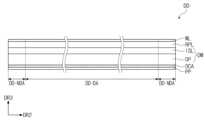
도 1a 내지 도 1c에 도시된 것과 같이, 표시장치(DD)는 동작 형태에 따라 정의되는 복수 개의 영역들을 포함할 수 있다. 표시장치(DD)는 제1 영역(NFA1), 제2 영역(NFA2), 및 제1 영역(NFA1)과 제2 영역(NFA2) 사이에 배치된 제3 영역(FA)을 포함할 수 있다. 제3 영역(FA)은 폴딩축(FX)에 기초하여(on the basis of the folding axis) 폴딩되는 영역으로 실질적으로 곡률을 형성하는 영역이다. 이하, 제1 영역(NFA1), 제2 영역(NFA2), 및 제3 영역(FA)은 제1 비폴딩영역(NFA1), 제2 비폴딩영역(NFA2) 및 폴딩영역(FA)으로 지칭될 수 있다.As shown in FIGS. 1A to 1C, the display device DD may include a plurality of areas defined according to the operation type. The display device DD may include a first area NFA1, a second area NFA2, and a third area FA disposed between the first area NFA1 and the second area NFA2. The third area (FA) is an area that is folded on the basis of the folding axis (FX) and is an area that substantially forms a curvature. Hereinafter, the first area (NFA1), the second area (NFA2), and the third area (FA) will be referred to as the first non-folding area (NFA1), the second non-folding area (NFA2), and the folding area (FA). You can.
도 1b에 도시된 것과 같이, 표시장치(DD)는 제1 비폴딩영역(NFA1)의 표시면(DD-IS)과 제2 비폴딩영역(NFA2)의 표시면(DD-IS)이 마주하도록 내측 폴딩(inner-folding)될 수 있다. 도 1c에 도시된 것과 같이, 표시모듈(DM)은 표시면(DD-IS)이 외부에 노출되도록 외측 폴딩(outer-folding)될 수도 있다.As shown in FIG. 1B, the display device DD is configured so that the display surface DD-IS of the first non-folding area NFA1 faces the display surface DD-IS of the second non-folding area NFA2. Can be inner-folded. As shown in FIG. 1C, the display module DM may be outer-folded so that the display surface DD-IS is exposed to the outside.
본 발명의 일 실시예에서 표시장치(DD)는 복수 개의 폴딩영역(FA)을 포함할 수 있다. 뿐만 아니라, 사용자가 표시장치(DD)를 조작하는 형태에 대응하게 폴딩영역(FA)이 정의될 수 있다. 예컨대, 폴딩영역(FA)은 도 1b 및 도 1c와 달리 제1 방향축(DR1)에 평행하게 정의될 수 있고, 대각선 방향으로 정의될 수도 있다. 폴딩영역(FA)의 면적은 고정되지 않고, 곡률반경에 따라 결정될 수 있다. 본 발명의 일 실시예에서 표시장치(DD)는 도 1a 및 도 1b에 도시된 동작모드만 반복되거나, 도 1a 및 도 1c에 도시된 동작모드만 반복되도록 구성될 수도 있다. 또한, 폴더블 표시장치(DD)를 예시적으로 도시하였으나, 이에 제한되지 않고 본 발명은 리지드한 표시장치에도 적용될 수 있다.In one embodiment of the present invention, the display device DD may include a plurality of folding areas FA. In addition, the folding area (FA) can be defined to correspond to the way the user manipulates the display device (DD). For example, unlike FIGS. 1B and 1C, the folding area FA may be defined parallel to the first direction axis DR1 or may be defined diagonally. The area of the folding area (FA) is not fixed and may be determined depending on the radius of curvature. In one embodiment of the present invention, the display device DD may be configured to repeat only the operation modes shown in FIGS. 1A and 1B, or may be configured to repeat only the operation modes shown in FIGS. 1A and 1C. In addition, although a foldable display device (DD) is shown as an example, the present invention is not limited thereto and can also be applied to a rigid display device.
본 실시예에서 핸드폰 단말기에 적용될 수 있는 표시장치(DD)를 예시적으로 도시하였다. 도시하지 않았으나, 메인보드에 실장된 전자모듈들, 카메라 모듈, 전원모듈 등이 표시장치(DD)과 함께 하우징(미 도시)에 결합 배치됨으로써 핸드폰 단말기를 구성할 수 있다. 하우징은 브라켓을 포함할 수 있다. 하우징은 표시장치(DD)를 지지하는 어떠한 형태의 프레임도 가능하며, 힌지 구조물이 포함된 지지체를 포함할 수도 있다. 본 발명에 따른 표시장치(DD)는 텔레비전, 모니터 등과 같은 대형 전자장치를 비롯하여, 테블릿, 자동차 네비게이션, 게임기, 스마트 와치 등과 같은 중소형 전자장치 등에 적용될 수 있다.In this embodiment, a display device (DD) that can be applied to a mobile phone terminal is shown as an example. Although not shown, a mobile phone terminal can be formed by combining electronic modules, camera modules, power modules, etc. mounted on the main board and the display device (DD) in a housing (not shown). The housing may include a bracket. The housing may be any type of frame that supports the display device DD, and may include a support body including a hinge structure. The display device (DD) according to the present invention can be applied to large electronic devices such as televisions and monitors, as well as small and medium-sized electronic devices such as tablets, car navigation systems, game consoles, and smart watches.
도 2a 내지 2d는 본 발명의 일 실시예에 따른 표시장치(DD)의 단면도이다. 도 2a 내지 2d는 제2 방향축(DR2)과 제3 방향축(DR3)이 정의하는 단면을 도시하였다. 도 2a 내지 2d는 표시장치(DD)를 구성하는 기능성 패널 및/또는 기능성 유닛들의 적층관계를 설명하기 위해 단순하게 도시되었다.2A to 2D are cross-sectional views of the display device DD according to an embodiment of the present invention. 2A to 2D show cross-sections defined by the second direction DR2 and the third direction DR3. 2A to 2D are simply shown to explain the stacking relationship of functional panels and/or functional units constituting the display device DD.
본 발명의 일 실시예에 따른 표시장치(DD)는 보호유닛, 표시패널, 입력감지센서, 반사방지유닛, 및 윈도우를 포함할 수 있다. 보호유닛, 표시패널, 입력감지센서, 및 반사방지유닛 중 일부의 구성들은 연속공정에 의해 형성되거나, 일부의 구성들은 접착부재를 통해 서로 결합될 수 있다. 도 2a 내지 2d에는 접착부재로써 광학 투명 접착부재(OCA)가 예시적으로 도시되었다. 이하에서 설명되는 접착부재는 통상의 접착제 또는 점착제를 포함할 수 있다. 본 발명의 일 실시예에서 보호유닛, 반사방지유닛, 및 입력감지센서는 다른 구성으로 대체되거나 생략될 수 있다.The display device DD according to an embodiment of the present invention may include a protection unit, a display panel, an input detection sensor, an anti-reflection unit, and a window. Some of the components of the protection unit, display panel, input detection sensor, and anti-reflection unit may be formed through a continuous process, or some of the components may be coupled to each other through an adhesive member. 2A to 2D exemplarily show an optically transparent adhesive member (OCA) as an adhesive member. The adhesive member described below may include a conventional adhesive or adhesive. In one embodiment of the present invention, the protection unit, anti-reflection unit, and input detection sensor may be replaced with other components or omitted.
도 2a 내지 도 2d에 있어서, 보호유닛, 입력감지센서, 및 반사방지유닛 중 다른 구성과 연속공정을 통해 형성된 해당 구성은 "층"으로 표현된다. 보호유닛, 입력감지센서, 반사방지유닛, 및 중 다른 구성과 접착부재를 통해 결합된 구성은 "패널"로 표현된다. 패널은 베이스면을 제공하는 베이스층, 예컨대 합성수지 필름, 복합재료 필름, 글래스 기판 등을 포함하지만, "층"은 상기 베이스층이 생략될 수 있다. 다시 말해, “층”으로 표현되는 상기 유닛들은 다른 유닛이 제공하는 베이스면 상에 배치된다.2A to 2D, the protection unit, the input detection sensor, and the anti-reflection unit are formed through a continuous process with other components and are expressed as “layers.” The protection unit, input detection sensor, anti-reflection unit, and other components combined through an adhesive member are expressed as a “panel.” The panel includes a base layer that provides a base surface, such as a synthetic resin film, composite material film, glass substrate, etc., but the base layer may be omitted as "layer". In other words, the units expressed as “layers” are placed on a base surface provided by other units.
보호유닛, 입력감지센서, 및 반사방지유닛은 베이스층의 유/무에 따라 보호패널, 입력감지패널, 및 반사방지패널 또는 보호층, 입력감지층, 및 반사방지층으로 지칭될 수 있다.The protection unit, input detection sensor, and anti-reflection unit may be referred to as a protection panel, input detection panel, and anti-reflection panel or a protection layer, input detection layer, and anti-reflection layer depending on the presence/absence of the base layer.
도 2a에 도시된 것과 같이, 표시장치(DD)는 보호패널(PP), 표시패널(DP), 입력감지층(ISL), 반사방지패널(RPP), 및 윈도우(WP)을 포함할 수 있다. 입력감지층(ISL)은 표시패널(DP)에 직접 배치된다. 본 명세서에서 "B의 구성이 A의 구성 상에 직접 배치된다"는 것은 A의 구성과 B의 구성 사이에 접착층/접착부재가 배치되지 않는 것을 의미한다. B 구성은 A 구성이 형성된 이후에 A구성이 제공하는 베이스면 상에 연속공정을 통해 형성된다.As shown in FIG. 2A, the display device DD may include a protection panel (PP), a display panel (DP), an input sensing layer (ISL), an anti-reflection panel (RPP), and a window (WP). . The input sensing layer (ISL) is placed directly on the display panel (DP). In this specification, “the component of B is placed directly on the component of A” means that no adhesive layer/adhesive member is disposed between the component of A and the component of B. Configuration B is formed through a continuous process on the base surface provided by configuration A after configuration A is formed.
표시패널(DP)과 표시패널(DP) 상에 직접 배치된 입력감지층(ISL)을 포함하여 표시모듈(DM)로 정의될 수 있다. 보호패널(PP)과 표시모듈(DM) 사이, 표시모듈(DM)과 반사방지패널(RPP) 사이, 반사방지패널(RPP)과 윈도우(WP) 사이 각각에 광학 투명 접착부재(OCA)가 배치된다.It can be defined as a display module (DM) including a display panel (DP) and an input sensing layer (ISL) disposed directly on the display panel (DP). An optically transparent adhesive member (OCA) is placed between the protection panel (PP) and the display module (DM), between the display module (DM) and the anti-reflection panel (RPP), and between the anti-reflection panel (RPP) and the window (WP). do.
표시패널(DP)은 이미지를 생성하고, 입력감지층(ISL)은 외부입력(예컨대, 터치 이벤트)의 좌표정보를 획득한다. 보호패널(PP)은 표시모듈(DM)의 하측에 배치되어 외부충격으로부터 표시모듈(DM)을 보호한다. 이하에서 설명되는 도 2b 내지 도 2d의 표시장치들(DD) 역시 보호패널(PP)를 더 포함할 수 있고, 도시된 것과 달리 보호패널(PP)은 보호층 형태로 대체될 수도 있다.The display panel (DP) generates an image, and the input sensing layer (ISL) acquires coordinate information of an external input (eg, a touch event). The protection panel (PP) is disposed on the lower side of the display module (DM) to protect the display module (DM) from external shock. The display devices DD of FIGS. 2B to 2D described below may also further include a protection panel PP, and unlike what is shown, the protection panel PP may be replaced with a protective layer.
보호패널(PP)은 합성수지필름 또는 금속 플레이트를 포함할 수 있다. 보호패널(PP)은 복수 개의 합성수지필름 및/또는 복수 개의 금속 플레이트를 포함하는 다층 구조를 가질 수 있다.The protective panel (PP) may include a synthetic resin film or a metal plate. The protective panel (PP) may have a multilayer structure including a plurality of synthetic resin films and/or a plurality of metal plates.
본 발명의 일 실시예에 따른 표시패널(DP)은 발광형 표시패널일 수 있고, 특별히 제한되지 않는다. 예컨대, 표시패널(DP)은 유기발광 표시패널 또는 퀀텀닷 발광 표시패널일 수 있다. 유기발광 표시패널의 발광층은 유기발광물질을 포함할 수 있다. 퀀텀닷 발광 표시패널의 발광층은 퀀텀닷, 및 퀀텀로드 등을 포함할 수 있다. 이하, 표시패널(DP)은 유기발광 표시패널로 설명된다.The display panel DP according to an embodiment of the present invention may be an emissive display panel and is not particularly limited. For example, the display panel DP may be an organic light emitting display panel or a quantum dot light emitting display panel. The light emitting layer of the organic light emitting display panel may include an organic light emitting material. The light emitting layer of the quantum dot light emitting display panel may include quantum dots, quantum rods, etc. Hereinafter, the display panel DP will be described as an organic light emitting display panel.
반사방지패널(RPP)은 윈도우(WP)의 상측으로부터 입사되는 외부광의 반사율을 감소시킨다. 본 발명의 일 실시예에 따른 반사방지패널(RPP)은 위상지연자(retarder) 및 편광자(polarizer)를 포함할 수 있다. 위상지연자는 필름타입 또는 액정 코팅타입일 수 있고, λ/2 위상지연자 및/또는 λ/4 위상지연자를 포함할 수 있다. 편광자 역시 필름타입 또는 액정 코팅타입일 수 있다. 필름타입은 연신형 합성수지 필름을 포함하고, 액정 코팅타입은 베이스층 상에 소정의 배열로 배열된 액정들을 포함할 수 있다. 위상지연자 및 편광자는 보호필름을 더 포함할 수 있다.The anti-reflection panel (RPP) reduces the reflectance of external light incident from the upper side of the window (WP). An anti-reflection panel (RPP) according to an embodiment of the present invention may include a phase retarder and a polarizer. The phase retarder may be a film type or a liquid crystal coating type, and may include a λ/2 phase retarder and/or a λ/4 phase retarder. The polarizer may also be a film type or a liquid crystal coating type. The film type may include a stretched synthetic resin film, and the liquid crystal coating type may include liquid crystals arranged in a predetermined arrangement on a base layer. The phase retarder and polarizer may further include a protective film.
본 발명의 일 실시예에 따른 반사방지패널(RPP)은 베이스층 상에 배치된 컬러필터들을 포함할 수 있다. 컬러필터들은 소정의 배열을 갖는다. 표시패널(DP)에 포함된 화소들의 발광컬러들을 고려하여 컬러필터들의 배열이 결정될 수 있다. 반사방지패널(RPP)은 컬러필터들에 인접한 블랙매트릭스를 더 포함할 수 있다. An anti-reflection panel (RPP) according to an embodiment of the present invention may include color filters disposed on a base layer. Color filters have a predetermined arrangement. The arrangement of the color filters may be determined by considering the emission colors of the pixels included in the display panel DP. The anti-reflection panel (RPP) may further include a black matrix adjacent to the color filters.
본 발명의 일 실시예에 따른 반사방지패널(RPP)은 베이스층 상에 배치된 상쇄간섭 구조물을 포함할 수 있다. 예컨대, 상쇄간섭 구조물은 서로 다른 층 상에 배치된 제1 반사층과 제2 반사층을 포함할 있다. 제1 반사층 및 제2 반사층에서 각각 반사된 제1 반사광과 제2 반사광은 상쇄간섭될 수 있고, 그에 따라 외부광 반사율이 감소된다. An anti-reflection panel (RPP) according to an embodiment of the present invention may include a destructive interference structure disposed on a base layer. For example, the destructive interference structure may include a first reflective layer and a second reflective layer disposed on different layers. The first reflected light and the second reflected light reflected from the first reflective layer and the second reflective layer, respectively, may cause destructive interference, thereby reducing the external light reflectance.
도 2b에 도시된 것과 같이, 반사방지층(RPL)이 입력감지층(ISL) 상에 배치될 수 있다. 반사방지층(RPL)과 입력감지층(ISL)의 적층 순서는 변경될 수 있다. 도 2c 및 도 2d에 도시된 것과 같이, 표시장치(DD)는 표시패널(DP), 입력감지패널(ISP), 반사방지패널(RPP), 및 윈도우(WP)를 포함할 수 있다. 입력감지패널(ISP)과 반사방지패널(RPP)의 적층 순서는 변경될 수 있다.As shown in FIG. 2B, an anti-reflection layer (RPL) may be disposed on the input sensing layer (ISL). The stacking order of the anti-reflection layer (RPL) and the input sensing layer (ISL) can be changed. As shown in FIGS. 2C and 2D, the display device DD may include a display panel DP, an input detection panel (ISP), an anti-reflection panel (RPP), and a window WP. The stacking order of the input detection panel (ISP) and anti-reflection panel (RPP) can be changed.
도 3a는 본 발명의 일 실시예에 따른 윈도우(WP)의 평면도이다. 도 3b 내지 도 3g는 본 발명의 일 실시예에 따른 윈도우(WP)의 단면도이다. 도 3h는 본 발명의 일 실시예에 따른 제1 부분(GP)의 단면도이다. 도 3i는 제1 부분(GP)의 두께에 따른 응력변화를 도시한 그래프이다.FIG. 3A is a top view of a window WP according to an embodiment of the present invention. 3B to 3G are cross-sectional views of the window WP according to an embodiment of the present invention. Figure 3h is a cross-sectional view of the first part (GP) according to an embodiment of the present invention. Figure 3i is a graph showing stress change according to the thickness of the first part (GP).
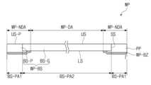
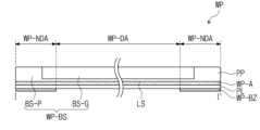
도 3a 내지 도 3g는 패널 타입의 윈도우(WP)를 도시하였다. 도 3a에 도시된 것과 같이, 평면 상에서 윈도우(WP)는 도 1a에 도시된 이미지영역(DD-DA) 및 베젤영역(DD-NDA)에 대응하는 투과영역(WP-DA) 및 차광영역(WP-NDA)을 포함한다. 차광영역(WP-NDA)은 후술하는 차광패턴(WP-BZ)이 배치된 영역으로 정의된다.3A to 3G show a panel-type window WP. As shown in FIG. 3A, the window (WP) on the plane has a transmission area (WP-DA) and a light blocking area (WP) corresponding to the image area (DD-DA) and the bezel area (DD-NDA) shown in FIG. 1A. -NDA). The light blocking area (WP-NDA) is defined as an area where a light blocking pattern (WP-BZ), which will be described later, is placed.
도 3b 내지 도 3g에 도시된 것과 같이, 본 발명의 일 실시예에 따른 윈도우(WP)는 베이스층(WP-BS) 및 차광패턴(WP-BZ)을 포함한다. 베이스층(WP-BS)은 재료 다른 2개의 부분들을 포함한다. 베이스층(WP-BS)은 무기재료 제1 부분(BS-G)과 유기재료를 포함하는 제2 부분(BS-P)을 포함한다. 제1 부분(BS-G)은 평면 상에서 윈도우(WP)의 대부분의 면적을 차지한다. 제1 부분(BS-G)은 윈도우(WP)의 평면상 면적의 90% 이상을 차지할 수 있다. 제2 부분(BS-P)은 평면 상에서 윈도우(WP)의 테두리 영역에 배치된다. 제2 부분(BS-P)은 적어도 제1 부분(BS-G)의 측면(SS)을 커버한다. 제2 부분(BS-P)은 제1 부분(BS-G)의 측면(SS)을 완전히 커버할 수 있다. 제2 부분(BS-P)은 제1 부분(BS-G)의 상면(US)을 노출시킨다. 이와 같은 구조의 베이스층(WP-BS)은 윈도우(WP)의 기계적 강도를 향상시킬 수 있다. 제1 부분(BS-G)의 파괴강도는 0.8Gpa 내지 5Gpa일 수 있다. 제2 부분(BS-P)의 항복 변형(yield strain)은1.5% 내지 3%일 수 있다.As shown in FIGS. 3B to 3G, the window WP according to an embodiment of the present invention includes a base layer WP-BS and a light blocking pattern WP-BZ. The base layer (WP-BS) contains two different parts of material. The base layer (WP-BS) includes a first part (BS-G) made of an inorganic material and a second part (BS-P) containing an organic material. The first part (BS-G) occupies most of the area of the window (WP) on the plane. The first part BS-G may occupy more than 90% of the planar area of the window WP. The second part BS-P is disposed in the border area of the window WP on the plane. The second part (BS-P) covers at least the side surface (SS) of the first part (BS-G). The second part (BS-P) may completely cover the side surface (SS) of the first part (BS-G). The second part (BS-P) exposes the upper surface (US) of the first part (BS-G). The base layer (WP-BS) with this structure can improve the mechanical strength of the window (WP). The breaking strength of the first part (BS-G) may be 0.8 Gpa to 5 Gpa. The yield strain of the second part (BS-P) may be 1.5% to 3%.
제1 부분(BS-G)은 글래스를 포함할 수 있다. 제1 부분(BS-G)은 글래스 기판일 수 있다. 제2 부분(BS-P)은 합성수지를 포함할 수 있다. 합성수지는 에폭시 아크릴레이트 수지, 폴리에스터 아크릴레이트 수지, 폴리에테러 아크릴레이트 수지, 우레탄 아크릴레이트 수지, 아크릴 아크릴레이트 수지, 불포화 폴리에스터 수지, 우레탄 수지, 아크릴로나이트릴-부타다이엔-스타이렌(ABS) 수지 중 적어도 하나를 포함할 수 있다. 제2 부분(BS-P)은 합성 고무를 포함할 수도 있다.The first part BS-G may include glass. The first portion BS-G may be a glass substrate. The second part (BS-P) may include synthetic resin. Synthetic resins include epoxy acrylate resin, polyester acrylate resin, polyether acrylate resin, urethane acrylate resin, acrylic acrylate resin, unsaturated polyester resin, urethane resin, acrylonitrile-butadiene-styrene ( ABS) resin may be included. The second portion (BS-P) may include synthetic rubber.
도 3b, 도 3e 내지 도 3g에 도시된 것과 같이, 제1 부분(BS-G)의 상면(US)과 제2 부분(BS-P)의 상면(US-P)은 연속된 면을 제공할 수 있다. 다시 말해 제1 부분(BS-G)의 상면(US)과 제2 부분(BS-P)의 상면(US-P)은 단차를 형성하지 않는다. 예컨대, 제1 부분(BS-G)의 상면(US)과 제2 부분(BS-P)의 상면(US-P)은 하나의 평면을 제공할 수 있다. 예컨대, 제1 부분(BS-G)의 상면(US) 중 일부 영역과 제2 부분(BS-P)의 상면(US-P)은 동일한 곡률을 갖는 곡면을 제공할 수 있다. 반면에 도 3c 및 도 3d에 도시된 것과 같이, 제1 부분(BS-G)의 상면(US)과 제2 부분(BS-P)의 상면(US-P)은 단차를 제공할 수도 있다.As shown in FIGS. 3B and 3E to 3G, the upper surface (US) of the first part (BS-G) and the upper surface (US-P) of the second part (BS-P) provide a continuous surface. You can. In other words, the upper surface (US) of the first part (BS-G) and the upper surface (US-P) of the second part (BS-P) do not form a step. For example, the top surface US of the first part BS-G and the top surface US-P of the second part BS-P may provide one plane. For example, a portion of the upper surface US of the first part BS-G and the upper surface US-P of the second part BS-P may provide a curved surface having the same curvature. On the other hand, as shown in FIGS. 3C and 3D, the upper surface US of the first part BS-G and the upper surface US-P of the second part BS-P may provide a step.
도 3b 내지 도 3f에 도시된 것과 같이, 제2 부분(BS-P)은 적어도 제1 부분(BS-G)의 측면(SS)을 커버한다. 도 3b에 도시된 것과 같이, 제2 부분(BS-P)은 제1 부분(BS-G)의 하면(LS)을 완전히 커버할 수 있다. 도 3e에 도시된 것과 같이, 제2 부분(BS-P)은 제1 부분(BS-G)의 하면(LS)을 부분적으로 커버할 수 있다. 도 3f에 도시된 것과 같이, 제2 부분(BS-P)은 제1 부분(BS-G)의 하면(LS)을 완전히 노출시킬 수 있다.As shown in FIGS. 3B to 3F, the second part BS-P covers at least the side surface SS of the first part BS-G. As shown in FIG. 3B, the second part BS-P may completely cover the lower surface LS of the first part BS-G. As shown in FIG. 3E, the second part BS-P may partially cover the lower surface LS of the first part BS-G. As shown in FIG. 3F, the second part BS-P may completely expose the lower surface LS of the first part BS-G.
도 3b 및 도 3e에 도시된 것과 같이, 제2 부분(BS-P)은 두께가 다른 제1 영역(BS-PA1) 및 제2 영역(BS-PA2)을 포함할 수 있다. 제1 영역(BS-PA1)은 제1 두께를 갖고, 제2 영역(BS-PA2)은 제1 두께보다 작은 제2 두께를 갖는다. 제2 영역(BS-PA2)은 제1 부분(BS-G)의 하면(LS)에 중첩하는 영역일 수 있다. 제1 영역(BS-PA1)은 제1 부분(BS-G)의 하면(LS)에 비중첩하는 영역일 수 있다.As shown in FIGS. 3B and 3E, the second part BS-P may include a first area BS-PA1 and a second area BS-PA2 having different thicknesses. The first area (BS-PA1) has a first thickness, and the second area (BS-PA2) has a second thickness that is smaller than the first thickness. The second area BS-PA2 may be an area overlapping the lower surface LS of the first part BS-G. The first area BS-PA1 may be an area that does not overlap the lower surface LS of the first part BS-G.
도 3b 및 도 3f에 도시된 것과 같이, 베이스층(WP-BS)은 투과영역(WP-DA) 및 차광영역(WP-NDA) 무관하게 동일한 두께를 가질 수 있다. 도 3e에 도시된 것과 같이, 베이스층(WP-BS)의 투과영역(WP-DA)은 차광영역(WP-NDA)보다 작은 두께를 가질 수 있다.As shown in FIGS. 3B and 3F, the base layer (WP-BS) may have the same thickness regardless of the transmission area (WP-DA) and the light blocking area (WP-NDA). As shown in FIG. 3E, the transmission area (WP-DA) of the base layer (WP-BS) may have a thickness smaller than the light blocking area (WP-NDA).
도 3b 내지 도 3f에 도시된 것과 같이, 차광패턴(WP-BZ)은 제2 부분(BS-P)의 하측에 배치된다. 차광패턴(WP-BZ)은 제2 부분(BS-P)에 직접 배치될 수 있다. 차광패턴(WP-BZ)의 일부분은 제1 부분(BS-G)에 중첩할 수 있고, 상기 일부분은 제1 부분(BS-G)에 직접 배치될 수 있다.As shown in FIGS. 3B to 3F, the light blocking pattern WP-BZ is disposed below the second portion BS-P. The light blocking pattern (WP-BZ) may be placed directly on the second portion (BS-P). A portion of the light blocking pattern WP-BZ may overlap the first portion BS-G, and the portion may be directly disposed on the first portion BS-G.
차광패턴(WP-BZ)은 베이스 수지 및 이에 혼합된 염료/안료를 포함할 수 있다. 예컨대, 코팅 또는 인쇄 또는 증착 방식으로 형성될 수 있다. 차광패턴(WP-BZ)은 다층 구조를 가질 수 있다. 차광패턴(WP-BZ)은 블랙 컬러층을 포함할 수 있다. 차광패턴(WP-BZ)은 유색의 컬러층을 포함할 수 있다.The light blocking pattern (WP-BZ) may include a base resin and dye/pigment mixed therewith. For example, it may be formed by coating, printing, or vapor deposition. The light blocking pattern (WP-BZ) may have a multi-layer structure. The light blocking pattern (WP-BZ) may include a black color layer. The light blocking pattern (WP-BZ) may include a colored color layer.
도 3g에 도시된 것과 같이, 윈도우(WP)는 합성수지 필름(PL) 및 합성수지 필름(PL)을 베이스층(WP-BS)에 부착시키는 윈도우 접착층(WP-A)을 더 포함할 수 있다. 윈도우 접착층(WP-A)은 통상의 접착층 또는 점착층일 수 있다. 차광패턴(WP-BZ)은 합성수지 필름(PL)의 하면에 직접 배치된다. 도 3g에 도시된 윈도우(WP)의 제조공정은 합성수지 필름(PL)에 차광패턴(WP-BZ)을 형성한 후, 합성수지 필름(PL)을 베이스층(WP-BS)의 하면(LS)에 라미네이션하는 단계를 포함한다. 베이스층(WP-BS)의 구조는 도 3e 또는 도 3f와 같이 변형될 수 있다.As shown in FIG. 3G, the window WP may further include a synthetic resin film PL and a window adhesive layer WP-A that attaches the synthetic resin film PL to the base layer WP-BS. The window adhesive layer (WP-A) may be a regular adhesive layer or an adhesive layer. The light blocking pattern (WP-BZ) is placed directly on the lower surface of the synthetic resin film (PL). The manufacturing process of the window (WP) shown in Figure 3g is to form a light-shielding pattern (WP-BZ) on the synthetic resin film (PL), and then attach the synthetic resin film (PL) to the lower surface (LS) of the base layer (WP-BS). It includes a lamination step. The structure of the base layer (WP-BS) may be modified as shown in FIG. 3E or FIG. 3F.
도 3b 내지 도 3g에 도시된 제1 부분(BS-G)은 화학적 강화된 글래스 기판일수 있다. 도 3h에 도시된 것과 같이, 제1 부분(BS-G)은 단면 상에서 압축응력 영역(CSA) 및 인장응력 영역(TSA)을 포함한다. 인장응력 영역(TSA)을 중심으로 양측에 압축응력 영역(CSA)이 배치될 수 있다. 압축응력 영역들(CSA) 중 하나는 상면(US)을 제공하고 다른 하나는 하면(LS)을 제공한다. 도 3i에는 상면(US)으로부터 하면(LS)까지 두께 방향에 따른 응력 프로파일을 간략히 도시하였다.The first part BS-G shown in FIGS. 3B to 3G may be a chemically strengthened glass substrate. As shown in FIG. 3H, the first portion BS-G includes a compressive stress area (CSA) and a tensile stress area (TSA) in cross section. Compressive stress areas (CSA) may be placed on both sides of the tensile stress area (TSA). One of the compressive stress areas (CSA) provides the upper surface (US) and the other provides the lower surface (LS). Figure 3i briefly shows the stress profile along the thickness direction from the upper surface (US) to the lower surface (LS).
한편, 압축응력 영역(CSA)은 상면(US)을 제공하는 영역에만 배치될 수도 있다. 화학적 강화 공정에서 하면(LS)을 제공하는 영역은 보호필름으로 커버하여 이온교환을 방지할 수 있다.Meanwhile, the compressive stress area (CSA) may be placed only in the area that provides the upper surface (US). In the chemical strengthening process, the area providing the lower surface (LS) can be covered with a protective film to prevent ion exchange.
화학적 강화 글래스 기판은 얇은 두께에도 큰 기계적 강도를 갖기 때문에 폴더블 표시장치에 적합하다. 글래스 부분(BS-G)의 두께는 100 ㎛ 이하일 수 있다. 글래스 부분(BS-G)의 두께는 20㎛ 내지 100 ㎛일 수 있다.Chemically strengthened glass substrates are suitable for foldable display devices because they have high mechanical strength even at a thin thickness. The thickness of the glass portion (BS-G) may be 100 μm or less. The thickness of the glass portion (BS-G) may be 20 μm to 100 μm.
별도로 도시하지는 않았으나, 윈도우(WP)는 베이스층(WP-BS)의 상면에 배치된 기능성 코팅층을 더 포함할 수 있다. 기능성 코팅층은 지문 방지층, 반사 방지층, 및 하드 코팅층 등을 포함할 수 있다.Although not separately shown, the window WP may further include a functional coating layer disposed on the upper surface of the base layer WP-BS. The functional coating layer may include an anti-fingerprint layer, an anti-reflection layer, and a hard coating layer.
차광패턴(WP-BZ)을 포함하는 윈도우(WP)를 예시적으로 설명하였으나, 본 발명의 일 실시예에서 윈도우(WP)에서 차광패턴(WP-BZ)은 생략될 수 있고, 차광패턴(WP-BZ)은 입력감지센서 또는 반사방지유닛에 배치될 수도 있다.Although the window WP including the light-shielding pattern WP-BZ has been described as an example, in one embodiment of the present invention, the light-shielding pattern WP-BZ may be omitted from the window WP, and the light-shielding pattern WP -BZ) may be placed in an input detection sensor or anti-reflection unit.
도 3b 내지 도 3g에 도시된 윈도우(WP)의 제조공정을 간략히 설명한다. 화학적 강화된 글래스 기판을 준비한다. 원 글래스 기판(raw glass substrate)에 공지된 화학적 강화 공정을 진행하여 강화 글래스 기판을 제조할 수 있다. 원 글래스 기판은 모서리가 연마된 상태일 수 있다.The manufacturing process of the window WP shown in FIGS. 3B to 3G will be briefly described. Prepare a chemically strengthened glass substrate. A strengthened glass substrate can be manufactured by performing a known chemical strengthening process on a raw glass substrate. The original glass substrate may have polished edges.
화학적 강화된 글래스 기판에 합성수지층을 형성한다. 슬릿 코팅, 바 코팅, 스핀 코팅, GDM(glass direct molding) 방법 등에 의해 합성수지층을 형성할 수 있다. 제조설비의 스테이지에 접촉하는 글래스 기판의 일면에는 합성수지층이 형성되지 않고, 글래스 기판의 측면 및 글래스 기판의 일면과 두께 방향에서 마주하는 타면에 합성수지층이 형성될 수 있다. 글래스 기판의 일면에 보호필름이 부착된 상태로 코팅공정을 진행할 수도 있다. 글래스 기판의 타면에 형성된 합성수지층은 후속 공정을 통해 부분적으로 제거될 수도 있다. 글래스 기판의 타면에도 부분적으로 보호필름을 부착하여 합성수지층이 형성되는 영역을 제어할 수도 있다.A synthetic resin layer is formed on a chemically strengthened glass substrate. The synthetic resin layer can be formed by slit coating, bar coating, spin coating, or GDM (glass direct molding) methods. A synthetic resin layer may not be formed on one side of the glass substrate that is in contact with the stage of the manufacturing facility, but a synthetic resin layer may be formed on the side of the glass substrate and the other side that faces one side of the glass substrate in the thickness direction. The coating process can also be performed with a protective film attached to one side of the glass substrate. The synthetic resin layer formed on the other side of the glass substrate may be partially removed through a subsequent process. A protective film can also be partially attached to the other side of the glass substrate to control the area where the synthetic resin layer is formed.
이와 같은 방법으로 도 3b 내지 도 3g에 도시된 베이스층(WP-BS)을 형성할 수 있다. 이후, 차광패턴(WP-BZ)의 형성공정 또는 합성수지 필름(PL)의 라미네이션 공정이 추가적으로 진행될 수 있다.In this way, the base layer (WP-BS) shown in FIGS. 3B to 3G can be formed. Afterwards, the formation process of the light-shielding pattern (WP-BZ) or the lamination process of the synthetic resin film (PL) may be additionally performed.
도 4a 및 도 4b는 본 발명의 일 실시예에 따른 표시패널(DP)의 단면도이다.4A and 4B are cross-sectional views of the display panel DP according to an embodiment of the present invention.
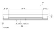
도 4a에 도시된 것과 같이, 표시패널(DP)은 베이스층(BL), 베이스층(BL) 상에 배치된 회로 소자층(DP-CL), 표시 소자층(DP-OLED) 및 상부 절연층(TFL)을 포함한다. 도 1a에 도시된 이미지영역(DD-DA)과 베젤영역(DD-NDA)에 대응하는 표시영역(DP-DA)과 비표시영역(DP-NDA)이 표시패널(DP)에 정의될 수 있다. 본 실시예에서 영역과 영역이 대응한다는 것은 서로 중첩한다는 것을 의미하고 동일한 면적을 갖는 것으로 제한되지 않는다.As shown in FIG. 4A, the display panel (DP) includes a base layer (BL), a circuit element layer (DP-CL) disposed on the base layer (BL), a display element layer (DP-OLED), and an upper insulating layer. (TFL). A display area (DP-DA) and a non-display area (DP-NDA) corresponding to the image area (DD-DA) and bezel area (DD-NDA) shown in FIG. 1A may be defined in the display panel (DP). . In this embodiment, regions corresponding to each other mean that they overlap each other and are not limited to having the same area.
베이스층(BL)은 적어도 하나의 합성수지 필름을 포함할 수 있다. 베이스층(BL)은 플라스틱 기판, 글래스 기판, 메탈 기판, 또는 유/무기 복합재료 기판 등을 포함할 수 있다.The base layer BL may include at least one synthetic resin film. The base layer BL may include a plastic substrate, a glass substrate, a metal substrate, or an organic/inorganic composite material substrate.
회로 소자층(DP-CL)은 적어도 하나의 중간 절연층과 회로 소자를 포함한다. 중간 절연층은 적어도 하나의 중간 무기막과 적어도 하나의 중간 유기막을 포함한다. 상기 회로 소자는 신호라인들, 화소의 구동회로 등을 포함한다.The circuit element layer (DP-CL) includes at least one intermediate insulating layer and a circuit element. The intermediate insulating layer includes at least one intermediate inorganic layer and at least one intermediate organic layer. The circuit elements include signal lines, pixel driving circuits, etc.
표시 소자층(DP-OLED)은 적어도 유기발광 다이오드들을 포함한다. 표시 소자층(DP-OLED)은 화소 정의막과 같은 유기막을 더 포함할 수 있다.The display element layer (DP-OLED) includes at least organic light emitting diodes. The display device layer (DP-OLED) may further include an organic layer such as a pixel defining layer.
상부 절연층(TFL)은 복수 개의 박막들을 포함한다. 일부 박막은 광학 효율을 향상시키기 위해 배치되고, 일부 박막은 유기발광 다이오드들을 보호하기 위해 배치된다. 복수 개의 박막들은 박막 봉지층을 포함할 수 있다. 박막 봉지층은 무기막/유기막/무기막 적층구조를 가질 수 있다. 복수 개의 박막들은 굴절률 매칭층을 포함할 수 있다.The top insulating layer (TFL) includes a plurality of thin films. Some thin films are placed to improve optical efficiency, and some thin films are placed to protect organic light emitting diodes. The plurality of thin films may include a thin film encapsulation layer. The thin film encapsulation layer may have an inorganic film/organic film/inorganic film stacked structure. The plurality of thin films may include a refractive index matching layer.
도 4b에 도시된 것과 같이, 표시패널(DP)은 베이스층(BL), 베이스층(BL) 상에 배치된 회로 소자층(DP-CL), 표시 소자층(DP-OLED), 봉지기판(ES) 및 베이스층(BL)과 봉지기판(ES)을 결합하는 실런트(SM)를 포함한다. 봉지기판(ES)은 표시 소자층(DP-OLED)으로부터 소정의 갭을 두고 이격될 수 있다. 베이스층(BL) 및 봉지기판(ES)은 플라스틱 기판, 글래스 기판, 메탈 기판, 또는 유/무기 복합재료 기판 등을 포함할 수 있다. 실런트(SM)는 유기 접착부재 또는 프릿 등을 포함할 수 있다.As shown in FIG. 4B, the display panel (DP) includes a base layer (BL), a circuit element layer (DP-CL) disposed on the base layer (BL), a display element layer (DP-OLED), and an encapsulation substrate ( ES) and a sealant (SM) that combines the base layer (BL) and the encapsulation substrate (ES). The encapsulation substrate (ES) may be spaced apart from the display element layer (DP-OLED) at a predetermined gap. The base layer (BL) and the encapsulation substrate (ES) may include a plastic substrate, a glass substrate, a metal substrate, or an organic/inorganic composite material substrate. Sealant (SM) may include an organic adhesive member or frit.
도 5a은 본 발명의 일 실시예에 따른 입력감지센서(ISL)의 단면도이다. 도 5b은 본 발명의 일 실시예에 따른 입력감지센서(ISL)의 평면도이다. 본 실시예에서 "층" 타입의 입력감지센서(ISL)를 예시적으로 도시하였다.Figure 5a is a cross-sectional view of an input detection sensor (ISL) according to an embodiment of the present invention. Figure 5b is a top view of an input detection sensor (ISL) according to an embodiment of the present invention. In this embodiment, a “layer” type input detection sensor (ISL) is shown as an example.
도 5a에 도시된 것과 같이, 입력감지센서(ISL)는 제1 절연층(IS-IL1), 제1 도전층(IS-CL1), 제2 절연층(IS-IL2), 제2 도전층(IS-CL2), 및 제3 절연층(IS-IL3)을 포함할 수 있다. 제1 절연층(IS-IL1)은 상부 절연층(TFL) 상에 직접 배치된다. 본 발명의 일 실시예에서 제1 절연층(IS-IL1)은 생략될 수 있다. "패널" 타입의 입력감지센서(ISL)는 제1 절연층(IS-IL1)을 지지하는 베이스 필름을 더 포함할 수 있다.As shown in Figure 5a, the input detection sensor (ISL) includes a first insulating layer (IS-IL1), a first conductive layer (IS-CL1), a second insulating layer (IS-IL2), and a second conductive layer ( IS-CL2), and a third insulating layer (IS-IL3). The first insulating layer (IS-IL1) is directly disposed on the upper insulating layer (TFL). In one embodiment of the present invention, the first insulating layer IS-IL1 may be omitted. The “panel” type input detection sensor (ISL) may further include a base film supporting the first insulating layer (IS-IL1).
제1 도전층(IS-CL1) 및 제2 도전층(IS-CL2) 각각은 단층구조를 갖거나, 제3 방향축(DR3)을 따라 적층된 다층구조를 가질 수 있다. 다층구조의 도전층은 투명 도전층들과 금속층들 중 적어도 2이상을 포함할 수 있다. 다층구조의 도전층은 서로 다른 금속을 포함하는 금속층들을 포함할 수 있다. 투명 도전층은 ITO(indium tin oxide), IZO(indium zinc oxide), ZnO(zinc oxide), ITZO(indium tin zinc oxide), PEDOT, 금속 나노 와이어, 그라핀을 포함할 수 있다. 금속층은 몰리브덴, 은, 티타늄, 구리, 알루미늄, 및 이들의 합금을 포함할 수 있다. 예컨대, 제1 도전층(IS-CL1) 및 제2 도전층(IS-CL2) 각각은 3층의 금속층 구조, 예컨대, 티타늄/알루미늄/티타늄의 3층 구조를 가질 수 있다.Each of the first conductive layer (IS-CL1) and the second conductive layer (IS-CL2) may have a single-layer structure or a multi-layer structure stacked along the third direction DR3. The multi-layered conductive layer may include at least two of transparent conductive layers and metal layers. The multi-layered conductive layer may include metal layers containing different metals. The transparent conductive layer may include indium tin oxide (ITO), indium zinc oxide (IZO), zinc oxide (ZnO), indium tin zinc oxide (ITZO), PEDOT, metal nanowire, and graphene. The metal layer may include molybdenum, silver, titanium, copper, aluminum, and alloys thereof. For example, each of the first conductive layer (IS-CL1) and the second conductive layer (IS-CL2) may have a three-layer metal layer structure, for example, a three-layer structure of titanium/aluminum/titanium.
제1 도전층(IS-CL1) 및 제2 도전층(IS-CL2) 각각은 복수 개의 도전패턴들을 포함한다. 이하, 제1 도전층(IS-CL1)은 제1 도전패턴들을 포함하고, 제2 도전층(IS-CL2)은 제2 도전패턴들을 포함하는 것으로 설명된다. 제1 도전패턴들과 제2 도전패턴들 각각은 감지전극들 및 이에 연결된 신호라인들을 포함할 수 있다.Each of the first conductive layer (IS-CL1) and the second conductive layer (IS-CL2) includes a plurality of conductive patterns. Hereinafter, the first conductive layer (IS-CL1) will be described as including first conductive patterns, and the second conductive layer (IS-CL2) will be described as including second conductive patterns. Each of the first conductive patterns and the second conductive patterns may include sensing electrodes and signal lines connected thereto.
제1 절연층(IS-IL1) 내지 제3 절연층(IS-IL3) 각각은 무기물 또는 유기물을 포함할 수 있다. 본 실시예에서 제1 절연층(IS-IL1) 및 제2 절연층(IS-IL2)은 무기물을 포함하는 무기막일 수 있다. 무기막은 알루미늄 옥사이드, 티타늄 옥사이드, 실리콘 옥사이드 실리콘옥시나이트라이드, 지르코늄옥사이드, 및 하프늄 옥사이드 중 적어도 하나를 포함할 수 있다. 제3 절연층(IS-IL3)은 유기막을 포함할 수 있다. 유기막은 아크릴계 수지, 메타크릴계 수지, 폴리이소프렌, 비닐계 수지, 에폭시계 수지, 우레탄계 수지, 셀룰로오스계 수지, 실록산계 수지, 폴리이미드계 수지, 폴리아미드계 수지 및 페릴렌계 수지 중 적어도 어느 하나를 포함할 수 있다.Each of the first to third insulating layers (IS-IL1) to IS-IL3 may include an inorganic material or an organic material. In this embodiment, the first insulating layer (IS-IL1) and the second insulating layer (IS-IL2) may be inorganic films containing an inorganic material. The inorganic film may include at least one of aluminum oxide, titanium oxide, silicon oxide, silicon oxynitride, zirconium oxide, and hafnium oxide. The third insulating layer (IS-IL3) may include an organic layer. The organic film is made of at least one of acrylic resin, methacrylic resin, polyisoprene, vinyl resin, epoxy resin, urethane resin, cellulose resin, siloxane resin, polyimide resin, polyamide resin, and perylene resin. It can be included.
도 5b에 도시된 것과 같이, 입력감지센서(ISL)는 표시패널(DP, 도 4a 참고)의 표시영역(DP-DA, 도 4a 참고)과 비표시영역(DP-NDA, 도 4a 참고)에 대응하는 센싱영역(IS-DA)과 배선영역(IS-NDA)을 포함할 수 있다. 센싱영역(IS-DA)은 후술하는 제1 전극 그룹(EG1) 및 제2 전극 그룹(EG2)이 배치된 영역으로 정의될 수 있다.As shown in Figure 5b, the input detection sensor (ISL) is located in the display area (DP-DA, see Figure 4a) and the non-display area (DP-NDA, see Figure 4a) of the display panel (DP, see Figure 4a). It may include a corresponding sensing area (IS-DA) and wiring area (IS-NDA). The sensing area IS-DA may be defined as an area where the first electrode group EG1 and the second electrode group EG2, which will be described later, are disposed.
입력감지센서(ISL)는 제1 전극 그룹(EG1), 제2 전극 그룹(EG2), 제1 전극 그룹(EG1)에 연결된 제1 신호라인 그룹(SG1), 및 제2 전극 그룹(EG2)에 연결된 제2 신호라인 그룹(SG2)을 포함할 수 있다.The input detection sensor (ISL) is connected to the first electrode group (EG1), the second electrode group (EG2), the first signal line group (SG1) connected to the first electrode group (EG1), and the second electrode group (EG2). It may include a connected second signal line group (SG2).
10개의 제1 전극들(IE1-1 내지 IE1-10)을 포함하는 제1 전극 그룹(EG1)을 예시적으로 도시하였다. 8개의 제2 전극들(IE2-1 내지 IE2-8)을 포함하는 제2 전극 그룹(EG2)을 예시적으로 도시하였다. 10개의 제1 신호라인들(SL1-1 내지 SL1-10)을 포함하는 제1 신호라인 그룹(SG1)을 예시적으로 도시하였다. 8개의 제2 신호라인들(SL2-1 내지 SL2-8)을 포함하는 제2 신호라인 그룹(SG2)을 예시적으로 도시하였다. 본 실시예에서, 입력감지센서(ISL)는 8개의 제3 신호라인들(SL3-1 내지 SL3-8)을 포함하는 제3 신호라인 그룹(SG3)을 더 포함할 수 있다.A first electrode group EG1 including 10 first electrodes IE1-1 to IE1-10 is shown as an example. The second electrode group EG2 including eight second electrodes IE2-1 to IE2-8 is shown as an example. A first signal line group (SG1) including 10 first signal lines (SL1-1 to SL1-10) is shown as an example. A second signal line group (SG2) including eight second signal lines (SL2-1 to SL2-8) is shown as an example. In this embodiment, the input detection sensor (ISL) may further include a third signal line group (SG3) including eight third signal lines (SL3-1 to SL3-8).
제1 전극 그룹(EG1)의 전극은 복수 개의 제1 센서부들(SP1)과 복수 개의 제1 연결부들(CP1)을 포함한다. 제1 센서부들(SP1)은 제2 방향(DR2)을 따라 나열된다. 제1 연결부들(CP1) 각각은 제1 센서부들(SP1)은 중 인접하는 2개의 제1 센서부들(SP1)을 연결한다.The electrode of the first electrode group EG1 includes a plurality of first sensor units SP1 and a plurality of first connection parts CP1. The first sensor units SP1 are arranged along the second direction DR2. Each of the first connection parts CP1 connects two adjacent first sensor parts SP1.
제2 전극 그룹(EG2)의 전극은 복수 개의 제2 센서부들(SP2)과 복수 개의 제2 연결부들(CP2)을 포함한다. 제2 센서부들(SP2)은 제1 방향(DR1)을 따라 나열된다. 제2 연결부들(CP2) 각각은 제2 센서부들(SP2)은 중 인접하는 2개의 제2 센서부들(SP2)을 연결한다.The electrode of the second electrode group EG2 includes a plurality of second sensor parts SP2 and a plurality of second connection parts CP2. The second sensor units SP2 are arranged along the first direction DR1. Each of the second connection parts CP2 connects two adjacent second sensor parts SP2.
제1 전극 그룹(EG1)의 전극과 제2 전극 그룹(EG2)의 전극은 서로 절연된다. 도 5b에는 제1 연결부(CP1)와 제2 연결부(CP2)에서 교차하는 실시예를 도시하였다. 복수 개의 제1 센서부들(SP1), 복수 개의 제1 연결부들(CP1), 복수 개의 제2 센서부들(SP2), 및 복수 개의 제2 연결부들(CP2) 중 일부는 도 5a에 도시된 제1 도전층(IS-CL1)을 패터닝하여 형성하고, 다른 일부는 도 5a에 도시된 제2 도전층(IS-CL2)을 패터닝하여 형성할 수 있다. 복수 개의 제1 센서부들(SP1) 및 복수 개의 제2 센서부들(SP2)은 메쉬 형상을 가질 수 있다.The electrodes of the first electrode group EG1 and the electrodes of the second electrode group EG2 are insulated from each other. Figure 5b shows an embodiment where the first connection part CP1 and the second connection part CP2 intersect. Some of the plurality of first sensor units SP1, the plurality of first connection parts CP1, the plurality of second sensor parts SP2, and the plurality of second connection parts CP2 are the first sensor units shown in FIG. 5A. The conductive layer (IS-CL1) may be formed by patterning, and the other portion may be formed by patterning the second conductive layer (IS-CL2) shown in FIG. 5A. The plurality of first sensor units SP1 and the plurality of second sensor units SP2 may have a mesh shape.
본 실시예에서 복수 개의 제1 연결부들(CP1)는 제1 도전층(IS-CL1)으로부터 형성되고, 복수 개의 제1 센서부들(SP1), 복수 개의 제2 센서부들(SP2), 및 복수 개의 제2 연결부들(CP2)은 제2 도전층(IS-CL2)으로부터 형성될 수 있다. 제2 절연층(IS-IL2)을 관통하는 컨택홀들을 통해서 제1 센서부들(SP1)과 제1 연결부(CP1)가 접속될 수 있다.In this embodiment, the plurality of first connection parts CP1 are formed from the first conductive layer IS-CL1, the plurality of first sensor parts SP1, the plurality of second sensor parts SP2, and the plurality of The second connection parts CP2 may be formed from the second conductive layer IS-CL2. The first sensor units SP1 and the first connection unit CP1 may be connected through contact holes penetrating the second insulating layer IS-IL2.
본 실시예에서 복수 개의 제1 연결부들(CP1)과 복수 개의 제2 연결부들(CP2)이 서로 교차하는 것으로 도시하였으나, 이에 제한되지 않는다. 예컨대, 제2 연결부들(CP2) 각각은 제1 연결부들(CP1)에 비중첩하도록 "<" 및/또는 ">" 형태로 변형될 수 있다. "<" 또는 ">" 형태의 제2 연결부들(CP2)은 제1 센서부들(SP1)에 중첩할 수 있다.In this embodiment, the plurality of first connection parts CP1 and the plurality of second connection parts CP2 are shown as crossing each other, but the present invention is not limited thereto. For example, each of the second connection parts CP2 may be transformed into a “<” and/or “>” shape so as not to overlap the first connection parts CP1. The second connection parts CP2 in the form of “<” or “>” may overlap the first sensor parts SP1.
본 실시예에서 입력감지센서(ISL)는 뮤츄얼캡 방식으로 외부입력을 감지하는 정전용량식 터치패널일 수 있다. 제1 전극 그룹(EG1)과 제2 전극 그룹(EG2) 중 어느 하나는 검출 신호(detection signal)을 수신하고, 다른 하나는 제1 전극 그룹(EG1)과 제2 전극 그룹(EG2) 사이의 정전용량 변화량을 출력 신호로써 출력한다.In this embodiment, the input detection sensor (ISL) may be a capacitive touch panel that senses an external input using a mutual cap method. One of the first electrode group EG1 and the second electrode group EG2 receives a detection signal, and the other receives the electrostatic discharge between the first electrode group EG1 and the second electrode group EG2. The capacity change amount is output as an output signal.
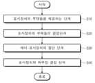
도 6a는 본 발명의 일 실시예에 따른 표시장치(DD)의 제조방법을 도시한 흐름도이다. 도 6b는 본 발명의 일 실시예에 따른 표시장치(DD)의 제조방법을 도시한 단면도이다. 도 6c는 본 발명의 일 실시예에 따른 표시장치(DD)의 제조방법을 도시한 단면도이다. 도 1a 내지 도 5b를 참조하여 설명한 구성과 동일한 구성에 대한 상세한 설명은 생략한다.FIG. 6A is a flowchart showing a method of manufacturing a display device DD according to an embodiment of the present invention. Figure 6b is a cross-sectional view showing a manufacturing method of the display device DD according to an embodiment of the present invention. FIG. 6C is a cross-sectional view showing a method of manufacturing a display device DD according to an embodiment of the present invention. Detailed descriptions of the same configurations as those described with reference to FIGS. 1A to 5B will be omitted.
도 6a에 도시된 것과 같이, 표시장치의 부재들을 제공한다(S10). 표시장치의 부재들은 적어도 접착부재(OCA), 표시패널(DP), 및 도 3a 내지 도 3i를 참조하여 설명한 윈도우(WP)를 포함할 수 있다. 표시장치의 부재들은 입력감지유닛을 더 포함할 수 있는데, 도 5a 및 도 5b를 참조하여 설명한 입력감지층(ISL)은 도 2a를 참조하여 설명한 것과 같이 표시모듈(DM) 형태(표시패널(DP)과 일체 형태)로 제공될 수 있다. 표시장치의 부재들은 보호패널(PP) 및 반사방지패널(RPP)을 더 포함할 수 있다. 앞서 설명한 부재들 중 접착부재(OCA)와 윈도우(WP)를 제외한 부재들은 기능성 부재로 통칭될 수 있다.As shown in FIG. 6A, members of the display device are provided (S10). Members of the display device may include at least an adhesive member (OCA), a display panel (DP), and a window (WP) described with reference to FIGS. 3A to 3I. Members of the display device may further include an input sensing unit. The input sensing layer (ISL) described with reference to FIGS. 5A and 5B is in the form of a display module (DM) (display panel (DP)) as described with reference to FIG. 2A. ) and an integrated form) can be provided. Members of the display device may further include a protection panel (PP) and an anti-reflection panel (RPP). Among the members described above, members excluding the adhesive member (OCA) and window (WP) may be collectively referred to as functional members.
표시장치의 제조 단계에서 제공된 표시장치의 부재들은 도 1a 내지 도 5b를 참조하여 설명한 표시장치의 구성 부품 대비 평면 상에서 더 큰 면적을 갖는다. 후술하는 것과 같이, 제공된 표시장치의 부재들의 테두리 영역이 절단되기 때문이다.Members of the display device provided in the manufacturing stage of the display device have a larger area on a plane than the component parts of the display device described with reference to FIGS. 1A to 5B. As will be described later, this is because the border areas of the members of the provided display device are cut.
다음, 표시장치의 부재들을 결합한다(S20). 윈도우(WP)와 기능성 부재 사이에 접착부재(OCA)를 배치시킨 후 윈도우(WP)와 기능성 부재를 결합시킨다. 기능성 부재가 복수 개의 부재들을 포함하는 경우, 복수 개의 부재들 사이에도 접착부재(OCA)가 배치된다.Next, the members of the display device are combined (S20). An adhesive member (OCA) is placed between the window (WP) and the functional member, and then the window (WP) and the functional member are joined. When the functional member includes a plurality of members, an adhesive member (OCA) is also disposed between the plurality of members.
도 6b에 도시된 것과 같이, 윈도우(WP)와 반사방지패널(RPP) 사이, 반사방지패널(RPP)과 표시모듈(DM) 사이, 표시모듈(DM)과 보호패널(PP) 사이에 접착부재(OCA)가 배치될 수 있다. 하나의 접착부재(OCA)를 중심으로 상측의 부재와 하측의 부재를 결합시킨다(라미네이션 공정). 도 6b에 도시된 표시장치(DD)는 3회의 라미네이션 공정을 통해 형성될 수 있다. 앞서 설명한 연속적인 라미네이션 공정과 달리 본 발명의 일 실시예에서 롤투롤 라미네이션 공정을 통해 도 8b에 도시된 표시장치(DD)를 형성할 수도 있다. 복수 개의 부재들과 복수 개의 접착부재들이 동시에 라미네이션 될 수 있다.As shown in Figure 6b, there is an adhesive member between the window (WP) and the anti-reflection panel (RPP), between the anti-reflection panel (RPP) and the display module (DM), and between the display module (DM) and the protection panel (PP). (OCA) may be deployed. The upper and lower members are joined around one adhesive member (OCA) (lamination process). The display device DD shown in FIG. 6B can be formed through three lamination processes. Unlike the continuous lamination process described above, in one embodiment of the present invention, the display device DD shown in FIG. 8B may be formed through a roll-to-roll lamination process. A plurality of members and a plurality of adhesive members may be laminated simultaneously.
도 6b에 도시된 예비-표시장치(DD-P)의 측면에는 단차들이 형성된다. 결합된 기능성 부재와 접착부재들(OCA)은 윈도우(WP)와 다른 면적을 갖기 때문이다. 측면에서 단차들이 형성되는 또 다른 이유는 라미네이션 공정에서 공정오차가 발생하기 때문이다.Steps are formed on the side of the pre-display device DD-P shown in FIG. 6B. This is because the combined functional member and adhesive member (OCA) has a different area than the window (WP). Another reason why steps are formed on the side is because process errors occur in the lamination process.
도 6a 및 도 6b에 도시된 것과 예비-표시장치(DD-P)의 테두리 영역을 절단한다(S30). 예비-표시장치(DD-P)의 측면에 형성된 단차들을 제거한다. 평면상에서 제2 부분(BS-P)의 내측에 절단선을 설정하고, 절단선을 따라 윈도우(WP), 접착부재(OCA), 및 기능성 부재를 절단한다. 절단선은 컴퓨터 시스템을 포함하는 기계설비에서 예비-표시장치(DD-P)에 설정하는 가상의 라인일 수 있다.The border area of the pre-display device (DD-P) shown in FIGS. 6A and 6B is cut (S30). Steps formed on the side of the pre-display device (DD-P) are removed. A cutting line is set inside the second part (BS-P) on a plane, and the window (WP), adhesive member (OCA), and functional member are cut along the cutting line. The cutting line may be an imaginary line that is set on a pre-display device (DD-P) in machinery including a computer system.
레이저 소스(LS)를 이용하여 절단단계를 수행할 수 있다. 레이저 소스(LS)는 CO2 레이저, Excimer 레이저, Fiber 레이저 등을 포함할 수 있다. 레이지 빔이 조사되어 윈도우(WP), 접착부재(OCA), 및 기능성 부재들이 절단되면, 이것들의 절단면들은 하나의 평면으로 정렬될 수 있다. 이것들의 절단면들은 표시장치(DD)의 측면을 이룰 수 있다.The cutting step can be performed using a laser source (LS). The laser source (LS) may include a CO2 laser, excimer laser, fiber laser, etc. When the lazy beam is irradiated to cut the window (WP), adhesive member (OCA), and functional members, their cut surfaces can be aligned in one plane. These cut surfaces may form the sides of the display device DD.
도 6c에 도시된 것과 같이, 적어도 제2 부분(BS-P)의 절단면과 접착부재(OCA)의 절단면이 정렬될 수 있다. 표시패널(DP)의 절단면은 도 4a에 도시된 표시패널(DP)을 구성하는 절연층들의 절단면을 포함할 수 있다. 또한, 입력감지센서(ISL)의 절단면은 도 5a를 참조한 입력감지센서(ISL)의 절연층들(IS-IL1, IS-IL2, IS-IL3)의 절단면들을 포함할 수 있다.As shown in FIG. 6C, at least the cut surface of the second part (BS-P) and the cut surface of the adhesive member (OCA) may be aligned. The cut surface of the display panel DP may include cut surfaces of the insulating layers constituting the display panel DP shown in FIG. 4A. Additionally, the cut surface of the input sensor (ISL) may include cut surfaces of the insulating layers (IS-IL1, IS-IL2, and IS-IL3) of the input sensor (ISL) with reference to FIG. 5A.
파괴강도가 높은 제1 부분(BS-G)은 제2 부분(BS-P) 대비 절단이 용이하지 않다. 뿐만 아니라, 제1 부분(BS-G)이 절단되면 절단면 주변 영역의 파괴강도가 급격히 떨어진다. 예컨대, 화학적 강화된 글래스 기판의 경우 응력 밸런스가 무너지면서 절단면 주변 영역의 파괴강도가 50% 이하로 낮아질 수 있다. 결과적으로 윈도우(WP)의 기계적 강도가 낮아지는 불량이 발생한다. 본 실시예의 경우 제2 부분(BS-P)을 절단하기 때문에 윈도우(WP)의 파괴강도를 유지할 수 있다.The first part (BS-G), which has high breaking strength, is not easy to cut compared to the second part (BS-P). In addition, when the first part (BS-G) is cut, the fracture strength of the area around the cut surface drops sharply. For example, in the case of a chemically strengthened glass substrate, the stress balance is lost and the fracture strength of the area around the cut surface may be lowered to 50% or less. As a result, a defect occurs in which the mechanical strength of the window (WP) is lowered. In this embodiment, since the second part (BS-P) is cut, the breaking strength of the window (WP) can be maintained.
다음, 도 6a 및 도 6c에 도시된 것과 같이, 표시장치(DD)를 하우징(HUS)에 결합한다(S40). 본 실시예에 따르면 표시장치(DD)의 하우징(HUS)에 대한 조립 오차가 감소될 수 있다. 도 6b에 도시된 예비-표시장치(DD-P)는 표시장치의 부재들 각각의 제조 오차와 라미네이션 공정 오차를 갖는데 비해, 도 6c에 도시된 표시장치(DD)는 하우징(HUS)과의 결합을 고려한 설계값에 따라 절단되었기 때문에 절단 공정의 오차만을 갖는다. 또한, 절단 공정을 반복하여 절단 공정의 오차를 최소화할 수 있다.Next, as shown in FIGS. 6A and 6C, the display device DD is coupled to the housing HUS (S40). According to this embodiment, assembly errors for the housing HUS of the display device DD can be reduced. The pre-display device DD-P shown in FIG. 6B has manufacturing errors and lamination process errors of each member of the display device, while the display device DD shown in FIG. 6C has a manufacturing error and a lamination process error in each member of the display device. Because it was cut according to design values that took into account, it only has errors in the cutting process. Additionally, errors in the cutting process can be minimized by repeating the cutting process.
이상에서는 본 발명의 바람직한 실시예를 참조하여 설명하였지만, 해당 기술 분야의 숙련된 당업자 또는 해당 기술 분야에 통상의 지식을 갖는 자라면, 후술될 특허청구범위에 기재된 본 발명의 사상 및 기술 영역으로부터 벗어나지 않는 범위 내에서 본 발명을 다양하게 수정 및 변경시킬 수 있음을 이해할 수 있을 것이다.Although the present invention has been described above with reference to preferred embodiments, those skilled in the art or have ordinary knowledge in the relevant technical field should not deviate from the spirit and technical scope of the present invention as set forth in the claims to be described later. It will be understood that the present invention can be modified and changed in various ways within the scope of the present invention.
따라서, 본 발명의 기술적 범위는 명세서의 상세한 설명에 기재된 내용으로 한정되는 것이 아니라 특허청구범위에 의해 정하여져야만 할 것이다.Therefore, the technical scope of the present invention should not be limited to what is described in the detailed description of the specification, but should be defined by the scope of the claims.
DD: 표시장치DM: 표시모듈
DP-DA: 표시영역DP-NDA: 비표시영역
DP: 표시패널WP: 윈도우
WP-DA: 투과영역WP-NDA: 차광영역
BS-G: 제1 부분BS-P: 제2 부분
WP-BS: 베이스층WP-BM: 차광패턴DD: Display device DM: Display module
DP-DA: Display area DP-NDA: Non-display area
DP: Display panel WP: Window
WP-DA: Transmission area WP-NDA: Light blocking area
BS-G: 1st part BS-P: 2nd part
WP-BS: Base layer WP-BM: Light blocking pattern
Claims (20)
Translated fromKorean상기 윈도우의 하측에 배치된 표시패널; 및
상기 윈도우와 상기 표시패널 사이에 배치된 접착층을 포함하며,
상기 표시패널의 측면 및 상기 접착층의 측면은 상기 합성수지 부분의 측면에 정렬되며,
상기 글래스 부분의 파괴강도는 0.8Gpa 내지 5Gpa이고,
상기 합성수지 부분의 항복 변형(yield strain)은 1.5% 내지 3%이며,
상기 글래스 부분은 화학적 강화된 글래스를 포함하며,
상기 표시패널의 측면, 상기 접착층의 측면 및 상기 합성수지 부분의 측면은 절단선을 따라 정렬되고, 상기 절단선이 상기 글래스 부분에 중첩하지 않는 표시장치.a window including a glass portion and a synthetic resin portion that covers at least a side surface of the glass portion and exposes a top surface of the glass portion;
a display panel disposed below the window; and
It includes an adhesive layer disposed between the window and the display panel,
The side of the display panel and the side of the adhesive layer are aligned with the side of the synthetic resin portion,
The breaking strength of the glass portion is 0.8 Gpa to 5 Gpa,
The yield strain of the synthetic resin portion is 1.5% to 3%,
The glass portion includes chemically strengthened glass,
A display device wherein the side of the display panel, the side of the adhesive layer, and the side of the synthetic resin portion are aligned along a cutting line, and the cutting line does not overlap the glass portion.
상기 합성수지 부분은 상기 글래스 부분의 하면의 적어도 일부를 커버하는 표시장치.According to claim 1,
The display device wherein the synthetic resin portion covers at least a portion of the lower surface of the glass portion.
상기 합성수지 부분은 상기 글래스 부분의 하면을 완전히 커버하는 표시장치.According to claim 1,
A display device in which the synthetic resin portion completely covers the lower surface of the glass portion.
상기 합성수지 부분은 제1 두께를 갖는 제1 영역 및 상기 제1 두께보다 작은 제2 두께를 갖는 제2 영역을 포함하고,
평면 상에서 상기 제1 영역은 상기 글래스 부분의 하면에 비중첩하고, 상기 제2 영역은 상기 글래스 부분의 상기 하면에 중첩하는 표시장치.According to claim 1,
The synthetic resin portion includes a first region having a first thickness and a second region having a second thickness less than the first thickness,
In a plan view, the first area does not overlap the lower surface of the glass portion, and the second region overlaps the lower surface of the glass portion.
상기 글래스 부분의 상기 상면과 상기 합성수지 부분의 상면은 연속된 면을 제공하거나 단차를 제공하는 표시장치.According to claim 1,
A display device wherein the upper surface of the glass portion and the upper surface of the synthetic resin portion provide a continuous surface or a step.
상기 윈도우는 상기 합성수지 부분의 하측에 배치된 차광패턴을 더 포함하고, 평면 상에서 상기 차광패턴은 적어도 상기 합성수지 부분에 중첩하는 표시장치.According to claim 1,
The window further includes a light-shielding pattern disposed below the synthetic resin portion, and the light-shielding pattern overlaps at least the synthetic resin portion in a plane view.
상기 윈도우는,
상기 글래스 부분 및 상기 합성수지 부분의 하측에 배치된 합성수지 필름; 및
상기 합성수지 필름을 상기 글래스 부분 및 상기 합성수지 부분에 부착시키는 윈도우 접착층을 더 포함하고,
상기 차광패턴은 상기 합성수지 필름의 하면에 직접 배치된 표시장치.According to clause 6,
The window is,
a synthetic resin film disposed below the glass portion and the synthetic resin portion; and
Further comprising a window adhesive layer that attaches the synthetic resin film to the glass portion and the synthetic resin portion,
The light blocking pattern is disposed directly on the lower surface of the synthetic resin film.
상기 글래스 부분의 두께는 100 ㎛ 이하인 표시장치.According to claim 1,
A display device wherein the thickness of the glass portion is 100 ㎛ or less.
상기 글래스 부분은 단면 상에서,
인장응력 영역; 및
상기 인장응력 영역의 외측에 배치되고 상기 글래스 부분의 상기 상면을 제공하는 압축응력 영역을 포함하는 표시장치.According to claim 1,
The glass portion is seen in cross section,
tensile stress area; and
A display device comprising a compressive stress region disposed outside the tensile stress region and providing the upper surface of the glass portion.
상기 표시장치는 폴딩 가능한 것을 특징으로 하는 표시장치.According to claim 1,
The display device is capable of being folded.
상기 윈도우의 하측에 배치된 입력감지센서 및 편광자를 더 포함하는 표시장치.According to claim 1,
A display device further comprising an input detection sensor and a polarizer disposed below the window.
상기 합성수지 부분은 상기 글래스 부분의 상기 측면을 완전히 커버하는 표시장치.According to claim 1,
A display device wherein the synthetic resin portion completely covers the side surface of the glass portion.
상기 윈도우의 하측에 배치된 표시패널; 및
상기 윈도우와 상기 표시패널 사이에 배치된 접착층을 포함하며,
상기 표시패널의 측면 및 상기 접착층의 측면은 상기 제2 부분의 측면에 정렬되며,
상기 제1 부분의 파괴강도는 0.8Gpa 내지 5Gpa이고,
상기 제2 부분의 항복 변형(yield strain)은 1.5% 내지 3%이며,
상기 제1 부분의 화학적 강화된 글래스를 포함하며,
상기 표시패널의 상기 측면, 상기 접착층의 상기 측면 및 상기 제2 부분의 상기 측면은 절단선을 따라 정렬되고, 상기 절단선은 상기 제1 부분과 중첩하지 않는 표시장치.
a window including a first part containing an inorganic material and a second part containing an organic material, covering at least a side surface of the first part and exposing a top surface of the first part;
a display panel disposed below the window; and
It includes an adhesive layer disposed between the window and the display panel,
A side surface of the display panel and a side surface of the adhesive layer are aligned with a side surface of the second portion,
The breaking strength of the first part is 0.8 Gpa to 5 Gpa,
The yield strain of the second portion is 1.5% to 3%,
comprising chemically strengthened glass of the first portion,
The display device wherein the side of the display panel, the side of the adhesive layer, and the side of the second portion are aligned along a cutting line, and the cutting line does not overlap the first portion.
상기 제2 부분은 합성수지를 포함하는 표시장치.According to claim 14,
A display device wherein the second portion includes synthetic resin.
상기 합성수지 부분의 하면과 상기 기능성 부재 사이에 접착부재가 배치되도록 상기 윈도우와 상기 기능성 부재를 결합하는 단계; 및
평면상에서 상기 합성수지 부분의 내측에 절단선을 설정하고, 상기 절단선을 따라 상기 윈도우, 상기 접착부재, 및 상기 기능성 부재를 절단하는 단계를 포함하며,
상기 글래스 부분의 파괴강도는 0.8Gpa 내지 5Gpa이고,
상기 합성수지 부분의 항복 변형(yield strain)은 1.5% 내지 3%이며,
상기 글래스 부분은 화학적 강화된 글래스를 포함하며,
상기 절단선은 상기 글래스 부분과 중첩하지 않는 표시장치의 제조방법.Providing a window, an adhesive member, and a functional member including a glass portion and a synthetic resin portion that covers at least a side surface of the glass portion and exposes an upper surface of the glass portion;
combining the window and the functional member so that an adhesive member is disposed between the lower surface of the synthetic resin portion and the functional member; and
Setting a cutting line on the inside of the synthetic resin part on a plane, and cutting the window, the adhesive member, and the functional member along the cutting line,
The breaking strength of the glass portion is 0.8 Gpa to 5 Gpa,
The yield strain of the synthetic resin portion is 1.5% to 3%,
The glass portion includes chemically strengthened glass,
A method of manufacturing a display device in which the cutting line does not overlap the glass portion.
상기 기능성 부재는 표시패널, 편광자, 및 입력감지센서 중 적어도 하나 이상을 포함하는 표시장치의 제조방법.According to claim 17,
A method of manufacturing a display device, wherein the functional member includes at least one of a display panel, a polarizer, and an input detection sensor.
상기 절단하는 단계를 레이저 소스를 이용하여 수행되는 표시장치의 제조방법.According to claim 17,
A method of manufacturing a display device in which the cutting step is performed using a laser source.
상기 합성수지 부분의 측면은 상기 접착부재의 측면과 정렬된 표시장치의 제조방법.
According to claim 17,
A method of manufacturing a display device in which a side surface of the synthetic resin portion is aligned with a side surface of the adhesive member.
Priority Applications (7)
| Application Number | Priority Date | Filing Date | Title |
|---|---|---|---|
| KR1020180134601AKR102668174B1 (en) | 2018-11-05 | 2018-11-05 | Display device and mathod for fabricating the same |
| US17/282,920US12156420B2 (en) | 2018-11-05 | 2019-10-12 | Display device and method of manufacturing the same |
| EP19882348.6AEP3879594A4 (en) | 2018-11-05 | 2019-10-17 | DISPLAY DEVICE AND METHOD OF MANUFACTURING IT |
| PCT/KR2019/013695WO2020096219A1 (en) | 2018-11-05 | 2019-10-17 | Display device and method for manufacturing same |
| CN201980072675.8ACN112956047A (en) | 2018-11-05 | 2019-10-17 | Display device and method of manufacturing the same |
| US18/957,118US20250089449A1 (en) | 2018-11-05 | 2024-11-22 | Display device and method of manufacturing the same |
| US19/199,897US20250271900A1 (en) | 2018-11-05 | 2025-05-06 | Display device and method of manufacturing the same |
Applications Claiming Priority (1)
| Application Number | Priority Date | Filing Date | Title |
|---|---|---|---|
| KR1020180134601AKR102668174B1 (en) | 2018-11-05 | 2018-11-05 | Display device and mathod for fabricating the same |
Publications (2)
| Publication Number | Publication Date |
|---|---|
| KR20200051898A KR20200051898A (en) | 2020-05-14 |
| KR102668174B1true KR102668174B1 (en) | 2024-05-24 |
Family
ID=70611940
Family Applications (1)
| Application Number | Title | Priority Date | Filing Date |
|---|---|---|---|
| KR1020180134601AActiveKR102668174B1 (en) | 2018-11-05 | 2018-11-05 | Display device and mathod for fabricating the same |
Country Status (5)
| Country | Link |
|---|---|
| US (3) | US12156420B2 (en) |
| EP (1) | EP3879594A4 (en) |
| KR (1) | KR102668174B1 (en) |
| CN (1) | CN112956047A (en) |
| WO (1) | WO2020096219A1 (en) |
Families Citing this family (3)
| Publication number | Priority date | Publication date | Assignee | Title |
|---|---|---|---|---|
| KR102810405B1 (en)* | 2019-10-31 | 2025-05-22 | 삼성디스플레이 주식회사 | Glass substrate, manufacturing method of the glass substrate, and display device including the glass substrate |
| KR20230152876A (en) | 2022-04-27 | 2023-11-06 | 삼성디스플레이 주식회사 | Method of manufacturing display device |
| KR20230171080A (en)* | 2022-06-10 | 2023-12-20 | 삼성디스플레이 주식회사 | Display device and manufacturing method for the same |
Family Cites Families (19)
| Publication number | Priority date | Publication date | Assignee | Title |
|---|---|---|---|---|
| WO2008035736A1 (en) | 2006-09-22 | 2008-03-27 | Nissha Printing Co., Ltd. | Housing case, method for manufacturing the housing case and glass insert forming die used in the method |
| CN101681216B (en)* | 2007-05-31 | 2012-10-03 | 日本写真印刷株式会社 | Insert molding laminate and its manufacturing method, and, insert molding and its manufacturing method |
| JP2010012601A (en)* | 2008-06-30 | 2010-01-21 | Nissha Printing Co Ltd | Housing case and method for producing housing case |
| KR101643377B1 (en) | 2010-02-26 | 2016-07-28 | 삼성전자주식회사 | Foldable touch screen display apparatus |
| KR101323600B1 (en) | 2011-12-02 | 2013-11-01 | 정형근 | Filter for protecting touch screen panel |
| KR20130139664A (en) | 2012-06-13 | 2013-12-23 | 재단법인 포항산업과학연구원 | Method for processing chemical tempered glass |
| KR102105994B1 (en)* | 2013-05-31 | 2020-05-29 | 엘지디스플레이 주식회사 | Liquid crystal display device and method of fabricating the same |
| KR20150051459A (en) | 2013-11-04 | 2015-05-13 | 배인수 | Protecting film for scattering of Touch Screen Panel, Preparation Method Thereof and Touch Screen Panel Comprising the same |
| KR102292101B1 (en) | 2014-03-18 | 2021-08-24 | 삼성디스플레이 주식회사 | Flexible display device and method for fabricating the same |
| MX2017001386A (en) | 2014-07-31 | 2017-08-21 | Corning Inc | Thermally tempered glass and methods and apparatuses for thermal tempering of glass. |
| KR101484452B1 (en) | 2014-08-25 | 2015-02-13 | 주식회사 맥스젠테크놀로지 | Touch screen protect galss and Method for manufacturing the same |
| CN108431725B (en)* | 2015-07-30 | 2021-08-13 | 康宁公司 | Thermally enhanced glass for consumer electronics and related systems and methods |
| KR102368462B1 (en) | 2015-08-07 | 2022-03-02 | 삼성디스플레이 주식회사 | Fabrication method of glass, fabrication method of display device |
| KR102388104B1 (en)* | 2015-08-13 | 2022-04-20 | 삼성디스플레이 주식회사 | Display device and method of manufacturing cover member |
| KR20170068823A (en) | 2015-12-10 | 2017-06-20 | 삼성전자주식회사 | Cover window protecting display panel, display apparatus using the same and method for producing the cover window |
| KR102494986B1 (en) | 2016-01-11 | 2023-02-03 | 삼성디스플레이 주식회사 | Foldable display device |
| KR101997582B1 (en) | 2016-02-24 | 2019-07-09 | 주식회사 엘지화학 | Photo curable adhesive composition for bonding cover window protect layer in organic light emitting device, organic light emitting device using the same and method for preparing organic light emitting device |
| KR102533902B1 (en) | 2016-04-28 | 2023-05-17 | 동우 화인켐 주식회사 | Fabrication Method of Cover Window and Cover Window Fabricated Using the Same |
| KR102311316B1 (en)* | 2017-04-24 | 2021-10-13 | 삼성디스플레이 주식회사 | Display device and fabricating method of the same |
- 2018
- 2018-11-05KRKR1020180134601Apatent/KR102668174B1/enactiveActive
- 2019
- 2019-10-12USUS17/282,920patent/US12156420B2/enactiveActive
- 2019-10-17WOPCT/KR2019/013695patent/WO2020096219A1/ennot_activeCeased
- 2019-10-17CNCN201980072675.8Apatent/CN112956047A/enactivePending
- 2019-10-17EPEP19882348.6Apatent/EP3879594A4/enactivePending
- 2024
- 2024-11-22USUS18/957,118patent/US20250089449A1/enactivePending
- 2025
- 2025-05-06USUS19/199,897patent/US20250271900A1/enactivePending
Also Published As
| Publication number | Publication date |
|---|---|
| KR20200051898A (en) | 2020-05-14 |
| WO2020096219A1 (en) | 2020-05-14 |
| US20210399257A1 (en) | 2021-12-23 |
| EP3879594A1 (en) | 2021-09-15 |
| EP3879594A4 (en) | 2022-08-17 |
| US12156420B2 (en) | 2024-11-26 |
| CN112956047A (en) | 2021-06-11 |
| US20250271900A1 (en) | 2025-08-28 |
| US20250089449A1 (en) | 2025-03-13 |
Similar Documents
| Publication | Publication Date | Title |
|---|---|---|
| JP7416585B2 (en) | display device | |
| KR20250031166A (en) | Display device | |
| CN111081731B (en) | Display device | |
| EP3623918A1 (en) | Display devices | |
| US20250271900A1 (en) | Display device and method of manufacturing the same | |
| EP3624196B1 (en) | Display device | |
| TW201322214A (en) | Display and electronic unit | |
| US12001624B2 (en) | Input sensing unit and display apparatus including the same | |
| KR102737591B1 (en) | Display device | |
| CN217983300U (en) | Apparatus for manufacturing display device | |
| TWI828751B (en) | Input sensing unit and display apparatus including the same | |
| CN111583815B (en) | Display device and method of manufacturing the same | |
| CN115995185A (en) | electronic device | |
| KR20230162816A (en) | Display substrate and display device including the same | |
| KR102426614B1 (en) | Display device | |
| KR102825971B1 (en) | Display device | |
| US20250040372A1 (en) | Display panel and method for manufacturing the same | |
| KR102622426B1 (en) | Window for display device and manufacturing method the same and display device including the window | |
| US20220057895A1 (en) | Display device and method for manufacturing same | |
| KR20230088600A (en) | Electronic device | |
| KR20250058152A (en) | Display device and manufacturing method thereof | |
| KR20250043650A (en) | Electronic device and manufacturing method for the same | |
| KR20240151314A (en) | Display device | |
| KR20240147834A (en) | Display device |
Legal Events
| Date | Code | Title | Description |
|---|---|---|---|
| PA0109 | Patent application | St.27 status event code:A-0-1-A10-A12-nap-PA0109 | |
| R18-X000 | Changes to party contact information recorded | St.27 status event code:A-3-3-R10-R18-oth-X000 | |
| PG1501 | Laying open of application | St.27 status event code:A-1-1-Q10-Q12-nap-PG1501 | |
| A201 | Request for examination | ||
| PA0201 | Request for examination | St.27 status event code:A-1-2-D10-D11-exm-PA0201 | |
| P22-X000 | Classification modified | St.27 status event code:A-2-2-P10-P22-nap-X000 | |
| P22-X000 | Classification modified | St.27 status event code:A-2-2-P10-P22-nap-X000 | |
| E902 | Notification of reason for refusal | ||
| PE0902 | Notice of grounds for rejection | St.27 status event code:A-1-2-D10-D21-exm-PE0902 | |
| AMND | Amendment | ||
| E13-X000 | Pre-grant limitation requested | St.27 status event code:A-2-3-E10-E13-lim-X000 | |
| P11-X000 | Amendment of application requested | St.27 status event code:A-2-2-P10-P11-nap-X000 | |
| P13-X000 | Application amended | St.27 status event code:A-2-2-P10-P13-nap-X000 | |
| E601 | Decision to refuse application | ||
| PE0601 | Decision on rejection of patent | St.27 status event code:N-2-6-B10-B15-exm-PE0601 | |
| X091 | Application refused [patent] | ||
| AMND | Amendment | ||
| E13-X000 | Pre-grant limitation requested | St.27 status event code:A-2-3-E10-E13-lim-X000 | |
| P11-X000 | Amendment of application requested | St.27 status event code:A-2-2-P10-P11-nap-X000 | |
| P13-X000 | Application amended | St.27 status event code:A-2-2-P10-P13-nap-X000 | |
| PX0901 | Re-examination | St.27 status event code:A-2-3-E10-E12-rex-PX0901 | |
| PX0701 | Decision of registration after re-examination | St.27 status event code:A-3-4-F10-F13-rex-PX0701 | |
| X701 | Decision to grant (after re-examination) | ||
| PR0701 | Registration of establishment | St.27 status event code:A-2-4-F10-F11-exm-PR0701 | |
| PR1002 | Payment of registration fee | St.27 status event code:A-2-2-U10-U11-oth-PR1002 Fee payment year number:1 | |
| PG1601 | Publication of registration | St.27 status event code:A-4-4-Q10-Q13-nap-PG1601 |