KR102667430B1 - Storage device using host memory and operating method thereof - Google Patents
Storage device using host memory and operating method thereofDownload PDFInfo
- Publication number
- KR102667430B1 KR102667430B1KR1020160099599AKR20160099599AKR102667430B1KR 102667430 B1KR102667430 B1KR 102667430B1KR 1020160099599 AKR1020160099599 AKR 1020160099599AKR 20160099599 AKR20160099599 AKR 20160099599AKR 102667430 B1KR102667430 B1KR 102667430B1
- Authority
- KR
- South Korea
- Prior art keywords
- host
- storage device
- data storage
- controller
- memory buffer
- Prior art date
- Legal status (The legal status is an assumption and is not a legal conclusion. Google has not performed a legal analysis and makes no representation as to the accuracy of the status listed.)
- Active
Links
Images


Classifications
- G—PHYSICS
- G06—COMPUTING OR CALCULATING; COUNTING
- G06F—ELECTRIC DIGITAL DATA PROCESSING
- G06F12/00—Accessing, addressing or allocating within memory systems or architectures
- G06F12/02—Addressing or allocation; Relocation
- G06F12/08—Addressing or allocation; Relocation in hierarchically structured memory systems, e.g. virtual memory systems
- G06F12/10—Address translation
- G06F12/1009—Address translation using page tables, e.g. page table structures
- G—PHYSICS
- G06—COMPUTING OR CALCULATING; COUNTING
- G06F—ELECTRIC DIGITAL DATA PROCESSING
- G06F3/00—Input arrangements for transferring data to be processed into a form capable of being handled by the computer; Output arrangements for transferring data from processing unit to output unit, e.g. interface arrangements
- G06F3/06—Digital input from, or digital output to, record carriers, e.g. RAID, emulated record carriers or networked record carriers
- G06F3/0601—Interfaces specially adapted for storage systems
- G06F3/0628—Interfaces specially adapted for storage systems making use of a particular technique
- G06F3/0655—Vertical data movement, i.e. input-output transfer; data movement between one or more hosts and one or more storage devices
- G06F3/0659—Command handling arrangements, e.g. command buffers, queues, command scheduling
- G—PHYSICS
- G06—COMPUTING OR CALCULATING; COUNTING
- G06F—ELECTRIC DIGITAL DATA PROCESSING
- G06F11/00—Error detection; Error correction; Monitoring
- G06F11/07—Responding to the occurrence of a fault, e.g. fault tolerance
- G06F11/08—Error detection or correction by redundancy in data representation, e.g. by using checking codes
- G06F11/10—Adding special bits or symbols to the coded information, e.g. parity check, casting out 9's or 11's
- G06F11/1008—Adding special bits or symbols to the coded information, e.g. parity check, casting out 9's or 11's in individual solid state devices
- G06F11/1048—Adding special bits or symbols to the coded information, e.g. parity check, casting out 9's or 11's in individual solid state devices using arrangements adapted for a specific error detection or correction feature
- G—PHYSICS
- G06—COMPUTING OR CALCULATING; COUNTING
- G06F—ELECTRIC DIGITAL DATA PROCESSING
- G06F11/00—Error detection; Error correction; Monitoring
- G06F11/07—Responding to the occurrence of a fault, e.g. fault tolerance
- G06F11/08—Error detection or correction by redundancy in data representation, e.g. by using checking codes
- G06F11/10—Adding special bits or symbols to the coded information, e.g. parity check, casting out 9's or 11's
- G06F11/1008—Adding special bits or symbols to the coded information, e.g. parity check, casting out 9's or 11's in individual solid state devices
- G06F11/1068—Adding special bits or symbols to the coded information, e.g. parity check, casting out 9's or 11's in individual solid state devices in sector programmable memories, e.g. flash disk
- G—PHYSICS
- G06—COMPUTING OR CALCULATING; COUNTING
- G06F—ELECTRIC DIGITAL DATA PROCESSING
- G06F12/00—Accessing, addressing or allocating within memory systems or architectures
- G06F12/02—Addressing or allocation; Relocation
- G06F12/0223—User address space allocation, e.g. contiguous or non contiguous base addressing
- G06F12/023—Free address space management
- G06F12/0238—Memory management in non-volatile memory, e.g. resistive RAM or ferroelectric memory
- G06F12/0246—Memory management in non-volatile memory, e.g. resistive RAM or ferroelectric memory in block erasable memory, e.g. flash memory
- G—PHYSICS
- G06—COMPUTING OR CALCULATING; COUNTING
- G06F—ELECTRIC DIGITAL DATA PROCESSING
- G06F3/00—Input arrangements for transferring data to be processed into a form capable of being handled by the computer; Output arrangements for transferring data from processing unit to output unit, e.g. interface arrangements
- G06F3/06—Digital input from, or digital output to, record carriers, e.g. RAID, emulated record carriers or networked record carriers
- G06F3/0601—Interfaces specially adapted for storage systems
- G06F3/0602—Interfaces specially adapted for storage systems specifically adapted to achieve a particular effect
- G06F3/0614—Improving the reliability of storage systems
- G06F3/0619—Improving the reliability of storage systems in relation to data integrity, e.g. data losses, bit errors
- G—PHYSICS
- G06—COMPUTING OR CALCULATING; COUNTING
- G06F—ELECTRIC DIGITAL DATA PROCESSING
- G06F3/00—Input arrangements for transferring data to be processed into a form capable of being handled by the computer; Output arrangements for transferring data from processing unit to output unit, e.g. interface arrangements
- G06F3/06—Digital input from, or digital output to, record carriers, e.g. RAID, emulated record carriers or networked record carriers
- G06F3/0601—Interfaces specially adapted for storage systems
- G06F3/0628—Interfaces specially adapted for storage systems making use of a particular technique
- G06F3/0629—Configuration or reconfiguration of storage systems
- G06F3/0631—Configuration or reconfiguration of storage systems by allocating resources to storage systems
- G—PHYSICS
- G06—COMPUTING OR CALCULATING; COUNTING
- G06F—ELECTRIC DIGITAL DATA PROCESSING
- G06F3/00—Input arrangements for transferring data to be processed into a form capable of being handled by the computer; Output arrangements for transferring data from processing unit to output unit, e.g. interface arrangements
- G06F3/06—Digital input from, or digital output to, record carriers, e.g. RAID, emulated record carriers or networked record carriers
- G06F3/0601—Interfaces specially adapted for storage systems
- G06F3/0628—Interfaces specially adapted for storage systems making use of a particular technique
- G06F3/0646—Horizontal data movement in storage systems, i.e. moving data in between storage devices or systems
- G06F3/065—Replication mechanisms
- G—PHYSICS
- G06—COMPUTING OR CALCULATING; COUNTING
- G06F—ELECTRIC DIGITAL DATA PROCESSING
- G06F3/00—Input arrangements for transferring data to be processed into a form capable of being handled by the computer; Output arrangements for transferring data from processing unit to output unit, e.g. interface arrangements
- G06F3/06—Digital input from, or digital output to, record carriers, e.g. RAID, emulated record carriers or networked record carriers
- G06F3/0601—Interfaces specially adapted for storage systems
- G06F3/0628—Interfaces specially adapted for storage systems making use of a particular technique
- G06F3/0653—Monitoring storage devices or systems
- G—PHYSICS
- G06—COMPUTING OR CALCULATING; COUNTING
- G06F—ELECTRIC DIGITAL DATA PROCESSING
- G06F3/00—Input arrangements for transferring data to be processed into a form capable of being handled by the computer; Output arrangements for transferring data from processing unit to output unit, e.g. interface arrangements
- G06F3/06—Digital input from, or digital output to, record carriers, e.g. RAID, emulated record carriers or networked record carriers
- G06F3/0601—Interfaces specially adapted for storage systems
- G06F3/0628—Interfaces specially adapted for storage systems making use of a particular technique
- G06F3/0655—Vertical data movement, i.e. input-output transfer; data movement between one or more hosts and one or more storage devices
- G06F3/0656—Data buffering arrangements
- G—PHYSICS
- G06—COMPUTING OR CALCULATING; COUNTING
- G06F—ELECTRIC DIGITAL DATA PROCESSING
- G06F3/00—Input arrangements for transferring data to be processed into a form capable of being handled by the computer; Output arrangements for transferring data from processing unit to output unit, e.g. interface arrangements
- G06F3/06—Digital input from, or digital output to, record carriers, e.g. RAID, emulated record carriers or networked record carriers
- G06F3/0601—Interfaces specially adapted for storage systems
- G06F3/0668—Interfaces specially adapted for storage systems adopting a particular infrastructure
- G06F3/0671—In-line storage system
- G06F3/0673—Single storage device
- G06F3/0679—Non-volatile semiconductor memory device, e.g. flash memory, one time programmable memory [OTP]
- G—PHYSICS
- G06—COMPUTING OR CALCULATING; COUNTING
- G06F—ELECTRIC DIGITAL DATA PROCESSING
- G06F3/00—Input arrangements for transferring data to be processed into a form capable of being handled by the computer; Output arrangements for transferring data from processing unit to output unit, e.g. interface arrangements
- G06F3/06—Digital input from, or digital output to, record carriers, e.g. RAID, emulated record carriers or networked record carriers
- G06F3/0601—Interfaces specially adapted for storage systems
- G06F3/0668—Interfaces specially adapted for storage systems adopting a particular infrastructure
- G06F3/0671—In-line storage system
- G06F3/0683—Plurality of storage devices
- G06F3/0688—Non-volatile semiconductor memory arrays
- G—PHYSICS
- G11—INFORMATION STORAGE
- G11C—STATIC STORES
- G11C29/00—Checking stores for correct operation ; Subsequent repair; Testing stores during standby or offline operation
- G11C29/52—Protection of memory contents; Detection of errors in memory contents
- G—PHYSICS
- G06—COMPUTING OR CALCULATING; COUNTING
- G06F—ELECTRIC DIGITAL DATA PROCESSING
- G06F2212/00—Indexing scheme relating to accessing, addressing or allocation within memory systems or architectures
- G06F2212/10—Providing a specific technical effect
- G06F2212/1016—Performance improvement
- G06F2212/1024—Latency reduction
- G—PHYSICS
- G06—COMPUTING OR CALCULATING; COUNTING
- G06F—ELECTRIC DIGITAL DATA PROCESSING
- G06F2212/00—Indexing scheme relating to accessing, addressing or allocation within memory systems or architectures
- G06F2212/65—Details of virtual memory and virtual address translation
- G—PHYSICS
- G06—COMPUTING OR CALCULATING; COUNTING
- G06F—ELECTRIC DIGITAL DATA PROCESSING
- G06F2212/00—Indexing scheme relating to accessing, addressing or allocation within memory systems or architectures
- G06F2212/72—Details relating to flash memory management
- G06F2212/7201—Logical to physical mapping or translation of blocks or pages
- G—PHYSICS
- G11—INFORMATION STORAGE
- G11C—STATIC STORES
- G11C29/00—Checking stores for correct operation ; Subsequent repair; Testing stores during standby or offline operation
- G11C29/04—Detection or location of defective memory elements, e.g. cell constructio details, timing of test signals
- G11C2029/0409—Online test
Landscapes
- Engineering & Computer Science (AREA)
- Theoretical Computer Science (AREA)
- Physics & Mathematics (AREA)
- General Engineering & Computer Science (AREA)
- General Physics & Mathematics (AREA)
- Human Computer Interaction (AREA)
- Quality & Reliability (AREA)
- Computer Security & Cryptography (AREA)
- Techniques For Improving Reliability Of Storages (AREA)
Abstract
Translated fromKorean
Description
Translated fromKorean본 발명은 데이터 저장 장치에 관한 것으로, 좀 더 자세하게는 호스트 메모리를 이용하는 데이터 저장 장치 및 그것의 동작 방법에 관한 것이다.The present invention relates to a data storage device, and more specifically, to a data storage device using a host memory and a method of operating the same.
호스트(Host)는 FTL(Flash translation layer)을 이용하여 플래시 메모리 셀을 포함하는 데이터 저장 장치를 사용할 수 있다. FTL은 맵핑(Mapping) 기법을 이용하여, 호스트에서 생성되는 논리적 어드레스(Logical address)와 데이터 저장 장치 내 플래시 메모리 셀의 물리적 어드레스(Physical address)를 맵핑할 수 있다. FTL에 의한 맵핑 테이블(Mapping table)은 데이터 저장 장치에 저장될 수 있다.A host can use a data storage device including flash memory cells using a flash translation layer (FTL). FTL can use a mapping technique to map the logical address generated in the host and the physical address of the flash memory cell in the data storage device. The mapping table by FTL can be stored in a data storage device.
일반적으로 데이터 저장 장치는 맵핑 테이블에 빠르게 접근하기 위해 별도의 휘발성 메모리(Volatile memory)를 포함할 수 있다. 데이터 저장 장치는 전원이 들어오면 맵핑 테이블을 휘발성 메모리에 저장할 수 있다. 상술한 휘발성 메모리는 DRAM(Dynamic random access memory) 또는 SRAM(Static random access memory)일 수 있다. 다만 휘발성 메모리로 인하여 데이터 저장 장치의 면적 및 비용이 증가되는 문제점이 있다.Typically, data storage devices may include separate volatile memory for quick access to mapping tables. When the data storage device is powered on, it can store the mapping table in volatile memory. The volatile memory described above may be dynamic random access memory (DRAM) or static random access memory (SRAM). However, there is a problem that the area and cost of the data storage device increase due to volatile memory.
본 발명은 상술한 기술적 과제를 해결하기 위한 것으로, 본 발명은 호스트 메모리를 이용하는 데이터 저장 장치 및 그것의 동작 방법을 제공할 수 있다.The present invention is intended to solve the above-described technical problem, and the present invention can provide a data storage device using a host memory and a method of operating the same.
불휘발성 메모리를 포함하되, 상기 불휘발성 메모리의 물리 주소와 논리 주소 사이의 맵핑 관계를 정의하는 맵핑 테이블은 호스트 메모리의 호스트 메모리 버퍼에 저장되는 데이터 저장 장치의 동작 방법은, 상기 호스로부터 수신된 상기 논리 주소에 관한 상기 맵핑 관계가 상기 맵핑 테이블에 포함되지 않는 미스 정보에 기초하여 비동기식 이벤트를 상기 호스트에 요청하는 단계, 상기 비동기식 이벤트에 기초하여 상기 호스트에 의해 조정된 상기 호스트 메모리 버퍼에 관한 정보를 수신하는 단계, 및 상기 호스트 메모리 버퍼에 관한 정보를 참조하여, 상기 맵핑 테이블을 상기 조정된 호스트 메모리 버퍼에 업데이트하는 단계를 포함할 수 있다.A method of operating a data storage device that includes a non-volatile memory, wherein a mapping table defining a mapping relationship between a physical address and a logical address of the non-volatile memory is stored in a host memory buffer of a host memory, the method of operating a data storage device includes: requesting an asynchronous event from the host based on miss information where the mapping relationship for a logical address is not included in the mapping table, and providing information about the host memory buffer adjusted by the host based on the asynchronous event. It may include receiving, and updating the mapping table to the adjusted host memory buffer with reference to information about the host memory buffer.
에러 정정을 위한 방어 코드가 저장된 불휘발성 메모리를 포함하는 데이터 저장 장치의 동작 방법은, 상기 불휘발성 메모리의 신뢰성 지수에 기초하여, 비동기식 이벤트를 호스트에 요청하는 단계, 상기 비동기식 이벤트에 기초하여 상기 호스트에 의해 조정된 상기 호스트 메모리 버퍼에 관한 정보를 수신하는 단계, 및 상기 호스트 메모리 버퍼에 관한 정보를 참조하여, 상기 방어 코드를 상기 조정된 호스트 메모리 버퍼에 업데이트 하는 단계를 포함할 수 있다.A method of operating a data storage device including a non-volatile memory storing a defense code for error correction includes requesting an asynchronous event from a host based on a reliability index of the non-volatile memory, and requesting an asynchronous event from the host based on the asynchronous event. It may include receiving information about the host memory buffer adjusted by , and updating the defense code to the adjusted host memory buffer with reference to the information about the host memory buffer.
본 발명의 실시 예에 따른 데이터 저장 장치의 동작 방법은 맵 미스 횟수를 줄이거나 불휘발성 메모리의 신뢰성을 향상시킬 수 있다.The method of operating a data storage device according to an embodiment of the present invention can reduce the number of map misses or improve the reliability of non-volatile memory.
도 1은 본 발명의 실시 예에 따라 동작하는 데이터 저장 장치가 적용된 컴퓨터 시스템을 예시적으로 보여주는 블록도이다.
도 2는 도 1에서 도시된 컨트롤러를 예시적으로 보여주는 블록도이다.
도 3은 본 발명의 실시 예에 따라 동작하는 데이터 저장 장치가 적용된 컴퓨터 시스템을 예시적으로 보여주는 블록도이다.
도 4는 도 3에서 도시된 호스트, 호스트 메모리, 및 컨트롤러 사이의 동작을 예시적으로 보여주는 도면이다.
도 5는 본 발명의 실시 예에 따른 데이터 저장 장치의 동작 방법을 예시적으로 보여주는 순서도이다.
도 6은 도 5에서 도시된 S240 단계를 좀 더 상세하게 보여주는 순서도이다.
도 7은 도 5에서 도시된 데이터 저장 장치의 동작 방법을 좀 더 상세하게 보여주는 순서도이다.
도 8은 도 5에서 도시된 데이터 저장 장치의 동작 방법을 좀 더 상세하게 보여주는 순서도이다.
도 9는 본 발명의 실시 예에 따른 데이터 저장 장치의 동작 방법을 예시적으로 보여주는 순서도이다.
도 10은 도 9에서 도시된 S540 단계를 좀 더 상세하게 보여주는 순서도이다.
도 11은 도 9에서 도시된 데이터 저장 장치의 동작 방법을 좀 더 상세하게 보여주는 순서도이다.
도 12는 본 발명의 실시 예에 따른 데이터 저장 장치의 동작 방법을 예시적으로 보여주는 순서도이다.
도 13은 본 발명의 실시 예에 따른 데이터 저장 장치의 동작 방법을 예시적으로 보여주는 순서도이다.
도 14는 도 5 내지 도 13에서 설명된 비동기식 이벤트에 대한 스펙을 예시적으로 보여주는 도면이다.
도 15는 도 5 내지 도 13에서 설명된 문턱 값에 대한 스펙을 예시적으로 보여주는 도면이다.1 is a block diagram illustrating a computer system to which a data storage device operating according to an embodiment of the present invention is applied.
FIG. 2 is a block diagram exemplarily showing the controller shown in FIG. 1.
Figure 3 is a block diagram illustrating a computer system to which a data storage device operating according to an embodiment of the present invention is applied.
FIG. 4 is a diagram illustrating operations between the host, host memory, and controller shown in FIG. 3.
Figure 5 is a flowchart exemplarily showing a method of operating a data storage device according to an embodiment of the present invention.
Figure 6 is a flowchart showing step S240 shown in Figure 5 in more detail.
FIG. 7 is a flowchart showing in more detail the operating method of the data storage device shown in FIG. 5.
FIG. 8 is a flowchart showing in more detail the operating method of the data storage device shown in FIG. 5.
Figure 9 is a flowchart exemplarily showing a method of operating a data storage device according to an embodiment of the present invention.
FIG. 10 is a flowchart showing step S540 shown in FIG. 9 in more detail.
FIG. 11 is a flowchart showing in more detail the operating method of the data storage device shown in FIG. 9.
Figure 12 is a flowchart illustrating a method of operating a data storage device according to an embodiment of the present invention.
Figure 13 is a flowchart illustrating a method of operating a data storage device according to an embodiment of the present invention.
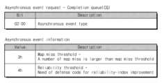
FIG. 14 is a diagram illustrating specifications for the asynchronous event described in FIGS. 5 to 13.
FIG. 15 is a diagram illustrating specifications for the threshold values described in FIGS. 5 to 13.
아래에서는, 본 발명의 기술 분야에서 통상의 지식을 가진 자가 본 발명을 용이하게 실시할 수 있을 정도로, 본 발명의 실시 예들이 명확하고 상세하게 기재될 것이다.Below, embodiments of the present invention will be described clearly and in detail so that those skilled in the art can easily practice the present invention.
도 1은 본 발명의 실시 예에 따라 동작하는 데이터 저장 장치가 적용된 컴퓨터 시스템을 예시적으로 보여주는 블록도이다. 도 1을 참조하면, 컴퓨터 시스템(Compute system, 100)은 호스트(Host, 110), 호스트 메모리(Host memory, 120), 및 데이터 저장 장치(130)를 포함할 수 있다.1 is a block diagram illustrating a computer system to which a data storage device operating according to an embodiment of the present invention is applied. Referring to FIG. 1 , a
호스트(110)는 컴퓨터 시스템(100)에 포함된 구성 요소들, 운영체제(OS; Operating System)를 구동시킬 수 있다. 예시적으로, 호스트(110)는 컴퓨터 시스템(100)에 포함된 구성 요소들을 제어하는 컨트롤러들, 인터페이스들, 그래픽 엔진 등을 포함할 수 있다. 예시적으로, 호스트(110)는 CPU(Central processing unit), GPU(Graphic processing unit), SoC(System on chip), 또는 AP(Application processor) 중 어느 하나일 수 있다.The
호스트 메모리(120)는 호스트(110)와 데이터 입출력을 수행할 수 있다. 호스트 메모리(120)는 컴퓨터 시스템(100)의 주 메모리, 동작 메모리, 버퍼 메모리 또는 캐시(Cache) 메모리로 동작할 수 있다. 호스트 메모리(120)는 DRAM 또는 SRAM 등과 같은 휘발성 메모리를 포함할 수 있다. 도 1을 참조하면, 호스트 메모리(120)는 호스트 메모리 버퍼(121)를 포함할 수 있다. 호스트 메모리 버퍼(121)는 데이터 저장 장치(130)와 같이 설명될 것이다.The
데이터 저장 장치(130)는 호스트(110)와 데이터 입출력을 수행할 수 있다. 도 1을 참조하면, 데이터 저장 장치(130)는 컨트롤러(131), 및 복수의 낸드 플래시 메모리들(Nand flash memory, 133a~133d)을 포함할 수 있다. 다만 데이터 저장 장치(130)는 휘발성 메모리(132)를 포함하지 않을 수 있다. 여기서 복수의 낸드 플래시 메모리들(133a~133d)의 개수는 도 1에 도시된 것에 한정되지 않는다.The
컨트롤러(131)는 호스트(110)와 데이터 입출력을 수행할 수 있다. 이를 위해, 컨트롤러(131)는 호스트(110)로부터 수신된 논리적 어드레스를 맵핑 테이블을 참조하여 물리적 어드레스로 변환할 수 있다. 컨트롤러(131)는 물리적 어드레스를 참조하여 복수의 낸드 플래시 메모리들(133a~133d)에 데이터를 저장하거나, 복수의 낸드 플래시 메모리들(133a~133d)로부터 데이터를 읽을 수 있다.The
컨트롤러(131)와 호스트(110) 사이의 인터페이스는 규약 또는 스펙(Specification)에 따라 통신하도록 구성될 수 있다. 예를 들어, 인터페이스는 USB(Universal Serial Bus), ATA(Advanced Technology Attachment), SATA(Serial ATA), SAS(Serial Attached SCSI), PATA(Parallel ATA), HSIC(High Speed Interchip), SCSI(Small Computer System Interface), 파이어와이어(Firewire), PCI(Peripheral Component Interconnection), PCIe(PCI express), NVMe(NonVolatile Memory express), UFS(Universal Flash Storage), SD(Secure Digital), MMC(MultiMedia Card), eMMC(embedded MMC) 등과 같은 다양한 규약들 중 적어도 하나를 이용하여 통신을 수행할 수 있다.The interface between the
복수의 낸드 플래시 메모리들(133a~133d)은 컨트롤러(131)의 제어에 응답하여 데이터 입출력을 수행할 수 있다. 도 1을 참조하면 데이터 저장 장치(130)는 내부에 복수의 낸드 플래시 메모리들(133a~133d)이 구비될 수 있다. 그러나 도 1에서 도시된 바에 한정되지 않고, 다른 종류의 플래시 메모리 또는 불휘발성 메모리가 구비될 수도 있다. 예를 들어, NOR 플래시 메모리(NOR flash memory), FRAM(Ferroelectric Random Access Memory), PRAM(Phase Change Random Access Memory), TRAM(Thyristor Random Access Memory), MRAM(Magnetic Random Access Memory), 또는 노어 플래시 메모리(NOR flash memory) 등이 데이터 저장 장치(130)에 포함될 수 있다.The plurality of
도 1을 참조하면, 데이터 저장 장치(130)는 휘발성 메모리(132)를 포함하지 않을 수 있다. 데이터 저장 장치(130)는 휘발성 메모리(132)를 포함하지 않는 대신에, 호스트(110)에 연결된 호스트 메모리(120)를 사용할 수 있다. 이를 위해, 호스트(110)는 호스트 메모리(120)의 일부를 호스트 메모리 버퍼(Host memory buffer, HMB, 121)로 할당할 수 있다. 여기서, 호스트 메모리 버퍼(121)란 호스트(110)가 데이터 저장 장치(130)를 위해 호스트 메모리(120) 중 일부를 할당한 영역을 의미할 수 있다.Referring to FIG. 1 , the
맵핑 테이블은 복수의 낸드 플래시 메모리들(133a~133d)에 사전에 저장되어있다. 데이터 저장 장치(130)에 전원이 인가되면, 맵핑 테이블은 호스트 메모리 버퍼(121)로 로딩(Loading)될 수 있다. 이 때, 호스트 메모리 버퍼(121)의 용량에 따라, 맵핑 테이블 전부가 호스트 메모리 버퍼(121)에 저장될 수도 있고, 일부가 호스트 메모리 버퍼(121)에 저장될 수도 있다.The mapping table is pre-stored in a plurality of
맵핑 테이블의 전부가 복수의 낸드 플래시 메모리들(133a~133d)에서 호스트 메모리 버퍼(121)에 저장되는 경우, 컨트롤러(131)는 맵 미스(Map miss)없이 데이터 입출력을 수행할 수 있다. 여기서, 맵 미스란 컨트롤러(131)가 호스트(110)로부터 수신한 논리 어드레스에 대응하는 맵핑 테이블을 호스트 메모리 버퍼(121)에서 찾을 수 없는 경우를 의미한다. 맵핑 테이블의 전부가 복수의 낸드 플래시 메모리들(133a~133d)에서 호스트 메모리 버퍼(121)에 저장되면, 맵 미스는 발생하지 않는다.When the entire mapping table is stored in the
컴퓨터 시스템(100)을 사용하는 유저(User)는 데이터 저장 장치(130)의 임의의 데이터에 접근할 수 있다. 이후, 일반적으로 유저는 최근 접근한 데이터를 다시 반복하여 접근할 수 있다. 또는 유저는 임의의 데이터에 접근한 후 인접 데이터에 접근할 수도 있다. 이러한 특성을 데이터의 지역성이라 한다. 데이터의 지역성을 고려하여, 맵핑 테이블의 전부가 호스트 메모리 버퍼(121)에 저장되는 대신에, 맵핑 테이블의 일부가 호스트 메모리 버퍼(121)에 저장될 수 있다.A user using the
데이터의 지역성을 고려하여 맵핑 테이블의 일부가 복수의 낸드 플래시 메모리들(133a~133d)로부터 로딩되어 호스트 메모리 버퍼(121)에 저장될 수 있다. 좀 더 구체적으로, 유저가 자주 사용하는 데이터를 고려하여, 컨트롤러(131)는 맵핑 테이블의 일부를 호스트 메모리 버퍼(121)에 저장할 수 있다. 이 경우, 맵핑 테이블의 전부가 호스트 메모리 버퍼(121)에 저장되는 경우에 비해, 호스트 메모리 버퍼(121)의 용량은 상대적으로 감소될 수 있다.Considering the locality of data, part of the mapping table may be loaded from the plurality of
다만 맵핑 테이블의 일부가 호스트 메모리 버퍼(121)에 저장되는 경우, 컨트롤러(131)에서 맵 미스가 발생될 수 있다. 이는 맵핑 테이블의 전부가 호스트 메모리 버퍼(121)에 저장되지 않았기 때문이다. 이 경우, 컨트롤러(131)는 복수의 낸드 플래시 메모리들(133a~133d)로부터 호스트(110)로부터 수신한 논리 어드레스에 대응하는 맵핑 테이블을 읽을 수 있다. 따라서, 맵 미스가 발생되면, 컨트롤러(131)는 맵핑 테이블을 복수의 낸드 플래시 메모리들(133a~133d)에서 읽어야 한다. 따라서, 컨트롤러(131)의 데이터 입출력 속도는 복수의 낸드 플래시 메모리들(133a~133d)에 접근하여 맵핑 테이블을 읽는 시간만큼 느려질 수 있다.However, if part of the mapping table is stored in the
도 2는 도 1에서 도시된 컨트롤러를 예시적으로 보여주는 블록도이다. 도 2는 도 1을 참조하여 설명될 것이다. 도 2를 참조하면, 컨트롤러(200)는 버스(210), 프로세서(220), RAM(230), 호스트 인터페이스(240), 및 메모리 인터페이스(260)를 포함할 수 있다. 컨트롤러(200)는 버퍼 컨트롤러(250)는 포함하지 않을 수 있다.FIG. 2 is a block diagram exemplarily showing the controller shown in FIG. 1. FIG. 2 will be explained with reference to FIG. 1 . Referring to FIG. 2 , the
버스(210)는 메모리 컨트롤러(131)의 구성 요소들 사이에 채널을 제공하도록 구성된다.
프로세서(220)는 메모리 컨트롤러(131)의 제반 동작을 제어하고, 논리 연산을 수행할 수 있다. 프로세서(220)는 호스트 인터페이스(240)를 통해 외부의 호스트와 통신할 수 있다. 프로세서(220)는 호스트 인터페이스(240)를 통해 수신되는 명령 또는 어드레스를 RAM(230)에 저장할 수 있다.The
RAM(230)은 프로세서(220)의 동작 메모리, 캐시 메모리 또는 버퍼 메모리로 사용될 수 있다. RAM(230)은 프로세서(220)가 실행하는 코드들 및 명령들을 저장할 수 있다. RAM(230)은 프로세서(220)에 의해 처리되는 데이터를 저장할 수 있다. RAM(230)은 SRAM을 포함할 수 있다.
호스트 인터페이스(240)는 프로세서(220)의 제어에 따라, 호스트(도 1 참조, 110)와 통신하도록 구성된다. 호스트 인터페이스(240)는 도 1에서 전술한 다양한 규약들 중 적어도 하나를 이용하여 통신하도록 구성될 수 있다.The
버퍼 컨트롤러(250)는 일반적으로 데이터 저장 장치에 내장된 버퍼(예를 들면, DRAM)를 제어하기 위해 구비된다. 그러나, 본 발명에 따르면 데이터 저장 장치(도 1 참조, 130) 내부에 버퍼가 구비되지 않고, 컨트롤러(200)는 호스트 메모리 버퍼(도 1 참조, 121)를 이용하여 데이터의 입출력 동작, 맵핑 테이블의 로딩 등을 수행하므로 버퍼 컨트롤러(250)는 구비되지 않는다. 따라서, 데이터 저장 장치(도 1 참조, 130)의 면적 및 비용이 감소된다.The
프로세서(220)의 제어에 따라, 휘발성 메모리(132, 도 1 참조)를 제어할 수 있다. 다만, 본 발명의 실시 예에 따라 동작하는 데이터 저장 장치가 적용된 컴퓨터 시스템(도 1 참조, 100)에서는 데이터 저장 장치(도 1 참조, 130)는 휘발성 메모리(도 1 참조, 132)를 포함하지 않을 수 있다. 따라서, 데이터 저장 장치(도 1 참조, 130)는 버퍼 컨트롤러(250)를 포함하지 않을 수 있다.According to the control of the
메모리 인터페이스(260)는 프로세서(220)의 제어에 응답하여 복수의 낸드 플래시 메모리들(도 1 참조, 133a~133d)과 통신할 수 있다.The
도 3은 본 발명의 실시 예에 따라 동작하는 데이터 저장 장치가 적용된 컴퓨터 시스템을 예시적으로 보여주는 블록도이다. 도 3을 참조하면, 컴퓨터 시스템(300)은 호스트(310), 호스트 메모리(320), 및 데이터 저장 장치(330)를 포함할 수 있다. 도 3에서는 본 발명의 실시 예에 따라 동작하는 데이터 저장 장치(330)에 의해 호스트 메모리 버퍼(321)의 사이즈(Size)가 증가되는 전반적인 동작이 설명될 것이다. 도 3은 도 1을 참조하여 설명될 것이며, 도 1에서의 설명과 중복되는 설명은 생략하기로 한다.Figure 3 is a block diagram illustrating a computer system to which a data storage device operating according to an embodiment of the present invention is applied. Referring to FIG. 3 , the
호스트(310)는 컨트롤러(331)로 비동기식 이벤트 명령을 전송할 수 있다(①). 상술한 명령은 제출 큐(Submission queue, SQ)에 저장될 수 있다. 여기서, 제출 큐(SQ)에는 호스트(310)가 컨트롤러(331)로 전송하는 임의의 명령들이 순차적으로 저장될 수 있다. 제출 큐(SQ)는 호스트에서 명령이 생성된 후 명령이 실행되기 전까지 명령이 저장되는 버퍼의 일종이다.The
컨트롤러(331)는 비동기식 이벤트 명령을 참조하여 비동기식 이벤트를 호스트(310)에게 요청할 수 있다(②). 상술한 요청은 완료 큐(Completion queue, CQ)에 저장될 수 있다. 여기서, 완료 큐(CQ)에는 데이터 저장 장치(330)가 호스트(310)의 명령들을 처리한 상태를 알리기 위한 결과들이 순차적으로 저장될 수 있다. 완료 큐(CQ)와 제출 큐(SQ)는 하나의 세트를 이룬다.The
본 발명의 실시 예에 따라 동작하는 컨트롤러(331)는 호스트 메모리 버퍼(321)의 사이즈가 적절한지 판단하고, 판단 결과에 따라 비동기식 이벤트를 호스트(310)에 요청할 수 있다. 예를 들어, 맵 미스 횟수가 증가되는 경우나, 복수의 낸드 플래시 메모리들(333a~333d)의 신뢰성 지수가 감소되는 경우에 컨트롤러(331)는 호스트(310)에게 호스트 메모리 버퍼(321)의 사이즈 증가를 요청할 수 있다.The
호스트(310)는 컨트롤러(331)의 비동기식 이벤트를 참조하여, 호스트 메모리 버퍼(321)의 사이즈를 조정할 수 있다(③). 도 3을 참조하면, 호스트 메모리 버퍼(321)의 사이즈는 호스트(310)에 의해 증가될 수 있다. 도시되진 않았지만, 반대로, 호스트 메모리 버퍼(321)의 사이즈는 호스트(310)에 의해 감소될 수도 있다.The
호스트(310)는 데이터 저장 장치(330)로 호스트 메모리 버퍼(321)의 사이즈 정보를 전송할 수 있다(④). 좀 더 구체적으로, 호스트(310)는 셋 피쳐(Set feature) 명령을 통해 호스트 메모리 버퍼(321)의 사이즈 정보 또는 호스트 메모리 버퍼(321)의 활성화 여부에 대한 정보를 전송할 수 있다.The
본 발명의 실시 예에 따른 데이터 저장 장치의 동작 방법에 의하면, 데이터 저장 장치(330)의 상태에 따라 호스트 메모리 버퍼(321)의 사이즈가 변동될 수 있다. 여기서, 데이터 저장 장치의 상태란 전술한대로 맵 미스 횟수가 증가되는 경우나, 복수의 낸드 플래시 메모리들(333a~333d)의 신뢰성 지수가 감소되는 경우를 의미할 수 있다.According to the method of operating a data storage device according to an embodiment of the present invention, the size of the
호스트 메모리 버퍼(321)의 사이즈가 증가되면, 컨트롤러(331)는 맵핑 데이터를 새로이 호스트 메모리 버퍼(321)에 업데이트 할 수 있다. 이 경우, 맵 미스 횟수는 감소될 수 있다.When the size of the
아울러, 컨트롤러(331)는 방어 코드(Defense code)를 호스트 메모리 버퍼(321)에 업데이트 할 수 있다. 여기서, 방어 코드란 복수의 낸드 플래시 메모리들(333a~333d)의 신뢰성 지수를 향상시키기 위한 코드를 의미할 수 있다. 예를 들어, 방어 코드는 ECC(Error correction code) 또는 LDPC(Low density parity check code) 등일 수 있다. 추가로, 방어 코드 외에 복수의 낸드 플래시 메모리들(333a~333d)의 신뢰성 지수를 향상시키기 위한 소프트웨어 프로그램(Software program)이 호스트 메모리 버퍼로 업데이트 될 수 있다. 예를 들어, 리드 리트라이 프로그램(Read retry program) 등이 호스트 메모리 버퍼로 업데이트 될 수 있다. 방어 코드가 업데이트 되는 경우, 복수의 낸드 플래시 메모리들(333a~333d)의 신뢰성 지수는 개선될 수 있다.In addition, the
도 4는 도 3에서 도시된 호스트, 호스트 메모리, 및 컨트롤러 사이의 동작을 예시적으로 보여주는 도면이다.FIG. 4 is a diagram illustrating operations between the host, host memory, and controller shown in FIG. 3.
S110 단계는 컴퓨터 시스템의 부팅(Booting) 과정을 나타낸다. S110 단계에서는 S111, S112, S113, 및 S114 단계들이 수행될 수 있다. S111 단계에서, 호스트(410)는 컨트롤러(431)를 인식할 수 있다. 좀 더 구체적으로, 호스트(410)는 식별자(Identifier)를 컨트롤러(431)에 전송하여, 컨트롤러(431)가 호스트 메모리 버퍼(421)를 사용할 수 있는지 확인할 수 있다.Step S110 represents the booting process of the computer system. In step S110, steps S111, S112, S113, and S114 may be performed. In step S111, the
S112 단계에서, 컨트롤러(431)는 호스트(410)로 호스트 메모리 버퍼(421)의 사용 여부를 알릴 수 있다. 컨트롤러(431)가 호스트 메모리 버퍼(421)를 사용하는 경우, 컨트롤러(431)는 필요한 호스트 메모리 버퍼(421)의 사이즈를 호스트(410)에게 더불어 요청할 수 있다.In step S112, the
S113 단계에서, 호스트(410)는 S112 단계에서 컨트롤러(431)의 요청을 참고하여 호스트 메모리 버퍼(421)를 할당할 수 있다. 호스트(410)는 호스트 메모리 버퍼(421)의 사이즈를 할당한 후(HMB size allocation), 할당 결과를 컨트롤러(431)로 알릴 수 있다. 좀 더 구체적으로, 호스트(410)는 할당 결과를 셋 피쳐(Set feature) 명령을 통해 컨트롤러(431)로 알릴 수 있다. 셋 피쳐 명령에는 호스트 메모리 버퍼(421)의 사이즈 정보 또는 호스트 메모리 버퍼(421)의 활성화 여부에 대한 정보가 포함될 수 있다. 전술한대로, 호스트 메모리 버퍼(421)에는 데이터의 지역성을 고려하여 맵핑 테이블의 일부만이 저장될 수 있다.In step S113, the
S114 단계에서, 컨트롤러(431)는 호스트 메모리 버퍼(421)로 맵핑 테이블의 일부를 업데이트(Update)할 수 있다. 좀 더 구체적으로, 컨트롤러(431)는 호스트(410)를 통해 호스트 메모리 버퍼(421)로 맵핑 테이블의 일부를 업데이트 할 수 있다.In step S114, the
S120 단계에서 호스트(410), 호스트 메모리(420), 및 컨트롤러(431)는 정상 동작(Normal operation)을 수행할 수 있다. 여기서, 정상 동작이란 유저에 의한 호스트(410), 호스트 메모리(320), 및 컨트롤러(431)의 전반적인 동작을 의미할 수 있다. S120 단계는 S121 단계 및 S122 단계를 포함할 수 있다.In step S120, the
S121 단계는 호스트(410)가 컨트롤러(431)로 명령 및 어드레스를 전송할 수 있다. 도시되진 않았지만, 호스트(410) 및 호스트 메모리(420) 사이에 데이터 입출력이 수행될 수 있다. 호스트(410) 및 컨트롤러(431) 사이에 데이터 입출력이 수행될 수 있다. 이를 위해, 컨트롤러(431)는 호스트 메모리 버퍼(421)에 저장된 맵핑 테이블을 참조할 수 있다.In step S121, the
S122 단계에서, 컨트롤러(431)는 본 발명의 동작 방법에 따라 맵 미스 횟수를 카운팅할 수 있다. 아울러 맵 미스와 관계 없이 시간이 경과됨에 따라, 불휘발성 메모리 셀의 쓰기 횟수 제한으로 인해 복수의 낸드 플래시 메모리들(도 3 참조, 333a~333d)의 신뢰성 지수는 점차 감소될 수 있다. 따라서 컨트롤러(431)는 본 발명의 동작 방법에 따라 복수의 낸드 플래시 메모리들(도 3 참조, 333a~333d)의 신뢰성 지수를 모니터링 할 수 있다.In step S122, the
S130 단계에서 호스트(410) 및 컨트롤러(431)는 비동기식 이벤트에 대한 동작(Asynchronous event operation)을 수행할 수 있다. S130 단계는 S131, S132, S133, 및 S134 단계를 포함할 수 있다.In step S130, the
S131 단계에서, 호스트(410)는 컨트롤러(431)로 비동기식 이벤트를 위한 명령을 전송할 수 있다.In step S131, the
S132 단계에서, 컨트롤러(431)는 S131 단계의 명령에 응답하여, 호스트(410)로 비동기식 이벤트를 요청할 수 있다. 컨트롤러(431)는 비동기식 이벤트를 통해 맵 미스 횟수를 감소시키거나, 복수의 낸드 플래시 메모리들(도 3 참조, 333a~333d)의 신뢰성 지수를 향상시킬 수도 있다. 좀 더 구체적으로, 컨트롤러(431)는 비동기식 이벤트를 통해 호스트 메모리 버퍼(421)의 사이즈 재조정을 위한 요청을 호스트(410)에 전송할 수 있다.In step S132, the
S133 단계에서, 호스트(410)는 비동기식 이벤트에 응답하여 호스트 메모리 버퍼(421)의 사이즈를 조정할 수 있다. 이를 통해, 호스트 메모리 버퍼(421)의 사이즈는 증가되거나 감소될 수 있다. 예를 들어, 맵 미스 횟수가 증가된 경우, 호스트 메모리 버퍼(421)의 사이즈는 증가될 수 있다. 맵 미스 횟수가 감소된 경우, 호스트 메모리 버퍼(421)의 사이즈는 감소될 수 있다.In step S133, the
복수의 낸드 플래시 메모리들(도 3 참조, 333a~333d)의 신뢰성 지수가 감소된 경우에는 호스트 메모리 버퍼(421)의 사이즈가 증가될 수 있다. 호스트(410)는 호스트 메모리 버퍼(421)의 사이즈를 조정한 후, 조정 결과를 컨트롤러(431)로 알릴 수 있다. 조정 결과를 컨트롤러(431)로 알리기 위해, 호스트(410)는 셋 피쳐 명령을 컨트롤러(431)로 전송할 수 있다. 전술한대로, 셋 피쳐 명령에는 호스트 메모리 버퍼(421)의 사이즈 정보 또는 호스트 메모리 버퍼(421)의 활성화 여부에 대한 정보가 포함될 수 있다.If the reliability index of the plurality of NAND flash memories (see FIG. 3, 333a to 333d) decreases, the size of the
S134 단계에서, 컨트롤러(431)는 호스트 메모리 버퍼(421)로 맵핑 테이블 또는 방어 코드(Defense code)를 업데이트할 수 있다. 좀 더 구체적으로, 컨트롤러(431)는 호스트(410)를 통해 호스트 메모리 버퍼(421)로 맵핑 테이블 또는 방어 코드(Defense code)를 업데이트할 수 있다.In step S134, the
S140 단계에서, 컨트롤러(431)가 요청한 비동기식 이벤트가 처리된 후, 호스트(410), 호스트 메모리(420), 및 컨트롤러(431)는 정상 동작(Normal operation)을 다시 수행할 수 있다. 즉, S140 단계는 S120 단계와 대체로 동일하다.In step S140, after the asynchronous event requested by the
다만, S140 단계에서는 데이터의 지역성을 고려하여, 컨트롤러(431)의 비동기식 이벤트에 의해 호스트 메모리 버퍼(421)의 사이즈가 조정된 상태이다. 따라서, S120 단계에 비해, S140 단계에서 맵 미스 횟수는 감소될 수 있다. 추가로, S140 단계에서는 복수의 낸드 플래시 메모리들(도 3 참조, 333a~333d)의 신뢰성 지수를 고려하여, 컨트롤러(431)의 비동기식 이벤트에 의해 호스트 메모리 버퍼(421)의 사이즈가 증가된 상태일 수 있다. 따라서, S120 단계에 비해, S140 단계에서는 데이터의 에러율이 현저히 감소될 수도 있다.However, in step S140, the size of the
도 4에서 도시되진 않았지만, 컨트롤러(431)는 비동기식 이벤트를 더 생성할 수도 있다. 좀 더 구체적으로, S141 단계 이후에도 데이터의 지역성 또는 신뢰성 지수를 고려하여, 추가로 비동기식 이벤트가 더 생성될 수 있다. Although not shown in FIG. 4, the
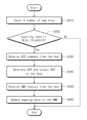
도 5는 본 발명의 실시 예에 따른 데이터 저장 장치의 동작 방법을 예시적으로 보여주는 순서도이다. 도 5는 도 3을 참조하여 설명될 것이다.Figure 5 is a flowchart exemplarily showing a method of operating a data storage device according to an embodiment of the present invention. FIG. 5 will be explained with reference to FIG. 3 .
S240 단계에서, 컨트롤러(도 3 참조, 331)는 맵 미스 정보에 기초하여 비동기식 이벤트 요청을 생성할 수 있다. 맵 미스 정보란 컨트롤러(도 3 참조, 331)가 호스트(도 3 참조, 310) 명령을 수행할 때 발생되는 맵 미스에 관한 정보를 의미할 수 있다. 생성된 비동기식 이벤트는 호스트(도 3 참조, 310)로 출력될 수 있다.In step S240, the controller (see FIG. 3, 331) may generate an asynchronous event request based on map miss information. Map miss information may refer to information about a map miss that occurs when a controller (331, see FIG. 3) executes a command from a host (310, see FIG. 3). The generated asynchronous event may be output to the host (see FIG. 3, 310).
S250 단계에서, 컨트롤러(도 3 참조, 331)는 비동기식 이벤트에 따라 호스트(도 3 참조, 310)에 의해 조정된 호스트 메모리 버퍼(도 3 참조, 321)에 관한 정보(HMB feature)를 수신할 수 있다.In step S250, the controller (see FIG. 3, 331) may receive information (HMB feature) about the host memory buffer (see FIG. 3, 321) adjusted by the host (see FIG. 3, 310) according to the asynchronous event. there is.
S260 단계에서, 컨트롤러(도 3 참조, 331)는 상술한 호스트 메모리 버퍼(도 3 참조, 321)에 관한 정보(HMB feature)를 참조하여, 방어 코드를 호스트 메모리 버퍼(도 3 참조, 321)로 업데이트 할 수 있다.In step S260, the controller (see FIG. 3, 331) refers to the information (HMB feature) about the host memory buffer (see FIG. 3, 321) described above, and transfers the defense code to the host memory buffer (see FIG. 3, 321). It can be updated.
도 6은 도 5에서 도시된 S240 단계를 좀 더 상세하게 보여주는 순서도이다. 도 10은 도 3 내지 도 5를 참조하여 설명될 것이다.Figure 6 is a flowchart showing step S240 shown in Figure 5 in more detail. FIG. 10 will be explained with reference to FIGS. 3 to 5.
S241 단계에서, 컨트롤러(도 3 참조, 331)는 맵 미스 횟수를 카운팅 할 수 있다. 전술한대로, 맵 미스는 호스트 메모리 버퍼(도 3 참조, 321)에 맵핑 테이블 중 일부만이 저장된 경우에 발생될 수 있다. S241 단계는 도 4의 S122 단계에 대응될 수 있다.In step S241, the controller (see FIG. 3, 331) may count the number of map misses. As described above, a map miss may occur when only a portion of the mapping table is stored in the host memory buffer (see 321 of FIG. 3). Step S241 may correspond to step S122 in FIG. 4.
S242 단계에서, 컨트롤러(도 3 참조, 331)는 카운팅 결과와 미스 문턱 값(Miss threshold)을 비교할 수 있다. 컨트롤러(도 3 참조, 331)는 비교 결과에 기초하여 비동기식 이벤트 요청 여부를 결정할 수 있다.In step S242, the controller (see FIG. 3, 331) may compare the counting result and the miss threshold. The controller (see FIG. 3, 331) may determine whether to request an asynchronous event based on the comparison result.
도 7은 도 5에서 도시된 데이터 저장 장치의 동작 방법을 좀 더 상세하게 보여주는 순서도이다. 도 7은 도 3 내지 도 5를 참조하여 설명될 것이다.FIG. 7 is a flowchart showing in more detail the operating method of the data storage device shown in FIG. 5. FIG. 7 will be explained with reference to FIGS. 3 to 5.
S310 단계에서, 컨트롤러(도 3 참조, 331)는 맵 미스 횟수를 카운팅 할 수 있다. 전술한대로, 맵 미스는 호스트 메모리 버퍼(도 3 참조, 321)에 맵핑 테이블 중 일부만이 저장된 경우에 발생될 수 있다. S310 단계는 도 4의 S122 단계 및 도 6의 S241 단계에 대응될 수 있다.In step S310, the controller (see FIG. 3, 331) may count the number of map misses. As described above, a map miss may occur when only a portion of the mapping table is stored in the host memory buffer (see 321 of FIG. 3). Step S310 may correspond to step S122 in FIG. 4 and step S241 in FIG. 6.
S320 단계에서, 컨트롤러(도 3 참조, 331)는 카운팅 결과와 미스 문턱 값(Miss threshold)을 비교할 수 있다. 카운팅 결과가 미스 문턱 값보다 큰 경우(Yes), S330 단계가 수행될 수 있다. 카운팅 결과가 미스 문턱 값보다 작은 경우(No), S360 단계가 수행될 수 있다.In step S320, the controller (see FIG. 3, 331) may compare the counting result and the miss threshold. If the counting result is greater than the miss threshold (Yes), step S330 may be performed. If the counting result is less than the miss threshold (No), step S360 may be performed.
S330 단계에서, 컨트롤러(도 3 참조, 331)는 호스트(도 3 참조, 310)로부터 비동기식 이벤트 명령을 수신할 수 있다. S330 단계는 도 4의 S131 단계 및 도 5의 S240 단계에 대응될 수 있다.In step S330, the controller (see FIG. 3, 331) may receive an asynchronous event command from the host (see FIG. 3, 310). Step S330 may correspond to step S131 in FIG. 4 and step S240 in FIG. 5.
S340 단계에서, 컨트롤러(도 3 참조, 331)는 비동기식 이벤트 명령에 응답하여, 비동기식 이벤트 요청(Asynchronous event request, AER)을 생성할 수 있다. 컨트롤러(도 3 참조, 331)는 비동기식 이벤트를 호스트(도 3 참조, 310)로 출력할 수 있다. 비동기식 이벤트는 카운팅 결과가 미스 문턱 값보다 큰 경우 컨트롤러(도 3 참조, 331)에 의해 생성될 수 있다. S340 단계는 도 4의 S132 단계 및 도 5의 S240 단계에 대응될 수 있다.In step S340, the controller (see FIG. 3, 331) may generate an asynchronous event request (Asynchronous event request, AER) in response to the asynchronous event command. The controller (see FIG. 3, 331) may output asynchronous events to the host (see FIG. 3, 310). An asynchronous event may be generated by the controller (see Figure 3, 331) when the counting result is greater than the miss threshold. Step S340 may correspond to step S132 in FIG. 4 and step S240 in FIG. 5.
S350 단계에서, 컨트롤러(도 3 참조, 331)는 비동기식 이벤트에 따라 호스트(도 3 참조, 310)가 호스트 메모리 버퍼(도 3 참조, 321)의 사이즈를 증가한 결과(HMB feature)를 수신할 수 있다. 좀 더 구체적으로, 컨트롤러(도 3 참조, 331)는 호스트(도 3 참조, 310)로부터 셋 피쳐 커맨드를 통해 상술한 결과(HMB feature)를 수신할 수 있다. 비동기식 이벤트에 응답하여, 호스트(도 3 참조, 310)는 호스트 메모리 버퍼(도 3 참조, 321)의 사이즈를 증가시킬 수 있다. S350 단계는 도 4의 S133 단계 및 도 5의 S250 단계에 대응될 수 있다. 여기서, 호스트 메모리 버퍼(도 3 참조, 321)의 사이즈가 증가되는 양은 컨트롤러(도 3 참조, 331)에 의해 결정될 수 있다. 혹은 호스트 메모리 버퍼(도 3 참조, 321)의 사이즈가 증가되는 양은 사전에 정의된 값일 수도 있다.In step S350, the controller (see FIG. 3, 331) may receive a result (HMB feature) in which the host (see FIG. 3, 310) increases the size of the host memory buffer (see FIG. 3, 321) according to an asynchronous event. . More specifically, the controller (see FIG. 3, 331) may receive the above-described result (HMB feature) from the host (see FIG. 3, 310) through a set feature command. In response to the asynchronous event, the host (see 310, Figure 3) may increase the size of the host memory buffer (321, Figure 3). Step S350 may correspond to step S133 in FIG. 4 and step S250 in FIG. 5. Here, the amount by which the size of the host memory buffer (see FIG. 3, 321) is increased may be determined by the controller (see FIG. 3, 331). Alternatively, the amount by which the size of the host memory buffer (see FIG. 3, 321) is increased may be a predefined value.
S360 단계에서, 컨트롤러(도 3 참조, 331)는 맵핑 테이블 중 새로운 일부 맵핑 테이블을 호스트 메모리 버퍼(도 3 참조, 321)로 업데이트 할 수 있다. 도 7를 참조하면, 카운팅 결과가 미스 문턱 값보다 큰 경우이므로, 호스트 메모리 버퍼(도 3 참조, 321)에는 이전에 호스트 메모리 버퍼(도 3 참조, 321)에 저장된 맵핑 테이블(도 4 참조, S114))보다 사이즈가 큰 새로운 맵핑 테이블이 저장될 수 있다. 맵핑 테이블은 호스트 메모리 버퍼(도 3 참조, 321)의 사이즈를 참조하여, 호스트 메모리 버퍼(도 3 참조, 321)로 업데이트될 수 있다. S360 단계는 도 4의 S134 단계 및 도 5의 S260 단계에 대응될 수 있다.In step S360, the controller (see FIG. 3, 331) may update some new mapping tables among the mapping tables to the host memory buffer (see FIG. 3, 321). Referring to FIG. 7, since the counting result is greater than the miss threshold value, the host memory buffer (see FIG. 3, 321) contains the mapping table (see FIG. 4, S114) previously stored in the host memory buffer (see FIG. 3, 321). A new mapping table with a size larger than )) can be stored. The mapping table may be updated with the host memory buffer (see FIG. 3, 321) by referring to the size of the host memory buffer (see FIG. 3, 321). Step S360 may correspond to step S134 in FIG. 4 and step S260 in FIG. 5.
본 발명의 실시 예에 따른 데이터 저장 장치의 동작 방법에 따르면, 맵 미스 횟수를 고려하여 비동기식 이벤트가 생성될 수 있다. 비동기식 이벤트에 따라 새로운 일부 맵핑 테이블이 호스트 메모리 버퍼(도 3 참조, 321)에 업데이트될 수 있다. 즉, 유저가 사용하는 데이터의 지역성을 고려하여, 맵핑 테이블이 호스트 메모리 버퍼(도 3 참조, 321)에 저장될 수 있다. 좀 더 구체적으로, 본 발명의 실시 예에 따른 데이터 저장 장치의 동작 방법은 맵 미스마다 발생되는 복수의 낸드 플래시 메모리들(도 3 참조, 333a~333d)에 접근하여 맵핑 테이블을 읽는 시간을 개선할 수 있다.According to the method of operating a data storage device according to an embodiment of the present invention, an asynchronous event may be generated considering the number of map misses. Depending on the asynchronous event, some new mapping table may be updated in the host memory buffer (see Figure 3, 321). That is, considering the locality of data used by the user, the mapping table may be stored in the host memory buffer (see FIG. 3, 321). More specifically, the method of operating a data storage device according to an embodiment of the present invention improves the time to read the mapping table by accessing a plurality of NAND flash memories (see FIG. 3, 333a to 333d) that occur for each map miss. You can.
추가로, 맵 미스가 발생되면 새로운 맵핑 테이블이 호스트 메모리 버퍼(도 3 참조, 321)에 업데이트 될 수 있다. 이 때, 이전의 맵핑 테이블은 복수의 낸드 플래시 메모리들(도 3 참조, 333a~333d)에 백업(Backup)될 수 있다. 맵 미스가 빈번하게 발생되면, 그만큼 복수의 낸드 플래시 메모리들(도 3 참조, 333a~333d)에 접근하는 횟수가 증가하게 된다. 따라서, 이전 맵핑 테이블의 백업에 의해, 복수의 낸드 플래시 메모리들(도 3 참조, 333a~333d)의 신뢰성 지수는 감소될 수 있다. 본 발명의 실시 예에 따른 데이터 저장 장치의 동작 방법은 이전 맵핑 테이블의 백업으로 인한 신뢰성 지수의 감소도 방지할 수 있다.Additionally, when a map miss occurs, a new mapping table may be updated in the host memory buffer (see 321 of FIG. 3). At this time, the previous mapping table may be backed up to a plurality of NAND flash memories (see FIG. 3, 333a to 333d). If map misses occur frequently, the number of accesses to a plurality of NAND flash memories (see FIG. 3, 333a to 333d) increases accordingly. Accordingly, by backing up the previous mapping table, the reliability index of the plurality of NAND flash memories (see FIG. 3, 333a to 333d) may be reduced. The method of operating a data storage device according to an embodiment of the present invention can also prevent a decrease in reliability index due to backup of the previous mapping table.
도시되진 않았지만, 본 발명의 실시 예에 따른 데이터 저장 장치의 동작 방법에서 미스 문턱 값은 복수의 레벨들(Levels)로 설정될 수 있다. 도 7에서는 호스트 메모리 버퍼(도 3 참조, 321)의 영역이 증가되는 경우에 대해서만 도시되었으나, 본 발명은 이에 한정되지 않는다. 예를 들어, 호스트 메모리 버퍼(도 3 참조, 321)의 사이즈가 증가된 후 맵 미스 횟수가 감소되면, 본 발명의 실시 예에 따른 데이터 저장 장치의 동작 방법에 의해 호스트 메모리 버퍼(도 3 참조, 321)의 사이즈는 초기 설정된 사이즈로 다시 감소될 수도 있다.Although not shown, in the method of operating a data storage device according to an embodiment of the present invention, the miss threshold value may be set to a plurality of levels. In FIG. 7, only the case where the area of the host memory buffer (see FIG. 3, 321) is increased is shown, but the present invention is not limited to this. For example, if the number of map misses decreases after the size of the host memory buffer (see FIG. 3, 321) is increased, the host memory buffer (see FIG. 3, 321) is decreased by the operation method of the data storage device according to an embodiment of the present invention. The size of 321) may be reduced back to the initially set size.
도 7은 초기 호스트 메모리 버퍼(도 3 참조, 321)의 사이즈가 작게 설정되었다가 맵 미스 횟수가 증가되는 경우, 호스트 메모리 버퍼(도 3 참조, 321)의 사이즈가 증가되는 경우에 관한 것이다. 도 8은 도 7와 반대되는 경우에 관한 것이다.FIG. 7 relates to a case where the initial size of the host memory buffer (see FIG. 3, 321) is set small, and then the number of map misses increases, and the size of the host memory buffer (see FIG. 3, 321) increases. Figure 8 relates to the opposite case to Figure 7.
도 8은 도 5에서 도시된 데이터 저장 장치의 동작 방법을 좀 더 상세하게 보여주는 순서도이다. 도 8은 도 3 내지 도 7를 참조하여 설명될 것이다.FIG. 8 is a flowchart showing in more detail the operating method of the data storage device shown in FIG. 5. FIG. 8 will be explained with reference to FIGS. 3 to 7.
S410 단계에서, 컨트롤러(도 3 참조, 331)는 맵 미스 횟수를 카운팅 할 수 있다. S410 단계는 도 4의 S122 단계 및 도 6의 S241 단계에 대응될 수 있다.In step S410, the controller (see FIG. 3, 331) may count the number of map misses. Step S410 may correspond to step S122 in FIG. 4 and step S241 in FIG. 6.
S420 단계에서, 컨트롤러(도 3 참조, 331)는 카운팅 결과와 미스 문턱 값(Miss threshold)을 비교할 수 있다. 여기서, 미스 문턱 값은 도 7의 S320 단계에서 설명된 미스 문턱 값과 동일할 수도 있고, 상이할 수도 있다. 카운팅 결과가 미스 문턱 값보다 작은 경우(Yes), S430 단계가 수행될 수 있다. 카운팅 결과가 미스 문턱 값보다 큰 경우(No), S460 단계가 수행될 수 있다.In step S420, the controller (see FIG. 3, 331) may compare the counting result and the miss threshold. Here, the miss threshold value may be the same as or different from the miss threshold value described in step S320 of FIG. 7. If the counting result is less than the miss threshold (Yes), step S430 may be performed. If the counting result is greater than the miss threshold (No), step S460 may be performed.
S430 단계에서, 컨트롤러(도 3 참조, 331)는 호스트(도 3 참조, 310)로부터 비동기식 이벤트 명령을 수신할 수 있다. S430 단계는 도 4의 S131 단계에 대응될 수 있다.In step S430, the controller (see FIG. 3, 331) may receive an asynchronous event command from the host (see FIG. 3, 310). Step S430 may correspond to step S131 of FIG. 4.
S440 단계에서, 컨트롤러(도 3 참조, 331)는 비동기식 이벤트 요청을 생성할 수 있다. 컨트롤러(도 3 참조, 331)는 비동기식 이벤트를 호스트(도 3 참조, 310)로 출력할 수 있다. 비동기식 이벤트는 카운팅 결과가 미스 문턱 값보다 작은 경우 컨트롤러(도 3 참조, 331)에 의해 생성될 수 있다. S440 단계는 도 4의 S132 단계 및 도 5의 S240 단계에 대응될 수 있다.In step S440, the controller (see FIG. 3, 331) may generate an asynchronous event request. The controller (see FIG. 3, 331) may output asynchronous events to the host (see FIG. 3, 310). Asynchronous events may be generated by the controller (see Figure 3, 331) when the counting result is less than a miss threshold. Step S440 may correspond to step S132 in FIG. 4 and step S240 in FIG. 5.
S450 단계에서, 컨트롤러(도 3 참조, 331)는 비동기식 이벤트에 따라 호스트(도 3 참조, 310)가 호스트 메모리 버퍼(도 3 참조, 321)를 회수한 결과(HMB feature)를 수신할 수 있다. 비동기식 이벤트에 응답하여, 호스트(도 3 참조, 310)는 호스트 메모리 버퍼(도 3 참조, 321)의 사이즈를 감소시킬 수 있다. S450 단계는 도 4의 S133 단계에 대응될 수 있다. 여기서, 호스트 메모리 버퍼(도 3 참조, 321)의 사이즈가 감소되는 양은 컨트롤러(도 3 참조, 331)에 의해 결정될 수 있다. 혹은 호스트 메모리 버퍼(도 3 참조, 321)의 사이즈가 감소되는 양은 사전에 정의된 값일 수도 있다.In step S450, the controller (see FIG. 3, 331) may receive a result (HMB feature) of the host (see FIG. 3, 310) retrieving the host memory buffer (see FIG. 3, 321) according to an asynchronous event. In response to the asynchronous event, the host 310 (see FIG. 3) may reduce the size of the host memory buffer 321 (see FIG. 3). Step S450 may correspond to step S133 in FIG. 4. Here, the amount by which the size of the host memory buffer (see FIG. 3, 321) is reduced may be determined by the controller (see FIG. 3, 331). Alternatively, the amount by which the size of the host memory buffer (see FIG. 3, 321) is reduced may be a predefined value.
S460 단계에서, 컨트롤러(도 3 참조, 331)는 맵핑 테이블 중 새로운 일부 맵핑 테이블을 호스트 메모리 버퍼(도 3 참조, 321)로 업데이트 할 수 있다. 도 8을 참조하면, 카운팅 결과가 미스 문턱 값보다 작은 경우이므로, 호스트 메모리 버퍼에는 이전에 호스트 메모리 버퍼에 저장된 맵핑 테이블(도 4 참조, S114)보다 사이즈가 작은 새로운 맵핑 테이블이 저장될 수 있다. 맵핑 테이블은 호스트 메모리 버퍼(도 3 참조, 321)의 사이즈를 참조하여, 호스트 메모리 버퍼(도 3 참조, 321)로 업데이트될 수 있다. S460 단계는 도 4의 S134 단계에 대응될 수 있다.In step S460, the controller (see FIG. 3, 331) may update some new mapping tables among the mapping tables to the host memory buffer (see FIG. 3, 321). Referring to FIG. 8, since the counting result is smaller than the miss threshold, a new mapping table smaller in size than the mapping table previously stored in the host memory buffer (see FIG. 4, S114) may be stored in the host memory buffer. The mapping table may be updated with the host memory buffer (see FIG. 3, 321) by referring to the size of the host memory buffer (see FIG. 3, 321). Step S460 may correspond to step S134 of FIG. 4.
도 8에서는 호스트 메모리 버퍼(도 3 참조, 321)의 사이즈가 감소되는 경우에 대해서만 도시되었으나, 본 발명은 이에 한정되지 않는다. 예를 들어, 호스트 메모리 버퍼(도 3 참조, 321)의 사이즈가 감소된 후 맵 미스 횟수가 증가되면, 본 발명의 실시 예에 따른 데이터 저장 장치의 동작 방법에 의해 호스트 메모리 버퍼(도 3 참조, 321)의 사이즈는 증가될 수도 있다.In FIG. 8, only the case where the size of the host memory buffer (see FIG. 3, 321) is reduced is shown, but the present invention is not limited to this. For example, if the number of map misses increases after the size of the host memory buffer (see FIG. 3, 321) is reduced, the host memory buffer (see FIG. 3, 321) is increased by the method of operating a data storage device according to an embodiment of the present invention. 321) may be increased in size.
도 9는 본 발명의 실시 예에 따른 데이터 저장 장치의 동작 방법을 예시적으로 보여주는 순서도이다. 도 9는 도 3 및 도 4를 참조하여 설명될 것이다.Figure 9 is a flowchart exemplarily showing a method of operating a data storage device according to an embodiment of the present invention. FIG. 9 will be explained with reference to FIGS. 3 and 4 .
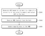
S540 단계에서, 컨트롤러(도 3 참조, 331)는 복수의 낸드 플래시 메모리들(도 3 참조, 333a~333d)의 신뢰성 지수에 기초하여 비동기식 이벤트 요청을 생성할 수 있다. 생성된 비동기식 이벤트는 호스트(도 3 참조, 310)로 출력될 수 있다.In step S540, the controller (see FIG. 3, 331) may generate an asynchronous event request based on the reliability index of a plurality of NAND flash memories (see FIG. 3, 333a to 333d). The generated asynchronous event may be output to the host (see FIG. 3, 310).
S550 단계에서, 컨트롤러(도 3 참조, 331)는 비동기식 이벤트에 따라 호스트(도 3 참조, 310)에 의해 조정된 호스트 메모리 버퍼(도 3 참조, 321)에 관한 정보(HMB feature)를 수신할 수 있다.In step S550, the controller (see FIG. 3, 331) may receive information (HMB feature) about the host memory buffer (see FIG. 3, 321) adjusted by the host (see FIG. 3, 310) according to the asynchronous event. there is.
S560 단계에서, 컨트롤러(도 3 참조, 331)는 상술한 호스트 메모리 버퍼(도 3 참조, 321)에 관한 정보(HMB feature)를 참조하여, 방어 코드를 호스트 메모리 버퍼(도 3 참조, 321)로 업데이트 할 수 있다.In step S560, the controller (see FIG. 3, 331) refers to the information (HMB feature) about the host memory buffer (see FIG. 3, 321) described above and transfers the defense code to the host memory buffer (see FIG. 3, 321). It can be updated.
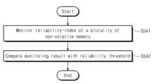
도 10은 도 9에서 도시된 S540 단계를 좀 더 상세하게 보여주는 순서도이다. 도 10은 도 3, 도 4, 및 도 9를 참조하여 설명될 것이다.FIG. 10 is a flowchart showing step S540 shown in FIG. 9 in more detail. FIG. 10 will be explained with reference to FIGS. 3, 4, and 9.
S541 단계에서, 컨트롤러(도 3 참조, 331)는 복수의 낸드 플래시 메모리들(도 3 참조, 333a~333d)의 신뢰성 지수를 모니터링 할 수 있다. 신뢰성 지수의 확인을 위해, 예를 들면, 컨트롤러(도 3 참조, 331)는 BER(Bit error rate)을 확인할 수 있다. 신뢰성 지수가 높은 경우, BER은 상대적으로 낮을 수 있다. 신뢰성 지수가 낮은 경우, BER은 상대적으로 높을 수 있다. 그러나 신뢰성 지수를 확인하는 방법은 상술한 것에 한정되지 않는다. S541 단계는 도 4의 S122 단계에 대응될 수 있다.In step S541, the controller (see FIG. 3, 331) may monitor the reliability index of a plurality of NAND flash memories (see FIG. 3, 333a to 333d). To check the reliability index, for example, the controller (see FIG. 3, 331) may check the bit error rate (BER). If the reliability index is high, the BER may be relatively low. If the reliability index is low, the BER may be relatively high. However, the method for checking the reliability index is not limited to the above. Step S541 may correspond to step S122 of FIG. 4.
S542 단계에서, 컨트롤러(도 3 참조, 331)는 모니터링 결과와 신뢰성 문턱 값(Reliability threshold)을 비교할 수 있다. 컨트롤러(도 3 참조, 331)는 비교 결과에 기초하여 비동기식 이벤트 요청 여부를 결정할 수 있다.In step S542, the controller (see FIG. 3, 331) may compare the monitoring results and the reliability threshold. The controller (see FIG. 3, 331) may determine whether to request an asynchronous event based on the comparison result.
도 11은 도 9에서 도시된 데이터 저장 장치의 동작 방법을 좀 더 상세하게 보여주는 순서도이다. 도 11은 도 3, 도 4, 도 9, 및 도 10을 참조하여 설명될 것이다.FIG. 11 is a flowchart showing in more detail the operating method of the data storage device shown in FIG. 9. FIG. 11 will be explained with reference to FIGS. 3, 4, 9, and 10.
S610 단계에서, 컨트롤러(도 3 참조, 331)는 복수의 낸드 플래시 메모리들(도 3 참조, 333a~333d)의 신뢰성 지수를 모니터링 할 수 있다. S610 단계는 도 4의 S122 단계 및 도 9의 S541 단계에 대응될 수 있다.In step S610, the controller (see FIG. 3, 331) may monitor the reliability index of a plurality of NAND flash memories (see FIG. 3, 333a to 333d). Step S610 may correspond to step S122 in FIG. 4 and step S541 in FIG. 9.
S620 단계에서, 컨트롤러(도 3 참조, 331)는 모니터링 결과와 신뢰성 문턱 값(Reliability threshold)을 비교할 수 있다. 모니터링 결과가 신뢰성 문턱 값보다 작은 경우(Yes), S630 단계가 수행될 수 있다. 모니터링 결과가 신뢰성 문턱 값보다 높은 경우(No), S660 단계가 수행될 수 있다.In step S620, the controller (see FIG. 3, 331) may compare the monitoring result and the reliability threshold. If the monitoring result is less than the reliability threshold (Yes), step S630 may be performed. If the monitoring result is higher than the reliability threshold (No), step S660 may be performed.
S630 단계에서, 컨트롤러(도 3 참조, 331)는 호스트(도 3 참조, 310)로부터 비동기식 이벤트 명령을 수신할 수 있다. S630 단계는 도 4의 S131 단계에 대응될 수 있다.In step S630, the controller (see FIG. 3, 331) may receive an asynchronous event command from the host (see FIG. 3, 310). Step S630 may correspond to step S131 of FIG. 4.
S640 단계에서, 컨트롤러(도 3 참조, 331)는 비동기식 이벤트 요청을 생성할 수 있다. 컨트롤러(도 3 참조, 331)는 비동기식 이벤트를 호스트(도 3 참조, 310)로 출력할 수 있다. 비동기식 이벤트는 모니터링 결과가 신뢰성 문턱 값보다 낮은 경우 컨트롤러(도 3 참조, 331)에 의해 생성될 수 있다. S640 단계는 도 4의 S132 단계 및 도 9의 S540 단계에 대응될 수 있다.In step S640, the controller (see FIG. 3, 331) may generate an asynchronous event request. The controller (see FIG. 3, 331) may output asynchronous events to the host (see FIG. 3, 310). Asynchronous events may be generated by the controller (see Figure 3, 331) when the monitoring result is below a reliability threshold. Step S640 may correspond to step S132 in FIG. 4 and step S540 in FIG. 9.
S650 단계에서, 컨트롤러(도 3 참조, 331)는 비동기식 이벤트에 따라 호스트(도 3 참조, 310)가 호스트 메모리 버퍼(도 3 참조, 321)의 사이즈를 증가한 결과(HMB feature)를 수신할 수 있다. 비동기식 이벤트에 응답하여, 호스트(도 3 참조, 310)는 호스트 메모리 버퍼(도 3 참조, 321)의 사이즈를 증가시킬 수 있다. S650 단계는 도 4의 S133 단계 및 도 9의 S550 단계에 대응될 수 있다.In step S650, the controller (see FIG. 3, 331) may receive a result (HMB feature) in which the host (see FIG. 3, 310) increases the size of the host memory buffer (see FIG. 3, 321) according to an asynchronous event. . In response to the asynchronous event, the host (see 310, Figure 3) may increase the size of the host memory buffer (321, Figure 3). Step S650 may correspond to step S133 in FIG. 4 and step S550 in FIG. 9.
S660 단계에서, 컨트롤러(도 3 참조, 331)는 방어 코드를 호스트 메모리 버퍼(도 3 참조, 321)로 업데이트 할 수 있다. 방어 코드가 새로이 호스트 메모리 버퍼(도 3 참조, 321)에 업데이트 되므로, 호스트 메모리 버퍼의 사이즈(도 3 참조, 321)는 증가될 수 있다. 방어 코드는 호스트 메모리 버퍼(도 3 참조, 321)의 사이즈를 참조하여, 호스트 메모리 버퍼(도 3 참조, 321)로 업데이트 될 수 있다. S660 단계는 도 4의 S134 단계 및 도 9의 S560 단계에 대응될 수 있다.In step S660, the controller (see FIG. 3, 331) may update the defense code to the host memory buffer (see FIG. 3, 321). Since the defense code is newly updated to the host memory buffer (see FIG. 3, 321), the size of the host memory buffer (see FIG. 3, 321) can be increased. The defense code may be updated to the host memory buffer (see FIG. 3, 321) by referring to the size of the host memory buffer (see FIG. 3, 321). Step S660 may correspond to step S134 of FIG. 4 and step S560 of FIG. 9.
도 12는 본 발명의 실시 예에 따른 데이터 저장 장치의 동작 방법을 예시적으로 보여주는 순서도이다. 도 12는 도 3을 참조하여 설명될 것이다.Figure 12 is a flowchart illustrating a method of operating a data storage device according to an embodiment of the present invention. FIG. 12 will be explained with reference to FIG. 3 .
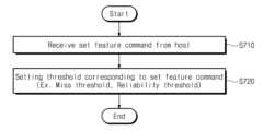
S710 단계에서, 컨트롤러(도 3 참조, 331)는 호스트(도 3 참조, 310)로부터 셋 피쳐(Set feature) 명령을 수신할 수 있다. S720 단계에서, 컨트롤러(도 3 참조, 331)는 셋 피쳐 명령에 응답하여, 문턱 값을 설정할 수 있다. 여기서, 문턱 값은 상술한 미스 문턱 값 또는 신뢰성 문턱 값이 될 수 있다. 이와 별개로, 문턱 값은 데이터 저장 장치(도 3 참조, 330)의 제조사에 의해 일정한 값으로 정해질 수도 있다. 도 12에서 도시된 데이터 저장 장치의 동작 방법은 상술한 도 5 내지 도 11에서 설명된 동작 방법과는 별도로 수행될 수 있다.In step S710, the controller (see FIG. 3, 331) may receive a Set feature command from the host (see FIG. 3, 310). In step S720, the controller (see FIG. 3, 331) may set a threshold value in response to the set feature command. Here, the threshold value may be the miss threshold value or the reliability threshold value described above. Separately, the threshold value may be set to a certain value by the manufacturer of the data storage device (see FIG. 3, 330). The operating method of the data storage device shown in FIG. 12 may be performed separately from the operating method described in FIGS. 5 to 11 described above.
도 13은 본 발명의 실시 예에 따른 데이터 저장 장치의 동작 방법을 예시적으로 보여주는 순서도이다. 도 13은 도 3을 참조하여 설명될 것이다.Figure 13 is a flowchart illustrating a method of operating a data storage device according to an embodiment of the present invention. FIG. 13 will be explained with reference to FIG. 3 .
S810 단계에서, 컨트롤러(도 3 참조, 331)는 호스트(도 3 참조, 310)로부터 겟 피쳐(Get feature) 명령을 수신할 수 있다. S820 단계에서, 컨트롤러(도 3 참조, 331)는 겟 피쳐 명령에 응답하여, 문턱 값을 호스트(도 3 참조, 310)로 출력할 수 있다. 마찬가지로, 문턱 값은 상술한 미스 문턱 값 또는 신뢰성 문턱 값이 될 수 있다. 도 13에서 도시된 데이터 저장 장치의 동작 방법은 상술한 도 5 내지 도 12에서 설명된 동작 방법과는 별도로 수행될 수 있다.In step S810, the controller (see FIG. 3, 331) may receive a Get feature command from the host (see FIG. 3, 310). In step S820, the controller (see FIG. 3, 331) may output a threshold value to the host (see FIG. 3, 310) in response to the get feature command. Likewise, the threshold may be the miss threshold or reliability threshold described above. The operating method of the data storage device shown in FIG. 13 may be performed separately from the operating method described in FIGS. 5 to 12 described above.
도 14는 도 5 내지 도 13에서 설명된 비동기식 이벤트에 대한 스펙을 예시적으로 보여주는 도면이다. 도 14는 도 3을 참조하여 설명될 것이다.FIG. 14 is a diagram illustrating specifications for the asynchronous event described in FIGS. 5 to 13. FIG. 14 will be explained with reference to FIG. 3 .
비동기식 이벤트 종류에 대한 정보는 완료 큐(CQ) 중 임의의 비트들에 포함될 수 있다. 도 14를 참조하면, 완료 큐(CQ) 내에서 0 내지 2 비트(Bit)에는 비동기식 이벤트 종류에 대한 정보가 포함될 수 있다. 호스트(도 3 참조, 310)는 컨트롤러(도 3 참조, 331)에 임의의 명령들을 제공할 수 있다. 제출 큐(SQ)에는 상술한 임의의 명령들을 순차적으로 저장될 수 있다. 이후, 저장된 임의의 명령들은 컨트롤러(도 3 참조, 331)로 순차적으로 제공될 수 있다. 한편, 완료 큐(CQ)에는 컨트롤러(도 3 참조, 331)가 상술한 임의의 명령들에 응답하여 처리한 결과들이 순차적으로 저장될 수 있다.Information about the asynchronous event type may be included in arbitrary bits of the completion queue (CQ). Referring to FIG. 14, bits 0 to 2 in the completion queue (CQ) may include information about the type of asynchronous event. The host (310, see FIG. 3) may provide arbitrary commands to the controller (331, see FIG. 3). The arbitrary commands described above can be stored sequentially in the submission queue (SQ). Thereafter, any stored commands may be sequentially provided to the controller (see FIG. 3, 331). Meanwhile, results processed by the controller (see FIG. 3, 331) in response to the arbitrary commands described above may be sequentially stored in the completion queue (CQ).
도 14를 참조하면, 완료 큐(CQ)의 값이 3h 인 경우, 비동기식 이벤트에는 컨트롤러(도 3 참조, 331)에서 맵 미스 횟수가 미스 문턱 값보다 크다는 정보가 포함될 수 있다. 완료 큐(CQ)의 값이 4h 인 경우, 비동기식 이벤트에는 복수의 낸드 플래시 메모리들에 대한 신뢰성 지수의 향상을 위해 방어 코드가 필요하다는 정보가 포함될 수 있다. 여기서, 비동기식 이벤트에 대한 정보에 대응하는 완료 큐(CQ)의 값은 도 14에서 상술된 바에 한정되지 않는다.Referring to FIG. 14, when the value of the completion queue (CQ) is 3h, the asynchronous event may include information that the number of map misses in the controller (see FIG. 3, 331) is greater than the miss threshold value. When the value of the completion queue (CQ) is 4h, the asynchronous event may include information that a defense code is needed to improve the reliability index for a plurality of NAND flash memories. Here, the value of the completion queue (CQ) corresponding to information about the asynchronous event is not limited to what is described above in FIG. 14.
도 15는 도 5 내지 도 13에서 설명된 문턱 값에 대한 스펙을 예시적으로 보여주는 도면이다. 도 15는 도 3, 도 4, 및 도 12를 참조하여 설명될 것이다.FIG. 15 is a diagram illustrating specifications for the threshold values described in FIGS. 5 to 13. FIG. 15 will be explained with reference to FIGS. 3, 4, and 12.
도 15를 참조하면, 피쳐 식별자(Feature identifier)가 OEh 인 경우, 셋 피쳐 정보에는 문턱 값에 대한 정보가 포함될 수 있다. 이 정보는 도 4의 S113 단계 및 도 12의 S610S710 단계에서 사용될 수 있다. 그러나, 피쳐 식별자의 값은 도 15에 도시된 바에 한정되지 않는다. 추가로, 문턱 값은 상술한 미스 문턱 값 또는 신뢰성 문턱 값이 될 수 있다.Referring to FIG. 15, when the feature identifier is OEh, the set feature information may include information about the threshold value. This information can be used in step S113 of FIG. 4 and step S610S710 of FIG. 12. However, the value of the feature identifier is not limited to that shown in FIG. 15. Additionally, the threshold may be the miss threshold or reliability threshold described above.
좀 더 구체적으로, 셋 피쳐 정보에서 20 내지 21 비트들에는 문턱 값의 종류가 구별되는 정보가 포함될 수 있다. 셋 피쳐 정보에서 16 내지 19 비트에는 문턱 값이 설정되는 정보가 포함될 수 있다. 즉, 셋 피쳐 명령에 의해 문턱 값이 수정될 수 있다. 또는 겟 피쳐 명령에 의해 문턱 값이 호스트(도 3 참조, 310)로 되돌아갈 수 있다. 셋 피쳐 정보에서 0 내지 15비트들에는 문턱 값의 구체적인 수치가 포함될 수 있다. 즉. 호스트(도 3 참조, 310)에 의해 문턱 값의 구체적인 수치들이 정해질 수 있다. 또는 데이터 저장 장치의 벤더(Vendor)에 의해, 제품 생산 시 문턱 값은 미리 정해질 수도 있다.More specifically, 20 to 21 bits in the set feature information may include information that distinguishes the type of threshold value. Bits 16 to 19 of the set feature information may include information for setting a threshold value. That is, the threshold value can be modified by a set feature command. Alternatively, the threshold value may be returned to the host (see FIG. 3, 310) by a get feature command. Bits 0 to 15 in the set feature information may include a specific value of the threshold value. in other words. Specific values of the threshold value may be determined by the host (see FIG. 3, 310). Alternatively, the threshold value may be determined in advance at the time of product production by the vendor of the data storage device.
위에서 설명한 내용은 본 발명을 실시하기 위한 구체적인 예들이다. 본 발명에는 위에서 설명한 실시 예들뿐만 아니라, 단순하게 설계 변경하거나 용이하게 변경할 수 있는 실시 예들도 포함될 것이다. 또한, 본 발명에는 상술한 실시 예들을 이용하여 앞으로 용이하게 변형하여 실시할 수 있는 기술들도 포함될 것이다.The contents described above are specific examples for carrying out the present invention. The present invention will include not only the embodiments described above, but also embodiments that can be simply changed or easily changed in design. In addition, the present invention will also include technologies that can be easily modified and implemented in the future using the above-described embodiments.
100, 300: 컴퓨터 시스템
110, 310, 410: 호스트
120, 320, 420: 호스트 메모리
130, 330: 데이터 저장 장치
131, 331, 431: 컨트롤러
132, 332: 휘발성 메모리
133a~133d, 333a~333d: 복수의 낸드 플래시 메모리들100, 300: Computer systems
110, 310, 410: Host
120, 320, 420: Host memory
130, 330: data storage device
131, 331, 431: Controller
132, 332: volatile memory
133a~133d, 333a~333d: Multiple NAND flash memories
Claims (10)
Translated fromKorean상기 컨트롤러가, 호스트로부터 수신된 논리 주소와 상기 불휘발성 메모리의 물리 주소 사이의 맵핑 관계를 맵핑 테이블에서 찾을 수 없는 경우를 나타내는 맵 미스에 대한 정보에 기초하여, 비동기식 이벤트를 상기 호스트에 요청하는 단계―상기 맵핑 테이블은 상기 데이터 저장 장치와 구별되고 상기 호스트에 의해 접근가능한 호스트 메모리 버퍼에 저장됨―;
상기 컨트롤러가, 상기 비동기식 이벤트에 기초하여 상기 호스트에 의해 조정된 호스트 메모리 버퍼에 관한 정보를 수신하는 단계; 및
상기 컨트롤러가, 상기 조정된 호스트 메모리 버퍼에 관한 정보에 기초하여, 상기 맵핑 테이블을 업데이트하는 단계를 포함하고,
상기 비동기식 이벤트를 상기 호스트에 요청하는 단계는,
상기 맵 미스의 횟수를 카운팅하는 단계; 및
상기 카운팅의 결과와 미스 문턱 값(Miss threshold)을 비교하는 단계를 포함하는 데이터 저장 장치의 동작 방법.In a method of operating a data storage device including a controller and non-volatile memory,
Requesting, by the controller, an asynchronous event to the host based on information about a map miss indicating a case where a mapping relationship between a logical address received from the host and a physical address of the non-volatile memory cannot be found in the mapping table. -the mapping table is stored in a host memory buffer that is distinct from the data storage device and accessible by the host;
receiving, by the controller, information regarding a host memory buffer adjusted by the host based on the asynchronous event; and
updating, by the controller, the mapping table based on information about the adjusted host memory buffer,
The step of requesting the asynchronous event from the host is,
Counting the number of map misses; and
A method of operating a data storage device comprising comparing the counting result and a miss threshold.
상기 데이터 저장 장치는 상기 맵핑 테이블을 저장하기 위한 휘발성 메모리를 포함하지 않는 데이터 저장 장치의 동작 방법.According to claim 1,
A method of operating a data storage device wherein the data storage device does not include volatile memory for storing the mapping table.
상기 카운팅의 결과가 상기 미스 문턱 값보다 큰 경우, 상기 호스트 메모리 버퍼의 사이즈는 상기 호스트에 의해 증가되는 데이터 저장 장치의 동작 방법.According to claim 1,
If the result of the counting is greater than the miss threshold, the size of the host memory buffer is increased by the host.
상기 호스트에 의해 증가된 호스트 메모리 버퍼의 사이즈에 기초하여, 상기 맵핑 테이블을 업데이트하는 데이터 저장 장치의 동작 방법.The method of claim 3, wherein the controller:
A method of operating a data storage device that updates the mapping table based on the size of the host memory buffer increased by the host.
상기 카운팅의 결과가 상기 미스 문턱 값보다 작은 경우, 상기 호스트 메모리 버퍼의 사이즈는 상기 호스트에 의해 감소되는 데이터 저장 장치의 동작 방법.According to claim 1,
If the result of the counting is less than the miss threshold, the size of the host memory buffer is reduced by the host.
상기 호스트에 의해 감소된 호스트 메모리 버퍼의 사이즈에 기초하여, 상기 맵핑 테이블을 업데이트하는 데이터 저장 장치의 동작 방법.The method of claim 5, wherein the controller:
A method of operating a data storage device that updates the mapping table based on the size of the host memory buffer reduced by the host.
상기 호스트의 요청에 응답하여 상기 미스 문턱 값을 설정하는 단계를 더 포함하는 데이터 저장 장치의 동작 방법.According to claim 1,
A method of operating a data storage device further comprising setting the miss threshold value in response to a request from the host.
상기 데이터 저장 장치의 전원이 인가되면, 상기 호스트가 상기 호스트 메모리에 제 1 사이즈의 호스트 메모리 버퍼를 할당하고, 상기 복수의 낸드 플래시 메모리들로부터 상기 매핑 테이블의 제 1 부분을 상기 호스트 메모리 버퍼로 로드하는 부팅 동작을 수행하는 단계;
상기 부팅 동작을 수행한 후, 상기 호스트 메모리 버퍼에 로드된 상기 매핑 테이블의 상기 제 1 부분을 참조하여 정상(nomal) 데이터 입출력(I/O) 동작들을 수행하고, 상기 컨트롤러를 사용하여 상기 정상 데이터 입출력 동작들의 결과로 발생하는 맵 미스의 횟수를 카운팅하고, 카운팅 결과를 생성하는 단계;
상기 컨트롤러에서 상기 카운팅 결과를 미스 문턱 값과 비교하고, 상기 카운팅 결과가 상기 미스 문턱 값보다 크다고 판별되면, 상기 컨트롤러로부터 상기 호스트로 비동기식 이벤트 요청을 발행하는 단계; 및
상기 비동기식 이벤트 요청에 대한 응답하여, 상기 호스트는 제 2 사이즈의 상기 호스트 메모리 버퍼를 재할당하는 단계를 포함하는 데이터 저장 장치의 동작 방법.A computer system including a host, host memory accessible by the host, and a data storage device, comprising a controller and a plurality of NAND flash memories storing a mapping table associated with a flash conversion layer for the plurality of NAND flash memories. In the method of operating the data storage device,
When the data storage device is powered on, the host allocates a host memory buffer of a first size to the host memory and loads a first part of the mapping table from the plurality of NAND flash memories into the host memory buffer. performing a boot operation;
After performing the booting operation, normal data input/output (I/O) operations are performed with reference to the first part of the mapping table loaded in the host memory buffer, and the normal data is input/output (I/O) operations using the controller. Counting the number of map misses that occur as a result of input/output operations and generating a counting result;
Comparing the counting result with a miss threshold in the controller, and if it is determined that the counting result is greater than the miss threshold, issuing an asynchronous event request from the controller to the host; and
In response to the asynchronous event request, the host reallocates the host memory buffer of a second size.
상기 부팅 동작은:
상기 호스트에 의해 상기 데이터 저장 장치를 식별하는 단계; 및
상기 호스트에 의해 식별된 후, 상기 데이터 저장 장치는 제 1 사이즈 정보를 상기 호스트에 전송하는 단계를 포함하고,
상기 호스트는 상기 제 1 사이즈 정보에 응답하여, 상기 호스트 메모리에서 상기 제 1 사이즈의 상기 호스트 메모리 버퍼를 할당하는 데이터 저장 장치의 동작 방법.According to claim 8,
The above boot operation is:
identifying the data storage device by the host; and
After being identified by the host, the data storage device transmits first size information to the host,
A method of operating a data storage device, wherein the host allocates the host memory buffer of the first size in the host memory in response to the first size information.
상기 제 2 사이즈의 상기 호스트 메모리 버퍼를 재할당 한 후, 상기 매핑 테이블의 제 2 부분을 상기 호스트 메모리 버퍼로 로드하는 단계를 더 포함하는 데이터 저장 장치의 동작 방법.According to claim 8,
After reallocating the host memory buffer of the second size, the method of operating a data storage device further includes loading a second portion of the mapping table into the host memory buffer.
Priority Applications (2)
| Application Number | Priority Date | Filing Date | Title |
|---|---|---|---|
| KR1020160099599AKR102667430B1 (en) | 2016-08-04 | 2016-08-04 | Storage device using host memory and operating method thereof |
| US15/652,259US10360156B2 (en) | 2016-08-04 | 2017-07-18 | Data storage device using host memory and method of operating same |
Applications Claiming Priority (1)
| Application Number | Priority Date | Filing Date | Title |
|---|---|---|---|
| KR1020160099599AKR102667430B1 (en) | 2016-08-04 | 2016-08-04 | Storage device using host memory and operating method thereof |
Publications (2)
| Publication Number | Publication Date |
|---|---|
| KR20180016679A KR20180016679A (en) | 2018-02-19 |
| KR102667430B1true KR102667430B1 (en) | 2024-05-23 |
Family
ID=61070091
Family Applications (1)
| Application Number | Title | Priority Date | Filing Date |
|---|---|---|---|
| KR1020160099599AActiveKR102667430B1 (en) | 2016-08-04 | 2016-08-04 | Storage device using host memory and operating method thereof |
Country Status (2)
| Country | Link |
|---|---|
| US (1) | US10360156B2 (en) |
| KR (1) | KR102667430B1 (en) |
Families Citing this family (50)
| Publication number | Priority date | Publication date | Assignee | Title |
|---|---|---|---|---|
| KR102618699B1 (en)* | 2016-09-28 | 2024-01-02 | 삼성전자주식회사 | Computing system including storage device controlled by host |
| US10929285B2 (en)* | 2018-02-27 | 2021-02-23 | Western Digital Technologies, Inc. | Storage system and method for generating a reverse map during a background operation and storing it in a host memory buffer |
| US10642536B2 (en)* | 2018-03-06 | 2020-05-05 | Western Digital Technologies, Inc. | Non-volatile storage system with host side command injection |
| US10613778B2 (en)* | 2018-03-21 | 2020-04-07 | Western Digital Technologies, Inc. | Dynamic host memory allocation to a memory controller |
| KR20190113443A (en)* | 2018-03-28 | 2019-10-08 | 에스케이하이닉스 주식회사 | Memory system and operating method of memory system |
| US10719243B2 (en)* | 2018-05-30 | 2020-07-21 | Apple Inc. | Techniques for preserving an expected lifespan of a non-volatile memory |
| US10635580B2 (en)* | 2018-07-09 | 2020-04-28 | Western Digital Technologies, Inc. | Buffering storage device data in a host memory buffer |
| KR102589402B1 (en)* | 2018-10-04 | 2023-10-13 | 삼성전자주식회사 | Storage device and method for operating storage device |
| KR102755961B1 (en)* | 2018-10-24 | 2025-01-17 | 삼성전자주식회사 | Data storage device using host memory buffer and method of operating the same |
| KR102766395B1 (en)* | 2018-11-01 | 2025-02-12 | 삼성전자주식회사 | Storage device, storage system and method of operating storage device |
| KR102599176B1 (en) | 2018-11-14 | 2023-11-08 | 삼성전자주식회사 | Storage device using host memory buffer and memory management method thereof |
| KR102686749B1 (en) | 2018-11-14 | 2024-07-22 | 삼성전자주식회사 | Storage device for performing map scheduling and electronic device including the same |
| KR102735049B1 (en)* | 2018-12-14 | 2024-11-28 | 에스케이하이닉스 주식회사 | Memory system and operating method thereof |
| KR102735042B1 (en) | 2018-12-19 | 2024-11-28 | 에스케이하이닉스 주식회사 | Memory controller and operating method thereof |
| KR102806973B1 (en) | 2019-01-15 | 2025-05-15 | 에스케이하이닉스 주식회사 | Memory controller and operating method thereof |
| KR102787556B1 (en) | 2019-02-15 | 2025-03-31 | 에스케이하이닉스 주식회사 | Memory controller and operating method thereof |
| KR102839234B1 (en) | 2019-03-18 | 2025-07-29 | 에스케이하이닉스 주식회사 | Memory System, Computing Apparatus and Operation Method Thereof |
| KR102809599B1 (en) | 2019-03-27 | 2025-05-20 | 에스케이하이닉스 주식회사 | Controller, memory system and operating method thereof |
| KR102839226B1 (en)* | 2019-04-16 | 2025-07-28 | 에스케이하이닉스 주식회사 | Controller, operating method thereof and memory system |
| KR102787772B1 (en) | 2019-06-28 | 2025-03-31 | 에스케이하이닉스 주식회사 | Apparatus and method for transmitting internal data of memory system in sleep mode |
| US11294825B2 (en)* | 2019-04-17 | 2022-04-05 | SK Hynix Inc. | Memory system for utilizing a memory included in an external device |
| KR102802236B1 (en)* | 2019-04-17 | 2025-04-29 | 에스케이하이닉스 주식회사 | Apparatus and method for transmitting map segment in memory system |
| KR102847052B1 (en) | 2019-06-05 | 2025-08-18 | 에스케이하이닉스 주식회사 | Memory system, memory controller and meta infomation storage device |
| KR102849235B1 (en) | 2019-06-17 | 2025-08-22 | 삼성전자 주식회사 | Electronic device including storage and method of using the storage thereof |
| JP2021005121A (en)* | 2019-06-25 | 2021-01-14 | 株式会社日立製作所 | Storage device and control method |
| KR102714211B1 (en) | 2019-08-01 | 2024-10-10 | 삼성전자주식회사 | Storage device, memory system comprising the same, and operation method thereof |
| EP3771986B1 (en) | 2019-08-01 | 2021-07-28 | Samsung Electronics Co., Ltd. | Storage device, memory system comprising the same, and operation method thereof |
| KR102864978B1 (en) | 2019-08-01 | 2025-09-30 | 삼성전자주식회사 | Storage device, memory system comprising the same, and operating method thereof |
| CN110737607B (en)* | 2019-09-30 | 2021-09-14 | 深圳忆联信息系统有限公司 | Method and device for managing HMB memory, computer equipment and storage medium |
| KR102691952B1 (en) | 2019-10-14 | 2024-08-06 | 에스케이하이닉스 주식회사 | Controller and data storage system having the same |
| KR102675313B1 (en)* | 2019-10-31 | 2024-06-17 | 에스케이하이닉스 주식회사 | Memory controller and operating method thereof |
| CN111522679A (en)* | 2020-04-17 | 2020-08-11 | 深圳忆联信息系统有限公司 | SSD log recording method and system based on host memory and computer equipment |
| US20210334200A1 (en)* | 2020-04-22 | 2021-10-28 | Micron Technology, Inc. | Storing translation layer metadata in host memory buffer |
| KR20210143387A (en) | 2020-05-20 | 2021-11-29 | 에스케이하이닉스 주식회사 | Memory system, memory controller, and operating method of memory system |
| US11734018B2 (en) | 2020-07-17 | 2023-08-22 | Western Digital Technologies, Inc. | Parallel boot execution of memory devices |
| US11579970B2 (en) | 2020-07-30 | 2023-02-14 | Micron Technology, Inc. | Maintenance command interfaces for a memory system |
| EP4014121A4 (en)* | 2020-10-29 | 2023-08-30 | Silicon Motion, Inc. | Methods for controlling data storage device, and associated flash memory controller |
| KR20220113159A (en) | 2021-02-05 | 2022-08-12 | 에스케이하이닉스 주식회사 | Storage device and operating method thereof |
| US11507296B2 (en)* | 2021-03-10 | 2022-11-22 | Micron Technology, Inc. | Repair operation techniques |
| US11698751B2 (en) | 2021-06-07 | 2023-07-11 | Western Digital Technologies, Inc. | Data storage device and method for low-latency power state transitions by having power islanding in a host memory buffer |
| KR20230037240A (en) | 2021-09-09 | 2023-03-16 | 에스케이하이닉스 주식회사 | Host device, memory controller and computing system including thereof |
| US11893275B2 (en) | 2021-09-20 | 2024-02-06 | Western Digital Technologies, Inc. | DRAM-less SSD with recovery from HMB loss |
| US11809742B2 (en) | 2021-09-20 | 2023-11-07 | Western Digital Technologies, Inc. | Recovery from HMB loss |
| KR102484065B1 (en)* | 2021-09-23 | 2023-01-02 | 삼성전자주식회사 | Memory controller and storage system comprising the same |
| KR20230044883A (en) | 2021-09-27 | 2023-04-04 | 삼성전자주식회사 | Storage device and operating method thereof |
| US12014080B2 (en) | 2021-11-10 | 2024-06-18 | Samsung Electronics Co., Ltd. | Memory system using host memory buffer and operation method thereof |
| US11836383B2 (en)* | 2021-11-23 | 2023-12-05 | Silicon Motion Inc. | Controllers of storage devices for arranging order of commands and methods of operating the same |
| CN114822631B (en)* | 2022-04-19 | 2024-10-11 | 山东华芯半导体有限公司 | MRAM (magnetic random Access memory) -based hybrid NVME (storage media management memory) SSD (solid State disk) storage system |
| KR20240076574A (en) | 2022-11-22 | 2024-05-30 | 삼성전자주식회사 | Memory controller, electronic system including the same and method of controlling memory access |
| US12045131B2 (en)* | 2022-12-13 | 2024-07-23 | SK Hynix Inc. | Read error injection |
Citations (1)
| Publication number | Priority date | Publication date | Assignee | Title |
|---|---|---|---|---|
| US20160007209A1 (en)* | 2014-07-02 | 2016-01-07 | Here Global B.V. | Method and apparatus for providing activity-based map job |
Family Cites Families (28)
| Publication number | Priority date | Publication date | Assignee | Title |
|---|---|---|---|---|
| JPH0799508B2 (en)* | 1990-10-15 | 1995-10-25 | インターナショナル・ビジネス・マシーンズ・コーポレイション | Method and system for dynamically partitioning cache storage |
| US8112574B2 (en)* | 2004-02-26 | 2012-02-07 | Super Talent Electronics, Inc. | Swappable sets of partial-mapping tables in a flash-memory system with a command queue for combining flash writes |
| US8745315B2 (en)* | 2006-11-06 | 2014-06-03 | Rambus Inc. | Memory Systems and methods supporting volatile and wear-leveled nonvolatile physical memory |
| KR100882740B1 (en) | 2007-02-22 | 2009-02-09 | 삼성전자주식회사 | Map History-based Nonvolatile Memory Mapping Method and Storage Device |
| US20090210620A1 (en) | 2008-02-19 | 2009-08-20 | Jibbe Mahmoud K | Method to handle demand based dynamic cache allocation between SSD and RAID cache |
| US8412911B2 (en)* | 2009-06-29 | 2013-04-02 | Oracle America, Inc. | System and method to invalidate obsolete address translations |
| WO2013025540A1 (en) | 2011-08-12 | 2013-02-21 | Sandisk Enterprise Ip Llc | Cache management including solid state device virtualization |
| US8874848B2 (en) | 2011-09-30 | 2014-10-28 | Net App, Inc. | Intelligence for controlling virtual storage appliance storage allocation |
| US9311226B2 (en)* | 2012-04-20 | 2016-04-12 | Memory Technologies Llc | Managing operational state data of a memory module using host memory in association with state change |
| US9218257B2 (en) | 2012-05-24 | 2015-12-22 | Stec, Inc. | Methods for managing failure of a solid state device in a caching storage |
| US9015418B2 (en) | 2012-11-20 | 2015-04-21 | Lsi Corporation | Self-sizing dynamic cache for virtualized environments |
| KR101430637B1 (en)* | 2012-12-11 | 2014-08-18 | 서울대학교산학협력단 | Nonvolatile memory device and method for managing data thereof |
| US9652376B2 (en) | 2013-01-28 | 2017-05-16 | Radian Memory Systems, Inc. | Cooperative flash memory control |
| TWI506430B (en)* | 2013-03-20 | 2015-11-01 | Phison Electronics Corp | Method of recording mapping information method, and memory controller and memory storage apparatus using the same |
| US9183151B2 (en)* | 2013-08-30 | 2015-11-10 | Vmware, Inc. | Thread cache allocation |
| US10013344B2 (en) | 2014-01-14 | 2018-07-03 | Avago Technologies General Ip (Singapore) Pte. Ltd. | Enhanced SSD caching |
| US9563382B2 (en)* | 2014-06-05 | 2017-02-07 | Sandisk Technologies Llc | Methods, systems, and computer readable media for providing flexible host memory buffer |
| US20160034217A1 (en)* | 2014-07-31 | 2016-02-04 | Samsung Electronics Co., Ltd. | Memory controller configured to control data sanitization and memory system including the same |
| KR20160024546A (en)* | 2014-08-26 | 2016-03-07 | 에스케이하이닉스 주식회사 | Data storage device and operating method thereof |
| US9836407B2 (en) | 2014-10-23 | 2017-12-05 | Netapp, Inc. | Method for using service level objectives to dynamically allocate cache resources among competing workloads |
| KR102398213B1 (en)* | 2015-03-09 | 2022-05-17 | 삼성전자주식회사 | Storage device, host system having the same and map table updating method thereof |
| CN106155579A (en)* | 2015-04-27 | 2016-11-23 | 广明光电股份有限公司 | Method for dynamically storing data of conversion layer in solid state disk |
| TWI537728B (en)* | 2015-09-23 | 2016-06-11 | 群聯電子股份有限公司 | Buffer memory management method, memory control circuit unit and memory storage device |
| TWI584122B (en)* | 2015-11-17 | 2017-05-21 | 群聯電子股份有限公司 | Buffer memory management method, memory control circuit unit and memory storage device |
| TWI579693B (en)* | 2016-04-29 | 2017-04-21 | 群聯電子股份有限公司 | Mapping table loading method, memory control circuit unit and mempry storage apparatus |
| US20170351452A1 (en)* | 2016-06-01 | 2017-12-07 | Intel Corporation | Dynamic host memory buffer allocation |
| TWI595356B (en)* | 2016-08-19 | 2017-08-11 | 大心電子(英屬維京群島)股份有限公司 | Data transmission method, and storage controller and list management circuit using the same |
| US10528463B2 (en)* | 2016-09-28 | 2020-01-07 | Intel Corporation | Technologies for combining logical-to-physical address table updates in a single write operation |
- 2016
- 2016-08-04KRKR1020160099599Apatent/KR102667430B1/enactiveActive
- 2017
- 2017-07-18USUS15/652,259patent/US10360156B2/enactiveActive
Patent Citations (1)
| Publication number | Priority date | Publication date | Assignee | Title |
|---|---|---|---|---|
| US20160007209A1 (en)* | 2014-07-02 | 2016-01-07 | Here Global B.V. | Method and apparatus for providing activity-based map job |
Also Published As
| Publication number | Publication date |
|---|---|
| US10360156B2 (en) | 2019-07-23 |
| KR20180016679A (en) | 2018-02-19 |
| US20180039578A1 (en) | 2018-02-08 |
Similar Documents
| Publication | Publication Date | Title |
|---|---|---|
| KR102667430B1 (en) | Storage device using host memory and operating method thereof | |
| US11854630B2 (en) | Storage device that uses a host memory buffer and a memory management method including the same | |
| US11579779B2 (en) | Computing systems including storage devices controlled by hosts | |
| CN111290704B (en) | Apparatus and method for controlling data stored in storage system | |
| KR102549545B1 (en) | Storage device and method of operating the storage device | |
| KR102094236B1 (en) | Storage device and computer system | |
| US11645213B2 (en) | Data processing system allocating memory area in host as extension of memory and operating method thereof | |
| US20210034536A1 (en) | Storage device, memory system comprising the same, and operating method thereof | |
| US20210240667A1 (en) | User device including storage device and trim management method thereof | |
| KR102782783B1 (en) | Operating method of controller and memory system | |
| US11893269B2 (en) | Apparatus and method for improving read performance in a system | |
| KR20220048569A (en) | Apparatus and method for controlling storage in a memory system | |
| US11269559B2 (en) | Data processing device | |
| CN112148208A (en) | Apparatus and method for transferring internal data of memory system in sleep mode | |
| KR20220135786A (en) | Apparatus and method for scheduing operations performed in plural memory devices included in a memory system | |
| KR102714211B1 (en) | Storage device, memory system comprising the same, and operation method thereof | |
| CN111831215A (en) | Apparatus for transferring mapping information in a memory system | |
| KR20220108342A (en) | Apparatus and method for securing a free memory block in a memory system | |
| KR20230072886A (en) | Apparatus and method for improving data input/output performance of storage | |
| KR20230035811A (en) | Apparatus and method for controlling a shared memory in a data processing system | |
| KR101549569B1 (en) | Method for performing garbage collection and flash memory apparatus using the method | |
| CN115458013A (en) | Storage device and operation method thereof | |
| CN108376051A (en) | Data storage device | |
| CN106055488A (en) | Data storage device and operating method thereof | |
| CN117406912A (en) | Memory system, memory controller and method of operating the same |
Legal Events
| Date | Code | Title | Description |
|---|---|---|---|
| PA0109 | Patent application | Patent event code:PA01091R01D Comment text:Patent Application Patent event date:20160804 | |
| PG1501 | Laying open of application | ||
| PA0201 | Request for examination | Patent event code:PA02012R01D Patent event date:20210702 Comment text:Request for Examination of Application Patent event code:PA02011R01I Patent event date:20160804 Comment text:Patent Application | |
| E902 | Notification of reason for refusal | ||
| PE0902 | Notice of grounds for rejection | Comment text:Notification of reason for refusal Patent event date:20230816 Patent event code:PE09021S01D | |
| E701 | Decision to grant or registration of patent right | ||
| PE0701 | Decision of registration | Patent event code:PE07011S01D Comment text:Decision to Grant Registration Patent event date:20240220 | |
| GRNT | Written decision to grant | ||
| PR0701 | Registration of establishment | Comment text:Registration of Establishment Patent event date:20240514 Patent event code:PR07011E01D | |
| PR1002 | Payment of registration fee | Payment date:20240516 End annual number:3 Start annual number:1 | |
| PG1601 | Publication of registration |