KR102666614B1 - Display device - Google Patents
Display deviceDownload PDFInfo
- Publication number
- KR102666614B1 KR102666614B1KR1020180148353AKR20180148353AKR102666614B1KR 102666614 B1KR102666614 B1KR 102666614B1KR 1020180148353 AKR1020180148353 AKR 1020180148353AKR 20180148353 AKR20180148353 AKR 20180148353AKR 102666614 B1KR102666614 B1KR 102666614B1
- Authority
- KR
- South Korea
- Prior art keywords
- electrode
- shielding
- disposed
- layer
- light emitting
- Prior art date
- Legal status (The legal status is an assumption and is not a legal conclusion. Google has not performed a legal analysis and makes no representation as to the accuracy of the status listed.)
- Active
Links
Images


Classifications
- H01L27/156—
- H—ELECTRICITY
- H10—SEMICONDUCTOR DEVICES; ELECTRIC SOLID-STATE DEVICES NOT OTHERWISE PROVIDED FOR
- H10H—INORGANIC LIGHT-EMITTING SEMICONDUCTOR DEVICES HAVING POTENTIAL BARRIERS
- H10H29/00—Integrated devices, or assemblies of multiple devices, comprising at least one light-emitting semiconductor element covered by group H10H20/00
- H10H29/10—Integrated devices comprising at least one light-emitting semiconductor component covered by group H10H20/00
- H10H29/14—Integrated devices comprising at least one light-emitting semiconductor component covered by group H10H20/00 comprising multiple light-emitting semiconductor components
- H10H29/142—Two-dimensional arrangements, e.g. asymmetric LED layout
- H—ELECTRICITY
- H01—ELECTRIC ELEMENTS
- H01L—SEMICONDUCTOR DEVICES NOT COVERED BY CLASS H10
- H01L25/00—Assemblies consisting of a plurality of semiconductor or other solid state devices
- H01L25/03—Assemblies consisting of a plurality of semiconductor or other solid state devices all the devices being of a type provided for in a single subclass of subclasses H10B, H10D, H10F, H10H, H10K or H10N, e.g. assemblies of rectifier diodes
- H01L25/04—Assemblies consisting of a plurality of semiconductor or other solid state devices all the devices being of a type provided for in a single subclass of subclasses H10B, H10D, H10F, H10H, H10K or H10N, e.g. assemblies of rectifier diodes the devices not having separate containers
- H01L25/075—Assemblies consisting of a plurality of semiconductor or other solid state devices all the devices being of a type provided for in a single subclass of subclasses H10B, H10D, H10F, H10H, H10K or H10N, e.g. assemblies of rectifier diodes the devices not having separate containers the devices being of a type provided for in group H10H20/00
- H01L25/0753—Assemblies consisting of a plurality of semiconductor or other solid state devices all the devices being of a type provided for in a single subclass of subclasses H10B, H10D, H10F, H10H, H10K or H10N, e.g. assemblies of rectifier diodes the devices not having separate containers the devices being of a type provided for in group H10H20/00 the devices being arranged next to each other
- H—ELECTRICITY
- H01—ELECTRIC ELEMENTS
- H01L—SEMICONDUCTOR DEVICES NOT COVERED BY CLASS H10
- H01L23/00—Details of semiconductor or other solid state devices
- H01L23/552—Protection against radiation, e.g. light or electromagnetic waves
- H01L33/38—
- H01L33/40—
- H—ELECTRICITY
- H10—SEMICONDUCTOR DEVICES; ELECTRIC SOLID-STATE DEVICES NOT OTHERWISE PROVIDED FOR
- H10H—INORGANIC LIGHT-EMITTING SEMICONDUCTOR DEVICES HAVING POTENTIAL BARRIERS
- H10H20/00—Individual inorganic light-emitting semiconductor devices having potential barriers, e.g. light-emitting diodes [LED]
- H10H20/80—Constructional details
- H10H20/83—Electrodes
- H10H20/831—Electrodes characterised by their shape
- H—ELECTRICITY
- H10—SEMICONDUCTOR DEVICES; ELECTRIC SOLID-STATE DEVICES NOT OTHERWISE PROVIDED FOR
- H10H—INORGANIC LIGHT-EMITTING SEMICONDUCTOR DEVICES HAVING POTENTIAL BARRIERS
- H10H20/00—Individual inorganic light-emitting semiconductor devices having potential barriers, e.g. light-emitting diodes [LED]
- H10H20/80—Constructional details
- H10H20/83—Electrodes
- H10H20/832—Electrodes characterised by their material
- H—ELECTRICITY
- H10—SEMICONDUCTOR DEVICES; ELECTRIC SOLID-STATE DEVICES NOT OTHERWISE PROVIDED FOR
- H10H—INORGANIC LIGHT-EMITTING SEMICONDUCTOR DEVICES HAVING POTENTIAL BARRIERS
- H10H20/00—Individual inorganic light-emitting semiconductor devices having potential barriers, e.g. light-emitting diodes [LED]
- H10H20/80—Constructional details
- H10H20/85—Packages
- H10H20/857—Interconnections, e.g. lead-frames, bond wires or solder balls
- H—ELECTRICITY
- H01—ELECTRIC ELEMENTS
- H01L—SEMICONDUCTOR DEVICES NOT COVERED BY CLASS H10
- H01L25/00—Assemblies consisting of a plurality of semiconductor or other solid state devices
- H01L25/16—Assemblies consisting of a plurality of semiconductor or other solid state devices the devices being of types provided for in two or more different subclasses of H10B, H10D, H10F, H10H, H10K or H10N, e.g. forming hybrid circuits
- H01L25/167—Assemblies consisting of a plurality of semiconductor or other solid state devices the devices being of types provided for in two or more different subclasses of H10B, H10D, H10F, H10H, H10K or H10N, e.g. forming hybrid circuits comprising optoelectronic devices, e.g. LED, photodiodes
- H—ELECTRICITY
- H10—SEMICONDUCTOR DEVICES; ELECTRIC SOLID-STATE DEVICES NOT OTHERWISE PROVIDED FOR
- H10H—INORGANIC LIGHT-EMITTING SEMICONDUCTOR DEVICES HAVING POTENTIAL BARRIERS
- H10H20/00—Individual inorganic light-emitting semiconductor devices having potential barriers, e.g. light-emitting diodes [LED]
- H10H20/80—Constructional details
- H10H20/81—Bodies
- H10H20/817—Bodies characterised by the crystal structures or orientations, e.g. polycrystalline, amorphous or porous
- H10H20/818—Bodies characterised by the crystal structures or orientations, e.g. polycrystalline, amorphous or porous within the light-emitting regions
- H—ELECTRICITY
- H10—SEMICONDUCTOR DEVICES; ELECTRIC SOLID-STATE DEVICES NOT OTHERWISE PROVIDED FOR
- H10H—INORGANIC LIGHT-EMITTING SEMICONDUCTOR DEVICES HAVING POTENTIAL BARRIERS
- H10H20/00—Individual inorganic light-emitting semiconductor devices having potential barriers, e.g. light-emitting diodes [LED]
- H10H20/80—Constructional details
- H10H20/83—Electrodes
- H10H20/832—Electrodes characterised by their material
- H10H20/833—Transparent materials
Landscapes
- Engineering & Computer Science (AREA)
- Physics & Mathematics (AREA)
- Microelectronics & Electronic Packaging (AREA)
- Power Engineering (AREA)
- Condensed Matter Physics & Semiconductors (AREA)
- General Physics & Mathematics (AREA)
- Computer Hardware Design (AREA)
- Health & Medical Sciences (AREA)
- Electromagnetism (AREA)
- Toxicology (AREA)
- Electroluminescent Light Sources (AREA)
- Devices For Indicating Variable Information By Combining Individual Elements (AREA)
Abstract
Translated fromKoreanDescription
Translated fromKorean본 발명은 표시 장치에 관한 것으로, 더욱 상세하게는 발광 소자의 정렬도 향상을 위해 배치되는 차폐전극층을 포함하는 표시 장치에 관한 것이다.The present invention relates to a display device, and more particularly, to a display device including a shielding electrode layer disposed to improve alignment of light emitting elements.
표시 장치는 멀티미디어의 발달과 함께 그 중요성이 증대되고 있다. 이에 부응하여 유기발광 표시 장치(Organic Light Emitting Display, OLED), 액정 표시 장치(Liquid Crystal Display, LCD) 등과 같은 여러 종류의 표시 장치가 사용되고 있다.The importance of display devices is increasing with the development of multimedia. In response to this, various types of display devices such as Organic Light Emitting Display (OLED) and Liquid Crystal Display (LCD) are being used.
표시 장치의 화상을 표시하는 장치로서 유기 발광 표시 패널이나 액정 표시 패널과 같은 표시 패널을 포함한다. 그 중, 발광 표시 패널로써, 발광 소자를 포함할 수 있는데, 예를 들어 발광 다이오드(Light Emitting Diode, LED)의 경우, 유기물을 형광 물질로 이용하는 유기 발광 다이오드(OLED), 무기물을 형광물질로 이용하는 무기 발광 다이오드 등이 있다.A display device that displays images includes a display panel such as an organic light emitting display panel or a liquid crystal display panel. Among them, the light emitting display panel may include a light emitting device, for example, a light emitting diode (LED), an organic light emitting diode (OLED) that uses an organic material as a fluorescent material, and an organic light emitting diode (OLED) that uses an inorganic material as a fluorescent material. Inorganic light emitting diodes, etc.
형광물질로 무기물 반도체를 이용하는 무기 발광 다이오드는 고온의 환경에서도 내구성을 가지며, 유기 발광 다이오드에 비해 청색 광의 효율이 높은 장점이 있다. 또한, 기존의 무기 발광 다이오드 소자의 한계로 지적되었던 제조 공정에 있어서도, 유전영동(Dielectrophoresis, DEP)법을 이용한 전사방법이 개발되었다. 이에 유기 발광 다이오드에 비해 내구성 및 효율이 우수한 무기 발광 다이오드에 대한 연구가 지속되고 있다.Inorganic light-emitting diodes that use inorganic semiconductors as fluorescent materials have the advantage of being durable even in high-temperature environments and having higher blue light efficiency compared to organic light-emitting diodes. In addition, in the manufacturing process, which was pointed out as a limitation of existing inorganic light emitting diode devices, a transfer method using dielectrophoresis (DEP) method was developed. Accordingly, research on inorganic light-emitting diodes, which are more durable and efficient than organic light-emitting diodes, continues.
본 발명이 해결하고자 하는 과제는 표시 장치의 제조시 무기 발광 다이오드의 정렬도를 향상시키기 위해 차폐 전극층이 배치된 표시 장치를 제공하는 것이다.The problem to be solved by the present invention is to provide a display device in which a shielding electrode layer is disposed to improve the alignment of inorganic light emitting diodes when manufacturing the display device.
본 발명의 과제들은 이상에서 언급한 과제로 제한되지 않으며, 언급되지 않은 또 다른 기술적 과제들은 아래의 기재로부터 당업자에게 명확하게 이해될 수 있을 것이다.The problems of the present invention are not limited to the problems mentioned above, and other technical problems not mentioned will be clearly understood by those skilled in the art from the description below.
상기 과제를 해결하기 위한 일 실시예에 따른 표시 장치는, 제1 전극 및 상기 제1 전극과 이격되어 대향하도록 배치된 제2 전극, 상기 제1 전극과 상기 제2 전극의 적어도 일부 영역을 덮도록 배치된 제1 절연층, 상기 제1 절연층 상에 배치되고, 상기 제1 전극과 상기 제2 전극의 적어도 일부와 중첩되지 않는 차폐 전극층 및 상기 제1 전극과 상기 제2 전극 사이에서 상기 차폐 전극층과 이격되어 배치된 적어도 하나의 발광 소자를 포함하되, 적어도 하나의 상기 발광 소자는 상기 차폐 전극층이 상기 제1 전극 및 상기 제2 전극과 중첩되지 않는 영역 내에 배치될 수 있다.A display device according to an embodiment for solving the above problem includes a first electrode and a second electrode disposed to face and be spaced apart from the first electrode, and to cover at least a partial area of the first electrode and the second electrode. A first insulating layer disposed, a shielding electrode layer disposed on the first insulating layer and not overlapping with at least a portion of the first electrode and the second electrode, and the shielding electrode layer between the first electrode and the second electrode. and at least one light-emitting device disposed spaced apart from the other, wherein the at least one light-emitting device may be disposed in an area where the shielding electrode layer does not overlap the first electrode and the second electrode.
상기 차폐 전극층은 상기 제1 전극의 적어도 일부와 중첩되도록 배치된 제1 차폐 전극 및 상기 제1 차폐 전극과 이격되어 상기 제2 전극의 적어도 일부와 중첩되도록 배치된 제2 차폐 전극을 포함할 수 있다.The shielding electrode layer may include a first shielding electrode disposed to overlap at least a portion of the first electrode and a second shielding electrode disposed to overlap at least a portion of the second electrode and spaced apart from the first shielding electrode. .
상기 제1 전극과 상기 제2 전극, 및 상기 제1 차폐 전극 및 상기 제2 차폐 전극은 각각 상기 발광 소자의 양 단부를 가로지르는 일 방향으로 서로 이격되어 배치되고, 상기 제1 전극과 상기 제2 전극이 이격된 거리는 상기 제1 차폐 전극과 상기 제2 차폐 전극이 이격된 거리보다 짧을 수 있다.The first electrode and the second electrode, and the first shielding electrode and the second shielding electrode are respectively arranged to be spaced apart from each other in one direction crossing both ends of the light emitting device, and the first electrode and the second electrode are respectively disposed apart from each other in one direction crossing both ends of the light emitting device. The distance between the electrodes may be shorter than the distance between the first shielding electrode and the second shielding electrode.
상기 발광 소자의 상기 일 방향으로 측정된 길이는 상기 제1 전극과 상기 제2 전극이 이격된 거리보다 길되, 상기 제1 차폐 전극과 상기 제2 차폐 전극이 이격된 거리보다 짧을 수 있다.The length measured in one direction of the light emitting device may be longer than the distance between the first electrode and the second electrode, but may be shorter than the distance between the first shielding electrode and the second shielding electrode.
상기 제1 전극, 상기 발광 소자의 일 단부 및 상기 제1 차폐 전극의 적어도 일 단부와 접촉하는 제1 접촉 전극 및 상기 제2 전극, 상기 발광 소자의 타 단부 및 상기 제2 차폐 전극의 적어도 일 단부와 접촉하는 제2 접촉 전극을 더 포함할 수 있다.A first contact electrode in contact with the first electrode, one end of the light-emitting device, and at least one end of the first shielding electrode and the second electrode, the other end of the light-emitting device, and at least one end of the second shielding electrode It may further include a second contact electrode in contact with.
상기 제1 차폐 전극 및 상기 제2 차폐 전극 상의 적어도 일부 영역에 배치되는 제2 절연층을 포함하고, 상기 제1 접촉 전극과 상기 제2 접촉 전극은 적어도 일부가 상기 제2 절연층의 상면에 배치될 수 있다.and a second insulating layer disposed on at least a portion of the first shielding electrode and the second shielding electrode, and at least a portion of the first contact electrode and the second contact electrode are disposed on an upper surface of the second insulating layer. It can be.
상기 차폐 전극층은 상기 제1 전극과 상기 제2 전극 사이에 배치되어 상기 제1 전극과 상기 제2 전극이 연장된 방향으로 이격된 적어도 하나의 차폐 전극 패턴을 포함하고, 상기 제1 절연층은 상기 제1 전극 및 상기 제2 전극과 상기 차폐 전극 패턴을 상호 절연시킬 수 있다.The shielding electrode layer includes at least one shielding electrode pattern disposed between the first electrode and the second electrode and spaced apart in a direction in which the first electrode and the second electrode extend, and the first insulating layer is The first electrode, the second electrode, and the shielding electrode pattern may be insulated from each other.
상기 차폐 전극 패턴은 상기 제1 전극 및 상기 제2 전극과 중첩되지 않도록 배치될 수 있다.The shielding electrode pattern may be arranged so as not to overlap the first electrode and the second electrode.
상기 차폐 전극 패턴은 상기 제1 전극과 상기 제2 전극이 서로 대향하는 각 측면과 부분적으로 중첩될 수 있다.The shielding electrode pattern may partially overlap each side of the first electrode and the second electrode facing each other.
상기 차폐 전극 패턴의 상기 제1 전극과 상기 제2 전극이 이격된 방향으로 측정된 폭은 상기 제1 전극과 상기 제2 전극 사이의 거리보다 클 수 있다.A width of the shielding electrode pattern measured in a direction in which the first electrode and the second electrode are spaced apart may be greater than the distance between the first electrode and the second electrode.
상기 발광 소자는 상기 제1 전극과 상기 제2 전극이 연장된 방향으로 이격되어 배치된 상기 차폐 전극 패턴 사이에 배치될 수 있다.The light emitting device may be disposed between the shielding electrode patterns spaced apart from each other in a direction in which the first electrode and the second electrode extend.
상기 과제를 해결하기 위한 다른 실시예에 따른 표시 장치는, 제1 방향으로 연장되고, 상기 제1 방향과 다른 제2 방향으로 이격된 제1 전극 및 제2 전극, 상기 제1 전극과 상기 제2 전극의 적어도 일부 영역을 덮도록 배치된 제1 절연층, 상기 제1 절연층 상에서 상기 제1 방향으로 연장되어 배치되고, 상기 제1 전극과 상기 제2 전극의 적어도 일부와 중첩되지 않는 차폐 전극층 및 상기 제1 전극과 상기 제2 전극 사이에서 상기 차폐 전극층과 이격되어 배치되고, 양 단부가 각각 상기 제1 전극 및 상기 제2 전극과 전기적으로 연결된 적어도 하나의 발광 소자를 포함할 수 있다.A display device according to another embodiment for solving the above problem includes a first electrode and a second electrode extending in a first direction and spaced apart in a second direction different from the first direction, the first electrode and the second electrode A first insulating layer disposed to cover at least a portion of the electrode, a shielding electrode layer disposed extending on the first insulating layer in the first direction and not overlapping with at least a portion of the first electrode and the second electrode, and It may be disposed between the first electrode and the second electrode to be spaced apart from the shielding electrode layer, and each end may include at least one light emitting element electrically connected to the first electrode and the second electrode.
상기 차폐 전극층은 상기 제1 전극 상에 배치되고 상기 제1 전극의 적어도 일부와 중첩되지 않도록 형성되는 적어도 하나의 제1 함몰패턴부를 포함하는 제1 차폐 전극 및 상기 제2 전극 상에 배치되고 상기 제2 전극의 적어도 일부와 중첩되지 않도록 형성되는 적어도 하나의 제2 함몰패턴부를 포함하는 제2 차폐 전극을 포함할 수 있다.The shielding electrode layer is disposed on the first shielding electrode and the second electrode and includes at least one first recessed pattern portion disposed on the first electrode and formed not to overlap at least a portion of the first electrode. It may include a second shielding electrode including at least one second recessed pattern portion that is formed not to overlap at least a portion of the two electrodes.
상기 제1 함몰패턴부는 상기 제1 전극의 상기 제2 전극과 대향하는 일 면으로부터 상기 제1 전극의 타 면을 향해 함몰되고, 상기 제2 함몰패턴부는 상기 제2 전극의 상기 제1 전극과 대향하는 일 면으로부터 상기 제2 전극의 타 면을 향해 함몰될 수 있다.The first depression pattern portion is depressed from one surface of the first electrode facing the second electrode toward the other surface of the first electrode, and the second depression pattern portion is depression of the second electrode facing the first electrode. It may be depressed from one side toward the other side of the second electrode.
상기 제1 함몰패턴부와 상기 제2 함몰패턴부는 서로 이격되어 대향하도록 배치되며, 상기 발광 소자는 상기 제1 함몰패턴부와 상기 제2 함몰패턴부 사이에 배치될 수 있다.The first depression pattern portion and the second depression pattern portion are disposed to face each other and spaced apart from each other, and the light emitting device may be disposed between the first depression pattern portion and the second depression pattern portion.
상기 차폐 전극층은 상기 제1 전극 및 상기 제2 전극 사이에 배치되는 적어도 하나의 차폐 전극 패턴부를 포함하고, 상기 차폐 전극 패턴부는 이웃하는 다른 상기 차폐 전극 패턴부와 이격될 수 있다.The shielding electrode layer includes at least one shielding electrode pattern portion disposed between the first electrode and the second electrode, and the shielding electrode pattern portion may be spaced apart from another neighboring shielding electrode pattern portion.
상기 차폐 전극 패턴부는 상기 제1 전극 및 상기 제2 전극과 중첩되지 않고, 상기 차폐 전극 패턴부가 이격된 영역에는 상기 제1 절연층이 노출되어 상기 제1 방향으로 패턴을 형성할 수 있다.The shielding electrode pattern portion does not overlap the first electrode and the second electrode, and the first insulating layer is exposed in areas where the shielding electrode pattern portion is spaced apart, thereby forming a pattern in the first direction.
상기 차폐 전극 패턴부의 상기 제2 방향으로 측정된 폭은 상기 제1 전극과 상기 제2 전극 사이의 거리보다 크고, 상기 차폐 전극 패턴부는 상기 제1 전극 및 상기 제2 전극과 부분적으로 중첩될 수 있다.The width of the shielding electrode pattern portion measured in the second direction is greater than the distance between the first electrode and the second electrode, and the shielding electrode pattern portion may partially overlap the first electrode and the second electrode. .
상기 제1 전극은 상기 제2 전극과 대향하는 일 측면의 적어도 일부 영역이 돌출된 제1 돌출부패턴을 포함하고, 상기 제2 전극은 상기 제1 전극과 대향하는 일 측면의 적어도 일부 영역이 돌출된 제2 돌출부패턴을 포함할 수 있다.The first electrode includes a first protrusion pattern in which at least a partial area of a side opposite to the second electrode protrudes, and the second electrode includes a protruding pattern in which at least a partial area of a side opposite to the first electrode protrudes. It may include a second protrusion pattern.
상기 제1 돌출부패턴과 상기 제2 돌출부패턴은 서로 이격되어 대향하도록 배치되며, 상기 발광 소자는 일 단부가 상기 제1 돌출부패턴과 전기적으로 연결되고, 타 단부는 상기 제2 돌출부패턴과 전기적으로 연결될 수 있다.The first protrusion pattern and the second protrusion pattern are arranged to face each other and spaced apart from each other, and the light emitting device has one end electrically connected to the first protrusion pattern and the other end electrically connected to the second protrusion pattern. You can.
기타 실시예의 구체적인 사항들은 상세한 설명 및 도면들에 포함되어 있다.Specific details of other embodiments are included in the detailed description and drawings.
일 실시예에 따른 표시 장치는 무기 발광다이오드의 정렬영역에 인접하여 배치되거나, 정렬되지 않는 영역에 패턴을 형성하며 배치되는 차폐전극을 포함할 수 있다. 차폐 전극은 무기 발광다이오드를 정렬할 때 전계가 형성되지 않는 영역을 형성함으로써, 차폐 전극이 배치되지 않는 영역에만 무기 발광 다이오드가 선택적으로 정렬될 수 있다.A display device according to an embodiment may include a shielding electrode disposed adjacent to an alignment area of the inorganic light emitting diode or forming a pattern in an area that is not aligned. The shielding electrode forms an area where an electric field is not formed when aligning the inorganic light emitting diodes, so that the inorganic light emitting diodes can be selectively aligned only in areas where the shielding electrode is not disposed.
이에 따라, 표시 장치는 차폐 전극이 배치되지 않은 영역에 높은 정렬도를 갖도록 무기 발광 다이오드가 정렬될 수 있다. 무기 발광 다이오드가 높은 정렬도로 정렬된 표시 장치는 화소별 발광 균일도가 향상되고, 무기 발광 다이오드를 손실율이 감소될 수 있다.Accordingly, in the display device, the inorganic light emitting diodes can be aligned to have a high degree of alignment in areas where the shielding electrode is not disposed. A display device in which inorganic light-emitting diodes are aligned with a high degree of alignment can improve light emission uniformity for each pixel and reduce the loss rate of the inorganic light-emitting diodes.
실시예들에 따른 효과는 이상에서 예시된 내용에 의해 제한되지 않으며, 더욱 다양한 효과들이 본 명세서 내에 포함되어 있다.Effects according to the embodiments are not limited to the content exemplified above, and further various effects are included in the present specification.
도 1은 일 실시예에 따른 표시 장치의 평면도이다.
도 2 및 도 3은 일 실시예예 따른 표시 장치의 단면을 나타내는 개략도이다.
도 4는 도 1의 Ia-Ia'선, Ⅱa-Ⅱa' 선 및 Ⅲa-Ⅲa' 선을 따라 자른 단면도이다.
도 5는 도 1의 Ⅱb-Ⅱb' 선을 따라 다른 단면도이다.
도 6은 일 실시예에 따른 발광 소자의 개략도이다.
도 7은 다른 실시예에 따른 발광 소자의 개략도이다.
도 8은 다른 실시예에 따른 전극 사이에 배치된 발광 소자의 단면을 도시하는 개략도이다.
도 9 내지 도 15는 일 실시예에 따른 표시 장치의 제조 방법을 개략적으로 도시하는 단면도들이다.
도 16은 다른 실시예에 따른 표시 장치의 평면도이다.
도 17은 도 16의 표시 장치의 일 단면을 나타내는 개략도이다.
도 18 내지 도 20은 다른 실시예에 따른 표시 장치의 일 단면을 나타내는 개략도이다.
도 21은 일 실시예에 따른 제3 절연층을 포함하는 표시 장치의 단면도이다.
도 22는 다른 실시예에 따른 표시 장치의 평면도이다.
도 23은 도 22의 Ⅱc-Ⅱc'선을 따라 자른 단면의 개략도이다.
도 24는 도 22의 Ⅱd-Ⅱd'선을 따라 자른 단면의 개략도이다.
도 25는 다른 실시예에 따른 표시 장치의 평면도이다.
도 26은 도 25의 Ⅱe-Ⅱe'선을 따라 자른 단면도이다.
도 27은 다른 실시예에 따른 표시 장치의 평면도이다.
도 28은 도 27의 Ⅱf-Ⅱf'선을 따라 자른 단면도이다.
도 29 내지 도 32는 다른 실시예에 따른 표시 장치의 평면도들이다.1 is a plan view of a display device according to an embodiment.
2 and 3 are schematic diagrams showing a cross section of a display device according to an exemplary embodiment.
FIG. 4 is a cross-sectional view taken along lines Ia-Ia', IIa-IIa', and IIIa-IIIa' of FIG. 1.
Figure 5 is another cross-sectional view taken along line IIb-IIb' in Figure 1.
Figure 6 is a schematic diagram of a light emitting device according to one embodiment.
Figure 7 is a schematic diagram of a light emitting device according to another embodiment.
Figure 8 is a schematic diagram showing a cross section of a light emitting element disposed between electrodes according to another embodiment.
9 to 15 are cross-sectional views schematically showing a method of manufacturing a display device according to an embodiment.
16 is a plan view of a display device according to another embodiment.
FIG. 17 is a schematic diagram showing a cross section of the display device of FIG. 16.
18 to 20 are schematic diagrams showing a cross section of a display device according to another exemplary embodiment.
Figure 21 is a cross-sectional view of a display device including a third insulating layer according to an embodiment.
Figure 22 is a plan view of a display device according to another embodiment.
FIG. 23 is a schematic diagram of a cross section taken along line IIc-IIc' of FIG. 22.
FIG. 24 is a schematic diagram of a cross section taken along line IId-IId' in FIG. 22.
Figure 25 is a plan view of a display device according to another embodiment.
FIG. 26 is a cross-sectional view taken along line IIe-IIe' of FIG. 25.
27 is a plan view of a display device according to another embodiment.
FIG. 28 is a cross-sectional view taken along line IIf-IIf' of FIG. 27.
29 to 32 are plan views of a display device according to another embodiment.
본 발명의 이점 및 특징, 그리고 그것들을 달성하는 방법은 첨부되는 도면과 함께 상세하게 후술되어 있는 실시예들을 참조하면 명확해질 것이다. 그러나 본 발명은 이하에서 개시되는 실시예들에 한정되는 것이 아니라 서로 다른 다양한 형태로 구현될 것이며, 단지 본 실시예들은 본 발명의 개시가 완전하도록 하며, 본 발명이 속하는 기술분야에서 통상의 지식을 가진 자에게 발명의 범주를 완전하게 알려주기 위해 제공되는 것이며, 본 발명은 청구항의 범주에 의해 정의될 뿐이다.The advantages and features of the present invention and methods for achieving them will become clear by referring to the embodiments described in detail below along with the accompanying drawings. However, the present invention is not limited to the embodiments disclosed below and will be implemented in various different forms. The present embodiments only serve to ensure that the disclosure of the present invention is complete and that common knowledge in the technical field to which the present invention pertains is not limited. It is provided to fully inform those who have the scope of the invention, and the present invention is only defined by the scope of the claims.
소자(elements) 또는 층이 다른 소자 또는 층의 "상(on)"으로 지칭되는 것은 다른 소자 바로 위에 또는 중간에 다른 층 또는 다른 소자를 개재한 경우를 모두 포함한다. 명세서 전체에 걸쳐 동일 참조 부호는 동일 구성 요소를 지칭한다.When an element or layer is referred to as “on” another element or layer, it includes instances where the element or layer is directly on top of or intervening with the other element. Like reference numerals refer to like elements throughout the specification.
비록 제1, 제2 등이 다양한 구성요소들을 서술하기 위해서 사용되나, 이들 구성요소들은 이들 용어에 의해 제한되지 않음은 물론이다. 이들 용어들은 단지 하나의 구성요소를 다른 구성요소와 구별하기 위하여 사용하는 것이다. 따라서, 이하에서 언급되는 제1 구성요소는 본 발명의 기술적 사상 내에서 제2 구성요소일 수도 있음은 물론이다.Although first, second, etc. are used to describe various components, these components are of course not limited by these terms. These terms are merely used to distinguish one component from another. Therefore, it goes without saying that the first component mentioned below may also be a second component within the technical spirit of the present invention.
이하, 첨부된 도면을 참고로 하여 실시예들에 대해 설명한다.Hereinafter, embodiments will be described with reference to the attached drawings.
도 1은 일 실시예에 따른 표시 장치의 평면도이다.1 is a plan view of a display device according to an embodiment.
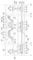
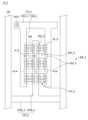
도 1을 참조하면, 표시 장치(10)는 복수의 화소(PX)를 포함할 수 있다. 화소(PX)들 각각은 특정 파장대의 광을 방출하는 발광 소자(300)를 하나 이상 포함하여 특정 색을 표시할 수 있다.Referring to FIG. 1 , the
복수의 화소(PX)들 각각은 제1 서브 화소(PX1), 제2 서브 화소(PX2) 및 제3 서브 화소(PX3)를 포함할 수 있다. 제1 서브 화소(PX1)는 제1 색의 광을 발광하고, 제2 서브 화소(PX2)는 제2 색의 광을 발광하며, 제3 서브 화소(PX3)는 제3 색의 광을 발광할 수 있다. 제1 색은 적색, 제2 색은 녹색, 제3 색은 청색일 수 있으나, 이에 제한되지 않는다. 경우에 따라서는 각 서브 화소(PXn)들이 동일한 색의 광을 발광할 수도 있다. 또한, 도 1에서는 화소(PX)들 각각이 3 개의 서브 화소들을 포함하는 것을 예시하였으나, 이에 제한되지 않고, 화소(PX)들 각각은 4 개 이상의 서브 화소들을 포함할 수 있다.Each of the plurality of pixels PX may include a first sub-pixel PX1, a second sub-pixel PX2, and a third sub-pixel PX3. The first sub-pixel (PX1) emits light of the first color, the second sub-pixel (PX2) emits light of the second color, and the third sub-pixel (PX3) emits light of the third color. You can. The first color may be red, the second color may be green, and the third color may be blue, but are not limited thereto. In some cases, each sub-pixel (PXn) may emit light of the same color. Additionally, in FIG. 1 , each of the pixels PX includes three sub-pixels, but the present invention is not limited thereto, and each of the pixels PX may include four or more sub-pixels.
표시 장치(10)의 각 서브 화소(PXn)들은 발광 소자(300)가 배치되는 정렬 영역(AA)과 비정렬 영역(NAA)을 포함할 수 있다. 정렬 영역(AA)은 후술하는 차폐 전극층(800)이 배치되지 않고 노출된 전극(210, 220) 상에 발광 소자(300)들이 정렬된 영역으로 정의될 수 있다. 비정렬 영역(NAA)은 정렬 영역(AA) 이외의 영역으로, 발광 소자(300)가 정렬되지 않는 영역으로 정의될 수 있다.Each sub-pixel PXn of the
한편, 본 명세서에서 '노출된', 또는 '노출시키는' 등의 용어는 제1 부재 및 제2 부재가 두께방향으로 부분적으로 중첩되지 않는 영역을 포함하는 것을 의미하며, 반드시 어느 한 부재가 외부로 드러나지 않더라도 상기 용어에 의해 해석될 수 있다. 즉, 제1 부재와 제2 부재 사이에 적어도 하나 이상의 부재가 배치되더라도, 제1 부재와 제2 부재가 두께 방향으로 중첩되지 않는 영역이 배치되는 경우, 어느 한 부재에 의해 다른 부재가 '노출된' 또는 '노출시키는' 것으로 해석될 수 있다.Meanwhile, in this specification, terms such as 'exposed' or 'exposed' mean that the first member and the second member include a region that does not partially overlap in the thickness direction, and one member must be exposed to the outside. Even if it is not revealed, it can be interpreted by the above terms. That is, even if at least one member is disposed between the first member and the second member, if an area where the first member and the second member do not overlap in the thickness direction is disposed, the other member is 'exposed' by one member. ' or 'expose'.
일 실시예에 따른 표시 장치(10)는 각 화소(PX) 또는 서브 화소(PXn)에 배치되는 전극(210, 220)의 적어도 일부를 노출시키는 차폐 전극층(800)을 포함할 수 있다. 차폐 전극층(800)은 전극(210, 220)의 적어도 일부를 노출시키며, 부분적으로 중첩되도록 배치될 수 있다. 상기 전극(210, 220)이 노출된 영역에서 발광 소자(300)가 정렬되어 정렬 영역(AA)이 형성된다. 또한, 상기 전극(210, 220) 상에서 차폐 전극층(800)이 덮는 영역을 포함하여, 정렬 영역(AA) 이외의 영역에 비정렬 영역(NAA)이 형성된다.The
표시 장치(10)의 제조 공정에서, 발광 소자(300)를 정렬하기 위해 전극(210, 220) 상에 전계를 형성하는 공정을 수행한다. 상기 전계는 전극(210, 220)에 정렬신호를 인가함으로써 형성될 수 있는데, 차폐 전극층(800)은 정렬신호에 의해 형성되는 전계를 차단시킬 수 있다. 즉, 차폐 전극층(800)이 전극(210, 220)을 덮는 영역에는 전계가 형성되지 않고, 그 이외에 전극(210, 220)이 노출된 영역에만 전계가 형성될 수 있다. 이에 따라, 표시 장치(10)의 제조 공정에서 특정 영역에 선택적으로 발광 소자(300)를 정렬시킴으로써, 표시 장치(10)에 배치된 발광 소자(300)의 정렬도를 향상시킬 수 있다. 보다 자세한 설명은 후술하기로 한다.In the manufacturing process of the
표시 장치(10)의 서브 화소(PXn)는 복수의 격벽(400), 복수의 전극(210, 220)과 발광 소자(300)를 포함하고, 전극(210, 220) 상의 적어도 일부 영역에는 중첩되지 않는 차폐 전극층(800) 등을 포함할 수 있다.The sub-pixel PXn of the
복수의 전극(210, 220)은 발광 소자(300)들과 전기적으로 연결되고, 발광 소자(300)가 발광하도록 소정의 전압을 인가 받을 수 있다. 또한, 각 전극(210, 220)의 적어도 일부는 발광 소자(300)를 정렬하기 위해, 서브 화소(PXn) 내에 전기장을 형성하는 데에 활용될 수 있다.The plurality of
도 1을 참조하여 구체적으로 설명하면, 복수의 전극(210, 220)은 제1 전극(210) 및 제2 전극(220)을 포함할 수 있다. 예시적인 실시예에서, 제1 전극(210)은 각 서브 화소(PXn) 마다 분리된 화소 전극이고, 제2 전극(220)은 각 서브 화소(PXn)를 따라 공통으로 연결된 공통전극일 수 있다. 제1 전극(210)과 제2 전극(220) 중 어느 하나는 발광 소자(300)의 애노드(Anode) 전극이고, 다른 하나는 발광 소자(300)의 캐소드(Cathode) 전극일 수 있다. 다만, 이에 제한되지 않으며 그 반대의 경우일 수도 있다.If described in detail with reference to FIG. 1 , the plurality of
제1 전극(210)과 제2 전극(220)은 각각 제1 방향(D1)으로 연장되어 배치되는 전극 줄기부(210S, 220S)와 전극 줄기부(210S, 220S)에서 제1 방향(D1)과 교차하는 방향인 제2 방향(D2)으로 연장되어 분지되는 적어도 하나의 전극 가지부(210B, 220B)를 포함할 수 있다.The
구체적으로, 제1 전극(210)은 제1 방향(D1)으로 연장되어 배치되는 제1 전극 줄기부(210S)와 제1 전극 줄기부(210S)에서 분지되되, 제2 방향(Y축 방향)으로 연장되는 적어도 하나의 제1 전극 가지부(210B)를 포함할 수 있다.Specifically, the
임의의 일 화소의 제1 전극 줄기부(210S)는 동일 행에 속하는(예컨대, 제1 방향(D1)으로 인접한) 이웃하는 서브 화소의 제1 전극 줄기부(210S)와 실질적으로 동일 직선 상에 놓일 수 있다. 다시 말해, 일 화소의 제1 전극 줄기부(210S)는 양 단이 각 서브 화소(PXn) 사이에서 이격되어 종지하되, 이웃 화소의 제1 전극 줄기부(210S)는 상기 일 화소의 제1 전극 줄기부(210S)의 연장선에 정렬될 수 있다. 이에 따라, 각 서브 화소(PXn)에 배치되는 제1 전극 줄기부(210S)는 각 제1 전극 가지부(210B)에 서로 다른 전기 신호를 인가할 수 있고, 제1 전극 가지부(210B)는 각각 별개로 구동될 수 있다.The
제1 전극 가지부(210B)는 제1 전극 줄기부(210S)의 적어도 일부에서 분지되고, 제2 방향(D2)으로 연장되어 배치되되, 제1 전극 줄기부(210S)에 대향되어 배치되는 제2 전극 줄기부(220S)와 이격된 상태에서 종지될 수 있다.The first
제2 전극(220)은 제1 방향(D1)으로 연장되어 제1 전극 줄기부(210S)와 이격되어 대향하도록 배치되는 제2 전극 줄기부(220S)와 제2 전극 줄기부(220S)에서 분지되되, 제2 방향(D2)으로 연장되어 배치되는 제2 전극 가지부(220B)를 포함할 수 있다. 다만, 제2 전극 줄기부(220S)는 타 단부가 제1 방향(D1)으로 인접한 복수의 서브 화소(PXn)로 연장될 수 있다. 이에 따라, 임의의 일 화소 제2 전극 줄기부(220S)는 양 단이 각 화소(PX) 사이에서 이웃 화소의 제2 전극 줄기부(220S)의 일 단에 연결될 수 있다.The
제2 전극 가지부(220B)는 제1 전극 가지부(210B)와 이격되어 대향하고, 제1 전극 줄기부(210S)와 이격된 상태에서 종지될 수 있다. 즉, 제2 전극 가지부(220B)는 일 단부가 제2 전극 줄기부(220S)와 연결되고, 타 단부는 제1 전극 줄기부(210S)와 이격된 상태로 서브 화소(PXn) 내에 배치될 수 있다.The
또한, 제1 전극 가지부(210B)는 각 서브 화소(PXn)에 하나 이상 배치될 수 있다. 도 1에서는 두개의 제1 전극 가지부(210B)가 배치되고, 그 사이에 제2 전극 가지부(220B)가 배치된 것을 도시하고 있으나, 이에 제한되지 않으며, 더 많은 수의 제1 전극 가지부(210B)가 배치되거나, 하나의 제1 전극 가지부(210B)가 배치되고 두개의 제2 전극 가지부(220B)가 배치될 수도 있다. 몇몇 실시예에서, 제1 전극 가지부(210B)들 사이에 제2 전극 가지부(220B)가 배치되어, 각 서브 화소(PXn)는 제2 전극 가지부(220B)를 기준으로 대칭구조를 가질 수 있다. 다만, 이에 제한되지 않는다.Additionally, one or more
복수의 격벽(400)은 각 서브 화소(PXn)간의 경계에 배치되는 제3 격벽(430), 각 전극(210, 220) 하부에 배치되는 제1 격벽(410) 및 제2 격벽(420)을 포함할 수 있다. 도면에서는 제1 전극(210)과 제2 전극(220)만이 도시되어 제1 격벽(410) 및 제2 격벽(420)이 도시되지 않았으나, 각 서브 화소(PXn)에는 제1 전극 가지부(210B)와 제2 전극 가지부(220B)와 실질적으로 동일한 형상을 갖는 제1 격벽(410) 및 제2 격벽(420)이 배치될 수 있다. 즉, 제1 전극 가지부(210B)와 제2 전극 가지부(220B)는 각각 제1 격벽(410)과 제2 격벽(420) 상에 배치된 것으로 이해될 수 있다.The plurality of partition walls 400 include a
제3 격벽(430)은 제1 서브 화소(PX1)와 제2 서브 화소(PX2), 제3 서브 화소(PX2)와 제3 서브 화소(PX3)의 경계에 배치될 수 있다. 복수의 제1 전극 줄기부(210S)는 각 단부가 제3 격벽(430)을 기준으로 서로 이격되어 종지할 수 있다. 제3 격벽(430)은 제2 방향(D2)으로 연장되어 제1 방향(D1)으로 배열된 서브 화소(PXn)들의 경계에 배치될 수 있다. 다만 이에 제한되지 않으며, 제3 격벽(430)은 제1 방향(D1)으로 연장되어 제2 방향(D2)으로 배열된 서브 화소(PXn)들의 경계에도 배치될 수 있다. 즉, 복수의 서브 화소(PXn)는 제3 격벽(430)을 기준으로 구분될 수 있다. 제3 격벽(430)은 제1 격벽(410) 및 제2 격벽(420)과 동일한 재료를 포함하여 실질적으로 동일한 공정에서 형성될 수 있다. 복수의 격벽(400)들에 대한 보다 자세한 설명은 다른 도면을 참조하여 후술하기로 한다.The
도 1에서는 도시하지 않았으나, 각 서브 화소(PXn)에는 제1 전극 가지부(210B)와 제2 전극 가지부(220B)를 포함하여 서브 화소(PXn)를 전면적으로 덮는 제1 절연층(510)이 배치될 수 있다. 제1 절연층(510)은 각 전극(210, 220)을 보호함과 동시에 이들이 직접 접촉하지 않도록 상호 절연시킬 수 있다.Although not shown in FIG. 1, each sub-pixel PXn includes a
차폐 전극층(800)은 제1 절연층(510) 상에 배치된다. 차폐 전극층(800)과 전극(210, 220)은 이들 사이에 배치된 제1 절연층(510)에 의해 직접적으로 접촉되지 않을 수 있다. 다만, 후술할 바와 같이, 접촉 전극(260)에 의해 서로 전기적으로 연결될 수 있다.The shielding
차폐 전극층(800)은 제1 전극(210) 상에 배치되는 제1 차폐 전극(810)과 제2 전극(220) 상에 배치되는 제2 차폐 전극(820)을 포함할 수 있다. 제1 차폐 전극(810)과 제2 차폐 전극(820)은 전극 줄기부(210S, 220S)와 전극 가지부(210B, 220B) 상에서 이들을 덮도록 배치될 수 있다. 즉, 제1 및 제2 차폐 전극(810, 820)도 줄기부와 가지부를 포함하여, 제1 및 제2 전극(210, 220)과 실질적으로 동일한 패턴을 형성할 수도 있다.The shielding
일 실시예에 따르면, 제1 차폐 전극(810)은 제1 차폐 전극 줄기부(810S)와 제1 차폐 전극 가지부(810B)를 포함하고, 제2 차폐 전극(820)은 제2 차폐 전극 줄기부(820S)와 제2 차폐 전극 가지부(820B)를 포함할 수 있다.According to one embodiment, the
제1 차폐 전극 줄기부(810S)와 제2 차폐 전극 줄기부(820S)는 각각 제1 방향(D1)으로 연장되고, 제2 방향(D2)으로 서로 이격될 수 있다. 즉, 제1 및 제2 차폐 전극 줄기부(810S, 820S)는 각각 제1 및 제2 전극 줄기부(210S, 220B)와 실질적으로 동일한 형상을 가질 수 있다. 특히, 제1 차폐 전극 줄기부(810S)는 이웃하는 서브 화소(PXn)의 경계에서 제3 격벽(430)에 이격되어 종지하고, 제2 차폐 전극 줄기부(820S)는 이웃하는 서브 화소(PXn)를 넘어 연장될 수 있다.The first
제1 차폐 전극 가지부(810B)와 제2 차폐 전극 가지부(820B)는 각각 줄기부로부터 분지되어 제2 방향(D2)으로 연장될 수 있다. 제1 및 제2 차폐 전극 가지부(810B, 820B)는 각각 제1 및 제2 전극 가지부(210B, 220B)와 실질적으로 동일한 형상을 가질 수 있다. 즉, 제1 및 제2 차폐 전극 가지부(810B, 820B)는 제2 방향(D2)으로 연장되어 서로 이격되어 대향할 수 있다.The first
한편, 일 실시예에 따르면, 제1 및 제2 차폐 전극(810, 820)은 측면의 적어도 일부 영역이 함몰된 패턴을 형성할 수 있다. 제1 및 제2 차폐 전극(810, 820)은 측면의 일부 영역이 함몰된 함몰패턴부(810C, 820C)를 포함하고, 함몰패턴부(810C, 820C)와 중첩된 영역의 전극(210, 220)은 부분적으로 노출될 수 있다. 즉, 제1 및 제2 차폐 전극(810, 820)은 전극(210, 220)의 적어도 일부와 중첩되지 않도록 함몰패턴부(810C, 820C)가 형성될 수 있다.Meanwhile, according to one embodiment, the first and
구체적으로, 제1 및 제2 차폐 전극 가지부(810B, 820B)는 적어도 일 측면, 예컨대 이들이 서로 대향하는 측면에는 함몰패턴부(810C, 820C)가 형성될 수 있다. 제1 차폐 전극 가지부(810B)가 제2 차폐 전극 가지부(820B)와 대향하는 일 측면에서, 상기 일 측면으로부터 제1 차폐 전극 가지부(810B)의 중심부를 향해 함몰된 제1 함몰패턴부(810C)가 형성될 수 있다. 제2 차폐 전극 가지부(820B)는 제1 차폐 전극 가지부(810B)와 대향하는 양 측면에서, 상기 양 측면으로부터 제2 차폐 전극 가지부(820B)의 중심부를 향해 함몰된 제2 함몰패턴부(820C)가 형성될 수 있다.Specifically, recessed
제1 함몰패턴부(810C)와 제2 함몰패턴부(820C)는 서로 이격되어 대향하고, 각각 이들과 중첩되는 제1 전극 가지부(210B)와 제2 전극 가지부(220B)는 부분적으로 노출될 수 있다. 상기 노출된 영역에서 발광 소자(300)가 정렬되어, 발광 소자(300)의 양 단부는 각각 제1 전극 가지부(210B)와 제2 전극 가지부(220B)에 전기적으로 연결될 수 있다. 즉, 제1 함몰패턴부(810C)와 제2 함몰패턴부(820C)가 서로 이격되어 대향함으로써 형성되는 영역은 정렬 영역(AA)일 수 있다.The first
반면에, 제1 함몰패턴부(810C)와 제2 함몰패턴부(820C)가 형성되지 않은 영역에는 제1 차폐 전극 가지부(810B) 및 제2 차폐 전극 가지부(820B)가 각각 제1 전극 가지부(210B)와 제2 전극 가지부(220B)를 덮도록 배치되고, 이들 사이의 영역에는 발광 소자(300)가 정렬되지 않는다. 이에 따라, 상기 영역은 비정렬 영역(NAA)일 수 있다.On the other hand, in the area where the first recessed
다만, 차폐 전극층(800)의 구조는 이에 제한되지 않는다. 후술할 바와 같이, 차폐 전극층(800)은 표시 장치(10)의 제조 공정에서 정렬 신호에 의해 형성되는 전계를 차단하는 구조이면 특별히 제한되지 않는다. 이에 대한 자세한 설명은 다른 실시예를 참조하여 후술하기로 한다.However, the structure of the shielding
한편, 차폐 전극층(800)은 표시 장치(10)의 제조 공정에서 전극(210, 220)과 절연되는 플로팅 전극(Floating electrode)일 수 있다. 발광 소자(300)를 정렬하기 위해 전극(210, 220)에서 인가되는 정렬 신호는 차폐 전극층(800)에는 전달되지 않으며, 차폐 전극층(800)은 상기 정렬 신호에 의해 형성되는 전계를 차단할 수 있다. 정렬 신호를 인가받은 전극(210, 220)이 전계를 형성할 때, 차폐 전극층(800)이 배치된 영역은 전계가 차단되는 영역이고, 그 이외의 영역은 전계가 형성되어 발광 소자(300)가 정렬될 수 있다. 즉, 상술한 바와 같이, 차폐 전극층(800)이 전극(210, 220)을 덮는 영역은 비정렬 영역(NAA)이고, 전극(210, 220)이 노출된 영역은 정렬 영역(AA)로 정의될 수 있다.Meanwhile, the shielding
일 실시예에 따른 차폐 전극층(800)은 전극(210, 220)과 실질적으로 동일한 재료를 포함할 수 있다. 예시적인 실시예에서, 차폐 전극층(800)은 알루미늄(Al), 은(Ag), 구리(Cu), ITO(Indium Tin Oxide), IZO(Indium Zinc Oxide), ITZO(Indium Tin-Zinc Oxide) 등을 포함하여, 하나의 층 또는 이중층 이상으로 형성될 수 있다.The shielding
차폐 전극층(800)은 표시 장치(10)의 제조 공정에서는 전극(210, 220)과 상호 절연되어 플로팅 전극으로써, 전계를 차단하는 기능을 수행할 수 있다. 반면에, 최종적으로 제조된 표시 장치(10)에서, 차폐 전극층(800)은 후술하는 접촉 전극(260)을 통해 전극(210, 220)과 전기적으로 연결될 수 있다. 표시 장치(10)의 제조시에는 전계를 차단함으로써 발광 소자(300)가 정렬되는 영역을 제어할 수 있고, 표시 장치(10)에서는 전극(210, 220)과 전기적으로 연결되어 구동 신호를 전달받을 수 있다.During the manufacturing process of the
제1 전극 가지부(210B)와 제2 전극 가지부(220B) 사이에는 복수의 발광 소자(300)가 정렬될 수 있다. 복수의 발광 소자(300) 중 적어도 일부는 일 단부가 제1 전극 가지부(210B)와 전기적으로 연결되고, 타 단부가 제2 전극 가지부(220B)와 전기적으로 연결될 수 있다.A plurality of light emitting
복수의 발광 소자(300)들은 제2 방향(D2)으로 이격되고, 실질적으로 서로 평행하게 정렬될 수 있다. 발광 소자(300)들이 이격되는 거리는 특별히 제한되지 않는다. 경우에 따라서는 복수의 발광 소자(300)들이 인접하게 배치되어 무리를 이루고, 다른 복수의 발광 소자(300)들은 일정 간격 이격된 상태로 무리를 이룰 수도 있으며, 불균일한 밀집도를 가지되 일 방향으로 배향되어 정렬될 수도 있다.The plurality of light emitting
일 실시예에 따르면, 발광 소자(300)는 차폐 전극층(800)과 전극(210, 220)이 중첩되지 않는 영역에 배치되어 양 단부가 전극(210, 220)과 전기적으로 연결될 수 있다. 구체적으로, 제1 전극(210)과 제2 전극(220)은 각각 제1 함몰패턴부(810C) 및 제2 함몰패턴부(820C)와 중첩되는 영역에서 부분적으로 노출될 수 있다. 상술한 바와 같이, 상기 노출된 영역에서는 정렬 신호에 의해 전계가 형성되고, 상기 전계에 의해 발광 소자(300)가 정렬될 수 있다. 반면에 제1 전극(210)과 제2 전극(220)이 노출되지 않는 영역은 상기 전계가 형성되지 않고, 발광 소자(300)가 정렬되지 않을 수 있다. 이에 따라, 표시 장치(10)의 제조 공정에서, 소정의 영역에만 발광 소자(300)의 선택적인 정렬을 유도함으로써, 표시 장치(10)의 정렬도를 향상시킬 수 있다.According to one embodiment, the
제1 전극 가지부(210B)와 제2 전극 가지부(220B) 상에는 각각 접촉 전극(260)이 배치될 수 있다. 다만, 접촉 전극(260)은 실질적으로 제1 절연층(510) 상에 배치되며, 제1 전극 가지부(210B) 및 제2 전극 가지부(220B)와 부분적으로 중첩될 수 있다.Contact
복수의 접촉 전극(260)은 제2 방향(D2)으로 연장된 형상으로 배치되며, 이들은 제1 방향(D1)으로 서로 이격되어 배치될 수 있다. 접촉 전극(260)은 상술한 제1 함몰패턴부(810C)와 제2 함몰패턴부(820C)가 이격되어 형성되는 영역에 배치되며, 제1 함몰패턴부(810C)와 제2 함몰패턴부(820C)가 배치되지 않는 영역에서는 단선되어 패터닝될 수 있다. 즉, 도면에 도시된 바와 같이 제1 전극 가지부(210B)와 제2 전극 가지부(220B) 사이에 배치되는 접촉 전극(260)은 제2 방향(D2)으로 배열된 패턴을 형성할 수 있다. 다만, 이에 제한되는 것은 아니며, 경우에 따라서 접촉 전극(260)은 제2 방향(D2)으로 연장되어 하나의 패턴으로 형성될 수도 있다.The plurality of
접촉 전극(260)은 소정을 폭을 가지며, 각 전극 가지부(210B, 220B)와 각 차폐 전극 가지부(810B, 820B) 상에서 이들을 부분적으로 덮도록 배치될 수 있다. 접촉 전극(260)은 발광 소자(300)의 적어도 일 단부와 컨택되고, 제1 전극(210) 또는 제2 전극(220)과 컨택되어 전기 신호를 인가받을 수 있다. 접촉 전극(260)은 차폐 전극(810, 820)의 일 측부에도 접촉될 수 있다. 이에 따라, 접촉 전극(260)은 각 전극(210, 220)으로부터 전달되는 전기 신호를 차폐 전극(810, 820)과 발광 소자(300)에 전달할 수 있다.The
접촉 전극(260)은 발광 소자(300)의 일 단부 또는 타 단부와 접촉되는 제1 접촉 전극(261)과 제2 접촉 전극(262)을 포함할 수 있다. 제1 접촉 전극(261)은 제1 전극 가지부(210B) 상에 배치되며, 발광 소자(300)의 일 단부와 컨택되어, 상기 일 단부는 제1 전극(210)과 전기적으로 연결될 수 있다. 제2 접촉 전극(262)은 제2 전극 가지부(220B) 상에 배치되며, 발광 소자(300)의 타 단부와 컨택되어, 상기 타 단부는 제2 전극(220)과 전기적으로 연결될 수 있다.The
도 1에 도시된 바와 같이, 각 서브 화소(PXn) 내에는 2개의 제1 전극 가지부(210B)가 배치되어 2개의 제1 접촉 전극(261)이 배치되고, 하나의 제2 전극 가지부(220B)가 배치되어 양 측면에 2개의 제2 접촉 전극(262)이 배치될 수 있다. 일 실시예에 따르면, 제1 접촉 전극(261)과 제2 접촉 전극(262) 각각은 제1 전극 가지부(210B)와 제2 전극 가지부(220B)의 일 측면에서 접촉할 수 있고, 이와 동시에 제1 차폐 전극(810)과 제2 차폐 전극(820)의 일 측면에서 접촉할 수 있다.As shown in FIG. 1, two
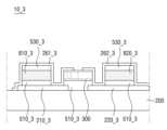
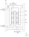
도 2 및 도 3은 일 실시예예 따른 표시 장치의 단면을 나타내는 개략도이다. 도 2는 도 1에서 발광 소자(300)의 양 단부를 포함하여 제1 방향(D1)으로 자른 단면을 나타내고, 도 3은 도 1에서 차폐 전극층(800)의 함몰패턴부(810C, 820C)를 포함하여 제2 방향(D2)으로 다른 단면을 나타낸다. 도 2 및 도 3은 일 실시예에 따른 표시 장치(10)의 단면을 개략적으로 도시한 것이며, 표시 장치(10)의 구조가 이에 제한되는 것은 아니다.2 and 3 are schematic diagrams showing a cross section of a display device according to an exemplary embodiment. FIG. 2 shows a cross section cut in the first direction D1 including both ends of the
먼저, 도 2를 참조하면, 제1 전극(210)과 제2 전극(220)은 이들을 지지하는 비아층(200) 상에서 서로 이격되어 배치된다. 비아층(200)에 대한 자세한 설명은 도 4를 참조하여 후술하기로 한다. 제1 전극(210)과 제2 전극(220) 상에는 이들을 부분적으로 덮는 제1 절연층(510)이 배치되고, 제1 전극(210)과 제2 전극(220) 사이에 배치된 제1 절연층(510) 상에는 발광 소자(300)가 배치될 수 있다. 제1 전극(210)과 제2 전극(220) 상에 배치된 제1 절연층(510) 상에는 제1 차폐 전극(810)과 제2 차폐 전극(820)이 배치될 수 있다.First, referring to FIG. 2, the
제1 차폐 전극(810)과 제2 차폐 전극(820)은 각각 제1 전극(210) 및 제2 전극(220)과 부분적으로 중첩되고, 이들이 서로 중첩되지 않는 영역은 함몰패턴부(810C, 820C)가 위치하는 영역일 수 있다. 제1 및 제2 접촉 전극(261, 262)은 각각 제1 및 제2 차폐 전극(810, 820), 발광 소자(300), 제1 및 제2 전극(210, 220) 및 제1 절연층(510)과 접촉할 수 있다. 제1 및 제2 접촉 전극(261, 262)은 함몰패턴부(810C, 820C)가 위치하는 영역에서 제1 전극(210) 및 제2 전극(220)에 접촉할 수 있다.The
일 실시예에 따르면, 제1 접촉 전극(261)은 제1 차폐 전극(810)의 일 측부와 접촉하고, 하나의 제2 접촉 전극(262)은 제2 차폐 전극(820)의 일 측부와 접촉할 수 있다. 다만, 이에 제한되지 않으며, 경우에 따라서 제1 접촉 전극(261)은 더 넓은 폭을 갖고 제1 차폐 전극(810)의 양 측부와 접촉하고, 제2 접촉 전극(262)도 하나의 접촉 전극(262)이 양 측부와 접촉할 수도 있다.According to one embodiment, the
한편, 차폐 전극층(800)은 함몰패턴부(810C, 820C)를 포함하여 제1 차폐 전극(810)과 제2 차폐 전극(820)이 이격된 거리와 제1 전극(210)과 제2 전극(220)이 이격된 거리는 서로 상이할 수 있다. 일 실시예에 따른 표시 장치(10)는 차폐 전극(810, 820)의 발광 소자(300)의 양 단부를 가로지르는 일 방향으로 측정된 거리는 각 전극(210, 220)의 일 방향으로 측정된 거리보다 길 수 있다.Meanwhile, the shielding
구체적으로, 도 1 및 도 2에 도시된 바와 같이 발광 소자(300)가 배치된 정렬 영역(AA)에서, 각 전극(210, 220)과 각 차폐 전극(810, 820)은 발광 소자(300)의 양 단부를 가로지르는 제1 방향(D1)으로 서로 이격될 수 있다. 전극(210, 220) 간의 제1 방향(D1)으로 측정된 거리(S1)는 제1 방향(D1)으로 측정된 차폐 전극(810, 820) 간의 거리(S2)보다 짧을 수 있다.Specifically, as shown in FIGS. 1 and 2, in the alignment area AA where the
제1 차폐 전극(810)과 제2 차폐 전극(820)은 각각 제1 전극(210) 및 제2 전극(220)과 실질적으로 동일한 패턴을 형성하되, 제1 함몰패턴부(810C)와 제2 함몰패턴부(820C)가 형성됨에 따라 일 측면이 각각 함몰되어 형성될 수 있다. 특히, 함몰패턴부(810C, 820C)가 형성된 정렬 영역(AA)에서 전극(210, 220) 간의 이격된 거리(S1)는 차폐 전극(810, 820) 간의 이격된 거리(S2) 보다 좁을 수 있다.The
이에 따라, 차폐 전극(810, 820)의 일 측면, 예컨대 발광 소자(300)와 대향하는 일 측면을 기준으로 각 전극(210, 220)의 일 측면은 돌출되도록 배치되고, 상기 돌출된 영역과 중첩되는 제1 절연층(510)은 차폐 전극(810, 820)이 배치되지 않고 노출될 수 있다. 표시 장치(10)의 제조 공정에서 전극(210, 220)이 돌출되어 제1 절연층(510)이 노출된 영역에서는 전계가 형성되어 발광 소자(300)가 정렬될 수 있다.Accordingly, one side of each
예시적인 실시예에 따르면 정렬 영역(AA)에서 제1 전극(210)과 제2 전극(220)의 이격된 거리(S1)는 발광 소자(300)의 양 단부 사이의 거리, 즉 일 방향으로 측정된 길이(h, 도 6에 도시)보다 짧고, 제1 차폐 전극(810)과 제2 차폐 전극(820)의 이격된 거리(S2)는 발광 소자(300)의 길이(h, 도 6에 도시)보다 길 수 있다.According to an exemplary embodiment, the distance S1 between the
발광 소자(300)는 제1 전극(210) 및 제2 전극(220) 사이의 거리(S1)보다 긴 길이(h)를 가짐으로써, 제1 전극(210)과 제2 전극(220) 사이에 배치되어 양 단부가 이들과 각각 연결될 수 있다. 또한, 발광 소자(300)가 제1 차폐 전극(810) 및 제2 차폐 전극(820) 사이의 거리(S2)보다 짧은 길이(h, 도 6에 도시)를 가짐으로써 차폐 전극(810, 820)과 중첩되지 않는 전극(210, 220) 상에서 차폐 전극(810, 820)과 이격되어 정렬될 수 있다.The
다만, 이에 제한되는 것은 아니며, 차폐 전극(810, 820)의 함몰패턴부(810C, 820C)가 형성되지 않은 영역의 경우, 차폐 전극(810, 820) 간의 이격된 거리는 전극(210, 220) 간의 이격된 거리와 동일하거나 이보다 짧을 수도 있다.However, it is not limited to this, and in the case of the area where the recessed
도 3을 참조하면, 제1 전극(210)과 제1 차폐 전극(810)이 배치된 영역의 제2 방향(D2) 단면에서는 제1 차폐 전극(810)이 패턴을 형성하며 제2 방향(D2)으로 배열되고, 이들이 이격된 사이에 복수의 발광 소자(300)들이 배치될 수 있다. 제1 차폐 전극(810)이 배치된 영역에서는 표시 장치(10)의 제조 공정에서 전계가 형성되지 않는 영역이고, 제1 차폐 전극(810)이 이격된 영역, 즉 제1 함몰패턴부(810C)가 형성된 영역은 전계가 형성되는 영역으로 이해될 수 있다. 제1 차폐 전극(810)이 형성됨에 따라, 발광 소자(300)들은 제1 함몰패턴부(810C)가 위치하는 영역에만 정렬될 수 있고, 불필요한 위치에 정렬되는 발광 소자(300)의 개수를 감소시킬 수 있다.Referring to FIG. 3, in the cross section of the area where the
한편, 제1 전극 줄기부(210S)와 제2 전극 줄기부(220S)는 각각 컨택홀, 예컨대 제1 전극 컨택홀(CNTD) 및 제2 전극 컨택홀(CNTS)을 통해 후술하는 제1 트랜지스터(120) 또는 전원 배선(161)과 전기적으로 연결될 수 있다. 도면에는 복수의 서브 화소(PXn)의 제2 전극 줄기부(220S)에 하나의 제2 전극 컨택홀(CNTS)이 형성된 것을 도시하고 있다. 다만, 이에 제한되지 않으며, 경우에 따라서는 각 서브 화소(PXn) 마다 제2 전극 컨택홀(CNTD)이 형성될 수 있다.Meanwhile, the
또한, 도 1에서는 도시하지 않았으나, 표시 장치(10)는 각 전극(210, 220) 및 발광 소자(300)의 적어도 일부를 덮도록 배치되는 제2 절연층(520, 도 4에 도시) 및 패시베이션층(550, 도 4에 도시)을 포함할 수 있다. 이들 간의 배치와 구조 등은 도 4를 참조하여 후술한다.In addition, although not shown in FIG. 1, the
표시 장치(10)는 도 1에 도시된 각 전극(210, 220)의 하부에 위치하는 회로소자층을 더 포함할 수 있다. 이하에서는 다른 도면을 참조하여 이에 대하여 상세히 서술하기로 한다.The
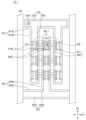
도 4는 도 1의 Ia-Ia'선, Ⅱa-Ⅱa' 선 및 Ⅲa-Ⅲa' 선을 따라 자른 단면도이다. 도 5는 도 1의 Ⅱb-Ⅱb' 선을 따라 다른 단면도이다. 도 4 및 도 5는 제1 서브 화소(PX1)의 단면도만을 도시하고 있으나, 다른 화소(PX) 또는 서브 화소(PXn)의 경우에도 동일하게 적용될 수 있다. 도 4는 임의의 발광 소자(300)의 일 단부와 타 단부를 가로지르는 단면을 도시한다.FIG. 4 is a cross-sectional view taken along lines Ia-Ia', IIa-IIa', and IIIa-IIIa' of FIG. 1. Figure 5 is another cross-sectional view taken along line IIb-IIb' in Figure 1. 4 and 5 only show a cross-sectional view of the first sub-pixel PX1, but the same can be applied to other pixels PX or sub-pixels PXn. FIG. 4 shows a cross section across one end and the other end of an arbitrary
도 1 및 도 4를 참조하면, 표시 장치(10)는 기판(110), 버퍼층(115), 제1 및 제2 브릿지 패턴(181, 182), 제1 및 제2 트랜지스터(120, 140)와 제1, 제2 트랜지스터(120, 140) 상에 배치된 전극(210, 220)과 발광 소자(300)를 포함할 수 있다.Referring to FIGS. 1 and 4 , the
구체적으로, 기판(110)은 절연 기판일 수 있다. 기판(110)은 유리, 석영, 또는 고분자 수지 등의 절연 물질로 이루어질 수 있다. 또한, 기판(110)은 리지드 기판일 수 있지만, 벤딩(bending), 폴딩(folding), 롤링(rolling) 등이 가능한 플렉시블(flexible) 기판일 수도 있다.Specifically, the
제1 및 제2 브릿지 패턴(181, 182)은 기판(110) 상에 배치될 수 있다. 제1 브릿지 패턴(181)은 후술하는 제1 트랜지스터(120)의 제1 드레인 전극(123)과 전기적으로 연결될 수 있다. 제2 브릿지 패턴(182)은 제2 트랜지스터(140)의 제2 드레인 전극(143)과 전기적으로 연결될 수 있다.The first and
제1 브릿지 패턴(181)과 제2 브릿지 패턴(182)은 각각 제1 트랜지스터(120)의 제1 활성물질층(126) 및 제2 트랜지스터(140)의 제2 활성물질층(146)과 중첩하도록 배치된다. 제1 및 제2 브릿지 패턴(181, 182)은 광을 차단하는 재료를 포함하여, 제1 및 제2 활성물질층(126, 146)에 광이 입사되는 것을 방지할 수 있다. 일 예로, 제1 및 제2 브릿지 패턴(181, 182)은 광의 투과를 차단하는 불투명한 금속 물질로 형성될 수 있다.The
버퍼층(115)은 제1 및 제2 브릿지 패턴(181, 182)과 기판(110) 상에 배치된다. 버퍼층(115)은 제1 및 제2 브릿지 패턴(181, 182)을 포함하여, 기판(110)을 전면적으로 덮도록 배치될 수 있다. 버퍼층(115)은 불순물 이온이 확산되는 것을 방지하고 수분이나 외기의 침투를 방지하며, 표면 평탄화 기능을 수행할 수 있다. 또한, 버퍼층(115)은 제1 및 제2 브릿지 패턴(181, 182)과 제1 및 제2 활성물질층(126, 146)을 상호 절연시킬 수 있다.The
버퍼층(115) 상에는 반도체층이 배치된다. 반도체층은 제1 트랜지스터(120)의 제1 활성물질층(126), 제2 트랜지스터(140)의 제2 활성물질층(146) 및 보조물질층(163)을 포함할 수 있다. 반도체층은 다결정 실리콘, 단결정 실리콘, 산화물 반도체 등을 포함할 수 있다.A semiconductor layer is disposed on the
반도체층 상에는 제1 게이트 절연막(170)이 배치된다. 제1 게이트 절연막(170)은 반도체층을 포함하여 버퍼층(115)을 전면적으로 덮도록 배치될 수 있다. 제1 게이트 절연막(170)은 제1 및 제2 트랜지스터(120, 140)의 게이트 절연막으로 기능할 수 있다.A first
제1 게이트 절연막(170) 상에는 제1 도전층이 배치된다. 제1 도전층은 제1 게이트 절연막(170) 상에서 제1 트랜지스터(120)의 제1 활성물질층(126) 상에 배치된 제1 게이트 전극(121), 제2 트랜지스터(140)의 제2 활성물질층(146) 상에 배치된 제2 게이트 전극(141) 및 보조물질층(163) 상에 배치된 전원 배선(161)을 포함할 수 있다.A first conductive layer is disposed on the first
제1 도전층 상에는 층간절연막(190)이 배치된다. 층간절연막(190)은 층간 절연막의 기능을 수행할 수 있다. 또한, 층간절연막(190)은 유기 절연 물질을 포함하고 표면 평탄화 기능을 수행할 수도 있다.An interlayer insulating
층간절연막(190) 상에는 제2 도전층이 배치된다. 제2 도전층은 제1 트랜지스터(120)의 제1 드레인 전극(123)과 제1 소스 전극(124), 제2 트랜지스터(140)의 제2 드레인 전극(143)과 제2 소스 전극(144), 및 전원 배선(161) 상부에 배치된 전원 전극(162)을 포함한다.A second conductive layer is disposed on the
제1 드레인 전극(123)과 제1 소스 전극(124)은 층간절연막(190)과 제1 게이트 절연막(170)을 관통하는 컨택홀을 통해 제1 활성물질층(126)과 전기적으로 연결될 수 있다. 제2 드레인 전극(143)과 제2 소스 전극(144)은 층간절연막(190)과 제1 게이트 절연막(170)을 관통하는 컨택홀을 통해 제2 활성물질층(146)과 전기적으로 연결될 수 있다. 또한, 제1 드레인 전극(123)과 제2 드레인 전극(143)은 또 다른 컨택홀을 통해 각각 제1 브릿지 패턴(181) 및 제2 브릿지 패턴(182)과 전기적으로 연결될 수 있다.The
제2 도전층 상에는 비아층(200)이 배치된다. 비아층(200)은 유기 절연 물질을 포함하여 표면 평탄화 기능을 수행할 수 있다.A via
비아층(200) 상에는 복수의 격벽(410, 420, 430)이 배치된다. 복수의 격벽(410, 420, 430)은 각 서브 화소(PXn) 내에서 서로 이격되어 배치될 수 있다. 복수의 격벽(410, 420, 430)은 서브 화소(PXn)의 중심부에 인접하여 배치된 제1 격벽(410) 및 제2 격벽(420), 서브 화소(PXn)간의 경계에 배치된 제3 격벽(430)을 포함할 수 있다.A plurality of
제3 격벽(430)은 각 서브 화소(PXn)의 경계를 구분하는 격벽일 수 있다. 제3 격벽(430)은 표시 장치(10)의 제조 시, 잉크젯 프린팅법(Inkjet printing)을 이용하여 유기물질 또는 용매를 분사할 때, 상기 유기물질 또는 용매가 서브 화소(PXn)의 경계를 넘지 않도록 차단하는 기능을 수행할 수 있다. 또는, 표시 장치(10)가 다른 부재를 더 포함하는 경우, 제3 격벽(430) 상에 상기 부재가 배치되어 제3 격벽(430)이 이를 지지하는 기능을 수행할 수도 있다. 다만, 이에 제한되는 것은 아니다.The
제1 격벽(410)과 제2 격벽(420)은 서로 이격되어 대향하도록 배치된다. 제1 격벽(410) 상에는 제1 전극(210)이, 제2 격벽(420) 상에는 제2 전극(220)이 배치될 수 있다. 도 1과 도 4를 참조하면, 제1 격벽(410) 상에는 제1 전극 가지부(210B)가, 제2 격벽(420) 상에는 제2 격벽(420)이 배치된 것으로 이해될 수 있다. 즉, 제1 격벽(410)과 제2 격벽(420)은 도 1을 기준으로 제2 방향(D2)으로 연장되어 제1 방향(D1)으로 이격되어 배치될 수 있다.The
도 4에서는 제1 내지 제3 격벽(410, 420, 430)이 하나씩 배치된 것을 도시하고 있으나, 이에 제한되지 않는다. 도 1과 같이 하나의 서브 화소(PXn) 내에 2개의 제1 전극 가지부(210B)가 배치되는 경우, 2개의 제1 격벽(410)과 하나의 제2 격벽(420)이 배치될 수 있으며, 각 서브 화소(PXn)는 더 많은 수의 격벽(410, 420, 430)을 포함할 수 있다.Figure 4 shows the first to
상술한 바와 같이, 제1 격벽(410), 제2 격벽(420) 및 제3 격벽(430)은 실질적으로 동일한 공정에서 형성될 수 있다. 이에 따라, 격벽(410, 420, 430)은 하나의 격자형 패턴을 이룰 수도 있다. 복수의 격벽(410, 420, 430)은 폴리이미드(Polyimide, PI)를 포함할 수 있다.As described above, the
복수의 격벽(410, 420, 430)은 비아층(200)을 기준으로 적어도 일부가 돌출된 구조를 가질 수 있다. 격벽(410, 420, 430)은 발광 소자(300)가 배치된 평면을 기준으로 상부로 돌출될 수 있고, 상기 돌출된 부분은 적어도 일부가 경사를 가질 수 있다. 돌출된 구조의 격벽(410, 420, 430)의 형상은 특별히 제한되지 않는다. 도면에 도시된 바와 같이, 제1 격벽(410)과 제2 격벽(420)은 동일한 높이로 돌출되되, 제3 격벽(430)은 더 높은 위치까지 돌출된 형상을 가질 수 있다.The plurality of
제1 격벽(410)과 제2 격벽(420) 상에는 반사층(211, 221)이 배치되고, 반사층(211, 221) 상에는 전극층(212, 222)이 배치될 수 있다. 반사층(211, 221)과 전극층(212, 222)은 각각 전극(210, 220)을 구성할 수 있다.
반사층(211, 221)은 제1 반사층(211)과 제2 반사층(221)을 포함한다. 제1 반사층(211)은 제1 격벽(410)을 덮으며, 일부는 비아층(200)을 관통하는 컨택홀을 통해 제1 드레인 전극(124)과 전기적으로 연결된다. 제2 반사층(221)은 제2 격벽(420)을 덮으며, 일부는 비아층(200)을 관통하는 컨택홀을 통해 전원 전극(162)과 전기적으로 된다. 제1 반사층(211)이 연결되는 상기 컨택홀은 도 1의 제1 전극 컨택홀(CNTD)이고, 제2 반사층(221)이 연결되는 상기 컨택홀은 도 1의 제2 전극 컨택홀(CNTS)일 수 있다.The
반사층(211, 221)은 반사율이 높은 물질을 포함하여 발광 소자(300)에서 방출되는 방출광(EL)을 반사시킬 수 있다. 일 예로, 반사층(211, 221)은 은(Ag), 구리(Cu), ITO(Indium Tin Oxide), IZO(Indium Zinc Oxide), ITZO(Indium Tin-Zinc Oxide) 등과 같은 물질을 포함할 수 있으나, 이에 제한되는 것은 아니다.The
전극층(212, 222)은 제1 전극층(212)과 제2 전극층(222)을 포함한다. 전극층(212, 222)은 실질적으로 반사층(211, 221)과 동일한 패턴을 가질 수 있다. 제1 반사층(211) 및 제1 전극층(212)은 제2 반사층(221) 및 제2 전극층(222)과 서로 이격되도록 배치된다.The electrode layers 212 and 222 include a
전극층(212, 222)은 투명성 전도성 물질을 포함하여 발광 소자(300)에서 방출되는 방출광(EL)이 반사층(211, 221)으로 입사될 수 있다. 일 예로, 전극층(212, 222)은 ITO(Indium Tin Oxide), IZO(Indium Zinc Oxide), ITZO(Indium Tin-Zinc Oxide) 등과 같은 물질을 포함할 수 있으나, 이에 제한되는 것은 아니다.The electrode layers 212 and 222 include a transparent conductive material so that the emission light (EL) emitted from the
몇몇 실시예에서, 반사층(211, 221)과 전극층(212, 222)은 ITO, IZO, ITZO 등과 같은 투명도전층과 은, 구리와 같은 금속층이 각각 한층 이상 적층된 구조를 이룰 수 있다. 일 예로, 반사층(211, 221)과 전극층(212, 222)은 ITO/은(Ag)/ITO/IZO의 적층구조를 형성할 수도 있다.In some embodiments, the
제1 반사층(211)과 제1 전극층(212)은 제1 전극(210)을 구성하고, 제2 반사층(221)과 제2 전극층(222)은 제2 전극(220)을 구성할 수 있다. 제1 전극(210)과 제2 전극(220)은 각각 제1 전극층(212) 및 제2 전극층(222)을 통해 제1 트랜지스터(120)와 전원 전극(162)에서 전달되는 전기 신호를 발광 소자(300)에 전달할 수 있다.The first
한편, 몇몇 실시예에서, 제1 전극(210)과 제2 전극(220)은 하나의 층으로 형성될 수 있다. 즉, 반사층(211, 221)과 전극층(212, 222)이 하나의 단일층으로 형성되어 발광 소자(300)에 전기 신호를 전달함과 동시에 방출광(EL)을 반사할 수 있다. 예시적인 실시예에서, 제1 전극(210)과 제2 전극(220)은 반사율이 높은 전도성 물질을 포함할 수 있다. 일 예로, 제1 전극(210) 및 제2 전극(220)은 알루미늄(Al), 니켈(Ni), 란타늄(La) 등을 포함하는 합금일 수 있다. 다만 이에 제한되는 것은 아니다.Meanwhile, in some embodiments, the
제1 전극(210)과 제2 전극(220) 상에는 이들을 부분적으로 덮는 제1 절연층(510)이 배치된다. 제1 절연층(510)은 제1 전극(210)과 제2 전극(220)의 상면을 대부분 덮도록 배치되되, 제1 전극(210)과 제2 전극(220)의 일부를 노출시킬 수 있다. 제1 절연층(510)은 제1 전극(210)과 제2 전극(220)이 이격된 공간과, 제1 전극(210) 및 제2 전극(220)의 상기 공간 반대편 영역도 부분적으로 덮도록 배치될 수 있다.A first insulating
제1 절연층(510)은 제1 전극(210)과 제2 전극(220)의 비교적 평탄한 상면이 노출되도록 배치되며, 각 전극(210, 220)이 제1 격벽(410)과 제2 격벽(420)의 경사진 측면과 중첩하도록 배치된다. 제1 절연층(510)은 발광 소자(300)가 배치되도록 평탄한 상면을 형성하고, 상기 상면이 제1 전극(210)과 제2 전극(220)을 향해 일 방향으로 연장된다. 제1 절연층(510)의 상기 연장된 부분은 제1 전극(210)과 제2 전극(220)의 경사진 측면에서 종지한다. 이에 따라, 후술하는 접촉 전극(260)은 상기 노출된 제1 전극(210) 및 제2 전극(220)과 접촉하고, 제1 절연층(510)의 평탄한 상면에서 발광 소자(300)와 원활하게 접촉할 수 있다.The first insulating
제1 절연층(510)은 제1 전극(210)과 제2 전극(220)을 보호함과 동시에 이들을 상호 절연시킬 수 있다. 제1 절연층(510) 상에 배치되는 발광 소자(300)가 다른 부재들과 직접 접촉하여 손상되는 것을 방지할 수도 있다. 또한, 제1 절연층(510)은 표시 장치(10)의 제조 공정에서 제1 전극(210) 및 제2 전극(220)과 차폐 전극층(800)을 절연시키는 기능을 수행할 수 있다. 상술한 바와 같이, 차폐 전극층(800)과 전극(210, 220)이 절연됨으로써, 이들이 중첩되는 영역에서는 정렬 신호에 의한 전계가 형성되지 않을 수 있다. 제1 절연층(510)은 이들 사이에 배치되어 차폐 전극층(800)과 전극(210, 220)을 상호 절연시킬 수 있다.The first insulating
제1 절연층(510) 상에는 발광 소자(300) 또는 차폐 전극층(800)이 배치된다.The
발광 소자(300)는 제1 전극(210)과 제2 전극(220) 사이의 제1 절연층(510) 상에 적어도 하나 배치될 수 있다. 발광 소자(300)는 비아층(200)에 수평한 방향으로 복수의 층들이 배치될 수 있다. 후술할 바와 같이, 발광 소자(300)는 제1 도전형 반도체(310), 활성층(330), 제2 도전형 반도체(320) 및 전극 물질층(370)을 포함할 수 있으며, 일 실시예에 따른 발광 소자(300)는 상기 복수의 층들이 비아층(200)에 수평한 방향으로 순차적으로 배치될 수 있다. 다만, 이에 제한되지 않으며, 발광 소자(300)의 복수의 층들이 배치된 순서는 반대방향일 수도 있다. 또한 경우에 따라서 발광 소자(300)가 다른 구조를 갖는 경우, 복수의 층들은 비아층(200)에 수직한 방향으로 배치될 수도 있다. 이에 대한 설명은 다른 도면을 참조하여 후술한다.At least one light emitting
차폐 전극층(800)은 제1 전극(210)과 제2 전극(220) 상에 배치된 제1 절연층(510)과 부분적으로 중첩되도록 배치될 수 있다. 도 4에 도시된 바와 같이, 차폐 전극층(800)은 제1 전극(210)과 제2 전극(220)의 상부면에 배치되며, 제1 절연층(510)을 따라 발광 소자(300)의 반대편 방향으로 연장될 수 있다. 여기서 차폐 전극층(800)과 발광 소자(300) 사이에 전극(210, 220)이 노출된 영역은 상술한 함몰패턴부(810C, 820C)가 위치하는 영역일 수 있다.The shielding
제1 전극(210) 상에는 제1 차폐 전극(810)이 배치되고, 제2 전극(220) 상에는 제2 차폐 전극(820)이 배치될 수 있다. 제1 차폐 전극(810)과 제2 차폐 전극(820)이 서로 대향하는 측부로부터 발광 소자(300)가 배치된 영역 사이의 공간에는 각각 제1 함몰패턴부(810C)와 제2 함몰패턴부(820C)가 위치하는 영역일 수 있다.A
표시 장치(10)의 제조 공정에서, 제1 함몰패턴부(810C)와 제2 함몰패턴부(820C)가 위치하는 영역에는 제1 전극(210)과 제2 전극(220)이 노출되어 전계가 형성될 수 있다. 반면에, 도 5와 같이, 제1 전극(210)과 제2 전극(220)이 차폐 전극층(800)과 중첩되는 영역에서는 상기 전계가 형성되지 않는다.In the manufacturing process of the
도 4는 함몰패턴부(810C, 820C)가 위치한 정렬 영역(AA)을 포함한 단면도이고, 도 5는 함몰패턴부(810C, 820C)가 위치하지 않는 비정렬 영역(NAA)을 포함한 단면도이다.FIG. 4 is a cross-sectional view including the aligned area AA where the recessed
도 5를 참조하면, 제1 절연층(510)은 제1 전극(210)과 제2 전극(220)의 전 영역을 덮도록 배치되고, 제1 차폐 전극(810)은 제1 전극(210)을, 제2 차폐 전극(820)은 제2 전극(220)을 덮도록 배치될 수 있다. 즉, 제1 및 제2 차폐 전극(810, 820)은 제1 전극(210)과 제2 전극(220) 사이의 영역에도 일부 배치될 수 있다. 도 5의 제1 및 제2 차폐 전극(810, 820)은 제1 전극(210)과 제2 전극(220)을 모두 덮도록 배치되므로, 표시 장치(10)의 제조 공정에서 도 5의 제1 전극(210)과 제2 전극(220) 사이에는 전계가 형성되지 않을 수 있다. 제1 전극(210)과 제2 전극(220)에 정렬신호가 인가되더라도, 제1 절연층(510)에 의해 절연된 제1 및 제2 차폐 전극(810, 820)에 의해 전계의 형성이 차단될 수 있다. 차폐 전극층(800)은 발광 소자(300)가 함몰패턴부(810C, 820C)가 형성된 영역에만 정렬되도록 유도할 수 있다. 특정 영역에만 발광 소자(300)가 정렬되는 경우, 표시 장치(10)의 제조 공정에서 생기는 발광 소자(300)의 오정렬이나 불필요한 영역에 정렬되는 발광 소자(300)의 수를 최소화할 수 있다. 이에 따라, 차폐 전극층(800)을 포함하는 표시 장치(10)는 발광 소자(300)의 정렬도를 향상시킬 수 있다.Referring to FIG. 5, the first insulating
한편, 차폐 전극층(800)의 배치나 구조는 도 1, 도 4 및 도 5에 도시된 구조로 제한되지 않는다. 경우에 따라서 발광 소자(300)의 정렬 영역(AA)에는 차폐 전극층(800)이 배치되지 않도록 패터닝될 수 있다. 이에 대한 자세한 설명은 다른 실시예가 참조된다.Meanwhile, the arrangement or structure of the shielding
다시 도 4를 참조하면, 발광 소자(300) 상에는 제2 절연층(520)이 배치될 수 있다. 제2 절연층(520)은 발광 소자(300)를 보호함과 동시에 이를 고정시키는 기능을 수행할 수도 있다. 제2 절연층(520)은 발광 소자(300)의 외면을 감싸도록 배치될 수 있다. 즉, 제2 절연층(520)의 재료 중 일부는 발광 소자(300)의 하면과 제1 절연층(510) 사이에 배치될 수도 있다. 제2 절연층(520)은 평면상 제1 전극 가지부(210B)와 제2 전극 가지부(220B) 사이에서 제2 방향(D2)으로 연장되어 섬형 또는 선형의 형상을 가질 수 있다.Referring again to FIG. 4, a second insulating
제2 절연층(520)은 발광 소자(300)의 양 측면이 노출되도록 배치된다. 이에 따라 접촉 전극(260)은 발광 소자(300)의 양 단부 측면과 원활하게 접촉될 수 있다. 다만, 이에 제한되지 않으며, 제2 절연층(520)은 발광 소자(300)와 양 단부가 정렬될 수 있다.The second
접촉 전극(260)은 각 전극(210, 220), 제2 절연층(520) 및 차폐 전극층(800) 상에 배치된다. 접촉 전극(260)은 제1 전극(210) 및 제1 차폐 전극(810) 상에 배치되는 제1 접촉 전극(261)과 제2 전극(220) 및 제2 차폐 전극(820) 상에 배치되는 제2 접촉 전극(262)을 포함한다. 제1 접촉 전극(261)과 제2 접촉 전극(262)은 제2 절연층(520) 상에서 서로 이격되어 배치된다. 이에 따라, 제2 절연층(520)은 제1 접촉 전극(261)과 제2 접촉 전극(262)을 상호 절연시킬 수 있다.The
제1 접촉 전극(261)은 제1 차폐 전극(810), 제1 절연층(510)이 패터닝되어 노출된 제1 전극(210), 제1 절연층(510), 발광 소자(300) 및 제2 절연층(520)과 접촉할 수 있다. 제2 접촉 전극(262)은 제2 차폐 전극(820), 제1 절연층(510)이 패터닝되어 노출된 제2 전극(220), 제1 절연층(510), 발광 소자(300) 및 제2 절연층(520)과 접촉할 수 있다. 제1 및 제2 접촉 전극(261, 262)은 발광 소자(300)의 양 단부 측면, 예컨대 제1 도전형 반도체(310), 제2 도전형 반도체(320) 또는 전극 물질층(370)에 각각 접촉할 수 있다. 상술한 바와 같이, 제1 절연층(510)은 평탄한 상면을 형성함으로써, 접촉 전극(260)이 발광 소자(300)의 측면에 원활하게 접촉할 수 있다.The
또한, 표시 장치(10)의 제조 공정에서 플로팅 상태로 배치된 제1 차폐 전극(810)과 제2 차폐 전극(820)은 각각 제1 접촉 전극(261) 및 제2 접촉 전극(262)에 접촉될 수 있다. 이에 따라 제1 전극(210)과 제2 전극(220)에서 인가되는 신호가 전달될 수 있다. 다만, 이에 제한되는 것은 아니며, 차폐 전극층(800)은 이들의 배치에 따라 표시 장치(10) 상에서 플로팅 상태를 유지할 수도 있다.In addition, during the manufacturing process of the
접촉 전극(260)은 전도성 물질을 포함할 수 있다. 예를 들어, ITO, IZO, ITZO, 알루미늄(Al) 등을 포함할 수 있다. 다만, 이에 제한되는 것은 아니다.
패시베이션층(550)은 차폐 전극층(800), 제2 절연층(520) 및 접촉 전극(260)의 상부에 형성되어, 비아층(200) 상에 배치되는 부재들을 외부 환경에 대하여 보호하는 기능을 할 수 있다.The
상술한 제1 절연층(510), 제2 절연층(520) 및 패시베이션층(550) 각각은 무기물 절연성 물질 또는 유기물 절연성 물질을 포함할 수 있다. 예시적인 실시예에서, 제1 절연층(510) 및 패시베이션층(550)은 실리콘 산화물(SiOx), 실리콘 질화물(SiNx), 실리콘 산질화물(SiOxNy), 산화 알루미늄(Al2O3), 질화 알루미늄(AlN)등과 같은 물질을 포함할 수 있다. 제2 절연층(520)은 유기물 절연성 물질로 포토레지스트 등을 포함할 수 있다. 다만, 이에 제한되는 것은 아니다.Each of the above-described first
한편, 발광 소자(300)는 임의의 도전형(예컨대, p형 또는 n형) 불순물로 도핑된 반도체 결정을 포함할 수 있다. 반도체 결정은 외부의 전원으로부터 인가되는 전기 신호를 전달받고, 이를 특정 파장대의 광으로 방출할 수 있다.Meanwhile, the
발광 소자(300)는 발광 다이오드(Light Emitting diode)일 수 있으며, 구체적으로 발광 소자(300)는 마이크로 미터(micro-meter) 또는 나노미터(nano-meter) 단위의 크기를 가지고, 무기물로 이루어진 무기 발광 다이오드일 수 있다. 발광 소자(300)가 무기 발광 다이오드일 경우, 서로 대향하는 두 전극들 사이에 특정 방향으로 전계를 형성하면, 무기 발광 다이오드는 극성이 형성되는 상기 두 전극 사이에 정렬될 수 있다. 이에 따라, 미세한 크기를 갖는 발광 소자(300)는 전계를 형성하여 표시 장치(10)의 전극 상에 정렬될 수 있다. 발광 소자(300)는 상기 전극으로부터 소정의 전기 신호를 인가받아 특정 파장대의 광을 방출할 수 있다.The
도 6은 일 실시예에 따른 발광 소자의 개략도이다.Figure 6 is a schematic diagram of a light emitting device according to one embodiment.
도 6을 참조하면, 일 실시예에 따른 발광 소자(300)는 복수의 도전형 반도체(310, 320), 활성층(330), 전극 물질층(370) 및 절연막(380)을 포함할 수 있다. 복수의 도전형 반도체(310, 320)는 발광 소자(300)로 전달되는 전기 신호를 활성층(330)으로 전달하고, 활성층(330)은 특정 파장대의 광을 방출할 수 있다.Referring to FIG. 6 , the
구체적으로, 발광 소자(300)는 제1 도전형 반도체(310), 제2 도전형 반도체(320), 제1 도전형 반도체(310)와 제2 도전형 반도체(320) 사이에 배치되는 활성층(330), 제2 도전형 반도체(320) 상에 배치되는 전극 물질층(370)과, 이들의 외면을 둘러싸도록 배치되는 절연막(380)을 포함할 수 있다. 도 6의 발광 소자(300)는 제1 도전형 반도체(310), 활성층(330), 제2 도전형 반도체(320) 및 전극 물질층(370)이 길이방향으로 순차적으로 형성된 구조를 도시하고 있으나, 이에 제한되지 않는다. 전극 물질층(370)은 생략될 수 있고, 몇몇 실시예에서는 제1 도전형 반도체(310) 및 제2 도전형 반도체(320)의 양 측면 중 적어도 어느 하나에 배치될 수도 있다. 후술되는 발광 소자(300)에 관한 설명은 발광 소자(300)가 다른 구조를 더 포함하더라도 동일하게 적용될 수 있다.Specifically, the
제1 도전형 반도체(310)는 n형 반도체층일 수 있다. 일 예로, 발광 소자(300)가 청색 파장대의 광을 방출하는 경우, 제1 도전형 반도체(310)는 InxAlyGa1-x-yN(0≤x≤1,0≤y≤1, 0≤x+y≤1)의 화학식을 갖는 반도체 재료일 수 있다. 예를 들어, n형으로 도핑된 InAlGaN, GaN, AlGaN, InGaN, AlN 및 InN 중에서 어느 하나 이상일 수 있다. 제1 도전형 반도체(310)는 제1 도전성 도펀트가 도핑될 수 있으며, 일 예로 제1 도전성 도펀트는 Si, Ge, Sn 등일 수 있다. 제1 도전형 반도체(310)의 길이는 1.5㎛ 내지 5㎛의 범위를 가질 수 있으나, 이에 제한되는 것은 아니다.The first
제2 도전형 반도체(320)는 p형 반도체층일 수 있다. 일 예로, 발광 소자(300)가 청색 파장대의 광을 방출하는 경우, 제2 도전형 반도체(320)는 InxAlyGa1-x-yN(0≤x≤1,0≤y≤1, 0≤x+y≤1)의 화학식을 갖는 반도체 재료일 수 있다. 예를 들어, p형으로 도핑된 InAlGaN, GaN, AlGaN, InGaN, AlN 및 InN 중에서 어느 하나 이상일 수 있다. 제2 도전형 반도체(320)는 제2 도전성 도펀트가 도핑될 수 있으며, 일 예로 제2 도전성 도펀트는 Mg, Zn, Ca, Se, Ba 등일 수 있다. 제2 도전형 반도체(320)의 길이는 0.08㎛ 내지 0.25㎛의 범위를 가질 수 있으나, 이에 제한되는 것은 아니다.The second
한편, 도면에서는 제1 도전형 반도체(310)와 제2 도전형 반도체(320)가 하나의 층으로 구성된 것을 도시하고 있으나, 이에 제한되는 것은 아니다. 경우에 따라서는 후술하는 활성층(330)의 물질에 따라 제1 도전형 반도체(310)와 제2 도전형 반도체(320)는 더 많은 수의 층을 포함할 수도 있다.Meanwhile, the drawing shows that the first
활성층(330)은 제1 도전형 반도체(310) 및 제2 도전형 반도체(320) 사이에 배치되며, 단일 또는 다중 양자 우물 구조의 물질을 포함할 수 있다. 활성층(330)이 다중 양자 우물 구조의 물질을 포함하는 경우, 양자층(Quantum layer)와 우물층(Well layer)가 서로 교번적으로 복수개 적층된 구조일 수도 있다. 활성층(330)은 제1 도전형 반도체(310) 및 제2 도전형 반도체(320)를 통해 인가되는 전기 신호에 따라 전자-정공 쌍의 결합에 의해 광을 발광할 수 있다. 일 예로, 활성층(330)이 청색 파장대의 광을 방출하는 경우, AlGaN, AlInGaN 등의 물질을 포함할 수 있다. 특히, 활성층(330)이 다중 양자 우물 구조로 양자층과 우물층이 교번적으로 적층된 구조인 경우, 양자층은 AlGaN 또는 AlInGaN, 우물층은 GaN 또는 AlGaN 등과 같은 물질을 포함할 수 있다.The
다만, 이에 제한되는 것은 아니며, 활성층(330)은 밴드갭(Band gap) 에너지가 큰 종류의 반도체 물질과 밴드갭 에너지가 작은 반도체 물질들이 서로 교번적으로 적층된 구조일 수도 있고, 발광하는 광의 파장대에 따라 다른 3족 내지 5족 반도체 물질들을 포함할 수도 있다. 이에 따라, 활성층(330)이 방출하는 광은 청색 파장대의 광으로 제한되지 않고, 경우에 따라 적색, 녹색 파장대의 광을 방출할 수도 있다. 활성층(330)의 길이는 0.05㎛ 내지 0.25㎛의 범위를 가질 수 있으나, 이에 제한되는 것은 아니다.However, it is not limited to this, and the
한편, 활성층(330)에서 방출되는 광은 발광 소자(300)의 길이방향 외부면 뿐만 아니라, 양 측면으로 방출될 수 있다. 활성층(330)에서 방출되는 광은 일 방향으로 방향성이 제한되지 않는다.Meanwhile, light emitted from the
전극 물질층(370)은 오믹(ohmic) 접촉 전극일 수 있다. 다만, 이에 제한되지 않고, 쇼트키(Schottky) 접촉 전극일 수도 있다. 전극 물질층(370)은 전도성이 있는 금속을 포함할 수 있다. 예를 들어, 전극 물질층(370)은 알루미늄(Al), 티타늄(Ti), 인듐(In), 금(Au), 은(Ag), ITO(Indium Tin Oxide), IZO(Indium Zinc Oxide) 및 ITZO(Indium Tin-Zinc Oxide) 중에서 적어도 어느 하나를 포함할 수 있다. 전극 물질층(370)은 동일한 물질을 포함할 수 있고, 서로 다른 물질을 포함할 수도 있으며, 이에 제한되는 것은 아니다.The
절연막(380)은 제1 도전형 반도체(310), 제2 도전형 반도체(320), 활성층(330) 및 전극 물질층(370) 과 접촉하며 이들의 외면을 감싸도록 형성될 수 있다. 절연막(380)은 상기 부재들을 보호하는 기능을 수행할 수 있다. 일 예로, 절연막(380)은 상기 부재들의 측면부를 둘러싸도록 형성되되, 발광 소자(300)의 길이방향의 양 단부는 노출되도록 형성될 수 있다. 다만, 이에 제한되지는 않는다.The insulating
절연막(380)은 절연특성을 가진 물질들, 예를 들어, 실리콘 산화물(Silicon oxide, SiOx), 실리콘 질화물(Silicon nitride, SiNx), 산질화 실리콘(SiOxNy), 질화알루미늄(Aluminum nitride, AlN), 산화알루미늄(Aluminum oxide, Al2O3) 등을 포함할 수 있다. 이에 따라 활성층(330)이 발광 소자(300)가 전기 신호가 전달되는 전극과 직접 접촉하는 경우 발생할 수 있는 전기적 단락을 방지할 수 있다. 또한, 절연막(380)은 활성층(330)을 포함하여 발광 소자(300)의 외면을 보호하기 때문에, 발광 효율의 저하를 방지할 수 있다.The insulating
도면에서는 절연막(380)이 발광 소자(300)의 길이방향으로 연장되어 제1 도전형 반도체(310)부터 전극 물질층(370)까지 커버할 수 있도록 형성된 것을 도시하고 있으나, 이에 제한되지 않는다. 절연막(380)은 제1 도전형 반도체(310), 활성층(330) 및 제2 도전형 반도체(320)만 커버하거나, 전극 물질층(370) 외면의 일부만 커버하여 전극 물질층(370)의 일부 외면이 노출될 수도 있다.In the drawing, the insulating
절연막(380)의 두께는 0.5 ㎛ 내지 1.5㎛의 범위를 가질 수 있으나, 이에 제한되는 것은 아니다.The thickness of the insulating
또한, 몇몇 실시예에서, 절연막(380)은 외면이 표면처리될 수 있다. 발광 소자(300)는 표시 장치(10)의 제조 시, 소정의 잉크 내에서 분산된 상태로 전극 상에 분사되어 정렬될 수 있다. 여기서, 발광 소자(300)가 잉크 내에서 인접한 다른 발광 소자(300)와 응집되지 않고 분산된 상태를 유지하기 위해, 절연막(380)은 표면이 소수성 또는 친수성 처리될 수 있다.Additionally, in some embodiments, the outer surface of the insulating
발광 소자(300)는 일 방향으로 연장된 형상을 가질 수 있다. 발광 소자(300)는 나노 로드, 나노 와이어, 나노 튜브 등의 형상을 가질 수 있다. 예시적인 실시예에서, 발광 소자(300)는 원통형 또는 로드형(rod)일 수 있다. 다만, 발광 소자(300)의 형태가 이에 제한되는 것은 아니며, 정육면체, 직육면체, 육각기둥형 등 다양한 형태를 가질 수 있다.The
도 7은 다른 실시예에 따른 발광 소자의 개략도이다.Figure 7 is a schematic diagram of a light emitting device according to another embodiment.
도 7을 참조하면, 발광 소자(300')의 복수의 층들이 일 방향으로 적층되지 않고, 각 층들이 어느 다른 층의 외면을 둘러싸도록 형성될 수 있다. 도 7의 발광 소자(300')는 각 층들의 형상이 일부 상이한 것을 제외하고는 도 6의 발광 소자(300)와 동일하다. 이하에서는 동일한 내용은 생략하고 차이점에 대하여 서술한다.Referring to FIG. 7 , the plurality of layers of the light emitting device 300' may not be stacked in one direction, but may be formed so that each layer surrounds the outer surface of another layer. The light emitting device 300' of FIG. 7 is the same as the
일 실시예에 따르면, 제1 도전형 반도체(310')는 일 방향으로 연장되고 양 단부가 중심부를 향해 경사지게 형성될 수 있다. 도 7의 제1 도전형 반도체(310')는 로드형 또는 원통형의 본체부와, 상기 본체부의 상부 및 하부에 각각 원뿔형의 단부가 형성된 형상일 수 있다. 상기 본체부의 상단부는 하단부에 비해 더 가파른 경사를 가질 수 있다.According to one embodiment, the first conductive semiconductor 310' may extend in one direction and have both ends inclined toward the center. The first conductive semiconductor 310' in FIG. 7 may have a rod-shaped or cylindrical body and cone-shaped ends formed at the top and bottom of the body, respectively. The upper end of the main body may have a steeper slope than the lower end.
활성층(330')은 제1 도전형 반도체(310')의 상기 본체부의 외면을 둘러싸도록 배치된다. 활성층(330')은 일 방향으로 연장된 고리형의 형상을 가질 수 있다. 활성층(330')은 제1 도전형 반도체(310')의 상단부 및 하단부 상에는 형성되지 않는다. 즉, 활성층(330')은 제1 도전형 반도체(310')의 평행한 측면에만 접촉할 수 있다.The active layer 330' is disposed to surround the outer surface of the main body portion of the first conductive semiconductor 310'. The active layer 330' may have a ring shape extending in one direction. The active layer 330' is not formed on the upper and lower ends of the first conductivity type semiconductor 310'. That is, the active layer 330' can only contact the parallel side of the first conductivity type semiconductor 310'.
제2 도전형 반도체(320')는 활성층(330')의 외면과 제1 도전형 반도체(310')의 상단부를 둘러싸도록 배치된다. 제2 도전형 반도체(320')는 일 방향으로 연장된 고리형의 본체부와 측면이 경사지도록 형성된 상단부를 포함할 수 있다. 즉, 제2 도전형 반도체(320')는 활성층(330')의 평행한 측면과 제1 도전형 반도체(310')의 경사진 상단부에 직접 접촉할 수 있다. 다만, 제2 도전형 반도체(320')는 제1 도전형 반도체(310')의 하단부에는 형성되지 않는다.The second conductive semiconductor 320' is disposed to surround the outer surface of the active layer 330' and the upper end of the first conductive semiconductor 310'. The second conductive semiconductor 320' may include a ring-shaped body portion extending in one direction and an upper portion whose side surfaces are inclined. That is, the second conductivity type semiconductor 320' may directly contact the parallel side of the active layer 330' and the inclined upper part of the first conductivity type semiconductor 310'. However, the second conductive semiconductor 320' is not formed at the lower end of the first conductive semiconductor 310'.
전극 물질층(370')은 제2 도전형 반도체(320')의 외면을 둘러싸도록 배치된다. 즉, 전극 물질층(370')의 형상은 실질적으로 제2 도전형 반도체(320')와 동일할 수 있다. 즉, 전극 물질층(370')은 제2 도전형 반도체(320')의 외면에 전면적으로 접촉할 수 있다.The electrode material layer 370' is disposed to surround the outer surface of the second conductive semiconductor 320'. That is, the shape of the electrode material layer 370' may be substantially the same as that of the second conductivity type semiconductor 320'. That is, the electrode material layer 370' may entirely contact the outer surface of the second conductive semiconductor 320'.
절연막(380')은 전극 물질층(370') 및 제1 도전형 반도체(310')의 외면을 둘러싸도록 배치될 수 있다. 절연막(380')은 전극 물질층(370')을 포함하여, 제1 도전형 반도체(310')의 하단부 및 활성층(330')과 제2 도전형 반도체(320')의 노출된 하단부와 직접 접촉할 수 있다.The insulating film 380' may be disposed to surround the outer surface of the electrode material layer 370' and the first conductivity type semiconductor 310'. The insulating film 380' includes an electrode material layer 370' and is directly connected to the lower part of the first conductive semiconductor 310' and the exposed lower part of the active layer 330' and the second conductive semiconductor 320'. can be contacted.
한편, 도 7의 발광 소자(300')는 제1 도전형 반도체(310')가 연장된 일 방향이 표시 장치(10)의 비아층(200)에 수평한 방향과 평행하도록 배치될 수 있다. 즉, 발광 소자(300')의 복수의 층들은 단면상 비아층(200)에 수직한 방향으로 적층된 구조를 가질 수도 있다.Meanwhile, the light emitting device 300' of FIG. 7 may be arranged so that one direction in which the first conductivity type semiconductor 310' extends is parallel to the horizontal direction of the via
도 8은 다른 실시예에 따른 전극 사이에 배치된 발광 소자의 단면을 도시하는 개략도이다.Figure 8 is a schematic diagram showing a cross section of a light emitting element disposed between electrodes according to another embodiment.
도 8을 참조하면, 일 실시예에 따른 표시 장치(10)는 도 7의 발광 소자(300')가 배치될 수 있다. 발광 소자(300')는 제1 도전형 반도체(310')의 본체부가 연장된 방향과 비아층(200)이 평행하도록 배치된다. 이에 따라, 발광 소자(300')는 단면상 절연막(380'), 전극 물질층(370'), 제2 도전형 반도체(320'), 활성층(330') 및 제1 도전형 반도체(310')가 비아층(200)에 수직하게 순차적으로 적층된 구조를 갖도록 배치될 수 있다. 또한, 발광 소자(300')의 각 층들은 서로 외면을 둘러싸도록 배치되어 단면상 중심을 기준으로 대칭 구조를 가질 수 있다. 즉, 제1 도전형 반도체(310')를 기준으로, 활성층(330'), 제2 도전형 반도체(320'), 전극 물질층(370') 및 절연층(380')이 순차적으로 적층된 형상을 가질 수도 있다.Referring to FIG. 8 , the
한편, 발광 소자(300')의 양 단부에서 접촉 전극(260)과 접촉하는 영역의 절연막(380')은 부분적으로 패터닝되어 제거될 수 있다. 발광 소자(300')를 정렬한 뒤, 제2 절연층(520)을 패터닝할 때, 발광 소자(300')의 절연막(380')이 일부 제거되어 전극 물질층(370')과 제1 도전형 반도체(310')가 부분적으로 노출될 수 있다. 발광 소자(300')의 상기 노출된 영역은 접촉 전극(260)과 직접 접촉될 수 있다.Meanwhile, the insulating film 380' in the area in contact with the
또한, 도 7의 발광 소자(300')는 본체부를 기준으로 상단부와 하단부가 경사진 측면을 포함한다. 제1 절연층(510) 상에 배치된 발광 소자(300')는 본체부의 측면은 제1 절연층(510)과 접촉하되, 상단부와 하단부의 경사진 측면은 제1 절연층(510)과 이격될 수 있다. 도 8을 참조하면, 일 실시예에 따른 표시 장치(10)는 발광 소자(300')와 제1 절연층(510) 사이의 이격된 영역에 제2 절연층(520)이 더 배치될 수 있다. 상술한 바와 같이, 제2 절연층(520)을 유기물을 포함하므로, 제2 절연층(520)을 형성할 때 발광 소자(300')와 제1 절연층(510) 사이에도 게재될 수 있다. 이에 따라, 발광 소자(300')가 경사진 측면을 갖더라도 제1 절연층(510) 상에서 고정될 수 있다. 다만, 이에 제한되지 않는다.Additionally, the light emitting device 300' of FIG. 7 includes sides with the upper and lower ends inclined with respect to the main body. The light emitting element 300' disposed on the first insulating
한편, 발광 소자(300)는 길이(h)가 1㎛ 내지 10㎛ 또는 2㎛ 내지 5㎛의 범위를 가질 수 있으며, 바람직하게는 4㎛ 내외의 길이를 가질 수 있다. 또한, 발광 소자(300)의 직경은 300nm 내지 700nm의 범위를 가질 수 있으며, 표시 장치(10)에 포함되는 복수의 발광 소자(300)들은 활성층(330)의 조성 차이에 따라 서로 다른 직경을 가질 수도 있다. 바람직하게는 발광 소자(300)의 직경은 500nm 내외의 범위를 가질 수 있다.Meanwhile, the
이하에서는 도 9 내지 도 15를 참조하여 일 실시예에 따른 표시 장치(10)의 제조 방법에 대하여 설명하기로 한다. 이하에서는 표시 장치(10)의 제조방법 중 일부에 대하여 개략적인 단면도를 참조하여 서술하기로 한다.Hereinafter, a method of manufacturing the
도 9 내지 도 15는 일 실시예에 따른 표시 장치의 제조 방법을 개략적으로 도시하는 단면도들이다. 이하에서는 표시 장치(10)의 제조 공정 순서에 대하여 자세하게 서술하기로 하며, 표시 장치(10)의 제조 공정에서 형성되는 부재들의 구조, 재료 및 기능 등은 생략하여 설명하기로 한다. 특히, 도 9 내지 도 15에 도시된 표시 장치(10)의 구조는 이를 개략적으로 도시한 것에 불과하며 일 실시예에 따른 표시 장치(10)가 이에 제한되는 것은 아니다.9 to 15 are cross-sectional views schematically showing a method of manufacturing a display device according to an embodiment. Hereinafter, the manufacturing process sequence of the
먼저, 도 9를 참조하면, 비아층(200) 상에 배치된 제1 전극(210)과 제2 전극(220) 및 제1 전극(210)과 제2 전극(220)을 덮는 제1 절연물층(511)을 포함하는 제1 기판층(1100)을 준비한다.First, referring to FIG. 9, the
비아층(200), 제1 전극(210) 및 제2 전극(220)의 형상 및 구조는 도 2 또는 도 4를 참조하여 상술한 바와 동일하다. 다만, 도 2와 달리 제1 절연물층(511)은 비아층(200) 상에서 제1 전극(210)과 제2 전극(220)을 포함하여 이들을 전면적으로 덮도록 배치될 수 있다. 제1 절연물층(511)은 후술하는 단계에서 패터닝되어, 도 2의 제1 절연층(510)을 형성할 수 있다. 또한, 도 9의 제1 기판층(1100)은 도 4에 비하여 복수의 격벽(410, 420, 430)이 생략되어 도시된 것으로 이해될 수 있다. 다만, 일 실시예에 따른 표시 장치(10)는 이에 제한되지 않고 도 4와 같이 격벽(410, 420, 430)을 포함하여 제조될 수도 있다.The shape and structure of the via
한편, 도 9의 제1 절연물층(511)은 도 5의 제1 절연층(510)과 실질적으로 동일한 형상을 가질 수 있다. 즉, 도 9의 제1 절연물층(511)은 일부 영역은 패터닝되어 도 2 또는 도 4의 제1 절연층(510)을, 나머지 영역은 패터닝되지 않고 도 5의 제1 절연층(510)과 동일한 형상을 형성할 수 있다.Meanwhile, the first insulating
다음으로 도 10 및 도 11을 참조하면, 제1 기판층(1100)의 제1 절연물층(511) 상에 차폐 전극층(800)을 형성한다. 상술한 바와 같이, 차폐 전극층(800)은 제1 차폐 전극(810)과 제2 차폐 전극(820)을 포함하며, 이들 각각은 제1 함몰패턴부(810C)와 제2 함몰패턴부(820C)를 포함할 수 있다. 도 10은 제1 및 제2 차폐 전극(810, 820)에서 제1 및 제2 함몰 패턴부(810C, 820C)가 형성된 영역을 도시하는 단면도이고, 도 11은 제1 및 제2 함몰 패턴부(810C, 820C)가 형성되지 않은 영역을 도시하는 단면도이다.Next, referring to FIGS. 10 and 11 , a shielding
도 10의 경우, 함몰패턴부(810C, 820C)에 의해 제1 전극(210)과 제2 전극(220)의 일부 영역이 제1 절연물층(511)을 통해 노출되고, 도 11의 경우 차폐 전극(810, 820)이 제1 전극(210)과 제2 전극(220)을 덮도록 배치된 것을 도시하고 있다. 도 10의 함몰패턴부(810C, 820C)가 위치하는 영역의 제1 절연물층(511)은 후술하는 단계에서 패터닝되어 제거될 수 있다.In the case of FIG. 10, partial areas of the
다음으로, 도 12 및 도 13을 참조하면, 함몰패턴부(810C, 820C)에 의해 노출된 제1 전극(210)과 제2 전극(220) 사이의 영역에 발광 소자(300)를 형성한다.Next, referring to FIGS. 12 and 13 , the
발광 소자(300)를 정렬하는 방법은 발광 소자(300)를 포함하는 용액을 전극(210, 220) 및 차폐 전극(810, 820) 상에 분사하고, 각 전극(210, 220)에 정렬 전원을 인가하여 발광 소자(300)를 정렬시킬 수 있다. 상기 정렬 전원은 각 전극(210, 220) 사이에 전기장에 의한 전계를 형성하여 발광 소자(300)에 유전영동힘을 인가할 수 있다. 발광 소자(300)는 상기 용액 내에서 유전영동힘에 의해 각 전극(210, 220) 사이에 랜딩될 수 있다.The method of aligning the
한편, 정렬 전원에 의한 전계는 함몰패턴부(810C, 820C)에 의해 제1 전극(210)과 제2 전극(220)이 노출된 영역에만 형성될 수 있다. 도 12에 도시된 바와 같이, 함몰패턴부(810C, 820C)에 의해 전극(210, 220)이 노출된 영역에서 정렬 전원에 의한 전계(E)가 형성될 수 있다. 반면에, 도 13에 도시된 바와 같이, 전극(210, 220)에 전면적으로 중첩되는 제1 차폐 전극(810)과 제2 차폐 전극(820)은 정렬 전원에 의해 형성되는 전계(E')를 차단할 수 있다. 제1 전극(210)과 제2 전극(220) 및 차폐 전극(810, 820) 상에 분사된 발광 소자(300)는 함몰패턴부(810C, 820C)가 위치하여 전계(E)가 형성된 영역에만 정렬되고, 차폐 전극(810, 820)이 형성된 영역에는 정렬되지 않을 수 있다. 이에 따라 발광 소자(300)는 함몰패턴부(810C, 820C)가 형성된 영역 상에 선택적으로 정렬될 수 있다.Meanwhile, the electric field generated by the alignment power source may be formed only in areas where the
다음으로 도 14를 참조하면, 발광 소자(300)와 차폐 전극(810, 820) 상에 제2 절연물층(521)을 형성한다. 제2 절연물층(521)은 제1 기판층(1100)과 차폐 전극(810, 820)을 전면적으로 덮도록 배치될 수 있다. 제2 절연물층(521)은 후술하는 단계에서 패터닝되어 제2 절연층(520)을 형성할 수 있다.Next, referring to FIG. 14, a second
다음으로 도 15를 참조하면, 제2 절연물층(521)과 함몰패턴부(810C, 820C)의 제1 절연물층(511)을 패터닝하여 제1 절연층(510)과 제2 절연층(520)을 형성하고, 전극(210, 220), 발광 소자(300) 및 차폐 전극(810, 820)과 접촉하는 접촉 전극(260)을 형성한다. 접촉 전극(260)은 제1 접촉 전극(261)과 제2 접촉 전극(262)을 포함하며, 이들은 발광 소자(300) 상에 형성된 제2 절연층(520) 상에서 서로 이격되어 배치될 수 있다. 이들에 대한 설명은 상술한 바와 동일하므로 자세한 설명은 생략하기로 한다.Next, referring to FIG. 15, the second insulating
한편, 경우에 따라서 도 2와 같이 제2 절연층(520)은 생략되고 접촉 전극(260)이 발광 소자(300) 상에 직접 형성될 수도 있다. 또한, 차폐 전극(810, 820) 상에 또 다른 절연층이 배치되거나, 차폐 전극(810, 820)의 일부 영역이 패터닝되어 접촉 전극(260)이 제1 전극(210) 및 제2 전극(220)과 접촉하는 영역이 증가할 수도 있다. 이에 대한 자세한 설명은 후술하기로 한다.Meanwhile, in some cases, the second insulating
다음으로, 도면에서 도시되지 않았으나, 비아층(200) 상에 배치된 복수의 부재들을 덮도록 패시베이션층(550)을 형성하여 표시 장치(10)를 제조할 수 있다. 상술한 공정을 통해 제조된 표시 장치(10)는 차폐 전극층(800)의 함몰패턴부(810C, 820C)가 형성된 영역에만 발광 소자(300)가 선택적으로 정렬됨으로써, 발광 소자(300)의 정렬도를 개선함과 동시에 불필요한 영역에 정렬되는 발광 소자(300)의 개수를 감소시킬 수 있다.Next, although not shown in the drawing, the
이하에서는 다른 실시예에 따른 표시 장치(10)에 대하여 설명하기로 한다.Hereinafter, the
도 16은 다른 실시예에 따른 표시 장치의 평면도이다.16 is a plan view of a display device according to another embodiment.
일 실시예에 따른 표시 장치(10_1)는 접촉 전극(260_1)이 차폐 전극(810_1, 820_1)의 양 측부와 접촉할 수 있다. 도 16을 참조하면, 차폐 전극(810_1, 820_1)은 양 측면에 함몰패턴부(810C_1, 820C_1)가 형성되고, 접촉 전극(260_1)은 함몰패턴부(810C_1, 820C_1)가 형성된 영역에서 차폐 전극(810_1, 820_1) 및 전극(210, 220)과 접촉할 수 있다.In the display device 10_1 according to an embodiment, the contact electrode 260_1 may contact both sides of the shielding electrodes 810_1 and 820_1. Referring to FIG. 16, the recessed pattern portions 810C_1 and 820C_1 are formed on both sides of the shielding electrodes 810_1 and 820_1, and the contact electrode 260_1 is formed with a shielding electrode (810_1, 820_1) in the area where the recessed pattern portions 810C_1 and 820C_1 are formed. 810_1, 820_1) and
구체적으로, 제1 전극 가지부(210B) 상에 배치되는 제1 차폐 전극 가지부(810B_1)는 양 측면에 제1 함몰패턴부(810C_1)가 형성되고, 제2 전극 가지부(220B) 상에 배치되는 제2 차폐 전극 가지부(820B_1)는 양 측면에 제2 함몰패턴부(820C_1)가 형성될 수 있다. 다만, 제1 차폐 전극 가지부(810B_1)와 제2 차폐 전극 가지부(820B_1)가 대향하는 각 측면에 배치된 제1 및 제2 함몰패턴부(810C_1, 820C_1)은 발광 소자(300)를 정렬하기 전에 형성될 수 있고, 제1 차폐 전극 가지부(810B_1)의 외측 측면에 배치된 제1 함몰패턴부(810C_1)는 발광 소자(300)를 정렬한 뒤, 접촉 전극(260_1)을 형성할 때 배치된 것일 수 있다.Specifically, the first shielding electrode branch 810B_1 disposed on the
즉, 표시 장치(10_1)의 제조 공정에서 제1 전극(210)과 제2 전극(220)의 대향하는 측면을 노출시키는 제1 및 제2 함몰패턴부(810C_1, 820C_1)을 형성하는 단계와, 상기 측면의 반대편 측면을 노출시키는 제1 함몰패턴부(810C_1)를 형성하는 단계는 분리된 것일 수 있다. 도 15에 도시된 바와 같이, 접촉 전극(260_1)을 형성할 때, 제1 절연물층(511)과 제2 절연물층(521)을 패터닝하는 공정을 수행하는데, 여기서 제1 및 제2 차폐 전극(810, 820)의 양 측부를 패터닝함으로써 도 16의 표시 장치(10_1)를 형성할 수 있다.That is, in the manufacturing process of the display device 10_1, forming first and second recessed pattern portions 810C_1 and 820C_1 that expose opposing sides of the
도 17은 도 16의 표시 장치의 일 단면을 나타내는 개략도이다.FIG. 17 is a schematic diagram showing a cross section of the display device of FIG. 16.
도 17을 참조하면, 도 2와 달리 일 실시예에 따른 표시 장치(10_1)는 제1 차폐 전극(810_1)과 제2 차폐 전극(820_1)이 각각 양 측면이 접촉 전극(260_1)과 접촉할 수 있다. 이에 따라, 제1 전극(210_1)과 제2 전극(220_1)의 경우에도, 발광 소자(300)가 배치된 영역의 일 측 단부와, 상기 일 측 단부의 반대편 타 측 단부에서 각각 접촉 전극(260_1)과 접촉될 수 있다. 이에 따라, 도 1의 표시 장치(10)에 비해 도 16의 표시 장치(10_1)는 접촉 전극(260_1)이 전극(210_1, 220_1) 및 차폐 전극(810_1, 820_1)과 더 많은 면적에서 접촉할 수 있어 전극(210_1, 220_1)을 통해 전류가 안전하게 흐를 수 있다.Referring to FIG. 17 , unlike FIG. 2 , in the display device 10_1 according to an embodiment, both sides of the first shielding electrode 810_1 and the second shielding electrode 820_1 may be in contact with the contact electrode 260_1. there is. Accordingly, in the case of the first electrode 210_1 and the second electrode 220_1, a contact electrode 260_1 is formed at one end of the area where the
한편, 일 실시예에 따른 표시 장치(10)는 차폐 전극층(800)과 접촉 전극(260) 사이에 배치되는 제3 절연층(530)을 더 포함할 수 있다.Meanwhile, the
도 18 내지 도 20은 다른 실시예에 따른 표시 장치의 일 단면을 나타내는 개략도이다.18 to 20 are schematic diagrams showing a cross section of a display device according to another exemplary embodiment.
도 18을 참조하면, 일 실시예에 따른 표시 장치(10_2)는 제1 차폐 전극(810_2) 및 제2 차폐 전극(820_2) 상에 배치되는 제3 절연층(530_2)을 더 포함할 수 있다. 제3 절연층(530_2)은 표시 장치(10_2)의 제조 시, 차폐 전극(810_2, 820_2)을 형성한 뒤, 이를 덮도록 배치된 후 패터닝 됨으로써 형성될 수 있다. 제1 전극(210)과 제2 전극(220) 사이의 발광 소자(300)가 정렬되는 영역이 패터닝되어 제3 절연층(530_2)은 각각 제1 차폐 전극(810_2)과 제2 차폐 전극(820_2) 상에 배치될 수 있다. 일 실시예에 따른 표시 장치(10_2)의 제조 공정에서 제3 절연층(530_2)이 차폐 전극(810_2, 820_2)을 덮도록 배치됨으로써, 정렬 신호에 의해 형성되는 전계를 효과적으로 차단할 수 있다. 또한, 접촉 전극(260_2)과 제1 및 제2 차폐 전극(810_2, 820_2) 사이에 제3 절연층(530_2)이 배치됨에 따라 이들간의 전기적 연결이 안정화될 수 있다.Referring to FIG. 18 , the display device 10_2 according to an embodiment may further include a third insulating layer 530_2 disposed on the first shielding electrode 810_2 and the second shielding electrode 820_2. The third insulating layer 530_2 may be formed by forming the shielding electrodes 810_2 and 820_2 when manufacturing the display device 10_2, then arranging them to cover them, and then patterning them. The area where the
도 19의 표시 장치(10_3)는 도 18의 표시 장치(10_2)에서 발광 소자(300) 상에 제2 절연층(520_3)이 배치된 것을 제외하고는 동일하다. 도 20의 표시 장치(10_4)는 도 19의 표시 장치(10_3)에서 접촉 전극(260_4)이 제3 절연층(530_4)과 제1 및 제2 차폐 전극(810_4, 820_4)의 양 측면에서 접촉되는 것을 제외하고는 동일하다. 이들의 구조에 대한 설명은 상술한 바와 동일하므로, 자세한 설명은 생략하기로 한다.The display device 10_3 of FIG. 19 is identical to the display device 10_2 of FIG. 18 except that the second insulating layer 520_3 is disposed on the
도 21은 일 실시예에 따른 제3 절연층을 포함하는 표시 장치의 단면도이다.Figure 21 is a cross-sectional view of a display device including a third insulating layer according to an embodiment.
도 21을 참조하면, 도 4의 표시 장치(10)와 달리 제1 전극(210_4) 및 제2 전극(220_4)의 상면에 제1 절연층(510_4)이 배치되고, 제1 절연층(510_4) 위에 제1 및 제2 차폐 전극(810_4, 820_4)과 제3 절연층(530_4)이 배치될 수 있다. 제1 접촉 전극(261_4)과 제2 접촉 전극(262_4)은 각각 제1 전극(210_4)과 제2 전극(220_4)의 측면에서 접촉함과 동시에 제1 절연층(510_4), 제1 및 제2 차폐 전극(810_4, 820_4) 및 제3 절연층(530_4)에 접촉할 수 있다.Referring to FIG. 21, unlike the
한편, 표시 장치(10)의 차폐 전극층(800)은 전극(210, 220)과 중첩되지 않도록 배치될 수도 있다. 일 실시예에 따른 표시 장치(10)는 적어도 하나의 차폐 전극 패턴(830)을 형성하는 차폐 전극층(800)을 포함하고, 차폐 전극 패턴(830)은 전극(210, 220)과 중첩되지 않고, 이들이 이격된 사이 영역에만 배치될 수도 있다.Meanwhile, the shielding
도 22는 다른 실시예에 따른 표시 장치의 평면도이다. 도 23은 도 22의 Ⅱc-Ⅱc'선을 따라 자른 단면의 개략도이고, 도 24는 도 22의 Ⅱd-Ⅱd'선을 따라 자른 단면의 개략도이다.Figure 22 is a plan view of a display device according to another embodiment. FIG. 23 is a schematic diagram of a cross section taken along the line IIc-IIc' of FIG. 22, and FIG. 24 is a schematic diagram of a cross section taken along the line IId-IId' of FIG. 22.
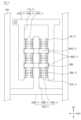
도 22의 표시 장치(10_5)는 차폐 전극층(800_5)의 형상이 도 1과 상이한 것을 제외하고는 실질적으로 동일하다. 이하에서는 차이점에 대하여 자세하게 설명하기로 한다.The display device 10_5 of FIG. 22 is substantially the same as that of FIG. 1 except that the shape of the shielding electrode layer 800_5 is different. Below, the differences will be explained in detail.
도 22를 참조하면, 표시 장치(10_5)의 차폐 전극층(800_5)은 복수의 차폐 전극 패턴(830_5)을 포함하고, 차폐 전극 패턴(830_5)은 제1 전극(210)과 제2 전극(220)이 이격된 영역, 예컨대 제1 전극 가지부(210B_5)와 제2 전극 가지부(220B_5) 사이에서 제1 방향(D1) 및 제2 방향 (D2)으로 서로 이격되어 배치될 수 있다.Referring to FIG. 22, the shielding electrode layer 800_5 of the display device 10_5 includes a plurality of shielding electrode patterns 830_5, and the shielding electrode pattern 830_5 includes the
차폐 전극 패턴(830_5)은 제1 절연층(510_5) 상에 배치되어 제2 방향(D2)으로 패턴을 형성하고, 이들이 배치되지 않는 영역에는 제1 절연층(510_5)이 노출될 수 있다. 즉, 평면상 제1 절연층(510_5)도 제2 방향(D2)으로 패턴을 형성할 수 있다. 표시 장치(10_5)의 제조 공정에서 차폐 전극 패턴(830_5)이 배치되지 않고 제1 절연층(510_5)이 노출된 영역은 전계가 형성되는 영역이고, 차폐 전극 패턴(830_5)이 배치된 영역은 상기 전계가 차단되는 영역일 수 있다. 이에 따라, 노출된 제1 절연층(510_5) 상에는 복수의 발광 소자(300)가 배치되어 정렬 영역(AA_5)을 형성하고, 차폐 전극 패턴(830_5)이 배치된 영역은 비정렬 영역(NAA_5)을 형성할 수 있다.The shielding electrode pattern 830_5 is disposed on the first insulating layer 510_5 to form a pattern in the second direction D2, and the first insulating layer 510_5 may be exposed in areas where the shielding electrode pattern 830_5 is not disposed. That is, the first insulating layer 510_5 in plan view may also form a pattern in the second direction D2. In the manufacturing process of the display device 10_5, the area where the shielding electrode pattern 830_5 is not disposed and the first insulating layer 510_5 is exposed is the area where an electric field is formed, and the area where the shielding electrode pattern 830_5 is disposed is the area where the shielding electrode pattern 830_5 is disposed. It may be an area where the electric field is blocked. Accordingly, a plurality of light emitting
도 23은 도 22의 표시 장치(10_5)에서 정렬 영역(AA)을 포함하여 제1 절연층(510_5)이 노출된 영역의 단면도이고, 도 24는 비정렬 영역(NAA)을 포함하여 차폐 전극 패턴(830_5)이 배치된 영역의 단면도이다.FIG. 23 is a cross-sectional view of the exposed area of the first insulating layer 510_5 including the alignment area AA in the display device 10_5 of FIG. 22, and FIG. 24 is a shielding electrode pattern including the non-alignment area NAA. This is a cross-sectional view of the area where (830_5) is placed.
도 23을 참조하면, 도 2의 표시 장치(10)와 달리 제1 전극(210_5)과 제2 전극(220_5) 상에 차폐 전극층(800_5)이 배치되지 않을 수 있다. 제1 절연층(510_5)은 제1 전극(210_5)과 제2 전극(220_5)의 일부를 덮고, 이들 사이에 배치될 수 있다. 도 24를 참조하면, 비정렬 영역(NAA_5)을 포함하는 단면에서는 발광 소자(300)가 배치되지 않으며, 제1 절연층(510_5)이 제1 전극(210_5)과 제2 전극(220_5)의 상면을 모두 덮도록 배치된다. 제1 절연층(510_5) 상에는 차폐 전극층(800_5), 즉 차폐 전극 패턴(830_5)이 배치되되, 제1 전극(210_5) 및 제2 전극(220_5)과 중첩되지 않도록 배치될 수 있다. 이에 따라, 차폐 전극 패턴(830_5)의 폭(w_5)은 제1 전극(210_5)과 제2 전극(220_5) 사이의 거리(S1_5)와 동일할 수 있다.Referring to FIG. 23 , unlike the
차폐 전극 패턴(830_5)은 제1 전극(210_5) 및 제2 전극(220_5) 사이에 배치되며 일 방향, 예컨대 제1 방향(D1)으로 이격되어 소정의 패턴을 형성할 수 있다. 제1 전극(210_5)과 제2 전극(220_5)에 정렬신호가 인가되더라도, 이들 사이에 배치된 차폐 전극 패턴(830_5)은 정렬 신호에 의해 형성되는 전계를 차단할 수 있다.The shielding electrode pattern 830_5 is disposed between the first electrode 210_5 and the second electrode 220_5 and may be spaced apart in one direction, for example, the first direction D1, to form a predetermined pattern. Even if an alignment signal is applied to the first electrode 210_5 and the second electrode 220_5, the shielding electrode pattern 830_5 disposed between them can block the electric field formed by the alignment signal.
또한, 일 실시예에 따르면, 비정렬 영역(NAA_5)에는 접촉 전극(260)이 배치되지 않을 수 있고, 차폐 전극 패턴(830_5)은 전극(210_5, 220_5)와 전기적으로 절연될 수 있다. 도 1의 표시 장치(10)와 달리, 도 22의 표시 장치(10_5)는 차폐 전극층(800_5)이 전극(210_5, 220_5)과 절연되어 플로팅 상태를 유지할 수 있다.Additionally, according to one embodiment, the
한편, 차폐 전극 패턴(830)은 부분적으로 제1 전극(210) 및 제2 전극(220)과 중첩될 수도 있다. 일 실시예에 따른 표시 장치(10_6, 10_7)는 제1 전극(210) 및 제2 전극(220)과 부분적으로 중첩되는 적어도 하나의 차폐 전극 패턴(830_6, 830_7)을 포함할 수 있다.Meanwhile, the shielding
도 25는 다른 실시예에 따른 표시 장치의 평면도이다. 도 26은 도 25의 Ⅱe-Ⅱe'선을 따라 자른 단면도이다.Figure 25 is a plan view of a display device according to another embodiment. FIG. 26 is a cross-sectional view taken along line IIe-IIe' of FIG. 25.
도 25의 표시 장치(10_6)는 차폐 전극 패턴(830_6)의 형상이 도 22와 상이한 것을 제외하고는 실질적으로 동일하다. 이하에서는 차이점에 대하여 자세하게 설명하기로 한다.The display device 10_6 of FIG. 25 is substantially the same as that of FIG. 22 except that the shape of the shielding electrode pattern 830_6 is different. Below, the differences will be explained in detail.
도 25를 참조하면, 표시 장치(10_6)의 차폐 전극층(800_6)은 제1 전극 가지부(210B_6)와 제2 전극 가지부(220B_6) 사이에 배치되어 이들과 부분적으로 중첩되는 차폐 전극 패턴(830_6)을 포함할 수 있다. 복수의 차폐 전극 패턴(830_6)은 소정의 폭(w_6)을 갖고 배치되며, 이들은 서로 제1 방향(D1) 및 제2 방향(D2)으로 이격될 수 있다.Referring to FIG. 25, the shielding electrode layer 800_6 of the display device 10_6 is disposed between the first electrode branch 210B_6 and the second electrode branch 220B_6 and has a shielding electrode pattern 830_6 that partially overlaps them. ) may include. The plurality of shielding electrode patterns 830_6 are arranged to have a predetermined width w_6, and they may be spaced apart from each other in the first direction D1 and the second direction D2.
상술한 바와 같이, 차폐 전극 패턴(830_6)이 배치된 영역은 표시 장치(10_6)의 제조 공정에서 전계가 차단되는 영역으로, 비정렬 영역(NAA_6)이 형성된다. 또한, 차폐 전극 패턴(830_6)이 이격된 영역에서는 제1 절연층(510_6)이 노출되어 전계가 형성되는 영역으로, 발광 소자(300)가 배치되어 정렬 영역(AA_6)이 형성될 수 있다. 차폐 전극 패턴(830_6)은 임의의 패턴이 다른 패턴과 제2 방향(D2)으로 이격되고, 이들 사이에는 제1 절연층(510_6)이 노출되어 정렬 영역(AA_6)이 형성될 수 있다.As described above, the area where the shielding electrode pattern 830_6 is disposed is an area where the electric field is blocked during the manufacturing process of the display device 10_6, and an unaligned area NAA_6 is formed. Additionally, in an area where the shielding electrode pattern 830_6 is spaced apart, the first insulating layer 510_6 is exposed and an electric field is formed, and the
한편, 일 실시예에 따르면, 차폐 전극 패턴(830_6)의 일 방향, 예컨대 제1 방향(D1)으로 측정된 폭(w_6)은 각 전극이 이격된 영역, 즉, 제1 전극 가지부(210B_6)와 제2 전극 가지부(220B_6)가 이격된 거리(S1_6)보다 클 수 있다. 도 22의 표시 장치(10_5)와 달리, 도 25의 표시 장치(10_6)는 차폐 전극 패턴(830_6)의 폭(w_6)이 제1 전극 가지부(210B_6)와 제2 전극 가지부(220B_6) 사이의 거리(S1_6)보다 커서 이들과 부분적으로 중첩될 수 있다.Meanwhile, according to one embodiment, the width w_6 measured in one direction, for example, the first direction D1, of the shielding electrode pattern 830_6 is the area where each electrode is spaced apart, that is, the first electrode branch portion 210B_6 The distance between the second electrode branch 220B_6 and 220B_6 may be greater than the distance S1_6. Unlike the display device 10_5 of FIG. 22, the display device 10_6 of FIG. 25 has the width w_6 of the shielding electrode pattern 830_6 between the first electrode branch 210B_6 and the second electrode branch 220B_6. It is larger than the distance (S1_6) and may partially overlap with them.
도 26을 참조하면, 제1 절연층(510_6) 상에 배치된 차폐 전극 패턴(830_6)은 제1 방향(D1)으로 이격되되, 제1 전극(210_6) 및 제2 전극(220_6)과 부분적으로 중첩될 수 있다. 다만, 차폐 전극 패턴(830_6)은 제2 전극(220_6)과 중첩되는 영역에서 제1 방향(D1)으로 이격되어 배치될 수 있다. 이에 따라, 도 25의 표시 장치(10_6)는 제조 공정시 정렬 신호에 의해 형성되는 전계를 효과적으로 차단할 수 있다.Referring to FIG. 26, the shielding electrode pattern 830_6 disposed on the first insulating layer 510_6 is spaced apart in the first direction D1, and is partially separated from the first electrode 210_6 and the second electrode 220_6. May overlap. However, the shielding electrode pattern 830_6 may be arranged to be spaced apart in the first direction D1 in the area overlapping the second electrode 220_6. Accordingly, the display device 10_6 of FIG. 25 can effectively block the electric field generated by the alignment signal during the manufacturing process.
도 27은 다른 실시예에 따른 표시 장치의 평면도이다. 도 28은 도 27의 Ⅱf-Ⅱf'선을 따라 자른 단면도이다.27 is a plan view of a display device according to another embodiment. FIG. 28 is a cross-sectional view taken along line IIf-IIf' of FIG. 27.
도 27의 표시 장치(10_7)는 차폐 전극 패턴(830_7)의 형상이 도 25와 상이한 것을 제외하고는 실질적으로 동일하다. 이하에서는 차이점에 대하여 자세하게 설명하기로 한다.The display device 10_7 of FIG. 27 is substantially the same as that of FIG. 25 except that the shape of the shielding electrode pattern 830_7 is different. Below, the differences will be explained in detail.
도 27 및 도 28을 참조하면, 하나의 차폐 전극 패턴(830_7)이 2개의 제1 전극 가지부(210B_7)와 하나의 제2 전극 가지부(220B_7)와 동시에 중첩될 수 있다. 도면에 도시된 바와 같이, 차폐 전극 패턴(830_7)의 폭(w_7)이 전극 가지부(210B_7, 220B_7)의 폭과 각 전극 가지부(210B_7, 220B_7) 사이의 거리(S1_7)를 합친 것보다 클 수 있다. 이 경우, 복수의 차폐 전극 패턴(830_7)은 각각 제1 방향(D1)으로 연장되고, 서로 제2 방향(D2)으로만 이격되어 배치될 수 있다.Referring to FIGS. 27 and 28 , one shielding electrode pattern 830_7 may simultaneously overlap two first electrode branches 210B_7 and one second electrode branch 220B_7. As shown in the figure, the width (w_7) of the shielding electrode pattern (830_7) is greater than the sum of the widths of the electrode branches (210B_7, 220B_7) and the distance (S1_7) between each electrode branch (210B_7, 220B_7). You can. In this case, the plurality of shielding electrode patterns 830_7 each extend in the first direction D1 and may be arranged to be spaced apart from each other only in the second direction D2.
한편, 도 1을 참조하여 상술한 바와 같이, 차폐 전극층(800)은 각 전극(210, 220)의 적어도 일부 영역을 노출시키기 위해 함몰패턴부(810C, 820C)가 형성될 수 있다. 이 경우, 제1 전극 가지부(210B)와 제2 전극 가지부(220B)는 서로 대향하는 측면이 일 방향으로 연장된 형상을 갖고, 이들 상에 배치된 제1 차폐 전극(810)과 제2 차폐 전극(820)은 적어도 일 측면이 함몰된 패턴이 형성될 수 있다. 다만, 이에 제한되는 것은 아니며 경우에 따라서 전극(210, 220)은 차폐 전극층(800)과 중첩되지 않도록 일부 영역이 돌출되도록 배치될 수 있다.Meanwhile, as described above with reference to FIG. 1 , the shielding
일 실시예에 따른 표시 장치(10)의 전극(210, 220)은 측면의 적어도 일부 영역이 돌출된 돌출패턴부(210C, 220C)를 포함하고, 돌출패턴부(210C, 220C)는 차폐 전극층(800)과 중첩되지 않을 수 있다.The
도 29 내지 도 32는 다른 실시예에 따른 표시 장치의 평면도들이다.29 to 32 are plan views of a display device according to another embodiment.
먼저, 도 29를 참조하면, 일 실시예에 따른 표시 장치(10_8)는 제1 전극 가지부(210B_8)와 제2 전극 가지부(220B_8)는 서로 대향하는 일 측면 또는 양 측면에 적어도 일부 영역이 돌출된 돌출패턴부(210C_8, 220C_8)가 형성될 수 있다. 제1 전극 가지부(210B_8)는 제2 전극 가지부(220B_8)와 대향하는 일 측면에 제1 방향(D1)으로 돌출된 제1 돌출패턴부(210C_8)가 형성되고, 제2 전극 가지부(220B_8)는 제1 전극 가지부(210B_8)와 대향하는 양 측면에 제1 방향(D1)으로 돌출된 제2 돌출패턴부(220C_8)가 형성될 수 있다. 제1 차폐 전극 가지부(810B_8) 및 제2 차폐 전극 가지부(820B_8)는 각 측면이 일 방향으로 연장된 형상을 갖고, 함몰패턴부(810C, 820C)가 형성되지 않을 수 있다. 이 경우에도, 각 전극 가지부(210B_8, 220B_8)가 이격된 거리(S1_8)는 각 차폐 전극 가지부(810B_8, 820B_8)가 이격된 거리(S2_8)보다 짧을 수 있다. 제1 돌출패턴부(210C_8)와 제2 돌출패턴부(220C_8)는 제1 차폐 전극(810_8) 및 제2 차폐 전극(820_8)과 중첩되지 않고, 표시 장치(10_8)의 제조 공정에서 정렬 신호에 의한 전계가 형성될 수 있다.First, referring to FIG. 29, in the display device 10_8 according to an embodiment, the first electrode branch 210B_8 and the second electrode branch 220B_8 have at least a partial area on one or both sides opposing each other. Protruding protruding pattern portions 210C_8 and 220C_8 may be formed. The first electrode branch 210B_8 has a first protruding pattern portion 210C_8 formed on one side opposite to the second electrode branch 220B_8, and protrudes in the first direction D1, and the second electrode branch ( 220B_8 may be formed with a second protruding pattern portion 220C_8 protruding in the first direction D1 on both sides opposite the first electrode branch portion 210B_8. The first shielding electrode branch 810B_8 and the second shielding electrode branch 820B_8 have each side extending in one direction, and the recessed
반면에 제1 전극 가지부(210B_8)와 제2 전극 가지부(220B_8) 중에서 돌출패턴부(210C_8, 220C_8)가 형성되지 않은 영역은 제1 차폐 전극(810_8) 또는 제2 차폐 전극(820_8)이 이와 중첩되도록 배치된다. 상기 영역은 표시 장치(10_8)의 제조 공정에서 정렬 신호에 의한 전계가 차단되는 영역이다. 이에 따라, 전극(210, 220)의 돌출패턴부(210C_8, 220C_8) 상에는 발광 소자(300)가 정렬되어 정렬 영역(AA_8)이 형성되고, 전극(210, 220)이 차폐 전극층(800_8)과 중첩되는 영역에는 비정렬 영역(NAA_8)이 형성될 수 있다.On the other hand, the area in which the protruding pattern portions 210C_8 and 220C_8 are not formed among the first electrode branch 210B_8 and the second electrode branch 220B_8 has the first shielding electrode 810_8 or the second shielding electrode 820_8. It is placed to overlap this. This area is an area where the electric field caused by the alignment signal is blocked during the manufacturing process of the display device 10_8. Accordingly, the
도 30의 표시 장치(10_9)는 도 28의 표시 장치(10_8)에 비해 접촉 전극(260_9)이 일 방향, 예컨대 제2 방향(D2)으로 연장된 형상을 갖는 것을 제외하고는 동일하다. 이하에서는 중복되는 설명은 생략하고 차이점에 대하여 자세하게 설명하기로 한다.The display device 10_9 of FIG. 30 is identical to the display device 10_8 of FIG. 28 except that the contact electrode 260_9 has a shape extending in one direction, for example, the second direction D2. Hereinafter, overlapping explanations will be omitted and the differences will be explained in detail.
표시 장치(10)의 접촉 전극(260)은 제2 방향(D2)으로 연장되되, 부분적으로 단선되어 패턴을 형성할 수 있으나, 도 29를 참조하면 일 실시예에 따른 표시 장치(10_9)는 접촉 전극(260_9)이 제2 방향(D2)으로 연장되어 비정렬 영역(NAA_9)으로 연장될 수 있다. 이에 따라, 제1 전극 가지부(210B_9)는 제2 전극 가지부(220B_9)와 대향하는 일 측면에 하나의 제1 접촉 전극(261_9)이 배치되고, 제2 전극 가지부(220B_9)는 제1 전극 가지부(210B_9)와 대향하는 양 측면에 각각 하나의 제2 접촉 전극(262_9)이 배치될 수 있다.The
도 31의 표시 장치(10_10)는 도 29의 표시 장치(10_8)에 비해 차폐 전극층(800_10)이 도 25의 표시 장치(10_6)와 같이 차폐 전극 패턴(830_10)을 포함하는 것을 제외하고는 실질적으로 동일하다. 도 32의 표시 장치(10_11)는 도 29의 표시 장치(10_8)에 비해 차폐 전극층(800_11)이 도 27의 표시 장치(10_7)와 같이 차폐 전극 패턴(830_11)을 포함하는 것을 제외하고는 실질적으로 동일하다.The display device 10_10 of FIG. 31 is substantially different from the display device 10_8 of FIG. 29 except that the shielding electrode layer 800_10 includes a shielding electrode pattern 830_10 like the display device 10_6 of FIG. 25. same. The display device 10_11 of FIG. 32 is substantially different from the display device 10_8 of FIG. 29 except that the shielding electrode layer 800_11 includes a shielding electrode pattern 830_11 like the display device 10_7 of FIG. 27. same.
즉, 도 31의 표시 장치(10_10)는 제1 전극 가지부(210B_10)와 제2 전극 가지부(220B_10)가 적어도 일부 영역이 돌출된 돌출패턴부(210C_10, 220C_10)를 포함하고, 차폐 전극층(800_10)이 제1 방향(D1) 및 제2 방향(D2)으로 이격되어 패턴을 형성하는 차폐 전극 패턴(830_10)을 포함할 수 있다. 표시 장치(10_10)의 차폐 전극 패턴(830_10)은 제1 방향(D1)으로 측정된 폭(w_10)이 제1 전극 가지부(210B_10)와 제2 전극 가지부(220B_10) 사이의 거리보다 클 수 있다.That is, the display device 10_10 of FIG. 31 includes protruding pattern portions 210C_10 and 220C_10 in which at least a portion of the first electrode branch 210B_10 and the second electrode branch 220B_10 protrude, and a shielding electrode layer ( 800_10) may include a shielding electrode pattern 830_10 that is spaced apart in the first direction D1 and the second direction D2 to form a pattern. The width (w_10) of the shielding electrode pattern 830_10 of the display device 10_10 measured in the first direction D1 may be greater than the distance between the first electrode branch 210B_10 and the second electrode branch 220B_10. there is.
도 32의 표시 장치(10_11)는 제1 전극 가지부(210B_11)와 제2 전극 가지부(220B_11)가 적어도 일부 영역이 돌출된 돌출패턴부(210C_11, 220C_11)를 포함하고, 차폐 전극층(800_11)이 제2 방향(D2)으로 이격되어 패턴을 형성하는 차폐 전극 패턴(830_11)을 포함할 수 있다. 표시 장치(10_11)의 차폐 전극 패턴(830_11)은 제1 방향(D1)으로 측정된 폭(w_11)이 전극 가지부(210B_7, 220B_7)의 폭과 각 전극 가지부(210B_7, 220B_7) 사이의 거리를 합친 것보다 클 수 있다.The display device 10_11 of FIG. 32 includes protruding pattern portions 210C_11 and 220C_11 in which at least a portion of the first electrode branch 210B_11 and the second electrode branch 220B_11 protrude, and a shielding electrode layer 800_11. It may include shielding electrode patterns 830_11 spaced apart in the second direction D2 to form a pattern. The width (w_11) of the shielding electrode pattern 830_11 of the display device 10_11 measured in the first direction D1 is equal to the width of the electrode branches 210B_7 and 220B_7 and the distance between each electrode branch 210B_7 and 220B_7. may be greater than the sum of the
이상 첨부된 도면을 참조하여 본 발명의 실시예들을 설명하였지만, 본 발명이 속하는 기술분야에서 통상의 지식을 가진 자는 본 발명의 그 기술적 사상이나 필수적인 특징을 변경하지 않고서 다른 구체적인 형태로 실시될 수 있다는 것을 이해할 수 있을 것이다. 그러므로 이상에서 기술한 실시예들은 모든 면에서 예시적인 것이며 한정적이 아닌 것으로 이해해야만 한다.Although embodiments of the present invention have been described above with reference to the attached drawings, those skilled in the art will understand that the present invention can be implemented in other specific forms without changing its technical idea or essential features. You will be able to understand it. Therefore, the embodiments described above should be understood in all respects as illustrative and not restrictive.
10: 표시 장치
210: 제1 전극220: 제2 전극
261: 제1 접촉 전극262: 제2 접촉 전극
300: 발광 소자
800: 차폐 전극층
810: 제1 차폐 전극820: 제2 차폐 전극
830: 차폐 전극 패턴10: display device
210: first electrode 220: second electrode
261: first contact electrode 262: second contact electrode
300: light emitting device
800: Shielding electrode layer
810: first shielding electrode 820: second shielding electrode
830: Shielding electrode pattern
Claims (20)
Translated fromKorean상기 제1 전극과 상기 제2 전극의 적어도 일부 영역을 덮도록 배치된 제1 절연층;
상기 제1 절연층 상에 배치되고, 상기 제1 전극과 상기 제2 전극의 적어도 일부와 중첩하는 차폐 전극층; 및
상기 제1 전극과 상기 제2 전극 사이에서 상기 차폐 전극층과 이격되어 배치된 적어도 하나의 발광 소자를 포함하되,
적어도 하나의 상기 발광 소자는 상기 차폐 전극층이 상기 제1 전극 및 상기 제2 전극과 중첩되지 않는 영역 내에 배치되는 표시 장치.a first electrode and a second electrode disposed to face and be spaced apart from the first electrode;
a first insulating layer disposed to cover at least a portion of the first electrode and the second electrode;
a shielding electrode layer disposed on the first insulating layer and overlapping at least a portion of the first electrode and the second electrode; and
At least one light emitting element disposed between the first electrode and the second electrode and spaced apart from the shielding electrode layer,
A display device wherein the at least one light emitting element is disposed in an area where the shielding electrode layer does not overlap the first electrode and the second electrode.
상기 차폐 전극층은 상기 제1 전극의 적어도 일부와 중첩되도록 배치된 제1 차폐 전극 및 상기 제1 차폐 전극과 이격되어 상기 제2 전극의 적어도 일부와 중첩되도록 배치된 제2 차폐 전극을 포함하는 표시 장치.According to claim 1,
The shielding electrode layer is a display device including a first shielding electrode disposed to overlap at least a portion of the first electrode and a second shielding electrode disposed to overlap at least a portion of the second electrode and spaced apart from the first shielding electrode. .
상기 제1 전극과 상기 제2 전극, 및 상기 제1 차폐 전극 및 상기 제2 차폐 전극은 각각 상기 발광 소자의 양 단부를 가로지르는 일 방향으로 서로 이격되어 배치되고,
상기 제1 전극과 상기 제2 전극이 이격된 거리는 상기 제1 차폐 전극과 상기 제2 차폐 전극이 이격된 거리보다 짧은 표시 장치.According to clause 2,
The first electrode, the second electrode, and the first shielding electrode and the second shielding electrode are respectively arranged to be spaced apart from each other in one direction crossing both ends of the light emitting device,
The display device wherein the distance between the first electrode and the second electrode is shorter than the distance between the first shielding electrode and the second shielding electrode.
상기 발광 소자의 상기 일 방향으로 측정된 길이는 상기 제1 전극과 상기 제2 전극이 이격된 거리보다 길되, 상기 제1 차폐 전극과 상기 제2 차폐 전극이 이격된 거리보다 짧은 표시 장치.According to clause 3,
The length measured in the one direction of the light emitting device is longer than the distance between the first electrode and the second electrode, but is shorter than the distance between the first shielding electrode and the second shielding electrode.
상기 제1 전극, 상기 발광 소자의 일 단부 및 상기 제1 차폐 전극의 적어도 일 단부와 접촉하는 제1 접촉 전극; 및
상기 제2 전극, 상기 발광 소자의 타 단부 및 상기 제2 차폐 전극의 적어도 일 단부와 접촉하는 제2 접촉 전극을 더 포함하는 표시 장치.According to clause 2,
a first contact electrode in contact with the first electrode, one end of the light emitting device, and at least one end of the first shielding electrode; and
The display device further includes a second contact electrode contacting the second electrode, the other end of the light emitting device, and at least one end of the second shielding electrode.
상기 제1 차폐 전극 및 상기 제2 차폐 전극 상의 적어도 일부 영역에 배치되는 제2 절연층을 포함하고,
상기 제1 접촉 전극과 상기 제2 접촉 전극은 적어도 일부가 상기 제2 절연층의 상면에 중첩되도록 배치된 표시 장치.According to clause 5,
It includes a second insulating layer disposed on at least a partial area on the first shielding electrode and the second shielding electrode,
A display device wherein at least a portion of the first contact electrode and the second contact electrode overlaps a top surface of the second insulating layer.
상기 차폐 전극층은 상기 제1 전극과 상기 제2 전극 사이에 배치되어 상기 제1 전극과 상기 제2 전극이 연장된 방향으로 이격된 적어도 하나의 차폐 전극 패턴을 포함하고,
상기 제1 절연층은 상기 제1 전극 및 상기 제2 전극과 상기 차폐 전극 패턴을 상호 절연시키는 표시 장치.According to claim 1,
The shielding electrode layer includes at least one shielding electrode pattern disposed between the first electrode and the second electrode and spaced apart in a direction in which the first electrode and the second electrode extend,
The first insulating layer insulates the first electrode, the second electrode, and the shielding electrode pattern from each other.
상기 차폐 전극 패턴은 상기 제1 전극 및 상기 제2 전극과 중첩되지 않도록 배치된 표시 장치.According to clause 7,
The display device is arranged so that the shielding electrode pattern does not overlap the first electrode and the second electrode.
상기 차폐 전극 패턴은 상기 제1 전극과 상기 제2 전극이 서로 대향하는 각 측면과 부분적으로 중첩되는 표시 장치.According to clause 7,
The display device wherein the shielding electrode pattern partially overlaps each side of the first electrode and the second electrode facing each other.
상기 차폐 전극 패턴의 상기 제1 전극과 상기 제2 전극이 이격된 방향으로 측정된 폭은 상기 제1 전극과 상기 제2 전극 사이의 거리보다 큰 표시 장치.According to clause 9,
A display device in which a width of the shielding electrode pattern measured in a direction in which the first electrode and the second electrode are separated is greater than a distance between the first electrode and the second electrode.
상기 발광 소자는 상기 제1 전극과 상기 제2 전극이 연장된 방향으로 이격되어 배치된 상기 차폐 전극 패턴 사이에 배치된 표시 장치.According to claim 10,
The light emitting element is disposed between the shielding electrode patterns spaced apart from each other in a direction in which the first electrode and the second electrode extend.
상기 제1 전극과 상기 제2 전극의 적어도 일부 영역을 덮도록 배치된 제1 절연층;
상기 제1 절연층 상에서 상기 제1 방향으로 연장되어 배치되고, 상기 제1 전극과 상기 제2 전극의 적어도 일부와 중첩되지 않는 차폐 전극층; 및
상기 제1 전극과 상기 제2 전극 사이에서 상기 차폐 전극층과 이격되어 배치되고, 양 단부가 각각 상기 제1 전극 및 상기 제2 전극과 전기적으로 연결된 적어도 하나의 발광 소자를 포함하는 표시 장치.a first electrode and a second electrode extending in a first direction and spaced apart in a second direction different from the first direction;
a first insulating layer disposed to cover at least a portion of the first electrode and the second electrode;
a shielding electrode layer extending in the first direction on the first insulating layer and not overlapping with at least a portion of the first electrode and the second electrode; and
A display device including at least one light emitting element disposed between the first electrode and the second electrode and spaced apart from the shielding electrode layer, and having both ends electrically connected to the first electrode and the second electrode, respectively.
상기 차폐 전극층은 상기 제1 전극 상에 배치되고 상기 제1 전극의 적어도 일부와 중첩되지 않도록 형성되는 적어도 하나의 제1 함몰패턴부를 포함하는 제1 차폐 전극; 및
상기 제2 전극 상에 배치되고 상기 제2 전극의 적어도 일부와 중첩되지 않도록 형성되는 적어도 하나의 제2 함몰패턴부를 포함하는 제2 차폐 전극을 포함하는 표시 장치.According to claim 12,
The shielding electrode layer includes a first shielding electrode disposed on the first electrode and including at least one first recessed pattern portion formed not to overlap at least a portion of the first electrode; and
A display device comprising a second shielding electrode disposed on the second electrode and including at least one second recessed pattern portion formed not to overlap at least a portion of the second electrode.
상기 제1 함몰패턴부는 상기 제1 전극의 상기 제2 전극과 대향하는 일 면으로부터 상기 제1 전극의 타 면을 향해 함몰되고,
상기 제2 함몰패턴부는 상기 제2 전극의 상기 제1 전극과 대향하는 일 면으로부터 상기 제2 전극의 타 면을 향해 함몰된 표시 장치.According to claim 13,
The first depression pattern portion is depressed from one side of the first electrode facing the second electrode toward the other side of the first electrode,
The second recessed pattern portion is recessed from one side of the second electrode facing the first electrode toward the other side of the second electrode.
상기 제1 함몰패턴부와 상기 제2 함몰패턴부는 서로 이격되어 대향하도록 배치되며,
상기 발광 소자는 상기 제1 함몰패턴부와 상기 제2 함몰패턴부 사이에 배치되는 표시 장치.According to claim 14,
The first depression pattern portion and the second depression pattern portion are arranged to face each other and be spaced apart from each other,
The light emitting element is disposed between the first recessed pattern portion and the second recessed pattern portion.
상기 차폐 전극층은 상기 제1 전극 및 상기 제2 전극 사이에 배치되는 적어도 하나의 차폐 전극 패턴부를 포함하고,
상기 차폐 전극 패턴부는 이웃하는 다른 상기 차폐 전극 패턴부와 이격된 표시 장치.According to claim 12,
The shielding electrode layer includes at least one shielding electrode pattern portion disposed between the first electrode and the second electrode,
The display device wherein the shielding electrode pattern portion is spaced apart from another neighboring shielding electrode pattern portion.
상기 차폐 전극 패턴부는 상기 제1 전극 및 상기 제2 전극과 중첩되지 않고,
상기 차폐 전극 패턴부가 이격된 영역에는 상기 제1 절연층이 노출되어 상기 제1 방향으로 패턴을 형성하는 표시 장치.According to claim 16,
The shielding electrode pattern portion does not overlap the first electrode and the second electrode,
A display device in which the first insulating layer is exposed in an area where the shielding electrode pattern portion is spaced apart to form a pattern in the first direction.
상기 차폐 전극 패턴부의 상기 제2 방향으로 측정된 폭은 상기 제1 전극과 상기 제2 전극 사이의 거리보다 크고, 상기 차폐 전극 패턴부는 상기 제1 전극 및 상기 제2 전극과 부분적으로 중첩되는 표시 장치.According to claim 16,
The width of the shielding electrode pattern portion measured in the second direction is greater than the distance between the first electrode and the second electrode, and the shielding electrode pattern portion partially overlaps the first electrode and the second electrode. .
상기 제1 전극은 상기 제2 전극과 대향하는 일 측면의 적어도 일부 영역이 돌출된 제1 돌출부패턴을 포함하고,
상기 제2 전극은 상기 제1 전극과 대향하는 일 측면의 적어도 일부 영역이 돌출된 제2 돌출부패턴을 포함하는 표시 장치.According to claim 12,
The first electrode includes a first protrusion pattern in which at least a portion of a side surface opposite the second electrode protrudes,
The second electrode includes a second protrusion pattern in which at least a portion of a side surface opposite the first electrode protrudes.
상기 제1 돌출부패턴과 상기 제2 돌출부패턴은 서로 이격되어 대향하도록 배치되며,
상기 발광 소자는 일 단부가 상기 제1 돌출부패턴과 전기적으로 연결되고, 타 단부는 상기 제2 돌출부패턴과 전기적으로 연결된 표시 장치.According to clause 19,
The first protrusion pattern and the second protrusion pattern are arranged to face each other and be spaced apart from each other,
A display device wherein one end of the light emitting element is electrically connected to the first protrusion pattern and the other end is electrically connected to the second protrusion pattern.
Priority Applications (5)
| Application Number | Priority Date | Filing Date | Title |
|---|---|---|---|
| KR1020180148353AKR102666614B1 (en) | 2018-11-27 | 2018-11-27 | Display device |
| EP19890576.2AEP3890021A4 (en) | 2018-11-27 | 2019-08-23 | INDICATOR |
| PCT/KR2019/010727WO2020111452A1 (en) | 2018-11-27 | 2019-08-23 | Display device |
| CN201980078388.8ACN113169210B (en) | 2018-11-27 | 2019-08-23 | Display device |
| US17/297,950US20220093828A1 (en) | 2018-11-27 | 2019-08-23 | Display device |
Applications Claiming Priority (1)
| Application Number | Priority Date | Filing Date | Title |
|---|---|---|---|
| KR1020180148353AKR102666614B1 (en) | 2018-11-27 | 2018-11-27 | Display device |
Publications (2)
| Publication Number | Publication Date |
|---|---|
| KR20200063380A KR20200063380A (en) | 2020-06-05 |
| KR102666614B1true KR102666614B1 (en) | 2024-05-17 |
Family
ID=70853790
Family Applications (1)
| Application Number | Title | Priority Date | Filing Date |
|---|---|---|---|
| KR1020180148353AActiveKR102666614B1 (en) | 2018-11-27 | 2018-11-27 | Display device |
Country Status (5)
| Country | Link |
|---|---|
| US (1) | US20220093828A1 (en) |
| EP (1) | EP3890021A4 (en) |
| KR (1) | KR102666614B1 (en) |
| CN (1) | CN113169210B (en) |
| WO (1) | WO2020111452A1 (en) |
Families Citing this family (18)
| Publication number | Priority date | Publication date | Assignee | Title |
|---|---|---|---|---|
| KR20200088950A (en)* | 2019-01-15 | 2020-07-24 | 삼성디스플레이 주식회사 | Display device and method of fabricating the same |
| KR102711128B1 (en)* | 2019-08-28 | 2024-09-27 | 삼성디스플레이 주식회사 | Display device and method for fabricating the same |
| KR102831677B1 (en) | 2020-01-09 | 2025-07-09 | 삼성디스플레이 주식회사 | Display device and fabricating method for display device |
| US20210242381A1 (en)* | 2020-01-30 | 2021-08-05 | Samsung Display Co., Ltd. | Display device and method of manufacturing the same |
| KR102858557B1 (en) | 2020-07-24 | 2025-09-11 | 삼성디스플레이 주식회사 | Display device |
| KR20220019141A (en)* | 2020-08-06 | 2022-02-16 | 삼성디스플레이 주식회사 | Display device and method of fabricating the same |
| KR20220083935A (en)* | 2020-12-11 | 2022-06-21 | 삼성디스플레이 주식회사 | Display device |
| KR20220086743A (en) | 2020-12-16 | 2022-06-24 | 삼성디스플레이 주식회사 | Display device |
| KR20220099145A (en)* | 2021-01-04 | 2022-07-13 | 삼성디스플레이 주식회사 | Display device |
| KR20220102188A (en) | 2021-01-12 | 2022-07-20 | 삼성디스플레이 주식회사 | Display device |
| KR20220120784A (en)* | 2021-02-23 | 2022-08-31 | 삼성디스플레이 주식회사 | Display device and manufacturing method thereof |
| KR102739539B1 (en)* | 2022-05-13 | 2024-12-10 | 한양대학교 에리카산학협력단 | Method for aligning micro led using electrostatic repulsive force and method for manufacturing micro led display using the same |
| KR20240038750A (en)* | 2021-07-21 | 2024-03-25 | 엘지전자 주식회사 | display device |
| US20240421264A1 (en)* | 2021-11-01 | 2024-12-19 | Lg Electronics Inc. | Display device |
| KR20230129106A (en)* | 2022-02-28 | 2023-09-06 | 삼성디스플레이 주식회사 | Display device, method of manufacturing the same and tiled display device including the same |
| KR20230139843A (en)* | 2022-03-23 | 2023-10-06 | 삼성디스플레이 주식회사 | Display device |
| KR20250099348A (en)* | 2022-10-21 | 2025-07-01 | 엘지전자 주식회사 | Display device |
| KR20240139125A (en)* | 2023-03-09 | 2024-09-23 | 삼성디스플레이 주식회사 | Light emitting element and display device including the same |
Family Cites Families (30)
| Publication number | Priority date | Publication date | Assignee | Title |
|---|---|---|---|---|
| JP4381428B2 (en)* | 2007-04-10 | 2009-12-09 | シャープ株式会社 | Fine structure arranging method, substrate on which fine structures are arranged, integrated circuit device and display element |
| JP5217949B2 (en)* | 2008-11-20 | 2013-06-19 | ソニー株式会社 | Method for manufacturing reflector and method for manufacturing display device |
| US8872214B2 (en)* | 2009-10-19 | 2014-10-28 | Sharp Kabushiki Kaisha | Rod-like light-emitting device, method of manufacturing rod-like light-emitting device, backlight, illuminating device, and display device |
| JP2012004535A (en)* | 2010-05-17 | 2012-01-05 | Sharp Corp | Method for manufacturing light emitting device |
| EP2546900A4 (en)* | 2010-03-12 | 2016-02-17 | Sharp Kk | METHOD FOR MANUFACTURING LIGHT EMITTING DEVICE, LIGHT EMITTING DEVICE, LIGHTING DEVICE, BACKLIGHT, LIQUID CRYSTAL PANEL, DISPLAY DEVICE, DISPLAY DEVICE MANUFACTURING METHOD, DISPLAY DEVICE DRIVING METHOD, AND DISPLAY DEVICE LIQUID CRYSTALS |
| WO2012042564A1 (en)* | 2010-09-29 | 2012-04-05 | パナソニック株式会社 | Thin-film semiconductor device for display device, method for producing thin-film semiconductor device for display device, el display panel and el display device |
| US8933433B2 (en)* | 2012-07-30 | 2015-01-13 | LuxVue Technology Corporation | Method and structure for receiving a micro device |
| US10804316B2 (en)* | 2012-08-07 | 2020-10-13 | Seoul Viosys Co., Ltd. | Wafer level light-emitting diode array |
| US9178123B2 (en)* | 2012-12-10 | 2015-11-03 | LuxVue Technology Corporation | Light emitting device reflective bank structure |
| US9111464B2 (en)* | 2013-06-18 | 2015-08-18 | LuxVue Technology Corporation | LED display with wavelength conversion layer |
| KR102203447B1 (en)* | 2014-05-27 | 2021-01-18 | 엘지디스플레이 주식회사 | Organic light emitting display panel and method of manufacturing the same |
| US9825202B2 (en)* | 2014-10-31 | 2017-11-21 | eLux, Inc. | Display with surface mount emissive elements |
| KR101672781B1 (en)* | 2014-11-18 | 2016-11-07 | 피에스아이 주식회사 | Nano-scale LED for horizontal arrayed assembly, method for manufacturing thereof and horizontal arrayed assembly comprising the same |
| KR101674052B1 (en)* | 2014-11-18 | 2016-11-09 | 피에스아이 주식회사 | Method for placing nano-scale LED on electrode assembly |
| KR101789123B1 (en)* | 2015-11-17 | 2017-10-23 | 피에스아이 주식회사 | Display backlight unit comprising nano-scale LED electrode assembly and the display comprising the same |
| KR101730929B1 (en)* | 2015-11-17 | 2017-04-28 | 피에스아이 주식회사 | Method for manufacturing Nano-scale LED electrode assembly comprising selective metal ohmic layer |
| KR102441882B1 (en)* | 2015-12-28 | 2022-09-08 | 삼성디스플레이 주식회사 | Liquid crystal display device |
| KR102699567B1 (en)* | 2016-07-11 | 2024-08-29 | 삼성디스플레이 주식회사 | Pixel structure, display apparatus including the pixel structure and method of manufacturing the same |
| KR102608419B1 (en)* | 2016-07-12 | 2023-12-01 | 삼성디스플레이 주식회사 | Display Apparatus and Method for manufacturing the same |
| KR102633079B1 (en)* | 2016-10-28 | 2024-02-01 | 엘지디스플레이 주식회사 | Light emitting diode display apparatus |
| KR102651097B1 (en)* | 2016-10-28 | 2024-03-22 | 엘지디스플레이 주식회사 | Light emitting diode display apparatus |
| US10319880B2 (en)* | 2016-12-02 | 2019-06-11 | Innolux Corporation | Display device |
| KR102707509B1 (en)* | 2016-12-19 | 2024-09-23 | 삼성디스플레이 주식회사 | Light emitting device and fabricating method thereof |
| KR102587215B1 (en)* | 2016-12-21 | 2023-10-12 | 삼성디스플레이 주식회사 | Light emitting device and display device having the same |
| KR102517393B1 (en)* | 2018-04-18 | 2023-04-03 | 삼성디스플레이 주식회사 | Display device and method for fabricating the same |
| KR102299992B1 (en)* | 2018-04-25 | 2021-09-10 | 삼성디스플레이 주식회사 | Light emitting device, display device having the same, and fabricating method thereof |
| KR102657126B1 (en)* | 2018-07-20 | 2024-04-16 | 삼성디스플레이 주식회사 | Light emitting device and display device having the same |
| KR102721569B1 (en)* | 2018-10-31 | 2024-10-23 | 엘지디스플레이 주식회사 | Displauy device and method of manufacturing the same |
| KR102827322B1 (en)* | 2019-06-21 | 2025-07-02 | 삼성디스플레이 주식회사 | Display device and method of fabricating the display device |
| KR102763305B1 (en)* | 2019-11-26 | 2025-02-05 | 삼성디스플레이 주식회사 | Display device |
- 2018
- 2018-11-27KRKR1020180148353Apatent/KR102666614B1/enactiveActive
- 2019
- 2019-08-23CNCN201980078388.8Apatent/CN113169210B/enactiveActive
- 2019-08-23EPEP19890576.2Apatent/EP3890021A4/enactivePending
- 2019-08-23WOPCT/KR2019/010727patent/WO2020111452A1/ennot_activeCeased
- 2019-08-23USUS17/297,950patent/US20220093828A1/enactivePending
Also Published As
| Publication number | Publication date |
|---|---|
| WO2020111452A1 (en) | 2020-06-04 |
| KR20200063380A (en) | 2020-06-05 |
| CN113169210B (en) | 2025-07-25 |
| EP3890021A1 (en) | 2021-10-06 |
| CN113169210A (en) | 2021-07-23 |
| US20220093828A1 (en) | 2022-03-24 |
| EP3890021A4 (en) | 2022-08-24 |
Similar Documents
| Publication | Publication Date | Title |
|---|---|---|
| KR102666614B1 (en) | Display device | |
| KR102661100B1 (en) | Display device | |
| KR102666627B1 (en) | Display device | |
| KR102749348B1 (en) | Display device | |
| KR102607727B1 (en) | Display device | |
| KR102606922B1 (en) | Display device and Method of manufacturing the same | |
| KR102545982B1 (en) | Display device and Method of manufacturing the same | |
| KR102662697B1 (en) | Display device and method for manufacturing the same | |
| KR102701115B1 (en) | Display device and method of fabricating the same | |
| KR102588659B1 (en) | Display device | |
| KR102719903B1 (en) | Display device | |
| CN114365289A (en) | Light emitting device, method of manufacturing the same, and display apparatus including the same | |
| KR20240155138A (en) | A light emitting diode and display device comprising the same | |
| KR102749357B1 (en) | Display device |
Legal Events
| Date | Code | Title | Description |
|---|---|---|---|
| PA0109 | Patent application | Patent event code:PA01091R01D Comment text:Patent Application Patent event date:20181127 | |
| PG1501 | Laying open of application | ||
| A201 | Request for examination | ||
| PA0201 | Request for examination | Patent event code:PA02012R01D Patent event date:20211119 Comment text:Request for Examination of Application Patent event code:PA02011R01I Patent event date:20181127 Comment text:Patent Application | |
| E902 | Notification of reason for refusal | ||
| PE0902 | Notice of grounds for rejection | Comment text:Notification of reason for refusal Patent event date:20230821 Patent event code:PE09021S01D | |
| E701 | Decision to grant or registration of patent right | ||
| PE0701 | Decision of registration | Patent event code:PE07011S01D Comment text:Decision to Grant Registration Patent event date:20240224 | |
| GRNT | Written decision to grant | ||
| PR0701 | Registration of establishment | Comment text:Registration of Establishment Patent event date:20240513 Patent event code:PR07011E01D | |
| PR1002 | Payment of registration fee | Payment date:20240513 End annual number:3 Start annual number:1 | |
| PG1601 | Publication of registration |