KR102663555B1 - Display device comprising fingerprint sensor - Google Patents
Display device comprising fingerprint sensorDownload PDFInfo
- Publication number
- KR102663555B1 KR102663555B1KR1020160129996AKR20160129996AKR102663555B1KR 102663555 B1KR102663555 B1KR 102663555B1KR 1020160129996 AKR1020160129996 AKR 1020160129996AKR 20160129996 AKR20160129996 AKR 20160129996AKR 102663555 B1KR102663555 B1KR 102663555B1
- Authority
- KR
- South Korea
- Prior art keywords
- electrode
- sensor
- pixel
- layer
- transistor
- Prior art date
- Legal status (The legal status is an assumption and is not a legal conclusion. Google has not performed a legal analysis and makes no representation as to the accuracy of the status listed.)
- Active
Links
Images


Classifications
- G—PHYSICS
- G06—COMPUTING OR CALCULATING; COUNTING
- G06V—IMAGE OR VIDEO RECOGNITION OR UNDERSTANDING
- G06V40/00—Recognition of biometric, human-related or animal-related patterns in image or video data
- G06V40/10—Human or animal bodies, e.g. vehicle occupants or pedestrians; Body parts, e.g. hands
- G06V40/12—Fingerprints or palmprints
- G06V40/13—Sensors therefor
- G06V40/1306—Sensors therefor non-optical, e.g. ultrasonic or capacitive sensing
- G—PHYSICS
- G06—COMPUTING OR CALCULATING; COUNTING
- G06F—ELECTRIC DIGITAL DATA PROCESSING
- G06F3/00—Input arrangements for transferring data to be processed into a form capable of being handled by the computer; Output arrangements for transferring data from processing unit to output unit, e.g. interface arrangements
- G06F3/01—Input arrangements or combined input and output arrangements for interaction between user and computer
- G06F3/03—Arrangements for converting the position or the displacement of a member into a coded form
- G06F3/041—Digitisers, e.g. for touch screens or touch pads, characterised by the transducing means
- G06F3/0412—Digitisers structurally integrated in a display
- H—ELECTRICITY
- H03—ELECTRONIC CIRCUITRY
- H03K—PULSE TECHNIQUE
- H03K17/00—Electronic switching or gating, i.e. not by contact-making and –breaking
- H03K17/94—Electronic switching or gating, i.e. not by contact-making and –breaking characterised by the way in which the control signals are generated
- H03K17/96—Touch switches
- H03K17/962—Capacitive touch switches
- G—PHYSICS
- G06—COMPUTING OR CALCULATING; COUNTING
- G06F—ELECTRIC DIGITAL DATA PROCESSING
- G06F21/00—Security arrangements for protecting computers, components thereof, programs or data against unauthorised activity
- G06F21/30—Authentication, i.e. establishing the identity or authorisation of security principals
- G06F21/31—User authentication
- G06F21/32—User authentication using biometric data, e.g. fingerprints, iris scans or voiceprints
- G—PHYSICS
- G06—COMPUTING OR CALCULATING; COUNTING
- G06F—ELECTRIC DIGITAL DATA PROCESSING
- G06F3/00—Input arrangements for transferring data to be processed into a form capable of being handled by the computer; Output arrangements for transferring data from processing unit to output unit, e.g. interface arrangements
- G06F3/01—Input arrangements or combined input and output arrangements for interaction between user and computer
- G06F3/03—Arrangements for converting the position or the displacement of a member into a coded form
- G06F3/041—Digitisers, e.g. for touch screens or touch pads, characterised by the transducing means
- G06F3/044—Digitisers, e.g. for touch screens or touch pads, characterised by the transducing means by capacitive means
- G06F3/0445—Digitisers, e.g. for touch screens or touch pads, characterised by the transducing means by capacitive means using two or more layers of sensing electrodes, e.g. using two layers of electrodes separated by a dielectric layer
- G—PHYSICS
- G06—COMPUTING OR CALCULATING; COUNTING
- G06V—IMAGE OR VIDEO RECOGNITION OR UNDERSTANDING
- G06V40/00—Recognition of biometric, human-related or animal-related patterns in image or video data
- G06V40/10—Human or animal bodies, e.g. vehicle occupants or pedestrians; Body parts, e.g. hands
- G06V40/12—Fingerprints or palmprints
- H—ELECTRICITY
- H10—SEMICONDUCTOR DEVICES; ELECTRIC SOLID-STATE DEVICES NOT OTHERWISE PROVIDED FOR
- H10K—ORGANIC ELECTRIC SOLID-STATE DEVICES
- H10K59/00—Integrated devices, or assemblies of multiple devices, comprising at least one organic light-emitting element covered by group H10K50/00
- H10K59/40—OLEDs integrated with touch screens
- H—ELECTRICITY
- H10—SEMICONDUCTOR DEVICES; ELECTRIC SOLID-STATE DEVICES NOT OTHERWISE PROVIDED FOR
- H10K—ORGANIC ELECTRIC SOLID-STATE DEVICES
- H10K59/00—Integrated devices, or assemblies of multiple devices, comprising at least one organic light-emitting element covered by group H10K50/00
- H10K59/60—OLEDs integrated with inorganic light-sensitive elements, e.g. with inorganic solar cells or inorganic photodiodes
- H10K59/65—OLEDs integrated with inorganic image sensors
Landscapes
- Engineering & Computer Science (AREA)
- Theoretical Computer Science (AREA)
- General Engineering & Computer Science (AREA)
- Physics & Mathematics (AREA)
- General Physics & Mathematics (AREA)
- Human Computer Interaction (AREA)
- Chemical & Material Sciences (AREA)
- Inorganic Chemistry (AREA)
- Computer Security & Cryptography (AREA)
- Life Sciences & Earth Sciences (AREA)
- Multimedia (AREA)
- Sustainable Development (AREA)
- Software Systems (AREA)
- Computer Hardware Design (AREA)
- Devices For Indicating Variable Information By Combining Individual Elements (AREA)
- Image Input (AREA)
- Electroluminescent Light Sources (AREA)
Abstract
Translated fromKoreanDescription
Translated fromKorean본 발명은 지문 인식 센서를 포함하는 표시 장치에 관한 것이다.The present invention relates to a display device including a fingerprint recognition sensor.
최근 유기 발광 표시 장치, 액정 표시 장치 같은 표시 장치는 영상을 표시하는 고유 기능 외에 다양한 기능이 추가되고 있다. 그 중 하나는 지문, 음성, 얼굴, 손, 홍채 같은 개인의 특유한 특징을 이용한 인증 기능이다. 이러한 개인의 특유한 특징 중 편의성 및 신뢰성 측면에서 지문을 이용한 개인 인증 방법이 각광받고 있다.Recently, various functions have been added to display devices such as organic light emitting displays and liquid crystal displays in addition to their inherent function of displaying images. One of them is an authentication function that uses an individual's unique characteristics such as fingerprint, voice, face, hand, and iris. Among these unique characteristics of individuals, personal authentication methods using fingerprints are in the spotlight in terms of convenience and reliability.
지문 인식을 위한 센서는 표시 장치의 표시 패널의 측면(비표시 영역)에 제공되거나 표시 패널 위에 제공될 수 있다. 전자의 경우 센서를 위한 추가적인 공간이 필요하고 영상과의 긴밀도가 떨어지며, 후자의 경우 표시 패널의 제조 비용이 증가하고 화소와 오정렬로 인한 모아레(moire)가 발생할 수 있다.A sensor for fingerprint recognition may be provided on the side (non-display area) of the display panel of the display device or may be provided on the display panel. In the former case, additional space for the sensor is required and closeness to the image is reduced, while in the latter case, the manufacturing cost of the display panel increases and moire may occur due to pixel misalignment.
실시예들은 표시 패널과 일체로 형성된 지문 인식 센서를 포함하는 표시 장치를 제공하는 것이다.Embodiments provide a display device including a fingerprint recognition sensor integrally formed with a display panel.
일 실시예에 따른 표시 장치는, 기판 위에 화소 트랜지스터 및 이에 연결되어 있는 발광 소자를 포함하는 화소, 그리고 상기 기판 위에 센서 트랜지스터 및 이에 연결되어 있는 센서 축전기를 포함하는 센서를 포함한다. 상기 발광 소자는 화소 전극, 공통 전극, 그리고 상기 화소 전극과 상기 공통 전극 사이에 위치하는 발광 부재를 포함하고, 상기 센서 축전기는 서로 중첩하는 제1 전극 및 제2 전극을 포함하고, 상기 제1 전극은 상기 화소 전극과 동일한 층에 위치하고, 상기 제2 전극은 상기 공통 전극과 동일한 층에 위치한다.A display device according to an embodiment includes a pixel including a pixel transistor on a substrate and a light-emitting element connected thereto, and a sensor including a sensor transistor on the substrate and a sensor capacitor connected thereto. The light emitting element includes a pixel electrode, a common electrode, and a light emitting member positioned between the pixel electrode and the common electrode, and the sensor capacitor includes a first electrode and a second electrode that overlap each other, and the first electrode is located on the same layer as the pixel electrode, and the second electrode is located on the same layer as the common electrode.
상기 센서 트랜지스터는 상기 화소 트랜지스터와 동일한 적층 구조를 가질 수 있다.The sensor transistor may have the same stacked structure as the pixel transistor.
상기 표시 장치는, 상기 화소 트랜지스터 및 상기 센서 트랜지스터 위에 위치하는 평탄화층, 그리고 상기 평탄화층 위에 위치하며 상기 발광 소자의 화소 전극과 중첩하는 개구부 및 상기 센서 축전기의 유전층과 중첩하는 개구부를 가진 화소 정의막을 더 포함할 수 있다.The display device includes a planarization layer located on the pixel transistor and the sensor transistor, and a pixel defining layer having an opening overlapping the pixel electrode of the light emitting device and an opening overlapping the dielectric layer of the sensor capacitor and located on the planarization layer. More may be included.
상기 제1 전극은 상기 화소 전극과 동일한 물질로 형성되어 있을 수 있다. 상기 제1 전극은 상기 평탄화층에 형성된 접촉 구멍을 통해 상기 센서 트랜지스터에 연결되어 있을 수 있다.The first electrode may be formed of the same material as the pixel electrode. The first electrode may be connected to the sensor transistor through a contact hole formed in the planarization layer.
상기 제2 전극은 상기 공통 전극의 일부분일 수 있다.The second electrode may be a part of the common electrode.
상기 유전층은 하면과 상면이 각각 상기 제1 전극의 상면 및 상기 공통 전극의 하면과 접할 수 있다.The lower and upper surfaces of the dielectric layer may be in contact with the upper surface of the first electrode and the lower surface of the common electrode, respectively.
상기 표시 장치는 적어도 2개의 센서에 의해 센싱된 신호들에 기초하여 지문 인식을 위한 데이터를 생성할 수 있다.The display device may generate data for fingerprint recognition based on signals sensed by at least two sensors.
각각의 센서는 자기 정전용량 방식으로 센싱 신호를 생성할 수 있다.Each sensor can generate a sensing signal using a self-capacitance method.
일 실시예에 따른 표시 장치는, 기판 위에 트랜지스터 및 이에 연결되어 있는 발광 소자를 포함하는 화소, 그리고 상기 기판 위에 상기 트랜지스터에 연결되어 있는 센서 축전기를 포함하는 센서를 포함한다. 상기 발광 소자는 화소 전극, 공통 전극, 그리고 상기 화소 전극과 상기 공통 전극 사이에 위치하는 발광 부재를 포함하고, 상기 센서 축전기는 서로 중첩하는 제1 전극 및 제2 전극을 포함하고, 상기 제1 전극은 상기 화소 전극과 동일한 층에 위치하고, 상기 제2 전극은 상기 공통 전극과 동일한 층에 위치한다.A display device according to an embodiment includes a pixel including a transistor and a light-emitting element connected to the transistor on a substrate, and a sensor including a sensor capacitor connected to the transistor on the substrate. The light emitting element includes a pixel electrode, a common electrode, and a light emitting member positioned between the pixel electrode and the common electrode, and the sensor capacitor includes a first electrode and a second electrode that overlap each other, and the first electrode is located on the same layer as the pixel electrode, and the second electrode is located on the same layer as the common electrode.
상기 센서 축전기의 유전층은 평면도에서 상기 발광 부재의 측면 중 적어도 일부를 둘러싸고 있을 수 있다.The dielectric layer of the sensor capacitor may surround at least a portion of a side surface of the light emitting member in a plan view.
상기 제1 전극은 상기 화소 전극과 일체로 형성되어 있을 수 있다.The first electrode may be formed integrally with the pixel electrode.
상기 제1 전극은 상기 화소 전극을 통해 상기 트랜지스터에 연결되어 있을 수 있다.The first electrode may be connected to the transistor through the pixel electrode.
상기 제2 전극은 상기 공통 전극의 일부분일 수 있다.The second electrode may be a part of the common electrode.
상기 표시 장치는, 상기 트랜지스터 위치하는 평탄화층, 그리고 상기 평탄화층 위에 위치하는 화소 정의막을 더 포함할 수 있다. 상기 제1 전극 및 상기 화소 전극은 상기 평탄화층에 형성된 접촉 구멍을 통해 상기 센서 트랜지스터에 연결되어 있을 수 있다.The display device may further include a planarization layer on which the transistor is located, and a pixel defining layer on the planarization layer. The first electrode and the pixel electrode may be connected to the sensor transistor through a contact hole formed in the planarization layer.
상기 유전층은 상기 제1 전극과 상기 화소 정의막 사이에 위치할 수 있다.The dielectric layer may be positioned between the first electrode and the pixel defining layer.
상기 유전층의 상면이 상기 화소 정의막의 하면과 접할 수 있다.The top surface of the dielectric layer may be in contact with the bottom surface of the pixel defining layer.
상기 유전층은 상기 제1 전극과 중첩하는 화소 정의막의 부분일 수 있다.The dielectric layer may be a portion of the pixel defining layer that overlaps the first electrode.
상기 제1 전극의 상면이 상기 화소 정의막의 하면과 접할 수 있다.The upper surface of the first electrode may contact the lower surface of the pixel defining layer.
실시예들에 따르면, 표시 패널과 일체로 형성된 지문 인식 센서를 포함하는 표시 장치를 제공할 수 있다.According to embodiments, a display device including a fingerprint recognition sensor formed integrally with a display panel can be provided.
도 1은 본 발명의 일 실시예에 따른 지문 인식 센서를 포함하는 표시 장치의 배치도이다.
도 2는 본 발명의 일 실시예에 따른 지문 인식 센서를 포함하는 표시 장치에서 지문 인식을 수행하는 과정을 보여주는 순서도이다.
도 3은 본 발명의 일 실시예에 따른 화소 및 센서의 평면 배치를 개략적으로 나타낸 도면이다.
도 4는 도 3에서 IV-IV' 선을 따라 취한 단면을 개략적으로 나타낸 도면이다.
도 5는 본 발명의 일 실시예에 따른 표시 장치에서 지문 인식과 관련된 센서의 개념을 회로로서 나타내는 도면이다.
도 6은 본 발명의 일 실시예에 따른 화소 및 센서의 평면 배치를 개략적으로 나타낸 도면이다.
도 7은 도 6에서 VII-VII' 선을 따라 취한 단면을 개략적으로 나타낸 도면이다.
도 8은 본 발명의 일 실시예에 따른 화소 및 센서의 평면 배치를 개략적으로 나타낸 도면이다.
도 9는 도 6에서 IX-IX' 선을 따라 취한 단면을 개략적으로 나타낸 도면이다.1 is a layout diagram of a display device including a fingerprint recognition sensor according to an embodiment of the present invention.
Figure 2 is a flowchart showing a process of performing fingerprint recognition in a display device including a fingerprint recognition sensor according to an embodiment of the present invention.
Figure 3 is a diagram schematically showing the planar arrangement of pixels and sensors according to an embodiment of the present invention.
FIG. 4 is a diagram schematically showing a cross section taken along line IV-IV' in FIG. 3.
Figure 5 is a diagram showing the concept of a sensor related to fingerprint recognition in a display device according to an embodiment of the present invention as a circuit.
Figure 6 is a diagram schematically showing the planar arrangement of pixels and sensors according to an embodiment of the present invention.
FIG. 7 is a diagram schematically showing a cross section taken along line VII-VII' in FIG. 6.
Figure 8 is a diagram schematically showing the planar arrangement of pixels and sensors according to an embodiment of the present invention.
FIG. 9 is a diagram schematically showing a cross section taken along line IX-IX' in FIG. 6.
이하, 첨부한 도면을 참고로 하여 본 발명의 여러 실시예들에 대하여 본 발명이 속하는 기술 분야에서 통상의 지식을 가진 자가 용이하게 실시할 수 있도록 상세히 설명한다. 본 발명은 여러 가지 상이한 형태로 구현될 수 있으며 여기에서 설명하는 실시예들에 한정되지 않는다.Hereinafter, with reference to the attached drawings, various embodiments of the present invention will be described in detail so that those skilled in the art can easily practice the present invention. The invention may be implemented in many different forms and is not limited to the embodiments described herein.
본 발명을 명확하게 설명하기 위해서 설명과 관계없는 부분은 생략하였으며, 명세서 전체를 통하여 동일 또는 유사한 구성요소에 대해서는 동일한 참조 부호를 붙이도록 한다.In order to clearly explain the present invention, parts that are not relevant to the description are omitted, and identical or similar components are given the same reference numerals throughout the specification.
도면에서 나타난 각 구성의 크기 및 두께는 설명의 편의를 위해 임의로 나타내었으므로, 본 발명이 반드시 도시된 바에 한정되지 않는다. 도면에서 여러 층 및 영역을 명확하게 표현하기 위하여 두께를 확대하여 나타내었다. 그리고 도면에서, 설명의 편의를 위해, 일부 층 및 영역의 두께를 과장되게 나타내었다.Since the size and thickness of each component shown in the drawings are arbitrarily shown for convenience of explanation, the present invention is not necessarily limited to what is shown. In the drawing, the thickness is enlarged to clearly express various layers and regions. And in the drawings, for convenience of explanation, the thicknesses of some layers and regions are exaggerated.
층, 막, 영역, 판 등의 부분이 다른 부분 "위에" 또는 "상에" 있다고 할 때, 이는 다른 부분 "바로 위에" 있는 경우뿐 아니라 그 중간에 또 다른 부분이 있는 경우도 포함한다. 반대로 어떤 부분이 다른 부분 "바로 위에" 있다고 할 때에는 중간에 다른 부분이 없는 것을 뜻한다. 또한, 기준이 되는 부분 "위에" 또는 "상에" 있다고 하는 것은 기준이 되는 부분의 위 또는 아래에 위치하는 것을 의미한다.When a part of a layer, membrane, region, plate, etc. is said to be "on" or "on" another part, this includes not only being "directly above" the other part, but also cases where there is another part in between. Conversely, when a part is said to be “right on top” of another part, it means that there is no other part in between. Additionally, being “on” or “on” a reference portion means being located above or below the reference portion.
명세서 전체에서, 어떤 부분이 어떤 구성요소를 "포함" 한다고 할 때, 이는 특별히 반대되는 기재가 없는 한 다른 구성요소를 제외하는 것이 아니라 다른 구성요소를 더 포함할 수 있는 것을 의미한다.Throughout the specification, when a part is said to “include” a certain element, this means that it may further include other elements rather than excluding other elements, unless specifically stated to the contrary.
명세서 전체에서, "평면상"이라 할 때, 이는 대상 부분을 위에서 보았을 때를 의미하며, "단면상"이라 할 때, 이는 대상 부분을 수직으로 자른 단면을 옆에서 보았을 때를 의미한다.Throughout the specification, when we say “on a plane,” this means when the target part is viewed from above, and when we say “on a cross section,” it means when we look at a cross section cut vertically from the target part from the side.
본 발명의 실시예에 따른 지문 인식 센서를 포함하는 표시 장치에 대하여 도면을 참고로 하여 상세하게 설명한다.A display device including a fingerprint recognition sensor according to an embodiment of the present invention will be described in detail with reference to the drawings.
도 1은 본 발명의 일 실시예에 따른 지문 인식 센서를 포함하는 표시 장치의 배치도이다.1 is a layout diagram of a display device including a fingerprint recognition sensor according to an embodiment of the present invention.
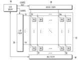
도 1을 참조하면, 본 발명의 일 실시예에 따른 표시 장치는 표시 패널(10), 스캔 구동부(20), 데이터 구동부(30), 센싱 처리부(40), 그리고 신호 제어부(50)를 포함한다.Referring to FIG. 1, a display device according to an embodiment of the present invention includes a
표시 패널(10)은 게이트선들(G1-Gn), 데이터선들(D1-Dm), 그리고 게이트선들(G1-Gn) 및 데이터선들(D1-Dm)에 연결되어 있으며 대략 행렬로 배열된 화소들(PX)을 포함한다. 표시 패널(10)은 센서선들(S1-Sp), 그리고 게이트선들(G1-Gn) 및 센서선들(S1-Sp)에 연결되어 있으며 대략 행렬로 배열된 지문 인식 센서들(SN)(이하 간략하게 센서라고도 함)을 또한 포함한다.The
게이트선들(G1-Gn)은 주로 제1 방향(예컨대, 행 방향)으로 뻗어 있을 수 있고, 데이터선들(D1-Dm)은 제1 방향과 교차하는 제2 방향(예컨대, 열 방향)으로 뻗어 있을 수 있다. 각각의 화소(PX)는 트랜지스터 같은 스위칭 소자를 턴-온시키는 게이트 온 전압과 턴-오프시키는 게이트 오프 전압을 포함하는 게이트 신호를 게이트선을 통해 인가받을 수 있고, 영상 신호에 대응하는 데이터 신호를 스위칭 소자의 턴-온 시 데이터선을 통해 인가받을 수 있다. 유기 발광 표시 장치의 경우, 구동 전압을 화소들(PX)에 전달하는 구동 전압선들(도시되지 않음)이 배치되어 있을 수 있고, 발광 신호 및/또는 초기화 신호를 화소들(PX)에 전달하는 신호선들(도시되지 않음)이 또한 배치되어 있을 수 있다.The gate lines (G1-Gn) may extend mainly in a first direction (e.g., row direction), and the data lines (D1-Dm) may extend in a second direction (e.g., column direction) that intersects the first direction. You can. Each pixel (PX) can receive a gate signal including a gate-on voltage that turns on a switching element such as a transistor and a gate-off voltage that turns it off through a gate line, and receives a data signal corresponding to the image signal. When the switching element is turned on, it can be applied through the data line. In the case of an organic light emitting display device, driving voltage lines (not shown) may be disposed to transmit a driving voltage to the pixels PX, and signal lines to transmit a light emitting signal and/or an initialization signal to the pixels PX. Fields (not shown) may also be arranged.
화소(PX)는 영상을 표시하는 단위로서, 하나의 화소가 기본 색(primary color) 중 하나를 고유하게 표시하거나, 복수의 화소가 시간에 따라 번갈아 기본 색을 표시함으로써, 기본 색들의 공간적 또는 시간적 합으로 원하는 색상을 표시할 수 있다.A pixel (PX) is a unit that displays an image. One pixel uniquely displays one of the primary colors, or a plurality of pixels alternately display primary colors over time, thereby maintaining the spatial or temporal stability of the primary colors. You can display the desired color by combining them.
센서선(S1-Sp)은 대략 열 방향 또는 대략 행 방향으로 연장되어 있으며, 센서들(SN)에 연결되어 센싱 신호를 센싱 처리부(40)로 전달한다.The sensor line S1-Sp extends approximately in the column direction or approximately the row direction, and is connected to the sensors SN to transmit a sensing signal to the
센서들(SN)은 자기 정전용량(self-capacitance) 방식으로 터치에 따른 센싱 신호를 생성할 수 있다. 예컨대, 센서(SN)에 구동 신호가 입력되면 센서(SN)의 축전기(도시되지 않음)는 소정의 전하량으로 충전되고, 손가락 같은 외부 물체의 터치 여부에 따라 변화된 전하량이 센싱 신호로서 센서선(S1-Sp)으로 출력된다. 즉, 외부 물체의 터치가 있으면 축전기에 구동 신호(입력 신호)에 의해 충전된 전하량이 변화하고 그에 따른 센싱 신호(출력 신호)가 센서선(S1-Sp)을 통해 센싱 처리부(40)로 전달된다. 센서(SN)의 구동 신호는 센서선(S1-Sp)을 통해 센서(SN)로 인가될 수 있고, 별도의 신호선을 통해 인가될 수도 있다.Sensors SN may generate a sensing signal according to touch using a self-capacitance method. For example, when a driving signal is input to the sensor SN, the capacitor (not shown) of the sensor SN is charged with a predetermined amount of charge, and the amount of charge that changes depending on whether or not an external object such as a finger touches the sensor line (S1) is used as a sensing signal. -Sp) is output. That is, when there is a touch of an external object, the amount of charge charged in the capacitor by the driving signal (input signal) changes, and the corresponding sensing signal (output signal) is transmitted to the
신호 제어부(50)는 스캔 구동부(20) 및 데이터 구동부(30)를 제어한다. 신호 제어부(50)는 외부의 그래픽 처리부(도시되지 않음)로부터 영상 신호 및 이의 제어 신호를 수신한다. 제어 신호는 예컨대 수평 동기 신호(Hsync), 수직 동기 신호(Vsync), 클록 신호(CLK), 데이터 인에이블 신호(DE) 등을 포함한다. 신호 제어부(50)는 영상 신호와 제어 신호를 기초로 영상 신호를 표시 패널(10)의 동작 조건에 적합하게 처리한 후, 영상 데이터(DAT), 게이트 제어 신호(CONT1), 데이터 제어 신호(CONT2) 및 클록 신호를 생성하여 출력한다. 신호 제어부(50)는 센싱 처리부(40)를 제어할 수 있다.The
스캔 구동부(20)는 신호 제어부(50)로부터 게이트 제어 신호(CONT1)를 수신하여 게이트 온 전압과 게이트 오프 전압을 포함하는 게이트 신호를 생성하고 이를 게이트선(G1-Gn)에 인가한다. 도시된 실시예에서 화소들(PX)과 센서들(SN)은 동일한 스캔 구동부(20)에 연결되어 있지만, 별개의 스캔 구동부에 연결되어 있을 수도 있다. 화소들(PX)과 센서들(SN)은 도시된 것과 같이 동일한 게이트선에 연결되어 있을 수 있고, 도시된 것과 달리 서로 다른 게이트선에 연결되어 있을 수도 있다.The
데이터 구동부(30)는 신호 제어부(50)로부터 데이터 제어 신호(CONT2) 및 영상 데이터(DAT)를 수신하고, 계조 전압 생성부(도시되지 않음)에서 생성된 계조 전압을 이용하여 영상 데이터(DAT)를 데이터 전압으로 변환하고 이를 데이터선(D1-Dm)에 인가한다.The
센싱 처리부(40)는 게이트 신호에 의해 센서들(SN)의 스위칭 소자가 턴-온되면, 센서들(SN)에 구동 신호를 인가하고 센서들(SN)로부터 센싱 신호를 수신한다. 구동 신호는 예컨대 신호 제어부(50)로부터 동기 신호 또는 센싱 인에이블 신호를 수신하고 이에 기초하여 생성될 수 있으며, 주기적으로 출력되는 펄스 또는 적어도 두 개의 서로 다른 전압 레벨을 포함할 수 있다. 센싱 처리부(40)는 센싱 신호에 기초하여 센싱 데이터를 생성한다. 센싱 데이터의 생성을 위해, 센싱 처리부(40)는 예컨대 적분기, 아날로그-디지털 변환기 등을 포함할 수 있다. 센싱 데이터는 지문의 요철 정보를 포함할 수 있다. 센싱 데이터는 신호 제어부(50) 또는 외부의 제어부/처리부로 전송되어 지문 정보를 생성하는데 사용될 수 있다.When the switching elements of the sensors SN are turned on by the gate signal, the
도 2는 본 발명의 일 실시예에 따른 지문 인식 센서를 포함하는 표시 장치에서 지문 인식을 수행하는 과정을 보여주는 순서도이다.Figure 2 is a flowchart showing a process of performing fingerprint recognition in a display device including a fingerprint recognition sensor according to an embodiment of the present invention.
도 2를 참고하면, 표시 장치는 표시 패널의 화면에 영상을 전체적으로 표시한다 (S21). 사용자 인증 등이 요구되는 경우, 표시 장치는 사용자에게 지문을 요청한다 (S22). 지문 요청 시 화면에 제공되는 영상은 화면의 소정 영역에 지문 인식 영역을 표시할 수 있다. 그러한 지문 인식 영역의 표시는 예컨대 지문이 그려져 있는 도형일 수 있다.Referring to FIG. 2, the display device displays the entire image on the screen of the display panel (S21). When user authentication, etc. is required, the display device requests a fingerprint from the user (S22). When requesting a fingerprint, the image provided on the screen may display a fingerprint recognition area in a predetermined area of the screen. The mark of such a fingerprint recognition area may be, for example, a figure depicting a fingerprint.
화면에 표시되는 지문 인식 영역을 사용자가 손가락으로 터치하면 표시 장치는 사용자의 터치를 확인하고 지문 인식 영역의 영상 표시를 중단한다 (S23). 이때 지문 인식 영역의 모든 화소가 발광하지 않고 오프 상태일 수 있고, 지문 인식 영역의 특정 색의 화소들만 오프 상태일 수도 있다. 오프 상태의 화소에는 예컨대 영상 표시를 위한 신호(예컨대, 발광 신호)가 인가되지 않을 수 있고, 블랙 데이터 전압이나 게이트 오프 전압이 인가될 수 있다. 사용자의 터치는 지문 인식 센서 또는 별도의 터치 센서에 의해 센싱될 수 있다.When the user touches the fingerprint recognition area displayed on the screen with his or her finger, the display device confirms the user's touch and stops displaying the image of the fingerprint recognition area (S23). At this time, all pixels in the fingerprint recognition area may not emit light and may be in an off state, and only pixels of a specific color in the fingerprint recognition area may be in an off state. For example, a signal for image display (eg, a light emission signal) may not be applied to a pixel in an off state, and a black data voltage or gate-off voltage may be applied to the pixel. The user's touch can be sensed by a fingerprint recognition sensor or a separate touch sensor.
그 다음, 지문 인식 센서가 활성화되고 (S24), 지문을 인식한다 (S25). 지문 인식 센서가 활성화되면 센싱 처리부는 지문 인식 영역에 위치하는 센서들에 구동 신호를 인가할 수 있고 센서들로부터 센싱 신호를 수신하여 센싱 데이터를 생성할 수 있다. 신호 제어부 또는 다른 제어부/처리부는 생성된 센싱 데이터에 기초하여 지문 인식을 수행한다. 지문 인식 후 영상 표시가 중단된 지문 인식 영역은 다시 영상을 표시한다 (S26). 즉, 지문 인식 영역의 오프 상태의 화소들이 온 상태가 되고, 표시 패널의 화면이 전체적으로 영상을 표시한다.Next, the fingerprint recognition sensor is activated (S24) and recognizes the fingerprint (S25). When the fingerprint recognition sensor is activated, the sensing processing unit can apply a driving signal to the sensors located in the fingerprint recognition area and receive sensing signals from the sensors to generate sensing data. The signal control unit or other control unit/processor performs fingerprint recognition based on the generated sensing data. The fingerprint recognition area where the image display stopped after fingerprint recognition displays the image again (S26). That is, the off-state pixels in the fingerprint recognition area are turned on, and the screen of the display panel displays the image as a whole.
센서 주변에 있는 화소들에 신호가 인가되면 이러한 신호는 매우 작은 변화를 센싱해야 하는 지문 인식 센서에 노이즈로 작용한다. 본 발명의 일 실시예에 따르면, 지문 인식 센서의 활성화 및 지문 인식 단계에서 지문 인식 영역에 영상 표시를 위한 신호가 인가되지 않으므로, 이러한 신호에 의해 센싱 신호가 영향을 받는 것을 방지할 수 있고, 따라서 센싱 감도 및 센싱 신뢰성을 증가시킬 수 있다. 지문 인식 센서의 활성화 시 지문 인식 영역뿐만 아니라 화면 전체의 화소가 오프 상태일 수도 있다.When signals are applied to pixels around the sensor, these signals act as noise to the fingerprint recognition sensor, which must sense very small changes. According to one embodiment of the present invention, since the signal for image display is not applied to the fingerprint recognition area during the activation and fingerprint recognition stage of the fingerprint recognition sensor, the sensing signal can be prevented from being affected by such signals, and thus Sensing sensitivity and sensing reliability can be increased. When the fingerprint recognition sensor is activated, not only the fingerprint recognition area but also the entire screen's pixels may be turned off.
지금까지 지문 인식 센서를 포함하는 표시 장치의 전체적인 배치 및 동작에 대해 살펴보았다. 이제 도 3 및 도 4를 참고하여, 표시 장치의 구체적인 구조에 대해 설명하기로 한다.So far, we have looked at the overall arrangement and operation of the display device including the fingerprint recognition sensor. Now, with reference to FIGS. 3 and 4 , the specific structure of the display device will be described.
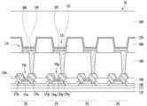
도 3은 본 발명의 일 실시예에 따른 화소 및 센서의 평면 배치를 개략적으로 나타낸 도면이고, 도 4는 도 3에서 IV-IV' 선을 따라 취한 단면을 개략적으로 나타낸 도면이다.FIG. 3 is a diagram schematically showing the planar arrangement of pixels and sensors according to an embodiment of the present invention, and FIG. 4 is a diagram schematically showing a cross section taken along line IV-IV' in FIG. 3.
도 3 및 도 4를 참고하면, 본 발명의 일 실시예에 따른 표시 장치의 표시 패널(10)에는 화소들(PX)이 소정 간격으로 배치되어 있고, 화소들(PX)이 위치하지 않는 영역에 센서들(SN)이 소정 간격으로 배치되어 있다.Referring to FIGS. 3 and 4 , pixels PX are arranged at predetermined intervals on the
화소들(PX)은 적색 화소, 녹색 화소 및 청색 화소를 포함할 수 있고, 대략 사각형일 수 있다. 화소들(PX)은 색상에 따라 그 크기 및/또는 개수가 다를 수 있다. 예컨대, 청색 화소가 가장 클 수 있고 녹색 화소가 단위 면적당 상대적으로 많을 수 있다. 도 3에 도시된 화소들(PX)의 크기, 모양 및 배치는 단지 예시적인 것이며, 실시예에 따라서 다양할 수 있다.The pixels PX may include a red pixel, a green pixel, and a blue pixel, and may be approximately square. The size and/or number of pixels (PX) may vary depending on color. For example, blue pixels may be the largest and green pixels may be relatively numerous per unit area. The size, shape, and arrangement of the pixels PX shown in FIG. 3 are merely exemplary and may vary depending on the embodiment.
각각의 화소(PX)는 발광 소자(LD) 및 발광 소자(LD)의 발광(예컨대, 발광 소자(LD)를 흐르는 전류량 또는 발광 소자(LD)의 온/오프)을 제어하기 위한 화소 트랜지스터(TRp)를 포함한다. 도시되지 않았지만, 각각의 화소(PX)는 두 개 이상의 트랜지스터를 포함할 수 있고, 하나 이상의 축전기를 포함할 수 있다.Each pixel PX includes a light emitting element LD and a pixel transistor TRp for controlling the light emission of the light emitting element LD (e.g., the amount of current flowing through the light emitting element LD or the on/off of the light emitting element LD). ) includes. Although not shown, each pixel PX may include two or more transistors and one or more capacitors.
센서들(SN)은 행렬로 배열되어 있을 수 있다. 인접하는 센서들(SN)의 간격은 예컨대 손가락 지문의 마루(ridge)와 골(valley) 사이의 간격과 대략 동일하거나 그보다 작을 수 있다. 예컨대, 인접하는 센서들(SN)의 간격은 약 50 마이크로미터 이하일 수 있다. 도 3에서 인접하는 센서들(SN) 사이에 두 개의 화소(PX)가 위치하고 있지만, 이것은 단지 예시적인 것에 불과하며, 표시 장치의 해상도에 따라서 하나 또는 세 개 이상의 화소(PX)가 위치할 수도 있다.Sensors SN may be arranged in a matrix. The spacing between adjacent sensors SN may be, for example, approximately equal to or smaller than the spacing between the ridges and valleys of a finger print. For example, the spacing between adjacent sensors SN may be about 50 micrometers or less. Although two pixels (PX) are located between adjacent sensors (SN) in FIG. 3, this is only an example, and one or three or more pixels (PX) may be located depending on the resolution of the display device. .
각각의 센서(SN)는 센서 축전기(CP) 및 센서 트랜지스터(TRs)를 포함한다. 센서 축전기(CP)는 손가락 등의 터치에 따라 충전량이 변화하고, 센서 트랜지스터(TRs)는 센서 축전기(CP)에 구동 신호가 인가되고 센서 축전기(CP)로부터 센싱 신호가 출력되는 것을 제어한다. 센서 트랜지스터(TRs)의 게이트 전극(124s) 및 소스 전극(173s)은 도 1에 도시된 게이트선(G1-Gn) 및 센서선(S1-Sp)에 각각 연결되어 있을 수 있고, 드레인 전극(175s)은 센서 축전기(CP)의 한 전극(195)에 연결되어 있을 수 있다.Each sensor (SN) includes a sensor capacitor (CP) and sensor transistors (TRs). The charge amount of the sensor capacitor (CP) changes depending on the touch of a finger, etc., and the sensor transistors (TRs) control the application of a driving signal to the sensor capacitor (CP) and the output of a sensing signal from the sensor capacitor (CP). The
센서 축전기(CP)는 화소(PX)의 발광 소자(LD)와 실질적으로 동일한 적층 구조(stacking structure) 또는 단면 구조를 가질 수 있고, 센서 트랜지스터(TRs)는 화소(PX)의 트랜지스터(TRs)(이하 간략하게 화소 트랜지스터로 함)와 실질적으로 동일한 적층 구조 또는 단면 구조를 가질 수 있다. 다만, 후술하는 바와 같이, 발광 소자(LD)는 두 전극(191, 270) 사이에 발광 부재(light emitting member)(370)가 위치하지만, 센서 축전기(CP)는 두 전극(195, 270) 사이에 유전층(dielectric layer)(380)이 위치한다. 유전층(380)의 하면은 제1 전극(195)의 상면과 접할 수 있고, 유전층(380)의 상면은 공통 전극(270)의 하면과 접할 수 있다.The sensor capacitor (CP) may have a stacking structure or cross-sectional structure that is substantially the same as the light emitting element (LD) of the pixel (PX), and the sensor transistor (TRs) may be similar to the transistor (TRs) of the pixel (PX). It may have a stacked structure or cross-sectional structure that is substantially the same as that of the transistor (hereinafter simply referred to as a pixel transistor). However, as will be described later, the light emitting element (LD) has a light emitting member (370) located between the two electrodes (191, 270), but the sensor capacitor (CP) has a light emitting member (370) located between the two electrodes (195, 270). A
도 4를 참고하여 표시 패널(10)의 적층 구조에 대해 상세하게 설명하면, 표시 패널(10)은 기판(110) 및 그 위에 위치하는 화소들(PX) 및 센서들(SN)을 포함한다. 화소들(PX)과 센서들(SN)을 기판(110) 위에 형성된 여러 층들의 조합에 의해 형성된다.To describe the stacked structure of the
기판(110)은 플라스틱 같은 연성(flexible) 물질이나 유리 같은 경성(rigid) 물질로 이루어진 투명한 절연 기판일 수 있다.The
기판(110) 위에는 반도체 특성을 열화시키는 불순물이 확산되는 것을 방지하고 수분 등의 침투를 방지하기 위한 배리어층(111)(또는 버퍼층)이 위치한다. 배리어층(111)은 규소 산화물(SiOx), 규소 질화물(SiNx) 등의 무기 절연 물질을 포함할 수 있다.A barrier layer 111 (or buffer layer) is positioned on the
배리어층(111) 위에는 화소 트랜지스터(TRp)의 반도체(154p) 및 센서 트랜지스터(TRs)의 반도체(154s)가 위치한다. 반도체(154p, 154s)는 채널 영역과 채널 영역의 양측에 위치하며 도핑되어 있는 소스 영역 및 드레인 영역을 포함한다. 반도체(154p, 154s)는 다결정 규소, 비정질 규소, 또는 산화물 반도체를 포함할 수 있다.The
도시되지 않았지만, 기판(110)과 반도체(154p, 154s) 사이에는 차광 전극이 위치할 수 있다. 차광 전극은 외부 광이 반도체(154p, 154s)에 도달하는 것을 차단하여 반도체(154)의 특성 저하를 막고 트랜지스터(TRp, TRs)의 누설 전류를 최소화할 수 있다.Although not shown, a light-blocking electrode may be located between the
반도체(154p, 154s) 위에는 게이트 절연층(140)이 위치한다. 게이트 절연층(140)은 규소 산화물(SiOx), 규소 질화물(SiNx) 등의 무기 절연 물질을 포함할 수 있다.A
게이트 절연층(140) 위에는 화소 트랜지스터(TRp)의 게이트 전극(124p), 센서 트랜지스터(TRs)의 게이트 전극(124s), 게이트선(도시되지 않음) 등을 포함하는 게이트 도전체가 위치한다. 게이트 전극(124p, 124s)은 반도체(154p, 154s)의 채널 영역과 중첩할 수 있다. 게이트 도전체는 몰리브덴(Mo), 구리(Cu), 알루미늄(Al), 은(Ag), 크롬(Cr), 탄탈륨(Ta), 티타늄(Ti) 등의 금속이나 금속 합금을 포함할 수 있으며, 단일층 또는 다중층으로 형성될 수 있다.A gate conductor including the
게이트 도전체 위에는 무기 절연 물질을 포함할 수 있는 층간 절연층(160)이 위치한다. 층간 절연층(160)은 규소 산화물, 규소 질화물, 규소 산질화물(SiON), 규소 산불화물(SiOF) 등의 무기 절연 물질을 포함할 수 있다.An interlayer insulating
층간 절연층(160) 위에는 화소 트랜지스터(TRp)의 소스 전극(173p) 및 드레인 전극(175p), 센서 트랜지스터(TRs)의 소스 전극(173s) 및 드레인 전극(175s), 데이터선(도시되지 않음), 구동 전압선(도시되지 않음) 등을 포함하는 데이터 도전체가 위치한다. 소스 전극(173p, 173s) 및 드레인 전극(175p, 175s)은 층간 절연층(160)에 형성된 접촉 구멍들을 통해 반도체(154p, 154s)의 소스 영역 및 드레인 영역에 각각 연결될 수 있다. 데이터 도전체는 알루미늄(Al), 구리(Cu), 은(Ag), 금(Au), 백금(Pt), 팔라듐(Pd), 니켈(Ni), 몰리브덴(Mo), 텅스텐(W), 티타늄(Ti), 크롬(Cr), 탄탈륨(Ta) 등의 금속이나 금속 합금을 포함할 수 있으며, 단일층 또는 다중층(예컨대, Ti/Al/Ti, Mo/Al/Mo, Mo/Cu/Mo 등)으로 형성될 수 있다.On the
게이트 전극(124p), 소스 전극(173p) 및 드레인 전극(175p)은 반도체(154p)와 함께 화소 트랜지스터(TRp)를 이룬다. 도시된 화소 트랜지스터(TRp)는 유기 발광 표시 장치의 화소에서 구동 트랜지스터일 수 있다. 게이트 전극(124s), 소스 전극(173s) 및 드레인 전극(175s)은 반도체(154s)와 함께 센서 트랜지스터(TRs)를 이룬다. 센서 트랜지스터(TRs)는 선택 트랜지스터 또는 리드아웃 트랜지스터로 불릴 수 있다. 센서 트랜지스터(TRs)는 화소 트랜지스터(TRp)와 동일한 물질로 함께 형성될 수 있다. 도시된 트랜지스터(TRp, TRs)는 게이트 전극(124p, 124s)이 반도체(154p, 154s)보다 위에 위치하므로 탑 게이트형(top-gate) 트랜지스터로 불린다. 트랜지스터의 구조는 이에 한정되는 것은 아니고 다양하게 바뀔 수 있으며, 예컨대, 게이트 전극이 반도체 아래 위치하는 바텀 게이트형(bottom-gate) 트랜지스터일 수도 있다.The
데이터 도전체 위에는 평탄화층(180)이 위치한다. 평탄화층(180)은 그 위에 형성될 발광 소자(LD)의 발광 효율을 높이기 위해 단차를 없애고 평탄화시키는 역할을 할 수 있다. 평탄화층(180)은 유기 절연 물질을 포함할 수 있다.A
평탄화층(180) 위에는 발광 소자(LD)의 화소 전극(191)이 위치한다. 화소 전극(191)은 평탄화층(180)에 형성된 접촉 구멍을 통해 화소 트랜지스터(TRp)의 드레인 전극(175p)에 연결되어 있다. 평탄화층(180) 위에는 센서 축전기(CP)의 제1 전극(195)이 위치한다. 제1 전극(195)은 평탄화층(180)에 형성된 접촉 구멍을 통해 센서 트랜지스터(TRs)의 드레인 전극(175s)에 연결되어 있다. 화소 전극(191) 및 제1 전극(195)은 동일한 물질로 함께 형성될 수 있으며, 예컨대 반사성 도전 물질 또는 반투과성 도전 물질로 형성될 수 있고, 투명한 도전 물질로 형성될 수도 있다. 예컨대, 화소 전극(191) 및 제1 전극(195)은 인듐 주석 산화물(ITO), 인듐 아연 산화물(IZO) 같은 투명 도전 물질, 리튬(Li), 칼슘(Ca), 알루미늄(Al), 은(Ag), 마그네슘(Mg), 금(Au) 같은 금속을 포함할 수 있다.The
평탄화층(180) 위에는 화소 전극(191) 및 제1 전극(195)과 중첩하는 개구부들을 가지는 화소 정의막(360)이 위치한다. 화소 정의막(360)은 폴리이미드, 폴리아크릴레이트, 폴리아미드 같은 유기 절연 물질을 포함할 수 있다.A
화소 전극(191) 위에는 발광 소자(LD)의 발광 부재(370)가 위치한다. 발광 부재(370)는 차례대로 적층된 제1 유기 공통층, 발광층 및 제2 유기 공통층 포함할 수 있다. 제1 유기 공통층은 정공 주입층 및 정공 수송층 중 적어도 하나를 포함할 수 있다. 발광층은 적색, 녹색 및 청색 등의 기본 색의 광을 고유하게 내는 유기 물질로 만들어질 수도 있고, 서로 다른 색의 광을 내는 복수의 유기 물질층이 적층된 구조를 가질 수도 있다. 제2 유기 공통층은 전자 수송층 및 전자 주입층 중 적어도 하나를 포함할 수 있다.The
제1 전극(195) 위에는 센서 축전기(CP)의 유전층(380)이 위치한다. 유전층(380)은 규소 산화물, 규소 질화물 등의 무기 절연 물질을 포함할 수 있고, 유기 절연 물질을 포함할 수도 있다. 제1 전극(195)과 중첩하는 화소 정의막(360)의 개구부는 유전층(380)과 또한 중첩한다.The
발광 부재(370) 위에는 공통 전압을 전달하는 공통 전극(270)이 위치한다. 공통 전극(270)은 유전층(380) 위에 또한 위치한다. 공통 전극(270)은 인듐 주석 산화물(ITO), 인듐 아연 산화물(IZO) 같은 투명 도전 물질을 포함할 수 있다. 공통 전극(270)은 칼슘(Ca), 바륨(Ba), 마그네슘(Mg), 알루미늄(Al), 은(Ag) 등의 금속을 얇게 적층하여 광 투과성을 가지도록 형성될 수도 있다. 공통 전극(270)은 표시 패널(10)의 전면에 걸쳐 하나의 통판으로 형성되어 있을 수 있고, 행 방향으로 및/또는 열 방향으로 분리되어 복수 개 형성될 수도 있다.A
화소(PX)의 화소 전극(191), 발광 부재(370) 및 공통 전극(270)은 유기 발광 다이오드인 발광 소자(LD)를 이룬다. 여기서, 화소 전극(191)은 정공 주입 전극인 애노드(anode)일 수 있고, 공통 전극(270)은 전자 주입 전극인 캐소드(cathode)일 수 있다. 이와 반대로, 화소 전극(191)이 캐소드일 수 있고, 공통 전극(270)이 애노드일 수도 있다. 화소 전극(191) 및 공통 전극(270)으로부터 각각 정공과 전자가 발광 부재(370) 내부로 주입되고, 주입된 정공과 전자가 결합한 엑시톤(exiton)이 여기 상태로부터 기저 상태로 떨어질 때 발광하게 된다.The
센서(SN)의 제1 전극(195), 유전층(380) 및 공통 전극(270)은 센서 축전기(CP)를 이룬다. 여기서 공통 전극(270)은 유전층(380)을 사이에 두고 제1 전극(195)과 마주하는 센서 축전기(CP)의 제2 전극에 해당한다. 따라서 제1 전극(195)과 중첩하는 공통 전극(270)의 부분이 제2 전극을 이룬다.The
공통 전극(270) 위에는 봉지층(encapsulation layer)(390)이 위치한다. 봉지층(390)은 발광 부재(370) 및 공통 전극(270)을 봉지하여 외부로부터 수분이나 산소가 침투하는 것을 방지할 수 있다. 봉지층(390)은 무기 물질을 포함하는 적어도 하나의 층을 포함할 수 있고, 유기 물질을 포함하는 적어도 하나의 층을 더 포함할 수 있다. 봉지층(390) 위에는 외광 반사를 방지하기 위한 편광 부재(도시되지 않음)가 위치할 수 있다.An
위와 같이, 센서(SN)는 화소(PX)와 그 크기나 모양은 다를 수 있으나, 실질적으로 동일한 적층 구조를 가진다. 센서 트랜지스터(TRs)는 화소 트랜지스터(TRp)와 실질적으로 동일한 적층 구조를 가질 수 있고, 센서 축전기(CP)는 발광 소자(LD)와 실질적으로 동일한 적층 구조를 가질 수 있다. 다만, 발광 소자(LD)는 화소 전극(191)과 공통 전극(270) 사이에 발광 부재(370)가 위치하지만, 센서 축전기(CP)는 제1 전극(195)과 제2 전극인 공통 전극(270) 사이에 유전층(380)이 위치하는 차이가 있다. 유전층(380)은 발광 부재(370)와 다른 물질로 형성되므로, 유전층(380)을 형성하기 위해서는 추가적인 마스크의 사용이 필요할 수 있다. 그렇더라도, 센서(SN)를 표시 패널(10) 내에 하나의 마스크를 추가하는 정도에서 형성할 수 있고, 그 외에는 추가적인 공정 단계를 요하지 않으므로, 제조 비용 및 시간을 절감할 수 있다.As above, the sensor SN may have a different size or shape from the pixel PX, but has a substantially identical stacked structure. The sensor transistor TRs may have a stacked structure substantially the same as that of the pixel transistor TRp, and the sensor capacitor CP may have a stacked structure substantially the same as that of the light emitting device LD. However, the light emitting element (LD) has a
이제 도 5를 참고하여, 지문 인식 센서의 센싱 원리에 대해 설명하기로 한다.Now, with reference to FIG. 5, the sensing principle of the fingerprint recognition sensor will be described.
도 5는 본 발명의 일 실시예에 따른 표시 장치에서 지문 인식과 관련된 센서의 개념을 회로로서 나타내는 도면이다.Figure 5 is a diagram showing the concept of a sensor related to fingerprint recognition in a display device according to an embodiment of the present invention as a circuit.
도 5는 두 개의 센서(SN1, SN2)와 관련된 구성을 회로를 사용하여 도시하고 있다. 도 1 내지 도 4를 교차 참고하면, 서로 인접할 수 있는 제1 센서(SN1) 및 제2 센서(SN2)는 각각 센서 축전기(CP) 및 센서 트랜지스터(TRs)를 포함하고, 센서 축전기(CP)의 제1 전극(195)은 센서 트랜지스터(TRs)의 드레인 전극(175s) 및 소스 전극(173s)을 통해 센서선(Si, Sj)에 연결되어 있다. 센서 트랜지스터(TRs)의 게이트 전극(124s)은 게이트선(Gi, Gj)에 연결되어 있다. 제1 센서(SN1)의 센서 축전기(CP)의 정전용량(Cs)과 제2 센서(SN2)의 센서 축전기(CP)의 정전용량(Cs)은 실질적으로 동일할 수 있다.Figure 5 shows a configuration related to two sensors (SN1, SN2) using a circuit. 1 to 4, the first sensor SN1 and the second sensor SN2, which may be adjacent to each other, each include a sensor capacitor (CP) and a sensor transistor (TRs), and the sensor capacitor (CP) The
게이트선(Gi, Gj)에 게이트 온 전압이 인가되어 센서 트랜지스터(TRs)가 온 되면 센서선(Si, Sj)을 통해 구동 신호가 인가되어 센서 축전기(CP)에 전하가 충전된다.When a gate-on voltage is applied to the gate lines (Gi, Gj) and the sensor transistor (TRs) is turned on, a driving signal is applied through the sensor lines (Si, Sj) to charge the sensor capacitor (CP).
사용자가 손가락으로 예컨대 표시 패널(10)의 표면을 터치하면, 손가락과 센서 축전기(CP)의 제2 전극(270) 사이에 정전용량(Cr, Cv)이 형성된다. 이때, 제1 센서(SN1)의 제2 전극(270)과 지문의 마루에 사이에 형성되는 정전용량(Cr)과 제2 센서(SN2)의 제2 전극(270)과 지문의 골 사이에 형성되는 정전용량(Cv)은 거리 등의 차이로 인해 그 차이가 미소할지라도 서로 다르다. 따라서 지문의 마루에 대응하는 제1 센서(SN1)의 센서 축전기(CP)의 전하량 변화와 지문의 골에 대응하는 제2 센서(SN2)의 센서 축전기(CP)의 전하량 변화가 서로 다르다. 그 결과, 제1 센서(SN1)에 연결된 센서선(Si)을 통해 출력되는 센싱 신호와 제1 센서(SN2)에 연결된 센서선(Sj)을 통해 출력되는 센싱 신호가 다르고, 센싱 처리부(40)는 이들 센싱 신호에 기초하여 지문의 요철 정보를 포함하는 센싱 데이터를 생성할 수 있다. 결국, 지문을 검출할 수 있는 센싱 데이터는 서로 다른 센서(SN1, SN2)가 센싱하는, 미소한 차이를 나타내는 두 정전용량(Cr, Cv)에 기초한다.When a user touches the surface of the
지문 센싱 시 제2 전극(270)은 플로팅 상태일 수 있다. 이를 위해, 지문 센싱은 수직 블랭크(vertical black) 기간 같이 영상이 표시되지 않는 기간에 수행될 수 있다. 즉, 지문 센싱과 영상 표시가 시분할 방식으로 동작할 수 있다. 지문 센싱 시 제2 전극(270)에 접지 전압이 인가될 수도 있다.When sensing a fingerprint, the
센서 트랜지스터(TRs)가 온 상태인 동안, 센싱 처리부(40)는 센서선(Si, Sj)을 통해 구동 신호를 센서 축전기(CP)에 인가하고 센서 축전기(CP)로부터 센싱 신호를 수신할 수 있다. 따라서 게이트선(G1-Gn)을 통해 인가되는 게이트 온 전압을 타이밍을 조절함으로써, 예컨대 각각의 센서(SN)에 순차적으로 구동 신호를 인가하고 센싱 신호를 전달받을 수 있으며, 각각의 센서(SN)를 자기 정전용량 방식으로 동작시킬 수 있다. 또한, 센서(SN)는 독립적으로 터치를 센싱할 수 있으므로, 지문 인식 센서뿐만 아니라, 멀티 터치의 센싱이 가능한 터치 센서로서 기능할 수 있다.While the sensor transistors (TRs) are in the on state, the
이하에는 본 발명의 몇몇 실시예에 대하여 전술한 실시예와 차이점을 위주로 설명하기로 한다.Hereinafter, several embodiments of the present invention will be described, focusing on differences from the above-described embodiments.
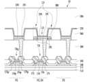
도 6은 본 발명의 일 실시예에 따른 화소 및 센서의 평면 배치를 개략적으로 나타낸 도면이고, 도 7은 도 6에서 VII-VII' 선을 따라 취한 단면을 개략적으로 나타낸 도면이다.FIG. 6 is a diagram schematically showing the planar arrangement of pixels and sensors according to an embodiment of the present invention, and FIG. 7 is a diagram schematically showing a cross section taken along line VII-VII' in FIG. 6.
도 6 및 도 7을 참고하면, 전술한 실시예와 달리, 센서(SN)가 화소(PX)와 별개로 형성되지 않고, 화소(PX)가 센서(SN)의 일부분을 구성한다. 즉, 센서(SN)의 축전기(CP)는 발광 소자(LD) 둘레에 형성되어 있고, 센서(SN)와 화소(PX)는 트랜지스터(TR)를 공유한다.Referring to FIGS. 6 and 7 , unlike the above-described embodiment, the sensor SN is not formed separately from the pixel PX, and the pixel PX constitutes a part of the sensor SN. That is, the capacitor (CP) of the sensor (SN) is formed around the light emitting element (LD), and the sensor (SN) and the pixel (PX) share the transistor (TR).
센서 축전기(CP)는 제1 전극(195), 유전층(380), 그리고 제1 전극(195)과 마주하는 제2 전극인 공통 전극(270)으로 이루어진다. 유전층(380)은 발광 부재(370) 둘레에 위치한다. 유전층(380)은 평면도에서 볼 때 발광 부재(370)를 둘러싸는 대략 사각형 고리와 같은 형상일 수 있지만 이에 제한되지 않으며, 예컨대 대략 원형 고리와 같은 형상일 수 있다. 유전층(380)의 내측 가장자리는 발광 부재(370)의 외측 가장자리와 접할 수 있지만, 접하지 않을 수도 있다. 유전층(380) 바로 위에는 화소 정의막(360)이 위치한다. 도시된 실시예와 달리, 유전층(380)의 적어도 일부분 위에 화소 정의막(360)이 위치하지 않고, 유전층(380)의 상면이 공통 전극(270)의 하면과 접할 수도 있다.The sensor capacitor (CP) consists of a
센서 축전기(CP)의 제1 전극(195)은 유전층(380) 아래에 유전층(380)과 중첩하게 위치한다. 제1 전극(195)은 화소 전극(191)과 동일한 층에 위치하며, 화소 전극(191)에 연결되어 있다. 제1 전극(195)은 화소 전극(191)을 둘러싸고 있을 수 있다. 제1 전극(195)은 화소 전극(191)의 확장된 부분일 수 있다. 따라서 제1 전극(195)은 화소 전극(191)과 동일한 물질로 일체로 형성되어 있을 수 있다. 제1 전극(195)은 화소 전극(191)을 통해 트랜지스터(TR)의 드레인 전극(175)에 연결되어 있다.The
센서(SN) 및 화소(PX)가 공유하는 트랜지스터(TR)는 화소(PX)에 의한 영상 표시 시 화소 트랜지스터로 사용되고, 센서(SN)에 의한 센싱 시 센서 트랜지스터로 사용된다. 트랜지스터(TR)는 센서(SN)와 공유하지 않고 화소(PX)만을 위해 형성되어 있는 화소 트랜지스터(TRp)와 동일한 구조를 가질 수 있다. 센서 트랜지스터로 사용되기 위해, 트랜지스터(TR)의 소스 전극(173)은 도 1에 도시된 센싱 처리부(40)에 연결되어 있을 수 있고, 트랜지스터(TR)의 게이트 전극(124)은 스캔 구동부(20)로부터 출력되는 게이트 신호를 전달하는 게이트선(G1-Gn)에 연결되어 있을 수 있다.The transistor (TR) shared by the sensor (SN) and the pixel (PX) is used as a pixel transistor when displaying an image by the pixel (PX) and as a sensor transistor when sensing by the sensor (SN). The transistor TR may have the same structure as the pixel transistor TRp, which is formed only for the pixel PX and not shared with the sensor SN. To be used as a sensor transistor, the
본 실시예에 따른 배치는 예컨대 표시 패널에서 센서(SN)를 추가로 형성하기 위한 공간을 확보하기가 어려울 경우 유리할 수 있다. 일부 화소(PX)만이 센서(SN)의 일부분을 구성하는 예가 도시되어 있지만, 해상도에 따라서 (예컨대 해상도가 낮을 경우) 모든 화소(PX)가 센서(SN)의 일부분을 구성할 수도 있다. 본 실시예에 따른 표시 장치에서 지문 인식은 전술한 것과 같은 식으로 수행될 수 있다.The arrangement according to this embodiment may be advantageous, for example, when it is difficult to secure space for additionally forming the sensor SN in the display panel. An example in which only some pixels PX constitute a part of the sensor SN is shown, but depending on the resolution (for example, when the resolution is low), all pixels PX may constitute a part of the sensor SN. Fingerprint recognition in the display device according to this embodiment can be performed in the same manner as described above.
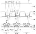
도 8은 본 발명의 일 실시예에 따른 화소 및 센서의 평면 배치를 개략적으로 나타낸 도면이고, 도 9는 도 6에서 IX-IX' 선을 따라 취한 단면을 개략적으로 나타낸 도면이다.FIG. 8 is a diagram schematically showing the planar arrangement of pixels and sensors according to an embodiment of the present invention, and FIG. 9 is a diagram schematically showing a cross section taken along line IX-IX' in FIG. 6.
도 8 및 도 9를 참고하면, 도 6 및 도 7의 실시예와 마찬가지로, 화소(PX)가 센서(SN)의 일부분을 구성한다. 차이점으로는, 별도로 유전층을 형성하지 않고, 화소 정의막(360)을 센서 축전기(CP)의 유전층으로 사용한다. 본 실시예에서, 제1 전극(195)과 중첩하는 화소 정의막(360)의 부분이 센서 축전기(CP)의 유전층(380)을 이룬다. 따라서 유전층을 별도로 형성하지 않아도 되므로, 센서 축전기(CP)의 형성을 위한 추가 공정 단계나 마스크를 요하지 않는다.Referring to FIGS. 8 and 9 , like the embodiment of FIGS. 6 and 7 , the pixel PX forms part of the sensor SN. The difference is that instead of forming a separate dielectric layer, the
화소 정의막(360)의 두께로 인해, 센서 축전기(CP)의 제1 전극(195)과 공통 전극(270)과의 거리가 증가하므로, 소정의 정전용량을 확보하기 위해서는 제1 전극(195)의 면적을 도시된 것과 같이 넓게 하는 것이 유리할 수 있다. 제1 전극(195)은 화소 전극(191)과 연결되어 있다. 제1 전극(195)은 화소 전극(191)과 동일한 층에 같은 물질로 일체로 형성되어 있을 수 있다. 도 8에서 제1 전극(195)이 화소 전극(191)의 세 측면을 둘러싸고 있지만, 화소 전극(191)의 적어도 한 측면으로부터 연장되거나 화소 전극(191)의 측면을 완전히 둘러싸도록 형성될 수 있다.Due to the thickness of the
이상에서 본 발명의 실시예에 대하여 상세하게 설명하였지만 본 발명의 권리범위는 이에 한정되는 것은 아니고 다음의 청구범위에서 정의하고 있는 본 발명의 기본 개념을 이용한 당업자의 여러 변형 및 개량 형태 또한 본 발명의 권리범위에 속하는 것이다.Although the embodiments of the present invention have been described in detail above, the scope of the present invention is not limited thereto, and various modifications and improvements made by those skilled in the art using the basic concept of the present invention defined in the following claims are also possible. It falls within the scope of rights.
10: 표시 패널20: 스캔 구동부
30: 데이터 구동부40: 센싱 처리부
50: 신호 제어부180: 평탄화층
191: 화소 전극195: 제1 전극
270: 공통 전극, 제2 전극360: 화소 정의막
370: 발광 부재380: 유전층
CP: 센서 축전기LD: 발광 소자
PX: 화소SN: 센서
TR, TRp, TRs: 트랜지스터10: display panel 20: scan driver
30: data driving unit 40: sensing processing unit
50: signal control unit 180: planarization layer
191: pixel electrode 195: first electrode
270: common electrode, second electrode 360: pixel defining layer
370: light emitting member 380: dielectric layer
CP: sensor capacitor LD: light emitting element
PX: Pixel SN: Sensor
TR, TRp, TRs: transistors
Claims (18)
Translated fromKorean상기 발광 소자를 통해 상기 화소의 상기 트랜지스터에 연결되어 있는 센서 축전기를 포함하는 센서;
를 포함하며,
상기 발광 소자는 화소 전극, 공통 전극, 그리고 상기 화소 전극과 상기 공통 전극 사이에 위치하는 발광 부재를 포함하고,
상기 센서 축전기는 서로 중첩하는 제1 전극 및 제2 전극을 포함하고,
상기 제1 전극은 상기 화소 전극과 동일한 층에 위치하고, 상기 제2 전극은 상기 공통 전극과 동일한 층에 위치하고,
상기 제1 전극과 상기 제2 전극 간의 간격이 상기 화소 전극과 상기 공통 전극 간의 간격보다 큰 표시 장치.a pixel including a transistor and a light-emitting element connected to the transistor; and
a sensor including a sensor capacitor connected to the transistor of the pixel through the light emitting element;
Includes,
The light emitting element includes a pixel electrode, a common electrode, and a light emitting member positioned between the pixel electrode and the common electrode,
The sensor capacitor includes a first electrode and a second electrode that overlap each other,
The first electrode is located on the same layer as the pixel electrode, and the second electrode is located on the same layer as the common electrode,
A display device in which a gap between the first electrode and the second electrode is greater than a gap between the pixel electrode and the common electrode.
상기 센서 축전기의 유전층은 평면도에서 상기 발광 부재의 측면 중 적어도 일부를 둘러싸고 있는 표시 장치.In paragraph 9:
A display device wherein the dielectric layer of the sensor capacitor surrounds at least a portion of a side surface of the light emitting member in a plan view.
상기 제1 전극은 상기 화소 전극과 일체로 형성되어 있는 표시 장치.In paragraph 10:
A display device wherein the first electrode is formed integrally with the pixel electrode.
상기 제1 전극은 상기 화소 전극을 통해 상기 트랜지스터에 연결되어 있는 표시 장치.In paragraph 10:
The first electrode is connected to the transistor through the pixel electrode.
상기 제2 전극은 상기 공통 전극의 일부분인 표시 장치.In paragraph 12:
A display device wherein the second electrode is part of the common electrode.
상기 트랜지스터 위에 위치하는 평탄화층; 및
상기 평탄화층 위에 위치하는 화소 정의막;
을 더 포함하며,
상기 화소 전극은 상기 평탄화층에 형성된 접촉 구멍을 통해 상기 트랜지스터에 연결되어 있는 표시 장치.In paragraph 13:
a planarization layer located on the transistor; and
a pixel defining layer located on the planarization layer;
It further includes,
A display device wherein the pixel electrode is connected to the transistor through a contact hole formed in the planarization layer.
상기 유전층은 상기 제1 전극과 상기 화소 정의막 사이에 위치하는 표시 장치.In paragraph 14:
The dielectric layer is located between the first electrode and the pixel defining layer.
상기 유전층의 상면이 상기 화소 정의막의 하면과 접하는 표시 장치.In paragraph 15:
A display device in which an upper surface of the dielectric layer is in contact with a lower surface of the pixel defining layer.
상기 유전층은 상기 제1 전극과 중첩하는 화소 정의막의 부분인 표시 장치.In paragraph 14:
The dielectric layer is a portion of the pixel defining layer that overlaps the first electrode.
상기 제1 전극의 상면이 상기 화소 정의막의 하면과 접하는 표시 장치.In paragraph 17:
A display device in which an upper surface of the first electrode is in contact with a lower surface of the pixel defining layer.
Priority Applications (2)
| Application Number | Priority Date | Filing Date | Title |
|---|---|---|---|
| KR1020160129996AKR102663555B1 (en) | 2016-10-07 | 2016-10-07 | Display device comprising fingerprint sensor |
| US15/710,251US10386977B2 (en) | 2016-10-07 | 2017-09-20 | Display device including sensor capacitor and light emitting device that contact same face of insulating layer |
Applications Claiming Priority (1)
| Application Number | Priority Date | Filing Date | Title |
|---|---|---|---|
| KR1020160129996AKR102663555B1 (en) | 2016-10-07 | 2016-10-07 | Display device comprising fingerprint sensor |
Publications (2)
| Publication Number | Publication Date |
|---|---|
| KR20180039222A KR20180039222A (en) | 2018-04-18 |
| KR102663555B1true KR102663555B1 (en) | 2024-05-08 |
Family
ID=61828827
Family Applications (1)
| Application Number | Title | Priority Date | Filing Date |
|---|---|---|---|
| KR1020160129996AActiveKR102663555B1 (en) | 2016-10-07 | 2016-10-07 | Display device comprising fingerprint sensor |
Country Status (2)
| Country | Link |
|---|---|
| US (1) | US10386977B2 (en) |
| KR (1) | KR102663555B1 (en) |
Families Citing this family (10)
| Publication number | Priority date | Publication date | Assignee | Title |
|---|---|---|---|---|
| KR102325171B1 (en)* | 2017-03-20 | 2021-11-10 | 삼성디스플레이 주식회사 | Display device |
| US10739900B2 (en)* | 2017-06-29 | 2020-08-11 | Wuhan China Star Optoelectronics Technology Co., Ltd. | Touch display panel having fingerprint recognition device integrated therewith and touch display device including same |
| CN107272244B (en)* | 2017-08-15 | 2020-12-08 | 京东方科技集团股份有限公司 | Array substrate and manufacturing method thereof, display panel and display device |
| CN108630731B (en)* | 2018-04-24 | 2020-09-25 | 武汉天马微电子有限公司 | Display panel, manufacturing method of display panel and display device |
| KR102591768B1 (en)* | 2018-07-17 | 2023-10-20 | 삼성디스플레이 주식회사 | Display device |
| CN110188744B (en) | 2019-05-28 | 2020-06-16 | 昆山国显光电有限公司 | Display panel and display device |
| KR20210017211A (en)* | 2019-08-07 | 2021-02-17 | 삼성전자주식회사 | Electronic device and method for controlling display thereof |
| US11170193B2 (en)* | 2019-08-29 | 2021-11-09 | Novatek Microelectronics Corp. | Object identifying method and related circuits |
| CN110970481B (en)* | 2019-12-18 | 2023-11-24 | 京东方科技集团股份有限公司 | Display substrate and preparation method thereof, display device |
| US20240185633A1 (en)* | 2021-04-22 | 2024-06-06 | Semiconductor Energy Laboratory Co., Ltd. | Electronic device and authentication method of electronic device |
Citations (2)
| Publication number | Priority date | Publication date | Assignee | Title |
|---|---|---|---|---|
| US20110273397A1 (en)* | 2010-05-06 | 2011-11-10 | Toshiba Mobile Display Co., Ltd. | Organic el display device and method for detecting touch |
| CN105867696A (en)* | 2016-06-03 | 2016-08-17 | 京东方科技集团股份有限公司 | Touch display panel, flexible display panel and display device |
Family Cites Families (13)
| Publication number | Priority date | Publication date | Assignee | Title |
|---|---|---|---|---|
| US6049620A (en) | 1995-12-15 | 2000-04-11 | Veridicom, Inc. | Capacitive fingerprint sensor with adjustable gain |
| US5778089A (en) | 1996-03-04 | 1998-07-07 | Dew Engineering And Development Limited | Driver circuit for a contact imaging array |
| US6259108B1 (en) | 1998-10-09 | 2001-07-10 | Kinetic Sciences Inc. | Fingerprint image optical input apparatus |
| KR101255283B1 (en)* | 2009-09-29 | 2013-04-15 | 엘지디스플레이 주식회사 | Liquid Crystal Display Device |
| KR20120014808A (en)* | 2010-08-10 | 2012-02-20 | 엘지디스플레이 주식회사 | LCD including touch sensor, driving method thereof and manufacturing method thereof |
| CN102881839B (en) | 2012-09-28 | 2014-05-07 | 京东方科技集团股份有限公司 | Organic light emitting diode, touch display device and manufacture methods thereof |
| KR101493494B1 (en)* | 2012-10-11 | 2015-02-16 | 크루셜텍 (주) | User device including fingerprint sensing region in touch screen |
| US10248274B2 (en)* | 2012-11-27 | 2019-04-02 | Guardian Glass, LLC | Transparent conductive coating for capacitive touch panel and method of making same |
| US9557871B2 (en)* | 2015-04-08 | 2017-01-31 | Guardian Industries Corp. | Transparent conductive coating for capacitive touch panel or the like |
| KR102208993B1 (en) | 2014-09-01 | 2021-01-29 | 엘지디스플레이 주식회사 | Organic light emitting display device with touch sensing function |
| KR20160056759A (en) | 2014-11-12 | 2016-05-20 | 크루셜텍 (주) | Flexible display apparatus able to image scan and driving method thereof |
| CN105808001B (en)* | 2016-03-10 | 2018-07-17 | 京东方科技集团股份有限公司 | A kind of pressure sensitivity touch screen and display device |
| KR20160065800A (en) | 2016-05-26 | 2016-06-09 | 크루셜텍 (주) | Interface apparatus for sensor module and pointing device |
- 2016
- 2016-10-07KRKR1020160129996Apatent/KR102663555B1/enactiveActive
- 2017
- 2017-09-20USUS15/710,251patent/US10386977B2/enactiveActive
Patent Citations (2)
| Publication number | Priority date | Publication date | Assignee | Title |
|---|---|---|---|---|
| US20110273397A1 (en)* | 2010-05-06 | 2011-11-10 | Toshiba Mobile Display Co., Ltd. | Organic el display device and method for detecting touch |
| CN105867696A (en)* | 2016-06-03 | 2016-08-17 | 京东方科技集团股份有限公司 | Touch display panel, flexible display panel and display device |
Also Published As
| Publication number | Publication date |
|---|---|
| KR20180039222A (en) | 2018-04-18 |
| US10386977B2 (en) | 2019-08-20 |
| US20180101259A1 (en) | 2018-04-12 |
Similar Documents
| Publication | Publication Date | Title |
|---|---|---|
| KR102663555B1 (en) | Display device comprising fingerprint sensor | |
| US10175843B2 (en) | Organic light-emitting diode (OLED) display including touch sensor | |
| US9483135B2 (en) | Organic light emitting display integrated with touch screen panel | |
| US20160132148A1 (en) | Organic light-emitting diode (oled) display | |
| TWI730542B (en) | Display device | |
| US10790342B2 (en) | Display device | |
| KR20160087981A (en) | Display device | |
| US20230354659A1 (en) | Display panel and display device | |
| US20240373706A1 (en) | Display panel and display device | |
| KR20150000779A (en) | Thin film transistor array substrate and display device including the substrate | |
| US20230301158A1 (en) | Display panel and display device | |
| US12045423B2 (en) | Display device | |
| US12426475B2 (en) | Display device | |
| US20230217704A1 (en) | Display device | |
| US20230172029A1 (en) | Display device and display panel | |
| US20230172017A1 (en) | Display panel and display device | |
| KR20160122899A (en) | Touch panel and display device | |
| KR102863810B1 (en) | Display apparatus | |
| KR102478540B1 (en) | Organic emitting diode display device | |
| US20230200185A1 (en) | Display Device | |
| KR102831823B1 (en) | Display device and driving method for the same | |
| US20230299065A1 (en) | Display panel and display device | |
| US20240215375A1 (en) | Display Device and Display Panel | |
| US20240260384A1 (en) | Display Device and Display Panel | |
| KR20220001837A (en) | Display Apparatus |
Legal Events
| Date | Code | Title | Description |
|---|---|---|---|
| PA0109 | Patent application | Patent event code:PA01091R01D Comment text:Patent Application Patent event date:20161007 | |
| PG1501 | Laying open of application | ||
| A201 | Request for examination | ||
| PA0201 | Request for examination | Patent event code:PA02012R01D Patent event date:20210914 Comment text:Request for Examination of Application Patent event code:PA02011R01I Patent event date:20161007 Comment text:Patent Application | |
| E902 | Notification of reason for refusal | ||
| PE0902 | Notice of grounds for rejection | Comment text:Notification of reason for refusal Patent event date:20230821 Patent event code:PE09021S01D | |
| E701 | Decision to grant or registration of patent right | ||
| PE0701 | Decision of registration | Patent event code:PE07011S01D Comment text:Decision to Grant Registration Patent event date:20240228 | |
| GRNT | Written decision to grant | ||
| PR0701 | Registration of establishment | Comment text:Registration of Establishment Patent event date:20240430 Patent event code:PR07011E01D | |
| PR1002 | Payment of registration fee | Payment date:20240430 End annual number:3 Start annual number:1 | |
| PG1601 | Publication of registration |