KR102658438B1 - Display device - Google Patents
Display deviceDownload PDFInfo
- Publication number
- KR102658438B1 KR102658438B1KR1020190032512AKR20190032512AKR102658438B1KR 102658438 B1KR102658438 B1KR 102658438B1KR 1020190032512 AKR1020190032512 AKR 1020190032512AKR 20190032512 AKR20190032512 AKR 20190032512AKR 102658438 B1KR102658438 B1KR 102658438B1
- Authority
- KR
- South Korea
- Prior art keywords
- touch
- display area
- pixels
- touch electrodes
- adjacent
- Prior art date
- Legal status (The legal status is an assumption and is not a legal conclusion. Google has not performed a legal analysis and makes no representation as to the accuracy of the status listed.)
- Active
Links
Images


Classifications
- G—PHYSICS
- G06—COMPUTING OR CALCULATING; COUNTING
- G06F—ELECTRIC DIGITAL DATA PROCESSING
- G06F3/00—Input arrangements for transferring data to be processed into a form capable of being handled by the computer; Output arrangements for transferring data from processing unit to output unit, e.g. interface arrangements
- G06F3/01—Input arrangements or combined input and output arrangements for interaction between user and computer
- G06F3/03—Arrangements for converting the position or the displacement of a member into a coded form
- G06F3/041—Digitisers, e.g. for touch screens or touch pads, characterised by the transducing means
- G06F3/044—Digitisers, e.g. for touch screens or touch pads, characterised by the transducing means by capacitive means
- G06F3/0445—Digitisers, e.g. for touch screens or touch pads, characterised by the transducing means by capacitive means using two or more layers of sensing electrodes, e.g. using two layers of electrodes separated by a dielectric layer
- G—PHYSICS
- G06—COMPUTING OR CALCULATING; COUNTING
- G06F—ELECTRIC DIGITAL DATA PROCESSING
- G06F3/00—Input arrangements for transferring data to be processed into a form capable of being handled by the computer; Output arrangements for transferring data from processing unit to output unit, e.g. interface arrangements
- G06F3/01—Input arrangements or combined input and output arrangements for interaction between user and computer
- G06F3/03—Arrangements for converting the position or the displacement of a member into a coded form
- G06F3/041—Digitisers, e.g. for touch screens or touch pads, characterised by the transducing means
- G06F3/044—Digitisers, e.g. for touch screens or touch pads, characterised by the transducing means by capacitive means
- G06F3/0443—Digitisers, e.g. for touch screens or touch pads, characterised by the transducing means by capacitive means using a single layer of sensing electrodes
- G—PHYSICS
- G06—COMPUTING OR CALCULATING; COUNTING
- G06F—ELECTRIC DIGITAL DATA PROCESSING
- G06F3/00—Input arrangements for transferring data to be processed into a form capable of being handled by the computer; Output arrangements for transferring data from processing unit to output unit, e.g. interface arrangements
- G06F3/01—Input arrangements or combined input and output arrangements for interaction between user and computer
- G06F3/03—Arrangements for converting the position or the displacement of a member into a coded form
- G06F3/041—Digitisers, e.g. for touch screens or touch pads, characterised by the transducing means
- G06F3/0412—Digitisers structurally integrated in a display
- H—ELECTRICITY
- H10—SEMICONDUCTOR DEVICES; ELECTRIC SOLID-STATE DEVICES NOT OTHERWISE PROVIDED FOR
- H10K—ORGANIC ELECTRIC SOLID-STATE DEVICES
- H10K59/00—Integrated devices, or assemblies of multiple devices, comprising at least one organic light-emitting element covered by group H10K50/00
- H10K59/40—OLEDs integrated with touch screens
- G—PHYSICS
- G06—COMPUTING OR CALCULATING; COUNTING
- G06F—ELECTRIC DIGITAL DATA PROCESSING
- G06F1/00—Details not covered by groups G06F3/00 - G06F13/00 and G06F21/00
- G06F1/16—Constructional details or arrangements
- G06F1/1601—Constructional details related to the housing of computer displays, e.g. of CRT monitors, of flat displays
- G—PHYSICS
- G06—COMPUTING OR CALCULATING; COUNTING
- G06F—ELECTRIC DIGITAL DATA PROCESSING
- G06F3/00—Input arrangements for transferring data to be processed into a form capable of being handled by the computer; Output arrangements for transferring data from processing unit to output unit, e.g. interface arrangements
- G06F3/01—Input arrangements or combined input and output arrangements for interaction between user and computer
- G06F3/03—Arrangements for converting the position or the displacement of a member into a coded form
- G06F3/041—Digitisers, e.g. for touch screens or touch pads, characterised by the transducing means
- G06F3/0416—Control or interface arrangements specially adapted for digitisers
- G06F3/04164—Connections between sensors and controllers, e.g. routing lines between electrodes and connection pads
- G—PHYSICS
- G06—COMPUTING OR CALCULATING; COUNTING
- G06F—ELECTRIC DIGITAL DATA PROCESSING
- G06F3/00—Input arrangements for transferring data to be processed into a form capable of being handled by the computer; Output arrangements for transferring data from processing unit to output unit, e.g. interface arrangements
- G06F3/01—Input arrangements or combined input and output arrangements for interaction between user and computer
- G06F3/03—Arrangements for converting the position or the displacement of a member into a coded form
- G06F3/041—Digitisers, e.g. for touch screens or touch pads, characterised by the transducing means
- G06F3/044—Digitisers, e.g. for touch screens or touch pads, characterised by the transducing means by capacitive means
- G06F3/0446—Digitisers, e.g. for touch screens or touch pads, characterised by the transducing means by capacitive means using a grid-like structure of electrodes in at least two directions, e.g. using row and column electrodes
- H—ELECTRICITY
- H10—SEMICONDUCTOR DEVICES; ELECTRIC SOLID-STATE DEVICES NOT OTHERWISE PROVIDED FOR
- H10K—ORGANIC ELECTRIC SOLID-STATE DEVICES
- H10K50/00—Organic light-emitting devices
- H10K50/80—Constructional details
- H10K50/805—Electrodes
- H—ELECTRICITY
- H10—SEMICONDUCTOR DEVICES; ELECTRIC SOLID-STATE DEVICES NOT OTHERWISE PROVIDED FOR
- H10K—ORGANIC ELECTRIC SOLID-STATE DEVICES
- H10K59/00—Integrated devices, or assemblies of multiple devices, comprising at least one organic light-emitting element covered by group H10K50/00
- H10K59/10—OLED displays
- H10K59/12—Active-matrix OLED [AMOLED] displays
- H10K59/131—Interconnections, e.g. wiring lines or terminals
Landscapes
- Engineering & Computer Science (AREA)
- General Engineering & Computer Science (AREA)
- Theoretical Computer Science (AREA)
- Physics & Mathematics (AREA)
- Human Computer Interaction (AREA)
- General Physics & Mathematics (AREA)
- Computer Hardware Design (AREA)
- Optics & Photonics (AREA)
- Microelectronics & Electronic Packaging (AREA)
- Computer Networks & Wireless Communication (AREA)
- Devices For Indicating Variable Information By Combining Individual Elements (AREA)
- Position Input By Displaying (AREA)
Abstract
Translated fromKoreanDescription
Translated fromKorean본 발명은 표시 장치에 관한 것이다.The present invention relates to a display device.
정보화 기술이 발달함에 따라 사용자와 정보간의 연결매체인 표시 장치의 중요성이 부각되고 있다. 이에 부응하여 액정 표시 장치(Liquid Crystal Display Device), 유기 발광 표시 장치(Organic Light Emitting Display Device), 플라즈마 표시 장치(Plasma Display Device) 등과 같은 표시 장치의 사용이 증가하고 있다.As information technology develops, the importance of display devices, which are a connecting medium between users and information, is emerging. In response to this, the use of display devices such as liquid crystal display devices, organic light emitting display devices, and plasma display devices is increasing.
표시 장치는 영상을 표시하는 표시 패널을 포함할 수 있고, 표시 패널은 복수의 화소들이 정의되는 표시 영역을 포함할 수 있다. 표시 영역의 코너는 라운드 형상의 굴곡진 코너일 수 있고, 복수의 화소들은 이러한 라운드 코너에서 계단 형태로 배열될 수 있다.A display device may include a display panel that displays an image, and the display panel may include a display area in which a plurality of pixels are defined. A corner of the display area may be a round curved corner, and a plurality of pixels may be arranged in a step shape at these round corners.
그리고, 표시 장치는 표시 장치 표면의 터치를 감지는 터치 패널을 포함할 수 있다. 터치 패널은 복수의 터치 전극들을 포함하며, 표시 장치의 표면에의 접촉에 의하여 복수의 터치 전극들 사이의 정전용량이 변화될 수 있고, 이러한 정전용량의 변화에 의하여 터치가 감지될 수 있다.Additionally, the display device may include a touch panel that senses a touch on the surface of the display device. The touch panel includes a plurality of touch electrodes, and the capacitance between the plurality of touch electrodes can be changed by contact with the surface of the display device, and the touch can be sensed by this change in capacitance.
본 발명이 해결하고자 하는 과제는, 표시 영역의 라운드 코너에 계단 형태로 배치된 화소들이 외부에 시인되는 것을 방지하는 가림 전극이 배치되고, 가림 전극이 인접한 터치 전극과 전기적으로 연결됨으로써, 터치 전극의 감도가 향상되고, 가림 전극을 터치 전극으로 활용함으로써 터치 인식 가능 면적이 증가될 수 있는 표시 장치를 제공하는 것이다.The problem to be solved by the present invention is that a shielding electrode is placed at the round corner of the display area to prevent the pixels arranged in a step shape from being visible to the outside, and the shielding electrode is electrically connected to an adjacent touch electrode, thereby protecting the touch electrode from being visible to the outside. The aim is to provide a display device with improved sensitivity and an increased touch recognition area by using a covering electrode as a touch electrode.
본 발명의 해결하고자 하는 과제는, 라운드 코너를 제외한 표시 영역의 직선형 모서리에 인접한 화소들이 외부에 시인되는 것을 방지하는 가림 전극이 더 배치되고, 가림 전극이 중첩되는 터치 전극들 각각에 대응되도록 패터닝되어 중첩되는 각각의 터치 전극들과 전기적으로 연결됨으로써, 터치 전극의 감도가 향상되고, 모서리에 배치된 가림 전극을 터치 전극으로 활용함으로써 터치 인식 가능 면적이 증가될 수 있는 표시 장치를 제공하는 것이다.The problem to be solved by the present invention is to further dispose a shielding electrode to prevent pixels adjacent to the straight edges of the display area, excluding round corners, from being visible to the outside, and to pattern the shielding electrode to correspond to each of the overlapping touch electrodes. The aim is to provide a display device in which the sensitivity of the touch electrode is improved by being electrically connected to each of the overlapping touch electrodes, and the touch recognition area can be increased by using the shielding electrode disposed at the corner as a touch electrode.
본 발명이 해결하고자 하는 과제는, 터치 전극들과 터치 패드들을 연결하는 터치 전극들이 표시 영역의 라운드 코너에 계단 형태로 배치된 화소들 상으로 연장되어 계단 형태로 배치된 상기 화소들을 가림으로써, 라운드 코너의 계단 형태의 화소들이 외부에 시인되는 것이 방지되고 표시 장치의 비표시 영역의 면적이 감소될 수 있는 표시 장치를 제공하는 것이다.The problem to be solved by the present invention is that the touch electrodes connecting the touch electrodes and the touch pads extend onto the pixels arranged in a staircase shape at the round corners of the display area and cover the pixels arranged in a staircase shape, thereby creating a round shape. The object of the present invention is to provide a display device in which corner step-shaped pixels are prevented from being visible to the outside and the area of the non-display area of the display device can be reduced.
본 발명의 일 실시예에 따른 표시 장치는 라운드 코너를 포함하고 복수의 화소가 배치된 표시 영역, 및 표시 영역을 둘러싸는 비표시 영역을 포함하는 표시 패널, 표시 영역과 중첩되며, 제1 방향으로 배치되고 서로 전기적으로 연결되는 복수의 제1 터치 전극들, 및 제1 방향과 수직인 제2 방향으로 배치되고 서로 전기적으로 연결되는 복수의 제2 터치 전극들을 포함하는 복수의 터치 전극들, 및 라운드 코너를 따라 배치되어 복수의 화소 중 라운드 코너와 인접한 배치된 화소들과 중첩되며, 복수의 터치 전극들 중 일부와 전기적으로 연결되는 제1 가림 전극을 포함할 수 있다.A display device according to an embodiment of the present invention includes a display panel including a display area including round corners and where a plurality of pixels are arranged, and a non-display area surrounding the display area, overlapping with the display area, and oriented in a first direction. A plurality of touch electrodes including a plurality of first touch electrodes disposed and electrically connected to each other, and a plurality of second touch electrodes disposed in a second direction perpendicular to the first direction and electrically connected to each other, and round It may include a first shielding electrode disposed along a corner, overlapping with pixels disposed adjacent to the round corner among the plurality of pixels, and electrically connected to some of the plurality of touch electrodes.
본 발명의 다른 특징에 따르면, 라운드 코너와 인접한 배치된 화소들은 계단 형태로 배치되고, 제1 가림 전극은 계단 형태로 배치된 화소들과 중첩될 수 있다.According to another feature of the present invention, pixels arranged adjacent to the round corner are arranged in a staircase shape, and the first shielding electrode may overlap the pixels arranged in a staircase shape.
본 발명의 또 다른 특징에 따르면, 제1 가림 전극은, 복수의 제1 터치 전극들 중 라운드 코너와 인접하는 제1 터치 전극과 전기적으로 연결된 제1-1 가림 전극, 및 복수의 제2 터치 전극들 중 라운드 코너와 인접하는 제2 터치 전극과 전기적으로 연결된 제1-2 가림 전극을 포함할 수 있다.According to another feature of the present invention, the first shielding electrode includes a 1-1 shielding electrode electrically connected to a first touch electrode adjacent to a round corner among a plurality of first touch electrodes, and a plurality of second touch electrodes. Among them, it may include a first-second shielding electrode electrically connected to a second touch electrode adjacent to the round corner.
본 발명의 또 다른 특징에 따르면, 제1 가림 전극은, 라운드 코너와 인접하는 터치 전극들과 절연층을 사이에 두고 중첩되고, 절연층에 형성된 컨택홀을 통하여 라운드 코너와 인접하는 터치 전극들과 전기적으로 연결될 수 있다.According to another feature of the present invention, the first shielding electrode overlaps touch electrodes adjacent to the round corner with an insulating layer interposed therebetween, and connects the touch electrodes adjacent to the round corner through a contact hole formed in the insulating layer. Can be electrically connected.
본 발명의 또 다른 특징에 따르면, 표시 영역의 모서리를 따라 배치되고, 복수의 화소 중 모서리와 인접한 외곽에 배치된 화소들과 중첩되며, 복수의 터치 전극들 중 일부와 전기적으로 연결되는 제2 가림 전극을 더 포함할 수 있다.According to another feature of the present invention, a second screen is disposed along the edge of the display area, overlaps pixels arranged on the outside adjacent to the edge among the plurality of pixels, and is electrically connected to some of the plurality of touch electrodes. It may further include electrodes.
본 발명의 또 다른 특징에 따르면, 제2 가림 전극은, 복수의 제1 터치 전극들 중 모서리와 인접한 제1 터치 전극과 전기적으로 연결된 제2-1 가림 전극, 및 복수의 제2 터치 전극들 중 모서리와 인접한 제2 터치 전극과 전기적으로 연결된 제2-2 가림 전극을 포함할 수 있다.According to another feature of the present invention, the second shielding electrode includes a 2-1 shielding electrode electrically connected to a first touch electrode adjacent to a corner among the plurality of first touch electrodes, and a second shielding electrode among the plurality of second touch electrodes. It may include a 2-2 shielding electrode electrically connected to a second touch electrode adjacent to a corner.
본 발명의 또 다른 특징에 따르면, 제2 가림 전극은 모서리와 인접한 터치 전극들과 절연층을 사이에 두고 중첩되며, 절연층에 형성된 컨택홀을 통하여 모서리와 인접한 터치 전극들과 전기적으로 연결될 수 있다.According to another feature of the present invention, the second shielding electrode overlaps the touch electrodes adjacent to the edge with an insulating layer between them, and can be electrically connected to the touch electrodes adjacent to the edge through a contact hole formed in the insulating layer. .
본 발명의 또 다른 특징에 따르면, 제2 가림 전극은 제1 가림 전극과 동일한 물질로 이루어질 수 있다.According to another feature of the present invention, the second shielding electrode may be made of the same material as the first shielding electrode.
본 발명의 또 다른 특징에 따르면, 표시 영역의 외곽을 따라 비표시 영역에 배치되며, 복수의 터치 전극들 각각과 연결된 복수의 터치 배선들을 더 포함할 수 있다.According to another feature of the present invention, it may further include a plurality of touch wires disposed in a non-display area along the outer edge of the display area and connected to each of a plurality of touch electrodes.
본 발명의 또 다른 특징에 따르면, 제1 가림 전극은, 복수의 터치 배선들과 표시 영역의 라운드 코너 사이에 배치될 수 있다.According to another feature of the present invention, the first shielding electrode may be disposed between a plurality of touch wires and a round corner of the display area.
본 발명의 또 다른 특징에 따르면, 제1 가림 전극은 복수의 터치 배선들과 동일한 물질로 이루어질 수 있다.According to another feature of the present invention, the first shielding electrode may be made of the same material as the plurality of touch wires.
본 발명의 또 다른 특징에 따르면, 복수의 터치 배선들은, 라운드 코너를 따라 표시 영역으로 연장되어 배치되고, 복수의 화소들 중 라운드 코너와 인접한 외곽에 배치된 화소들과 중첩될 수 있다.According to another feature of the present invention, the plurality of touch wires may be arranged to extend into the display area along the round corner, and may overlap with pixels arranged on the outside adjacent to the round corner among the plurality of pixels.
본 발명의 또 다른 특징에 따르면, 라운드 코너와 인접하여 표시 영역에 배치된 복수의 터치 배선들 사이의 간격은 5μm이하일 수 있다.According to another feature of the present invention, the gap between the plurality of touch wires arranged in the display area adjacent to the round corner may be 5 μm or less.
본 발명의 또 다른 특징에 따르면, 복수의 터치 배선들은, 표시 영역의 모서리를 따라 표시 영역으로 연장되어 배치되고, 복수의 화소들 중 모서리와 인접한 외곽에 배치된 화소들과 중첩될 수 있다.According to another feature of the present invention, the plurality of touch wires may be arranged to extend into the display area along the edge of the display area, and may overlap with pixels arranged on the outside adjacent to the edge among the plurality of pixels.
본 발명의 실시예들에 따른 표시 장치는 터치 전극들의 감도가 향상되고, 표시 영역의 라운드 코너의 계단 형태로 배치된 화소들이 외부에 시인되지 않을 수 있다.In display devices according to embodiments of the present invention, the sensitivity of touch electrodes is improved, and pixels arranged in a step shape at round corners of the display area may not be visible to the outside.
도 1은 본 발명의 일 실시예에 따른 표시 장치의 평면도이다.
도 2a는 도 1의 A영역에 대한 확대 평면도이다.
도 2b는 도 1의 B영역에 대한 확대 평면도이다.
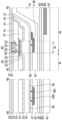
도 3은 도 1의 IIIa-IIIa' 및 도 2b의 IIIb-IIIb'에 따른 단면도이다.
도 4는 본 발명의 다른 실시예에 따른 표시 장치의 평면도이다.
도 5는 본 발명의 또 다른 실시예에 따른 표시 장치의 평면도이다.
도 6은 도 5의 VI-VI'에 따른 단면도이다.1 is a plan view of a display device according to an embodiment of the present invention.
FIG. 2A is an enlarged plan view of area A of FIG. 1.
FIG. 2B is an enlarged plan view of area B of FIG. 1.
Figure 3 is a cross-sectional view taken along line IIIa-IIIa' in Figure 1 and IIIb-IIIb' in Figure 2b.
Figure 4 is a plan view of a display device according to another embodiment of the present invention.
Figure 5 is a plan view of a display device according to another embodiment of the present invention.
FIG. 6 is a cross-sectional view taken along line VI-VI' of FIG. 5.
본 발명의 이점 및 특징, 그리고 그것들을 달성하는 방법은 첨부되는 도면과 함께 상세하게 후술되어 있는 실시예들을 참조하면 명확해질 것이다. 그러나 본 발명은 이하에서 개시되는 실시예들에 한정되는 것이 아니라 서로 다른 다양한 형태로 구현될 것이며, 단지 본 실시예들은 본 발명의 개시가 완전하도록 하며, 본 발명이 속하는 기술분야에서 통상의 지식을 가진 자에게 발명의 범주를 완전하게 알려주기 위해 제공되는 것이며, 본 발명은 청구항의 범주에 의해 정의될 뿐이다.The advantages and features of the present invention and methods for achieving them will become clear by referring to the embodiments described in detail below along with the accompanying drawings. However, the present invention is not limited to the embodiments disclosed below and will be implemented in various different forms. The present embodiments only serve to ensure that the disclosure of the present invention is complete and that common knowledge in the technical field to which the present invention pertains is not limited. It is provided to fully inform those who have the scope of the invention, and the present invention is only defined by the scope of the claims.
명세서 전체에 걸쳐 동일 참조 부호는 동일 구성 요소를 지칭한다. 또한, 본 발명을 설명함에 있어서, 관련된 공지 기술에 대한 구체적인 설명이 본 발명의 요지를 불필요하게 흐릴 수 있다고 판단되는 경우 그 상세한 설명은 생략한다. 본 명세서 상에서 언급된 '포함한다', '갖는다', '이루어진다' 등이 사용되는 경우 '~만'이 사용되지 않는 이상 다른 부분이 추가될 수 있다. 구성 요소를 단수로 표현한 경우에 특별히 명시적인 기재 사항이 없는 한 복수를 포함하는 경우를 포함한다.Like reference numerals refer to like elements throughout the specification. Additionally, in describing the present invention, if it is determined that a detailed description of related known technologies may unnecessarily obscure the gist of the present invention, the detailed description will be omitted. When 'includes', 'has', 'consists of', etc. mentioned in the specification are used, other parts may be added unless 'only' is used. In cases where a component is expressed in the singular, the plural is included unless specifically stated otherwise.
구성 요소를 해석함에 있어서, 별도의 명시적 기재가 없더라도 오차 범위를 포함하는 것으로 해석한다.When interpreting a component, it is interpreted to include the margin of error even if there is no separate explicit description.
비록 제1, 제2 등이 다양한 구성요소들을 서술하기 위해서 사용되나, 이들 구성요소들은 이들 용어에 의해 제한되지 않는다. 이들 용어들은 단지 하나의 구성요소를 다른 구성요소와 구별하기 위하여 사용하는 것이다. 따라서, 이하에서 언급되는 제1 구성요소는 본 발명의 기술적 사상 내에서 제2 구성요소일 수도 있다.Although first, second, etc. are used to describe various elements, these elements are not limited by these terms. These terms are merely used to distinguish one component from another. Accordingly, the first component mentioned below may also be the second component within the technical spirit of the present invention.
명세서 전체에 걸쳐 동일 참조 부호는 동일 구성 요소를 지칭한다.Like reference numerals refer to like elements throughout the specification.
본 발명의 여러 실시예들의 각각 특징들이 부분적으로 또는 전체적으로 서로 결합 또는 조합 가능하며, 당업자가 충분히 이해할 수 있듯이 기술적으로 다양한 연동 및 구동이 가능하며, 각 실시예들이 서로에 대하여 독립적으로 실시 가능할 수도 있고 연관 관계로 함께 실시 가능할 수도 있다.Each feature of the various embodiments of the present invention can be partially or fully combined or combined with each other, and as can be fully understood by those skilled in the art, various technical interconnections and operations are possible, and each embodiment may be implemented independently of each other. It may be possible to conduct them together due to a related relationship.
이하, 첨부한 도면들을 참조하여 본 발명의 바람직한 실시예를 보다 상세하게 설명한다.Hereinafter, preferred embodiments of the present invention will be described in more detail with reference to the attached drawings.
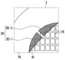
도 1은 본 발명의 일 실시예에 따른 표시 장치의 평면도이다. 도 2a는 도 1의 A영역에 대한 확대 평면도이다. 도 2b는 도 1의 B영역에 대한 확대 평면도이다. 도 3은 도 1의 IIIa-IIIa' 및 도 2b의 IIIb-IIIb'에 따른 단면도이다. 도 2a의 평면도는 복수의 터치 전극들(TE1, TE2)을 생략하여 도시한 것이다.1 is a plan view of a display device according to an embodiment of the present invention. FIG. 2A is an enlarged plan view of area A of FIG. 1. FIG. 2B is an enlarged plan view of area B of FIG. 1. Figure 3 is a cross-sectional view taken along line IIIa-IIIa' in Figure 1 and IIIb-IIIb' in Figure 2b. The top view of FIG. 2A shows the plurality of touch electrodes TE1 and TE2 omitted.
도 1 내지 도 3을 참조하면, 표시 장치(100)는 표시 패널(110), 복수의 터치 전극들(TE1, TE2), 복수의 터치 배선들(TL1, TL2), 복수의 터치 패드(TP)들, 복수의 제1 가림 전극(SE1)들을 포함한다.1 to 3, the
표시 패널(110)은 영상이 표시되는 구성으로서, 표시 영역(AA)과 비표시 영역(NA)을 포함할 수 있다. 표시 영역(AA)은 영상이 표시되는 영역으로서, 라운드 코너를 포함할 수 있다. 예를 들면, 표시 영역(AA)의 4개의 귀퉁이는 각진 형상이 아닌 굴곡진 형상을 이룰 수 있다. 그러나, 이에 제한되지 않으며, 표시 영역(AA)은 4개의 귀퉁이 중 일부만이 라운드 코너이고, 나머지 귀퉁이는 각진 코너일 수도 있다.The
표시 영역(AA)에는 복수의 화소들(PX)이 정의될 수 있다. 복수의 화소들(PX) 각각은 도시되지는 않았으나, 데이터 라인, 주사 라인 및 발광 라인과 연결되어 데이터 신호, 주사 신호 및 발광 신호에 의하여 영상을 출력할 수 있다. 그리고, 도 2a에 도시된 것과 같이, 표시 영역(AA)에 배치되는 복수의 화소들(PX)은 라운드 코너와 인접하여 계단 형태로 배치될 수 있다. 표시 영역(AA)의 라운드 코너에 최대한 많은 수의 화소들(PX)이 배치되기 위하여, 라운드 코너와 인접하는 복수의 화소들(PX)은 계단 형태로 배치될 수 있다.A plurality of pixels PX may be defined in the display area AA. Although not shown, each of the plurality of pixels (PX) is connected to a data line, a scan line, and a light emitting line and can output an image using a data signal, a scan signal, and a light emitting signal. And, as shown in FIG. 2A, the plurality of pixels PX arranged in the display area AA may be arranged in a staircase shape adjacent to the round corner. In order to arrange as many pixels (PX) as possible in the round corner of the display area (AA), a plurality of pixels (PX) adjacent to the round corner may be arranged in a staircase shape.
복수의 화소들(PX) 각각은, 도 3에 도시된 것과 같이, 트랜지스터(120) 및 유기 발광 다이오드(130)를 포함할 수 있다.Each of the plurality of pixels PX may include a
구체적으로, 기판(111)은 표시 장치(100)의 다양한 구성요소들을 지지하는 구성이다. 기판(111)은, 예를 들면, 폴리이미드(polyimide) 등과 같은 플라스틱으로 이루어질 수 있으나, 이에 제한되는 것은 아니다.Specifically, the
기판(111) 상에는 트랜지스터(120)가 배치된다. 구체적으로, 기판(111) 상에는 트랜지스터(120)의 액티브층(121)이 배치된다. 액티브층(121)은 실리콘, 산화물 반도체, 유기 반도체 등으로 이루어질 수 있으나, 이에 제한되는 것은 아니다. 액티브층(121)은 채널이 형성되는 채널 영역, 소스 전극(123)과 연결되는 소스 영역 및 드레인 전극(124)과 연결되는 드레인 영역을 포함한다.A
액티브층(121) 상에는 게이트 절연층(112)이 형성된다. 게이트 절연층(112)은 실리콘옥사이드, 실리콘나이트라이드 및/또는 실리콘옥시나이트라이드 등의 무기 물질로 이루어질 수 있으며, 액티브층(121)과 게이트 전극(122)을 절연시킬 수 있다.A
게이트 절연층(112) 상에는 게이트 전극(122)이 배치된다. 게이트 전극(122)은 몰리브덴(Mo), 알루미늄(Al), 구리(Cu) 및/또는 티타늄(Ti) 등을 포함하는 도전 물질로 이루어진 단일막 또는 다층막일 수 있다.A
게이트 전극(122) 상에는 층간 절연층(113)이 형성된다. 층간 절연층(113)은 질화 실리콘(SiNx) 또는 산화 실리콘(SiOx) 등과 같은 무기물로 이루어지고, 단일층이거나 이들의 복수의 층으로 이루어질 수 있으나, 이에 제한되는 것은 아니다.An interlayer insulating
층간 절연층(113) 상에는 트랜지스터(120)의 소스 전극(123) 및 드레인 전극(124)이 형성된다. 소스 전극(123) 및 드레인 전극(124)은 게이트 절연층(112) 및 층간 절연층(113)에 형성된 컨택홀을 통하여 액티브층(121)과 전기적으로 연결된다. 소스 전극(123) 및 드레인 전극(124)은 도전성 물질로 이루어질 수 있으며, 동일한 공정을 통하여 동일한 물질로 이루어질 수 있으나, 이에 제한되는 것은 아니다.The
소스 전극(123) 및 드레인 전극(124) 상에는 평탄화층(114)이 배치된다. 평탄화층(114)은 트랜지스터(120)의 상부를 평탄화하기 위한 층으로서, 도 3에 도시된 것과 같이 단층일 수 있으나, 이와 달리 복층으로 이루어질 수도 있다. 평탄화층(114)은 아크릴(acryl)계 유기 물질로 이루어질 수 있으나, 이에 제한되지 않는다.A
평탄화층(114) 상에는 유기 발광 다이오드(130)가 배치된다. 유기 발광 다이오드(130)는 트랜지스터(120)의 드레인 전극(124)과 전기적으로 연결된 애노드(131), 애노드(131) 상에 배치된 유기층(132) 및 유기층(132) 상에 형성된 캐소드(133)를 포함한다. 표시 장치(100)가 탑 에미션 방식의 유기 발광 표시 장치(100)일 경우, 애노드(131)는 방출된 광을 캐소드(133) 측으로 반사시키기 위한 반사층 및 유기층(132)에 정공을 공급하기 위한 투명 도전층을 더 포함할 수 있다. 도 3에서는 유기층(132)이 녹색, 청색 또는 적색 등의 특정 색의 광을 발광하기 위하여 화소(PX) 별로 패터닝된 것으로 도시되었으나, 이에 제한되지 않고 유기층(132)은 표시 영역(AA) 전체에 걸쳐 형성될 수도 있다.An organic
애노드(131) 및 평탄화층(114) 상에는 화소 정의막(115)이 배치된다. 화소 정의막(115)은 표시 영역(AA)에서 서로 인접하는 화소(PX)를 구분하기 위한 구조물로서, 복수의 화소(PX)를 정의할 수 있다. 화소 정의막(115)은 유기 물질로 이루어질 수 있다. 또한, 화소 정의막(115)은 애노드(131)의 적어도 일부를 노출시킬 수 있다. 예를 들면, 화소 정의막(115)은 애노드(131)의 에지를 커버하고, 나머지 영역을 노출시킬 수 있다.A
유기 발광 다이오드(130) 상에는 봉지층(116)이 배치된다. 봉지층(116)은 유기 발광 다이오드(130)를 덮어 이를 보호할 수 있다. 봉지층(116)은 표시 영역(AA) 전체를 덮으며 표시 영역(AA)의 외곽까지 연장될 수 있다. 봉지층(116)은 도시된 것과 같이 하나의 층으로 이루어질 수 있으나, 이에 제한되지 않으며, 예를 들면 봉지층(116)은 무기 봉지층, 유기 봉지층 및 무기 봉지층이 차례로 적층된 다중층 구조를 가질 수도 있다.An
봉지층(116) 상에는 복수의 터치 전극들(TE1, TE2)이 배치된다. 복수의 터치 전극들(TE1, TE2)은 복수의 제1 터치 전극(TE1)들 및 복수의 제2 터치 전극(TE2)들을 포함한다.A plurality of touch electrodes TE1 and TE2 are disposed on the
복수의 제1 터치 전극(TE1)들은 제1 방향으로 배열된 터치 전극들이다. 복수의 제1 터치 전극(TE1)들은 제1 연결 전극(CNP1)들을 통하여 제1 방향으로 연결된다. 도시되지는 않았으나, 복수의 제1 터치 전극(TE1)들은 봉지층(116) 상에 형성될 수 있고, 투명한 도전층으로 이루어질 수 있다. 예를 들면, 복수의 제1 터치 전극(TE1)들은 TCO(Transparent Conductive Oxide)로 이루어질 수 있으며, 예를 들면 ITO(Indium tin oxide)로 이루어질 수 있다. 이에, 복수의 화소(PX) 상에 배치될지라도 복수의 화소(PX)가 방출하는 빛은 표시 장치(100)의 외부에서 시인될 수 있다. 그러나, 이와 달리, 복수의 터치 전극들(TE1, TE2)은 메쉬 패턴으로 이루어질 수 있다. 메쉬 패턴은 금속 배선들이 교차된 형상일 수 있으며, 금속 배선들은 구리(Cu), 알루미늄(Ti), 몰리브덴(Mo), 티타늄(Ti), 은(Ag), 금(Au), 니켈(Ni), 크롬(Cr) 등의 저저항 금속 물질로 이루어질 수 있다.The plurality of first touch electrodes TE1 are touch electrodes arranged in a first direction. The plurality of first touch electrodes TE1 are connected in a first direction through first connection electrodes CNP1. Although not shown, a plurality of first touch electrodes TE1 may be formed on the
도 2b에 도시된 것과 같이, 서로 인접하는 제1 터치 전극(TE1)들 사이에는 제1 연결 전극(CNP1)들이 배치되고, 제1 연결 전극(CNP1)들은 제1 터치 전극(TE1)들을 연결할 수 있다. 제1 연결 전극(CNP1)들은 복수의 제1 터치 전극(TE1)들 상에 배치되는 터치 절연층(117) 상에 배치되고, 터치 절연층(117)에 형성된 컨택홀을 통하여 복수의 제1 터치 전극(TE1)을 사이에서 서로 연결시킬 수 있다.As shown in FIG. 2B, first connection electrodes CNP1 are disposed between adjacent first touch electrodes TE1, and the first connection electrodes CNP1 can connect the first touch electrodes TE1. there is. The first connection electrodes CNP1 are disposed on the
복수의 제2 터치 전극(TE2)들은 제1 방향과 수직인 제2 방향으로 배열된 터치 전극들이다. 복수의 제2 터치 전극(TE2)들과 복수의 제1 터치 전극(TE1)들은 제1 방향 및 제2 방향을 따라 격자 모양으로 교대로 배치된다. 복수의 제2 터치 전극(TE2)들은 복수의 제1 터치 전극(TE1)들과 동일한 물질로 이루어질 수 있다. 예를 들면, 복수의 제2 터치 전극(TE2)들은 전극들은 TCO(Transparent Conductive Oxide)로 이루어질 수 있으며, 예를 들면, ITO(Indium tin oxide)로 이루어질 수 있다. 이와 달리, 복수의 제2 터치 전극(TE2)들은 금속 배선들이 교차된 형상인 메쉬 패턴일 수 있다.The plurality of second touch electrodes TE2 are touch electrodes arranged in a second direction perpendicular to the first direction. The plurality of second touch electrodes TE2 and the plurality of first touch electrodes TE1 are alternately arranged in a grid shape along the first and second directions. The plurality of second touch electrodes TE2 may be made of the same material as the plurality of first touch electrodes TE1. For example, the plurality of second touch electrodes TE2 may be made of transparent conductive oxide (TCO), for example, indium tin oxide (ITO). In contrast, the plurality of second touch electrodes TE2 may have a mesh pattern in which metal wires are crossed.
서로 인접하는 제2 터치 전극(TE2)들 사이에는 제2 연결 전극(CNP2)들이 배치되고, 제2 연결 전극(CNP2)들은 제2 터치 전극(TE2)들을 연결할 수 있다. 제2 연결 전극(CNP2)들은 복수의 제2 터치 전극(TE2)과 동일한 층 상에서 복수의 제2 터치 전극(TE2)들과 동일한 물질로 동시에 형성될 수 있다. 이에, 제2 터치 전극(TE2)들과 제2 연결 전극(CNP2)들은 모두 봉지층(116) 상에 배치될 수 있다.Second connection electrodes CNP2 are disposed between adjacent second touch electrodes TE2, and the second connection electrodes CNP2 may connect the second touch electrodes TE2. The second connection electrodes CNP2 may be formed simultaneously on the same layer as the plurality of second touch electrodes TE2 and of the same material as the plurality of second touch electrodes TE2. Accordingly, both the second touch electrodes TE2 and the second connection electrodes CNP2 may be disposed on the
제2 연결 전극(CNP2)들은 제1 연결 전극(CNP1)들과 절연층을 사이에 두고 교차하여 중첩될 수 있다. 구체적으로, 앞서 설명한 것과 같이, 봉지층(116) 상에 배치되는 터치 전극들 상에는 터치 절연층(117)이 배치된다. 이에, 봉지층(116) 상에 배치되는 제2 연결 전극(CNP2)들과 터치 절연층(117) 상에 배치되는 제1 연결 전극(CNP1)들은 제1 방향과 제2 방향으로 서로 교차하여 중첩될 수 있고, 터치 절연층(117)에 의하여 서로 절연될 수 있다. 제2 연결 전극(CNP2)들은 금속 물질로 이루어질 수 있다.The second connection electrodes (CNP2) may overlap and cross the first connection electrodes (CNP1) with an insulating layer interposed therebetween. Specifically, as described above, the
제2 터치 전극(TE2)들의 연결 전극들은 제1 터치 전극(TE1)들의 연결 전극들 하부에 배치된 것에 제한되지 않으며, 제1 터치 전극(TE1)들은 제1 터치 전극(TE1)들과 동일한 층 상에 배치된 제1 연결 전극(CNP1)들에 의하여 서로 연결될 수 있다. 이 경우, 제2 터치 전극(TE2)들은 터치 절연층(117) 상에 형성된 제2 연결 전극(CNP2)들에 의하여 서로 연결될 수 있다.The connection electrodes of the second touch electrodes TE2 are not limited to being disposed below the connection electrodes of the first touch electrodes TE1, and the first touch electrodes TE1 are located on the same layer as the first touch electrodes TE1. They may be connected to each other by first connection electrodes CNP1 disposed on the surface. In this case, the second touch electrodes TE2 may be connected to each other by second connection electrodes CNP2 formed on the
복수의 터치 전극들(TE1, TE2)은 표시 영역(AA) 전체에 대응되도록 형성될 수 있다. 이때, 표시 영역(AA)의 라운드 코너와 인접한 터치 전극들(TE1, TE2)은 라운드 코너에 대응되도록 형성될 수 있다. 예를 들면, 도 1에 도시된 것과 같이, 라운드 코너와 인접하여 배치되는 제1 터치 전극(TE1)과 제2 터치 전극(TE2)은 라운드진 형상을 가질 수 있다.The plurality of touch electrodes TE1 and TE2 may be formed to correspond to the entire display area AA. At this time, the touch electrodes TE1 and TE2 adjacent to the round corner of the display area AA may be formed to correspond to the round corner. For example, as shown in FIG. 1, the first touch electrode TE1 and the second touch electrode TE2 disposed adjacent to the round corner may have a rounded shape.
복수의 제1 가림 전극(SE1)들은 표시 영역(AA)의 라운드 코너와 인접하여 표시 영역(AA)의 외곽을 따라 비표시 영역(NA)에 배치된 전극들이다. 구체적으로, 제1 가림 전극(SE1)들은 표시 영역(AA)의 라운드 코너를 따라 곡선의 형태로 형성될 수 있다. 앞서 설명한 것과 같이, 표시 영역(AA)의 라운드 코너에는 계단 형태로 화소들(PX)이 배치될 수 있고, 제1 가림 전극(SE1)은 화소들(PX)의 계단 형태와 중첩되어 배치될 수 있다. 이에, 계단 형태의 화소들(PX)이 표시 장치(100)의 외부에서 시인되는 것이 방지될 수 있다.The plurality of first shielding electrodes SE1 are electrodes disposed in the non-display area NA adjacent to the round corner of the display area AA and along the outer edge of the display area AA. Specifically, the first shielding electrodes SE1 may be formed in a curved shape along the round corners of the display area AA. As described above, pixels PX may be arranged in a staircase shape at the round corners of the display area AA, and the first shielding electrode SE1 may be arranged to overlap the staircase shape of the pixels PX. there is. Accordingly, the stair-shaped pixels PX can be prevented from being visible from the outside of the
제1 가림 전극(SE1)들은 복수의 터치 전극들(TE1, TE2)과 전기적으로 연결될 수 있다. 구체적으로, 제1 가림 전극(SE1)은 라운드 코너에 인접하여 배치되는 터치 전극(TE1, TE2)과 전기적으로 연결될 수 있다. 도 1에 도시된 것과 같이, 표시 영역(AA)의 라운드 코너에 배치된 제1 가림 전극(SE1)은 제1 터치 전극(TE1)과 연결되는 제1-1 가림 전극(SE1-1)과 제2 터치 전극(TE2)과 연결되는 제1-2 가림 전극(SE1-2)을 포함할 수 있다. 예를 들면, 도 3에 도시된 것과 같이, 터치 절연층(117) 상에는 제1-2 가림 전극(SE1-2)이 배치될 수 있다. 제1-2 가림 전극(SE1-2)은 터치 절연층(117) 하부에 배치된 제2 터치 전극(TE2)과 중첩될 수 있고, 터치 절연층(117)에 형성된 컨택홀을 통하여 제2 터치 전극(TE2)과 전기적으로 연결될 수 있다. 이에, 제1-2 가림 전극(SE1-2)은 라운드 코너와 인접하여 외곽에 배치된 화소(PX)와 중첩되어 계단 형태의 화소들(PX)이 외부에서 시인되는 것이 방지될 수 있다. 이처럼 제1 가림 전극(SE1)들이 중첩되는 터치 전극들 각각과 전기적으로 연결됨으로써, 제1 가림 전극(SE1)들은 계단 형태의 화소들(PX)이 시인되는 것을 방지하는 것에 더불어, 터치 전극의 역할을 수행할 수 있다.The first shielding electrodes SE1 may be electrically connected to a plurality of touch electrodes TE1 and TE2. Specifically, the first shielding electrode SE1 may be electrically connected to the touch electrodes TE1 and TE2 disposed adjacent to the round corner. As shown in FIG. 1, the first shielding electrode SE1 disposed at the round corner of the display area AA is connected to the first touch electrode TE1 and the 1-1 shielding electrode SE1-1. 2 It may include a first-second shielding electrode (SE1-2) connected to the touch electrode (TE2). For example, as shown in FIG. 3, the 1-2 shielding electrode SE1-2 may be disposed on the
제1 가림 전극(SE1)들 및 터치 절연층(117) 상에는 커버층(118)이 배치될 수 있다. 커버층(118)은 제1 가림 전극(SE1)들 및 터치 전극들(TE1, TE2) 상에서 하부에 배치된 구성 요소들을 보호하는 층이다.A
커버층(118) 상에는 제1 접착층(141)이 배치될 수 있다. 제1 접착층(141)은 제1 접착층(141)의 상부 및 하부에 배치된 구성 요소들을 부착시키는 층일 수 있다. 제1 접착층(141)은 접착 물질로 이루어질 수 있고, 예를 들면, 광학 투명 점착제(optical clear adhesive, OCA)로 이루어질 수 있다. 그러나, 이에 제한되는 것은 아니다.A first
제1 접착층(141) 상에는 편광층(150)이 배치될 수 있다. 편광층(150)은 복수의 화소들(PX)로부터 방출된 광을 편광시킬 수 있다.A
편광층 상에는 제2 접착층(142)이 배치될 수 있다. 제2 접착층(142)은 편광층(150)과 윈도우 부재(170)를 부착시키는 층일 수 있다. 제2 접착층(142)은 제1 접착층(141)과 동일한 접착 물질로 이루어질 수 있으며, 예를 들면, 광학 투명 점착제(optical clear adhesive, OCA)로 이루어질 수 있다. 그러나, 이에 제한되는 것은 아니다.A second
제2 접착층(142) 상에는 차광층(160)이 배치된다. 차광층(160)은 비표시 영역(NA)의 적어도 일부에 대응될 수 있으며, 표시 장치(100)의 비표시 영역(NA)에 배치된 여러 구성 요소들이 외부에서 시인되는 것을 방지할 수 있다. 차광층(160)은 차광 물질을 포함할 수 있다.A
윈도우 부재(170)는 제2 접착층(142) 및 차광층(160) 상에 배치된다. 윈도우 부재(170)는 표시 영역(AA) 및 비표시 영역(NA) 전체에 대응되도록 형성되어 표시 장치(100)의 상면을 보호할 수 있다. 표시 장치(100)의 사용자는 윈도우 부재(170)의 상면에 터치 입력을 가할 수 있고, 표시 장치(100)는 이를 인식할 수 있다. 윈도우 부재(170)는 차광층(160)과 중첩되지 않는 제2 접착층(142)의 상면, 차광층(160)의 상면, 차광층(160)의 측면 중 일부와 접할 수 있다.The
비표시 영역(NA)은 표시 영역(AA)을 둘러싸는 영역이다. 비표시 영역(NA)은 표시 영역(AA)과 마찬가지로 라운드 코너를 포함할 수 있다. 그러나, 이에 제한되지 않으며, 비표시 영역(NA)의 코너는 라운드 코너가 아닌 직각 형태의 코너일 수도 있다.The non-display area (NA) is an area surrounding the display area (AA). The non-display area (NA) may include round corners like the display area (AA). However, the present invention is not limited thereto, and the corners of the non-display area (NA) may be right-angled corners rather than round corners.
비표시 영역(NA)에는 복수의 터치 배선들(TL1, TL2) 및 복수의 터치 패드(TP)들이 배치된다. 복수의 터치 배선들(TL1, TL2)은 복수의 터치 전극들(TE1, TE2) 각각과 연결되는 배선들이다. 구체적으로, 복수의 터치 배선(TL1, TL2)은 복수의 제1 터치 전극(TE1)들 각각과 연결된 복수의 제1 터치 배선(TL1)들, 및 복수의 제2 터치 배선(TL2)들 각각과 연결된 복수의 제2 터치 배선(TL2)들을 포함할 수 있다. 제1 터치 배선(TL1)들 및 제2 터치 배선(TL2)들은 표시 영역(AA)의 가장자리를 따라 연장되어 복수의 터치 패드(TP)들과 연결될 수 있다. 그리고, 복수의 터치 배선들(TL1, TL2)은 제1 가림 전극(SE1)과 동일한 물질로 이루어질 수 있다. 즉, 터치 배선들(TL1, TL2)과 제1 가림 전극(SE1)들은 터치 절연층(117) 상에서 동일한 물질로 동일한 공정을 통하여 형성될 수 있다.A plurality of touch wires TL1 and TL2 and a plurality of touch pads TP are disposed in the non-display area NA. The plurality of touch wires TL1 and TL2 are wires connected to each of the plurality of touch electrodes TE1 and TE2. Specifically, the plurality of touch wires TL1 and TL2 are each connected to a plurality of first touch electrodes TE1 and a plurality of second touch wires TL2. It may include a plurality of connected second touch wires TL2. The first touch wires TL1 and the second touch wires TL2 may extend along the edge of the display area AA and be connected to a plurality of touch pads TP. Additionally, the plurality of touch wires TL1 and TL2 may be made of the same material as the first shielding electrode SE1. That is, the touch wires TL1 and TL2 and the first shielding electrode SE1 may be formed on the
본 발명의 일 실시예에 따른 표시 장치(100)는 라운드 코너를 따라 배치되는 제1 가림 전극(SE1)들을 포함한다. 라운드 코너와 인접한 화소들(PX)은 계단 형태로 배치될 수 있고, 제1 가림 전극(SE1)은 계단 형태의 화소들(PX)과 중첩되어 계단 형태가 외부에 시인되는 것이 방지될 수 있다.The
그리고, 본 발명의 일 실시예에 따른 표시 장치(100)의 경우, 제1 가림 전극(SE1)이 인접하는 터치 전극(TE1, TE2)과 전기적으로 연결될 수 있다. 제1 가림 전극(SE1)이 터치 전극(TE1, TE2)과 연결되지 못하고 플로팅될 경우, 제1 가림 전극(SE1) 주위에 배치된 다양한 도전체들에 의하여 제1 가림 전극(SE1)에는 차지(Charge)가 축적될 수 있고, 축적된 차지는 방전되지 못할 수 있다. 이러한 경우, 제1 가림 전극(SE1) 주위에 배치된 터치 전극(TE1, TE2)의 터치 감도가 저하될 수 있다. 그러나, 본 발명의 일 실시예에 따른 표시 장치(100)의 제1 가림 전극(SE1)은 중첩되는 터치 전극(TE1, TE2)과 전기적으로 연결될 수 있고, 플로팅되지 않을 수 있다. 따라서, 터치 전극들(TE1, TE2)에 의한 터치 감도는 보다 향상될 수 있다. 또한, 제1 가림 전극(SE1)이 터치 전극(TE1, TE2)과 전기적으로 연결됨으로써 제1 가림 전극(SE1)은 연결된 터치 전극(TE1, TE2)과 동일한 역할을 수행할 수 있다. 따라서, 터치를 감지할 수 있는 영역의 넓이가 보다 넓어질 수 있다.And, in the case of the
한편, 본 발명의 다양한 실시예에 따르면, 제1 가림 전극(SE1)은 표시 영역(AA)의 외곽 방향으로 최대한 확장될 수 있다. 구체적으로, 제1 가림 전극(SE1)은 표시 영역(AA)의 라운드 코너로부터 비표시 영역(NA)으로 최대한 확장되어 형성될 수 있다. 예를 들면, 제1 가림 전극(SE1)은 표시 영역(AA)의 라운드 코너에서 제1 가림 전극(SE1)과 바로 인접하여 배치되는 터치 배선(TL1, TL2)과 최대한 인접하도록 배치될 수 있고, 이에, 제1 가림 전극(SE1)은 면적이 최대가 될 수 있다. 앞서 설명한 것과 같이 제1 가림 전극(SE1)은 터치 전극(TE1, TE2)과 전기적으로 연결됨으로써 터치 전극으로서 기능할 수 있다. 따라서, 제1 가림 전극(SE1)의 면적이 보다 넓어질 경우, 터치 인식 가능 면적이 보다 넓어질 수 있다.Meanwhile, according to various embodiments of the present invention, the first shielding electrode SE1 may be expanded as much as possible toward the outer edge of the display area AA. Specifically, the first shielding electrode SE1 may be formed to extend as much as possible from the round corner of the display area AA to the non-display area NA. For example, the first shielding electrode SE1 may be arranged to be as close as possible to the touch wires TL1 and TL2 disposed immediately adjacent to the first shielding electrode SE1 at the round corner of the display area AA. Accordingly, the area of the first shielding electrode SE1 may be maximized. As described above, the first shielding electrode SE1 may function as a touch electrode by being electrically connected to the touch electrodes TE1 and TE2. Accordingly, when the area of the first shielding electrode SE1 becomes wider, the touch recognition area can become wider.
제1 가림 전극(SE1)의 면적이 최대한 확장되고, 제1 가림 전극(SE1)과 바로 인접하여 터치 배선(TL1, TL2)이 배치될 경우, 제1 가림 전극(SE1)과 바로 인접하는 터치 배선(TL1, TL2) 사이의 간격은 5μm 이상일 수 있다. 제1 가림 전극(SE1)과 바로 인접하는 터치 배선(TL1, TL2) 사이의 간격이 5μm보다 작을 경우, 터치 전극(TE1, TE2)과 전기적으로 연결되어 터치 전극(TE1, TE2)과 동일한 기능을 수행하는 제1 가림 전극(SE1)과 터치 배선(TL1, TL2)의 전기적 신호가 서로 중첩될 수 있다. 따라서, 코너부 가림 전극의 면적이 이와 같이 최대한 확장된 경우, 제1 가림 전극(SE1)과 터치 배선(TL1, TL2) 사이의 거리는 5μm 이상으로 설정될 수 있고, 터치 전극(TE1, TE2)과 터치 배선(TL1, TL2) 사이의 신호의 중첩이 방지될 수 있다.When the area of the first shielding electrode SE1 is expanded as much as possible and the touch wires TL1 and TL2 are disposed immediately adjacent to the first shielding electrode SE1, the touch wires immediately adjacent to the first shielding electrode SE1 The gap between (TL1, TL2) may be 5 μm or more. When the gap between the first shielding electrode (SE1) and the immediately adjacent touch wires (TL1, TL2) is less than 5 μm, it is electrically connected to the touch electrodes (TE1, TE2) and has the same function as the touch electrodes (TE1, TE2). Electrical signals of the first shielding electrode SE1 and the touch wires TL1 and TL2 may overlap each other. Therefore, when the area of the corner shielding electrode is expanded as much as possible, the distance between the first shielding electrode SE1 and the touch wires TL1 and TL2 may be set to 5 μm or more, and the distance between the touch electrodes TE1 and TE2 may be set to 5 μm or more. Overlapping of signals between the touch wires TL1 and TL2 can be prevented.
도 4는 본 발명의 다른 실시예에 따른 표시 장치의 평면도이다. 도 4의 표시 장치(200)는 도 1 내지 도 3의 표시 장치(100)와 비교하여 복수의 제2 가림 전극(SE2)들을 더 포함한다는 것을 제외하면 실질적으로 동일한 바, 중복 설명은 생략한다.Figure 4 is a plan view of a display device according to another embodiment of the present invention. The
도 4를 참조하면, 복수의 제2 가림 전극(SE2)들은 표시 영역(AA)의 모서리를 따라 배치된 전극들이다. 구체적으로, 제2 가림 전극(SE2)들은 표시 영역(AA)의 라운드 코너를 제외한 4개의 모서리에 대응되도록 모서리를 따라 연장되어 배치될 수 있다.Referring to FIG. 4 , the plurality of second shielding electrodes SE2 are electrodes arranged along the edges of the display area AA. Specifically, the second shielding electrodes SE2 may be arranged to extend along the edges of the display area AA to correspond to four corners excluding the round corners.
복수의 제2 가림 전극(SE2)들은 제1 터치 전극(TE1)들과 연결된 제2-1 가림 전극(SE2-1)들과 제2 터치 전극(TE2)들과 연결된 제2-2 가림 전극(SE2-2)들을 포함할 수 있다.The plurality of second shielding electrodes (SE2) include 2-1 shielding electrodes (SE2-1) connected to the first touch electrodes (TE1) and 2-2 shielding electrodes (SE2-1) connected to the second touch electrodes (TE2). SE2-2) may be included.
표시 영역(AA)의 모서리 중 제1 터치 전극(TE1)들과 인접한 모서리에는 제2-1 가림 전극(SE2-1)들이 배치될 수 있다. 제2-1 가림 전극(SE2-1)들은 인접하는 제1 터치 전극(TE1)들에 대응되도록 패터닝될 수 있다. 제2-1 가림 전극(SE2-1)들은 제1 가림 전극(SE1)들과 동일한 층 상에, 즉, 터치 절연층(117) 상에 형성될 수 있고, 터치 절연층(117)에 형성된 컨택홀을 통하여 제1 터치 전극(TE1)과 전기적으로 연결될 수 있다. 제2-1 가림 전극(SE2-1)들은 제1 가림 전극(SE1)들과 동일한 물질로 이루어질 수 있고, 동일한 공정을 통하여 형성될 수 있다. 그러나, 이에 제한되는 것은 아니다.2-1 shielding electrodes SE2-1 may be disposed at corners of the display area AA adjacent to the first touch electrodes TE1. The 2-1st shielding electrodes SE2-1 may be patterned to correspond to the adjacent first touch electrodes TE1. The 2-1st shielding electrodes SE2-1 may be formed on the same layer as the first shielding electrodes SE1, that is, on the
표시 영역(AA)의 모서리 중 제2 터치 전극(TE2)들과 인접한 모서리에는 제2-2 가림 전극(SE2-2)들이 배치될 수 있다. 제2-2 가림 전극(SE2-2)들은 인접하는 제2 터치 전극(TE2)들에 대응되도록 패터닝될 수 있다. 제2-2 가림 전극(SE2-2)들은 제1 가림 전극(SE1)들과 동일한 층 상에, 즉, 터치 절연층(117) 상에 형성될 수 있고, 터치 절연층(117)에 형성된 컨택홀을 통하여 제2 터치 전극(TE2)과 전기적으로 연결될 수 있다. 제2-2 가림 전극(SE2-2)들은 제1 가림 전극(SE1)들과 동일한 물질로 이루어질 수 있고, 동일한 공정을 통하여 형성될 수 있다. 그러나, 이에 제한되는 것은 아니다.2-2 shielding electrodes SE2-2 may be disposed at corners of the display area AA adjacent to the second touch electrodes TE2. The 2-2 shielding electrodes SE2-2 may be patterned to correspond to the adjacent second touch electrodes TE2. The 2-2 shielding electrodes SE2-2 may be formed on the same layer as the first shielding electrodes SE1, that is, on the
본 발명의 다른 실시예에 따른 표시 장치(200)의 경우, 복수의 제2 가림 전극(SE2)이 표시 영역(AA)의 모서리를 따라 연장되어 배치된다. 제2 가림 전극(SE2)들은 인접하는 터치 전극들(TE1, TE2)에 대응되도록 패터닝될 수 있고, 인접하는 터치 전극(TE1, TE2)과 전기적으로 연결될 수 있다. 따라서, 제2 가림 전극(SE2)들은 플로팅되지 않고, 전기적으로 연결된 터치 전극(TE1, TE2)에 인가되는 전압이 인가될 수 있다. 따라서, 터치 전극(TE1, TE2)의 감도는 보다 향상될 수 있다. 그리고, 터치 전극(TE1, TE2)의 면적은 제2 가림 전극(SE2)들의 면적에 대응되는 만큼 증가될 수 있다.In the
도 5는 본 발명의 또 다른 실시예에 따른 표시 장치의 평면도이다. 도 6은 도 5의 VI-VI'에 따른 단면도이다. 도 5 및 도 6의 표시 장치(300)는 도 1 내지 도 3의 표시 장치(100)와 비교하여 제1 가림 전극(SE1) 및 터치 배선(TL1, TL2)의 배치가 상이하다는 것을 제외하면 실질적으로 동일한 바, 중복 설명은 생략한다.Figure 5 is a plan view of a display device according to another embodiment of the present invention. FIG. 6 is a cross-sectional view taken along line VI-VI' of FIG. 5. The
도 5 및 도 6을 참조하면, 표시 영역(AA)은 제1 내지 제4 코너(C1 내지 C4)를 포함한다. 표시 영역(AA)의 제1 코너(C1)에는 제1 가림 전극(SE1)이 배치된다. 제1 코너(C1)에 배치된 제1 가림 전극(SE1)은 도 1 내지 도 3의 제1 가림 전극(SE1)과 실질적으로 동일한 바, 중복 설명은 생략한다.Referring to FIGS. 5 and 6 , the display area AA includes first to fourth corners C1 to C4. A first shielding electrode SE1 is disposed at the first corner C1 of the display area AA. The first shielding electrode SE1 disposed at the first corner C1 is substantially the same as the first shielding electrode SE1 of FIGS. 1 to 3, and therefore duplicate description will be omitted.
표시 영역(AA)의 제2 코너(C2) 및 제3 코너(C3)에는 복수의 제2 터치 배선(TL2)들이 배치된다. 복수의 제2 터치 배선(TL2)들은 복수의 제2 터치 전극(TE2)들 각각과 연결되고, 제2 코너(C2)와 인접하여 계단 형상으로 배치된 복수의 화소들(PX) 상으로 연장된다. 이에, 제2 코너(C2)를 따라 배치된 제2 터치 배선(TL2)들은 라운드 코너인 제2 코너(C2)와 인접하여 계단 형태로 배치된 화소들(PX)과 중첩될 수 있다. 도 6에 도시된 것과 같이, 제2 터치 배선(TL2)들은 터치 절연층(117) 상에 배치될 수 있고, 제2 터치 배선(TL2)들은 제2 코너(C2)와 인접한 외곽에 배치된 화소(PX)와 중첩될 수 있다. 이에, 제2 코너(C2)와 인접하여 배치된 계단 형태의 화소들(PX)은 복수의 제2 터치 배선(TL2)들에 의하여 외부에서 시인되지 않을 수 있다.A plurality of second touch wires TL2 are disposed at the second corner C2 and the third corner C3 of the display area AA. The plurality of second touch wires TL2 are connected to each of the plurality of second touch electrodes TE2 and extend onto the plurality of pixels PX arranged in a step shape adjacent to the second corner C2. . Accordingly, the second touch wires TL2 arranged along the second corner C2 may overlap with the pixels PX arranged in a staircase shape adjacent to the second corner C2, which is a round corner. As shown in FIG. 6, the second touch wires TL2 may be disposed on the
그리고, 인접한 제2 터치 배선(TL2)들 사이의 간격은 하부에 배치된 화소(PX)에서 방출되는 광이 외부에 시인되지 않을 수 있는 간격으로 설정될 수 있다. 예를 들면, 제2 터치 배선(TL2)들 사이의 이격 거리는 5μm 이하일 수 있다. 제2 터치 배선(TL2)들의 이격 거리가 5μm보다 클 경우 제2 터치 배선(TL2)들 사이 공간을 통하여 하부에 배치된 화소(PX)에서 방출되는 광이 표시 장치(300)의 사용자에 의하여 시인될 수 있다. 따라서, 제2 터치 배선(TL2)들은 이격 거리가 5μm 이하로 배치됨으로써 하부에 배치된 계단 형태의 화소들(PX)이 외부에 시인되는 것이 방지될 수 있다.Additionally, the spacing between adjacent second touch wires TL2 may be set to an interval such that light emitted from the pixel PX disposed below may not be visible to the outside. For example, the separation distance between the second touch wires TL2 may be 5 μm or less. When the separation distance between the second touch wires TL2 is greater than 5 μm, the light emitted from the pixel PX disposed below is visible by the user of the
복수의 제2 터치 배선(TL2)들은 제3 코너(C3)와 인접하여 계단 형상으로 배치된 복수의 화소들(PX) 상으로 연장된다. 이에, 제3 코너(C3)를 따라 배치된 제2 터치 배선(TL2)들은 라운드 코너인 제3 코너(C3)와 인접하여 계단 형태로 배치된 화소들(PX)과 중첩될 수 있다. 이에, 제3 코너(C3)와 인접하여 배치된 계단 형태의 화소들(PX)은 복수의 제2 터치 배선(TL2)들에 의하여 외부에서 시인되지 않을 수 있다.The plurality of second touch wires TL2 extend onto the plurality of pixels PX arranged in a step shape adjacent to the third corner C3. Accordingly, the second touch wires TL2 arranged along the third corner C3 may overlap with the pixels PX arranged in a staircase shape adjacent to the third corner C3, which is a round corner. Accordingly, the step-shaped pixels PX disposed adjacent to the third corner C3 may not be visible from the outside due to the plurality of second touch wires TL2.
그리고, 인접한 제2 터치 배선(TL2)들 사이의 이격 거리는 하부에 배치된 화소(PX)에서 방출되는 광이 외부에 시인되지 않을 수 있는 거리로 설정될 수 있다. 예를 들면, 제2 터치 배선(TL2)들 사이의 이격 거리는 5μm 이하일 수 있다.Additionally, the separation distance between adjacent second touch wires TL2 may be set to a distance where light emitted from the pixel PX disposed below may not be visible to the outside. For example, the separation distance between the second touch wires TL2 may be 5 μm or less.
복수의 제2 터치 배선(TL2)들은 복수의 터치 패드(TP)들과 연결될 수 있다.The plurality of second touch wires TL2 may be connected to the plurality of touch pads TP.
표시 영역(AA)의 제4 코너(C4)에는 복수의 제1 터치 배선(TL1)들이 배치된다. 복수의 제1 터치 배선(TL1)들은 복수의 제1 터치 전극(TE1)들 각각과 연결되고, 제4 코너(C4)와 인접하여 계단 형상으로 배치된 복수의 화소들(PX) 상으로 연장된다. 이에, 제4 코너(C4)를 따라 배치된 제1 터치 배선(TL1)들은 라운드 코너인 제4 코너(C4)와 인접하여 계단 형태로 배치된 화소들(PX)과 중첩될 수 있다. 이에, 제4 코너(C4)와 인접하여 배치된 계단 형태의 화소들(PX)은 복수의 제1 터치 배선(TL1)들에 의하여 외부에서 시인되지 않을 수 있다.A plurality of first touch wires TL1 are disposed at the fourth corner C4 of the display area AA. The plurality of first touch wires TL1 are connected to each of the plurality of first touch electrodes TE1 and extend onto the plurality of pixels PX arranged in a step shape adjacent to the fourth corner C4. . Accordingly, the first touch wires TL1 arranged along the fourth corner C4 may overlap with the pixels PX arranged in a staircase shape adjacent to the fourth corner C4, which is a round corner. Accordingly, the step-shaped pixels PX disposed adjacent to the fourth corner C4 may not be visible from the outside due to the plurality of first touch wires TL1.
그리고, 인접한 제1 터치 배선(TL1)들 사이의 간격은 하부에 배치된 화소(PX)에서 방출되는 광이 외부에 시인되지 않을 수 있는 간격으로 설정될 수 있다. 예를 들면, 제1 터치 배선(TL1)들 사이의 이격 거리는 5μm 이하일 수 있다. 제1 터치 배선(TL1)들은 이격 거리가 5μm 이하로 배치됨으로써 하부에 배치된 계단 형태의 화소들(PX)이 외부에 시인되는 것이 방지될 수 있다.Additionally, the spacing between adjacent first touch wires TL1 may be set to an interval such that light emitted from the pixel PX disposed below may not be visible to the outside. For example, the separation distance between the first touch wires TL1 may be 5 μm or less. By arranging the first touch wires TL1 at a distance of 5 μm or less, the step-shaped pixels PX disposed below can be prevented from being visible to the outside.
본 발명의 또 다른 실시예에 따른 표시 장치(300)의 경우, 표시 영역(AA)의 라운드 코너와 인접하여 계단 형태로 배치된 화소들(PX) 상으로 터치 배선(TL1, TL2)이 배치될 수 있다. 이때, 터치 배선(TL1, TL2) 사이의 이격 거리는 터치 배선(TL1, TL2) 사이의 미세한 틈으로 하부에 배치된 화소들(PX)이 시인되지 않을 수 있는 거리로 설정될 수 있다. 터치 배선(TL1, TL2)이 라운드 코너를 따라 연장되며 계단 형태의 화소들(PX) 상에 배치됨으로써 계단 형태의 화소들(PX)이 외부에서 시인되지 않을 수 있다.In the case of the
이상의 상세한 설명은 본 발명을 예시하고 설명하는 것이다. 또한, 전술한 내용은 본 발명의 바람직한 실시 형태를 나타내고 설명하는 것에 불과하며, 전술한 바와 같이 본 발명은 다양한 다른 조합, 변경 및 환경에서 사용할 수 있으며, 본 명세서에 개시된 발명의 개념의 범위, 저술한 개시 내용과 균등한 범위 및/또는 당업계의 기술 또는 지식의 범위 내에서 변경 또는 수정이 가능하다. 따라서, 이상의 발명의 상세한 설명은 개시된 실시 상태로 본 발명을 제한하려는 의도가 아니다. 또한, 첨부된 청구범위는 다른 실시 상태도 포함하는 것으로 해석되어야 한다.The foregoing detailed description illustrates and explains the invention. In addition, the foregoing merely shows and describes preferred embodiments of the present invention, and as described above, the present invention can be used in various other combinations, modifications, and environments, and the scope and scope of the inventive concept disclosed in this specification. Changes or modifications may be made within the scope of equivalent disclosure and/or skill or knowledge in the art. Accordingly, the above detailed description of the invention is not intended to limit the invention to the disclosed embodiments. Additionally, the appended claims should be construed to include other embodiments as well.
100, 200, 300: 표시 장치
110: 표시 패널
111: 기판
112: 게이트 절연층
113: 층간 절연층
114: 평탄화층
115: 화소 정의막
116: 봉지층
117: 터치 절연층
118: 커버층
120: 트랜지스터
121: 액티브층
122: 게이트 전극
123: 소스 전극
124: 드레인 전극
130: 유기 발광 다이오드
131: 애노드
132: 유기층
133: 캐소드
141: 제1 접착층
142: 제2 접착층
150: 편광층
160: 차광층
170: 윈도우 부재
AA: 표시 영역
NA: 비표시 영역
C1: 제1 코너
C2: 제2 코너
C3: 제2 코너
C4: 제4 코너
CNP1: 제1 연결 전극
CNP2: 제2 연결 전극
TE1: 제1 터치 전극
TE2: 제2 터치 전극
TL1: 제1 터치 배선
TL2: 제2 터치 배선
TP: 터치 패드
SE1: 제1 가림 전극
SE1-1: 제1-1 가림 전극
SE1-2: 제1-2 가림 전극
SE2: 제2 가림 전극
SE2-1: 제2-1 가림 전극
SE2-2: 제2-2 가림 전극
A: A영역
B: B영역
PX: 화소100, 200, 300: display device
110: display panel
111: substrate
112: Gate insulating layer
113: Interlayer insulation layer
114: Flattening layer
115: Pixel definition film
116: Encapsulation layer
117: Touch insulation layer
118: cover layer
120: transistor
121: active layer
122: Gate electrode
123: source electrode
124: drain electrode
130: Organic light emitting diode
131: anode
132: Organic layer
133: cathode
141: first adhesive layer
142: second adhesive layer
150: Polarizing layer
160: light blocking layer
170: No window
AA: display area
NA: Non-display area
C1: 1st corner
C2: 2nd corner
C3: 2nd corner
C4: 4th corner
CNP1: first connection electrode
CNP2: second connection electrode
TE1: first touch electrode
TE2: second touch electrode
TL1: first touch wiring
TL2: second touch wiring
TP: Touchpad
SE1: first shielding electrode
SE1-1: 1-1 shielding electrode
SE1-2: 1-2 shielding electrode
SE2: second shielding electrode
SE2-1: 2-1 shielding electrode
SE2-2: 2-2 shielding electrode
A: Area A
B: B area
PX: pixel
Claims (17)
Translated fromKorean상기 표시 영역과 중첩되며, 제1 방향으로 배치되고 서로 전기적으로 연결되는 복수의 제1 터치 전극들, 및 상기 제1 방향과 수직인 제2 방향으로 배치되고 서로 전기적으로 연결되는 복수의 제2 터치 전극들을 포함하는 복수의 터치 전극들; 및
상기 라운드 코너를 따라 배치되어 상기 복수의 화소 중 상기 라운드 코너와 인접하게 배치된 화소들과 중첩되며, 상기 복수의 터치 전극들 중 일부와 전기적으로 연결되는 제1 가림 전극을 포함하고,
상기 제1 가림 전극은, 상기 라운드 코너와 인접하는 터치 전극들과 절연층을 사이에 두고 중첩되고, 상기 절연층에 형성된 컨택홀을 통하여 상기 라운드 코너와 인접하는 터치 전극들과 전기적으로 연결되는, 표시 장치.a display panel including a display area including round corners and where a plurality of pixels are arranged, and a non-display area surrounding the display area;
A plurality of first touch electrodes overlapping the display area, arranged in a first direction and electrically connected to each other, and a plurality of second touch electrodes arranged in a second direction perpendicular to the first direction and electrically connected to each other. a plurality of touch electrodes including electrodes; and
a first shielding electrode disposed along the round corner, overlapping pixels disposed adjacent to the round corner among the plurality of pixels, and electrically connected to some of the plurality of touch electrodes;
The first shielding electrode overlaps the touch electrodes adjacent to the round corner with an insulating layer interposed therebetween, and is electrically connected to the touch electrodes adjacent to the round corner through a contact hole formed in the insulating layer. display device.
상기 라운드 코너와 인접한 배치된 화소들은 계단 형태로 배치되고,
상기 제1 가림 전극은 상기 계단 형태로 배치된 상기 화소들과 중첩되는, 표시 장치.According to paragraph 1,
Pixels arranged adjacent to the round corner are arranged in a staircase shape,
The first shielding electrode overlaps the pixels arranged in the staircase shape.
상기 제1 가림 전극은,
상기 복수의 제1 터치 전극들 중 상기 라운드 코너와 인접하는 제1 터치 전극과 전기적으로 연결된 제1-1 가림 전극; 및
상기 복수의 제2 터치 전극들 중 상기 라운드 코너와 인접하는 제2 터치 전극과 전기적으로 연결된 제1-2 가림 전극을 포함하는, 표시 장치.According to paragraph 1,
The first shielding electrode is,
a 1-1 shielding electrode electrically connected to a first touch electrode adjacent to the round corner among the plurality of first touch electrodes; and
A display device comprising a first-second shielding electrode electrically connected to a second touch electrode adjacent to the round corner among the plurality of second touch electrodes.
상기 표시 영역의 모서리를 따라 배치되고, 상기 복수의 화소 중 상기 모서리와 인접한 외곽에 배치된 화소들과 중첩되며, 상기 복수의 터치 전극들 중 일부와 전기적으로 연결되는 제2 가림 전극을 더 포함하는, 표시 장치.According to paragraph 1,
Further comprising a second shielding electrode disposed along an edge of the display area, overlapping pixels disposed on the outside of the plurality of pixels adjacent to the edge, and electrically connected to some of the plurality of touch electrodes. , display device.
상기 제2 가림 전극은,
상기 복수의 제1 터치 전극들 중 상기 모서리와 인접한 제1 터치 전극과 전기적으로 연결된 제2-1 가림 전극; 및
상기 복수의 제2 터치 전극들 중 상기 모서리와 인접한 제2 터치 전극과 전기적으로 연결된 제2-2 가림 전극을 포함하는, 표시 장치.According to clause 5,
The second shielding electrode is,
a 2-1 shielding electrode electrically connected to a first touch electrode adjacent to the corner among the plurality of first touch electrodes; and
A display device comprising a 2-2 shielding electrode electrically connected to a second touch electrode adjacent to the corner among the plurality of second touch electrodes.
상기 제2 가림 전극은 상기 모서리와 인접한 터치 전극들과 절연층을 사이에 두고 중첩되며, 상기 절연층에 형성된 컨택홀을 통하여 상기 모서리와 인접한 터치 전극들과 전기적으로 연결되는, 표시 장치.According to clause 5,
The second shielding electrode overlaps the touch electrodes adjacent to the corner with an insulating layer therebetween, and is electrically connected to the touch electrodes adjacent to the corner through a contact hole formed in the insulating layer.
상기 제2 가림 전극은 상기 제1 가림 전극과 동일한 물질로 이루어진, 표시 장치.According to clause 5,
The second shielding electrode is made of the same material as the first shielding electrode.
상기 표시 영역의 외곽을 따라 상기 비표시 영역에 배치되며, 상기 복수의 터치 전극들 각각과 연결된 복수의 터치 배선들을 더 포함하는, 표시 장치.According to paragraph 1,
The display device further includes a plurality of touch wires disposed in the non-display area along an outer edge of the display area and connected to each of the plurality of touch electrodes.
상기 제1 가림 전극은, 상기 복수의 터치 배선들과 상기 표시 영역의 상기 라운드 코너 사이에 배치되는, 표시 장치.According to clause 9,
The first shielding electrode is disposed between the plurality of touch wires and the round corner of the display area.
상기 제1 가림 전극은 상기 복수의 터치 배선들과 동일한 물질로 이루어진, 표시 장치.According to clause 9,
The first shielding electrode is made of the same material as the plurality of touch wires.
상기 복수의 터치 배선들은, 상기 라운드 코너를 따라 상기 표시 영역으로 연장되어 배치되고, 상기 복수의 화소들 중 상기 라운드 코너와 인접한 외곽에 배치된 화소들과 중첩되는, 표시 장치.According to clause 9,
The plurality of touch wires are arranged to extend into the display area along the round corner, and overlap pixels arranged on the outside of the plurality of pixels adjacent to the round corner.
상기 라운드 코너와 인접하여 상기 표시 영역에 배치된 상기 복수의 터치 배선들 사이의 간격은 5μm이하인, 표시 장치.According to clause 12,
A display device wherein an interval between the plurality of touch wires disposed in the display area adjacent to the round corner is 5 μm or less.
상기 복수의 터치 배선들은, 상기 표시 영역의 모서리를 따라 상기 표시 영역으로 연장되어 배치되고, 상기 복수의 화소들 중 상기 모서리와 인접한 외곽에 배치된 화소들과 중첩되는, 표시 장치.According to clause 12,
The plurality of touch wires are arranged to extend into the display area along an edge of the display area, and overlap pixels arranged on an outer edge adjacent to the edge among the plurality of pixels.
상기 표시 영역과 중첩되며, 제1 방향으로 배치되고 서로 전기적으로 연결되는 복수의 제1 터치 전극들, 및 상기 제1 방향과 수직인 제2 방향으로 배치되고 서로 전기적으로 연결되는 복수의 제2 터치 전극들을 포함하는 복수의 터치 전극들;
상기 라운드 코너를 따라 배치되어 상기 복수의 화소 중 상기 라운드 코너와 인접하게 배치된 화소들과 중첩되며, 상기 복수의 터치 전극들 중 일부와 전기적으로 연결되는 제1 가림 전극; 및
상기 표시 영역의 외곽을 따라 상기 비표시 영역에 배치되며, 상기 복수의 터치 전극들 각각과 연결된 복수의 터치 배선들을 포함하고,
상기 복수의 터치 배선들은, 상기 라운드 코너를 따라 상기 표시 영역으로 연장되어 배치되고, 상기 복수의 화소들 중 상기 라운드 코너와 인접한 외곽에 배치된 화소들과 중첩되는, 표시 장치.a display panel including a display area including round corners and where a plurality of pixels are arranged, and a non-display area surrounding the display area;
A plurality of first touch electrodes overlapping the display area, arranged in a first direction and electrically connected to each other, and a plurality of second touch electrodes arranged in a second direction perpendicular to the first direction and electrically connected to each other. a plurality of touch electrodes including electrodes;
a first shielding electrode disposed along the round corner, overlapping pixels disposed adjacent to the round corner among the plurality of pixels, and electrically connected to some of the plurality of touch electrodes; and
disposed in the non-display area along the outer edge of the display area and including a plurality of touch wires connected to each of the plurality of touch electrodes;
The plurality of touch wires are arranged to extend into the display area along the round corner, and overlap pixels arranged on the outside of the plurality of pixels adjacent to the round corner.
상기 라운드 코너와 인접하여 상기 표시 영역에 배치된 상기 복수의 터치 배선들 사이의 간격은 5μm이하인, 표시 장치.According to clause 15,
A display device wherein an interval between the plurality of touch wires disposed in the display area adjacent to the round corner is 5 μm or less.
상기 복수의 터치 배선들은, 상기 표시 영역의 모서리를 따라 상기 표시 영역으로 연장되어 배치되고, 상기 복수의 화소들 중 상기 모서리와 인접한 외곽에 배치된 화소들과 중첩되는, 표시 장치.According to clause 15,
The plurality of touch wires are arranged to extend into the display area along an edge of the display area, and overlap pixels arranged on an outer edge adjacent to the edge among the plurality of pixels.
Priority Applications (4)
| Application Number | Priority Date | Filing Date | Title |
|---|---|---|---|
| KR1020190032512AKR102658438B1 (en) | 2019-03-21 | 2019-03-21 | Display device |
| US16/699,886US11042252B2 (en) | 2019-03-21 | 2019-12-02 | Display device |
| EP20159869.5AEP3712753B1 (en) | 2019-03-21 | 2020-02-27 | Display device |
| CN202010146557.1ACN111722744B (en) | 2019-03-21 | 2020-03-05 | Display device |
Applications Claiming Priority (1)
| Application Number | Priority Date | Filing Date | Title |
|---|---|---|---|
| KR1020190032512AKR102658438B1 (en) | 2019-03-21 | 2019-03-21 | Display device |
Publications (2)
| Publication Number | Publication Date |
|---|---|
| KR20200113090A KR20200113090A (en) | 2020-10-06 |
| KR102658438B1true KR102658438B1 (en) | 2024-04-19 |
Family
ID=69742815
Family Applications (1)
| Application Number | Title | Priority Date | Filing Date |
|---|---|---|---|
| KR1020190032512AActiveKR102658438B1 (en) | 2019-03-21 | 2019-03-21 | Display device |
Country Status (4)
| Country | Link |
|---|---|
| US (1) | US11042252B2 (en) |
| EP (1) | EP3712753B1 (en) |
| KR (1) | KR102658438B1 (en) |
| CN (1) | CN111722744B (en) |
Families Citing this family (8)
| Publication number | Priority date | Publication date | Assignee | Title |
|---|---|---|---|---|
| KR102491224B1 (en) | 2017-06-01 | 2023-01-20 | 엘지디스플레이 주식회사 | Touch display device and touch panel |
| WO2021081760A1 (en)* | 2019-10-29 | 2021-05-06 | 京东方科技集团股份有限公司 | Touch substrate and touch display device |
| DE112020006989T5 (en)* | 2020-09-28 | 2023-01-12 | Boe Technology Group Co., Ltd. | TOUCH CONTROL STRUCTURE AND DISPLAY DEVICE |
| JP7565204B2 (en)* | 2020-12-11 | 2024-10-10 | 上海天馬微電子有限公司 | Touch panel and display device |
| TWI783668B (en)* | 2021-09-03 | 2022-11-11 | 友達光電股份有限公司 | Touch panel and manufacturing method thereof |
| KR20230048189A (en) | 2021-10-01 | 2023-04-11 | 삼성디스플레이 주식회사 | Display device |
| KR20230103391A (en) | 2021-12-31 | 2023-07-07 | 엘지디스플레이 주식회사 | Display apparatus |
| CN114911376A (en)* | 2022-05-31 | 2022-08-16 | 武汉天马微电子有限公司 | Touch panel and touch display device |
Citations (1)
| Publication number | Priority date | Publication date | Assignee | Title |
|---|---|---|---|---|
| US20180348929A1 (en) | 2017-06-01 | 2018-12-06 | Lg Display Co., Ltd. | Touch display device and touch display panel |
Family Cites Families (24)
| Publication number | Priority date | Publication date | Assignee | Title |
|---|---|---|---|---|
| KR101916306B1 (en) | 2012-04-27 | 2018-11-09 | 엘지이노텍 주식회사 | Touch panel |
| TW201447666A (en) | 2013-06-13 | 2014-12-16 | Wintek Corp | Touch panel |
| KR102144084B1 (en)* | 2013-11-19 | 2020-08-14 | 삼성디스플레이 주식회사 | display device integrated touch screen panel |
| CN104750326A (en)* | 2013-12-26 | 2015-07-01 | 彭志远 | Projection-type capacitive touch screen |
| CN104216584B (en)* | 2014-06-24 | 2017-08-25 | 京东方科技集团股份有限公司 | Touch-control display panel and display device |
| KR20160090227A (en)* | 2015-01-20 | 2016-07-29 | 일진디스플레이(주) | Touch panel and display device having narrow bezel using the same |
| US10168844B2 (en)* | 2015-06-26 | 2019-01-01 | Samsung Display Co., Ltd. | Flexible display device |
| KR102355653B1 (en) | 2015-10-30 | 2022-01-27 | 엘지디스플레이 주식회사 | Display panel with touch screen and desplay device |
| KR102531127B1 (en) | 2015-12-24 | 2023-05-10 | 엘지디스플레이 주식회사 | Touch-Integrated Display Panel and Display Device having the same |
| KR102481057B1 (en)* | 2015-12-30 | 2022-12-27 | 엘지디스플레이 주식회사 | Touch-Integrated Display Panel and Display Device having the same |
| KR20170092726A (en) | 2016-02-03 | 2017-08-14 | 삼성디스플레이 주식회사 | Display device |
| KR102464277B1 (en)* | 2016-02-29 | 2022-11-08 | 삼성디스플레이 주식회사 | Touch panel and display device having the same |
| KR102654508B1 (en)* | 2016-05-04 | 2024-04-04 | 삼성디스플레이 주식회사 | Display device |
| KR102561709B1 (en) | 2016-07-25 | 2023-07-31 | 삼성디스플레이 주식회사 | Display device |
| KR102649441B1 (en) | 2016-12-28 | 2024-03-22 | 삼성디스플레이 주식회사 | Display device |
| JP6879746B2 (en)* | 2017-01-13 | 2021-06-02 | 株式会社ジャパンディスプレイ | Display device |
| CN106803514B (en)* | 2017-02-22 | 2020-06-30 | 上海天马微电子有限公司 | Touch-control integrated organic light-emitting diode display device |
| KR20180098466A (en)* | 2017-02-25 | 2018-09-04 | 삼성전자주식회사 | Electronic device comprising display having rounded corners |
| CN107092400B (en)* | 2017-06-27 | 2019-10-01 | 上海天马微电子有限公司 | Touch display panel and touch display device comprising same |
| CN107315500B (en)* | 2017-06-29 | 2020-03-20 | 厦门天马微电子有限公司 | Array substrate and touch display panel |
| KR102364418B1 (en)* | 2017-07-11 | 2022-02-18 | 삼성디스플레이 주식회사 | Touch display apparatus integrated fingerprint sensor |
| KR102377960B1 (en)* | 2017-08-04 | 2022-03-22 | 엘지디스플레이 주식회사 | display device |
| KR20190023866A (en)* | 2017-08-30 | 2019-03-08 | 엘지디스플레이 주식회사 | Organic emissive display device |
| CN108182015B (en)* | 2017-12-07 | 2021-04-20 | 上海天马有机发光显示技术有限公司 | An organic light-emitting display panel and display device |
- 2019
- 2019-03-21KRKR1020190032512Apatent/KR102658438B1/enactiveActive
- 2019-12-02USUS16/699,886patent/US11042252B2/enactiveActive
- 2020
- 2020-02-27EPEP20159869.5Apatent/EP3712753B1/enactiveActive
- 2020-03-05CNCN202010146557.1Apatent/CN111722744B/enactiveActive
Patent Citations (1)
| Publication number | Priority date | Publication date | Assignee | Title |
|---|---|---|---|---|
| US20180348929A1 (en) | 2017-06-01 | 2018-12-06 | Lg Display Co., Ltd. | Touch display device and touch display panel |
Also Published As
| Publication number | Publication date |
|---|---|
| CN111722744B (en) | 2024-03-15 |
| EP3712753A1 (en) | 2020-09-23 |
| US20200301544A1 (en) | 2020-09-24 |
| EP3712753B1 (en) | 2023-01-18 |
| KR20200113090A (en) | 2020-10-06 |
| US11042252B2 (en) | 2021-06-22 |
| CN111722744A (en) | 2020-09-29 |
Similar Documents
| Publication | Publication Date | Title |
|---|---|---|
| KR102658438B1 (en) | Display device | |
| KR102471154B1 (en) | Touch sensor and display device having the same | |
| JP7529698B2 (en) | Display substrate and display device | |
| KR102299875B1 (en) | Touch panel, method of manufacturing the same and touch panel integrated organic light emitting display device | |
| KR101980962B1 (en) | Display device | |
| TWI483157B (en) | Touch panel and touch display panel | |
| KR102809753B1 (en) | Display device | |
| JP7351979B2 (en) | transparent display device | |
| KR20180076689A (en) | Display device | |
| JP2018112859A (en) | Display device | |
| EP3839713A1 (en) | Display device | |
| EP3901696B1 (en) | Display device | |
| KR20220012455A (en) | Display device | |
| KR102004820B1 (en) | Touch panel and touch panel integrated organic light emitting display device | |
| US20200159356A1 (en) | Display device | |
| KR20190081756A (en) | Electro-luminescence display apparatus with touch sensor | |
| KR102307532B1 (en) | Touch panel integrated organic light emitting display device | |
| JP6815173B2 (en) | Touch sensor and display device | |
| KR20230094458A (en) | Transparent display device with touch sensor | |
| KR102309172B1 (en) | Touch panel and touch panel integrated organic light emitting display device | |
| KR102318067B1 (en) | Display device | |
| KR102741567B1 (en) | Electronic panel and display device comprising the same | |
| CN115148761A (en) | Display device | |
| KR101961019B1 (en) | Display device | |
| KR20230103248A (en) | Display device |
Legal Events
| Date | Code | Title | Description |
|---|---|---|---|
| PA0109 | Patent application | St.27 status event code:A-0-1-A10-A12-nap-PA0109 | |
| R17-X000 | Change to representative recorded | St.27 status event code:A-3-3-R10-R17-oth-X000 | |
| PG1501 | Laying open of application | St.27 status event code:A-1-1-Q10-Q12-nap-PG1501 | |
| R17-X000 | Change to representative recorded | St.27 status event code:A-3-3-R10-R17-oth-X000 | |
| A201 | Request for examination | ||
| E13-X000 | Pre-grant limitation requested | St.27 status event code:A-2-3-E10-E13-lim-X000 | |
| P11-X000 | Amendment of application requested | St.27 status event code:A-2-2-P10-P11-nap-X000 | |
| P13-X000 | Application amended | St.27 status event code:A-2-2-P10-P13-nap-X000 | |
| PA0201 | Request for examination | St.27 status event code:A-1-2-D10-D11-exm-PA0201 | |
| P22-X000 | Classification modified | St.27 status event code:A-2-2-P10-P22-nap-X000 | |
| P22-X000 | Classification modified | St.27 status event code:A-2-2-P10-P22-nap-X000 | |
| E701 | Decision to grant or registration of patent right | ||
| PE0701 | Decision of registration | St.27 status event code:A-1-2-D10-D22-exm-PE0701 | |
| PR0701 | Registration of establishment | St.27 status event code:A-2-4-F10-F11-exm-PR0701 | |
| PR1002 | Payment of registration fee | St.27 status event code:A-2-2-U10-U11-oth-PR1002 Fee payment year number:1 | |
| PG1601 | Publication of registration | St.27 status event code:A-4-4-Q10-Q13-nap-PG1601 |