KR102658051B1 - Compound semiconductor device - Google Patents
Compound semiconductor deviceDownload PDFInfo
- Publication number
- KR102658051B1 KR102658051B1KR1020210074293AKR20210074293AKR102658051B1KR 102658051 B1KR102658051 B1KR 102658051B1KR 1020210074293 AKR1020210074293 AKR 1020210074293AKR 20210074293 AKR20210074293 AKR 20210074293AKR 102658051 B1KR102658051 B1KR 102658051B1
- Authority
- KR
- South Korea
- Prior art keywords
- semiconductor layer
- gate electrode
- layer
- semiconductor device
- semiconductor
- Prior art date
- Legal status (The legal status is an assumption and is not a legal conclusion. Google has not performed a legal analysis and makes no representation as to the accuracy of the status listed.)
- Active
Links
Images


Classifications
- H01L29/7783—
- H—ELECTRICITY
- H10—SEMICONDUCTOR DEVICES; ELECTRIC SOLID-STATE DEVICES NOT OTHERWISE PROVIDED FOR
- H10D—INORGANIC ELECTRIC SEMICONDUCTOR DEVICES
- H10D30/00—Field-effect transistors [FET]
- H10D30/40—FETs having zero-dimensional [0D], one-dimensional [1D] or two-dimensional [2D] charge carrier gas channels
- H10D30/47—FETs having zero-dimensional [0D], one-dimensional [1D] or two-dimensional [2D] charge carrier gas channels having 2D charge carrier gas channels, e.g. nanoribbon FETs or high electron mobility transistors [HEMT]
- H10D30/471—High electron mobility transistors [HEMT] or high hole mobility transistors [HHMT]
- H10D30/473—High electron mobility transistors [HEMT] or high hole mobility transistors [HHMT] having confinement of carriers by multiple heterojunctions, e.g. quantum well HEMT
- H10D30/4732—High electron mobility transistors [HEMT] or high hole mobility transistors [HHMT] having confinement of carriers by multiple heterojunctions, e.g. quantum well HEMT using Group III-V semiconductor material
- H01L29/2003—
- H01L29/66462—
- H—ELECTRICITY
- H10—SEMICONDUCTOR DEVICES; ELECTRIC SOLID-STATE DEVICES NOT OTHERWISE PROVIDED FOR
- H10D—INORGANIC ELECTRIC SEMICONDUCTOR DEVICES
- H10D30/00—Field-effect transistors [FET]
- H10D30/01—Manufacture or treatment
- H10D30/015—Manufacture or treatment of FETs having heterojunction interface channels or heterojunction gate electrodes, e.g. HEMT
- H—ELECTRICITY
- H10—SEMICONDUCTOR DEVICES; ELECTRIC SOLID-STATE DEVICES NOT OTHERWISE PROVIDED FOR
- H10D—INORGANIC ELECTRIC SEMICONDUCTOR DEVICES
- H10D62/00—Semiconductor bodies, or regions thereof, of devices having potential barriers
- H10D62/80—Semiconductor bodies, or regions thereof, of devices having potential barriers characterised by the materials
- H10D62/85—Semiconductor bodies, or regions thereof, of devices having potential barriers characterised by the materials being Group III-V materials, e.g. GaAs
- H10D62/8503—Nitride Group III-V materials, e.g. AlN or GaN
Landscapes
- Chemical & Material Sciences (AREA)
- Engineering & Computer Science (AREA)
- Materials Engineering (AREA)
- Insulated Gate Type Field-Effect Transistor (AREA)
Abstract
Translated fromKoreanDescription
Translated fromKorean본 발명은 화합물 반도체 소자에 관한 것으로서, 보다 상세하게는 이종 접합된 반도체 층들을 포함하는 화합물 반도체 소자에 관한 것이다.The present invention relates to a compound semiconductor device, and more specifically, to a compound semiconductor device including heterojunction semiconductor layers.
화합물 반도체 소자는 다양한 전력 소자들을 포함할 수 있다. 일 예로, 고전자 이동도 트랜지스터(HEMT: High Electron Mobility Transistor) 소자는 서로 다른 에너지 밴드갭(bandgap)을 가지는 반도체 층들이 이종접합을 형성할 때, 그 계면에서의 분극(polarization)과 밴드-단절(band-discontinuity)에 의해서 발생하는 2DEG(2 Dimensional Electron Gas)층을 포함한다. 2DEG 층은 트랜지스터의 채널 영역(소스 전극에서 드레인 전극으로 전자가 이동하는 통로)으로 기능한다. HEMT 소자는 2DEG층에 존재하는 전자의 농도가 높고, 전자의 이동도가 빨라 다양한 분야에 사용되고 있다.Compound semiconductor devices may include various power devices. For example, a high electron mobility transistor (HEMT) device exhibits polarization and band disconnection at the interface when semiconductor layers with different energy bandgaps form a heterojunction. It includes a 2DEG (2 Dimensional Electron Gas) layer generated by band-discontinuity. The 2DEG layer functions as a channel region (a passage for electrons to move from the source electrode to the drain electrode) of the transistor. HEMT devices have a high concentration of electrons in the 2DEG layer and have fast electron mobility, so they are used in various fields.
본 발명이 이루고자 하는 기술적 과제는 성능을 가변 할 수 있는 화합물 반도체 소자를 제공하는데 있다.The technical problem to be achieved by the present invention is to provide a compound semiconductor device with variable performance.
상기 과제를 해결하기 위한 본 발명의 실시예들에 따른 화합물 반도체 소자는 기판의 상에 제1 방향으로 연장된 핀을 갖는 제1 반도체 층; 상기 제1 반도체 층 상에 상기 제1 방향과 수직한 제2 방향으로 연장된 상부 게이트 전극; 상기 핀의 측벽과 상기 상부 게이트 전극 사이의 제2 반도체 층; 상기 핀의 상면 및 상기 상부 게이트 전극 사이의 유전층; 및 상기 기판을 관통하여 상기 제1 반도체 층의 하면과 연결되는 하부 게이트 구조체를 포함할 수 있다.A compound semiconductor device according to embodiments of the present invention for solving the above problems includes a first semiconductor layer having a fin extending in a first direction on a substrate; an upper gate electrode extending in a second direction perpendicular to the first direction on the first semiconductor layer; a second semiconductor layer between the sidewall of the fin and the top gate electrode; a dielectric layer between the top surface of the fin and the top gate electrode; and a lower gate structure that penetrates the substrate and is connected to the lower surface of the first semiconductor layer.
실시예들에 따르면, 상기 제2 반도체 층은 상기 핀의 측벽을 따라 상기 제1 방향으로 연장될 수 있다.According to embodiments, the second semiconductor layer may extend in the first direction along the sidewall of the fin.
실시예들에 따르면, 상기 제2 반도체 층의 상기 제2 방향의 폭은 상기 제2 반도체 층의 높이에 비해 작을 수 있다.According to embodiments, the width of the second semiconductor layer in the second direction may be smaller than the height of the second semiconductor layer.
실시예들에 따르면, 상기 제2 반도체 층의 상면은 상기 제1 반도체 층의 상면과 동일한 수직적 레벨에 위치할 수 있다.According to embodiments, the top surface of the second semiconductor layer may be located at the same vertical level as the top surface of the first semiconductor layer.
실시예들에 따르면, 상기 제2 반도체 층은 상기 제1 반도체 층과 다른 밴드 갭을 가질 수 있다.According to embodiments, the second semiconductor layer may have a different band gap from the first semiconductor layer.
실시예들에 따르면, 상기 유전층은 상기 제2 반도체 층의 상면을 덮을 수 있다.According to embodiments, the dielectric layer may cover the top surface of the second semiconductor layer.
실시예들에 따르면, 상기 제1 방향으로 서로 이격되어 상기 제1 반도체 층에 접속되는 소스/드레인 콘택들을 더 포함하고, 상기 상부 게이트 전극은 상기 소스/드레인 콘택들의 사이에 위치할 수 있다.According to embodiments, the electrode may further include source/drain contacts spaced apart from each other in the first direction and connected to the first semiconductor layer, and the upper gate electrode may be positioned between the source/drain contacts.
실시예들에 따르면, 상기 하부 게이트 구조체는 상기 제2 방향으로 연장될 수 있다.According to embodiments, the lower gate structure may extend in the second direction.
실시예들에 따르면, 상기 하부 게이트 구조체는 상기 상부 게이트 전극과 수직적으로 중첩될 수 있다.According to embodiments, the lower gate structure may vertically overlap the upper gate electrode.
실시예들에 따르면, 상기 유전층의 상면과 상기 게이트 전극의 사이의 계면 절연층을 더 포함하되, 상기 계면 절연층은 상기 유전층에 비해 얇은 두께를 가질 수 있다.According to embodiments, it may further include an interfacial insulating layer between the top surface of the dielectric layer and the gate electrode, and the interfacial insulating layer may have a thinner thickness than the dielectric layer.
실시예들에 따르면, 상기 상부 게이트 전극의 하단은 상기 핀의 상면에 비해 상기 제1 반도체 층의 하면과 가까이에 위치할 수 있다.According to embodiments, the lower end of the upper gate electrode may be located closer to the lower surface of the first semiconductor layer than the upper surface of the fin.
실시예들에 따르면, 상기 유전층의 두께는 20nm 내지 100nm 범위의 값을 가질 수 있다.According to embodiments, the thickness of the dielectric layer may range from 20 nm to 100 nm.
실시예들에 따르면, 상기 상부 게이트 전극은 상기 제2 반도체 층과 직접 접촉할 수 있다.According to embodiments, the upper gate electrode may directly contact the second semiconductor layer.
상기 과제를 해결하기 위한 본 발명의 실시예들에 따른 화합물 반도체 소자는 기판의 상에 제1 방향으로 연장된 핀을 갖는 제1 반도체 층; 상기 제1 반도체 층 상에 상기 제1 방향과 수직한 제2 방향으로 연장된 상부 게이트 전극; 상기 핀의 측벽들과 상기 상부 게이트 전극 사이의 제2 반도체 층들; 및 상기 핀의 상면 및 상기 제2 반도체 층들의 상면들 상의 유전층을 포함하되, 상기 제2 반도체 층들은 제2 방향으로 서로 이격되고, 상기 제1 방향을 따라 서로 나란히 연장될 수 있다.A compound semiconductor device according to embodiments of the present invention for solving the above problems includes a first semiconductor layer having a fin extending in a first direction on a substrate; an upper gate electrode extending in a second direction perpendicular to the first direction on the first semiconductor layer; second semiconductor layers between the sidewalls of the fin and the top gate electrode; and a dielectric layer on the upper surface of the fin and the upper surfaces of the second semiconductor layers, wherein the second semiconductor layers may be spaced apart from each other in a second direction and extend parallel to each other along the first direction.
실시예들에 따르면, 상기 제2 반도체 층들의 상면들은 상기 제1 반도체 층의 상면과 동일한 수직적 레벨에 위치할 수 있다.According to embodiments, the top surfaces of the second semiconductor layers may be located at the same vertical level as the top surface of the first semiconductor layer.
실시예들에 따르면, 상기 제2 반도체 층은 상기 제1 반도체 층과 다른 밴드 갭을 가질 수 있다.According to embodiments, the second semiconductor layer may have a different band gap from the first semiconductor layer.
실시예들에 따르면, 상기 기판을 관통하여 상기 제1 반도체 층의 하면과 연결되는 하부 게이트 구조체를 포함하고, 상기 하부 게이트 구조체는 상기 제2 방향으로 연장될 수 있다.According to embodiments, it may include a lower gate structure that penetrates the substrate and is connected to a lower surface of the first semiconductor layer, and the lower gate structure may extend in the second direction.
실시예들에 따르면, 상기 유전층의 상면과 상기 게이트 전극의 사이의 계면 절연층을 더 포함하되, 상기 계면 절연층은 상기 유전층에 비해 얇은 두께를 가질 수 있다.According to embodiments, it may further include an interfacial insulating layer between the top surface of the dielectric layer and the gate electrode, and the interfacial insulating layer may have a thinner thickness than the dielectric layer.
실시예들에 따르면, 상기 상부 게이트 전극은 상기 제2 반도체 층들과 직접 접촉할 수 있다.According to embodiments, the upper gate electrode may directly contact the second semiconductor layers.
실시예들에 따르면, 상기 제1 방향으로 서로 이격되어 상기 제1 반도체 층에 접속되는 소스/드레인 콘택들을 더 포함하되, 상기 상부 게이트 전극은 상기 소스/드레인 콘택들의 사이에 위치할 수 있다.According to embodiments, source/drain contacts may be spaced apart from each other in the first direction and connected to the first semiconductor layer, and the upper gate electrode may be located between the source/drain contacts.
본 발명의 실시예들에 따르면, 누설 전류가 감소되고, 용이하게 성능을 제어할 수 있는 화합물 반도체 소자가 제공될 수 있다.According to embodiments of the present invention, a compound semiconductor device with reduced leakage current and easily controllable performance can be provided.
본 발명의 실시예들에 화합물 반도체 소자는 개별적으로 제어되는 상부 게이트 전극 및 하부 게이트 전극을 포함함으로써 채널 내의 2DEG의 농도 및 전자이동도를 조절(modulation)할 수 있다.In embodiments of the present invention, the compound semiconductor device can modulate the concentration and electron mobility of 2DEG in the channel by including an upper gate electrode and a lower gate electrode that are individually controlled.
본 발명의 실시예들에 따른 화합물 반도체 소자의 제1 반도체 층은 핀 구조를 가질 수 있다. 핀 구조의 측벽 상에는 제2 반도체 층이 이종접합 되어, 핀 구조의 측벽과 인접하게 2DEG를 형성할 수 있다. 이로써, 제1 반도체 층 내의 포텐셜이 하부 게이트 전극에 의해 용이하게 제어될 수 있다.The first semiconductor layer of the compound semiconductor device according to embodiments of the present invention may have a fin structure. A second semiconductor layer may be heterogeneously bonded on the sidewall of the fin structure to form a 2DEG adjacent to the sidewall of the fin structure. Thereby, the potential within the first semiconductor layer can be easily controlled by the lower gate electrode.
도 1은 본 발명의 실시예들에 따른 화합물 반도체 소자를 나타낸 평면도이다.
도 2는 도 1의 A-A' 선에 따른 단면도이다.
도 3는 도 1의 B-B' 선에 따른 단면도이다.
도 4a는 도 2의 A 부분을 확대한 확대 단면도이다.
도 4b는 도 2의 B 부분을 확대한 확대 단면도이다.
도 5a, 도 6a, 도 7a, 도 8a, 도 9a, 및 도 10a는 본 발명의 실시예들에 따른 화합물 반도체 소자의 제조 방법을 설명하기 위한 평면도들이다.
도 5b, 도 6b, 도 7b, 도 8b, 도 9b, 도 10b 및 도 11b는 각각 도 5a, 도 6a, 도 7a, 도 8a, 도 9a, 도 10a 및 도 10a의 A-A' 선을 따라 절취한 단면도들이다.
도 5c, 도 6c, 도 7c, 도 8c, 도 9c, 도 10c 및 도 11c는 각각 도 5a, 도 6a, 도 7a, 도 8a, 도 9a, 도 10a 및 도 10a의 B-B' 선을 따라 절취한 단면도들이다.1 is a plan view showing a compound semiconductor device according to embodiments of the present invention.
FIG. 2 is a cross-sectional view taken along line AA' of FIG. 1.
Figure 3 is a cross-sectional view taken along line BB' in Figure 1.
FIG. 4A is an enlarged cross-sectional view of portion A of FIG. 2.
Figure 4b is an enlarged cross-sectional view of part B of Figure 2.
FIGS. 5A, 6A, 7A, 8A, 9A, and 10A are plan views for explaining a method of manufacturing a compound semiconductor device according to embodiments of the present invention.
FIGS. 5B, 6B, 7B, 8B, 9B, 10B and 11B are taken along line AA′ of FIGS. 5A, 6A, 7A, 8A, 9A, 10A and 10A, respectively. These are cross-sectional views.
FIGS. 5C, 6C, 7C, 8C, 9C, 10C and 11C are taken along line BB′ in FIGS. 5A, 6A, 7A, 8A, 9A, 10A and 10A, respectively. These are cross-sectional views.
본 발명의 구성 및 효과를 충분히 이해하기 위하여, 첨부한 도면을 참조하여 본 발명의 바람직한 실시 예들을 설명한다. 그러나 본 발명은, 이하에서 개시되는 실시예들에 한정되는 것이 아니라, 여러 가지 형태로 구현될 수 있고 다양한 변경을 가할 수 있다. 단지, 본 실시예들의 설명을 통해 본 발명의 개시가 완전하도록 하며, 본 발명이 속하는 기술 분야의 통상의 지식을 가진 자에게 발명의 범주를 완전하게 알려주기 위하여 제공되는 것이다. 당해 기술분야에서 통상의 기술을 가진 자는 본 발명의 개념이 어떤 적합한 환경에서 수행될 수 있다는 것을 이해할 것이다.In order to fully understand the configuration and effects of the present invention, preferred embodiments of the present invention will be described with reference to the attached drawings. However, the present invention is not limited to the embodiments disclosed below, and can be implemented in various forms and various changes can be made. However, the description of the present embodiments is provided to ensure that the disclosure of the present invention is complete and to fully inform those skilled in the art of the present invention of the scope of the invention. Those of ordinary skill in the art will understand that the inventive concepts can be practiced in any suitable environment.
본 명세서에서 사용된 용어는 실시 예들을 설명하기 위한 것이며 본 발명을 제한하고자 하는 것은 아니다. 본 명세서에서, 단수형은 문구에서 특별히 언급하지 않는 한 복수형도 포함한다. 명세서에서 사용되는 ‘포함한다(comprises)’ 및/또는 ‘포함하는(comprising)’은 언급된 구성요소, 단계, 동작 및/또는 소자는 하나 이상의 다른 구성요소, 단계, 동작 및/또는 소자의 존재 또는 추가를 배제하지 않는다.The terms used in this specification are for describing embodiments and are not intended to limit the invention. As used herein, singular forms also include plural forms, unless specifically stated otherwise in the context. As used in the specification, 'comprises' and/or 'comprising' refers to the presence of one or more other components, steps, operations and/or elements. or does not rule out addition.
본 명세서에서 어떤 막(또는 층)이 다른 막(또는 층) 또는 기판 상에 있다고 언급되는 경우에 그것은 다른 막(또는 층) 또는 기판 상에 직접 형성될 수 있거나 또는 그들 사이에 제 3의 막(또는 층)이 개재될 수도 있다.When a film (or layer) is referred to herein as being on another film (or layer) or substrate, it may be formed directly on the other film (or layer) or substrate or may have a third film (or layer) between them. or layer) may be interposed.
본 명세서의 다양한 실시예들에서 제1, 제2 등의 용어가 다양한 영역, 막들(또는 층들) 등을 기술하기 위해서 사용되었지만, 이들 영역, 막들이 이 같은 용어들에 의해서 한정되어서는 안 된다. 이들 용어들은 단지 어느 소정 영역 또는 막(또는 층)을 다른 영역 또는 막(또는 층)과 구별시키기 위해서 사용되었을 뿐이다. 따라서, 어느 한 실시 예에의 제1막질로 언급된 막질이 다른 실시 예에서는 제2막질로 언급될 수도 있다. 여기에 설명되고 예시되는 각 실시 예는 그것의 상보적인 실시예도 포함한다. 명세서 전체에 걸쳐서 동일한 참조번호로 표시된 부분들은 동일한 구성요소들을 나타낸다. In various embodiments of the present specification, terms such as first and second are used to describe various regions, films (or layers), etc., but these regions and films should not be limited by these terms. These terms are merely used to distinguish one region or film (or layer) from another region or film (or layer). Accordingly, a film quality referred to as a first film quality in one embodiment may be referred to as a second film quality in another embodiment. Each embodiment described and illustrated herein also includes its complementary embodiment. Parts indicated with the same reference numerals throughout the specification represent the same elements.
본 발명의 실시예들에서 사용되는 용어들은 다르게 정의되지 않는 한, 해당 기술 분야에서 통상의 지식을 가진 자에게 통상적으로 알려진 의미로 해석될 수 있다.Unless otherwise defined, terms used in the embodiments of the present invention may be interpreted as meanings commonly known to those skilled in the art.
이하 도면들을 참조하여 본 발명의 실시예들에 따른 화합물 반도체 소자가 설명된다.A compound semiconductor device according to embodiments of the present invention will be described below with reference to the drawings.
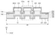
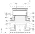
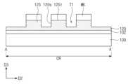
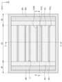
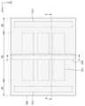
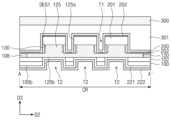
도 1은 본 발명의 실시예들에 따른 화합물 반도체 소자를 나타낸 평면도이다. 도 2는 도 1의 A-A' 선에 따른 단면도이다. 도 3는 도 1의 B-B' 선에 따른 단면도이다. 도 4a는 도 2의 A 부분을 확대한 확대 단면도이다. 도 4b는 도 2의 B 부분을 확대한 확대 단면도이다.1 is a plan view showing a compound semiconductor device according to embodiments of the present invention. FIG. 2 is a cross-sectional view taken along line A-A' in FIG. 1. FIG. 3 is a cross-sectional view taken along line B-B' in FIG. 1. FIG. 4A is an enlarged cross-sectional view of portion A of FIG. 2. Figure 4b is an enlarged cross-sectional view of part B of Figure 2.
도 1 내지 도 3를 참조하면, 중심 영역(CR) 및 외곽 영역들(OR)을 포함하는 기판(100)이 제공될 수 있다. 외곽 영역들(OR)은 중심 영역(CR)을 사이에 두고 기판(100)의 상면과 평행한 제1 방향(D1)으로 서로 이격될 수 있다. 중심 영역(CR)은 화합물 반도체 소자의 채널이 제공되는 영역일 수 있고, 외곽 영역들(OR)은 화합물 반도체 소자의 소스/드레인 영역들이 제공되는 영역일 수 있다. 중심 영역(CR) 및 외곽 영역들(OR)은 후술될 제1 트렌치들(T1)에 의해 정의될 수 있다. 기판(100)은 반도체 기판 및 절연 기판 중 하나를 포함할 수 있다. 기판(100)은, 예컨대, 실리콘 기판, 실리콘카바이드 기판, 갈륨나이트라이드 기판, 사파이어 기판 및 다이아몬드 기판 중 하나를 포함할 수 있다.Referring to FIGS. 1 to 3 , a
전이층(102)이 기판(100) 상에 제공될 수 있다. 전이층(102)은 기판(100)의 상면 상에 전면적으로 형성될 수 있다. 전이층(102)은 기판(100)의 상면과 제1 반도체 층(120)의 하면 사이에 위치할 수 있다. 전이층(102)은 기판(100)과 제1 반도체 층(120) 간의 열팽창 계수 및 격자 상수의 차이를 완화시킬 수 있다. 전이층(102)의 격자 상수는 기판(100)의 격자 상수와 제1 반도체 층(120)의 격자 상수 사이의 값을 가질 수 있다. 전이층(102)은, 예컨대, AlN, GaN, InN, AlGaN, InGaN, AlInN 및 AlGaInN 중 하나를 포함할 수 있다.A
제1 반도체 층(120)이 전이층(102) 상에 제공될 수 있다. 제1 반도체 층(120)은 도핑된 반도체 물질 또는 도핑되지 않은 반도체 물질을 포함할 수 있다. 실시예들에 따르면, 제1 반도체 층(120)은 III-V족 반도체 화합물을 포함할 수 있다. 제1 반도체 층(120)은, 예컨대, AlN, InN, GaN, AlGaN, InGaN, AlInN, AlGaInN 및 GaAs 중 하나를 포함할 수 있다. 제1 반도체 층(120)은 중심 영역(CR)의 기판(100) 상에 형성된 핀들(125)을 가질 수 있다. 핀들(125)은 제1 방향(D1)으로 연장되어 기판(100)의 중심 영역(CR)을 가로지를 수 있다. 핀들(125)은 제1 방향(D1)과 수직한 제2 방향(D2)으로 배열될 수 있다. 핀들(125)은 제2 방향(D2)으로 서로 이격될 수 있다. 핀들(125)은 제1 반도체 층(120)의 일부일 수 있으며, 제1 반도체 층(120)의 상부에 형성될 수 있다. 실시예들에 따르면, 제1 반도체 층(120)은 나란히 연장된 세 개의 핀들(125)을 가질 수 있다.A
실시예들에 따르면, 핀들(125)의 개수는 화합물 반도체 소자에 요구되는 출력 특성에 따라 조절될 수 있다. 예컨대, 화합물 반도체 소자는 HEMT 소자일 수 있으며, 핀들(125)의 개수는 HEMT 소자의 출력 전력이 증가할수록 증가될 수 있다. 실시예들에 따르면, 제1 반도체 층(120)은 하나의 핀(125)을 가질 수 있다.According to embodiments, the number of
도 1 내지 도 4a를 참조하면, 핀들(125)은 제1 반도체 층(120)의 상면으로부터 제1 반도체 층(120)의 하면(120b)을 향하여 형성된 제1 트렌치들(T1)에 의해 정의될 수 있다. 제1 트렌치들(T1)은, 도 1에 도시된 바와 같이, 제1 방향(D1)으로 연장되어 중심 영역(CR)의 폭을 정의할 수 있다. 제1 트렌치들(T1)은 제2 방향(D2)으로 배열될 수 있다. 실시예들에 따르면, 각각의 제1 트렌치들(T1)의 제2 방향(D2)의 폭들은 각각의 핀들(125)의 제2 방향(D2)의 폭들에 비해 작을 수 있다. 실시예들에 따르면, 제1 트렌치들(T1)의 바닥면(T1b)은 핀(125)의 상면(125t)에 비해 제1 반도체 층(120)의 하면(120b)과 가까이 위치할 수 있다. 달리 말해서, 제1 트렌치들(T1)의 깊이(즉, 핀(125)의 높이)는 제1 반도체 층(120)의 두께의 절반보다 클 수 있다.1 to 4A, the
도 1, 도 2 및 도 4a를 참조하여, 화합물 반도체 소자의 중심 영역(CR)에 대해 설명한다. 중심 영역(CR)의 기판(100) 상에 제2 반도체 층(130)이 제공될 수 있다. 제2 반도체 층(130)은 제1 반도체 층(120)의 측벽(125s) 상에 위치할 수 있다. 제2 반도체 층(130)은 제1 반도체 층(120)과 다른 물질을 포함할 수 있다. 제2 반도체 층(130)은 제1 반도체 층(120)과 다른 격자 상수를 가질 수 있다. 제2 반도체 층(130)은 제1 반도체 층(120)과 다른 밴드갭을 가질 수 있다. 예컨대, 제2 반도체 층(130)은 제1 반도체 층(120)에 비해 넓은 밴드갭을 가질 수 있다. 제2 반도체 층(130)은 제1 반도체 층(120)과 접합되어 제1 반도체 층(120) 내에 2차원 전자가스 영역 (2-dimensional electron gas region) 을 형성할 수 있는 물질을 포함할 수 있다. 제2 반도체 층(130)은 Al, Ga, In 및 B 중 적어도 하나를 포함하는 질화물 반도체 물질을 포함할 수 있다. 제2 반도체 층(130)은, 예컨대, GaN, InN, AlGaN, AlInN, InGaN, AlN 및 AlInGaN 중 하나를 포함할 수 있다. 실시예들에 따르면, 제2 반도체 층(130)은 서로 상이한 물질들을 포함하는 복수의 반도체 층들을 포함할 수 있다.Referring to FIGS. 1, 2, and 4A, the central region (CR) of the compound semiconductor device will be described. A
제2 반도체 층(130)은 제1 반도체 층(120)의 핀들(125)과 직접 접촉할 수 있다. 제2 반도체 층(130) 및 제1 반도체 층(120)이 서로 다른 반도체 물질을 포함하면서 접합됨에 따라 제1 반도체 층(120) 내에 제1 이차원 전자가스 영역들(DEG1)이 형성될 수 있다. 제1 이차원 전자가스 영역들(DEG1)은 제2 반도체 층(130)과 제1 반도체 층(120)의 계면과 인접하게 형성될 수 있다. 즉, 제1 이차원 전자가스 영역들(DEG1)은 핀들(125)의 측벽(125s)과 인접하게 형성될 수 있다. 제1 이차원 전자가스 영역들(DEG1)은 핀들(125)을 따라 제1 방향(D1)으로 연장될 수 있다. 제1 이차원 전자가스 영역(DEG1)은 소스/드레인 전극들(210) 사이의 전자의 이동 경로를 제공하기 위한 채널로 기능할 수 있다. 제1 이차원 전자가스 영역(DEG1)은 핀들(125)의 측벽들(125s)을 따라 수직적으로(즉, 제3 방향(D3)으로) 연장될 수 있다.The
제1 이차원 전자가스 영역(DEG1)은 제2 방향(D2)으로 연장되지 않을 수 있다. 즉, 제1 이차원 전자가스 영역(DEG1)은 핀들(125)의 측벽들(125s)과 인접한 영역에 국소적으로 형성될 수 있다. 측벽들(125s)과 인접한 영역 형성된 제1 이차원 전자가스 영역(DEG1)은 화합물 반도체 소자의 누설 전류를 감소시킬 수 있으며, 후술될 하부 게이트 구조체(221, 222)에 의한 문턱전압, 드레인 전류 및 주파수 특성의 제어를 용이하게 할 수 있다.The first two-dimensional electron gas region DEG1 may not extend in the second direction D2. That is, the first two-dimensional electron gas region DEG1 may be formed locally in an area adjacent to the
유전층들(201)이 제1 반도체 층(120) 및 제2 반도체 층(130) 상에 제공될 수 있다. 유전층들(201)은 핀들(125) 상에 각각 제공될 수 있으며, 핀들(125)을 따라 제1 방향(D1)으로 연장될 수 있다(도 8a 참조). 유전층(201)은 핀(125)의 상면(125t) 및 제2 반도체 층(130)의 상면(130t) 상에 위치할 수 있다. 유전층(201)의 제2 방향(D2)의 폭은 핀(125)의 제2 방향(D2)의 폭 및 핀(125)의 두 측벽들(125s) 상의 제2 반도체 층들(130)의 폭의 합과 같을 수 있다. 유전층(201)의 측면은 제2 반도체 층(130)의 측면과 정렬될 수 있다. 유전층(201)은 계면 절연층(202)에 비해 두꺼운 두께를 가질 수 있다. 또한, 유전층(201)은 후술될 하부 게이트 절연막(221)에 비해 두꺼운 두께를 가질 수 있다. 유전층(201)의 두께는 20nm 내지 100nm의 범위의 값을 가질 수 있다.
유전층(201)은, 예컨대, 실리콘 산화물, 실리콘 질화물 및 실리콘 산질화물 중 하나를 포함할 수 있다. 실시예들에 따르면, 유전층(201)은 다층 구조를 가질 수 있고, 고유전 물질을 포함하는 적어도 하나의 층을 포함할 수 있다.
계면 절연층(202)이, 중심 영역(CR) 상에서, 유전층(201) 및 제1 반도체 층(120) 상에 제공될 수 있다. 계면 절연층(202)의 일부는 유전층(201)의 상면과 상부 게이트 전극(200)의 사이에 위치할 수 있다. 계면 절연층(202)의 상기 일부는 유전층(201)의 상면을 완전히 덮을 수 있다. 계면 절연층(202)의 다른 일부는 제1 트렌치(T1)의 바닥면(T1b) 상에 위치할 수 있다. 계면 절연층(202)의 상기 다른 일부는 제1 반도체 층(120)의 표면을 부분적으로 덮을 수 있다. 계면 절연층(202)의 두께는 유전층(201)보다 얇은 두께로 제공될 수 있으며, 제2반도체층(130)과 상부 게이트전극(200) 그리고 유전층(201)과 상부 게이트전극(200) 사이에도 위치할 수 있다. 계면 절연층(202)은, 예컨대, 실리콘 산화물, 실리콘 질화물 및 실리콘 산질화물 중 하나를 포함할 수 있다. 계면 절연층(200)의 두께는 1nm 내지 5nm의 범위를 가질 수 있다.An interfacial insulating
도 1, 도 3 및 도 4b를 참조하여, 화합물 반도체 소자의 외곽 영역들(OR)에 대해 설명한다. 외곽 영역들(OR)의 기판(100) 상에 제3 반도체 층(140)이 제공될 수 있다. 제3 반도체 층(140)은 제1 반도체 층(120)의 상면(120t) 상에 위치할 수 있다. 제3 반도체 층(140)은 제1 반도체 층(120)과 다른 물질을 포함할 수 있다. 제2 반도체 층(130)은 제1 반도체 층(120)과 격자 상수가 다를 수 있다. 제3 반도체 층(140)은 제1 반도체 층(120)과 다른 밴드갭을 가질 수 있다. 예컨대, 제3 반도체 층(140)은 제1 반도체 층(120)에 비해 넓은 밴드갭을 가질 수 있다. 제3 반도체 층(140)은 제1 반도체 층(120)과 접합되어 제1 반도체 층(120) 내에 2차원 전자가스 영역을 형성할 수 있는 물질을 포함할 수 있다. 실시예들에 따르면, 제3 반도체 층(140)은 Al, Ga, In 및 B 중 적어도 하나를 포함하는 질화물 반도체 물질을 포함할 수 있다. 실시예들에 따르면, 제3 반도체 층(140)은 서로 상이한 물질들을 포함하는 복수의 반도체 층들을 포함할 수 있다. 실시예들에 따르면, 제3 반도체 층(140)은 중심 영역(CR) 상의 제2 반도체 층(130)과 동일한 물질을 포함할 수 있다.With reference to FIGS. 1, 3, and 4B, the outer regions (OR) of the compound semiconductor device will be described. A
소스/드레인 콘택들(180)이 제1 반도체 층(120) 상에 제공될 수 있다. 소스/드레인 콘택들(180)은 제1 반도체 층(120)의 내부로 연장되어 제2 이차원 전자가스 영역(DEG2)과 인접하게 위치할 수 있다. 소스/드레인 콘택(180)의 하면은 제1 반도체 층(120)의 상면(120t)에 비해 낮은 레벨에 위치할 수 있다. 소스/드레인 콘택들(180)은 금속 또는 도핑된 반도체 물질을 포함할 수 있다. 예컨대, 소스/드레인 콘택들(180)은 제1 반도체 층(120)과 오믹 접촉될 수 있다.Source/
계면 절연층(202)은, 외곽 영역(OR) 상에서, 제3 반도체 층(140) 및 소스/드레인 콘택들(180)의 상부 측벽들을 덮을 수 있다.The
소스/드레인 전극(210)이 소스/드레인 콘택(180)상에 제공될 수 있다. 소스/드레인 전극(210)은 금속을 포함할 수 있다. 소스/드레인 전극(210)은, 예컨대, 구리(Cu), 알루미늄(Al), 금(Au) 및 니켈(Ni) 중 하나를 포함할 수 있다.Source/
다시 도 1 내지 도 4b를 참조하면, 분리 영역(108)이 중심 영역(CR), 및 외곽 영역들(OR)의 가장자리에 형성될 수 있다. 분리 영역(108)은 폐곡선의 형상을 가질 수 있으며, 중심영역(CR)을 둘러쌀 수 있다. 분리 영역(108)은 높은 도펀트 농도를 갖는 반도체 물질을 포함할 수 있다. 실시예들에 따르면, 분리 영역(108)은 불순물을 포함할 수 있다. 분리 영역(108)은, 예컨대, 인(P) 또는 아르곤(Ar)을 포함할 수 있다. 분리 영역(108)은 화합물 반도체 소자를 기판(100)의 다른 영역들로부터 전기적으로 고립시킬 수 있다. 분리 영역(108)은 제1 반도체 층(120), 제2 반도체 층(130) 및 제3 반도체층(140)의 일부분들로부터 형성될 수 있다. 분리 영역(108)은 제1 반도체 층(120), 제2 반도체 층(130) 및 제3 반도체층(140)에 비해 낮은 전기 전도도를 가질 수 있다.Referring again to FIGS. 1 to 4B ,
기판(100)의 하면 상에 하부 게이트 구조체(221, 222)가 제공될 수 있다. 하부 게이트 구조체(221, 222)는 기판(100) 및 전이층(102)을 관통하여 제1 반도체 층(120)의 하면(120b)에 접속될 수 있다. 하부 게이트 구조체(221, 222)는 제2 방향(D2)으로 연장될 수 있으며, 상부 게이트 전극(200)과 수직적으로 중첩될 수 있다. 하부 게이트 구조체(221, 222)는 제1 반도체 층(120)의 하면(120b)을 노출하도록 형성된 제2 트렌치들(T2)을 적어도 부분적으로 채울 수 있다. 제2 트렌치들(T2)은 핀들(125)과 중첩되어 형성될 수 있다.
하부 게이트 구조체(221, 222)는 하부 게이트 절연막(221) 및 하부 게이트 전극(222)을 포함할 수 있다. 하부 게이트 절연막(221)은 기판(100)의 하면 및 제2 트렌치(T2)의 내면들을 컨포멀하게 덮을 수 있다. 하부 게이트 절연막(221)은 제1 반도체 층(120)의 하면(120b)과 접촉할 수 있다. 하부 게이트 절연막(221)은 유전층(201)에 비해 얇은 두께를 가질 수 있다. 하부 게이트 절연막(221)은, 예컨대, 실리콘 산화물, 실리콘 질화물 및 실리콘 산질화물 중 하나를 포함할 수 있다.The
하부 게이트 전극(222)은 하부 게이트 절연막(221)의 하면 상에 위치할 수 있다. 하부 게이트 전극(222)은 제2 방향(D2)으로 연장될 수 있다. 하부 게이트 전극(222)은, 도 3에 도시된 바와 같이, 상부 게이트 전극(200)과 수직적으로 중첩될 수 있다. 하부 게이트 전극(222)은 금속 또는 도핑된 반도체 물질을 포함할 수 있다.The
하부 게이트 전극(222)은 기판(100)상의 반도체 층들에 전압을 인가하여 화합물 반도체 소자의 문턱전압, 드레인전류 또는 출력-주파수 특성을 조절(modulation)할 수 있다. 구체적으로, 상부 게이트 전극(200) 및 하부 게이트 전극(222)은 개별적으로 제어되어 화합물 반도체 소자의 반도체 층들 내의 포텐셜(potential)을 제어할 수 있다. 하부 게이트 전극(222)에 인가된 전압에 의해 발생하는 포텐셜은 상부 게이트 전극(200)에 인가되는 전압에 의해 발생하는 포텐셜과 중첩될 수 있다. 본 발명의 실시예들에 따른 화합물 반도체 소자는 동작상태에 따라서 성능을 가변 할 수 있다. 예컨대, 시스템이 대기상태인 경우 누설전류를 줄여 전력소모량을 감소시킬 수 있다. 예컨대, 시스템이 고출력 동작 상태일 경우, 드레인전류를 증가시켜 시스템의 출력을 증가시킬 수 있다.The
이하 도면들을 참조하여 본 발명의 실시예들에 따른 화합물 반도체 소자의 제조 방법이 설명된다.A method of manufacturing a compound semiconductor device according to embodiments of the present invention will be described below with reference to the drawings.
도 5a, 도 6a, 도 7a, 도 8a, 도 9a, 및 도 10a는 본 발명의 실시예들에 따른 화합물 반도체 소자의 제조 방법을 설명하기 위한 평면도들이다. 도 5b, 도 6b, 도 7b, 도 8b, 도 9b, 도 10b 및 도 11b는 각각 도 5a, 도 6a, 도 7a, 도 8a, 도 9a, 도 10a 및 도 10a의 A-A' 선을 따라 절취한 단면도들이다. 도 5c, 도 6c, 도 7c, 도 8c, 도 9c, 도 10c 및 도 11c는 각각 도 5a, 도 6a, 도 7a, 도 8a, 도 9a, 도 10a 및 도 10a의 B-B' 선을 따라 절취한 단면도들이다.FIGS. 5A, 6A, 7A, 8A, 9A, and 10A are plan views for explaining a method of manufacturing a compound semiconductor device according to embodiments of the present invention. FIGS. 5B, 6B, 7B, 8B, 9B, 10B and 11B are taken along line A-A′ in FIGS. 5A, 6A, 7A, 8A, 9A, 10A and 10A, respectively. These are cross-sectional views. FIGS. 5C, 6C, 7C, 8C, 9C, 10C and 11C are taken along line B-B′ in FIGS. 5A, 6A, 7A, 8A, 9A, 10A and 10A, respectively. These are cross-sectional views.
도 5a 내지 도 5c를 참조하면, 기판(100) 상에 전이층(102) 및 제1 반도체 층(120)이 순차적으로 적층될 수 있다. 전이층(102) 및 제1 반도체 층(120)은 유기 금속 화학 기상증착(metal-organic chemical vapor deposition: MOCVD) 또는 분자선 에피택시(molecular beam epitaxy: MBE)를 이용하여 형성될 수 있다.Referring to FIGS. 5A to 5C , the
제1 반도체 층(120)을 패터닝하여 기판(100)의 중심 영역(CR) 상에 핀들(125)을 형성할 수 있다. 제1 반도체 층(120)을 패터닝하는 것은 제1 반도체 층(120) 상에 마스크 패턴(MK1)을 형성하고, 마스크 패턴(MK1)을 식각 마스크로 이용하여 식각 공정을 수행하는 것을 포함할 수 있다. 마스크 패턴(MK1)은 기판(100)의 외곽 영역(OR) 상의 제1 반도체 층(120)을 전면적으로 덮을 수 있다. 마스크 패턴(MK1)은 기판(100)의 중심 영역(CR) 상의 제1 반도체 층(120)을 부분적으로 노출할 수 있다. 식각 공정이 수행됨에 따라 제1 반도체 층(120)의 상부에 제1 트렌치들(T1)이 형성될 수 있다. 제1 트렌치들(T1)은 제1 방향(D1)으로 연장될 수 있고, 제2 방향(D2)으로 배열될 수 있다. 서로 인접한 두 제1 트렌치들(T1)의 사이에 핀(125)이 정의될 수 있다.The
식각 공정이 수행되는 동안 중심 영역(CR) 상에 위치한 핀들(125)의 상면들(125t)과 외곽 영역(OR) 상에 위치한 제1 반도체 층(120)의 상면(120t)은 마스크 패턴(MK1)에 의해 가려질 수 있다. 따라서, 핀들(125)의 상면들(125t)은 외곽 영역(OR) 상에 위치한 제1 반도체 층(120)의 상면(120t)과 동일한 레벨에 위치할 수 있다. 마스크 패턴(MK1)은 식각 공정의 수행 이후 제거될 수 있다.While the etching process is performed, the
도 6a 내지 도 6c를 참조하면, 기판(100)의 중심 영역(CR) 상에 제2 반도체 층(130)이 형성될 수 있고, 기판(100)의 외곽 영역(OR) 상에 제3 반도체 층(140)이 형성될 수 있다. 실시예들에 따르면, 제2 반도체 층(130) 및 제3 반도체 층(140)을 형성하는 것은 제1 반도체 층(120) 상에 제1 반도체 층(120)과 다른 물질을 포함하는 예비 반도체 층을 형성하는 것 및 상기 예비 반도체 층을 패터닝 하는 것을 포함할 수 있다. 실시예들에 따르면, 제2 반도체 층(130) 및 제3 반도체 층(140)을 형성하는 것은 제1 반도체 층(120) 상에 희생 패턴을 형성한 후, 상기 희생 패턴에 의해 노출된 제1 반도체 층(120)의 표면 상에 증착 공정을 수행하는 것을 포함할 수 있다. 제2 반도체 층(130)은 제1 반도체 층(120)의 핀들(125)의 측벽(125s) 상에 형성될 수 있다. 제3 반도체 층(140)은 외곽 영역(OR) 상에 위치한 제1 반도체 층(120)의 상면(120t) 상에 형성될 수 있다.6A to 6C, a
제1 반도체 층(120)은 제2 반도체 층(130) 및 제3 반도체 층(140)과 이종 접합되어 2차원 전자 가스 영역(2-dimensional electron gas region)을 형성할 수 있다. 2차원 전자 가스 영역은 자발 분극(Spontaneous polarization) 또는 피에조 분극(Piezo polarization)에 의해 제1 반도체 층(120) 내에 형성될 수 있다. 구체적으로, 제1 반도체 층(120)과 제2 반도체 층(130)의 격자 부정합에 의해 핀들(125)의 측벽(125s)과 인접한 영역에 제1 이차원 전자가스 영역들(DEG1)이 형성될 수 있다. 제1 반도체 층(120)과 제3 반도체 층(140)의 격자 부정합에 의해 외곽 영역들(OR) 상에 위치한 제1 반도체 층(120)의 상면(120t)과 인접한 영역에 제2 이차원 전자가스 영역들(DEG2)이 형성될 수 있다.The
도 7a 내지 도 7c를 참조하면, 외곽 영역들(OR) 상에 소스/드레인 콘택들(180)이 형성될 수 있다. 소스/드레인 콘택들(180)을 형성하는 것은 제3 반도체 층(140) 상에 금속 패턴을 형성하고, 상기 금속 패턴을 제1 반도체 층(120)의 내부로 확산시키는 것을 포함할 수 있다. 상기 금속 패턴은 급속 열처리 공정에 의해 제1 반도체 층(120)의 내부로 확산될 수 있다. 급속 열처리 공정은, 예컨대, 700℃ 내지 1000℃의 온도 범위에서 수행될 수 있다. 급속 열처리 공정을 수행하기에 앞서, 제1 반도체 층(120), 제2 반도체 층(130), 제3 반도체 층(140) 및 금속 패턴을 덮는 보호층을 형성할 수 있다. 보호층은 실리콘 산화물 및 실리콘 질화물 중 하나를 포함할 수 있다. 보호층은 급속 열처리 공정을 수행한 이후 제거될 수 있다. 실시예들에 따르면, 소스/드레인 콘택들(180)을 형성하는 것은 제1 반도체 층(120) 및 제2 반도체 층(130) 상에 트렌치를 형성하는 것 및 상기 트렌치를 체우는 금속 패턴을 형성하는 것을 포함할 수 있다.Referring to FIGS. 7A to 7C , source/
이어서, 중심 영역(CR), 및 외곽 영역들(OR)의 가장자리에 분리 영역(108)을 형성할 수 있다. 분리 영역(108)을 형성하는 것은 기판(100)의 가장자리를 노출하는 마스크 패턴을 형성한 후, 이온주입 공정을 수행하는 것을 포함할 수 있다. 이온 주입 공정은, 예컨대, 인(P) 또는 아르곤(Ar)을 이용하여 수행될 수 있다. 분리 영역(108)은 제1 반도체 층(120), 제2 반도체 층(130) 및 제3 반도체층(140)의 일부분들로부터 형성될 수 있다. 분리 영역(108)은 제1 반도체 층(120), 제2 반도체 층(130) 및 제3 반도체층(140)에 비해 높은 불순물 농도를 가질 수 있다.Subsequently,
도 8a 내지 도 8c를 참조하면, 핀들(125)의 상면들(125t) 상에 유전층(201)을 형성할 수 있다. 예컨대, 유전층(201)은 화학 기상증착(CVD), 물리 기상증착(PVD) 또는 원자층증착(ALD) 공정에 의해 형성될 수 있다. 유전층(201)은 핀들(125)의 상면들(125t) 및 제2 반도체 층(130)의 상면들(130t)을 덮도록 형성될 수 있다. 유전층(201)은 핀들(125)을 따라 제1 방향(D1)으로 연장될 수 있다.Referring to FIGS. 8A to 8C, a
도 9a 내지 도 9c를 참조하면, 상부 게이트 전극(200)을 형성할 수 있다. 예컨대, 상부 게이트 전극(200)은 금속증발(Metal Evaporaotion) 또는 스퍼터링 공정에 의해 형성될 수 있다. 상부 게이트 전극(200)은 제2 방향(D2)으로 연장되며, 제1 반도체 층(120), 제2 반도체 층(130) 및 유전층(201)의 표면들을 컨포멀하게 덮을 수 있다.Referring to FIGS. 9A to 9C, the
상부 게이트 전극(200)을 형성하기에 앞서, 계면 절연층(202)이 형성될 수 있다. 계면 절연층(202)의 일부는 유전층(201)의 상면과 상부 게이트 전극(200)의 사이에 형성되어 유전층(201)의 상면을 완전히 덮을 수 있다. 계면 절연층(202)의 다른 일부는 제1 반도체 층(120)의 표면들 및 제3 반도체 층(140)의 표면들을 덮을 수 있다. 계면 절연층(202)은 제2 반도체 층(130)과 이격될 수 있다.Prior to forming the
도 10a 내지 도 10c를 참조하면, 기판(100)의 상면 상에 접착층(301) 및 캐리어 기판(300)을 형성할 수 있다. 접착층(301)은 기판(100)의 상면 상에 형성된 구성들을 덮을 수 있다. 접착층(301)은, 예컨대, BCB(benzocyclobutene) 또는 내열 왁스를 포함할 수 있다. 캐리어 기판(300)은, 예컨대, 실리콘(Si), 탄화규소(SiC), 질화갈륨(GaN), 사파이어(sapphire), 다이아몬드(diamond) 및 질화알루미늄(AlN) 중 하나를 포함할 수 있다.Referring to FIGS. 10A to 10C , an
이어서, 기판(100)의 하면(100b) 상에 패터닝 공정을 수행하여 제2 트렌치들(T2)을 형성할 수 있다. 제2 트렌치들(T2)은 기판(100) 및 전이층(102)을 관통하여 제1 반도체 층(120)의 하면(120b)을 노출시킬 수 있다. 제2 트렌치들(T2)은 핀들(125)과 수직적으로 중첩되어 형성될 수 있다. 도시되지 않았으나, 제2 트렌치들(T2)은 제1 방향(D1)으로 연장될 수 있다.Next, a patterning process may be performed on the
도 11a 및 도 11b를 참조하면, 기판(100)의 하면(100b) 상에 하부 게이트 구조체(221, 222)를 형성할 수 있다. 하부 게이트 구조체(221, 222)는 기판(100) 및 전이층(102)을 관통하여 제1 반도체 층(120)의 하면(120b)에 접속될 수 있다. 하부 게이트 구조체(221, 222)는 제2 트렌치들(T2)을 적어도 부분적으로 채울 수 있다. 하부 게이트 구조체(221, 222)를 형성하는 것은 기판(100)의 하면(100b) 상에 하부 게이트 절연막(221)을 컨포멀하게 형성하는 것 및 하부 게이트 절연막(221)의 하면 상에 하부 게이트 전극(222)을 형성하는 것을 포함할 수 있다. 하부 게이트 절연막(221)은 기판(100)의 하면(100b) 상에 전면적으로 형성될 수 있다. 하부 게이트 전극(222)은 제2 방향(D2)으로 연장될 수 있으며, 상부 게이트 전극(200)과 수직적으로 중첩될 수 있다.Referring to FIGS. 11A and 11B ,
다시 도 1 내지 도 3을 참조하면, 접착층(301) 및 캐리어 기판(300)을 제거함으로써 화합물 반도체 소자를 제조할 수 있다.Referring again to FIGS. 1 to 3, a compound semiconductor device can be manufactured by removing the
발명이 속하는 기술분야에서 통상의 지식을 가진 자는 본 발명이 그 기술적 사상이나 필수적인 특징을 변경하지 않고서 다른 구체적인 형태로 실시될 수 있다는 것을 이해할 수 있을 것이다. 그러므로 이상에서 기술한 실시예들은 모든 면에서 예시적인 것이며 한정적이 아닌 것으로 이해해야만 한다.A person skilled in the art to which the invention pertains will understand that the present invention can be implemented in other specific forms without changing its technical idea or essential features. Therefore, the embodiments described above should be understood in all respects as illustrative and not restrictive.
Claims (20)
Translated fromKorean상기 제1 반도체 층 상에 상기 제1 방향과 수직한 제2 방향으로 연장된 상부 게이트 전극;
상기 트렌치 내의 상기 핀들의 측벽들과 상기 상부 게이트 전극 사이의 제2 반도체 층들;
상기 핀들의 상면 및 상기 상부 게이트 전극 사이의 유전층;
상기 유전층과 상기 상부 게이트 전극 사이, 상기 제1 반도체 층의 상기 트렌치의 바닥과 상기 상부 게이트 전극 사이, 그리고 상기 제2 반도체 층들의 측벽들과 상기 상부 게이트 전극 사이에 제공되고, 상기 유전층의 두께보다 작은 두께를 갖는 계면 절연층; 및
상기 기판을 관통하여 상기 제1 반도체 층의 하면과 연결되는 하부 게이트 구조체를 포함하는 화합물 반도체 소자.a first semiconductor layer having fins extending in a first direction on a substrate and a trench between the fins;
an upper gate electrode extending in a second direction perpendicular to the first direction on the first semiconductor layer;
second semiconductor layers between the top gate electrode and sidewalls of the fins in the trench;
a dielectric layer between the top surfaces of the fins and the top gate electrode;
provided between the dielectric layer and the top gate electrode, between the bottom of the trench of the first semiconductor layer and the top gate electrode, and between the sidewalls of the second semiconductor layers and the top gate electrode, and having a thickness greater than the thickness of the dielectric layer. an interfacial insulating layer having a small thickness; and
A compound semiconductor device including a lower gate structure that penetrates the substrate and is connected to a lower surface of the first semiconductor layer.
상기 제2 반도체 층들은 상기 핀들의 측벽들을 따라 상기 제1 방향으로 연장하는 화합물 반도체 소자.According to claim 1,
The compound semiconductor device wherein the second semiconductor layers extend in the first direction along sidewalls of the fins.
상기 제2 반도체 층들의 상기 제2 방향의 폭은 상기 제2 반도체 층들의 높이에 비해 작은 화합물 반도체 소자.According to claim 1,
A compound semiconductor device wherein the width of the second semiconductor layers in the second direction is smaller than the height of the second semiconductor layers.
상기 제2 반도체 층들의 상면은 상기 제1 반도체 층의 상면과 동일한 수직적 레벨에 위치하는 화합물 반도체 소자.According to claim 1,
A compound semiconductor device wherein the top surfaces of the second semiconductor layers are located at the same vertical level as the top surfaces of the first semiconductor layer.
상기 제2 반도체 층들은 상기 제1 반도체 층과 다른 밴드 갭을 갖는 화합물 반도체 소자.According to claim 1,
A compound semiconductor device wherein the second semiconductor layers have a different band gap from the first semiconductor layer.
상기 유전층은 상기 제2 반도체 층들의 상면을 덮는 화합물 반도체 소자.According to claim 1,
A compound semiconductor device wherein the dielectric layer covers upper surfaces of the second semiconductor layers.
상기 제1 방향으로 서로 이격되어 상기 제1 반도체 층에 접속되는 소스/드레인 콘택들을 더 포함하고,
상기 상부 게이트 전극은 상기 소스/드레인 콘택들의 사이에 위치하는 화합물 반도체 소자.According to claim 1,
Further comprising source/drain contacts spaced apart from each other in the first direction and connected to the first semiconductor layer,
The upper gate electrode is a compound semiconductor device located between the source/drain contacts.
상기 하부 게이트 구조체는 상기 제2 방향으로 연장되는 화합물 반도체 소자.According to claim 1,
A compound semiconductor device wherein the lower gate structure extends in the second direction.
상기 하부 게이트 구조체는 상기 상부 게이트 전극과 수직적으로 중첩되는 화합물 반도체 소자.According to claim 1,
A compound semiconductor device wherein the lower gate structure vertically overlaps the upper gate electrode.
상기 상부 게이트 전극의 하단은 상기 핀들의 상면에 비해 상기 제1 반도체 층의 하면과 가까이에 위치하는 화합물 반도체 소자.According to claim 1,
A compound semiconductor device wherein the lower end of the upper gate electrode is located closer to the lower surface of the first semiconductor layer than the upper surface of the fins.
상기 상부 게이트 전극은 상기 제2 반도체 층들과 직접 접촉하는 화합물 반도체 소자.According to claim 1,
A compound semiconductor device wherein the upper gate electrode directly contacts the second semiconductor layers.
상기 유전층의 두께는 20nm 내지 100nm 범위의 값을 갖는 화합물 반도체 소자.According to claim 1,
A compound semiconductor device wherein the dielectric layer has a thickness ranging from 20 nm to 100 nm.
상기 제1 반도체 층 상에 상기 제1 방향과 수직한 제2 방향으로 연장된 상부 게이트 전극;
상기 트렌치 내의 상기 핀들의 측벽들과 상기 상부 게이트 전극 사이의 제2 반도체 층들;
상기 핀들의 상면 및 상기 상부 게이트 전극 사이, 그리고 상기 제2 반도체 층들의 측면들 및 상기 상부 게이트 전극 사이의 유전층; 및
상기 유전층과 상기 상부 게이트 전극 사이, 상기 제1 반도체 층의 상기 트렌치의 바닥과 상기 상부 게이트 전극 사이, 그리고 상기 제2 반도체 층들의 측벽들과 상기 상부 게이트 전극 사이에 제공되고, 상기 유전층의 두께보다 작은 두께를 갖는 계면 절연층을 포함하되,
상기 제2 반도체 층들은 제2 방향으로 서로 이격되고, 상기 제1 방향을 따라 서로 나란히 연장하는 화합물 반도체 소자.A first semiconductor layer having fins extending in a first direction on a substrate and a trench between the fins;
an upper gate electrode extending in a second direction perpendicular to the first direction on the first semiconductor layer;
second semiconductor layers between the top gate electrode and sidewalls of the fins in the trench;
a dielectric layer between the top surfaces of the fins and the top gate electrode and between the sides of the second semiconductor layers and the top gate electrode; and
provided between the dielectric layer and the top gate electrode, between the bottom of the trench of the first semiconductor layer and the top gate electrode, and between the sidewalls of the second semiconductor layers and the top gate electrode, and having a thickness greater than the thickness of the dielectric layer. Includes an interfacial insulating layer having a small thickness,
A compound semiconductor device wherein the second semiconductor layers are spaced apart from each other in a second direction and extend parallel to each other along the first direction.
상기 제2 반도체 층들의 상면들은 상기 제1 반도체 층의 상면과 동일한 수직적 레벨에 위치하는 화합물 반도체 소자.According to claim 14,
A compound semiconductor device wherein the top surfaces of the second semiconductor layers are located at the same vertical level as the top surface of the first semiconductor layer.
상기 제2 반도체 층들은 상기 제1 반도체 층과 다른 밴드 갭을 갖는 화합물 반도체 소자.According to claim 14,
A compound semiconductor device wherein the second semiconductor layers have a different band gap from the first semiconductor layer.
상기 기판을 관통하여 상기 제1 반도체 층의 하면과 연결되는 하부 게이트 구조체를 포함하고,
상기 하부 게이트 구조체는 상기 제2 방향으로 연장되는 화합물 반도체 소자.According to claim 14,
It includes a lower gate structure that penetrates the substrate and is connected to a lower surface of the first semiconductor layer,
A compound semiconductor device wherein the lower gate structure extends in the second direction.
상기 상부 게이트 전극은 상기 제2 반도체 층들과 직접 접촉하는 화합물 반도체 소자.According to claim 14,
A compound semiconductor device wherein the upper gate electrode directly contacts the second semiconductor layers.
상기 제1 방향으로 서로 이격되어 상기 제1 반도체 층에 접속되는 소스/드레인 콘택들을 더 포함하되,
상기 상부 게이트 전극은 상기 소스/드레인 콘택들의 사이에 위치하는 화합물 반도체 소자.
According to claim 14,
Further comprising source/drain contacts spaced apart from each other in the first direction and connected to the first semiconductor layer,
The upper gate electrode is a compound semiconductor device located between the source/drain contacts.
Priority Applications (1)
| Application Number | Priority Date | Filing Date | Title |
|---|---|---|---|
| US17/508,933US11916140B2 (en) | 2021-02-03 | 2021-10-22 | Compound semiconductor device |
Applications Claiming Priority (2)
| Application Number | Priority Date | Filing Date | Title |
|---|---|---|---|
| KR1020210015161 | 2021-02-03 | ||
| KR20210015161 | 2021-02-03 |
Publications (2)
| Publication Number | Publication Date |
|---|---|
| KR20220112159A KR20220112159A (en) | 2022-08-10 |
| KR102658051B1true KR102658051B1 (en) | 2024-04-17 |
Family
ID=82847029
Family Applications (1)
| Application Number | Title | Priority Date | Filing Date |
|---|---|---|---|
| KR1020210074293AActiveKR102658051B1 (en) | 2021-02-03 | 2021-06-08 | Compound semiconductor device |
Country Status (1)
| Country | Link |
|---|---|
| KR (1) | KR102658051B1 (en) |
Citations (2)
| Publication number | Priority date | Publication date | Assignee | Title |
|---|---|---|---|---|
| JP2008235465A (en)* | 2007-03-19 | 2008-10-02 | Toshiba Corp | Field effect transistor |
| JP2013243383A (en)* | 2013-07-16 | 2013-12-05 | Semiconductor Energy Lab Co Ltd | Semiconductor device |
Family Cites Families (2)
| Publication number | Priority date | Publication date | Assignee | Title |
|---|---|---|---|---|
| US9461160B2 (en)* | 2011-12-19 | 2016-10-04 | Intel Corporation | Non-planar III-N transistor |
| KR101729653B1 (en)* | 2013-12-30 | 2017-04-25 | 한국전자통신연구원 | Nitride semiconductor device |
- 2021
- 2021-06-08KRKR1020210074293Apatent/KR102658051B1/enactiveActive
Patent Citations (2)
| Publication number | Priority date | Publication date | Assignee | Title |
|---|---|---|---|---|
| JP2008235465A (en)* | 2007-03-19 | 2008-10-02 | Toshiba Corp | Field effect transistor |
| JP2013243383A (en)* | 2013-07-16 | 2013-12-05 | Semiconductor Energy Lab Co Ltd | Semiconductor device |
Also Published As
| Publication number | Publication date |
|---|---|
| KR20220112159A (en) | 2022-08-10 |
Similar Documents
| Publication | Publication Date | Title |
|---|---|---|
| TWI430341B (en) | Manufacture of single or multiple gate field plates | |
| JP2022551725A (en) | Stepped field plate in close proximity to conductive channel and associated manufacturing method | |
| CN103972284A (en) | Semiconductor device | |
| US9263567B2 (en) | Nitride high electron mobility transistor having a channel forming stack | |
| TW201926718A (en) | Semiconductor device | |
| US20220376074A1 (en) | Nitride-based semiconductor device and method for manufacturing the same | |
| US20220376041A1 (en) | Semiconductor device and method for manufacturing the same | |
| CN114078965A (en) | High electron mobility transistor and manufacturing method thereof | |
| TW202230799A (en) | High electron mobility transistor and fabrication method thereof | |
| US20250212447A1 (en) | Method of forming high electron mobility transistor (hemt) device | |
| KR20190027700A (en) | Field effect transistor | |
| US20220376042A1 (en) | Semiconductor device and method for manufacturing the same | |
| JP2003051508A (en) | GaN-based semiconductor device | |
| US11916140B2 (en) | Compound semiconductor device | |
| US20240088260A1 (en) | Power semiconductor device and manufacturing method thereof | |
| US20240038847A1 (en) | Gallium nitride device and method for manufacturing high electron mobility transistor | |
| KR102658051B1 (en) | Compound semiconductor device | |
| US12266713B2 (en) | Transistor with dielectric spacers and method of fabrication therefor | |
| US12057490B2 (en) | High electron mobility transistor structure and method of fabricating the same | |
| CN117995875A (en) | Semiconductor structure and preparation method thereof | |
| CN112490278B (en) | Semiconductor epitaxial structures with reduced defects | |
| TW201737354A (en) | Semiconductor device, electronic component, electronic device, and method for manufacturing the same | |
| WO2021029183A1 (en) | Semiconductor device, semiconductor module and electronic machine | |
| US20240304710A1 (en) | Hemt device having improved on-state performance and manufacturing process thereof | |
| CN115863401B (en) | Normally-off transistor and preparation method thereof |
Legal Events
| Date | Code | Title | Description |
|---|---|---|---|
| PA0109 | Patent application | St.27 status event code:A-0-1-A10-A12-nap-PA0109 | |
| PA0201 | Request for examination | St.27 status event code:A-1-2-D10-D11-exm-PA0201 | |
| PG1501 | Laying open of application | St.27 status event code:A-1-1-Q10-Q12-nap-PG1501 | |
| E902 | Notification of reason for refusal | ||
| PE0902 | Notice of grounds for rejection | St.27 status event code:A-1-2-D10-D21-exm-PE0902 | |
| E13-X000 | Pre-grant limitation requested | St.27 status event code:A-2-3-E10-E13-lim-X000 | |
| P11-X000 | Amendment of application requested | St.27 status event code:A-2-2-P10-P11-nap-X000 | |
| P13-X000 | Application amended | St.27 status event code:A-2-2-P10-P13-nap-X000 | |
| E701 | Decision to grant or registration of patent right | ||
| PE0701 | Decision of registration | St.27 status event code:A-1-2-D10-D22-exm-PE0701 | |
| PR0701 | Registration of establishment | St.27 status event code:A-2-4-F10-F11-exm-PR0701 | |
| PR1002 | Payment of registration fee | St.27 status event code:A-2-2-U10-U11-oth-PR1002 Fee payment year number:1 | |
| PG1601 | Publication of registration | St.27 status event code:A-4-4-Q10-Q13-nap-PG1601 | |
| P22-X000 | Classification modified | St.27 status event code:A-4-4-P10-P22-nap-X000 |