KR102657125B1 - Data output circuit - Google Patents
Data output circuitDownload PDFInfo
- Publication number
- KR102657125B1 KR102657125B1KR1020180063675AKR20180063675AKR102657125B1KR 102657125 B1KR102657125 B1KR 102657125B1KR 1020180063675 AKR1020180063675 AKR 1020180063675AKR 20180063675 AKR20180063675 AKR 20180063675AKR 102657125 B1KR102657125 B1KR 102657125B1
- Authority
- KR
- South Korea
- Prior art keywords
- pull
- circuit
- voltage
- data
- code signals
- Prior art date
- Legal status (The legal status is an assumption and is not a legal conclusion. Google has not performed a legal analysis and makes no representation as to the accuracy of the status listed.)
- Active
Links
- 230000004044responseEffects0.000claimsdescription37
- 238000009966trimmingMethods0.000claimsdescription30
- 238000005086pumpingMethods0.000claimsdescription13
- 230000008859changeEffects0.000claimsdescription10
- 238000005516engineering processMethods0.000abstractdescription4
- 239000013069drug device combination productSubstances0.000description26
- 238000010586diagramMethods0.000description14
- 230000001276controlling effectEffects0.000description7
- 238000012986modificationMethods0.000description4
- 230000004048modificationEffects0.000description4
- 230000014509gene expressionEffects0.000description3
- 238000012545processingMethods0.000description3
- 238000004891communicationMethods0.000description2
- 230000007423decreaseEffects0.000description2
- 238000000034methodMethods0.000description2
- 230000001105regulatory effectEffects0.000description2
- 239000004065semiconductorSubstances0.000description2
- 230000003068static effectEffects0.000description2
- JBRZTFJDHDCESZ-UHFFFAOYSA-NAsGaChemical compound[As]#[Ga]JBRZTFJDHDCESZ-UHFFFAOYSA-N0.000description1
- XUIMIQQOPSSXEZ-UHFFFAOYSA-NSiliconChemical compound[Si]XUIMIQQOPSSXEZ-UHFFFAOYSA-N0.000description1
- 230000005540biological transmissionEffects0.000description1
- 230000001413cellular effectEffects0.000description1
- 230000006870functionEffects0.000description1
- 229910052732germaniumInorganic materials0.000description1
- GNPVGFCGXDBREM-UHFFFAOYSA-Ngermanium atomChemical compound[Ge]GNPVGFCGXDBREM-UHFFFAOYSA-N0.000description1
- 229910052738indiumInorganic materials0.000description1
- APFVFJFRJDLVQX-UHFFFAOYSA-Nindium atomChemical compound[In]APFVFJFRJDLVQX-UHFFFAOYSA-N0.000description1
- 230000003287optical effectEffects0.000description1
- 230000002093peripheral effectEffects0.000description1
- 230000008569processEffects0.000description1
- 230000008054signal transmissionEffects0.000description1
- 229910052710siliconInorganic materials0.000description1
- 239000010703siliconSubstances0.000description1
- 230000001360synchronised effectEffects0.000description1
- 238000012546transferMethods0.000description1
- 238000013519translationMethods0.000description1
Images


Classifications
- G—PHYSICS
- G11—INFORMATION STORAGE
- G11C—STATIC STORES
- G11C7/00—Arrangements for writing information into, or reading information out from, a digital store
- G11C7/10—Input/output [I/O] data interface arrangements, e.g. I/O data control circuits, I/O data buffers
- G11C7/1048—Data bus control circuits, e.g. precharging, presetting, equalising
- G—PHYSICS
- G11—INFORMATION STORAGE
- G11C—STATIC STORES
- G11C7/00—Arrangements for writing information into, or reading information out from, a digital store
- G11C7/10—Input/output [I/O] data interface arrangements, e.g. I/O data control circuits, I/O data buffers
- G11C7/1051—Data output circuits, e.g. read-out amplifiers, data output buffers, data output registers, data output level conversion circuits
- G—PHYSICS
- G11—INFORMATION STORAGE
- G11C—STATIC STORES
- G11C29/00—Checking stores for correct operation ; Subsequent repair; Testing stores during standby or offline operation
- G11C29/02—Detection or location of defective auxiliary circuits, e.g. defective refresh counters
- G11C29/022—Detection or location of defective auxiliary circuits, e.g. defective refresh counters in I/O circuitry
- G—PHYSICS
- G11—INFORMATION STORAGE
- G11C—STATIC STORES
- G11C29/00—Checking stores for correct operation ; Subsequent repair; Testing stores during standby or offline operation
- G11C29/02—Detection or location of defective auxiliary circuits, e.g. defective refresh counters
- G11C29/028—Detection or location of defective auxiliary circuits, e.g. defective refresh counters with adaption or trimming of parameters
- G—PHYSICS
- G11—INFORMATION STORAGE
- G11C—STATIC STORES
- G11C5/00—Details of stores covered by group G11C11/00
- G11C5/14—Power supply arrangements, e.g. power down, chip selection or deselection, layout of wirings or power grids, or multiple supply levels
- G11C5/145—Applications of charge pumps; Boosted voltage circuits; Clamp circuits therefor
- G—PHYSICS
- G11—INFORMATION STORAGE
- G11C—STATIC STORES
- G11C5/00—Details of stores covered by group G11C11/00
- G11C5/14—Power supply arrangements, e.g. power down, chip selection or deselection, layout of wirings or power grids, or multiple supply levels
- G11C5/147—Voltage reference generators, voltage or current regulators; Internally lowered supply levels; Compensation for voltage drops
- G—PHYSICS
- G11—INFORMATION STORAGE
- G11C—STATIC STORES
- G11C7/00—Arrangements for writing information into, or reading information out from, a digital store
- G11C7/04—Arrangements for writing information into, or reading information out from, a digital store with means for avoiding disturbances due to temperature effects
- G—PHYSICS
- G11—INFORMATION STORAGE
- G11C—STATIC STORES
- G11C2207/00—Indexing scheme relating to arrangements for writing information into, or reading information out from, a digital store
- G11C2207/22—Control and timing of internal memory operations
- G11C2207/2254—Calibration
Landscapes
- Engineering & Computer Science (AREA)
- Power Engineering (AREA)
- Logic Circuits (AREA)
- Dram (AREA)
Abstract
Translated fromKorean
Description
Translated fromKorean본 발명은 전자 장치에 관한 것으로, 특히 구동 세기가 조절되는 데이터 출력 회로에 관한 것이다.The present invention relates to electronic devices, and more particularly to a data output circuit whose drive intensity is adjusted.
메모리 시스템(memory system)을 저장 매체로 사용하는 이동 정보 기기들, 특히 스마트폰 및 태블릿 피씨 등의 사용이 증가함에 따라서 메모리 장치에 대한 관심과 중요성이 더욱 커지고 있다.As the use of mobile information devices that use a memory system as a storage medium, especially smartphones and tablet PCs, increases, interest in and importance of memory devices is growing.
고속의 프로세서나 멀티코어를 이용한 병렬화뿐만 아니라 다양한 어플리케이션들의 등장으로 인해 반도체 메모리 시스템에 대한 요구 수준은 성능뿐 아니라 신뢰성 측면에서도 계속 높아지고 있다.Due to the emergence of various applications as well as parallelization using high-speed processors and multi-cores, the level of requirements for semiconductor memory systems continues to increase not only in terms of performance but also reliability.
메모리 시스템은 실리콘(Si, silicon), 게르마늄(Ge, Germanium), 비화 갈륨(GaAs, gallium arsenide), 인화인듐(InP, indium phospide) 등과 같은 반도체를 이용하여 구현되는 기억장치이다. 메모리 시스템은 크게 휘발성 메모리 장치(Volatile memory device)와 불휘발성 메모리(Nonvolatile memory device)로 구분될 수 있다. 휘발성 메모리 장치는 전원 공급이 차단되면 저장하고 있던 데이터가 소멸되는 메모리 장치이다. 휘발성 메모리 장치에는 SRAM (Static RAM), DRAM (Dynamic RAM), SDRAM (Synchronous DRAM) 등이 있다. 불휘발성 메모리 장치는 전원 공급이 차단되어도 저장하고 있던 데이터가 유지되는 메모리 장치이다. 불휘발성 메모리 장치에는 ROM (Read Only Memory), PROM (Programmable ROM), EPROM (Electrically Programmable ROM), EEPROM (Electrically Erasable and Programmable ROM), 플래시 메모리, PRAM (Phase-change RAM), MRAM (Magnetic RAM), RRAM (Resistive RAM), FRAM (Ferroelectric RAM) 등이 있다. 플래시 메모리는 크게 노어 타입과 낸드 타입으로 구분될 수 있다.A memory system is a memory device implemented using semiconductors such as silicon (Si), germanium (Ge), gallium arsenide (GaAs), and indium phospide (InP). Memory systems can be largely divided into volatile memory devices and nonvolatile memory devices. A volatile memory device is a memory device in which the stored data is lost when the power supply is cut off. Volatile memory devices include SRAM (Static RAM), DRAM (Dynamic RAM), and SDRAM (Synchronous DRAM). A non-volatile memory device is a memory device that retains stored data even when the power supply is cut off. Non-volatile memory devices include Read Only Memory (ROM), Programmable ROM (PROM), Electrically Programmable ROM (EPROM), Electrically Erasable and Programmable ROM (EEPROM), flash memory, Phase-change RAM (PRAM), and Magnetic RAM (MRAM). , RRAM (Resistive RAM), FRAM (Ferroelectric RAM), etc. Flash memory can be largely divided into NOR type and NAND type.
메모리 시스템은 데이터가 저장되는 메모리 장치와 메모리 장치를 제어하는 메모리 컨트롤러를 포함할 수 있다. 메모리 장치와 메모리 컨트롤러 각각은 데이터 출력 회로를 이용하여 내부 데이터를 데이터 패드를 통해 외부로 출력하여 서로 간의 데이터 전송 동작을 수행할 수 있다.The memory system may include a memory device that stores data and a memory controller that controls the memory device. Each of the memory device and the memory controller can use a data output circuit to output internal data to the outside through a data pad to perform a data transfer operation between them.
본 발명의 실시 예는 데이터 출력 동작 시 설정된 ZQ 캘리브레이션(calibration) 코드 값에 따라 설정된 구동 세기(driving strength)로 구동되는 데이터 출력 회로를 제공한다.An embodiment of the present invention provides a data output circuit driven with a driving strength set according to a ZQ calibration code value set during a data output operation.
본 발명의 실시 예에 따른 데이터 출력 회로는 제1 전원 전압 및 제2 전원 전압 레벨보다 높은 일정한 전위 레벨을 갖는 동작 전압을 생성하는 전압 생성 회로; 캘리브레이션 코드 신호들과 상기 동작 전압에 따라 풀업 코드 신호들 및 풀다운 코드 신호들을 생성하기 위한 프리 드라이버 회로; 데이터 신호 및 상기 제1 전원 전압에 따라 프리 데이터 신호를 생성하여 출력하는 데이터 프리 드라이버 회로; 및 상기 프리 데이터 신호 및 상기 제2 전원 전압에 따라 출력 데이터 신호를 생성하되, 상기 풀업 코드 신호들 및 풀다운 코드 신호들에 따라 구동 세기가 조절되는 메인 드라이버 회로를 포함한다.A data output circuit according to an embodiment of the present invention includes a voltage generating circuit that generates an operating voltage having a constant potential level higher than the first power supply voltage and the second power supply voltage level; a pre-driver circuit for generating pull-up code signals and pull-down code signals according to the calibration code signals and the operating voltage; a data pre-driver circuit that generates and outputs a pre-data signal according to a data signal and the first power voltage; and a main driver circuit that generates an output data signal according to the pre-data signal and the second power voltage, and whose driving strength is adjusted according to the pull-up code signals and pull-down code signals.
본 발명의 실시 예에 따른 데이터 출력 회로는 전원 전압 레벨보다 높은 동작 전압을 생성하는 전압 생성 회로; 상기 동작 전압에 따라 풀업 코드 신호들 및 풀다운 코드 신호들을 생성하되, 상기 풀업 코드 신호들 및 풀다운 코드 신호들이 접지 전압 레벨 또는 상기 동작 전압 레벨을 갖도록 생성하기 위한 프리 드라이버 회로; 및 프리 데이터 신호에 따라 상기 전원 전압 레벨 또는 접지 전압 레벨의 출력 데이터 신호를 생성하되, 상기 풀업 코드 신호들 및 풀다운 코드 신호들에 따라 구동 세기가 조절되는 메인 드라이버 회로를 포함한다.A data output circuit according to an embodiment of the present invention includes a voltage generation circuit that generates an operating voltage higher than the power supply voltage level; a pre-driver circuit for generating pull-up code signals and pull-down code signals according to the operating voltage so that the pull-up code signals and pull-down code signals have a ground voltage level or the operating voltage level; and a main driver circuit that generates an output data signal of the power voltage level or the ground voltage level according to the pre-data signal, and whose driving strength is adjusted according to the pull-up code signals and pull-down code signals.
본 기술에 따르면, 데이터의 출력 동작 시 설정된 ZQ 캘리브레이션 코드 값에 따라 설정된 구동 세기로 구동되는 데이터 출력 회로에 의해 별도의 캘리브레이션 시간이 필요하지 않아 동작 속도를 개선시킬 수 있다.According to this technology, the operation speed can be improved by eliminating the need for separate calibration time due to the data output circuit being driven at a drive intensity set according to the ZQ calibration code value set during the data output operation.
도 1은 본 발명의 실시 예에 따른 메모리 시스템을 설명하기 위한 도면이다.
도 2는 도 1의 데이터 출력 회로를 설명하기 위한 블록도이다.
도 3은 도 2의 메인 드라이버 회로를 설명하기 위한 회로도이다
도 4는 메모리 시스템의 다른 실시 예를 설명하기 위한 도면이다.
도 5는 메모리 시스템의 다른 실시 예를 설명하기 위한 도면이다.
도 6은 메모리 시스템의 다른 실시 예를 설명하기 위한 도면이다.
도 7은 메모리 시스템의 다른 실시 예를 설명하기 위한 도면이다.1 is a diagram for explaining a memory system according to an embodiment of the present invention.
FIG. 2 is a block diagram for explaining the data output circuit of FIG. 1.
FIG. 3 is a circuit diagram for explaining the main driver circuit of FIG. 2.
Figure 4 is a diagram for explaining another embodiment of a memory system.
Figure 5 is a diagram for explaining another embodiment of a memory system.
Figure 6 is a diagram for explaining another embodiment of a memory system.
Figure 7 is a diagram for explaining another embodiment of a memory system.
본 명세서 또는 출원에 개시되어 있는 본 발명의 개념에 따른 실시 예들에 대해서 특정한 구조적 내지 기능적 설명들은 단지 본 발명의 개념에 따른 실시 예를 설명하기 위한 목적으로 예시된 것으로, 본 발명의 개념에 따른 실시 예들은 다양한 형태로 실시될 수 있으며 본 명세서 또는 출원에 설명된 실시 예들에 한정되는 것으로 해석되어서는 아니 된다.Specific structural and functional descriptions of the embodiments according to the concept of the present invention disclosed in this specification or application are merely illustrative for the purpose of explaining the embodiments according to the concept of the present invention, and the implementation according to the concept of the present invention The examples may be implemented in various forms and should not be construed as limited to the embodiments described in this specification or application.
본 발명의 개념에 따른 실시 예는 다양한 변경을 가할 수 있고 여러 가지 형태를 가질 수 있으므로 특정 실시 예들을 도면에 예시하고 본 명세서 또는 출원에 상세하게 설명하고자 한다. 그러나, 이는 본 발명의 개념에 따른 실시 예를 특정한 개시 형태에 대해 한정하려는 것이 아니며, 본 발명의 사상 및 기술 범위에 포함되는 모든 변경, 균등물 내지 대체물을 포함하는 것으로 이해되어야 한다.Since embodiments according to the concept of the present invention can make various changes and have various forms, specific embodiments will be illustrated in the drawings and described in detail in the present specification or application. However, this is not intended to limit the embodiments according to the concept of the present invention to a specific disclosed form, and should be understood to include all changes, equivalents, and substitutes included in the spirit and technical scope of the present invention.
제1 및/또는 제2 등의 용어는 다양한 구성 요소들을 설명하는데 사용될 수 있지만, 상기 구성 요소들은 상기 용어들에 의해 한정되어서는 안 된다. 상기 용어들은 하나의 구성 요소를 다른 구성 요소로부터 구별하는 목적으로만, 예컨대 본 발명의 개념에 따른 권리 범위로부터 이탈되지 않은 채, 제1 구성요소는 제2 구성요소로 명명될 수 있고, 유사하게 제2 구성요소는 제1 구성요소로도 명명될 수 있다.Terms such as first and/or second may be used to describe various components, but the components should not be limited by the terms. The above terms are used only for the purpose of distinguishing one component from another component, for example, without departing from the scope of rights according to the concept of the present invention, a first component may be named a second component, and similarly The second component may also be referred to as the first component.
어떤 구성요소가 다른 구성요소에 "연결되어" 있다거나 "접속되어" 있다고 언급된 때에는, 그 다른 구성요소에 직접적으로 연결되어 있거나 또는 접속되어 있을 수도 있지만, 중간에 다른 구성요소가 존재할 수도 있다고 이해되어야 할 것이다. 반면에, 어떤 구성요소가 다른 구성요소에 "직접 연결되어" 있다거나 "직접 접속되어" 있다고 언급된 때에는, 중간에 다른 구성요소가 존재하지 않는 것으로 이해되어야 할 것이다. 구성요소들 간의 관계를 설명하는 다른 표현들, 즉 "~사이에"와 "바로 ~사이에" 또는 "~에 이웃하는"과 "~에 직접 이웃하는" 등도 마찬가지로 해석되어야 한다.When a component is said to be "connected" or "connected" to another component, it is understood that it may be directly connected to or connected to the other component, but that other components may exist in between. It should be. On the other hand, when it is mentioned that a component is “directly connected” or “directly connected” to another component, it should be understood that there are no other components in between. Other expressions that describe the relationship between components, such as "between" and "immediately between" or "neighboring" and "directly adjacent to" should be interpreted similarly.
본 명세서에서 사용한 용어는 단지 특정한 실시 예를 설명하기 위해 사용된 것으로, 본 발명을 한정하려는 의도가 아니다. 단수의 표현은 문맥상 명백하게 다르게 뜻하지 않는 한, 복수의 표현을 포함한다. 본 명세서에서, "포함하다" 또는 "가지다" 등의 용어는 서술된 특징, 숫자, 단계, 동작, 구성요소, 부분품 또는 이들을 조합한 것이 존재함을 지정하려는 것이지, 하나 또는 그 이상의 다른 특징들이나 숫자, 단계, 동작, 구성요소, 부분품 또는 이들을 조합한 것들의 존재 또는 부가 가능성을 미리 배제하지 않는 것으로 이해되어야 한다.The terms used in this specification are merely used to describe specific embodiments and are not intended to limit the present invention. Singular expressions include plural expressions unless the context clearly dictates otherwise. In this specification, terms such as “comprise” or “have” are intended to designate the existence of a described feature, number, step, operation, component, part, or combination thereof, but are not intended to indicate the presence of one or more other features or numbers. It should be understood that this does not exclude in advance the possibility of the existence or addition of steps, operations, components, parts, or combinations thereof.
다르게 정의되지 않는 한, 기술적이거나 과학적인 용어를 포함해서 여기서 사용되는 모든 용어들은 본 발명이 속하는 기술 분야에서 통상의 지식을 가진 자에 의해 일반적으로 이해되는 것과 동일한 의미를 가지고 있다. 일반적으로 사용되는 사전에 정의되어 있는 것과 같은 용어들은 관련 기술의 문맥상 가지는 의미와 일치하는 의미를 가지는 것으로 해석되어야 하며, 본 명세서에서 명백하게 정의하지 않는 한, 이상적이거나 과도하게 형식적인 의미로 해석되지 않는다.Unless otherwise defined, all terms used herein, including technical or scientific terms, have the same meaning as commonly understood by a person of ordinary skill in the technical field to which the present invention pertains. Terms defined in commonly used dictionaries should be interpreted as having meanings consistent with the meanings they have in the context of the related technology, and unless clearly defined in this specification, should not be interpreted in an idealized or overly formal sense. No.
실시 예를 설명함에 있어서 본 발명이 속하는 기술 분야에 익히 알려져 있고 본 발명과 직접적으로 관련이 없는 기술 내용에 대해서는 설명을 생략한다. 이는 불필요한 설명을 생략함으로써 본 발명의 요지를 흐리지 않고 더욱 명확히 전달하기 위함이다.In describing the embodiments, description of technical content that is well known in the technical field to which the present invention belongs and that is not directly related to the present invention will be omitted. This is to convey the gist of the present invention more clearly without obscuring it by omitting unnecessary explanation.
이하에서, 본 발명이 속하는 기술분야에서 통상의 지식을 가진 자가 본 발명의 기술적 사상을 용이하게 실시할 수 있을 정도로 상세히 설명하기 위하여, 본 발명의 실시 예를 첨부된 도면을 참조하여 설명하기로 한다.Hereinafter, in order to explain in detail enough to enable a person skilled in the art of the present invention to easily implement the technical idea of the present invention, embodiments of the present invention will be described with reference to the attached drawings. .
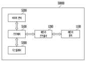
도 1은 본 발명의 실시 예에 따른 메모리 시스템을 설명하기 위한 블록도이다.1 is a block diagram for explaining a memory system according to an embodiment of the present invention.
도 1을 참조하면, 메모리 시스템(Memory System; 1000)은 데이터가 저장되는 메모리 장치(Memory Device; 1100)와, 호스트(Host; 2000)의 제어에 따라 메모리 장치(1100)를 제어하는 메모리 컨트롤러(Memory Controller; 1200)를 포함할 수 있다.Referring to FIG. 1, a memory system (Memory System) 1000 includes a memory device (Memory Device) 1100 in which data is stored, and a memory controller that controls the
호스트(2000)는 PCI-E(Peripheral Component Interconnect - Express), ATA(Advanced Technology Attachment), SATA(Serial ATA), PATA(Parallel ATA), 또는 SAS(serial attached SCSI)와 같은 인터페이스 프로토콜을 사용하여 메모리 시스템(1000)과 통신할 수 있다. 또한 호스트(2000)와 메모리 시스템(1000) 간의 인터페이스 프로토콜들은 상술한 예에 한정되지 않으며, USB(Universal Serial Bus), MMC(Multi-Media Card), ESDI(Enhanced Small Disk Interface), 또는 IDE(Integrated Drive Electronics) 등과 같은 다른 인터페이스 프로토콜들 중 하나일 수 있다.The
메모리 장치(1100)는 메모리 컨트롤러(1200)의 제어에 응답하여 동작한다. 실시 예로서, 메모리 장치(1100)는 플래시 메모리 장치(Flash Memory Device) 일 수 있다. 메모리 장치(1100)는 복수의 메모리 블록들을 갖는 메모리 셀 어레이를 포함할 수 있다.The
메모리 장치(1100)는 메모리 컨트롤러(1200)로부터 채널을 통해 커맨드(CMD) 및 어드레스(ADD)를 수신하고, 메모리 셀 어레이 중 어드레스(ADD)에 의해 선택된 영역을 액세스하도록 구성된다. 즉, 메모리 장치(1100)는 어드레스(ADD)에 의해 선택된 영역에 대해 커맨드(CMD)에 해당하는 내부 동작을 수행한다. 예를 들어 메모리 장치(1100)는 프로그램 동작에 대응하는 커맨드(CMD), 어드레스(ADD), 데이터(DATA)에 응답하여 선택된 메모리 블록에 대한 프로그램 동작을 수행한다. 또한 메모리 장치(1100)는 리드 동작에 대응하는 커맨드(CMD) 및 어드레스(ADD)에 응답하여 선택된 메모리 블록에 대한 리드 동작을 수행하고, 리드된 데이터(DATA)는 메모리 컨트롤러(1200)로 출력될 수 있다.The
실시 예로써, 메모리 장치(1100)는 내부 회로(400) 및 데이터 출력 회로(500)를 포함하여 구성될 수 있다. 내부 회로(400)는 프로그램 동작 시 커맨드(CMD), 어드레스(ADD), 데이터(DATA)에 응답하여 선택된 메모리 블록에 대한 프로그램 동작을 수행한다. 또한 내부 회로(400)는 리드 동작 시 커맨드(CMD) 및 어드레스(ADD)에 응답하여 선택된 메모리 블록에 대한 리드 동작을 수행한다. 데이터 출력 회로(500)는 리드 동작시 내부 회로(400)에 의해 리드된 데이터를 수신하여 메모리 컨트롤러(1200)로 출력할 수 있다.As an embodiment, the
메모리 컨트롤러(1200)는 메모리 시스템(1000)의 동작을 전반적으로 제어하며, 호스트(2000)와 메모리 장치(1100) 사이의 데이터 교환을 제어할 수 있다. 예를 들면, 메모리 컨트롤러(1200)는 호스트(2000)로부터의 요청(request)에 따라 메모리 장치(1100)를 제어하여 데이터를 프로그램하거나 리드하거나, 프로그램된 데이터를 소거할 수 있다. 예를 들어 메모리 컨트롤러(1200)는 호스트(2000)로부터의 요청에 따라 각 제반 동작에 대응하는 커맨드(CMD), 어드레스(ADD), 및 데이터(DATA)를 메모리 장치(1100)로 출력할 수 있으며, 메모리 장치(1100)로부터 데이터(DATA)를 수신하여 호스트(2000)로 출력할 수 있다.The
메모리 컨트롤러(1200)는 프로세서(100), 메모리(200), 및 데이터 출력 회로(300)를 포함하여 구성될 수 있다.The
프로세서(100)는 메모리 장치(1100)의 리드 동작, 프로그램 동작, 소거 동작, 그리고 배경(background) 동작을 제어하도록 구성된다. 프로세서(100)는 메모리 장치(1100)를 제어하기 위한 펌웨어(firmware)를 구동하도록 구성된다.The
호스트(2000)로부터 요청이 수신될 경우, 프로세서(100)는 호스트(2000)로부터 수신되는 요청에 대응하는 커맨드를 생성하고, 호스트(2000)로부터 수신되는 논리 어드레스(Logical Block Address)를 물리 블록 어드레스(Physical Block Address)로 변환하여 어드레스를 생성한다. 실시 예로서, 프로세서(100)는 플래시 변환 레이어(Flash Translation Layer, FTL)의 기능을 수행한다.When a request is received from the
메모리(200)는 프로세서(100)의 제어에 응답하여 동작한다. 메모리(200)는 프로세서(100)의 동작 메모리, 캐시 메모리 또는 버퍼 메모리로 사용될 수 있다. 메모리(200)는 프로세서(100)가 실행하는 코드들 및 커맨드들을 저장할 수 있다. 메모리(200)는 프로세서(100)에 의해 처리되는 데이터를 저장할 수 있다. 메모리(200)는 SRAM(Static RAM), 또는 DRAM(Dynamic RAM)을 포함할 수 있다.The
데이터 출력 회로(300)는 프로세서(100)에서 생성된 커맨드와 어드레스 및 메모리(200)에서 출력되는 데이터를 수신하고, 수신된 커맨드와 어드레스 및 데이터를 메모리 장치(1100)에 적합한 신호 레벨로 변환시켜 커맨드(CMD), 어드레스(ADD), 및 데이터(DATA)를 출력한다.The
본 발명의 실시 예에서는 메모리 컨트롤러(1200)가 메모리 장치(1100)로 커맨드(CMD), 어드레스(ADD), 및 데이터(DATA)를 출력하는 데이터 출력 회로(300)를 포함하는 것으로 도시 및 설명되었으나, 이에 한정되지 아니하고 메모리 장치(1100)로부터 수신된 데이터를 호스트(2000)로 출력하기 위한 데이터 출력 회로를 더 포함하도록 구성할 수 있다.In an embodiment of the present invention, the
도 2는 도 1의 데이터 출력 회로(300)를 설명하기 위한 블록도이다.FIG. 2 is a block diagram for explaining the
메모리 컨트롤로(도 1의 1200) 내에 포함되어 구성된 데이터 출력 회로(300) 및 메모리 장치(도 1의 1100) 내에 포함되어 구성된 데이터 출력 회로(500)는 구성 및 동작이 유사하므로 데이터 출력 회로(300)을 일예로 자세하게 설명하도록 한다.The
도 2를 참조하면, 데이터 출력 회로(300)는 전압 생성 회로(310), ZQ 캘리브레이션 코드 생성 회로(320), 프리 드라이버 회로(330), 데이터 프리 드라이버 회로(340), 및 메인 드라이버 회로(350)를 포함하여 구성될 수 있다.Referring to FIG. 2, the
전압 생성 회로(310)는 제1 전원 전압(VDD)과 클럭 신호(CLK)에 응답하여 일정한 레벨로 레귤레이팅된 동작 전압(VDDCP)을 생성하여 출력한다. 전압 생성 회로(310)는 제1 전원 전압(VDD)이 외부 환경 변화에 의해 전위 레벨이 변화되어도 이와 무관하게 일정한 전위 레벨을 갖는 동작 전압(VDDCP)을 생성하여 출력한다. 동작 전압(VDDCP)은 메인 드라이버 회로(350)에서 출력되는 출력 데이터(DATA_out)의 제1 로직 레벨(예를 들어 하이 레벨)의 전위에 따라 조절될 수 있다.The
전압 생성 회로(310)는 고전압(VPP)을 생성하는 차지 펌프(311), 고전압(VPP)을 레귤레이팅하여 동작 전압(VDDCP)을 출력하는 레귤레이터(312), 및 메인 드라이버 회로(350)에서 출력되는 출력 데이터(DATA_out)의 제1 로직 레벨과 동일한 전위 레벨을 갖는 레플리카 전압(Vreplica)을 출력하는 레플리카 회로(313)를 포함한다.The
차지 펌프(311)는 일정한 주기를 갖는 클럭 신호(CLK)에 응답하여 제1 전원 전압(VDD)을 이용한 펌핑 동작을 수행하여 고전압(VPP)을 생성하여 출력한다.The
레귤레이터(312)는 차지 펌프(311)로부터 고전압(VPP)을 수신하고, 레플리카 전압(Vreplica)과 기준 전압(Vref)을 비교하여 인에이블 제어 신호(EN_CS)를 생성하여 출력한다. 차지 펌프(311)는 인에이블 제어 신호(EN_CS)에 응답하여 펌핑 동작을 수행하거나 수행중인 펌핑 동작을 중단할 수 있다. 즉, 레귤레이터(312)는 레플리카 회로(313)로부터 수신된 레플리카 전압(Vreplica)과 기준 전압(Vref)을 비교하여 펌핑 동작을 제어하는 인에이블 제어 신호(EN_CS)를 생성하고, 차지 펌프(311)는 인에이블 제어 신호(EN_CS)에 응답하여 펌핑 동작을 수행하거나 수행중인 펌핑 동작을 중단하여 동작 전압(VDDCP)의 전위 레벨을 조절하여 출력한다. 동작 전압(VDDCP)은 제1 전원 전압(VDD)보다 높은 전위 레벨을 갖는 것이 바람직하다.The
예를 들어 레플리카 전압(Vreplica)이 기준 전압(Vref)보다 전위 레벨이 높을 경우, 레귤레이터(312)는 인에이블 제어 신호(EN_CS)를 비활성화시켜 차지 펌프(311)의 펌핑 동작을 중단시켜 동작 전압(VDDCP)의 전위 레벨을 하강시키고, 레플리카 전압(Vreplica)이 기준 전압(Vref)보다 전위 레벨이 낮을 경우, 레귤레이터(312)는 인에이블 제어 신호(EN_CS)를 활성화시켜 차지 펌프(311)의 펌핑 동작을 수행시켜 동작 전압(VDDCP)의 전위 레벨을 상승시킬 수 있다. For example, when the replica voltage (Vreplica) has a potential level higher than the reference voltage (Vref), the
레플리카 회로(313)는 프리 드라이버 회로(330) 및 메인 드라이버 회로(350)와 동일한 구조로 구성될 수 있으며, 더욱 바람직하게는 풀업 프리 드라이버 회로(330) 및 메인 드라이버 회로(350)와 동일한 회로 구조를 설계된 구성을 포함하도록 구성되며, 메인 드라이버 회로(350)에서 출력되는 출력 데이터(DATA_out)의 제1 로직 레벨과 동일한 전위 레벨을 갖는 레플리카 전압(Vreplica)을 생성하여 출력하도록 설계될 수 있다. 따라서, 전압 생성 회로(310)는 메인 드라이버 회로(350)에서 출력되는 출력 데이터(DATA_out)의 제1 로직 레벨에 따라 전위 레벨이 조절되는 동작 전압(VDDCP)을 생성하여 출력할 수 있다.The
레플리카 회로(313)는 레귤레이터(312)에 포함되도록 구성될 수 있다.The
ZQ 캘리브레이션 코드 생성 회로(320)는 온도 변화 및 전원 전압 변화를 감지하여 이에 대응하는 풀업 캘리브레이션 코드 신호들(PU_cal_code<n:1>) 및 풀다운 캘리브레이션 코드 신호들(PD_cal_code<n:1>)을 생성하여 출력할 수 있다. 예를 들어 ZQ 캘리브레이션 코드 생성 회로(320)는 검출된 온도와 기준 온도와의 차이 값 및 검출된 전원 전압의 레벨과 기준 레벨과의 차이 값에 따라 코드 값이 변화되는 풀업 캘리브레이션 코드 신호들(PU_cal_code<n:1>) 및 풀다운 캘리브레이션 코드 신호들(PD_cal_code<n:1>)을 생성하여 출력할 수 있다.The ZQ calibration
프리 드라이버 회로(330)는 풀업 캘리브레이션 코드 신호들(PU_cal_code<n:1>) 및 풀다운 캘리브레이션 코드 신호들(PD_cal_code<n:1>)에 응답하여 풀업 코드 신호들(PU_code<n:1>) 및 풀다운 코드 신호들(PD_code<n:1>)을 생성하여 출력하되, 전압 생성 회로(310)에서 출력되는 동작 전압(VDDCP)에 따라 풀업 코드 신호들(PU_code<n:1>) 및 풀다운 코드 신호들(PD_code<n:1>)의 전위 레벨을 동작 전압(VDDCP) 레벨로 변환시켜 출력한다. 예를 들어 풀업 코드 신호들(PU_code<n:1>) 및 풀다운 코드 신호들(PD_code<n:1>)의 로직 하이 레벨의 신호들을 동작 전압(VDDCP) 레벨로 상승시켜 출력한다.The
프리 드라이버 회로(330)는 풀업 프리 드라이버(331) 및 풀다운 프리 드라이버(332)를 포함하여 구성될 수 있다. 풀업 프리 드라이버(331)는 풀업 캘리브레이션 코드 신호들(PU_cal_code<n:1>)에 응답하여 동작 전압(VDDCP) 레벨 및 접지 전압 레벨을 갖는 풀업 코드 신호들(PU_code<n:1>)를 생성하여 출력한다. 풀다운 프리 드라이버(332)는 풀다운 캘리브레이션 코드 신호들(PD_cal_code<n:1>)에 응답하여 동작 전압(VDDCP) 레벨 및 접지 전압 레벨을 갖는 풀다운 코드 신호들(PD_code<n:1>)을 생성하여 출력한다.The
데이터 프리 드라이버 회로(340)는 출력하고자하는 데이터 또는 신호(DATA)를 반전시켜 내부 데이터(DATA_pre)로 출력한다. 데이터 프리 드라이버 회로(340)는 제1 전원 전압(VDD)을 이용하여 출력되는 내부 데이터(DATA_pre) 중 로직 하이 레벨의 신호들을 제1 전원 전압(VDD) 레벨로 생성하여 출력한다.The data
메인 드라이버 회로(350)는 내부 데이터(DATA_pre)에 응답하여 출력 데이터(DATA_out)를 생성하여 출력하되, 풀업 코드 신호들(PU_code<n:1>) 및 풀다운 코드 신호들(PD_code<n:1>)에 응답하여 데이터 출력 동작의 구동 세기(driving strength)를 조절한다. 메인 드라이버 회로(350)는 제2 내부 전원 전압(VDDQ)을 공급받아 구동되는 것이 바람직하다.The
상술한 본원 발명의 실시 예에 따른 데이터 출력 회로는 전압 생성 회로(310)를 이용하여 메인 드라이버 회로(350)에서 출력되는 출력 데이터(DATA_out)의 제1 로직 레벨에 따라 전위 레벨이 조절되는 동작 전압(VDDCP)을 생성하고, 프리 드라이버 회로(330)가 동작 전압(VDDCP)을 이용하여 풀업 코드 신호들(PU_code<n:1>) 및 풀다운 코드 신호들(PD_code<n:1>)을 생성한다. 따라서 풀업 코드 신호들(PU_code<n:1>) 및 풀다운 코드 신호들(PD_code<n:1>) 중 하이 레벨의 신호는 전원 전압 변화에 무관하게 동작 전압(VDDCP)과 동일한 전위 레벨을 갖는다. 이에 ZQ 캘리브레이션 코드 생성 회로(320)는 전원 전압 변화를 검출하여 이를 캘리브레이션하는 동작을 스킵하고 일정 값으로 고정된 코드 값과 온도 변화에 따른 코드 값을 이용하여 풀업 캘리브레이션 코드 신호들(PU_cal_code<n:1>) 및 풀다운 캘리브레이션 코드 신호들(PD_cal_code<n:1>)을 생성할 수 있다. 이로 인하여 데이터 출력 회로(300)의 동작 속도가 개선될 수 있다.The data output circuit according to the embodiment of the present invention described above is an operating voltage whose potential level is adjusted according to the first logic level of the output data (DATA_out) output from the
도 3은 도 2의 메인 드라이버 회로(350)를 설명하기 위한 회로도이다.FIG. 3 is a circuit diagram for explaining the
메인 드라이버 회로(350)는 풀업 회로(351), 풀다운 회로(352), 및 트리밍 회로(353)를 포함하여 구성된다.The
풀업 회로(351)는 제2 전원 전압(VDDQ)이 인가되는 단자와 트리밍 회로(353) 사이에 연결되며, 내부 데이터(DATA_pre)에 응답하여 제2 전원 전압(VDDQ)을 트리밍 회로(353)에 인가한다. 풀업 회로(351)는 PMOS 트랜지스터로 구성될 수 있다.The pull-up
풀다운 회로(352)는 트리밍 회로(353)와 접지 전원(Vss)이 연결되는 단자 사이에 연결되며, 내부 데이터(DATA_pre)에 응답하여 접지 전원(Vss)을 트리밍 회로(353)에 인가한다. 풀다운 회로(352)는 NMOS 트랜지스터로 구성될 수 있다.The pull-
트리밍 회로(353)는 복수의 트리밍 유닛(353<1> 내지 353<n>)을 포함한다. 복수의 트리밍 유닛(353<1> 내지 353<n>) 각각은 출력 노드(Node)에 공통으로 연결된다.The
복수의 트리밍 유닛(353<1> 내지 353<n>) 각각은 풀업 코드 신호들(PU_code<n:1>) 중 어느 하나 및 풀다운 코드 신호들(PD_code<n:1>) 중 어느 하나에 응답하여 활성화 또는 비활성화되어 데이터 출력 동작의 구동 세기(driving strength)를 조절한다.Each of the plurality of trimming
복수의 트리밍 유닛(353<1> 내지 353<n>)은 구조가 서로 유사하므로 트리밍 유닛(353<1>)를 일예로 설명하도록 한다.Since the plurality of trimming
트리밍 유닛(353<1>)은 풀업 회로(351)와 풀다운 회로(352) 사이에 직렬 연결된 NMOS 트랜지스터(N1) 및 NMOS 트랜지스터(N2)를 포함하여 구성된다.The
NMOS 트랜지스터(N1)와 NMOS 트랜지스터(N2) 사이의 노드는 출력 노드(Node)와 연결된다.The node between the NMOS transistor (N1) and the NMOS transistor (N2) is connected to the output node (Node).
NMOS 트랜지스터(N1)는 풀업 코드 신호(PU_code<1>)에 응답하여 턴온 또는 턴오프되어, 풀업 회로(351)를 통해 인가되는 제2 전원 전압(VDDQ)을 출력 노드(Node)에 인가하거나 차단한다.The NMOS transistor (N1) is turned on or off in response to the pull-up code signal (PU_code<1>) to apply the second power voltage (VDDQ ) applied through the pull-up
NMOS 트랜지스터(N2)는 풀다운 코드 신호(PD_code<1>)에 응답하여 턴온 또는 턴오프되어, 출력 노드(Node)에 풀다운 회로(352)를 통해 인가되는 접지 전원(Vss)을 인가하거나 차단한다.The NMOS transistor N2 is turned on or off in response to the pull-down code signal PD_code<1> to apply or block the ground power Vss applied through the pull-
예를 들어, 메인 드라이버 회로(350)는 로직 로우 레벨(접지 전압 레벨)의 내부 데이터(DATA_pre)와 로직 하이 레벨(VDDCP)의 풀업 코드 신호(PU_code<1>)에 응답하여 출력 노드(Node)에 제2 전원 전압(VDDQ)을 인가하고, 로직 하이 레벨(제1 전원 전압(VDD) 레벨)의 내부 데이터(DATA_pre) 또는 로직 로우 레벨(접지 전압 레벨)의 풀업 코드 신호(PU_code<1>)에 응답하여 출력 노드(Node)에 제2 전원 전압(VDDQ)이 인가되는 것을 차단한다. 풀업 코드 신호(PU_code<1>)의 로직 하이 레벨의 전위 레벨은 동작 전압(VDDCP) 레벨이며, 동작 전압(VDDCP)은 제2 전원 전압(VDDQ)보다 전위 레벨이 높은 것이 바람직하다.For example, the
본 발명의 실시 예에서는 풀업 코드 신호(PU_code<1>)에 응답하여 턴온 또는 턴오프되는 트랜지스터를 NMOS 트랜지스터(N1)로 구성한다. NMOS 트랜지스터는 PMOS 트랜지스터에 비해 동일 전류 전송 능력을 가지는 트랜지스터의 사이즈를 작게 설계 가능하다.In an embodiment of the present invention, the transistor that is turned on or off in response to the pull-up code signal (PU_code<1>) is configured as the NMOS transistor (N1). Compared to PMOS transistors, NMOS transistors can be designed to have a smaller transistor size with the same current transmission capability.
삭제delete
삭제delete
삭제delete
예를 들어, 메인 드라이버 회로(350)는로직 하이 레벨(제2 전원 전압 레벨(VDD))의 내부 데이터(DATA_pre)와 로직 하이 레벨(VDDCP)의 풀다운 코드 신호(PD_code<1>)에 응답하여 출력 노드(Node)에 접지 전원(Vss)을 인가하여 디스차지하고, 로직 로우 레벨(접지 전원 레벨)의 내부 데이터(DATA_pre) 또는 로직 로우 레벨(접지 전압 레벨)의 풀다운 코드 신호(PD_code<1>)에 응답하여 출력 노드(Node)에 접지 전원(Vss)이 인가되는 것을 차단한다.For example, the
메인 드라이버 회로(350)는 수신되는 풀업 코드 신호들(PU_code<n:1>) 및 풀다운 코드 신호들(PD_code<n:1>) 중 로직 하이 레벨로 인가되는 신호들의 수가 증가할수록 복수의 트리밍 유닛(353<1> 내지 353<n>)들 중 활성화되는 트리밍 유닛의 수가 증가하게 되어 구동 세기가 증가하게 되고, 풀업 코드 신호들(PU_code<n:1>) 및 풀다운 코드 신호들(PD_code<n:1>) 중 로직 하이 레벨이 인가되는 신호들의 신호들의 수가 감소할수록 복수의 트리밍 유닛(353<1> 내지 353<n>)들 중 활성화되는 트리밍 유닛의 수가 감소하게 되어 구동 세기가 감소하게 된다.The
도 2 및 도 3을 참조하여, 데이터 출력 회로(300)의 동작을 설명하면 다음과 같다.With reference to FIGS. 2 and 3 , the operation of the
전압 생성 회로(310)는 제1 전원 전압(VDD)과 클럭 신호(CLK)에 응답하여 일정한 레벨로 레귤레이팅된 동작 전압(VDDCP)을 생성하여 출력한다. ZQ 캘리브레이션 코드 생성 회로(320)는 온도 변화를 감지하여 이에 대응하는 풀업 캘리브레이션 코드 신호들(PU_cal_code<n:1>) 및 풀다운 캘리브레이션 코드 신호들(PD_cal_code<n:1>)을 생성하여 출력한다. 이때 ZQ 캘리브레이션 코드 생성 회로(320)는 전원 전압 변화에 따른 캘리브레이션 동작은 스킵하고, 일정 값으로 고정된 코드 값과 온도 변화에 따른 코드 값을 이용하여 풀업 캘리브레이션 코드 신호들(PU_cal_code<n:1>) 및 풀다운 캘리브레이션 코드 신호들(PD_cal_code<n:1>)을 생성할 수 있다. 프리 드라이버 회로(330)는 풀업 캘리브레이션 코드 신호들(PU_cal_code<n:1>) 및 풀다운 캘리브레이션 코드 신호들(PD_cal_code<n:1>)에 응답하여 풀업 코드 신호들(PU_code<n:1>) 및 풀다운 코드 신호들(PD_code<n:1>)을 생성하여 출력하되, 전압 생성 회로(310)에서 출력되는 동작 전압(VDDCP)에 따라 풀업 코드 신호들(PU_code<n:1>) 및 풀다운 코드 신호들(PD_code<n:1>)의 전위 레벨을 동작 전압(VDDCP) 레벨로 변환시켜 출력한다. 풀업 프리 드라이버(331)는 풀업 캘리브레이션 코드 신호들(PU_cal_code<n:1>)에 응답하여 동작 전압(VDDCP) 레벨 및 접지 전압 레벨을 갖는 풀업 코드 신호들(PU_code<n:1>)를 생성하여 출력한다. 풀다운 프리 드라이버(332)는 풀다운 캘리브레이션 코드 신호들(PD_cal_code<n:1>)에 응답하여 동작 전압(VDDCP) 레벨 및 접지 전압 레벨을 갖는 풀다운 코드 신호들(PD_code<n:1>)을 생성하여 출력한다. 데이터 프리 드라이버 회로(340)는 출력하고자하는 데이터 또는 신호(DATA)를 반전시켜 내부 데이터(DATA_pre)로 출력한다. 예를 들어 데이터(DATA)가 로직 하이 레벨일 경우 데이터 프리 드라이버 회로(340)는 로직 로우 레벨의 내부 데이터(DATA_pre)를 생성하여 출력하고, 데이터(DATA)가 로직 로우 레벨일 경우 데이터 프리 드라이버 회로(340)는 로직 하이 레벨의 내부 데이터(DATA_pre)를 생성하여 출력한다. 메인 드라이버 회로(350)는 내부 데이터(DATA_pre)에 응답하여 출력 데이터(DATA_out)를 생성하여 출력하되, 풀업 코드 신호들(PU_code<n:1>) 및 풀다운 코드 신호들(PD_code<n:1>)에 응답하여 데이터 출력 동작의 구동 세기(driving strength)를 조절하여 출력한다.The
상술한 본원 발명의 실시 예에 따르면, 전압 생성 회로를 이용하여 제1 전원 전압 레벨보다 높고 일정한 전위 레벨로 생성되는 동작 전압을 이용하여 풀업 코드 신호 및 풀다운 코드 신호들을 생성함으로써, 전원 전압 변화에 따른 ZQ 캘리브레이션 동작을 스킵할 수 있으며, 풀업 코드 신호의 전위 레벨이 제 및 제2 전원 전압 레벨보다 높아 메인 드라이버의 풀업부를 NMOS 트랜지스터로 구성하여 풀업부의 사이즈를 감소시켜 설계할 수 있다.According to the above-described embodiment of the present invention, a pull-up code signal and a pull-down code signal are generated using an operating voltage that is higher than the first power supply voltage level and generated at a constant potential level using a voltage generation circuit, according to the change in power supply voltage. The ZQ calibration operation can be skipped, and the potential level of the pull-up code signal is higher than the first and second power supply voltage levels, so the pull-up part of the main driver can be designed with an NMOS transistor to reduce the size of the pull-up part.
본원 발명의 실시 예에서는 데이터 출력 회로가 메모리 컨트롤러 및 메모리 장치에 포함되는 것을 일예로 설명하였으나, 이에 한정되지 않고 데이터 또는 신호들을 출력하는 전자 장치들에 포함되도록 설계 가능하다.In an embodiment of the present invention, the data output circuit has been described as an example of being included in a memory controller and a memory device, but the circuit is not limited to this and can be designed to be included in electronic devices that output data or signals.
도 4는 메모리 시스템의 다른 실시 예를 설명하기 위한 도면이다.Figure 4 is a diagram for explaining another embodiment of a memory system.
도 4를 참조하면, 메모리 시스템(Memory System; 30000)은 이동 전화기(cellular phone), 스마트폰(smart phone), 태블릿(tablet) PC, PDA(personal digital assistant) 또는 무선 통신 장치로 구현될 수 있다. 메모리 시스템(30000)은 메모리 장치(1100)와 상기 메모리 장치(1100)의 동작을 제어할 수 있는 메모리 컨트롤러(1200)를 포함할 수 있다. 메모리 컨트롤러(1200)는 프로세서(Processor; 3100)의 제어에 따라 메모리 장치(1100)의 데이터 액세스 동작, 예컨대 프로그램(program) 동작, 소거(erase) 동작 또는 리드(read) 동작을 제어할 수 있다.Referring to FIG. 4, the memory system (Memory System) 30000 may be implemented as a cellular phone, a smart phone, a tablet PC, a personal digital assistant (PDA), or a wireless communication device. . The
메모리 장치(1100)에 프로그램된 데이터는 메모리 컨트롤러(1200)의 제어에 따라 디스플레이(Display; 3200)를 통하여 출력될 수 있다.Data programmed in the
무선 송수신기(RADIO TRANSCEIVER; 3300)는 안테나(ANT)를 통하여 무선 신호를 주고받을 수 있다. 예컨대, 무선 송수신기(3300)는 안테나(ANT)를 통하여 수신된 무선 신호를 프로세서(3100)에서 처리(process)될 수 있는 신호로 변경할 수 있다. 따라서, 프로세서(3100)는 무선 송수신기(3300)로부터 출력된 신호를 처리(process)하고 처리(process)된 신호를 메모리 컨트롤러(1200) 또는 디스플레이(3200)로 전송할 수 있다. 메모리 컨트롤러(1200)는 프로세서(3100)에 의하여 처리(process)된 신호를 메모리 장치(1100)에 프로그램할 수 있다. 또한, 무선 송수신기(3300)는 프로세서(3100)로부터 출력된 신호를 무선 신호로 변경하고 변경된 무선 신호를 안테나(ANT)를 통하여 외부 장치로 출력할 수 있다. 입력 장치(Input Device; 3400)는 프로세서(3100)의 동작을 제어하기 위한 제어 신호 또는 프로세서(3100)에 의하여 처리(process)될 데이터를 입력할 수 있는 장치로서, 터치 패드(touch pad)와 컴퓨터 마우스(computer mouse)와 같은 포인팅 장치(pointing device), 키패드(keypad) 또는 키보드로 구현될 수 있다. 프로세서(3100)는 메모리 컨트롤러(1200)로부터 출력된 데이터, 무선 송수신기(3300)로부터 출력된 데이터, 또는 입력 장치(3400)로부터 출력된 데이터가 디스플레이(3200)를 통하여 출력될 수 있도록 디스플레이(3200)의 동작을 제어할 수 있다.The wireless transceiver (RADIO TRANSCEIVER; 3300) can send and receive wireless signals through an antenna (ANT). For example, the
실시 예에 따라, 메모리 장치(1100)의 동작을 제어할 수 있는 메모리 컨트롤러(1200)는 프로세서(3100)의 일부로서 구현될 수 있고 또한 프로세서(3100)와 별도의 칩으로 구현될 수 있다. 또한 메모리 컨트롤러(1200)는 도 1에 도시된 메모리 컨트롤러의 예시를 통해 구현될 수 있으며, 메모리 장치(1100)는 도 1에 도시된 메모리 장치의 예시를 통해 구현될 수 있다.Depending on the embodiment, the
도 5는 메모리 시스템의 다른 실시 예를 설명하기 위한 도면이다.Figure 5 is a diagram for explaining another embodiment of a memory system.
도 5를 참조하면, 메모리 시스템(Memory System; 40000)은 PC(personal computer), 태블릿(tablet) PC, 넷-북(net-book), e-리더(e-reader), PDA(personal digital assistant), PMP(portable multimedia player), MP3플레이어, 또는 MP4 플레이어로 구현될 수 있다.Referring to FIG. 5, a memory system (Memory System) 40000 is used in a personal computer (PC), a tablet PC, a net-book, an e-reader, and a personal digital assistant (PDA). ), PMP (portable multimedia player), MP3 player, or MP4 player.
메모리 시스템(40000)은 메모리 장치(Memory Device; 1100)와 상기 메모리 장치(1100)의 데이터 처리 동작을 제어할 수 있는 메모리 컨트롤러(memory Controller; 1200)를 포함할 수 있다.The
프로세서(Processor; 4100)는 입력 장치(Input Device; 4200)를 통하여 입력된 데이터에 따라 메모리 장치(1100)에 저장된 데이터를 디스플레이(Display; 4300)를 통하여 출력할 수 있다. 예컨대, 입력 장치(4200)는 터치 패드 또는 컴퓨터 마우스와 같은 포인팅 장치, 키패드, 또는 키보드로 구현될 수 있다.The
프로세서(4100)는 메모리 시스템(40000)의 전반적인 동작을 제어할 수 있고 메모리 컨트롤러(1200)의 동작을 제어할 수 있다. 실시 예에 따라 메모리 장치(1100)의 동작을 제어할 수 있는 메모리 컨트롤러(1200)는 프로세서(4100)의 일부로서 구현되거나, 프로세서(4100)와 별도의 칩으로 구현될 수 있다. 또한 메모리 컨트롤러(1200)는 도 1에 도시된 메모리 컨트롤러의 예시를 통해 구현될 수 있으며, 메모리 장치(1100)는 도 1에 도시된 메모리 장치의 예시를 통해 구현될 수 있다.The
도 6은 메모리 시스템의 다른 실시 예를 설명하기 위한 도면이다.Figure 6 is a diagram for explaining another embodiment of a memory system.
도 6을 참조하면, 메모리 시스템(50000)은 이미지 처리 장치, 예컨대 디지털 카메라, 디지털 카메라가 부착된 이동 전화기, 디지털 카메라가 부착된 스마트 폰, 또는 디지털 카메라가 부착된 태블릿 PC로 구현될 수 있다.Referring to FIG. 6, the
메모리 시스템(50000)은 메모리 장치(Memory Device; 1100)와 상기 메모리 장치(1100)의 데이터 처리 동작, 예컨대 프로그램 동작, 소거 동작 또는 리드 동작을 제어할 수 있는 메모리 컨트롤러(1200)를 포함한다.The
메모리 시스템(50000)의 이미지 센서(Image Sensor; 5200)는 광학 이미지를 디지털 신호들로 변환할 수 있고, 변환된 디지털 신호들은 프로세서(Processor; 5100) 또는 메모리 컨트롤러(1200)로 전송될 수 있다. 프로세서(5100)의 제어에 따라, 상기 변환된 디지털 신호들은 디스플레이(Display; 5300)를 통하여 출력되거나 메모리 컨트롤러(1200)를 통하여 메모리 장치(1100)에 저장될 수 있다. 또한, 메모리 장치(1100)에 저장된 데이터는 프로세서(5100) 또는 메모리 컨트롤러(1200)의 제어에 따라 디스플레이(5300)를 통하여 출력될 수 있다.The
실시 예에 따라 메모리 장치(1100)의 동작을 제어할 수 있는 메모리 컨트롤러(1200)는 프로세서(5100)의 일부로서 구현되거나 프로세서(5100)와 별개의 칩으로 구현될 수 있다. 또한 메모리 컨트롤러(1200)는 도 1에 도시된 메모리 컨트롤러의 예시를 통해 구현될 수 있으며, 메모리 장치(1100)는 도 1에 도시된 메모리 장치의 예시를 통해 구현될 수 있다.Depending on the embodiment, the
도 7은 메모리 시스템의 다른 실시 예를 설명하기 위한 도면이다.Figure 7 is a diagram for explaining another embodiment of a memory system.
도 7을 참조하면, 메모리 시스템(Memory System; 70000)은 메모리 카드(memory card) 또는 스마트 카드(smart card)로 구현될 수 있다. 메모리 시스템(70000)은 메모리 장치(Memory Device; 1100), 메모리 컨트롤러(Memory Controller; 1200) 및 카드 인터페이스(Card Interface; 7100)를 포함할 수 있다.Referring to FIG. 7, a memory system (Memory System) 70000 may be implemented as a memory card or smart card. The
메모리 컨트롤러(1200)는 메모리 장치(1100)와 카드 인터페이스(7100) 사이에서 데이터의 교환을 제어할 수 있다. 실시 예에 따라, 카드 인터페이스(7100)는 SD(secure digital) 카드 인터페이스 또는 MMC(multi-media card) 인터페이스일 수 있으나 이에 한정되는 것은 아니다.The
카드 인터페이스(7100)는 호스트(HOST; 60000)의 프로토콜에 따라 호스트(60000)와 메모리 컨트롤러(1200) 사이에서 데이터 교환을 인터페이스할 수 있다. 실시 예에 따라 카드 인터페이스(7100)는 USB(Universal Serial Bus)프로토콜, IC(Inter Chip)-USB 프로토콜을 지원할 수 있다. 여기서, 카드 인터페이스는 호스트(60000)가 사용하는 프로토콜을 지원할 수 있는 하드웨어, 상기 하드웨어에 탑재된 소프트웨어 또는 신호 전송 방식을 의미할 수 있다.The
메모리 시스템(70000)이 PC, 태블릿 PC, 디지털 카메라, 디지털 오디오 플레이어, 이동 전화기, 콘솔 비디오 게임 하드웨어, 또는 디지털 셋-탑 박스와 같은 호스트(60000)의 호스트 인터페이스(6200)와 접속될 때, 호스트 인터페이스(6200)는 마이크로프로세서(Microprocessor; 6100)의 제어에 따라 카드 인터페이스(7100)와 메모리 컨트롤러(1200)를 통하여 메모리 장치(1100)와 데이터 통신을 수행할 수 있다. 또한 메모리 컨트롤러(1200)는 도 1에 도시된 메모리 컨트롤러의 예시를 통해 구현될 수 있으며, 메모리 장치(1100)는 도 1에 도시된 메모리 장치의 예시를 통해 구현될 수 있다.When
본 발명의 상세한 설명에서는 구체적인 실시 예에 관하여 설명하였으나, 본 발명의 범위와 기술적 사상에서 벗어나지 않는 한도 내에서 여러 가지 변형이 가능하다. 그러므로 본 발명의 범위는 상술한 실시 예에 국한되어 정해져서는 안되며 후술하는 특허청구범위뿐만 아니라 이 발명의 특허청구범위와 균등한 것들에 의해 정해져야 한다.In the detailed description of the present invention, specific embodiments have been described, but various modifications are possible without departing from the scope and technical spirit of the present invention. Therefore, the scope of the present invention should not be limited to the above-described embodiments, but should be determined by the claims and equivalents of this invention as well as the claims described later.
이상과 같이 본 발명은 비록 한정된 실시 예와 도면에 의해 설명되었으나, 본 발명은 상기의 실시 예에 한정되는 것은 아니며, 본 발명이 속하는 분야에서 통상의 지식을 가진 자라면 이러한 기재로부터 다양한 수정 및 변형이 가능하다.As described above, although the present invention has been described with limited examples and drawings, the present invention is not limited to the above-mentioned examples, and various modifications and variations can be made from these descriptions by those skilled in the art. This is possible.
그러므로, 본 발명의 범위는 설명된 실시 예에 국한되어 정해져서는 아니 되며, 후술하는 특허청구범위뿐 아니라 이 특허청구범위와 균등한 것들에 의해 정해져야 한다.Therefore, the scope of the present invention should not be limited to the described embodiments, but should be determined by the claims and equivalents thereof as well as the claims described later.
상술한 실시 예들에서, 모든 단계는 선택적으로 수행의 대상이 되거나 생략의 대상이 될 수 있다. 또한 각 실시 예에서 단계들은 반드시 순서대로 일어날 필요는 없으며, 뒤바뀔 수 있다. 한편, 본 명세서와 도면에 개시된 본 명세서의 실시 예들은 본 명세서의 기술 내용을 쉽게 설명하고 본 명세서의 이해를 돕기 위해 특정 예를 제시한 것일 뿐이며, 본 명세서의 범위를 한정하고자 하는 것은 아니다. 즉 본 명세서의 기술적 사상에 바탕을 둔 다른 변형 예들이 실시 가능하다는 것은 본 명세서가 속하는 기술 분야에서 통상의 지식을 가진 자에게 자명한 것이다.In the above-described embodiments, all steps may be selectively performed or omitted. Additionally, in each embodiment the steps do not necessarily occur in order and may be reversed. Meanwhile, the embodiments of the present specification disclosed in the specification and drawings are merely provided as specific examples to easily explain the technical content of the present specification and aid understanding of the present specification, and are not intended to limit the scope of the present specification. In other words, it is obvious to those skilled in the art that other modifications based on the technical idea of the present specification can be implemented.
한편, 본 명세서와 도면에는 본 발명의 바람직한 실시 예에 대하여 개시하였으며, 비록 특정 용어들이 사용되었으나, 이는 단지 본 발명의 기술 내용을 쉽게 설명하고 발명의 이해를 돕기 위한 일반적인 의미에서 사용된 것이지, 본 발명의 범위를 한정하고자 하는 것은 아니다. 여기에 개시된 실시 예 외에도 본 발명의 기술적 사상에 바탕을 둔 다른 변형 예들이 실시 가능하다는 것은 본 발명이 속하는 기술 분야에서 통상의 지식을 가진 자에게 자명한 것이다.Meanwhile, the specification and drawings disclose preferred embodiments of the present invention, and although specific terms are used, they are used only in a general sense to easily explain the technical content of the present invention and aid understanding of the present invention. It is not intended to limit the scope of the invention. In addition to the embodiments disclosed herein, it is obvious to those skilled in the art that other modifications based on the technical idea of the present invention can be implemented.
1000 : 메모리 시스템1100 : 메모리 장치
1200 : 메모리 컨트롤러100 : 프로세서
200 : 메모리300 : 데이터 출력 회로
400 : 내부 회로500 : 데이터 출력 회로1000: memory system 1100: memory device
1200: memory controller 100: processor
200: memory 300: data output circuit
400: Internal circuit 500: Data output circuit
Claims (17)
Translated fromKorean상기 동작 전압에 기초하여 풀업 코드 신호들 및 풀다운 코드 신호들을 생성하는 프리 드라이버 회로;
출력 데이터 신호를 출력하되, 상기 풀업 코드 신호들 및 상기 풀다운 코드 신호들에 기초하여 상기 출력 데이터 신호의 출력 세기를 조절하는 메인 드라이버 회로를 포함하고,
상기 전압 생성 회로는,
고전압을 생성하는 펌핑 동작을 수행하는 차지 펌프;
상기 출력 데이터 신호 중 제1 로직 레벨과 동일한 전위 레벨을 가지는 레플리카 전압을 생성하는 레플리카 회로; 및
상기 고전압을 레귤레이팅하여 상기 동작 전압을 출력하되, 상기 레플리카 전압과 기준 전압에 기초하여 상기 펌핑 동작의 제어 신호를 생성하여 상기 동작 전압의 전위 레벨을 조절하는 레귤레이터를 포함하는 데이터 출력 회로.
a voltage generating circuit that generates an operating voltage;
a pre-driver circuit that generates pull-up code signals and pull-down code signals based on the operating voltage;
A main driver circuit that outputs an output data signal and adjusts the output strength of the output data signal based on the pull-up code signals and the pull-down code signals,
The voltage generating circuit is,
A charge pump that performs a pumping action to generate high voltage;
a replica circuit that generates a replica voltage having the same potential level as a first logic level among the output data signals; and
A data output circuit comprising a regulator that regulates the high voltage to output the operating voltage and generates a control signal for the pumping operation based on the replica voltage and the reference voltage to adjust the potential level of the operating voltage.
상기 동작 전압은 제1 전원 전압의 전위 레벨 및 제2 전원 전압의 전위 레벨보다 높은 전위 레벨을 갖고,
상기 차지 펌프는 상기 제1 전원 전압, 클럭 신호, 및 상기 제어 신호에 응답하여 상기 펌핑 동작을 수행하여 상기 고전압을 생성하고,
상기 레귤레이터는 상기 제어 신호를 기초로 상기 고전압의 전위 레벨을 조절하여 상기 동작 전압의 전위 레벨을 조절하는 데이터 출력 회로.
According to claim 1,
The operating voltage has a potential level higher than the potential level of the first power supply voltage and the potential level of the second power supply voltage,
The charge pump generates the high voltage by performing the pumping operation in response to the first power voltage, the clock signal, and the control signal,
The regulator is a data output circuit that adjusts the potential level of the operating voltage by adjusting the potential level of the high voltage based on the control signal.
캘리브레이션 코드 신호들을 생성하기 위한 ZQ 캘리브레이션 코드 생성 회로를 더 포함하며,
상기 ZQ 캘리브레이션 코드 생성 회로는 온도 변화에 따른 제1 캘리브레이션 코드 값과 전원 전압 변화에 따른 제2 캘리브레이션 코드값에 따라 상기 캘리브레이션 코드 신호들을 생성하고,
상기 프리 드라이버 회로는 상기 캘리브레이션 코드 신호들 및 상기 동작 전압에 기초하여 상기 풀업 코드 신호 및 상기 풀다운 코드 신호들을 생성하는 데이터 출력 회로.
According to claim 1,
It further includes a ZQ calibration code generation circuit for generating calibration code signals,
The ZQ calibration code generation circuit generates the calibration code signals according to a first calibration code value according to temperature change and a second calibration code value according to power supply voltage change,
The pre-driver circuit is a data output circuit that generates the pull-up code signal and the pull-down code signal based on the calibration code signals and the operating voltage.
상기 ZQ 캘리브레이션 코드 생성 회로는 상기 전원 전압 변화를 검출하여 이를 캘리브레이션하는 동작을 스킵하고 상기 제2 캘리브레이션 코드값을 일정 값으로 고정된 코드 값으로 사용하는 데이터 출력 회로.
According to claim 3,
The ZQ calibration code generation circuit is a data output circuit that skips the operation of detecting and calibrating the change in the power supply voltage and uses the second calibration code value as a code value fixed to a constant value.
데이터 신호 및 제1 전원 전압에 기초하여 프리 데이터 신호를 출력하는 데이터 프리 드라이버 회로를 더 포함하고,
상기 메인 드라이버 회로는 상기 프리 데이터 신호 및 제2 전원 전압에 기초하여 상기 출력 데이터 신호를 출력하는 데이터 출력 회로.
According to claim 1,
It further includes a data pre-driver circuit that outputs a pre-data signal based on the data signal and the first power voltage,
The main driver circuit is a data output circuit that outputs the output data signal based on the free data signal and the second power voltage.
상기 프리 드라이버 회로는 캘리브레이션 코드 신호들에 따라 상기 풀업 코드 신호들을 생성하는 풀업 프리 드라이버; 및
상기 캘리브레이션 코드 신호들에 따라 상기 풀다운 코드 신호들을 생성하는 풀다운 프리 드라이버를 포함하며,
상기 풀업 프리 드라이버 및 상기 풀다운 프리 드라이버는 상기 동작 전압을 이용하여 상기 풀업 코드 신호들 및 상기 풀다운 코드 신호들 중 로직 하이 레벨의 신호들을 동작 전압 레벨로 상승시켜 출력하는 데이터 출력 회로.
According to claim 5,
The pre-driver circuit includes a pull-up pre-driver that generates the pull-up code signals according to calibration code signals; and
A pull-down pre-driver that generates the pull-down code signals according to the calibration code signals,
A data output circuit wherein the pull-up pre-driver and the pull-down pre-driver use the operating voltage to increase logic high level signals among the pull-up code signals and the pull-down code signals to an operating voltage level and output them.
상기 메인 드라이버 회로는 상기 제2 전원 전압이 인가되는 단자와 접지 전원이 인가되는 단자 사이에 직렬 연결된 풀업 회로, 트리밍 회로, 및 풀다운 회로를 포함하며,
상기 풀업 회로는 상기 프리 데이터 신호에 응답하여 상기 제2 전원 전압을 상기 트리밍 회로에 인가하고,
상기 풀다운 회로는 상기 프리 데이터 신호에 응답하여 상기 접지 전원을 상기 트리밍 회로에 인가하는 데이터 출력 회로.
According to claim 5,
The main driver circuit includes a pull-up circuit, a trimming circuit, and a pull-down circuit connected in series between a terminal to which the second power voltage is applied and a terminal to which ground power is applied,
The pull-up circuit applies the second power voltage to the trimming circuit in response to the free data signal,
The pull-down circuit is a data output circuit that applies the ground power to the trimming circuit in response to the free data signal.
상기 풀업 회로는 PMOS 트랜지스터로 구성되고, 상기 풀다운 회로는 NMOS 트랜지스터로 구성되는 데이터 출력 회로.
According to claim 7,
A data output circuit wherein the pull-up circuit is comprised of a PMOS transistor, and the pull-down circuit is comprised of an NMOS transistor.
상기 트리밍 회로는 출력 노드와 공통으로 연결된 복수의 트리밍 유닛들을 포함하며,
상기 복수의 트리밍 유닛들 각각은 상기 풀업 코드 신호들 중 하나와 상기 풀다운 코드 신호들 중 하나에 응답하여 활성화 또는 비활성화되는 데이터 출력 회로.
According to claim 7,
The trimming circuit includes a plurality of trimming units commonly connected to an output node,
A data output circuit wherein each of the plurality of trimming units is activated or deactivated in response to one of the pull-up code signals and one of the pull-down code signals.
상기 복수의 트리밍 유닛들 각각은 상기 풀업 회로와 상기 출력 노드 사이에 연결되어 상기 풀업 코드 신호들 중 하나에 응답하여 턴온 또는 턴오프되는 제1 NMOS 트랜지스터; 및
상기 풀다운 회로와 상기 출력 노드 사이에 연결되어 상기 풀다운 코드 신호들 중 하나에 응답하여 턴온 또는 턴오프되는 제2 NMOS 트랜지스터를 포함하는 데이터 출력 회로.
According to clause 9,
Each of the plurality of trimming units includes a first NMOS transistor connected between the pull-up circuit and the output node and turned on or off in response to one of the pull-up code signals; and
A data output circuit including a second NMOS transistor connected between the pull-down circuit and the output node and turned on or off in response to one of the pull-down code signals.
상기 동작 전압에 기초하여 풀업 코드 신호들 및 풀다운 코드 신호들을 생성하되, 상기 풀업 코드 신호들 및 풀다운 코드 신호들이 접지 전압 레벨 또는 동작 전압 레벨을 갖도록 생성하는 프리 드라이버 회로; 및
출력 데이터 신호를 출력하되, 상기 풀업 코드 신호들 및 상기 풀다운 코드 신호들에 기초하여 상기 출력 데이터 신호의 출력 세기를 조절하는 메인 드라이버 회로를 포함하고,
상기 전압 생성 회로는,
고전압을 생성하는 펌핑 동작을 수행하는 차지 펌프;
상기 출력 데이터 신호의 제1 로직 레벨과 동일한 전위 레벨을 가지는 레플리카 전압을 생성하는 레플리카 회로;
상기 고전압을 레귤레이팅하여 상기 동작 전압을 출력하되, 상기 레플리카 전압과 기준 전압에 기초하여 상기 펌핑 동작의 제어 신호를 생성하여 상기 동작 전압의 전위 레벨을 조절하는 레귤레이터를 포함하는 데이터 출력 회로.
a voltage generating circuit that generates an operating voltage;
a pre-driver circuit that generates pull-up code signals and pull-down code signals based on the operating voltage so that the pull-up code signals and pull-down code signals have a ground voltage level or an operating voltage level; and
A main driver circuit that outputs an output data signal and adjusts the output strength of the output data signal based on the pull-up code signals and the pull-down code signals,
The voltage generating circuit is,
A charge pump that performs a pumping action to generate high voltage;
a replica circuit that generates a replica voltage having the same potential level as the first logic level of the output data signal;
A data output circuit comprising a regulator that regulates the high voltage to output the operating voltage and generates a control signal for the pumping operation based on the replica voltage and the reference voltage to adjust the potential level of the operating voltage.
상기 동작 전압은 제1 전원 전압의 전위 레벨 및 제2 전원 전압의 전위 레벨보다 높은 전위 레벨을 갖고,
상기 차지 펌프는 상기 제1 전원 전압, 클럭 신호, 및 상기 제어 신호에 응답하여 상기 펌핑 동작을 수행하여 상기 고전압을 생성하고,
상기 레귤레이터는 상기 제어 신호를 기초로 상기 고전압의 전위 레벨을 조절하여 상기 동작 전압의 전위 레벨을 조절하는 데이터 출력 회로.
According to claim 11,
The operating voltage has a potential level higher than the potential level of the first power supply voltage and the potential level of the second power supply voltage,
The charge pump generates the high voltage by performing the pumping operation in response to the first power voltage, the clock signal, and the control signal,
The regulator is a data output circuit that adjusts the potential level of the operating voltage by adjusting the potential level of the high voltage based on the control signal.
데이터 신호 및 제1 전원 전압에 기초하여 프리 데이터 신호를 출력하는 데이터 프리 드라이버 회로를 더 포함하고,
상기 메인 드라이버 회로는 상기 프리 데이터 신호 및 제2 전원 전압에 기초하여 상기 출력 데이터 신호를 출력하고,
상기 메인 드라이버 회로는 제2 전원 전압이 인가되는 제1 단자와 접지 전원이 인가되는 제2 단자 사이에 직렬 연결된 풀업 회로, 트리밍 회로, 및 풀다운 회로를 포함하는 데이터 출력 회로.
According to claim 11,
It further includes a data pre-driver circuit that outputs a pre-data signal based on the data signal and the first power voltage,
The main driver circuit outputs the output data signal based on the free data signal and the second power voltage,
The main driver circuit is a data output circuit including a pull-up circuit, a trimming circuit, and a pull-down circuit connected in series between a first terminal to which a second power voltage is applied and a second terminal to which ground power is applied.
상기 트리밍 회로는 출력 노드와 공통으로 연결된 복수의 트리밍 유닛들을 포함하며, 상기 복수의 트리밍 유닛들 각각은 상기 풀업 코드 신호들 중 하나와 상기 풀다운 코드 신호들 중 하나에 응답하여 활성화 또는 비활성화되는 데이터 출력 회로.
According to claim 13,
The trimming circuit includes a plurality of trimming units commonly connected to an output node, and each of the plurality of trimming units outputs data that is activated or deactivated in response to one of the pull-up code signals and one of the pull-down code signals. Circuit.
상기 풀업 회로는 상기 제1 단자와 상기 트리밍 회로 사이에 연결되며, 상기 프리 데이터 신호에 응답하여 턴온 또는 턴오프되는 PMOS 트랜지스터를 포함하는 데이터 출력 회로.
According to claim 13,
The pull-up circuit is connected between the first terminal and the trimming circuit, and includes a PMOS transistor that is turned on or off in response to the free data signal.
상기 풀다운 회로는 상기 제2 단자와 상기 트리밍 회로 사이에 연결되며, 상기 프리 데이터 신호에 응답하여 턴온 또는 턴오프되는 NMOS 트랜지스터를 포함하는 데이터 출력 회로.
According to claim 13,
The pull-down circuit is connected between the second terminal and the trimming circuit, and includes an NMOS transistor turned on or off in response to the free data signal.
상기 복수의 트리밍 유닛들 각각은 상기 풀업 회로와 상기 출력 노드 사이에 연결되어 상기 풀업 코드 신호들 중 하나에 응답하여 턴온 또는 턴오프되는 제1 NMOS 트랜지스터; 및
상기 풀다운 회로와 상기 출력 노드 사이에 연결되어 상기 풀다운 코드 신호들 중 하나에 응답하여 턴온 또는 턴오프되는 제2 NMOS 트랜지스터를 포함하는 데이터 출력 회로.
According to clause 14,
Each of the plurality of trimming units includes a first NMOS transistor connected between the pull-up circuit and the output node and turned on or off in response to one of the pull-up code signals; and
A data output circuit including a second NMOS transistor connected between the pull-down circuit and the output node and turned on or off in response to one of the pull-down code signals.
Priority Applications (3)
| Application Number | Priority Date | Filing Date | Title |
|---|---|---|---|
| KR1020180063675AKR102657125B1 (en) | 2018-06-01 | 2018-06-01 | Data output circuit |
| US16/248,416US10607667B2 (en) | 2018-06-01 | 2019-01-15 | Data output circuit |
| CN201910104356.2ACN110556135B (en) | 2018-06-01 | 2019-02-01 | Data output circuit |
Applications Claiming Priority (1)
| Application Number | Priority Date | Filing Date | Title |
|---|---|---|---|
| KR1020180063675AKR102657125B1 (en) | 2018-06-01 | 2018-06-01 | Data output circuit |
Publications (2)
| Publication Number | Publication Date |
|---|---|
| KR20190137459A KR20190137459A (en) | 2019-12-11 |
| KR102657125B1true KR102657125B1 (en) | 2024-04-15 |
Family
ID=68694236
Family Applications (1)
| Application Number | Title | Priority Date | Filing Date |
|---|---|---|---|
| KR1020180063675AActiveKR102657125B1 (en) | 2018-06-01 | 2018-06-01 | Data output circuit |
Country Status (3)
| Country | Link |
|---|---|
| US (1) | US10607667B2 (en) |
| KR (1) | KR102657125B1 (en) |
| CN (1) | CN110556135B (en) |
Families Citing this family (7)
| Publication number | Priority date | Publication date | Assignee | Title |
|---|---|---|---|---|
| JP2017097825A (en) | 2015-11-16 | 2017-06-01 | 株式会社東芝 | Host equipment and expansion devices |
| JP6890701B1 (en) | 2020-05-19 | 2021-06-18 | 華邦電子股▲ふん▼有限公司Winbond Electronics Corp. | Code shift calculation circuit and code shift value calculation method |
| KR20210153240A (en)* | 2020-06-10 | 2021-12-17 | 에스케이하이닉스 주식회사 | Temperature sensor and method for controlling the thereof |
| TWI734531B (en)* | 2020-06-17 | 2021-07-21 | 華邦電子股份有限公司 | Code shift calculation circuit and method for calculating code shift value |
| US10951206B1 (en) | 2020-08-05 | 2021-03-16 | Nanya Technology Corporation | Off chip driving system and signal compensation method |
| US12197765B2 (en)* | 2021-11-01 | 2025-01-14 | Advanced Energy Industries, Inc. | Tensor non-linear signal processing random access memory |
| US11741023B1 (en)* | 2022-02-09 | 2023-08-29 | Pixart Imaging Inc. | Pointing device and method capable of correcting its USB state by monitoring voltage/state of USB communication interface |
Citations (4)
| Publication number | Priority date | Publication date | Assignee | Title |
|---|---|---|---|---|
| US20070070780A1 (en) | 2005-09-29 | 2007-03-29 | Hynix Semiconductor Inc. | Output driving device |
| US20120119578A1 (en) | 2010-11-11 | 2012-05-17 | Elpida Memory, Inc. | Semiconductor device having pull-up circuit and pull-down circuit |
| US20130070542A1 (en) | 2011-03-18 | 2013-03-21 | Genusion, Inc. | Replica Circuit and It's Applications |
| US20140225656A1 (en)* | 2006-11-03 | 2014-08-14 | Micron Technology, Inc. | Output slew rate control |
Family Cites Families (11)
| Publication number | Priority date | Publication date | Assignee | Title |
|---|---|---|---|---|
| KR100780646B1 (en)* | 2006-10-31 | 2007-11-30 | 주식회사 하이닉스반도체 | An on die termination device and a semiconductor device comprising the same. |
| KR100902104B1 (en)* | 2007-06-08 | 2009-06-09 | 주식회사 하이닉스반도체 | Semiconductor memory device |
| US7876123B2 (en)* | 2007-10-09 | 2011-01-25 | Lsi Corporation | High speed multiple memory interface I/O cell |
| KR100917642B1 (en)* | 2008-08-14 | 2009-09-17 | 주식회사 하이닉스반도체 | Sense amplifier drive control circuit and method, and core voltage discharge circuit of the circuit |
| KR101020291B1 (en)* | 2009-02-03 | 2011-03-07 | 주식회사 하이닉스반도체 | Pre-driver and output driver circuit using the same |
| KR101806817B1 (en)* | 2010-10-20 | 2017-12-11 | 삼성전자주식회사 | Data output buffer and semiconductor memory device having the same |
| KR20150049267A (en)* | 2013-10-29 | 2015-05-08 | 삼성전자주식회사 | A semiconductor memory device and a method of operating the same |
| KR20150124521A (en)* | 2014-04-28 | 2015-11-06 | 에스케이하이닉스 주식회사 | Power up signal generation circuit and semiconductor device including same |
| KR20180003938A (en)* | 2016-07-01 | 2018-01-10 | 삼성전자주식회사 | Reception interface circuit and memory system including the same |
| KR102609441B1 (en)* | 2016-08-25 | 2023-12-05 | 에스케이하이닉스 주식회사 | Data transmitting device, semiconductor apparatus and system including the same |
| US10003335B2 (en)* | 2016-08-25 | 2018-06-19 | SK Hynix Inc. | Data transmission device, and semiconductor device and system including the same |
- 2018
- 2018-06-01KRKR1020180063675Apatent/KR102657125B1/enactiveActive
- 2019
- 2019-01-15USUS16/248,416patent/US10607667B2/enactiveActive
- 2019-02-01CNCN201910104356.2Apatent/CN110556135B/enactiveActive
Patent Citations (4)
| Publication number | Priority date | Publication date | Assignee | Title |
|---|---|---|---|---|
| US20070070780A1 (en) | 2005-09-29 | 2007-03-29 | Hynix Semiconductor Inc. | Output driving device |
| US20140225656A1 (en)* | 2006-11-03 | 2014-08-14 | Micron Technology, Inc. | Output slew rate control |
| US20120119578A1 (en) | 2010-11-11 | 2012-05-17 | Elpida Memory, Inc. | Semiconductor device having pull-up circuit and pull-down circuit |
| US20130070542A1 (en) | 2011-03-18 | 2013-03-21 | Genusion, Inc. | Replica Circuit and It's Applications |
Also Published As
| Publication number | Publication date |
|---|---|
| KR20190137459A (en) | 2019-12-11 |
| US10607667B2 (en) | 2020-03-31 |
| CN110556135A (en) | 2019-12-10 |
| CN110556135B (en) | 2022-11-04 |
| US20190371372A1 (en) | 2019-12-05 |
Similar Documents
| Publication | Publication Date | Title |
|---|---|---|
| KR102657125B1 (en) | Data output circuit | |
| US10599170B2 (en) | Internal voltage generation circuit and memory device including the internal voltage generation circuit | |
| KR102735060B1 (en) | Memory device and operating method of the memory device | |
| US11133073B2 (en) | Memory device and memory system including the same | |
| US9531365B1 (en) | Signal generator adjusting a duty cycle and semiconductor apparatus using the same | |
| TW202006717A (en) | Data output buffer | |
| KR102495364B1 (en) | Buffer circuit and memory device having the same | |
| US10629246B2 (en) | Data output buffer | |
| US10991401B2 (en) | Input/output circuit, memory device having the same, and operating method thereof | |
| US10666232B2 (en) | Level shifter and memory system including the same | |
| US11170827B2 (en) | Data buffer and memory device having the same | |
| US10679684B2 (en) | Data output buffer having pull-up main driver and memory device having the data output buffer | |
| US10644678B2 (en) | Oscillator and memory system including the same |
Legal Events
| Date | Code | Title | Description |
|---|---|---|---|
| PA0109 | Patent application | Patent event code:PA01091R01D Comment text:Patent Application Patent event date:20180601 | |
| PG1501 | Laying open of application | ||
| PA0201 | Request for examination | Patent event code:PA02012R01D Patent event date:20210601 Comment text:Request for Examination of Application Patent event code:PA02011R01I Patent event date:20180601 Comment text:Patent Application | |
| E902 | Notification of reason for refusal | ||
| PE0902 | Notice of grounds for rejection | Comment text:Notification of reason for refusal Patent event date:20230420 Patent event code:PE09021S01D | |
| E90F | Notification of reason for final refusal | ||
| PE0902 | Notice of grounds for rejection | Comment text:Final Notice of Reason for Refusal Patent event date:20230829 Patent event code:PE09021S02D | |
| E801 | Decision on dismissal of amendment | ||
| E90F | Notification of reason for final refusal | ||
| PE0801 | Dismissal of amendment | Patent event code:PE08012E01D Comment text:Decision on Dismissal of Amendment Patent event date:20231122 Patent event code:PE08011R01I Comment text:Amendment to Specification, etc. Patent event date:20231013 Patent event code:PE08011R01I Comment text:Amendment to Specification, etc. Patent event date:20230608 Patent event code:PE08011R01I Comment text:Amendment to Specification, etc. Patent event date:20210601 | |
| PE0902 | Notice of grounds for rejection | Comment text:Final Notice of Reason for Refusal Patent event date:20231122 Patent event code:PE09021S02D | |
| E701 | Decision to grant or registration of patent right | ||
| PE0701 | Decision of registration | Patent event code:PE07011S01D Comment text:Decision to Grant Registration Patent event date:20240216 | |
| GRNT | Written decision to grant | ||
| PR0701 | Registration of establishment | Comment text:Registration of Establishment Patent event date:20240408 Patent event code:PR07011E01D | |
| PR1002 | Payment of registration fee | Payment date:20240409 End annual number:3 Start annual number:1 | |
| PG1601 | Publication of registration |