KR102654870B1 - Backlight unit for 3D image display and method of manufacturing the backlight unit - Google Patents
Backlight unit for 3D image display and method of manufacturing the backlight unitDownload PDFInfo
- Publication number
- KR102654870B1 KR102654870B1KR1020160148592AKR20160148592AKR102654870B1KR 102654870 B1KR102654870 B1KR 102654870B1KR 1020160148592 AKR1020160148592 AKR 1020160148592AKR 20160148592 AKR20160148592 AKR 20160148592AKR 102654870 B1KR102654870 B1KR 102654870B1
- Authority
- KR
- South Korea
- Prior art keywords
- guide plate
- light guide
- diffraction gratings
- backlight unit
- light
- Prior art date
- Legal status (The legal status is an assumption and is not a legal conclusion. Google has not performed a legal analysis and makes no representation as to the accuracy of the status listed.)
- Active
Links
- 238000004519manufacturing processMethods0.000titleclaimsdescription18
- 239000011347resinSubstances0.000claimsdescription68
- 229920005989resinPolymers0.000claimsdescription68
- 239000000758substrateSubstances0.000claimsdescription34
- 229920001187thermosetting polymerPolymers0.000claimsdescription7
- 238000003825pressingMethods0.000claimsdescription6
- 239000004973liquid crystal related substanceSubstances0.000claimsdescription3
- 238000000034methodMethods0.000description14
- 239000000463materialSubstances0.000description8
- 238000010586diagramMethods0.000description4
- 239000011521glassSubstances0.000description4
- XUIMIQQOPSSXEZ-UHFFFAOYSA-NSiliconChemical compound[Si]XUIMIQQOPSSXEZ-UHFFFAOYSA-N0.000description3
- 230000007423decreaseEffects0.000description3
- 229910052710siliconInorganic materials0.000description3
- 239000010703siliconSubstances0.000description3
- 230000000295complement effectEffects0.000description2
- 229920003023plasticPolymers0.000description2
- 239000012780transparent materialSubstances0.000description2
- 230000000694effectsEffects0.000description1
- 238000000609electron-beam lithographyMethods0.000description1
- 238000000206photolithographyMethods0.000description1
- 230000010076replicationEffects0.000description1
Images


Classifications
- G—PHYSICS
- G02—OPTICS
- G02B—OPTICAL ELEMENTS, SYSTEMS OR APPARATUS
- G02B6/00—Light guides; Structural details of arrangements comprising light guides and other optical elements, e.g. couplings
- G02B6/0001—Light guides; Structural details of arrangements comprising light guides and other optical elements, e.g. couplings specially adapted for lighting devices or systems
- G02B6/0011—Light guides; Structural details of arrangements comprising light guides and other optical elements, e.g. couplings specially adapted for lighting devices or systems the light guides being planar or of plate-like form
- G02B6/0033—Means for improving the coupling-out of light from the light guide
- G02B6/0035—Means for improving the coupling-out of light from the light guide provided on the surface of the light guide or in the bulk of it
- G02B6/0036—2-D arrangement of prisms, protrusions, indentations or roughened surfaces
- G—PHYSICS
- G02—OPTICS
- G02B—OPTICAL ELEMENTS, SYSTEMS OR APPARATUS
- G02B6/00—Light guides; Structural details of arrangements comprising light guides and other optical elements, e.g. couplings
- G02B6/0001—Light guides; Structural details of arrangements comprising light guides and other optical elements, e.g. couplings specially adapted for lighting devices or systems
- G02B6/0011—Light guides; Structural details of arrangements comprising light guides and other optical elements, e.g. couplings specially adapted for lighting devices or systems the light guides being planar or of plate-like form
- G02B6/0013—Means for improving the coupling-in of light from the light source into the light guide
- G02B6/0015—Means for improving the coupling-in of light from the light source into the light guide provided on the surface of the light guide or in the bulk of it
- G02B6/0016—Grooves, prisms, gratings, scattering particles or rough surfaces
- G—PHYSICS
- G02—OPTICS
- G02B—OPTICAL ELEMENTS, SYSTEMS OR APPARATUS
- G02B30/00—Optical systems or apparatus for producing three-dimensional [3D] effects, e.g. stereoscopic images
- G02B30/20—Optical systems or apparatus for producing three-dimensional [3D] effects, e.g. stereoscopic images by providing first and second parallax images to an observer's left and right eyes
- G02B30/26—Optical systems or apparatus for producing three-dimensional [3D] effects, e.g. stereoscopic images by providing first and second parallax images to an observer's left and right eyes of the autostereoscopic type
- G02B30/27—Optical systems or apparatus for producing three-dimensional [3D] effects, e.g. stereoscopic images by providing first and second parallax images to an observer's left and right eyes of the autostereoscopic type involving lenticular arrays
- G—PHYSICS
- G02—OPTICS
- G02B—OPTICAL ELEMENTS, SYSTEMS OR APPARATUS
- G02B5/00—Optical elements other than lenses
- G02B5/18—Diffraction gratings
- G02B5/1861—Reflection gratings characterised by their structure, e.g. step profile, contours of substrate or grooves, pitch variations, materials
- G—PHYSICS
- G02—OPTICS
- G02B—OPTICAL ELEMENTS, SYSTEMS OR APPARATUS
- G02B6/00—Light guides; Structural details of arrangements comprising light guides and other optical elements, e.g. couplings
- G02B6/0001—Light guides; Structural details of arrangements comprising light guides and other optical elements, e.g. couplings specially adapted for lighting devices or systems
- G02B6/0011—Light guides; Structural details of arrangements comprising light guides and other optical elements, e.g. couplings specially adapted for lighting devices or systems the light guides being planar or of plate-like form
- G02B6/0013—Means for improving the coupling-in of light from the light source into the light guide
- G02B6/0023—Means for improving the coupling-in of light from the light source into the light guide provided by one optical element, or plurality thereof, placed between the light guide and the light source, or around the light source
- G02B6/0026—Wavelength selective element, sheet or layer, e.g. filter or grating
- G—PHYSICS
- G02—OPTICS
- G02B—OPTICAL ELEMENTS, SYSTEMS OR APPARATUS
- G02B6/00—Light guides; Structural details of arrangements comprising light guides and other optical elements, e.g. couplings
- G02B6/0001—Light guides; Structural details of arrangements comprising light guides and other optical elements, e.g. couplings specially adapted for lighting devices or systems
- G02B6/0011—Light guides; Structural details of arrangements comprising light guides and other optical elements, e.g. couplings specially adapted for lighting devices or systems the light guides being planar or of plate-like form
- G02B6/0033—Means for improving the coupling-out of light from the light guide
- G02B6/0035—Means for improving the coupling-out of light from the light guide provided on the surface of the light guide or in the bulk of it
- G—PHYSICS
- G02—OPTICS
- G02B—OPTICAL ELEMENTS, SYSTEMS OR APPARATUS
- G02B6/00—Light guides; Structural details of arrangements comprising light guides and other optical elements, e.g. couplings
- G02B6/0001—Light guides; Structural details of arrangements comprising light guides and other optical elements, e.g. couplings specially adapted for lighting devices or systems
- G02B6/0011—Light guides; Structural details of arrangements comprising light guides and other optical elements, e.g. couplings specially adapted for lighting devices or systems the light guides being planar or of plate-like form
- G02B6/0033—Means for improving the coupling-out of light from the light guide
- G02B6/0058—Means for improving the coupling-out of light from the light guide varying in density, size, shape or depth along the light guide
- G02B6/0061—Means for improving the coupling-out of light from the light guide varying in density, size, shape or depth along the light guide to provide homogeneous light output intensity
- G—PHYSICS
- G02—OPTICS
- G02B—OPTICAL ELEMENTS, SYSTEMS OR APPARATUS
- G02B6/00—Light guides; Structural details of arrangements comprising light guides and other optical elements, e.g. couplings
- G02B6/0001—Light guides; Structural details of arrangements comprising light guides and other optical elements, e.g. couplings specially adapted for lighting devices or systems
- G02B6/0011—Light guides; Structural details of arrangements comprising light guides and other optical elements, e.g. couplings specially adapted for lighting devices or systems the light guides being planar or of plate-like form
- G02B6/0065—Manufacturing aspects; Material aspects
- G—PHYSICS
- G02—OPTICS
- G02B—OPTICAL ELEMENTS, SYSTEMS OR APPARATUS
- G02B6/00—Light guides; Structural details of arrangements comprising light guides and other optical elements, e.g. couplings
- G02B6/24—Coupling light guides
- G02B6/26—Optical coupling means
- G02B6/34—Optical coupling means utilising prism or grating
- G—PHYSICS
- G02—OPTICS
- G02F—OPTICAL DEVICES OR ARRANGEMENTS FOR THE CONTROL OF LIGHT BY MODIFICATION OF THE OPTICAL PROPERTIES OF THE MEDIA OF THE ELEMENTS INVOLVED THEREIN; NON-LINEAR OPTICS; FREQUENCY-CHANGING OF LIGHT; OPTICAL LOGIC ELEMENTS; OPTICAL ANALOGUE/DIGITAL CONVERTERS
- G02F1/00—Devices or arrangements for the control of the intensity, colour, phase, polarisation or direction of light arriving from an independent light source, e.g. switching, gating or modulating; Non-linear optics
- G02F1/01—Devices or arrangements for the control of the intensity, colour, phase, polarisation or direction of light arriving from an independent light source, e.g. switching, gating or modulating; Non-linear optics for the control of the intensity, phase, polarisation or colour
- G02F1/13—Devices or arrangements for the control of the intensity, colour, phase, polarisation or direction of light arriving from an independent light source, e.g. switching, gating or modulating; Non-linear optics for the control of the intensity, phase, polarisation or colour based on liquid crystals, e.g. single liquid crystal display cells
- G02F1/133—Constructional arrangements; Operation of liquid crystal cells; Circuit arrangements
- G02F1/1333—Constructional arrangements; Manufacturing methods
- G02F1/1335—Structural association of cells with optical devices, e.g. polarisers or reflectors
- G02F1/1336—Illuminating devices
- G02F1/133602—Direct backlight
- G—PHYSICS
- G02—OPTICS
- G02F—OPTICAL DEVICES OR ARRANGEMENTS FOR THE CONTROL OF LIGHT BY MODIFICATION OF THE OPTICAL PROPERTIES OF THE MEDIA OF THE ELEMENTS INVOLVED THEREIN; NON-LINEAR OPTICS; FREQUENCY-CHANGING OF LIGHT; OPTICAL LOGIC ELEMENTS; OPTICAL ANALOGUE/DIGITAL CONVERTERS
- G02F1/00—Devices or arrangements for the control of the intensity, colour, phase, polarisation or direction of light arriving from an independent light source, e.g. switching, gating or modulating; Non-linear optics
- G02F1/01—Devices or arrangements for the control of the intensity, colour, phase, polarisation or direction of light arriving from an independent light source, e.g. switching, gating or modulating; Non-linear optics for the control of the intensity, phase, polarisation or colour
- G02F1/13—Devices or arrangements for the control of the intensity, colour, phase, polarisation or direction of light arriving from an independent light source, e.g. switching, gating or modulating; Non-linear optics for the control of the intensity, phase, polarisation or colour based on liquid crystals, e.g. single liquid crystal display cells
- G02F1/133—Constructional arrangements; Operation of liquid crystal cells; Circuit arrangements
- G02F1/1333—Constructional arrangements; Manufacturing methods
- G02F1/1335—Structural association of cells with optical devices, e.g. polarisers or reflectors
- G02F1/1336—Illuminating devices
- G02F1/133615—Edge-illuminating devices, i.e. illuminating from the side
Landscapes
- Physics & Mathematics (AREA)
- General Physics & Mathematics (AREA)
- Optics & Photonics (AREA)
- Nonlinear Science (AREA)
- Mathematical Physics (AREA)
- Chemical & Material Sciences (AREA)
- Crystallography & Structural Chemistry (AREA)
- Engineering & Computer Science (AREA)
- Manufacturing & Machinery (AREA)
- Planar Illumination Modules (AREA)
- Diffracting Gratings Or Hologram Optical Elements (AREA)
Abstract
Translated fromKoreanDescription
Translated fromKorean3차원 영상 디스플레이용 백라이트 유닛체 및 그 제조방법에 관한 것이다.It relates to a backlight unit for 3D image display and a method of manufacturing the same.
일반적으로 3차원 영상은 사람의 두 눈을 통한 스테레오 시각의 원리에 의해 이루어지는데, 두 눈 사이의 거리 때문에 나타나는 양안시차(binocular parallax)가 입체감의 가장 중요한 요인이라고 할 수 있다. 3차원 영상 디스플레이에는 안경을 이용한 3차원 영상 디스플레이와 무안경 방식의 3차원 영상 디스플레이가 있으며, 무안경 방식의 3차원 영상 디스플레이는 안경을 사용하지 않고 좌우 영상을 분리하여 3차원 영상을 얻는 것이다.In general, 3D images are made based on the principle of stereo vision through a person's two eyes, and binocular parallax, which occurs due to the distance between the two eyes, can be said to be the most important factor in the three-dimensional effect. 3D image displays include 3D image displays using glasses and glasses-free 3D image displays. Glasses-free 3D image displays obtain 3D images by separating left and right images without using glasses.
최근에는 무안경 방식 중에서 지향성 백라이트(directional backlight) 기반의 멀티뷰(multiview) 방식이 개발되고 있다. 이러한 지향성 백라이트 기반의 멀티뷰 방식은 백라이튜 유닛의 도광판(LGP; Light Guiding Plate) 표면에 형성된 회절 격자(diffraction grating) 구조를 통해 지향성 광을 형성하는 방식으로, 낮은 크로스 토크(cross-talk)를 구현함으로써 선형하고 깊이감이 있는 3차원 영상을 제공할 수 있다.Recently, among glasses-free methods, a multiview method based on directional backlight is being developed. This directional backlight-based multi-view method generates directional light through a diffraction grating structure formed on the surface of the light guiding plate (LGP) of the backlight unit, resulting in low cross-talk. By implementing , it is possible to provide a 3D image that is linear and has a sense of depth.
3차원 영상 디스플레이용 백라이트 유닛 및 그 제조방법 이 제공된다.A backlight unit for a three-dimensional image display and a method of manufacturing the same are provided.
일 측면에 있어서,In terms of work,
도광판;light guide plate;
상기 도광판의 적어도 일면에 광을 조사하는 광원; 및a light source that irradiates light to at least one surface of the light guide plate; and
상기 도광판의 일면에 마련되어 상기 도광판의 일면으로부터 출사되는 광을 회절시키는 것으로 서로 다른 높이를 가지는 복수의 회절 격자를 포함하는 회절 격자 구조체;를 포함하는 3차원 영상 디스플레이용 백라이트 유닛이 제공된다.A backlight unit for a three-dimensional image display including a diffraction grating structure provided on one surface of the light guide plate and including a plurality of diffraction gratings having different heights to diffract light emitted from the light guide plate.
상기 회절 격자들은 상기 도광판의 일면으로부터 다른 높이를 가지도록 배치되어 높이 구배(height gradient)를 형성할 수 있다. 이 경우, 상기 회절 격자들은 상기 도광판의 광 입사면으로부터 멀어질수록 높은 높이를 가지도록 배치될 수 있다.The diffraction gratings may be arranged to have different heights from one side of the light guide plate to form a height gradient. In this case, the diffraction gratings may be arranged to have a higher height as the distance from the light incident surface of the light guide plate increases.
추가적으로 상기 회절 격자들은 서로 다른 폭을 가질 수도 있다.Additionally, the diffraction gratings may have different widths.
다른 측면에 있어서,On the other side,
백라이트 유닛; 및backlight unit; and
상기 백라이트 유닛으로부터 입사되는 광을 영상 정보에 따라 변조하는 디스플레이 패널;을 포함하고,A display panel that modulates light incident from the backlight unit according to image information,
상기 백라이트 유닛은,The backlight unit is,
도광판;light guide plate;
상기 도광판의 적어도 일면에 광을 조사하는 광원; 및a light source that irradiates light to at least one surface of the light guide plate; and
상기 도광판의 일면에 마련되어 상기 도광판의 일면으로부터 출사되는 광을 회절시키는 것으로 서로 다른 높이를 가지는 복수의 회절 격자를 포함하는 회절 격자 구조체;를 포함하는 3차원 영상 디스플레이 장치가 제공된다.A three-dimensional image display device including a diffraction grating structure provided on one surface of the light guide plate and including a plurality of diffraction gratings having different heights to diffract light emitted from the light guide plate.
상기 디스플레이 패널은 액정 패널을 포함할 수 있다.The display panel may include a liquid crystal panel.
상기 회절 격자들은 상기 도광판의 일면으로부터 다른 높이를 가지도록 배치되어 높이 구배(height gradient)를 형성할 수 있다. 이 경우, 상기 회절 격자들은 상기 도광판의 광 입사면으로부터 멀어질수록 높은 높이를 가지도록 배치될 수 있다.The diffraction gratings may be arranged to have different heights from one side of the light guide plate to form a height gradient. In this case, the diffraction gratings may be arranged to have a higher height as the distance from the light incident surface of the light guide plate increases.
추가적으로 상기 회절 격자들은 서로 다른 폭을 가질 수도 있다.Additionally, the diffraction gratings may have different widths.
또 다른 측면에 있어서,In another aspect,
제1 격자 패턴들을 포함하는 제1 스탬프(stamp)를 마련하는 단계;providing a first stamp including first grid patterns;
기판의 일면에 위치에 따라 조절된 양의 제1 수지(resin)를 도포하는 단계;Applying an amount of first resin adjusted according to location on one surface of the substrate;
상기 제1 스탬프를 가압하여 상기 제1 격자 패턴들 사이에 상기 제1 수지를 채우는 단계; 및filling the first resin between the first grid patterns by pressing the first stamp; and
상기 제1 수지를 경화시켜 상기 기판의 일면에 제1 회절 격자들을 포함하는 제1 회절 격자 구조체를 형성하는 단계;를 포함하는 3차원 영상 디스플레이용 백라이트 유닛의 제조방법이 제공된다.Curing the first resin to form a first diffraction grating structure including first diffraction gratings on one surface of the substrate. A method of manufacturing a backlight unit for a three-dimensional image display including a step is provided.
상기 제1 스탬프의 가압 시 상기 제1 격자 패턴들 사이의 공간들에 채워지는 제1 수지의 높이가 달라지고, 상기 제1 회절 격자들은 다른 높이를 가지도록 형성될 수 있다. 상기 제1 회절 격자들은 일 방향을 따라 점점 높은 높이를 가지도록 형성될 수 있다.When the first stamp is pressed, the height of the first resin filled in the spaces between the first grid patterns changes, and the first diffraction gratings may be formed to have different heights. The first diffraction gratings may be formed to have gradually higher heights along one direction.
상기 제1 격자 패턴들은 동일한 높이를 가질 수 있다. 상기 제1 수지는 예를들면, 광경화성 또는 열경화성 수지를 포함할 수 있다.The first grid patterns may have the same height. The first resin may include, for example, a photocurable or thermosetting resin.
추가적으로 상기 제1 회절 격자들은 서로 다른 폭을 가지도록 형성될 수도 있다.Additionally, the first diffraction gratings may be formed to have different widths.
상기 기판은 도광판을 포함할 수 있다.The substrate may include a light guide plate.
상기 백라이트 유닛의 제조방법은 기판 및 상기 제1 회절 격자 구조체를 마스터 몰드(master mold)로 이용하여 상기 제1 회절 격자들에 대응하는 제2 격자 패턴들을 포함하는 제2 스탬프를 마련하는 단계를 포함할 수 있다.The method of manufacturing the backlight unit includes preparing a second stamp including second grating patterns corresponding to the first diffraction gratings using a substrate and the first diffraction grating structure as a master mold. can do.
이 경우, 상기 백라이트 유닛의 제조방법은 도광판의 일면에 제2 수지를 도포하는 단계; 상기 제2 스탬프를 가압하여 상기 제2 격자 패턴들 사이에 상기 제2 수지를 채우는 단계; 및 상기 제2 수지를 경화시켜 상기 도광판의 일면에 제2 회절 격자들을 포함하는 제2 회절 격자 구조체를 형성하는 단계;를 포함할 수 있다.In this case, the method of manufacturing the backlight unit includes applying a second resin to one surface of the light guide plate; filling the second resin between the second grid patterns by pressing the second stamp; and curing the second resin to form a second diffraction grating structure including second diffraction gratings on one surface of the light guide plate.
상기 제2 스탬프의 가압 시 상기 제2 격자 패턴들 사이의 공간들에 상기 제2 수지가 완전히 채워질 수 있다. 상기 제1 및 제2 회절 격자들은 동일한 형상을 가질 수 있다.When the second stamp is pressed, the spaces between the second grid patterns may be completely filled with the second resin. The first and second diffraction gratings may have the same shape.
예시적인 실시예에 의하면, 도광판의 출사면에 마련된 회절 격자 구조체의 회절 격자들은 위치에 따라 그 높이가 변화되도록 마련됨으로써 회절 격자들의 회절 효율을 위치에 따라 미세하게 조절할 수 있다. 이에 따라, 회절 격자 구조체로부터 나오는 방향성을 가지는 회절된 출사광은 위치에 따라 균일한 세기를 가지는 출사광이 될 수 있으므로, 출사광의 균일도 및 밝기가 확보될 수 있다.According to an exemplary embodiment, the height of the diffraction gratings of the diffraction grating structure provided on the exit surface of the light guide plate is changed depending on the position, so that the diffraction efficiency of the diffraction gratings can be finely adjusted depending on the position. Accordingly, the diffracted emitted light with directionality coming from the diffraction grating structure can be emitted light with uniform intensity depending on the position, and thus uniformity and brightness of the emitted light can be secured.
도 1은 일반적인 3차원 영상 디스플레이용 백라이트 유닛을 개략적으로 도시한 것이다.
도 2는 도 1에 도시된 백라이트 유닛에서, 회절 격자 구조체로부터 나오는 회절된 출사광의 세기를 위치에 따라 도시한 것이다.
도 3은 예시적인 실시예에 따른 3차원 영상 디스플레이용 백라이트 유닛을 도시한 것이다.
도 4는 도 3의 A 부분을 확대하여 도시한 것이다.
도 5는 도 3에 도시된 백라이트 유닛에서, 회절 격자 구조체로부터 나오는 회절된 출사광을 도시한 것이다.
도 6은 다른 예시적인 실시예에 따른 3차원 영상 디스플레이용 백라이트 유닛을 도시한 것이다.
도 7은 다른 예시적인 실시예에 따른 3차원 영상 디스플레이 장치를 도시한 것이다.
도 8 내지 도 14는 예시적인 실시예에 따른 3차원 영상 디스플레이용 백라이트 유닛의 제조방법을 설명하기 위한 도면들이다.
도 15a는 실리콘으로 제작된 마스터 몰드를 찍은 SEM(Scanning Electron Microscope) 사진이다,
도 15b 내지 도 15f는 도 15a에 도시된 마스터 몰드를 이용하여 도 8 내지 도 14에 도시된 방법에 의해 제작된 회절 격자 구조체의 회절 격자들을 찍은 SEM 사진들이다.
도 16은 도 15b 내지 도 15f에 도시된 5개의 위치에 있는 회절 격자들의 높이를 측정한 결과를 도시한 것이다.
도 17 내지 도 23은 다른 예시적인 실시예에 따른 3차원 영상 디스플레이용 백라이트 유닛의 제조방법을 설명하기 위한 도면들이다.Figure 1 schematically shows a backlight unit for a general 3D image display.
FIG. 2 shows the intensity of diffracted light emitted from the diffraction grating structure according to position in the backlight unit shown in FIG. 1.
Figure 3 shows a backlight unit for a three-dimensional image display according to an exemplary embodiment.
Figure 4 is an enlarged view of part A of Figure 3.
FIG. 5 shows diffracted emitted light coming from a diffraction grating structure in the backlight unit shown in FIG. 3.
Figure 6 illustrates a backlight unit for a three-dimensional image display according to another exemplary embodiment.
Figure 7 shows a 3D image display device according to another exemplary embodiment.
8 to 14 are diagrams for explaining a method of manufacturing a backlight unit for a 3D image display according to an exemplary embodiment.
Figure 15a is a SEM (Scanning Electron Microscope) photograph of a master mold made of silicon.
FIGS. 15B to 15F are SEM photographs of diffraction gratings of the diffraction grating structure manufactured by the method shown in FIGS. 8 to 14 using the master mold shown in FIG. 15A.
Figure 16 shows the results of measuring the heights of diffraction gratings at five positions shown in Figures 15b to 15f.
17 to 23 are diagrams for explaining a method of manufacturing a backlight unit for a 3D image display according to another exemplary embodiment.
이하, 첨부된 도면을 참조하여 실시예를 상세히 설명한다. 도면에서 동일한 참조부호는 동일한 구성요소를 지칭하며, 각 구성요소의 크기나 두께는 설명의 명료성을 위하여 과장되어 있을 수 있다. 또한, 소정의 물질층이 기판이나 다른 층 상에 존재한다고 설명될 때, 그 물질층은 기판이나 다른 층에 직접 접하면서 존재할 수도 있고, 그 사이에 다른 제3의 층이 존재할 수도 있다. 그리고, 아래의 실시예에서 각 층을 이루는 물질은 예시적인 것이므로, 이외에 다른 물질이 사용될 수도 있다.Hereinafter, embodiments will be described in detail with reference to the attached drawings. In the drawings, the same reference numerals refer to the same components, and the size or thickness of each component may be exaggerated for clarity of explanation. Additionally, when a predetermined material layer is described as existing on a substrate or another layer, the material layer may exist in direct contact with the substrate or other layer, or a third layer may exist in between. In addition, since the materials forming each layer in the examples below are illustrative, other materials may be used.
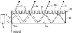
도 1은 일반적인 3차원 영상 디스플레이용 백라이트 유닛을 개략적으로 도시한 것이다.Figure 1 schematically shows a backlight unit for a general 3D image display.
도 1을 참조하면, 백라이트 유닛은 광원(10)과, 이 광원(10)으로부터 입사된 광(L)을 가이드하여 출사면(20b)으로 출사하는 도광판(20)과, 도광판(20)의 출사면 (20b)에 마련되는 회절 격자 구조체(30)를 포함한다. 도광판(20)은 광원(10)에서 입사된 광(L)을 전반사에 의해 도광판(20) 내부에서 가이드하며, 출사면(20b)으로 출사시킨다. 이러한 도광판(20)은 광이 입사되는 입사면(20a)과, 입사면(20a)을 통해 입사된 광이 출사되는 출사면(20b)과, 출사면(20b)과 마주하는 반사면(20c)을 구비한다.Referring to FIG. 1, the backlight unit includes a
회절 격자 구조체(30)는 도광판(20)의 출사면(20b)으로부터 나오는 광을 소정 방향으로 향하도록 회절시킬 수 있다. 이러한 회절 격자 구조체(30)로부터 나오는 지향성을 가지는 회절된 출사광(DL)은 디스플레이 패널(미도시)에 의해 변조됨으로써 3차원 영상이 구현될 수 있다. 회절 격자 구조체(30)는 도광판(20)의 출사면(20b)에 서로 이격되게 마련되는 다수의 회절 격자(31)를 포함한다. 여기서, 회절 격자들(31)은 동일한 높이를 가질 수 있다.The diffraction
이와 같은 백라이트 유닛에서는 회절 격자 구조체(30)가 모두 동일한 높이의 회절 격자(31)를 포함함으로써 회절 격자 구조체(30)로부터 나오는 회절된 출사광(DL)의 균일도가 떨어질 수 있다.In such a backlight unit, the
도 2는 도 1에 도시된 백라이트 유닛에서, 회절 격자 구조체(30)로부터 나오는 회절된 출사광(DL)의 세기를 위치에 따라 도시한 것이다. 도 2에서 거리(distance)는 도광판(20)의 입사면(20a)으로부터 떨어진 거리를 의미하며, 세기(intensity)는 회절 격자 구조체(30)로부터 나오는 회절된 출사광(DL)의 세기를 나타낸다.FIG. 2 shows the intensity of the diffracted light DL emitted from the diffraction
도 2를 참조하면, 회절 격자 구조체(30)로부터 나오는 회절된 출사광(DL)의 세기가 도광판(20)의 입사면(20a)으로부터의 거리가 증가할수록 점점 약해지는 것을 알 수 있다. 이와 같이, 일반적인 백라이트 유닛의 회절 격자 구조체(30)에서는 회절 격자들(31)의 높이가 동일함에 따라 회절 격자 구조체(30)의 전 부분에서 회절 효율이 거의 비슷하게 된다. 따라서, 도광판(20)에 입사된 광(L)이 도광판(20) 내부를 점점 진행함에 따라 회절 격자 구조체(30)로부터 나오는 회절된 출사광(DL)의 세기는 점점 약해지게 된다. 즉, 회절 격자 구조체(30)로부터 나오는 회절된 출사광(DL)의 세기가 도광판(20)의 입사면(20a)으로부터의 거리가 증가할수록 점점 약해지게 된다. 이와 같이, 일반적인 백라이트 유닛에서는 도광판(20)으로부터 나오는 회절된 출사광(DL)의 세기가 위치에 따라 변하게 됨으로써 출사광(DL)의 균일도가 떨어질 수 있다.Referring to FIG. 2, it can be seen that the intensity of the diffracted light DL emitted from the diffraction
도 3은 예시적인 실시예에 따른 3차원 영상 디스플레이용 백라이트 유닛을 도시한 것이다. 그리고, 도 4는 도 3의 A 부분을 확대하여 도시한 것이다.Figure 3 shows a backlight unit for a three-dimensional image display according to an exemplary embodiment. And, Figure 4 is an enlarged view of part A of Figure 3.
도 3 및 도 4를 참조하면, 백라이트 유닛(100)은 광원(110), 도광판(120) 및 회절 격자 구조체(130)를 포함한다. 광원(110)은 도광판(120)의 적어도 한 일측에 배치될 수 있으며, 도광판(120)의 적어도 일면에 광을 조사할 수 있다. 도 3에는 광원(110)이 도광판(120)의 좌측에 마련되는 경우가 예시적으로 도시되어 있으며, 이외에도 광원(110)의 위치는 다양하게 변형될 수 있다 광원(110)은 예를 들면, LED(Light Emitting Diode) 또는 LD(Laser Diode)를 포함할 수 있지만, 이에 한정되는 것은 아니다.Referring to FIGS. 3 and 4 , the
도광판(120)은 광원(110)으로부터 입사된 광을 전반사에 의해 도광판(120) 내부에서 가이드하며, 그 일부는 상부에 있는 출사면(120b)으로 출사시킨다. 이러한 도광판(120)은 예를 들면, 글라스 또는 투명한 플라스틱 소재 등과 같은 투명한 물질을 포함할 수 있다. 도광판(120)은 광원(110)으로부터 방출된 광이 입사되는 입사면(120a)과, 입사면(120a)을 통해 입사된 광이 출사되는 출사면(120b)과, 출사면(120b)과 마주하는 반사면(120c)을 포함할 수 있다.The
회절 격자 구조체(130)는 도광판(120)의 출사면(120b)에 마련되어 출사면(120b)으로부터 나오는 광을 소정 방향으로 향하도록 회절시킨다. 이러한 회절 격자 구조체(130)로부터 나오는 지향성을 가지는 회절된 출사광은 디스플레이 패널(미도시)에 의해 변조됨으로써 3차원 영상이 구현될 수 있다. 회절 격자 구조체(130)는 도광판(120)의 출사면(120b)에 서로 이격되게 마련되는 다수의 회절 격자(131)를 포함한다. 이러한 회절 격자 구조체(130)는 예를 들면, 광경화성 또는 열경화성 수지를 포함하고 있으며, 후술하는 바와 같은 나노 임프린트(nano imprint) 공정을 통해 형성될 수 있다.The diffraction
본 실시예에서는, 회절 격자 구조체(130)의 회절 격자들(131)은 서로 다른 높이(H)를 가짐으로써 소정의 높이 구배(height gradient)가 형성될 수 있다. 여기서, 회절 격자(131)의 높이(H)는 회절 격자들(131) 사이의 바닥면으로부터 회절 격자(131)의 상면까지의 높이를 의미한다. 그리고, 회절 격자들(131) 사이의 바닥면들은 도광판(120)의 출사면(120b)으로부터 동일한 높이(h)를 가지고 있다. 따라서, 회절 격자 구조체(130)의 회절 격자들(131)은 도광판(120)의 출사면(120b)으로부터 다른 높이(H+h)를 가지도록 형성될 수 있다. In this embodiment, the
도 3에는 회절 격자 구조체(130)의 회절 격자들(131)이 일 방향을 따라 점점 그 높이(H)가 증가하도록 마련되는 경우가 도시되어 있다. 보다 구체적으로는, 회절 격자 구조체(130)의 회절 격자들(131)은 도광판(120)의 입사면(120a)으로부터 거리가 멀어질수록 그 높이(H)가 점점 증가하도록 배치될 수 있다. 여기서, 회절 격자들(131)은 일 방향을 따라 그 높이(H)가 연속적으로(continuously) 변화하거나 또는 단속적으로(discretly) 변화할 수 있다.FIG. 3 shows a case where the
이와 같이, 회절 격자 구조체(130)의 회절 격자들(131)의 높이(H)를 위치에 따라 변화시킴으로써 회절 격자들(131)의 회절 효율을 위치에 따라 조절할 수 있다. 예를 들어, 회절 격자들(131)의 높이(H)가 도광판(120)의 입사면(120a)으로부터 멀어질수록 점점 증가하게 되면 회절 격자들(131)의 회절 효율도 회절 격자들(131)의 높이(H)에 대응하여 도광판(120)의 입사면(120a)으로부터 멀어질수록 점점 커지게 된다. 따라서, 회절 격자 구조체(130)로부터 나오는 회절된 출사광은 전 위치에 걸쳐 균일한 세기를 가질 수 있다.In this way, by changing the height (H) of the
한편, 이상에서는 회절 격자 구조체(130)의 회절 격자들(131)이 일 방향을 따라 점점 그 높이(H)가 증가하는 경우가 예시적으로 설명되었다. 그러나, 본 실시예가 이에 한정되는 것은 아니며, 회절 격자들(131)의 높이(H)를 다양하게 변화시킴으로써 회절 효율을 위치에 따라 조절할 수 있다. 예를 들어, 회절 격자 구조체(130)의 회절 격자들(131)은 일부 영역에서는 동일한 높이(H)를 가질 수도 있다. 또한, 회절 격자 구조체(130)의 회절 격자들(131)이 일 방향을 따라 그 높이(H)가 점점 증가하도록 배치되지 않을 수도 있다.Meanwhile, in the above, the case where the height (H) of the
회절 격자들(131)의 회절 효율을 조절하기 위해서 회절 격자들(131)의 높이(H) 뿐만 아니라 회절 격자들(131) 각각의 폭(W)도 변화시킬 수 있다. 도 3에는 회절 격자 구조체(130)의 회절 격자들(131)이 도광판(120)의 입사면(120a)으로부터 멀어질 수록 점점 그 폭(W)이 줄어드는 경우가 예시적으로 도시되어 있다. 하지만 본 실시예는 이에 한정되는 것은 아니며 회절 격자 구조체(130)의 회절 격자들(131)은 그 폭(W)이 다양하게 변화시킴으로써 회절 효율을 위치에 따라 조절할 수 있다.In order to adjust the diffraction efficiency of the
도 5는 도 3에 도시된 백라이트 유닛(100)에서, 회절 격자 구조체(130)로부터 나오는 회절된 출사광(DL)을 도시한 것이다.FIG. 5 illustrates diffracted light DL emitted from the diffraction
도 5를 참조하면, 도광판(120)의 일측에 마련된 광원(110)으로부터 방출된 광(L)은 도광판(120)의 입사면(120a)으로 입사된 다음,, 전반사에 의해 도광판(120)의 내부를 진행할 수 있다. 이 과정에서, 도광판(120)의 출사면(120b)으로 나오는 광은 회절 격자 구조체(130)에 의해 회절되어 지향성을 가지고 출사되게 된다. 전술한 바와 같이. 회절 격자 구조체(130)의 회절 격자들(131)은 도광판(120)의 입사면(120a)으로부터 멀어질수록 그 높이(H)가 점점 높아지도록 마련되어 있으므로, 회절 격자들(131)의 회절 효율은 도광판(120)의 입사면(120a)으로부터 멀어질수록 점점 증가할 수 있다. 이와 같이, 회절 격자들(131)의 회절 효율을 도광판(120)의 입사면(120a)으로부터 멀어질수록 점점 증가하도록 조절함에 따라 회전 격자 구조체(130)로부터 나오는 회절된 출사광(DL)은 전 위치에 걸쳐 그 세기가 균일하게 될 수 있다. 이에 따라, 회절된 출사광(DL)의 균일도 및 밝기를 확보할 수 있다.Referring to FIG. 5, light L emitted from the
도 6은 다른 예시적인 실시예에 따른 3차원 영상 디스플레이용 백라이트 유닛을 도시한 것이다.Figure 6 illustrates a backlight unit for 3D image display according to another exemplary embodiment.
도 6을 참조하면, 백라이트 유닛(200)은 광원(210), 도광판(220) 및 회절 격자 구조체(230)를 포함한다. 광원(210)은 도광판(220)의 일측 상면의 상부에 배치될 수 있다. 도 6에는 광원(210)이 도광판(220)의 좌측 상면의 상부에 배치된 경우가 도시되어 있다. 이러한 광원(210)으로부터 방출된 광(L)은 도광판(220)의 좌측 상면에 입사될 수 있다.Referring to FIG. 6 , the
도광판(220)은 광원(210)으로부터 입사된 광(L)을 전반사에 의해 도광판(220) 내부에서 가이드하며, 이 과정에서 진행하는 광의 일부가 상부에 있는 출사면(220b)으로 출사시킨다. 도광판(220)은 광원(210)으로부터 방출된 광(L)이 입사되는 입사면(220a)과, 입사면(220a)을 통해 입사된 광이 출사되는 출사면(220b)과, 출사면(220b)과 마주하는 반사면(220c)을 포함할 수 있다. 전술한 바와 같이, 광원(210)으로부터 방출된 광(L)이 도광판(220)의 좌측 상면에 입사되므로, 도광판(220)의 입사면(220a)은 도광판(220)의 좌측 상면이 될 수 있다. 이러한 도광판(220)의 좌측 상면에 소정 각도로 입사된 광은 전반사를 통해 도광판(220)의 내부를 진행할 수 있다. 여기서, 도광판(220)의 출사면(220b)은 도광판(220)의 중심부 상면 및 우측 상면이 될 수 있다.The
도광판(220)의 상면에는 회절 격자 구조체(230)가 마련되어 있다. 이러한 회절 격자 구조체(230)는 도광판(220)의 입사면(220a)에 마련되는 회절 격자들(232)과 도광판(220)의 출사면(220b)에 마련되는 회절 격자들(231)을 포함할 수 있다.A diffraction
도광판(220)의 출사면(220b)에 마련되어 있는 회절 격자들(231)은 출사면(220b)으로부터 나오는 광을 소정 방향으로 향하도록 회절시킨다. 도광판(220)의 출사면(220b)에 마련되어 있는 회절 격자들(231)은 서로 다른 높이를 가짐으로써 소정의 높이 구배가 형성될 수 있다. 예를 들면, 도광판(220)의 출사면(220b)에 마련되어 있는 회절 격자들(231)은 도광판(220)의 입사면(220a)으로부터 거리가 멀어질수록 그 높이가 점점 증가하도록 배치될 수 있다. 이와 같이, 회절 격자 구조체(230)의 회절 격자들(231)의 높이를 위치에 따라 변화시킴으로써 회절 격자들(231)의 회절 효율을 위치에 따라 조절할 수 있다. 또한, 도광판(220)의 출사면(220b)에 마련되어 있는 회절 격자들(231)의 회절 효율을 조절하기 위해서 회절 격자들(231)의 높이 뿐만 아니라 회절 격자들(231) 각각의 폭도 변화시킬 수도 있다.The
도광판(220)의 입사면(220a)에 마련되어 있는 회절 격자들(232)은 광원(210)으로부터 입사면(220a)으로 입사되는 광(L)이 위치에 따라 그 세기가 균일할 수 있도록 동일한 형태를 가질 수 있다. 예를 들면, 도광판(220)의 입사면(220a)에 마련되어 있는 회절 격자들(232)은 동일한 높이 및 폭을 가질 수 있다. 대체적으로(alternatively), 도광판(220)의 입사면(220a)에는 회절 격자들(232)이 마련되어 있지 않을 수도 있다.The
도 7은 다른 예시적인 실시예에 따른 3차원 영상 디스플레이 장치를 도시한 것이다.Figure 7 shows a 3D image display device according to another exemplary embodiment.
도 7을 참조하면, 3차원 영상 디스플레이 장치(1000)는 백라이트 유닛(300)과, 이 백라이트 유닛(300)으로부터 입사되는 광을 변조하는 디스플레이 패널(1100)을 포함한다.Referring to FIG. 7, the three-dimensional
백라이트 유닛(300)은 광원(310), 도광판(320) 및 회절 격자 구조체(330)를 포함한다. 광원(310)은 도광판(320)의 일측에 배치되어 도광판(320)의 입사면(320a)에 광을 조사할 수 있다. 도광판(320)은 광원(310)으로부터 입사된 광(L)을 전반사에 의해 도광판(320) 내부에서 가이드하며, 이 광의 일부는 상부에 있는 출사면(320b)으로 출사시킨다. 도광판(320)은 광원(310)으로부터 방출된 광(L)이 입사되는 입사면(320a)과, 입사면(320a)을 통해 입사된 광이 출사되는 출사면(320b)과, 출사면(320b)과 마주하는 반사면(320c)을 포함할 수 있다.The
회절 격자 구조체(330)는 도광판(320)의 출사면(320b)에 마련되어 출사면(320b)으로부터 나오는 광을 소정 방향으로 향하도록 회절시킨다. 회절 격자 구조체(330)는 도광판(320)의 출사면(320b)에 서로 이격되게 마련되는 다수의 회절 격자(331)를 포함한다. 도광판(320)의 출사면(320b)에 마련된 회절 격자들(331)은 다른 높이를 가질 수 있다. 구체적으로, 회절 격자 구조체(330)의 회절 격자들(331)은 도광판(320)의 입사면(320a)으로부터 거리가 멀어질수록 그 높이가 점점 증가하도록 배치될 수 있다. 회절 격자 구조체(330)의 회절 격자들(331)의 높이를 위치에 따라 변화시킴으로써 회절 격자들(331)의 회절 효율을 위치에 따라 조절할 수 있다. 이에 따라, 백라이트 유닛(300)의 회절 격자 구조체(330)로부터 나오는 지향성을 가지는 회절된 출사광(DL)은 전 위치에 걸쳐 그 세기가 균일한 출사광이 될 수 있다.The diffraction
백라이트 유닛(300)의 상부에는 디스플레이 패널(1100)이 마련되어 있다. 이 디스플레이 패널(1100)은 백라이트 유닛(300)으로부터 나오는 방향성을 가지는 회절된 출사광(DL)을 영상 정보에 따라 변조시켜 출사할 수 있다. 이러한 디스플레이 패널(1100)은 예를 들면 액정 디스플레이(LCD; liquid crystal display) 패널이 될 수 있지만, 이에 한정되지는 않는다.A
이러한 디스플레이 패널(1100)로부터 서로 다른 방향으로 출사되는 변조된 광(ML)은 복수의 시역(viewing zone)에서 각각 서로 다른 뷰(view)를 제공함으로써 3차원 영상을 표시할 수 있다. 이와 같이, 복수의 시역에서 서로 다른 뷰가 제공됨으로써 시청자가 3차원 영상을 인지할 수 있게 된다. 한편, 이상에서는 3차원 디스플레이 장치(1000)의 백라이트 유닛(300)으로 도 3에 도시된 백라이트 유닛(100)이 사용된 경우에 예시적으로 설명되었으며, 이외에도 도 6에 도시된 백라이트 유닛(200)이 적용되는 것도 얼마든지 가능하다.The modulated light ML emitted from the
도 8 내지 도 14는 예시적인 실시예에 따른 3차원 영상 디스플레이용 백라이트 유닛의 제조방법을 설명하기 위한 도면들이다.8 to 14 are diagrams for explaining a method of manufacturing a backlight unit for a 3D image display according to an exemplary embodiment.
도 8을 참조하면, 먼저 마스터 몰드(master mold,450)를 마련한다. 마스터 몰드(450)의 일면에는 다수의 몰드 패턴(451)이 서로 이격되게 형성되어 있다. 여기서, 마스터 몰드(450)의 몰드 패턴들(451)은 동일한 높이를 가질 수 있다. 몰드 패턴들(451)의 높이는 몰드 패턴들(451) 사이의 바닥면으로부터 몰드 패턴들(451)의 상면까지의 높이를 의미한다. 또한, 몰드 패턴들(451)은 적어도 일부가 다른 폭을 가질 수도 있다. 이러한 몰드 패턴들(451)을 포함하는 마스터 몰드(450)는 예를 들면 포토리소그래피(photolithography) 또는 전자빔 리소그래피(E-beam lithography) 등에 의해 제작될 수 있다.Referring to FIG. 8, first, a master mold (450) is prepared. On one side of the
도 9를 참조하면, 도 8에 도시된 마스터 몰드(450)를 이용하여 스탬프(stamp, 440)를 복제한다. 이러한 스탬프(440)는 마스터 몰드(450)의 몰드 패턴들(451)을 덮도록 복제용 수지(미도시)를 도포한 다음, 이 복제용 수지를 가압한 후 빛 또는 열에 의해 경화시킴으로써 제작될 수 있다. 이에 따라, 스탬프(440)의 일면에는 마스터 몰드(450)의 몰드 패턴들(451)에 상보적인 격자 패턴들(441)이 형성될 수 있다. 여기서, 스탬프(440)의 격자 패턴들(441)은 몰드 패턴들(452)과 마찬가지로 동일한 높이를 가질 수 있다.Referring to FIG. 9, the
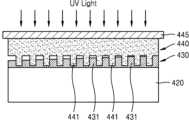
도 10을 참조하면, 기판(420)의 상면에 수지(435)를 도포한다. 여기서, 기판(420)은 도파관을 포함할 수 있지만 이에 한정되는 것은 아니다. 이 과정에서, 기판(420)의 상면에 도포되는 수지(435)는 위치에 따라 도포되는 양이 조절될 수 있다. 예를 들면, 수지(435)는 기판(420)의 일 측면으로부터 멀어질수록 점점 많은 양이 도포되도록 조절될 수 있다. 이러한 수지(435)는 예를 들면 광경화성 또는 열경화성 수지를 포함할 수 있다.Referring to FIG. 10,
도 11을 참조하면, 스탬프(440)를 기판(420)의 상부에 마련한다. 여기서, 스탬프(440)는 그 격자 패턴들(441)이 기판(420)에 도포된 수지(435)를 마주보도록 배치될 수 있다. 이어서, 도 12를 참조하면, 스탬프(440)를 수지(435)와 접촉시킨 다음 스탬프(440)에 압력을 가하여 누른다. 이 경우, 스탬프(440)에 균일한 압력을 가하기 위해 스탬프(440)의 상면에 단단한 재질의 가압 플레이트(445)를 더 마련할 수 있다.Referring to FIG. 11, a
도 12에 도시된 바와 같이, 스탬프(440)에 압력을 가하게 되면 스탬프(440)에 형성된 격자 패턴들(441) 사이에 수지(435)가 채워질 수 있다. 여기서, 격자 패턴들(441) 사이의 공간들에는 수지(435)가 전부 채워지거나 또는 일부만 채워질 수 있다. 전술한 바와 같이, 수지(435)는 기판(420)의 상면에서 위치에 따라 도포되는 양이 달라지게 되므로, 격자 패턴들(441) 사이의 공간들에 채워지는 수지(435)의 양도 달라질 수 있다. 구체적으로, 기판(420)의 일 측면으로부터 멀어질수록 도포되는 수지(435)의 양이 점점 증가하는 경우에는 격자 패턴들(441) 사이의 공간들에 채워지는 수지(435)의 양도 기판(420)의 일 측면으로부터 멀어질수록 점점 증가하게 된다. 이에 따라, 격자 패턴들(441) 사이의 공간들에 채워지는 수지(435)의 높이도 기판(420)의 일 측면으로부터 멀어질수록 점점 높아질 수 있다.As shown in FIG. 12, when pressure is applied to the
도 13을 참조하면, 도 12에 도시된 상태에서 광(예를 들면, UV 광)을 가압 플레이트(445) 및 스탬프(440)를 통해 수지(435)에 조사하게 되면 수지(435)가 경화될 수 있다. 이어서, 가압 플레이트(445) 및 스탬프(440)를 떼어내게 되면 기판(420)의 상면에는 도 14에 도시된 바와 같이 회절 격자들(431)을 포함하는 회절 격자 구조체(430)가 형성될 수 있다. 도 13에는 수지(435)가 광경화성 수지로 이루어져 있고, 이 수지(435)가 UV 광의 조사에 의해 경화되어 회절 격자 구조체(430)가 형성되는 경우가 예시적으로 도시되어 있다. 하지만, 이에 한정되지 않고 수지(435)가 열경화성 수지로 이루어져 있고, 이 수지(435)가 열에 의해 경화되어 회절 격자 구조체(430)가 형성되는 것도 가능하다.Referring to FIG. 13, when light (e.g., UV light) is irradiated to the
전술한 바와 같이, 격자 패턴들(441) 사이의 공간들에 채워지는 수지(435)의 높이가 달라짐에 따라, 회절 격자 구조체(430)의 회절 격자들(431)은 기판(420)의 일 측면으로부터 멀어질수록 그 높이가 점점 높아질 수 있다. 여기서, 회절 격자들(431)의 높이는 회절 격자들(431) 사이의 바닥면으로부터 회절 격자들(431)의 상면까지의 높이를 의미할 수 있다. 그리고, 회절 격자들(431) 사이의 바닥면들은 기판(420)의 상면으로부터 동일한 높이로 형성될 수 있다. 따라서, 회절 격자 구조체(430)의 회절 격자들(431)은 기판(420)의 상면으로부터 다른 높이를 가지도록 형성될 수 있다.As described above, as the height of the
이상에서 설명된 도 8 내지 도 14에 도시된 과정을 한번 또는 복수 회 수행함으로써 위치에 따라 높이가 미세하게 조절된 회절 격자들(431)이 형성된 회절 격자 구조체(430)를 제작할 수 있다. 전술한 바와 같이, 기판(420)으로 도광판을 사용하는 경우 이 기판(420)의 상면에 회절 격자들(431)의 높이가 조절된 회절 격자 구조체(430)를 형성하고, 광원(미도시)을 기판(420)의 적어도 일측에 배치함으로써 3차원 영상 디스플레이용 백라이트 유닛을 제작할 수 있다.By performing the process shown in FIGS. 8 to 14 described above once or multiple times, the diffraction
한편, 이상에서는 기판(420)의 일 측면으로부터 멀어질수록 회절 격자들(431)의 높이가 높아지는 경우가 설명되었으나, 이에 한정되지 않고 기판(420)의 상면에 도포되는 수지(435)의 양을 위치에 따라 조절함으로써 회절 격자들(431)의 높이를 위치에 따라 다양하게 변형할 수 있다.Meanwhile, in the above description, the case where the height of the
도 15a 내지 도 15f는 도 8 내지 도 14에 도시된 방법에 의해 제작된 회절 격자 구조체의 회절 격자들을 찍은 SEM 사진들이다.FIGS. 15A to 15F are SEM pictures of diffraction gratings of the diffraction grating structure manufactured by the method shown in FIGS. 8 to 14.
도 15a는 실리콘으로 제작된 마스터 몰드를 찍은 SEM(Scanning Electron Microscope) 사진이다, 도 15a에 도시된 마스터 몰드는 165nm의 동일한 높이를 가지는 몰드 패턴들을 포함하고 있다.Figure 15a is a SEM (Scanning Electron Microscope) photograph of a master mold made of silicon. The master mold shown in Figure 15a includes mold patterns with the same height of 165 nm.
도 15b 내지 도 15f는 도 15a에 도시된 마스터 몰드를 이용하여 도 8 내지 도 14에 도시된 방법에 의해 제작된 회절 격자 구조체의 회절 격자들을 찍은 SEM 사진들이다. 구체적으로, 도 15b 내지 도 15f에는 회절 격자 구조체에서 5개의 위치(#1 ~ #5)에 있는 회절 격자들을 찍은 SEM 사진에 도시되어 있다.FIGS. 15B to 15F are SEM photographs of diffraction gratings of the diffraction grating structure manufactured by the method shown in FIGS. 8 to 14 using the master mold shown in FIG. 15A. Specifically, FIGS. 15B to 15F show SEM photographs of diffraction gratings at five positions (#1 to #5) in the diffraction grating structure.
도 15b, 도 15c, 도 15d, 도 15e 및 도 15f에는 각각 Point #1, Point #2, Point #3, Point #4 및 Point #5에 위치하고 있는 회절 격자들이 도시되어 있다. 여기서, Point #1, Point #2, Point #3, Point #4 및 Point #5는 각각 회절 격자 구조체의 일 측면으로부터 10nm, 20nm, 30nm, 40nm 및 50nm 떨어진 위치를 나타낸다.Figures 15b, 15c, 15d, 15e, and 15f show diffraction gratings located at
도 16은 도 15b 내지 도 15f에 도시된 회절 격자들의 높이를 측정한 결과를 도시한 것이다. 도 16을 참조하면, 회절 격자들은 대략 35nm ~ 145nm 범위의 높이로 형성되었다. 이러한 회절 격자들의 높이는 도 15a에 도시된 실리콘 마스터 몰드에 형성된 몰드 패턴들의 높이(165nm)에 비해 대략 22% ~ 87% 정도가 됨을 알 수 있다.Figure 16 shows the results of measuring the heights of the diffraction gratings shown in Figures 15b to 15f. Referring to FIG. 16, the diffraction gratings were formed with a height ranging from approximately 35 nm to 145 nm. It can be seen that the height of these diffraction gratings is approximately 22% to 87% of the height (165 nm) of the mold patterns formed on the silicon master mold shown in FIG. 15A.
도 17 내지 도 23은 다른 예시적인 실시예에 따른 3차원 영상 디스플레이용 백라이트 유닛의 제조방법을 설명하기 위한 도면들이다. 도 17 내지 도 23에는 도 14에 도시된 기판(420) 및 회절 격자 구조체(430)를 마스터 몰드(550)로 이용하여 백라이트 유닛을 제조하는 과정들이 도시되어 있다.17 to 23 are diagrams for explaining a method of manufacturing a backlight unit for a 3D image display according to another exemplary embodiment. FIGS. 17 to 23 show processes for manufacturing a backlight unit using the
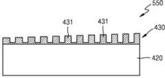
도 17을 참조하면, 마스터 몰드(550)를 준비한다. 여기서, 마스터 몰드(550)는 도 14에 도시된 기판(420) 및 회절 격자 구조체(430)가 될 수 있다. 따라서, 도 14에 도시된 회절 격자 구조체(430)의 회절 격자들(431)은 마스터 몰드(550)의 몰드 패턴들(431)이 될 수 있다. 따라서, 도 17에 도시된 마스터 몰드(550)는 위치에 따라 높이가 조절된 몰드 패턴들(431)을 포함할 수 있다. 예를 들면, 몰드 패턴들(431)은 마스터 몰드(550)의 일 측면으로부터 멀어질수록 그 높이가 점점 높아지도록 배치될 수 있다. 여기서, 몰드 패턴들(431)의 높이는 몰드 패턴들(431) 사이의 바닥면으로부터 몰드 패턴들(431)의 상면까지의 높이를 의미한다. 그리고, 몰드 패턴들(431) 사이의 바닥면들은 기판(420)의 상면으로부터 동일한 높이로 형성될 수 있다.Referring to FIG. 17, a
도 18을 참조하면, 도 17에 도시된 마스터 몰드(550)를 이용하여 스탬프(540)를 복제한다. 이러한 스탬프(540)는 마스터 몰드(550)의 몰드 패턴들(431)을 덮도록 복제용 수지(미도시)를 도포한 다음, 이 복제용 수지를 가압한 후 빛 또는 열에 의해 경화시킴으로써 제작될 수 있다. 이러한 복제 과정에 따라, 스탬프(540)의 일면에는 마스터 몰드(550)의 몰드 패턴들(431)에 상보적인 격자 패턴들(541)이 형성될 수 있다. 따라서, 스탬프(540)의 격자 패턴들(541) 사이의 공간들이 마스터 몰드(550)의 몰드 패턴들(431)에 대응하는 형상을 가질 수 있다.Referring to FIG. 18, the
도 19를 참조하면, 도광판(520)의 상면에 수지(535)를 도포한다. 도광판(520)은 예를 들면, 글라스 또는 투명한 플라스틱 소재 등과 같은 투명한 물질을 포함할 수 있다. 도광판(520)의 상면에 도포되는 수지(535)는 전 위치에 걸쳐 도포되는 양이 균일할 수 있다. 하지만, 반드시 이에 한정되는 것은 아니며, 도광판(520)의 상면에 도포되는 수지(535)가 위치에 따라 도포되는 양이 조절될 수도 있다. 이러한 수지(535)는 예를 들면 광경화성 또는 열경화성 수지를 포함할 수 있다. Referring to FIG. 19,
도 20을 참조하면, 스탬프(540)를 도광판(520)의 상부에 마련한다. 여기서, 스탬프(540)는 그 격자 패턴들(541)이 도광판(520)에 도포된 수지(535)를 마주보도록 배치될 수 있다. 이어서, 도 21을 참조하면, 스탬프(540)를 수지(535)와 접촉시킨 다음 스탬프(540)에 압력을 가하여 누른다. 이 경우, 스탬프(540)에 균일한 압력을 가하기 위해 스탬프(540)의 상면에 단단한 재질의 가압 플레이트(545)를 더 마련할 수 있다. 도 21에 도시된 바와 같이, 스탬프(540)에 압력을 가하게 되면 스탬프(540)에 형성된 격자 패턴들(541) 사이에 수지(535)가 채워질 수 있다. 이 과정에서 스탬프(540)의 격자 패턴들(541) 사이의 공간들은 수지(535)로 완전히 채워질 수 있다.Referring to FIG. 20, a
도 22를 참조하면, 도 21에 도시된 상태에서 광(예를 들면, UV 광)을 가압 플레이트(545) 및 스탬프(540)를 통해 수지(535)에 조사하게 되면 수지(535)가 경화될 수 있다. 이어서, 가압 플레이트(545) 및 스탬프(540)를 떼어내게 되면 도광판(520)의 상면에는 도 23에 도시된 바와 같이 높이가 조절된 회절 격자들(531)을 포함하는 회절 격자 구조체(530)가 형성될 수 있다. 도 22에는 수지(535)가 광경화성 수지로 이루어져 있고, 이 수지(535)가 UV 광의 조사에 의해 경화되어 회절 격자 구조체가 형성되는 경우가 예시적으로 도시되어 있다. 하지만, 이에 한정되지 않고 수지(535)가 열경화성 수지로 이루어져 있고, 이 수지(535)가 열에 의해 경화되어 회절 격자 구조체(530)가 형성되는 것도 가능하다.Referring to FIG. 22, when light (e.g., UV light) is irradiated to the
전술한 바와 같이, 스탬프(540)의 격자 패턴들(541) 사이의 공간들은 수지(535)로 완전히 채워지게 되므로, 회절 격자 구조체(530)의 회절 격자들(531)은 도 17에 도시된 마스터 몰드(550)의 몰드 패턴들(431)과 동일한 형상을 가질 수 있다. 이에 따라, 회절 격자 구조체(530)의 회절 격자들(531)은 위치에 따라 높이가 조절될 수 있다. 예를 들면, 회절 격자 구조체(530)의 회절 격자들(531)은 도광판(520)의 일 측면으로부터 멀어질수록 그 높이가 점점 높아지도록 형성될 수 있다.As described above, the spaces between the
이상과 같이, 도 14에 도시된 바와 같은 기판(420) 및 회절 격자 구조체(430)를 마스터 몰드(550)로 사용하게 되면 위치에 따라 높이가 조절된 회절 격자들(531)을 포함하는 회절 격자 구조체(530)를 도광판(520)의 상면에 반복적으로 제작할 수 있게 된다. 그리고, 광원(미도시)을 도광판(520)의 적어도 일측에 배치하게 되면 3차원 영상 디스플레이용 백라이트 유닛을 제작할 수 있다.As described above, when the
이상의 실시예들에 의하면, 도광판의 출사면에 마련된 회절 격자 구조체의 회절 격자들이 위치에 따라 그 높이가 변화되도록 마련됨으로써 회절 격자들의 회절 효율을 위치에 따라 미세하게 조절할 수 있다. 이에 따라, 회절 격자 구조체로부터 나오는 방향성을 가지는 회절된 출사광은 위치에 따라 균일한 세기를 가지는 출사광이 될 수 있으므로, 출사광의 균일도 및 밝기가 확보될 수 있다.According to the above embodiments, the height of the diffraction gratings of the diffraction grating structure provided on the exit surface of the light guide plate is changed depending on the position, so that the diffraction efficiency of the diffraction gratings can be finely adjusted depending on the position. Accordingly, the diffracted emitted light with directionality coming from the diffraction grating structure can be emitted light with uniform intensity depending on the position, and thus uniformity and brightness of the emitted light can be secured.
10, 110, 210, 310.. 광원
20, 120, 220, 320.. 520.. 도광판
20a, 120a, 220a, 320a.. 도광판의 입사면
20b, 120b, 220b, 320b.. 도광판의 출사면
20c, 120c, 220c, 320c.. 도광판의 반사면
30, 130, 230, 330, 430, 530.. 회절 격자 구조체
31, 131, 231, 331, 431, 531.. 회절 격자
100, 200, 300.. 백라이트 유닛
420.. 기판
435,535.. 수지
440,540.. 스탬프
441,541.. 격자 패턴
445,545.. 가압 플레이트
450,550.. 마스터 몰드
451.. 몰드 패턴
1000.. 3차원 영상 디스플레이 장치
1100.. 디스플레이 패널10, 110, 210, 310.. Light source
20, 120, 220, 320.. 520.. light guide plate
20a, 120a, 220a, 320a.. Incidence surface of the light guide plate
20b, 120b, 220b, 320b.. Exit surface of the light guide plate
20c, 120c, 220c, 320c.. Reflective surface of light guide plate
30, 130, 230, 330, 430, 530.. Diffraction grating structure
31, 131, 231, 331, 431, 531.. Diffraction grating
100, 200, 300.. Backlight unit
420.. Substrate
435,535.. Resin
440,540.. stamp
441,541.. Grid pattern
445,545.. Pressure plate
450,550.. master mold
451.. Mold pattern
1000.. 3D image display device
1100.. Display panel
Claims (20)
Translated fromKorean상기 도광판의 입사면에 광을 조사하는 광원; 및
상기 도광판의 입사면 및 출사면에 마련되는 복수의 회절 격자를 포함하는 회절 격자 구조체;를 포함하고,
상기 도광판의 입사면에 마련되는 복수의 회절 격자는 동일한 높이를 가지고, 상기 도광판의 출사면에 마련되는 복수의 회절 격자는 상기 도광판의 입사면으로부터 멀어질수록 높은 높이를 가지는 3차원 영상 디스플레이용 백라이트 유닛.A light guide plate including an entrance surface and an exit surface;
a light source that irradiates light to the incident surface of the light guide plate; and
A diffraction grating structure including a plurality of diffraction gratings provided on an incident surface and an emission surface of the light guide plate,
A backlight for a three-dimensional image display wherein the plurality of diffraction gratings provided on the incident surface of the light guide plate have the same height, and the plurality of diffraction gratings provided on the exit surface of the light guide plate have a higher height as the distance from the incident surface of the light guide plate increases. unit.
상기 도광판의 출사면에 마련되는 회절 격자들은 서로 다른 폭을 가지는 3차원 영상 디스플레이용 백라이트 유닛.According to claim 1,
A backlight unit for a three-dimensional image display in which diffraction gratings provided on the emission surface of the light guide plate have different widths.
상기 백라이트 유닛으로부터 입사되는 광을 영상 정보에 따라 변조하는 디스플레이 패널;을 포함하고,
상기 백라이트 유닛은,
입사면과 출사면을 포함하는 도광판;
상기 도광판의 입사면에 광을 조사하는 광원; 및
상기 도광판의 입사면 및 출사면에 마련되는 복수의 회절 격자를 포함하는 회절 격자 구조체;를 포함하고,
상기 도광판의 입사면에 마련되는 복수의 회절 격자는 동일한 높이를 가지고, 상기 도광판의 출사면에 마련되는 복수의 회절 격자는 상기 도광판의 입사면으로부터 멀어질수록 높은 높이를 가지는 3차원 영상 디스플레이 장치.backlight unit; and
A display panel that modulates light incident from the backlight unit according to image information,
The backlight unit is,
A light guide plate including an entrance surface and an exit surface;
a light source that irradiates light to the incident surface of the light guide plate; and
A diffraction grating structure including a plurality of diffraction gratings provided on an incident surface and an emission surface of the light guide plate,
A three-dimensional image display device wherein the plurality of diffraction gratings provided on the incident surface of the light guide plate have the same height, and the plurality of diffraction gratings provided on the exit surface of the light guide plate have a height that increases as the distance from the incident surface of the light guide plate increases.
상기 디스플레이 패널은 액정 패널을 포함하는 3차원 영상 디스플레이 장치.According to claim 5,
The display panel is a three-dimensional image display device including a liquid crystal panel.
상기 도광판의 출사면에 마련되는 회절 격자들은 서로 다른 폭을 가지는 3차원 영상 디스플레이 장치.According to claim 5,
A three-dimensional image display device in which diffraction gratings provided on the emission surface of the light guide plate have different widths.
기판의 일면에 위치에 따라 다른 양의 제1 수지(resin)를 도포하는 단계;
상기 제1 스탬프를 가압하여 상기 제1 격자 패턴들 사이에 상기 제1 수지를 채우는 단계; 및
상기 제1 수지를 경화시켜 상기 기판의 일면에 제1 회절 격자들을 포함하는 제1 회절 격자 구조체를 형성하는 단계;를 포함하고,
상기 제1 스탬프의 가압 시 상기 제1 격자 패턴들 사이의 공간들에 채워지는 제1 수지의 높이가 달라지고, 상기 제1 회절 격자들은 다른 높이를 가지도록 형성되는 3차원 영상 디스플레이용 백라이트 유닛의 제조방법.providing a first stamp including first grid patterns having the same height;
Applying a different amount of first resin depending on the position on one side of the substrate;
filling the first resin between the first grid patterns by pressing the first stamp; and
Curing the first resin to form a first diffraction grating structure including first diffraction gratings on one surface of the substrate,
When the first stamp is pressed, the height of the first resin filled in the spaces between the first grid patterns changes, and the first diffraction gratings are formed to have different heights of the backlight unit for a three-dimensional image display. Manufacturing method.
상기 제1 수지는 광경화성 또는 열경화성 수지를 포함하는 3차원 영상 디스플레이용 백라이트 유닛의 제조방법.According to claim 10,
A method of manufacturing a backlight unit for a three-dimensional image display, wherein the first resin includes a photocurable or thermosetting resin.
상기 제1 회절 격자들은 서로 다른 폭을 가지도록 형성되는 3차원 영상 디스플레이용 백라이트 유닛의 제조방법.According to claim 10,
A method of manufacturing a backlight unit for a three-dimensional image display in which the first diffraction gratings are formed to have different widths.
상기 기판은 도광판을 포함하는 3차원 영상 디스플레이용 백라이트 유닛의 제조방법.According to claim 10,
A method of manufacturing a backlight unit for a three-dimensional image display, wherein the substrate includes a light guide plate.
상기 기판 및 상기 제1 회절 격자 구조체를 마스터 몰드(master mold)로 이용하여 상기 제1 회절 격자들에 대응하는 제2 격자 패턴들을 포함하는 제2 스탬프를 마련하는 단계를 포함하는 3차원 영상 디스플레이용 백라이트 유닛의 제조방법.According to claim 10,
For a three-dimensional image display comprising preparing a second stamp including second grating patterns corresponding to the first diffraction gratings using the substrate and the first diffraction grating structure as a master mold. Manufacturing method of backlight unit.
도광판의 일면에 제2 수지를 도포하는 단계;
상기 제2 스탬프를 가압하여 상기 제2 격자 패턴들 사이에 상기 제2 수지를 채우는 단계; 및
상기 제2 수지를 경화시켜 상기 도광판의 일면에 제2 회절 격자들을 포함하는 제2 회절 격자 구조체를 형성하는 단계;를 포함하는 3차원 영상 디스플레이용 백라이트 유닛의 제조방법.According to claim 17,
Applying a second resin to one surface of the light guide plate;
filling the second resin between the second grid patterns by pressing the second stamp; and
Curing the second resin to form a second diffraction grating structure including second diffraction gratings on one surface of the light guide plate.
상기 제2 스탬프의 가압 시 상기 제2 격자 패턴들 사이의 공간들에 상기 제2 수지가 완전히 채워지는 3차원 영상 디스플레이용 백라이트 유닛의 제조방법.According to claim 18,
A method of manufacturing a backlight unit for a three-dimensional image display in which the spaces between the second grid patterns are completely filled with the second resin when the second stamp is pressed.
상기 제1 및 제2 회절 격자들은 동일한 형상을 가지는 3차원 영상 디스플레이용 백라이트 유닛의 제조방법.According to claim 19,
A method of manufacturing a backlight unit for a three-dimensional image display, wherein the first and second diffraction gratings have the same shape.
Priority Applications (4)
| Application Number | Priority Date | Filing Date | Title |
|---|---|---|---|
| KR1020160148592AKR102654870B1 (en) | 2016-11-09 | 2016-11-09 | Backlight unit for 3D image display and method of manufacturing the backlight unit |
| US15/654,097US10788681B2 (en) | 2016-11-09 | 2017-07-19 | Backlight unit for 3D image display and method of manufacturing the backlight unit |
| CN201710942761.2ACN108061931B (en) | 2016-11-09 | 2017-10-11 | Backlight unit for 3D image display and method of manufacturing the same |
| EP17196444.8AEP3321572B1 (en) | 2016-11-09 | 2017-10-13 | Method of manufacturing a backlight unit for 3d image display |
Applications Claiming Priority (1)
| Application Number | Priority Date | Filing Date | Title |
|---|---|---|---|
| KR1020160148592AKR102654870B1 (en) | 2016-11-09 | 2016-11-09 | Backlight unit for 3D image display and method of manufacturing the backlight unit |
Publications (2)
| Publication Number | Publication Date |
|---|---|
| KR20180051802A KR20180051802A (en) | 2018-05-17 |
| KR102654870B1true KR102654870B1 (en) | 2024-04-05 |
Family
ID=60117537
Family Applications (1)
| Application Number | Title | Priority Date | Filing Date |
|---|---|---|---|
| KR1020160148592AActiveKR102654870B1 (en) | 2016-11-09 | 2016-11-09 | Backlight unit for 3D image display and method of manufacturing the backlight unit |
Country Status (4)
| Country | Link |
|---|---|
| US (1) | US10788681B2 (en) |
| EP (1) | EP3321572B1 (en) |
| KR (1) | KR102654870B1 (en) |
| CN (1) | CN108061931B (en) |
Families Citing this family (36)
| Publication number | Priority date | Publication date | Assignee | Title |
|---|---|---|---|---|
| US11726332B2 (en) | 2009-04-27 | 2023-08-15 | Digilens Inc. | Diffractive projection apparatus |
| WO2016020630A2 (en) | 2014-08-08 | 2016-02-11 | Milan Momcilo Popovich | Waveguide laser illuminator incorporating a despeckler |
| US9933684B2 (en) | 2012-11-16 | 2018-04-03 | Rockwell Collins, Inc. | Transparent waveguide display providing upper and lower fields of view having a specific light output aperture configuration |
| WO2016042283A1 (en) | 2014-09-19 | 2016-03-24 | Milan Momcilo Popovich | Method and apparatus for generating input images for holographic waveguide displays |
| KR102322340B1 (en)* | 2015-01-10 | 2021-11-05 | 레이아 인코포레이티드 | Diffraction grating-based backlighting having controlled diffractive coupling efficiency |
| WO2016113534A1 (en) | 2015-01-12 | 2016-07-21 | Milan Momcilo Popovich | Environmentally isolated waveguide display |
| US9632226B2 (en) | 2015-02-12 | 2017-04-25 | Digilens Inc. | Waveguide grating device |
| CN113759555B (en) | 2015-10-05 | 2024-09-20 | 迪吉伦斯公司 | Waveguide Display |
| WO2018102834A2 (en) | 2016-12-02 | 2018-06-07 | Digilens, Inc. | Waveguide device with uniform output illumination |
| US10545346B2 (en) | 2017-01-05 | 2020-01-28 | Digilens Inc. | Wearable heads up displays |
| JP7127116B2 (en)* | 2017-09-12 | 2022-08-29 | エルジー・ケム・リミテッド | Diffraction light guide plate and method for manufacturing diffraction light guide plate |
| FI128882B (en)* | 2017-12-22 | 2021-02-15 | Dispelix Oy | Optical waveguide and diffractive waveguide display |
| EP3710894B1 (en) | 2018-01-08 | 2025-07-30 | Digilens Inc. | Methods for fabricating optical waveguides |
| US10732569B2 (en) | 2018-01-08 | 2020-08-04 | Digilens Inc. | Systems and methods for high-throughput recording of holographic gratings in waveguide cells |
| US10732351B2 (en) | 2018-04-23 | 2020-08-04 | Facebook Technologies, Llc | Gratings with variable depths formed using planarization for waveguide displays |
| US11067726B2 (en) | 2018-04-23 | 2021-07-20 | Facebook Technologies, Llc | Gratings with variable depths for waveguide displays |
| US10649141B1 (en)* | 2018-04-23 | 2020-05-12 | Facebook Technologies, Llc | Gratings with variable etch heights for waveguide displays |
| CN108710226B (en)* | 2018-05-24 | 2021-04-23 | 京东方科技集团股份有限公司 | A transparent display device and display method |
| TW202509550A (en) | 2018-11-07 | 2025-03-01 | 美商應用材料股份有限公司 | Depth-modulated slanted gratings using gray-tone lithography and slant etch |
| US20200225471A1 (en) | 2019-01-14 | 2020-07-16 | Digilens Inc. | Holographic Waveguide Display with Light Control Layer |
| US20200247017A1 (en) | 2019-02-05 | 2020-08-06 | Digilens Inc. | Methods for Compensating for Optical Surface Nonuniformity |
| US20220283377A1 (en) | 2019-02-15 | 2022-09-08 | Digilens Inc. | Wide Angle Waveguide Display |
| KR102866596B1 (en) | 2019-02-15 | 2025-09-29 | 디지렌즈 인코포레이티드. | Method and device for providing a holographic waveguide display using an integral grating |
| KR102773858B1 (en)* | 2019-04-28 | 2025-03-04 | 레이아 인코포레이티드 | Method for making a diffractive backlight |
| EP3980825A4 (en) | 2019-06-07 | 2023-05-03 | Digilens Inc. | WAVEGUIDES WITH TRANSMITTING AND REFLECTING GRIDS AND RELATED MANUFACTURING PROCESSES |
| KR102775783B1 (en) | 2019-08-29 | 2025-02-28 | 디지렌즈 인코포레이티드. | Vacuum grid and method for manufacturing the same |
| KR102786891B1 (en)* | 2019-09-30 | 2025-03-26 | 주식회사 엘지화학 | Manufacturing method for diffraction light guide plate |
| WO2021066391A1 (en)* | 2019-09-30 | 2021-04-08 | 주식회사 엘지화학 | Holographic optical device and manufacturing method therefor |
| CN111338128B (en)* | 2020-04-10 | 2022-11-22 | 马鞍山晶智科技有限公司 | Transparent light source system for display device |
| WO2022150841A1 (en) | 2021-01-07 | 2022-07-14 | Digilens Inc. | Grating structures for color waveguides |
| US12158612B2 (en) | 2021-03-05 | 2024-12-03 | Digilens Inc. | Evacuated periodic structures and methods of manufacturing |
| KR20230172558A (en)* | 2021-06-28 | 2023-12-22 | 레이아 인코포레이티드 | Multi-view backlight, display and method with reflective sub-elements having various protrusion distances |
| US12072534B2 (en)* | 2021-08-27 | 2024-08-27 | Taiwan Semiconductor Manufacturing Company, Ltd. | Fiber to chip coupler and method of using |
| CN116609871B (en)* | 2023-07-19 | 2023-10-03 | 上海鲲游科技有限公司 | Manufacturing method of unequal-height straight tooth grating |
| KR102802599B1 (en)* | 2023-09-12 | 2025-05-07 | (주)세경하이테크 | Backcover with fresnel pattern and the manufacturing method thereof |
| KR102842242B1 (en)* | 2023-11-30 | 2025-08-04 | (주)세경하이테크 | Back cover of electronic device and method for manufacturing thereof |
Citations (1)
| Publication number | Priority date | Publication date | Assignee | Title |
|---|---|---|---|---|
| US20160308020A1 (en)* | 2015-04-20 | 2016-10-20 | Board Of Regents, The University Of Texas System | Fabricating large area multi-tier nanostructures |
Family Cites Families (34)
| Publication number | Priority date | Publication date | Assignee | Title |
|---|---|---|---|---|
| DE69030831T2 (en)* | 1989-03-10 | 1998-01-15 | Canon Kk | Photodetector with wavelength-selective optical coupler |
| FI106323B (en)* | 1998-12-30 | 2001-01-15 | Nokia Mobile Phones Ltd | The backlight light guide for a flat screen |
| KR100539090B1 (en) | 2003-04-18 | 2005-12-26 | 포스트마이크로 주식회사 | Method for manufacturing micro-lens |
| KR100582781B1 (en)* | 2003-10-20 | 2006-05-23 | 엘지전자 주식회사 | Stamper manufacturing method for imprint lithography |
| WO2006080710A1 (en)* | 2004-10-09 | 2006-08-03 | Cheil Industries Inc. | Light guide plate for liquid crystal display back light units and liquid crystal display back light unit using the same |
| US20060267231A1 (en)* | 2005-05-27 | 2006-11-30 | Asml Netherlands B.V. | Imprint lithography |
| KR100647327B1 (en) | 2005-06-18 | 2006-11-23 | 삼성전기주식회사 | Lighting device for flat display device, and flat display device having same |
| KR20070024198A (en)* | 2005-08-26 | 2007-03-02 | 삼성전자주식회사 | Direct type backlight unit and liquid crystal display using the same |
| CN1932602A (en)* | 2005-09-14 | 2007-03-21 | 鸿富锦精密工业(深圳)有限公司 | Light-conducting plate |
| CN100414330C (en)* | 2005-09-21 | 2008-08-27 | 北京交通大学 | A method of fabricating a sampled fiber grating |
| WO2008059098A1 (en)* | 2006-11-16 | 2008-05-22 | Nanocomp Ltd | An arrangement and a method for coupling light into a plate-like light guide |
| US20110002143A1 (en)* | 2006-12-28 | 2011-01-06 | Nokia Corporation | Light guide plate and a method of manufacturing thereof |
| KR20090034608A (en)* | 2007-10-04 | 2009-04-08 | 삼성전자주식회사 | Integrated light guide plate and backlight device having same |
| KR100949663B1 (en)* | 2008-01-31 | 2010-03-30 | 고려대학교 산학협력단 | Fiber Bragg Grating Manufacturing Method |
| US8731349B2 (en)* | 2008-05-19 | 2014-05-20 | Imec | Integrated photonics device |
| JP2010076219A (en) | 2008-09-25 | 2010-04-08 | Canon Inc | Method for processing substrate by nanoimprint |
| CN101446759A (en)* | 2008-12-24 | 2009-06-03 | 武汉光迅科技股份有限公司 | Method for producing secondary coining moulding board for nanometer coining and secondary coining moulding board thereof |
| NL2004735A (en)* | 2009-07-06 | 2011-01-10 | Asml Netherlands Bv | Imprint lithography apparatus and method. |
| JP5910042B2 (en) | 2010-12-17 | 2016-04-27 | ソニー株式会社 | Illumination device and display device |
| EP2653913B1 (en) | 2010-12-17 | 2018-08-15 | Sony Corporation | Illumination device, display device and three-dimensional display device |
| EP2769252A4 (en) | 2011-10-21 | 2015-12-02 | Hewlett Packard Development Co | Grating couplers with deep-groove non-uniform gratings |
| US9459461B2 (en) | 2012-05-31 | 2016-10-04 | Leia Inc. | Directional backlight |
| US9201270B2 (en) | 2012-06-01 | 2015-12-01 | Leia Inc. | Directional backlight with a modulation layer |
| PL2938919T3 (en) | 2013-07-30 | 2019-06-28 | Leia Inc. | Multibeam diffraction grating-based backlighting |
| KR102123456B1 (en)* | 2013-12-10 | 2020-06-17 | 엘지디스플레이 주식회사 | Liquid crystal display device |
| CN103762136B (en)* | 2014-01-21 | 2016-02-24 | 安徽华东光电技术研究所 | A kind of manufacture method of parallel grating |
| US9557466B2 (en)* | 2014-07-30 | 2017-01-31 | Leia, Inc | Multibeam diffraction grating-based color backlighting |
| KR102322340B1 (en)* | 2015-01-10 | 2021-11-05 | 레이아 인코포레이티드 | Diffraction grating-based backlighting having controlled diffractive coupling efficiency |
| JP6611450B2 (en) | 2015-03-31 | 2019-11-27 | キヤノン株式会社 | Imprint apparatus, imprint method, and article manufacturing method |
| CN205334016U (en)* | 2016-01-08 | 2016-06-22 | 京东方科技集团股份有限公司 | Display device |
| CN105487151A (en)* | 2016-01-22 | 2016-04-13 | 武汉理工大学 | Grating preparation method through pattern transfer based on nano-imprint |
| CN105676351A (en)* | 2016-03-11 | 2016-06-15 | 南京威宁锐克信息技术有限公司 | Grating manufacturing method |
| CN105676473B (en)* | 2016-04-18 | 2019-05-03 | 苏州苏大维格光电科技股份有限公司 | A naked eye 3D display device |
| CN105785493B (en)* | 2016-05-09 | 2019-01-22 | 深圳市华星光电技术有限公司 | Metal grating polaroid and preparation method thereof |
- 2016
- 2016-11-09KRKR1020160148592Apatent/KR102654870B1/enactiveActive
- 2017
- 2017-07-19USUS15/654,097patent/US10788681B2/enactiveActive
- 2017-10-11CNCN201710942761.2Apatent/CN108061931B/enactiveActive
- 2017-10-13EPEP17196444.8Apatent/EP3321572B1/enactiveActive
Patent Citations (1)
| Publication number | Priority date | Publication date | Assignee | Title |
|---|---|---|---|---|
| US20160308020A1 (en)* | 2015-04-20 | 2016-10-20 | Board Of Regents, The University Of Texas System | Fabricating large area multi-tier nanostructures |
Also Published As
| Publication number | Publication date |
|---|---|
| EP3321572A1 (en) | 2018-05-16 |
| KR20180051802A (en) | 2018-05-17 |
| US10788681B2 (en) | 2020-09-29 |
| CN108061931B (en) | 2021-05-07 |
| US20180129060A1 (en) | 2018-05-10 |
| CN108061931A (en) | 2018-05-22 |
| EP3321572B1 (en) | 2021-03-17 |
Similar Documents
| Publication | Publication Date | Title |
|---|---|---|
| KR102654870B1 (en) | Backlight unit for 3D image display and method of manufacturing the backlight unit | |
| CN110651204B (en) | Diffraction grating with variable diffraction efficiency and method for displaying images | |
| KR102739947B1 (en) | Backlight unit and three-dimensional image display apparatus including the same | |
| JP6430516B2 (en) | Improvements in and related to waveguides | |
| KR102581465B1 (en) | Three-dimensional image display apparatus including the diffractive color filter | |
| TWI764135B (en) | Light guide plate, manufacturing method thereof, light guide plate module and image display device | |
| EP3299868A1 (en) | Directional backlight unit and three-dimensional image display apparatus including the same | |
| JP6951055B2 (en) | Light guide plate and display device | |
| CN109425927B (en) | Backlight unit, holographic display device and method of manufacturing input coupler | |
| CN102314014A (en) | Changeable three-dimensional switching device, its manufacturing approach and stereoscopic display device | |
| KR102796865B1 (en) | Backlight unit and holographic display apparatus including the same | |
| KR102848817B1 (en) | backlight unit and holographic display apparatus including the same | |
| US20240125996A1 (en) | Method for Replicating Large-Area Holographic Optical Element, and Large Area Holographic Optical Element Replicated Thereby | |
| KR102102901B1 (en) | Thin Flat Type Controlled Viewing Window Display | |
| KR102299367B1 (en) | Backlight unit for holographic display apparatus and holographic display apparatus including the same | |
| JP2013205512A (en) | Light diffusion film, polarization plate, image forming apparatus, and display device | |
| KR102761434B1 (en) | Backlight unit and holographic display apparatus including the same | |
| US10539734B2 (en) | Directional backlight unit, method for manufacturing the same, and 3D image display apparatus having the same | |
| US8730311B2 (en) | Manufacturing device of a film patterned retarder for a three dimensional display device | |
| US20250020923A1 (en) | Waveguide structure, back light unit including the same, and display apparatus including the waveguide structure | |
| JP5589563B2 (en) | Stereoscopic image display | |
| JP5942527B2 (en) | Method for designing light diffusing film, method for producing light diffusing film, and method for evaluating diffusion characteristics of light diffusing film | |
| KR102377297B1 (en) | Transmissive type diffraction optical elements and manufacturing method for the same | |
| KR101279118B1 (en) | Display for converting 2 dimensional display and 3 dimensional display and Manufacturing Method thereof | |
| CZ36445U1 (en) | Planar optical element |
Legal Events
| Date | Code | Title | Description |
|---|---|---|---|
| PA0109 | Patent application | Patent event code:PA01091R01D Comment text:Patent Application Patent event date:20161109 | |
| PG1501 | Laying open of application | ||
| A201 | Request for examination | ||
| PA0201 | Request for examination | Patent event code:PA02012R01D Patent event date:20211108 Comment text:Request for Examination of Application Patent event code:PA02011R01I Patent event date:20161109 Comment text:Patent Application | |
| E902 | Notification of reason for refusal | ||
| PE0902 | Notice of grounds for rejection | Comment text:Notification of reason for refusal Patent event date:20230714 Patent event code:PE09021S01D | |
| E701 | Decision to grant or registration of patent right | ||
| PE0701 | Decision of registration | Patent event code:PE07011S01D Comment text:Decision to Grant Registration Patent event date:20240108 | |
| GRNT | Written decision to grant | ||
| PR0701 | Registration of establishment | Comment text:Registration of Establishment Patent event date:20240401 Patent event code:PR07011E01D | |
| PR1002 | Payment of registration fee | Payment date:20240402 End annual number:3 Start annual number:1 | |
| PG1601 | Publication of registration |