KR102651596B1 - Display apparatus - Google Patents
Display apparatusDownload PDFInfo
- Publication number
- KR102651596B1 KR102651596B1KR1020180075937AKR20180075937AKR102651596B1KR 102651596 B1KR102651596 B1KR 102651596B1KR 1020180075937 AKR1020180075937 AKR 1020180075937AKR 20180075937 AKR20180075937 AKR 20180075937AKR 102651596 B1KR102651596 B1KR 102651596B1
- Authority
- KR
- South Korea
- Prior art keywords
- electrode
- layer
- electrode layer
- pixel
- transistor
- Prior art date
- Legal status (The legal status is an assumption and is not a legal conclusion. Google has not performed a legal analysis and makes no representation as to the accuracy of the status listed.)
- Active
Links
Images


Classifications
- H—ELECTRICITY
- H10—SEMICONDUCTOR DEVICES; ELECTRIC SOLID-STATE DEVICES NOT OTHERWISE PROVIDED FOR
- H10K—ORGANIC ELECTRIC SOLID-STATE DEVICES
- H10K59/00—Integrated devices, or assemblies of multiple devices, comprising at least one organic light-emitting element covered by group H10K50/00
- H10K59/10—OLED displays
- H10K59/12—Active-matrix OLED [AMOLED] displays
- H10K59/131—Interconnections, e.g. wiring lines or terminals
- G—PHYSICS
- G09—EDUCATION; CRYPTOGRAPHY; DISPLAY; ADVERTISING; SEALS
- G09G—ARRANGEMENTS OR CIRCUITS FOR CONTROL OF INDICATING DEVICES USING STATIC MEANS TO PRESENT VARIABLE INFORMATION
- G09G3/00—Control arrangements or circuits, of interest only in connection with visual indicators other than cathode-ray tubes
- G09G3/20—Control arrangements or circuits, of interest only in connection with visual indicators other than cathode-ray tubes for presentation of an assembly of a number of characters, e.g. a page, by composing the assembly by combination of individual elements arranged in a matrix no fixed position being assigned to or needed to be assigned to the individual characters or partial characters
- G09G3/22—Control arrangements or circuits, of interest only in connection with visual indicators other than cathode-ray tubes for presentation of an assembly of a number of characters, e.g. a page, by composing the assembly by combination of individual elements arranged in a matrix no fixed position being assigned to or needed to be assigned to the individual characters or partial characters using controlled light sources
- G09G3/30—Control arrangements or circuits, of interest only in connection with visual indicators other than cathode-ray tubes for presentation of an assembly of a number of characters, e.g. a page, by composing the assembly by combination of individual elements arranged in a matrix no fixed position being assigned to or needed to be assigned to the individual characters or partial characters using controlled light sources using electroluminescent panels
- G09G3/32—Control arrangements or circuits, of interest only in connection with visual indicators other than cathode-ray tubes for presentation of an assembly of a number of characters, e.g. a page, by composing the assembly by combination of individual elements arranged in a matrix no fixed position being assigned to or needed to be assigned to the individual characters or partial characters using controlled light sources using electroluminescent panels semiconductive, e.g. using light-emitting diodes [LED]
- G09G3/3208—Control arrangements or circuits, of interest only in connection with visual indicators other than cathode-ray tubes for presentation of an assembly of a number of characters, e.g. a page, by composing the assembly by combination of individual elements arranged in a matrix no fixed position being assigned to or needed to be assigned to the individual characters or partial characters using controlled light sources using electroluminescent panels semiconductive, e.g. using light-emitting diodes [LED] organic, e.g. using organic light-emitting diodes [OLED]
- G09G3/3225—Control arrangements or circuits, of interest only in connection with visual indicators other than cathode-ray tubes for presentation of an assembly of a number of characters, e.g. a page, by composing the assembly by combination of individual elements arranged in a matrix no fixed position being assigned to or needed to be assigned to the individual characters or partial characters using controlled light sources using electroluminescent panels semiconductive, e.g. using light-emitting diodes [LED] organic, e.g. using organic light-emitting diodes [OLED] using an active matrix
- G09G3/3233—Control arrangements or circuits, of interest only in connection with visual indicators other than cathode-ray tubes for presentation of an assembly of a number of characters, e.g. a page, by composing the assembly by combination of individual elements arranged in a matrix no fixed position being assigned to or needed to be assigned to the individual characters or partial characters using controlled light sources using electroluminescent panels semiconductive, e.g. using light-emitting diodes [LED] organic, e.g. using organic light-emitting diodes [OLED] using an active matrix with pixel circuitry controlling the current through the light-emitting element
- G—PHYSICS
- G09—EDUCATION; CRYPTOGRAPHY; DISPLAY; ADVERTISING; SEALS
- G09G—ARRANGEMENTS OR CIRCUITS FOR CONTROL OF INDICATING DEVICES USING STATIC MEANS TO PRESENT VARIABLE INFORMATION
- G09G3/00—Control arrangements or circuits, of interest only in connection with visual indicators other than cathode-ray tubes
- G09G3/20—Control arrangements or circuits, of interest only in connection with visual indicators other than cathode-ray tubes for presentation of an assembly of a number of characters, e.g. a page, by composing the assembly by combination of individual elements arranged in a matrix no fixed position being assigned to or needed to be assigned to the individual characters or partial characters
- G09G3/22—Control arrangements or circuits, of interest only in connection with visual indicators other than cathode-ray tubes for presentation of an assembly of a number of characters, e.g. a page, by composing the assembly by combination of individual elements arranged in a matrix no fixed position being assigned to or needed to be assigned to the individual characters or partial characters using controlled light sources
- G09G3/30—Control arrangements or circuits, of interest only in connection with visual indicators other than cathode-ray tubes for presentation of an assembly of a number of characters, e.g. a page, by composing the assembly by combination of individual elements arranged in a matrix no fixed position being assigned to or needed to be assigned to the individual characters or partial characters using controlled light sources using electroluminescent panels
- G09G3/32—Control arrangements or circuits, of interest only in connection with visual indicators other than cathode-ray tubes for presentation of an assembly of a number of characters, e.g. a page, by composing the assembly by combination of individual elements arranged in a matrix no fixed position being assigned to or needed to be assigned to the individual characters or partial characters using controlled light sources using electroluminescent panels semiconductive, e.g. using light-emitting diodes [LED]
- G09G3/3208—Control arrangements or circuits, of interest only in connection with visual indicators other than cathode-ray tubes for presentation of an assembly of a number of characters, e.g. a page, by composing the assembly by combination of individual elements arranged in a matrix no fixed position being assigned to or needed to be assigned to the individual characters or partial characters using controlled light sources using electroluminescent panels semiconductive, e.g. using light-emitting diodes [LED] organic, e.g. using organic light-emitting diodes [OLED]
- G09G3/3266—Details of drivers for scan electrodes
- H—ELECTRICITY
- H10—SEMICONDUCTOR DEVICES; ELECTRIC SOLID-STATE DEVICES NOT OTHERWISE PROVIDED FOR
- H10D—INORGANIC ELECTRIC SEMICONDUCTOR DEVICES
- H10D30/00—Field-effect transistors [FET]
- H10D30/60—Insulated-gate field-effect transistors [IGFET]
- H10D30/67—Thin-film transistors [TFT]
- H10D30/674—Thin-film transistors [TFT] characterised by the active materials
- H10D30/6741—Group IV materials, e.g. germanium or silicon carbide
- H10D30/6743—Silicon
- H10D30/6745—Polycrystalline or microcrystalline silicon
- H—ELECTRICITY
- H10—SEMICONDUCTOR DEVICES; ELECTRIC SOLID-STATE DEVICES NOT OTHERWISE PROVIDED FOR
- H10D—INORGANIC ELECTRIC SEMICONDUCTOR DEVICES
- H10D30/00—Field-effect transistors [FET]
- H10D30/60—Insulated-gate field-effect transistors [IGFET]
- H10D30/67—Thin-film transistors [TFT]
- H10D30/6757—Thin-film transistors [TFT] characterised by the structure of the channel, e.g. transverse or longitudinal shape or doping profile
- H—ELECTRICITY
- H10—SEMICONDUCTOR DEVICES; ELECTRIC SOLID-STATE DEVICES NOT OTHERWISE PROVIDED FOR
- H10D—INORGANIC ELECTRIC SEMICONDUCTOR DEVICES
- H10D86/00—Integrated devices formed in or on insulating or conducting substrates, e.g. formed in silicon-on-insulator [SOI] substrates or on stainless steel or glass substrates
- H10D86/40—Integrated devices formed in or on insulating or conducting substrates, e.g. formed in silicon-on-insulator [SOI] substrates or on stainless steel or glass substrates characterised by multiple TFTs
- H10D86/421—Integrated devices formed in or on insulating or conducting substrates, e.g. formed in silicon-on-insulator [SOI] substrates or on stainless steel or glass substrates characterised by multiple TFTs having a particular composition, shape or crystalline structure of the active layer
- H—ELECTRICITY
- H10—SEMICONDUCTOR DEVICES; ELECTRIC SOLID-STATE DEVICES NOT OTHERWISE PROVIDED FOR
- H10D—INORGANIC ELECTRIC SEMICONDUCTOR DEVICES
- H10D86/00—Integrated devices formed in or on insulating or conducting substrates, e.g. formed in silicon-on-insulator [SOI] substrates or on stainless steel or glass substrates
- H10D86/40—Integrated devices formed in or on insulating or conducting substrates, e.g. formed in silicon-on-insulator [SOI] substrates or on stainless steel or glass substrates characterised by multiple TFTs
- H10D86/441—Interconnections, e.g. scanning lines
- H—ELECTRICITY
- H10—SEMICONDUCTOR DEVICES; ELECTRIC SOLID-STATE DEVICES NOT OTHERWISE PROVIDED FOR
- H10D—INORGANIC ELECTRIC SEMICONDUCTOR DEVICES
- H10D86/00—Integrated devices formed in or on insulating or conducting substrates, e.g. formed in silicon-on-insulator [SOI] substrates or on stainless steel or glass substrates
- H10D86/40—Integrated devices formed in or on insulating or conducting substrates, e.g. formed in silicon-on-insulator [SOI] substrates or on stainless steel or glass substrates characterised by multiple TFTs
- H10D86/481—Integrated devices formed in or on insulating or conducting substrates, e.g. formed in silicon-on-insulator [SOI] substrates or on stainless steel or glass substrates characterised by multiple TFTs integrated with passive devices, e.g. auxiliary capacitors
- H—ELECTRICITY
- H10—SEMICONDUCTOR DEVICES; ELECTRIC SOLID-STATE DEVICES NOT OTHERWISE PROVIDED FOR
- H10D—INORGANIC ELECTRIC SEMICONDUCTOR DEVICES
- H10D86/00—Integrated devices formed in or on insulating or conducting substrates, e.g. formed in silicon-on-insulator [SOI] substrates or on stainless steel or glass substrates
- H10D86/40—Integrated devices formed in or on insulating or conducting substrates, e.g. formed in silicon-on-insulator [SOI] substrates or on stainless steel or glass substrates characterised by multiple TFTs
- H10D86/60—Integrated devices formed in or on insulating or conducting substrates, e.g. formed in silicon-on-insulator [SOI] substrates or on stainless steel or glass substrates characterised by multiple TFTs wherein the TFTs are in active matrices
- H—ELECTRICITY
- H10—SEMICONDUCTOR DEVICES; ELECTRIC SOLID-STATE DEVICES NOT OTHERWISE PROVIDED FOR
- H10K—ORGANIC ELECTRIC SOLID-STATE DEVICES
- H10K59/00—Integrated devices, or assemblies of multiple devices, comprising at least one organic light-emitting element covered by group H10K50/00
- H10K59/10—OLED displays
- H10K59/12—Active-matrix OLED [AMOLED] displays
- H10K59/121—Active-matrix OLED [AMOLED] displays characterised by the geometry or disposition of pixel elements
- H10K59/1213—Active-matrix OLED [AMOLED] displays characterised by the geometry or disposition of pixel elements the pixel elements being TFTs
- H—ELECTRICITY
- H10—SEMICONDUCTOR DEVICES; ELECTRIC SOLID-STATE DEVICES NOT OTHERWISE PROVIDED FOR
- H10K—ORGANIC ELECTRIC SOLID-STATE DEVICES
- H10K59/00—Integrated devices, or assemblies of multiple devices, comprising at least one organic light-emitting element covered by group H10K50/00
- H10K59/10—OLED displays
- H10K59/12—Active-matrix OLED [AMOLED] displays
- H10K59/121—Active-matrix OLED [AMOLED] displays characterised by the geometry or disposition of pixel elements
- H10K59/1216—Active-matrix OLED [AMOLED] displays characterised by the geometry or disposition of pixel elements the pixel elements being capacitors
- H—ELECTRICITY
- H10—SEMICONDUCTOR DEVICES; ELECTRIC SOLID-STATE DEVICES NOT OTHERWISE PROVIDED FOR
- H10K—ORGANIC ELECTRIC SOLID-STATE DEVICES
- H10K59/00—Integrated devices, or assemblies of multiple devices, comprising at least one organic light-emitting element covered by group H10K50/00
- H10K59/10—OLED displays
- H10K59/12—Active-matrix OLED [AMOLED] displays
- H10K59/123—Connection of the pixel electrodes to the thin film transistors [TFT]
- H—ELECTRICITY
- H10—SEMICONDUCTOR DEVICES; ELECTRIC SOLID-STATE DEVICES NOT OTHERWISE PROVIDED FOR
- H10K—ORGANIC ELECTRIC SOLID-STATE DEVICES
- H10K59/00—Integrated devices, or assemblies of multiple devices, comprising at least one organic light-emitting element covered by group H10K50/00
- H10K59/80—Constructional details
- H10K59/805—Electrodes
- H10K59/8051—Anodes
- H—ELECTRICITY
- H10—SEMICONDUCTOR DEVICES; ELECTRIC SOLID-STATE DEVICES NOT OTHERWISE PROVIDED FOR
- H10K—ORGANIC ELECTRIC SOLID-STATE DEVICES
- H10K59/00—Integrated devices, or assemblies of multiple devices, comprising at least one organic light-emitting element covered by group H10K50/00
- H10K59/80—Constructional details
- H10K59/805—Electrodes
- H10K59/8052—Cathodes
- G—PHYSICS
- G09—EDUCATION; CRYPTOGRAPHY; DISPLAY; ADVERTISING; SEALS
- G09G—ARRANGEMENTS OR CIRCUITS FOR CONTROL OF INDICATING DEVICES USING STATIC MEANS TO PRESENT VARIABLE INFORMATION
- G09G2300/00—Aspects of the constitution of display devices
- G09G2300/08—Active matrix structure, i.e. with use of active elements, inclusive of non-linear two terminal elements, in the pixels together with light emitting or modulating elements
- G09G2300/0809—Several active elements per pixel in active matrix panels
- G09G2300/0819—Several active elements per pixel in active matrix panels used for counteracting undesired variations, e.g. feedback or autozeroing
- G—PHYSICS
- G09—EDUCATION; CRYPTOGRAPHY; DISPLAY; ADVERTISING; SEALS
- G09G—ARRANGEMENTS OR CIRCUITS FOR CONTROL OF INDICATING DEVICES USING STATIC MEANS TO PRESENT VARIABLE INFORMATION
- G09G2300/00—Aspects of the constitution of display devices
- G09G2300/08—Active matrix structure, i.e. with use of active elements, inclusive of non-linear two terminal elements, in the pixels together with light emitting or modulating elements
- G09G2300/0809—Several active elements per pixel in active matrix panels
- G09G2300/0842—Several active elements per pixel in active matrix panels forming a memory circuit, e.g. a dynamic memory with one capacitor
- G09G2300/0852—Several active elements per pixel in active matrix panels forming a memory circuit, e.g. a dynamic memory with one capacitor being a dynamic memory with more than one capacitor
- G—PHYSICS
- G09—EDUCATION; CRYPTOGRAPHY; DISPLAY; ADVERTISING; SEALS
- G09G—ARRANGEMENTS OR CIRCUITS FOR CONTROL OF INDICATING DEVICES USING STATIC MEANS TO PRESENT VARIABLE INFORMATION
- G09G2300/00—Aspects of the constitution of display devices
- G09G2300/08—Active matrix structure, i.e. with use of active elements, inclusive of non-linear two terminal elements, in the pixels together with light emitting or modulating elements
- G09G2300/0809—Several active elements per pixel in active matrix panels
- G09G2300/0842—Several active elements per pixel in active matrix panels forming a memory circuit, e.g. a dynamic memory with one capacitor
- G09G2300/0861—Several active elements per pixel in active matrix panels forming a memory circuit, e.g. a dynamic memory with one capacitor with additional control of the display period without amending the charge stored in a pixel memory, e.g. by means of additional select electrodes
- G—PHYSICS
- G09—EDUCATION; CRYPTOGRAPHY; DISPLAY; ADVERTISING; SEALS
- G09G—ARRANGEMENTS OR CIRCUITS FOR CONTROL OF INDICATING DEVICES USING STATIC MEANS TO PRESENT VARIABLE INFORMATION
- G09G2320/00—Control of display operating conditions
- G09G2320/02—Improving the quality of display appearance
- G09G2320/0233—Improving the luminance or brightness uniformity across the screen
- G—PHYSICS
- G09—EDUCATION; CRYPTOGRAPHY; DISPLAY; ADVERTISING; SEALS
- G09G—ARRANGEMENTS OR CIRCUITS FOR CONTROL OF INDICATING DEVICES USING STATIC MEANS TO PRESENT VARIABLE INFORMATION
- G09G2320/00—Control of display operating conditions
- G09G2320/02—Improving the quality of display appearance
- G09G2320/0242—Compensation of deficiencies in the appearance of colours
Landscapes
- Engineering & Computer Science (AREA)
- Physics & Mathematics (AREA)
- Microelectronics & Electronic Packaging (AREA)
- Computer Hardware Design (AREA)
- General Physics & Mathematics (AREA)
- Theoretical Computer Science (AREA)
- Geometry (AREA)
- Electroluminescent Light Sources (AREA)
- Chemical & Material Sciences (AREA)
- Crystallography & Structural Chemistry (AREA)
- Devices For Indicating Variable Information By Combining Individual Elements (AREA)
- Control Of El Displays (AREA)
Abstract
Translated fromKoreanDescription
Translated fromKorean본 발명의 실시예들은 표시장치에 관한 것이다.Embodiments of the present invention relate to display devices.
유기 발광 표시 장치, 액정 표시 장치 등과 같은 표시 장치는 박막 트랜지스터(Thin Film Transistor: TFT), 커패시터, 및 복수의 배선을 포함하는 어레이 기판을 포함한다. 어레이 기판은 TFT, 커패시터, 및 배선 등의 미세 패턴으로 이루어지고, 상기 TFT, 커패시터 및 배선 간의 복잡한 연결에 의해 표시 장치가 작동된다.A display device, such as an organic light emitting display device or a liquid crystal display device, includes an array substrate including a thin film transistor (TFT), a capacitor, and a plurality of wires. The array substrate is made of fine patterns such as TFTs, capacitors, and wires, and the display device operates by complex connections between the TFTs, capacitors, and wires.
최근 콤팩트하고 해상도가 높은 표시장치에 대한 요구가 증가함에 따라, 표시장치에 포함된 TFT, 커패시터 및 배선들 간의 효율적인 공간 배치, 연결 구조, 구동 방식 및 구현되는 화상의 품질 개선에 대한 요구가 높아지고 있다.Recently, as the demand for compact and high-resolution display devices increases, there is a growing demand for efficient spatial arrangement, connection structure, driving method, and improved image quality between the TFTs, capacitors, and wires included in the display device. .
본 발명의 실시예들은 색끌림 현상을 방지할 수 있는 표시장치를 제공한다.Embodiments of the present invention provide a display device that can prevent color fading.
본 발명의 일 실시에에 따른 표시장치는, 제1 전극층; 소스 영역, 드레인 영역 및 채널 영역을 포함하고, 상기 소스 영역 또는 상기 드레인 영역의 적어도 일부가 상기 제1 전극층과 중첩하는 반도체층; 상기 채널 영역에 대응하게 배치된 제2 전극층; 상기 제2 전극층, 및 상기 소스 영역 또는 상기 드레인 영역의 적어도 일부와 중첩하는 제3 전극층; 및 상기 제1 전극층 및 상기 제3 전극층과 전기적으로 연결된 전원선;을 포함한다.A display device according to an embodiment of the present invention includes a first electrode layer; a semiconductor layer including a source region, a drain region, and a channel region, wherein at least a portion of the source region or the drain region overlaps the first electrode layer; a second electrode layer disposed corresponding to the channel region; a third electrode layer overlapping the second electrode layer and at least a portion of the source region or the drain region; and a power line electrically connected to the first electrode layer and the third electrode layer.
상기 제1 전극층은 상기 채널 영역과 중첩할 수 있다.The first electrode layer may overlap the channel region.
상기 제1 전극층은 상기 반도체층의 하부층에 배치되고, 상기 제3 전극층은 상기 반도체층의 상부층에 배치될 수 있다.The first electrode layer may be disposed on a lower layer of the semiconductor layer, and the third electrode layer may be disposed on an upper layer of the semiconductor layer.
상기 전원선은 일정한 정 전압을 인가받을 수 있다.The power line can receive a constant constant voltage.
상기 반도체층의 채널 영역은 굴곡진 형태를 가질 수 있다.The channel region of the semiconductor layer may have a curved shape.
상기 표시장치는, 상기 제1 전극층과 상기 반도체층 사이의 제1 절연층; 상기 반도체층과 상기 제2 전극층 사이의 제2 절연층; 상기 제2 전극층과 상기 제3 전극층 사이의 제3 절연층; 및 상기 제3 전극층과 상기 전원선 사이의 제4 절연층;을 포함할 수 있다.The display device includes: a first insulating layer between the first electrode layer and the semiconductor layer; a second insulating layer between the semiconductor layer and the second electrode layer; a third insulating layer between the second electrode layer and the third electrode layer; and a fourth insulating layer between the third electrode layer and the power line.
본 발명의 일 실시에에 따른 표시장치는, 기판의 제1 화소 영역에 배치되고, 제1 반도체층 및 제1 게이트 전극을 포함하고, 상기 제1 반도체층이 제1 소스 영역, 제1 드레인 영역, 및 제1 채널 영역을 포함하는, 제1 구동 트랜지스터; 상기 기판의 상기 제1 화소 영역에 인접한 제2 화소 영역에 배치되고, 제2 반도체층 및 제2 게이트 전극을 포함하고, 상기 제2 반도체층이 제2 소스 영역, 제2 드레인 영역 및 제2 채널 영역을 포함하는, 제2 구동 트랜지스터; 상기 제1 소스 영역 또는 상기 제1 드레인 영역의 적어도 일부와 마주하는 제1 전극층; 상기 제1 게이트 전극, 및 상기 제1 소스 영역 또는 상기 제1 드레인 영역의 적어도 일부와 마주하는 제2 전극층; 상기 제2 소스 영역 또는 상기 제2 드레인 영역의 적어도 일부와 마주하는 제3 전극층; 상기 제2 게이트 전극, 및 상기 제2 소스 영역 또는 상기 제2 드레인 영역의 적어도 일부와 마주하는 제4 전극층; 및 상기 제1 전극층 내지 상기 제4 전극층과 전기적으로 연결된 전원선;을 포함한다.A display device according to an embodiment of the present invention is disposed in a first pixel region of a substrate and includes a first semiconductor layer and a first gate electrode, wherein the first semiconductor layer includes a first source region and a first drain region. , and a first driving transistor including a first channel region; It is disposed in a second pixel area adjacent to the first pixel area of the substrate, and includes a second semiconductor layer and a second gate electrode, wherein the second semiconductor layer includes a second source region, a second drain region, and a second channel. a second driving transistor comprising a region; a first electrode layer facing at least a portion of the first source region or the first drain region; a second electrode layer facing the first gate electrode and at least a portion of the first source region or the first drain region; a third electrode layer facing at least a portion of the second source region or the second drain region; a fourth electrode layer facing the second gate electrode and at least a portion of the second source region or the second drain region; and a power line electrically connected to the first to fourth electrode layers.
상기 제3 전극층과 상기 제2 소스 영역 또는 상기 제2 드레인 영역의 대향 면적이 상기 제1 전극층과 상기 제1 소스 영역 또는 상기 제1 드레인 영역의 대향 면적보다 클 수 있다.The opposing area of the third electrode layer and the second source region or the second drain region may be larger than the opposing area of the first electrode layer and the first source region or the first drain region.
상기 제3 전극층과 마주하는 상기 제2 소스 영역 또는 상기 제2 드레인 영역의 면적이 상기 제1 전극층과 마주하는 상기 제1 소스 영역 또는 상기 제1 드레인 영역의 면적보다 클 수 있다.An area of the second source region or the second drain region facing the third electrode layer may be larger than an area of the first source region or the first drain region facing the first electrode layer.
상기 제4 전극층과 상기 제2 소스 영역 또는 상기 제2 드레인 영역의 대향 면적이 상기 제2 전극층과 상기 제1 소스 영역 또는 상기 제1 드레인 영역의 대향 면적보다 클 수 있다.The opposing area of the fourth electrode layer and the second source region or the second drain region may be larger than the opposing area of the second electrode layer and the first source region or the first drain region.
상기 제4 전극층과 마주하는 상기 제2 소스 영역 또는 상기 제2 드레인 영역의 면적이 상기 제2 전극층과 마주하는 상기 제1 소스 영역 또는 상기 제1 드레인 영역의 면적보다 클 수 있다.An area of the second source region or the second drain region facing the fourth electrode layer may be larger than an area of the first source region or the first drain region facing the second electrode layer.
상기 제4 전극층의 면적이 상기 제2 전극층의 면적보다 클 수 있다.The area of the fourth electrode layer may be larger than the area of the second electrode layer.
상기 표시장치는, 상기 기판의 상기 제2 화소 영역에 인접한 제3 화소 영역에 배치되고, 제3 반도체층 및 제3 게이트 전극을 포함하고, 상기 제3 반도체층이 제3 소스 영역, 제3 드레인 영역, 및 제3 채널 영역을 포함하는, 제3 구동 트랜지스터; 상기 제3 소스 영역 또는 상기 제3 드레인 영역의 적어도 일부와 마주하는 제5 전극층; 및 상기 제3 게이트 전극, 및 상기 제3 소스 영역 또는 상기 제3 드레인 영역의 적어도 일부와 마주하는 제6 전극층;을 더 포함하고, 상기 제5 전극층 및 상기 제6 전극층이 상기 전원선과 전기적으로 연결될 수 있다.The display device is disposed in a third pixel area adjacent to the second pixel area of the substrate, and includes a third semiconductor layer and a third gate electrode, wherein the third semiconductor layer has a third source region and a third drain. a third driving transistor comprising a region, and a third channel region; a fifth electrode layer facing at least a portion of the third source region or the third drain region; and a sixth electrode layer facing the third gate electrode and at least a portion of the third source region or the third drain region, wherein the fifth electrode layer and the sixth electrode layer are electrically connected to the power line. You can.
상기 제5 전극층과 상기 제3 소스 영역 또는 상기 제3 드레인 영역의 대향 면적이 상기 제1 전극층과 상기 제1 소스 영역 또는 상기 제1 드레인 영역의 대향 면적과 동일할 수 있다.The opposing area of the fifth electrode layer and the third source region or the third drain region may be the same as the opposing area of the first electrode layer and the first source region or the first drain region.
상기 제5 전극층과 상기 제3 소스 영역 또는 상기 제3 드레인 영역의 대향 면적이 상기 제3 전극층과 상기 제2 소스 영역 또는 상기 제2 드레인 영역의 대향 면적과 동일할 수 있다.The opposing area of the fifth electrode layer and the third source region or the third drain region may be the same as the opposing area of the third electrode layer and the second source region or the second drain region.
본 발명의 일 실시에에 따른 표시장치는, 상기 기판의 제1 화소 영역에 배치되고, 제1 소스 영역과 제1 드레인 영역을 포함하는 제1 반도체층 및 제1 게이트 전극을 포함하는 제1 구동 트랜지스터와, 제1 하부전극 및 제1 상부전극을 포함하는 제1 커패시터와, 제2 하부전극 및 제2 상부전극을 포함하는 제2 커패시터를 포함하는 제1 화소회로; 및 상기 제1 상부전극 및 상기 제2 하부전극과 전기적으로 연결된 전원선;을 포함하고, 상기 제1 하부전극 및 상기 제2 상부전극이 상기 제1 소스 영역 또는 상기 제1 드레인 영역의 일부이고, 상기 제1 상부전극이 상기 제1 반도체층의 상부층에 배치되고, 상기 제2 하부전극이 상기 제1 반도체층의 하부층에 배치된다.A display device according to an embodiment of the present invention is disposed in a first pixel region of the substrate, and includes a first semiconductor layer including a first source region and a first drain region, and a first driving device including a first gate electrode. a first pixel circuit including a transistor, a first capacitor including a first lower electrode and a first upper electrode, and a second capacitor including a second lower electrode and a second upper electrode; and a power line electrically connected to the first upper electrode and the second lower electrode, wherein the first lower electrode and the second upper electrode are part of the first source region or the first drain region, The first upper electrode is disposed on an upper layer of the first semiconductor layer, and the second lower electrode is disposed on a lower layer of the first semiconductor layer.
상기 제2 하부전극은 상기 제1 반도체층의 채널 영역과 중첩할 수 있다.The second lower electrode may overlap the channel region of the first semiconductor layer.
상기 제1 화소회로는, 제3 하부전극 및 제3 상부전극을 포함하는 제3 커패시터;를 더 포함하고, 상기 제3 상부전극은 상기 전원선과 전기적으로 연결되고, 상기 제3 하부전극이 상기 제1 게이트 전극의 일부일 수 있다.The first pixel circuit further includes a third capacitor including a third lower electrode and a third upper electrode, wherein the third upper electrode is electrically connected to the power line, and the third lower electrode is electrically connected to the power line. 1 It may be part of the gate electrode.
상기 표시장치는, 상기 기판의 상기 제1 화소 영역에 인접한 제2 화소 영역에 배치되고, 제2 소스 영역과 제2 드레인 영역을 포함하는 제2 반도체층 및 제2 게이트 전극을 포함하는 제2 구동 트랜지스터와, 제4 하부전극 및 제4 상부전극을 포함하는 제4 커패시터와, 제5 하부전극 및 제5 상부전극을 포함하는 제5 커패시터를 포함하는 제2 화소회로;를 더 포함하고, 상기 제4 상부전극 및 상기 제5 하부전극이 상기 전원선과 전기적으로 연결되고, 상기 제4 하부전극 및 상기 제5 상부전극이 상기 제2 소스 영역 또는 상기 제2 드레인 영역의 일부이고, 상기 제4 상부전극이 상기 제2 반도체층의 상부층에 배치되고, 상기 제5 하부전극이 상기 제2 반도체층의 하부층에 배치될 수 있다.The display device is disposed in a second pixel area adjacent to the first pixel area of the substrate, and has a second driving layer including a second semiconductor layer including a second source region and a second drain region and a second gate electrode. It further includes a second pixel circuit including a transistor, a fourth capacitor including a fourth lower electrode and a fourth upper electrode, and a fifth capacitor including a fifth lower electrode and a fifth upper electrode. 4 The upper electrode and the fifth lower electrode are electrically connected to the power line, the fourth lower electrode and the fifth upper electrode are part of the second source region or the second drain region, and the fourth upper electrode This may be disposed on the upper layer of the second semiconductor layer, and the fifth lower electrode may be disposed on the lower layer of the second semiconductor layer.
상기 제4 하부전극의 면적이 상기 제1 하부전극의 면적보다 클 수 있다.The area of the fourth lower electrode may be larger than the area of the first lower electrode.
본 발명의 실시예에 따른 표시장치는 색끌림 현상을 방지하여 고품질의 화상을 제공할 수 있다.A display device according to an embodiment of the present invention can prevent color fading and provide high-quality images.
도 1은 본 발명의 일 실시예에 따른 표시장치를 개략적으로 나타낸 면도이다.
도 2는 본 발명의 일 실시예에 따른 도 1의 표시장치의 하나의 화소의 등가 회로도이다.
도 3은 본 발명의 일 실시예에 따른 도 2의 화소의 구동을 나타내는 타이밍도이다.
도 4는 비교예에 따른 도 2의 화소의 구동을 나타내는 타이밍도이다.
도 5는 박막 트랜지스터의 히스테리시스 특성을 보여주는 도면이다.
도 6은 박막 트랜지스터의 히스테리시스 특성으로 인한 표시장치의 휘도 문제를 나타내는 도면이다.
도 7은 본 발명의 일 실시예에 따른 도 2에 도시된 화소의 화소회로를 나타낸 평면도이다.
도 8은 도 7의 제1 트랜지스터(T1) 및 저장 커패시터(Cst)와 보상 커패시터(Cse1, Cse2)의 확대 평면도이다.
도 9는 도 8의 A-A'를 따라 절단한 단면도이다.
도 10은 본 발명의 일 실시예에 따른 서로 다른 색 화소의 화소회로를 나타낸 평면도이다.
도 11은 도 10의 제1 트랜지스터(T1) 및 저장 커패시터(Cst)와 보상 커패시터(Cse)의 확대 평면도이다.
도 12는 도 10의 B-B' 및 C-C'를 따라 절단한 단면도이다.
도 13은 본 발명의 다른 실시예에 따른 제1 트랜지스터(T1) 및 저장 커패시터(Cst)와 보상 커패시터(Cse)의 확대 평면도이다.
도 14는 도 13의 D-D' 및 E-E'를 따라 절단한 단면도이다.
도 15는 본 발명의 다른 실시예에 따른 도 2에 도시된 화소의 화소회로를 나타낸 평면도이다.
도 16은 도 15의 제1 트랜지스터(T1) 및 저장 커패시터(Cst)와 보상 커패시터(Cse1, Cse2)의 확대 평면도이다.
도 17은 도 16의 F-F'를 따라 절단한 단면도이다.
도 18은 본 발명의 다른 실시예에 따른 서로 다른 색 화소의 화소회로를 나타낸 평면도이다.
도 19는 도 18의 제1 트랜지스터(T1) 및 저장 커패시터(Cst)와 보상 커패시터(Cse)의 확대 평면도이다.
도 20은 도 18의 G-G' 및 H-H'를 따라 절단한 단면도이다.
도 21은 본 발명의 다른 실시예에 따른 제1 트랜지스터(T1) 및 저장 커패시터(Cst)와 보상 커패시터(Cse)의 확대 평면도이다.
도 22는 도 21의 I-I' 및 J-J'를 따라 절단한 단면도이다.1 is a schematic view of a display device according to an embodiment of the present invention.
FIG. 2 is an equivalent circuit diagram of one pixel of the display device of FIG. 1 according to an embodiment of the present invention.
FIG. 3 is a timing diagram showing driving of the pixel of FIG. 2 according to an embodiment of the present invention.
FIG. 4 is a timing diagram showing driving of the pixel of FIG. 2 according to a comparative example.
Figure 5 is a diagram showing hysteresis characteristics of a thin film transistor.
Figure 6 is a diagram showing a luminance problem of a display device due to the hysteresis characteristics of a thin film transistor.
FIG. 7 is a plan view showing a pixel circuit of the pixel shown in FIG. 2 according to an embodiment of the present invention.
FIG. 8 is an enlarged plan view of the first transistor T1, storage capacitor Cst, and compensation capacitors Cse1 and Cse2 of FIG. 7.
Figure 9 is a cross-sectional view taken along line A-A' of Figure 8.
Figure 10 is a plan view showing a pixel circuit for different color pixels according to an embodiment of the present invention.
FIG. 11 is an enlarged plan view of the first transistor T1, storage capacitor Cst, and compensation capacitor Cse of FIG. 10.
FIG. 12 is a cross-sectional view taken along lines BB' and C-C' of FIG. 10.
Figure 13 is an enlarged plan view of the first transistor (T1), the storage capacitor (Cst), and the compensation capacitor (Cse) according to another embodiment of the present invention.
FIG. 14 is a cross-sectional view taken along lines DD' and E-E' of FIG. 13.
FIG. 15 is a plan view showing a pixel circuit of the pixel shown in FIG. 2 according to another embodiment of the present invention.
FIG. 16 is an enlarged plan view of the first transistor T1, storage capacitor Cst, and compensation capacitors Cse1 and Cse2 of FIG. 15.
Figure 17 is a cross-sectional view taken along line FF' of Figure 16.
Figure 18 is a plan view showing a pixel circuit for different color pixels according to another embodiment of the present invention.
FIG. 19 is an enlarged plan view of the first transistor T1, storage capacitor Cst, and compensation capacitor Cse of FIG. 18.
Figure 20 is a cross-sectional view taken along GG' and H-H' of Figure 18.
Figure 21 is an enlarged plan view of the first transistor (T1), the storage capacitor (Cst), and the compensation capacitor (Cse) according to another embodiment of the present invention.
FIG. 22 is a cross-sectional view taken along lines II' and J-J' of FIG. 21.
본 발명은 다양한 변환을 가할 수 있고 여러 가지 실시예를 가질 수 있는 바, 특정 실시예들을 도면에 예시하고 상세한 설명에 상세하게 설명하고자 한다. 본 발명의 효과 및 특징, 그리고 그것들을 달성하는 방법은 도면과 함께 상세하게 후술되어 있는 실시예들을 참조하면 명확해질 것이다. 그러나 본 발명은 이하에서 개시되는 실시예들에 한정되는 것이 아니라 다양한 형태로 구현될 수 있다.Since the present invention can be modified in various ways and can have various embodiments, specific embodiments will be illustrated in the drawings and described in detail in the detailed description. The effects and features of the present invention and methods for achieving them will become clear by referring to the embodiments described in detail below along with the drawings. However, the present invention is not limited to the embodiments disclosed below and may be implemented in various forms.
이하의 실시예에서, 제1, 제2 등의 용어는 한정적인 의미가 아니라 하나의 구성 요소를 다른 구성 요소와 구별하는 목적으로 사용되었다.In the following embodiments, terms such as first and second are used not in a limiting sense but for the purpose of distinguishing one component from another component.
이하의 실시예에서, 단수의 표현은 문맥상 명백하게 다르게 뜻하지 않는 한, 복수의 표현을 포함한다.In the following examples, singular terms include plural terms unless the context clearly dictates otherwise.
이하의 실시예에서, 포함하다 또는 가지다 등의 용어는 명세서상에 기재된 특징, 또는 구성요소가 존재함을 의미하는 것이고, 하나 이상의 다른 특징들 또는 구성요소가 부가될 가능성을 미리 배제하는 것은 아니다.In the following embodiments, terms such as include or have mean that the features or components described in the specification exist, and do not exclude in advance the possibility of adding one or more other features or components.
이하의 실시예에서, 막, 영역, 구성 요소 등의 부분이 다른 부분 위에 또는 상에 있다고 할 때, 다른 부분의 바로 위에 있는 경우뿐만 아니라, 그 중간에 다른 막, 영역, 구성 요소 등이 개재되어 있는 경우도 포함한다.In the following embodiments, when a part of a film, region, component, etc. is said to be on or on another part, it is not only the case where it is directly on top of the other part, but also when another film, region, component, etc. is interposed between them. Also includes cases where there are.
도면에서는 설명의 편의를 위하여 구성 요소들이 그 크기가 과장 또는 축소될 수 있다. 예컨대, 도면에서 나타난 각 구성의 크기 및 두께는 설명의 편의를 위해 임의로 나타내었으므로, 본 발명이 반드시 도시된 바에 한정되지 않는다.In the drawings, the sizes of components may be exaggerated or reduced for convenience of explanation. For example, the size and thickness of each component shown in the drawings are shown arbitrarily for convenience of explanation, so the present invention is not necessarily limited to what is shown.
어떤 실시예가 달리 구현 가능한 경우에 특정한 공정 순서는 설명되는 순서와 다르게 수행될 수도 있다. 예를 들어, 연속하여 설명되는 두 공정이 실질적으로 동시에 수행될 수도 있고, 설명되는 순서와 반대의 순서로 진행될 수 있다.In cases where an embodiment can be implemented differently, a specific process sequence may be performed differently from the described sequence. For example, two processes described in succession may be performed substantially at the same time, or may be performed in an order opposite to the order in which they are described.
이하, 첨부된 도면을 참조하여 본 발명의 실시예들을 상세히 설명하기로 하며, 도면을 참조하여 설명할 때 동일하거나 대응하는 구성 요소는 동일한 도면부호를 부여하고 이에 대한 중복되는 설명은 생략하기로 한다.Hereinafter, embodiments of the present invention will be described in detail with reference to the accompanying drawings. When describing with reference to the drawings, identical or corresponding components will be assigned the same reference numerals and redundant description thereof will be omitted. .
도 1은 본 발명의 일 실시예에 따른 표시장치를 개략적으로 나타낸 면도이다.1 is a schematic view of a display device according to an embodiment of the present invention.
도 1을 참조하면, 본 발명의 일 실시예에 따른 표시장치(1)는 기판(10)을 구비한다. 기판(10)은 표시영역(DA)과 표시영역(DA) 외측의 주변영역(PA)을 포함한다.Referring to FIG. 1, a
기판(10)의 표시영역(DA)에는 복수의 화소(PX)들이 배치될 수 있다. 기판(10)의 주변영역(PA)에는 표시영역(DA)에 인가할 전기적 신호를 전달하는 다양한 배선들이 위치할 수 있다.A plurality of pixels (PX) may be disposed in the display area (DA) of the
화소(PX)는 제1 색을 발광하는 제1 화소, 제2 색을 발광하는 제2 화소 및 제3 색을 발광하는 제3 화소를 포함할 수 있다. 제1 화소는 적색 화소이고, 제2 화소는 녹색 화소이고, 제3 화소는 청색 화소일 수 있다. 본 발명의 실시예는 이에 한정되지 않고, 서로 다른 색을 발광하는 하나 이상의 화소들을 포함할 수 있다.The pixel PX may include a first pixel that emits a first color, a second pixel that emits a second color, and a third pixel that emits a third color. The first pixel may be a red pixel, the second pixel may be a green pixel, and the third pixel may be a blue pixel. Embodiments of the present invention are not limited to this and may include one or more pixels that emit different colors.
도 2는 본 발명의 일 실시예에 따른 도 1의 표시장치의 하나의 화소의 등가 회로도이다.FIG. 2 is an equivalent circuit diagram of one pixel of the display device of FIG. 1 according to an embodiment of the present invention.
화소(PX)는 빛을 발광하는 발광소자 및 복수의 배선들로부터 신호를 전달받아 발광소자를 구동하는 화소회로를 포함한다. 이하에서는 유기발광소자(organic light-emitting device, OLED)를 발광소자로 갖는 화소(PX)를 예로서 설명한다.The pixel PX includes a light-emitting device that emits light and a pixel circuit that receives signals from a plurality of wires to drive the light-emitting device. Hereinafter, a pixel (PX) having an organic light-emitting device (OLED) as a light-emitting device will be described as an example.
상기 배선들은 제1 주사신호(GI)를 전달하는 제1 주사선(GIL), 제2 주사신호(GW)를 전달하는 제2 주사선(GWL), 제3 주사신호(GB)를 전달하는 제3 주사선(GBL), 데이터 신호(DATA)를 전달하는 데이터선(DL), 및 제1 전원전압(ELVDD)을 전달하는 전원선(PL)을 포함할 수 있다. 한편, 본 발명은 이에 한정되지 않고, 도 2에 도시된 바와 같이 초기화 전압(Vint)을 전달하는 초기화선(VL), 및 발광 제어 신호(EM)를 전달하는 발광 제어선(EML)을 더 포함할 수 있다.The wires include a first scan line (GIL) that transmits the first scan signal (GI), a second scan line (GWL) that transmits the second scan signal (GW), and a third scan line that transmits the third scan signal (GB). (GBL), a data line (DL) transmitting a data signal (DATA), and a power line (PL) transmitting a first power voltage (ELVDD). Meanwhile, the present invention is not limited to this, and as shown in FIG. 2, it further includes an initialization line (VL) that transmits an initialization voltage (Vint), and an emission control line (EML) that transmits an emission control signal (EM). can do.
화소(PX)의 화소회로는 다수의 트랜지스터(T1 내지 T7) 및 커패시터(Cst 및 Cse)를 포함할 수 있다. 도 2의 제1 전극들(E11~E71) 및 제2 전극들(E12~E72)은 트랜지스터의 종류(p-type or n-type) 및/또는 동작 조건에 따라 소스전극(소스영역) 또는 드레인전극(드레인영역)일 수 있다.The pixel circuit of the pixel PX may include a plurality of transistors T1 to T7 and capacitors Cst and Cse. The first electrodes (E11 to E71) and the second electrodes (E12 to E72) in FIG. 2 are a source electrode (source region) or a drain depending on the type of transistor (p-type or n-type) and/or operating conditions. It may be an electrode (drain area).
제1 트랜지스터(T1)는 저장 커패시터(Cst)의 제1 전극(Cst1)에 연결된 게이트 전극(G1), 제5 트랜지스터(T5)를 경유하여 전원선(PL)과 연결된 제1 전극(E11), 제6 트랜지스터(T6)를 경유하여 유기발광소자(OLED)의 화소전극과 전기적으로 연결된 제2 전극(E12)을 포함한다. 제1 트랜지스터(T1)는 구동 트랜지스터로서 역할을 하며, 제2 트랜지스터(T2)의 스위칭 동작에 따라 데이터신호(DATA)를 전달받아 유기발광소자(OLED)에 전류를 공급한다.The first transistor (T1) includes a gate electrode (G1) connected to the first electrode (Cst1) of the storage capacitor (Cst), a first electrode (E11) connected to the power line (PL) via the fifth transistor (T5), It includes a second electrode (E12) electrically connected to the pixel electrode of the organic light emitting device (OLED) via the sixth transistor (T6). The first transistor (T1) serves as a driving transistor, receives the data signal (DATA) according to the switching operation of the second transistor (T2), and supplies current to the organic light emitting device (OLED).
제2 트랜지스터(T2)는 제2 주사선(GWL)에 연결된 게이트 전극(G2), 데이터선(DL)에 연결된 제1 전극(E21), 제1 트랜지스터(T1)의 제1 전극(E11)에 연결된 제2 전극(E22)을 포함한다. 제2 트랜지스터(T2)는 제2 주사선(GWL)을 통해 전달받은 제2 주사신호(GW)에 따라 턴온되어 데이터선(DL)으로 전달된 데이터신호(DATA)를 제1 트랜지스터(T1)의 제1 전극(E11)으로 전달하는 스위칭 동작을 수행한다.The second transistor (T2) has a gate electrode (G2) connected to the second scan line (GWL), a first electrode (E21) connected to the data line (DL), and a first electrode (E11) connected to the first transistor (T1). It includes a second electrode (E22). The second transistor (T2) is turned on according to the second scan signal (GW) received through the second scan line (GWL) and transmits the data signal (DATA) transmitted to the data line (DL) to the second transistor (T1). 1 A switching operation is performed to transmit data to the electrode (E11).
제3 트랜지스터(T3)는 제2 주사선(GWL)에 연결된 게이트 전극(G3), 제1 트랜지스터(T1)의 제2 전극(E12)에 연결된 제1 전극(E31), 저장 커패시터(Cst)의 제1 전극(Cst1), 제4 트랜지스터(T4)의 제2 전극(E42) 및 제1 트랜지스터(T1)의 게이트 전극(G1)에 연결된 제2 전극(E32)을 포함한다. 제3 트랜지스터(T3)는 제2 주사선(GWL)을 통해 전달받은 제2 주사신호(GW)에 따라 턴온되어 제1 트랜지스터(T1)를 다이오드 연결시킨다.The third transistor T3 includes a gate electrode G3 connected to the second scan line GWL, a first electrode E31 connected to the second electrode E12 of the first transistor T1, and a first electrode of the storage capacitor Cst. It includes a first electrode (Cst1), a second electrode (E42) of the fourth transistor (T4), and a second electrode (E32) connected to the gate electrode (G1) of the first transistor (T1). The third transistor T3 is turned on according to the second scan signal GW received through the second scan line GWL and diode-connects the first transistor T1.
제4 트랜지스터(T4)는 제1 주사선(GIL)에 연결된 게이트 전극(G4), 초기화선(VL)에 연결된 제1 전극(E41), 저장 커패시터(Cst)의 제1 전극(Cst1), 제3 트랜지스터(T3)의 제2 전극(E32) 및 제1 트랜지스터(T1)의 게이트 전극(G1)에 연결된 제2 전극(E42)을 포함한다. 제4 트랜지스터(T4)는 제1 주사선(GIL)을 통해 전달받은 제1 주사신호(GI)에 따라 턴온되어 초기화 전압(Vint)을 제1 트랜지스터(T1)의 게이트 전극(G1)에 전달하여 제1 트랜지스터(T1)의 게이트 전압을 초기화시키는 초기화 동작을 수행한다.The fourth transistor T4 includes a gate electrode G4 connected to the first scan line GIL, a first electrode E41 connected to the initialization line VL, a first electrode Cst1 of the storage capacitor Cst, and a third electrode E41 connected to the initialization line VL. It includes a second electrode E32 of the transistor T3 and a second electrode E42 connected to the gate electrode G1 of the first transistor T1. The fourth transistor T4 is turned on according to the first scan signal GI received through the first scan line GIL and transfers the initialization voltage Vint to the gate electrode G1 of the first transistor T1. 1 Perform an initialization operation to initialize the gate voltage of the transistor (T1).
제5 트랜지스터(T5)는 발광 제어선(EML)에 연결된 게이트 전극(G5), 전원선(PL)에 연결된 제1 전극(E51), 제1 트랜지스터(T1)의 제1 전극(E11) 및 제2 트랜지스터(T2)의 제2 전극(E22)과 연결된 제2 전극(E52)을 포함한다.The fifth transistor T5 includes a gate electrode G5 connected to the emission control line EML, a first electrode E51 connected to the power line PL, a first electrode E11 of the first transistor T1, and a first electrode E51 connected to the power line PL. 2 It includes a second electrode (E52) connected to the second electrode (E22) of the transistor (T2).
제6 트랜지스터(T6)는 발광 제어선(EML)에 연결된 게이트 전극(G6), 제1 트랜지스터(T1)의 제2 전극(E12) 및 제3 트랜지스터(T3)의 제1 전극(E31)에 연결된 제1 전극(E61), 유기발광소자(OLED)의 화소전극에 연결된 제2 전극(E62)을 포함한다.The sixth transistor T6 is connected to the gate electrode G6 connected to the emission control line EML, the second electrode E12 of the first transistor T1, and the first electrode E31 of the third transistor T3. It includes a first electrode (E61) and a second electrode (E62) connected to the pixel electrode of the organic light emitting device (OLED).
제5 트랜지스터(T5) 및 제6 트랜지스터(T6)가 발광 제어선(EML)을 통해 전달받은 발광 제어신호(EM)에 따라 동시에 턴온되어 유기발광소자(OLED)에 전류가 흐르게 된다.The fifth transistor T5 and the sixth transistor T6 are simultaneously turned on according to the emission control signal EM received through the emission control line EML, allowing current to flow through the organic light emitting diode OLED.
제7 트랜지스터(T7)는 제3 주사선(GBL)과 연결된 게이트 전극(G7), 제6 트랜지스터(T6)의 제2 전극(E62) 및 유기발광소자(OLED)의 화소전극에 연결된 제1 전극(E71), 초기화선(VL)에 연결된 제2 전극(E72)을 포함한다. 제7 트랜지스터(T7)는 제3 주사선(GBL)을 통해 전달받은 제3 주사신호(GB)에 따라 턴온되어 초기화 전압(Vint)을 유기발광소자(OLED)의 화소전극에 전달하여 유기발광소자(OLED)의 화소전극의 전압을 초기화시키는 초기화 동작을 수행한다.The seventh transistor T7 has a gate electrode G7 connected to the third scan line GBL, a second electrode E62 of the sixth transistor T6, and a first electrode connected to the pixel electrode of the organic light emitting device OLED. E71) and a second electrode (E72) connected to the initialization line (VL). The seventh transistor (T7) is turned on according to the third scan signal (GB) received through the third scan line (GBL) and transfers the initialization voltage (Vint) to the pixel electrode of the organic light emitting device (OLED) to display the organic light emitting device (OLED). An initialization operation is performed to initialize the voltage of the pixel electrode of the OLED.
제7 트랜지스터(T7)의 게이트 전극(G7)에 연결된 제3 주사선(GBL)은 다음 행 또는 이전 행의 제1 주사선(GIL) 또는 제2 주사선(GWL)일 수 있고, 제3 주사신호(GB)는 다음 행 또는 이전 행의 제1 주사신호(GI) 또는 제2 주사신호(GW)일 수 있다. 제7 트랜지스터(T7)는 생략될 수 있다.The third scan line (GBL) connected to the gate electrode (G7) of the seventh transistor (T7) may be the first scan line (GIL) or second scan line (GWL) of the next or previous row, and the third scan signal (GB) ) may be the first scan signal (GI) or the second scan signal (GW) of the next or previous row. The seventh transistor T7 may be omitted.
저장 커패시터(Cst)는 제1 트랜지스터(T1)의 게이트 전극(G1)에 연결된 제1 전극(Cst1) 및 전원선(PL)에 연결된 제2 전극(Cst2)을 포함한다. 저장 커패시터(Cst)의 제1 전극(Cst1)은 제3 트랜지스터(T3)의 제2 전극(E32) 및 제4 트랜지스터(T4)의 제2 전극(E42)과도 연결된다.The storage capacitor Cst includes a first electrode Cst1 connected to the gate electrode G1 of the first transistor T1 and a second electrode Cst2 connected to the power line PL. The first electrode (Cst1) of the storage capacitor (Cst) is also connected to the second electrode (E32) of the third transistor (T3) and the second electrode (E42) of the fourth transistor (T4).
제1 보상 커패시터(Cse1)는 제1 트랜지스터(T1)의 제1 전극(E11)에 연결된 제1 전극(Cse11) 및 전원선(PL)에 연결된 제2 전극(Cse12)을 포함한다. 제1 보상 커패시터(Cse1)의 제1 전극(Cse11)은 제2 트랜지스터(T2)의 제2 전극(E22) 및 제5 트랜지스터(T5)의 제2 전극(E52)과도 연결된다.The first compensation capacitor Cse1 includes a first electrode Cse11 connected to the first electrode E11 of the first transistor T1 and a second electrode Cse12 connected to the power line PL. The first electrode (Cse11) of the first compensation capacitor (Cse1) is also connected to the second electrode (E22) of the second transistor (T2) and the second electrode (E52) of the fifth transistor (T5).
제2 보상 커패시터(Cse2)는 제1 보상 커패시터(Cse1)와 병렬 연결된다. 제2 보상 커패시터(Cse2)는 제1 트랜지스터(T1)의 제1 전극(E11)에 연결된 제1 전극(Cse21) 및 전원선(PL)에 연결된 제2 전극(Cse22)을 포함한다. 제2 보상 커패시터(Cse2)의 제1 전극(Cse21)은 제2 트랜지스터(T2)의 제2 전극(E22) 및 제5 트랜지스터(T5)의 제2 전극(E52)과도 연결된다.The second compensation capacitor Cse2 is connected in parallel with the first compensation capacitor Cse1. The second compensation capacitor Cse2 includes a first electrode Cse21 connected to the first electrode E11 of the first transistor T1 and a second electrode Cse22 connected to the power line PL. The first electrode Cse21 of the second compensation capacitor Cse2 is connected to the second electrode E22 of the second transistor T2 and the second electrode E52 of the fifth transistor T5.
유기발광소자(OLED)는 화소전극 및 화소전극에 대향하는 공통전극을 포함하고, 공통전극은 제2 전원전압(ELVSS)을 인가받을 수 있다.An organic light emitting device (OLED) includes a pixel electrode and a common electrode opposing the pixel electrode, and the common electrode can receive a second power voltage (ELVSS).
유기발광소자(OLED)의 화소전극과 공통전극 사이에는 중간층을 포함한다. 중간층은 광을 방출하는 유기 발광층을 구비하며, 그 외에 정공 주입층(HIL: hole injection layer), 정공 수송층(HTL: hole transport layer), 전자 수송층(ETL: electron transport layer) 및 전자 주입층(EIL: electron injection layer) 중 적어도 하나가 더 배치될 수 있다. 그러나, 본 실시예는 이에 한정되지 아니하고, 화소전극과 공통전극의 사이에는 다양한 기능층이 더 배치될 수 있다.An intermediate layer is included between the pixel electrode and the common electrode of an organic light emitting device (OLED). The middle layer includes an organic light-emitting layer that emits light, and in addition, a hole injection layer (HIL), a hole transport layer (HTL), an electron transport layer (ETL), and an electron injection layer (EIL). : electron injection layer) may be further disposed. However, this embodiment is not limited to this, and various functional layers may be further disposed between the pixel electrode and the common electrode.
유기 발광층은 적색광, 녹색광 또는 청색광을 방출할 수 있다. 그러나, 본 발명은 이에 한정되지 않으며, 유기 발광층은 백색광을 방출할 수도 있다. 이 경우, 유기 발광층은 적색광을 방출하는 발광 물질, 녹색광을 방출하는 발광 물질 및 청색광을 방출하는 발광 물질이 적층된 구조를 포함하거나, 적색광을 방출하는 발광 물질, 녹색광을 방출하는 발광 물질 및 청색광을 방출하는 발광 물질이 혼합된 구조를 포함할 수 있다.The organic light-emitting layer may emit red light, green light, or blue light. However, the present invention is not limited to this, and the organic emission layer may emit white light. In this case, the organic light-emitting layer includes a structure in which a light-emitting material that emits red light, a light-emitting material that emits green light, and a light-emitting material that emits blue light are stacked, or a light-emitting material that emits red light, a light-emitting material that emits green light, and blue light. It may include a structure in which light-emitting materials are mixed.
유기발광소자(OLED)는 제1 트랜지스터(T1)로부터 구동전류(IOLED)를 전달받아 소정의 색으로 발광함으로써 화상을 표시할 수 있다.The organic light emitting device (OLED) can display an image by receiving a driving current (IOLED ) from the first transistor (T1) and emitting light in a predetermined color.
도 3은 본 발명의 일 실시예에 따른 도 2의 화소의 구동을 나타내는 타이밍도이다.FIG. 3 is a timing diagram showing driving of the pixel of FIG. 2 according to an embodiment of the present invention.
도 3을 참조하면, 본 발명의 화소(PX)는 한 프레임 동안 히스테리시스 보상(t1 내지 t4), 초기화(t5), 문턱전압 보상 및 데이터기입(t6) 및 발광(t8) 동작을 수행한다. 발광(t8) 전에 발광소자의 초기화(t7)가 더 수행될 수 있다.Referring to FIG. 3, the pixel PX of the present invention performs hysteresis compensation (t1 to t4), initialization (t5), threshold voltage compensation, data writing (t6), and light emission (t8) operations during one frame. Initialization (t7) of the light emitting device may be further performed before light emission (t8).
히스테리시스 보상 기간(t1 내지 t4) 동안, 화소(PX)는 초기화 및 문턱전압 보상이 반복 수행된다.During the hysteresis compensation period (t1 to t4), initialization and threshold voltage compensation are repeatedly performed on the pixel (PX).
제1 기간(t1) 및 제3 기간(t3)에 제1 주사선(GIL)으로 제1 주사신호(GI)가 공급되고, 이에 따라 턴온된 제4 트랜지스터(T4)를 통해 제1 트랜지스터(T1)의 게이트 전극(G1)으로 초기화 전압(Vint)이 공급된다.The first scan signal GI is supplied to the first scan line GIL in the first period t1 and the third period t3, and the first transistor T1 is supplied through the fourth transistor T4, which is turned on accordingly. The initialization voltage (Vint) is supplied to the gate electrode (G1) of .
그리고 제2 기간(t2)과 제4 기간(t4)에 제2 주사선(GWL)으로 제2 주사신호(GW)가 공급되고, 이에 따라 턴온된 제3 트랜지스터(T3)에 의해 제1 트랜지스터(T1)가 다이오드 연결되며 제1 트랜지스터(T1)의 문턱전압을 보상한다.Then, the second scan signal (GW) is supplied to the second scan line (GWL) in the second period (t2) and the fourth period (t4), and the first transistor (T1) is supplied by the third transistor (T3) turned on accordingly. ) is connected to a diode and compensates for the threshold voltage of the first transistor (T1).
제1 기간 내지 제4 기간(t1 내지 t4) 동안, 데이터신호가 화소(PX)에 인가되기 전에 제1 트랜지스터(T1)의 게이트 전극(G1)에 온 바이어스 전압이 인가되어, 제1 트랜지스터(T1)의 히스테리시스 보상이 수행된다.During the first to fourth periods (t1 to t4), before the data signal is applied to the pixel (PX), an on-bias voltage is applied to the gate electrode (G1) of the first transistor (T1), ) hysteresis compensation is performed.
다음으로, 제5 기간(t5)에 제1 주사선(GIL)으로 제1 주사신호(GI)가 공급되고, 이에 따라 턴온된 제4 트랜지스터(T4)를 통해 제1 트랜지스터(T1)의 게이트 전극(G1)으로 초기화 전압(Vint)이 공급된다. 이때 제1 보상 커패시터(Cse)는 제1 트랜지스터(T1)의 제1 전극(E11)의 전압 강하를 방지한다.Next, the first scan signal GI is supplied to the first scan line GIL in the fifth period t5, and the gate electrode of the first transistor T1 is supplied through the turned-on fourth transistor T4 accordingly. The initialization voltage (Vint) is supplied to G1). At this time, the first compensation capacitor Cse prevents the voltage drop of the first electrode E11 of the first transistor T1.
이어서, 제6 기간(t6)에 제2 주사선(GWL)으로 제2 주사신호(GW)가 공급되고, 제2 트랜지스터(T2) 및 제3 트랜지스터(T3)가 턴온된다. 제3 트랜지스터(T3)가 턴온되면 제1 트랜지스터(T1)가 다이오드 연결된다. 제1 트랜지스터(T1)가 다이오드 연결되면 제1 트랜지스터(T1)의 게이트 전극(G1)에 데이터신호(DATA) 및 제1 트랜지스터(T1)의 문턱전압에 대응하는 보상 전압이 인가된다. 이때 저장 커패시터(Cst)에는 제1 전원전압(ELVDD)과 보상 전압의 차에 대응하는 전하가 저장된다.Subsequently, in the sixth period t6, the second scan signal GW is supplied to the second scan line GWL, and the second transistor T2 and the third transistor T3 are turned on. When the third transistor T3 is turned on, the first transistor T1 is diode-connected. When the first transistor T1 is diode-connected, a compensation voltage corresponding to the data signal DATA and the threshold voltage of the first transistor T1 is applied to the gate electrode G1 of the first transistor T1. At this time, a charge corresponding to the difference between the first power voltage ELVDD and the compensation voltage is stored in the storage capacitor Cst.
제7 기간(t7)에 제3 주사선(GBL)으로 제3 주사신호(GB)가 공급되고, 제7 트랜지스터(T7)가 턴온된다. 제7 트랜지스터(T7)를 통해 유기발광소자(OLED)의 화소전극으로 초기화 전압(Vint)이 공급된다.In the seventh period t7, the third scan signal GB is supplied to the third scan line GBL, and the seventh transistor T7 is turned on. The initialization voltage (Vint) is supplied to the pixel electrode of the organic light emitting device (OLED) through the seventh transistor (T7).
제8 기간(t8)에 발광 제어선(EML)으로부터 공급되는 발광 제어신호(EM)에 의해 제5 트랜지스터(T5) 및 제6 트랜지스터(T6)가 턴온된다. 이에 따라 제1 트랜지스터(T1)에 제1 트랜지스터(T1)의 게이트 전극(G1)의 전압과 제1 전원전압(ELVDD) 간의 전압차에 따르는 구동 전류(IOLED)가 발생하고, 제6 트랜지스터(T6)를 통해 구동 전류(IOLED)가 유기발광소자(OLED)에 공급된다.In the eighth period t8, the fifth transistor T5 and the sixth transistor T6 are turned on by the emission control signal EM supplied from the emission control line EML. Accordingly, a driving current (I OLED ) according to the voltage difference between the voltage of the gate electrode (G1) of the first transistor (T1) and the first power supply voltage (ELVDD ) is generated in the first transistor (T1), and the sixth transistor ( The driving current (IOLED ) is supplied to the organic light emitting device (OLED) through T6).
도 3의 실시예에서 제7 기간(t7)에 제3 주사선(GBL)으로 제3 주사신호(GB)가 공급되고 있으나, 본 발명은 이에 한정되지 않고, 제7 기간(t7)은 제2 기간(t2), 제4 기간(t4), 및 제6 기간(t6) 중 적어도 하나와 중첩하고, 제3 주사선(GBL)으로 제2 주사신호(GW)가 공급될 수 있다.In the embodiment of FIG. 3, the third scan signal GB is supplied to the third scan line GBL in the seventh period t7, but the present invention is not limited to this, and the seventh period t7 is the second period. It overlaps with at least one of (t2), the fourth period (t4), and the sixth period (t6), and the second scan signal (GW) may be supplied to the third scan line (GBL).
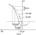
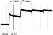
도 4는 비교예에 따른 도 2의 화소의 구동을 나타내는 타이밍도이다. 도 5는 박막 트랜지스터의 히스테리시스 특성을 보여주는 도면이고, 도 6은 박막 트랜지스터의 히스테리시스 특성으로 인한 표시장치의 휘도 문제를 나타내는 도면이다.FIG. 4 is a timing diagram showing driving of the pixel of FIG. 2 according to a comparative example. FIG. 5 is a diagram showing hysteresis characteristics of a thin film transistor, and FIG. 6 is a diagram showing a luminance problem of a display device due to the hysteresis characteristics of a thin film transistor.
표시장치가 화상을 표시할 때 소정 색의 색끌림(잔상) 현상이 발생하는데, 이는 상이한 색을 발광하는 화소(이하, '색 화소'라 함)들의 발광 시점의 차이와, 박막 트랜지스터의 히스테리시스 특성에 기인한다.When a display device displays an image, color fading (afterimage) of a certain color occurs, which is due to differences in the timing of light emission of pixels that emit different colors (hereinafter referred to as 'color pixels') and the hysteresis characteristics of thin film transistors. It is caused by.
도 4의 비교예에 따른 화소 구동은 도 3의 본 발명의 실시예에 따른 화소 구동의 히스테리시스 보상 구간(t1 내지 t4) 없이, 제1 트래지스터의 초기화(t5'), 문턱전압 보상 및 데이터기입(t6'), 발광소자의 초기화(t7') 및 발광(t8') 동작을 수행한다.The pixel driving according to the comparative example of FIG. 4 includes initialization (t5') of the first transistor, threshold voltage compensation, and data writing without the hysteresis compensation period (t1 to t4) of the pixel driving according to the embodiment of the present invention in FIG. 3. (t6'), initialization (t7') and light emission (t8') operations of the light emitting device are performed.
도 5 및 도 6을 참조하면, 제2 주사선(GWL)으로 제2 주사신호(GW)가 공급될 때, 데이터 신호가 인가되면서 제1 트랜지스터(T1)의 문턱전압을 보상하게 되는데, 박막 트랜지스터의 히스테리시스 특성에 의해 이전 발광 상태가 온 상태(on state)인지 오프 상태(off state)인지에 따라 문턱전압이 달라진다.Referring to FIGS. 5 and 6, when the second scan signal (GW) is supplied to the second scan line (GWL), the data signal is applied to compensate for the threshold voltage of the first transistor (T1). Due to hysteresis characteristics, the threshold voltage varies depending on whether the previous light emitting state was on or off.
이에 따라, 화소가 블랙을 표시하다가 화이트 표시로 바뀌는 경우, 제1 트랜지스터(T1)가 오프 상태에서 데이터신호를 인가받는 첫번째 프레임의 화이트 휘도와 제1 트랜지스터(T1)가 온 상태에서 데이터신호를 인가받는 두번째 프레임의 화이트 휘도 사이에 휘도 차이가 발생한다.Accordingly, when the pixel changes from displaying black to displaying white, the white luminance of the first frame in which the data signal is applied when the first transistor (T1) is off and the data signal is applied when the first transistor (T1) is on. A luminance difference occurs between the white luminance of the second frame received.
본 발명의 실시예는 박막 트랜지스터의 히스테리시스 특성에 기인한 문제점을 해소하기 위해 문턱전압 보상 전에 임의의 온 바이어스 전압을 소정 횟수 제1 트랜지스터(T1)에 인가하여 제1 트랜지스터(T1)의 문턱전압을 동일한 방향으로 쉬프트시켜 히스테리시스를 보상한다. 바이어스 전압(Vgs)은 제1 트랜지스터(T1)의 게이트 전극(G1)의 전압(Vgate)과 제1 전극(E11)의 전압(Vsource)의 차이(Vsource- Vgate=Vgs)를 의미한다. 온 바이어스 전압은 문턱전압(Vth)보다 큰 바이어스 전압이다.In an embodiment of the present invention, in order to solve the problem caused by the hysteresis characteristics of the thin film transistor, a random on-bias voltage is applied to the first transistor T1 a predetermined number of times before threshold voltage compensation to increase the threshold voltage of the first transistor T1. Hysteresis is compensated by shifting in the same direction. The bias voltage (Vgs) means the difference (Vsource-Vgate=Vgs) between the voltage (Vgate) of the gate electrode (G1) of the first transistor (T1) and the voltage (Vsource) of the first electrode (E11). The on bias voltage is a bias voltage greater than the threshold voltage (Vth).
한편, 도 3의 타이밍도에서, 제5 기간(t5)에 제1 트랜지스터(T1)의 게이트 전극(G1)으로 초기화 전압(Vint)이 인가되면, 제1 트랜지스터(T1)의 게이트 전극(G1)의 전압은 초기화 전압 인가 전의 전압과 초기화 전압의 차이가 된다. 제1 트랜지스터(T1)의 게이트 전극(G1)의 전압은 제1 트랜지스터(T1)의 기생 커패시터에 의해 전압 강하되고, 제1 트랜지스터(T1)의 제1 전극(E11)의 전압도 전압 강하된다. 이 경우 제1 트랜지스터(T1)의 바이어스 전압이 감소한다. 이에 따라 제1 트랜지스터(T1)의 출력 전류가 감소할 수 있다.Meanwhile, in the timing diagram of FIG. 3, when the initialization voltage Vint is applied to the gate electrode G1 of the first transistor T1 in the fifth period t5, the gate electrode G1 of the first transistor T1 The voltage is the difference between the voltage before applying the initialization voltage and the initialization voltage. The voltage of the gate electrode (G1) of the first transistor (T1) drops due to the parasitic capacitor of the first transistor (T1), and the voltage of the first electrode (E11) of the first transistor (T1) also drops. In this case, the bias voltage of the first transistor T1 decreases. Accordingly, the output current of the first transistor T1 may decrease.
따라서, 본 발명의 실시예는 화소(PX)의 전원선(PL)과 제1 트랜지스터(T1)의 제1 전극(E11) 사이에 전압 안정화를 위한 제1 보상 커패시터(Cse1) 및 제2 보상 커패시터(Cse2)를 추가한다. 제1 보상 커패시터(Cse1) 및 제2 보상 커패시터(Cse2)는 제1 트랜지스터(T1)의 제1 전극(E11)에서의 전압 변동을 줄임으로써 온 바이어스 전압을 확보할 수 있도록 한다. 온 바이어스 전압이 높을수록 화소의 발광량이 증가하여 블랙 표시 후 화이트를 표시하는 첫번째 프레임의 휘도와 두번째 프레임의 휘도 편차를 줄일 수 있다.Therefore, an embodiment of the present invention includes a first compensation capacitor Cse1 and a second compensation capacitor for voltage stabilization between the power line PL of the pixel PX and the first electrode E11 of the first transistor T1. Add (Cse2). The first compensation capacitor Cse1 and the second compensation capacitor Cse2 ensure an on-bias voltage by reducing voltage fluctuations at the first electrode E11 of the first transistor T1. As the on bias voltage increases, the amount of light emitted from the pixel increases, thereby reducing the difference between the luminance of the first frame and the second frame, which displays black and then white.
본 발명의 실시예는 제1 보상 커패시터(Cse1) 및 제2 보상 커패시터(Cse2)의 병렬연결을 개시하나, 이에 한정되지 않고, 제1 보상 커패시터(Cse1) 및 제2 보상 커패시터(Cse2) 중 하나의 보상 커패시터만을 구비하는 실시예를 포함할 수 있다. 제1 보상 커패시터(Cse1) 및 제2 보상 커패시터(Cse2)를 병렬연결하는 실시예는 제1 보상 커패시터(Cse1) 또는 제2 보상 커패시터(Cse2)와 같이 하나의 보상 커패시터를 구비하는 실시예보다 보상 커패시터 용량을 증가시켜 잔상 개선 효과를 더 높일 수 있다.The embodiment of the present invention discloses a parallel connection of the first compensation capacitor (Cse1) and the second compensation capacitor (Cse2), but is not limited thereto, and one of the first compensation capacitor (Cse1) and the second compensation capacitor (Cse2) An embodiment may include only a compensation capacitor. The embodiment in which the first compensation capacitor (Cse1) and the second compensation capacitor (Cse2) are connected in parallel is better than the embodiment in which one compensation capacitor is provided, such as the first compensation capacitor (Cse1) or the second compensation capacitor (Cse2). By increasing the capacitor capacity, the afterimage improvement effect can be further improved.
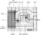
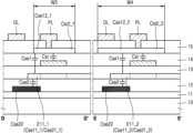
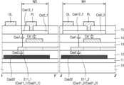
도 7은 본 발명의 일 실시예에 따른 도 2에 도시된 화소의 화소회로를 나타낸 평면도이다. 도 8은 도 7의 제1 트랜지스터(T1) 및 저장 커패시터(Cst)와 보상 커패시터(Cse1, Cse2)의 확대 평면도이다. 도 9는 도 8의 A-A'를 따라 절단한 단면도이다.FIG. 7 is a plan view showing a pixel circuit of the pixel shown in FIG. 2 according to an embodiment of the present invention. FIG. 8 is an enlarged plan view of the first transistor T1, storage capacitor Cst, and compensation capacitors Cse1 and Cse2 of FIG. 7. Figure 9 is a cross-sectional view taken along line A-A' of Figure 8.
화소(PX)는 제1 방향으로 연장되는 복수의 배선들 및 제1 방향과 교차하는 제2 방향으로 연장되는 복수의 배선들이 교차하는 지점에 배치된다. 제1 주사선(GIL), 제2 주사선(GWL), 제3 주사선(GBL), 초기화선(VL) 및 발광 제어선(EML)은 제2 방향으로 연장된다. 데이터선(DL) 및 전원선(PL)은 제1 방향으로 연장된다.The pixel PX is disposed at a point where a plurality of wires extending in a first direction and a plurality of wires extending in a second direction intersecting the first direction intersect. The first scan line (GIL), second scan line (GWL), third scan line (GBL), initialization line (VL), and emission control line (EML) extend in the second direction. The data line DL and the power line PL extend in the first direction.
화소회로의 제1 내지 제7 트랜지스터(T1 내지 T7)는 각각 소스 영역, 드레인 영역, 소스 영역과 드레인 영역 사이의 채널 영역을 포함하는 반도체층 및 채널 영역에 대응하는 위치에 반도체층과 절연 배치된 게이트 전극을 포함한다. 소스 영역은 도 2에 도시된 제1 전극 및 제2 전극 중 하나일 수 있고, 드레인 영역은 제1 전극 및 제2 전극 중 나머지 하나일 수 있다. 이하에서는 설명의 편의를 위해, 제1 전극 및 제2 전극으로 표기한다.The first to seventh transistors (T1 to T7) of the pixel circuit are arranged insulated from the semiconductor layer at positions corresponding to the semiconductor layer and the channel region including a source region, a drain region, and a channel region between the source region and the drain region, respectively. Includes a gate electrode. The source region may be one of the first electrode and the second electrode shown in FIG. 2, and the drain region may be the other one of the first electrode and the second electrode. Hereinafter, for convenience of explanation, they are referred to as first electrode and second electrode.
반도체층은 기판(10) 상의 제1 절연층(12) 상에 형성될 수 있다.The semiconductor layer may be formed on the first insulating
기판(10)은 가요성 기판일 수 있다. 기판(10)은 플라스틱 기판일 수 있다. 기판(10)은 유기물층 및 무기물층의 적층 구조로 형성될 수 있다. 예를 들어, 기판(10)은 유기물층/무기물층/유기물층/무기물층의 적층 구조일 수 있다. 기판(10)의 최상층인 무기물층은 배리어층으로 기능할 수 있다.
반도체층은, 예를 들어, 폴리 실리콘으로 이루어지며, 불순물이 도핑되지 않은 채널 영역과, 불순물이 도핑된 제1 전극 및 제2 전극을 포함한다. 여기서, 불순물은 트랜지스터의 종류에 따라 달라지며, N형 불순물 또는 P형 불순물이 가능하다. 제1 내지 제7 트랜지스터(T1 내지 T7)의 반도체층은 동일층에 배치되며, 서로 연결되며 다양한 형상으로 굴곡질 수 있다.The semiconductor layer is made of, for example, polysilicon and includes a channel region that is not doped with impurities, and a first electrode and a second electrode that are doped with impurities. Here, the impurity varies depending on the type of transistor, and can be N-type impurity or P-type impurity. The semiconductor layers of the first to seventh transistors T1 to T7 are disposed on the same layer, are connected to each other, and can be curved into various shapes.
기판(10)과 반도체층 사이에 제2 보상 커패시터(Cse2)의 제2 전극(Cse22)으로 기능하는 전극층(110)이 배치될 수 있다. 전극층(110)은 버퍼층(11, 도 9 참조) 상에 배치될 수 있다. 버퍼층(11)은 생략될 수 있다.An
반도체층과 게이트 전극 사이에는 제2 절연층(13, 도 9 참조)이 배치된다.A second insulating layer 13 (see FIG. 9) is disposed between the semiconductor layer and the gate electrode.
제1 내지 제7 트랜지스터(T1 내지 T7)의 게이트 전극(G1 내지 G7)과 동일층에 제1 주사선(GIL), 제2 주사선(GWL), 제3 주사선(GBL), 및 발광 제어선(EML)이 제2 방향으로 연장되며 배치된다. 제1 내지 제7 트랜지스터(T1 내지 T7)의 게이트 전극(G1 내지 G7) 상에는 제3 절연층(14, 도 9 참조)이 배치된다.A first scan line (GIL), a second scan line (GWL), a third scan line (GBL), and an emission control line (EML) are formed on the same layer as the gate electrodes (G1 to G7) of the first to seventh transistors (T1 to T7). ) is arranged and extends in the second direction. A third insulating layer 14 (see FIG. 9) is disposed on the gate electrodes G1 to G7 of the first to seventh transistors T1 to T7.
제1 트랜지스터(T1)는 제1 전극(E11), 제2 전극(E12), 채널 영역(C1)을 포함하는 반도체층 및 게이트 전극(G1)을 포함한다. 제1 트랜지스터(T1)의 게이트 전극(G1)은 평면상 채널 영역(C1)과 중첩한다. 제1 트랜지스터(T1)의 반도체층은 제1 전극(E11)과 제2 전극(E12) 사이에서 굴곡을 가짐으로써 채널 영역(C1)을 길게 형성할 수 있어, 게이트 전극(G1)에 인가되는 게이트 전압의 구동 범위(driving range)가 넓어질 수 있다. 제1 트랜지스터(T1)의 반도체층의 형상은 'ㄷ', 'ㄹ', 'S', 'M', 'W' 등의 굴곡 있는 형상 또는 구부러진 형상과 같이 다양한 실시예가 가능하다.The first transistor T1 includes a first electrode E11, a second electrode E12, a semiconductor layer including a channel region C1, and a gate electrode G1. The gate electrode (G1) of the first transistor (T1) overlaps the channel region (C1) in a plane view. The semiconductor layer of the first transistor (T1) is curved between the first electrode (E11) and the second electrode (E12) to form a long channel region (C1), so that the gate applied to the gate electrode (G1) The driving range of voltage may be expanded. The shape of the semiconductor layer of the first transistor T1 can be of various embodiments, such as a curved or curved shape such as 'ㄷ', 'ㄹ', 'S', 'M', or 'W'.
제2 트랜지스터(T2)는 제1 전극(E21), 제2 전극(E22), 채널 영역(C2)을 포함하는 반도체층 및 게이트 전극(G2)을 포함한다. 제2 트랜지스터(T2)의 게이트 전극(G2)은 평면상 채널 영역(C2)과 중첩한다. 제2 트랜지스터(T2)의 제1 전극(E21)은 제2 절연층(13) 내지 제4 절연층(15, 도 9 참조)의 컨택홀을 통해 데이터선(DL)과 전기적으로 연결된다. 제2 트랜지스터(T2)의 제2 전극(E22)은 제1 트랜지스터(T1)의 제1 전극(E11)과 연결된다.The second transistor T2 includes a first electrode E21, a second electrode E22, a semiconductor layer including a channel region C2, and a gate electrode G2. The gate electrode (G2) of the second transistor (T2) overlaps the channel region (C2) in plan view. The first electrode E21 of the second transistor T2 is electrically connected to the data line DL through a contact hole in the second to fourth insulating
제3 트랜지스터(T3)는 제1 전극(E31), 제2 전극(E32), 채널 영역(C3)을 포함하는 반도체층 및 게이트 전극(G3)을 포함한다. 제3 트랜지스터(T3)의 게이트 전극(G3)은 평면상 채널 영역(C3)과 중첩하고, 제2 주사선(GWL)의 일부에 의해 형성된다. 제3 트랜지스터(T3)의 제1 전극(E31)은 제1 트랜지스터(T1)의 제2 전극(E12)과 연결되고, 제2 전극(E32)은 제1 트랜지스터(T1)의 게이트 전극(G1)과 연결전극에 의해 전기적으로 연결된다. 연결전극은 제3 트랜지스터(T3)의 제2 전극(E32)을 노출하는 제2 절연층(13) 내지 제4 절연층(15)의 컨택홀과 제1 트랜지스터(T1)의 게이트 전극(G1)을 노출하는 제3 절연층(14) 및 제4 절연층(15)의 컨택홀을 통해 제3 트랜지스터(T3)의 제2 전극(E32)과 제1 트랜지스터(T1)의 게이트 전극(G1)을 연결한다.The third transistor T3 includes a first electrode E31, a second electrode E32, a semiconductor layer including a channel region C3, and a gate electrode G3. The gate electrode G3 of the third transistor T3 overlaps the channel region C3 in plan and is formed by a portion of the second scan line GWL. The first electrode E31 of the third transistor T3 is connected to the second electrode E12 of the first transistor T1, and the second electrode E32 is connected to the gate electrode G1 of the first transistor T1. and is electrically connected by a connecting electrode. The connection electrode is connected to the contact hole of the second to fourth insulating
제4 트랜지스터(T4)는 제1 전극(E41), 제2 전극(E42), 채널 영역(C4)을 포함하는 반도체층 및 게이트 전극(G4)을 포함한다. 제4 트랜지스터(T4)의 게이트 전극(G4)은 평면상 채널 영역(C4)과 중첩하고, 제1 주사선(GIL)의 일부에 의해 형성된다. 제4 트랜지스터(T4)의 제1 전극(E41)은 연결전극에 의해 초기화선(VL)과 전기적으로 연결되고, 제2 전극(E42)은 제3 트랜지스터(T3)의 제2 전극(E32) 및 제1 트랜지스터(T1)의 게이트 전극(G1)과 전기적으로 연결된다. 연결전극은 제4 트랜지스터(T4)의 제1 전극(E41)을 노출하는 제2 절연층(13) 내지 제4 절연층(15)의 컨택홀과 초기화선(VL)을 노출하는 제4 절연층(15)의 컨택홀을 통해 제4 트랜지스터(T4)의 제1 전극(E41)과 초기화선(VL)을 연결한다. 초기화선(VL)은 저장 커패시터(Cst)의 제2 전극(Cst2)과 동일층에 배치된다.The fourth transistor T4 includes a first electrode E41, a second electrode E42, a semiconductor layer including a channel region C4, and a gate electrode G4. The gate electrode G4 of the fourth transistor T4 overlaps the channel region C4 in plan and is formed by a portion of the first scanning line GIL. The first electrode (E41) of the fourth transistor (T4) is electrically connected to the initialization line (VL) by a connection electrode, and the second electrode (E42) is connected to the second electrode (E32) of the third transistor (T3) and It is electrically connected to the gate electrode (G1) of the first transistor (T1). The connection electrode is a contact hole of the second to fourth insulating
제5 트랜지스터(T5)는 제1 전극(E51), 제2 전극(E52), 채널 영역(C5)을 포함하는 반도체층 및 게이트 전극(G5)을 포함한다. 제5 트랜지스터(T5)의 게이트 전극(G5)은 평면상 채널 영역(C5)과 중첩하고, 발광 제어선(EML)의 일부에 의해 형성된다. 제5 트랜지스터(T45)의 제1 전극(E51)은 자신의 일부를 노출하는 제2 절연층(13) 내지 제4 절연층(15)의 컨택홀을 통해 전원선(PL)과 전기적으로 연결되고, 제2 전극(E52)은 제1 트랜지스터(T1)의 제1 전극(E11)과 연결된다.The fifth transistor T5 includes a first electrode E51, a second electrode E52, a semiconductor layer including a channel region C5, and a gate electrode G5. The gate electrode G5 of the fifth transistor T5 overlaps the channel region C5 in plan and is formed by a portion of the emission control line EML. The first electrode E51 of the fifth transistor T45 is electrically connected to the power line PL through a contact hole in the second to fourth insulating
제6 트랜지스터(T6)는 제1 전극(E61), 제2 전극(E62), 채널 영역(C6)을 포함하는 반도체층 및 게이트 전극(G6)을 포함한다. 제6 트랜지스터(T6)의 게이트 전극(G6)은 평면상 채널 영역(C6)과 중첩하고, 발광 제어선(EML)의 일부에 의해 형성된다. 제6 트랜지스터(T6)의 제1 전극(E61)은 제1 트랜지스터(T1)의 제2 전극(E12)과 연결되고, 제2 전극(E62)은 유기발광소자(OLED)의 화소전극과 전기적으로 연결된다. 제6 트랜지스터(T6)의 제2 전극(E62)은 자신의 일부를 노출하는 제2 절연층(13) 내지 제4 절연층(15)의 컨택홀을 통해 제4 절연층(15) 상의 연결전극과 전기적으로 연결된다. 화소전극은 제6 트랜지스터(T6)의 제2 전극(E62)과 연결된 연결전극 상부의 제5 절연층의 비아홀을 통해 연결전극과 전기적으로 연결됨으로써, 제6 트랜지스터(T6)의 제2 전극(E62)과 연결된다.The sixth transistor T6 includes a first electrode E61, a second electrode E62, a semiconductor layer including a channel region C6, and a gate electrode G6. The gate electrode G6 of the sixth transistor T6 overlaps the channel region C6 in plan and is formed by a portion of the emission control line EML. The first electrode (E61) of the sixth transistor (T6) is connected to the second electrode (E12) of the first transistor (T1), and the second electrode (E62) is electrically connected to the pixel electrode of the organic light emitting device (OLED). connected. The second electrode E62 of the sixth transistor T6 is connected to the connection electrode on the fourth insulating
제7 트랜지스터(T7)는 제1 전극(E71), 제2 전극(E72), 채널 영역(C7)을 포함하는 반도체층 및 게이트 전극(G7)을 포함한다. 제7 트랜지스터(T7)의 게이트 전극(G7)은 평면상 채널 영역(C7)과 중첩하고, 제3 주사선(GBL)의 일부에 의해 형성된다. 제7 트랜지스터(T7)의 제2 전극(E72)은 제4 트랜지스터(T4)의 제1 전극(E41)과 연결되고, 제1 전극(E71)은 제6 트랜지스터(T6)의 제2 전극(E62)과 연결된다.The seventh transistor T7 includes a first electrode E71, a second electrode E72, a semiconductor layer including a channel region C7, and a gate electrode G7. The gate electrode G7 of the seventh transistor T7 overlaps the channel region C7 in plan and is formed by a portion of the third scan line GBL. The second electrode E72 of the seventh transistor T7 is connected to the first electrode E41 of the fourth transistor T4, and the first electrode E71 is connected to the second electrode E62 of the sixth transistor T6. ) is connected to.
저장 커패시터(Cst)의 제1 전극(Cst1)은 제1 트랜지스터(T1)의 게이트 전극(G1)이다. 즉, 저장 커패시터(Cst)의 제1 전극(Cst1)과 제1 트랜지스터(T1)의 게이트 전극(G1)은 일체(一體)인 것으로 이해될 수 있다. 저장 커패시터(Cst)의 제1 전극(Cst1)은 인접한 화소와 분리되어 사각 형상으로 형성되어 있으며, 제1 주사선(GIL), 제2 주사선(GWL), 제3 주사선(GBL), 발광 제어선(EML)과 동일한 물질로 동일한 층에 형성된다.The first electrode (Cst1) of the storage capacitor (Cst) is the gate electrode (G1) of the first transistor (T1). That is, it can be understood that the first electrode (Cst1) of the storage capacitor (Cst) and the gate electrode (G1) of the first transistor (T1) are integrated. The first electrode (Cst1) of the storage capacitor (Cst) is separated from the adjacent pixel and is formed in a square shape, and includes a first scan line (GIL), a second scan line (GWL), a third scan line (GBL), and a light emission control line ( It is formed in the same layer with the same material as EML).
저장 커패시터(Cst)의 제2 전극(Cst2)은 제2 방향으로 인접한 화소들, 즉 동일 행의 화소들의 제2 전극(Cst2)과 연결된다. 저장 커패시터(Cst)의 제2 전극(Cst2)은 제1 전극(Cst1) 전체를 커버하도록 제1 전극(Cst1)과 중첩하고, 제1 트랜지스터(T1)와 평면상 및 단면상 수직으로 중첩하는 구조를 갖는다. 저장 커패시터(Cst)의 제1 전극(Cst1)과 제2 전극(Cst2) 사이의 제3 절연층(14)이 유전체층으로 기능한다. 저장 커패시터(Cst)의 제2 전극(Cst2)은 제1 전극(Cst1)의 일부를 노출하는 컨택홀에 대응하는 위치에 개구를 구비한다.The second electrode Cst2 of the storage capacitor Cst is connected to the second electrode Cst2 of pixels adjacent to each other in the second direction, that is, pixels in the same row. The second electrode (Cst2) of the storage capacitor (Cst) has a structure that overlaps the first electrode (Cst1) to cover the entire first electrode (Cst1) and vertically overlaps the first transistor (T1) in plan and cross-section. have The third insulating
저장 커패시터(Cst)의 제2 전극(Cst2) 상에는 제4 절연층(15)이 배치된다. 제4 절연층(15) 상에 데이터선(DL) 및 전원선(PL)이 제1 방향으로 연장되며 배치된다. 전원선(PL)은 저장 커패시터(Cst)의 제2 전극(Cst2)과 일부 중첩한다.A fourth insulating
저장 커패시터(Cst)의 제2 전극(Cst2)은 자신의 일부를 노출하는 제4 절연층(15)의 컨택홀(CH1)을 통해 전원선(PL)과 전기적으로 연결된다. 이에 따라 전원선(PL)은 제1 방향의 전원선으로 기능하고, 저장 커패시터(Cst)의 제2 전극(Cst2)은 제2 방향의 전원선으로 기능하여, 전원선(PL)은 전체적으로 메쉬(mesh) 구조를 가질 수 있다. 또한 전원선(PL)은 제5 트랜지스터(T5)의 제1 전극(E51)과 전기적으로 연결된다.The second electrode Cst2 of the storage capacitor Cst is electrically connected to the power line PL through the contact hole CH1 of the fourth insulating
제1 보상 커패시터(Cse1)의 제1 전극(Cse11)은 제1 트랜지스터(T1)의 제1 전극(E11)의 적어도 일부이다. 즉, 제1 보상 커패시터(Cse1)의 제1 전극(Cse11)과 제1 트랜지스터(T1)의 제1 전극(E11)은 일체(一體)인 것으로 이해될 수 있다.The first electrode (Cse11) of the first compensation capacitor (Cse1) is at least a part of the first electrode (E11) of the first transistor (T1). That is, it can be understood that the first electrode (Cse11) of the first compensation capacitor (Cse1) and the first electrode (E11) of the first transistor (T1) are integrated.
제1 보상 커패시터(Cse1)의 제2 전극(Cse12)은 저장 커패시터(Cst)의 제2 전극(Cst2)으로부터 연장되어 제1 트랜지스터(T1)의 제1 전극(E11)의 적어도 일부를 커버하는 전극층이다. 즉, 제1 보상 커패시터(Cse1)의 제2 전극(Cse12)과 저장 커패시터(Cst)의 제2 전극(Cst2)은 일체(一體)인 것으로 이해될 수 있다. 이에 따라 제1 보상 커패시터(Cse1)의 제2 전극(Cse12)은 전원선(PL)과 전기적으로 연결된다.The second electrode Cse12 of the first compensation capacitor Cse1 is an electrode layer extending from the second electrode Cst2 of the storage capacitor Cst and covering at least a portion of the first electrode E11 of the first transistor T1. am. That is, it can be understood that the second electrode (Cse12) of the first compensation capacitor (Cse1) and the second electrode (Cst2) of the storage capacitor (Cst) are integrated. Accordingly, the second electrode (Cse12) of the first compensation capacitor (Cse1) is electrically connected to the power line (PL).
제2 보상 커패시터(Cse2)의 제1 전극(Cse21)은 제1 트랜지스터(T1)의 제1 전극(E11)의 적어도 일부이다. 즉, 제2 보상 커패시터(Cse2)의 제1 전극(Cse21)과 제1 트랜지스터(T1)의 제1 전극(E11)은 일체(一體)인 것으로 이해될 수 있다.The first electrode (Cse21) of the second compensation capacitor (Cse2) is at least a part of the first electrode (E11) of the first transistor (T1). That is, it can be understood that the first electrode (Cse21) of the second compensation capacitor (Cse2) and the first electrode (E11) of the first transistor (T1) are integrated.
제2 보상 커패시터(Cse2)의 제2 전극(Cse22)은 제1 트랜지스터(T1)의 제1 전극(E11)의 하부층에 제1 트랜지스터(T1)의 제1 전극(E11)과 중첩하게 배치된 전극층(110)이다. 제2 보상 커패시터(Cse2)의 제2 전극(Cse22)은 제1 트랜지스터(T1)의 채널 영역(C1)과 중첩하지 않는다. 제2 보상 커패시터(Cse2)의 제2 전극(Cse22)은 제1 절연층(12) 내지 제3 절연층(14)의 컨택홀(CH2)을 통해 제1 보상 커패시터(Cse1)의 제2 전극(Cse12)과 전기적으로 연결된다. 이에 따라 제2 보상 커패시터(Cse2)의 제2 전극(Cse22)은 전원선(PL)과 전기적으로 연결된다.The second electrode (Cse22) of the second compensation capacitor (Cse2) is an electrode layer disposed on a lower layer of the first electrode (E11) of the first transistor (T1) and overlaps the first electrode (E11) of the first transistor (T1). It is (110). The second electrode Cse22 of the second compensation capacitor Cse2 does not overlap the channel region C1 of the first transistor T1. The second electrode (Cse22) of the second compensation capacitor (Cse2) is connected to the second electrode (Cse22) of the first compensation capacitor (Cse1) through the contact hole (CH2) of the first to third insulating layers (12) to (14). It is electrically connected to Cse12). Accordingly, the second electrode (Cse22) of the second compensation capacitor (Cse2) is electrically connected to the power line (PL).
저장 커패시터(Cst)의 제2 전극(Cst2)과 동일층에 초기화선(VL)이 제2 방향으로 연장되며 배치된다. 데이터선(DL) 및 전원선(PL)은 제4 절연층(15, 도 9 참조) 상에 제1 방향으로 연장되며 배치된다.The initialization line (VL) is disposed on the same layer as the second electrode (Cst2) of the storage capacitor (Cst) and extends in the second direction. The data line DL and the power line PL extend in the first direction and are disposed on the fourth insulating layer 15 (see FIG. 9).
한편, 화소(PX)에 제2 트랜지스터(T2)의 제1 전극(E21) 및 제2 전극(E22) 중 적어도 하나의 일부, 및/또는 제3 트랜지스터(T3)의 제1 전극(E31) 및 제2 전극(E32) 중 적어도 하나의 일부, 및/또는 제4 트랜지스터(T4)의 제1 전극(E41) 및 제2 전극(E42) 중 적어도 하나의 일부를 커버하는 차광부재(120)가 배치될수 있다.Meanwhile, a portion of at least one of the first electrode E21 and the second electrode E22 of the second transistor T2 and/or the first electrode E31 of the third transistor T3 are applied to the pixel PX. A
차광부재(120)는 초기화선(VL)과 동일층에 배치될 수 있다. 차광부재(120)는 초기화선(VL)과 동일 물질을 포함할 수 있다. 차광부재(120)는 전원선(PL) 또는 초기화선(VL)과 전기적으로 연결될 수 있다. 차광부재(120)는 전원선(PL) 또는 초기화선(VL)과 연결되어 정전압을 인가받음으로써 제2 트랜지스터(T2), 제3 트랜지스터(T3) 및 제4 트랜지스터(T4)가 주변의 다른 전기적 신호에 의해 영향받는 것을 차단할 수 있다. 즉, 차광부재(120)는 화소(PX)의 회로의 동작 특성을 향상시킬 수 있다.The
도 8 및 도 9를 참조하면, 화소(PX)의 제1 트랜지스터(T1)는 제1 전극(E11), 제2 전극(E12) 및 채널 영역(C1)을 포함하는 반도체층과, 채널 영역(C1)에 대응하게 배치된 게이트 전극(G1)을 구비한다. 제1 트랜지스터(T1)와 평면상 및 단면상 수직으로 중첩하게 저장 커패시터(Cst)와 제1 보상 커패시터(Cse1) 및 제2 보상 커패시터(Cse2)가 구비된다. 저장 커패시터(Cst)는 하부전극인 제1 전극(Cst1) 및 상부전극인 제2 전극(Cst2)를 구비한다. 제1 보상 커패시터(Cse1)는 하부전극인 제1 전극(Cse11) 및 상부전극인 제2 전극(Cse12)를 구비한다. 제2 보상 커패시터(Cse2)는 하부전극인 제2 전극(Cse22) 및 상부전극인 제1 전극(Cse21)을 구비한다.8 and 9, the first transistor T1 of the pixel PX includes a semiconductor layer including a first electrode E11, a second electrode E12, and a channel region C1, and a channel region ( It has a gate electrode (G1) disposed corresponding to C1). A storage capacitor (Cst), a first compensation capacitor (Cse1), and a second compensation capacitor (Cse2) are provided to vertically overlap the first transistor (T1) in plan and cross-section. The storage capacitor Cst includes a first electrode Cst1 as a lower electrode and a second electrode Cst2 as an upper electrode. The first compensation capacitor Cse1 includes a first electrode Cse11 as a lower electrode and a second electrode Cse12 as an upper electrode. The second compensation capacitor Cse2 includes a second electrode Cse22 as a lower electrode and a first electrode Cse21 as an upper electrode.
전극층(110)은 적어도 제1 트랜지스터(T1)의 제1 전극(E11)과 중첩한다. 전극층(111)은 적어도 제1 트랜지스터(T1)의 게이트 전극(G1)과 중첩하는 제1 영역(111-1)과 적어도 제1 트랜지스터(T1)의 제1 전극(E11)과 중첩하는 제2 영역(111-2)을 포함한다. 전극층(110)의 일부와 전극층(111)의 제2 영역은 데이터선(DL)과 중첩한다.The
전극층(111)의 제1 영역은 저장 커패시터(Cst)의 제2 전극(Cst2)의 역할을 한다. 전극층(111)의 제2 영역은 제1 보상 커패시터(Cse1)의 제2 전극(Cse12)의 역할을 한다. 전극층(111)은 컨택홀(CH1)을 통해 전원선(PL)과 전기적으로 연결된다.The first area of the
저장 커패시터(Cst)는 제1 트랜지스터(T1)의 게이트 전극(G1)인 제1 전극(Cst1)과 제1 전극(Cst1)에 대향하는 제2 전극(Cst2)에 의해 형성된다. 제1 보상 커패시터(Cse1)는 제1 트랜지스터(T1)의 제1 전극(E11)인 제1 전극(Cse11)과 제1 전극(Cse11)에 대향하는 제2 전극(Cse12)에 의해 형성된다. 저장 커패시터(Cst)의 제2 전극(Cst2) 및 제1 보상 커패시터(Cse1)의 제2 전극(Cse12)은 제4 절연층(15)의 컨택홀(CH1)을 통해 전원선(PL)에 전기적으로 연결된다.The storage capacitor Cst is formed by a first electrode Cst1, which is the gate electrode G1 of the first transistor T1, and a second electrode Cst2 opposing the first electrode Cst1. The first compensation capacitor Cse1 is formed by the first electrode Cse11, which is the first electrode E11 of the first transistor T1, and the second electrode Cse12 opposing the first electrode Cse11. The second electrode (Cst2) of the storage capacitor (Cst) and the second electrode (Cse12) of the first compensation capacitor (Cse1) are electrically connected to the power line (PL) through the contact hole (CH1) of the fourth insulating layer (15). It is connected to
전극층(110)의 제1 영역은 제2 보상 커패시터(Cse2)의 제2 전극(Cse22)의 역할을 한다. 전극층(110)은 컨택홀(CH2)을 통해 전원선(PL)과 전기적으로 연결된다. 제2 보상 커패시터(Cse2)는 제1 트랜지스터(T1)의 제1 전극(E11)인 제1 전극(Cse21)과 제1 전극(Cse21)에 대향하는 제2 전극(Cse22)에 의해 형성된다.The first region of the
본 발명의 실시예는 색 화소별로 제1 보상 커패시터(Cse1) 및 제2 보상 커패시터(Cse2)의 용량을 달리 설계하여 색 화소별 온 바이어스 전압을 다르게 설정할 수 있어 색 화소별 발광량을 조절할 수 있다. 이에 따라 색 화소별 출력 전류의 편차로 인한 발광 시점의 차이를 줄일 수 있다. 색 화소별 제1 보상 커패시터(Cse1) 및 제2 보상 커패시터(Cse2)의 용량은 전극들의 대향 면적(중첩 면적)을 달리함으로써 구현할 수 있다.In an embodiment of the present invention, the capacity of the first compensation capacitor (Cse1) and the second compensation capacitor (Cse2) can be designed differently for each color pixel, so that the on bias voltage can be set differently for each color pixel, thereby adjusting the amount of light emitted for each color pixel. Accordingly, the difference in light emission timing due to the variation in output current for each color pixel can be reduced. The capacities of the first compensation capacitor Cse1 and the second compensation capacitor Cse2 for each color pixel can be implemented by varying the opposing areas (overlapping areas) of the electrodes.
도 10은 본 발명의 일 실시예에 따른 서로 다른 색 화소의 화소회로를 나타낸 평면도이다. 도 11은 도 10의 제1 트랜지스터(T1) 및 저장 커패시터(Cst)와 보상 커패시터(Cse)의 확대 평면도이다. 도 12는 도 10의 B-B' 및 C-C'를 따라 절단한 단면도이다. 이하에서, 도 7 내지 도 9를 참조하여 설명한 내용과 중복하는 내용의 상세한 설명은 생략한다.Figure 10 is a plan view showing a pixel circuit for different color pixels according to an embodiment of the present invention. FIG. 11 is an enlarged plan view of the first transistor T1, storage capacitor Cst, and compensation capacitor Cse of FIG. 10. FIG. 12 is a cross-sectional view taken along lines B-B' and C-C' of FIG. 10. Hereinafter, detailed description of content that overlaps with the content described with reference to FIGS. 7 to 9 will be omitted.
도 10은 기판(10)의 제1 화소영역에 제1 화소(PX1)가 배치되고, 제1 화소영역에 인접한 제2 화소영역에 제2 화소(PX2)가 배치된 예를 도시하고 있다. 도시되지 않았으나, 제2 화소영역에 인접한 제3 화소영역에 제3 화소(PX3)가 배치될 수 있다. 제1 화소영역 내지 제3 화소영역은 제2 방향을 따라 순차적으로 배치될 수 있다. 제1 화소(PX1) 내지 제3 화소(PX3)는 각각 도 2에 도시된 바와 같이 발광소자 및 발광소자와 연결된 화소회로를 포함한다. 도 10에서는 설명의 편의를 위해 제1 화소영역에 제1 화소(PX1)의 화소회로가 배치되고, 제2 화소영역에 제2 화소(PX2)의 화소회로가 배치된 예로 설명한다.FIG. 10 shows an example in which the first pixel PX1 is disposed in the first pixel region of the
도 11 및 도 12에서, 설명의 편의상, 제1 화소(PX1)의 화소회로와 제2 화소(PX2)의 화소회로를 구분하기 위해 각각 상이한 도면부호로 표시하였다.In FIGS. 11 and 12 , for convenience of explanation, the pixel circuits of the first pixel (PX1) and the pixel circuits of the second pixel (PX2) are indicated by different reference numerals to distinguish them.
제1 화소(PX1)의 전극층(110a)과 제2 화소(PX2)의 전극층(110b)의 길이와 폭(또는 면적)은 동일하다. 제1 화소(PX1)의 전극층(111a)과 제2 화소(PX2)의 전극층(111b)의 길이와 폭(또는 면적)은 동일하다. 여기서, 길이는 제1 방향으로의 크기이고, 폭은 제2 방향으로의 크기이다.The length and width (or area) of the
제2 화소(PX2)의 제1 트랜지스터(T1)의 제1 전극(E11_2)의 폭(W2) 또는 면적은 제1 화소(PX1)의 제1 트랜지스터(T1)의 제1 전극(E11_1)의 폭(W1) 또는 면적보다 크다. 이에 따라 제2 화소(PX2)의 제1 트랜지스터(T1)의 제1 전극(E11_2)과 전극층(110a) 및 전극층(111a) 각각의 대향 면적이, 제1 화소(PX1)의 제1 트랜지스터(T1)의 제1 전극(E11_1)과 전극층(110b) 및 전극층(111b) 각각의 대향 면적보다 크다. 따라서, 제2 화소(PX2)의 제1 보상 커패시터(Cse1)의 용량은 제1 화소(PX1)의 제1 보상 커패시터(Cse1)의 용량보다 크고, 제2 화소(PX2)의 제2 보상 커패시터(Cse2)의 용량은 제1 화소(PX1)의 제2 보상 커패시터(Cse2)의 용량보다 크다.The width W2 or area of the first electrode E11_2 of the first transistor T1 of the second pixel PX2 is the width of the first electrode E11_1 of the first transistor T1 of the first pixel PX1. (W1) or greater than the area. Accordingly, the opposing area of the first electrode E11_2 of the first transistor T1 of the second pixel PX2 and each of the
본 발명의 실시예는, 제1 트랜지스터(T1)의 제1 전극(E11)의 폭 또는 면적 조절에 의한 제1 및 제2 보상 커패시터(Cse1, Cse2)의 용량 차이를 이용하여 제1 화소(PX1)와 제2 화소(PX2)의 온 바이어스 편차를 유도할 수 있다. 이에 따라 제1 화소(PX1) 대비 제2 화소(PX2)에 강한 온 바이어스를 인가하여 응답속도를 더 빠르게 함으로써 화소 간 발광 지연 차이를 줄일 수 있다.An embodiment of the present invention uses the difference in capacity of the first and second compensation capacitors (Cse1, Cse2) by adjusting the width or area of the first electrode (E11) of the first transistor (T1) to generate ) and the on bias deviation of the second pixel (PX2) can be derived. Accordingly, by applying a stronger on bias to the second pixel (PX2) compared to the first pixel (PX1) to make the response speed faster, the difference in emission delay between pixels can be reduced.
제3 화소영역에 배치된 제3 화소(PX3)의 제1 및 제2 보상 커패시터(Cse1, Cse2)의 용량은 제1 화소(PX1)의 제1 및 제2 보상 커패시터(Cse1, Cse2)의 용량 또는 제2 화소(PX2)의 제1 및 제2 보상 커패시터(Cse1, Cse2)의 용량과 동일 또는 상이할 수 있다. 즉, 제3 화소(PX3)의 제1 트랜지스터(T1)의 제1 전극(E11)의 폭 또는 면적은 제1 화소(PX1) 또는 제2 화소(PX2)의 제1 트랜지스터(T1)의 제1 전극(E11)의 폭 또는 면적과 동일 또는 상이할 수 있다.The capacity of the first and second compensation capacitors Cse1 and Cse2 of the third pixel PX3 disposed in the third pixel area is the capacity of the first and second compensation capacitors Cse1 and Cse2 of the first pixel PX1. Alternatively, the capacitance may be the same as or different from the capacity of the first and second compensation capacitors Cse1 and Cse2 of the second pixel PX2. That is, the width or area of the first electrode E11 of the first transistor T1 of the third pixel PX3 is the width or area of the first transistor T1 of the first pixel PX1 or the second pixel PX2. It may be the same as or different from the width or area of the electrode E11.
도 13은 본 발명의 다른 실시예에 따른 제1 트랜지스터(T1) 및 저장 커패시터(Cst)와 보상 커패시터(Cse)의 확대 평면도이다. 도 14는 도 13의 D-D' 및 E-E'를 따라 절단한 단면도이다. 이하에서, 전술한 실시예와 상이한 내용을 중심으로 설명한다.Figure 13 is an enlarged plan view of the first transistor (T1), the storage capacitor (Cst), and the compensation capacitor (Cse) according to another embodiment of the present invention. FIG. 14 is a cross-sectional view taken along lines D-D' and E-E' of FIG. 13. Below, description will be given focusing on content that is different from the above-described embodiment.
도 13 및 도 14의 실시예는, 제1 화소(PX1)의 전극층(111a)과 제2 화소(PX2)의 전극층(111b)의 크기(면적)가 상이한 점에서, 도 11 및 도 12의 실시예와 차이가 있다.13 and 14 are similar to those of FIGS. 11 and 12 in that the sizes (areas) of the
제2 화소(PX2)의 전극층(111b)의 폭(W4) 또는 면적은 제1 화소(PX1)의 전극층(111a)의 폭(W3) 또는 면적보다 크다. 제2 화소(PX2)의 전극층(111b)이 제1 트랜지스터(T1)의 게이트 전극(G1_2)과 제1 전극(E11_2)을 모두 커버하는 반면, 제1 화소(PX1)의 전극층(111a)은 제1 트랜지스터(T1)의 게이트 전극(G1_1)과 제1 트랜지스터(T1)의 제1 전극(E11_1)의 일부를 커버한다. 제1 화소(PX1)의 제1 트랜지스터(T1)의 제1 전극(E11_1)과 제2 화소(PX2)의 제1 트랜지스터(T1)의 제1 전극(E11_2)의 폭은 동일하다.The width W4 or area of the
이에 따라, 제2 화소(PX2)의 제1 트랜지스터(T1)의 제1 전극(E11_2)과 전극층(111a)의 대향 면적이, 제1 화소(PX1)의 제1 트랜지스터(T1)의 제1 전극(E11_1)과 전극층(111b) 각각의 대향 면적보다 크다. 따라서, 제2 화소(PX2)의 제1 보상 커패시터(Cse1)의 용량은 제1 화소(PX1)의 제1 보상 커패시터(Cse1)의 용량보다 크다.Accordingly, the opposing area between the first electrode E11_2 of the first transistor T1 of the second pixel PX2 and the
본 발명의 실시예는, 제1 보상 커패시터(Cse1)의 제2 전극(Cse12)의 폭 또는 면적 조절에 의한 제1 보상 커패시터(Cse1)의 용량 차이를 이용하여 제1 화소(PX1)와 제2 화소(PX2)의 온 바이어스 편차를 유도할 수 있다. 이에 따라 제1 화소(PX1) 대비 제2 화소(PX2)에 강한 온 바이어스를 인가하여 응답속도를 더 빠르게 함으로써 화소 간 발광 지연 차이를 줄일 수 있다.An embodiment of the present invention uses the difference in capacity of the first compensation capacitor (Cse1) by adjusting the width or area of the second electrode (Cse12) of the first compensation capacitor (Cse1) to connect the first pixel (PX1) and the second pixel (PX1). The on bias deviation of the pixel (PX2) can be induced. Accordingly, by applying a stronger on bias to the second pixel (PX2) compared to the first pixel (PX1) to make the response speed faster, the difference in emission delay between pixels can be reduced.
제3 화소영역에 배치된 제3 화소(PX3)의 제1 보상 커패시터(Cse1)의 용량은 제1 화소(PX1)의 제1 보상 커패시터(Cse1)의 용량 또는 제2 화소(PX2)의 제1 보상 커패시터(Cse1)의 용량과 동일 또는 상이할 수 있다. 즉, 제3 화소(PX3)의 제1 보상 커패시터(Cse1)의 제2 전극(Cse12)의 폭 또는 면적은 제1 화소(PX1) 또는 제2 화소(PX2)의 제1 보상 커패시터(Cse1)의 제2 전극(Cse12)의 폭 또는 면적과 동일 또는 상이할 수 있다.The capacity of the first compensation capacitor Cse1 of the third pixel PX3 disposed in the third pixel area is the capacity of the first compensation capacitor Cse1 of the first pixel PX1 or the capacity of the first compensation capacitor Cse1 of the second pixel PX2. It may be the same as or different from the capacity of the compensation capacitor (Cse1). That is, the width or area of the second electrode Cse12 of the first compensation capacitor Cse1 of the third pixel PX3 is that of the first compensation capacitor Cse1 of the first pixel PX1 or the second pixel PX2. It may be the same as or different from the width or area of the second electrode Cse12.
도 15는 본 발명의 다른 실시예에 따른 도 2에 도시된 화소의 화소회로를 나타낸 평면도이다. 도 16은 도 15의 제1 트랜지스터(T1) 및 저장 커패시터(Cst)와 보상 커패시터(Cse1, Cse2)의 확대 평면도이다. 도 17은 도 16의 F-F'를 따라 절단한 단면도이다. 이하에서는 도 7 내지 도 9의 실시예와 상이한 내용을 중심으로 설명한다.FIG. 15 is a plan view showing a pixel circuit of the pixel shown in FIG. 2 according to another embodiment of the present invention. FIG. 16 is an enlarged plan view of the first transistor T1, storage capacitor Cst, and compensation capacitors Cse1 and Cse2 of FIG. 15. Figure 17 is a cross-sectional view taken along line FF' of Figure 16. Hereinafter, the description will focus on content that is different from the embodiment of FIGS. 7 to 9.
도 15 내지 도 17의 실시예는, 화소(PX)의 전극층(110)이 제1 트랜지스터(T1)의 제1 전극(E11) 및 채널 영역(C1)과 중첩하는 점에서, 도 7 내지 도 9의 실시예와 차이가 있다.15 to 17 , the
전극층(110)은 적어도 제1 트랜지스터(T1)의 제1 전극(E11)과 중첩하는 제1 영역(110-1), 및 제1 영역(110-1)으로부터 연장되고 제1 트랜지스터(T1)의 채널 영역(C1)과 중첩하는 제2 영역(110-2)을 포함한다.The
전극층(110)의 제1 영역은 제2 보상 커패시터(Cse2)의 제2 전극(Cse22)의 역할을 한다. 전극층(110)의 제2 영역은 제1 트랜지스터(T1)의 게이트 전극(G1)과 함께 채널 영역(C1)의 캐리어 이동을 제어하는 바텀 게이트 전극의 역할을 한다. 전극층(110)이 제1 전원전압(ELVDD)을 인가받음에 따라 제1 트랜지스터(T1)의 온 바이어스 전압을 보다 확보할 수 있다.The first region of the
도 18은 본 발명의 다른 실시예에 따른 서로 다른 색 화소의 화소회로를 나타낸 평면도이다. 도 19는 도 18의 제1 트랜지스터(T1) 및 저장 커패시터(Cst)와 보상 커패시터(Cse)의 확대 평면도이다. 도 20은 도 18의 G-G' 및 H-H'를 따라 절단한 단면도이다.Figure 18 is a plan view showing a pixel circuit for different color pixels according to another embodiment of the present invention. FIG. 19 is an enlarged plan view of the first transistor T1, storage capacitor Cst, and compensation capacitor Cse of FIG. 18. FIG. 20 is a cross-sectional view taken along lines G-G' and H-H' of FIG. 18.
도 18 내지 도 20의 실시예는, 화소(PX)의 전극층(110)이 제1 트랜지스터(T1)의 제1 전극(E11) 및 채널 영역(C1)과 중첩하는 점에서, 도 10 내지 도 12의 실시예와 차이가 있다.18 to 20, the
도 18 내지 도 20의 실시예는, 제2 화소(PX2)의 제1 트랜지스터(T1)의 제1 전극(E11_2)의 폭(W2) 또는 면적이 제1 화소(PX1)의 제1 트랜지스터(T1)의 제1 전극(E11_1)의 폭(W1) 또는 면적보다 크다. 즉, 본 발명의 실시예는, 제1 트랜지스터(T1)의 제1 전극(E11)의 폭 또는 면적 조절에 의한 제1 및 제2 보상 커패시터(Cse1, Cse2)의 용량 차이를 이용하여 제1 화소(PX1)와 제2 화소(PX2)의 온 바이어스 편차를 유도할 수 있다. 이에 따라 제1 화소(PX1) 대비 제2 화소(PX2)에 강한 온 바이어스를 인가하여 응답속도를 더 빠르게 함으로써 화소 간 발광 지연 차이를 줄일 수 있다.18 to 20, the width (W2) or area of the first electrode (E11_2) of the first transistor (T1) of the second pixel (PX2) is greater than or equal to that of the first transistor (T1) of the first pixel (PX1). ) is larger than the width (W1) or area of the first electrode (E11_1). That is, the embodiment of the present invention uses the difference in capacity between the first and second compensation capacitors Cse1 and Cse2 by adjusting the width or area of the first electrode E11 of the first transistor T1 to determine the first pixel The on bias deviation of the pixel (PX1) and the second pixel (PX2) can be derived. Accordingly, by applying a stronger on bias to the second pixel (PX2) compared to the first pixel (PX1) to make the response speed faster, the difference in emission delay between pixels can be reduced.
또한, 본 발명의 실시예는, 전극층(110)이 제1 트랜지스터(T1)의 제1 전극(E11) 및 채널 영역(C1)과 중첩함에 따라, 전극층(110)의 일부는 제2 보상 커패시터(Cse2)의 제2 전극(Cse22)의 역할을 하고, 일부는 채널 영역(C1)의 캐리어 이동을 제어하는 바텀 게이트 전극의 역할을 한다. 이에 따라, 전극층(110)이 제1 전원전압(ELVDD)을 인가받음으로써 제1 트랜지스터(T1)의 온 바이어스 전압을 보다 확보할 수 있다.In addition, in an embodiment of the present invention, as the
도 21은 본 발명의 다른 실시예에 따른 제1 트랜지스터(T1) 및 저장 커패시터(Cst)와 보상 커패시터(Cse)의 확대 평면도이다. 도 22는 도 21의 I-I' 및 J-J'를 따라 절단한 단면도이다. 이하에서, 전술한 실시예와 상이한 내용을 중심으로 설명한다.Figure 21 is an enlarged plan view of the first transistor (T1), the storage capacitor (Cst), and the compensation capacitor (Cse) according to another embodiment of the present invention. FIG. 22 is a cross-sectional view taken along lines II' and J-J' of FIG. 21. Below, description will be given focusing on content that is different from the above-described embodiment.
도 21 및 도 22의 실시예는, 제1 화소(PX1)의 전극층(111a)과 제2 화소(PX2)의 전극층(111b)의 크기(면적)가 상이한 점에서, 도 19 및 도 20의 실시예와 차이가 있다.21 and 22 are similar to those of FIGS. 19 and 20 in that the sizes (areas) of the
제2 화소(PX2)의 전극층(111b)의 폭(W4) 또는 면적은 제1 화소(PX1)의 전극층(111a)의 폭(W3) 또는 면적보다 크다. 즉, 본 발명의 실시예는, 제1 보상 커패시터(Cse1)의 제2 전극(Cse12)의 폭 또는 면적 조절에 의한 제1 보상 커패시터(Cse1)의 용량 차이를 이용하여 제1 화소(PX1)와 제2 화소(PX2)의 온 바이어스 편차를 유도할 수 있다. 이에 따라 제1 화소(PX1) 대비 제2 화소(PX2)에 강한 온 바이어스를 인가하여 응답속도를 더 빠르게 함으로써 화소 간 발광 지연 차이를 줄일 수 있다.The width W4 or area of the
또한, 본 발명의 실시예는, 전극층(110)이 제1 트랜지스터(T1)의 제1 전극(E11) 및 채널 영역(C1)과 중첩함에 따라, 전극층(110)의 일부는 제2 보상 커패시터(Cse2)의 제2 전극(Cse22)의 역할을 하고, 일부는 채널 영역(C1)의 캐리어 이동을 제어하는 바텀 게이트 전극의 역할을 한다. 이에 따라, 전극층(110)이 제1 전원전압(ELVDD)을 인가받음으로써 제1 트랜지스터(T1)의 온 바이어스 전압을 보다 확보할 수 있다.In addition, in an embodiment of the present invention, as the
본 발명의 실시예들에 따른 표시장치는 구동 트랜지스터의 소스 영역 또는 드레인 영역의 적어도 일부인 제1 전극과 제1 전원전압을 인가받는 전원선에 연결된 제2 전극을 포함하는 보상 커패시터를 구비함으로써 구동 트랜지스터의 온 바이어스 전압을 증가시킬 수 있다. 또한 병렬 연결된 한 쌍의 보상 커패시터를 구비함으로써 구동 트랜지스터의 온 바이어스 전압을 더욱 증가시킬 수 있다.A display device according to embodiments of the present invention includes a compensation capacitor including a first electrode that is at least part of the source region or drain region of the driving transistor and a second electrode connected to a power line that receives the first power voltage, so that the driving transistor The on bias voltage of can be increased. Additionally, the on-bias voltage of the driving transistor can be further increased by providing a pair of compensation capacitors connected in parallel.
또한, 본 발명의 실시예들에 따른 표시장치는 보상 커패시터의 대향 전극들의 면적(폭) 조절에 의한 용량 제어를 통해 온 바이어스 전압을 색 화소별로 차등화할 수 있다. 이로써 색 화소별로 온 바이어스 전압을 제어하여 색 화소별로 발광량 및 발광 시점을 조절할 수 있다. 따라서, 본 발명의 실시예들에 따른 표시장치는 색 화소들 간의 발광 지연 편차를 줄일 수 있어 색끌림 및/또는 색번짐을 개선할 수 있다.Additionally, display devices according to embodiments of the present invention can differentiate the on bias voltage for each color pixel through capacitance control by adjusting the area (width) of the opposing electrodes of the compensation capacitor. As a result, the on-bias voltage for each color pixel can be controlled to adjust the amount and timing of light emission for each color pixel. Accordingly, display devices according to embodiments of the present invention can reduce light emission delay differences between color pixels, thereby improving color fading and/or color bleeding.
이와 같이 본 발명은 도면에 도시된 일 실시예를 참고로 하여 설명하였으나 이는 예시적인 것에 불과하며 당해 분야에서 통상의 지식을 가진 자라면 이로부터 다양한 변형 및 실시예의 변형이 가능하다는 점을 이해할 것이다. 따라서, 본 발명의 진정한 기술적 범위는 첨부된 특허청구범위의 기술적 사상에 의하여 정해져야 할 것이다.As such, the present invention has been described with reference to an embodiment shown in the drawings, but this is merely an example, and those skilled in the art will understand that various modifications and variations of the embodiment are possible therefrom. Therefore, the true technical scope of the present invention should be determined by the technical spirit of the appended claims.
Claims (20)
Translated fromKorean소스 영역, 드레인 영역 및 채널 영역을 포함하고, 상기 소스 영역 또는 상기 드레인 영역의 적어도 일부가 상기 제1 전극층과 중첩하는 반도체층;
상기 채널 영역에 대응하게 배치된 제2 전극층;
상기 제2 전극층, 및 상기 소스 영역 또는 상기 드레인 영역의 적어도 일부와 중첩하는 제3 전극층;
상기 제1 전극층 및 상기 제3 전극층과 전기적으로 연결된 전원선;
상기 제1 전극층과 상기 반도체층 사이의 제1 절연층;
상기 반도체층과 상기 제2 전극층 사이의 제2 절연층;
상기 제2 전극층과 상기 제3 전극층 사이의 제3 절연층; 및
상기 제3 전극층과 상기 전원선 사이의 제4 절연층;을 포함하는 표시장치.first electrode layer;
a semiconductor layer including a source region, a drain region, and a channel region, wherein at least a portion of the source region or the drain region overlaps the first electrode layer;
a second electrode layer disposed corresponding to the channel region;
a third electrode layer overlapping the second electrode layer and at least a portion of the source region or the drain region;
a power line electrically connected to the first electrode layer and the third electrode layer;
a first insulating layer between the first electrode layer and the semiconductor layer;
a second insulating layer between the semiconductor layer and the second electrode layer;
a third insulating layer between the second electrode layer and the third electrode layer; and
A display device comprising: a fourth insulating layer between the third electrode layer and the power line.
상기 제1 전극층은 상기 채널 영역과 중첩하는, 표시장치.According to paragraph 1,
The display device wherein the first electrode layer overlaps the channel region.
상기 제1 전극층은 상기 반도체층의 하부층에 배치되고,
상기 제3 전극층은 상기 반도체층의 상부층에 배치된, 표시장치.According to paragraph 1,
The first electrode layer is disposed on a lower layer of the semiconductor layer,
The third electrode layer is disposed on an upper layer of the semiconductor layer.
상기 전원선은 일정한 정 전압을 인가받는, 표시장치.According to paragraph 1,
A display device in which the power line receives a constant constant voltage.
상기 반도체층의 채널 영역은 굴곡진 형태를 갖는, 표시장치.According to paragraph 1,
A display device wherein the channel region of the semiconductor layer has a curved shape.
상기 기판의 상기 제1 화소 영역에 인접한 제2 화소 영역에 배치되고, 제2 반도체층 및 제2 게이트 전극을 포함하는 제2 구동 트랜지스터;
상기 제1 반도체층의 하부에 배치되고, 상기 제1 반도체층의 일단에 중첩된 제1 전극층;
상기 제1 게이트 전극의 상부에 배치되고, 상기 제1 게이트 전극 및 상기 제1 반도체층의 일단에 중첩하는 제2 전극층;
상기 제2 반도체층의 하부에 배치되고, 상기 제2 반도체층의 일단에 중첩된 제3 전극층;
상기 제2 게이트 전극의 상부에 배치되고, 상기 제2 게이트 전극 및 상기 제2 반도체층의 일단에 중첩하는 제4 전극층; 및
상기 제1 전극층 내지 상기 제4 전극층과 전기적으로 연결된 전원선;을 포함하고,
상기 제1 반도체층의 일단과 상기 제1 전극층의 중첩 면적은 상기 제2 반도체층의 일단과 상기 제3 전극층의 중첩 면적과 상이한, 표시장치.a first driving transistor disposed in the first pixel area of the substrate and including a first semiconductor layer and a first gate electrode;
a second driving transistor disposed in a second pixel area adjacent to the first pixel area of the substrate and including a second semiconductor layer and a second gate electrode;
a first electrode layer disposed below the first semiconductor layer and overlapping one end of the first semiconductor layer;
a second electrode layer disposed on top of the first gate electrode and overlapping one end of the first gate electrode and the first semiconductor layer;
a third electrode layer disposed below the second semiconductor layer and overlapping one end of the second semiconductor layer;
a fourth electrode layer disposed on top of the second gate electrode and overlapping one end of the second gate electrode and the second semiconductor layer; and
It includes a power line electrically connected to the first electrode layer to the fourth electrode layer,
An overlapping area of one end of the first semiconductor layer and the first electrode layer is different from an overlapping area of one end of the second semiconductor layer and the third electrode layer.
상기 제3 전극층에 중첩하는 상기 제2 반도체층의 일단은 상기 제2 반도체층의 소스 영역 또는 드레인 영역이고, 상기 제1 전극층에 중첩하는 상기 제1 반도체층의 일단은 상기 제1 반도체층의 소스 영역 또는 드레인 영역인, 표시장치.In clause 7,
One end of the second semiconductor layer overlapping the third electrode layer is a source region or a drain region of the second semiconductor layer, and one end of the first semiconductor layer overlapping the first electrode layer is a source region of the first semiconductor layer. A display area or drain area.
상기 제2 반도체층의 일단과 상기 제3 전극층의 중첩 면적이 상기 제1 반도체층의 일단과 상기 제1 전극층의 중첩 면적보다 큰, 표시장치In clause 7,
A display device wherein the overlapping area of one end of the second semiconductor layer and the third electrode layer is larger than the overlapping area of one end of the first semiconductor layer and the first electrode layer.
상기 제4 전극층과 상기 제2 반도체층의 일단의 중첩 면적이 상기 제2 전극층과 상기 제1 반도체층의 일단의 중첩 면적보다 큰, 표시장치.In clause 7,
A display device wherein the overlapping area of one end of the fourth electrode layer and the second semiconductor layer is larger than the overlapping area of one end of the second electrode layer and the first semiconductor layer.
상기 제4 전극층이 상기 제3 전극층에 중첩하고, 상기 제2 전극층이 상기 제1 전극층에 중첩하고,
상기 제4 전극층과 상기 제3 전극층의 중첩 면적이 상기 제2 전극층과 상기 제1 전극층의 중첩 면적보다 큰, 표시장치.According to clause 10,
The fourth electrode layer overlaps the third electrode layer, and the second electrode layer overlaps the first electrode layer,
The display device wherein the overlapping area of the fourth electrode layer and the third electrode layer is larger than the overlapping area of the second electrode layer and the first electrode layer.
상기 제4 전극층의 면적이 상기 제2 전극층의 면적보다 큰, 표시장치.According to clause 10,
A display device wherein the area of the fourth electrode layer is larger than the area of the second electrode layer.
상기 기판의 상기 제2 화소 영역에 인접한 제3 화소 영역에 배치되고, 제3 반도체층 및 제3 게이트 전극을 포함하는, 제3 구동 트랜지스터;
상기 제3 반도체층의 하부에 배치되고, 상기 제3 반도체층의 일단에 중첩된 제5 전극층; 및
상기 제3 게이트 전극의 상부에 배치되고, 상기 제3 게이트 전극 및 상기 제3 반도체층의 일단에 중첩하는 제6 전극층;을 더 포함하고,
상기 제5 전극층 및 상기 제6 전극층이 상기 전원선과 전기적으로 연결된, 표시장치.In clause 7,
a third driving transistor disposed in a third pixel area adjacent to the second pixel area of the substrate and including a third semiconductor layer and a third gate electrode;
a fifth electrode layer disposed below the third semiconductor layer and overlapping one end of the third semiconductor layer; and
It further includes a sixth electrode layer disposed on the third gate electrode and overlapping one end of the third gate electrode and the third semiconductor layer,
A display device wherein the fifth electrode layer and the sixth electrode layer are electrically connected to the power line.
상기 제3 반도체층의 일단과 상기 제5 전극층의 중첩 면적이 상기 제1 반도체층의 일단과 상기 제1 전극층의 중첩 면적과 동일한, 표시장치.According to clause 13,
A display device wherein an overlapping area between one end of the third semiconductor layer and the fifth electrode layer is the same as an overlapping area between one end of the first semiconductor layer and the first electrode layer.
상기 복수의 화소들 각각은,
전원선과 발광소자 사이에 연결된 구동 트랜지스터;
상기 구동 트랜지스터의 게이트 전극에 연결된 제1 전극 및 상기 전원선에 연결된 제2 전극을 포함하는 제1 커패시터;
상기 구동 트랜지스터의 제1 전극에 연결된 제3 전극 및 상기 전원선에 연결된 제4 전극을 포함하는 제2 커패시터; 및
상기 제2 커패시터에 병렬 연결된 제3 커패시터;를 포함하고,
상기 복수의 화소들 중 제1색으로 발광하는 제1화소의 제2커패시터의 용량과 제2색으로 발광하는 제2화소의 제2커패시터의 용량이 상이한, 표시장치.In a display device including a plurality of pixels,
Each of the plurality of pixels,
A driving transistor connected between the power line and the light emitting element;
a first capacitor including a first electrode connected to the gate electrode of the driving transistor and a second electrode connected to the power line;
a second capacitor including a third electrode connected to the first electrode of the driving transistor and a fourth electrode connected to the power line; and
It includes a third capacitor connected in parallel to the second capacitor,
Among the plurality of pixels, a capacity of a second capacitor of a first pixel that emits light in a first color is different from a capacity of a second capacitor of a second pixel that emits light in a second color.
상기 제1화소의 제3 커패시터의 용량은 상기 제2화소의 제3커패시터의 용량과 상이한, 표시장치.According to clause 16,
A display device wherein the capacity of the third capacitor of the first pixel is different from the capacity of the third capacitor of the second pixel.
상기 복수의 화소들 중 제3색으로 발광하는 제3화소의 제2 커패시터의 용량은 상기 제1화소의 제2 커패시터의 용량과 동일한, 표시장치.According to clause 16,
Among the plurality of pixels, the capacity of the second capacitor of the third pixel emitting light in a third color is the same as the capacity of the second capacitor of the first pixel.
상기 제1화소의 제2 커패시터의 제4 전극의 면적이 상기 제2화소의 제2 커패시터의 제4 전극의 면적보다 큰, 표시장치.
According to clause 16,
The display device wherein the area of the fourth electrode of the second capacitor of the first pixel is larger than the area of the fourth electrode of the second capacitor of the second pixel.
Priority Applications (9)
| Application Number | Priority Date | Filing Date | Title |
|---|---|---|---|
| KR1020180075937AKR102651596B1 (en) | 2018-06-29 | 2018-06-29 | Display apparatus |
| US16/361,135US10903250B2 (en) | 2018-06-29 | 2019-03-21 | Display device having power line electrically connected to electrode layers located above and below transistor |
| CN201910572327.9ACN110660355B (en) | 2018-06-29 | 2019-06-28 | Display device |
| CN202510106836.8ACN120014972A (en) | 2018-06-29 | 2019-06-28 | Display device |
| US17/099,629US11855104B2 (en) | 2018-06-29 | 2020-11-16 | Display device having power line electrically connected to electrode layers located above and below transistor |
| US18/388,594US12218156B2 (en) | 2018-06-29 | 2023-11-10 | Display device having power line electrically connected to electrode layers located above and below transistor |
| KR1020240030915AKR102823576B1 (en) | 2018-06-29 | 2024-03-04 | Display apparatus |
| US19/016,707US20250151406A1 (en) | 2018-06-29 | 2025-01-10 | Display device having power line electrically connected to electrode layers located above and below transistor |
| KR1020250077010AKR20250091175A (en) | 2018-06-29 | 2025-06-12 | Display apparatus |
Applications Claiming Priority (1)
| Application Number | Priority Date | Filing Date | Title |
|---|---|---|---|
| KR1020180075937AKR102651596B1 (en) | 2018-06-29 | 2018-06-29 | Display apparatus |
Related Child Applications (1)
| Application Number | Title | Priority Date | Filing Date |
|---|---|---|---|
| KR1020240030915ADivisionKR102823576B1 (en) | 2018-06-29 | 2024-03-04 | Display apparatus |
Publications (2)
| Publication Number | Publication Date |
|---|---|
| KR20200003333A KR20200003333A (en) | 2020-01-09 |
| KR102651596B1true KR102651596B1 (en) | 2024-03-27 |
Family
ID=69028714
Family Applications (3)
| Application Number | Title | Priority Date | Filing Date |
|---|---|---|---|
| KR1020180075937AActiveKR102651596B1 (en) | 2018-06-29 | 2018-06-29 | Display apparatus |
| KR1020240030915AActiveKR102823576B1 (en) | 2018-06-29 | 2024-03-04 | Display apparatus |
| KR1020250077010APendingKR20250091175A (en) | 2018-06-29 | 2025-06-12 | Display apparatus |
Family Applications After (2)
| Application Number | Title | Priority Date | Filing Date |
|---|---|---|---|
| KR1020240030915AActiveKR102823576B1 (en) | 2018-06-29 | 2024-03-04 | Display apparatus |
| KR1020250077010APendingKR20250091175A (en) | 2018-06-29 | 2025-06-12 | Display apparatus |
Country Status (3)
| Country | Link |
|---|---|
| US (4) | US10903250B2 (en) |
| KR (3) | KR102651596B1 (en) |
| CN (2) | CN110660355B (en) |
Families Citing this family (20)
| Publication number | Priority date | Publication date | Assignee | Title |
|---|---|---|---|---|
| CN109192140B (en)* | 2018-09-27 | 2020-11-24 | 武汉华星光电半导体显示技术有限公司 | Pixel driving circuit and display device |
| DE102019106527A1 (en) | 2019-03-14 | 2020-09-17 | OSRAM Opto Semiconductors Gesellschaft mit beschränkter Haftung | METHOD OF OPERATING AN OPTICAL DISPLAY DEVICE AND OPTICAL DISPLAY DEVICE |
| CN112309332B (en)* | 2019-07-31 | 2022-01-18 | 京东方科技集团股份有限公司 | Pixel circuit, driving method thereof, display substrate and display panel |
| RU2770179C1 (en)* | 2019-10-29 | 2022-04-14 | Боэ Текнолоджи Груп Ко., Лтд. | Display substrate, its manufacturing method and display device |
| CN110890387A (en)* | 2019-11-26 | 2020-03-17 | 京东方科技集团股份有限公司 | Display substrate, display panel and display device |
| CN113366644B (en)* | 2019-11-29 | 2024-04-09 | 京东方科技集团股份有限公司 | Array substrate and manufacturing method thereof, and display panel |
| US20210193049A1 (en)* | 2019-12-23 | 2021-06-24 | Apple Inc. | Electronic Display with In-Pixel Compensation and Oxide Drive Transistors |
| US11581382B2 (en)* | 2020-04-16 | 2023-02-14 | Samsung Display Co., Ltd. | Display device and capacitor plates including different size holes |
| CN111383600B (en)* | 2020-04-28 | 2022-04-19 | 厦门天马微电子有限公司 | Pixel driving circuit, driving method, display panel and display device |
| KR20230052784A (en) | 2020-08-17 | 2023-04-20 | 보에 테크놀로지 그룹 컴퍼니 리미티드 | Display panels and display devices |
| CN111968573A (en)* | 2020-08-31 | 2020-11-20 | 合肥维信诺科技有限公司 | Pixel circuit and display device |
| KR20220034280A (en)* | 2020-09-10 | 2022-03-18 | 삼성디스플레이 주식회사 | Display device and method of manufacturing the same |
| CN112271192B (en)* | 2020-09-29 | 2023-07-04 | 京东方科技集团股份有限公司 | Display substrate and display device thereof |
| DE112020007039T5 (en) | 2020-11-12 | 2023-02-23 | Boe Technology Group Co. Ltd. | Display substrate, method of driving a display substrate and display device |
| KR20230071861A (en) | 2021-11-15 | 2023-05-24 | 삼성디스플레이 주식회사 | Display apparatus |
| KR20230092066A (en)* | 2021-12-16 | 2023-06-26 | 삼성디스플레이 주식회사 | Display device and method for manufacturing the same |
| JP7748873B2 (en)* | 2021-12-27 | 2025-10-03 | 株式会社Magnolia Blue | display device |
| KR20230117013A (en)* | 2022-01-28 | 2023-08-07 | 삼성디스플레이 주식회사 | display device |
| CN117042525A (en)* | 2023-08-22 | 2023-11-10 | 京东方科技集团股份有限公司 | Display substrate and display device |
| US20250081778A1 (en)* | 2023-08-29 | 2025-03-06 | Samsung Display Co., Ltd. | Display apparatus |
Citations (2)
| Publication number | Priority date | Publication date | Assignee | Title |
|---|---|---|---|---|
| JP2004341196A (en) | 2003-05-15 | 2004-12-02 | Advanced Lcd Technologies Development Center Co Ltd | Display device and manufacturing method therefor |
| JP2005115104A (en) | 2003-10-09 | 2005-04-28 | Sharp Corp | Element substrate and manufacturing method thereof |
Family Cites Families (43)
| Publication number | Priority date | Publication date | Assignee | Title |
|---|---|---|---|---|
| JP4488557B2 (en) | 1999-09-29 | 2010-06-23 | 三洋電機株式会社 | EL display device |
| KR100426031B1 (en)* | 2001-12-29 | 2004-04-03 | 엘지.필립스 엘시디 주식회사 | an active matrix organic electroluminescence display and a manufacturing method of the same |
| US7045861B2 (en)* | 2002-03-26 | 2006-05-16 | Semiconductor Energy Laboratory Co., Ltd. | Light-emitting device, liquid-crystal display device and method for manufacturing same |
| KR100570696B1 (en) | 2004-06-16 | 2006-04-12 | 삼성에스디아이 주식회사 | Light emitting display device and driving method thereof |
| CN1822385B (en)* | 2005-01-31 | 2013-02-06 | 株式会社半导体能源研究所 | Display device and electronic equipment containing same |
| US8057408B2 (en) | 2005-09-22 | 2011-11-15 | The Regents Of The University Of Michigan | Pulsed cavitational ultrasound therapy |
| JP2007109868A (en) | 2005-10-13 | 2007-04-26 | Sanyo Electric Co Ltd | Thin film transistor and organic electroluminescence display device |
| KR101242030B1 (en) | 2006-06-22 | 2013-03-11 | 엘지디스플레이 주식회사 | Organic Electroluminescent Device |
| US7507998B2 (en)* | 2006-09-29 | 2009-03-24 | Tpo Displays Corp. | System for displaying images and method for fabricating the same |
| US20080109361A1 (en) | 2006-11-08 | 2008-05-08 | Healthunity Corporation | Health record access system and method |
| KR20080045886A (en)* | 2006-11-21 | 2008-05-26 | 삼성전자주식회사 | Mask for organic film deposition and manufacturing method thereof, and manufacturing method of organic light emitting display device comprising same |
| KR101016759B1 (en)* | 2007-11-06 | 2011-02-25 | 엘지디스플레이 주식회사 | Organic light emitting display device and manufacturing method |
| KR101791664B1 (en)* | 2010-10-28 | 2017-11-21 | 삼성디스플레이 주식회사 | Organic Light Emitting Display Device |
| KR101486038B1 (en)* | 2012-08-02 | 2015-01-26 | 삼성디스플레이 주식회사 | Organic light emitting diode display |
| KR102018284B1 (en)* | 2013-02-28 | 2019-09-05 | 삼성디스플레이 주식회사 | Substrate formed thin film transistor array and organic light emitting diode display |
| KR102038076B1 (en)* | 2013-04-04 | 2019-10-30 | 삼성디스플레이 주식회사 | Organic light emitting display apparatus |
| US9496608B2 (en) | 2013-04-17 | 2016-11-15 | Apple Inc. | Tunable multiband antenna with passive and active circuitry |
| FR3006739B1 (en) | 2013-06-06 | 2016-01-01 | Trw Automotive Electron & Comp | FASTENING CLIP |
| DE102013214319A1 (en) | 2013-07-22 | 2015-01-22 | E.G.O. Elektro-Gerätebau GmbH | Method of operating a gas oven and gas oven |
| US9196977B2 (en) | 2013-07-30 | 2015-11-24 | Consert Inc. | Apparatus for use in wiring a multi-configurable electrical device during installation thereof at a point of operation |
| US9647048B2 (en) | 2013-11-26 | 2017-05-09 | Apple Inc. | Capacitor structures for display pixel threshold voltage compensation circuits |
| CN104376813B (en)* | 2013-11-26 | 2017-09-08 | 苹果公司 | Display picture element unit |
| JP6169005B2 (en) | 2014-01-17 | 2017-07-26 | 株式会社ジャパンディスプレイ | Light emitting element display device |
| KR102279392B1 (en)* | 2014-02-24 | 2021-07-21 | 엘지디스플레이 주식회사 | Thin Film Transistor Substrate And Display Using The Same |
| KR102278601B1 (en)* | 2014-03-07 | 2021-07-19 | 삼성디스플레이 주식회사 | Organic light emitting display device |
| US9934723B2 (en) | 2014-06-25 | 2018-04-03 | Lg Display Co., Ltd. | Thin film transistor substrate, display panel including the same, and method of manufacturing the same |
| KR102367274B1 (en)* | 2014-06-25 | 2022-02-25 | 엘지디스플레이 주식회사 | Thin Film Transistor Substrate, Display Panel Using The Same And Method Of Manufacturing The Same |
| KR20160001584A (en)* | 2014-06-25 | 2016-01-06 | 엘지디스플레이 주식회사 | Flexible organic light emitting display panel and method of driving the same |
| JP6425114B2 (en)* | 2014-07-02 | 2018-11-21 | Tianma Japan株式会社 | Foldable display device and electric device |
| KR102343143B1 (en)* | 2014-11-12 | 2021-12-27 | 삼성디스플레이 주식회사 | Display Apparatus and Driving Method Thereof |
| KR102386458B1 (en) | 2014-11-17 | 2022-04-15 | 삼성디스플레이 주식회사 | Organic light emitting display device and method of manufacturing the same |
| JP2016154225A (en)* | 2015-02-12 | 2016-08-25 | 株式会社半導体エネルギー研究所 | Semiconductor device and manufacturing method of the same |
| KR102491117B1 (en)* | 2015-07-07 | 2023-01-20 | 삼성디스플레이 주식회사 | Organic light emitting diode display |
| ITUB20152264A1 (en) | 2015-07-17 | 2017-01-17 | St Microelectronics Srl | DEVICE FOR EMISSION OF LIGHT IN POROUS SILICON AND ITS RELATED MANUFACTURING METHOD |
| KR102500271B1 (en)* | 2015-08-19 | 2023-02-16 | 삼성디스플레이 주식회사 | Organic light emitting display apparatus and method for manufacturing the same |
| KR102631445B1 (en) | 2015-10-27 | 2024-01-31 | 삼성디스플레이 주식회사 | Organic light emitting diode display |
| KR102517446B1 (en)* | 2015-12-02 | 2023-04-04 | 엘지디스플레이 주식회사 | Display Device And Method For manufacturing Of The Same |
| US10109696B2 (en) | 2015-12-29 | 2018-10-23 | Nlt Technologies, Ltd. | Display apparatus and method of manufacturing display apparatus |
| JP6749591B2 (en)* | 2015-12-29 | 2020-09-02 | 天馬微電子有限公司 | Display device and method of manufacturing display device |
| KR102387791B1 (en)* | 2015-12-31 | 2022-04-15 | 엘지디스플레이 주식회사 | Organic electroluminescenence display device and method for fabricating the same |
| JP6673731B2 (en)* | 2016-03-23 | 2020-03-25 | 株式会社ジャパンディスプレイ | Display device and manufacturing method thereof |
| KR102772357B1 (en)* | 2016-12-20 | 2025-02-21 | 엘지디스플레이 주식회사 | Light emitting diode chip and light emitting diode display apparatus comprising the same |
| KR102448030B1 (en)* | 2017-09-21 | 2022-09-28 | 삼성디스플레이 주식회사 | display |
- 2018
- 2018-06-29KRKR1020180075937Apatent/KR102651596B1/enactiveActive
- 2019
- 2019-03-21USUS16/361,135patent/US10903250B2/enactiveActive
- 2019-06-28CNCN201910572327.9Apatent/CN110660355B/enactiveActive
- 2019-06-28CNCN202510106836.8Apatent/CN120014972A/enactivePending
- 2020
- 2020-11-16USUS17/099,629patent/US11855104B2/enactiveActive
- 2023
- 2023-11-10USUS18/388,594patent/US12218156B2/enactiveActive
- 2024
- 2024-03-04KRKR1020240030915Apatent/KR102823576B1/enactiveActive
- 2025
- 2025-01-10USUS19/016,707patent/US20250151406A1/enactivePending
- 2025-06-12KRKR1020250077010Apatent/KR20250091175A/enactivePending
Patent Citations (2)
| Publication number | Priority date | Publication date | Assignee | Title |
|---|---|---|---|---|
| JP2004341196A (en) | 2003-05-15 | 2004-12-02 | Advanced Lcd Technologies Development Center Co Ltd | Display device and manufacturing method therefor |
| JP2005115104A (en) | 2003-10-09 | 2005-04-28 | Sharp Corp | Element substrate and manufacturing method thereof |
Also Published As
| Publication number | Publication date |
|---|---|
| US11855104B2 (en) | 2023-12-26 |
| US12218156B2 (en) | 2025-02-04 |
| US20240079419A1 (en) | 2024-03-07 |
| KR102823576B1 (en) | 2025-06-23 |
| CN110660355B (en) | 2025-02-21 |
| KR20240034178A (en) | 2024-03-13 |
| US10903250B2 (en) | 2021-01-26 |
| US20250151406A1 (en) | 2025-05-08 |
| KR20200003333A (en) | 2020-01-09 |
| US20200006401A1 (en) | 2020-01-02 |
| CN120014972A (en) | 2025-05-16 |
| US20210074740A1 (en) | 2021-03-11 |
| KR20250091175A (en) | 2025-06-20 |
| CN110660355A (en) | 2020-01-07 |
Similar Documents
| Publication | Publication Date | Title |
|---|---|---|
| KR102651596B1 (en) | Display apparatus | |
| US11514854B2 (en) | Organic light emitting diode display device including driving transistor having gate electrode under semiconductor layer | |
| KR102448030B1 (en) | display | |
| US11690259B2 (en) | Organic light emitting display apparatus and method of manufacturing the same | |
| CN110729324B (en) | Pixel and organic light emitting display device including the same | |
| US11682353B2 (en) | Organic light emitting diode display device | |
| KR102270081B1 (en) | Organic light emitting display apparatus | |
| KR102665322B1 (en) | Thin film transistor substrate, and display apparatus | |
| KR102362092B1 (en) | Organic light emitting diode display | |
| KR102351507B1 (en) | Organic light emitting diode display | |
| KR20160096787A (en) | Organic light emitting diode display | |
| KR20160129157A (en) | Organic light emitting diode display | |
| US20240090263A1 (en) | Display panel | |
| US20220398980A1 (en) | Pixel circuit configured to control light-emitting element | |
| US20250185462A1 (en) | Display apparatus |
Legal Events
| Date | Code | Title | Description |
|---|---|---|---|
| PA0109 | Patent application | Patent event code:PA01091R01D Comment text:Patent Application Patent event date:20180629 | |
| PG1501 | Laying open of application | ||
| PA0201 | Request for examination | Patent event code:PA02012R01D Patent event date:20210521 Comment text:Request for Examination of Application Patent event code:PA02011R01I Patent event date:20180629 Comment text:Patent Application | |
| E902 | Notification of reason for refusal | ||
| PE0902 | Notice of grounds for rejection | Comment text:Notification of reason for refusal Patent event date:20230612 Patent event code:PE09021S01D | |
| E701 | Decision to grant or registration of patent right | ||
| PE0701 | Decision of registration | Patent event code:PE07011S01D Comment text:Decision to Grant Registration Patent event date:20231221 | |
| A107 | Divisional application of patent | ||
| PA0107 | Divisional application | Comment text:Divisional Application of Patent Patent event date:20240304 Patent event code:PA01071R01D | |
| GRNT | Written decision to grant | ||
| PR0701 | Registration of establishment | Comment text:Registration of Establishment Patent event date:20240321 Patent event code:PR07011E01D | |
| PR1002 | Payment of registration fee | Payment date:20240322 End annual number:3 Start annual number:1 | |
| PG1601 | Publication of registration |