KR102650383B1 - Electronic apparatus and method of driving the same - Google Patents
Electronic apparatus and method of driving the sameDownload PDFInfo
- Publication number
- KR102650383B1 KR102650383B1KR1020190034505AKR20190034505AKR102650383B1KR 102650383 B1KR102650383 B1KR 102650383B1KR 1020190034505 AKR1020190034505 AKR 1020190034505AKR 20190034505 AKR20190034505 AKR 20190034505AKR 102650383 B1KR102650383 B1KR 102650383B1
- Authority
- KR
- South Korea
- Prior art keywords
- electronic device
- disposed
- pressure
- sensing unit
- pressure sensing
- Prior art date
- Legal status (The legal status is an assumption and is not a legal conclusion. Google has not performed a legal analysis and makes no representation as to the accuracy of the status listed.)
- Active
Links
Images


Classifications
- H—ELECTRICITY
- H04—ELECTRIC COMMUNICATION TECHNIQUE
- H04M—TELEPHONIC COMMUNICATION
- H04M1/00—Substation equipment, e.g. for use by subscribers
- H04M1/02—Constructional features of telephone sets
- H04M1/0202—Portable telephone sets, e.g. cordless phones, mobile phones or bar type handsets
- H04M1/026—Details of the structure or mounting of specific components
- H—ELECTRICITY
- H04—ELECTRIC COMMUNICATION TECHNIQUE
- H04M—TELEPHONIC COMMUNICATION
- H04M1/00—Substation equipment, e.g. for use by subscribers
- H04M1/72—Mobile telephones; Cordless telephones, i.e. devices for establishing wireless links to base stations without route selection
- H04M1/724—User interfaces specially adapted for cordless or mobile telephones
- H—ELECTRICITY
- H10—SEMICONDUCTOR DEVICES; ELECTRIC SOLID-STATE DEVICES NOT OTHERWISE PROVIDED FOR
- H10K—ORGANIC ELECTRIC SOLID-STATE DEVICES
- H10K59/00—Integrated devices, or assemblies of multiple devices, comprising at least one organic light-emitting element covered by group H10K50/00
- G—PHYSICS
- G06—COMPUTING OR CALCULATING; COUNTING
- G06F—ELECTRIC DIGITAL DATA PROCESSING
- G06F3/00—Input arrangements for transferring data to be processed into a form capable of being handled by the computer; Output arrangements for transferring data from processing unit to output unit, e.g. interface arrangements
- G06F3/01—Input arrangements or combined input and output arrangements for interaction between user and computer
- G06F3/03—Arrangements for converting the position or the displacement of a member into a coded form
- G06F3/041—Digitisers, e.g. for touch screens or touch pads, characterised by the transducing means
- G06F3/0412—Digitisers structurally integrated in a display
- G—PHYSICS
- G06—COMPUTING OR CALCULATING; COUNTING
- G06F—ELECTRIC DIGITAL DATA PROCESSING
- G06F3/00—Input arrangements for transferring data to be processed into a form capable of being handled by the computer; Output arrangements for transferring data from processing unit to output unit, e.g. interface arrangements
- G06F3/01—Input arrangements or combined input and output arrangements for interaction between user and computer
- G06F3/03—Arrangements for converting the position or the displacement of a member into a coded form
- G06F3/041—Digitisers, e.g. for touch screens or touch pads, characterised by the transducing means
- G06F3/0414—Digitisers, e.g. for touch screens or touch pads, characterised by the transducing means using force sensing means to determine a position
- H—ELECTRICITY
- H04—ELECTRIC COMMUNICATION TECHNIQUE
- H04M—TELEPHONIC COMMUNICATION
- H04M1/00—Substation equipment, e.g. for use by subscribers
- H04M1/02—Constructional features of telephone sets
- H04M1/0202—Portable telephone sets, e.g. cordless phones, mobile phones or bar type handsets
- H04M1/026—Details of the structure or mounting of specific components
- H04M1/0266—Details of the structure or mounting of specific components for a display module assembly
- H—ELECTRICITY
- H10—SEMICONDUCTOR DEVICES; ELECTRIC SOLID-STATE DEVICES NOT OTHERWISE PROVIDED FOR
- H10K—ORGANIC ELECTRIC SOLID-STATE DEVICES
- H10K59/00—Integrated devices, or assemblies of multiple devices, comprising at least one organic light-emitting element covered by group H10K50/00
- H10K59/40—OLEDs integrated with touch screens
- H—ELECTRICITY
- H04—ELECTRIC COMMUNICATION TECHNIQUE
- H04M—TELEPHONIC COMMUNICATION
- H04M2201/00—Electronic components, circuits, software, systems or apparatus used in telephone systems
- H04M2201/34—Microprocessors
- H—ELECTRICITY
- H04—ELECTRIC COMMUNICATION TECHNIQUE
- H04M—TELEPHONIC COMMUNICATION
- H04M2201/00—Electronic components, circuits, software, systems or apparatus used in telephone systems
- H04M2201/36—Memories
- H—ELECTRICITY
- H04—ELECTRIC COMMUNICATION TECHNIQUE
- H04M—TELEPHONIC COMMUNICATION
- H04M2201/00—Electronic components, circuits, software, systems or apparatus used in telephone systems
- H04M2201/38—Displays
- H—ELECTRICITY
- H04—ELECTRIC COMMUNICATION TECHNIQUE
- H04M—TELEPHONIC COMMUNICATION
- H04M2250/00—Details of telephonic subscriber devices
- H04M2250/12—Details of telephonic subscriber devices including a sensor for measuring a physical value, e.g. temperature or motion
- H—ELECTRICITY
- H10—SEMICONDUCTOR DEVICES; ELECTRIC SOLID-STATE DEVICES NOT OTHERWISE PROVIDED FOR
- H10K—ORGANIC ELECTRIC SOLID-STATE DEVICES
- H10K2102/00—Constructional details relating to the organic devices covered by this subclass
- H10K2102/301—Details of OLEDs
- H10K2102/311—Flexible OLED
- H—ELECTRICITY
- H10—SEMICONDUCTOR DEVICES; ELECTRIC SOLID-STATE DEVICES NOT OTHERWISE PROVIDED FOR
- H10K—ORGANIC ELECTRIC SOLID-STATE DEVICES
- H10K77/00—Constructional details of devices covered by this subclass and not covered by groups H10K10/80, H10K30/80, H10K50/80 or H10K59/80
- H10K77/10—Substrates, e.g. flexible substrates
- H10K77/111—Flexible substrates
Landscapes
- Engineering & Computer Science (AREA)
- General Engineering & Computer Science (AREA)
- Theoretical Computer Science (AREA)
- Human Computer Interaction (AREA)
- Signal Processing (AREA)
- Physics & Mathematics (AREA)
- General Physics & Mathematics (AREA)
- Computer Networks & Wireless Communication (AREA)
- Electroluminescent Light Sources (AREA)
Abstract
Translated fromKoreanDescription
Translated fromKorean본 발명은 전자 장치 및 이의 구동 방법에 관한 것으로, 상세하게는 외부 압력을 감지할 수 있는 전자 장치 및 이의 구동 방법에 관한 것이다.The present invention relates to an electronic device and a driving method thereof, and more particularly, to an electronic device capable of detecting external pressure and a driving method thereof.
전자 장치는 전기적 신호를 인가 받아 활성화된다. 전자 장치는 영상을 표시하는 표시 유닛이나 외부로부터 인가되는 외부 입력을 감지하는 입력 감지 유닛을 포함한다. 외부 입력은 터치, 압력, 광, 또는 열 등 다양한 형태로 제공될 수 있다.Electronic devices are activated by receiving electrical signals. Electronic devices include a display unit that displays an image or an input detection unit that detects an external input applied from the outside. External input can come in various forms, such as touch, pressure, light, or heat.
전자 장치는 전기적 신호에 의해 활성화 되도록 다양한 도전 패턴들을 포함할 수 있다. 도전 패턴들이 활성화된 영역은 정보가 표시되거나 외부로부터 인가되는 터치에 반응한다. 전자 장치는 인가되는 터치를 감지하여 터치에 관한 정보를 사용자에게 제공하거나, 이를 기초로 다양한 어플리케이션들을 구동시킬 수 있다.Electronic devices may include various conductive patterns to be activated by electrical signals. The area where the conductive patterns are activated displays information or responds to a touch applied from the outside. An electronic device can detect an applied touch and provide information about the touch to the user, or run various applications based on this.
따라서, 본 발명은 외부에서 인가되는 압력의 위치와 세기를 감지할 수 있는 전자 장치를 제공하는 것을 목적으로 한다.Therefore, the purpose of the present invention is to provide an electronic device capable of detecting the location and intensity of externally applied pressure.
본 발명의 일 실시예에 따른 전자 장치는 전면, 상기 전면으로부터 절곡된 복수의 측면들을 포함하는 윈도우, 상기 전면에 영상을 표시하고, 상기 측면들 중 적어도 어느 하나와 대응되는 면을 포함하는 전자 패널, 외부 압력을 감지하는 압력 감지 유닛, 및 상기 전자 패널 및 상기 압력 감지 유닛을 수용하는 하우징 유닛을 포함하고, 상기 외부 압력은 상기 측면들 중 제1 면에 제공되고, 상기 압력 감지 유닛은 상기 제1 면에 대향하는 상기 제2 면에 배치된다.An electronic device according to an embodiment of the present invention includes a front surface, a window including a plurality of sides bent from the front surface, and an electronic panel that displays an image on the front surface and includes a surface corresponding to at least one of the sides. , a pressure sensing unit that senses external pressure, and a housing unit that accommodates the electronic panel and the pressure sensing unit, wherein the external pressure is provided on a first of the sides, and the pressure sensing unit is provided on the first side. It is disposed on the second side opposite to the first side.
상기 압력 감지 유닛은 상기 윈도우와 상기 하우징 유닛 사이에 배치될 수 있다.The pressure sensing unit may be disposed between the window and the housing unit.
상기 압력 감지 유닛은 상기 윈도우와 상기 전자 패널 사이에 배치될 수 있다.The pressure sensing unit may be disposed between the window and the electronic panel.
본 발명의 일 실시예에 따른 전자 장치는상기 하우징 유닛과 상기 윈도우 사이 또는 상기 하우징 유닛과 상기 전자 패널 사이에 배치된 추가 압력 감지 유닛을 더 포함하고, 상기 압력 감지 유닛은, 상기 제1 면에 배치된 제1 압력 감지 유닛, 및 상기 제2 면에 배치된 제2 압력 감지 유닛을 포함하고, 상기 추가 압력 감지 유닛은 상기 윈도우 및 상기 전자 패널 중 적어도 어느 하나와 접촉하고 서로 이격되어 상기 하우징 유닛 내에 배치된 제3 및 제4 압력 감지 유닛들을 포함할 수 있다.The electronic device according to an embodiment of the present invention further includes an additional pressure sensing unit disposed between the housing unit and the window or between the housing unit and the electronic panel, wherein the pressure sensing unit is mounted on the first surface. It includes a first pressure sensing unit disposed, and a second pressure sensing unit disposed on the second surface, wherein the additional pressure sensing unit is in contact with at least one of the window and the electronic panel and is spaced apart from the housing unit. It may include third and fourth pressure sensing units disposed within.
상기 압력 감지 유닛은, 도전성을 가진 제1 패턴, 및 도전성을 갖고 상기 제1 패턴으로부터 이격된 제2 패턴을 포함할 수 있다.The pressure sensing unit may include a conductive first pattern and a conductive second pattern spaced apart from the first pattern.
상기 압력 감지 유닛은 상기 제1 패턴과 상기 제2 패턴 사이의 정전 용량 변화를 감지할 수 있다.The pressure sensing unit may detect a change in capacitance between the first pattern and the second pattern.
본 발명의 일 실시예에 따른 전자 장치는상기 제1 패턴과 상기 제2 패턴과 접촉하는 수지 및 상기 수지 내에 분산된 복수의 도전성 나노 입자들을 포함하는 제1 패널을 더 포함하고, 상기 압력 감지 유닛은 상기 제1 패널의 저항 변화를 감지할 수 있다.The electronic device according to an embodiment of the present invention further includes a first panel including a resin in contact with the first pattern and the second pattern and a plurality of conductive nanoparticles dispersed in the resin, and the pressure sensing unit. can detect a change in resistance of the first panel.
본 발명의 일 실시예에 따른 전자 장치는상기 전자 패널과 상기 하우징 유닛 사이에 배치된 지지 부재를 더 포함하고, 상기 압력 감지 유닛은 상기 지지 부재와 상기 전자 패널 사이에 배치될 수 있다.The electronic device according to an embodiment of the present invention may further include a support member disposed between the electronic panel and the housing unit, and the pressure sensing unit may be disposed between the support member and the electronic panel.
상기 전자 패널은 베이스 기판, 상기 베이스 기판 상에 배치된 박막 트랜지스터, 상기 박막 트랜지스터에 연결된 발광 소자, 및 상기 발광 소자를 커버하는 봉지층을 포함하고, 상기 압력 감지 유닛은 상기 베이스 기판과 상기 윈도우 사이에 배치될 수 있다.The electronic panel includes a base substrate, a thin film transistor disposed on the base substrate, a light emitting element connected to the thin film transistor, and an encapsulation layer covering the light emitting element, and the pressure sensing unit is located between the base substrate and the window. can be placed in
상기 압력 감지 유닛은 상기 봉지층 상에 배치될 수 있다.The pressure sensing unit may be disposed on the encapsulation layer.
상기 압력 감지 유닛은 상기 베이스 기판과 상기 박막 트랜지스터 사이에 배치될 수 있다.The pressure sensing unit may be disposed between the base substrate and the thin film transistor.
본 발명의 일 실시예에 따른 전자 장치는 상기 봉지층 상에 배치되고 외부 입력을 감지하는 감지 유닛을 더 포함하고, 상기 감지 유닛은, 상기 봉지층 상에 배치된 제1 감지 절연층, 상기 제1 감지 절연층 상에 배치된 제2 감지 절연층, 상기 제1 감지 절연층과 상기 제2 감지 절연층 사이에 배치된 제1 감지 도전 패턴, 상기 제2 감지 절연층 상에 배치된 제2 감지 도전 패턴을 포함하고, 상기 압력 감지 유닛은 상기 제1 감지 도전 패턴과 동일한 층 상에 배치될 수 있다.The electronic device according to an embodiment of the present invention further includes a sensing unit disposed on the encapsulation layer and detects an external input, the sensing unit comprising: a first sensing insulating layer disposed on the encapsulation layer; 1 A second sensing insulating layer disposed on the sensing insulating layer, a first sensing conductive pattern disposed between the first sensing insulating layer and the second sensing insulating layer, and a second sensing layer disposed on the second sensing insulating layer. It may include a conductive pattern, and the pressure sensing unit may be disposed on the same layer as the first sensing conductive pattern.
상기 제2 감지 도전 패턴 중 적어도 일부는 상기 제1 감지 도전 패턴에 접속될 수 있다.At least a portion of the second sensing conductive pattern may be connected to the first sensing conductive pattern.
상기 제1 감지 절연층은 수지 및 상기 수지 내에 분산된 복수의 도전성 나노 입자들을 포함할 수 있다.The first sensing insulating layer may include a resin and a plurality of conductive nanoparticles dispersed in the resin.
상기 전자 패널은 영상이 표시되는 액티브 영역 및 상기 액티브 영역에 인접한 주변 영역을 포함하고, 상기 압력 감지 유닛은 상기 액티브 영역에 중첩할 수 있다.The electronic panel includes an active area where an image is displayed and a peripheral area adjacent to the active area, and the pressure sensing unit may overlap the active area.
상기 전자 패널은 영상이 표시되는 액티브 영역 및 상기 액티브 영역에 인접한 주변 영역을 포함하고, 상기 압력 감지 유닛은 상기 주변 영역에 중첩할 수 있다.The electronic panel includes an active area where an image is displayed and a peripheral area adjacent to the active area, and the pressure sensing unit may overlap the peripheral area.
본 발명의 일 실시예에 따른 전자 장치는 상기 하우징 유닛에 수용되고 외부 피사체를 촬영하는 전자 모듈을 더 포함하고, 상기 전자 패널은 상기 전자 모듈과 중첩하여 정의된 관통홀을 포함할 수 있다.The electronic device according to an embodiment of the present invention further includes an electronic module that is accommodated in the housing unit and photographs an external subject, and the electronic panel may include a through hole defined by overlapping with the electronic module.
본 발명의 일 실시예에 따른 전자 장치 구동 방법은 전자 장치의 전면, 상기 전면에 대향하는 배면, 및 상기 전면에 연결되고 상기 전면으로부터 절곡된 제1 내지 제4 측면들을 중 적어도 일 면에 외부 압력이 제공되는 단계, 및 일 면과 대향되는 면에서 상기 외부 압력을 감지하는 단계를 포함한다.A method of driving an electronic device according to an embodiment of the present invention applies external pressure to at least one of the front side of the electronic device, the back side facing the front side, and the first to fourth sides connected to the front side and bent from the front side. providing and sensing the external pressure on a side opposite to one side.
상기 일면에서 상기 외부 압력을 감지하는 단계를 더 포함할 수 있다.It may further include detecting the external pressure on the one surface.
상기 외부 압력이 상기 전면과 상기 배면에 동시에 가해지는 경우, 상기 제1 내지 제4 측면들 중 적어도 어느 하나를 활성화시킬 수 있다.When the external pressure is simultaneously applied to the front and back surfaces, at least one of the first to fourth sides may be activated.
상기 외부 압력이 서로 대향된 제1 측면과 제2 측면에 동시에 가해지는 경우, 상기 제3 및 상기 제4 측면들 중 적어도 어느 하나를 활성화시킬 수 있다.When the external pressure is simultaneously applied to the first and second sides facing each other, at least one of the third and fourth sides may be activated.
본 발명에 따르면, 압력이 직접적으로 제공되는 면과 압력을 감지하는 면이 분리될 수 있다. 이에 따라, 압력을 감지하기 위한 감도 및 정확도가 향상될 수 있다.According to the present invention, the side to which pressure is directly provided and the side that senses the pressure can be separated. Accordingly, sensitivity and accuracy for detecting pressure can be improved.
도 1a는 본 발명의 일 실시예에 따른 전자 장치의 사시도이다.
도 1b는 도 1a에 도시된 전자 장치의 단면도이다.
도 2a는 도 1a에 도시된 전자 장치의 분해 사시도이다.
도 2b는 도 2a에 도시된 전자 장치의 일부 구성의 단면도이다.
도 3a 내지 도 3d는 본 발명의 일 실시예에 따른 전자 장치의 단면도들이다.
도 4a는 본 발명의 일 실시예에 따른 전자 장치의 사시도이다.
도 4b는 도 4a에 도시된 전자 장치의 분해 사시도이다.
도 4c는 도 4a에 도시된 전자 장치의 단면도이다.
도 4d는 본 발명의 일 실시예에 따른 전자 장치의 단면도이다.
도 5a는 본 발명의 일 실시예에 따른 압력 감지 유닛을 간략히 도시한 사시도이다.
도 5b 및 도 5c는 도 5a에 도시된 Ⅱ-Ⅱ'를 따라 자른 단면도들이다.
도 6a 및 도 6b는 본 발명의 일 실시예에 따른 압력 감지 유닛의 단면도들이다.
도 7a 및 도 7b는 본 발명의 일 실시예에 따른 압력 감지 유닛의 단면도들이다.
도 8a 내지 도 8c는 본 발명의 일 실시예에 따른 전자 패널의 단면도들이다.
도 9a는 본 발명의 일 실시예에 따른 전자 장치의 사시도이다.
도 9b는 도 9a에 도시된 전자 장치의 분해 사시도이다.
도 10a는 본 발명의 일 실시예에 따른 전자 패널의 전개도이다.
도 10b는 도 10a에 도시된 전자 패널의 사시도이다.
도 11a는 본 발명의 일 실시예에 따른 전자 장치의 사시도이다.
도 11b는 도 11a에 도시된 전자 장치의 분해 사시도이다.
도 11c는 본 발명의 일 실시예에 따른 전자 장치의 분해 사시도이다.
도 12는 본 발명의 일 실시예에 따른 전자 장치의 작동 방법을 간략히 도시한 순서도이다.
도 13a 및 도 13b는 본 발명의 일 실시예에 따른 전자 장치를 간략히 도시한 평면도들이다.
도 13c는 본 발명의 일 실시예에 따른 전자 장치를 간략히 도시한 단면도이다.
도 14a 및 도 14b는 본 발명의 일 실시예에 따른 전자 장치의 측면도들이다.1A is a perspective view of an electronic device according to an embodiment of the present invention.
FIG. 1B is a cross-sectional view of the electronic device shown in FIG. 1A.
FIG. 2A is an exploded perspective view of the electronic device shown in FIG. 1A.
FIG. 2B is a cross-sectional view of a portion of the electronic device shown in FIG. 2A.
3A to 3D are cross-sectional views of an electronic device according to an embodiment of the present invention.
Figure 4a is a perspective view of an electronic device according to an embodiment of the present invention.
FIG. 4B is an exploded perspective view of the electronic device shown in FIG. 4A.
FIG. 4C is a cross-sectional view of the electronic device shown in FIG. 4A.
Figure 4D is a cross-sectional view of an electronic device according to an embodiment of the present invention.
Figure 5a is a schematic perspective view of a pressure sensing unit according to an embodiment of the present invention.
Figures 5b and 5c are cross-sectional views taken along line II-II' shown in Figure 5a.
6A and 6B are cross-sectional views of a pressure sensing unit according to an embodiment of the present invention.
7A and 7B are cross-sectional views of a pressure sensing unit according to an embodiment of the present invention.
8A to 8C are cross-sectional views of an electronic panel according to an embodiment of the present invention.
Figure 9A is a perspective view of an electronic device according to an embodiment of the present invention.
FIG. 9B is an exploded perspective view of the electronic device shown in FIG. 9A.
Figure 10a is an exploded view of an electronic panel according to an embodiment of the present invention.
FIG. 10B is a perspective view of the electronic panel shown in FIG. 10A.
Figure 11A is a perspective view of an electronic device according to an embodiment of the present invention.
FIG. 11B is an exploded perspective view of the electronic device shown in FIG. 11A.
Figure 11C is an exploded perspective view of an electronic device according to an embodiment of the present invention.
Figure 12 is a flow chart briefly illustrating a method of operating an electronic device according to an embodiment of the present invention.
13A and 13B are schematic plan views of an electronic device according to an embodiment of the present invention.
FIG. 13C is a schematic cross-sectional view of an electronic device according to an embodiment of the present invention.
14A and 14B are side views of an electronic device according to an embodiment of the present invention.
본 명세서에서, 어떤 구성요소(또는 영역, 층, 부분 등)가 다른 구성요소 "상에 있다", "연결 된다", 또는 "결합된다"고 언급되는 경우에 그것은 다른 구성요소 상에 직접 배치/연결/결합될 수 있거나 또는 그들 사이에 제3의 구성요소가 배치될 수도 있다는 것을 의미한다.In this specification, when a component (or region, layer, portion, etc.) is referred to as being “on,” “connected to,” or “coupled to” another component, it is directly placed/on the other component. This means that they can be connected/combined or a third component can be placed between them.
동일한 도면부호는 동일한 구성요소를 지칭한다. 또한, 도면들에 있어서, 구성요소들의 두께, 비율, 및 치수는 기술적 내용의 효과적인 설명을 위해 과장된 것이다.Like reference numerals refer to like elements. Additionally, in the drawings, the thickness, proportions, and dimensions of components are exaggerated for effective explanation of technical content.
"및/또는"은 연관된 구성들이 정의할 수 있는 하나 이상의 조합을 모두 포함한다. “And/or” includes all combinations of one or more that the associated configurations may define.
제1, 제2 등의 용어는 다양한 구성요소들을 설명하는데 사용될 수 있지만, 상기 구성요소들은 상기 용어들에 의해 한정되어서는 안 된다. 상기 용어들은 하나의 구성요소를 다른 구성요소로부터 구별하는 목적으로만 사용된다. 예를 들어, 본 발명의 권리 범위를 벗어나지 않으면서 제1 구성요소는 제2 구성요소로 명명될 수 있고, 유사하게 제2 구성요소도 제1 구성요소로 명명될 수 있다. 단수의 표현은 문맥상 명백하게 다르게 뜻하지 않는 한, 복수의 표현을 포함한다.Terms such as first, second, etc. may be used to describe various components, but the components should not be limited by the terms. The above terms are used only for the purpose of distinguishing one component from another. For example, a first component may be named a second component, and similarly, the second component may also be named a first component without departing from the scope of the present invention. Singular expressions include plural expressions unless the context clearly dictates otherwise.
또한, "아래에", "하측에", "위에", "상측에" 등의 용어는 도면에 도시된 구성들의 연관관계를 설명하기 위해 사용된다. 상기 용어들은 상대적인 개념으로, 도면에 표시된 방향을 기준으로 설명된다.Additionally, terms such as “below,” “on the lower side,” “above,” and “on the upper side” are used to describe the relationship between the components shown in the drawings. The above terms are relative concepts and are explained based on the direction indicated in the drawings.
다르게 정의되지 않는 한, 본 명세서에서 사용된 모든 용어 (기술 용어 및 과학 용어 포함)는 본 발명이 속하는 기술 분야의 당업자에 의해 일반적으로 이해되는 것과 동일한 의미를 갖는다. 또한, 일반적으로 사용되는 사전에서 정의된 용어와 같은 용어는 관련 기술의 맥락에서 의미와 일치하는 의미를 갖는 것으로 해석되어야 하고, 이상적인 또는 지나치게 형식적인 의미로 해석되지 않는 한, 명시적으로 여기에서 정의됩니다.Unless otherwise defined, all terms (including technical terms and scientific terms) used in this specification have the same meaning as commonly understood by a person skilled in the art to which the present invention pertains. Additionally, terms such as those defined in commonly used dictionaries should be construed as having a meaning consistent with their meaning in the context of the relevant technology, and unless interpreted in an idealized or overly formal sense, are explicitly defined herein. It's possible.
"포함하다" 또는 "가지다" 등의 용어는 명세서 상에 기재된 특징, 숫자, 단계, 동작, 구성요소, 부품 또는 이들을 조합한 것이 존재함을 지정하려는 것이지, 하나 또는 그 이상의 다른 특징들이나 숫자, 단계, 동작, 구성요소, 부분품 또는 이들을 조합한 것들의 존재 또는 부가 가능성을 미리 배제하지 않는 것으로 이해되어야 한다.Terms such as “include” or “have” are intended to designate the presence of features, numbers, steps, operations, components, parts, or combinations thereof described in the specification, but do not include one or more other features, numbers, or steps. , it should be understood that it does not exclude in advance the possibility of the existence or addition of operations, components, parts, or combinations thereof.
이하, 도면을 참조하여 본 발명의 실시예들을 설명한다.Hereinafter, embodiments of the present invention will be described with reference to the drawings.
도 1a는 본 발명의 일 실시예에 따른 전자 장치의 사시도이다. 도 1b는 도 1a에 도시된 전자 장치의 단면도이다. 도 2a는 본 발명의 일 실시예에 따른 전자 장치의 분해 사시도이다. 도 2b는 도 2a에 도시된 전자 장치의 일부 구성의 단면도이다. 이하 도 1a 내지 도 2b를 참조하여 본 발명에 대해 설명한다.1A is a perspective view of an electronic device according to an embodiment of the present invention. FIG. 1B is a cross-sectional view of the electronic device shown in FIG. 1A. Figure 2a is an exploded perspective view of an electronic device according to an embodiment of the present invention. FIG. 2B is a cross-sectional view of a portion of the electronic device shown in FIG. 2A. Hereinafter, the present invention will be described with reference to FIGS. 1A to 2B.
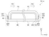
전자 장치(EA)는 전기적 신호에 따라 영상(IM)을 표시하고 외부 입력(TC)을 감지할 수 있다. 외부 입력(TC)은 사용자 신체의 일부, 광, 열, 또는 압력 등 다양한 형태의 외부 입력들을 포함한다. 또한, 외부 입력(TC)은 접촉 터치나 근접 터치를 포함할 수 있다. 본 실시예에서, 전자 장치(EA)는 스마트폰으로 도시되었고, 외부 입력(TC)은 사용자의 손으로 도시되었다. 한편, 본 실시예에서, 외부 입력(TC)은 압력(force)과 터치(touch)로 구분될 수 있다.The electronic device (EA) can display an image (IM) and detect an external input (TC) according to electrical signals. External input (TC) includes various types of external inputs such as parts of the user's body, light, heat, or pressure. Additionally, the external input (TC) may include a contact touch or a proximity touch. In this embodiment, the electronic device (EA) is shown as a smartphone, and the external input (TC) is shown as the user's hand. Meanwhile, in this embodiment, external input (TC) can be divided into pressure and touch.
전자 장치(EA)는 전면(FS), 제1 측면(SS1), 제2 측면(SS2), 및 배면(BS)을 포함할 수 있다. 전면(FS)은 제3 방향(D3)에 수직한 면으로, 제3 방향(D3)을 향해 영상(IM)이 표시되는 면일 수 있다. 사용자는 전면(FS)에 표시되는 영상(IM)을 통해 전자 장치(EA)를 제어하거나, 전자 장치(EA)로부터 제공되는 정보를 습득할 수 있다.The electronic device EA may include a front side FS, a first side SS1, a second side SS2, and a back side BS. The front surface FS is a surface perpendicular to the third direction D3 and may be a surface on which the image IM is displayed toward the third direction D3. The user can control the electronic device (EA) or acquire information provided from the electronic device (EA) through the image (IM) displayed on the front surface (FS).
배면(BS)은 전면(FS)에 대향되는(opposing) 면일 수 있다. 도 1a에서 배면(BS)은 사용자 손 중 손바닥에 의해 지지되는 면일 수 있다.The back surface (BS) may be a surface opposing the front surface (FS). In FIG. 1A, the back surface BS may be a surface supported by the palm of the user's hand.
제1 측면(SS1)은 전면(FS)으로부터 절곡되어 제1 방향(D1)에 수직한 면일 수 있다. 제1 측면(SS1)은 사용자의 손 중 엄지 손가락에 의해 지지되는 면일 수 있다. 즉, 제1 측면(SS1)은 외부 입력(TC) 중 압력(FS1)이 실질적으로 가해지는 면일 수 있다.The first side surface SS1 may be bent from the front surface FS and may be perpendicular to the first direction D1. The first side SS1 may be a side supported by the thumb of the user's hand. That is, the first side SS1 may be a surface on which the pressure FS1 of the external input TC is actually applied.
제2 측면(SS2)은 전면(FS)으로부터 절곡되어 제1 측면(SS2)에 대향되는 면일 수 있다. 제2 측면(SS2)은 사용자의 손 중 나머지 네 개의 손가락들에 의해 지지되는 면일 수 있다. 본 실시예에서, 제2 측면(SS2)은 압력(FS1)이 실질적으로 가해지는 면의 대향면일 수 있으며, 압력(FS1)을 감지하는 면일 수 있다. 즉, 본 실시예에서, 압력(FS1)이 가해지는 면과 압력(FS1)을 감지하는 면은 서로 다를 수 있다. 이에 대한 상세한 설명은 후술하기로 한다.The second side (SS2) may be bent from the front (FS) and faces the first side (SS2). The second side (SS2) may be a side supported by the remaining four fingers of the user's hand. In this embodiment, the second side surface SS2 may be a surface opposite to the surface on which the pressure FS1 is actually applied, and may be a surface that senses the pressure FS1. That is, in this embodiment, the surface on which the pressure FS1 is applied and the surface on which the pressure FS1 is sensed may be different. A detailed description of this will be provided later.
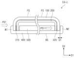
전자 장치(EA)는 윈도우(100), 전자 패널(200), 복수의 압력 감지 유닛들(310, 320), 및 하우징 유닛(400)을 포함할 수 있다. 윈도우(100)는 광학적으로 투명할 수 있다. 본 실시예에서, 윈도우(100)는 유리, 플라스틱, 또는 필름으로 구성될 수 있다.The electronic device EA may include a
윈도우(100)는 제1 방향(D1) 및 제2 방향(D2)에 의해 정의되는 단면상에서 휘어진 적어도 일부를 포함할 수 있다. 전면(FS), 제1 측면(SS1), 및 제2 측면(SS2)은 실질적으로 단일의 윈도우(100)에 의해 제공될 수 있다.The
전자 패널(200)은 영상(IM)을 표시한다. 전자 패널(200)은 유기발광 표시 패널, 양자점 발광 표시 패널, 액정 표시 패널, 전기영동 표시 패널, 전기 습윤 표시 패널 등 다양한 실시예들로 제공될 수 있다.The
한편, 본 실시예에서, 전자 패널(200)은 윈도우(100)의 형상을 따라 휘어진 적어도 일부를 포함할 수 있다. 전자 패널(200)은 전면(FS), 제1 측면(SS1), 및 제2 측면(SS2) 각각을 향하도록 절곡된 상면을 포함한다. 상면에는 복수의 액티브 영역들(AA0, AA1)이 제공될 수 있다. 액티브 영역들(AA0, AA1) 각각에는 복수의 화소들이 배치될 수 있다. 액티브 영역들(AA0, AA1) 각각에는 서로 독립적이거나 연관된 영상들이 표시될 수 있다.Meanwhile, in this embodiment, the
한편, 전자 패널(200) 중 제2 측면(SS2)과 대응되도록 절곡된 상면에도 액티브 영역(미 도시)이 제공될 수 있다. 이에 따라, 전자 패널(200)이 제공하는 액티브 영역의 크기나 형상에 따라, 전면(FS)은 물론, 제1 측면(SS1) 및 제2 측면(SS2) 중 적어도 어느 하나에 영상(IM)이 표시될 수도 있으며, 어느 하나의 실시예로 한정되지 않는다.Meanwhile, an active area (not shown) may also be provided on the upper surface of the
도 2b에 도시된 것과 같이, 전자 패널(200)은 표시 유닛(210) 및 입력 감지 유닛(220)을 포함할 수 있다. 도 2b에는 용이한 설명을 위해 도 2a에서 Ⅰ-Ⅰ'를 따라 자른 영역을 도시하였다.As shown in FIG. 2B, the
표시 유닛(210)은 베이스 기판(BSL), 화소(PX), 및 복수의 절연층들(10, 20, 30, 40, 50, 60)을 포함할 수 있다. 도 2b에는 용이한 설명을 위해 화소(PX) 구성들 중 제2 박막 트랜지스터(TR, 이하, 화소 트랜지스터) 및 발광 소자(ELD)가 예시적으로 도시되었다.The
베이스 기판(BSL)은 절연 물질을 포함할 수 있다. 예를 들어, 베이스 기판(BSL)은 폴리 이미드(Polyimide, PI)를 포함할 수 있다. 이에 따라, 도 2b에 도시된 것과 같이, 전자 패널(200)의 적어도 일부는 용이하게 휘어질 수 있다. 다만, 이는 예시적으로 설명한 것이고, 베이스 기판(BSL)은 리지드한 상태로 제공될 수도 있다. 예를 들어, 베이스 기판(BSL)은 유리, 플라스틱 등 다양한 물질로 구성될 수 있으며, 어느 하나의 실시예로 한정되지 않는다.The base substrate (BSL) may include an insulating material. For example, the base substrate (BSL) may include polyimide (PI). Accordingly, as shown in FIG. 2B, at least a portion of the
제1 절연층(10)은 베이스 기판(BSL) 상에 배치된다. 제1 절연층(10)은 베이스 기판(BSL)의 전면(front surface)을 커버한다. 제1 절연층(10)은 배리어 층(11) 및 버퍼층(12)을 포함할 수 있다.The first insulating
배리어 층(11)은 무기물을 포함할 수 있다. 배리어 층(11)은 베이스 기판(BSL)을 통해 유입되는 산소나 수분이 화소(PX)에 침투되는 것을 방지할 수 있다. 버퍼층(12)은 무기물을 포함할 수 있다. 버퍼층(12)은 화소(PX)가 베이스 기판(BSL) 상에 안정적으로 형성되도록 베이스 기판(BSL)보다 낮은 표면 에너지를 가질 수 있다.The
도 2b에는 용이한 설명을 위해 배리어 층(11) 및 버퍼층(12) 각각은 단일의 층으로 도시되었다. 다만, 이는 예시적으로 도시한 것이고, 본 발명의 일 실시예에 따른 배리어 층(11) 및 버퍼층(12)은 복수로 제공되어 서로 교번하여 적층될 수도 있다. 또는, 배리어 층(11) 및 버퍼층(12) 중 적어도 어느 하나는 복수로 제공될 수도 있고 생략될 수도 있다.In FIG. 2B, for easy explanation, the
화소 트랜지스터(TR)는 반도체 패턴(SP), 제어 전극(CE), 입력 전극(IE), 및 출력 전극(OE)을 포함한다. 반도체 패턴(SP)은 베이스 기판(BSL) 상에 배치된다. 반도체 패턴(SP)은 반도체 물질을 포함할 수 있다. 제어 전극(CE)은 제2 절연층(20)을 사이에 두고 반도체 패턴(SP)으로부터 이격된다. 제어 전극(CE)은 상술한 제1 박막 트랜지스터(TR1) 및 커패시터(CPP)의 일 전극과 연결될 수 있다.The pixel transistor TR includes a semiconductor pattern SP, a control electrode CE, an input electrode IE, and an output electrode OE. The semiconductor pattern SP is disposed on the base substrate BSL. The semiconductor pattern (SP) may include a semiconductor material. The control electrode CE is spaced apart from the semiconductor pattern SP with the second insulating
입력 전극(IE)과 출력 전극(OE)은 제3 절연층(30)을 사이에 두고 제어 전극(CE)으로부터 이격된다. 화소 트랜지스터(TR)의 입력 전극(IE)과 출력 전극(OE)은 제2 절연층(20) 및 제3 절연층(30)을 관통하여 반도체 패턴(SP)의 일 측 및 타 측에 각각 접속된다.The input electrode (IE) and the output electrode (OE) are spaced apart from the control electrode (CE) with the third insulating
제4 절연층(40)은 제2 절연층(30) 상에 배치되어 입력 전극(IE) 및 출력 전극(OE)을 커버한다. 제4 절연층(40)은 유기물 및/또는 무기물을 포함할 수 있으며, 단층 또는 적층 구조를 가질 수 있다.The fourth insulating
한편, 화소 트랜지스터(TR)에 있어서, 반도체 패턴(SP)이 제어 전극(CE) 상에 배치될 수도 있다. 또는, 반도체 패턴(SP)이 입력 전극(IE)과 출력 전극(OE) 상에 배치될 수도 있다. 또는, 입력 전극(IE)과 출력 전극(OE)은 반도체 패턴(SP)과 동일 층 상에 배치되어 반도체 패턴(SP)에 직접 접속될 수도 있다. 본 발명의 일 실시예에 따른 화소 트랜지스터(TR)는 다양한 구조들로 형성될 수 있으며, 어느 하나의 실시예로 한정되지 않는다.Meanwhile, in the pixel transistor TR, the semiconductor pattern SP may be disposed on the control electrode CE. Alternatively, the semiconductor pattern SP may be disposed on the input electrode IE and the output electrode OE. Alternatively, the input electrode (IE) and the output electrode (OE) may be disposed on the same layer as the semiconductor pattern (SP) and directly connected to the semiconductor pattern (SP). The pixel transistor TR according to an embodiment of the present invention may be formed in various structures and is not limited to any one embodiment.
발광 소자(ELD)는 제4 절연층(40) 상에 배치된다. 발광 소자(ELD)는 제1 전극(E1), 발광층(EL), 및 제2 전극(E2)을 포함한다. 제1 전극(E1)은 제4 절연층(40)을 관통하여 화소 트랜지스터(TR)에 접속될 수 있다. 한편, 도시되지 않았으나, 전자 패널(200)은 제1 전극(E1)과 박막 트랜지스터(TR) 사이에 배치되는 별도의 연결 전극을 더 포함할 수도 있고, 이때, 제1 전극(E1)은 연결 전극을 통해 화소 트랜지스터(TR)에 전기적으로 접속될 수 있다.The light emitting device (ELD) is disposed on the fourth insulating
제5 절연층(50)은 제4 절연층(40) 상에 배치된다. 제5 절연층(50)에는 개구부(50_OP)가 정의될 수 있다. 개구부(50_OP)는 제1 전극(E1)의 적어도 일부를 노출시킨다. 제5 절연층(50)은 유기물을 포함할 수 있다. 본 실시예에서, 제5 절연층(50)은 화소 정의막일 수 있다.The fifth insulating
발광층(EL)은 개구부(50_OP)에 배치되어, 개구부(50_OP)에 의해 노출된 제1 전극(E1) 상에 배치된다. 발광층(EL)은 발광 물질을 포함할 수 있다. 예를 들어, 발광층(EL)은 적색, 녹색, 및 청색을 발광하는 물질들 중 적어도 어느 하나의 물질로 구성될 수 있으며, 형광 물질 또는 인광 물질을 포함할 수 있다. 발광층(EL)은 유기 발광 물질 또는 무기 발광 물질을 포함할 수 있다. 발광층(EL)은 제1 전극(E1) 및 제2 전극(E2) 사이의 전위 차이에 응답하여 광을 발광할 수 있다.The light emitting layer EL is disposed in the opening 50_OP and is disposed on the first electrode E1 exposed by the opening 50_OP. The light emitting layer (EL) may include a light emitting material. For example, the light emitting layer EL may be made of at least one material that emits red, green, and blue light, and may include a fluorescent material or a phosphorescent material. The light emitting layer (EL) may include an organic light emitting material or an inorganic light emitting material. The light emitting layer EL may emit light in response to a potential difference between the first electrode E1 and the second electrode E2.
제2 전극(E2)은 발광층(EL) 상에 배치된다. 제2 전극(E2)은 제1 전극(E1)과 대향될 수 있다. 제2 전극(E2)은 액티브 영역(AA1)으로부터 주변 영역(NAA)까지 연장된 일체의 형상을 가질 수 있다. 제2 전극(E2)은 복수의 화소들에 공통적으로 제공될 수 있다. 화소들 각각에 배치된 각각의 발광 소자(ELD)는 제2 전극(E2)을 통해 공통의 제2 전원 전압을 수신한다.The second electrode E2 is disposed on the light emitting layer EL. The second electrode E2 may face the first electrode E1. The second electrode E2 may have an integrated shape extending from the active area AA1 to the peripheral area NAA. The second electrode E2 may be commonly provided to a plurality of pixels. Each light emitting device (ELD) disposed in each pixel receives a common second power voltage through the second electrode (E2).
제2 전극(E2)은 투과형 도전 물질 또는 반 투과형 도전 물질을 포함할 수 있다. 이에 따라, 발광층(EL)에서 생성된 광은 제2 전극(E2)을 통해 전면(FS: 도 1a 참조)을 향해 용이하게 출사될 수 있다. 다만, 이는 예시적으로 도시한 것이고, 본 발명의 일 실시예에 따른 발광 소자(ELD)는 설계에 따라, 제1 전극(E1)이 투과형 또는 반 투과형 물질을 포함하는 배면 발광 방식으로 구동되거나, 전면과 배면 모두를 향해 발광하는 양면 발광 방식으로 구동될 수도 있으며, 어느 하나의 실시예로 한정되지 않는다.The second electrode E2 may include a transmissive conductive material or a semi-transmissive conductive material. Accordingly, the light generated in the light emitting layer EL can be easily emitted toward the front surface (FS: see FIG. 1A) through the second electrode E2. However, this is an exemplary illustration, and the light-emitting device (ELD) according to an embodiment of the present invention is driven in a bottom-emitting manner in which the first electrode (E1) includes a transmissive or semi-transmissive material, depending on the design. It may be driven in a double-sided light emission method that emits light toward both the front and back sides, and is not limited to any one embodiment.
제6 절연층(60)은 발광 소자(ELD) 상에 배치되어 발광 소자(ELD)를 봉지한다. 본 실시예에서, 제6 절연층(60)은 봉지층일 수 있다. 제6 절연층(60)은 액티브 영역(AA1)으로부터 주변 영역(NAA)까지 연장된 일체의 형상을 가질 수 있다. 제6 절연층(60)은 복수의 화소들에 공통적으로 제공될 수 있다. 한편, 도시되지 않았으나, 제2 전극(E2)과 제6 절연층(60) 사이에는 제2 전극(E2)을 커버하는 캡핑층이 더 배치될 수도 있다.The sixth insulating
제6 절연층(60)은 전자 패널(200)의 두께 방향을 따라 순차적으로 적층된 제1 무기층(61), 유기층(62), 및 제2 무기층(63)을 포함할 수 있다. 본 실시예에서, 제1 무기층(61), 유기층(62), 및 제2 무기층(63) 각각은 단일의 층으로 도시되었다. 다만, 이는 예시적으로 도시한 것이고, 제1 무기층(61), 유기층(62), 및 제2 무기층(63) 중 적어도 어느 하나는 복수로 제공되거나 생략될 수도 있으며, 어느 하나의 실시예로 한정되지 않는다.The sixth insulating
제1 무기층(61)은 제2 전극(E2)을 커버할 수 있다. 제1 무기층(61)은 외부 수분이나 산소가 발광 소자(ELD)에 침투하는 것을 방지할 수 있다. 예를 들어, 제1 무기층(61)은 실리콘 질화물, 실리콘 산화물, 또는 이들이 조합된 화합물을 포함할 수 있다. 제1 무기층(61)은 증착 공정을 통해 형성될 수 있다.The first
유기층(62)은 제1 무기층(61) 상에 배치되어 제1 무기층(61)에 접촉할 수 있다. 유기층(62)은 제1 무기층(61) 상에 평탄면을 제공할 수 있다. 구체적으로, 유기층(62)은 액티브 영역(AA1)에 평탄면을 제공할 수 있다.The
제1 무기층(61) 상면에 형성된 굴곡이나 제1 무기층(61) 상에 존재하는 파티클(particle) 등은 유기층(OL)에 의해 커버되어, 제1 무기층(61)의 상면의 표면 상태가 유기층(62) 상에 형성되는 구성들에 미치는 영향을 차단할 수 있다. 또한, 유기층(62)은 접촉하는 층들 사이의 응력을 완화시킬 수 있다. 유기층(62)은 유기물을 포함할 수 있고, 스핀 코팅, 슬릿 코팅, 잉크젯 공정과 같은 용액 공정을 통해 형성될 수 있다.The curves formed on the upper surface of the first
제2 무기층(63)은 유기층(62) 상에 배치되어 유기층(62)을 커버한다. 제2 무기층(63)은 제1 무기층(61) 상에 배치되는 것보다 상대적으로 평탄한 면에 안정적으로 형성될 수 있다. 제2 무기층(63)은 유기층(62)으로부터 방출되는 수분 등을 봉지하여 외부로 유입되는 것을 방지한다. 제2 무기층(63)은 실리콘 질화물, 실리콘 산화물, 또는 이들이 조합된 화합물을 포함할 수 있다. 제2 무기층(63)은 증착 공정을 통해 형성될 수 있다.The second
한편, 본 발명에 따르면, 전자 패널(200)은 주변 영역(NAA)에 배치된 박막 트랜지스터(TR-D, 이하 구동 트랜지스터), 복수의 신호 패턴들(VSS1, E-CNT1, VT, CL), 및 복수의 댐 부들(DM1, DM2)을 더 포함할 수 있다.Meanwhile, according to the present invention, the
구동 트랜지스터(TR-D), 신호 패턴들(VSS1, E-CNT1, VT, CL), 및 댐 부들(DM1, DM2)은 표시 유닛(210: 도 2c 참조)을 구성한다. 한편, 구동 트랜지스터(TR-D) 및 신호 패턴들(VSS1, E-CNT1, VT, CL) 중 일부는 게이트 라인(GL)에 게이트 신호를 제공하는 게이트 구동회로를 구성할 수 있다.The driving transistor TR-D, signal patterns VSS1, E-CNT1, VT, CL, and dam parts DM1 and DM2 constitute a display unit 210 (see FIG. 2C). Meanwhile, some of the driving transistor TR-D and signal patterns VSS1, E-CNT1, VT, and CL may form a gate driving circuit that provides a gate signal to the gate line GL.
구동 트랜지스터(TR-D)는 화소 트랜지스터(TR-P)와 대응되는 구조를 가진 것으로 예시적으로 도시되었다. 예를 들어, 구동 트랜지스터(TR-D)는 제1 절연층(10) 상에 배치된 반도체 패턴(SP), 제2 절연층(20) 상에 배치된 제어 전극(CE), 제3 절연층(30) 상에 배치된 입력 전극(IE) 및 출력 전극(OE)을 포함할 수 있다.The driving transistor (TR-D) is exemplarily shown as having a structure corresponding to the pixel transistor (TR-P). For example, the driving transistor TR-D includes a semiconductor pattern SP disposed on the first insulating
이에 따라, 화소 트랜지스터(TR-P)와 구동 트랜지스터(TR-D)는 동일 공정 내에서 동시에 형성될 수 있어, 공정이 단순화되고 공정 비용이 절감될 수 있다. 다만, 이는 예시적으로 도시한 것이고, 본 발명의 일 실시예에 따른 구동 트랜지스터(TR-D)는 화소 트랜지스터(TR-P)와 다른 층 상에 배치된 전극들 및 반도체 패턴을 포함하거나, 화소 트랜지스터(TR-P)와 상이한 구조를 가질 수 있으며, 어느 하나의 실시예로 한정되지 않는다.Accordingly, the pixel transistor (TR-P) and the driving transistor (TR-D) can be formed simultaneously within the same process, thereby simplifying the process and reducing process costs. However, this is shown as an example, and the driving transistor (TR-D) according to an embodiment of the present invention includes electrodes and a semiconductor pattern disposed on a different layer from the pixel transistor (TR-P), or It may have a different structure from the transistor (TR-P) and is not limited to any one embodiment.
신호 패턴들(VSS1, E-CNT1, VT, CL)은 전원 공급 라인(VSS1), 연결 전극(E-CNT1), 초기화 전압 라인(VT), 및 구동 신호 라인(CL)을 포함할 수 있다. 전원 공급 라인(VSS1)은 화소(PX)의 전원 단자(VSS)와 대응될 수 있다. 전원 공급 라인(VSS1)은 발광 소자(ELD)에 제2 전원 전압을 공급한다.The signal patterns (VSS1, E-CNT1, VT, CL) may include a power supply line (VSS1), a connection electrode (E-CNT1), an initialization voltage line (VT), and a driving signal line (CL). The power supply line (VSS1) may correspond to the power terminal (VSS) of the pixel (PX). The power supply line (VSS1) supplies the second power voltage to the light emitting device (ELD).
전원 공급 라인(VSS1)은 제2 절연층(30) 상에 배치된다. 전원 공급 라인(VSS1)은 구동 트랜지스터(TR-D)의 입력 전극(IE)이나 출력 전극(OE)과 동일 층 상에 배치된다. 전원 공급 라인(VSS1)은 구동 트랜지스터(TR-D)의 입력 전극(IE)이나 출력 전극(OE)과 동일 공정 내에서 하나의 마스크로 동시에 패터닝될 수 있다. 다만, 이는 예시적으로 도시한 것이고, 전원 공급 라인(VSS1)은 구동 트랜지스터(TR-D)의 입력 전극(IE)이나 출력 전극(OE)과 다른 층 상에 배치되어 별도의 공정을 통해 형성될 수도 있으며, 어느 하나의 실시예로 한정되지 않는다.The power supply line (VSS1) is disposed on the second insulating
연결 전극(E-CNT1)은 제4 절연층(40) 상에 배치된다. 연결 전극(E-CNT1)은 전원 공급 라인(VSS1)에 전기적으로 접속된다. 연결 전극(E-CNT1)은 제4 절연층(40)으로부터 노출된 전원 공급 라인(VSS1)을 커버한다.The connection electrode (E-CNT1) is disposed on the fourth insulating
발광 소자(ELD)의 제2 전극(E2)은 액티브 영역(AA1)으로부터 연장되어 연결 전극(E-CNT1)에 접속된다. 연결 전극(E-CNT1)은 전원 공급 라인(VSS1)으로부터 제2 전원 전압을 수신할 수 있다. 이에 따라, 제2 전원 전압은 연결 전극(E-CNT1)을 통해 제2 전극(E2)에 전달되어 화소들마다 각각 공통의 제2 전원 전압이 제공될 수 있다.The second electrode E2 of the light emitting device ELD extends from the active area AA1 and is connected to the connection electrode E-CNT1. The connection electrode (E-CNT1) may receive the second power voltage from the power supply line (VSS1). Accordingly, the second power voltage is transmitted to the second electrode E2 through the connection electrode E-CNT1, so that a common second power voltage can be provided to each pixel.
연결 전극(E-CNT1)은 발광 소자(ELD)의 제1 전극(E1)과 동일한 층 상에 배치되어 제1 전극(E1)과 동시에 형성될 수 있다. 다만, 이는 예시적으로 도시한 것이고, 연결 전극(E-CNT1)은 제1 전극(E1)과 다른 층 상에 배치될 수도 있다.The connection electrode E-CNT1 may be disposed on the same layer as the first electrode E1 of the light emitting device ELD and formed simultaneously with the first electrode E1. However, this is shown as an example, and the connection electrode E-CNT1 may be disposed on a different layer from the first electrode E1.
구동 신호 라인들(CL)은 복수로 제공되어 제3 절연층(30) 상에 배치될 수 있다. 구동 신호 라인들(CL)은 주변 영역(NAA)에 배치될 수 있다. 구동 신호 라인(CL)은 패드(미 도시)와 연결되는 라우팅(routing) 배선이거나, 집적 회로(IC)를 구성하는 배선일 수도 있다. 구동 신호 라인들(CL)은 제1 방향(D1)에서 서로 이격되어 배치되며 각각 독립적으로 전기적 신호를 전달한다.A plurality of driving signal lines CL may be provided and disposed on the third insulating
초기화 전압 라인(VT)은 화소(PX)에 초기화 전압을 제공한다. 도시되지 않았으나, 초기화 전압 라인(VT)은 복수로 제공되어 복수의 화소들 각각에 초기화 전압을 제공할 수 있다.The initialization voltage line VT provides an initialization voltage to the pixel PX. Although not shown, a plurality of initialization voltage lines VT may be provided to provide an initialization voltage to each of the plurality of pixels.
구동 신호 라인들(CL)과 초기화 전압 라인(VT)은 동일한 층 상에 배치되어 동일 공정을 통해 동시에 형성될 수 있다. 다만, 이는 예시적으로 도시한 것이고, 구동 신호 라인들(CL)과 초기화 전압 라인(VT)은 별도의 공정을 통해 독립적으로 형성될 수도 있으며, 어느 하나의 실시예로 한정되지 않는다.The driving signal lines CL and the initialization voltage line VT may be disposed on the same layer and formed simultaneously through the same process. However, this is shown as an example, and the driving signal lines CL and the initialization voltage line VT may be formed independently through separate processes, and are not limited to any one embodiment.
댐 부(DM1, DM2)는 주변 영역(NAA)에 배치된다. 댐 부(DM1, DM2)는 유기층(62)이 액티브 영역(AA1)으로부터 댐 부(DM1, DM2)의 외 측을 향해, 예를 들어 도 2b에서 제1 방향(D1)의 반대 방향을 향해, 흘러 넘치는 것을 방지할 수 있다.The dam parts (DM1, DM2) are placed in the surrounding area (NAA). In the dam portions DM1 and DM2, the
댐 부(DM1, DM2)는 액티브 영역(AA1)의 적어도 일 측에 인접하여 배치될 수 있다. 댐 부(DM1, DM2)는 평면상에서 액티브 영역(AA1)을 에워쌀 수 있다. 댐 부(DM1, DM2)는 복수로 제공되어 제1 댐 부(DM1) 및 제2 댐 부(DM2)를 포함할 수 있다.The dam portions DM1 and DM2 may be disposed adjacent to at least one side of the active area AA1. The dam portions DM1 and DM2 may surround the active area AA1 on a plane. The dam units DM1 and DM2 may be provided in plurality and may include a first dam unit DM1 and a second dam unit DM2.
제1 댐 부(DM1)는 제2 댐 부(DM2)에 비해 상대적으로 액티브 영역(AA1)에 가까이 배치될 수 있다. 제1 댐 부(DM1)는 전원 공급 라인(VSS1)과 평면상에서 중첩하도록 배치될 수 있다. 본 실시예에서, 연결 전극(E-CNT1)은 단면상에서 제1 댐 부(DM1)와 전원 공급 라인(VSS1) 사이를 지날 수 있다.The first dam unit DM1 may be placed relatively closer to the active area AA1 than the second dam unit DM2. The first dam portion DM1 may be arranged to overlap the power supply line VSS1 on a plane. In this embodiment, the connection electrode (E-CNT1) may pass between the first dam portion (DM1) and the power supply line (VSS1) in cross section.
본 실시예에서, 제1 댐 부(DM1)는 제5 절연층(50)과 동일한 물질을 포함하며, 하나의 마스크를 통해 제5 절연층(50)과 동시에 형성될 수 있다. 이에 따라, 제1 댐 부(DM1)를 형성하기 위한 별도의 공정을 추가하지 않을 수 있어 공정 비용이 절감되고 공정이 단순화될 수 있다.In this embodiment, the first dam portion DM1 includes the same material as the fifth insulating
제2 댐 부(DM2)는 제1 댐 부(DM1)에 비해 상대적으로 외 측에 배치될 수 있다. 제2 댐 부(DM2)는 전원 공급 라인(VSS1)의 일부를 커버하는 위치에 배치될 수 있다. 본 실시예에서, 제2 댐 부(DM2)는 제1 층(P1), 제2 층(P2), 및 제3 층(P3)을 포함하는 복층 구조를 가질 수 있다.The second dam part DM2 may be disposed relatively outside the first dam part DM1. The second dam portion DM2 may be disposed at a location that covers a portion of the power supply line VSS1. In this embodiment, the second dam portion DM2 may have a multi-layer structure including a first layer P1, a second layer P2, and a third layer P3.
본 실시예에서, 연결 전극(E-CNT1)은 제2 댐 부(DM2)의 제1 층(P1) 상에 일부 중첩하여 배치될 수 있다. 연결 전극(E-CNT1)의 끝 단은 제1 층(P1)과 제2 층(P2) 사이에 삽입될 수 있다. 다만, 이는 예시적으로 도시한 것이고, 연결 전극(E-CNT1)은 제2 댐 부(DM2)까지 연장되지 않을 수도 있으며, 어느 하나의 실시예로 한정되지 않는다.In this embodiment, the connection electrode E-CNT1 may be disposed to partially overlap the first layer P1 of the second dam portion DM2. The end of the connection electrode (E-CNT1) may be inserted between the first layer (P1) and the second layer (P2). However, this is shown as an example, and the connection electrode (E-CNT1) may not extend to the second dam portion (DM2), and is not limited to any one embodiment.
입력 감지 유닛(220)은 표시 유닛(210) 상에 배치된다. 다만, 이는 예시적으로 도시한 것이고, 입력 감지 유닛(220)은 표시 유닛(210) 하 측에 배치되거나, 표시 유닛(210) 내부에 삽입될 수도 있으며, 어느 하나의 실시예로 한정되지 않는다.The
입력 감지 유닛(220)은 제1 감지 절연층(TIS1), 제1 감지 절연층(TIS2), 제1 감지 도전 패턴(MT1), 및 제2 감지 도전 패턴(MT2)을 포함할 수 있다. 제1 패턴(MT1) 및 제2 패턴(MT2)은 정전 용량을 형성하도록 서로 대향된 전압을 수신하는 감지 전극들 각각을 구성할 수 있다.The
제1 감지 도전 패턴(MT1) 및 제2 감지 도전 패턴(MT2)은 서로 상이한 층 상에 배치된다. 제1 감지 도전 패턴(MT1)은 제1 감지 절연층(TIS1)과 제2 감지 절연층(TIS2) 사이에 배치된다. 제2 감지 도전 패턴(MT2)은 제2 감지 절연층(TIS2) 상에 배치된다.The first sensing conductive pattern MT1 and the second sensing conductive pattern MT2 are disposed on different layers. The first sensing conductive pattern MT1 is disposed between the first sensing insulating layer TIS1 and the second sensing insulating layer TIS2. The second sensing conductive pattern MT2 is disposed on the second sensing insulating layer TIS2.
제1 감지 도전 패턴(MT1) 및 제2 감지 도전 패턴(MT2) 중 적어도 어느 하나는 복수의 메쉬선들을 포함할 수 있다. 제2 감지 도전 패턴(MT2) 중 적어도 일부는 제2 감지 절연층(TIS2)을 관통하여 제1 감지 도전 패턴(MT1)에 접속된다.At least one of the first sensing conductive pattern MT1 and the second sensing conductive pattern MT2 may include a plurality of mesh lines. At least a portion of the second sensing conductive pattern MT2 penetrates the second sensing insulating layer TIS2 and is connected to the first sensing conductive pattern MT1.
본 발명에 따르면, 전자 패널(200)은 메쉬선들을 포함하는 입력 감지 유닛(220)을 포함함으로써, 향상된 유연성을 가질 수 있다. 이에 따라, 전자 패널(200)은 액티브 영역(AA1)의 적어도 일부가 휘어진 형상을 안정적으로 가질 수 있다.According to the present invention, the
한편, 이는 예시적으로 도시한 것이고, 제1 감지 도전 패턴(MT1) 및 제2 감지 도전 패턴(MT2) 중 적어도 어느 하나는 투명한 도전성 물질로 형성될 수도 있다. 이때, 제1 감지 도전 패턴(MT1) 및 제2 감지 도전 패턴(MT2)은 발광 소자(ELD)가 배치된 영역과 평면상에서 중첩하여 배치될 수도 있다. 또는, 제1 감지 도전 패턴(MT1) 및 제2 감지 도전 패턴(MT2)은 전기적으로 서로 절연되어 각각이 서로 대향된 감지 전극들을 구성할 수도 있다. 입력 감지 유닛(220)은 대향된 감지 전극들 사이의 정전 용량 변화를 감지하거나, 감지 전극들과 외부 터치 사이의 정전 용량을 감지하여 외부 터치를 감지할 수 있다. 본 발명의 일 실시예에 따른 입력 감지 유닛(220)은 다양한 실시예들을 포함할 수 있으며, 어느 하나의 실시예로 한정되지 않는다.Meanwhile, this is shown as an example, and at least one of the first and second sensing conductive patterns MT1 and MT2 may be formed of a transparent conductive material. At this time, the first sensing conductive pattern MT1 and the second sensing conductive pattern MT2 may be arranged to overlap the area where the light emitting device ELD is disposed on a plane. Alternatively, the first sensing conductive pattern MT1 and the second sensing conductive pattern MT2 may be electrically insulated from each other to form sensing electrodes facing each other. The
한편, 도시되지 않았으나, 입력 감지 유닛(220)은 제2 감지 절연층(TIS2) 상에 배치된 반사 방지층을 더 포함할 수도 있다. 반사 방지층은 편광 필름 또는 컬러 필터를 포함할 수 있다.Meanwhile, although not shown, the
다시 도 2a를 참조하면, 압력 감지 유닛들(310, 320)은 서로 대향되어 배치된 제1 압력 감지 유닛(310) 및 제2 압력 감지 유닛(320)를 포함할 수 있다. 제1 압력 감지 유닛(310)은 제1 측면(SS1)에 배치되고 제2 압력 감지 유닛(320)은 제2 측면(SS2)에 배치된다. 제1 압력 감지 유닛(310)은 제1 측면(SS1)과 하우징 유닛(400) 사이에 배치되고 제2 압력 감지 유닛(320)은 제2 측면(SS2)과 하우징 유닛(400) 사이에 배치된다.Referring again to FIG. 2A , the
제1 및 제2 압력 감지 유닛들(310, 320) 각각은 대향되는 면에 가해지는 압력을 감지한다. 예를 들어, 도 1b에 도시된 것과 같이, 제1 측면(SS1)에 가해진 압력(PS1)은 제2 압력 감지 유닛(320)에서 감지될 수 있다. 본 발명에 따르면, 압력이 제공된 면과 압력이 감지되는 면을 분리하여 압력 감지의 정확도를 향상시킬 수 있다.Each of the first and second
하우징 유닛(400)은 윈도우(100)와 결합된다. 하우징 유닛(400)은 전자 패널(200), 제1 및 제2 압력 감지 유닛들(310, 320)을 수용한다.The
하우징 유닛(400)은 바닥부(BB), 및 복수의 측부들(W1, W2, W3 W4)을 포함할 수 있다. 바닥부(BB)는 제1 방향(D1) 및 제2 방향(D2)에 평행한 면일 수 있다. 측부들(W1, W2, W3 W4)은 바닥부(BB)로부터 각각 제3 방향(D3)을 향해 절곡된다. 측부들(W1, W2, W3 W4)은 제1 내지 제4 측부들(W1, W2, W3 W4)을 포함할 수 있다.The
제1 및 제2 측부들(W1, W2)은 각각 제2 방향(D2)을 따라 연장된 길이를 가질 수 있다. 제1 및 제2 측부들(W1, W2)은 각각 제1 및 제2 측면(SS1, SS2)과 나란하게 배치된다. 제1 및 제2 압력 감지 유닛들(310, 320)은 각각 제1 측면(SS1)과 제1 측부(W1) 사이 및 제2 측면(SS2)과 제2 측부(W2) 사이에 배치될 수 있다.The first and second sides W1 and W2 may each have a length extending along the second direction D2. The first and second side parts W1 and W2 are arranged in parallel with the first and second side parts SS1 and SS2, respectively. The first and second
제3 및 제4 측부들(W3, W4)은 각각 제1 방향(D1)을 따라 연장된 길이를 가질 수 있다. 제3 및 제4 측부들(W3, W4)은 각각 제1 및 제2 측부들(W1, W2)보다 제3 방향(D3)을 향해 상대적으로 두꺼운 높이로 제공될 수 있다.The third and fourth side parts W3 and W4 may each have a length extending along the first direction D1. The third and fourth sides W3 and W4 may be provided with a relatively thicker height toward the third direction D3 than the first and second sides W1 and W2, respectively.
도 3a 내지 도 3d는 본 발명의 일 실시예에 따른 전자 장치의 단면도들이다. 도 3a 도 3d에는 전자 장치들(EA-a, EA-b, EA-c, EA-d) 각각에 도 1a와 대응되는 압력(PS1)이 가해진 경우의 단면도들을 도시하였다. 이하, 도 3a 내지 도 3d를 참조하여 본 발명에 대해 설명한다. 한편, 도 1a 내지 도 2에서 설명한 구성과 동일한 구성에 대해서는 동일한 참조부호를 부여하고 중복된 설명은 생략하기로 한다.3A to 3D are cross-sectional views of an electronic device according to an embodiment of the present invention. Figures 3a and 3d show cross-sectional views when the pressure PS1 corresponding to Figure 1a is applied to each of the electronic devices EA-a, EA-b, EA-c, and EA-d. Hereinafter, the present invention will be described with reference to FIGS. 3A to 3D. Meanwhile, the same reference numerals will be assigned to the same components as those described in FIGS. 1A to 2, and duplicate descriptions will be omitted.
도 3a에 도시된 것과 같이, 전자 장치(EA-a)에 있어서, 압력 감지 유닛들(310, 320) 각각은 하우징 유닛에 결합되고 윈도우(100)로부터 분리되어 제공될 수 있다. 제1 압력 감지 유닛(310)은 제1 측부(W1)에 결합되고 제2 압력 감지 유닛(320)은 제2 측부(W2)에 결합된다. 본 실시예에서, 윈도우(100) 및 전자 패널(200)은 외부 압력(PS1)에 의해 하우징 유닛(400) 내에서 이동될 수 있다. 윈도우(100) 및 전자 패널(200)은 외부 압력(PS1)에 의해 제1 방향(D1)으로 이동한다.As shown in FIG. 3A, in the electronic device EA-a, each of the
외부 압력(PS1)은 제1 및 제2 압력 감지 유닛들(310, 320) 중 제2 압력 감지 유닛(320)에 전달되어 제2 압력 감지 유닛(320)의 두께를 변형시킬 수 있다. 외부 압력(PS1)에 의해 제2 압력 감지 유닛(320)의 두께(TH2)는 제1 압력 감지 유닛(310)의 두께(TH1)보다 감소될 수 있다. 제2 압력 감지 유닛(320)은 두께변화를 통해 외부 압력(PS1)을 감지할 수 있다.The external pressure PS1 may be transmitted to the second
또는, 도 3b에 도시된 것과 같이, 전자 장치(EA-b)에 있어서, 압력 감지 유닛들(310, 320) 각각은 윈도우(100)에 결합되고 하우징 유닛으로부터 분리되어 제공될 수도 있다. 제1 압력 감지 유닛은 제1 측면(SS1)에 결합되고 제2 압력 감지 유닛(320)는 제2 측면(SS2)에 결합된다. 도 3a에서와 마찬가지로, 제1 측면(SS1)에 가해진 외부 압력(PS1)은 제2 압력 감지 유닛(320)의 두께를 변형시킨다. 제2 압력 감지 유닛(320)은 두께 변화를 통해 외부 압력(PS1)을 감지할 수 있다.Alternatively, as shown in FIG. 3B, in the electronic device EA-b, each of the
또는, 도 3c에 도시된 것과 같이, 전자 장치(EA-c)에 있어서, 압력 감지 유닛들(310, 320)은 전자 패널(200)과 윈도우(100) 사이에 배치될 수도 있다. 압력 감지 유닛들(310, 320)은 전자 패널(200)에 부착되거나 전자 패널(200) 내에 삽입될 수 있다. 한편, 본 실시예에 따른 전자 장치(EA-c)는 지지 부재(500)를 더 포함할 수 있다. 지지 부재(500)는 전자 패널(200)의 벤딩된 형상을 지지할 수 있다. 외부 압력(PS1)이 인가되면, 지지 부재(500)는 이와 대응되는 압력(PS11)을 전자 패널(200)에 제공할 수 있다. 제2 압력 감지 유닛(320)은 외부 압력(PS1)과 대응되는 압력(PS11)에 의해 변형되는 두께를 가짐으로써, 외부 압력(PS1)을 감지할 수 있다.Alternatively, as shown in FIG. 3C, in the electronic device EA-c, the
또는, 도 3d에 도시된 것과 같이, 전자 장치(EA-d)에 있어서, 압력 감지 유닛들(310, 320)은 전자 패널(200)과 지지부재(500) 사이에 배치될 수도 있다. 압력 감지 유닛들(310, 320)은 전자 패널(200) 배면에 부착되거나 전자 패널(200) 내에 삽입될 수 있다. 외부 압력(PS1)이 인가되면, 지지부재(500)는 이와 대응되는 압력(PS11)을 압력 감지 유닛들(310, 320) 중 외부 압력(PS1)이 인가되는 쪽의 대향되는 쪽에 배치된 제2 압력 감지 유닛(320)에 제공할 수 있다. 제2 압력 감지 유닛(320)은 외부 압력(PS1)과 대응되는 압력(PS11)에 의해 변형되는 두께를 가짐으로써, 외부 압력(PS1)을 감지할 수 있다.Alternatively, as shown in FIG. 3D, in the electronic device EA-d, the
본 발명에 따르면, 전자 장치(EA-a, EA-b, EA-c)는 외부 압력(PS1)이 제공되는 면과 대향되는 면에서 압력을 감지할 수 있다. 이에 따라, 압력 감지에 대해 향상된 민감도를 가진 전자 장치(EA-a, EA-b, EA-c)가 제공될 수 있다.According to the present invention, the electronic devices EA-a, EA-b, and EA-c can sense pressure on a side opposite to the side where the external pressure PS1 is provided. Accordingly, electronic devices (EA-a, EA-b, EA-c) with improved sensitivity to pressure sensing can be provided.
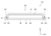
도 4a는 본 발명의 일 실시예에 따른 전자 장치의 사시도이다. 도 4b는 도 4a에 도시된 전자 장치의 분해 사시도이다. 도 4c는 도 4a에 도시된 전자 장치의 단면도이다. 도 4d는 본 발명의 일 실시예에 따른 전자 장치의 단면도이다. 이하, 도 4a 내지 도 4d를 참조하여 본 발명에 대해 설명한다. 도 4a에 도시된 것과 같이, 전자 장치(EA1)는 전면(FS)에 가해지는 외부 압력(PS2)을 감지할 수 도 있다. 이때, 전자 장치(EA1)는 배면(BS)에서 외부 압력(PS2)의 유무 및 세기를 감지할 수 있다.Figure 4a is a perspective view of an electronic device according to an embodiment of the present invention. FIG. 4B is an exploded perspective view of the electronic device shown in FIG. 4A. FIG. 4C is a cross-sectional view of the electronic device shown in FIG. 4A. Figure 4D is a cross-sectional view of an electronic device according to an embodiment of the present invention. Hereinafter, the present invention will be described with reference to FIGS. 4A to 4D. As shown in FIG. 4A, the electronic device EA1 may sense the external pressure PS2 applied to the front surface FS. At this time, the electronic device EA1 can detect the presence and intensity of the external pressure PS2 on the back surface BS.
구체적으로, 도 4b 및 도 4c에 도시된 것과 같이, 전자 장치(EA1)는 제3 및 제4 압력 감지 유닛들(330, 340)을 포함할 수 있다. 제3 및 제4 압력 감지 유닛들(330, 340)은 각각 하우징 유닛(400)과 윈도우(100) 사이에 배치되며, 구체적으로, 윈도우(100)와 바닥부(BB) 사이에 배치될 수 있다. 한편, 이는 예시적으로 도시한 것이고, 제3 및 제4 압력 감지 유닛들(330, 340)은 전자 패널(200)의 휘어진 측면들과 바다부(BB) 사이에 배치될 수도 있으며, 어느 하나의 실시예로 한정되지 않는다.Specifically, as shown in FIGS. 4B and 4C, the electronic device EA1 may include third and fourth
전면(FS)에 가해지는 압력(PS2)에 의해 제3 및 제4 압력 감지 유닛들(330, 340)의 두께 변화가 발생될 수 있다. 전자 장치(EA1)는 제3 및 제4 압력 감지 유닛들(330, 340)의 두께 변화를 통해 전면(FS)에서의 외부 압력(PS2)을 감지한다. 한편, 제3 및 제4 압력 감지 유닛들(330, 340)의 두께 차이를 통해 외부 압력(PS2)이 가해진 위치가 제1 측면(SS1) 및 제2 측면(SS2) 중 어디에 더 가까운지가 판별될 수도 있다.A change in the thickness of the third and fourth
또는, 도 4d에 도시된 것과 같이, 전자 장치(EA2)는 도 1b에 도시된 제1 및 제2 압력 감지 유닛들(310, 320)을 더 포함할 수도 있다. 전자 장치(EA2)는 전면(FS), 제1 측면(SS1), 및 제2 측면(SS2) 중 어느 위치에 가해지는 외부 압력에 대해서도 용이하게 감지할 수 있다. 본 발명에 따르면, 압력 감지 유닛들(310, 320, 330, 340)의 배치 위치에 따라 다양한 위치에 제공되는 외부 압력을 용이하게 감지할 수 있는 전자 장치가 제공될 수 있으며, 어느 하나의 실시예로 한정되지 않는다.Alternatively, as shown in FIG. 4D, the electronic device EA2 may further include the first and second
도 5a는 본 발명의 일 실시예에 따른 압력 감지 유닛을 간략히 도시한 사시도이다. 도 5b 및 도 5c는 도 5a에 도시된 Ⅱ-Ⅱ'를 따라 자른 단면도들이다. 용이한 설명을 위해 도 5b에는 외부 압력(PS1)이 가해지기 전 상태의 단면도를 도시하였고, 도 5c에는 외부 압력(PS1)이 가해진 상태의 단면도를 도시하였다. 이하, 도 5a 내지 도 5c를 참조하여 본 발명에 대해 설명한다. 한편, 도 1a 내지 도 4b에서 설명한 구성과 동일한 구성에 대해서는 동일한 참조부호를 부여하고 중복된 설명은 생략하기로 한다.Figure 5a is a schematic perspective view of a pressure sensing unit according to an embodiment of the present invention. Figures 5b and 5c are cross-sectional views taken along line II-II' shown in Figure 5a. For easy explanation, Figure 5b shows a cross-sectional view before external pressure (PS1) is applied, and Figure 5c shows a cross-sectional view before external pressure (PS1) is applied. Hereinafter, the present invention will be described with reference to FIGS. 5A to 5C. Meanwhile, the same reference numerals will be given to the same components as those described in FIGS. 1A to 4B and duplicate descriptions will be omitted.
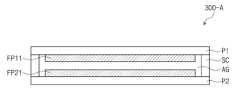
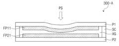
압력 감지 유닛(300)은 제1 패턴(FP1), 제2 패턴(FP2), 제1 패널(P1), 제2 패널(P2), 및 지지부(SC)를 포함할 수 있다. 제1 패턴(FP1)과 제2 패턴(FP2) 각각은 도전성을 가질 수 있다. 제1 패턴(FP1)과 제2 패턴(FP2)은 서로 상이한 전위를 가질 수 있다. 제1 패턴(FP1)과 제2 패턴(FP2)은 평면상에서 서로 맞물린 형상으로 제공될 수 있다. 제1 패턴(FP1)과 제2 패턴(FP2)은 평면상에서 서로 비 중첩하며 이격되어 배치될 수 있다.The
제1 패널(P1)과 제2 패널(P2)은 제3 방향(D3)에서 서로 마주할 수 있다. 지지부(SC)는 제1 패널(P1)과 제2 패널(P2) 사이에 배치되어, 소정의 갭(AG)을 가지며 제1 패널(P1)과 제2 패널(P2)이 서로 이격되도록 제1 패널(P1)과 제2 패널(P2)을 지지한다.The first panel (P1) and the second panel (P2) may face each other in the third direction (D3). The support portion (SC) is disposed between the first panel (P1) and the second panel (P2), has a predetermined gap (AG), and the first panel (P1) and the second panel (P2) are spaced apart from each other. Supports the panel (P1) and the second panel (P2).
제1 패턴(FP1) 및 제2 패턴(FP2)은 제1 패널(P1)에 배치될 수 있다. 제1 패널(P1)과 제2 패널(P2)은 연성을 가질 수 있다. 외부 압력(PS)은 제1 패널(P1)에 제공되는 것으로 도시되었다. 외부 압력(PS)에 의해 제1 패널(P1)의 형상이 변형됨에 따라, 제1 패턴(FP1)과 제2 패턴(FP2) 사이의 간격이 변형될 수 있다. 압력 감지 유닛(300)은 제1 패턴(FP1)과 제2 패턴(FP2) 사이의 정전 용량 변화를 통해 외부 압력(PS)을 감지할 수 있다.The first pattern FP1 and the second pattern FP2 may be disposed on the first panel P1. The first panel (P1) and the second panel (P2) may be flexible. External pressure PS is shown as being provided to the first panel P1. As the shape of the first panel P1 is deformed by the external pressure PS, the gap between the first pattern FP1 and the second pattern FP2 may be deformed. The
한편, 본 발명의 일 실시예에 따른 압력 감지 유닛(300)에 있어서, 제1 패턴(FP1)과 제2 패턴(FP2)은 스트레인 게이지(strain guage)로 기능할 수도 있다. 이때, 외부 압력(PS)에 의해 제1 패턴(FP1)과 제2 패턴(FP2)의 형상이 변형되고, 압력 감지 유닛(300)은 제1 패턴(FP1)과 제2 패턴(FP2)의 저항 변화를 통해 외부 압력(PS)을 감지할 수 있다. 본 발명의 일 실시예에 따른 압력 감지 유닛(300)은 다양한 방식으로 구동될 수 있으며, 어느 하나의 실시예로 한정되지 않는다.Meanwhile, in the
도 6a 및 도 6b는 본 발명의 일 실시예에 따른 압력 감지 유닛의 단면도들이다. 도 6a는 도 5b와 대응되는 상태의 단면도를 도시하였고, 도 6b는 도 5c와 대응되는 단면도를 도시하였다. 이하, 도 6a 및 도 6b를 참조하여 본 발명에 대해 설명한다.6A and 6B are cross-sectional views of a pressure sensing unit according to an embodiment of the present invention. FIG. 6A shows a cross-sectional view corresponding to FIG. 5B, and FIG. 6B shows a cross-sectional view corresponding to FIG. 5C. Hereinafter, the present invention will be described with reference to FIGS. 6A and 6B.
압력 감지 유닛(300-A)은 서로 다른 패널들에 배치된 제1 패턴(FP11)과 제2 패턴(FP21)을 포함할 수 있다. 제1 패턴(FP11)은 제1 패널(P1)에 배치되고 제2 패턴(FP21)은 제2 패널(P2)에 배치될 수 있다. 본 실시예에서, 제1 패턴(FP11)과 제2 패턴(FP21)은 평면상에서 중첩하는 형상으로 서로 마주하여 배치될 수 있다.The pressure sensing unit 300-A may include a first pattern FP11 and a second pattern FP21 arranged on different panels. The first pattern FP11 may be placed on the first panel P1 and the second pattern FP21 may be placed on the second panel P2. In this embodiment, the first pattern FP11 and the second pattern FP21 may be arranged to face each other in an overlapping shape on a plane.
외부 압력(PS)이 제1 패널(P1)에 가해지면 제1 패널(P1)에 변형이 발생되어 제1 패턴(FP11)과 제2 패턴(FP21) 사이의 거리가 축소될 수 있다. 압력 감지 유닛(300-A)은 제1 패턴(FP11)과 제2 패턴(FP21) 사이의 정전 용량 변화를 통해 외부 압력(PS)을 감지할 수 있다.When external pressure PS is applied to the first panel P1, deformation may occur in the first panel P1 and the distance between the first pattern FP11 and the second pattern FP21 may be reduced. The pressure sensing unit 300-A may detect external pressure PS through a change in capacitance between the first pattern FP11 and the second pattern FP21.
도 7a 및 도 7b는 본 발명의 일 실시예에 따른 압력 감지 유닛의 단면도들이다. 도 7a는 도 5b와 대응되는 상태의 단면도를 도시하였고, 도 7b는 도 5c와 대응되는 단면도를 도시하였다. 이하, 도 7a 및 도 7b를 참조하여 본 발명에 대해 설명한다.7A and 7B are cross-sectional views of a pressure sensing unit according to an embodiment of the present invention. FIG. 7A shows a cross-sectional view corresponding to FIG. 5B, and FIG. 7B shows a cross-sectional view corresponding to FIG. 5C. Hereinafter, the present invention will be described with reference to FIGS. 7A and 7B.
압력 감지 유닛(300-B)은 베이스 패널(BP) 및 복수의 나노 입자들(NP)을 포함하는 제2 패널(P21)을 포함할 수 있다. 베이스 패널(BP)은 연성을 가진 절연 물질로 형성될 수 있으며, 예를 들어, 탄성 중합체 바인더 수지를 포함할 수 있다. 나노 입자들(NP) 각각은 도전성을 가질 수 있다.The pressure sensing unit 300-B may include a base panel (BP) and a second panel (P21) including a plurality of nanoparticles (NP). The base panel BP may be formed of a flexible insulating material and may include, for example, an elastomeric binder resin. Each nanoparticle (NP) may have conductivity.
제1 패턴(FP1) 및 제2 패턴(FP2) 각각은 제1 패널(P1)과 제2 패널(P21)에 결합될 수 있다. 제1 패널(P1)에 외부 압력(PS)이 가해지면, 제1 패턴(FP1)과 제2 패턴(FP21)에 의해 베이스 패널(BP)이 화살표 방향을 따라 확장될 수 있다. 이에 따라, 나노 입자들(NP) 사이의 거리가 증가되면서 제2 패널(P21)의 저항이 변화될 수 있다.Each of the first pattern FP1 and the second pattern FP2 may be coupled to the first panel P1 and the second panel P21. When external pressure PS is applied to the first panel P1, the base panel BP may be expanded along the direction of the arrow by the first pattern FP1 and the second pattern FP21. Accordingly, as the distance between nanoparticles (NP) increases, the resistance of the second panel (P21) may change.
예를 들어, 나노 입자들(NP) 사이의 거리가 감소될수록 제2 패널(P21)에서의 전자 터널링 가능성이 높아져 제2 패널(P21)의 저항이 감소될 수 있다. 압력 감지 유닛(300-B)은 제2 패널(P21)의 저항 변화를 통해 외부 압력(PS)을 감지할 수 있다.For example, as the distance between nanoparticles (NP) decreases, the possibility of electron tunneling in the second panel (P21) increases, thereby reducing the resistance of the second panel (P21). The pressure sensing unit 300-B can detect external pressure PS through a change in resistance of the second panel P21.
도 8a 내지 도 8c는 본 발명의 일 실시예에 따른 전자 패널의 단면도들이다. 도 8a에는 전자 패널(200-A) 중 도 2b와 대응되는 영역을 도시하였고, 도 8b 및 도 8c에는 전자 패널들(200-A, 200-B)의 액티브 영역(AA1)에서의 단면도들을 각각 도시하였다. 이하, 도 8a 내지 도 8c를 참조하여 본 발명에 대해 설명한다.8A to 8C are cross-sectional views of an electronic panel according to an embodiment of the present invention. FIG. 8A shows a region of the electronic panel 200-A corresponding to FIG. 2B, and FIGS. 8B and 8C show cross-sectional views of the active area AA1 of the electronic panels 200-A and 200-B, respectively. Shown. Hereinafter, the present invention will be described with reference to FIGS. 8A to 8C.
도 8a 내지 도 8c에 도시된 것과 같이, 압력 감지 유닛(300-P1, 300-P2, 300-P3)은 전자 패널(200-A, 200-B, 200-C)에 삽입될 수도 있다.As shown in FIGS. 8A to 8C, pressure sensing units 300-P1, 300-P2, and 300-P3 may be inserted into electronic panels 200-A, 200-B, and 200-C.
예를 들어, 도 8a에 도시된 것과 같이, 압력 감지 유닛(300-P1)은 입력 감지 유닛(220)과 표시 유닛(210) 사이에 배치될 수 있다. 본 실시예에서, 압력 감지 유닛(300-P1)을 구성하는 제1 및 제2 패턴들(FP1A, FP2A)은 추가층(FL) 상에 배치될 수 있다.For example, as shown in FIG. 8A, the pressure sensing unit 300-P1 may be disposed between the
추가층(FL)이 연성을 가진 유기 물질을 포함하는 경우, 외부 압력에 의해 형상이 변형될 수 있다. 제1 및 제2 패턴들(FP1A, FP2A)은 추가층(FL)의 형상 변화에 따른 정전 용량 변화를 통해 외부 압력을 감지할 수 있다.When the additional layer FL includes a flexible organic material, its shape may be deformed by external pressure. The first and second patterns FP1A and FP2A may sense external pressure through a change in capacitance according to a change in the shape of the additional layer FL.
또는, 추가층(FL)은 내부에 분산된 복수의 도전성 나노 입자들을 더 포함할 수도 있다. 이때, 제1 및 제2 패턴들(FP1A, FP2A)에 의해 추가층(FL)의 형상이 변형됨으로써, 나노 입자들 사이의 거리가 달라질 수 있다. 압력 감지 유닛(300-P1)은 추가층(FL)의 저항 변화를 감지하여 외부 압력을 감지할 수도 있다.Alternatively, the additional layer FL may further include a plurality of conductive nanoparticles dispersed therein. At this time, the shape of the additional layer FL is modified by the first and second patterns FP1A and FP2A, so that the distance between the nanoparticles may vary. The pressure sensing unit 300-P1 may sense external pressure by detecting a change in resistance of the additional layer FL.
한편, 압력 감지 유닛(300-P1)은 주변 영역(NAA)에 배치될 수 있다. 압력 본 발명에 따르면, 감지 유닛(300-P1)을 주변 영역(NAA)에 배치시킴으로써, 압력 감지 영역과 터치 감지 영역이 분리될 수 있다. 이에 따라, 주변 영역(NAA)에 가해지는 외부 압력에 대해서도 용이하게 감지할 수 있다.Meanwhile, the pressure sensing unit 300-P1 may be placed in the peripheral area (NAA). Pressure According to the present invention, the pressure sensing area and the touch sensing area can be separated by placing the sensing unit 300-P1 in the peripheral area NAA. Accordingly, external pressure applied to the surrounding area (NAA) can be easily sensed.
또는, 도 8b에 도시된 것과 같이, 압력 감지 유닛(300-P2)은 표시 유닛(210)에 배치될 수도 있다. 압력 감지 유닛(300-P2)은 액티브 영역(AA1)에 배치된다. 압력 감지 유닛(300-P2)을 구성하는 제1 및 제2 패턴들(FP1B, FP2B)은 베이스 기판(BSL)과 제1 절연층(10) 사이에 배치될 수 있다.Alternatively, as shown in FIG. 8B, the pressure sensing unit 300-P2 may be disposed in the
제1 및 제2 패턴들(FP1B, FP2B)은 박막 트랜지스터(TR)와 평면상에서 중첩하여 배치될 수 있다. 본 실시예에서, 제1 및 제2 패턴들(FP1B, FP2B)은 반도체 패턴(SP) 및 제어 전극(CE)과 평면상에서 중첩하는 위치에 배치된 것으로 도시되었다. 본 발명에 따르면, 압력 감지 유닛(300-P2)은 박막 트랜지스터(TR) 공정 과정에서 형성할 수 있어 공정이 단순화되고 공정 비용이 절감될 수 있다.The first and second patterns FP1B and FP2B may be arranged to overlap the thin film transistor TR on a plane. In this embodiment, the first and second patterns FP1B and FP2B are shown as being disposed in a position that overlaps the semiconductor pattern SP and the control electrode CE on a plane. According to the present invention, the pressure sensing unit 300-P2 can be formed during a thin film transistor (TR) process, thereby simplifying the process and reducing process costs.
또는, 도 8c에 도시된 것과 같이, 압력 감지 유닛(300-P3)은 입력 감지 유닛(220)에 배치될 수도 있다. 이때, 압력 감지 유닛(300-P3)을 구성하는 제1 및 제2 패턴들(FP1C, FP2C)은 도 8a에 도시된 압력 감지 유닛(300-P1)과 달리 액티브 영역(AA1)에 배치될 수 있다.Alternatively, as shown in FIG. 8C, the pressure sensing unit 300-P3 may be disposed in the
제1 및 제2 패턴들(FP1C, FP2C)은 제1 감지 도전 패턴(MT1)과 동일 층 상에 배치될 수 있다. 이때, 제1 감지 절연층(TIS11)은 베이스 패널(BP) 및 복수의 나노 입자들(NP)을 포함할 수 있다. 본 실시예에 따른 제1 감지 절연층(TIS11)은 도 7b에 도시된 제2 패널(P21)과 실질적으로 대응될 수 있다. 본 발명에 따르면, 터치 감지를 위한 감지 전극들(MT1, MT2)과 압력 감지를 위한 패턴들(FP1C, FP2C)을 동시에 형성할 수 있어 공정이 단순화되고 공정 비용이 절감될 수 있다.The first and second patterns FP1C and FP2C may be disposed on the same layer as the first sensing conductive pattern MT1. At this time, the first sensing insulating layer TIS11 may include a base panel BP and a plurality of nanoparticles NP. The first sensing insulating layer (TIS11) according to this embodiment may substantially correspond to the second panel (P21) shown in FIG. 7B. According to the present invention, the sensing electrodes (MT1, MT2) for touch sensing and the patterns (FP1C, FP2C) for pressure sensing can be formed at the same time, thereby simplifying the process and reducing process costs.
한편, 도 8c에 도시된 것과 같이, 표시 유닛(210)은 차광 패턴(BP)을 더 포함할 수 있다. 도 8b에 도시된 제1 및 제2 패턴들(FP1B, FP2B)은 실질적으로 차광 패턴(BP)과 동일한 층 상에 배치된 것일 수 있다. 본 실시예에서, 차광 패턴(BP)은 도전성 물질을 포함할 수 있다. 예를 들어, 차광 패턴(BP)은 금속, 합금, 도전성 산화물, 및 도전성 폴리머 중 적어도 어느 하나를 포함할 수 있다. 차광 패턴(BP)은 베이스 기판(BSL)으로부터 반도체 패턴(SP)에 입사되는 외부 광을 차단하거나, 제어 전극(CE)과 함께 반도체 패턴(SP)에 채널(channel)을 형성할 수도 있다. 본 발명의 일 실시예에 따른 전자 패널(200-C)은 다양한 실시예들을 포함할 수 있으며, 어느 하나의 실시예로 한정되지 않는다.Meanwhile, as shown in FIG. 8C, the
도 8a 내지 도 8c에 도시된 것과 같이, 본 발명의 일 실시예에 따른 전자 패널(200-A, 200-B, 200-C)은 압력 감지 유닛(300-P1, 300-P2, 300-P3)을 포함할 수 있다. 압력 감지 유닛(300-P1, 300-P2, 300-P3)은 전자 패널(200-A, 200-B, 200-C)에 있어서, 다양한 위치에 배치될 수 있다. 이에 따라, 압력 감지 유닛(300-P1, 300-P2, 300-P3)을 형성하기 위한 공정이 단순화되고 공정 비용이 절감될 수 있다.As shown in FIGS. 8A to 8C, the electronic panels 200-A, 200-B, and 200-C according to an embodiment of the present invention include pressure sensing units 300-P1, 300-P2, and 300-P3. ) may include. The pressure sensing units 300-P1, 300-P2, and 300-P3 may be placed in various positions in the electronic panels 200-A, 200-B, and 200-C. Accordingly, the process for forming the pressure sensing units 300-P1, 300-P2, and 300-P3 can be simplified and process costs can be reduced.
도 9a는 본 발명의 일 실시예에 따른 전자 장치의 사시도이다. 도 9b는 도 9a에 도시된 전자 장치의 분해 사시도이다. 도 9b에는 용이한 설명을 위해 전자 장치(EA-1)의 구성들 중 일부는 생략하여 도시하였다.Figure 9A is a perspective view of an electronic device according to an embodiment of the present invention. FIG. 9B is an exploded perspective view of the electronic device shown in FIG. 9A. In FIG. 9B , some of the components of the electronic device EA-1 are omitted for ease of explanation.
도 9a 및 도 9b에 도시된 것과 같이, 전자 장치(EA-1)는 전면(FS), 제1 내지 제4 측면들(SS1, SS2, SS3, SS4)에 영상(IM)을 표시할 수 있다. 전자 장치(EA-1)는 윈도우(100-1) 및 전자 패널(200-1)을 포함한다.As shown in FIGS. 9A and 9B, the electronic device EA-1 may display an image IM on the front surface FS and the first to fourth sides SS1, SS2, SS3, and SS4. . The electronic device EA-1 includes a window 100-1 and an electronic panel 200-1.
전자 패널(200-1)은 메인부(201) 및 복수의 절개부들(202, 203, 204, 205)을 포함할 수 있다. 메인부(201)는 전면(FS)과 평행하게 배치되며 전면(FS)과 대응되는 사각 형상을 가진다. 메인부(201)는 전면(FS)에 영상(IM)을 제공하기 위한 메인 액티브 영역(AA0)을 포함할 수 있다.The electronic panel 200-1 may include a
절개부들(202, 203, 204, 205)은 제1 내지 제4 절개부들(202, 203, 204, 205)을 포함할 수 있다. 제1 내지 제4 절개부들(202, 203, 204, 205)은 각각 메인부(201)의 변들에 배치되어 메인부(201)로부터 돌출된다. 도 9b에는 용이한 설명을 위해 제1 내지 제4 절개부들(202, 203, 204, 205)이 메인부(201)와 평행하도록 도시되었으나, 제1 내지 제4 절개부들(202, 203, 204, 205)은 각각 제1 내지 제4 측면들(SS1, SS2, SS3, SS4)을 향하도록 메인부(MPP)로부터 벤딩되어 조립될 수 있다. 제1 내지 제4 절개부들(202, 203, 204, 205)은 제1 내지 제4 측면들(SS1, SS2, SS3, SS4)에 영상(IM1, IM2, IM3, IM4)을 제공하기 위한 서브 액티브 영역들(AA1, AA2, AA3, AA4)을 포함할 수 있다.The
본 실시예에 따른 전자 장치(EA-1)는 압력이 제공되는 면과 압력이 감지되는 면이 분리될 수 있다. 예를 들어, 전자 장치(EA-1) 중 제1 측면(SS1)에 제공되는 압력은 제2 측면(SS2)에 배치된 압력 감지 유닛(320)을 통해 감지될 수 있다. 제3 측면(SS3)에 제공되는 압력은 제4 측면(SS4)에 배치된 압력 감지 유닛(340)을 통해 감지될 수 있다. 본 발명에 따르면, 압력이 제공되는 면과 대향되는 면에 배치된 압력 감지 유닛을 통해 압력을 감지함으로써, 압력 감지에 대해 보다 향상된 민감도를 가진 전자 장치(EA-1)가 제공될 수 있다.In the electronic device EA-1 according to this embodiment, the side on which pressure is provided and the side on which pressure is sensed may be separated. For example, the pressure provided to the first side SS1 of the electronic device EA-1 may be sensed through the
또한, 본 발명에 따르면, 제1 내지 제4 측면들(SS1, SS2, SS3, SS4) 각각에 압력 감지 유닛들(310, 320, 330, 340)이 배치됨으로써, 제1 내지 제4 측면들(SS1, SS2, SS3, SS4)에 입력되는 외부 압력을 용이하게 감지할 수 있다.In addition, according to the present invention,
한편, 도시되지 않았으나, 압력 감지 유닛들(310, 320, 330, 340)은 상술한 바와 같이, 전자 패널(200-1) 내부에 삽입될 수 있고, 설계에 따라 액티브 영역(AA0, AA1, AA2, AA3, AA4)이나 주변 영역(NAA) 어디에나 배치될 수 있으며, 어느 하나의 실시예로 한정되지 않는다.Meanwhile, although not shown, the
도 10a는 본 발명의 일 실시예에 따른 전자 패널의 전개도이다. 도 10b는 도 10a에 도시된 전자 패널의 사시도이다. 이하 도 10a 및 도 10b를 참조하여 본 발명에 대해 설명한다.Figure 10a is an exploded view of an electronic panel according to an embodiment of the present invention. FIG. 10B is a perspective view of the electronic panel shown in FIG. 10A. Hereinafter, the present invention will be described with reference to FIGS. 10A and 10B.
도 10a에 도시된 것과 같이, 전자 패널(200-11)은 메인부(MPP), 제1 절개부(202-1) 및 제2 절개부(203-1)를 포함할 수 있다. 메인부(201)는 도 9a에 도시된 메인부(201)와 실질적으로 대응될 수 있다. 도 10b에 도시된 전자 패널(200-11)의 형상은 도 9a에 도시된 전자 패널(200-1)이 조립된 상태에서의 형상과 대응될 수 있다.As shown in FIG. 10A, the electronic panel 200-11 may include a main part (MPP), a first cutout 202-1, and a second cutout 203-1. The
제1 절개부(202-1)는 메인부(201)의 일 변에 배치된다. 제1 절개부(202-1)는 복수의 액티브 영역들(A11, A41)을 포함할 수 있다. 액티브 영역들(A11, A21)은 실질적으로 제1 측면(SS1) 및 제4 측면(SS4)에 각각 영상들을 제공하는 영역들일 수 있다.The first cut part 202-1 is disposed on one side of the
제2 절개부(203-1)는 메인부(MPP)의 다른 일 변에 배치된다. 제2 절개부(203-1)는 제1 절개부(202-1)와 대향되는 변에 배치될 수 있다. 제2 절개부(203-1)는 복수의 액티브 영역들(A21, A31)을 포함할 수 있다. 액티브 영역들(A21, A31)은 실질적으로 제2 측면(SS2) 및 제3 측면(SS3)에 각각 영상들을 제공하는 영역들일 수 있다.The second cutout 203-1 is disposed on the other side of the main part (MPP). The second cut part 203-1 may be disposed on the side opposite to the first cut part 202-1. The second cutout 203-1 may include a plurality of active areas A21 and A31. The active areas A21 and A31 may be areas that provide images to the second side SS2 and the third side SS3, respectively.
본 발명에 따르면, 전자 패널(200-11)은 전면(FS) 및 복수의 측면들(SS1, SS2, SS3, SS4)에 액티브 영역들(AA0, AA1, AA2, AA3, AA4)을 각각 제공할 수 있다면, 다양한 형상으로 제공될 수 있다.According to the present invention, the electronic panel 200-11 may provide active areas AA0, AA1, AA2, AA3, and AA4 on the front surface FS and a plurality of side surfaces SS1, SS2, SS3, and SS4, respectively. If possible, it can be provided in various shapes.
도 11a는 본 발명의 일 실시예에 따른 전자 장치의 사시도이다. 도 11b는 도 11a에 도시된 전자 장치의 분해 사시도이다. 도 11c는 본 발명의 일 실시예에 따른 전자 장치의 분해 사시도이다. 도 11b 및 도 11c에는 용이한 설명을 위해 일부 구성들은 생략하여 도시하였다. 이하, 도 11a 내지 도 11c를 참조하여 본 발명에 대해 설명한다. 한편, 도 1a 내지 도 10b에서 설명한 구성과 동일한 구성에 대해서는 동일한 참조부호를 부여하고 중복된 설명은 생략하기로 한다.Figure 11A is a perspective view of an electronic device according to an embodiment of the present invention. FIG. 11B is an exploded perspective view of the electronic device shown in FIG. 11A. Figure 11C is an exploded perspective view of an electronic device according to an embodiment of the present invention. In FIGS. 11B and 11C, some components are omitted for ease of explanation. Hereinafter, the present invention will be described with reference to FIGS. 11A to 11C. Meanwhile, the same reference numerals will be given to the same components as those described in FIGS. 1A to 10B and duplicate descriptions will be omitted.
도 11a 및 도 11b에 도시된 것과 같이, 전자 장치(EA-2)는 윈도우(100-2), 전자 패널(200-2), 전자 모듈(EM), 및 하우징 유닛(400)을 포함할 수 있다. 도시되지 않았으나, 압력 감지 유닛은 도 2a에 도시된 것과 같이 전자 패널(200-2)로부터 독립되어 제공되거나 전자 패널(200-2)에 내재된 상태로 제공될 수 있으며, 어느 하나의 실시예로 한정되지 않는다.As shown in FIGS. 11A and 11B, the electronic device EA-2 may include a window 100-2, an electronic panel 200-2, an electronic module (EM), and a
전자 장치(EA-2)는 전면(FS)에 정의된 카메라 홀(H1, H2)을 더 포함할 수 있다. 본 실시예에서, 카메라 홀(H1, H2)은 서로 이격된 복수로 제공되었다. 전자 장치(EA-2)는 영상(IM)을 표시하고 카메라 홀(H1, H2)을 통해 외부 피사체 정보를 감지할 수 있다.The electronic device EA-2 may further include camera holes H1 and H2 defined on the front surface FS. In this embodiment, the camera holes H1 and H2 are provided in plural numbers spaced apart from each other. The electronic device EA-2 can display an image IM and detect external subject information through the camera holes H1 and H2.
구체적으로, 윈도우(100-2)는 전면(FS), 및 복수의 측면들(SS1, SS2, SS3, SS4)을 포함할 수 있다. 윈도우(100-2)는 실질적으로 도 9b에 도시된 윈도우(100-1)와 대응될 수 있다.Specifically, the window 100-2 may include a front surface (FS) and a plurality of side surfaces (SS1, SS2, SS3, and SS4). Window 100-2 may substantially correspond to window 100-1 shown in FIG. 9B.
전자 패널(200-2)은 메인부(201-1), 및 복수의 절개부들(202, 203, 204, 205)을 포함할 수 있다. 본 실시예에 따른 전자 패널(200-2)은 관통홀(H1, H2)을 제외하고 실질적으로 도 9b에 도시된 전자 패널(200-1)과 대응될 수 있다.The electronic panel 200-2 may include a main portion 201-1 and a plurality of
관통홀(H1, H2)은 복수로 제공될 수 있다. 관통홀들(H1, H2)은 각각 전자 패널(200-2)을 관통하여 정의된다. 관통홀들(H1, H2)은 메인부(201-1)를 관통하고, 메인부(201-1)의 액티브 영역(AA0) 내에 정의될 수 있다.A plurality of through holes (H1, H2) may be provided. The through holes H1 and H2 are each defined as penetrating the electronic panel 200-2. The through holes H1 and H2 pass through the main part 201-1 and may be defined within the active area AA0 of the main part 201-1.
전자 모듈(EM)은 전자 장치(EA)를 동작시키기 위한 다양한 기능성 모듈을 포함한다. 전자 모듈(EM)은 전자 패널(200-2)과 전기적으로 연결된 마더보드에 직접 실장되거나 별도의 기판에 실장되어 커넥터(미 도시) 등을 통해 마더보드에 전기적으로 연결될 수 있다. 전자 모듈(EM)은 카메라, 스피커, 광 감지 센서, 및 열 감지 센서 중 적어도 어느 하나를 포함할 수 있다.The electronic module (EM) includes various functional modules for operating the electronic device (EA). The electronic module (EM) may be mounted directly on a motherboard electrically connected to the electronic panel 200-2, or may be mounted on a separate board and electrically connected to the motherboard through a connector (not shown). The electronic module (EM) may include at least one of a camera, a speaker, a light sensor, and a heat sensor.
전자 모듈(EM)은 복수로 제공된 것으로 도시되었다. 전자 모듈들(EM)은 관통홀들(H1, H2)에 각각 중첩하여 배치될 수 있다. 전자 모듈들(EM)은 홀들(H1, H2)을 통해 각각 전달되는 외부 입력들을 수신하거나 홀들(H1, H2)을 통해 각각 출력을 제공할 수 있다. 전자 모듈들(EM) 각각의 일부 또는 전부는 홀들(H1, H2) 각각에 수용될 수 있다. 본 발명에 따르면, 전자 모듈들(EM)은 액티브 영역(AA0)에 중첩하여 배치됨으로써, 베젤 영역의 증가를 방지할 수 있다.Electronic modules (EM) are shown as being provided in plurality. The electronic modules EM may be arranged to overlap each of the through holes H1 and H2. The electronic modules EM may receive external inputs transmitted through the holes H1 and H2, respectively, or provide outputs through the holes H1 and H2, respectively. Some or all of the electronic modules EM may be accommodated in each of the holes H1 and H2. According to the present invention, the electronic modules EM are arranged to overlap the active area AA0, thereby preventing an increase in the bezel area.
또는, 도 11c에 도시된 것과 같이, 전자 장치는 윈도우(100-3) 및 전자 패널(200-3)을 포함할 수 있다. 윈도우(100-3)는 도 11b에 도시된 윈도우(100-2)와 실질적으로 대응될 수 있다. 본 실시예에서는 용이한 설명을 위해 전자 모듈(EM)은 단일 구성으로 도시되었다.Alternatively, as shown in FIG. 11C, the electronic device may include a window 100-3 and an electronic panel 200-3. Window 100-3 may substantially correspond to window 100-2 shown in FIG. 11B. In this embodiment, for ease of explanation, the electronic module (EM) is shown as a single configuration.
본 실시예에 따른 전자 패널(200-3)은 도 11b 대비 일부가 제거된 형상을 가진 메인부(201-2)를 포함할 수 있다. 메인부(201-2)는 전자 모듈(EM)과 중첩되는 영역이 제거된 형상을 가질 수 있으며, 전자 모듈(EM)과 중첩하는 홀 영역(HA)은 전자 패널(200-3)의 외 측에 정의될 수 있다.The electronic panel 200-3 according to this embodiment may include a main portion 201-2 with a portion of the main portion 201-2 removed compared to FIG. 11B. The main portion 201-2 may have a shape in which the area overlapping with the electronic module EM is removed, and the hole area HA overlapping with the electronic module EM is outside the electronic panel 200-3. It can be defined in .
도 11a 내지 도 11c에 도시된 것과 같이, 전자 패널(200-2, 200-3)은 전자 모듈(EM)과의 간섭 방지를 위해 다양한 형상으로 제공될 수 있다. 전자 장치(EA-2)는 전자 모듈(EM)과의 간섭이 방지되면서도 다양한 위치에 제공되는 압력을 감지할 수 있다.As shown in FIGS. 11A to 11C, the electronic panels 200-2 and 200-3 may be provided in various shapes to prevent interference with the electronic module (EM). The electronic device (EA-2) is capable of detecting pressure provided at various locations while preventing interference with the electronic module (EM).
도 12는 본 발명의 일 실시예에 따른 전자 장치의 작동 방법을 간략히 도시한 순서도이다. 도 12에 도시된 것과 같이, 전자 장치의 작동 방법은 제1 면에 압력을 제공하는 단계(S10) 이후 제2 면에서 압력을 감지하는 단계(S20) 또는 제1 면 및 제2 면에서 압력을 감지하는 단계(S30)를 포함할 수 있다.Figure 12 is a flow chart briefly illustrating a method of operating an electronic device according to an embodiment of the present invention. As shown in FIG. 12, the method of operating an electronic device includes providing pressure to the first surface (S10) and then detecting pressure on the second surface (S20) or detecting pressure on the first and second surfaces. It may include a detection step (S30).
본 발명에 따르면, 압력이 제공되는 면(제1 면)과 압력이 감지되는 면(제2 면)이 서로 다를 수 있다. 상술한 바와 같이, 본 발명에 따른 전자 장치는 압력이 제공되는 면(제1 면)과 대향되는 면(제2 면)을 통해 압력을 감지한다. 이에 따라, 압력이 제공되는 면이 밀림 등으로 인해 압력이 정확히 감지되지 않더라도, 대향 면을 통해 압력이 감지될 수 있어, 압력 감지의 민감도가 향상될 수 있다.According to the present invention, the side on which pressure is provided (the first side) and the side on which the pressure is sensed (the second side) may be different. As described above, the electronic device according to the present invention senses pressure through a surface (second surface) opposite to the surface on which pressure is provided (first surface). Accordingly, even if the pressure is not accurately sensed due to the side on which the pressure is provided being pushed, the pressure can be sensed through the opposing side, thereby improving the sensitivity of pressure sensing.
또한, 본 발명에 따르면, 압력이 제공되는 면(제1 면)과 대향면(제2 면)에서 동시에 압력 감지가 이루어질 수도 있다. 이에 따라, 압력이 직접적으로 제공되는 면에 압력에 따른 변화가 있는 경우, 이를 용이하게 감지할 수 있다. 따라서, 본 발명에 따르면, 압력 감지의 정확도가 향상될 수 있다.Additionally, according to the present invention, pressure may be sensed simultaneously on the surface where pressure is provided (the first surface) and the opposing surface (the second surface). Accordingly, if there is a change in pressure on the surface to which pressure is directly provided, this can be easily detected. Therefore, according to the present invention, the accuracy of pressure sensing can be improved.
도 13a 및 도 13b는 본 발명의 일 실시예에 따른 전자 장치를 간략히 도시한 평면도들이다. 도 13c는 본 발명의 일 실시예에 따른 전자 장치를 간략히 도시한 단면도이다. 도 13a 내지 도 13c에는 용이한 설명을 위해 일부 구성들은 생략하여 도시하였다.13A and 13B are schematic plan views of an electronic device according to an embodiment of the present invention. FIG. 13C is a schematic cross-sectional view of an electronic device according to an embodiment of the present invention. In FIGS. 13A to 13C , some components are omitted for ease of explanation.
도 13a에 도시된 것과 같이, 외부 압력(PS)이 제1 측면(SS1)에 제공되는 경우, 압력이 제공되는 영역(FA)은 제1 면(SS1)이 되고, 압력이 감지되는 영역(DA)은 제1 면(SS1)에 대향되는 제2 면(SS2)에 형성될 수 있다. 즉, 본 실시예에서, 압력 감지 유닛은 적어도 제2 측면(SS2)에 배치될 수 있다. 압력 감지 유닛은 배치된 면과 대향되는 면에 제공되는 압력을 감지함으로써, 향상된 압력 감도를 제공할 수 있다.As shown in FIG. 13A, when the external pressure PS is provided to the first side SS1, the area FA where the pressure is provided becomes the first side SS1, and the area DA where the pressure is sensed. ) may be formed on the second surface (SS2) opposite to the first surface (SS1). That is, in this embodiment, the pressure sensing unit may be disposed at least on the second side SS2. The pressure sensing unit may provide improved pressure sensitivity by detecting pressure provided to a surface opposite to the surface on which it is placed.
도 13b에 도시된 것과 같이, 외부 압력(PS)이 제4 측면(SS4)에 제공되는 경우, 압력이 제공되는 영역(FA)은 제4 면(SS4)이 되고, 압력이 감지되는 영역(DA)은 제4 면(SS4)에 대향되는 제3 면(SS3)에 형성될 수 있다. 즉, 본 실시예에서, 압력 감지 유닛은 적어도 제2 측면(SS2)에 배치될 수 있다. 압력 감지 유닛은 배치된 면과 대향되는 면에 제공되는 압력을 감지함으로써, 향상된 압력 감도를 제공할 수 있다.As shown in FIG. 13B, when the external pressure PS is provided to the fourth side SS4, the area FA where the pressure is provided becomes the fourth side SS4, and the area DA where the pressure is sensed. ) may be formed on the third surface (SS3) opposite to the fourth surface (SS4). That is, in this embodiment, the pressure sensing unit may be disposed at least on the second side SS2. The pressure sensing unit may provide improved pressure sensitivity by detecting pressure provided to a surface opposite to the surface on which it is placed.
도 13c에 도시된 것과 같이, 외부 압력(PS)이 전면(FS)에 제공되는 경우, 압력이 제공되는 영역(FA)은 전면(FS)이 되고, 압력이 감지되는 영역(DA)은 전면(FS)에 대향되는 배면(BS)에 형성될 수 있다. 즉, 본 실시예에서, 압력 감지 유닛은 적어도 제2 측면(SS2)에 배치될 수 있다. 압력 감지 유닛은 배치된 면과 대향되는 면에 제공되는 압력을 감지함으로써, 향상된 압력 감도를 제공할 수 있다.As shown in Figure 13c, when the external pressure (PS) is provided to the front (FS), the area (FA) where the pressure is provided becomes the front (FS), and the area (DA) where the pressure is sensed is the front ( It may be formed on the back surface (BS) opposite to the FS). That is, in this embodiment, the pressure sensing unit may be disposed at least on the second side SS2. The pressure sensing unit may provide improved pressure sensitivity by detecting pressure provided to a surface opposite to the surface on which it is placed.
본 발명에 따르면, 전자 장치는 압력이 제공되는 면과 대향되는 면을 통해 압력을 감지한다. 이에 따라, 압력이 제공되는 면에 직접적인 변형이 없더라도 압력을 안정적으로 감지할 수 있다. 또한, 본 발명에 따르면, 전자 장치는 압력이 제공되는 면과 대향되는 면, 두 면들을 통해 압력을 감지할 수 있다. 이에 따라, 압력 감지 정확도가 향상될 수 있다.According to the present invention, the electronic device senses pressure through a surface opposite to the surface on which the pressure is provided. Accordingly, pressure can be sensed stably even if there is no direct deformation of the surface to which pressure is provided. Additionally, according to the present invention, the electronic device can sense pressure through two sides, a side on which pressure is provided and a side opposite to the pressure. Accordingly, pressure sensing accuracy can be improved.
도 14a 및 도 14b는 본 발명의 일 실시예에 따른 전자 장치의 측면도들이다. 도 14a 및 도 14b에는 용이한 설명을 위해 일부 구성은 생략하여 도시하였다. 도 14a 및 도 14b에 도시된 것과 같이, 전자 장치(EA)에 가해지는 외부 압력(PS)은 서로 대향되는 두 면들에 동시에 가해질 수도 있다.14A and 14B are side views of an electronic device according to an embodiment of the present invention. In FIGS. 14A and 14B, some components are omitted for ease of explanation. As shown in FIGS. 14A and 14B, the external pressure PS applied to the electronic device EA may be applied simultaneously to two opposing surfaces.
예를 들어, 도 14a에 도시된 것과 같이, 전자 장치(EA) 중 전면(FS)과 배면(BS)에 압력(PS)이 동시에 가해질 수도 있다. 도 14a에 도시된 전자 장치(EA)에 있어서, 압력 감지 유닛은 전면(FS)과 배면(BS) 각각에 구비될 수 있다. 이때, 전자 장치(EA)는 전면(FS)과 배면(BS) 모두에서 압력(PS)을 감지할 수 있다. 이 경우, 전자 장치(EA)는 제3 측면(SS3)을 활성화시켜 영상(IM)을 표시하거나, 외부 터치 등을 감지하는 동작을 수행할 수 있다. 전자 장치(EA)는 전면(FS)과 배면(BS) 모두에서 압력(PS)이 감지되는 경우에 한해 제3 측면(SS3)을 활성화시킴으로써, 사용자에게 다양한 사용 환경을 제공할 수 있다.For example, as shown in FIG. 14A, pressure PS may be applied to the front FS and back BS of the electronic device EA at the same time. In the electronic device EA shown in FIG. 14A, pressure sensing units may be provided on the front FS and the back BS, respectively. At this time, the electronic device (EA) can sense the pressure (PS) from both the front (FS) and the back (BS). In this case, the electronic device EA may display an image IM by activating the third side surface SS3 or perform an operation such as detecting an external touch. The electronic device (EA) can provide various usage environments to the user by activating the third side (SS3) only when pressure (PS) is sensed from both the front (FS) and the back (BS).
또는, 예를 들어, 도 14b에 도시된 것과 같이, 전자 장치(EA) 중 제1 측면(SS1)과 제2 측면(SS2)에 압력(PS)이 동시에 가해질 수도 있다. 이때, 전자 장치(EA)는 제1 측면(SS1)과 제2 측면(SS2) 모두에서 압력(PS)을 감지할 수 있다. 이 경우, 전자 장치(EA)는 제3 측면(SS3)을 활성화 시켜 영상(IM)을 표시하거나, 외부 터치 등을 감지하는 동작을 수행할 수 있다. 전자 장치(EA)는 제1 측면(SS1)과 제2 측면(SS2) 모두에서 압력(PS)이 감지되는 경우에 한해 제3 측면(SS3)을 활성화시킴으로써, 사용자에게 다양한 사용 환경을 제공할 수 있다.Alternatively, for example, as shown in FIG. 14B, the pressure PS may be applied to the first side SS1 and the second side SS2 of the electronic device EA at the same time. At this time, the electronic device EA can sense the pressure PS from both the first side SS1 and the second side SS2. In this case, the electronic device EA may display an image IM by activating the third side SS3 or perform an operation such as detecting an external touch. The electronic device (EA) can provide users with a variety of usage environments by activating the third side (SS3) only when pressure (PS) is detected on both the first side (SS1) and the second side (SS2). there is.
이상에서는 본 발명의 바람직한 실시예를 참조하여 설명하였지만, 해당 기술 분야의 숙련된 당업자 또는 해당 기술 분야에 통상의 지식을 갖는 자라면, 후술될 특허청구범위에 기재된 본 발명의 사상 및 기술 영역으로부터 벗어나지 않는 범위 내에서 본 발명을 다양하게 수정 및 변경시킬 수 있음을 이해할 수 있을 것이다.Although the present invention has been described above with reference to preferred embodiments, those skilled in the art or have ordinary knowledge in the relevant technical field should not deviate from the spirit and technical scope of the present invention as set forth in the claims to be described later. It will be understood that the present invention can be modified and changed in various ways within the scope not permitted.
따라서, 본 발명의 기술적 범위는 명세서의 상세한 설명에 기재된 내용으로 한정되는 것이 아니라 특허청구범위에 의해 정하여져야만 할 것이다.Therefore, the technical scope of the present invention should not be limited to what is described in the detailed description of the specification, but should be defined by the scope of the patent claims.
100: 윈도우200: 전자 패널
310: 압력 감지 유닛100: Windows 200: Electronic panel
310: pressure sensing unit
Claims (21)
Translated fromKorean상기 전면에 영상을 표시하고, 상기 측면들 중 적어도 어느 하나를 향하도록 절곡된 상면을 포함하는 전자 패널;
외부 압력을 감지하는 압력 감지 유닛; 및
상기 전자 패널 및 상기 압력 감지 유닛을 수용하는 하우징 유닛을 포함하고,
상기 외부 압력은 상기 측면들 중 제1 면에 제공되고,
상기 압력 감지 유닛은 상기 제1 면에 대향하는 제2 면에 배치된 전자 장치.A window including a front surface and a plurality of sides bent from the front surface;
an electronic panel that displays an image on the front surface and includes an upper surface bent to face at least one of the side surfaces;
A pressure sensing unit that detects external pressure; and
Comprising a housing unit accommodating the electronic panel and the pressure sensing unit,
the external pressure is provided to a first of the sides,
The pressure sensing unit is disposed on a second side opposite to the first side.
상기 압력 감지 유닛은 상기 윈도우와 상기 하우징 유닛 사이에 배치된 전자 장치.According to claim 1,
The pressure sensing unit is an electronic device disposed between the window and the housing unit.
상기 압력 감지 유닛은 상기 윈도우와 상기 전자 패널 사이에 배치된 전자 장치.According to claim 1,
The pressure sensing unit is an electronic device disposed between the window and the electronic panel.
상기 하우징 유닛과 상기 윈도우 사이 또는 상기 하우징 유닛과 상기 전자 패널 사이에 배치된 추가 압력 감지 유닛을 더 포함하고,
상기 압력 감지 유닛은, 상기 제1 면에 배치된 제1 압력 감지 유닛, 및 상기 제2 면에 배치된 제2 압력 감지 유닛을 포함하고,
상기 추가 압력 감지 유닛은 상기 윈도우 및 상기 전자 패널 중 적어도 어느 하나와 접촉하고 서로 이격되어 상기 하우징 유닛 내에 배치된 제3 및 제4 압력 감지 유닛들을 포함하는 전자 장치.According to claim 1,
Further comprising an additional pressure sensing unit disposed between the housing unit and the window or between the housing unit and the electronic panel,
The pressure sensing unit includes a first pressure sensing unit disposed on the first side, and a second pressure sensing unit disposed on the second side,
The additional pressure sensing unit is in contact with at least one of the window and the electronic panel and includes third and fourth pressure sensing units disposed within the housing unit and spaced apart from each other.
상기 압력 감지 유닛은,
도전성을 가진 제1 패턴; 및
도전성을 갖고 상기 제1 패턴으로부터 이격된 제2 패턴을 포함하는 전자 장치.According to claim 1,
The pressure sensing unit,
A first conductive pattern; and
An electronic device comprising a second pattern that is conductive and spaced apart from the first pattern.
상기 압력 감지 유닛은 상기 제1 패턴과 상기 제2 패턴 사이의 정전 용량 변화를 감지하는 전자 장치.According to clause 5,
The pressure sensing unit is an electronic device that detects a change in capacitance between the first pattern and the second pattern.
상기 제1 패턴과 상기 제2 패턴과 접촉하는 수지 및 상기 수지 내에 분산된 복수의 도전성 나노 입자들을 포함하는 제1 패널을 더 포함하고,
상기 압력 감지 유닛은 상기 제1 패널의 저항 변화를 감지하는 전자 장치.According to clause 5,
Further comprising a first panel including a resin in contact with the first pattern and the second pattern and a plurality of conductive nanoparticles dispersed in the resin,
The pressure sensing unit is an electronic device that detects a change in resistance of the first panel.
상기 전자 패널과 상기 하우징 유닛 사이에 배치된 지지 부재를 더 포함하고,
상기 압력 감지 유닛은 상기 지지 부재와 상기 전자 패널 사이에 배치된 전자 장치.According to claim 1,
Further comprising a support member disposed between the electronic panel and the housing unit,
The pressure sensing unit is an electronic device disposed between the support member and the electronic panel.
상기 전자 패널은 베이스 기판, 상기 베이스 기판 상에 배치된 박막 트랜지스터, 상기 박막 트랜지스터에 연결된 발광 소자, 및 상기 발광 소자를 커버하는 봉지층을 포함하고,
상기 압력 감지 유닛은 상기 베이스 기판과 상기 윈도우 사이에 배치된 전자 장치.According to claim 1,
The electronic panel includes a base substrate, a thin film transistor disposed on the base substrate, a light emitting element connected to the thin film transistor, and an encapsulation layer covering the light emitting element,
The pressure sensing unit is an electronic device disposed between the base substrate and the window.
상기 압력 감지 유닛은 상기 봉지층 상에 배치된 전자 장치.According to clause 9,
The pressure sensing unit is an electronic device disposed on the encapsulation layer.
상기 압력 감지 유닛은 상기 베이스 기판과 상기 박막 트랜지스터 사이에 배치된 전자 장치.According to clause 9,
The pressure sensing unit is an electronic device disposed between the base substrate and the thin film transistor.
상기 봉지층 상에 배치되고 외부 입력을 감지하는 감지 유닛을 더 포함하고,
상기 감지 유닛은,
상기 봉지층 상에 배치된 제1 감지 절연층, 상기 제1 감지 절연층 상에 배치된 제2 감지 절연층, 상기 제1 감지 절연층과 상기 제2 감지 절연층 사이에 배치된 제1 감지 도전 패턴, 상기 제2 감지 절연층 상에 배치된 제2 감지 도전 패턴을 포함하고,
상기 압력 감지 유닛은 상기 제1 감지 도전 패턴과 동일한 층 상에 배치된 전자 장치.According to clause 9,
Further comprising a sensing unit disposed on the encapsulation layer and detecting an external input,
The sensing unit is,
A first sensing insulating layer disposed on the encapsulation layer, a second sensing insulating layer disposed on the first sensing insulating layer, and a first sensing conductor disposed between the first sensing insulating layer and the second sensing insulating layer. a pattern, comprising a second sensing conductive pattern disposed on the second sensing insulating layer;
The pressure sensing unit is disposed on the same layer as the first sensing conductive pattern.
상기 제2 감지 도전 패턴 중 적어도 일부는 상기 제1 감지 도전 패턴에 접속된 전자 장치.According to claim 12,
At least a portion of the second sensing conductive pattern is connected to the first sensing conductive pattern.
상기 제1 감지 절연층은 수지 및 상기 수지 내에 분산된 복수의 도전성 나노 입자들을 포함하는 전자 장치.According to claim 12,
The first sensing insulating layer is an electronic device comprising a resin and a plurality of conductive nanoparticles dispersed in the resin.
상기 전자 패널은 영상이 표시되는 액티브 영역 및 상기 액티브 영역에 인접한 주변 영역을 포함하고,
상기 압력 감지 유닛은 상기 액티브 영역에 중첩하는 전자 장치.According to claim 1,
The electronic panel includes an active area where an image is displayed and a peripheral area adjacent to the active area,
An electronic device wherein the pressure sensing unit overlaps the active area.
상기 전자 패널은 영상이 표시되는 액티브 영역 및 상기 액티브 영역에 인접한 주변 영역을 포함하고,
상기 압력 감지 유닛은 상기 주변 영역에 중첩하는 전자 장치.According to claim 1,
The electronic panel includes an active area where an image is displayed and a peripheral area adjacent to the active area,
An electronic device wherein the pressure sensing unit overlaps the peripheral area.
상기 하우징 유닛에 수용되고 외부 피사체를 촬영하는 전자 모듈을 더 포함하고,
상기 전자 패널은 상기 전자 모듈과 중첩하여 정의된 관통홀을 포함하는 전자 장치.According to claim 1,
Further comprising an electronic module accommodated in the housing unit and photographing an external subject,
An electronic device wherein the electronic panel includes a through hole defined to overlap the electronic module.
일 면과 대향되는 면에서 상기 외부 압력을 감지하는 단계를 포함하고,
상기 전자 장치는
상기 제1 내지 제4 측면들 중 적어도 일 면을 향하도록 절곡된 상면을 포함하는 전자 패널을 포함하는 전자 장치 구동 방법.providing external pressure to at least one of the front side of the electronic device, the back side facing the front side, and first to fourth sides connected to the front side and bent from the front side; and
Comprising detecting the external pressure on a side opposite to one side,
The electronic device is
A method of driving an electronic device including an electronic panel including an upper surface bent to face at least one of the first to fourth sides.
상기 일면에서 상기 외부 압력을 감지하는 단계를 더 포함하는 전자 장치 구동 방법.According to clause 18,
A method of driving an electronic device further comprising detecting the external pressure from the one surface.
상기 외부 압력이 상기 전면과 상기 배면에 동시에 가해지는 경우, 상기 제1 내지 제4 측면들 중 적어도 어느 하나를 활성화시키는 전자 장치 구동 방법.According to clause 18,
A method of driving an electronic device that activates at least one of the first to fourth sides when the external pressure is applied simultaneously to the front and back surfaces.
상기 외부 압력이 서로 대향된 제1 측면과 제2 측면에 동시에 가해지는 경우, 상기 제3 및 상기 제4 측면들 중 적어도 어느 하나를 활성화시키는 전자 장치 구동 방법.According to clause 18,
A method of driving an electronic device that activates at least one of the third and fourth sides when the external pressure is simultaneously applied to the first and second sides facing each other.
Priority Applications (4)
| Application Number | Priority Date | Filing Date | Title |
|---|---|---|---|
| KR1020190034505AKR102650383B1 (en) | 2019-03-26 | 2019-03-26 | Electronic apparatus and method of driving the same |
| US16/795,599US11599211B2 (en) | 2019-03-26 | 2020-02-20 | Electronic apparatus and method of driving the same |
| CN202010218222.6ACN111756892B (en) | 2019-03-26 | 2020-03-25 | Electronic devices |
| US18/117,212US11983345B2 (en) | 2019-03-26 | 2023-03-03 | Electronic apparatus and method of driving the same |
Applications Claiming Priority (1)
| Application Number | Priority Date | Filing Date | Title |
|---|---|---|---|
| KR1020190034505AKR102650383B1 (en) | 2019-03-26 | 2019-03-26 | Electronic apparatus and method of driving the same |
Publications (2)
| Publication Number | Publication Date |
|---|---|
| KR20200115797A KR20200115797A (en) | 2020-10-08 |
| KR102650383B1true KR102650383B1 (en) | 2024-03-25 |
Family
ID=72605968
Family Applications (1)
| Application Number | Title | Priority Date | Filing Date |
|---|---|---|---|
| KR1020190034505AActiveKR102650383B1 (en) | 2019-03-26 | 2019-03-26 | Electronic apparatus and method of driving the same |
Country Status (3)
| Country | Link |
|---|---|
| US (2) | US11599211B2 (en) |
| KR (1) | KR102650383B1 (en) |
| CN (1) | CN111756892B (en) |
Families Citing this family (2)
| Publication number | Priority date | Publication date | Assignee | Title |
|---|---|---|---|---|
| KR20220157118A (en)* | 2021-05-20 | 2022-11-29 | 삼성전자주식회사 | Electronic device including grip sensor |
| CN117223276A (en) | 2021-05-20 | 2023-12-12 | 三星电子株式会社 | Electronic device including grip sensor |
Family Cites Families (27)
| Publication number | Priority date | Publication date | Assignee | Title |
|---|---|---|---|---|
| JP2006528366A (en)* | 2003-05-14 | 2006-12-14 | テクスカン・インコーポレーテッド | High temperature pressure sensing device and method |
| KR101242030B1 (en) | 2006-06-22 | 2013-03-11 | 엘지디스플레이 주식회사 | Organic Electroluminescent Device |
| TWI412968B (en) | 2008-12-25 | 2013-10-21 | Nissha Printing | Touch panel having press detection function and pressure sensitive sensor for the touch panel |
| JP5026486B2 (en) | 2009-09-29 | 2012-09-12 | 日本写真印刷株式会社 | Mounting structure of touch input device with pressure sensitive sensor |
| US9122088B2 (en) | 2011-03-31 | 2015-09-01 | Nissha Printing Co., Ltd. | Capacitance type touch screen |
| US8723824B2 (en)* | 2011-09-27 | 2014-05-13 | Apple Inc. | Electronic devices with sidewall displays |
| WO2014043664A1 (en) | 2012-09-17 | 2014-03-20 | Tk Holdings Inc. | Single layer force sensor |
| KR101681305B1 (en)* | 2014-08-01 | 2016-12-02 | 주식회사 하이딥 | Touch input device |
| KR102105462B1 (en) | 2013-08-12 | 2020-04-28 | 엘지전자 주식회사 | Mobile terminal |
| US9430180B2 (en)* | 2013-11-15 | 2016-08-30 | Semiconductor Energy Laboratory Co., Ltd | Display panel and electronic device |
| US9934723B2 (en) | 2014-06-25 | 2018-04-03 | Lg Display Co., Ltd. | Thin film transistor substrate, display panel including the same, and method of manufacturing the same |
| KR101719208B1 (en)* | 2015-06-17 | 2017-03-23 | 주식회사 하이딥 | Touch pressure detectable touch input device including display module |
| CN105487703A (en) | 2015-07-22 | 2016-04-13 | 敦泰电子有限公司 | Pressure detector and related display module thereof |
| KR102396458B1 (en) | 2015-08-26 | 2022-05-10 | 엘지디스플레이 주식회사 | Flexible display device |
| KR102398552B1 (en) | 2015-08-26 | 2022-05-17 | 엘지디스플레이 주식회사 | Flexible display device having bending sensing device |
| KR102379186B1 (en) | 2015-08-31 | 2022-03-25 | 엘지디스플레이 주식회사 | Flexible display device having the bending sensing device and method for bending sensing the same |
| KR102491287B1 (en) | 2016-01-14 | 2023-01-25 | 삼성전자주식회사 | Electronic device |
| KR102510396B1 (en)* | 2016-02-12 | 2023-03-16 | 삼성디스플레이 주식회사 | Flexible display apparatus and manufacturing method thereof |
| KR20170129372A (en)* | 2016-05-17 | 2017-11-27 | 삼성전자주식회사 | Electronic device comprising display |
| US10643511B2 (en) | 2016-08-19 | 2020-05-05 | Apple Inc. | Electronic device display with monitoring circuitry |
| KR102659420B1 (en)* | 2016-09-27 | 2024-04-22 | 삼성디스플레이 주식회사 | Display device |
| KR102645631B1 (en)* | 2016-11-22 | 2024-03-08 | 삼성디스플레이 주식회사 | Bended display device |
| KR102687729B1 (en) | 2017-02-03 | 2024-07-24 | 삼성전자주식회사 | Electronic Apparatus and the Method for Graphic Object |
| KR20190027553A (en)* | 2017-09-07 | 2019-03-15 | 주식회사 하이딥 | Portable terminal comprising touch pressure detector on side of the same |
| KR101866395B1 (en) | 2018-02-19 | 2018-06-11 | 엘지디스플레이 주식회사 | Organic light emitting display with touch sensor |
| KR102581974B1 (en)* | 2018-07-31 | 2023-09-22 | 삼성디스플레이 주식회사 | Force sensor and display device including the same |
| KR20190027801A (en)* | 2019-02-26 | 2019-03-15 | 주식회사 하이딥 | Portable terminal comprising touch pressure detector on side of the same |
- 2019
- 2019-03-26KRKR1020190034505Apatent/KR102650383B1/enactiveActive
- 2020
- 2020-02-20USUS16/795,599patent/US11599211B2/enactiveActive
- 2020-03-25CNCN202010218222.6Apatent/CN111756892B/enactiveActive
- 2023
- 2023-03-03USUS18/117,212patent/US11983345B2/enactiveActive
Also Published As
| Publication number | Publication date |
|---|---|
| KR20200115797A (en) | 2020-10-08 |
| US11983345B2 (en) | 2024-05-14 |
| US11599211B2 (en) | 2023-03-07 |
| US20200310576A1 (en) | 2020-10-01 |
| US20230236688A1 (en) | 2023-07-27 |
| CN111756892B (en) | 2024-11-12 |
| CN111756892A (en) | 2020-10-09 |
Similar Documents
| Publication | Publication Date | Title |
|---|---|---|
| US11409384B2 (en) | Electronic device and touch device with transmission line in bending area | |
| US10516009B2 (en) | Display module and display apparatus thereof | |
| KR102686637B1 (en) | Electronic apparatus | |
| KR20220062191A (en) | Electronic device | |
| CN113282188B (en) | Display device | |
| KR20210109694A (en) | Display device | |
| KR20220033558A (en) | Electlonic apparatus | |
| KR102839203B1 (en) | Electronic panel and electronic apparatus including the same | |
| CN113140593A (en) | Electronic panel and display device including the same | |
| US11983345B2 (en) | Electronic apparatus and method of driving the same | |
| KR20240126853A (en) | Electronic device and method of manufacturing of the same | |
| KR20250004545A (en) | Electronic apparatus | |
| KR20210127297A (en) | Method for manufacturing display device | |
| CN111796704A (en) | Electronic equipment | |
| US11740750B2 (en) | Input sensing circuit including a pressure sensing part and a display device including the same | |
| US11474639B2 (en) | Electronic device | |
| KR20210127295A (en) | Display device | |
| KR102840234B1 (en) | Circuit board and display device comprising thereof | |
| KR102791166B1 (en) | Display device and method of manufacturing the same | |
| KR20240033729A (en) | Electronic apparatus | |
| KR20220094295A (en) | Display device | |
| KR20230174333A (en) | The input sensing panel and the display panel including the same | |
| KR20240154142A (en) | Electronic apparatus | |
| KR20220089741A (en) | Electronic device | |
| CN119923123A (en) | Display modules and electronic devices |
Legal Events
| Date | Code | Title | Description |
|---|---|---|---|
| PA0109 | Patent application | Patent event code:PA01091R01D Comment text:Patent Application Patent event date:20190326 | |
| PG1501 | Laying open of application | ||
| A201 | Request for examination | ||
| PA0201 | Request for examination | Patent event code:PA02012R01D Patent event date:20220223 Comment text:Request for Examination of Application Patent event code:PA02011R01I Patent event date:20190326 Comment text:Patent Application | |
| E902 | Notification of reason for refusal | ||
| PE0902 | Notice of grounds for rejection | Comment text:Notification of reason for refusal Patent event date:20230717 Patent event code:PE09021S01D | |
| E701 | Decision to grant or registration of patent right | ||
| PE0701 | Decision of registration | Patent event code:PE07011S01D Comment text:Decision to Grant Registration Patent event date:20240102 | |
| GRNT | Written decision to grant | ||
| PR0701 | Registration of establishment | Comment text:Registration of Establishment Patent event date:20240319 Patent event code:PR07011E01D | |
| PR1002 | Payment of registration fee | Payment date:20240320 End annual number:3 Start annual number:1 | |
| PG1601 | Publication of registration |