KR102650330B1 - Organic light emitting display device - Google Patents
Organic light emitting display deviceDownload PDFInfo
- Publication number
- KR102650330B1 KR102650330B1KR1020160107926AKR20160107926AKR102650330B1KR 102650330 B1KR102650330 B1KR 102650330B1KR 1020160107926 AKR1020160107926 AKR 1020160107926AKR 20160107926 AKR20160107926 AKR 20160107926AKR 102650330 B1KR102650330 B1KR 102650330B1
- Authority
- KR
- South Korea
- Prior art keywords
- cathode
- organic light
- light emitting
- layer
- display device
- Prior art date
- Legal status (The legal status is an assumption and is not a legal conclusion. Google has not performed a legal analysis and makes no representation as to the accuracy of the status listed.)
- Active
Links
Images

Classifications
- H—ELECTRICITY
- H10—SEMICONDUCTOR DEVICES; ELECTRIC SOLID-STATE DEVICES NOT OTHERWISE PROVIDED FOR
- H10K—ORGANIC ELECTRIC SOLID-STATE DEVICES
- H10K50/00—Organic light-emitting devices
- H10K50/80—Constructional details
- H10K50/805—Electrodes
- H10K50/82—Cathodes
- H—ELECTRICITY
- H10—SEMICONDUCTOR DEVICES; ELECTRIC SOLID-STATE DEVICES NOT OTHERWISE PROVIDED FOR
- H10K—ORGANIC ELECTRIC SOLID-STATE DEVICES
- H10K59/00—Integrated devices, or assemblies of multiple devices, comprising at least one organic light-emitting element covered by group H10K50/00
- H10K59/80—Constructional details
- H10K59/805—Electrodes
- H10K59/8052—Cathodes
- H—ELECTRICITY
- H10—SEMICONDUCTOR DEVICES; ELECTRIC SOLID-STATE DEVICES NOT OTHERWISE PROVIDED FOR
- H10K—ORGANIC ELECTRIC SOLID-STATE DEVICES
- H10K50/00—Organic light-emitting devices
- H10K50/10—OLEDs or polymer light-emitting diodes [PLED]
- H10K50/11—OLEDs or polymer light-emitting diodes [PLED] characterised by the electroluminescent [EL] layers
- G—PHYSICS
- G09—EDUCATION; CRYPTOGRAPHY; DISPLAY; ADVERTISING; SEALS
- G09G—ARRANGEMENTS OR CIRCUITS FOR CONTROL OF INDICATING DEVICES USING STATIC MEANS TO PRESENT VARIABLE INFORMATION
- G09G3/00—Control arrangements or circuits, of interest only in connection with visual indicators other than cathode-ray tubes
- G09G3/20—Control arrangements or circuits, of interest only in connection with visual indicators other than cathode-ray tubes for presentation of an assembly of a number of characters, e.g. a page, by composing the assembly by combination of individual elements arranged in a matrix no fixed position being assigned to or needed to be assigned to the individual characters or partial characters
- G09G3/22—Control arrangements or circuits, of interest only in connection with visual indicators other than cathode-ray tubes for presentation of an assembly of a number of characters, e.g. a page, by composing the assembly by combination of individual elements arranged in a matrix no fixed position being assigned to or needed to be assigned to the individual characters or partial characters using controlled light sources
- G09G3/30—Control arrangements or circuits, of interest only in connection with visual indicators other than cathode-ray tubes for presentation of an assembly of a number of characters, e.g. a page, by composing the assembly by combination of individual elements arranged in a matrix no fixed position being assigned to or needed to be assigned to the individual characters or partial characters using controlled light sources using electroluminescent panels
- G09G3/32—Control arrangements or circuits, of interest only in connection with visual indicators other than cathode-ray tubes for presentation of an assembly of a number of characters, e.g. a page, by composing the assembly by combination of individual elements arranged in a matrix no fixed position being assigned to or needed to be assigned to the individual characters or partial characters using controlled light sources using electroluminescent panels semiconductive, e.g. using light-emitting diodes [LED]
- G09G3/3208—Control arrangements or circuits, of interest only in connection with visual indicators other than cathode-ray tubes for presentation of an assembly of a number of characters, e.g. a page, by composing the assembly by combination of individual elements arranged in a matrix no fixed position being assigned to or needed to be assigned to the individual characters or partial characters using controlled light sources using electroluminescent panels semiconductive, e.g. using light-emitting diodes [LED] organic, e.g. using organic light-emitting diodes [OLED]
- G09G3/3225—Control arrangements or circuits, of interest only in connection with visual indicators other than cathode-ray tubes for presentation of an assembly of a number of characters, e.g. a page, by composing the assembly by combination of individual elements arranged in a matrix no fixed position being assigned to or needed to be assigned to the individual characters or partial characters using controlled light sources using electroluminescent panels semiconductive, e.g. using light-emitting diodes [LED] organic, e.g. using organic light-emitting diodes [OLED] using an active matrix
- G09G3/3258—Control arrangements or circuits, of interest only in connection with visual indicators other than cathode-ray tubes for presentation of an assembly of a number of characters, e.g. a page, by composing the assembly by combination of individual elements arranged in a matrix no fixed position being assigned to or needed to be assigned to the individual characters or partial characters using controlled light sources using electroluminescent panels semiconductive, e.g. using light-emitting diodes [LED] organic, e.g. using organic light-emitting diodes [OLED] using an active matrix with pixel circuitry controlling the voltage across the light-emitting element
- H—ELECTRICITY
- H10—SEMICONDUCTOR DEVICES; ELECTRIC SOLID-STATE DEVICES NOT OTHERWISE PROVIDED FOR
- H10K—ORGANIC ELECTRIC SOLID-STATE DEVICES
- H10K30/00—Organic devices sensitive to infrared radiation, light, electromagnetic radiation of shorter wavelength or corpuscular radiation
- H10K30/80—Constructional details
- H10K30/81—Electrodes
- H10K30/82—Transparent electrodes, e.g. indium tin oxide [ITO] electrodes
- H—ELECTRICITY
- H10—SEMICONDUCTOR DEVICES; ELECTRIC SOLID-STATE DEVICES NOT OTHERWISE PROVIDED FOR
- H10K—ORGANIC ELECTRIC SOLID-STATE DEVICES
- H10K50/00—Organic light-emitting devices
- H10K50/10—OLEDs or polymer light-emitting diodes [PLED]
- H10K50/14—Carrier transporting layers
- H10K50/16—Electron transporting layers
- H—ELECTRICITY
- H10—SEMICONDUCTOR DEVICES; ELECTRIC SOLID-STATE DEVICES NOT OTHERWISE PROVIDED FOR
- H10K—ORGANIC ELECTRIC SOLID-STATE DEVICES
- H10K50/00—Organic light-emitting devices
- H10K50/80—Constructional details
- H10K50/805—Electrodes
- H10K50/82—Cathodes
- H10K50/828—Transparent cathodes, e.g. comprising thin metal layers
- H—ELECTRICITY
- H10—SEMICONDUCTOR DEVICES; ELECTRIC SOLID-STATE DEVICES NOT OTHERWISE PROVIDED FOR
- H10K—ORGANIC ELECTRIC SOLID-STATE DEVICES
- H10K50/00—Organic light-emitting devices
- H10K50/80—Constructional details
- H10K50/84—Passivation; Containers; Encapsulations
- H10K50/844—Encapsulations
- H—ELECTRICITY
- H10—SEMICONDUCTOR DEVICES; ELECTRIC SOLID-STATE DEVICES NOT OTHERWISE PROVIDED FOR
- H10K—ORGANIC ELECTRIC SOLID-STATE DEVICES
- H10K50/00—Organic light-emitting devices
- H10K50/80—Constructional details
- H10K50/85—Arrangements for extracting light from the devices
- H10K50/858—Arrangements for extracting light from the devices comprising refractive means, e.g. lenses
- H—ELECTRICITY
- H10—SEMICONDUCTOR DEVICES; ELECTRIC SOLID-STATE DEVICES NOT OTHERWISE PROVIDED FOR
- H10K—ORGANIC ELECTRIC SOLID-STATE DEVICES
- H10K59/00—Integrated devices, or assemblies of multiple devices, comprising at least one organic light-emitting element covered by group H10K50/00
- H10K59/10—OLED displays
- H—ELECTRICITY
- H10—SEMICONDUCTOR DEVICES; ELECTRIC SOLID-STATE DEVICES NOT OTHERWISE PROVIDED FOR
- H10K—ORGANIC ELECTRIC SOLID-STATE DEVICES
- H10K59/00—Integrated devices, or assemblies of multiple devices, comprising at least one organic light-emitting element covered by group H10K50/00
- H10K59/80—Constructional details
- H10K59/805—Electrodes
- H10K59/8052—Cathodes
- H10K59/80524—Transparent cathodes, e.g. comprising thin metal layers
- H—ELECTRICITY
- H10—SEMICONDUCTOR DEVICES; ELECTRIC SOLID-STATE DEVICES NOT OTHERWISE PROVIDED FOR
- H10K—ORGANIC ELECTRIC SOLID-STATE DEVICES
- H10K59/00—Integrated devices, or assemblies of multiple devices, comprising at least one organic light-emitting element covered by group H10K50/00
- H10K59/80—Constructional details
- H10K59/87—Passivation; Containers; Encapsulations
- H10K59/873—Encapsulations
- H—ELECTRICITY
- H10—SEMICONDUCTOR DEVICES; ELECTRIC SOLID-STATE DEVICES NOT OTHERWISE PROVIDED FOR
- H10K—ORGANIC ELECTRIC SOLID-STATE DEVICES
- H10K59/00—Integrated devices, or assemblies of multiple devices, comprising at least one organic light-emitting element covered by group H10K50/00
- H10K59/80—Constructional details
- H10K59/875—Arrangements for extracting light from the devices
- H10K59/879—Arrangements for extracting light from the devices comprising refractive means, e.g. lenses
- G—PHYSICS
- G09—EDUCATION; CRYPTOGRAPHY; DISPLAY; ADVERTISING; SEALS
- G09G—ARRANGEMENTS OR CIRCUITS FOR CONTROL OF INDICATING DEVICES USING STATIC MEANS TO PRESENT VARIABLE INFORMATION
- G09G3/00—Control arrangements or circuits, of interest only in connection with visual indicators other than cathode-ray tubes
- G09G3/20—Control arrangements or circuits, of interest only in connection with visual indicators other than cathode-ray tubes for presentation of an assembly of a number of characters, e.g. a page, by composing the assembly by combination of individual elements arranged in a matrix no fixed position being assigned to or needed to be assigned to the individual characters or partial characters
- G09G3/22—Control arrangements or circuits, of interest only in connection with visual indicators other than cathode-ray tubes for presentation of an assembly of a number of characters, e.g. a page, by composing the assembly by combination of individual elements arranged in a matrix no fixed position being assigned to or needed to be assigned to the individual characters or partial characters using controlled light sources
- G09G3/30—Control arrangements or circuits, of interest only in connection with visual indicators other than cathode-ray tubes for presentation of an assembly of a number of characters, e.g. a page, by composing the assembly by combination of individual elements arranged in a matrix no fixed position being assigned to or needed to be assigned to the individual characters or partial characters using controlled light sources using electroluminescent panels
- G09G3/32—Control arrangements or circuits, of interest only in connection with visual indicators other than cathode-ray tubes for presentation of an assembly of a number of characters, e.g. a page, by composing the assembly by combination of individual elements arranged in a matrix no fixed position being assigned to or needed to be assigned to the individual characters or partial characters using controlled light sources using electroluminescent panels semiconductive, e.g. using light-emitting diodes [LED]
- G09G3/3208—Control arrangements or circuits, of interest only in connection with visual indicators other than cathode-ray tubes for presentation of an assembly of a number of characters, e.g. a page, by composing the assembly by combination of individual elements arranged in a matrix no fixed position being assigned to or needed to be assigned to the individual characters or partial characters using controlled light sources using electroluminescent panels semiconductive, e.g. using light-emitting diodes [LED] organic, e.g. using organic light-emitting diodes [OLED]
- G09G3/3275—Details of drivers for data electrodes
- G09G3/3291—Details of drivers for data electrodes in which the data driver supplies a variable data voltage for setting the current through, or the voltage across, the light-emitting elements
- H—ELECTRICITY
- H10—SEMICONDUCTOR DEVICES; ELECTRIC SOLID-STATE DEVICES NOT OTHERWISE PROVIDED FOR
- H10K—ORGANIC ELECTRIC SOLID-STATE DEVICES
- H10K2102/00—Constructional details relating to the organic devices covered by this subclass
- H10K2102/301—Details of OLEDs
- H10K2102/302—Details of OLEDs of OLED structures
- H10K2102/3023—Direction of light emission
- H10K2102/3026—Top emission
- H—ELECTRICITY
- H10—SEMICONDUCTOR DEVICES; ELECTRIC SOLID-STATE DEVICES NOT OTHERWISE PROVIDED FOR
- H10K—ORGANIC ELECTRIC SOLID-STATE DEVICES
- H10K2102/00—Constructional details relating to the organic devices covered by this subclass
- H10K2102/301—Details of OLEDs
- H10K2102/351—Thickness
- H—ELECTRICITY
- H10—SEMICONDUCTOR DEVICES; ELECTRIC SOLID-STATE DEVICES NOT OTHERWISE PROVIDED FOR
- H10K—ORGANIC ELECTRIC SOLID-STATE DEVICES
- H10K50/00—Organic light-emitting devices
- H10K50/10—OLEDs or polymer light-emitting diodes [PLED]
- H10K50/14—Carrier transporting layers
- H10K50/15—Hole transporting layers
- Y—GENERAL TAGGING OF NEW TECHNOLOGICAL DEVELOPMENTS; GENERAL TAGGING OF CROSS-SECTIONAL TECHNOLOGIES SPANNING OVER SEVERAL SECTIONS OF THE IPC; TECHNICAL SUBJECTS COVERED BY FORMER USPC CROSS-REFERENCE ART COLLECTIONS [XRACs] AND DIGESTS
- Y02—TECHNOLOGIES OR APPLICATIONS FOR MITIGATION OR ADAPTATION AGAINST CLIMATE CHANGE
- Y02E—REDUCTION OF GREENHOUSE GAS [GHG] EMISSIONS, RELATED TO ENERGY GENERATION, TRANSMISSION OR DISTRIBUTION
- Y02E10/00—Energy generation through renewable energy sources
- Y02E10/50—Photovoltaic [PV] energy
- Y02E10/549—Organic PV cells
Landscapes
- Physics & Mathematics (AREA)
- Optics & Photonics (AREA)
- Engineering & Computer Science (AREA)
- Computer Hardware Design (AREA)
- General Physics & Mathematics (AREA)
- Theoretical Computer Science (AREA)
- Electromagnetism (AREA)
- Electroluminescent Light Sources (AREA)
Abstract
Translated fromKoreanDescription
Translated fromKorean본 발명은 유기 발광 표시 장치에 관한 것으로서, 보다 상세하게는 캐소드의 공정 마진이 향상된 유기 발광 표시 장치에 관한 것이다.The present invention relates to an organic light emitting display device, and more specifically, to an organic light emitting display device with an improved cathode process margin.
유기 발광 표시 장치(organic light emitting display device; OLED)는 자체 발광형 표시 장치로서, 액정 표시 장치(liquid crystal display device; LCD)와는 달리 별도의 광원이 필요하지 않아 경량 박형으로 제조 가능하다. 또한, 유기 발광 표시 장치는 저전압 구동에 의해 소비 전력 측면에서 유리할 뿐만 아니라, 색상 구현, 응답 속도, 색시야각, 명암 대비비(contrast ratio; CR)도 우수하여, 차세대 디스플레이로서 연구되고 있다.An organic light emitting display device (OLED) is a self-emitting display device. Unlike a liquid crystal display device (LCD), an organic light emitting display device (OLED) does not require a separate light source and can be manufactured in a lightweight and thin form. In addition, organic light emitting display devices are not only advantageous in terms of power consumption due to low voltage driving, but also have excellent color reproduction, response speed, color viewing angle, and contrast ratio (CR), and are being studied as next-generation displays.
유기 발광 표시 장치는 전자와 정공이 결합하여 광을 발광하는 유기 발광층을 포함한다. 일반적으로, 유기 발광 표시 장치는 애노드(anode), 정공 주입층(Hole Injection Layer; HIL), 정공 수송층(Hole Transport Layer; HTL), 유기 발광층(Emitting Layer; EML), 전자 수송층(Electron Transport Layer; ETL), 전자 주입층(Electron Injection Layer; EIL) 및 캐소드(cathode)를 포함한다.An organic light emitting display device includes an organic light emitting layer in which electrons and holes combine to emit light. Generally, an organic light emitting display device includes an anode, a hole injection layer (HIL), a hole transport layer (HTL), an organic light emitting layer (EML), and an electron transport layer; ETL), electron injection layer (EIL), and cathode.
유기 발광 표시 장치는 발광층으로부터 발생된 광이 방출되는 방향에 따라 배면 발광 구조와 전면 발광 구조로 나눌 수 있는데, 배면 발광 구조는 소자가 형성된 기판측으로 광이 방출되는 것으로서 상부전극을 반사전극으로 형성하고 하부전극을 투명전극으로 형성한다. 박막트랜지스터가 형성되는 능동 매트릭스 방식의 유기 방광 표시 장치에서는 배면 발광 구조에서 박막트랜지스터가 형성된 부분으로 광이 투과하지 못하게 되므로 광이 나올 수 있는 면적이 줄어들 수 있다. 이와 달리, 전면 발광 구조는 상부전극을 반투과 금속막으로 형성하고 하부전극을 반사막을 포함하는 투명전극으로 형성함으로써 광이 기판측과 반대되는 방향으로 방출되므로 광이 투과하는 면적이 배면 발광 구조보다 넓다.Organic light emitting display devices can be divided into a bottom emitting structure and a top emitting structure depending on the direction in which the light generated from the light emitting layer is emitted. In the bottom emitting structure, light is emitted toward the substrate on which the device is formed, and the upper electrode is formed as a reflective electrode. The lower electrode is formed as a transparent electrode. In an active matrix organic bladder display device in which a thin film transistor is formed, light cannot pass through the part of the back light emitting structure where the thin film transistor is formed, so the area through which light can come out may be reduced. In contrast, the top emitting structure forms the upper electrode with a semi-transparent metal film and the lower electrode with a transparent electrode including a reflective film, so that light is emitted in the direction opposite to the substrate side, so the area through which light transmits is larger than that of the bottom emitting structure. wide.
[관련기술문헌][Related technical literature]
1. 유기 발광 다이오드 및 이의 제조 방법(특허출원번호 제 10-2005-0099378호)1. Organic light emitting diode and method for manufacturing the same (Patent Application No. 10-2005-0099378)
종래의 전면 발광 구조를 갖는 유기 발광 표시 장치에서는 광이 방출되는 상부전극을 매우 얇은 두께의 MgAg와 같은 반투과 금속막으로 형성하고 있다.In a conventional organic light emitting display device with a top emission structure, the upper electrode through which light is emitted is formed of a translucent metal film such as MgAg with a very thin thickness.
그러나, 상부전극을 MgAg와 같은 반투과 금속막으로 상부전극을 형성하는 경우, 투과율을 확보하기 위해 매우 얇은 두께로 상부전극을 형성하게 된다.However, when the upper electrode is formed with a semi-permeable metal film such as MgAg, the upper electrode is formed with a very thin thickness to ensure transmittance.
관련하여, 본 발명의 발명자들은 전면 발광 구조의 유기 발광 표시 장치에 있어서, 반투과 금속막을 이용한 상부전극 형성시 상부전극의 두께가 작아, 공정상 상부전극의 두께 변동이 크게 나타나고, 이에 따라 제품 수율의 저하가 발생할 수 있다는 점을 인식하였다.In relation to this, the inventors of the present invention found that, in an organic light emitting display device with a top-emitting structure, when forming the upper electrode using a semi-transparent metal film, the thickness of the upper electrode is small, so the thickness of the upper electrode varies significantly during the process, and thus the product yield. It was recognized that a decline may occur.
구체적으로, 투과율 확보를 위해 반투과 금속막으로 구성된 상부전극이 140Å 내지 180Å의 두께 내에서 성막되는 경우, 공정상 두께 변동의 정도가 커져 효율, 색좌표, 시야각 및 수명 측면에서 매우 큰 공정 산포를 가지게 되고, 이는 제품의 수율을 저하시키는 원인으로 작용된다.Specifically, when the upper electrode composed of a semi-transparent metal film is formed within a thickness of 140Å to 180Å to secure transmittance, the degree of thickness variation during the process increases, resulting in very large process dispersion in terms of efficiency, color coordinates, viewing angle, and lifespan. This acts as a cause of lowering the yield of the product.
일반적인 금속합금 상부전극의 경우, 두께에 따른 투과율의 차이가 급격히 변하게 되어, 전면 발광 소자에서 반투과 금속막 형성 시 일정 두께를 유지해야 균일한 특성의 제품을 생산할 수 있다.In the case of a general metal alloy upper electrode, the difference in transmittance depending on the thickness changes rapidly, so a certain thickness must be maintained when forming a semi-transmissive metal film in a front light-emitting device to produce a product with uniform characteristics.
예를 들어, ±20Å 수준의 공정 산포를 가지는 경우, 생산 차수 간 효율, 색좌표, 시야각 및 수명 등에서 큰 산포를 보인다. 이러한 현상은 상부전극의 두께 불균일성에 따른 평면상의 투과율의 차이에 의한 것으로, Ag와 Mg 등의 기존 재료들의 경우 두께에 대한 투과율 변동량이 매우 크게 나타난다.For example, in the case of a process dispersion of ±20 Å, there is a large dispersion in efficiency, color coordinates, viewing angle, and lifespan between production orders. This phenomenon is due to the difference in transmittance on the plane due to the uneven thickness of the upper electrode, and in the case of existing materials such as Ag and Mg, the change in transmittance with respect to thickness is very large.
상부전극의 두께 균일성을 확보하기 위하여 캐소드 생산 공정시 단위막 평가를 통해 두께 보정이 진행되는데, 이러한 두께 보정으로 인해 공정 수율 및 제품 수율이 저하될 뿐만 아니라 생산비가 증가되고 있다.In order to ensure thickness uniformity of the upper electrode, thickness correction is performed through unit film evaluation during the cathode production process. This thickness correction not only reduces process yield and product yield, but also increases production costs.
이에, 본 발명의 발명자들은 캐소드의 두께에 따른 투과율의 차이가 최소화되어, 캐소드의 공정 마진이 향상된 유기 발광 표시 장치를 발명하였다.Accordingly, the inventors of the present invention have invented an organic light emitting display device in which the difference in transmittance depending on the thickness of the cathode is minimized and the process margin of the cathode is improved.
본 발명이 해결하고자 하는 과제는 캐소드에 금속과 산화금속의 합금을 이용함으로써, 캐소드의 두께를 증가시키는 동시에 향상된 투과율 및 면저항을 가져 효율, 색좌표, 시야각 면에서 균일성이 향상된 유기 발광 표시 장치를 제공하는 것이다.The problem to be solved by the present invention is to provide an organic light emitting display device with improved uniformity in terms of efficiency, color coordinates, and viewing angle by increasing the thickness of the cathode and improving transmittance and sheet resistance by using an alloy of metal and metal oxide in the cathode. It is done.
본 발명이 해결하고자 하는 다른 과제는 상부전극에 대한 불필요한 두께 보정 공정을 감소시키고, 상부전극 형성시의 공정 마진이 높아진 유기 발광 표시 장치를 제공하는 것이다.Another problem to be solved by the present invention is to provide an organic light emitting display device that reduces unnecessary thickness correction processes for the upper electrode and has an increased process margin when forming the upper electrode.
본 발명이 해결하고자 하는 또 다른 과제는 소자의 전압 강하를 최소화하여 대면적화에서 별도의 보조배선이 필요 없는 유기 발광 표시 장치를 제공하는 것이다.Another problem that the present invention aims to solve is to provide an organic light emitting display device that does not require separate auxiliary wiring in a large area by minimizing the voltage drop of the device.
본 발명의 과제들은 이상에서 언급한 과제들로 제한되지 않으며, 언급되지 않은 또 다른 과제들은 아래의 기재로부터 당업자에게 명확하게 이해될 수 있을 것이다.The problems of the present invention are not limited to the problems mentioned above, and other problems not mentioned will be clearly understood by those skilled in the art from the description below.
전술한 바와 같은 과제를 해결하기 위하여 본 발명의 일 실시예에 따른 유기 발광 표시 장치가 제공된다. 유기 발광 표시 장치는 애노드, 애노드 상의 유기 발광층 및 유기발광층으로부터의 광의 적어도 일부를 투과시키도록 구성되고, 제1 금속과 제2 금속의 산화물의 합금으로 이루어진 유기 발광층 상의 캐소드를 포함하도록 구성된다. 따라서, 캐소드의 두께에 따른 투과율의 차이가 개선되어, 캐소드의 공정 마진이 향상될 수 있다.In order to solve the problems described above, an organic light emitting display device according to an embodiment of the present invention is provided. An organic light emitting display device is configured to transmit at least a portion of light from the organic light emitting layer, an anode, an organic light emitting layer on the anode, and a cathode on the organic light emitting layer made of an alloy of an oxide of a first metal and a second metal. Accordingly, the difference in transmittance depending on the thickness of the cathode is improved, and the process margin of the cathode can be improved.
기타 실시예의 구체적인 사항들은 상세한 설명 및 도면들에 포함되어 있다.Specific details of other embodiments are included in the detailed description and drawings.
본 발명은 캐소드에 금속과 산화금속의 합금을 이용함으로써, 캐소드의 두께를 증가시키는 동시에 향상된 투과율 및 면저항을 가져 효율, 색좌표, 시야각면에서 균일성을 향상시킬 수 있다.By using an alloy of metal and metal oxide in the cathode, the present invention increases the thickness of the cathode and has improved transmittance and sheet resistance, thereby improving uniformity in terms of efficiency, color coordinates, and viewing angle.
본 발명은 캐소드의 두께 변화에 따른 투과율 변동이 낮아 소자의 두께 균일성 및 공정 마진이 향상되는 효과가 있다.The present invention has the effect of improving the thickness uniformity and process margin of the device by lowering the change in transmittance due to changes in the thickness of the cathode.
본 발명은 캐소드의 면저항을 낮춰 대면적 표시 장치를 구성하는 경우에도 전압 강하가 최소화되어 캐소드에 전원을 공급하기 위한 별도의 보조배선이 필요 없기 때문에 개구율이 향상되는 효과가 있다.The present invention has the effect of improving the aperture ratio because the voltage drop is minimized even when forming a large-area display device by lowering the sheet resistance of the cathode, eliminating the need for separate auxiliary wiring to supply power to the cathode.
본 발명은 캡핑층의 굴절률을 캐소드의 굴절률에 기초하여 결정하여 캐소드와 캡핑층 간 계면에서의 반사와 굴절에 의한 영향이 최소화되어 발광 효율을 향상시키는 효과가 있다.The present invention determines the refractive index of the capping layer based on the refractive index of the cathode, thereby minimizing the effects of reflection and refraction at the interface between the cathode and the capping layer, thereby improving luminous efficiency.
본 발명은 캐소드의 두께 변동에 의한 영향이 최소화되므로 캐소드 형성 시 단위막의 두께 평가 횟수를 감소시키거나 없앨 수 있어 수율 향상 및 생산비 절감 효과가 있다.In the present invention, the influence of changes in the thickness of the cathode is minimized, so the number of times to evaluate the thickness of the unit film when forming the cathode can be reduced or eliminated, thereby improving yield and reducing production costs.
본 발명에 따른 효과는 이상에서 예시된 내용에 의해 제한되지 않으며, 더욱 다양한 효과들이 본 명세서 내에 포함되어 있다.The effects according to the present invention are not limited to the contents exemplified above, and further various effects are included in the present specification.
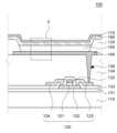
도 1은 본 발명의 일 실시예에 따른 유기 발광 표시 장치를 설명하기 위한 개략적인 단면도이다.
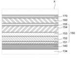
도 2는 도 1의 X 영역에 대한 확대도이다.
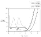
도 3은 본 발명의 실시예 3 및 비교예 3에 따른 유기 발광 표시 장치의 전압 대비 전류 밀도를 나타낸 그래프이다.
도 4는 본 발명의 실시예 3 및 비교예 3에 따른 유기 발광 표시 장치의 휘도 대비 전류 효율을 나타낸 그래프이다.1 is a schematic cross-sectional view illustrating an organic light emitting display device according to an embodiment of the present invention.
Figure 2 is an enlarged view of area X in Figure 1.
Figure 3 is a graph showing current density versus voltage of the organic light emitting display device according to Example 3 and Comparative Example 3 of the present invention.
Figure 4 is a graph showing current efficiency versus luminance of the organic light emitting display device according to Example 3 and Comparative Example 3 of the present invention.
본 발명의 이점 및 특징, 그리고 그것들을 달성하는 방법은 첨부되는 도면과 함께 상세하게 후술되어 있는 실시예들을 참조하면 명확해질 것이다. 그러나 본 발명은 이하에서 개시되는 실시예들에 한정되는 것이 아니라 서로 다른 다양한 형태로 구현될 것이며, 단지 본 실시예들은 본 발명의 개시가 완전하도록 하며, 본 발명이 속하는 기술분야에서 통상의 지식을 가진 자에게 발명의 범주를 완전하게 알려주기 위해 제공되는 것이며, 본 발명은 청구항의 범주에 의해 정의될 뿐이다.The advantages and features of the present invention and methods for achieving them will become clear by referring to the embodiments described in detail below along with the accompanying drawings. However, the present invention is not limited to the embodiments disclosed below and will be implemented in various different forms. The present embodiments only serve to ensure that the disclosure of the present invention is complete and that common knowledge in the technical field to which the present invention pertains is not limited. It is provided to fully inform those who have the scope of the invention, and the present invention is only defined by the scope of the claims.
본 발명의 실시예를 설명하기 위한 도면에 개시된 형상, 크기, 비율, 각도, 개수 등은 예시적인 것이므로 본 발명이 도시된 사항에 한정되는 것은 아니다. 명세서 전체에 걸쳐 동일 참조 부호는 동일 구성 요소를 지칭한다. 또한, 본 발명을 설명함에 있어서, 관련된 공지 기술에 대한 구체적인 설명이 본 발명의 요지를 불필요하게 흐릴 수 있다고 판단되는 경우 그 상세한 설명은 생략한다. 본 명세서 상에서 언급된 '포함한다', '갖는다', '이루어진다' 등이 사용되는 경우 '~만'이 사용되지 않는 이상 다른 부분이 추가될 수 있다. 구성 요소를 단수로 표현한 경우에 특별히 명시적인 기재 사항이 없는 한 복수를 포함하는 경우를 포함한다.The shapes, sizes, proportions, angles, numbers, etc. disclosed in the drawings for explaining embodiments of the present invention are illustrative, and the present invention is not limited to the matters shown. Like reference numerals refer to like elements throughout the specification. Additionally, in describing the present invention, if it is determined that a detailed description of related known technologies may unnecessarily obscure the gist of the present invention, the detailed description will be omitted. When 'includes', 'has', 'consists of', etc. mentioned in this specification are used, other parts may be added unless 'only' is used. When a component is expressed in the singular, the plural is included unless specifically stated otherwise.
구성 요소를 해석함에 있어서, 별도의 명시적 기재가 없더라도 오차 범위를 포함하는 것으로 해석한다.When interpreting a component, it is interpreted to include the margin of error even if there is no separate explicit description.
위치 관계에 대한 설명일 경우, 예를 들어, '~상에', '~상부에', '~하부에', '~옆에' 등으로 두 부분의 위치 관계가 설명되는 경우, '바로' 또는 '직접'이 사용되지 않는 이상 두 부분 사이에 하나 이상의 다른 부분이 위치할 수도 있다.In the case of a description of a positional relationship, for example, if the positional relationship of two parts is described as 'on top', 'on the top', 'on the bottom', 'next to', etc., 'immediately' Alternatively, there may be one or more other parts placed between the two parts, unless 'directly' is used.
소자 또는 층이 다른 소자 또는 층 "위(on)"로 지칭되는 것은 다른 소자 바로 위에 또는 중간에 다른 층 또는 다른 소자를 개재한 경우를 모두 포함한다.When an element or layer is referred to as “on” another element or layer, it includes instances where the other layer or other element is directly on top of or interposed between the other element and the other element.
비록 제1, 제2 등이 다양한 구성요소들을 서술하기 위해서 사용되나, 이들 구성요소들은 이들 용어에 의해 제한되지 않는다. 이들 용어들은 단지 하나의 구성요소를 다른 구성요소와 구별하기 위하여 사용하는 것이다. 따라서, 이하에서 언급되는 제1 구성요소는 본 발명의 기술적 사상 내에서 제2 구성요소일 수도 있다.Although first, second, etc. are used to describe various elements, these elements are not limited by these terms. These terms are merely used to distinguish one component from another. Accordingly, the first component mentioned below may also be the second component within the technical spirit of the present invention.
명세서 전체에 걸쳐 동일 참조 부호는 동일 구성 요소를 지칭한다.Like reference numerals refer to like elements throughout the specification.
도면에서 나타난 각 구성의 크기 및 두께는 설명의 편의를 위해 도시된 것이며, 본 발명이 도시된 구성의 크기 및 두께에 반드시 한정되는 것은 아니다.The size and thickness of each component shown in the drawings are shown for convenience of explanation, and the present invention is not necessarily limited to the size and thickness of the components shown.
본 발명의 여러 실시예들의 각각 특징들이 부분적으로 또는 전체적으로 서로 결합 또는 조합 가능하고, 기술적으로 다양한 연동 및 구동이 가능하며, 각 실시예들이 서로에 대하여 독립적으로 실시 가능할 수도 있고 연관 관계로 함께 실시할 수도 있다.Each feature of the various embodiments of the present invention can be combined or combined with each other, partially or entirely, and various technical interconnections and operations are possible, and each embodiment may be implemented independently of each other or together in a related relationship. It may be possible.
이하, 첨부된 도면을 참조하여 본 발명의 다양한 실시예들을 상세히 설명한다.Hereinafter, various embodiments of the present invention will be described in detail with reference to the attached drawings.
도 1은 본 발명의 일 실시예에 따른 유기 발광 표시 장치를 설명하기 위한 개략적인 단면도이고, 도 2는 도 1의 X 영역에 대한 확대도이다.FIG. 1 is a schematic cross-sectional view for explaining an organic light emitting display device according to an embodiment of the present invention, and FIG. 2 is an enlarged view of area X of FIG. 1 .
도 1을 참조하면, 본 발명의 일 실시예에 따른 유기 발광 표시 장치(100)는 기판(110), 박막 트랜지스터(120), 애노드(Anode, 140), 복수의 유기층(150), 캐소드(Cathode, 160) 및 캡핑층(capping layer, 170)을 포함한다.Referring to FIG. 1, an organic light emitting
유기 발광 표시 장치(100)는 복수의 화소(pixel)를 포함한다. 화소는 실제 빛이 발광되는 최소 단위의 영역을 말하며, 서브 화소 또는 화소 영역으로 지칭될 수 있다. 또한, 복수의 화소가 모여 백색의 광을 표현할 수 있는 최소의 군을 이룰 수 있으며, 예를 들어, 세 개의 화소의 군으로서, 적색 화소(red pixel), 녹색 화소(green pixel) 및 청색 화소(blue pixel)가 하나의 군을 이룰 수 있다. 그러나, 이에 한정된 것은 아니며, 다양한 화소 설계가 가능하다. 도 1에서는 설명의 편의를 위해 유기 발광 표시 장치(100)의 복수의 서브 화소 중 하나의 서브 화소만을 도시하였다.The organic light emitting
기판(110)은 제조 과정에서 유기 발광 표시 장치(100)의 다양한 구성요소들을 지지하기 위하여 절연 물질로 형성된다. 예를 들어, 기판(110)은 유리 또는 플라스틱과 같은 유연성(flexibility)을 갖는 물질로 이루어질 수 있다. 기판(110) 상에 기판(110) 외부로부터의 수분(H2O) 및 수소(H2) 등의 침투로부터 유기 발광 표시 장치(100)의 다양한 구성요소들을 보호하기 위한 버퍼층(131)이 배치된다. 다만, 기판(110)은 유기 발광 장치(100)의 제조 과정 중에 제거될 수 있고, 버퍼층(131)은 유기 발광 표시 장치(100)의 구조나 특성에 따라 생략될 수도 있다.The
버퍼층(131) 상에 게이트 전극(121), 액티브층(122), 소스 전극(123) 및 드레인 전극(124)을 포함하는 박막 트랜지스터(120)가 배치된다. 예를 들어, 기판(110) 상에 액티브층(122)이 배치되고, 액티브층(122) 상에 액티브층(122)과 게이트 전극(121)을 절연시키기 위한 게이트 절연층(132)이 배치된다. 게이트 전극(121)과 소스 전극(123) 및 드레인 전극(124)을 절연시키기 위한 층간 절연층(133)이 배치되고, 층간 절연층(133) 상에 액티브층(122)과 각각 접하는 소스 전극(123) 및 드레인 전극(124)이 배치된다. 본 명세서에서는 설명의 편의를 위해, 유기 발광 표시 장치(100)에 포함될 수 있는 다양한 박막 트랜지스터 중 구동 박막 트랜지스터만을 도시하였으나, 스위칭 박막 트랜지스터, 커패시터 등도 유기 발광 표시 장치(100)에 포함될 수 있다. 또한, 본 명세서에서는 박막 트랜지스터(120)가 코플래너(coplanar) 구조인 것으로 설명하나, 스태거드(staggered) 구조의 박막 트랜지스터도 사용될 수 있다.A
박막 트랜지스터(120) 상에 오버 코팅층(over coating layer, 134)이 배치된다. 오버 코팅층(134)은 기판(110) 상부를 평탄화하는 평탄화층으로서 기능한다. 오버 코팅층(134)은 박막 트랜지스터(120)와 애노드(140)를 전기적으로 연결하기 위한 컨택홀(contact hole, 136)을 포함한다.An over
애노드(140)는 오버 코팅층(134) 상에 배치된다. 애노드(140)는 복수의 유기층(150) 중 유기 발광층(153)으로 정공을 공급하도록 구성되는 전극이며, 애노드(140)는 오버 코팅층(134)의 컨택홀(136)을 통해 박막 트랜지스터(120)와 전기적으로 연결되고, 예를 들어, 박막 트랜지스터(120)의 소스 전극(123)과 전기적으로 연결될 수 있다. 애노드(140)는 화소별로 이격되어 배치된다.The
본 발명의 일 실시예에 따른 유기 발광 표시 장치(100)가 전면 발광 구조를 채택하고 있으므로, 애노드(140)는 유기 발광층(153)로부터 발광된 광이 애노드(140)에 반사되어 보다 원활하게 상부 방향으로 방출될 수 있도록, 반사층을 포함한 투명 도전성 물질로 형성될 수 있다.Since the organic light emitting
예를 들어, 애노드(140)는 위로부터 투명 도전성 물질로 형성된 투명 도전층과 반사층이 차례로 적층된 2층 구조이거나, 투명 도전층, 반사층 및 투명 도전층이 차례로 적층된 3층 구조일 수 있다.For example, the
투명 도전성 물질은, 예를 들어, 인듐 주석 산화물(Indium Tin Oxide, ITO), 인듐 아연 산화물(Indium Zin Oxide, IZO) 등과 같은 물질일 수 있다. 반사층은 은(Ag) 또는 은을 포함하는 합금일 수 있으며, 예를 들어, 은 또는 APC(Ag/Pd/Cu)일 수 있다.The transparent conductive material may be, for example, a material such as indium tin oxide (ITO), indium zinc oxide (IZO), or the like. The reflective layer may be silver (Ag) or an alloy containing silver, for example, silver or APC (Ag/Pd/Cu).
애노드(140) 및 오버 코팅층(134) 상에 뱅크(135)가 배치된다. 뱅크(135)는 인접하는 서브 화소 영역을 구분한다. 또한, 뱅크(135)는 복수의 서브 화소 영역으로 구성된 화소 영역을 구분할 수도 있다.A
애노드(140) 상에 복수의 유기층(150)이 배치된다. 여기서 복수의 유기층(150)은 유기 발광 스택을 구성하는 유기층들을 지칭한다. 복수의 유기층(150)에는 필요에 따라 다양한 유기층들이 포함되나, 빛을 발광하기 위한 유기 발광층(153)은 필수적으로 포함되어야 한다.A plurality of
복수의 유기층(150)은 애노드(140) 상에 배치된 정공 주입층 (Hole Injection Layer; HIL, 151), 정공 주입층(151) 상에 배치된 정공 수송층 (Hole Transport Layer; HTL, 152), 정공 수송층(152) 상에 배치된 유기 발광층(Organic Emitting Layer; EML, 153), 유기 발광층(153) 상에 배치된 전자 수송층(Electron Transport Layer; ETL, 154) 및 전자 수송층(154) 상에 배치된 전자 주입층(Electron Injection Layer; EIL, 155)을 포함한다.The plurality of
정공 주입층(151)은 애노드(140) 상에 배치되며, 애노드(140)로부터 유기 발광층(153)으로 정공의 주입을 원활하게 하는 유기층이다. 정공 주입층(151)은, 예를 들어, HAT-CN(dipyrazino[2,3-f:2',3'-h]quinoxaline-2,3,6,7,10.11-hexacarbonitrile), CuPc(phthalocyanine), 및 NPD(N,N'-bis(naphthalene-1-yl)-N,N'-bis(phenyl)-2,2'-dimethylbenzidine)로 이루어진 군에서 선택된 어느 하나 이상으로 이루어질 수 있으나, 이에 제한되는 것은 아니다. 정공 주입층(151)은 유기 발광 표시 장치(100)의 구조나 특성에 따라 생략될 수도 있다.The
정공 수송층(152)은 정공 주입층(151) 상에 배치되며, 정공 주입층(151)으로부터 유기 발광층(153)으로 원할하게 정공을 전달하는 유기층이다. 정공 수송층(152)은, 예를 들어, NPD(N,N'-bis(naphthalene-1-yl)-N,N'-bis(phenyl)-2,2'-dimethylbenzidine), TPD(N,N'-bis-(3-methylphenyl)-N,N'-bis-(phenyl)-benzidine), s-TAD(2,2',7,7'-tetrakis(N,N-dimethylamino)-9,9-spirofluorene) 및 MTDATA(4,4',4"-Tris(N-3-methylphenyl-N-phenyl-amino)-triphenylamine)로 이루어진 군에서 선택된 어느 하나 이상으로 이루어질 수 있으나, 이에 제한되는 것은 아니다.The
유기 발광층(153)은 정공 수송층(152) 상에 배치된다. 유기 발광층(153)은 특정 색의 광을 발광할 수 있는 물질을 포함할 수 있다. 예를 들어, 유기 발광층(153)은 적색 광, 녹색 광, 청색 광 또는 황녹색 광을 발광할 수 있는 발광 물질을 포함할 수 있다. 그러나, 이에 제한되지 않고 다른 색의 광을 발광할 수 있는 발광 물질을 포함할 수도 있다.The organic light-emitting
전자 수송층(154)은 유기 발광층(153) 상에 배치되며, 전자 주입층(155)으로부터 유기 발광층(153)으로 전자를 전달하는 유기층이다. 전자 수송층(154)의 두께는 전자 수송 특성을 고려하여 조절될 수 있다. 전자 수송층(154)은, 예를 들어, Liq(8-hydroxyquinolinolato-lithium), PBD(2-(4-biphenyl)-5-(4-tert-butylphenyl)-1,3,4oxadiazole), TAZ(3-(4-biphenyl)4-phenyl-5-tert-butylphenyl-1,2,4-triazole), spiro-PBD, BCP(2,9-Dimethyl-4,7-diphenyl-1,10-phenanthroline) 및 BAlq(bis(2-methyl-8-quinolinolate)-4-(phenylphenolato)aluminium)로 이루어진 군에서 선택된 어느 하나 이상으로 이루어질 수 있으나, 이에 제한되는 것은 아니다. 전자 수송층(154)은 유기 발광 장치(100)의 구조나 특성에 따라 생략될 수도 있다.The
전자 주입층(155)은 전자 수송층(154) 상에 배치된다. 전자 주입층(155)은 캐소드(160)로부터 유기 발광층(153)으로 전자의 주입을 원활하게 하는 유기층이다. 전자 주입층(155)은 BaF2, LiF, NaCl, CsF, Li2O 및 BaO와 같은 금속 무기 화합물일 수 있다. 또한, 전자 주입층(155)은 HAT-CN(dipyrazino[2,3-f:2',3'-h]quinoxaline-2,3,6,7,10.11-hexacarbonitrile), CuPc(phthalocyanine), 및 NPD(N,N'-bis(naphthalene-1-yl)-N,N'-bis(phenyl)-2,2'-dimethylbenzidine)로 이루어진 군에서 선택된 어느 하나 이상의 유기 화합물일 수 있으나, 이에 제한되는 것은 아니다. 전자 주입층(155)은 유기 발광 장치(100)의 구조나 특성에 따라 생략될 수도 있다.The
캐소드(160)는 전자 주입층(155) 상에 배치된다. 캐소드(160)는 유기 발광층(153)으로 전자를 공급한다.The
상부 방향으로 빛을 출사하는 전면 발광 구조 방식의 유기 발광 표시 장치(100)에서 캐소드(160)는 유기 발광층(153)으로부터 발광된 광의 적어도 일부를 투과시키는 반투과 금속막으로 구성된다.In the organic light emitting
구체적으로, 본 발명의 일 실시예에 따른 유기 발광 표시 장치(100)는 금속과 산화금속의 합금을 포함하는 캐소드(160)를 포함한다.Specifically, the organic light emitting
보다 구체적으로, 캐소드(160)는 제1 금속과 제2 금속의 산화물의 합금을 포함하여 구성된다.More specifically, the
여기서, 제1 금속은 예를 들어, 은(Ag), 알루미늄(Al) 및 구리(Cu) 중에서 선택된 어느 하나일 수 있다. 제2 금속은 예를 들어, 네오디뮴(Nd), 탄탈륨(Ta), 니오븀(Nb), 몰리브덴(Mo), 텅스텐(W), 티타늄(Ti), 실리콘(Si), 붕소(B), 니켈(Ni), 금(Au), 구리(Cu), 알루미늄(Al), 주석(Sn), 마그네슘(Mg), 백금(Pt) 및 팔라듐(Pd) 중에서 선택된 어느 하나일 수 있다.Here, the first metal may be, for example, any one selected from silver (Ag), aluminum (Al), and copper (Cu). The second metal is, for example, neodymium (Nd), tantalum (Ta), niobium (Nb), molybdenum (Mo), tungsten (W), titanium (Ti), silicon (Si), boron (B), nickel ( It may be any one selected from Ni), gold (Au), copper (Cu), aluminum (Al), tin (Sn), magnesium (Mg), platinum (Pt), and palladium (Pd).
제2 금속은 산화물로 제1 금속과 합금을 이루며, 캐소드의 재료가 된다. 제2 금속이 제1 금속보다 분자량이 큰 금속일 경우, 제1 금속과의 산화금속 합금 형성 시에 제1 금속의 응집을 억제하는 효과를 가질 수 있어 보다 바람직하다. 예를 들어, 캐소드(160)는 은(Ag)과 산화몰리브덴(MoO3)의 합금인 Ag:MoO3로 구성될 수 있다.The second metal is an oxide that forms an alloy with the first metal and becomes the material of the cathode. When the second metal is a metal with a larger molecular weight than the first metal, it is more preferable because it can have the effect of suppressing aggregation of the first metal when forming a metal oxide alloy with the first metal. For example, the
캐소드(160)가 제1 금속과 고투과율의 산화금속 합금을 포함하여 구성될 경우, MgAg 반투과 캐소드에 비해 투과율을 향상시키면서도 캐소드(160)의 두께를 증가시킬 수 있다.When the
이러한 캐소드(160)의 두께는 투과율 특성 및 공정 마진을 고려하여 조절될 수 있다. 바람직하게, 캐소드(160)의 두께는 250Å 이상으로 형성될 수 있다.The thickness of the
본 발명의 일 실시예에 따른 유기 발광 표시 장치(100)에서는 금속과 산화금속의 합금을 포함하는 캐소드(160)를 구성함으로써, 캐소드(160)의 두께를 250Å 이상으로 증가시켜도 MgAg 반투과 금속으로 이루어진 캐소드보다 향상된 투과율 및 면저항을 가진다.In the organic light emitting
또한, 캐소드(160)의 두께가 250Å 이상일 때, 캐소드(160)의 두께 50Å 변동당 투과율 변화율이 1.5% 이하가 되어 캐소드(160)의 두께 변화에 따른 투과율 변동이 매우 작아 소자의 두께 균일도(uniformity)가 개선되고, 캐소드(160)의 두께 균일도에 대한 공정 마진이 확보되어 수율이 향상되는 효과가 있다. 이때, 캐소드(160)의 두께 균일도는 ±10% 내에서 결정되며, 대략 두께 30 Å 내지 40Å일 수 있다.In addition, when the thickness of the
MgAg와 같은 금속 합금을 캐소드로 사용하는 전면 발광 유기 발광 표시 장치는 두께를 얇게, 예를 들어 200Å 정도로 형성하므로, 작은 두께 차이에도 두께의 변동 비율이 크다. 이에 따라 형성 공정 중간에 단위막의 두께 측정을 통해 두께 보정을 실시하고 있으며, 이러한 두께 보정에 의해 공정 수율 및 제품 수율이 저하됨과 동시에 생산비가 증가되는 문제점이 있었다.A top-emitting organic light-emitting display device that uses a metal alloy such as MgAg as a cathode is formed with a thin thickness, for example, about 200 Å, so the rate of thickness variation is large even for small thickness differences. Accordingly, thickness correction is performed by measuring the thickness of the unit film in the middle of the formation process. This thickness correction has the problem of lowering process yield and product yield and increasing production costs.
그러나, 본 발명은 금속과 산화금속의 합금을 포함하는 캐소드(160)를 통해 캐소드(160)의 두께 균일도가 향상됨으로써, 얇은 두께의 금속 합금의 캐소드 형성시와는 달리 단위막의 두께 평가 횟수를 감소시키거나 없앨 수 있어 수율 향상 및 생산비 절감 효과가 있다.However, in the present invention, the thickness uniformity of the
본 발명은 상기한 캐소드(160)의 두께가 증가하므로 면저항을 낮출 수 있다. 상부 발광 구조의 유기 발광 표시 장치(100)는 대면적으로 구현될 경우, 중심 영역에서의 전압 강하(IR drop)가 급격히 발생하여 중앙에서의 유기 발광 표시 장치의 발광 성능이 저하될 수 있다. 따라서, 기존의 유기 발광 표시 장치는 전압 강하를 예방하고자 대면적화시에는 캐소드에 전원을 공급하기 위한 별도의 보조배선을 마련하고 있다.In the present invention, the sheet resistance can be lowered because the thickness of the
그러나, 본 실시예의 유기 발광 표시 장치(100)는, 캐소드(160)의 두께 증가를 통해 면저항을 낮춰, 장치의 대면적화시, 예를 들어 12인치 이상에서도 전압 강하가 최소화되어, 캐소드(160)에 전원을 공급하기 위한 별도의 보조배선이 요구되지 않을 수 있다. 따라서, 본 실시예의 유기 발광 표시 장치(100)는 대면적화에서도 별도의 보조배선의 생략을 통해 개구율을 향상시키고, 표시 장치 중앙에서의 발광 균일도를 향상시킬 수 있다.However, in the organic light emitting
캐소드(160)는 제1 금속과 산화된 제2 금속의 합금비율이 2 : 1 이상으로 조성될 수 있고, 바람직하게는 제1 금속과 산화된 제2 금속의 합금비율이 3 내지 5 : 1로 조성될 수 있다.The
또한, 캐소드(160)의 굴절률은 0.2 내지 1.8 범위 내일 수 있다.Additionally, the refractive index of the
도 1을 다시 참조하면, 캡핑층(170)이 캐소드(160) 상에 배치된다. 캡핑층(170)은 외부로부터의 수분(H2O) 및 수소(H2) 등의 침투로부터 복수의 유기층(150) 및 캐소드(160)를 보호하기 위한 보호층이다.Referring back to FIG. 1 , a
한편, 도 1에 도시하지는 않았지만, 캡핑층(170) 상에는 캡핑층(170)과 유사 굴절률을 갖는 실리콘질화막(SiNx) 등으로 이루어진 보호층이 더 형성될 수 있다.Meanwhile, although not shown in FIG. 1, a protective layer made of a silicon nitride (SiNx) film having a similar refractive index as that of the
이러한 보호층과 캡핑층(170)은 굴절률 차이가 없으므로, 캐소드(160)와 캡핑층(170)의 굴절률 차이가 작을수록 효율이 증가된다. 이에 따라, 캡핑층(170)의 굴절률은 캐소드(160)의 굴절률에 기초하여 결정될 수 있다. 예를 들어, 캐소드(160)와 캡핑층(170)의 굴절률 차이(dN)는 0 < dN < 1.6 범위 내일 수 있다.Since there is no difference in refractive index between the protective layer and the
본 실시예에서는 캐소드(160)가 산화물 합금으로 구성됨으로써 기존 AgMg 대비 캐소드(160)와 캡핑층(170) 간의 굴절률 차이가 작아져 이들 계면에서의 반사와 굴절에 의한 영향이 최소화되어 발광 효율이 향상될 수 있다.In this embodiment, the
상술한 바와 같이, 본 실시예의 유기 발광 표시 장치(100)는 금속과 산화금속의 합금을 포함한 캐소드(160)와, 캐소드(160)의 두께 및 합금비율 설계를 통해 캐소드의 공정 마진 및 두께 균일도 등을 향상시켜 수율 향상, 생산비 절감 및 별도의 보조배선 생략을 통한 개구율 향상 등의 다양한 효과를 얻을 수 있다.As described above, the organic light emitting
이하에서는 본 발명의 효과에 대해서 알아보기 위하여, 실시예 1 내지 4 및 비교예 1 내지 8의 유기 발광 표시 장치를 제조하였다.Below, in order to investigate the effect of the present invention, organic light emitting display devices of Examples 1 to 4 and Comparative Examples 1 to 8 were manufactured.
실시예 1 내지 4는 본 발명의 일 실시예에 따라 금속과 산화금속의 합금을 포함한 캐소드가 배치된 유기 발광 표시 장치로서, 도 1 및 도 2에 도시된 구조를 갖는다. 실시예 1 내지 4 및 비교예 1 내지 8은 애노드(ITO/APC/ITO), 정공주입층(HIL), 정공수송층(HTL, R'/G' HTL), 유기 발광층(EML), 전자 수송층(ETL), 전자 주입층(EIL), 캐소드(Cathode) 및 캡핑층(CPL)이 순차적으로 적층된 구조를 가진다. 이때, 실시예 1 내지 4는 Ag:MoO3를 캐소드로 포함한다. 비교예 1 내지 8은 Ag:Mg를 캐소드로 포함하고, 일부 정공수송층(R'/G' HTL)의 두께가 다른 것을 제외하고, 나머지는 실시예 1 내지 4와 동일한 구조를 가진다.Examples 1 to 4 are organic light emitting display devices in which a cathode including an alloy of metal and metal oxide is disposed according to an embodiment of the present invention, and has the structure shown in FIGS. 1 and 2. Examples 1 to 4 and Comparative Examples 1 to 8 include an anode (ITO/APC/ITO), a hole injection layer (HIL), a hole transport layer (HTL, R'/G' HTL), an organic light emitting layer (EML), and an electron transport layer ( ETL), electron injection layer (EIL), cathode, and capping layer (CPL) are sequentially stacked. At this time, Examples 1 to 4 include Ag:MoO3 as the cathode. Comparative Examples 1 to 8 included Ag:Mg as a cathode and had the same structure as Examples 1 to 4, except that the thickness of some hole transport layers (R'/G' HTL) was different.
하기 표 1은 전술한 실시예 1 내지 4 및 비교예 1 내지 8에 따른 유기 발광 표시 장치의 층별 조성 및/또는 두께를 나타낸다.Table 1 below shows the composition and/or thickness of each layer of the organic light emitting display device according to the above-described Examples 1 to 4 and Comparative Examples 1 to 8.

하기 표 2 및 표 3은 전술한 실시예 1 내지 4 및 비교예 1 내지 8에 따른 유기 발광 표시 장치의 투과율(%) 및 투과율 변동량(%) 평가 결과를 나타낸다.Tables 2 and 3 below show the evaluation results of the transmittance (%) and transmittance variation (%) of the organic light emitting display devices according to the above-described Examples 1 to 4 and Comparative Examples 1 to 8.


표 1 내지 표 3을 참조하면, 본 발명의 실시예 1 내지 4는 캐소드의 두께가 증가되었음에도 불구하고 비교예 1 내지 4와 유사한 투과율을 보임을 확인할 수 있다.Referring to Tables 1 to 3, it can be seen that Examples 1 to 4 of the present invention showed similar transmittances to Comparative Examples 1 to 4 even though the thickness of the cathode was increased.
또한, 비교예 1 내지 4는 캐소드의 두께 20Å 변동당 투과율 변동량이 5.4%이나, 본 발명의 실시예 1 내지 4는 캐소드의 두께 50Å 변동당 투과율 변동량이 1.46%로 유의미하게 낮음을 확인할 수 있다.In addition, in Comparative Examples 1 to 4, the transmittance variation per 20Å variation in cathode thickness is 5.4%, but in Examples 1 to 4 of the present invention, it can be confirmed that the transmittance variation per 50Å variation in cathode thickness is 1.46%, which is significantly low.
이렇듯, 본 발명은 캐소드의 두께 변동에 따라 투과율의 변동이 최소화되므로, 캐소드의 두께를 보다 두껍게 구성할 수 있으며 공정 마진을 충분히 확보할 수 있다.In this way, in the present invention, the change in transmittance according to the change in the thickness of the cathode is minimized, so the cathode can be configured to be thicker and a sufficient process margin can be secured.
하기 표 4는 전술한 실시예 3 및 비교예 3에 따른 유기 발광 표시 장치의 구동 전압, 전류 효율, 발광 피크, FWHW 및 색좌표 평가 결과를 나타낸다. 도 3은 본 발명의 실시예 3 및 비교예 3에 따른 유기 발광 표시 장치의 전압 대비 전류 밀도를 나타낸 그래프이고, 도 4는 본 발명의 실시예 3 및 비교예 3에 따른 유기 발광 표시 장치의 휘도 대비 전류 효율을 나타낸 그래프이다.Table 4 below shows the driving voltage, current efficiency, emission peak, FWHW, and color coordinate evaluation results of the organic light emitting display device according to Example 3 and Comparative Example 3 described above. Figure 3 is a graph showing the current density versus voltage of the organic light emitting display device according to Example 3 and Comparative Example 3 of the present invention, and Figure 4 is a graph showing the luminance of the organic light emitting display device according to Example 3 and Comparative Example 3 of the present invention. This is a graph showing comparison current efficiency.

(여기서, FWHM(full width at half maximum)은 반치폭을 의미한다.)(Here, FWHM (full width at half maximum) means full width at half maximum.)
표 4, 도 3 및 도 4를 참조하면, 실시예 3과 비교예 3의 구동 전압은 동등하고, 색좌표, 발광 효율 및 FWHM은 동등 또는 유사하고, 전류 효율은 소폭 상승함을 확인할 수 있다.Referring to Table 4 and Figures 3 and 4, it can be seen that the driving voltage of Example 3 and Comparative Example 3 are the same, the color coordinates, luminous efficiency and FWHM are the same or similar, and the current efficiency slightly increases.
즉, 캐소드에 금속과 산화금속의 합금이 포함되어 유기 발광 표시 장치의 캐소드의 두께가 증가함에도 불구하고, 실시예 3은 비교예 3 대비 동등 또는 동등 수준 이상의 전자 주입 특성 및 효율 특성을 보임을 알 수 있다.That is, although the thickness of the cathode of the organic light emitting display device increases due to the inclusion of an alloy of metal and metal oxide in the cathode, Example 3 shows electron injection characteristics and efficiency characteristics that are equal to or better than those of Comparative Example 3. You can.
상술한 결과를 종합하여 보면, 본 발명의 실시예에 따른 유기 발광 표시 장치는 금속과 산화금속의 합금을 포함한 캐소드를 포함함으로써, 캐소드 두께에 따른 투과율 변동량이 매우 작아 캐소드의 공정 마진이 향상되고, 캐소드의 발광 성능은 기존 소자 대비 향상될 수 있다.Considering the above results, the organic light emitting display device according to the embodiment of the present invention includes a cathode containing an alloy of metal and metal oxide, so that the change in transmittance depending on the cathode thickness is very small, thereby improving the process margin of the cathode, The light emission performance of the cathode can be improved compared to existing devices.
본 발명의 일 실시예에 따른 유기 발광 표시 장치가 제공된다. 유기 발광 표시 장치는 애노드, 애노드 상의 유기 발광층 및 유기발광층으로부터의 광의 적어도 일부를 투과시키도록 구성되고, 제1 금속과 제2 금속의 산화물의 합금으로 이루어진 유기 발광층 상의 캐소드를 포함하도록 구성된다. 따라서, 캐소드의 두께에 따른 투과율의 차이가 개선되어, 캐소드의 공정 마진이 향상될 수 있다.An organic light emitting display device according to an embodiment of the present invention is provided. An organic light emitting display device is configured to transmit at least a portion of light from the organic light emitting layer, an anode, an organic light emitting layer on the anode, and a cathode on the organic light emitting layer made of an alloy of an oxide of a first metal and a second metal. Accordingly, the difference in transmittance depending on the thickness of the cathode is improved, and the process margin of the cathode can be improved.
제1 금속은 Ag, Al 및 Cu 중에서 선택된 어느 하나일 수 있다.The first metal may be any one selected from Ag, Al, and Cu.
제2 금속은 Nd, Ta, Nb, Mo, W, Ti, Si, B, Ni, Au, Cu, Al, Sn, Mg, Pt 및 Pd 중에서 선택된 어느 하나일 수 있다.The second metal may be any one selected from Nd, Ta, Nb, Mo, W, Ti, Si, B, Ni, Au, Cu, Al, Sn, Mg, Pt, and Pd.
캐소드의 두께는 250Å 이상일 수 있다.The thickness of the cathode may be 250Å or more.
캐소드의 두께 50Å 변동당 투과율 변화율이 1.5% 이하일 수 있다.The rate of change in transmittance per 50Å change in the thickness of the cathode may be 1.5% or less.
캐소드의 두께 균일도는 ±10% 내에서 결정될 수 있다.The thickness uniformity of the cathode can be determined within ±10%.
제1 금속과 제2 금속의 합금비율은 2 : 1 이상일 수 있다.The alloy ratio of the first metal and the second metal may be 2:1 or more.
제1 금속과 제2 금속의 합금비율은 3 내지 5 : 1일 수 있다.The alloy ratio of the first metal and the second metal may be 3 to 5:1.
캐소드는 전원을 공급하기 위한 별도의 보조배선이 없을 수 있다.The cathode may not have separate auxiliary wiring to supply power.
캐소드 상의 캡핑층을 더 포함하며, 캡핑층의 굴절률은 캐소드의 굴절률에 기초하여 결정될 수 있다.It further includes a capping layer on the cathode, and the refractive index of the capping layer can be determined based on the refractive index of the cathode.
캐소드의 굴절률은 0.2 내지 1.8 범위 내일 수 있다.The refractive index of the cathode may range from 0.2 to 1.8.
캐소드의 굴절률과 캡핑층의 굴절률 차이 dN은 0 < dN < 1.6 범위 내일 수 있다.The difference dN between the refractive index of the cathode and the capping layer may be in the range of 0 < dN < 1.6.
이상 첨부된 도면을 참조하여 본 발명의 실시예들을 더욱 상세하게 설명하였으나, 본 발명은 반드시 이러한 실시예로 국한되는 것은 아니고, 본 발명의 기술사상을 벗어나지 않는 범위 내에서 다양하게 변형 실시될 수 있다. 따라서, 본 발명에 개시된 실시예들은 본 발명의 기술 사상을 한정하기 위한 것이 아니라 설명하기 위한 것이고, 이러한 실시예에 의하여 본 발명의 기술 사상의 범위가 한정되는 것은 아니다. 그러므로, 이상에서 기술한 실시예들은 모든 면에서 예시적인 것이며 한정적이 아닌 것으로 이해해야 한다. 본 발명의 보호 범위는 아래의 청구범위에 의하여 해석되어야 하며, 그와 동등한 범위 내에 있는 모든 기술 사상은 본 발명의 권리범위에 포함되는 것으로 해석되어야 할 것이다.Although embodiments of the present invention have been described in more detail with reference to the accompanying drawings, the present invention is not necessarily limited to these embodiments, and various modifications may be made without departing from the technical spirit of the present invention. . Accordingly, the embodiments disclosed in the present invention are not intended to limit the technical idea of the present invention, but are for illustrative purposes, and the scope of the technical idea of the present invention is not limited by these embodiments. Therefore, the embodiments described above should be understood in all respects as illustrative and not restrictive. The scope of protection of the present invention should be interpreted in accordance with the claims below, and all technical ideas within the equivalent scope should be construed as being included in the scope of rights of the present invention.
100: 유기 발광 표시 장치 110: 기판
120: 박막 트랜지스터 121: 게이트 전극
122: 액티브층 123: 소스 전극
124: 드레인 전극 131: 버퍼층
132: 게이트 절연층 133: 층간 절연층
134: 오버 코팅층 135: 뱅크
136 : 콘택홀 140: 애노드
150: 복수의 유기층 151: 전공 주입층
152: 전공 수송층 153: 유기 발광층
154: 전자 수송층 155: 전자 주입층
160: 캐소드 170: 캡핑층100: Organic light emitting display device 110: Substrate
120: thin film transistor 121: gate electrode
122: active layer 123: source electrode
124: drain electrode 131: buffer layer
132: Gate insulating layer 133: Interlayer insulating layer
134: overcoating layer 135: bank
136: contact hole 140: anode
150: plural organic layers 151: electroporation injection layer
152: electroporous transport layer 153: organic light emitting layer
154: electron transport layer 155: electron injection layer
160: cathode 170: capping layer
Claims (12)
Translated fromKorean상기 애노드 상의 유기 발광층; 및
상기 유기발광층으로부터의 광의 적어도 일부를 투과시키도록 구성되고, 제1 금속과 제2 금속의 산화물의 합금으로 이루어진 상기 유기 발광층 상의 캐소드를 포함하고,
상기 제1 금속은 Ag, Al 및 Cu 중에서 선택된 어느 하나이고,
상기 제2 금속은 Nd, Ta, Nb, Mo, W, Ti, Si, B, Ni, Au, Cu, Al, Sn, Mg, Pt 및 Pd 중에서 선택된 어느 하나인, 유기 발광 표시 장치.anode;
an organic light-emitting layer on the anode; and
A cathode on the organic light-emitting layer configured to transmit at least a portion of the light from the organic light-emitting layer and made of an alloy of an oxide of a first metal and a second metal,
The first metal is any one selected from Ag, Al, and Cu,
The second metal is any one selected from Nd, Ta, Nb, Mo, W, Ti, Si, B, Ni, Au, Cu, Al, Sn, Mg, Pt, and Pd.
상기 캐소드의 두께는 250Å 이상인, 유기 발광 표시 장치.According to paragraph 1,
An organic light emitting display device wherein the cathode has a thickness of 250 Å or more.
상기 캐소드의 두께 50Å 변동당 투과율 변화율이 1.5% 이하인, 유기 발광 표시 장치.According to clause 4,
An organic light emitting display device having a transmittance change rate of 1.5% or less per 50Å change in the thickness of the cathode.
상기 캐소드의 두께 균일도는 ±10% 내에서 결정되는, 유기 발광 표시 장치.According to clause 5,
An organic light emitting display device in which the thickness uniformity of the cathode is determined within ±10%.
상기 제1 금속과 상기 제2 금속의 합금비율은 2 : 1 이상인, 유기 발광 표시 장치.According to paragraph 1,
An organic light emitting display device wherein an alloy ratio of the first metal and the second metal is 2:1 or more.
상기 제1 금속과 상기 제2 금속의 합금비율은 3 내지 5 : 1인, 유기 발광 표시 장치.In clause 7,
An alloy ratio of the first metal and the second metal is 3 to 5:1.
상기 캐소드는 전원을 공급하기 위한 별도의 보조배선이 없는, 유기 발광 표시 장치.According to paragraph 1,
The cathode is an organic light emitting display device that does not have separate auxiliary wiring for supplying power.
상기 캐소드 상의 캡핑층을 더 포함하며,
상기 캡핑층의 굴절률은 상기 캐소드의 굴절률에 기초하여 결정되는, 유기 발광 표시 장치.According to paragraph 1,
Further comprising a capping layer on the cathode,
The refractive index of the capping layer is determined based on the refractive index of the cathode.
상기 캐소드의 굴절률은 0.2 내지 1.8 범위 내인, 유기 발광 표시 장치.According to clause 10,
An organic light emitting display device wherein the refractive index of the cathode is in the range of 0.2 to 1.8.
상기 캐소드의 굴절률과 상기 캡핑층의 굴절률 차이 dN은 0 < dN < 1.6 범위 내인, 유기 발광 표시 장치.According to clause 10,
The difference dN between the refractive index of the cathode and the capping layer is within the range of 0 < dN < 1.6.
Priority Applications (3)
| Application Number | Priority Date | Filing Date | Title |
|---|---|---|---|
| KR1020160107926AKR102650330B1 (en) | 2016-08-24 | 2016-08-24 | Organic light emitting display device |
| US15/667,257US10650745B2 (en) | 2016-08-24 | 2017-08-02 | Organic light-emitting display device |
| CN201710705682.XACN107785494B (en) | 2016-08-24 | 2017-08-17 | Organic Light Emitting Display Device |
Applications Claiming Priority (1)
| Application Number | Priority Date | Filing Date | Title |
|---|---|---|---|
| KR1020160107926AKR102650330B1 (en) | 2016-08-24 | 2016-08-24 | Organic light emitting display device |
Publications (2)
| Publication Number | Publication Date |
|---|---|
| KR20180022463A KR20180022463A (en) | 2018-03-06 |
| KR102650330B1true KR102650330B1 (en) | 2024-03-21 |
Family
ID=61240645
Family Applications (1)
| Application Number | Title | Priority Date | Filing Date |
|---|---|---|---|
| KR1020160107926AActiveKR102650330B1 (en) | 2016-08-24 | 2016-08-24 | Organic light emitting display device |
Country Status (3)
| Country | Link |
|---|---|
| US (1) | US10650745B2 (en) |
| KR (1) | KR102650330B1 (en) |
| CN (1) | CN107785494B (en) |
Families Citing this family (18)
| Publication number | Priority date | Publication date | Assignee | Title |
|---|---|---|---|---|
| KR20180075589A (en) | 2015-10-26 | 2018-07-04 | 오티아이 루미오닉스 인크. | A method of patterning a coating on a surface and a device comprising a patterned coating |
| JP7056964B2 (en) | 2016-12-02 | 2022-04-19 | オーティーアイ ルミオニクス インコーポレーテッド | Devices with conductive coatings placed over the radiating region and methods for them |
| JP2020518107A (en) | 2017-04-26 | 2020-06-18 | オーティーアイ ルミオニクス インコーポレーテッドOti Lumionics Inc. | Method for patterning a coating on a surface and device containing the patterned coating |
| CN110832660B (en) | 2017-05-17 | 2023-07-28 | Oti照明公司 | Method for selectively depositing conductive coating on patterned coating and device comprising conductive coating |
| US11751415B2 (en) | 2018-02-02 | 2023-09-05 | Oti Lumionics Inc. | Materials for forming a nucleation-inhibiting coating and devices incorporating same |
| CN112074966A (en) | 2018-05-07 | 2020-12-11 | Oti照明公司 | Method for providing an auxiliary electrode and device comprising an auxiliary electrode |
| US10861881B2 (en)* | 2018-07-20 | 2020-12-08 | Shenzhen China Star Optoelectronics Technology Co., Ltd. | Array substrate |
| KR20240134065A (en) | 2018-11-23 | 2024-09-05 | 오티아이 루미오닉스 인크. | Optoelectronic device including a light transmissive region |
| CN116456753A (en) | 2019-03-07 | 2023-07-18 | Oti照明公司 | an optoelectronic device |
| KR102831863B1 (en) | 2019-04-18 | 2025-07-10 | 오티아이 루미오닉스 인크. | Material for forming a nucleation-inhibiting coating and device comprising the same |
| CN114072705A (en) | 2019-05-08 | 2022-02-18 | Oti照明公司 | Material for forming nucleation inhibiting coatings and apparatus incorporating the same |
| US11007938B1 (en)* | 2019-06-18 | 2021-05-18 | Angelo Fernandes | Vehicular safety video system |
| US11832473B2 (en) | 2019-06-26 | 2023-11-28 | Oti Lumionics Inc. | Optoelectronic device including light transmissive regions, with light diffraction characteristics |
| JP7386556B2 (en) | 2019-06-26 | 2023-11-27 | オーティーアイ ルミオニクス インコーポレーテッド | Optoelectronic devices containing optically transparent regions with applications related to optical diffraction properties |
| CN114342068A (en) | 2019-08-09 | 2022-04-12 | Oti照明公司 | Optoelectronic device containing auxiliary electrodes and partitions |
| CN110993823A (en)* | 2019-12-18 | 2020-04-10 | 武汉华星光电半导体显示技术有限公司 | Display panel, preparation method thereof and display device |
| KR20220131245A (en) | 2019-12-24 | 2022-09-27 | 오티아이 루미오닉스 인크. | Light emitting device including capping layer and manufacturing method thereof |
| KR20250139404A (en) | 2020-12-07 | 2025-09-23 | 오티아이 루미오닉스 인크. | Patterning a conductive deposited layer using a nucleation inhibiting coating and an underlying metallic coating |
Citations (1)
| Publication number | Priority date | Publication date | Assignee | Title |
|---|---|---|---|---|
| US20060145600A1 (en) | 2004-12-30 | 2006-07-06 | Industrial Technology Research Institute | Organic light emitting diode with brightness enhancer |
Family Cites Families (17)
| Publication number | Priority date | Publication date | Assignee | Title |
|---|---|---|---|---|
| WO2000069625A1 (en) | 1999-05-13 | 2000-11-23 | The University Of Southern California | Titanium nitride anode for use in organic light emitting devices |
| CN1942551A (en)* | 2004-04-19 | 2007-04-04 | 西巴特殊化学品控股有限公司 | New organic luminescent element |
| EP1805547A2 (en)* | 2004-10-25 | 2007-07-11 | The Regents of the University of California | Stacked layer electrode for organic electronic devices |
| KR100721428B1 (en)* | 2005-10-20 | 2007-05-23 | 학교법인 포항공과대학교 | Organic light emitting diode and method for manufacturing same |
| TWI368456B (en)* | 2007-04-20 | 2012-07-11 | Au Optronics Corp | Organic electro-luminescence display |
| US20080309225A1 (en) | 2007-05-18 | 2008-12-18 | Masao Shimizu | Organic electroluminescent display device |
| JP2010153365A (en)* | 2008-11-19 | 2010-07-08 | Semiconductor Energy Lab Co Ltd | Light-emitting element, light-emitting device, electronic equipment, and illumination device |
| KR101458402B1 (en)* | 2011-04-01 | 2014-11-06 | 엘지디스플레이 주식회사 | Organic electro-luminescent device |
| AU2012268323A1 (en)* | 2011-06-06 | 2014-01-16 | Nanoholdings, Llc | Transparent infrared-to-visible up-conversion device |
| WO2013039914A1 (en)* | 2011-09-12 | 2013-03-21 | Nitto Denko Corporation | Efficient organic light-emitting diodes and fabrication of the same |
| JP2014089825A (en)* | 2012-10-29 | 2014-05-15 | Nitto Denko Corp | Organic electroluminescent light-emitting device and method of manufacturing the same |
| CN104518117A (en) | 2013-09-29 | 2015-04-15 | 海洋王照明科技股份有限公司 | Organic light emitting diode device and preparation method thereof |
| KR102255234B1 (en)* | 2014-04-04 | 2021-05-21 | 삼성전자주식회사 | Organic photoelectronic device and image sensor |
| CN104659068A (en) | 2015-02-13 | 2015-05-27 | 京东方科技集团股份有限公司 | Top-emitting type OLED (organic electroluminescent display) device, manufacturing method thereof as well as display device |
| CN105140410A (en)* | 2015-06-26 | 2015-12-09 | 京东方科技集团股份有限公司 | Electroluminescent device, manufacture and drive methods thereof, and display device |
| CN105390443B (en)* | 2015-12-03 | 2018-11-23 | 深圳市华星光电技术有限公司 | The production method of TFT substrate |
| EP3196953B1 (en)* | 2016-01-19 | 2022-10-12 | Samsung Electronics Co., Ltd. | Optoelectronic device, and image sensor and electronic device including the same |
- 2016
- 2016-08-24KRKR1020160107926Apatent/KR102650330B1/enactiveActive
- 2017
- 2017-08-02USUS15/667,257patent/US10650745B2/enactiveActive
- 2017-08-17CNCN201710705682.XApatent/CN107785494B/enactiveActive
Patent Citations (1)
| Publication number | Priority date | Publication date | Assignee | Title |
|---|---|---|---|---|
| US20060145600A1 (en) | 2004-12-30 | 2006-07-06 | Industrial Technology Research Institute | Organic light emitting diode with brightness enhancer |
Also Published As
| Publication number | Publication date |
|---|---|
| US10650745B2 (en) | 2020-05-12 |
| US20180061323A1 (en) | 2018-03-01 |
| CN107785494B (en) | 2019-10-25 |
| KR20180022463A (en) | 2018-03-06 |
| CN107785494A (en) | 2018-03-09 |
Similar Documents
| Publication | Publication Date | Title |
|---|---|---|
| KR102650330B1 (en) | Organic light emitting display device | |
| KR102525501B1 (en) | Organic light emitting display device | |
| US9231030B2 (en) | Organic light-emitting display device and method of manufacturing the same | |
| KR20230157926A (en) | Organic Light Emitting Display Device | |
| KR101116825B1 (en) | Organic Light Emitting Diode Display Device | |
| KR102704838B1 (en) | Organic light emitting display apparatus | |
| US20120018749A1 (en) | Organic light emitting display apparatus and method for manufacturing the same | |
| KR20180075958A (en) | Organic light emitting display device | |
| KR20160050996A (en) | Organic light emitting device and method of fabricating the same | |
| EP2333865A1 (en) | Organic light emitting diode device | |
| KR20120111798A (en) | Organic electro-luminescent device | |
| KR102632542B1 (en) | Organic light emitting display apparatus | |
| CN106449693B (en) | Organic Light Emitting Display Device | |
| EP4086977A1 (en) | Organic light emitting display device | |
| KR20130068920A (en) | Organic light emitting diode display device | |
| KR20170006336A (en) | Organic light emitting diode, manufacturing method for the same, and organic light emitting display device having the organic light emitting diode | |
| KR102606565B1 (en) | Organic light emitting display device | |
| KR101560409B1 (en) | Organic electroluminescent display device | |
| KR20170074468A (en) | Organic light emitting display device | |
| KR102718361B1 (en) | Organic light emitting display device | |
| KR102447311B1 (en) | Organic light emitting diode and organic light emitting display device including the same | |
| KR101878326B1 (en) | Organic electro-luminescent Device | |
| KR20110043324A (en) | Organic light emitting display device | |
| KR20130070770A (en) | Organic light emitting diode display device | |
| KR20150137012A (en) | Organic light emitting display device |
Legal Events
| Date | Code | Title | Description |
|---|---|---|---|
| PA0109 | Patent application | St.27 status event code:A-0-1-A10-A12-nap-PA0109 | |
| PG1501 | Laying open of application | St.27 status event code:A-1-1-Q10-Q12-nap-PG1501 | |
| R18-X000 | Changes to party contact information recorded | St.27 status event code:A-3-3-R10-R18-oth-X000 | |
| PA0201 | Request for examination | St.27 status event code:A-1-2-D10-D11-exm-PA0201 | |
| P22-X000 | Classification modified | St.27 status event code:A-2-2-P10-P22-nap-X000 | |
| P22-X000 | Classification modified | St.27 status event code:A-2-2-P10-P22-nap-X000 | |
| E902 | Notification of reason for refusal | ||
| PE0902 | Notice of grounds for rejection | St.27 status event code:A-1-2-D10-D21-exm-PE0902 | |
| E13-X000 | Pre-grant limitation requested | St.27 status event code:A-2-3-E10-E13-lim-X000 | |
| P11-X000 | Amendment of application requested | St.27 status event code:A-2-2-P10-P11-nap-X000 | |
| P13-X000 | Application amended | St.27 status event code:A-2-2-P10-P13-nap-X000 | |
| E701 | Decision to grant or registration of patent right | ||
| PE0701 | Decision of registration | St.27 status event code:A-1-2-D10-D22-exm-PE0701 | |
| GRNT | Written decision to grant | ||
| PR0701 | Registration of establishment | St.27 status event code:A-2-4-F10-F11-exm-PR0701 | |
| PR1002 | Payment of registration fee | St.27 status event code:A-2-2-U10-U11-oth-PR1002 Fee payment year number:1 | |
| PG1601 | Publication of registration | St.27 status event code:A-4-4-Q10-Q13-nap-PG1601 | |
| R18-X000 | Changes to party contact information recorded | St.27 status event code:A-5-5-R10-R18-oth-X000 | |
| P22-X000 | Classification modified | St.27 status event code:A-4-4-P10-P22-nap-X000 |