KR102648921B1 - Imprint master template and method of manufacturing the same - Google Patents
Imprint master template and method of manufacturing the sameDownload PDFInfo
- Publication number
- KR102648921B1 KR102648921B1KR1020160101479AKR20160101479AKR102648921B1KR 102648921 B1KR102648921 B1KR 102648921B1KR 1020160101479 AKR1020160101479 AKR 1020160101479AKR 20160101479 AKR20160101479 AKR 20160101479AKR 102648921 B1KR102648921 B1KR 102648921B1
- Authority
- KR
- South Korea
- Prior art keywords
- fine pattern
- pattern unit
- wafer substrate
- master template
- imprint
- Prior art date
- Legal status (The legal status is an assumption and is not a legal conclusion. Google has not performed a legal analysis and makes no representation as to the accuracy of the status listed.)
- Active
Links
- 238000004519manufacturing processMethods0.000titleclaimsdescription18
- 239000000758substrateSubstances0.000claimsdescription75
- 239000010410layerSubstances0.000claimsdescription40
- 239000000853adhesiveSubstances0.000claimsdescription39
- 230000001070adhesive effectEffects0.000claimsdescription39
- 238000005520cutting processMethods0.000claimsdescription35
- 238000000034methodMethods0.000claimsdescription16
- 239000012790adhesive layerSubstances0.000claimsdescription12
- 238000005498polishingMethods0.000claimsdescription8
- 238000002360preparation methodMethods0.000claimsdescription8
- 239000011241protective layerSubstances0.000claimsdescription8
- 229910052782aluminiumInorganic materials0.000claimsdescription6
- XAGFODPZIPBFFR-UHFFFAOYSA-NaluminiumChemical compound[Al]XAGFODPZIPBFFR-UHFFFAOYSA-N0.000claimsdescription6
- 239000013078crystalSubstances0.000claimsdescription6
- 229910000679solderInorganic materials0.000claimsdescription5
- XUIMIQQOPSSXEZ-UHFFFAOYSA-NSiliconChemical compound[Si]XUIMIQQOPSSXEZ-UHFFFAOYSA-N0.000claimsdescription4
- 229910052710siliconInorganic materials0.000claimsdescription4
- 239000010703siliconSubstances0.000claimsdescription4
- XLYOFNOQVPJJNP-UHFFFAOYSA-NwaterSubstancesOXLYOFNOQVPJJNP-UHFFFAOYSA-N0.000claimsdescription4
- 239000010432diamondSubstances0.000claimsdescription3
- 229910003460diamondInorganic materials0.000claimsdescription3
- 238000007517polishing processMethods0.000claimsdescription2
- 229920005989resinPolymers0.000description16
- 239000011347resinSubstances0.000description16
- 230000000052comparative effectEffects0.000description6
- 239000004973liquid crystal related substanceSubstances0.000description6
- 230000003287optical effectEffects0.000description4
- 239000000463materialSubstances0.000description3
- 229910052751metalInorganic materials0.000description3
- 239000002184metalSubstances0.000description3
- 230000003746surface roughnessEffects0.000description3
- 239000000919ceramicSubstances0.000description2
- 230000000694effectsEffects0.000description2
- 238000001459lithographyMethods0.000description2
- 239000011159matrix materialSubstances0.000description2
- 238000003825pressingMethods0.000description2
- 239000004925Acrylic resinSubstances0.000description1
- 150000001408amidesChemical class0.000description1
- 229910021417amorphous siliconInorganic materials0.000description1
- 238000000149argon plasma sinteringMethods0.000description1
- 238000005452bendingMethods0.000description1
- 230000015572biosynthetic processEffects0.000description1
- 238000006243chemical reactionMethods0.000description1
- 210000002858crystal cellAnatomy0.000description1
- 239000003822epoxy resinSubstances0.000description1
- 238000005530etchingMethods0.000description1
- 239000011521glassSubstances0.000description1
- 150000003949imidesChemical class0.000description1
- 238000012986modificationMethods0.000description1
- 230000004048modificationEffects0.000description1
- 229920002120photoresistant polymerPolymers0.000description1
- 229920000647polyepoxidePolymers0.000description1
- 229920000642polymerPolymers0.000description1
- 239000010453quartzSubstances0.000description1
- 238000000926separation methodMethods0.000description1
- VYPSYNLAJGMNEJ-UHFFFAOYSA-Nsilicon dioxideInorganic materialsO=[Si]=OVYPSYNLAJGMNEJ-UHFFFAOYSA-N0.000description1
- 229920002050silicone resinPolymers0.000description1
- 230000000007visual effectEffects0.000description1
- 239000013585weight reducing agentSubstances0.000description1
Images


Classifications
- G—PHYSICS
- G03—PHOTOGRAPHY; CINEMATOGRAPHY; ANALOGOUS TECHNIQUES USING WAVES OTHER THAN OPTICAL WAVES; ELECTROGRAPHY; HOLOGRAPHY
- G03F—PHOTOMECHANICAL PRODUCTION OF TEXTURED OR PATTERNED SURFACES, e.g. FOR PRINTING, FOR PROCESSING OF SEMICONDUCTOR DEVICES; MATERIALS THEREFOR; ORIGINALS THEREFOR; APPARATUS SPECIALLY ADAPTED THEREFOR
- G03F7/00—Photomechanical, e.g. photolithographic, production of textured or patterned surfaces, e.g. printing surfaces; Materials therefor, e.g. comprising photoresists; Apparatus specially adapted therefor
- G03F7/0002—Lithographic processes using patterning methods other than those involving the exposure to radiation, e.g. by stamping
- B—PERFORMING OPERATIONS; TRANSPORTING
- B29—WORKING OF PLASTICS; WORKING OF SUBSTANCES IN A PLASTIC STATE IN GENERAL
- B29C—SHAPING OR JOINING OF PLASTICS; SHAPING OF MATERIAL IN A PLASTIC STATE, NOT OTHERWISE PROVIDED FOR; AFTER-TREATMENT OF THE SHAPED PRODUCTS, e.g. REPAIRING
- B29C69/00—Combinations of shaping techniques not provided for in a single one of main groups B29C39/00 - B29C67/00, e.g. associations of moulding and joining techniques; Apparatus therefore
- B29C69/001—Combinations of shaping techniques not provided for in a single one of main groups B29C39/00 - B29C67/00, e.g. associations of moulding and joining techniques; Apparatus therefore a shaping technique combined with cutting, e.g. in parts or slices combined with rearranging and joining the cut parts
- B—PERFORMING OPERATIONS; TRANSPORTING
- B29—WORKING OF PLASTICS; WORKING OF SUBSTANCES IN A PLASTIC STATE IN GENERAL
- B29C—SHAPING OR JOINING OF PLASTICS; SHAPING OF MATERIAL IN A PLASTIC STATE, NOT OTHERWISE PROVIDED FOR; AFTER-TREATMENT OF THE SHAPED PRODUCTS, e.g. REPAIRING
- B29C33/00—Moulds or cores; Details thereof or accessories therefor
- B29C33/38—Moulds or cores; Details thereof or accessories therefor characterised by the material or the manufacturing process
- B29C33/3842—Manufacturing moulds, e.g. shaping the mould surface by machining
- B—PERFORMING OPERATIONS; TRANSPORTING
- B29—WORKING OF PLASTICS; WORKING OF SUBSTANCES IN A PLASTIC STATE IN GENERAL
- B29C—SHAPING OR JOINING OF PLASTICS; SHAPING OF MATERIAL IN A PLASTIC STATE, NOT OTHERWISE PROVIDED FOR; AFTER-TREATMENT OF THE SHAPED PRODUCTS, e.g. REPAIRING
- B29C59/00—Surface shaping of articles, e.g. embossing; Apparatus therefor
- B29C59/02—Surface shaping of articles, e.g. embossing; Apparatus therefor by mechanical means, e.g. pressing
- G—PHYSICS
- G03—PHOTOGRAPHY; CINEMATOGRAPHY; ANALOGOUS TECHNIQUES USING WAVES OTHER THAN OPTICAL WAVES; ELECTROGRAPHY; HOLOGRAPHY
- G03F—PHOTOMECHANICAL PRODUCTION OF TEXTURED OR PATTERNED SURFACES, e.g. FOR PRINTING, FOR PROCESSING OF SEMICONDUCTOR DEVICES; MATERIALS THEREFOR; ORIGINALS THEREFOR; APPARATUS SPECIALLY ADAPTED THEREFOR
- G03F9/00—Registration or positioning of originals, masks, frames, photographic sheets or textured or patterned surfaces, e.g. automatically
- G03F9/70—Registration or positioning of originals, masks, frames, photographic sheets or textured or patterned surfaces, e.g. automatically for microlithography
- G03F9/7003—Alignment type or strategy, e.g. leveling, global alignment
- G03F9/7042—Alignment for lithographic apparatus using patterning methods other than those involving the exposure to radiation, e.g. by stamping or imprinting
- H—ELECTRICITY
- H01—ELECTRIC ELEMENTS
- H01L—SEMICONDUCTOR DEVICES NOT COVERED BY CLASS H10
- H01L21/00—Processes or apparatus adapted for the manufacture or treatment of semiconductor or solid state devices or of parts thereof
- H01L21/02—Manufacture or treatment of semiconductor devices or of parts thereof
- H01L21/02104—Forming layers
- H01L21/02365—Forming inorganic semiconducting materials on a substrate
- H01L21/02367—Substrates
- H01L21/0237—Materials
- H01L21/02373—Group 14 semiconducting materials
- H01L21/02381—Silicon, silicon germanium, germanium
- H—ELECTRICITY
- H01—ELECTRIC ELEMENTS
- H01L—SEMICONDUCTOR DEVICES NOT COVERED BY CLASS H10
- H01L21/00—Processes or apparatus adapted for the manufacture or treatment of semiconductor or solid state devices or of parts thereof
- H01L21/02—Manufacture or treatment of semiconductor devices or of parts thereof
- H01L21/027—Making masks on semiconductor bodies for further photolithographic processing not provided for in group H01L21/18 or H01L21/34
- H01L21/0271—Making masks on semiconductor bodies for further photolithographic processing not provided for in group H01L21/18 or H01L21/34 comprising organic layers
- H01L21/0273—Making masks on semiconductor bodies for further photolithographic processing not provided for in group H01L21/18 or H01L21/34 comprising organic layers characterised by the treatment of photoresist layers
- H01L21/0274—Photolithographic processes
- H—ELECTRICITY
- H01—ELECTRIC ELEMENTS
- H01L—SEMICONDUCTOR DEVICES NOT COVERED BY CLASS H10
- H01L21/00—Processes or apparatus adapted for the manufacture or treatment of semiconductor or solid state devices or of parts thereof
- H01L21/02—Manufacture or treatment of semiconductor devices or of parts thereof
- H01L21/04—Manufacture or treatment of semiconductor devices or of parts thereof the devices having potential barriers, e.g. a PN junction, depletion layer or carrier concentration layer
- H01L21/18—Manufacture or treatment of semiconductor devices or of parts thereof the devices having potential barriers, e.g. a PN junction, depletion layer or carrier concentration layer the devices having semiconductor bodies comprising elements of Group IV of the Periodic Table or AIIIBV compounds with or without impurities, e.g. doping materials
- H01L21/185—Joining of semiconductor bodies for junction formation
- H—ELECTRICITY
- H01—ELECTRIC ELEMENTS
- H01L—SEMICONDUCTOR DEVICES NOT COVERED BY CLASS H10
- H01L21/00—Processes or apparatus adapted for the manufacture or treatment of semiconductor or solid state devices or of parts thereof
- H01L21/02—Manufacture or treatment of semiconductor devices or of parts thereof
- H01L21/04—Manufacture or treatment of semiconductor devices or of parts thereof the devices having potential barriers, e.g. a PN junction, depletion layer or carrier concentration layer
- H01L21/18—Manufacture or treatment of semiconductor devices or of parts thereof the devices having potential barriers, e.g. a PN junction, depletion layer or carrier concentration layer the devices having semiconductor bodies comprising elements of Group IV of the Periodic Table or AIIIBV compounds with or without impurities, e.g. doping materials
- H01L21/30—Treatment of semiconductor bodies using processes or apparatus not provided for in groups H01L21/20 - H01L21/26
- H01L21/302—Treatment of semiconductor bodies using processes or apparatus not provided for in groups H01L21/20 - H01L21/26 to change their surface-physical characteristics or shape, e.g. etching, polishing, cutting
- H01L21/304—Mechanical treatment, e.g. grinding, polishing, cutting
- H—ELECTRICITY
- H01—ELECTRIC ELEMENTS
- H01L—SEMICONDUCTOR DEVICES NOT COVERED BY CLASS H10
- H01L21/00—Processes or apparatus adapted for the manufacture or treatment of semiconductor or solid state devices or of parts thereof
- H01L21/02—Manufacture or treatment of semiconductor devices or of parts thereof
- H01L21/04—Manufacture or treatment of semiconductor devices or of parts thereof the devices having potential barriers, e.g. a PN junction, depletion layer or carrier concentration layer
- H01L21/18—Manufacture or treatment of semiconductor devices or of parts thereof the devices having potential barriers, e.g. a PN junction, depletion layer or carrier concentration layer the devices having semiconductor bodies comprising elements of Group IV of the Periodic Table or AIIIBV compounds with or without impurities, e.g. doping materials
- H01L21/30—Treatment of semiconductor bodies using processes or apparatus not provided for in groups H01L21/20 - H01L21/26
- H01L21/302—Treatment of semiconductor bodies using processes or apparatus not provided for in groups H01L21/20 - H01L21/26 to change their surface-physical characteristics or shape, e.g. etching, polishing, cutting
- H01L21/306—Chemical or electrical treatment, e.g. electrolytic etching
- H01L21/30625—With simultaneous mechanical treatment, e.g. mechanico-chemical polishing
- H—ELECTRICITY
- H01—ELECTRIC ELEMENTS
- H01L—SEMICONDUCTOR DEVICES NOT COVERED BY CLASS H10
- H01L21/00—Processes or apparatus adapted for the manufacture or treatment of semiconductor or solid state devices or of parts thereof
- H01L21/02—Manufacture or treatment of semiconductor devices or of parts thereof
- H01L21/04—Manufacture or treatment of semiconductor devices or of parts thereof the devices having potential barriers, e.g. a PN junction, depletion layer or carrier concentration layer
- H01L21/50—Assembly of semiconductor devices using processes or apparatus not provided for in a single one of the groups H01L21/18 - H01L21/326 or H10D48/04 - H10D48/07 e.g. sealing of a cap to a base of a container
- H01L21/56—Encapsulations, e.g. encapsulation layers, coatings
- H—ELECTRICITY
- H01—ELECTRIC ELEMENTS
- H01L—SEMICONDUCTOR DEVICES NOT COVERED BY CLASS H10
- H01L21/00—Processes or apparatus adapted for the manufacture or treatment of semiconductor or solid state devices or of parts thereof
- H01L21/70—Manufacture or treatment of devices consisting of a plurality of solid state components formed in or on a common substrate or of parts thereof; Manufacture of integrated circuit devices or of parts thereof
- H01L21/71—Manufacture of specific parts of devices defined in group H01L21/70
- H01L21/76—Making of isolation regions between components
- H—ELECTRICITY
- H01—ELECTRIC ELEMENTS
- H01L—SEMICONDUCTOR DEVICES NOT COVERED BY CLASS H10
- H01L21/00—Processes or apparatus adapted for the manufacture or treatment of semiconductor or solid state devices or of parts thereof
- H01L21/70—Manufacture or treatment of devices consisting of a plurality of solid state components formed in or on a common substrate or of parts thereof; Manufacture of integrated circuit devices or of parts thereof
- H01L21/77—Manufacture or treatment of devices consisting of a plurality of solid state components or integrated circuits formed in, or on, a common substrate
- H01L21/78—Manufacture or treatment of devices consisting of a plurality of solid state components or integrated circuits formed in, or on, a common substrate with subsequent division of the substrate into plural individual devices
- B—PERFORMING OPERATIONS; TRANSPORTING
- B29—WORKING OF PLASTICS; WORKING OF SUBSTANCES IN A PLASTIC STATE IN GENERAL
- B29C—SHAPING OR JOINING OF PLASTICS; SHAPING OF MATERIAL IN A PLASTIC STATE, NOT OTHERWISE PROVIDED FOR; AFTER-TREATMENT OF THE SHAPED PRODUCTS, e.g. REPAIRING
- B29C59/00—Surface shaping of articles, e.g. embossing; Apparatus therefor
- B29C59/02—Surface shaping of articles, e.g. embossing; Apparatus therefor by mechanical means, e.g. pressing
- B29C2059/027—Grinding; Polishing
- B—PERFORMING OPERATIONS; TRANSPORTING
- B29—WORKING OF PLASTICS; WORKING OF SUBSTANCES IN A PLASTIC STATE IN GENERAL
- B29C—SHAPING OR JOINING OF PLASTICS; SHAPING OF MATERIAL IN A PLASTIC STATE, NOT OTHERWISE PROVIDED FOR; AFTER-TREATMENT OF THE SHAPED PRODUCTS, e.g. REPAIRING
- B29C2793/00—Shaping techniques involving a cutting or machining operation
- B29C2793/0027—Cutting off
Landscapes
- Engineering & Computer Science (AREA)
- Physics & Mathematics (AREA)
- General Physics & Mathematics (AREA)
- Manufacturing & Machinery (AREA)
- Condensed Matter Physics & Semiconductors (AREA)
- Computer Hardware Design (AREA)
- Microelectronics & Electronic Packaging (AREA)
- Power Engineering (AREA)
- Mechanical Engineering (AREA)
- Chemical & Material Sciences (AREA)
- Materials Engineering (AREA)
- Shaping Of Tube Ends By Bending Or Straightening (AREA)
Abstract
Translated fromKoreanDescription
Translated fromKorean본 발명은 임프린트 마스터 템플릿 및 상기 임프린트 마스터 템플릿의 제조 방법에 관한 것으로, 보다 상세하게는 대면적 임프린트 레지스트 패턴을 형성하기 위한 임프린트 마스터 템플릿 및 상기 임프린트 마스터 템플릿의 제조 방법에 관한 것이다.The present invention relates to an imprint master template and a method of manufacturing the imprint master template, and more specifically, to an imprint master template for forming a large-area imprint resist pattern and a method of manufacturing the imprint master template.
최근 들어, 기술의 발전에 힘입어 소형, 경량화 되면서 성능은 더욱 뛰어난 디스플레이 제품들이 생산되고 있다. 지금까지 디스플레이 장치에는 기존 브라운관 텔레비전(cathode ray tube: CRT)이 성능이나 가격 면에서 많은 장점을 가지고 널리 사용되었으나, 소형화 또는 휴대성의 측면에서 CRT의 단점을 극복하고, 소형화, 경량화 및 저전력 소비 등의 장점을 갖는 표시 장치, 예를 들면 플라즈마 표시 장치, 액정 표시 장치 및 유기 발광 표시 장치 등이 주목을 받고 있다.Recently, thanks to technological advancements, display products are being produced that are smaller, lighter, and have better performance. Until now, existing cathode ray tube (CRT) display devices have been widely used with many advantages in terms of performance and price, but the shortcomings of CRT in terms of miniaturization and portability have been overcome, and the shortcomings of CRT have been overcome, such as miniaturization, weight reduction, and low power consumption. Display devices with advantages, such as plasma displays, liquid crystal displays, and organic light emitting display devices, are attracting attention.
상기 액정 표시 장치는 액정의 특정한 분자 배열에 전압을 인가하여 분자 배열을 변환시키고, 이러한 분자 배열의 변환에 의해 발광하는 액정셀의 복굴절성, 선광성, 2색성 및 광산란 특성 등의 광학적 성질의 변화를 시각 변화로 변환하여 영상을 표시하는 디스플레이 장치이다.The liquid crystal display device converts the molecular arrangement by applying a voltage to a specific molecular arrangement of the liquid crystal, and changes the optical properties such as birefringence, rotation, dichroism, and light scattering characteristics of the liquid crystal cell that emits light by this conversion of the molecular arrangement. It is a display device that displays images by converting them into visual changes.
상기 액정 표시 장치는 상기 액정의 분자 배열을 제어하기 위한 편광판, 표시 패널, 광학시트 및 백라이트 어셈블리를 포함한다. 최근, 상기 편광판이 상기 패널 내부에 배치되는 구조(in-cell polarizer)가 사용되는데, 예를 들면 와이어 그리드 편광 소자(wire grid polarizer) 가 사용될 수 있다. 상기 와이어 그리드 편광 소자는 임프린트 리소그래피 공정(imprint lithography)의해 제조될 수 있다. 그러나, 상기 임프린트 리소그래피 공정에서 사용하는 마스터 템플릿의 크기가 제한되어 있으므로, 대형 패널의 제작에 어려움이 있었다.The liquid crystal display device includes a polarizer, a display panel, an optical sheet, and a backlight assembly for controlling the molecular arrangement of the liquid crystal. Recently, a structure in which the polarizer is disposed inside the panel (in-cell polarizer) is used, for example, a wire grid polarizer may be used. The wire grid polarizing element may be manufactured using an imprint lithography process. However, since the size of the master template used in the imprint lithography process is limited, it has been difficult to manufacture large panels.
이에 본 발명의 기술적 과제는 이러한 점에서 착안된 것으로, 본 발명의 목적은 대면적 임프린트 레지스트 패턴을 형성하기 위한 임프린트 마스터 템플릿을 제공하는 것이다.Accordingly, the technical problem of the present invention was conceived from this point, and the purpose of the present invention is to provide an imprint master template for forming a large-area imprint resist pattern.
본 발명의 다른 목적은 상기 임프린트 마스터 템플릿의 제조 방법을 제공하는 것이다.Another object of the present invention is to provide a method for manufacturing the imprint master template.
상기한 본 발명의 목적을 실현하기 위한 일 실시예에 따른 임프린트 마스터 템플릿은 상면에 미세 패턴이 형성된 제1 미세 패턴 유닛, 상기 제1 미세 패턴 유닛에 인접하고, 상면에 미세 패턴이 형성된 제2 미세 패턴 유닛, 및 상기 제1 미세 패턴 유닛 및 상기 제2 미세 패턴 유닛을 지지하는 지지부를 포함한다. 상기 제1 미세 패턴 유닛의 측면은 상기 제2 미세 패턴 유닛의 측면과 마주본다. 상기 제1 미세 패턴 유닛의 상기 측면은 상기 상면과 수직한 제1 면 및 상기 제1 면과 소정각도 경사진 제2 면을 포함한다. 상기 제2 미세 패턴 유닛의 상기 측면은 상기 상면과 수직한 제1 면 및 상기 제1 면과 소정각도 경사진 제2 면을 포함한다.An imprint master template according to an embodiment for realizing the object of the present invention described above includes a first fine pattern unit having a fine pattern formed on the upper surface, a second fine pattern unit adjacent to the first fine pattern unit, and a fine pattern formed on the upper surface. It includes a pattern unit, and a support portion supporting the first fine pattern unit and the second fine pattern unit. A side surface of the first fine pattern unit faces a side surface of the second fine pattern unit. The side surface of the first fine pattern unit includes a first surface perpendicular to the upper surface and a second surface inclined at a predetermined angle with the first surface. The side surface of the second fine pattern unit includes a first surface perpendicular to the upper surface and a second surface inclined at a predetermined angle with the first surface.
본 발명의 일 실시예에 있어서, 상기 제1 및 제2 미세 패턴 유닛들은 실리콘(Si) 웨이퍼 기판으로부터 형성되며, 상기 제1 면은 결정면(crystal face)일 수 있다.In one embodiment of the present invention, the first and second fine pattern units are formed from a silicon (Si) wafer substrate, and the first surface may be a crystal face.
본 발명의 일 실시예에 있어서, 상기 제2 면은 연마공정을 통해 형성된 것일 수 있다.In one embodiment of the present invention, the second surface may be formed through a polishing process.
본 발명의 일 실시예에 있어서, 상기 임프린트 마스터 템플릿은 상기 제1 미세 패턴 유닛의 제1 면과 상기 제2 미세 패턴 유닛의 제1 면 사이에 배치되어 상기 제1 미세 패턴 유닛과 상기 제2 미세 패턴 유닛을 서로 접착시키는 접작체를 더 포함할 수 있다.In one embodiment of the present invention, the imprint master template is disposed between the first surface of the first fine pattern unit and the first surface of the second fine pattern unit to form the first fine pattern unit and the second fine pattern unit. It may further include an adhesive that adheres the pattern units to each other.
본 발명의 일 실시예에 있어서, 상기 접착제는 알루미늄을 포함하는 솔더(solder)일 수 있다.In one embodiment of the present invention, the adhesive may be a solder containing aluminum.
본 발명의 일 실시예에 있어서, 상기 접착제는 상기 제1 및 제2 미세 패턴 유닛들의 상기 상면들 보다 높게 형성되어, 상기 상면 상에 볼록부를 형성할 수 있다.In one embodiment of the present invention, the adhesive may be formed higher than the upper surfaces of the first and second micro pattern units to form a convex portion on the upper surfaces.
본 발명의 일 실시예에 있어서, 상기 제1 및 제2 미세 패턴 유닛들의 상기 미세 패턴들은 와이어 그리드 편광 소자를 형성하기 위한 와이어 그리드 패턴으로, 상기 와이어 그리드 패턴의 피치(pitch)는 50nm(나노미터) 내지 150nm일 수 있다.In one embodiment of the present invention, the fine patterns of the first and second fine pattern units are wire grid patterns for forming a wire grid polarizing element, and the pitch of the wire grid pattern is 50 nm (nanometers). ) to 150 nm.
본 발명의 일 실시예에 있어서, 상기 임프린트 마스터 템플릿은 상기 지지부와 상기 제1 및 제2 미세 패턴 유닛들 사이에 배치되는 접착층을 더 포함할 수 있다. 상기 지지부는 상기 제1 및/또는 상기 제2 미세 패턴 유닛들의 측면을 감싸는 측벽을 포함하고, 외력에 의해 변형되지 않는 강체(rigid body)일 수 있다.In one embodiment of the present invention, the imprint master template may further include an adhesive layer disposed between the support part and the first and second micro pattern units. The support unit may include a side wall surrounding the side surfaces of the first and/or second micro pattern units and may be a rigid body that is not deformed by external force.
본 발명의 일 실시예에 있어서, 상기 지지부는 복수의 층들이 적층되어 형성될 수 있다.In one embodiment of the present invention, the support part may be formed by stacking a plurality of layers.
본 발명의 일 실시예에 있어서, 상기 지지부의 상기 복수의 층들은 별도의 접착제 없이 서로의 마찰력에 의해 접착될 수 있다.In one embodiment of the present invention, the plurality of layers of the support part may be adhered to each other by frictional force without a separate adhesive.
상기한 본 발명의 목적을 실현하기 위한 일 실시예에 따른 임프린트 마스터 템플릿의 제조 방법은 웨이퍼 기판 및 상기 웨이퍼 기판의 상면 상에 형성된 미세 패턴을 포함하는 제1 미세 패턴 유닛의 가장자리에 절단선 가이드를 형성하는 절단 준비 단계, 상기 절단선 가이드를 따라 상기 웨이퍼 기판을 할렬절삭(cleaving)하여, 상기 웨이퍼 기판의 측면에, 상기 절단선 가이드가 형성되었던 부분인 원시 제2 면과 상기 할렬절삭에 의해 절단된 면인 제1 면을 포함하는 절단면을 형성하는 절단 단계, 상기 원시 제2 면을 연마하여 상기 제1 면과 소정각도 경사진 제2 면을 형성하는 연마 단계, 상기 제1 미세 패턴 유닛의 제1 면과 제2 미세 패턴 유닛의 제1 면이 서로 마주보도록하여 상기 제1 미세 패턴 유닛과 상기 제2 미세 패턴 유닛을 접합하는 접합 단계, 및 상기 제1 미세 패턴 유닛과 상기 제2 미세 패턴 유닛을 지지하는 지지부를 형성하는 단계를 포함한다.A method of manufacturing an imprint master template according to an embodiment for realizing the object of the present invention described above includes a cutting line guide at the edge of a wafer substrate and a first fine pattern unit including a fine pattern formed on the upper surface of the wafer substrate. In the cutting preparation step, the wafer substrate is cleaved along the cut line guide, and the original second side, which is the portion where the cut line guide was formed, is cut on the side of the wafer substrate by the cleave cut. A cutting step of forming a cut surface including a first surface that is a surface, a polishing step of polishing the raw second surface to form a second surface inclined at a predetermined angle with the first surface, and the first surface of the first fine pattern unit. A bonding step of bonding the first fine pattern unit and the second fine pattern unit so that the first surface of the second fine pattern unit faces each other, and bonding the first fine pattern unit and the second fine pattern unit. It includes forming a supporting support.
본 발명의 일 실시예에 있어서, 상기 제조 방법은 상기 미세 패턴 상에 보호층을 형성하는 단계를 더 포함할 수 있다.In one embodiment of the present invention, the manufacturing method may further include forming a protective layer on the fine pattern.
본 발명의 일 실시예에 있어서, 상기 절단 준비 단계에서는, 상기 웨이퍼 기판에 레이저 조사하여, 상기 웨이퍼 기판 내부에 개질(改質) 영역을 형성할 수 있다.In one embodiment of the present invention, in the cutting preparation step, the wafer substrate may be irradiated with a laser to form a modified area inside the wafer substrate.
본 발명의 일 실시예에 있어서, 상기 제1 면은 상기 제1 미세 패턴 유닛의 상면에 대해 수직하고, 결정면(crystal face)일 수 있다.In one embodiment of the present invention, the first surface is perpendicular to the top surface of the first fine pattern unit and may be a crystal face.
본 발명의 일 실시예에 있어서, 상기 접합 단계에서는, 상기 제1 및 제2 미세 패턴 유닛들의 상면이 지면 방향을 향하도록 위치시킨 후, 상기 제1 미세 패턴 유닛의 제1 및 제2 면들과 상기 제2 미세 패턴 유닛의 제1 및 제2 면들 사이에 접착제를 제공할 수 있다.In one embodiment of the present invention, in the bonding step, the first and second fine pattern units are positioned with the upper surfaces facing the ground, and then the first and second surfaces of the first fine pattern unit and the An adhesive may be provided between the first and second surfaces of the second fine pattern unit.
본 발명의 일 실시예에 있어서, 상기 접착제는 알루미늄을 포함하는 솔더(solder)일 수 있다.In one embodiment of the present invention, the adhesive may be a solder containing aluminum.
본 발명의 일 실시예에 있어서, 상기 접착제는 상기 제1 미세 패턴 유닛의 제1 면과 상기 제2 미세 패턴 유닛의 제1 면 사이를 통해, 상기 웨이퍼 기판의 상면까지 제공되어, 상기 접착제의 일부가 상기 웨이퍼 기판의 상들 상에 볼록부를 형성할 수 있다.In one embodiment of the present invention, the adhesive is provided to the upper surface of the wafer substrate between the first surface of the first micro-pattern unit and the first surface of the second micro-pattern unit, and a portion of the adhesive may form a convex portion on the phases of the wafer substrate.
본 발명의 일 실시예에 있어서, 상기 지지부는 복수의 층들이 적층되어 형성될 수 있다.In one embodiment of the present invention, the support part may be formed by stacking a plurality of layers.
본 발명의 일 실시예에 있어서, 상기 제조 방법은 상기 지지부와 상기 제1 및 제2 미세 패턴 유닛들 사이에 접착층을 형성하는 단계를 더 포함할 수 있다. 상기 지지부는 상기 제1 및/또는 상기 제2 미세 패턴 유닛들의 측면을 감싸는 측벽을 포함하고, 외력에 의해 변형되지 않는 강체(rigid body)일 수 있다.In one embodiment of the present invention, the manufacturing method may further include forming an adhesive layer between the support part and the first and second micro pattern units. The support unit may include a side wall surrounding the side surfaces of the first and/or second micro pattern units and may be a rigid body that is not deformed by external force.
본 발명의 일 실시예에 있어서, 상기 절단 준비 단계에서는, 상기 절단선 가이드는 상기 웨이퍼 기판의 일부에 형성된 홈(groove)으로, 상기 홈은 다이아몬드 소 다이싱(diamond saw dicing), 워터젯 다이싱(water jet dicing) 또는 보쉬 프로세스(Borsch process)에 의해 형성될 수 있다.In one embodiment of the present invention, in the cutting preparation step, the cutting line guide is a groove formed in a portion of the wafer substrate, and the groove is formed by diamond saw dicing or water jet dicing ( It can be formed by water jet dicing or the Borsch process.
본 발명의 실시예들에 따르면, 임프린트 마스터 템플릿은 상면에 미세 패턴이 형성된 제1 미세 패턴 유닛, 상기 제1 미세 패턴 유닛에 인접하고, 상면에 미세 패턴이 형성된 제2 미세 패턴 유닛, 및 상기 제1 미세 패턴 유닛 및 상기 제2 미세 패턴 유닛을 지지하는 지지부를 포함한다. 상기 제1 미세 패턴 유닛의 측면은 상기 제2 미세 패턴 유닛의 측면과 마주보고, 상기 제1 미세 패턴 유닛의 상기 측면은 상기 상면과 수직한 제1 면 및 상기 제1 면과 소정각도 경사진 제2 면을 포함하고, 상기 제2 미세 패턴 유닛의 상기 측면은 상기 상면과 수직한 제1 면 및 상기 제1 면과 소정각도 경사진 제2 면을 포함하므로, 상기 제1 미세 패턴 유닛과 상기 제2 미세 패턴 유닛의 접합면에 의해 형성되는 이음매 선(seam line)이 최소화 될 수 있다.According to embodiments of the present invention, the imprint master template includes a first fine pattern unit having a fine pattern formed on its upper surface, a second fine pattern unit adjacent to the first fine pattern unit and having a fine pattern formed on its upper surface, and the first fine pattern unit. It includes a support portion supporting one fine pattern unit and the second fine pattern unit. A side surface of the first fine pattern unit faces a side surface of the second fine pattern unit, and the side surface of the first fine pattern unit has a first surface perpendicular to the upper surface and a second surface inclined at a predetermined angle with the first surface. It includes two surfaces, and the side of the second fine pattern unit includes a first surface perpendicular to the upper surface and a second surface inclined at a predetermined angle with the first surface, so that the first fine pattern unit and the second surface 2 The seam line formed by the joint surface of the fine pattern unit can be minimized.
또한, 상기 지지부는 상기 제1 및 제2 미세 패턴 유닛들의 변형 및 움직임을 방지하여 상기 임프린트 마스터 템플릿의 품질을 유지할 수 있다.Additionally, the support portion may maintain the quality of the imprint master template by preventing deformation and movement of the first and second fine pattern units.
또한, 상기 접착제는 상기 임프린트 마스터 템플릿의 상기 상면 상에 볼록부를 형성할 수 있다. 이에 따라, 이음매가 최소화되어, 임프린트 패턴의 품질을 향상시킬 수 있다.Additionally, the adhesive may form a convex portion on the upper surface of the imprint master template. Accordingly, seams can be minimized and the quality of the imprint pattern can be improved.
다만, 본 발명의 효과는 상기 효과들로 한정되는 것이 아니며, 본 발명의 사상 및 영역으로부터 벗어나지 않는 범위에서 다양하게 확장될 수 있을 것이다.However, the effects of the present invention are not limited to the above effects, and may be expanded in various ways without departing from the spirit and scope of the present invention.
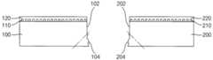
도 1은 본 발명의 일 실시예에 따른 임프린트 마스터 템플릿의 평면도이다.
도 2는 도 1의 I-I'선을 따라 절단한 단면도이다.
도 3a 내지 3g는 본 발명의 일 실시예에 따른 임프린트 마스터 템플릿의 제조 방법을 설명하기 위한 단면도들이다.
도 4a 내지 4c는 본 발명의 일 실시예에 따른 임프린트 마스터 템플릿을 이용하여 임프린트 레지스트 패턴을 형성하는 방법을 설명하기 위한 단면도들이다.
도 5a 내지 5c는 비교예에 따른 임프린트 마스터 템플릿을 이용하여 임프린트 레지스트 패턴을 형성하는 방법을 설명하기 위한 단면도들이다.
도 6a 내지 도 6c는 본 발명의 실시예들에 따른 임프린트 마스터 템플릿들의 단면도들이다.1 is a plan view of an imprint master template according to an embodiment of the present invention.
Figure 2 is a cross-sectional view taken along line II' of Figure 1.
Figures 3A to 3G are cross-sectional views for explaining a method of manufacturing an imprint master template according to an embodiment of the present invention.
4A to 4C are cross-sectional views illustrating a method of forming an imprint resist pattern using an imprint master template according to an embodiment of the present invention.
5A to 5C are cross-sectional views illustrating a method of forming an imprint resist pattern using an imprint master template according to a comparative example.
6A to 6C are cross-sectional views of imprint master templates according to embodiments of the present invention.
이하, 도면들을 참조하여 본 발명의 바람직한 실시예들을 보다 상세하게 설명하기로 한다.Hereinafter, preferred embodiments of the present invention will be described in more detail with reference to the drawings.
도 1은 본 발명의 일 실시예에 따른 임프린트 마스터 템플릿의 평면도이다. 도 2는 도 1의 I-I'선을 따라 절단한 단면도이다.1 is a plan view of an imprint master template according to an embodiment of the present invention. Figure 2 is a cross-sectional view taken along line II' of Figure 1.
도 1 및 2를 참조하면, 상기 임프린트 마스터 템플릿(10)은 매트릭스 형태로 배열되는 복수의 미세 패턴 유닛들(100, 200)을 포함할 수 있다. 본 실시예에 따르면, 상기 미세 패턴들은 4*3 매트릭스 형태로 배치될 수 있다. 일정한 크기를 갖는 미세 패턴 유닛들을 복수개 배열하여, 상기 임프린트 마스터 템플릿(10)의 대면적화가 가능 할 수 있다. 하나의 미세 패턴 유닛은 하나의 웨이퍼를 이용하여 형성할 수 있으므로, 하나의 미세 패턴 유닛의 크기는 웨이퍼의 크기보다 작으나, 상기 임프린트 마스터 템플릿(10)은 복수의 미세 패턴 유닛들을 포함하므로, 일반적인 웨이퍼의 크기 이상으로 형성될 수 있다.Referring to FIGS. 1 and 2 , the
상기 미세 패턴 유닛들은 제1 미세 패턴 유닛 및 상기 제1 미세 패턴 유닛에 인접하는 제2 미세 패턴 유닛을 포함할 수 있다. 각각의 상기 미세 패턴 유닛의 상면에는 미세 패턴들이 돌출되어 형성될 수 있다. 상기 제1 및 제2 미세 패턴 유닛들(100, 200)의 구제척인 구성은 도 3a 내지 도 3g에서 자세히 설명한다.The fine pattern units may include a first fine pattern unit and a second fine pattern unit adjacent to the first fine pattern unit. Fine patterns may be formed to protrude on the upper surface of each fine pattern unit. The overall configuration of the first and second
상기 제1 미세 패턴 유닛의 측면의 제1 면(102)은 상기 제2 미세 패턴 유닛의 측면의 제1 면(202)과 마주보게 배치될 수 있다. 상기 제1 미세 패턴 유닛의 상기 제1 면(102)과 상기 제2 미세 패턴 유닛의 측면의 제1 면(202) 사이에 배치되는 접착제(도 3f의 300 참조)에 의해, 상기 제1 면(102)과 상기 제2 면(202)이 서로 접착될 수 있다.The
도 3a 내지 3g는 본 발명의 일 실시예에 따른 임프린트 마스터 템플릿의 제조 방법을 설명하기 위한 단면도들이다.Figures 3A to 3G are cross-sectional views for explaining a method of manufacturing an imprint master template according to an embodiment of the present invention.
도 3a를 참조하면, 제1 웨이퍼 기판(100)의 상면에 미세 패턴(110)이 돌출되어 형성된 제1 미세 패턴 유닛 및 제2 웨이퍼 기판(100)의 상면에 미세 패턴(210)이 돌출되어 형성된 제2 미세 패턴 유닛을 준비한다. 상기 제1 미세 패턴 유닛과 상기 제2 미세 패턴 유닛은 실질적으로 동일할 수 있다.Referring to FIG. 3A, a first fine pattern unit is formed by protruding a
상기 제1 미세 패턴 유닛은 일반적인 실리콘(Si) 웨이퍼를 가공하여 형성할 수 있다. 상기 미세 패턴(110)은 와이어 그리드 편광 소자(wire grid polarizer)를 형성하기 위한 미세 패턴일 수 있다. 예를 들면, 상기 미세 패턴은 일정한 간격으로 형성되고 일 방향으로 연장되는 복수의 돌출부들을 포함하는 와이어 그리드 패턴일 수 있고, 상기 와이어 그리드 패턴은 약 50nm(나노미터) 내지 150nm의 피치(pitch)를 가질 수 있다. 상기 피치는 이웃하는 상기 돌출부들 사이의 거리의 합을 말한다.The first fine pattern unit can be formed by processing a general silicon (Si) wafer. The
상기 제1 미세 패턴 유닛 상에 보호층(120)을 형성할 수 있다. 상기 보호층(120)은 후속 공정에서 상기 미세 패턴(110)이 손상되는 것을 방지하기 위한 것으로, 포토레지시트 물질을 도포하고 경화시켜 형성할 수 있으나, 이에 한정되지 않는다. 상기 보호층(120)은 상기 미세 패턴(110)을 보호할 수 있고, 후에 상기 미세 패턴(110)을 손상시키지 않고 제거될 수 있는 것이라면 무방하다.A
상기 제2 미세 패턴 유닛에도 동일하게 보호층(220)이 형성될 수 있다.The
도 3b를 참조하면, 상기 제1 웨이퍼 기판(100)의 가장자리에 절단선 가이드(GD)를 형성할 수 있다. 상기 절단선 가이드(GD)는 이후 상기 제1 웨이퍼 기판(100)이 절단되는 절단선의 가이드 역할을 할 수 있다. 예를 들면, 상기 절단선 가이드(GD)는 스텔스 다이싱(stealth dicing) 등의 공정을 통해 형성될 수 있다. 상기 공정에 따르면, 상기 제1 웨이퍼 기판(100)에 레이저 조사하여, 상기 제1 웨이퍼 기판(100) 내부에 개질(改質) 영역을 형성하여 상기 개질 영역 부분이 상기 절단선 가이드가 될 수 있다.Referring to FIG. 3B, a cutting line guide GD may be formed at the edge of the
또한, 다른 실시예에 따르면, 상기 절단선 가이드는 상기 제1 웨이퍼 기판(100)의 일부에 형성된 홈(groove)으로, 상기 홈은 레이저 다이싱(laser dicing), 다이아몬드 소 다이싱(diamond saw dicing), 워터젯 다이싱(water jet dicing) 또는 에칭과 폴리머층의 형성단계를 반복하는 보쉬 프로세스(Borsch process)에 의해 형성될 수 있다.Additionally, according to another embodiment, the cutting line guide is a groove formed in a portion of the
이때, 상기 절단선 가이드(GD)는 상기 제1 웨이퍼 기판(100)의 하부쪽에만 형성되어, 상기 절단선 가이드(GD)는 상기 제1 웨이퍼 기판(100)의 단면 상에서 하부쪽에 형성되고, 상부쪽에는 형성되지 않을 수 있다.At this time, the cutting line guide (GD) is formed only on the lower side of the
도 3c를 참조하면, 상기 절단선 가이드(GD)를 따라 상기 제1 웨이퍼 기판(100)을 할렬절삭(cleaving) 등의 공정을 통해 절단할 수 있다. 이에 따라, 상기 제1 웨이퍼 기판(100)의 측면에 절단면이 형성될 수 있다. 상기 절단면은 제1 면(102) 및 원시 제2 면(104)을 포함할 수 있다. 상기 제1 면(102)은 상기 할렬절삭 공정에 의해, 상기 제1 웨이퍼 기판(100)을 이루는 실리콘(Si)의 결정면을 따라 절단되는 결정면(crystal face)일 수 있다. 상기 제1 면(102)은 상기 제1 웨이퍼 기판(100)의 상면과 수직할 수 있다.Referring to FIG. 3C, the
상기 원시 제2 면(104)은 상기 절단선 가이드(GD)가 형성되었던 부분으로, 비정질(amorphous) 상태의 실리콘이 절단된 비정질면일 수 있다. 따라서, 상기 제1 면(102)의 표면 거칠기(roughness)는 상기 원시 제2 면(104)의 표면 거칠기보다 매우 작을 수 있다.The original
상기 제2 미세 패턴 유닛도 동일하게 절단되어, 제1 면(202) 및 원시 제2 면(204)을 포함하는 절단면이 형성될 수 있다.The second fine pattern unit may also be cut in the same manner to form a cut surface including the
도 3d 및 도 3e를 참조하면, 상기 제1 미세 패턴 유닛의 상기 제1 웨이퍼 기판(100)의 상기 원시 제2 면(104)이 연마되어, 제2 면(106)을 형성할 수 있다. 상기 제2 면(106)은 상기 제1 면(102)과 소정각도 경사지도록 형성될 수 있다. 표면 거칠기가 큰 상기 원시 제2 면(104)의 표면은 모두 연마되어 상기 제1 면(102)과 소정각도 경사진 상기 제2 면(106)으로 형성되므로, 상기 제1 미세 패턴 유닛의 상기 제1 면(102)과 상기 제2 미세 패턴 유닛의 상기 제1 면(202)이 서로 마주보게 배치되면, 상기 제1 미세 패턴 유닛과 상기 제2 미세 패턴 유닛 사이의 이격거리가 최소화 될 수 있으며, 이에 따라 상기 제1 미세 패턴 유닛과 상기 제2 미세 패턴 유닛 사이의 간격에 의해 형성되는 이음매(seam)이 최소화될 수 있다.Referring to FIGS. 3D and 3E , the raw
상기 제2 미세 패턴 유닛의 상기 원시 제2 면(204)도 동일하게 연마되어 제2 면(206)이 형성될 수 있다.The original
도 3f를 참조하면, 상기 제1 미세 패턴 유닛의 상기 제1 면(102)과 상기 제2 미세 패턴 유닛의 상기 제1 면(202)이 서로 마주보도록하여 상기 제1 미세 패턴 유닛과 상기 제2 미세 패턴 유닛을 접합할 수 있다.Referring to FIG. 3F, the
상기 제1 및 제2 미세 패턴 유닛들의 상기 미세 패턴들(110, 210)이 지면을 향하도록, 즉 상기 제1 및 제2 미세 패턴 유닛들의 상면이 지면을 향하도록 위치시킨 후, 상기 제1 미세 패턴 유닛의 상기 제1 면(102)과 상기 제2 미세 패턴 유닛의 상기 제1 면(202) 사이에 접착제(300)를 제공하여, 상기 제1 미세 패턴 유닛과 상기 제2 미세 패턴 유닛을 접합할 수 있다.After positioning the
이때, 상기 미세 패턴들(110, 210) 상에는 상기 보호층(120, 220)이 형성되어 있으므로, 상기 미세 패턴들(110, 210)이 손상되는 것을 방지할 수 있다. 또한, 상기 미세 패턴들(110, 210)이 지면을 향하도록 위치하게 되므로, 상기 미세 패턴들(110, 210)이 동일한 평면 상에 위치한 채로, 상기 제1 미세 패턴 유닛과 상기 제2 미세 패턴 유닛이 접합될 수 있다.At this time, since the
상기 접착제(300)는 알루미늄을 포함하는 솔더(solder)일 수 있으나, 이에 한정되지 않는다. 상기 접착제(300)는 상기 제1 미세 패턴 유닛과 상기 제2 미세 패턴 유닛을 서로 접착시킬 수 있는 물질이면 무방하며, 에폭시 수지, 이미드 수지, 아미드 수지, 실리콘 수지, 아크릴레이트 수지 등의 접착제가 사용될 수도 있다.The adhesive 300 may be a solder containing aluminum, but is not limited thereto. The adhesive 300 may be any material that can bond the first micro-pattern unit and the second micro-pattern unit to each other, and may be an adhesive such as epoxy resin, imide resin, amide resin, silicone resin, or acrylate resin. It may also be used.
상기 접착제(300)는 이상적으로는 상기 제1 및 제2 웨이퍼 기판(100, 200)의 상면과 동일한 높이까지 제공되어, 상기 미세 패턴(110, 210)에 영향을 주지 않는 것이 바람직할 수 있다. 그러나, 제조 공정상 상기 접착제(300)가 제공되는 정도를 정밀하게 제어하기 어려우며, 상기 접착제(300)는 상기 제1 및 제2 웨이퍼 기판(100, 200)의 상면 이상으로 제공되어 상기 상면 상에 볼록부(도 4a 참조)를 형성할 수 있다. 이에 대한 자세한 설명은 도 4a 내지 도 4c에서 후술한다.Ideally, the adhesive 300 may be provided to the same height as the upper surfaces of the first and
도 3g를 참조하면, 상기 제1 미세 패턴 유닛과 상기 제2 미세 패턴 유닛을 지지하는 지지부(400)를 형성할 수 있다.Referring to FIG. 3G, a
상기 제1 및 제2 미세 패턴 유닛들의 하면 상에 상기 지지부(400)가 부착되어 상기 제1 및 제2 미세 패턴 유닛들을 고정시킬 수 있다. 상기 지지부(400)와 상기 제1 및 제2 미세 패턴 유닛들 사이에는 접착층(410)이 더 형성될 수 있다.The
상기 지지부(400)는 상기 제1 미세 패턴 유닛의 측면과 상기 제2 미세 패턴 유닛의 측면을 감싸는 측벽(410)을 포함할 수 있다. 상기 지지부(400)는 외력에 의해 변형되지 않는 강체(rigid body)일 수 있다. 예를 들면, 상기 지지부(400)는 금속 또는 세라믹으로 형성되어 상기 제1 및 제2 미세 패턴 유닛들의 변형 및 움직임을 방지할 수 있다.The
상기 지지부(400)는 다양한 형상 및 구성을 가질 수 있으며, 이에 대한 자세한 설명은 도 6a 내지 도 6c에서 후술한다.The
도 4a 내지 4c는 본 발명의 일 실시예에 따른 임프린트 마스터 템플릿을 이용하여 임프린트 레지스트 패턴을 형성하는 방법을 설명하기 위한 단면도들이다.4A to 4C are cross-sectional views illustrating a method of forming an imprint resist pattern using an imprint master template according to an embodiment of the present invention.
도 4a를 참조하면, 상기 임프린트 마스터 템플릿(10)을 이용하여 임프린트 스탬프를 형성할 수 있다.Referring to FIG. 4A, an imprint stamp can be formed using the
상기 임프린트 마스터 템플릿(10)의 미세 패턴을 임프린트 레진층(20)에 전사하여, 임프린트 레진층(20) 상에 임프린트 패턴(22)을 형성할 수 있다. 이에 따라 상기 임프린트 패턴(22)이 형성된 상기 임프린트 스탬프를 형성할 수 있다.The fine pattern of the
예를 들면, 기판 상에 임프린트 수지 용액을 도포한 후, 상기 임프린트 마스터 템플릿(10)을 이용하여 상기 임프린트 수지 용액을 가압한 후, 상기 임프린트 수지 용액을 경화 시킨 후, 경화된 수지층을 상기 임프린트 마스터 템플릿(10)으로부터 분리 시켜, 상기 임프린트 스탬프를 형성할 수 있다.For example, after applying the imprint resin solution on a substrate, pressing the imprint resin solution using the
이때, 상기 임프린트 마스터 템플릿(10)의 제1 미세 패턴 유닛과 제2 미세 패턴 유닛 사이에 위치하는 접착제(300)는 상기 임프린트 마스터 템플릿(10)의 상면 상에 돌출되는 볼록부(524)를 가질 수 있다. 이에 따라, 상기 임프린트 스탬프는 상기 제1 미세 패턴 유닛과 상기 제2 미세 패턴 유닛의 경계에 해당하는 이음매(seam) 부분에 오목부(24)가 형성될 수 있다.At this time, the adhesive 300 located between the first fine pattern unit and the second fine pattern unit of the
도 4b를 참조하면, 상기 임프린트 스탬프를 이용하여 임프린트 레지스트 패턴(520)을 형성할 수 있다.Referring to FIG. 4B, an imprint resist
예를 들면, 기판(500) 상에 제1 층(510)이 형성될 수 있다. 상기 제1 층(510)은 와이어 그리드 편광 소자(wire grid polarizer; WGP)를 형성하기 위한 금속층일 수 있다. 예를 들면, 상기 제1 층(510)은 알루미늄을 포함할 수 있다.For example, the
상기 제1 층(510) 상에 임프린트 수지 용액을 도포한 후, 상기 임프린트 스탬프를 이용하여 상기 임프린트 수지 용액을 가압한 후, 상기 임프린트 수지 용액을 경화 시킨 후, 상기 임프린트 스탬프를 분리 시켜, 상기 임프린트 레지스트 패턴(520)을 형성할 수 있다. 필요에 따라, 상기 임프린트 레지스트 패턴(520)의 잔막(residual layer)을 제거하는 공정이 더 진행될 수 있다.After applying the imprint resin solution on the
이때, 상기 임프린트 스탬프의 상기 오목부(24)에 대응하여, 상기 임프린트 레지스트 패턴(520)의 오류 패턴(524)이 형성될 수 있다. 상기 오류 패턴(524)은 상기 임프린트 마스터 템플릿(10)의 상기 이음매에 대응하여 형성되며, 상기 접착층(300)의 상기 볼록부에 의해 볼록한 형태의 패턴인 상기 오류 패턴(524)이 형성될 수 있다.At this time, an
도 4c를 참조하면, 상기 임프린트 레지스트 패턴(520)을 이용하여 상기 제1 층(510)을 패터닝 하여 제1 층 패턴(512)을 형성할 수 있다. 상기 제1 층 패턴(512)은 와이어 그리드 편광 소자일 수 있다.Referring to FIG. 4C, the
이때, 상기 오류 패턴(524)에 의해 상기 이음매에 대응하는 부분에 이음매 패턴(514)이 형성될 수 있다. 상기 이음매 패턴(514)은 상기 제1 층(510)이 패터닝되지 않은 부분으로, 소위, 블랙 심(black seam)일 수 있다.At this time, a
상기 접착제(300)가 상기 볼록부를 형성하는 경우, 도 4c에서와 같이 상기 이음매에 대응하여 블랙 심(black seam)이 형성된다. 반대로 상기 접착제(300)가 충분히 제공되지 않아 오목부를 형성하는 경우(도 5a 내지 도 5c 참조), 화이트 심(white seam)을 형성하며, 블랙 심의 경우에 비해, 오류 패턴의 크기가 커지며, 상기 와이어 그리드 편광 소자의 광학적 성능이 저하될 수 있다.When the adhesive 300 forms the convex portion, a black seam is formed corresponding to the seam as shown in FIG. 4C. Conversely, when the adhesive 300 is not sufficiently provided to form a concave portion (see FIGS. 5A to 5C), a white seam is formed, the size of the error pattern becomes larger compared to the case of a black seam, and the wire The optical performance of the grid polarizing element may deteriorate.
도 5a 내지 5c는 비교예에 따른 임프린트 마스터 템플릿을 이용하여 임프린트 레지스트 패턴을 형성하는 방법을 설명하기 위한 단면도들이다.5A to 5C are cross-sectional views illustrating a method of forming an imprint resist pattern using an imprint master template according to a comparative example.
도 5a 를 참조하면, 비교예에 따른 임프린트 마스터 템플릿(10')을 이용하여 임프린트 스탬프를 형성할 수 있다.Referring to FIG. 5A, an imprint stamp can be formed using the imprint master template 10' according to the comparative example.
상기 임프린트 마스터 템플릿(10')의 미세 패턴을 임프린트 레진층(20')에 전사하여, 임프린트 레진층(20') 상에 임프린트 패턴(22')을 형성할 수 있다. 이에 따라 상기 임프린트 패턴(22')이 형성된 상기 임프린트 스탬프를 형성할 수 있다.The fine pattern of the imprint master template 10' may be transferred to the imprint resin layer 20' to form an imprint pattern 22' on the imprint resin layer 20'. Accordingly, the imprint stamp on which the imprint pattern 22' is formed can be formed.
이때, 상기 비교예에 따른 상기 임프린트 마스터 템플(10')의 접착제(300')는 상기 임프린트 마스터 템플릿(10')의 상면까지 제공되지 못하여, 상기 상면 상에 오목부를 형성할 수 있다.At this time, the adhesive 300' of the imprint master template 10' according to the comparative example may not be provided to the upper surface of the imprint master template 10', thereby forming a concave portion on the upper surface.
이에 따라, 상기 비교예에 따른 임프린트 마스터 템플릿(10')을 이용하여 형성된 임프린트 스탬프는 상기 제1 미세 패턴 유닛과 상기 제2 미세 패턴 유닛의 경계에 해당하는 이음매(seam) 부분에 볼록부(24')가 형성될 수 있다.Accordingly, the imprint stamp formed using the imprint master template 10' according to the comparative example has a
도 5b를 참조하면, 상기 임프린트 스탬프를 이용하여 임프린트 레지스트 패턴(620)을 형성할 수 있다.Referring to FIG. 5B, an imprint resist
이때, 상기 임프린트 스탬프의 상기 볼록부(24')에 대응하여, 상기 임프린트 레지스트 패턴(620)의 오류 패턴이 형성될 수 있다. 상기 오류 패턴(624)은 상기 임프린트 마스터 템플릿(10')의 상기 이음매에 대응하여 형성되며, 상기 임프린트 스탬프의 상기 볼록부(24')에 의해, 상기 임프린트 스탬프와 수지층이 서로 밀착되지 못하고, 상기 임프린트 패턴(22')이 상기 수지 층에 전사되지 못하여 상기 오류 패턴이 형성될 수 있다.At this time, an error pattern of the imprint resist
도 5c를 참조하면, 상기 임프린트 레지스트 패턴(620)을 이용하여 제1 층(610)을 패터닝 하여 제1 층 패턴(612)을 형성할 수 있다. 상기 제1 층 패턴(612)은 와이어 그리드 편광 소자일 수 있다.Referring to FIG. 5C, the
이때, 상기 오류 패턴에 의해 상기 이음매에 대응하는 부분에 이음매 패턴(614)이 형성될 수 있다. 상기 이음매 패턴(614)은 상기 제1 층(610)이 패터닝되지 않은 부분으로, 소위, 화이트 심(white seam)일 수 있다.At this time, a
상기 비교예의 경우, 본 발명의 실시예의 경우에 비해, 오류 패턴의 크기가 커지며, 상기 와이어 그리드 편광 소자의 광학적 성능이 저하될 수 있다.In the case of the comparative example, the size of the error pattern may increase and the optical performance of the wire grid polarizing element may deteriorate compared to the embodiment of the present invention.
따라서, 임프린트 마스터 템플릿의 접착제는 상면 상에 돌출부를 형성하도록 충분히 제공되는 것이 유리함을 알 수 있다.Accordingly, it can be seen that it is advantageous for the adhesive of the imprint master template to be sufficiently provided to form protrusions on the upper surface.
도 6a 내지 도 6c는 본 발명의 실시예들에 따른 임프린트 마스터 템플릿들의 단면도들이다.6A to 6C are cross-sectional views of imprint master templates according to embodiments of the present invention.
도 6a를 참조하면, 임프린트 마스터 템플릿은 제1 및 제2 미세 패턴 유닛들 및 상기 제1 및 제2 미세 패턴 유닛을 지지하는 지지부를 포함할 수 있다. 상기 지지부는 접착층(710) 및 기판(700)을 포함할 수 있다.Referring to FIG. 6A, the imprint master template may include first and second fine pattern units and a support portion supporting the first and second fine pattern units. The support part may include an
상기 제1 미세 패턴 유닛의 제1 웨이퍼 기판(100)과 상기 제2 미세 패턴 유닛의 제2 웨이퍼 기판(200)은 접착제(300)에 의해 접착될 수 있다. 상기 제1 웨이퍼 기판(100)및 상기 제2 웨이퍼 기판(200)은 상기 기판(700)에 의해 지지될 수 있다. 상기 기판(700)과 상기 제1 및 제2 웨이퍼 기판들(100, 200) 사이에는 상기 접착층(710)이 형성되어, 상기 제1 및 제2 웨이퍼 기판들(100, 200)을 상기 기판(700)에 고정시킬 수 있다.The
상기 기판(700)은 상기 제1 및 제2 웨이퍼 기판들(100, 200)을 지지하고 고정할 수 있도록 충분한 강성을 가질 수 있다. 예를 들면, 상기 기판(700)은 유리 기판, 석영 기판, 수지 기판 등으로 구성될 수 있다.The
도 6b를 참조하면, 임프린트 마스터 템플릿은 제1 및 제2 미세 패턴 유닛들 및 상기 제1 및 제2 미세 패턴 유닛을 지지하는 지지부를 포함할 수 있다. 상기 지지부는 접착층(820) 제1 층(800) 및 제2 층(810)을 포함할 수 있다.Referring to FIG. 6B, the imprint master template may include first and second fine pattern units and a support portion supporting the first and second fine pattern units. The support portion may include an
상기 제1 미세 패턴 유닛의 제1 웨이퍼 기판(100)과 상기 제2 미세 패턴 유닛의 제2 웨이퍼 기판(200)은 접착제(300)에 의해 접착될 수 있다. 상기 제1 웨이퍼 기판(100)및 상기 제2 웨이퍼 기판(200)은 상기 제1 및 제2 층들(800, 810)에 의해 지지될 수 있다. 상기 제2 층(810)과 상기 제1 및 제2 웨이퍼 기판들(100, 200) 사이에는 상기 접착층(810)이 형성될 수 있다.The
상기 제1 층(800)과 상기 제2 층(810)은 서로 밀착되어, 별도의 접착제 없이도 서로의 마찰력에 의해 강하게 접착될 수 있다. 한편, 상기 제1 층(800)과 상기 제2 층(810)은 서로 접착제에 의해 접착될 수도 있다.The
상기 제1 및 제2 층(800, 810) 각각은 기판 또는 필름 등으로 형성될 수 있으나 이에 한정되지 않고, 상기 제1 및 제2 웨이퍼 기판들(100, 200)을 지지할 수 있는 것이면 무방하다.Each of the first and
본 실시예에 따른 상기 임프린트 마스터 템플릿은 상기 제1 및 제2 층들(810, 820)이 적층된 것으로 설명되었으나, 이에 한정되지 않으며, 복수의 층들이 적층되어, 서로의 마찰에 의해 굽힘 변형에 강한 구조면 무방하다.The imprint master template according to the present embodiment has been described as a stack of the first and
도 6c를 참조하면, 임프린트 마스터 템플릿은 제1 및 제2 미세 패턴 유닛들 및 상기 제1 및 제2 미세 패턴 유닛을 지지하는 지지부를 포함할 수 있다.Referring to FIG. 6C, the imprint master template may include first and second fine pattern units and a support portion supporting the first and second fine pattern units.
상기 제1 미세 패턴 유닛의 제1 웨이퍼 기판(100)과 상기 제2 미세 패턴 유닛의 제2 웨이퍼 기판(200)은 접착제(300)에 의해 접착될 수 있다. 상기 제1 웨이퍼 기판(100)및 상기 제2 웨이퍼 기판(200)은 상기 지지부에 의해 지지될 수 있다.The
상기 지지부는 접착층(920), 몸체(900) 및 측벽(902)을 포함할 수 있다. 상기 몸체(900)는 상기 제1 및 제2 미세 패턴 유닛을 지지할 수 있다. 상기 측벽(902)은 상기 몸체(900)로부터 돌출되어, 상기 제1 및 제2 미세 패턴 유닛들의 측면을 감쌀 수 있다. 상기 지지부는 외력에 의해 변형되지 않는 강체(rigid body)일 수 있다. 예를 들면, 상기 지지부는 세라믹 또는 금속으로 형성되어, 상기 제1 및 제2 웨이퍼 기판들(100, 200)을 견고하게 지지할 수 있다.The support portion may include an
본 발명의 실시예들에 따르면, 임프린트 마스터 템플릿은 상면에 미세 패턴이 형성된 제1 미세 패턴 유닛, 상기 제1 미세 패턴 유닛에 인접하고, 상면에 미세 패턴이 형성된 제2 미세 패턴 유닛, 및 상기 제1 미세 패턴 유닛 및 상기 제2 미세 패턴 유닛을 지지하는 지지부를 포함한다. 상기 제1 미세 패턴 유닛의 측면은 상기 제2 미세 패턴 유닛의 측면과 마주보고, 상기 제1 미세 패턴 유닛의 상기 측면은 상기 상면과 수직한 제1 면 및 상기 제1 면과 소정각도 경사진 제2 면을 포함하고, 상기 제2 미세 패턴 유닛의 상기 측면은 상기 상면과 수직한 제1 면 및 상기 제1 면과 소정각도 경사진 제2 면을 포함하므로, 상기 제1 미세 패턴 유닛과 상기 제2 미세 패턴 유닛의 접합면에 의해 형성되는 이음매 선(seam line)이 최소화 될 수 있다.According to embodiments of the present invention, the imprint master template includes a first fine pattern unit having a fine pattern formed on its upper surface, a second fine pattern unit adjacent to the first fine pattern unit and having a fine pattern formed on its upper surface, and the first fine pattern unit. It includes a support portion supporting one fine pattern unit and the second fine pattern unit. A side surface of the first fine pattern unit faces a side surface of the second fine pattern unit, and the side surface of the first fine pattern unit has a first surface perpendicular to the upper surface and a second surface inclined at a predetermined angle with the first surface. It includes two surfaces, and the side of the second fine pattern unit includes a first surface perpendicular to the upper surface and a second surface inclined at a predetermined angle with the first surface, so that the first fine pattern unit and the second surface 2 The seam line formed by the joint surface of the fine pattern unit can be minimized.
또한, 상기 지지부는 상기 제1 및 제2 미세 패턴 유닛들의 변형 및 움직임을 방지하여 상기 임프린트 마스터 템플릿의 품질을 유지할 수 있다.Additionally, the support portion may maintain the quality of the imprint master template by preventing deformation and movement of the first and second fine pattern units.
또한, 상기 접착제는 상기 임프린트 마스터 템플릿의 상기 상면 상에 볼록부를 형성할 수 있다. 이에 따라, 이음매가 최소화되어, 임프린트 패턴의 품질을 향상시킬 수 있다.Additionally, the adhesive may form a convex portion on the upper surface of the imprint master template. Accordingly, seams can be minimized and the quality of the imprint pattern can be improved.
이상 실시예를 참조하여 설명하였지만, 해당 기술 분야의 숙련된 당업자는 하기의 특허 청구의 범위에 기재된 본 발명의 사상 및 영역으로부터 벗어나지 않는 범위 내에서 본 발명을 다양하게 수정 및 변경시킬 수 있음을 이해할 수 있을 것이다Although the description has been made with reference to the above examples, those skilled in the art will understand that various modifications and changes can be made to the present invention without departing from the spirit and scope of the present invention as set forth in the claims below. will be able to
100, 200: 제1 및 제2 웨이퍼 기판102, 202: 제1 면
104, 204: 원시 제2 면106, 206: 제2 면
110, 210: 미세 패턴120, 220: 보호층
300: 접착제400: 몸체
402: 측벽410: 접착층100, 200: first and
104, 204: raw second side 106, 206: second side
110, 210:
300: Adhesive 400: Body
402: side wall 410: adhesive layer
Claims (20)
Translated fromKorean상기 제1 미세 패턴 유닛에 인접하고, 상면에 미세 패턴이 형성된 제2 미세 패턴 유닛; 및
상기 제1 미세 패턴 유닛 및 상기 제2 미세 패턴 유닛을 지지하는 지지부를 포함하고,
상기 제1 미세 패턴 유닛의 측면은 상기 제2 미세 패턴 유닛의 측면과 마주보고,
상기 제1 미세 패턴 유닛의 상기 측면은 상기 상면과 수직한 제1 면 및 상기 제1 면과 소정각도 경사진 제2 면을 포함하고,
상기 제2 미세 패턴 유닛의 상기 측면은 상기 상면과 수직한 제1 면 및 상기 제1 면과 소정각도 경사진 제2 면을 포함하고,
상기 제1 미세 패턴 유닛의 제1 면과 상기 제2 미세 패턴 유닛의 제1 면 사이에 배치되어 상기 제1 미세 패턴 유닛과 상기 제2 미세 패턴 유닛을 서로 접착시키는 접착제를 더 포함하며,
상기 접착제는 상기 제1 및 제2 미세 패턴 유닛들의 상기 상면들 보다 높게 형성되어, 상기 상면 상에 볼록부를 형성하는 것을 특징으로 하는 임프린트 마스터 템플릿.A first fine pattern unit having a fine pattern formed on the upper surface;
a second fine pattern unit adjacent to the first fine pattern unit and having a fine pattern formed on its upper surface; and
It includes a support part supporting the first fine pattern unit and the second fine pattern unit,
A side surface of the first fine pattern unit faces a side surface of the second fine pattern unit,
The side surface of the first fine pattern unit includes a first surface perpendicular to the upper surface and a second surface inclined at a predetermined angle with the first surface,
The side surface of the second fine pattern unit includes a first surface perpendicular to the upper surface and a second surface inclined at a predetermined angle with the first surface,
It further includes an adhesive disposed between the first surface of the first fine pattern unit and the first surface of the second fine pattern unit to adhere the first fine pattern unit and the second fine pattern unit to each other,
The adhesive is formed higher than the upper surfaces of the first and second micro pattern units to form a convex portion on the upper surfaces.
상기 제1 및 제2 미세 패턴 유닛들은 실리콘(Si) 웨이퍼 기판으로부터 형성되며, 상기 제1 면은 결정면(crystal face)인 것을 특징으로 하는 임프린트 마스터 템플릿.According to claim 1,
The first and second micro-pattern units are formed from a silicon (Si) wafer substrate, and the first surface is a crystal face.
상기 제2 면은 연마공정을 통해 형성된 것을 특징으로 하는 임프린트 마스터 템플릿.According to clause 2,
An imprint master template, wherein the second surface is formed through a polishing process.
상기 접착제는 알루미늄을 포함하는 솔더(solder)인 것을 특징으로 하는 임프린트 마스터 템플릿.According to paragraph 1,
An imprint master template, wherein the adhesive is a solder containing aluminum.
상기 제1 및 제2 미세 패턴 유닛들의 상기 미세 패턴들은 와이어 그리드 편광 소자를 형성하기 위한 와이어 그리드 패턴으로,
상기 와이어 그리드 패턴의 피치(pitch)는 50nm(나노미터) 내지 150nm인 것을 특징으로 하는 임프린트 마스터 템플릿.According to paragraph 1,
The fine patterns of the first and second fine pattern units are wire grid patterns for forming a wire grid polarizing element,
An imprint master template, characterized in that the pitch of the wire grid pattern is 50 nm (nanometers) to 150 nm.
상기 지지부와 상기 제1 및 제2 미세 패턴 유닛들 사이에 배치되는 접착층을 더 포함하고,
상기 지지부는 상기 제1 및/또는 상기 제2 미세 패턴 유닛들의 측면을 감싸는 측벽을 포함하고, 외력에 의해 변형되지 않는 강체(rigid body)인 것을 특징으로 하는 임프린트 마스터 템플릿.According to claim 1,
Further comprising an adhesive layer disposed between the support portion and the first and second micro pattern units,
The imprint master template is characterized in that the support part includes a side wall surrounding the sides of the first and/or second micro pattern units and is a rigid body that is not deformed by external force.
상기 지지부는 복수의 층들이 적층되어 형성된 것을 특징으로 하는 임프린트 마스터 템플릿.According to claim 1,
An imprint master template, wherein the support portion is formed by stacking a plurality of layers.
상기 제1 미세 패턴 유닛에 인접하고, 상면에 미세 패턴이 형성된 제2 미세 패턴 유닛; 및
상기 제1 미세 패턴 유닛 및 상기 제2 미세 패턴 유닛을 지지하는 지지부를 포함하고,
상기 제1 미세 패턴 유닛의 측면은 상기 제2 미세 패턴 유닛의 측면과 마주보고,
상기 제1 미세 패턴 유닛의 상기 측면은 상기 상면과 수직한 제1 면 및 상기 제1 면과 소정각도 경사진 제2 면을 포함하고,
상기 제2 미세 패턴 유닛의 상기 측면은 상기 상면과 수직한 제1 면 및 상기 제1 면과 소정각도 경사진 제2 면을 포함하고,
상기 지지부는 복수의 층들이 적층되어 형성되며,
상기 지지부의 상기 복수의 층들은 별도의 접착제 없이 서로의 마찰력에 의해 접착되는 것을 특징으로 하는 임프린트 마스터 템플릿.A first fine pattern unit having a fine pattern formed on the upper surface;
a second fine pattern unit adjacent to the first fine pattern unit and having a fine pattern formed on its upper surface; and
It includes a support part supporting the first fine pattern unit and the second fine pattern unit,
A side surface of the first fine pattern unit faces a side surface of the second fine pattern unit,
The side surface of the first fine pattern unit includes a first surface perpendicular to the upper surface and a second surface inclined at a predetermined angle with the first surface,
The side surface of the second fine pattern unit includes a first surface perpendicular to the upper surface and a second surface inclined at a predetermined angle with the first surface,
The support portion is formed by stacking a plurality of layers,
An imprint master template, wherein the plurality of layers of the support part are bonded to each other by friction without a separate adhesive.
상기 절단선 가이드를 따라 상기 웨이퍼 기판을 할렬절삭(cleaving)하여, 상기 웨이퍼 기판의 측면에, 상기 절단선 가이드가 형성되었던 부분인 원시 제2 면과 상기 할렬절삭에 의해 절단된 면인 제1 면을 포함하는 절단면을 형성하는 절단 단계;
상기 원시 제2 면을 연마하여 상기 제1 면과 소정각도 경사진 제2 면을 형성하는 연마 단계;
상기 제1 미세 패턴 유닛의 제1 면과 제2 미세 패턴 유닛의 제1 면이 서로 마주보도록하여 상기 제1 미세 패턴 유닛과 상기 제2 미세 패턴 유닛을 접합하는 접합 단계; 및
상기 제1 미세 패턴 유닛과 상기 제2 미세 패턴 유닛을 지지하는 지지부를 형성하는 단계를 포함하고,
상기 미세 패턴 상에 보호층을 형성하는 단계를 더 포함하는 것을 특징으로 하는 임프린트 마스터 템플릿의 제조 방법.A cutting preparation step of forming a cutting line guide at the edge of a first micro-pattern unit including a wafer substrate and a micro-pattern formed on the upper surface of the wafer substrate;
By cleaving the wafer substrate along the cutting line guide, a raw second surface, which is the part where the cutting line guide was formed, and a first surface, which is the surface cut by the cleaving line, are formed on the side of the wafer substrate. A cutting step of forming a cut surface comprising;
A polishing step of polishing the raw second surface to form a second surface inclined at a predetermined angle with the first surface;
A bonding step of bonding the first fine pattern unit and the second fine pattern unit such that the first surface of the first fine pattern unit and the first surface of the second fine pattern unit face each other; and
Comprising the step of forming a support portion supporting the first fine pattern unit and the second fine pattern unit,
A method of manufacturing an imprint master template, further comprising forming a protective layer on the fine pattern.
상기 절단 준비 단계에서는, 상기 웨이퍼 기판에 레이저 조사하여, 상기 웨이퍼 기판 내부에 개질(改質) 영역을 형성하는 것을 특징으로 하는 임프린트 마스터 템플릿의 제조 방법.According to claim 11,
In the cutting preparation step, the wafer substrate is irradiated with a laser to form a modified area inside the wafer substrate.
상기 제1 면은 상기 제1 미세 패턴 유닛의 상면에 대해 수직하고, 결정면(crystal face)인 것을 한 것을 특징으로 하는 임프린트 마스터 템플릿의 제조 방법.According to claim 13,
The first surface is perpendicular to the upper surface of the first fine pattern unit and is a crystal face.
상기 접합 단계에서는, 상기 제1 및 제2 미세 패턴 유닛들의 상면이 지면 방향을 향하도록 위치시킨 후, 상기 제1 미세 패턴 유닛의 제1 및 제2 면들과 상기 제2 미세 패턴 유닛의 제1 및 제2 면들 사이에 접착제를 제공하는 것을 특징으로 하는 임프린트 마스터 템플릿의 제조 방법.According to claim 11,
In the bonding step, the first and second fine pattern units are positioned with the upper surfaces facing the ground, and then the first and second surfaces of the first fine pattern unit and the first and second surfaces of the second fine pattern unit are bonded to each other. A method of manufacturing an imprint master template comprising providing an adhesive between the second sides.
상기 접착제는 알루미늄을 포함하는 솔더(solder)인 것을 특징으로 하는 임프린트 마스터 템플릿의 제조 방법.According to claim 15,
A method of manufacturing an imprint master template, wherein the adhesive is a solder containing aluminum.
상기 절단선 가이드를 따라 상기 웨이퍼 기판을 할렬절삭(cleaving)하여, 상기 웨이퍼 기판의 측면에, 상기 절단선 가이드가 형성되었던 부분인 원시 제2 면과 상기 할렬절삭에 의해 절단된 면인 제1 면을 포함하는 절단면을 형성하는 절단 단계;
상기 원시 제2 면을 연마하여 상기 제1 면과 소정각도 경사진 제2 면을 형성하는 연마 단계;
상기 제1 미세 패턴 유닛의 제1 면과 제2 미세 패턴 유닛의 제1 면이 서로 마주보도록하여 상기 제1 미세 패턴 유닛과 상기 제2 미세 패턴 유닛을 접합하는 접합 단계; 및
상기 제1 미세 패턴 유닛과 상기 제2 미세 패턴 유닛을 지지하는 지지부를 형성하는 단계를 포함하고,
상기 접합 단계에서는, 상기 제1 및 제2 미세 패턴 유닛들의 상면이 지면 방향을 향하도록 위치시킨 후, 상기 제1 미세 패턴 유닛의 제1 및 제2 면들과 상기 제2 미세 패턴 유닛의 제1 및 제2 면들 사이에 접착제를 제공하며,
상기 접착제는 상기 제1 미세 패턴 유닛의 제1 면과 상기 제2 미세 패턴 유닛의 제1 면 사이를 통해, 상기 웨이퍼 기판의 상면까지 제공되어,
상기 접착제의 일부가 상기 웨이퍼 기판의 상들 상에 볼록부를 형성하는 것을 특징으로 하는 마스터 템플릿의 제조 방법.A cutting preparation step of forming a cutting line guide at the edge of a first micro-pattern unit including a wafer substrate and a micro-pattern formed on the upper surface of the wafer substrate;
By cleaving the wafer substrate along the cutting line guide, a raw second surface, which is the part where the cutting line guide was formed, and a first surface, which is the surface cut by the cleaving line, are formed on the side of the wafer substrate. A cutting step of forming a cut surface comprising;
a polishing step of polishing the raw second surface to form a second surface inclined at a predetermined angle with the first surface;
A bonding step of bonding the first fine pattern unit and the second fine pattern unit such that the first surface of the first fine pattern unit and the first surface of the second fine pattern unit face each other; and
Comprising the step of forming a support part supporting the first fine pattern unit and the second fine pattern unit,
In the bonding step, the first and second fine pattern units are positioned with the upper surfaces facing the ground, and then the first and second surfaces of the first fine pattern unit and the first and second surfaces of the second fine pattern unit are bonded to each other. providing adhesive between the second sides,
The adhesive is provided between the first surface of the first fine pattern unit and the first surface of the second fine pattern unit to the upper surface of the wafer substrate,
A method of manufacturing a master template, wherein a portion of the adhesive forms a convex portion on the phases of the wafer substrate.
상기 절단선 가이드를 따라 상기 웨이퍼 기판을 할렬절삭(cleaving)하여, 상기 웨이퍼 기판의 측면에, 상기 절단선 가이드가 형성되었던 부분인 원시 제2 면과 상기 할렬절삭에 의해 절단된 면인 제1 면을 포함하는 절단면을 형성하는 절단 단계;
상기 원시 제2 면을 연마하여 상기 제1 면과 소정각도 경사진 제2 면을 형성하는 연마 단계;
상기 제1 미세 패턴 유닛의 제1 면과 제2 미세 패턴 유닛의 제1 면이 서로 마주보도록하여 상기 제1 미세 패턴 유닛과 상기 제2 미세 패턴 유닛을 접합하는 접합 단계; 및
상기 제1 미세 패턴 유닛과 상기 제2 미세 패턴 유닛을 지지하는 지지부를 형성하는 단계를 포함하고,
상기 지지부는 복수의 층들이 적층되어 형성된 것을 특징으로 하는 임프린트 마스터 템플릿의 제조 방법.A cutting preparation step of forming a cutting line guide at the edge of a first micro-pattern unit including a wafer substrate and a micro-pattern formed on the upper surface of the wafer substrate;
By cleaving the wafer substrate along the cutting line guide, a raw second surface, which is the part where the cutting line guide was formed, and a first surface, which is the surface cut by the cleaving line, are formed on the side of the wafer substrate. A cutting step of forming a cut surface comprising;
A polishing step of polishing the raw second surface to form a second surface inclined at a predetermined angle with the first surface;
A bonding step of bonding the first fine pattern unit and the second fine pattern unit such that the first surface of the first fine pattern unit and the first surface of the second fine pattern unit face each other; and
Comprising the step of forming a support portion supporting the first fine pattern unit and the second fine pattern unit,
A method of manufacturing an imprint master template, wherein the support portion is formed by stacking a plurality of layers.
상기 지지부와 상기 제1 및 제2 미세 패턴 유닛들 사이에 접착층을 형성하는 단계를 더 포함하고,
상기 지지부는 상기 제1 및/또는 상기 제2 미세 패턴 유닛들의 측면을 감싸는 측벽을 포함하고, 외력에 의해 변형되지 않는 강체(rigid body)인 것을 특징으로 하는 임프린트 마스터 템플릿의 제조 방법.According to claim 11,
Further comprising forming an adhesive layer between the support portion and the first and second micro-pattern units,
The method of manufacturing an imprint master template, wherein the support part includes a side wall surrounding the sides of the first and/or second micro pattern units, and is a rigid body that is not deformed by external force.
상기 절단 준비 단계에서는, 상기 절단선 가이드는 상기 웨이퍼 기판의 일부에 형성된 홈(groove)으로, 상기 홈은 다이아몬드 소 다이싱(diamond saw dicing), 워터젯 다이싱(water jet dicing) 또는 보쉬 프로세스(Borsch process)에 의해 형성되는 것을 특징으로 하는 임프린트 마스터 템플릿의 제조 방법.
According to claim 11,
In the cutting preparation step, the cutting line guide is a groove formed in a portion of the wafer substrate, and the groove is formed by diamond saw dicing, water jet dicing, or Borsch process. A method of manufacturing an imprint master template, characterized in that it is formed by a process.
Priority Applications (3)
| Application Number | Priority Date | Filing Date | Title |
|---|---|---|---|
| KR1020160101479AKR102648921B1 (en) | 2016-08-09 | 2016-08-09 | Imprint master template and method of manufacturing the same |
| US15/469,946US10751953B2 (en) | 2016-08-09 | 2017-03-27 | Imprint master template and method of manufacturing the same |
| US16/983,326US11376800B2 (en) | 2016-08-09 | 2020-08-03 | Imprint master template and method of manufacturing the same |
Applications Claiming Priority (1)
| Application Number | Priority Date | Filing Date | Title |
|---|---|---|---|
| KR1020160101479AKR102648921B1 (en) | 2016-08-09 | 2016-08-09 | Imprint master template and method of manufacturing the same |
Publications (2)
| Publication Number | Publication Date |
|---|---|
| KR20180018890A KR20180018890A (en) | 2018-02-22 |
| KR102648921B1true KR102648921B1 (en) | 2024-03-19 |
Family
ID=61160305
Family Applications (1)
| Application Number | Title | Priority Date | Filing Date |
|---|---|---|---|
| KR1020160101479AActiveKR102648921B1 (en) | 2016-08-09 | 2016-08-09 | Imprint master template and method of manufacturing the same |
Country Status (2)
| Country | Link |
|---|---|
| US (2) | US10751953B2 (en) |
| KR (1) | KR102648921B1 (en) |
Families Citing this family (12)
| Publication number | Priority date | Publication date | Assignee | Title |
|---|---|---|---|---|
| US10948818B2 (en)* | 2018-03-19 | 2021-03-16 | Applied Materials, Inc. | Methods and apparatus for creating a large area imprint without a seam |
| WO2019211083A1 (en)* | 2018-05-04 | 2019-11-07 | Asml Netherlands B.V. | Pellicle for euv lithography |
| WO2019236136A1 (en) | 2018-06-06 | 2019-12-12 | Leia Inc. | Wafer tiling method to form large-area mold master having sub-micrometer features |
| USD930632S1 (en)* | 2019-01-04 | 2021-09-14 | Samsung Electronics Co., Ltd. | Modular display |
| USD930630S1 (en)* | 2019-01-04 | 2021-09-14 | Samsung Electronics Co., Ltd. | Modular display |
| USD930631S1 (en)* | 2019-01-04 | 2021-09-14 | Samsung Electronics Co., Ltd. | Modular display |
| USD931262S1 (en)* | 2019-01-04 | 2021-09-21 | Samsung Electronics Co., Ltd. | Modular display |
| USD931263S1 (en)* | 2019-01-04 | 2021-09-21 | Samsung Electronics Co., Ltd. | Modular display |
| JP7474266B2 (en)* | 2019-02-11 | 2024-04-24 | アプライド マテリアルズ インコーポレイテッド | Method for manufacturing large area seamless master and imprint stamp |
| JP7737443B2 (en)* | 2020-07-31 | 2025-09-10 | モーフォトニクス ホールディング ベスローテン フェノーツハップ | A welding method for producing an extended master. |
| CN116056866A (en)* | 2020-08-03 | 2023-05-02 | 应用材料公司 | Apparatus and method for making seamless soft impressions |
| US20250085625A1 (en)* | 2021-12-22 | 2025-03-13 | Leia Inc. | Nanoimprint lithography mold, tiling system, and method |
Citations (2)
| Publication number | Priority date | Publication date | Assignee | Title |
|---|---|---|---|---|
| JP2009141350A (en) | 2007-12-06 | 2009-06-25 | Asml Netherlands Bv | Imprint lithography |
| US20150108000A1 (en) | 2007-06-28 | 2015-04-23 | Emot Co., Ltd. | Method of duplicating nano pattern texture on object's surface by nano imprinting and electroforming |
Family Cites Families (7)
| Publication number | Priority date | Publication date | Assignee | Title |
|---|---|---|---|---|
| KR101284113B1 (en)* | 2011-01-13 | 2013-07-10 | 한국기계연구원 | Method for manufacturing large area nanotemplate using side bonding |
| CN104903072A (en) | 2012-11-22 | 2015-09-09 | 综研化学株式会社 | Imprint mold manufacturing method, imprint mold, and imprint mold manufacturing kit |
| EP2950330B1 (en) | 2013-01-24 | 2019-03-20 | Soken Chemical & Engineering Co., Ltd. | Light-transmitting imprinting mold and method for manufacturing large-area mold |
| EP3031577A4 (en)* | 2013-08-09 | 2017-03-22 | Fujimi Incorporated | Polishing tool and processing method for member |
| KR102336499B1 (en)* | 2014-08-04 | 2021-12-07 | 삼성전자주식회사 | Pattern structure and method of manufacturing the pattern structure, and liquid crystal display device having metal wire grid polarizer |
| KR20160024410A (en) | 2014-08-25 | 2016-03-07 | 삼성전자주식회사 | Pattern structure and method of manufacturing the same |
| KR20170091439A (en)* | 2016-02-01 | 2017-08-09 | 삼성전자주식회사 | Pattern structure and method of manufacturing the same |
- 2016
- 2016-08-09KRKR1020160101479Apatent/KR102648921B1/enactiveActive
- 2017
- 2017-03-27USUS15/469,946patent/US10751953B2/enactiveActive
- 2020
- 2020-08-03USUS16/983,326patent/US11376800B2/enactiveActive
Patent Citations (2)
| Publication number | Priority date | Publication date | Assignee | Title |
|---|---|---|---|---|
| US20150108000A1 (en) | 2007-06-28 | 2015-04-23 | Emot Co., Ltd. | Method of duplicating nano pattern texture on object's surface by nano imprinting and electroforming |
| JP2009141350A (en) | 2007-12-06 | 2009-06-25 | Asml Netherlands Bv | Imprint lithography |
Also Published As
| Publication number | Publication date |
|---|---|
| US20180046075A1 (en) | 2018-02-15 |
| US10751953B2 (en) | 2020-08-25 |
| US20200361160A1 (en) | 2020-11-19 |
| US11376800B2 (en) | 2022-07-05 |
| KR20180018890A (en) | 2018-02-22 |
Similar Documents
| Publication | Publication Date | Title |
|---|---|---|
| KR102648921B1 (en) | Imprint master template and method of manufacturing the same | |
| JP5029523B2 (en) | GLASS LAMINATE, PANEL FOR DISPLAY DEVICE WITH SUPPORT, PANEL FOR DISPLAY DEVICE, DISPLAY DEVICE AND MANUFACTURING METHOD THEREOF | |
| EP2983021B1 (en) | Pattern structure and method of manufacturing the pattern structure, and liquid crystal display device | |
| CN101833215B (en) | Transfer structure of flexible electronic device and method of manufacturing flexible electronic device | |
| EP2995995B1 (en) | Pattern structure and method of manufacturing the pattern structure | |
| KR102552270B1 (en) | Peeling method for mother protective film and manufacturing method for the organic light emitting display apparatus | |
| KR20170100507A (en) | Optical object, optical-film laminate, and process for producing optical object | |
| KR20200060655A (en) | Peeling method for mother protective film, manufacturing method for the organic light emitting display apparatus, and organic light emitting display apparatus | |
| JPWO2010090085A1 (en) | Laminated body with polarizer, display device panel with support, display device panel, display device, and methods for producing the same | |
| JP5949334B2 (en) | Bonded substrate and manufacturing method | |
| CN104865744A (en) | 3D display device and manufacturing method thereof | |
| CN117835751A (en) | Display panel and display device | |
| JP5750992B2 (en) | Imprint method and imprint apparatus for implementing the method | |
| US7521272B2 (en) | Display device producing method and display device producing device | |
| KR20170091439A (en) | Pattern structure and method of manufacturing the same | |
| US12288774B2 (en) | Micro light emitting diode structure and micro light emitting diode device | |
| US10007124B2 (en) | Master wafer, method of manufacturing the same, and method of manufacturing optical device by using the same | |
| JP6500885B2 (en) | Method of manufacturing light emitting device | |
| JP7052358B2 (en) | Wire grid polarizing plate and its manufacturing method | |
| JP2008016604A (en) | Semiconductor element and its manufacturing method | |
| JP2002296576A (en) | Electronic component and manufacturing method for electronic component | |
| US20240042712A1 (en) | Optical element and method for manufacturing optical element | |
| JP2001083304A (en) | Microlens substrate, liquid crystal display device and their manufacture | |
| KR101592619B1 (en) | A pellicle for lithography | |
| CN120010035A (en) | Fully bonded structure, optical control sheet and method for forming the fully bonded structure |
Legal Events
| Date | Code | Title | Description |
|---|---|---|---|
| PA0109 | Patent application | Patent event code:PA01091R01D Comment text:Patent Application Patent event date:20160809 | |
| PG1501 | Laying open of application | ||
| A201 | Request for examination | ||
| PA0201 | Request for examination | Patent event code:PA02012R01D Patent event date:20210607 Comment text:Request for Examination of Application Patent event code:PA02011R01I Patent event date:20160809 Comment text:Patent Application | |
| E902 | Notification of reason for refusal | ||
| PE0902 | Notice of grounds for rejection | Comment text:Notification of reason for refusal Patent event date:20230720 Patent event code:PE09021S01D | |
| E701 | Decision to grant or registration of patent right | ||
| PE0701 | Decision of registration | Patent event code:PE07011S01D Comment text:Decision to Grant Registration Patent event date:20240111 | |
| GRNT | Written decision to grant | ||
| PR0701 | Registration of establishment | Comment text:Registration of Establishment Patent event date:20240313 Patent event code:PR07011E01D | |
| PR1002 | Payment of registration fee | Payment date:20240314 End annual number:3 Start annual number:1 | |
| PG1601 | Publication of registration |