KR102648211B1 - High contrast optical film and device comprising same - Google Patents
High contrast optical film and device comprising sameDownload PDFInfo
- Publication number
- KR102648211B1 KR102648211B1KR1020197028997AKR20197028997AKR102648211B1KR 102648211 B1KR102648211 B1KR 102648211B1KR 1020197028997 AKR1020197028997 AKR 1020197028997AKR 20197028997 AKR20197028997 AKR 20197028997AKR 102648211 B1KR102648211 B1KR 102648211B1
- Authority
- KR
- South Korea
- Prior art keywords
- optical
- layer
- layers
- optical film
- polarization state
- Prior art date
- Legal status (The legal status is an assumption and is not a legal conclusion. Google has not performed a legal analysis and makes no representation as to the accuracy of the status listed.)
- Active
Links
- 239000012788optical filmSubstances0.000titleclaimsabstractdescription568
- 230000003287optical effectEffects0.000claimsabstractdescription560
- 230000010287polarizationEffects0.000claimsabstractdescription315
- 230000005540biological transmissionEffects0.000claimsabstractdescription93
- 239000010408filmSubstances0.000claimsdescription144
- 230000002452interceptive effectEffects0.000claimsdescription88
- 125000006850spacer groupChemical group0.000claimsdescription67
- 238000002834transmittanceMethods0.000claimsdescription62
- 239000004973liquid crystal related substanceSubstances0.000claimsdescription58
- 230000000052comparative effectEffects0.000claimsdescription23
- 238000010521absorption reactionMethods0.000claimsdescription6
- 230000002708enhancing effectEffects0.000claims1
- 239000010410layerSubstances0.000description1005
- 230000006870functionEffects0.000description43
- 239000000463materialSubstances0.000description33
- 230000036961partial effectEffects0.000description26
- 238000012417linear regressionMethods0.000description23
- 230000000670limiting effectEffects0.000description20
- 238000000034methodMethods0.000description15
- 239000004417polycarbonateSubstances0.000description14
- 229920000515polycarbonatePolymers0.000description14
- 238000000576coating methodMethods0.000description13
- 230000008569processEffects0.000description13
- 239000011248coating agentSubstances0.000description12
- 230000008859changeEffects0.000description10
- 239000011112polyethylene naphthalateSubstances0.000description9
- 229920000642polymerPolymers0.000description9
- 210000001747pupilAnatomy0.000description9
- 229920000139polyethylene terephthalatePolymers0.000description8
- 239000005020polyethylene terephthalateSubstances0.000description8
- 238000004519manufacturing processMethods0.000description7
- 230000001427coherent effectEffects0.000description6
- 239000000203mixtureSubstances0.000description6
- 238000013461designMethods0.000description5
- 238000001125extrusionMethods0.000description5
- -1polyethylene terephthalatePolymers0.000description5
- 230000009467reductionEffects0.000description5
- 229920001634CopolyesterPolymers0.000description4
- LYCAIKOWRPUZTN-UHFFFAOYSA-NEthylene glycolChemical compoundOCCOLYCAIKOWRPUZTN-UHFFFAOYSA-N0.000description4
- 229920000106Liquid crystal polymerPolymers0.000description4
- 239000004977Liquid-crystal polymers (LCPs)Substances0.000description4
- 229910052782aluminiumInorganic materials0.000description4
- XAGFODPZIPBFFR-UHFFFAOYSA-NaluminiumChemical compound[Al]XAGFODPZIPBFFR-UHFFFAOYSA-N0.000description4
- 230000000903blocking effectEffects0.000description4
- 238000005266castingMethods0.000description4
- 238000004891communicationMethods0.000description4
- 239000012530fluidSubstances0.000description4
- 229920003207poly(ethylene-2,6-naphthalate)Polymers0.000description4
- 239000000853adhesiveSubstances0.000description3
- 230000001070adhesive effectEffects0.000description3
- 230000000712assemblyEffects0.000description3
- 238000000429assemblyMethods0.000description3
- 230000008901benefitEffects0.000description3
- 230000004313glareEffects0.000description3
- 238000001746injection mouldingMethods0.000description3
- 229920000058polyacrylatePolymers0.000description3
- 230000001681protective effectEffects0.000description3
- 230000002829reductive effectEffects0.000description3
- 230000003595spectral effectEffects0.000description3
- 238000001228spectrumMethods0.000description3
- 238000001429visible spectrumMethods0.000description3
- GWEVSGVZZGPLCZ-UHFFFAOYSA-NTitan oxideChemical compoundO=[Ti]=OGWEVSGVZZGPLCZ-UHFFFAOYSA-N0.000description2
- 238000002835absorbanceMethods0.000description2
- 239000002253acidSubstances0.000description2
- 238000001816coolingMethods0.000description2
- 229920001577copolymerPolymers0.000description2
- 238000000151depositionMethods0.000description2
- 238000010586diagramMethods0.000description2
- 239000003623enhancerSubstances0.000description2
- 210000000887faceAnatomy0.000description2
- 239000011521glassSubstances0.000description2
- WGCNASOHLSPBMP-UHFFFAOYSA-NhydroxyacetaldehydeNatural productsOCC=OWGCNASOHLSPBMP-UHFFFAOYSA-N0.000description2
- 238000003384imaging methodMethods0.000description2
- 238000010030laminatingMethods0.000description2
- 238000003475laminationMethods0.000description2
- 230000028161membrane depolarizationEffects0.000description2
- 229910052751metalInorganic materials0.000description2
- 239000002184metalSubstances0.000description2
- 229920000728polyesterPolymers0.000description2
- 238000012545processingMethods0.000description2
- 230000001902propagating effectEffects0.000description2
- 239000000126substanceSubstances0.000description2
- OGIDPMRJRNCKJF-UHFFFAOYSA-Ntitanium oxideInorganic materials[Ti]=OOGIDPMRJRNCKJF-UHFFFAOYSA-N0.000description2
- 229920000089Cyclic olefin copolymerPolymers0.000description1
- 239000004713Cyclic olefin copolymerSubstances0.000description1
- 239000004698PolyethyleneSubstances0.000description1
- 239000004372Polyvinyl alcoholSubstances0.000description1
- 239000003463adsorbentSubstances0.000description1
- 238000010923batch productionMethods0.000description1
- 239000002131composite materialSubstances0.000description1
- 238000002425crystallisationMethods0.000description1
- 230000008025crystallizationEffects0.000description1
- 238000009792diffusion processMethods0.000description1
- 230000005684electric fieldEffects0.000description1
- 238000005516engineering processMethods0.000description1
- 230000001747exhibiting effectEffects0.000description1
- 238000007710freezingMethods0.000description1
- 230000008014freezingEffects0.000description1
- 238000009998heat settingMethods0.000description1
- 230000006872improvementEffects0.000description1
- 238000002329infrared spectrumMethods0.000description1
- 239000011229interlayerSubstances0.000description1
- 238000005297material degradation processMethods0.000description1
- 239000000155meltSubstances0.000description1
- 238000000465mouldingMethods0.000description1
- 230000008447perceptionEffects0.000description1
- 229920003229poly(methyl methacrylate)Polymers0.000description1
- 229920000573polyethylenePolymers0.000description1
- 239000002861polymer materialSubstances0.000description1
- 239000004926polymethyl methacrylateSubstances0.000description1
- 229920002451polyvinyl alcoholPolymers0.000description1
- 239000011241protective layerSubstances0.000description1
- 238000002310reflectometryMethods0.000description1
- 239000011347resinSubstances0.000description1
- 229920005989resinPolymers0.000description1
- 238000006748scratchingMethods0.000description1
- 230000002393scratching effectEffects0.000description1
- 239000004065semiconductorSubstances0.000description1
- 238000000926separation methodMethods0.000description1
- 229910052709silverInorganic materials0.000description1
- 239000004332silverSubstances0.000description1
- 239000002356single layerSubstances0.000description1
- 239000000758substrateSubstances0.000description1
- KKEYFWRCBNTPAC-UHFFFAOYSA-Lterephthalate(2-)Chemical compound[O-]C(=O)C1=CC=C(C([O-])=O)C=C1KKEYFWRCBNTPAC-UHFFFAOYSA-L0.000description1
- 238000012360testing methodMethods0.000description1
- 238000003856thermoformingMethods0.000description1
- 229920001169thermoplasticPolymers0.000description1
- 239000004416thermosoftening plasticSubstances0.000description1
- 238000000411transmission spectrumMethods0.000description1
Images


Classifications
- G—PHYSICS
- G02—OPTICS
- G02B—OPTICAL ELEMENTS, SYSTEMS OR APPARATUS
- G02B5/00—Optical elements other than lenses
- G02B5/30—Polarising elements
- G02B5/3025—Polarisers, i.e. arrangements capable of producing a definite output polarisation state from an unpolarised input state
- G02B5/3033—Polarisers, i.e. arrangements capable of producing a definite output polarisation state from an unpolarised input state in the form of a thin sheet or foil, e.g. Polaroid
- G02B5/3041—Polarisers, i.e. arrangements capable of producing a definite output polarisation state from an unpolarised input state in the form of a thin sheet or foil, e.g. Polaroid comprising multiple thin layers, e.g. multilayer stacks
- G02B5/305—Polarisers, i.e. arrangements capable of producing a definite output polarisation state from an unpolarised input state in the form of a thin sheet or foil, e.g. Polaroid comprising multiple thin layers, e.g. multilayer stacks including organic materials, e.g. polymeric layers
- G—PHYSICS
- G02—OPTICS
- G02B—OPTICAL ELEMENTS, SYSTEMS OR APPARATUS
- G02B27/00—Optical systems or apparatus not provided for by any of the groups G02B1/00 - G02B26/00, G02B30/00
- G02B27/28—Optical systems or apparatus not provided for by any of the groups G02B1/00 - G02B26/00, G02B30/00 for polarising
- G02B27/283—Optical systems or apparatus not provided for by any of the groups G02B1/00 - G02B26/00, G02B30/00 for polarising used for beam splitting or combining
- G—PHYSICS
- G02—OPTICS
- G02B—OPTICAL ELEMENTS, SYSTEMS OR APPARATUS
- G02B5/00—Optical elements other than lenses
- G02B5/08—Mirrors
- G02B5/0816—Multilayer mirrors, i.e. having two or more reflecting layers
- G02B5/0825—Multilayer mirrors, i.e. having two or more reflecting layers the reflecting layers comprising dielectric materials only
- G—PHYSICS
- G02—OPTICS
- G02B—OPTICAL ELEMENTS, SYSTEMS OR APPARATUS
- G02B5/00—Optical elements other than lenses
- G02B5/18—Diffraction gratings
- G02B5/1814—Diffraction gratings structurally combined with one or more further optical elements, e.g. lenses, mirrors, prisms or other diffraction gratings
- G—PHYSICS
- G02—OPTICS
- G02B—OPTICAL ELEMENTS, SYSTEMS OR APPARATUS
- G02B5/00—Optical elements other than lenses
- G02B5/20—Filters
- G02B5/28—Interference filters
- G02B5/285—Interference filters comprising deposited thin solid films
- G—PHYSICS
- G02—OPTICS
- G02F—OPTICAL DEVICES OR ARRANGEMENTS FOR THE CONTROL OF LIGHT BY MODIFICATION OF THE OPTICAL PROPERTIES OF THE MEDIA OF THE ELEMENTS INVOLVED THEREIN; NON-LINEAR OPTICS; FREQUENCY-CHANGING OF LIGHT; OPTICAL LOGIC ELEMENTS; OPTICAL ANALOGUE/DIGITAL CONVERTERS
- G02F1/00—Devices or arrangements for the control of the intensity, colour, phase, polarisation or direction of light arriving from an independent light source, e.g. switching, gating or modulating; Non-linear optics
- G02F1/01—Devices or arrangements for the control of the intensity, colour, phase, polarisation or direction of light arriving from an independent light source, e.g. switching, gating or modulating; Non-linear optics for the control of the intensity, phase, polarisation or colour
- G02F1/13—Devices or arrangements for the control of the intensity, colour, phase, polarisation or direction of light arriving from an independent light source, e.g. switching, gating or modulating; Non-linear optics for the control of the intensity, phase, polarisation or colour based on liquid crystals, e.g. single liquid crystal display cells
- G02F1/133—Constructional arrangements; Operation of liquid crystal cells; Circuit arrangements
- G02F1/1333—Constructional arrangements; Manufacturing methods
- G02F1/1335—Structural association of cells with optical devices, e.g. polarisers or reflectors
- G02F1/133528—Polarisers
- G02F1/133536—Reflective polarizers
- G—PHYSICS
- G02—OPTICS
- G02B—OPTICAL ELEMENTS, SYSTEMS OR APPARATUS
- G02B27/00—Optical systems or apparatus not provided for by any of the groups G02B1/00 - G02B26/00, G02B30/00
- G02B27/10—Beam splitting or combining systems
- G—PHYSICS
- G02—OPTICS
- G02B—OPTICAL ELEMENTS, SYSTEMS OR APPARATUS
- G02B27/00—Optical systems or apparatus not provided for by any of the groups G02B1/00 - G02B26/00, G02B30/00
- G02B27/28—Optical systems or apparatus not provided for by any of the groups G02B1/00 - G02B26/00, G02B30/00 for polarising
- G—PHYSICS
- G02—OPTICS
- G02B—OPTICAL ELEMENTS, SYSTEMS OR APPARATUS
- G02B5/00—Optical elements other than lenses
- G02B5/30—Polarising elements
- G02B5/3083—Birefringent or phase retarding elements
Landscapes
- Physics & Mathematics (AREA)
- General Physics & Mathematics (AREA)
- Optics & Photonics (AREA)
- Nonlinear Science (AREA)
- Mathematical Physics (AREA)
- Chemical & Material Sciences (AREA)
- Crystallography & Structural Chemistry (AREA)
- Polarising Elements (AREA)
- Liquid Crystal (AREA)
- Optical Elements Other Than Lenses (AREA)
Abstract
Translated fromKoreanDescription
Translated fromKorean본 개시는 액정 디스플레이에 사용될 수 있는 반사 편광기 필름에 관한 것이다.This disclosure relates to reflective polarizer films that can be used in liquid crystal displays.
광학 디스플레이가 랩톱 컴퓨터, 핸드헬드 계산기, 디지털 시계 등에 널리 사용된다. 친숙한 액정 디스플레이(LCD)는 그러한 광학 디스플레이의 일반적인 예이다. LCD 디스플레이에서, 액정의 부분들은 전기장의 인가에 의해 변경되는 그들의 광학 상태를 갖는다. 이러한 과정은 정보의 "픽셀(pixel)"을 표시하는 데 필요한 콘트라스트(contrast)를 생성한다. 몇몇 예에서, LCD 디스플레이는 디스플레이 조립체의 광 특성을 변경하기 위해, 반사 편광기를 비롯한, 다양한 광학 필름들의 조합을 포함할 수 있다.Optical displays are widely used in laptop computers, handheld calculators, and digital watches. The familiar liquid crystal display (LCD) is a common example of such an optical display. In an LCD display, portions of the liquid crystal have their optical state changed by the application of an electric field. This process creates the contrast needed to display a "pixel" of information. In some examples, LCD displays may include a combination of various optical films, including reflective polarizers, to modify the optical properties of the display assembly.
LCD 디스플레이는 조명의 유형에 기초하여 분류될 수 있다. "반사" 디스플레이는 "전방"으로부터 디스플레이에 들어가는 주변 광에 의해 조명된다. 전형적으로, 브러싱된(brushed) 알루미늄 반사기가 LCD 조립체 "뒤에" 배치된다. 다른 일반적인 예는 주변 광의 세기가 관찰에 불충분한 응용에서 브러싱된 반사 알루미늄 표면을 위한 "백라이트" 조립체를 통합시키는 것이다. 전형적인 백라이트 조립체는 광학 공동(optical cavity) 및 광을 발생시키는 램프 또는 다른 구조체를 포함한다. 주변 광 및 백라이트 조건 둘 모두 하에서 관찰되도록 의도되는 디스플레이는 "반투과형(transflective)"으로 불린다. 반투과형 디스플레이에 관한 하나의 문제는 전형적인 백라이트가 전통적인 브러싱된 알루미늄 표면만큼 효율적인 반사기가 아니라는 것이다. 또한, 백라이트는 광의 편광을 무작위화하고 LCD 디스플레이를 조명하는 데 이용가능한 광의 양을 더욱 감소시키는 경향이 있다. 결과적으로, LCD 디스플레이에 백라이트를 추가하는 것은 일반적으로 주변 광 하에서 관찰될 때 디스플레이를 덜 밝게 만든다.LCD displays can be classified based on the type of lighting. A “reflective” display is illuminated by ambient light entering the display from the “front”. Typically, a brushed aluminum reflector is placed “behind” the LCD assembly. Another common example is incorporating a “backlight” assembly for a brushed reflective aluminum surface in applications where the intensity of ambient light is insufficient for observation. A typical backlight assembly includes an optical cavity and a lamp or other structure that generates light. Displays that are intended to be viewed under both ambient light and backlight conditions are called “transflective.” One problem with transflective displays is that typical backlights are not as effective reflectors as traditional brushed aluminum surfaces. Additionally, backlights tend to randomize the polarization of light and further reduce the amount of light available to illuminate the LCD display. As a result, adding a backlight to an LCD display generally makes the display less bright when viewed under ambient light.
몇몇 예에서, 본 개시는 광학 필름으로서, 복수의 간섭 층을 포함하며, 각각의 간섭 층은 주로 광학 간섭에 의해 광을 반사하거나 투과시키고, 간섭 층의 총 개수는 약 1000개 미만이어서, 사전결정된 파장 범위 내의 실질적으로 수직 입사 광에 대해, 복수의 간섭 층은 제1 편광 상태에 대한 약 85% 초과의 평균 광학 투과율, 직교하는 제2 편광 상태에 대한 약 80% 초과의 평균 광학 반사율, 및 제2 편광 상태에 대한 약 0.2% 미만의 평균 광학 투과율을 갖는, 광학 필름을 기술한다.In some examples, the present disclosure is an optical film, comprising a plurality of interference layers, each interference layer reflecting or transmitting light primarily by optical interference, the total number of interference layers being less than about 1000, such that the predetermined For substantially normally incident light within the wavelength range, the plurality of interference layers has an average optical transmission greater than about 85% for the first polarization state, an average optical reflectance greater than about 80% for the second orthogonal polarization state, and a first polarization state. An optical film is described having an average optical transmission of less than about 0.2% for two polarization states.
몇몇 예에서, 본 개시는 광학 필름으로서, 복수의 간섭 층을 포함하며, 각각의 간섭 층은 주로 광학 간섭에 의해 광을 반사하거나 투과시키고, 간섭 층의 총 개수는 약 1000개 미만이어서, 사전결정된 파장 범위 내의 실질적으로 수직 입사 광에 대해, 광학 필름은 제1 편광 상태(a)에 대한 평균 광학 투과율(Ta) 및 평균 광학 반사율(Ra)을 갖고, 직교하는 제2 편광 상태(b)에 대한 평균 광학 투과율(Tb) 및 평균 광학 반사율(Rb)을 가지며, Tb/Rb는 약 0.002 미만이고 Ra/Ta는 약 0.17 미만인, 광학 필름을 기술한다.In some examples, the present disclosure is an optical film, comprising a plurality of interference layers, each interference layer reflecting or transmitting light primarily by optical interference, the total number of interference layers being less than about 1000, such that the predetermined For substantially normally incident light within the wavelength range, the optical film has an average optical transmission (Ta ) and an average optical reflectance (Ra ) for a first polarization state (a) and an orthogonal second polarization state (b). Describes an optical film havingan average optical transmittance( Tb) andan average optical reflectance (Rb ) for
몇몇 예에서, 본 개시는 광학 필름으로서, (N)개의 순차적으로 번호부여된 층을 포함하며, (N)은 200보다 크고 1000보다 작은 정수이고, 각각의 층은 약 200 nm 미만의 평균 두께를 갖고, 피팅된 곡선(fitted curve)은 층 개수의 함수로서 각각의 층의 두께를 플로팅하는 층 두께 프로파일에 적용되는 최적 회귀(best-fit regression)이고, 제1 층으로부터 (제N) 층까지 연장되는 영역에서의 피팅된 곡선의 평균 기울기는 약 0.2 nm/층 미만이어서, 사전결정된 파장 범위 내의 실질적으로 수직 입사 광에 대해, 광학 필름은 제1 편광 상태에 대한 약 85% 초과의 평균 광학 투과율 및 직교하는 제2 편광 상태에 대한 약 80% 초과의 평균 광학 반사율을 갖는, 광학 필름을 기술한다.In some examples, the present disclosure is an optical film comprising (N) sequentially numbered layers, where (N) is an integer greater than 200 and less than 1000, and each layer has an average thickness of less than about 200 nm. and the fitted curve is a best-fit regression applied to the layer thickness profile plotting the thickness of each layer as a function of the number of layers, extending from the first layer to the (N)th layer. The average slope of the fitted curve in the region of An optical film is described having an average optical reflectance greater than about 80% for an orthogonal second polarization state.
몇몇 예에서, 본 개시는 광학 필름으로서, (N)개의 순차적으로 번호부여된 층을 포함하며, (N)은 200보다 큰 정수이고, 층 중 10% 미만이 약 200 nm 초과의 두께를 갖고, 피팅된 곡선은 층 개수의 함수로서 광학 필름의 층 두께에 적용되는 최적 회귀이고, 제1 층으로부터 (제N) 층까지 연장되는 영역에서의 피팅된 곡선의 평균 기울기는 약 0.2 nm 미만인, 광학 필름을 기술한다.In some examples, the present disclosure provides an optical film comprising (N) sequentially numbered layers, where (N) is an integer greater than 200, and less than 10% of the layers have a thickness greater than about 200 nm, The fitted curve is an optimal regression applied to the layer thickness of the optical film as a function of the number of layers, and the average slope of the fitted curve in the region extending from the first layer to the (N)th layer is less than about 0.2 nm. Describe.
몇몇 예에서, 본 개시는 광학 필름으로서, 1부터 (N)까지 순차적으로 번호부여된 복수의 층을 포함하며, (N)은 50보다 크고 1000보다 작은 정수이고, 광학 필름은 사전결정된 파장 범위 내의 제1 편광 상태를 갖는 광의 적어도 80%를 투과시키고 사전결정된 파장 범위 내의 직교하는 제2 편광 상태를 갖는 광의 적어도 80%를 반사하며, 피팅된 곡선은 층 개수의 함수로서 광학 필름의 층 두께에 적용되는 최적 회귀이어서, 제1 층으로부터 (제N) 층까지 연장되는 영역에서, 피팅된 곡선의 최대 기울기와 최소 기울기 사이의 차이는 약 0.70 nm/층 미만이고, 최대 기울기와 최소 기울기는 각각 25개 내지 50개의 인접 층의 임의의 그룹에 걸쳐 구해지는, 광학 필름을 기술한다.In some examples, the present disclosure is an optical film, comprising a plurality of layers numbered sequentially from 1 to (N), where (N) is an integer greater than 50 and less than 1000, and the optical film has an optical film within a predetermined wavelength range. transmitting at least 80% of the light having a first polarization state and reflecting at least 80% of the light having an orthogonal second polarization state within a predetermined wavelength range, wherein the fitted curve applies to the layer thickness of the optical film as a function of the number of layers. is the optimal regression, so that in the region extending from the first layer to the (N)th layer, the difference between the maximum and minimum slopes of the fitted curve is less than about 0.70 nm/layer, and the maximum and minimum slopes are each 25 Optical films are described, spanning any group of from to 50 contiguous layers.
몇몇 예에서, 본 개시는 사전결정된 파장 범위 내의 제1 편광 상태를 갖는 광의 적어도 80%를 투과시키고 사전결정된 파장 범위 내의 직교하는 제2 편광 상태를 갖는 광의 적어도 80%를 반사하는 광학 필름으로서, (N)개의 층의 스택(stack)을 포함하며, (N)은 50보다 크고 1000보다 작은 정수이어서, (N)개의 층의 스택 내의 순차적으로 배열된 층의 복수의 비-중첩 그룹에 대해, 각각의 그룹 내의 층은 1 내지 (m)으로 번호부여되고, (m)은 25보다 크고, 각각의 비-중첩 그룹에 대해, 피팅된 곡선은 층 개수의 함수로서 그룹의 층 두께에 적용되는 최적 회귀이고, 그룹 내의 제1 층으로부터 그룹 내의 (제m) 층까지 연장되는 영역에서, 피팅된 곡선은 복수의 비-중첩 그룹에서 피팅된 곡선의 평균 기울기 사이의 최대 차이가 0.70 nm/층 미만이 되게 하는 평균 기울기를 갖는, 광학 필름을 기술한다.In some examples, the present disclosure provides an optical film that transmits at least 80% of light having a first polarization state within a predetermined wavelength range and reflects at least 80% of light having an orthogonal second polarization state within a predetermined wavelength range, comprising: Comprising a stack of N layers, where (N) is an integer greater than 50 and less than 1000, for a plurality of non-overlapping groups of sequentially arranged layers within the stack of (N) layers, respectively. The layers within a group are numbered from 1 to (m ), (m ) is greater than 25, and for each non-overlapping group, the fitted curve is an optimal regression applied to the layer thickness of the group as a function of the number of layers. and, in the region extending from the first layer in the group to the (m )th layer in the group, the fitted curve is such that the maximum difference between the average slopes of the fitted curves in the plurality of non-overlapping groups is less than 0.70 nm/layer. An optical film is described, having an average slope of
몇몇 예에서, 본 개시는 광학 필름으로서, 복수의 교번하는 제1 층 및 제2 층을 포함하며, 각각의 제1 층 및 각각의 제2 층은 주로 광학 간섭에 의해 광을 반사하거나 투과시키고, 제1 층 및 제2 층 각각의 총 개수는 400개 미만이고 100개 초과이며, 인접한 제1 층 및 제2 층의 각각의 쌍에 대해, 제1 층의 평면에서, 제1 층은 x-방향을 따른 최대 굴절률 n1x를 갖고, 제2 층은 x-방향을 따른 굴절률 n2x를 갖고, n1x와 n2x 사이의 차이는 약 0.24 초과이고, 제1 층의 x-방향의 최대 각도 범위는 약 2도 미만인, 광학 필름을 기술한다.In some examples, the present disclosure is an optical film comprising a plurality of alternating first and second layers, each first layer and each second layer reflecting or transmitting light primarily by optical interference; The total number of each of the first and second layers is less than 400 and more than 100, and for each pair of adjacent first and second layers, in the plane of the first layers, the first layer is in the x-direction. and the second layer hasa refractive index n2 xalong the x-direction, the difference between n1x and n2x is greater than about 0.24, and the maximum angular range in the x-direction of the first layer is Describes an optical film that is less than about 2 degrees.
몇몇 예에서, 본 개시는 광학 필름으로서, 복수의 교번하는 더 높은 굴절률의 간섭 층 및 더 낮은 굴절률의 간섭 층을 포함하며, 각각의 간섭 층은 주로 광학 간섭에 의해 광을 반사하거나 투과시키고, 간섭 층의 총 개수는 300개 초과이고, 간섭 층당 광학 필름의 광파워(optical power)는 약 0.7 초과인, 광학 필름을 기술한다.In some examples, the present disclosure is an optical film comprising a plurality of alternating higher index interference layers and lower refractive index interference layers, each interference layer reflecting or transmitting light primarily by optical interference, and An optical film is described wherein the total number of layers is greater than 300 and the optical power of the optical film per interference layer is greater than about 0.7.
몇몇 예에서, 본 개시는 광학 필름으로서, 복수의 교번하는 더 높은 굴절률의 간섭 층 및 더 낮은 굴절률의 간섭 층을 포함하며, 각각의 간섭 층은 주로 광학 간섭에 의해 광을 반사하거나 투과시키고, 간섭 층당 복수의 간섭 층의 광파워는 (-0.0012* N + 1.46)보다 크며, (N)은 교번하는 더 높은 굴절률의 간섭 층 및 더 낮은 굴절률의 간섭 층의 총 개수이고, (N)은 100보다 크고 1000보다 작은, 광학 필름을 기술한다.In some examples, the present disclosure is an optical film comprising a plurality of alternating higher index interference layers and lower refractive index interference layers, each interference layer reflecting or transmitting light primarily by optical interference, and The optical power of a plurality of interference layers per layer is greater than (-0.0012*N + 1.46), (N) is the total number of alternating higher and lower refractive index interference layers, and (N) is greater than 100. Describes optical films, larger and smaller than 1000.
몇몇 예에서, 본 개시는 광학 필름으로서, 주로 광학 간섭에 의해 광을 반사하고 투과시키는 복수의 간섭 층을 포함하여, 사전결정된 파장 범위 내의 실질적으로 수직 입사 광에 대해, 복수의 간섭 층은 제1 편광 상태를 갖는 광의 적어도 80%를 투과시키고, 직교하는 제2 편광 상태를 갖는 광의 적어도 80%를 반사하고, 약 2.5 초과의 평균 광학 밀도를 가지며, 복수의 간섭 층은 복수의 광학 스택으로 분할되고, 인접한 광학 스택의 각각의 쌍은 주로 광학 간섭에 의해 광을 반사하거나 투과시키지 않는 하나 이상의 스페이서 층(spacer layer)에 의해 분리되고, 각각의 광학 스택은 사전결정된 파장 범위 내의 제1 편광 상태를 갖는 광의 적어도 50%를 투과시키고 사전결정된 파장 범위 내의 제2 편광 상태를 갖는 광의 적어도 50%를 반사하며, 각각의 광학 스택 내의 간섭 층은 순차적으로 번호부여되고, 각각의 광학 스택은 광학 스택의 두께를 간섭 층 개수와 상관시키는 최적 선형 방정식을 갖고, 선형 방정식은 스택 내의 최초 간섭 층으로부터 스택 내의 마지막 간섭 층까지 연장되는 영역에서 평균 기울기를 갖고, 복수의 광학 스택의 선형 방정식의 평균 기울기 사이의 최대 차이는 약 20% 미만인, 광학 필름을 기술한다.In some examples, the present disclosure is an optical film comprising a plurality of interference layers that reflect and transmit light primarily by optical interference, wherein for substantially normally incident light within a predetermined wavelength range, the plurality of interference layers comprises a first transmitting at least 80% of the light having a polarization state and reflecting at least 80% of the light having an orthogonal second polarization state, having an average optical density greater than about 2.5, the plurality of interference layers being divided into a plurality of optical stacks, and , each pair of adjacent optical stacks is separated by one or more spacer layers that do not reflect or transmit light primarily by optical interference, and each optical stack has a first polarization state within a predetermined wavelength range. Transmitting at least 50% of the light and reflecting at least 50% of the light having a second polarization state within a predetermined wavelength range, the interference layers within each optical stack are numbered sequentially, and each optical stack has a thickness of the optical stack. has an optimal linear equation that correlates with the number of interfering layers, the linear equation having an average slope in a region extending from the first interfering layer in the stack to the last interfering layer in the stack, and the maximum difference between the average slopes of the linear equations of the plurality of optical stacks. describes an optical film, which is less than about 20%.
몇몇 예에서, 본 개시는 사전결정된 파장 범위 내의 제1 편광 상태를 갖는 광의 적어도 80%를 투과시키고 사전결정된 파장 범위 내의 직교하는 제2 편광 상태를 갖는 광의 적어도 80%를 반사하는 광학 필름으로서, 200개 이상이고 400개 이하의 순차적으로 배열된 단위 셀(unit cell)을 포함하며, 각각의 단위 셀은 더 낮은 굴절률의 제1 층 및 인접한 더 높은 굴절률의 제2 층을 포함하고, 각각의 단위 셀에 대한 더 높은 굴절률과 더 낮은 굴절률 사이의 차이는 약 0.24 초과이고, 각각의 단위 셀은 사전결정된 파장 범위 내의 중심 파장의 절반과 동일한 총 광학 두께를 가져서, 순차적으로 배열된 단위 셀 내의 인접한 단위 셀의 쌍의 적어도 80% 각각에 대해, 인접한 단위 셀의 중심 파장의 평균에 대한 인접한 단위 셀의 중심 파장의 차이의 비는 약 2% 미만인, 광학 필름을 기술한다.In some examples, the present disclosure provides an optical film that transmits at least 80% of light having a first polarization state within a predetermined wavelength range and reflects at least 80% of light having an orthogonal second polarization state within a predetermined wavelength range, comprising: comprising at least 400 sequentially arranged unit cells, each unit cell comprising a lower refractive index first layer and an adjacent higher refractive index second layer, each unit cell The difference between the higher and lower refractive indices for is greater than about 0.24, and each unit cell has a total optical thickness equal to half the central wavelength within the predetermined wavelength range, such that adjacent unit cells within a sequentially arranged unit cell Describes an optical film wherein for each of at least 80% of the pairs, the ratio of the difference in the central wavelengths of adjacent unit cells to the average of the central wavelengths of the adjacent unit cells is less than about 2%.
몇몇 예에서, 본 개시는 광학 필름으로서, 사전결정된 파장 범위 내에서 주로 광학 간섭에 의해 광을 반사하거나 투과시키는 복수의 간섭 층을 포함하며, 간섭 층의 굴절률 사이의 최대 차이는 Δn이고, 피팅된 곡선은 층 개수의 함수로서 광학 필름의 층 두께에 적용되는 최적 회귀이고, 피팅된 곡선은 복수의 간섭 층에 걸쳐 연장되는 영역에서 평균 기울기 K를 갖고, Δn/K는 약 1.2 초과인, 광학 필름을 기술한다.In some examples, the present disclosure is an optical film comprising a plurality of interference layers that reflect or transmit light primarily by optical interference within a predetermined wavelength range, wherein the maximum difference between the refractive indices of the interference layers is Δn, and the fitted The curve is an optimal regression applied to the layer thickness of the optical film as a function of the number of layers, and the fitted curve has an average slope K in the region extending over the plurality of interfering layers, and Δn/K is greater than about 1.2. Describe.
몇몇 예에서, 본 개시는 광학 필름으로서, 제2 사전결정된 파장 범위가 아니라 제1 사전결정된 파장 범위 내의 광을 투과시키거나 반사하도록 최적화된 (Ma)개의 순차적으로 배열된 제1 단위 셀 - 제1 단위 셀 각각은 제1 고 굴절률 층 및 제2 저 굴절률 층을 포함함 -; 및 제1 사전결정된 파장 범위가 아니라 제2 사전결정된 파장 범위 내의 광을 투과시키거나 반사하도록 최적화된 (Mb)개의 순차적으로 배열된 제2 단위 셀 - 제2 단위 셀 각각은 제3 고 굴절률 층 및 제4 저 굴절률 층을 포함함 - 을 포함하여, (Ma)개의 순차적으로 배열된 제1 단위 셀에 대해, 제2 저 굴절률 층의 굴절률의 평균에 대한 제1 고 굴절률 층의 굴절률의 평균의 비 곱하기 (Ma)는 약 300 초과이고, (Mb)개의 순차적으로 배열된 제2 단위 셀에 대해, 제4 저 굴절률 층의 굴절률의 평균에 대한 제3 고 굴절률 층의 굴절률의 평균의 비 곱하기 (Mb)는 약 300 초과이고, 제1 및 제2 사전결정된 파장 범위 내의 임의의 파장을 갖는 약 0도 내지 약 30도의 임의의 입사각으로 광학 필름에 입사하는 광에 대해, 제1 편광 상태에 대한 광학 필름의 평균 광학 투과율(Ta) 대 직교하는 제2 편광 상태에 대한 광학 필름의 평균 광학 투과율(Tb)의 비는 약 1000:1 이상인, 광학 필름을 기술한다.In some examples, the present disclosure is an optical film comprising (Ma ) sequentially arranged first unit cells optimized to transmit or reflect light within a first predetermined wavelength range rather than a second predetermined wavelength range - one unit cell each comprising a first high refractive index layer and a second low refractive index layer; and (Mb ) sequentially arranged second unit cells optimized to transmit or reflect light within a second predetermined wavelength range rather than the first predetermined wavelength range, each of the second unit cells comprising a third high refractive index layer. and a fourth low refractive index layer, wherein, for (Ma ) sequentially arranged first unit cells, the average of the refractive index of the first high refractive index layer relative to the average of the refractive index of the second low refractive index layer. The ratio times (Ma ) is greater than about 300 and, for (Mb ) sequentially arranged second unit cells, the average of the refractive index of the third high refractive index layer relative to the average of the refractive index of the fourth low refractive index layer. The ratio times (Mb ) is greater than about 300 and, for light incident on the optical film at any angle of incidence from about 0 degrees to about 30 degrees with any wavelength within the first and second predetermined wavelength ranges, the first polarization An optical film is described wherein the ratio of the average optical transmission of the optical film for a state (Ta ) to the average optical transmission of the optical film for an orthogonal second polarization state (Tb ) is at least about 1000:1.
몇몇 예에서, 본 개시는 디스플레이 조립체로서, 광원, 액정 디스플레이 조립체, 및 액정 디스플레이 조립체와 광원 사이에 배치되는 전술된 광학 필름 중 하나를 포함하는, 디스플레이 조립체를 기술한다.In some examples, the present disclosure describes a display assembly, the display assembly comprising a light source, a liquid crystal display assembly, and one of the previously described optical films disposed between the liquid crystal display assembly and the light source.
몇몇 예에서, 본 개시는 디스플레이 조립체로서, 광원, 광원에 의해 조명되도록 구성된 액정 층, 디스플레이 조립체의 축방향 휘도를 증가시키기 위해 광원과 액정 층 사이에 배치된 하나 이상의 휘도 향상 필름, 및 하나 이상의 휘도 향상 필름과 액정 층 사이에 배치되고, 제1 편광 상태를 갖는 광을 실질적으로 투과시키고 직교하는 제2 편광 상태를 갖는 광을 실질적으로 반사하도록 구성된 반사 편광기를 포함하며, 반사 편광기는 제2 편광 상태에 대해 약 0.2% 미만의 평균 광학 투과율을 갖고, 광원과 액정 층 사이에 흡수 편광기가 배치되지 않으며, 디스플레이 조립체의 콘트라스트 비(contrast ratio)는 제2 편광 상태에 대한 비교 디스플레이 조립체의 반사 편광기의 평균 투과율이 약 1.0% 초과인 것을 제외하고는 동일한 구성을 갖는 비교 디스플레이 조립체의 콘트라스트 비의 적어도 2배인, 디스플레이 조립체를 기술한다.In some examples, the present disclosure provides a display assembly comprising a light source, a liquid crystal layer configured to be illuminated by the light source, one or more brightness enhancement films disposed between the light source and the liquid crystal layer to increase the axial brightness of the display assembly, and one or more brightness enhancers. a reflective polarizer disposed between the enhancement film and the liquid crystal layer, the reflective polarizer configured to substantially transmit light having a first polarization state and substantially reflect light having an orthogonal second polarization state, the reflective polarizer being configured to substantially transmit light having an orthogonal second polarization state; has an average optical transmittance of less than about 0.2%, no absorbing polarizer is disposed between the light source and the liquid crystal layer, and the contrast ratio of the display assembly is equal to the average of the reflective polarizer of the comparative display assembly for the second polarization state. A display assembly is described wherein the transmittance is at least twice the contrast ratio of a comparative display assembly having the same configuration except that it is greater than about 1.0%.
몇몇 예에서, 본 개시는 디스플레이 조립체로서, 광원, 광원에 의해 조명되도록 구성된 액정 층, 디스플레이 조립체의 축방향 휘도를 증가시키기 위해 광원과 액정 층 사이에 배치된 하나 이상의 휘도 향상 필름, 및 하나 이상의 휘도 향상 필름과 액정 층 사이에 배치되고, 주로 광학 간섭에 의해 광을 투과시키거나 반사하는 복수의 간섭 층을 포함하는 반사 편광기를 포함하여, 사전결정된 파장 범위 내의 실질적으로 수직 입사 광에 대해, 복수의 간섭 층은 제1 편광 상태를 갖는 광의 적어도 80%를 투과시키고 직교하는 제2 편광 상태를 갖는 광의 약 0.2% 미만을 투과시키며, 광원과 액정 층 사이에 흡수 편광기가 배치되지 않는, 디스플레이 조립체를 기술한다.In some examples, the present disclosure provides a display assembly comprising a light source, a liquid crystal layer configured to be illuminated by the light source, one or more brightness enhancement films disposed between the light source and the liquid crystal layer to increase the axial brightness of the display assembly, and one or more brightness enhancers. a reflective polarizer disposed between the enhancement film and the liquid crystal layer, the reflective polarizer comprising a plurality of interference layers that transmit or reflect light primarily by optical interference, for substantially normally incident light within a predetermined wavelength range; Describes a display assembly wherein the interference layer transmits at least 80% of the light having a first polarization state and less than about 0.2% of the light having an orthogonal second polarization state, and wherein no absorbing polarizer is disposed between the light source and the liquid crystal layer. do.
몇몇 예에서, 본 개시는 광학 스택으로서, 복수의 간섭 층을 포함하는 반사 편광기 - 각각의 간섭 층은 주로 광학 간섭에 의해 광을 반사하거나 투과시키고, 사전결정된 파장을 갖는 실질적으로 수직 입사 광에 대해, 복수의 간섭 층은 제1 편광 상태에 대한 약 85% 초과의 광학 투과율, 직교하는 제2 편광 상태에 대한 약 80% 초과의 광학 반사율, 및 제2 편광 상태에 대한 약 0.1% 미만의 광학 투과율을 가짐 -; 및 반사 편광기에 접합되고 반사 편광기와 실질적으로 동일한 공간을 차지하는 흡수 편광기 - 사전결정된 파장을 갖는 실질적으로 수직 입사 광에 대해, 흡수 편광기는 제1 편광 상태에 대한 제1 광학 투과율, 제2 편광 상태에 대한 약 50% 초과의 광학 흡수율, 및 제2 편광 상태에 대한 제2 광학 투과율을 갖고, 제1 광학 투과율에 대한 제2 광학 투과율의 비는 약 0.001 초과임 - 를 포함하는, 광학 스택을 기술한다.In some examples, the present disclosure provides an optical stack comprising a reflective polarizer comprising a plurality of interference layers, each interference layer reflecting or transmitting light primarily by optical interference, for substantially normally incident light having a predetermined wavelength. , the plurality of interfering layers have an optical transmission of greater than about 85% for the first polarization state, an optical reflectance of greater than about 80% for an orthogonal second polarization state, and an optical transmission of less than about 0.1% for the second polarization state. Having -; and an absorbing polarizer bonded to the reflective polarizer and occupying substantially the same space as the reflective polarizer - for substantially normal incident light having a predetermined wavelength, the absorbing polarizer has a first optical transmittance for the first polarization state, and an absorbing polarizer for the second polarization state. An optical stack is described, comprising: an optical absorption greater than about 50%, and a second optical transmission for a second polarization state, wherein the ratio of the second optical transmission to the first optical transmission is greater than about 0.001. .
몇몇 예에서, 본 개시는 광축에 중심설정된 관찰자에게 물체를 표시하기 위한 광학 시스템으로서, 0이 아닌 광파워를 갖는 적어도 하나의 광학 렌즈; 광학 렌즈의 제1 주 표면(major surface) 상에 배치되고 제1 주 표면에 정합하는 반사 편광기 - 반사 편광기는 제1 편광 상태를 갖는 광을 실질적으로 투과시키고 직교하는 제2 편광 상태를 갖는 광을 실질적으로 반사함 -; 및 광학 렌즈의 상이한 제2 주 표면 상에 배치되고 제2 주 표면에 정합하는 부분 반사기 - 부분 반사기는 사전결정된 파장 범위에 대해 적어도 30%의 평균 광학 반사율을 가짐 - 를 포함하여, 제2 편광 상태를 갖는 광축을 따른 입사 광에 대한 광학 시스템의 평균 광학 투과율은 약 0.1% 미만인, 광학 시스템을 기술한다.In some examples, the present disclosure provides an optical system for displaying an object to a viewer centered on an optical axis, comprising: at least one optical lens having non-zero optical power; A reflective polarizer disposed on and registering with the first major surface of the optical lens, wherein the reflective polarizer substantially transmits light having a first polarization state and transmits light having an orthogonal second polarization state. Substantially reflective -; and a partial reflector disposed on a different second major surface of the optical lens and registering with the second major surface, the partial reflector having an average optical reflectance of at least 30% over a predetermined wavelength range, the second polarization state. An optical system is described wherein the optical system has an average optical transmittance for incident light along an optical axis of less than about 0.1%.
몇몇 예에서, 본 개시는 편광 빔 분할기(polarizing beam splitter, PBS)로서, 제1 및 제2 프리즘; 및 제1 프리즘과 제2 프리즘 사이에 배치되고 제1 및 제2 프리즘에 부착된 반사 편광기 - 반사 편광기는 제1 편광 상태를 갖는 편광된 광을 실질적으로 반사하고 직교하는 제2 편광 상태를 갖는 편광된 광을 실질적으로 투과시킴 - 를 포함하여, 사전결정된 파장을 갖는 입사 광이 PBS의 입력 측으로부터 PBS에 들어가고 반사 편광기와 적어도 1회 만난 후에 PBS의 출력 측으로부터 PBS를 빠져나갈 때, 입사 광의 평균 세기에 대한 출사 광의 평균 세기의 비는, 입사 광이 제1 편광 상태를 갖는 경우 약 90% 초과이고, 입사 광이 제2 편광 상태를 갖는 경우 약 0.2% 미만인, PBS를 기술한다.In some examples, the present disclosure provides a polarizing beam splitter (PBS), comprising: first and second prisms; and a reflective polarizer disposed between the first prism and the second prism and attached to the first and second prisms, the reflective polarizer substantially reflecting polarized light having a first polarization state and polarizing light having an orthogonal second polarization state. substantially transmitting light, including - when incident light having a predetermined wavelength enters the PBS from the input side of the PBS and exits the PBS from the output side of the PBS after encountering the reflective polarizer at least once, the average of the incident light The ratio of the average intensity of the exiting light to the intensity is greater than about 90% when the incident light has a first polarization state and less than about 0.2% when the incident light has a second polarization state.
몇몇 예에서, 본 개시는 본 명세서에 기술된 바와 같은 광학 필름을 포함하는 액정 디스플레이 프로젝션 시스템을 기술한다.In some examples, this disclosure describes a liquid crystal display projection system that includes an optical film as described herein.
몇몇 예에서, 본 개시는 디스플레이 조립체로서, 광원; 광원에 의해 조명되도록 구성된 액정 층; 및 항목 1 내지 126 중 어느 한 항목의 광학 필름을 포함하는 반사 편광기 - 반사 편광기는 액정 층에 인접하여 배치됨 - 를 포함하는, 디스플레이 조립체를 기술한다.In some examples, the present disclosure provides a display assembly comprising: a light source; a liquid crystal layer configured to be illuminated by a light source; and a reflective polarizer comprising the optical film of any one of
하나 이상의 예의 상세 사항들이 첨부 도면 및 아래의 설명에 기술된다. 다른 특징, 목적 및 이점이 설명 및 도면으로부터, 그리고 청구범위로부터 명백할 것이다.Details of one or more examples are set forth in the accompanying drawings and the description below. Other features, objects and advantages will be apparent from the description and drawings and from the claims.
도 1은 1 내지 (N)으로 순차적으로 번호부여된 복수의 간섭 층을 포함하는 예시적인 광학 필름.
도 2는 교번 간섭 층을 예시한 도 1의 광학 필름의 세그먼트의 개략 사시도.
도 3은 도 1의 광학 필름의 예시적인 두께 프로파일의 플롯.
도 4a는 본 명세서에 기술된 광학 특성 중 하나 이상을 보이도록 형성될 수 있는 광학 필름의 다른 예를 도시한 도면.
도 4b는 도 4a의 광학 필름의 예시적인 두께 프로파일의 플롯.
도 4c는 도 4a의 광학 필름의 예시적인 두께 프로파일의 한 쌍의 플롯.
도 5a 및 도 5b는 본 개시에 따른 예시적인 광학 필름에 대한 대표적인 투과율 플롯.
도 6은 본 명세서에 기술된 광학 특성 중 하나 이상을 보이도록 형성될 수 있는 광학 필름의 다른 예를 도시한 도면.
도 7은 반사 편광기 광학 필름, 액정 디스플레이 조립체, 및 광원을 포함하는 예시적인 디스플레이 조립체의 다이어그램.
도 8은 도 7의 디스플레이 조립체에 대한 예시적인 휘도 프로파일.
도 9는 예 1에 대한 층 프로파일을 도시한 플롯.
도 10은 반사 편광기의 형태의 광학 필름을 포함하는 예시적인 광학 시스템의 개략 단면도.
도 11은 반사 편광기의 형태의 광학 필름을 포함하는 예시적인 편광 빔 분할기의 개략 단면도.
도 12는 종래의 반사 편광기 필름과 비교한 본 명세서에 기술된 바와 같은 예시적인 반사 편광기 필름에 대한 예시적인 두께 프로파일(층 두께 대 층 개수)의 플롯.
도 13은 예 7의 광학 필름에 대한 층 두께 프로파일의 플롯.
도 14는 375 내지 850 nm의 파장 범위에 걸친 예 6의 필름에 대한 차단 상태 투과율(Tb)의 플롯.
도 15는 표 6의 비교예와 비교한 본 개시에 따라 제조된 예 1 및 예 4의 비-제한적인 광학 필름에 대한 층당 광파워 대 층의 개수를 도시한 도면.1 is an exemplary optical film comprising a plurality of interference layers numbered sequentially from 1 to (N).
Figure 2 is a schematic perspective view of a segment of the optical film of Figure 1 illustrating alternating interference layers.
FIG. 3 is a plot of an exemplary thickness profile of the optical film of FIG. 1.
FIG. 4A illustrates another example of an optical film that can be formed to exhibit one or more of the optical properties described herein.
FIG. 4B is a plot of an exemplary thickness profile of the optical film of FIG. 4A.
FIG. 4C is a pair of plots of an exemplary thickness profile of the optical film of FIG. 4A.
5A and 5B are representative transmittance plots for exemplary optical films according to the present disclosure.
FIG. 6 illustrates another example of an optical film that can be formed to exhibit one or more of the optical properties described herein.
7 is a diagram of an exemplary display assembly including a reflective polarizer optical film, a liquid crystal display assembly, and a light source.
Figure 8 is an example luminance profile for the display assembly of Figure 7;
Figure 9 is a plot showing the layer profile for Example 1.
Figure 10 is a schematic cross-sectional view of an exemplary optical system including an optical film in the form of a reflective polarizer.
Figure 11 is a schematic cross-sectional view of an exemplary polarizing beam splitter comprising an optical film in the form of a reflective polarizer.
12 is a plot of an exemplary thickness profile (layer thickness versus layer number) for an exemplary reflective polarizer film as described herein compared to a conventional reflective polarizer film.
Figure 13 is a plot of layer thickness profile for the optical film of Example 7.
Figure 14 is a plot of the blocked state transmittance (Tb ) for the film of Example 6 over the wavelength range of 375 to 850 nm.
FIG. 15 illustrates optical power per layer versus number of layers for non-limiting optical films of Examples 1 and 4 made in accordance with the present disclosure compared to the comparative examples in Table 6.
본 명세서에 기술된 광학 필름은 주변 광 하에서 관찰될 때 디스플레이의 휘도를 향상시키거나, 디스플레이 조립체의 전체 두께를 감소시키거나, 다른 유용한 이점을 제공하기 위해 디스플레이 조립체에 사용될 수 있다. 몇몇 예에서, 본 명세서에 기술된 광학 필름은 직교 반사 편광 상태에서 필름을 통해 투과되는 광에 비해 통과 편광 상태 내에서 광학 필름을 통해 투과되는 원하는 파장 범위 내의 입사 광의 비교적 높은 콘트라스트 비를 보여주는 반사 편광기로서 사용될 수 있다. 몇몇 예에서, 기술된 광학 필름은 비교적 적은 수의 총 광학 층(예컨대, 총 1000개 이하의 층)을 사용하면서, 적어도 1000:1의 콘트라스트 비를 보일 수 있다. 몇몇 예에서, 본 명세서에 기술된 광학 필름의 특성 및 구성은 상당히 낮게(예컨대, 약 100 μm 미만) 유지되는 전체 두께를 가지면서 고 콘트라스트 비를 보이는 반사 편광기를 제공할 수 있다.The optical films described herein can be used in display assemblies to enhance the brightness of the display when viewed under ambient light, reduce the overall thickness of the display assembly, or provide other useful benefits. In some examples, the optical films described herein are reflective polarizers that exhibit a relatively high contrast ratio of incident light within a desired wavelength range transmitted through the optical film in a pass polarization state compared to light transmitted through the film in an orthogonal reflective polarization state. It can be used as. In some examples, the described optical films can exhibit a contrast ratio of at least 1000:1 while using a relatively small number of total optical layers (e.g., no more than 1000 layers total). In some examples, the properties and configurations of the optical films described herein can provide reflective polarizers that exhibit high contrast ratios while having an overall thickness that remains fairly low (e.g., less than about 100 μm).
본 명세서에 기술된 광학 필름은 사전결정된 파장 범위 내의 광을 선택적으로 투과시키고 반사하도록 구성된 복수의 광학 층(예컨대, 간섭 층)을 갖춘 다층 광학 필름으로서 특성화될 수 있다. 몇몇 그러한 예에서, 광학 필름은 상이한 편광 상태들의 광을 선택적으로 투과시키고 반사하는 반사 편광기 또는 RP로서 기능할 수 있다. 예를 들어, 도 1은 총 (N)개의 간섭 층(102)을 갖춘 광학 필름(100)을 형성하도록 중심 축을 따라 위치되는 복수의 간섭 층(102)을 포함하는 다층 광학 필름(100)의 일례의 개략 사시도이다. 이러한 도면은 광학 필름(100)의 인식에서 언급되는 X, Y, 및 Z 방향을 정의하는 좌표계를 포함한다.The optical films described herein can be characterized as multilayer optical films with a plurality of optical layers (e.g., interference layers) configured to selectively transmit and reflect light within a predetermined wavelength range. In some such examples, the optical film can function as a reflective polarizer, or RP, to selectively transmit and reflect light of different polarization states. For example, Figure 1 shows an example of a multilayer
사용 중에, 입사 광(110)에 의해 도시되는, 광학 필름(100)의 주 표면(예컨대, 필름 표면(104))에 입사하는 광은 광학 필름(100)의 제1 층에 들어가서 복수의 간섭 층(102)을 통해 전파되어, 입사 광(110)의 편광 상태에 따라 광학 간섭에 의해 선택된 반사 또는 투과를 겪을 수 있다. 입사 광(110)은 서로 상호 직교하는 제1 편광 상태(a) 및 제2 편광 상태(b)를 포함할 수 있다. 제1 편광 상태(a)는 "통과" 상태로 고려될 수 있는 반면, 제2 편광 상태(b)는 "반사" 상태로 고려될 수 있다. 입사 광(110)이 복수의 간섭 층(102)을 통해 전파됨에 따라, 제2 편광 상태(b)에 있는 광의 일부는 층들에 의해 반사되어 제2 편광 상태(b)에서 광학 필름(100)에 의해 반사되는 것으로 합계될 것인 반면, 제1 편광 상태(a)에 있는 광의 일부는 집합적으로 광학 필름(100)을 통과한다.During use, light incident on a major surface of optical film 100 (e.g., film surface 104), represented by
몇몇 예에서, 광학 필름(100)은 입사 광(110)의 제1 및 제2 편광 상태(a, b)의 그것의 반사율 및 투과율에 관하여 특성화될 수 있다. 예를 들어, 광학 필름(100)을 통해 투과되는 사전결정된 파장에 대한 입사 광(110)의 양은 제1 편광 상태(a)에 대한 광학 투과율(Ta)의 퍼센트 및 Ta에 직교하는, 제2 편광 상태(b)에 대한 광학 투과율(Tb)의 퍼센트로서 표현될 수 있다. 광학 필름(100)에 의해 반사되는 사전결정된 파장 범위에 대한 입사 광(110)의 양은 제1 편광 상태(a)에 대한 광학 반사율(Ra)의 퍼센트 및 Ta에 직교하는, 제2 편광 상태(b)에 대한 광학 반사율(Rb)의 퍼센트로서 표현될 수 있다. 주어진 광학 필름에 대해, 투과율, 반사율, 및 예를 들어 흡수로 인한 손실의 합은 사전결정된 파장 범위 내의 광에 대해 100%에 달할 것이다. 본 개시에서, 광학 필름(100)은 사전결정된 파장 범위 내의 광에 대해 비교적 낮은 흡광도(absorbance)를 가질 수 있다. 몇몇 예에서, 광학 필름(100)에 의한 입사 광(110)의 비교적 낮은 흡광도는 보다 적은 열이 광학 필름(100) 내에서 발생되도록 하여, 전체적으로 더욱 효율적인 반사 필름으로 이어질 수 있다.In some examples,
사전결정된 파장 범위는 예를 들어 가시 광(예컨대, 약 400 내지 700 nm), 근-적외선(예컨대, 약 800 내지 1300 nm), 액정 디스플레이 백라이트의 출력에 기초한 범위(425 내지 675 nm) 등을 비롯한 임의의 적합한 파장 범위일 수 있다. 몇몇 예에서, 광학 필름(100)은 하나 초과의 사전결정된 파장 범위 내의 상이한 편광 상태의 광, 예컨대 가시 광 및 근-적외선을 투과시키고 반사하도록 구성될 수 있다. 예를 들어, 사전결정된 파장 범위는 약 430 nm 내지 약 465 nm의 제1 범위, 약 490 nm 내지 약 555 nm의 제2 범위, 및 약 600 nm 내지 약 665 nm의 제3 범위를 포함할 수 있다. 몇몇 그러한 예에서, 광학 필름(100)은 각각 복수의 간섭 층을 포함하는, 도 4에 관하여 추가로 후술되는 바와 같은 다수의 스택/패킷(packet)을 포함할 수 있으며, 여기서 각각의 스택/패킷은 상이한 사전결정된 파장 범위로 지향될 수 있다.Predetermined wavelength ranges include, for example, visible light (e.g., about 400 to 700 nm), near-infrared (e.g., about 800 to 1300 nm), a range based on the output of the liquid crystal display backlight (425 to 675 nm), etc. It may be any suitable wavelength range. In some examples,
몇몇 예에서, 추가로 후술되는 바와 같이, 간섭 층은 일련의 2층 단위 셀로서 특성화될 수 있다. 각각의 단위 셀의 두께는 사전결정된 파장 범위 내의 목표 파장을 반사하도록 구성될 수 있다. 몇몇 예에서, 단위 셀에 대한 반사율의 중심 파장은 2층 단위 셀의 광학 두께의 2배에 해당한다. 따라서, 사전결정된 파장 범위(예컨대, 400 내지 1000 nm)를 반사하기 위해, 스택/패킷 내의 단위 셀은 좌측 대역-에지, 우측 대역-에지, 및 그것들 사이의 파장을 커버하도록 상이한 두께를 가질 것이다.In some examples, as described further below, the interference layer may be characterized as a series of two-layer unit cells. The thickness of each unit cell can be configured to reflect a target wavelength within a predetermined wavelength range. In some examples, the central wavelength of reflectance for a unit cell corresponds to twice the optical thickness of the two-layer unit cell. Therefore, to reflect a predetermined wavelength range (e.g., 400 to 1000 nm), the unit cells within the stack/packet will have different thicknesses to cover the left band-edge, right band-edge, and the wavelengths in between.
몇몇 비-제한적인 예에서, 광학 필름(100)은 약 1000개 미만의(N) 간섭 층(102)을 포함할 수 있으며, 이때 각각의 간섭 층(102)은 주로 광학 간섭에 의해 입사 광(110)을 반사하거나 투과시킨다. 1000개 미만의(N) 총 간섭 층(102)을 갖춘 광학 필름(100)이 하나의 예로서 제공되지만, 몇몇 예에서, 광학 필름(100)은 1000개보다 많은 총 간섭 층(102)을 포함할 수 있고, 여전히 기술된 광학 특성 중 일부를 얻을 수 있다. 다른 예에서, 디스플레이 조립체(예컨대, LCD 디스플레이)의 전체 두께를 감소시키는 것이 많은 응용에서 바람직하기 때문에 필름의 전체 두께를 감소시키기 위해 보다 적은 총 층을 사용하여 원하는 광학 성능을 달성하는 것이 바람직할 수 있다. 추가적으로 또는 대안적으로, 보다 적은 총 개수의 간섭 층(102)은 제조 공정의 복잡성을 감소시킬 수 있을 뿐만 아니라, 최종 광학 필름에서의 가변성(예컨대, 차단 또는 통과 상태에서의 스펙트럼 가변성) 또는 생산 오차(예컨대, 층들 사이의 탈편광으로 인한 증가된 차단 상태 투과율, 감소된 통과 상태 투과율 등)를 도입하는 것에 대한 가능성을 감소시킬 수 있다. 몇몇 예에서, 광학 필름(100)은 다른 층에서 900개 미만의(N) 총 층, 또는 800개 미만의(N) 총 층을 포함할 수 있다.In some non-limiting examples, the
몇몇 그러한 예에서, 약 1000개 미만의 총(N) 간섭 층(102)을 사용하여, 광학 필름은 사전결정된 파장 범위 내의 실질적으로 수직 입사 광(110)에 대해서 제1 편광 상태(a)에 대해 약 85%보다 큰 평균 광학 투과율(Ta), 직교하는 제2 편광 상태(b)에 대해 약 80%보다 큰 평균 광학 반사율(Rb), 및 제2 편광 상태(b)에 대해 약 0.2%보다 작은 평균 광학 투과율(Tb)을 가질 수 있다.In some such examples, using less than about 1000 total (N) interference layers 102, the optical film can provide a first polarization state (a) for substantially normally
몇몇 예에서, 광학 필름(100)은 필름의 광학 투과율 또는 반사율에 관하여 특성화될 수 있다. 몇몇 예에서, 사전결정된 파장 범위 내의 입사 광(110)(예컨대, 공기로부터 광학 필름(100) 내로의)에 대해 광학 필름(100)의 제1/통과 편광 상태(a)에 대한 평균 광학 투과율(Ta)은 1000개 이하의 총(N) 간섭 층(102)을 사용하여 약 85%보다 클 수 있고, 몇몇 예에서 87%보다 클 수 있고, 몇몇 예에서 89%보다 클 수 있다. 몇몇 예에서, 사전결정된 파장 범위 내의 입사 광(110)에 대해 광학 필름(100)의 제2/반사 편광 상태(b)에 대한 평균 광학 투과율(Tb)은 1000개 이하의 총(N) 간섭 층(102)을 사용하여 약 0.15% 미만일 수 있고, 몇몇 예에서 0.10% 미만일 수 있다.In some examples,
몇몇 예에서, 광학 필름(100)은 복수의 간섭 층(102)을 통한 광학 투과율에 관하여 특성화될 수 있다(예컨대, 공기-필름 계면에서의 반사율과 관련된 임의의 손실을 무시함). 몇몇 예에서, 사전결정된 파장 범위 내의 입사 광(110)에 대해 복수의 간섭 층(102)을 통한 제1/통과 편광 상태(a)에 대한 평균 광학 투과율(Ta)은 1000개 미만의 총(N) 간섭 층(102)을 사용하여 약 90%보다 클 수 있고, 몇몇 예에서 95%보다 클 수 있고, 몇몇 예에서 98%보다 클 수 있다.In some examples,
광학 필름(100)의 특성 및 구성은 비교적 높은 콘트라스트 비를 갖는 필름을 제공할 수 있다. 콘트라스트 비는 특정 파장 범위에 대해 제1 편광 상태(a)(예컨대, "통과" 상태)에서 광학 필름(100)을 통해 투과되는 수직 축 입사 광(110)을 제2 직교 편광 상태(b)(예컨대, "반사" 상태)에서 광학 필름(100)을 통해 투과되는 수직 축 입사 광(110)으로 나눈 비로 정의될 수 있다.The properties and configuration of
몇몇 예에서, 광학 필름(100)의 투과율 및 반사율의 정도는 주어진 편광 상태에 대한 투과율 대 반사율의 비에 관하여 특성화될 수 있다. 예를 들어, 사전결정된 파장 범위 내의 입사 광(110)에 대해 제1 편광 상태(a)에 대한 광학 투과율의 퍼센트 대 광학 반사율의 퍼센트의 비는 (Ra/Ta)로 표현될 수 있고, 사전결정된 파장 범위 내의 입사 광(110)에 대해 제2 편광 상태(b)에 대한 광학 투과율의 퍼센트 대 광학 반사율의 퍼센트의 비는 (Tb/Rb)로 표현될 수 있다. 몇몇 예에서, Ra/Ta 비는 비교적 낮을 수 있는데, 예컨대 약 0.17 미만일 수 있고, Tb/Rb 비는 비교적 낮을 수 있는데, 예컨대 약 0.002 미만일 수 있다.In some examples, the degree of transmittance and reflectance of
몇몇 비-제한적인 예에서, 광학 필름(100)은 사전결정된 파장 범위 내의 실질적으로 수직 입사 광(110)에 대해, 광학 필름(100)에 대한 Tb/Rb 비가 약 0.002 미만(예컨대, 0.001 미만)이고, Ra/Ta가 약 0.017 미만(예컨대, 0.14 미만)이도록 주로 광학 간섭에 의해 광을 반사하거나 투과시키는 총(N) 약 1000개 미만의 간섭 층(102)을 포함하며, 여기서 사전결정된 파장 범위 내의 입사 광(110)에 대해, Ta 및 Ra는 제1 편광 상태(a)(예컨대, "통과" 상태)에 대한 각각 평균 광학 투과율 및 반사율이고, Tb 및 Rb는 제2 편광 상태(b)(예컨대, "차단" 상태)에 대한 각각 평균 광학 투과율 및 반사율이다.In some non-limiting examples,
몇몇 예에서, 광학 필름(100)은 제1(a) 및 제2(b) 편광 상태에 대한 광학 투과율의 퍼센트 사이의 비에 관하여 특성화될 수 있다. 예를 들어, 제1(a) 및 제2(b) 편광 상태 광학 필름(100)에 대한 광학 투과율을 나타내는 비 Ta/Tb는 약 425보다 클 수 있다.In some examples,
추가적으로 또는 대안적으로 광학 필름(100)은 제2(b) 및 제1(a) 편광 상태에 대한 광학 반사율의 퍼센트 사이의 비에 관하여 특성화될 수 있다. 예를 들어, 제2(b) 및 제1(a) 편광 상태 광학 필름(100)에 대한 광학 반사율을 나타내는 비 Rb/Ra는 약 6.7보다 클 수 있다.Additionally or alternatively,
몇몇 예에서, 광학 필름(100)의 투과율 및 반사율 특성은 약 30° 미만, 예를 들어 약 20° 미만, 또는 약 10° 미만의 설정각 내의 표면(104)에 대한 입사각을 갖는 사전결정된 파장 범위 내의 입사 광에 대해 특성화될 수 있으며, 이때 입사각은 표면(104)의 법선으로부터 측정되며, 이때 0°는 수직을 나타낸다. 예를 들어, 몇몇 비-제한적인 예에서, 사전결정된 파장 범위 내에서 약 10° 미만의 입사각으로 광학 필름(100)의 표면(104)에 입사하는 광(예컨대, 약 400 nm 내지 약 700 nm의 가시 광)은 제1 편광 상태(a)에 대한 약 85%보다 큰 평균 광학 투과율(Ta), 제2 편광 상태(b)에 대한 약 80%보다 큰 평균 광학 반사율(Rb), 및 제2 편광 상태(b)에 대한 약 0.2% 미만의 평균 광학 투과율(Tb)을 겪을 수 있다.In some examples, the transmittance and reflectance properties of
몇몇 예에서, 광학 필름(100)의 간섭 층(102)은 상이한 굴절률 특성을 보이는 2가지 상이한 중합체 재료의 교번 층(예컨대, A 및 B)을 포함할 수 있다. 예를 들어, 도 2는 교번 간섭 층(102a, 102b)을 예시한 광학 필름(100)의 세그먼트의 개략 사시도이다. 도 2는 광학 필름(100)의 광학 특성을 기술하는 데 도움을 주기 위해 X, Y, 및 Z 축을 정의하는 좌표계를 포함한다.In some examples, the
도 2에 도시된 바와 같이, 광학 필름(100)은 도면 및 설명 전반에 걸쳐 재료 "(A)" 및 재료 "(B)"로 지칭되는 상이한 광학 재료의 교번 층(예컨대, ABABA. . .)을 포함한다. 추가로 후술되는 바와 같이, 2가지 상이한 재료의 다양한 층은 층이 함께 압출되어 함께 부착되는 다수의 광학 층(102)(ABABA. . .)을 형성하는 압출/라미네이션 공정을 통해 형성될 수 있다.As shown in FIG. 2,
몇몇 예에서, 압출 공정 중에, 광학 층(102)은 필름의 다양한 간섭 특성을 부여하기 위해 신장될 수 있다. 예를 들어, A 및 B 광학 재료의 층은 하나의 축(예컨대, X-축)을 따라 (예컨대, 5:1 비 또는 6:1 비로) 신장될 수 있고, 직교 축(예컨대, Y-축)을 따라서는 눈에 띄게 신장되지 않을 수 있다(1:1). X-축은 "신장" 방향으로 지칭되는 반면, Y-축은 "횡"방향으로 지칭된다.In some examples, during the extrusion process,
A 및 B 층을 형성하기 위해 사용되는 광학 재료의 선택은 신장 공정의 결과로서 필름에 특정 광학 특성을 부여하도록 선택될 수 있다. 예를 들어, 광학 층(102b)을 형성하는 (B) 재료는 신장 공정에 의해 실질적으로 변경되지 않는 공칭 굴절률(예컨대, n2=1.64)을 가질 수 있다. 그렇기 때문에, x 및 y 방향 둘 모두로의 "B" 층(102b)에 대한 굴절률(n2x및 n2y)은 신장 공정 후에 둘 모두의 방향에 대해 실질적으로 동일할 수 있다. 대조적으로, 광학 층(102a)을 형성하는 (A) 재료는 신장 공정에 의해 변경되는 굴절률을 가질 수 있다. 예를 들어, (A) 재료의 단축 신장 층(102a)은 X-축 또는 신장 방향(120)으로 보다 높은 굴절률(예컨대, n1x =1.88)을, 그리고 Y-축 또는 비-신장 방향(122)과 관련된 상이한 굴절률(예컨대, n1y= 1.64)을 가질 수 있다. 신장 방향으로의 증가된 굴절률로 인해, 재료(A)를 포함하는 층(102a)은 고 굴절률(high index of refraction, HIR) 층(102a)으로 고려될 수 있는 반면, 재료(B)를 포함하는 간섭 층(102b)은 저 굴절률(low index of refraction, LIR) 층(102b)으로 고려될 수 있다. 몇몇 예에서, 교번 AB 층의 굴절률은 신중한 재료 선택 및 처리 조건에 의해 제어될 수 있다. 몇몇 예에서, 층(102)의 광학 특성은 광학 필름(100)이 비-신장 축(122)에 대해 배향된 사전결정된 파장 범위 내의 입사 광(110)의 제1 편광 상태(a) 성분을 실질적으로 투과시킬 반사 편광기로서의 역할을 하게 할 수 있는 반면, 신장 축(120)은 사전결정된 파장 범위 내의 제2 편광 상태(b)의 입사 광(110)의 성분이 광학 간섭을 통해 실질적으로 반사될 반사-축에 해당할 것이다.The selection of optical materials used to form the A and B layers can be chosen to impart specific optical properties to the film as a result of the stretching process. For example, the (B) material forming
몇몇 예에서, 광학 필름(100)은 신장 축(120)을 따른 교번 HIR 층(102a) 및 LIR 층(102b) 사이의 굴절률들 사이의 차이(즉, Δnx = n1x-n2x)에 의해 특성화될 수 있다. 몇몇 그러한 예에서, 비-신장 축 방향(122)을 따른 교번 HIR 층(102a) 및 LIR 층(102b) 사이의 굴절률은 비-신장 축 방향(122)으로의 굴절률들 사이의 차이(즉, Δny = n1y-n2y)가 약 0.0이도록 실질적으로 동일할 수 있다. 몇몇 예에서, HIR 및 LIR 층(102a, 102b) 사이의 Δnx를 증가시키는 것은 동일한 광파워에 대해 보다 낮은 Δnx를 갖는 광학 필름에 비해 보다 적은 총 개수의 간섭 층을 사용하여 주어진 파장 범위에 대해 편광된 광의 충분한 투과/반사를 허용할 수 있다.In some examples,
바람직하게는, 간섭 층(102)들 각각의 신장 축 방향은 각자의 층(102) 각각에 대한 X-축이 각각의 층에 대해 X-Y 평면(도 2) 내에서 최대 굴절률을 얻기 위한 방향을 나타내도록 실질적으로 정렬(예컨대, 정렬 또는 거의 정렬)될 것이다. 그러나, 기계 공차 및 간섭 층(102)의 개수로 인해, (예컨대, 층에 대한 최대 굴절률을 얻는 방향을 나타내는) 간섭 층들 각각에 대한 신장 축(120)은 약 ±2°의 분산(variance) 내로 정렬될 수 있다.Preferably, the direction of the stretching axis of each of the interfering
몇몇 비-제한적인 예에서, 광학 필름(100)은 주로 광학 간섭에 의해 광을 반사하거나 투과시키는 총 200개 초과 및 1000개 미만의(N) 제1 층(102a) 및 제2 층(102b)을 포함할 수 있다. 예를 들어, 광학 필름(100)은 400개 미만 및 100개 초과의 제1 층(102a)과 400개 미만 및 100개 초과의 제2 층(102b)을 포함할 수 있다. 몇몇 그러한 예에서, 인접 제1 및 제2 층(102a, 102b)의 각각의 쌍에 대해, 층들은 각자의 층에 대해 최대 굴절률이 얻어진 방향을 나타내는 신장 축을 한정할 수 있다(예컨대, X-축/방향(120)은 2개의 층에 대한 굴절률 n1x및 n2x에 대응함). 주 축(primary axis)에 대한 제1 층(102a)과 제2 층(102b) 사이의 굴절률의 차이(예컨대, Δnx = n1x-n2x)는 약 0.24보다 클 수 있다. 몇몇 그러한 예에서, 제1 및 제2 광학 층(102a, 102b) 각각에 대한 각자의 신장 축 방향은 간섭 층(102)들이 약 2도 미만의 각자의 신장-축 방향의 최대 각도 범위를 한정하도록 실질적으로 정렬될 수 있다.In some non-limiting examples,
복수의 간섭 층(102)을 포함하는 광학 필름(100)은 임의의 적합한 기술을 사용하여 형성될 수 있다. 예를 들어, 각각 광학 재료 A 및 B를 포함하는 층(102a, 102b)은 공압출, 캐스팅, 및 배향 공정을 사용하여 수십 내지 수백 개의 간섭 층(102)의 스택/패킷을 형성한 후에, 압출된 층을 신장 또는 달리 배향시켜 간섭 층(102)의 스택/패킷을 형성하여 제조될 수 있다. 각각의 스택/패킷은 광학 필름(100)의 원하는 특성에 따라 약 200개 내지 1000개의 총 간섭 층을 포함할 수 있다. 본 명세서에 사용되는 바와 같이, "스택/패킷"은 스택/패킷 내에 형성된(예컨대, 순차적으로 배열된) 임의의 스페이서 또는 비-간섭 층이 없는 교번 간섭 층(102a, 102b)의 연속 세트를 지칭하는 데 사용된다. 몇몇 예에서, 스페이서, 비-간섭 층, 또는 다른 층이 주어진 스택/패킷의 외부에 추가되어서, 스택/패킷 내의 간섭 층(102)의 교번 패턴을 붕괴시킴이 없이 필름의 외측 층을 형성할 수 있다.
몇몇 예에서, 광학 필름(100)은 공압출에 의해 제조될 수 있다. 제조 방법은 (a) 완성된 필름에 사용될 제1 및 제2 중합체들에 대응하는 수지의 적어도 제1 및 제2 스트림들을 제공하는 단계; (b) (i) 제1 및 제2 유동 채널들을 포함하는 구배 플레이트 - 여기서, 제1 유동 채널은 유동 채널을 따라 제1 위치로부터 제2 위치로 변화하는 단면적을 가짐 -, (ii) 제1 유동 채널과 유체 연통하는 제1 복수의 도관들 및 제2 유동 채널과 유체 연통하는 제2 복수의 도관들을 구비한 피더 튜브 플레이트(feeder tube plate) - 각각의 도관은 그 자신의 각자의 슬롯 다이(slot die)에 공급하고, 각각의 도관은 제1 단부와 제2 단부를 가지며, 도관들의 제1 단부는 유동 채널들과 유체 연통하고, 도관들의 제2 단부는 슬롯 다이와 유체 연통함 -, 및 (iii) 선택적으로, 상기 도관들에 근접 위치된 축방향 로드 히터(axial rod heater)를 포함하는 것과 같은, 적합한 피드블록을 사용하여 제1 및 제2 스트림들을 복수의 층들로 분할하는 단계; (c) 복합 스트림을 압출 다이에 통과시켜 각각의 층이 인접 층들의 주 표면에 대체로 평행한 다층 웨브를 형성하는 단계; 및 (d) 때때로 캐스팅 휠 또는 캐스팅 드럼으로 지칭되는 냉각 롤 상에 다층 웨브를 캐스팅하여, 캐스팅된 다층 필름을 형성하는 단계를 포함할 수 있다. 이러한 캐스팅된 필름은 완성된 필름과 동일한 수의 층을 가질 수 있지만, 캐스팅된 필름의 층은 전형적으로 완성된 필름의 층보다 훨씬 더 두껍다.In some examples,
냉각 후에, 다층 웨브는 거의-완성된 다층 광학 필름을 생성하기 위해 재가열 및 연신 또는 신장될 수 있다. 연신 또는 신장은 2가지 목표를 달성하는데, 즉 그것은 층들을 그들의 원하는 최종 두께 프로파일로 박화하고, 그것은 층들 중 적어도 일부가 복굴절성이 되도록 층들을 배향시킨다. 배향 또는 신장은 (예컨대, 텐터(tenter)를 통해) 웨브-횡단 방향(cross-web direction)을 따라, (예컨대, 길이 배향기(length orienter)를 통해) 웨브-하류 방향(down-web direction)을 따라, 또는, 동시에든지 또는 순차적으로든지 간에, 이들의 임의의 조합으로 달성될 수 있다. 하나의 방향만을 따라 신장되는 경우, 신장은 "비구속"되거나(여기서 필름은 신장 방향에 수직인 평면내 방향으로 치수적으로 이완되도록 허용됨) "구속"될 수 있다(여기서 필름은 구속되며 이에 따라 신장 방향에 수직인 평면내 방향으로 치수적으로 이완되도록 허용되지 않음). 둘 모두의 평면내 방향을 따라 신장된다면, 신장은 대칭적이거나, 즉 직교하는 평면내 방향들을 따라 동일하거나, 비대칭적일 수 있다. 대안적으로, 필름은 배치 공정(batch process)으로 신장될 수 있다. 어떤 경우에도, 후속적인 또는 동시적인 연신 감소, 응력 또는 변형 평형, 열 고정(heat setting), 및 다른 처리 작업이 또한 필름에 적용될 수 있다.After cooling, the multilayer web can be reheated and drawn or stretched to produce a nearly-finished multilayer optical film. Stretching or stretching achieves two goals: it thins the layers to their desired final thickness profile, and it orients the layers such that at least some of them are birefringent. Orientation or stretching is along the cross-web direction (e.g., via a tenter) or in the down-web direction (e.g., via a length orienter). This can be achieved along or in any combination thereof, whether simultaneously or sequentially. When stretched along only one direction, the stretch may be "unconstrained" (where the film is allowed to relax dimensionally in an in-plane direction perpendicular to the direction of stretching) or "constrained" (where the film is constrained and thus not allowed to relax dimensionally in the in-plane direction perpendicular to the direction of extension). If stretched along both in-plane directions, the stretching may be symmetrical, i.e. equal along orthogonal in-plane directions, or asymmetrical. Alternatively, the film can be stretched in a batch process. In any case, subsequent or simultaneous draw reduction, stress or strain equalization, heat setting, and other processing operations may also be applied to the film.
다양한 층들의 중합체들은 바람직하게는 유사한 리올로지 특성, 예를 들어 용융 점도를 갖도록 선택되어, 그것들은 상당한 유동 교란 없이 공압출될 수 있다. 압출 조건은 각자의 중합체들을 공급 스트림들 또는 용융 스트림들로서 연속적이고 안정된 방식으로 적절히 공급, 용융, 혼합 및 펌핑하도록 선택될 수 있다. 용융 스트림들 각각을 형성 및 유지하는 데 사용되는 온도는, 온도 범위의 하한에서 동결, 결정화, 또는 과도하게 높은 압력 강하를 회피하고, 그 범위의 상한에서 재료 열화를 회피하는 범위 내에 있도록 선택될 수 있다.The polymers of the various layers are preferably selected to have similar rheological properties, such as melt viscosity, so that they can be coextruded without significant flow disturbance. Extrusion conditions can be selected to properly feed, melt, mix and pump the respective polymers in a continuous and stable manner as feed streams or melt streams. The temperature used to form and maintain each of the melt streams may be selected to be within a range to avoid freezing, crystallization, or excessively high pressure drop at the lower end of the temperature range and to avoid material degradation at the upper end of the range. there is.
광학 필름(102)에 적합한 예시적인 (A) 재료는 예를 들어 폴리에틸렌 나프탈레이트(PEN), PEN 및 폴리에스테르를 함유하는 공중합체(예컨대, 폴리에틸렌 테레프탈레이트(PET) 또는 디벤조산), 글리콜 개질 폴리에틸렌 테레프탈레이트 등을 포함할 수 있다. 광학 필름(102)에 적합한 예시적인 (B) 재료는 예를 들어 PEN에 기반한 코폴리에스테르, PET에 기반한 코폴리에스테르, 폴리카르보네이트(PC), 또는 이들 3가지 부류의 재료의 블렌드 등을 포함할 수 있다. 적당한 수의 층에 의한 고 반사율을 달성하기 위해, 인접한 미세층이 후술되는 두께 프로파일에 더하여 x-축을 따라 편광되는 광에 대해 적어도 0.2의 굴절률 차이(Δnx)를 나타낼 수 있다.Exemplary (A) materials suitable for
몇몇 예에서, 복수의 간섭 층(102)의 각자의 HIR 및 LIR 층(102a, 102b) 각각에 대한 신장 축(122)(예컨대, 도 2의 Y-축)은 실질적으로 서로 정렬될 수 있다(예컨대, 평행하게 또는 거의 평행하게 정렬될 수 있음). 몇몇 예에서, 제조 공차로 인해, 신장 축(122)의 정렬은 최대 2° 분산을 포함할 수 있다.In some examples, the elongation axis 122 (e.g., the Y-axis in FIG. 2 ) for each of the respective HIR and
광학 필름(100)이 몇몇 예에서 1000개 이하의 총(N) 간섭 층(102)을 구비하는 것으로 기술될 수 있지만, 층의 총 개수(N)의 하한은 기술된 광학 특성을 얻도록 구성되는 임의의 적합한 양일 수 있는 것이 인식될 것이다. 몇몇 예에서, 얻어지는 광학 특성과 결과적인 필름의 층의 총 개수(N)/두께 사이에 트레이드-오프(trade-off)가 있을 수 있다. 예를 들어, 몇몇 예에서, 필름의 콘트라스트 비는 일반적으로 이전에 논의된 바와 같은 임의의 제조 문제가 없으면 광학 필름(100) 내에 포함되는 간섭 층(102)의 총 개수를 증가시킴으로써 증가할 수 있지만, 필름의 두께가 또한 층의 개수 증가에 따라 증가할 것이다. 몇몇 예에서, 예컨대 현대의 박형 광학 디스플레이 장치에서, 필름의 전체 두께는 제한 요인(limiting factor)일 수 있는데, 왜냐하면 그러한 광학 디스플레이 유닛 내의 공간에 대한 이용가능성이 제한되기 때문이다. 몇몇 예에서, 광학 필름(100)은 다른 필름 구성(예컨대, 몇몇 종래의 디스플레이 유닛에 사용되는 조합된 흡수 편광기 및 반사 편광기)에 비해 현저히 감소된 필름 두께(예컨대, 절반)를 가지면서, 하나 이상의 광학 특성(예컨대, 콘트라스트 비)의 현저한 증가를 제공할 수 있다. 또한, 필름의 과도한 두께는 필름을 통해 전파되는 통과-상태 광의 탈편광으로 인해 전체 콘트라스트 비를 감소시킬 위험을 수반한다.Although
몇몇 예에서, 광학 필름(100)은 임의의 선택적인 비-간섭 또는 보호 층을 포함하여 광학 필름(100)에 대한 전체 두께가 약 100 μm 미만인 약 200개 내지 약 1000개의 총 간섭 층(102)을 구비할 수 있다. 몇몇 예에서, 광학 필름(100)은 광학 필름(100)의 모든 층에 걸쳐 약 100 μm 미만(예컨대, 60 μm 미만)의 총 두께를 가질 수 있다.In some examples,
몇몇 예에서, 개별 간섭 층(102)의 두께는 간섭 층(102)의 30% 미만이 약 200 nm보다 큰 두께를 갖도록(예컨대, 간섭 층(102)의 5% 미만이 200 nm보다 큰 두께를 갖거나, 모든 간섭 층(102)이 약 200 nm 미만의 두께를 가짐) 비교적 얇을 수 있지만, 광학 필름(100) 내에서의 위치의 함수로서 달라질 수 있다. 예를 들어, 개별 간섭 층(102)의 두께는 개별 간섭 층(102)의 두께가 일반적으로 제1 층 번호로부터 제N 층 번호로 이동하면서 증가하도록(예컨대, 국소 변동 외에 증가하는 두께) 달라질 수 있다. 몇몇 예에서, 광학 필름(100)은 필름의 두께 프로파일에 관하여 특성화될 수 있다. 예를 들어, 도 3은 층 번호의 함수로서 개별 간섭 층(102)의 상대 두께를 보여주는 광학 필름(100)의 예시적인 두께 프로파일의 플롯이다(예컨대, 층의 두께가 일반적으로 층 1로부터 층 N으로 증가하도록 층 번호 1 내지 N이 플로팅됨). 피팅된 곡선(300)은 제1 층으로부터 제N 층까지 연장되는 영역으로 설정될 수 있으며(예컨대, 임의의 비-간섭 층, 스페이서 층, 또는 스택/패킷의 부분을 형성하지 않는 다른 선택적인 광학 층은 제외함), 이때 피팅된 곡선(300)은 광학 필름(100)의 층 두께 프로파일에 적용되는 최적 회귀를 나타낸다. 몇몇 예에서, 피팅된 곡선(300)은 2차, 3차, 4차, 또는 5차 다항 회귀 분석, 지수 회귀 분석 등을 나타낼 수 있다.In some examples, the thickness of the individual interference layers 102 may be such that less than 30% of the interference layers 102 have a thickness greater than about 200 nm (e.g., less than 5% of the interference layers 102 have a thickness greater than 200 nm). It may be relatively thin (or all of the interference layers 102 have a thickness of less than about 200 nm), but may vary as a function of location within the
도 3에 도시된 바와 같이, 피팅된 곡선(300)은 층 번호의 함수로서 광학 필름(100)의 개별 간섭 층(102)의 층 두께 프로파일을 나타내는 평균 기울기를 갖는 것으로 표현된다. 특히, x-축은 1 내지 N으로 번호부여된, 순차적으로 번호부여된 간섭 층(102)의 층 번호를 나타내고, y-축은 주어진 층 번호에 대한 평균 두께(예컨대, 도 1의 전체 X-Y 평면에 대한 평균 두께)를 나타낸다. 본 명세서에 사용되는 바와 같이, "순차적으로 번호부여된" 간섭 층(102)은 특정 방향으로(예컨대, 도 1의 Z-축을 따라 이동하면서) 순차적으로 번호부여된 간섭 층(102)을 지칭하는 데 사용된다. 몇몇 예에서, 간섭 층(102)은 도 1에 도시된 바와 같이 단일 스택/패킷을 형성하도록 순차적으로 배열될 수 있다. 다른 예에서, 순차적으로 번호부여된 간섭 층(102)은, 광학 간섭에 의해 기능하지 않으며 순차적으로 번호부여된 간섭 층(102)의 일부로서 번호부여되지 않은 하나 이상의 스페이서 층(예컨대, 아래의 도 4에 묘사된 비-간섭 층(408)과 같은 가능하게는 보다 두꺼운 비-간섭 층)을 포함할 수 있다. 예를 들어, 몇몇 예에서, 1 내지 N으로 번호부여된 순차적으로 번호부여된 간섭 층(102)은 각각의 스택/패킷이 스페이서 층에 의해 분리되는 순차적으로 배열된 간섭 층(102)을 포함하는 간섭 층의 2개의 스택/패킷(예컨대, 층 1 내지m을 포함하는 제1 스택 및 층 (m +1) 내지 N을 포함하는 제2 스택)을 나타낼 수 있다. 그렇기 때문에 스페이서 층은 도 3에 도시된 두께 프로파일을 구성하는 층으로 간주되지 않는다.As shown in Figure 3, the fitted
몇몇 비-제한적인 예에서, 피팅된 곡선(300)의 기울기는 양의 기울기(예컨대, 0보다 큰)일 수 있고, 광학 필름(100)의 1 내지 N으로 순차적으로 번호부여된 간섭 층(102)에 걸쳐 평균화된 층당 약 0.2 nm 미만일 수 있으며, 이때 N은 200보다 크며, 이때 간섭 층(102)의 30% 미만이 약 200 nm보다 큰 두께를 갖는다. 예를 들어, 간섭 층(102)의 10% 미만이 약 200 nm보다 큰 두께를 가질 수 있고; 몇몇 예에서, 간섭 층(102)의 5% 미만이 약 200 nm보다 큰 두께를 가질 수 있으며; 몇몇 예에서, 1 내지 N으로 순차적으로 번호부여된 모든 간섭 층(102)이 약 200 nm 미만의 두께를 가질 수 있다.In some non-limiting examples, the slope of the fitted
몇몇 비-제한적인 예에서, 광학 필름(100)은 N은 200보다 크고 1000보다 작은 정수인, N개의 순차적으로 번호부여된 간섭 층(102)을 포함할 수 있으며, 이때 각각의 층(102)은 약 200 nm 미만의 평균 두께를 갖는다. 몇몇 그러한 예에서, 층 번호의 함수로서 개별 광학 층(102)의 각자의 두께를 플로팅하는 두께 프로파일에 적용되는 최적 회귀를 나타내는 피팅된 곡선(300)은 제1 층으로부터 제N 층까지 측정될 때 약 0.2 nm/층 미만의 평균 기울기를 한정할 수 있다. 몇몇 그러한 예에서, 광학 필름(100)의 두께 프로파일로 인해, 필름은 사전결정된 파장 범위 내의 수직 입사 광(110)에 대해 제1 편광 상태(a)에 대한 약 85%보다 큰 평균 광학 투과율(Ta) 및 직교하는 제2 편광 상태(b)에 대한 약 80%보다 큰 평균 광학 반사율(Tb)을 한정할 수 있다.In some non-limiting examples,
몇몇 예에서, 기울기는 모든 간섭 층(102)에 걸쳐 실질적으로 동일하여, 층간 두께의 연속적이고 일정한 변화를 나타낼 수 있다. 몇몇 그러한 예에서, 평균 기울기는 인접 간섭 층(202)들 사이에서 층 두께의 거의 일정한 단계적-변화를 갖는 것으로 특성화될 수 있다. 예를 들어, 기울기가 약 0.2 nm로 실질적으로 일정한 경우, 층 번호x는t nm의 두께를 가질 수 있는 반면, 층 번호 (x+1)은 (t+ 0.2 nm)의 두께를 가질 수 있다.In some examples, the slope may be substantially the same across all interfering
몇몇 예에서, 인접 간섭 층(102)들 사이에서의 층 두께의 상대 변화는 광학 필름(100) 내에서의 위치의 함수로서 달라질 수 있어, 피팅된 곡선(300)의 기울기가 모든 간섭 층(102)에 걸쳐 실질적으로 동일하지 않을 수 있다. 몇몇 그러한 예에서, 피팅된 곡선(300)의 기울기는 최대 및 최소 기울기에 관하여 특성화될 수 있다. 예를 들어, 광학 필름(100)은 N이 50보다 크고 1000보다 작은 정수인, N개의 순차적으로 번호부여된 간섭 층(102)을 포함할 수 있다. 최적 회귀를 나타내는 피팅된 곡선(300)은 층 번호의 함수로서 개별 간섭 층(102)의 각자의 두께를 플로팅하는 두께 프로파일에 적용될 수 있고, 층 번호의 함수로서 최대 기울기 및 최소 기울기 둘 모두를 한정할 수 있다. 몇몇 그러한 예에서, 최대 기울기와 최소 기울기 사이의 차이는 약 0.70 nm/층 미만(예컨대, 약 0.57 nm/층 미만)일 수 있으며, 여기서 최대 및 최소 기울기들은 각각 25개 내지 50개의 인접 간섭 층(102)의 임의의 그룹에 걸쳐 구해진다. 몇몇 그러한 예에서, 광학 필름(100)의 두께 프로파일로 인해, 필름은 사전결정된 파장 범위 내의 수직 입사 광(110)에 대해 제1 편광 상태(a)에 대한 약 80%보다 큰 평균 광학 투과율(Ta) 및 직교하는 제2 편광 상태(b)에 대한 약 80%보다 큰 평균 광학 반사율(Tb)을 한정할 수 있다.In some examples, the relative change in layer thickness between adjacent interfering
몇몇 예에서, 광학 필름(100)은 복수의 간섭 층(102)의 굴절률 사이의 최대 차이(예컨대, 간섭 층(102a, 102b) 사이의 최대 Δnx) 대 피팅된 곡선(300)의 평균 기울기 사이의 비, 예컨대 Δnx/K에 의해 특성화될 수 있으며, 여기서 K는 피팅된 곡선(300)의 평균 기울기를 나타낸다. 보다 낮은 평균 기울기는 광학 필름(100)의 사이의 광학 간섭을 개선할 수 있다. 몇몇 예에서, 비교적 크도록(예컨대, 1보다 크도록) Δnx/K 비를 증가시키도록 광학 필름(100)을 설계하는 것은 보다 높은 콘트라스트 비를 생성할 수 있다.In some examples, the
몇몇 비-제한적인 예에서, 광학 필름(100)은 약 1.2보다 큰 Δnx/K를 한정할 수 있다. 몇몇 그러한 예에서, 광학 필름은 사전결정된 파장 범위에 대해 약 1.4 초과, 1.6 초과, 1.8 초과, 2.0 초과, 또는 약 3.0 초과의 광학 밀도를 한정할 수 있다. 본 명세서에 사용되는 바와 같은 "광학 밀도"는 관심 대상의 파장 범위(예컨대, 400 내지 700 nm)에 걸쳐 평균화된 -log(Tb)로서 계산된다. 몇몇 예에서, 광학 밀도가 높을수록, 광학 필름에 대한 콘트라스트 비가 높을 것이다.In some non-limiting examples,
몇몇 그러한 예에서, 피팅된 곡선(300)의 기울기(302)는 간섭 층(102)의 서브그룹에 걸친 평균 기울기를 나타낼 수 있다. 예를 들어, 복수의 간섭 층(102)은 광학 필름(100) 내의 순차적으로 배열된 간섭 층(102)의 복수의 비-중첩 그룹으로 분할될 수 있다. 본 명세서에 사용되는 바와 같이, "순차적으로 배열된" 간섭 층(102)은 간섭 층들이 서로 바로 인접하고 층들의 순차적인 배열 내에서 임의의 2개의 인접 간섭 층(102) 사이에 배치되는 임의의 스페이서 층(예컨대, 아래에서 도 4에 묘사되는 비-간섭 층(408))을 포함하지 않음을 의미한다. 순차적으로 배열된 간섭 층(102)의 각각의 그룹에 대해, 층들은 1부터m까지 순차적으로 번호부여될 수 있으며, 이때m은 25보다 크지만 N보다 작으며, 이때 N은 광학 필름(100) 내의 간섭 층(102)의 총 개수(예컨대, 50개 내지 1000개의 층)를 나타낸다. 피팅된 곡선(300)은 층 번호의 함수로서의 간섭 층(102)의 전체 두께 프로파일에 적용될 수 있다. 결과적인 평균 기울기(302)(예컨대,m개의 층 번호당 두께 변화)는m개의 층의 각각의 서브그룹에 대해 결정될 수 있다. 몇몇 그러한 예에서, 모든 서브그룹에 대한 평균 기울기들 사이의 최대 차이(예컨대, 하나의 그룹으로부터 측정된 최대 기울기와 상이한 그룹으로부터 측정된 최소 기울기 사이의 차이)는 0.70 nm/층 미만일 수 있다.In some such examples,
광학 필름(100)의 두께 프로파일을 고려하여, 상이한 간섭 층(102)들 중 적어도 일부의 상대 두께가 광학 필름(100) 내의 간섭 층(102)들의 스택/패킷 전체에 걸쳐 상이할 것임을 인식할 것이다. 몇몇 예에서, 복수의 간섭 층(102)의 두께의 차이는 간섭 층(102)들 중 일부의 평균 두께의 차이에 의해 특성화될 수 있다. 예를 들어, 광학 필름(100)은 약 50 nm 미만의 평균 두께를 한정하는 적어도 하나의 간섭 층(102)(예컨대, 층 번호 1)을 포함할 수 있고, 간섭 층(102)들 중 적어도 하나의 다른 것(예컨대, 층 번호 N)의 평균 두께는 약 100 nm보다 클 수 있다. 몇몇 예에서, 광학 필름(100)은 적어도 약 30% 미만의 평균 두께의 차이를 갖는 적어도 2개의 간섭 층(102)을 포함할 수 있다(예컨대, 층 번호 1은 층 번호 N의 평균 두께보다 적어도 30% 더 작은 평균 두께를 한정함).Considering the thickness profile of the
몇몇 예에서, 간섭 층(102)의 상대 두께는 단위 셀(106a, 106b)의 광학 두께에 관하여 기술될 수 있다. 본 명세서에 사용되는 바와 같이, "단위 셀"은 하나의 HIR 층(102a)과 하나의 LIR 층(102b)의 순차적으로 배열된 쌍을 지칭하는 데 사용되며, 일반적으로 단위 셀(106)로 지칭된다. 도 2 내에, 단지 2개의 각자의 단위 셀(106)(예컨대, 단위 셀(106a) 및 단위 셀(106b))만이 도시되지만, 광학 필름(100)은 수십 내지 수백 개의 단위 셀(106)을 포함할 수 있다. 몇몇 예에서, 단위 셀(106)은 순차적으로 배열되거나 하나 이상의 스페이서 층에 의해 상이한 스택/패킷으로 분리될 수 있다.In some examples, the relative thickness of
단위 셀(106)의 "광학 두께"(τ)는 단위 셀의 각자의 HIR 층(102a)의 두께(dHIR) 곱하기 관심 대상의 파장에서의 신장 방향으로의 HIR 층의 굴절률(예컨대, n1x) 더하기 셀의 각자의 LIR 층(102b)의 두께(dLIR) 곱하기 관심 대상의 동일 파장에서의 신장 방향으로의 LIR 층의 굴절률(예컨대, n2x)로서 정의될 수 있다. 각각의 단위 셀(106)은 단위 셀이 사전결정된 파장 범위 내의 상이한 각자의 중심 파장의 대략 절반과 동일한 각자의 광학 두께를 한정하도록 크기설정될 수 있다. 예를 들어, 단위 셀(106a)은 중심 파장(λa)에 대응하여서, (τa = λa/2 =dHIR*n1x + dLIR*n2x)의 광학 두께(τa)를 한정할 수 있다. 광학 필름(100) 내의 각자의 단위 셀(106) 각각은 사전결정된 파장 범위에 걸쳐 필름에 원하는 투과 및 반사 특성을 제공하기 위해 사전결정된 파장 범위 내의 상이한 중심 파장에 대응할 수 있다.The “optical thickness” (τ) of a
몇몇 예에서, 단위 셀(106)의 광학 두께(τ)는 주어진 단위 셀의 고유 대역폭이 인접 단위 셀의 고유 대역폭과 중첩되도록 제어될 수 있다. 인접 단위 셀(106)들의 고유 대역폭을 중첩시킴으로써, 간섭 층(102)들에 의해 얻어지는 보강 간섭(constructive interference)이 높게 유지된다. 광학 필름(100)에서 얻어지는 보강 간섭을 개선하는 하나의 방식은 충분한 양의 고유 대역폭 중첩을 생성하기 위해 인접 단위 셀(106)들의 광학 두께(τ)의 차이를 비교적 작게 유지시키는 것이다. 몇몇 예에서, 단위 셀(106)의 광학 두께(τ)는 인접 단위 셀들의 10% 미만이 1%를 초과하는 광학 두께(τ)의 차이를 갖도록 제어될 수 있다. 예를 들어, 추가로 후술되는 예 1의 광학 필름은, 인접 단위 셀들의 6% 미만이 1%를 초과하는 광학 두께(τ)의 차이를 가졌고, 인접 단위 셀들의 1.2% 미만이 1.5%를 초과하는 광학 두께(τ)의 차이를 가졌다.In some examples, the optical thickness (τ) of
몇몇 예에서, 인접 단위 셀들(예컨대, 단위 셀(106a) 및 단위 셀(106b)) 사이의 광학 두께의 변화는 원하는 광학 특성을 얻기 위해 비교적 작을 수 있다. 예를 들어, 몇몇 비-제한적인 예에서, 광학 필름(100)은 각각이 적어도 약 0.24의 굴절률의 차이(예컨대, Δnx)를 갖는 하나의 HIR 층(102a) 및 하나의 LIR 층(102b)을 갖춘, 약 100개 내지 약 400개의 순차적으로 배열된 단위 셀(106)을 포함할 수 있다. 각각의 단위 셀(106)은 사전결정된 파장 범위 내의 각자의, 그리고 상이한, 중심 파장의 대략 절반(예컨대, λ/2)과 동일한 각자의 광학 두께(τ)를 한정한다. 몇몇 그러한 예에서, 인접 단위 셀들의 쌍(예컨대, 단위 셀(106a) 및 단위 셀(106b)이 인접 단위 셀들의 하나의 쌍(108)을 형성함)의 적어도 80%에 대해, 인접 단위 셀(106a, 106b)의 중심 파장의 평균에 대한 인접 단위 셀(106a, 106b)의 중심 파장의 차이의 비는 약 2% 미만이다(예컨대, abs([λa(n)-λa(n+1)]/[ (λa(n)-λa(n+1))/2]) < 2%).In some examples, the change in optical thickness between adjacent unit cells (eg, unit cell 106a and unit cell 106b) may be relatively small to achieve desired optical properties. For example, in some non-limiting examples,
몇몇 예에서, 광학 필름(100)은 간섭 층(102)의 광파워에 관하여 특성화될 수 있다. "광파워"는 차단 편광 상태(b)에 대한 관심 대상의 영역에 걸친 1/(파장) 공간 내의 광학 밀도의 적분으로 정의될 수 있다. 몇몇 예에서, 보다 높은 광파워는 관심 대상의 영역에서의 보다 높은 콘트라스트 비에 대응할 수 있다. 광학 필름(100)에 대한 의도된 응용에 따라, 광학 필름에 대한 소정량의 광파워가 요망될 수 있다. 그러나, 간섭 층당 광파워는 일반적으로 간섭 층의 총 개수와 반비례 관계에 있을 것이어서, 층당 광파워는 층의 총 개수의 증가에 따라 감소할 것이다. 그렇기 때문에, 간섭 층의 총 개수를 증가시키는 것은 다른 광학 특성(예컨대, 사전결정된 파장 범위의 충분한 커버리지(coverage))을 얻는 데 유용하지만, 층당 광파워의 전반적인 감소를 초래할 수 있다. 본 명세서에 기술된 광학 필름은, 주어진 개수의 간섭 층에 대해, 종래의 반사 편광기 필름으로 얻어질 수 있는 것보다 더 높은 층당 광파워를 제공할 수 있다.In some examples,
몇몇 비-제한적인 예에서, 광학 필름(100)은 약 100개 내지 약 1000개의 교번 HIR(102a) 층과 LIR(102b) 층을 포함할 수 있으며, 이때 각자의 간섭 층(102) 각각은 주로 광학 간섭에 의해 광을 반사하거나 투과시킨다. 몇몇 그러한 예에서, 광학 필름은 약 (-0.0012*N + 1.46)보다 큰 간섭 층(102)당 광학 필름(100)의 광파워를 한정할 수 있으며, 여기서 N은 간섭 층(102)의 총 개수를 나타낸다(예컨대, N은 약 100 내지 약 1000임).In some non-limiting examples,
추가적으로 또는 대안적으로, 몇몇 비-제한적인 예에서, 광학 필름(100)은 각자의 간섭 층(102) 각각이 주로 광학 간섭에 의해 광을 반사하거나 투과시키는 적어도 300개의 총 교번 HIR(102a) 층과 LIR(102b) 층을 포함할 수 있으며, 따라서 광학 필름(100)은 약 0.7보다 큰 간섭 층(102)당 광파워를 한정한다.Additionally or alternatively, in some non-limiting examples,
추가로 후술되는 도 15는 본 개시에 따라 제조된 예 1의 비-제한적인 광학 필름에 대한 층당 광파워 대 층의 개수를 도시한다. 구매가능하거나 문헌에 기술된 종래의 반사 편광기 필름의 여러 비교예(표 6 참조)가 또한 도 15의 플롯에 포함된다. 도 15 및 표 6에 나타내어진 바와 같이, 예 1의 광학 필름은 총 650개의 간섭 층을 포함하고, 층당 대략 0.74의 광파워를 한정한다.Figure 15, discussed further below, illustrates optical power per layer versus number of layers for the non-limiting optical film of Example 1 prepared in accordance with the present disclosure. Several comparative examples (see Table 6) of conventional reflective polarizer films commercially available or described in the literature are also included in the plot of FIG. 15. As shown in Figure 15 and Table 6, the optical film of Example 1 includes a total of 650 interference layers and defines an optical power of approximately 0.74 per layer.
몇몇 예에서, 광학 필름(100)의 복수의 간섭 층(102)은 각각의 간섭 층(102)이 이웃한 간섭 층에 바로 인접하여 최대 1000개의 개별 층의 광학 스택/패킷을 형성하도록 순차적으로 배열될 수 있다. 다른 예에서, 광학 필름(100)은 스페이서 층(예컨대, 주로 광학 간섭에 의해 광을 반사하거나 투과시키지 않는 광학 층)으로서의 역할을 하는 비교적 두꺼운 비-간섭 층에 의해 분리되는 간섭 층(102)들의 하나 초과의 스택/패킷으로 분리될 수 있다. 예를 들어, 도 4a는 광학 필름(100)에 관하여 전술된 광학 특성 중 하나 이상을 보이도록 형성될 수 있는 광학 필름(400)의 다른 예를 도시한다. 도 4a에 도시된 바와 같이, 광학 필름(400)은 각각이 복수의 간섭 층(402)을 포함하는 2개의 광학 스택/패킷(406a, 406b)으로 분리되는 복수의 간섭 층(402)을 포함한다. 광학 스택/패킷(406a, 406b)은 비교적 두꺼운(예컨대, 개별 간섭 층(402)에 비해 두꺼운) 스페이서 층(408)에 의해 분리된다.In some examples, the plurality of interference layers 102 of
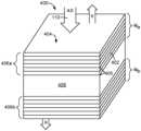
광학 필름(100)에서와 같이, 광학 필름(400)은 광학 스택/패킷(406a, 406b)으로 분할되는 수십 내지 수백 개의 간섭 층(402)을 포함할 수 있다. 제1 광학 스택/패킷(406a)은 총 (Na)개의 간섭 층(402)을 포함하고, 제2 스택/패킷(406b)은 총 (Nb)개의 간섭 층(402)을 포함하며, 따라서 광학 필름(400)은 총 (N = Na + Nb)개의 순차적으로 번호부여된 간섭 층(402)을 포함한다.As with
각각의 간섭 층(402)은 도 1 및 도 2에 관하여 기술된 간섭 층(102)과 실질적으로 동일할 수 있다. 예를 들어, 간섭 층(402) 교번 HIR 층(예컨대, HIR 층(102a)과 유사함) 및 LIR 층(예컨대, LIR 층(102a)과 유사함). 또한, 광학 필름(100)에서와 같이, 몇몇 예에서, 광학 필름(400)의 광학 스택/패킷(406a, 406b) 중 간섭 층(402)의 총 개수(예컨대, N개)는 전술된 바와 같이 1000개 미만, 또는 800개 미만일 수 있다.Each
몇몇 예에서, 광학 스택/패킷(406a, 406b)은 실질적으로 동일한(예컨대, 동일한 또는 거의 동일한) 총 개수의 간섭 층(402)을 포함할 수 있다. 예를 들어, 광학 스택/패킷(406a, 406b)은 독립적으로 각각 약 50개 내지 약 400개의 간섭 층(402)을 포함할 수 있으며, 이때 각각의 광학 스택/패킷(406a, 406b) 내의 간섭 층(402)의 총 개수는 동일하다(예컨대, Na = Nb). 몇몇 예에서, 단일 광학 스택/패킷(406a, 406b) 내의 간섭 층(402)의 총 개수는 약 325개의 층일 수 있다. 다른 예에서, 광학 스택/패킷(406a, 406b)은 상이한 총 개수의 간섭 층(402)을 포함할 수 있다(예컨대, Na ≠ Nb).In some examples, optical stack/
스페이서 층(408)은 주로 광학 간섭에 의해 광을 반사하거나 투과시키지 않는 임의의 적합한 광학 재료(예컨대, 비-간섭 층)를 포함할 수 있다. 몇몇 예에서, 스페이서 층(408)은 폴리에틸렌 나프탈레이트(PEN), PEN 및 폴리에스테르를 함유하는 공중합체(예컨대, 폴리에틸렌 테레프탈레이트(PET) 또는 디벤조산), 글리콜 개질 폴리에틸렌 테레프탈레이트, 폴리카르보네이트(PC), 또는 이들 4가지 부류의 재료의 블렌드 등을 포함할 수 있다. 몇몇 예에서, 스페이서 층(408)은 공압출 또는 라미네이션에 의해 형성되어, 광학 스택/패킷(406a, 406b)을 스페이서 층(408)이 2개의 스택/패킷 사이에 있는 상태로 함께 라미네이팅할 수 있다. 추가적으로 또는 대안적으로, 스페이서 층(408)은 광학 스택/패킷(406a, 406b)에 광학적으로 결합될 수 있다(예컨대, 광이 상당한 반사 또는 굴절을 겪음이 없이 스페이서 층(408) 내로 그리고 그것을 통해 투과되도록 각자의 스택/패킷(406a, 406b)에 부착됨).
스페이서 층(408)은 개별 간섭 층(402)에 비해 상대적으로 두꺼울 수 있다. 예를 들어, 스페이서 층(408)은 약 500 nm보다 큰 평균 두께를 가질 수 있다. 추가적으로 또는 대안적으로, 스페이서 층(408)은 사전결정된 파장 범위 내의 최대 파장의 적어도 10배인 평균 두께를 가질 수 있다. 예를 들어, 사전결정된 파장 범위가 가시 광(예컨대, 약 400 내지 700 nm)을 포함하면, 스페이서 층(408)의 두께는 7,000 nm보다 클 수 있다. 몇몇 예에서, 스페이서 층(408)은 사전결정된 파장 범위 내의 최대 파장의 적어도 50배인 평균 두께를 가질 수 있다. 몇몇 예에서, 스페이서 층(408)은 그렇지 않으면 다층 광학 스택/패킷(406a, 406b)을 형성하는 공-압출 공정 중에 발생할 수 있는 유동 교란을 감소시키는 데 도움을 줄 수 있다.The
몇몇 예에서, 광학 스택/패킷(406a, 406b)은 상이한 사전결정된 파장 범위의 광을 투과시키거나 반사하도록 독립적으로 최적화될 수 있다. 그렇기 때문에, 광학 필름(400)은 다수의 신중한 파장 범위에 걸쳐 그것의 편광 상태에 따라 광을 투과시키고 반사하도록 구성될 수 있다. 예를 들어, 제1 광학 스택/패킷(406a)은 가시 스펙트럼(예컨대, 약 400 내지 700 nm) 내의 광을 투과시키고 반사하도록 구성될 수 있는 반면, 제2 광학 스택/패킷(406b)은 근-적외 스펙트럼(예컨대, 약 800 내지 1300 nm) 내의 광을 투과시키고 반사하도록 구성될 수 있다.In some examples, optical stack/
몇몇 예에서, 2개의 광학 스택/패킷(406a, 406b)은 광학 필름(400)이 연속적인 사전결정된 파장 범위(예컨대, 약 400 내지 1300 nm)에 걸쳐 그것의 편광 상태에 따라 광을 투과시키고 반사하도록 구성될 수 있다. 예를 들어, 광학 스택/패킷(406a, 406b)은 각자의 스택/패킷(406a, 406b)의 사전결정된 파장 범위가 실질적으로 연속적인(예컨대, 연속적인 또는 거의 연속적인) 사전결정된 파장 범위에 걸쳐 서로 맞닿거나 중첩되도록 구성될 수 있다.In some examples, two optical stacks/
몇몇 예에서, 제1 광학 스택/패킷(406a)은 제1 사전결정된 파장 범위 내의 상이한 편광 상태의 광을 투과시키거나 반사하도록 구성되는 교번 HIR 및 LIR 층의 1 내지 (Na)로 번호부여된 순차적으로 배열된 간섭 층(402)을 포함할 수 있다. 한 쌍의 바로 인접한 HIR 및 LIR 간섭 층(402)이 단위 셀(405)로 특성화될 수 있으며, 따라서 제1 광학 스택/패킷(406a)은 총 약 (Ma= Na/2)개의 단위 셀(405)을 구비한다. 마찬가지로, 제2 광학 스택/패킷(406b)은 제2 사전결정된 파장 범위 내의 상이한 편광 상태의 광을 투과시키거나 반사하도록 구성되는, 교번 HIR 및 LIR 층의 1 내지 (Nb)로 번호부여된 순차적으로 배열된 간섭 층(402), 또는 약 (Mb= Nb/2)개의 단위 셀(405)을 포함할 수 있다. 각자의 단위 셀(405)을 형성하는 각자의 HIR 및 LIR 간섭 층(402)은 HIR 층에 대한 평균 굴절률 대 LIR 층에 대한 평균 굴절률 사이의 비, 예컨대 (n1x/n2x)에 의해 특성화될 수 있다.In some examples, the first optical stack/
몇몇 예에서, HIR(예컨대, n1x) 및 LIR(예컨대, n2x) 간섭 층(402)에 대한 굴절률뿐만 아니라 각자의 광학 스택/패킷(406) 내의 단위 셀(405)의 총 개수(예컨대, M개)는 광학 스택/패킷이 사전결정된 파장 범위 내의 광을 반사하고 투과시키기 위해 비교적 높은 콘트라스트 비(예컨대, 1000:1 초과)를 보이도록 선택될 수 있다. 몇몇 예에서, 각자의 광학 스택/패킷(406)은 방정식 [(n1x/n2x)*M > 300]에 맞도록 구성될 수 있다.In some examples, the refractive index for the HIR (e.g.,n1 M) may be selected such that the optical stack/packet exhibits a relatively high contrast ratio (e.g., greater than 1000:1) to reflect and transmit light within a predetermined wavelength range. In some examples, each optical stack/packet 406 may be configured to fit the equation [(n1x /n2x )*M > 300].
몇몇 비-제한적인 예에서, 광학 필름(400)은 교번하는 제1 HIR 및 제2 LIR 간섭 층(402)의 Ma개의 순차적으로 배열된 제1 단위 셀(405)을 포함할 수 있다. 제1 단위 셀(405)은 제1 사전결정된 파장 범위(예컨대, 약 400 내지 700 nm) 내의 광을 투과시키거나 반사하도록, 그러나 제2 사전결정된 파장 범위(예컨대, 약 800 내지 1300 nm)에서는 그러하지 않도록 최적화될 수 있다. 몇몇 그러한 예에서, 교번하는 제1 HIR 및 제2 LIR 간섭 층(402)은 제2 LIR 층의 굴절률(n2x)의 평균에 대한 제1 HIR 층의 굴절률(n1x)의 평균의 비 곱하기 제1 단위 셀(405)의 총 개수(Ma개)가 약 300보다 크도록 각각 (n1x) 및 (n2x)의 평균 굴절률을 한정할 수 있다. 또한, 광학 필름은 교번하는 제3 HIR 및 제4 LIR 간섭 층(402)의 Mb개의 순차적으로 배열된 제2 단위 셀(405)을 포함할 수 있다. 제2 단위 셀(405)은 제2 사전결정된 파장 범위(예컨대, 약 400 내지 700 nm) 내의 광을 투과시키거나 반사하도록, 그러나 제1 사전결정된 파장 범위(예컨대, 약 800 내지 1300 nm)에서는 그러하지 않도록 최적화될 수 있다. 교번하는 제3 HIR 및 제4 LIR 간섭 층(402)은 제4 LIR 층의 굴절률(n4x)의 평균에 대한 제3 HIR 층의 굴절률(n3x)의 평균의 비 곱하기 제2 단위 셀(405)의 총 개수(Mb개)가 약 300보다 크도록 각각 (n3x) 및 (n4x)의 평균 굴절률을 한정할 수 있다. 몇몇 그러한 예에서, 제1 및 제2 사전결정된 파장 범위 내의 임의의 파장을 갖는 약 30도 미만의 임의의 입사각으로 광학 필름(400)에 입사하는 광은 제1 편광 상태(a)에 대한 평균 광학 투과율(예컨대, Ta) 대 제2 편광 상태(b)에 대한 평균 광학 투과율(예컨대, Tb)의 비가 약 1000:1보다 크도록 (Ta) 및 (Tb)를 겪을 수 있다.In some non-limiting examples, the
몇몇 그러한 예에서, 광학 필름(400)의 다중 스택/패킷(406) 설계는 부분적으로 층의 총 개수의 감소 및 큰 단일 스택을 형성하는 복잡성으로 인해, 예를 들어 동일한 연속적인 사전결정된 파장 범위 내의 광을 반사하고 투과시키도록 구성되는 간섭 층의 단일 패킷만을 포함하는 광학 필름에 비해 필름을 제조하기 위한 더욱 효율적인 공정을 더욱 양호하게 제공할 수 있다.In some such examples, multiple stack/packet 406 designs of
광학 필름(100)에서와 같이, 몇몇 예에서, 사전결정된 파장 범위(예컨대, 가시 광 또는 약 400 내지 700 nm) 내의 실질적으로 수직 입사 광(110)(예컨대, 표면(404)에 수직 또는 거의 수직)에 대한 광학 필름(400)의 투과율 및 반사율의 정도는 제1/통과 편광 상태(a)에 대한 (Ta)의 평균 광학 투과율 및 (Ra)의 광학 반사율과 제2/반사 편광 상태(a)에 대한 (Tb)의 평균 광학 투과율 및 (Rb)의 광학 반사율을 갖는 것으로서 특성화될 수 있다. 광학 필름(400)의 광학 투과율 및 반사율 값은 광학 필름(100)에 관하여 위에서 논의된 값과 실질적으로 유사할 수 있다. 예를 들어, 광학 필름(400)에 대한 (Ta)의 평균 광학 투과율은 제1/통과 편광 상태(a)에 대해 약 80%보다 클 수 있고, 평균 광학 반사율(Rb)은 직교하는 제2/반사 편광 상태(b)에 대해 약 80%보다 클 수 있고, 평균 광학 투과율(Tb)은 직교하는 제2/반사 편광 상태(b)에 대해 약 0.2%보다 작을 수 있다. 몇몇 예에서, 각각의 광학 스택/패킷(406a, 406b)은 사전결정된 파장 범위 내의 제1 편광 상태(a)를 갖는 수직 입사 광(110)의 적어도 50%를 투과시키고 사전결정된 파장 범위 내의 제2 편광 상태(b)를 갖는 수직 입사 광(110)의 적어도 50%를 반사하는 것으로서 특성화될 수 있다.In some examples, as with
도 4b는 층 번호의 함수로서 각각의 개별 간섭 층(402)의 두께를 도시한 광학 필름(400)에 대한 예시적인 두께 프로파일의 플롯이며, 여기서 복수의 간섭 층(402)은 1 내지 N으로 순차적으로 번호부여되며, 이때 N은 광학 필름(400) 내의 간섭 층(402)의 총 개수(예컨대, N = Na+Nb)를 나타낸다. 도 4b에 도시된 바와 같이, 스페이서 층(408)은 광학 필름(400)의 두께 프로파일 플롯으로부터 제외된다.FIG. 4B is a plot of an example thickness profile for an
광학 필름(400)의 두께 프로파일은 각각 각자의 광학 스택/패킷(406a, 406b)의 두께 프로파일에 각각 대응하는 2개의 피팅된 곡선(410, 412)에 의해 특성화될 수 있다. 피팅된 곡선(410, 412)은 각자의 스택/패킷 내의 간섭 층(402)에 기초하여 광학 필름(400)의 층 두께 프로파일에 적용되는 최적 회귀를 나타낸다. 예를 들어, 피팅된 곡선(410)은 1 내지 Na로 순차적으로 번호부여된 간섭 층(402)을 나타내는, 제1 스택/패킷(406a)의 두께 프로파일을 나타내고, 피팅된 곡선(412)은 (Na+1) 내지 (Na+Nb)로 순차적으로 번호부여된 간섭 층(402)(예컨대, 제2 스택/패킷(406b)의 1 내지 Nb로 순차적으로 번호부여된 간섭 층(402)에 해당함)을 나타내는, 제2 스택/패킷(406a)의 두께 프로파일을 나타낸다.The thickness profile of
도 4b에 도시된 바와 같이, 각각의 광학 스택/패킷(406a, 406b)은 각자의 기울기를 한정하는 층 두께 프로파일(예컨대, 개별 층 두께 대 층 번호를 플로팅함)을 포함할 수 있다. 몇몇 예에서, 피팅된 곡선(410, 412)에 대한 평균 기울기는 각자의 광학 스택/패킷(406a, 406b) 내의 간섭 층(402)에 대해 0.2 nm/층 번호보다 작을 수 있다. 광학 필름(400)의 각각의 광학 스택/패킷(406a, 406b)은 약 400개 미만의 총 간섭 층(402)을 포함할 수 있으며, 이때 각자의 간섭 층(402)의 각각의 개별 층 두께는 비교적 얇다(예컨대, 약 200 nm 미만의 평균 두께를 가짐).As shown in FIG. 4B, each optical stack/
몇몇 예에서, 피팅된 곡선(410, 412)의 평균 기울기는 각자의 광학 스택/패킷(406a, 406b) 내의 간섭 층(402)의 서브그룹에 걸친 평균 기울기를 나타낼 수 있다. 예를 들어, 제1 광학 스택/패킷(406a) 내의 간섭 층(402)은 순차적으로 배열된 간섭 층(402)의 복수의 비-중첩 그룹으로 분할될 수 있다. 순차적으로 배열된 간섭 층(402)의 각각의 그룹에 대해, 층은 1부터m까지 순차적으로 번호부여될 수 있으며, 이때m은 Na/10보다 크지만 Na보다 작고, Na는 제1 광학 스택/패킷(406a) 내의 간섭 층(402)의 총 개수를 나타낸다. 피팅된 곡선(410)은 층 번호의 함수로서 층들의 각각의 그룹에 대한 두께 프로파일에 적용될 수 있으며, 이때 각각의 그룹에 대한 결과적인 평균 기울기(예컨대,m개의 층 번호당 두께 변화)가 층들의 각각의 그룹에 대해 결정된다. 모든 그룹에 대한 평균 기울기들 사이의 최대 차이(예컨대, 하나의 그룹으로부터 측정된 최대 기울기와 상이한 그룹으로부터 측정된 최소 기울기 사이의 차이)는 0.70 미만(예컨대, 0.57 nm/층 미만)일 수 있으며, 여기서 최대 기울기 및 최소 기울기는 각각 25개 내지 50개의 인접 층의 임의의 그룹에 걸쳐 구해진다.In some examples, the average slope of the fitted
몇몇 예에서, 광학 필름(400)의 층 두께 프로파일은 층 번호의 함수로서 각각의 광학 스택/패킷(406a, 406b)의 두께 프로파일에 적용되는 최적 선형 방정식에 의해 특성화될 수 있다. 예를 들어, 도 4c는 간섭 층 번호의 함수로서 제1 및 제2 광학 스택/패킷(406a, 406b)의 두께를 도시한 광학 필름(400)에 대한 예시적인 두께 프로파일의 한 쌍의 플롯이다. 도시된 바와 같이, 제1 광학 스택/패킷(406a)은 1 내지 Na로 번호부여된 순차적으로 번호부여된 간섭 층(402)을 포함하고, 제2 광학 스택/패킷(406b)은 1 내지 Nb로 번호부여된 순차적으로 번호부여된 간섭 층(402)을 포함한다. 최적 선형 회귀(420, 422)가 각각의 관련 최적 회귀에 대한 각자의 평균 기울기를 제공하기 위해 각각의 플롯(예컨대, 선형 최소 제곱 회귀)에 적용될 수 있다. 몇몇 예에서, 광학 필름(400) 내의 모든 광학 스택/패킷(406a, 406b)에 대한 최적 선형 회귀(420, 422)의 평균 기울기들 사이의 최대 차이는 약 20% 미만일 수 있다. 예를 들어, 비-제한적인 예 1 및 도 9의 광학 필름에 관하여 후술되는 바와 같이, 예 1의 광학 필름을 형성하는 패킷 1 및 패킷 2의 기울기는 각각 0.17 nm/층 및 0.18 nm/층의 평균 기울기를 각각 보여 대략 6%의 기울기의 차이를 생성하였다.In some examples, the layer thickness profile of
몇몇 예에서, 제1 및 제2 광학 스택/패킷(406a, 406b)은 영역(424, 426) 내에 스티칭(stitching)을 포함할 수 있다. 스티칭은 각각의 패킷과 관련된 반사 대역들 사이에 단지 소량의 중첩이 존재하는, 적어도 2개의 패킷이 존재하는 광학 설계를 기술한다. 이는 보다 낮은 기울기가 개별 패킷에 사용되도록 허용하며, 이는 각각의 층과 관련된 광파워를 증가시킨다. 도 13은 스티칭된 층 설계의 일례를 도시한다. 그러한 예에서, 층(408)에 인접한 각자의 광학 스택/패킷(406a, 406b)의 층(예컨대, 주어진 스택/패킷 내의 스페이서 층(408)에 인접한 처음 30개의 간섭 층(402))에 대한 층 두께의 변화는 광학 스택/패킷(406a, 406b) 내의 다른 간섭 층(402)에 대한 두께/층의 변화에 비해 증가할 수 있다. 이러한 변화는 광학 스택/패킷(406a, 406b)이 스페이서 층(408)에 대한 이웃한 면을 구비하는 두께 프로파일의 단부에서 약간의 컬(curl)을 갖는 층 두께 프로파일로서 도 4c의 영역(424, 426)에 도시된다.In some examples, first and second optical stacks/
몇몇 비-제한적인 예에서, 광학 필름(400)은 주로 광학 간섭에 의해 광을 반사하고 투과시키는 복수의 간섭 층(402)을 포함할 수 있으며, 따라서 사전결정된 파장 범위 내의 실질적으로 수직 입사 광에 대해, 복수의 간섭 층(402)은 제1 편광 상태를 갖는 광의 적어도 80%를 투과시키고(예컨대, Ta-), 직교하는 제2 편광 상태를 갖는 광의 적어도 80%를 반사한다(예컨대, Tb). 복수의 간섭 층(402)은 복수의 광학 스택/패킷(406a, 406b)으로 분할될 수 있으며, 이때 인접 광학 스택/패킷(406a, 406b)의 각각의 쌍은 주로 광학 간섭에 의해 광을 반사하거나 투과시키지 않는 하나 이상의 스페이서 층(408)에 의해 분리되며, 각각의 광학 스택/패킷(406a, 406b)은 사전결정된 파장 범위 내의 제1 편광 상태(a)를 갖는 광의 적어도 50%를 투과시키고, 사전결정된 파장 범위 내의 제2 편광 상태(b)를 갖는 광의 적어도 50%를 반사한다. 각각의 광학 스택/패킷(406a, 406b) 내에서, 간섭 층(402)은 순차적으로 번호부여될 수 있으며(예컨대, N-a 또는 Nb), 이때 각각의 광학 스택/패킷(406a, 406b)은 광학 스택/패킷(406a, 406b)의 두께를 간섭 층 번호와 상관시키는 최적 선형 방정식(예컨대, 피팅된 선(420, 422))을 갖고, 이러한 선형 방정식은 스택/패킷 내의 최초 간섭 층(402)으로부터 스택/패킷 내의 마지막 간섭 층까지 연장되는 영역에서 평균 기울기(예컨대, 스택 두께/층 번호)를 가지며(예컨대, 최초 광학 스택/패킷(406a)의 층 번호 1 내지 Na에 적용된 선(420)), 광학 필름(400) 내의 복수의 광학 스택/패킷(406a, 406b)의 최적 선형 방정식의 평균 기울기들 사이의 최대 차이는 약 20% 미만이다. 몇몇 그러한 예에서, 광학 필름(400)은 약 2.5보다 큰 평균 광학 밀도를 가질 수 있다.In some non-limiting examples, the
도 5a 및 도 5b는 가시 스펙트럼에 해당하는 특정 파장 범위 400 내지 700 nm 내의 수직 입사 광(110)에 대해 제1 및 제2 편광 상태(예컨대, 각각 통과 및 반사 편광 상태)에 대한 투과 백분율을 도시한, 본 개시에 따른 예시적인 광학 필름(예컨대, 광학 필름(400))에 대한 대표적인 투과율 플롯이다. 도 5b는 제2 편광 상태(b)(예컨대, 반사 편광 상태)에 대해 투과 백분율에 대한 로그 플롯을 도시한다. 시험된 대표적인 광학 필름(400)은 각각 투과 스펙트럼이 람다(Lambda)900 분광계(펄킨 엘머(Perkin Elmer))로 제1 및 제2 편광 상태에 대해 측정되는 각각 325개의 간섭 층(402)을 갖춘 2개의 광학 스택(예컨대, 406a, 406b)을 포함하였다. 도시된 바와 같이, 가시 스펙트럼 범위에 걸친 전체 제2 편광 상태(b) 투과율(예컨대, 반사-축, Tb)은 0.1%보다 상당히 더 낮았다.5A and 5B show percent transmission for first and second polarization states (e.g., transit and reflection polarization states, respectively) for normally
몇몇 예에서, 광학 필름(100, 400)은 간섭 층(102, 402)의 스택(들)/패킷(들) 중 하나 이상을 분리 및/또는 보호하는 데 사용될 수 있는 하나 이상의 비-간섭 층을 포함하거나 그것과 조합될 수 있다. 예를 들어, 도 6은 광학 필름(100, 400)에 관하여 전술된 특성 중 하나 이상을 보이도록 형성될 수 있는 광학 필름(600)의 다른 예를 도시한다. 도 6에 도시된 바와 같이, 광학 필름(600)은 비교적 두꺼운 비-간섭 층(608)들 사이에 라미네이팅되는 2개의 광학 스택/패킷(606a, 606b)으로 분할되는 복수의 간섭 층(602)을 포함한다. 도 6에 도시된 바와 같이, 제1 광학 스택/패킷(606a)은 비-간섭 층(608a, 608b) 사이에 놓이는 반면 제2 광학 스택/패킷(606b)은 비-간섭 층(608c, 608d) 사이에 놓이며, 따라서 비-간섭 층(608b, 608c)이 서로 바로 인접하고 제1 및 제2 광학 스택/패킷(606a, 606b) 사이의 스페이서 층으로서의 역할을 한다. 몇몇 예에서, 그것들의 상대 두께로 인해, 광학 스택/패킷(606a, 606b)의 외부에 있는 비-간섭 층(608a, 608d)은 각자의 스택/패킷을 의도하지 않은 손상(예컨대, 스크래칭)으로부터 보호하는 데 도움을 줄 수 있다. 몇몇 예에서, 비-간섭 층(608a, 608b)은 약 1.57의 반응성 지수(reactive index)를 한정할 수 있다.In some examples,
추가적으로 또는 대안적으로, 비-간섭 층(608)들 중 하나 이상은 하드 코트(hard coat)(스크래칭-방지 코팅), 확산 코팅, 반사-방지 코팅, 또는 눈부심-방지 코팅과 같은 코팅을 포함할 수 있다.Additionally or alternatively, one or more of the non-interfering layers 608 may include a coating such as a hard coat (anti-scratch coating), diffusion coating, anti-reflection coating, or anti-glare coating. You can.
도 7은 반사 편광기 광학 필름(702), 액정 디스플레이(LCD) 조립체(710) 및 광원(720)을 포함하는 예시적인 디스플레이 조립체(700)의 다이어그램이다. 도시된 바와 같이, LCD 조립체(710)는 광학 필름(702) 및 광원(720)에 의해 제공되는 편광된 광에 의해 조명된다. LCD 조립체(710)는 외측 흡수 편광기 필름(712), 하나 이상의 유리 층(714), 및 액정 층(716)을 갖춘 다층 배열을 포함할 수 있다.7 is a diagram of an
도 7은 디스플레이 조립체(700)를 통해 수송되는 2가지 유형의 광을 도시한다. 주변 광(730)은 디스플레이 표면(711)에 입사하는 광을 나타내며, 이 광은 LCD 조립체(710), 광학 필름(702)을 통해 횡단하여서 광원(720)의 확산 반사 표면에 부딪치고 그곳에서 다시 광학 필름(702)을 향해 반사된다. 광은 또한 광원(720)의 백라이트 조립체로부터 유래할 수 있다. 예를 들어, 광원(720)은 반사 램프 하우징(724) 내에 램프(722)를 포함하는 에지형 백라이트(edge lit backlight)를 포함할 수 있다. 램프(722)로부터의 광은 도광체(726)에 결합되며, 그곳에서 그것이 스폿(spot)(728)(예컨대, 산화티타늄 착색 재료의 불연속 층)과 같은 확산 반사 구조체와 만날 때까지 전파된다. 스폿들의 이러한 불연속 어레이는 램프 광을 추출하고 그것을 LCD 조립체(710)를 향해 지향시키도록 배열된다. 광원(720)에 들어가는 주변 광(730)은 스폿에 부딪칠 수 있거나, 그것은 스폿들 사이의 간극 영역을 통해 도광체로부터 빠져나갈 수 있다. 확산 반사 층(729)(예컨대, 산화티타늄 착색 재료의 층)이 그러한 광선을 도중차단하고 반사하기 위해 도광체(726) 아래에 위치될 수 있다. 일반적으로, 광원(720)으로부터 LCD 조립체(710)를 향해 나오는 모든 광선은 광선 다발(ray bundle)(732)로서 예시될 수 있다. 이러한 광선 다발은 "(a)"로 지칭되는 제1 편광 상태를 갖는 광을 투과시키고 직교 편광 상태(b)를 갖는 광을 효과적으로 반사하는 광학 필름(702)에 입사한다. 광학 필름(702)은 전술된 광학 필름(100, 400, 600) 중 임의의 것에 대응할 수 있다.Figure 7 shows two types of light transported through
몇몇 예에서, LCD 디스플레이 조립체는 광원(720)과 LCD 조립체(710) 사이에 흡수 편광기 필름 및 반사 편광기 필름(AP/RP 필름)을 포함할 수 있다. 그러한 예에서, AP 필름은 전형적으로 디스플레이 조립체에 충분한 콘트라스트를 생성하는 데 사용될 수 있는 반면, RP 필름의 포함은 AP 필름만의 시스템에 비해, AP/RP 필름 조합의 휘도, 특히 높은 주변 광 환경 또는 높은 눈부심 조건을 개선한다. 놀랍게도, AP/RP 필름이 높은 주변 광 환경(예컨대, 외부 조건)에서도 디스플레이 조립체(700)에 대한 휘도 또는 콘트라스트의 임의의 상당한 감소 없이 본 명세서에 기술된 바와 같은 고-콘트라스트 반사 편광기(RP) 광학 필름(702)으로 대체될 수 있는 것으로 밝혀졌다. 예를 들어, 후방 AP 필름 없이 디스플레이 조립체(700) 내에 광학 필름(702)만을 포함시키는 것은 주변 광이 바람직하지 않게 광학 필름(702)으로부터 반사되어 높은 수준의 눈부심을 일으키게 할 것이라고 이론화되었지만, 실제로는 무시할 수 있거나 비교적 미미한 눈부심의 증가가 관찰되었다.In some examples, the LCD display assembly may include an absorbing polarizer film and a reflective polarizer film (AP/RP film) between the
몇몇 예에서, 광학 필름(702)을 포함하는 디스플레이 조립체(700)는 AP/RP 필름을 포함하는 비교할 만한 디스플레이 조립체에 비해 약 10% 내지 15%의 향상된 휘도를 보일 수 있다.In some examples,
몇몇 예에서, 디스플레이 조립체(700)는 디스플레이 조립체(700)의 축방향 휘도를 증가시키기 위해 광원(720)과 광학 필름(702) 사이에 배치되는 하나 이상의 휘도 향상 필름(740)을 포함할 수 있다. 예시적인 휘도 향상 필름(740)은 예를 들어 방향전환 필름, 프리즘 필름 등을 포함할 수 있다.In some examples,
몇몇 비-제한적인 예에서, 디스플레이 조립체(700)는 광원(720), 광원(720)에 의해 조명되도록 구성되는 LCD 조립체(710), 디스플레이 조립체(700)의 축방향 휘도를 증가시키기 위해 광원(720)과 LCD 조립체(710) 사이에 배치되는 하나 이상의 휘도 향상 필름(740), 및 하나 이상의 휘도 향상 필름(740)과 LCD 조립체(710) 사이에 배치되고, 제1 편광 상태(a)를 갖는 광을 실질적으로 투과시키고 직교하는 제2 편광 상태(b)를 갖는 광을 실질적으로 반사하도록 구성되는 광학 필름(702)(예컨대, RP)을 포함할 수 있다. 광학 필름(702)은 광원(720)과 LCD 조립체(710) 사이에 흡수 편광기(AP)가 배치되지 않은 상태에서 제2 편광 상태에 대해 약 0.2% 미만의 평균 광학 투과율(예컨대, Tb)을 한정할 수 있다. 몇몇 그러한 예에서, 디스플레이 조립체(700)는 제2 편광 상태(b)에 대한 비교 디스플레이 조립체의 RP의 평균 투과율이 약 1.0%보다 큰 것을 제외하고는 동일한 구성을 갖는 비교 디스플레이 조립체의 콘트라스트 비의 적어도 2배의 콘트라스트 비를 한정할 수 있다.In some non-limiting examples,
추가적으로 또는 대안적으로, 몇몇 비-제한적인 예에서, 디스플레이 조립체(700)는 광원(720), 광원(720)에 의해 조명되도록 구성되는 LCD 조립체(710), 디스플레이 조립체(700)의 축방향 휘도를 증가시키기 위해 광원(720)과 LCD 조립체(710) 사이에 배치되는 하나 이상의 휘도 향상 필름(740), 및 하나 이상의 휘도 향상 필름(740)과 LCD 조립체(710) 사이에 배치되는 광학 필름(702)(예컨대, RP)을 포함할 수 있다. 광학 필름(702)은 주로 광학 간섭에 의해 광을 투과시키거나 반사하는 복수의 간섭 층을 포함할 수 있으며, 따라서 사전결정된 파장 범위 내의 실질적으로 수직 입사 광에 대해, 복수의 간섭 층은, 흡수 편광기(AP)가 광원(720)과 LCD 조립체(710) 사이에 배치됨이 없이, 제1 편광 상태를 갖는 광의 적어도 80%를 투과시키고(예컨대, Ta) 직교하는 제2 편광 상태를 갖는 광의 약 0.2% 미만을 투과시킨다(예컨대, Tb).Additionally or alternatively, in some non-limiting examples,
도 8은 AP/RP 필름을 갖춘 디스플레이 조립체와 비교하여 시야각의 함수로서 광학 필름(702)을 포함하는 디스플레이 조립체(700)에 대한 예시적인 휘도 프로파일이다. 곡선(800)은 디스플레이 조립체(700) 광학 필름(702)에 대한 휘도 프로파일을 나타내는 반면, 곡선(802)은 AP/RP 필름(예컨대, 닛토 덴코 코포레이션(Nitto Denko Corp)(일본 도쿄)으로부터 입수가능한 APCF)을 포함하는 비교할 만한 디스플레이 조립체에 대한 휘도 프로파일을 나타낸다. 도시된 바와 같이, 광학 필름(702)은 축외 관찰 위치(예컨대, >50°)에 대한 휘도 프로파일의 약간의 개선을 제공하면서 정상 시야각(예컨대, ±20°)에 대한 비교 관찰 휘도 프로파일을 제공한다.Figure 8 is an example brightness profile for a
몇몇 그러한 예에서, 전통적인 AP/RP 필름과는 대조적으로 광학 필름(702)의 사용은 LCD 디스플레이 조립체의 전체 두께가 현저히 감소될 수 있는 결과를 가져올 수 있는데, 왜냐하면 본 명세서에 기술된 고-콘트라스트 RP 광학 필름이 전통적인 AP/RP 필름의 두께의 대략 절반으로 형성될 수 있기 때문이다. AP/RP 필름과는 대조적으로 디스플레이 조립체(700)에 광학 필름(702)만을 사용하는 것이 디스플레이 조립체 두께의 감소와 관련된 이점을 가져올 수 있지만, 몇몇 예에서, 흡수 편광기 필름이 선택적으로 LCD 조립체(710)와 광학 필름(702)(도시되지 않음) 사이에 포함될 수 있다. 몇몇 그러한 예에서, 흡수 편광기/광학 필름(702) 조합은 전통적인 AP/RP 필름에 비해 개선된 휘도 및/또는 콘트라스트 비를 제공할 수 있다.In some such instances, the use of
몇몇 예에서, 디스플레이 조립체(700)의 광학 필름(702)은 제1 편광 상태(a)를 갖는 광을 실질적으로 투과시키고 직교하는 제2 편광 상태(b)를 갖는 광을 실질적으로 반사하는 고-콘트라스트 RP로서 작동할 수 있다. 몇몇 예에서, 광학 필름(702)은 제2 편광 상태(b)에 대해 약 0.2% 미만의 평균 광학 투과율을 한정할 수 있으며, 여기서 광원(720)과 액정 층(716) 사이에 흡수 편광기가 배치되지 않고, 디스플레이 조립체(700)의 콘트라스트 비는 제2 편광 상태에 대한 비교 디스플레이 조립체의 반사 편광기의 평균 투과율이 약 1.0%보다 큰 것을 제외하고는 동일한 구성을 갖는 비교 디스플레이 조립체의 콘트라스트 비의 적어도 2배이다.In some examples, the
몇몇 예에서, 본 명세서에 기술된 광학 필름(100, 200, 400, 600) 중 하나 이상은 광축에 중심설정된 관찰자에게 물체를 표시하기 위해 설계된 광학 시스템(예컨대, 가상 현실 디스플레이 시스템) 내에 통합될 수 있다. 그러한 광학 시스템은 0이 아닌 광파워를 갖는 하나 이상의 광학 렌즈를 포함할 수 있으며, 이때 반사 편광기(예컨대, 광학 필름(100, 200, 400, 600))가 하나 이상의 광학 렌즈의 제1 주 표면 상에 배치되고 그것에 정합하며, 부분 반사기가 하나 이상의 광학 렌즈의 제2 주 표면 상에 배치되고 그것에 정합한다. 몇몇 예에서, 렌즈 및 반사 편광기는 하나 또는 2개의 직교 축을 중심으로 볼록할 수 있고, 예를 들어 머리-장착 디스플레이, 예컨대 가상 현실 디스플레이, 및 카메라, 예컨대 휴대 전화 내에 포함된 카메라를 비롯한 다양한 장치에 유용한 소형 구성으로 고 시야, 고 콘트라스트, 저 색수차, 저 왜곡, 및/또는 고 효율을 갖는 시스템을 생성하기 위해 정지 표면(예를 들어, 출사동(exit pupil) 또는 입사동(entrance pupil))과 이미지 표면(예컨대, 디스플레이 패널의 표면 또는 이미지 리코더의 표면) 사이에 배치될 수 있다.In some examples, one or more of the
도 10은 이미지 표면(1030), 정지 표면(1035), 및 이미지 표면(1030)과 정지 표면(1035) 사이에 배치되는 광학 스택(1010)을 포함하는 예시적인 광학 시스템(1000)(예컨대, 가상 현실 디스플레이 시스템)의 개략 단면도이다. x-y-z 좌표계가 도 10에 제공되어 있다. 이미지 표면(1030)은 편광된 또는 비편광된 광을 방출하는 디스플레이 패널과 같은 이미지 형성 장치의 출력 표면일 수 있는 반면, 정지 표면(1035)은 광학 시스템(1000)의 출사동일 수 있고, 예를 들어 관찰자의 눈 또는 카메라일 수 있는 제2 광학 시스템의 입사동과 중첩되도록 구성될 수 있다.10 illustrates an example optical system 1000 (e.g., a virtual This is a schematic cross-sectional view of the reality display system. The x-y-z coordinate system is provided in Figure 10.
몇몇 예에서, 광학 스택(1010)은 제1 및 제2 주 표면(1014, 1016)을 갖춘 광학 렌즈(1012), 제1 주 표면(1014) 상에 배치되는 반사 편광기(1027)(예컨대, 광학 필름(100, 200, 400, 600)), 및 광학 렌즈(1012)의 제2 주 표면(1016) 상에 배치되는 부분 반사기(1017)를 포함할 수 있다. 몇몇 예에서, 광학 스택(1010)은 또한 각자의 제1 및 제2 주 표면(1014, 1016) 상에 배치되는 하나 이상의 1/4 파장 지연기(1015, 1025)를 포함할 수 있다.In some examples,
도 10에 도시된 바와 같이, 광학 스택(1010)은 직교하는 제1 및/또는 제2 축(예컨대, 각각 x-축 및 y-축)을 따라 이미지 표면(1030)을 향해 볼록할 수 있다. 광학 스택(1010)은 먼저 반사 편광기(1027)를 반사 편광기(1027)에 코팅되거나 라미네이팅된 선택적인 제1 1/4 파장 지연기(1025)와 함께 형성하고 이어서 결과적인 필름을 광학 렌즈(1012)에 대응하도록 원하는 형상으로 열성형함으로써 제조될 수 있다. 부분 반사기(1017) 및 선택적인 제2 1/4 파장 지연기(1015)는 부분 반사기 필름 상에 1/4 파장 지연기를 코팅함으로써, 1/4 파장 지연기 필름 상에 부분 반사기 코팅을 코팅함으로써, 부분 반사기 필름과 1/4 파장 지연기 필름을 함께 라미네이팅함으로써, 또는 먼저 필름 인서트 성형 공정에서 렌즈(1012)(반사 편광기(1027)를 포함하는 필름 상에 형성될 수 있음)를 형성하고 이어서 제2 주 표면(1016) 상에 부분 반사기(1017)를 코팅함으로써 제조될 수 있다. 몇몇 예에서, 렌즈(1012)는 렌즈(1012)를 반사 편광기(1027) 및 부분 반사기(1017)의 제1 및 제2 필름 사이에 사출 성형함으로써 형성될 수 있다. 제1 및 제2 필름은 사출 성형 단계 전에 열성형될 수 있다.As shown in FIG. 10 ,
이미지 소스(image source)(1031)는 이미지 표면(1030)을 포함하고, 정지 표면(1035)은 광학 시스템(1000)을 위한 출사동이다. 몇몇 예에서, 이미지 소스(1031)는 디스플레이 패널일 수 있다. 다른 예에서, 디스플레이 패널이 존재하지 않을 수 있고, 대신에 이미지 표면(1030)은 광학 시스템(1000)의 외부에 있는 물체로부터 반사된 광을 수광하도록 구성되는 애퍼처(aperture)이다.Image source 1031 includes an
몇몇 예에서, 입사동(1034)을 갖춘 제2 광학 시스템(1033)이 정지 표면(1035)이 입사동(1034)과 중첩되는 상태로 광학 시스템(1000)에 근접하게 배치될 수 있다. 제2 광학 시스템(1033)은 예를 들어 이미지 표면(637)을 통해 투과된 이미지를 기록하도록 구성되는 카메라일 수 있다. 몇몇 예에서, 제2 광학 시스템(1033)은 관찰자의 눈이고, 입사동(1034)은 관찰자의 눈의 동공이다. 그러한 예에서, 광학 시스템(1000)은 머리-장착 디스플레이에 사용하도록 구성될 수 있다.In some examples, a second
반사 편광기(1027)는 본 명세서에 기재된 광학 필름(100, 200, 400, 600) 중 임의의 것일 수 있다. 예를 들어, 반사 편광기는 적어도 50개의 순차적으로 번호부여된 간섭 층을 포함할 수 있으며, 이때 각각의 층은 비교적 얇을 수 있으며(예컨대, 약 200 nm 미만의 평균 두께를 가짐), 여기서 피팅된 곡선(예컨대, 도 3의 곡선(300))은 층 번호의 함수로서 반사 편광기(1027)의 층 두께 프로파일에 적용되는 최적 회귀이고, 제1 층으로부터 제N 층까지 연장되는 영역에서의 피팅된 곡선의 평균 기울기는 약 0.2 nm/층 미만이다. 반사 편광기(1027)는 (예컨대, 제1 방향으로 선형 편광된) 제1 편광 상태(a)를 갖는 광을 실질적으로 투과시키고, (예컨대, 제1 방향에 직교하는 제2 방향으로 선형 편광된) 직교하는 제2 편광 상태(b)를 갖는 광을 실질적으로 반사한다.
부분 반사기(1017)는 본 명세서의 다른 곳에 기술된 파장 범위들 중 임의의 것일 수 있는, 사전결정된 파장 범위에서 적어도 30%의 평균 광학 반사율 및 적어도 30%의 광학 투과율을 갖는다. 임의의 적합한 부분 반사기가 사용될 수 있다. 몇몇 예에서, 부분 반사기(1017)는 예를 들어 하프 미러(half mirror)일 수 있다. 몇몇 예에서, 부분 반사기(1017)는 투명 기재(substrate) 상에 금속(예컨대, 은 또는 알루미늄)의 얇은 층을 코팅함으로써 구성될 수 있다. 추가적으로 또는 대안적으로, 부분 반사기(1017)는 또한 예를 들어 렌즈의 표면 상에 박막 유전체 코팅을 퇴적시킴으로써, 또는 렌즈의 표면 상에 금속과 유전체 코팅들의 조합을 퇴적시킴으로써 형성될 수 있다. 몇몇 예에서, 부분 반사기(1017)는 그 자체가 반사 편광기일 수 있다.
선택적인 제1 및 제2 1/4 파장 지연기(1015, 1025)는 예를 들어 선형 광중합성 중합체(linear photopolymerizable polymer, LPP) 재료 및 미국 특허 출원 공개 US 2002/0180916호(샤트(Schadt) 등), US 2003/028048호(셰르카위(Cherkaoui) 등) 및 US 2005/0072959호(모이아(Moia) 등)에 기재된 액정 중합체(liquid crystal polymer, LCP) 재료를 비롯한 임의의 적합한 재료로부터 형성되는 코팅 또는 필름일 수 있다. 적합한 LPP 재료는 ROP-131 EXP 306 LPP를 포함하고, 적합한 LCP 재료는 ROF-5185 EXP 410 LCP를 포함하며, 이들 둘 모두는 스위스 알슈빌 소재의 롤릭 테크놀로지스(Rolic Technologies)로부터 입수가능하다. 몇몇 예에서, 1/4 파장 지연기(1015, 1025)는 사전결정된 파장 범위 내의 적어도 하나의 파장에서의 1/4 파장 지연기일 수 있다.The optional first and second
광학 시스템(1000)의 작동 중에, 광선(1037, 1038)은 각각 이미지 표면(1030) 및 정지 표면(1035)을 통해 투과된다. 광선(1037, 1038)은 각각 이미지 표면(1030)으로부터 정지 표면(1035)으로 투과될 수 있거나(예를 들어, 머리-장착 디스플레이 응용에서), 광선(1037, 1038)은 정지 표면(1035)으로부터 이미지 표면(1030)으로 투과될 수 있다(예를 들어, 카메라 응용에서). 광선(1038)은 그것의 광학 경로가 광학 시스템(1000)을 위한 접힌 광축(1040)을 한정하는 중심 광선일 수 있으며, 광학 시스템은 접힌 광축(1040)에 중심설정될 수 있다. 광선(1038)은 광축(1040)으로부터의 상당한 편차 없이 광학 스택(1010)을 통과할 수 있다.During operation of
광선(1037)의 경로는 광학 스택(1010)으로 인해 편향될 수 있다. 광선(1037)은 부분 반사기(1017)(선택적인 제2 1/4 파장 지연기(1015) 포함함)를 통해 렌즈(1012) 내로 그리고 그것을 통해 투과된다. 먼저 렌즈(1012)를 통과한 후에, 광선은 선택적인 제1 1/4 파장 지연기(1025)를 통과하고 반사 편광기(1027)로부터 반사된다. 2개의 1/4 파장 지연기(1015, 1025)가 광학 스택(1010) 내에 통합되는 예에서, 1/4 파장 지연기(1015, 1025)는 1/4 파장 지연기(1015, 1025)가 반사 편광기(1027)와 이미지 소스(1031) 사이에 놓이도록 렌즈(1012)의 양측에 배치될 수 있다. 몇몇 그러한 예에서, 이미지 소스(1031)는 반사 편광기(1027)를 위한 통과 축을 따른 편광(a)을 갖는 광을 방출하여, 1/4 파장 지연기(1015, 1025)를 통과한 후에, 광이 필름에 처음 입사할 때 광이 반사 편광기(1027)를 위한 차단 축을 따라 편광되고 이에 따라 반사 편광기(1027)로부터 반사되게 하도록 구성될 수 있다. 광선(1037)이 처음에 반사 편광기(1027)로부터 반사된 후에, 그것은 제1 1/4 파장 지연기(1025)를 다시 통과하고, 이어서 부분 반사기(1017)로부터 반사되어(예시되지 않은 다른 광선들은 부분 반사기(1017)를 통해 투과됨) 다시 렌즈(1012) 및 제1 1/4 파장 지연기(1025)를 통과하고 이어서 다시 반사 편광기(1027)에 입사한다. 제1 1/4 파장 지연기(1025)를 통과하고, 부분 반사기(1017)로부터 반사되고, 다시 제1 1/4 파장 지연기(1025)를 통과한 후에, 광선(1037)은 반사 편광기(1027)를 위한 통과 축을 따른 편광(a)을 갖는다. 광선(1037)은 이에 따라 반사 편광기(1027)를 통해 투과되고 이어서 정지 표면(1035)을 통해 제2 광학 시스템(1033) 내로 투과된다.The path of
단일 통합형 광학 스택(1010)의 설계는 소형 시스템에서 고 시야를 제공할 수 있다. 이미지 표면(1030)의 외측 에지를 통해 투과되는 광선(1037)은 예컨대 적어도 40도, 적어도 45도 또는 적어도 50도일 수 있는 θ의 시야각으로 접힌 광축(1040)에서 정지 표면(1035)과 교차하는 주 광선이다. 정지 표면(1035)에서의 시야는 2θ이며, 이는 예를 들어 적어도 80도, 적어도 90도 또는 적어도 100도일 수 있다.The design of a single integrated
몇몇 비-제한적인 예에서, 광학 시스템(1000)은 0이 아닌 광파워를 갖는 하나 이상의 광학 렌즈(1012), 하나 이상의 광학 렌즈(1012)의 제1 주 표면(1014) 상에 배치되고 그것에 정합하는 반사 편광기(1027), 및 하나 이상의 광학 렌즈(1012)의 상이한 제2 주 표면(1016) 상에 배치되고 그것에 정합하는 부분 반사기(1017)를 포함할 수 있다. 반사 편광기(1027)는 제1 편광 상태(a)를 갖는 광(1037)을 실질적으로 투과시키고 직교하는 제2 편광 상태(b)를 갖는 광을 실질적으로 반사할 수 있으며, 이때 부분 반사기(1017)는 사전결정된 파장 범위에 대해 적어도 30%의 평균 광학 반사율을 가지며, 따라서 제2 편광 상태(b)를 갖는 광축(1040)을 따른 입사 광(1037)에 대한 광학 시스템(1000)의 평균 광학 투과율은 약 0.1% 미만이다.In some non-limiting examples,
하나 이상의 반사 편광기를 포함하는, 광축에 중심설정된 관찰자에게 물체를 표시하기 위한 광학 시스템의 추가의 예가 전체적으로 본 명세서에 참고로 포함되는 미국 특허 출원 제14/865,017호에 개시되고 기재된다. 본 명세서에 기술된 광학 필름(100, 200, 400, 600) 중 하나 이상은 본 명세서에 기술된 반사 편광기로서 그러한 시스템에 사용될 수 있다.Additional examples of optical systems for displaying objects to a viewer centered on an optical axis, including one or more reflective polarizers, are disclosed and described in U.S. Patent Application No. 14/865,017, which is incorporated herein by reference in its entirety. One or more of the
몇몇 예에서, 본 명세서에 기술된 광학 필름(100, 200, 400, 600) 중 하나 이상은 편광 빔 분할기(PBS) 내에 반사 편광기로서 통합될 수 있다. PBS는 비편광된 광을 2가지 편광된 상태로 효과적으로 분할하는 데 사용될 수 있다. PBS 시스템은 제1 편광 상태(a)에 있는 광을 실질적으로 투과하는 반면 제2 직교 편광 상태(b)에 있는 편광된 광을 실질적으로 반사하기 위해 반도체, 포토닉스 기구(photonics instrumentation), 또는 다른 광학 시스템에 사용될 수 있다. 몇몇 예에서, PBS 시스템은 0° 또는 45°의 입사각으로 광을 수광하는 반면 약 90°의 분리각으로 출력 편광된 빔을 분할하도록 설계될 수 있다.In some examples, one or more of the
도 11은 제1 프리즘(1102), 제2 프리즘(1104), 반사 편광기(1110), 및 광원(1150)을 포함하는 예시적인 PBS(1100)의 개략 단면도이다. 제1 프리즘(1102)은 광원(1150)으로부터 입사 광을 수광하기 위한 입력 면(1112), 출력 면(1114) 및 제1 빗변(1116)을 포함한다. 몇몇 예에서, 입력 면(1112) 및 출력 면(114)은 제1 프리즘(1102)을 통과하는 광을 수광하고 투과시키기 위한 활성 영역을 구비하도록 추가로 형상화될 수 있다. 제2 프리즘(1104)은 출력 표면(1118) 및 제2 빗변(1120)을 포함한다.11 is a schematic cross-sectional view of an
반사 편광기(1110)는 각자의 제1 및 제2 프리즘(1102, 1104)의 제1 및 제2 빗변(1116, 1120) 사이에 배치된다. 반사 편광기(1110)는 본 명세서에 기술된 광학 필름(100, 200, 400, 600) 중 임의의 것을 포함할 수 있다. 예를 들어, 반사 편광기(1110)는 적어도 50개의 순차적으로 번호부여된 간섭 층을 포함할 수 있으며, 이때 각각의 층은 비교적 얇을 수 있으며(예컨대, 약 200 nm 미만의 평균 두께를 가짐), 여기서 피팅된 곡선(예컨대, 도 3의 곡선(300))은 층 번호의 함수로서 반사 편광기(1110)의 층 두께 프로파일에 적용되는 최적 회귀이고, 제1 층으로부터 제N 층까지 연장되는 영역에서의 피팅된 곡선의 평균 기울기는 약 0.2 nm/층 미만이다.A
제1 및 제2 프리즘(1102, 1104)은 유리 또는 중합체 재료를 포함할 수 있다. 제1 및 제2 프리즘(1102, 1104)에 적합한 중합체 재료는 예를 들어 투명 광학 중합체, 예컨대 아크릴 중합체(예컨대, 폴리메틸메타크릴레이트), 환형-올레핀 공중합체, 폴리카르보네이트, 및 이들의 조합을 포함한다. 몇몇 예에서, 제1 및 제2 프리즘(1102, 1104)은 일본 도쿄 소재의 히타치 케미칼 컴퍼니 엘티디(Hitachi Chemical Company, Ltd)로부터 상표명 "옵토레즈(OPTOREZ) OZ-1330" 시리즈 중합체로 구매가능한 아크릴 중합체와 같은 열가소성 아크릴 중합체를 사용하여 사출 성형에 의해 형성될 수 있다. 몇몇 예에서, 2개의 프리즘 사이의 광학 편차를 감소시키기 위해 동일한 중합체 재료를 사용하여 제1 및 제2 프리즘(1102, 1104)을 형성하는 것이 바람직할 수 있지만, 다른 예에서, 제1 및 제2 프리즘(1102, 1104)은 상이한 재료로 형성될 수 있다. 몇몇 예에서, 제1 및 제2 프리즘(1102, 1104)은 유사하게 크기설정될 수 있는 반면, 다른 예에서, 제1 프리즘(1102)은 제2 프리즘(1104)의 체적보다 작은 체적을 가질 수 있다. 몇몇 예에서, 제1 프리즘(1102)의 체적은 제2 프리즘(1104)의 체적의 약 절반 이하(또는 약 60% 이하, 또는 약 40% 이하)일 수 있다. 제1 프리즘(1102)의 어느 부분이 제거될 수 있는지의 선택은 엔벨로프(envelop)(1152) 내에서 유래하는 입사, 투과 및 반사 광의 광학 경로에 부분적으로 의존할 수 있다.The first and
작동 중에, 광원(1150)은 중심 광선(1154)을 포함하는 엔벨로프(1152)를 갖는 광 빔을 생성한다. 광원(1150)으로부터의 광은 사전결정된 파장 범위를 갖고서 비-편광될 수 있다. 중심 광선(1154)은 입력 표면(1112)을 통해 제1 프리즘(1102)에 들어가고 거기서 이어서 프리즘을 통해 투과되고 약 45°의 입사각으로 반사 편광기(1110)에 입사하게 된다. 그러한 시점에서, 중심 광선(1154)은 이어서 광의 편광 상태에 따라 반사 편광기(1110)를 통해 투과되고 그것으로부터 반사된다. 예를 들어, 제1 편광 상태(a)(예컨대, 통과 상태)에 대응하는 광은 반사 편광기(1110)를 통과하고, 제1 편광 상태(a)를 갖는 투과 광선(1156)으로서 제2 프리즘(1104)을 통해 계속 진행하며 거기서 출력 표면(1118)에 도달한다. 제2 직교 편광 상태(b)(예컨대, 차단/반사)에 대응하는 광은 제2 직교 편광 상태(b)를 갖는 반사 광선(1158)으로서 반사 편광기(1110)로부터 반사될 것이다. 광선(1154)과 반사 편광기(1110) 사이의 입사각으로 인해, 반사 광선(1158)은 반사 편광기(1110)로부터 출력 면(1114)의 방향으로 반사될 것이다. 몇몇 예에서, 투과 광선(1156) 및 반사 광선(1158)은 서로 90°로 진행할 것이다.In operation,
PBS(1100)는 제1 및 제2 프리즘(1102, 1104)의 출력 또는 다른 면 중 하나 이상에 부착되는 추가의 구성요소(도시되지 않음)를 포함할 수 있다. 추가적으로 또는 대안적으로, PBS(1100)는 상이한 광학 시스템 내에 통합될 수 있다. 다양한 구성요소 또는 PBS(1100) 또는 PBS(1100)에 부착된 그러한 구성요소는 광학적으로 투명한 접착제를 통해 직접 접촉하거나 부착될 수 있다. 몇몇 예에서, 반사 편광기(1110)는 광학적으로 투명한 접착제 층을 사용해 제1 및 제2 프리즘(1102, 1104) 중 하나 또는 둘 모두에 부착된다. PBS 설계 및 PBS 시스템을 포함하는 광학 시스템의 추가의 예가 전체적으로 본 명세서에 참고로 포함되는 미국 특허 출원 제14/865,017호에 개시되고 기재된다.
몇몇 비-제한적인 예에서, PBS(1100)는 제1 및 제2 프리즘(1102, 1104)과, (예컨대, 제1 및 제2 빗변(1116, 1120)을 따라) 제1 및 제2 프리즘(1102, 1104) 사이에 배치되고 그것들에 부착되는 반사 편광기(1110)를 포함할 수 있다. 그러한 예에서, 반사 편광기(1110)는 제1 편광 상태(a)를 갖는 편광된 광을 실질적으로 반사하고 직교하는 제2 편광 상태(b)를 갖는 편광된 광을 실질적으로 투과시킬 수 있으며, 따라서 사전결정된 파장을 갖는 입사 광(예컨대, 광선(1154))이 PBS(1100)의 입력 면(1112)으로부터 PBS(1100)에 들어가고 반사 편광기(1110)와 적어도 1회 만난 후에 PBS(1110)의 출력 면(예컨대, 출력 면(1118 또는 1114))을 통해 빠져나갈 때, 입사 광(예컨대, 광선(1154))의 평균 세기에 대한 출사 광(예컨대, 투과 광선(1156) 또는 반사 광선(1158))의 평균 세기의 비는 입사 광이 제1 편광 상태(a)를 가질 때 약 90%보다 크고, 입사 광이 제2 편광 상태(b)를 가질 때 약 0.2%보다 작다.In some non-limiting examples,
예yes
예 1 - 복굴절 반사 편광기 광학 필름을 다음과 같이 제조하였다. 2개의 다층 광학 패킷을 공-압출하였으며, 이때 각각의 패킷은 폴리에틸렌 나프탈레이트(PEN)와 저 굴절률 등방성 층의 325개의 교번 층으로 구성되었으며, 이러한 저 굴절률 등방성 층은 굴절률이 약 1.57이고 단축 배향시 실질적으로 등방성으로 유지되도록 폴리카르보네이트와 코폴리에스테르(PC:coPET)의 블렌드로 제조하였으며, 여기서 PC:coPET 몰비는 대략 42.5 몰% PC 및 57.5 몰% coPET이고 Tg가 섭씨 105도이다. 이러한 등방성 재료는, 신장 후에 두 비-신장 방향으로의 그것의 굴절률이 비-신장 방향으로의 복굴절 재료의 것과 실질적으로 일치되어 유지되는 반면 신장 방향으로 복굴절 층과 및 비-복굴절 층 사이에 굴절률의 실질적인 불일치가 존재하도록 선택하였다. PEN 및 PC/coPET 중합체를 별도의 압출기로부터 다층 공압출 피드블록으로 공급하였으며, 여기서 그것들을, 총 652개의 층에 대해, 325개의 교번 광학 층의 패킷(각각 "패킷 1" 및 "패킷 2") + 적층된 광학 패킷의 외측의, PC/coPET의 더 두꺼운 보호 경계 층으로 조립하였다.Example 1 - A birefringent reflective polarizer optical film was prepared as follows. Two multilayer optical packets were co-extruded, each packet consisting of 325 alternating layers of polyethylene naphthalate (PEN) and low-index isotropic layers, which have a refractive index of approximately 1.57 and It was made from a blend of polycarbonate and copolyester (PC:coPET) to remain substantially isotropic, with a PC:coPET molar ratio of approximately 42.5 mol% PC and 57.5 mol% coPET and a Tg of 105 degrees Celsius. This isotropic material maintains, after stretching, its refractive index in both non-stretching directions substantially matching that of the birefringent material in the non-stretching direction, while having a difference of refractive index between the birefringent layer and the non-birefringent layer in the stretching direction. It was chosen to ensure that substantial inconsistencies exist. PEN and PC/coPET polymers were fed from separate extruders into a multilayer coextrusion feedblock where they were packaged in packets of 325 alternating optical layers (“
예 1의 고 콘트라스트 반사 편광기(HCRP) 광학 필름에 대한 이러한 층 프로파일이 패킷 1 및 패킷 2가 표시된 도 9에 도시된다. 최소 제곱 선형 회귀를 사용하여 패킷 1의 평균 기울기는 대략 0.17 nm/층이었고 패킷 2의 평균 기울기는 대략 0.18 nm/층이었으며, 이는 대략 6%의 2개의 패킷에 대한 각자의 기울기에 있어서의 차이를 보인다. 예 1의 필름은 커패시턴스 게이지(capacitance gauge)에 의해 측정될 때 대략 63.2 μm의 결과적인 총 두께를 가졌다.This layer profile for the high contrast reflective polarizer (HCRP) optical film of Example 1 is shown in Figure 9 where
예 1의 복수의 간섭 층의 정렬을 평가하기 위해, 필름의 각자의 주 표면 각각에 입사하는 선형 편광된 광에 대해 필름의 광축을 결정하였다. 필름의 광축은 최소량의 선형 편광된 광이 필름을 통과하도록 허용하는 필름의 평면 내에서의 입사 편광된 광의 배향에 대응한다(예컨대, 도 2의 신장 축(120)과 정렬됨). 이상적인 시나리오에서, 필름의 광축은 편광된 광이 필름에 들어가는 표면에 무관하게 동일할 것이다. 그러나, 제조 공정의 편차 또는 복수의 간섭 층의 개별 광축들의 오정렬로 인해, 필름의 광축은 편광된 광이 어느 표면에 들어가는지에 의존할 수 있다. 몇몇 예에서, 복수의 층 사이의 오정렬의 정도가 클수록, 필름에 대해 광축들의 차이가 클 수 있다. 두 표면에 대한 필름의 광축들 사이의 차이는 몇몇 예에서 복수의 간섭 층 사이의 정렬을 평가하기 위한 메트릭(metric)으로서 사용될 수 있다. 예 1의 필름에 대한 2개의 광축을 선형 편광된 광을 사용하여 2개의 표면에 대해 측정하였다. 편광된 광을 필름의 제1 주 표면에 직접 투사하였고, 최소량의 편광된 광이 필름을 통과할 때까지 필름을 회전시켰다. 이어서 제1 주 표면에 대한 광축을 편광된 광의 편광 축에 평행한 것으로 표시하였다. 이러한 과정을 필름의 제2 주 표면에 대해 반복하였다. 예 1의 필름에 대해 제1 주 표면 및 제2 주 표면에 대한 광축들 사이의 차이는 약 0.1도 미만으로 결정되었으며, 이는 복수의 간섭 층 사이의 강한 정렬을 나타낸다.To evaluate the alignment of the plurality of interference layers of Example 1, the optical axis of the film was determined for linearly polarized light incident on each of the respective major surfaces of the film. The optical axis of the film corresponds to the orientation of incident polarized light within the plane of the film that allows the minimum amount of linearly polarized light to pass through the film (e.g., aligned with the
예 2 - 광학 필름을 커패시턴스 게이지에 의해 측정될 때 대략 66.7 μm의 전체 두께로 제조한 것을 제외하고는, 예 1의 필름과 동일한 공정 조건으로 복굴절 반사 편광기 광학 필름을 제조하였다.Example 2 - A birefringent reflective polarizer optical film was prepared with the same process conditions as the film in Example 1, except that the optical film was made to an overall thickness of approximately 66.7 μm as measured by a capacitance gauge.
예 3 - 복굴절 반사 편광기 광학 필름을 다음과 같이 제조하였다. 2개의 다층 광학 패킷을 공-압출하였으며, 이때 각각의 광학 패킷은 90/10 coPEN(예컨대, 90 몰% 폴리에틸렌 나프탈레이트(PEN) 및 10 몰% 폴리에틸렌 테레프탈레이트(PET))과 예 1에서 전술된 바와 같은 PC/coPET의 저 굴절 등방성 층의 325개의 교번 층으로 구성되었다. 90/10 coPEN 및 PC/coPET 중합체를 별도의 압출기로부터 다층 공압출 피드블록으로 공급하였으며, 여기서 그것들을, 총 652개의 층에 대해, 325개의 교번 광학 층의 패킷 + 적층된 광학 패킷의 외측의, PC:coPET의 더 두꺼운 보호 경계 층으로 조립하였다. 이러한 필름은 커패시턴스 게이지에 의해 측정될 때 대략 63.2 μm의 결과적인 물리 총 두께를 가졌다.Example 3 - A birefringent reflective polarizer optical film was prepared as follows. Two multilayer optical packets were co-extruded, each optical packet containing 90/10 coPEN (e.g., 90 mol% polyethylene naphthalate (PEN) and 10 mol% polyethylene terephthalate (PET)) and It consisted of 325 alternating layers of low-refractive isotropic layers of PC/coPET as shown. The 90/10 coPEN and PC/coPET polymers were fed from separate extruders into a multilayer coextrusion feedblock where they were packed into packets of 325 alternating optical layers + the outer layer of the stacked optical packets, for a total of 652 layers. It was assembled with a thicker protective boundary layer of PC:coPET. This film had a resulting physical total thickness of approximately 63.2 μm as measured by a capacitance gauge.
아래의 표 1은 구매가능한 흡수 편광기(AP) 및 반사 편광기(RP), 및 문헌에서 언급된 것들과 비교하여, 예 1 내지 예 3의 광학 필름에 대해 450 내지 650 nm의 가시 스펙트럼 범위에 걸친 제1 및 제2 편광 상태(a) 및 (b)(예컨대, 통과-축 및 차단-축)에 대한 비교 평균 투과율 프로파일을 제공한다.Table 1 below shows the optical spectra over the visible spectral range of 450 to 650 nm for the optical films of Examples 1 to 3, compared to commercially available absorbing polarizers (AP) and reflective polarizers (RP) and those mentioned in the literature. Comparative average transmittance profiles are provided for the first and second polarization states (a) and (b) (e.g., pass-axis and block-axis).
[표 1][Table 1]

아래의 표 2는 표 1의 값에 기초하여 예 필름 1 내지 예 필름 3에 대해 계산된 제1 편광 상태(a) 및 직교하는 제2 편광 상태(b)에서의 투과율 및 반사율 값을 나타낸다. 이들 값은 필름 층에 의한 흡수와 관련된 광 에너지의 무시할 수 있는 손실을 가정하여 계산된다.Table 2 below shows the transmittance and reflectance values in the first polarization state (a) and the orthogonal second polarization state (b) calculated for
[표 2][Table 2]

도 12는 종래의 반사 편광기와 비교한 본 명세서에 기술된 바와 같은 예시적인 반사 편광기 필름에 대한 예시적인 두께 프로파일(층 두께 대 층 개수)의 플롯이다. 필름들이 아래 표 3에 기재되어 있다. 필름(1206, 1208)은 미국 미네소타주 세인트 폴 소재의 쓰리엠으로부터 입수가능한 구매가능한 다층 반사 편광기 필름을 나타낸다. 필름(1210)은 2.2의 최대 두께 대 최소 두께 비를 갖는 275개의 층을 갖춘 대표적인 종래의 편광기 필름이며, 여기서 두께는 그 특허에 기재된 바와 같이 연속적으로 변한다. 선(1202, 1204)은 HCPR 예 1의 각각 제1 및 제2 광학 스택/패킷에 대응한다. 층 두께 프로파일을 원자간력 현미경(Atomic Force Microscope, AFM)을 사용하여 측정하였다.Figure 12 is a plot of an exemplary thickness profile (layer thickness versus layer number) for an exemplary reflective polarizer film as described herein compared to a conventional reflective polarizer. The films are listed in Table 3 below.
[표 3][Table 3]

아래의 표 4는 도 12에 도시된 필름/패킷(1202 내지 1208) 각각에 대한 최고 기울기 영역과 최저 기울기 영역 사이의 계산된 차이를 나타낸다. 주어진 영역에 대한 각자의 기울기를 25개의 층의 범위에 걸쳐 최소 제곱 선형 회귀를 사용하여 결정하였다.Table 4 below shows the calculated difference between the highest and lowest slope areas for each of the films/packets 1202-1208 shown in FIG. 12. The respective slopes for a given area were determined using least squares linear regression over a range of 25 layers.
[표 4][Table 4]

예 4 - 예 1, 예 2, 및 예 3에 관하여 기술된 바와 유사한 제조 공정을 사용하여 광학 필름을 생성하였다. 예 1, 예 2, 및 예 3의 것보다 낮은 기울기/층 프로파일을 이용하는 대안적인 층 두께 프로파일을 구현하였다. 특히, 각각 폴리에틸렌 나프탈레이트(PEN)의 HIR 층과, 폴리카르보네이트와 코폴리에스테르의 혼합물인 80 중량% 자일렉스(Xylex)(미국 텍사스주 휴스턴 소재의 사빅(Sabic))와 20 중량% PETg(미국 테네시주 녹스빌 소재의 이스트만 케미칼즈(Eastman Chemicals))의 블렌드로 제조된 LIR 등방성 층의 325개의 교번 층을 포함하는 2개의 다층 광학 스택/패킷을 공-압출하였다. LIR 층의 굴절률은 대략 1.57이었고 단축 배향시 실질적으로 등방성으로 유지되었다. 이러한 등방성 재료는 신장 후에 신장 방향으로의 그것의 굴절률이 실질적으로 변함없이 그리고 비-신장 방향으로의 HIR 층의 굴절률의 것과 유사하게 유지되는 반면, 신장 방향으로의 HIR 층의 굴절률이 동일한 방향으로의 LIR 층의 굴절률에 대한 실질적인 불일치를 갖도록 선택하였다. HIR 및 LIR 층을 위한 재료를 별도의 압출기로부터 공급하여 다층 공압출 피드블록에 공급하였으며, 여기서 그것들을, 총 653개의 층에 대해, 325개의 교번 광학 층의 2개의 패킷 + 각각의 패킷의 각각의 측의, 등방성 LIR 재료의 더 두꺼운 보호 경계 층으로 조립하였으며, 여기서 적층된 광학 패킷 사이의 스페이서 층은 광학적으로 그리고 기계적으로 단일 층으로 고려된다. 각각 대략 390 nm 내지 620 nm 및 600 nm 내지 900 nm의 사전결정된 파장 범위에 대응하도록 제1 패킷(예컨대, "패킷 1")은 비교적 얇은 교번 HIR/LIR 층으로 구성된 반면 제2 패킷(예컨대, "패킷 2")은 비교적 두꺼운 교번 HIR/LIR 층으로 구성되었다. 필름을 전체적으로 참고로 포함되는 미국 특허 제6,916,440호에 기재된 바와 같은 포물선형 텐터에서 신장시켰다. 필름을 대략 316℉(예컨대, 158℃)의 온도에서 신장시켰다. 필름을 횡방향으로 대략 6:1 비로 그리고 기계 방향으로 대략 0.46:1 비로 신장시켰는데, 즉 필름은 기계 방향으로 이완된다.Example 4 - An optical film was produced using a manufacturing process similar to that described for Examples 1, 2, and 3. An alternative layer thickness profile was implemented using a lower slope/layer profile than those in Examples 1, 2, and 3. In particular, the HIR layer of polyethylene naphthalate (PEN), 80 wt% Xylex (Sabic, Houston, TX, USA) and 20 wt% PETg, a mixture of polycarbonate and copolyester, respectively. Two multilayer optical stacks/packets containing 325 alternating layers of LIR isotropic layers made from a blend (Eastman Chemicals, Knoxville, TN, USA) were co-extruded. The refractive index of the LIR layer was approximately 1.57 and remained substantially isotropic during uniaxial orientation. This isotropic material is such that after stretching its refractive index in the stretching direction remains substantially unchanged and similar to that of the HIR layer in the non-stretching direction, while the refractive index of the HIR layer in the stretching direction remains substantially unchanged and similar to that of the HIR layer in the non-stretching direction. It was chosen to have a substantial mismatch in the refractive index of the LIR layer. Materials for the HIR and LIR layers were supplied from separate extruders and fed into a multilayer coextrusion feedblock where they were processed into two packets of 325 alternating optical layers + each packet of each packet, for a total of 653 layers. Laterally, it is assembled with a thicker protective boundary layer of isotropic LIR material, where the spacer layer between the stacked optical packets is optically and mechanically considered a single layer. The first packet (e.g., “
도 13은 AFM에 의해 얻어진 예 4의 광학 필름에 대한 층 두께 프로파일의 플롯을 도시한다. 최소 제곱 선형 회귀를 사용하여 패킷 1의 평균 기울기는 대략 0.104 nm/층으로 계산되었고 패킷 2의 평균 기울기는 대략 0.141 nm/층으로 계산되었다. 예 4의 필름은 커패시턴스 게이지에 의해 측정될 때 대략 65.7 μm의 결과적인 총 두께를 가졌다. 450 내지 650 nm의 파장 범위에 걸쳐 구해진, 평균 통과 상태 투과율(Ta)은 대략 89.1%였고 평균 차단/반사 상태 투과율(Tb)은 대략 0.057%였다.Figure 13 shows a plot of the layer thickness profile for the optical film of Example 4 obtained by AFM. Using least squares linear regression, the average slope of
도 14는 375 내지 850 nm의 파장 범위에 걸친 예 4의 필름에 대한 차단 상태 투과율(Tb)의 플롯을 도시한다.Figure 14 shows a plot of the blocked state transmittance (Tb ) for the film of Example 4 over the wavelength range of 375 to 850 nm.
예 5 - 아래의 표 5는 예 시판 RP 2 및 RP 3과 비교한 전술된 예 1 및 예 4의 광학 필름에 대한 Δnx/K 비를 나타낸다. 나타낸 바와 같이, 예 1 및 예 4의 광학 필름의 각자의 패킷 각각은 1.2보다 큰 Δnx/K 비를 보이는 반면 예 시판 RP 2 및 RP 3은 1 미만의 Δnx/K 비를 갖는다.Example 5 - Table 5 below shows theΔn As shown, each of the respective packets of optical films of Examples 1 and 4 exhibitaΔn
[표 5][Table 5]

예 6 - 아래의 표 5는 예 1의 광학 필름에 대한 광학 밀도, 광파워, 및 다른 광학 특성을 나타낸다. 종래의 반사 편광기 필름의 24개의 비교 샘플에 대해 얻어진 결과가 또한 표 5에 포함된다. 비교 샘플은 구매가능하거나 문헌에 개시된 기술을 사용하여 제조된 다양한 편광기 필름에 해당한다. 표 6에 열거된 필름에 대한 층당 광파워 대 층의 총 개수가 도 15에 플로팅된다. 도 15에 도시된 바와 같이, 예 1 및 예 4의 광학 필름은 각각 (-0.0012*N + 1.46)(선에 의해 표시됨)보다 큰 층당 광파워를 보인다.Example 6 - Table 5 below shows the optical density, optical power, and other optical properties for the optical film of Example 1. Results obtained for 24 comparative samples of conventional reflective polarizer films are also included in Table 5. Comparative samples correspond to various polarizer films that are commercially available or made using techniques disclosed in the literature. The optical power per layer versus the total number of layers for the films listed in Table 6 is plotted in Figure 15. As shown in Figure 15, the optical films of Examples 1 and 4 each exhibit optical power per layer greater than (-0.0012*N + 1.46) (indicated by the line).
[표 6][Table 6]

예 7- 아이패드4(미국 캘리포니아주 쿠퍼티노 소재의 애플 컴퓨터(Apple Computer))의 LCD 디스플레이를 사용하여 비교 디스플레이 조립체 연구를 수행하였다. 3개의 반사 편광기를 후방 반사 편광기(예컨대, 디스플레이 조립체(700) 내의 광학 필름(702)의 위치)로서 디스플레이 조립체에서 시험하였다. 시험된 반사 편광기는 폴리비닐 알코올 유형의 흡착 편광기에 라미네이팅된 아이패드4의 스톡 RP 필름("비교 AP/RP 필름"); RP가 없는 아이패드4의 스톡 RP 필름("비교 RP 필름"); 및 예 1의 고 콘트라스트 반사 편광기 광학 필름을 포함하였다. 편광기 광학 필름을 LCD 디스플레이에 접착하는 데 사용된 접합 접착제는 미국 미네소타주 세인트 폴 소재의 쓰리엠 컴퍼니로부터 입수가능한 투명 OCA 8171이었다. 시험에 사용된 광원은 아이패드4 장치와 함께 제공되는 휘도 향상 필름(예컨대, 프리즘 필름/프리즘 필름/확산기 시트)을 구비한 스톡 백라이트였다.Example 7 - A comparative display assembly study was performed using the LCD display of an iPad 4 (Apple Computer, Cupertino, CA). Three reflective polarizers were tested in the display assembly as back reflective polarizers (e.g., the location of the
3개의 상이한 디스플레이 조립체의 광학 성능을 시판 코노스코프(conoscope) 엘딤(ELDIM) L80(프랑스 에후빌르-셍-끌레흐 소재의 엘딤 에스에이(ELDIM SA))을 사용하여 검사하였다. 디스플레이 조립체에 대한 휘도 및 콘트라스트 결과가 비교 AP/RP 필름에 대해 정규화된 값으로 표 7에 표시된다. 결과로부터 보이는 바와 같이, 예 1의 광학 필름은 비교 AP/RP 및 RP 필름 둘 모두에 비해 우수한 휘도를 나타내었다. 또한, 예 1의 광학 필름은 스톡 비교 RP 필름 단독의 것보다 훨씬 더 큰 콘트라스트 비를 보였고, 디스플레이 조립체 내에 후방 AP 층이 없음에도 불구하고 비교 AP/RP의 것과 유사하게 유지되었다.The optical performance of three different display assemblies was examined using a commercial conoscope ELDIM L80 (ELDIM SA, Ehuville-Saint-Clerchs, France). Brightness and contrast results for the display assemblies are shown in Table 7 with values normalized to comparative AP/RP films. As seen from the results, the optical film of Example 1 exhibited superior brightness compared to both the comparative AP/RP and RP films. Additionally, the optical film of Example 1 showed a contrast ratio that was significantly greater than that of the stock comparative RP film alone and remained similar to that of the comparative AP/RP despite the absence of a rear AP layer within the display assembly.
[표 7][Table 7]
항목 1: 일 예에서, 광학 필름으로서, 복수의 간섭 층을 포함하며, 각각의 간섭 층은 주로 광학 간섭에 의해 광을 반사하거나 투과시키고, 간섭 층의 총 개수는 약 1000개 미만이어서, 사전결정된 파장 범위 내의 실질적으로 수직 입사 광에 대해, 복수의 간섭 층은 제1 편광 상태에 대한 약 85% 초과의 평균 광학 투과율, 직교하는 제2 편광 상태에 대한 약 80% 초과의 평균 광학 반사율, 및 제2 편광 상태에 대한 약 0.2% 미만의 평균 광학 투과율을 갖는, 광학 필름.Item 1: In one example, an optical film comprising a plurality of interference layers, each interference layer reflecting or transmitting light primarily by optical interference, the total number of interference layers being less than about 1000, such that the predetermined For substantially normally incident light within the wavelength range, the plurality of interference layers has an average optical transmission greater than about 85% for the first polarization state, an average optical reflectance greater than about 80% for the second orthogonal polarization state, and a first polarization state. An optical film having an average optical transmission of less than about 0.2% for two polarization states.
항목 2: 항목 1의 광학 필름의 몇몇 예에서, 복수의 간섭 층은 사전결정된 파장 범위에서 제1 편광 상태에 대한 약 90% 초과의 평균 광학 투과율을 갖는다.Item 2: In some examples of the optical film of
항목 3: 항목 1의 광학 필름의 몇몇 예에서, 복수의 간섭 층은 사전결정된 파장 범위에서 제1 편광 상태에 대한 약 95% 초과의 평균 광학 투과율을 갖는다.Item 3: In some examples of the optical film of
항목 4: 항목 1의 광학 필름의 몇몇 예에서, 복수의 간섭 층은 사전결정된 파장 범위에서 제1 편광 상태에 대한 약 98% 초과의 평균 광학 투과율을 갖는다.Item 4: In some examples of the optical film of
항목 5: 선행하는 항목 중 어느 한 항목의 광학 필름의 몇몇 예에서, 복수의 간섭 층은 사전결정된 파장 범위에서 제2 편광 상태에 대한 약 0.15% 미만의 평균 광학 투과율을 갖는다.Item 5: In some examples of the optical film of any of the preceding items, the plurality of interference layers have an average optical transmission for the second polarization state in the predetermined wavelength range of less than about 0.15%.
항목 6: 선행하는 항목 중 어느 한 항목의 광학 필름의 몇몇 예에서, 복수의 간섭 층은 사전결정된 파장 범위에서 제2 편광 상태에 대한 약 0.10% 미만의 평균 광학 투과율을 갖는다.Item 6: In some examples of the optical film of any of the preceding items, the plurality of interference layers have an average optical transmission for the second polarization state in the predetermined wavelength range of less than about 0.10%.
항목 7: 선행하는 항목 중 어느 한 항목의 광학 필름의 몇몇 예에서, 사전결정된 파장 범위 내의 약 10도의 입사각으로 광학 필름에 입사하는 광에 대해, 복수의 간섭 층은 제1 편광 상태에 대한 약 85% 초과의 평균 광학 투과율, 제2 편광 상태에 대한 약 80% 초과의 평균 광학 반사율, 및 제2 편광 상태에 대한 약 0.2% 미만의 평균 광학 투과율을 갖는다.Item 7: Some examples of the optical film of any of the preceding items, wherein, for light incident on the optical film at an angle of incidence of about 10 degrees within a predetermined wavelength range, the plurality of interference layers have a polarization angle of about 85 degrees for the first polarization state. % average optical transmission, greater than about 80% average optical reflectance for the second polarization state, and less than about 0.2% average optical transmission for the second polarization state.
항목 8: 선행하는 항목 중 어느 한 항목의 광학 필름의 몇몇 예에서, 사전결정된 파장 범위 내의 약 20도의 입사각으로 광학 필름에 입사하는 광에 대해, 복수의 간섭 층은 제1 편광 상태에 대한 약 85% 초과의 평균 광학 투과율, 제2 편광 상태에 대한 약 80% 초과의 평균 광학 반사율, 및 제2 편광 상태에 대한 약 0.2% 미만의 평균 광학 투과율을 갖는다.Item 8: Some examples of the optical film of any of the preceding items, wherein, for light incident on the optical film at an angle of incidence of about 20 degrees within a predetermined wavelength range, the plurality of interference layers have a polarization angle of about 85 degrees for the first polarization state. % average optical transmission, greater than about 80% average optical reflectance for the second polarization state, and less than about 0.2% average optical transmission for the second polarization state.
항목 9: 항목 1의 광학 필름의 몇몇 예에서, 사전결정된 파장 범위 내의 약 30도의 입사각으로 광학 필름에 입사하는 광에 대해, 복수의 간섭 층은 제1 편광 상태에 대한 약 85% 초과의 평균 광학 투과율, 제2 편광 상태에 대한 약 80% 초과의 평균 광학 반사율, 및 제2 편광 상태에 대한 약 0.2% 미만의 평균 광학 투과율을 갖는다.Item 9: In some examples of the optical film of
항목 10: 일 예에서, 광학 필름으로서, 복수의 간섭 층을 포함하며, 각각의 간섭 층은 주로 광학 간섭에 의해 광을 반사하거나 투과시키고, 간섭 층의 총 개수는 약 1000개 미만이어서, 사전결정된 파장 범위 내의 실질적으로 수직 입사 광에 대해, 광학 필름은 제1 편광 상태에 대한 평균 광학 투과율 Ta 및 평균 광학 반사율 Ra를 갖고, 직교하는 제2 편광 상태에 대한 평균 광학 투과율 Tb 및 평균 광학 반사율 Rb를 가지며, Tb/Rb는 약 0.002 미만이고 Ra/Ta는 약 0.17 미만인, 광학 필름.Item 10: In one example, an optical film comprising a plurality of interference layers, each interference layer reflecting or transmitting light primarily by optical interference, the total number of interference layers being less than about 1000, such that the predetermined For substantially normally incident light within the wavelength range, the optical film has an average optical transmission Ta and an average optical reflectance Ra for the first polarization state, and an average optical transmission Tb and an average optical reflection for the orthogonal second polarization state. An optical film having a reflectance Rb , wherein Tb /Rb is less than about 0.002 and Ra /Ta is less than about 0.17.
항목 11: 항목 10의 광학 필름의 몇몇 예에서, Ta/Tb는 약 425 초과이다.Item 11: In some examples of the optical film of
항목 12: 항목 10 또는 11의 광학 필름의 몇몇 예에서, Rb/Ra는 약 6.7 초과이다.Item 12: In some examples of the optical film of
항목 13: 항목 10 내지 12 중 어느 한 항목의 광학 필름의 몇몇 예에서, 복수의 간섭 층에 대한 Ta는 사전결정된 파장 범위에서 약 90% 초과이다.Item 13: In some examples of the optical film of any of items 10-12, the Ta for the plurality of interference layers is greater than about 90% in the predetermined wavelength range.
항목 14: 항목 10 내지 13 중 어느 한 항목의 광학 필름의 몇몇 예에서, 복수의 간섭 층에 대한 Ta는 사전결정된 파장 범위에서 약 95% 초과이다.Item 14: In some examples of the optical film of any of items 10-13, the Ta for the plurality of interference layers is greater than about 95% in the predetermined wavelength range.
항목 15: 항목 10 내지 14 중 어느 한 항목의 광학 필름의 몇몇 예에서, 복수의 간섭 층에 대한 Ta는 사전결정된 파장 범위에서 약 98% 초과이다.Item 15: In some examples of the optical film of any of items 10-14, the Ta for the plurality of interference layers is greater than about 98% in the predetermined wavelength range.
항목 16: 항목 10 내지 15 중 어느 한 항목의 광학 필름의 몇몇 예에서, Tb는 사전결정된 파장 범위에서 약 0.15% 미만이다.Item 16: In some examples of the optical film of any of items 10-15, Tb is less than about 0.15% in the predetermined wavelength range.
항목 17: 항목 10 내지 16 중 어느 한 항목의 광학 필름의 몇몇 예에서, Tb는 사전결정된 파장 범위에서 약 0.10% 미만이다.Item 17: In some examples of the optical film of any of items 10-16, Tb is less than about 0.10% in the predetermined wavelength range.
항목 18: 항목 10 내지 17 중 어느 한 항목의 광학 필름의 몇몇 예에서, 사전결정된 파장 범위 내의 약 10도의 입사각으로 광학 필름에 입사하는 광에 대해, Ta는 약 85% 초과이고, Rb는 약 80% 초과이고, Tb는 약 0.2% 미만이다.Item 18: In some examples of the optical film of any of items 10-17, for light incident on the optical film at an angle of incidence of about 10 degrees within a predetermined wavelength range, Ta is greater than about 85%, and Rb is greater than about 80%, and Tb is less than about 0.2%.
항목 19: 항목 10 내지 18 중 어느 한 항목의 광학 필름의 몇몇 예에서, 사전결정된 파장 범위 내의 약 20도의 입사각으로 광학 필름에 입사하는 광에 대해, Ta는 약 85% 초과이고, Rb는 약 80% 초과이고, Tb는 약 0.2% 미만이다.Item 19: In some examples of the optical film of any of items 10-18, for light incident on the optical film at an angle of incidence of about 20 degrees within a predetermined wavelength range, Ta is greater than about 85%, and Rb is greater than about 80%, and Tb is less than about 0.2%.
항목 20: 항목 10 내지 19 중 어느 한 항목의 광학 필름의 몇몇 예에서, 사전결정된 파장 범위 내의 약 30도의 입사각으로 광학 필름에 입사하는 광에 대해, Ta는 약 85% 초과이고, Rb는 약 80% 초과이고, Tb는 약 0.2% 미만이다.Item 20: In some examples of the optical film of any of items 10-19, for light incident on the optical film at an angle of incidence of about 30 degrees within a predetermined wavelength range, Ta is greater than about 85%, and Rb is greater than about 80%, and Tb is less than about 0.2%.
항목 21: 선행하는 항목 중 어느 한 항목의 광학 필름의 몇몇 예에서, 광학 필름은 2개의 간섭 층 사이에 배치된 적어도 하나의 비-간섭 층을 포함하고, 적어도 하나의 비-간섭 층 각각은 주로 광학 간섭에 의해 광을 반사하거나 투과시키지 않는다.Item 21: In some examples of the optical film of any of the preceding items, the optical film includes at least one non-interfering layer disposed between two interfering layers, wherein each of the at least one non-interfering layers is primarily Does not reflect or transmit light due to optical interference.
항목 22: 항목 21의 광학 필름의 몇몇 예에서, 적어도 하나의 비-간섭 층 각각의 평균 두께는 사전결정된 파장 범위 내의 최대 파장의 적어도 10배이다.Item 22: In some examples of the optical film of item 21, the average thickness of each of the at least one non-interfering layer is at least 10 times the maximum wavelength within the predetermined wavelength range.
항목 23: 항목 21의 광학 필름의 몇몇 예에서, 적어도 하나의 비-간섭 층 각각의 평균 두께는 사전결정된 파장 범위 내의 최대 파장의 적어도 50배이다.Item 23: In some examples of the optical film of item 21, the average thickness of each of the at least one non-interfering layer is at least 50 times the maximum wavelength within the predetermined wavelength range.
항목 24: 선행하는 항목 중 어느 한 항목의 광학 필름의 몇몇 예에서, 사전결정된 파장 범위는 약 400 nm 내지 약 700 nm이다.Item 24: In some examples of the optical film of any of the preceding items, the predetermined wavelength range is from about 400 nm to about 700 nm.
항목 25: 선행하는 항목 중 어느 한 항목의 광학 필름의 몇몇 예에서, 사전결정된 파장 범위는 약 400 nm 내지 약 700 nm 및 약 800 nm 내지 약 1300 nm이다.Item 25: In some examples of the optical film of any of the preceding items, the predetermined wavelength range is from about 400 nm to about 700 nm and from about 800 nm to about 1300 nm.
항목 26: 선행하는 항목 중 어느 한 항목의 광학 필름의 몇몇 예에서, 간섭 층의 총 개수는 약 900개 미만이다.Item 26: In some examples of the optical film of any of the preceding items, the total number of interference layers is less than about 900.
항목 27: 선행하는 항목 중 어느 한 항목의 광학 필름의 몇몇 예에서, 간섭 층의 총 개수는 약 800개 미만이다.Item 27: In some examples of the optical film of any of the preceding items, the total number of interference layers is less than about 800.
항목 28: 선행하는 항목 중 어느 한 항목의 광학 필름의 몇몇 예에서, 광학 필름은 약 60 μm 미만의 두께를 갖는다.Item 28: In some examples of the optical film of any of the preceding items, the optical film has a thickness of less than about 60 μm.
항목 29: 선행하는 항목 중 어느 한 항목의 광학 필름의 몇몇 예에서, 복수의 간섭 층은 복수의 교번하는 더 높은 굴절률의 제1 층과 더 낮은 굴절률의 제2 층을 포함한다.Item 29: In some examples of the optical film of any of the preceding items, the plurality of interference layers comprises a plurality of alternating higher refractive index first layers and lower refractive index second layers.
항목 30: 일 예에서, 광학 필름으로서, N개의 순차적으로 번호부여된 층을 포함하며, N은 200보다 크고 1000보다 작은 정수이고, 각각의 층은 약 200 nm 미만의 평균 두께를 갖고, 피팅된 곡선은 층 개수의 함수로서 각각의 층의 두께를 플로팅하는 층 두께 프로파일에 적용되는 최적 회귀이고, 제1 층으로부터 제N 층까지 연장되는 영역에서의 피팅된 곡선의 평균 기울기는 약 0.2 nm/층 미만이어서, 사전결정된 파장 범위 내의 실질적으로 수직 입사 광에 대해, 광학 필름은 제1 편광 상태에 대한 약 85% 초과의 평균 광학 투과율 및 직교하는 제2 편광 상태에 대한 약 80% 초과의 평균 광학 반사율을 갖는, 광학 필름.Item 30: In one example, an optical film comprising N sequentially numbered layers, where N is an integer greater than 200 and less than 1000, each layer having an average thickness of less than about 200 nm, and fitted: The curve is a best fit regression applied to the layer thickness profile plotting the thickness of each layer as a function of the number of layers, and the average slope of the fitted curve in the region extending from the first layer to the Nth layer is about 0.2 nm/layer. So that, for substantially normally incident light within a predetermined wavelength range, the optical film has an average optical transmission greater than about 85% for the first polarization state and an average optical reflectance greater than about 80% for the orthogonal second polarization state. Having an optical film.
항목 31: 일 예에서, 광학 필름으로서, N개의 순차적으로 번호부여된 층을 포함하며, N은 200보다 큰 정수이고, 층 중 10% 미만이 약 200 나노미터(nm) 초과의 평균 두께를 갖고, 피팅된 곡선은 층 개수의 함수로서 광학 필름의 층 두께에 적용되는 최적 회귀이고, 제1 층으로부터 제N 층까지 연장되는 영역에서의 피팅된 곡선의 평균 기울기는 약 0.2 nm 미만인, 광학 필름.Item 31: In one example, an optical film comprising N sequentially numbered layers, where N is an integer greater than 200, and less than 10% of the layers have an average thickness greater than about 200 nanometers (nm). , wherein the fitted curve is an optimal regression applied to the layer thickness of the optical film as a function of the number of layers, and the average slope of the fitted curve in the region extending from the first layer to the Nth layer is less than about 0.2 nm.
항목 32: 항목 31의 광학 필름의 몇몇 예에서, N개의 순차적으로 번호부여된 층 내의 적어도 하나의 번호부여된 층의 평균 두께는 N개의 순차적으로 번호부여된 층 내의 적어도 하나의 다른 번호부여된 층의 평균 두께보다 적어도 30% 작다.Item 32: In some examples of the optical film of item 31, the average thickness of at least one numbered layer in the N sequentially numbered layers is greater than that of the at least one other numbered layer in the N sequentially numbered layers. is at least 30% smaller than the average thickness of
항목 33: 항목 30 또는 32의 광학 필름의 몇몇 예에서, 최적 회귀는 최적 선형 회귀, 최적 비-선형 회귀, 최적 다항 회귀, 및 최적 지수 회귀 중 하나 이상이다.Item 33: In some examples of the optical film of
항목 34: 항목 30 내지 33 중 어느 한 항목의 광학 필름의 몇몇 예에서, 광학 필름은 N개의 순차적으로 번호부여된 층 내의 2개의 순차적으로 번호부여된 층 사이에 배치된 적어도 하나의 스페이서 층을 포함하고, 적어도 하나의 스페이서 층 내의 각각의 스페이서 층은 약 500 nm 초과의 평균 두께를 갖는다.Item 34: In some examples of the optical film of any of items 30-33, the optical film comprises at least one spacer layer disposed between two sequentially numbered layers in the N sequentially numbered layers. and each spacer layer in the at least one spacer layer has an average thickness of greater than about 500 nm.
항목 35: 항목 30 내지 34 중 어느 한 항목의 광학 필름의 몇몇 예에서, 광학 필름은 N개의 순차적으로 번호부여된 층 내의 2개의 순차적으로 번호부여된 층 사이에 배치된 적어도 하나의 스페이서 층을 포함하고, 적어도 하나의 스페이서 층 내의 각각의 스페이서 층은 사전결정된 파장 범위 내의 최대 파장의 적어도 10배인 평균 두께를 갖는다.Item 35: In some examples of the optical film of any of items 30-34, the optical film comprises at least one spacer layer disposed between two sequentially numbered layers in the N sequentially numbered layers. and each spacer layer in the at least one spacer layer has an average thickness that is at least 10 times the maximum wavelength within the predetermined wavelength range.
항목 36: 항목 30 내지 35 중 어느 한 항목의 광학 필름의 몇몇 예에서, 광학 필름은 N개의 순차적으로 번호부여된 층 내의 2개의 순차적으로 번호부여된 층 사이에 배치된 적어도 하나의 스페이서 층을 포함하고, 적어도 하나의 스페이서 층 내의 각각의 스페이서 층은 사전결정된 파장 범위 내의 최대 파장의 적어도 50배인 평균 두께를 갖는다.Item 36: In some examples of the optical film of any of items 30-35, the optical film comprises at least one spacer layer disposed between two sequentially numbered layers in the N sequentially numbered layers. and each spacer layer in the at least one spacer layer has an average thickness that is at least 50 times the maximum wavelength within the predetermined wavelength range.
항목 37: 항목 30 내지 36 중 어느 한 항목의 광학 필름의 몇몇 예에서, N개의 순차적으로 번호부여된 층 내의 적어도 하나의 층의 평균 두께는 약 50 nm 미만이고, N개의 순차적으로 번호부여된 층 내의 적어도 하나의 다른 층의 평균 두께는 약 100 nm 초과이다.Item 37: In some examples of the optical film of any of items 30-36, wherein the average thickness of at least one layer in the N sequentially numbered layers is less than about 50 nm, and wherein the N sequentially numbered layers The average thickness of at least one other layer within is greater than about 100 nm.
항목 38: 항목 30 내지 37 중 어느 한 항목의 광학 필름의 몇몇 예에서, N개의 순차적으로 번호부여된 층은 순차적으로 배열된다.Item 38: In some examples of the optical film of any of
항목 39: 항목 30 내지 38 중 어느 한 항목의 광학 필름의 몇몇 예에서, 최적 회귀는 최적 선형 회귀, 최적 비-선형 회귀, 최적 다항 회귀, 및 최적 지수 회귀 중 하나 이상이다.Item 39: In some examples of the optical film of any of items 30-38, the optimal regression is one or more of optimal linear regression, optimal non-linear regression, optimal polynomial regression, and optimal exponential regression.
항목 40: 항목 30 내지 39 중 어느 한 항목의 광학 필름의 몇몇 예에서, N개의 순차적으로 번호부여된 층은 복수의 교번하는 더 높은 굴절률의 제1 층과 더 낮은 굴절률의 제2 층을 포함한다.Item 40: In some examples of the optical film of any of items 30-39, the N sequentially numbered layers comprise a plurality of alternating higher refractive index first layers and lower refractive index second layers. .
항목 41: 일 예에서, 광학 필름으로서, 1부터 N까지 순차적으로 번호부여된 복수의 층을 포함하며, N은 50보다 크고 1000보다 작은 정수이고, 광학 필름은 사전결정된 파장 범위 내의 제1 편광 상태를 갖는 광의 적어도 80%를 투과시키고 사전결정된 파장 범위 내의 직교하는 제2 편광 상태를 갖는 광의 적어도 80%를 반사하며, 피팅된 곡선은 층 개수의 함수로서 광학 필름의 층 두께에 적용되는 최적 회귀이어서, 제1 층으로부터 제N 층까지 연장되는 영역에서, 피팅된 곡선의 최대 기울기와 최소 기울기 사이의 차이는 약 0.70 nm/층 미만이고, 최대 기울기와 최소 기울기는 각각 25개 내지 50개의 인접 층의 임의의 그룹에 걸쳐 구해지는, 광학 필름.Item 41: In an example, an optical film comprising a plurality of layers numbered sequentially from 1 to N, where N is an integer greater than 50 and less than 1000, and the optical film is in a first polarization state within a predetermined wavelength range. transmits at least 80% of the light having an orthogonal second polarization state within a predetermined wavelength range, and the fitted curve is an optimal regression applied to the layer thickness of the optical film as a function of the number of layers, such that , in the region extending from the first layer to the Nth layer, the difference between the maximum and minimum slopes of the fitted curve is less than about 0.70 nm/layer, and the maximum and minimum slopes are each of 25 to 50 adjacent layers. Optical films, obtained across any group.
항목 42: 항목 41의 광학 필름의 몇몇 예에서, 복수의 층 내의 각각의 층은 약 200 nm 미만의 평균 두께를 갖는다.Item 42: In some examples of the optical film of item 41, each layer in the plurality of layers has an average thickness of less than about 200 nm.
항목 43: 항목 41 또는 42의 광학 필름의 몇몇 예에서, 복수의 층 내의 번호부여된 층은 순차적으로 배열된다.Item 43: In some examples of the optical film of item 41 or 42, the numbered layers within the plurality of layers are arranged sequentially.
항목 44: 항목 41 내지 43 중 어느 한 항목의 광학 필름의 몇몇 예에서, 제1 층으로부터 제N 층까지 연장되는 영역에서의 피팅된 곡선의 평균 기울기는 약 0.2 nm 미만이어서, 사전결정된 파장 범위 내의 실질적으로 수직 입사 광에 대해.Item 44: In some examples of the optical film of any one of items 41-43, the average slope of the fitted curve in the area extending from the first layer to the Nth layer is less than about 0.2 nm, such that the optical film of any one of items 41-43 has an average slope of less than about 0.2 nm, Practically for normally incident light.
항목 45: 항목 41 내지 44 중 어느 한 항목의 광학 필름의 몇몇 예에서, 최적 회귀는 최적 선형 회귀, 최적 비-선형 회귀, 최적 다항 회귀, 및 최적 지수 회귀 중 하나 이상이다.Item 45: In some examples of the optical film of any of items 41-44, the optimal regression is one or more of optimal linear regression, optimal non-linear regression, optimal polynomial regression, and optimal exponential regression.
항목 46: 항목 41 내지 45 중 어느 한 항목의 광학 필름의 몇몇 예에서, 광학 필름은 1부터 N까지 순차적으로 번호부여된 복수의 층 내의 2개의 순차적으로 번호부여된 층 사이에 배치된 스페이서 층을 포함하고, 스페이서 층은 사전결정된 파장 범위 내의 최대 파장의 적어도 10배인 평균 두께를 갖는다.Item 46: In some examples of the optical film of any of items 41-45, the optical film comprises a spacer layer disposed between two sequentially numbered layers in a plurality of sequentially numbered layers from 1 to N. and wherein the spacer layer has an average thickness that is at least 10 times the maximum wavelength within the predetermined wavelength range.
항목 47: 항목 46의 광학 필름의 몇몇 예에서, 스페이서 층은 사전결정된 파장 범위 내의 최대 파장의 적어도 50배인 평균 두께를 갖는다.Item 47: In some examples of the optical film of item 46, the spacer layer has an average thickness that is at least 50 times the maximum wavelength within the predetermined wavelength range.
항목 48: 항목 41 내지 47 중 어느 한 항목의 광학 필름의 몇몇 예에서, 1부터 N까지 순차적으로 번호부여된 복수의 층 내의 적어도 하나의 층의 평균 두께는 약 50 nm 미만이고, 1부터 N까지 순차적으로 번호부여된 복수의 층 내의 적어도 하나의 다른 층의 평균 두께는 약 100 nm 초과이다.Item 48: In some examples of the optical film of any of items 41-47, the average thickness of at least one layer in the plurality of layers sequentially numbered 1 through N is less than about 50 nm, and 1 through N are: The average thickness of at least one other layer in the plurality of sequentially numbered layers is greater than about 100 nm.
항목 49: 항목 41 내지 48 중 어느 한 항목의 광학 필름의 몇몇 예에서, N개의 순차적으로 번호부여된 층은 복수의 교번하는 더 높은 굴절률의 제1 층과 더 낮은 굴절률의 제2 층을 포함한다.Item 49: In some examples of the optical film of any of items 41-48, the N sequentially numbered layers comprise a plurality of alternating higher refractive index first layers and lower refractive index second layers. .
항목 50: 일 예에서, 사전결정된 파장 범위 내의 제1 편광 상태를 갖는 광의 적어도 80%를 투과시키고 사전결정된 파장 범위 내의 직교하는 제2 편광 상태를 갖는 광의 적어도 80%를 반사하는 광학 필름으로서, N개의 층의 스택을 포함하며, N은 50보다 크고 1000보다 작은 정수이어서, N개의 층의 스택 내의 순차적으로 배열된 층의 복수의 비-중첩 그룹에 대해, 각각의 그룹 내의 층은 1 내지 m으로 번호부여되고, m은 25보다 크고, 각각의 비-중첩 그룹에 대해, 피팅된 곡선은 층 개수의 함수로서 그룹의 층 두께에 적용되는 최적 회귀이고, 그룹 내의 제1 층으로부터 그룹 내의 제m 층까지 연장되는 영역에서, 피팅된 곡선은 복수의 비-중첩 그룹에서 피팅된 곡선의 평균 기울기 사이의 최대 차이가 0.70 nm/층 미만이 되게 하는 평균 기울기를 갖는, 광학 필름.Item 50: In an example, an optical film that transmits at least 80% of light having a first polarization state within a predetermined wavelength range and reflects at least 80% of light having an orthogonal second polarization state within a predetermined wavelength range, comprising: comprising a stack of layers, where N is an integer greater than 50 and less than 1000, such that for a plurality of non-overlapping groups of sequentially arranged layers within a stack of N layers, the layers within each group are from 1 to m. Numbered, m is greater than 25, and for each non-overlapping group, the fitted curve is an optimal regression applied to the layer thickness of the group as a function of the number of layers, from the first layer in the group to themth layer in the group. In the region extending to , the fitted curve has an average slope such that the maximum difference between the average slopes of the fitted curves in the plurality of non-overlapping groups is less than 0.70 nm/layer.
항목 51: 항목 51의 광학 필름의 몇몇 예에서, N개의 층의 스택 내의 적어도 하나의 층의 평균 두께는 N개의 층의 스택 내의 적어도 하나의 다른 층의 평균 두께보다 적어도 30% 작다.Item 51: In some examples of the optical film of item 51, the average thickness of at least one layer in the stack of N layers is at least 30% less than the average thickness of at least one other layer in the stack of N layers.
항목 52: 항목 51 또는 52의 광학 필름의 몇몇 예에서, 최적 회귀는 최적 선형 회귀, 최적 비-선형 회귀, 최적 다항 회귀, 및 최적 지수 회귀 중 하나 이상이다.Item 52: In some examples of the optical film of item 51 or 52, the optimal regression is one or more of optimal linear regression, optimal non-linear regression, optimal polynomial regression, and optimal exponential regression.
항목 53: 항목 50 내지 52 중 어느 한 항목의 광학 필름의 몇몇 예에서, N개의 층의 스택 내의 적어도 하나의 층의 평균 두께는 약 50 nm 미만이고, N개 층의 스택 내의 적어도 하나의 다른 층의 평균 두께는 약 100 nm 초과이다.Item 53: In some examples of the optical film of any of items 50-52, wherein at least one layer in the stack of N layers has an average thickness of less than about 50 nm, and at least one other layer in the stack of N layers The average thickness of is greater than about 100 nm.
항목 54: 일 예에서, 광학 필름으로서, 복수의 교번하는 제1 층 및 제2 층을 포함하며, 각각의 제1 층 및 각각의 제2 층은 주로 광학 간섭에 의해 광을 반사하거나 투과시키고, 제1 층 및 제2 층 각각의 총 개수는 400개 미만이고 100개 초과이며, 인접한 제1 층 및 제2 층의 각각의 쌍에 대해, 제1 층의 평면에서, 제1 층은 x-방향을 따른 최대 굴절률 n1x를 갖고; 제2 층은 x-방향을 따른 굴절률 n2x를 갖고; n1x와 n2x 사이의 차이는 약 0.24 초과이고; 제1 층의 x-방향의 최대 각도 범위는 약 2도 미만인, 광학 필름.Item 54: In one example, an optical film comprising a plurality of alternating first and second layers, each first layer and each second layer reflecting or transmitting light primarily by optical interference; The total number of each of the first and second layers is less than 400 and more than 100, and for each pair of adjacent first and second layers, in the plane of the first layers, the first layer is in the x-direction. has a maximum refractive index n1x along; the second layer has a refractive index n2x along the x-direction; The difference between n1x and n2x is greater than about 0.24; An optical film, wherein the maximum angular range in the x-direction of the first layer is less than about 2 degrees.
항목 55: 항목 54의 광학 필름의 몇몇 예에서, 복수의 교번하는 제1 층과 제2 층은 순차적으로 배열된다.Item 55: In some examples of the optical film of item 54, the plurality of alternating first layers and second layers are arranged sequentially.
항목 56: 항목 54 또는 55의 광학 필름의 몇몇 예에서, 복수의 교번하는 제1 층과 제2 층은 총 N개의 순차적으로 배열된 층을 포함하고, 광학 필름은 사전결정된 파장 범위 내의 제1 편광 상태를 갖는 광의 적어도 80%를 투과시키고 사전결정된 파장 범위 내의 직교하는 제2 편광 상태를 갖는 광의 적어도 80%를 반사하며, 피팅된 곡선은 층 개수의 함수로서 광학 필름의 층 두께에 적용되는 최적 회귀이어서, 제1 층으로부터 제N 층까지 연장되는 영역에서 약 0.2 nm/층 개수 미만의 기울기를 포함한다.Item 56: In some examples of the optical film of item 54 or 55, the plurality of alternating first and second layers comprise a total of N sequentially arranged layers, and the optical film has a first polarization within a predetermined wavelength range. transmitting at least 80% of the light having a state and reflecting at least 80% of the light having an orthogonal second polarization state within a predetermined wavelength range, wherein the fitted curve is an optimal regression applied to the layer thickness of the optical film as a function of the number of layers. It then includes a slope of less than about 0.2 nm/number of layers in the region extending from the first layer to the Nth layer.
항목 57: 항목 54 내지 56 중 어느 한 항목의 광학 필름의 몇몇 예에서, 최적 회귀는 최적 선형 회귀, 최적 비-선형 회귀, 최적 다항 회귀, 및 최적 지수 회귀 중 하나 이상이다.Item 57: In some examples of the optical film of any of items 54-56, the optimal regression is one or more of optimal linear regression, optimal non-linear regression, optimal polynomial regression, and optimal exponential regression.
항목 58: 항목 54 내지 57 중 어느 한 항목의 광학 필름의 몇몇 예에서, 복수의 교번하는 제1 층과 제2 층 내의 각각의 층은 약 200 nm 미만의 층당 평균 두께.Item 58: In some examples of the optical film of any of items 54-57, each layer in the plurality of alternating first layers and second layers has an average thickness per layer of less than about 200 nm.
항목 59: 항목 54 내지 58 중 어느 한 항목의 광학 필름의 몇몇 예에서, 복수의 교번하는 제1 층과 제2 층은 복수의 교번하는 제1 층과 제2 층의 적어도 일부를 각각 포함하는 적어도 2개의 스택을 포함하고, 광학 필름은 2개의 스택 사이에 배치된 스페이서 층을 추가로 포함하고, 스페이서 층은 사전결정된 파장 범위 내의 최대 파장의 적어도 10배인 평균 두께를 갖는다.Item 59: In some examples of the optical film of any of items 54-58, the plurality of alternating first layers and second layers each comprise at least a portion of the plurality of alternating first layers and second layers. Comprising two stacks, the optical film further comprises a spacer layer disposed between the two stacks, the spacer layer having an average thickness that is at least 10 times the maximum wavelength within the predetermined wavelength range.
항목 60: 항목 59의 광학 필름의 몇몇 예에서, 스페이서 층은 사전결정된 파장 범위 내의 최대 파장의 적어도 50배인 평균 두께를 갖는다.Item 60: In some examples of the optical film of item 59, the spacer layer has an average thickness that is at least 50 times the maximum wavelength within the predetermined wavelength range.
항목 61: 항목 54 내지 60 중 어느 한 항목의 광학 필름의 몇몇 예에서, 복수의 교번하는 제1 층과 제2 층 내의 적어도 하나의 층의 평균 두께는 약 50 nm 미만이고, 복수의 교번하는 제1 층과 제2 층 내의 적어도 하나의 다른 층의 평균 두께는 약 100 nm 초과이다.Item 61: In some examples of the optical film of any one of items 54-60, wherein the average thickness of at least one layer in the plurality of alternating first layers and the second layer is less than about 50 nm, and wherein the plurality of alternating first layers and the second layer have an average thickness of less than about 50 nm. The average thickness of the first layer and at least one other layer within the second layer is greater than about 100 nm.
항목 62: 일 예에서, 광학 필름으로서, 복수의 교번하는 더 높은 굴절률의 간섭 층 및 더 낮은 굴절률의 간섭 층을 포함하며, 각각의 간섭 층은 주로 광학 간섭에 의해 광을 반사하거나 투과시키고, 간섭 층의 총 개수는 300개 초과이고, 간섭 층당 광학 필름의 광파워는 약 0.7 초과인, 광학 필름.Item 62: In one example, an optical film comprising a plurality of alternating higher index interference layers and lower refractive index interference layers, each interference layer reflecting or transmitting light primarily by optical interference, and An optical film, wherein the total number of layers is greater than 300 and the optical power of the optical film per interference layer is greater than about 0.7.
항목 63: 항목 62의 광학 필름의 몇몇 예에서, 더 높은 굴절률의 간섭 층 및 더 낮은 굴절률의 간섭 층의 총 개수는 1000개 미만이다.Item 63: In some examples of the optical film of item 62, the total number of higher refractive index interference layers and lower refractive index interference layers is less than 1000.
항목 64: 항목 62 또는 63의 광학 필름의 몇몇 예에서, 더 높은 굴절률의 간섭 층 및 더 낮은 굴절률의 간섭 층은 더 높은 굴절률의 간섭 층 및 더 낮은 굴절률의 간섭 층의 적어도 일부를 각각 포함하는 적어도 2개의 스택을 포함하고, 광학 필름은 2개의 스택 사이에 배치된 스페이서 층을 추가로 포함하고, 스페이서 층은 사전결정된 파장 범위 내의 최대 파장의 적어도 10배인 평균 두께를 갖는다.Item 64: In some examples of the optical film of item 62 or 63, the higher refractive index interference layer and the lower refractive index interference layer each comprise at least a portion of the higher refractive index interference layer and the lower refractive index interference layer. Comprising two stacks, the optical film further comprises a spacer layer disposed between the two stacks, the spacer layer having an average thickness that is at least 10 times the maximum wavelength within the predetermined wavelength range.
항목 65: 항목 62 내지 64 중 어느 한 항목의 광학 필름의 몇몇 예에서, 스페이서 층은 사전결정된 파장 범위 내의 최대 파장의 적어도 50배인 평균 두께를 갖는다.Item 65: In some examples of the optical film of any of items 62-64, the spacer layer has an average thickness that is at least 50 times the maximum wavelength within the predetermined wavelength range.
항목 66: 항목 62 내지 65 중 어느 한 항목의 광학 필름의 몇몇 예에서, 복수의 교번하는 더 높은 굴절률의 간섭 층과 더 낮은 굴절률의 간섭 층 내의 적어도 하나의 층의 평균 두께는 약 50 nm 미만이고, 복수의 교번하는 더 높은 굴절률의 간섭 층과 더 낮은 굴절률의 간섭 층 내의 적어도 하나의 다른 층의 평균 두께는 약 100 nm 초과이다.Item 66: In some examples of the optical film of any one of items 62-65, wherein the average thickness of at least one layer in the plurality of alternating higher refractive index interference layers and lower refractive index interference layers is less than about 50 nm. , the average thickness of at least one other layer within the plurality of alternating higher refractive index interference layers and lower refractive index interference layers is greater than about 100 nm.
항목 67: 일 예에서, 광학 필름으로서, 복수의 교번하는 더 높은 굴절률의 간섭 층 및 더 낮은 굴절률의 간섭 층을 포함하며, 각각의 간섭 층은 주로 광학 간섭에 의해 광을 반사하거나 투과시키고, 간섭 층당 복수의 간섭 층의 광파워는 -0.0012* N + 1.46보다 크며, N은 교번하는 더 높은 굴절률의 간섭 층 및 더 낮은 굴절률의 간섭 층의 총 개수이고, N은 100보다 크고 1000보다 작은, 광학 필름.Item 67: In one example, an optical film comprising a plurality of alternating higher index interference layers and lower refractive index interference layers, each interference layer reflecting or transmitting light primarily by optical interference, and The optical power of a plurality of interference layers per layer is greater than -0.0012*N + 1.46, N is the total number of alternating higher and lower refractive index interference layers, N is greater than 100 and less than 1000, optical film.
항목 68: 항목 67의 광학 필름의 몇몇 예에서, 더 높은 굴절률의 간섭 층 및 더 낮은 굴절률의 간섭 층의 총 개수는 1000개 미만이다.Item 68: In some examples of the optical film of item 67, the total number of higher refractive index interference layers and lower refractive index interference layers is less than 1000.
항목 69: 항목 67 또는 68의 광학 필름의 몇몇 예에서, 더 높은 굴절률의 간섭 층 및 더 낮은 굴절률의 간섭 층은 더 높은 굴절률의 간섭 층 및 더 낮은 굴절률의 간섭 층의 적어도 일부를 각각 포함하는 적어도 2개의 스택을 포함하고, 광학 필름은 2개의 스택 사이에 배치된 스페이서 층을 추가로 포함하고, 스페이서 층은 사전결정된 파장 범위 내의 최대 파장의 적어도 10배인 평균 두께를 갖는다.Item 69: In some examples of the optical film of item 67 or 68, the higher refractive index interference layer and the lower refractive index interference layer each comprise at least a portion of the higher refractive index interference layer and the lower refractive index interference layer. Comprising two stacks, the optical film further comprises a spacer layer disposed between the two stacks, the spacer layer having an average thickness that is at least 10 times the maximum wavelength within the predetermined wavelength range.
항목 70: 항목 69의 광학 필름의 몇몇 예에서, 스페이서 층은 사전결정된 파장 범위 내의 최대 파장의 적어도 50배인 평균 두께를 갖는다.Item 70: In some examples of the optical film of item 69, the spacer layer has an average thickness that is at least 50 times the maximum wavelength within the predetermined wavelength range.
항목 71: 항목 67 내지 70 중 어느 한 항목의 광학 필름의 몇몇 예에서, 복수의 교번하는 더 높은 굴절률의 간섭 층과 더 낮은 굴절률의 간섭 층 내의 적어도 하나의 층의 평균 두께는 약 50 nm 미만이고, 복수의 교번하는 더 높은 굴절률의 간섭 층과 더 낮은 굴절률의 간섭 층 내의 적어도 하나의 다른 층의 평균 두께는 약 100 nm 초과이다.Item 71: In some examples of the optical film of any of items 67-70, wherein the average thickness of at least one layer in the plurality of alternating higher refractive index interference layers and lower refractive index interference layers is less than about 50 nm. , the average thickness of at least one other layer within the plurality of alternating higher refractive index interference layers and lower refractive index interference layers is greater than about 100 nm.
항목 72: 일 예에서, 광학 필름으로서, 주로 광학 간섭에 의해 광을 반사하고 투과시키는 복수의 간섭 층을 포함하여, 사전결정된 파장 범위 내의 실질적으로 수직 입사 광에 대해, 복수의 간섭 층은 제1 편광 상태를 갖는 광의 적어도 80%를 투과시키고, 직교하는 제2 편광 상태를 갖는 광의 적어도 80%를 반사하고, 약 2.5 초과의 평균 광학 밀도를 가지며, 복수의 간섭 층은 복수의 광학 스택으로 분할되고, 인접한 광학 스택의 각각의 쌍은 주로 광학 간섭에 의해 광을 반사하거나 투과시키지 않는 하나 이상의 스페이서 층에 의해 분리되고, 각각의 광학 스택은 사전결정된 파장 범위 내의 제1 편광 상태를 갖는 광의 적어도 50%를 투과시키고 사전결정된 파장 범위 내의 제2 편광 상태를 갖는 광의 적어도 50%를 반사하며, 각각의 광학 스택 내의 간섭 층은 순차적으로 번호부여되고, 각각의 광학 스택은 광학 스택의 두께를 간섭 층 개수와 상관시키는 최적 선형 방정식을 갖고, 선형 방정식은 스택 내의 최초 간섭 층으로부터 스택 내의 마지막 간섭 층까지 연장되는 영역에서 평균 기울기를 갖고, 복수의 광학 스택의 선형 방정식의 평균 기울기 사이의 최대 차이는 약 20% 미만인, 광학 필름.Item 72: In an example, an optical film, comprising a plurality of interference layers that reflect and transmit light primarily by optical interference, wherein, for substantially normally incident light within a predetermined wavelength range, the plurality of interference layers comprises a first transmitting at least 80% of the light having a polarization state and reflecting at least 80% of the light having an orthogonal second polarization state, having an average optical density greater than about 2.5, the plurality of interference layers being divided into a plurality of optical stacks, and , each pair of adjacent optical stacks is separated by one or more spacer layers that do not reflect or transmit light primarily by optical interference, and each optical stack transmits at least 50% of the light having a first polarization state within a predetermined wavelength range. transmits and reflects at least 50% of the light having a second polarization state within a predetermined wavelength range, wherein the interfering layers within each optical stack are numbered sequentially, and each optical stack corresponds to the thickness of the optical stack and the number of interfering layers. has an optimal linear equation to correlate, the linear equation having an average slope in a region extending from the first interfering layer in the stack to the last interfering layer in the stack, and the maximum difference between the average slopes of the linear equations of the plurality of optical stacks is about 20%. Less than, optical film.
항목 73: 항목 72의 광학 필름의 몇몇 예에서, 각각의 광학 스택은 복수의 간섭 층의 적어도 50개의 간섭 층을 포함한다.Item 73: In some examples of the optical film of item 72, each optical stack includes at least 50 interfering layers of the plurality of interfering layers.
항목 74: 항목 72 또는 73의 광학 필름의 몇몇 예에서, 광학 필름은 복수의 간섭 층의 1000개 미만의 층을 포함한다.Item 74: In some examples of the optical film of item 72 or 73, the optical film comprises less than 1000 layers of the plurality of interference layers.
항목 75: 항목 72 내지 74 중 어느 한 항목의 광학 필름의 몇몇 예에서, 하나 이상의 스페이서 층은 사전결정된 파장 범위 내의 최대 파장의 적어도 10배인 평균 두께를 갖는다.Item 75: In some examples of the optical film of any of items 72-74, the one or more spacer layers have an average thickness that is at least 10 times the maximum wavelength within the predetermined wavelength range.
항목 76: 항목 72 내지 75 중 어느 한 항목의 광학 필름의 몇몇 예에서, 하나 이상의 스페이서 층은 사전결정된 파장 범위 내의 최대 파장의 적어도 50배인 평균 두께를 갖는다.Item 76: In some examples of the optical film of any of items 72-75, the one or more spacer layers have an average thickness that is at least 50 times the maximum wavelength within the predetermined wavelength range.
항목 77: 항목 72 내지 76 중 어느 한 항목의 광학 필름의 몇몇 예에서, 복수의 간섭 층 내의 적어도 하나의 층의 평균 두께는 약 50 nm 미만이고, 복수의 간섭 층 내의 적어도 하나의 다른 층의 평균 두께는 약 100 nm 초과이다.Item 77: In some examples of the optical film of any of items 72-76, the average thickness of at least one layer in the plurality of interference layers is less than about 50 nm and the average thickness of the at least one other layer in the plurality of interference layers is less than about 50 nm. The thickness is greater than about 100 nm.
항목 78: 일 예에서, 사전결정된 파장 범위 내의 제1 편광 상태를 갖는 광의 적어도 80%를 투과시키고 사전결정된 파장 범위 내의 직교하는 제2 편광 상태를 갖는 광의 적어도 80%를 반사하는 광학 필름으로서, 100개 이상이고 400개 이하의 순차적으로 배열된 단위 셀을 포함하며, 각각의 단위 셀은 더 낮은 굴절률의 제1 층 및 인접한 더 높은 굴절률의 제2 층을 포함하고, 각각의 단위 셀에 대한 더 높은 굴절률과 더 낮은 굴절률 사이의 차이는 약 0.24 초과이고, 각각의 단위 셀은 사전결정된 파장 범위 내의 상이한 중심 파장의 절반과 동일한 총 광학 두께를 가져서, 순차적으로 배열된 단위 셀 내의 인접한 단위 셀의 쌍의 적어도 80% 각각에 대해, 인접한 단위 셀의 중심 파장의 평균에 대한 인접한 단위 셀의 중심 파장의 차이의 비는 약 2% 미만인, 광학 필름.Item 78: In an example, an optical film that transmits at least 80% of light having a first polarization state within a predetermined wavelength range and reflects at least 80% of light having an orthogonal second polarization state within a predetermined wavelength range, comprising: 100 comprising at least 400 sequentially arranged unit cells, each unit cell comprising a lower refractive index first layer and an adjacent higher refractive index second layer, the higher refractive index for each unit cell. The difference between the refractive index and the lower index of refraction is greater than about 0.24, and each unit cell has a total optical thickness equal to half the different center wavelengths within the predetermined wavelength range, such that the number of pairs of adjacent unit cells within the sequentially arranged unit cell An optical film, wherein for at least 80% of each, the ratio of the difference in the central wavelengths of adjacent unit cells to the average of the central wavelengths of the adjacent unit cells is less than about 2%.
항목 79: 항목 78의 광학 필름의 몇몇 예에서, 순차적으로 배열된 단위 셀 내의 적어도 하나의 층의 평균 두께는 순차적으로 배열된 단위 셀 내의 적어도 하나의 다른 층의 평균 두께보다 적어도 30% 작다.Item 79: In some examples of the optical film of item 78, the average thickness of at least one layer within the sequentially arranged unit cells is at least 30% less than the average thickness of at least one other layer within the sequentially arranged unit cells.
항목 80: 항목 78 또는 79의 광학 필름의 몇몇 예에서, 순차적으로 배열된 단위 셀은 총 N개의 순차적으로 배열된 층을 포함하고, N개의 순차적으로 배열된 층의 각각의 층은 약 200 nm 미만의 평균 두께를 갖고, 피팅된 곡선은 층 개수의 함수로서 광학 필름의 층 두께에 적용되는 최적 회귀이고, 제1 층으로부터 제N 층까지 연장되는 영역에서의 피팅된 곡선의 평균 기울기는 약 0.2 nm 미만이어서, 사전결정된 파장 범위 내의 실질적으로 수직 입사 광에 대해, 광학 필름은 제1 편광 상태에 대한 약 80% 초과의 평균 광학 투과율 및 직교하는 제2 편광 상태에 대한 약 80% 초과의 평균 광학 반사율을 갖는다.Item 80: In some examples of the optical film of item 78 or 79, the sequentially arranged unit cell comprises a total of N sequentially arranged layers, and each layer of the N sequentially arranged layers is less than about 200 nm. The fitted curve is an optimal regression applied to the layer thickness of the optical film as a function of the number of layers, and the average slope of the fitted curve in the region extending from the first layer to the Nth layer is about 0.2 nm. So that, for substantially normally incident light within a predetermined wavelength range, the optical film has an average optical transmission of greater than about 80% for the first polarization state and an average optical reflectance of greater than about 80% for the orthogonal second polarization state. has
항목 81: 항목 78 내지 80 중 어느 한 항목의 광학 필름의 몇몇 예에서, 최적 회귀는 최적 선형 회귀, 최적 비-선형 회귀, 최적 다항 회귀, 및 최적 지수 회귀 중 하나 이상이다.Item 81: In some examples of the optical film of any of items 78-80, the optimal regression is one or more of optimal linear regression, optimal non-linear regression, optimal polynomial regression, and optimal exponential regression.
항목 82: 항목 78 내지 81 중 어느 한 항목의 광학 필름의 몇몇 예에서, N개의 순차적으로 배열된 층의 스택 내의 적어도 하나의 층의 평균 두께는 약 50 nm 미만이고, N개의 순차적으로 배열된 층의 스택 내의 적어도 하나의 다른 층의 평균 두께는 약 100 nm 초과이다.Item 82: In some examples of the optical film of any one of items 78-81, wherein the average thickness of at least one layer in the stack of N sequentially arranged layers is less than about 50 nm, and the N sequentially arranged layers The average thickness of at least one other layer within the stack is greater than about 100 nm.
항목 83: 일 예에서, 광학 필름으로서, 사전결정된 파장 범위 내에서 주로 광학 간섭에 의해 광을 반사하거나 투과시키는 복수의 간섭 층을 포함하며, 간섭 층의 굴절률 사이의 최대 차이는 Δn이고, 피팅된 곡선은 층 개수의 함수로서 광학 필름의 층 두께에 적용되는 최적 회귀이고, 피팅된 곡선은 복수의 간섭 층에 걸쳐 연장되는 영역에서 평균 기울기 K를 갖고, Δn/K는 약 1.2 초과인, 광학 필름.Item 83: In one example, an optical film, comprising a plurality of interference layers that reflect or transmit light primarily by optical interference within a predetermined wavelength range, wherein the maximum difference between the refractive indices of the interference layers is Δn, and the fitted The curve is an optimal regression applied to the layer thickness of the optical film as a function of the number of layers, and the fitted curve has an average slope K in the region extending over the plurality of interfering layers, and Δn/K is greater than about 1.2. .
항목 84: 항목 83의 광학 필름의 몇몇 예에서, Δn/K는 약 1.5 초과이다.Item 84: In some examples of the optical film of item 83, Δn/K is greater than about 1.5.
항목 85: 항목 83 또는 84의 광학 필름의 몇몇 예에서, 사전결정된 파장 범위에서 약 2.0 초과의 광학 밀도를 갖는다.Item 85: In some examples of the optical film of item 83 or 84, the optical film has an optical density greater than about 2.0 in a predetermined wavelength range.
항목 86: 항목 83 내지 85 중 어느 한 항목의 광학 필름의 몇몇 예에서, 사전결정된 파장 범위에서 약 3.0 초과의 광학 밀도를 갖는다.Item 86: In some examples of the optical film of any of items 83-85, the optical film has an optical density greater than about 3.0 in a predetermined wavelength range.
항목 87: 항목 83 내지 86 중 어느 한 항목의 광학 필름의 몇몇 예에서, 사전결정된 파장 범위에서 약 3.0 초과의 광학 밀도를 갖는다.Item 87: In some examples of the optical film of any of items 83-86, the optical film has an optical density greater than about 3.0 in a predetermined wavelength range.
항목 88: 항목 83 내지 87 중 어느 한 항목의 광학 필름의 몇몇 예에서, Δn은 약 0.24 초과이다.Item 88: In some examples of the optical film of any of items 83-87, Δn is greater than about 0.24.
항목 89: 항목 83 내지 88 중 어느 한 항목의 광학 필름의 몇몇 예에서, 복수의 간섭 층은 총 N개의 순차적으로 배열된 층을 포함하고, N은 1000 미만이고, N개의 순차적으로 배열된 층의 각각의 층은 약 200 nm 미만의 평균 두께를 갖고, 피팅된 곡선은 층 개수의 함수로서 광학 필름의 층 두께에 적용되는 최적 회귀이고, 제1 층으로부터 제N 층까지 연장되는 영역에서의 피팅된 곡선의 평균 기울기는 약 0.2 nm 미만이어서, 사전결정된 파장 범위 내의 실질적으로 수직 입사 광에 대해, 광학 필름은 제1 편광 상태에 대한 약 80% 초과의 평균 광학 투과율 및 직교하는 제2 편광 상태에 대한 약 80% 초과의 평균 광학 반사율을 갖는다.Item 89: In some examples of the optical film of any of items 83 to 88, the plurality of interference layers comprise a total of N sequentially arranged layers, where N is less than 1000, and wherein the N sequentially arranged layers Each layer has an average thickness of less than about 200 nm, the fitted curve is an optimal regression applied to the layer thickness of the optical film as a function of the number of layers, and the fitted curve in the region extending from the first layer to the Nth layer is The average slope of the curve is less than about 0.2 nm such that, for substantially normally incident light within a predetermined wavelength range, the optical film has an average optical transmission of greater than about 80% for the first polarization state and an orthogonal second polarization state. It has an average optical reflectance greater than about 80%.
항목 90: 항목 89의 광학 필름의 몇몇 예에서, 최적 회귀는 최적 선형 회귀, 최적 비-선형 회귀, 최적 다항 회귀, 및 최적 지수 회귀 중 하나 이상이다.Item 90: In some examples of the optical film of item 89, the optimal regression is one or more of optimal linear regression, optimal non-linear regression, optimal polynomial regression, and optimal exponential regression.
항목 91: 항목 89 또는 90의 광학 필름의 몇몇 예에서, N개의 순차적으로 배열된 층 내의 적어도 하나의 층의 평균 두께는 약 50 nm 미만이고, N개의 순차적으로 배열된 층 내의 적어도 하나의 다른 층의 평균 두께는 약 100 nm 초과이다.Item 91: In some examples of the optical film of
항목 92: 항목 83 내지 91 중 어느 한 항목의 광학 필름의 몇몇 예에서, 광학 필름은 복수의 간섭 층의 2개의 층 사이에 배치된 스페이서 층을 포함하고, 스페이서 층은 사전결정된 파장 범위 내의 최대 파장의 적어도 10배인 평균 두께를 갖는다.Item 92: In some examples of the optical film of any of items 83-91, the optical film comprises a spacer layer disposed between two layers of the plurality of interference layers, wherein the spacer layer has a maximum wavelength within a predetermined wavelength range. It has an average thickness of at least 10 times that of
항목 93: 항목 92의 광학 필름의 몇몇 예에서, 스페이서 층은 사전결정된 파장 범위 내의 최대 파장의 적어도 50배인 평균 두께를 갖는다.Item 93: In some examples of the optical film of item 92, the spacer layer has an average thickness that is at least 50 times the maximum wavelength within the predetermined wavelength range.
항목 94: 일 예에서, 광학 필름으로서, 제2 사전결정된 파장 범위가 아니라 제1 사전결정된 파장 범위 내의 광을 투과시키거나 반사하도록 최적화된 Ma개의 순차적으로 배열된 제1 단위 셀 - 제1 단위 셀 각각은 제1 고 굴절률 층 및 제2 저 굴절률 층을 포함함 -; 및 제1 사전결정된 파장 범위가 아니라 제2 사전결정된 파장 범위 내의 광을 투과시키거나 반사하도록 최적화된 Mb개의 순차적으로 배열된 제2 단위 셀 - 제2 단위 셀 각각은 제3 고 굴절률 층 및 제4 저 굴절률 층을 포함함 - 을 포함하여, Ma개의 순차적으로 배열된 제1 단위 셀에 대해, 제2 저 굴절률 층의 굴절률의 평균에 대한 제1 고 굴절률 층의 굴절률의 평균의 비 곱하기 Ma는 약 300 초과이고; Mb개의 순차적으로 배열된 제2 단위 셀에 대해, 제4 저 굴절률 층의 굴절률의 평균에 대한 제3 고 굴절률 층의 굴절률의 평균의 비 곱하기 Mb는 약 300 초과이고, 제1 및 제2 사전결정된 파장 범위 내의 임의의 파장을 갖는 약 0도 내지 약 30도의 임의의 입사각으로 광학 필름에 입사하는 광에 대해, 제1 편광 상태에 대한 광학 필름의 평균 광학 투과율 Ta 대 직교하는 제2 편광 상태에 대한 광학 필름의 평균 광학 투과율 Tb의 비는 약 1000:1 이상인, 광학 필름.Item 94: In an example, an optical film comprising M a sequentially arranged first unit cells optimized to transmit or reflect light within a first predetermined wavelength range and nota second predetermined wavelength range - a first unit. each cell comprising a first high refractive index layer and a second low refractive index layer; and Mb sequentially arranged second unit cells optimized to transmit or reflect light within a second predetermined wavelength range rather than the first predetermined wavelength range, each of the second unit cells comprising a third high refractive index layer and For Ma sequentially arranged first unit cells, including 4 low refractive index layers, the ratio of the average of the refractive index of the first high index layer to the average of the refractive index of the second low index layer times Ma is greater than about 300; For Mb sequentially arranged second unit cells, the ratio of the average of the refractive index of the third high refractive index layer to the average of the refractive index of the fourth low refractive index layer times Mb is greater than about 300, and the first and second For light incident on the optical film at any angle of incidence from about 0 degrees to about 30 degrees with any wavelength within a predetermined wavelength range, the average optical transmittance Ta of the optical film for the first polarization state versus the orthogonal second polarization An optical film, wherein the ratio of the average optical transmittance Tb of the optical film to state is at least about 1000:1.
항목 95: 항목 94의 광학 필름의 몇몇 예에서, 제1 및 제2 사전결정된 파장 범위는 전자기 스펙트럼의 각자의 가시 및 적외 범위 내에 있다.Item 95: In some examples of the optical film of item 94, the first and second predetermined wavelength ranges are within respective visible and infrared ranges of the electromagnetic spectrum.
항목 96: 항목 94 또는 95의 광학 필름의 몇몇 예에서, 제1 사전결정된 파장 범위는 약 400 nm 내지 약 700 nm이다.Item 96: In some examples of the optical film of item 94 or 95, the first predetermined wavelength range is from about 400 nm to about 700 nm.
항목 97: 항목 94 내지 96 중 어느 한 항목의 광학 필름의 몇몇 예에서, 제2 사전결정된 파장 범위는 약 800 nm 내지 약 1300 nm이다.Item 97: In some examples of the optical film of any of items 94-96, the second predetermined wavelength range is from about 800 nm to about 1300 nm.
항목 98: 항목 94 내지 97 중 어느 한 항목의 광학 필름의 몇몇 예에서, Ma개의 순차적으로 배열된 제1 단위 셀 및 Mb개의 순차적으로 배열된 제2 단위 셀은 각각 약 400개 미만의 총 간섭 층을 포함하고, 각각의 간섭 층은 약 200 nm 미만의 평균 두께를 갖고, 피팅된 곡선은 층 개수의 함수로서 Ma개의 순차적으로 배열된 제1 단위 셀의 층 두께에 적용되는 최적 회귀이고, 제1 간섭 층으로부터 제(2*Ma) 층까지 연장되는 영역에서의 피팅된 곡선의 평균 기울기는 약 0.2 nm/층 개수 미만이어서, 제1 사전결정된 파장 범위 내의 실질적으로 수직 입사 광에 대해, 광학 필름은 제1 편광 상태에 대한 약 80% 초과의 평균 광학 투과율 및 직교하는 제2 편광 상태에 대한 약 80% 초과의 평균 광학 반사율을 갖는다.Item 98: In some examples of the optical film of any one of items 94-97, the Ma sequentially arranged first unit cells and the Mb sequentially arranged second unit cells each have a total of less than about 400. comprising interfering layers, each interfering layer having an average thickness of less than about 200 nm, wherein the fitted curve is an optimal regression applied to the layer thickness of Ma sequentially arranged first unit cells as a function of the number of layers: , the average slope of the fitted curve in the region extending from the first interference layer to the (2*Ma) layer is less than about 0.2 nm/layer number, such that for substantially normal incident light within the first predetermined wavelength range, The optical film has an average optical transmission of greater than about 80% for the first polarization state and an average optical reflectance of greater than about 80% for the orthogonal second polarization state.
항목 99: 항목 94 내지 98 중 어느 한 항목의 광학 필름의 몇몇 예에서, 최적 회귀는 최적 선형 회귀, 최적 비-선형 회귀, 최적 다항 회귀, 및 최적 지수 회귀 중 하나 이상이다.Item 99: In some examples of the optical film of any of items 94-98, the optimal regression is one or more of optimal linear regression, optimal non-linear regression, optimal polynomial regression, and optimal exponential regression.
항목 100: 항목 94 내지 99 중 어느 한 항목의 광학 필름의 몇몇 예에서, Ma개의 순차적으로 배열된 제1 단위 셀 내의 적어도 하나의 간섭 층의 평균 두께는 약 50 nm 미만이고, Ma개의 순차적으로 배열된 제1 단위 셀 내의 적어도 하나의 다른 간섭 층의 평균 두께는 약 100 nm 초과이다.Item 100: In some examples of the optical film of any of items 94-99, wherein the average thickness of the at least one interference layer in the Ma sequentially arranged first unit cells is less than about 50 nm, and the Ma sequentially arranged first unit cells have an average thickness of less than about 50 nm. The average thickness of the at least one other interfering layer within the first unit cell arranged is greater than about 100 nm.
항목 101: 항목 94 내지 100 중 어느 한 항목의 광학 필름의 몇몇 예에서, 광학 필름은 Ma개의 순차적으로 배열된 제1 단위 셀과 Mb개의 순차적으로 배열된 제2 단위 셀 사이에 배치된 스페이서 층을 포함하고, 스페이서 층은 제1 및 제2 사전결정된 파장 범위 내의 최대 파장의 적어도 10배인 평균 두께를 갖는다.Item 101: In some examples of the optical film of any of items 94 to 100, the optical film comprises a spacer disposed between the Ma sequentially arranged first unit cells and the Mb sequentially arranged second unit cells. wherein the spacer layer has an average thickness that is at least 10 times the maximum wavelength within the first and second predetermined wavelength ranges.
항목 102: 항목 101의 광학 필름의 몇몇 예에서, 스페이서 층은 제1 및 제2 사전결정된 파장 범위 내의 최대 파장의 적어도 50배인 평균 두께를 갖는다.Item 102: In some examples of the optical film of item 101, the spacer layer has an average thickness that is at least 50 times the maximum wavelength within the first and second predetermined wavelength ranges.
항목 103: 항목 30 내지 100 중 어느 한 항목의 광학 필름의 몇몇 예에서, 사전결정된 파장 범위 내의 실질적으로 수직 입사 광에 대해, 광학 필름은 제1 편광 상태에 대한 평균 광학 투과율 Ta 및 평균 광학 반사율 Ra를 갖고, 직교하는 제2 편광 상태에 대한 평균 광학 투과율 Tb 및 평균 광학 반사율 Rb를 가지며, Tb/Rb는 약 0.002 미만이고 Ra/Ta는 약 0.17 미만이다.Item 103: In some examples of the optical film of any of items 30-100, for substantially normally incident light within a predetermined wavelength range, the optical film has an average optical transmittance Ta and an average optical reflectance for a first polarization state. has Ra , and has an average optical transmission Tb and an average optical reflectance Rb for orthogonal second polarization states, where Tb /Rb is less than about 0.002 and Ra /Ta is less than about 0.17.
항목 104: 항목 103의 광학 필름의 몇몇 예에서, Ta/Tb는 약 425 초과이다.Item 104: In some examples of the optical film of item 103, Ta /Tb is greater than about 425.
항목 105: 항목 103 또는 104의 광학 필름의 몇몇 예에서, Rb/Ra는 약 6.7 초과이다.Item 105: In some examples of the optical film of
항목 106: 항목 103 내지 105 중 어느 한 항목의 광학 필름의 몇몇 예에서, 사전결정된 파장 범위는 약 400 nm 내지 약 700 nm이다.Item 106: In some examples of the optical film of any of items 103-105, the predetermined wavelength range is from about 400 nm to about 700 nm.
항목 107: 항목 103 내지 106 중 어느 한 항목의 광학 필름의 몇몇 예에서, 사전결정된 파장 범위는 약 400 nm 내지 약 700 nm 및 약 800 nm 내지 약 1300 nm이다.Item 107: In some examples of the optical film of any of items 103-106, the predetermined wavelength range is from about 400 nm to about 700 nm and from about 800 nm to about 1300 nm.
항목 108: 항목 103 내지 107 중 어느 한 항목의 광학 필름의 몇몇 예에서, 층에 대한 Ta는 사전결정된 파장 범위에서 약 90% 초과이다.Item 108: In some examples of the optical film of any of items 103-107, the Ta for the layer is greater than about 90% in the predetermined wavelength range.
항목 109: 항목 103 내지 108 중 어느 한 항목의 광학 필름의 몇몇 예에서, 층에 대한 Ta는 사전결정된 파장 범위에서 약 95% 초과이다.Item 109: In some examples of the optical film of any of items 103-108, the Ta for the layer is greater than about 95% in the predetermined wavelength range.
항목 110: 항목 103 내지 109 중 어느 한 항목의 광학 필름의 몇몇 예에서, 층에 대한 Ta는 사전결정된 파장 범위에서 약 98% 초과이다.Item 110: In some examples of the optical film of any of items 103-109, the Ta for the layer is greater than about 98% in the predetermined wavelength range.
항목 111: 항목 103 내지 110 중 어느 한 항목의 광학 필름의 몇몇 예에서, Tb는 사전결정된 파장 범위에서 약 0.15% 미만이다.Item 111: In some examples of the optical film of any of items 103-110, Tb is less than about 0.15% in the predetermined wavelength range.
항목 112: 항목 103 내지 111 중 어느 한 항목의 광학 필름의 몇몇 예에서, Tb는 사전결정된 파장 범위에서 약 0.10% 미만이다.Item 112: In some examples of the optical film of any of items 103-111, Tb is less than about 0.10% in the predetermined wavelength range.
항목 113: 항목 103 내지 112 중 어느 한 항목의 광학 필름의 몇몇 예에서, 사전결정된 파장 범위 내의 약 10도의 입사각으로 광학 필름에 입사하는 광에 대해, Ta는 약 85% 초과이고, Rb는 약 80% 초과이고, Tb는 약 0.2% 미만이다.Item 113: In some examples of the optical film of any of items 103-112, for light incident on the optical film at an angle of incidence of about 10 degrees within a predetermined wavelength range, Ta is greater than about 85%, and Rb is greater than about 80%, and Tb is less than about 0.2%.
항목 114: 항목 103 내지 113 중 어느 한 항목의 광학 필름의 몇몇 예에서, 사전결정된 파장 범위 내의 약 20도의 입사각으로 광학 필름에 입사하는 광에 대해, Ta는 약 85% 초과이고, Rb는 약 80% 초과이고, Tb는 약 0.2% 미만이다.Item 114: In some examples of the optical film of any of items 103-113, for light incident on the optical film at an angle of incidence of about 20 degrees within a predetermined wavelength range, Ta is greater than about 85%, and Rb is greater than about 80%, and Tb is less than about 0.2%.
항목 115: 항목 103 내지 114 중 어느 한 항목의 광학 필름의 몇몇 예에서, 사전결정된 파장 범위 내의 약 30도의 입사각으로 광학 필름에 입사하는 광에 대해, Ta는 약 85% 초과이고, Rb는 약 80% 초과이고, Tb는 약 0.2% 미만이다.Item 115: In some examples of the optical film of any of items 103-114, for light incident on the optical film at an angle of incidence of about 30 degrees within a predetermined wavelength range, Ta is greater than about 85%, and Rb is greater than about 80%, and Tb is less than about 0.2%.
항목 116: 항목 30 내지 115 중 어느 한 항목의 광학 필름의 몇몇 예에서, 광학 필름은 약 60 μm 미만의 두께를 갖는다.Item 116: In some examples of the optical film of any of items 30-115, the optical film has a thickness of less than about 60 μm.
항목 117: 항목 30 내지 116 중 어느 한 항목의 광학 필름의 몇몇 예에서, 층은 복수의 교번하는 더 높은 굴절률의 제1 층과 더 낮은 굴절률의 제2 층을 포함한다.Item 117: In some examples of the optical film of any of items 30-116, the layers include a plurality of alternating higher refractive index first layers and lower refractive index second layers.
항목 118: 항목 30 내지 117 중 어느 한 항목의 광학 필름의 몇몇 예에서, 층의 총 개수는 약 900개 미만이다.Item 118: In some examples of the optical film of any of items 30-117, the total number of layers is less than about 900.
항목 119: 항목 30 내지 118 중 어느 한 항목의 광학 필름의 몇몇 예에서, 층의 총 개수는 약 800개 미만이다.Item 119: In some examples of the optical film of any of items 30-118, the total number of layers is less than about 800.
항목 120: 선행하는 항목 중 어느 한 항목의 광학 필름의 몇몇 예에서, 광학 필름은 1000:1 초과의 콘트라스트 비를 갖는다.Item 120: In some examples of the optical film of any of the preceding items, the optical film has a contrast ratio greater than 1000:1.
항목 121: 선행하는 항목 중 어느 한 항목의 광학 필름의 몇몇 예에서, 광학 필름은 사전결정된 파장 범위에서 약 2.0 초과의 광학 밀도를 갖는다.Item 121: In some examples of the optical film of any of the preceding items, the optical film has an optical density greater than about 2.0 in a predetermined wavelength range.
항목 122: 선행하는 항목 중 어느 한 항목의 광학 필름의 몇몇 예에서, 광학 필름은 약 0.7 초과의 간섭 층당 광파워를 갖는다.Item 122: In some examples of the optical film of any of the preceding items, the optical film has an optical power per coherence layer greater than about 0.7.
항목 123: 선행하는 항목 중 어느 한 항목의 광학 필름의 몇몇 예에서, 사전결정된 파장 범위는 약 430 nm 내지 약 465 nm, 490 nm 내지 약 555 nm, 및 약 600 nm 내지 약 665 nm의 3개의 사전결정된 파장 범위를 포함한다.Item 123: In some examples of the optical film of any of the preceding items, the predetermined wavelength range is one of three predetermined wavelength ranges: from about 430 nm to about 465 nm, from 490 nm to about 555 nm, and from about 600 nm to about 665 nm. Includes the determined wavelength range.
항목 124: 선행하는 항목 중 어느 한 항목의 광학 필름의 몇몇 예에서, 교번하는 더 높은 굴절률의 제1 층과 더 낮은 굴절률의 제2 층은 제1 편광 상태에 대응하는 축에 대한 약 0.24 초과의 굴절률 사이의 차이를 한정한다.Item 124: In some examples of the optical film of any of the preceding items, the alternating higher refractive index first layer and lower refractive index second layer have a polarization angle greater than about 0.24 about the axis corresponding to the first polarization state. Defines the difference between the refractive indices.
항목 125: 항목 124의 광학 필름의 몇몇 예에서, 교번하는 더 높은 굴절률의 제1 층과 더 낮은 굴절률의 제2 층의 굴절률 사이의 최대 차이는 Δn이고, 피팅된 곡선은 층 개수의 함수로서 광학 필름의 층 두께에 적용되는 최적 회귀이고, 피팅된 곡선은 복수의 간섭 층에 걸쳐 연장되는 영역에서 평균 기울기 K를 갖고, Δn/K는 약 1.2 초과이다.Item 125: In some examples of the optical film of item 124, the maximum difference between the refractive indices of the alternating higher refractive index first layer and the lower refractive index second layer is Δn, and the fitted curve is a function of the optical film as a function of layer number. The optimal regression is applied to the layer thickness of the film, and the fitted curve has an average slope K in the region extending over the plurality of interfering layers, with Δn/K greater than about 1.2.
항목 126: 항목 125의 광학 필름의 몇몇 예에서, Δn/K는 약 1.5 초과이다.Item 126: In some examples of the optical film of item 125, Δn/K is greater than about 1.5.
항목 127: 일 예에서, 디스플레이 조립체로서, 광원; 액정 디스플레이 조립체; 및 액정 디스플레이 조립체와 광원 사이에 배치되는 선행하는 항목 중 어느 한 항목의 광학 필름을 포함하는, 디스플레이 조립체.Item 127: In an example, a display assembly comprising: a light source; liquid crystal display assembly; and the optical film of any of the preceding items disposed between the liquid crystal display assembly and the light source.
항목 128: 항목 127의 디스플레이 조립체의 몇몇 예에서, 광원은 광을 광학 필름을 향해 지향시키도록 구성된 도광체를 포함하고, 액정 디스플레이 조립체는 액정 층 및 흡수 편광기를 포함하고, 액정 층은 광학 필름과 흡수 편광기 사이에 배치된다.Item 128: In some examples of the display assembly of item 127, the light source includes a light guide configured to direct light toward an optical film, the liquid crystal display assembly includes a liquid crystal layer and an absorbing polarizer, and the liquid crystal layer includes the optical film and It is placed between the absorbing polarizers.
항목 129: 항목 127 또는 128의 디스플레이 조립체의 몇몇 예에서, 디스플레이 조립체는 액정 층과 광학 필름 사이에 흡수 편광기 필름을 포함하지 않는다.Item 129: In some examples of the display assembly of item 127 or 128, the display assembly does not include an absorbing polarizer film between the liquid crystal layer and the optical film.
항목 130: 항목 127 또는 128의 디스플레이 조립체의 몇몇 예에서, 디스플레이 조립체는 액정 층과 광학 필름 사이에 배치된 흡수 편광기를 추가로 포함한다.Item 130: In some examples of the display assembly of item 127 or 128, the display assembly further includes an absorbing polarizer disposed between the liquid crystal layer and the optical film.
항목 131: 일 예에서, 디스플레이 조립체로서, 광원; 광원에 의해 조명되도록 구성된 액정 층; 디스플레이 조립체의 축방향 휘도를 증가시키기 위해 광원과 액정 층 사이에 배치된 하나 이상의 휘도 향상 필름; 및 하나 이상의 휘도 향상 필름과 액정 층 사이에 배치되고, 제1 편광 상태를 갖는 광을 실질적으로 투과시키고 직교하는 제2 편광 상태를 갖는 광을 실질적으로 반사하도록 구성된 반사 편광기를 포함하며, 반사 편광기는 제2 편광 상태에 대해 약 0.2% 미만의 평균 광학 투과율을 갖고, 광원과 액정 층 사이에 흡수 편광기가 배치되지 않으며, 디스플레이 조립체의 콘트라스트 비는 제2 편광 상태에 대한 비교 디스플레이 조립체의 반사 편광기의 평균 투과율이 약 1.0% 초과인 것을 제외하고는 동일한 구성을 갖는 비교 디스플레이 조립체의 콘트라스트 비의 적어도 2배인, 디스플레이 조립체.Item 131: In an example, a display assembly comprising: a light source; a liquid crystal layer configured to be illuminated by a light source; one or more brightness enhancement films disposed between the light source and the liquid crystal layer to increase the axial brightness of the display assembly; and a reflective polarizer disposed between the at least one brightness enhancement film and the liquid crystal layer, the reflective polarizer configured to substantially transmit light having a first polarization state and substantially reflect light having an orthogonal second polarization state, the reflective polarizer The display assembly has an average optical transmission of less than about 0.2% for the second polarization state, no absorbing polarizer is disposed between the light source and the liquid crystal layer, and the contrast ratio of the display assembly is equal to the average of the reflective polarizer of the comparative display assembly for the second polarization state. A display assembly wherein the contrast ratio is at least twice the contrast ratio of a comparative display assembly having the same configuration except that the transmittance is greater than about 1.0%.
항목 132: 항목 131의 디스플레이 조립체의 몇몇 예에서, 반사 편광기는 항목 1 내지 126 중 어느 한 항목의 광학 필름을 포함한다.Item 132: In some examples of the display assembly of item 131, the reflective polarizer includes the optical film of any of items 1-126.
항목 133: 일 예에서, 디스플레이 조립체로서, 광원; 광원에 의해 조명되도록 구성된 액정 층; 디스플레이 조립체의 축방향 휘도를 증가시키기 위해 광원과 액정 층 사이에 배치된 하나 이상의 휘도 향상 필름; 및 하나 이상의 휘도 향상 필름과 액정 층 사이에 배치되고, 주로 광학 간섭에 의해 광을 투과시키거나 반사하는 복수의 간섭 층을 포함하는 반사 편광기를 포함하여, 사전결정된 파장 범위 내의 실질적으로 수직 입사 광에 대해, 복수의 간섭 층은 제1 편광 상태를 갖는 광의 적어도 80%를 투과시키고 직교하는 제2 편광 상태를 갖는 광의 약 0.2% 미만을 투과시키며, 광원과 액정 층 사이에 흡수 편광기가 배치되지 않는, 디스플레이 조립체.Item 133: In an example, a display assembly comprising: a light source; a liquid crystal layer configured to be illuminated by a light source; one or more brightness enhancement films disposed between the light source and the liquid crystal layer to increase the axial brightness of the display assembly; and a reflective polarizer disposed between the at least one brightness enhancement film and the liquid crystal layer, the reflective polarizer comprising a plurality of interference layers that transmit or reflect light primarily by optical interference, to substantially normal incident light within a predetermined wavelength range. In contrast, the plurality of interference layers transmit at least 80% of the light having a first polarization state and less than about 0.2% of the light having an orthogonal second polarization state, and no absorbing polarizer is disposed between the light source and the liquid crystal layer. Display assembly.
항목 134: 항목 133의 디스플레이 조립체의 몇몇 예에서, 반사 편광기는 항목 1 내지 126 중 어느 한 항목의 광학 필름을 포함한다.Item 134: In some examples of the display assembly of item 133, the reflective polarizer includes the optical film of any of items 1-126.
항목 135: 일 예에서, 광학 스택으로서, 복수의 간섭 층을 포함하는 반사 편광기 - 각각의 간섭 층은 주로 광학 간섭에 의해 광을 반사하거나 투과시키고, 사전결정된 파장을 갖는 실질적으로 수직 입사 광에 대해, 복수의 간섭 층은 제1 편광 상태에 대한 약 85% 초과의 광학 투과율, 직교하는 제2 편광 상태에 대한 약 80% 초과의 광학 반사율, 및 제2 편광 상태에 대한 약 0.1% 미만의 광학 투과율을 가짐 -; 및 반사 편광기에 접합되고 반사 편광기와 실질적으로 동일한 공간을 차지하는 흡수 편광기 - 사전결정된 파장을 갖는 실질적으로 수직 입사 광에 대해, 흡수 편광기는 제1 편광 상태에 대한 제1 광학 투과율, 제2 편광 상태에 대한 약 50% 초과의 광학 흡수율, 및 제2 편광 상태에 대한 제2 광학 투과율을 갖고, 제1 광학 투과율에 대한 제2 광학 투과율의 비는 약 0.001 초과임 - 를 포함하는, 광학 스택.Item 135: In an example, an optical stack, comprising a reflective polarizer comprising a plurality of interfering layers, each interfering layer reflecting or transmitting light primarily by optical interference, for substantially normally incident light having a predetermined wavelength. , the plurality of interfering layers have an optical transmission of greater than about 85% for the first polarization state, an optical reflectance of greater than about 80% for an orthogonal second polarization state, and an optical transmission of less than about 0.1% for the second polarization state. Having -; and an absorbing polarizer bonded to the reflective polarizer and occupying substantially the same space as the reflective polarizer - for substantially normal incident light having a predetermined wavelength, the absorbing polarizer has a first optical transmittance for the first polarization state, and an absorbing polarizer for the second polarization state. An optical stack, comprising: an optical absorption greater than about 50%, and a second optical transmission for a second polarization state, wherein the ratio of the second optical transmission to the first optical transmission is greater than about 0.001.
항목 136: 항목 135의 광학 스택의 몇몇 예에서, 제1 광학 투과율에 대한 제2 광학 투과율의 비는 약 0.01 초과이다.Item 136: In some examples of the optical stack of item 135, the ratio of the second optical transmittance to the first optical transmittance is greater than about 0.01.
항목 137: 항목 135 또는 136의 광학 스택의 몇몇 예에서, 제1 광학 투과율에 대한 제2 광학 투과율의 비는 약 0.1 초과이다.Item 137: In some examples of the optical stack of item 135 or 136, the ratio of the second optical transmittance to the first optical transmittance is greater than about 0.1.
항목 138: 항목 135 내지 137 중 어느 한 항목의 광학 스택의 몇몇 예에서, 사전결정된 파장은 약 550 nm이다.Item 138: In some examples of the optical stack of any of items 135-137, the predetermined wavelength is about 550 nm.
항목 139: 항목 135 내지 138 중 어느 한 항목의 광학 스택의 몇몇 예에서, 반사 편광기는 항목 1 내지 126 중 어느 한 항목의 광학 필름을 포함한다.Item 139: In some examples of the optical stack of any of items 135-138, the reflective polarizer includes the optical film of any of items 1-126.
항목 140: 일 예에서, 광축에 중심설정된 관찰자에게 물체를 표시하기 위한 광학 시스템으로서, 0이 아닌 광파워를 갖는 적어도 하나의 광학 렌즈; 광학 렌즈의 제1 주 표면 상에 배치되고 제1 주 표면에 정합하는 반사 편광기 - 반사 편광기는 제1 편광 상태를 갖는 광을 실질적으로 투과시키고 직교하는 제2 편광 상태를 갖는 광을 실질적으로 반사함 -; 및 광학 렌즈의 상이한 제2 주 표면 상에 배치되고 제2 주 표면에 정합하는 부분 반사기 - 부분 반사기는 사전결정된 파장 범위에 대해 적어도 30%의 평균 광학 반사율을 가짐 - 를 포함하여, 제2 편광 상태를 갖는 광축을 따른 입사 광에 대한 광학 시스템의 평균 광학 투과율은 약 0.1% 미만인, 광학 시스템.Item 140: In an example, an optical system for displaying an object to a viewer centered on an optical axis, comprising: at least one optical lens having non-zero optical power; A reflective polarizer disposed on and registering with the first major surface of the optical lens, wherein the reflective polarizer substantially transmits light having a first polarization state and substantially reflects light having an orthogonal second polarization state. -; and a partial reflector disposed on a different second major surface of the optical lens and registering with the second major surface, the partial reflector having an average optical reflectance of at least 30% over a predetermined wavelength range, the second polarization state. An optical system, wherein the optical system has an average optical transmittance for incident light along an optical axis of less than about 0.1%.
항목 141: 항목 140의 광학 시스템의 몇몇 예에서, 반사 편광기는 N개의 순차적으로 번호부여된 간섭 층을 포함하며, N은 50보다 큰 정수이고, 각각의 층은 약 200 nm 미만의 평균 두께를 갖고, 피팅된 곡선은 층 개수의 함수로서 각각의 층의 두께를 플로팅하는 층 두께 프로파일에 적용되는 최적 회귀이고, 제1 층으로부터 제N 층까지 연장되는 영역에서의 피팅된 곡선의 평균 기울기는 약 0.2 nm/층 미만이다.Item 141: In some examples of the optical system of
항목 142: 항목 140 또는 141의 광학 시스템의 몇몇 예에서, 반사 편광기는 항목 1 내지 126 중 어느 한 항목의 광학 필름을 포함한다.Item 142: In some examples of the optical system of
항목 143: 항목 140 내지 142 중 어느 한 항목의 광학 시스템의 몇몇 예에서, 적어도 하나의 광학 렌즈의 제1 주 표면은 적어도 제1 방향을 따라 만곡된다.Item 143: In some examples of the optical system of any of items 140-142, the first major surface of the at least one optical lens is curved at least along the first direction.
항목 144: 항목 140 내지 143 중 어느 한 항목의 광학 시스템의 몇몇 예에서, 적어도 하나의 광학 렌즈의 제2 주 표면은 적어도 제1 방향을 따라 만곡된다.Item 144: In some examples of the optical system of any of items 140-143, the second major surface of the at least one optical lens is curved at least along the first direction.
항목 145: 항목 140 내지 144 중 어느 한 항목의 광학 시스템의 몇몇 예에서, 제1 및 제2 주 표면 각각은 2개의 상호 직교하는 방향을 따라 만곡된다.Item 145: In some examples of the optical system of any of items 140-144, each of the first and second major surfaces are curved along two mutually orthogonal directions.
항목 146: 일 예에서, 편광 빔 분할기(PBS)로서, 제1 및 제2 프리즘; 및 제1 프리즘과 제2 프리즘 사이에 배치되고 제1 및 제2 프리즘에 부착된 반사 편광기 - 반사 편광기는 제1 편광 상태를 갖는 편광된 광을 실질적으로 반사하고 직교하는 제2 편광 상태를 갖는 편광된 광을 실질적으로 투과시킴 - 를 포함하여, 사전결정된 파장을 갖는 입사 광이 PBS의 입력 측으로부터 PBS에 들어가고 반사 편광기와 적어도 1회 만난 후에 PBS의 출력 측으로부터 PBS를 빠져나갈 때, 입사 광의 평균 세기에 대한 출사 광의 평균 세기의 비는, 입사 광이 제1 편광 상태를 갖는 경우 약 90% 초과이고, 입사 광이 제2 편광 상태를 갖는 경우 약 0.2% 미만인, PBS.Item 146: In one example, a polarizing beam splitter (PBS) comprising: first and second prisms; and a reflective polarizer disposed between the first prism and the second prism and attached to the first and second prisms, the reflective polarizer substantially reflecting polarized light having a first polarization state and polarizing light having an orthogonal second polarization state. substantially transmitting light, including - when incident light having a predetermined wavelength enters the PBS from the input side of the PBS and exits the PBS from the output side of the PBS after encountering the reflective polarizer at least once, the average of the incident light wherein the ratio of the average intensity of the outgoing light to the intensity is greater than about 90% when the incident light has a first polarization state and less than about 0.2% when the incident light has a second polarization state.
항목 147: 항목 146의 PBS의 몇몇 예에서, 반사 편광기는 N개의 순차적으로 번호부여된 간섭 층을 포함하며, N은 50보다 큰 정수이고, 각각의 층은 약 200 nm 미만의 평균 두께를 갖고, 피팅된 곡선은 층 개수의 함수로서 각각의 층의 두께를 플로팅하는 층 두께 프로파일에 적용되는 최적 회귀이고, 제1 층으로부터 제N 층까지 연장되는 영역에서의 피팅된 곡선의 평균 기울기는 약 0.2 nm/층 미만이다.Item 147: In some examples of the PBS of item 146, the reflective polarizer includes N sequentially numbered interference layers, where N is an integer greater than 50, and each layer has an average thickness of less than about 200 nm; The fitted curve is an optimal regression applied to the layer thickness profile plotting the thickness of each layer as a function of the number of layers, and the average slope of the fitted curve in the region extending from the first layer to the Nth layer is about 0.2 nm. It is less than / floor.
항목 148: 항목 146 또는 147의 PBS의 몇몇 예에서, 반사 편광기는 항목 1 내지 126 중 어느 한 항목의 광학 필름을 포함한다.Item 148: In some examples of the PBS of items 146 or 147, the reflective polarizer comprises the optical film of any of
항목 149: 항목 146 내지 148 중 어느 한 항목의 PBS의 몇몇 예에서, 제1 및 제2 프리즘 중 적어도 하나는 중합체성이다.Item 149: In some examples of the PBS of any of items 146-148, at least one of the first and second prisms is polymeric.
항목 150: 항목 146 내지 149 중 어느 한 항목의 PBS의 몇몇 예에서, 사전결정된 파장은 약 400 nm 내지 약 700 nm의 범위 내이다.Item 150: In some examples of the PBS of any of items 146-149, the predetermined wavelength is in the range of about 400 nm to about 700 nm.
항목 151: 일 예에서, 항목 1 내지 126 중 어느 한 항목의 광학 필름을 포함하는 액정 디스플레이 프로젝션 시스템.Item 151: In one example, a liquid crystal display projection system comprising the optical film of any one of items 1-126.
항목 152: 항목 151의 액정 디스플레이 프로젝션 시스템의 몇몇 예에서, 시스템은 광학 필름 옆에 위치된 하나 이상의 광 파장 지연기 층을 포함하고, 하나 이상의 광 파장 지연기 층은 입사 광의 편광 상태를 변경하도록 구성된다.Item 152: In some examples of the liquid crystal display projection system of item 151, the system includes one or more optical wavelength retarder layers positioned next to the optical film, wherein the one or more optical wavelength retarder layers are configured to change the polarization state of the incident light. do.
항목 153: 항목 152의 액정 디스플레이 프로젝션 시스템의 몇몇 예에서, 광 파장 지연기 층 중 적어도 하나는 광학 필름에 직접 광학적으로 결합된다.Item 153: In some examples of the liquid crystal display projection system of item 152, at least one of the optical wavelength retarder layers is directly optically coupled to the optical film.
항목 154: 항목 152 또는 153의 액정 디스플레이 프로젝션 시스템의 몇몇 예에서, 광 파장 지연기 층 중 적어도 하나는 광학 필름으로부터 이격된다.Item 154: In some examples of the liquid crystal display projection system of item 152 or 153, at least one of the optical wavelength retarder layers is spaced from the optical film.
항목 155: 일 예에서, 디스플레이 조립체로서, 광원; 광원에 의해 조명되도록 구성된 액정 층; 및 항목 1 내지 126 중 어느 한 항목의 광학 필름을 포함하는 반사 편광기 - 반사 편광기는 액정 층에 인접하여 배치됨 - 를 포함하는, 디스플레이 조립체.Item 155: In an example, a display assembly comprising: a light source; a liquid crystal layer configured to be illuminated by a light source; and a reflective polarizer comprising the optical film of any one of
항목 156: 일 예에서, 광학 필름으로서, 복수의 간섭 층을 포함하며, 각각의 간섭 층은 주로 광학 간섭에 의해 광을 반사하거나 투과시키고, 간섭 층의 총 개수는 약 800개 미만이어서, 사전결정된 파장 범위 내의 실질적으로 수직 입사 광에 대해, 복수의 간섭 층은 제1 편광 상태에 대한 약 85% 초과의 평균 광학 투과율, 직교하는 제2 편광 상태에 대한 약 80% 초과의 평균 광학 반사율, 및 제2 편광 상태에 대한 약 0.2% 미만의 평균 광학 투과율을 갖는, 광학 필름.Item 156: In an example, an optical film comprising a plurality of interference layers, each interference layer reflecting or transmitting light primarily by optical interference, the total number of interference layers being less than about 800, such that the predetermined For substantially normally incident light within the wavelength range, the plurality of interference layers has an average optical transmission greater than about 85% for the first polarization state, an average optical reflectance greater than about 80% for the second orthogonal polarization state, and a first polarization state. An optical film having an average optical transmission of less than about 0.2% for two polarization states.
항목 157: 항목 156의 광학 필름의 몇몇 예에서, 광학 필름은 2개의 간섭 층 사이에 배치된 적어도 하나의 비간섭 층을 추가로 포함하고, 적어도 하나의 비간섭 층 각각은 주로 광학 간섭에 의해 광을 반사하거나 투과시키지 않는다.Item 157: In some examples of the optical film of item 156, the optical film further comprises at least one incoherent layer disposed between two coherent layers, wherein each of the at least one incoherent layer transmits light primarily by optical interference. does not reflect or transmit
항목 158: 항목 157의 광학 필름의 몇몇 예에서, 적어도 하나의 비간섭 층 각각의 평균 두께는 사전결정된 파장 범위 내의 최대 파장의 적어도 10배이다.Item 158: In some examples of the optical film of item 157, the average thickness of each of the at least one non-interfering layer is at least 10 times the maximum wavelength within the predetermined wavelength range.
항목 159: 항목 157의 광학 필름의 몇몇 예에서, 적어도 하나의 비간섭 층 각각의 평균 두께는 사전결정된 파장 범위 내의 최대 파장의 적어도 50배이다.Item 159: In some examples of the optical film of item 157, the average thickness of each of the at least one non-interfering layer is at least 50 times the maximum wavelength within the predetermined wavelength range.
항목 160: 항목 156의 광학 필름의 몇몇 예에서, 사전결정된 파장 범위는 약 400 nm 내지 약 700 nm이다.Item 160: In some examples of the optical film of item 156, the predetermined wavelength range is from about 400 nm to about 700 nm.
항목 161: 항목 156의 광학 필름의 몇몇 예에서, 사전결정된 파장 범위는 약 400 nm 내지 약 700 nm 및 약 800 nm 내지 약 1300 nm이다.Item 161: In some examples of the optical film of item 156, the predetermined wavelength range is from about 400 nm to about 700 nm and from about 800 nm to about 1300 nm.
항목 162: 항목 156의 광학 필름의 몇몇 예에서, 복수의 간섭 층은 복수의 교번하는 더 높은 굴절률의 제1 층과 더 낮은 굴절률의 제2 층을 포함한다.Item 162: In some examples of the optical film of item 156, the plurality of interference layers comprises a plurality of alternating higher refractive index first layers and lower refractive index second layers.
항목 163: 항목 156의 광학 필름의 몇몇 예에서, 복수의 간섭 층은 사전결정된 파장 범위에서 제1 편광 상태에 대한 약 90% 초과의 평균 광학 투과율을 갖는다.Item 163: In some examples of the optical film of item 156, the plurality of interference layers have an average optical transmission of greater than about 90% for the first polarization state in the predetermined wavelength range.
항목 164: 항목 156의 광학 필름의 몇몇 예에서, 복수의 간섭 층은 사전결정된 파장 범위에서 제1 편광 상태에 대한 약 95% 초과의 평균 광학 투과율을 갖는다.Item 164: In some examples of the optical film of item 156, the plurality of interference layers have an average optical transmission of greater than about 95% for the first polarization state in the predetermined wavelength range.
항목 165: 항목 156의 광학 필름의 몇몇 예에서, 복수의 간섭 층은 사전결정된 파장 범위에서 제1 편광 상태에 대한 약 98% 초과의 평균 광학 투과율을 갖는다.Item 165: In some examples of the optical film of item 156, the plurality of interference layers have an average optical transmission of greater than about 98% for the first polarization state in the predetermined wavelength range.
항목 166: 항목 156의 광학 필름의 몇몇 예에서, 복수의 간섭 층은 사전결정된 파장 범위에서 제2 편광 상태에 대한 약 0.15% 미만의 평균 광학 투과율을 갖는다.Item 166: In some examples of the optical film of item 156, the plurality of interference layers have an average optical transmission of less than about 0.15% for the second polarization state in the predetermined wavelength range.
항목 167: 항목 156의 광학 필름의 몇몇 예에서, 복수의 간섭 층은 사전결정된 파장 범위에서 제2 편광 상태에 대한 약 0.10% 미만의 평균 광학 투과율을 갖는다.Item 167: In some examples of the optical film of item 156, the plurality of interference layers have an average optical transmission of less than about 0.10% for the second polarization state in the predetermined wavelength range.
항목 168: 항목 156의 광학 필름의 몇몇 예에서, 사전결정된 파장 범위 내의 약 10도의 입사각으로 광학 필름에 입사하는 광에 대해, 복수의 간섭 층은 제1 편광 상태에 대한 약 85% 초과의 평균 광학 투과율, 제2 편광 상태에 대한 약 80% 초과의 평균 광학 반사율, 및 제2 편광 상태에 대한 약 0.2% 미만의 평균 광학 투과율을 갖는다.Item 168: In some examples of the optical film of item 156, for light incident on the optical film at an angle of incidence of about 10 degrees within a predetermined wavelength range, the plurality of interference layers have an average optical polarization of greater than about 85% for the first polarization state. Transmittance, an average optical reflectance greater than about 80% for the second polarization state, and an average optical transmittance less than about 0.2% for the second polarization state.
항목 169: 항목 156의 광학 필름의 몇몇 예에서, 사전결정된 파장 범위 내의 약 20도의 입사각으로 광학 필름에 입사하는 광에 대해, 복수의 간섭 층은 제1 편광 상태에 대한 약 85% 초과의 평균 광학 투과율, 제2 편광 상태에 대한 약 80% 초과의 평균 광학 반사율, 및 제2 편광 상태에 대한 약 0.2% 미만의 평균 광학 투과율을 갖는다.Item 169: In some examples of the optical film of item 156, for light incident on the optical film at an angle of incidence of about 20 degrees within a predetermined wavelength range, the plurality of interference layers have an average optical polarization of greater than about 85% for the first polarization state. Transmittance, an average optical reflectance greater than about 80% for the second polarization state, and an average optical transmittance less than about 0.2% for the second polarization state.
항목 170: 항목 156의 광학 필름의 몇몇 예에서, 사전결정된 파장 범위 내의 약 30도의 입사각으로 광학 필름에 입사하는 광에 대해, 복수의 간섭 층은 제1 편광 상태에 대한 약 85% 초과의 평균 광학 투과율, 제2 편광 상태에 대한 약 80% 초과의 평균 광학 반사율, 및 제2 편광 상태에 대한 약 0.2% 미만의 평균 광학 투과율을 갖는다.Item 170: In some examples of the optical film of item 156, for light incident on the optical film at an angle of incidence of about 30 degrees within a predetermined wavelength range, the plurality of interference layers have an average optical density greater than about 85% for the first polarization state. Transmittance, an average optical reflectance greater than about 80% for the second polarization state, and an average optical transmittance less than about 0.2% for the second polarization state.
항목 171: 일 예에서, 광학 필름으로서, 복수의 간섭 층을 포함하며, 각각의 간섭 층은 주로 광학 간섭에 의해 광을 반사하거나 투과시키고, 간섭 층의 총 개수는 약 800개 미만이어서, 사전결정된 파장 범위 내의 실질적으로 수직 입사 광에 대해, 광학 필름은 제1 편광 상태에 대한 평균 광학 투과율 Ta 및 평균 광학 반사율 Ra를 갖고, 직교하는 제2 편광 상태에 대한 평균 광학 투과율 Tb 및 평균 광학 반사율 Rb를 가지며, Tb/Rb는 약 0.002 미만이고 Ra/Ta는 약 0.17 미만인, 광학 필름.Item 171: In an example, an optical film comprising a plurality of interference layers, each interference layer reflecting or transmitting light primarily by optical interference, the total number of interference layers being less than about 800, such that the predetermined For substantially normally incident light within the wavelength range, the optical film has an average optical transmission Ta and an average optical reflectance Ra for the first polarization state, and an average optical transmission Tb and an average optical reflection for the orthogonal second polarization state. An optical film having a reflectance Rb , wherein Tb /Rb is less than about 0.002 and Ra /Ta is less than about 0.17.
항목 172: 항목 171의 광학 필름의 몇몇 예에서, 복수의 간섭 층은 순차적으로 배열된다.Item 172: In some examples of the optical film of item 171, the plurality of interference layers are arranged sequentially.
항목 173: 항목 171의 광학 필름의 몇몇 예에서, 광학 필름은 복수의 간섭 층 내의 2개의 간섭 층 사이에 배치된 적어도 하나의 비간섭 층을 추가로 포함하고, 적어도 하나의 비간섭 층 각각은 주로 광학 간섭에 의해 광을 반사하거나 투과시키지 않는다.Item 173: In some examples of the optical film of item 171, the optical film further comprises at least one incoherent layer disposed between two coherent layers in the plurality of coherent layers, wherein each at least one incoherent layer is primarily Does not reflect or transmit light due to optical interference.
항목 174: 항목 171의 광학 필름의 몇몇 예에서, Ta/Tb는 약 425 초과이다.Item 174: In some examples of the optical film of item 171, Ta /Tb is greater than about 425.
항목 175: 항목 171의 광학 필름의 몇몇 예에서, Rb/Ra는 약 6.7 초과이다.Item 175: In some examples of the optical film of item 171, Rb /Ra is greater than about 6.7.
항목 176: 일 예에서, 광학 필름으로서, N개의 순차적으로 번호부여된 층을 포함하고, N은 200보다 크고 800보다 작은 정수이고, 각각의 층은 약 200 nm 미만의 평균 두께를 갖고, 피팅된 곡선은 층 개수의 함수로서 광학 필름의 두께에 적용되는 최적 회귀이고, 제1 층으로부터 제N 층까지 연장되는 영역에서의 피팅된 곡선의 평균 기울기는 약 0.2 nm 미만이어서, 사전결정된 파장 범위 내의 실질적으로 수직 입사 광에 대해, 광학 필름은 제1 편광 상태에 대한 약 85% 초과의 평균 광학 투과율 및 직교하는 제2 편광 상태에 대한 약 80% 초과의 평균 광학 반사율을 갖는, 광학 필름.Item 176: In one example, an optical film comprising N sequentially numbered layers, where N is an integer greater than 200 and less than 800, each layer having an average thickness of less than about 200 nm, and fitted: The curve is an optimal regression applied to the thickness of the optical film as a function of the number of layers, and the average slope of the fitted curve in the region extending from the first layer to the Nth layer is less than about 0.2 nm, such that the substantially For normally incident light, the optical film has an average optical transmission greater than about 85% for the first polarization state and an average optical reflectance greater than about 80% for the orthogonal second polarization state.
항목 177: 항목 176의 광학 필름의 몇몇 예에서, N개의 순차적으로 번호부여된 층은 순차적으로 배열된다.Item 177: In some examples of the optical film of item 176, the N sequentially numbered layers are arranged sequentially.
항목 178: 항목 176의 광학 필름의 몇몇 예에서, 최적 회귀는 최적 선형 회귀, 최적 비-선형 회귀, 최적 다항 회귀, 및 최적 지수 회귀 중 하나 이상이다.Item 178: In some examples of the optical film of item 176, the optimal regression is one or more of optimal linear regression, optimal non-linear regression, optimal polynomial regression, and optimal exponential regression.
항목 179: 항목 176의 광학 필름의 몇몇 예에서, 광학 필름은 N개의 순차적으로 번호부여된 층 내의 2개의 순차적으로 번호부여된 층 사이에 배치된 스페이서 층을 추가로 포함하고, 스페이서 층은 사전결정된 파장 범위 내의 최대 파장의 적어도 10배인 평균 두께를 갖는다.Item 179: In some examples of the optical film of item 176, the optical film further comprises a spacer layer disposed between two sequentially numbered layers within the N sequentially numbered layers, wherein the spacer layer is a predetermined layer. It has an average thickness that is at least 10 times the maximum wavelength within the wavelength range.
항목 180: 항목 176의 광학 필름의 몇몇 예에서, N개의 순차적으로 번호부여된 층 내의 적어도 하나의 층의 평균 두께는 약 50 nm 미만이고, N개의 순차적으로 번호부여된 층 내의 적어도 하나의 다른 층의 평균 두께는 약 100 nm 초과이다.Item 180: In some examples of the optical film of item 176, the average thickness of at least one layer in the N sequentially numbered layers is less than about 50 nm, and at least one other layer in the N sequentially numbered layers The average thickness of is greater than about 100 nm.
항목 181: 일 예에서, 광학 필름으로서, N개의 순차적으로 번호부여된 층을 포함하며, N은 200보다 큰 정수이고, 각각의 층은 약 200 nm 미만의 평균 두께를 갖고, 피팅된 곡선은 층 개수의 함수로서 광학 필름의 두께에 적용되는 최적 회귀이고, 제1 층으로부터 제N 층까지 연장되는 영역에서의 피팅된 곡선의 평균 기울기는 약 0.2 nm 미만인, 광학 필름.Item 181: In one example, an optical film comprising N sequentially numbered layers, where N is an integer greater than 200, each layer having an average thickness of less than about 200 nm, and the fitted curve is An optimal regression applied to the thickness of the optical film as a function of number, wherein the average slope of the fitted curve in the region extending from the first layer to the Nth layer is less than about 0.2 nm.
항목 182: 항목 181의 광학 필름의 몇몇 예에서, 광학 필름은 N개의 순차적으로 번호부여된 층 내의 2개의 순차적으로 번호부여된 층 사이에 배치된 적어도 하나의 스페이서 층을 추가로 포함하고, 적어도 하나의 스페이서 층 내의 각각의 스페이서 층은 약 500 nm 초과의 평균 두께를 갖는다.Item 182: In some examples of the optical film of item 181, the optical film further comprises at least one spacer layer disposed between two sequentially numbered layers in the N sequentially numbered layers, and at least one spacer layer: Each spacer layer within the spacer layer has an average thickness of greater than about 500 nm.
항목 183: 항목 181의 광학 필름의 몇몇 예에서, N개의 순차적으로 번호부여된 층은 순차적으로 배열된다.Item 183: In some examples of the optical film of item 181, the N sequentially numbered layers are arranged sequentially.
항목 184: 항목 181의 광학 필름의 몇몇 예에서, N개의 순차적으로 번호부여된 층 내의 적어도 하나의 번호부여된 층의 평균 두께는 N개의 순차적으로 번호부여된 층 내의 적어도 하나의 다른 번호부여된 층의 평균 두께보다 적어도 30% 작다.Item 184: In some examples of the optical film of item 181, the average thickness of at least one numbered layer within the N sequentially numbered layers is greater than or equal to the thickness of at least one other numbered layer within the N sequentially numbered layers. is at least 30% smaller than the average thickness of
항목 185: 일 예에서, 광학 필름으로서, 1부터 N까지 순차적으로 번호부여된 복수의 층을 포함하며, N은 50보다 크고 800보다 작은 정수이고, 광학 필름은 사전결정된 파장 범위 내의 제1 편광 상태를 갖는 광의 적어도 80%를 투과시키고 사전결정된 파장 범위 내의 직교하는 제2 편광 상태를 갖는 광의 적어도 80%를 반사하며, 피팅된 곡선은 층 개수의 함수로서 광학 필름의 두께에 적용되는 최적 회귀이어서, 제1 층으로부터 제N 층까지 연장되는 영역에서, 피팅된 곡선의 최대 기울기와 최소 기울기 사이의 차이는 약 0.70 nm/층 미만인, 광학 필름.Item 185: In an example, an optical film comprising a plurality of layers numbered sequentially from 1 to N, where N is an integer greater than 50 and less than 800, and the optical film is in a first polarization state within a predetermined wavelength range. transmitting at least 80% of the light having an orthogonal second polarization state within a predetermined wavelength range, wherein the fitted curve is an optimal regression applied to the thickness of the optical film as a function of the number of layers, In the region extending from the first layer to the Nth layer, the difference between the maximum and minimum slopes of the fitted curve is less than about 0.70 nm/layer.
항목 186: 항목 185의 광학 필름의 몇몇 예에서, 복수의 층 내의 각각의 층은 약 200 nm 미만의 평균 두께를 갖는다.Item 186: In some examples of the optical film of item 185, each layer in the plurality of layers has an average thickness of less than about 200 nm.
항목 187: 항목 181의 광학 필름의 몇몇 예에서, 복수의 층 내의 번호부여된 층은 순차적으로 배열된다.Item 187: In some examples of the optical film of item 181, the numbered layers within the plurality of layers are arranged sequentially.
항목 188: 일 예에서, 사전결정된 파장 범위 내의 제1 편광 상태를 갖는 광의 적어도 80%를 투과시키고 사전결정된 파장 범위 내의 직교하는 제2 편광 상태를 갖는 광의 적어도 80%를 반사하는 광학 필름으로서, N개의 층의 스택을 포함하며, N은 50보다 크고 800보다 작은 정수이어서, N개의 층의 스택 내의 순차적으로 배열된 층의 복수의 비-중첩 그룹에 대해, 각각의 그룹 내의 층은 1 내지 m으로 번호부여되고, m은 N/10보다 크고, 각각의 그룹에 대해, 피팅된 곡선은 층 개수의 함수로서 그룹의 두께에 적용되는 최적 회귀이고; 그룹 내의 제1 층으로부터 그룹 내의 제m 층까지 연장되는 영역에서, 피팅된 곡선은 복수의 비-중첩 그룹에서 피팅된 곡선의 평균 기울기 사이의 최대 차이가 0.70 nm/층 미만이 되게 하는 평균 기울기를 갖는, 광학 필름.Item 188: In an example, an optical film that transmits at least 80% of light having a first polarization state within a predetermined wavelength range and reflects at least 80% of light having an orthogonal second polarization state within a predetermined wavelength range, N comprising a stack of layers, where N is an integer greater than 50 and less than 800, such that for a plurality of non-overlapping groups of sequentially arranged layers within a stack of N layers, the layers within each group are from 1 to m. Numbered, m is greater than N/10, and for each group, the fitted curve is the best fit regression applied to the thickness of the group as a function of the number of layers; In the region extending from the first layer in the group to the mth layer in the group, the fitted curve has an average slope such that the maximum difference between the average slopes of the fitted curves in the plurality of non-overlapping groups is less than 0.70 nm/layer. Having an optical film.
항목 189: 일 예에서, 광학 필름으로서, 복수의 교번하는 제1 층 및 제2 층을 포함하며, 각각의 제1 층 및 각각의 제2 층은 주로 광학 간섭에 의해 광을 반사하거나 투과시키고, 제1 층 및 제2 층 각각의 총 개수는 400개 미만이고 100개 초과이며, 인접한 제1 층 및 제2 층의 각각의 쌍에 대해, 제1 층의 평면에서, 제1 층은 x-방향을 따른 최대 굴절률 n1x를 갖고; 제2 층은 x-방향을 따른 굴절률 n2x를 갖고; n1x와 n2x 사이의 차이는 약 0.24 초과이고; 제1 층의 x-방향의 최대 각도 범위는 약 2도 미만인, 광학 필름.Item 189: In one example, an optical film comprising a plurality of alternating first and second layers, each first layer and each second layer reflecting or transmitting light primarily by optical interference; The total number of each of the first and second layers is less than 400 and more than 100, and for each pair of adjacent first and second layers, in the plane of the first layers, the first layer is in the x-direction. has a maximum refractive index n1x along; the second layer has a refractive index n2x along the x-direction; The difference between n1x and n2x is greater than about 0.24; An optical film, wherein the maximum angular range in the x-direction of the first layer is less than about 2 degrees.
항목 190: 항목 189의 광학 필름의 몇몇 예에서, 복수의 교번하는 제1 층과 제2 층은 순차적으로 배열된다.Item 190: In some examples of the optical film of item 189, the plurality of alternating first and second layers are arranged sequentially.
항목 191: 일 예에서, 광학 필름으로서, 복수의 교번하는 더 높은 굴절률의 간섭 층 및 더 낮은 굴절률의 간섭 층을 포함하며, 각각의 간섭 층은 주로 광학 간섭에 의해 광을 반사하거나 투과시키고, 층의 총 개수는 300개 초과이고, 간섭 층당 광학 필름의 광파워는 약 0.7 초과인, 광학 필름.Item 191: In an example, an optical film comprising a plurality of alternating higher index interference layers and lower refractive index interference layers, each interference layer reflecting or transmitting light primarily by optical interference, the layers comprising: The total number of is greater than 300, and the optical power of the optical film per interference layer is greater than about 0.7.
항목 192: 항목 191의 광학 필름의 몇몇 예에서, 간섭 층의 총 개수는 800개 미만이다.Item 192: In some examples of the optical film of item 191, the total number of interference layers is less than 800.
항목 193: 일 예에서, 광학 필름으로서, 복수의 교번하는 더 높은 굴절률의 간섭 층 및 더 낮은 굴절률의 간섭 층을 포함하며, 각각의 간섭 층은 주로 광학 간섭에 의해 광을 반사하거나 투과시키고, 간섭 층당 복수의 간섭 층의 광파워는 -0.0012*N + 1.5보다 크며, N은 간섭 층의 총 개수이고, N은 100보다 크고 1000보다 작은, 광학 필름.Item 193: In one example, an optical film, comprising a plurality of alternating higher index interference layers and lower refractive index interference layers, each interference layer reflecting or transmitting light primarily by optical interference, and The optical power of the plurality of interference layers per layer is greater than -0.0012*N + 1.5, N is the total number of interference layers, and N is greater than 100 and less than 1000.
항목 194: 일 예에서, 광학 필름으로서, 주로 광학 간섭에 의해 광을 반사하고 투과시키는 복수의 간섭 층을 포함하여, 사전결정된 파장 범위 내의 실질적으로 수직 입사 광에 대해, 복수의 간섭 층은 제1 편광 상태를 갖는 광의 적어도 80%를 투과시키고, 직교하는 제2 편광 상태를 갖는 광의 적어도 80%를 반사하고, 약 2.5 초과의 평균 광학 밀도를 가지며, 복수의 간섭 층은 복수의 광학 스택으로 분할되고, 인접한 광학 스택의 각각의 쌍은 주로 광학 간섭에 의해 광을 반사하거나 투과시키지 않는 하나 이상의 스페이서 층에 의해 분리되고, 각각의 광학 스택은 사전결정된 파장 범위 내의 제1 편광 상태를 갖는 광의 적어도 50%를 투과시키고 사전결정된 파장 범위 내의 제2 편광 상태를 갖는 광의 적어도 50%를 반사하며, 각각의 광학 스택 내의 간섭 층은 순차적으로 번호부여되고, 각각의 광학 스택은 광학 스택의 두께를 간섭 층 개수와 상관시키는 최적 선형 방정식을 갖고, 선형 방정식은 스택 내의 최초 간섭 층으로부터 스택 내의 마지막 간섭 층까지 연장되는 영역에서 평균 기울기를 갖고, 복수의 광학 스택의 선형 방정식의 평균 기울기 사이의 최대 차이는 약 20% 미만인, 광학 필름.Item 194: In an example, an optical film, comprising a plurality of interference layers that reflect and transmit light primarily by optical interference, wherein, for substantially normally incident light within a predetermined wavelength range, the plurality of interference layers comprises a first transmitting at least 80% of the light having a polarization state, reflecting at least 80% of the light having an orthogonal second polarization state, and having an average optical density greater than about 2.5, the plurality of interference layers being divided into a plurality of optical stacks, and , each pair of adjacent optical stacks is separated by one or more spacer layers that do not reflect or transmit light primarily by optical interference, and each optical stack transmits at least 50% of the light having a first polarization state within a predetermined wavelength range. transmits and reflects at least 50% of the light having a second polarization state within a predetermined wavelength range, wherein the interfering layers within each optical stack are numbered sequentially, and each optical stack corresponds to the thickness of the optical stack and the number of interfering layers. has an optimal linear equation to correlate, the linear equation having an average slope in a region extending from the first interfering layer in the stack to the last interfering layer in the stack, and the maximum difference between the average slopes of the linear equations of the plurality of optical stacks is about 20%. Less than, optical film.
항목 195: 항목 194의 광학 필름의 몇몇 예에서, 각각의 광학 스택은 복수의 간섭 층의 적어도 50개의 간섭 층을 포함한다.Item 195: In some examples of the optical film of item 194, each optical stack includes at least 50 interfering layers of the plurality of interfering layers.
항목 196: 일 예에서, 디스플레이 시스템으로서, 광원; 광원에 의해 조명되도록 구성된 액정 층; 디스플레이 시스템의 축방향 휘도를 증가시키기 위해 광원과 액정 층 사이에 배치된 하나 이상의 휘도 향상 필름; 및 하나 이상의 휘도 향상 필름과 액정 층 사이에 배치되고, 제1 편광 상태를 갖는 광을 실질적으로 투과시키고 직교하는 제2 편광 상태를 갖는 광을 실질적으로 반사하도록 구성된 반사 편광기를 포함하며, 반사 편광기는 제2 편광 상태에 대해 약 0.2% 미만의 평균 광학 투과율을 갖고, 광원과 액정 층 사이에 흡수 편광기가 배치되지 않으며, 디스플레이 시스템의 콘트라스트 비는 제2 편광 상태에 대한 비교 디스플레이 시스템의 반사 편광기의 평균 투과율이 약 1.0% 초과인 것을 제외하고는 동일한 구성을 갖는 비교 디스플레이 시스템의 콘트라스트 비의 적어도 2배인, 디스플레이 시스템.Item 196: In an example, a display system comprising: a light source; a liquid crystal layer configured to be illuminated by a light source; one or more brightness enhancement films disposed between the light source and the liquid crystal layer to increase the axial brightness of the display system; and a reflective polarizer disposed between the at least one brightness enhancement film and the liquid crystal layer, the reflective polarizer configured to substantially transmit light having a first polarization state and substantially reflect light having an orthogonal second polarization state, the reflective polarizer The display system has an average optical transmission of less than about 0.2% for the second polarization state, no absorbing polarizer is disposed between the light source and the liquid crystal layer, and the contrast ratio of the display system is equal to the average of the reflective polarizer of the comparable display system for the second polarization state. A display system wherein the contrast ratio is at least twice that of a comparative display system having the same configuration except that the transmittance is greater than about 1.0%.
항목 197: 일 예에서, 디스플레이 시스템으로서, 광원; 광원에 의해 조명되도록 구성된 액정 층; 디스플레이 시스템의 축방향 휘도를 증가시키기 위해 광원과 액정 층 사이에 배치된 하나 이상의 휘도 향상 필름; 및 하나 이상의 휘도 향상 필름과 액정 층 사이에 배치되고, 주로 광학 간섭에 의해 광을 투과시키거나 반사하는 복수의 간섭 층을 포함하는 반사 편광기를 포함하여, 사전결정된 파장 범위 내의 실질적으로 수직 입사 광에 대해, 복수의 간섭 층은 제1 편광 상태를 갖는 광의 적어도 80%를 투과시키고 직교하는 제2 편광 상태를 갖는 광의 약 0.2% 미만을 투과시키며, 광원과 액정 층 사이에 흡수 편광기가 배치되지 않는, 디스플레이 시스템.Item 197: In an example, a display system comprising: a light source; a liquid crystal layer configured to be illuminated by a light source; one or more brightness enhancement films disposed between the light source and the liquid crystal layer to increase the axial brightness of the display system; and a reflective polarizer disposed between the at least one brightness enhancement film and the liquid crystal layer, the reflective polarizer comprising a plurality of interference layers that transmit or reflect light primarily by optical interference, to substantially normal incident light within a predetermined wavelength range. In contrast, the plurality of interference layers transmit at least 80% of the light having a first polarization state and less than about 0.2% of the light having an orthogonal second polarization state, and no absorbing polarizer is disposed between the light source and the liquid crystal layer. display system.
항목 198: 일 예에서, 사전결정된 파장 범위 내의 제1 편광 상태를 갖는 광의 적어도 80%를 투과시키고 사전결정된 파장 범위 내의 직교하는 제2 편광 상태를 갖는 광의 적어도 80%를 반사하는 광학 필름으로서, 200개 이상이고 400개 이하의 순차적으로 배열된 단위 셀을 포함하며, 각각의 단위 셀은 더 낮은 굴절률의 제1 층 및 인접한 더 높은 굴절률의 제2 층을 포함하고, 각각의 단위 셀에 대한 더 높은 굴절률과 더 낮은 굴절률 사이의 차이는 약 0.24 초과이고, 각각의 단위 셀은 사전결정된 파장 범위 내의 상이한 중심 파장의 절반과 동일한 총 광학 두께를 가져서, 순차적으로 배열된 단위 셀 내의 인접한 단위 셀의 쌍의 적어도 80% 각각에 대해, 단위 셀의 중심 파장의 평균에 대한 단위 셀의 중심 파장의 차이의 비는 약 2% 미만인, 광학 필름.Item 198: In an example, an optical film that transmits at least 80% of light having a first polarization state within a predetermined wavelength range and reflects at least 80% of light having an orthogonal second polarization state within a predetermined wavelength range, comprising: 200 comprising at least 400 sequentially arranged unit cells, each unit cell comprising a lower refractive index first layer and an adjacent higher refractive index second layer, the higher refractive index for each unit cell. The difference between the refractive index and the lower index of refraction is greater than about 0.24, and each unit cell has a total optical thickness equal to half the different center wavelengths within the predetermined wavelength range, such that the number of pairs of adjacent unit cells within the sequentially arranged unit cell An optical film, wherein for each of at least 80%, the ratio of the difference of the central wavelengths of the unit cells to the average of the central wavelengths of the unit cells is less than about 2%.
항목 199: 일 예에서, 광학 필름으로서, 사전결정된 파장 범위 내에서 주로 광학 간섭에 의해 광을 반사하거나 투과시키는 복수의 간섭 층을 포함하며, 간섭 층의 굴절률 사이의 최대 차이는 Δn이고, 피팅된 곡선은 층 개수의 함수로서 광학 필름의 두께에 적용되는 최적 회귀이고, 피팅된 곡선은 복수의 간섭 층에 걸쳐 연장되는 영역에서 평균 기울기 K를 갖고, Δn/K는 약 1.2 초과인, 광학 필름.Item 199: In an example, an optical film, comprising a plurality of interference layers that reflect or transmit light primarily by optical interference within a predetermined wavelength range, wherein the maximum difference between the refractive indices of the interference layers is Δn, and the fitted The curve is an optimal regression applied to the thickness of the optical film as a function of the number of layers, and the fitted curve has an average slope K in the region extending over the plurality of interfering layers, and Δn/K is greater than about 1.2.
항목 200: 항목 199의 광학 필름의 몇몇 예에서, Δn/K는 약 1.5 초과이다.Item 200: In some examples of the optical film of item 199, Δn/K is greater than about 1.5.
항목 201: 항목 199의 광학 필름의 몇몇 예에서, 사전결정된 파장 범위에서 약 2.0 초과의 광학 밀도를 갖는다.Item 201: In some examples of the optical film of item 199, the optical film has an optical density greater than about 2.0 in a predetermined wavelength range.
항목 202: 항목 199의 광학 필름의 몇몇 예에서, 사전결정된 파장 범위에서 약 3.0 초과의 광학 밀도를 갖는다.Item 202: In some examples of the optical film of item 199, it has an optical density greater than about 3.0 in a predetermined wavelength range.
항목 203: 일 예에서, 광학 필름으로서, 제2 사전결정된 파장 범위가 아니라 제1 사전결정된 파장 범위 내의 광을 투과시키거나 반사하도록 최적화된 M개의 순차적으로 배열된 제1 단위 셀, 및 제1 사전결정된 파장 범위가 아니라 제2 사전결정된 파장 범위 내의 광을 투과시키거나 반사하도록 최적화된 N개의 순차적으로 배열된 제2 단위 셀 - 각각의 제1 및 제2 단위 셀은 더 낮은 굴절률의 층 및 인접한 더 높은 굴절률의 층을 포함함 - 을 포함하여, M개의 순차적으로 배열된 제1 단위 셀에 대해, 제2 층의 굴절률의 평균에 대한 제1 층의 굴절률의 평균의 비 곱하기 M은 약 300 초과이고; N개의 순차적으로 배열된 제2 단위 셀에 대해, 제2 층의 굴절률의 평균에 대한 제1 층의 굴절률의 평균의 비 곱하기 N은 약 300 초과이고, 제1 및 제2 사전결정된 파장 범위 내의 임의의 파장을 갖는 약 0도 내지 약 30도의 임의의 입사각으로 광학 필름에 입사하는 광에 대해, 직교하는 제2 편광 상태에 대한 광학 필름의 평균 광학 투과율 Tb에 대한 제1 편광 상태에 대한 광학 필름의 평균 광학 투과율 Ta의 비는 약 1000 이상인, 광학 필름.Item 203: In an example, an optical film, comprising M sequentially arranged first unit cells optimized to transmit or reflect light within a first predetermined wavelength range and not a second predetermined wavelength range, and a first dictionary. N sequentially arranged second unit cells optimized to transmit or reflect light within a second predetermined wavelength range rather than the determined wavelength range, each of the first and second unit cells having a lower index layer and an adjacent further unit cell. comprising a high refractive index layer - for M sequentially arranged first unit cells, including: the ratio of the average of the refractive index of the first layer to the average of the refractive index of the second layer times M is greater than about 300; ; For N sequentially arranged second unit cells, the ratio of the average of the refractive index of the first layer to the average of the refractive index of the second layer times N is greater than about 300, and is any within the first and second predetermined wavelength ranges. The optical film for a first polarization state with respect to the average optical transmittance Tb of the optical film for a second orthogonal polarization state for light incident on the optical film at any angle of incidence from about 0 degrees to about 30 degrees and having a wavelength of An optical film, wherein the ratio of the average optical transmittance Ta is about 1000 or more.
항목 204: 항목 203의 광학 필름의 몇몇 예에서, 제1 및 제2 사전결정된 파장 범위는 전자기 스펙트럼의 각자의 가시 및 적외 범위 내에 있다.Item 204: In some examples of the optical film of item 203, the first and second predetermined wavelength ranges are within respective visible and infrared ranges of the electromagnetic spectrum.
항목 205: 일 예에서, 편광 빔 분할기(PBS)로서, 제1 프리즘과 제2 프리즘 사이에 배치되고 제1 및 제2 프리즘에 부착된 반사 편광기 - 반사 편광기는 제1 편광 상태를 갖는 편광된 광을 실질적으로 반사하고 반대의 제2 편광 상태를 갖는 편광된 광을 실질적으로 투과시킴 - 를 포함하여, 사전결정된 파장을 갖는 입사 광이 PBS의 입력 측으로부터 PBS에 들어가고 반사 편광기와 적어도 1회 만난 후에 PBS의 출력 측으로부터 PBS를 빠져나갈 때, 입사 광의 평균 세기에 대한 출사 광의 평균 세기의 비는, 입사 광이 제1 편광 상태를 갖는 경우 약 90% 초과이고; 입사 광이 제2 편광 상태를 갖는 경우 약 0.2% 미만인, PBS.Item 205: In an example, a polarizing beam splitter (PBS), comprising a reflective polarizer disposed between a first prism and a second prism and attached to the first and second prisms, wherein the reflective polarizer splits polarized light having a first polarization state. substantially reflecting and substantially transmitting polarized light having an opposite second polarization state, including after incident light having a predetermined wavelength enters the PBS from an input side of the PBS and encounters the reflective polarizer at least once. When exiting the PBS from the output side of the PBS, the ratio of the average intensity of the outgoing light to the average intensity of the incident light is greater than about 90% when the incident light has the first polarization state; PBS, less than about 0.2% when the incident light has a second polarization state.
항목 206: 항목 205의 PBS의 몇몇 예에서, 제1 및 제2 프리즘 중 적어도 하나는 중합체성이다.Item 206: In some examples of the PBS of item 205, at least one of the first and second prisms is polymeric.
항목 207: 항목 205의 PBS의 몇몇 예에서, 반사 편광기는 N개의 순차적으로 번호부여된 층을 포함하며, N은 50보다 큰 정수이고, 각각의 층은 약 200 nm 미만의 평균 두께를 갖고, 피팅된 곡선은 층 개수의 함수로서 광학 필름의 두께에 적용되는 최적 회귀이고, 제1 층으로부터 제N 층까지 연장되는 영역에서의 피팅된 곡선의 평균 기울기는 약 0.2 nm 미만이다.Item 207: In some examples of the PBS of item 205, the reflective polarizer includes N sequentially numbered layers, where N is an integer greater than 50, each layer having an average thickness of less than about 200 nm, and fitting The curve shown is an optimal regression applied to the thickness of the optical film as a function of the number of layers, and the average slope of the fitted curve in the region extending from the first layer to the Nth layer is less than about 0.2 nm.
항목 208: 항목 205의 PBS의 몇몇 예에서, 사전결정된 파장은 약 400 nm 내지 약 700 nm의 범위 내이다.Item 208: In some examples of the PBS of item 205, the predetermined wavelength ranges from about 400 nm to about 700 nm.
항목 209: 항목 205의 PBS의 몇몇 예에서, 반사 편광기는 선행하는 항목 중 어느 한 항목에 기재된 바와 같은 광학 필름을 포함한다.Item 209: In some examples of the PBS of item 205, the reflective polarizer comprises an optical film as described in any one of the preceding items.
항목 210: 일 예에서, 광축에 중심설정된 관찰자에게 물체를 표시하기 위한 광학 시스템으로서, 0이 아닌 광파워를 갖는 하나 이상의 광학 렌즈; 하나 이상의 광학 렌즈의 제1 표면 상에 배치되고 제1 표면에 정합하는 반사 편광기 - 반사 편광기는 제1 편광 상태를 갖는 광을 실질적으로 투과시키고 직교하는 제2 편광 상태를 갖는 광을 실질적으로 반사함 -; 및 하나 이상의 광학 렌즈의 상이한 제2 표면 상에 배치되고 제2 표면에 정합하는 부분 반사기 - 부분 반사기는 사전결정된 파장 범위에 대해 적어도 30%의 평균 광학 반사율을 가짐 - 를 포함하여, 제2 편광 상태를 갖는 광축을 따른 입사 광에 대한 광학 시스템의 평균 광학 투과율은 약 0.1% 미만인, 광학 시스템.Item 210: In one example, an optical system for displaying an object to a viewer centered on an optical axis, comprising: one or more optical lenses having non-zero optical power; A reflective polarizer disposed on and registering with the first surface of the one or more optical lenses, the reflective polarizer substantially transmitting light having a first polarization state and substantially reflecting light having an orthogonal second polarization state. -; and a partial reflector disposed on and registering with the second surface of the one or more optical lenses, wherein the partial reflector has an average optical reflectance of at least 30% over a predetermined wavelength range, the second polarization state. An optical system, wherein the average optical transmittance of the optical system for incident light along an optical axis is less than about 0.1%.
항목 211: 항목 210의 광학 시스템의 몇몇 예에서, 반사 편광기는 N개의 순차적으로 번호부여된 층을 포함하며, N은 50보다 큰 정수이고, 각각의 층은 약 200 nm 미만의 평균 두께를 갖고, 피팅된 곡선은 층 개수의 함수로서 광학 필름의 두께에 적용되는 최적 회귀이고, 제1 층으로부터 제N 층까지 연장되는 영역에서의 피팅된 곡선의 평균 기울기는 약 0.2 nm 미만이다.Item 211: In some examples of the optical system of item 210, the reflective polarizer includes N sequentially numbered layers, where N is an integer greater than 50, and each layer has an average thickness of less than about 200 nm; The fitted curve is an optimal regression applied to the thickness of the optical film as a function of the number of layers, and the average slope of the fitted curve in the region extending from the first layer to the Nth layer is less than about 0.2 nm.
항목 212: 항목 210의 광학 시스템의 몇몇 예에서, 하나 이상의 광학 렌즈의 제1 표면은 적어도 제1 방향을 따라 만곡된다.Item 212: In some examples of the optical system of item 210, the first surface of the one or more optical lenses is curved at least along a first direction.
항목 213: 항목 210의 광학 시스템의 몇몇 예에서, 하나 이상의 광학 렌즈의 제2 표면은 적어도 제1 방향을 따라 만곡된다.Item 213: In some examples of the optical system of item 210, the second surface of the one or more optical lenses is curved at least along the first direction.
항목 214: 항목 210의 광학 시스템의 몇몇 예에서, 제1 및 제2 표면 각각은 2개의 상호 직교하는 방향을 따라 만곡된다.Item 214: In some examples of the optical system of item 210, each of the first and second surfaces is curved along two mutually orthogonal directions.
항목 215: 항목 210의 광학 시스템의 몇몇 예에서, 반사 편광기는 선행하는 항목 중 어느 한 항목에 기재된 바와 같은 광학 필름을 포함한다.Item 215: In some examples of the optical system of item 210, the reflective polarizer includes an optical film as described in any one of the preceding items.
항목 216: 일 예에서, 광학 스택으로서, 복수의 간섭 층을 포함하는 반사 편광기 - 각각의 간섭 층은 주로 광학 간섭에 의해 광을 반사하거나 투과시키고, 사전결정된 파장을 갖는 실질적으로 수직 입사 광에 대해, 복수의 간섭 층은 제1 편광 상태에 대한 약 85% 초과의 광학 투과율, 직교하는 제2 편광 상태에 대한 약 80% 초과의 광학 반사율, 및 제2 편광 상태에 대한 약 0.1% 미만의 광학 투과율을 가짐 -; 및 반사 편광기에 접합되고 반사 편광기와 실질적으로 동일한 공간을 차지하는 흡수 편광기 - 사전결정된 파장을 갖는 실질적으로 수직 입사 광에 대해, 흡수 편광기는 제1 편광 상태에 대한 제1 광학 투과율, 제2 편광 상태에 대한 약 50% 초과의 광학 흡수율, 및 제2 편광 상태에 대한 제2 광학 투과율을 갖고, 제1 광학 투과율에 대한 제2 광학 투과율의 비는 약 0.001 초과임 - 를 포함하는, 광학 스택.Item 216: In an example, an optical stack, comprising a reflective polarizer comprising a plurality of interfering layers, each interfering layer reflecting or transmitting light primarily by optical interference, for substantially normally incident light having a predetermined wavelength. , the plurality of interfering layers have an optical transmission of greater than about 85% for the first polarization state, an optical reflectance of greater than about 80% for an orthogonal second polarization state, and an optical transmission of less than about 0.1% for the second polarization state. Having -; and an absorbing polarizer bonded to the reflective polarizer and occupying substantially the same space as the reflective polarizer - for substantially normal incident light having a predetermined wavelength, the absorbing polarizer has a first optical transmittance for the first polarization state, and an absorbing polarizer for the second polarization state. An optical stack, comprising: an optical absorption greater than about 50%, and a second optical transmission for a second polarization state, wherein the ratio of the second optical transmission to the first optical transmission is greater than about 0.001.
항목 217: 항목 216의 광학 스택의 몇몇 예에서, 사전결정된 파장은 약 550 nm이다.Item 217: In some examples of the optical stack of item 216, the predetermined wavelength is about 550 nm.
항목 218: 상기의 항목 중 어느 한 항목의 광학 필름의 몇몇 예에서, 광학 필름의 사전결정된 파장 범위는 약 430 nm 내지 약 465 nm, 490 nm 내지 약 555 nm, 및 약 600 nm 내지 약 665 nm이다.Item 218: In some examples of the optical film of any of the preceding items, the predetermined wavelength range of the optical film is from about 430 nm to about 465 nm, from 490 nm to about 555 nm, and from about 600 nm to about 665 nm. .
항목 219: 상기의 항목 중 어느 한 항목의 광학 필름의 몇몇 예에서, 광학 필름의 사전결정된 파장 범위는 약 400 nm 내지 약 430 nm, 450 nm 내지 약 500 nm, 및 약 550 nm 내지 약 600 nm이다.Item 219: In some examples of the optical film of any of the preceding items, the predetermined wavelength range of the optical film is about 400 nm to about 430 nm, 450 nm to about 500 nm, and about 550 nm to about 600 nm. .
다양한 예가 설명되었다. 이들 및 다른 예는 하기 청구범위의 범주 내에 속한다.Various examples have been described. These and other examples are within the scope of the following claims.
Claims (23)
Translated fromKorean복수의 간섭 층을 포함하며, 각각의 간섭 층은 광학 간섭에 의해 광을 반사하거나 투과시키고, 간섭 층의 총 개수는 1000개 미만이어서, 사전결정된 파장 범위 내의 실질적으로 수직 입사 광에 대해, 복수의 간섭 층은 제1 편광 상태에 대한 90% 초과의 평균 광학 투과율, 직교하는 제2 편광 상태에 대한 80% 초과의 평균 광학 반사율, 및 제2 편광 상태에 대한 0.2% 미만의 평균 광학 투과율을 갖고, 간섭 층당 광학 필름의 광파워(optical power)는 0.7 초과인, 광학 필름.As an optical film,
comprising a plurality of interference layers, each interference layer reflecting or transmitting light by optical interference, the total number of interference layers being less than 1000, so that for substantially normally incident light within a predetermined wavelength range, the plurality of interference layers the interference layer has an average optical transmission of greater than 90% for the first polarization state, an average optical reflectance of greater than 80% for the second orthogonal polarization state, and an average optical transmission of less than 0.2% for the second polarization state, An optical film, wherein the optical power of the optical film per interference layer is greater than 0.7.
복수의 간섭 층을 포함하며, 각각의 간섭 층은 광학 간섭에 의해 광을 반사하거나 투과시키고, 간섭 층의 총 개수는 1000개 미만이어서, 사전결정된 파장 범위 내의 실질적으로 수직 입사 광에 대해, 광학 필름은 제1 편광 상태에 대한 90% 초과의 평균 광학 투과율 Ta 및 평균 광학 반사율 Ra를 갖고, 직교하는 제2 편광 상태에 대한 0.2% 미만의 평균 광학 투과율 Tb 및 평균 광학 반사율 Rb를 가지며, Tb/Rb는 0.002 미만이고 Ra/Ta는 0.17 미만이고, 간섭 층당 광학 필름의 광파워는 0.7 초과인, 광학 필름.As an optical film,
An optical film comprising a plurality of interference layers, each interference layer reflecting or transmitting light by optical interference, the total number of interference layers being less than 1000, for substantially normally incident light within a predetermined wavelength range. has an average optical transmission Ta and an average optical reflectance Ra greater than 90% for the first polarization state and an average optical transmission Tb and an average optical reflectance Rb less than 0.2% for the orthogonal second polarization state; , Tb /Rb is less than 0.002 and Ra /Ta is less than 0.17, and the optical power of the optical film per interference layer is greater than 0.7.
N개의 순차적으로 번호부여된 층을 포함하며, N은 200보다 크고 1000보다 작은 정수이고, 각각의 층은 200 nm 미만의 평균 두께를 갖고, 피팅된 곡선(fitted curve)은 층 개수의 함수로서 각각의 층의 두께를 플로팅하는 층 두께 프로파일에 적용되는 최적 회귀(best-fit regression)이고, 제1 층으로부터 제N 층까지 연장되는 영역에서의 피팅된 곡선의 평균 기울기는 0.2 nm/층 미만이어서, 사전결정된 파장 범위 내의 실질적으로 수직 입사 광에 대해, 광학 필름은 제1 편광 상태에 대한 90% 초과의 평균 광학 투과율, 직교하는 제2 편광 상태에 대한 80% 초과의 평균 광학 반사율, 및 제2 편광 상태에 대한 0.2% 미만의 평균 광학 투과율을 갖고, 간섭 층당 광학 필름의 광파워는 0.7 초과인, 광학 필름.As an optical film,
Contains N sequentially numbered layers, where N is an integer greater than 200 and less than 1000, each layer has an average thickness of less than 200 nm, and the fitted curve is each as a function of the number of layers. is a best-fit regression applied to the layer thickness profile plotting the thickness of the layer, and the average slope of the fitted curve in the region extending from the first layer to the Nth layer is less than 0.2 nm/layer, For substantially normally incident light within a predetermined wavelength range, the optical film has an average optical transmission greater than 90% for the first polarization state, an average optical reflectance greater than 80% for the second orthogonal polarization state, and a second polarization state. An optical film having an average optical transmittance of less than 0.2% for the state, and having an optical power of the optical film per interference layer greater than 0.7.
복수의 광학 간섭 층을 포함하는 N개의 순차적으로 번호부여된 층을 포함하며, N은 200보다 큰 정수이고, 층 중 10% 미만이 200 나노미터(nm) 초과의 평균 두께를 갖고, 피팅된 곡선은 층 개수의 함수로서 광학 필름의 층 두께에 적용되는 최적 회귀이고, 제1 층으로부터 제N 층까지 연장되는 영역에서의 피팅된 곡선의 평균 기울기는 0.2 nm 미만인, 광학 필름.According to claim 1 or 2,
Comprising N sequentially numbered layers comprising a plurality of optical interference layers, N being an integer greater than 200, less than 10% of the layers having an average thickness greater than 200 nanometers (nm), and a fitted curve is an optimal regression applied to the layer thickness of the optical film as a function of the number of layers, and the average slope of the fitted curve in the region extending from the first layer to the Nth layer is less than 0.2 nm.
1부터 N까지 순차적으로 번호부여된 복수의 층을 포함하며, N은 50보다 크고 1000보다 작은 정수이고, 광학 필름은 사전결정된 파장 범위 내의 제1 편광 상태를 갖는 광의 적어도 90%를 투과시키고, 사전결정된 파장 범위 내의 직교하는 제2 편광 상태를 갖는 광의 적어도 80%를 반사하며, 사전결정된 파장 범위 내의 제2 편광 상태를 갖는 광의 0.2% 미만을 투과시키고, 피팅된 곡선은 층 개수의 함수로서 광학 필름의 층 두께에 적용되는 최적 회귀이어서, 제1 층으로부터 제N 층까지 연장되는 영역에서, 피팅된 곡선의 최대 기울기와 최소 기울기 사이의 차이는 0.70 nm/층 미만이고, 최대 기울기와 최소 기울기는 각각 25개 내지 50개의 인접 층의 임의의 그룹에 걸쳐 구해지는, 광학 필름.As an optical film,
Comprising a plurality of layers numbered sequentially from 1 to N, where N is an integer greater than 50 and less than 1000, the optical film transmits at least 90% of light having a first polarization state within a predetermined wavelength range, and The optical film reflects at least 80% of the light with the orthogonal second polarization state within the determined wavelength range and transmits less than 0.2% of the light with the second polarization state within the predetermined wavelength range, and the fitted curve is a function of the number of layers. is an optimal regression applied to a layer thickness of , such that in the region extending from the first layer to the Nth layer, the difference between the maximum and minimum slopes of the fitted curve is less than 0.70 nm/layer, and the maximum and minimum slopes are respectively An optical film, obtained over any group of 25 to 50 contiguous layers.
N개의 층의 스택(stack)을 포함하며, N은 50보다 크고 1000보다 작은 정수이어서, N개의 층의 스택 내의 순차적으로 배열된 층의 복수의 비-중첩 그룹에 대해, 각각의 그룹 내의 층은 1 내지 m으로 번호부여되고, m은 25보다 크고, 각각의 비-중첩 그룹에 대해, 피팅된 곡선은 층 개수의 함수로서 그룹의 층 두께에 적용되는 최적 회귀이고, 그룹 내의 제1 층으로부터 그룹 내의 제m 층까지 연장되는 영역에서, 피팅된 곡선은 복수의 비-중첩 그룹에서 피팅된 곡선의 평균 기울기 사이의 최대 차이가 0.70 nm/층 미만이 되게 하는 평균 기울기를 갖는, 광학 필름.transmitting at least 90% of light having a first polarization state within a predetermined wavelength range, reflecting at least 80% of light having an orthogonal second polarization state within a predetermined wavelength range, and having a second polarization state within a predetermined wavelength range. An optical film that transmits less than 0.2% of the light having,
comprising a stack of N layers, where N is an integer greater than 50 and less than 1000, such that for a plurality of non-overlapping groups of sequentially arranged layers within the stack of N layers, the layers within each group are Numbered from 1 to m, where m is greater than 25, for each non-overlapping group, the fitted curve is an optimal regression applied to the layer thickness of the group as a function of the number of layers, from the first layer in the group to the group In the region extending up to the mth layer in the optical film, the fitted curve has an average slope such that the maximum difference between the average slopes of the fitted curves in the plurality of non-overlapping groups is less than 0.70 nm/layer.
복수의 간섭 층은 복수의 교번하는 제1 층 및 제2 층을 포함하며, 각각의 제1 층 및 각각의 제2 층은 광학 간섭에 의해 광을 반사하거나 투과시키고, 제1 층 및 제2 층 각각의 총 개수는 400개 미만이고 100개 초과이며, 인접한 제1 층 및 제2 층의 각각의 쌍에 대해,
제1 층의 평면에서, 제1 층은 x-방향을 따른 최대 굴절률 n1x를 갖고,
제2 층은 x-방향을 따른 굴절률 n2x를 갖고,
n1x와 n2x 사이의 차이는 0.24 초과이고,
제1 층의 x-방향의 최대 각도 범위는 2도 미만인, 광학 필름.According to claim 1 or 2,
The plurality of interference layers includes a plurality of alternating first layers and second layers, each first layer and each second layer reflecting or transmitting light by optical interference, and the first layer and each second layer The total number of each is less than 400 and more than 100, for each pair of adjacent first and second layers,
In the plane of the first layer, the first layer has a maximum refractive index n1x along the x-direction,
the second layer has a refractive index n2x along the x-direction,
The difference between n1x and n2x is greater than 0.24,
An optical film, wherein the maximum angular range in the x-direction of the first layer is less than 2 degrees.
복수의 간섭 층은 복수의 교번하는 더 높은 굴절률의 간섭 층 및 더 낮은 굴절률의 간섭 층을 포함하며, 각각의 간섭 층은 광학 간섭에 의해 광을 반사하거나 투과시키고, 간섭 층의 총 개수는 300개 초과인, 광학 필름.According to claim 1 or 2,
The plurality of interference layers includes a plurality of alternating higher refractive index interference layers and lower refractive index interference layers, each interference layer reflecting or transmitting light by optical interference, the total number of interference layers being 300. Excessive, optical film.
간섭 층당 복수의 간섭 층의 광파워는 -0.0012* N + 1.46보다 크며, N은 간섭 층의 총 개수이고, N은 100보다 크고 1000보다 작은, 광학 필름.According to claim 1 or 2,
The optical power of the plurality of interference layers per interference layer is greater than -0.0012*N + 1.46, N is the total number of interference layers, and N is greater than 100 and less than 1000, the optical film.
광학 간섭에 의해 광을 반사하고 투과시키는 복수의 간섭 층을 포함하여, 사전결정된 파장 범위 내의 실질적으로 수직 입사 광에 대해, 복수의 간섭 층은 제1 편광 상태를 갖는 광의 적어도 90%를 투과시키고, 직교하는 제2 편광 상태를 갖는 광의 적어도 80%를 반사하고, 제2 편광 상태를 갖는 광의 0.2% 미만을 투과시키고, 2.5 초과의 평균 광학 밀도를 가지며, 복수의 간섭 층은 복수의 광학 스택으로 분할되고, 인접한 광학 스택의 각각의 쌍은 광학 간섭에 의해 광을 반사하거나 투과시키지 않는 하나 이상의 스페이서 층(spacer layer)에 의해 분리되고, 각각의 광학 스택은 사전결정된 파장 범위 내의 제1 편광 상태를 갖는 광의 적어도 50%를 투과시키고 사전결정된 파장 범위 내의 제2 편광 상태를 갖는 광의 적어도 50%를 반사하며, 각각의 광학 스택 내의 간섭 층은 순차적으로 번호부여되고, 각각의 광학 스택은 광학 스택의 두께를 간섭 층 개수와 상관시키는 최적 선형 방정식을 갖고, 선형 방정식은 스택 내의 최초 간섭 층으로부터 스택 내의 마지막 간섭 층까지 연장되는 영역에서 평균 기울기를 갖고, 복수의 광학 스택의 선형 방정식의 평균 기울기 사이의 최대 차이는 20% 미만인, 광학 필름.As an optical film,
a plurality of interference layers that reflect and transmit light by optical interference, wherein for substantially normally incident light within a predetermined wavelength range, the plurality of interference layers transmit at least 90% of the light having a first polarization state; reflecting at least 80% of the light having orthogonal second polarization states, transmitting less than 0.2% of the light having the second polarization state, and having an average optical density greater than 2.5, the plurality of interference layers being divided into a plurality of optical stacks. wherein each pair of adjacent optical stacks is separated by one or more spacer layers that do not reflect or transmit light by optical interference, and each optical stack has a first polarization state within a predetermined wavelength range. Transmitting at least 50% of the light and reflecting at least 50% of the light having a second polarization state within a predetermined wavelength range, the interference layers within each optical stack are numbered sequentially, and each optical stack has a thickness of the optical stack. has an optimal linear equation that correlates with the number of interfering layers, the linear equation having an average slope in a region extending from the first interfering layer in the stack to the last interfering layer in the stack, and the maximum difference between the average slopes of the linear equations of the plurality of optical stacks. is less than 20% of the optical film.
100개 이상이고 400개 이하의 순차적으로 배열된 단위 셀(unit cell)을 포함하며, 각각의 단위 셀은 더 낮은 굴절률의 제1 층 및 인접한 더 높은 굴절률의 제2 층을 포함하고, 각각의 단위 셀에 대한 더 높은 굴절률과 더 낮은 굴절률 사이의 차이는 0.24 초과이고, 각각의 단위 셀은 사전결정된 파장 범위 내의 상이한 중심 파장의 절반과 동일한 총 광학 두께를 가져서, 순차적으로 배열된 단위 셀 내의 인접한 단위 셀의 쌍의 적어도 80% 각각에 대해, 인접한 단위 셀의 중심 파장의 평균에 대한 인접한 단위 셀의 중심 파장의 차이의 비는 2% 미만인, 광학 필름.transmitting at least 90% of light having a first polarization state within a predetermined wavelength range, reflecting at least 80% of light having an orthogonal second polarization state within a predetermined wavelength range, and having a second polarization state within a predetermined wavelength range. An optical film that transmits less than 0.2% of the light having,
Comprising at least 100 and not more than 400 sequentially arranged unit cells, each unit cell comprising a lower refractive index first layer and an adjacent higher refractive index second layer, each unit The difference between the higher and lower refractive indices for a cell is greater than 0.24, and each unit cell has a total optical thickness equal to half the different center wavelengths within the predetermined wavelength range, such that adjacent units within a sequentially arranged unit cell An optical film, wherein for each of at least 80% of the pairs of cells, the ratio of the difference in the central wavelengths of adjacent unit cells to the average of the central wavelengths of the adjacent unit cells is less than 2%.
순차적으로 배열된 단위 셀은 총 N개의 순차적으로 배열된 층을 포함하고, N개의 순차적으로 배열된 층의 각각의 층은 200 nm 미만의 평균 두께를 갖고, 피팅된 곡선은 층 개수의 함수로서 광학 필름의 층 두께에 적용되는 최적 회귀이고, 제1 층으로부터 제N 층까지 연장되는 영역에서의 피팅된 곡선의 평균 기울기는 0.2 nm 미만인, 광학 필름.According to clause 11,
The sequentially arranged unit cell contains a total of N sequentially arranged layers, each of the N sequentially arranged layers has an average thickness of less than 200 nm, and the fitted curve is a function of the number of layers. An optical film, wherein the optimal regression is applied to the layer thickness of the film, and the average slope of the fitted curve in the region extending from the first layer to the Nth layer is less than 0.2 nm.
사전결정된 파장 범위 내에서 광학 간섭에 의해 광을 반사하거나 투과시키는 복수의 간섭 층을 포함하며, 간섭 층의 굴절률 사이의 최대 차이는 Δn이고, 피팅된 곡선은 층 개수의 함수로서 광학 필름의 층 두께에 적용되는 최적 회귀이고, 피팅된 곡선은 복수의 간섭 층에 걸쳐 연장되는 영역에서 평균 기울기 K를 갖고, Δn/K는 1.2 초과이고,
복수의 간섭 층은 총 N개의 순차적으로 배열된 층을 포함하고, N은 1000 미만이고, N개의 순차적으로 배열된 층의 각각의 층은 200 nm 미만의 평균 두께를 갖고, 피팅된 곡선은 층 개수의 함수로서 광학 필름의 층 두께에 적용되는 최적 회귀이고, 제1 층으로부터 제N 층까지 연장되는 영역에서의 피팅된 곡선의 평균 기울기는 0.2 nm 미만이어서, 사전결정된 파장 범위 내의 실질적으로 수직 입사 광에 대해, 광학 필름은 제1 편광 상태에 대한 90% 초과의 평균 광학 투과율, 직교하는 제2 편광 상태에 대한 80% 초과의 평균 광학 반사율, 및 제2 편광 상태에 대한 0.2% 미만의 평균 광학 투과율을 갖는, 광학 필름.As an optical film,
comprising a plurality of interference layers that reflect or transmit light by optical interference within a predetermined wavelength range, wherein the maximum difference between the refractive indices of the interference layers is Δn, and the fitted curve is the layer thickness of the optical film as a function of the number of layers. is the optimal regression applied to , and the fitted curve has an average slope K in the region extending across multiple interference layers, and Δn/K is greater than 1.2,
The plurality of interfering layers includes a total of N sequentially arranged layers, N is less than 1000, each layer of the N sequentially arranged layers has an average thickness of less than 200 nm, and the fitted curve is is an optimal regression applied to the layer thickness of the optical film as a function of For the optical film, the optical film has an average optical transmission of greater than 90% for the first polarization state, an average optical reflectance of greater than 80% for the second orthogonal polarization state, and an average optical transmission of less than 0.2% for the second polarization state. Having an optical film.
제2 사전결정된 파장 범위가 아니라 제1 사전결정된 파장 범위 내의 광을 투과시키거나 반사하도록 최적화된 Ma개의 순차적으로 배열된 제1 단위 셀 - 제1 단위 셀 각각은 제1 고 굴절률 층 및 제2 저 굴절률 층을 포함함 -; 및
제1 사전결정된 파장 범위가 아니라 제2 사전결정된 파장 범위 내의 광을 투과시키거나 반사하도록 최적화된 Mb개의 순차적으로 배열된 제2 단위 셀 - 제2 단위 셀 각각은 제3 고 굴절률 층 및 제4 저 굴절률 층을 포함함 - 을 포함하여,
Ma개의 순차적으로 배열된 제1 단위 셀에 대해, 제2 저 굴절률 층의 굴절률의 평균에 대한 제1 고 굴절률 층의 굴절률의 평균의 비 곱하기 Ma는 300 초과이고,
Mb개의 순차적으로 배열된 제2 단위 셀에 대해, 제4 저 굴절률 층의 굴절률의 평균에 대한 제3 고 굴절률 층의 굴절률의 평균의 비 곱하기 Mb는 300 초과이고,
제1 및 제2 사전결정된 파장 범위 내의 임의의 파장을 갖는 0도 내지 30도의 임의의 입사각으로 광학 필름에 입사하는 광에 대해, 제1 편광 상태에 대한 광학 필름의 평균 광학 투과율 Ta 대 직교하는 제2 편광 상태에 대한 광학 필름의 평균 광학 투과율 Tb의 비는 1000:1 이상이고,
Ma개의 순차적으로 배열된 제1 단위 셀 및 Mb개의 순차적으로 배열된 제2 단위 셀은 각각 400개 미만의 총 간섭 층을 포함하고, 각각의 간섭 층은 200 nm 미만의 평균 두께를 갖고, 피팅된 곡선은 층 개수의 함수로서 Ma개의 순차적으로 배열된 제1 단위 셀의 층 두께에 적용되는 최적 회귀이고, 제1 간섭 층으로부터 제(2*Ma) 층까지 연장되는 영역에서의 피팅된 곡선의 평균 기울기는 0.2 nm/층 개수 미만이어서, 제1 사전결정된 파장 범위 내의 실질적으로 수직 입사 광에 대해, 광학 필름은 제1 편광 상태에 대한 90% 초과의 평균 광학 투과율 및 직교하는 제2 편광 상태에 대한 80% 초과의 평균 광학 반사율, 및 제2 편광 상태에 대한 0.2% 미만의 평균 광학 투과율을 갖는, 광학 필름.As an optical film,
Ma sequentially arranged first unit cells optimized to transmit or reflect light within a first predetermined wavelength range but not a second predetermined wavelength range, each of the first unit cells comprising a first high refractive index layer and a second Contains a low refractive index layer -; and
Mb sequentially arranged second unit cells optimized to transmit or reflect light within a second predetermined wavelength range rather than the first predetermined wavelength range, each of the second unit cells comprising a third high refractive index layer and a fourth comprising a low refractive index layer - including,
For Ma sequentially arranged first unit cells, the ratio of the average of the refractive index of the first high refractive index layer to the average of the refractive index of the second low refractive index layer times Ma is greater than 300,
For Mb sequentially arranged second unit cells, the ratio of the average of the refractive index of the third high refractive index layer to the average of the refractive index of the fourth low refractive index layer times Mb is greater than 300,
For light incident on the optical film at any angle of incidence between 0 degrees and 30 degrees with any wavelength within the first and second predetermined wavelength ranges, the average optical transmittance Ta of the optical film for the first polarization state is orthogonal to The ratio of the average optical transmittance Tb of the optical film to the second polarization state is at least 1000:1,
The Ma sequentially arranged first unit cells and the Mb sequentially arranged second unit cells each comprise less than 400 total interference layers, each interference layer having an average thickness of less than 200 nm, The fitted curve is an optimal regression applied to the layer thickness of Ma sequentially arranged first unit cells as a function of the number of layers, and the fitted curve in the region extending from the first interfering layer to the (2*Ma)th layer. The average slope of the curve is less than 0.2 nm/layer number such that, for substantially normally incident light within the first predetermined wavelength range, the optical film has an average optical transmission of greater than 90% for the first polarization state and the orthogonal second polarization. An optical film having an average optical reflectance of greater than 80% for the first polarization state and an average optical transmission of less than 0.2% for the second polarization state.
광원;
광원에 의해 조명되도록 구성된 액정 층;
디스플레이 조립체의 축방향 휘도를 증가시키기 위해 광원과 액정 층 사이에 배치된 하나 이상의 휘도 향상 필름; 및
하나 이상의 휘도 향상 필름과 액정 층 사이에 배치되고, 제1 편광 상태를 갖는 광을 실질적으로 투과시키고 직교하는 제2 편광 상태를 갖는 광을 실질적으로 반사하도록 구성된 반사 편광기를 포함하며, 반사 편광기는 제2 편광 상태에 대해 0.2% 미만의 평균 광학 투과율, 및 제1 편광 상태에 대해 90% 초과의 평균 광학 투과율을 갖고, 광원과 액정 층 사이에 흡수 편광기가 배치되지 않으며, 디스플레이 조립체의 콘트라스트 비(contrast ratio)는 제2 편광 상태에 대한 비교 디스플레이 조립체의 반사 편광기의 평균 투과율이 1.0% 초과인 것을 제외하고는 동일한 구성을 갖는 비교 디스플레이 조립체의 콘트라스트 비의 적어도 2배인, 디스플레이 조립체.As a display assembly,
light source;
a liquid crystal layer configured to be illuminated by a light source;
one or more brightness enhancement films disposed between the light source and the liquid crystal layer to increase the axial brightness of the display assembly; and
a reflective polarizer disposed between the at least one brightness enhancing film and the liquid crystal layer, the reflective polarizer configured to substantially transmit light having a first polarization state and substantially reflect light having an orthogonal second polarization state, an average optical transmission of less than 0.2% for the second polarization state and an average optical transmission of greater than 90% for the first polarization state, no absorbing polarizer disposed between the light source and the liquid crystal layer, and a contrast ratio of the display assembly. ratio is at least twice the contrast ratio of a comparative display assembly having the same configuration except that the average transmittance of the reflective polarizer of the comparative display assembly for the second polarization state is greater than 1.0%.
광원;
광원에 의해 조명되도록 구성된 액정 층;
디스플레이 조립체의 축방향 휘도를 증가시키기 위해 광원과 액정 층 사이에 배치된 하나 이상의 휘도 향상 필름; 및
하나 이상의 휘도 향상 필름과 액정 층 사이에 배치되고, 광학 간섭에 의해 광을 투과시키거나 반사하는 복수의 간섭 층을 포함하는 반사 편광기를 포함하여, 사전결정된 파장 범위 내의 실질적으로 수직 입사 광에 대해, 복수의 간섭 층은 제1 편광 상태를 갖는 광의 적어도 90%를 투과시키고 직교하는 제2 편광 상태를 갖는 광의 0.2% 미만을 투과시키며, 광원과 액정 층 사이에 흡수 편광기가 배치되지 않고, 간섭 층당 광학 필름의 광파워는 0.7 초과인, 디스플레이 조립체.As a display assembly,
light source;
a liquid crystal layer configured to be illuminated by a light source;
one or more brightness enhancement films disposed between the light source and the liquid crystal layer to increase the axial brightness of the display assembly; and
For substantially normally incident light within a predetermined wavelength range, comprising a reflective polarizer disposed between the at least one brightness enhancement film and the liquid crystal layer, the reflective polarizer comprising a plurality of interference layers that transmit or reflect light by optical interference, The plurality of interference layers transmit at least 90% of the light having a first polarization state and less than 0.2% of the light having an orthogonal second polarization state, no absorbing polarizer is disposed between the light source and the liquid crystal layer, and the optical A display assembly, wherein the optical power of the film is greater than 0.7.
복수의 간섭 층을 포함하는 반사 편광기 - 각각의 간섭 층은 광학 간섭에 의해 광을 반사하거나 투과시키고, 사전결정된 파장을 갖는 실질적으로 수직 입사 광에 대해, 복수의 간섭 층은 제1 편광 상태에 대한 90% 초과의 광학 투과율, 직교하는 제2 편광 상태에 대한 80% 초과의 광학 반사율, 및 제2 편광 상태에 대한 0.1% 미만의 광학 투과율을 가짐 -; 및
반사 편광기에 접합되고 반사 편광기와 실질적으로 동일한 공간을 차지하는 흡수 편광기 - 사전결정된 파장을 갖는 실질적으로 수직 입사 광에 대해, 흡수 편광기는 제1 편광 상태에 대한 제1 광학 투과율, 제2 편광 상태에 대한 50% 초과의 광학 흡수율, 및 제2 편광 상태에 대한 제2 광학 투과율을 갖고, 제1 광학 투과율에 대한 제2 광학 투과율의 비는 0.001 초과임 - 를 포함하는, 광학 스택.As an optical stack,
A reflective polarizer comprising a plurality of interference layers, each interference layer reflecting or transmitting light by optical interference, and for substantially normally incident light having a predetermined wavelength, the plurality of interference layers having a first polarization state. has an optical transmittance greater than 90%, an optical reflectance greater than 80% for an orthogonal second polarization state, and an optical transmittance less than 0.1% for the second polarization state; and
an absorbing polarizer bonded to the reflective polarizer and occupying substantially the same space as the reflective polarizer - for substantially normal incident light having a predetermined wavelength, the absorbing polarizer has a first optical transmittance for the first polarization state, and an absorbing polarizer for the second polarization state. An optical stack, comprising: an optical absorption greater than 50%, and a second optical transmission for a second polarization state, wherein the ratio of the second optical transmission to the first optical transmission is greater than 0.001.
제1 및 제2 프리즘; 및
제1 프리즘과 제2 프리즘 사이에 배치되고 제1 및 제2 프리즘에 부착된 반사 편광기 - 반사 편광기는 제1 편광 상태를 갖는 편광된 광을 실질적으로 반사하고 직교하는 제2 편광 상태를 갖는 편광된 광을 실질적으로 투과시킴 - 를 포함하여, 사전결정된 파장을 갖는 입사 광이 PBS의 입력 측으로부터 PBS에 들어가고 반사 편광기와 적어도 1회 만난 후에 PBS의 출력 측으로부터 PBS를 빠져나갈 때, 입사 광의 평균 세기에 대한 출사 광의 평균 세기의 비는,
입사 광이 제1 편광 상태를 갖는 경우 90% 초과이고,
입사 광이 제2 편광 상태를 갖는 경우 0.2% 미만인, PBS.As a polarizing beam splitter (PBS),
first and second prisms; and
a reflective polarizer disposed between the first prism and the second prism and attached to the first and second prisms, wherein the reflective polarizer substantially reflects polarized light having a first polarization state and polarized light having an orthogonal second polarization state. Substantially transmitting light - including, when incident light having a predetermined wavelength enters the PBS from the input side of the PBS and exits the PBS from the output side of the PBS after encountering the reflective polarizer at least once, the average intensity of the incident light The ratio of the average intensity of the emitted light to
greater than 90% when the incident light has a first polarization state,
PBS, less than 0.2% when the incident light has a second polarization state.
반사 편광기는 N개의 순차적으로 번호부여된 간섭 층을 포함하며, N은 50보다 큰 정수이고, 각각의 층은 200 nm 미만의 평균 두께를 갖고, 피팅된 곡선은 층 개수의 함수로서 각각의 층의 두께를 플로팅하는 층 두께 프로파일에 적용되는 최적 회귀이고, 제1 층으로부터 제N 층까지 연장되는 영역에서의 피팅된 곡선의 평균 기울기는 0.2 nm/층 미만인, PBS.According to clause 18,
The reflective polarizer comprises N sequentially numbered interference layers, where N is an integer greater than 50, each layer has an average thickness of less than 200 nm, and the fitted curve is a function of the number of layers for each layer. PBS, where the optimal regression is applied to the layer thickness profile plotting the thickness, and the average slope of the fitted curve in the region extending from the first layer to the Nth layer is less than 0.2 nm/layer.
Applications Claiming Priority (3)
| Application Number | Priority Date | Filing Date | Title |
|---|---|---|---|
| US201762467712P | 2017-03-06 | 2017-03-06 | |
| US62/467,712 | 2017-03-06 | ||
| PCT/IB2018/051186WO2018163009A1 (en) | 2017-03-06 | 2018-02-26 | High contrast optical film and devices including the same |
Publications (2)
| Publication Number | Publication Date |
|---|---|
| KR20190118667A KR20190118667A (en) | 2019-10-18 |
| KR102648211B1true KR102648211B1 (en) | 2024-03-14 |
Family
ID=61627134
Family Applications (1)
| Application Number | Title | Priority Date | Filing Date |
|---|---|---|---|
| KR1020197028997AActiveKR102648211B1 (en) | 2017-03-06 | 2018-02-26 | High contrast optical film and device comprising same |
Country Status (6)
| Country | Link |
|---|---|
| US (3) | US11493677B2 (en) |
| EP (2) | EP4478120A3 (en) |
| JP (3) | JP7668616B2 (en) |
| KR (1) | KR102648211B1 (en) |
| CN (4) | CN110383123B (en) |
| WO (1) | WO2018163009A1 (en) |
Families Citing this family (39)
| Publication number | Priority date | Publication date | Assignee | Title |
|---|---|---|---|---|
| KR102648211B1 (en)* | 2017-03-06 | 2024-03-14 | 쓰리엠 이노베이티브 프로퍼티즈 컴파니 | High contrast optical film and device comprising same |
| CN110799332B (en) | 2017-06-26 | 2021-12-21 | 3M创新有限公司 | Roll film comprising multilayer birefringent reflective polarizer with low pass axis variation |
| CN110799333B (en) | 2017-06-26 | 2021-12-07 | 3M创新有限公司 | Roll film comprising multilayer birefringent reflective polarizer and polyvinyl alcohol layer with low transmission axis variation |
| JP7541921B2 (en) | 2017-10-09 | 2024-08-29 | スリーエム イノベイティブ プロパティズ カンパニー | Optical components and optical systems |
| KR102692844B1 (en) | 2017-10-10 | 2024-08-06 | 쓰리엠 이노베이티브 프로퍼티즈 컴파니 | Curved reflective polarizer film and shaping method |
| KR102709744B1 (en) | 2017-10-20 | 2024-09-24 | 쓰리엠 이노베이티브 프로퍼티즈 컴파니 | Optical assembly |
| JP7213240B2 (en) | 2017-10-27 | 2023-01-26 | スリーエム イノベイティブ プロパティズ カンパニー | Molded optical film and method of molding optical film |
| KR102760535B1 (en) | 2017-12-20 | 2025-01-24 | 쓰리엠 이노베이티브 프로퍼티즈 컴파니 | Optical stacks and polarizing beam splitters |
| CN112218753A (en) | 2018-06-04 | 2021-01-12 | 3M创新有限公司 | Thermoformed wear-resistant multilayer optical film and method of making same |
| WO2019239271A1 (en) | 2018-06-14 | 2019-12-19 | 3M Innovative Properties Company | Optical assembly with protective coating |
| US12001041B2 (en)* | 2018-09-27 | 2024-06-04 | Toyobo Co., Ltd. | Multilayer laminate film |
| WO2020178923A1 (en)* | 2019-03-01 | 2020-09-10 | シャープ株式会社 | Display device |
| WO2020222053A1 (en)* | 2019-05-01 | 2020-11-05 | 3M Innovative Properties Company | Polarizer film |
| JP7235585B2 (en)* | 2019-05-09 | 2023-03-08 | 東芝産業機器システム株式会社 | LAMINATED CORE MANUFACTURING SYSTEM AND LAMINATED CORE MANUFACTURING METHOD |
| JP7614120B2 (en) | 2019-05-23 | 2025-01-15 | スリーエム イノベイティブ プロパティズ カンパニー | Optical film and optical laminate |
| US12072519B2 (en) | 2019-05-23 | 2024-08-27 | 3M Innovative Properties Company | Multilayer optical film |
| CN114502993B (en)* | 2019-09-27 | 2024-09-27 | 3M创新有限公司 | Reflective polarizer and optical system |
| CN111221173B (en)* | 2019-11-06 | 2021-07-06 | 惠州市华星光电技术有限公司 | Backlight module and display device |
| CN114761215B (en) | 2019-12-06 | 2024-04-16 | 3M创新有限公司 | Optical assembly with encapsulated multilayer optical film and method for making the same |
| WO2021116849A1 (en)* | 2019-12-09 | 2021-06-17 | 3M Innovative Properties Company | Optical filter and optical system |
| US20230350119A1 (en)* | 2019-12-23 | 2023-11-02 | 3M Innovative Properties Company | Optical stack and display |
| US11740480B2 (en) | 2020-01-31 | 2023-08-29 | 3M Innovative Properties Company | Polarization beam splitter and hot mirror for heads up display |
| WO2021156728A1 (en)* | 2020-02-07 | 2021-08-12 | 3M Innovative Properties Company | Reflective polarizer and display system |
| US20210263205A1 (en)* | 2020-02-26 | 2021-08-26 | Facebook Technologies, Llc | Polymer thin films having high optical anisotropy |
| CN111258099B (en) | 2020-02-28 | 2022-07-26 | 京东方科技集团股份有限公司 | Display panel and display device |
| EP4147088A4 (en)* | 2020-05-08 | 2024-06-12 | 3M Innovative Properties Company | Display system for vehicle |
| WO2021224760A1 (en)* | 2020-05-08 | 2021-11-11 | 3M Innovative Properties Company | Optical film |
| WO2021224761A1 (en)* | 2020-05-08 | 2021-11-11 | 3M Innovative Properties Company | Optical construction and display system including same |
| CN115552292A (en)* | 2020-05-08 | 2022-12-30 | 3M创新有限公司 | Optical construction and display system |
| WO2021224799A1 (en)* | 2020-05-08 | 2021-11-11 | 3M Innovative Properties Company | Optical film |
| US20230266515A1 (en)* | 2020-08-07 | 2023-08-24 | 3M Innovative Properties Company | Optical stack and housing for electronic device |
| US20220105696A1 (en)* | 2020-10-05 | 2022-04-07 | Facebook Technologies, Llc | Apparatus and method for manufacturing optically anisotropic polymer thin films |
| WO2022079507A1 (en)* | 2020-10-15 | 2022-04-21 | 3M Innovative Properties Company | Reflective polarizer and display system including same |
| CN116802524A (en)* | 2020-12-07 | 2023-09-22 | 3M创新有限公司 | Optical films, optical structures and display systems |
| WO2022200904A1 (en)* | 2021-03-26 | 2022-09-29 | 3M Innovative Properties Company | Optical film and optical system |
| WO2023159545A1 (en) | 2022-02-28 | 2023-08-31 | 京东方科技集团股份有限公司 | Projection device |
| JP2024021120A (en)* | 2022-08-03 | 2024-02-16 | Toppanホールディングス株式会社 | light control sheet |
| EP4591115A1 (en)* | 2022-09-19 | 2025-07-30 | 3M Innovative Properties Company | Optical film, backlight, and display system |
| WO2025003847A1 (en)* | 2023-06-30 | 2025-01-02 | 3M Innovative Properties Company | Optical film and optical system including same |
Citations (1)
| Publication number | Priority date | Publication date | Assignee | Title |
|---|---|---|---|---|
| JP2012013919A (en) | 2010-06-30 | 2012-01-19 | Teijin Ltd | Reflective polarizing film for polarizing plate to be stuck to liquid crystal cell, liquid crystal panel for liquid crystal display device comprising the same, and liquid crystal display device |
Family Cites Families (58)
| Publication number | Priority date | Publication date | Assignee | Title |
|---|---|---|---|---|
| US6160597A (en) | 1993-02-17 | 2000-12-12 | Rolic Ag | Optical component and method of manufacture |
| US6096375A (en) | 1993-12-21 | 2000-08-01 | 3M Innovative Properties Company | Optical polarizer |
| US5882774A (en)* | 1993-12-21 | 1999-03-16 | Minnesota Mining And Manufacturing Company | Optical film |
| US6025897A (en) | 1993-12-21 | 2000-02-15 | 3M Innovative Properties Co. | Display with reflective polarizer and randomizing cavity |
| WO1995017303A1 (en)* | 1993-12-21 | 1995-06-29 | Minnesota Mining And Manufacturing Company | Multilayered optical film |
| US5828488A (en)* | 1993-12-21 | 1998-10-27 | Minnesota Mining And Manufacturing Co. | Reflective polarizer display |
| JPH08286034A (en) | 1995-04-17 | 1996-11-01 | Fuji Photo Optical Co Ltd | Polarized light beam splitter |
| US6080467A (en)* | 1995-06-26 | 2000-06-27 | 3M Innovative Properties Company | High efficiency optical devices |
| US6072629A (en)* | 1997-02-26 | 2000-06-06 | Reveo, Inc. | Polarizer devices and methods for making the same |
| DE69823425T2 (en)* | 1997-06-09 | 2005-05-19 | Seiko Epson Corp. | Electronic clock |
| US6111697A (en)* | 1998-01-13 | 2000-08-29 | 3M Innovative Properties Company | Optical device with a dichroic polarizer and a multilayer optical film |
| KR100452608B1 (en)* | 1999-04-20 | 2004-10-14 | 다이니폰 인사츠 가부시키가이샤 | Polarized light extraction optical element |
| GB9930557D0 (en) | 1999-12-23 | 2000-02-16 | Rolic Ag | Optically active materials |
| US20020015910A1 (en)* | 2000-01-12 | 2002-02-07 | William Roberts | Anti-reflective coating conformality control |
| EP1227347A1 (en) | 2001-01-29 | 2002-07-31 | Rolic AG | Optical device and method for manufacturing same |
| US6939499B2 (en) | 2001-05-31 | 2005-09-06 | 3M Innovative Properties Company | Processes and apparatus for making transversely drawn films with substantially uniaxial character |
| US6899440B2 (en) | 2002-05-17 | 2005-05-31 | Infocus Corporation | Polarized light source system with mirror and polarization converter |
| CN100492070C (en)* | 2004-09-14 | 2009-05-27 | 富士胶片株式会社 | Cellulose acylate film, polarizing plate and liquid crystal display |
| US20060227421A1 (en)* | 2005-04-06 | 2006-10-12 | Stover Carl A | Optical bodies including strippable boundary layers |
| US7385763B2 (en)* | 2005-04-18 | 2008-06-10 | 3M Innovative Properties Company | Thick film multilayer reflector with tailored layer thickness profile |
| US20060255486A1 (en)* | 2005-05-10 | 2006-11-16 | Benson Olester Jr | Method of manufacturing composite optical body containing inorganic fibers |
| US20070097509A1 (en)* | 2005-10-31 | 2007-05-03 | Nevitt Timothy J | Optical elements for high contrast applications |
| FR2897693B1 (en)* | 2006-02-23 | 2008-11-21 | Essilor Int | POLARIZING OPTICAL ELEMENT COMPRISING A POLARIZER FILM AND METHOD OF FARBINATING SUCH A ELEMENT |
| US20070236636A1 (en)* | 2006-03-31 | 2007-10-11 | Watson Philip E | Contrast ratio enhancement optical stack |
| JP4827255B2 (en) | 2006-04-05 | 2011-11-30 | 日東電工株式会社 | Liquid crystal panel and liquid crystal display device |
| KR20080023752A (en) | 2006-04-05 | 2008-03-14 | 닛토덴코 가부시키가이샤 | Liquid crystal panel and liquid crystal display |
| DE102006037431A1 (en)* | 2006-08-09 | 2008-04-17 | Ovd Kinegram Ag | Production of multi-layer bodies useful in element for security- and value document such as banknotes and credit cards, by forming a relief structure in an area of replication layer and applying a layer on carrier and/or replication layer |
| US7826009B2 (en) | 2006-12-21 | 2010-11-02 | 3M Innovative Properties Company | Hybrid polarizer |
| CN101681056B (en) | 2007-05-20 | 2013-03-27 | 3M创新有限公司 | Backlight and display system using same |
| KR101633133B1 (en)* | 2008-03-31 | 2016-06-23 | 쓰리엠 이노베이티브 프로퍼티즈 컴파니 | Low layer count reflective polarizer with optimized gain |
| US8012571B2 (en)* | 2008-05-02 | 2011-09-06 | 3M Innovative Properties Company | Optical film comprising birefringent naphthalate copolyester having branched or cyclic C4-C10 alkyl units |
| KR101405570B1 (en)* | 2008-07-10 | 2014-06-10 | 젠텍스 코포레이션 | Rearview mirror assemblies with anisotropic polymer laminates |
| WO2010059568A1 (en)* | 2008-11-19 | 2010-05-27 | 3M Innovative Properties Company | Reflective film combinations with output confinement in both polar and azimuthal directions and related constructions |
| JP5746045B2 (en)* | 2008-12-22 | 2015-07-08 | スリーエム イノベイティブ プロパティズ カンパニー | Internal pattern forming multilayer optical film having a plurality of birefringent layers |
| JP2013508781A (en) | 2009-10-24 | 2013-03-07 | スリーエム イノベイティブ プロパティズ カンパニー | Immersion reflective polarizer with high off-axis reflectivity |
| CN102652063B (en) | 2009-12-18 | 2014-12-24 | 帝人株式会社 | multilayer stretch film |
| CN102906605B (en)* | 2010-05-21 | 2016-02-03 | 3M创新有限公司 | Partially reflective multilayer optical film with reduced color |
| EP2588897B1 (en)* | 2010-06-30 | 2018-08-15 | 3M Innovative Properties Company | Multilayer optical film |
| US9097858B2 (en)* | 2010-06-30 | 2015-08-04 | 3M Innovative Properties Company | Retarder film combinations with spatially selective birefringence reduction |
| JP2012088613A (en)* | 2010-10-21 | 2012-05-10 | Teijin Dupont Films Japan Ltd | Uniaxially stretched multilayer laminate film and uniaxially stretched multilayer laminate film laminate comprising the same |
| US20120161344A1 (en)* | 2010-12-27 | 2012-06-28 | Skc Haas Display Films Co., Ltd. | Method of manufacturing a diffusely-reflecting polarizer having a nearly isotropic continuous phase |
| JP5934552B2 (en)* | 2011-04-11 | 2016-06-15 | 住友化学株式会社 | Optical film, surface light source device and liquid crystal display device |
| WO2012173170A1 (en) | 2011-06-17 | 2012-12-20 | 帝人株式会社 | Reflective polarizing film, optical member for liquid crystal display device formed from same, and liquid crystal display device |
| KR101971754B1 (en) | 2011-10-20 | 2019-04-23 | 쓰리엠 이노베이티브 프로퍼티즈 컴파니 | Apodized broadband partial reflectors having differing optical packets |
| EP2769247B1 (en)* | 2011-10-20 | 2021-12-01 | 3M Innovative Properties Company | Apodized broadband partial reflectors |
| KR101792319B1 (en)* | 2011-10-20 | 2017-10-31 | 데이진 필름 솔루션스 가부시키가이샤 | Uniaxially oriented multi-layer laminate film |
| KR101493475B1 (en)* | 2012-03-30 | 2015-02-13 | 닛토덴코 가부시키가이샤 | Method for manufacturing liquid crystal display device |
| WO2014046225A1 (en) | 2012-09-24 | 2014-03-27 | 帝人株式会社 | Uniaxially stretched multi-layer laminate film, polarizing plate comprising same, optical member for liquid crystal display device, and liquid crystal display device |
| CN105103045A (en)* | 2012-12-18 | 2015-11-25 | 兰斯维克托公司 | Liquid crystal optical device with advanced electric field control capability |
| US9279921B2 (en)* | 2013-04-19 | 2016-03-08 | 3M Innovative Properties Company | Multilayer stack with overlapping harmonics for wide visible-infrared coverage |
| KR102227059B1 (en)* | 2013-09-06 | 2021-03-15 | 쓰리엠 이노베이티브 프로퍼티즈 컴파니 | Multilayer reflective polarizer |
| JP6267013B2 (en) | 2014-03-06 | 2018-01-24 | 帝人株式会社 | Multilayer uniaxially stretched film, reflective polarizing plate comprising the same, optical member for IPS liquid crystal display device, and IPS liquid crystal display device |
| CN106062597B (en)* | 2014-03-19 | 2019-05-17 | 帝人株式会社 | Liquid crystal display polarizing film reflective polarizer films, liquid crystal display polarizing film, liquid crystal display optical component and liquid crystal display comprising it |
| US9823395B2 (en)* | 2014-10-17 | 2017-11-21 | 3M Innovative Properties Company | Multilayer optical film having overlapping harmonics |
| CN105093555B (en) | 2015-07-13 | 2018-08-14 | 深圳多新哆技术有限责任公司 | Short distance optical amplifier module and the nearly eye display optics module for using it |
| KR102069024B1 (en) | 2015-09-03 | 2020-01-22 | 쓰리엠 이노베이티브 프로퍼티즈 컴파니 | Optical system |
| KR102648211B1 (en)* | 2017-03-06 | 2024-03-14 | 쓰리엠 이노베이티브 프로퍼티즈 컴파니 | High contrast optical film and device comprising same |
| US11156757B2 (en)* | 2017-03-06 | 2021-10-26 | 3M Innovative Properties Company | High contrast optical film and devices including the same |
- 2018
- 2018-02-26KRKR1020197028997Apatent/KR102648211B1/enactiveActive
- 2018-02-26CNCN201880016559.XApatent/CN110383123B/enactiveActive
- 2018-02-26EPEP24201607.9Apatent/EP4478120A3/enactivePending
- 2018-02-26WOPCT/IB2018/051186patent/WO2018163009A1/ennot_activeCeased
- 2018-02-26EPEP18710918.6Apatent/EP3593180B1/enactiveActive
- 2018-02-26CNCN202110902960.7Apatent/CN113608291B/enactiveActive
- 2018-02-26CNCN202110903401.8Apatent/CN113608292B/enactiveActive
- 2018-02-26CNCN202110902684.4Apatent/CN113640911B/enactiveActive
- 2018-02-26JPJP2019548475Apatent/JP7668616B2/enactiveActive
- 2018-02-26USUS16/487,109patent/US11493677B2/enactiveActive
- 2021
- 2021-09-23USUS17/448,540patent/US11846792B2/enactiveActive
- 2022
- 2022-04-01JPJP2022061515Apatent/JP7641928B2/enactiveActive
- 2023
- 2023-07-06JPJP2023111085Apatent/JP2023126923A/enactivePending
- 2023-11-16USUS18/511,500patent/US12429643B2/enactiveActive
Patent Citations (1)
| Publication number | Priority date | Publication date | Assignee | Title |
|---|---|---|---|---|
| JP2012013919A (en) | 2010-06-30 | 2012-01-19 | Teijin Ltd | Reflective polarizing film for polarizing plate to be stuck to liquid crystal cell, liquid crystal panel for liquid crystal display device comprising the same, and liquid crystal display device |
Also Published As
| Publication number | Publication date |
|---|---|
| JP2023126923A (en) | 2023-09-12 |
| EP4478120A3 (en) | 2025-03-05 |
| EP3593180A1 (en) | 2020-01-15 |
| WO2018163009A1 (en) | 2018-09-13 |
| CN113608291A (en) | 2021-11-05 |
| CN113608292A (en) | 2021-11-05 |
| JP2020510239A (en) | 2020-04-02 |
| EP3593180B1 (en) | 2024-09-25 |
| CN113608291B (en) | 2024-03-08 |
| CN113640911B (en) | 2024-05-28 |
| CN113640911A (en) | 2021-11-12 |
| JP7641928B2 (en) | 2025-03-07 |
| CN110383123B (en) | 2022-05-27 |
| EP4478120A2 (en) | 2024-12-18 |
| CN113608292B (en) | 2023-10-03 |
| KR20190118667A (en) | 2019-10-18 |
| US12429643B2 (en) | 2025-09-30 |
| US20240085608A1 (en) | 2024-03-14 |
| US20220003911A1 (en) | 2022-01-06 |
| US20210116747A1 (en) | 2021-04-22 |
| JP7668616B2 (en) | 2025-04-25 |
| JP2022091938A (en) | 2022-06-21 |
| CN110383123A (en) | 2019-10-25 |
| US11493677B2 (en) | 2022-11-08 |
| US11846792B2 (en) | 2023-12-19 |
Similar Documents
| Publication | Publication Date | Title |
|---|---|---|
| KR102648211B1 (en) | High contrast optical film and device comprising same | |
| US11156757B2 (en) | High contrast optical film and devices including the same | |
| JP6073837B2 (en) | Optimized gain low-layer reflective polarizer | |
| JP3448626B2 (en) | Reflective polarizer display | |
| KR102227059B1 (en) | Multilayer reflective polarizer | |
| KR20200076691A (en) | Optical film and polarizing beam splitter | |
| KR102760535B1 (en) | Optical stacks and polarizing beam splitters | |
| KR20200066672A (en) | Optical components and optical systems | |
| WO2020068513A1 (en) | Glass laminate including reflective film | |
| JP2020536291A (en) | Partial reflector for correcting color shift | |
| KR20190009426A (en) | Optical stack including reflective polarizer and compensation film | |
| US12130455B2 (en) | Multilayer partial mirror, backlight, and display system | |
| US20240168210A1 (en) | Optical film and optical system |
Legal Events
| Date | Code | Title | Description |
|---|---|---|---|
| PA0105 | International application | Patent event date:20191002 Patent event code:PA01051R01D Comment text:International Patent Application | |
| PG1501 | Laying open of application | ||
| A201 | Request for examination | ||
| PA0201 | Request for examination | Patent event code:PA02012R01D Patent event date:20210205 Comment text:Request for Examination of Application | |
| E902 | Notification of reason for refusal | ||
| PE0902 | Notice of grounds for rejection | Comment text:Notification of reason for refusal Patent event date:20221212 Patent event code:PE09021S01D | |
| E902 | Notification of reason for refusal | ||
| PE0902 | Notice of grounds for rejection | Comment text:Notification of reason for refusal Patent event date:20230619 Patent event code:PE09021S01D | |
| E701 | Decision to grant or registration of patent right | ||
| PE0701 | Decision of registration | Patent event code:PE07011S01D Comment text:Decision to Grant Registration Patent event date:20231213 | |
| GRNT | Written decision to grant | ||
| PR0701 | Registration of establishment | Comment text:Registration of Establishment Patent event date:20240312 Patent event code:PR07011E01D | |
| PR1002 | Payment of registration fee | Payment date:20240312 End annual number:3 Start annual number:1 | |
| PG1601 | Publication of registration |