KR102647969B1 - Light field display device and method of manufacturing the same - Google Patents
Light field display device and method of manufacturing the sameDownload PDFInfo
- Publication number
- KR102647969B1 KR102647969B1KR1020160142385AKR20160142385AKR102647969B1KR 102647969 B1KR102647969 B1KR 102647969B1KR 1020160142385 AKR1020160142385 AKR 1020160142385AKR 20160142385 AKR20160142385 AKR 20160142385AKR 102647969 B1KR102647969 B1KR 102647969B1
- Authority
- KR
- South Korea
- Prior art keywords
- electrode
- liquid crystal
- layer
- display device
- micro
- Prior art date
- Legal status (The legal status is an assumption and is not a legal conclusion. Google has not performed a legal analysis and makes no representation as to the accuracy of the status listed.)
- Active
Links
- 238000004519manufacturing processMethods0.000titleclaimsdescription27
- 239000004973liquid crystal related substanceSubstances0.000claimsabstractdescription182
- 239000000758substrateSubstances0.000claimsabstractdescription69
- 238000005538encapsulationMethods0.000claimsabstractdescription64
- 239000010409thin filmSubstances0.000claimsabstractdescription64
- 230000003287optical effectEffects0.000claimsabstractdescription45
- 239000010408filmSubstances0.000claimsabstractdescription37
- 230000005684electric fieldEffects0.000claimsabstractdescription22
- 229920001721polyimidePolymers0.000claimsdescription23
- 238000000034methodMethods0.000claimsdescription22
- 239000002952polymeric resinSubstances0.000claimsdescription17
- YVTHLONGBIQYBO-UHFFFAOYSA-Nzinc indium(3+) oxygen(2-)Chemical compound[O--].[Zn++].[In+3]YVTHLONGBIQYBO-UHFFFAOYSA-N0.000claimsdescription9
- 239000009719polyimide resinSubstances0.000claimsdescription5
- 238000000576coating methodMethods0.000claimsdescription4
- 239000011248coating agentSubstances0.000claimsdescription3
- 238000000059patterningMethods0.000claimsdescription3
- 238000000151depositionMethods0.000claimsdescription2
- 239000010410layerSubstances0.000description211
- 239000011295pitchSubstances0.000description28
- 239000011159matrix materialSubstances0.000description9
- 229910052581Si3N4Inorganic materials0.000description5
- 238000009826distributionMethods0.000description5
- 239000012044organic layerSubstances0.000description5
- HQVNEWCFYHHQES-UHFFFAOYSA-Nsilicon nitrideChemical compoundN12[Si]34N5[Si]62N3[Si]51N64HQVNEWCFYHHQES-UHFFFAOYSA-N0.000description5
- 238000010586diagramMethods0.000description4
- 239000011229interlayerSubstances0.000description4
- 238000009766low-temperature sinteringMethods0.000description4
- PXHVJJICTQNCMI-UHFFFAOYSA-NNickelChemical compound[Ni]PXHVJJICTQNCMI-UHFFFAOYSA-N0.000description3
- VYPSYNLAJGMNEJ-UHFFFAOYSA-NSilicium dioxideChemical compoundO=[Si]=OVYPSYNLAJGMNEJ-UHFFFAOYSA-N0.000description3
- 230000005540biological transmissionEffects0.000description3
- 229910010272inorganic materialInorganic materials0.000description3
- 239000011147inorganic materialSubstances0.000description3
- BASFCYQUMIYNBI-UHFFFAOYSA-NplatinumChemical compound[Pt]BASFCYQUMIYNBI-UHFFFAOYSA-N0.000description3
- 229920000307polymer substratePolymers0.000description3
- 239000000565sealantSubstances0.000description3
- 229910052814silicon oxideInorganic materials0.000description3
- XLOMVQKBTHCTTD-UHFFFAOYSA-NZinc monoxideChemical compound[Zn]=OXLOMVQKBTHCTTD-UHFFFAOYSA-N0.000description2
- 239000011651chromiumSubstances0.000description2
- 239000010949copperSubstances0.000description2
- 230000000694effectsEffects0.000description2
- 238000005516engineering processMethods0.000description2
- 239000011521glassSubstances0.000description2
- 229910044991metal oxideInorganic materials0.000description2
- 150000004706metal oxidesChemical class0.000description2
- 238000000926separation methodMethods0.000description2
- 239000010936titaniumSubstances0.000description2
- 239000004925Acrylic resinSubstances0.000description1
- 229920000178Acrylic resinPolymers0.000description1
- VYZAMTAEIAYCRO-UHFFFAOYSA-NChromiumChemical compound[Cr]VYZAMTAEIAYCRO-UHFFFAOYSA-N0.000description1
- RYGMFSIKBFXOCR-UHFFFAOYSA-NCopperChemical compound[Cu]RYGMFSIKBFXOCR-UHFFFAOYSA-N0.000description1
- ZOKXTWBITQBERF-UHFFFAOYSA-NMolybdenumChemical compound[Mo]ZOKXTWBITQBERF-UHFFFAOYSA-N0.000description1
- 229910052779NeodymiumInorganic materials0.000description1
- 239000004642PolyimideSubstances0.000description1
- BQCADISMDOOEFD-UHFFFAOYSA-NSilverChemical compound[Ag]BQCADISMDOOEFD-UHFFFAOYSA-N0.000description1
- RTAQQCXQSZGOHL-UHFFFAOYSA-NTitaniumChemical compound[Ti]RTAQQCXQSZGOHL-UHFFFAOYSA-N0.000description1
- 239000000853adhesiveSubstances0.000description1
- 230000001070adhesive effectEffects0.000description1
- 229910045601alloyInorganic materials0.000description1
- 239000000956alloySubstances0.000description1
- 229910052782aluminiumInorganic materials0.000description1
- XAGFODPZIPBFFR-UHFFFAOYSA-NaluminiumChemical compound[Al]XAGFODPZIPBFFR-UHFFFAOYSA-N0.000description1
- 230000015572biosynthetic processEffects0.000description1
- 239000003990capacitorSubstances0.000description1
- 229910052804chromiumInorganic materials0.000description1
- 239000004020conductorSubstances0.000description1
- 229910052802copperInorganic materials0.000description1
- 230000000994depressogenic effectEffects0.000description1
- 239000003822epoxy resinSubstances0.000description1
- 238000003384imaging methodMethods0.000description1
- 229910003437indium oxideInorganic materials0.000description1
- RHZWSUVWRRXEJF-UHFFFAOYSA-Nindium tinChemical compound[In].[Sn]RHZWSUVWRRXEJF-UHFFFAOYSA-N0.000description1
- PJXISJQVUVHSOJ-UHFFFAOYSA-Nindium(iii) oxideChemical compound[O-2].[O-2].[O-2].[In+3].[In+3]PJXISJQVUVHSOJ-UHFFFAOYSA-N0.000description1
- AMGQUBHHOARCQH-UHFFFAOYSA-Nindium;oxotinChemical compound[In].[Sn]=OAMGQUBHHOARCQH-UHFFFAOYSA-N0.000description1
- 238000009413insulationMethods0.000description1
- 239000000463materialSubstances0.000description1
- 229910052751metalInorganic materials0.000description1
- 239000002184metalSubstances0.000description1
- 150000002739metalsChemical class0.000description1
- 238000012986modificationMethods0.000description1
- 230000004048modificationEffects0.000description1
- 229910052750molybdenumInorganic materials0.000description1
- 239000011733molybdenumSubstances0.000description1
- QEFYFXOXNSNQGX-UHFFFAOYSA-Nneodymium atomChemical compound[Nd]QEFYFXOXNSNQGX-UHFFFAOYSA-N0.000description1
- 229910052759nickelInorganic materials0.000description1
- 239000011368organic materialSubstances0.000description1
- 230000002093peripheral effectEffects0.000description1
- 229910052697platinumInorganic materials0.000description1
- 229920000647polyepoxidePolymers0.000description1
- 229920000728polyesterPolymers0.000description1
- 229910052706scandiumInorganic materials0.000description1
- SIXSYDAISGFNSX-UHFFFAOYSA-Nscandium atomChemical compound[Sc]SIXSYDAISGFNSX-UHFFFAOYSA-N0.000description1
- 229910052709silverInorganic materials0.000description1
- 239000004332silverSubstances0.000description1
- 238000004528spin coatingMethods0.000description1
- 229910052715tantalumInorganic materials0.000description1
- GUVRBAGPIYLISA-UHFFFAOYSA-Ntantalum atomChemical compound[Ta]GUVRBAGPIYLISA-UHFFFAOYSA-N0.000description1
- 229910052719titaniumInorganic materials0.000description1
- WFKWXMTUELFFGS-UHFFFAOYSA-NtungstenChemical compound[W]WFKWXMTUELFFGS-UHFFFAOYSA-N0.000description1
- 229910052721tungstenInorganic materials0.000description1
- 239000010937tungstenSubstances0.000description1
- 239000011787zinc oxideSubstances0.000description1
Images


Classifications
- G—PHYSICS
- G02—OPTICS
- G02B—OPTICAL ELEMENTS, SYSTEMS OR APPARATUS
- G02B30/00—Optical systems or apparatus for producing three-dimensional [3D] effects, e.g. stereoscopic images
- G02B30/20—Optical systems or apparatus for producing three-dimensional [3D] effects, e.g. stereoscopic images by providing first and second parallax images to an observer's left and right eyes
- G02B30/26—Optical systems or apparatus for producing three-dimensional [3D] effects, e.g. stereoscopic images by providing first and second parallax images to an observer's left and right eyes of the autostereoscopic type
- G02B30/27—Optical systems or apparatus for producing three-dimensional [3D] effects, e.g. stereoscopic images by providing first and second parallax images to an observer's left and right eyes of the autostereoscopic type involving lenticular arrays
- G—PHYSICS
- G02—OPTICS
- G02B—OPTICAL ELEMENTS, SYSTEMS OR APPARATUS
- G02B3/00—Simple or compound lenses
- G02B3/0006—Arrays
- G—PHYSICS
- G02—OPTICS
- G02F—OPTICAL DEVICES OR ARRANGEMENTS FOR THE CONTROL OF LIGHT BY MODIFICATION OF THE OPTICAL PROPERTIES OF THE MEDIA OF THE ELEMENTS INVOLVED THEREIN; NON-LINEAR OPTICS; FREQUENCY-CHANGING OF LIGHT; OPTICAL LOGIC ELEMENTS; OPTICAL ANALOGUE/DIGITAL CONVERTERS
- G02F1/00—Devices or arrangements for the control of the intensity, colour, phase, polarisation or direction of light arriving from an independent light source, e.g. switching, gating or modulating; Non-linear optics
- G02F1/01—Devices or arrangements for the control of the intensity, colour, phase, polarisation or direction of light arriving from an independent light source, e.g. switching, gating or modulating; Non-linear optics for the control of the intensity, phase, polarisation or colour
- G02F1/13—Devices or arrangements for the control of the intensity, colour, phase, polarisation or direction of light arriving from an independent light source, e.g. switching, gating or modulating; Non-linear optics for the control of the intensity, phase, polarisation or colour based on liquid crystals, e.g. single liquid crystal display cells
- G02F1/133—Constructional arrangements; Operation of liquid crystal cells; Circuit arrangements
- G02F1/1333—Constructional arrangements; Manufacturing methods
- G02F1/1343—Electrodes
- G02F1/134309—Electrodes characterised by their geometrical arrangement
- G—PHYSICS
- G02—OPTICS
- G02B—OPTICAL ELEMENTS, SYSTEMS OR APPARATUS
- G02B3/00—Simple or compound lenses
- G02B3/0006—Arrays
- G02B3/0037—Arrays characterized by the distribution or form of lenses
- G—PHYSICS
- G02—OPTICS
- G02F—OPTICAL DEVICES OR ARRANGEMENTS FOR THE CONTROL OF LIGHT BY MODIFICATION OF THE OPTICAL PROPERTIES OF THE MEDIA OF THE ELEMENTS INVOLVED THEREIN; NON-LINEAR OPTICS; FREQUENCY-CHANGING OF LIGHT; OPTICAL LOGIC ELEMENTS; OPTICAL ANALOGUE/DIGITAL CONVERTERS
- G02F1/00—Devices or arrangements for the control of the intensity, colour, phase, polarisation or direction of light arriving from an independent light source, e.g. switching, gating or modulating; Non-linear optics
- G02F1/01—Devices or arrangements for the control of the intensity, colour, phase, polarisation or direction of light arriving from an independent light source, e.g. switching, gating or modulating; Non-linear optics for the control of the intensity, phase, polarisation or colour
- G02F1/13—Devices or arrangements for the control of the intensity, colour, phase, polarisation or direction of light arriving from an independent light source, e.g. switching, gating or modulating; Non-linear optics for the control of the intensity, phase, polarisation or colour based on liquid crystals, e.g. single liquid crystal display cells
- G02F1/133—Constructional arrangements; Operation of liquid crystal cells; Circuit arrangements
- G02F1/1333—Constructional arrangements; Manufacturing methods
- G02F1/1335—Structural association of cells with optical devices, e.g. polarisers or reflectors
- G02F1/133526—Lenses, e.g. microlenses or Fresnel lenses
- G—PHYSICS
- G02—OPTICS
- G02F—OPTICAL DEVICES OR ARRANGEMENTS FOR THE CONTROL OF LIGHT BY MODIFICATION OF THE OPTICAL PROPERTIES OF THE MEDIA OF THE ELEMENTS INVOLVED THEREIN; NON-LINEAR OPTICS; FREQUENCY-CHANGING OF LIGHT; OPTICAL LOGIC ELEMENTS; OPTICAL ANALOGUE/DIGITAL CONVERTERS
- G02F1/00—Devices or arrangements for the control of the intensity, colour, phase, polarisation or direction of light arriving from an independent light source, e.g. switching, gating or modulating; Non-linear optics
- G02F1/01—Devices or arrangements for the control of the intensity, colour, phase, polarisation or direction of light arriving from an independent light source, e.g. switching, gating or modulating; Non-linear optics for the control of the intensity, phase, polarisation or colour
- G02F1/13—Devices or arrangements for the control of the intensity, colour, phase, polarisation or direction of light arriving from an independent light source, e.g. switching, gating or modulating; Non-linear optics for the control of the intensity, phase, polarisation or colour based on liquid crystals, e.g. single liquid crystal display cells
- G02F1/133—Constructional arrangements; Operation of liquid crystal cells; Circuit arrangements
- G02F1/1333—Constructional arrangements; Manufacturing methods
- G02F1/1337—Surface-induced orientation of the liquid crystal molecules, e.g. by alignment layers
- G—PHYSICS
- G02—OPTICS
- G02F—OPTICAL DEVICES OR ARRANGEMENTS FOR THE CONTROL OF LIGHT BY MODIFICATION OF THE OPTICAL PROPERTIES OF THE MEDIA OF THE ELEMENTS INVOLVED THEREIN; NON-LINEAR OPTICS; FREQUENCY-CHANGING OF LIGHT; OPTICAL LOGIC ELEMENTS; OPTICAL ANALOGUE/DIGITAL CONVERTERS
- G02F1/00—Devices or arrangements for the control of the intensity, colour, phase, polarisation or direction of light arriving from an independent light source, e.g. switching, gating or modulating; Non-linear optics
- G02F1/29—Devices or arrangements for the control of the intensity, colour, phase, polarisation or direction of light arriving from an independent light source, e.g. switching, gating or modulating; Non-linear optics for the control of the position or the direction of light beams, i.e. deflection
- H—ELECTRICITY
- H04—ELECTRIC COMMUNICATION TECHNIQUE
- H04N—PICTORIAL COMMUNICATION, e.g. TELEVISION
- H04N13/00—Stereoscopic video systems; Multi-view video systems; Details thereof
- H04N13/30—Image reproducers
- H04N13/302—Image reproducers for viewing without the aid of special glasses, i.e. using autostereoscopic displays
- H04N13/305—Image reproducers for viewing without the aid of special glasses, i.e. using autostereoscopic displays using lenticular lenses, e.g. arrangements of cylindrical lenses
- H—ELECTRICITY
- H10—SEMICONDUCTOR DEVICES; ELECTRIC SOLID-STATE DEVICES NOT OTHERWISE PROVIDED FOR
- H10K—ORGANIC ELECTRIC SOLID-STATE DEVICES
- H10K59/00—Integrated devices, or assemblies of multiple devices, comprising at least one organic light-emitting element covered by group H10K50/00
- H—ELECTRICITY
- H10—SEMICONDUCTOR DEVICES; ELECTRIC SOLID-STATE DEVICES NOT OTHERWISE PROVIDED FOR
- H10K—ORGANIC ELECTRIC SOLID-STATE DEVICES
- H10K59/00—Integrated devices, or assemblies of multiple devices, comprising at least one organic light-emitting element covered by group H10K50/00
- H10K59/50—OLEDs integrated with light modulating elements, e.g. with electrochromic elements, photochromic elements or liquid crystal elements
- H—ELECTRICITY
- H10—SEMICONDUCTOR DEVICES; ELECTRIC SOLID-STATE DEVICES NOT OTHERWISE PROVIDED FOR
- H10K—ORGANIC ELECTRIC SOLID-STATE DEVICES
- H10K59/00—Integrated devices, or assemblies of multiple devices, comprising at least one organic light-emitting element covered by group H10K50/00
- H10K59/80—Constructional details
- H10K59/875—Arrangements for extracting light from the devices
- H10K59/879—Arrangements for extracting light from the devices comprising refractive means, e.g. lenses
- G—PHYSICS
- G02—OPTICS
- G02F—OPTICAL DEVICES OR ARRANGEMENTS FOR THE CONTROL OF LIGHT BY MODIFICATION OF THE OPTICAL PROPERTIES OF THE MEDIA OF THE ELEMENTS INVOLVED THEREIN; NON-LINEAR OPTICS; FREQUENCY-CHANGING OF LIGHT; OPTICAL LOGIC ELEMENTS; OPTICAL ANALOGUE/DIGITAL CONVERTERS
- G02F1/00—Devices or arrangements for the control of the intensity, colour, phase, polarisation or direction of light arriving from an independent light source, e.g. switching, gating or modulating; Non-linear optics
- G02F1/29—Devices or arrangements for the control of the intensity, colour, phase, polarisation or direction of light arriving from an independent light source, e.g. switching, gating or modulating; Non-linear optics for the control of the position or the direction of light beams, i.e. deflection
- G02F1/294—Variable focal length devices
- G—PHYSICS
- G02—OPTICS
- G02F—OPTICAL DEVICES OR ARRANGEMENTS FOR THE CONTROL OF LIGHT BY MODIFICATION OF THE OPTICAL PROPERTIES OF THE MEDIA OF THE ELEMENTS INVOLVED THEREIN; NON-LINEAR OPTICS; FREQUENCY-CHANGING OF LIGHT; OPTICAL LOGIC ELEMENTS; OPTICAL ANALOGUE/DIGITAL CONVERTERS
- G02F2201/00—Constructional arrangements not provided for in groups G02F1/00 - G02F7/00
- G02F2201/15—Constructional arrangements not provided for in groups G02F1/00 - G02F7/00 periodic
- H—ELECTRICITY
- H10—SEMICONDUCTOR DEVICES; ELECTRIC SOLID-STATE DEVICES NOT OTHERWISE PROVIDED FOR
- H10K—ORGANIC ELECTRIC SOLID-STATE DEVICES
- H10K59/00—Integrated devices, or assemblies of multiple devices, comprising at least one organic light-emitting element covered by group H10K50/00
- H10K59/10—OLED displays
- H10K59/12—Active-matrix OLED [AMOLED] displays
- H—ELECTRICITY
- H10—SEMICONDUCTOR DEVICES; ELECTRIC SOLID-STATE DEVICES NOT OTHERWISE PROVIDED FOR
- H10K—ORGANIC ELECTRIC SOLID-STATE DEVICES
- H10K59/00—Integrated devices, or assemblies of multiple devices, comprising at least one organic light-emitting element covered by group H10K50/00
- H10K59/80—Constructional details
- H10K59/87—Passivation; Containers; Encapsulations
- H10K59/873—Encapsulations
Landscapes
- Physics & Mathematics (AREA)
- Nonlinear Science (AREA)
- Optics & Photonics (AREA)
- General Physics & Mathematics (AREA)
- Chemical & Material Sciences (AREA)
- Crystallography & Structural Chemistry (AREA)
- Mathematical Physics (AREA)
- Spectroscopy & Molecular Physics (AREA)
- Engineering & Computer Science (AREA)
- Multimedia (AREA)
- Signal Processing (AREA)
- Geometry (AREA)
- Electroluminescent Light Sources (AREA)
- Liquid Crystal (AREA)
Abstract
Translated fromKoreanDescription
Translated fromKorean본 발명은 표시 장치에 관한 것으로서, 더욱 광 필드 표시 장치 및 이의 제조 방법에 관한 것이다.The present invention relates to a display device, and further relates to a light field display device and a method of manufacturing the same.
삼차원 디스플레이 기술은 영화, TV, 휴대폰 등 다양한 영상 디스플레이 분야에 적용되고 있다. 삼차원 디스플레이의 궁극적 목적은 사람이 실제 환경에서 경험하는 것과 같은 입체감을 느낄 수 있게 하는 것으로, 이를 위해 스테레오 방식, 다시점 방식 등 많은 종류의 기술이 연구되고 있다. 그 중 광 필드(Light Field) 방식은 스테레오 방식 또는 다시점 방식에 비하여 삼차원 공간 정보를 보다 정확하게 재현할 수 있다.Three-dimensional display technology is being applied to various video display fields such as movies, TV, and mobile phones. The ultimate goal of three-dimensional displays is to allow people to feel the same three-dimensional feeling as they experience in the real environment, and for this purpose, many types of technologies, such as stereo and multi-view methods, are being researched. Among them, the light field method can reproduce three-dimensional spatial information more accurately than the stereo method or multi-view method.
최근, 전기장으로 액정 분자의 방향 분포를 제어하여 렌즈를 구현하는 액티브 액정 렌즈들이 제조되고 있다. 상기 액정 렌즈들은 상판, 하판 및 상기 상판 및 하판 사이의 두꺼운 액정층을 포함한다. 상기 액정 렌즈는 복수의 전극으로 이루어져 있으며, 각각의 전극에 상이한 전압을 공급하여 액정 분자의 방향 분포를 제어한다. 상기 액정 제어에 의해 2차원/3차원 표시 모드의 전환이 가능하다.Recently, active liquid crystal lenses, which implement lenses by controlling the directional distribution of liquid crystal molecules using an electric field, have been manufactured. The liquid crystal lenses include an upper plate, a lower plate, and a thick liquid crystal layer between the upper plate and the lower plate. The liquid crystal lens consists of a plurality of electrodes, and different voltages are supplied to each electrode to control the directional distribution of liquid crystal molecules. The liquid crystal control allows switching between two-dimensional and three-dimensional display modes.
다만, 종래의 2차원/3차원 겸용 표시 장치는 단순히 표시 패널에 광학용 투명 접착제(Optically clear adhesive; OCA) 등을 이용하여 상판, 하판 및 상기 상판 및 하판 사이의 복수의 전극층들과 두꺼운 액정층을 포함하는 액정 렌즈 패널을 부착한 형태를 갖는다. 이에 따라, 광 필드 표시 장치에 있어서, 표시 패널의 두께를 줄이고 플렉서블 표시 패널을 구현하는 데에 다소 어려움이 있다.However, the conventional two-dimensional/three-dimensional display device simply uses an optically clear adhesive (OCA) on the display panel to form an upper plate, a lower plate, a plurality of electrode layers between the upper plate and the lower plate, and a thick liquid crystal layer. It has a form in which a liquid crystal lens panel containing is attached. Accordingly, in the optical field display device, there is some difficulty in reducing the thickness of the display panel and implementing a flexible display panel.
본 발명의 일 목적은 유기 발광 표시 패널에 배향막 및/또는 렌즈 전극이 직접적으로 형성된 광 필드 표시 장치를 제공하는 것이다.One object of the present invention is to provide an optical field display device in which an alignment layer and/or a lens electrode are formed directly on an organic light emitting display panel.
본 발명의 다른 목적은 발광 표시 패널에 배향막 및/또는 렌즈 전극을 집적하는 광 필드 표시 장치의 제조 방법을 제공하는 것이다.Another object of the present invention is to provide a method of manufacturing a light field display device that integrates an alignment film and/or lens electrode into a light emitting display panel.
다만, 본 발명의 목적은 상술한 목적들로 한정되는 것이 아니며, 본 발명의 사상 및 영역으로부터 벗어나지 않는 범위에서 다양하게 확장될 수 있을 것이다.However, the purpose of the present invention is not limited to the above-mentioned purposes, and may be expanded in various ways without departing from the spirit and scope of the present invention.
본 발명의 일 목적을 달성하기 위하여 본 발명의 실시예들에 따른 광 필드(light field) 표시 장치는 하부 기판, 상기 하부 기판 상에 배치되는 백-플레인(black plane) 구조물, 상기 백-플레인 구조물과 전기적으로 연결되는 제1 전극, 상기 제1 전극 상에 배치되는 유기 발광 표시층, 상기 표시층을 커버하며, 상기 제1 전극과 대향하는 제2 전극, 상기 제2 전극을 커버하는 박막 봉지층, 상기 박막 봉지층 상에 직접 배치되는 하부 배향막, 상기 하부 배향막 상에 배치되고, 마이크로 렌즈 어레이를 구성하기 위한 복수의 마이크로 액정 렌즈들을 포함하는 액정층, 상기 액정층 상에 배치되고, 상기 제2 전극과 전기장을 형성하는 상부 렌즈 전극, 및 상기 상부 렌즈 전극 상에 배치되는 상부 기판을 포함할 수 있다.In order to achieve an object of the present invention, a light field display device according to embodiments of the present invention includes a lower substrate, a back-plane (black plane) structure disposed on the lower substrate, and the back-plane structure. a first electrode electrically connected to the first electrode, an organic light emitting display layer disposed on the first electrode, a second electrode covering the display layer and facing the first electrode, and a thin film encapsulation layer covering the second electrode. , a lower alignment film disposed directly on the thin film encapsulation layer, a liquid crystal layer disposed on the lower alignment layer and including a plurality of micro liquid crystal lenses for forming a micro lens array, disposed on the liquid crystal layer, and the second It may include an upper lens electrode that forms an electric field with the electrode, and an upper substrate disposed on the upper lens electrode.
일 실시예에서, 차원 표시 모드에서 상기 상부 렌즈 전극에 전압이 인가됨으로써, 상기 상부 렌즈 전극과 상기 제2 전극 사이에 전기장이 형성될 수 있다.In one embodiment, an electric field may be formed between the upper lens electrode and the second electrode by applying a voltage to the upper lens electrode in the dimensional display mode.
일 실시예에 의하면, 상기 광 필드 표시 장치는 상기 액정층과 상기 상부 렌즈 전극 사이에 배치되는 상부 배향막을 더 포함할 수 있다.According to one embodiment, the optical field display device may further include an upper alignment layer disposed between the liquid crystal layer and the upper lens electrode.
일 실시예에 의하면, 상기 상부 렌즈 전극은 상기 마이크로 액정 렌즈들 각각을 둘러싸는 고리 형태의 패턴들을 가질 수 있다.According to one embodiment, the upper lens electrode may have ring-shaped patterns surrounding each of the micro liquid crystal lenses.
일 실시예에 의하면, 상기 마이크로 액정 렌즈들 각각의 평면 형상은 원형 또는 타원형일 수 있다.According to one embodiment, the planar shape of each of the micro liquid crystal lenses may be circular or oval.
일 실시예에 의하면, 상기 상부 렌즈 전극의 상기 패턴들 각각의 평면 형상의 바깥쪽 형상은 육각형일 수 있다.According to one embodiment, the planar outer shape of each of the patterns of the upper lens electrode may be hexagonal.
일 실시예에 의하면, 상기 상부 렌즈 전극의 상기 패턴들 각각의 평면 형상의 바깥쪽 형상은 사각형일 수 있다.According to one embodiment, the outer planar shape of each of the patterns of the upper lens electrode may be square.
일 실시예에 의하면, 상기 마이크로 액정 렌즈들 각각의 평면 형상은 육각형이고, 상기 상부 렌즈 전극의 상기 패턴들 각각의 평면 형상의 바깥쪽 형상은 육각형일 수 있다.According to one embodiment, the planar shape of each of the micro liquid crystal lenses may be hexagonal, and the outer shape of the planar shape of each of the patterns of the upper lens electrode may be hexagonal.
일 실시예에 의하면, 상기 상부 렌즈 전극의 패턴의 폭은 상기 마이크로 액정 렌즈들 각각의 피치(pitch)의 3% 내지 20% 범위에 포함될 수 있다.According to one embodiment, the width of the pattern of the upper lens electrode may be within a range of 3% to 20% of the pitch of each of the micro liquid crystal lenses.
일 실시예에 의하면, 상기 광 필드 표시 장치는 기 상부 기판 상에 배치되는 터치 센싱 유닛을 더 포함할 수 있다.According to one embodiment, the light field display device may further include a touch sensing unit disposed on the upper substrate.
본 발명의 일 목적을 달성하기 위하여 본 발명의 실시예들에 따른 광 필드 표시 장치는 하부 기판과 박막 봉지층 사이에서 매트릭스 형태로 배열되는 복수의 서브 화소들을 포함하는 유기 발광 표시 패널, 상기 박막 봉지층 상에 직접 배치되는 하부 렌즈 전극, 상기 하부 렌즈 전극을 커버하는 하부 배향막, 상기 하부 배향막 상에 배치되고, 복수의 마이크로 액정 렌즈들로 구성된 마이크로 렌즈 어레이를 포함하는 액정층, 상기 액정층 상에 배치되는 상부 배향막, 상기 상부 배향막 상에 배치되고, 상기 하부 렌즈 전극과 전기장을 형성하는 상부 렌즈 전극, 및 상기 상부 렌즈 전극 상에 배치되는 상부 기판을 포함할 수 있다.In order to achieve one object of the present invention, an optical field display device according to embodiments of the present invention includes an organic light emitting display panel including a plurality of sub-pixels arranged in a matrix form between a lower substrate and a thin film encapsulation layer, and the thin film encapsulation layer. A lower lens electrode disposed directly on the layer, a lower alignment layer covering the lower lens electrode, a liquid crystal layer disposed on the lower alignment layer and including a micro lens array composed of a plurality of micro liquid crystal lenses, on the liquid crystal layer It may include an upper alignment layer disposed, an upper lens electrode disposed on the upper alignment layer and forming an electric field with the lower lens electrode, and an upper substrate disposed on the upper lens electrode.
일 실시예에 의하면, 상기 하부 렌즈 전극은 상기 서브 화소들에 공통적으로 대향하여 배치되고, 상기 상부 렌즈 전극은 상기 마이크로 액정 렌즈들 각각을 둘러싸는 고리 형태의 패턴들을 가질 수 있다.According to one embodiment, the lower lens electrode may be disposed to commonly face the sub-pixels, and the upper lens electrode may have ring-shaped patterns surrounding each of the micro liquid crystal lenses.
일 실시예에 의하면, 상기 상부 렌즈 전극은 상기 서브 화소들에 공통적으로 대향하여 배치되고, 상기 하부 렌즈 전극은 상기 마이크로 액정 렌즈들 각각을 둘러싸는 고리 형태의 패턴들을 가질 수 있다.According to one embodiment, the upper lens electrode may be disposed to commonly face the sub-pixels, and the lower lens electrode may have ring-shaped patterns surrounding each of the micro liquid crystal lenses.
일 실시예에 의하면, 상기 하부 렌즈 전극의 상기 패턴들과 상기 상부 렌즈 전극은 상기 마이크로 액정 렌즈들이 배열되는 기 설정된 제1 방향으로 서로 교번하여 상기 마이크로 액정 렌즈들 중 대응하는 각각을 둘러싸는 고리 형태의 패턴을 가질 수 있다. 서로 인접한 마이크로 액정 렌즈들 각각에 대응하는 상기 하부 렌즈 전극의 가장자리의 일부와 상기 상부 렌즈 전극의 가장자리의 일부가 서로 중첩할 수 있다.According to one embodiment, the patterns of the lower lens electrode and the upper lens electrode alternate with each other in a preset first direction in which the micro liquid crystal lenses are arranged to form a ring surrounding each corresponding one of the micro liquid crystal lenses. It can have a pattern of A portion of an edge of the lower lens electrode and a portion of an edge of the upper lens electrode corresponding to each of adjacent micro liquid crystal lenses may overlap each other.
본 발명의 일 목적을 달성하기 위하여 본 발명의 실시예들에 따른 광 필드 표시 장치의 제조 방법은 하부 기판, 백-플레인(back-plane) 구조물, 제1 전극, 유기 발광 표시층, 제2 전극, 및 상기 제2 전극을 커버하는 박막 봉지층 순으로 적층되는 유기 발광 표시 패널을 형성하고, 상기 박막 봉지층 상에 하부 배향막을 형성하며, 3차원 표시 모드에서 상기 제2 전극과 전기장을 형성하는 상부 렌즈 전극을 상부 기판 하면에 패터닝하고, 상기 상부 렌즈 전극을 커버하는 상부 배향막을 상기 상부 기판 하면에 형성하며, 상기 하부 배향막 또는 상기 상부 배향막 상에 복수의 마이크로 액정 렌즈들을 포함하는 마이크로 렌즈 어레이를 구성하기 위한 액정층을 형성한 후, 상기 하부 배향막과 상기 상부 배향막 사이에 상기 액정층이 배치되도록 상기 상부 기판과 상기 박막 봉지층을 합착할 수 있다.In order to achieve an object of the present invention, a method of manufacturing an optical field display device according to embodiments of the present invention includes a lower substrate, a back-plane structure, a first electrode, an organic light emitting display layer, and a second electrode. , and a thin film encapsulation layer covering the second electrode to form an organic light emitting display panel in that order, forming a lower alignment film on the thin film encapsulation layer, and forming an electric field with the second electrode in a three-dimensional display mode. An upper lens electrode is patterned on the lower surface of the upper substrate, an upper alignment film covering the upper lens electrode is formed on the lower surface of the upper substrate, and a micro lens array including a plurality of micro liquid crystal lenses is formed on the lower alignment film or the upper alignment film. After forming the liquid crystal layer, the upper substrate and the thin film encapsulation layer may be bonded so that the liquid crystal layer is disposed between the lower alignment layer and the upper alignment layer.
일 실시예에 의하면, 상기 하부 배향막을 형성하는 것은 폴리이미드 계열 고분자 수지를 상기 박막 봉지층 상면에 직접 코팅하고, 100℃ 환경에서 상기 코팅된 폴리이미드 수지를 베이킹한 후 자외선 경화하는 것을 포함할 수 있다.According to one embodiment, forming the lower alignment layer may include directly coating a polyimide-based polymer resin on the upper surface of the thin film encapsulation layer, baking the coated polyimide resin in an environment of 100°C, and then curing it with ultraviolet rays. there is.
일 실시예에 의하면, 상기 상부 렌즈 전극은 상온 환경에서 패터닝되는 인듐-아연 산화물을 포함할 수 있다.According to one embodiment, the upper lens electrode may include indium-zinc oxide that is patterned in a room temperature environment.
일 실시예에 의하면, 상기 상부 렌즈 전극은 상기 마이크로 액정 렌즈들 각각을 둘러싸는 고리 형태의 패턴들을 가질 수 있다.According to one embodiment, the upper lens electrode may have ring-shaped patterns surrounding each of the micro liquid crystal lenses.
일 실시예에 의하면, 상기 마이크로 액정 렌즈들 각각의 평면 형상은 원형 또는 타원형 형상일 수 있다.According to one embodiment, the planar shape of each of the micro liquid crystal lenses may be circular or oval.
일 실시예에 의하면, 상기 상부 렌즈 전극의 상기 패턴들 각각의 평면 형상의 바깥쪽 형상은 육각형일 수 있다.According to one embodiment, the planar outer shape of each of the patterns of the upper lens electrode may be hexagonal.
일 실시예에 의하면, 상기 박막 봉지층 상에 하부 배향막을 형성하는 것은, 상온 환경에서 상기 박막 봉지층 상에 인듐-아연 산화물을 포함하는 하부 렌즈 전극을 증착하고, 폴리이미드 계열 고분자 수지를 상기 박막 봉지층의 노출된 부분 및 상기 하부 렌즈 전극 상에 직접 코팅하며, 100℃ 환경에서 상기 코팅된 폴리이미드 수지를 베이킹한 후 자외선 경화하는 것을 포함할 수 있다.According to one embodiment, forming the lower alignment film on the thin film encapsulation layer includes depositing a lower lens electrode containing indium-zinc oxide on the thin film encapsulation layer in a room temperature environment, and applying a polyimide-based polymer resin to the thin film. It may be coated directly on the exposed portion of the encapsulation layer and the lower lens electrode, and may include baking the coated polyimide resin in an environment of 100°C and then curing it with ultraviolet rays.
본 발명의 실시예들에 따른 광 필드 표시 장치는 유기 발광 표시 패널 상에 마이크로 렌즈 어레이를 포함하는 액정 렌즈 구조가 직접적으로 집적됨으로써, 액정 렌즈 패널 제조에 필요한 기판, 액정 렌즈의 하부 전극 등이 제거될 수 있다. 이에 따라, 광 필드 표시 장치의 제조 비용이 감소되고, 광 필드 표시 장치의 두께가 감소되며, 플렉서블한 유기 발광 표시 패널을 이용한 광 필드 디스플레이가 가능해질 수 있다. 사용자는 다시점을 이용한 자연스러운 입체 영상을 시청할 수 있다. 또한, 유기 발광 표시 패널의 제2 전극이 액정층 제어를 위한 구동 전극으로 활용되며, 상부 렌즈 전극에 인가되는 전압만을 제어함으로써, 2차원/3차원 표시 모드를 구현할 수 있다.In the optical field display device according to embodiments of the present invention, a liquid crystal lens structure including a micro lens array is directly integrated on an organic light emitting display panel, thereby eliminating the substrate and lower electrode of the liquid crystal lens required for manufacturing the liquid crystal lens panel. It can be. Accordingly, the manufacturing cost of the light field display device can be reduced, the thickness of the light field display device can be reduced, and a light field display using a flexible organic light emitting display panel can be made possible. Users can watch natural three-dimensional images using multiple perspectives. Additionally, the second electrode of the organic light emitting display panel is used as a driving electrode for controlling the liquid crystal layer, and two-dimensional/three-dimensional display modes can be implemented by controlling only the voltage applied to the upper lens electrode.
또한, 본 발명의 실시예들에 따른 광 필드 표시 장치의 제조 방법은 종래의 액정 렌즈 제조 공정보다 상대적으로 저온 환경에서 하부 배향막, 액정 렌즈 하부 전극 등이 형성됨으로써, 열에 취약한 유기 발광 표시 패널의 특성 변화없이 유기 발광 표시 패널 상에 마이크로 렌즈 어레이의 집적이 가능해진다. 이에 따라, 액정 렌즈 패널 제조에 필요한 기판 및 액정 렌즈 하부 전극이 제거되어 제조 비용이 감소되고, 광 필드 표시 장치의 두께가 감소되며, 플렉서블한 유기 발광 표시 패널(100)을 이용한 광 필드 디스플레이가 가능해질 수 있다.In addition, the manufacturing method of the optical field display device according to the embodiments of the present invention forms the lower alignment layer and the lower electrode of the liquid crystal lens in a relatively lower temperature environment than the conventional liquid crystal lens manufacturing process, thereby making the organic light emitting display panel vulnerable to heat. It becomes possible to integrate a micro lens array on an organic light emitting display panel without change. Accordingly, the substrate and liquid crystal lens lower electrode required for manufacturing the liquid crystal lens panel are eliminated, thereby reducing manufacturing costs, reducing the thickness of the optical field display device, and enabling optical field display using the flexible organic light
다만, 본 발명의 효과는 상술한 효과에 한정되는 것이 아니며, 본 발명의 사상 및 영역으로부터 벗어나지 않는 범위에서 다양하게 확장될 수 있을 것이다.However, the effects of the present invention are not limited to the effects described above, and may be expanded in various ways without departing from the spirit and scope of the present invention.
도 1a는 본 발명의 실시예들에 따른 광 필드 표시 장치를 간략히 나타낸 분해 사시도이다.
도 1b는 도 1a의 광 필드 표시 장치를 사용하여 사용자가 입체 영상을 시청하는 것을 나타낸 개념도이다.
도 2는 본 발명의 실시예들에 따른 광 필드 표시 장치를 나타내는 단면도이다.
도 3a는 도 2의 광 필드 표시 장치에 포함되는 마이크로 렌즈 어레이와 상부 렌즈 전극의 일 예를 나타내는 평면도이다.
도 3b는 도 3a의 I-I'라인을 따라 자른 단면의 일부를 개략적으로 나타내는 단면도이다.
도 4는 도 2의 광 필드 표시 장치에 포함되는 마이크로 렌즈 어레이와 상부 렌즈 전극의 다른 예를 나타내는 평면도이다.
도 5는 도 2의 광 필드 표시 장치에 포함되는 마이크로 렌즈 어레이와 상부 렌즈 전극의 또 다른 예를 나타내는 평면도이다.
도 6a 내지 도 6c는 도 2의 광 필드 표시 장치에서 마이크로 렌즈 어레이와 서브 화소들의 배치 관계의 일 예들을 나타내는 도면들이다.
도 7은 도 2의 광 필드 표시 장치에 포함되는 유기 발광 표시 패널의 일 예를 나타내는 단면도이다.
도 8a 내지 도 8b는 본 발명의 실시예들에 따른 광 필드 표시 장치의 제조 방법을 설명하기 위한 단면도들이다.
도 9는 본 발명의 실시예들에 따른 광 필드 표시 장치를 나타내는 단면도이다.
도 10은 본 발명의 실시예들에 따른 광 필드 표시 장치를 나타내는 단면도이다.
도 11은 도 10의 광 필드 표시 장치에 포함되는 마이크로 렌즈 어레이의 일 예를 나타내는 단면도이다.
도 12a는 10의 광 필드 표시 장치에 포함되는 마이크로 렌즈 어레이와 상부 렌즈 전극 및 하부 렌즈 전극의 일 예를 나타내는 평면도이다.
도 12b는 도 11a의 II-II'라인을 따라 자른 단면의 일부를 개략적으로 나타내는 단면도이다.1A is a schematic exploded perspective view of a light field display device according to embodiments of the present invention.
FIG. 1B is a conceptual diagram showing a user viewing a three-dimensional image using the light field display device of FIG. 1A.
Figure 2 is a cross-sectional view showing a light field display device according to embodiments of the present invention.
FIG. 3A is a plan view showing an example of a micro lens array and an upper lens electrode included in the optical field display device of FIG. 2.
FIG. 3B is a cross-sectional view schematically showing a portion of a cross-section taken along line II' of FIG. 3A.
FIG. 4 is a plan view showing another example of a micro lens array and an upper lens electrode included in the optical field display device of FIG. 2.
FIG. 5 is a plan view showing another example of a micro lens array and an upper lens electrode included in the optical field display device of FIG. 2.
FIGS. 6A to 6C are diagrams showing examples of the arrangement relationship between the micro lens array and sub-pixels in the light field display device of FIG. 2.
FIG. 7 is a cross-sectional view showing an example of an organic light emitting display panel included in the light field display device of FIG. 2.
Figures 8A and 8B are cross-sectional views for explaining a method of manufacturing a light field display device according to embodiments of the present invention.
Figure 9 is a cross-sectional view showing a light field display device according to embodiments of the present invention.
Figure 10 is a cross-sectional view showing a light field display device according to embodiments of the present invention.
FIG. 11 is a cross-sectional view showing an example of a micro lens array included in the optical field display device of FIG. 10.
FIG. 12A is a plan view showing an example of a micro lens array, an upper lens electrode, and a lower lens electrode included in the optical field display device of 10.
FIG. 12B is a cross-sectional view schematically showing a portion of the cross section taken along line II-II' of FIG. 11A.
이하, 첨부한 도면들을 참조하여, 본 발명의 바람직한 실시예를 보다 상세하게 설명하고자 한다. 도면상의 동일한 구성요소에 대해서는 동일한 참조부호를 사용하고 동일한 구성요소에 대해서 중복된 설명은 생략한다.Hereinafter, preferred embodiments of the present invention will be described in more detail with reference to the attached drawings. The same reference numerals are used for the same components in the drawings, and duplicate descriptions for the same components are omitted.
도 1a는 본 발명의 실시예들에 따른 광 필드 표시 장치를 간략히 나타낸 분해 사시도이다. 도 1b는 도 1a의 광 필드 표시 장치를 사용하여 사용자가 입체 영상을 시청하는 것을 나타낸 개념도이다.1A is a schematic exploded perspective view of a light field display device according to embodiments of the present invention. FIG. 1B is a conceptual diagram showing a user viewing a three-dimensional image using the light field display device of FIG. 1A.
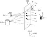
광 필드 표시 장치(1000)는 복수의 유기 발광 소자들을 포함하는 유기 발광 표시 패널(100) 및 복수의 마이크로 액정 렌즈(ML)들을 포함하며 유기 발광 표시 패널(100) 상에 집적되는 마이크로 렌즈 어레이(200)를 포함할 수 있다.The optical
유기 발광 표시 패널(100)은 유기 발광 소자를 포함하는 복수의 화소들을 포함할 수 있다. 각각의 화소들은 복수의 서브 화소들 (SP; 예를 들면 적색 서브 화소, 녹색 서브 화소, 청색 서브 화소)을 포함할 수 있다. 서브 화소들(SP)은 제1 방향(D1) 및 상기 제1 방향과 실질적으로 수직한 제2 방향(D2)으로 매트릭스 형태로 배열될 수 있다. 서브 화소들(SP) 각각은 화소 회로, 제1 전극, 유기 발광 표시층, 제2 전극으로 구성될 수 있다.The organic light emitting
마이크로 렌즈 어레이(200)는 유기 발광 표시 패널(100) 상에 집적된다. 일 실시예에서, 마이크로 렌즈 어레이(200)는 유기 발광 표시 패널(100)의 박막 봉지층 상에 집적될 수 있다. 마이크로 렌즈 어레이(200)는 복수의 마이크로 렌즈(ML)들을 포함할 수 있다. 유기 발광 표시 패널(100)의 서브 화소(SP)들에서 발생한 광들이 상기 마이크로 렌즈 어레이(200)의 마이크로 렌즈(ML)들을 통과하여 광 필드(light field)를 형성할 수 있다.The
상기 광 필드를 형성하기 위한 유기 발광 표시 패널(100)의 서브 화소(SP)들의 배열, 마이크로 렌즈 어레이(200)를 구성하는 마이크로 렌즈(ML)들의 배열 및 서브 화소(SP)들과 마이크로 렌즈(ML)들의 상대적인 위치 관계는 다양한 실시예로 구현될 수 있다.Arrangement of sub-pixels (SP) of the organic light emitting
마이크로 렌즈 어레이(200)는 액티브(active) 렌즈로 구성된다. 마이크로 렌즈 어레이(200)는 마이크로 렌즈 어레이를 구성하는 전극들에 인가되는 전압에 의해 전기장(전계)를 생성하고, 이에 따라 액정 분자의 배열을 변형시킬 수 있다. 마이크로 렌즈 어레이(200)은 2차원 표시 모드에서는 유기 발광 표시 패널(100)에서 표시된 영상이 그대로 투과되도록 하고, 3차원 표시 모드에서는 유기 발광 표시 패널(100)의 영상의 시역을 분리한다. 예컨대, 3차원 표시 모드로 동작하는 마이크로 렌즈 어레이(200)는 유기 발광 표시 패널(100)에 표시된 다시점 영상을 광의 회절 및 굴절 현상을 이용하여 각 시점 영상 별로 해당하는 시역에 상이 맺히도록 한다.The
도 1b에 도시된 바와 같이, '광 필드(Light Field)'는 빛이 공간 상에서 분포하는 상태를 광선의 분포를 통해 표현하는 개념이다. 이 개념을 이용하면 사물에서 반사되거나 발생한 빛은 공간 속을 직진하여 사람의 눈에 들어오는 것으로 정의되며, 삼차원 공간은 무수히 많은 광 필드로 구성될 수 있다. 개별적인 광 필드를 수학적으로 표현하는 데는 예를 들어, 5차원 플렌옵틱(Plenoptic) 함수가 사용될 수 있다. 즉, 공간 상의 특정 평면 상에서 광선이 평면을 지나는 점의 삼차원 공간 좌표 (x, y, z)와 광선이 향하는 공간 방향각 (θ, φ)에 대한 휘도로 표기될 수 있다. 광 필드는 앞에서 말한 특정 평면을 지나는 빛의 플렌옵틱 함수값을 정보화 함으로써 획득(capture)될 수 있다. 즉, 광 필드는 일정 영역의 (x, y, z) 좌표 각각에 대하여 (θ, φ)별 휘도값에 의해 획득될 수 있다. 예를 들어, 광 필드 카메라 (Light Field Camera)는 광 필드 획득을 목적으로 하는 카메라로, 2D 카메라가 공간 상의 특정 한 하나의 점 (=시점)에 대하여 (θ, φ)별 휘도값을 기록하는 것에 비하여, 광 필드 카메라는 일정 영역 내의 모든 좌표값에 대하여 (θ, φ)별 휘도값을 기록할 수 있다.As shown in Figure 1b, 'Light Field' is a concept that expresses the state in which light is distributed in space through the distribution of light rays. Using this concept, light reflected or generated from an object is defined as traveling straight through space and entering the human eye, and a three-dimensional space can be composed of countless light fields. For example, a five-dimensional plenoptic function can be used to mathematically represent individual light fields. In other words, it can be expressed as the luminance for the three-dimensional spatial coordinates (x, y, z) of the point where the ray passes through the plane on a specific plane in space and the spatial direction angle (θ, ϕ) toward which the ray is directed. The light field can be captured by informing the plenoptic function value of the light passing through the specific plane mentioned above. In other words, the light field can be obtained by the luminance value for each (θ, ϕ) for each (x, y, z) coordinate of a certain area. For example, a light field camera is a camera aimed at acquiring a light field. A 2D camera records luminance values for each (θ, ϕ) at a specific point (= viewpoint) in space. In comparison, a light field camera can record luminance values for each (θ, ϕ) for all coordinate values within a certain area.
상기 광 필드 카메라를 이용하여 획득한 상기 광 필드를 광 필드 표시 장치(1000)에 표시 하여, 사용자(2)는 사물(OJ1, OJ2)에 대한 3차원 영상을 시청할 수 있다. 광 필드 표시 장치(1000)는 광 필드를 구현할 수 있으므로, 사용자(2)가 이동함에 따라, 서로 다른 형태의 입체 영상을 시청할 수 있고, 따라서, 종래의 스테레오 방식 또는 다시점 방식의 입체 영상 표시 장치에 비해, 현실감 있는 입체 영상을 시청할 수 있다.By displaying the light field acquired using the light field camera on the light
도 2는 본 발명의 실시예들에 따른 광 필드 표시 장치를 나타내는 단면도이다.Figure 2 is a cross-sectional view showing a light field display device according to embodiments of the present invention.
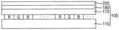
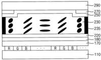
도 2를 참조하면, 광 필드 표시 장치(1000)는 하부 기판(110), 백-플레인 구조물, 제2 전극(170)을 포함하는 표시 구조물, 박막 봉지층(180), 하부 배향막(220), 액정층(230), 상부 렌즈 전극(270), 상부 기판(290)을 포함할 수 있다. 광 필드 표시 장치(1000)는 액정층(230)과 상부 렌즈 전극(270) 사이에 배치되는 상부 배향막(250)을 더 포함할 수 있다. 일 실시예에서, 상부 기판(290) 상에는 광의 투과축 방향 제어를 위한 편광자(polarizer)가 더 배치될 수 있다. 표시 구조물(120)은 화소 회로, 상기 화소 회로 상에 배치되는 제1 전극, 상기 제1 전극 상에 배치되는 유기 발광 표시층 및 상기 유기 발광 표시층 상에 배치되는 제2 전극(170)을 포함할 수 있다.Referring to FIG. 2, the optical
광 필드 표시 장치(1000)는 유기 발광 표시 패널(100) 및 유기 발광 표시 패널(100)의 발광면 상에 집적되는 마이크로 렌즈 어레이(200)로 구분될 수 있다.The optical
마이크로 렌즈 어레이(200)는 하부 배향막(220), 액정층(230), 상부 배향막(250), 상부 렌즈 전극(270) 및 상부 기판(290)을 포함할 수 있다.The
광 필드 표시 장치(1000)는 2차원 영상을 표시하는 2차원 표시 모드 및 3차원 영상(입체 영상)을 표시하는 3차원 표시 모드로 동작할 수 있다. 즉, 마이크로 렌즈 어레이(200)에 포함되는 액정 분자의 방향 분포가 제어됨으로써 2차원 영상 또는 3차원 영상이 제어될 수 있다. 상기 액정의 분자의 방향 분포는 액정층 상하부에 배치되는 구동 전극들에 인가되는 전압에 의해 제어될 수 있다.The light
3차원 표시 모드에서, 상부 렌즈 전극(270)은 액정층(230)의 상부 구동 전극으로 기능하고, 유기 발광 표시 패널(100)의 제2 전극(170)(예를 들어, 캐소드 전극)이 액정층(230)을 구동하는 하부 구동 전극으로 기능할 수 있다. 따라서, 상부 렌즈 전극(270)과 제2 전극(170) 사이에 형성된 전기장에 의해 액정층(230)에 포함되는 액정 분자의 배향 방향이 적절하게 조절될 수 있다.In the three-dimensional display mode, the
2차원 표시 모드에서는, 상부 렌즈 전극(270)에 전압을 인가하지 않음으로써 액정층(230)(즉, 제2 전극(170)과 상부 렌즈 전극(270) 사이)에 전기장이 생성되지 않는다. 따라서, 2차원 표시 모드에서는 서브 화소들(R, G, B)에서 출력되는 영상이 그대로 투과될 수 있다.In the two-dimensional display mode, an electric field is not generated in the liquid crystal layer 230 (that is, between the
하부 기판(110)은 광 필드 표시 장치(1000)의 백-플레이 기판 혹은 베이스 기판으로 제공될 수 있다. 하부 기판(110)은 폴리머 기판으로서 투명 절연 기판을 사용할 수 있으며, 예를 들면 투명성 및 소정의 유연성을 갖는 폴리머 재질의 기판을 사용할 수 있다.The
하부 기판(110) 상에 상기 화소 회로, 상기 화소 회로와 전기적으로 연결되는 상기 제1 전극, 상기 제1 전극 상에 배치되는 상기 유기 발광 표시층, 상기 표시층을 커버하며 상기 제1 전극과 대향하는 제2 전극(170)이 형성될 수 있다. 일 실시예에서, 상기 제1 전극은 서브 화소(R, G, B)의 애노드(anode) 전극으로 제공되고, 제2 전극(170)은 서브 화소(R, G, B)의 캐소드(cathode) 전극으로 제공될 수 있다.The pixel circuit on the
제2 전극(170)은 복수의 서브 화소들에 공통적으로 배치되는 공통 전극으로 제공될 수 있다. 제2 전극(170)은 알루미늄(Al), 은(Ag), 텅스텐(W), 구리(Cu), 니켈(Ni), 크롬(Cr), 몰리브덴(Mo), 티타늄(Ti), 백금(Pt), 탄탈륨(Ta), 네오디뮴(Nd), 스칸듐(Sc) 등과 같은 일 함수가 낮은 금속 물질 또는 이들 금속의 합금을 포함할 수 있다.The
제2 전극(170) 상에 표시 구조물(120)을 보호하기 위한 박막 봉지층(180)이 배치될 수 있다. 박막 봉지층(180)은 예를 들면, 실리콘 질화물 및/또는 금속 산화물과 같은 무기 물질을 포함할 수 있다. 또한, 박막 봉지층(180)은 평탄화를 위해 무기층들 사이에 유기층이 배치되는 다수의 층을 포함하는 형태를 가질 수도 있다. 이에 따라, 박막 봉지층(180)의 상면은 평탄한 형태를 가질 수 있다. 다만, 박막 봉지층(180)이 이에 한정되는 것은 아니고, 박막 봉지층은 리지드(rigid)한 글래스(glass) 기판으로 대체될 수도 있다.A thin
박막 봉지층(180) 상에 하부 배향막(220)이 직접 배치될 수 있다. 일 실시예에서, 하부 배향막(220)은 폴리이미드 계열의 고분자 수지를 포함할 수 있다. 하부 배향막(220)은 액정층(230)에 포함되는 액정 분자들의 초기 배향을 결정하고, 상기 액정 분자들의 배열 방향을 미리 결정할 수 있다.The
하부 배향막(220)은 저온 소성 공정에 의해 박막 봉지층(180) 상에 직접 배치될 수 있다. 백-플레인 구조물 및 표시 구조물의 변형을 방지하기 위해 약 100℃ 환경에서 하부 배향막(220)이 형성될 수 있다.The
일 실시예에서, 상기 폴리이미드 계열의 고분자 수지의 점도는 약 1.7cP(centi-poise) 내지 3cP를 가질 수 있다. 일 실시예에서, 박막 봉지층(180) 상에 코팅된 상기 폴리이미드 계열의 고분자 수지가 약 100℃ 환경에서 약 1분간 건조된 후 약 300nm 내지 320nm(바람직하게는 313nm)의 파장 및 약 20mW/cm2의 에너지를 갖는 자외선 경화를 거쳐 하부 배향막(220)이 형성될 수 있다. 하부 배향막(220)이 종래보다 상대적으로 저온 환경에서 유기 발광 표시 패널(100)의 박막 봉지층(180) 상에 직접 형성되므로, 하부 배향막(220) 형성 공정에 의해 표시 구조물이 변형되지 않는다.In one embodiment, the polyimide-based polymer resin may have a viscosity of about 1.7 cP (centi-poise) to 3 cP. In one embodiment, the polyimide-based polymer resin coated on the thin
마이크로 렌즈 어레이를 구성하기 위한 복수의 마이크로 액정 렌즈(ML)들을 포함하는 액정층(230)이 하부 배향막(220) 상에 배치될 수 있다. 일 실시예에서, 마이크로 액정 렌즈들 각각의 단면은 원형, 타원형, 육각형 중 적어도 하나의 형태를 가질 수 있다. 상기 마이크로 액정 렌즈의 피치(pitch)(가로 피치 및 세로 피치) 및 서브 화소의 피치에 따라 하나의 마이크로 액정 렌즈가 서브 화소들로부터 출력되는 광을 커버할 수 있는 시점 수가 결정될 수 있다. 예를 들어, 마이크로 액정 렌즈 당 15 수평 시점 수 및 7 수직 시점 수를 커버할 수 있다. 이에 따라, 다시점의 입체 영상이 구현될 수 있다. 이에 대해서는 도 6a 내지 도 6c를 참조하여 설명하기로 한다.A
마이크로 액정 렌즈(ML)의 수평 시점 수란 마이크로 액정 렌즈(ML)의 수평 피치에 대응하는 서브 화소들의 수평 방향으로의 개수를 말한다. 마이크로 렌즈(ML)의 수직 시점 수란 마이크로 액정 렌즈(ML)의 수직 피치에 대응하는 서브 화소들의 수직 방향으로의 개수를 말한다.The number of horizontal viewpoints of the micro liquid crystal lens (ML) refers to the number of sub-pixels in the horizontal direction corresponding to the horizontal pitch of the micro liquid crystal lens (ML). The number of vertical viewpoints of the micro lens (ML) refers to the number of sub-pixels in the vertical direction corresponding to the vertical pitch of the micro liquid crystal lens (ML).
액정층(230)은 하부 배향막(220)과 상부 배향막(250)의 사이에 주입하거나 또는 적하하는 과정을 거쳐 형성될 수 있다.The
일 실시예에서, 마이크로 액정 렌즈(ML)는 구동 전극들 사이의 거리 차이에 기초하여 액정을 제어하는 갭 컨트롤 렌즈(gap control lens) 방식, 액정 구동 전극들에 인가되는 전압 차이를 조절하여 액정을 제어하는 전압 컨트롤 렌즈(voltage control lens; VCL) 방식, 프레넬 렌즈(gresnel lens) 방식 등의 방식에 기초하여 제어될 수 있다.In one embodiment, the micro liquid crystal lens (ML) is a gap control lens that controls the liquid crystal based on the distance difference between the driving electrodes, and controls the liquid crystal by adjusting the voltage difference applied to the liquid crystal driving electrodes. It can be controlled based on a method such as a voltage control lens (VCL) method or a Fresnel lens method.
상부 배향막(250)이 액정층(230)과 상부 렌즈 전극(270) 사이에 배치될 수 있다. 일 실시예에서, 상부 배향막(250)은 상기 폴리이미드 계열의 고분자 수지를 포함할 수 있다. 상부 배향막(250)은 액정층(230)에 포함되는 액정 분자들의 초기 배향을 결정하고, 상기 액정 분자들의 배열 방향을 미리 결정할 수 있다.The
상부 렌즈 전극(270)은 액정층(230) 및 상부 배향막(250) 상에 배치될 수 있다. 상부 렌즈 전극(270)은 상기 3차원 표시 모드에서 제2 전극(170)과 전기장을 형성할 수 있다. 상부 렌즈 전극(270)은 각각의 마이크로 액정 렌즈(ML)를 둘러싸는 고리 형태의 패턴들을 가질 수 있다. 일 실시예에서, 상부 렌즈 전극(270)의 상기 패턴들 각각의 평면 형상의 바깥쪽 변은 육각형일 수 있다. 일 실시예에서, 상부 렌즈 전극(270)의 상기 패턴들 각각의 평면 형상의 바깥쪽 변은 사각형일 수 있다. 일 실시예에서, 상부 렌즈 전극(270)의 상기 패턴들 각각의 평면 형상의 바깥쪽 변은 원형일 수 있다. 다만, 이는 예시적인 것으로서, 상부 렌즈 전극(270)의 패턴이 이에 한정되는 것은 아니다.The
상부 렌즈 전극(270)은 인듐- 아연 산화물(Indium Zinc Oxide: IZO), 인듐-주석 산화물(Idium Tin Oxide; ITO) 등을 포함할 수 있다.The
일 실시예에서, 상부 렌즈 전극(270)의 각각의 패턴의 폭(W)은 마이크로 액정 렌즈(ML)의 피치의 약 3% 내지 20% 범위에 포함될 수 있다. 이에 따라, 상부 렌즈 전극(270)의 배치에 의한 의도치 않은 광의 굴절 및 회절 등이 방지될 수 있다.In one embodiment, the width W of each pattern of the
상부 기판(290)은 상부 렌즈 전극(270) 상에 배치될 수 있다.The
일 실시예에서, 광 필드 표시 장치(1000)는 상부 기판(290) 상에 배치되는 터치 센싱 유닛을 더 포함할 수 있다.In one embodiment, the light
상술한 바와 같이, 본 발명의 실시예들에 따른 광 필드 표시 장치(1000)는 유기 발광 표시 패널(100) 상에 마이크로 렌즈 어레이를 포함하는 액정 렌즈 구조가 직접적으로 집적됨으로써, 액정 렌즈 패널 제조에 필요한 기판 및 액정 렌즈의 하부 전극이 제거될 수 있다. 이에 따라, 광 필드 표시 장치(1000)의 제조 비용이 감소되고, 광 필드 표시 장치(1000)의 두께가 감소되며, 플렉서블한 유기 발광 표시 패널(100)을 이용한 광 필드 디스플레이가 가능해질 수 있다. 사용자는 다시점을 이용한 자연스러운 입체 영상을 시청할 수 있다. 또한, 유기 발광 표시 패널(100)의 제2 전극(170)이 액정층 제어를 위한 구동 전극으로 활용되며, 상부 렌즈 전극(270)에 인가되는 전압만을 제어함으로써, 2차원/3차원 표시 모드를 구현할 수 있다.As described above, the optical
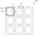
도 3a는 도 2의 광 필드 표시 장치에 포함되는 마이크로 렌즈 어레이와 상부 렌즈 전극의 일 예를 나타내는 평면도이다. 도 3b는 도 3a의 I-I'라인을 따라 자른 단면의 일부를 개략적으로 나타내는 단면도이다.FIG. 3A is a plan view showing an example of a micro lens array and an upper lens electrode included in the optical field display device of FIG. 2. FIG. 3B is a cross-sectional view schematically showing a portion of a cross section taken along line II′ of FIG. 3A.
도 2 내지 도 3b를 참조하면, 마이크로 렌즈 어레이(MLA)는 복수의 마이크로 액정 렌즈(ML)들을 포함할 수 있다.Referring to FIGS. 2 to 3B , the micro lens array (MLA) may include a plurality of micro liquid crystal lenses (ML).
일 실시예에서, 마이크로 액정 렌즈(ML)의 평면 형상은 원형 또는 타원형일 수 있다. 마이크로 액정 렌즈(ML)들은 상부 렌즈 전극(270A)의 패턴들에 의해 서로 이격하여 배치될 수 있다. 다만, 이는 예시적인 것으로서, 마이크로 액정 렌즈(ML)의의 배열이 이에 한정되는 것은 아니다. 상기 원형 또는 타원형 모양은 마이크로 렌즈(ML)의 필 팩터(fill factor)가 최대가 될 수 있도록, 서로 인접하는 두 마이크로 렌즈(ML)들이 중 어느 한쪽이 함입되어 형성될 수 있다. 즉, 상기 원형 또는 타원형 모양의 가장자리의 일부는 함몰된 형상일 수 있다. 상기 필 팩터란 마이크로 렌즈들이 형성된 평면에서 마이크로 렌즈 들이 실제 차지하는 면적의 비율을 말한다.In one embodiment, the planar shape of the micro liquid crystal lens ML may be circular or oval. The micro liquid crystal lenses ML may be arranged to be spaced apart from each other by patterns of the
일 실시예에서, 상부 렌즈 전극(270A)은 마이크로 액정 렌즈(ML)들 각각을 둘러싸는 고리 형태의 전극 패턴(EP)들을 가질 수 있다. 예를 들어, 상기 각각의 전극 패턴(EP)의 평면 형상의 안쪽 형상은 마이크로 액정 렌즈(ML)에 대응하는 원형 또는 타원형이고, 바깥쪽 형상은 육각형의 형상일 수 있다.In one embodiment, the
마이크로 액정 렌즈(ML)가 형성되지 않는 부분에 대응하는 서브 화소로부터 발생한 광은 입체 영상 구현을 위해 원하는 광 필드 형성에 방해가 될 수 있으므로(즉, crosstalk가 발생됨), 마이크로 액정 렌즈(ML)가 형성되지 않는 부분은 최소화 되는 것이 바람직하다. 따라서, 일 실시예에서, 상부 렌즈 전극(270A)의 패턴(EP)의 폭(W)은 마이크로 액정 렌즈(ML)의 피치(pitch, P)의 약 3% 내지 20% 범위 내에 포함될 수 있다. 예를 들어, 마이크로 액정 렌즈(ML)의 피치(P)가 약 500μm인 경우, 전극 패턴(EP)의 폭(W)은 약 2μm 내지 10μm 범위 내에서 형성될 수 있다. 마이크로 액정 렌즈(ML)의 피치(P)가 약 55μm인 경우, 전극 패턴(EP)의 폭(W)은 약 1μm 내지 5μm 범위 내에서 형성될 수 있다. 여기서, 마이크로 렌즈(ML)의 피치는 이웃하는 마이크로 렌즈(ML)들의 중심들 사이의 거리를 의미한다.The light generated from the sub-pixel corresponding to the area where the micro liquid crystal lens (ML) is not formed may interfere with the formation of the desired light field for stereoscopic imaging (i.e., crosstalk occurs), so the micro liquid crystal lens (ML) is It is desirable to minimize the unformed portion. Accordingly, in one embodiment, the width W of the pattern EP of the
일 실시예에서, 마이크로 렌즈 어레이(MLA)에 포함되는 마이크로 렌즈(ML)들의 피치(P)들은 실질적으로 동일할 수 있다.In one embodiment, the pitches (P) of the micro lenses (ML) included in the micro lens array (MLA) may be substantially the same.
도 3b에 도시된 바와 같이, 유기 발광 표시 패널의 제2 전극(170)(예를 들어, 캐소드 전극) 상에 배치되는 박막 봉지층(180) 상에 하부 배향막(220)이 배치될 수 있다. 또한, 패터닝된 상부 렌즈 전극(270A)과 상부 배향막(250)이 형성된 상부 기판(290)과 하부 배향막(210) 사이에 마이크로 렌즈(ML)들을 포함하는 액정층(230)이 배치될 수 있다.As shown in FIG. 3B, the
3차원 표시 모드에서, 상기 전극 패턴(EP)을 갖는 상부 렌즈 전극(270A)과 유기 발광 표시 패널의 공통 전극인 제2 전극(캐소드) 사이에 발생된 전기장에 의해 마이크로 렌즈 어레이(MLA)에 포함되는 액정 분자들이 재배열되고, 광 필드가 구현될 수 있다.In the 3D display mode, included in the micro lens array (MLA) by an electric field generated between the
도 4는 도 2의 광 필드 표시 장치에 포함되는 마이크로 렌즈 어레이와 상부 렌즈 전극의 다른 예를 나타내는 평면도이다.FIG. 4 is a plan view showing another example of a micro lens array and an upper lens electrode included in the optical field display device of FIG. 2.
도 4를 참조하면, 상기 광 필드 표시 장치는 상부 렌즈 전극의 패턴의 형상을 제외하고, 도 3a의 광 필드 표시 장치와 실질적으로 동일할 수 있다. 따라서 반복되는 설명은 간략히 하거나 생략한다.Referring to FIG. 4 , the light field display device may be substantially the same as the light field display device of FIG. 3A except for the shape of the pattern of the upper lens electrode. Therefore, repeated explanations are simplified or omitted.
마이크로 렌즈 어레이(MLA)는 복수의 마이크로 액정 렌즈(ML)들을 포함할 수 있다.The micro lens array (MLA) may include a plurality of micro liquid crystal lenses (ML).
일 실시예에서, 마이크로 액정 렌즈(ML)의 평면 형상은 원형 또는 타원형일 수 있다. 마이크로 액정 렌즈(ML)들은 상부 렌즈 전극(270B)의 패턴들에 의해 서로 이격하여 배치될 수 있다.In one embodiment, the planar shape of the micro liquid crystal lens ML may be circular or oval. The micro liquid crystal lenses ML may be arranged to be spaced apart from each other by patterns of the
일 실시예에서, 상부 렌즈 전극(270B)은 마이크로 액정 렌즈(ML)들 각각을 둘러싸는 고리 형태의 전극 패턴들을 가질 수 있다. 예를 들어, 상기 각각의 전극 패턴의 평면 형상의 안쪽 형상은 마이크로 액정 렌즈(ML)에 대응하는 원형 또는 타원형이고, 바깥쪽 형상은 사각형의 형상일 수 있다. 상부 렌즈 전극(270B)의 패턴의 폭(W)은 마이크로 액정 렌즈(ML)의 피치(P)의 약 3% 내지 20% 범위 내에 포함될 수 있다.In one embodiment, the
3차원 표시 모드에서, 상기 전극 패턴을 갖는 상부 렌즈 전극(270B)과 유기 발광 표시 패널의 공통 전극인 제2 전극(캐소드) 사이에 발생된 전기장에 의해 마이크로 렌즈 어레이(MLA)에 포함되는 액정 분자들이 재배열되고, 광 필드가 구현될 수 있다.In the three-dimensional display mode, liquid crystal molecules included in the micro lens array (MLA) by the electric field generated between the
도 5는 도 2의 광 필드 표시 장치에 포함되는 마이크로 렌즈 어레이와 상부 렌즈 전극의 또 다른 예를 나타내는 평면도이다.FIG. 5 is a plan view showing another example of a micro lens array and an upper lens electrode included in the optical field display device of FIG. 2.
도 5를 참조하면, 상기 광 필드 표시 장치는 상부 렌즈 전극의 패턴의 형상 및 마이크로 액정 렌즈의 형상을 제외하고, 도 3a의 광 필드 표시 장치와 실질적으로 동일할 수 있다. 따라서 반복되는 설명은 간략히 하거나 생략한다.Referring to FIG. 5 , the optical field display device may be substantially the same as the optical field display device of FIG. 3A except for the shape of the pattern of the upper lens electrode and the shape of the micro liquid crystal lens. Therefore, repeated explanations are simplified or omitted.
마이크로 렌즈 어레이(MLA)는 복수의 마이크로 액정 렌즈(ML)들을 포함할 수 있다.The micro lens array (MLA) may include a plurality of micro liquid crystal lenses (ML).
일 실시예에서, 마이크로 액정 렌즈(ML)의 평면 형상은 육각형일 수 있다. 마이크로 액정 렌즈(ML)들은 상부 렌즈 전극(270C)의 패턴들에 의해 서로 이격하여 배치될 수 있다.In one embodiment, the planar shape of the micro liquid crystal lens ML may be hexagonal. The micro liquid crystal lenses ML may be arranged to be spaced apart from each other by patterns of the
일 실시예에서, 상부 렌즈 전극(270C)은 마이크로 액정 렌즈(ML)들 각각을 둘러싸는 고리 형태의 전극 패턴들을 가질 수 있다. 예를 들어, 상기 각각의 전극 패턴의 평면 형상의 안쪽 형상은 마이크로 액정 렌즈(ML)에 대응하는 육각형이고, 바깥쪽 형상도 육각형의 형상일 수 있다. 상부 렌즈 전극(270C)의 패턴의 폭(W)은 마이크로 액정 렌즈(ML)의 피치(P)의 약 3% 내지 20% 범위 내에 포함될 수 있다.In one embodiment, the
3차원 표시 모드에서, 상기 전극 패턴을 갖는 상부 렌즈 전극(270C)과 유기 발광 표시 패널의 공통 전극인 제2 전극(캐소드) 사이에 발생된 전기장에 의해 마이크로 렌즈 어레이(MLA)에 포함되는 액정 분자들이 재배열되고, 광 필드가 구현될 수 있다.In the 3D display mode, liquid crystal molecules included in the micro lens array (MLA) by the electric field generated between the
도 6a 내지 도 6c는 도 2의 광 필드 표시 장치에서 마이크로 렌즈 어레이와 서브 화소들의 배치 관계의 일 예들을 나타내는 도면들이다.FIGS. 6A to 6C are diagrams showing examples of the arrangement relationship between the micro lens array and sub-pixels in the light field display device of FIG. 2.
도 6a 내지 도 6c를 참조하면, 광 필드 표시 장치는 복수의 서브 화소들(SP)을 포함하는 표시 패널 및 상부 렌즈 전극 패턴으로 각각 둘러싸인 복수의 마이크로 렌즈(ML)를 포함하는 마이크로 렌즈 어레이를 포함할 수 있다.Referring to FIGS. 6A to 6C , the optical field display device includes a display panel including a plurality of sub-pixels (SP) and a micro-lens array including a plurality of micro-lenses (ML) each surrounded by an upper lens electrode pattern. can do.
서브 화소들(SP)은 제1 방향(D1) 및 상기 제1 방향(D1)과 실질적으로 수직한 제2 방향(D2)으로 매트릭스 형태로 배열될 수 있다. 도면상에서는 선으로 표시되어 있으나, 인접하는 서브 화소들(SP) 사이에는 광을 차단하는 블랙 매트릭스가 형성될 수 있다.The sub-pixels SP may be arranged in a matrix form in a first direction D1 and a second direction D2 substantially perpendicular to the first direction D1. Although indicated as a line in the drawing, a black matrix that blocks light may be formed between adjacent sub-pixels SP.
서브 화소들(SP)은 적색 광을 방출하는 적색 서브 화소(R), 녹색 광을 방출하는 녹색 서브 화소(G), 청색 광을 방출하는 청색 서브 화소(B)를 포함할 수 있다(RGB 구조). 일 실시예에서, 적색 서브 화소(R), 녹색 서브 화소(G) 및 청색 서브 화소(B)는 제1 방향(D1)을 따라 반복적으로 배열될 수 있다. 적색 서브 화소들(R), 녹색 서브 화소들(G) 및 청색 서브 화소들(B)은 제2 방향(D2)을 따라 각각 연속적으로 배열될 수 있다. 즉, 적색 서브 화소(R), 녹색 서브 화소(G) 및 청색 서브 화소(B)는 스트립(strip) 형태로 배열될 수 있다.The sub-pixels SP may include a red sub-pixel (R) that emits red light, a green sub-pixel (G) that emits green light, and a blue sub-pixel (B) that emits blue light (RGB structure) ). In one embodiment, the red sub-pixel (R), green sub-pixel (G), and blue sub-pixel (B) may be repeatedly arranged along the first direction D1. The red sub-pixels (R), green sub-pixels (G), and blue sub-pixels (B) may each be sequentially arranged along the second direction D2. That is, the red sub-pixel (R), green sub-pixel (G), and blue sub-pixel (B) may be arranged in a strip shape.
마이크로 렌즈(ML)의 평면 형상은 육각형 모양을 가질 수 있다. 일 실시예에서, 상기 육각형 모양은 좌우 대칭으로 두 변의 길이가 다른 네 변의 길이보다 길 수 있다. 일 실시예에서, 상기 육각형 모양은 정육각형일 수 있다. 또 다른 실시예에서, 상기 육각형 모양은 좌우 대칭으로 두 변의 길이가 다른 네 변의 길이보다 짧은 모양일 수 있다. 또 다른 실시예에서, 상기 육각형 모양 두 변의 길이가 동일하고, 좌우 비대칭인 육각형 모양일 수 있다.The planar shape of the micro lens ML may have a hexagonal shape. In one embodiment, the hexagonal shape is left-right symmetrical and the length of two sides may be longer than the length of the other four sides. In one embodiment, the hexagonal shape may be a regular hexagon. In another embodiment, the hexagonal shape may be left-right symmetrical, with two sides shorter than the other four sides. In another embodiment, the hexagon shape may be a hexagon shape in which two sides have the same length and are left and right asymmetric.
마이크로 렌즈들(ML)을 둘러싸는 상부 렌즈 전극의 각각의 패턴의 인접하는 변이 서로 접하도록 배치되어 벌집 구조를 형성할 수 있다.Adjacent sides of each pattern of the upper lens electrode surrounding the micro lenses ML may be arranged to contact each other to form a honeycomb structure.
마이크로 렌즈들(ML)은 각각 상기 제1 방향(D1)과 상기 제2 방향(D2)에 대해 기 설정된 틸트(tilt) 각도(θ) 기울어져 배열될 수 있다. 일 실시예예서, 상기 틸트 각도(θ)는 서브 화소의 제1 방향(D1)으로의 피치, 서브 화소의 제2 방향(D2)으로의 피치, 및 마이크로 렌즈(ML)의 수평 시점수에 기초하여 결정될 수 있다.The micro lenses ML may be arranged at a preset tilt angle θ with respect to the first direction D1 and the second direction D2, respectively. In one embodiment, the tilt angle θ is based on the pitch of the sub-pixel in the first direction D1, the pitch of the sub-pixel in the second direction D2, and the number of horizontal viewpoints of the micro lens ML. It can be decided.
상기 마이크로 렌즈(ML)의 수평 시점 수란 마이크로 렌즈(ML)의 수평 피치(즉, 제1 방향(D1)으로의 피치)에 대응하는 서브 화소들의 상기 제1 방향(D1)으로의 개수를 말한다. 마이크로 렌즈(ML)의 수직 시점 수란 마이크로 렌즈(ML)의 수직 피치(즉, 제2 방향(D2)으로의 피치)에 대응하는 서브 화소들의 상기 제2 방향(D2)으로의 개수를 말한다.The number of horizontal viewpoints of the micro lens ML refers to the number of sub-pixels in the first direction D1 corresponding to the horizontal pitch of the micro lens ML (that is, the pitch in the first direction D1). The number of vertical viewpoints of the micro lens ML refers to the number of sub-pixels in the second direction D2 corresponding to the vertical pitch of the micro lens ML (that is, the pitch in the second direction D2).
마이크로 렌즈(ML)의 수평 피치란 이웃하는 마이크로 렌즈들의 중심들 간의 상기 제1 방향(D1)으로의 거리를 말한다. 상기 마이크로 렌즈(ML)의 수직 피치란 이웃하는 마이크로 렌즈들의 중심들 간의 상기 제2 방향(D1)으로의 거리를 말한다.The horizontal pitch of the micro lens ML refers to the distance between the centers of neighboring micro lenses in the first direction D1. The vertical pitch of the micro lens ML refers to the distance between centers of neighboring micro lenses in the second direction D1.
상기 수평 시점수는 하나의 단위 화소를 구성하는 서브 화소들(SP)의 개수와 관련되어 결정될 수 있다. 상기 수직 시점 수는 하나의 서브 화소의 가로, 세로 피치 및 단위 화소를 구성하는 서브 화소들 수에 따라 결정될 수 있다.The number of horizontal viewpoints may be determined in relation to the number of sub-pixels (SP) constituting one unit pixel. The number of vertical viewpoints may be determined according to the horizontal and vertical pitches of one sub-pixel and the number of sub-pixels constituting a unit pixel.
이에 따라, 광 필드 표시 장치는 수평 시점 및 수직 시점이 반영된 다시점(예를 들어, 수평 시점수 15, 수직 시점수 7의 105 시점수)의 입체 영상을 출력할 수 있으며, 사용자는 특정 색상이 강조되지 않는 자연스러운 입체 영상을 시청할 수 있다.Accordingly, the light field display device can output a stereoscopic image of multiple views (for example, 105 views with the number of horizontal views and 7 vertical views) reflecting the horizontal and vertical views, and the user can select a specific color. You can watch natural three-dimensional images without emphasis.
도 6b에 도시된 바와 같이, 서브 화소들(SP)은 제1 방향(D1) 및 상기 제1 방향(D1)과 실질적으로 수직한 제2 방향(D2)으로 매트릭스 형태로 배열될 수 있다. 상기 서브 화소들(SP)은 적색 서브 화소(R), 녹색 서브 화소(G), 청색 서브 화소(B) 및 백색 서브 화소(W)를 포함할 수 있다. (RGBW 구조) 적색 서브 화소(R), 녹색 서브 화소(G), 청색 서브 화소(B) 및 백색 서브 화소(W)는 타일 형식으로 배열될 수 있다.As shown in FIG. 6B, the sub-pixels SP may be arranged in a matrix form in a first direction D1 and a second direction D2 substantially perpendicular to the first direction D1. The sub-pixels SP may include a red sub-pixel (R), a green sub-pixel (G), a blue sub-pixel (B), and a white sub-pixel (W). (RGBW structure) The red sub-pixel (R), green sub-pixel (G), blue sub-pixel (B), and white sub-pixel (W) may be arranged in a tile format.
상기 마이크로 렌즈(ML)는 육각형 모양을 가질 수 있다. 상기 육각형의 마주보는 두변의 길이가 동일할 수 있다. 상기 육각형의 좌, 우측 변은 상기 제2 방향(D2)과 평행하고, 상부 꼭지점과 하부 꼭지점을 연결한 선은 상기 제2 방향(D2)에 대해 소정 각도 (α) 기울어 질 수 있다. 즉, 상기 마이크로 렌즈는 비대칭 육각형 모양을 가질 수 있다. 예를 들면, 상기 육각형의 상기 상부 꼭지점과 상기 하부 꼭지점의 상기 제1 방향(D1)으로의 이격 거리는 하나의 서브 화소 가로 피치 이하 이도록, 상기 소정 각도(α)가 결정될 수 있다. 본 실시예에서는 상기 마이크로 렌즈(ML)의 수평 시점수는 15, 수직 시점수는 7인 경우가 예시되어 있다.The micro lens ML may have a hexagonal shape. The two opposite sides of the hexagon may have the same length. The left and right sides of the hexagon are parallel to the second direction (D2), and a line connecting the upper and lower vertices may be inclined at a predetermined angle (α) with respect to the second direction (D2). That is, the micro lens may have an asymmetric hexagonal shape. For example, the predetermined angle α may be determined such that the separation distance between the upper vertex and the lower vertex of the hexagon in the first direction D1 is less than one sub-pixel horizontal pitch. In this embodiment, the number of horizontal viewpoints of the micro lens ML is 15 and the number of vertical viewpoints is 7.
도 6c에 도시된 바와 같이, 상기 서브 화소들(SP)은 적색 서브 화소(R), 녹색 서브 화소(G) 및 청색 서브 화소(B)를 포함할 수 있다. 제n 행에서, 상기 제1 방향(D1)으로 적색 서브 화소(R), 녹색 서브 화소(G), 청색 서브 화소(B) 및 상기 블랙 매트릭스(BM)가 반복적으로 배열되고, 제n+1 행에서, 상기 제1 방향(D1)으로 상기 블랙 매트릭스(BM) 및 녹색 서브 화소(G)가 반복적으로 배열될 수 있다. (소위 RGBG pentile 구조)As shown in FIG. 6C, the sub-pixels SP may include a red sub-pixel (R), a green sub-pixel (G), and a blue sub-pixel (B). In the n-th row, the red sub-pixel (R), green sub-pixel (G), blue sub-pixel (B) and the black matrix (BM) are repeatedly arranged in the first direction (D1), and the n+1 In a row, the black matrix BM and the green sub-pixel G may be repeatedly arranged in the first direction D1. (so-called RGBG pentile structure)
상기 마이크로 렌즈(ML)는 육각형 모양을 가질 수 있다. 상기 육각형의 마주보는 두변의 길이가 동일할 수 있다. 상기 육각형의 좌, 우측 변은 상기 제2 방향(D2)과 평행하고, 상부 꼭지점과 하부 꼭지점을 연결한 선은 상기 제2 방향(D2)에 대해 소정 각도 (α) 기울어 질 수 있다. 즉, 상기 마이크로 렌즈는 비대칭 육각형 모양을 가질 수 있다. 예를 들면, 상기 육각형의 상기 상부 꼭지점과 상기 하부 꼭지점의 상기 제1 방향(D1)으로의 이격 거리는 하나의 서브 화소 가로 피치 이하 이도록, 상기 소정 각도(α)가 결정될 수 있다.The micro lens ML may have a hexagonal shape. The two opposite sides of the hexagon may have the same length. The left and right sides of the hexagon are parallel to the second direction (D2), and a line connecting the upper and lower vertices may be inclined at a predetermined angle (α) with respect to the second direction (D2). That is, the micro lens may have an asymmetric hexagonal shape. For example, the predetermined angle α may be determined such that the separation distance between the upper vertex and the lower vertex of the hexagon in the first direction D1 is less than one sub-pixel horizontal pitch.
도 7은 도 2의 광 필드 표시 장치에 포함되는 유기 발광 표시 패널의 일 예를 나타내는 단면도이다.FIG. 7 is a cross-sectional view showing an example of an organic light emitting display panel included in the optical field display device of FIG. 2.
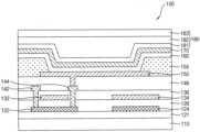
도 7을 참조하면, 유기 발광 표시 패널(100)은 하부 기판(110), 하부 기판 상에 형성된 백-플레인(Back Plane) 구조물, 상기 백-플레인 구조물 상에 적층되는 표시 구조물을 포함할 수 있다.Referring to FIG. 7 , the organic light emitting
하부 기판(110)은 폴리머 기판(105)으로서 투명 절연 기판을 사용할 수 있다.The
하부 기판(110) 상에 버퍼층(121)이 배치될 수 있다. 버퍼층(121)은 실리콘 산화막 및 실리콘 질화막이 적층된 구조를 가질 수 있다. 버퍼층(121) 상에는 액티브 패턴(122, 124)이 배치될 수 있다. 게이트 절연막(126)은 버퍼층(121) 상에 형성되어 상기 액티브 패턴들을 커버할 수 있다. 게이트 절연막(126)은 실리콘 산화물 혹은 실리콘 질화물을 포함할 수 있다. 게이트 절연막(126) 상에는 게이트 전극(132, 134)이 배치될 수 있다. 층간 절연막(136)은 게이트 절연막(126) 상에 형성되어 게이트 전극들(132, 134)을 커버할 수 있다. 층간 절연막(136)은 실리콘 산화물 혹은 실리콘 질화물을 포함할 수 있다. 소스 전극(142) 및 드레인 전극(144)은 층간 절연막(136) 및 게이트 절연막(126)을 관통하여 각각 액티브 패턴(122)의 소스 영역 및 드레인 영역에 각각 접촉될 수 있다.A
상술한 제1 액티브 패턴(122), 게이트 절연막(126), 게이트 전극(132), 소스 전극(142) 및 드레인 전극(144)에 의해 상기 박막 트랜지스터가 정의될 수 있다. 또한, 액티브 패턴(124), 게이트 절연막(126) 및 게이트 전극(134)에 의해 커패시터가 정의될 수 있다.The thin film transistor may be defined by the above-described first
비아 절연막(146)은 층간 절연막(136) 상에 형성되어 소스 전극(142) 및 드레인 전극(144)을 커버할 수 있다. 비아 절연막(146)은 실질적으로 평탄화 층으로 제공될 수 있다.The via insulating
비아 절연막(146) 상에는 상기 표시 구조물이 적층될 수 있다. 일 실시예에서, 상기 표시 구조물은 비아 절연막(146) 상에 순차적으로 적층되는 제1 전극(150), 유기 발광 표시층(160) 및 제2 전극(170)을 포함할 수 있다.The display structure may be stacked on the via insulating
제1 전극(150)은 화소 전극으로 제공되며, 각 화소 마다 형성될 수 있다. 또한, 제1 전극(150)은 유기 발광 표시 패널(100)의 애노드 전극으로 제공될 수 있다. 화소 정의막(155)은 비아 절연막(146) 상에 배치되어, 제1 전극(150)의 주변부를 커버할 수 있다. 유기 발광 표시층(160)은 화소 정의막(155) 및 제1 전극(150) 상에 배치될 수 있다. 유기 발광 표시층(160)은 적색 서브 화소, 녹색 서브 화소 및 청색 서브 화소마다 독립적으로 패터닝되어 각 화소별로 다른 색광들을 발생시키는 유기 발광층을 포함할 수 있다.The first electrode 150 serves as a pixel electrode and can be formed for each pixel. Additionally, the first electrode 150 may serve as an anode electrode of the organic light emitting
제2 전극(170)은 화소 정의막(155) 및 표시층(160) 상에 배치될 수 있다. 일 실시예에서, 제2 전극(170)은 복수의 서브 화소들에 공통적으로 배치되는 공통 전극으로 제공될 수 있다. 또한, 제2 전극(170)은 제1 전극(150)과 대향하며 유기 발광 표시 패널의 캐소드 전극으로 제공될 수 있다.The
제2 전극(170) 상에는 상기 표시 구조물을 보호하기 위한 박막 봉지층(180)이 배치될 수 있다. 박막 봉지층(180)은 예를 들면, 실리콘 질화물 및/또는 금속 산화물과 같은 무기 물질을 포함할 수 있다. 일 실시예에서, 봉지층(181) 상기 무기 물질을 포함하는 제1 무기층(181), 제1 무기층 상에 배치되어 평탄화층 역할을 하는 유기층(182) 및 상기 유기층(182) 상에 배치되어 봉지 역할을 하는 제2 무기층이 배치될 수 있다. 유기층(182)은 폴리이미드, 에폭시계 수지, 아크릴계 수지, 폴리에스테르와 같은 유기 물질을 포함할 수 있다.A thin
일 실시예에서, 제2 전극 상에 박막 봉지층(180) 대신 글라스(glass) 기판이 배치될 수도 있다.In one embodiment, a glass substrate may be disposed on the second electrode instead of the thin
상기 평탄화된 박막 봉지층(180) 상에 하부 배향막 또는 하부 렌즈 전극이 형성될 수 있다.A lower alignment layer or lower lens electrode may be formed on the flattened thin
도 8a 내지 도 8e는 본 발명의 실시예들에 따른 광 필드 표시 장치의 제조 방법을 설명하기 위한 단면도들이다.8A to 8E are cross-sectional views for explaining a method of manufacturing a light field display device according to embodiments of the present invention.
도 8a 내지 도 8e를 참조하면 광 필드 표시 장치의 제조 방법은 하부 기판, 제1 전극, 유기 발광 표시층, 제2 전극, 및 상기 제2 전극을 커버하는 박막 봉지층 순으로 적층되는 유기 발광 표시 패널을 형성하고, 상기 박막 봉지층 상에 하부 배향막을 형성하며, 상부 렌즈 전극을 상부 기판 하면에 패터닝하고, 상기 상부 렌즈 전극을 커버하는 상부 배향막을 상기 상부 기판 하면에 형성하고, 상기 하부 배향막 또는 상기 상부 배향막 상에 복수의 마이크로 액정 렌즈들을 포함하는 마이크로 렌즈 어레이를 구성하기 위한 액정층을 형성한 후, 상기 하부 배향막과 상기 상부 배향막 사이에 상기 액정층이 배치되도록 상기 상부 기판과 상기 박막 봉지층을 합착하는 것을 포함할 수 있다.Referring to FIGS. 8A to 8E, the method of manufacturing an optical field display device includes stacking a lower substrate, a first electrode, an organic light emitting display layer, a second electrode, and a thin film encapsulation layer covering the second electrode in that order. Forming a panel, forming a lower alignment film on the thin film encapsulation layer, patterning an upper lens electrode on the lower surface of the upper substrate, forming an upper alignment film covering the upper lens electrode on the lower surface of the upper substrate, and forming the lower alignment film or After forming a liquid crystal layer on the upper alignment layer to form a micro lens array including a plurality of micro liquid crystal lenses, the upper substrate and the thin film encapsulation layer are aligned so that the liquid crystal layer is disposed between the lower alignment layer and the upper alignment layer. It may include cementing.
도 7 및 도 8a에 도시된 바와 같이, 하부 기판(110), 백-플레인 구조물, 제1 전극, 유기 발광 표시층, 제2 전극(170) 및 제2 전극(170)을 커버하는 박막 봉지층(180)이 순차적으로 적층되는 유기 발광 표시 패널(100)이 형성될 수 있다. 일 실시예에서, 제2 전극(170)은 복수의 서브 화소들에 공통적으로 배치되는 공통 전극으로 제공될 수 있다. 또한, 제2 전극(170)은 제1 전극(150)과 대향하며 상기 투명 표시 장치의 캐소드로 제공될 수 있다. 박막 봉지층(180)은 제1 무기층, 평탄화를 위한 유기층, 및 제2 무기층이 순서대로 적층되어 박막 봉지층(180)이 형성될 수 있다.As shown in FIGS. 7 and 8A, the
박막 봉지층(180) 상에 하부 배향막(220)이 형성될 수 있다. 일 실시예에서, 하부 배향막(220)은 폴리이미드 계열의 고분자 수지를 포함할 수 있다. 실시예에서, 상기 폴리이미드 계열의 고분자 수지의 점도는 약 1.7cP(centi-poise) 내지 3cP를 가질 수 있다. 하부 배향막(220)은 저온 소성 공정에 의해 박막 봉지층(180) 상에 직접 형성될 수 있다. 일 실시예에서, 박막 봉지층(180) 상에 상기 폴리이미드 계열의 고분자 수지가 스핀 코팅, 바 코팅 공정 등의 방법으로 직접 코팅될 수 있다. 이 후, 상기 코팅된 폴리이미드 계열의 고분자 수지가 약 100℃ 환경에서 약 1분간 건조(baking)되고, 약 300nm 내지 320nm(바람직하게는 313nm)의 파장 및 약 20mW/cm2의 에너지를 갖는 자외선 노광을 이용한 경화를 거쳐 하부 배향막(220)이 형성될 수 있다. 하부 배향막(220)이 종래보다 상대적으로 저온 환경(약 100℃)에서 유기 발광 표시 패널(100)의 박막 봉지층(180) 상에 직접 형성될 수 있다. 따라서, 하부 배향막(220)을 박막 봉지층 상에 직접 형성하는 공정에 의한 표시 구조물의 변형 및 막의 들뜸 현상이 방지될 수 있다.A
일 실시예에서, 하부 배향막(220)을 형성하기 전에 상온 환경에서 박막 봉지층(180) 상에 인듐-아연 산화물을 포함하는 하부 렌즈 전극이 증착될 수 있다. 이후, 상기 증착된 하부 렌즈 전극 및 박막 봉지층(180)의 노출된 상면에 상기 폴리이미드 계열 고분자 수지가 코팅되고, 약 100℃ 환경에서 상기 코팅된 폴리이미드 수지가 베이킹된 후 자외선 노광에 의해 경되어 하부 배향막(220)이 형성될 수 있다. 즉, 박막 봉지층(180) 상에 액정층을 구동하는 상기 하부 렌즈 전극이 형성될 수도 있다. 상기 하부 렌즈 전극은 도 9 내지 도 12b를 참조하여 상술하기로 한다.In one embodiment, before forming the
도 8b에 도시된 바와 같이, 상부 기판(290)의 하면에 상부 렌즈 전극(270)이 패터닝될 수 있다. 상기 렌즈 전극(270)은 광 필드 표시 장치의 3차원 표시 모드에서 제2 전극(170)과 전기장을 형성할 수 있다. 상기 전기장에 따라 액정 분자들의 배열이 제어될 수 있다. 상부 렌즈 전극(270)은 마이크로 액정 렌즈들 각각을 둘러싸는 고리 형태 또는 벌집 형태의 패턴들을 가질 수 있다. 일 실시예에서, 상부 렌즈 전극(270)의 상기 패턴들 각각의 평면 형상의 바깥쪽 형상은 육각형일 수 있다. 다른 실시예에서, 상부 렌즈 전극(270)의 상기 패턴들 각각의 평면 형상의 바깥쪽 형상은 사각형일 수 있다. 또 다른 실시예에서, 상부 렌즈 전극(270)의 상기 패턴들 각각의 평면 형상의 바깥쪽 형상은 원형 또는 타원형일 수도 있다.As shown in FIG. 8B, the
일 실시예에서, 상부 렌즈 전극(270)의 패턴의 폭(W)은 상기 마이크로 액정 렌즈들 각각의 피치의 약 3% 내지 20% 범위에 포함될 수 있다.In one embodiment, the width (W) of the pattern of the
상부 렌즈 전극(270)은 일함수가 높은 투명 도전성 물질을 포함할 수도 있다. 일 실시예에서, 상부 렌즈 전극(270)은 상온 환경(예를 들어, 약 20℃ 내지 30℃)에서 인듐-아연 산화물을 패터닝함으로써 형성될 수 있다. 다만, 이는 예시적인 것으로서, 제1 전극(150)은 인듐 주석 화합물, 아연 산화물 또는 인듐 산화물 등을 포함할 수도 있다.The
이후, 도 8c에 도시된 바와 같이, 상부 렌즈 전극(270)을 커버하는 상부 배향막(250)이 상부 기판(290) 하면에 형성될 수 있다. 상부 배향막(250)은 하부 배향막(220)과 실질적으로 동일한 물질을 포함할 수 있다. 일 실시예에서, 상부 배향막(250)은 하부 배향막(220) 형성 공정과 실질적으로 동일한 공정에 의해 형성될 수 있다. 예를 들어, 상부 배향막(250) 또한 약 100℃의 저온 환경에서 형성될 수 있다.Thereafter, as shown in FIG. 8C, an
이후, 도 8d에 도시된 바와 같이, 하부 배향막(220) 상에 복수의 마이크로 액정 렌즈(ML)들을 포함하는 마이크로 렌즈 어레이를 구성하기 위한 액정층(230)이 형성될 수 있다. 일 실시예에서, 하부 배향막(220) 상에 실런트(235)가 형성되고, 액정이 주입되거나 적하될 수 있다. 다른 실시예에서, 액정층(230)은 상부 배향막(220) 상에 주입되거나 적하될 수 있다.Thereafter, as shown in FIG. 8D, a
이후, 도 8e에 도시된 바와 같이, 하부 배향막(220)과 상부 배향막(250) 사이에 액정층(230)이 배치되도록 상부 기판(290)과 박막 봉지층(180)이 합착될 수 있다. 예를 들어, 자외선 노광에 의해 실런트(235)가 경화되어 상부 기판(290)과 박막 봉지층(180)이 합착될 수 있다.Thereafter, as shown in FIG. 8E, the
상술한 바와 같이, 본 발명의 실시예들에 따른 광 필드 표시 장치의 제조 방법은 종래의 액정 렌즈 제조 공정보다 상대적으로 저온에서 하부 배향막(220)이 형성됨으로써 유기 발광 표시 패널(100) 상에 마이크로 렌즈 어레이를 포함하는 액정 렌즈 구조가 집적될 수 있다. 이에 따라, 액정 렌즈 패널 제조에 필요한 기판 및 액정 렌즈 하부 전극이 제거되어 제조 비용이 감소되고, 광 필드 표시 장치의 두께가 감소되며, 플렉서블한 유기 발광 표시 패널(100)을 이용한 광 필드 디스플레이가 가능해질 수 있다.As described above, in the method of manufacturing an optical field display device according to embodiments of the present invention, the
도 9는 본 발명의 실시예들에 따른 광 필드 표시 장치를 나타내는 단면도이다.Figure 9 is a cross-sectional view showing a light field display device according to embodiments of the present invention.
본 실시예에 따른 광 필드 표시 장치는 하부 렌즈 전극 및 하부 배향막의 구성을 제외하면 제2 내지 도 7에 따른 광 필드 표시 장치와 동일하므로, 동일하거나 대응되는 구성 요소에 대해서는 동일한 참조 번호를 이용하고, 중복되는 설명은 생략한다.The light field display device according to this embodiment is the same as the light field display device according to FIGS. 2 to 7 except for the configuration of the lower lens electrode and the lower alignment film, so the same reference numerals are used for the same or corresponding components. , Redundant explanations are omitted.
도 9를 참조하면, 광 필드 표시 장치(2000)는 하부 기판(110)과 박막 봉지층(180) 사이에서 매트릭스 형태로 배열되는 복수의 서브 화소들을 포함하는 유기 발광 표시 패널(100), 하부 렌즈 전극(210), 하부 배향막(220), 액정층(230), 상부 배향막(250), 상부 렌즈 전극(270) 및 상부 기판(290)을 포함할 수 있다. 일 실시예에서, 상부 기판(290) 상에는 광의 투과축 방향 제어를 위한 편광자(polarizer)가 더 배치될 수 있다.Referring to FIG. 9, the optical
광 필드 표시 장치(2000)는 유기 발광 표시 패널(100) 및 유기 발광 표시 패널(100)의 발광면 상에 집적되는 마이크로 렌즈 어레이(200)로 구분될 수 있다.The optical
유기 발광 표시 패널(100)의 구성은 도 2 및 도 7을 참조하여 상술하였으므로, 이에 중복되는 설명은 생략한다.The configuration of the organic light emitting
3차원 표시 모드에서, 상부 렌즈 전극(270)은 액정층(230)의 상부 구동 전극으로 기능하고, 하부 렌즈 전극(210) 및/또는 유기 발광 표시 패널(100)의 제2 전극(170)(예를 들어, 캐소드 전극)이 액정층(230)을 구동하는 하부 구동 전극으로 기능할 수 있다. 따라서, 상부 렌즈 전극(270)과 제2 전극(170) 사이에 형성된 전기장에 의해 액정층(230)에 포함되는 액정 분자의 배향 방향이 적절하게 조절될 수 있다.In the three-dimensional display mode, the
하부 렌즈 전극(210)은 박막 봉지층(180) 상에 직접 배치될 수 있다. 일 실시예에서, 하부 렌즈 전극(210)은 인듐-아연 산화물을 포함할 수 있다. 하부 렌즈 전극(210)은 상온 환경(약 20℃ 내지 30℃)에서 박막 봉지층(180) 상에 직접 증착될 수 있다. 일 실시예에서, 하부 렌즈 전극(210)은 상기 서브 화소들에 공통적으로 대향하여 배치될 수 있다. 즉, 하부 렌즈 전극(210)은 공통 전극으로 제공될 수 있다.The
하부 배향막(220)은 폴리이미드 계열의 고분자 수지를 이용한 저온 소성 공정에 의해 하부 렌즈 전극(210) 상에 직접 배치될 수 있다. 유기 발광 표시 패널(100)의 특성 변화를 방지하기 위해 약 100℃ 환경에서 하부 배향막(220)이 형성될 수 있다.The
이와 같이, 하부 렌즈 전극(210) 및 하부 배향막(220)이 비교적 저온 환경에서 형성되므로, 열에 민감한 유기 발광 표시 패널(100) 상에 하부 렌즈 전극(210) 및 하부 배향막(220)이 집적될 수 있다.In this way, since the
마이크로 렌즈 어레이를 구성하기 위한 복수의 마이크로 액정 렌즈(ML)들을 포함하는 액정층(230)이 하부 배향막(220) 상에 배치될 수 있다. 일 실시예에서, 마이크로 액정 렌즈들 각각의 단면은 원형, 타원형, 육각형 중 적어도 하나의 형태를 가질 수 있다. 액정층(230)은 하부 배향막(220)과 상부 배향막(250)의 사이에 주입하거나 또는 적하하는 과정을 거쳐 형성될 수 있다.A
상부 배향막(250)이 액정층(230)과 상부 렌즈 전극(270) 사이에 배치될 수 있다. 일 실시예에서, 상부 배향막(250)은 상기 폴리이미드 계열의 고분자 수지를 포함할 수 있다.The
상부 렌즈 전극(270)은 액정층(250) 및 상부 배향막(250) 상에 배치될 수 있다. 상부 렌즈 전극(270)은 상기 3차원 표시 모드에서 제2 전극(170)과 전기장을 형성할 수 있다. 상부 렌즈 전극(270)은 각각의 마이크로 액정 렌즈(ML)를 둘러싸는 고리 형태의 패턴들을 가질 수 있다. 일 실시예에서, 상부 렌즈 전극(270)의 상기 패턴들 각각의 평면 형상의 바깥쪽 변은 육각형일 수 있다. 일 실시예에서, 상부 렌즈 전극(270)의 상기 패턴들 각각의 평면 형상의 바깥쪽 변은 사각형일 수 있다. 일 실시예에서, 상부 렌즈 전극(270)의 상기 패턴들 각각의 평면 형상의 바깥쪽 변은 원형일 수 있다. 다만, 이는 예시적인 것으로서, 상부 렌즈 전극(270)의 패턴이 이에 한정되는 것은 아니다.The
일 실시예에서, 상부 렌즈 전극(270)의 각각의 패턴의 폭(W)은 마이크로 액정 렌즈(ML)의 피치의 약 3% 내지 20% 범위에 포함될 수 있다. 이에 따라, 상부 렌즈 전극(270)의 배치에 의한 의도치 않은 광의 굴절 및 회절 등이 방지될 수 있다.In one embodiment, the width W of each pattern of the
상부 기판(290)은 상부 렌즈 전극(270) 상에 배치될 수 있다.The
일 실시예에서, 광 필드 표시 장치(2000)는 상부 기판(290) 상에 배치되는 터치 센싱 유닛을 더 포함할 수 있다.In one embodiment, the light
상술한 바와 같이, 본 발명의 실시예들에 따른 광 필드 표시 장치(2000)는 유기 발광 표시 패널(100) 상에 마이크로 렌즈 어레이를 포함하는 액정 렌즈 구조가 직접적으로 집적됨으로써, 액정 렌즈 패널 제조에 필요한 기판이 제거될 수 있다. 이에 따라, 광 필드 표시 장치(2000)의 제조 비용이 감소되고, 광 필드 표시 장치(2000)의 두께가 감소되며, 플렉서블한 유기 발광 표시 패널(100)을 이용한 광 필드 디스플레이가 가능해질 수 있다.As described above, the optical
도 10은 본 발명의 실시예들에 따른 광 필드 표시 장치를 나타내는 단면도이다.Figure 10 is a cross-sectional view showing a light field display device according to embodiments of the present invention.
본 실시예에 따른 광 필드 표시 장치는 하부 렌즈 전극 및 상부 렌즈 전극의 구성을 제외하면 제2 내지 도 7에 따른 광 필드 표시 장치와 동일하므로, 동일하거나 대응되는 구성 요소에 대해서는 동일한 참조 번호를 이용하고, 중복되는 설명은 생략한다.The light field display device according to this embodiment is the same as the light field display device according to FIGS. 2 to 7 except for the configuration of the lower lens electrode and the upper lens electrode, so the same reference numerals are used for the same or corresponding components. And redundant explanations are omitted.
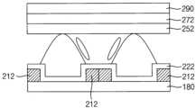
도 10을 참조하면, 광 필드 표시 장치(3000)는 하부 기판(110)과 박막 봉지층(180) 사이에서 매트릭스 형태로 배열되는 복수의 서브 화소들을 포함하는 유기 발광 표시 패널(100), 하부 렌즈 전극(212), 하부 배향막(222), 액정층(230), 상부 배향막(252), 상부 렌즈 전극(272) 및 상부 기판(290)을 포함할 수 있다. 일 실시예에서, 상부 기판(290) 상에는 광의 투과축 방향 제어를 위한 편광자(polarizer)가 더 배치될 수 있다. 또한, 상부 기판(290) 상에는 터치 인식을 위한 터치 센싱 유닛이 더 배치될 수도 있다.Referring to FIG. 10, the optical
3차원 표시 모드에서, 상부 렌즈 전극(270)은 액정층(230)의 상부 구동 전극으로 기능하고, 하부 렌즈 전극(210) 및/또는 유기 발광 표시 패널(100)의 제2 전극(170)(예를 들어, 캐소드 전극)이 액정층(230)을 구동하는 하부 구동 전극으로 기능할 수 있다.In the three-dimensional display mode, the
하부 렌즈 전극(212)은 박막 봉지층(180) 상에 직접 패터닝될 수 있다. 일 실시예에서, 하부 렌즈 전극(212)은 인듐-아연 산화물을 포함할 수 있다. 하부 렌즈 전극(212)은 상온 환경(약 20℃ 내지 30℃)에서 박막 봉지층(180) 상에 직접 증착될 수 있다. 일 실시예에서, 하부 렌즈 전극(212)은 마이크로 액정 렌즈(ML)들 각각을 둘러싸는 고리 형태의 패턴들을 가질 수 있다. 일 실시예에서, 하부 렌즈 전극(212)의 상기 패턴들 각각의 평면 형상의 바깥쪽 변은 육각형일 수 있다. 일 실시예에서, 하부 렌즈 전극(212)의 상기 패턴들 각각의 평면 형상의 바깥쪽 변은 사각형일 수 있다. 일 실시예에서, 하부 렌즈 전극(212)의 상기 패턴들 각각의 평면 형상의 바깥쪽 변은 원형일 수 있다. 다만, 이는 예시적인 것으로서, 하부 렌즈 전극(212)의 패턴이 이에 한정되는 것은 아니다.The
하부 배향막(220)은 폴리이미드 계열의 고분자 수지를 이용한 저온 소성 공정에 의해 하부 렌즈 전극(210)를 커버하며 박막 봉지층(180) 상에 배치될 수 있다. 유기 발광 표시 패널(100)의 특성 변화를 방지하기 위해 약 100℃ 환경에서 하부 배향막(220)이 형성될 수 있다.The
마이크로 렌즈 어레이를 구성하기 위한 복수의 마이크로 액정 렌즈(ML)들을 포함하는 액정층(230)이 하부 배향막(220) 상에 배치될 수 있다.A
상부 배향막(250)이 액정층(230)과 상부 렌즈 전극(272) 사이에 배치될 수 있다. 일 실시예에서, 상부 배향막(250)은 상기 폴리이미드 계열의 고분자 수지를 포함할 수 있다.The
상부 렌즈 전극(272)은 액정층(250) 및 상부 배향막(250) 상에 배치될 수 있다. 상부 렌즈 전극(272)은 상기 3차원 표시 모드에서 하부 렌즈 전극(212) 및/또는 제2 전극(170)과 전기장을 형성할 수 있다. 일 실시예에서, 상부 렌즈 전극(272)은 상기 서브 화소들에 공통적으로 대향하여 배치될 수 있다. 즉, 상부 렌즈 전극(272)은 공통 전극으로 제공될 수 있다.The
상부 기판(290)은 상부 렌즈 전극(270) 상에 배치될 수 있다.The
상술한 바와 같이, 본 발명의 실시예들에 따른 광 필드 표시 장치(3000)는 유기 발광 표시 패널(100) 상에 마이크로 렌즈 어레이를 포함하는 액정 렌즈 구조가 직접적으로 집적됨으로써, 액정 렌즈 패널 제조에 필요한 기판이 제거될 수 있다.As described above, the optical
도 11은 도 10의 광 필드 표시 장치에 포함되는 마이크로 렌즈 어레이의 일 예를 나타내는 단면도이다.FIG. 11 is a cross-sectional view showing an example of a micro lens array included in the optical field display device of FIG. 10.
도 11에 도시된 바와 같이, 유기 발광 표시 패널의 박막 봉지층(180) 상에 패터닝된 하부 렌즈 전극(212)이 배치되고, 이를 커버하는 하부 배향막(222)이 배치될 수 있다. 또한, 공통 전극인 상부 렌즈 전극(272)과 상부 배향막(252)이 형성된 상부 기판(290)과 하부 배향막(222) 사이에 마이크로 렌즈들을 포함하는 액정층(230)이 배치될 수 있다.As shown in FIG. 11, a patterned
3차원 표시 모드에서, 상기 전극 패턴을 갖는 하부 렌즈 전극(212)과 공통 전극 패턴을 갖는 상부 렌즈 전극(272) 사이에 발생된 전기장에 의해 마이크로 렌즈 어레이에 포함되는 액정 분자들이 재배열되고, 광 필드가 구현될 수 있다.In the three-dimensional display mode, the liquid crystal molecules included in the micro lens array are rearranged by the electric field generated between the
도 12a는 10의 광 필드 표시 장치에 포함되는 마이크로 렌즈 어레이와 상부 렌즈 전극 및 하부 렌즈 전극의 일 예를 나타내는 평면도이다. 도 12b는 도 11a의 II-II'라인을 따라 자른 단면의 일부를 개략적으로 나타내는 단면도이다.FIG. 12A is a plan view showing an example of a micro lens array, an upper lens electrode, and a lower lens electrode included in the optical field display device of 10. FIG. 12B is a cross-sectional view schematically showing a portion of the cross section taken along line II-II' of FIG. 11A.
도 10, 도 12a 및 도 12b를 참조하면, 광 필드 표시 장치에 포함되는 하부 렌즈 전극(212A)과 상부 렌즈 전극(274A)은 각각 패턴 형태로 배치될 수 있다.Referring to FIGS. 10, 12A, and 12B, the
일 실시예에서, 하부 렌즈 전극(212A)과 상부 렌즈 전극(274A)은 마이크로 액정 렌즈(ML)가 배열되는 제1 방향(D1)을 따라 서로 교번하여 고리 형태의 패턴(EP1, EP2)을 가질 수 있다. 예를 들어, 하나의 마이크로 액정 렌즈에 대하여 하부 렌즈 전극(212A)과 상부 렌즈 전극(274A) 중 하나만이 고리 형태의 패턴을 가지고, 다른 하나는 편평한 전극 형태를 가질 수 있다.In one embodiment, the
도 12b에 도시된 바와 같이, 하부 렌즈 전극(212A)은 제1 마이크로 액정 렌즈(ML1)에 대응하여 제1 마이크로 액정 렌즈(ML1)를 둘러싸는 고리 형태의 패턴을 가지고, 제2 마이크로 액정 렌즈(ML2)에 대응하는 전극부(212)를 가질 수 있다. 예를 들어, 하부 렌즈 전극(212A)은 제1 방향(DL1)을 따라 기 설정된 마이크로 액정 렌즈들마다 홀(hole)을 가질 수 있다. 또한, 상부 렌즈 전극(274A)은 제2 마이크로 액정 렌즈(ML2)에 대응하여 제2 마이크로 액정 렌즈(ML2)를 둘러싸는 고리 형태의 패턴을 가지고, 제2 마이크로 액정 렌즈(ML2)에 대응하는 전극부(274)를 가질 수 있다. 예를 들어, 상부 렌즈 전극(274A)은 하부 렌즈 전극(212A)이 홀을 갖지 않는 마이크로 액정 렌즈들마다 홀을 가질 수 있다.As shown in FIG. 12B, the
일 실시예에서, 서로 인접한 마이크로 액정 렌즈들(예를 들어, 제1 마이크로 액정 렌즈(ML1)와 제2 마이크로 액정 렌즈(ML2)) 각각에 대응하는 상부 렌즈 전극(274A)의 전극부(274)의 가장자리 일부와 하부 렌즈 전극(212A)의 전극부(212)의 가장자리 일부가 서로 중첩할 수 있다.In one embodiment, the electrode portion 274 of the
이와 같이, 마이크로 렌즈 어레이를 구성하는 상부 렌즈 전극(274A)과 하부 렌즈 전극(212A)은 마이크로 액정 렌즈의 위치에 대응하여 각각 서로 다른 위치에서 패터닝될 수 있다.In this way, the
상술한 바와 같이, 마이크로 렌즈 어레이에 포함되는 마이크로 액정 렌즈의 형상과 렌즈 전극들의 패턴 형태를 조절함으로써, 2000 PPI 이상의 고해상도 영상의 다시점 3D 영상이 구현될 수 있다.As described above, by adjusting the shape of the micro liquid crystal lens included in the micro lens array and the pattern shape of the lens electrodes, a multi-view 3D image with a high resolution of 2000 PPI or more can be realized.
본 발명은 광 필드 디스플레이를 구현하는 표시 장치에 적용될 수 있다. 예를 들면, 상기 투명 표시 장치는 컴퓨터, 휴대폰, 스마트폰, 스마트패드, MP3 플레이어 등의 전자 기기뿐만 아니라, 자동차용 네비게이션 또는 헤드 업(Head up) 디스플레이 등에도 적용될 수 있다. 또한, 신체에 부착 가능한 웨어러블(wearable) 디스플레이 장치에도 적용될 수 있다.The present invention can be applied to a display device implementing a light field display. For example, the transparent display device can be applied not only to electronic devices such as computers, mobile phones, smartphones, smart pads, and MP3 players, but also to automobile navigation or head up displays. Additionally, it can also be applied to wearable display devices that can be attached to the body.
이상에서는 본 발명의 실시예들을 참조하여 설명하였지만, 해당 기술 분야의 숙련된 당업자는 하기의 특허 청구의 범위에 기재된 본 발명의 사상 및 영역으로부터 벗어나지 않는 범위 내에서 본 발명을 다양하게 수정 및 변경시킬 수 있음을 이해할 수 있을 것이다.Although the present invention has been described above with reference to embodiments, those skilled in the art can make various modifications and changes to the present invention without departing from the spirit and scope of the present invention as set forth in the claims below. You will understand that it is possible.
100: 유기 발광 표시 패널110: 하부 기판
170: 제2 전극180: 박막 봉지층
200: 마이크로 렌즈 어레이210, 212: 하부 렌즈 전극
220, 222: 하부 배향막230: 액정층
235: 실런트250, 252: 상부 배향막
270, 272: 상부 렌즈 전극290: 상부 기판
1000, 2000, 3000: 광 필드 표시 장치
ML: 마이크로 액정 렌즈100: Organic light emitting display panel 110: Lower substrate
170: second electrode 180: thin film encapsulation layer
200:
220, 222: lower alignment layer 230: liquid crystal layer
235:
270, 272: upper lens electrode 290: upper substrate
1000, 2000, 3000: Optical field display device
ML: Micro liquid crystal lens
Claims (20)
Translated fromKorean상기 하부 기판 상에 배치되는 백-플레인(black plane) 구조물;
상기 백-플레인 구조물과 전기적으로 연결되는 애노드 전극;
상기 애노드 전극 상에 배치되는 유기 발광 표시층;
상기 표시층을 커버하며, 상기 애노드 전극과 대향하는 캐소드 전극;
상기 캐소드 전극을 커버하는 박막 봉지층;
상기 박막 봉지층 상에 직접 배치되는 하부 배향막;
상기 하부 배향막 상에 배치되고, 마이크로 렌즈 어레이를 구성하기 위한 복수의 마이크로 액정 렌즈들을 포함하는 액정층;
상기 액정층 상에 배치되고, 상기 캐소드 전극과 전기장을 형성하는 상부 렌즈 전극; 및
상기 상부 렌즈 전극 상에 배치되는 상부 기판을 포함하는 광 필드(light field) 표시 장치.lower substrate;
a back-plane (black plane) structure disposed on the lower substrate;
an anode electrically connected to the back-plane structure;
an organic light emitting display layer disposed on the anode electrode;
a cathode electrode that covers the display layer and faces the anode electrode;
a thin film encapsulation layer covering the cathode electrode;
a lower alignment layer disposed directly on the thin film encapsulation layer;
a liquid crystal layer disposed on the lower alignment layer and including a plurality of micro liquid crystal lenses to form a micro lens array;
an upper lens electrode disposed on the liquid crystal layer and forming an electric field with the cathode electrode; and
A light field display device comprising an upper substrate disposed on the upper lens electrode.
상기 액정층과 상기 상부 렌즈 전극 사이에 배치되는 상부 배향막을 더 포함하는 것을 특징으로 하는 광 필드 표시 장치.According to claim 1,
An optical field display device further comprising an upper alignment layer disposed between the liquid crystal layer and the upper lens electrode.
상기 상부 렌즈 전극의 상기 패턴들 각각의 평면 형상의 바깥쪽 형상은 육각형인 것을 특징으로 하는 광 필드 표시 장치.The method of claim 4, wherein the planar shape of each of the micro liquid crystal lenses is hexagonal,
An optical field display device, characterized in that the outer planar shape of each of the patterns of the upper lens electrode is hexagonal.
상기 상부 기판 상에 배치되는 터치 센싱 유닛을 더 포함하는 것을 특징으로 하는 광 필드 표시 장치.According to claim 3,
A light field display device further comprising a touch sensing unit disposed on the upper substrate.
상기 박막 봉지층 상에 하부 배향막을 형성하는 단계;
상기 캐소드 전극과 전기장을 형성하는 상부 렌즈 전극을 상부 기판 하면에 패터닝하는 단계;
상기 상부 렌즈 전극을 커버하는 상부 배향막을 상기 상부 기판 하면에 형성하는 단계;
상기 하부 배향막 또는 상기 상부 배향막 상에 복수의 마이크로 액정 렌즈들을 포함하는 마이크로 렌즈 어레이를 구성하기 위한 액정층을 형성하는 단계; 및
상기 하부 배향막과 상기 상부 배향막 사이에 상기 액정층이 배치되도록 상기 상부 기판과 상기 박막 봉지층을 합착하는 단계를 포함하는 광 필드 표시 장치의 제조 방법.Forming an organic light emitting display panel in which a lower substrate, a back-plane structure, an anode electrode, an organic light emitting display layer, a cathode electrode, and a thin film encapsulation layer covering the cathode electrode are sequentially stacked;
forming a lower alignment film on the thin film encapsulation layer;
patterning an upper lens electrode that forms an electric field with the cathode electrode on the lower surface of the upper substrate;
forming an upper alignment film covering the upper lens electrode on the lower surface of the upper substrate;
forming a liquid crystal layer for configuring a micro lens array including a plurality of micro liquid crystal lenses on the lower alignment layer or the upper alignment layer; and
A method of manufacturing a light field display device comprising bonding the upper substrate and the thin film encapsulation layer so that the liquid crystal layer is disposed between the lower alignment layer and the upper alignment layer.
폴리이미드 계열 고분자 수지를 상기 박막 봉지층 상면에 직접 코팅하는 단계; 및
100℃ 환경에서 상기 코팅된 폴리이미드 수지를 베이킹한 후 자외선 경화하는 단계를 포함하는 것을 특징으로 하는 광 필드 표시 장치의 제조 방법.The method of claim 15, wherein forming the lower alignment layer includes
Directly coating a polyimide-based polymer resin on the upper surface of the thin film encapsulation layer; and
A method of manufacturing a light field display device comprising the step of baking the coated polyimide resin in an environment of 100°C and then curing it with ultraviolet rays.
상기 상부 렌즈 전극의 상기 패턴들 각각의 평면 형상의 바깥쪽 형상은 육각형인 것을 특징으로 하는 광 필드 표시 장치의 제조 방법.The method of claim 18, wherein the planar shape of each of the micro liquid crystal lenses is circular or oval,
A method of manufacturing a light field display device, wherein the outer planar shape of each of the patterns of the upper lens electrode is hexagonal.
상온 환경에서 상기 박막 봉지층 상에 인듐-아연 산화물을 포함하는 하부 렌즈 전극을 증착하는 단계;
폴리이미드 계열 고분자 수지를 상기 박막 봉지층의 노출된 부분 및 상기 하부 렌즈 전극 상에 직접 코팅하는 단계; 및
100℃ 환경에서 상기 코팅된 폴리이미드 수지를 베이킹한 후 자외선 경화하는 단계를 포함하는 것을 특징으로 하는 광 필드 표시 장치의 제조 방법.
The method of claim 15, wherein forming a lower alignment layer on the thin film encapsulation layer comprises:
depositing a lower lens electrode containing indium-zinc oxide on the thin film encapsulation layer in a room temperature environment;
directly coating the exposed portion of the thin film encapsulation layer and the lower lens electrode with a polyimide-based polymer resin; and
A method of manufacturing a light field display device comprising the step of baking the coated polyimide resin in an environment of 100°C and then curing it with ultraviolet rays.
Priority Applications (4)
| Application Number | Priority Date | Filing Date | Title |
|---|---|---|---|
| KR1020160142385AKR102647969B1 (en) | 2016-10-28 | 2016-10-28 | Light field display device and method of manufacturing the same |
| US15/685,859US10298915B2 (en) | 2016-10-28 | 2017-08-24 | Light field display device and method of manufacturing the same |
| CN201711020568.XACN108020929B (en) | 2016-10-28 | 2017-10-27 | Light field display device and method of manufacturing the same |
| US16/374,507US10630964B2 (en) | 2016-10-28 | 2019-04-03 | Light field display device and method of manufacturing the same |
Applications Claiming Priority (1)
| Application Number | Priority Date | Filing Date | Title |
|---|---|---|---|
| KR1020160142385AKR102647969B1 (en) | 2016-10-28 | 2016-10-28 | Light field display device and method of manufacturing the same |
Publications (2)
| Publication Number | Publication Date |
|---|---|
| KR20180046985A KR20180046985A (en) | 2018-05-10 |
| KR102647969B1true KR102647969B1 (en) | 2024-03-18 |
Family
ID=62022718
Family Applications (1)
| Application Number | Title | Priority Date | Filing Date |
|---|---|---|---|
| KR1020160142385AActiveKR102647969B1 (en) | 2016-10-28 | 2016-10-28 | Light field display device and method of manufacturing the same |
Country Status (3)
| Country | Link |
|---|---|
| US (2) | US10298915B2 (en) |
| KR (1) | KR102647969B1 (en) |
| CN (1) | CN108020929B (en) |
Families Citing this family (27)
| Publication number | Priority date | Publication date | Assignee | Title |
|---|---|---|---|---|
| KR102629389B1 (en)* | 2016-03-25 | 2024-01-25 | 삼성디스플레이 주식회사 | Liquid crystal lens and display device including the same |
| AU2017250112B2 (en) | 2016-04-12 | 2020-09-17 | Quidient, Llc | Quotidian scene reconstruction engine |
| KR20230131497A (en) | 2016-07-15 | 2023-09-13 | 라이트 필드 랩 인코포레이티드 | Energy Propagation and Transverse Anderson Localization with Two-Dimensional, Light Field and Holographic Relays |
| KR102704962B1 (en)* | 2016-09-23 | 2024-09-09 | 삼성디스플레이 주식회사 | Lens panel and display device including the same |
| CN112105976B (en) | 2018-01-14 | 2022-12-09 | 光场实验室公司 | Energy Field 3D Printing System |
| EP3737977A4 (en) | 2018-01-14 | 2021-11-10 | Light Field Lab, Inc. | HOLOGRAPHIC AND DIFFACTIVE OPTICAL CODING SYSTEMS |
| CN112105975A (en) | 2018-01-14 | 2020-12-18 | 光场实验室公司 | System and method for lateral energy localization using ordered structures in energy repeaters |
| JP7399879B2 (en) | 2018-05-02 | 2023-12-18 | クイッディエント・エルエルシー | Codec for processing scenes with almost unlimited detail |
| CN110737000B (en)* | 2018-07-02 | 2023-11-17 | 亿光电子工业股份有限公司 | Adjustable light-emitting device |
| KR102707258B1 (en)* | 2018-10-15 | 2024-09-23 | 삼성디스플레이 주식회사 | Display device and fabricating method thereof |
| CN111273512A (en)* | 2018-12-04 | 2020-06-12 | 深圳光峰科技股份有限公司 | Projection Screens and Projection Systems |
| CN109782499B (en)* | 2019-02-26 | 2022-02-01 | 京东方科技集团股份有限公司 | Liquid crystal display device and electronic apparatus |
| CN109656049B (en)* | 2019-02-26 | 2020-12-08 | 京东方科技集团股份有限公司 | Display panels and display devices |
| WO2021040012A1 (en)* | 2019-08-29 | 2021-03-04 | 富士フイルム株式会社 | Light deflection device and optical device |
| KR20210078802A (en)* | 2019-12-19 | 2021-06-29 | 엘지디스플레이 주식회사 | Dislay Device |
| EP4131397A4 (en)* | 2020-03-27 | 2023-08-09 | BOE Technology Group Co., Ltd. | DISPLAY SUBSTRATE AND METHOD FOR PRODUCTION THEREOF, AND DISPLAY DEVICE |
| KR20210121357A (en)* | 2020-03-27 | 2021-10-08 | 삼성디스플레이 주식회사 | Display device and method for manufacturing the same |
| CN111524946A (en)* | 2020-04-27 | 2020-08-11 | 武汉华星光电半导体显示技术有限公司 | OLED display panel, preparation method and display device |
| CN115335761A (en) | 2020-10-30 | 2022-11-11 | 京东方科技集团股份有限公司 | Display substrate, display panel and display device |
| WO2022104750A1 (en)* | 2020-11-20 | 2022-05-27 | 京东方科技集团股份有限公司 | Display apparatus and driving method therefor |
| KR102823813B1 (en) | 2020-12-24 | 2025-06-20 | 엘지디스플레이 주식회사 | Organic light emitting display device |
| CN115349107B (en) | 2021-01-29 | 2024-01-12 | 京东方科技集团股份有限公司 | Array substrate and liquid crystal display panel |
| CN113538300B (en)* | 2021-06-22 | 2023-07-14 | 武汉工程大学 | High-definition light field imaging method based on liquid crystal D-type optical element |
| KR20230084709A (en) | 2021-12-06 | 2023-06-13 | 엘지디스플레이 주식회사 | Display device and mobile terminal including the same |
| CN114335125B (en)* | 2021-12-30 | 2025-08-19 | 京东方科技集团股份有限公司 | Display substrate, preparation method thereof and display device |
| CN114815291B (en)* | 2022-03-16 | 2024-08-09 | 京东方科技集团股份有限公司 | Display panel, display device and manufacturing method of display panel |
| KR20240077586A (en)* | 2022-11-23 | 2024-06-03 | 삼성디스플레이 주식회사 | Lens device and display assembly including the same |
Citations (3)
| Publication number | Priority date | Publication date | Assignee | Title |
|---|---|---|---|---|
| JP2010204415A (en)* | 2009-03-04 | 2010-09-16 | Seiko Epson Corp | Liquid crystal device and electronic apparatus |
| JP2014112157A (en)* | 2012-12-05 | 2014-06-19 | Akita Univ | Microlens array and illumination control device employing the same |
| JP2014112757A (en)* | 2012-12-05 | 2014-06-19 | Nlt Technologies Ltd | Stereoscopic image display device |
Family Cites Families (19)
| Publication number | Priority date | Publication date | Assignee | Title |
|---|---|---|---|---|
| KR100754874B1 (en)* | 2005-11-15 | 2007-09-04 | 삼성전자주식회사 | Double-sided display |
| US7701642B2 (en)* | 2005-12-02 | 2010-04-20 | Sony Corporation | Liquid lens |
| JP2008026654A (en)* | 2006-07-21 | 2008-02-07 | Hitachi Displays Ltd | 3D display device |
| KR101222990B1 (en)* | 2007-10-22 | 2013-01-18 | 엘지디스플레이 주식회사 | Liquid Crystal Lens Electrically driven and Stereoscopy Display Device |
| KR101528143B1 (en)* | 2007-11-02 | 2015-06-15 | 엘지디스플레이 주식회사 | Stereoscopic display device using liquid crystal electric field lens |
| KR101274717B1 (en)* | 2009-12-24 | 2013-06-12 | 엘지디스플레이 주식회사 | Liquid Crystal Lens Electrically driven and Stereoscopy Display Device Using the Same |
| KR101772153B1 (en)* | 2010-03-17 | 2017-08-29 | 삼성디스플레이 주식회사 | Display device using diffractive lens |
| KR20130046116A (en)* | 2011-10-27 | 2013-05-07 | 삼성디스플레이 주식회사 | 2 dimension/3 dimension switchable display apparatus |
| KR101928939B1 (en)* | 2011-11-30 | 2019-03-13 | 삼성디스플레이 주식회사 | 2 dimension/3 dimension switchable display apparatus |
| KR20130112537A (en)* | 2012-04-04 | 2013-10-14 | 삼성디스플레이 주식회사 | Liquid crystal lens and stereoscopic image display panel having the same |
| KR102017203B1 (en)* | 2012-05-25 | 2019-10-22 | 삼성디스플레이 주식회사 | Liquid crystal lens and display device including the same |
| JPWO2015045251A1 (en) | 2013-09-27 | 2017-03-09 | パナソニックIpマネジメント株式会社 | Autostereoscopic image device |
| JP2015118342A (en)* | 2013-12-20 | 2015-06-25 | 大日本印刷株式会社 | Display device with liquid crystal lens unit |
| KR20150081102A (en)* | 2014-01-03 | 2015-07-13 | 삼성디스플레이 주식회사 | Liquid crystal lens and panel and display device including liquid crystal lens panel |
| CN203707136U (en)* | 2014-02-12 | 2014-07-09 | 京东方科技集团股份有限公司 | Three-dimensional display panel and three-dimensional display device |
| CN104020572A (en)* | 2014-05-27 | 2014-09-03 | 四川虹视显示技术有限公司 | Glasses-free 3D touch AMOLED display device and manufacturing method thereof |
| KR102380155B1 (en)* | 2015-03-25 | 2022-03-29 | 삼성디스플레이 주식회사 | Optical unit and organic light emitting diode display comprising the same |
| JP2016186599A (en)* | 2015-03-27 | 2016-10-27 | セイコーエプソン株式会社 | Method for manufacturing liquid crystal device, liquid crystal device, and electronic apparatus |
| CN105093543B (en) | 2015-07-06 | 2017-12-22 | 深圳市华星光电技术有限公司 | 3d display device |
- 2016
- 2016-10-28KRKR1020160142385Apatent/KR102647969B1/enactiveActive
- 2017
- 2017-08-24USUS15/685,859patent/US10298915B2/enactiveActive
- 2017-10-27CNCN201711020568.XApatent/CN108020929B/enactiveActive
- 2019
- 2019-04-03USUS16/374,507patent/US10630964B2/enactiveActive
Patent Citations (3)
| Publication number | Priority date | Publication date | Assignee | Title |
|---|---|---|---|---|
| JP2010204415A (en)* | 2009-03-04 | 2010-09-16 | Seiko Epson Corp | Liquid crystal device and electronic apparatus |
| JP2014112157A (en)* | 2012-12-05 | 2014-06-19 | Akita Univ | Microlens array and illumination control device employing the same |
| JP2014112757A (en)* | 2012-12-05 | 2014-06-19 | Nlt Technologies Ltd | Stereoscopic image display device |
Also Published As
| Publication number | Publication date |
|---|---|
| CN108020929B (en) | 2021-08-03 |
| KR20180046985A (en) | 2018-05-10 |
| US10298915B2 (en) | 2019-05-21 |
| US20180124384A1 (en) | 2018-05-03 |
| US20190230343A1 (en) | 2019-07-25 |
| CN108020929A (en) | 2018-05-11 |
| US10630964B2 (en) | 2020-04-21 |
Similar Documents
| Publication | Publication Date | Title |
|---|---|---|
| KR102647969B1 (en) | Light field display device and method of manufacturing the same | |
| US8659739B2 (en) | Liquid crystal lens and display including the same | |
| TWI789565B (en) | Multiview display, system, and method having dynamic color sub-pixels remapping | |
| US20130250195A1 (en) | Display device and electronic device | |
| CN103748874B (en) | Autostereoscopic display device | |
| EP1784026A1 (en) | Three-dimensional display device and driving method thereof | |
| US10432924B2 (en) | Three-dimensional display device and driving method thereof | |
| KR20060078405A (en) | Micro Lens Substrate Array, Stereoscopic Image Display Apparatus Comprising The Same And Method Of Manufacturing The Same | |
| TWI471665B (en) | 2d and 3d switchable display device | |
| CN103609107A (en) | Autostereoscopic display apparatus having optical magnification | |
| CN105334632B (en) | A kind of three-dimensional display apparatus and its driving method | |
| CN106896519A (en) | A kind of three-dimensional display apparatus and its driving method | |
| CN113031303B (en) | Display substrate, control method, and display device | |
| KR20160015314A (en) | Multi-view display device | |
| JP6376715B2 (en) | Autostereoscopic display device and driving method thereof | |
| CN201740951U (en) | Display device capable of switching imaging modes | |
| CN113311594B (en) | Display panel and display device | |
| EP3299883B1 (en) | Display device including lens panel | |
| US10191351B2 (en) | Lens panel and display device including the same | |
| JP2020064092A (en) | Stereoscopic display | |
| CN205644488U (en) | Three -dimensional organic electroluminescence display device of touch | |
| CN110928034B (en) | Color film substrate, display panel and display device | |
| CN114551763A (en) | Display substrate and display device | |
| US10459281B2 (en) | Stereoscopic image display device | |
| WO2022246694A1 (en) | Display substrate, preparation method, and display device |
Legal Events
| Date | Code | Title | Description |
|---|---|---|---|
| PA0109 | Patent application | Patent event code:PA01091R01D Comment text:Patent Application Patent event date:20161028 | |
| PG1501 | Laying open of application | ||
| PA0201 | Request for examination | Patent event code:PA02012R01D Patent event date:20211001 Comment text:Request for Examination of Application Patent event code:PA02011R01I Patent event date:20161028 Comment text:Patent Application | |
| E902 | Notification of reason for refusal | ||
| PE0902 | Notice of grounds for rejection | Comment text:Notification of reason for refusal Patent event date:20230619 Patent event code:PE09021S01D | |
| E701 | Decision to grant or registration of patent right | ||
| PE0701 | Decision of registration | Patent event code:PE07011S01D Comment text:Decision to Grant Registration Patent event date:20231218 | |
| GRNT | Written decision to grant | ||
| PR0701 | Registration of establishment | Comment text:Registration of Establishment Patent event date:20240312 Patent event code:PR07011E01D | |
| PR1002 | Payment of registration fee | Payment date:20240313 End annual number:3 Start annual number:1 | |
| PG1601 | Publication of registration |