KR102646794B1 - Ⅱ-Ⅵ based non-Cd quantum dots, manufacturing method thereof and QLED using the same - Google Patents
Ⅱ-Ⅵ based non-Cd quantum dots, manufacturing method thereof and QLED using the sameDownload PDFInfo
- Publication number
- KR102646794B1 KR102646794B1KR1020210120022AKR20210120022AKR102646794B1KR 102646794 B1KR102646794 B1KR 102646794B1KR 1020210120022 AKR1020210120022 AKR 1020210120022AKR 20210120022 AKR20210120022 AKR 20210120022AKR 102646794 B1KR102646794 B1KR 102646794B1
- Authority
- KR
- South Korea
- Prior art keywords
- znse
- shell
- znsete
- core
- zns
- Prior art date
- Legal status (The legal status is an assumption and is not a legal conclusion. Google has not performed a legal analysis and makes no representation as to the accuracy of the status listed.)
- Active
Links
- 239000002096quantum dotSubstances0.000titleclaimsabstractdescription178
- 238000004519manufacturing processMethods0.000titleclaimsabstractdescription28
- SBIBMFFZSBJNJF-UHFFFAOYSA-Nselenium;zincChemical compound[Se]=[Zn]SBIBMFFZSBJNJF-UHFFFAOYSA-N0.000claimsabstractdescription238
- 238000000034methodMethods0.000claimsabstractdescription33
- 239000002243precursorSubstances0.000claimsdescription70
- 239000000243solutionSubstances0.000claimsdescription60
- 239000011259mixed solutionSubstances0.000claimsdescription48
- 239000002994raw materialSubstances0.000claimsdescription32
- 239000002904solventSubstances0.000claimsdescription30
- 238000010438heat treatmentMethods0.000claimsdescription22
- XTAZYLNFDRKIHJ-UHFFFAOYSA-Nn,n-dioctyloctan-1-amineChemical compoundCCCCCCCCN(CCCCCCCC)CCCCCCCCXTAZYLNFDRKIHJ-UHFFFAOYSA-N0.000claimsdescription17
- 239000006185dispersionSubstances0.000claimsdescription16
- 230000035484reaction timeEffects0.000claimsdescription13
- 235000014113dietary fatty acidsNutrition0.000claimsdescription8
- 229930195729fatty acidNatural products0.000claimsdescription8
- 239000000194fatty acidSubstances0.000claimsdescription8
- 150000004665fatty acidsChemical class0.000claimsdescription8
- 238000009792diffusion processMethods0.000claimsdescription3
- 125000002924primary amino groupChemical class[H]N([H])*0.000claims1
- 238000005424photoluminescenceMethods0.000description98
- 239000011669seleniumSubstances0.000description88
- 239000011701zincSubstances0.000description68
- 238000006862quantum yield reactionMethods0.000description54
- 239000010410layerSubstances0.000description38
- 238000002347injectionMethods0.000description37
- 239000007924injectionSubstances0.000description37
- WRIDQFICGBMAFQ-UHFFFAOYSA-N(E)-8-Octadecenoic acidNatural productsCCCCCCCCCC=CCCCCCCC(O)=OWRIDQFICGBMAFQ-UHFFFAOYSA-N0.000description28
- LQJBNNIYVWPHFW-UHFFFAOYSA-N20:1omega9c fatty acidNatural productsCCCCCCCCCCC=CCCCCCCCC(O)=OLQJBNNIYVWPHFW-UHFFFAOYSA-N0.000description28
- QSBYPNXLFMSGKH-UHFFFAOYSA-N9-HeptadecensaeureNatural productsCCCCCCCC=CCCCCCCCC(O)=OQSBYPNXLFMSGKH-UHFFFAOYSA-N0.000description28
- ZQPPMHVWECSIRJ-UHFFFAOYSA-NOleic acidNatural productsCCCCCCCCC=CCCCCCCCC(O)=OZQPPMHVWECSIRJ-UHFFFAOYSA-N0.000description28
- 239000005642Oleic acidSubstances0.000description28
- QXJSBBXBKPUZAA-UHFFFAOYSA-Nisooleic acidNatural productsCCCCCCCC=CCCCCCCCCC(O)=OQXJSBBXBKPUZAA-UHFFFAOYSA-N0.000description28
- ZQPPMHVWECSIRJ-KTKRTIGZSA-Noleic acidChemical compoundCCCCCCCC\C=C/CCCCCCCC(O)=OZQPPMHVWECSIRJ-KTKRTIGZSA-N0.000description28
- 239000000203mixtureSubstances0.000description22
- 230000003595spectral effectEffects0.000description20
- 238000005401electroluminescenceMethods0.000description19
- 230000015572biosynthetic processEffects0.000description18
- 239000002105nanoparticleSubstances0.000description17
- 238000003917TEM imageMethods0.000description14
- 230000006798recombinationEffects0.000description14
- 238000005215recombinationMethods0.000description14
- 238000006243chemical reactionMethods0.000description12
- 230000001976improved effectEffects0.000description12
- CCCMONHAUSKTEQ-UHFFFAOYSA-Noctadec-1-eneChemical compoundCCCCCCCCCCCCCCCCC=CCCCMONHAUSKTEQ-UHFFFAOYSA-N0.000description12
- 238000000103photoluminescence spectrumMethods0.000description12
- -1poly(ethylenedioxythiophene)Polymers0.000description12
- 238000000862absorption spectrumMethods0.000description11
- 230000000694effectsEffects0.000description11
- 230000007423decreaseEffects0.000description10
- 229920003227poly(N-vinyl carbazole)Polymers0.000description10
- 238000003786synthesis reactionMethods0.000description10
- 238000010586diagramMethods0.000description9
- 230000005525hole transportEffects0.000description9
- 229910044991metal oxideInorganic materials0.000description9
- 150000004706metal oxidesChemical class0.000description9
- VLKZOEOYAKHREP-UHFFFAOYSA-Nn-HexaneChemical compoundCCCCCCVLKZOEOYAKHREP-UHFFFAOYSA-N0.000description9
- 230000008569processEffects0.000description9
- RMZAYIKUYWXQPB-UHFFFAOYSA-NtrioctylphosphaneChemical compoundCCCCCCCCP(CCCCCCCC)CCCCCCCCRMZAYIKUYWXQPB-UHFFFAOYSA-N0.000description9
- CSCPPACGZOOCGX-UHFFFAOYSA-NAcetoneChemical compoundCC(C)=OCSCPPACGZOOCGX-UHFFFAOYSA-N0.000description8
- LFQSCWFLJHTTHZ-UHFFFAOYSA-NEthanolChemical compoundCCOLFQSCWFLJHTTHZ-UHFFFAOYSA-N0.000description8
- 229910003363ZnMgOInorganic materials0.000description8
- 230000001419dependent effectEffects0.000description8
- 239000011550stock solutionSubstances0.000description8
- 229920000144PEDOT:PSSPolymers0.000description7
- MJNSMKHQBIVKHV-UHFFFAOYSA-Nselenium;trioctylphosphaneChemical compound[Se].CCCCCCCCP(CCCCCCCC)CCCCCCCCMJNSMKHQBIVKHV-UHFFFAOYSA-N0.000description7
- KFZMGEQAYNKOFK-UHFFFAOYSA-NIsopropanolChemical compoundCC(C)OKFZMGEQAYNKOFK-UHFFFAOYSA-N0.000description6
- OKKJLVBELUTLKV-UHFFFAOYSA-NMethanolChemical compoundOCOKKJLVBELUTLKV-UHFFFAOYSA-N0.000description6
- 238000009835boilingMethods0.000description6
- 230000008859changeEffects0.000description6
- 229910052751metalInorganic materials0.000description6
- 239000002184metalSubstances0.000description6
- 238000002161passivationMethods0.000description6
- 239000000843powderSubstances0.000description6
- RIOQSEWOXXDEQQ-UHFFFAOYSA-NtriphenylphosphineChemical compoundC1=CC=CC=C1P(C=1C=CC=CC=1)C1=CC=CC=C1RIOQSEWOXXDEQQ-UHFFFAOYSA-N0.000description6
- FJLUATLTXUNBOT-UHFFFAOYSA-N1-HexadecylamineChemical compoundCCCCCCCCCCCCCCCCNFJLUATLTXUNBOT-UHFFFAOYSA-N0.000description5
- KRHYYFGTRYWZRS-UHFFFAOYSA-NFluoraneChemical compoundFKRHYYFGTRYWZRS-UHFFFAOYSA-N0.000description5
- 238000013459approachMethods0.000description5
- 238000000576coating methodMethods0.000description5
- 230000007547defectEffects0.000description5
- GPAYUJZHTULNBE-UHFFFAOYSA-NdiphenylphosphineChemical compoundC=1C=CC=CC=1PC1=CC=CC=C1GPAYUJZHTULNBE-UHFFFAOYSA-N0.000description5
- 238000001194electroluminescence spectrumMethods0.000description5
- 239000000463materialSubstances0.000description5
- 229910052711seleniumInorganic materials0.000description5
- 239000000758substrateSubstances0.000description5
- TUQOTMZNTHZOKS-UHFFFAOYSA-NtributylphosphineChemical compoundCCCCP(CCCC)CCCCTUQOTMZNTHZOKS-UHFFFAOYSA-N0.000description5
- ZDAWFMCVTXSZTC-UHFFFAOYSA-N2-n',7-n'-dinaphthalen-1-yl-2-n',7-n'-diphenyl-9,9'-spirobi[fluorene]-2',7'-diamineChemical compoundC1=CC=CC=C1N(C=1C2=CC=CC=C2C=CC=1)C1=CC=C(C=2C(=CC(=CC=2)N(C=2C=CC=CC=2)C=2C3=CC=CC=C3C=CC=2)C23C4=CC=CC=C4C4=CC=CC=C43)C2=C1ZDAWFMCVTXSZTC-UHFFFAOYSA-N0.000description4
- IAZDPXIOMUYVGZ-UHFFFAOYSA-NDimethylsulphoxideChemical compoundCS(C)=OIAZDPXIOMUYVGZ-UHFFFAOYSA-N0.000description4
- 238000002441X-ray diffractionMethods0.000description4
- 238000010521absorption reactionMethods0.000description4
- 239000011248coating agentSubstances0.000description4
- DMBHHRLKUKUOEG-UHFFFAOYSA-NdiphenylamineChemical compoundC=1C=CC=CC=1NC1=CC=CC=C1DMBHHRLKUKUOEG-UHFFFAOYSA-N0.000description4
- 238000000724energy-dispersive X-ray spectrumMethods0.000description4
- 230000005284excitationEffects0.000description4
- IPCSVZSSVZVIGE-UHFFFAOYSA-Nhexadecanoic acidChemical compoundCCCCCCCCCCCCCCCC(O)=OIPCSVZSSVZVIGE-UHFFFAOYSA-N0.000description4
- 238000004020luminiscence typeMethods0.000description4
- 230000009467reductionEffects0.000description4
- 229910052717sulfurInorganic materials0.000description4
- WGTYBPLFGIVFAS-UHFFFAOYSA-Mtetramethylammonium hydroxideChemical compound[OH-].C[N+](C)(C)CWGTYBPLFGIVFAS-UHFFFAOYSA-M0.000description4
- 229920001609Poly(3,4-ethylenedioxythiophene)Polymers0.000description3
- 238000005275alloyingMethods0.000description3
- 230000004888barrier functionEffects0.000description3
- 230000003247decreasing effectEffects0.000description3
- 238000002149energy-dispersive X-ray emission spectroscopyMethods0.000description3
- 238000002474experimental methodMethods0.000description3
- 238000005286illuminationMethods0.000description3
- 229910001425magnesium ionInorganic materials0.000description3
- QPJSUIGXIBEQAC-UHFFFAOYSA-Nn-(2,4-dichloro-5-propan-2-yloxyphenyl)acetamideChemical compoundCC(C)OC1=CC(NC(C)=O)=C(Cl)C=C1ClQPJSUIGXIBEQAC-UHFFFAOYSA-N0.000description3
- TVMXDCGIABBOFY-UHFFFAOYSA-NoctaneChemical compoundCCCCCCCCTVMXDCGIABBOFY-UHFFFAOYSA-N0.000description3
- 150000003141primary aminesChemical class0.000description3
- 238000001228spectrumMethods0.000description3
- 238000004528spin coatingMethods0.000description3
- 239000002335surface treatment layerSubstances0.000description3
- 230000005428wave functionEffects0.000description3
- 229910052725zincInorganic materials0.000description3
- WPUSEOSICYGUEW-UHFFFAOYSA-N4-[4-(4-methoxy-n-(4-methoxyphenyl)anilino)phenyl]-n,n-bis(4-methoxyphenyl)anilineChemical compoundC1=CC(OC)=CC=C1N(C=1C=CC(=CC=1)C=1C=CC(=CC=1)N(C=1C=CC(OC)=CC=1)C=1C=CC(OC)=CC=1)C1=CC=C(OC)C=C1WPUSEOSICYGUEW-UHFFFAOYSA-N0.000description2
- AWXGSYPUMWKTBR-UHFFFAOYSA-N4-carbazol-9-yl-n,n-bis(4-carbazol-9-ylphenyl)anilineChemical compoundC12=CC=CC=C2C2=CC=CC=C2N1C1=CC=C(N(C=2C=CC(=CC=2)N2C3=CC=CC=C3C3=CC=CC=C32)C=2C=CC(=CC=2)N2C3=CC=CC=C3C3=CC=CC=C32)C=C1AWXGSYPUMWKTBR-UHFFFAOYSA-N0.000description2
- ZOKIJILZFXPFTO-UHFFFAOYSA-N4-methyl-n-[4-[1-[4-(4-methyl-n-(4-methylphenyl)anilino)phenyl]cyclohexyl]phenyl]-n-(4-methylphenyl)anilineChemical compoundC1=CC(C)=CC=C1N(C=1C=CC(=CC=1)C1(CCCCC1)C=1C=CC(=CC=1)N(C=1C=CC(C)=CC=1)C=1C=CC(C)=CC=1)C1=CC=C(C)C=C1ZOKIJILZFXPFTO-UHFFFAOYSA-N0.000description2
- 229910016036BaF 2Inorganic materials0.000description2
- 101000837344Homo sapiens T-cell leukemia translocation-altered gene proteinProteins0.000description2
- 235000021314Palmitic acidNutrition0.000description2
- 239000004793PolystyreneSubstances0.000description2
- 102100028692T-cell leukemia translocation-altered gene proteinHuman genes0.000description2
- XLOMVQKBTHCTTD-UHFFFAOYSA-NZinc monoxideChemical compound[Zn]=OXLOMVQKBTHCTTD-UHFFFAOYSA-N0.000description2
- ZOIORXHNWRGPMV-UHFFFAOYSA-Nacetic acid;zincChemical group[Zn].CC(O)=O.CC(O)=OZOIORXHNWRGPMV-UHFFFAOYSA-N0.000description2
- JXLHNMVSKXFWAO-UHFFFAOYSA-Nazane;7-fluoro-2,1,3-benzoxadiazole-4-sulfonic acidChemical compoundN.OS(=O)(=O)C1=CC=C(F)C2=NON=C12JXLHNMVSKXFWAO-UHFFFAOYSA-N0.000description2
- 238000012512characterization methodMethods0.000description2
- MVPPADPHJFYWMZ-UHFFFAOYSA-NchlorobenzeneChemical compoundClC1=CC=CC=C1MVPPADPHJFYWMZ-UHFFFAOYSA-N0.000description2
- IGARGHRYKHJQSM-UHFFFAOYSA-NcyclohexylbenzeneChemical compoundC1CCCCC1C1=CC=CC=C1IGARGHRYKHJQSM-UHFFFAOYSA-N0.000description2
- 230000001627detrimental effectEffects0.000description2
- 230000005684electric fieldEffects0.000description2
- 239000011521glassSubstances0.000description2
- 229910010272inorganic materialInorganic materials0.000description2
- 239000011147inorganic materialSubstances0.000description2
- 230000007774longtermEffects0.000description2
- 238000005259measurementMethods0.000description2
- 230000000116mitigating effectEffects0.000description2
- 238000012986modificationMethods0.000description2
- 230000004048modificationEffects0.000description2
- WQEPLUUGTLDZJY-UHFFFAOYSA-Nn-Pentadecanoic acidNatural productsCCCCCCCCCCCCCCC(O)=OWQEPLUUGTLDZJY-UHFFFAOYSA-N0.000description2
- 230000003287optical effectEffects0.000description2
- 239000011368organic materialSubstances0.000description2
- 229920002223polystyrenePolymers0.000description2
- 239000002356single layerSubstances0.000description2
- 238000005728strengtheningMethods0.000description2
- 230000001629suppressionEffects0.000description2
- 229910052714telluriumInorganic materials0.000description2
- 238000001161time-correlated single photon countingMethods0.000description2
- 238000012546transferMethods0.000description2
- 238000004402ultra-violet photoelectron spectroscopyMethods0.000description2
- 239000004246zinc acetateSubstances0.000description2
- JIAARYAFYJHUJI-UHFFFAOYSA-Lzinc dichlorideChemical compound[Cl-].[Cl-].[Zn+2]JIAARYAFYJHUJI-UHFFFAOYSA-L0.000description2
- QGLWBTPVKHMVHM-KTKRTIGZSA-N(z)-octadec-9-en-1-amineChemical compoundCCCCCCCC\C=C/CCCCCCCCNQGLWBTPVKHMVHM-KTKRTIGZSA-N0.000description1
- 229910000861Mg alloyInorganic materials0.000description1
- BUGBHKTXTAQXES-UHFFFAOYSA-NSeleniumChemical compound[Se]BUGBHKTXTAQXES-UHFFFAOYSA-N0.000description1
- 230000005699Stark effectEffects0.000description1
- NINIDFKCEFEMDL-UHFFFAOYSA-NSulfurChemical compound[S]NINIDFKCEFEMDL-UHFFFAOYSA-N0.000description1
- 229910001215Te alloyInorganic materials0.000description1
- HCHKCACWOHOZIP-UHFFFAOYSA-NZincChemical compound[Zn]HCHKCACWOHOZIP-UHFFFAOYSA-N0.000description1
- 229910007709ZnTeInorganic materials0.000description1
- 238000002835absorbanceMethods0.000description1
- NLTSCOZQKALPGZ-UHFFFAOYSA-Nacetic acid;dihydrateChemical compoundO.O.CC(O)=ONLTSCOZQKALPGZ-UHFFFAOYSA-N0.000description1
- 239000000654additiveSubstances0.000description1
- 230000002411adverseEffects0.000description1
- 238000004458analytical methodMethods0.000description1
- 230000008901benefitEffects0.000description1
- 238000005266castingMethods0.000description1
- 125000002091cationic groupChemical group0.000description1
- 238000005119centrifugationMethods0.000description1
- 238000001311chemical methods and processMethods0.000description1
- 239000003086colorantSubstances0.000description1
- 230000002301combined effectEffects0.000description1
- 230000000052comparative effectEffects0.000description1
- 239000000356contaminantSubstances0.000description1
- 230000008602contractionEffects0.000description1
- 238000000151depositionMethods0.000description1
- 230000008021depositionEffects0.000description1
- 238000013461designMethods0.000description1
- 238000003618dip coatingMethods0.000description1
- DKHNGUNXLDCATP-UHFFFAOYSA-Ndipyrazino[2,3-f:2',3'-h]quinoxaline-2,3,6,7,10,11-hexacarbonitrileChemical compoundC12=NC(C#N)=C(C#N)N=C2C2=NC(C#N)=C(C#N)N=C2C2=C1N=C(C#N)C(C#N)=N2DKHNGUNXLDCATP-UHFFFAOYSA-N0.000description1
- 238000009826distributionMethods0.000description1
- 230000001747exhibiting effectEffects0.000description1
- 229910001385heavy metalInorganic materials0.000description1
- 230000006872improvementEffects0.000description1
- 239000012535impuritySubstances0.000description1
- 239000004615ingredientSubstances0.000description1
- 230000003993interactionEffects0.000description1
- 239000003446ligandSubstances0.000description1
- 239000004973liquid crystal related substanceSubstances0.000description1
- UEGPKNKPLBYCNK-UHFFFAOYSA-Lmagnesium acetateChemical compound[Mg+2].CC([O-])=O.CC([O-])=OUEGPKNKPLBYCNK-UHFFFAOYSA-L0.000description1
- 230000005012migrationEffects0.000description1
- 238000013508migrationMethods0.000description1
- 239000012046mixed solventSubstances0.000description1
- 229910000476molybdenum oxideInorganic materials0.000description1
- 239000012299nitrogen atmosphereSubstances0.000description1
- OVXYGICQHQNTFU-UHFFFAOYSA-Noctadecanoic acid;tetradecanoic acidChemical compoundCCCCCCCCCCCCCC(O)=O.CCCCCCCCCCCCCCCCCC(O)=OOVXYGICQHQNTFU-UHFFFAOYSA-N0.000description1
- IOQPZZOEVPZRBK-UHFFFAOYSA-Noctan-1-amineChemical compoundCCCCCCCCNIOQPZZOEVPZRBK-UHFFFAOYSA-N0.000description1
- PQQKPALAQIIWST-UHFFFAOYSA-NoxomolybdenumChemical compound[Mo]=OPQQKPALAQIIWST-UHFFFAOYSA-N0.000description1
- 239000002245particleSubstances0.000description1
- 229920003023plasticPolymers0.000description1
- 230000010287polarizationEffects0.000description1
- 229920001467poly(styrenesulfonates)Polymers0.000description1
- 239000011970polystyrene sulfonateSubstances0.000description1
- 229960002796polystyrene sulfonateDrugs0.000description1
- 230000008092positive effectEffects0.000description1
- 238000001556precipitationMethods0.000description1
- 238000007639printingMethods0.000description1
- 238000012545processingMethods0.000description1
- 230000005855radiationEffects0.000description1
- 230000004044responseEffects0.000description1
- 230000002441reversible effectEffects0.000description1
- 238000007650screen-printingMethods0.000description1
- 229910052709silverInorganic materials0.000description1
- 238000005507sprayingMethods0.000description1
- 238000003860storageMethods0.000description1
- 239000000126substanceSubstances0.000description1
- 239000011593sulfurSubstances0.000description1
- 230000002459sustained effectEffects0.000description1
- 238000001308synthesis methodMethods0.000description1
- 230000002194synthesizing effectEffects0.000description1
- 238000010189synthetic methodMethods0.000description1
- 230000009897systematic effectEffects0.000description1
- PORWMNRCUJJQNO-UHFFFAOYSA-Ntellurium atomChemical compound[Te]PORWMNRCUJJQNO-UHFFFAOYSA-N0.000description1
- TUNFSRHWOTWDNC-HKGQFRNVSA-Ntetradecanoic acidChemical compoundCCCCCCCCCCCCC[14C](O)=OTUNFSRHWOTWDNC-HKGQFRNVSA-N0.000description1
- 238000002207thermal evaporationMethods0.000description1
- 238000002371ultraviolet--visible spectrumMethods0.000description1
- 229910052724xenonInorganic materials0.000description1
- FHNFHKCVQCLJFQ-UHFFFAOYSA-Nxenon atomChemical compound[Xe]FHNFHKCVQCLJFQ-UHFFFAOYSA-N0.000description1
- 239000011592zinc chlorideSubstances0.000description1
- 235000005074zinc chlorideNutrition0.000description1
- 239000011787zinc oxideSubstances0.000description1
- XOOUIPVCVHRTMJ-UHFFFAOYSA-Lzinc stearateChemical compound[Zn+2].CCCCCCCCCCCCCCCCCC([O-])=O.CCCCCCCCCCCCCCCCCC([O-])=OXOOUIPVCVHRTMJ-UHFFFAOYSA-L0.000description1
Images


Classifications
- C—CHEMISTRY; METALLURGY
- C09—DYES; PAINTS; POLISHES; NATURAL RESINS; ADHESIVES; COMPOSITIONS NOT OTHERWISE PROVIDED FOR; APPLICATIONS OF MATERIALS NOT OTHERWISE PROVIDED FOR
- C09K—MATERIALS FOR MISCELLANEOUS APPLICATIONS, NOT PROVIDED FOR ELSEWHERE
- C09K11/00—Luminescent, e.g. electroluminescent, chemiluminescent materials
- C09K11/02—Use of particular materials as binders, particle coatings or suspension media therefor
- C09K11/025—Use of particular materials as binders, particle coatings or suspension media therefor non-luminescent particle coatings or suspension media
- C—CHEMISTRY; METALLURGY
- C09—DYES; PAINTS; POLISHES; NATURAL RESINS; ADHESIVES; COMPOSITIONS NOT OTHERWISE PROVIDED FOR; APPLICATIONS OF MATERIALS NOT OTHERWISE PROVIDED FOR
- C09K—MATERIALS FOR MISCELLANEOUS APPLICATIONS, NOT PROVIDED FOR ELSEWHERE
- C09K11/00—Luminescent, e.g. electroluminescent, chemiluminescent materials
- C09K11/08—Luminescent, e.g. electroluminescent, chemiluminescent materials containing inorganic luminescent materials
- C09K11/0805—Chalcogenides
- C09K11/0811—Chalcogenides with zinc or cadmium
- C—CHEMISTRY; METALLURGY
- C09—DYES; PAINTS; POLISHES; NATURAL RESINS; ADHESIVES; COMPOSITIONS NOT OTHERWISE PROVIDED FOR; APPLICATIONS OF MATERIALS NOT OTHERWISE PROVIDED FOR
- C09K—MATERIALS FOR MISCELLANEOUS APPLICATIONS, NOT PROVIDED FOR ELSEWHERE
- C09K11/00—Luminescent, e.g. electroluminescent, chemiluminescent materials
- C09K11/08—Luminescent, e.g. electroluminescent, chemiluminescent materials containing inorganic luminescent materials
- C09K11/54—Luminescent, e.g. electroluminescent, chemiluminescent materials containing inorganic luminescent materials containing zinc or cadmium
- C—CHEMISTRY; METALLURGY
- C09—DYES; PAINTS; POLISHES; NATURAL RESINS; ADHESIVES; COMPOSITIONS NOT OTHERWISE PROVIDED FOR; APPLICATIONS OF MATERIALS NOT OTHERWISE PROVIDED FOR
- C09K—MATERIALS FOR MISCELLANEOUS APPLICATIONS, NOT PROVIDED FOR ELSEWHERE
- C09K11/00—Luminescent, e.g. electroluminescent, chemiluminescent materials
- C09K11/08—Luminescent, e.g. electroluminescent, chemiluminescent materials containing inorganic luminescent materials
- C09K11/88—Luminescent, e.g. electroluminescent, chemiluminescent materials containing inorganic luminescent materials containing selenium, tellurium or unspecified chalcogen elements
- C09K11/881—Chalcogenides
- C09K11/883—Chalcogenides with zinc or cadmium
- H01L33/005—
- H01L33/06—
- H01L33/24—
- H—ELECTRICITY
- H10—SEMICONDUCTOR DEVICES; ELECTRIC SOLID-STATE DEVICES NOT OTHERWISE PROVIDED FOR
- H10H—INORGANIC LIGHT-EMITTING SEMICONDUCTOR DEVICES HAVING POTENTIAL BARRIERS
- H10H20/00—Individual inorganic light-emitting semiconductor devices having potential barriers, e.g. light-emitting diodes [LED]
- H10H20/01—Manufacture or treatment
- H—ELECTRICITY
- H10—SEMICONDUCTOR DEVICES; ELECTRIC SOLID-STATE DEVICES NOT OTHERWISE PROVIDED FOR
- H10H—INORGANIC LIGHT-EMITTING SEMICONDUCTOR DEVICES HAVING POTENTIAL BARRIERS
- H10H20/00—Individual inorganic light-emitting semiconductor devices having potential barriers, e.g. light-emitting diodes [LED]
- H10H20/80—Constructional details
- H10H20/81—Bodies
- H10H20/811—Bodies having quantum effect structures or superlattices, e.g. tunnel junctions
- H10H20/812—Bodies having quantum effect structures or superlattices, e.g. tunnel junctions within the light-emitting regions, e.g. having quantum confinement structures
- H—ELECTRICITY
- H10—SEMICONDUCTOR DEVICES; ELECTRIC SOLID-STATE DEVICES NOT OTHERWISE PROVIDED FOR
- H10H—INORGANIC LIGHT-EMITTING SEMICONDUCTOR DEVICES HAVING POTENTIAL BARRIERS
- H10H20/00—Individual inorganic light-emitting semiconductor devices having potential barriers, e.g. light-emitting diodes [LED]
- H10H20/80—Constructional details
- H10H20/81—Bodies
- H10H20/819—Bodies characterised by their shape, e.g. curved or truncated substrates
- H10H20/821—Bodies characterised by their shape, e.g. curved or truncated substrates of the light-emitting regions, e.g. non-planar junctions
- H—ELECTRICITY
- H10—SEMICONDUCTOR DEVICES; ELECTRIC SOLID-STATE DEVICES NOT OTHERWISE PROVIDED FOR
- H10K—ORGANIC ELECTRIC SOLID-STATE DEVICES
- H10K50/00—Organic light-emitting devices
- H10K50/10—OLEDs or polymer light-emitting diodes [PLED]
- H10K50/14—Carrier transporting layers
- H10K50/15—Hole transporting layers
- B—PERFORMING OPERATIONS; TRANSPORTING
- B82—NANOTECHNOLOGY
- B82Y—SPECIFIC USES OR APPLICATIONS OF NANOSTRUCTURES; MEASUREMENT OR ANALYSIS OF NANOSTRUCTURES; MANUFACTURE OR TREATMENT OF NANOSTRUCTURES
- B82Y20/00—Nanooptics, e.g. quantum optics or photonic crystals
- B—PERFORMING OPERATIONS; TRANSPORTING
- B82—NANOTECHNOLOGY
- B82Y—SPECIFIC USES OR APPLICATIONS OF NANOSTRUCTURES; MEASUREMENT OR ANALYSIS OF NANOSTRUCTURES; MANUFACTURE OR TREATMENT OF NANOSTRUCTURES
- B82Y40/00—Manufacture or treatment of nanostructures
Landscapes
- Chemical & Material Sciences (AREA)
- Engineering & Computer Science (AREA)
- Materials Engineering (AREA)
- Organic Chemistry (AREA)
- Inorganic Chemistry (AREA)
- Physics & Mathematics (AREA)
- Optics & Photonics (AREA)
- Luminescent Compositions (AREA)
Abstract
Translated fromKoreanDescription
Translated fromKorean본 발명은 비 Cd 조성의 양자점(QD), 그 제조 방법 및 이를 이용한 소자에 관한 것으로, 보다 상세하게는, Ⅱ-Ⅵ계 청색 발광 QD, 그 제조 방법 및 이를 이용한 QD-발광소자에 관한 것이다.The present invention relates to quantum dots (QDs) of non-Cd composition, a manufacturing method thereof, and a device using the same. More specifically, it relates to II-VI blue light-emitting QD, a manufacturing method thereof, and a QD-light emitting device using the same.
유기발광다이오드(organic light-emitting diode, OLED)의 강력한 경쟁자로서, QD 디스플레이 소자는 액정표시소자(LCD) 기반 QD-강화 필름(QD-enhancement film, QDEF) 비 자발광 방식으로부터 OLED 구동 QD 픽셀(통칭 QD-OLED) 자발광 방식으로 발전하고 있다. 두 QD 디스플레이 소자는 서로 다른 작동 원리에도 불구하고 전자는 InGaN 청색 LED 칩이, 후자는 청색 OLED가 제공하는 청색 광원의 여기에 의해 녹색과 적색 발광 QD의 색상 변환을 활용하는 것이 공통점이다. 위의 색상 변환 QD 소자 외에도 QD 전계 발광(electroluminescence, EL) 소자(QD 발광다이오드, QLED라고도 함)는 최고의 자발광 플랫폼으로 여겨져 왔다. 코어/쉘 QD의 이종구조 설계, 전하 운반 재료 및 소자 아키텍처의 뛰어난 발전에 힘입어, Cd(Se, S)와 심지어 비 Cd 조성 기반 QLED에서도 최대 20% 이상의 뛰어난 외부 양자 효율(EQE)이 달성되었다.As a strong competitor to organic light-emitting diodes (OLEDs), QD display devices are based on liquid crystal display (LCD)-based QD-enhancement films (QDEF). OLED driving QD pixels ( Commonly known as QD-OLED, it is developing into a self-luminous method. Despite their different operating principles, the former utilizes an InGaN blue LED chip and the latter utilizes color conversion of green and red emitting QDs by excitation of a blue light source provided by a blue OLED. In addition to the above color-converting QD devices, QD electroluminescence (EL) devices (also known as QD light-emitting diodes, QLEDs) have been considered the best self-luminous platform. Thanks to outstanding advances in core/shell QD heterostructure design, charge transport materials, and device architecture, outstanding external quantum efficiency (EQE) of up to 20% or more has been achieved in QLEDs based on Cd (Se, S) and even non-Cd compositions. .
비 Cd계로서 중금속을 사용하지 않는 Ⅲ-V계 InP QD이 환경친화적인 디스플레이 및 조명용 발광 재료로 각광을 받고 있다. 하지만 InP QD는 녹색과 적색에만 유효해 보이며, 청색 발광성은 광발광(photoluminescence, PL) 파장과 양자효율(quantum yield, QY) 모두에서 크게 떨어진다. InP QD은 1.35 eV의 비교적 낮은 에너지의 벌크 밴드 갭(band gap)을 가지므로, 높은 에너지의 청색 발광을 하기 위해서는, InP QD이 매우 작은 크기가 되거나 매우 강한 양자 제한 영역에 위치하여야 한다. 그런데, 이를 제어하기 위한 합성 방법의 개발이 어렵다. 그동안 몇 종류의 InP 청색 발광 QD이 제안되었으나 발광파장이 >468 nm이고, 청색 InP QD의 QY가 45% 이하로 상용화에 어려움이 있다.III-V-based InP QD, which is non-Cd-based and does not use heavy metals, is attracting attention as an environmentally friendly luminescent material for displays and lighting. However, InP QD appears to be effective only in green and red, and blue luminescence is significantly lower in both photoluminescence (PL) wavelength and quantum yield (QY). InP QDs have a relatively low energy bulk band gap of 1.35 eV, so in order to emit high energy blue light, InP QDs must be very small in size or be located in a very strong quantum confinement region. However, it is difficult to develop a synthetic method to control this. Several types of InP blue-emitting QDs have been proposed, but their emission wavelength is >468 nm and the QY of blue InP QDs is less than 45%, making commercialization difficult.
비 Cd 조성 후보 중 Ⅱ-Ⅵ계 ZnSe QD은 벌크 밴드 갭(2.69 eV)이 청색에 가깝다. 보다 적절한 청색 파장(450~460nm)을 내려면 ZnSe QD의 크기가 매우 커져야 하는데, 이 또한 크기 제어를 위한 합성 방법의 개발이 어렵다. 때문에, 현재까지 개발된 ZnSe QD 대부분은 보라색(420nm)과 청색(440nm) 사이의 중간 파장이 보고되어 있다. Te를 ZnSe QD에 합금화하는 것이 PL을 점진적으로 장파장 쪽으로 확장해가는 가장 실행 가능한 수단이다. 그러나, 넓은 반치폭(full width at half maximum, FWHM)과 열등한 QY를 개선해야만 한다.Among non-Cd composition candidates, II-VI ZnSe QD has a bulk band gap (2.69 eV) close to blue. To produce a more appropriate blue wavelength (450-460 nm), the size of ZnSe QDs must be very large, which also makes it difficult to develop a synthesis method to control the size. Therefore, most of the ZnSe QDs developed to date have been reported to have intermediate wavelengths between violet (420 nm) and blue (440 nm). Alloying Te to ZnSe QDs is the most feasible means to gradually extend PL toward longer wavelengths. However, the wide full width at half maximum (FWHM) and poor QY must be improved.
기존의 청색 발광 ZnSeTe QD 관련하여, PL QY가 70%이고 EL 소자의 EQE가 4.2%인 결과가 있다(Jang, E.-P.; Han, C.-Y.; Lim, S.-W.; Jo, J.-H.; Jo, D.-Y.; Lee, S.-H.; Yoon, S.-Y.; Yang, H. Synthesis of Alloyed ZnSeTe Quantum Dots as Bright, Color-Pure Blue Emitters.ACS Appl. Mater. Interfaces2019,11, 46062-46069). PL QY가 84%인 청색(445nm) QD 합성 및 QLED에서 9.5% EQE를 달성한 결과도 있다(Han, C.-Y.; Lee, S.-H.; Song, S.-W.; Yoon, S.-Y.; Jo, J.-H.; Jo, D.-Y.; Kim, H.-M.; Lee, B.-J.; Kim, H.-S.; Yang, H. More Than 9% Efficient ZnSeTe Quantum Dot-Based Blue Electroluminescent Devices.ACS Energy Lett.2020,5, 1568-1576).Regarding the existing blue-emitting ZnSeTe QD, there are results showing that the PL QY is 70% and the EQE of the EL device is 4.2% (Jang, E.-P.; Han, C.-Y.; Lim, S.-W. ; Jo, J.-H.; Jo, D.-Y.; Lee, S.-H.; Yoon, S.-Y.; Yang, H. Synthesis of Alloyed ZnSeTe Quantum Dots as Bright, Color-Pure Blue Emitters.ACS Appl. Mater. Interfaces2019 ,11 , 46062-46069). There are also results of blue (445nm) QD synthesis with 84% PL QY and 9.5% EQE achieved in QLED (Han, C.-Y.; Lee, S.-H.; Song, S.-W.; Yoon , S.-Y.; Jo, J.-H.; Jo, D.-Y.; Kim, H.-M.; Lee, B.-J.; Kim, H.-S.; Yang, H. . More Than 9% Efficient ZnSeTe Quantum Dot-Based Blue Electroluminescent Devices.ACS Energy Lett.2020 ,5 , 1568-1576).
큐브 모양의 청색(457nm) QD 합성의 결과도 있다(Kim, T.; Kim, K.-H.; Kim, S.; Choi, S.-M.; Jang, H.; Seo, H.-K.; Lee, H.; Chung, D.-Y.; Jang, E. Efficient and Stable Blue Quantum Dot Light-Emitting Diode.Nature2020,586, 385-389). 큐브 모양의 QD는 정밀하지만 복잡하게 2단계 방식으로 불산(HF) 및 ZnCl2를 첨가하여 ZnSe 내측 쉘의 적층 결함(stacking fault)을 제거한 후 별도의 유기-무기 리간드 교환(즉, 올레산 →Cl-)을 실시해야 한다. QD 표면을 Cl- 처리하고 이로부터 제조한 청색 QLED는 14.3%의 높은 EQE를 보였다.Results of the synthesis of cube-shaped blue (457 nm) QDs are also available (Kim, T.; Kim, K.-H.; Kim, S.; Choi, S.-M.; Jang, H.; Seo, H.- K.; Lee, H.; Chung, D.-Y.; Jang, E. Efficient and Stable Blue Quantum Dot Light-Emitting Diode.Nature2020 ,586 , 385-389). Cube-shaped QDs are made in a precise but complex two-step manner by adding hydrofluoric acid (HF) and ZnCl2 to remove the stacking fault of the ZnSe inner shell, followed by a separate organic-inorganic ligand exchange (i.e., oleic acid → Cl- ) must be carried out. Blue QLED prepared by treating the QD surface with Cl- showed a high EQE of 14.3%.
Ⅱ-Ⅵ계 청색 발광 QD의 상용화를 위해서는 발광특성이 더욱 개선된 QD 제조 방법이 필요하다.In order to commercialize II-VI blue light-emitting QDs, a QD manufacturing method with further improved light-emitting properties is needed.
본 발명이 해결하고자 하는 과제는 넓은 반치폭과 열등한 양자효율을 개선하면서 Ⅱ-Ⅵ계 비 Cd 청색 발광 양자점 및 그 제조 방법을 제공하는 것이다.The problem to be solved by the present invention is to provide a II-VI non-Cd blue light-emitting quantum dot and a method of manufacturing the same while improving the wide half width and poor quantum efficiency.
본 발명이 해결하고자 하는 다른 과제는 이러한 Ⅱ-Ⅵ계 비 Cd 청색 발광 양자점을 이용한 양자점-발광소자를 제공하는 것이다.Another problem to be solved by the present invention is to provide a quantum dot-light emitting device using these II-VI series ratio Cd blue light-emitting quantum dots.
상기의 과제를 해결하기 위하여 본 발명에 따른 양자점은, 공칭 Te/Se 비율이 0.01-0.05인 Ⅱ-Ⅵ계 삼성분계 ZnSeTe 코어; 상기 코어를 둘러싸며 1nm-3nm 두께를 갖는 ZnSe 내측 쉘; 및 상기 ZnSe 내측 쉘을 둘러싸며 0.5nm-2nm 두께를 갖는 ZnS 외측 쉘을 포함하는 것을 특징으로 하는 ZnSeTe/ZnSe/ZnS 코어/쉘/쉘 양자점이다.In order to solve the above problems, the quantum dot according to the present invention includes a II-VI ternary ZnSeTe core with a nominal Te/Se ratio of 0.01-0.05; a ZnSe inner shell surrounding the core and having a thickness of 1nm-3nm; and a ZnSeTe/ZnSe/ZnS core/shell/shell quantum dot, characterized in that it includes a ZnS outer shell surrounding the ZnSe inner shell and having a thickness of 0.5nm-2nm.
상기 코어 직경은 5nm-8nm일 수 있다.The core diameter may be 5nm-8nm.
상기 양자점은 청색 발광을 한다.The quantum dots emit blue light.
상기의 과제를 해결하기 위하여 본 발명에 따른 양자점 제조 방법은, Zn 전구체와 용매를 포함하는 제1 혼합 용액에 Se 전구체와 Te 전구체를 주입하여 Ⅱ-Ⅵ계 삼성분계 ZnSeTe 코어를 형성하는 단계; 상기 ZnSeTe 코어가 형성되어 있는 상기 제1 혼합 용액에 대해 ZnSe 쉘을 형성할 수 있는 Zn 원료 용액과 Se 전구체를 주입하여, 상기 ZnSeTe 코어를 둘러싸는 ZnSe 내측 쉘을 형성하여 ZnSeTe/ZnSe 코어/쉘 양자점을 형성하는 단계; 상기 제1 혼합 용액으로부터 상기 ZnSeTe/ZnSe 코어/쉘 양자점을 분리해낸 후, ZnSeTe/ZnSe 코어/쉘 양자점 분산액을 제조하는 단계; 및 상기 ZnSeTe/ZnSe 코어/쉘 양자점 분산액을 포함하는 제2 혼합 용액에 ZnS 쉘을 형성할 수 있는 Zn 원료 용액과 S 전구체를 주입하여, 상기 ZnSe 내측 쉘을 둘러싸는 ZnS 외측 쉘을 형성하여 ZnSeTe/ZnSe/ZnS 코어/쉘/쉘 양자점을 형성하는 단계를 포함한다.In order to solve the above problems, the quantum dot manufacturing method according to the present invention includes the steps of injecting a Se precursor and a Te precursor into a first mixed solution containing a Zn precursor and a solvent to form a II-VI ternary ZnSeTe core; A Zn raw material solution capable of forming a ZnSe shell and a Se precursor are injected into the first mixed solution in which the ZnSeTe core is formed, thereby forming a ZnSe inner shell surrounding the ZnSeTe core to form ZnSeTe/ZnSe core/shell quantum dots. forming a; After separating the ZnSeTe/ZnSe core/shell quantum dots from the first mixed solution, preparing a ZnSeTe/ZnSe core/shell quantum dot dispersion; And a Zn raw material solution capable of forming a ZnS shell and an S precursor are injected into the second mixed solution containing the ZnSeTe/ZnSe core/shell quantum dot dispersion to form a ZnS outer shell surrounding the ZnSe inner shell, forming ZnSeTe/ It includes forming ZnSe/ZnS core/shell/shell quantum dots.
본 발명에 따른 양자점 제조 방법에 있어서, 상기 ZnSeTe 코어를 형성하는 단계는, Zn 전구체와 용매를 포함하는 제1 혼합 용액을 1차 가열하는 단계; 상기 제1 혼합 용액을 상기 1차 가열 온도보다 높은 온도로 2차 가열하는 단계; 및 상기 제1 혼합 용액에 Se 전구체와 Te 전구체를 주입하여 반응시키는 단계를 포함할 수 있다.In the quantum dot manufacturing method according to the present invention, forming the ZnSeTe core includes first heating a first mixed solution containing a Zn precursor and a solvent; Secondary heating the first mixed solution to a temperature higher than the primary heating temperature; And it may include the step of injecting a Se precursor and a Te precursor into the first mixed solution to react.
이 때, 상기 제1 혼합 용액에 Se 전구체와 Te 전구체를 주입하여 반응시키는 단계 동안에 상기 2차 가열 온도보다 높은 온도로 3차 가열하는 단계를 더 포함할 수 있다.At this time, a step of third heating to a temperature higher than the second heating temperature may be further included during the step of injecting and reacting the Se precursor and Te precursor into the first mixed solution.
상기 ZnSeTe/ZnSe 코어/쉘 양자점을 형성하는 단계는, 상기 ZnSeTe 코어가 형성되어 있는 상기 제1 혼합 용액에 60분 이상 180분 이하의 반응 시간 동안 ZnSe 쉘을 형성할 수 있는 Zn 원료 용액과 Se 전구체를 주입하는 단계를 포함할 수 있다.The step of forming the ZnSeTe/ZnSe core/shell quantum dots includes adding a Zn raw material solution and a Se precursor capable of forming a ZnSe shell for a reaction time of 60 minutes or more and 180 minutes or less in the first mixed solution in which the ZnSeTe core is formed. It may include the step of injecting.
상기 ZnSeTe/ZnSe 코어/쉘 양자점을 형성하는 단계 동안에 상기 ZnSeTe 코어와 상기 ZnSe 내측 쉘 사이의 상호 확산이 이루어질 수 있다.During the step of forming the ZnSeTe/ZnSe core/shell quantum dots, mutual diffusion may occur between the ZnSeTe core and the ZnSe inner shell.
상기 ZnSeTe/ZnSe 코어/쉘 양자점을 형성하는 단계 동안에 상기 제1 혼합 용액의 온도를 300℃ 이상으로 유지함이 바람직하다.During the step of forming the ZnSeTe/ZnSe core/shell quantum dots, the temperature of the first mixed solution is preferably maintained at 300°C or higher.
상기 ZnSe 쉘을 형성할 수 있는 Zn 원료 용액은 Zn 전구체를 지방산(fatty acid)과 TOP, TBP 및 TOA 중 1종 이상을 포함하는 용매에 녹여 준비한 것일 수 있다.The Zn raw material solution capable of forming the ZnSe shell may be prepared by dissolving a Zn precursor in a solvent containing fatty acid and one or more of TOP, TBP, and TOA.
본 발명에 따른 양자점 제조 방법에 있어서, 상기 ZnSeTe/ZnSe/ZnS 코어/쉘/쉘 양자점을 형성하는 단계는,In the method for manufacturing quantum dots according to the present invention, the step of forming the ZnSeTe/ZnSe/ZnS core/shell/shell quantum dots is,
Zn 전구체와 용매를 포함하는 제2 혼합 용액을 1차 가열하는 단계; 상기 제2 혼합 용액에 상기 ZnSeTe/ZnSe 코어/쉘 양자점 분산액을 주입한 후 상기 제2 혼합 용액을 상기 1차 가열 온도보다 높은 온도로 2차 가열하는 단계; 및 상기 제2 혼합 용액에 ZnS 쉘을 형성할 수 있는 Zn 원료 용액과 S 전구체를 주입하여 반응시키는 단계를 포함할 수 있다.Primary heating a second mixed solution containing a Zn precursor and a solvent; Injecting the ZnSeTe/ZnSe core/shell quantum dot dispersion into the second mixed solution and then secondarily heating the second mixed solution to a temperature higher than the first heating temperature; And it may include the step of injecting a Zn raw material solution capable of forming a ZnS shell and an S precursor into the second mixed solution to react.
상기 ZnS 쉘을 형성할 수 있는 Zn 원료 용액은 Zn 전구체를 지방산, 1차아민(primary amine) 및 TOA을 포함하는 용매에 녹여 준비한 것일 수 있다.The Zn raw material solution capable of forming the ZnS shell may be prepared by dissolving a Zn precursor in a solvent containing fatty acid, primary amine, and TOA.
이 때, 상기 제2 혼합 용액을 2차 가열하는 상기 2차 가열시의 온도는 320-350℃일 수 있다.At this time, the temperature during secondary heating of the second mixed solution may be 320-350°C.
본 발명에 따른 양자점 제조 방법에 있어서, 상기 ZnSeTe 코어의 공칭 Te/Se 비율은 0.01-0.05가 되게 하고, 상기 ZnSe 내측 쉘의 두께는 1nm-3nm가 되게 하며, 상기 ZnS 외측 쉘의 두께는 0.5nm-2nm가 되게 할 수 있다.In the quantum dot manufacturing method according to the present invention, the nominal Te/Se ratio of the ZnSeTe core is 0.01-0.05, the thickness of the ZnSe inner shell is 1nm-3nm, and the thickness of the ZnS outer shell is 0.5nm. -2nm can be achieved.
상기 코어 직경은 5nm-8nm이 되게 할 수 있다.The core diameter can be 5nm-8nm.
본 발명에서는 본 발명에 따른 양자점을 포함하는 양자점-발광 소자도 제공한다. 이 양자점-발광 소자는, 정공 수송층, 양자점 발광층, 및 전자 수송층을 포함하고, 상기 양자점 발광층이 본 발명에 따른 양자점을 포함하는 것이다.The present invention also provides a quantum dot-light emitting device containing quantum dots according to the present invention. This quantum dot-light emitting device includes a hole transport layer, a quantum dot light emitting layer, and an electron transport layer, and the quantum dot light emitting layer includes quantum dots according to the present invention.
본 발명에 따른 양자점-발광 소자는, 양극, 정공 주입층 및 음극을 더 포함하고, 상기 정공 수송층과 정공 주입층은 poly(ethylenedioxythiophene):polystyrene sulphonate(PEDOT:PSS), poly[(9, 9-dioctyl-fluorenyl-2, 7-diyl)-co-(4, 4'-(N-(p-butylphenyl))diphenylamine)](TFB), poly(9-vinlycarbazole)(PVK), N, N, N, N', N'-tetrakis(4-methoxyphenyl)-benzidine(TPD), poly-TPD, 4, 4', 4''-tris(N-carbazolyl)-triphenylamine(TCTA), N, N'-bis(naphthalen-1-yl)-N, N'bis(phenyl)-9, 9-spiro-bifluorene(spiro-NPB), dipyrazino[2, 3-f:2', 3'-h]quinoxaline-2, 3, 6, 7, 10, 11-hexacarbonitrile(HATCN), 1, 1-bis[(di-4-tolylamino)phenylcyclohexane(TAPC), p-형 금속 산화물 및 이들의 조합 중에서 선택되는 어느 하나일 수 있다.The quantum dot-light emitting device according to the present invention further includes an anode, a hole injection layer, and a cathode, and the hole transport layer and the hole injection layer are poly(ethylenedioxythiophene):polystyrene sulphonate (PEDOT:PSS), poly[(9, 9- dioctyl-fluorenyl-2, 7-diyl)-co-(4, 4'-(N-(p-butylphenyl))diphenylamine)](TFB), poly(9-vinlycarbazole)(PVK), N, N, N , N', N'-tetrakis(4-methoxyphenyl)-benzidine(TPD), poly-TPD, 4, 4', 4''-tris(N-carbazolyl)-triphenylamine(TCTA), N, N'-bis (naphthalen-1-yl)-N, N'bis(phenyl)-9, 9-spiro-bifluorene(spiro-NPB), dipyrazino[2, 3-f:2', 3'-h]quinoxaline-2, It may be any one selected from 3, 6, 7, 10, 11-hexacarbonitrile (HATCN), 1, 1-bis[(di-4-tolylamino)phenylcyclohexane (TAPC), p-type metal oxide, and combinations thereof. .
상기 전자 수송층이 금속 산화물 나노입자를 포함하며, 상기 금속 산화물 나노입자는 Zn1-xMgxO(0≤x≤0.5) 조성의 Zn 함유 Mg 산화물 나노입자; 및 상기 나노입자 표면에 형성된 Mg 이온 표면 처리층을 포함하고 있는 것일 수 있다.The electron transport layer includes metal oxide nanoparticles, and the metal oxide nanoparticles include Zn-containing Mg oxide nanoparticles of the composition Zn1-x Mgx O (0≤x≤0.5); And it may include a Mg ion surface treatment layer formed on the surface of the nanoparticle.
본 발명에 따르면, 최대 96%의 뛰어난 PL QY와 적절한 딥블루(특히 >450nm) 발광성을 보유하는 QD가 제공된다. 그리고 이러한 QD를 이용하여 용액 방법으로 QLED를 제조할 수 있다.According to the present invention, QDs are provided that possess excellent PL QY of up to 96% and appropriate deep blue (especially >450nm) luminescence. And QLEDs can be manufactured using a solution method using these QDs.
본 발명에 따라 제조되는 청색 QLED는 ZnSe 내측 쉘, ZnS 외측 쉘 두께 및 ZnSeTe 코어 조성에 따라 6107-12654 cd/m2의 휘도와 5.3-18.6%의 외부 양자 효율이라는 높은 전계 발광 성능을 보인다.The blue QLED manufactured according to the present invention exhibits high electroluminescence performance of 6107-12654 cd/m2 and external quantum efficiency of 5.3-18.6% depending on the ZnSe inner shell, ZnS outer shell thickness, and ZnSeTe core composition.
도 1은 본 발명의 일 실시예에 따른 QD의 개략적인 도면이다.
도 2는 본 발명의 일 실시예에 따른 QD 제조 방법의 순서도이다.
도 3은 본 발명의 일 실시예에 따른 QD-발광소자의 단면도이다.
도 4는 ZnSe 쉘 성장 시간의 함수로서 나타낸 (a) PL 스펙트럼, (b) PL 피크 파장, QY, FWHM의 변화 및 (c) ZnSeTe/ZnSe QD의 흡수 스펙트럼, (d) TEM 이미지, (e) ZnSeTe 코어가 ZnSe 쉘링 과정에서 확대되는 것을 그린 개략도이다.
도 5는 (a) ZnSeTe, (b) ZnSeTe/얇은-ZnSe, (c) ZnSeTe/중간-ZnSe, (d) ZnSeTe/두꺼운-ZnSe QD의 PL 스펙트럼 분해도, (e)는 (a) 내지 (d)로부터 얻은 결과를 정리한 것이다.
도 6은 (a) ZnSeTe/ZnSe/ZnS QD의 TEM 이미지, (b) ZnSeTe 코어, ZnSeTe/ZnSe/ZnS QD의 XRD 패턴, (c) 표준화된 PL, (d) PL 피크 파장, QY, FWHM 및 (e) PL 붕괴 프로파일이다.
도 7은 (a) 0.035의 공칭 Te/Se 몰비로 합성된 ZnSeTe 코어의 EDS 스펙트럼 및 실제 조성, (b) ZnSeTe/얇은-ZnSe/ZnS QD, ZnSeTe/중간-ZnSe/ZnS QD, 및 ZnSeTe/두꺼운-ZnSe/ZnS QD의 EDS 스펙트럼, (c) Zn, Se, S의 조성(원자%)이다.
도 8은 코어/쉘과 코어/쉘/쉘 QD 간 흡수 스펙트럼 비교로서, (a) 얇은 ZnSe, (b) 중간 ZnSe, (c) 두꺼운 ZnSe의 경우이다.
도 9는 코어/쉘과 코어/쉘/쉘 QD 간 PL 붕괴 프로파일 비교로서, (a) 얇은 ZnSe, (b) 중간 ZnSe, (c) 두꺼운 ZnSe의 경우이다.
도 10은 (a) 다층 청색 QLED 소자 개략도, (b) ZnSeTe/중간-ZnSe/ZnS QD로 제작된 청색 QLED의 단면 TEM 이미지(삽입그림: 점 영역에 해당하는 더 높은 배율), (c) 다층 청색 QLED의 에너지 레벨, (d) 정규화된 EL 스펙트럼(8V에서 수집), (e) 전류 밀도-전압, (f) 휘도-전류 밀도 및 (g) 전류 효율과 EQE-전류 밀도 관계이다.
도 11은 (a) ZnSeTe/얇은-ZnSe/ZnS 및 (b) ZnSeTe/두꺼운-ZnSe/ZnS QD로 제작된 청색 QLED의 확대된 단면 TEM 이미지이다.
도 12는 용액 PL(상부) 대 8V 구동 EL(하부)의 스펙트럼 비교로서, (a) ZnSeTe/얇은-ZnSe/ZnS, (b) ZnSeTe/중간-ZnSe/ZnS, (c) ZnSeTe/두꺼운-ZnSe/ZnS QD의 경우이다.
도 13은 (a) ZnSeTe 코어 및 (b) Te/Se 몰비가 0.023, 0.035, 0.047인 ZnSeTe/중간-ZnSe 코어/쉘 QD의 흡수 및 PL 스펙트럼이다.
도 14는 (a) 흡수와 PL 스펙트럼 및 (b) 다른 Te/Se 몰비 0.023, 0.035, 0.047로 합성된 청색 ZnSeTe/중간 ZnSe/ZnS QD의 PL 피크 파장, QY, FWHM 비교, (c) 실내 조명 및 UV 램프 하에서의 사진이다.
도 15는 쉘링 단계에 따른 PL 피크 파장, QY 및 FWHM 변화로서, (a) 0.023, (b) 0.035 및 (c) 0.047의 Te/Se 비율이다.
도 16은 (a) Te/Se 몰 비율이 0.023, 0.035, 0.047인 ZnSeTe/중간 ZnSe/ZnS QD로 제작된 청색 소자의 전류 밀도-전압, (b) 휘도-전류 밀도 및 (d) 전류 효율 및 EQE-전류 밀도 관계, (d) Te/Se 몰 비율이 0.023인 소자의 전압 의존 EL 스펙트럼 진화, (e) Te/Se 몰 비율이 0.035인 소자의 전압 의존 EL 스펙트럼 진화, (f) Te/Se 몰 비율이 0.047인 소자의 전압 의존 EL 스펙트럼 진화, (g) 8V에서 기록된 CIE 색상 좌표이다.
도 17은 (a) Te/Se=0.035 기반 ZnSeTe/중간-ZnSe/얇은-ZnS 및 ZnSeTe/중간-ZnSe/두꺼운-ZnS QD의 TEM 이미지, (b) 흡수, (c) ZnS 외측 쉘 두께 의존 코어/쉘/쉘 QD의 PL의 스펙트럼 비교, (d) ZnS 외측 쉘 두께의 함수로써 나타낸 전류 밀도와 휘도-전압, (f) ZnS 외측 쉘 두께의 함수로써 나타낸 EOD와 HOD의 전류 밀도 전압 특성, (g) ZnS 외측 쉘 두께에 따라 전자와 정공의 주입 정도(전하 균형 차이)를 다르게 묘사한 개략도이다.
도 18은 ZnS 외측 쉘 두께 의존 코어/쉘/쉘 QD의 PL 피크 파장, QY, FWHM 비교 그래프이다.1 is a schematic diagram of a QD according to an embodiment of the present invention.
Figure 2 is a flow chart of a QD manufacturing method according to an embodiment of the present invention.
Figure 3 is a cross-sectional view of a QD-light emitting device according to an embodiment of the present invention.
Figure 4 shows (a) PL spectrum, (b) changes in PL peak wavelength, QY, FWHM and (c) absorption spectrum of ZnSeTe/ZnSe QDs, (d) TEM images, (e) as a function of ZnSe shell growth time. This is a schematic diagram showing the expansion of the ZnSeTe core during the ZnSe shelling process.
Figure 5 shows the resolved PL spectra of (a) ZnSeTe, (b) ZnSeTe/thin-ZnSe, (c) ZnSeTe/medium-ZnSe, and (d) ZnSeTe/thick-ZnSe QDs, and (e) shows (a) to (d). ) is a summary of the results obtained from.
Figure 6 shows (a) TEM image of ZnSeTe/ZnSe/ZnS QD, (b) ZnSeTe core, XRD pattern of ZnSeTe/ZnSe/ZnS QD, (c) normalized PL, (d) PL peak wavelength, QY, FWHM, and (e) PL decay profile.
Figure 7 shows (a) the EDS spectra and actual compositions of ZnSeTe cores synthesized with a nominal Te/Se molar ratio of 0.035, (b) ZnSeTe/thin-ZnSe/ZnS QDs, ZnSeTe/medium-ZnSe/ZnS QDs, and ZnSeTe/thick EDS spectrum of -ZnSe/ZnS QD, (c) Composition of Zn, Se, and S (atomic %).
Figure 8 is a comparison of absorption spectra between core/shell and core/shell/shell QDs for (a) thin ZnSe, (b) medium ZnSe, and (c) thick ZnSe.
Figure 9 is a comparison of PL decay profiles between core/shell and core/shell/shell QDs for (a) thin ZnSe, (b) medium ZnSe, and (c) thick ZnSe.
Figure 10 shows (a) a schematic diagram of a multilayer blue QLED device, (b) a cross-sectional TEM image of a blue QLED fabricated with ZnSeTe/mid-ZnSe/ZnS QDs (inset: higher magnification corresponding to the dot area), and (c) a multilayer Energy level of blue QLED, (d) normalized EL spectrum (collected at 8 V), (e) current density-voltage, (f) luminance-current density, and (g) current efficiency and EQE-current density relationships.
Figure 11 is an enlarged cross-sectional TEM image of blue QLEDs fabricated with (a) ZnSeTe/thin-ZnSe/ZnS and (b) ZnSeTe/thick-ZnSe/ZnS QDs.
Figure 12 is a spectral comparison of solution PL (top) versus 8V driven EL (bottom) for (a) ZnSeTe/thin-ZnSe/ZnS, (b) ZnSeTe/medium-ZnSe/ZnS, (c) ZnSeTe/thick-ZnSe. This is the case for /ZnS QDs.
Figure 13 is the absorption and PL spectra of (a) ZnSeTe core and (b) ZnSeTe/mid-ZnSe core/shell QDs with Te/Se molar ratios of 0.023, 0.035, and 0.047.
Figure 14 shows (a) absorption and PL spectra and (b) PL peak wavelength, QY, and FWHM comparison of blue ZnSeTe/intermediate ZnSe/ZnS QDs synthesized with different Te/Se molar ratios of 0.023, 0.035, and 0.047, and (c) indoor illumination. and a photograph under a UV lamp.
Figure 15 shows the PL peak wavelength, QY, and FWHM changes according to the shelling step, with Te/Se ratios of (a) 0.023, (b) 0.035, and (c) 0.047.
Figure 16 shows (a) current density-voltage, (b) luminance-current density, and (d) current efficiency of blue devices fabricated with ZnSeTe/intermediate ZnSe/ZnS QDs with Te/Se molar ratios of 0.023, 0.035, and 0.047. EQE-current density relationship, (d) voltage-dependent EL spectral evolution of a device with a Te/Se molar ratio of 0.023, (e) voltage-dependent EL spectral evolution of a device with a Te/Se molar ratio of 0.035, (f) Te/Se Voltage-dependent EL spectral evolution of the device with a molar ratio of 0.047, (g) CIE color coordinates recorded at 8 V.
Figure 17 shows (a) TEM images of ZnSeTe/medium-ZnSe/thin-ZnS and ZnSeTe/medium-ZnSe/thick-ZnS QDs based on Te/Se=0.035, (b) absorption, (c) core ZnS outer shell thickness dependence. Comparison of spectra of PL of /shell/shell QDs, (d) current density and luminance-voltage as a function of ZnS outer shell thickness, (f) current density-voltage characteristics of EOD and HOD as a function of ZnS outer shell thickness, ( g) This is a schematic diagram depicting the different degrees of injection of electrons and holes (charge balance difference) depending on the thickness of the ZnS outer shell.
Figure 18 is a graph comparing the PL peak wavelength, QY, and FWHM of core/shell/shell QDs depending on the ZnS outer shell thickness.
이하에서 첨부된 도면들을 참조하여 본 발명의 바람직한 실시예에 대해 상세하게 설명한다. 그러나 본 발명은 이하에서 개시되는 실시예에 한정되는 것이 아니라 서로 다른 다양한 형태로 구현될 것이며, 단지 본 실시예는 본 발명의 개시가 완전하도록 하며, 통상의 지식을 가진 자에게 발명의 범주를 완전하게 알려주기 위해 제공되는 것이다.Hereinafter, preferred embodiments of the present invention will be described in detail with reference to the attached drawings. However, the present invention is not limited to the embodiments disclosed below and will be implemented in various different forms, but the present embodiments only serve to ensure that the disclosure of the present invention is complete and to fully convey the scope of the invention to those skilled in the art. This is provided to inform you.
삼원계 ZnSeTe QD은 자발광 QD 디스플레이 소자 또는 QLED 제작에 활용할 수 있는 가장 유망한 비 Cd 청색 발광체이다. 본 발명에서는 독특한 2-스텝 접근법으로 ZnSe 내측 쉘과 ZnS 외측 쉘의 이중 쉘 구조를 가진 고품질 청색 ZnSeTe QD를 제공할 수 있다.Ternary ZnSeTe QDs are the most promising non-Cd blue emitters that can be utilized to fabricate self-luminescent QD display devices or QLEDs. In the present invention, a unique two-step approach can provide high-quality blue ZnSeTe QDs with a double-shell structure of ZnSe inner shell and ZnS outer shell.
도 1은 본 발명의 일 실시예에 따른 QD의 개략적인 도면이다.1 is a schematic diagram of a QD according to an embodiment of the present invention.
본 발명의 일 실시예에 따른 QD(100)은, Ⅱ-Ⅵ계 삼성분계 ZnSeTe 코어(10), 상기 코어(10)를 둘러싸는 ZnSe 내측 쉘(20) 및 상기 ZnSe 내측 쉘(20)을 둘러싸는 ZnS 외측 쉘(30)을 포함한다.QD (100) according to an embodiment of the present invention includes a II-VI ternary ZnSeTe core (10), a ZnSe inner shell (20) surrounding the core (10), and a ZnSe inner shell (20) surrounding the ZnSe inner shell (20). includes a ZnS
ZnSeTe 코어(10)에서 Te/Se 비율은 청색(450nm 이상)의 발광대역을 달성할 수 있도록 하기 위해 조정된다. ZnSe(2.69eV)보다 더 작은 벌크 밴드 갭을 갖는 ZnTe(2.3eV)와 합금화를 통해 구현하기 어려운 청색파장을 구현함에 있어 Te/Se 비율에 따라 밴드 갭이 변화한다. Te/Se 비율을 적절히 조절하여 원하는 타겟 파장을 표현할 수 있다. 제조 방법에 따라 QD의 크기와 모양이 조금씩 다르고 그에 따라 같은 조성의 QD이어도 각각의 밴드 갭이 다르다는 점을 감안하여 본 발명의 코어의 Te/Se 비율을 이해하여야 한다.The Te/Se ratio in the
Te/Se 비율은 전류 효율성에도 영향을 미친다. Te/Se 비율이 클수록 전체 전류 밀도 영역에서 전류 효율성이 더 높다. Te/Se 비율은 FWHM에도 영향을 미친다. ZnSeTe 코어(10)가 451nm-463nm의 파장과 18nm-38nm의 FWHM을 가질 수 있도록 하기 위하여, 바람직하게, ZnSeTe 코어(10)에서 공칭 Te/Se 비율은 0.01-0.05으로 한다. 상기 0.01-0.05 비율을 벗어나면 청색(450nm 이상)의 발광대역을 달성하기 어렵다. 더욱 바람직하게, 0.023-0.047으로 한다. 공칭 Te/Se 비율 0.023에서 0.047로 변화할수록, ZnSeTe/ZnSe/ZnS 코어/쉘/쉘 QD(100)에서 PL 피크 파장이 451에서 463nm로, FWHM은 18에서 38nm로 확대된다. 상기 0.023-0.047 비율을 벗어나면 PL 피크 파장과 FWHM이 달라진다.The Te/Se ratio also affects current efficiency. The larger the Te/Se ratio, the higher the current efficiency across the entire current density range. The Te/Se ratio also affects the FWHM. In order to enable the
ZnSe 내측 쉘(20)은 ZnSeTe 코어(10)를 둘러싸며 피복한다. ZnS 외측 쉘(30)은 ZnSe 내측 쉘(20)을 둘러싸며 피복한다. ZnSeTe 코어(10) 표면에는 각종 결함이 존재할 수 있고, 이러한 결함은 비방사성 이완 사이트(non-radiative relaxation site)로 작용하여 열등한 QY를 보이게 된다. ZnSe 내측 쉘(20) 및 ZnS 외측 쉘(30)은 ZnSeTe 코어(10)의 표면 결함을 캡핑하여 보다 향상된 QY와 좁은 반치폭을 갖도록 한다.The ZnSe
코어(10) 직경은 5nm 이상일 수 있다. 예를 들어 코어(10) 직경은 5nm-8nm일 수 있다. 이러한 직경의 코어(10)를 포함하는 코어/쉘/쉘 구조의 QD(100)는 직경이 10nm 이상일 수 있다. 예를 들어 코어/쉘/쉘 구조의 QD(100)는 직경이 10nm-12nm일 수 있다. 이러한 QD(100)는 청색발광할 수 있다.The core 10 diameter may be 5 nm or more. For example, the core 10 diameter may be 5nm-8nm.
ZnSeTe 코어 직경이 커지면, 비방사성 경로가 되어 QLED 효율성에 있어 가장 해로운 요소로 잘 알려진 Auger 재결합이 어려워지기 때문에 바람직하다. 하지만 기존에 알려진 제조 방법으로는 제어 가능하게 ZnSeTe 코어 직경을 5nm 이상으로 크게 하기 어려웠다. 본 발명의 일 실시예에 따르면 ZnSeTe 코어(10) 직경을 5nm 이상으로 만들 수 있다. 이러한 코어(10)를 포함하는 QD(100)는 PL 특성이 우수해진다.Increasing the ZnSeTe core diameter is desirable because it creates a non-radiative path, making Auger recombination, which is well known to be the most detrimental factor for QLED efficiency, difficult. However, it was difficult to controlably increase the ZnSeTe core diameter to 5 nm or more using known manufacturing methods. According to one embodiment of the present invention, the diameter of the
본 발명의 일 실시예에 따르면, 코어(10) 크기는 5nm 이상으로 커질 수 있어 10nm 정도까지도 만들 수 있지만, 직경이 큰 코어에 후속적으로 쉘들을 균일한 두께로 원활하게 형성하기가 어려울 수도 있다. 쉘들이 잘 형성되지 못하면 오히려 QD의 PL 특성을 저하시키게 된다. 따라서, 코어(10) 크기는 8nm 이하로 할 수 있다.According to one embodiment of the present invention, the size of the core 10 can be increased to 5 nm or more and can be made up to about 10 nm, but it may be difficult to smoothly form shells with a uniform thickness subsequent to the large diameter core. . If the shells are not formed well, the PL characteristics of the QD will actually deteriorate. Therefore, the size of the core 10 can be 8 nm or less.
ZnSe 내측 쉘(20)의 두께는 1nm-3nm일 수 있다. ZnS 외측 쉘(30)의 두께는 0.5nm-2nm일 수 있다. 이러한 두께는 만족할 만한 수준의 PL 또는 EL 특성을 나타내기 위한 두께이다. ZnSe 내측 쉘(20)의 두께가 1nm보다 작아지고 ZnS 외측 쉘(30)의 두께가 0.5nm보다 작아지면 코어(10)에 대한 패시베이션 정도가 불충분하고 FWHM을 좁아지게 할 수 없어 바람직하지 않다. ZnSe 내측 쉘(20)의 두께가 3nm보다 커지고 ZnS 외측 쉘(30)의 두께가 2nm보다 커지면 PL QY가 감소되어 바람직하지 않다.The thickness of the ZnSe
실험예에서, 5.38nm의 크기를 갖는 ZnSeTe 코어에 대해 2.16nm 두께의 ZnSe 내측 쉘(20)이 형성될 때에 가장 높은 QY(40%)가 달성되었다. 상당한 계면 응력없이 일관성있게 성장이 가능한 ZnSe 내측 쉘(20)의 임계 두께는 2.16nm이라고 추정할 수 있다. ZnS 외측 쉘(30)을 더 형성하면 PL QY가 더 증가한다. 5.38nm의 크기를 갖는 ZnSeTe 코어에 대해 ZnSe 내측 쉘(20)의 두께는 1.14nm-2.47nm일 수 있다. 그리고 ZnS 외측 쉘(30)의 두께는 0.52nm-1.00nm일 수 있다. 이와 같이 ZnSe 내측 쉘(20)과 ZnS 외측 쉘(30)을 포함함에 따라 본 발명의 일 실시예에 따른 QD(100)는 최대 96%의 뛰어난 PL QY를 나타낼 수 있다.In the experimental example, the highest QY (40%) was achieved when a 2.16 nm thick ZnSe
이러한 구성을 갖는 본 발명의 일 실시예에 따른 QD(100)는 청색 발광 QD이다. 특히 본 발명의 일 실시예에 따른 QD(100)는 적절한 딥블루(특히 >450nm) 발광성을 보유한다.QD (100) according to an embodiment of the present invention having this configuration is a blue light-emitting QD. In particular, QD (100) according to one embodiment of the present invention possesses appropriate deep blue (especially >450 nm) luminescence.
이러한 이중 쉘의 ZnSeTe/ZnSe/ZnS 이종구조인 QD(100)에서, ZnSe 내측 쉘(20)과 ZnS 외측 쉘(30)의 두께뿐만 아니라 ZnSeTe 코어(10)의 Te/Se 조성을 조절하여 QD(100)의 PL 및 이러한 QD(100)를 포함하는 소자의 EL 성능을 조절할 수 있다. ZnSeTe 코어(10)에서 공칭 Te/Se 비율을 0.023-0.047으로 한 결과, 딥블루 ZnSeTe/ZnSe/ZnS QD는 451-463nm의 튜닝 가능한 PL 파장과 18-38nm의 좁은 대역폭을 나타내며, ZnSe 내측 쉘(20) 두께와 함께 ZnSeTe 코어(10) 조성에 의해 그 특성이 제어된다.In this double-shell ZnSeTe/ZnSe/ZnS heterostructure QD (100), the thickness of the ZnSe inner shell (20) and the ZnS outer shell (30) as well as the Te/Se composition of the ZnSeTe core (10) are adjusted to control the QD (100). ) of the PL and EL performance of the device containing these QDs (100) can be adjusted. As a result of the nominal Te/Se ratio of 0.023–0.047 in the ZnSeTe core (10), the deep blue ZnSeTe/ZnSe/ZnS QDs exhibit a tunable PL wavelength of 451–463 nm and a narrow bandwidth of 18–38 nm, and the ZnSe inner shell (20 ) Its properties are controlled by the composition of the
도 2는 본 발명의 일 실시예에 따른 QD 제조 방법의 순서도이다.Figure 2 is a flow chart of a QD manufacturing method according to an embodiment of the present invention.
본 발명에서는 앞에서 설명한 바와 같은 ZnSeTe/ZnSe/ZnS 구조의 청색 QD를 2-스텝 접근법으로 합성하는 방법을 제안한다. 여기에서는, 제어 가능한 ZnSe 두께를 가지도록 연속적으로 성장한 단일 쉘 ZnSeTe/ZnSe QD를 별도의 포트(pot)로 옮겨 다음의 ZnS 쉘링에 배치하는 것을 제안한다. 이러한 2-스텝 접근법에 의해 청색 QD의 광범위한 합성을 수행할 수 있다. 그리고, 매우 간단한 방법으로 고효율의 QD을 합성할 수 있다.In the present invention, we propose a method for synthesizing blue QDs with the ZnSeTe/ZnSe/ZnS structure as described above using a two-step approach. Here, we propose to transfer the continuously grown single-shell ZnSeTe/ZnSe QDs with controllable ZnSe thickness to a separate pot and place them on the next ZnS shelling. A wide range of syntheses of blue QDs can be performed by this two-step approach. And, highly efficient QDs can be synthesized using a very simple method.
도 2를 참조하면, 먼저 Ⅱ-Ⅵ계 삼성분계 ZnSeTe 코어를 합성한다(단계 S10).Referring to Figure 2, first, a II-VI ternary ZnSeTe core is synthesized (step S10).
ZnSeTe 코어의 합성에 있어, 저온에서 전구체 물질을 혼합한 후 고온으로 가열하여 코어를 형성하는 가열(heat-up) 방법이 가장 바람직하다. 그러나 본 발명은 여기에 한정되지 않고, 고온에서 전구체 물질을 주입하여 코어를 형성하는 핫 인젝션(hot-injection) 방법에 의할 수도 있다.In the synthesis of the ZnSeTe core, the most preferred heat-up method is to mix precursor materials at a low temperature and then heat them to a high temperature to form the core. However, the present invention is not limited to this, and may also use a hot-injection method of forming a core by injecting a precursor material at high temperature.
예를 들어, Zn 전구체와 Se 전구체와 Te 전구체를 반응시켜 ZnSeTe 코어를 합성한다. 먼저 Zn 전구체와 용매를 포함하는 제1 혼합 용액을 낮은 온도, 예를 들어 120℃로 1차 가열하고 디개싱할 수 있다. 제1 혼합 용액의 용매는 올레산(oleic acid, OA), 1-옥타데센(1-octadecene, ODE)일 수 있다.For example, a ZnSeTe core is synthesized by reacting a Zn precursor, a Se precursor, and a Te precursor. First, the first mixed solution containing the Zn precursor and the solvent may be first heated to a low temperature, for example, 120°C and degassed. The solvent of the first mixed solution may be oleic acid (OA) or 1-octadecene (ODE).
Zn 전구체는 아연 아세테이트[Zn(Ac)2]가 가능하다. 이외에도 Zn 전구체를 준비하는 데 있어 Zn 금속 분말, ZnO, 아연 클로라이드 또는 아연 스테아레이트 등이 포함될 수 있다.Zn precursor can be zinc acetate [Zn(Ac)2 ]. In addition, when preparing the Zn precursor, Zn metal powder, ZnO, zinc chloride, or zinc stearate may be included.
그런 다음 상기 제1 혼합 용액을 상기 1차 가열 온도보다 높은 온도로 2차 가열할 수 있다. 예를 들어, 상기 제1 혼합 용액의 온도를 210℃까지 올릴 수 있다. 온도가 안정화된 후 Se 전구체와 Te 전구체를 원하는 Te/Se 비율로 상기 제1 혼합 용액에 주입할 수 있다.The first mixed solution may then be secondarily heated to a temperature higher than the first heating temperature. For example, the temperature of the first mixed solution may be raised to 210°C. After the temperature is stabilized, Se precursor and Te precursor can be injected into the first mixed solution at a desired Te/Se ratio.
Se 전구체는 Se 분말 또는 Se 분말을 용해시켜 준비한 Se 스톡용액일 수 있다. 마찬가지로 Te 전구체는 Te 스톡용액일 수 있다. 스톡용액의 용매는 DPP(diphenylphosphine), TOP(trioctylphosphine), TBP(tributylphosphine) 및 TPP(tri-phenylphosphine) 중 하나 이상을 포함할 수 있다. 예를 들어 Se 전구체는 Se-DPP이고, Te 전구체는 Te-TOP일 수 있다.The Se precursor may be Se powder or a Se stock solution prepared by dissolving Se powder. Likewise, the Te precursor may be a Te stock solution. The solvent of the stock solution may include one or more of diphenylphosphine (DPP), trioctylphosphine (TOP), tributylphosphine (TBP), and tri-phenylphosphine (TPP). For example, the Se precursor may be Se-DPP, and the Te precursor may be Te-TOP.
Se 전구체와 Te 전구체를 주입한 다음에는 반응이 충분히 이루어지도록 일정 시간 유지할 수 있다. 이 때 상기 2차 가열 온도보다 높은 온도로 3차 가열하는 단계를 더 포함할 수 있다. 즉, 210℃인 상기 제1 혼합 용액의 온도를 더 올려, 예를 들어 300℃로 올려, 일정 시간 유지하는 단계를 더 포함할 수 있다. 이러한 방법에 의해 상기 제1 혼합 용액 내에 ZnSeTe 코어가 합성이 된다. ZnSeTe 코어의 크기는 반응 온도 및 시간으로 조절할 수 있다.After injecting the Se precursor and Te precursor, they can be maintained for a certain period of time to ensure sufficient reaction. At this time, a third heating step may be further included at a temperature higher than the second heating temperature. That is, the step of further raising the temperature of the first mixed solution, which is 210°C, to 300°C, for example, and maintaining it for a certain period of time may be further included. By this method, the ZnSeTe core is synthesized in the first mixed solution. The size of the ZnSeTe core can be controlled by reaction temperature and time.
다음으로, 상기 코어를 둘러싸는 ZnSe 내측 쉘(도 1의 20에 해당)을 형성함으로써, ZnSeTe/ZnSe 코어/쉘 양자점을 형성한다(단계 S20). 이 때, ZnSeTe 코어가 합성되어 있는 상기 제1 혼합 용액으로부터 ZnSeTe 코어를 꺼내는 일이 없이, 즉 ZnSeTe 코어 합성 단계와 연속적으로, ZnSeTe 코어가 합성되어 있는 상기 제1 혼합 용액에 대해 ZnSe 쉘을 형성할 수 있는 Zn 원료 용액과 Se 전구체를 주입하여, ZnSeTe 코어를 둘러싸는 ZnSe 내측 쉘(20)을 형성하는 것이 중요하다. Zn 원료 용액과 Se 전구체를 함께 ZnSe 스톡 용액이라고 부를 수도 있다.Next, ZnSeTe/ZnSe core/shell quantum dots are formed by forming a ZnSe inner shell (corresponding to 20 in FIG. 1) surrounding the core (step S20). At this time, without taking out the ZnSeTe core from the first mixed solution in which the ZnSeTe core is synthesized, that is, continuously with the ZnSeTe core synthesis step, a ZnSe shell is formed for the first mixed solution in which the ZnSeTe core is synthesized. It is important to form a ZnSe
예를 들어, 앞선 단계 S10에서 ZnSeTe 코어 합성시의 최종 온도가 300℃이면, 바람직하게 그 온도를 계속 유지한 상태에서 ZnSe 쉘을 형성할 수 있는 Zn 원료 용액과 Se 전구체를 상기 제1 혼합 용액에 주입한다. 이 때, ZnSe 쉘을 형성할 수 있는 Zn 원료 용액은 Zn 전구체를 지방산(fatty acid)과 TOP, TBP 및 TOA 중 1종 이상을 포함하는 용매에 녹여 준비한 것을 사용할 수 있다. 지방산 은 팔미트산(palmitic acid), 미리스트산(myristic acid, stearic acid) 또는 올레산(oleic acid, OA)일 수 있다. 예를 들어, Zn(Ac)2를 OA, TOP 및 트리옥틸아민(TOA)에 녹여 준비한 것을 사용할 수 있다(이하에서, Zn(OA)2 용액이라고 함).For example, if the final temperature during the synthesis of the ZnSeTe core in the previous step S10 is 300°C, the Zn raw material solution and the Se precursor capable of forming the ZnSe shell are preferably added to the first mixed solution while maintaining the temperature. Inject. At this time, the Zn raw material solution capable of forming the ZnSe shell can be prepared by dissolving the Zn precursor in a solvent containing fatty acid and one or more of TOP, TBP, and TOA. The fatty acid may be palmitic acid, myristic acid (stearic acid), or oleic acid (OA). For example, a solution prepared by dissolving Zn(Ac)2 in OA, TOP, and trioctylamine (TOA) can be used (hereinafter referred to as Zn(OA)2 solution).
앞서 예를 든 바와 같이 ZnSe 쉘링이 고온인 300℃에서 진행되면, 쉘링하는 동안 미리 성장한 ZnSeTe 코어와 ZnSe 쉘 사이의 상호 확산 가능성이 매우 높으며, 이를 통해 ZnSeTe 코어의 유효 영역을 어느 정도 확장해 비로소 도 1의 QD(100)의 ZnSeTe 코어(10) 영역이 정해질 수 있다. 쉘링이 진행됨에 따라, 확대된 ZnSeTe 코어에서는 Se에 대한 Te 함량이 낮아지게 되므로, 테일 발광을 완화하여 전체 PL의 스펙트럼 대칭성을 더 좁히거나 색상 순도를 더 높이도록 개선되는 효과가 있다.As mentioned above, if ZnSe shelling is carried out at a high temperature of 300°C, the possibility of mutual diffusion between the pre-grown ZnSe core and the ZnSe shell is very high during shelling, and this expands the effective area of the ZnSe The area of the
ZnSe 쉘링은 300℃ 이상의 더 고온에서 진행하면 더 개선되는 효과를 기대할 수 있다. 따라서, ZnSe 쉘을 형성할 수 있는 Zn 원료 용액의 용매는 비등점이 300℃보다 높은 것을 사용해 반응 온도를 300℃ 이상으로 하는 것이 바람직하다. 본 실시예에서 상기 용매로서 TOA를 사용할 수 있는데, TOA의 비등점이 365℃이므로, ZnSe 쉘링을 300℃, 또는 그 이상으로 높여서 진행할 수 있다.If ZnSe shelling is performed at a higher temperature of 300℃ or higher, further improved effects can be expected. Therefore, it is desirable to use a solvent for the Zn raw material solution capable of forming the ZnSe shell that has a boiling point higher than 300°C, and to set the reaction temperature to 300°C or higher. In this example, TOA can be used as the solvent, and since the boiling point of TOA is 365°C, ZnSe shelling can be performed by raising the temperature to 300°C or higher.
이와 같이 본 발명에서는 ZnSe 쉘링을 진행하는 반응 온도를 300℃ 이상으로 높여 전체 PL의 스펙트럼 대칭성을 더 좁히거나 색상 순도를 더 높일 수 있다. 반응 온도의 상한은 용매의 비등점일 수 있다.As such, in the present invention, the spectral symmetry of the overall PL can be further narrowed or color purity can be further increased by increasing the reaction temperature for ZnSe shelling to 300°C or higher. The upper limit of the reaction temperature may be the boiling point of the solvent.
Zn 원료 용액과 Se 전구체의 양과 주입 속도는, 원하는 두께의 ZnSe 내측 쉘(20)을 형성하기 적합하게 적절히 제어될 수 있다. 예를 들어, Zn 원료 용액과 Se 전구체의 양이 많아질수록 ZnSe 내측 쉘(20)의 두께가 증가할 수 있다.The amounts and injection rates of the Zn raw material solution and the Se precursor can be appropriately controlled to form the ZnSe
예를 들어, Zn 원료 용액으로서 Zn(OA)2 용액을 사용하고 Se 전구체로서 Se-TOP를 사용하는 경우, Zn(OA)2 용액 10mL, Se-TOP 2.5mL를 주입하는 경우에 비해, Zn(OA)2 용액 20mL, Se-TOP 5.0mL를 주입하는 경우에 ZnSe 내측 쉘(20)의 두께가 더 크다. 마찬가지로, Zn(OA)2 용액 20mL, Se-TOP 5.0mL를 주입하는 경우에 비해 Zn(OA)2 용액 30mL, Se-TOP 7.5mL를 주입하는 경우에 ZnSe 내측 쉘(20)의 두께가 더 크다.For example, when using a Zn(OA)2 solution as a Zn raw material solution and Se-TOP as a Se precursor, compared to the case of injecting 10 mL of Zn(OA)2 solution and 2.5 mL of Se-TOP, Zn ( OA)2 When 20 mL of solution and 5.0 mL of Se-TOP are injected, the thickness of the ZnSe
Zn 원료 용액과 Se 전구체를 상기 제1 혼합 용액에 주입하는 시간, 즉 ZnSe 내측 쉘(20)을 형성하는 반응 시간도 ZnSe 내측 쉘(20)의 두께에 영향을 미친다. 반응 시간이 길어질수록 ZnSe 내측 쉘(20)의 두께가 증가한다. 바람직하게, 60분 이상 180분 이하의 반응 시간을 가지도록 한다.The time to inject the Zn raw material solution and the Se precursor into the first mixed solution, that is, the reaction time to form the ZnSe
반응 시간 증가에 따라 ZnSe 내측 쉘(20)의 두께가 증가할수록 ZnSeTe 코어에서의 피크 파장이 점차 적색편이 된다. 하지만 일정 시간이 지나면 반응 시간을 더 증가시켜도 적색편이가 발생하지 않는다. 반응 시간 증가에 따라 PL QY도 변화한다. PL QY는 반응 시간 증가에 따라 점차 증가하다가 감소할 수 있다. 적당한 시간보다 더 긴 반응 시간으로 인해 과도하게 두꺼운 ZnSe 내측 쉘(20)이 형성되면 계면 응력의 증가 때문에 PL QY가 감소되는 것이다.As the reaction time increases and the thickness of the ZnSe
실험예에서, 5.38nm의 크기를 갖는 ZnSeTe 코어에 대해 2.16nm 두께의 ZnSe 내측 쉘(20)이 형성될 때에 가장 높은 QY(40%)가 달성되었다. 이러한 두께의 ZnSe 내측 쉘(20)을 형성하도록 하는 반응 시간은 120분이었다. 상당한 계면 응력없이 일관성있게 성장이 가능한 ZnSe 내측 쉘(20)의 임계 두께는 2.16nm이라고 추정할 수 있다. 그리고, 다른 모든 조건이 동일하다면, 반응 시간은 120분을 전후하는 것이 바람직하다는 것을 알 수 있다.In the experimental example, the highest QY (40%) was achieved when a 2.16 nm thick ZnSe
이와 같이 ZnSe 내측 쉘(20)의 두께에 따라 PL 파장과 QY가 변화되는 것 외에도, PL 대역폭에 영향을 미쳐, ZnSe 내측 쉘(20)의 두께가 증가할수록 FWHM은 좁아진다.In addition to changing the PL wavelength and QY depending on the thickness of the ZnSe
또한, Auger 재결합은 QD 이종구조 세부사항에도 크게 의존하게 된다. ZnSe 내측 쉘(20)이 두꺼울수록 Auger 재결합을 느리게 한다. 이 맥락에서, 비대칭적으로 과도한 전자 주입으로 인해 소자 작동 시 QD가 음전하를 띠게 되는 청색 QLED의 경우, 두꺼운 ZnSe 내측 쉘(20)을 가진 QD가 Auger 재결합 억제에서 우수할 수 있어, 소자 효율성 향상으로 이어질 가능성이 높다. 그리고 ZnSe 내측 쉘(20)이 두꺼워질수록 QD(100) 평균 수명은 길어진다.Additionally, Auger recombination is also highly dependent on the QD heterostructure details. The thicker the ZnSe
따라서, 이 모든 조건들을 고려해 적절한 PL 파장과 QY와 FWHM을 나타내도록 하기 위하여 ZnSe 내측 쉘(20)의 두께를 조절할 수 있으며, 본 발명에서는 Zn 원료 용액과 Se 전구체의 양, 및/또는 반응 시간을 이용해 조절할 수 있음을 제안한다.Therefore, considering all these conditions, the thickness of the ZnSe
Zn 원료 용액과 Se 전구체 주입 완료 후에는 상기 제1 혼합 용액을 상온으로 냉각하고 그 결과로 생긴 ZnSeTe/ZnSe 코어/쉘 QD(즉, ZnSeTe 코어(10)를 ZnSe 내측 쉘(20)이 둘러싸고 있는 구조)를 상기 제1 혼합 용액으로부터 분리해낸 후, 예를 들어 헥산과 같은 용매에 분산시켜 ZnSeTe/ZnSe QD 분산액을 제조한다(단계 S30).After completing the injection of the Zn raw material solution and the Se precursor, the first mixed solution is cooled to room temperature and the resulting ZnSeTe/ZnSe core/shell QD (i.e., a structure in which the
다음으로, ZnSeTe/ZnSe QD 분산액을 이용하여, ZnSeTe/ZnSe QD 표면에 ZnS 외측 쉘(30)을 형성함으로써 ZnSeTe/ZnSe/ZnS 코어/쉘/쉘 양자점을 형성하도록 한다(단계 S40).Next, using the ZnSeTe/ZnSe QD dispersion, a ZnS
이러한 단계를 수행하기 위하여, 예를 들어 Zn 전구체와 용매를 포함하는 제2 혼합 용액을 낮은 온도, 예를 들어 120℃로 1차 가열하고 디개싱할 수 있다. 상기 제2 혼합 용액의 용매는 예를 들어 OA, 1-헥사데실아민(HDA), TOA일 수 있다.To perform this step, for example, the second mixed solution containing the Zn precursor and the solvent may be first heated to a low temperature, for example, 120° C. and degassed. The solvent of the second mixed solution may be, for example, OA, 1-hexadecylamine (HDA), or TOA.
온도가 안정화된 후 상기 ZnSeTe/ZnSe QD 분산액을 상기 제2 혼합 용액에 주입한다. 그런 다음, 상기 제2 혼합 용액을 상기 1차 가열 온도보다 높은 온도로 2차 가열할 수 있다. 예를 들어 330℃까지 올릴 수 있다. 이어서, ZnS 쉘을 형성할 수 있는 Zn 원료 용액과 S 전구체를 상기 제2 혼합 용액에 주입해 반응시킨다. ZnS 쉘을 형성할 수 있는 Zn 원료 용액과 S 전구체를 ZnS 스톡용액이라고 부를 수도 있다.After the temperature is stabilized, the ZnSeTe/ZnSe QD dispersion is injected into the second mixed solution. Then, the second mixed solution may be secondarily heated to a temperature higher than the first heating temperature. For example, it can be raised to 330℃. Next, a Zn raw material solution capable of forming a ZnS shell and an S precursor are injected into the second mixed solution and reacted. The Zn raw material solution and S precursor that can form a ZnS shell may be called a ZnS stock solution.
이 때, ZnS 쉘을 형성할 수 있는 Zn 원료 용액은 Zn 전구체를 지방산, 1차아민(primary amine) 및 TOA을 포함하는 용매에 녹여 준비한 것을 사용할 수 있다. 지방산은 팔미트산, 미리스트산 또는 OA일 수 있다. 1차아민은 올레일 아민(oleyl amine), 옥틸 아민(octyl amine), HAD일 수 있다. 예를 들어, ZnS 쉘을 형성할 수 있는 Zn 원료 용액은 앞의 단계 S20에서 사용한 것과 같은, Zn(OA)2 용액을 사용할 수 있다. S 전구체는 S 스톡용액일 수 있다. 스톡용액의 용매는 앞서 언급한 바와 같이, TOP, TBP, TPP, DPP 등일 수 있다. 예를 들어 S 전구체는 S-TOP일 수 있다.At this time, the Zn raw material solution capable of forming the ZnS shell can be prepared by dissolving the Zn precursor in a solvent containing fatty acid, primary amine, and TOA. The fatty acid may be palmitic acid, myristic acid, or OA. The primary amine may be oleyl amine, octyl amine, or HAD. For example, the Zn raw material solution capable of forming the ZnS shell may be the same Zn(OA)2 solution used in step S20. The S precursor may be an S stock solution. As mentioned above, the solvent of the stock solution may be TOP, TBP, TPP, DPP, etc. For example, the S precursor may be S-TOP.
Zn 원료 용액과 S 전구체의 양과 주입 속도는, 원하는 두께의 ZnS 외측 쉘(30)을 형성하기 적합하게 적절히 제어될 수 있다. 예를 들어, Zn 원료 용액과 S 전구체의 양이 많아질수록 ZnS 외측 쉘(30)의 두께가 증가할 수 있다.The amounts and injection rates of the Zn raw material solution and the S precursor can be appropriately controlled to form the ZnS
예를 들어, Zn 원료 용액으로서 Zn(OA)2 용액을 사용하고 S 전구체로서 S-TOP를 사용하는 경우, Zn(OA)2 용액 2mL, S-TOP 0.5mL를 주입하는 경우에 비해, Zn(OA)2 용액 4mL, S-TOP 1.0mL를 주입하는 경우에 ZnS 외측 쉘(30)의 두께가 더 크다. 마찬가지로, Zn(OA)2 용액 4mL, S-TOP 1.0mL를 주입하는 경우에 비해 Zn(OA)2 용액 6mL, S-TOP 1.5mL를 주입하는 경우에 ZnS 외측 쉘(30)의 두께가 더 크다.For example, when using Zn(OA)2 solution as the Zn raw material solution and S-TOP as the S precursor, compared to the case of injecting 2 mL of Zn(OA)2 solution and 0.5 mL of S-TOP, Zn ( OA)2 When 4 mL of solution and 1.0 mL of S-TOP are injected, the thickness of the ZnS
ZnS 외측 쉘(30)까지 포함하는 QD(100)는, ZnSeTe 코어(10)를 ZnSe 내측 쉘(20)이 둘러싸고 있는 구조에 비하여 청색편이되며, 이는 양자 제한의 강화와 밴드 갭의 증가 때문이다. ZnS 외측 쉘(30)은 전자 파장 함수의 비편재화에 대해 높은 에너지 장벽을 구축할 수 있다. ZnS 외측 쉘(30)을 형성하면 PL QY가 증가한다. 이는 본 발명에 따른 ZnS 외측 쉘(30) 형성이 매우 효과적인 표면 패시베이션을 제공하기 때문이다. 높은 비등점(365℃)을 가진 TOA를 용매로 사용함으로써 ZnS 외측 쉘(30)을 형성하는 반응 온도를 예를 들어 335℃까지도 올릴 수 있다. 이와 같이 비교적 높은 온도에서 ZnS 외측 쉘(30)을 균일한 ZnS를 두껍게 형성하기 용이하고 이로써 PL QY가 증가된 QD(100)를 제조할 수 있다.The QD (100) including the ZnS outer shell (30) is blue-shifted compared to the structure in which the ZnSe Te core (10) is surrounded by the ZnSe inner shell (20), which is due to the strengthening of quantum confinement and the increase in the band gap. The ZnS
ZnS 외측 쉘(30)의 두께를 증가시키면 정공에 비해 전자 주입이 오히려 더 방해를 받게 되고, 이는 QD(100)를 포함하는 소자에서 더 나은 전하 균형에 이르게 한다. 이런 점에서 ZnS 외측 쉘(30)의 두께가 증가할수록 전하 균형 및 소자 효율 면에서 우수성을 보일 수 있다. ZnS 외측 쉘(30)이 두꺼울수록 휘도도 향상된다. 하지만 ZnS 외측 쉘(30)이 두꺼울수록 전류 밀도는 감소하게 된다.Increasing the thickness of the ZnS outer shell (30) hinders electron injection more than hole injection, which leads to better charge balance in the device containing QD (100). In this respect, as the thickness of the ZnS
따라서, 이러한 모든 조건을 고려하여 ZnS 외측 쉘(30)의 두께를 조절할 수 있으며, 본 발명에서는 Zn 원료 용액과 S 전구체의 양, 및/또는 반응 온도를 이용해 조절할 수 있음을 제안한다.Therefore, considering all these conditions, the thickness of the ZnS
Zn 원료 용액과 S 전구체 주입 완료 후에는 상기 제2 혼합 용액을 상온으로 냉각하고 그 결과로 생긴 ZnSeTe/ZnSe/ZnS 코어/쉘/쉘 QD(즉, ZnSeTe 코어(10)를 ZnSe 내측 쉘(20)이 둘러싸고 있고, ZnSe 내측 쉘(20)을 ZnS 외측 쉘(30)이 둘러싸고 있는, 본 발명의 일 실시예에 따른 QD(100))를 분리해낸다.After completing the injection of the Zn raw material solution and the S precursor, the second mixed solution is cooled to room temperature and the resulting ZnSeTe/ZnSe/ZnS core/shell/shell QD (i.e., the ZnSeTe core 10) is mixed with the ZnSe
이러한 방법을 통해 제조된 QD(100)는 예를 들어 옥탄과 같은 용매에 재분산되어 보관, 유통, 혹은 용액 방법으로 소자를 제조하는 데에 이용될 수 있다.QDs (100) manufactured through this method can be redispersed in a solvent, such as octane, for storage, distribution, or used to manufacture devices using a solution method.
이상 설명한 바와 같이, ZnSeTe 코어(10)를 ZnSe 내측 쉘(20)이 둘러싸고 있고, ZnSe 내측 쉘(20)을 ZnS 외측 쉘(30)이 둘러싸고 있는, 본 발명의 일 실시예에 따른 QD(100)에서, ZnSeTe 코어(10)와 ZnSe 내측 쉘(20)은 하나의 포트 내에서 연속적으로 형성된다. ZnS 외측 쉘(30)은 다른 포트 내에서 형성되기 때문에, ZnSe 내측 쉘(20)과 ZnS 외측 쉘(30)은 비연속적으로 형성된다. 즉, 내측 쉘(20)을 형성하는 단계까지는 하나의 포트에서 진행하고, 외측 쉘(30)을 형성하는 단계는 다른 포트에서 진행하는 독특한 2-스텝 접근법이다.As described above, the QD (100) according to an embodiment of the present invention, in which the
하나의 공정 내에서 ZnSe 내측 쉘(20)에 ZnS 외측 쉘(30)을 연속하여 형성하지 않고, 원하는 두께의 ZnSe 내측 쉘(20)을 형성한 후에 공정을 종료하기 때문에, 후속 공정에서 ZnS 외측 쉘(30)을 형성하는 동안에 ZnSe 내측 쉘(20)의 두께 변화가 적으며, 이에 따라 ZnSeTe QD(100)의 PL 및 이를 포함하는 소자의 EL 특성을 원하는 바로 제조할 수 있게 된다.Since the process is terminated after forming the ZnSe
본 발명에서는 독특한 2-스텝 접근법으로 ZnSe 내측 쉘(20)과 ZnS 외측 쉘(30)의 이중 쉘 구조를 가진 고품질 청색 ZnSeTe QD(100)를 제조할 수 있다. ZnSeTe/ZnSe/ZnS 이종구조에서 ZnSe 내측 쉘(20)의 두께를 변화시키면 ZnS 외측 쉘(30)의 두께뿐만 아니라 피크 파장, 색상 순도 관련 대역폭, 양자 효율 등 PL 특성이 변화된다. 만족할만한 수준의 PL 특성을 얻을 수 있도록, ZnSe 내측 쉘(20)의 두께 및 ZnSeTe 코어(10)의 Te/Se 비를 조절할 수 있다. 특히 ZnS 외측 쉘(30)을 형성하는 단계를 분리하여 진행함으로써, 앞선 단계에서 조절한 ZnSe 내측 쉘(20)의 두께 및 ZnSeTe 코어(10)의 Te/Se 비의 유의미한 변화없이 ZnS 외측 쉘(30)을 형성할 수가 있다. 또한, ZnS 외측 쉘(30) 형성을 고온에서 진행할 수 있으므로 완벽한 캡핑을 이룰 수 있다.In the present invention, high-quality blue ZnSeTe QDs (100) with a double-shell structure of ZnSe inner shell (20) and ZnS outer shell (30) can be fabricated using a unique two-step approach. In the ZnSeTe/ZnSe/ZnS heterostructure, changing the thickness of the ZnSe
앞서 종래기술에서 언급한 Kim, T. 등의 논문에서 PL QY를 50-93%까지 극적으로 향상시킬 수 있게 한 첨가제(HF, ZnCl2)가 도입되지 않음에도 불구하고, 본 발명의 일 실시예에 따라 합성되는 QD(100)는 89% 이상의 PL QY를 보일 수 있으며, 실험예에 의하면 특히 최고 96%까지 높은 PL QY를 보였다.Despite the fact that additives (HF, ZnCl2 ) that allowed the PL QY to be dramatically improved by 50-93% in the paper by Kim, T., etc. mentioned in the prior art were not introduced, one embodiment of the present invention QD (100) synthesized according to can show a PL QY of more than 89%, and according to experimental examples, it showed a particularly high PL QY of up to 96%.
본 발명의 일 실시예에 의한 QD(100)는 청색 QD-발광소자 제조에 이용될 수 있다. 즉, 이상의 방법으로 제조한 본 발명에 따른 ZnSeTe/ZnSe/ZnS 코어/쉘/쉘 조성을 갖는 QD는 디스플레이용 청색 QLED에 QD 발광층(EML)로 적용 가능하다. 이 때 청색 QLED 구조는 양극/정공 주입층(HIL)/정공 수송층(HTL)/청색 QD EML/전자 수송층(ETL)/음극의 정구조 또는 위 적층순서와 반대인 역구조일 수 있다. 본 발명에 따른 ZnSeTe/ZnSe/ZnS 코어/쉘/쉘 조성을 갖는 QD을 QD EML에 적용한 디스플레이용 청색 QLED는 색변환 소자의 청색 여기 광원으로 적용될 수 있다. 이 QLED를 청색 여기 광원으로 사용하여 예컨대 녹색 및 적색 InP QD을 색변환시킴으로써, 청색, 녹색, 적색을 구현하는 자발광 디스플레이 소자를 제조할 수도 있다.QD (100) according to an embodiment of the present invention can be used to manufacture a blue QD-light emitting device. In other words, QDs having a ZnSeTe/ZnSe/ZnS core/shell/shell composition according to the present invention prepared by the above method can be applied as a QD emitting layer (EML) to blue QLED for displays. At this time, the blue QLED structure may be a positive structure of anode/hole injection layer (HIL)/hole transport layer (HTL)/blue QD EML/electron transport layer (ETL)/cathode, or a reverse structure opposite to the above stacking order. A blue QLED for display using QDs having a ZnSeTe/ZnSe/ZnS core/shell/shell composition according to the present invention applied to QD EML can be applied as a blue excitation light source of a color conversion device. By using this QLED as a blue excitation light source to color-convert green and red InP QDs, for example, self-luminous display devices that implement blue, green, and red colors can be manufactured.
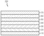
도 3은 본 발명의 일 실시예에 따른 QD-발광소자의 단면도이다.Figure 3 is a cross-sectional view of a QD-light emitting device according to an embodiment of the present invention.
도 3에 예로 든 것은 QLED(200)이다. 본 발명의 일 실시예에 따른 QLED(200)는, 정공 수송층(140, HTL), QD 발광층(150, EML), 및 전자 수송층(160, ETL)을 포함한다. QD 발광층(150)은 각각 정공 수송층(140)과 전자 수송층(160)으로부터 들어온 정공과 전자를 결합시켜 발광시키는 층이다. 이러한 다층 구조는 기계적 지지 역할을 하는 기판(110) 상부에 형성될 수 있으며, 정공 주입을 위한 양극(120, anode)과 전자 주입을 위한 음극(170, cathode), 그리고 양극(120)과 정공 수송층(140) 사이에 정공 주입층(130, HIL)을 더 포함하여 이루어질 수 있다.The example shown in Figure 3 is QLED (200). The QLED (200) according to an embodiment of the present invention includes a hole transport layer (140, HTL), a QD emission layer (150, EML), and an electron transport layer (160, ETL). The QD light-emitting
기판(110)은 투명하고 표면이 편평한 유리 기판 또는 투명 플라스틱 기판일 수 있다. 기판(110)은 오염 물질의 제거를 위해 이소프로필알코올(IPA), 아세톤, 메탄올 등의 용매로 초음파 세척하고 UV-오존 처리를 한 후 사용할 수 있다.The substrate 110 may be a glass substrate or a transparent plastic substrate that is transparent and has a flat surface. The substrate 110 can be used after being ultrasonically cleaned with a solvent such as isopropyl alcohol (IPA), acetone, or methanol to remove contaminants and subjected to UV-ozone treatment.
양극(120) 및 음극(170)은 금속을 포함하여, 각 투명/불투명 조건에 맞는 금속 산화물이거나 그 외 기타 비산화물의 무기물로 이루어진다. 하부 발광을 위해서 양극(120)은 투명한 ITO, IZO, ITZO, AZO와 같은 투명 전도성 금속으로 이루어질 수 있고, 음극(170)은 전자 주입이 용이하도록 일함수가 작은 금속 즉, I, Ca, Ba, Ca/Al, LiF/Ca, LiF/Al, BaF2/Al, BaF2/Ca/Al, Al, Mg, Ag:Mg 합금 등을 사용할 수 있다.The
정공 주입층(130)과 정공 수송층(140)은 양극(120)으로부터 정공 주입을 용이하게 해주고, QD 발광층(150)으로의 정공을 전달하는 역할을 한다. 이들을 형성하기 위해 유기물 또는 무기물 적용이 가능하며, poly(ethylenedioxythiophene):polystyrene sulphonate(PEDOT:PSS), poly[(9, 9-dioctyl-fluorenyl-2, 7-diyl)-co-(4, 4'-(N-(p-butylphenyl))diphenylamine)](TFB), poly(9-vinlycarbazole)(PVK), N, N, N, N', N'-tetrakis(4-methoxyphenyl)-benzidine(TPD), poly-TPD, 4, 4', 4''-tris(N-carbazolyl)-triphenylamine(TCTA), N, N'-bis(naphthalen-1-yl)-N, N'bis(phenyl)-9, 9-spiro-bifluorene(spiro-NPB), dipyrazino[2, 3-f:2', 3'-h]quinoxaline-2, 3, 6, 7, 10, 11-hexacarbonitrile(HATCN), 1, 1-bis[(di-4-tolylamino)phenylcyclohexane(TAPC), p-형 금속 산화물 및 이들의 조합 중에서 선택되는 어느 하나일 수 있다. p-형 금속 산화물은 예컨대 NiO, MoO3, WO3일 수 있다. 바람직한 실시예에 따르면, 상기 정공 수송층(140)은 유기물이다. 하나의 구체적인 예에서, 상기 정공 주입층(130)은 PEDOT:PSS, 상기 정공 수송층(140)은 PVK 또는 TFB이다.The
QD 발광층(150)은, 본 발명에 따른 QD(100)들이 채워져 이루어진 층이며, 여기서, QD 발광층(150)은 예를 들어, 용매에 QD(100)을 포함시킨 분산액을 코팅하는 용액 공정으로 정공 수송층(140) 상에 코팅한 후, 용매를 휘발시켜 형성할 수 있다. 코팅 방법은 예를 들면, 드롭캐스팅(drop casting), 스핀코팅(spin coating), 딥코팅(dip coating), 분무코팅(spray coating), 흐름코팅(flow coating), 스크린 인쇄(screen printing) 또는 잉크젯 프린팅 등을 단독 또는 조합하여 사용할 수 있다.The
전자 수송층(160)은 음극(170)으로부터의 전자 주입을 용이하게 해주고, QD 발광층(150)으로 전자를 전송하는 역할을 한다. 이 전자 수송층(160)은 금속 산화물 나노입자를 포함한다. 예를 들어, 전자 수송층(160)은 용매에 상기 금속 산화물 나노입자를 포함시킨 분산액을 코팅하는 용액 공정으로 QD 발광층(150) 상에 코팅한 후, 용매를 휘발시켜 형성할 수 있다.The
상기 금속 산화물 나노입자는 Zn1-xMgxO(0≤x≤0.5) 조성의 Zn 함유 Mg 산화물 나노입자; 및 상기 나노입자 표면에 형성된 Mg 이온 표면 처리층을 포함할 수 있다. Mg 이온 표면 처리층을 통해 전하 불균형 현상을 개선할 수 있다. QD 발광층(150) 내로 균형 있는 전자 및 정공의 주입을 가능케 하므로, QLED(200)의 성능, 특히 휘도 및 효율을 향상시킬 수 있다.The metal oxide nanoparticles include Zn-containing Mg oxide nanoparticles of the composition Zn1-x Mgx O (0≤x≤0.5); And it may include a Mg ion surface treatment layer formed on the surface of the nanoparticle. The charge imbalance phenomenon can be improved through the Mg ion surface treatment layer. Since it enables balanced injection of electrons and holes into the
이와 같이 용액을 이용한 공정을 가지고 청색 QLED(200)을 제조할 수 있다. 실험예에서는 소자 성능에 대한 ZnSe 내측 쉘(20) 및 ZnS 외측 쉘(30)의 두께의 영향을 조사하여, 전하 균형 개선을 할 수 있도록 한 결과, 비교적 두꺼운 외측 쉘이 있는 최적의 QD 이종구조에서 18.6%의 높은 EQE를 달성할 수 있음을 확인하였다.In this way, a blue QLED (200) can be manufactured using a process using a solution. In the experimental example, the effect of the thickness of the ZnSe
이하에서는 본 발명의 실험예를 상세히 설명함으로써 본 발명에 대하여 더욱 상세히 설명하기로 한다. 하지만 아래의 실험예로 본 발명이 제한되는 것은 아니다.Hereinafter, the present invention will be described in more detail by describing experimental examples of the present invention in detail. However, the present invention is not limited to the experimental examples below.
실험을 통하여, ZnSeTe/ZnSe/ZnS 이종 구조에서 ZnSe 내측 쉘의 두께를 변화시키면 ZnS 외측 쉘의 두께뿐만 아니라 피크 파장, 색상 순도 관련 대역폭, QY 등 PL 특성에도 변화를 가져옴을 확인하였다. 딥블루 영역에서 중간 수준의 PL 변조가능성을 입증하기 위해 ZnSeTe 코어의 Te/Se 비를 정밀하게 조절할 수 있으며, ZnS 외측 쉘의 두께가 QLED 성능에 미치는 영향을 검사하였다.Through experiments, it was confirmed that changing the thickness of the ZnSe inner shell in the ZnSeTe/ZnSe/ZnS heterostructure resulted in changes not only in the thickness of the ZnS outer shell but also in PL characteristics such as peak wavelength, color purity-related bandwidth, and QY. To demonstrate the possibility of medium-level PL modulation in the deep blue region, the Te/Se ratio of the ZnSeTe core can be precisely adjusted, and the effect of the thickness of the ZnS outer shell on QLED performance was examined.
재료ingredient
아연 아세테이트(Zn(Ac)2, ≥ 99.9%), 셀레늄(Se, 99.999% 분말), 1-헥사데실아민(HDA, 90%)은 Alfa Aesar에서 구매할 수 있다. 황(S, 99.998%, 금속기준), 텔루륨(Te, 99.8%, 분말), 올레산(OA, 90%) 1-옥타데센(ODE, 90%), PVK(Mw = ~25000-50000)는 Sigma Aldrich에서 구매할 수 있다. TPBi(99.9%), CBP(99.9%), 몰리브덴옥사이드(MoO3, 99.95%)는 OSM에서는 구매할 수 있다. 다이페닐포스핀(DPP, > 98%)과 트리옥틸포스핀(TOP, ≥99%)은 Lake Materials 에서 구매할 수 있다. 트리옥틸아민(TOA, 97%)은 Acros Organics에서 구입할 수 있다. 위 모든 화학물질은 수령된 것을 추가 처리 없이 실험에 사용하였다.Zinc acetate (Zn(Ac)2 , ≥ 99.9%), selenium (Se, 99.999% powder) and 1-hexadecylamine (HDA, 90%) are available from Alfa Aesar. Sulfur (S, 99.998%, metal basis), tellurium (Te, 99.8%, powder), oleic acid (OA, 90%) 1-octadecene (ODE, 90%), PVK (Mw = ~25000-50000) Available from Sigma Aldrich. TPBi (99.9%), CBP (99.9%), and molybdenum oxide (MoO3 , 99.95%) can be purchased from OSM. Diphenylphosphine (DPP, > 98%) and trioctylphosphine (TOP, ≥99%) are available from Lake Materials. Trioctylamine (TOA, 97%) is available from Acros Organics. All of the above chemicals were used in experiments as received without further processing.
특성 분석Characterization
QD의 UV-Vis 흡수 및 PL 스펙트럼은 각각 흡수 분광장치(Shimadzu, UV-2450) 및 500 W 크세논 램프-장착된 분광광도계(PSI Inc., Darsa Pro-5200)를 가지고 기록하였다. 희석된 QD 분산액의 PL 양자효율 절대값은 PL QY 측정 시스템 (Otsuka, QE-2000)을 가지고 평가하였다. QD 입자의 TEM 영상과 단면 QLED는 JEM-2100F(JEOL Ltd.)를 활용해 확보했다. 40 kV 및 30 mA에서 작동하는 Cu Kα 방사선의 분말 X선 회절계(Rigaku, Ultima IV))를 사용하여 QD의 이종구조 진화에 대한 보충 정보를 얻었다. QD의 원소 성분은 15kV에서 작동하는 에너지 분산형 X선 분광계(옥스포드 기기 X-MAX 80)가 장착된 전계 발광 주사 전자 현미경(JEOL JSM-7800F)으로 평가하였다. QD의 VBM 수준은 UV 광전자 분광계(Kratos Inc. AXIS Ultra DLD)로 추정하였다. QD의 PL 붕괴 프로파일은 피코초 펄스 다이오드 레이저(EPL-375) 장착 분광 광도계(에딘버그 인스트루먼트 FS5)에 시간 상관 단일 광자 계수(TCSPC) 방식으로 기록됐다. QLED의 EL 스펙트럼 및 전류-전압-휘도(I-V-L) 특성은 Konica-Minolta CS-2000A 분광 휘도계와 Keithley 2400 전압-전류 전원 장치로 측정되었다.The UV-Vis absorption and PL spectra of QDs were recorded with an absorption spectrometer (Shimadzu, UV-2450) and a 500 W xenon lamp-equipped spectrophotometer (PSI Inc., Darsa Pro-5200), respectively. The absolute PL quantum efficiency of the diluted QD dispersion was evaluated using a PL QY measurement system (Otsuka, QE-2000). TEM images and cross-sectional QLED images of QD particles were obtained using JEM-2100F (JEOL Ltd.). Supplementary information on the heterostructure evolution of QDs was obtained using a powder X-ray diffractometer (Rigaku, Ultima IV) with Cu Kα radiation operating at 40 kV and 30 mA. The elemental composition of the QDs was evaluated by an electroluminescence scanning electron microscope (JEOL JSM-7800F) equipped with an energy-dispersive X-ray spectrometer (Oxford Instruments X-MAX 80) operating at 15 kV. The VBM level of QDs was estimated with a UV photoelectron spectrometer (Kratos Inc. AXIS Ultra DLD). The PL decay profiles of QDs were recorded by time-correlated single photon counting (TCSPC) on a spectrophotometer (Edinburg Instruments FS5) equipped with a picosecond pulsed diode laser (EPL-375). The EL spectrum and current-voltage-luminance (I-V-L) characteristics of the QLED were measured with a Konica-Minolta CS-2000A spectroluminance meter and a Keithley 2400 voltage-current power supply.
ZnSeTe/ZnSe/ZnS QD 합성ZnSeTe/ZnSe/ZnS QD synthesis
청색 발광 ZnSeTe 코어를 합성하기 위해, 100 mL 3목 플라스크 안에서 Zn(Ac)2 2 mmol, OA 2 mL, ODE 15 mL를 함유한 혼합물을 120℃로 가열하고 1시간 동안 디개싱하였다. 그런 다음 N2 분위기에서 반응 플라스크를 210℃까지 가열하였다. 온도가 안정화된 후 2 M Se-DPP 0.5 mL와 0.047 M Te-TOP 용액 0.75 mL(즉, 공칭 Te/Se 비율 = 0.035)를 순차적으로 반응 플라스크에 주입하였다. ZnSeTe 코어의 성장은 이 온도에서 30분간 유지하다가 300℃로 온도를 증가시켜 1시간 더 유지하였다.To synthesize the blue-emitting ZnSeTe core, a mixture containing 2 mmol Zn(Ac)2 , 2 mL OA, and 15 mL ODE in a 100 mL three-neck flask was heated to 120°C and degassed for 1 hour. Then, the reaction flask was heated to 210°C in N2 atmosphere. After the temperature was stabilized, 0.5 mL of 2 M Se-DPP and 0.75 mL of 0.047 M Te-TOP solution (i.e., nominal Te/Se ratio = 0.035) were sequentially injected into the reaction flask. The growth of the ZnSeTe core was maintained at this temperature for 30 minutes, then the temperature was increased to 300°C and maintained for an additional hour.
1.2 M Se-TOP 2.5, 5.0, 7.5 mL와 10, 20, 30 mL의 Zn(OA)2 용액(Zn(Ac)2 60 mmol를 OA 40 mL, TOP 20 mL 및 TOA 20 mL에 녹여서 준비) 각각을, 300℃에서 시린지 펌프로 함께 적가하여, 각각 얇은, 중간, 두꺼운 ZnSe 내측 쉘을 형성하게 함으로써, 두께가 다른 ZnSe 내측 쉘을 가지는 QD를 형성하도록 하였다(주입 속도: Se-TOP의 경우 2.5 mL/h, Zn(OA)2의 경우 10 mL/h).1.2 M Se-TOP 2.5, 5.0, 7.5 mL and 10, 20, 30 mL of Zn(OA)2 solution (prepared by dissolving 60 mmol of Zn(Ac)2 in 40 mL of OA, 20 mL of TOP, and 20 mL of TOA), respectively. were added dropwise together with a syringe pump at 300°C to form thin, medium, and thick ZnSe inner shells, respectively, to form QDs with ZnSe inner shells of different thicknesses (injection rate: 2.5 mL for Se-TOP) /h, 10 mL/h for Zn(OA)2 ).
주입 완료 후 반응 플라스크를 상온으로 냉각하고 그 결과로 생긴 ZnSeTe/ZnSe 코어/쉘 QD를 에탄올로 침전시켜 헥산 9 mL로 재분산해 ZnSeTe/ZnSe QD 분산액을 제조하였다.After completion of injection, the reaction flask was cooled to room temperature, and the resulting ZnSeTe/ZnSe core/shell QDs were precipitated with ethanol and redispersed in 9 mL of hexane to prepare a ZnSeTe/ZnSe QD dispersion.
ZnS 외측 쉘 형성을 위하여, 50 mL 3목 플라스크 안에서 Zn(Ac)2 2 mmol, HDA 4 mmol, OA 2 mL, TOA 20 mL로 조성된 혼합물을 120℃에서 10분간 디개싱하였다. N2로 백필링(backfilling) 후, 상기 ZnSeTe/ZnSe QD 분산액을 3 mL 주입하고 온도를 330℃까지 높였다. 이어서 1.2 M S-TOP 0.5, 1.0, 1.5 mL를, Zn(OA)2 2, 4, 6 mL 각각과 함께 지속적으로 주입하여 1시간 동안 반응시킴으로써, 얇은, 중간, 두꺼운 ZnS를 각각 생성하였다. 그 결과 생성된 ZnSeTe/ZnSe/ZnS 코어/쉘/쉘 QD는 헥산과 과잉 아세톤 혼합 용매를 가지고 원심분리 방식으로 반복적으로 정제되었다. 정제된 QD는 특성 분석 및 EML 스핀 캐스팅을 위해 옥탄에 분산되었다.To form the ZnS outer shell, a mixture of 2 mmol Zn(Ac)2 , 4 mmol HDA, 2 mL OA, and 20 mL TOA was degassed in a 50 mL three-neck flask at 120°C for 10 minutes. After backfilling with N2 , 3 mL of the ZnSeTe/ZnSe QD dispersion was injected and the temperature was raised to 330°C. Then, 0.5, 1.0, and 1.5 mL of 1.2 M S-TOP were continuously injected together with 2, 4, and 6 mL of Zn(OA)2 , respectively, and reacted for 1 hour to produce thin, medium, and thick ZnS, respectively. The resulting ZnSeTe/ZnSe/ZnS core/shell/shell QDs were repeatedly purified by centrifugation using a mixed solvent of hexane and excess acetone. Purified QDs were dispersed in octane for characterization and EML spin casting.
ZnMgO 나노입자(NP) 형성ZnMgO nanoparticle (NP) formation
ZnMgO 나노입자는 용액-침전 화학 방법을 통해 합성하였다.ZnMgO nanoparticles were synthesized through solution-precipitation chemistry method.
10 mmol의 TMAH(tetramethylammoniumhydroxide) 및 10 mL의 에탄올을 포함하는 투명 용액을 실온에서 8.5 mmol의 Zn 아세테이트 디하이드레이트 및 1.5 mmol Mg 아세테이트 테트라하이드레이트가 30 mL의 DMSO(dimethyl sulfoxide) 안에 용해되어 있는 양이온 용액에 천천히 추가한 후 온도를 유지하며 1시간 동안 유지하였다. 합성된 ZnMgO 나노입자를 과량의 아세톤으로 침전시키고 ETL 스핀 코팅을 위해 에탄올에 재분산시켰다.A clear solution containing 10 mmol of tetramethylammoniumhydroxide (TMAH) and 10 mL of ethanol was added to a cationic solution containing 8.5 mmol of Zn acetate dihydrate and 1.5 mmol of Mg acetate tetrahydrate in 30 mL of dimethyl sulfoxide (DMSO) at room temperature. After adding it slowly, the temperature was maintained for 1 hour. The synthesized ZnMgO nanoparticles were precipitated with excess acetone and redispersed in ethanol for ETL spin coating.
QLED 제작QLED production
다층 아키텍처를 갖춘 청색 발광 QLED는 Al 음극을 제외한 모든 층을 순차적 용액 증착으로 제작하였다. 패턴 있는 ITO 유리는 아세톤과 메탄올로 각각 10분간 초음파 세척한 후 UV-오존으로 30분간 처리하였다. 30nm 두께의 PEDOT: PSS(Heraeus Clevios AI 4083)를 30초 동안 3000rpm으로 스핀 코팅한 후, 30분 동안 150℃에서 베이킹하여 HIL을 형성하였다. PVK 용액(클로로벤젠 내 PVK 10mg/mL)을 사용하여 두께가 25nm인 HTL을 HIL 위에 3000rpm에서 30초간 스핀 코팅한 후 150℃에서 30분간 베이킹하였다.A blue-emitting QLED with a multilayer architecture was manufactured by sequential solution deposition of all layers except the Al cathode. The patterned ITO glass was ultrasonically cleaned with acetone and methanol for 10 minutes each and then treated with UV-ozone for 30 minutes. 30 nm thick PEDOT: PSS (Heraeus Clevios AI 4083) was spin-coated at 3000 rpm for 30 seconds and then baked at 150°C for 30 minutes to form HIL. Using a PVK solution (10 mg/mL of PVK in chlorobenzene), HTL with a thickness of 25 nm was spin-coated on the HIL at 3000 rpm for 30 seconds and baked at 150°C for 30 minutes.
그 후 옥탄에 7.5mg/mL의 농도로 분산한 ZnSeTe/ZnSe/ZnS QD 분산액을 20초 동안 3000rpm에서 스핀 코팅해 거의 모노레이어 두께의 QD EML으로 형성한 후 70℃에서 10분간 베이킹하였다. QD EML 형성 후에는, ZnMgO 나노입자 에탄올 분산액(농도 28~30 mg/mL)을 3000 rpm에서 30초간 스핀코팅하여 40nm 두께의 ZnMgO NP ETL을 형성하였다.Afterwards, the ZnSeTe/ZnSe/ZnS QD dispersion dispersed in octane at a concentration of 7.5 mg/mL was spin-coated at 3000 rpm for 20 seconds to form a QD EML with a thickness of almost a monolayer, and then baked at 70°C for 10 minutes. After QD EML formation, ZnMgO nanoparticle ethanol dispersion (concentration 28-30 mg/mL) was spin-coated at 3000 rpm for 30 seconds to form 40 nm thick ZnMgO NP ETL.
마지막으로 선형 금속 마스크를 통한 열 증발법에 의해 100nm 두께의 Al 음극을 형성하여 소자의 제조를 완료하였다.Finally, the fabrication of the device was completed by forming a 100 nm thick Al cathode by thermal evaporation using a linear metal mask.
ZnS 외측 쉘 두께가 전하 균형에 미치는 영향을 추가로 조사하기 위해 EOD, HOD도 제작하였다. EOD의 구조는 ITO/ZnMgO NP(40nm)/QDs/TPBi(40nm)/Al이고, HOD의 구조는 ITO/PEDOT:PSS(30nm)/PVK(25nm)/QD/CBP(40nm)/MoO3(10nm)/Al이었다. To further investigate the effect of ZnS outer shell thickness on charge balance, EOD and HOD were also fabricated. The structure of EOD is ITO/ZnMgO NP(40nm)/QDs/TPBi(40nm)/Al, and the structure of HOD is ITO/PEDOT:PSS(30nm)/PVK(25nm)/QD/CBP(40nm)/MoO3 ( 10nm)/Al.
결과result
InP 이종구조 QD 제조와 유사하게, 보통 ZnSeTe 코어/쉘 QD는 1-포트 또는 2-스텝 방식으로 제조되어 오고 있다. 전형적인 2-스텝 유도 다중쉘 InP 또는 ZnSeTe QD에서는, 코어 성장 용액에서 추출된 사전 성장 코어에 대해 이중 쉘을 연속적으로 형성한다. 이러한 기존 2-스텝 프로토콜과 다르게, 본 발명에서는 동일한 포트에서 연속적으로 합성된 내측 쉘(20)을 가지는 ZnSeTe/ZnSe QD를 다른 포트로 분리하여 최종 ZnS 외측 쉘(30)을 형성하는 방법을 제안한다.Similar to InP heterostructure QD fabrication, usually ZnSeTe core/shell QDs have been fabricated using a 1-port or 2-step method. In a typical two-step induced multishell InP or ZnSeTe QD, a double shell is formed sequentially on a pre-grown core extracted from the core growth solution. Unlike this existing two-step protocol, the present invention proposes a method of forming the final ZnS outer shell (30) by separating ZnSeTe/ZnSe QDs with the inner shell (20) continuously synthesized in the same port to different ports. .
도 4는 ZnSe 쉘 성장 시간의 함수로서 나타낸 (a) PL 스펙트럼, (b) PL 피크 파장, QY, FWHM의 변화 및 (c) ZnSeTe/ZnSe QD의 흡수 스펙트럼, (d) TEM 이미지, (e) ZnSeTe 코어가 ZnSe 쉘링 과정에서 확대되는 것을 그린 개략도이다.Figure 4 shows (a) PL spectrum, (b) changes in PL peak wavelength, QY, FWHM and (c) absorption spectrum of ZnSeTe/ZnSe QDs, (d) TEM images, (e) as a function of ZnSe shell growth time. This is a schematic diagram showing the expansion of the ZnSeTe core during the ZnSe shelling process.
300℃에서 ZnSeTe 코어의 성장이 완료되면 ZnSe 스톡 용액을 장시간 적가하여 지속적으로 주입하였다. 도 4의 (a)는 최대 180분까지의 내측 쉘 성장 시간의 함수로서 ZnSeTe/ZnSe QD의 PL 스펙트럼 진화를 보여준다. PL 측정을 위한 모든 샘플의 광학 밀도(도 4의 (a))는 370nm에서 0.05로 동일하게 조정되었다.When the growth of the ZnSeTe core was completed at 300°C, the ZnSe stock solution was continuously injected dropwise over a long period of time. Figure 4(a) shows the PL spectrum evolution of ZnSeTe/ZnSe QDs as a function of inner shell growth time up to 180 min. The optical density of all samples for PL measurement (Figure 4(a)) was adjusted to be the same at 0.05 at 370 nm.
도 4의 (a)를 참조하면, 최대 120분까지 ZnSe 내측 쉘 반응시간이 지속적으로 증가하면 PL은 주어진 조성(즉, 공칭 Te/Se 몰비 0.035)에서 ZnSeTe 코어의 경우 440nm이던 피크 파장이 458nm로 점차 적색편이 되었다.Referring to Figure 4 (a), as the ZnSe inner shell reaction time continues to increase up to 120 minutes, the PL increases from a peak wavelength of 440 nm to 458 nm for the ZnSeTe core at a given composition (i.e., nominal Te/Se molar ratio of 0.035). It gradually shifted to red.
그 후, 더 연장된 성장 시간은 더 이상 PL 이동을 유도하지 않았다(도 4의 (b)).Afterwards, longer growth times no longer induced PL migration (Figure 4(b)).
이러한 PL 이동은 흡수 스펙트럼 결과와도 잘 일치했다(도 4의 (c)).This PL shift also matched well with the absorption spectrum results (Figure 4(c)).
ZnSeTe/ZnSe 이종구조의 quasi-type II 대역 정렬은, 정공 파동 함수는 코어 영역에 상대적으로 제한되고, 전자 파동 함수는 ZnSe 내측 쉘 상에서 상당히 비편재되도록 한다(도 4의 (c) 삽입그림).The quasi-type II band alignment of the ZnSeTe/ZnSe heterostructure causes the hole wave function to be relatively confined to the core region and the electron wave function to be highly delocalized on the ZnSe inner shell (inset of Figure 4(c)).
양자 제한 효과의 감소를 수반하는 쉘 전체에 걸친 이러한 전자 누설이 밴드 갭 감소의 원인이다. ZnSe 내측 쉘의 두께 증가(이후 전자 비편재화를 유도함)는 120분 성장시 최대 458nm 피크 파장에서 점진적인 PL 적색 편이를 유도했다. 그 후 스펙트럼 변화는 포화 상태에 도달하여 최대 180분까지 더 연장된 성장 시간을 통해 두꺼운 내측 쉘을 성장시킬 때 더 이상의 전자 비편재화가 없음을 나타낸다(도 4의 (b)).This electron leakage across the shell, accompanied by a reduction in quantum confinement effects, is responsible for the band gap reduction. Increasing the thickness of the ZnSe inner shell (which subsequently induces electron delocalization) induced a gradual PL red shift with a peak wavelength of up to 458 nm upon 120 min growth. Afterwards, the spectral change reaches saturation, indicating no further electron delocalization upon growing the thick inner shell through further extended growth times up to 180 min (Figure 4(b)).
도 4의 (b)를 참조하면, PL QY는 ZnSeTe 코어에서 18%이던 것이 120분 쉘링한 ZnSeTe/ZnSe QD에서 최대 40%로 점차 증가하다가 180분 더 장기 쉘링 후 25%로 감소하였다. 이러한 PL QY 감소는 120분보다 긴 성장 시간으로 인해 과도하게 두꺼운 ZnSe 내측 쉘이 형성되는 것과 관련이 있으며, 이로 인해 계면 응력이 더욱 현저해진다. 여기서는 편의상 60분, 120분, 180분 성장 시간의 ZnSe 쉘을 각각 얇은(thin) ZnSe, 중간(medium) ZnSe, 두꺼운(thick) ZnSe로 표시한다.Referring to Figure 4 (b), the PL QY gradually increased from 18% in the ZnSeTe core to a maximum of 40% in the ZnSeTe/ZnSe QD shelled for 120 minutes, and then decreased to 25% after a further 180 minutes of long-term shelling. This PL QY decrease is related to the formation of an excessively thick ZnSe inner shell due to growth times longer than 120 min, which makes the interfacial stress more pronounced. Here, for convenience, the ZnSe shells with growth times of 60 minutes, 120 minutes, and 180 minutes are denoted as thin ZnSe, medium ZnSe, and thick ZnSe, respectively.
투과 전자 현미경(TEM) 이미지(도 4의 (d))와 비교했을 때 크기는 ZnSeTe 코어의 5.38nm, ZnSeTe/얇은-ZnSe의 7.67nm, ZnSeTe/중간-ZnSe의 9.71nm에서 ZnSeTe/두꺼운-ZnSe의 10.31nm로 꾸준히 증가했다. 얇은 ZnSe, 중간 ZnSe, 두꺼운 ZnSe 쉘 각각의 두께는 대략 1.14, 2.16, 2.47nm이다. 120분의 성장에 따른 중간-ZnSe가 가장 높은 PL QY(즉, 40%)를 보인 것을 고려하면, 상당한 계면 응력없이 일관성있는 성장이 가능한 ZnSe 내측 쉘의 임계 두께는 약 2.16nm이라고 추정할 수 있다.Compared to the transmission electron microscopy (TEM) image ((d) in Figure 4), the size is 5.38 nm for ZnSeTe core, 7.67 nm for ZnSeTe/thin-ZnSe, and 9.71 nm for ZnSeTe/thick-ZnSe. steadily increased to 10.31nm. The thicknesses of the thin ZnSe, medium ZnSe, and thick ZnSe shells are approximately 1.14, 2.16, and 2.47 nm, respectively. Considering that mid-ZnSe showed the highest PL QY (i.e., 40%) following 120 min of growth, the critical thickness of the ZnSe inner shell that allows consistent growth without significant interfacial stress can be estimated to be approximately 2.16 nm. .
near-UV에서 자색 발광까지의 이성분계 ZnSe QD는 20nm 미만의 매우 좁은 PL 대역폭을 보일 수 있는 반면, ZnSeTe QD에 Te 합금을 하면 불가피하게 비균질 스펙트럼 확장을 유발하며, 그 정도 역시 청색 발광 ZnSeTe QD의 상대적 Te 함량에 비례하는 것으로 나타난다. 개별 QD에 대한 Te 합금 및 격자 결함(Se와 Te 사이의 이온 반경의 큰 차이에 의해 유도됨) 또는 표면 불순물(쉘을 형성하는 작업 중 도입됨)에서 형성된 트랩 준위의 존재로 인해 스펙트럼 확장이 일어날 수 있다. 위의 PL 파장과 QY의 변화 외에도, ZnSe 내측 쉘의 두께도 PL 대역폭에 영향을 미쳐, FWHM에서 ZnSeTe 코어의 52nm, ZnSeTe/얇은-ZnSe의 28nm, ZnSeTe/중간-ZnSe의 26nm에서 ZnSeTe/두꺼운-ZnSe의 24nm까지 일관되게 스펙트럼이 좁혀졌다(도 4의 (a), (b)).While binary ZnSe QDs from near-UV to violet emission can exhibit very narrow PL bandwidths of less than 20 nm, Te alloying of ZnSeTe QDs inevitably causes inhomogeneous spectral broadening, the extent of which is also comparable to that of blue-emitting ZnSeTe QDs. It appears to be proportional to the relative Te content. Spectral broadening will occur due to the presence of trap levels formed from Te alloys and lattice defects (induced by the large difference in ionic radii between Se and Te) or surface impurities (introduced during the shell forming operation) for individual QDs. You can. In addition to the above changes in PL wavelength and QY, the thickness of the ZnSe inner shell also affects the PL bandwidth, which varies from FWHM to 52 nm for ZnSeTe core, 28 nm for ZnSeTe/thin-ZnSe, and 26 nm for ZnSeTe/medium-ZnSe. The spectrum was consistently narrowed to 24 nm for ZnSe (Figures 4 (a) and (b)).
도 5는 (a) ZnSeTe, (b) ZnSeTe/얇은-ZnSe, (c) ZnSeTe/중간-ZnSe, (d) ZnSeTe/두꺼운-ZnSe QD의 PL 스펙트럼 분해도, (e)는 (a) 내지 (d)로부터 얻은 결과를 정리한 것이다.Figure 5 shows the resolved PL spectra of (a) ZnSeTe, (b) ZnSeTe/thin-ZnSe, (c) ZnSeTe/medium-ZnSe, and (d) ZnSeTe/thick-ZnSe QDs, and (e) shows (a) to (d). ) is a summary of the results obtained from.
이 4개의 QD 샘플 중 PL은 고에너지 여기 및 저에너지 테일(또는 트랩) 발광 성분으로 조성된 두 개의 하위 스펙트럼으로 분해되었으며, ZnSe 쉘 두께 증가에 따른 후자의 스펙트럼 기여도 지속 감소(도 5)를 보여주었다. 이러한 스펙트럼 수축은 결국 전체 PL의 비대칭을 감소시켜 발광 반치폭을 좁힌다.Among these four QD samples, PL was decomposed into two subspectra composed of high-energy excitation and low-energy tail (or trap) emission components, showing a sustained decrease in the spectral contribution of the latter with increasing ZnSe shell thickness (Figure 5). . This spectral contraction eventually reduces the asymmetry of the overall PL and narrows the luminescence half width.
본 발명에서의 ZnSe 쉘링이 고온(300℃)에서 장기간 진행된다는 점을 고려할 때, 쉘링하는 동안 미리 성장한 ZnSeTe 코어와 ZnSe 쉘 사이의 상호 확산 가능성이 매우 높으며, 이를 통해 ZnSeTe 코어의 유효 영역을 어느 정도 확장할 수 있다(도 4(e) 참조). 따라서 쉘링이 진행됨에 따라, 확대된 ZnSeTe 코어에서는 Se에 대한 Te 함량이 낮아지게 되므로, 테일 발광을 완화하여 전체 PL의 스펙트럼 대칭성을 더 향상시키거나 색상 순도를 더 높이도록 개선된다.Considering that the ZnSe shelling in the present invention is carried out at high temperature (300°C) for a long period of time, the possibility of interdiffusion between the pre-grown ZnSeTe core and the ZnSe shell during shelling is very high, thereby reducing the effective area of the ZnSeTe core to some extent. It can be expanded (see Figure 4(e)). Therefore, as shelling progresses, the content of Te relative to Se in the enlarged ZnSeTe core decreases, thereby mitigating tail emission to further improve the spectral symmetry of the overall PL or to further increase color purity.
도 6은 (a) ZnSeTe/ZnSe/ZnS QD의 TEM 이미지, (b) ZnSeTe 코어, ZnSeTe/ZnSe/ZnS QD의 XRD 패턴, (c) 표준화된 PL, (d) PL 피크 파장, QY, FWHM 및 (e) PL 붕괴 프로파일이다. 도 7은 (a) 0.035의 공칭 Te/Se 몰비로 합성된 ZnSeTe 코어의 EDS 스펙트럼 및 실제 조성, (b) ZnSeTe/얇은-ZnSe/ZnS, ZnSeTe/중간-ZnSe/ZnS, 및 ZnSeTe/두꺼운-ZnSe/ZnS QD의 EDS 스펙트럼, (c) Zn, Se, S의 조성(원자%)이다.Figure 6 shows (a) TEM image of ZnSeTe/ZnSe/ZnS QD, (b) ZnSeTe core, XRD pattern of ZnSeTe/ZnSe/ZnS QD, (c) normalized PL, (d) PL peak wavelength, QY, FWHM, and (e) PL decay profile. Figure 7 shows (a) the EDS spectra and actual compositions of ZnSeTe cores synthesized with a nominal Te/Se molar ratio of 0.035, (b) ZnSeTe/thin-ZnSe/ZnS, ZnSeTe/medium-ZnSe/ZnS, and ZnSeTe/thick-ZnSe. EDS spectrum of /ZnS QD, (c) Composition (atomic %) of Zn, Se, and S.
성장 용액에서 추출한 위의 얇은, 중간 및 두꺼운 ZnSe 쉘을 가진 ZnSeTe QD는 2-스텝 방식으로 최종 ZnS 쉘링에 동일하게 배치되었다. 그 결과 ZnSeTe/얇은, 중간, 두꺼운-ZnSe/ZnS 코어/쉘/쉘 QD의 평균 크기는 9.66, 10.93, 11.36nm로 나타났으며, 이를 통해 ZnS 외측 쉘의 두께는 각각 1.00, 0.61, 0.52nm로 추정되었다(도 6의 (a)). 동일한 ZnS 쉘링을 적용하였으므로, 두꺼운 ZnSe 내측 쉘 QD가 크기가 커서 표면적이 넓다보니 ZnS 외측 쉘의 두께는 자연스럽게 얇아지는 것이다.ZnSeTe QDs with the above thin, medium, and thick ZnSe shells extracted from the growth solution were equally placed into the final ZnS shelling in a two-step manner. As a result, the average sizes of ZnSeTe/thin, medium, and thick-ZnSe/ZnS core/shell/shell QDs were 9.66, 10.93, and 11.36 nm, and the thickness of the ZnS outer shell was 1.00, 0.61, and 0.52 nm, respectively. It was estimated ((a) in Figure 6). Since the same ZnS shelling is applied, the thick ZnSe inner shell QD is large and has a large surface area, so the thickness of the ZnS outer shell naturally becomes thinner.
도 6의 (b)는 ZnSeTe 코어와 함께 ZnSe 두께의 함수로서 ZnSeTe/ZnSe 코어/쉘과 ZnSeTe/ZnSe/ZnS 코어/쉘/쉘의 X선 회절(XRD) 패턴을 보여준다. ZnSe 두께에 관계없이 모든 ZnSeTe/ZnSe QD와 ZnSeTe 코어의 반사 피크는 눈에 띄는 격자 변화를 유도할 정도는 아닌 ZnSeTe 코어의 낮은 Te 함량 때문에 징크 블렌드 ZnSe 상과 거의 일치하게 된다. ZnSeTe 코어의 합성에 사용된 공칭 Te/Se 몰비(0.035)는 에너지 분산 분광기(EDS) 분석(도 7의 (a))의 실제 몰비(0.036)와 거의 동일한 것으로 확인되었다.Figure 6(b) shows the X-ray diffraction (XRD) patterns of ZnSeTe/ZnSe core/shell and ZnSeTe/ZnSe/ZnS core/shell/shell as a function of ZnSe thickness along with ZnSeTe core. Regardless of the ZnSe thickness, the reflection peaks of all ZnSeTe/ZnSe QDs and ZnSeTe cores closely match those of the zinc blend ZnSe phase due to the low Te content of the ZnSeTe core, which is not sufficient to induce noticeable lattice changes. The nominal Te/Se molar ratio (0.035) used in the synthesis of the ZnSeTe core was confirmed to be almost identical to the actual molar ratio (0.036) in energy dispersive spectroscopy (EDS) analysis (FIG. 7(a)).
ZnS 쉘링 시, 모든 코어/쉘 QD의 반사 피크가 큰 2θ(즉, 벌크 ZnS 상)로 약간 이동한 것으로부터, ZnS 쉘이 코어/쉘 QD 상에서 전체적으로 성장했음을 알 수 있다. 한편, ZnSe 내측 쉘의 두께가 증가하여도 코어/쉘과 코어/쉘/쉘 간에 XRD 피크 이동이 적다는 것을 알 수 있다. 이것은 ZnSe 내측 쉘이 두꺼운 샘플일수록 ZnS 외측 쉘이 더 얇게 형성되기 때문이며, 도 6의 (a)에 나타낸 TEM 이미지 및 코어/쉘/쉘 QD의 추가 EDS 기반 조성 결과(도 7의 (b), (c))와 일치한다.Upon ZnS shelling, the reflection peaks of all core/shell QDs shifted slightly to large 2θ (i.e., bulk ZnS phase), indicating that the ZnS shell was entirely grown on the core/shell QDs. Meanwhile, it can be seen that even when the thickness of the ZnSe inner shell increases, the XRD peak shift between core/shell and core/shell/shell is small. This is because samples with thicker ZnSe inner shells have thinner ZnS outer shells, and the TEM image shown in (a) of Figure 6 and the additional EDS-based composition results of core/shell/shell QDs ((b) in Figure 7, Consistent with c)).
도 6의 (c)는 다양한 ZnSe 내측 쉘 두께를 가진 코어/쉘/쉘 QD의 정규화된 PL 스펙트럼을 보여주는데, 얇은, 중간, 두꺼운 ZnSe 기반 코어/쉘/쉘 QD의 경우 각각 452, 455 및 457nm의 중심파장을 나타낸다(도 6의 (d)). 참고로 이러한 코어/쉘/쉘 QD의 PL 피크는 각각의 코어/쉘 QD에 비해 1-3nm 정도 약간 청색 편이 되며, 이는 양자 감금의 강화와 밴드 갭의 증가 때문이다.Figure 6(c) shows the normalized PL spectra of core/shell/shell QDs with various ZnSe inner shell thicknesses of 452, 455, and 457 nm for thin, medium, and thick ZnSe-based core/shell/shell QDs, respectively. The central wavelength is shown (Figure 6(d)). For reference, the PL peak of these core/shell/shell QDs is slightly blue-shifted by 1-3 nm compared to each core/shell QD, which is due to the strengthening of quantum confinement and the increase in the band gap.
도 8은 코어/쉘과 코어/쉘/쉘 QD 간 흡수 스펙트럼 비교로서, (a) 얇은 ZnSe, (b) 중간 ZnSe, (c) 두꺼운 ZnSe의 경우이다.Figure 8 is a comparison of absorption spectra between core/shell and core/shell/shell QDs for (a) thin ZnSe, (b) medium ZnSe, and (c) thick ZnSe.
ZnS 외측 쉘은 전자 파장 함수의 비편재화에 대해 높은 에너지 장벽을 구축할 수 있다. ZnS 외측 쉘을 형성한 후 이러한 밴드 갭 증가는 코어/쉘과 코어/쉘/쉘 QD 사이의 흡수 스펙트럼을 비교하여 더욱 검증할 수 있다(도 8). PL QY는 코어/쉘 QD의 25-40%(도 4의 (b))에서 코어/쉘/쉘의 90-96%(ZnSe 내측 쉘 두께에 따라 다름)로 급격히 증가했으며(도 6의 (d)), 이는 본 발명에 따른 ZnS 외측 쉘 형성이 매우 효과적인 표면 패시베이션을 제공했음을 시사한다. 이러한 완벽에 가까운 쉘링은 높은 비등점(365℃)을 가진 TOA를 용매로 사용함으로써 가능했던 335℃의 비교적 높은 온도에서 ZnS 외측 쉘을 형성함으로써 달성할 수 있는 것이다.The ZnS outer shell can establish a high energy barrier against the delocalization of the electronic wavelength function. This band gap increase after forming the ZnS outer shell can be further verified by comparing the absorption spectra between core/shell and core/shell/shell QDs (Figure 8). The PL QY increased rapidly from 25-40% of core/shell QDs ((b) in Figure 4) to 90-96% of core/shell/shell (depending on the ZnSe inner shell thickness) ((d in Figure 6). )), which suggests that the formation of the ZnS outer shell according to the present invention provided a very effective surface passivation. This near-perfect shelling can be achieved by forming the ZnS outer shell at a relatively high temperature of 335°C, which was made possible by using TOA, which has a high boiling point (365°C), as a solvent.
비교예로서, TOA를 비등점이 315℃로 낮은 ODE으로 교체하고 쉘 성장 온도를 300℃로 낮추어 ZnSeTe/중간 ZnSe QD의 ZnS 쉘링을 수행한 결과, 제조된 코어/쉘/쉘 QD는 본 발명 실시예(93%)에 비해 PL QY가 80%로 현저히 낮은 것으로 나타났다.As a comparative example, ZnS shelling of ZnSeTe/intermediate ZnSe QDs was performed by replacing TOA with ODE with a low boiling point of 315°C and lowering the shell growth temperature to 300°C. As a result, the prepared core/shell/shell QDs were similar to those of the present invention. The PL QY was found to be significantly lower at 80% compared to (93%).
한편, 코어/쉘/쉘 QD의 PL QY는 얇은 ZnSe의 경우인 96%에서 두꺼운 ZnSe(도 6의 (d))의 경우인 90%로 꾸준히 감소하였는데, 이는 두꺼운 ZnSe의 경우 얇은 ZnS 외측 쉘이 형성되므로 코어/쉘 QD 표면의 완전한 패시베이션 가능성이 낮아졌기 때문이다. 또한 일련의 코어/쉘/쉘 QD의 FWHM 값(23-27nm)은 ZnS와의 효과적인 표면 패시베이션에 의해 활성화된 비방사성 재결합 억제로 인해 각각의 코어/쉘에 비해 1nm만큼 근소하게 좁혀졌다(도 6의 (d)). 여기에서 개발된 코어/쉘/쉘 QD의 FWHM은 PL QY가 가장 잘 수행된 전례의 결과(HF/ZnCl2를 사용한 것, PL 피크 457nm, FWHM 36nm)보다 약간 낮았지만 현재까지의 딥블루(특히 >450nm) ZnSeTe 발광체 중에서 가장 좁다.Meanwhile, the PL QY of the core/shell/shell QD steadily decreased from 96% for thin ZnSe to 90% for thick ZnSe ((d) in Figure 6), which means that the thin ZnS outer shell is This is because the possibility of complete passivation of the core/shell QD surface is reduced. Additionally, the FWHM values (23-27 nm) of the series of core/shell/shell QDs were narrowed slightly by 1 nm compared to the individual core/shell QDs due to the non-radiative suppression of recombination activated by the effective surface passivation with ZnS (Figure 6). (d)). The FWHM of the core/shell/shell QDs developed here was slightly lower than the results of the best-performing PL QY precedent (using HF/ZnCl2 , PL peak 457 nm, FWHM 36 nm), but was higher than that of the deep blue QDs to date (especially >450 nm). ) It is the narrowest among ZnSeTe emitters.
도 9는 코어/쉘과 코어/쉘/쉘 QD 간 PL 붕괴 프로파일 비교로서, (a) 얇은 ZnSe, (b) 중간 ZnSe, (c) 두꺼운 ZnSe의 경우이다.Figure 9 is a comparison of PL decay profiles between core/shell and core/shell/shell QDs for (a) thin ZnSe, (b) medium ZnSe, and (c) thick ZnSe.
도 9에서 PL 붕괴 수명은 일반적으로 코어/쉘에서 코어/쉘/쉘 QD로 길어졌다. ZnS 외측 쉘 형성에 따른 이러한 PL 붕괴는 코어/쉘 QD 표면에서 ZnS 외측 쉘에 의해 비방사성 전하 재결합이 크게 억제된 결과이다. 도 6의 (e)를 참조하면, 얇은 ZnSe 쉘의 평균 수명 54.3ns가 두꺼운 ZnSe 쉘의 평균 수명 67.9ns로 증가하는 것을 알 수 있다. ZnSe 쉘 두께의 증가에 따른 PL QY의 추세(도 6의 (d))와 같이 고려하면, ZnSe 내측 쉘이 두꺼워질수록 QD 평균 수명은 길어지고 PL QY는 낮아진다. 이것으로부터, 전체 PL 붕괴를 결정하는 데에 있어 방사/비방사 재결합 과정에 전자 비편재화가 지배적이라는 것을 알 수 있다.In Figure 9, the PL decay lifetime is generally longer from core/shell to core/shell/shell QD. This PL collapse due to the formation of the ZnS outer shell is a result of the significant suppression of nonradiative charge recombination by the ZnS outer shell on the core/shell QD surface. Referring to (e) of FIG. 6, it can be seen that the average lifetime of the thin ZnSe shell increases from 54.3 ns to the average lifetime of the thick ZnSe shell of 67.9 ns. Considering the trend of PL QY as the ZnSe shell thickness increases ((d) in Figure 6), as the ZnSe inner shell becomes thicker, the average QD lifetime becomes longer and the PL QY becomes lower. From this, it can be seen that electron delocalization over radiative/non-radiative recombination processes is dominant in determining the overall PL decay.
도 10은 (a) 다층 청색 QLED 소자 개략도, (b) ZnSeTe/중간-ZnSe/ZnS QD로 제작된 청색 QLED의 단면 TEM 이미지(삽입그림: 점 영역에 해당하는 더 높은 배율), (c) 다층 청색 QLED의 에너지 레벨, (d) 정규화된 EL 스펙트럼(8V에서 수집), (e) 전류 밀도-전압, (f) 휘도-전류 밀도 및 (g) 전류 효율과 EQE-전류 밀도 관계이다. 도 11은 (a) ZnSeTe/얇은-ZnSe/ZnS 및 (b) ZnSeTe/두꺼운-ZnSe/ZnS QD로 제작된 청색 QLED의 확대된 단면 TEM 이미지이다. 도 12는 용액 PL(상부) 대 8V 구동 EL(하부)의 스펙트럼 비교로서, (a) ZnSeTe/얇은-ZnSe/ZnS, (b) ZnSeTe/중간-ZnSe/ZnS, (c) ZnSeTe/두꺼운-ZnSe/ZnS QD의 경우이다.Figure 10 shows (a) a schematic diagram of a multilayer blue QLED device, (b) a cross-sectional TEM image of a blue QLED fabricated with ZnSeTe/mid-ZnSe/ZnS QDs (inset: higher magnification corresponding to the dot area), and (c) a multilayer Energy level of blue QLED, (d) normalized EL spectrum (collected at 8 V), (e) current density-voltage, (f) luminance-current density, and (g) current efficiency and EQE-current density relationships. Figure 11 is an enlarged cross-sectional TEM image of blue QLEDs fabricated with (a) ZnSeTe/thin-ZnSe/ZnS and (b) ZnSeTe/thick-ZnSe/ZnS QDs. Figure 12 is a spectral comparison of solution PL (top) versus 8V driven EL (bottom) for (a) ZnSeTe/thin-ZnSe/ZnS, (b) ZnSeTe/medium-ZnSe/ZnS, (c) ZnSeTe/thick-ZnSe. This is the case for /ZnS QDs.
얇은, 중간, 두꺼운 ZnSe 내측 쉘(각각 두꺼운, 중간, 얇은 ZnS 외측 쉘을 동반한 일련의 코어/쉘/쉘 QD)을 사용하여 청색-발광 다층 QLED를 제작하였다. ITO 양극/ poly(ethylenedioxythiophene):polystyrenesulfonate (PEDOT:PSS) HIL/poly(9-vinylcarbazole) (PVK) HTL/QD EML/ZnMgO NP ETL/Al 음극의 구조를 가지는 것이다(도 10의 (a)). ZnSe/중간-ZnSe/ZnS QD를 가지고 제조한 QLED의 단면 TEM 이미지(도 10의 (b))에서 볼 수 있듯이, QD EML은 얇고 두꺼운 내측 쉘을 가진 QD를 사용하여 구성된 다른 2개의 EL 장치(도 11)와 마찬가지로 거의 모노레이어로 이루어져 있다.Blue-emitting multilayer QLEDs were fabricated using thin, medium, and thick ZnSe inner shells (a series of core/shell/shell QDs with thick, medium, and thin ZnS outer shells, respectively). It has the structure of ITO anode/poly(ethylenedioxythiophene):polystyrenesulfonate (PEDOT:PSS) HIL/poly(9-vinylcarbazole) (PVK) HTL/QD EML/ZnMgO NP ETL/Al cathode (Figure 10 (a)). As can be seen in the cross-sectional TEM image (Figure 10(b)) of a QLED fabricated with ZnSe/mid-ZnSe/ZnS QDs, the QD EML is similar to the other two EL devices constructed using QDs with thin and thick inner shells ( Like Figure 11), it consists almost of a monolayer.
도 10의 (c)에 에너지 레벨 다이어그램을 제시하였다. QD EML의 VBM(valence band maximum)과 CBM(conduction band minimum) 수준을 UV 광전자 분광기(UPS)로 측정하였다.The energy level diagram is presented in (c) of Figure 10. The valence band maximum (VBM) and conduction band minimum (CBM) levels of QD EML were measured using UV photoelectron spectroscopy (UPS).
도 10의 (d)는 3개의 QLED에서의 8V 구동 표준화된 EL 스펙트럼을 보여준다. 얇은, 중간, 두꺼운 ZnSe에서 각각 455, 457, 459nm의 피크 파장이 나타난다. 모든 EL 스펙트럼은 전계 유도 양자 제한 스타크 효과로 인해 PL(도 12)에 비해 2-3nm만큼 적색 편이되었다. 얇은 ZnS 외측 쉘 형성에 수반되는 두꺼운 ZnS 내측 쉘을 가진 QD의 경우 결과 소자의 전류 밀도(J)가 증가하는 경향이 있었다(도 10의 (e)). QD 이종구조의 높은 밴드 갭 ZnS 외측 쉘은 HTL과 ETL에서 QD EML에 이르는 전하 주입에 대해 높은 에너지 장벽을 설정하므로, 그 두께를 감소시키면 전자와 정공의 주입이 상대적으로 용이해져 소자의 전류 밀도가 높아진다.Figure 10 (d) shows the normalized EL spectrum of three QLEDs driven by 8V. Peak wavelengths of 455, 457, and 459 nm appear for thin, medium, and thick ZnSe, respectively. All EL spectra were red-shifted by 2-3 nm compared to PL (Figure 12) due to the field-induced quantum confinement Stark effect. For QDs with a thick ZnS inner shell accompanied by the formation of a thin ZnS outer shell, the current density (J) of the resulting device tended to increase (Figure 10(e)). The high band gap ZnS outer shell of the QD heterostructure sets a high energy barrier for charge injection from HTL and ETL to QD EML, so reducing its thickness makes injection of electrons and holes relatively easy, increasing the current density of the device. It gets higher.
상기 J-V 결과와 일관되게, ZnSe 내측 쉘이 두꺼운 소자(또는 ZnS 외측 쉘이 얇은 소자)는 더 높은 휘도(L)를 생성했으며, 특히 얇은, 중간, 두꺼운 ZnSe 내측 쉘을 가진 QD의 경우 각각 7200, 7841, 10020 cd/m2의 피크 값을 보였다(도 10의 (f)). 피크 전류 효율성과 EQE는 얇은, 중간 및 두꺼운 ZnSe 내측 쉘 기반 QLED의 경우 각각 10, 8.9, 9.8 cd/A, 15.3, 13.7, 12.7%이었고, 1925-3522 cd/m2의 높은 휘도 수준(전류 밀도 영역에서 ca.20-40mA/cm2에 해당)에서 달성되었다(도 10의 (g)).Consistent with the above JV results, devices with thicker ZnSe inner shells (or devices with thinner ZnSe outer shells) produced higher luminance (L), especially 7200 for QDs with thin, medium, and thick ZnSe inner shells, respectively. It showed peak values of 7841 and 10020 cd/m2 (Figure 10 (f)). The peak current efficiency and EQE were 10, 8.9, 9.8 cd/A, 15.3, 13.7, and 12.7% for thin, medium, and thick ZnSe inner shell-based QLEDs, respectively, at high luminance levels of 1925-3522 cd/m2 (current density It was achieved in the region (corresponding to ca.20-40mA/cm2 ) ((g) of FIG. 10).
전류 효율과 EQE의 이러한 ZnSe 내측 쉘 두께 의존에도 불구하고, 소자간 불균형은 크지 않았고 전류 밀도 전반에 걸쳐 상당히 전체적인 소자 효율은 비슷했다. 이와 관련하여 소자 효율성은 QD 이종구조 세부사항(즉, 내측 및 외측 쉘 두께)에 크게 민감하지 않은 것으로 나타났다. 이는 두 가지 측면, 즉 ZnS 외측 쉘과 ZnSe 내측 쉘 두께가 각각 전하 주입과 비방사성 Auger 재결합에 미치는 영향을 고려하여 이해될 수 있다. 첫째, ZnS 외측 쉘 두께를 증가시키면 HTL/ETL에서 QD EML로 전하의 주입이 감소하지만, 주입 감소 정도는 전하 유형에 따라 다를 수 있다. ZnS 외측 쉘의 두께가 증가하면 정공에 비해 전자 주입이 오히려 더 방해를 받게 되고, 이는 소자의 더 나은 전하 균형에 이르게 한다. 이런 점에서 가장 두꺼운 ZnS 외측 쉘을 가진 얇은 ZnSe 내측 쉘 기반 QD는 전하 균형 및 소자 효율 면에서 우수성을 보일 수 있다. 둘째, 비방사성 경로가 되어 QLED 효율성에 있어 가장 해로운 요소로 잘 알려진 Auger 재결합은 QD 이종구조 세부사항에 크게 의존하게 된다. 더 두꺼운 ZnSe 내측 쉘은 Auger 재결합을 느리게 한다. 이 맥락에서, 비대칭적으로 과도한 전자 주입으로 인해 소자 작동 시 QD가 음전하를 띠게 되는 청색 QLED의 경우, 두꺼운 ZnSe 내측 쉘을 가진 QD가 Auger 재결합 억제에서 우수할 수 있어, 소자 효율성 향상으로 이어질 가능성이 높다. 그러나 두꺼운 ZnSe 내측 쉘을 가진 ZnSeTe QD는 더 얇은 ZnS 외측 쉘을 가지고 있었다(도 6의 (a) 참조). 이는 (앞에서 언급한 바와 같이) 전하 균형에 역효과를 낳았다. 따라서 내측 쉘과 외측 쉘의 두께가 다른 QD에 대한 상기 소자 효율의 유사성은 (도 6의 (g)) 얇은 ZnS 외측 쉘이 전하 균형에 미치는 부정적 효과와 두꺼운 ZnSe 내측 쉘이 Auger 재결합에 미치는 긍정적 효과의 일치된 결과로 이해할 수 있다.Despite this dependence of current efficiency and EQE on the ZnSe inner shell thickness, the device-to-device imbalance was not significant and the overall device efficiency was fairly similar across current densities. In this regard, device efficiency appears to be not very sensitive to QD heterostructure details (i.e. inner and outer shell thickness). This can be understood by considering the effects of two aspects: ZnS outer shell and ZnSe inner shell thickness on charge injection and nonradiative Auger recombination, respectively. First, increasing the ZnS outer shell thickness reduces charge injection from HTL/ETL to QD EML, but the degree of injection reduction may vary depending on the charge type. As the thickness of the ZnS outer shell increases, electron injection is hindered more than hole injection, which leads to better charge balance of the device. In this respect, QDs based on a thin ZnSe inner shell with the thickest ZnS outer shell can show superiority in charge balance and device efficiency. Second, Auger recombination, which is a non-radiative path and is well known to be the most detrimental factor for QLED efficiency, is highly dependent on the QD heterostructure details. The thicker ZnSe inner shell slows down Auger recombination. In this context, in the case of blue QLEDs, where QDs have a negative charge during device operation due to asymmetrically excessive electron injection, QDs with thick ZnSe inner shells may be superior in suppressing Auger recombination, potentially leading to improved device efficiency. high. However, ZnSeTe QDs with a thick ZnSe inner shell had a thinner ZnS outer shell (see (a) in Figure 6). This had an adverse effect on charge balance (as mentioned earlier). Therefore, the similarity of the above device efficiencies for QDs with different thicknesses of the inner and outer shells (Figure 6(g)) is due to the negative effect of the thin ZnS outer shell on charge balance and the positive effect of the thick ZnSe inner shell on Auger recombination. It can be understood as a consistent result of .
도 13은 (a) ZnSeTe 코어 및 (b) Te/Se 몰비가 0.023, 0.035, 0.047인 ZnSeTe/중간-ZnSe 코어/쉘 QD의 흡수 및 PL 스펙트럼이다. 도 14는 (a) 흡수와 PL 스펙트럼 및 (b) 다른 Te/Se 몰비 0.023, 0.035, 0.047로 합성된 청색 ZnSeTe/중간 ZnSe/ZnS QD의 PL 피크 파장, QY, FWHM 비교, (c) 실내 조명 및 UV 램프 하에서의 사진이다.Figure 13 is the absorption and PL spectra of (a) ZnSeTe core and (b) ZnSeTe/mid-ZnSe core/shell QDs with Te/Se molar ratios of 0.023, 0.035, and 0.047. Figure 14 shows (a) absorption and PL spectra and (b) PL peak wavelength, QY, and FWHM comparison of blue ZnSeTe/intermediate ZnSe/ZnS QDs synthesized with different Te/Se molar ratios of 0.023, 0.035, and 0.047, and (c) indoor illumination. and a photograph under a UV lamp.
ZnSeTe 코어의 합성에 있어서의 공칭 Te/Se 비를 0.023-0.047로 더욱 변화시켜 청색 계열의 발광 튜닝하는 한편, ZnSe 내측 쉘링, 즉 중간 ZnSe의 경우 120분의 성장 시간을 적용하였다. Te/Se 비율의 증가는 ZnSeTe 코어, ZnSeTe/중간-ZnSe 코어/쉘(도 13) 및 ZnSeTe/중간-ZnSe/ZnS 코어/쉘/쉘 QD(도 14)의 모든 단계에서 흡수 및 PL의 체계적 적색 편이로 이어졌다.In the synthesis of the ZnSeTe core, the nominal Te/Se ratio was further varied from 0.023 to 0.047 to tune the blue-based emission, while for the ZnSe inner shelling, i.e., intermediate ZnSe, a growth time of 120 min was applied. The increase in Te/Se ratio leads to systematic reddening of absorption and PL in all phases of ZnSeTe core, ZnSeTe/middle-ZnSe core/shell (Figure 13), and ZnSeTe/middle-ZnSe/ZnS core/shell/shell QDs (Figure 14). It led to convenience.
쉘링 단계에 따른 Te/Se 비율 변동 ZnSeTe QD의 PL 특성(즉, 피크 파장, QY, FWHM)의 자세한 진화는 도 15에도 요약되어 있다. 도 15는 쉘링 단계에 따른 PL 피크 파장, QY 및 FWHM 변화로서, (a) 0.023, (b) 0.035 및 (c) 0.047의 Te/Se 비율이다.The detailed evolution of the PL properties (i.e., peak wavelength, QY, and FWHM) of the Te/Se ratio variation ZnSeTe QDs according to the shelling step is also summarized in Figure 15. Figure 15 shows the PL peak wavelength, QY, and FWHM changes according to the shelling step, with Te/Se ratios of (a) 0.023, (b) 0.035, and (c) 0.047.
도 16은 (a) Te/Se 몰 비율이 0.023, 0.035, 0.047인 ZnSeTe/중간 ZnSe/ZnS QD로 제작된 청색 소자의 전류 밀도-전압, (b) 휘도-전류 밀도 및 (d) 전류 효율 및 EQE 전류 밀도 관계, (d) Te/Se 몰 비율이 0.023인 소자의 전압 의존 EL 스펙트럼 진화, (e) Te/Se 몰 비율이 0.035인 소자의 전압 의존 EL 스펙트럼 진화, (f) Te/Se 몰 비율이 0.047인 소자의 전압 의존 EL 스펙트럼 진화, (g) 8V에서 기록된 CIE 색상 좌표이다.Figure 16 shows (a) current density-voltage, (b) luminance-current density, and (d) current efficiency of blue devices fabricated with ZnSeTe/intermediate ZnSe/ZnS QDs with Te/Se molar ratios of 0.023, 0.035, and 0.047. EQE current density relationship, (d) voltage-dependent EL spectral evolution of a device with a Te/Se molar ratio of 0.023, (e) voltage-dependent EL spectral evolution of a device with a Te/Se molar ratio of 0.035, (f) Te/Se molar ratio Voltage-dependent EL spectral evolution of the device with a ratio of 0.047, (g) CIE color coordinates recorded at 8 V.
Te/Se 비율이 0.023에서 0.047로 증가함에 따라 최종 코어/쉘/쉘 QD의 PL 피크 파장이 451에서 463nm로, FWHM이 18에서 38nm로 증가되었다(도 14의 (b)). 비록 ZnSe 내측 쉘을 장기간(즉, 120분) 형성하는 동안 유효 코어 직경이 확대되어 좁은 발광 반치폭을 향한 모든 QD에 대해 동일하게 유효했지만(도 16), Te/Se 비율이 증가하면서 스펙트럼 확대가 보편적으로 나타났으며, ZnSeTe 코어의 Te 함량이 더 높을수록 불가피하게 밴드 갭 내 결함 레벨을 더 많이 포함하므로 테일 발광으로부터의 스펙트럼 기여도가 증가된다.As the Te/Se ratio increased from 0.023 to 0.047, the PL peak wavelength of the final core/shell/shell QD increased from 451 to 463 nm and the FWHM increased from 18 to 38 nm (Figure 14(b)). Although the broadening of the effective core diameter during long-term (i.e., 120 min) formation of the ZnSe inner shell was equally effective for all QDs toward a narrow emission half-width (Figure 16), spectral broadening became prevalent as the Te/Se ratio increased. It has been shown that the higher the Te content of the ZnSeTe core inevitably contains more defect levels in the band gap, thus increasing the spectral contribution from tail emission.
실내 조명 하 QD 분산 조명 이미지에서 알아볼 수 있듯이(도 14의 (c)), Te/Se 비율에 상관없이 모든 코어/쉘/쉘 QD는 89-93%의 PL QY 수준을 나타내었다(도 14의 (b)). 이후 Te/Se 비는 다르지만 ZnSe 내측 쉘과 ZnS 외측 쉘의 두께는 동일한 코어/쉘/쉘 QD를 다음과 같은 청색 QLED 제작에 대해 개별적으로 시험하였다.As can be seen in the QD distributed illumination image under indoor lighting ((c) in Figure 14), all core/shell/shell QDs, regardless of Te/Se ratio, exhibited PL QY levels of 89-93% (Figure 14). (b)). Afterwards, core/shell/shell QDs with different Te/Se ratios but the same thickness of ZnSe inner shell and ZnS outer shell were individually tested for the following blue QLED fabrication.
그 결과로 나타난 세 개의 청색 QLED는 거의 동일한 J-V 결과를 보였으며(도 16의 (a)), 이는 전하 주입이 미세한 변화(즉, Te/Se=0.023-0.047) 때문에 ZnSeTe 코어의 조성(또는 에너지 수준)에 민감하지만 대부분 쉘 두께에 의해 제어된다는 것을 나타낸다.The resulting three blue QLEDs showed almost identical J-V results (Figure 16(a)), which is due to the slight change in charge injection (i.e., Te/Se=0.023-0.047), which changes the composition (or energy) of the ZnSeTe core. level), but is mostly controlled by shell thickness.
한편, 이 청색 영역에서 더 긴 발광파장에 대한 높은 시감도와 더 넓은 발광 범위(확대한 FWHM의 이점)의 결합 효과로 인해 ZnSeTe QD의 Te/Se 비율이 증가하면서 휘도는 현저하게 밝아졌으며, Te/Se 비율 0.023, 0.035, 0.047에 대해 피크 값은 6538, 7841, 12654 cd/m2이었다(도 16의 (b)). 따라서 Te/Se 비율이 클수록 전체 전류 밀도 영역에서 전류 효율성이 더 높았으며, Te/Se= 0.023의 경우 7.2 cd/A에서 Te/Se= 0.047의 경우 최대 14.8 cd/A로 피크 값이 증가했다.Meanwhile, the luminance became noticeably brighter as the Te/Se ratio of ZnSeTe QDs increased due to the combined effect of high visibility for longer emission wavelengths in this blue region and wider emission range (benefit of expanded FWHM), and Te/Se The peak values were 6538, 7841, and 12654 cd/m2 for Se ratios of 0.023, 0.035, and 0.047 ((b) of FIG. 16). Therefore, the larger the Te/Se ratio, the higher the current efficiency in the entire current density region, with the peak value increasing from 7.2 cd/A for Te/Se= 0.023 to a maximum of 14.8 cd/A for Te/Se= 0.047.
그러나 전체 EQE는 크게 다르지 않아 13.4-13.7%의 유사한 피크 EQE를 산출했다(각각 0.023, 0.035, 0.047의 Te/Se 비율에 대해 높은 휘도 수준 2661, 3522 및 4775 cd/m2에서 구함). EQE의 이러한 유사성은 거의 동일한 PL QY(즉, 89-93%)에 ZnSe/ZnS 이중 쉘의 동일한 두께(전하 주입 및 Auger 재결합의 동일성으로 이어짐)에 기인한다.However, the overall EQE was not significantly different, yielding similar peak EQEs of 13.4-13.7% (obtained at high luminance levels of 2661, 3522, and 4775 cd/m2 for Te/Se ratios of 0.023, 0.035, and 0.047, respectively). This similarity in EQE is due to the almost identical PL QY (i.e., 89-93%) and identical thickness of the ZnSe/ZnS double shell (leading to identity of charge injection and Auger recombination).
Te/Se 비율이 각각 0.023, 0.035, 0.047인 3개의 청색 QLED에 대해 453, 457 및 465nm의 EL 피크는 인가 전압(도 16의 (d)-(f))에 관계없이 잘 유지되었으며, 또한 Commission Internationale de l'Eclairage (CIE) 색상 좌표 (0.146, 0.045), (0.140, 0.059), (0.128, 0.109)에 해당된다(도 16의 (g)). 전압에 대한 그러한 스펙트럼 안정성은 현재 청색 QD 이종구조가 외부 전계를 차단하기에 충분히 두꺼운 쉘이 존재하기 때문에 전계 유도 여기자 분극화에 내성이 있음을 시사한다.The EL peaks at 453, 457, and 465 nm for the three blue QLEDs with Te/Se ratios of 0.023, 0.035, and 0.047, respectively, were well maintained regardless of the applied voltage ((d)-(f) in Figure 16), and also according to the Commission Corresponds to the Internationale de l'Eclairage (CIE) color coordinates (0.146, 0.045), (0.140, 0.059), (0.128, 0.109) ((g) in Figure 16). Such spectral stability with respect to voltage suggests that the current blue QD heterostructure is resistant to electric field-induced exciton polarization due to the presence of a sufficiently thick shell to block external electric fields.
도 6의 (a)에서 앞서 언급한 바와 같이, ZnS 외측 쉘의 최종 두께는 동일한 ZnS 쉘링 전구체를 적용할 때 ZnSe 내측 쉘의 두께에 좌우되었다. ZnS 외측 쉘의 두께가 독립적으로 EL 성능에 미치는 영향을 추가로 검토하기 위해 Te/Se= 0.035 기반 ZnSeTe/중간-ZnSe 코어/쉘 QD로 두께를 변화시켜 ZnS 쉘링 전구체를 비례적으로 변조하여, 표준 대비 50% 감소 및 증가시킨 실험을 하였다.As previously mentioned in Figure 6(a), the final thickness of the ZnS outer shell depended on the thickness of the ZnSe inner shell when applying the same ZnS shelling precursor. To further examine the effect of the thickness of the ZnS outer shell on the EL performance independently, we proportionally modulated the ZnS shelling precursor by varying its thickness with ZnSeTe/middle-ZnSe core/shell QDs based on Te/Se = 0.035, An experiment was conducted to reduce and increase the amount by 50%.
도 17은 (a) Te/Se= 0.035 기반 ZnSeTe/중간-ZnSe/얇은-ZnS 및 ZnSeTe/중간-ZnSe/두꺼운-ZnS QD의 TEM 이미지, (b) 흡수, (c) ZnS 외측 쉘 두께 의존 코어/쉘/쉘 QD의 PL의 스펙트럼 비교, (d) ZnS 외측 쉘 두께의 함수로써 나타낸 전류 밀도와 휘도-전압, (f) ZnS 외측 쉘 두께의 함수로써 나타낸 EOD와 HOD의 전류 밀도 전압 특성, (g) ZnS 외측 쉘 두께에 따라 전자와 정공의 주입 정도(전하 균형 차이)를 다르게 묘사한 개략도이다.Figure 17 shows (a) TEM images of Te/Se = 0.035 based ZnSeTe/medium-ZnSe/thin-ZnS and ZnSeTe/medium-ZnSe/thick-ZnS QDs, (b) absorption, (c) core ZnS outer shell thickness dependence. Comparison of spectra of PL of /shell/shell QDs, (d) current density and luminance-voltage as a function of ZnS outer shell thickness, (f) current density-voltage characteristics of EOD and HOD as a function of ZnS outer shell thickness, ( g) This is a schematic diagram depicting the different degrees of injection of electrons and holes (charge balance difference) depending on the thickness of the ZnS outer shell.
표준 코어/쉘/쉘 QD(도 6의 (a)의 중간)에서는 ZnS 외측 쉘의 두께가 0.61nm였지만, ZnS 쉘의 감소와 증가로 인해 원래 의도했던 대로 ZnS 외측 쉘이 0.44nm와 1.06nm로 각각 얇고 두꺼워졌다(도 17의 (a)). 이러한 두꺼운 ZnS 성장은 흡수 스펙트럼(370nm에서 동일한 광학 밀도(0.05)로 기록)에서도 인지할 수 있었으며, ZnS 쉘링 전구체를 통해 340nm 이하의 흡광도가 점차 증가했다(도 17의 (b)).In the standard core/shell/shell QD (middle of Figure 6(a)), the thickness of the ZnS outer shell was 0.61 nm, but due to the decrease and increase of the ZnS shell, the ZnS outer shell was reduced to 0.44 nm and 1.06 nm, as originally intended. They became thinner and thicker, respectively ((a) in Figure 17). This thick ZnS growth was also recognizable in the absorption spectrum (recorded at 370 nm with the same optical density (0.05)), with the absorbance gradually increasing below 340 nm through the ZnS shelling precursor (Figure 17(b)).
도 17의 (c)는 도 17의 (b)와 동일한 QD 세트의 기록된 PL 스펙트럼을 보여준다. PL 피크와 FWHM은 각각 455nm와 25-26nm로 거의 변화가 없었으며, PL QY는 얇은 ZnS의 90%에서 두꺼운 ZnS 코어/쉘/쉘 QD의 95%로 증가하여, 두꺼운 ZnS 성장에 의해 완전한 표면 패시베이션이 달성되었음을 나타낸다(도 18). 도 18은 ZnS 외측 쉘 두께 의존 코어/쉘/쉘 QD의 PL 피크 파장, QY, FWHM 비교 그래프이다.Figure 17(c) shows the recorded PL spectrum of the same QD set as Figure 17(b). The PL peak and FWHM were almost unchanged at 455 nm and 25-26 nm, respectively, and the PL QY increased from 90% for thin ZnS to 95% for thick ZnS core/shell/shell QDs, indicating complete surface passivation by thick ZnS growth. This shows that this has been achieved (Figure 18). Figure 18 is a graph comparing the PL peak wavelength, QY, and FWHM of core/shell/shell QDs depending on the ZnS outer shell thickness.
ZnS 외측 쉘 두께의 함수로써 3개의 청색 QLED의 J-V-L 결과(도 17의 (d))와 비교했을 때, ZnS 외측 쉘이 두꺼울수록 전류 밀도는 감소하지만 휘도는 향상되었다. 전자는 HTL/ETL에서 QD EML로 두 전하의 주입이 억제된 것에 원인이 있고, 후자는 유사한 PL QY(90-95%)를 감안할 때 주로 향상된 전하 균형과 관련이 있다. 그 결과 두꺼운 ZnS 기반 QD를 가진 소자는 4366 cd/m2의 높은 휘도 수준에서 기록된 18.6%(현재 효율에서 12.9 cd/A에 해당)의 가장 높은 EQE를 생성했다(도 17의 (e)).Compared to the JVL results of three blue QLEDs as a function of the ZnS outer shell thickness (Figure 17(d)), as the ZnS outer shell becomes thicker, the current density decreases but the luminance improves. The former is due to the suppressed injection of both charges from HTL/ETL to the QD EML, while the latter is mainly related to the improved charge balance given the similar PL QY (90-95%). As a result, the device with thick ZnS-based QDs produced the highest EQE of 18.6% (corresponding to 12.9 cd/A at the current efficiency) recorded at a high luminance level of 4366 cd/m2 ((e) in Figure 17). .
소자 성능의 재현성을 검증하기 위해 25개의 소자를 반복적으로 제작하였으며, 그 결과 평균 최대 EQE는 17.4%를 나타냈고 그 중 6개 소자에서는 20% 이상을 나타냈다.To verify the reproducibility of device performance, 25 devices were manufactured repeatedly, and as a result, the average maximum EQE was 17.4%, and 6 of them showed more than 20%.
두꺼운 ZnS 외측 쉘이 더 나은 전하 균형에 어떻게 기여하는지 밝히기 위해 전자전용소자(EOD)와 정공전용소자(HOD)를 제작하였으며, 각각 ITO/ZnMgO NPs/QDs/TPBi)/Al 및 ITO/PEDOT:PSS/ PVK/QDs/CBP/MoO3/Al 의 적층 순서를 갖는다. 이러한 단일 전하 소자의 J-V 특성은 ZnS 외측 쉘이 두꺼워질수록 전자 전류 밀도 감소가 정공 전류 밀도보다 우세했음을 보여준다(도 17의 (f)). 즉, 두꺼운 ZnS 기반 QD를 적용한 QLED에서 향상된 전하 균형은 현재의 HTL/ETL 기반 청색 소자 시스템(도 17의 (g))에서 전자 주입을 더 억제함으로써 달성할 수 있게 되었다.To elucidate how the thick ZnS outer shell contributes to better charge balance, electron-only devices (EOD) and hole-only devices (HOD) were fabricated, ITO/ZnMgO NPs/QDs/TPBi)/Al and ITO/PEDOT:PSS, respectively. / PVK/QDs/CBP/MoO3 /Al has a stacking order. The JV characteristics of this single charge device show that as the ZnS outer shell becomes thicker, the decrease in electron current density dominates the hole current density (Figure 17(f)). In other words, improved charge balance in QLEDs using thick ZnS-based QDs can be achieved by further suppressing electron injection in the current HTL/ETL-based blue device system ((g) of Figure 17).
요약하자면 먼저 ZnSeTe/ZnSe QD 이종구조에서 ZnSe 쉘의 두께를 변화시키고 PL에 미치는 영향을 조사했다. ZnSe 쉘 두께가 증가하면서 quasi-type II 대역 정렬에서 전자 파동 함수의 비편재화로 인해 코어/쉘 QD의 PL이 적색편이 되고, 유효 코어 영역의 확장에 의해 가능하게 된 테일 발광에 의한 스펙트럼 기여의 감소로 인해 FWHM이 감소했다. 최종 ZnS 쉘링 후 ZnSeTe/ZnSe/ZnS QDs는 ZnSe 쉘 두께에 따라 452-457nm의 조정 가능한 딥블루 PL, 90-96%의 뛰어난 PL QY와 23-27nm의 좁은 FHWM을 보였다. 청색 QLED 제작에 각각 얇은-, 중간-, 두꺼운-ZnSe 내측 쉘(반대로 두꺼운-, 중간-, 얇은-ZnS 외측 쉘을 형성하는)을 생성한 위의 코어/쉘/쉘 QD는 이러한 내측 및 외측 쉘 두께의 조합에 의해 전반적인 소자 효율성이 크게 달라지지는 않는다는 것을 보여준다. 이는 얇은 ZnS 외측 쉘이 전하 균형에 미치는 부정적 영향과 두꺼운 ZnSe 내측 쉘이 Auger 재결합에 미치는 긍정적 영향 사이의 상호작용에 의해 이해된다. 청색 계열에서 보다 눈에 띄는 발광 변조를 위해 ZnSeTe 코어의 Te/Se 비율이 변경되었다. 동일한 이중 쉘링을 적용한 결과 각각의 코어/쉘/쉘 QD는 Te/Se 비율 변화에 따라 89-93%의 높은 PL QY와 함께 451-463nm의 적절한 PL 피크를 보였다. 이러한 Te/Se 비율 변동 QD를 적용한 각각의 소자는 유사한 PL QY와 동일한 ZnSe/ZnS 이중 쉘 두께로 인해 동등한 EQE(즉, 피크 값 13.4-13.7%)를 산출했다. ZnSeTe/중간-ZnSe 코어/쉘 QD를 사용하여 ZnS 외측 쉘 두께를 더욱 제어하여 소자 효율에 미치는 영향을 조사하였다. ZnS 외측 쉘의 두께가 증가하면 전하 균형 개선에 유리하도록 정공에 비해 전자의 주입이 억제되어 피크 EQE에서 최대 18.6%까지 상당한 효율성 향상으로 이어졌다.In summary, we first varied the thickness of the ZnSe shell in the ZnSeTe/ZnSe QD heterostructure and investigated the effect on PL. With increasing ZnSe shell thickness, the PL of core/shell QDs redshifts due to the delocalization of the electronic wave function in the quasi-type II band alignment, and the reduction of the spectral contribution by tail emission enabled by the expansion of the effective core area. As a result, FWHM decreased. After final ZnS shelling, the ZnSeTe/ZnSe/ZnS QDs showed tunable deep blue PL of 452-457 nm, excellent PL QY of 90-96% and narrow FHWM of 23-27 nm, depending on the ZnSe shell thickness. The above core/shell/shell QDs that created thin-, medium-, and thick-ZnSe inner shells (conversely forming thick-, medium-, and thin-ZnS outer shells), respectively, for blue QLED fabrication. It shows that the overall device efficiency does not change significantly depending on the combination of thickness. This is understood by the interaction between the negative influence of the thin ZnS outer shell on charge balance and the positive influence of the thick ZnSe inner shell on Auger recombination. The Te/Se ratio of the ZnSeTe core was changed for more noticeable emission modulation in the blue range. As a result of applying the same double shelling, each core/shell/shell QD showed an appropriate PL peak at 451-463 nm with a high PL QY of 89-93% depending on the Te/Se ratio change. Each device employing these Te/Se ratio-varying QDs yielded equivalent EQEs (i.e., peak values of 13.4-13.7%) due to similar PL QY and identical ZnSe/ZnS double shell thickness. The ZnS outer shell thickness was further controlled using ZnSeTe/mid-ZnSe core/shell QDs, and the effect on device efficiency was investigated. As the thickness of the ZnS outer shell increased, the injection of electrons compared to holes was suppressed to favor improved charge balance, leading to a significant efficiency improvement of up to 18.6% in peak EQE.
이상에서 본 발명의 바람직한 실시예에 대해 도시하고 설명하였으나, 본 발명은 상술한 특정의 바람직한 실시예에 한정되지 아니하며, 청구범위에서 청구하는 본 발명의 요지를 벗어남이 없이 당해 발명이 속하는 기술분야에서 통상의 지식을 가진 자라면 누구든지 다양한 변형 실시가 가능한 것은 물론이고, 그와 같은 변경은 청구범위 기재의 범위 내에 있게 된다.Although preferred embodiments of the present invention have been shown and described above, the present invention is not limited to the specific preferred embodiments described above, and can be used in the technical field to which the invention pertains without departing from the gist of the present invention as claimed in the claims. Anyone skilled in the art can make various modifications, and such modifications fall within the scope of the claims.
10 : ZnSeTe 코어
20 : ZnSe 내측 쉘
30 : ZnS 외측 쉘
100 : QD10: ZnSeTe core
20: ZnSe inner shell
30: ZnS outer shell
100:QD
Claims (17)
Translated fromKorean상기 ZnSeTe 코어가 형성되어 있는 상기 제1 혼합 용액에 대해 ZnSe 쉘을 형성할 수 있는 Zn 원료 용액과 Se 전구체를 주입하여, 상기 ZnSeTe 코어를 둘러싸는 ZnSe 내측 쉘을 상기 코어와 연속적으로 형성하여 ZnSeTe/ZnSe 코어/쉘 양자점을 형성하는 단계;
상기 제1 혼합 용액으로부터 상기 ZnSeTe/ZnSe 코어/쉘 양자점을 분리해낸 후, ZnSeTe/ZnSe 코어/쉘 양자점 분산액을 제조하는 단계; 및
상기 ZnSeTe/ZnSe 코어/쉘 양자점 분산액을 포함하는 제2 혼합 용액에 ZnS 쉘을 형성할 수 있는 Zn 원료 용액과 S 전구체를 주입하여, 상기 ZnSe 내측 쉘을 둘러싸는 ZnS 외측 쉘을 상기 ZnSe 내측 쉘과 비연속적으로 형성하여 ZnSeTe/ZnSe/ZnS 코어/쉘/쉘 양자점을 형성하는 단계를 포함하는 양자점 제조 방법.Forming a II-VI ternary ZnSeTe core by injecting a Se precursor and a Te precursor into a first mixed solution containing a Zn precursor and a solvent;
A Zn raw material solution capable of forming a ZnSe shell and a Se precursor are injected into the first mixed solution in which the ZnSeTe core is formed, and a ZnSe inner shell surrounding the ZnSeTe core is formed continuously with the core to form ZnSeTe/ forming ZnSe core/shell quantum dots;
After separating the ZnSeTe/ZnSe core/shell quantum dots from the first mixed solution, preparing a ZnSeTe/ZnSe core/shell quantum dot dispersion; and
A Zn raw material solution capable of forming a ZnS shell and an S precursor are injected into the second mixed solution containing the ZnSeTe/ZnSe core/shell quantum dot dispersion to form a ZnS outer shell surrounding the ZnSe inner shell and the ZnSe inner shell. A method of manufacturing quantum dots comprising discontinuously forming ZnSeTe/ZnSe/ZnS core/shell/shell quantum dots.
Zn 전구체와 용매를 포함하는 제1 혼합 용액을 1차 가열하는 단계;
상기 제1 혼합 용액을 상기 1차 가열 온도보다 높은 온도로 2차 가열하는 단계; 및
상기 제1 혼합 용액에 Se 전구체와 Te 전구체를 주입하여 반응시키는 단계를 포함하는 것을 특징으로 하는 양자점 제조 방법.The method of claim 3, wherein forming the ZnSeTe core comprises:
Primary heating a first mixed solution containing a Zn precursor and a solvent;
Secondary heating the first mixed solution to a temperature higher than the primary heating temperature; and
A method for manufacturing quantum dots, comprising the step of injecting a Se precursor and a Te precursor into the first mixed solution and causing them to react.
상기 ZnSeTe 코어가 형성되어 있는 상기 제1 혼합 용액에 60분 이상 180분 이하의 반응 시간 동안 ZnSe 쉘을 형성할 수 있는 Zn 원료 용액과 Se 전구체를 주입하는 단계를 포함하는 것을 특징으로 하는 양자점 제조 방법.The method of claim 3, wherein forming the ZnSeTe/ZnSe core/shell quantum dots comprises:
A quantum dot manufacturing method comprising the step of injecting a Zn raw material solution capable of forming a ZnSe shell and a Se precursor into the first mixed solution in which the ZnSeTe core is formed for a reaction time of 60 minutes or more and 180 minutes or less. .
상기 ZnSe 쉘을 형성할 수 있는 Zn 원료 용액은 Zn 전구체를 지방산(fatty acid)과 TOP, TBP 및 TOA 중 1종 이상을 포함하는 용매에 녹여 준비한 것을 특징으로 하는 양자점 제조 방법.According to clause 6,
A method of manufacturing quantum dots, wherein the Zn raw material solution capable of forming the ZnSe shell is prepared by dissolving a Zn precursor in a solvent containing fatty acid and at least one of TOP, TBP, and TOA.
Zn 전구체와 용매를 포함하는 제2 혼합 용액을 1차 가열하는 단계;
상기 제2 혼합 용액에 상기 ZnSeTe/ZnSe 코어/쉘 양자점 분산액을 주입한 후 상기 제2 혼합 용액을 상기 1차 가열 온도보다 높은 온도로 2차 가열하는 단계; 및
상기 제2 혼합 용액에 ZnS 쉘을 형성할 수 있는 Zn 원료 용액과 S 전구체를 주입하여 반응시키는 단계를 포함하는 것을 특징으로 하는 양자점 제조 방법.The method of claim 3, wherein forming the ZnSeTe/ZnSe/ZnS core/shell/shell quantum dots comprises:
Primary heating a second mixed solution containing a Zn precursor and a solvent;
Injecting the ZnSeTe/ZnSe core/shell quantum dot dispersion into the second mixed solution and then secondarily heating the second mixed solution to a temperature higher than the first heating temperature; and
A quantum dot manufacturing method comprising the step of injecting a Zn raw material solution capable of forming a ZnS shell and an S precursor into the second mixed solution to react.
상기 ZnS 쉘을 형성할 수 있는 Zn 원료 용액은 Zn 전구체를 지방산, 1차아민(primary amine) 및 TOA을 포함하는 용매에 녹여 준비한 것을 특징으로 하는 양자점 제조 방법.According to clause 10,
A method of manufacturing quantum dots, wherein the Zn raw material solution capable of forming the ZnS shell is prepared by dissolving a Zn precursor in a solvent containing fatty acid, primary amine, and TOA.
Priority Applications (1)
| Application Number | Priority Date | Filing Date | Title |
|---|---|---|---|
| KR1020210120022AKR102646794B1 (en) | 2021-09-08 | 2021-09-08 | Ⅱ-Ⅵ based non-Cd quantum dots, manufacturing method thereof and QLED using the same |
Applications Claiming Priority (1)
| Application Number | Priority Date | Filing Date | Title |
|---|---|---|---|
| KR1020210120022AKR102646794B1 (en) | 2021-09-08 | 2021-09-08 | Ⅱ-Ⅵ based non-Cd quantum dots, manufacturing method thereof and QLED using the same |
Publications (2)
| Publication Number | Publication Date |
|---|---|
| KR20230036920A KR20230036920A (en) | 2023-03-15 |
| KR102646794B1true KR102646794B1 (en) | 2024-03-11 |
Family
ID=85512109
Family Applications (1)
| Application Number | Title | Priority Date | Filing Date |
|---|---|---|---|
| KR1020210120022AActiveKR102646794B1 (en) | 2021-09-08 | 2021-09-08 | Ⅱ-Ⅵ based non-Cd quantum dots, manufacturing method thereof and QLED using the same |
Country Status (1)
| Country | Link |
|---|---|
| KR (1) | KR102646794B1 (en) |
Cited By (1)
| Publication number | Priority date | Publication date | Assignee | Title |
|---|---|---|---|---|
| PL447194A1 (en)* | 2023-12-20 | 2025-06-23 | Qna Technology Spółka Akcyjna | Method of manufacturing ZnSe cores, ZnSe cores, method of manufacturing tellurium-doped ZnSe(Te) cores and method of manufacturing blue-range light-emitting ZnSe(Te)/ZnSe/ZnS quantum dots and blue-range light-emitting ZnSe(Te)/ZnSe/ZnS quantum dots |
Families Citing this family (3)
| Publication number | Priority date | Publication date | Assignee | Title |
|---|---|---|---|---|
| KR102684790B1 (en)* | 2022-08-25 | 2024-07-11 | 홍익대학교 산학협력단 | Ⅱ-VI based non-Cd quantum dots and manufacturing method thereof |
| KR102840860B1 (en)* | 2023-09-06 | 2025-07-31 | 아주대학교산학협력단 | Quantum dots and preparing method of the same |
| KR102816641B1 (en)* | 2023-11-16 | 2025-06-05 | 한국생산기술연구원 | Core-multilayer shell quantum dots with excellent luminescence lifetime and blue luminescence efficiency, light-emitting device including same, and method for manufacturing same |
Citations (1)
| Publication number | Priority date | Publication date | Assignee | Title |
|---|---|---|---|---|
| KR102181062B1 (en)* | 2019-05-16 | 2020-11-19 | 홍익대학교 산학협력단 | Ⅱ-Ⅵ based non-Cd quantum dots, manufacturing method thereof and QLED using the same |
- 2021
- 2021-09-08KRKR1020210120022Apatent/KR102646794B1/enactiveActive
Patent Citations (1)
| Publication number | Priority date | Publication date | Assignee | Title |
|---|---|---|---|---|
| KR102181062B1 (en)* | 2019-05-16 | 2020-11-19 | 홍익대학교 산학협력단 | Ⅱ-Ⅵ based non-Cd quantum dots, manufacturing method thereof and QLED using the same |
Cited By (1)
| Publication number | Priority date | Publication date | Assignee | Title |
|---|---|---|---|---|
| PL447194A1 (en)* | 2023-12-20 | 2025-06-23 | Qna Technology Spółka Akcyjna | Method of manufacturing ZnSe cores, ZnSe cores, method of manufacturing tellurium-doped ZnSe(Te) cores and method of manufacturing blue-range light-emitting ZnSe(Te)/ZnSe/ZnS quantum dots and blue-range light-emitting ZnSe(Te)/ZnSe/ZnS quantum dots |
Also Published As
| Publication number | Publication date |
|---|---|
| KR20230036920A (en) | 2023-03-15 |
Similar Documents
| Publication | Publication Date | Title |
|---|---|---|
| KR102646794B1 (en) | Ⅱ-Ⅵ based non-Cd quantum dots, manufacturing method thereof and QLED using the same | |
| US11186770B2 (en) | II-VI based non-Cd quantum dots, manufacturing method thereof and QLED using the same | |
| US11011721B2 (en) | Electroluminescent display device | |
| KR102181060B1 (en) | Metal oxide nanoparticles with metal ion surface-treatment, quantum dot-light-emitting devices comprising the same and method for fabricating the same | |
| Lee et al. | Heterostructural tailoring of blue ZnSeTe quantum dots toward high-color purity and high-efficiency electroluminescence | |
| KR101626525B1 (en) | Quantum dot-light-emitting devices comprising alloyed nanoparticle electron transport layer and method for fabricating the same | |
| KR102354900B1 (en) | Quantum dot light emitting diode and quantum dot light emitting device having thereof | |
| KR101695442B1 (en) | White electroluminescent device based on bilayered yellow and blue quantum dots and method for fabricating the same | |
| Han et al. | Development of colloidal quantum dots for electrically driven light-emitting devices | |
| US9887318B2 (en) | Quantum dot for emitting light and method for synthesizing same | |
| Choi et al. | Color-tunable Ag-In-Zn-S quantum-dot light-emitting devices realizing green, yellow and amber emissions | |
| Kim et al. | Fabrication of a white electroluminescent device based on bilayered yellow and blue quantum dots | |
| KR102685147B1 (en) | Metal oxide nano particles, electron transport layers, quantum dot light-emitting devices comprising the same and fabricating methods thereof | |
| KR102718896B1 (en) | Electronic device including quantum dots | |
| Cho et al. | Colour-encoded electroluminescent white light-emitting diodes enabled using perovskite–Cu–In–S quantum composites | |
| JP7733837B2 (en) | Light-emitting element and display device | |
| KR101665450B1 (en) | A light emitting element having quantum dot of indium-gallium metal nitride and a manufacturing method of the same, and a light emitting device using the same | |
| JP2021027002A (en) | Quantum dot light emitting element and display device | |
| KR102765088B1 (en) | Quantum dot-light-emitting diode and method for fabricating the same | |
| Channa et al. | Advancements in Eco‐Friendly Colloidal Quantum Dots and their Application in Light Emitting Diodes: Achieving Bright and Color‐Pure Emission for Displays | |
| Sharma et al. | Hole transport layer engineering in high performance quasi-2D perovskite blue light emitting diodes | |
| KR20240154254A (en) | Method for Preparing II-VI Ternary Quantum Dot Using Chalcogen Alloy Precursor | |
| KR102378322B1 (en) | Quantum dot-light emitting devices comprising non-Cd based I-Ⅲ-VI group quantum dots and method for fabricating the same | |
| KR102687582B1 (en) | Quantum dot light-emitting devices and fabricating methods thereof | |
| US12364092B2 (en) | Electroluminescent display device including a red pixel, a green pixel, and a blue pixel |
Legal Events
| Date | Code | Title | Description |
|---|---|---|---|
| PA0109 | Patent application | Patent event code:PA01091R01D Comment text:Patent Application Patent event date:20210908 | |
| PA0201 | Request for examination | ||
| PG1501 | Laying open of application | ||
| E902 | Notification of reason for refusal | ||
| PE0902 | Notice of grounds for rejection | Comment text:Notification of reason for refusal Patent event date:20231027 Patent event code:PE09021S01D | |
| E701 | Decision to grant or registration of patent right | ||
| PE0701 | Decision of registration | Patent event code:PE07011S01D Comment text:Decision to Grant Registration Patent event date:20240125 | |
| GRNT | Written decision to grant | ||
| PR0701 | Registration of establishment | Comment text:Registration of Establishment Patent event date:20240307 Patent event code:PR07011E01D | |
| PR1002 | Payment of registration fee | Payment date:20240307 End annual number:3 Start annual number:1 | |
| PG1601 | Publication of registration |