KR102645604B1 - Electron transport layer composition for inkjet print and manufacturing method thereof - Google Patents
Electron transport layer composition for inkjet print and manufacturing method thereofDownload PDFInfo
- Publication number
- KR102645604B1 KR102645604B1KR1020210091490AKR20210091490AKR102645604B1KR 102645604 B1KR102645604 B1KR 102645604B1KR 1020210091490 AKR1020210091490 AKR 1020210091490AKR 20210091490 AKR20210091490 AKR 20210091490AKR 102645604 B1KR102645604 B1KR 102645604B1
- Authority
- KR
- South Korea
- Prior art keywords
- transport layer
- electron transport
- layer composition
- metal oxide
- inkjet printing
- Prior art date
- Legal status (The legal status is an assumption and is not a legal conclusion. Google has not performed a legal analysis and makes no representation as to the accuracy of the status listed.)
- Active
Links
Images

Classifications
- C—CHEMISTRY; METALLURGY
- C09—DYES; PAINTS; POLISHES; NATURAL RESINS; ADHESIVES; COMPOSITIONS NOT OTHERWISE PROVIDED FOR; APPLICATIONS OF MATERIALS NOT OTHERWISE PROVIDED FOR
- C09K—MATERIALS FOR MISCELLANEOUS APPLICATIONS, NOT PROVIDED FOR ELSEWHERE
- C09K11/00—Luminescent, e.g. electroluminescent, chemiluminescent materials
- C09K11/08—Luminescent, e.g. electroluminescent, chemiluminescent materials containing inorganic luminescent materials
- C09K11/54—Luminescent, e.g. electroluminescent, chemiluminescent materials containing inorganic luminescent materials containing zinc or cadmium
- C—CHEMISTRY; METALLURGY
- C09—DYES; PAINTS; POLISHES; NATURAL RESINS; ADHESIVES; COMPOSITIONS NOT OTHERWISE PROVIDED FOR; APPLICATIONS OF MATERIALS NOT OTHERWISE PROVIDED FOR
- C09D—COATING COMPOSITIONS, e.g. PAINTS, VARNISHES OR LACQUERS; FILLING PASTES; CHEMICAL PAINT OR INK REMOVERS; INKS; CORRECTING FLUIDS; WOODSTAINS; PASTES OR SOLIDS FOR COLOURING OR PRINTING; USE OF MATERIALS THEREFOR
- C09D11/00—Inks
- C09D11/30—Inkjet printing inks
- C09D11/32—Inkjet printing inks characterised by colouring agents
- C09D11/322—Pigment inks
- C—CHEMISTRY; METALLURGY
- C09—DYES; PAINTS; POLISHES; NATURAL RESINS; ADHESIVES; COMPOSITIONS NOT OTHERWISE PROVIDED FOR; APPLICATIONS OF MATERIALS NOT OTHERWISE PROVIDED FOR
- C09D—COATING COMPOSITIONS, e.g. PAINTS, VARNISHES OR LACQUERS; FILLING PASTES; CHEMICAL PAINT OR INK REMOVERS; INKS; CORRECTING FLUIDS; WOODSTAINS; PASTES OR SOLIDS FOR COLOURING OR PRINTING; USE OF MATERIALS THEREFOR
- C09D11/00—Inks
- C09D11/02—Printing inks
- C09D11/03—Printing inks characterised by features other than the chemical nature of the binder
- C09D11/033—Printing inks characterised by features other than the chemical nature of the binder characterised by the solvent
- C—CHEMISTRY; METALLURGY
- C09—DYES; PAINTS; POLISHES; NATURAL RESINS; ADHESIVES; COMPOSITIONS NOT OTHERWISE PROVIDED FOR; APPLICATIONS OF MATERIALS NOT OTHERWISE PROVIDED FOR
- C09D—COATING COMPOSITIONS, e.g. PAINTS, VARNISHES OR LACQUERS; FILLING PASTES; CHEMICAL PAINT OR INK REMOVERS; INKS; CORRECTING FLUIDS; WOODSTAINS; PASTES OR SOLIDS FOR COLOURING OR PRINTING; USE OF MATERIALS THEREFOR
- C09D11/00—Inks
- C09D11/02—Printing inks
- C09D11/03—Printing inks characterised by features other than the chemical nature of the binder
- C09D11/037—Printing inks characterised by features other than the chemical nature of the binder characterised by the pigment
- C—CHEMISTRY; METALLURGY
- C09—DYES; PAINTS; POLISHES; NATURAL RESINS; ADHESIVES; COMPOSITIONS NOT OTHERWISE PROVIDED FOR; APPLICATIONS OF MATERIALS NOT OTHERWISE PROVIDED FOR
- C09D—COATING COMPOSITIONS, e.g. PAINTS, VARNISHES OR LACQUERS; FILLING PASTES; CHEMICAL PAINT OR INK REMOVERS; INKS; CORRECTING FLUIDS; WOODSTAINS; PASTES OR SOLIDS FOR COLOURING OR PRINTING; USE OF MATERIALS THEREFOR
- C09D11/00—Inks
- C09D11/30—Inkjet printing inks
- C09D11/36—Inkjet printing inks based on non-aqueous solvents
- H—ELECTRICITY
- H10—SEMICONDUCTOR DEVICES; ELECTRIC SOLID-STATE DEVICES NOT OTHERWISE PROVIDED FOR
- H10K—ORGANIC ELECTRIC SOLID-STATE DEVICES
- H10K50/00—Organic light-emitting devices
- H—ELECTRICITY
- H10—SEMICONDUCTOR DEVICES; ELECTRIC SOLID-STATE DEVICES NOT OTHERWISE PROVIDED FOR
- H10K—ORGANIC ELECTRIC SOLID-STATE DEVICES
- H10K50/00—Organic light-emitting devices
- H10K50/10—OLEDs or polymer light-emitting diodes [PLED]
- H10K50/11—OLEDs or polymer light-emitting diodes [PLED] characterised by the electroluminescent [EL] layers
- H10K50/115—OLEDs or polymer light-emitting diodes [PLED] characterised by the electroluminescent [EL] layers comprising active inorganic nanostructures, e.g. luminescent quantum dots
- H—ELECTRICITY
- H10—SEMICONDUCTOR DEVICES; ELECTRIC SOLID-STATE DEVICES NOT OTHERWISE PROVIDED FOR
- H10K—ORGANIC ELECTRIC SOLID-STATE DEVICES
- H10K50/00—Organic light-emitting devices
- H10K50/10—OLEDs or polymer light-emitting diodes [PLED]
- H10K50/14—Carrier transporting layers
- H10K50/15—Hole transporting layers
- H—ELECTRICITY
- H10—SEMICONDUCTOR DEVICES; ELECTRIC SOLID-STATE DEVICES NOT OTHERWISE PROVIDED FOR
- H10K—ORGANIC ELECTRIC SOLID-STATE DEVICES
- H10K50/00—Organic light-emitting devices
- H10K50/10—OLEDs or polymer light-emitting diodes [PLED]
- H10K50/14—Carrier transporting layers
- H10K50/16—Electron transporting layers
- H—ELECTRICITY
- H10—SEMICONDUCTOR DEVICES; ELECTRIC SOLID-STATE DEVICES NOT OTHERWISE PROVIDED FOR
- H10K—ORGANIC ELECTRIC SOLID-STATE DEVICES
- H10K50/00—Organic light-emitting devices
- H10K50/10—OLEDs or polymer light-emitting diodes [PLED]
- H10K50/17—Carrier injection layers
- H—ELECTRICITY
- H10—SEMICONDUCTOR DEVICES; ELECTRIC SOLID-STATE DEVICES NOT OTHERWISE PROVIDED FOR
- H10K—ORGANIC ELECTRIC SOLID-STATE DEVICES
- H10K71/00—Manufacture or treatment specially adapted for the organic devices covered by this subclass
- H10K71/10—Deposition of organic active material
- H10K71/12—Deposition of organic active material using liquid deposition, e.g. spin coating
- H10K71/13—Deposition of organic active material using liquid deposition, e.g. spin coating using printing techniques, e.g. ink-jet printing or screen printing
- H10K71/135—Deposition of organic active material using liquid deposition, e.g. spin coating using printing techniques, e.g. ink-jet printing or screen printing using ink-jet printing
- H—ELECTRICITY
- H10—SEMICONDUCTOR DEVICES; ELECTRIC SOLID-STATE DEVICES NOT OTHERWISE PROVIDED FOR
- H10K—ORGANIC ELECTRIC SOLID-STATE DEVICES
- H10K71/00—Manufacture or treatment specially adapted for the organic devices covered by this subclass
- H10K71/10—Deposition of organic active material
- H10K71/12—Deposition of organic active material using liquid deposition, e.g. spin coating
- H10K71/15—Deposition of organic active material using liquid deposition, e.g. spin coating characterised by the solvent used
- H—ELECTRICITY
- H10—SEMICONDUCTOR DEVICES; ELECTRIC SOLID-STATE DEVICES NOT OTHERWISE PROVIDED FOR
- H10K—ORGANIC ELECTRIC SOLID-STATE DEVICES
- H10K99/00—Subject matter not provided for in other groups of this subclass
Landscapes
- Chemical & Material Sciences (AREA)
- Engineering & Computer Science (AREA)
- Materials Engineering (AREA)
- Organic Chemistry (AREA)
- Wood Science & Technology (AREA)
- Life Sciences & Earth Sciences (AREA)
- Physics & Mathematics (AREA)
- Optics & Photonics (AREA)
- Chemical Kinetics & Catalysis (AREA)
- General Chemical & Material Sciences (AREA)
- Inorganic Chemistry (AREA)
- Manufacturing & Machinery (AREA)
- Nanotechnology (AREA)
- Crystallography & Structural Chemistry (AREA)
- Inks, Pencil-Leads, Or Crayons (AREA)
- Electroluminescent Light Sources (AREA)
Abstract
Translated fromKoreanDescription
Translated fromKorean본 발명은 금속산화물 나노입자; 및 점도, 극성 및 증기압 중 하나 이상이 상이한 적어도 3종의 용매를 포함하여 잉크젯 토출이 가능한 잉크젯 프린팅용 전자수송층 조성물 및 그 제조방법, 상기 조성물로부터 형성된 전자수송층을 구비하는 발광소자에 관한 것이다.The present invention relates to metal oxide nanoparticles; and an electron transport layer composition for inkjet printing capable of inkjet ejection, including at least three types of solvents different in at least one of viscosity, polarity, and vapor pressure, and a method for manufacturing the same. It relates to a light emitting device having an electron transport layer formed from the composition.
양자점 발광소자(QLED)는 양자 효율과 색 순도가 높아 차세대 디스플레이로 주목받고 있다. QLED를 제작하는 방법으로 용액 기반의 스핀 코팅법이 주로 사용되고 있으나, 이러한 스핀 코팅법은 대형화 및 상용화에 취약하여 잉크젯 방식에 관한 연구가 많이 진행되고 있다. 잉크젯 프린팅 방식을 적용할 경우 간단하고 저렴한 공정이 가능하게 되어 상용화, 대형화에 보다 유리하다.Quantum dot light emitting devices (QLED) are attracting attention as next-generation displays due to their high quantum efficiency and color purity. Solution-based spin coating is mainly used as a method of manufacturing QLED, but this spin coating method is vulnerable to large-scale and commercialization, so much research is being conducted on the inkjet method. Applying the inkjet printing method enables a simple and inexpensive process, making it more advantageous for commercialization and large-scale production.
최근 잉크젯 프린팅 방식의 양자점 용액은 많이 연구되고 있으나, 잉크젯용 전자수송층(ETL)에 관한 연구는 거의 이루어지지 않고 있다. 특히 패턴화된 발광층(Emission layer, EML) 위에 균일한 전자수송층 박막을 성막하기 위해서는 잉크젯용 전자수송층(ETL)의 조성 연구가 필수적으로 요구되고 있는 실정이다.Recently, a lot of research has been done on quantum dot solutions for inkjet printing, but little research has been done on the electron transport layer (ETL) for inkjet. In particular, in order to form a uniform electron transport layer thin film on a patterned emission layer (EML), research on the composition of the electron transport layer (ETL) for inkjet is essential.
한편 본 발명자들은, 현재 널리 알려진 에탄올 기반의 전자수송층 조성물의 경우 잉크젯 프린팅 장비에서의 균일한 토출이 불가하다는 것을 인식하였다.Meanwhile, the present inventors recognized that the currently widely known ethanol-based electron transport layer composition cannot be uniformly ejected from inkjet printing equipment.
이에, 본 발명은 전술한 문제점을 해결하기 위해 안출된 것으로서, 특정 물성으로 조절된 적어도 3종의 용매를 혼용(混用)함으로써 잉크젯 프린팅에 의한 균일한 토출이 용이할 뿐만 아니라 토출된 잉크에 의해 균일한 성막이 가능한 잉크젯 프린팅용 전자수송층 조성물 및 그 제조방법을 제공하는 것을 기술적 과제로 한다.Accordingly, the present invention was developed to solve the above-mentioned problems. By mixing at least three types of solvents adjusted to specific physical properties, not only is uniform discharge by inkjet printing easy, but also uniform discharge is achieved by the discharged ink. The technical task is to provide an electron transport layer composition for inkjet printing capable of forming a single film and a method for manufacturing the same.
또한 본 발명은 전술한 전자수송층 조성물을 이용하여 잉크젯법에 의해 형성된 전자수송층을 구비하는 발광소자를 제공하는 것을 또 다른 기술적 과제로 한다.Another technical object of the present invention is to provide a light emitting device having an electron transport layer formed by an inkjet method using the above-described electron transport layer composition.
본 발명의 다른 목적 및 이점은 하기 발명의 상세한 설명 및 청구범위에 의해 보다 명확하게 설명될 수 있다.Other objects and advantages of the present invention can be more clearly explained by the following detailed description and claims.
상기한 기술적 과제를 달성하기 위해, 본 발명은 금속산화물 나노입자; 및 점도, 극성 및 증기압 중 하나 이상이 상이한 적어도 3종의 용매를 포함하며, 잉크젯에 의해 토출이 가능한, 잉크젯 프린팅용 전자수송층 조성물을 제공한다.In order to achieve the above-described technical problem, the present invention provides metal oxide nanoparticles; and at least three types of solvents different in one or more of viscosity, polarity, and vapor pressure, and capable of being ejected by inkjet. An electron transport layer composition for inkjet printing is provided.
본 발명의 일 실시예를 들면, 상기 조성물은 20℃에서의 점도가 1.0 내지 3.0 cps이고, 20℃에서 증기압이 0.6 내지 45 mmHg이고, 접촉각이 25 내지 80°이고, 고형분 함량이 5 내지 30 wt% 일수 있다.For example, the composition has a viscosity of 1.0 to 3.0 cps at 20°C, a vapor pressure of 0.6 to 45 mmHg at 20°C, a contact angle of 25 to 80°, and a solid content of 5 to 30 wt. It can be %.
본 발명에 따른 일 실시예를 들면, 상기 적어도 3종의 용매는 디메틸 설폭사이드(DMSO), 에탄올, 2-메톡시 에탄올, 및 부탄올을 포함할 수 있다.For one embodiment according to the present invention, the at least three solvents may include dimethyl sulfoxide (DMSO), ethanol, 2-methoxy ethanol, and butanol.
본 발명에 따른 일 실시예를 들면, 상기 DMSO, 에탄올, 2-메톡시에탄올, 및 부탄올의 혼합 비율은 3 ~ 8 : 1 ~ 3 : 1 ~ 2 : 0 ~ 1 부피비일 수 있다.For an example according to the present invention, the mixing ratio of DMSO, ethanol, 2-methoxyethanol, and butanol may be 3 to 8:1 to 3:1 to 2:0 to 1 by volume.
본 발명에 따른 일 실시예를 들면, 상기 금속산화물 나노입자는, Zn 함유 금속산화물 나노입자일 수 있다.For one embodiment according to the present invention, the metal oxide nanoparticles may be Zn-containing metal oxide nanoparticles.
본 발명에 따른 일 실시예를 들면, 상기 Zn 함유 금속산화물 나노입자는, ZnO 밴드갭을 증가시킬 수 있는 금속이 합금화된 것일 수 있다.For one embodiment according to the present invention, the Zn-containing metal oxide nanoparticles may be alloyed with a metal that can increase the ZnO band gap.
본 발명에 따른 일 실시예를 들면, 상기 Zn 함유 금속산화물 나노입자는 ZnMgO일 수 있다.For one embodiment according to the present invention, the Zn-containing metal oxide nanoparticles may be ZnMgO.
본 발명에 따른 일 실시예를 들면, 상기 금속산화물 나노입자는, 표면의 일부 또는 전부에 친수성 모이어티를 갖는 유기 리간드가 부착되어 있을 수 있다.For example, in one embodiment according to the present invention, the metal oxide nanoparticle may have an organic ligand having a hydrophilic moiety attached to part or all of the surface.
본 발명에 따른 일 실시예를 들면, 상기 유기 리간드는 카르복실기 및 하이드록시기로부터 선택된 친수성 모이어티를 적어도 2개 이상 포함할 수 있다.For one embodiment according to the present invention, the organic ligand may include at least two hydrophilic moieties selected from carboxyl groups and hydroxy groups.
본 발명에 따른 일 실시예를 들면, 상기 유기 리간드는 상기 금속산화물 나노입자에 포함된 아연 1몰 대비 0.0001 내지 10 mol 범위로 포함될 수 있다.For one embodiment according to the present invention, the organic ligand may be included in the range of 0.0001 to 10 mol relative to 1 mol of zinc contained in the metal oxide nanoparticles.
본 발명에 따른 일 실시예를 들면, 상기 금속산화물 나노입자는, 표면의 일부 또는 전부에 형성된 고분자 코팅층을 포함할 수 있다.For one embodiment according to the present invention, the metal oxide nanoparticle may include a polymer coating layer formed on part or all of the surface.
또한 본 발명은 제1 전극; 상기 제1 전극과 대향되게 배치되는 제2 전극; 상기 제1 전극과 상기 제2 전극 사이에 배치되는 발광층; 상기 제1 전극과 상기 발광층 사이에 배치되는 정공수송층; 및 상기 발광층과 상기 제2 전극 사이에 배치되고, 전술한 전자수송층 조성물로부터 형성된 전자수송층을 포함하는 발광 소자를 제공한다.In addition, the present invention includes a first electrode; a second electrode disposed opposite to the first electrode; a light emitting layer disposed between the first electrode and the second electrode; a hole transport layer disposed between the first electrode and the light emitting layer; and an electron transport layer disposed between the light emitting layer and the second electrode and formed from the electron transport layer composition described above.
본 발명에 따른 일 실시예를 들면, 상기 전자수송층은 잉크젯 프린팅을 통해 형성될 수 있다.For example, in one embodiment according to the present invention, the electron transport layer may be formed through inkjet printing.
본 발명에 따른 일 실시예를 들면, 상기 발광 소자는 정공주입층 및 전자주입층 중 적어도 하나를 더 포함할 수 있다.For one embodiment according to the present invention, the light emitting device may further include at least one of a hole injection layer and an electron injection layer.
아울러 본 발명은 전술한 전자수송층 조성물의 제조방법으로서, 아연 함유 화합물과, ZnO 밴드갭을 증가시킬 수 있는 금속 함유 화합물이 용매에 용해된 반응용액에 염기성 물질을 첨가한 후 침전시켜 금속산화물 나노입자 분산액을 제조하는 제1 단계; 상기 제조된 금속산화물 나노입자 분산액에, 점도, 극성 및 증기압 중 하나 이상이 상이한 적어도 3종의 용매를 투입한 후 혼합하여 전자수송층 조성물을 제조하는 제2 단계;를 포함하는 잉크젯 프린팅용 전자수송층 조성물의 제조방법을 제공한다.In addition, the present invention is a method of manufacturing the electron transport layer composition described above, in which a basic material is added to a reaction solution in which a zinc-containing compound and a metal-containing compound capable of increasing the ZnO band gap are dissolved in a solvent, and then precipitated to produce metal oxide nanoparticles. A first step of preparing a dispersion; A second step of preparing an electron transport layer composition by adding at least three solvents different in viscosity, polarity, and vapor pressure to the prepared metal oxide nanoparticle dispersion and then mixing them. An electron transport layer composition for inkjet printing comprising a. Provides a manufacturing method.
본 발명에 따른 일 실시예를 들면, 상기 제1 단계에서 제조된 금속산화물 나노입자 분산액은 유기 리간드를 더 포함하며, 상기 유기 리간드는 상기 금속산화물 나노입자 분산액 100 중량% 대비 10 중량% 이하로 포함될 수 있다.For example, in one embodiment according to the present invention, the metal oxide nanoparticle dispersion prepared in the first step further includes an organic ligand, and the organic ligand is included in an amount of 10% by weight or less compared to 100% by weight of the metal oxide nanoparticle dispersion. You can.
본 발명에 따른 일 실시예를 들면, 상기 제2 단계에서 제조된 전자수송층 조성물은 단량체 및 분산제 중 적어도 하나를 더 포함하며, 상기 단량체 및 분산제 중 적어도 하나는 상기 전자수송층 조성물 100 부피% 대비 10 부피% 이하로 포함될 수 있다.For example, the electron transport layer composition prepared in the second step further includes at least one of a monomer and a dispersant, and at least one of the monomer and the dispersant is present in an amount of 10% by volume relative to 100% by volume of the electron transport layer composition. It may be included in less than %.
본 발명의 일 실시예에 따르면, 점도, 극성, 증기압 등의 물성이 상이한 적어도 3종의 용매를 혼용(混用)함으로써, 잉크젯법에 의한 균일한 토출이 용이할 뿐만 아니라 토출된 잉크에 의해 균일한 성막이 가능한 잉크젯 프린팅용 전자수송층 조성물을 제공할 수 있다.According to an embodiment of the present invention, by mixing at least three types of solvents with different physical properties such as viscosity, polarity, and vapor pressure, not only is uniform discharge by the inkjet method easy, but also uniform discharge is achieved by the discharged ink. It is possible to provide an electron transport layer composition for inkjet printing that can be formed into a film.
또한 본 발명에서는 전자수송층으로 사용되는 금속산화물 나노입자의 합성시, 소정 리간드 및 단량체(분산제)를 적용함으로써, 형성되는 막의 균일도를 확보할 수 있다.In addition, in the present invention, when synthesizing metal oxide nanoparticles used as an electron transport layer, uniformity of the formed film can be secured by applying a predetermined ligand and monomer (dispersant).
이에 따라, 본 발명의 전자수송층 조성물은 잉크젯 프린팅 공정을 통해 발광소자, 구체적으로 자발광 디스플레이 제작에 유용하게 적용될 수 있을 뿐만 아니라 간단하고 저렴한 잉크젯 공정 적용을 통해 상용화 및 대형화에 보다 유리한 효과를 발휘할 수 있다.Accordingly, the electron transport layer composition of the present invention can not only be usefully applied to the production of light-emitting devices, specifically self-luminous displays, through an inkjet printing process, but can also exhibit a more advantageous effect in commercialization and large-scale production through the application of a simple and inexpensive inkjet process. there is.
본 발명에 따른 효과는 이상에서 예시된 내용에 의해 제한되지 않으며, 보다 다양한 효과들이 본 명세서 내에 포함되어 있다.The effects according to the present invention are not limited to the contents exemplified above, and more diverse effects are included in the present specification.
도 1은 실시예 1에서 제조된 ZnMgO 나노입자의 흡수 스펙트럼 그래프이다.
도 2는 비교예 1에서 제조된 ZnMgO나노입자의 흡수 스펙트럼 그래프이다.
도 3은 실시예 1에서 제조된 전자수송층 잉크 조성물의 토출된 형상의 표면 형상 분석 이미지와 그래프이다.
도 4는 실시예 3에서 제조된 전자수송층 잉크 조성물을 이용한 토출 잉크의 이미지이다.
도 5는 실시예 2에서 제조된 전자수송층 잉크 조성물의 ZnMgO 1drop 및 1*5 패턴 형상 이미지이다.
도 6은 실시예 3에서 제조된 전자수송층 잉크 조성물의 ZnMgO 1drop 및 1*5 패턴 형상 형상 이미지이다.
도 7은 실시예 2에서 제조된 전자수송층 잉크 조성물을 이용하여 기판 상에 형성된 1drop 및 1*5 pattern 이미지이다.
도 8은 실시예 4에서 제조된 전자수송층 잉크 조성물의 ZnMgO 1drop 형상 이미지이다.
도 9는 실시예 5에서 제조된 전자수송층 잉크 조성물의 ZnMgO 1drop 형상 이미지이다.
도 10은 실시예 6에서 제조된 전자수송층 잉크 조성물의 ZnMgO 1drop 형상 이미지이다.
도 11은 실시예 7에서 제조된 전자수송층 잉크 조성물의 ZnMgO 1drop 형상 이미지이다.
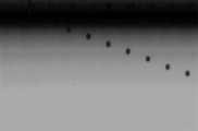
도 12는 비교예 1에서 제조된 토출 잉크의 이미지이다.
도 13은 비교예 1의 one-dot 패턴 이미지이다.
도 14는 비교예 2의 one-dot 패턴 이미지이다.
도 15는 실시예 1-3 및 6-7의 전자수송층 조성물을 이용하여 기판 위에 형성된 잉크 형상의 CRF(coffee ring factor) 결과 그래프이다.
도 16은 실시예 1-3 및 6-7의 전자수송층 조성물을 이용하여 제작된 발광소자의 발광효율을 나타낸 그래프이다.
도 17은 실시예 1-3 및 6-7의 전자수송층 조성물을 이용하여 제작된 발광소자의 양자효율을 나타낸 그래프이다Figure 1 is an absorption spectrum graph of ZnMgO nanoparticles prepared in Example 1.
Figure 2 is an absorption spectrum graph of ZnMgO nanoparticles prepared in Comparative Example 1.
Figure 3 is a surface shape analysis image and graph of the ejected shape of the electron transport layer ink composition prepared in Example 1.
Figure 4 is an image of ejected ink using the electron transport layer ink composition prepared in Example 3.
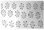
Figure 5 is an image of ZnMgO 1 drop and 1*5 pattern shape of the electron transport layer ink composition prepared in Example 2.
Figure 6 is an image of the ZnMgO 1 drop and 1*5 pattern shape of the electron transport layer ink composition prepared in Example 3.
Figure 7 is a 1 drop and 1*5 pattern image formed on a substrate using the electron transport layer ink composition prepared in Example 2.
Figure 8 is a ZnMgO 1drop shape image of the electron transport layer ink composition prepared in Example 4.
Figure 9 is a ZnMgO 1drop shape image of the electron transport layer ink composition prepared in Example 5.
Figure 10 is a ZnMgO 1drop shape image of the electron transport layer ink composition prepared in Example 6.
Figure 11 is a ZnMgO 1drop shape image of the electron transport layer ink composition prepared in Example 7.
Figure 12 is an image of the discharged ink prepared in Comparative Example 1.
Figure 13 is a one-dot pattern image of Comparative Example 1.
Figure 14 is a one-dot pattern image of Comparative Example 2.
Figure 15 is a graph of the CRF (coffee ring factor) results of the ink shape formed on the substrate using the electron transport layer composition of Examples 1-3 and 6-7.
Figure 16 is a graph showing the luminous efficiency of light-emitting devices manufactured using the electron transport layer compositions of Examples 1-3 and 6-7.
Figure 17 is a graph showing the quantum efficiency of light-emitting devices manufactured using the electron transport layer compositions of Examples 1-3 and 6-7.
이하, 본 발명을 상세히 설명한다.Hereinafter, the present invention will be described in detail.
본 명세서에서 사용되는 모든 용어(기술 및 과학적 용어를 포함)는, 다른 정의가 없다면, 본 발명이 속하는 기술분야에서 통상의 지식을 가진 자에게 공통적으로 이해될 수 있는 의미로 사용될 수 있을 것이다. 또 일반적으로 사용되는 사전에 정의되어 있는 용어들은 명백하게 특별히 정의되어 있지 않은 한 이상적으로 또는 과도하게 해석되지 않는다.All terms (including technical and scientific terms) used in this specification, unless otherwise defined, may be used with meanings that can be commonly understood by those skilled in the art to which the present invention pertains. Additionally, terms defined in commonly used dictionaries are not to be interpreted ideally or excessively unless clearly specifically defined.
또한 본 명세서 전체에서, 어떤 부분이 어떤 구성요소를 "포함" 한다고 할 때, 이는 특별히 반대되는 기재가 없는 한, 다른 구성요소를 제외하는 것이 아니라 다른 구성요소를 더 포함할 가능성을 내포하는 개방형 용어(open-ended terms)로 이해되어야 한다. 또한 명세서 전체에서, "위에" 또는 "상에"라 함은 대상 부분의 위 또는 아래에 위치하는 경우 뿐만 아니라 그 중간에 또 다른 부분이 있는 경우도 포함함을 의미하는 것이며, 반드시 중력 방향을 기준으로 위쪽에 위치하는 것을 의미하는 것은 아니다.In addition, throughout this specification, when a part is said to "include" a certain component, unless specifically stated to the contrary, this is an open term that implies the possibility of further including other components rather than excluding other components. It should be understood as (open-ended terms). In addition, throughout the specification, the term "above" or "on" means not only the case where it is located above or below the object part, but also the case where there is another part in the middle, and must be based on the direction of gravity. This does not mean that it is located at the top.
또한, 본 명세서 중에 있어서, "(메타)아크릴레이트"는 아크릴레이트 및 메타크릴레이트를 나타내고, "(메타)아크릴"은 아크릴 및 메타크릴을 나타내며, "(메타)아크릴로일"은 아크릴로일 및 메타크릴로일을 의미한다.In addition, in this specification, "(meth)acrylate" refers to acrylate and methacrylate, "(meth)acrylic" refers to acrylic and methacrylic, and "(meth)acryloyl" refers to acryloyl. and methacryloyl.
그리고 본 명세서 중에 있어서, "단량체" 와 "모노머"는 동일한 의미이다. 본 발명에 있어서의 단량체는 올리고머 및 폴리머와 구별되고, 중량 평균 분자량이 1,000 이하인 화합물을 말한다.In addition, in this specification, “monomer” and “monomer” have the same meaning. Monomers in the present invention are distinguished from oligomers and polymers, and refer to compounds with a weight average molecular weight of 1,000 or less.
본 발명은 잉크젯 프린팅 방식에 의해 토출이 가능하고, 소자의 특성 구현이 가능한 전자수송층 조성물을 제공하고자 한다.The present invention seeks to provide an electron transport layer composition that can be ejected by inkjet printing and can realize device characteristics.
이를 위해, 본 발명에서는 잉크젯 장비의 적정한 점도와 증기압(vapor pressure)을 고려하여 토출 가능한 적어도 3종 이상의 용매를 선정하고 이를 소정 비율로 혼용하여 잉크 조성물의 용매로 사용한다.For this purpose, in the present invention, at least three types of solvents that can be discharged are selected in consideration of the appropriate viscosity and vapor pressure of the inkjet equipment, and they are mixed in a predetermined ratio and used as solvents for the ink composition.
또한 금속산화물 나노입자 표면에 소정의 리간드, 단량체 또는 미세입자 응집 방지를 위한 분산제를 첨가함으로써, 잉크젯 토출시 커피링 효과(Coffee ring Effect, CRF)가 개선되어 막의 균일도를 확보할 수 있다.In addition, by adding a predetermined ligand, monomer, or dispersant to prevent fine particle aggregation to the surface of the metal oxide nanoparticle, the coffee ring effect (CRF) during inkjet ejection is improved and uniformity of the film can be secured.
이를 통해, 본 발명에서는 잉크젯 프린팅 공정을 통한 전자수송층 및 이를 구비하는 자발광 디스플레이를 제공할 수 있다.Through this, the present invention can provide an electron transport layer through an inkjet printing process and a self-luminous display including the same.
<잉크젯 프린팅용 전자수송층 조성물><Electron transport layer composition for inkjet printing>
본 발명의 일 실시예에 따른 전자수송층 조성물은, 일반적인 잉크젯법에 의해 토출되어 전자수송층(ETL)을 형성할 수 있는 잉크 조성물이다.The electron transport layer composition according to an embodiment of the present invention is an ink composition that can be discharged by a general inkjet method to form an electron transport layer (ETL).
일 구체예를 들면, 상기 조성물은 금속산화물 나노입자; 및 점도, 극성 및 증기압 중 하나 이상이 상이한 적어도 3종의 용매를 포함하며, 이들이 소정의 비율로 구성된다. 필요에 따라 당 분야의 통상적인 첨가제를 적어도 1종 이상 더 포함할 수 있다.In one specific example, the composition includes metal oxide nanoparticles; and at least three solvents that differ in one or more of viscosity, polarity, and vapor pressure, and are comprised in a predetermined ratio. If necessary, at least one additional additive common in the art may be included.
이하, 상기 전자수송층 조성물의 조성을 구체적으로 살펴보면 다음과 같다.Hereinafter, the composition of the electron transport layer composition will be examined in detail as follows.
금속산화물 나노입자Metal oxide nanoparticles
본 발명에 따른 전자수송층 조성물은, 금속산화물 나노입자를 포함한다.The electron transport layer composition according to the present invention includes metal oxide nanoparticles.
상기 금속산화물 나노입자는 당 분야에서 전자수송층에 사용되는 물질을 제한 없이 사용할 수 있다. 일례로, 도펀트 물질로 사용되는 통상의 금속 산화물 나노입자를 사용할 수 있으며, 이의 비제한적인 예로는 In2S3, Cu2S, Ag2S, ZnSe, ZnS, ZnO, ZnTe, ZnSe, TiO2, SnO2, ZnS 또는 전술한 성분에 적어도 1종의 원소가 첨가된 형태를 포함할 수 있다.The metal oxide nanoparticles can be any material used in the electron transport layer in the art without limitation. For example, common metal oxide nanoparticles used as dopant materials can be used, non-limiting examples of which include In2 S3 , Cu2 S, Ag2 S, ZnSe, ZnS, ZnO, ZnTe, ZnSe, TiO2 , SnO2 , ZnS, or a form in which at least one element is added to the above-mentioned components.
일 구체예를 들면, 상기 금속산화물 나노입자는 Zn 함유 금속산화물 나노입자이며, 보다 구체적으로 ZnO 밴드갭을 증가시킬 수 있는 금속(M)이 합금화된 것[ZnMO(M = Ca, Mg)]일 수 있다. ZnO 밴드갭을 증가시킬 수 있는 금속(M)은 Ca 또는 Mg이다. 이들 금속은 Zn의 이온 반경과 유사하여 응력 유발없이 ZnO 격자내로 혼입될 수 있으며 ZnO 크기 감소를 통해 ZnO 밴드갭을 증가시킬 수 있다. 바람직하게는 ZnMgO일 수 있다.For example, the metal oxide nanoparticles are Zn-containing metal oxide nanoparticles, and more specifically, they are alloyed with a metal (M) that can increase the ZnO band gap [ZnMO (M = Ca, Mg)]. You can. The metal (M) that can increase the ZnO band gap is Ca or Mg. These metals are similar to the ionic radius of Zn, so they can be incorporated into the ZnO lattice without causing stress and can increase the ZnO band gap by reducing the size of ZnO. Preferably it may be ZnMgO.
이와 같이 합금에 의해 ZnO 나노입자의 밴드갭을 증가시켜 전자 수송층으로 적용하면 전도대의 최저점(conduction band minimum: CBM) 준위의 상향천이(upshift)가 발생하여 양자점 발광층의 CBM과 전자수송층 사이의 에너지 근접성을 가져오고, 이는 전자 에너지 장벽을 낮추어 결과적으로 양자점 영역으로의 전자 주입을 촉진한다. 이에 따라, 합금화된 ZnO 나노입자가 함유된 전자수송층을 구비하는 발광소자는 ZnO 나노입자가 함유된 전자수송층을 구비하는 소자에 비해 휘도 및 효율 측면에서 우수해지고 더 낮은 구동 전압에서도 더 높은 발광 효율을 가질 수 있게 된다. 즉, 전술한 전자수송층을 적용할 경우, 전자 주입 장벽을 감소시켜 QLED의 구동 전압 감소, 효율 향상, 더 나아가 소비 전력 감소의 효과를 얻을 수 있다. 소자의 구동 전압이 감소하게 되면 소자의 발열 또한 감소하게 되고, 이에 따라 수명 증가를 예상할 수 있다.In this way, when the band gap of ZnO nanoparticles is increased by alloying and applied as an electron transport layer, an upshift in the conduction band minimum (CBM) level occurs, increasing the energy proximity between the CBM of the quantum dot emitting layer and the electron transport layer. This lowers the electron energy barrier and consequently promotes electron injection into the quantum dot region. Accordingly, the light emitting device having an electron transport layer containing alloyed ZnO nanoparticles is superior in terms of luminance and efficiency compared to the device having an electron transport layer containing ZnO nanoparticles, and has higher luminous efficiency even at a lower driving voltage. You can have it. In other words, when applying the above-mentioned electron transport layer, the electron injection barrier can be reduced, thereby reducing the driving voltage of the QLED, improving efficiency, and further reducing power consumption. When the driving voltage of the device decreases, the heat generation of the device also decreases, and thus the lifespan can be expected to increase.
일 구체예를 들면, 상기 금속산화물 나노입자는, 표면의 일부 또는 전부에 친수성 모이어티를 갖는 유기 리간드가 부착되어 있을 수 있다.For example, the metal oxide nanoparticle may have an organic ligand having a hydrophilic moiety attached to part or all of its surface.
유기 리간드는 당 분야에 공지된 것을 제한 없이 사용할 수 있으며, 일례로 C5 내지 C20의 알킬 카르복실산, 알케닐 카르복실산 또는 알키닐 카르복실산; 피리딘(pyridine); 메르캅토 알콜(mercapto alcohol); 티올(thiol); 포스핀(phosphine); 포스핀 산화물(phosphine oxide); 1차 아민(primary amine); 2차 아민(secondary amine); 또는 이들의 조합 등이 있다. 구체적으로, 상기 유기 리간드는 카르복실기 및 하이드록시기로부터 선택된 친수성 모이어티를 적어도 2개 이상 포함할 수 있으며, 보다 구체적으로 분자 구조의 양(兩) 말단에 전술한 카르복실기, 및/또는 하이드록실기 친수성 모이어티를 갖는 리간드 물질이 바람직하다. 사용 가능한 유기 리간드로의 비제한적인 예로는, mono(2-acryloyloxyethyl) succinate (MAES), mono-2-(Methacryloyloxy)ethyl succinate(MMES), 2-(2-Methoxyethoxy)acetic acid(MEAA), 또는 이들의 혼합물 등이 있다.Organic ligands known in the art can be used without limitation, and examples include C5 to C20 alkyl carboxylic acid, alkenyl carboxylic acid, or alkynyl carboxylic acid; pyridine; mercapto alcohol; thiol; phosphine; phosphine oxide; primary amine; secondary amine; or a combination thereof. Specifically, the organic ligand may include at least two hydrophilic moieties selected from a carboxyl group and a hydroxyl group, and more specifically, the above-described carboxyl group and/or hydroxyl group hydrophilic moieties at both ends of the molecular structure. Ligand materials with moieties are preferred. Non-limiting examples of organic ligands that can be used include mono(2-acryloyloxyethyl) succinate (MAES), mono-2-(Methacryloyloxy)ethyl succinate (MMES), 2-(2-Methoxyethoxy)acetic acid (MEAA), or There are mixtures of these, etc.
이러한 유기 리간드는 금속산화물 나노입자 표면에 부착되어, 잉크젯 토출시 Coffee ring Effect(CRF) 개선 효과를 발휘함에 따라 막 균일도를 확보하는 역할을 할 수 있다. 여기서, 커피링 효과(CRF)는 증발 과정의 유체역학적 효과에 의해 콜로이드 입자들이 가장 자리로 이동하게 되어 입자의 밀도 분포가 불균일하게 되는 현상을 지칭한다. 즉, 입자의 크기가 작을수록 가장자리로 더 이동할 수가 있어 크기가 작은 입자들이 액적의 가장 자리에 가까운 쪽에 분포하게 되고, 상대적으로 큰 입자들은 액적의 중심부에 가까운 쪽에 분포하게 된다. 본 발명에서는 전자수송층 조성물에 소정의 유기 리간드 및/또는 후술되는 단량체를 도입함으로써, coffee ring 효과를 최소화하고 막의 균일도를 극대화할 수 있다.These organic ligands are attached to the surface of metal oxide nanoparticles and can play a role in ensuring film uniformity by improving the coffee ring effect (CRF) during inkjet ejection. Here, the coffee ring effect (CRF) refers to a phenomenon in which colloidal particles move to the edge due to the hydrodynamic effect of the evaporation process and the density distribution of the particles becomes non-uniform. In other words, the smaller the particle size, the more it can move to the edge, so smaller particles are distributed closer to the edge of the droplet, and relatively larger particles are distributed closer to the center of the droplet. In the present invention, by introducing a predetermined organic ligand and/or a monomer described later into the electron transport layer composition, the coffee ring effect can be minimized and the uniformity of the film can be maximized.
유기 리간드의 함량은 특별히 제한되지 않으며, 당 분야에 공지된 함량 범위 내에서 적절히 조절될 수 있다. 분산성과 막 균일성을 고려하여 상기 금속산화물 나노입자에 포함된 금속, 예컨대 아연(Zn) 1몰 대비 0.0001 내지 10 mol 범위로 포함될 수 있으며, 구체적으로 0.001 내지 5 mol 범위일 수 있다.The content of the organic ligand is not particularly limited and can be appropriately adjusted within the content range known in the art. In consideration of dispersibility and film uniformity, the metal contained in the metal oxide nanoparticles, such as zinc (Zn), may be contained in the range of 0.0001 to 10 mol, specifically 0.001 to 5 mol, relative to 1 mole of zinc (Zn).
일 구체예를 들면, 상기 금속산화물 나노입자는, 표면의 일부 또는 전부에 형성된 고분자 코팅층을 포함할 수 있다.For example, the metal oxide nanoparticle may include a polymer coating layer formed on part or all of the surface.
상기 고분자 코팅층의 성분은 특별히 제한되지 않으며, 당 분야에 공지된 통상의 고분자가 적용 가능하다. 일례로, 당 분자에 공지된 아크릴계 또는 메타크릴계 고분자이나 폴리에틸렌글리콜을 제한 없이 사용하여 형성될 수 있다. 구체적으로, 분자 내 극성 작용기를 소정 범위로 포함하는 (메타)아크릴계 고분자 및/또는 친수성 모이어티를 갖는 폴리에틸렌글리콜을 사용하는 것이 바람직하다. 이러한 작용기는 일부 화학물질과 반응을 일으킬 수 있으며, 이 반응을 이용하여 금속 산화물 나노입자 표면에 고분자 코팅을 유도하도록 한다.The components of the polymer coating layer are not particularly limited, and common polymers known in the art can be applied. For example, the sugar molecule may be formed using known acrylic or methacrylic polymers or polyethylene glycol without limitation. Specifically, it is preferable to use a (meth)acrylic polymer containing a predetermined range of polar functional groups in the molecule and/or polyethylene glycol having a hydrophilic moiety. These functional groups can react with some chemicals, and this reaction is used to induce a polymer coating on the surface of metal oxide nanoparticles.
상기 고분자 코팅층을 형성하는 단량체(단분자)로는 당 분야에 공지된 통상의 (메타)아크릴레이트 모노머를 사용할 수 있다. 그러나 이에 특별히 제한되지 않는다. 사용 가능한 단량체의 비제한적인 예를 들면, 카프로락톤 아크릴레이트, 오르쏘-페닐페놀 에톡시 아크릴레이트, 라우릴 아크릴레이트, 이소데실 아크릴레이트, 테트라하이드로 퍼퓨릴 아크릴레이트, 2-하이드록시에틸 아크릴레이트, 4-하이드록시부틸 아크릴레이트, 2-히드록시에틸 메타크릴레이트, 에톡시 에톡시 에틸 아크릴레이트, 이소보르닐 (메트)아크릴레이트, 알콕시화 테트라히드로퍼퓨릴 (메트)아크릴레이트, 2-에틸헥실아크릴레이트 등의 단관능 (메타)아크릴레이트 모노머; 에틸렌글리콜 디(메타)아크릴레이트, 프로필렌글리콜 디(메타)아크릴레이트, 폴리올레핀글리콜 디(메타)아크릴레이트, 에톡시화 폴리프로필렌글리콜 디(메타)아크릴레이트, 2-히드록시-3-아크릴로일옥시프로필메타크릴레이트, 2-히드록시-1,3-디메타크릴옥시프로판, 디옥산글리콜 디(메타)아크릴레이트, 트리시클로데칸디메탄올 디(메타)아크릴레이트, 1,4-부탄디올 디(메타)아크릴레이트, 글리세린 디(메타)아크릴레이트, 1,6-헥산디올 디(메타)아크릴레이트, 1,9-노난디올 디(메타)아크릴레이트, 1,10-데칸디올 디(메타)아크릴레이트, 네오펜틸글리콜 디(메타)아크릴레이트, 2-메틸-1,8-옥탄디올 디(메타)아크릴레이트, 1,9-노난디올 디(메타)아크릴레이트, 부틸에틸프로판디올 디(메타)아크릴레이트, 3-메틸-1,5-펜탄디올 디(메타)아크릴레이트, 트리프로필렌 글리콜 디아크릴레이트, 디프로필렌 글리콜 디아크릴레이트, 트리에틸렌 글리콜 디아크릴레이트 및 트리클로데칸 디메탄올 디아크릴레이트 등의 방향환을 갖는 디(메타)아크릴레이트; 에톡시화 글리세린 트리(메타)아크릴레이트, 트리메틸올프로판 트리(메타)아크릴레이트, 트리메틸올프로판 (에틸렌옥사이드)변성 트리아크릴레이트, 에톡시화트리메틸올프로판 트리(메타)아크릴레이트, 프로폭시화 트리메틸올프로판 트리(메타)아크릴레이트, 펜타에리트리톨 트리(메타)아크릴레이트, 트리메틸올프로판(프로필렌옥사이드)변성 트리아크릴레이트 및 트리스(2-하이드록시에틸) 이소시아우레이트 트리아크릴레이트 등의 3관능 (메타)아크릴레이트 모노머; 펜타에리트리톨 테트라(메타)아크릴레이트, 디트리메틸올프로판 테트라(메타)아크릴레이트, 에톡시화 펜타에리트리톨 테트라(메타)아크릴레이트(4 관능 단량체) 또는 이들의 혼합물 등의 4관능 (메타)아크릴레이트 모노머; 디펜타에리트리톨 펜타아크릴레이트, 프로피온산 변성 디펜타에리트리톨 펜타아크릴레이트, 디펜타에리트리톨 펜타메타크릴레이트, 프로피온산 변성 디펜타에리트리톨 펜타메타크릴레이트 또는 이들의 혼합물 등의 5관능 (메타)아크릴레이트 모노머; 디펜타에리트리톨헥사아크릴레이트, 카프로락톤 변성 디펜타에리트리톨헥사아크릴레이트, 디펜타에리트리톨헥사메타크릴레이트, 카프로락톤 변성 디펜타에리트리톨 헥사메타크릴레이트, 또는 이들의 혼합물 등의 6관능 (메타)아크릴레이트 모노머 등이 있다.As a monomer (single molecule) forming the polymer coating layer, a typical (meth)acrylate monomer known in the art can be used. However, it is not particularly limited thereto. Non-limiting examples of monomers that can be used include caprolactone acrylate, ortho-phenylphenol ethoxy acrylate, lauryl acrylate, isodecyl acrylate, tetrahydrofurfuryl acrylate, and 2-hydroxyethyl acrylate. , 4-hydroxybutyl acrylate, 2-hydroxyethyl methacrylate, ethoxy ethoxy ethyl acrylate, isobornyl (meth)acrylate, alkoxylated tetrahydrofurfuryl (meth)acrylate, 2-ethyl Monofunctional (meth)acrylate monomers such as hexyl acrylate; Ethylene glycol di(meth)acrylate, propylene glycol di(meth)acrylate, polyolefin glycol di(meth)acrylate, ethoxylated polypropylene glycol di(meth)acrylate, 2-hydroxy-3-acryloyloxy Propyl methacrylate, 2-hydroxy-1,3-dimethacryloxypropane, dioxane glycol di(meth)acrylate, tricyclodecane dimethanol di(meth)acrylate, 1,4-butanediol di(meth)acrylate ) Acrylate, glycerin di(meth)acrylate, 1,6-hexanediol di(meth)acrylate, 1,9-nonanediol di(meth)acrylate, 1,10-decanediol di(meth)acrylate , neopentyl glycol di(meth)acrylate, 2-methyl-1,8-octanediol di(meth)acrylate, 1,9-nonanediol di(meth)acrylate, butyl ethyl propanediol di(meth)acrylate. Directions such as 3-methyl-1,5-pentanediol di(meth)acrylate, tripropylene glycol diacrylate, dipropylene glycol diacrylate, triethylene glycol diacrylate and triclodecane dimethanol diacrylate. Di(meth)acrylate having a ring; Ethoxylated glycerin tri(meth)acrylate, trimethylolpropane tri(meth)acrylate, trimethylolpropane (ethylene oxide) modified triacrylate, ethoxylated trimethylolpropane tri(meth)acrylate, propoxylated trimethylolpropane. Tri-functional (meth)acrylate, such as tri(meth)acrylate, pentaerythritol tri(meth)acrylate, trimethylolpropane (propylene oxide) modified triacrylate, and tris(2-hydroxyethyl) isocyanurate triacrylate. ) Acrylate monomer; Tetrafunctional (meth)acrylates such as pentaerythritol tetra(meth)acrylate, ditrimethylolpropane tetra(meth)acrylate, ethoxylated pentaerythritol tetra(meth)acrylate (tetrafunctional monomer), or mixtures thereof. monomer; Pentaerythritol pentaacrylate, propionic acid-modified dipentaerythritol pentaacrylate, dipentaerythritol pentamethacrylate, propionic acid-modified dipentaerythritol pentamethacrylate, or mixtures thereof, and other pentafunctional (meth)acrylates. monomer; Hexafunctional (methacrylic) such as dipentaerythritol hexaacrylate, caprolactone-modified dipentaerythritol hexaacrylate, dipentaerythritol hexamethacrylate, caprolactone-modified dipentaerythritol hexamethacrylate, or mixtures thereof ) Acrylate monomer, etc.
상기 고분자 코팅층은 금속산화물 나노입자 표면에 형성되어, 잉크젯 토출시 Coffee ring Effect(CRF) 개선 효과를 발휘하여 막 균일도를 확보할 수 있다.The polymer coating layer is formed on the surface of the metal oxide nanoparticles and can ensure film uniformity by improving the coffee ring effect (CRF) during inkjet discharge.
한편 본 발명에서는 전자수송층을 구성하는 물질로서 금속산화물 나노입자를 주로 설명하고 있다. 그러나 전술한 물질에 한정되지 않고, 당 분야에서 전자수송층 물질로서 사용 가능한 유기물, 또는 유무기 합성물을 적용하는 것도 본 발명의 범주에 속한다.Meanwhile, the present invention mainly describes metal oxide nanoparticles as a material constituting the electron transport layer. However, it is not limited to the above-described materials, and the application of organic materials or organic-inorganic composites that can be used as electron transport layer materials in the art also falls within the scope of the present invention.
본 발명에서, 상기 금속산화물 나노입자의 함량은 특별히 제한되지 않으며, 당 분야에 공지된 범위 내에서 적절히 조절할 수 있다. 일례로, 당해 전자수송층 조성물의 총 중량(예, 100 중량부)을 기준으로 하여 5 내지 30 중량부일 수 있으며, 구체적으로 10 내지 20 중량부일 수 있다.In the present invention, the content of the metal oxide nanoparticles is not particularly limited and can be appropriately adjusted within a range known in the art. For example, it may be 5 to 30 parts by weight, specifically 10 to 20 parts by weight, based on the total weight (e.g., 100 parts by weight) of the electron transport layer composition.
용매menstruum
본 발명에 따른 전자수송층 조성물은 점도, 극성, 증기압 등의 물성이 상이한 적어도 3종의 용매를 포함한다.The electron transport layer composition according to the present invention includes at least three types of solvents with different physical properties such as viscosity, polarity, and vapor pressure.
종래 금속산화물 나노입자, 예컨대 ZnMgO는 재료의 특성상 알코올계 용매를 분산매로 사용하는데, 에탄올을 단독으로 사용할 경우 소자의 특성은 구현되는 반면, 잉크젯 토출이 되지 않는다는 문제점이 있다.Conventional metal oxide nanoparticles, such as ZnMgO, use an alcohol-based solvent as a dispersion medium due to the nature of the material. However, when ethanol is used alone, the device characteristics are realized, but there is a problem in that inkjet ejection is not possible.
한편 잉크젯 장비의 토출 조건은 크게 점도와 증기압(Vapor pressure)로 나뉠 수 있다. 점도가 지나치게 높거나 낮으면 균일한 막이 얻어지지 않게 되며, 또한 증기압에 따라 토출 정도가 결정된다. 본 발명에서는 잉크젯 토출에 적정한 점도와 증기압을 고려하고, 이러한 물성을 만족할 수 있는 적어도 3종 용매를 선정하고, 이들의 혼합비율로 소정범위로 제어하여 전자수송층 잉크 조성물의 용매로 구성하는 것을 특징으로 한다.Meanwhile, the discharge conditions of inkjet equipment can be largely divided into viscosity and vapor pressure. If the viscosity is too high or too low, a uniform film cannot be obtained, and the degree of discharge is determined by the vapor pressure. In the present invention, considering the viscosity and vapor pressure appropriate for inkjet discharge, at least three types of solvents that can satisfy these physical properties are selected, and their mixing ratio is controlled to a predetermined range to form the solvent for the electron transport layer ink composition. do.
일 구체예를 들면, 적어도 3종의 용매가 포함된 본 발명의 전자수송층 조성물은 20℃에서의 점도가 1.0 내지 3.0 cps이고, 20℃에서 증기압이 0.6 내지 45 mmHg이고, 접촉각이 25 내지 80°이고, 고형분 함량이 5 내지 30 중량%일 수 있다. 보다 구체적으로, 1.2 내지 2.0 cps의 점도, 1.0 내지 30 mmHg의 증기압, 30 내지 50°의 접촉각, 및 5 내지 25 중량%의 고형분 함량을 가질 수 있다.For example, the electron transport layer composition of the present invention containing at least three types of solvents has a viscosity of 1.0 to 3.0 cps at 20°C, a vapor pressure of 0.6 to 45 mmHg at 20°C, and a contact angle of 25 to 80°. and the solid content may be 5 to 30% by weight. More specifically, it may have a viscosity of 1.2 to 2.0 cps, a vapor pressure of 1.0 to 30 mmHg, a contact angle of 30 to 50°, and a solid content of 5 to 25% by weight.
전술한 점도, 증기압과 접촉각 물성을 가질 경우, 잉크젯 토출이 용이할 뿐만 아니라 토출된 잉크의 균일성으로 인해 소자의 특성이 구현될 수 있다.When the above-described viscosity, vapor pressure, and contact angle properties are present, not only is inkjet ejection easy, but the device characteristics can be realized due to the uniformity of the ejected ink.
본 발명에 따른 전자수송층 조성물은 전술한 점도, 증기압, 접촉각 특성을 만족한다면, 상기 조성물을 구성하는 적어도 3종 이상의 용매의 구체 성분 및/또는 이의 함량 등에 특별히 제한되지 않는다.The electron transport layer composition according to the present invention is not particularly limited in terms of the specific components and/or content thereof of at least three types of solvents constituting the composition, as long as it satisfies the above-mentioned viscosity, vapor pressure, and contact angle characteristics.
일 구체예를 들면, 상기 적어도 3종의 용매는 디메틸 설폭사이드(DMSO), 에탄올, 2-메톡시 에탄올 및 부탄올을 포함한다.For one specific example, the at least three solvents include dimethyl sulfoxide (DMSO), ethanol, 2-methoxy ethanol, and butanol.
즉, 본 발명에서는 분산성이 좋으면서 점도가 있는 디메틸설폭사이드(DMSO)를 주용매로 사용하는데, 잉크젯 토출 용도를 고려하여 DMSO 용매를 단독 사용할 경우 젖음성(Wettablity)이 저조하게 된다. 반면, 젖음성(Wettablity)이 우수한 에탄올과 혼합한 2종 용매는 잉크젯 토출 특성에서 요구되는 점도, 접촉각 물성 수준을 확보할 수 없다. 이에, 본 발명에서는 DMSO 용매와 에탄올을 사용하고, 여기에 알코올계 용매 중 적정한 점도를 지닌 2-메톡시에탄올과 부탄올을 혼용하여, 최종 조성물이 전술한 점도, 증기압, 접촉각 특성을 동시에 만족하도록 제어한다. 일례로, 각 용매의 점도는 DMSO(1.98 cps), 에탄올(1.07 cps), 2-메톡시 에탄올(1.70 cps), 부탄올(2.57 cps)을 나타낸다. 또한 각 용매의 증기압은 DMSO (0.6 mmHg), 에탄올(44.62 mmHg), 2-메톡시 에탄올 (6 mmhg), 부탄올 (5.47 mmHg)을 나타낸다. 전술한 3종 이상의 용매를 소정의 혼합비율로 구성함에 따라 1.0 ~ 3.0 cps의 점도, 25 ~ 80°의 접촉각, 및 0.6~45 mmHg의 증기압으로 최적화된 전자수송층 조성물을 구성할 수 있다.That is, in the present invention, dimethyl sulfoxide (DMSO), which has good dispersibility and viscosity, is used as the main solvent, but considering inkjet discharge applications, if DMSO solvent is used alone, wettability is low. On the other hand, the two types of solvent mixed with ethanol, which has excellent wettability, cannot secure the level of viscosity and contact angle properties required for inkjet ejection characteristics. Therefore, in the present invention, DMSO solvent and ethanol are used, and 2-methoxyethanol and butanol, which have appropriate viscosity among alcohol-based solvents, are mixed together to control the final composition so that it simultaneously satisfies the above-mentioned viscosity, vapor pressure, and contact angle characteristics. do. For example, the viscosity of each solvent is DMSO (1.98 cps), ethanol (1.07 cps), 2-methoxyethanol (1.70 cps), and butanol (2.57 cps). Additionally, the vapor pressure of each solvent is DMSO (0.6 mmHg), ethanol (44.62 mmHg), 2-methoxyethanol (6 mmhg), and butanol (5.47 mmHg). By composing the three or more solvents described above in a predetermined mixing ratio, an optimized electron transport layer composition can be formed with a viscosity of 1.0 to 3.0 cps, a contact angle of 25 to 80°, and a vapor pressure of 0.6 to 45 mmHg.
본 발명에 따른 일 실시예를 들면, 적어도 3종의 용매는 디메틸 설폭사이드(DMSO)를 주(主)용매로 포함하며, 이러한 DMSO는 전체 용매 100 부피%를 기준으로 하여 30 부피% 이상을 갖도록 구성될 수 있다. 또한 에탄올의 함량은 전체 용매 100 부피%를 기준으로 하여 10 부피% 이상을 갖도록 구성할 수 있다. 또한 2-메톡시 에탄올의 함량은 전체 용매 100 부피%를 기준으로 하여 10 부피% 이상일 수 있으며, 부탄올은 전체 용매 100 부피%를 기준으로 하여 0 내지 50 부피% 범위로 사용 가능하다. 여기서, 전체 용매는 전술한 적어도 3종 이상의 용매의 부피의 합을 의미하는 것일 수 있다. 또한 전술한 적어도 3종의 용매에 후술되는 금속산화물 나노입자 분산액에 포함된 분산용매를 더 포함한 것을 의미할 수도 있다.For example, in one embodiment according to the present invention, at least three types of solvents include dimethyl sulfoxide (DMSO) as the main solvent, and such DMSO is contained in an amount of 30% by volume or more based on 100% by volume of the total solvent. It can be configured. Additionally, the content of ethanol may be 10% by volume or more based on 100% by volume of the total solvent. Additionally, the content of 2-methoxyethanol may be 10 vol% or more based on 100 vol% of the total solvent, and butanol may be used in the range of 0 to 50 vol% based on 100 vol% of the total solvent. Here, the total solvent may mean the sum of the volumes of at least three types of solvents described above. It may also mean that the dispersion solvent contained in the metal oxide nanoparticle dispersion described later is further included in addition to the at least three types of solvents described above.
일 구체예를 들면, 상기 적어도 3종의 용매 중 디메틸 설폭사이드(DMSO), 에탄올, 2-메톡시에탄올, 및 부탄올의 혼합 비율은 3 ~ 8 : 1 ~ 3 : 1 ~ 2 : 0 ~ 1부피비이며, 바람직하게는 5 : 3 : 1 : 1 부피비일 수 있다. 이때 DMSO 비율이 3 미만일 경우 잉크젯 토출이 불안정하며, 알코올계 용매 비율이 상대적으로 높아지게 되어 소자 특성 면에서만 유리한 결과가 발생된다. 또한 2-메톡시에탄올과 부탄올은 금속산화물 나노입자 (ZnMgO)의 소정 점도 및 접촉각 물성을 확보하기 위해 첨가되는 것으로서, 이들 용매 간의 함량 비율이 1을 초과할 경우 점도가 높아져 잉크젯 토출과 소자 구현에 악영향을 미치게 된다.For example, the mixing ratio of dimethyl sulfoxide (DMSO), ethanol, 2-methoxyethanol, and butanol among the at least three solvents is 3 to 8: 1 to 3: 1 to 2: 0 to 1.The volume ratio may be preferably 5:3:1:1. At this time, if the DMSO ratio is less than 3, inkjet ejection is unstable, and the alcohol-based solvent ratio becomes relatively high, resulting in favorable results only in terms of device characteristics. In addition, 2-methoxyethanol and butanol are added to secure the desired viscosity and contact angle properties of metal oxide nanoparticles (ZnMgO). If the content ratio between these solvents exceeds 1, the viscosity increases, making it difficult for inkjet ejection and device implementation. It will have a negative impact.
본 발명에서, 상기 적어도 3종의 용매의 함량은 특별히 제한되지 않으며, 당 분야에 공지된 범위 내에서 적절히 조절할 수 있다. 일례로, 당해 전자수송층 조성물 100 중량부를 만족시키는 잔량일 수 있으며, 구체적으로 70 내지 95 중량부일 수 있다.In the present invention, the content of the at least three solvents is not particularly limited and can be appropriately adjusted within the range known in the art. For example, the remaining amount may be sufficient to satisfy 100 parts by weight of the electron transport layer composition, and may specifically be 70 to 95 parts by weight.
첨가제additive
전술한 성분들 이외에, 본 발명의 전자수송층 조성물은 발명의 효과를 저해하지 않는 범위 내에서 당 분야에 공지된 적어도 1종의 첨가제를 제한 없이 사용할 수 있다.In addition to the above-described components, the electron transport layer composition of the present invention may use at least one additive known in the art without limitation as long as it does not impair the effect of the invention.
사용 가능한 첨가제의 일례를 들면, 광 안정화제, 열 안정화제, 광 개시 촉진제, 열 개시 촉진제, 평활화제, 강인화제, 증점제, 착색제, 반응성 희석제, 커플링제, 분산제, 용제 등이 함유될 수 있다. 이들은 단독으로 사용하거나 또는 2종 이상 혼용할 수 있다. 이때 첨가제의 함량은 당 분야에 공지된 범위 내에서 적절히 조절할 수 있으며, 특별히 제한되지 않는다. 일례로, 상기 적어도 1종의 첨가제는 당해 전자수송층 조성물의 전체 중량을 기준으로 0.01 내지 5 중량부, 구체적으로 0.01 내지 2 중량부로 포함될 수 있다.Examples of usable additives include light stabilizers, heat stabilizers, light initiation accelerators, heat initiation accelerators, smoothers, tougheners, thickeners, colorants, reactive diluents, coupling agents, dispersants, solvents, etc. These can be used individually or in combination of two or more types. At this time, the content of the additive can be appropriately adjusted within a range known in the art and is not particularly limited. For example, the at least one additive may be included in an amount of 0.01 to 5 parts by weight, specifically 0.01 to 2 parts by weight, based on the total weight of the electron transport layer composition.
본 발명에 따른 잉크젯 프린팅용 전자수송층 조성물은, 전술한 금속산화물 나노입자, 적어도 3종의 용매 및 필요에 따라 배합되는 리간드, 단량체, 그 밖의 첨가제를 당 분야에 알려진 통상적인 방법에 따라 혼합 및 교반하여 제조될 수 있다.The electron transport layer composition for inkjet printing according to the present invention is made by mixing and stirring the above-described metal oxide nanoparticles, at least three solvents, and ligands, monomers, and other additives mixed as necessary according to a conventional method known in the art. It can be manufactured.
상기 전자수송층 조성물을 제조하는 일 실시예를 들면, (i) 아연 함유 화합물과, ZnO 밴드갭을 증가시킬 수 있는 금속 함유 화합물이 용매에 용해된 반응용액에 염기성 물질을 첨가한 후 침전시켜 금속산화물 나노입자 분산액을 제조하는 제1 단계; 및 상기 제조된 금속산화물 나노입자 분산액에, 점도, 극성 및 증기압 중 하나 이상이 상이한 적어도 3종의 용매를 투입한 후 혼합하여 전자수송층 조성물을 제조하는 제2 단계;를 포함하여 구성될 수 있다.For example, for preparing the electron transport layer composition, (i) a basic material is added to a reaction solution in which a zinc-containing compound and a metal-containing compound capable of increasing the ZnO band gap are dissolved in a solvent, and then precipitated to form a metal oxide. A first step of preparing a nanoparticle dispersion; And a second step of preparing an electron transport layer composition by adding at least three solvents having different viscosity, polarity, and vapor pressure to the prepared metal oxide nanoparticle dispersion and then mixing them.
상기 제1 단계에서, 아연 함유 화합물과 금속 함유 화합물은 특별히 제한되지 않으며, 당 분야에 공지된 물질을 제한 없이 사용할 수 있다. 일례로, Zn acetate dihydrate, Zn chloride, Zn nitrate, Zn sulfate, Mg acetate tetrahydrate 등을 사용할 수 있다.In the first step, the zinc-containing compound and the metal-containing compound are not particularly limited, and materials known in the art can be used without limitation. For example, Zn acetate dihydrate, Zn chloride, Zn nitrate, Zn sulfate, Mg acetate tetrahydrate, etc. can be used.
또한 염기성 물질은 특별히 제한되지 않으며, 당 분야에 공지된 물질을 제한 없이 사용할 수 있다. 일례로 테트라메틸 암모늄 하이드록사이드(Tetramethyl ammonium hydroxide, TMAH), 포타슘 하이드록이드(KOH), 소듐 하이드록사이드(NaOH) 및 아민류(amine)로 구성된 군에서 선택된 적어도 1종의 물질이 사용할 수 있다.Additionally, the basic material is not particularly limited, and materials known in the art can be used without limitation. For example, at least one substance selected from the group consisting of tetramethyl ammonium hydroxide (TMAH), potassium hydroxide (KOH), sodium hydroxide (NaOH), and amines can be used. .
상기 제1 단계에서, 금속산화물 나노입자 분산액은 유기 리간드를 더 포함할 수 있다. 이때 유기 리간드는 상기 금속산화물 나노입자 분산액의 총 중량(예, 100 중량%) 대비 0 내지 10 중량% 범위로 포함될 수 있으며, 구체적으로 0 초과, 5 중량% 이하로 포함될 수 있다.In the first step, the metal oxide nanoparticle dispersion may further include an organic ligand. At this time, the organic ligand may be included in the range of 0 to 10% by weight relative to the total weight (e.g., 100% by weight) of the metal oxide nanoparticle dispersion, and may specifically be included in an amount greater than 0 and less than or equal to 5% by weight.
또한 제1 단계에서, 금속산화물 나노입자 분산액은 고분자를 더 포함할 수 있다. 이러한 고분자는 당 분야에 공지된 통상의 친수성 모이어티를 포함할 수 있으며, 일례로 카르복실기 및 하이드록시기로부터 선택된 친수성 모이어티를 적어도 2개 이상 포함할 수 있다. 사용 가능한 고분자의 일례로는, 카르복실기를 갖는 Polyethylene glycol (PEG) 등이 있다. 상기 고분자는 금속산화물 나노입자 분산액의 총 중량(예, 100 중량%) 대비 0 내지 10 중량% 범위로 포함될 수 있으나, 이에 특별히 제한되지 않는다.Additionally, in the first step, the metal oxide nanoparticle dispersion may further include a polymer. These polymers may contain conventional hydrophilic moieties known in the art, and for example, may contain at least two hydrophilic moieties selected from carboxyl groups and hydroxy groups. An example of a usable polymer is polyethylene glycol (PEG), which has a carboxyl group. The polymer may be included in an amount of 0 to 10% by weight relative to the total weight (e.g., 100% by weight) of the metal oxide nanoparticle dispersion, but is not particularly limited thereto.
염기성 물질을 첨가한 후 55 내지 65℃의 온도로 승온한 후 대략 0.5 내지 2시간 동안 균일한 속도로 교반 및 반응하여 나노입자를 침전시키고, 용매(solvent)와 비용매(non-solvent) 특성을 이용하여 금속산화물 나노입자를 분리한 후, 금속산화물 나노입자가 균일하게 분산된 분산액을 제조한다.After adding the basic material, the temperature is raised to 55 to 65°C, and then stirred and reacted at a uniform rate for approximately 0.5 to 2 hours to precipitate the nanoparticles and maintain solvent and non-solvent properties. After separating the metal oxide nanoparticles, a dispersion solution in which the metal oxide nanoparticles are uniformly dispersed is prepared.
사용 가능한 용매(solvent)의 비제한적인 예로는, 헥산(hexane), 벤젠, 자일렌 (xylene), 톨루엔(toluene),옥테인, 클로로포름(chloroform), 클로로벤젠, 테트라히드로푸란(THF), 염화메틸렌, 1,4-디옥세인(1,4-dioxane), 디에틸에테르(diethyl ether), 사이클로헥세인, 디클로로벤젠 등이 있으며, 이들을 단독 또는 2종 이상 혼용할 수 있다. 또한 사용 가능한 비용매(non-solvent)의 비제한적인 예로는 아세톤, 에탄올, 메탄올, 부탄올, 프로판올, 아이소프로필알코올, 테트라하이드로퓨란, 디메틸설폭시드, 디메틸포름아미드 등이 있으며, 이들을 단독 또는 2종 이상 혼용할 수 있다.Non-limiting examples of usable solvents include hexane, benzene, xylene, toluene, octane, chloroform, chlorobenzene, tetrahydrofuran (THF), and chloride. There are methylene, 1,4-dioxane, diethyl ether, cyclohexane, dichlorobenzene, etc., and they can be used alone or in combination of two or more. Additionally, non-limiting examples of non-solvents that can be used include acetone, ethanol, methanol, butanol, propanol, isopropyl alcohol, tetrahydrofuran, dimethyl sulfoxide, and dimethylformamide, which can be used alone or in combination. The above can be mixed.
상기 제2 단계에서, 상기 금속산화물 나노입자와 상기 적어도 3종의 용매 간의 혼합 비율은 5 ~ 30 : 95 ~ 70 중량비일 수 있다. 그러나, 이에 특별히 제한되지 않으며, 당 분야에 공지된 범위 내에서 적절히 조절 가능하다.In the second step, the mixing ratio between the metal oxide nanoparticles and the at least three solvents may be 5 to 30:95 to 70 by weight. However, it is not particularly limited thereto and can be appropriately adjusted within a range known in the art.
또한 혼합방법은 특별히 제한되지 않으며, 일례로 당 분야에 공지된 통상의 호모 디스퍼, 호모 믹서, 만능 믹서, 플래니터리 믹서, 니더, 3 본 롤 등의 혼합기를 사용할 수 있다.In addition, the mixing method is not particularly limited, and for example, mixers known in the art such as homo disper, homo mixer, universal mixer, planetary mixer, kneader, and three-bone roll can be used.
상기 제2 단계에서 제조된 전자수송층 조성물은 단량체 및 분산제 중 적어도 하나를 더 포함할 수 있다. 이때 단량체 및/또는 분산제는 상기 전자수송층 조성물 100 부피% 대비 0 내지 10 부피% 범위로 포함될 수 있으며, 구체적으로 0 초과, 5 부피% 이하로 포함될 수 있다.The electron transport layer composition prepared in the second step may further include at least one of a monomer and a dispersant. At this time, the monomer and/or dispersant may be included in the range of 0 to 10 vol% relative to 100 vol% of the electron transport layer composition, and may specifically be included in an amount greater than 0 and less than or equal to 5 vol%.
전술한 바와 같이 구성되는 본 발명의 전자수송층 조성물은 점도, 증기압 특성이 최적화됨에 따라 우수한 작업성과 공정성을 부여할 수 있으며, 특히 잉크젯 토출성, 토출된 잉크의 형상, 기판 상에 형상된 잉크의 형상 면에서 모두 균일성과 안정성을 확보함에 따라 잉크젯 프린팅 방식에 유용하게 적용될 수 있다.The electron transport layer composition of the present invention configured as described above can provide excellent workability and processability by optimizing viscosity and vapor pressure characteristics, especially inkjet ejection properties, shape of ejected ink, and shape of ink formed on the substrate. As it ensures uniformity and stability in all aspects, it can be usefully applied to the inkjet printing method.
<발광 소자><Light-emitting device>
본 발명의 일 실시예에 따른 발광소자는, 전술한 전자수송층 조성물로부터 형성된 전자수송층을 구비한다는 점에서, 종래 발광소자와 구별된다.A light emitting device according to an embodiment of the present invention is distinguished from a conventional light emitting device in that it includes an electron transport layer formed from the electron transport layer composition described above.
일 구체예를 들면, 상기 발광소자는, 제1 전극; 상기 제1 전극과 대향되게 배치되는 제2 전극; 상기 제1 전극과 상기 제2 전극 사이에 배치되는 발광층; 상기 제1 전극과 상기 발광층 사이에 배치되는 정공수송층; 및 상기 발광층과 상기 제2 전극 사이에 배치되고, 전술한 전자수송층 조성물을 잉크젯 프린팅하여 형성된 전자수송층을 포함한다. 필요에 따라, 상기 발광 소자는 정공주입층 및 전자주입층 중 적어도 하나를 더 포함할 수 있다.For one specific example, the light emitting device includes: a first electrode; a second electrode disposed opposite to the first electrode; a light emitting layer disposed between the first electrode and the second electrode; a hole transport layer disposed between the first electrode and the light emitting layer; and an electron transport layer disposed between the light emitting layer and the second electrode and formed by inkjet printing the electron transport layer composition described above. If necessary, the light emitting device may further include at least one of a hole injection layer and an electron injection layer.
이하, 본 발명은 양자점 발광 소자(Quantum dot Light Emitting Device)를 예로 들어 설명한다. 그러나, 이에 국한되지 않고 발광 소자는 유기 발광 소자 등 다양한 종류의 발광 소자에 적용될 수 있다.Hereinafter, the present invention will be described using a quantum dot light emitting device as an example. However, the light emitting device is not limited to this and can be applied to various types of light emitting devices such as organic light emitting devices.
제1 전극은 기판 상에 위치한다. 이러한 기판은 투명하고 표면이 편평한 유리 기판 또는 투명 플라스틱 기판일 수 있다. 기판은 오염 물질의 제거를 위해 이소프로필알코올, 아세톤, 메탄올 등의 용매로 초음파 세척하고 UV-오존 처리를 한 후 사용할 수 있다.The first electrode is located on the substrate. This substrate may be a glass substrate or a transparent plastic substrate that is transparent and has a flat surface. The substrate can be used after ultrasonic cleaning with a solvent such as isopropyl alcohol, acetone, or methanol to remove contaminants and UV-ozone treatment.
제1 전극은 양극으로 제공될 수 있다. 일례로, 양극은 금속을 포함하여, 각 투명/불투명 조건에 맞는 금속 산화물이거나 그 외 기타 비산화물의 무기물로 이루어질 수 있다. 하부 발광을 위해서 제1 전극은 투명한 ITO, IZO, ITZO, AZO와 같은 투명 전도성 금속으로 이루어질 수 있다.The first electrode may serve as an anode. For example, the anode may be a metal oxide that satisfies each transparent/opaque condition, including metal, or it may be made of other non-oxide inorganic materials. For bottom emission, the first electrode may be made of a transparent conductive metal such as transparent ITO, IZO, ITZO, or AZO.
정공주입층과 정공수송층은 제1 전극 상에 위치한다. 이러한 정공주입층과 정공수송층은 제1 전극으로부터 정공 주입을 용이하게 해주고, 발광층으로 정공을 전달하는 역할을 한다. 정공수송층은 유기물 또는 무기물 적용이 가능하며, 유기물인 경우 CBP(4, 4'-N, N'-dicarbazole-biphenyl), α-NPD(N,N'-diphenyl-N,N'-bis(1=naphtyl)-1,1'-biphenyl-4,4''-diamine), TCTA(4,4',4''-tris(N-carbazolyl)-triphenylamine), TFB 또는 DNTPD(N, N'-di(4-(N,N'-diphenyl-amino)phenyl)-N.N'-diphenylbenzidine)일 수 있으며, 무기물일 경우에는, NiO 또는 MoO3의 산화물로 이루어질 수 있다. 일례로, 정공주입층은 poly(ethylenedioxythiophene):polystyrene sulphonate(PEDOT:PSS)이 제공될 수 있다. 또한 정공수송층은 TFB나 poly(9-vinlycarbazole)(PVK) 등이 제공될 수 있다.The hole injection layer and the hole transport layer are located on the first electrode. These hole injection layers and hole transport layers facilitate hole injection from the first electrode and serve to transfer holes to the light emitting layer. The hole transport layer can be made of organic or inorganic materials. In the case of organic materials, CBP (4, 4'-N, N'-dicarbazole-biphenyl), α-NPD (N, N'-diphenyl-N, N'-bis (1 =naphtyl)-1,1'-biphenyl-4,4''-diamine), TCTA (4,4',4''-tris(N-carbazolyl)-triphenylamine), TFB or DNTPD(N, N'- It may be di(4-(N,N'-diphenyl-amino)phenyl)-N.N'-diphenylbenzidine), and if it is an inorganic material, it may be made of an oxide of NiO or MoO3. For example, the hole injection layer may be provided with poly(ethylenedioxythiophene):polystyrene sulphonate (PEDOT:PSS). Additionally, the hole transport layer may be provided by TFB or poly(9-vinlycarbazole) (PVK).
발광층은 정공수송층 상에 위치하며, 양자점이 발광층으로 제공될 수 있다. 일례로 발광층은 용매에 양자점을 분산시킨 분산액을 코팅하는 용액 공정으로 정공수송층 상에 코팅한 후, 상기 용매를 휘발시켜 형성할 수 있다. 상기 코팅 방법의 예를 들면, 드롭캐스팅(dropcasting), 스핀코팅(spin coating), 딥코팅(dip coating), 분무코팅(spray coating), 흐름코팅(flow coating), 스크린 인쇄(screen printing) 또는 잉크젯 프린팅 등을 단독 또는 조합하여 사용할 수 있다.The light-emitting layer is located on the hole transport layer, and quantum dots may be provided as the light-emitting layer. For example, the light-emitting layer can be formed by coating a dispersion of quantum dots in a solvent on the hole transport layer through a solution process and then volatilizing the solvent. Examples of the coating method include dropcasting, spin coating, dip coating, spray coating, flow coating, screen printing or inkjet. Printing, etc. can be used alone or in combination.
발광층을 구성하는 양자점(QD)은 나노 크기의 반도체 물질을 일컬을 수 있다. 원자가 분자를 이루고, 분자는 클러스터라고 하는 작은 분자들의 집합체를 구성하여 나노 입자를 이루게 되는데, 이러한 나노 입자들이 반도체 특성을 띠고 있을 때 양자점이라고 한다. 상기 양자점은 외부에서 에너지를 받아 들뜬 상태에 이르면, 상기 양자점의 자체적으로 해당하는 에너지 밴드갭에 따른 에너지를 방출하게 된다.Quantum dots (QDs) that make up the light-emitting layer can refer to nano-sized semiconductor materials. Atoms form molecules, and molecules form a collection of small molecules called clusters to form nanoparticles. When these nanoparticles have semiconductor properties, they are called quantum dots. When the quantum dot receives energy from the outside and reaches an excited state, it emits energy according to the energy band gap corresponding to the quantum dot itself.
이러한 양자점은 균질한(homogeneous) 단일층 구조; 코어-쉘(core-shell) 형태, 그래디언트(gradient) 구조 등과 같은 다중층 구조; 또는 이들의 혼합 구조일 수 있다.These quantum dots have a homogeneous single-layer structure; Multi-layer structures such as core-shell structures, gradient structures, etc.; Or it may be a mixed structure thereof.
단일층 구조의 양자점(QD), 또는 다중층 구조를 구성하는 코어(core), 및/또는 표면(최외각)을 제외한 복수 층의 쉘(shell) 성분은, 각각 독립적으로 후술되는 II-VI족 화합물, III-V족 화합물, IV-VI족 화합물, IV족 원소, IV족 화합물 및 이들의 조합에서 자유롭게 선택될 수 있다. 이때 쉘이 복수층일 경우, 각 층은 서로 상이한 성분, 예컨대 (준)금속산화물을 함유할 수 있으며, 하기 예시된 성분에서 자유롭게 구성될 수 있다.Quantum dots (QDs) of a single-layer structure, or a core of a multi-layer structure, and/or a multi-layer shell component excluding the surface (outermost layer) are group II-VI, each independently described later. It can be freely selected from compounds, group III-V compounds, group IV-VI compounds, group IV elements, group IV compounds, and combinations thereof. At this time, when the shell has multiple layers, each layer may contain different components, such as (semi-)metal oxides, and may be freely composed of the components exemplified below.
일례로, II-VI족 화합물은 CdO, CdS, CdSe, CdTe, ZnO, ZnS, ZnSe, ZnTe, HgS, HgSe, HgTe, MgSe, MgS 및 이들의 혼합물로 이루어진 군에서 선택되는 이원소 화합물; CdSeS, CdSeTe, CdSTe, ZnSeS, ZnSeTe, ZnSTe, HgSeS, HgSeTe, HgSTe, CdZnS, CdZnSe, CdZnTe, CdHgS, CdHgSe, CdHgTe, HgZnS, HgZnSe, HgZnTe, MgZnSe, MgZnS 및 이들의 혼합물로 이루어진 군에서 선택되는 삼원소 화합물; 및 CdZnSeS, CdZnSeTe, CdZnSTe, CdHgSeS, CdHgSeTe, CdHgSTe, HgZnSeS, HgZnSeTe, HgZnSTe 및 이들의 혼합물로 이루어진 군에서 선택되는 사원소 화합물로 이루어진 군에서 선택될 수 있다.For example, the group II-VI compound is a binary compound selected from the group consisting of CdO, CdS, CdSe, CdTe, ZnO, ZnS, ZnSe, ZnTe, HgS, HgSe, HgTe, MgSe, MgS, and mixtures thereof; A ternary selected from the group consisting of CdSeS, CdSeTe, CdSTe, ZnSeS, ZnSeTe, ZnSTe, HgSeS, HgSeTe, HgSTe, CdZnS, CdZnSe, CdZnTe, CdHgS, CdHgSe, CdHgTe, HgZnS, HgZnSe, HgZnTe, MgZnSe, MgZnS and mixtures thereof. small compounds; and a tetraelement compound selected from the group consisting of CdZnSeS, CdZnSeTe, CdZnSTe, CdHgSeS, CdHgSeTe, CdHgSTe, HgZnSeS, HgZnSeTe, HgZnSTe, and mixtures thereof.
다른 일례로, III-V족 화합물은 GaN, GaP, GaAs, GaSb, AlN, AlP, AlAs, AlSb, InN, InP, InAs, InSb 및 이들의 혼합물로 이루어진 군에서 선택되는 이원소 화합물; GaNP, GaNAs, GaNSb, GaPAs, GaPSb, AlNP, AlNAs, AlNSb, AlPAs, AlPSb, InNP, InNAs, InNSb, InPAs, InPSb 및 이들의 혼합물로 이루어진 군에서 선택되는 삼원소 화합물; 및 GaAlNP, GaAlNAs, GaAlNSb, GaAlPAs, GaAlPSb, GaInNP, GaInNAs, GaInNSb, GaInPAs, GaInPSb, InAlNP, InAlNAs, InAlNSb, InAlPAs, InAlPSb 및 이들의 혼합물로 이루어진 군에서 선택되는 사원소 화합물로 이루어진 군에서 선택될 수 있다.In another example, the group III-V compound is a binary compound selected from the group consisting of GaN, GaP, GaAs, GaSb, AlN, AlP, AlAs, AlSb, InN, InP, InAs, InSb, and mixtures thereof; A ternary compound selected from the group consisting of GaNP, GaNAs, GaNSb, GaPAs, GaPSb, AlNP, AlNAs, AlNSb, AlPAs, AlPSb, InNP, InNAs, InNSb, InPAs, InPSb and mixtures thereof; and a tetraelement compound selected from the group consisting of GaAlNP, GaAlNAs, GaAlNSb, GaAlPAs, GaAlPSb, GaInNP, GaInNAs, GaInNSb, GaInPAs, GaInPSb, InAlNP, InAlNAs, InAlNSb, InAlPAs, InAlPSb, and mixtures thereof. there is.
다른 일례로, IV-VI족 화합물은 SnS, SnSe, SnTe, PbS, PbSe, PbTe 및 이들의 혼합물로 이루어진 군에서 선택되는 이원소 화합물; SnSeS, SnSeTe, SnSTe, PbSeS, PbSeTe, PbSTe, SnPbS, SnPbSe, SnPbTe 및 이들의 혼합물로 이루어진 군에서 선택되는 삼원소 화합물; 및 SnPbSSe, SnPbSeTe, SnPbSTe 및 이들의 혼합물로 이루어진 군에서 선택되는 사원소 화합물로 이루어진 군에서 선택될 수 있다.In another example, the group IV-VI compound is a binary compound selected from the group consisting of SnS, SnSe, SnTe, PbS, PbSe, PbTe, and mixtures thereof; A ternary compound selected from the group consisting of SnSeS, SnSeTe, SnSTe, PbSeS, PbSeTe, PbSTe, SnPbS, SnPbSe, SnPbTe and mixtures thereof; and a quaternary element compound selected from the group consisting of SnPbSSe, SnPbSeTe, SnPbSTe, and mixtures thereof.
다른 일례로, IV족 원소로는 Si, Ge 및 이들의 혼합물로 이루어진 군에서 선택될 수 있다. IV족 화합물로는 SiC, SiGe 및 이들의 혼합물로 이루어진 군에서 선택되는 이원소 화합물일 수 있다.In another example, the group IV element may be selected from the group consisting of Si, Ge, and mixtures thereof. The group IV compound may be a binary compound selected from the group consisting of SiC, SiGe, and mixtures thereof.
전술한 이원소 화합물, 삼원소 화합물 또는 사원소 화합물은 균일한 농도로 입자 내에 존재하거나, 농도 분포가 부분적으로 다른 상태로 나누어져 동일 입자 내에 존재하는 것일 수 있다. 또한 하나의 양자점이 다른 양자점을 둘러싸는 코어/쉘 구조를 가질 수도 있다. 코어와 쉘의 계면은 쉘에 존재하는 원소의 농도가 중심으로 갈수록 낮아지는 농도 구배(gradient)를 가질 수 있다.The above-mentioned di-element compound, tri-element compound, or quaternary compound may exist in a particle at a uniform concentration, or may exist in the same particle with a partially different concentration distribution. Additionally, one quantum dot may have a core/shell structure surrounding other quantum dots. The interface between the core and the shell may have a concentration gradient in which the concentration of elements present in the shell decreases toward the center.
양자점의 형태는 당 분야에서 일반적으로 사용되는 형태라면 특별히 제한되지 않는다. 일례로, 구형, 막대(rod)형, 피라미드형, 디스크(disc)형, 다중 가지형(multi-arm), 또는 입방체(cubic)의 나노 입자, 나노 튜브, 나노와이어, 나노 섬유, 나노 판상 입자 등의 형태의 것을 사용할 수 있다.The form of the quantum dot is not particularly limited as long as it is a form commonly used in the art. For example, spherical, rod-shaped, pyramid-shaped, disc-shaped, multi-arm, or cubic nanoparticles, nanotubes, nanowires, nanofibers, nanoplate-shaped particles. Forms such as these can be used.
또한, 양자점의 크기는 특별히 제한되지 않으며, 당 분야에 공지된 통상의 범위 내에서 적절히 조절할 수 있다. 일례로, 양자점의 평균 입경(D50)은 1 내지 20 nm 일 수 있으며, 구체적으로 2 내지 15 nm 일 수 있다. 이와 같이 양자점의 입경이 대략 약 1 내지 20 nm 범위로 제어될 경우, 원하는 색상의 광을 방출할 수 있다. 예를 들어, 본 발명에서는 청색 발광 양자점(QD)를 사용할 수 있다. 구체적인 일례를 들면, 청색-발광 QD(Quantum dot)로서는 Cd계 II-VI족 QD(예로서, CdZnS, CdZnSSe, CdZnSe, CdS, CdSe), 비-Cd계 II-VI족 QD(예로서, ZnSe, ZnTe, ZnS, HgS), 또는 비-Cd계 III-V족 QD(예로서, InP, InGaP, InZnP, GaN, GaAs, GaP)을 사용할 수 있다.Additionally, the size of the quantum dot is not particularly limited and can be appropriately adjusted within the usual range known in the art. For example, the average particle diameter (D50 ) of quantum dots may be 1 to 20 nm, specifically 2 to 15 nm. In this way, when the particle size of the quantum dots is controlled to approximately 1 to 20 nm, light of a desired color can be emitted. For example, blue light-emitting quantum dots (QDs) can be used in the present invention. To give a specific example, blue-emitting QDs (quantum dots) include Cd-based II-VI group QDs (e.g., CdZnS, CdZnSSe, CdZnSe, CdS, CdSe), non-Cd-based group II-VI QDs (e.g., ZnSe) , ZnTe, ZnS, HgS), or non-Cd group III-V QDs (e.g., InP, InGaP, InZnP, GaN, GaAs, GaP) can be used.
전자수송층은 제2 전극으로부터의 전자 주입을 용이하게 해주고, 발광층으로 전자를 전송하는 역할을 한다. 이러한 전자수송층은 ZnO 밴드갭을 증가시킬 수 있는 금속이 합금화된 Zn 함유 금속 산화물 나노입자를 포함한다. 일례로, 전자 수송층은 발광층 상에 전술한 전자수송층 조성물을 잉크젯 프린팅한 후 용매를 휘발시켜 형성될 수 있다. 본 발명의 전자수송층은 전자주입층 역할을 겸하는 단일층 구조로 제공되거나 혹은 별개로 전자주입층을 적층 구조로 형성될 수 있다.The electron transport layer facilitates electron injection from the second electrode and serves to transmit electrons to the light emitting layer. This electron transport layer includes Zn-containing metal oxide nanoparticles alloyed with a metal that can increase the ZnO band gap. For example, the electron transport layer may be formed by inkjet printing the above-described electron transport layer composition on the light emitting layer and then volatilizing the solvent. The electron transport layer of the present invention may be provided as a single layer structure that also serves as an electron injection layer, or may be formed as a separate electron injection layer in a laminated structure.
제2 전극은 전자주입/수송층 상에 위치하며, 음극으로 제공될 수 있다. 제2 전극은 금속을 포함하여, 각 투명/불투명 조건에 맞는 금속 산화물이거나 그 외 기타 비산화물의 무기물로 이루어질 수 있다. 특히 제2 전극극은 발광층의 LUMO 준위로 전자의 주입이 용이하도록 낮은 일함수를 가지며 내부 반사율이 뛰어난 금속류의 전극이 사용될 수 있으며, 구체적으로 전자 주입이 용이하도록 일함수가 작은 금속 즉, I, Ca, Ba, Ca/Al, LiF/Ca, LiF/Al, BaF2/Al, BaF2/Ca/Al, Al, Mg, Ag:Mg 합금 등을 사용할 수 있다.The second electrode is located on the electron injection/transport layer and may serve as a cathode. The second electrode may be made of a metal oxide that satisfies each transparent/opaque condition, including metal, or other non-oxide inorganic materials. In particular, the second electrode may be a metal electrode with a low work function and excellent internal reflectivity to facilitate the injection of electrons into the LUMO level of the light emitting layer. Specifically, a metal with a small work function to facilitate electron injection, that is, I, Ca, Ba, Ca/Al, LiF/Ca, LiF/Al, BaF2/Al, BaF2/Ca/Al, Al, Mg, Ag:Mg alloy, etc. can be used.
이상에서 본 실시예에 따른 발광 소자는 양자점 발광 소자인 것으로 설명하였다. 그러나, 상술한 바와 달리, 발광 소자는 다양한 종류의 발광 소자일 수 있다. 일 예로, 발광 소자는 유기 발광 소자일 수 있다. 또한, 본 실시예에서는 전자주입/수송층이 단일 물질로 이루어진 것으로 설명하였으나, 이와 달리 전자주입층과 전자수송층은 각각 제공될 수 있다.In the above, the light emitting device according to this embodiment has been described as being a quantum dot light emitting device. However, unlike what was described above, the light emitting device may be of various types. As an example, the light-emitting device may be an organic light-emitting device. Additionally, in this embodiment, the electron injection/transport layer is described as being made of a single material, but unlike this, the electron injection layer and the electron transport layer may be provided separately.
이하, 본 발명을 실시예를 통하여 상세히 설명하면 다음과 같다. 단, 하기 실시예는 본 발명을 예시하는 것일 뿐, 본 발명이 하기 실시예에 의해 한정되는 것은 아니다.Hereinafter, the present invention will be described in detail through examples. However, the following examples are merely illustrative of the present invention, and the present invention is not limited by the following examples.
[실시예 1. 잉크젯 프린팅용 전자수송층 조성물 제작][Example 1. Production of electron transport layer composition for inkjet printing]
징크 아세테이트 탈수화물(Zinc acetate dehydrate: Zn(OAc)2)과 마그네슘 아세테이트 테트라하이드레이트(Magnesium-acetate-tetrahydrate)를 디메틸설폭사이드 (Dimethyl-sulfoxide: DMSO)에 용해시킨 후 염기성 물질인 테트라메틸 암모늄 하이드록사이드(Tetramethyl ammonium hydroxide: TMAH)를 주입하여 60℃로 가열하고 약 1시간 동안 반응시켰다. 반응이 끝난 ZnMgO 용액은 헥산과 아세톤을 첨가하여 입자를 원심 분리하고 DMSO, 에탄올, 2-메톡시에탄올, 부탄올의 혼합 비율을 5 : 3 : 1 : 1 부피비로 투입하고 분산시켰다. 상기와 같은 방법으로 잉크젯 프린팅이 가능한 실시예 1의 전자수송층 조성물(ZnMgO 나노입자 분산액)을 제조하였다.Zinc acetate dehydrate (Zn(OAc)2 ) and magnesium acetate tetrahydrate (Magnesium-acetate-tetrahydrate) were dissolved in dimethyl-sulfoxide (DMSO) and then dissolved in tetramethyl ammonium hydroxide, a basic substance. Tetramethyl ammonium hydroxide (TMAH) was injected, heated to 60°C, and reacted for about 1 hour. After the reaction was completed, hexane and acetone were added to the ZnMgO solution, the particles were centrifuged, and DMSO, ethanol, 2-methoxyethanol, and butanol were mixed in a volume ratio of 5:3:1:1 and dispersed. The electron transport layer composition (ZnMgO nanoparticle dispersion) of Example 1 capable of inkjet printing was prepared in the same manner as above.
[실시예 2. 리간드를 갖는 잉크젯 프린팅용 전자수송층 조성물 제작 (1)][Example 2. Production of electron transport layer composition for inkjet printing with ligand (1)]
징크 아세테이트 탈수화물(Zinc acetate dehydrate: Zn(OAc)2)과 마그네슘 아세테이트 테트라하이드레이트 (Magnesium-acetate-tetrahydrate)를 디메틸설폭사이드 (Dimethyl-sulfoxide: DMSO)에 용해시킨 후 염기성 물질인 테트라메틸 암모늄 하이드록사이드(Tetramethyl ammonium hydroxide: TMAH) 주입하여 60℃로 가열하였다. 상기 반응용액에, 에탄올에 5wt%로 희석된 mono(2-acryloyloxyethyl) succinate (MAES) 0.2ml를 주입한 후 약 1시간 동안 반응시켰다. 반응이 끝난 ZnMgO 용액은 헥산과 아세톤을 첨가하여 양자점 입자를 원심 분리하고 DMSO, 에탄올, 2-메톡시에탄올, 부탄올의 혼합비율을 5 : 3 : 1 : 1 부피비로 투입하고 분산시켰다. 상기와 같은 방법으로 잉크젯 프린팅이 가능한 실시예 2의 전자수송층 조성물을 제조하였다.Zinc acetate dehydrate (Zn(OAc)2 ) and magnesium acetate tetrahydrate (Magnesium-acetate-tetrahydrate) were dissolved in dimethyl-sulfoxide (DMSO) and then dissolved in tetramethyl ammonium hydroxide, a basic substance. Tetramethyl ammonium hydroxide (TMAH) was injected and heated to 60°C. Into the reaction solution, 0.2 ml of mono(2-acryloyloxyethyl) succinate (MAES) diluted to 5 wt% in ethanol was injected and reacted for about 1 hour. After the reaction was completed, hexane and acetone were added to the ZnMgO solution, the quantum dot particles were centrifuged, and DMSO, ethanol, 2-methoxyethanol, and butanol were added and dispersed in a mixing ratio of 5:3:1:1 by volume. The electron transport layer composition of Example 2 capable of inkjet printing was prepared in the same manner as above.
[실시예 3. 리간드를 갖는 잉크젯용 전자수송층 조성물 제작 (2)][Example 3. Production of electron transport layer composition for inkjet with ligand (2)]
징크 아세테이트 탈수화물(Zinc acetate dehydrate: Zn(OAc)2)와 마그네슘 아세테이트 테트라하이드레이트(Magnesium-acetate-tetrahydrate)를 디메틸설폭사이드 (Dimethyl-sulfoxide: DMSO)에 용해시킨 후 염기성 물질인 테트라메틸 암모늄 하이드록사이드(Tetramethyl ammonium hydroxide: TMAH) 주입하여 60℃로 가열하였다. 상기 반응용액에, mono(2-acryloyloxyethyl) succinate (MAES) 0.2ml를 주입한 후 약 1시간 동안 반응시켰다. 반응이 끝난 ZnMgO 용액은 헥산과 아세톤을 첨가하여 입자를 원심 분리하여 DMSO, 에탄올, 2-메톡시에탄올, 부탄올을 5 : 3 : 1 : 1 부피비로 넣고 분산시켰다. 상기와 같은 방법으로 잉크젯 프린팅이 가능한 실시예 3의 전자수송층 조성물을 제조하였다.Zinc acetate dehydrate (Zn(OAc)2 ) and magnesium acetate tetrahydrate (Magnesium-acetate-tetrahydrate) were dissolved in dimethyl-sulfoxide (DMSO) and then dissolved in tetramethyl ammonium hydroxide, a basic substance. Tetramethyl ammonium hydroxide (TMAH) was injected and heated to 60°C. 0.2 ml of mono(2-acryloyloxyethyl) succinate (MAES) was injected into the reaction solution and reacted for about 1 hour. After the reaction was completed, hexane and acetone were added to the ZnMgO solution, the particles were centrifuged, and DMSO, ethanol, 2-methoxyethanol, and butanol were added and dispersed in a volume ratio of 5:3:1:1. The electron transport layer composition of Example 3 capable of inkjet printing was prepared in the same manner as above.
[실시예 4. 단량체가 첨가된 잉크젯 프린팅용 전자수송층 조성물 제작 (1)][Example 4. Production of electron transport layer composition for inkjet printing with added monomer (1)]
전자수송층 조성물(ZnMgO 나노입자 분산액)의 전체 100 부피% 대비 1,6-hexanediol diacrylate 단량체를 1 부피% 비율로 혼합한 것을 제외하고는, 상기 실시예 1과 동일하게 실시하여 실시예 4의 잉크젯용 전자수송층 조성물을 제조하였다.The inkjet application of Example 4 was carried out in the same manner as in Example 1, except that 1,6-hexanediol diacrylate monomer was mixed at a ratio of 1 vol% relative to the total 100 vol% of the electron transport layer composition (ZnMgO nanoparticle dispersion). An electron transport layer composition was prepared.
[실시예 5. 단량체가 첨가된 잉크젯 프린팅용 전자수송층 조성물 제작 (2)][Example 5. Production of electron transport layer composition for inkjet printing with added monomer (2)]
전자수송층 조성물의 전체 100 부피% 대비 1,6-hexanediol diacrylate 단량체를 2 부피% 비율로 혼합한 것을 제외하고는, 상기 실시예 1과 동일하게 실시하여 실시예 5의 잉크젯용 전자수송층 조성물을 제조하였다.The electron transport layer composition for inkjet of Example 5 was prepared in the same manner as Example 1, except that 1,6-hexanediol diacrylate monomer was mixed at a ratio of 2% by volume relative to the total 100% by volume of the electron transport layer composition. .
[실시예 6. 단량체가 첨가된 잉크젯 프린팅용 전자수송층 조성물 제작 (3)][Example 6. Production of electron transport layer composition for inkjet printing with added monomer (3)]
전자수송층 조성물의 전체 100 부피% 대비 1,6-hexanediol diacrylate 단량체를 3 부피% 비율로 혼합한 것을 제외하고는, 상기 실시예 1과 동일하게 실시하여 실시예 6의 잉크젯용 전자수송층 조성물을 제조하였다.The electron transport layer composition for inkjet of Example 6 was prepared in the same manner as Example 1, except that 1,6-hexanediol diacrylate monomer was mixed at a ratio of 3% by volume relative to the total 100% by volume of the electron transport layer composition. .
[실시예 7. 고분자 코팅된 잉크젯 프린팅용 전자수송층 조성물 제작][Example 7. Production of polymer-coated electron transport layer composition for inkjet printing]
실시예 1의 반응 용액에, 카르복실기를 갖는 Polyethylene glycol (PEG) 0.2ml를 주입한 후 약 1시간 동안 반응시켰다. 반응이 끝난 ZnMgO : PEG 용액은 원심 분리하여 DMSO, 에탄올, 2-메톡시에탄올, 부탄올을 5 : 3 : 1 : 1 부피비로 넣고 분산시켰다. 상기와 같은 방법으로 잉크젯 프린팅이 가능한 실시예 7의 전자수송층 조성물을 제조하였다.0.2 ml of polyethylene glycol (PEG) having a carboxyl group was injected into the reaction solution of Example 1 and reacted for about 1 hour. After the reaction was completed, the ZnMgO:PEG solution was centrifuged and dispersed by adding DMSO, ethanol, 2-methoxyethanol, and butanol in a volume ratio of 5:3:1:1. The electron transport layer composition of Example 7 capable of inkjet printing was prepared in the same manner as above.
[비교예 1. 스핀 코팅용 전자수송층 조성물 제조][Comparative Example 1. Preparation of electron transport layer composition for spin coating]
징크 아세테이트 탈수화물과 마그세슘 아세테이트 테트라하이드레이트를 다이메틸설폭사이드(Dimethyl-sulfoxide: DMSO)에 용해시킨 후 염기성 물질인 테트라메틸 암모늄 하이드록시드(Tetramethyl ammonium hydroxide: TMAH)를 주입하여 60℃로 가열하고 약 1시간 동안 반응시켰다. 반응이 끝난 ZnMgO 용액과 헥산과 아세톤을 1 : 2 : 6의 부피비로 넣고 원심분리기를 이용하여 용매를 분리한 후 에탄올로 분산시켜 비교예 1의 전자수송층 조성물을 제조하였다.Zinc acetate dehydrate and magnesium acetate tetrahydrate were dissolved in dimethyl-sulfoxide (DMSO), then the basic substance tetramethyl ammonium hydroxide (TMAH) was injected and heated to 60°C. It was reacted for about 1 hour. The reacted ZnMgO solution, hexane, and acetone were added in a volume ratio of 1:2:6, the solvent was separated using a centrifuge, and the mixture was dispersed in ethanol to prepare the electron transport layer composition of Comparative Example 1.
[비교예 2. 리간드를 갖는 스핀 코팅용 전자수송층 조성물 제조][Comparative Example 2. Preparation of electron transport layer composition for spin coating with ligand]
상기의 방법과 동일하게 Zn(OAc)2), TMAH를 각각 용해하고 두 물질을 반응시키는 과정에서 Zn(OAc)2): TMAH (60 ml) 대비 mono(2-acryloyloxyethyl) succinate: MAES 0.2ml의 비율로 주입하여 60℃로 가열하고 약 1시간 동안 반응시켰다. 반응이 끝난 ZnMgO : MAES 용액은 헥산과 아세톤을 첨가하여 원심분리기를 이용하여 용매를 분리한 후 에탄올을 넣고 분산시켜 비교예 2의 전자수송층 조성물을 제조하였다.In the same manner as the above method, in the process of dissolving Zn(OAc)2 ) and TMAH and reacting the two substances, Zn(OAc)2 ): mono(2-acryloyloxyethyl) succinate: 0.2 ml of MAES compared to TMAH (60 ml) It was injected in proportions, heated to 60°C, and reacted for about 1 hour. After the reaction was completed, hexane and acetone were added to the ZnMgO:MAES solution, the solvent was separated using a centrifuge, and ethanol was added and dispersed to prepare the electron transport layer composition of Comparative Example 2.
[실험예 1. 분광 평가][Experimental Example 1. Spectral evaluation]
실시예 1 및 비교예 1에서 제조된 전자수송층 조성물을 이용하여 흡수 스펙트럼을 측정하였다.The absorption spectrum was measured using the electron transport layer composition prepared in Example 1 and Comparative Example 1.
도 1은 실시예 1에서 합성된 ZnMgO 나노입자의 UV-visible 흡수 스펙트럼이며, 도 2는 비교예 1에서 합성된 ZnMgO 나노입자의 UV-visible 흡수 스펙트럼이다.Figure 1 is a UV-visible absorption spectrum of ZnMgO nanoparticles synthesized in Example 1, and Figure 2 is a UV-visible absorption spectrum of ZnMgO nanoparticles synthesized in Comparative Example 1.
도 1 및 2에 나타난 바와 같이, 제조된 ZnMgO의 최대 흡수 파장은 대략 330 nm 로, 자외선 영역에서 넓은 흡수대역을 가진다는 것을 알 수 있었다. 이에 따라, 스핀 코팅용 조성물과 잉크젯용 조성물을 사용하더라도 동일한 분광 특성을 나타낸다는 것을 확인할 수 있었다.As shown in Figures 1 and 2, the maximum absorption wavelength of the produced ZnMgO was approximately 330 nm, and it was found to have a wide absorption band in the ultraviolet region. Accordingly, it was confirmed that the same spectral characteristics were exhibited even when the spin coating composition and the inkjet composition were used.
[실험예 2. 잉크젯 토출 및 형상 평가][Experimental Example 2. Inkjet discharge and shape evaluation]
실시예 1~3 및 6~7 비교예 1~2에서 전자수송층 조성물을 이용하여 잉크젯 프린팅에 따른 토출 및 형상을 분석하였다.Examples 1 to 3 and 6 to 7 In Comparative Examples 1 to 2, the ejection and shape according to inkjet printing were analyzed using the electron transport layer composition.
구체적으로, 제조된 각 잉크 조성물을 잉크젯 프린팅 장비 (OMNIJET200)를 사용하여 토출하였으며, 이때 1 drop 형태 및 5개의 drop으로 형성된 1*5 패턴 형태로 토출하였다.Specifically, each prepared ink composition was discharged using an inkjet printing equipment (OMNIJET200), and was discharged in the form of 1 drop and a 1*5 pattern formed of 5 drops.
또한 기판 위에 형성되는 잉크는 3차원 표면 형상 측정기 (NV9000, Zygo)를 이용하여 분석하였으며, 이때 커피링 효과(coffee-ring effect) 정도를 정량화하기 위해서 하기 식 1을 도입하였으며, 그 결과를 하기 표 1과 도 3 내지 15에 각각 나타내었다.In addition, the ink formed on the substrate was analyzed using a 3D surface shape measuring device (NV9000, Zygo). At this time, Equation 1 below was introduced to quantify the degree of coffee-ring effect, and the results are shown in the table below. 1 and Figures 3 to 15, respectively.
[식 1][Equation 1]
Coffee Ring Factor,
[상기 식에서, Hmax = 패턴의 가장 두꺼운 두께이며, Hmin = 패턴의 가장 얇은 두께를 나타내며, CRF 값은 coffee ring effect 정도를 의미한다. 즉, CRF = 1은 Coffee ring이 완벽히 제거되었음을 나타낸다.][In the above equation, Hmax = the thickest thickness of the pattern, Hmin = the thinnest thickness of the pattern, and the CRF value means the degree of coffee ring effect. In other words, CRF = 1 indicates that the coffee ring has been completely removed.]
상기 표 1에 나타난 바와 같이, 비교예 1 및 2은 잉크젯법에 의한 토출 및 패턴 형성 자체가 불가하다는 것을 알 수 있었다.As shown in Table 1, it was found that in Comparative Examples 1 and 2, ejection and pattern formation by the inkjet method were impossible.
이에 비해, 물성이 상이한 적어도 3종의 용매가 혼용된 본 발명의 전자수송층 조성물은, 일반적인 잉크젯 프린팅 장비에서 토출이 용이할 뿐만 아니라 토출된 잉크 및 기판에 형성된 잉크의 형상 면에서 모두 균일한 특성을 나타내므로, 잉크젯 프린팅법에 유용하게 적용 가능하다는 확인할 수 있었다(도 3 내지 도 15 참조).In contrast, the electron transport layer composition of the present invention, which is a mixture of at least three types of solvents with different physical properties, is not only easy to eject from general inkjet printing equipment, but also has uniform characteristics in terms of both the shape of the ejected ink and the ink formed on the substrate. Therefore, it was confirmed that it can be usefully applied to the inkjet printing method (see FIGS. 3 to 15).
[실험예 3. 발광소자의 제작 및 물성 평가][Experimental Example 3. Fabrication and physical property evaluation of light-emitting devices]
실시예 1~3 및 6~7과 비교예 1 및 2에서 전자수송층 조성물을 이용하여 발광소자를 제작한 후 이의 물성을 평가하였다.In Examples 1 to 3 and 6 to 7 and Comparative Examples 1 and 2, light emitting devices were manufactured using the electron transport layer composition, and then their physical properties were evaluated.
구체적으로, 인듐틴옥사이트(ITO) 기판을 이소프로필알코올과 아세톤으로 각각 15분씩 세척 후 60℃ 오븐에서 30분 건조하였다. 건조가 완료된 기판을 20분 UV-오존처리한 후 PEDOT : PSS를 스핀 코팅하여 정공주입층(HIL)을 형성하였다. 이때 스핀코팅 조건은 4,500 rpm/60초, 열처리 조건은 150℃/20분이었다.Specifically, the indium tin oxide (ITO) substrate was washed with isopropyl alcohol and acetone for 15 minutes each and then dried in an oven at 60°C for 30 minutes. After the dried substrate was treated with UV-ozone for 20 minutes, PEDOT:PSS was spin-coated to form a hole injection layer (HIL). At this time, the spin coating conditions were 4,500 rpm/60 seconds and the heat treatment conditions were 150°C/20 minutes.
이어서, 질소 가스(N2) 분위기 하에서 6mg/ml로 클로로벤젠에 녹아있는 TFB 재료를 4500 rpm/30초 조건으로 막을 형성하고, 15℃/30분 동안 열처리하여 정공수송층(HTL)을 형성하였다.Next, a film was formed using the TFB material dissolved in chlorobenzene at 6 mg/ml under a nitrogen gas (N2 ) atmosphere at 4500 rpm/30 seconds, and heat treated for 15°C/30 minutes to form a hole transport layer (HTL).
그 후, 발광층(EML)을 형성하기 위해 인듐포스파이드(InP) 기반 양자점을 옥탄 5ml에 분산시킨 분산액을 스핀 코팅을 이용하여 3,500 rpm/20초로 박막을 형성하였다.Afterwards, to form an emitting layer (EML), a thin film was formed by spin coating a dispersion of indium phosphide (InP)-based quantum dots in 5 ml of octane at 3,500 rpm/20 seconds.
이어서, 실시예 1~3, 6~7 및 비교예 1~2에서 제조된 전자수송층 조성물을 사용하여 잉크젯으로 코팅하여 전자수송층(ETL)을 제작한 후, 진공 열증착법을 통해 전극을 형성하여 발광소자를 제조하였다.Next, the electron transport layer composition prepared in Examples 1 to 3, 6 to 7 and Comparative Examples 1 to 2 was coated with inkjet to produce an electron transport layer (ETL), and then an electrode was formed through vacuum thermal evaporation to emit light. The device was manufactured.
전술한 방법에 의해 제조된 발광 소자에 대해 IVL 측정 장비를 이용하여 소자의 효율을 평가하였으며, 그 결과를 하기 표 2와 도 16~17에 나타내었다.The efficiency of the light emitting device manufactured by the above-described method was evaluated using IVL measurement equipment, and the results are shown in Table 2 and Figures 16 and 17.
상기 표 2에 나타난 바와 같이, 비교예 1 및 2의 발광소자는 소자의 구동 자체가 불가하다는 것을 알 수 있었다.As shown in Table 2, it was found that the light emitting devices of Comparative Examples 1 and 2 were unable to be driven.
이에 비해, 본 발명의 전자수송층 조성물을 이용하여 형성된 전자수송층을 구비하는 실시예 1 내지 3 및 6 내지 7의 발광소자는 낮은 구동전압, 우수한 발광효율과 외부 양자효율 (EQE, external quantum efficiency)을 동시에 갖는다는 것을 확인할 수 있었다(도 16 및 17 참조).In contrast, the light emitting devices of Examples 1 to 3 and 6 to 7 having an electron transport layer formed using the electron transport layer composition of the present invention have a low driving voltage, excellent luminous efficiency and external quantum efficiency (EQE). It was confirmed that they were present at the same time (see Figures 16 and 17).
Claims (17)
Translated fromKorean점도, 극성 및 증기압 중 하나 이상이 상이한 적어도 3종의 용매;를 포함하며,
잉크젯에 의해 토출이 가능한, 잉크젯 프린팅용 전자수송층 조성물로서,
상기 적어도 3종의 용매는 디메틸 설폭사이드(DMSO), 에탄올, 2-메톡시 에탄올, 및 부탄올을 포함하고,
상기 디메틸 설폭사이드(DMSO), 에탄올, 2-메톡시에탄올, 및 부탄올의 혼합 비율은 3 ~ 8 : 1 ~ 3 : 1 ~ 2 : 0 ~ 1 부피비이며,
20℃에서의 점도가 1.0 내지 3.0 cps이고,
20℃에서 증기압이 0.6 내지 45 mmHg이고,
접촉각이 25 내지 80°이고,
고형분 함량이 5 내지 30 중량%인, 잉크젯 프린팅용 전자수송층 조성물.
metal oxide nanoparticles; and
At least three solvents differing in one or more of viscosity, polarity, and vapor pressure;
An electron transport layer composition for inkjet printing that can be ejected by inkjet,
The at least three solvents include dimethyl sulfoxide (DMSO), ethanol, 2-methoxy ethanol, and butanol,
The mixing ratio of dimethyl sulfoxide (DMSO), ethanol, 2-methoxyethanol, and butanol is 3 to 8:1 to 3:1 to 2:0 to 1 by volume,
The viscosity at 20°C is 1.0 to 3.0 cps,
The vapor pressure is 0.6 to 45 mmHg at 20°C,
The contact angle is 25 to 80°,
An electron transport layer composition for inkjet printing, wherein the solid content is 5 to 30% by weight.
상기 금속산화물 나노입자는, Zn 함유 금속산화물 나노입자인, 잉크젯 프린팅용 전자수송층 조성물.According to paragraph 1,
The metal oxide nanoparticles are Zn-containing metal oxide nanoparticles, an electron transport layer composition for inkjet printing.
상기 Zn 함유 금속산화물 나노입자는, ZnO 밴드갭을 증가시킬 수 있는 금속이 합금화된 것인, 잉크젯 프린팅용 전자수송층 조성물.According to clause 5,
The Zn-containing metal oxide nanoparticles are alloyed with a metal capable of increasing the ZnO band gap. An electron transport layer composition for inkjet printing.
상기 Zn 함유 금속산화물 나노입자는 ZnMgO인 잉크젯 프린팅용 전자수송층 조성물.According to clause 5,
An electron transport layer composition for inkjet printing wherein the Zn-containing metal oxide nanoparticles are ZnMgO.
상기 금속산화물 나노입자는, 표면의 일부 또는 전부에 친수성 모이어티를 갖는 유기 리간드가 부착되어 있는, 잉크젯 프린팅용 전자수송층 조성물.According to paragraph 1,
The metal oxide nanoparticle is an electron transport layer composition for inkjet printing in which an organic ligand having a hydrophilic moiety is attached to part or all of the surface.
상기 유기 리간드는 카르복실기 및 하이드록시기로부터 선택된 친수성 모이어티를 적어도 2개 이상 포함하는, 잉크젯 프린팅용 전자수송층 조성물.According to clause 8,
The organic ligand is an electron transport layer composition for inkjet printing, including at least two hydrophilic moieties selected from carboxyl groups and hydroxy groups.
상기 유기 리간드는 상기 금속산화물 나노입자에 포함된 금속 1몰 대비 0.0001 내지 10 mol 범위로 포함되는, 잉크젯 프린팅용 전자수송층 조성물.According to clause 8,
An electron transport layer composition for inkjet printing, wherein the organic ligand is contained in the range of 0.0001 to 10 mol relative to 1 mol of metal contained in the metal oxide nanoparticles.
상기 금속산화물 나노입자는, 표면의 일부 또는 전부에 형성된 고분자 코팅층을 포함하는, 잉크젯 프린팅용 전자수송층 조성물.According to paragraph 1,
The metal oxide nanoparticle is an electron transport layer composition for inkjet printing, including a polymer coating layer formed on part or all of the surface.
상기 제1 전극과 대향되게 배치되는 제2 전극;
상기 제1 전극과 상기 제2 전극 사이에 배치되는 발광층;
상기 제1 전극과 상기 발광층 사이에 배치되는 정공수송층; 및
상기 발광층과 상기 제2 전극 사이에 배치되고, 제1항, 제5항 내지 제11항 중 어느 한 항에 기재된 전자수송층 조성물로부터 형성된 전자수송층;
을 포함하는 발광 소자.first electrode;
a second electrode disposed opposite to the first electrode;
a light emitting layer disposed between the first electrode and the second electrode;
a hole transport layer disposed between the first electrode and the light emitting layer; and
an electron transport layer disposed between the light emitting layer and the second electrode and formed from the electron transport layer composition according to any one of claims 1, 5 to 11;
A light emitting device containing a.
상기 전자수송층은 잉크젯 프린팅을 통해 형성되는, 발광 소자.According to clause 12,
A light emitting device wherein the electron transport layer is formed through inkjet printing.
상기 발광 소자는 정공주입층 및 전자주입층 중 적어도 하나를 더 포함하는, 발광 소자.According to clause 12,
The light emitting device further includes at least one of a hole injection layer and an electron injection layer.
상기 제조된 금속산화물 나노입자 분산액에, 점도, 극성 및 증기압 중 하나 이상이 상이한 적어도 3종의 용매;를 투입한 후 혼합하여 전자수송층 조성물을 제조하는 제2 단계;를 포함하되,
상기 적어도 3종의 용매는 디메틸 설폭사이드(DMSO), 에탄올, 2-메톡시 에탄올, 및 부탄올을 포함하고,
상기 디메틸 설폭사이드(DMSO), 에탄올, 2-메톡시에탄올, 및 부탄올의 혼합 비율은 3 ~ 8 : 1 ~ 3 : 1 ~ 2 : 0 ~ 1 부피비이며,
상기 제조된 조성물은, 20℃에서의 점도가 1.0 내지 3.0 cps이고,
20℃에서 증기압이 0.6 내지 45 mmHg이고,
접촉각이 25 내지 80°이고,
고형분 함량이 5 내지 30 중량%인, 제1항에 기재된 잉크젯 프린팅용 전자수송층 조성물의 제조방법.A first step of preparing a metal oxide nanoparticle dispersion by adding a basic material to a reaction solution in which a zinc-containing compound and a metal-containing compound capable of increasing the ZnO band gap are dissolved in a solvent and then precipitating it;
A second step of preparing an electron transport layer composition by adding at least three solvents having different viscosity, polarity, and vapor pressure to the prepared metal oxide nanoparticle dispersion and then mixing them,
The at least three solvents include dimethyl sulfoxide (DMSO), ethanol, 2-methoxy ethanol, and butanol,
The mixing ratio of dimethyl sulfoxide (DMSO), ethanol, 2-methoxyethanol, and butanol is 3 to 8:1 to 3:1 to 2:0 to 1 by volume,
The prepared composition has a viscosity of 1.0 to 3.0 cps at 20°C,
The vapor pressure is 0.6 to 45 mmHg at 20°C,
The contact angle is 25 to 80°,
A method for producing the electron transport layer composition for inkjet printing according to claim 1, wherein the solid content is 5 to 30% by weight.
상기 제1 단계의 금속산화물 나노입자 분산액은 유기 리간드를 더 포함하며,
상기 유기 리간드는 상기 금속산화물 나노입자 분산액 100 중량% 대비 10 중량% 이하로 포함되는, 제조방법.According to clause 15,
The metal oxide nanoparticle dispersion of the first step further includes an organic ligand,
A manufacturing method wherein the organic ligand is contained in an amount of 10% by weight or less based on 100% by weight of the metal oxide nanoparticle dispersion.
상기 제2 단계에서 제조된 전자수송층 조성물은 단량체를 더 포함하며,
상기 단량체는 상기 전자수송층 조성물 100 부피% 대비 10 부피% 이하로 포함되는, 제조방법.According to clause 15,
The electron transport layer composition prepared in the second step further includes a monomer,
A manufacturing method wherein the monomer is contained in an amount of 10% by volume or less based on 100% by volume of the electron transport layer composition.
Priority Applications (4)
| Application Number | Priority Date | Filing Date | Title |
|---|---|---|---|
| KR1020210091490AKR102645604B1 (en) | 2021-07-13 | 2021-07-13 | Electron transport layer composition for inkjet print and manufacturing method thereof |
| JP2024501987AJP7719941B2 (en) | 2021-07-13 | 2022-07-05 | Electron transport layer composition for inkjet printing and method of making same |
| PCT/KR2022/009698WO2023287098A1 (en) | 2021-07-13 | 2022-07-05 | Electron transport layer composition for inkjet printing and method for preparing same |
| US18/579,338US20240343975A1 (en) | 2021-07-13 | 2022-07-05 | Electron Transport Layer Composition For Inkjet Printing And Method For Preparing Same |
Applications Claiming Priority (1)
| Application Number | Priority Date | Filing Date | Title |
|---|---|---|---|
| KR1020210091490AKR102645604B1 (en) | 2021-07-13 | 2021-07-13 | Electron transport layer composition for inkjet print and manufacturing method thereof |
Publications (2)
| Publication Number | Publication Date |
|---|---|
| KR20230011528A KR20230011528A (en) | 2023-01-25 |
| KR102645604B1true KR102645604B1 (en) | 2024-03-11 |
Family
ID=84920472
Family Applications (1)
| Application Number | Title | Priority Date | Filing Date |
|---|---|---|---|
| KR1020210091490AActiveKR102645604B1 (en) | 2021-07-13 | 2021-07-13 | Electron transport layer composition for inkjet print and manufacturing method thereof |
Country Status (4)
| Country | Link |
|---|---|
| US (1) | US20240343975A1 (en) |
| JP (1) | JP7719941B2 (en) |
| KR (1) | KR102645604B1 (en) |
| WO (1) | WO2023287098A1 (en) |
Families Citing this family (3)
| Publication number | Priority date | Publication date | Assignee | Title |
|---|---|---|---|---|
| WO2024172199A1 (en)* | 2023-02-13 | 2024-08-22 | 주식회사 이엠앤아이 | Ink composition comprising surface-modified metal oxide used as electron transport layer |
| KR20240131078A (en)* | 2023-02-23 | 2024-08-30 | 한남대학교 산학협력단 | a ink composition containing metal oxide with core-shell structure |
| KR102750100B1 (en)* | 2023-08-01 | 2025-01-03 | 광운대학교 산학협력단 | Modified Zinc Magnesium Oxide for Optimal Charge-Injection Balance in InP Quantum Dot Light-Emitting Diodes and preparation method therefor |
Citations (1)
| Publication number | Priority date | Publication date | Assignee | Title |
|---|---|---|---|---|
| KR101305119B1 (en) | 2010-11-05 | 2013-09-12 | 현대자동차주식회사 | Oxide semiconductor ink For Ink-Jet Printing and manufacturing method thereof, manufacturing method of photovoltaics using thereof |
Family Cites Families (9)
| Publication number | Priority date | Publication date | Assignee | Title |
|---|---|---|---|---|
| TW201235442A (en)* | 2003-12-12 | 2012-09-01 | Sumitomo Chemical Co | Polymer and light-emitting element using said polymer |
| JP5471048B2 (en)* | 2008-06-13 | 2014-04-16 | 住友化学株式会社 | Copolymer and polymer light emitting device using the same |
| US9939682B2 (en) | 2013-02-15 | 2018-04-10 | E-Vision, Llc | Liquid crystal alignment layers and method of fabrication |
| KR101567809B1 (en)* | 2013-03-20 | 2015-11-12 | 경희대학교 산학협력단 | A method of making zinc oxide precursor, zinc oxide precursor obtained therefrom and zinc oxide film formed using the zinc oxide precursor |
| US20200328325A1 (en) | 2017-10-19 | 2020-10-15 | Ns Materials Inc. | Light emitting device and illumination device |
| KR102649297B1 (en)* | 2018-08-21 | 2024-03-18 | 삼성전자주식회사 | Electroluminescent device, and display device comprising thereof |
| WO2020067011A1 (en) | 2018-09-25 | 2020-04-02 | 日産化学株式会社 | Ink composition |
| KR102629349B1 (en)* | 2019-01-15 | 2024-01-24 | 삼성전자주식회사 | Quantum dot device and display device |
| CN110993808B (en) | 2019-11-29 | 2022-09-13 | 纳晶科技股份有限公司 | Nanocrystal, nanocrystal composition, light-emitting device and preparation method of nanocrystal |
- 2021
- 2021-07-13KRKR1020210091490Apatent/KR102645604B1/enactiveActive
- 2022
- 2022-07-05JPJP2024501987Apatent/JP7719941B2/enactiveActive
- 2022-07-05WOPCT/KR2022/009698patent/WO2023287098A1/ennot_activeCeased
- 2022-07-05USUS18/579,338patent/US20240343975A1/enactivePending
Patent Citations (1)
| Publication number | Priority date | Publication date | Assignee | Title |
|---|---|---|---|---|
| KR101305119B1 (en) | 2010-11-05 | 2013-09-12 | 현대자동차주식회사 | Oxide semiconductor ink For Ink-Jet Printing and manufacturing method thereof, manufacturing method of photovoltaics using thereof |
Also Published As
| Publication number | Publication date |
|---|---|
| JP2024526765A (en) | 2024-07-19 |
| JP7719941B2 (en) | 2025-08-06 |
| US20240343975A1 (en) | 2024-10-17 |
| WO2023287098A1 (en) | 2023-01-19 |
| KR20230011528A (en) | 2023-01-25 |
Similar Documents
| Publication | Publication Date | Title |
|---|---|---|
| US11793011B2 (en) | Quantum dot device and display device | |
| KR102645604B1 (en) | Electron transport layer composition for inkjet print and manufacturing method thereof | |
| CN109817772B (en) | Quantum dot devices and electronic devices | |
| CN110783468B (en) | Quantum dot device and display apparatus | |
| CN105153811B (en) | Printing ink for printing electronics | |
| US20200067005A1 (en) | Electroluminescent device, and display device comprising thereof | |
| US10923668B2 (en) | Electroluminescent device, and display device comprising thereof | |
| US11555128B2 (en) | Printing composition, electronic device comprising same and preparation method for functional material thin film | |
| US11575099B2 (en) | Electroluminescent device comprising thermally activated delayed fluorescence material, and display device comprising the same | |
| CN111406440A (en) | Particles, inks and light-emitting elements | |
| KR102097587B1 (en) | Quantum dot light emitting device and manufacturing method for thereof | |
| KR102669050B1 (en) | Ink composition for light emitting layer and electroluminescent device using the same | |
| CN114316942A (en) | Composite material and preparation method thereof, and light-emitting diode | |
| CN111373842A (en) | Method for forming light-emitting layer and method for manufacturing light-emitting element | |
| CN113801470B (en) | Preparation method of composite material and light-emitting diode | |
| JP6849089B2 (en) | Ink and light emitting element | |
| US20250228116A1 (en) | Colloidal particle ink composition, method of forming colloidal particle pattern by using the same, colloidal particle patterned film using the same, and electronic device including colloidal particle pattern | |
| JP6973494B2 (en) | Ink, light emitting element manufacturing method and light emitting element | |
| KR20170091818A (en) | Light emitting diode | |
| CN117682947A (en) | Electronic transmission materials, light-emitting devices and preparation methods thereof, display devices | |
| CN114695690A (en) | Solution composition, film layer and light emitting diode | |
| CN119463574A (en) | Ink and preparation method thereof, light-emitting device and preparation method thereof and application thereof | |
| CN117683404A (en) | Ink, thin film, preparation method, photoelectric device and display device | |
| CN115893472A (en) | Zinc oxide solution, preparation method and quantum dot light-emitting diode | |
| CN118419964A (en) | Metal oxide nanoparticles, preparation method thereof, and light-emitting device containing the same |
Legal Events
| Date | Code | Title | Description |
|---|---|---|---|
| PA0109 | Patent application | St.27 status event code:A-0-1-A10-A12-nap-PA0109 | |
| PA0201 | Request for examination | St.27 status event code:A-1-2-D10-D11-exm-PA0201 | |
| D13-X000 | Search requested | St.27 status event code:A-1-2-D10-D13-srh-X000 | |
| D14-X000 | Search report completed | St.27 status event code:A-1-2-D10-D14-srh-X000 | |
| P22-X000 | Classification modified | St.27 status event code:A-2-2-P10-P22-nap-X000 | |
| PG1501 | Laying open of application | St.27 status event code:A-1-1-Q10-Q12-nap-PG1501 | |
| P22-X000 | Classification modified | St.27 status event code:A-2-2-P10-P22-nap-X000 | |
| E902 | Notification of reason for refusal | ||
| PE0902 | Notice of grounds for rejection | St.27 status event code:A-1-2-D10-D21-exm-PE0902 | |
| E13-X000 | Pre-grant limitation requested | St.27 status event code:A-2-3-E10-E13-lim-X000 | |
| P11-X000 | Amendment of application requested | St.27 status event code:A-2-2-P10-P11-nap-X000 | |
| P13-X000 | Application amended | St.27 status event code:A-2-2-P10-P13-nap-X000 | |
| E701 | Decision to grant or registration of patent right | ||
| PE0701 | Decision of registration | St.27 status event code:A-1-2-D10-D22-exm-PE0701 | |
| GRNT | Written decision to grant | ||
| PR0701 | Registration of establishment | St.27 status event code:A-2-4-F10-F11-exm-PR0701 | |
| PR1002 | Payment of registration fee | St.27 status event code:A-2-2-U10-U11-oth-PR1002 Fee payment year number:1 | |
| PG1601 | Publication of registration | St.27 status event code:A-4-4-Q10-Q13-nap-PG1601 | |
| P22-X000 | Classification modified | St.27 status event code:A-4-4-P10-P22-nap-X000 | |
| P22-X000 | Classification modified | St.27 status event code:A-4-4-P10-P22-nap-X000 |