KR102645419B1 - Light emitting display apparatus - Google Patents
Light emitting display apparatusDownload PDFInfo
- Publication number
- KR102645419B1 KR102645419B1KR1020180096990AKR20180096990AKR102645419B1KR 102645419 B1KR102645419 B1KR 102645419B1KR 1020180096990 AKR1020180096990 AKR 1020180096990AKR 20180096990 AKR20180096990 AKR 20180096990AKR 102645419 B1KR102645419 B1KR 102645419B1
- Authority
- KR
- South Korea
- Prior art keywords
- layer
- light emitting
- display device
- encapsulation
- emitting display
- Prior art date
- Legal status (The legal status is an assumption and is not a legal conclusion. Google has not performed a legal analysis and makes no representation as to the accuracy of the status listed.)
- Active
Links
Images


Classifications
- H—ELECTRICITY
- H10—SEMICONDUCTOR DEVICES; ELECTRIC SOLID-STATE DEVICES NOT OTHERWISE PROVIDED FOR
- H10D—INORGANIC ELECTRIC SEMICONDUCTOR DEVICES
- H10D86/00—Integrated devices formed in or on insulating or conducting substrates, e.g. formed in silicon-on-insulator [SOI] substrates or on stainless steel or glass substrates
- H10D86/40—Integrated devices formed in or on insulating or conducting substrates, e.g. formed in silicon-on-insulator [SOI] substrates or on stainless steel or glass substrates characterised by multiple TFTs
- H01L27/156—
- H—ELECTRICITY
- H10—SEMICONDUCTOR DEVICES; ELECTRIC SOLID-STATE DEVICES NOT OTHERWISE PROVIDED FOR
- H10K—ORGANIC ELECTRIC SOLID-STATE DEVICES
- H10K59/00—Integrated devices, or assemblies of multiple devices, comprising at least one organic light-emitting element covered by group H10K50/00
- H10K59/80—Constructional details
- H10K59/875—Arrangements for extracting light from the devices
- H10K59/879—Arrangements for extracting light from the devices comprising refractive means, e.g. lenses
- H—ELECTRICITY
- H10—SEMICONDUCTOR DEVICES; ELECTRIC SOLID-STATE DEVICES NOT OTHERWISE PROVIDED FOR
- H10H—INORGANIC LIGHT-EMITTING SEMICONDUCTOR DEVICES HAVING POTENTIAL BARRIERS
- H10H29/00—Integrated devices, or assemblies of multiple devices, comprising at least one light-emitting semiconductor element covered by group H10H20/00
- H10H29/10—Integrated devices comprising at least one light-emitting semiconductor component covered by group H10H20/00
- H10H29/14—Integrated devices comprising at least one light-emitting semiconductor component covered by group H10H20/00 comprising multiple light-emitting semiconductor components
- H10H29/142—Two-dimensional arrangements, e.g. asymmetric LED layout
- H01L33/22—
- H01L33/54—
- H01L33/58—
- H—ELECTRICITY
- H10—SEMICONDUCTOR DEVICES; ELECTRIC SOLID-STATE DEVICES NOT OTHERWISE PROVIDED FOR
- H10D—INORGANIC ELECTRIC SEMICONDUCTOR DEVICES
- H10D86/00—Integrated devices formed in or on insulating or conducting substrates, e.g. formed in silicon-on-insulator [SOI] substrates or on stainless steel or glass substrates
- H10D86/40—Integrated devices formed in or on insulating or conducting substrates, e.g. formed in silicon-on-insulator [SOI] substrates or on stainless steel or glass substrates characterised by multiple TFTs
- H10D86/60—Integrated devices formed in or on insulating or conducting substrates, e.g. formed in silicon-on-insulator [SOI] substrates or on stainless steel or glass substrates characterised by multiple TFTs wherein the TFTs are in active matrices
- H—ELECTRICITY
- H10—SEMICONDUCTOR DEVICES; ELECTRIC SOLID-STATE DEVICES NOT OTHERWISE PROVIDED FOR
- H10H—INORGANIC LIGHT-EMITTING SEMICONDUCTOR DEVICES HAVING POTENTIAL BARRIERS
- H10H20/00—Individual inorganic light-emitting semiconductor devices having potential barriers, e.g. light-emitting diodes [LED]
- H10H20/80—Constructional details
- H10H20/81—Bodies
- H10H20/819—Bodies characterised by their shape, e.g. curved or truncated substrates
- H10H20/82—Roughened surfaces, e.g. at the interface between epitaxial layers
- H—ELECTRICITY
- H10—SEMICONDUCTOR DEVICES; ELECTRIC SOLID-STATE DEVICES NOT OTHERWISE PROVIDED FOR
- H10H—INORGANIC LIGHT-EMITTING SEMICONDUCTOR DEVICES HAVING POTENTIAL BARRIERS
- H10H20/00—Individual inorganic light-emitting semiconductor devices having potential barriers, e.g. light-emitting diodes [LED]
- H10H20/80—Constructional details
- H10H20/85—Packages
- H10H20/852—Encapsulations
- H10H20/853—Encapsulations characterised by their shape
- H—ELECTRICITY
- H10—SEMICONDUCTOR DEVICES; ELECTRIC SOLID-STATE DEVICES NOT OTHERWISE PROVIDED FOR
- H10H—INORGANIC LIGHT-EMITTING SEMICONDUCTOR DEVICES HAVING POTENTIAL BARRIERS
- H10H20/00—Individual inorganic light-emitting semiconductor devices having potential barriers, e.g. light-emitting diodes [LED]
- H10H20/80—Constructional details
- H10H20/85—Packages
- H10H20/855—Optical field-shaping means, e.g. lenses
- H—ELECTRICITY
- H10—SEMICONDUCTOR DEVICES; ELECTRIC SOLID-STATE DEVICES NOT OTHERWISE PROVIDED FOR
- H10K—ORGANIC ELECTRIC SOLID-STATE DEVICES
- H10K50/00—Organic light-emitting devices
- H10K50/80—Constructional details
- H10K50/805—Electrodes
- H10K50/81—Anodes
- H—ELECTRICITY
- H10—SEMICONDUCTOR DEVICES; ELECTRIC SOLID-STATE DEVICES NOT OTHERWISE PROVIDED FOR
- H10K—ORGANIC ELECTRIC SOLID-STATE DEVICES
- H10K50/00—Organic light-emitting devices
- H10K50/80—Constructional details
- H10K50/805—Electrodes
- H10K50/82—Cathodes
- H—ELECTRICITY
- H10—SEMICONDUCTOR DEVICES; ELECTRIC SOLID-STATE DEVICES NOT OTHERWISE PROVIDED FOR
- H10K—ORGANIC ELECTRIC SOLID-STATE DEVICES
- H10K50/00—Organic light-emitting devices
- H10K50/80—Constructional details
- H10K50/85—Arrangements for extracting light from the devices
- H10K50/854—Arrangements for extracting light from the devices comprising scattering means
- H—ELECTRICITY
- H10—SEMICONDUCTOR DEVICES; ELECTRIC SOLID-STATE DEVICES NOT OTHERWISE PROVIDED FOR
- H10K—ORGANIC ELECTRIC SOLID-STATE DEVICES
- H10K50/00—Organic light-emitting devices
- H10K50/80—Constructional details
- H10K50/85—Arrangements for extracting light from the devices
- H10K50/858—Arrangements for extracting light from the devices comprising refractive means, e.g. lenses
- H—ELECTRICITY
- H10—SEMICONDUCTOR DEVICES; ELECTRIC SOLID-STATE DEVICES NOT OTHERWISE PROVIDED FOR
- H10K—ORGANIC ELECTRIC SOLID-STATE DEVICES
- H10K59/00—Integrated devices, or assemblies of multiple devices, comprising at least one organic light-emitting element covered by group H10K50/00
- H10K59/80—Constructional details
- H10K59/875—Arrangements for extracting light from the devices
- H10K59/877—Arrangements for extracting light from the devices comprising scattering means
- H—ELECTRICITY
- H10—SEMICONDUCTOR DEVICES; ELECTRIC SOLID-STATE DEVICES NOT OTHERWISE PROVIDED FOR
- H10K—ORGANIC ELECTRIC SOLID-STATE DEVICES
- H10K59/00—Integrated devices, or assemblies of multiple devices, comprising at least one organic light-emitting element covered by group H10K50/00
- H10K59/10—OLED displays
- H10K59/12—Active-matrix OLED [AMOLED] displays
- H—ELECTRICITY
- H10—SEMICONDUCTOR DEVICES; ELECTRIC SOLID-STATE DEVICES NOT OTHERWISE PROVIDED FOR
- H10K—ORGANIC ELECTRIC SOLID-STATE DEVICES
- H10K59/00—Integrated devices, or assemblies of multiple devices, comprising at least one organic light-emitting element covered by group H10K50/00
- H10K59/80—Constructional details
- H10K59/87—Passivation; Containers; Encapsulations
- H10K59/873—Encapsulations
- H10K59/8731—Encapsulations multilayered coatings having a repetitive structure, e.g. having multiple organic-inorganic bilayers
Landscapes
- Physics & Mathematics (AREA)
- Optics & Photonics (AREA)
- Electroluminescent Light Sources (AREA)
Abstract
Translated fromKoreanDescription
Translated fromKorean본 발명은 발광 표시 장치에 관한 것으로서, 보다 상세하게는 시야각 의존성이 개선되고 소자 안정성 확보가 가능한 발광 표시 장치에 관한 것이다.The present invention relates to a light emitting display device, and more specifically, to a light emitting display device capable of improving viewing angle dependence and ensuring device stability.
현재 본격적인 정보화 시대로 접어들면서 전기적 정보신호를 시각적으로 표시하는 표시 장치 분야가 급속도로 발전하고 있으며, 여러 가지 표시 장치에 대해 박형화, 경량화 및 저소비 전력화 등의 성능을 개발시키기 위한 연구가 계속되고 있다.Currently, as we enter the full-fledged information age, the field of display devices that visually display electrical information signals is developing rapidly, and research is continuing to develop performance such as thinner, lighter, and lower power consumption for various display devices.
이러한 다양한 표시 장치 중, 발광 표시 장치는 자체 발광형 표시 장치로서, 액정 표시 장치와는 달리 별도의 광원이 필요하지 않아 경량 박형으로 제조가 가능하다. 또한, 발광 발광 표시 장치는 저전압 구동에 의해 소비 전력 측면에서 유리할 뿐만 아니라, 색상 구현, 응답 속도, 시야각(viewing angle), 명암 대비비(Contrast Ratio; CR)도 우수하여, 다양한 분야에서 활용이 기대되고 있다.Among these various display devices, a light emitting display device is a self-emitting display device and, unlike a liquid crystal display device, does not require a separate light source and can be manufactured in a lightweight and thin form. In addition, light emitting display devices are not only advantageous in terms of power consumption due to low voltage operation, but also have excellent color reproduction, response speed, viewing angle, and contrast ratio (CR), so they are expected to be used in various fields. It is becoming.
탑 에미션(top emission) 방식의 발광 표시 장치의 경우, 발광층에서 발광된 빛을 상부로 발광시키기 위해 캐소드로 투과 특성을 갖는 물질을 사용한다. 캐소드가 투과 특성을 갖더라도, 발광층에서 발광된 광의 일부는 투과 특성을 갖는 캐소드에서 반사되어 애노드 측으로 향하게 되고, 애노드에서 다시 반사되어, 애노드와 캐소드 사이에서 반복적으로 반사되는 광이 발생한다. 이때, 애노드와 캐소드 사이의 거리에 기초하여 발광층에서 발광되는 광 중 특정 파장의 광이 보강 간섭을 통해 휘도가 개선되는 마이크로 캐비티(micro cavity)가 구현될 수 있다.In the case of a top emission type light emitting display device, a material with transmission characteristics is used as a cathode to emit light emitted from the light emitting layer upward. Even if the cathode has transmission characteristics, some of the light emitted from the light-emitting layer is reflected by the cathode, which has transmission characteristics, and is directed to the anode, and is reflected again at the anode, generating light that is repeatedly reflected between the anode and the cathode. At this time, a micro cavity in which luminance is improved through constructive interference of light of a specific wavelength among the light emitted from the light emitting layer based on the distance between the anode and the cathode can be implemented.
이에, 본 발명의 발명자들은 광효율을 개선하기 위해 마이크로 캐비티를 구현하는 경우, 정면 휘도가 증가하므로 정면에서의 광효율은 개선된다는 것을 인식하였다. 그러나, 본 발명의 발명자들은 마이크로 캐비티 구현 시 정면 휘도와는 상이하게 측면 휘도는 감소되므로 시야각 측면에서 불리함이 존재함을 인식하였다. 예를 들면, 본 발명의 발명자들은 마이크로 캐비티를 구현하는 경우, 시야각에 따라 휘도 및 색변화(color shift)가 심하게 발생할 수 있음을 확인하였다.Accordingly, the inventors of the present invention recognized that when a micro cavity is implemented to improve light efficiency, front light efficiency increases and thus light efficiency at the front is improved. However, the inventors of the present invention recognized that when implementing a micro cavity, the side luminance is reduced unlike the front luminance, so there is a disadvantage in terms of viewing angle. For example, the inventors of the present invention confirmed that when implementing a micro cavity, luminance and color shift may occur significantly depending on the viewing angle.
이에, 본 발명의 발명자들은 마이크로 캐비티를 구현함과 동시에 시야각에 따른 휘도 및 시야각에 따른 색변화가 발생하는 시야각 의존성을 개선할 수 있는 새로운 구조의 발광 표시 장치를 발명하였다.Accordingly, the inventors of the present invention have invented a light emitting display device with a new structure that can implement a micro cavity and simultaneously improve viewing angle dependence, which causes luminance and color change depending on the viewing angle.
이에, 본 발명이 해결하고자 하는 과제는 발광 소자의 시야각에 따른 휘도 변화를 저감할 수 있는 발광 표시 장치를 제공하는 것이다.Accordingly, the problem to be solved by the present invention is to provide a light emitting display device that can reduce the change in luminance depending on the viewing angle of the light emitting device.
또한, 본 발명이 해결하고자 하는 다른 과제는 발광 소자의 시야각에 따른 색변화를 최소화하거나 줄일 수 있는 발광 표시 장치를 제공하는 것이다.Additionally, another problem to be solved by the present invention is to provide a light emitting display device that can minimize or reduce color change depending on the viewing angle of the light emitting device.
또한, 본 발명이 해결하고자 하는 또 다른 과제는 산란 필름을 적용함에 따라 발생할 수 있는 블러링(blurring) 현상을 줄일 수 있다.In addition, another problem that the present invention aims to solve is to reduce the blurring phenomenon that may occur when applying a scattering film.
본 발명의 과제들은 이상에서 언급한 과제들로 제한되지 않으며, 언급되지 않은 또 다른 과제들은 아래의 기재로부터 당업자에게 명확하게 이해될 수 있을 것이다.The problems of the present invention are not limited to the problems mentioned above, and other problems not mentioned will be clearly understood by those skilled in the art from the description below.
본 발명의 일 실시예에 따른 발광 표시 장치는, 기판 상의 발광 소자, 발광 소자 상의 봉지부, 및 봉지부와 발광 소자 사이 또는 봉지부 내에 배치되는 산란 필름을 포함한다. 따라서, 마이크로 캐비티 구현 시 발생할 수 있는 시야각에 따른 휘도 및 색변화를 최소화하거나 줄일 수 있다.A light emitting display device according to an embodiment of the present invention includes a light emitting device on a substrate, an encapsulation portion on the light emitting device, and a scattering film disposed between the encapsulation portion and the light emitting device or within the encapsulation portion. Therefore, luminance and color changes depending on the viewing angle that may occur when implementing a micro cavity can be minimized or reduced.
본 발명의 다른 실시예에 따른 발광 표시 장치는 탑 에미션(top emission) 방식의 발광 소자, 발광 소자 상에 배치되는 제1 무기층, 제1 무기층 상에 배치되는 이물 커버층, 이물 커버층 상에 배치되는 제2 무기층, 및 제2 무기층과 발광 소자 사이에 배치되어, 마이크로 캐비티(micro cavity)에 따른 발광 소자의 시야각 의존성을 감소시키도록 구성된 산란 필름을 포함할 수 있다. 따라서, 마이크로 캐비티 구현 시 발생할 수 있는 시야각 의존성을 개선하고 소자의 전기적인 안정성을 확보할 수 있다.A light emitting display device according to another embodiment of the present invention includes a top emission type light emitting device, a first inorganic layer disposed on the light emitting device, a foreign matter cover layer disposed on the first inorganic layer, and a foreign matter cover layer. It may include a second inorganic layer disposed on the light-emitting device, and a scattering film disposed between the second inorganic layer and the light-emitting device to reduce the viewing angle dependence of the light-emitting device on the micro cavity. Therefore, viewing angle dependence that may occur when implementing a micro cavity can be improved and the electrical stability of the device can be secured.
기타 실시예의 구체적인 사항들은 상세한 설명 및 도면들에 포함되어 있다.Specific details of other embodiments are included in the detailed description and drawings.
본 발명은 마이크로 캐비티 구현 시 시야각이 변화함에 따라 발생할 수 있는 휘도 변화를 최소화할 수 있다.The present invention can minimize luminance changes that may occur as the viewing angle changes when implementing a micro cavity.
본 발명은 마이크로 캐비티 구현 시 시야각이 변화함에 따라 발생할 수 있는 색변화를 감소시킬 수 있다.The present invention can reduce color changes that may occur as the viewing angle changes when implementing a micro cavity.
본 발명은 산란 필름을 발광 소자에 가깝게 배치하여 발광 소자에서 발광된 광이 산란되는 것을 억제하거나 줄일 수 있다.In the present invention, the scattering of light emitted from the light emitting device can be suppressed or reduced by disposing the scattering film close to the light emitting device.
본 발명에 따른 효과는 이상에서 예시된 내용에 의해 제한되지 않으며, 더욱 다양한 효과들이 본 발명 내에 포함되어 있다.The effects according to the present invention are not limited to the details exemplified above, and further various effects are included within the present invention.
도 1은 본 발명의 일 실시예에 따른 발광 표시 장치의 개략적인 평면도이다.
도 2는 도 1의 II-II'에 따른 발광 표시 장치의 단면도이다.
도 3은 도 2의 X영역에 대한 확대도이다.
도 4는 본 발명의 다른 실시예에 따른 발광 표시 장치의 확대 단면도이다.
도 5는 본 발명의 또 다른 실시예에 따른 발광 표시 장치의 확대 단면도이다.
도 6은 본 발명의 또 다른 실시예 및 비교예에 따른 발광 표시 장치의 시야각에 대한 색변화량을 나타낸 그래프이다.
도 7은 본 발명의 또 다른 실시예 및 비교예에 따른 발광 표시 장치의 시야각에 대한 휘도 변화량을 나타낸 그래프이다.
도 8a 및 도 8b는 비교예 및 본 발명의 또 다른 실시예에 따른 발광 표시 장치의 블러링 현상을 설명하기 위한 도면이다.1 is a schematic plan view of a light emitting display device according to an embodiment of the present invention.
FIG. 2 is a cross-sectional view of the light emitting display device taken along line II-II′ of FIG. 1 .
Figure 3 is an enlarged view of area X in Figure 2.
Figure 4 is an enlarged cross-sectional view of a light emitting display device according to another embodiment of the present invention.
Figure 5 is an enlarged cross-sectional view of a light emitting display device according to another embodiment of the present invention.
Figure 6 is a graph showing the amount of color change with respect to the viewing angle of a light emitting display device according to another embodiment and a comparative example of the present invention.
Figure 7 is a graph showing the amount of change in luminance with respect to viewing angle of a light emitting display device according to another embodiment and a comparative example of the present invention.
FIGS. 8A and 8B are diagrams for explaining a blurring phenomenon in a light emitting display device according to a comparative example and another embodiment of the present invention.
본 발명의 이점 및 특징, 그리고 그것들을 달성하는 방법은 첨부되는 도면과 함께 상세하게 후술되어 있는 실시예들을 참조하면 명확해질 것이다. 그러나, 본 발명은 이하에서 개시되는 실시예들에 제한되는 것이 아니라 서로 다른 다양한 형상으로 구현될 것이며, 단지 본 실시예들은 본 발명의 개시가 완전하도록 하며, 본 발명이 속하는 기술 분야에서 통상의 지식을 가진 자에게 발명의 범주를 완전하게 알려주기 위해 제공되는 것이며, 본 발명은 청구항의 범주에 의해 정의될 뿐이다.The advantages and features of the present invention and methods for achieving them will become clear by referring to the embodiments described in detail below along with the accompanying drawings. However, the present invention is not limited to the embodiments disclosed below and will be implemented in various different forms, and only the present embodiments make the disclosure of the present invention complete, and are known to those skilled in the art in the technical field to which the present invention pertains. It is provided to fully inform those who have the scope of the invention, and the present invention is only defined by the scope of the claims.
본 발명의 실시예를 설명하기 위한 도면에 개시된 형상, 면적, 비율, 각도, 개수 등은 예시적인 것이므로 본 발명이 도시된 사항에 제한되는 것은 아니다. 명세서 전체에 걸쳐 동일 참조 부호는 동일 구성 요소를 지칭한다. 또한, 본 발명을 설명함에 있어서, 관련된 공지 기술에 대한 구체적인 설명이 본 발명의 요지를 불필요하게 흐릴 수 있다고 판단되는 경우 그 상세한 설명은 생략한다. 본 발명 상에서 언급된 '포함한다', '갖는다', '이루어진다' 등이 사용되는 경우 '~만'이 사용되지 않는 이상 다른 부분이 추가될 수 있다. 구성 요소를 단수로 표현한 경우에 특별히 명시적인 기재 사항이 없는 한 복수를 포함하는 경우를 포함한다.The shape, area, ratio, angle, number, etc. disclosed in the drawings for explaining embodiments of the present invention are illustrative and the present invention is not limited to the matters shown. Like reference numerals refer to like elements throughout the specification. Additionally, in describing the present invention, if it is determined that a detailed description of related known technologies may unnecessarily obscure the gist of the present invention, the detailed description will be omitted. When 'comprises', 'has', 'consists of', etc. mentioned in the present invention are used, other parts may be added unless 'only' is used. When a component is expressed in the singular, the plural is included unless specifically stated otherwise.
구성 요소를 해석함에 있어서, 별도의 명시적 기재가 없더라도 오차 범위를 포함하는 것으로 해석한다.When interpreting a component, it is interpreted to include the margin of error even if there is no separate explicit description.
위치 관계에 대한 설명일 경우, 예를 들어, '~상에', '~상부에', '~하부에', '~옆에' 등으로 두 부분의 위치 관계가 설명되는 경우, '바로' 또는 '직접'이 사용되지 않는 이상 두 부분 사이에 하나 이상의 다른 부분이 위치할 수도 있다.In the case of a description of a positional relationship, for example, if the positional relationship of two parts is described as 'on top', 'on the top', 'on the bottom', 'next to', etc., 'immediately' Alternatively, there may be one or more other parts placed between the two parts, unless 'directly' is used.
소자 또는 층이 다른 소자 또는 층 "위 (on)"로 지칭되는 것은 다른 소자 바로 위에 또는 중간에 다른 층 또는 다른 소자를 개재한 경우를 모두 포함한다.When an element or layer is referred to as “on” another element or layer, it includes instances where the other layer or other element is directly on top of or interposed between the other elements.
또한 제 1, 제 2 등이 다양한 구성 요소들을 서술하기 위해서 사용되나, 이들 구성 요소들은 이들 용어에 의해 제한되지 않는다. 이들 용어들은 단지 하나의 구성 요소를 다른 구성 요소와 구별하기 위하여 사용하는 것이다. 따라서, 이하에서 언급되는 제 1 구성 요소는 본 발명의 기술적 사상 내에서 제 2 구성 요소일 수도 있다.Additionally, first, second, etc. are used to describe various components, but these components are not limited by these terms. These terms are merely used to distinguish one component from another. Accordingly, the first component mentioned below may also be the second component within the technical spirit of the present invention.
명세서 전체에 걸쳐 동일 참조 부호는 동일 구성 요소를 지칭한다.Like reference numerals refer to like elements throughout the specification.
도면에서 나타난 각 구성의 면적 및 두께는 설명의 편의를 위해 도시된 것이며, 본 발명이 도시된 구성의 면적 및 두께에 반드시 한정되는 것은 아니다.The area and thickness of each component shown in the drawings are shown for convenience of explanation, and the present invention is not necessarily limited to the area and thickness of the components shown.
본 발명의 여러 실시예들의 각각 특징들이 부분적으로 또는 전체적으로 서로 결합 또는 조합 가능하고, 기술적으로 다양한 연동 및 구동이 가능하며, 각 실시예들이 서로에 대하여 독립적으로 실시 가능할 수도 있고 연관 관계로 함께 실시할 수도 있다.Each feature of the various embodiments of the present invention can be combined or combined with each other, partially or entirely, and various technical interconnections and operations are possible, and each embodiment may be implemented independently of each other or together in a related relationship. It may be possible.
이하에서는 도면을 참조하여 본 발명에 대해 설명하기로 한다.Hereinafter, the present invention will be described with reference to the drawings.
도 1은 본 발명의 일 실시예에 따른 발광 표시 장치의 평면도이다. 도 2는 도 1의 II-II'에 따른 발광 표시 장치의 단면도이다. 도 1 및 도 2를 참조하면, 발광 표시 장치(100)는 기판(110), 박막 트랜지스터(120), 발광 소자(130) 및 봉지부(140)를 포함한다.1 is a plan view of a light emitting display device according to an embodiment of the present invention. FIG. 2 is a cross-sectional view of the light emitting display device taken along line II-II′ of FIG. 1 . Referring to FIGS. 1 and 2 , the light
기판(110)은 발광 표시 장치(100)의 여러 구성요소들을 지지하고 보호하기 위한 기판이다. 기판(110)은 유리 또는 플렉서빌리티(flexibility)를 갖는 플라스틱 물질로 이루어질 수 있다. 기판(110)이 플라스틱 물질로 이루어지는 경우, 예를 들어, 폴리이미드(polyimide)로 이루어질 수 있다. 그러나, 이에 제한되는 것은 아니다.The
발광 표시 장치(100)의 기판(110)은 표시 영역(AA) 및 비표시 영역(NA)을 포함한다.The
표시 영역(AA)은 발광 표시 장치(100)에서 영상이 표시되는 영역으로서, 표시 영역(AA)에서는 표시 소자 및 표시 소자를 구동하기 위한 다양한 구동 소자들이 배치될 수 있다. 예를 들어, 표시 소자는 애노드(131), 발광층(132) 및 캐소드(133)를 포함하는 발광 소자(130)로 구성될 수 있다. 또한, 표시 소자를 구동하기 위한 트랜지스터, 커패시터, 배선 등과 같은 다양한 구동 소자가 표시 영역(AA)에 배치될 수 있다.The display area AA is an area where an image is displayed in the light
표시 영역(AA)에는 복수의 화소(PX)가 포함될 수 있다. 화소(PX)는 화면을 구성하는 최소 단위로, 복수의 화소(PX) 각각은 발광 소자(130) 및 구동 회로를 포함할 수 있다. 그리고, 복수의 화소(PX) 각각은 서로 다른 파장의 광을 발광할 수 있다. 예를 들어, 복수의 화소(PX)는 적색 화소, 녹색 화소 및 청색 화소를 포함할 수 있다.The display area AA may include a plurality of pixels PX. A pixel (PX) is the minimum unit that constitutes a screen, and each of the plurality of pixels (PX) may include a
비표시 영역(NA)은 영상이 표시되지 않는 영역으로서, 표시 영역(AA)에 배치된 복수의 화소(PX)를 구동하기 위한 다양한 구성요소들이 배치될 수 있다. 예를 들어, 복수의 화소(PX)의 구동을 위한 신호를 공급하는 구동 IC, 플렉서블 필름 등이 배치될 수도 있다.The non-display area (NA) is an area where an image is not displayed, and various components for driving a plurality of pixels (PX) arranged in the display area (AA) may be disposed. For example, a driving IC, a flexible film, etc. that supply signals for driving a plurality of pixels (PX) may be disposed.
비표시 영역(NA)은 도 1에 도시된 바와 같이 표시 영역(AA)을 둘러싸는 영역일 수 있다. 그러나, 이에 제한되지 않는다. 예를 들면, 비표시 영역(NA)은 표시 영역(AA)에서 연장되는 영역일 수도 있다.The non-display area (NA) may be an area surrounding the display area (AA) as shown in FIG. 1 . However, it is not limited to this. For example, the non-display area NA may be an area extending from the display area AA.
이하에서는 도 2를 참조하여 발광 표시 장치(100)의 표시 영역(AA)에 배치된 복수의 화소(PX) 중 하나의 화소(PX)에 대해 보다 상세히 설명한다.Hereinafter, one pixel PX among the plurality of pixels PX disposed in the display area AA of the light emitting
도 2를 참조하면, 기판(110) 상에 버퍼층(111)이 배치된다. 버퍼층(111)은 버퍼층(111) 상에 형성되는 층들과 기판(110) 간의 접착력을 향상시키고, 기판(110)으로부터 유출되는 알칼리 성분 등을 차단하는 역할 등을 수행한다. 버퍼층(111)은 질화 실리콘(SiNx) 또는 산화 실리콘(SiOx)의 단일층 또는 질화 실리콘(SiNx)과 산화 실리콘(SiOx)의 다중층으로 이루어질 수 있다. 다만, 버퍼층(111)은 필수적인 구성요소는 아니며, 기판(110)의 종류 및 물질, 박막 트랜지스터(120)의 구조 및 타입 등에 기초하여 생략될 수도 있다.Referring to FIG. 2, a
표시 영역(AA)의 발광 소자(130)를 구동하기 위해 버퍼층(111) 상에 박막 트랜지스터(120)가 배치된다. 박막 트랜지스터(120)는 액티브층(121), 게이트 전극(122), 소스 전극(123), 드레인 전극(124)을 포함한다. 도 2에 도시된 박막 트랜지스터(120)는 구동 트랜지스터이고, 게이트 전극(122)이 액티브층(121) 상에 배치되는 탑 게이트 구조의 박막 트랜지스터이다. 다만, 이에 제한되지 않고, 박막 트랜지스터(120)는 바텀 게이트 구조의 박막 트랜지스터로 구현될 수도 있다.A
도 2를 참조하면, 박막 트랜지스터(120)의 액티브층(121)이 버퍼층(111) 상에 배치된다. 액티브층(121)은 박막 트랜지스터(120) 구동 시 채널이 형성되는 영역이다. 액티브층(121)은 산화물(oxide) 반도체로 형성될 수도 있고, 비정질 실리콘(amorphous silicon, a-Si), 다결정 실리콘(polycrystalline silicon, poly-Si), 또는 유기물(organic) 반도체 등으로 형성될 수 있다.Referring to FIG. 2, the
도 2를 참조하면, 게이트 절연층(112)이 액티브층(121) 상에 배치된다. 게이트 절연층(112)은 무기물인 질화 실리콘(SiNx) 또는 산화 실리콘(SiOx)의 단일층 또는 질화 실리콘(SiNx) 또는 산화 실리콘(SiOx)의 다중층으로 구성될 수 있다. 게이트 절연층(112)에는 소스 전극(123) 및 드레인 전극(124) 각각이 액티브층(121)의 소스 영역 및 드레인 영역 각각에 컨택하기 위한 컨택홀이 형성된다. 게이트 절연층(112)은 도 2에 도시된 바와 같이 기판(110) 전면에 걸쳐 형성될 수도 있고, 게이트 전극(122)과 동일한 폭을 갖도록 패터닝될 수도 있으나, 이에 한정되는 것은 아니다.Referring to FIG. 2, the
도 2를 참조하면, 게이트 절연층(112) 상에 게이트 전극(122)이 배치된다. 게이트 전극(122)은 액티브층(121)의 채널 영역과 중첩하도록 게이트 절연층(112) 상에 배치된다. 게이트 전극(122)은 다양한 금속 물질, 예를 들어, 몰리브덴(Mo), 알루미늄(Al), 크롬(Cr), 금(Au), 티타늄(Ti), 니켈(Ni), 네오디뮴(Nd), 및 구리(Cu) 중 어느 하나이거나 둘 이상의 합금, 또는 이들의 다중층일 수 있다.Referring to FIG. 2, a
도 2를 참조하면, 게이트 전극(122) 상에 층간 절연층(113)이 배치된다. 층간 절연층(113)은 무기물인 질화 실리콘(SiNx) 또는 산화 실리콘(SiOx)의 단일층 또는 질화 실리콘(SiNx) 또는 산화 실리콘(SiOx)의 다중층으로 구성될 수 있다. 층간 절연층(113)에는 소스 전극(123) 및 드레인 전극(124) 각각이 액티브층(121)의 소스 영역 및 드레인 영역 각각에 컨택하기 위한 컨택홀이 형성된다.Referring to FIG. 2, an
도 2를 참조하면, 층간 절연층(113) 상에 소스 전극(123) 및 드레인 전극(124)이 배치된다. 소스 전극(123) 및 드레인 전극(124)은 게이트 절연층(112) 및 층간 절연층(113)의 컨택홀을 통해 액티브층(121)과 전기적으로 연결된다. 소스 전극(123) 및 드레인 전극(124)은 다양한 금속 물질, 예를 들어, 몰리브덴(Mo), 알루미늄(Al), 크롬(Cr), 금(Au), 티타늄(Ti), 니켈(Ni), 네오디뮴(Nd), 및 구리(Cu) 중 어느 하나로 이루어지거나 둘 이상의 합금, 또는 이들의 다중층일 수 있다.Referring to FIG. 2, a
도 2에서는 설명의 편의를 위해, 발광 표시 장치(100)에 포함되는 다양한 박막 트랜지스터(120) 중 구동 트랜지스터만을 도시하였으나, 스위칭 트랜지스터 등과 같은 다른 트랜지스터들도 배치될 수도 있다.In FIG. 2 , for convenience of explanation, only the driving transistor is shown among the various
도 2를 참조하면, 박막 트랜지스터(120) 상에는 박막 트랜지스터(120)를 보호하기 위한 패시베이션층(114)이 배치된다. 패시베이션층(114)에는 박막 트랜지스터(120)의 드레인 전극(124)을 노출시키기 위한 컨택홀이 형성된다. 도 2에서는 패시베이션층(114)에 드레인 전극(124)을 노출시키기 위한 컨택홀이 형성되는 것으로 도시되었으나, 소스 전극(123)을 노출시키기 위한 컨택홀이 형성될 수도 있다. 패시베이션층(114)은 질화 실리콘(SiNx) 또는 산화 실리콘(SiOx)의 단일층 또는 질화 실리콘(SiNx) 또는 산화 실리콘(SiOx)의 다중층으로 구성될 수 있다. 다만, 패시베이션층(114)은 실시예에 따라 생략될 수 있다.Referring to FIG. 2, a
도 2를 참조하면, 박막 트랜지스터(120)의 상부를 평탄화하기 위한 오버 코팅층(115)이 배치된다. 오버 코팅층(115)에는 박막 트랜지스터(120)의 드레인 전극(124)을 노출시키기 위한 컨택홀이 형성된다. 도 2에서는 오버 코팅층(115)에 드레인 전극(124)을 노출시키기 위한 컨택홀이 형성되는 것으로 도시되었으나, 소스 전극(123)을 노출시키기 위한 컨택홀이 형성될 수도 있다. 오버 코팅층(115)은 아크릴(acryl) 수지, 에폭시(epoxy) 수지, 페놀(phenol) 수지, 폴리아미드(polyamide) 수지, 폴리이미드(polyimide) 수지, 불포화 폴리에스테르(polyester) 수지, 폴리페닐렌(polyphenylene) 수지, 폴리페닐렌설파이드(polyphenylene sulfide) 수지, 벤조사이클로부텐(benzocyclobutene) 및 포토레지스트 중 하나로 이루어질 수 있다. Referring to FIG. 2, an
도 2를 참조하면, 오버 코팅층(115) 상에 발광 소자(130)가 배치된다. 발광 소자(130)는 오버 코팅층(115)에 형성되어 박막 트랜지스터(120)의 드레인 전극(124)과 전기적으로 연결된 애노드(131), 애노드(131) 상에 배치된 발광층(132) 및 발광층(132) 상에 형성된 캐소드(133)를 포함한다.Referring to FIG. 2, the
애노드(131)는 오버 코팅층(115) 상에 배치되어 패시베이션층(114)과 오버 코팅층(115)에 형성된 컨택홀을 통해 드레인 전극(124)과 전기적으로 연결된다. 그리고, 애노드(131)는 발광층(132)에 정공을 공급하기 위하여 일함수가 높은 도전성 물질로 이루어질 수 있다. 예를 들어, 애노드(131)는, 인듐 주석 산화물(Indium Tin Oxide, ITO), 인듐 아연 산화물(Indium Zinc Oxide, IZO), 인듐 주석 아연 산화물(Indium Tin Zinc Oxide, ITZO), 아연 산화물(Zinc Oxide, ZnO) 및 주석 산화물(Tin Oxide, TO) 계열의 투명 도전성 산화물로 이루어질 수 있다.The
발광 표시 장치(100)가 탑 에미션 방식의 표시 장치이므로, 발광 소자(130) 또한 탑 에미션 방식으로 구성된다. 이에, 애노드(131)는 발광층(132)에서 발광된 광을 캐소드(133) 측으로 반사시키기 위한 반사층 및 발광층(132)에 정공을 공급하기 위한 투명 도전층을 포함할 수 있으나, 이에 제한되지 않는다. 예를 들면, 애노드(131)는 투명 도전층만을 포함하고 반사층은 애노드(131)와 별개의 구성요소일 수 있다.Since the light emitting
도 2에서는 애노드(131)가 컨택홀을 통해 박막 트랜지스터(120)의 드레인 전극(124)과 전기적으로 연결되는 것으로 도시되었으나, 박막 트랜지스터(120)의 종류, 구동 회로의 설계 방식 등을 통해 애노드(131)가 컨택홀을 통해 박막 트랜지스터(120)의 소스 전극(123)과 전기적으로 연결되도록 구성될 수 있다.In Figure 2, the
도 2를 참조하면, 애노드(131) 및 오버 코팅층(115) 상에 뱅크(116)가 배치된다. 뱅크(116)는 발광 소자(130)의 애노드(131)의 일부를 커버하여 발광 영역을 정의할 수 있다. 뱅크(116)는 유기물로 이루어질 수 있다. 예를 들어, 뱅크(116)는 폴리이미드(polyimide) 수지, 아크릴(acryl) 수지 또는 벤조사이클로부텐(benzocyclobutene) 수지로 이루어질 수 있으나, 이에 한정되는 것은 아니다.Referring to FIG. 2, a
도 2를 참조하면, 애노드(131) 상에 발광층(132)이 배치된다. 발광층(132)은 특정 색의 광을 발광하기 위한 층으로서, 적색 발광층, 녹색 발광층, 청색 발광층 및 백색 발광층 중 하나를 포함할 수 있다. 또한, 발광층(132)은 정공 수송층, 정공 주입층, 전자 주입층, 전자 수송층 등과 같은 다양한 층을 더 포함할 수도 있다. 도 2에서는 발광층(132)이 패터닝된 것으로 도시되었으나, 발광층(132)은 표시 영역(AA) 전체에 걸쳐 하나의 층으로 형성될 수도 있다.Referring to FIG. 2, the
도 2를 참조하면, 발광층(132) 상에 캐소드(133)가 배치된다. 캐소드(133)는 발광층(132)으로 전자를 공급한다. 캐소드(133)는 인듐 주석 산화물(Indium Tin Oxide, ITO), 인듐 아연 산화물(Indium Zin Oxide, IZO), 인듐 주석 아연 산화물(Indium Tin Zinc Oxide, ITZO), 아연 산화물(Zinc Oxide, ZnO) 및 주석 산화물(Tin Oxide, TO) 계열의 투명 도전성 산화물 또는 이테르븀(Yb) 합금으로 이루어질 수도 있다. 또는, 캐소드(133)는 매우 얇은 두께의 금속 물질로 이루어질 수도 있다.Referring to FIG. 2, a
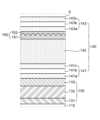
도 2를 참조하면, 캐소드(133) 상에 봉지부(140)가 배치된다. 또한, 봉지부(140) 내에 산란 필름(150)이 배치된다.Referring to FIG. 2, the sealing
이하에서는 봉지부(140) 및 산란 필름(150)에 대한 보다 상세한 설명을 위해 도 3을 함께 참조한다.Hereinafter, reference is made to FIG. 3 for a more detailed description of the
도 3은 도 2의 X영역에 대한 확대도이다.Figure 3 is an enlarged view of area X in Figure 2.
도 2 및 도 3을 참조하면, 봉지부(140)는 발광 소자(130) 상에 배치된다. 예를 들면, 봉지부(140)는 발광 소자(130)를 덮도록 캐소드(133) 상에 배치된다. 봉지부(140)는 발광 표시 장치(100) 외부로부터 침투하는 수분 등으로부터 발광 소자(130)를 보호한다.Referring to FIGS. 2 and 3 , the
캐소드(133) 상에 제1 봉지층(141)이 배치된다. 제1 봉지층(141)은 발광 소자(130)로의 수분 침투 차단 효과가 우수하고, 저온 증착이 가능하면서 투명한 무기물로 형성될 수 있다. 예를 들어 제1 봉지층(141)은 질화 실리콘(SiNx) 또는 산화 실리콘(SiOx), 산화 알루미늄(Al2O3) 등과 같은 무기물로 이루어질 수 있으나, 이에 한정되는 것은 아니다.A
제1 봉지층(141)은 하나 이상의 고굴절층 및 하나 이상의 저굴절층이 교대로 적층된 구조를 가질 수 있다. 예를 들면, 제1 봉지층(141)은 상대적으로 고굴절률을 갖는 무기층과 상대적으로 저굴절률을 갖는 무기층이 교대로 적층된 구조를 가질 수 있다.The
예를 들어, 도 3을 참조하면, 제1 봉지층(141)은 제1 층(141a), 제1 층(141a) 상의 제2 층(141b) 및 제2 층(141b) 상의 제3 층(141c)을 포함할 수 있다. 이때, 제1 층(141a) 및 제3 층(141c)이 상대적으로 고굴절률을 갖는 무기층이고, 제2 층(141b)이 상대적으로 저굴절률을 갖는 무기층일 수 있다. 또는 제1 층(141a) 및 제3 층(141c)이 상대적으로 저굴절률을 갖는 무기층이고, 제2 층(141b)이 상대적으로 고굴절률을 갖는 무기층일 수 있다.For example, referring to Figure 3, the
도 3을 참조하면, 제1 봉지층(141) 상에 이물 커버층(142)이 배치된다. 이물 커버층(142)은 제조 공정 중에 발생할 수 있는 이물을 커버하여 이물에 의한 단차를 보상할 수 있는 유기층이다. 제조 공정 중에 발생한 이물은 발광 소자(130)의 불량을 야기할 수 있으며, 제1 봉지층(141) 또는 제3 봉지층(143)과 같은 무기층의 크랙(crack)을 야기할 수도 있다. 따라서, 이물 커버층(142)은 이물에 의해 발생한 크랙을 커버하거나, 이물에 의해 발생하는 단차를 보상하는 역할을 할 수도 있다. 또한, 이물 커버층(142)은 발광 소자(130) 위의 표면을 평탄하게 하는 역할도 할 수 있다.Referring to FIG. 3, a foreign
이물 커버층(142)은 유기물로 이루어질 수 있다. 예를 들어, 이물 커버층(142)은 아크릴(acryl) 수지 또는 에폭시(epoxy) 수지가 사용될 수 있으나, 이에 제한되는 것은 아니다.The foreign
도 3을 참조하면, 이물 커버층(142) 상에 제2 봉지층(143)이 배치된다. 제2 봉지층(143)은 발광 소자(130)로의 수분 침투 차단 효과가 우수하고, 저온 증착이 가능하면서 투명한 무기물로 형성될 수 있다. 예를 들어 제2 봉지층(143)은 질화 실리콘(SiNx) 또는 산화 실리콘(SiOx), 산화 알루미늄(Al2O3) 등과 같은 무기물로 이루어질 수 있다.Referring to FIG. 3, the
제2 봉지층(143)은 하나 이상의 고굴절층 및 하나 이상의 저굴절층이 교대로 적층된 구조를 가질 수 있다. 즉, 제2 봉지층(143)은 상대적으로 고굴절률을 갖는 무기층과 상대적으로 저굴절률을 갖는 무기층이 교대로 적층된 구조를 가질 수 있다.The
예를 들어, 도 3을 참조하면, 제2 봉지층(143)은 제1 층(143a), 제1 층(143a) 상의 제2 층(143b) 및 제2 층(143b) 상의 제3 층(143c)을 포함할 수 있다. 이때, 제1 층(143a) 및 제3 층(143c)이 상대적으로 고굴절률을 갖는 무기층이고, 제2 층(143b)이 상대적으로 저굴절률을 갖는 무기층일 수 있다. 또는 제1 층(143a) 및 제3 층(143c)이 상대적으로 저굴절률을 갖는 무기층이고, 제2 층(143b)이 상대적으로 고굴절률을 갖는 무기층일 수 있다.For example, referring to Figure 3, the
도 3을 참조하면, 봉지부(140) 내에 산란 필름(150)이 배치된다. 구체적으로, 이물 커버층(142)과 제2 봉지층(143) 사이에 산란 필름(150)이 배치된다. 예를 들면, 산란 필름(150)의 하면은 이물 커버층(142)과 접하고, 산란 필름(150)의 상면은 제2 봉지층(143)과 접할 수 있다.Referring to FIG. 3, a
산란 필름(150)은 발광 표시 장치(100)의 시야각 의존성을 개선하기 위한 구성일 수 있다. 이에, 산란 필름(150)은 비평탄한 평상을 갖는 산란층(151) 및 산란층(151)을 덮는 평탄층(152)으로 구성될 수 있다. 예를 들면, 산란 필름(150)은 복수의 오목부 또는 복수의 볼록부를 포함하는 산란층(151) 및 산란층(151) 상에 배치되는 평탄층(152)을 포함한다.The
산란층(151)의 복수의 볼록부 또는 복수의 오목부는, 예를 들어, 마스크 공정을 통해 형성될 수 있으나, 이에 제한되는 것은 아니다. 또한, 복수의 볼록부 또는 복수의 오목부는 대략 10nm 내지 100㎛의 직경을 가질 수 있으며, 이에 제한되는 것은 아니다.The plurality of convex portions or the plurality of concave portions of the scattering layer 151 may be formed through, for example, a mask process, but are not limited thereto. Additionally, the plurality of convex portions or the plurality of concave portions may have a diameter of approximately 10 nm to 100 μm, but are not limited thereto.
도 3에 도시된 바와 같이, 산란층(151)의 복수의 볼록부 또는 복수의 오목부는 발광 소자(130)가 형성된 위치에 대응하는 영역에 형성될 수 있다. 다만, 이에 제한되는 것은 아니며, 산란층(151)의 복수의 볼록부 또는 복수의 오목부는 기판(110) 전면에 형성될 수도 있다.As shown in FIG. 3, a plurality of convex portions or a plurality of concave portions of the scattering layer 151 may be formed in an area corresponding to a position where the
도 3에서는 산란층(151)의 복수의 볼록부가 반구 형상인 것으로 도시하였지만, 반타원체 형상일 수 있고, 피라미드 형상일 수도 있으며, 이외 다양한 형상으로 형성될 수 있다.In FIG. 3, the plurality of convex portions of the scattering layer 151 are shown as having a hemispherical shape, but they may have a semi-ellipsoid shape, a pyramid shape, or other various shapes.
도 3을 참조하면, 산란층(151)을 덮는 평탄층(152)이 배치된다. 평탄층(152)은 산란층(151) 상에서 산란층(151)을 평탄화하기 위한 절연층이다. 예를 들면, 평탄층(152) 하부에 배치된 산란층(151)이 비평탄한 형상을 갖지만, 평탄층(152)이 배치됨에 따라 제2 봉지층(143)은 평탄층(152) 상에서 평탄한 면에 배치될 수 있다.Referring to FIG. 3, a flat layer 152 covering the scattering layer 151 is disposed. The flattening layer 152 is an insulating layer for flattening the scattering layer 151 on the scattering layer 151 . For example, the scattering layer 151 disposed below the flattening layer 152 has a non-flat shape, but as the flattening layer 152 is disposed, the
평탄층(152)은 투명한 유기물로 이루어질 수 있다. 예를 들면, 평탄층(152)은 발광 소자 제조 중 또는 발광 소자 제조 후 아웃개싱(outgassing)이 없는 물질로 이루어질 수 있다. 예를 들어, 평탄층(152)은 진공 증착 중에 반사된 광이 통과할 수 있도록, 아웃개싱이 되지 않는 투명한 유기물이어야 한다. 예를 들어, 평탄층(152)은 아크릴(acryl) 수지, 에폭시(epoxy) 수지, 페놀(phenol) 수지, 폴리아미드(polyamide) 수지, 폴리이미드(polyimide) 수지, 불포화 폴리에스테르(polyester) 수지, 폴리페닐렌(polyphenylene) 수지, 폴리페닐렌설파이드(polyphenylene sulfide) 수지, 벤조사이클로부텐(benzocyclobutene) 및 포토레지스트 중 하나로 이루어질 수 있으나, 이에 한정되는 것은 아니다.The planarization layer 152 may be made of a transparent organic material. For example, the planarization layer 152 may be made of a material that does not cause outgassing during or after manufacturing the light emitting device. For example, the planarization layer 152 must be a transparent organic material that does not outgas so that reflected light can pass through during vacuum deposition. For example, the flat layer 152 is made of acryl resin, epoxy resin, phenol resin, polyamide resin, polyimide resin, unsaturated polyester resin, It may be made of one of polyphenylene resin, polyphenylene sulfide resin, benzocyclobutene, and photoresist, but is not limited thereto.
또한, 평탄층(152)은 산란층(151)과 굴절률이 서로 상이할 수 있다. 평탄층(152)과 산란층(151)의 굴절률이 동일하거나 굴절률 차이가 매우 작은 경우, 평탄층(152)과 산란층(151)이 광학적으로 하나의 층으로 기능할 수 있다. 즉, 평탄층(152)과 산란층(151)의 굴절률이 동일하거나 굴절률 차이가 매우 작은 경우에는, 평탄층(152)과 산란층(151) 사이의 경계에서 광이 산란될 수 없다. 이에, 예를 들어, 산란층(151)과 평탄층(152)의 굴절률 차이는 0.05 이상일 수 있다.Additionally, the flattening layer 152 may have a different refractive index from the scattering layer 151. If the refractive index of the flattening layer 152 and the scattering layer 151 is the same or the difference in refractive index is very small, the flattening layer 152 and the scattering layer 151 may optically function as one layer. That is, if the refractive index of the flattening layer 152 and the scattering layer 151 are the same or the difference in refractive index is very small, light cannot be scattered at the boundary between the flattening layer 152 and the scattering layer 151. Therefore, for example, the difference in refractive index between the scattering layer 151 and the flat layer 152 may be 0.05 or more.
탑 에미션 방식의 발광 표시 장치의 경우, 발광층에서 발광된 빛을 상부로 발광시키기 위해 캐소드는 투과 특성을 갖는 물질을 사용한다. 다만, 캐소드가 투과 특성을 갖더라도, 발광층에서 발광된 광의 일부는 투과 특성을 갖는 캐소드에서 반사되어 애노드 측으로 향하게 되고, 애노드에서 다시 반사되어, 애노드와 캐소드 사이에서 반복적으로 반사되는 광이 발생한다. 이에, 탑 에미션 방식의 발광 표시 장치에서 마이크로 캐비티가 구현될 수 있다.In the case of a top emission type light emitting display device, the cathode uses a material with transmission properties to emit light emitted from the light emitting layer upward. However, even if the cathode has transmission characteristics, some of the light emitted from the light-emitting layer is reflected by the cathode, which has transmission characteristics, and is directed to the anode, and is reflected again at the anode, generating light that is repeatedly reflected between the anode and the cathode. Accordingly, a micro cavity can be implemented in a top emission type light emitting display device.
다만, 마이크로 캐비티를 구현하는 경우, 광 효율 측면에서는 유리하지만, 시야각이 변화함에 따라 휘도가 변화하고 색변화 현상이 발생하여 표시 품질이 저하될 수 있다. 예를 들면, 마이크로 캐비티를 이용하여 광 효율을 향상시키는 발광 표시 장치는 시야각에 따라 빛의 세기와 파장 특성이 변화하기 때문에 시야각에 따른 휘도가 크게 감소하고 색변화가 크게 발생하는 문제점이 있다.However, when implementing a micro cavity, although it is advantageous in terms of light efficiency, as the viewing angle changes, luminance changes and color change occurs, which may deteriorate display quality. For example, a light emitting display device that improves light efficiency using a micro cavity has problems in that the intensity and wavelength characteristics of light change depending on the viewing angle, resulting in a significant decrease in luminance and significant color change depending on the viewing angle.
이에, 본 발명의 일 실시예에 따른 발광 표시 장치(100)에서는 발광 소자(130) 상에 굴절률이 서로 상이한 다층 구조의 봉지부(140)가 형성되어 색변화 현상을 감소시킴으로써 마이크로 캐비티 특성을 억제할 수 있는 효과가 있다. 예를 들면, 봉지부(140)의 제1 봉지층(141) 및 제2 봉지층(143)은 상대적으로 고굴절률을 갖는 무기층과 상대적으로 저굴절률을 갖는 무기층이 교대로 적층된 구조를 가질 수 있다. 따라서, 본 발명의 일 실시예에 따른 발광 표시 장치(100)에서 구현되는 마이크로 캐비티 특성이 억제될 수 있으므로, 시야각에 따른 휘도 저하 및 색변화 현상을 저감시킬 수 있다.Accordingly, in the light emitting
또한, 본 발명의 일 실시예에 따른 발광 표시 장치(100)에서는 봉지부(140) 내에 산란 필름(150)이 배치된다. 예를 들면, 이물 커버층(142)과 제2 층(143) 사이에 산란 필름(150)이 배치된다. 또한, 산란 필름(150)은 서로 다른 굴절률을 갖는 산란층(151)과 평탄층(152)을 포함하고, 산란층(151)은 복수의 볼록부 또는 복수의 오목부를 포함할 수 있다. 이에, 발광 소자(130)에서 발광되는 광이 산란 필름(150)에서 산란되어 마이크로 캐비티 특성을 억제할 수 있고, 시야각에 따른 휘도 변화 및 색변화를 최소화할 수 있다.Additionally, in the light emitting
이에, 본 발명의 일 실시예에 따른 표시 장치(100)에서는 봉지부(140) 및 산란 필름(150)을 사용하여 마이크로 캐비티를 구현함에 따라 발생할 수 있는 시야각 의존성을 개선할 수 있는 효과가 있다.Accordingly, the
또한, 본 발명의 일 실시예에 따른 표시 장치(100)에서는 산란 필름(150)이 봉지부(140) 내에 배치된다. 예를 들면, 산란 필름(150)은 봉지부(140) 상부가 아닌 봉지부(140) 내에서 이물 커버층(142)과 제2 층(143) 사이에 배치된다. 따라서, 본 발명의 일 실시예에 따른 표시 장치(100)에서는 봉지부(140) 상부에 산란 필름(150)을 배치하는 경우보다 블러링 현상이 감소할 수 있다.Additionally, in the
본 발명의 일 실시예에 따른 표시 장치(100)의 시야각 의존성 및 블러링 현상과 관련된 효과에 대하여 도 6 내지 도 8b에서 보다 상세히 설명한다.Effects related to viewing angle dependence and blurring of the
도 4는 본 발명의 다른 실시예에 따른 발광 표시 장치의 확대 단면도이다. 도 4에 도시된 발광 표시 장치(400)는 도 1 내지 도 3에 도시된 발광 표시 장치(100)와 비교하여 산란 필름(450)의 위치가 상이하며, 다른 구성은 실질적으로 동일하므로, 중복 설명은 생략한다.Figure 4 is an enlarged cross-sectional view of a light emitting display device according to another embodiment of the present invention. The light emitting
도 4를 참조하면, 봉지부(140) 내에 산란 필름(450)이 배치된다. 구체적으로, 제1 봉지층(141)과 이물 커버층(142) 사이에 산란 필름(450)이 배치된다. 예를 들면, 산란 필름(450)의 하면은 제1 봉지층(141)과 접하고, 산란 필름(150)의 상면은 이물 커버층(142)과 접할 수 있다.Referring to FIG. 4, a
산란 필름(450)은 발광 표시 장치(400)의 시야각 의존성을 개선하기 위한 구성일 수 있다. 이에, 산란 필름(450)은 비평탄한 평상을 갖는 산란층(451) 및 산란층(451)을 덮는 평탄층(452)으로 구성된다. 산란층(451) 및 평탄층(452)은 도 1 내지 도 3을 참조하여 설명한 산란층(141) 및 평탄층(152)과 실질적으로 동일하므로, 중복 설명은 생략한다.The
본 발명의 다른 실시예에 따른 발광 표시 장치(400)에서는 봉지부(140)의 제1 봉지층(141) 및 제2 봉지층(143)은 상대적으로 고굴절률을 갖는 무기층과 상대적으로 저굴절률을 갖는 무기층이 교대로 적층된 구조를 가질 수 있다. 또한, 본 발명의 다른 실시예에 따른 발광 표시 장치(400)에서는 봉지부(140) 내에 산란 필름(450)이 배치된다. 예를 들면, 제1 층(141)과 이물 커버층(142) 사이에 산란 필름(450)이 배치된다. 따라서, 본 발명의 다른 실시예에 따른 발광 표시 장치(400)에서 구현되는 마이크로 캐비티 특성이 억제되어 시야각에 따른 휘도 저하 및 색변화 현상을 저감시킬 수 있다. 예를 들면, 본 발명의 다른 실시예에 따른 표시 장치(400)에서는 봉지부(140) 및 산란 필름(450)을 사용하여 마이크로 캐비티를 구현함에 따라 발생할 수 있는 시야각 의존성을 개선할 수 있는 효과가 있다.In the light emitting
또한, 본 발명의 다른 실시예에 따른 표시 장치(400)에서는 산란 필름(450)이 봉지부(140) 내에 배치된다. 예를 들면, 산란 필름(450)은 봉지부(140) 상부가 아닌 봉지부(140) 내에서 제1 층(141)과 이물 커버층(142) 사이에 배치된다. 따라서, 본 발명의 다른 실시예에 따른 표시 장치(400)에서는 봉지부(140) 상부에 산란 필름(450)을 배치하는 경우보다 블러링 현상이 감소할 수 있다.Additionally, in the
본 발명의 다른 실시예에 따른 표시 장치(400)의 시야각 의존성 및 블러링 현상과 관련된 효과에 대하여 도 6 내지 도 8b에서 보다 상세히 설명한다.Effects related to viewing angle dependence and blurring of the
도 5는 본 발명의 또 다른 실시예에 따른 발광 표시 장치의 확대 단면도이다. 도 5에 도시된 발광 표시 장치(500)는 도 1 내지 도 3에 도시된 발광 표시 장치(100)와 비교하여 산란 필름(550)의 위치가 상이하며, 다른 구성은 실질적으로 동일하므로, 중복 설명은 생략한다.Figure 5 is an enlarged cross-sectional view of a light emitting display device according to another embodiment of the present invention. The light emitting
도 5를 참조하면, 봉지부(140)와 발광 소자(130) 사이에 산란 필름(550)이 배치된다. 예를 들면, 산란 필름(550)의 하면은 발광 소자(130)의 캐소드(133)와 접하고, 산란 필름(550)의 상면은 봉지부(140)의 제1 봉지층(141)과 접할 수 있다.Referring to FIG. 5, a
산란 필름(550)은 발광 표시 장치(500)의 시야각 의존성을 개선하기 위한 구성일 수 있다. 이에, 산란 필름(550)은 비평탄한 평상을 갖는 산란층(551) 및 산란층(551)을 덮는 평탄층(552)으로 구성된다. 산란층(551) 및 평탄층(552)은 도 1 내지 도 3을 참조하여 설명한 산란층(141) 및 평탄층(152)과 실질적으로 동일하므로, 중복 설명은 생략한다.The
본 발명의 또 다른 실시예에 따른 발광 표시 장치(500)에서는 봉지부(140)의 제1 봉지층(141) 및 제2 봉지층(143)은 상대적으로 고굴절률을 갖는 무기층과 상대적으로 저굴절률을 갖는 무기층이 교대로 적층된 구조를 가질 수 있다. 또한, 본 발명의 또 다른 실시예에 따른 발광 표시 장치(500)에서는 봉지부(140)와 발광 소자(130) 사이에 산란 필름(550)이 배치된다. 예를 들면, 발광 소자(130)의 캐소드(133)과 봉지부(140)의 제1 층(141) 사이에 산란 필름(550)이 배치된다. 이에, 본 발명의 또 다른 실시예에 따른 발광 표시 장치(500)에서 구현되는 마이크로 캐비티 특성이 억제되어 시야각에 따른 휘도 저하 및 색변화 현상을 저감시킬 수 있다. 예를 들면, 본 발명의 다른 실시예에 따른 표시 장치(500)에서는 봉지부(140) 및 산란 필름(550)을 사용하여 마이크로 캐비티를 구현함에 따라 발생할 수 있는 시야각 의존성을 개선할 수 있는 효과가 있다.In the light emitting
또한, 본 발명의 또 다른 실시예에 따른 표시 장치(500)에서는 산란 필름(550)이 봉지부(140) 아래에 배치된다. 예를 들면, 산란 필름(550)은 봉지부(140) 상부가 아닌 봉지부(140) 아래서 발광 소자(130)와 봉지부(140) 사이에 배치된다. 따라서, 본 발명의 또 다른 실시예에 따른 표시 장치(500)에서는 봉지부(140) 상부에 산란 필름(550)을 배치하는 경우보다 블러링 현상이 감소할 수 있다.Additionally, in the
본 발명의 또 다른 실시예에 따른 표시 장치(500)의 시야각 의존성 및 블러링 현상과 관련된 효과에 대한 보다 상세한 설명을 위해 도 6 내지 도 8b을 참조한다.Refer to FIGS. 6 to 8B for a more detailed description of effects related to viewing angle dependence and blurring of the
도 6은 본 발명의 또 다른 실시예 및 비교예에 따른 발광 표시 장치의 시야각에 대한 색변화량을 나타낸 그래프이다. 도 6을 참조하면, X축은 시야각(Viewing Angle(°)을 나타내고, Y축은 시야각에 따른 색좌표변화량(Δu'v')를 나타낸다. 또한, 실시예는 도 5를 참조하여 설명한 발광 표시 장치(500)이고, 비교예는 실시예에서 산란 필름이 적용되지 않은 발광 표시 장치이다.Figure 6 is a graph showing the amount of color change with respect to the viewing angle of a light emitting display device according to another embodiment and a comparative example of the present invention. Referring to FIG. 6, the ), and the comparative example is a light emitting display device to which the scattering film was not applied in the example.
도 6을 참조하면, 색좌표변화량(Δu'v')은 정면에서 바라볼 때인 0°에서의 색좌표를 기준으로 시야각이 변화함에 따라 발생하는 색좌표의 차이를 의미한다. 색좌표(u'v')는 국제조명위원회 CIE 15.2에 정의된 1976 UCS(Uniform Chromaticity Scale Diagram) 좌표일 수 있으나, 이에 제한되는 것은 아니다.Referring to FIG. 6, the color coordinate change amount (Δu'v') refers to the difference in color coordinates that occurs as the viewing angle changes based on the color coordinates at 0° when viewed from the front. Color coordinates (u'v') may be 1976 UCS (Uniform Chromaticity Scale Diagram) coordinates defined in CIE 15.2 of the International Commission on Illumination, but are not limited thereto.
도 6을 참조하면, 시야각이 증가함에 따라, 예를 들면, 발광 표시 장치의 시청자가 정면에서 측면으로 이동함에 따라, 비교예에서의 색변화는 급격히 증가하는 것을 확인할 수 있다. 예를 들어, 비교예의 발광 표시 장치에서 시야각이 10°인 경우와 시야각이 40°인 경우에서의 색좌표변화량(Δu'v')은 대략 0.015 이상 차이가 나는 것을 확인할 수 있다.Referring to FIG. 6, it can be seen that as the viewing angle increases, for example, as the viewer of the light emitting display device moves from the front to the side, the color change in the comparative example rapidly increases. For example, in the light emitting display device of the comparative example, it can be seen that the color coordinate change amount (Δu'v') between the case where the viewing angle is 10° and the case where the viewing angle is 40° differs by approximately 0.015 or more.
이에 반해, 실시예의 발광 표시 장치(500)는 비교예의 발광 표시 장치와 비교했을 때, 시야각이 증가함에 따른 색변화의 증가량이 감소한 것을 확인할 수 있다. 예를 들어, 실시예의 발광 표시 장치(500)에서 시야각이 10°인 경우와 시야각이 40°인 경우에서의 색좌표변화량(Δu'v')은 대략 0.01 이하로 차이가 나는 것을 확인할 수 있다.On the other hand, it can be confirmed that the amount of color change in the light emitting
따라서, 비교예의 발광 표시 장치는 시야각에 따라 색변화가 크게 증가하는 문제점이 있는 반면, 실시예의 발광 표시 장치(500)는 마이크로 캐비티 구현 시 시야각이 변화함에 따라 발생할 수 있는 색변화를 최소화할 수 있다.Accordingly, while the light emitting display device of the comparative example has a problem in that color change significantly increases depending on the viewing angle, the light emitting
도 6에서는 실시예로 도 5를 참조하여 설명한 발광 표시 장치(500)를 설명하였으나, 이에 제한되지 않고, 실시예로서 도 1 내지 도 4를 참조하여 설명한 발광 표시 장치(100, 400) 또한 유사한 그래프가 나타날 수 있다.In FIG. 6 , the light-emitting
도 7은 본 발명의 또 다른 실시예, 비교예 1 및 비교예 2에 따른 발광 표시 장치의 시야각에 대한 휘도 변화량을 나타내는 그래프이다. 도 7을 참조하면, X축은 시야각(Viewing Angle(°))을 나타내고, Y축은 정규화된 휘도(Nomalized intensity)를 나타낸다. 여기서, 정규화된 휘도는 최대 휘도 값이 1이 되도록 시야각에 따른 휘도를 정규화한 휘도를 의미한다. 또한, 도 5를 참조하여 설명한 발광 표시 장치(500)이고, 비교예 1은 램버시안(Lambertian) 분포 특성에 따른 시야각에 따른 휘도 변화량이고, 비교예 2는 실시예에서 산란 필름이 적용되지 않은 발광 표시 장치이다.FIG. 7 is a graph showing the amount of change in luminance with respect to viewing angle of a light emitting display device according to Comparative Examples 1 and 2, which are still another embodiment of the present invention. Referring to FIG. 7, the X-axis represents viewing angle (°), and the Y-axis represents normalized intensity. Here, normalized luminance refers to luminance normalized according to the viewing angle so that the maximum luminance value is 1. In addition, the light emitting
도 7을 참조하면, 비교예 1의 자연 광원에 대한 시야각 분포 특성을 나타내는 램버시안 분포 특성에 따른 시야각에 따른 휘도 변화량은 시야각이 증가함에 따라 완만하게 감소하는 것을 확인할 수 있다. 이에 반해, 비교예 2의 발광 표시 장치는 시야각이 증가함에 따라 휘도가 급격하게 감소하는 것을 확인할 수 있다.Referring to FIG. 7, it can be seen that the amount of luminance change according to the viewing angle according to the Lambertian distribution characteristic, which represents the viewing angle distribution characteristic for the natural light source of Comparative Example 1, gradually decreases as the viewing angle increases. On the other hand, it can be seen that the luminance of the light emitting display device of Comparative Example 2 rapidly decreases as the viewing angle increases.
그러나, 실시예의 발광 표시 장치(500)는 산란 필름(550)을 사용함으로써, 시야각이 증가함에 따라 휘도가 비교예 2의 발광 표시 장치에 비해 완만하게 감소할 수 있다. 또한, 실시예의 발광 표시 장치(500)는 비교예 2의 발광 표시 장치보다 램버시안 분포 특성에 근접할 수 있다.However, since the light emitting
따라서, 비교예 2의 발광 표시 장치는 시야각에 따라 휘도가 크게 감소하는 문제점이 있는 반면, 실시예의 발광 표시 장치(500)는 마이크로 캐비티 구현 시 시야각이 변화함에 따라 발생할 수 있는 급격한 휘도 변화를 저감할 수 있다.Therefore, while the light-emitting display device of Comparative Example 2 has a problem in that luminance significantly decreases depending on the viewing angle, the light-emitting
도 7에서는 실시예로 도 5를 참조하여 설명한 발광 표시 장치(500)를 설명하였으나, 이에 제한되지 않고, 실시예로서 도 1 내지 도 4를 참조하여 설명한 발광 표시 장치(100, 400) 또한 유사한 그래프가 나타날 수 있다.In FIG. 7 , the light emitting
도 8a 및 도 8b는 비교예 및 본 발명의 또 다른 실시예에 따른 발광 표시 장치의 블러링 현상을 설명하기 위한 도면이다. 예를 들면, 도 8a 및 도 8b는 하나의 화소의 중심을 원점으로 하며, 화소의 경계인 제1 경계면(870a, 870b) 대비 휘도가 1/10인 지점인 제2 경계면(880a, 880b)을 나타내는 도면이다. 여기서, 도 8b는 실시예에 대한 도면으로, 도 5를 참조하여 설명한 발광 표시 장치(500)의 하나의 화소에 대한 도면이고, 도 8a는 비교예에 대한 도면으로, 실시예에서 산란 필름(550)이 봉지부(140) 상으로 이동한 경우의 하나의 화소에 대한 도면이다. 도 8a 및 도 8b에서 X축 및 Y축은 화소의 중심을 원점으로 한 좌표를 나타내기 위한 축이다.FIGS. 8A and 8B are diagrams for explaining a blurring phenomenon in a light emitting display device according to a comparative example and another embodiment of the present invention. For example, FIGS. 8A and 8B show the center of one pixel as the origin and the second boundary surfaces 880a and 880b, which are points where the luminance is 1/10 compared to the first boundary surfaces 870a and 870b, which are the boundaries of the pixels. It is a drawing. Here, FIG. 8B is a diagram for an example, and is a diagram for one pixel of the light emitting
도 8a를 참조하면, 비교예에서는 산란 필름이 봉지부 상에 배치됨에 따라 산란 필름과 발광 소자 간의 거리가 증가하여 블러링 현상이 심하게 발생하는 것을 이미지로도 확인할 수 있다. 또한, 제1 경계면(870a)과 제2 경계면(880a) 사이의 영역은 사용자가 눈으로 블러링 현상을 인식할 수 있는 영역으로, 비교예의 발광 표시 장치 경우 제1 경계면(870a)과 제2 경계면(880a)이 상당히 이격되어 블러링 현상이 심하게 발생하는 것을 확인할 수 있다.Referring to FIG. 8A, in the comparative example, it can be seen from the image that as the scattering film is placed on the encapsulation portion, the distance between the scattering film and the light emitting device increases, causing a severe blurring phenomenon. In addition, the area between the first boundary surface 870a and the second boundary surface 880a is an area where the user can visually perceive the blurring phenomenon. In the case of the light emitting display device of the comparative example, the first boundary surface 870a and the second boundary surface It can be seen that (880a) is significantly spaced apart, causing severe blurring.
다만, 도 8b를 참조하면, 실시예의 발광 표시 장치(500)에서는 산란 필름(550)이 봉지부(140)와 발광 소자(130) 사이에 배치됨에 따라 산란 필름(550)과 발광 소자(130) 간의 거리가 최소화되어 블러링 현상이 거의 발생하지 않는 것을 이미지로도 확인할 수 있다. 예를 들면, 제1 경계면(870b)과 제2 경계면(880b) 사이의 영역은 사용자가 눈으로 블러링 현상을 인식할 수 있는 영역이지만, 도 8b에서 확인할 수 있는 바와 같이, 실시예의 발광 표시 장치(500)에서는 해당 영역이 매우 좁으므로, 예를 들면, 제1 경계면(870b)과 제2 경계면(880b)이 이격 거리가 매우 작으므로 블러링 현상이 거의 발생하지 않는 것을 확인할 수 있다.However, referring to FIG. 8B, in the light emitting
도 8a 및 도 8b에서는 실시예로 도 5를 참조하여 설명한 발광 표시 장치(500)를 설명하였으나, 이에 제한되지 않고, 실시예로서 도 1 내지 도 4를 참조하여 설명한 발광 표시 장치(100, 400) 또한 유사한 그래프가 나타날 수 있다. 예를 들면, 발광 표시 장치(100, 400)에서도 산란 필름(150, 450)이 봉지부(140) 상부가 아닌 봉지부(140) 내부에 배치되므로, 산란 필름(150, 450)과 발광 소자(130) 사이의 거리가 비교예보다 작을 수 있다. 따라서, 발광 표시 장치(100, 400)에서도 비교예와 비교하여 블러링 현상이 적게 발생할 수 있다.In FIGS. 8A and 8B , the light emitting
본 발명의 다양한 실시예들에 따른 발광 표시 장치는 다음과 같이 설명될 수 있다.A light emitting display device according to various embodiments of the present invention may be described as follows.
본 발명의 일 실시예에 따른 발광 표시 장치는 기판 상의 발광 소자, 발광 소자 상의 봉지부, 및 봉지부와 발광 소자 사이 또는 봉지부 내에 배치되는 산란 필름을 포함할 수 있다.A light emitting display device according to an embodiment of the present invention may include a light emitting device on a substrate, an encapsulation portion on the light emitting device, and a scattering film disposed between or within the encapsulation portion and the light emitting device.
본 발명의 다른 특징에 따르면, 봉지부는, 하나 이상의 고굴절층 및 하나 이상의 저굴절층이 교대로 적층된 제1 봉지층, 제1 봉지층 상에 배치된 이물 커버층, 및 하나 이상의 고굴절층 및 하나 이상의 저굴절층이 교대로 적층된 제2 봉지층을 포함할 수 있다.According to another feature of the present invention, the encapsulation unit includes a first encapsulation layer in which one or more high refractive index layers and one or more low refractive index layers are alternately stacked, a foreign matter cover layer disposed on the first encapsulation layer, and one or more high refractive index layers and one It may include a second encapsulation layer in which the above low refractive layers are alternately stacked.
본 발명의 또 다른 특징에 따르면, 산란 필름은 제1 봉지층과 이물 커버층 사이에 배치될 수 있다.According to another feature of the present invention, the scattering film may be disposed between the first encapsulation layer and the foreign matter cover layer.
본 발명의 또 다른 특징에 따르면, 산란 필름은 이물 커버층과 제2 봉지층 사이에 배치될 수 있다.According to another feature of the present invention, the scattering film may be disposed between the foreign matter cover layer and the second encapsulation layer.
본 발명의 또 다른 특징에 따르면, 산란 필름은, 복수의 오목부 또는 복수의 볼록부를 포함하는 산란층, 및 산란층 상에 배치되는 평탄층을 포함할 수 있다.According to another feature of the present invention, the scattering film may include a scattering layer including a plurality of concave portions or a plurality of convex portions, and a flat layer disposed on the scattering layer.
본 발명의 또 다른 특징에 따르면, 복수의 볼록부 또는 복수의 오목부는 반구 형상, 반타원체 형상 및 피라미드 형상 중 어느 하나의 형상을 가질 수 있다.According to another feature of the present invention, the plurality of convex portions or the plurality of concave portions may have any one of a hemispherical shape, a semi-ellipsoid shape, and a pyramid shape.
본 발명의 다른 실시예에 따른 발광 표시 장치는 탑 에미션(top emission) 방식의 발광 소자, 발광 소자 상에 배치되는 제1 무기층, 제1 무기층 상에 배치되는 이물 커버층, 이물 커버층 상에 배치되는 제2 무기층, 및 제2 무기층과 발광 소자 사이에 배치되어, 마이크로 캐비티(micro cavity)에 따른 발광 소자의 시야각 의존성을 감소시키도록 구성된 산란 필름을 포함할 수 있다.A light emitting display device according to another embodiment of the present invention includes a top emission type light emitting device, a first inorganic layer disposed on the light emitting device, a foreign matter cover layer disposed on the first inorganic layer, and a foreign matter cover layer. It may include a second inorganic layer disposed on the light-emitting device, and a scattering film disposed between the second inorganic layer and the light-emitting device to reduce the viewing angle dependence of the light-emitting device on the micro cavity.
본 발명의 다른 특징에 따르면, 발광 표시 장치는 산란 필름은 발광 소자, 제1 무기층 및 이물 커버층 중 어느 하나의 층의 상면에 배치될 수 있다.According to another feature of the present invention, in the light emitting display device, the scattering film may be disposed on the upper surface of any one layer of the light emitting element, the first inorganic layer, and the foreign matter cover layer.
본 발명의 또 다른 특징에 따르면, 산란 필름은, 복수의 오목부 또는 복수의 볼록부를 포함하는 산란층, 및 산란층 상에 배치되는 평탄층을 포함하고, 산란층과 평탄층의 굴절률 차이는 0.05 이상일 수 있다.According to another feature of the present invention, the scattering film includes a scattering layer including a plurality of concave portions or a plurality of convex portions, and a flat layer disposed on the scattering layer, and the refractive index difference between the scattering layer and the flat layer is 0.05. It could be more than that.
본 발명의 또 다른 특징에 따르면, 제1 무기층 및 제2 무기층은 굴절률이 서로 상이한 층이 교대로 적층된 구조를 가질 수 있다.According to another feature of the present invention, the first inorganic layer and the second inorganic layer may have a structure in which layers with different refractive indices are alternately stacked.
이상 첨부된 도면을 참조하여 본 발명의 실시예들을 더욱 상세하게 설명하였으나, 본 발명은 반드시 이러한 실시예로 국한되는 것은 아니고, 본 발명의 기술사상을 벗어나지 않는 범위 내에서 다양하게 변형실시될 수 있다. 따라서, 본 발명에 개시된 실시예들은 본 발명의 기술 사상을 제한하기 위한 것이 아니라 설명하기 위한 것이고, 이러한 실시예에 의하여 본 발명의 기술 사상의 범위가 제한되는 것은 아니다. 그러므로, 이상에서 기술한 실시예들은 모든 면에서 예시적인 것이며 제한적이 아닌 것으로 이해해야만 한다. 본 발명의 보호 범위는 아래의 청구범위에 의하여 해석되어야 하며, 그와 동등한 범위 내에 있는 모든 기술 사상은 본 발명의 권리범위에 포함되는 것으로 해석되어야 할 것이다.Although embodiments of the present invention have been described in more detail with reference to the accompanying drawings, the present invention is not necessarily limited to these embodiments, and various modifications may be made without departing from the technical spirit of the present invention. . Accordingly, the embodiments disclosed in the present invention are not intended to limit the technical idea of the present invention but are for illustrative purposes, and the scope of the technical idea of the present invention is not limited by these embodiments. Therefore, the embodiments described above should be understood in all respects as illustrative and not restrictive. The scope of protection of the present invention should be interpreted in accordance with the claims below, and all technical ideas within the equivalent scope should be construed as being included in the scope of rights of the present invention.
100, 400, 500: 발광 표시 장치
110: 기판
111: 버퍼층
112: 게이트 절연층
113: 층간 절연층
114: 패시베이션층
115: 오버 코팅층
116: 뱅크
120: 박막 트랜지스터
121: 액티브층
122: 게이트 전극
123: 소스 전극
124: 드레인 전극
130: 발광 소자
131: 애노드
132: 발광층
133: 캐소드
140: 봉지부
141: 제1 봉지층
141a: 제1 봉지층의 제1 층
141b: 제1 봉지층의 제2 층
141c: 제1 봉지층의 제3 층
142: 이물 커버층
143: 제2 봉지층
143a: 제2 봉지층의 제1 층
143b: 제2 봉지층의 제2 층
143c: 제2 봉지층의 제3 층
150, 550, 650: 산란 필름
151, 451, 551: 산란층
152, 452, 552: 평탄층
870a, 870b: 제1 경계면
880a, 880b: 제2 경계면
AA: 표시 영역
NA: 비표시 영역
PX: 화소100, 400, 500: Luminous display device
110: substrate
111: buffer layer
112: Gate insulating layer
113: Interlayer insulation layer
114: Passivation layer
115: Overcoating layer
116: bank
120: thin film transistor
121: active layer
122: Gate electrode
123: source electrode
124: drain electrode
130: light emitting element
131: anode
132: light emitting layer
133: cathode
140: Encapsulation part
141: first encapsulation layer
141a: first layer of first encapsulation layer
141b: second layer of first encapsulation layer
141c: Third layer of the first encapsulation layer
142: Foreign matter cover layer
143: Second encapsulation layer
143a: first layer of second encapsulation layer
143b: second layer of second encapsulation layer
143c: Third layer of the second encapsulation layer
150, 550, 650: scattering film
151, 451, 551: scattering layer
152, 452, 552: Flat layer
870a, 870b: first boundary surface
880a, 880b: second boundary surface
AA: display area
NA: Non-display area
PX: pixel
Claims (11)
Translated fromKorean상기 발광 소자 상의 봉지부; 및
상기 봉지부와 상기 발광 소자 사이 또는 상기 봉지부 내에 배치되는 산란 필름을 포함하고,
상기 봉지부는,
굴절률이 서로 상이한 무기층이 교대로 적층된 제1 봉지층;
상기 제1 봉지층 상에 배치되는 이물 커버층; 및
상기 이물 커버층 상에 배치되며, 굴절률이 서로 상이한 무기층이 교대로 적층된 제2 봉지층을 포함하는, 발광 표시 장치.A light emitting element on a substrate;
an encapsulation portion on the light emitting device; and
Comprising a scattering film disposed between the encapsulation part and the light emitting element or within the encapsulation part,
The encapsulation part,
a first encapsulation layer in which inorganic layers having different refractive indices are alternately laminated;
a foreign matter cover layer disposed on the first encapsulation layer; and
A light emitting display device disposed on the foreign matter cover layer and comprising a second encapsulation layer in which inorganic layers having different refractive indices are alternately stacked.
상기 제1 봉지층은 하나 이상의 고굴절층 및 하나 이상의 저굴절층이 교대로 적층되고,
상기 제2 봉지층은 하나 이상의 고굴절층 및 하나 이상의 저굴절층이 교대로 적층된, 발광 표시 장치.According to paragraph 1,
The first encapsulation layer is composed of one or more high refractive index layers and one or more low refractive index layers alternately stacked,
The second encapsulation layer is a light emitting display device in which one or more high refractive index layers and one or more low refractive index layers are alternately stacked.
상기 봉지부 내는 상기 제1 봉지층과 상기 이물 커버층 사이인, 발광 표시 장치.According to paragraph 1,
The light emitting display device wherein the encapsulation part is between the first encapsulation layer and the foreign matter cover layer.
상기 봉지부 내는 상기 이물 커버층과 상기 제2 봉지층 사이인, 발광 표시 장치.According to paragraph 1,
The light emitting display device wherein the encapsulation part is between the foreign matter cover layer and the second encapsulation layer.
상기 봉지부와 상기 발광 소자 사이는 상기 발광 소자와 상기 제1 봉지층 사이인, 발광 표시 장치.According to paragraph 1,
A light emitting display device wherein a space between the encapsulation portion and the light emitting device is between the light emitting device and the first encapsulation layer.
상기 산란 필름은,
복수의 오목부 또는 복수의 볼록부를 포함하는 산란층; 및
상기 산란층 상에 배치되는 평탄층을 포함하는, 발광 표시 장치.According to paragraph 1,
The scattering film is,
A scattering layer including a plurality of concave portions or a plurality of convex portions; and
A light emitting display device comprising a planarization layer disposed on the scattering layer.
상기 복수의 볼록부 또는 상기 복수의 오목부는 반구 형상, 반타원체 형상 및 피라미드 형상 중 어느 하나의 형상을 갖는, 발광 표시 장치.According to clause 6,
A light emitting display device, wherein the plurality of convex portions or the plurality of concave portions have any one of a hemispherical shape, a semi-ellipsoid shape, and a pyramid shape.
상기 발광 소자 상에 배치되는 제1 무기층;
상기 제1 무기층 상에 배치되는 이물 커버층;
상기 이물 커버층 상에 배치되는 제2 무기층; 및
상기 제2 무기층과 상기 발광 소자 사이에 배치되어, 마이크로 캐비티(micro cavity)에 따른 상기 발광 소자의 시야각 의존성을 감소시키도록 구성된 산란 필름을 포함하고,
상기 제1 무기층 및 상기 제2 무기층은 각각 굴절률이 서로 상이한 층이 교대로 적층된 구조를 갖는, 발광 표시 장치.Top emission type light emitting device;
a first inorganic layer disposed on the light emitting device;
a foreign matter cover layer disposed on the first inorganic layer;
a second inorganic layer disposed on the foreign matter cover layer; and
A scattering film disposed between the second inorganic layer and the light-emitting element and configured to reduce the viewing angle dependence of the light-emitting element on a micro cavity,
The first inorganic layer and the second inorganic layer each have a structure in which layers having different refractive indices are alternately stacked.
상기 산란 필름은 상기 발광 소자, 상기 제1 무기층 및 상기 이물 커버층 중 어느 하나의 층의 상면에 배치되는, 발광 표시 장치.According to clause 8,
The light emitting display device wherein the scattering film is disposed on an upper surface of any one of the light emitting element, the first inorganic layer, and the foreign matter cover layer.
상기 산란 필름은,
복수의 오목부 또는 복수의 볼록부를 포함하는 산란층; 및
상기 산란층 상에 배치되는 평탄층을 포함하고,
상기 산란층과 상기 평탄층의 굴절률 차이는 0.05 이상인, 발광 표시 장치.According to clause 8,
The scattering film is,
A scattering layer including a plurality of concave portions or a plurality of convex portions; and
It includes a flat layer disposed on the scattering layer,
A light emitting display device wherein a difference in refractive index between the scattering layer and the flattening layer is 0.05 or more.
Priority Applications (3)
| Application Number | Priority Date | Filing Date | Title |
|---|---|---|---|
| KR1020180096990AKR102645419B1 (en) | 2018-08-20 | 2018-08-20 | Light emitting display apparatus |
| CN201910655271.3ACN110854126B (en) | 2018-08-20 | 2019-07-19 | Light-emitting display device |
| US16/525,320US10804498B2 (en) | 2018-08-20 | 2019-07-29 | Light emitting display apparatus |
Applications Claiming Priority (1)
| Application Number | Priority Date | Filing Date | Title |
|---|---|---|---|
| KR1020180096990AKR102645419B1 (en) | 2018-08-20 | 2018-08-20 | Light emitting display apparatus |
Publications (2)
| Publication Number | Publication Date |
|---|---|
| KR20200021350A KR20200021350A (en) | 2020-02-28 |
| KR102645419B1true KR102645419B1 (en) | 2024-03-07 |
Family
ID=69523475
Family Applications (1)
| Application Number | Title | Priority Date | Filing Date |
|---|---|---|---|
| KR1020180096990AActiveKR102645419B1 (en) | 2018-08-20 | 2018-08-20 | Light emitting display apparatus |
Country Status (3)
| Country | Link |
|---|---|
| US (1) | US10804498B2 (en) |
| KR (1) | KR102645419B1 (en) |
| CN (1) | CN110854126B (en) |
Families Citing this family (8)
| Publication number | Priority date | Publication date | Assignee | Title |
|---|---|---|---|---|
| KR20210025751A (en)* | 2019-08-27 | 2021-03-10 | 삼성디스플레이 주식회사 | Display device |
| CN115997488A (en)* | 2020-08-20 | 2023-04-21 | 应用材料公司 | OLED light field architecture |
| CN112885979A (en)* | 2021-02-01 | 2021-06-01 | 合肥京东方卓印科技有限公司 | Display panel, preparation method thereof and display device |
| KR102770054B1 (en) | 2021-04-19 | 2025-02-19 | 삼성디스플레이 주식회사 | Display device |
| CN113161400A (en)* | 2021-04-22 | 2021-07-23 | 安徽熙泰智能科技有限公司 | CPL structure for improving Micro OLED microcavity effect and preparation method thereof |
| CN114256437B (en)* | 2021-12-21 | 2023-07-18 | 合肥维信诺科技有限公司 | OLED display panel and display device |
| CN115411212A (en)* | 2022-09-14 | 2022-11-29 | 昆山国显光电有限公司 | Display panel and display device |
| KR20250029977A (en)* | 2022-09-21 | 2025-03-05 | 후지필름 가부시키가이샤 | Optical film, organic electroluminescent display device |
Citations (1)
| Publication number | Priority date | Publication date | Assignee | Title |
|---|---|---|---|---|
| JP2010015862A (en)* | 2008-07-04 | 2010-01-21 | Fujifilm Corp | Organic electroluminescent element |
Family Cites Families (16)
| Publication number | Priority date | Publication date | Assignee | Title |
|---|---|---|---|---|
| US7719182B2 (en)* | 2005-09-22 | 2010-05-18 | Global Oled Technology Llc | OLED device having improved light output |
| KR20090089151A (en)* | 2008-02-18 | 2009-08-21 | 삼성전자주식회사 | OLED display and manufacturing method thereof |
| KR101034053B1 (en)* | 2010-05-25 | 2011-05-12 | 엘지이노텍 주식회사 | Light emitting device, light emitting device manufacturing method and light emitting device package |
| US8704441B2 (en)* | 2010-06-29 | 2014-04-22 | Zeon Corporation | Surface light source device |
| KR101931177B1 (en)* | 2012-03-02 | 2018-12-21 | 삼성디스플레이 주식회사 | Organic light emitting display device |
| KR101946391B1 (en)* | 2012-05-31 | 2019-02-12 | 삼성디스플레이 주식회사 | Organic light emitting display and the manufacturing method thereof |
| WO2014031360A1 (en) | 2012-08-22 | 2014-02-27 | 3M Innovative Properties Company | Microcavity oled light extraction |
| KR102010789B1 (en)* | 2012-12-27 | 2019-10-21 | 엘지디스플레이 주식회사 | Transparent organic light emitting display device and method for manufacturing the same |
| KR102012046B1 (en)* | 2013-01-02 | 2019-10-24 | 삼성디스플레이 주식회사 | Organic light emitting display device and manufacturing method thereof |
| JP2014192081A (en)* | 2013-03-28 | 2014-10-06 | Japan Display Inc | Display panel manufacturing method an display panel |
| KR102296915B1 (en)* | 2014-07-30 | 2021-09-02 | 삼성디스플레이 주식회사 | organic light emitting diode display |
| KR102326152B1 (en)* | 2014-08-14 | 2021-11-16 | 삼성디스플레이 주식회사 | Display device |
| KR102295614B1 (en)* | 2014-09-29 | 2021-08-27 | 엘지디스플레이 주식회사 | Organic light emitting display device |
| EP4258844B1 (en)* | 2014-09-30 | 2025-05-21 | LG Display Co., Ltd. | Flexible organic light emitting display device |
| KR102297423B1 (en)* | 2015-09-01 | 2021-09-06 | 삼성디스플레이 주식회사 | Organic light emitting display apparatus |
| CN107681057B (en)* | 2016-08-01 | 2019-07-26 | 上海和辉光电有限公司 | Flexible organic light-emitting device and method of making the same |
- 2018
- 2018-08-20KRKR1020180096990Apatent/KR102645419B1/enactiveActive
- 2019
- 2019-07-19CNCN201910655271.3Apatent/CN110854126B/enactiveActive
- 2019-07-29USUS16/525,320patent/US10804498B2/enactiveActive
Patent Citations (1)
| Publication number | Priority date | Publication date | Assignee | Title |
|---|---|---|---|---|
| JP2010015862A (en)* | 2008-07-04 | 2010-01-21 | Fujifilm Corp | Organic electroluminescent element |
Also Published As
| Publication number | Publication date |
|---|---|
| CN110854126A (en) | 2020-02-28 |
| CN110854126B (en) | 2024-10-18 |
| US10804498B2 (en) | 2020-10-13 |
| US20200058904A1 (en) | 2020-02-20 |
| KR20200021350A (en) | 2020-02-28 |
Similar Documents
| Publication | Publication Date | Title |
|---|---|---|
| KR102645419B1 (en) | Light emitting display apparatus | |
| KR102726226B1 (en) | Light emitting display apparatus | |
| US11165001B2 (en) | Light emitting display apparatus | |
| US11527590B2 (en) | Light emitting display apparatus | |
| US11417798B2 (en) | Light emitting display apparatus | |
| KR102735986B1 (en) | Display device | |
| KR102738008B1 (en) | Light emitting display apparatus | |
| US11552270B2 (en) | Light emitting display apparatus having improved light extraction and color gamut | |
| KR102709897B1 (en) | Light emitting display apparatus | |
| US12439795B2 (en) | Display device | |
| KR102833370B1 (en) | Light emitting display apparatus | |
| KR102868030B1 (en) | Light emitting display apparatus | |
| KR20200133653A (en) | Light emitting display apparatus | |
| US20250212667A1 (en) | Transparent display device | |
| US20250275430A1 (en) | Transparent display device | |
| KR102834122B1 (en) | Light emitting display apparatus | |
| US20250221130A1 (en) | Transparent display panel and transparent display device | |
| KR20250138329A (en) | Display device and method for fabrication thereof | |
| KR20250103153A (en) | Display device |
Legal Events
| Date | Code | Title | Description |
|---|---|---|---|
| PA0109 | Patent application | Patent event code:PA01091R01D Comment text:Patent Application Patent event date:20180820 | |
| PG1501 | Laying open of application | ||
| PA0201 | Request for examination | Patent event code:PA02012R01D Patent event date:20210730 Comment text:Request for Examination of Application Patent event code:PA02011R01I Patent event date:20180820 Comment text:Patent Application | |
| E902 | Notification of reason for refusal | ||
| PE0902 | Notice of grounds for rejection | Comment text:Notification of reason for refusal Patent event date:20230404 Patent event code:PE09021S01D | |
| E701 | Decision to grant or registration of patent right | ||
| PE0701 | Decision of registration | Patent event code:PE07011S01D Comment text:Decision to Grant Registration Patent event date:20231222 | |
| GRNT | Written decision to grant | ||
| PR0701 | Registration of establishment | Comment text:Registration of Establishment Patent event date:20240305 Patent event code:PR07011E01D | |
| PR1002 | Payment of registration fee | Payment date:20240305 End annual number:3 Start annual number:1 | |
| PG1601 | Publication of registration |