KR102644681B1 - Sensing circuit of display apparatus - Google Patents
Sensing circuit of display apparatusDownload PDFInfo
- Publication number
- KR102644681B1 KR102644681B1KR1020160108091AKR20160108091AKR102644681B1KR 102644681 B1KR102644681 B1KR 102644681B1KR 1020160108091 AKR1020160108091 AKR 1020160108091AKR 20160108091 AKR20160108091 AKR 20160108091AKR 102644681 B1KR102644681 B1KR 102644681B1
- Authority
- KR
- South Korea
- Prior art keywords
- current
- pixel
- unit
- detection
- leakage
- Prior art date
- Legal status (The legal status is an assumption and is not a legal conclusion. Google has not performed a legal analysis and makes no representation as to the accuracy of the status listed.)
- Active
Links
- 238000001514detection methodMethods0.000claimsabstractdescription67
- 238000000034methodMethods0.000claimsabstractdescription22
- 238000006243chemical reactionMethods0.000claimsabstractdescription9
- 239000003990capacitorSubstances0.000claimsdescription17
- 230000010354integrationEffects0.000claimsdescription7
- 238000005070samplingMethods0.000claimsdescription7
- 238000010586diagramMethods0.000description6
- 230000006866deteriorationEffects0.000description1
- 238000004519manufacturing processMethods0.000description1
- 239000011159matrix materialSubstances0.000description1
- 238000012986modificationMethods0.000description1
- 230000004048modificationEffects0.000description1
Images


Classifications
- G—PHYSICS
- G09—EDUCATION; CRYPTOGRAPHY; DISPLAY; ADVERTISING; SEALS
- G09G—ARRANGEMENTS OR CIRCUITS FOR CONTROL OF INDICATING DEVICES USING STATIC MEANS TO PRESENT VARIABLE INFORMATION
- G09G3/00—Control arrangements or circuits, of interest only in connection with visual indicators other than cathode-ray tubes
- G09G3/20—Control arrangements or circuits, of interest only in connection with visual indicators other than cathode-ray tubes for presentation of an assembly of a number of characters, e.g. a page, by composing the assembly by combination of individual elements arranged in a matrix no fixed position being assigned to or needed to be assigned to the individual characters or partial characters
- G09G3/22—Control arrangements or circuits, of interest only in connection with visual indicators other than cathode-ray tubes for presentation of an assembly of a number of characters, e.g. a page, by composing the assembly by combination of individual elements arranged in a matrix no fixed position being assigned to or needed to be assigned to the individual characters or partial characters using controlled light sources
- G09G3/30—Control arrangements or circuits, of interest only in connection with visual indicators other than cathode-ray tubes for presentation of an assembly of a number of characters, e.g. a page, by composing the assembly by combination of individual elements arranged in a matrix no fixed position being assigned to or needed to be assigned to the individual characters or partial characters using controlled light sources using electroluminescent panels
- G09G3/32—Control arrangements or circuits, of interest only in connection with visual indicators other than cathode-ray tubes for presentation of an assembly of a number of characters, e.g. a page, by composing the assembly by combination of individual elements arranged in a matrix no fixed position being assigned to or needed to be assigned to the individual characters or partial characters using controlled light sources using electroluminescent panels semiconductive, e.g. using light-emitting diodes [LED]
- G09G3/3208—Control arrangements or circuits, of interest only in connection with visual indicators other than cathode-ray tubes for presentation of an assembly of a number of characters, e.g. a page, by composing the assembly by combination of individual elements arranged in a matrix no fixed position being assigned to or needed to be assigned to the individual characters or partial characters using controlled light sources using electroluminescent panels semiconductive, e.g. using light-emitting diodes [LED] organic, e.g. using organic light-emitting diodes [OLED]
- G09G3/3275—Details of drivers for data electrodes
- G09G3/3291—Details of drivers for data electrodes in which the data driver supplies a variable data voltage for setting the current through, or the voltage across, the light-emitting elements
- G—PHYSICS
- G09—EDUCATION; CRYPTOGRAPHY; DISPLAY; ADVERTISING; SEALS
- G09G—ARRANGEMENTS OR CIRCUITS FOR CONTROL OF INDICATING DEVICES USING STATIC MEANS TO PRESENT VARIABLE INFORMATION
- G09G3/00—Control arrangements or circuits, of interest only in connection with visual indicators other than cathode-ray tubes
- G09G3/20—Control arrangements or circuits, of interest only in connection with visual indicators other than cathode-ray tubes for presentation of an assembly of a number of characters, e.g. a page, by composing the assembly by combination of individual elements arranged in a matrix no fixed position being assigned to or needed to be assigned to the individual characters or partial characters
- G09G3/22—Control arrangements or circuits, of interest only in connection with visual indicators other than cathode-ray tubes for presentation of an assembly of a number of characters, e.g. a page, by composing the assembly by combination of individual elements arranged in a matrix no fixed position being assigned to or needed to be assigned to the individual characters or partial characters using controlled light sources
- G09G3/30—Control arrangements or circuits, of interest only in connection with visual indicators other than cathode-ray tubes for presentation of an assembly of a number of characters, e.g. a page, by composing the assembly by combination of individual elements arranged in a matrix no fixed position being assigned to or needed to be assigned to the individual characters or partial characters using controlled light sources using electroluminescent panels
- G09G3/32—Control arrangements or circuits, of interest only in connection with visual indicators other than cathode-ray tubes for presentation of an assembly of a number of characters, e.g. a page, by composing the assembly by combination of individual elements arranged in a matrix no fixed position being assigned to or needed to be assigned to the individual characters or partial characters using controlled light sources using electroluminescent panels semiconductive, e.g. using light-emitting diodes [LED]
- G09G3/3208—Control arrangements or circuits, of interest only in connection with visual indicators other than cathode-ray tubes for presentation of an assembly of a number of characters, e.g. a page, by composing the assembly by combination of individual elements arranged in a matrix no fixed position being assigned to or needed to be assigned to the individual characters or partial characters using controlled light sources using electroluminescent panels semiconductive, e.g. using light-emitting diodes [LED] organic, e.g. using organic light-emitting diodes [OLED]
- G09G3/3275—Details of drivers for data electrodes
- G09G3/3283—Details of drivers for data electrodes in which the data driver supplies a variable data current for setting the current through, or the voltage across, the light-emitting elements
- G—PHYSICS
- G09—EDUCATION; CRYPTOGRAPHY; DISPLAY; ADVERTISING; SEALS
- G09G—ARRANGEMENTS OR CIRCUITS FOR CONTROL OF INDICATING DEVICES USING STATIC MEANS TO PRESENT VARIABLE INFORMATION
- G09G3/00—Control arrangements or circuits, of interest only in connection with visual indicators other than cathode-ray tubes
- G09G3/20—Control arrangements or circuits, of interest only in connection with visual indicators other than cathode-ray tubes for presentation of an assembly of a number of characters, e.g. a page, by composing the assembly by combination of individual elements arranged in a matrix no fixed position being assigned to or needed to be assigned to the individual characters or partial characters
- G09G3/22—Control arrangements or circuits, of interest only in connection with visual indicators other than cathode-ray tubes for presentation of an assembly of a number of characters, e.g. a page, by composing the assembly by combination of individual elements arranged in a matrix no fixed position being assigned to or needed to be assigned to the individual characters or partial characters using controlled light sources
- G09G3/30—Control arrangements or circuits, of interest only in connection with visual indicators other than cathode-ray tubes for presentation of an assembly of a number of characters, e.g. a page, by composing the assembly by combination of individual elements arranged in a matrix no fixed position being assigned to or needed to be assigned to the individual characters or partial characters using controlled light sources using electroluminescent panels
- G09G3/32—Control arrangements or circuits, of interest only in connection with visual indicators other than cathode-ray tubes for presentation of an assembly of a number of characters, e.g. a page, by composing the assembly by combination of individual elements arranged in a matrix no fixed position being assigned to or needed to be assigned to the individual characters or partial characters using controlled light sources using electroluminescent panels semiconductive, e.g. using light-emitting diodes [LED]
- G09G3/3208—Control arrangements or circuits, of interest only in connection with visual indicators other than cathode-ray tubes for presentation of an assembly of a number of characters, e.g. a page, by composing the assembly by combination of individual elements arranged in a matrix no fixed position being assigned to or needed to be assigned to the individual characters or partial characters using controlled light sources using electroluminescent panels semiconductive, e.g. using light-emitting diodes [LED] organic, e.g. using organic light-emitting diodes [OLED]
- G09G3/3225—Control arrangements or circuits, of interest only in connection with visual indicators other than cathode-ray tubes for presentation of an assembly of a number of characters, e.g. a page, by composing the assembly by combination of individual elements arranged in a matrix no fixed position being assigned to or needed to be assigned to the individual characters or partial characters using controlled light sources using electroluminescent panels semiconductive, e.g. using light-emitting diodes [LED] organic, e.g. using organic light-emitting diodes [OLED] using an active matrix
- G09G3/3233—Control arrangements or circuits, of interest only in connection with visual indicators other than cathode-ray tubes for presentation of an assembly of a number of characters, e.g. a page, by composing the assembly by combination of individual elements arranged in a matrix no fixed position being assigned to or needed to be assigned to the individual characters or partial characters using controlled light sources using electroluminescent panels semiconductive, e.g. using light-emitting diodes [LED] organic, e.g. using organic light-emitting diodes [OLED] using an active matrix with pixel circuitry controlling the current through the light-emitting element
- G09G3/3241—Control arrangements or circuits, of interest only in connection with visual indicators other than cathode-ray tubes for presentation of an assembly of a number of characters, e.g. a page, by composing the assembly by combination of individual elements arranged in a matrix no fixed position being assigned to or needed to be assigned to the individual characters or partial characters using controlled light sources using electroluminescent panels semiconductive, e.g. using light-emitting diodes [LED] organic, e.g. using organic light-emitting diodes [OLED] using an active matrix with pixel circuitry controlling the current through the light-emitting element the current through the light-emitting element being set using a data current provided by the data driver, e.g. by using a two-transistor current mirror
- G—PHYSICS
- G09—EDUCATION; CRYPTOGRAPHY; DISPLAY; ADVERTISING; SEALS
- G09G—ARRANGEMENTS OR CIRCUITS FOR CONTROL OF INDICATING DEVICES USING STATIC MEANS TO PRESENT VARIABLE INFORMATION
- G09G3/00—Control arrangements or circuits, of interest only in connection with visual indicators other than cathode-ray tubes
- G09G3/20—Control arrangements or circuits, of interest only in connection with visual indicators other than cathode-ray tubes for presentation of an assembly of a number of characters, e.g. a page, by composing the assembly by combination of individual elements arranged in a matrix no fixed position being assigned to or needed to be assigned to the individual characters or partial characters
- G09G3/22—Control arrangements or circuits, of interest only in connection with visual indicators other than cathode-ray tubes for presentation of an assembly of a number of characters, e.g. a page, by composing the assembly by combination of individual elements arranged in a matrix no fixed position being assigned to or needed to be assigned to the individual characters or partial characters using controlled light sources
- G09G3/30—Control arrangements or circuits, of interest only in connection with visual indicators other than cathode-ray tubes for presentation of an assembly of a number of characters, e.g. a page, by composing the assembly by combination of individual elements arranged in a matrix no fixed position being assigned to or needed to be assigned to the individual characters or partial characters using controlled light sources using electroluminescent panels
- G09G3/32—Control arrangements or circuits, of interest only in connection with visual indicators other than cathode-ray tubes for presentation of an assembly of a number of characters, e.g. a page, by composing the assembly by combination of individual elements arranged in a matrix no fixed position being assigned to or needed to be assigned to the individual characters or partial characters using controlled light sources using electroluminescent panels semiconductive, e.g. using light-emitting diodes [LED]
- G09G3/3208—Control arrangements or circuits, of interest only in connection with visual indicators other than cathode-ray tubes for presentation of an assembly of a number of characters, e.g. a page, by composing the assembly by combination of individual elements arranged in a matrix no fixed position being assigned to or needed to be assigned to the individual characters or partial characters using controlled light sources using electroluminescent panels semiconductive, e.g. using light-emitting diodes [LED] organic, e.g. using organic light-emitting diodes [OLED]
- G09G3/3225—Control arrangements or circuits, of interest only in connection with visual indicators other than cathode-ray tubes for presentation of an assembly of a number of characters, e.g. a page, by composing the assembly by combination of individual elements arranged in a matrix no fixed position being assigned to or needed to be assigned to the individual characters or partial characters using controlled light sources using electroluminescent panels semiconductive, e.g. using light-emitting diodes [LED] organic, e.g. using organic light-emitting diodes [OLED] using an active matrix
- G09G3/3258—Control arrangements or circuits, of interest only in connection with visual indicators other than cathode-ray tubes for presentation of an assembly of a number of characters, e.g. a page, by composing the assembly by combination of individual elements arranged in a matrix no fixed position being assigned to or needed to be assigned to the individual characters or partial characters using controlled light sources using electroluminescent panels semiconductive, e.g. using light-emitting diodes [LED] organic, e.g. using organic light-emitting diodes [OLED] using an active matrix with pixel circuitry controlling the voltage across the light-emitting element
- G—PHYSICS
- G09—EDUCATION; CRYPTOGRAPHY; DISPLAY; ADVERTISING; SEALS
- G09G—ARRANGEMENTS OR CIRCUITS FOR CONTROL OF INDICATING DEVICES USING STATIC MEANS TO PRESENT VARIABLE INFORMATION
- G09G2310/00—Command of the display device
- G09G2310/02—Addressing, scanning or driving the display screen or processing steps related thereto
- G09G2310/0264—Details of driving circuits
- G—PHYSICS
- G09—EDUCATION; CRYPTOGRAPHY; DISPLAY; ADVERTISING; SEALS
- G09G—ARRANGEMENTS OR CIRCUITS FOR CONTROL OF INDICATING DEVICES USING STATIC MEANS TO PRESENT VARIABLE INFORMATION
- G09G2320/00—Control of display operating conditions
- G09G2320/02—Improving the quality of display appearance
- G09G2320/0209—Crosstalk reduction, i.e. to reduce direct or indirect influences of signals directed to a certain pixel of the displayed image on other pixels of said image, inclusive of influences affecting pixels in different frames or fields or sub-images which constitute a same image, e.g. left and right images of a stereoscopic display
- G09G2320/0214—Crosstalk reduction, i.e. to reduce direct or indirect influences of signals directed to a certain pixel of the displayed image on other pixels of said image, inclusive of influences affecting pixels in different frames or fields or sub-images which constitute a same image, e.g. left and right images of a stereoscopic display with crosstalk due to leakage current of pixel switch in active matrix panels
- G—PHYSICS
- G09—EDUCATION; CRYPTOGRAPHY; DISPLAY; ADVERTISING; SEALS
- G09G—ARRANGEMENTS OR CIRCUITS FOR CONTROL OF INDICATING DEVICES USING STATIC MEANS TO PRESENT VARIABLE INFORMATION
- G09G2320/00—Control of display operating conditions
- G09G2320/02—Improving the quality of display appearance
- G09G2320/029—Improving the quality of display appearance by monitoring one or more pixels in the display panel, e.g. by monitoring a fixed reference pixel
Landscapes
- Engineering & Computer Science (AREA)
- Physics & Mathematics (AREA)
- Computer Hardware Design (AREA)
- General Physics & Mathematics (AREA)
- Theoretical Computer Science (AREA)
- Control Of Indicators Other Than Cathode Ray Tubes (AREA)
- Electroluminescent Light Sources (AREA)
- Control Of El Displays (AREA)
Abstract
Translated fromKoreanDescription
Translated fromKorean본 발명은 디스플레이 장치의 센싱 회로에 관한 것으로서, 보다 상세하게는 디스플레이 패널로부터 제공되는 픽셀 전류를 센싱하기 위한 디스플레이 장치의 센싱 회로에 관한 것이다.The present invention relates to a sensing circuit of a display device, and more specifically, to a sensing circuit of a display device for sensing pixel current provided from a display panel.
디스플레이 장치 중 유기발광 표시장치는 OLED를 이용한 픽셀들을 매트릭스 형태로 배열한 디스플레이 패널을 이용하여 구성되며 데이터의 계조에 따라 픽셀들의 휘도를 조절하여 디스플레이한다.Among display devices, organic light emitting display devices are constructed using a display panel in which pixels using OLED are arranged in a matrix form, and the brightness of the pixels is adjusted and displayed according to the gradation of data.
각 픽셀들은 OLED를 구동하기 위한 스위칭 트랜지스터와 구동 트랜지스터를 포함한다. 이 중, 구동 트랜지스터는 픽셀 별로 전기적 특성 편차가 다를 수 있다. 구동 트랜지스터의 전기적 특성은 문턱 전압이나 이동도 등을 포함할 수 있으며 구동 시간이 누적되면 열화로 인하여 변경될 수 있고 편차가 더욱 심화될 수 있다.Each pixel includes a switching transistor and a driving transistor to drive the OLED. Among these, the driving transistor may have different electrical characteristics for each pixel. The electrical characteristics of the driving transistor may include threshold voltage or mobility, and as driving time accumulates, it may change due to deterioration and deviation may become more severe.
상기와 같이 구동 트랜지스터에 의하여 결정되는 픽셀의 전기적 특성을 픽셀 특성이라 정의할 수 있다. 픽셀 특성은 구동 트랜지스터의 전기적 특성 편차에 따라 픽셀들마다 달라질 수 있고, 동일 계조의 데이터에 대한 휘도도 픽셀들의 편차에 따라 달라질 수 있다.As described above, the electrical characteristics of the pixel determined by the driving transistor can be defined as pixel characteristics. Pixel characteristics may vary for each pixel depending on deviations in the electrical characteristics of the driving transistor, and luminance for data of the same gray level may also vary depending on the deviations of the pixels.
픽셀 별 특성 편차를 유발하는 상기한 구동 트랜지스터의 전기적 특성을 보상하기 위한 여러 형태의 보상 방법이 제시될 수 있다.Various types of compensation methods may be proposed to compensate for the electrical characteristics of the driving transistor that causes characteristic deviations for each pixel.
일례로, 외부 보상 방법은 디스플레이 패널의 외부에서 픽셀 특성 정보를 리드-아웃(Read-out)하고 이를 반영하여 보상된 픽셀 데이터로 디스플레이 패널을 구동시키기 위한 것이다.For example, the external compensation method reads out pixel characteristic information from outside the display panel and reflects this to drive the display panel with compensated pixel data.
보다 구체적으로, 외부 보상 방법은 픽셀 별 구동 트랜지스터의 OLED의 전기적 특성 정보를 표현하는 픽셀 전류를 디스플레이 패널의 외부 드라이버에서 리드-아웃하여 센싱하고, 픽셀 전류에 대응하는 보상값을 어플리케이션 프로세서에서 연산하며, 드라이버에서 디스플레이 패널의 각 픽셀로 제공되는 구동 신호에 보상값을 반영함으로써 보상을 수행하는 것이다.More specifically, the external compensation method reads out and senses the pixel current representing the electrical characteristic information of the OLED of the driving transistor for each pixel from the external driver of the display panel, and calculates the compensation value corresponding to the pixel current in the application processor. , Compensation is performed by reflecting the compensation value in the driving signal provided from the driver to each pixel of the display panel.
그런데, 구동 트랜지스터의 전기적 특성 정보를 센싱하는 경우, 드라이버 입력단에는 센싱 대상인 데이터 전류뿐만 아니라 누설 전류도 함께 포함될 수 있다. 데이터 전류는 픽셀의 구동 트랜지스터 또는 OLED의 전기적 특성 정보를 표현하는 것이다. 반면, 누설 전류는 드라이버의 입력단에 공유되고 센싱 대상으로 선택되지 않은 픽셀들의 트랜지스터들로부터 유입되는 전류에 의해 형성될 수 있다.However, when sensing the electrical characteristic information of the driving transistor, the driver input terminal may include not only the data current that is to be sensed but also the leakage current. Data current expresses the electrical characteristic information of the pixel's driving transistor or OLED. On the other hand, leakage current may be formed by current flowing in from transistors of pixels that are shared at the input terminal of the driver and not selected as sensing targets.
따라서 외부 보상 방법은 수 피코 레벨부터 수 나노 레벨 크기의 픽셀 전류를 센싱함에 있어서, 극성과 크기를 예측할 수 없는 누설 전류가 포함되는 경우, 데이터 전류를 정확히 센싱하는데 어려움이 있다.Therefore, the external compensation method has difficulty in accurately sensing the data current when sensing pixel currents ranging in size from several pico levels to several nano levels, when leakage current whose polarity and size cannot be predicted is included.
픽셀 전류를 센싱하는 드라이버의 센싱 회로는 데이터 전류를 정확하게 판단하기 위해서 아날로그 디지털 컨버터를 포함할 수 있으며 이를 통해 데이터 전류에 대한 높은 분해능을 갖도록 요구된다. 그러나, 드라이버의 센싱 회로는 누설 전류에 의하여 상기한 요구를 만족하도록 구성하기에 어려움이 있다.The sensing circuit of the driver that senses the pixel current may include an analog-to-digital converter to accurately determine the data current, and is required to have high resolution for the data current. However, it is difficult to configure the driver's sensing circuit to satisfy the above requirements due to leakage current.
그러므로, 외부 보상 방법에 의해 픽셀 특성 편차를 센싱하는 경우, 드라이버의 센싱 회로는 데이터 전류의 정확한 센싱을 위하여 픽셀 전류에 포함된 누설 전류에 둔감하도록 설계될 필요가 있다.Therefore, when sensing a pixel characteristic deviation using an external compensation method, the driver's sensing circuit needs to be designed to be insensitive to the leakage current included in the pixel current in order to accurately sense the data current.
또한, 각 픽셀의 구동 트랜지스터는 보통 고전압으로 구동된다. 이 때 구동 트랜지스터 또는 OLED에 흐르는 전류를 센싱하기 위하여 디스플레이 패널로부터 드라이버로 제공되는 픽셀 전류에 대응되는 바이어스 전압 범위가 포지티브 레벨부터 네가티브 레벨까지 넓은 범위로 형성될 수 있다.Additionally, the driving transistor of each pixel is usually driven with a high voltage. At this time, in order to sense the current flowing through the driving transistor or OLED, the bias voltage range corresponding to the pixel current provided from the display panel to the driver can be formed in a wide range from positive level to negative level.
이 경우, 바이어스 전압이 센싱되는 범위를 다수의 범위(일례로, 포지티브 레벨과 네가티브 레벨)로 구분할 수 있으며, 각 범위에 대응되는 센싱 회로가 드라이버 내에 구성되어야 한다. 상기한 구성에 의해서, 포지티브 레벨에 대응하는 픽셀 전류와 네가티브 레벨에 대응하는 픽셀 전류는 각각에 대응되는 센싱 회로에 의하여 센싱될 수 있다.In this case, the range in which the bias voltage is sensed can be divided into multiple ranges (for example, positive level and negative level), and a sensing circuit corresponding to each range must be configured in the driver. With the above configuration, the pixel current corresponding to the positive level and the pixel current corresponding to the negative level can be sensed by the corresponding sensing circuit.
그러나, 이 경우, 드라이버 내에서 센싱 회로가 차지하는 면적이 증가되고 제작 비용이 상승하는 문제점이 있다.However, in this case, there is a problem that the area occupied by the sensing circuit within the driver increases and the manufacturing cost increases.
또한, 외부 보상 방법의 경우, 드라이버의 픽셀 전류는 전류의 방향이 바뀔 수 있다. 일례로, OLED에 흐르는 전류를 센싱하기 위해 특정한 전압을 OLED의 애노드에 인가하는 경우, 픽셀 전류는 드라이버에서 디스플레이 패널로 흐르도록 형성될 수 있다. 이 경우, 센싱 회로(일례로 적분기)는 픽셀 전류에 의해 높은 레벨로 고정된 공통 모드 전압을 갖게 되고, 해당 공통 모드 전압이 증가함으로 인해 클램핑된다. 결국, 드라이버의 센싱 회로는 공통 모드 전압 이상의 제한된 범위로 픽셀 전류를 센싱하는 범위가 제한되는 문제점이 있다.Additionally, in the case of external compensation methods, the driver's pixel current may change direction. For example, when a specific voltage is applied to the anode of the OLED to sense the current flowing through the OLED, the pixel current may be formed to flow from the driver to the display panel. In this case, the sensing circuit (e.g., integrator) will have the common mode voltage held at a high level by the pixel current, and will be clamped as that common mode voltage increases. Ultimately, the driver's sensing circuit has a problem in that the range for sensing the pixel current is limited to a limited range above the common mode voltage.
본 발명이 해결하고자 하는 과제는 외부 보상 방법으로 픽셀 특성을 판단하기 위하여 픽셀에 구성된 구동 트랜지스터의 전기적 특성 편차를 센싱하며 누설 전류를 제외한 데이터 전류만을 센싱할 수 있는 디스플레이 장치의 센싱 회로를 제공하는 것에 있다.The problem to be solved by the present invention is to provide a sensing circuit for a display device that can sense the deviation of the electrical characteristics of the driving transistor configured in the pixel in order to determine the pixel characteristics using an external compensation method and can sense only the data current excluding the leakage current. there is.
또한, 본 발명이 해결하고자 하는 다른 과제는 픽셀 특성을 판단하기 위하여 픽셀에 구성된 구동 트랜지스터의 전기적 특성 편차에 대한 픽셀 전류를 센싱하고, 넓은 범위에 분포되는 픽셀 전류에 대응되는 바이어스 전압을 센싱할 수 있는 디스플레이 장치의 센싱 회로를 제공하는 것에 있다.In addition, another problem that the present invention aims to solve is to sense the pixel current for the deviation of the electrical characteristics of the driving transistor configured in the pixel in order to determine the pixel characteristics, and to sense the bias voltage corresponding to the pixel current distributed over a wide range. The goal is to provide a sensing circuit for a display device.
또한, 본 발명이 해결하고자 하는 또 다른 과제는 픽셀 특성을 판단하기 위하여 픽셀에 구성된 구동 트랜지스터의 전기적 특성 편차에 대한 픽셀 전류를 센싱하고, 넓은 범위에 분포되는 픽셀 전류에 대응되는 바이어스 전압 레벨을 센싱할 수 있으며, 작은 면적으로 구현할 수 있고 경제성을 갖는 디스플레이 장치의 센싱 회로를 제공하는 것에 있다.In addition, another problem that the present invention aims to solve is to sense the pixel current for the deviation of the electrical characteristics of the driving transistor configured in the pixel in order to determine the pixel characteristics, and to sense the bias voltage level corresponding to the pixel current distributed over a wide range. The goal is to provide a sensing circuit for a display device that can be implemented in a small area and is economical.
또한, 본 발명이 해결하고자 하는 또 다른 과제는 디스플레이 패널에 인가되는 전압에 따라 픽셀 전류의 흐르는 방향이 변화하는 경우에도 센싱 범위가 제한되지 않도록 센서의 공통 모드 전압을 선택할 수 있는 디스플레이 장치의 센싱 회로를 제공하는 것에 있다.In addition, another problem that the present invention aims to solve is a sensing circuit of a display device that can select the common mode voltage of the sensor so that the sensing range is not limited even when the direction of pixel current changes depending on the voltage applied to the display panel. It is about providing.
상기 기술적 과제를 해결하기 위한 본 실시 예에 따른 디스플레이 장치의 센싱 회로는 적어도 누설 전류를 포함하는 픽셀 전류를 수신하고, 미리 설정된 전류비로 상기 픽셀 전류를 변환하여 출력하는 픽셀 전류 변환부; 상기 픽셀 전류에 대하여 미리 정해진 양의 소스 전류를 제공하는 전류 소스부; 상기 픽셀 전류에 대하여 미리 정해진 양의 싱킹 전류를 싱크하는 전류 싱킹부; 상기 누설 전류에 대응하는 검출 전류를 제공하는 전류 검출부; 및 상기 검출 전류를 이용하여 상기 누설 전류에 대응하는 오프셋 전압을 샘플링하고, 상기 픽셀 전류에 디스플레이 패널의 픽셀 특성을 센싱한 데이터 전류가 포함되는 경우 상기 오프셋 전압에 의하여 상기 픽셀 전류에서 상기 누설 전류를 제거하며, 상기 데이터 전류에 대응하는 검출 신호를 출력하는 검출 신호 출력부;를 포함한다.The sensing circuit of the display device according to this embodiment for solving the above technical problem includes a pixel current converter that receives a pixel current including at least leakage current, converts the pixel current at a preset current ratio, and outputs it; a current source unit providing a predetermined amount of source current relative to the pixel current; a current sinking unit that sinks a predetermined amount of sinking current relative to the pixel current; a current detection unit providing a detection current corresponding to the leakage current; and sampling an offset voltage corresponding to the leakage current using the detection current, and, when the pixel current includes a data current sensing pixel characteristics of the display panel, dividing the leakage current from the pixel current by the offset voltage. and a detection signal output unit that outputs a detection signal corresponding to the data current.
본 발명에 따른 디스플레이 장치의 센싱 회로는 외부 보상 방법으로 픽셀 특성을 판단하기 위하여 픽셀에 구성된 구동 트랜지스터의 전기적 특성 편차를 센싱하며 누설 전류를 제외한 데이터 전류만을 센싱함으로써 센싱 효율을 증대시킬 수 있다.The sensing circuit of the display device according to the present invention senses the deviation of the electrical characteristics of the driving transistor configured in the pixel to determine the pixel characteristics using an external compensation method, and can increase sensing efficiency by sensing only the data current excluding the leakage current.
또한, 본 발명에 따른 디스플레이 장치의 센싱 회로는 픽셀 특성을 판단하기 위하여 픽셀에 구성된 구동 트랜지스터의 전기적 특성 편차에 대한 픽셀 전류를 센싱하고, 넓은 범위에 분포되는 픽셀 전류에 대응되는 바이어스 전압 레벨을 센싱할 수 있다.In addition, the sensing circuit of the display device according to the present invention senses the pixel current for the deviation of the electrical characteristics of the driving transistor configured in the pixel to determine the pixel characteristics, and senses the bias voltage level corresponding to the pixel current distributed over a wide range. can do.
또한, 픽셀 특성을 판단하기 위하여 픽셀에 구성된 구동 트랜지스터의 전기적 특성 편차에 대한 픽셀 전류를 센싱하고, 넓은 범위에 분포되는 픽셀 전류에 대응되는 바이어스 전압 레벨을 센싱함으로써, 작은 면적으로 구현할 수 있고 경제성을 보장하는 효과가 있다. 또한, 픽셀 전류의 흐르는 방향이 변화하는 경우에도 센싱 범위가 제한되지 않도록 센싱에 이용되는 센서의 공통 모드 전압을 선택할 수 있는 환경을 제공할 수 있다.In addition, in order to determine pixel characteristics, the pixel current is sensed for the deviation of the electrical characteristics of the driving transistor configured in the pixel, and by sensing the bias voltage level corresponding to the pixel current distributed over a wide range, it can be implemented in a small area and is economical. It has a guaranteed effect. In addition, it is possible to provide an environment in which the common mode voltage of the sensor used for sensing can be selected so that the sensing range is not limited even when the direction in which the pixel current flows changes.
도 1은 본 발명의 디스플레이 장치의 센싱 회로의 일 실시예를 나타낸 블록도.
도 2는 도 1의 실시예의 동작을 설명하기 위한 타이밍도.
도 3은 본 발명의 디스플레이 장치의 센싱 회로의 다른 실시예를 나타낸 블록도.
도 4는 본 발명의 디스플레이 장치의 센싱 회로의 또 다른 실시예를 나타낸 블록도.
도 5는 본 발명의 디스플레이 장치의 센싱 회로의 또 다른 실시예를 나타낸 블록도.1 is a block diagram showing an embodiment of a sensing circuit of a display device of the present invention.
Figure 2 is a timing diagram for explaining the operation of the embodiment of Figure 1.
Figure 3 is a block diagram showing another embodiment of the sensing circuit of the display device of the present invention.
Figure 4 is a block diagram showing another embodiment of the sensing circuit of the display device of the present invention.
Figure 5 is a block diagram showing another embodiment of the sensing circuit of the display device of the present invention.
이하, 첨부된 도면을 참조하여 본 발명의 바람직한 실시예를 상세하게 설명한다. 본 명세서 및 특허청구범위에 사용된 용어는 통상적이거나 사전적 의미로 한정되어 해석되지 아니하며, 본 발명의 기술적 사항에 부합하는 의미와 개념으로 해석되어야 한다.Hereinafter, preferred embodiments of the present invention will be described in detail with reference to the attached drawings. Terms used in this specification and patent claims should not be construed as limited to their usual or dictionary meanings, but should be construed with meanings and concepts consistent with the technical details of the present invention.
본 명세서에 기재된 실시예와 도면에 도시된 구성은 본 발명의 바람직한 실시예이며, 본 발명의 기술적 사상을 모두 대변하는 것이 아니므로, 본 출원 시점에서 이들을 대체할 수 있는 다양한 균등물과 변형예들이 있을 수 있다.The embodiments described in this specification and the configurations shown in the drawings are preferred embodiments of the present invention, and do not represent the entire technical idea of the present invention, so various equivalents and modifications that can replace them at the time of filing the present application are available. There may be.
도 1은 본 발명의 디스플레이 장치의 센싱 회로의 실시예를 나타내는 블록도이다.1 is a block diagram showing an embodiment of a sensing circuit of a display device of the present invention.
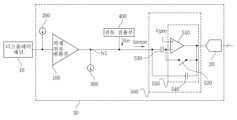
도 1을 참조하면, 본 발명의 실시예는 픽셀 전류 변환부(100), 전류 소스부(Current Source Part)(200), 전류 싱킹부(Current Sinking Part)(300), 전류 검출부(Current Detecting Part)(400) 및 검출 신호 출력부(500)를 포함한다.Referring to Figure 1, the embodiment of the present invention includes a pixel
디스플레이 장치의 드라이버(30)는 디스플레이 패널(10)에 픽셀 데이터(Pixel Data)에 대응하는 구동 신호(도시되지 않음)를 제공하며 디스플레이 패널(10)의 픽셀 전류(Iin)를 수신하도록 구성된다.The
상기한 도 1의 실시예는 외부 보상 방법을 구현하기 위한 드라이버(30)의 구성을 예시한 것이다. 상기한 픽셀 전류 변환부(100), 전류 소스부(200), 전류 싱킹부(300), 전류 검출부(400) 및 검출 신호 출력부(500)는 드라이버(30)에 포함될 수 있다.The embodiment of FIG. 1 described above illustrates the configuration of the
도 1의 드라이버(30)의 검출 신호 출력부(500)의 검출 신호가 아날로그 디지털 컨버터(20)를 통하여 어플리케이션 프로세서(도시되지 않음)에 제공되며, 어플리케이션 프로세서는 보상 신호에 대응하는 보상값을 구하여 드라이버(30)에서 출력되는 구동 신호에 보상값이 반영될 수 있도록 제어한다.The detection signal of the detection
디스플레이 패널(10)의 각 픽셀은 픽셀 특성 즉 구동 트랜지스터(도시되지 않음)의 특성을 표현하는 데이터 전류를 출력한다. 이러한 데이터 전류가 전달되는 센싱 라인은 드라이버(30)의 입력단에 연결된다. 도 1에서 픽셀 전류 변환부(100)의 입력단이 드라이버(30)의 입력단으로 이해될 수 있다. 즉, 픽셀 전류 변환부(100)는 디스플레이 패널(10)의 픽셀 전류(Iin)를 수신하도록 구성된다.Each pixel of the
픽셀의 구동 트랜지스터의 전기적 특성 정보를 센싱한 경우, 픽셀 전류 변환부(100)에 입력되는 픽셀 전류(Iin)에는 데이터 전류(Idata)와 누설 전류(Ileak)가 포함될 수 있다. 이와 달리, 픽셀의 구동 트랜지스터의 전기적 특성 정보를 센싱하지 않은 경우, 픽셀 전류(Iin)에는 누설 전류(Ileak)만 포함될 수 있다.When electrical characteristic information of a driving transistor of a pixel is sensed, the pixel current (Iin) input to the pixel
데이터 전류(Idata)는 구동 트랜지스터의 전기적 특성을 표현하기 위한 소스-드레인 간 전류로 예시될 수 있다. 그리고, 데이터 전류(Idata)의 제공 여부는 픽셀 내부의 스위칭 트랜지스터(도시되지 않음)에 의해 제어될 수 있다. 즉, 스위칭 트랜지스터가 턴 온 되면 데이터 전류(Idata)가 발생하고, 스위칭 트랜지스터가 턴 오프 되면 데이터 전류(Idata)가 발생하지 않는다.The data current (Idata) may be exemplified as a source-drain current to express the electrical characteristics of the driving transistor. Additionally, whether or not the data current Idata is provided can be controlled by a switching transistor (not shown) inside the pixel. That is, when the switching transistor is turned on, the data current (Idata) is generated, and when the switching transistor is turned off, the data current (Idata) is not generated.
누설 전류(Ileak)는 스위칭 트랜지스터의 동작과 무관하게 발생한다. 픽셀 전류 변환부(100)의 입력단은 디스플레이 패널(10) 내의 다수의 픽셀의 센싱 라인에 동시에 연결된다. 그러므로, 센싱이 선택되지 않은 픽셀에서 발생하는 누설 전류(Ileak)나 다양한 원인에 의해 발생하는 노이즈에 의한 누설 전류(Ileak)가 픽셀 전류 변환부(100)의 입력단에 입력될 수 있다. 누설 전류(Ileak)는 크기와 극성을 예측하기 힘들다.Leakage current (Ileak) occurs regardless of the operation of the switching transistor. The input terminal of the pixel
픽셀 전류 변환부(100)는 상기와 같이 입력되는 디스플레이 패널(10)의 픽셀 전류(Iin)를 변환한다. 이를 위하여 픽셀 전류 변환부(100)는 전류 증폭기(Current Amplifier)를 포함하여 구성될 수 있으며, 일종의 버퍼 역할을 수행할 수 있다. 예시적으로 픽셀 전류 변환부(100)는 1:1의 비율로 픽셀 전류(Iin)를 증폭하여 출력할 수 있다. 이 경우, 픽셀 전류 변환부(100)는 입력된 픽셀 전류(Iin)와 동일한 크기의 전류를 출력한다. 그러므로, 픽셀 전류 변환부(100)에서 출력되는 전류도 픽셀 전류(Iin)로 통칭한다.The pixel
픽셀 전류 변환부(100)는 입력측과 출력측의 전압 환경을 분리하는 기능을 수행한다.The pixel
디스플레이 패널(10)의 픽셀은 제1 전압 환경에서 구동하며, 픽셀 전류 변환부(100)가 구동되는 제1 전압 환경은 예시적으로 10V 이상의 고전압 환경을 의미할 수 있으며, 픽셀 전류 변환부(100)는 이러한 고전압 환경에서 픽셀 전류(Iin)를 변환하도록 구성된다. 픽셀 전류 변환부(100)의 출력측에 구성되는 전류 소스부(200), 전류 싱킹부(300), 전류 검출부(400) 및 검출 신호 출력부(500)는 픽셀 전류 변환부(100)에서 출력되는 픽셀 전류(Iin)를 고려하여 제2 전압 환경에서 구동하는 트랜지스터를 이용하여 구성될 수 있다. 여기에서, 제2 전압 환경은 수 V 범위의 저전압 환경으로 이해될 수 있다. 이와 같이, 픽셀 전류 변환부(100)는 입력측의 고전압 환경을 출력측과 분리한다.The pixels of the
따라서, 본 발명의 실시예는 전류 소스부(200), 전류 싱킹부(300), 전류 검출부(400) 및 검출 신호 출력부(500)가 저전압 환경에서 동작되는 작은 채널 면적을 갖는 트랜지스터를 이용하여 구성될 수 있다. 따라서 본 발명의 실시예는 작은 면적으로 구현될 수 있고 경제성을 가질 수 있다.Therefore, in an embodiment of the present invention, the
그리고, 본 발명의 실시예는 픽셀 전류 변환부(100)에 의하여 넓은 범위에 분포되는 픽셀 전류의 레벨에 대응한 센싱을 수행할 수 있다.Additionally, an embodiment of the present invention can perform sensing corresponding to the level of pixel current distributed over a wide range by the pixel
한편, 픽셀 전류 변환부(100)의 출력단에 노드(N1)가 형성되며, 전류 소스부(200), 전류 싱킹부(300) 및 전류 검출부(400)가 노드(N1)에 연결된다.Meanwhile, a node N1 is formed at the output terminal of the pixel
이 중, 전류 소스부(200)는 미리 정해진 양의 전류를 노드(N1)에 제공하며, 전류 싱킹부(300)는 노드(N1)에 대하여 미리 정해진 양의 전류를 싱크한다. 전류 소스부(200)에서 노드(N1)로 제공되는 전류는 소스 전류(Ib1)라 하고, 전류 싱킹부(300)에 의하여 노드(N1)에서 싱크되는 전류는 싱킹 전류(Ib2)라 한다. 본 발명의 실시예는 소스 전류(Ib1)를 싱킹 전류(Ib2)보다 많거나 반대로 소스 전류(Ib1)가 싱킹 전류(Ib2)보다 적도록 설정될 수 있다.Among these, the
이 때, 미리 정해진 양의 소스 전류(Ib1)나 싱킹 전류(Ib2)는 센싱 과정에서 일정한 크기를 가질 수 있으나, 그 크기는 사용자가 원하는 센싱 회로의 환경이나 사용자의 의도에 따라 다르게 설정되어 일정한 크기를 가질 수 있다.At this time, a predetermined amount of source current (Ib1) or sinking current (Ib2) may have a certain size during the sensing process, but the size is set differently depending on the environment of the sensing circuit desired by the user or the user's intention, so it has a constant size. You can have
상기한 구조에 의하여, 누설 전류(Ileak)만 포함된 픽셀 전류(Iin)가 입력되는 경우, 전류 검출부(400)는 누설 전류(Ileak)에 대응하는 검출 전류(Ice)를 노드(N1)로 제공한다.노드(N1)에서 싱킹 전류(Ib2)는 소스 전류(Ib1), 누설 전류(Ileak) 및 검출 전류(Ice)의 총 합과 같다. 여기에서, 소스 전류(Ib1)와 싱킹 전류(Ib2)는 미리 정해진 전류의 값을 가지므로, 검출 전류(Ice)는 누설 전류(Ileak)에 의해 결정된다.According to the above structure, when the pixel current (Iin) containing only the leakage current (Ileak) is input, the
보다 구체적으로 누설 전류(Ileak)만 픽셀 전류(Iin)에 존재하는 경우를 가정하여 설명한다. 싱킹 전류(Ib2)가 1000μA이고, 소스 전류(Ib1)가 900μA이며, 누설 전류(Ileak)가 90μA인 경우, 검출 전류(Ice)는 10μA이다. 이때, 후술하는 캐패시터(530)가 스위치(520)가 턴온된 상태에서 검출 전류(Ice)를 샘플링한다. 즉, 캐패시터(530)는 누설 전류(Ileak)에 해당하는 전압을 샘플링한다.More specifically, the description will be made assuming that only the leakage current (Ileak) exists in the pixel current (Iin). If the sinking current (Ib2) is 1000 μA, the source current (Ib1) is 900 μA, and the leakage current (Ileak) is 90 μA, the detection current (Ice) is 10 μA. At this time, a
즉, 전류 검출부(400)는 누설 전류(Ileak)에 대응하는 검출 전류(Ice)를 노드(N1)로 공급하는 역할을 하며 결과적으로 누설 전류(Ileak)를 검출하는 기능을 갖는다. That is, the
전류 검출부(400)는 누설 전류(Ileak)에 대응하는 검출 전류(Ice)를 제공하기 위하여 다이오드, 저항, 샘플/홀드 회로 등의 수동 소자(Passive Element)를 포함하여 구성될 수 있다. 검출 신호 출력부(500)는 누설 전류(Ileak)를 샘플 및 홀드하며, 검출 신호 출력부(500)는 누설 전류(Ileak)가 제거된 픽셀 전류(Iin), 즉 데이터 전류(Idata)를 검출하여 아날로그 디지털 컨버터(20)에 출력하도록 구성된다.The
소스 전류(Ib1)와 싱킹 전류(Ib2)의 전류량이 같은 경우, 누설 전류(Ileak)의 크기나 방향에 따라 검출 전류(Ice)의 크기와 방향이 달라질 수 있다. 그러나, 전류 검출부(400)를 구성하는 소자에 따라서 전류 검출부(400)에서 제공되는 검출 전류(Ice)가 일정한 방향으로 흐를 필요성이 있다. 따라서 전류 소스부(200)가 제공하는 소스 전류(Ib1)와 전류 싱킹부(300)가 싱크하는 싱킹 전류(Ib2)의 전류량을 서로 다르게 설정함으로써, 누설 전류(Ileak)의 크기나 방향에 관계 없이 노드(N1)로 제공되는 검출 전류(Ice)의 방향을 일정하게 할 수 있다.When the source current (Ib1) and the sinking current (Ib2) have the same amount of current, the size and direction of the detection current (Ice) may vary depending on the size or direction of the leakage current (Ileak). However, depending on the elements constituting the
검출 신호 출력부(500)는 캐패시터(530)와 적분 회로(550)를 포함한다.The detection
캐패시터(530)는 제1 전극이 노드(N2)를 통하여 노드(N1)와 전류 검출부(400)에 병렬로 연결되도록 구성되며 노드(N2)를 통하여 노드(N1)로 흐르는 검출 전류(Ice)에 의한 오프셋 전압을 형성한다. 이때 오프셋 전압은 누설 전류(Ileak)를 샘플 및 홀드한 전압에 해당한다.The
검출 신호 출력부(500)의 적분 회로(550)는 증폭기(510), 스위치(520), 캐패시터(540)를 포함하여 구성된다.The
여기에서, 증폭기(510)는 포지티브단(+)과 네가티브단(-)을 포함하는 두 개의 입력단을 가지며, 포지티브단(+)에 공통 모드 전압(Vpre)이 인가되고 네가티브단(-)에 캐패시터(530)의 제2 전극이 연결된다. 그리고, 증폭기(510)는 출력단과 네가티브단(-) 사이에 스위치(520)가 연결되고 출력단과 캐패시터의 제1 전극 사이에 데이터 전류(Idata)의 샘플링을 위한 캐패시터(540)가 연결된다.Here, the
상기한 구성에서, 스위치(520)는 누설 전류(Ileak)를 샘플링하는 제1 구간(PS)에 대응하여 턴온되고, 누설 전류(Ileak)를 홀딩하는 제2 구간(PH)에 대응하여 턴오프된다. 여기에서, 제1 구간(PS)은 픽셀의 구동 트랜지스터의 전기적 특성 정보를 센싱하지 않아서 픽셀 전류(Iin)에 누설 전류(Ileak)만 포함되는 구간에 대응하도록 설정될 수 있고, 제2 구간(PH)은 픽셀의 구동 트랜지스터의 전기적 특성 정보를 센싱하여서 픽셀 전류(Iin)에 데이터 전류(Idata)와 누설 전류(Ileak)가 포함되는 구간에 대응하도록 설정될 수 있다.In the above configuration, the
상기한 바와 같이 구성되는 본 발명의 도 1의 실시예의 동작에 대하여 도 2를 참조하여 설명한다.The operation of the embodiment of FIG. 1 of the present invention configured as described above will be described with reference to FIG. 2.
먼저, 제1 구간(PS)에 대한 실시예의 동작을 설명한다.First, the operation of the embodiment for the first section PS will be described.
제1 구간(PS)에서, 픽셀 전류(Iin)에는 누설 전류(Ileak)만 포함된다. 그러므로, 누설 전류(Ileak)를 검출한 검출 전류(Ice)가 형성되고, 캐패시터(530)는 누설 전류(Ileak)에 대응한 검출 전류(Ice)에 의한 오프셋 전압을 샘플링한다. 이때, 적분 회로(550)의 증폭기(510)의 네가티브단(-)으로 입력되는 전류(Isense)는 “0”이다.In the first section PS, the pixel current Iin includes only the leakage current Ileak. Therefore, a detection current (Ice) that detects the leakage current (Ileak) is formed, and the
상기와 같이 제1 구간(PS) 동안, 누설 전류(ILeak)에 대응한 오프셋 전압이 캐패시터(530)에 샘플링된다.As described above, during the first period PS, an offset voltage corresponding to the leakage current ILeak is sampled in the
제1 구간(PS)에 이어서 제2 구간(PH) 구간에 대한 실시예의 동작이 수행된다.The operation of the embodiment is performed for the second section (PH) following the first section (PS).
제2 구간(PH)에서, 픽셀 전류(Iin)에는 데이터 전류(Idata)와 누설 전류(Ileak)가 포함된다. 이때, 캐패시터(530)는 샘플링된 오프셋 전압을 홀딩한다. 즉, 캐패시터(530)에 의하여 오프셋 전압이 증폭기(510)의 네가티브단(-)에 형성되며, 픽셀 전류(Iin)의 누설 전류(Ileak)는 오프셋 전압에 의해 제거된다. 그러므로, 픽셀 전류(Iin) 중 누설 전류(Ileak)는 제거되고 나머지 데이터 전류(Idata)가 적분 회로(550)의 증폭기(510)의 네가티브단(-)으로 입력된다. 즉, 적분 회로(550)의 증폭기(510)의 네가티브단(-)으로 입력되는 전류(Isense)는 데이터 전류(Idata)이다.In the second section PH, the pixel current Iin includes the data current Idata and the leakage current Ileak. At this time, the
상술한 바와 같이, 검출 신호 출력부(500)는 누설 전류(Ileak)만 포함된 픽셀 전류(Iin)가 입력되는 제1 구간(PS)에 누설 전류(Ileak)에 대응한 오프셋 전압을 형성한다. 그리고, 검출 신호 출력부(500)는 누설 전류(Ileak)와 데이터 전류(Idata)가 포함되는 픽셀 전류(Iin)가 입력되는 제2 구간(PH)에 미리 형성된 오프셋 전압을 홀딩하며, 해당 오프셋 전압으로 누설 전류(Ileak)를 제거하고, 데이터 전류(Idata)만 갖는 픽셀 전류(Iin)에 대한 샘플링 및 적분을 수행하여 검출 신호를 출력한다.As described above, the detection
그러므로, 본 발명의 실시예는 누설 전류가 제거된 픽셀 전류(Iin)로부터 데이터 전류(Idata)를 높은 분해능으로 센싱할 수 있게 한다.Therefore, embodiments of the present invention enable sensing of the data current (Idata) with high resolution from the pixel current (Iin) from which the leakage current has been removed.
한편, 본 발명의 실시예는 검출 신호 출력부(500)에 적분을 위하여 구성되는 증폭기(510)에 제공되는 공통 모드 전압(Vpre)이 선택된 레벨을 갖도록 구성될 수 있다.Meanwhile, an embodiment of the present invention may be configured so that the common mode voltage (Vpre) provided to the
즉, 공통 모드 전압(Vpre)은 증폭기(510)의 네가티브단(-)으로 입력되는 전류(Isense)의 상태를 고려하여 미리 설정된 복수의 레벨 중 하나를 갖도록 선택될 수 있고, 여기서 증폭기(510)의 네가티브단(-)으로 입력되는 전류(Isense)의 상태란 증폭기(510)의 네가티브단(-)으로 입력되는 전류(Isense)의 크기나 방향을 포함하는 의미로 해석될 수 있다.That is, the common mode voltage (Vpre) may be selected to have one of a plurality of levels preset in consideration of the state of the current (Isense) input to the negative terminal (-) of the
예시적으로,디스플레이 패널(10)의 OLED에 흐르는 전류를 센싱하는 경우, 픽셀 전류(Iin)의 흐름이 드라이버(30)에서 디스플레이 패널(10)로 흐르는 것으로 변화될 수 있다. 보다 구체적으로, OLED에 흐르는 전류를 센싱하기 위해 특정 전압을 OLED의 애노드에 인가하는 경우, 드라이버(30)의 입력단이 디스플레이 패널(10)보다 고전위를 갖게 되며, 픽셀 전류(Iin)의 흐름이 드라이버(30)에서 디스플레이 패널(10)로 형성될 수 있다.By way of example,When sensing the current flowing through the OLED of the
이 경우, 검출 신호 출력부(500)의 적분 회로(550)에 포함되는 증폭기(510)의 네가티브단(-)에 데이터 전류(Idata)에 대응한 입력 전압이 높게 형성될 수 있다. 이때, 데이터 전류(Idata)에 의한 샘플링이 캐패시터(540)에 정상적으로 이루어짐에도 불구하고, 픽셀 전류(Iin)에 의한 높은 레벨의 입력 전압은 고정된 레벨의 공통 모드 전압(Vpre)에 의하여 클램핑된다.In this case, the input voltage corresponding to the data current (Idata) may be formed high at the negative terminal (-) of the
결국, 드라이버(30)의 검출 신호 출력부(500)는 공통 모드 전압(Vpre) 이상으로 픽셀 전류(Iin)를 센싱하는 범위가 제한될 수 있다.As a result, the detection
상기와 같이 픽셀 전류(Iin)를 센싱하는 범위가 제한되는 문제를 해결하기 위하여 본 발명의 실시예는 가변적인 공통 모드 전압(Vpre)을 제공하도록 구성될 수 있다.In order to solve the problem that the range for sensing the pixel current (Iin) is limited as described above, an embodiment of the present invention may be configured to provide a variable common mode voltage (Vpre).
따라서, 본 발명은 픽셀 전류(Iin)의 흐름이 드라이버(30)에서 디스플레이 패널(10)로 변화되는 경우 낮은 레벨의 공통 모드 전압(Vpre)을 선택하여 적분을 수행할 수 있으며, 그에 따라 픽셀 전류(Iin)를 센싱하는 범위가 제한되는 것을 해소할 수 있다.Therefore, in the present invention, when the flow of the pixel current (Iin) changes from the
한편, 본 발명의 실시예는 도 3 내지 도 5와 같이 변형될 수 있다.Meanwhile, the embodiment of the present invention may be modified as shown in FIGS. 3 to 5.
도 3 내지 도 5에서 도 1과 동일한 구성 및 그 기능에 대한 중복된 설명은 생략한다. 도 3 내지 도 5를 참조하면, 전류 소스부(200) 및 전류 싱킹부(300)의 배치 방법이 도 1과 달리 변경된 것을 알 수 있다.In FIGS. 3 to 5 , duplicate descriptions of the same configuration and function as in FIG. 1 will be omitted. Referring to FIGS. 3 to 5 , it can be seen that the arrangement method of the
전류 소스부(200)와 전류 싱킹부(300)는 센싱 회로의 설계 방법이나 환경에 따라 그 배치 방법이 변경될 수 있다.The arrangement method of the
도 3의 실시예는 전류 소스부(200)가 픽셀 전류 변환부(100)의 출력단에 연결되어 소스 전류를 제공하고, 전류 싱킹부(300)가 픽셀 전류 변환부(100)의 입력단에 연결되어 싱킹 전류가 싱크되는 것을 나타낸다.In the embodiment of FIG. 3, the
도 4의 실시예는 전류 소스부(200)가 픽셀 전류 변환부(100)의 입력단에 연결되어 소스 전류를 제공하고, 전류 싱킹부(300)가 픽셀 전류 변환부(100)의 출력단에 연결되어 싱킹 전류가 싱크되는 것을 나타낸다.In the embodiment of FIG. 4, the
도 5의 실시예는 전류 소스부(200) 및 전류 싱킹부(300)가 픽셀 전류 변환부(100)의 입력단에 연결되어 소스 전류가 제공되고, 싱킹 전류가 싱크되는 것을 나타낸다.The embodiment of FIG. 5 shows that the
도 3 내지 도 4의 실시예는 모두 도 1의 실시예와 마찬가지로 픽셀 전류 변환부(100)의 출력단에 연결된 노드(N1)를 기준으로 누설 전류(Ileak)에 대응하는 검출 전류(Ice)가 생성된다. 따라서 검출 전류(Ice)의 생성 및 전류 검출부(400)에 대해 도 1의 실시예와 중복되는 설명의 기재는 생략한다.In the embodiments of FIGS. 3 and 4 , like the embodiment of FIG. 1 , the detection current (Ice) corresponding to the leakage current (Ileak) is generated based on the node (N1) connected to the output terminal of the pixel
도 5의 실시예에서 노드(N1)는 픽셀 전류 변환부(100)의 입력단에 연결되나, 앞선 도 1, 도 3, 도 4의 실시예와 같이 누설 전류(Ileak), 소스 전류 및 싱킹 전류에 의해서 검출 전류(Ice)가 결정되므로 앞선 실시예와 같은 기능 및 효과를 가진다.In the embodiment of FIG. 5, the node N1 is connected to the input terminal of the pixel
상기한 구성을 통하여 본 발명은 외부 보상 방법으로 픽셀 특성을 판단하기 위하여 픽셀에 구성된 구동 트랜지스터의 전기적 특성 편차를 센싱하며, 픽셀 전류로부터 누설 전류를 제외한 데이터 전류만을 높은 분해능으로 센싱할 수 있도록 함으로써 누설 전류에 둔감해질 수 있다.Through the above configuration, the present invention senses the deviation of the electrical characteristics of the driving transistor configured in the pixel to determine the pixel characteristics using an external compensation method, and detects only the data current excluding the leakage current from the pixel current with high resolution, thereby reducing leakage. You may become insensitive to electric current.
또한, 본 발명에 따른 디스플레이 장치의 센싱 회로는 픽셀 특성을 판단하기 위하여 픽셀에 구성된 구동 트랜지스터의 전기적 특성 편차를 센싱한 픽셀 전류를 센싱하고, 넓은 범위에 분포되는 픽셀 전류의 레벨에 대응한 센싱을 수행할 수 있다.In addition, the sensing circuit of the display device according to the present invention senses the pixel current by sensing the difference in the electrical characteristics of the driving transistor configured in the pixel to determine the pixel characteristics, and performs sensing corresponding to the level of the pixel current distributed over a wide range. It can be done.
또한, 픽셀 특성을 판단하기 위하여 픽셀에 구성된 구동 트랜지스터의 전기적 특성 편차를 센싱한 픽셀 전류를 센싱하고, 넓은 범위에 분포되는 픽셀 전류의 레벨에 대응한 센싱을 수행함으로써, 작은 면적으로 구현할 수 있고 경제성을 보장하는 효과가 있다.In addition, in order to determine pixel characteristics, the pixel current is sensed by sensing the deviation in the electrical characteristics of the driving transistor configured in the pixel, and by performing sensing corresponding to the level of the pixel current distributed over a wide range, it can be implemented in a small area and is economical. It has the effect of guaranteeing.
또한, 디스플레이 패널에 인가되는 전압에 따라 픽셀 전류의 흐르는 방향이 변화하는 경우에도 센싱 범위가 제한되지 않도록 센싱에 이용되는 공통 모드 전압을 선택할 수 있는 환경을 제공할 수 있다.Additionally, even when the direction of pixel current changes depending on the voltage applied to the display panel, an environment can be provided in which the common mode voltage used for sensing can be selected so that the sensing range is not limited.
Claims (13)
Translated fromKorean상기 픽셀 전류에 대하여 미리 정해진 양의 소스 전류를 제공하는 전류 소스부;
상기 픽셀 전류에 대하여 미리 정해진 양의 싱킹 전류를 싱크하는 전류 싱킹부;
상기 누설 전류에 대응하는 검출 전류를 제공하는 전류 검출부; 및
상기 검출 전류를 이용하여 상기 누설 전류에 대응하는 오프셋 전압을 샘플링하고, 상기 픽셀 전류에 디스플레이 패널의 픽셀 특성을 센싱한 데이터 전류가 포함되는 경우 상기 오프셋 전압에 의하여 상기 픽셀 전류에서 상기 누설 전류를 제거하며, 상기 데이터 전류에 대응하는 검출 신호를 출력하는 검출 신호 출력부;를 포함하며,
상기 전류 검출부는 상기 싱킹 전류가 상기 소스 전류와 상기 누설 전류 및 상기 검출 전류를 합한 값과 동일하도록 상기 검출 전류를 제공하는 디스플레이 장치의 센싱 회로.a pixel current conversion unit that receives a pixel current including at least leakage current, converts the pixel current to a preset current ratio, and outputs the converted pixel current;
a current source unit providing a predetermined amount of source current relative to the pixel current;
a current sinking unit that sinks a predetermined amount of sinking current relative to the pixel current;
a current detection unit providing a detection current corresponding to the leakage current; and
Using the detection current, an offset voltage corresponding to the leakage current is sampled, and when the pixel current includes a data current that senses pixel characteristics of the display panel, the leakage current is removed from the pixel current by the offset voltage. and a detection signal output unit that outputs a detection signal corresponding to the data current,
The current detection unit provides the detection current such that the sinking current is equal to the sum of the source current, the leakage current, and the detection current.
전류 대 전류 변환을 수행하는 디스플레이 장치의 센싱 회로.The method of claim 1, wherein the pixel current converter
A sensing circuit in a display device that performs current-to-current conversion.
증폭기를 포함하는 버퍼로 구성되는 디스플레이 장치의 센싱 회로.The method of claim 1, wherein the pixel current converter
A sensing circuit in a display device consisting of a buffer containing an amplifier.
제1 전압 환경에서 구동하도록 상기 픽셀 전류 변환부가 구성되고, 상기 픽셀 전류 변환부에서 출력되는 픽셀 전류에 대응하여 상기 제1 전압 환경보다 낮은 전압 범위를 갖는 제2 전압 환경에서 구동하도록 상기 전류 소스부, 상기 전류 싱킹부, 상기 전류 검출부가 구성되는 디스플레이 장치의 센싱 회로.According to claim 1,
The pixel current converter is configured to be driven in a first voltage environment, and the current source unit is configured to be driven in a second voltage environment having a voltage range lower than the first voltage environment in response to the pixel current output from the pixel current converter. , A sensing circuit of a display device comprising the current sinking unit and the current detecting unit.
상기 싱킹 전류와 상기 소스 전류의 전류량의 차는 상기 누설 전류와 상기 검출 전류의 합과 같도록 설정되는 디스플레이 장치의 센싱 회로.According to claim 1,
A sensing circuit of a display device wherein the difference between the sinking current and the source current is set to be equal to the sum of the leakage current and the detection current.
상기 누설 전류에 대응하여 상기 검출 전류를 제공하기 위하여 수동 소자를 포함하는 디스플레이 장치의 센싱 회로.The method of claim 1, wherein the current detection unit
A sensing circuit of a display device including a passive element to provide the detection current in response to the leakage current.
상기 검출 전류를 이용하여 상기 누설 전류에 대응하는 상기 오프셋 전압을 샘플 및 홀드하는 제1 캐패시터; 및
상기 픽셀 전류에 상기 데이터 전류가 포함되는 경우 상기 오프셋 전압에 의하여 상기 픽셀 전류에서 상기 누설 전류를 제거하며, 상기 데이터 전류에 대응하는 상기 검출 신호를 출력하는 적분 회로; 를 포함하는 디스플레이 장치의 센싱 회로.The method of claim 1, wherein the detection signal output unit,
a first capacitor that samples and holds the offset voltage corresponding to the leakage current using the detection current; and
an integrator that removes the leakage current from the pixel current by the offset voltage when the pixel current includes the data current and outputs the detection signal corresponding to the data current; A sensing circuit of a display device including a.
상기 데이터 전류와 공통 모드 전압을 비교하여 상기 검출 신호를 생성하며, 상기 공통 모드 전압은 상기 누설 전류의 상태를 고려하여 미리 설정된 복수의 레벨 중 하나를 갖도록 선택되는 디스플레이 장치의 센싱 회로.The method of claim 8, wherein the integrating circuit is
The detection signal is generated by comparing the data current and the common mode voltage, and the common mode voltage is selected to have one of a plurality of preset levels in consideration of the state of the leakage current.
공통 모드 전압이 인가되는 제1 입력단과 상기 제1 캐패시터에 의해 상기 오프셋 전압이 샘플 및 홀드되며 상기 데이터 전류에 대응하는 전압이 인가되는 제2 입력단을 포함하는 증폭기;
상기 증폭기의 상기 제2 입력단과 출력단 사이에 연결되는 스위치; 및
상기 데이터 전류의 샘플링을 수행하며 상기 증폭기의 상기 제2 입력단과 상기 출력단 사이에 구성되는 제2 캐패시터;를 포함하며,
제1 구간에 대응하여 상기 스위치가 턴온되어 상기 제1 캐패시터에 상기 누설 전류가 샘플링되며,
제2 구간에 대응하여 상기 오프셋 전압에 의하여 상기 픽셀 전류에서 상기 누설 전류가 제거하며, 상기 스위치가 턴오프되어 상기 데이터 전류에 대한 샘플링과 적분을 수행하여 상기 검출 신호를 출력하는 디스플레이 장치의 센싱 회로.The method of claim 8, wherein the integrating circuit is:
An amplifier including a first input terminal to which a common mode voltage is applied and a second input terminal to which the offset voltage is sampled and held by the first capacitor and a voltage corresponding to the data current is applied;
a switch connected between the second input terminal and the output terminal of the amplifier; and
A second capacitor performs sampling of the data current and is configured between the second input terminal and the output terminal of the amplifier,
In response to the first section, the switch is turned on to sample the leakage current in the first capacitor,
In response to a second section, the leakage current is removed from the pixel current by the offset voltage, and the switch is turned off to perform sampling and integration of the data current and output the detection signal. .
상기 제1 구간은 상기 픽셀 전류가 누설 전류만 포함하는 구간에 대응하여 설정되고
상기 제2 구간은 상기 픽셀 전류가 상기 데이터 전류와 상기 누설 전류를 포함하는 구간에 대응하여 설정되는 디스플레이 장치의 센싱 회로.According to claim 10,
The first section is set to correspond to a section in which the pixel current includes only leakage current, and
The second section is set to correspond to a section in which the pixel current includes the data current and the leakage current.
상기 전류 소스부는 상기 픽셀 전류 변환부의 입력단과 출력단 중 어느 하나에 연결되는 디스플레이 장치의 센싱 회로.According to claim 1,
A sensing circuit of a display device in which the current source unit is connected to one of an input terminal and an output terminal of the pixel current converter.
상기 전류 싱킹부는 상기 픽셀 전류 변환부의 입력단과 출력단 중 어느 하나에 연결되는 디스플레이 장치의 센싱 회로.According to claim 1,
A sensing circuit of a display device in which the current sinking unit is connected to either an input terminal or an output terminal of the pixel current converting unit.
Priority Applications (3)
| Application Number | Priority Date | Filing Date | Title |
|---|---|---|---|
| KR1020160108091AKR102644681B1 (en) | 2016-08-25 | 2016-08-25 | Sensing circuit of display apparatus |
| US15/674,925US10657902B2 (en) | 2016-08-25 | 2017-08-11 | Sensing circuit of display device for sensing pixel current |
| CN201710734497.3ACN107784973B (en) | 2016-08-25 | 2017-08-24 | Sensing circuit of display device |
Applications Claiming Priority (1)
| Application Number | Priority Date | Filing Date | Title |
|---|---|---|---|
| KR1020160108091AKR102644681B1 (en) | 2016-08-25 | 2016-08-25 | Sensing circuit of display apparatus |
Publications (2)
| Publication Number | Publication Date |
|---|---|
| KR20180023188A KR20180023188A (en) | 2018-03-07 |
| KR102644681B1true KR102644681B1 (en) | 2024-03-07 |
Family
ID=61243151
Family Applications (1)
| Application Number | Title | Priority Date | Filing Date |
|---|---|---|---|
| KR1020160108091AActiveKR102644681B1 (en) | 2016-08-25 | 2016-08-25 | Sensing circuit of display apparatus |
Country Status (3)
| Country | Link |
|---|---|
| US (1) | US10657902B2 (en) |
| KR (1) | KR102644681B1 (en) |
| CN (1) | CN107784973B (en) |
Families Citing this family (13)
| Publication number | Priority date | Publication date | Assignee | Title |
|---|---|---|---|---|
| KR102578706B1 (en)* | 2018-12-21 | 2023-09-15 | 엘지디스플레이 주식회사 | Sensing Circuit, Data Driver Integrated Circuit, Display Device And Driving Method Thereof |
| CN109493806B (en)* | 2019-01-28 | 2019-08-23 | 苹果公司 | Electronic device including a display with oxide transistor threshold voltage compensation |
| CN112102771B (en)* | 2019-06-17 | 2022-02-25 | 京东方科技集团股份有限公司 | Pixel circuit, driving method and display device |
| KR102659207B1 (en)* | 2019-09-26 | 2024-04-18 | 엘지디스플레이 주식회사 | Sensing circuit and display device including the same |
| KR102634653B1 (en) | 2019-09-30 | 2024-02-08 | 주식회사 엘엑스세미콘 | Pixel sensing circuit and source driver integrated circuit |
| KR102751668B1 (en)* | 2019-10-29 | 2025-01-10 | 주식회사 엘엑스세미콘 | Display driving apparatus |
| CN110867151B (en)* | 2019-11-29 | 2022-07-05 | 合肥维信诺科技有限公司 | Display mother board, display panel and electronic leakage testing method |
| CN111899691B (en)* | 2020-06-29 | 2021-11-05 | 京东方科技集团股份有限公司 | External compensation circuit, array substrate and detection method |
| KR102812019B1 (en)* | 2020-12-17 | 2025-05-23 | 엘지디스플레이 주식회사 | Electroluminescence Display Device |
| EP4181112A4 (en) | 2020-12-23 | 2023-09-06 | BOE Technology Group Co., Ltd. | Display apparatus, display panel and driving method therefor, and detection method for pixel circuit |
| CN112863440A (en)* | 2021-01-26 | 2021-05-28 | 京东方科技集团股份有限公司 | Pixel compensation circuit and driving method thereof, and display device |
| US11955057B2 (en) | 2021-03-30 | 2024-04-09 | Samsung Electronics Co., Ltd. | Display apparatus |
| CN113176517B (en)* | 2021-04-15 | 2024-12-17 | 武汉励行科技有限公司 | Micro-current compensation method and system for precise control |
Citations (3)
| Publication number | Priority date | Publication date | Assignee | Title |
|---|---|---|---|---|
| US20110007067A1 (en) | 2009-07-10 | 2011-01-13 | Do-Hyung Ryu | Organic light emitting display and driving method thereof |
| US20140198092A1 (en)* | 2013-01-14 | 2014-07-17 | Ignis Innovation Inc. | Driving scheme for emissive displays providing compensation for driving transistor variations |
| US20150029171A1 (en) | 2013-07-24 | 2015-01-29 | Samsung Display Co., Ltd. | Organic light emitting display device and driving method thereof |
Family Cites Families (13)
| Publication number | Priority date | Publication date | Assignee | Title |
|---|---|---|---|---|
| SG119186A1 (en)* | 2002-05-17 | 2006-02-28 | Semiconductor Energy Lab | Display apparatus and driving method thereof |
| TWI402790B (en)* | 2004-12-15 | 2013-07-21 | Ignis Innovation Inc | Method and system for programming, calibrating and driving a light-emitting element display |
| US7973759B2 (en)* | 2006-07-06 | 2011-07-05 | Industrial Technology Research Institute | System and method for driving light emitters of backlight module using current mixing |
| JP2011029306A (en)* | 2009-07-23 | 2011-02-10 | Sanyo Electric Co Ltd | Light emitting element drive circuit |
| KR101201722B1 (en)* | 2010-02-23 | 2012-11-15 | 삼성디스플레이 주식회사 | Organic light emitting display and driving method thereof |
| KR101170241B1 (en)* | 2010-06-03 | 2012-07-31 | 하이디스 테크놀로지 주식회사 | Driving circuit for electric paper display and display device |
| KR101985435B1 (en)* | 2012-11-30 | 2019-06-05 | 삼성디스플레이 주식회사 | Pixel array and organic light emitting display including the same |
| CN103219047B (en)* | 2013-04-03 | 2015-09-09 | 京东方科技集团股份有限公司 | TFT threshold voltage compensation circuit and method, shift register and display device |
| KR102054368B1 (en)* | 2013-09-09 | 2019-12-11 | 삼성디스플레이 주식회사 | Display device and driving method therof |
| KR102058577B1 (en) | 2013-09-13 | 2019-12-24 | 삼성디스플레이 주식회사 | Display device and driving method therof |
| CN104916244A (en)* | 2014-03-10 | 2015-09-16 | 硅工厂股份有限公司 | Source driver |
| KR101529005B1 (en) | 2014-06-27 | 2015-06-16 | 엘지디스플레이 주식회사 | Organic Light Emitting Display For Sensing Electrical Characteristics Of Driving Element |
| DE102015218248A1 (en)* | 2014-09-23 | 2016-03-24 | Ignis Innovation Inc. | Clean common unwanted signals from pixel measurements in emission displays |
- 2016
- 2016-08-25KRKR1020160108091Apatent/KR102644681B1/enactiveActive
- 2017
- 2017-08-11USUS15/674,925patent/US10657902B2/enactiveActive
- 2017-08-24CNCN201710734497.3Apatent/CN107784973B/enactiveActive
Patent Citations (3)
| Publication number | Priority date | Publication date | Assignee | Title |
|---|---|---|---|---|
| US20110007067A1 (en) | 2009-07-10 | 2011-01-13 | Do-Hyung Ryu | Organic light emitting display and driving method thereof |
| US20140198092A1 (en)* | 2013-01-14 | 2014-07-17 | Ignis Innovation Inc. | Driving scheme for emissive displays providing compensation for driving transistor variations |
| US20150029171A1 (en) | 2013-07-24 | 2015-01-29 | Samsung Display Co., Ltd. | Organic light emitting display device and driving method thereof |
Also Published As
| Publication number | Publication date |
|---|---|
| CN107784973B (en) | 2022-03-11 |
| US10657902B2 (en) | 2020-05-19 |
| KR20180023188A (en) | 2018-03-07 |
| CN107784973A (en) | 2018-03-09 |
| US20180061329A1 (en) | 2018-03-01 |
Similar Documents
| Publication | Publication Date | Title |
|---|---|---|
| KR102644681B1 (en) | Sensing circuit of display apparatus | |
| KR102643806B1 (en) | Organic Light-Emitting Diode driving characteristic detection circuit AND ORGANIC LIGHT-EMMITTING DISPLAY | |
| JP6461774B2 (en) | Detection circuit and organic light emitting display device | |
| US10896643B2 (en) | Current detection method for pixel circuit, display panel and display device | |
| KR102312350B1 (en) | Electroluminescent Display Device And Driving Method Of The Same | |
| US20190378459A1 (en) | Organic Light Emitting Display Device and Driving Method Thereof | |
| KR101529005B1 (en) | Organic Light Emitting Display For Sensing Electrical Characteristics Of Driving Element | |
| KR101560492B1 (en) | Organic Light Emitting Display For Sensing Electrical Characteristics Of Driving Element | |
| KR101597037B1 (en) | Organic Light Emitting Display For Compensating Electrical Characteristics Deviation Of Driving Element | |
| US11030951B2 (en) | Light-emitting display and method of driving the same | |
| KR102453421B1 (en) | Organic light emitting display device and method of driving the same | |
| KR101549343B1 (en) | Organic Light Emitting Display For Sensing Electrical Characteristics Of Driving Element | |
| US20140152642A1 (en) | Error compensator and organic light emitting display device using the same | |
| US11138932B2 (en) | Pixel current detection circuit and method, and display device | |
| KR20180045937A (en) | Organic Light Emitting Display Device | |
| KR102524626B1 (en) | A circuit for sensing a threshold voltage and display device including the same | |
| KR20160030007A (en) | Organic Light Emitting Display For Sensing Electrical Characteristics Of Driving Element | |
| CN114902319B (en) | Display device and method for driving the same | |
| CN112802420A (en) | Display device and method of driving the same | |
| KR20200066940A (en) | Deterioration Sensing Device And Method Of Organic Light Emitting Display | |
| CN111128074A (en) | Display driving device and display apparatus including the same | |
| US11410601B2 (en) | Voltage adjusting method for a display panel and related computer readable medium | |
| JP2014202826A (en) | Light-emitting device | |
| KR102792031B1 (en) | Sensing circuit and display driving device including the same | |
| US11475851B2 (en) | Pixel sensing apparatus and panel driving apparatus |
Legal Events
| Date | Code | Title | Description |
|---|---|---|---|
| PA0109 | Patent application | Patent event code:PA01091R01D Comment text:Patent Application Patent event date:20160825 | |
| PG1501 | Laying open of application | ||
| A201 | Request for examination | ||
| PA0201 | Request for examination | Patent event code:PA02012R01D Patent event date:20210701 Comment text:Request for Examination of Application Patent event code:PA02011R01I Patent event date:20160825 Comment text:Patent Application | |
| E902 | Notification of reason for refusal | ||
| PE0902 | Notice of grounds for rejection | Comment text:Notification of reason for refusal Patent event date:20230531 Patent event code:PE09021S01D | |
| E701 | Decision to grant or registration of patent right | ||
| PE0701 | Decision of registration | Patent event code:PE07011S01D Comment text:Decision to Grant Registration Patent event date:20231204 | |
| GRNT | Written decision to grant | ||
| PR0701 | Registration of establishment | Comment text:Registration of Establishment Patent event date:20240304 Patent event code:PR07011E01D | |
| PR1002 | Payment of registration fee | Payment date:20240305 End annual number:3 Start annual number:1 | |
| PG1601 | Publication of registration |