KR102644598B1 - Semiconductor package - Google Patents
Semiconductor packageDownload PDFInfo
- Publication number
- KR102644598B1 KR102644598B1KR1020190033423AKR20190033423AKR102644598B1KR 102644598 B1KR102644598 B1KR 102644598B1KR 1020190033423 AKR1020190033423 AKR 1020190033423AKR 20190033423 AKR20190033423 AKR 20190033423AKR 102644598 B1KR102644598 B1KR 102644598B1
- Authority
- KR
- South Korea
- Prior art keywords
- interposer
- semiconductor
- package
- semiconductor device
- adhesive
- Prior art date
- Legal status (The legal status is an assumption and is not a legal conclusion. Google has not performed a legal analysis and makes no representation as to the accuracy of the status listed.)
- Active
Links
Images


Classifications
- H—ELECTRICITY
- H01—ELECTRIC ELEMENTS
- H01L—SEMICONDUCTOR DEVICES NOT COVERED BY CLASS H10
- H01L23/00—Details of semiconductor or other solid state devices
- H01L23/48—Arrangements for conducting electric current to or from the solid state body in operation, e.g. leads, terminal arrangements ; Selection of materials therefor
- H01L23/488—Arrangements for conducting electric current to or from the solid state body in operation, e.g. leads, terminal arrangements ; Selection of materials therefor consisting of soldered or bonded constructions
- H01L23/498—Leads, i.e. metallisations or lead-frames on insulating substrates, e.g. chip carriers
- H01L23/49811—Additional leads joined to the metallisation on the insulating substrate, e.g. pins, bumps, wires, flat leads
- H01L23/49816—Spherical bumps on the substrate for external connection, e.g. ball grid arrays [BGA]
- H—ELECTRICITY
- H01—ELECTRIC ELEMENTS
- H01L—SEMICONDUCTOR DEVICES NOT COVERED BY CLASS H10
- H01L23/00—Details of semiconductor or other solid state devices
- H01L23/52—Arrangements for conducting electric current within the device in operation from one component to another, i.e. interconnections, e.g. wires, lead frames
- H01L23/538—Arrangements for conducting electric current within the device in operation from one component to another, i.e. interconnections, e.g. wires, lead frames the interconnection structure between a plurality of semiconductor chips being formed on, or in, insulating substrates
- H01L23/5384—Conductive vias through the substrate with or without pins, e.g. buried coaxial conductors
- H—ELECTRICITY
- H01—ELECTRIC ELEMENTS
- H01L—SEMICONDUCTOR DEVICES NOT COVERED BY CLASS H10
- H01L25/00—Assemblies consisting of a plurality of semiconductor or other solid state devices
- H01L25/03—Assemblies consisting of a plurality of semiconductor or other solid state devices all the devices being of a type provided for in a single subclass of subclasses H10B, H10D, H10F, H10H, H10K or H10N, e.g. assemblies of rectifier diodes
- H01L25/04—Assemblies consisting of a plurality of semiconductor or other solid state devices all the devices being of a type provided for in a single subclass of subclasses H10B, H10D, H10F, H10H, H10K or H10N, e.g. assemblies of rectifier diodes the devices not having separate containers
- H01L25/065—Assemblies consisting of a plurality of semiconductor or other solid state devices all the devices being of a type provided for in a single subclass of subclasses H10B, H10D, H10F, H10H, H10K or H10N, e.g. assemblies of rectifier diodes the devices not having separate containers the devices being of a type provided for in group H10D89/00
- H01L25/0655—Assemblies consisting of a plurality of semiconductor or other solid state devices all the devices being of a type provided for in a single subclass of subclasses H10B, H10D, H10F, H10H, H10K or H10N, e.g. assemblies of rectifier diodes the devices not having separate containers the devices being of a type provided for in group H10D89/00 the devices being arranged next to each other
- H—ELECTRICITY
- H01—ELECTRIC ELEMENTS
- H01L—SEMICONDUCTOR DEVICES NOT COVERED BY CLASS H10
- H01L21/00—Processes or apparatus adapted for the manufacture or treatment of semiconductor or solid state devices or of parts thereof
- H01L21/02—Manufacture or treatment of semiconductor devices or of parts thereof
- H01L21/04—Manufacture or treatment of semiconductor devices or of parts thereof the devices having potential barriers, e.g. a PN junction, depletion layer or carrier concentration layer
- H01L21/48—Manufacture or treatment of parts, e.g. containers, prior to assembly of the devices, using processes not provided for in a single one of the groups H01L21/18 - H01L21/326 or H10D48/04 - H10D48/07
- H01L21/4814—Conductive parts
- H01L21/4846—Leads on or in insulating or insulated substrates, e.g. metallisation
- H01L21/4853—Connection or disconnection of other leads to or from a metallisation, e.g. pins, wires, bumps
- H—ELECTRICITY
- H01—ELECTRIC ELEMENTS
- H01L—SEMICONDUCTOR DEVICES NOT COVERED BY CLASS H10
- H01L21/00—Processes or apparatus adapted for the manufacture or treatment of semiconductor or solid state devices or of parts thereof
- H01L21/02—Manufacture or treatment of semiconductor devices or of parts thereof
- H01L21/04—Manufacture or treatment of semiconductor devices or of parts thereof the devices having potential barriers, e.g. a PN junction, depletion layer or carrier concentration layer
- H01L21/48—Manufacture or treatment of parts, e.g. containers, prior to assembly of the devices, using processes not provided for in a single one of the groups H01L21/18 - H01L21/326 or H10D48/04 - H10D48/07
- H01L21/4814—Conductive parts
- H01L21/4846—Leads on or in insulating or insulated substrates, e.g. metallisation
- H01L21/486—Via connections through the substrate with or without pins
- H—ELECTRICITY
- H01—ELECTRIC ELEMENTS
- H01L—SEMICONDUCTOR DEVICES NOT COVERED BY CLASS H10
- H01L23/00—Details of semiconductor or other solid state devices
- H01L23/48—Arrangements for conducting electric current to or from the solid state body in operation, e.g. leads, terminal arrangements ; Selection of materials therefor
- H01L23/482—Arrangements for conducting electric current to or from the solid state body in operation, e.g. leads, terminal arrangements ; Selection of materials therefor consisting of lead-in layers inseparably applied to the semiconductor body (electrodes)
- H01L23/485—Arrangements for conducting electric current to or from the solid state body in operation, e.g. leads, terminal arrangements ; Selection of materials therefor consisting of lead-in layers inseparably applied to the semiconductor body (electrodes) consisting of layered constructions comprising conductive layers and insulating layers, e.g. planar contacts
- H01L23/4855—Overhang structure
- H—ELECTRICITY
- H01—ELECTRIC ELEMENTS
- H01L—SEMICONDUCTOR DEVICES NOT COVERED BY CLASS H10
- H01L23/00—Details of semiconductor or other solid state devices
- H01L23/48—Arrangements for conducting electric current to or from the solid state body in operation, e.g. leads, terminal arrangements ; Selection of materials therefor
- H01L23/488—Arrangements for conducting electric current to or from the solid state body in operation, e.g. leads, terminal arrangements ; Selection of materials therefor consisting of soldered or bonded constructions
- H01L23/498—Leads, i.e. metallisations or lead-frames on insulating substrates, e.g. chip carriers
- H01L23/49827—Via connections through the substrates, e.g. pins going through the substrate, coaxial cables
- H—ELECTRICITY
- H01—ELECTRIC ELEMENTS
- H01L—SEMICONDUCTOR DEVICES NOT COVERED BY CLASS H10
- H01L23/00—Details of semiconductor or other solid state devices
- H01L23/48—Arrangements for conducting electric current to or from the solid state body in operation, e.g. leads, terminal arrangements ; Selection of materials therefor
- H01L23/488—Arrangements for conducting electric current to or from the solid state body in operation, e.g. leads, terminal arrangements ; Selection of materials therefor consisting of soldered or bonded constructions
- H01L23/498—Leads, i.e. metallisations or lead-frames on insulating substrates, e.g. chip carriers
- H01L23/49838—Geometry or layout
- H—ELECTRICITY
- H01—ELECTRIC ELEMENTS
- H01L—SEMICONDUCTOR DEVICES NOT COVERED BY CLASS H10
- H01L23/00—Details of semiconductor or other solid state devices
- H01L23/52—Arrangements for conducting electric current within the device in operation from one component to another, i.e. interconnections, e.g. wires, lead frames
- H01L23/522—Arrangements for conducting electric current within the device in operation from one component to another, i.e. interconnections, e.g. wires, lead frames including external interconnections consisting of a multilayer structure of conductive and insulating layers inseparably formed on the semiconductor body
- H01L23/525—Arrangements for conducting electric current within the device in operation from one component to another, i.e. interconnections, e.g. wires, lead frames including external interconnections consisting of a multilayer structure of conductive and insulating layers inseparably formed on the semiconductor body with adaptable interconnections
- H—ELECTRICITY
- H01—ELECTRIC ELEMENTS
- H01L—SEMICONDUCTOR DEVICES NOT COVERED BY CLASS H10
- H01L23/00—Details of semiconductor or other solid state devices
- H01L23/52—Arrangements for conducting electric current within the device in operation from one component to another, i.e. interconnections, e.g. wires, lead frames
- H01L23/538—Arrangements for conducting electric current within the device in operation from one component to another, i.e. interconnections, e.g. wires, lead frames the interconnection structure between a plurality of semiconductor chips being formed on, or in, insulating substrates
- H01L23/5383—Multilayer substrates
- H—ELECTRICITY
- H01—ELECTRIC ELEMENTS
- H01L—SEMICONDUCTOR DEVICES NOT COVERED BY CLASS H10
- H01L23/00—Details of semiconductor or other solid state devices
- H01L23/52—Arrangements for conducting electric current within the device in operation from one component to another, i.e. interconnections, e.g. wires, lead frames
- H01L23/538—Arrangements for conducting electric current within the device in operation from one component to another, i.e. interconnections, e.g. wires, lead frames the interconnection structure between a plurality of semiconductor chips being formed on, or in, insulating substrates
- H01L23/5386—Geometry or layout of the interconnection structure
- H—ELECTRICITY
- H01—ELECTRIC ELEMENTS
- H01L—SEMICONDUCTOR DEVICES NOT COVERED BY CLASS H10
- H01L23/00—Details of semiconductor or other solid state devices
- H01L23/52—Arrangements for conducting electric current within the device in operation from one component to another, i.e. interconnections, e.g. wires, lead frames
- H01L23/538—Arrangements for conducting electric current within the device in operation from one component to another, i.e. interconnections, e.g. wires, lead frames the interconnection structure between a plurality of semiconductor chips being formed on, or in, insulating substrates
- H01L23/5389—Arrangements for conducting electric current within the device in operation from one component to another, i.e. interconnections, e.g. wires, lead frames the interconnection structure between a plurality of semiconductor chips being formed on, or in, insulating substrates the chips being integrally enclosed by the interconnect and support structures
- H—ELECTRICITY
- H01—ELECTRIC ELEMENTS
- H01L—SEMICONDUCTOR DEVICES NOT COVERED BY CLASS H10
- H01L24/00—Arrangements for connecting or disconnecting semiconductor or solid-state bodies; Methods or apparatus related thereto
- H01L24/01—Means for bonding being attached to, or being formed on, the surface to be connected, e.g. chip-to-package, die-attach, "first-level" interconnects; Manufacturing methods related thereto
- H01L24/26—Layer connectors, e.g. plate connectors, solder or adhesive layers; Manufacturing methods related thereto
- H01L24/31—Structure, shape, material or disposition of the layer connectors after the connecting process
- H01L24/32—Structure, shape, material or disposition of the layer connectors after the connecting process of an individual layer connector
- H—ELECTRICITY
- H01—ELECTRIC ELEMENTS
- H01L—SEMICONDUCTOR DEVICES NOT COVERED BY CLASS H10
- H01L24/00—Arrangements for connecting or disconnecting semiconductor or solid-state bodies; Methods or apparatus related thereto
- H01L24/01—Means for bonding being attached to, or being formed on, the surface to be connected, e.g. chip-to-package, die-attach, "first-level" interconnects; Manufacturing methods related thereto
- H01L24/26—Layer connectors, e.g. plate connectors, solder or adhesive layers; Manufacturing methods related thereto
- H01L24/31—Structure, shape, material or disposition of the layer connectors after the connecting process
- H01L24/33—Structure, shape, material or disposition of the layer connectors after the connecting process of a plurality of layer connectors
- H—ELECTRICITY
- H01—ELECTRIC ELEMENTS
- H01L—SEMICONDUCTOR DEVICES NOT COVERED BY CLASS H10
- H01L24/00—Arrangements for connecting or disconnecting semiconductor or solid-state bodies; Methods or apparatus related thereto
- H01L24/93—Batch processes
- H01L24/95—Batch processes at chip-level, i.e. with connecting carried out on a plurality of singulated devices, i.e. on diced chips
- H01L24/97—Batch processes at chip-level, i.e. with connecting carried out on a plurality of singulated devices, i.e. on diced chips the devices being connected to a common substrate, e.g. interposer, said common substrate being separable into individual assemblies after connecting
- H—ELECTRICITY
- H01—ELECTRIC ELEMENTS
- H01L—SEMICONDUCTOR DEVICES NOT COVERED BY CLASS H10
- H01L2224/00—Indexing scheme for arrangements for connecting or disconnecting semiconductor or solid-state bodies and methods related thereto as covered by H01L24/00
- H01L2224/01—Means for bonding being attached to, or being formed on, the surface to be connected, e.g. chip-to-package, die-attach, "first-level" interconnects; Manufacturing methods related thereto
- H01L2224/10—Bump connectors; Manufacturing methods related thereto
- H01L2224/12—Structure, shape, material or disposition of the bump connectors prior to the connecting process
- H01L2224/13—Structure, shape, material or disposition of the bump connectors prior to the connecting process of an individual bump connector
- H01L2224/13001—Core members of the bump connector
- H01L2224/13099—Material
- H01L2224/131—Material with a principal constituent of the material being a metal or a metalloid, e.g. boron [B], silicon [Si], germanium [Ge], arsenic [As], antimony [Sb], tellurium [Te] and polonium [Po], and alloys thereof
- H—ELECTRICITY
- H01—ELECTRIC ELEMENTS
- H01L—SEMICONDUCTOR DEVICES NOT COVERED BY CLASS H10
- H01L2224/00—Indexing scheme for arrangements for connecting or disconnecting semiconductor or solid-state bodies and methods related thereto as covered by H01L24/00
- H01L2224/01—Means for bonding being attached to, or being formed on, the surface to be connected, e.g. chip-to-package, die-attach, "first-level" interconnects; Manufacturing methods related thereto
- H01L2224/10—Bump connectors; Manufacturing methods related thereto
- H01L2224/15—Structure, shape, material or disposition of the bump connectors after the connecting process
- H01L2224/16—Structure, shape, material or disposition of the bump connectors after the connecting process of an individual bump connector
- H01L2224/161—Disposition
- H01L2224/16151—Disposition the bump connector connecting between a semiconductor or solid-state body and an item not being a semiconductor or solid-state body, e.g. chip-to-substrate, chip-to-passive
- H01L2224/16221—Disposition the bump connector connecting between a semiconductor or solid-state body and an item not being a semiconductor or solid-state body, e.g. chip-to-substrate, chip-to-passive the body and the item being stacked
- H01L2224/16225—Disposition the bump connector connecting between a semiconductor or solid-state body and an item not being a semiconductor or solid-state body, e.g. chip-to-substrate, chip-to-passive the body and the item being stacked the item being non-metallic, e.g. insulating substrate with or without metallisation
- H01L2224/16227—Disposition the bump connector connecting between a semiconductor or solid-state body and an item not being a semiconductor or solid-state body, e.g. chip-to-substrate, chip-to-passive the body and the item being stacked the item being non-metallic, e.g. insulating substrate with or without metallisation the bump connector connecting to a bond pad of the item
- H—ELECTRICITY
- H01—ELECTRIC ELEMENTS
- H01L—SEMICONDUCTOR DEVICES NOT COVERED BY CLASS H10
- H01L2224/00—Indexing scheme for arrangements for connecting or disconnecting semiconductor or solid-state bodies and methods related thereto as covered by H01L24/00
- H01L2224/01—Means for bonding being attached to, or being formed on, the surface to be connected, e.g. chip-to-package, die-attach, "first-level" interconnects; Manufacturing methods related thereto
- H01L2224/26—Layer connectors, e.g. plate connectors, solder or adhesive layers; Manufacturing methods related thereto
- H01L2224/28—Structure, shape, material or disposition of the layer connectors prior to the connecting process
- H01L2224/28105—Layer connectors formed on an encapsulation of the semiconductor or solid-state body, e.g. layer connectors on chip-scale packages
- H—ELECTRICITY
- H01—ELECTRIC ELEMENTS
- H01L—SEMICONDUCTOR DEVICES NOT COVERED BY CLASS H10
- H01L2224/00—Indexing scheme for arrangements for connecting or disconnecting semiconductor or solid-state bodies and methods related thereto as covered by H01L24/00
- H01L2224/01—Means for bonding being attached to, or being formed on, the surface to be connected, e.g. chip-to-package, die-attach, "first-level" interconnects; Manufacturing methods related thereto
- H01L2224/26—Layer connectors, e.g. plate connectors, solder or adhesive layers; Manufacturing methods related thereto
- H01L2224/28—Structure, shape, material or disposition of the layer connectors prior to the connecting process
- H01L2224/29—Structure, shape, material or disposition of the layer connectors prior to the connecting process of an individual layer connector
- H01L2224/29001—Core members of the layer connector
- H01L2224/29099—Material
- H01L2224/2919—Material with a principal constituent of the material being a polymer, e.g. polyester, phenolic based polymer, epoxy
- H—ELECTRICITY
- H01—ELECTRIC ELEMENTS
- H01L—SEMICONDUCTOR DEVICES NOT COVERED BY CLASS H10
- H01L2224/00—Indexing scheme for arrangements for connecting or disconnecting semiconductor or solid-state bodies and methods related thereto as covered by H01L24/00
- H01L2224/01—Means for bonding being attached to, or being formed on, the surface to be connected, e.g. chip-to-package, die-attach, "first-level" interconnects; Manufacturing methods related thereto
- H01L2224/26—Layer connectors, e.g. plate connectors, solder or adhesive layers; Manufacturing methods related thereto
- H01L2224/31—Structure, shape, material or disposition of the layer connectors after the connecting process
- H01L2224/32—Structure, shape, material or disposition of the layer connectors after the connecting process of an individual layer connector
- H01L2224/3201—Structure
- H01L2224/32012—Structure relative to the bonding area, e.g. bond pad
- H01L2224/32014—Structure relative to the bonding area, e.g. bond pad the layer connector being smaller than the bonding area, e.g. bond pad
- H—ELECTRICITY
- H01—ELECTRIC ELEMENTS
- H01L—SEMICONDUCTOR DEVICES NOT COVERED BY CLASS H10
- H01L2224/00—Indexing scheme for arrangements for connecting or disconnecting semiconductor or solid-state bodies and methods related thereto as covered by H01L24/00
- H01L2224/01—Means for bonding being attached to, or being formed on, the surface to be connected, e.g. chip-to-package, die-attach, "first-level" interconnects; Manufacturing methods related thereto
- H01L2224/26—Layer connectors, e.g. plate connectors, solder or adhesive layers; Manufacturing methods related thereto
- H01L2224/31—Structure, shape, material or disposition of the layer connectors after the connecting process
- H01L2224/32—Structure, shape, material or disposition of the layer connectors after the connecting process of an individual layer connector
- H01L2224/3205—Shape
- H01L2224/32057—Shape in side view
- H01L2224/32058—Shape in side view being non uniform along the layer connector
- H—ELECTRICITY
- H01—ELECTRIC ELEMENTS
- H01L—SEMICONDUCTOR DEVICES NOT COVERED BY CLASS H10
- H01L2224/00—Indexing scheme for arrangements for connecting or disconnecting semiconductor or solid-state bodies and methods related thereto as covered by H01L24/00
- H01L2224/01—Means for bonding being attached to, or being formed on, the surface to be connected, e.g. chip-to-package, die-attach, "first-level" interconnects; Manufacturing methods related thereto
- H01L2224/26—Layer connectors, e.g. plate connectors, solder or adhesive layers; Manufacturing methods related thereto
- H01L2224/31—Structure, shape, material or disposition of the layer connectors after the connecting process
- H01L2224/32—Structure, shape, material or disposition of the layer connectors after the connecting process of an individual layer connector
- H01L2224/321—Disposition
- H01L2224/32104—Disposition relative to the bonding area, e.g. bond pad
- H01L2224/32105—Disposition relative to the bonding area, e.g. bond pad the layer connector connecting bonding areas being not aligned with respect to each other
- H—ELECTRICITY
- H01—ELECTRIC ELEMENTS
- H01L—SEMICONDUCTOR DEVICES NOT COVERED BY CLASS H10
- H01L2224/00—Indexing scheme for arrangements for connecting or disconnecting semiconductor or solid-state bodies and methods related thereto as covered by H01L24/00
- H01L2224/01—Means for bonding being attached to, or being formed on, the surface to be connected, e.g. chip-to-package, die-attach, "first-level" interconnects; Manufacturing methods related thereto
- H01L2224/26—Layer connectors, e.g. plate connectors, solder or adhesive layers; Manufacturing methods related thereto
- H01L2224/31—Structure, shape, material or disposition of the layer connectors after the connecting process
- H01L2224/32—Structure, shape, material or disposition of the layer connectors after the connecting process of an individual layer connector
- H01L2224/321—Disposition
- H01L2224/32104—Disposition relative to the bonding area, e.g. bond pad
- H01L2224/32106—Disposition relative to the bonding area, e.g. bond pad the layer connector connecting one bonding area to at least two respective bonding areas
- H—ELECTRICITY
- H01—ELECTRIC ELEMENTS
- H01L—SEMICONDUCTOR DEVICES NOT COVERED BY CLASS H10
- H01L2224/00—Indexing scheme for arrangements for connecting or disconnecting semiconductor or solid-state bodies and methods related thereto as covered by H01L24/00
- H01L2224/01—Means for bonding being attached to, or being formed on, the surface to be connected, e.g. chip-to-package, die-attach, "first-level" interconnects; Manufacturing methods related thereto
- H01L2224/26—Layer connectors, e.g. plate connectors, solder or adhesive layers; Manufacturing methods related thereto
- H01L2224/31—Structure, shape, material or disposition of the layer connectors after the connecting process
- H01L2224/32—Structure, shape, material or disposition of the layer connectors after the connecting process of an individual layer connector
- H01L2224/321—Disposition
- H01L2224/32151—Disposition the layer connector connecting between a semiconductor or solid-state body and an item not being a semiconductor or solid-state body, e.g. chip-to-substrate, chip-to-passive
- H01L2224/32221—Disposition the layer connector connecting between a semiconductor or solid-state body and an item not being a semiconductor or solid-state body, e.g. chip-to-substrate, chip-to-passive the body and the item being stacked
- H01L2224/32225—Disposition the layer connector connecting between a semiconductor or solid-state body and an item not being a semiconductor or solid-state body, e.g. chip-to-substrate, chip-to-passive the body and the item being stacked the item being non-metallic, e.g. insulating substrate with or without metallisation
- H—ELECTRICITY
- H01—ELECTRIC ELEMENTS
- H01L—SEMICONDUCTOR DEVICES NOT COVERED BY CLASS H10
- H01L2224/00—Indexing scheme for arrangements for connecting or disconnecting semiconductor or solid-state bodies and methods related thereto as covered by H01L24/00
- H01L2224/73—Means for bonding being of different types provided for in two or more of groups H01L2224/10, H01L2224/18, H01L2224/26, H01L2224/34, H01L2224/42, H01L2224/50, H01L2224/63, H01L2224/71
- H01L2224/732—Location after the connecting process
- H01L2224/73201—Location after the connecting process on the same surface
- H01L2224/73203—Bump and layer connectors
- H01L2224/73204—Bump and layer connectors the bump connector being embedded into the layer connector
- H—ELECTRICITY
- H01—ELECTRIC ELEMENTS
- H01L—SEMICONDUCTOR DEVICES NOT COVERED BY CLASS H10
- H01L2224/00—Indexing scheme for arrangements for connecting or disconnecting semiconductor or solid-state bodies and methods related thereto as covered by H01L24/00
- H01L2224/80—Methods for connecting semiconductor or other solid state bodies using means for bonding being attached to, or being formed on, the surface to be connected
- H01L2224/83—Methods for connecting semiconductor or other solid state bodies using means for bonding being attached to, or being formed on, the surface to be connected using a layer connector
- H01L2224/831—Methods for connecting semiconductor or other solid state bodies using means for bonding being attached to, or being formed on, the surface to be connected using a layer connector the layer connector being supplied to the parts to be connected in the bonding apparatus
- H01L2224/83102—Methods for connecting semiconductor or other solid state bodies using means for bonding being attached to, or being formed on, the surface to be connected using a layer connector the layer connector being supplied to the parts to be connected in the bonding apparatus using surface energy, e.g. capillary forces
- H—ELECTRICITY
- H01—ELECTRIC ELEMENTS
- H01L—SEMICONDUCTOR DEVICES NOT COVERED BY CLASS H10
- H01L2224/00—Indexing scheme for arrangements for connecting or disconnecting semiconductor or solid-state bodies and methods related thereto as covered by H01L24/00
- H01L2224/91—Methods for connecting semiconductor or solid state bodies including different methods provided for in two or more of groups H01L2224/80 - H01L2224/90
- H01L2224/92—Specific sequence of method steps
- H01L2224/921—Connecting a surface with connectors of different types
- H01L2224/9212—Sequential connecting processes
- H01L2224/92122—Sequential connecting processes the first connecting process involving a bump connector
- H01L2224/92125—Sequential connecting processes the first connecting process involving a bump connector the second connecting process involving a layer connector
- H—ELECTRICITY
- H01—ELECTRIC ELEMENTS
- H01L—SEMICONDUCTOR DEVICES NOT COVERED BY CLASS H10
- H01L23/00—Details of semiconductor or other solid state devices
- H01L23/52—Arrangements for conducting electric current within the device in operation from one component to another, i.e. interconnections, e.g. wires, lead frames
- H01L23/538—Arrangements for conducting electric current within the device in operation from one component to another, i.e. interconnections, e.g. wires, lead frames the interconnection structure between a plurality of semiconductor chips being formed on, or in, insulating substrates
- H01L23/5385—Assembly of a plurality of insulating substrates
- H—ELECTRICITY
- H01—ELECTRIC ELEMENTS
- H01L—SEMICONDUCTOR DEVICES NOT COVERED BY CLASS H10
- H01L24/00—Arrangements for connecting or disconnecting semiconductor or solid-state bodies; Methods or apparatus related thereto
- H01L24/01—Means for bonding being attached to, or being formed on, the surface to be connected, e.g. chip-to-package, die-attach, "first-level" interconnects; Manufacturing methods related thereto
- H01L24/10—Bump connectors ; Manufacturing methods related thereto
- H01L24/12—Structure, shape, material or disposition of the bump connectors prior to the connecting process
- H01L24/13—Structure, shape, material or disposition of the bump connectors prior to the connecting process of an individual bump connector
- H—ELECTRICITY
- H01—ELECTRIC ELEMENTS
- H01L—SEMICONDUCTOR DEVICES NOT COVERED BY CLASS H10
- H01L24/00—Arrangements for connecting or disconnecting semiconductor or solid-state bodies; Methods or apparatus related thereto
- H01L24/01—Means for bonding being attached to, or being formed on, the surface to be connected, e.g. chip-to-package, die-attach, "first-level" interconnects; Manufacturing methods related thereto
- H01L24/10—Bump connectors ; Manufacturing methods related thereto
- H01L24/15—Structure, shape, material or disposition of the bump connectors after the connecting process
- H01L24/16—Structure, shape, material or disposition of the bump connectors after the connecting process of an individual bump connector
- H—ELECTRICITY
- H01—ELECTRIC ELEMENTS
- H01L—SEMICONDUCTOR DEVICES NOT COVERED BY CLASS H10
- H01L24/00—Arrangements for connecting or disconnecting semiconductor or solid-state bodies; Methods or apparatus related thereto
- H01L24/01—Means for bonding being attached to, or being formed on, the surface to be connected, e.g. chip-to-package, die-attach, "first-level" interconnects; Manufacturing methods related thereto
- H01L24/26—Layer connectors, e.g. plate connectors, solder or adhesive layers; Manufacturing methods related thereto
- H01L24/28—Structure, shape, material or disposition of the layer connectors prior to the connecting process
- H01L24/29—Structure, shape, material or disposition of the layer connectors prior to the connecting process of an individual layer connector
- H—ELECTRICITY
- H01—ELECTRIC ELEMENTS
- H01L—SEMICONDUCTOR DEVICES NOT COVERED BY CLASS H10
- H01L24/00—Arrangements for connecting or disconnecting semiconductor or solid-state bodies; Methods or apparatus related thereto
- H01L24/80—Methods for connecting semiconductor or other solid state bodies using means for bonding being attached to, or being formed on, the surface to be connected
- H01L24/83—Methods for connecting semiconductor or other solid state bodies using means for bonding being attached to, or being formed on, the surface to be connected using a layer connector
- H—ELECTRICITY
- H01—ELECTRIC ELEMENTS
- H01L—SEMICONDUCTOR DEVICES NOT COVERED BY CLASS H10
- H01L2924/00—Indexing scheme for arrangements or methods for connecting or disconnecting semiconductor or solid-state bodies as covered by H01L24/00
- H01L2924/15—Details of package parts other than the semiconductor or other solid state devices to be connected
- H01L2924/151—Die mounting substrate
- H01L2924/1517—Multilayer substrate
- H01L2924/15192—Resurf arrangement of the internal vias
- H—ELECTRICITY
- H01—ELECTRIC ELEMENTS
- H01L—SEMICONDUCTOR DEVICES NOT COVERED BY CLASS H10
- H01L2924/00—Indexing scheme for arrangements or methods for connecting or disconnecting semiconductor or solid-state bodies as covered by H01L24/00
- H01L2924/15—Details of package parts other than the semiconductor or other solid state devices to be connected
- H01L2924/151—Die mounting substrate
- H01L2924/153—Connection portion
- H01L2924/1531—Connection portion the connection portion being formed only on the surface of the substrate opposite to the die mounting surface
- H01L2924/15311—Connection portion the connection portion being formed only on the surface of the substrate opposite to the die mounting surface being a ball array, e.g. BGA
Landscapes
- Engineering & Computer Science (AREA)
- Microelectronics & Electronic Packaging (AREA)
- Power Engineering (AREA)
- Physics & Mathematics (AREA)
- Computer Hardware Design (AREA)
- Condensed Matter Physics & Semiconductors (AREA)
- General Physics & Mathematics (AREA)
- Geometry (AREA)
- Ceramic Engineering (AREA)
- Manufacturing & Machinery (AREA)
- Wire Bonding (AREA)
Abstract
Translated fromKoreanDescription
Translated fromKorean본 발명은 반도체 패키지 및 반도체 패키지의 제조 방법에 관한 것이다. 보다 자세하게, 본 발명은 하나의 패키지 안에 여러 개의 칩들이 적층된 반도체 패키지 및 이의 제조 방법에 관한 것이다.The present invention relates to a semiconductor package and a method of manufacturing the semiconductor package. More specifically, the present invention relates to a semiconductor package in which multiple chips are stacked in one package and a method of manufacturing the same.
최근, 전자 장치는 고 대역폭 메모리(High Bandwidth Memory, HBM)나 적층 칩 패키지를 포함하여 고용량 및 고속 동작 등과 같은 하이 퍼포먼스를 제공할 수 있다. 이러한 전자 장치에 사용되는 패키지에 실리콘 인터포저와 같은 별도의 기판을 사용하여 고밀도의 인터커넥션이 제공될 수 있다. 그러나, 실장되는 칩들이 상기 인터포저의 면적 안으로 설계되어 상기 인터포저의 크기가 증가하고 이에 따라 상기 인터포저의 제작이 어렵고 수율이 저하되는 문제점이 있다.Recently, electronic devices can provide high performance, such as high capacity and high-speed operation, including high bandwidth memory (HBM) and stacked chip packages. High-density interconnections can be provided in the packages used in these electronic devices by using a separate substrate, such as a silicon interposer. However, since the chips to be mounted are designed to fit within the area of the interposer, the size of the interposer increases, making it difficult to manufacture the interposer and lowering the yield.
본 발명의 일 과제는 인터포저의 제작이 용이하고 수율을 향상시킬 수 있는 반도체 패키지를 제공하는 데 있다.One object of the present invention is to provide a semiconductor package that facilitates the manufacture of an interposer and improves yield.
본 발명의 다른 과제는 상술한 반도체 패키지를 제조하는 방법을 제공하는 데 있다.Another object of the present invention is to provide a method for manufacturing the above-described semiconductor package.
상기 본 발명의 일 과제를 달성하기 위한 예시적인 실시예들에 따른 반도체 패키지는 패키지 기판, 상기 패키지 기판 상에 배치되는 인터포저, 및 상기 인터포저 상에 서로 이격 배치되며 상기 인터포저에 의해 서로 전기적으로 연결되는 제1 및 제2 반도체 장치들을 포함한다. 상기 제1 및 제2 반도체 장치들 중 적어도 하나는 상기 인터포저의 일측부로부터 돌출하는 오버행 부분을 포함한다.A semiconductor package according to exemplary embodiments for achieving the object of the present invention includes a package substrate, an interposer disposed on the package substrate, and spaced apart from each other on the interposer, and are electrically connected to each other by the interposer. It includes first and second semiconductor devices connected to. At least one of the first and second semiconductor devices includes an overhang portion protruding from one side of the interposer.
상기 본 발명의 일 과제를 달성하기 위한 예시적인 실시예들에 따른 반도체 패키지는 패키지 기판, 상기 패키지 기판 상에 배치되고, 반도체 기판 및 상기 반도체 기판의 상부면에 복수 개의 배선들을 갖는 배선층을 포함하는 인터포저, 및 상기 인터포저 상에 서로 이격 배치되며 상기 배선들 중 적어도 하나에 의해 서로 전기적으로 연결되는 제1 및 제2 반도체 장치들을 포함한다. 상기 제1 및 제2 반도체 장치들 중 적어도 하나는 상기 인터포저의 일측부로부터 돌출하는 오버행 부분을 포함한다.A semiconductor package according to exemplary embodiments for achieving the object of the present invention includes a package substrate, a wiring layer disposed on the package substrate, and having a plurality of wiring lines on an upper surface of the semiconductor substrate and the semiconductor substrate. It includes an interposer, and first and second semiconductor devices disposed on the interposer to be spaced apart from each other and electrically connected to each other by at least one of the wires. At least one of the first and second semiconductor devices includes an overhang portion protruding from one side of the interposer.
상기 본 발명의 다른 과제를 달성하기 위한 예시적인 실시예들에 따른 반도체 패키지의 제조 방법에 있어서, 패키지 기판 상에 인터포저를 적층시킨다. 상기 인터포저 상에 서로 이격 배치되며 상기 인터포저에 의해 서로 전기적으로 연결되도록 제1 및 제2 반도체 장치들을 적층시킨다. 상기 인터포저와 상기 패키지 기판 사이에 제1 접착제로 언더필한다. 상기 제1 및 제2 반도체 장치들 및 상기 인터포저 사이에 제2 접착제로 언더필한다. 상기 제1 및 제2 반도체 장치들 중 적어도 하나는 상기 인터포저의 일측부로부터 돌출하는 오버행 부분을 포함한다.In a method of manufacturing a semiconductor package according to exemplary embodiments for achieving another object of the present invention, an interposer is stacked on a package substrate. First and second semiconductor devices are stacked on the interposer to be spaced apart from each other and electrically connected to each other by the interposer. Underfill with a first adhesive between the interposer and the package substrate. Underfill with a second adhesive between the first and second semiconductor devices and the interposer. At least one of the first and second semiconductor devices includes an overhang portion protruding from one side of the interposer.
예시적인 실시예들에 따르면, 반도체 패키지는 인터포저 상에 서로 이격 배치되며 상기 인터포저에 의해 서로 전기적으로 연결되는 제1 및 제2 반도체 장치들을 포함할 수 있다. 상기 제1 및 제2 반도체 장치들은 인터포저의 일측부로부터 돌출하는 오버행 부분을 포함할 수 있다.According to example embodiments, a semiconductor package may include first and second semiconductor devices that are spaced apart from each other on an interposer and are electrically connected to each other by the interposer. The first and second semiconductor devices may include an overhang portion protruding from one side of the interposer.
이에 따라, 상기 제1 및 제2 반도체 장치들이 오버행 구조를 가짐으로써, 상기 인터포저의 크기를 최소화하여 상기 인터포저의 제조를 용이하게 하고 수율을 향상시킬 수 있다.Accordingly, since the first and second semiconductor devices have an overhang structure, the size of the interposer can be minimized to facilitate manufacturing of the interposer and improve yield.
다만, 본 발명의 효과는 상기 언급한 효과에 한정되는 것이 아니며, 본 발명의 사상 및 영역으로부터 벗어나지 않는 범위에서 다양하게 확장될 수 있을 것이다.However, the effects of the present invention are not limited to the effects mentioned above, and may be expanded in various ways without departing from the spirit and scope of the present invention.
도 1는 예시적인 실시예들에 따른 반도체 패키지를 나타내는 단면도이다.
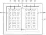
도 2은 도 1의 반도체 패키지를 나타내는 평면도이다.
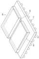
도 3은 도 1의 반도체 패키지를 나타내는 사시도이다.
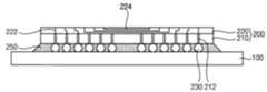
도 4은 도 1의 "A" 부분을 나타내는 확대 단면도이다.
도 5 내지 도 8은 예시적인 실시예들에 따른 반도체 패키지의 제조 방법을 나타내는 도면들이다.
도 9는 예시적인 실시예들에 따른 반도체 패키지를 나타내는 단면도이다.
도 10은 예시적인 실시예들에 따른 반도체 패키지의 제조 방법을 나타내는 단면도이다.
도 11은 예시적인 실시예들에 따른 반도체 패키지를 나타내는 단면도이다.
도 12는 예시적인 실시예들에 따른 반도체 패키지를 나타내는 단면도이다.
도 13 내지 도 16은 예시적인 실시예들에 따른 반도체 패키지의 제조 방법을 나타내는 도면들이다.
도 17은 예시적인 실시예들에 따른 반도체 패키지를 나타내는 단면도이다.
도 18은 도 17의 반도체 패키지를 나타내는 평면도이다.1 is a cross-sectional view showing a semiconductor package according to example embodiments.
FIG. 2 is a plan view showing the semiconductor package of FIG. 1.
FIG. 3 is a perspective view showing the semiconductor package of FIG. 1.
FIG. 4 is an enlarged cross-sectional view showing portion “A” of FIG. 1.
5 to 8 are diagrams showing a method of manufacturing a semiconductor package according to example embodiments.
9 is a cross-sectional view showing a semiconductor package according to example embodiments.
Figure 10 is a cross-sectional view showing a method of manufacturing a semiconductor package according to example embodiments.
11 is a cross-sectional view showing a semiconductor package according to example embodiments.
12 is a cross-sectional view showing a semiconductor package according to example embodiments.
13 to 16 are diagrams showing a method of manufacturing a semiconductor package according to example embodiments.
17 is a cross-sectional view showing a semiconductor package according to example embodiments.
FIG. 18 is a plan view showing the semiconductor package of FIG. 17.
이하, 첨부한 도면들을 참조하여, 본 발명의 바람직한 실시예를 보다 상세하게 설명하고자 한다.Hereinafter, preferred embodiments of the present invention will be described in more detail with reference to the attached drawings.
도 1는 예시적인 실시예들에 따른 반도체 패키지를 나타내는 단면도이다. 도 2은 도 1의 반도체 패키지를 나타내는 평면도이다. 도 3은 도 1의 반도체 패키지를 나타내는 사시도이다. 도 4은 도 1의 "A" 부분을 나타내는 확대 단면도이다.1 is a cross-sectional view showing a semiconductor package according to example embodiments. FIG. 2 is a plan view showing the semiconductor package of FIG. 1. FIG. 3 is a perspective view showing the semiconductor package of FIG. 1. FIG. 4 is an enlarged cross-sectional view showing portion “A” of FIG. 1.
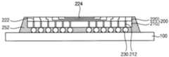
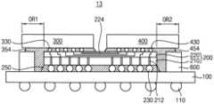
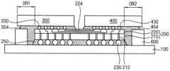
도 1 내지 도 4를 참조하면, 반도체 패키지(10)는 패키지 기판(100), 인터포저(200), 제1 반도체 장치(300) 및 제2 반도체 장치(400)를 포함할 수 있다.Referring to FIGS. 1 to 4 , the
예시적인 실시예들에 있어서, 반도체 패키지(10)는 복수 개의 다이(칩)들이 적층된 적층 칩 구조를 갖는 메모리 장치일 수 있다. 예를 들면, 반도체 패키지(10)는 2.5D 칩 구조의 반도체 메모리 장치를 포함할 수 있다. 이 경우에 있어서, 제1 반도체 장치(300)은 로직 반도체 장치를 포함하고, 제2 반도체 장치(400)은 메모리 장치를 포함할 수 있다. 상기 로직 반도체 장치는 CPU, GPU, SoC와 같은 호스트(Host)로서의 ASIC일 수 있다. 상기 메모리 장치는 고 대역폭 메모리(HBM, High Bandwidth Memory) 장치를 포함할 수 있다.In example embodiments, the
예시적인 실시예들에 있어서, 패키지 기판(100)은 서로 마주보는 상부면과 하부면을 갖는 기판일 수 있다. 예를 들면, 패키지 기판(100)은 인쇄회로기판(PCB)일 수 있다. 상기 인쇄회로기판은 내부에 비아와 다양한 회로들을 갖는 다층 회로 보드일 수 있다.In example embodiments, the
인터포저(200)는 패키지 기판(100) 상에 배치될 수 있다. 인터포저(200)는 솔더 범프들(230)을 통해 패키지 기판(100) 상에 실장될 수 있다. 인터포저(200)의 평면적은 패키지 기판(100)의 평면적보다 작을 수 있다. 평면도에서 보았을 때, 인터포저(200)는 패키지 기판(100)의 영역 내에 배치될 수 있다.The
인터포저(200)는 내부에 형성된 복수 개의 연결 배선들을 갖는 실리콘 인터포저일 수 있다. 제1 반도체 장치(300) 및 제2 반도체 장치(400)는 인터포저(200) 내부의 상기 연결 배선들을 통해 서로 연결되거나 솔더 범프들(230)을 통해 패키지 기판(100)에 전기적으로 연결될 수 있다. 상기 실리콘 인터포저는 제1 및 제2 반도체 칩들(300, 400) 사이의 고밀도 인터커넥션을 제공할 수 있다The
예시적인 실시예들에 있어서, 인터포저(200)는 반도체 기판(210) 및 반도체 기판(210)의 상부면에 복수 개의 배선들을 갖는 배선층(220)을 포함할 수 있다. 복수 개의 상기 배선들은 제1 배선들(222) 및 제2 배선들(224)을 포함할 수 있다. 반도체 기판(210)은 내부에 관통 형성된 복수 개의 관통 전극들(212)을 포함할 수 있다. 관통 전극들(212) 각각은 관통 실리콘 비아(TSV)를 포함할 수 있다.In example embodiments, the
제1 배선들(222)은 관통 전극들(212)과 전기적으로 연결될 수 있다. 제1 및 제2 반도체 장치들(300, 400)은 제1 배선들(222) 및 관통 전극들(212)을 통해 패키지 기판(100)과 전기적으로 연결될 수 있다. 제1 반도체 장치(300) 및 제2 반도체 장치(400)는 제2 배선들(224)에 의해 서로 전기적으로 연결될 수 있다.The
도 4에 도시된 바와 같이, 배선층(220)은 적어도 2개의 금속 배선층들을 포함할 수 있다. 배선층(220)은 순차적으로 적층된 제1 내지 제5 절연막들(220a, 220b, 220c, 220d, 220e)을 포함할 수 있다. 제1 배선(222)은 제1 내지 제5 절연막들(220a, 220b, 220c, 220d, 220e) 내에 각각 형성된 제1 금속 배선(222a), 제1 콘택(224a), 제2 금속 배선(222b), 제2 콘택(224b) 및 제3 금속 배선(222c)를 포함할 수 있다. 제3 금속 배선(222c)의 적어도 일부분이 랜딩 패드로서의 접속 패드의 역할을 수행할 수 있다. 제3 금속 배선(222c) 상에는 솔더 범프(330, 430)가 배치될 수 있다.As shown in FIG. 4, the
제1 반도체 장치(300)는 인터포저(200) 상에 배치될 수 있다. 제1 반도체 장치(300)는 플립 칩 본딩(flip chip bonding) 방식에 의해 인터포저(200) 상에 실장될 수 있다. 이 경우에 있어서, 제1 반도체 장치(300)는 칩 패드들이 형성된 활성면이 인터포저(200)를 향하도록 인터포저(200) 상에 실장될 수 있다. 제1 반도체 장치(300)의 상기 칩 패드들은 도전성 범프들, 예를 들면, 솔더 범프들(330)에 의해 인터포저(200)의 상기 접속 패드들과 전기적으로 연결될 수 있다.The
제1 반도체 장치(300)는 상기 칩 패드들이 형성되어 있는 접속 영역(IR1)을 포함할 수 있다. 평면도에서 보았을 때, 제1 반도체 장치(300)의 접속 영역(IR1)은 인터포저(200)의 영역 내에 위치할 수 있다.The
예시적인 실시예들에 있어서, 제1 반도체 장치(300)는 인터포저(200)의 일측부로부터 돌출하는 오버행 부분(OR1)을 포함할 수 있다. 제1 반도체 장치(300)의 외측 단부는 인터포저(200)의 일측부로부터 돌출할 수 있다. 제1 반도체 장치(300)는 인터포저(200)의 일측부로부터 수평 방향으로 연장하도록 배치될 수 있다. 평면도에서 보았을 때, 인터포저(200)의 외측 단부가 제1 반도체 장치(300)의 외측 단부보다 안쪽에 위치할 수 있다.In example embodiments, the
제2 반도체 장치(400)는 인터포저(200) 상에서 제1 반도체 장치(300)로부터 이격되도록 배치될 수 있다. 제2 반도체 장치(400)는 플립 칩 본딩(flip chip bonding) 방식에 의해 인터포저(200) 상에 실장될 수 있다. 이 경우에 있어서, 제2 반도체 장치(400)는 칩 패드들이 형성된 활성면이 인터포저(200)를 향하도록 인터포저(200) 상에 실장될 수 있다. 제2 반도체 장치(400)의 상기 칩 패드들은 도전성 범프들, 예를 들면, 솔더 범프들(430)에 의해 인터포저(200)의 상기 접속 패드들과 전기적으로 연결될 수 있다.The
제2 반도체 장치(400)는 상기 칩 패드들이 형성되어 있는 접속 영역(IR2)을 포함할 수 있다. 평면도에서 보았을 때, 제2 반도체 장치(400)의 접속 영역(IR2)은 인터포저(200) 영역 내에 위치할 수 있다.The
예시적인 실시예들에 있어서, 제2 반도체 장치(400)는 인터포저(200)의 타측부로부터 돌출하는 오버행 부분(OR2)을 포함할 수 있다. 제2 반도체 장치(400)의 외측 단부는 인터포저(200)의 타측부로부터 돌출할 수 있다. 제2 반도체 장치(400)는 인터포저(200)의 타측부로부터 수평 방향으로 연장하도록 배치될 수 있다. 평면도에서 보았을 때, 인터포저(200)의 외측 단부가 제2 반도체 장치(400)의 외측 단부보다 안쪽에 위치할 수 있다.In example embodiments, the
하나의 제1 반도체 장치(300) 및 하나의 제2 반도체 장치(400)가 배치되도록 도시되어 있지만, 이에 제한되지 않음을 이해할 수 있다. 예를 들면, 제2 반도체 장치(400)는 버퍼 다이 및 상기 버퍼 다이 상에 순차적으로 적층된 복수 개의 메모리 다이(칩)들을 포함할 수 있다. 상기 버퍼 다이 및 상기 메모리 다이들은 실리콘 관통 비아들(TSVs)에 의해 서로 전기적으로 연결될 수 있다.Although one
예시적인 실시예들에 있어서, 반도체 패키지(10)는 인터포저(200)와 패키지 기판(100) 사이에 언더필되는 제1 접착제(250), 제1 반도체 장치(300) 및 인터포저(200) 사이에 언더필되는 제2 접착제(350), 및 제2 반도체 장치(400) 및 인터포저(200) 사이에 언더필되는 제3 접착제(450)를 더 포함할 수 있다.In example embodiments, the
예를 들면, 상기 제1 내지 제3 접착제들은 에폭시 물질을 포함하여 인터포저(200)와 패키지 기판(100) 사이 그리고 제1 및 제2 반도체 장치들(300, 400)과 인터포저(200) 사이의 틈을 보강할 수 있다.For example, the first to third adhesives include an epoxy material and are used between the
패키지 기판(100)의 상기 하부면 상에는 외부 접속 패드들이 형성되고, 상기 외부 접속 패드들 상에는 외부 장치와의 전기적 연결을 위하여 외부 연결 부재들(110)이 배치될 수 있다. 예를 들면, 외부 연결 부재(100)는 솔더 볼일 수 있다. 반도체 패키지(100)는 상기 솔더 볼들을 매개로 하여 모듈 기판(도시되지 않음)에 실장되어 메모리 모듈을 구성할 수 있다.External connection pads are formed on the lower surface of the
상술한 바와 같이, 반도체 패키지(10)는 인터포저(200) 상에 서로 이격 배치되며 인터포저(200)에 의해 서로 전기적으로 연결되는 제1 및 제2 반도체 장치들(300, 400)을 포함할 수 있다. 제1 및 제2 반도체 장치들(300, 400)은 인터포저(200)의 대향하는 측부들로부터 돌출하는 오버행 부분(OR1, OR2)을 각각 포함할 수 있다.As described above, the
이에 따라, 제1 및 제2 반도체 장치들(300, 400)이 오버행 구조를 가짐으로써, 인터포저(200)의 크기를 최소화하여 상기 인터포저(200)의 제조를 용이하게 하고 수율을 향상시킬 수 있다.Accordingly, since the first and
이하에서는, 상술한 반도체 패키지를 제조하는 방법에 대하여 설명하기로 한다. 상기 반도체 패키지의 제조 방법은 2.5D 패키지를 제조하는 데 이용될 수 있다. 다만, 이로 인하여 예시적인 실시예들에 따른 반도체 패키지의 제조 방법이 이로 한정되지 않음을 이해할 수 있을 것이다.Hereinafter, a method of manufacturing the above-described semiconductor package will be described. The above semiconductor package manufacturing method can be used to manufacture a 2.5D package. However, it will be understood that the method of manufacturing a semiconductor package according to example embodiments is not limited thereto.
도 5 내지 도 8은 예시적인 실시예들에 따른 반도체 패키지의 제조 방법을 나타내는 도면들이다. 도 5 내지 도 7은 상기 반도체 패키지의 제조 방법을 나타내는 단면도들이고, 도 8은 도 7의 평면도이다.5 to 8 are diagrams showing a method of manufacturing a semiconductor package according to example embodiments. FIGS. 5 to 7 are cross-sectional views showing a method of manufacturing the semiconductor package, and FIG. 8 is a plan view of FIG. 7 .
도 5를 참조하면, 먼저, 인터포저(200)를 패키지 기판(100) 상에 배치시킬 수 있다.Referring to FIG. 5, first, the
예시적인 실시예들에 있어서, 먼저, 웨이퍼에 복수 개의 상기 실리콘 인터포저 다이들을 형성한 후, 상기 웨이퍼를 소잉하여 개별적인 실리콘 인터포저를 형성할 수 있다. 상기 개별적인 실리콘 인터포저(즉, 인터포저(200))를 패키지 기판(100) 상에 실장시킬 수 있다.In exemplary embodiments, first, a plurality of the silicon interposer dies may be formed on a wafer, and then the wafer may be sawed to form individual silicon interposers. The individual silicon interposer (i.e., interposer 200) may be mounted on the
인터포저(200)는 솔더 범프들(230)을 통해 패키지 기판(100) 상에 실장될 수 있다. 이어서, 인터포저(200)과 패키지 기판(100) 사이에는 제1 접착제(250)가 언더필(underfill)될 수 있다. 인터포저(200)의 평면적은 패키지 기판(100)의 평면적보다 작을 수 있다. 평면도에서 보았을 때, 인터포저(200)는 패키지 기판(100)의 영역 내에 배치될 수 있다.The
인터포저(200)는 내부에 형성된 복수 개의 연결 배선들을 가질 수 있다. 인터포저(200)는 반도체 기판(예로, 실리콘 기판)(210) 및 반도체 기판(210)의 상부면에 복수 개의 배선들을 갖는 배선층(220)을 포함할 수 있다. 복수 개의 상기 배선들은 제1 배선들(222) 및 제2 배선들(224)을 포함할 수 있다. 반도체 기판(210)은 내부에 관통 형성된 복수 개의 관통 전극들(212)을 포함할 수 있다. 관통 전극(212)은 관통 실리콘 비아(TSV)를 포함할 수 있다.The
도 6을 참조하면, 인터포저(200) 상에 제1 반도체 장치(300) 및 제2 반도체 장치(400)를 서로 이격되도록 배치시킬 수 있다.Referring to FIG. 6 , the
예시적인 실시예들에 있어서, 제1 및 제2 반도체 장치들(300, 400)는 플립 칩 본딩(flip chip bonding) 방식에 의해 인터포저(200) 상에 실장될 수 있다. 제1 반도체 장치(300)의 칩 패드들은 도전성 범프들, 예를 들면, 솔더 범프들(330)에 의해 인터포저(200)의 접속 패드들과 전기적으로 연결될 수 있다. 제2 반도체 장치(400)의 칩 패드들은 도전성 범프들, 예를 들면, 솔더 범프들(430)에 의해 인터포저(200)의 상기 접속 패드들과 전기적으로 연결될 수 있다.In example embodiments, the first and
예를 들면, 제1 반도체 장치(300)는 로직 반도체 장치를 포함하고, 제2 반도체 장치(400)는 메모리 장치를 포함할 수 있다. 상기 로직 반도체 장치는 CPU, GPU, SoC와 같은 호스트(Host)로서의 ASIC일 수 있다. 상기 메모리 장치는 고 대역폭 메모리(HBM, High Bandwidth Memory) 장치를 포함할 수 있다.For example, the
도 7 및 도 8을 참조하면, 제1 반도체 장치(300)와 인터포저(200) 사이에 제2 접착제(350)를 언더필(underfill)하고, 제2 반도체 장치(400)와 인터포저(200) 사이에 제3 접착제(450)를 언더필(underfill)할 수 있다.7 and 8, a
디스펜서 노즐을 제1 반도체 장치(300)의 내측 단부를 따라 이동시키면서 상기 디스펜스 노즐을 통해 제1 반도체 장치(300)와 인터포저(200) 사이에 언더필 용액을 디스펜싱하고, 상기 언더필 용액이 경화되어 제2 접착제(350)를 형성할 수 있다.An underfill solution is dispensed between the
이와 유사하게, 상기 디스펜서 노즐을 제2 반도체 장치(300)의 내측 단부를 따라 이동시키면서 상기 디스펜서 노즐을 통해 제2 반도체 장치(400)와 인터포저(200) 사이에 언더필 용액을 디스펜싱하고, 상기 언더필 용액이 경화되어 제3 접착제(450)를 형성할 수 있다.Similarly, the underfill solution is dispensed between the
예를 들면, 상기 제1, 제2 및 제3 접착제들(250, 350, 450)는 에폭시 물질을 포함하여 인터포저(200)와 패키지 기판(100) 사이 그리고 제1 및 제2 반도체 장치들(300, 400)과 인터포저(200) 사이의 틈을 보강할 수 있다.For example, the first, second, and
일반적으로, 웨이퍼 상에 복수 개의 실리콘 인터포저 다이들 각각에 서로 다른 반도체 칩들을 이격되도록 실장한 후, 상기 웨이퍼를 절단한 후, 상기 반도체 칩들이 실장된 하나의 인터포저를 패키지 기판 상에 실장하였다. 따라서, 상기 반도체 칩들이 인터포저로부터 돌출되도록 배치할 수 없고, 이에 따라, 상기 인터포저의 크기를 감소시킬 수 없다.In general, after mounting different semiconductor chips on each of a plurality of silicon interposer dies on a wafer to be spaced apart, the wafer is cut, and then one interposer with the semiconductor chips mounted on it is mounted on a package substrate. . Accordingly, the semiconductor chips cannot be arranged to protrude from the interposer, and accordingly, the size of the interposer cannot be reduced.
삭제delete
이에 반해, 예시적인 실시예들에 따르면, 복수 개의 실리콘 인터포저 다이들이 형성된 웨이퍼를 소잉한 후, 개별적인 실리콘 인터포저(200)를 패키지 기판(100) 상에 실장할 수 있다. 이어서, 상기 인터포저(200) 상에 제1 및 제2 반도체 장치들(300, 400)을 이격되게 배치시키므로, 상기 제1 및 제2 반도체 장치들(300, 400)이 인터포저(200)로부터 측방으로 돌출되도록(즉, 제1 및 제2 반도체 장치들(300, 400)의 외측 단부들이 인터포저(200)의 측부들로부터 각각 돌출되도록) 배치할 수 있고, 이에 따라, 상기 인터포저(200)의 크기를 감소시킬 수 있다. 즉, 제1 및 제2 반도체 장치들(300, 400)이 상기 인터포저(200)엥 대해 오버행 구조를 가짐으로써, 인터포저(200)의 크기를 최소화하여 상기 인터포저(200)의 제조를 용이하게 하고 수율을 향상시킬 수 있다.In contrast, according to exemplary embodiments, after sawing a wafer on which a plurality of silicon interposer dies are formed,
도 9는 예시적인 실시예들에 따른 반도체 패키지를 나타내는 단면도이다. 상기 반도체 패키지는 제1 내지 제3 접착제들을 제외하고는 도 1을 참조로 설명한 반도체 패키지(10)와 실질적으로 동일하다. 이에 따라, 동일한 구성요소들에 대해서는 동일한 참조부호들로 나타내고, 또한 동일한 구성요소들에 대한 반복 설명은 생략한다.9 is a cross-sectional view showing a semiconductor package according to example embodiments. The semiconductor package is substantially the same as the
도 9를 참조하면, 반도체 패키지(11)는 인터포저(200)와 패키지 기판(100) 사이에 언더필되는 제1 접착제(252), 제1 반도체 장치(300) 및 인터포저(200) 사이에 언더필되는 제2 접착제(352), 및 제2 반도체 장치(400) 및 인터포저(200) 사이에 언더필되는 제3 접착제(452)를 포함할 수 있다.Referring to FIG. 9, the
제1 접착제(252)는 인터포저(200)의 양측부를 따라 패키지 기판(100)으로부터 상방으로 연장할 수 있다. 제1 접착제(252)의 패키지 기판(100)으로부터 높이는 인터포저(200)의 패키지 기판(100)으로부터의 높이와 동일할 수 있다. 제2 접착제(352)는 인터포저(200)의 일측부로부터 제1 접착제(252)의 상부면까지 연장할 수 있다. 제3 접착제(452)는 인터포저(200)의 타측부로부터 제1 접착제(252)의 상부면까지 연장할 수 있다.The
따라서, 제1 접착제(252)는 제2 접착제(352) 및 제3 접착제(452)와 접촉 지지할 수 있다. 이에 따라, 제1 내지 제3 접착제들(252, 352, 452)은 오버행 구조를 갖는 제1 및 제2 반도체 장치들(300, 400)을 견고히 지지할 수 있다.Accordingly, the
이하에서는, 도 9의 반도체 패키지(11)를 제조하는 방법에 대하여 설명하기로 한다.Below, a method of manufacturing the
도 10은 예시적인 실시예들에 따른 반도체 패키지의 제조 방법을 나타내는 단면도이다.Figure 10 is a cross-sectional view showing a method of manufacturing a semiconductor package according to example embodiments.
도 10을 참조하면, 인터포저(200)를 패키지 기판(100) 상에 배치시킨 후, 제1 접착제(252)를 인터포저(200)와 패키지 기판(100) 사이에 언더필할 수 있다.Referring to FIG. 10 , after the
예시적인 실시예들에 있어서, 디스펜서 노즐을 인터포저(200)의 양 측부를 따라 이동시키면서 상기 디스펜서 노즐을 통해 인터포저(200)와 패키지 기판(100) 사이에 언더필 용액을 디스펜싱하고, 상기 언더필 용액이 경화되어 예비 접착제를 형성할 수 있다.In exemplary embodiments, an underfill solution is dispensed between the
이어서, 상기 디스펜서 노즐을 인터포저(200)의 양측부를 따라 상방으로 이동시키면서 상기 디스펜서 노즐을 통해 상기 언더필 용액을 상기 예비 접착제 상에 디스펜싱하고, 상기 언더필 용액이 경화되어 제1 접착제(252)를 형성할 수 있다.Next, the underfill solution is dispensed onto the preliminary adhesive through the dispenser nozzle while moving the dispenser nozzle upward along both sides of the
제1 접착제(252)는 인터포저(200)의 양측부를 따라 패키지 기판(100)으로부터 상방으로 연장할 수 있다. 제1 접착제(252)의 패키지 기판(100)으로부터 높이는 인터포저(200)의 패키지 기판(100)으로부터의 높이와 동일할 수 있다.The
이어서, 도 6 내지 도 8을 참조로 설명한 공정들과 유사한 공정들을 수행하여 도 9의 반도체 패키지(11)를 완성할 수 있다.Next, processes similar to those described with reference to FIGS. 6 to 8 may be performed to complete the
도 11은 예시적인 실시예들에 따른 반도체 패키지를 나타내는 단면도이다. 상기 반도체 패키지는 추가적인 접착제를 제외하고는 도 1을 참조로 설명한 반도체 패키지(10)와 실질적으로 동일하다. 이에 따라, 동일한 구성요소들에 대해서는 동일한 참조부호들로 나타내고, 또한 동일한 구성요소들에 대한 반복 설명은 생략한다.11 is a cross-sectional view showing a semiconductor package according to example embodiments. The semiconductor package is substantially the same as the
도 11을 참조하면, 반도체 패키지(12)는 제1 반도체 장치(300)와 패키지 기판(100) 사이에 언더필되는 제4 접착제(500) 및 제2 반도체 장치(400) 및 패키지 기판(100) 사이에 언더필되는 제5 접착제(550)를 더 포함할 수 있다.Referring to FIG. 11, the
제4 접착제(500)는 제1 반도체 장치(300)와 패키지 기판(100) 사이에 배치되며 인터포저(200)의 일측부를 따라 패키지 기판(100)으로부터 상방으로 연장할 수 있다. 제4 접착제(500)는 제1 반도체 장치(300)의 오버행 부분(OR1)과 접촉 지지할 수 있다.The
제5 접착제(550)는 제2 반도체 장치(400)와 패키지 기판(100) 사이에 배치되며 인터포저(200)의 타측부를 따라 패키지 기판(100)으로부터 상방으로 연장할 수 있다. 제5 접착제(500)는 제2 반도체 장치(400)의 오버행 부분(OR2)과 접촉 지지할 수 있다.The
이에 따라, 제4 및 제5 접착제들(500, 550)은 오버행 구조를 갖는 제1 및 제2 반도체 장치들(300, 400)을 견고히 지지할 수 있다.Accordingly, the fourth and
이하에서는, 도 11의 반도체 패키지(12)를 제조하는 방법에 대하여 설명하기로 한다.Below, a method of manufacturing the
도 5 내지 도 8을 참조로 설명한 공정들과 유사한 공정들을 수행하여, 인터포저(200) 상에 제1 및 제2 반도체 장치들(300, 400)을 실장시킨 후, 제4 접착제(500)를 제1 반도체 장치(300)와 패키지 기판(100) 사이에 언더필하고 제5 접착제(550)을 제2 반도체 장치(400) 및 패키지 기판(100) 사이에 언더필할 수 있다.After performing processes similar to those described with reference to FIGS. 5 to 8 to mount the first and
예시적인 실시예들에 있어서, 디스펜서 노즐을 인터포저(200)의 일측부를 따라 이동시키면서 상기 디스펜서 노즐을 통해 제1 반도체 장치(300)와 패키지 기판(100) 사이에 언더필 용액을 디스펜싱하고, 상기 언더필 용액이 경화되어 제4 접착제(500)를 형성할 수 있다.In exemplary embodiments, an underfill solution is dispensed between the
이어서, 상기 디스펜서 노즐을 인터포저(200)의 타측부를 따라 이동시키면서 상기 디스펜서 노즐을 통해 제2 반도체 장치(400)와 패키지 기판(100) 사이에 언더필 용액을 디스펜싱하고, 상기 언더필 용액이 경화되어 제5 접착제(550)를 형성할 수 있다.Next, the underfill solution is dispensed between the
제4 접착제(500)는 인터포저(200)의 일측부를 따라 패키지 기판(100)으로부터 상방으로 연장하여 제1 반도체 장치(300)의 오버행 부분(OR1)과 접촉 지지할 수 있다.The
제5 접착제(550)는 인터포저(200)의 타측부를 따라 패키지 기판(100)으로부터 상방으로 연장하여 제2 반도체 장치(400)의 오버행 부분(OR2)과 접촉 지지할 수 있다.The
도 12는 예시적인 실시예들에 따른 반도체 패키지를 나타내는 단면도이다. 상기 반도체 패키지는 제2 및 제3 접착제들의 구성 및 추가적인 지지 부재를 제외하고는 도 1을 참조로 설명한 반도체 패키지(10)와 실질적으로 동일하다. 이에 따라, 동일한 구성요소들에 대해서는 동일한 참조부호들로 나타내고, 또한 동일한 구성요소들에 대한 반복 설명은 생략한다.12 is a cross-sectional view showing a semiconductor package according to example embodiments. The semiconductor package is substantially the same as the
도 12를 참조하면, 반도체 패키지(13)는 제1 반도체 장치(300) 및 패키지 기판(100) 사이 그리고 제2 반도체 장치(400) 및 패키지 기판(100)에 사이에 배치되는 지지 부재들(600)을 포함할 수 있다. 지지 부재들(600)은 인터포저(200) 둘레를 따라 배열될 수 있다.Referring to FIG. 12, the
지지 부재(600)는 제1 반도체 장치(300)의 오버행 부분(OR1) 아래에 배치될 수 있다. 지지 부재(600)는 패키지 기판(100)으로부터 상방으로 연장하는 기둥 형상을 가질 수 있다. 지지 부재(600)는 제1 반도체 장치(300)의 오버행 부분(OR1)으로부터 이격되어 이들 사이에 제1 갭을 형성할 수 있다. 지지 부재(600)는 인터포저(200)의 일측부로부터 이격되어 이들 사이에 제2 갭을 형성할 수 있다. 제2 접착제(354)는 인터포저(200)의 일측부로부터 측방으로 연장하여 상기 제1 갭을 채우고 하방으로 연장하여 상기 제2 갭을 채울 수 있다.The
지지 부재(600)는 제2 반도체 장치(400)의 오버행 부분(OR2) 아래에 배치될 수 있다. 지지 부재(600)는 패키지 기판(100)으로부터 상방으로 연장하는 기둥 형상을 가질 수 있다. 지지 부재(600)는 제2 반도체 장치(400)의 오버행 부분(OR2)으로부터 이격되어 이들 사이에 제3 갭을 형성할 수 있다. 지지 부재(600)는 인터포저(200)의 타측부로부터 이격되어 이들 사이에 제4 갭을 형성할 수 있다. 제3 접착제(454)는 인터포저(200)의 타측부로부터 측방으로 연장하여 상기 제3 갭을 채우고 하방으로 연장하여 상기 제4 갭을 채울 수 있다.The
이하에서는, 도 12의 반도체 패키지(13)를 제조하는 방법에 대하여 설명하기로 한다.Below, a method of manufacturing the
도 13 내지 도 16은 예시적인 실시예들에 따른 반도체 패키지의 제조 방법을 나타내는 도면들이다. 도 13, 도 15 및 도 16은 상기 반도체 패키지의 제조 방법을 나타내는 단면도들이고, 도 14는 도 13의 평면도이다.13 to 16 are diagrams showing a method of manufacturing a semiconductor package according to example embodiments. FIGS. 13, 15, and 16 are cross-sectional views showing a method of manufacturing the semiconductor package, and FIG. 14 is a plan view of FIG. 13.
도 13 및 도 14를 참조하면, 인터포저(200)를 패키지 기판(100) 상에 배치시키고, 복수 개의 지지 부재들(600)을 패키지 기판(100) 상에 배치시킬 수 있다.Referring to FIGS. 13 and 14 , the
예시적인 실시예들에 있어서, 지지 부재들(600)은 인터포저(200) 둘레를 따라 배열시킬 수 있다. 접착제와 같은 물질을 패키지 기판(100) 상에 디스펜싱하여 지지 부재들(600)을 형성할 수 있다.In example embodiments,
지지 부재(600)는 패키지 기판(100)으로부터 상부로 연장하는 기둥 형상을 가질 수 있다. 지지 부재(600)는 인터포저(200)의 일측부로부터 이격되어 이들 사이에 제2 갭을 형성할 수 있다. 지지 부재(600)는 인터포저(200)의 타측부로부터 이격되어 이들 사이에 제4 갭을 형성할 수 있다.The
도 15 및 도 16을 참조하면, 인터포저(200) 상에 제1 및 제2 반도체 장치들(300, 400)을 배치시킨 후, 제1 반도체 장치(300)와 인터포저(200) 사이에는 제2 접착제(354)를 언더필(underfill)하고, 제2 반도체 장치(400)와 인터포저(200) 사이에 제3 접착제(454)를 언더필(underfill)할 수 있다.15 and 16, after placing the first and
예시적인 실시예들에 있어서, 제1 반도체 장치(300)의 오버행 부분(OR1)은 지지 부재(600)으로부터 이격되어 이들 사이에 제1 갭을 형성할 수 있다. 제2 반도체 장치(400)의 오버행 부분(OR2)은 지지 부재(600)로부터 이격되어 이들 사이에 제3 갭을 형성할 수 있다. 제2 반도체 장치(400)의 오버행 부분(OR2)은 지지 부재(600)로부터 이격되어 이들 사이에 제3 갭을 형성할 수 있다.In example embodiments, the overhang portion OR1 of the
이어서, 디스펜서 노즐을 제1 반도체 장치(300)의 내측 단부를 따라 이동시키면서 상기 디스펜서 노즐을 통해 제1 반도체 장치(300)와 인터포저(200) 사이에 언더필 용액을 디스펜싱하고, 상기 언더필 용액이 경화되어 제2 접착제(354)를 형성할 수 있다. 이 때, 상기 언더필 용액은 상기 제1 갭 및 상기 제2 갭 내부로 이동하고 경화되어 제2 접착제(354)는 인터포저(200)의 일측부로부터 측방으로 연장하여 상기 제1 갭을 채우고 하방으로 연장하여 상기 제2 갭을 채울 수 있다.Next, the underfill solution is dispensed between the
이후, 상기 디스펜서 노즐을 제2 반도체 장치(400)의 내측 단부를 따라 이동시키면서 상기 디스펜서 노즐을 통해 제2 반도체 장치(400)와 인터포저(200) 사이에 언더필 용액을 디스펜싱하고, 상기 언더필 용액이 경화되어 제3 접착제(454)를 형성할 수 있다. 이 때, 상기 언더필 용액은 상기 제3 갭 및 상기 제4 갭 내부로 이동하고 경화되어 제3 접착제(454)는 인터포저(200)의 타측부로부터 측방으로 연장하여 상기 제3 갭을 채우고 하방으로 연장하여 상기 제4 갭을 채울 수 있다.Thereafter, the underfill solution is dispensed between the
도 17은 예시적인 실시예들에 따른 반도체 패키지를 나타내는 단면도이다. 도 18은 도 17의 반도체 패키지를 나타내는 평면도이다. 상기 반도체 패키지는 제1 및 제2 반도체 장치들의 배열 및 구성을 제외하고는 도 1을 참조로 설명한 반도체 패키지(10)와 실질적으로 동일하다. 이에 따라, 동일한 구성요소들에 대해서는 동일한 참조부호들로 나타내고, 또한 동일한 구성요소들에 대한 반복 설명은 생략한다.17 is a cross-sectional view showing a semiconductor package according to example embodiments. FIG. 18 is a plan view showing the semiconductor package of FIG. 17. The semiconductor package is substantially the same as the
도 17 및 도 18을 참조하면, 반도체 패키지(14)는 패키지 기판(100), 인터포저(200), 제1 반도체 장치(300) 및 복수 개의 제2 반도체 장치들(400)를 포함할 수 있다.17 and 18, the
예시적인 실시예들에 있어서, 제1 반도체 장치(300)는 인터포저(200)의 중심 영역에 배치되고, 제2 반도체 장치들(400)은 인터포저(200)의 주변 영역에 배치될 수 있다. 예를 들면, 4개의 제2 반도체 장치들(400)이 인터포저(200)의 모서리 영역들에 각각 배치될 수 있다.In example embodiments, the
제1 반도체 장치(300)는 로직 반도체 장치를 포함하고, 제2 반도체 장치들(400)은 메모리 장치를 포함할 수 있다. 상기 로직 반도체 장치는 CPU, GPU, SoC와 같은 호스트(Host)로서의 ASIC일 수 있다. 상기 메모리 장치는 고 대역폭 메모리(HBM, High Bandwidth Memory) 장치를 포함할 수 있다.The
예시적인 실시예들에 있어서, 평면도에서 보았을 때, 제1 반도체 장치(300)는 인터포저(200)의 내부에 배치되고, 제2 반도체 장치들(400)는 인터포저(200)의 측부로부터 돌출하도록 배치될 수 있다.In example embodiments, when viewed in plan view, the
제2 반도체 장치(400)는 인터포저(200)의 일측부로부터 돌출하는 오버행 부분(OR2)을 포함할 수 있다. 제2 반도체 장치(400)의 외측 단부는 인터포저(200)의 타측부로부터 돌출할 수 있다. 제2 반도체 장치(400)는 인터포저(200)의 타측부로부터 수평 방향으로 연장하도록 배치될 수 있다. 평면도에서 보았을 때, 인터포저(200)의 외측 단부가 제2 반도체 장치들(400)의 외측 단부보다 안쪽에 위치할 수 있다.The
제1 및 제2 반도체 장치들(300, 400)은 제1 배선들(222) 및 관통 전극들(212)을 통해 패키지 기판(100)과 전기적으로 연결될 수 있다. 제1 반도체 장치(300) 및 제2 반도체 장치들(400)은 인터포저(200)에 의해 서로 전기적으로 연결될 수 있다. 제1 반도체 장치(300) 및 제2 반도체 장치(400)는 제2 배선들(224)에 의해 서로 전기적으로 연결될 수 있다.The first and
예시적인 실시예들에 따른 반도체 패키지를 포함하는 전자 장치는, 예를 들어 중앙처리장치(CPU, MPU), 애플리케이션 프로세서(AP) 등과 같은 로직 소자, 예를 들어 에스램(SRAM) 장치, 디램(DRAM) 장치, 고대역폭 메모리(HBM) 장치 등과 같은 휘발성 메모리 장치, 및 예를 들어 플래시 메모리 장치, 피램(PRAM) 장치, 엠램(MRAM) 장치, 알램(RRAM) 장치 등과 같은 불휘발성 메모리 장치를 포함할 수 있다. 상기 전자 장치는 TV, 컴퓨터, 휴대용 컴퓨터, 랩톱 컴퓨터, 개인휴대단말기, 태블릿, 휴대폰, 디지털 음악 재생기 등에 적용될 수 있다.An electronic device including a semiconductor package according to example embodiments may include, for example, a logic element such as a central processing unit (CPU, MPU), an application processor (AP), etc., such as an SRAM device, a DRAM ( Volatile memory devices such as DRAM devices, High Bandwidth Memory (HBM) devices, and non-volatile memory devices such as flash memory devices, PRAM devices, MRAM devices, RRAM devices, etc. can do. The electronic device can be applied to TVs, computers, portable computers, laptop computers, personal digital assistants, tablets, mobile phones, digital music players, etc.
이상에서는 본 발명의 실시예들을 참조하여 설명하였지만, 해당 기술 분야의 숙련된 당업자는 하기의 특허 청구의 범위에 기재된 본 발명의 사상 및 영역으로부터 벗어나지 않는 범위 내에서 본 발명을 다양하게 수정 및 변경시킬 수 있음을 이해할 수 있을 것이다.Although the present invention has been described above with reference to embodiments, those skilled in the art can make various modifications and changes to the present invention without departing from the spirit and scope of the present invention as set forth in the claims below. You will understand that it is possible.
10, 11, 12, 13, 14: 반도체 패키지 100: 패키지 기판
200: 인터포저 210: 반도체 기판
212: 관통 전극 220: 배선층
222: 제1 배선 224: 제2 배선
230, 330, 430: 솔더 범프 250: 제1 접착제
300: 제1 반도체 장치 350, 352, 354: 제2 접착제
400: 제2 반도체 장치 450, 452, 454: 제3 접착제
500: 제4 접착제 550: 제5 접착제
600: 지지 부재10, 11, 12, 13, 14: semiconductor package 100: package substrate
200: Interposer 210: Semiconductor substrate
212: penetrating electrode 220: wiring layer
222: first wiring 224: second wiring
230, 330, 430: solder bump 250: first adhesive
300:
400:
500: fourth adhesive 550: fifth adhesive
600: support member
Claims (10)
Translated fromKorean상기 패키지 기판 상에 배치되는 인터포저; 및
상기 인터포저 상에 서로 이격 배치되며 상기 인터포저에 의해 서로 전기적으로 연결되는 제1 및 제2 반도체 장치들을 포함하고,
상기 제1 및 제2 반도체 장치들 중 적어도 하나는 상기 인터포저의 일측부로부터 돌출하는 오버행 부분을 포함하고,
상기 제1 및 제2 반도체 장치들은 도전성 범프들을 매개로 하여 상기 인터포저 상에 실장되고, 상기 제1 및 제2 반도체 장치들은 상기 인터포저에 의해 상기 패키지 기판과 전기적으로 연결되고,
상기 오버행 부분 아래에는, 상기 오버행 부분을 포함하는 상기 제1 및 제2 반도체 장치들 중 적어도 하나를 상기 패키지 기판에 전기적으로 연결시키는 도전성 부재들이 배치되지 않는 반도체 패키지.package substrate;
an interposer disposed on the package substrate; and
Comprising first and second semiconductor devices spaced apart from each other on the interposer and electrically connected to each other by the interposer,
At least one of the first and second semiconductor devices includes an overhang portion protruding from one side of the interposer,
The first and second semiconductor devices are mounted on the interposer via conductive bumps, and the first and second semiconductor devices are electrically connected to the package substrate by the interposer,
A semiconductor package in which conductive members electrically connecting at least one of the first and second semiconductor devices including the overhang portion to the package substrate are not disposed below the overhang portion.
반도체 기판; 및
상기 반도체 기판의 상부면에 복수 개의 배선들을 갖는 배선층을 포함하는 반도체 패키지.The method of claim 1, wherein the interposer
semiconductor substrate; and
A semiconductor package including a wiring layer having a plurality of wiring lines on an upper surface of the semiconductor substrate.
상기 인터포저와 상기 패키지 기판 사이에 언더필되는 제1 접착제; 및
상기 제1 반도체 장치 및 상기 인터포저 사이에 언더필되는 제2 접착제를 더 포함하는 반도체 패키지.According to claim 1,
a first adhesive underfilled between the interposer and the package substrate; and
A semiconductor package further comprising a second adhesive underfilled between the first semiconductor device and the interposer.
상기 제1 반도체 장치 및 상기 패키지 기판 사이에 언더필되는 제3 접착제를 더 포함하는 반도체 패키지.According to claim 1,
A semiconductor package further comprising a third adhesive underfilled between the first semiconductor device and the package substrate.
상기 제1 반도체 장치 및 상기 패키지 기판 사이에 배치되는 지지 부재를 더 포함하는 반도체 패키지.
According to claim 1,
A semiconductor package further comprising a support member disposed between the first semiconductor device and the package substrate.
Priority Applications (4)
| Application Number | Priority Date | Filing Date | Title |
|---|---|---|---|
| KR1020190033423AKR102644598B1 (en) | 2019-03-25 | 2019-03-25 | Semiconductor package |
| US16/529,194US11694949B2 (en) | 2019-03-25 | 2019-08-01 | Semiconductor package and method of manufacturing the same |
| US18/318,864US12136590B2 (en) | 2019-03-25 | 2023-05-17 | Semiconductor package and method of manufacturing the same |
| US18/897,421US20250014977A1 (en) | 2019-03-25 | 2024-09-26 | Semiconductor package and method of manufacturing the same |
Applications Claiming Priority (1)
| Application Number | Priority Date | Filing Date | Title |
|---|---|---|---|
| KR1020190033423AKR102644598B1 (en) | 2019-03-25 | 2019-03-25 | Semiconductor package |
Publications (2)
| Publication Number | Publication Date |
|---|---|
| KR20200113372A KR20200113372A (en) | 2020-10-07 |
| KR102644598B1true KR102644598B1 (en) | 2024-03-07 |
Family
ID=72604712
Family Applications (1)
| Application Number | Title | Priority Date | Filing Date |
|---|---|---|---|
| KR1020190033423AActiveKR102644598B1 (en) | 2019-03-25 | 2019-03-25 | Semiconductor package |
Country Status (2)
| Country | Link |
|---|---|
| US (3) | US11694949B2 (en) |
| KR (1) | KR102644598B1 (en) |
Families Citing this family (6)
| Publication number | Priority date | Publication date | Assignee | Title |
|---|---|---|---|---|
| KR102644598B1 (en)* | 2019-03-25 | 2024-03-07 | 삼성전자주식회사 | Semiconductor package |
| KR102789179B1 (en)* | 2020-11-25 | 2025-04-01 | 삼성전자주식회사 | Semiconductor package and method of manufacturing the semiconductor package |
| KR20220135447A (en) | 2021-03-30 | 2022-10-07 | 삼성전자주식회사 | Semiconductor package and method of fabricating the same |
| KR20220140215A (en) | 2021-04-09 | 2022-10-18 | 삼성전자주식회사 | Semiconductor package |
| KR20230010079A (en)* | 2021-07-08 | 2023-01-18 | 삼성전자주식회사 | Semiconductor package |
| US20230369232A1 (en)* | 2022-05-11 | 2023-11-16 | Intel Corporation | Molded interconnect memory on package |
Citations (1)
| Publication number | Priority date | Publication date | Assignee | Title |
|---|---|---|---|---|
| JP2015095655A (en)* | 2013-11-14 | 2015-05-18 | 三星電子株式会社Samsung Electronics Co.,Ltd. | Semiconductor package and manufacturing method of the same |
Family Cites Families (15)
| Publication number | Priority date | Publication date | Assignee | Title |
|---|---|---|---|---|
| US6268660B1 (en) | 1999-03-05 | 2001-07-31 | International Business Machines Corporation | Silicon packaging with through wafer interconnects |
| JP4581768B2 (en)* | 2005-03-16 | 2010-11-17 | ソニー株式会社 | Manufacturing method of semiconductor device |
| WO2009035849A2 (en) | 2007-09-10 | 2009-03-19 | Vertical Circuits, Inc. | Semiconductor die mount by conformal die coating |
| WO2010068699A2 (en)* | 2008-12-09 | 2010-06-17 | Vertical Circuits, Inc. | Semiconductor die interconnect formed by aerosol application of electrically conductive material |
| US8227904B2 (en) | 2009-06-24 | 2012-07-24 | Intel Corporation | Multi-chip package and method of providing die-to-die interconnects in same |
| US9059179B2 (en) | 2011-12-28 | 2015-06-16 | Broadcom Corporation | Semiconductor package with a bridge interposer |
| US9209156B2 (en) | 2012-09-28 | 2015-12-08 | Taiwan Semiconductor Manufacturing Co., Ltd. | Three dimensional integrated circuits stacking approach |
| US9136236B2 (en)* | 2012-09-28 | 2015-09-15 | Intel Corporation | Localized high density substrate routing |
| US8963339B2 (en)* | 2012-10-08 | 2015-02-24 | Qualcomm Incorporated | Stacked multi-chip integrated circuit package |
| KR101934581B1 (en) | 2012-11-02 | 2019-01-02 | 에스케이하이닉스 주식회사 | Semiconductor package |
| US9087765B2 (en) | 2013-03-15 | 2015-07-21 | Qualcomm Incorporated | System-in-package with interposer pitch adapter |
| KR101787832B1 (en) | 2015-10-22 | 2017-10-19 | 앰코 테크놀로지 코리아 주식회사 | Method for fabricating semiconductor package and semiconductor package using the same |
| US9607973B1 (en) | 2015-11-19 | 2017-03-28 | Globalfoundries Inc. | Method for establishing interconnects in packages using thin interposers |
| KR20180109850A (en)* | 2016-02-10 | 2018-10-08 | 르네사스 일렉트로닉스 가부시키가이샤 | Semiconductor device |
| KR102644598B1 (en)* | 2019-03-25 | 2024-03-07 | 삼성전자주식회사 | Semiconductor package |
- 2019
- 2019-03-25KRKR1020190033423Apatent/KR102644598B1/enactiveActive
- 2019-08-01USUS16/529,194patent/US11694949B2/enactiveActive
- 2023
- 2023-05-17USUS18/318,864patent/US12136590B2/enactiveActive
- 2024
- 2024-09-26USUS18/897,421patent/US20250014977A1/enactivePending
Patent Citations (1)
| Publication number | Priority date | Publication date | Assignee | Title |
|---|---|---|---|---|
| JP2015095655A (en)* | 2013-11-14 | 2015-05-18 | 三星電子株式会社Samsung Electronics Co.,Ltd. | Semiconductor package and manufacturing method of the same |
Also Published As
| Publication number | Publication date |
|---|---|
| US20250014977A1 (en) | 2025-01-09 |
| KR20200113372A (en) | 2020-10-07 |
| US11694949B2 (en) | 2023-07-04 |
| US20230290711A1 (en) | 2023-09-14 |
| US12136590B2 (en) | 2024-11-05 |
| US20200312755A1 (en) | 2020-10-01 |
Similar Documents
| Publication | Publication Date | Title |
|---|---|---|
| US20240250067A1 (en) | Multi-die package structures including redistribution layers | |
| US9502335B2 (en) | Package structure and method for fabricating the same | |
| KR102644598B1 (en) | Semiconductor package | |
| US9607947B2 (en) | Reliable microstrip routing for electronics components | |
| US8338929B2 (en) | Stacked-type chip package structure and fabrication method thereof | |
| CN107808878A (en) | Stacking type chip packaging structure | |
| US20120193789A1 (en) | Package stack device and fabrication method thereof | |
| KR20190099815A (en) | Semiconductor package and method of manufacturing the semiconductor package | |
| US11972995B2 (en) | Semiconductor package and method of manufacturing semiconductor package | |
| TWI793962B (en) | Semiconductor package and semiconductor device | |
| US20130256915A1 (en) | Packaging substrate, semiconductor package and fabrication method thereof | |
| CN107708300B (en) | Electronic stack structure and method for fabricating the same | |
| TWI647798B (en) | Electronic package and its manufacturing method | |
| CN115377047A (en) | Electronic package and its manufacturing method | |
| US20230029098A1 (en) | Semiconductor package | |
| TWI862166B (en) | Electronic package and manufacturing method thereof | |
| CN222966141U (en) | Electronic package | |
| US20250038080A1 (en) | Semiconductor package | |
| US20210082854A1 (en) | Semiconductor device and method for manufacturing semiconductor device | |
| CN118352323A (en) | Semiconductor packaging | |
| TW202531534A (en) | Semiconductor package structure |
Legal Events
| Date | Code | Title | Description |
|---|---|---|---|
| PA0109 | Patent application | Patent event code:PA01091R01D Comment text:Patent Application Patent event date:20190325 | |
| PG1501 | Laying open of application | ||
| A201 | Request for examination | ||
| PA0201 | Request for examination | Patent event code:PA02012R01D Patent event date:20220314 Comment text:Request for Examination of Application Patent event code:PA02011R01I Patent event date:20190325 Comment text:Patent Application | |
| E902 | Notification of reason for refusal | ||
| PE0902 | Notice of grounds for rejection | Comment text:Notification of reason for refusal Patent event date:20230905 Patent event code:PE09021S01D | |
| E701 | Decision to grant or registration of patent right | ||
| PE0701 | Decision of registration | Patent event code:PE07011S01D Comment text:Decision to Grant Registration Patent event date:20231211 | |
| GRNT | Written decision to grant | ||
| PR0701 | Registration of establishment | Comment text:Registration of Establishment Patent event date:20240304 Patent event code:PR07011E01D | |
| PR1002 | Payment of registration fee | Payment date:20240305 End annual number:3 Start annual number:1 | |
| PG1601 | Publication of registration |