KR102641752B1 - Gas injection module, substrate processing apparatus and method for manufacturing semiconductor device using the same - Google Patents
Gas injection module, substrate processing apparatus and method for manufacturing semiconductor device using the sameDownload PDFInfo
- Publication number
- KR102641752B1 KR102641752B1KR1020180144454AKR20180144454AKR102641752B1KR 102641752 B1KR102641752 B1KR 102641752B1KR 1020180144454 AKR1020180144454 AKR 1020180144454AKR 20180144454 AKR20180144454 AKR 20180144454AKR 102641752 B1KR102641752 B1KR 102641752B1
- Authority
- KR
- South Korea
- Prior art keywords
- gas
- disposed
- flow rate
- holes
- area
- Prior art date
- Legal status (The legal status is an assumption and is not a legal conclusion. Google has not performed a legal analysis and makes no representation as to the accuracy of the status listed.)
- Active
Links
Images


Classifications
- C—CHEMISTRY; METALLURGY
- C23—COATING METALLIC MATERIAL; COATING MATERIAL WITH METALLIC MATERIAL; CHEMICAL SURFACE TREATMENT; DIFFUSION TREATMENT OF METALLIC MATERIAL; COATING BY VACUUM EVAPORATION, BY SPUTTERING, BY ION IMPLANTATION OR BY CHEMICAL VAPOUR DEPOSITION, IN GENERAL; INHIBITING CORROSION OF METALLIC MATERIAL OR INCRUSTATION IN GENERAL
- C23C—COATING METALLIC MATERIAL; COATING MATERIAL WITH METALLIC MATERIAL; SURFACE TREATMENT OF METALLIC MATERIAL BY DIFFUSION INTO THE SURFACE, BY CHEMICAL CONVERSION OR SUBSTITUTION; COATING BY VACUUM EVAPORATION, BY SPUTTERING, BY ION IMPLANTATION OR BY CHEMICAL VAPOUR DEPOSITION, IN GENERAL
- C23C16/00—Chemical coating by decomposition of gaseous compounds, without leaving reaction products of surface material in the coating, i.e. chemical vapour deposition [CVD] processes
- C23C16/44—Chemical coating by decomposition of gaseous compounds, without leaving reaction products of surface material in the coating, i.e. chemical vapour deposition [CVD] processes characterised by the method of coating
- C23C16/455—Chemical coating by decomposition of gaseous compounds, without leaving reaction products of surface material in the coating, i.e. chemical vapour deposition [CVD] processes characterised by the method of coating characterised by the method used for introducing gases into reaction chamber or for modifying gas flows in reaction chamber
- C23C16/45563—Gas nozzles
- C23C16/45565—Shower nozzles
- H—ELECTRICITY
- H01—ELECTRIC ELEMENTS
- H01J—ELECTRIC DISCHARGE TUBES OR DISCHARGE LAMPS
- H01J37/00—Discharge tubes with provision for introducing objects or material to be exposed to the discharge, e.g. for the purpose of examination or processing thereof
- H01J37/32—Gas-filled discharge tubes
- H01J37/32431—Constructional details of the reactor
- H01J37/3244—Gas supply means
- H01J37/32449—Gas control, e.g. control of the gas flow
- H—ELECTRICITY
- H01—ELECTRIC ELEMENTS
- H01L—SEMICONDUCTOR DEVICES NOT COVERED BY CLASS H10
- H01L21/00—Processes or apparatus adapted for the manufacture or treatment of semiconductor or solid state devices or of parts thereof
- H01L21/67—Apparatus specially adapted for handling semiconductor or electric solid state devices during manufacture or treatment thereof; Apparatus specially adapted for handling wafers during manufacture or treatment of semiconductor or electric solid state devices or components ; Apparatus not specifically provided for elsewhere
- H01L21/67005—Apparatus not specifically provided for elsewhere
- H01L21/67011—Apparatus for manufacture or treatment
- H01L21/67017—Apparatus for fluid treatment
- H01L21/67063—Apparatus for fluid treatment for etching
- H01L21/67069—Apparatus for fluid treatment for etching for drying etching
- C—CHEMISTRY; METALLURGY
- C23—COATING METALLIC MATERIAL; COATING MATERIAL WITH METALLIC MATERIAL; CHEMICAL SURFACE TREATMENT; DIFFUSION TREATMENT OF METALLIC MATERIAL; COATING BY VACUUM EVAPORATION, BY SPUTTERING, BY ION IMPLANTATION OR BY CHEMICAL VAPOUR DEPOSITION, IN GENERAL; INHIBITING CORROSION OF METALLIC MATERIAL OR INCRUSTATION IN GENERAL
- C23C—COATING METALLIC MATERIAL; COATING MATERIAL WITH METALLIC MATERIAL; SURFACE TREATMENT OF METALLIC MATERIAL BY DIFFUSION INTO THE SURFACE, BY CHEMICAL CONVERSION OR SUBSTITUTION; COATING BY VACUUM EVAPORATION, BY SPUTTERING, BY ION IMPLANTATION OR BY CHEMICAL VAPOUR DEPOSITION, IN GENERAL
- C23C16/00—Chemical coating by decomposition of gaseous compounds, without leaving reaction products of surface material in the coating, i.e. chemical vapour deposition [CVD] processes
- C23C16/44—Chemical coating by decomposition of gaseous compounds, without leaving reaction products of surface material in the coating, i.e. chemical vapour deposition [CVD] processes characterised by the method of coating
- C23C16/455—Chemical coating by decomposition of gaseous compounds, without leaving reaction products of surface material in the coating, i.e. chemical vapour deposition [CVD] processes characterised by the method of coating characterised by the method used for introducing gases into reaction chamber or for modifying gas flows in reaction chamber
- C23C16/45561—Gas plumbing upstream of the reaction chamber
- C—CHEMISTRY; METALLURGY
- C23—COATING METALLIC MATERIAL; COATING MATERIAL WITH METALLIC MATERIAL; CHEMICAL SURFACE TREATMENT; DIFFUSION TREATMENT OF METALLIC MATERIAL; COATING BY VACUUM EVAPORATION, BY SPUTTERING, BY ION IMPLANTATION OR BY CHEMICAL VAPOUR DEPOSITION, IN GENERAL; INHIBITING CORROSION OF METALLIC MATERIAL OR INCRUSTATION IN GENERAL
- C23C—COATING METALLIC MATERIAL; COATING MATERIAL WITH METALLIC MATERIAL; SURFACE TREATMENT OF METALLIC MATERIAL BY DIFFUSION INTO THE SURFACE, BY CHEMICAL CONVERSION OR SUBSTITUTION; COATING BY VACUUM EVAPORATION, BY SPUTTERING, BY ION IMPLANTATION OR BY CHEMICAL VAPOUR DEPOSITION, IN GENERAL
- C23C16/00—Chemical coating by decomposition of gaseous compounds, without leaving reaction products of surface material in the coating, i.e. chemical vapour deposition [CVD] processes
- C23C16/44—Chemical coating by decomposition of gaseous compounds, without leaving reaction products of surface material in the coating, i.e. chemical vapour deposition [CVD] processes characterised by the method of coating
- C23C16/455—Chemical coating by decomposition of gaseous compounds, without leaving reaction products of surface material in the coating, i.e. chemical vapour deposition [CVD] processes characterised by the method of coating characterised by the method used for introducing gases into reaction chamber or for modifying gas flows in reaction chamber
- C23C16/45563—Gas nozzles
- C23C16/45574—Nozzles for more than one gas
- C—CHEMISTRY; METALLURGY
- C23—COATING METALLIC MATERIAL; COATING MATERIAL WITH METALLIC MATERIAL; CHEMICAL SURFACE TREATMENT; DIFFUSION TREATMENT OF METALLIC MATERIAL; COATING BY VACUUM EVAPORATION, BY SPUTTERING, BY ION IMPLANTATION OR BY CHEMICAL VAPOUR DEPOSITION, IN GENERAL; INHIBITING CORROSION OF METALLIC MATERIAL OR INCRUSTATION IN GENERAL
- C23C—COATING METALLIC MATERIAL; COATING MATERIAL WITH METALLIC MATERIAL; SURFACE TREATMENT OF METALLIC MATERIAL BY DIFFUSION INTO THE SURFACE, BY CHEMICAL CONVERSION OR SUBSTITUTION; COATING BY VACUUM EVAPORATION, BY SPUTTERING, BY ION IMPLANTATION OR BY CHEMICAL VAPOUR DEPOSITION, IN GENERAL
- C23C16/00—Chemical coating by decomposition of gaseous compounds, without leaving reaction products of surface material in the coating, i.e. chemical vapour deposition [CVD] processes
- C23C16/44—Chemical coating by decomposition of gaseous compounds, without leaving reaction products of surface material in the coating, i.e. chemical vapour deposition [CVD] processes characterised by the method of coating
- C23C16/455—Chemical coating by decomposition of gaseous compounds, without leaving reaction products of surface material in the coating, i.e. chemical vapour deposition [CVD] processes characterised by the method of coating characterised by the method used for introducing gases into reaction chamber or for modifying gas flows in reaction chamber
- C23C16/45563—Gas nozzles
- C23C16/45578—Elongated nozzles, tubes with holes
- C—CHEMISTRY; METALLURGY
- C23—COATING METALLIC MATERIAL; COATING MATERIAL WITH METALLIC MATERIAL; CHEMICAL SURFACE TREATMENT; DIFFUSION TREATMENT OF METALLIC MATERIAL; COATING BY VACUUM EVAPORATION, BY SPUTTERING, BY ION IMPLANTATION OR BY CHEMICAL VAPOUR DEPOSITION, IN GENERAL; INHIBITING CORROSION OF METALLIC MATERIAL OR INCRUSTATION IN GENERAL
- C23C—COATING METALLIC MATERIAL; COATING MATERIAL WITH METALLIC MATERIAL; SURFACE TREATMENT OF METALLIC MATERIAL BY DIFFUSION INTO THE SURFACE, BY CHEMICAL CONVERSION OR SUBSTITUTION; COATING BY VACUUM EVAPORATION, BY SPUTTERING, BY ION IMPLANTATION OR BY CHEMICAL VAPOUR DEPOSITION, IN GENERAL
- C23C16/00—Chemical coating by decomposition of gaseous compounds, without leaving reaction products of surface material in the coating, i.e. chemical vapour deposition [CVD] processes
- C23C16/44—Chemical coating by decomposition of gaseous compounds, without leaving reaction products of surface material in the coating, i.e. chemical vapour deposition [CVD] processes characterised by the method of coating
- C23C16/50—Chemical coating by decomposition of gaseous compounds, without leaving reaction products of surface material in the coating, i.e. chemical vapour deposition [CVD] processes characterised by the method of coating using electric discharges
- C23C16/505—Chemical coating by decomposition of gaseous compounds, without leaving reaction products of surface material in the coating, i.e. chemical vapour deposition [CVD] processes characterised by the method of coating using electric discharges using radio frequency discharges
- C23C16/509—Chemical coating by decomposition of gaseous compounds, without leaving reaction products of surface material in the coating, i.e. chemical vapour deposition [CVD] processes characterised by the method of coating using electric discharges using radio frequency discharges using internal electrodes
- H—ELECTRICITY
- H01—ELECTRIC ELEMENTS
- H01L—SEMICONDUCTOR DEVICES NOT COVERED BY CLASS H10
- H01L21/00—Processes or apparatus adapted for the manufacture or treatment of semiconductor or solid state devices or of parts thereof
- H01L21/02—Manufacture or treatment of semiconductor devices or of parts thereof
- H01L21/04—Manufacture or treatment of semiconductor devices or of parts thereof the devices having potential barriers, e.g. a PN junction, depletion layer or carrier concentration layer
- H01L21/18—Manufacture or treatment of semiconductor devices or of parts thereof the devices having potential barriers, e.g. a PN junction, depletion layer or carrier concentration layer the devices having semiconductor bodies comprising elements of Group IV of the Periodic Table or AIIIBV compounds with or without impurities, e.g. doping materials
- H01L21/30—Treatment of semiconductor bodies using processes or apparatus not provided for in groups H01L21/20 - H01L21/26
- H01L21/302—Treatment of semiconductor bodies using processes or apparatus not provided for in groups H01L21/20 - H01L21/26 to change their surface-physical characteristics or shape, e.g. etching, polishing, cutting
- H01L21/306—Chemical or electrical treatment, e.g. electrolytic etching
- H01L21/3065—Plasma etching; Reactive-ion etching
- H—ELECTRICITY
- H01—ELECTRIC ELEMENTS
- H01L—SEMICONDUCTOR DEVICES NOT COVERED BY CLASS H10
- H01L21/00—Processes or apparatus adapted for the manufacture or treatment of semiconductor or solid state devices or of parts thereof
- H01L21/67—Apparatus specially adapted for handling semiconductor or electric solid state devices during manufacture or treatment thereof; Apparatus specially adapted for handling wafers during manufacture or treatment of semiconductor or electric solid state devices or components ; Apparatus not specifically provided for elsewhere
- H01L21/67005—Apparatus not specifically provided for elsewhere
- H01L21/67242—Apparatus for monitoring, sorting or marking
- H01L21/67253—Process monitoring, e.g. flow or thickness monitoring
- H—ELECTRICITY
- H01—ELECTRIC ELEMENTS
- H01L—SEMICONDUCTOR DEVICES NOT COVERED BY CLASS H10
- H01L21/00—Processes or apparatus adapted for the manufacture or treatment of semiconductor or solid state devices or of parts thereof
- H01L21/67—Apparatus specially adapted for handling semiconductor or electric solid state devices during manufacture or treatment thereof; Apparatus specially adapted for handling wafers during manufacture or treatment of semiconductor or electric solid state devices or components ; Apparatus not specifically provided for elsewhere
- H01L21/683—Apparatus specially adapted for handling semiconductor or electric solid state devices during manufacture or treatment thereof; Apparatus specially adapted for handling wafers during manufacture or treatment of semiconductor or electric solid state devices or components ; Apparatus not specifically provided for elsewhere for supporting or gripping
- H01L21/6831—Apparatus specially adapted for handling semiconductor or electric solid state devices during manufacture or treatment thereof; Apparatus specially adapted for handling wafers during manufacture or treatment of semiconductor or electric solid state devices or components ; Apparatus not specifically provided for elsewhere for supporting or gripping using electrostatic chucks
- H01L21/6833—Details of electrostatic chucks
- H—ELECTRICITY
- H01—ELECTRIC ELEMENTS
- H01J—ELECTRIC DISCHARGE TUBES OR DISCHARGE LAMPS
- H01J2237/00—Discharge tubes exposing object to beam, e.g. for analysis treatment, etching, imaging
- H01J2237/32—Processing objects by plasma generation
- H01J2237/33—Processing objects by plasma generation characterised by the type of processing
- H01J2237/334—Etching
Landscapes
- Chemical & Material Sciences (AREA)
- Engineering & Computer Science (AREA)
- Physics & Mathematics (AREA)
- Organic Chemistry (AREA)
- Metallurgy (AREA)
- Mechanical Engineering (AREA)
- Materials Engineering (AREA)
- Chemical Kinetics & Catalysis (AREA)
- General Chemical & Material Sciences (AREA)
- Manufacturing & Machinery (AREA)
- Plasma & Fusion (AREA)
- Power Engineering (AREA)
- Microelectronics & Electronic Packaging (AREA)
- Computer Hardware Design (AREA)
- General Physics & Mathematics (AREA)
- Condensed Matter Physics & Semiconductors (AREA)
- Analytical Chemistry (AREA)
- Drying Of Semiconductors (AREA)
Abstract
Translated fromKorean
Description
Translated fromKorean본 발명은 반도체 소자의 제조 장치 및 그의 제조 방법에 관한 것으로, 보다 상세하게는 가스 주입 모듈, 기판 처리 장치 및 그를 이용한 반도체 소자의 제조 방법에 관한 것이다.The present invention relates to a semiconductor device manufacturing apparatus and a manufacturing method thereof, and more specifically, to a gas injection module, a substrate processing apparatus, and a semiconductor device manufacturing method using the same.
일반적으로 반도체 소자는 복수의 단위 공정들에 통해 제조될 수 있다. 단위 공정들은 증착(deposition) 공정, 확산(diffusion) 공정, 열처리(thermal) 공정, 포토리소그래피(photo-lithography) 공정, 연마(polishing) 공정, 식각(etching) 공정, 이온주입 공정, 및 세정 공정을 포함할 수 있다. 그 중에 식각 공정은 건식 식각 공정과 습식 식각 공정을 포함할 수 있다. 건식 식각 공정은 대부분 플라즈마 에 의해 수행될 수 있다. 플라즈마에 의해 기판은 고온으로 처리될 수 있다. 이와 같은 플라즈마를 이용한 기판 처리 장치 및 검사 방법은 국내출원번호 제10-2014-0149880호에 개시되어 있다.In general, semiconductor devices can be manufactured through a plurality of unit processes. Unit processes include deposition process, diffusion process, thermal process, photo-lithography process, polishing process, etching process, ion implantation process, and cleaning process. It can be included. Among them, the etching process may include a dry etching process and a wet etching process. Most dry etching processes can be performed by plasma. The substrate can be treated at high temperatures by plasma. A substrate processing device and inspection method using such plasma is disclosed in Domestic Application No. 10-2014-0149880.
본 발명의 해결 과제는, 기판의 식각 균일도를 증가시킬 수 있는 가스 주입 모듈 및 그를 포함하는 기판 처리 장치를 제공하는 데 있다.The problem of the present invention is to provide a gas injection module that can increase the etching uniformity of a substrate and a substrate processing device including the same.
본 발명은 가스 주입 모듈을 개시한다. 그의 모듈은, 제 1 영역의 제 1 분사구들과 상기 제 1 영역 외곽의 제 2 영역의 제 2 분사구들을 갖는 샤워헤드; 상기 샤워헤드 상에 배치되고, 상기 제 1 및 제 2 분사구들과 각각 연결되는 제 1 및 제 2 상부 유로들을 갖는 제 1 분배 플레이트; 및 상기 제 1 분배 플레이트의 상기 제 1 및 제 2 상부 유로들에 배치되고, 상기 제 1 및 제 2 상부 유로들 내의 압력 차이를 감소시켜 상기 제 1 및 제 2 분사구들 내의 가스의 유속을 유사하게 조절하는 유속 조절 부를 포함한다.The present invention discloses a gas injection module. Its module includes a showerhead having first jets in a first area and second jets in a second area outside the first area; a first distribution plate disposed on the showerhead and having first and second upper flow paths respectively connected to the first and second spray nozzles; and disposed in the first and second upper flow passages of the first distribution plate to reduce the pressure difference in the first and second upper flow passages to make the flow rate of gas in the first and second injection holes similar. It includes a flow rate control unit that controls the flow rate.
본 발명의 일 예에 따른 기판 처리 장치는, 챔버; 상기 챔버 하부에 배치되고 기판을 수납하는 척; 및 상기 척 상의 상기 챔버 상부에 배치되고, 상기 기판 상으로 가스를 제공하는 가스 주입 모듈을 포함한다. 여기서, 상기 가스 주입 모듈은: 제 1 영역의 제 1 분사구들과 상기 제 1 영역 외곽의 제 2 영역의 제 2 분사구들을 갖는 샤워헤드; 상기 샤워헤드 상에 배치되고, 상기 제 1 및 제 2 분사구들과 각각 연결되는 제 1 및 제 2 유로들을 갖는 제 1 분배 플레이트; 및 상기 제 1 분배 플레이트의 상기 제 1 및 제 2 유로들에 배치되고, 상기 제 1 분배 플레이트 내의 압력 차이를 감소시켜 상기 제 1 및 제 2 분사구들 내의 가스의 유속을 유사하게 조절하는 유속 조절 부를 포함할 수 있다.A substrate processing apparatus according to an example of the present invention includes a chamber; a chuck disposed below the chamber and accommodating a substrate; and a gas injection module disposed above the chamber on the chuck and providing gas onto the substrate. Here, the gas injection module includes: a showerhead having first jets in a first area and second jets in a second area outside the first area; a first distribution plate disposed on the showerhead and having first and second flow paths respectively connected to the first and second spray nozzles; and a flow rate control unit disposed in the first and second flow paths of the first distribution plate and similarly adjusting the flow rate of gas in the first and second injection holes by reducing the pressure difference within the first distribution plate. It can be included.
본 발명의 일 예에 따른 반도체 소자의 제조방법은, 챔버 내의 척 상에 기판을 제공하는 단계; 상기 챔버 상부의 제 1 유로들과 상기 제 1 유로들 외곽의 제 2 유로들을 갖는 가스 주입 모듈을 이용하여 상기 기판 상에 가스를 제공하는 단계; 상기 가스 주입 모듈의 제 1 및 제 2 유로들 내의 상기 가스의 압력을 검출하는 단계; 상기 제 1 및 제 2 유로들 내의 상기 가스의 압력 차이가 있는지를 판별하는 단계; 및 상기 제 1 및 제 2 유로들 내의 상기 가스의 압력 차이가 있는 것으로 판별될 경우, 상기 제 1 및 제 2 유로들 내의 상기 가스의 압력을 유사하게 조절하는 단계를 포함한다.A method of manufacturing a semiconductor device according to an example of the present invention includes providing a substrate on a chuck in a chamber; providing gas on the substrate using a gas injection module having first flow paths at the top of the chamber and second flow paths outside the first flow paths; detecting the pressure of the gas in first and second passages of the gas injection module; determining whether there is a pressure difference between the gas in the first and second flow paths; and when it is determined that there is a pressure difference between the gases in the first and second flow paths, similarly adjusting the pressures of the gas in the first and second flow paths.
본 발명의 가스 주입 모듈은 샤워헤드의 중심 영역과 에지 영역의 분사구들의 크기 차이에 기인한 압력 차이를 감소시켜 가스의 유속을 유사하게 조절하는 유속 조절 부를 이용하여 기판의 식각 균일도를 증가시킬 수 있다.The gas injection module of the present invention can increase the etching uniformity of the substrate by using a flow rate control unit that similarly adjusts the flow rate of the gas by reducing the pressure difference caused by the size difference between the injection holes in the center area and the edge area of the showerhead. .
도 1은 본 발명의 개념에 따른 기판 처리 장치를 보여주는 도면이다.
도 2는 도 1의 가스 주입 모듈의 일 예를 보여주는 사시도이다.
도 3은 도 2의 샤워헤드의 일 예를 보여주는 평면도이다.
도 4는 도 1의 기판의 식각 균일도를 보여주는 그래프이다.
도 5는 도 2의 제 2 분배 플레이트의 일 예를 보여주는 사시도이다.
도 6은 본 발명의 반도체 소자의 제조 방법을 보여주는 플로우 챠트이다.1 is a diagram showing a substrate processing apparatus according to the concept of the present invention.
FIG. 2 is a perspective view showing an example of the gas injection module of FIG. 1.
FIG. 3 is a plan view showing an example of the showerhead of FIG. 2.
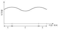
Figure 4 is a graph showing the etch uniformity of the substrate of Figure 1.
Figure 5 is a perspective view showing an example of the second distribution plate of Figure 2.
Figure 6 is a flow chart showing the manufacturing method of the semiconductor device of the present invention.
도 1은 본 발명의 개념에 따른 기판 처리 장치(100)를 보여준다.Figure 1 shows a
도 1을 참조하면, 본 발명의 기판 처리 장치(100)는 CCP(Capacitively Coupled Plasma) 장치일 수 있다. 일 예에 따르면, 상기 기판 처리 장치(100)는 챔버(110), 척(120), 파워 공급 부(130), 가스 공급 부(140), 가스 주입 모듈(150), 및 제어 부(160)를 포함할 수 있다. 기판(W)은 상기 챔버(110) 내의 상기 척(120) 상에 제공될 수 있다. 상기 파워 공급 부(130)는 고주파 파워(132)를 이용하여 상기 챔버(110) 내에 플라즈마(12)를 생성할 수 있다. 상기 가스 공급 부(140)는 가스(10)를 상기 가스 주입 모듈(150)에 공급하고, 상기 가스 주입 모듈(150)은 상기 가스(10)를 상기 챔버(110) 내에 제공할 수 있다. 상기 제어 부(160)는 상기 가스(10)의 유속, 및 상기 고주파 파워(132)를 제어하여 상기 기판(W)의 제조 공정을 관리할 수 있다.Referring to FIG. 1, the
상기 챔버(110)는 기판(W)에 대해 외부로부터 밀폐된 공간을 제공할 수 있다. 도시되지는 않았지만, 상기 챔버(110)는 하부 하우징과 상기 하부 하우징 상의 상부 하우징을 포함할 수 있다. 상기 하부 하우징이 상기 상부 하우징으로부터 분리될 경우, 상기 기판(W)은 로봇 암에 의해 상기 척(120) 상에 제공될 수 있다.The
상기 척(120)은 상기 챔버(110)의 하부 내에 배치될 수 있다. 상기 척(120)은 기판(W)을 수납할 수 있다. 상기 척(120)은 정전압을 이용하여 상기 기판(W)을 고정할 수 있다. 상기 정전압은 상기 챔버(110) 외부의 정전압 공급 부를 통해 제공될 수 있다.The
상기 파워 공급 부(130)는 상기 척(120)에 연결될 수 있다. 상기 파워 공급 부(130)는 상기 척(120)에 상기 고주파 파워(132)를 공급할 수 있다. 상기 고주파 파워(132)는 상기 기판(W) 상의 상기 가스(10)를 플라즈마 상태로 여기시킬 수 있다. 즉, 상기 고주파 파워(132)는 상기 가스(10)의 플라즈마(12)를 생성시킬 수 있다.The
상기 가스 공급 부(140)는 상기 가스 주입 모듈(150)을 통해 상기 챔버(110) 내에 가스(10)를 공급할 수 있다. 일 예로, 상기 가스 공급 부(140)는 제 1 가스 공급 부들(142), 가스 유량 제어기(144), 및 제 2 가스 공급 부들(146)을 포함할 수 있다. 상기 제 1 가스 공급 부들(142)은 상기 가스 주입 모듈(150)에 상기 가스(10)의 주 가스(main gas, ex, Ar, N2, SF6)를 공급할 수 있다. 상기 제 1 가스 공급 부들(142)의 각각은 질량 유량 조절 밸브(143)를 가질 수 있다. 상기 가스 유량 제어기(144)는 상기 제 1 가스 공급 부들(142)와 상기 가스 주입 모듈(150) 사이에 배치될 수 있다. 상기 가스 유량 제어기(144)는 상기 주 가스의 유량을 제어할 수 있다. 상기 제 2 가스 공급 부들(146)은 상기 가스 유량 제어 기(144)와 상기 가스 주입 모듈(150) 사이의 배관(141)에 연결될 수 있다. 상기 제 2 가스 공급 부들(146)은 상기 가스 유량 제어 기(144)와 상기 가스 주입 모듈(150) 사이의 배관(141)에 연결되는 보조 밸브들(145)을 가질 수 있다. 상기 제 2 가스 공급 부들(146)은 상기 가스 주입 모듈(150)에 상기 가스(10)의 추가 가스(additional gas, ex, O2, C4F6, C4F8)를 제공할 수 있다.The
상기 가스 주입 모듈(150)은 상기 챔버(110)의 상부 내에 배치될 수 있다. 상기 가스 주입 모듈(150)은 상기 기판(W) 상에 상기 가스(10)를 제공할 수 있다. 상기 가스 주입 모듈(150) 내의 상기 가스(10)의 압력은 상기 가스 유량 제어기(144)와 상기 가스 주입 모듈(150) 사이의 상기 배관(141) 내의 가스(10)의 압력보다 작을 수 있다.The
도 2는 도 1의 가스 주입 모듈(150)의 일 예를 보여준다.Figure 2 shows an example of the
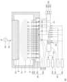
도 1 및 도 2를 참조하면, 가스 주입 모듈(150)은 샤워헤드(152), 제 1 분배 플레이트(154), 제 2 분배 플레이트(156), 및 유속 조절 부(158)를 포함할 수 있다.1 and 2, the
상기 샤워헤드(152)는 다수개의 분사구들(30)을 포함할 수 있다. 상기 분사구들(30)은 상기 기판(W) 상에 상기 가스(10)을 분사할 수 있다. 예를 들어, 상기 분사구들(30)의 각각은 약 0.5mm 내지 약 1mm의 직경을 가질 수 있다. 상기 샤워헤드(152)의 사용 초기에, 상기 분사구들(30)의 각각은 서로 동일한 크기를 가질 수 있다. 또한, 상기 분사구들(30) 내의 상기 가스(10)의 유속은 유사하거나 동일할 수 있다. 상기 분사구들(30)은 상기 기판(W)의 모양에 근거하여 배열될 수 있다. 상기 기판(W)이 원형일 경우, 상기 분사구들(30)은 동심원 모양으로 배열될 수 있다. 일 예로, 상기 샤워헤드(152)는 상기 기판(W)의 위치에 따라 제 1 영역(22)과 제 2 영역(24)을 가질 수 있다. 상기 제 1 영역(22)은 상기 기판(W)의 중심(C)에 대응되고, 상기 제 2 영역(24)은 상기 기판(W)의 에지(E)에 대응될 수 있다. 상기 제 1 영역(22)은 중심 영역(21)과 중간 영역(23)을 포함할 수 있다. 상기 제 2 영역(24)은 상기 제 1 영역(22)의 외곽에 배치될 수 있다. 상기 제 2 영역(24)은 에지 영역(25)과 극에지 영역(extreme edge region, 27)을 포함할 수 있다. 상기 제 1 및 제 2 영역들(22, 24) 내에서, 상기 분사구들(30)은 규칙적이고 균등하게 배열될 수 있다. 일 예로, 상기 분사구들(30)은 제 1 분사구들(32)과 제 2 분사구들(34)을 포함할 수 있다.The
상기 제 1 분사구들(32)은 상기 제 1 영역(22) 내에 배치되고, 상기 제 2 분사구들(34)은 상기 제 2 영역(24) 내에 배치될 수 있다. 상기 제 1 분사구들(32)은 중심 분사구들(31)과, 중간 분사구들(33)을 포함할 수 있다. 예를 들어, 상기 중심 분사구들(31)은 약 3개의 링 모양들로 배열될 수 있다. 상기 중심 분사구들(31)은 제 1 링(ex, 4개), 제 2 링(ex, 12개), 및 제 3 링(ex, 24)의 모양으로 배열될 수 있다. 상기 중간 분사구들(33)은 상기 중심 분사구들(31)의 외곽에 배치될 수 있다. 상기 중간 분사구들(33)은 제 4 링(ex, 36개), 제 5 링(ex, 48개), 및 제 6 링(ex, 60개)의 모양으로 배열될 수 있다.The
상기 제 2 분사구들(34)은 상기 중간 분사구들(33)의 외곽에 배치될 수 있다. 일 예로, 상기 제 2 분사구들(34)은 에지 분사구들(35)과, 극에지 분사구들(37)을 포함할 수 있다. 상기 에지 분사구들(35)는 제 7 링(ex, 80개)의 모양으로 배열될 수 있다. 상기 극에지 분사구들(37)은 상기 에지 분사구들(35)의 외곽에 배치될 수 있다. 상기 극에지 분사구들(37)은 제 8 링(ex, 100 개)의 모양으로 배열될 수 있다.The second injection holes 34 may be disposed outside the middle injection holes 33. As an example, the second injection holes 34 may include edge injection holes 35 and polar edge injection holes 37. The
도 3은 도 2의 샤워헤드(152)의 일 예를 보여준다.Figure 3 shows an example of the
도 3을 참조하여, 상기 샤워헤드(152)가 일정 시간 동안 사용되면, 상기 제 1 분사구들(32)은 상기 제 2 분사구들(34)보다 커질 수 있다. 상기 중심 영역(21)의 플라즈마(12)의 밀도가 상기 제 2 영역(24)의 플라즈마(12)의 밀도보다 크기 때문에 상기 제 1 분사구들(32)은 상기 플라즈마(12)에 의해 상기 제 2 분사구들(34)보다 크게 확장되거나 넓어질 수 있다. 이와 달리, 상기 제 2 분사구들(34)은 상기 제 1 분사구들(32)보다 커질 수 있다. 즉, 상기 제 1 및 제 2 분사구들(32, 34)은 그들 사이의 크기 차이를 가질 수 있다. 상기 제 1 분사구들(32)과 제 2 분사구들(34)의 크기 차이가 발생되면, 상기 가스(10)는 상기 제 1 및 제 2 분사구들(32, 34) 내의 가스(10)는 유속 차이를 생성될 수 있다. 상기 제 1 및 제 2 분사구들(32, 34) 내의 가스(10)의 유속 차이가 생성되면, 상기 기판(W)의 식각 균일도가 감소할 수 있다.Referring to FIG. 3 , when the
도 4는 도 1의 기판(W)의 식각 균일도(uniformity)를 보여준다.FIG. 4 shows the etch uniformity of the substrate W of FIG. 1.
도 4를 참조하여, 상기 제 1 분사구들(32)이 상기 제 2 분사구들(34)보다 커지면, 상기 기판(W)의 식각량은 중심(C)보다 에지(E)가 높을 수 있다. 이는 상기 제 1 분사구들(32) 내의 가스(10)의 유속이 상기 제 2 분사구들(34) 내의 가스(10)의 유속보다 작아지기 때문일 수 있다. 또한, 제 1 및 제 2 분사구들(32, 34)에 제공되는 상기 가스(10)의 압력 차이가 발생되기 때문일 수 있다. 가령, 상기 제 1 및 제 2 분사구들(32, 34) 내의 가스(10)의 유속이 동일해지면, 상기 기판(W)의 식각 균일도는 증가할 수 있다. 상기 제 1 및 제 2 분사구들(32, 34)에 제공되는 상기 가스(10)의 압력이 동일해지면, 상기 기판(W)의 식각 균일도는 증가할 수 있다.Referring to FIG. 4, when the first injection holes 32 are larger than the second injection holes 34, the etching amount of the substrate W may be higher at the edge E than at the center C. This may be because the flow rate of the
이하, 상기 가스 주입 모듈(150) 내의 상기 가스(10)의 압력 및/또는 유속을 유사하게 조절하여 기판(W)의 식각 균일도를 증가시키는 기술에 대해 설명한다.Hereinafter, a technique for increasing the etching uniformity of the substrate W by similarly adjusting the pressure and/or flow rate of the
다시 도 2를 참조하면, 상기 제 1 분배 플레이트(154)는 상기 샤워헤드(152) 상에 배치될 수 있다. 상기 제 1 분배 플레이트(154)는 복수개의 하부 유로들(40)을 가질 수 있다. 상기 하부 유로들(40)은 상기 분사구들(30)에 연결될 수 있다. 상기 가스(10)는 상기 하부 유로들(40)을 통해 상기 분사구들(30)에 제공될 수 있다. 일 예로, 상기 하부 유로들(40)은 동심원의 홈 모양을 가질 수 있다. 상기 하부 유로들(40)은 하부 홈들(46), 및 상기 하부 홈들(46) 내의 하부 홀들(48)을 포함할 수 있다. 상기 하부 홀들(48)은 상기 분사구들(30)에 정렬될 수 있다. 상기 하부 홈들(46)은 상기 분사구들(30) 상에 배치될 수 있다. 일 예로, 하부 홈들(46)은 제 1 하부 홈들(42), 및 제 2 하부 홈들(44)을 포함할 수 있다. 상기 제 1 하부 홈들(42)은 상기 제 1 분사구들(32) 상에 배치될 수 있다. 상기 제 1 하부 홈들(42)은 중심 하부 홈들(41), 및 중간 하부 홈들(43)을 포함할 수 있다. 상기 제 2 하부 홈들(44)은 상기 제 1 하부 홈들(42) 외곽에 배치될 수 있다. 상기 제 2 하부 홈들(44)은 하부 에지 홈(45)과 하부 극에지 홈(47)을 포함할 수 있다.Referring again to FIG. 2, the
상기 제 2 분배 플레이트(156)는 상기 제 1 분배 플레이트(154) 상에 배치될 수 있다. 상기 제 2 분배 플레이트(156)는 상부 유로들(50)을 가질 수 있다. 상기 상부 유로들(50)은 상기 하부 유로들(40)에 연결될 수 있다. 상기 가스(10)는 상기 상부 유로들(50)을 통해 상기 하부 유로들(40)에 제공될 수 있다. 일 예로, 상기 상부 유로들(50)은 제 1 및 제 2 상부 유로들(52, 54)을 포함할 수 있다.The
상기 제 1 상부 유로들(52)은 제 1 영역(22) 내에 배치될 수 있다. 일 예로, 상기 제 1 상부 유로들(52)은 중심 상부 유로(51), 및 중간 상부 유로(53)를 포함할 수 있다. 상기 중심 상부 유로(51)는 중심 영역(21) 내에 배치될 수 있다. 상기 중간 상부 유로(53)는 중간 영역(23) 내에 배치될 수 있다.The first
상기 제 2 상부 유로들(54)은 상기 제 1 상부 유로들(52) 외곽에 배치될 수 있다. 상기 제 2 상부 유로들(54)은 에지 상부 유로(55) 및 극에지 상부 유로(57)를 포함할 수 있다. 상기 에지 상부 유로(55)는 극에지 영역(27) 내에 배치될 수 있다.The second
도 5는 도 2의 제 2 분배 플레이트(156)의 일 예를 보여준다.Figure 5 shows an example of the
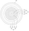
도 5를 참조하면, 제 2 분배 플레이트(156)는 하부 플레이트(155), 중부 플레이트(157), 및 상부 플레이트(159)를 포함할 수 있다.Referring to FIG. 5, the
상기 하부 플레이트(155)는 상기 제 1 분배 플레이트(154) 상에 배치될 수 있다. 일 예로, 상기 하부 플레이트(155)는 하부 홀들(60)을 포함할 수 있다. 상기 하부 홀들(60)은 상기 하부 유로들(40)에 연결될 수 있다. 상기 하부 홀들(60)은 제 1 및 제 2 하부 홀들(62, 64)을 포함할 수 있다. 상기 제 1 하부 홀들(62)은 제 1 영역(22) 내에 배치되고, 상기 제 2 하부 홀들(64)은 제 2 영역(24) 내에 배치될 수 있다. 상기 제 1 하부 홀들(62)은 하부 중심 홀들(61)과 하부 중간 홀들(63)을 포함할 수 있다. 상기 하부 중심 홀(61)은 중심 영역(21) 내에 배치되고, 상기 하부 중간 홀들(63)은 중간 영역(23) 내에 배치될 수 있다. 상기 제 2 하부 홀들(64)은 상기 제 1 하부 홀들(62)의 외곽에 배치될 수 있다. 상기 제 2 하부 홀들(64)은 하부 에지 홀들(65)과 하부 극에지 홀들(67)을 포함할 수 있다. 상기 하부 에지 홀들(65)은 에지 영역(25) 내에 배치될 수 있다. 상기 하부 극에지 홀들(67)은 극에지 영역(27) 내에 배치될 수 있다.The
상기 중부 플레이트(157)는 상기 하부 플레이트(155) 상에 배치될 수 있다. 일 예로, 상기 중부 플레이트(157)는 중부 홀들(70)을 포함할 수 있다. 상기 중부 홀들(70)은 상기 하부 홀들(60)에 연결될 수 있다. 상기 중부 홀들(70)은 제 1 및 제 2 중부 홀들(72, 74)을 포함할 수 있다. 상기 제 1 중부 홀들(72)은 제 1 영역(22) 내에 배치되고, 상기 제 2 중부 홀들(74)은 제 2 영역(24) 내에 배치될 수 있다. 상기 제 1 중부 홀들(72)은 중부 중심 홀들(71)과 중부 중간 홀들(73)을 포함할 수 있다. 상기 중부 중심 홀들(71)은 중심 영역(21) 내에 배치되고, 상기 중부 중간 홀들(73)은 중간 영역(23) 내에 배치될 수 있다. 상기 제 2 중부 홀들(74)은 상기 제 1 중부 홀들(72)의 외곽에 배치될 수 있다. 상기 제 2 중부 홀들(74)은 중부 에지 홀들(75)과 중부 극에지 홀들(77)을 포함할 수 있다. 상기 중부 에지 홀들(75)은 에지 영역(25) 내에 배치되고, 상기 중부 극에지 홀들(77)은 극에지 영역(27) 내에 배치될 수 있다.The
상기 상부 플레이트(159)는 상기 중부 플레이트(157) 상에 배치될 수 있다. 상기 상부 플레이트(159)는 상부 홈들(80)과 상기 상부 홈들(80) 상의 주입구들(90)을 가질 수 있다.The
상기 상부 홈들(80)은 상기 중부 홀들(70)에 연결될 수 있다. 상기 상부 홈들(80)은 동심원의 홈 모양을 가질 수 있다. 상기 상부 홈들(80)은 제 1 및 제 2 상부 홈들(82, 84)을 포함할 수 있다. 상기 제 1 및 제 2 상부 홈들(82, 84)은 제 1 및 제 2 영역들(22, 24) 내에 각각 배치될 수 있다. 상기 제 1 상부 홈들(82)은 중심 상부 홈(81)과, 중간 상부 홈(83)을 포함할 수 있다. 상기 중심 상부 홈(81)은 중심 영역(21) 내에 배치되고, 상기 중간 상부 홈(83)은 중간 영역(23) 내에 배치될 수 있다. 상기 제 2 상부 홈들(84)은 상기 제 1 상부 홈들(82) 외곽에 배치될 수 있다. 상기 제 2 상부 홈들(84)은 에지 상부 홈(85)과 극에지 상부 홈(87)을 포함할 수 있다. 상기 에지 상부 홈(85)는 에지 영역(25) 내에 배치되고, 상기 극에지 상부 홈(87)은 극에지 영역(27) 내에 배치될 수 있다.The
상기 주입구들(90)은 상기 가스 유량 제어기(144)의 배관들(141)에 연결될 수 있다. 일 예로, 상기 주입구들(90)은 제 1 주입구들(92), 및 제 2 주입구들(92, 94)을 포함할 수 있다. 상기 제 1주입구들(92)은 상기 제 1 상부 홈들(82)에 연결될 수 있다. 상기 제 1 주입구들(92)은 중심 주입구(91)와 중간 주입구(93)를 포함할 수 있다. 상기 중심 주입구(91)는 상기 중심 상부 홈(81)에 연결될 수 있다. 상기 중간 주입구(93)는 상기 중간 상부 홈(83)에 연결될 수 있다. 상기 제 2 주입구들(94)은 상기 제 1 주입구(92)의 외곽에 배치될 수 있다. 상기 제 2 주입구들(94)은 에지 주입구(95)와 극에지 주입구(97)를 포함할 수 있다. 상기 에지 주입구(95)는 상기 에지 상부 홈(85)에 연결될 수 있다. 상기 극에지 주입구(97)는 상기 극에지 상부 홈(87)에 연결될 수 있다.The
도 1, 도 2, 및 도 5를 참조하면, 상기 유속 조절 부(158)는 상기 제 2 분배 플레이트(156)의 내부 및 상부에 배치될 수 있다. 상기 유속 조절 부(158)는 상부 유로들(50)의 제 1 상부 유로들(52) 및 제 2 상부 유로들(54) 내의 가스(10)의 압력을 감지할 수 있다. 상기 유속 조절 부(158)는 상기 감지된 압력에 근거하여 상기 제 1 상부 유로들(52)과 상기 제 2 상부 유로들(54) 내의 상기 가스(10)의 압력 차이를 감소 상기 제 1 분사구들(32)과 상기 제 2 분사구들(34) 내의 상기 가스(10)의 유속을 유사하게 조절할 수 있다. 일 예로, 상기 유속 조절 부(158)는 압력 센서들(170), 하부 밸브들(180), 및 상부 밸브들(190)을 포함할 수 있다.Referring to FIGS. 1, 2, and 5, the flow
상기 압력 센서들(170)은 상기 상부 홈들(80)의 측벽에 배치될 수 있다. 상기 압력 센서들(170)은 상기 상부 홈들(80) 내의 상기 가스(10)의 압력을 감지할 수 있다. 일 예로, 상기 압력 센서들(170)은 제 1 압력 센서들(172), 및 제 2 압력 센서들(174)을 포함할 수 있다.The
상기 제 1 압력 센서들(172)은 상기 제 1상부 홈들(82) 내에 배치되고, 상기 제 1 상부 홈들(82) 내의 상기 가스(10)의 압력을 감지할 수 있다. 상기 제 1 압력 센서들(172)는 중심 센서(171)와 중간 센서(173)를 포함할 수 있다. 상기 중심 센서(171)는 상기 중심 상부 홈(81) 내에 배치되고, 상기 중심 상부 홈(81) 내의 상기 가스(10)의 압력을 감지할 수 있다. 상기 중간 센서(173)는 상기 중간 상부 홈(83) 내에 배치되고, 상기 중간 상부 홈(83) 내의 상기 가스(10)의 압력을 감지할 수 있다.The
상기 제 2 압력 센서들(174)은 상기 제 2 상부 홈들(84) 내에 배치되고, 상기 제 2 상부 홈들(84) 내의 상기 가스(10)의 압력을 감지할 수 있다. 일 예로, 상기 제 2 압력 센서들(174)은 에지 센서(175)와 극에지 센서(177)를 포함할 수 있다. 상기 에지 센서(175)는 상기 에지 상부 홈(85) 내에 배치되고, 상기 에지 상부 홈(85) 내의 상기 가스(10)의 압력을 감지할 수 있다. 상기 극에지 센서(177)는 상기 극에지 상부 홈(87) 내에 배치되고, 상기 극에지 상부 홈(87) 내의 상기 가스(10)의 압력을 감지할 수 있다.The
상기 하부 밸브들(180)은 상기 압력 센서들(170) 아래에 배치될 수 있다. 일 예로, 상기 하부 밸브들(180)은 상기 하부 홀들(60) 내에 각각 배치될 수 있다. 상기 하부 밸브들(180)은 상기 하부 홀들(60) 내의 상기 가스(10)의 유속을 제어할 수 있다. 예를 들어, 상기 하부 밸브들(180)은 오리피스(orifice) 밸브를 포함할 수 있다. 상기 하부 밸브들(180)이 열리거나 확장되면, 상기 하부 홀들(60) 내의 상기 가스(10)의 유속은 증가할 수 있다. 상기 하부 밸브들(180)이 닫히거나 감소되면, 상기 가스(10)의 유속은 감소할 수 있다. 일 예로, 하부 밸브들(180)은 제 1 및 제 2 하부 밸브들(182, 184)을 포함할 수 있다.The
상기 제 1 하부 밸브들(182)은 상기 제 1 하부 홀들(62) 내에 배치되고, 상기 제 1 하부 홀들(62) 내의 상기 가스(10)의 유속을 조절할 수 있다. 상기 제 1 하부 밸브들(182)은 하부 중심 밸브(181)와 하부 중간 밸브(183)를 포함할 수 있다. 상기 하부 중심 밸브(181)는 상기 하부 중심 홀(61) 내에 배치되고, 상기 하부 중심 홀들(61) 내의 상기 가스(10)의 유속을 조절할 수 있다. 상기 중간 밸브(183)는 상기 하부 중간 홀(63) 내에 배치되고, 상기 하부 중간 홀(63) 내의 상기 가스(10)의 유속을 조절할 수 있다.The first
상기 제 2 하부 밸브들(184)은 상기 제 2 하부 홀들(64) 내에 배치되고, 상기 제 2 하부 홀들(64) 내의 상기 가스(10)의 유속을 조절할 수 있다. 일 예로, 상기 제 2 하부 밸브들(184)은 하부 에지 밸브(185)와 하부 극에지 밸브(187)를 포함할 수 있다. 상기 하부 에지 밸브(185)는 상기 하부 에지 홀(65) 내에 배치되고, 상기 하부 에지 홀(65) 내의 상기 가스(10)의 유속을 조절할 수 있다. 상기 하부 극에지 밸브(187)는 상기 하부 극에지 홀(67) 내에 배치되고, 상기 하부 극에지 홀(67) 내의 상기 가스(10)의 유속을 조절할 수 있다.The second
상기 상부 밸브들(190)은 상기 압력 센서들(170) 상에 배치될 수 있다. 예를 들어, 상기 상부 밸브들(190)은 상기 가스 유량 제어기(144)와 상기 상부 플레이트(159)의 상기 주입구들(90) 사이에 연결될 수 있다. 상기 상부 밸브들(190)은 오리피스 밸브를 포함할 수 있다. 일 예로, 상부 밸브들(190)은 제 1 상부 밸브들(192), 및 제 2 상부 밸브들(194)을 포함할 수 있다.The
상기 제 1 상부 밸브들(192)은 제 1 주입구들(92)에 연결되고, 상기 제 1 주입구들(92) 내의 상기 가스(10)의 유속을 제어할 수 있다. 상기 제 1 상부 밸브들(192)은 중심 상부 밸브(191), 및 중간 상부 밸브(193)를 포함할 수 있다. 상기 중심 상부 밸브(191)는 중심 주입구(91)에 연결되고, 상기 중심 주입구(91) 내의 상기 가스(10)의 유속을 제어할 수 있다. 상기 중간 상부 밸브(193)는 중간 주입구(93)에 연결되고, 상기 중간 주입구(93) 내의 상기 가스(10)의 유속을 제어할 수 있다.The first
상기 제 2 상부 밸브들(194)은 제 2 주입구들(94)에 연결되고, 상기 제 2 주입구들(94) 내의 상기 가스(10)의 유속을 제어할 수 있다. 일 예로, 상기 제 2 상부 밸브들(194)은 에지 상부 밸브(195), 극에지 상부 밸브(197)를 포함할 수 있다. 상기 에지 상부 밸브(195)는 상기 에지 주입구(95)에 연결되고, 상기 에지 주입구(95) 내의 상기 가스(10)의 유속을 조절할 수 있다. 상기 극에지 상부 밸브(197)는 상기 극에지 주입구(97)에 연결되고, 상기 극에지 주입구(97) 내의 상기 가스(10)의 유속을 조절할 수 있다.The second
상기 제어 부(160)는 상기 압력 센서들(170), 상기 하부 밸브들(180), 및 상기 상부 밸브들(190)에 연결될 수 있다. 상기 제어 부(160)는 상기 상부 홈들(80) 내의 상기 가스(10)의 압력 값들을 획득하고, 상기 가스(10)의 압력 값들을 비교하고, 상기 비교된 압력 값들에 근거하여 상기 가스(10)의 유속을 조절할 수 있다. 일 예로, 상기 제어 부(160)는 감지 제어 부(162), 압력 비교 부(164), 및 유속 제어 부(166)를 포함할 수 있다.The control unit 160 may be connected to the
상기 감지 제어 부(162)는 상기 압력 센서들(170)에 연결될 수 있다. 상기 감지 제어부(162)는 상기 가스 주입 모듈(150) 내의 상기 가스(10)의 압력 값을 획득할 수 있다.The
상기 압력 비교 부(164)는 상기 획득된 상기 압력 값을 비교할 수 있다. 상기 압력 비교 부(164)는 상기 비교된 압력 값에 따라 상기 분사구들(30)의 크기 차이가 발생된 것을 판별할 수 있다.The pressure comparison unit 164 may compare the obtained pressure values. The pressure comparison unit 164 may determine whether a difference in size of the
상기 유속 제어 부(166)는 상기 하부 밸브(180) 및 상기 상부 밸브들(190)을 제어하여 상기 가스 주입 모듈(150) 내의 상기 가스(10)의 압력을 유사하게 조절할 수 있다. 또한, 상기 유속 제어 부(166)는 상기 가스 주입 모듈(150) 내의 상기 가스(10)의 유속을 유사하게 조절할 수 있다.The flow
가령, 상기 압력 비교 부(164)가 제 1 영역(22) 내의 상기 가스(10)의 압력이 상기 제 2 영역(24) 내의 상기 가스(10) 압력보다 낮은 것으로 판별할 경우, 상기 유속 제어 부(166)는 상기 제 1 상부 밸브들(192)을 상기 제 2 상부 밸브들(194)보다 더 오픈시킬 수 있다. 상기 제 1 상부 밸브들(192)이 상기 제 2 상부 밸브들(194)보다 더 오픈되면, 상기 제 1 영역(22) 내의 상기 가스(10)의 압력이 증가할 수 있다. 상기 제 1 영역(22) 내의 상기 가스(10)의 압력이 증가하면, 상기 제 1 영역(22)과 상기 제 2 영역(24) 내의 상기 가스(10)의 압력은 동일해질 수 있다. 또한, 상기 제 1 및 제 2 분사구들(32, 34) 내의 상기 가스(10)의 유속은 동일해질 수 있다. 상기 기판(W)의 식각 균일도는 증가할 수 있다.For example, when the pressure comparison unit 164 determines that the pressure of the
상기 제 1 영역(22) 내의 가스(10)의 압력이 상기 제 2 영역(24) 내의 가스(10)의 압력보다 낮은 것으로 판별될 경우, 상기 유속 제어 부(166)는 상기 제 2 영역(24)의 제 2 하부 밸브들(184)을 상기 제 1 하부 밸브들(182)보다 더 클로즈시킬 수 있다. 상기 제 2 하부 밸브들(184)이 상기 제 1 하부 밸브들(182)보다 더 클로즈되면, 상기 제 2 영역(24)의 압력이 낮아질 수 있다. 상기 제 2 영역(24) 내의 가스(10)의 압력이 낮아지면, 상기 제 1 영역(22)과 상기 제 2 영역(24) 내의 상기 가스(10)의 압력은 동일해지고, 상기 제 1 및 제 2 분사구들(32, 34) 내의 상기 가스(10)의 유속은 동일해질 수 있다.When it is determined that the pressure of the
이와 같이 구성된 본 발명의 기판 처리 장치(100)의 반도체 소자의 제조 방법을 설명하면 다음과 같다.The manufacturing method of the semiconductor device of the
도 6은 본 발명의 반도체 소자의 제조 방법을 보여준다.Figure 6 shows the manufacturing method of the semiconductor device of the present invention.
도 6을 참조하면, 본 발명의 반도체 소자의 제조 방법은, 기판(W)을 제공하는 단계(S100), 가스(10)를 제공하는 단계(S200), 가스 주입 모듈(150) 내의 가스(10)의 압력을 검출하는 단계(S300), 상기 가스(10)의 압력 값을 비교하는 단계(S400), 상기 가스(10)의 압력을 유사하게 조절하는 단계(S500)를 포함할 수 있다.Referring to FIG. 6, the method for manufacturing a semiconductor device of the present invention includes providing a substrate W (S100), providing a gas 10 (S200), and providing a
먼저, 로봇 암(미도시)은 상기 챔버(110) 내의 상기 척(120) 상에 상기 기판(W)을 제공한다(S100).First, a robot arm (not shown) provides the substrate W on the
다음, 상기 가스 주입 모듈(150)은 상기 가스(10)를 상기 기판(W) 상에 제공한다(S200). 상기 파워 공급 부(130)는 상기 고주파 파워(132)를 공급하여 상기 플라즈마(12)를 생성할 수 있다. 상기 기판(W)은 상기 플라즈마(12)에 의해 식각될 수 있다. 이와 달리, 상기 플라즈마(12)는 상기 기판(W) 상에 박막을 형성시킬 수 있다.Next, the
그 다음, 상기 감지 제어 부(162)는 상기 압력 센서들(170)을 통해 상기 가스 주입 모듈(150) 내의 상기 가스(10)의 압력을 검출한다(S300).Next, the
그 후, 상기 압력 비교 부(164)는 상기 가스(10)의 압력 값들을 비교하여 상기 가스 주입 모듈(150) 내의 상기 가스(10)의 압력 차이가 있는지를 판별한다(400). 상기 가스(10)의 압력 차이가 없을 경우, 상기 감지 제어 부(162)는 상기 가스 주입 모듈(150) 내의 상기 가스(10)의 압력을 일정 시간마다 검출할 수 있다(S400).Thereafter, the pressure comparison unit 164 compares the pressure values of the
상기 가스(10)의 압력 차이가 있을 경우, 상기 유속 제어 부(166)는 상기 하부 밸브들(180) 및 상기 상부 밸브들(190)을 제어하여 상기 가스 주입 모듈(150) 내의 상기 가스(10)의 압력을 동일하거나 균일하게 조절한다(S500).If there is a pressure difference between the
이상, 첨부된 도면을 참조하여 본 발명의 실시 예를 설명하였지만, 본 발명이 속하는 기술분야에서 통상의 지식을 가진 자는 본 발명이 그 기술적 사상이나 필수적인 특징을 변경하지 않고서 다른 구체적인 형태로 실시될 수 있다는 것을 이해할 수 있을 것이다. 그러므로 이상에서 기술한 실시 예에는 모든 면에서 예시적인 것이며 한정적이 아닌 것으로 이해해야만 한다.Above, embodiments of the present invention have been described with reference to the attached drawings, but those skilled in the art will understand that the present invention can be implemented in other specific forms without changing its technical idea or essential features. You will understand that it exists. Therefore, the embodiments described above should be understood in all respects as illustrative and not restrictive.
Claims (20)
Translated fromKorean상기 샤워헤드 상에 배치되고, 상기 제 1 및 제 2 분사구들과 각각 연결되는 제 1 및 제 2 상부 유로들을 갖는 상부 분배 플레이트; 및
상기 상부 분배 플레이트의 상기 제 1 및 제 2 상부 유로들 내에 배치되고, 상기 제 1 및 제 2 상부 유로들 내의 압력 차이를 감소시켜 상기 제 1 및 제 2 분사구들 내의 가스의 유속을 유사하게 조절하는 유속 조절 부를 포함하되,
상기 유속 조절 부는 상기 제 1 및 제 2 상부 유로들 내에 각각 배치되고, 상기 제 1 및 제 2 상부 유로들 내의 상기 가스의 압력을 각각 감지하는 제 1 압력 센서들 및 제 2 압력 센서들을 포함하되,
상기 상부 분배 플레이트는:
상기 제 1 및 제 2 분사구들에 각각 연결되는 제 1 및 제 2 하부 홀들을 갖는 하부 플레이트; 및
상기 제 1 및 제 2 하부 홀들 상의 제 1 및 제 2 홈들을 갖는 상부 플레이트를 포함하되,
상기 제 1 및 제 2 압력 센서들은 상기 제 1 및 제 2 홈들 내에 각각 배치되는 가스 주입 모듈.
A showerhead having first nozzles in a first area and second nozzles in a second area outside the first area;
an upper distribution plate disposed on the showerhead and having first and second upper flow paths respectively connected to the first and second spray nozzles; and
disposed within the first and second upper flow paths of the upper distribution plate, and similarly adjusting the flow rate of gas within the first and second injection holes by reducing the pressure difference within the first and second upper flow paths. Including a flow rate control unit,
The flow rate control unit is disposed in the first and second upper passages, and includes first pressure sensors and second pressure sensors that respectively detect the pressure of the gas in the first and second upper passages,
The upper distribution plate:
a lower plate having first and second lower holes respectively connected to the first and second injection holes; and
an upper plate having first and second grooves on the first and second lower holes,
The first and second pressure sensors are disposed in the first and second grooves, respectively.
상기 유속 조절 부는 상기 제 1 및 제 2 압력 센서들 아래의 상기 제 1 및 제 2 하부 홀들에 각각 배치되는 제 1 하부 밸브와 제 2 하부 밸브를 더 포함하는 가스 주입 모듈.
According to claim 1,
The flow rate control unit further includes a first lower valve and a second lower valve respectively disposed in the first and second lower holes below the first and second pressure sensors.
상기 상부 플레이트는 상기 제 1 및 제 2 홈들 상의 제 1 및 제 2 주입구들을 갖는 가스 주입 모듈.
According to claim 1,
The top plate has first and second inlets on the first and second grooves.
상기 유속 조절 부는 상기 제 1 및 제 2 상기 압력 센서들 상의 상기 제 1 및 제 2 주입구들에 연결되는 제 1 상부 밸브 및 제 2 상부 밸브를 더 포함하는 가스 주입 모듈.
According to claim 5,
The gas injection module further includes a first upper valve and a second upper valve connected to the first and second inlets on the first and second pressure sensors.
상기 상부 분배 플레이트는 상기 제 1 및 제 2 분사구들과 상기 제 1 및 제 2 홈들 사이의 제 1 및 제 2 중부 홀들을 갖는 중부 플레이트를 더 포함하는 가스 주입 모듈.
According to claim 1,
The upper distribution plate further includes a central plate having first and second central holes between the first and second injection nozzles and the first and second grooves.
상기 제 1 영역은 중심 영역과 상기 중심 영역 외곽의 중간 영역을 포함하되,
상기 제 1 압력 센서들은:
상기 중심 영역 상의 중심 센서; 및
상기 중간 영역 상의 중간 센서를 포함하는 가스 주입 모듈.
According to claim 1,
The first area includes a central area and a middle area outside the central area,
The first pressure sensors:
a center sensor on the center area; and
A gas injection module comprising an intermediate sensor on the intermediate region.
상기 제 2 영역은 에지 영역과 상기 에지 영역 외곽의 극에지 영역을 포함하되,
상기 제 2 압력 센서들은:
상기 에지 영역 상의 에지 센서; 및
상기 극에지 영역 상의 극에지 센서를 포함하는 가스 주입 모듈.
According to claim 1,
The second area includes an edge area and a polar edge area outside the edge area,
The second pressure sensors:
an edge sensor on the edge area; and
A gas injection module comprising a pole edge sensor on the pole edge region.
상기 샤워헤드와 상기 상부 분배 플레이트 사이에 배치되고, 상기 제 1 및 제 2 분사구들과 상기 제 1 및 제 2 상부 유로들 사이의 제 1 및 제 2 하부 유로들을 갖는 하부 분배 플레이트를 더 포함하는 가스 주입 모듈.
According to claim 1,
Gas disposed between the showerhead and the upper distribution plate, the gas further comprising a lower distribution plate having first and second lower passages between the first and second injection nozzles and the first and second upper passages Injection module.
상기 챔버 하부에 배치되고 기판을 수납하는 척; 및
상기 척 상의 상기 챔버 상부에 배치되고, 상기 기판 상으로 가스를 제공하는 가스 주입 모듈을 포함하되,
상기 가스 주입 모듈은:
제 1 영역의 제 1 분사구들과 상기 제 1 영역 외곽의 제 2 영역의 제 2 분사구들을 갖는 샤워헤드;
상기 샤워헤드 상에 배치되고, 상기 제 1 및 제 2 분사구들과 각각 연결되는 제 1 및 제 2 상부 유로들을 갖는 상부 분배 플레이트; 및
상기 상부 분배 플레이트의 상기 제 1 및 제 2 상부 유로들 내에 배치되고, 상기 제 1 및 제 2 상부 유로들 내의 압력 차이를 감소시켜 상기 제 1 및 제 2 분사구들 내의 가스의 유속을 유사하게 조절하는 유속 조절 부를 포함하되,
상기 유속 조절 부는 상기 제 1 및 제 2 상부 유로들 내에 각각 배치되고, 상기 제 1 및 제 2 상부 유로들 내의 상기 가스의 압력을 각각 감지하는 제 1 압력 센서들 및 제 2 압력 센서들을 포함하되,
상기 상부 분배 플레이트는:
상기 제 1 및 제 2 분사구들에 각각 연결되는 제 1 및 제 2 하부 홀들을 갖는 하부 플레이트; 및
상기 제 1 및 제 2 하부 홀들 상의 제 1 및 제 2 홈들을 갖는 상부 플레이트를 포함하되,
상기 제 1 및 제 2 압력 센서들은 상기 제 1 및 제 2 홈들 내에 각각 배치되는 기판 처리 장치.
chamber;
a chuck disposed below the chamber and accommodating a substrate; and
A gas injection module disposed above the chamber on the chuck and providing gas onto the substrate,
The gas injection module:
A showerhead having first nozzles in a first area and second nozzles in a second area outside the first area;
an upper distribution plate disposed on the showerhead and having first and second upper flow paths respectively connected to the first and second spray nozzles; and
disposed within the first and second upper flow paths of the upper distribution plate, and similarly adjusting the flow rate of gas within the first and second injection holes by reducing the pressure difference within the first and second upper flow paths. Including a flow rate control unit,
The flow rate control unit is disposed in the first and second upper passages, and includes first pressure sensors and second pressure sensors that respectively detect the pressure of the gas in the first and second upper passages,
The upper distribution plate:
a lower plate having first and second lower holes respectively connected to the first and second injection holes; and
an upper plate having first and second grooves on the first and second lower holes,
The first and second pressure sensors are disposed in the first and second grooves, respectively.
상기 유속 조절 부는 상기 제 1 및 제 2 압력 센서들의 상부 또는 하부에 배치되는 제 1 및 제 2 밸브들을 더 포함하는 기판 처리 장치.
According to claim 11,
The flow rate control unit further includes first and second valves disposed above or below the first and second pressure sensors.
상기 제 1 및 제 2 압력 센서들과, 상기 제 1 및 제 2 밸브들을 제어하는 제어 부를 더 포함하되,
상기 제어 부는:
상기 제 1 및 제 2 압력 센서들에 연결되고, 상기 제 1 및 제 2 센서들을 통해 상기 제 1 및 제 2 상부 유로들 내의 상기 가스의 압력 값을 획득하는 감지 제어 부; 및
상기 제 1 및 제 2 상부 유로들 내의 상기 가스의 상기 획득된 압력 값을 비교하는 비교 제어 부를 포함하는 기판 처리 장치.
According to claim 12,
Further comprising a control unit that controls the first and second pressure sensors and the first and second valves,
The above control section is:
a detection control unit connected to the first and second pressure sensors and acquiring pressure values of the gas in the first and second upper passages through the first and second sensors; and
A substrate processing apparatus comprising: a comparison control unit that compares the obtained pressure values of the gas in the first and second upper flow paths.
상기 제어 부는 상기 비교된 압력 값에 근거하여 상기 제 1 및 제 2 밸브들을 제어하는 밸브 제어 부를 더 포함하는 기판 처리 장치.
According to claim 13,
The control unit further includes a valve control unit that controls the first and second valves based on the compared pressure value.
상기 가스 주입 모듈을 통해 상기 챔버 내에 상기 가스를 공급하는 가스 공급 부를 더 포함하되,
상기 가스 공급 부는:
제 1 가스를 공급하는 제 1 가스 공급 부;
상기 제 1 가스 공급 부와 상기 가스 주입 모듈 사이에 배치되고, 상기 제 1 가스의 유량을 제어하는 가스 유량 제어기; 및
상기 가스 유량 제어기와 상기 가스 주입 모듈 사이에 배치되고, 상기 제 1 가스와 다른 제 2 가스를 상기 가스 주입 모듈에 공급하는 제 2 가스 공급 부를 포함하는 기판 처리 장치.
According to claim 11,
It further includes a gas supply unit that supplies the gas into the chamber through the gas injection module,
The gas supply blowing is:
a first gas supply unit supplying a first gas;
a gas flow rate controller disposed between the first gas supply unit and the gas injection module and controlling a flow rate of the first gas; and
A substrate processing apparatus including a second gas supply unit disposed between the gas flow controller and the gas injection module and supplying a second gas different from the first gas to the gas injection module.
상기 챔버 내에 가스를 공급하는 단계; 및
상기 챔버에 연결된 가스 주입 모듈을 이용하여 상기 기판 상에 상기 가스를 제공하는 단계를 포함하되,
상기 가스 주입 모듈은:
제 1 영역의 제 1 분사구들과 상기 제 1 영역 외곽의 제 2 영역의 제 2 분사구들을 갖는 샤워헤드;
상기 샤워헤드 상에 배치되고, 상기 제 1 및 제 2 분사구들과 각각 연결되는 제 1 및 제 2 상부 유로들을 갖는 상부 분배 플레이트; 및
상기 상부 분배 플레이트의 상기 제 1 및 제 2 상부 유로들 내에 배치되고, 상기 제 1 및 제 2 상부 유로들 내의 압력 차이를 감소시켜 상기 제 1 및 제 2 분사구들 내의 가스의 유속을 유사하게 조절하는 유속 조절 부를 포함하되,
상기 유속 조절 부는 상기 제 1 및 제 2 상부 유로들 내에 각각 배치되고, 상기 제 1 및 제 2 상부 유로들 내의 상기 가스의 압력을 각각 감지하는 제 1 압력 센서들 및 제 2 압력 센서들을 포함하되,
상기 상부 분배 플레이트는:
상기 제 1 및 제 2 분사구들에 각각 연결되는 제 1 및 제 2 하부 홀들을 갖는 하부 플레이트; 및
상기 제 1 및 제 2 하부 홀들 상의 제 1 및 제 2 홈들을 갖는 상부 플레이트를 포함하되,
상기 제 1 및 제 2 압력 센서들은 상기 제 1 및 제 2 홈들 내에 각각 배치되는 반도체 소자의 제조방법.
providing a substrate within the chamber;
supplying gas into the chamber; and
Providing the gas on the substrate using a gas injection module connected to the chamber,
The gas injection module:
A showerhead having first nozzles in a first area and second nozzles in a second area outside the first area;
an upper distribution plate disposed on the showerhead and having first and second upper flow paths respectively connected to the first and second spray nozzles; and
disposed within the first and second upper flow paths of the upper distribution plate, and similarly adjusting the flow rate of gas within the first and second injection holes by reducing the pressure difference within the first and second upper flow paths. Including a flow rate control unit,
The flow rate control unit is disposed in the first and second upper passages, and includes first pressure sensors and second pressure sensors that respectively detect the pressure of the gas in the first and second upper passages,
The upper distribution plate:
a lower plate having first and second lower holes respectively connected to the first and second injection holes; and
an upper plate having first and second grooves on the first and second lower holes,
The first and second pressure sensors are respectively disposed in the first and second grooves.
상기 유속 조절 부는 상기 제 1 및 제 2 압력 센서들의 하부 및 상부의 상기 제 1 및 제 2 상부 유로들에 연결되는 제 1 및 제 2 하부 밸브들과 제 1 및 제 2 상부 밸브들을 더 포함하는 반도체 소자의 제조방법.According to clause 16,
The flow rate control unit further includes first and second lower valves and first and second upper valves connected to the first and second upper flow passages below and above the first and second pressure sensors. Device manufacturing method.
Priority Applications (4)
| Application Number | Priority Date | Filing Date | Title |
|---|---|---|---|
| KR1020180144454AKR102641752B1 (en) | 2018-11-21 | 2018-11-21 | Gas injection module, substrate processing apparatus and method for manufacturing semiconductor device using the same |
| CN201910601953.6ACN111211030B (en) | 2018-11-21 | 2019-07-05 | Gas injection module, substrate processing apparatus, and method of manufacturing semiconductor device |
| US16/509,946US10934621B2 (en) | 2018-11-21 | 2019-07-12 | Gas injection module, substrate processing apparatus, and method of fabricating semiconductor device using the same |
| US17/159,244US11384433B2 (en) | 2018-11-21 | 2021-01-27 | Gas injection module, substrate processing apparatus, and method of fabricating semiconductor device using the same |
Applications Claiming Priority (1)
| Application Number | Priority Date | Filing Date | Title |
|---|---|---|---|
| KR1020180144454AKR102641752B1 (en) | 2018-11-21 | 2018-11-21 | Gas injection module, substrate processing apparatus and method for manufacturing semiconductor device using the same |
Publications (2)
| Publication Number | Publication Date |
|---|---|
| KR20200060579A KR20200060579A (en) | 2020-06-01 |
| KR102641752B1true KR102641752B1 (en) | 2024-03-04 |
Family
ID=70727357
Family Applications (1)
| Application Number | Title | Priority Date | Filing Date |
|---|---|---|---|
| KR1020180144454AActiveKR102641752B1 (en) | 2018-11-21 | 2018-11-21 | Gas injection module, substrate processing apparatus and method for manufacturing semiconductor device using the same |
Country Status (3)
| Country | Link |
|---|---|
| US (2) | US10934621B2 (en) |
| KR (1) | KR102641752B1 (en) |
| CN (1) | CN111211030B (en) |
Families Citing this family (25)
| Publication number | Priority date | Publication date | Assignee | Title |
|---|---|---|---|---|
| US9132436B2 (en) | 2012-09-21 | 2015-09-15 | Applied Materials, Inc. | Chemical control features in wafer process equipment |
| US9741593B2 (en) | 2015-08-06 | 2017-08-22 | Applied Materials, Inc. | Thermal management systems and methods for wafer processing systems |
| US10504700B2 (en) | 2015-08-27 | 2019-12-10 | Applied Materials, Inc. | Plasma etching systems and methods with secondary plasma injection |
| US10504754B2 (en)* | 2016-05-19 | 2019-12-10 | Applied Materials, Inc. | Systems and methods for improved semiconductor etching and component protection |
| US9865484B1 (en) | 2016-06-29 | 2018-01-09 | Applied Materials, Inc. | Selective etch using material modification and RF pulsing |
| US11276590B2 (en) | 2017-05-17 | 2022-03-15 | Applied Materials, Inc. | Multi-zone semiconductor substrate supports |
| JP7176860B6 (en) | 2017-05-17 | 2022-12-16 | アプライド マテリアルズ インコーポレイテッド | Semiconductor processing chamber to improve precursor flow |
| US11276559B2 (en) | 2017-05-17 | 2022-03-15 | Applied Materials, Inc. | Semiconductor processing chamber for multiple precursor flow |
| US11328909B2 (en) | 2017-12-22 | 2022-05-10 | Applied Materials, Inc. | Chamber conditioning and removal processes |
| KR102641752B1 (en)* | 2018-11-21 | 2024-03-04 | 삼성전자주식회사 | Gas injection module, substrate processing apparatus and method for manufacturing semiconductor device using the same |
| US11437242B2 (en) | 2018-11-27 | 2022-09-06 | Applied Materials, Inc. | Selective removal of silicon-containing materials |
| TWI730548B (en)* | 2018-12-17 | 2021-06-11 | 美商應用材料股份有限公司 | Electron beam apparatus for optical device fabrication |
| CN113396240A (en)* | 2019-03-11 | 2021-09-14 | 应用材料公司 | Lid assembly apparatus and method for substrate processing chamber |
| WO2021034508A1 (en) | 2019-08-16 | 2021-02-25 | Lam Research Corporation | Spatially tunable deposition to compensate within wafer differential bow |
| CN119980191A (en) | 2019-08-28 | 2025-05-13 | 朗姆研究公司 | Metal Deposition |
| KR102656744B1 (en) | 2020-01-03 | 2024-04-12 | 램 리써치 코포레이션 | Station-to-station control of backside bow compensation deposition |
| WO2021154641A1 (en) | 2020-01-30 | 2021-08-05 | Lam Research Corporation | Uv cure for local stress modulation |
| JP2023048726A (en)* | 2021-09-28 | 2023-04-07 | 東京エレクトロン株式会社 | SUBSTRATE PROCESSING APPARATUS, GAS SHOWER HEAD, AND SUBSTRATE PROCESSING METHOD |
| US12417899B2 (en) | 2022-03-16 | 2025-09-16 | Applied Materials, Inc. | Integrated showerhead |
| KR20250011930A (en)* | 2022-05-13 | 2025-01-22 | 램 리써치 코포레이션 | Multi-zone gas distribution for asymmetric wafer warpage compensation |
| US20230374660A1 (en)* | 2022-05-17 | 2023-11-23 | Applied Materials, Inc. | Hardware to uniformly distribute active species for semiconductor film processing |
| CN120129951A (en)* | 2023-01-19 | 2025-06-10 | 应用材料公司 | Air flow control for improved thickness uniformity |
| US11940819B1 (en)* | 2023-01-20 | 2024-03-26 | Applied Materials, Inc. | Mass flow controller based fast gas exchange |
| US20250135473A1 (en)* | 2023-10-27 | 2025-05-01 | Applied Materials, Inc. | Dual channel showerhead conductance optimization for uniform radial flow distribution |
| US20250276335A1 (en)* | 2024-02-29 | 2025-09-04 | Applied Materials, Inc. | Bonded showerhead assembly and method for using the same |
Citations (1)
| Publication number | Priority date | Publication date | Assignee | Title |
|---|---|---|---|---|
| KR100801768B1 (en)* | 2005-03-25 | 2008-02-11 | 동경 엘렉트론 주식회사 | Etching Method and Etching Apparatus |
Family Cites Families (61)
| Publication number | Priority date | Publication date | Assignee | Title |
|---|---|---|---|---|
| JP3468859B2 (en)* | 1994-08-16 | 2003-11-17 | 富士通株式会社 | Gas phase processing apparatus and gas phase processing method |
| JPH0945624A (en)* | 1995-07-27 | 1997-02-14 | Tokyo Electron Ltd | Leaf-type heat treating system |
| KR100492258B1 (en)* | 1996-10-11 | 2005-09-02 | 가부시키가이샤 에바라 세이사꾸쇼 | Reaction gas ejection head |
| US6245192B1 (en)* | 1999-06-30 | 2001-06-12 | Lam Research Corporation | Gas distribution apparatus for semiconductor processing |
| US6502530B1 (en) | 2000-04-26 | 2003-01-07 | Unaxis Balzers Aktiengesellschaft | Design of gas injection for the electrode in a capacitively coupled RF plasma reactor |
| AU2001288225A1 (en)* | 2000-07-24 | 2002-02-05 | The University Of Maryland College Park | Spatially programmable microelectronics process equipment using segmented gas injection showerhead with exhaust gas recirculation |
| GB0111485D0 (en)* | 2001-05-11 | 2001-07-04 | Amersham Pharm Biotech Ab | Scalable liquid distribution system for large scale chromatography columns |
| KR100862658B1 (en)* | 2002-11-15 | 2008-10-10 | 삼성전자주식회사 | Gas injection device of semiconductor processing system |
| US7384876B2 (en) | 2002-12-20 | 2008-06-10 | Tokyo Electron Limited | Method and apparatus for determining consumable lifetime |
| US7708859B2 (en)* | 2004-04-30 | 2010-05-04 | Lam Research Corporation | Gas distribution system having fast gas switching capabilities |
| US20070066038A1 (en)* | 2004-04-30 | 2007-03-22 | Lam Research Corporation | Fast gas switching plasma processing apparatus |
| JP4550507B2 (en)* | 2004-07-26 | 2010-09-22 | 株式会社日立ハイテクノロジーズ | Plasma processing equipment |
| US20060042754A1 (en)* | 2004-07-30 | 2006-03-02 | Tokyo Electron Limited | Plasma etching apparatus |
| US20060124169A1 (en)* | 2004-12-09 | 2006-06-15 | Tokyo Electron Limited | Gas supply unit, substrate processing apparatus, and supply gas setting method |
| US20060288934A1 (en)* | 2005-06-22 | 2006-12-28 | Tokyo Electron Limited | Electrode assembly and plasma processing apparatus |
| US20070021935A1 (en) | 2005-07-12 | 2007-01-25 | Larson Dean J | Methods for verifying gas flow rates from a gas supply system into a plasma processing chamber |
| US7896967B2 (en)* | 2006-02-06 | 2011-03-01 | Tokyo Electron Limited | Gas supply system, substrate processing apparatus and gas supply method |
| JP4911984B2 (en)* | 2006-02-08 | 2012-04-04 | 東京エレクトロン株式会社 | Gas supply apparatus, substrate processing apparatus, gas supply method, and shower head |
| US7892358B2 (en)* | 2006-03-29 | 2011-02-22 | Tokyo Electron Limited | System for introducing a precursor gas to a vapor deposition system |
| US8187415B2 (en)* | 2006-04-21 | 2012-05-29 | Applied Materials, Inc. | Plasma etch reactor with distribution of etch gases across a wafer surface and a polymer oxidizing gas in an independently fed center gas zone |
| US20070249173A1 (en)* | 2006-04-21 | 2007-10-25 | Applied Materials, Inc. | Plasma etch process using etch uniformity control by using compositionally independent gas feed |
| US7540971B2 (en)* | 2006-04-28 | 2009-06-02 | Applied Materials, Inc. | Plasma etch process using polymerizing etch gases across a wafer surface and additional polymer managing or controlling gases in independently fed gas zones with time and spatial modulation of gas content |
| US7541292B2 (en)* | 2006-04-28 | 2009-06-02 | Applied Materials, Inc. | Plasma etch process with separately fed carbon-lean and carbon-rich polymerizing etch gases in independent inner and outer gas injection zones |
| US8231799B2 (en)* | 2006-04-28 | 2012-07-31 | Applied Materials, Inc. | Plasma reactor apparatus with multiple gas injection zones having time-changing separate configurable gas compositions for each zone |
| US7431859B2 (en)* | 2006-04-28 | 2008-10-07 | Applied Materials, Inc. | Plasma etch process using polymerizing etch gases with different etch and polymer-deposition rates in different radial gas injection zones with time modulation |
| US20080073032A1 (en) | 2006-08-10 | 2008-03-27 | Akira Koshiishi | Stage for plasma processing apparatus, and plasma processing apparatus |
| US20080078746A1 (en)* | 2006-08-15 | 2008-04-03 | Noriiki Masuda | Substrate processing system, gas supply unit, method of substrate processing, computer program, and storage medium |
| KR100849929B1 (en)* | 2006-09-16 | 2008-08-26 | 주식회사 피에조닉스 | Chemical vapor deposition method and apparatus equipped with a shower head for actively controlling the injection speed of the reaction gas |
| US20080081114A1 (en)* | 2006-10-03 | 2008-04-03 | Novellus Systems, Inc. | Apparatus and method for delivering uniform fluid flow in a chemical deposition system |
| JP5034594B2 (en)* | 2007-03-27 | 2012-09-26 | 東京エレクトロン株式会社 | Film forming apparatus, film forming method, and storage medium |
| US7976631B2 (en)* | 2007-10-16 | 2011-07-12 | Applied Materials, Inc. | Multi-gas straight channel showerhead |
| JP5192214B2 (en)* | 2007-11-02 | 2013-05-08 | 東京エレクトロン株式会社 | Gas supply apparatus, substrate processing apparatus, and substrate processing method |
| US20090159213A1 (en)* | 2007-12-19 | 2009-06-25 | Applied Materials, Inc. | Plasma reactor gas distribution plate having a path splitting manifold immersed within a showerhead |
| US8512509B2 (en)* | 2007-12-19 | 2013-08-20 | Applied Materials, Inc. | Plasma reactor gas distribution plate with radially distributed path splitting manifold |
| US8066895B2 (en)* | 2008-02-28 | 2011-11-29 | Applied Materials, Inc. | Method to control uniformity using tri-zone showerhead |
| US20090275206A1 (en)* | 2008-05-05 | 2009-11-05 | Applied Materials, Inc. | Plasma process employing multiple zone gas distribution for improved uniformity of critical dimension bias |
| JP5142914B2 (en) | 2008-09-25 | 2013-02-13 | 東京エレクトロン株式会社 | Mounting table and plasma processing apparatus |
| KR101121202B1 (en)* | 2008-11-14 | 2012-03-23 | 세메스 주식회사 | Chemical vapor deposition apparatus that can supply process gas using multiple channels |
| KR101110080B1 (en)* | 2009-07-08 | 2012-03-13 | 주식회사 유진테크 | Substrate treatment method for selectively inserting diffusion plate |
| KR101128740B1 (en)* | 2009-07-24 | 2012-03-23 | 엘아이지에이디피 주식회사 | Chemical vapor deposition apparatus and method for controlling process gas used in the apparatus |
| US8551248B2 (en)* | 2010-04-19 | 2013-10-08 | Texas Instruments Incorporated | Showerhead for CVD depositions |
| JP5709505B2 (en) | 2010-12-15 | 2015-04-30 | 東京エレクトロン株式会社 | Plasma processing apparatus, plasma processing method, and storage medium |
| JP5902896B2 (en)* | 2011-07-08 | 2016-04-13 | 東京エレクトロン株式会社 | Substrate processing equipment |
| JP6157061B2 (en)* | 2012-05-11 | 2017-07-05 | 東京エレクトロン株式会社 | Gas supply apparatus and substrate processing apparatus |
| JP6034655B2 (en)* | 2012-10-25 | 2016-11-30 | 東京エレクトロン株式会社 | Plasma processing equipment |
| JP6007143B2 (en)* | 2013-03-26 | 2016-10-12 | 東京エレクトロン株式会社 | Shower head, plasma processing apparatus, and plasma processing method |
| JP6199619B2 (en)* | 2013-06-13 | 2017-09-20 | 株式会社ニューフレアテクノロジー | Vapor growth equipment |
| US9677176B2 (en)* | 2013-07-03 | 2017-06-13 | Novellus Systems, Inc. | Multi-plenum, dual-temperature showerhead |
| CN104576279B (en)* | 2013-10-22 | 2017-02-15 | 中微半导体设备(上海)有限公司 | Gas adjusting device and plasma reactor employing same |
| KR101560623B1 (en)* | 2014-01-03 | 2015-10-15 | 주식회사 유진테크 | Substrate processing apparatus and substrate processing method |
| KR102451499B1 (en)* | 2014-05-16 | 2022-10-06 | 어플라이드 머티어리얼스, 인코포레이티드 | Showerhead design |
| KR20160050821A (en)* | 2014-10-31 | 2016-05-11 | 세메스 주식회사 | Test method and apparatus for treating substrate |
| US10023959B2 (en)* | 2015-05-26 | 2018-07-17 | Lam Research Corporation | Anti-transient showerhead |
| JP6868616B2 (en)* | 2015-10-08 | 2021-05-12 | アプライド マテリアルズ インコーポレイテッドApplied Materials,Incorporated | Shower head with reduced plasma ignition on the back |
| TWI733712B (en)* | 2015-12-18 | 2021-07-21 | 美商應用材料股份有限公司 | A diffuser for a deposition chamber and an electrode for a deposition chamber |
| US10403476B2 (en)* | 2016-11-09 | 2019-09-03 | Lam Research Corporation | Active showerhead |
| US10604841B2 (en)* | 2016-12-14 | 2020-03-31 | Lam Research Corporation | Integrated showerhead with thermal control for delivering radical and precursor gas to a downstream chamber to enable remote plasma film deposition |
| JP6811147B2 (en)* | 2017-06-23 | 2021-01-13 | 東京エレクトロン株式会社 | How to inspect the gas supply system |
| US10851457B2 (en)* | 2017-08-31 | 2020-12-01 | Lam Research Corporation | PECVD deposition system for deposition on selective side of the substrate |
| WO2019113478A1 (en)* | 2017-12-08 | 2019-06-13 | Lam Research Corporation | Integrated showerhead with improved hole pattern for delivering radical and precursor gas to a downstream chamber to enable remote plasma film deposition |
| KR102641752B1 (en)* | 2018-11-21 | 2024-03-04 | 삼성전자주식회사 | Gas injection module, substrate processing apparatus and method for manufacturing semiconductor device using the same |
- 2018
- 2018-11-21KRKR1020180144454Apatent/KR102641752B1/enactiveActive
- 2019
- 2019-07-05CNCN201910601953.6Apatent/CN111211030B/enactiveActive
- 2019-07-12USUS16/509,946patent/US10934621B2/enactiveActive
- 2021
- 2021-01-27USUS17/159,244patent/US11384433B2/enactiveActive
Patent Citations (1)
| Publication number | Priority date | Publication date | Assignee | Title |
|---|---|---|---|---|
| KR100801768B1 (en)* | 2005-03-25 | 2008-02-11 | 동경 엘렉트론 주식회사 | Etching Method and Etching Apparatus |
Also Published As
| Publication number | Publication date |
|---|---|
| CN111211030B (en) | 2024-04-26 |
| KR20200060579A (en) | 2020-06-01 |
| US11384433B2 (en) | 2022-07-12 |
| CN111211030A (en) | 2020-05-29 |
| US20210147982A1 (en) | 2021-05-20 |
| US20200157682A1 (en) | 2020-05-21 |
| US10934621B2 (en) | 2021-03-02 |
Similar Documents
| Publication | Publication Date | Title |
|---|---|---|
| KR102641752B1 (en) | Gas injection module, substrate processing apparatus and method for manufacturing semiconductor device using the same | |
| US11342163B2 (en) | Variable depth edge ring for etch uniformity control | |
| US11424103B2 (en) | Control of on-wafer cd uniformity with movable edge ring and gas injection adjustment | |
| US11011353B2 (en) | Systems and methods for performing edge ring characterization | |
| KR102503328B1 (en) | Adjustable side gas plenum for edge etch rate control in a downstream reactor | |
| US11217432B2 (en) | Gas supply system, plasma processing apparatus, and control method for gas supply system | |
| JP5891300B2 (en) | Gas distribution showerhead for inductively coupled plasma etching reactor | |
| JP7229061B2 (en) | Substrate etching apparatus and etching method | |
| US11610759B2 (en) | Gas splitting by time average injection into different zones by fast gas valves | |
| JP2014515561A (en) | Gas distribution system for ceramic showerhead in plasma etching reactor | |
| KR20100115788A (en) | Method and apparatus for controlling exhaust gas flow rate in processing chamber | |
| TWI890811B (en) | Process chamber lid and processing method for high temperature chemical vapor deposition | |
| US20090156011A1 (en) | Method of controlling CD bias and CD microloading by changing the ceiling-to-wafer gap in a plasma reactor | |
| US12400833B2 (en) | Methods and apparatus for processing a substrate | |
| CN100377300C (en) | Reaction chamber for semiconductor treatment | |
| US20250149312A1 (en) | Substrate processing apparatus including fluid supply unit and fluid control method for controlling flow variability of fluid | |
| JP7665861B2 (en) | Symmetrical Semiconductor Processing Chamber | |
| US20230298859A1 (en) | Optimizing edge radical flux in a downstream plasma chamber | |
| KR101751746B1 (en) | Plasma etching apparatus using dual-etching | |
| WO2022265882A1 (en) | Frontside and backside pressure monitoring for substrate movement prevention | |
| KR20030094933A (en) | PUMPING EQUIPMENT AND METHOD FOR CLEANING He GAS SUPPLY HOLE OF ESC THEREOF | |
| JP2021125504A (en) | Plasma etching method and plasma etching device | |
| KR20070077669A (en) | Semiconductor manufacturing apparatus including gas dispersion plate |
Legal Events
| Date | Code | Title | Description |
|---|---|---|---|
| PA0109 | Patent application | St.27 status event code:A-0-1-A10-A12-nap-PA0109 | |
| PG1501 | Laying open of application | St.27 status event code:A-1-1-Q10-Q12-nap-PG1501 | |
| A201 | Request for examination | ||
| PA0201 | Request for examination | St.27 status event code:A-1-2-D10-D11-exm-PA0201 | |
| D13-X000 | Search requested | St.27 status event code:A-1-2-D10-D13-srh-X000 | |
| D14-X000 | Search report completed | St.27 status event code:A-1-2-D10-D14-srh-X000 | |
| E902 | Notification of reason for refusal | ||
| PE0902 | Notice of grounds for rejection | St.27 status event code:A-1-2-D10-D21-exm-PE0902 | |
| E13-X000 | Pre-grant limitation requested | St.27 status event code:A-2-3-E10-E13-lim-X000 | |
| P11-X000 | Amendment of application requested | St.27 status event code:A-2-2-P10-P11-nap-X000 | |
| P13-X000 | Application amended | St.27 status event code:A-2-2-P10-P13-nap-X000 | |
| E701 | Decision to grant or registration of patent right | ||
| PE0701 | Decision of registration | St.27 status event code:A-1-2-D10-D22-exm-PE0701 | |
| PR0701 | Registration of establishment | St.27 status event code:A-2-4-F10-F11-exm-PR0701 | |
| PR1002 | Payment of registration fee | St.27 status event code:A-2-2-U10-U11-oth-PR1002 Fee payment year number:1 | |
| PG1601 | Publication of registration | St.27 status event code:A-4-4-Q10-Q13-nap-PG1601 |