KR102640257B1 - Display panel - Google Patents
Display panelDownload PDFInfo
- Publication number
- KR102640257B1 KR102640257B1KR1020180136739AKR20180136739AKR102640257B1KR 102640257 B1KR102640257 B1KR 102640257B1KR 1020180136739 AKR1020180136739 AKR 1020180136739AKR 20180136739 AKR20180136739 AKR 20180136739AKR 102640257 B1KR102640257 B1KR 102640257B1
- Authority
- KR
- South Korea
- Prior art keywords
- touch
- film
- display panel
- disposed
- electrode
- Prior art date
- Legal status (The legal status is an assumption and is not a legal conclusion. Google has not performed a legal analysis and makes no representation as to the accuracy of the status listed.)
- Active
Links
Images

Classifications
- G—PHYSICS
- G06—COMPUTING OR CALCULATING; COUNTING
- G06F—ELECTRIC DIGITAL DATA PROCESSING
- G06F3/00—Input arrangements for transferring data to be processed into a form capable of being handled by the computer; Output arrangements for transferring data from processing unit to output unit, e.g. interface arrangements
- G06F3/01—Input arrangements or combined input and output arrangements for interaction between user and computer
- G06F3/03—Arrangements for converting the position or the displacement of a member into a coded form
- G06F3/041—Digitisers, e.g. for touch screens or touch pads, characterised by the transducing means
- G06F3/044—Digitisers, e.g. for touch screens or touch pads, characterised by the transducing means by capacitive means
- G06F3/0443—Digitisers, e.g. for touch screens or touch pads, characterised by the transducing means by capacitive means using a single layer of sensing electrodes
- G—PHYSICS
- G06—COMPUTING OR CALCULATING; COUNTING
- G06F—ELECTRIC DIGITAL DATA PROCESSING
- G06F3/00—Input arrangements for transferring data to be processed into a form capable of being handled by the computer; Output arrangements for transferring data from processing unit to output unit, e.g. interface arrangements
- G06F3/01—Input arrangements or combined input and output arrangements for interaction between user and computer
- G06F3/03—Arrangements for converting the position or the displacement of a member into a coded form
- G06F3/041—Digitisers, e.g. for touch screens or touch pads, characterised by the transducing means
- G06F3/0412—Digitisers structurally integrated in a display
- H—ELECTRICITY
- H10—SEMICONDUCTOR DEVICES; ELECTRIC SOLID-STATE DEVICES NOT OTHERWISE PROVIDED FOR
- H10K—ORGANIC ELECTRIC SOLID-STATE DEVICES
- H10K59/00—Integrated devices, or assemblies of multiple devices, comprising at least one organic light-emitting element covered by group H10K50/00
- H10K59/40—OLEDs integrated with touch screens
- G—PHYSICS
- G02—OPTICS
- G02F—OPTICAL DEVICES OR ARRANGEMENTS FOR THE CONTROL OF LIGHT BY MODIFICATION OF THE OPTICAL PROPERTIES OF THE MEDIA OF THE ELEMENTS INVOLVED THEREIN; NON-LINEAR OPTICS; FREQUENCY-CHANGING OF LIGHT; OPTICAL LOGIC ELEMENTS; OPTICAL ANALOGUE/DIGITAL CONVERTERS
- G02F1/00—Devices or arrangements for the control of the intensity, colour, phase, polarisation or direction of light arriving from an independent light source, e.g. switching, gating or modulating; Non-linear optics
- G02F1/01—Devices or arrangements for the control of the intensity, colour, phase, polarisation or direction of light arriving from an independent light source, e.g. switching, gating or modulating; Non-linear optics for the control of the intensity, phase, polarisation or colour
- G02F1/13—Devices or arrangements for the control of the intensity, colour, phase, polarisation or direction of light arriving from an independent light source, e.g. switching, gating or modulating; Non-linear optics for the control of the intensity, phase, polarisation or colour based on liquid crystals, e.g. single liquid crystal display cells
- G02F1/133—Constructional arrangements; Operation of liquid crystal cells; Circuit arrangements
- G02F1/1333—Constructional arrangements; Manufacturing methods
- G02F1/1335—Structural association of cells with optical devices, e.g. polarisers or reflectors
- G02F1/1336—Illuminating devices
- H—ELECTRICITY
- H10—SEMICONDUCTOR DEVICES; ELECTRIC SOLID-STATE DEVICES NOT OTHERWISE PROVIDED FOR
- H10H—INORGANIC LIGHT-EMITTING SEMICONDUCTOR DEVICES HAVING POTENTIAL BARRIERS
- H10H20/00—Individual inorganic light-emitting semiconductor devices having potential barriers, e.g. light-emitting diodes [LED]
- H10H20/80—Constructional details
- H10H20/85—Packages
- H10H20/852—Encapsulations
- H10H20/854—Encapsulations characterised by their material, e.g. epoxy or silicone resins
- H—ELECTRICITY
- H10—SEMICONDUCTOR DEVICES; ELECTRIC SOLID-STATE DEVICES NOT OTHERWISE PROVIDED FOR
- H10K—ORGANIC ELECTRIC SOLID-STATE DEVICES
- H10K30/00—Organic devices sensitive to infrared radiation, light, electromagnetic radiation of shorter wavelength or corpuscular radiation
- H10K30/80—Constructional details
- H10K30/88—Passivation; Containers; Encapsulations
- H—ELECTRICITY
- H10—SEMICONDUCTOR DEVICES; ELECTRIC SOLID-STATE DEVICES NOT OTHERWISE PROVIDED FOR
- H10K—ORGANIC ELECTRIC SOLID-STATE DEVICES
- H10K50/00—Organic light-emitting devices
- H10K50/80—Constructional details
- H10K50/805—Electrodes
- H—ELECTRICITY
- H10—SEMICONDUCTOR DEVICES; ELECTRIC SOLID-STATE DEVICES NOT OTHERWISE PROVIDED FOR
- H10K—ORGANIC ELECTRIC SOLID-STATE DEVICES
- H10K59/00—Integrated devices, or assemblies of multiple devices, comprising at least one organic light-emitting element covered by group H10K50/00
- H10K59/10—OLED displays
- H10K59/12—Active-matrix OLED [AMOLED] displays
- Y—GENERAL TAGGING OF NEW TECHNOLOGICAL DEVELOPMENTS; GENERAL TAGGING OF CROSS-SECTIONAL TECHNOLOGIES SPANNING OVER SEVERAL SECTIONS OF THE IPC; TECHNICAL SUBJECTS COVERED BY FORMER USPC CROSS-REFERENCE ART COLLECTIONS [XRACs] AND DIGESTS
- Y02—TECHNOLOGIES OR APPLICATIONS FOR MITIGATION OR ADAPTATION AGAINST CLIMATE CHANGE
- Y02E—REDUCTION OF GREENHOUSE GAS [GHG] EMISSIONS, RELATED TO ENERGY GENERATION, TRANSMISSION OR DISTRIBUTION
- Y02E10/00—Energy generation through renewable energy sources
- Y02E10/50—Photovoltaic [PV] energy
- Y02E10/549—Organic PV cells
Landscapes
- Engineering & Computer Science (AREA)
- Physics & Mathematics (AREA)
- Theoretical Computer Science (AREA)
- General Engineering & Computer Science (AREA)
- General Physics & Mathematics (AREA)
- Human Computer Interaction (AREA)
- Nonlinear Science (AREA)
- Optics & Photonics (AREA)
- Mathematical Physics (AREA)
- Chemical & Material Sciences (AREA)
- Crystallography & Structural Chemistry (AREA)
- Electromagnetism (AREA)
- Microelectronics & Electronic Packaging (AREA)
- Electroluminescent Light Sources (AREA)
- Devices For Indicating Variable Information By Combining Individual Elements (AREA)
Abstract
Translated fromKoreanDescription
Translated fromKorean본 발명은 터치센서를 포함하는 표시패널에 관한 것이다.The present invention relates to a display panel including a touch sensor.
표시장치(Display Device)는 TV, 휴대폰, 노트북 및 태블릿 등과 같은 다양한 전자기기에 적용된다. 이에 표시장치의 박형화, 경량화 및 저소비전력화 등을 개발시키기 위한 연구가 계속되고 있다.Display devices are applied to various electronic devices such as TVs, mobile phones, laptops, and tablets. Accordingly, research is continuing to develop display devices that are thinner, lighter, and have lower power consumption.
이러한 표시장치는 영상이 표시되는 표시영역을 포함하는 평판의 표시패널과, 표시패널을 구동하는 패널구동부를 포함하는 것이 일반적이다.Such a display device generally includes a flat display panel including a display area where an image is displayed, and a panel driver that drives the display panel.
표시장치의 대표적인 예로는 액정표시장치(Liquid Crystal Display device: LCD), 플라즈마표시장치(Plasma Display Panel device: PDP), 전계방출표시장치(Field Emission Display device: FED), 전기발광표시장치(Electro Luminescence Display device: ELD), 전기습윤표시장치(Electro-Wetting Display device: EWD) 및 유기발광표시장치(Organic Light Emitting Display device: OLED) 등을 들 수 있다.Representative examples of display devices include Liquid Crystal Display device (LCD), Plasma Display Panel device (PDP), Field Emission Display device (FED), and Electro Luminescence. Display device (ELD), Electro-Wetting Display device (EWD), and Organic Light Emitting Display device (OLED).
유기발광표시장치(OLED)의 표시패널은 발광소자를 이용하여 영상 표시를 위한 광을 방출한다. 여기서, 유기발광소자는 자체발광형 소자이므로, 유기발광표시장치는 별도의 광원이 없이도 영상을 표시할 수 있다. 이에 따라, 유기발광표시장치는 액정표시장치에 비해 경량화 및 박형화에 유리한 장점이 있다.The display panel of an organic light emitting display (OLED) uses light emitting elements to emit light for image display. Here, since the organic light emitting device is a self-emitting device, the organic light emitting display device can display an image without a separate light source. Accordingly, the organic light emitting display device has the advantage of being lighter and thinner than the liquid crystal display device.
한편, 최근 사용자의 편의를 향상시키기 위해, 표시패널은 터치를 감지하기 위한 터치센서를 포함할 수 있다. 터치센서는 표시영역 중 사람의 손 또는 물체의 접촉 지점을 감지하여 사용자의 명령을 입력 받는 기능을 구현한다.Meanwhile, recently, to improve user convenience, the display panel may include a touch sensor to detect a touch. The touch sensor implements the function of receiving user commands by detecting the contact point of a person's hand or object in the display area.
한편, 터치 감지의 감도 저하를 방지하기 위하여, 터치센서는 표시패널의 표시면에 인접하게 배치될 수 있다. 이 경우, 발광소자로부터 방출된 광이 터치센서를 통과하는 경로를 통해 외부로 방출됨에 따라, 광손실이 유발될 수 있다. 그로 인해 휘도 저하가 불가피하므로, 표시 품질의 향상에 한계가 있는 문제점이 있다.Meanwhile, in order to prevent deterioration of touch detection sensitivity, the touch sensor may be placed adjacent to the display surface of the display panel. In this case, as the light emitted from the light emitting device is emitted to the outside through a path passing through the touch sensor, light loss may be caused. As a result, a decrease in luminance is inevitable, so there is a problem that there is a limit to the improvement of display quality.
본 발명은 터치센서를 포함하면서도 표시 품질을 향상시킬 수 있는 표시패널을 제공하기 위한 것이다.The present invention is intended to provide a display panel that can improve display quality while including a touch sensor.
본 발명의 목적들은 이상에서 언급한 목적으로 제한되지 않으며, 언급되지 않은 본 발명의 다른 목적 및 장점들은 하기의 설명에 의해서 이해될 수 있고, 본 발명의 실시예에 의해 보다 분명하게 이해될 것이다. 또한, 본 발명의 목적 및 장점들은 특허 청구 범위에 나타낸 수단 및 그 조합에 의해 실현될 수 있음을 쉽게 알 수 있을 것이다.The objects of the present invention are not limited to the objects mentioned above, and other objects and advantages of the present invention that are not mentioned can be understood by the following description and will be more clearly understood by the examples of the present invention. Additionally, it will be readily apparent that the objects and advantages of the present invention can be realized by the means and combinations thereof indicated in the patent claims.
본 발명의 일 예시는 표시영역에 정렬된 복수의 화소영역에 대응한 복수의 발광소자를 포함하는 발광소자 어레이, 상기 발광소자 어레이를 덮는 봉지막, 상기 봉지막 상에 배치되는 터치센서, 및 상기 터치센서를 덮고 코어쉘 입자를 함유하는 재료로 이루어지는 터치보호막을 포함하는 표시패널을 제공한다.An example of the present invention includes a light-emitting device array including a plurality of light-emitting devices corresponding to a plurality of pixel areas aligned in a display area, an encapsulation film covering the light-emitting device array, a touch sensor disposed on the encapsulation film, and the A display panel including a touch protective film covering a touch sensor and made of a material containing core-shell particles is provided.
상기 코어셀 입자는 금속산화물로 이루어진 중심부, 및 상기 중심부를 둘러싸고 분자체(molecular sieve)로 이루어진 외곽부를 포함한다. 여기서, 상기 금속산화물은 Ti 또는 Fe를 포함하는 산화물로 이루어지고, 상기 분자체는 MCM-41 또는 SBA-15로 이루어질 수 있다.The core shell particle includes a central portion made of a metal oxide and an outer portion surrounding the central portion and made of a molecular sieve. Here, the metal oxide may be made of an oxide containing Ti or Fe, and the molecular sieve may be made of MCM-41 or SBA-15.
상기 표시패널은 상기 터치보호막 상에 부착되고 상기 표시영역에 대응한 편광필름을 더 포함할 수 있다.The display panel may be attached on the touch protection layer and may further include a polarizing film corresponding to the display area.
상기 터치센서는 상기 봉지막 상에 배치되는 터치층간절연막, 상기 터치층간절연막 상에 배치되고 제 1 방향으로 배열된 복수의 제 1 전극패턴과, 상기 제 1 방향으로 상호 이웃한 제 1 전극패턴 사이를 연결하는 제 1 브릿지를 포함하는 제 1 터치전극, 및 상기 터치층간절연막 상에 배치되고 상기 제 1 터치전극으로부터 이격되며 상기 제 1 방향에 교차하는 제 2 방향으로 배열된 복수의 제 2 전극패턴과, 상기 제 2 방향으로 상호 이웃한 제 2 전극패턴 사이를 연결하는 제 2 브릿지를 포함하는 제 2 터치전극을 포함한다. 상기 제 1 브릿지는 상기 터치층간절연막 상에 배치되고, 상기 제 2 브릿지는 상기 봉지막 상에 배치되고 상기 터치층간절연막으로 커버되며, 상기 터치층간절연막을 관통하는 콘택홀을 통해 상기 제 2 전극패턴에 연결될 수 있다.The touch sensor is provided between a touch interlayer insulating film disposed on the encapsulation film, a plurality of first electrode patterns disposed on the touch interlayer insulating film and arranged in a first direction, and first electrode patterns adjacent to each other in the first direction. a first touch electrode including a first bridge connecting a first touch electrode, and a plurality of second electrode patterns disposed on the touch interlayer insulating film, spaced apart from the first touch electrode, and arranged in a second direction crossing the first direction. and a second touch electrode including a second bridge connecting adjacent second electrode patterns in the second direction. The first bridge is disposed on the touch interlayer insulating film, the second bridge is disposed on the encapsulation film and covered with the touch interlayer insulating film, and the second electrode pattern is formed through a contact hole penetrating the touch interlayer insulating film. can be connected to
본 발명의 일 실시예에 따르면, 터치센서는 발광소자 어레이를 덮는 봉지막 상에 배치되고, 터치센서를 덮는 터치보호막은 코어쉘 입자를 함유하는 재료로 이루어진다. 여기서, 코어쉘 입자는 금속산화물로 이루어진 중심부와 중심부를 둘러싸고 분자체로 이루어진 외곽부를 포함한다. 예시적으로, 분자체는 MCM-41 또는 SBA-15일 수 있다. 이러한 분자체는 육각기둥 형태의 구조로 이루어짐에 따라, 광이 분자체의 기공을 통과하면서 광의 직진성이 강화될 수 있다. 더불어, 중심부는 비교적 굴절률이 높은 금속산화물로 이루어지므로, 터치보호막의 광투과율이 향상될 수 있다.According to one embodiment of the present invention, the touch sensor is disposed on an encapsulation film covering the light emitting device array, and the touch protection film covering the touch sensor is made of a material containing core-shell particles. Here, the core-shell particle includes a center made of metal oxide and an outer portion surrounding the center made of molecular sieve. By way of example, the molecular sieve may be MCM-41 or SBA-15. As these molecular sieves have a hexagonal pillar-shaped structure, the straight path of light can be enhanced as the light passes through the pores of the molecular sieve. In addition, since the center is made of metal oxide with a relatively high refractive index, the light transmittance of the touch protection film can be improved.
이로써, 코어쉘 입자를 함유하는 재료로 이루어진 터치보호막에 의해 발광소자 어레이의 광이 외부로 방출되는 광추출효율이 향상될 수 있다.As a result, the light extraction efficiency in which light from the light emitting device array is emitted to the outside by the touch protective film made of a material containing core-shell particles can be improved.
따라서, 본 발명의 일 실시예에 따른 표시패널은 터치센서를 포함하면서도, 터치보호막에 의해 향상된 광추출효율으로 인해 휘도 저하를 최소화할 수 있다. 그로 인해, 유기발광표시장치의 표시품질이 향상될 수 있고, 소비전력이 저감될 수 있다.Accordingly, the display panel according to an embodiment of the present invention can minimize luminance degradation due to improved light extraction efficiency by the touch protection film while including a touch sensor. As a result, the display quality of the organic light emitting display device can be improved and power consumption can be reduced.
도 1은 본 발명의 일 실시예에 따른 유기발광표시장치를 나타낸 도면이다.
도 2는 도 1의 표시패널을 나타낸 도면이다.
도 3은 도 2의 터치센서의 상면에 대한 일 예시를 나타낸 도면이다.
도 4는 도 3의 I-I'에 대한 일 예시를 나타낸 도면이다.1 is a diagram showing an organic light emitting display device according to an embodiment of the present invention.
FIG. 2 is a diagram showing the display panel of FIG. 1.
FIG. 3 is a diagram showing an example of the top surface of the touch sensor of FIG. 2.
FIG. 4 is a diagram showing an example of line II' of FIG. 3.
전술한 목적, 특징 및 장점은 첨부된 도면을 참조하여 상세하게 후술되며, 이에 따라 본 발명이 속하는 기술분야에서 통상의 지식을 가진 자가 본 발명의 기술적 사상을 용이하게 실시할 수 있을 것이다. 본 발명을 설명함에 있어서 본 발명과 관련된 공지 기술에 대한 구체적인 설명이 본 발명의 요지를 불필요하게 흐릴 수 있다고 판단되는 경우에는 상세한 설명을 생략한다. 이하, 첨부된 도면을 참조하여 본 발명에 따른 바람직한 실시예를 상세히 설명하기로 한다. 도면에서 동일한 참조부호는 동일 또는 유사한 구성요소를 가리키는 것으로 사용된다.The above-mentioned objects, features, and advantages will be described in detail later with reference to the attached drawings, so that those skilled in the art will be able to easily implement the technical idea of the present invention. In describing the present invention, if it is determined that a detailed description of known technologies related to the present invention may unnecessarily obscure the gist of the present invention, the detailed description will be omitted. Hereinafter, preferred embodiments according to the present invention will be described in detail with reference to the attached drawings. In the drawings, identical reference numerals are used to indicate identical or similar components.
이하, 본 발명의 일 실시예에 따른 표시패널 및 이를 포함하는 유기발광표시장치에 대하여 첨부한 도면을 참고로 하여 상세히 설명하기로 한다.Hereinafter, a display panel and an organic light emitting display device including the same according to an embodiment of the present invention will be described in detail with reference to the attached drawings.
도 1은 본 발명의 일 실시예에 따른 유기발광표시장치를 나타낸 도면이다. 도 2는 도 1의 표시패널을 나타낸 도면이다. 도 3은 도 2의 터치센서의 상면에 대한 일 예시를 나타낸 도면이다. 도 4는 도 3의 I-I'에 대한 일 예시를 나타낸 도면이다.1 is a diagram showing an organic light emitting display device according to an embodiment of the present invention. FIG. 2 is a diagram showing the display panel of FIG. 1. FIG. 3 is a diagram showing an example of the top surface of the touch sensor of FIG. 2. FIG. 4 is a diagram showing an example of line II' of FIG. 3.
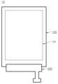
도 1에 도시한 바와 같이, 본 발명의 일 실시예에 따른 유기발광표시장치(10)는 영상이 표시되는 표시영역(AA)을 포함하는 표시패널(100)과, 표시패널(100)에 접속되고 표시패널(100)의 구동을 위한 제어신호 및 전원을 공급하는 회로기판(200)을 포함한다.As shown in FIG. 1, the organic light
표시패널(100)은 표시영역(AA)의 외곽인 비표시영역 중 일부에 배치되고 회로기판(200)이 접속되는 패드영역을 더 포함한다.The
도 2에 도시된 바와 같이, 표시패널(100)은 발광소자 어레이(110), 발광소자 어레이(110)를 덮는 봉지막(120), 봉지막(120) 상에 배치되는 터치센서(130), 터치센서(130)를 덮고 코어쉘 입자(CS; Core Shell particle)를 함유하는 재료로 이루어지는 터치보호막(140) 및 터치보호막(140) 상에 배치되는 편광필름(150)을 포함한다.As shown in FIG. 2, the
발광소자 어레이(110)는 표시영역(AA)에 정렬된 복수의 화소영역(PA)에 대응한 복수의 발광소자(OLED)를 포함한다.The light
발광소자 어레이(110)는 각 화소영역(PA)에 대응하고 각 발광소자(OLED)에 구동전류를 공급하는 적어도 하나의 박막트랜지스터(DT, ST)를 더 포함할 수 있다.The light
일 예로, 발광소자 어레이(110)의 각 화소영역(PA)은 유기발광소자(OLED), 제 1 구동전원라인(VDD)과 제 2 구동전원라인(VSS) 사이에 유기발광소자(OLED)와 직렬로 배치되는 구동 트랜지스터(DT), 및 구동 트랜지스터(DT)의 게이트전극과 데이터라인(DL) 사이에 배치되는 스위칭 트랜지스터(ST)를 포함한다. 그리고, 각 화소영역(PA)은 구동 트랜지스터(DT)의 게이트전극과 유기발광소자(OLED)의 애노드전극 사이에 배치되는 스토리지 커패시터(Cst)를 더 포함할 수 있다.As an example, each pixel area (PA) of the light
스위칭 트랜지스터(ST)는 스캔라인(SL)의 스캔신호에 기초하여 턴온하면, 데이터라인(DL)의 데이터신호를 구동 트랜지스터(DT)의 게이트전극 및 스토리지 커패시터(Cst)에 전달한다. 이때, 구동 트랜지스터(DT)가 스위칭 트랜지스터(ST)의 출력 및 스토리지 커패시터(Cst)의 충전전압에 기초하여 턴온하면, 유기발광소자(OLED)에 구동전류가 공급된다.When the switching transistor (ST) is turned on based on the scan signal of the scan line (SL), it transfers the data signal of the data line (DL) to the gate electrode of the driving transistor (DT) and the storage capacitor (Cst). At this time, when the driving transistor (DT) is turned on based on the output of the switching transistor (ST) and the charging voltage of the storage capacitor (Cst), a driving current is supplied to the organic light emitting device (OLED).
각 화소영역(PA)은 적색(R), 녹색(G) 및 청색(B) 중 어느 하나의 색상에 대응될 수 있다. 또는, 각 화소영역(PA)은 적색(R), 녹색(G), 청색(B) 및 백색(W) 중 어느 하나의 색상에 대응될 수 있다. 이를 위해, 발광소자 어레이(110)의 각 유기발광소자(OLED)는 어느 하나의 색상에 대응되는 광을 방출하는 소자로 마련될 수 있다. 또는, 발광소자 어레이(110)에 포함된 복수의 유기발광소자(OLED)는 동일한 색상을 방출하는 소자로 마련되고, 표시패널(100)은 각 화소영역(PA)의 색상을 표시하기 위한 컬러필터 어레이(미도시)를 더 포함할 수 있다.Each pixel area (PA) may correspond to one of red (R), green (G), and blue (B) colors. Alternatively, each pixel area (PA) may correspond to any one of red (R), green (G), blue (B), and white (W). To this end, each organic light emitting device (OLED) of the light
유기발광소자(OLED)는 수분 또는 산소에 의해 용이하게 열화되므로, 유기발광소자(OLED)의 열화를 지연시키기 위해 유기발광소자(OLED)에 대한 수분 또는 산소의 침투를 차단할 필요가 있다. 이에 따라, 표시패널(100)은 발광소자 어레이(110)를 덮는 봉지막(120)을 포함한다.Since organic light emitting devices (OLEDs) are easily deteriorated by moisture or oxygen, it is necessary to block the penetration of moisture or oxygen into the organic light emitting devices (OLEDs) in order to delay deterioration of the organic light emitting devices (OLEDs). Accordingly, the
봉지막(120)은 서로 다른 조성 또는 서로 다른 두께로 이루어진 적어도 하나의 절연막이 적층된 구조로 이루어질 수 있다.The
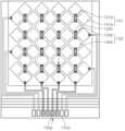
터치센서(130)는 봉지막(120) 상에 배치되고, 상호 교차하는 방향으로 이루어진 제 1 및 제 2 터치전극(131, 132)을 포함한다.The
터치센서(130)에 있어서, 표시영역(AA)의 일부 영역에 터치가 발생되면, 상호 인접한 제 1 및 제 2 터치전극(131, 132) 사이의 정전용량(Cm)이 터치에 의해 변동된다. 이러한 정전용량(Cm)의 변화를 통해 터치가 발생된 영역이 검출될 수 있다.In the
표시패널(100)은 외부의 전기적 또는 물리적 충격으로부터 터치센서(130)를 보호하기 위하여 터치센서(130)를 덮는 터치보호막(140)을 포함한다.The
본 발명의 일 실시예에 따르면, 터치보호막(140)은 표시패널(100)의 광추출효율을 향상시키기 위한 코어쉘 입자(CS)를 함유하는 재료로 이루어진다. 코어쉘 입자(CS)에 대해서는 도 4를 참조하여 이하에서 상세히 설명한다.According to one embodiment of the present invention, the
편광필름(150)은 터치보호막(140) 상에 배치된다. 여기서, 편광필름(150)은 외부광반사 등을 방지하기 위한 것이다. 편광필름(150)의 용이한 고정을 위하여, 터치보호막(140)은 점착성을 갖는 재료로 이루어질 수 있다.The
도 3에 도시된 바와 같이, 터치센서(130)는 제 1 방향(도 3의 좌우방향)으로 배치되는 복수의 제 1 터치전극(131) 및 제 1 방향에 교차하는 제 2 방향(도 3의 상하방향)으로 배치되는 복수의 제 2 터치전극(132)을 포함한다.As shown in FIG. 3, the
각 제 1 터치전극(131)은 제 1 방향으로 배열되는 복수의 제 1 전극패턴(131e)과, 제 1 방향으로 상호 이웃한 제 1 전극패턴(131e) 사이를 연결하는 제 1 브릿지(131b)를 포함한다.Each
각 제 2 터치전극(132)은 제 2 방향으로 배열되는 복수의 제 2 전극패턴(132e)과, 제 2 방향으로 상호 이웃한 제 2 전극패턴(132e) 사이를 연결하는 제 2 브릿지(132b)를 포함한다.Each
여기서, 제 1 브릿지(131b)는 제 1 전극패턴(131e)과 동일한 층에 배치되고, 제 2 브릿지(132b)는 제 2 전극패턴(132e)과 상이한 층에 배치될 수 있다. 이 경우, 제 2 브릿지(132b)는 제 2 브릿지(132b)와 제 2 전극패턴(132e) 사이를 절연하는 막을 관통하는 콘택홀(132h)을 통해 제 2 전극패턴(132e)에 연결된다.Here, the
또한, 복수의 제 1 터치전극(131) 각각은 표시영역(AA)의 외곽에 배치되는 제 1 터치링크를 통해 제 1 터치전극패드(131p)에 연결될 수 있다.Additionally, each of the plurality of
여기서, 제 1 터치전극패드(131p)는 표시영역(AA)의 외곽 중 표시영역(AA)의 어느 일 모서리에 인접한 패드영역에 배치될 수 있다.Here, the first
제 1 터치링크는 제 2 브릿지(132b)와 동일층에 배치될 수 있다. 이 경우, 제 1 터치링크는 콘택홀을 통해 제 1 터치전극(131)에 연결될 수 있다.The first touch link may be placed on the same layer as the
복수의 제 2 터치전극(132) 각각은 표시영역(AA)의 외곽에 배치되는 제 2 터치링크를 통해 제 2 터치전극패드(132p)에 연결될 수 있다.Each of the plurality of
여기서, 제 2 터치전극패드(131p)는 제 1 터치전극패드(131p)와 마찬가지로, 표시영역(AA)의 외곽 중 표시영역(AA)의 어느 일 모서리에 인접한 패드영역에 배치될 수 있다.Here, like the first
제 2 터치링크는 제 2 브릿지(132b)와 동일층에 배치될 수 있다. 이 경우, 제 2 터치링크는 콘택홀을 통해 제 2 터치전극(132)에 연결될 수 있다.The second touch link may be placed on the same floor as the
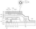
도 4에 도시된 바와 같이, 본 발명의 일 실시예에 따른 표시패널(100)은 표시영역(AA)에 정렬된 복수의 화소영역(PA)에 대응한 복수의 발광소자(OLED)를 포함하는 발광소자 어레이(110), 발광소자 어레이(110)를 덮는 봉지막(120), 봉지막(120) 상에 배치되는 터치센서(130), 및 터치센서(130)를 덮고 코어쉘 입자(CS)를 함유하는 재료로 이루어지는 터치보호막(140)을 포함한다.As shown in FIG. 4, the
그리고, 표시패널(100)은 터치보호막(140) 상에 배치되고 표시영역(AA)에 대응한 편광필름(150)을 더 포함할 수 있다.Additionally, the
발광소자 어레이(110)는 각 화소영역(PA)에 대응하는 구동 트랜지스터(DT)와 발광소자(OLED)를 포함한다.The light emitting
구동 트랜지스터(DT)는 기판(101) 상에 배치되는 게이트전극(GE), 게이트전극(GE)을 덮는 게이트절연막(111) 상에 배치되는 액티브층(ACT), 및 액티브층(ACT)을 덮는 제 1 층간절연막(112) 상에 배치되는 소스전극(SE)과 드레인전극(DE)을 포함할 수 있다.The driving transistor (DT) includes a gate electrode (GE) disposed on the
여기서, 액티브층(ACT)은 산화물반도체로 이루어질 수 있으며, 게이트전극(GE)에 중첩되는 채널영역과, 채널영역의 양측에 배치되는 소스영역 및 드레인영역을 포함할 수 있다.Here, the active layer (ACT) may be made of an oxide semiconductor and may include a channel region overlapping the gate electrode (GE), and a source region and a drain region disposed on both sides of the channel region.
소스전극(SE)은 제 1 층간절연막(112)을 관통하는 콘택홀을 통해 액티브층(ACT)의 소스영역에 연결된다.The source electrode SE is connected to the source region of the active layer ACT through a contact hole penetrating the first
드레인전극(DE)은 제 1 층간절연막(112)을 관통하는 콘택홀을 통해 액티브층(ACT)의 드레인영역에 연결된다.The drain electrode DE is connected to the drain region of the active layer ACT through a contact hole penetrating the first
이러한 구동 트랜지스터(DT)는 제 2 층간절연막(113)으로 커버된다.This driving transistor DT is covered with a second
도 4에서는 구동 트랜지스터(DT)가 바텀게이트구조인 것을 예시하고 있으나, 본 발명의 일 실시예는 이에 국한되지 않으며, 구동 트랜지스터(DT)는 탑게이트구조 또는 더블게이트구조일 수 있다. 그리고, 구동 트랜지스터(DT)는 산화물반도체의 액티브층(ACT) 대신 저온성장실리콘반도체(LTPS)의 액티브층을 포함할 수도 있다.Although FIG. 4 illustrates that the driving transistor DT has a bottom gate structure, the embodiment of the present invention is not limited thereto, and the driving transistor DT may have a top gate structure or a double gate structure. Additionally, the driving transistor DT may include an active layer of low-temperature grown silicon semiconductor (LTPS) instead of the active layer of oxide semiconductor (ACT).
발광소자(OLED)는 제 2 층간절연막(113) 상에 배치되는 애노드전극(AE), 애노드전극(AE)에 대향하는 캐소드전극(CE) 및 애노드전극(AE)과 캐소드전극(CE) 사이에 배치되는 발광구조물(EL)을 포함한다.The light emitting device (OLED) has an anode electrode (AE) disposed on the second
애노드전극(AE)의 가장자리는 뱅크절연막(114)으로 커버될 수 있다.The edge of the anode electrode (AE) may be covered with the
발광구조물(EL)은 유기발광물질로 이루어질 수 있다. 이 경우, 발광구조물(EL)은 순차 적층되는 정공수송층, 발광층 및 전자수송층을 포함할 수 있다. 여기서, 정공수송층은 애노드전극(AE)에 인접하고, 전자수송층은 캐소드전극(CE)에 인접한다. 또는, 발광구조물(EL)은 정공수송층과 애노드전극(AE) 사이에 배치되는 정공주입층 및 전자수송층과 캐소드전극(CE) 사이에 배치되는 전자주입층 중 적어도 어느 하나를 더 포함할 수도 있다.The light emitting structure (EL) may be made of an organic light emitting material. In this case, the light emitting structure (EL) may include a hole transport layer, a light emitting layer, and an electron transport layer that are sequentially stacked. Here, the hole transport layer is adjacent to the anode electrode (AE), and the electron transport layer is adjacent to the cathode electrode (CE). Alternatively, the light emitting structure EL may further include at least one of a hole injection layer disposed between the hole transport layer and the anode electrode (AE) and an electron injection layer disposed between the electron transport layer and the cathode electrode (CE).
이러한 발광소자 어레이(110)는 수분 또는 산소의 침투를 차단하기 위한 봉지막(120)으로 커버된다.This light emitting
봉지막(120)은 서로 다른 조성 또는 서로 다른 두께를 갖는 복수의 절연막이 적층된 구조로 이루어질 수 있다.The
예시적으로, 봉지막(120)은 발광소자 어레이(110)를 덮고 무기절연물질로 이루어진 제 1 봉지막(121), 제 1 봉지막(121) 상에 배치되는 유기절연물질로 이루어진 제 2 봉지막(122) 및 제 2 봉지막(122)을 덮고 무기절연물질로 이루어진 제 3 봉지막(123)을 포함할 수 있다.Exemplarily, the
더불어, 표시패널(100)은 표시영역(AA)과 패드영역 사이에 배치되는 댐구조물(160)을 더 포함할 수 있다.In addition, the
댐구조물(160)은 봉지층(120)이 기판(101)에 접하는 영역에서 봉지층(120)이 무너지는 것을 방지하기 위한 것이다. 예시적으로, 댐구조물(160)은 제 2 층간절연막(113)과 동일한 층으로 이루어진 제 1 댐층과 뱅크절연막(114)과 동일한 층으로 이루어진 제 2 댐층이 적층된 구조로 이루어질 수 있다.The
터치센서(130)는 봉지막(120) 상에 배치되는 터치버퍼막(133), 및 터치버퍼막(133) 상에 배치되는 터치층간절연막(134)을 포함한다.The
그리고, 앞서 도 3에 대한 설명에서 언급한 바와 같이, 터치센서(130)는 복수의 제 1 터치전극(131)과 복수의 제 2 터치전극(132)을 포함한다. 각 제 1 터치전극(131)은 복수의 제 1 전극패턴(131e) 및 제 1 방향으로 이웃한 제 1 전극패턴(131e) 사이의 제 1 브릿지(131b)를 포함한다. 각 제 2 터치전극(132)은 복수의 제 2 전극패턴(132e) 및 제 2 방향으로 이웃한 제 2 전극패턴(132e) 사이의 제 2 브릿지(132b)를 포함한다.And, as previously mentioned in the description of FIG. 3, the
도 4의 도시와 같이, 제 1 및 제 2 전극패턴(131e, 132e)과 제 1 브릿지(131b)는 터치층간절연막(134) 상에 배치될 수 있다.As shown in FIG. 4 , the first and
그리고, 제 2 브릿지(132b)는 터치버퍼막(133) 상에 배치될 수 있다. 이때, 제 2 브릿지(132b)는 터치층간절연막(134)로 커버되고, 터치층간절연막(134)을 관통하는 콘택홀(132h)을 통해 제 2 전극패턴(132e)과 연결된다.And, the
이와 같이, 터치센서(130)는 봉지막(120) 상에 배치되는 터치층간절연막(134), 터치층간절연막(134) 상에 배치되고 제 1 방향으로 배열된 복수의 제 1 전극패턴(131e)과, 제 1 방향으로 상호 이웃한 제 1 전극패턴(131e) 사이를 연결하는 제 1 브릿지(131b)를 포함하는 제 1 터치전극(131), 및 터치층간절연막(134) 상에 배치되고 제 1 방향에 교차하는 제 2 방향으로 배열된 복수의 제 2 전극패턴(132e)과, 제 2 방향으로 상호 이웃한 제 2 전극패턴(132e) 사이를 연결하는 제 2 브릿지(132b)를 포함하는 제 2 터치전극(132)을 포함한다.In this way, the
여기서, 제 1 브릿지(131b)는 터치층간절연막(134) 상에 배치되고, 제 2 브릿지(132b)는 봉지막(120) 상에 배치되고 터치층간절연막(134)으로 커버된다. 일 예로, 제 2 브릿지(132b)는 터치버퍼막(133) 상에 배치될 수 있다. 그리고, 제 2 브릿지(132b)는 터치층간절연막(134)을 관통하는 콘택홀(132h)을 통해 제 2 전극패턴(132e)에 연결된다.Here, the
이러한 터치센서(130)는 터치보호막(140)으로 커버된다.This
터치보호막(140)은 적어도 표시영역(AA)에 대응하며, 터치센서(130)를 덮는다. 터치보호막(140)은 코어쉘 입자(CS)를 함유하는 재료로 이루어진다.The
이러한 터치보호막(140)은 약 2㎛의 두께로 이루어질 수 있다.This
코어쉘 입자(CS)는 금속산화물로 이루어진 중심부(CCS), 및 중심부(CCS)를 둘러싸고 분자체(molecular sieve)로 이루어진 외곽부(BCS)를 포함한다. 이러한 코어쉘 입자(CS)는 4nm 내지 6nm의 직경으로 이루어질 수 있다.Core-shell particles (CS) include a core (CCS) made of a metal oxide, and an outer portion (BCS) made of a molecular sieve surrounding the core (CCS). These core-shell particles (CS) may have a diameter of 4 nm to 6 nm.
예시적으로, 중심부(CCS)의 금속산화물은 Ti 또는 Fe를 포함하는 산화물로 이루어질 수 있다.For example, the metal oxide in the center (CCS) may be made of an oxide containing Ti or Fe.
외곽부(BCS)의 분자체는 MCM-41 또는 SBA-15로 이루어질 수 있다. 여기서, 분자체는 육각기둥 형태의 구조이다.The molecular sieve of the outer layer (BCS) may consist of MCM-41 or SBA-15. Here, the molecular sieve has a hexagonal pillar-shaped structure.
특히, 코어쉘 입자(CS)의 외곽부(BCS)가 MCM물질로 선택되는 경우, 터치보호막(140)의 벌키니스(bulkiness)가 증가됨으로써, 터치보호막(140)의 팩킹 덴시티(Packing density)가 낮아질 수 있다.In particular, when the outer portion (BCS) of the core-shell particle (CS) is selected as an MCM material, the bulkiness of the touch
여기서, MCM 물질은 Sodium methasilicate를 실리카 도입 물질로서 사용하고, cetyltrimethylammonium bromide를 계면 활성제로 사용하여 수열 조건하에서 합성된 Si-MCM-41일 수 있다.Here, the MCM material may be Si-MCM-41 synthesized under hydrothermal conditions using sodium methasilicate as a silica introduction material and cetyltrimethylammonium bromide as a surfactant.
그리고, 코어쉘 입자(CS)는 합성된 Si-MCM-41에 Metal Oxide인 Titanium oxide를 담지하여 마련될 수 있으며, 이때, Tetraethylorthosilicate를 처리하여 코어쉘 입자(CS)의 기공 크기가 조절될 수 있다.In addition, core-shell particles (CS) can be prepared by supporting titanium oxide, a metal oxide, on synthesized Si-MCM-41. At this time, the pore size of the core-shell particles (CS) can be adjusted by treating tetraethylorthosilicate. .
또한, 터치보호막(140)은 적어도 하나의 바인더 및 광감제를 더 포함할 수 있다. 이러한 터치보호막(140)은 적어도 하나의 바인더에 의한 점착성을 가질 수 있다.Additionally, the touch
여기서, 바인더는 알칼리 현상성 바인더 및 실리콘계 바인더 중 적어도 하나로 이루어질 수 있다. 특히, 바인더는 실리콘 폴리머(Silicone polymer)로 선택될 수 있다. 이와 같이 터치보호막(140)의 재료가 실리콘 폴리머의 바인더를 포함함에 따라, 보호막의 기존 재료인 아크릴계 폴리머보다 내열성이 높아질 수 있는 장점이 있다. 또한, 실리콘 폴리머의 Si-O 결합은 아크릴계 폴리머의 C-C결합에 비해 더 높은 결합에너지 및 더 긴 결합길이를 가지므로, 터치보호막(140)이 더 벌키(bulky)해짐으로써, 터치보호막(140)의 팩킹 덴시티(Packing density)가 낮아질 수 있다.Here, the binder may be made of at least one of an alkali-developable binder and a silicone-based binder. In particular, the binder may be selected as a silicone polymer. As the material of the touch
광감제는 Oxime계 화합물 또는 벤조페논계 화합물로 이루어질 수 있다. 특히, 광감제는 벤조페논계 화합물로 선택될 수 있다.The photosensitizer may be composed of an oxime-based compound or a benzophenone-based compound. In particular, the photosensitizer may be selected as a benzophenone-based compound.
예시적으로, 터치보호막(140)의 배치는 코어쉘 입자(CS), 알칼리 현상성 바인더 또는 실리콘계 바인더, Oxime계 화합물 또는 벤조페논계 화합물로 이루어진 광감제, 및 소정의 솔벤트가 혼합된 액상재료를 터치센서(130) 상에 도포하는 과정과, 터치센서(130) 상의 액상재료를 광경화하는 과정을 통해 실시될 수 있다. 여기서, 솔벤트는 레진을 용해하기 위한 것으로서, PGMEA(Propylene glycol monomethyl ether acetate)일 수 있다. 그리고, 액상재료를 광경화하는 과정에서, 소성온도는 100℃ 미만, 특히, 85℃ 이하일 수 있다. 이와 같이 터치보호막(140)의 배치 과정 시 소성온도를 100℃ 미만으로 한정함으로써, 터치보호막(140)의 배치 과정에 의한 발광소자 어레이(110)의 손상이 최소화될 수 있다. 이때, 100℃ 미만의 소성온도로 실시되는 저온공정으로 인해, 터치보호막(140)의 접착력이 저하될 수 있다. 이를 방지하기 위해, 터치보호막(140)의 배치과정은 액상재료를 광경화하는 과정 이후에 광경화된 재료에 대한 전면 노광공정을 실시하는 과정을 더 포함할 수 있다. 이러한 전면 노광 공정으로 인해, 터치보호막(140)의 접착력 및 경화도가 향상될 수 있다.Illustratively, the
이와 같이, 터치보호막(140)이 코어쉘 입자(CS)를 함유하는 재료로 이루어짐에 따라, 발광소자 어레이(110)에서 방출된 광이 육각기둥 형태로 이루어진 외곽부(BCS)의 분자체를 통과하면서 더욱 강화된 직진성을 가질 수 있다. 그리고, 비교적 굴절률이 높은 중심부(CCS)의 금속산화물로 인해, 터치보호막(140)의 광투과율이 향상될 수 있다. 예시적으로, 금속산화물의 굴절률은 약 2.6 내지 약 2.9일 수 있다.In this way, as the
이로써, 코어쉘 입자(CS)를 함유하는 터치보호막(140)으로 인해, 발광소자 어레이(110)의 광이 외부로 방출되는 비율, 즉 광추출효율이 향상될 수 있다.Accordingly, the rate at which light from the light emitting
따라서, 표시패널(100)은 발광소자 어레이(110)의 광이 방출되는 경로에 터치센서(130)를 배치하는 것과 더불어, 터치센서(130) 상에 코어쉘 입자(CS)를 함유하는 터치보호막(140)을 더 배치함으로써 광추출효율을 향상시킬 수 있다. 그러므로, 터치센서(130)에 의한 휘도 저하를 최소화할 수 있고, 그로 인해, 표시패널(100)의 표시품질이 향상될 수 있으며, 소비전력이 저감될 수 있다.Therefore, the
편광필름(150)은 터치보호막(140) 상에 배치된다. 여기서, 터치보호막(140)은 바인더에 의한 점착성을 가지므로, 터치보호막(140)과 편광필름(150) 사이의 점착층이 제거될 수 있다. 따라서, 표시패널(100)의 간소화 및 슬림화에 유리해질 수 있다.The
이상과 같이, 본 발명의 일 실시예에 따르면, 터치센서(130)를 덮는 터치보호막(140)이 코어쉘 입자(CS)를 함유하는 재료로 이루어짐에 따라, 광추출효율이 향상될 수 있고, 그로 인해 표시품질이 향상될 수 있으며, 소비전력이 저감될 수 있다.As described above, according to an embodiment of the present invention, as the touch
이상에서 설명한 본 발명은 상술한 실시예 및 첨부된 도면에 한정되는 것이 아니고, 본 발명의 기술적 사상을 벗어나지 않는 범위 내에서 여러 가지 치환, 변형 및 변경이 가능하다는 것이 본 발명이 속하는 기술분야에서 종래의 지식을 가진 자에게 있어 명백할 것이다.The present invention described above is not limited to the above-described embodiments and the accompanying drawings, and various substitutions, modifications, and changes are possible without departing from the technical spirit of the present invention. It will be clear to those who have the knowledge of.
10: 유기발광표시장치100: 표시패널
AA: 표시영역PA: 화소영역
110: 발광소자 어레이120: 봉지막
130: 터치센서140: 터치보호막
150: 편광필름CS: 코어쉘 입자10: Organic light emitting display device 100: Display panel
AA: Display area PA: Pixel area
110: light emitting element array 120: encapsulation film
130: Touch sensor 140: Touch protection film
150: Polarizing film CS: Core-shell particles
Claims (7)
Translated fromKorean상기 발광소자 어레이를 덮는 봉지막;
상기 봉지막 상부면에 배치되는 터치센서; 및
상기 봉지막 상부면으로부터 이격하여 위치하고, 상기 터치센서의 노출면을 덮으면서 중심부, 및 상기 중심부를 둘러싸는 외곽부를 포함하는 코어쉘 입자를 함유하는 재료로 이루어지는 터치보호막을 포함하되,
상기 복수의 발광소자로부터 방출되어 상기 봉지막 및 상기 터치센서를 통과한 광이 상기 터치보호막의 상기 코어쉘 입자를 통과하면서 직진성을 가지는 광이 외부로 방출되도록,
상기 코어쉘 입자의 중심부는 2.6 내지 2.9의 굴절률을 가지는 금속산화물로 이루어지고, 상기 외곽부는 상기 중심부를 둘러싸면서 육각기둥 형태의 구조로 이루어지고 기공을 포함하는 분자체(molecular sieve)로 이루어져, 상기 분자체를 통과한 광이 직진성을 가지는 표시패널.
a light emitting element array including a plurality of light emitting elements corresponding to a plurality of pixel areas aligned in the display area;
an encapsulation film covering the light emitting device array;
A touch sensor disposed on the upper surface of the encapsulation film; and
A touch protective film made of a material containing core-shell particles, which is located spaced apart from the upper surface of the encapsulation film and covers the exposed surface of the touch sensor and includes a central portion and an outer portion surrounding the central portion,
So that the light emitted from the plurality of light-emitting devices and passing through the encapsulation film and the touch sensor passes through the core-shell particles of the touch protection film and is emitted to the outside as straight light,
The center of the core-shell particle is made of a metal oxide having a refractive index of 2.6 to 2.9, and the outer portion is made of a molecular sieve that surrounds the center and has a hexagonal pillar-shaped structure and includes pores. A display panel in which light passing through a molecular sieve travels straight.
상기 금속산화물은 Ti 또는 Fe를 포함하는 산화물로 이루어지고,
상기 분자체는 MCM-41 또는 SBA-15로 이루어지는 표시패널.
According to claim 1,
The metal oxide consists of an oxide containing Ti or Fe,
A display panel where the molecular sieve is MCM-41 or SBA-15.
상기 터치보호막의 재료는 적어도 하나의 바인더 및 광감제를 더 포함하고,
상기 터치보호막은 상기 적어도 하나의 바인더에 의한 점착성을 갖는 표시패널.
According to claim 1,
The material of the touch protective film further includes at least one binder and a photosensitizer,
A display panel wherein the touch protective film has adhesive properties due to the at least one binder.
상기 바인더는 알칼리 현상성 바인더 및 실리콘계 바인더 중 적어도 하나로 이루어지고,
상기 광감제는 Oxime계 화합물 또는 벤조페논계 화합물로 이루어지는 표시패널.
According to claim 4,
The binder consists of at least one of an alkali developable binder and a silicone-based binder,
The display panel wherein the photosensitizer is made of an oxime-based compound or a benzophenone-based compound.
상기 터치보호막 상부면에 부착되고 상기 표시영역에 대응한 편광필름을 더 포함하는 표시패널.
According to claim 4,
A display panel attached to the upper surface of the touch protection film and further comprising a polarizing film corresponding to the display area.
상기 터치센서는
상기 봉지막 상에 배치되는 터치층간절연막;
상기 터치층간절연막 상에 배치되고 제 1 방향으로 배열된 복수의 제 1 전극패턴과, 상기 제 1 방향으로 상호 이웃한 제 1 전극패턴 사이를 연결하는 제 1 브릿지를 포함하는 제 1 터치전극; 및
상기 터치층간절연막 상에 배치되고 상기 제 1 터치전극으로부터 이격되며 상기 제 1 방향에 교차하는 제 2 방향으로 배열된 복수의 제 2 전극패턴과, 상기 제 2 방향으로 상호 이웃한 제 2 전극패턴 사이를 연결하는 제 2 브릿지를 포함하는 제 2 터치전극을 포함하며,
상기 제 1 브릿지는 상기 터치층간절연막 상에 배치되고,
상기 제 2 브릿지는 상기 봉지막 상에 배치되고 상기 터치층간절연막으로 커버되며, 상기 터치층간절연막을 관통하는 콘택홀을 통해 상기 제 2 전극패턴에 연결되는 표시패널.According to claim 1,
The touch sensor is
a touch interlayer insulating film disposed on the encapsulation film;
a first touch electrode including a plurality of first electrode patterns disposed on the touch interlayer insulating film and arranged in a first direction, and a first bridge connecting adjacent first electrode patterns in the first direction; and
Between a plurality of second electrode patterns disposed on the touch interlayer insulating film, spaced apart from the first touch electrode, and arranged in a second direction crossing the first direction, and second electrode patterns adjacent to each other in the second direction. It includes a second touch electrode including a second bridge connecting the
The first bridge is disposed on the touch interlayer insulating film,
The display panel wherein the second bridge is disposed on the encapsulation film, covered with the inter-touch insulating layer, and connected to the second electrode pattern through a contact hole penetrating the inter-touch insulating layer.
Priority Applications (3)
| Application Number | Priority Date | Filing Date | Title |
|---|---|---|---|
| KR1020180136739AKR102640257B1 (en) | 2018-11-08 | 2018-11-08 | Display panel |
| CN201911022608.3ACN111221432B (en) | 2018-11-08 | 2019-10-25 | Display Panel |
| US16/668,241US10969892B2 (en) | 2018-11-08 | 2019-10-30 | Display panel |
Applications Claiming Priority (1)
| Application Number | Priority Date | Filing Date | Title |
|---|---|---|---|
| KR1020180136739AKR102640257B1 (en) | 2018-11-08 | 2018-11-08 | Display panel |
Publications (2)
| Publication Number | Publication Date |
|---|---|
| KR20200053291A KR20200053291A (en) | 2020-05-18 |
| KR102640257B1true KR102640257B1 (en) | 2024-02-26 |
Family
ID=70551304
Family Applications (1)
| Application Number | Title | Priority Date | Filing Date |
|---|---|---|---|
| KR1020180136739AActiveKR102640257B1 (en) | 2018-11-08 | 2018-11-08 | Display panel |
Country Status (3)
| Country | Link |
|---|---|
| US (1) | US10969892B2 (en) |
| KR (1) | KR102640257B1 (en) |
| CN (1) | CN111221432B (en) |
Families Citing this family (5)
| Publication number | Priority date | Publication date | Assignee | Title |
|---|---|---|---|---|
| KR20210109694A (en)* | 2020-02-27 | 2021-09-07 | 삼성디스플레이 주식회사 | Display device |
| CN119883047A (en)* | 2020-09-18 | 2025-04-25 | 群创光电股份有限公司 | Electronic Devices |
| US12336377B2 (en) | 2020-10-27 | 2025-06-17 | Lg Display Co., Ltd. | Display device including a sealing structure |
| CN112928145B (en)* | 2021-01-26 | 2024-06-21 | 京东方科技集团股份有限公司 | Display panel, display device and manufacturing method thereof |
| KR20240050648A (en)* | 2022-10-12 | 2024-04-19 | 엘지디스플레이 주식회사 | Display panel and display apparatus |
Citations (2)
| Publication number | Priority date | Publication date | Assignee | Title |
|---|---|---|---|---|
| JP2013156975A (en)* | 2012-01-30 | 2013-08-15 | Samsung Display Co Ltd | Touch panel and display device including touch panel |
| KR101834792B1 (en)* | 2016-08-31 | 2018-03-06 | 엘지디스플레이 주식회사 | Organic light emitting display with touch sensor and fabricating method thereof |
Family Cites Families (20)
| Publication number | Priority date | Publication date | Assignee | Title |
|---|---|---|---|---|
| US20100194265A1 (en)* | 2007-07-09 | 2010-08-05 | Katholieke Universiteit Leuven | Light-emitting materials for electroluminescent devices |
| DE102008060113A1 (en) | 2008-12-03 | 2010-07-29 | Tesa Se | Method for encapsulating an electronic device |
| JP5178631B2 (en)* | 2009-05-26 | 2013-04-10 | 株式会社ジャパンディスプレイウェスト | Touch sensor, display device, and electronic device |
| KR101323434B1 (en)* | 2009-06-08 | 2013-10-29 | 엘지디스플레이 주식회사 | Organic Light Emitting Display Device |
| KR20130108028A (en)* | 2012-03-23 | 2013-10-02 | 주식회사 엘지화학 | Organic light emitting device |
| KR102044476B1 (en)* | 2013-05-02 | 2019-11-13 | 삼성전자주식회사 | Touch screen panel, touch senssing controller and touch sensing system comprising the same |
| US9425418B2 (en)* | 2014-09-30 | 2016-08-23 | Lg Display Co., Ltd. | Flexible display device with bend stress reduction member and manufacturing method for the same |
| KR101884387B1 (en)* | 2014-12-05 | 2018-08-01 | 한국화학연구원 | A polymer membrane for gas separation or enrichment comprising hybrid nanoporous material, uses thereof, and a preparation method thereof |
| KR102410527B1 (en)* | 2014-12-19 | 2022-06-20 | 삼성디스플레이 주식회사 | Display device and manufacturing method thereof |
| KR102283002B1 (en)* | 2015-02-16 | 2021-07-30 | 삼성디스플레이 주식회사 | Display device |
| JP6669742B2 (en)* | 2015-06-09 | 2020-03-18 | 旭化成株式会社 | Aqueous resin composition for touch panel, transfer film and cured film laminate, method for producing resin pattern, and touch panel display device |
| KR20170050847A (en)* | 2015-10-31 | 2017-05-11 | 엘지디스플레이 주식회사 | Organic light emitting diode display |
| KR102069286B1 (en)* | 2015-11-20 | 2020-01-22 | 동우 화인켐 주식회사 | Flexible image displaying unit |
| KR102415044B1 (en)* | 2015-12-11 | 2022-07-01 | 삼성디스플레이 주식회사 | Touch screen panel, method of manufacturing the same and touch display apparatus |
| KR102653473B1 (en)* | 2015-12-29 | 2024-04-01 | 삼성전자주식회사 | Electronic devices including quantum dots |
| KR20180025466A (en)* | 2016-08-31 | 2018-03-09 | 엘지디스플레이 주식회사 | Light shield insulating film and organic light emitting diode display device having the flim |
| KR102588852B1 (en) | 2016-10-21 | 2023-10-13 | 엘지디스플레이 주식회사 | Nano particle, led assembly and display device using the prticle |
| KR102811755B1 (en)* | 2017-02-03 | 2025-05-23 | 삼성디스플레이 주식회사 | Touch sensor and display device having the touch sensor |
| KR101932650B1 (en)* | 2017-05-15 | 2018-12-28 | 삼성디스플레이 주식회사 | Touch sensor and display device having the touch sensor |
| KR102362080B1 (en)* | 2017-05-31 | 2022-02-10 | 엘지디스플레이 주식회사 | Foldable display device |
- 2018
- 2018-11-08KRKR1020180136739Apatent/KR102640257B1/enactiveActive
- 2019
- 2019-10-25CNCN201911022608.3Apatent/CN111221432B/enactiveActive
- 2019-10-30USUS16/668,241patent/US10969892B2/enactiveActive
Patent Citations (2)
| Publication number | Priority date | Publication date | Assignee | Title |
|---|---|---|---|---|
| JP2013156975A (en)* | 2012-01-30 | 2013-08-15 | Samsung Display Co Ltd | Touch panel and display device including touch panel |
| KR101834792B1 (en)* | 2016-08-31 | 2018-03-06 | 엘지디스플레이 주식회사 | Organic light emitting display with touch sensor and fabricating method thereof |
Also Published As
| Publication number | Publication date |
|---|---|
| CN111221432B (en) | 2025-07-01 |
| US20200150806A1 (en) | 2020-05-14 |
| US10969892B2 (en) | 2021-04-06 |
| CN111221432A (en) | 2020-06-02 |
| KR20200053291A (en) | 2020-05-18 |
Similar Documents
| Publication | Publication Date | Title |
|---|---|---|
| KR102640257B1 (en) | Display panel | |
| KR102668295B1 (en) | Display device | |
| KR102256084B1 (en) | Flexible display device and method of fabricating thereof | |
| KR102562900B1 (en) | Flexible display apparatus and touch sensitive display apparatus | |
| JP6987164B2 (en) | Luminescent device | |
| KR100768905B1 (en) | An electroluminescence device and an electronic apparatus | |
| JP5471774B2 (en) | Electro-optical device, method of manufacturing electro-optical device, and electronic apparatus | |
| CN111326548A (en) | display device | |
| KR101960388B1 (en) | Organic light emitting diode display device | |
| KR20220075203A (en) | Organic light emitting display device | |
| KR20170072973A (en) | Optical cleared adhesive and foldable display device including the same | |
| KR101754787B1 (en) | Organic light emitting diodes and stereoscopic display device using the same | |
| US9905619B2 (en) | Display device and manufacturing method of the same | |
| KR20180046708A (en) | Organic Light Emitting Display Device | |
| KR102589906B1 (en) | Organic light emitting display device | |
| TWI886943B (en) | Light emitting display apparatus | |
| KR102786527B1 (en) | Display Device | |
| KR20210033233A (en) | Electroluminescent Display | |
| KR20200080753A (en) | Display device | |
| KR102199034B1 (en) | High Luminescence Large Viewing Angle Organic Light Emitting Diode Display | |
| KR20180003253A (en) | Organic Light Emitting Display Device | |
| US20250275352A1 (en) | Organic light-emitting display device | |
| KR102813657B1 (en) | Optical film and display device comprising the same | |
| KR20250132749A (en) | Display apparatus | |
| KR20250134751A (en) | display device |
Legal Events
| Date | Code | Title | Description |
|---|---|---|---|
| PA0109 | Patent application | Patent event code:PA01091R01D Comment text:Patent Application Patent event date:20181108 | |
| PG1501 | Laying open of application | ||
| A201 | Request for examination | ||
| PA0201 | Request for examination | Patent event code:PA02012R01D Patent event date:20210727 Comment text:Request for Examination of Application Patent event code:PA02011R01I Patent event date:20181108 Comment text:Patent Application | |
| E902 | Notification of reason for refusal | ||
| PE0902 | Notice of grounds for rejection | Comment text:Notification of reason for refusal Patent event date:20230217 Patent event code:PE09021S01D | |
| AMND | Amendment | ||
| E601 | Decision to refuse application | ||
| PE0601 | Decision on rejection of patent | Patent event date:20230920 Comment text:Decision to Refuse Application Patent event code:PE06012S01D Patent event date:20230217 Comment text:Notification of reason for refusal Patent event code:PE06011S01I | |
| X091 | Application refused [patent] | ||
| AMND | Amendment | ||
| PX0901 | Re-examination | Patent event code:PX09011S01I Patent event date:20230920 Comment text:Decision to Refuse Application Patent event code:PX09012R01I Patent event date:20230511 Comment text:Amendment to Specification, etc. | |
| PX0701 | Decision of registration after re-examination | Patent event date:20240205 Comment text:Decision to Grant Registration Patent event code:PX07013S01D Patent event date:20240115 Comment text:Amendment to Specification, etc. Patent event code:PX07012R01I Patent event date:20230920 Comment text:Decision to Refuse Application Patent event code:PX07011S01I Patent event date:20230511 Comment text:Amendment to Specification, etc. Patent event code:PX07012R01I | |
| X701 | Decision to grant (after re-examination) | ||
| GRNT | Written decision to grant | ||
| PR0701 | Registration of establishment | Comment text:Registration of Establishment Patent event date:20240220 Patent event code:PR07011E01D | |
| PR1002 | Payment of registration fee | Payment date:20240221 End annual number:3 Start annual number:1 | |
| PG1601 | Publication of registration |