KR102633138B1 - Integrated Circuit and Semiconductor Device - Google Patents
Integrated Circuit and Semiconductor DeviceDownload PDFInfo
- Publication number
- KR102633138B1 KR102633138B1KR1020160134544AKR20160134544AKR102633138B1KR 102633138 B1KR102633138 B1KR 102633138B1KR 1020160134544 AKR1020160134544 AKR 1020160134544AKR 20160134544 AKR20160134544 AKR 20160134544AKR 102633138 B1KR102633138 B1KR 102633138B1
- Authority
- KR
- South Korea
- Prior art keywords
- gate electrode
- gate line
- contact
- disposed
- cut
- Prior art date
- Legal status (The legal status is an assumption and is not a legal conclusion. Google has not performed a legal analysis and makes no representation as to the accuracy of the status listed.)
- Active
Links
- 239000004065semiconductorSubstances0.000titleclaimsdescription43
- 239000000758substrateSubstances0.000claimsdescription35
- 229910052751metalInorganic materials0.000claimsdescription24
- 239000002184metalSubstances0.000claimsdescription24
- 150000004767nitridesChemical class0.000claimsdescription9
- 238000010586diagramMethods0.000description12
- 238000012545processingMethods0.000description9
- 238000000034methodMethods0.000description8
- 102100035294Chemokine XC receptor 1Human genes0.000description7
- 101000804783Homo sapiens Chemokine XC receptor 1Proteins0.000description7
- 230000007423decreaseEffects0.000description7
- 229910021332silicideInorganic materials0.000description7
- 239000011810insulating materialSubstances0.000description6
- 208000036971interstitial lung disease 2Diseases0.000description5
- 238000002955isolationMethods0.000description5
- 239000000463materialSubstances0.000description5
- 125000006850spacer groupChemical group0.000description5
- WFKWXMTUELFFGS-UHFFFAOYSA-NtungstenChemical compound[W]WFKWXMTUELFFGS-UHFFFAOYSA-N0.000description5
- 229910052721tungstenInorganic materials0.000description5
- 239000010937tungstenSubstances0.000description5
- 108700026963CB1aProteins0.000description4
- 239000010949copperSubstances0.000description4
- RYGMFSIKBFXOCR-UHFFFAOYSA-NCopperChemical compound[Cu]RYGMFSIKBFXOCR-UHFFFAOYSA-N0.000description3
- 238000000231atomic layer depositionMethods0.000description3
- 230000000052comparative effectEffects0.000description3
- 229910052802copperInorganic materials0.000description3
- 238000013461designMethods0.000description3
- 238000005516engineering processMethods0.000description3
- 208000036252interstitial lung disease 1Diseases0.000description3
- 229910021420polycrystalline siliconInorganic materials0.000description3
- 229920005591polysiliconPolymers0.000description3
- 229910052715tantalumInorganic materials0.000description3
- GUVRBAGPIYLISA-UHFFFAOYSA-Ntantalum atomChemical compound[Ta]GUVRBAGPIYLISA-UHFFFAOYSA-N0.000description3
- XUIMIQQOPSSXEZ-UHFFFAOYSA-NSiliconChemical compound[Si]XUIMIQQOPSSXEZ-UHFFFAOYSA-N0.000description2
- 238000004891communicationMethods0.000description2
- 238000005137deposition processMethods0.000description2
- 238000011161developmentMethods0.000description2
- 239000012535impuritySubstances0.000description2
- 230000010354integrationEffects0.000description2
- 239000007769metal materialSubstances0.000description2
- 229910052594sapphireInorganic materials0.000description2
- 239000010980sapphireSubstances0.000description2
- 229910052710siliconInorganic materials0.000description2
- 239000010703siliconSubstances0.000description2
- 238000012360testing methodMethods0.000description2
- 239000010936titaniumSubstances0.000description2
- JBRZTFJDHDCESZ-UHFFFAOYSA-NAsGaChemical compound[As]#[Ga]JBRZTFJDHDCESZ-UHFFFAOYSA-N0.000description1
- 229910001218Gallium arsenideInorganic materials0.000description1
- ZOKXTWBITQBERF-UHFFFAOYSA-NMolybdenumChemical compound[Mo]ZOKXTWBITQBERF-UHFFFAOYSA-N0.000description1
- KJTLSVCANCCWHF-UHFFFAOYSA-NRutheniumChemical compound[Ru]KJTLSVCANCCWHF-UHFFFAOYSA-N0.000description1
- 229910000577Silicon-germaniumInorganic materials0.000description1
- RTAQQCXQSZGOHL-UHFFFAOYSA-NTitaniumChemical compound[Ti]RTAQQCXQSZGOHL-UHFFFAOYSA-N0.000description1
- LEVVHYCKPQWKOP-UHFFFAOYSA-N[Si].[Ge]Chemical compound[Si].[Ge]LEVVHYCKPQWKOP-UHFFFAOYSA-N0.000description1
- 229910045601alloyInorganic materials0.000description1
- 239000000956alloySubstances0.000description1
- 229910052782aluminiumInorganic materials0.000description1
- XAGFODPZIPBFFR-UHFFFAOYSA-NaluminiumChemical compound[Al]XAGFODPZIPBFFR-UHFFFAOYSA-N0.000description1
- 230000000295complement effectEffects0.000description1
- 238000009792diffusion processMethods0.000description1
- 239000000284extractSubstances0.000description1
- 229910052732germaniumInorganic materials0.000description1
- GNPVGFCGXDBREM-UHFFFAOYSA-Ngermanium atomChemical compound[Ge]GNPVGFCGXDBREM-UHFFFAOYSA-N0.000description1
- 239000012212insulatorSubstances0.000description1
- 238000012986modificationMethods0.000description1
- 230000004048modificationEffects0.000description1
- 229910052750molybdenumInorganic materials0.000description1
- 239000011733molybdenumSubstances0.000description1
- 230000003287optical effectEffects0.000description1
- 230000002250progressing effectEffects0.000description1
- 229910052707rutheniumInorganic materials0.000description1
- FVBUAEGBCNSCDD-UHFFFAOYSA-Nsilicide(4-)Chemical compound[Si-4]FVBUAEGBCNSCDD-UHFFFAOYSA-N0.000description1
- 230000001360synchronised effectEffects0.000description1
- 229910052719titaniumInorganic materials0.000description1
- 238000012546transferMethods0.000description1
Images


Classifications
- H01L27/0207—
- H—ELECTRICITY
- H10—SEMICONDUCTOR DEVICES; ELECTRIC SOLID-STATE DEVICES NOT OTHERWISE PROVIDED FOR
- H10D—INORGANIC ELECTRIC SEMICONDUCTOR DEVICES
- H10D89/00—Aspects of integrated devices not covered by groups H10D84/00 - H10D88/00
- H10D89/10—Integrated device layouts
- G—PHYSICS
- G11—INFORMATION STORAGE
- G11C—STATIC STORES
- G11C11/00—Digital stores characterised by the use of particular electric or magnetic storage elements; Storage elements therefor
- G11C11/21—Digital stores characterised by the use of particular electric or magnetic storage elements; Storage elements therefor using electric elements
- G11C11/34—Digital stores characterised by the use of particular electric or magnetic storage elements; Storage elements therefor using electric elements using semiconductor devices
- G11C11/40—Digital stores characterised by the use of particular electric or magnetic storage elements; Storage elements therefor using electric elements using semiconductor devices using transistors
- G11C11/41—Digital stores characterised by the use of particular electric or magnetic storage elements; Storage elements therefor using electric elements using semiconductor devices using transistors forming static cells with positive feedback, i.e. cells not needing refreshing or charge regeneration, e.g. bistable multivibrator or Schmitt trigger
- G11C11/413—Auxiliary circuits, e.g. for addressing, decoding, driving, writing, sensing, timing or power reduction
- G11C11/417—Auxiliary circuits, e.g. for addressing, decoding, driving, writing, sensing, timing or power reduction for memory cells of the field-effect type
- G11C11/419—Read-write [R-W] circuits
- H—ELECTRICITY
- H01—ELECTRIC ELEMENTS
- H01L—SEMICONDUCTOR DEVICES NOT COVERED BY CLASS H10
- H01L21/00—Processes or apparatus adapted for the manufacture or treatment of semiconductor or solid state devices or of parts thereof
- H01L21/70—Manufacture or treatment of devices consisting of a plurality of solid state components formed in or on a common substrate or of parts thereof; Manufacture of integrated circuit devices or of parts thereof
- H01L21/71—Manufacture of specific parts of devices defined in group H01L21/70
- H01L21/768—Applying interconnections to be used for carrying current between separate components within a device comprising conductors and dielectrics
- H01L21/76838—Applying interconnections to be used for carrying current between separate components within a device comprising conductors and dielectrics characterised by the formation and the after-treatment of the conductors
- H01L21/76895—Local interconnects; Local pads, as exemplified by patent document EP0896365
- H—ELECTRICITY
- H01—ELECTRIC ELEMENTS
- H01L—SEMICONDUCTOR DEVICES NOT COVERED BY CLASS H10
- H01L23/00—Details of semiconductor or other solid state devices
- H01L23/52—Arrangements for conducting electric current within the device in operation from one component to another, i.e. interconnections, e.g. wires, lead frames
- H01L23/522—Arrangements for conducting electric current within the device in operation from one component to another, i.e. interconnections, e.g. wires, lead frames including external interconnections consisting of a multilayer structure of conductive and insulating layers inseparably formed on the semiconductor body
- H01L23/528—Layout of the interconnection structure
- H01L23/5286—Arrangements of power or ground buses
- H—ELECTRICITY
- H01—ELECTRIC ELEMENTS
- H01L—SEMICONDUCTOR DEVICES NOT COVERED BY CLASS H10
- H01L23/00—Details of semiconductor or other solid state devices
- H01L23/52—Arrangements for conducting electric current within the device in operation from one component to another, i.e. interconnections, e.g. wires, lead frames
- H01L23/538—Arrangements for conducting electric current within the device in operation from one component to another, i.e. interconnections, e.g. wires, lead frames the interconnection structure between a plurality of semiconductor chips being formed on, or in, insulating substrates
- H01L23/5386—Geometry or layout of the interconnection structure
- H—ELECTRICITY
- H10—SEMICONDUCTOR DEVICES; ELECTRIC SOLID-STATE DEVICES NOT OTHERWISE PROVIDED FOR
- H10B—ELECTRONIC MEMORY DEVICES
- H10B10/00—Static random access memory [SRAM] devices
- H10B10/12—Static random access memory [SRAM] devices comprising a MOSFET load element
- H—ELECTRICITY
- H10—SEMICONDUCTOR DEVICES; ELECTRIC SOLID-STATE DEVICES NOT OTHERWISE PROVIDED FOR
- H10D—INORGANIC ELECTRIC SEMICONDUCTOR DEVICES
- H10D84/00—Integrated devices formed in or on semiconductor substrates that comprise only semiconducting layers, e.g. on Si wafers or on GaAs-on-Si wafers
- H10D84/90—Masterslice integrated circuits
- H10D84/903—Masterslice integrated circuits comprising field effect technology
- G—PHYSICS
- G11—INFORMATION STORAGE
- G11C—STATIC STORES
- G11C5/00—Details of stores covered by group G11C11/00
- G11C5/14—Power supply arrangements, e.g. power down, chip selection or deselection, layout of wirings or power grids, or multiple supply levels
- G11C5/147—Voltage reference generators, voltage or current regulators; Internally lowered supply levels; Compensation for voltage drops
- G—PHYSICS
- G11—INFORMATION STORAGE
- G11C—STATIC STORES
- G11C7/00—Arrangements for writing information into, or reading information out from, a digital store
- G11C7/18—Bit line organisation; Bit line lay-out
Landscapes
- Engineering & Computer Science (AREA)
- Microelectronics & Electronic Packaging (AREA)
- Computer Hardware Design (AREA)
- Physics & Mathematics (AREA)
- General Physics & Mathematics (AREA)
- Condensed Matter Physics & Semiconductors (AREA)
- Power Engineering (AREA)
- Geometry (AREA)
- Manufacturing & Machinery (AREA)
- Design And Manufacture Of Integrated Circuits (AREA)
- General Engineering & Computer Science (AREA)
- Semiconductor Integrated Circuits (AREA)
- Metal-Oxide And Bipolar Metal-Oxide Semiconductor Integrated Circuits (AREA)
Abstract
Translated fromKoreanDescription
Translated fromKorean본 개시의 기술적 사상은 집적 회로에 관한 것으로, 더욱 상세하게는, 표준 셀을 포함하는 집적 회로 및 상기 집적 회로에 따라 제조된 반도체 장치에 관한 것이다.The technical idea of the present disclosure relates to an integrated circuit, and more specifically, to an integrated circuit including a standard cell and a semiconductor device manufactured according to the integrated circuit.
반도체 공정 기술의 발달에 따라, 집적 회로의 다운-스케일링(down-scaling)이 급속도로 진행되고 있으며, 최근에는 집적 회로에 포함된 표준 셀의 높이가 감소되고 있다. 크로스 커플 구조를 포함하는 집적 회로의 경우, 프로세스 리스크 패턴을 제거하고 디자인 룰을 위반하지 않는 레이아웃이 요구된다.With the development of semiconductor processing technology, down-scaling of integrated circuits is progressing rapidly, and recently, the height of standard cells included in integrated circuits has been reduced. For integrated circuits containing cross-coupled structures, a layout that eliminates process risk patterns and does not violate design rules is required.
본 개시의 기술적 사상은 공간 효율성 및 집적도를 향상시킬 수 있도록 설계된 표준 셀을 포함하는 집적 회로 및 상기 집적 회로에 따라 제조된 반도체 장치를 제공한다.The technical idea of the present disclosure provides an integrated circuit including a standard cell designed to improve space efficiency and integration, and a semiconductor device manufactured according to the integrated circuit.
본 개시의 기술적 사상에 따른 집적 회로는, 표준 셀을 포함하는 집적 회로로서, 상기 표준 셀은, 서로 다른 도전형을 갖고 제1 방향으로 연장된 제1 및 제2 액티브 영역들, 상기 제1 및 제2 액티브 영역들에 걸쳐서 상기 제1 방향에 수직인 제2 방향으로 연장되고 서로 평행하게 배치된 제1, 제2 및 제3 게이트 라인들, 상기 제1 및 제2 액티브 영역들 사이에서 상기 제1 게이트 라인 상에 배치되어, 상기 제1 게이트 라인을 제1 상부 게이트 라인 및 제1 하부 게이트 라인으로 분리하는 제1 절단 레이어, 및 상기 제1 및 제2 액티브 영역들 사이에서 상기 제3 게이트 라인 상에 배치되어, 상기 제3 게이트 라인을 제3 상부 게이트 라인 및 제3 하부 게이트 라인으로 분리하는 제2 절단 레이어를 포함하고, 상기 제1 상부 게이트 라인 및 상기 제3 하부 게이트 라인은 서로 전기적으로 연결된다.An integrated circuit according to the technical idea of the present disclosure is an integrated circuit including a standard cell, wherein the standard cell includes first and second active regions having different conductivity types and extending in a first direction, the first and second active regions First, second and third gate lines extending in a second direction perpendicular to the first direction across second active areas and arranged parallel to each other, and between the first and second active areas. a first cutting layer disposed on the first gate line, separating the first gate line into a first upper gate line and a first lower gate line, and a third gate line between the first and second active regions. and a second cut layer disposed on the third gate line to separate the third gate line into a third upper gate line and a third lower gate line, wherein the first upper gate line and the third lower gate line are electrically connected to each other. connected.
또한, 본 개시의 기술적 사상에 따른 반도체 장치는, 서로 다른 도전형을 갖고 제1 방향으로 연장된 제1 및 제2 액티브 영역들을 갖는 기판, 상기 제1 액티브 영역 상에서, 상기 제1 방향에 수직인 제2 방향으로 연장되고 서로 평행하도록 배치된 제1 및 제3 하부 게이트 전극들, 및 상기 제2 액티브 영역 상에서, 상기 제1 및 제3 하부 게이트 전극들과 각각 일렬로 배치되고, 상기 제1 및 제3 하부 게이트 전극들과 각각 절연된 제1 및 제3 상부 게이트 전극들, 및 상기 제1 및 제2 액티브 영역들 상에서, 상기 제2 방향으로 연장되도록 배치된 제2 게이트 전극을 포함하고, 상기 제1 상부 게이트 전극과 상기 제3 하부 게이트 전극는 서로 전기적으로 연결된다.In addition, a semiconductor device according to the technical idea of the present disclosure may include a substrate having first and second active regions having different conductivity types and extending in a first direction, and, on the first active region, an area perpendicular to the first direction. first and third lower gate electrodes extending in a second direction and arranged parallel to each other, and arranged in line with the first and third lower gate electrodes, respectively, on the second active area, and First and third upper gate electrodes insulated from the third lower gate electrodes, respectively, and a second gate electrode disposed on the first and second active regions to extend in the second direction, The first upper gate electrode and the third lower gate electrode are electrically connected to each other.
또한, 본 개시의 기술적 사상에 따른 반도체 장치는, 서로 다른 도전형을 갖고 제1 방향으로 연장된 제1 및 제2 액티브 영역들을 갖는 기판, 상기 제2 액티브 영역에 걸쳐서, 상기 제1 방향에 수직인 제2 방향으로 연장되도록 배치된 제1 게이트 전극, 상기 제1 및 제2 액티브 영역들에 걸쳐서, 상기 제2 방향으로 연장되도록 배치된 제2 게이트 전극, 상기 제1 액티브 영역에 걸쳐서, 상기 제2 방향으로 연장되도록 배치된 제3 게이트 전극, 상기 제1 및 제3 게이트 전극들에 제1 제어 신호를 인가하도록 구성된 제1 배선, 및 상기 제1 배선의 상부에 배치되고, 상기 제2 게이트 전극에 제2 제어 신호를 인가하도록 구성된 제2 배선을 포함한다.In addition, a semiconductor device according to the technical idea of the present disclosure may include a substrate having first and second active regions having different conductivity types and extending in a first direction, the second active region being perpendicular to the first direction. a first gate electrode arranged to extend in the second direction, across the first and second active areas, a second gate electrode arranged to extend in the second direction, across the first active area, A third gate electrode arranged to extend in two directions, a first wire configured to apply a first control signal to the first and third gate electrodes, and disposed on top of the first wire, the second gate electrode and a second wiring configured to apply a second control signal to.
또한, 본 개시의 기술적 사상에 따른 반도체 장치는, 서로 다른 도전형을 갖고 제1 방향으로 연장된 제1 및 제2 액티브 영역들을 갖는 기판, 상기 제2 액티브 영역에 걸쳐서, 상기 제1 방향에 수직인 제2 방향으로 연장되도록 배치된 제1 게이트 전극, 상기 제1 및 제2 액티브 영역들에 걸쳐서, 상기 제2 방향으로 연장되도록 배치된 제2 게이트 전극, 상기 제1 액티브 영역에 걸쳐서, 상기 제2 방향으로 연장되도록 배치된 제3 게이트 전극, 상기 제1 내지 제3 게이트 전극들의 상부에 배치되고, 상기 제1 및 제3 게이트 전극들에 각각 전기적으로 연결된 제1 내지 제3 배선들을 포함하는 제1 금속층, 및 상기 제1 및 제3 배선들의 상부에 배치되고, 상기 제1 및 제3 배선들을 전기적으로 연결시키는 제2 금속층을 포함한다.In addition, a semiconductor device according to the technical idea of the present disclosure may include a substrate having first and second active regions having different conductivity types and extending in a first direction, the second active region being perpendicular to the first direction. a first gate electrode arranged to extend in the second direction, across the first and second active areas, a second gate electrode arranged to extend in the second direction, across the first active area, A third gate electrode disposed to extend in two directions, disposed on top of the first to third gate electrodes, and including first to third wires electrically connected to the first and third gate electrodes, respectively. It includes one metal layer, and a second metal layer disposed on top of the first and third wires and electrically connecting the first and third wires.
본 개시의 기술적 사상에 따른 집적 회로는 제1 내지 제3 게이트 라인들, 제1 게이트 라인을 분리하는 제1 절단 레이어, 및 제3 게이트 라인을 분리하는 제2 절단 레이어를 포함함으로써, 예를 들어, 사선 컨택과 같은 프로세스 리스크 패턴을 제거할 수 있다. 또한, 제1 및 제2 절단 레이어에 의해, 제1 및 제3 게이트 라인들 상의 게이트 컨택들의 배치 자유도를 향상시킴으로써 표준 셀의 높이 감소에도 불구하고 디자인 룰을 위반하지 않고 공간 효율성 및 집적도를 향상시킬 수 있다.An integrated circuit according to the technical idea of the present disclosure includes first to third gate lines, a first cut layer separating the first gate line, and a second cut layer separating the third gate line, for example , process risk patterns such as diagonal contact can be eliminated. In addition, by improving the freedom of placement of gate contacts on the first and third gate lines by the first and second cut layers, space efficiency and integration can be improved without violating design rules despite the height reduction of the standard cell. You can.
도 1은 본 개시의 일 실시예에 따른 크로스 커플 구조를 나타내는 회로도이다.
도 2a 및 도 2b는 본 개시의 일 실시예에 따라, 도 1의 크로스 커플 구조에 대응하는 표준 셀의 일부를 나타내는 레이아웃이고, 도 2c는 본 개시의 비교예에 따라, 크로스 커플 구조에 대응하는 표준 셀의 일부를 나타내는 레이아웃이다.
도 3은 본 개시의 일 실시예에 따른 서로 다른 높이들을 갖는 제1 내지 제3 표준 셀들을 나타낸다.
도 4는 본 개시의 일 실시예에 따른 표준 셀의 일부를 나타내는 레이아웃이다.
도 5는 도 4의 V-V' 선에 따른 단면도를 나타내고, 도 6은 도 4의 VI-VI' 선에 따른 단면도를 나타내며, 도 7은 도 4의 VII-VII' 선에 따른 단면도를 나타낸다.
도 8은 본 개시의 일 실시예에 따른 표준 셀의 일부를 나타내는 레이아웃이다.
도 9는 도 8의 레이아웃을 가지는 반도체 장치의 일 예를 나타내는 사시도이다.
도 10은 도 8의 X-X' 선에 따른 단면도이다.
도 11은 도 9의 제1 하부 게이트 전극 및 제1 상부 게이트 전극을 포함하는게이트 구조체를 더욱 자세하게 나타내는 사시도이다.
도 12는 도 11의 XII-XII' 선에 따른 단면도이고, 도 13은 도 11의 XIIIa-XIIIa' 선 및 XIIIb-XIIIb' 선에 따른 단면도이다.
도 14는 본 개시의 일 실시예에 따른 표준 셀의 일부를 나타내는 레이아웃이다.
도 15는 도 14의 XV-XV' 선에 따른 단면도를 나타내고, 도 16은 도 14의 XVI-XVI' 선에 따른 단면도를 나타내며, 도 17은 도 14의 XVII-XVII' 선에 따른 단면도를 나타낸다.
도 18은 본 개시의 일 실시예에 따른 표준 셀의 일부를 나타내는 레이아웃이다.
도 19는 도 18의 XIX-XIX' 선에 따른 단면도를 나타낸다.
도 20은 본 개시의 일 실시예에 따른 크로스 커플 구조를 갖는 스캔 플립플롭을 나타내는 블록도이다.
도 21는 본 개시의 일 실시예에 따른 크로스 커플 구조를 갖는 멀티플렉서를 나타내는 회로도이다.
도 22는 본 개시의 일 실시예에 따라, 도 21의 멀티플렉서가 구현된 표준 셀을 포함하는 집적 회로를 나타내는 레이아웃이다.
도 23은 본 개시의 일 실시예에 따른 크로스 커플 구조를 갖는 메모리 셀을 나타내는 회로도이다.
도 24는 본 개시의 일 실시예에 따른 크로스 커플 구조를 갖는 스캔 플립플롭을 포함하는 데이터 처리 장치를 나타내는 블록도이다.
도 25는 본 개시의 일 실시예에 따른 저장 매체를 나타내는 블록도이다.1 is a circuit diagram showing a cross-couple structure according to an embodiment of the present disclosure.
2A and 2B are layouts showing a portion of a standard cell corresponding to the cross-coupled structure of FIG. 1, according to an embodiment of the present disclosure, and FIG. 2C is a layout showing a portion of a standard cell corresponding to the cross-coupled structure, according to a comparative example of the present disclosure. This is a layout that represents part of a standard cell.
Figure 3 shows first to third standard cells having different heights according to an embodiment of the present disclosure.
Figure 4 is a layout showing a portion of a standard cell according to an embodiment of the present disclosure.
FIG. 5 shows a cross-sectional view taken along line VV' of FIG. 4, FIG. 6 shows a cross-sectional view taken along line VI-VI' of FIG. 4, and FIG. 7 shows a cross-sectional view taken along line VII-VII' of FIG. 4.
Figure 8 is a layout showing a part of a standard cell according to an embodiment of the present disclosure.
FIG. 9 is a perspective view showing an example of a semiconductor device having the layout of FIG. 8.
FIG. 10 is a cross-sectional view taken along line XX' in FIG. 8.
FIG. 11 is a perspective view showing the gate structure including the first lower gate electrode and the first upper gate electrode of FIG. 9 in more detail.
FIG. 12 is a cross-sectional view taken along line XII-XII' of FIG. 11, and FIG. 13 is a cross-sectional view taken along line XIIIa-XIIIa' and line XIIIb-XIIIb' of FIG. 11.
Figure 14 is a layout showing a part of a standard cell according to an embodiment of the present disclosure.
FIG. 15 shows a cross-sectional view taken along line XV-XV' of FIG. 14, FIG. 16 shows a cross-sectional view taken along line .
Figure 18 is a layout showing a part of a standard cell according to an embodiment of the present disclosure.
FIG. 19 shows a cross-sectional view taken along line XIX-XIX' of FIG. 18.
Figure 20 is a block diagram showing a scan flip-flop with a cross-coupled structure according to an embodiment of the present disclosure.
Figure 21 is a circuit diagram showing a multiplexer with a cross-coupled structure according to an embodiment of the present disclosure.
FIG. 22 is a layout showing an integrated circuit including a standard cell in which the multiplexer of FIG. 21 is implemented, according to an embodiment of the present disclosure.
Figure 23 is a circuit diagram showing a memory cell with a cross-coupled structure according to an embodiment of the present disclosure.
FIG. 24 is a block diagram illustrating a data processing device including a scan flip-flop with a cross-coupled structure according to an embodiment of the present disclosure.
Figure 25 is a block diagram showing a storage medium according to an embodiment of the present disclosure.
이하, 첨부한 도면을 참조하여 본 개시의 실시 예에 대해 상세히 설명한다. 도면 상의 동일한 구성요소에 대해서는 동일한 참조부호를 사용하고, 이에 대한 중복된 설명은 생략한다. 본 명세서에서는, 표준 셀은 "게이트 라인"을 포함하고, 상기 표준 셀에 따라 구현된 반도체 장치는 상기 게이트 라인에 대응하는 "게이트 전극"을 포함하는 것으로 기재하기로 한다. 또한, 표준 셀은 "절단 레이어"를 포함하고, 상기 표준 셀에 따라 구현된 반도체 장치는 상기 절단 레이어에 대응하는 "절단 영역"을 가지는 것으로 기재하기로 한다.Hereinafter, embodiments of the present disclosure will be described in detail with reference to the attached drawings. The same reference numerals are used for the same components in the drawings, and duplicate descriptions thereof are omitted. In this specification, a standard cell is described as including a “gate line,” and a semiconductor device implemented according to the standard cell includes a “gate electrode” corresponding to the gate line. Additionally, a standard cell includes a “cut layer,” and a semiconductor device implemented according to the standard cell will be described as having a “cut area” corresponding to the cut layer.
도 1은 본 개시의 일 실시예에 따른 크로스 커플 구조(cross-couple structure)(XC)를 나타내는 회로도이다.1 is a circuit diagram showing a cross-couple structure (XC) according to an embodiment of the present disclosure.
도 1을 참조하면, 크로스 커플 구조(XC)는 직렬 연결된 제1 PMOS 트랜지스터(PM1) 및 제1 NMOS 트랜지스터(NM1), 그리고 직렬 연결된 제2 PMOS 트랜지스터(PM2) 및 제2 NMOS 트랜지스터(NM2)를 포함할 수 있다. 본 실시예에 따른 크로스 커플 구조(XC)는 예를 들어, 래치, 플립플롭 등과 같은 순차(sequential) 논리 셀들, 또는 멀티플렉서(multiplexer), 가산기(adder) 등과 같은 조합(combinational) 논리 셀들을 포함하는 다양한 표준 셀들에 포함될 수 있다.Referring to FIG. 1, the cross-coupled structure (XC) includes a first PMOS transistor (PM1) and a first NMOS transistor (NM1) connected in series, and a second PMOS transistor (PM2) and a second NMOS transistor (NM2) connected in series. It can be included. The cross-coupled structure (XC) according to this embodiment includes, for example, sequential logic cells such as latches, flip-flops, etc., or combinational logic cells such as multiplexers, adders, etc. Can be included in a variety of standard cells.
구체적으로, 제1 PMOS 트랜지스터(PM1)는 제1 전압 단자(V1)에 연결된 소스, 제1 제어 신호(A)를 수신하는 게이트, 및 출력 노드(Y)에 연결된 드레인을 가질 수 있다. 제1 NMOS 트랜지스터(NM1)는 출력 노드(Y)에 연결된 드레인, 제2 제어 신호(B)를 수신하는 게이트, 및 제2 전압 단자(V2)에 연결된 소스를 가질 수 있다. 제2 PMOS 트랜지스터(PM2)는 제3 전압 단자(V3)에 연결된 소스, 제2 제어 신호(B)를 수신하는 게이트, 및 출력 노드(Y)에 연결된 드레인을 가질 수 있다. 제2 NMOS 트랜지스터(NM2)는 출력 노드(Y)에 연결된 드레인, 제1 제어 신호(A)를 수신하는 게이트, 및 제4 전압 단자(V4)에 연결된 소스를 가질 수 있다.Specifically, the first PMOS transistor PM1 may have a source connected to the first voltage terminal V1, a gate receiving the first control signal A, and a drain connected to the output node Y. The first NMOS transistor NM1 may have a drain connected to the output node Y, a gate receiving the second control signal B, and a source connected to the second voltage terminal V2. The second PMOS transistor PM2 may have a source connected to the third voltage terminal V3, a gate receiving the second control signal B, and a drain connected to the output node Y. The second NMOS transistor NM2 may have a drain connected to the output node Y, a gate receiving the first control signal A, and a source connected to the fourth voltage terminal V4.
본 실시예에서, 제1 PMOS 트랜지스터(PM1)와 제2 NMOS 트랜지스터(NM2)의 게이트들은 서로 전기적으로 연결되어 제1 제어 신호(A)를 수신할 수 있다. 또한, 제1 NMOS 트랜지스터(NM1)와 제2 PMOS 트랜지스터(PM2)의 게이트들은 서로 전기적으로 연결되어 제2 제어 신호(B)를 수신할 수 있다. 이로써, 제1 및 제2 PMOS 트랜지스터들(PM1, PM2)과 제1 및 제2 NMOS 트랜지스터들(NM1, NM2)은 크로스 커플 구조(XC)를 구성할 수 있다.In this embodiment, the gates of the first PMOS transistor (PM1) and the second NMOS transistor (NM2) are electrically connected to each other to receive the first control signal (A). Additionally, the gates of the first NMOS transistor NM1 and the second PMOS transistor PM2 may be electrically connected to each other to receive the second control signal B. Accordingly, the first and second PMOS transistors (PM1 and PM2) and the first and second NMOS transistors (NM1 and NM2) may form a cross-coupled structure (XC).
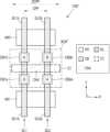
도 2a는 본 개시의 일 실시예에 따라, 도 1의 크로스 커플 구조에 대응하는 표준 셀(100)의 일부를 나타내는 레이아웃이다.FIG. 2A is a layout showing a portion of a
도 2a를 참조하면, 표준 셀(100)은 제1 및 제2 액티브 영역들(AR1, AR2), 제1 내지 제3 게이트 라인들(GL1, GL2, GL3), 제1 및 제2 절단 레이어들(cutting layers)(CT1, CT2), 및 제1 내지 제3 컨택들(CB1 내지 CB3)을 포함할 수 있다. 본 명세서에서, 제1 및 제2 절단 레이어들(CT1, CT2) 및 제1 내지 제3 컨택들(CB1 내지 CB3)이 배치되는 영역을 크로스 커플 영역(XCR)이라고 지칭하기로 한다. 본 실시예에 따르면, 크로스 커플 영역(XCR)은 제1 및 제2 액티브 영역들(AR1, AR2) 사이에 구현될 수 있다. 도 2a에서는 설명의 편의를 위하여 표준 셀(100)의 일부만을 도시하였으며, 표준 셀(100)은 다른 구성 요소들을 더 포함하도록 설계될 수 있다.Referring to FIG. 2A, the
제1 및 제2 액티브 영역들(AR1, AR2)은 제1 방향(예를 들어, X 방향)을 따라 연장되며, 제1 방향에 실질적으로 수직인 제2 방향(예를 들어, Y 방향)으로 서로 평행하게 배치될 수 있다. 제1 액티브 영역(AR1)과 제2 액티브 영역(AR2)은 제2 방향으로 서로 이격되도록 배치될 수 있고, 서로 다른 도전형을 가질 수 있다. 제1 및 제2 액티브 영역들(AR1, AR2)은 디퓨전(diffusion) 영역들이라고 지칭될 수 있다. 또한, 제1 액티브 영역(AR1)과 제2 액티브 영역(AR2) 사이의 영역을 더미 영역(dummy region)(예를 들어, 도 8 또는 도 18의 DR) 또는 MOL(Middle Of Line) 영역이라고 지칭할 수 있고, 크로스 커플 영역(XCR)은 더미 영역 내에 구현될 수 있다.The first and second active areas AR1 and AR2 extend along a first direction (eg, X direction) and extend in a second direction (eg, Y direction) substantially perpendicular to the first direction. They can be placed parallel to each other. The first active area AR1 and the second active area AR2 may be arranged to be spaced apart from each other in the second direction and may have different conductivity types. The first and second active areas AR1 and AR2 may be referred to as diffusion areas. Additionally, the area between the first active area AR1 and the second active area AR2 is referred to as a dummy region (e.g., DR in FIG. 8 or 18) or a Middle Of Line (MOL) area. It can be done, and the cross couple region (XCR) can be implemented in the dummy region.
제1 내지 제3 게이트 라인들(GL1 내지 GL3)은 제1 및 제2 액티브 영역들(AR1, AR2)에 걸쳐서 제2 방향을 따라 연장되고, 제1 방향으로 서로 평행하게 배치될 수 있다. 제1 내지 제3 게이트 라인들(GL1 내지 GL3)은 반도체 장치의 게이트 전극들에 대응할 수 있다. 제1 내지 제3 게이트 라인들(GL1 내지 GL3)은 서로 일정한 간격으로 이격될 수 있다. 제1 내지 제3 게이트 라인들(GL1 내지 GL3)의 피치, 즉, 게이트 피치는 CPP(Critical Poly Pitch 또는 Contacted Poly Pitch)라고 지칭할 수 있다. 본 실시예에 따르면, 표준 셀(100)에서 크로스 커플 구조는 3CPP에 해당하는 영역에 설계될 수 있고, 이에 따라, 표준 셀(100)에 포함된 크로스 커플 구조를 "3CPP 크로스 커플 구조"라고 지칭할 수 있다.The first to third gate lines GL1 to GL3 may extend along the second direction across the first and second active regions AR1 and AR2 and may be arranged parallel to each other in the first direction. The first to third gate lines GL1 to GL3 may correspond to gate electrodes of a semiconductor device. The first to third gate lines GL1 to GL3 may be spaced apart from each other at regular intervals. The pitch of the first to third gate lines GL1 to GL3, that is, the gate pitch, may be referred to as CPP (Critical Poly Pitch or Contacted Poly Pitch). According to this embodiment, the cross-couple structure in the
제1 절단 레이어(CT1)는 제1 및 제2 액티브 영역들(AR1, AR2)의 사이에서 제1 게이트 라인(GL1) 상에 배치될 수 있다. 제2 절단 레이어(CT2)는 제1 및 제2 액티브 영역들(AR1, AR2)의 사이에서 제3 게이트 라인(GL3) 상에 배치될 수 있다. 여기서, 제1 및 제2 절단 레이어들(CT1, CT2)은 제1 및 제3 게이트 라인들(GL1, GL3)의 일부 영역을 절단하기 위한 표시(marking) 레이어일 수 있고, 이에 따라, 제1 및 제3 게이트 라인들(GL1, GL3)은 각각 두 개로 분리될 수 있다. 구체적으로, 제1 절단 레이어(CT1)는 제1 게이트 라인(GL1)을 가로질러 배치되어, 제1 게이트 라인(GL1)을 제1 하부 게이트 라인(GL1a) 및 제1 상부 게이트 라인(GL1b)으로 분리할 수 있다. 제2 절단 레이어(CT2)는 제3 게이트 라인(GL3)을 가로질러 배치되어, 제3 게이트 라인(GL3)을 제3 하부 게이트 라인(GL3a) 및 제3 상부 게이트 라인(GL3b)으로 분리할 수 있다.The first cut layer CT1 may be disposed on the first gate line GL1 between the first and second active regions AR1 and AR2. The second cut layer CT2 may be disposed on the third gate line GL3 between the first and second active regions AR1 and AR2. Here, the first and second cutting layers (CT1, CT2) may be marking layers for cutting partial areas of the first and third gate lines (GL1, GL3), and accordingly, the first and the third gate lines GL1 and GL3 may each be divided into two. Specifically, the first cut layer CT1 is disposed across the first gate line GL1 to connect the first gate line GL1 to the first lower gate line GL1a and the first upper gate line GL1b. It can be separated. The second cut layer CT2 may be disposed across the third gate line GL3 to separate the third gate line GL3 into a third lower gate line GL3a and a third upper gate line GL3b. there is.
일 실시예에서, 제1 절단 레이어(CT1)의 제1 방향에 따른 사이즈인 제1 너비(W1)는 1CPP 이하일 수 있다. 또한, 제2 절단 레이어(CT2)의 제1 방향에 따른 사이즈인 제2 너비(W2)도 1CPP 이하일 수 있다. 이때, 제1 및 제2 너비들(W1, W2)은 실질적으로 동일할 수 있다. 이에 따라, 표준 셀(100)에 포함된 크로스 커플 구조를 "1CPP 절단 레이어를 갖는 3CPP 크로스 커플 구조"라고 지칭할 수 있다.In one embodiment, the first width W1, which is the size of the first cut layer CT1 in the first direction, may be 1 CPP or less. Additionally, the second width W2, which is the size of the second cut layer CT2 in the first direction, may also be 1 CPP or less. At this time, the first and second widths W1 and W2 may be substantially the same. Accordingly, the cross-coupled structure included in the
그러나, 본 발명은 이에 한정되지 않으며, 제1 너비(W1)는 제1 절단 레이어(CT1)가 제1 게이트 전극(GL1)에 완전히 오버랩되고 제2 게이트 전극(GL2)에는 오버랩되지 않도록 제1 게이트 전극(GL1)의 너비보다는 크고, 2CPP 보다는 작은 임의의 사이즈를 가질 수 있다. 마찬가지로, 제2 너비(W2)는 제2 절단 레이어(CT2)가 제3 게이트 전극(GL3)에 완전히 오버랩되고 제2 게이트 전극(GL2)에 오버랩되지 않도록 제3 게이트 전극(GL3)의 너비보다는 크고, 2CPP 보다는 작은 임의의 사이즈를 가질 수 있다. 또한, 제1 너비(W1)과 제2 너비(W2)는 서로 다를 수도 있다.However, the present invention is not limited to this, and the first width W1 is set so that the first cut layer CT1 completely overlaps the first gate electrode GL1 and does not overlap the second gate electrode GL2. It can have any size larger than the width of the electrode GL1 and smaller than 2CPP. Likewise, the second width W2 is greater than the width of the third gate electrode GL3 so that the second cut layer CT2 completely overlaps the third gate electrode GL3 and does not overlap the second gate electrode GL2. , it can have an arbitrary size smaller than 2CPP. Additionally, the first width W1 and the second width W2 may be different from each other.
제1 내지 제3 컨택들(CB1 내지 CB3)은 제1 액티브 영역(AR1)과 제2 액티브 영역(AR2) 사이에 각각 배치될 수 있다. 구체적으로, 제1 상부 게이트 라인(GL1b) 상에는 제1 컨택(CB1)이 배치되고, 제2 게이트 라인(GL2) 상에는 제2 컨택(CB2)이 배치되며, 제3 하부 게이트 라인(GL3a)에는 제3 컨택(CB3)이 배치될 수 있다. 이때, 제1 내지 제3 컨택들(CB1 내지 CB3)은 반도체 장치의 게이트 컨택들에 대응할 수 있고, 게이트 컨택 패턴들 또는 게이트 컨택 플러그들이라고 지칭할 수도 있다.The first to third contacts CB1 to CB3 may be disposed between the first active area AR1 and the second active area AR2, respectively. Specifically, the first contact (CB1) is disposed on the first upper gate line (GL1b), the second contact (CB2) is disposed on the second gate line (GL2), and the third contact (CB2) is disposed on the third lower gate line (GL3a). 3 contacts (CB3) can be placed. At this time, the first to third contacts CB1 to CB3 may correspond to gate contacts of the semiconductor device and may also be referred to as gate contact patterns or gate contact plugs.
제1 및 제3 컨택들(CB1, CB3)을 통해 제1 제어 신호(A)가 인가될 수 있고, 제1 제어 신호(A)는 제1 상부 게이트 라인(GL1b) 및 제3 하부 게이트 라인(GL3a)에 전달될 수 있다. 한편, 제2 컨택(CB2)을 통해 제2 제어 신호(B)가 인가될 수 있고, 제2 제어 신호(B)는 제2 게이트 라인(GL2)에 전달될 수 있다. 제1 하부 게이트 라인(GL1a) 및 제3 상부 게이트 라인(GL3b) 상에는 컨택이 배치되지 않고, 이에 따라, 제1 하부 게이트 라인(GL1a) 및 제3 상부 게이트 라인(GL3b)은 더미 게이트 라인들 또는 더미 게이트 전극들에 대응할 수 있다. 본 실시예에 따르면, 서로 분리된 제1 상부 게이트 라인(GL1b)과 제3 하부 게이트 라인(GL3a)에 동일한 제1 제어 신호(A)가 인가되므로, 제1 상부 게이트 라인(GL1b)과 제3 하부 게이트 라인(GL3a)을 전기적으로 연결할 것이 요구된다. 이에 대해, 도 4 및 도 14를 참조하여 후술하기로 한다.A first control signal A may be applied through the first and third contacts CB1 and CB3, and the first control signal A may be applied to the first upper gate line GL1b and the third lower gate line ( It can be passed on to GL3a). Meanwhile, the second control signal B may be applied through the second contact CB2, and the second control signal B may be transmitted to the second gate line GL2. Contacts are not disposed on the first lower gate line GL1a and the third upper gate line GL3b, and accordingly, the first lower gate line GL1a and the third upper gate line GL3b are dummy gate lines or It can correspond to dummy gate electrodes. According to this embodiment, the same first control signal (A) is applied to the first upper gate line (GL1b) and the third lower gate line (GL3a), which are separated from each other, so that the first upper gate line (GL1b) and the third lower gate line (GL3a) are applied. It is required to electrically connect the lower gate line (GL3a). This will be described later with reference to FIGS. 4 and 14.
본 실시예에서, 제1 절단 레이어(CT1)와 제2 절단 레이어(CT2)는 서로 엇갈린 형태(staggered form)로 배치될 수 있다. 구체적으로, 크로스 커플 영역(XCR) 내에서, 제1 절단 레이어(CT1)는 제1 액티브 영역(AR1)에 인접하게 배치되고, 제2 절단 레이어(CT2)는 제2 액티브 영역(AR2)에 인접하게 배치될 수 있다. 이에 따라, 제1 내지 제3 게이트 전극들(GL1 내지 GL3)을 가로지르는 3CPP 절단 레이어를 포함하는 표준 셀에 비해, 본 실시예에 따른 표준 셀(100)에서 제1 및 제3 컨택들(CB1, CB3)의 배치 자유도가 향상될 수 있고, 크로스 커플 영역(XCR)의 제2 방향에 따른 사이즈(이하, '높이')를 감소시킬 수 있다.In this embodiment, the first cut layer (CT1) and the second cut layer (CT2) may be arranged in a staggered form. Specifically, within the cross couple region (XCR), the first cut layer (CT1) is disposed adjacent to the first active region (AR1), and the second cut layer (CT2) is disposed adjacent to the second active region (AR2) It can be placed like this. Accordingly, compared to a standard cell including a 3CPP cut layer crossing the first to third gate electrodes GL1 to GL3, the first and third contacts CB1 in the
도 2b는 본 개시의 일 실시예에 따라, 도 1의 크로스 커플 구조에 대응하는 표준 셀(100')의 일부를 나타내는 레이아웃이다.FIG. 2B is a layout showing a portion of a standard cell 100' corresponding to the cross-coupled structure of FIG. 1, according to an embodiment of the present disclosure.
도 2b를 참조하면, 표준 셀(100')은 제1 및 제2 액티브 영역들(AR1, AR2), 제1 내지 제3 게이트 라인들(GL1, GL2, GL3), 제1 및 제2 절단 레이어들(CT1, CT2), 및 제1 내지 제3 컨택들(CB1, CB2a, CB2b 및 CB3)을 포함할 수 있다. 표준 셀(100')은 도 2a의 표준 셀(100)의 변형 실시예이며, 도 2a를 참조하여 상술된 내용은 본 실시예에 적용될 수 있다. 본 실시예에 따르면, 크로스 커플 영역(XCR')에서, 제2 게이트 라인(GL2) 상에 서로 이격된 두 개의 제2 컨택들(CB2a, CB2b)이 배치될 수 있다. 두 개의 제2 컨택들(CB2a, CB2b)을 통해 제2 제어 신호(B)가 인가될 수 있고, 제2 제어 신호(B)는 제2 게이트 라인(GL2)에 전달될 수 있다. 이하에서는, 도 2a와 같이 하나의 제2 컨택(CB2)을 포함하는 구현예들을 상술하지만, 해당 구현예들은 도 2b와 같이 두 개의 제2 컨택들(CB2a, CB2b)을 포함할 수도 있다.Referring to FIG. 2B, the standard cell 100' includes first and second active regions AR1 and AR2, first to third gate lines GL1, GL2, and GL3, and first and second cut layers. may include CT1, CT2, and first to third contacts CB1, CB2a, CB2b, and CB3. The standard cell 100' is a modified example of the
도 2c는 본 개시의 비교예에 따라, 크로스 커플 구조에 대응하는 표준 셀(100")의 일부를 나타내는 레이아웃이다. 이때, 표준 셀(100")은 2CPP 크로스 커플 구조에 대응된다.FIG. 2C is a layout showing a portion of a
도 2c를 참조하면, 표준 셀(100")은 제1 및 제2 액티브 영역들(AR1, AR2), 제1 및 제2 게이트 라인들(GL1, GL2), 절단 레이어(CT), 및 복수의 컨택들(CB1a 내지 CB2b, CAd)을 포함한다. 절단 레이어(CT)는 제1 및 제2 게이트 라인들(GL1, GL2) 상에 제1 방향을 따라 연장되도록 배치됨으로써, 제1 게이트 라인(GL1)은 제1 하부 게이트 라인(GL1a) 및 제1 상부 게이트 라인(GL1b)으로 분리되고, 제2 게이트 라인(GL2)은 제2 하부 게이트 라인(GL2a) 및 제2 상부 게이트 라인(GL2b)으로 분리된다.Referring to FIG. 2C, the
제1 상부 게이트 라인(GL1b) 및 제2 하부 게이트 라인(GL2a) 상의 컨택들(CB1b, CB2a)에는 제1 제어 신호(A)가 인가되고, 제1 하부 게이트 라인(GL1a) 및 제2 상부 게이트 라인(GL2b) 상의 컨택들(CB1a, CB2b)에는 제2 제어 신호(B)가 인가된다. 이때, 컨택들(CB1a, CB2b)은 사선(diagonal) 컨택(CAd)에 의해 전기적으로 연결된다. 표준 셀(100")에 따라 반도체 장치를 형성할 경우, 컨택들(CB1a, CB2b)과 사선 컨택(CAd)의 연결이 끊어지거나 사선 컨택(CAd)이 중간에 끊어지는 워닝 포인트(warning point) 또는 위크 패턴(weak pattern)이 발생할 수 있고, 이에 따라, 반도체 장치의 수율이 감소할 수 있다.The first control signal (A) is applied to the contacts (CB1b, CB2a) on the first upper gate line (GL1b) and the second lower gate line (GL2a), and the first lower gate line (GL1a) and the second upper gate The second control signal B is applied to the contacts CB1a and CB2b on the line GL2b. At this time, the contacts CB1a and CB2b are electrically connected by a diagonal contact CAd. When forming a semiconductor device according to the standard cell (100"), there is a warning point where the connection between the contacts (CB1a, CB2b) and the diagonal contact (CAd) is disconnected or the diagonal contact (CAd) is disconnected in the middle, or A weak pattern may occur, and accordingly, the yield of the semiconductor device may decrease.
도 3은 본 개시의 일 실시예에 따른 서로 다른 높이들(H, H', H")을 갖는 제1 내지 제3 표준 셀들(SC1 내지 SC3)을 나타낸다.Figure 3 shows first to third standard cells (SC1 to SC3) having different heights (H, H', H") according to an embodiment of the present disclosure.
도 3을 참조하면, 제1 표준 셀(SC1)은 제1 높이(H)를 갖고, 제2 표준 셀(SC2)은 제1 높이(H1)보다 작은 제2 높이(H')를 갖고, 제3 표준 셀(SC3)은 제2 높이(H')보다 작은 제3 높이(H")를 갖는다. 제1 내지 제3 높이들(H, H', H")은 제1 내지 제3 표준 셀들(SC1 내지 SC3) 상부의 트랙들의 개수(이하 '트랙 넘버'라고 지칭함)에 따라 각각 결정될 수 있다. 여기서, 트랙들은 제1 방향(예를 들어, X 방향)을 따라 연장되고 서로 평행하게 배치되는 도전성 라인들이며, 예를 들어, 반도체 장치의 제2 금속층에 대응할 수 있다.Referring to Figure 3, the first standard cell (SC1) has a first height (H), the second standard cell (SC2) has a second height (H') smaller than the first height (H1), and the second standard cell (SC2) has a second height (H') that is smaller than the first height (H1). 3 The standard cell (SC3) has a third height (H") that is smaller than the second height (H'). The first to third heights (H, H', H") are the first to third standard cells (SC1 to SC3) can each be determined according to the number of upper tracks (hereinafter referred to as 'track number'). Here, the tracks are conductive lines extending along a first direction (eg, X direction) and arranged parallel to each other, and may correspond, for example, to a second metal layer of a semiconductor device.
제1 내지 제3 표준 셀들(SC1 내지 SC3) 각각은, 예를 들어, 접지 전압 및 전원 전압이 각각 인가되는 제1 및 제2 파워 영역들(VSS, VDD), 제1 및 제2 액티브 영역들(AR1, AR2), 및 MOL 영역(MOL)을 포함할 수 있다. 제1 높이(H)는 H1 내지 H5의 합에 대응할 수 있고(즉, H=H1+H2+H3+H4+H5), 제2 높이(H')는 H1' 내지 H5'의 합에 대응할 수 있고(즉, H'=H1'+H2'+H3'+H4'+H5'), 제3 높이(H")는 H1" 내지 H5"의 합에 대응할 수 있다(즉, H"=H1"+H2"+H3"+H4"+H5").Each of the first to third standard cells (SC1 to SC3) includes, for example, first and second power regions (VSS, VDD), first and second active regions to which ground voltage and power voltage are applied, respectively. (AR1, AR2), and MOL area (MOL). The first height (H) may correspond to the sum of H1 to H5 (i.e., H=H1+H2+H3+H4+H5), and the second height (H') may correspond to the sum of H1' to H5'. (i.e., H'=H1'+H2'+H3'+H4'+H5'), and the third height (H") may correspond to the sum of H1" to H5" (i.e., H"=H1" +H2"+H3"+H4"+H5").
본 실시예에 따르면, 제1 내지 제3 표준 셀들(SC1 내지 SC3)은 제1 크로스 커플 영역(XCR1)을 포함할 수 있다. 제1 크로스 커플 영역(XCR1)은 본 개시의 실시예들에 따른 3CPP 크로스 커플 영역, 예를 들어, 도 2a의 XCR 또는 도 2b의 XCR'에 대응할 수 있다. 한편, 제2 크로스 커플 영역(XCR2)은 본 개시의 비교예에 따른 2CPP 크로스 커플 영역, 예를 들어, 도 2c의 XCR"에 대응할 수 있다. 제1 크로스 커플 영역(XCR1)은 제2 크로스 커플 영역(XCR2)에 비해 제1 방향에 따른 사이즈(이하, '너비')는 1CPP만큼 더 크지만, 높이는 더 작다. 이에 따라, 제1 크로스 커플 영역(XCR1)은 낮은 높이를 갖는 표준 셀(예를 들어, SC2, SC3)에 적합하다.According to this embodiment, the first to third standard cells SC1 to SC3 may include a first cross couple region XCR1. The first cross-coupled region XCR1 may correspond to a 3CPP cross-coupled region according to embodiments of the present disclosure, for example, XCR of FIG. 2A or Meanwhile, the second cross couple region (XCR2) may correspond to a 2CPP cross couple region according to a comparative example of the present disclosure, for example, Compared to the area For example, it is suitable for SC2, SC3).
반도체 공정 기술의 발달에 따라 반도체 장치의 전반적인 디자인 룰이 더욱 축소되고 있다. 특히, 각 표준 셀 상부의 트랙들의 개수가 감소함에 따라, 표준 셀의 높이(이하 '셀 높이')가 감소할 수 있다. 제1 표준 셀(SC1)에서 제3 표준 셀(SC3)의 방향으로 갈수록 트랙 넘버가 감소하고, 이로써, 셀 높이가 감소함에 따라, MOL 영역(MOL)의 높이도 H3에서 H3"로 감소하게 된다. 제1 표준 셀(SC1)에서는, MOL 영역(MOL)의 높이(H3)가 충분히 높으므로, 제1 또는 제2 크로스 커플 영역(XCR1, XCR2)을 포함하여 크로스 커플 구조를 구현하는 것이 모두 가능하다.As semiconductor processing technology develops, the overall design rules for semiconductor devices are further reduced. In particular, as the number of tracks on top of each standard cell decreases, the height of the standard cell (hereinafter referred to as 'cell height') may decrease. The track number decreases in the direction from the first standard cell (SC1) to the third standard cell (SC3), and as the cell height decreases, the height of the MOL area (MOL) also decreases from H3 to H3". In the first standard cell (SC1), the height (H3) of the MOL region (MOL) is sufficiently high, so it is possible to implement a cross-coupled structure including the first or second cross-coupled regions (XCR1 and XCR2). do.
제2 및 제3 표준 셀들(SC2, SC3)에서는, 제2 크로스 커플 영역(XCR2)의 높이가 MOL 영역의 높이(H3', H3")보다 크다. 따라서, 제2 및 제3 표준 셀들(SC2, SC3)의 경우, 제2 크로스 커플 영역(XCR2)을 포함하여 크로스 커플 구조를 구현하는 것이 불가능하다. 그러나, 제1 크로스 커플 영역(XCR1)의 높이는 MOL 영역의 높이(H3', H3")보다 작기 때문에, 제2 및 제3 표준 셀들(SC2, SC3)의 경우, 제1 크로스 커플 영역(XCR1)을 포함하여 크로스 커플 구조를 구현할 수 있다.In the second and third standard cells (SC2, SC3), the height of the second cross couple region (XCR2) is greater than the height (H3', H3") of the MOL region. Therefore, the second and third standard cells (SC2) , SC3), it is impossible to implement a cross-coupled structure including the second cross-coupled region (XCR2). However, the height of the first cross-coupled region (XCR1) is equal to the height of the MOL region (H3', H3") Since the second and third standard cells SC2 and SC3 are smaller, a cross-coupled structure can be implemented by including the first cross-coupled region XCR1.
한편, 3CPP 절단 레이어를 갖는 3CPP 크로스 커플 구조의 경우, 3CPP 절단 레이어의 배치로 인해 게이트 컨택들(예를 들어, 도 2b의 CB1, CB2a, CB2b, CB3)의 배치 자유도가 감소하게 된다. 이로써, 3CPP 절단 레이어를 갖는 3CPP 크로스 커플 구조의 크로스 커플 영역의 높이는, 제1 크로스 커플 영역(XCR1)에 비해 높이가 클 수 있고, 예를 들어, 제2 크로스 커플 영역(XCR2)의 높이만큼 클 수 있다. 따라서, 제2 및 제3 표준 셀들(SC2, SC3)의 경우, 3CPP 절단 레이어를 갖는 3CPP 크로스 커플 구조를 구현하는 것이 불가능할 수 있다.Meanwhile, in the case of a 3CPP cross-coupled structure with a 3CPP cut layer, the degree of freedom in placement of gate contacts (eg, CB1, CB2a, CB2b, and CB3 in FIG. 2B) is reduced due to the arrangement of the 3CPP cut layer. Accordingly, the height of the cross couple region of the 3CPP cross couple structure having a 3CPP cut layer may be greater than the first cross couple region (XCR1), for example, as large as the height of the second cross couple region (XCR2). You can. Therefore, in the case of the second and third standard cells SC2 and SC3, it may be impossible to implement a 3CPP cross-couple structure with a 3CPP truncation layer.
이와 같이, 본 실시예에 따른 제1 크로스 커플 영역(XCR1)은 1CPP 사이즈를 갖는 두 개의 절단 레이어들(예를 들어, 도 2a의 CT1, CT2)을 포함함으로써, 게이트 컨택들의 배치 자유도를 증가시켜서 제1 크로스 커플 영역(XCR1)의 높이를 감소시킬 수 있다. 따라서, 반도체 공정 기술 발달에 따라 셀 높이가 감소하더라도(예를 들어, sub 9T) 도 1에 예시된 크로스 커플 구조(XC)를 안정적으로 구현할 수 있다.As such, the first cross-coupled region The height of the first cross couple region (XCR1) may be reduced. Therefore, even if the cell height decreases with the development of semiconductor processing technology (for example, sub 9T), the cross-coupled structure (XC) illustrated in FIG. 1 can be stably implemented.
도 4는 본 개시의 일 실시예에 따른 표준 셀(100a)의 일부를 나타내는 레이아웃이다.FIG. 4 is a layout showing a portion of a
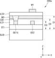
도 4를 참조하면, 표준 셀(100a)은 제1 및 제2 액티브 영역들(AR1, AR2), 제1 내지 제3 게이트 라인들(GL1 내지 GL3), 제1 내지 제3 컨택들(CB1 내지 CB3), 제1 및 제2 절단 레이어들(CT1, CT2), 및 제1 및 제2 배선들(M0, M1)을 포함할 수 있다. 본 실시예에 따른 표준 셀(100a)는 도 2a에 예시된 표준 셀(100)의 일 구현예로서, 도 2a를 참조하여 상술된 내용은 본 실시예에 적용될 수 있으며, 중복된 설명은 생략하기로 한다. 이하에서는, 본 실시예에 따른 표준 셀(100a)과 도 2a에 예시된 표준 셀(100)과의 차이점을 중심으로 설명하기로 한다.Referring to FIG. 4, the
제1 배선(M0)은 제1 및 제3 컨택들(CB1, CB3)에 전기적으로 연결될 수 있다. 제1 배선(M0)은, 제1 컨택(CB1)에 전기적으로 연결되고 제1 방향으로 연장되는 제1 부분, 및 제3 컨택(CB3)에 전기적으로 연결되고 제2 방향으로 연장되는 제2 부분을 포함할 수 있다. 표준 셀(100a)에 따라 구현된 반도체 장치(예를 들어, 도 5 내지 도 7의 200a)에서, 제1 배선(M0)의 상면은 제1 및 제3 컨택들(CB1, CB3)의 상면과 실질적으로 동일 레벨로 구현될 수 있다. 제1 배선(M0)의 하면은 제1 및 제3 컨택들(CB1, CB3)의 하면 및 제2 게이트 라인(GL2)의 상면보다 높게 구현될 수 있고, 이에 따라, 제1 배선(M0)은 제2 게이트 라인(GL2)와 절연될 수 있다.The first wiring M0 may be electrically connected to the first and third contacts CB1 and CB3. The first wiring M0 includes a first portion electrically connected to the first contact CB1 and extending in the first direction, and a second portion electrically connected to the third contact CB3 and extending in the second direction. may include. In a semiconductor device implemented according to the
제2 배선(M1)은 제2 게이트 라인(GL2) 및 제2 컨택(CB2)의 상부에 배치되고, 제2 컨택(CB2)에 전기적으로 연결될 수 있다. 제2 배선(M1)은 제1 배선(M0)의 상부에 배치되는 상부 금속층에 대응할 수 있다. 예를 들어, 표준 셀(100a)에 따라 구현된 반도체 장치(예를 들어, 도 5 내지 도 7의 200a)에서, 제2 배선(M1)은 제2 방향으로 연장되는 제1 금속층을 구성할 수 있다.The second wiring M1 is disposed on the second gate line GL2 and the second contact CB2, and may be electrically connected to the second contact CB2. The second wiring M1 may correspond to an upper metal layer disposed on top of the first wiring M0. For example, in a semiconductor device implemented according to the
도 5는 도 4의 V-V' 선에 따른 단면도를 나타내고, 도 6은 도 4의 VI-VI' 선에 따른 단면도를 나타내며, 도 7은 도 4의 VII-VII' 선에 따른 단면도를 나타낸다. 이때, 반도체 장치(200a)는 도 4의 레이아웃에 따라 구현된 반도체 장치의 일 예일 수 있다.FIG. 5 shows a cross-sectional view taken along line V-V' of FIG. 4, FIG. 6 shows a cross-sectional view taken along line VI-VI' of FIG. 4, and FIG. 7 shows a cross-sectional view taken along line VII-VII' of FIG. 4. At this time, the
도 5를 참조하면, 기판(SUB)은 반도체 기판일 수 있는데, 예를 들어, 반도체 기판은 실리콘, 실리콘-온-절연체(Silicon-On-Insulator, SOI), 실리콘-온-사파이어(Silicon-On-Sapphire), 게르마늄, 실리콘-게르마늄 및 갈륨 비소(gallium-arsenide) 중 어느 하나를 포함할 수 있다. 소자 분리막(STI)은 기판(SUB) 상에 배치될 수 있고, 제1 절연층(ILD1)은 소자 분리막(STI) 상에 배치될 수 있다.Referring to FIG. 5, the substrate (SUB) may be a semiconductor substrate. For example, the semiconductor substrate may be silicon, silicon-on-insulator (SOI), or silicon-on-sapphire (Silicon-On). -Sapphire), germanium, silicon-germanium, and gallium-arsenide. The device isolation layer (STI) may be disposed on the substrate (SUB), and the first insulating layer (ILD1) may be disposed on the device isolation layer (STI).
제1 상부 게이트 전극(GE1b) 및 제2 게이트 전극(GE2)이 소자 분리막(STI) 상에 배치될 수 있다. 제1 상부 게이트 전극(GE1b) 및 제2 게이트 전극(GE2)은 예를 들어, 텅스텐(W), 탄탈륨(Ta) 등과 같은 금속 물질, 이들의 질화물, 이들의 실리사이드, 도핑된 폴리실리콘 등을 포함할 수 있고, 예를 들어, 증착 공정을 이용하여 형성될 수 있다. 이때, 제1 상부 게이트 전극(GE1b) 및 제2 게이트 전극(GE2)은 도 4의 제1 상부 게이트 라인(GL1b) 및 제2 게이트 라인(GL2)에 각각 대응할 수 있다.The first upper gate electrode GE1b and the second gate electrode GE2 may be disposed on the device isolation layer STI. The first upper gate electrode (GE1b) and the second gate electrode (GE2) include, for example, metal materials such as tungsten (W), tantalum (Ta), their nitrides, their silicides, doped polysilicon, etc. It can be formed, for example, using a deposition process. At this time, the first upper gate electrode GE1b and the second gate electrode GE2 may correspond to the first upper gate line GL1b and the second gate line GL2 of FIG. 4, respectively.
제1 상부 게이트 전극(GE1b) 상에는 제1 컨택(CB1)이 배치되고, 제1 컨택(CB1)은 예를 들어, 텅스텐과 같이 전기 전도성을 갖는 임의의 물질을 포함할 수 있다. 제1 배선(M0)은 제1 컨택(CB1)에 전기적으로 연결되며, 예를 들어, 구리와 같이 전기 전도성을 갖는 임의의 물질을 포함할 수 있다. 제1 배선(M0)의 상면은 제1 컨택(CB1)의 상면과 실질적으로 동일 레벨로 구현될 수 있다. 구체적으로, 기판(SUB)의 상면에서 제1 컨택(CB1)의 상면까지의 거리는 기판(SUB)의 상면에서 제1 배선(M0)의 상면까지의 거리(D1)와 실질적으로 동일할 수 있다. 한편, 제1 배선(M0)의 하면은 제1 컨택(CB1)의 하면보다 높게 형성될 수 있다. 구체적으로, 기판(SUB)의 상면에서 제1 배선(M0)의 하면까지의 거리(D2)는 기판(SUB)의 상면에서 제1 컨택(CB1)의 하면까지의 거리(D3)보다 클 수 있다. 이에 따라, 제1 배선(M0)은 제2 게이트 전극(GE2)과 전기적으로 절연될 수 있다.A first contact CB1 is disposed on the first upper gate electrode GE1b, and the first contact CB1 may include any material having electrical conductivity, such as tungsten. The first wiring M0 is electrically connected to the first contact CB1 and may include any material having electrical conductivity, such as copper. The top surface of the first wiring M0 may be implemented at substantially the same level as the top surface of the first contact CB1. Specifically, the distance from the top surface of the substrate SUB to the top surface of the first contact CB1 may be substantially equal to the distance D1 from the top surface of the substrate SUB to the top surface of the first wiring M0. Meanwhile, the lower surface of the first wiring M0 may be formed to be higher than the lower surface of the first contact CB1. Specifically, the distance D2 from the top surface of the substrate SUB to the bottom surface of the first wiring M0 may be greater than the distance D3 from the top surface of the substrate SUB to the bottom surface of the first contact CB1. . Accordingly, the first wiring M0 may be electrically insulated from the second gate electrode GE2.
제2 절연층(ILD2)은 제1 배선(MO) 상에 배치될 수 있다. 제2 절연층(ILD2)은 절연 물질을 포함할 수 있는데, 예를 들어, 절연 물질은 산화막, 질화막 또는 산질화막 중 어느 하나를 포함할 수 있다. 제2 배선(M1)은 제2 절연층(ILD2) 상에 배치될 수 있다.The second insulating layer ILD2 may be disposed on the first wiring MO. The second insulating layer ILD2 may include an insulating material. For example, the insulating material may include any one of an oxide film, a nitride film, and an oxynitride film. The second wiring M1 may be disposed on the second insulating layer ILD2.
도 6을 참조하면, 제3 하부 게이트 전극(GE3a) 및 제3 상부 게이트 전극(GE3b)이 소자 분리막(STI) 상에 배치될 수 있다. 제3 하부 게이트 전극(GE3a) 및 제3 상부 게이트 전극(GE3b)은 예를 들어, 텅스텐(W), 탄탈륨(Ta) 등과 같은 금속 물질, 이들의 질화물, 이들의 실리사이드, 도핑된 폴리실리콘 등을 포함할 수 있고, 예를 들어, 증착 공정을 이용하여 형성될 수 있다.Referring to FIG. 6 , the third lower gate electrode GE3a and the third upper gate electrode GE3b may be disposed on the device isolation layer STI. For example, the third lower gate electrode (GE3a) and the third upper gate electrode (GE3b) are made of metal materials such as tungsten (W), tantalum (Ta), their nitrides, their silicides, doped polysilicon, etc. It may include and, for example, may be formed using a deposition process.
제3 하부 게이트 전극(GE3a) 상에는 제3 컨택(CB3)이 배치되고, 제3 컨택(CB3)은 예를 들어, 텅스텐과 같이 전기 전도성을 갖는 임의의 물질을 포함할 수 있다. 제1 배선(M0)은 제3 컨택(CB3)에 전기적으로 연결되며, 예를 들어, 구리와 같이 전기 전도성을 갖는 임의의 물질을 포함할 수 있다. 제1 배선(M0)의 상면은 제3 컨택(CB3)의 상면과 실질적으로 동일 레벨로 구현될 수 있다. 구체적으로, 기판(SUB)의 상면에서 제3 컨택(CB3)의 상면까지의 거리는 기판(SUB)의 상면에서 제1 배선(M0)의 상면까지의 거리(D1)와 실질적으로 동일할 수 있다. 한편, 제1 배선(M0)의 하면은 제3 컨택(CB3)의 하면보다 높게 형성될 수 있다. 구체적으로, 기판(SUB)의 상면에서 제1 배선(M0)의 하면까지의 거리(D2)는 기판(SUB)의 상면에서 제3 컨택(CB3)의 하면까지의 거리(D3)보다 클 수 있다.A third contact CB3 is disposed on the third lower gate electrode GE3a, and the third contact CB3 may include any material having electrical conductivity, such as tungsten. The first wiring M0 is electrically connected to the third contact CB3 and may include any material having electrical conductivity, such as copper. The top surface of the first wiring M0 may be implemented at substantially the same level as the top surface of the third contact CB3. Specifically, the distance from the top surface of the substrate SUB to the top surface of the third contact CB3 may be substantially equal to the distance D1 from the top surface of the substrate SUB to the top surface of the first wiring M0. Meanwhile, the lower surface of the first wiring M0 may be formed to be higher than the lower surface of the third contact CB3. Specifically, the distance D2 from the top surface of the substrate SUB to the bottom surface of the first wiring M0 may be greater than the distance D3 from the top surface of the substrate SUB to the bottom surface of the third contact CB3. .
일 실시예에서, 제3 하부 게이트 전극(GE3a)과 제3 상부 게이트 전극(GE3b) 사이의 영역(즉, 도 4의 제2 절단 레이어(CT2)에 대응하는 제2 절단 영역(CT2))에 갭필층(GF)이 배치될 수 있다. 일 실시예에서, 갭필층(GF)은 질화막으로 구현될 수 있고, 예를 들어, 실리콘 절연층(SiN)을 포함할 수 있다. 일 실시예에서, 제3 하부 게이트 전극(GE3a)의 절단면(cutting surface)(CS1) 및 제3 상부 게이트 전극(GE3b)의 절단면(CS2)은 직사각형 형태일 수 있다. 이때, 제3 하부 게이트 전극(GE3a)의 절단면(CS1)과 갭필층(GF) 사이, 그리고, 제3 상부 게이트 전극(GE3b)의 절단면(CS2)과 갭필층(GF) 사이에는 스페이서가 배치되지 않을 수 있다.In one embodiment, in the area between the third lower gate electrode GE3a and the third upper gate electrode GE3b (i.e., the second cut area CT2 corresponding to the second cut layer CT2 in FIG. 4) A gap fill layer (GF) may be disposed. In one embodiment, the gap fill layer (GF) may be implemented as a nitride layer and may include, for example, a silicon insulating layer (SiN). In one embodiment, the cutting surface CS1 of the third lower gate electrode GE3a and the cutting surface CS2 of the third upper gate electrode GE3b may have a rectangular shape. At this time, no spacer is disposed between the cut surface CS1 of the third lower gate electrode GE3a and the gap fill layer GF, and between the cut surface CS2 of the third upper gate electrode GE3b and the gap fill layer GF. It may not be possible.
도 7을 참조하면, 비아(V0)는 제2 컨택(CB2) 상에 배치되어 제2 컨택(CB2)과 전기적으로 연결될 수 있다. 비아(V0)는 전기 전도성을 갖는 임의의 물질을 포함하도록 형성될 수 있다. 제2 배선(M1)은 비아(V0) 상에 배치되어 비아(V0)와 전기적으로 연결될 수 있다. 제2 배선(M1)에 의해 제2 게이트 전극(GE2)은 동일한 제어 신호(예를 들어, 도 4의 B)를 수신할 수 있다. 예를 들어, 제2 배선(M1)은 텅스텐(W), 알루미늄(Al), 구리(Cu), 또는 몰리브덴(Mo), 타이타늄(Ti), 탄탈륨(Ta), 루테늄(Ru), 또는 이들의 합금을 포함하는 금속층 또는 폴리실리콘층일 수 있다.Referring to FIG. 7 , the via V0 may be disposed on the second contact CB2 and electrically connected to the second contact CB2. The via (V0) may be formed to include any material having electrical conductivity. The second wire M1 may be disposed on the via V0 and electrically connected to the via V0. The second gate electrode GE2 may receive the same control signal (eg, B in FIG. 4 ) through the second wiring M1. For example, the second wiring M1 is made of tungsten (W), aluminum (Al), copper (Cu), molybdenum (Mo), titanium (Ti), tantalum (Ta), ruthenium (Ru), or any of these. It may be a metal layer containing an alloy or a polysilicon layer.
도 8은 본 개시의 일 실시예에 따른 집적 회로(300a)의 일부를 나타내는 레이아웃이다.FIG. 8 is a layout showing a portion of an
도 8을 참조하면, 집적 회로(300a)는 제1 및 제2 액티브 영역들(AR1, AR2), 더미 영역(DR), 제1 내지 제4 액티브 핀들(AF1 내지 AF4), 제1 내지 제6 더미 핀들(DF1 내지 DF6), 제1 내지 제3 게이트 라인들(320 내지 340), 제1 및 제2 절단 레이어들(CT1, CT2), 제1 내지 제3 게이트 컨택들(350a 내지 350c), 및 제1 및 제2 배선들(360, 370)을 포함할 수 있다. 또한, 표준 셀(300a)은 트렌치 실리사이드들(TS) 및 소스/드레인 컨택들(CA)을 더 포함할 수 있다. 본 실시예에 따른 집적 회로(300a)은 도 4에 예시된 표준 셀(100a)에 대한 구체적인 구현 예로서, 도 4를 참조하여 상술된 내용은 본 실시예에 적용될 수 있고, 중복된 설명은 생략하기로 한다.Referring to FIG. 8, the
제1 내지 제4 액티브 핀들(AF1 내지 AF4) 및 제1 내지 제6 더미 핀들(DF1 내지 DF6)은 제1 방향을 따라 연장되며, 제2 방향으로 서로 평행하게 배치될 수 있다. 일 실시예에서, 제1 내지 제4 액티브 핀들(AF1 내지 AF4) 및 제1 내지 제6 더미 핀들(DF1 내지 DF6)은 서로 일정한 간격으로 이격될 수 있다. 제1 및 제2 액티브 핀들(AF1, AF2)은 제1 액티브 영역(AR1)에 배치되고, 예를 들어, NMOS 트랜지스터(예를 들어, 도 1의 NM1, NM2)를 구성할 수 있다. 또한, 제3 및 제4 액티브 핀들(AF3, AF4)은 제2 액티브 영역(AR2)에 배치되고, 예를 들어, PMOS 트랜지스터(예를 들어, 도 1의 PM1, PM2)를 구성할 수 있다. 이때, 표준 셀(300a)에 포함된 액티브 핀들(AF1 내지 AF4) 및 더미 핀들(DF1 내지 DF6)의 개수는 실시예에 따라 다양하게 변경될 수 있다.The first to fourth active fins AF1 to AF4 and the first to sixth dummy fins DF1 to DF6 extend along the first direction and may be arranged parallel to each other in the second direction. In one embodiment, the first to fourth active fins AF1 to AF4 and the first to sixth dummy fins DF1 to DF6 may be spaced apart from each other at regular intervals. The first and second active fins AF1 and AF2 are disposed in the first active area AR1 and may form, for example, NMOS transistors (eg, NM1 and NM2 in FIG. 1). Additionally, the third and fourth active fins AF3 and AF4 are disposed in the second active area AR2 and may form, for example, a PMOS transistor (eg, PM1 and PM2 in FIG. 1 ). At this time, the number of active fins (AF1 to AF4) and dummy fins (DF1 to DF6) included in the
제1 절단 레이어(CT1)는 더미 영역(DR)에서 제1 액티브 영역(AR1)에 인접하도록 배치되어, 제1 게이트 라인(320)을 제1 하부 게이트 라인(320a) 및 제1 상부 게이트 라인(320b)으로 분리할 수 있다. 제2 절단 레이어(CT2)는 더미 영역(DR)에서 제2 액티브 영역(AR2)에 인접하도록 배치되어, 제3 게이트 라인(340)을 제3 하부 게이트 라인(340a) 및 제3 상부 게이트 라인(340b)으로 분리할 수 있다. 본 실시예에서, 제1 및 제2 절단 레이어들(CT1, CT2)은 1CPP 절단 레이어들로 구현될 수 있다. 본 실시예에서, 제1 하부 게이트 라인(320a) 및 제3 상부 게이트 라인(340b)은 더미 게이트 라인들에 대응할 수 있다.The first cut layer CT1 is disposed adjacent to the first active region AR1 in the dummy region DR, and connects the
트렌치 실리사이드들(TS)은 제2 방향을 따라 연장되도록, 제1 및 제2 액티브 영역들(AR1, AR2) 상에 배치될 수 있다. 구체적으로, 각 트렌치 실리사이드(TS)는 서로 인접한 두 개의 게이트 라인들(GL1 내지 GL3) 사이에 배치될 수 있다. 소스/드레인 컨택들(CA)은 트렌치 실리사이드들(TS) 상에 배치될 수 있다.The trench silicides TS may be disposed on the first and second active regions AR1 and AR2 to extend along the second direction. Specifically, each trench silicide TS may be disposed between two adjacent gate lines GL1 to GL3. Source/drain contacts (CA) may be disposed on trench silicides (TS).
도 9는 도 8의 집적 회로(300a)에 따라 제조된 반도체 장치(300A)의 일 예를 나타내는 사시도이다. 도 10은 도 8의 X-X' 선에 따른 단면도이다.FIG. 9 is a perspective view showing an example of a
도 9 및 도 10을 참조하면, 반도체 장치(300A)는 기판(305), 제1 및 제2 절연층들(310, 315), 제1 내지 제4 액티브 핀들(AF1 내지 AF4), 제1 내지 제6 더미 핀들(DF1 내지 DF6), 제1 하부 게이트 전극(320a) 및 제1 상부 게이트 전극(320b)을 포함할 수 있다. 제1 하부 게이트 전극(320a) 및 제1 상부 게이트 전극(320b)은 도 8의 제1 하부 게이트 라인(320a) 및 제1 상부 게이트 라인(320b)에 각각 대응할 수 있다. 또한, 제1 절단 영역(CT1)은 도 8의 제1 절단 레이어(CT1)에 대응할 수 있다. 기판(305)은 반도체 기판일 수 있고, 도 5 내지 도 7의 기판(SUB)과 실질적으로 동일하게 구현될 수 있다.9 and 10, the
제1 내지 제4 액티브 핀들(AF1 내지 AF4), 및 제1 내지 제6 더미 핀들(DF1 내지 DF6)은 기판(305)과 연결되게 배치될 수 있다. 일 실시예에서, 제1 및 제2 액티브 핀들(AF1, AF2)은 기판(305)에서 수직 부분으로 돌출된 부분을 n+ 불순물로 도핑한 액티브 영역일 수 있고, 제3 및 제4 액티브 핀들(AF3, AF4)은 기판(305)에서 수직 부분으로 돌출된 부분을 p+ 불순물로 도핑한 액티브 영역일 수 있고, 제1 내지 제6 더미 핀들(DF1 내지 DF6)은 기판(305)에서 수직 부분으로 돌출된 부분을 도핑하지 않은 영역일 수 있다.The first to fourth active fins AF1 to AF4 and the first to sixth dummy fins DF1 to DF6 may be arranged to be connected to the
제1 절연층(310)은 절연 물질을 포함할 수 있는데, 예를 들어, 절연 물질은 산화막, 질화막 또는 산질화막 중 어느 하나를 포함할 수 있다. 제1 절연층(310)은 제1 내지 제4 액티브 핀들(AF1 내지 AF4) 및 제1 내지 제6 더미 핀들(DF1 내지 DF6) 사이의 스페이스에서 소정 높이를 가지도록 배치될 수 있다. 제1 절연층(310)은 제1 내지 제4 액티브 핀들(AF1 내지 AF4) 및 제1 내지 제6 더미 핀들(DF1 내지 DF6) 사이에 배치됨으로써, 소자 분리막으로써 이용될 수 있다.The first insulating
제2 절연층(315)은 절연 물질을 포함할 수 있는데, 예를 들어, 절연 물질은 산화막, 질화막 또는 산질화막 중 어느 하나를 포함할 수 있다. 제2 절연층(315)은 제1 내지 제4 액티브 핀들(AF1 내지 AF4), 제1 내지 제6 더미 핀들(DF1 내지 DF6) 및 제1 절연층(310) 상에 배치될 수 있다. 제2 절연층(315)은 제1 및 제2 액티브 핀들(AF1, AF2)과 제1 하부 게이트 라인(320a) 사이에서, 그리고, 제3 및 제4 액티브 핀들(AF3, AF4)과 제1 상부 게이트 라인(320b) 사이에서, 게이트 절연막으로써 이용될 수 있다.The second
제1 하부 게이트 전극(320a)은 제2 절연층(315), 제1 및 제2 액티브 핀들(AF1, AF2), 제1 더미 핀(DF1) 및 제2 더미 핀(DF2)의 일부 영역의 상부에 배치될 수 있다. 이로써, 제1 하부 게이트 전극(320a)은 제1 및 제2 액티브 핀들(AF1, AF2), 제1 더미 핀(DF1) 및 제2 더미 핀(DF2)의 일부 영역 및 제2 절연층(315)을 둘러싸는 구조를 가질 수 있다. 제1 상부 게이트 라인(320b)은 제2 절연층(315), 제4 내지 제6 더미 핀들(DF4 내지 DF6), 제3 및 제4 액티브 핀들(AF3, AF4)의 상부에 배치될 수 있다. 이로써, 제1 상부 게이트 라인(320b)은 제4 내지 제6 더미 핀들(DF4 내지 DF6), 제3 및 제4 액티브 핀들(AF3, AF4)을 둘러싸는 구조를 가질 수 있다.The first
본 실시예에 따르면, 제1 게이트 전극(320)이 먼저 형성되고, 이어서, 제1 게이트 전극(320)의 양 측벽에 스페이서(SP)가 형성되고, 제1 절단 영역(CT1)에 의해 제1 게이트 전극(320)의 일부 영역이 제거될 수 있다. 이에 따라, 제1 게이트 전극(320)은 제1 하부 게이트 전극(320a) 및 제1 상부 게이트 전극(320b)으로 분리된다. 이때, 제1 절단 영역(CT1)과 접하는 제1 하부 게이트 전극(320a)의 제1 절단면(321) 및 제1 절단 영역(CT1)과 접하는 제1 상부 게이트 전극(320b)의 제2 절단면(322)은 각각 직사각형으로 구현될 수 있다. 도시되지는 않았지만, 마찬가지로, 제2 절단 영역(CT2)과 접하는 제3 하부 게이트 전극(340a)의 제3 절단면 및 제2 절단 영역(CT2)과 접하는 제3 상부 게이트 전극(340b)의 제4 절단면도 각각 직사각형으로 구현될 수 있다.According to this embodiment, the
본 실시예에 따르면, 제1 게이트 전극(320)에서 제1 절단 영역(CT1)에 대응하는 상기 일부 영역에 갭필층(325)이 배치될 수 있다. 일 실시예에서, 갭필층(325)은 질화막으로 구현될 수 있고, 예를 들어, SiN을 포함할 수 있다. 구체적으로, 제1 절단 영역(CT1)에 의해 제1 게이트 전극(320)의 일부 영역을 제거한 후에, 예를 들어, 원자층 증착(Atomic Layer Deposition, ALD) 공정을 이용하여, 제1 절단 영역(CT1)에 대응하는, 제1 하부 게이트 전극(320a) 및 제1 상부 게이트 전극(320b) 사이에 갭필층(325)을 형성할 수 있다. 도시되지는 않았으나, 마찬가지로, 제3 하부 게이트 전극(340a)과 제3 상부 게이트 라인(340b) 사이의 제2 절단 영역(CT2)에 갭필층이 배치될 수 있다.According to this embodiment, the
제1 절연층(ILD1)은 제1 하부 게이트 전극(320a), 갭필층(325) 및 제1 상부 게이트 전극(320b) 상에 배치될 수 있다. 제1 게이트 컨택(350a)은 더미 영역(DR)에서 제1 상부 게이트 전극(320b) 상에 배치될 수 있다. 제1 배선(360)은 제1 게이트 컨택(350a)과 동일한 레벨로 배치되어, 제1 게이트 컨택(350a)과 전기적으로 연결될 수 있다. 제2 절연층(ILD2)은 제1 절연층(ILD1), 제1 게이트 컨택(350a) 및 제1 배선(360) 상에 배치될 수 있다. 제2 배선(370)은 제1 배선(360)의 상부에, 구체적으로, 제2 절연층(ILD2) 상에 배치될 수 있다.The first insulating layer ILD1 may be disposed on the first
도 11은 도 9의 제1 하부 게이트 전극(320a) 및 제1 상부 게이트 전극(320b)을 포함하는 게이트 구조체(GS)를 더욱 자세하게 나타내는 사시도이다. 도 12는 도 11의 XII-XII' 선에 따른 단면도이고, 도 13은 도 11의 XIIIa-XIIIa' 선 및 XIIIb-XIIIb' 선에 따른 단면도이다. 도 11 내지 도 13에서는 편의상 게이트 절연층을 생략하였으나, 도 9에 도시된 바와 같이, 제2 절연층(315)이 더 배치될 수 있다.FIG. 11 is a perspective view showing the gate structure GS including the first
도 11을 참조하면, 제1 게이트 전극(320)의 양 측벽에 스페이서(SP)가 형성된 후에, 제1 게이트 전극(320)에서 제1 절단 영역(CT1)에 대응하는 일부 영역이 제거될 수 있다. 이때, 제1 절단 영역(CT1)에 의해, 제1 게이트 전극(320)의 상기 일부 영역이 제거되는 반면, 스페이서(SP)는 제거되지 않는다. 따라서, 스페이서(SP)는 제1 하부 게이트 전극(320a), 제1 절단 영역(CT1) 및 제1 상부 게이트 전극(320b)에 연속적으로 배치될 수 있다.Referring to FIG. 11, after spacers SP are formed on both sidewalls of the
제1 하부 게이트 전극(320a)과 제1 상부 게이트 라인(320b) 사이의 제1 절단 영역(CT1)에 갭필층(325)이 배치될 수 있다. 예를 들어, 갭필층(325)은 SiN을 포함할 수 있다. 구체적으로, 제1 절단 영역(CT1)에 의해 제1 게이트 전극(320)의 일부 영역을 제거한 후에, 예를 들어, 원자층 증착 공정을 이용하여, 제1 절단 영역(CT1)에 대응하는, 제1 하부 게이트 전극(320a) 및 제1 상부 게이트 전극(320b) 사이에 갭필층(325)을 형성할 수 있다. 도시되지는 않았으나, 마찬가지로, 제3 하부 게이트 전극(340a)과 제3 상부 게이트 라인(340b) 사이의 제2 절단 영역(CT2)에 갭필층이 배치될 수 있다.A
도 14는 본 개시의 일 실시예에 따른 표준 셀(100b)의 일부를 나타내는 레이아웃이다.FIG. 14 is a layout showing a portion of a
도 14를 참조하면, 표준 셀(100b)은 제1 및 제2 액티브 영역들(AR1, AR2), 제1 내지 제3 게이트 라인들(GL1 내지 GL3), 제1 내지 제3 컨택들(CB1 내지 CB3), 제1 및 제2 절단 레이어들(CT1, CT2), 및 제1 내지 제4 배선들(M1a, M1b, M1c, M2)을 포함할 수 있다. 본 실시예에 따른 표준 셀(100b)은 도 2a에 예시된 표준 셀(100)의 일 구현예로서, 도 2a를 참조하여 상술된 내용은 본 실시예에 적용될 수 있으며, 중복된 설명은 생략하기로 한다. 이하에서는, 본 실시예에 따른 표준 셀(100b)과 도 2에 예시된 표준 셀(100)과의 차이점을 중심으로 설명하기로 한다.Referring to FIG. 14, the
제1 내지 제3 배선들(M1a 내지 M1c)은 제1 내지 제3 게이트 라인들(GL1 내지 GL3)의 상부에 각각 배치될 수 있다. 구체적으로, 제1 배선(M1a)은 제1 상부 게이트 라인(GL1b) 및 제1 컨택(CB1)의 상부에 배치되고, 제1 컨택(CB1)에 전기적으로 연결될 수 있다. 제2 배선(M1b)은 제2 게이트 라인(GL2) 및 제2 컨택(CB2)의 상부에 배치되고, 제2 컨택(CB2)에 전기적으로 연결될 수 있다. 제3 배선(M1c)은 제3 하부 게이트 라인(GL3a) 및 제3 컨택(CB3)의 상부에 배치되고, 제3 컨택(CB3)에 전기적으로 연결될 수 있다. 예를 들어, 표준 셀(100b)에 따라 구현된 반도체 장치(예를 들어, 도 15 내지 도 17의 200b)에서, 제1 내지 제3 배선들(M1a 내지 M1c)은 제2 방향으로 연장되는 제1 금속층을 구성할 수 있다.The first to third wires M1a to M1c may be disposed on top of the first to third gate lines GL1 to GL3, respectively. Specifically, the first wiring M1a is disposed on the first upper gate line GL1b and the first contact CB1, and may be electrically connected to the first contact CB1. The second wiring M1b is disposed on the second gate line GL2 and the second contact CB2, and may be electrically connected to the second contact CB2. The third wiring M1c is disposed on the third lower gate line GL3a and the third contact CB3, and may be electrically connected to the third contact CB3. For example, in a semiconductor device implemented according to the
제2 배선(M2)은 제1 내지 제3 배선들(M1a 내지 M1c)의 상부에 배치되고, 제1 및 제3 배선들(M1a, M1c)에 전기적으로 연결될 수 있다. 구체적으로, 제2 배선(M2)은 제1 배선(M1a) 상의 비아(V1a) 및 제3 배선(M1c) 상의 비아(V1b) 상에 배치되고, 제1 및 제3 배선들(M1a, M1c)을 전기적으로 연결할 수 있다. 예를 들어, 표준 셀(100b)에 따라 구현된 반도체 장치(예를 들어, 도 15 내지 도 17의 200b)에서, 제4 배선(M2)은 제1 방향으로 연장되는 제2 금속층을 구성할 수 있다.The second wire M2 is disposed on top of the first to third wires M1a to M1c and may be electrically connected to the first and third wires M1a to M1c. Specifically, the second wire M2 is disposed on the via V1a on the first wire M1a and the via V1b on the third wire M1c, and the first and third wires M1a and M1c can be electrically connected. For example, in a semiconductor device implemented according to the
도 15는 도 14의 XV-XV' 선에 따른 단면도를 나타내고, 도 16은 도 14의 XVI-XVI' 선에 따른 단면도를 나타내며, 도 17은 도 14의 XVII-XVII' 선에 따른 단면도를 나타낸다. 이때, 반도체 장치(200b)는 도 14의 레이아웃에 따라 구현된 반도체 장치의 일 예일 수 있다. 반도체 장치(200b)는 도 5 내지 도 7에 예시된 반도체 장치(200a)의 변형 예에 대응하며, 중복된 설명은 생략하기로 한다.FIG. 15 shows a cross-sectional view taken along line XV-XV' of FIG. 14, FIG. 16 shows a cross-sectional view taken along line . At this time, the
도 15를 참조하면, 제1 컨택(CB1)은 제1 상부 게이트 전극(GE1b) 상에 배치될 수 있고, 비아(V0a)는 제1 컨택(CB1) 상에 배치될 수 있고, 제1 배선(M1a)은 비아(V0a) 상에 배치될 수 있고, 제1 내지 제3 배선들(M1a 내지 M1c)는 동일 레벨로 배치되어 제1 금속층을 구성할 수 있다. 도 16을 참조하면, 제2 컨택(CB2)은 제2 게이트 전극(GE2) 상에 배치될 수 있고, 비아(V0b)는 제2 컨택(CB2) 상에 배치될 수 있고, 제2 배선(M1b)은 비아(V0b) 상에 배치될 수 있고, 제1 내지 제3 배선들(M1a 내지 M1c)는 동일 레벨로 배치되어 제1 금속층을 구성할 수 있다. 도 17을 참조하면, 제3 컨택(CB3)은 제3 하부 게이트 전극(GE3a) 상에 배치될 수 있고, 비아(V0c)는 제3 컨택(CB3) 상에 배치될 수 있고, 제3 배선(M1c)은 비아(V0c) 상에 배치될 수 있다. 비아(V1b)는 제3 배선(M1c) 상에 배치될 수 있고, 제4 배선(M2)은 비아(V1b) 상에 배치되어 제2 금속층을 구성할 수 있다.Referring to FIG. 15, the first contact CB1 may be disposed on the first upper gate electrode GE1b, the via V0a may be disposed on the first contact CB1, and the first wiring ( M1a) may be disposed on the via V0a, and the first to third wires M1a to M1c may be disposed at the same level to form a first metal layer. Referring to FIG. 16, the second contact CB2 may be disposed on the second gate electrode GE2, the via V0b may be disposed on the second contact CB2, and the second wiring M1b. ) may be disposed on the via V0b, and the first to third wires M1a to M1c may be disposed at the same level to form a first metal layer. Referring to FIG. 17, the third contact CB3 may be disposed on the third lower gate electrode GE3a, the via V0c may be disposed on the third contact CB3, and the third wiring ( M1c) may be placed on the via (V0c). The via (V1b) may be disposed on the third wiring (M1c), and the fourth wiring (M2) may be disposed on the via (V1b) to form a second metal layer.
도 18은 본 개시의 일 실시예에 따른 집적 회로(300b)의 일부를 나타내는 레이아웃이다.FIG. 18 is a layout showing a portion of an
도 18을 참조하면, 집적 회로(300b)는 제1 및 제2 액티브 영역들(AR1, AR2), 더미 영역(DR), 제1 내지 제4 액티브 핀들(AF1 내지 AF4), 제1 내지 제3 더미 핀들(DF1 내지 DF3), 제1 내지 제3 게이트 라인들(320 내지 340), 제1 및 제2 절단 레이어들(CT1, CT2), 제1 내지 제3 게이트 컨택들(350a 내지 350c), 제1 내지 제3 배선들(370a 내지 370c) 및 제4 배선(380)을 포함할 수 있다. 또한, 집적 회로(300b)은 트렌치 실리사이드들(TS) 및 소스/드레인 컨택들(CA)을 더 포함할 수 있다. 본 실시예에 따른 집적 회로(300b)는 도 8의 집적 회로(300a)의 변형 실시예이며, 중복된 설명은 생략하기로 한다.Referring to FIG. 18, the
제1 내지 제3 게이트 컨택들(350a 내지 350c)은 제1 내지 제3 게이트 라인들(320 내지 340) 상에 각각 배치될 수 있다. 제1 비아들(355b 내지 355d)은 제1 내지 제3 게이트 컨택들(350a 내지 350c) 상에 각각 배치될 수 있다. 제1 내지 제3 배선들(370a 내지 370c)은 제2 방향으로 연장되도록 제1 내지 제3 게이트 라인들(320 내지 340)의 상부에 각각 배치될 수 있다. 구체적으로, 제1 배선(370a)은 제1 비아(355b) 상에 배치되어, 제1 비아(355b)와 전기적으로 연결될 수 있다. 또한, 제2 배선(370b)은 제1 비아(355c) 상에 배치되어, 제1 비아(355c)와 전기적으로 연결될 수 있다. 나아가, 제3 배선(370c)은 제1 비아(355d) 상에 배치되어, 제1 비아(355d)와 전기적으로 연결될 수 있다. 제2 비아들(375a 및 375b)은 제1 및 제3 배선들(370a, 370c) 상에 각각 배치될 수 있다. 제4 배선(380)은 제2 비아들(375a, 375b) 상에 배치되고, 제1 방향으로 연장될 수 있다.The first to
도 19는 도 18의 XIX-XIX' 선에 따른 단면도를 나타낸다.FIG. 19 shows a cross-sectional view taken along line XIX-XIX' of FIG. 18.
도 19을 참조하면, 반도체 장치(300B)는 도 18에 예시된 레이아웃에 따라 제조된 반도체 장치의 일 예일 수 있다. 본 실시예에 따른 반도체 장치(300B)는 도 9 및 도 10의 반도체 장치(300A)의 변형 실시예이며, 중복된 설명은 생략하기로 한다. 제1 하부 게이트 전극(320a)은 제2 절연층(315), 제1 및 제2 액티브 영역들(AF1, AF2) 및 제1 더미 핀(DF1)의 일부 영역의 상부에 배치될 수 있다. 제1 상부 게이트 전극(320b)은 제2 절연층(315), 제3 더미 핀(DF3), 제3 및 제4 액티브 핀들(AF3, AF4)의 상부에 배치될 수 있다.Referring to FIG. 19 , the
제1 게이트 컨택(350a)은 더미 영역(DR)에서 제1 상부 게이트 전극(320b) 상에 형성될 수 있다. 제1 비아(355b)는 제1 게이트 컨택(350a) 상에 배치되고, 제1 배선(370a)은 제1 비아(355b) 상에 배치되어 제1 금속층을 구성할 수 있다. 제2 비아(375a)는 제1 배선(370a) 상에 배치되고, 제4 배선(380)은 제2 비아(375a) 상에 배치되어 제2 금속층을 구성할 수 있다.The
도 20은 본 개시의 일 실시예에 따른 크로스 커플 구조를 갖는 스캔 플립플롭(400)을 나타내는 블록도이다.FIG. 20 is a block diagram showing a scan flip-
도 20을 참조하면, 스캔 플립플롭(400)은 멀티플렉서(MUX) 및 플립플롭(FF)을 포함할 수 있다. 스캔 플립플롭(400)은 도 1 내지 도 19를 참조하여 상술한 크로스 커플 구조를 포함할 수 있으며, 구체적으로, 멀티플렉서(MUX) 및 플립플롭(FF)은 각각 크로스 커플 구조(예를 들어, 도 1의 XC)를 포함할 수 있다. 본 실시예에 따르면, 멀티플렉서(MUX), 마스터 래치(ML) 및/또는 슬레이브 래치(SL)는 도 2a, 도 2b, 도 4, 도 8, 도 14 또는 도 18에 예시된 표준 셀(100, 100', 100a, 300a, 100b, 300b)과 같이 구현될 수 있다. 본 실시예에 따른 스캔 플립플롭(400)은 표준 셀로 구현될 수 있다. 본 발명의 실시예들에 따른 집적 회로는 이러한 크로스 커플 구조를 포함한 스캔 플립플롭(400)가 구현될 표준 셀을 포함할 수 있다.Referring to FIG. 20, the scan flip-
멀티플렉서(MUX)는 데이터 입력 신호(D) 및 스캔 입력 신호(SI)를 수신하고, 동작 모드에 따라 데이터 입력 신호(D) 및 스캔 입력 신호(SI) 중 하나를 선택하여 내부 신호(IS)로 제공할 수 있다. 본 실시예에서, 멀티플렉서(MUX)는 크로스 커플 구조(예를 들어, 도 1의 XC)를 포함하도록 구현될 수 있다. 멀티플렉서(MUX)는 제1 동작 모드에서 데이터 입력 신호(D)를 선택하고 데이터 입력 신호(D)에 기초하여 내부 신호(IS)를 제공하며, 제2 동작 모드에서 스캔 입력 신호(SI)를 선택하고 스캔 입력 신호(SI)에 기초하여 내부 신호(IS)를 제공한다. 예를 들어, 제1 동작 모드는 데이터 전달을 수행하는 정상(normal) 동작 모드이고 제2 동작 모드는 테스트 동작을 수행하는 스캔 테스트 모드일 수 있다.The multiplexer (MUX) receives the data input signal (D) and the scan input signal (SI), and selects one of the data input signal (D) and scan input signal (SI) according to the operation mode to the internal signal (IS). can be provided. In this embodiment, the multiplexer (MUX) may be implemented to include a cross-coupled structure (eg, XC in FIG. 1). The multiplexer (MUX) selects the data input signal (D) in the first mode of operation and provides an internal signal (IS) based on the data input signal (D), and selects the scan input signal (SI) in the second mode of operation. and provides an internal signal (IS) based on the scan input signal (SI). For example, the first operation mode may be a normal operation mode that performs data transfer, and the second operation mode may be a scan test mode that performs a test operation.
플립플롭(FF)은 클럭 신호(CLK)에 기초하여 내부 신호(IS)를 래치할 수 있다. 본 실시예에서, 플립플롭(FF)은 마스터 래치(ML) 및 슬레이브 래치(SL)를 포함하는 마스터-슬레이브 플립플롭일 수 있다. 마스터 래치(ML)는 클럭 신호(CLK)에 기초하여 내부 신호(IS)를 래치하고, 슬레이브 래치(SL)는 클럭 신호(CLK)에 기초하여 마스터 래치(ML)의 출력을 래치하여 출력 신호(OUT)를 제공할 수 있다. 일 실시예에서, 마스터 래치(ML) 및/또는 슬레이브 래치(SL)는 크로스 커플 구조를 포함하도록 구현될 수 있다.The flip-flop (FF) can latch the internal signal (IS) based on the clock signal (CLK). In this embodiment, the flip-flop (FF) may be a master-slave flip-flop including a master latch (ML) and a slave latch (SL). The master latch (ML) latches the internal signal (IS) based on the clock signal (CLK), and the slave latch (SL) latches the output of the master latch (ML) based on the clock signal (CLK) to signal the output signal ( OUT) can be provided. In one embodiment, the master latch (ML) and/or the slave latch (SL) may be implemented to include a cross-coupled structure.
도 21은 본 개시의 일 실시예에 따른 크로스 커플 구조(XC)를 갖는 멀티플렉서(500)를 나타내는 회로도이다.FIG. 21 is a circuit diagram illustrating a
도 21을 참조하면, 멀티플렉서(500)는 제1 삼상 인버터(tri-state inverter)(TIVTa) 및 제2 삼상 인버터(TIVTb)를 포함할 수 있다. 제1 및 제2 삼상 인버터들(TIVTa, TIVITb)은 출력 노드(Y)를 공유하고, 서로 마주보도록 배치될 수 있다. 멀티플렉서(500)는 표준 셀로 구현될 수 있다. 크로스 커플 구조(XC)는 도 1의 크로스 커플 구조(XC)에 대응할 수 있다.Referring to FIG. 21, the
제1 삼상 인버터(TIVTa)는 제1 및 제3 PMOS 트랜지스터들(PM1, PM3) 및 제1 및 제3 NMOS 트랜지스터들(NM1, NM3)을 포함할 수 있다. 구체적으로, 제3 PMOS 트랜지스터(PM3)는 전원 단자(VDD)에 연결된 소스 및 데이터 입력 신호(D)가 인가되는 게이트를 포함할 수 있고, 제3 NMOS 트랜지스터(NM3)는 그라운드 단자(GND)에 연결된 소스 및 데이터 입력 신호(D)가 인가되는 게이트를 포함할 수 있다. 제1 PMOS 트랜지스터(PM1)는 제3 PMOS 트랜지스터(PM3)의 드레인에 연결된 소스, 스캔 인에이블 신호(SE)가 인가되는 게이트, 및 출력 노드(Y)에 연결된 드레인을 포함할 수 있다. 제1 NMOS 트랜지스터(NM1)는 제1 PMOS 트랜지스터(PM1) 및 출력 노드(Y)에 연결된 드레인, 반전 스캔 인에이블 신호(NSE)가 인가되는 게이트, 및 제3 NMOS 트랜지스터(NM3)에 연결된 소스를 포함할 수 있다.The first three-phase inverter (TIVTa) may include first and third PMOS transistors (PM1, PM3) and first and third NMOS transistors (NM1, NM3). Specifically, the third PMOS transistor (PM3) may include a source connected to the power terminal (VDD) and a gate to which the data input signal (D) is applied, and the third NMOS transistor (NM3) is connected to the ground terminal (GND). It may include a connected source and a gate to which a data input signal (D) is applied. The first PMOS transistor PM1 may include a source connected to the drain of the third PMOS transistor PM3, a gate to which the scan enable signal SE is applied, and a drain connected to the output node Y. The first NMOS transistor (NM1) has a drain connected to the first PMOS transistor (PM1) and the output node (Y), a gate to which an inverted scan enable signal (NSE) is applied, and a source connected to the third NMOS transistor (NM3). It can be included.
제2 삼상 인버터(TIVTb)는 제2 및 제4 PMOS 트랜지스터들(PM2, PM4) 및 제2 및 제4 NMOS 트랜지스터들(NM2, NM4)을 포함할 수 있다. 구체적으로, 제4 PMOS 트랜지스터(PM4)는 전원 단자(VDD)에 연결된 소스 및 스캔 입력 신호(SI)가 인가되는 게이트를 포함할 수 있고, 제4 NMOS 트랜지스터(NM4)는 그라운드 단자(GND)에 연결된 소스 및 스캔 입력 신호(SI)가 인가되는 게이트를 포함할 수 있다. 제2 PMOS 트랜지스터(PM2)는 제4 PMOS 트랜지스터(PM4)의 드레인에 연결된 소스, 반전 스캔 인에이블 신호(NSE)가 인가되는 게이트, 및 출력 노드(Y)에 연결된 드레인을 포함할 수 있다. 제2 NMOS 트랜지스터(NM2)는 제2 PMOS 트랜지스터(PM2) 및 출력 노드(Y)에 연결된 드레인, 스캔 인에이블 신호(SE)가 인가되는 게이트, 및 제4 NMOS 트랜지스터(NM4)에 연결된 소스를 포함할 수 있다.The second three-phase inverter TIVTb may include second and fourth PMOS transistors PM2 and PM4 and second and fourth NMOS transistors NM2 and NM4. Specifically, the fourth PMOS transistor (PM4) may include a source connected to the power terminal (VDD) and a gate to which the scan input signal (SI) is applied, and the fourth NMOS transistor (NM4) may be connected to the ground terminal (GND). It may include a connected source and a gate to which a scan input signal (SI) is applied. The second PMOS transistor PM2 may include a source connected to the drain of the fourth PMOS transistor PM4, a gate to which the inverted scan enable signal NSE is applied, and a drain connected to the output node Y. The second NMOS transistor (NM2) includes a drain connected to the second PMOS transistor (PM2) and the output node (Y), a gate to which a scan enable signal (SE) is applied, and a source connected to the fourth NMOS transistor (NM4). can do.
이와 같이, 본 실시예에 따르면, 제1 PMOS 트랜지스터(PM1)와 제2 NMOS 트랜지스터(NM2)의 게이트들에는 스캔 인에이블 신호(SE)가 인가되고, 제1 NMOS 트랜지스터(NM1)와 제2 PMOS 트랜지스터(PM2)의 게이트들에는 반전 스캔 인에이블 신호(NSE)가 인가될 수 있다. 따라서, 제1 및 제2 PMOS 트랜지스터들(PM1, PM2) 및 상기 제1 및 제2 NMOS 트랜지스터들(NM1, NM2)은 크로스 커플 구조(XC)를 구성할 수 있다. 본 실시예에 따르면, 크로스 커플 구조(XC)는 도 2a, 도 2b, 도 4, 도 8, 도 14 또는 도 18에 예시된 표준 셀(100, 100', 100a, 300a, 100b, 300b)과 같이 구현될 수 있다.As such, according to this embodiment, the scan enable signal SE is applied to the gates of the first PMOS transistor PM1 and the second NMOS transistor NM2, and the first NMOS transistor NM1 and the second PMOS transistor NMOS The inverted scan enable signal NSE may be applied to the gates of the transistor PM2. Accordingly, the first and second PMOS transistors (PM1, PM2) and the first and second NMOS transistors (NM1, NM2) may form a cross-coupled structure (XC). According to this embodiment, the cross-coupled structure (XC) includes the standard cells (100, 100', 100a, 300a, 100b, 300b) illustrated in Figures 2a, 2b, 4, 8, 14 or 18. They can be implemented together.
도 22는 본 개시의 일 실시예에 따라, 도 21의 멀티플렉서가 구현된 표준 셀(500a)을 포함하는 집적 회로(IC)를 나타내는 레이아웃이다.FIG. 22 is a layout showing an integrated circuit (IC) including a
도 22를 참조하면, 집적 회로(IC)는 굵은 실선으로 표시된 셀 바운더리(CB)에 의해 한정되는 적어도 하나의 표준 셀(500a)을 포함할 수 있다. 표준 셀(500a)은 제1 및 제2 액티브 영역들(AR1, AR2), 더미 영역(DR), 복수의 게이트 라인들(GL), 복수의 게이트 컨택들(CB), 복수의 소스/드레인 컨택들(CA), 전원 라인들(VDD, VSS), 제1 금속층(M1) 및 제2 금속층(M2)을 포함할 수 있다.Referring to FIG. 22, an integrated circuit (IC) may include at least one
본 실시예에서, 표준 셀(500a)은 크로스 커플 영역(510)을 포함할 수 있고, 크로스 커플 영역(510)은 도 2a의 크로스 커플 영역(XCR) 또는 도 2b의 크로스 커플 영역(XCR')에 대응할 수 있다. 이때, 크로스 커플 영역(510)은 제1 내지 제3 게이트 라인들(520 내지 540)에 대응하는 3CPP 사이즈에 걸쳐서 구현되며, 1CPP 사이즈를 갖는 제1 및 제2 절단 레이어들(CT1, CT2)을 포함할 수 있다. 따라서, 표준 셀(500a)은 1CPP 절단 레이어를 갖는 3CPP 크로스 커플 구조를 포함하도록 구현될 수 있다.In this embodiment, the
본 실시예에서, 제1 내지 제3 게이트 라인들(520 내지 540)의 상부에는 제1 내지 제3 배선들(550a 내지 550c)이 배치되고, 제1 내지 제3 배선들(550a 내지 550c)은 게이트 컨택들(CB)을 통해 제1 내지 제3 게이트 라인들(520 내지 540)에 각각 전기적으로 연결될 수 있다. 또한, 제1 및 제3 배선들(550a, 550c)의 상부에는 제4 배선(560)이 배치되고, 제4 배선(560)은 비아들(V1)를 통해 제1 및 제3 배선들(550a, 550b)에 전기적으로 연결될 수 있다. 그러나, 본 발명은 이에 한정되지 않으며, 도 4 내지 도 13에 예시된 바와 같이, 제1 및 제3 게이트 라인들(520, 540) 상의 게이트 컨택들(CB)에 전기적으로 연결되고 게이트 컨택들(CB)의 상면들과 실질적으로 동일한 레벨의 상면을 갖는 제1 배선(예를 들어, 도 4의 M0), 및 제2 게이트 라인(530) 상부의 제2 배선(예를 들어, 도 4의 M1)을 포함할 수도 있다.In this embodiment, first to
도 23은 본 개시의 일 실시예에 따른 크로스 커플 구조(XC')를 갖는 메모리 셀(600)을 나타내는 회로도이다.FIG. 23 is a circuit diagram showing a
도 23을 참조하면, 메모리 셀(600)은 전원 단자(Vcc)와 접지 노드(Vss) 사이에 병렬 연결된 한 쌍의 인버터(INV1, INV2)와, 각각의 인버터(INV1, INV2)의 출력 노드에 연결된 제1 및 제2 패스 트랜지스터들(PS1, PS2)을 포함할 수 있다. 한 쌍의 인버터(INV1, INV2)는 크로스 커플 구조(XC')를 구성하며, 크로스 커플 구조(XC')는 도 1의 크로스 커플 구조(XC)에 대응할 수 있다. 제1 패스 트랜지스터(PS1)와 제2 패스 트랜지스터(PS2)는 각각 비트 라인(BL)과 상보 비트 라인(/BL)과 연결될 수 있다. 제1 패스 트랜지스터(PS1)와 제2 패스 트랜지스터(PS2)의 게이트는 워드 라인(WL)에 연결될 수 있다.Referring to FIG. 23, the
제1 인버터(INV1)는 직렬로 연결된 제1 풀업 트랜지스터(PU1)와 제1 풀다운 트랜지스터(PD1)를 포함하고, 제2 인버터(INV2)는 직렬로 연결된 제2 풀업 트랜지스터(PU2)와 제2 풀다운 트랜지스터(PD2)를 포함한다. 제1 풀업 트랜지스터(PU1)와 제2 풀업 트랜지스터(PU2)은 PMOS 트랜지스터이고, 제1 풀다운 트랜지스터(PD1)와 제2 풀다운 트랜지스터(PD2)는 NMOS 트랜지스터일 수 있다. 또한, 제1 인버터(INV1) 및 제2 인버터(INV2)는 하나의 래치 회로를 구성하기 위하여, 제1 인버터(INV1)의 입력 노드가 제2 인버터(INV2)의 출력 노드와 연결되고, 제2 인버터(INV2)의 입력 노드는 제1 인버터(INV1)의 출력 노드와 연결될 수 있다. 본 실시예에 따르면, 크로스 커플 구조(XC')는 도 2a, 도 2b, 도 4, 도 8, 도 14 또는 도 18에 예시된 표준 셀(100, 100', 100a, 300a, 100b, 300b)과 같이 구현될 수 있다.The first inverter (INV1) includes a first pull-up transistor (PU1) and a first pull-down transistor (PD1) connected in series, and the second inverter (INV2) includes a second pull-up transistor (PU2) and a second pull-down transistor (PU2) connected in series. Includes transistor (PD2). The first pull-up transistor PU1 and the second pull-up transistor PU2 may be PMOS transistors, and the first pull-down transistor PD1 and the second pull-down transistor PD2 may be NMOS transistors. In addition, in order for the first inverter (INV1) and the second inverter (INV2) to form one latch circuit, the input node of the first inverter (INV1) is connected to the output node of the second inverter (INV2), and the second inverter (INV2) is connected to the output node of the second inverter (INV2). The input node of the inverter (INV2) may be connected to the output node of the first inverter (INV1). According to this embodiment, the cross-coupled structure (XC') is the standard cell (100, 100', 100a, 300a, 100b, 300b) illustrated in Figures 2a, 2b, 4, 8, 14 or 18. It can be implemented as follows.
도 24는 본 개시의 일 실시예에 따른 크로스 커플 구조를 갖는 스캔 플립플롭을 포함하는 데이터 처리 장치(1000)를 나타내는 블록도이다.FIG. 24 is a block diagram illustrating a
도 24를 참조하면, 데이터 처리 장치(1000)는 스캔 플립플롭 그룹(1100) 및 로직 회로(1200)를 포함할 수 있고, 데이터 처리 장치(1000)는 집적 회로(IC), 시스템 온 칩(SoC), CPU(central processing unit) 또는 프로세서(processor)로 구현될 수 있다.Referring to FIG. 24, the
스캔 플립플롭 그룹(1100)은 복수의 스캔 플립플롭들(SFF)을 포함할 수 있고, 각 스캔 플립플롭(SFF)은 도 18에 예시된 스캔 플립플롭(400)으로 구현될 수 있다. 각 스캔 플립 플롭(SFF)은 본 발명의 실시예들에 따른 크로스 커플 구조를 포함할 수 있고, 구체적으로, 도 2a, 도 2b, 도 4, 도 8, 도 14 또는 도 18에 예시된 표준 셀(100, 100', 100a, 300a, 100b, 300b)과 같이 구현될 수 있다. 각 스캔 플립플롭(SFF)은 클럭 신호(CLK)에 따라 로직 회로(1200)와 데이터 통신을 수행할 수 있다. 로직 회로(1200)는 동기 회로 또는 비동기 회로로 구현될 수 있다. 로직 회로(1200)는 입력 데이터(DIN) 또는 스캔 데이터(SIN)를 처리하고, 처리 결과에 대응되는 출력 데이터(DOUT)를 출력할 수 있다.The scan flip-
도 25는 본 개시의 일 실시예에 따른 저장 매체(2000)를 나타내는 블록도이다.Figure 25 is a block diagram showing a
도 25를 참조하면, 저장 매체(2000)는 컴퓨터로 읽을 수 있는 저장 매체로서, 컴퓨터에 명령어들 및/또는 데이터를 제공하는데 사용되는 동안 컴퓨터에 의해 읽혀질 수 있는 임의의 저장 매체를 포함할 수 있다. 예를 들면, 컴퓨터로 읽을 수 있는 저장 매체(2000)는 디스크, 테이프, CD-ROM, DVD-ROM, CD-R, CD-RW, DVD-R, DVD-RW 등과 같은 자기 또는 광학 매체, RAM, ROM, 플래시 메모리 등과 같은 휘발성 또는 비휘발성 메모리, USB 인터페이스를 통해서 엑세스 가능한 비휘발성 메모리, 그리고 MEMS(microelectromechanical systems) 등을 포함할 수 있다. 컴퓨터로 읽을 수 있는 저장 매체는 컴퓨터에 삽입 가능하거나, 컴퓨터 내에 집적되거나, 네트워크 및/또는 무선 링크와 같은 통신 매개체를 통해서 컴퓨터와 결합될 수 있다.Referring to FIG. 25,
도 25에 도시된 바와 같이, 컴퓨터로 읽을 수 있는 저장 매체(2000)는 배치 및 배선 프로그램(2100), 라이브러리(2200), 분석 프로그램(2300), 데이터 구조(2400)를 포함할 수 있다. 배치 및 배선 프로그램(2100)은 본 발명의 예시적 실시예에 따른 크로스 커플 구조를 갖는 표준 셀들에 대한 정보를 포함한 표준 셀 라이브러리를 사용하여 집적 회로를 설계하는 방법을 수행하기 위하여 복수개의 명령어들을 포함할 수 있다. 예를 들면, 컴퓨터로 읽을 수 있는 저장 매체(2000)는 선행하는 도면들 중 하나 이상에서 도시된 표준 셀을 포함하는 표준 셀 라이브러리를 이용하여 집적 회로를 설계하기 위한 임의의 명령들을 포함하는 배치 및 배선 프로그램(2100)을 저장할 수 있다. 라이브러리(2200)는 집적 회로를 구성하는 단위인 표준 셀에 대한 정보를 포함할 수 있다.As shown in FIG. 25, the computer-
분석 프로그램(2300)은 집적 회로를 정의하는 데이터에 기초하여 집적 회로를 분석하는 방법을 수행하는 복수개의 명령들을 포함할 수 있다. 데이터 구조(2400)는 라이브러리(2200)에 포함된 표준 셀 라이브러리를 사용하거나, 라이브러리(2200)에 포함된 일반 표준 셀 라이브러리로부터 특정 정보를 추출하거나, 또는 분석 프로그램(2300)에 의해서 집적 회로의 특성을 분석하는 과정에서 생성된 데이터를 관리하기 위한 저장 공간 등을 포함할 수 있다.The
이상에서와 같이 도면과 명세서에서 예시적인 실시예들이 개시되었다. 본 명세서에서 특정한 용어를 사용하여 실시예들을 설명되었으나, 이는 단지 본 개시의 기술적 사상을 설명하기 위한 목적에서 사용된 것이지 의미 한정이나 특허청구범위에 기재된 본 개시의 범위를 제한하기 위하여 사용된 것은 아니다. 그러므로 본 기술분야의 통상의 지식을 가진 자라면 이로부터 다양한 변형 및 균등한 타 실시예가 가능하다는 점을 이해할 것이다. 따라서, 본 개시의 진정한 기술적 보호범위는 첨부된 특허청구범위의 기술적 사상에 의해 정해져야 할 것이다.As above, exemplary embodiments have been disclosed in the drawings and specification. Although embodiments have been described in this specification using specific terms, this is only used for the purpose of explaining the technical idea of the present disclosure and is not used to limit the meaning or scope of the present disclosure as set forth in the claims. . Therefore, those skilled in the art will understand that various modifications and other equivalent embodiments are possible therefrom. Therefore, the true technical protection scope of the present disclosure should be determined by the technical spirit of the attached patent claims.
100, 100', 100", 100a, 100b, 300a, 300b, 500a: 표준 셀
200a, 200b, 300A, 300B: 반도체 장치, 300a, 300b: 집적 회로
400: 스캔 플립플롭, 500: 멀티플렉서, 600: 메모리 셀100, 100', 100", 100a, 100b, 300a, 300b, 500a: standard cells
200a, 200b, 300A, 300B: semiconductor device, 300a, 300b: integrated circuit
400: scan flip-flop, 500: multiplexer, 600: memory cell
Claims (20)
Translated fromKorean서로 다른 도전형을 갖고 제1 방향으로 연장된 제1 및 제2 액티브 영역들;
상기 제1 및 제2 액티브 영역들에 걸쳐서 상기 제1 방향에 수직인 제2 방향으로 연장되고 서로 평행하게 배치된 제1, 제2 및 제3 게이트 라인들;
상기 제1 및 제2 액티브 영역들 사이에서 상기 제1 게이트 라인 상에 배치되어, 상기 제1 게이트 라인을 제1 상부 게이트 라인 및 제1 하부 게이트 라인으로 분리하는 제1 절단 레이어(cutting layer); 및
상기 제1 및 제2 액티브 영역들 사이에서 상기 제3 게이트 라인 상에 배치되어, 상기 제3 게이트 라인을 제3 상부 게이트 라인 및 제3 하부 게이트 라인으로 분리하는 제2 절단 레이어를 포함하고,
상기 제1 상부 게이트 라인 및 상기 제3 하부 게이트 라인은 서로 전기적으로 연결되며,
상기 제2 게이트 라인은 상기 제1 게이트 라인과 상기 제3 게이트 라인의 사이에 배치되고,
상기 제2 게이트 라인은 상기 제1 및 제2 액티브 영역들에 걸쳐서 상기 제2 방향으로 연장되며,
상기 제2 게이트 라인의 상기 제2 방향의 길이는, 상기 제1 상부 게이트 라인의 상기 제2 방향의 길이 및 상기 제3 하부 게이트 라인의 상기 제2 방향의 길이보다 긴 것을 특징으로 하는 집적 회로.An integrated circuit comprising a standard cell, the standard cell comprising:
first and second active regions having different conductivity types and extending in a first direction;
first, second, and third gate lines extending in a second direction perpendicular to the first direction across the first and second active regions and arranged parallel to each other;
a first cutting layer disposed on the first gate line between the first and second active regions to separate the first gate line into a first upper gate line and a first lower gate line; and
a second cut layer disposed on the third gate line between the first and second active regions to separate the third gate line into a third upper gate line and a third lower gate line;
The first upper gate line and the third lower gate line are electrically connected to each other,
The second gate line is disposed between the first gate line and the third gate line,
the second gate line extends in the second direction across the first and second active regions,
An integrated circuit, wherein the length of the second gate line in the second direction is longer than the length of the first upper gate line in the second direction and the length of the third lower gate line in the second direction.
상기 제1 및 제2 절단 레이어들 각각의 상기 제1 방향에 따른 너비는, 상기 제1 내지 제3 게이트 라인들의 피치 이하인 것을 특징으로 하는 집적 회로.According to paragraph 1,
A width of each of the first and second cut layers in the first direction is less than or equal to the pitch of the first to third gate lines.
상기 제1 절단 레이어의 상기 제1 방향에 따른 제1 너비는, 상기 제1 절단 레이어가 상기 제1 게이트 라인에 완전히 오버랩되고 상기 제2 게이트 라인에는 오버랩되지 않는 사이즈를 갖고,
상기 제2 절단 레이어의 상기 제1 방향에 따른 제2 너비는, 상기 제2 절단 레이어가 상기 제3 게이트 라인에 완전히 오버랩되고 상기 제2 게이트 라인에는 오버랩되지 않는 사이즈를 갖는 것을 특징으로 하는 집적 회로.According to paragraph 1,
The first width of the first cut layer along the first direction has a size where the first cut layer completely overlaps the first gate line and does not overlap the second gate line,
The second width of the second cut layer in the first direction is such that the second cut layer has a size that completely overlaps the third gate line and does not overlap the second gate line. .
상기 제1 및 제2 절단 레이어들은 엇갈린 형태(staggered form)로 배치되는 것을 특징으로 하는 집적 회로.According to paragraph 1,
An integrated circuit, wherein the first and second cut layers are arranged in a staggered form.
상기 제1 하부 게이트 라인 및 상기 제3 상부 게이트 라인은 더미 게이트 라인들에 대응하는 것을 특징으로 하는 집적 회로.According to paragraph 1,
The first lower gate line and the third upper gate line correspond to dummy gate lines.
상기 제1 상부 게이트 라인 상의 제1 컨택;
상기 제2 게이트 라인 상의 적어도 하나의 제2 컨택; 및
상기 제3 하부 게이트 라인 상의 제3 컨택을 더 포함하는 것을 특징으로 하는 집적 회로.According to paragraph 1,
a first contact on the first upper gate line;
at least one second contact on the second gate line; and
The integrated circuit further comprising a third contact on the third lower gate line.
상기 제1 및 제3 컨택들에 전기적으로 연결된 제1 배선; 및
상기 제2 게이트 라인 및 상기 적어도 하나의 제2 컨택의 상부에 배치되고, 상기 적어도 하나의 제2 컨택에 전기적으로 연결된 제2 배선을 더 포함하고,
상기 제2 배선은 상기 제1 배선의 상부에 배치되는 것을 특징으로 하는 집적 회로.According to clause 6,
a first wiring electrically connected to the first and third contacts; and
Further comprising a second wiring disposed on the second gate line and the at least one second contact, and electrically connected to the at least one second contact,
The integrated circuit is characterized in that the second wiring is disposed above the first wiring.
상기 제1 배선은, 상기 제1 컨택에 전기적으로 연결되고 상기 제1 방향으로 연장되는 제1 부분, 및 상기 제3 컨택에 전기적으로 연결되고 상기 제2 방향으로 연장되는 제2 부분을 포함하는 것을 특징으로 하는 집적 회로.In clause 7,
The first wiring includes a first portion electrically connected to the first contact and extending in the first direction, and a second portion electrically connected to the third contact and extending in the second direction. Characterized integrated circuit.
상기 제1 배선의 상면은 상기 제1 및 제3 컨택들의 상면과 동일 레벨로 구현되는 것을 특징으로 하는 집적 회로.In clause 7,
An integrated circuit, wherein the top surface of the first wiring is implemented at the same level as the top surfaces of the first and third contacts.
상기 제2 배선은, 상기 제2 방향으로 연장되고 제1 금속층을 구성하는 것을 특징으로 하는 집적 회로.In clause 7,
The second wiring extends in the second direction and constitutes a first metal layer.
상기 제1 상부 게이트 라인 및 상기 제1 컨택의 상부에 배치되고, 상기 제1 컨택에 전기적으로 연결된 제1 배선;
상기 제2 게이트 라인 및 상기 적어도 하나의 제2 컨택의 상부에 배치되고, 상기 적어도 하나의 제2 컨택에 전기적으로 연결된 제2 배선; 및
상기 제3 하부 게이트 라인 및 상기 제3 컨택의 상부에 배치되고, 상기 제3 컨택에 전기적으로 연결된 제3 배선;
상기 제1 내지 제3 배선들의 상부에 배치되고, 상기 제1 및 제3 배선들을 전기적으로 연결시키는 제4 배선을 더 포함하는 것을 특징으로 하는 집적 회로.According to clause 6,
a first wire disposed on top of the first upper gate line and the first contact, and electrically connected to the first contact;
a second wire disposed on top of the second gate line and the at least one second contact, and electrically connected to the at least one second contact; and
a third wire disposed above the third lower gate line and the third contact, and electrically connected to the third contact;
The integrated circuit further includes a fourth wire disposed on top of the first to third wires and electrically connecting the first and third wires.
상기 제1 내지 제3 배선들은, 상기 제2 방향으로 연장되고 제1 금속층을 구성하며,
상기 제4 배선은, 상기 제1 방향으로 연장되고 제2 금속층을 구성하는 것을 특징으로 하는 집적 회로.According to clause 11,
The first to third wires extend in the second direction and form a first metal layer,
The fourth wiring extends in the first direction and constitutes a second metal layer.
상기 제1 액티브 영역 상에서, 상기 제1 방향에 수직인 제2 방향으로 연장되고 서로 평행하도록 배치된 제1 및 제3 하부 게이트 전극들; 및
상기 제2 액티브 영역 상에서, 상기 제1 및 제3 하부 게이트 전극들과 각각 일렬로 배치되고, 상기 제1 및 제3 하부 게이트 전극들과 각각 절연된 제1 및 제3 상부 게이트 전극들; 및
상기 제1 및 제2 액티브 영역들 상에서, 상기 제2 방향으로 연장되도록 배치된 제2 게이트 전극을 포함하고,
상기 제1 상부 게이트 전극과 상기 제3 하부 게이트 전극는 서로 전기적으로 연결되며,
상기 제2 게이트 전극은 상기 제1 상부 게이트 전극과 상기 제3 하부 게이트 전극의 사이에 배치되고,
상기 제2 게이트 전극의 상기 제2 방향의 길이는, 상기 제1 상부 게이트 전극의 상기 제2 방향의 길이 및 상기 제3 하부 게이트 전극의 상기 제2 방향의 길이보다 긴 것을 특징으로 하는 반도체 장치.a substrate having first and second active regions having different conductivity types and extending in a first direction;
first and third lower gate electrodes extending in a second direction perpendicular to the first direction and arranged parallel to each other on the first active area; and
first and third upper gate electrodes arranged in line with the first and third lower gate electrodes, respectively, on the second active area and insulated from the first and third lower gate electrodes, respectively; and
A second gate electrode disposed on the first and second active regions to extend in the second direction,
The first upper gate electrode and the third lower gate electrode are electrically connected to each other,
The second gate electrode is disposed between the first upper gate electrode and the third lower gate electrode,
The length of the second gate electrode in the second direction is longer than the length of the first upper gate electrode in the second direction and the length of the third lower gate electrode in the second direction.
상기 제3 상부 게이트 전극 및 상기 제1 하부 게이트 전극은 더미 게이트 전극들에 대응하는 것을 특징으로 하는 반도체 장치.According to clause 13,
The third upper gate electrode and the first lower gate electrode correspond to dummy gate electrodes.
상기 제1 상부 게이트 전극 상의 제1 컨택;
상기 제2 게이트 전극 상의 적어도 하나의 제2 컨택; 및
상기 제3 하부 게이트 전극 상의 제2 컨택을 더 포함하는 것을 특징으로 하는 반도체 장치.According to clause 13,
a first contact on the first upper gate electrode;
at least one second contact on the second gate electrode; and
A semiconductor device further comprising a second contact on the third lower gate electrode.
상기 제1 및 제3 컨택들에 전기적으로 연결된 제1 배선; 및
상기 제2 게이트 전극 및 상기 적어도 하나의 제2 컨택의 상부에서 상기 제2 방향으로 연장되도록 배치되고, 상기 적어도 하나의 제2 컨택에 전기적으로 연결되며, 제1 금속층을 구성하는 제2 배선을 더 포함하는 것을 특징으로 하는 반도체 장치.According to clause 15,
a first wiring electrically connected to the first and third contacts; and
a second wire disposed to extend in the second direction from the top of the second gate electrode and the at least one second contact, electrically connected to the at least one second contact, and constituting a first metal layer; A semiconductor device comprising:
상기 제1 배선의 상면은 상기 제1 및 제3 컨택들의 상면과 동일 레벨로 구현되는 것을 특징으로 하는 반도체 장치.According to clause 16,
A semiconductor device, wherein the top surface of the first wiring is implemented at the same level as the top surfaces of the first and third contacts.
상기 제1 상부 게이트 전극, 상기 제2 게이트 전극 및 상기 제3 하부 게이트 전극의 상부에 배치된 제1 금속층; 및
상기 제1 금속층의 상부에 배치된 제2 금속층을 더 포함하고,
상기 제1 금속층은,
상기 제1 상부 게이트 전극 및 상기 제1 컨택의 상부에서 상기 제2 방향으로 연장되도록 배치되고, 상기 제1 컨택에 전기적으로 연결된 제1 배선;
상기 제2 게이트 전극 및 상기 적어도 하나의 제2 컨택의 상부에서 상기 제2 방향으로 연장되도록 배치되고, 상기 적어도 하나의 제2 컨택에 전기적으로 연결된 제2 배선; 및
상기 제3 하부 게이트 전극 및 상기 제3 컨택의 상부에서 상기 제2 방향으로 연장되도록 배치되고, 상기 제3 컨택에 전기적으로 연결된 제3 배선을 포함하고,
상기 제2 금속층은, 상기 제1 및 제3 배선들을 전기적으로 연결시키고 상기 제1 방향으로 연장되는 제4 배선을 포함하는 것을 특징으로 하는 반도체 장치.According to clause 15,
a first metal layer disposed on top of the first upper gate electrode, the second gate electrode, and the third lower gate electrode; and
Further comprising a second metal layer disposed on top of the first metal layer,
The first metal layer is,
a first wire disposed to extend from the top of the first upper gate electrode and the first contact in the second direction and electrically connected to the first contact;
a second wire disposed to extend in the second direction from the top of the second gate electrode and the at least one second contact, and electrically connected to the at least one second contact; and
a third wire disposed to extend from the third lower gate electrode and the third contact in the second direction and electrically connected to the third contact;
The second metal layer electrically connects the first and third wires and includes a fourth wire extending in the first direction.
상기 제1 하부 게이트 전극과 상기 제1 상부 게이트 전극을 분리하기 위한 제1 절단 영역에 따라, 상기 제1 하부 게이트 전극과 상기 제1 상부 게이트 전극 사이에 배치된 제1 질화막; 및
상기 제3 하부 게이트 전극과 상기 제3 상부 게이트 전극을 분리하기 위한 제2 절단 영역에 따라, 상기 제3 하부 게이트 전극과 상기 제3 상부 게이트 전극 사이에 배치된 제2 질화막을 더 포함하는 것을 특징으로 하는 반도체 장치.According to clause 13,
a first nitride film disposed between the first lower gate electrode and the first upper gate electrode along a first cut area for separating the first lower gate electrode and the first upper gate electrode; and
and a second nitride film disposed between the third lower gate electrode and the third upper gate electrode according to the second cut area for separating the third lower gate electrode and the third upper gate electrode. A semiconductor device made of.
상기 제1 절단 영역과 접하는 상기 제1 하부 게이트 전극의 제1 절단면, 상기 제1 절단 영역과 접하는 상기 제1 상부 게이트 전극의 제2 절단면, 상기 제2 절단 영역과 접하는 상기 제3 하부 게이트 전극의 제3 절단면, 및 상기 제2 절단 영역과 접하는 상기 제3 상부 게이트 전극의 제4 절단면은 직사각형 형상인 것을 특징으로 하는 반도체 장치.According to clause 19,
A first cut surface of the first lower gate electrode in contact with the first cut area, a second cut surface of the first upper gate electrode in contact with the first cut area, and a third lower gate electrode in contact with the second cut area. A semiconductor device, wherein the third cut surface and the fourth cut surface of the third upper gate electrode that contacts the second cut area have a rectangular shape.
Priority Applications (7)
| Application Number | Priority Date | Filing Date | Title |
|---|---|---|---|
| KR1020160134544AKR102633138B1 (en) | 2016-10-17 | 2016-10-17 | Integrated Circuit and Semiconductor Device |
| US15/674,931US10515943B2 (en) | 2016-10-17 | 2017-08-11 | Integrated circuit and semiconductor device |
| CN202410056013.4ACN118016660A (en) | 2016-10-17 | 2017-10-17 | Standard cells and integrated circuits |
| TW106135492ATWI736691B (en) | 2016-10-17 | 2017-10-17 | Standard cell |
| CN201710962330.2ACN107958904B (en) | 2016-10-17 | 2017-10-17 | Standard unit |
| US16/685,471US10804257B2 (en) | 2016-10-17 | 2019-11-15 | Integrated circuit and semiconductor device |
| US17/038,292US11289469B2 (en) | 2016-10-17 | 2020-09-30 | Integrated circuit and semiconductor device |
Applications Claiming Priority (1)
| Application Number | Priority Date | Filing Date | Title |
|---|---|---|---|
| KR1020160134544AKR102633138B1 (en) | 2016-10-17 | 2016-10-17 | Integrated Circuit and Semiconductor Device |
Publications (2)
| Publication Number | Publication Date |
|---|---|
| KR20180042012A KR20180042012A (en) | 2018-04-25 |
| KR102633138B1true KR102633138B1 (en) | 2024-02-02 |
Family
ID=61904730
Family Applications (1)
| Application Number | Title | Priority Date | Filing Date |
|---|---|---|---|
| KR1020160134544AActiveKR102633138B1 (en) | 2016-10-17 | 2016-10-17 | Integrated Circuit and Semiconductor Device |
Country Status (4)
| Country | Link |
|---|---|
| US (3) | US10515943B2 (en) |
| KR (1) | KR102633138B1 (en) |
| CN (2) | CN118016660A (en) |
| TW (1) | TWI736691B (en) |
Families Citing this family (26)
| Publication number | Priority date | Publication date | Assignee | Title |
|---|---|---|---|---|
| US10374058B2 (en) | 2017-09-15 | 2019-08-06 | Taiwan Semiconductor Manufacturing Co., Ltd. | Semiconductor device and method for manufacturing the same |
| US10276581B1 (en) | 2017-10-31 | 2019-04-30 | Taiwan Semiconductor Manufacturing Co., Ltd. | Integrated circuit chip and manufacturing method thereof |
| DE102018108836B4 (en)* | 2017-11-14 | 2023-10-05 | Taiwan Semiconductor Manufacturing Co. Ltd. | SEMICONDUCTOR DEVICES WITH STANDARD CELLS |
| US10276554B1 (en) | 2018-06-14 | 2019-04-30 | Taiwan Semiconductor Manufacturing Co., Ltd. | Integrated standard cell structure |
| US11282957B2 (en) | 2018-07-24 | 2022-03-22 | Samsung Electronics Co., Ltd. | Vertical field-effect transistor (VFET) devices including latches having cross-couple structure |
| KR102539066B1 (en)* | 2018-11-09 | 2023-06-01 | 삼성전자주식회사 | Integrated circuit including different types of cells, and method and system of designing the same |
| KR102650199B1 (en)* | 2018-11-20 | 2024-03-25 | 삼성전자주식회사 | Semiconductor device |
| US10930675B2 (en)* | 2018-11-20 | 2021-02-23 | Samsung Electronics Co., Ltd. | Semiconductor device |
| KR102748881B1 (en)* | 2019-04-02 | 2025-01-02 | 삼성전자주식회사 | Intergrated circuits and semiconductor device including standard cell |
| CN111952304B (en)* | 2019-05-17 | 2023-05-26 | 中芯国际集成电路制造(上海)有限公司 | SRAM memory and forming method thereof |
| DE102020115154A1 (en)* | 2019-06-14 | 2020-12-17 | Taiwan Semiconductor Manufacturing Co., Ltd. | MULTIPLEXER |
| US10854604B1 (en)* | 2019-09-20 | 2020-12-01 | Qualcomm Incorporated | Offset gate contact |
| CN112736079A (en)* | 2019-10-28 | 2021-04-30 | 联华电子股份有限公司 | Semiconductor device having contact plug connected to gate structure of PMOS region |
| CN110690215A (en)* | 2019-11-13 | 2020-01-14 | 上海华力微电子有限公司 | Layout structure of small area standard cell based on FinFET |
| KR102754002B1 (en) | 2019-12-20 | 2025-01-14 | 삼성전자주식회사 | Integrated Circuit including integrated standard cell structure |
| US11735592B2 (en)* | 2019-12-20 | 2023-08-22 | Samsung Electronics Co., Ltd. | Integrated circuit including integrated standard cell structure |
| KR102853671B1 (en) | 2020-01-03 | 2025-09-03 | 삼성전자주식회사 | Semiconductor device including standard cell |
| KR102863078B1 (en)* | 2020-03-27 | 2025-09-19 | 삼성전자주식회사 | Semiconductor package |
| US11296682B2 (en)* | 2020-04-01 | 2022-04-05 | Taiwan Semiconductor Manufacturing Company Ltd. | Input circuit of a flip-flop and associated manufacturing method |
| US11437998B2 (en) | 2020-04-30 | 2022-09-06 | Taiwan Semiconductor Manufacturing Company, Ltd. | Integrated circuit including back side conductive lines for clock signals |
| CN113192950B (en)* | 2020-04-30 | 2025-04-18 | 台湾积体电路制造股份有限公司 | Integrated circuit and method for manufacturing the same |
| US11948939B2 (en) | 2021-01-13 | 2024-04-02 | Taiwan Semiconductor Manufacturing Company, Ltd | Profile control of gate structures in semiconductor devices |
| KR20220128040A (en)* | 2021-03-12 | 2022-09-20 | 삼성전자주식회사 | semiconductor device |
| US20230047840A1 (en)* | 2021-08-13 | 2023-02-16 | Samsung Electronics Co., Ltd. | Integrated circuit devices including a cross-coupled structure |
| TWI802013B (en)* | 2021-09-17 | 2023-05-11 | 力晶積成電子製造股份有限公司 | Semiconductor device and method for manufacturing the same |
| US20250021735A1 (en)* | 2023-07-12 | 2025-01-16 | Taiwan Semiconductor Manufacturing Company, Ltd. | Systems and methods for optimizing layouts of integrated circuits |
Citations (3)
| Publication number | Priority date | Publication date | Assignee | Title |
|---|---|---|---|---|
| US20120254817A1 (en) | 2011-03-30 | 2012-10-04 | Synopsys, Inc. | Cell Architecture for Increasing Transistor Size |
| US20140027918A1 (en) | 2012-07-30 | 2014-01-30 | Globalfoundries Inc. | Cross-coupling based design using diffusion contact structures |
| US20140131816A1 (en) | 2012-05-07 | 2014-05-15 | GLOBALFOUNDERS Inc. | Cross-coupling-based design using diffusion contact structures |
Family Cites Families (21)
| Publication number | Priority date | Publication date | Assignee | Title |
|---|---|---|---|---|
| US191192A (en)* | 1877-05-22 | Improvement in wire bale-ties | ||
| US7956421B2 (en)* | 2008-03-13 | 2011-06-07 | Tela Innovations, Inc. | Cross-coupled transistor layouts in restricted gate level layout architecture |
| US9035359B2 (en)* | 2006-03-09 | 2015-05-19 | Tela Innovations, Inc. | Semiconductor chip including region including linear-shaped conductive structures forming gate electrodes and having electrical connection areas arranged relative to inner region between transistors of different types and associated methods |
| US8258578B2 (en) | 2009-08-31 | 2012-09-04 | Advanced Micro Devices, Inc. | Handshake structure for improving layout density |
| WO2012012538A2 (en)* | 2010-07-20 | 2012-01-26 | University Of Virginia Patent Foundation | Memory cell |
| US20130032885A1 (en) | 2011-08-03 | 2013-02-07 | Qualcomm Incorporated | Area efficient gridded polysilicon layouts |
| US8741763B2 (en) | 2012-05-07 | 2014-06-03 | Globalfoundries Inc. | Layout designs with via routing structures |
| KR101937851B1 (en)* | 2012-06-27 | 2019-04-10 | 삼성전자 주식회사 | Semiconductor integrated circuit, method of designing the same, and method of fabricating the same |
| US8969199B1 (en)* | 2013-10-15 | 2015-03-03 | Globalfoundries Inc. | Methods of forming a circuit that includes a cross-coupling gate contact structure wherein the circuit is to be manufactured using a triple patterning process |
| KR102178732B1 (en)* | 2013-12-20 | 2020-11-13 | 삼성전자주식회사 | Semiconductor device |
| US20150325514A1 (en) | 2014-05-09 | 2015-11-12 | Qualcomm Incorporated | High density sram array design with skipped, inter-layer conductive contacts |
| KR20160025056A (en) | 2014-08-25 | 2016-03-08 | 삼성전자주식회사 | Memory device |
| US9536596B2 (en) | 2014-08-26 | 2017-01-03 | Qualcomm Incorporated | Three-port bit cell having increased width |
| US9704862B2 (en)* | 2014-09-18 | 2017-07-11 | Samsung Electronics Co., Ltd. | Semiconductor devices and methods for manufacturing the same |
| KR102288869B1 (en) | 2014-10-01 | 2021-08-10 | 삼성전자주식회사 | System on chip |
| US9589955B2 (en)* | 2014-10-01 | 2017-03-07 | Samsung Electronics Co., Ltd. | System on chip |
| KR102368072B1 (en) | 2014-10-02 | 2022-02-28 | 삼성전자주식회사 | Scan flop flop and Scan test circuit including the scan flip flip |
| US9753086B2 (en) | 2014-10-02 | 2017-09-05 | Samsung Electronics Co., Ltd. | Scan flip-flop and scan test circuit including the same |
| KR102254031B1 (en) | 2014-10-10 | 2021-05-20 | 삼성전자주식회사 | Semiconductor device and Method of manufacturing the same |
| KR102298775B1 (en)* | 2015-01-21 | 2021-09-07 | 에스케이하이닉스 주식회사 | Single poly non-volatile memory device and method of fabricating the same |
| US9583493B2 (en) | 2015-04-08 | 2017-02-28 | Samsung Electronics Co., Ltd. | Integrated circuit and semiconductor device |
- 2016
- 2016-10-17KRKR1020160134544Apatent/KR102633138B1/enactiveActive
- 2017
- 2017-08-11USUS15/674,931patent/US10515943B2/enactiveActive
- 2017-10-17CNCN202410056013.4Apatent/CN118016660A/enactivePending
- 2017-10-17TWTW106135492Apatent/TWI736691B/enactive
- 2017-10-17CNCN201710962330.2Apatent/CN107958904B/enactiveActive
- 2019
- 2019-11-15USUS16/685,471patent/US10804257B2/enactiveActive
- 2020
- 2020-09-30USUS17/038,292patent/US11289469B2/enactiveActive
Patent Citations (3)
| Publication number | Priority date | Publication date | Assignee | Title |
|---|---|---|---|---|
| US20120254817A1 (en) | 2011-03-30 | 2012-10-04 | Synopsys, Inc. | Cell Architecture for Increasing Transistor Size |
| US20140131816A1 (en) | 2012-05-07 | 2014-05-15 | GLOBALFOUNDERS Inc. | Cross-coupling-based design using diffusion contact structures |
| US20140027918A1 (en) | 2012-07-30 | 2014-01-30 | Globalfoundries Inc. | Cross-coupling based design using diffusion contact structures |
Also Published As
| Publication number | Publication date |
|---|---|
| TW201816943A (en) | 2018-05-01 |
| CN107958904B (en) | 2024-02-02 |
| US20210028160A1 (en) | 2021-01-28 |
| US20180108646A1 (en) | 2018-04-19 |
| KR20180042012A (en) | 2018-04-25 |
| CN107958904A (en) | 2018-04-24 |
| US10804257B2 (en) | 2020-10-13 |
| TWI736691B (en) | 2021-08-21 |
| US20200083210A1 (en) | 2020-03-12 |
| US11289469B2 (en) | 2022-03-29 |
| CN118016660A (en) | 2024-05-10 |
| US10515943B2 (en) | 2019-12-24 |
Similar Documents
| Publication | Publication Date | Title |
|---|---|---|
| KR102633138B1 (en) | Integrated Circuit and Semiconductor Device | |
| KR102633141B1 (en) | Integrated circuit devices | |
| US9905561B2 (en) | Integrated circuit and semiconductor device | |
| KR102308781B1 (en) | Integrated circuit and semiconductor device | |
| US10720429B2 (en) | Integrated circuit and standard cell library | |
| KR102419646B1 (en) | Integrated circuit having cross couple construct and semiconductor including the same | |
| CN105608243B (en) | The method of the layout of integrated circuit and integrated design circuit | |
| CN103579241B (en) | SRAM cell connection structure | |
| US10043571B1 (en) | SRAM structure | |
| US12439700B2 (en) | Integrated circuit including standard cell and method of designing the same | |
| TWI745544B (en) | Integrated circuit having contact jumper and semiconductor device | |
| KR20230040391A (en) | Semiconductor device and layout method of the same | |
| US20240403529A1 (en) | Zero diffusion break between standard cells using three-dimensional cross field effect self-aligned transistors | |
| EP4451332A2 (en) | Integrated circuit including read only memory (rom) cell | |
| US20240250028A1 (en) | Integrated circuit including backside wiring and method of designing the same | |
| KR20240153875A (en) | Integrated circuit including rom(read only memory) cell | |
| KR20240124160A (en) | Integrated circuit including backside wiring pattern |
Legal Events
| Date | Code | Title | Description |
|---|---|---|---|
| PA0109 | Patent application | Patent event code:PA01091R01D Comment text:Patent Application Patent event date:20161017 | |
| PG1501 | Laying open of application | ||
| A201 | Request for examination | ||
| PA0201 | Request for examination | Patent event code:PA02012R01D Patent event date:20210830 Comment text:Request for Examination of Application Patent event code:PA02011R01I Patent event date:20161017 Comment text:Patent Application | |
| E902 | Notification of reason for refusal | ||
| PE0902 | Notice of grounds for rejection | Comment text:Notification of reason for refusal Patent event date:20221028 Patent event code:PE09021S01D | |
| E90F | Notification of reason for final refusal | ||
| PE0902 | Notice of grounds for rejection | Comment text:Final Notice of Reason for Refusal Patent event date:20230427 Patent event code:PE09021S02D | |
| E701 | Decision to grant or registration of patent right | ||
| PE0701 | Decision of registration | Patent event code:PE07011S01D Comment text:Decision to Grant Registration Patent event date:20231030 | |
| GRNT | Written decision to grant | ||
| PR0701 | Registration of establishment | Comment text:Registration of Establishment Patent event date:20240130 Patent event code:PR07011E01D | |
| PR1002 | Payment of registration fee | Payment date:20240131 End annual number:3 Start annual number:1 | |
| PG1601 | Publication of registration |